ELEC4614 Power Electronics Lecture 2 - Overview 2-1 F. Rahman of power switches Lecture 2 - Overview of power switching devices The Power Switch: what is a good power switch? A G K Attributes of a good power switch are: 1. No power loss when ON 2. No power loss when OFF 3. No power loss during turning ON or OFF 4. Little power required to turn it ON or OFF 5. Bi-directional? 6. Adequate voltage and current ratings 7. Low Turn-on and Turn-off times

Welcome message from author
This document is posted to help you gain knowledge. Please leave a comment to let me know what you think about it! Share it to your friends and learn new things together.
Transcript

ELEC4614 Power Electronics
Lecture 2 - Overview 2-1 F. Rahman of power switches
Lecture 2 - Overview of power switching devices
The Power Switch: what is a good power switch?
A
G
K
Attributes of a good power switch are:
1. No power loss when ON 2. No power loss when OFF 3. No power loss during turning ON or OFF 4. Little power required to turn it ON or OFF 5. Bi-directional? 6. Adequate voltage and current ratings 7. Low Turn-on and Turn-off times

ELEC4614 Power Electronics
Lecture 2 - Overview 2-2 F. Rahman of power switches

ELEC4614 Power Electronics
Lecture 2 - Overview 2-3 F. Rahman of power switches

ELEC4614 Power Electronics
Lecture 2 - Overview 2-4 F. Rahman of power switches
More on classification of power semiconductors
Source: S. Bernet, “Recent developments of high power semiconductors for industry and traction applications”, IEEE Transactions on Power Electronics, Vol. 15, No. 6, Nov. 2000, pp 1102-1117.

ELEC4614 Power Electronics
Lecture 2 - Overview 2-5 F. Rahman of power switches
Diodes of various sizes
(d) Thyristor (e) Thyristor (f) 3-φ IPM with IGBTs 50A, 400V 1200V, 1000A 1200V, 100A
Typical power device encapsulations
Key Attributes of power semiconductor switches 1. High breakdown voltage (BV) 2. Low On-state resistance 3. Fast switching times
There is not much freedom to enhance one without affecting the others two.
4. Low gate drive requirement

ELEC4614 Power Electronics
Lecture 2 - Overview 2-6 F. Rahman of power switches
Static I-V characteristics of power semiconductor switches
For power electronic converters, only the saturation region and blocking regions of the characteristic (shaded part) are used. Majority-carrier devices such as MOSFETS, and Schottky diodes have low breakdown voltage in order to have acceptable On-resistance. These have very fast switching times. Minority-carrier devices such as BJTs, IGBTs, GTOs, SCRs, MCTs have low On-resistance, due to injection of large quantities of minority carries into the depletion layer when switched on. Such devices can have high breakdown voltage. These are however much slower than majority carrier devices.
BV
Vsat
IRON

ELEC4614 Power Electronics
Lecture 2 - Overview 2-7 F. Rahman of power switches
DEVICE RATINGS SUMMARY
(Mohan, 1995)
ELEC4614 Power Electronics
Lecture 2 - Overview 2-8 F. Rahman of power switches
DEVICE RATINGS SUMMARY (SEMIKRON, 2004)

ELEC4614 Power Electronics
Lecture 2 - Overview 2-9 F. Rahman of power switches
Power Devices and Applications
Power rating VS frequency range of power semiconductor devices (Courtesy of Powerex. Inc)

ELEC4614 Power Electronics
Lecture 2 - Overview 2-10 F. Rahman of power switches
The Power Diode
Chapter 19 of Mohan gives a good introduction to physics of pn junctions.
Junction p-n diode: static characteristic
ON
1R
Signal PN diode structure

ELEC4614 Power Electronics
Lecture 2 - Overview 2-11 F. Rahman of power switches
The avalanche breakdown voltage BVBD is inversely proportional to the impurity densities.
217BD
BDd d
E1.3 10BVN 2qN
ε×≈ = V
where Nd = donor atom densities/m3 ε = dielectric constant of the depletion layer q = electronic charge in Coulomb EBD = field strength for avalanche breakdown ≈ 20
MV/m
19 310 / cm 19 310 / cm14 310 / cm
Power diode structure
The n− layer gives the high breakdown voltage capability. The lightly doped n− layer supports most of the reverse blocking voltage. The breakdown electric field in the n−
layer AK , max
d
VW
⎛ ⎞≈⎜ ⎟⎝ ⎠
giving avalanche breakdown in the n−
layer is determined by width Wd of the n− layer and the impurity density of this layer. These are selected for the required maximum VAK, or BVBD or VRRM.

ELEC4614 Power Electronics
Lecture 2 - Overview 2-12 F. Rahman of power switches
The wide n− layer does not necessarily mean increased conduction voltage drop across the diode. The relative levels of impurity densities ensure that adequate conductivity is achieved when minority carriers are injected across the junctions.
Refer to diode data sheets 1-3 in the Lecture Notes webpage for diode parameters. Switching Characteristics
Rdidt
Fdidt
rrt 50 300 n sec≈ − for fast recovery diodes. ≈ several 100 μsecs for line-frequency power diodes
rrQ = Reverse recovery charge, C

ELEC4614 Power Electronics
Lecture 2 - Overview 2-13 F. Rahman of power switches
S = snappiness factor = 5
4
tt
( )rr RR rr R Rrr 4 d0
2Q di / dtdi t di diI t 2 Idt S 1 dt S 1 dt
τ= = × = <+ +
( )rr d 0rr
R R
2Q 1 S ) 2 Itdi / dt di / dt
τ+= <
12 2
BD4 10 BVτ −≈ × Schottky diodes
Power Schottky diodes are formed from metal-semiconductor junctions, with an n-1 layer as shown in figure below. Note: only majority carriers.
Anode, A
Cathode, K
SiO2 SiO2
p p
n−1
n
Metal contact
Depletion layer with p guard rings
Depletion layer w/o p guard rings
Metal contact

ELEC4614 Power Electronics
Lecture 2 - Overview 2-14 F. Rahman of power switches
Compared to junction (bipolar) pn diodes Schottky diodes, being a majority carrier device, have
1. much lower forward on-state voltage drop, ≈ 0.3 – 0.4V
2. much smaller turn-off times; no reverse recovery current
3. low reverse blocking voltage ratings, up to ≈ 200V 4. higher junction capacitance; the charging current of
this capacitance at turn-off is comparable to the reverse recovery current of junction (bipolar) pn diodes.
5. high efficiency and switching frequency.

ELEC4614 Power Electronics
Lecture 2 - Overview 2-15 F. Rahman of power switches
The Power MOSFET • Very fast, toff ≈ 50 nsec - 500 nsec.
• Rdson increases with 2.6BDV ; typically, Rds ≈ 40 mΩ for a
500V, 15A device.
• Turned-on and -off by VGS. VGS,TH ≈ 5-20V.
• These devices are easily connected in parallel.
N-Channel MOSFET (a) symbol, (b) v-i characteristic, (c) idealized characteristic.
blocking
MOSFET with parasitic reverse diode
MOSFET with blocked parasitic and fast recovery diode

ELEC4614 Power Electronics
Lecture 2 - Overview 2-16 F. Rahman of power switches
Switching of Power Devices (Resistive load)
Gate input power: ont
G G G s0
p v i dt f⎛ ⎞= ×⎜ ⎟⎝ ⎠∫ , W
Switching power loss = SW
p = shaded area × fs, W

ELEC4614 Power Electronics
Lecture 2 - Overview 2-17 F. Rahman of power switches
Switching ON/OFF a resistive-inductive circuit
The turn-off problem
Suppose the switch T is ON for a while and the inductive
load current is do
LOAD
VIR
= .
Assume that the free-wheeling resistor RFW, is not present. When T is turned OFF, Io falls to zero in time tfi or trv (whichever is longer). If Vd = 5V and RLOAD = 0.1Ω, L = 30 mH, tfi = trv = 150 nsec,
(i) What is voltage Vds across the switch when it is turned off?
(ii) What role could the free-wheeling resistor play in limiting this voltage?
(iii) What role could RFW play in turning off the load current quickly?
Vd Io
FW Resistor
iT
vTT
RFW RLOAD
L
ELEC4614 Power Electronics
Lecture 2 - Overview 2-18 F. Rahman of power switches
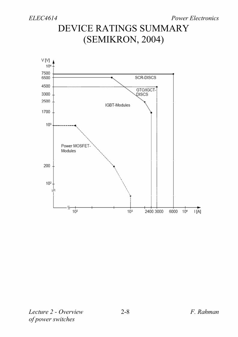
Switching a diode-clamped circuit
The load current Io is assumed to remain constant while the switch turns ON and OFF with a duty cycle at the switching frequency fs.
We assume:
• ideal devices and no reverse recovery current in the diode.
• Io = iT + iD at all time.
• Voltage vT(t) and current iT(t) transients at turn-on and turn-off occur along straight tines.
When the switch T is turned on, the diode continues to carry part of Io as iT builds up. Until iT becomes equal to Io, the diode remains in the conducting state (i.e., forward biased). The diode starts to become reverse biased after Io fully commutates to T in time tri. Thus, while iT rises from zero to Io, vT remains clamped to Vd. Once Io fully commutates to T, the voltage vT (or vAK) across switch falls to zero in time tfv.
Vd
Io Ideal Diode, D
iT
vT
iD
T

ELEC4614 Power Electronics
Lecture 2 - Overview 2-19 F. Rahman of power switches
When the switch T is turned off, the diode does not conduct until the potential at the cathode of diode D rises to Vd. Thus, diode D remains reverse biased until vT rises to Vd in time trv. Thereafter, the diode becomes forward biased and starts to conduct. Thus, the current through T remains clamped to Io until vT rises to Vd in time trv. Until then iT = Io. Once vT rises to Vd, current iT falls to zero in time tfi. Note that diode clamping increases the areas of overlap during both transitions. The power loss in the switch is given by the product p = vT * iT, given by the shaded areas. Note also that the reverse recovery current of the diode at turn-on of T increases the peak current loading of switch T. The following analysis assumes ideal diode, i.e., the reverse recovery current of the diode is neglected.
The energy dissipated (power lost) in the switch during turn-on and turn-off transients can be found by multiplying the voltage vT(t) and current iT(t) of the switch and integrating the product over the duration of each transient. The calculation is simplified if the origin t = 0 for each case is shifted to time when the respective transitions begin, and if the on-state voltage of the switch is neglected in comparison with the DC supply voltage Vd.

ELEC4614 Power Electronics
Lecture 2 - Overview 2-20 F. Rahman of power switches
tdon
TON
TOFF
tri tfv
iT
IO Vd
iD
IO
vT
pT
VdIO
tdoff
Vd
trv tfi
on on o onW V I t=
con d o con1W V I t2
=
coff d o coff1W V I t2
=
tcoff = trv + tfi tcon=tri + tfv
Ts = s
1f
= TON + TOFF
ELEC4614 Power Electronics
Lecture 2 - Overview 2-21 F. Rahman of power switches
Thus, for turn-on transient,
dtttVItdt
tIVW ri fvt t
fvdo
ri
odons ∫ ∫ ⎟
⎟⎠
⎞⎜⎜⎝
⎛−+=
0 01 Joules
d o ri d o fv1 1V I t V I t2 2
= +
( )d o ri fv d o con1 1V I t t V I t2 2
= + = J
Similarly, it can be shown that for turn-off transient,
dtttIVtdt
tVIW rv fit t
fiod
rv
dooffs ∫ ∫ ⎟
⎟⎠
⎞⎜⎜⎝
⎛−+=
0 01 J
( )d o rv fi d o coff1 1V I t t V I t2 2
= + = J
The total switching power loss is thus given by
( ) scoffconodsw fttIVP ×+= 21 W
If the turn-on and turn-off transients are not short compared to Ts, the average power loss in the switching process, Ps, may become large compared to the loss during the ON time.
( )sw d o s con coff1P V I f t t2
= + The on-state power loss is given by

ELEC4614 Power Electronics
Lecture 2 - Overview 2-22 F. Rahman of power switches
on on o on sP V I t f= W where ton is the on-time of the switch in a switching period. Note that Psw increases proportionately with fs, while PON does not, since Ton and fs are inversely proportional to each other.
Related Documents