SEPTEMBER 2007 VOLUME 54 NUMBER 9 IETDAI (ISSN 0018-9383) SPECIAL ISSUE ON SIMULATION AND MODELING OF NANOELECTRONICS DEVICES

Welcome message from author
This document is posted to help you gain knowledge. Please leave a comment to let me know what you think about it! Share it to your friends and learn new things together.
Transcript
SEPTEMBER 2007 VOLUME 54 NUMBER 9 IETDAI (ISSN 0018-9383)
SPECIAL ISSUE ON SIMULATION AND MODELING OF NANOELECTRONICS DEVICES
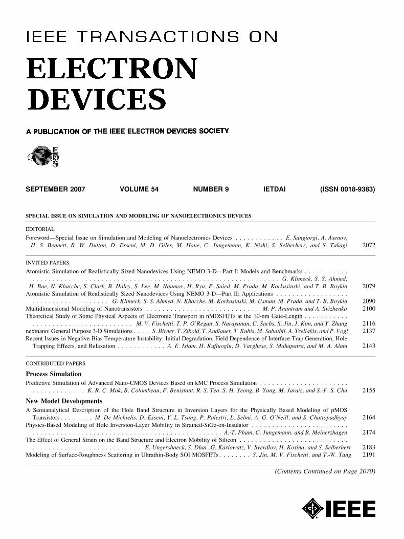
SEPTEMBER 2007 VOLUME 54 NUMBER 9 IETDAI (ISSN 0018-9383)
SPECIAL ISSUE ON SIMULATION AND MODELING OF NANOELECTRONICS DEVICES
EDITORIAL
Foreword—Special Issue on Simulation and Modeling of Nanoelectronics Devices . . . . . . . . . . . . E. Sangiorgi, A. Asenov,H. S. Bennett, R. W. Dutton, D. Esseni, M. D. Giles, M. Hane, C. Jungemann, K. Nishi, S. Selberherr, and S. Takagi 2072
INVITED PAPERS
Atomistic Simulation of Realistically Sized Nanodevices Using NEMO 3-D—Part I: Models and Benchmarks . . . . . . . . . . .
. . . . . . . . . . . . . . . . . . . . . . . . . . . . . . . . . . . . . . . . . . . . . . . . . . . . . . . . . . . . . G. Klimeck, S. S. Ahmed,H. Bae, N. Kharche, S. Clark, B. Haley, S. Lee, M. Naumov, H. Ryu, F. Saied, M. Prada, M. Korkusinski, and T. B. Boykin 2079
Atomistic Simulation of Realistically Sized Nanodevices Using NEMO 3-D—Part II: Applications . . . . . . . . . . . . . . . . . .
. . . . . . . . . . . . . . . . . . . G. Klimeck, S. S. Ahmed, N. Kharche, M. Korkusinski, M. Usman, M. Prada, and T. B. Boykin 2090Multidimensional Modeling of Nanotransistors . . . . . . . . . . . . . . . . . . . . . . . . . . . . M. P. Anantram and A. Svizhenko 2100Theoretical Study of Some Physical Aspects of Electronic Transport in nMOSFETs at the 10-nm Gate-Length . . . . . . . . . . .
. . . . . . . . . . . . . . . . . . . . . . . . . M. V. Fischetti, T. P. O’Regan, S. Narayanan, C. Sachs, S. Jin, J. Kim, and Y. Zhang 2116nextnano: General Purpose 3-D Simulations . . . . S. Birner, T. Zibold, T. Andlauer, T. Kubis, M. Sabathil, A. Trellakis, and P. Vogl 2137Recent Issues in Negative-Bias Temperature Instability: Initial Degradation, Field Dependence of Interface Trap Generation, Hole
Trapping Effects, and Relaxation . . . . . . . . . . . . A. E. Islam, H. Kufluoglu, D. Varghese, S. Mahapatra, and M. A. Alam 2143
CONTRIBUTED PAPERS
Process Simulation
Predictive Simulation of Advanced Nano-CMOS Devices Based on kMC Process Simulation . . . . . . . . . . . . . . . . . . . . . .
. . . . . . . . . . . . . K. R. C. Mok, B. Colombeau, F. Benistant, R. S. Teo, S. H. Yeong, B. Yang, M. Jaraiz, and S.-F. S. Chu 2155
New Model Developments
A Semianalytical Description of the Hole Band Structure in Inversion Layers for the Physically Based Modeling of pMOS
Transistors . . . . . . . . M. De Michielis, D. Esseni, Y. L. Tsang, P. Palestri, L. Selmi, A. G. O’Neill, and S. Chattopadhyay 2164Physics-Based Modeling of Hole Inversion-Layer Mobility in Strained-SiGe-on-Insulator . . . . . . . . . . . . . . . . . . . . . . . .
. . . . . . . . . . . . . . . . . . . . . . . . . . . . . . . . . . . . . . . . . . . . . . . A.-T. Pham, C. Jungemann, and B. Meinerzhagen 2174The Effect of General Strain on the Band Structure and Electron Mobility of Silicon . . . . . . . . . . . . . . . . . . . . . . . . . . .
. . . . . . . . . . . . . . . . . . . . . . . . . . . E. Ungersboeck, S. Dhar, G. Karlowatz, V. Sverdlov, H. Kosina, and S. Selberherr 2183Modeling of Surface-Roughness Scattering in Ultrathin-Body SOI MOSFETs . . . . . . . . S. Jin, M. V. Fischetti, and T.-W. Tang 2191
(Contents Continued on Page 2070)
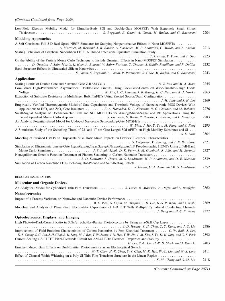
(Contents Continued from Page 2069)
Low-Field Electron Mobility Model for Ultrathin-Body SOI and Double-Gate MOSFETs With Extremely Small Silicon
Thicknesses . . . . . . . . . . . . . . . . . . . . . . . . . . . . . S. Reggiani, E. Gnani, A. Gnudi, M. Rudan, and G. Baccarani 2204
Modeling Approaches
A Self-Consistent Full 3-D Real-Space NEGF Simulator for Studying Nonperturbative Effects in Nano-MOSFETs . . . . . . . . .
. . . . . . . . . . . . . . . . . . A. Martinez, M. Bescond, J. R. Barker, A. Svizhenko, M. P. Anantram, C. Millar, and A. Asenov 2213Scaling Behaviors of Graphene Nanoribbon FETs: A Three-Dimensional Quantum Simulation Study . . . . . . . . . . . . . . . . . .
. . . . . . . . . . . . . . . . . . . . . . . . . . . . . . . . . . . . . . . . . . . . . . . . . . . . . . . . . . Y. Ouyang, Y. Yoon, and J. Guo 2223On the Ability of the Particle Monte Carlo Technique to Include Quantum Effects in Nano-MOSFET Simulation . . . . . . . . . .
. . . . . . D. Querlioz, J. Saint-Martin, K. Huet, A. Bournel, V. Aubry-Fortuna, C. Chassat, S. Galdin-Retailleau, and P. Dollfus 2232Band-Structure Effects in Ultrascaled Silicon Nanowires . . . . . . . . . . . . . . . . . . . . . . . . . . . . . . . . . . . . . . . . . . . . .
. . . . . . . . . . . . . . . . . . . . . . . . . E. Gnani, S. Reggiani, A. Gnudi, P. Parruccini, R. Colle, M. Rudan, and G. Baccarani 2243
Applications
Scaling Limits of Double-Gate and Surround-Gate Z-RAM Cells . . . . . . . . . . . . . . . . . . . . . . . N. Z. Butt and M. A. Alam 2255Low-Power High-Performance Asymmetrical Double-Gate Circuits Using Back-Gate-Controlled Wide-Tunable-Range Diode
Voltage . . . . . . . . . . . . . . . . . . . . . . . . . . . . . . . . K. Kim, C.-T. Chuang, J. B. Kuang, H. C. Ngo, and K. J. Nowka 2263Extraction of Substrate Resistance in Multifinger Bulk FinFETs Using Shorted Source/Drain Configuration . . . . . . . . . . . . . .
. . . . . . . . . . . . . . . . . . . . . . . . . . . . . . . . . . . . . . . . . . . . . . . . . . . . . . . . . . . . . . . J.-H. Jung and J.-H. Lee 2269Empirically Verified Thermodynamic Model of Gate Capacitance and Threshold Voltage of Nanoelectronic MOS Devices With
Applications to HfO2 and ZrO2 Gate Insulators . . . . . . . . E. A. Hamadeh, D. L. Niemann, N. G. Gunther, and M. Rahman 2276Small-Signal Analysis of Decananometer Bulk and SOI MOSFETs for Analog/Mixed-Signal and RF Applications Using the
Time-Dependent Monte Carlo Approach . . . . . . . . . . . . . S. Eminente, N. Barin, P. Palestri, C. Fiegna, and E. Sangiorgi 2283An Analytic Potential-Based Model for Undoped Nanoscale Surrounding-Gate MOSFETs . . . . . . . . . . . . . . . . . . . . . . . .
. . . . . . . . . . . . . . . . . . . . . . . . . . . . . . . . . . . . . . . . . . . . . . . . . W. Bian, J. He, Y. Tao, M. Fang, and J. Feng 2293A Simulation Study of the Switching Times of 22- and 17-nm Gate-Length SOI nFETs on High Mobility Substrates and Si . . .
. . . . . . . . . . . . . . . . . . . . . . . . . . . . . . . . . . . . . . . . . . . . . . . . . . . . . . . . . . . . . . . . . . . . . . . . S. E. Laux 2304Modeling of Strained CMOS on Disposable SiGe Dots: Strain Impacts on Devices’ Electrical Characteristics . . . . . . . . . . . .
. . . . . . . . . . . . . . . . . . . . . . . . . . . . . . . . . . . . . . . . . . . . . . . . . . S. Fregonese, Y. Zhuang, and J. N. Burghartz 2321Simulation of Ultrasubmicrometer-Gate In0:52Al0:48As/In0:75Ga0:25As/In0:52Al0:48As/InP Pseudomorphic HEMTs Using a Full-Band
Monte Carlo Simulator . . . . . . . . . . . . . . . . . . J. S. Ayubi-Moak, D. K. Ferry, S. M. Goodnick, R. Akis, and M. Saraniti 2327Nonequilibrium Green’s Function Treatment of Phonon Scattering in Carbon-Nanotube Transistors . . . . . . . . . . . . . . . . . . .
. . . . . . . . . . . . . . . . . . . . . . . . . . . . S. O. Koswatta, S. Hasan, M. S. Lundstrom, M. P. Anantram, and D. E. Nikonov 2339Simulation of Carbon Nanotube FETs Including Hot-Phonon and Self-Heating Effects . . . . . . . . . . . . . . . . . . . . . . . . . . .
. . . . . . . . . . . . . . . . . . . . . . . . . . . . . . . . . . . . . . . . . . . . . . . . . . . S. Hasan, M. A. Alam, and M. S. Lundstrom 2352
REGULAR ISSUE PAPERS
Molecular and Organic Devices
An Analytical Model for Cylindrical Thin-Film Transistors . . . . . . . . . . . S. Locci, M. Maccioni, E. Orgiu, and A. Bonfiglio 2362
Nanoelectronics
Impact of a Process Variation on Nanowire and Nanotube Device Performance . . . . . . . . . . . . . . . . . . . . . . . . . . . . . . .
. . . . . . . . . . . . . . . . . . . . . . . . . . . . . . . . . B. C. Paul, S. Fujita, M. Okajima, T. H. Lee, H.-S. P. Wong, and Y. Nishi 2369Modeling and Analysis of Planar-Gate Electrostatic Capacitance of 1-D FET With Multiple Cylindrical Conducting Channels
. . . . . . . . . . . . . . . . . . . . . . . . . . . . . . . . . . . . . . . . . . . . . . . . . . . . . . . . . . . . . J. Deng and H.-S. P. Wong 2377
Optoelectronics, Displays, and Imaging
High Photo-to-Dark-Current Ratio in SiGe/Si Schottky-Barrier Photodetectors by Using an a-Si:H Cap Layer . . . . . . . . . . . .
. . . . . . . . . . . . . . . . . . . . . . . . . . . . . . . . . . . . . . . . . . . . . . J.-D. Hwang, Y. H. Chen, C. Y. Kung, and J. C. Liu 2386Improvement of Field-Emission Characteristics of Carbon Nanotubes by Post Electrical Treatment . . . . . C.-W. Baik, J. Lee,
D. S. Chung, S. C. Jun, J. H. Choi, B. K. Song, M. J. Bae, T. W. Jeong, J. N. Heo, Y. W. Jin, J.-M. Kim, S. Yu, K.-H. Jang, and G.-S. Park 2392Current-Scaling a-Si:H TFT Pixel-Electrode Circuit for AM-OLEDs: Electrical Properties and Stability . . . . . . . . . . . . . . . .
. . . . . . . . . . . . . . . . . . . . . . . . . . . . . . . . . . . . . . . . . . . . . . . . H. Lee, Y.-C. Lin, H.-P. D. Shieh, and J. Kanicki 2403Emitter-Induced Gain Effects on Dual-Emitter Phototransistor as an Electrooptical Switch . . . . . . . . . . . . . . . . . . . . . . . .
. . . . . . . . . . . . . . . . . . . . . . . . . . . . . . . . W.-T. Chen, H.-R. Chen, S.-Y. Chiu, M.-K. Hsu, W.-C. Liu, and W.-S. Lour 2411Effect of Channel-Width Widening on a Poly-Si Thin-Film Transistor Structure in the Linear Region . . . . . . . . . . . . . . . . .
. . . . . . . . . . . . . . . . . . . . . . . . . . . . . . . . . . . . . . . . . . . . . . . . . . . . . . . . . . . . . K.-M. Chang and G.-M. Lin 2418
(Contents Continued on Page 2071)
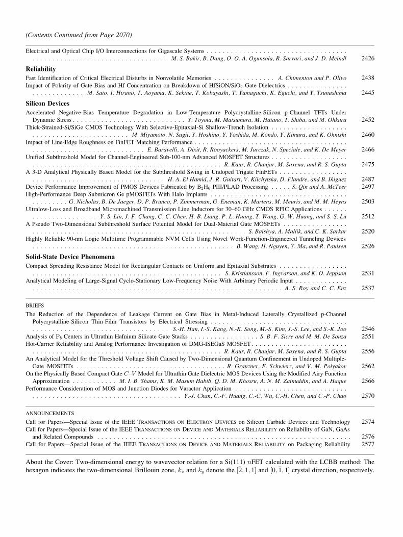
(Contents Continued from Page 2070)
Electrical and Optical Chip I/O Interconnections for Gigascale Systems . . . . . . . . . . . . . . . . . . . . . . . . . . . . . . . . . . .
. . . . . . . . . . . . . . . . . . . . . . . . . . . . . . . . . . M. S. Bakir, B. Dang, O. O. A. Ogunsola, R. Sarvari, and J. D. Meindl 2426
Reliability
Fast Identification of Critical Electrical Disturbs in Nonvolatile Memories . . . . . . . . . . . . . . . A. Chimenton and P. Olivo 2438Impact of Polarity of Gate Bias and Hf Concentration on Breakdown of HfSiON/SiO2 Gate Dielectrics . . . . . . . . . . . . . . .
. . . . . . . . . . . . . M. Sato, I. Hirano, T. Aoyama, K. Sekine, T. Kobayashi, T. Yamaguchi, K. Eguchi, and Y. Tsunashima 2445
Silicon Devices
Accelerated Negative-Bias Temperature Degradation in Low-Temperature Polycrystalline-Silicon p-Channel TFTs Under
Dynamic Stress . . . . . . . . . . . . . . . . . . . . . . . . . . . . Y. Toyota, M. Matsumura, M. Hatano, T. Shiba, and M. Ohkura 2452Thick-Strained-Si/SiGe CMOS Technology With Selective-Epitaxial-Si Shallow-Trench Isolation . . . . . . . . . . . . . . . . . . .
. . . . . . . . . . . . . . . . . . . . . . . . M. Miyamoto, N. Sugii, Y. Hoshino, Y. Yoshida, M. Kondo, Y. Kimura, and K. Ohnishi 2460Impact of Line-Edge Roughness on FinFET Matching Performance . . . . . . . . . . . . . . . . . . . . . . . . . . . . . . . . . . . . . .
. . . . . . . . . . . . . . . . . . . . . . . . . . . . E. Baravelli, A. Dixit, R. Rooyackers, M. Jurczak, N. Speciale, and K. De Meyer 2466Unified Subthreshold Model for Channel-Engineered Sub-100-nm Advanced MOSFET Structures . . . . . . . . . . . . . . . . . . .
. . . . . . . . . . . . . . . . . . . . . . . . . . . . . . . . . . . . . . . . . . . . . . . R. Kaur, R. Chaujar, M. Saxena, and R. S. Gupta 2475A 3-D Analytical Physically Based Model for the Subthreshold Swing in Undoped Trigate FinFETs . . . . . . . . . . . . . . . . .
. . . . . . . . . . . . . . . . . . . . . . . . . . . . . . . . . H. A. El Hamid, J. R. Guitart, V. Kilchytska, D. Flandre, and B. Iniguez 2487Device Performance Improvement of PMOS Devices Fabricated by B2H6 PIII/PLAD Processing . . . . . S. Qin and A. McTeer 2497High-Performance Deep Submicron Ge pMOSFETs With Halo Implants . . . . . . . . . . . . . . . . . . . . . . . . . . . . . . . . . .
. . . . . . . . . G. Nicholas, B. De Jaeger, D. P. Brunco, P. Zimmerman, G. Eneman, K. Martens, M. Meuris, and M. M. Heyns 2503Ultralow-Loss and Broadband Micromachined Transmission Line Inductors for 30–60 GHz CMOS RFIC Applications . . . . . .
. . . . . . . . . . . . . . . . Y.-S. Lin, J.-F. Chang, C.-C. Chen, H.-B. Liang, P.-L. Huang, T. Wang, G.-W. Huang, and S.-S. Lu 2512A Pseudo Two-Dimensional Subthreshold Surface Potential Model for Dual-Material Gate MOSFETs . . . . . . . . . . . . . . . .
. . . . . . . . . . . . . . . . . . . . . . . . . . . . . . . . . . . . . . . . . . . . . . . . . . . . . S. Baishya, A. Mallik, and C. K. Sarkar 2520Highly Reliable 90-nm Logic Multitime Programmable NVM Cells Using Novel Work-Function-Engineered Tunneling Devices
. . . . . . . . . . . . . . . . . . . . . . . . . . . . . . . . . . . . . . . . . . . . . . . . . . B. Wang, H. Nguyen, Y. Ma, and R. Paulsen 2526
Solid-State Device Phenomena
Compact Spreading Resistance Model for Rectangular Contacts on Uniform and Epitaxial Substrates . . . . . . . . . . . . . . . . .
. . . . . . . . . . . . . . . . . . . . . . . . . . . . . . . . . . . . . . . . . . . . . . . S. Kristiansson, F. Ingvarson, and K. O. Jeppson 2531Analytical Modeling of Large-Signal Cyclo-Stationary Low-Frequency Noise With Arbitrary Periodic Input . . . . . . . . . . . . .
. . . . . . . . . . . . . . . . . . . . . . . . . . . . . . . . . . . . . . . . . . . . . . . . . . . . . . . . . . . . . . A. S. Roy and C. C. Enz 2537
BRIEFS
The Reduction of the Dependence of Leakage Current on Gate Bias in Metal-Induced Laterally Crystallized p-Channel
Polycrystalline-Silicon Thin-Film Transistors by Electrical Stressing . . . . . . . . . . . . . . . . . . . . . . . . . . . . . . . . . .
. . . . . . . . . . . . . . . . . . . . . . . . . . . . . . . . . . S.-H. Han, I.-S. Kang, N.-K. Song, M.-S. Kim, J.-S. Lee, and S.-K. Joo 2546Analysis of Pb Centers in Ultrathin Hafnium Silicate Gate Stacks . . . . . . . . . . . . . . . . . S. B. F. Sicre and M. M. De Souza 2551Hot-Carrier Reliability and Analog Performance Investigation of DMG-ISEGaS MOSFET. . . . . . . . . . . . . . . . . . . . . . . .
. . . . . . . . . . . . . . . . . . . . . . . . . . . . . . . . . . . . . . . . . . . . . . . R. Kaur, R. Chaujar, M. Saxena, and R. S. Gupta 2556An Analytical Model for the Threshold Voltage Shift Caused by Two-Dimensional Quantum Confinement in Undoped Multiple-
Gate MOSFETs . . . . . . . . . . . . . . . . . . . . . . . . . . . . . . . . . . . . . R. Granzner, F. Schwierz, and V. M. Polyakov 2562On the Physically Based Compact Gate C–V Model for Ultrathin Gate Dielectric MOS Devices Using the Modified Airy Function
Approximation . . . . . . . . . . . M. I. B. Shams, K. M. Masum Habib, Q. D. M. Khosru, A. N. M. Zainuddin, and A. Haque 2566Performance Consideration of MOS and Junction Diodes for Varactor Application . . . . . . . . . . . . . . . . . . . . . . . . . . . .
. . . . . . . . . . . . . . . . . . . . . . . . . . . . . . . . . . . . . Y.-J. Chan, C.-F. Huang, C.-C. Wu, C.-H. Chen, and C.-P. Chao 2570
ANNOUNCEMENTS
Call for Papers—Special Issue of the IEEE TRANSACTIONS ON ELECTRON DEVICES on Silicon Carbide Devices and Technology 2574Call for Papers—Special Issue of the IEEE TRANSACTIONS ON DEVICE AND MATERIALS RELIABILITY on Reliability of GaN, GaAs
and Related Compounds . . . . . . . . . . . . . . . . . . . . . . . . . . . . . . . . . . . . . . . . . . . . . . . . . . . . . . . . . . . . . . . 2576Call for Papers—Special Issue of the IEEE TRANSACTIONS ON DEVICE AND MATERIALS RELIABILITY on Packaging Reliability 2577
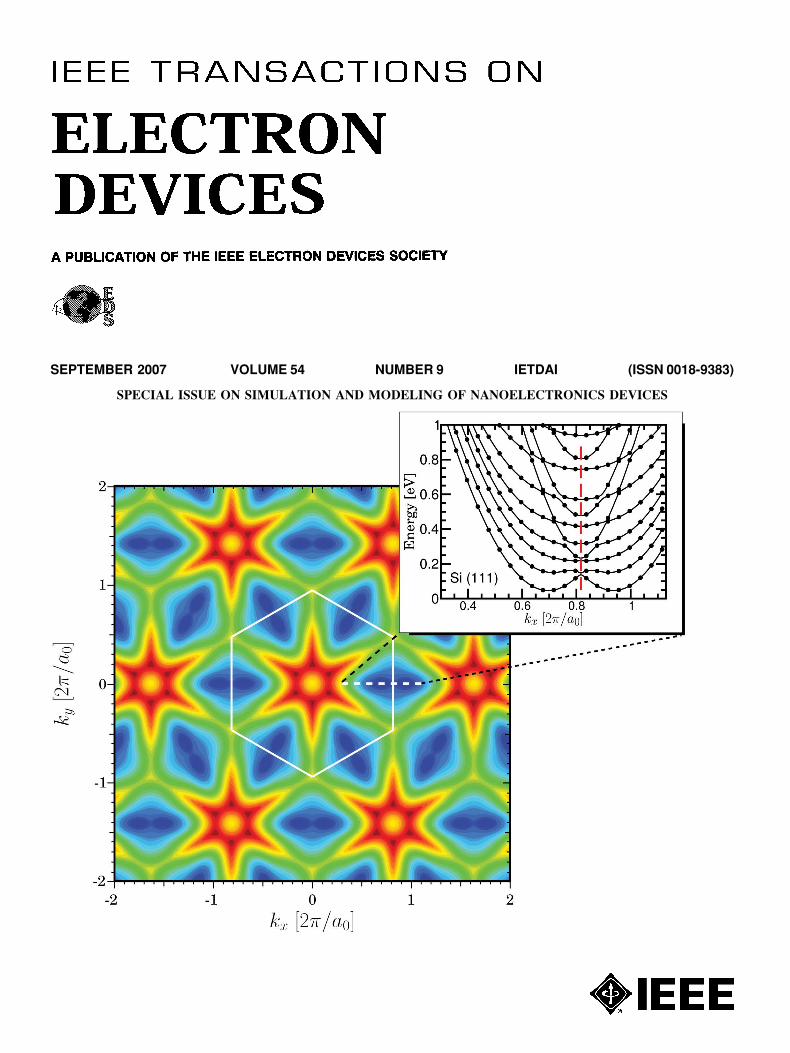
About the Cover: Two-dimensional energy to wavevector relation for a Si(111) nFET calculated with the LCBB method: The
hexagon indicates the two-dimensional Brillouin zone, kx and ky denote the ½2; 1; 1� and ½0; 1; 1� crystal direction, respectively.
2072 IEEE TRANSACTIONS ON ELECTRON DEVICES, VOL. 54, NO. 9, SEPTEMBER 2007
ForewordSpecial Issue on Simulation and Modeling
of Nanoelectronics Devices
THIS SPECIAL Issue is devoted to research activitiesin the field of simulation and modeling of nanoscale
electronic devices. According to the 2006 update of the In-ternational Technology Roadmap for Semiconductors (ITRS),microprocessing units with physical gate lengths of 18, 10,and 6 nm will be produced in 2010, 2015, and 2020, respec-tively. New device architectures will be required to reach theperformance of the future technology generations that the ITRSprescribes. In addition, control of gate leakage current requiresthe introduction of gate insulators with high dielectric con-stants, and the need for increased carrier mobility pushes the useof unconventional channel materials and processing to induceappropriate stresses. Finally, in the longer term, the traditionalMOSFET concept might be replaced by other structures likenanowire MOSFETs and/or carbon nanotubes (CNTs).
In order to steer the above developments, the availability ofadvanced models and simulation tools is of utmost importancefor the following:
1) Early evaluations of the most promising device architec-tures and materials in terms of performance and potentialfor continued scaling.
2) Assessments of processing and design strategies.3) Reductions of cycle time and of R&D costs. Measure-
ments and tests at the nanoscale tend to be much moreexpensive than at the microscale and macroscale.
If models and simulation tools are to be suitable for theanalysis of future-generation CMOS and post-CMOS devices,such models and tools will have to cope with important issuesthat are presently recognized as difficult challenges by theModeling and Simulation section of the ITRS. In view of therapid technological changes in the CMOS and “beyond CMOS”areas that involve novel device structures and materials, theaim of this Special Issue is to bring together the advancesin the topic of “Simulation and Modeling of Nanoscale De-vices” to a device-oriented academic and industrial communityrepresented by the readers of the IEEE TRANSACTIONS ON
ELECTRON DEVICES. This Special Issue consists of 25 care-fully selected papers, 5 of which are invited and 20 of whichare contributed, that discuss topics like process modeling,device modeling, and atomistic modeling, and address issueslike reliability, manufacturability, and variability. The SpecialIssue starts with the five invited papers. In the first paper,entitled “Atomistic Simulation of Realistically Sized Nanode-vices Using NEMO 3-D—Part I: Models and Benchmarks,”Klimeck et al. discuss the essential components of the atomistic
Digital Object Identifier 10.1109/TED.2007.905342
simulator called NEMO and demonstrate its successful usein the calculations of single-particle electronic states of self-assembled quantum dots, stacked quantum dot systems usedin quantum cascade lasers, SiGe quantum wells for quantumcomputation, and SiGe nanowires. Using the nonequilibriumGreen’s function (NEGF) method to model nanotransistors,Anantram et al. review recent work in the next paper entitled“Multidimensional Modeling of Nanotransistors.” After givinga motivation for the need for quantum mechanical modeling, theauthors give an account of the equations and implementationfor both 1-D and 2-D modeling, and illustrate examples on theuse of the developed models. They highlight possible futuredirections in the quantum mechanical modeling of transport innanotransistors and summarize the computational challenges.In the third paper, which is entitled “Theoretical Study of SomePhysical Aspects of Electronic Transport in nMOSFETs at the10-nm Gate-Length,” Fischetti et al. discuss selected aspectsof the physics of electronic transport in MOSFETs at the10-nm scale, such as long-range Coulomb interactions, scat-tering with high-κ insulator interfacial modes, and use of ahigh-mobility substrate that is accompanied by the detrimentaleffect of a limited density of states. The fourth paper byBirner et al., which is entitled “nextnano: General Purpose 3-DSimulations,” presents several applications that highlight thecapabilities of the Nextnano simulation software. Nextnano isa versatile software package for the simulation of nanometer-scale semiconductor quantum structures that focuses on nano-structures where quantum mechanical effects such as electronicband structures, optical matrix elements, magnetic field effects,or tunneling effects play a vital role. In the last invited paper,which is entitled “Recent Issues in Negative-Bias TemperatureInstability: Initial Degradation, Field Dependence of InterfaceTrap Generation, Hole Trapping Effects, and Relaxation,” Is-lam et al. discuss recent advances in measurement techniques,availability of new data, and refinements in the modeling ap-proach that allow the authors to provide a systematic analysisof experimental data based on a comprehensive theoreticalfoundation of negative-bias temperature instability degradation.
Next, there are 20 contributed papers included in this SpecialIssue. The first one, which is entitled “Predictive Simulationof Advanced Nano-CMOS Devices Based on kMC ProcessSimulation” by Mok et al., deals with process simulation.In this paper, accurate and advanced CMOS process and de-vice simulations based on an atomistic kinetic Monte Carlo(kMC) process simulator are presented. First, the methodologyused to predict continuum 2-D/3-D doping profiles from 3-Datomistic distribution that can be directly transferred fromprocess to device simulator is described. Then, a comparison
0018-9383/$25.00 © 2007 IEEE
IEEE TRANSACTIONS ON ELECTRON DEVICES, VOL. 54, NO. 9, SEPTEMBER 2007 2073
with a wide range of electrical device characteristics shows thatthe experimental results were remarkably well reproduced bythe simulations.
The next five papers cover new model developments withthe first one by De Michielis et al., which is entitled “ASemi-analytical Description of the Hole Band Structure inInversion Layers for the Physically Based Modeling of pMOSTransistors,” which presents a new semi-analytical model forthe energy dispersion of holes in the inversion layer of pMOStransistors. In the next paper, which is entitled “Physics-BasedModeling of Hole Inversion Layer Mobility in Strained SiGe onInsulator,” Pham et al. model the hole inversion layer mobilityof strained SiGe on the insulator in ultrathin-body hetero-structure MOSFETs by a microscopic approach that takes intoaccount the subband structure of the 2-D hole gas and threeimportant scattering mechanisms, i.e., optical and acousticphonons, and surface roughness. The third paper, which isentitled “The Effect of General Strain on Band Structure andElectron Mobility of Silicon” by Ungersboeck et al., presentsa model that captures the effect of general strain on the elec-tron effective masses and band edge energies of the lowestconduction band of silicon (Si). The model includes analyticalexpressions for the effective mass change induced by shearstrain and valley shift splitting, which is obtained using a de-generate k·p-theory at the zone boundary X point. In the fourthpaper, which is entitled “Modeling of Surface-Roughness Scat-tering in Ultrathin-Body SOI MOSFETs,” Jin et al. presenta rigorous surface roughness scattering model for ultrathin-body silicon-on-insulator (SOI) MOSFETs, which reduces tothe well-known Ando’s model in case of bulk MOSFETs.The last paper of this group, which is entitled “Low-FieldElectron Mobility Model for Ultrathin-Body SOI and Double-Gate MOSFETs With Extremely Small Silicon Thicknesses”by Reggiani et al., presents a compact model for mobilitythat is suited for implementation in device simulators, whichaccurately predicts the low-field mobility in SOI single- anddouble-gate MOSFETs with Si thickness down to 2.48 nm.
Next, four papers dealing with modeling approaches fol-low. The first paper of this group, which is entitled “ASelf-Consistent Full 3-D Real-Space NEGF Simulator forStudying Nonperturbative Effects in Nano-MOSFETs” byMartinez et al., presents a full 3-D real-space quantum transportsimulator based on the Green’s function formalism that is devel-oped to study the nonperturbative effects in nanotransistors inthe ballistic transport approximation. In the next paper, which isentitled “Scaling Behaviors of Graphene Nanoribbon FETs: AThree-Dimensional Quantum Simulation Study,” Ouyang et al.study the scaling behavior of Graphene nanoribbon Schottkybarrier FET by using the NEGF approach in an atomistic basisset self-consistently with a 3-D Poisson equation. The thirdpaper of this group, which is entitled “On the Ability of theParticle Monte Carlo Technique to Include Quantum Effectsin Nano-MOSFET Simulation” by Querlioz et al., reports onthe possibility to use particle-based Monte-Carlo techniques toincorporate all relevant quantum effects in the simulation ofsemiconductor nanotransistors. Starting from the conventionalMonte-Carlo approach within the semiclassical Boltzmann ap-proximation, the authors develop a multi-subband description
of transport to include quantization in ultrathin-body devices.This technique is then extended to the particle simulation ofquantum transport within the Wigner formulation. In the lastpaper of this group, which is entitled “Band-Structure Effectsin Ultrascaled Silicon Nanowires,” Gnani et al. investigatethe effects of the full-band structure on the transport proper-ties of ultrascaled silicon nanowire FETs operating under thequantum-ballistic limit assumption.
The final ten papers cover various applications. The firstpaper, which is entitled “Scaling Limits of Double-Gate andSurround-Gate Z-RAM Cells” by Butt et al., evaluates the scal-ing limits of capacitorless single-transistor DRAM cells havingsurrounded gate and double-gate structures. The paper showsthat the scaling is limited for both structures to the channellength of 25 nm due to the combined effects of short channel,quantum confinement of carriers in the body, and band-to-bandtunneling at the source/drain to body junctions. In the nextpaper, which is entitled “Low-Power High-Performance Asym-metrical Double-Gate Circuits Using Back-Gate-ControlledWide-Tunable-Range Diode Voltage,” Kim et al. present a newpower reduction scheme using a back-gate-controlled asym-metrical double-gate device for high-performance logic/SRAMpower gating or variable/dynamic supply applications. Numer-ical mix-mode device/circuit simulations confirm that the pro-posed scheme can be applied for low-power high-performancecircuit applications in the 65-nm technology node and beyond.In the third paper, which is entitled “Extraction of SubstrateResistance in Multifinger Bulk FinFETs Using ShortedSource/Drain Configuration” by Jung et al., the substrate resis-tances of highly scaled bulk FinFETs are extracted by using anew RF equivalent circuit verified by 3-D device simulations.The proposed method shows frequency-independent substrateresistances in highly scaled devices and has been verified upto 50 GHz in devices operating in the saturation region. In thefourth paper, which is entitled “Empirically Verified Thermo-dynamic Model of Gate Capacitance and Threshold Voltage ofNanoelectronic MOS Devices With Applications to HfO2 andZrO2 Gate Insulators” by Hamadeh et al., a thermodynamicvariational model derived from minimizing the Helmholtz freeenergy of the MOS device is presented. The model incorporatesan anisotropic permittivity tensor and accommodates a correc-tion for quantum mechanical charge confinement at the dielec-tric/substrate interface. The model is verified using empiricaland TCAD capacitance–voltage data obtained on MOS deviceswith ZrO2, HfO2, and SiO2 gate insulators. In the fifth paperby Eminente et al., which is entitled “Small-Signal Analysis ofDecananometer Bulk and SOI MOSFETs for Analog/Mixed-Signal and RF Applications Using the Time-Dependent MonteCarlo Approach,” a state-of-the-art Monte Carlo simulatoris applied to the investigation of RF performance of bulkand ultrathin-body single-gate SOI MOSFETs designed foranalog and mixed-signal applications. A comparison witha standard drift diffusion approach is presented in order todiscuss the main differences between the two transport modelsin terms of high-frequency ac analysis. In the next paper,which is entitled “An Analytic Potential-Based Model forUndoped Nanoscale Surrounding-Gate MOSFETs,” He et al.present a complete potential-based analytic model of the
2074 IEEE TRANSACTIONS ON ELECTRON DEVICES, VOL. 54, NO. 9, SEPTEMBER 2007
undoped nanoscale surrounding-gate MOSFETs derived froma fully self-consistent physical description between potential,charge, and current formulations. The derivation is based on therigorous Poisson equation solution and drain current procedureequivalent to the Pao-Sah current double integral formulation.The validity of the analytic model has been verified by com-parison with TCAD simulations. The seventh paper, whichis entitled “A Simulation Study of the Switching times of22- and 17-nm Gate-Length SOI nFETs on High MobilitySubstrates and Si” by Laux, reports the analysis of the switch-ing times of ultrathin-body SOI nFETs with 22- and 17-nmgate lengths, and compares the results obtained for four high-mobility substrates (Ge, GaAs, InP, and In0.53Ga0.47As) to Si.From the extrinsic device results, it is found that at a 22-nm gatelength, the switching times for the considered semiconductorsvary at most by a factor of 2, while at 17 nm, they varyby at most a factor of 2.5. In both cases, In0.53Ga0.47Asprovides the best and Si the worst switching times. In thenext paper, which is entitled “Modeling of Strained CMOSon Diposable SiGe Dots: Strain Impacts on Devices’ Electri-cal Characteristics,” Fregonese et al. propose a novel CMOSdevice concept formed on a disposable SiGe dot structure, inwhich the degree of local strain effect on the performance ofboth NMOS and PMOS can be optimized by incorporatingwith silicon-on-nothing technology. Verified from a detailedsimulation study including a dual stress liner process, the paperdemonstrates a step to the next-generation CMOS performanceto be taken without reducing channel lengths. In the ninth pa-per, which is entitled “Simulation of Ultrasubmicrometer-GateIn0.52Al0.48As/In0.75Ga0.25As/In0.52Al0.48As/InP Pseudomor-phic HEMTs Using a Full-Band Monte Carlo Simulator,”Ayubi-Moak et al. model pseudomorphic delta-doped 0.07-µm-gate HEMTs using a full-band cellular Monte-Carlo simulator.A peak transconductance of 1679 mS/mm is extracted fromsimulation results, and an fT of 212 GHz is estimated fromthe gate capacitance, which shows excellent agreement withrecent device measurements. In the next paper, which is enti-tled “Nonequilibrium Green’s Function Treatment of PhononScattering in Carbon-Nanotube Transistors,” Koswatta et al.explore the dissipative quality of quantum transport in carbonnanotube FETs. They find that the effect of phonon scatteringon device performance has a bias dependence. Up to moderategate biases device current is reduced due to elastic back-scattering by acoustic phonons and low-energy radial breathingmode phonons. At large gate biases the current degradation ismainly due to high-energy optical phonon scattering. In thelast paper of this Special Issue, which is entitled “Simulationof Carbon Nanotube FETs Including Hot-Phonon and Self-Heating Effects,” Hasan et al. study the effects of nonequi-librium population of optical phonon (hot-phonon effect) andacoustic phonon (self-heating effect) on the dc performanceof CNT MOSFET by solving coupled, semiclassical elec-tron, and phonon transport equations. Full-band electron andphonon Boltzmann transport equations are solved to simulatethe electron and phonon transports. The results of this papershow that the dc ballisticity of a CNT MOSFET degrades byapproximately 10% due to hot-phonon effects.
The members of the IEEE Electron Device Society TCADTechnical Committee, Guest Editors for this Special Issue,
would like to thank the authors for their work in submittingand revising their manuscripts. We would also wish to expressour deepest gratitude to our reviewers for their efforts anddedication. This issue would not have been possible withouttheir expert advice. The supporting work from Jo Ann Marsh ofthe EDS Office is also greatly appreciated.
ENRICO SANGIORGI, Guest EditorFaculty of EngineeringUniversity of Bologna47023 Casena, Italy
ASEN ASENOV, Guest EditorDepartment of Electronics and Electrical EngineeringGlasgow UniversityG12 8QQ, Glasgow, U.K.
HERBERT S. BENNETT, Guest EditorSemiconductor Electronics Division, Electronics andElectrical Engineering LaboratoryNational Institute of Standards and TechnologyGaithersburg, MD 20899-8110 USA
ROBERT W. DUTTON, Guest EditorIntegrated Circuits LaboratoryStanford UniversityStanford, CA 94305-4075 USA
DAVID ESSENI, Guest EditorDipartimento di Ingegneria Elettrica,Gestionale e MeccanicaUniversity of Udinev33100 Udine, Italy
MARTIN D. GILES, Guest EditorTechnology CAD DivisionIntel CorporationHillsboro, OR 97124 USA
MASAMI HANE, Guest EditorSystem Devices Research LaboratoriesNEC CorporationSagamihara 229-1198, Japan
CHRISTOPH JUNGEMANN, Guest EditorInstitut für ElektronikUniversität der Bundeswehr85577 Neubiberg, Germany
KENJI NISHI, Guest EditorDepartment of General Science and HumanitiesKinki University Technical CollegeMie 519-4395, Japan
SIEGFRIED SELBERHERR, Guest EditorInstitute for MicroelectronicsTechnical University of Vienna1040 Vienna, Austria
SHINICHI TAKAGI, Guest EditorGraduate School of Frontier ScienceUniversity of TokyoTokyo 113-8656, Japan
IEEE TRANSACTIONS ON ELECTRON DEVICES, VOL. 54, NO. 9, SEPTEMBER 2007 2075
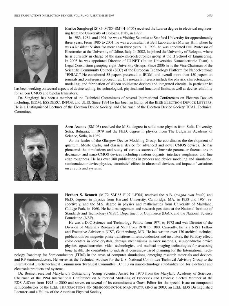
Enrico Sangiorgi (S’85–M’85–SM’01–F’05) received the Laurea degree in electrical engineer-ing from the University of Bologna, Italy, in 1979.
In 1983, 1984, and 1991, he was a Visiting Scientist at Stanford University for approximatelythree years. From 1985 to 2001, he was a consultant at Bell Laboratories Murray Hill, where hewas a Resident Visitor for more than three years. In 1993, he was appointed Full Professor ofElectronics at the University of Udine, Italy. In 2002, he joined the University of Bologna, wherehe is currently in charge of the nano- microelectronics group at the II School of Engineering.In 2005 he was appointed Director of IU.NET (Italian Universities Nanoelectronic Team), aLegal Consortium grouping eight University Groups. Since 2006 he is the Vice Chairman of theScientific Community Council (SCC) of the European Technology Platform for Nanoelectronic“ENIAC.” He coauthored 33 papers presented at IEDM, and overall more than 150 papers onjournals and conference proceedings. His research interests include the physics, characterization,modeling, and fabrication of silicon solid-state devices and integrated circuits. In particular he
has been working on several aspects of device scaling, its technological, physical, and functional limits, as well as device reliabilityfor silicon CMOS and bipolar transistors.
Dr. Sangiorgi has been a member of the Technical Committees of several International Conferences on Electron Devicesincluding: IEDM, ESSDERC, INFOS, and ULIS. Since 1994 he has been an Editor of the IEEE ELECTRON DEVICE LETTERS.He is a Distinguished Lecturer of the Electron Device Society, and Chairman of the Electron Device Society TCAD TechnicalCommittee.
Asen Asenov (SM’03) received the M.Sc. degree in solid-state physics from Sofia University,Sofia, Bulgaria, in 1979 and the Ph.D. degree in physics from The Bulgarian Academy ofScience, Sofia, in 1989.
As the leader of the Glasgow Device Modeling Group, he coordinates the development ofquantum, Monte Carlo, and classical device for advanced and novel CMOS devices. He haspioneered the simulations and study of various sources of intrinsic parameter fluctuations indecanano- and nano-CMOS devices including random dopants, interface roughness, and lineedge roughness. He has over 380 publications in process and device modeling and simulation,semiconductor device physics, “atomistic” effects in ultrasmall devices, and impact of variationson circuits and systems.
Herbert S. Bennett (M’72–SM’85–F’97–LF’04) received the A.B. (magna cum laude) andPh.D. degrees in physics from Harvard University, Cambridge, MA, in 1958 and 1964, re-spectively, and the M.S. degree in physics and mathematics from University of Maryland,College Park, in 1960. He held management and research positions at the National Institute ofStandards and Technology (NIST), Department of Commerce (DoC), and the National ScienceFoundation (NSF).
He was a DoC Science and Technology Fellow from 1971 to 1972 and was Director of theDivision of Materials Research at NSF from 1978 to 1980. Currently, he is a NIST Fellowand Executive Advisor at NIST, Gaithersburg, MD. He has written over 130 archival technicalpublications on magnetic phase transitions in semiconductors and insulators, the Faraday effect,color centers in ionic crystals, damage mechanisms in laser materials, semiconductor devicephysics, optoelectronics, video technologies, and medical imaging technologies for assessingbone health. He contributes to industrial consensus-based planning for the International Tech-
nology Roadmap for Semiconductors (ITRS) in the areas of computer simulations, emerging research materials and devices,and RF semiconductors. He serves as the Technical Advisor for the U.S. National Committee Technical Advisory Group to theInternational Electrotechnical Commission Technical Committee TC 113 on nanotechnology standardization for electrical andelectronic products and systems.
Dr. Bennett received Maryland’s Outstanding Young Scientist Award for 1970 from the Maryland Academy of Sciences;Chairman of the 1994 International Conference on Numerical Modeling of Processes and Devices; elected Member of theEDS AdCom from 1995 to 2000 and serves on several of its committees; a Guest Editor for the special issue on compoundsemiconductors of the IEEE TRANSACTIONS ON SEMICONDUCTOR MANUFACTURING in 2003; an IEEE EDS DistinguishedLecturer; and a Fellow of the American Physical Society.
2076 IEEE TRANSACTIONS ON ELECTRON DEVICES, VOL. 54, NO. 9, SEPTEMBER 2007
Robert W. Dutton received the B.S., M.S., and Ph.D. degrees from the University of California,Berkeley, in 1966, 1967, and 1970, respectively.
He held summer staff positions with Fairchild, Bell Telephone Laboratories, Hewlett-Packard,IBM Research, and Matsushita in 1967, 1973, 1975, 1977, and 1988, respectively. He is currentlya Professor of electrical engineering with Stanford University, Stanford, CA, and the Director ofResearch in the Center for Integrated Systems. He has published more than 200 journal articlesand graduated more than four dozen doctorate students. His research interests focus on integratedcircuit process, device, and circuit technologies—especially the use of computer-aided design(CAD) in device scaling and for RF applications.
Dr. Dutton was the Editor of the IEEE JOURNAL ON TECHNOLOGY IN COMPUTER AIDED
DESIGN from 1984 to 1986 and was elected to the National Academy of Engineering in 1991.He was the recipient of the 1987 IEEE J. J. Ebers and 1996 Jack Morton Awards, the 1988Guggenheim Fellowship to study in Japan, and the C&C Prize (Japan) in 2000. Most recently,
he received a Career Achievement Award in 2005 from the Semiconductor Industry Association (SIA) for sustained contributionsin support of research that is critical to SIA needs.
David Esseni (S’98–M’00–SM’06) received the Laurea degree and the Ph.D. degree in electronicengineering from the University of Bologna, Bologna, Italy, in 1994 and 1998, respectively.
In 2000, he was a Visiting Scientist with Bell Labs–Lucent Technologies, Murray Hill, NJ.Since 2005, he has been an Associate Professor with the University of Udine, Udine, Italy. Hisresearch contributions have included characterization techniques and modeling activities relatedto the hot-electron phenomena in MOSFETs and Flash memories, which touched several aspectsof the performance and reliability of devices. He has also investigated thin-oxide reliability andthe issue of the statistical distribution of SILC nonvolatile memories. More recently, he has beeninvolved in the experimental characterization and modeling of low-field mobility in advancedCMOS technologies and in the semiclassical transport modeling of nanometric MOSFETs.
Dr. Esseni served as a member of the technical committee of the International Electron DevicesMeeting (IEDM) in 2003 and 2004, is currently in the technical committee of the European Solid-State Device Research Conference (ESSDERC) and the International Reliability Physics (IRPS),
and is a member of the Technology Computer Aided Design Committee of the Electron Devices Society (EDS).
Martin D. Giles received the Ph.D. degree from Stanford University, Stanford, CA, in 1984.He was with AT&T Bell Laboratories in 1984 and the University of Michigan, Ann Arbor,
in 1990. Since 1994, he has been with Intel Corporation, Hillsboro, OR, where he is currently aSenior Principal Engineer in the Process Technology Modeling Department leading a group thatdevelops process models and device applications for advanced logic and memory technologies.His research interests include defect-coupled diffusion, stress effects on device transport, andchallenges in technology scaling.
IEEE TRANSACTIONS ON ELECTRON DEVICES, VOL. 54, NO. 9, SEPTEMBER 2007 2077
Masami Hane received the Ph.D. degree from Keio University, Yokohama, Japan, in 2003.In 1987, he was with the Microelectronics Research Laboratories, NEC Corporation,
Kawasaki, Japan. From 1993 to 1994, he was a Visiting Scholar with the Center for IntegratedSystems, Stanford University, Stanford, CA. From 1996 to 1999, he was a SELETE 3D-TCAD project member in Japan. Since joining NEC Corporation, Sagamihara, Japan, hehas been engaged in ULSI process/device modeling and scaled CMOS technology researchand development. He is currently a Principal Researcher in the Device Platforms ResearchLaboratories, NEC Corporation.
Dr. Hane is a member of the IEEE Electron Devices Society and the Japan Society of AppliedPhysics.
Christoph Jungemann (M’97–SM’06) received the Dipl.-Ing. and Dr.-Ing. degrees in electricalengineering from the Technical University of Aachen (RWTH Aachen), Aachen, Germany, in1990 and 1995, respectively, and the “venia legendi” degree in “Theoretische Elektrotechnik”from the University of Bremen, Bremen, Germany, in 2001.
From 1990 to 1995, he was a Research and Teaching Assistant with the “Institut fürTheoretische Elektrotechnik,” RWTH Aachen. From 1995 to 1997, he was with the Researchand Development Facility, Fujitsu Limited, Kawasaki, Japan. From 1997 to 2002, he was a ChiefEngineer with the “Institut für Theoretische Elektrotechnik und Mikroelektronik,” Universityof Bremen. From 2002 to 2003, he spent a one-year sabbatical with the Center for IntegratedSystems, Stanford University. From 2003 to 2006, he was a Research Associate with theTechnical University of Braunschweig, Braunschweig, Germany. Since 2006, he has been aFull Professor of microelectronics with Bundeswehr University, Munich, Germany. His mainresearch interests are full-band Monte-Carlo simulation of Si and SiGe devices, numerical device
modeling, transport in inversion layers, and noise modeling.Prof. Jungemann is a member of the Board of Editors of the IEEE TRANSACTIONS ON ELECTRON DEVICES and has served on
the technical program committees of the International Workshop on Computational Electronics (IWCE), the International ElectronDevices Meeting (IEDM), and the International Conference on Computer-Aided Design (ICCAD). He was the corecipient of theIEEE EDS Paul Rappaport Award in 2005.
Kenji Nishi (F’01) received the B.Eng. and Ph.D. degrees from Tokyo University, Tokyo, Japan,in 1973 and 1988, respectively, both in applied physics.
From 1973 to 2003, he was with OKI Electric Industry Company, Tokyo, Japan, where hewas first engaged in logic simulation and then in process/device development of bipolar devices.In 1979, he started his career in semiconductor process simulation. From 1982 to 1984, he wasa Visiting Scientist with the Massachusetts Institute of Technology (MIT), Cambridge. As hewas promoted to Manager in the 1990s, his work extended from semiconductor simulationto logic device development, semiconductor characterization, and reliability enhancement. In1999, he was the project leader of a 3-D simulation system development called ENEXSSwith major Japanese semiconductor companies. Since 2003, he has been with Kinki UniversityTechnical College, Mie, Japan, where he currently is a Professor and a Senior Vice-President. Hecoauthored more than 160 books, technical journals, and conference proceedings. He also is theholder of several patents.
Dr. Nishi served as a Technical Committee Member of the International Electron Devices Meeting (IEDM), the InternationalConference on Simulation of Semiconductor Processes and Devices (SISPAD), and the Asia and South Pacific Design AutomationConference (ASP-DAC), including program chair of SISPAD99. He currently serves as a peer-reviewer for New EnergyDevelopment Organization (NEDO).
2078 IEEE TRANSACTIONS ON ELECTRON DEVICES, VOL. 54, NO. 9, SEPTEMBER 2007
Siegfried Selberherr was born in Klosterneuburg, Austria, in 1955. He received the “Diplomin-genieur” degree in electrical engineering and the Doctoral degree in technical sciences from“Technische Universität Wien,” Wien, Austria, in 1978 and 1981, respectively.
Since 1984, he has been holding the “venia docendi” on computer-aided design. Since 1988,he has been the Chair Professor of the “Institut für Mikroelektronik.” From 1998 to 2005, hewas the Dean of the “Fakultät für Elektrotechnik und Informationstechnik.” His current researchinterests are modeling and simulation of problems for microelectronics engineering.
Shinichi Takagi (M’93) was born in Tokyo, Japan, on August 25, 1959. He received the B.S.,M.S., and Ph.D. degrees in electronic engineering from the University of Tokyo, Tokyo, Japan,in 1982, 1984, and 1987, respectively. His Ph.D. thesis involved the study on the surface carriertransport in MISFETs based on III–V semiconductors.
He was with the Toshiba Research and Development Center, Kawasaki, Japan, in 1987, wherehe has been engaged in the research on the device physics of Si MOSFETs, including the carriertransport in the inversion layer, the impact ionization phenomena, the hot carrier degradation, andthe electric properties of Si/SiO2 interface. From 1993 to 1995, he was a Visiting Scholar withStanford University, Stanford, CA, where he studied the Si/SiGe heterostructure devices. Sincereturning to the Ultralarge-Scale Integration Research Laboratories, he was also engaged in thephysics and technology of the reliability of SiO2, ferroelectric devices, and strained-Si MOSdevices. Since 2001, he has been working for the MIRAI Project, as the leader of Ultra-HighPerformance New Transistor Structures Theme. In October 2003, he moved to the University of
Tokyo, where he is currently working as a Professor in the Department of Electronic Engineering, School of Engineering. Hisrecent interests include the science and the technologies of advanced CMOS devices using new channel materials such as strainedSi, Ge, and III–Vs.
Dr. Takagi served on the technical program committee on several international conferences, including International ElectronDevice Meeting, International Reliability Physics Symposium, International Conference on Solid State Device, and Materialsand International Solid State Circuits Conference. He received five awards, 18th IBM Japan Science Award (2004), InternationalSolid State Circuits Conference Takuo Sugano Outstanding Paper Award (2004), 2003 Electron Devices Society George E. SmithAward, International Conference on Solid State Devices and Materials Paper Award (2002), and International Reliability PhysicsSymposium Outstanding Paper Award (1998). He is a member of the IEEE Electron Device Society and the Japan Society ofApplied Physics.
Related Documents