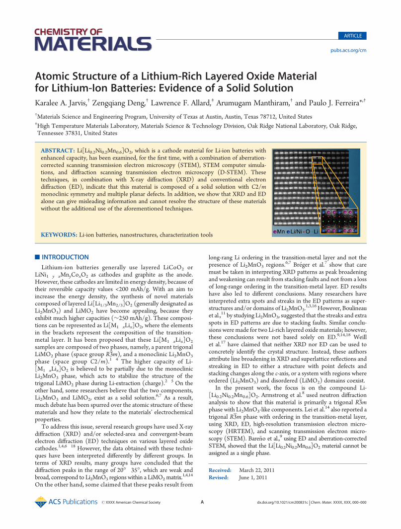
rXXXX American Chemical Society A dx.doi.org/10.1021/cm200831c | Chem. Mater. XXXX, XXX, 000–000 ARTICLE pubs.acs.org/cm Atomic Structure of a Lithium-Rich Layered Oxide Material for Lithium-Ion Batteries: Evidence of a Solid Solution Karalee A. Jarvis, † Zengqiang Deng, † Lawrence F. Allard, ‡ Arumugam Manthiram, † and Paulo J. Ferreira* ,† † Materials Science and Engineering Program, University of Texas at Austin, Austin, Texas 78712, United States ‡ High Temperature Materials Laboratory, Materials Science & Technology Division, Oak Ridge National Laboratory, Oak Ridge, Tennessee 37831, United States ’ INTRODUCTION Lithium-ion batteries generally use layered LiCoO 2 or LiNi 1 y x Mn y Co x O 2 as cathodes and graphite as the anode. However, these cathodes are limited in energy density, because of their reversible capacity values <200 mAh/g. With an aim to increase the energy density, the synthesis of novel materials composed of layered Li[Li 1/3 Mn 2/3 ]O 2 (generally designated as Li 2 MnO 3 ) and LiMO 2 have become appealing, because they exhibit much higher capacities (∼250 mAh/g). These composi- tions can be represented as Li[M 1 x Li x ]O 2 , where the elements in the brackets represent the composition of the transition- metal layer. It has been proposed that these Li[M 1 x Li x ]O 2 samples are composed of two phases, namely, a parent trigonal LiMO 2 phase (space group R 3m), and a monoclinic Li 2 MnO 3 phase (space group C2/m). 1 4 The higher capacity of Li- [M 1 x Li x ]O 2 is believed to be partially due to the monoclinic Li 2 MnO 3 phase, which acts to stabilize the structure of the trigonal LiMO 2 phase during Li-extraction (charge). 2 5 On the other hand, some researchers believe that the two components, Li 2 MnO 3 and LiMO 2 , exist as a solid solution. 6,7 As a result, much debate has been spurred over the atomic structure of these materials and how they relate to the materials’ electrochemical properties. To address this issue, several research groups have used X-ray diffraction (XRD) and/or selected-area and convergent-beam electron diffraction (ED) techniques on various layered oxide cathodes. 1,4,6 18 However, the data obtained with these techni- ques have been interpreted differently by different groups. In terms of XRD results, many groups have concluded that the diffraction peaks in the range of 20° 35°, which are weak and broad, correspond to Li 2 MnO 3 regions within a LiMO 2 matrix. 1,4,14 On the other hand, some claimed that these peaks result from long-rang Li ordering in the transition-metal layer and not the presence of Li 2 MnO 3 regions. 6,7 Br eger et al. 7 show that care must be taken in interpreting XRD patterns as peak broadening and weakening can result from stacking faults and not from a loss of long-range ordering in the transition-metal layer. ED results have also led to different conclusions. Many researchers have interpreted extra spots and streaks in the ED patterns as super- structures and/or domains of Li 2 MnO 3 . 1,3,16 However, Boulineau et al., 11 by studying Li 2 MnO 3 , suggested that the streaks and extra spots in ED patterns are due to stacking faults. Similar conclu- sions were made for two Li-rich layered oxide materials; however, these conclusions were not based solely on ED. 9,14,18 Weill et al. 17 have claimed that neither XRD nor ED can be used to concretely identify the crystal structure. Instead, these authors attribute line broadening in XRD and superlattice reflections and streaking in ED to either a structure with point defects and stacking changes along the c-axis, or a system with regions where ordered (Li 2 MnO 3 ) and disordered (LiMO 2 ) domains coexist. In the present work, the focus is on the compound Li- [Li 0.2 Ni 0.2 Mn 0.6 ]O 2 . Armstrong et al. 8 used neutron diffraction analysis to show that this material is primarily a trigonal R 3m phase with Li 2 MnO 3 -like components. Lei et al. 14 also reported a trigonal R 3m phase with ordering in the transition-metal layer, using XRD, ED, high-resolution transmission electron micro- scopy (HRTEM), and scanning transmission electron micro- scopy (STEM). Bare~ no et al., 9 using ED and aberration-corrected STEM, showed that the Li[Li 0.2 Ni 0.2 Mn 0.6 ]O 2 material cannot be assigned as a single phase. Received: March 22, 2011 Revised: June 1, 2011 ABSTRACT: Li[Li 0.2 Ni 0.2 Mn 0.6 ]O 2 , which is a cathode material for Li-ion batteries with enhanced capacity, has been examined, for the first time, with a combination of aberration- corrected scanning transmission electron microscopy (STEM), STEM computer simula- tions, and diffraction scanning transmission electron microscopy (D-STEM). These techniques, in combination with X-ray diffraction (XRD) and conventional electron diffraction (ED), indicate that this material is composed of a solid solution with C2/m monoclinic symmetry and multiple planar defects. In addition, we show that XRD and ED alone can give misleading information and cannot resolve the structure of these materials without the additional use of the aforementioned techniques. KEYWORDS: Li-ion batteries, nanostructures, characterization tools

Welcome message from author
This document is posted to help you gain knowledge. Please leave a comment to let me know what you think about it! Share it to your friends and learn new things together.
Transcript
rXXXX American Chemical Society A dx.doi.org/10.1021/cm200831c | Chem. Mater. XXXX, XXX, 000–000
ARTICLE
pubs.acs.org/cm
Atomic Structure of a Lithium-Rich Layered Oxide Materialfor Lithium-Ion Batteries: Evidence of a Solid SolutionKaralee A. Jarvis,† Zengqiang Deng,† Lawrence F. Allard,‡ Arumugam Manthiram,† and Paulo J. Ferreira*,†
†Materials Science and Engineering Program, University of Texas at Austin, Austin, Texas 78712, United States‡High Temperature Materials Laboratory, Materials Science & Technology Division, Oak Ridge National Laboratory, Oak Ridge,Tennessee 37831, United States
’ INTRODUCTION
Lithium-ion batteries generally use layered LiCoO2 orLiNi1�y�xMnyCoxO2 as cathodes and graphite as the anode.However, these cathodes are limited in energy density, because oftheir reversible capacity values <200 mAh/g. With an aim toincrease the energy density, the synthesis of novel materialscomposed of layered Li[Li1/3Mn2/3]O2 (generally designated asLi2MnO3) and LiMO2 have become appealing, because theyexhibit much higher capacities (∼250 mAh/g). These composi-tions can be represented as Li[M1�xLix]O2, where the elementsin the brackets represent the composition of the transition-metal layer. It has been proposed that these Li[M1�xLix]O2
samples are composed of two phases, namely, a parent trigonalLiMO2 phase (space group R3m), and a monoclinic Li2MnO3
phase (space group C2/m).1�4 The higher capacity of Li-[M1�xLix]O2 is believed to be partially due to the monoclinicLi2MnO3 phase, which acts to stabilize the structure of thetrigonal LiMO2 phase during Li-extraction (charge).2�5 On theother hand, some researchers believe that the two components,Li2MnO3 and LiMO2, exist as a solid solution.6,7 As a result,much debate has been spurred over the atomic structure of thesematerials and how they relate to the materials’ electrochemicalproperties.
To address this issue, several research groups have used X-raydiffraction (XRD) and/or selected-area and convergent-beamelectron diffraction (ED) techniques on various layered oxidecathodes.1,4,6�18 However, the data obtained with these techni-ques have been interpreted differently by different groups. Interms of XRD results, many groups have concluded that thediffraction peaks in the range of 20��35�, which are weak andbroad, correspond to Li2MnO3 regions within a LiMO2matrix.
1,4,14
On the other hand, some claimed that these peaks result from
long-rang Li ordering in the transition-metal layer and not thepresence of Li2MnO3 regions.
6,7 Br�eger et al.7 show that caremust be taken in interpreting XRD patterns as peak broadeningand weakening can result from stacking faults and not from a lossof long-range ordering in the transition-metal layer. ED resultshave also led to different conclusions. Many researchers haveinterpreted extra spots and streaks in the ED patterns as super-structures and/or domains of Li2MnO3.
1,3,16 However, Boulineauet al.,11 by studying Li2MnO3, suggested that the streaks and extraspots in ED patterns are due to stacking faults. Similar conclu-sions were made for two Li-rich layered oxidematerials; however,these conclusions were not based solely on ED.9,14,18 Weillet al.17 have claimed that neither XRD nor ED can be used toconcretely identify the crystal structure. Instead, these authorsattribute line broadening in XRD and superlattice reflections andstreaking in ED to either a structure with point defects andstacking changes along the c-axis, or a system with regions whereordered (Li2MnO3) and disordered (LiMO2) domains coexist.
In the present work, the focus is on the compound Li-[Li0.2Ni0.2Mn0.6]O2. Armstrong et al.8 used neutron diffractionanalysis to show that this material is primarily a trigonal R3mphase with Li2MnO3-like components. Lei et al.14 also reported atrigonal R3m phase with ordering in the transition-metal layer,using XRD, ED, high-resolution transmission electron micro-scopy (HRTEM), and scanning transmission electron micro-scopy (STEM). Bare~no et al.,9 using ED and aberration-correctedSTEM, showed that the Li[Li0.2Ni0.2Mn0.6]O2 material cannot beassigned as a single phase.
Received: March 22, 2011Revised: June 1, 2011
ABSTRACT: Li[Li0.2Ni0.2Mn0.6]O2, which is a cathode material for Li-ion batteries withenhanced capacity, has been examined, for the first time, with a combination of aberration-corrected scanning transmission electron microscopy (STEM), STEM computer simula-tions, and diffraction scanning transmission electron microscopy (D-STEM). Thesetechniques, in combination with X-ray diffraction (XRD) and conventional electrondiffraction (ED), indicate that this material is composed of a solid solution with C2/mmonoclinic symmetry and multiple planar defects. In addition, we show that XRD and EDalone can give misleading information and cannot resolve the structure of these materialswithout the additional use of the aforementioned techniques.
KEYWORDS: Li-ion batteries, nanostructures, characterization tools

B dx.doi.org/10.1021/cm200831c |Chem. Mater. XXXX, XXX, 000–000
Chemistry of Materials ARTICLE
The objectives of the current paper are i) clarify the afore-mentioned debate, by determining if the Li[Li0.2Ni0.2Mn0.6]O2
compound is composed of two separate phases, Li2MnO3 andLiMO2, or whether it is a solid solution, ii) better understand theatomic arrangements of this material, and iii) determine whichtechniques can accurately determine the atomic structures. Theseobjectives are critical for any future work trying to correlate theelectrochemical behavior of lithium-rich layered oxides with localcomposition and structure.
To address this issue, we first used XRD and nanobeamelectron diffraction (NBED) to characterize the material. How-ever, as discussed above, these techniques may lead to differentinterpretations, and thus are not able to provide conclusiveevidence regarding the crystal structure or phase analysis. There-fore, aberration-corrected high-angle annular dark-field (HAADF)STEM imaging was subsequently employed, which allowed us toexamine the structure and composition at the atomic level. Inorder to more reliably interpret the HAADF-STEM images,computer simulations were also performed, using the opticalparameters of the aberration-corrected electron microscope andcompared with the experimental images. Finally, we employeda novel technique, diffraction scanning transmission electronmicro-scopy (D-STEM),19 recently developed in our laboratory, whichallows us to collect electron diffraction maps from specific locationswith a spatial resolution of 1�2 nm. This is the first time that thiscombination of techniques, namely XRD, aberration-correctedHAADF-STEM imaging, STEM image simulations, and D-STEM,has been used on layered oxide cathodes, allowing us to unambigu-ously determine the atomic structure of this material.
In order to facilitate the discussion to follow, it is importantto define some of the crystallographic terminology that isused throughout the paper. So far, many different terms havebeen used in the literature to describe the R3m phase of theselayered oxides, in particular, trigonal, rhombohedral, and hexa-gonal.1,3,4,6,7,9�11,13,14,16,17,20�22While none of these are incorrect,the different nomenclature used by various authors may lead tosome confusion.
Table 1 shows the different terminology possible for the R3mand the C2/m phases. The R3m phase can be categorized ashexagonal according to the crystal family, trigonal according tothe crystal system, and rhombohedral according to the latticesystem. However, since the hexagonal definition could indicate a6-fold or a 3-fold axis of rotation while the trigonal nomenclaturecan only have a 3-fold axis of rotation, we will refer to the R3mphase as trigonal in this paper. On the other hand, the C2/mspace group exhibits one 2-fold axis of rotation and one mirrorplane and, thus, belongs to the monoclinic crystal and latticesystems. In summary, this paper will use the crystal system classifica-tion (trigonal or monoclinic) to define the crystal structures, toavoid confusion and ambiguity.
Following the aforementioned nomenclature, LiMO2, theparent structure, is reported to have a trigonal R3m structure(see Figure 1a).4,6,16,21,22 In particular, its composition is a
repeating sequence of a transition-metal layer, an oxygen layer,a lithium layer, an oxygen layer, and a transition-metal layer. Theatoms in the transition-metal (M) layer, which correspond to the(001) plane, are arranged in a hexagonal pattern (see Figure 1b),where each atomic site (gray) has the same probability of beingoccupied by any M with no specific ordering. On the other hand,while Li2MnO3 has the same stacking sequence as LiMO2
(Figure 2a), the transition-metal layer (Li1/3Mn2/3 or LiMn2)orders, such that the excess Li occupies atomic sites S1(Figure 2b) and Li is surrounded by six Mn atoms on sites S2.
Table 1. Classification of Crystallographic Phases
crystal family crystal system required symmetries of point group number of space groups lattice system
monoclinic monoclinic one 2-fold axis of rotation and one mirror plane 13 monoclinic
hexagonal trigonal one 3-fold axis of rotation 7 rhombohedral
hexagonal trigonal one 3-fold axis of rotation 18 hexagonal
hexagonal hexagonal one 6-fold axis of rotation 27 hexagonal
Figure 1. Trigonal (R3m) LiMO2 (a) unit cell and (b) atomic arrange-ment in the transition-metal layer. (The lattice parameters are a= b=2.8873Å, c = 14.2901 Å, R = β = 90�, and γ = 120�.16)
Figure 2. Monoclinic (C2/m) Li2MnO3 (a) unit cell and (b) atomicarrangement in the transition-metal layer. S1 and S2 indicate sitesoccupied, respectively, by excess Li atoms and Mn atoms. (The latticeparameters are a = 4.937 Å, b = 8.532 Å, c = 5.030 Å, R = γ = 90�, andβ = 109.46�.23)
C dx.doi.org/10.1021/cm200831c |Chem. Mater. XXXX, XXX, 000–000
Chemistry of Materials ARTICLE
This ordering reduces the symmetry to the monoclinic C2/munit cell.4,7,10,11,15,23 This information is the basis for ourcharacterization of the composition Li[Li0.2Ni0.2Mn0.6]O2 inorder to determine the crystal structure and the phases present.
’EXPERIMENTAL SECTION
The Li[Li0.2Ni0.2Mn0.6]O2 oxide was synthesized by a combinedcitric acid and EDTA (ethylenediamine tetraacetic acid) complexationroute. EDTA and citric acid were first dissolved in NH4OH and anaqueous solution containing required amounts of lithium, manganese,and nickel acetates were added to this solution. The citric acid:EDTA:metal ions molar ratio were optimized to be ∼1.5: 1: 1. The mixedsolution was then heated at ∼120 �C under stirring until a viscous gelwas obtained, which then heated first at∼250 �C and then at 850 �C for5 h to get the final oxide powder.The sample was characterized by XRD with a Philips X’pert diffract-
ometer (with Cu KR radiation). Data were collected in a step-scanmodein the range of 10��110� with intervals of 0.03�. XRD computer simula-tions were carried out using Diamond 3.2e2 software with a wavelength of1.5406 Š(Cu KR).Subsequently, the samples were sonicated or ground with a mortar
and pestle in methanol and deposited onto lacy carbon grids. Uponsample preparation, NBED and D-STEM19 were performed on a JEOLModel 2010F TEM system. The samples were imaged with a JEOLModel 2200FS TEM/STEM system that was equipped with a CEOScorrector for the illuminating lenses, and a high-angle annular dark-field(HAADF) detector. The instrument, located in the Advanced Micro-scopy Laboratory at Oak Ridge National Laboratory, was made availablethrough the High Temperature Materials Laboratory’s national userprogram. ED pattern simulations were carried out using the onlinesoftware WebEmaps.24
To simulate the STEM images, atomic models, created in VESTA,were exported to HREM Simulation Suite, which is a TEM/STEMsimulation software package based on the FFT Multislice technique.25
The HREM Simulation Suite evaluates both the wave function and itsFourier transform at each slice, using the approximation byWeickenmeierand Kohl26 to calculate the elastic scattering amplitude. This is a goodapproximation when considering electrons scattered at high angles,which is the geometry for recording HAADF images.25 The HAADFintensity is then calculated by adding the thermal diffuse scattering factorto the elastic scattering amplitude.25 This is important because atomicvibrations dampen the intensity of the electron waves going through thespecimen.Microscope parameters corresponding to the settings used forthe operation of the JEOL 2200FS aberration-corrected STEM at OakRidge National Laboratory were used. For all structures, the multislicesimulations were carried out assuming a step scanning size of 0.2 Å (lessthan the distance to be resolved) and aminimum slice thickness of 1.0 Å.TheDebye�Waller factor (B), which is related to themean square of thethermal displacement of an atom from its equilibrium position, wasacquired for each atomic position from the literature. For Li2MnO3, Bwas obtained from Strobel et al.23 for each atomic position. These valueswere also used for the solid solution, since they have similar structures.For Li[Mn0.5Ni0.5]O2, B was taken from Meng et al.16 After thesimulations were completed, the simulated images were compared withthe actual STEM images for verification.
’RESULTS AND DISCUSSION
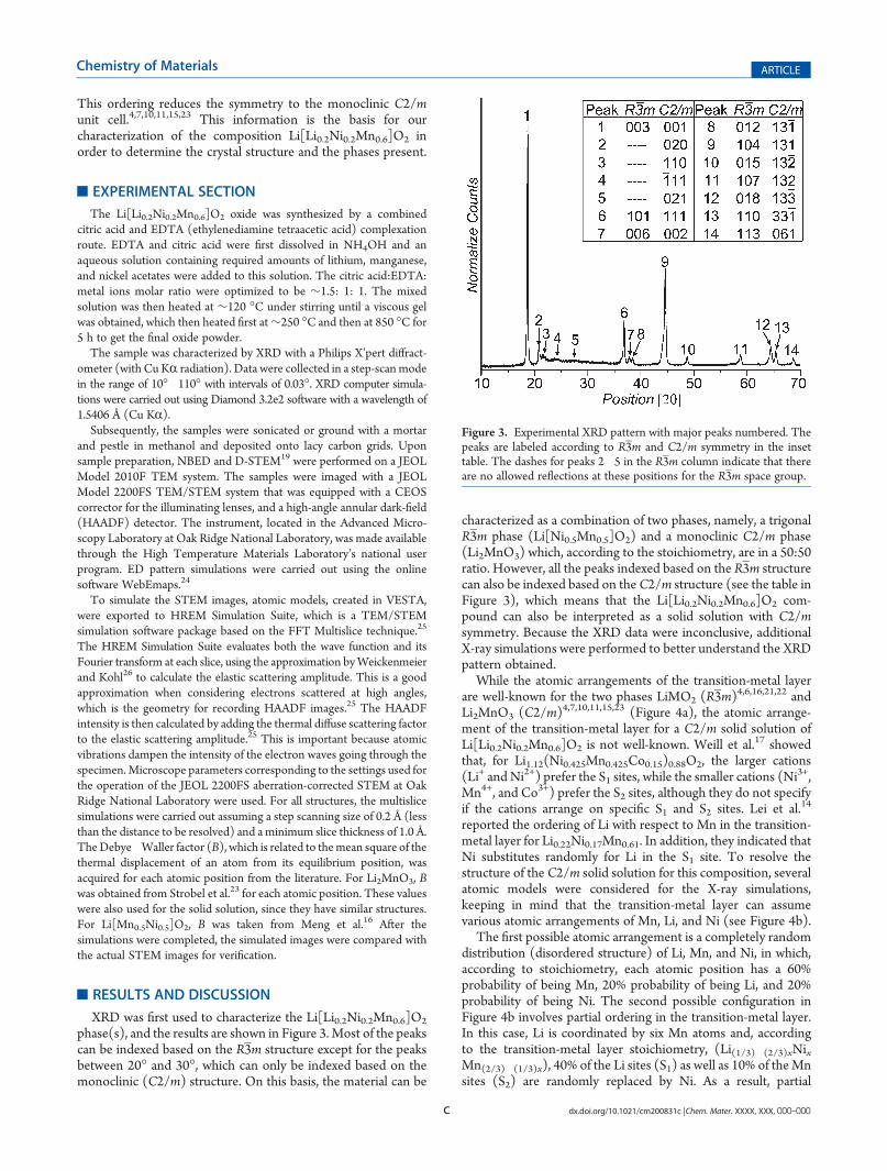
XRD was first used to characterize the Li[Li0.2Ni0.2Mn0.6]O2
phase(s), and the results are shown in Figure 3. Most of the peakscan be indexed based on the R3m structure except for the peaksbetween 20� and 30�, which can only be indexed based on themonoclinic (C2/m) structure. On this basis, the material can be
characterized as a combination of two phases, namely, a trigonalR3m phase (Li[Ni0.5Mn0.5]O2) and a monoclinic C2/m phase(Li2MnO3) which, according to the stoichiometry, are in a 50:50ratio. However, all the peaks indexed based on the R3m structurecan also be indexed based on the C2/m structure (see the table inFigure 3), which means that the Li[Li0.2Ni0.2Mn0.6]O2 com-pound can also be interpreted as a solid solution with C2/msymmetry. Because the XRD data were inconclusive, additionalX-ray simulations were performed to better understand the XRDpattern obtained.
While the atomic arrangements of the transition-metal layerare well-known for the two phases LiMO2 (R3m)
4,6,16,21,22 andLi2MnO3 (C2/m)
4,7,10,11,15,23 (Figure 4a), the atomic arrange-ment of the transition-metal layer for a C2/m solid solution ofLi[Li0.2Ni0.2Mn0.6]O2 is not well-known. Weill et al.17 showedthat, for Li1.12(Ni0.425Mn0.425Co0.15)0.88O2, the larger cations(Li+ and Ni2+) prefer the S1 sites, while the smaller cations (Ni3+,Mn4+, and Co3+) prefer the S2 sites, although they do not specifyif the cations arrange on specific S1 and S2 sites. Lei et al.14
reported the ordering of Li with respect to Mn in the transition-metal layer for Li0.22Ni0.17Mn0.61. In addition, they indicated thatNi substitutes randomly for Li in the S1 site. To resolve thestructure of the C2/m solid solution for this composition, severalatomic models were considered for the X-ray simulations,keeping in mind that the transition-metal layer can assumevarious atomic arrangements of Mn, Li, and Ni (see Figure 4b).
The first possible atomic arrangement is a completely randomdistribution (disordered structure) of Li, Mn, and Ni, in which,according to stoichiometry, each atomic position has a 60%probability of being Mn, 20% probability of being Li, and 20%probability of being Ni. The second possible configuration inFigure 4b involves partial ordering in the transition-metal layer.In this case, Li is coordinated by six Mn atoms and, accordingto the transition-metal layer stoichiometry, (Li(1/3)�(2/3)xNixMn(2/3)�(1/3)x), 40% of the Li sites (S1) as well as 10% of theMnsites (S2) are randomly replaced by Ni. As a result, partial
Figure 3. Experimental XRD pattern with major peaks numbered. Thepeaks are labeled according to R3m and C2/m symmetry in the insettable. The dashes for peaks 2�5 in the R3m column indicate that thereare no allowed reflections at these positions for the R3m space group.

D dx.doi.org/10.1021/cm200831c |Chem. Mater. XXXX, XXX, 000–000
Chemistry of Materials ARTICLE
ordering results in a change of the lattice parameter b from 2.844Å (disordered C2/m structure) to 8.532 Å (partially ordered)(see Figure 4b), while the lattice parameters a and c remain thesame compared with the disordered system. The final possiblearrangement (Figure 4b) involves nickel ordering in specific S1sites in the transition-metal layer. Because of theC2/m symmetryoperations, it is not possible to completely order all the nickel inthe S1 sites while maintaining the Li0.2Ni0.2Mn0.6 composition inthe transition-metal layer. To resolve this issue, we have ran-domly replaced 10% of the Mn sites with Ni and 10% of the Lisites with Ni. We term this structure “highly ordered”. Whilethere are multiple ways of ordering the Ni in the lattice,we have chosen to order Ni such that the smallest unit cellsare produced. In this case, the lattice parameter a increases to14.81 Å, while b and c are maintained at 8.53 Å and 5.03 Å, whencompared with the partially ordered C2/m structure (Figure 4b).Any other arrangement of Ni will either increase the latticeparameters or maintain the same cell size.
Because of the increase in lattice parameters, the XRD peaksshift to lower angles (Figure 5). As a result, there are peaks at2θ < 18� for the highly ordered structure that do not match the ex-perimental data. On the other hand, for the partially ordered C2/mstructure, the peak positions match very well with the experimentaldata. The absence of peaks between 20� <2θ<30� donotmatch theexperimental data for the fully disordered case. Therefore, we canconclude that, for the case of a solid solution, the compositionLi[Li0.2Ni0.2Mn0.6]O2 should exhibit a partially ordered structure,which is similar to results reported byLei et al.,14 andC2/m symmetry.
To this point, based on XRD data alone, the crystal structureof Li[Li0.2Ni0.2Mn0.6]O2 is either a combination of a disorderedR3m structure with smallC2/m regions, or a single partially orderedC2/m monoclinic phase. We next describe the results obtained bySTEM imaging, ED, D-STEM, and image simulations, whichprovide critical additional information on the crystal structure.
In order to interpret the STEM images, it is important tounderstand that, for images of atomic columns in a crystalstructure, the contrast has been shown to be directly related tothe relative atomic number by a factor of ∼Z1.7 (where Z is theatomic number).27 As a result, the brighter regions in the STEMimages correspond to areas with atomic columns that have higheraverage atomic number. In the case of Li[Li0.2Ni0.2Mn0.6]O2, theelements Mn and Ni have significantly higher masses than Li andO; therefore, atomic columns with high concentrations of theseelements are expected to be brighter. Direct imaging of thismaterial has been observed by Bareno et al.9 and Lei et al.14 Theyshowed that, when the transition-metal planes are observedparallel to the electron beam and like atoms stack on top of eachother, lithium ordering is revealed (a dark spot corresponding tothe Li column, followed by two bright spots, corresponding to theMn columns). Similar results were shown for Li1.2Co0.4Mn0.4O2
12
and Li[Ni0.17Li0.2Co0.07 Mn0.56]O2.18 However, since the
HAADF-STEM images are also affected (to various degrees)by the defocus value, thickness, thermal scattering factor, andaberration coefficients, STEM image simulations are neces-sary to verify the presence of lithium ordering. We performedSTEM image simulations for both the case of a single partiallyordered C2/m monoclinic phase and the case of a disorderedR3m structure with a small C2/m region.
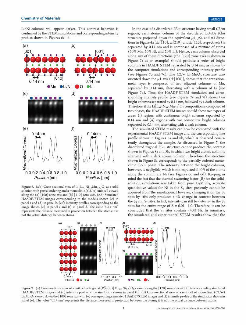
We first consider the case of the single partially orderedmonoclinic C2/m structure observed along the μ1, μ2, and μ3directions (Figure 4b), which correspond to the monoclinic([100], ([110], and ([110] directions, respectively. Thesezone axes were selected because the beam is parallel to thetransition-metal plane and the Mn atoms all line up in a singlecolumn, while the Ni and Li all line up together in a differentcolumn, thus facilitating the interpretation of contrast of theSTEM images. Under these conditions, the projected structuresalong the [100] and [110] directions show that the transition-metal layer is composed of two adjacent columns of Mn sepa-rated by 0.14 nm, alternating with a column of Li/Ni (60% Li and40% Ni) (see Figures 6a and 6b). Heavier Mn columns willappear bright in the HAADF STEM images, while the lighter
Figure 4. Atomic ordering in a single transition-metal layer ofLi[Li0.2Ni0.2Mn0.6]O2 for (a) a two-phase system with a trigonalparent structure, Li[Ni0.5Mn0.5]O2, and regions of a monoclinic phase,Li[Li1/3Mn2/3]O2 (Li2MnO3), and (b) a solid solution with varyingdegrees of order. The lattice parameters (a and b) for each unit cell areshown. The atomic ratios for the light gray, dark gray, and blue sites are givenas follows: light gray, 50% Mn and 50% Ni; dark gray, 60% Mn, 20% Ni,and 20% Li; and blue sites, 40% Ni and 60% Li. While not indicated inthe legend, 10% of the Mn sites are occupied randomly by Ni for boththe partially ordered and highly ordered model and 10% of the Li sites inthe highly ordered model are occupied randomly by Ni. This will notchange the unit-cell dimensions.
Figure 5. (a) Experimental XRD pattern for Li[Li0.2Ni0.2Mn0.6]O2 andsimulated XRD patterns for the cases where the transition-metal layer ishighly ordered, partially ordered, and disordered for a C2/m structure.The asterisk (*) indicates peaks in the simulated XRD pattern that areabsent in the experimental data.
E dx.doi.org/10.1021/cm200831c |Chem. Mater. XXXX, XXX, 000–000
Chemistry of Materials ARTICLE
Li/Ni-columns will appear darker. This contrast behavior isconfirmed by the STEM simulations and corresponding intensityprofiles shown in Figures 6c�f.
In the case of a disordered R3m structure having small C2/mregions, each atomic column of the disordered LiMO2 R3mstructure projected down the equivalent μ1, μ2, and μ3 direc-tions in Figure 4a (([110],([210], and([120], respectively) isseparated by 0.14 nm and is composed of a mixture of atoms(60% Mn, 20% Ni, and 20% Li). Hence, each column observedalong any of these directions (the [120] zone axes is shown inFigure 7a as an example) should produce a series of brightcolumns in HAADF STEM separated by 0.14 nm, as shown bythe computer simulations and corresponding intensity profile(see Figures 7b and 7c). The C2/m Li2MnO3 structure, alsooriented down the μ1-axis (([100]), shows that the transition-metal layer is composed of two adjacent columns of Mn,separated by 0.14 nm, alternating with a column of Li (seeFigure 7d). Thus, the HAADF-STEM simulation and corre-sponding intensity profile (see Figures 7e and 7f) shows twobright columns separated by 0.14 nm, followed by a dark column.Therefore, if the Li[Li0.2Ni0.2Mn0.6]O2 composition is composed oftwo phases, the HAADF STEM images should show two types ofareas: (i) regions with continuous bright columns separated by0.14 nm and (ii) regions with two consecutive bright columnsseparated by 0.14 nm, alternating with a dark column.
The simulated STEM results can now be compared with theexperimental HAADF-STEM image and the corresponding lineprofile shown in Figures 8a and 8b, which is observed consis-tently throughout the sample. As discussed in Figure 7, thedisordered trigonal R3m structure cannot produce the contrastshown in Figures 8a and 8b, in which two bright atomic columnsalternate with a dark atomic column. Therefore, the structureshown in Figure 8a corresponds to the partially ordered mono-clinic C2/m phase. The intensity between the bright columns,however, is negligible, which is not expected if 40% of the atomsalong the column are Ni (see Figures 6c and 6d). Keeping inmind the fact that the thermal scattering factor (B) for the solid-solution simulations was taken from pure Li2MnO3, accuratequantitative values for Ni in the S1 sites presently cannot beacquired from the simulations. However, changing B on the S1sites by 10% only produces a 4% change in contrast betweenthe S1 and S2 sites. In fact, intensity can still be detected in the S1sites for the entire range of B = 0.01�1.0. Therefore, it can beconcluded that the S1 sites contain <40% Ni. In summary,the simulated and experimental STEM results show that the
Figure 6. (a,b) Cross-sectional view of Li[Li0.2Ni0.2Mn0.6]O2 as a solidsolution with partial ordering and a monoclinic (C2/m) unit cell viewedalong the (a) [100] zone axis and (b) [110] zone axis. (c,d) SimulatedHAADF/STEM images corresponding to the models shown (c) inpanel a and (d) in panel b. (e,f) Intensity profiles corresponding to theimage shown (e) in panel c and (f) in panel d. The value “0.14 nm”represents the distance measured in projection between the atoms; it isnot the actual distance between atoms.
Figure 7. (a) Cross-sectional view of a unit cell of trigonal (R3m) Li[Mn0.5Ni0.5]O2 viewed along the [120] zone axis with (b) corresponding simulatedHAADF/STEM images and (c) intensity profile of the simulation shown in panel (b). (d) Cross-sectional view of a unit cell of monoclinic (C2/m)Li2MnO3 viewed down the [100] zone axis with (e) corresponding simulatedHAADF/STEM images and (f) intensity profile of the simulation shown inpanel (e). The value “0.14 nm” represents the distance measured in projection between the atoms; it is not the actual distance between atoms.
F dx.doi.org/10.1021/cm200831c |Chem. Mater. XXXX, XXX, 000–000
Chemistry of Materials ARTICLE
Li[Li0.2Ni0.2Mn0.6]O2 composition is a single-phase materialwith C2/m symmetry and exhibits significant ordering betweenLi+ and the transition metal, hereafter referred to as Li ordering,in the transition-metal layers.
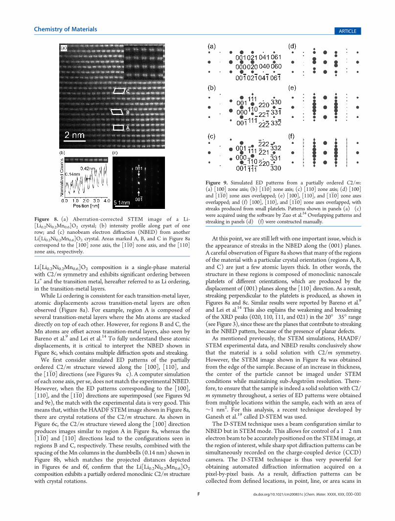
While Li ordering is consistent for each transition-metal layer,atomic displacements across transition-metal layers are oftenobserved (Figure 8a). For example, region A is composed ofseveral transition-metal layers where the Mn atoms are stackeddirectly on top of each other. However, for regions B and C, theMn atoms are offset across transition-metal layers, also seen byBareno et al.9 and Lei et al.14 To fully understand these atomicdisplacements, it is critical to interpret the NBED shown inFigure 8c, which contains multiple diffraction spots and streaking.
We first consider simulated ED patterns of the partiallyordered C2/m structure viewed along the [100], [110], andthe [110] directions (see Figures 9a�c). A computer simulationof each zone axis, per se, does notmatch the experimental NBED.However, when the ED patterns corresponding to the [100],[110], and the [110] directions are superimposed (see Figures 9dand 9e), the match with the experimental data is very good. Thismeans that, within the HAADF STEM image shown in Figure 8a,there are crystal rotations of the C2/m structure. As shown inFigure 6c, the C2/m structure viewed along the [100] directionproduces images similar to region A in Figure 8a, whereas the[110] and [110] directions lead to the configurations seen inregions B and C, respectively. These results, combined with thespacing of theMn columns in the dumbbells (0.14 nm) shown inFigure 8b, which matches the projected distances depictedin Figures 6e and 6f, confirm that the Li[Li0.2Ni0.2Mn0.6]O2
composition exhibits a partially ordered monoclinic C2/m structurewith crystal rotations.
At this point, we are still left with one important issue, which isthe appearance of streaks in the NBED along the (001) planes.A careful observation of Figure 8a shows that many of the regionsof the material with a particular crystal orientation (regions A, B,and C) are just a few atomic layers thick. In other words, thestructure in these regions is composed of monoclinic nanoscaleplatelets of different orientations, which are produced by thedisplacement of (001) planes along the [110] direction. As a result,streaking perpendicular to the platelets is produced, as shown inFigures 8a and 8c. Similar results were reported by Bareno et al.9
and Lei et al.14 This also explains the weakening and broadeningof the XRD peaks (020, 110, 111, and 021) in the 20��35� range(see Figure 3), since these are the planes that contribute to streakingin the NBED pattern, because of the presence of planar defects.
As mentioned previously, the STEM simulations, HAADF/STEM experimental data, and NBED results conclusively showthat the material is a solid solution with C2/m symmetry.However, the STEM image shown in Figure 8a was obtainedfrom the edge of the sample. Because of an increase in thickness,the center of the particle cannot be imaged under STEMconditions while maintaining sub-Ångstr€om resolution. There-fore, to ensure that the sample is indeed a solid solution withC2/m symmetry throughout, a series of ED patterns were obtainedfrom multiple locations within the sample, each with an area of∼1 nm2. For this analysis, a recent technique developed byGanesh et al.19 called D-STEM was used.
The D-STEM technique uses a beam configuration similar toNBED but in STEM mode. This allows for control of a 1�2 nmelectron beam to be accurately positioned on the STEM image, atthe region of interest, while sharp spot diffraction patterns can besimultaneously recorded on the charge-coupled device (CCD)camera. The D-STEM technique is thus very powerful forobtaining automated diffraction information acquired on apixel-by-pixel basis. As a result, diffraction patterns can becollected from defined locations, in point, line, or area scans in
Figure 8. (a) Aberration-corrected STEM image of a Li-[Li0.2Ni0.2Mn0.6]O2 crystal; (b) intensity profile along part of onerow; and (c) nanobeam electron diffraction (NBED) from anotherLi[Li0.2Ni0.2Mn0.6]O2 crystal. Areas marked A, B, and C in Figure 8acorrespond to the [100] zone axis, the [110] zone axis, and the [110]zone axis, respectively.
Figure 9. Simulated ED patterns from a partially ordered C2/m:(a) [100] zone axis; (b) [110] zone axis; (c) [110] zone axis; (d) [100]and [110] zone axes overlapped; (e) [100], [110], and [110] zone axesoverlapped; and (f) [100], [110], and [110] zone axes overlapped, withstreaks produced from small platelets. Patterns shown in panels (a)�(c)were acquired using the software by Zuo et al.24 Overlapping patterns andstreaking in panels (d)�(f) were constructed manually.

G dx.doi.org/10.1021/cm200831c |Chem. Mater. XXXX, XXX, 000–000
Chemistry of Materials ARTICLE
real time. In this fashion, we have been able, for the first time, tomap ED patterns with a 1�2 nm resolution from entire particles(∼1000 nm2). On the other hand, while NBED can also collectdiffraction patterns from a 1-nm region, the scanning coils of themicroscope are not employed, and thus automation is not possible.Therefore, collecting diffraction data from multiple areas within alarge particle is very time-consuming. In addition, in the NBEDmode, it is not possible to form a small probe on the area of interestand image the sample at the same time. As a result, it is challengingto place the beam exactly on the region of interest.
Figure 10 shows a series of ED patterns acquired under theD-STEM mode and collected from different regions within the
Li[Li0.2Ni0.2Mn0.6]O2 sample. Although the entire particle wasscanned with a step size of 1 nm, the four patterns shownrepresent the overall observations seen throughout the particle.Diffraction patterns 1 and 4 in Figure 10 match well with the[110] zone axis monoclinic pattern shown in Figure 9c, while thestreaking is due to the planar defects discussed above. Patterns 2and 3 in Figure 10 match well with the simulated ED patternresulting from overlapping the [100], [110], and [110] zone axes,while the streaking again represents thin planar defects (seeFigure 9f). On the other hand, the diffraction patterns in Figure 10do not match the expected pattern for R3m. Hence, it can beconcluded that no R3m regions exist in the sample, even at thenanoscale. The D-STEM technique was used to analyze multipleparticles, and they all showed the same results. Hence, theD-STEM analysis confirms the results obtained from aberra-tion-corrected STEM imaging, STEM simulations and NBEDdata, that the Li[Li0.2Ni0.2Mn0.6]O2 composition is a singlemonoclinic C2/m phase with multiple planar defects.
’CONCLUSIONS
The combination of X-ray diffraction (XRD), XRD simula-tions, aberration-corrected high-angle annular dark-field scanningtransmission electron microscopy (HAADF/STEM), HAADF/STEM simulations, nanobeam electron diffraction (NBED), anddiffraction scanning transmission electron microscopy (D-STEM)show that the compound Li[Li0.2Ni0.2Mn0.6]O2 has a monoclinic(C2/m) structure with Li-ordering. D-STEM, used for the first timefor layered oxide materials, is especially important in revealingthe absence of R3m regions. In addition, the HAADF-STEMsimulations, used in conjunction with HAADF-STEM imagingand NBED, show that the compound Li[Li0.2Ni0.2Mn0.6]O2
consists of a C2/m phase with a significant number of thin planardefects along the (001) planes, which lead to crystal rotations ofthe lattice. These thin planar defects produce intensity streaks onthe electron diffraction (ED) patterns along the [001] directionand XRD peak broadening in the 20��35� range.
This work shows that the Li[Li0.2Ni0.2Mn0.6]O2 compositiondoes not separate into regions of LiMO2 and Li2MnO3; instead,it forms a solid solution. Although two phases have not beenobserved for this compound, other compositions, especially thosewith less excess lithium, may result in two-phase regions, because ofa lack of ordering between Li+ and Mn4+ in the transition-metallayer. However, the high capacity of this class of materials cannot beattributed to the presence of two phases; therefore, this idea cannotbe generalized for all Li-rich layered oxides. Now that the atomicstructure and techniques for accurately determining atomic struc-ture of a lithium-rich layered oxide material before operation havebeen clearly identified, future work will focus on understanding therole of the solid solutionon enhancing the electrochemical propertiesof these materials and the behavior of these materials during cycling.
’AUTHOR INFORMATION
Corresponding Author*Tel.: 512-471-3244. Fax: 512-471-7681. E-mail: [email protected].
’ACKNOWLEDGMENT
This material is based on work supported as part of the program,“Understanding Charge Separation and Transfer at Interfaces in
Figure 10. (Top) BF TEM image of a particle of Li[Li0.2Ni0.2Mn0.6]O2
oriented down the [100], [110], and/or [110] directions, (Bottom)Corresponding D-STEM diffraction patterns collected at the areasindicated as 1�4 in the BF TEM image.
H dx.doi.org/10.1021/cm200831c |Chem. Mater. XXXX, XXX, 000–000
Chemistry of Materials ARTICLE
Energy Materials (EFRC:CST)”, an Energy Frontier ResearchCenter funded by the U.S. Department of Energy, Officeof Science, Office of Basic Energy Sciences (under Award No.DE-SC0001091). Microscopy research at the Oak Ridge NationalLaboratory’s High Temperature Materials Laboratory wassponsored by the U.S. Department of Energy, Office of EnergyEfficiency and Renewable Energy, Vehicle Technologies Program.We gratefully acknowledge the assistance of Dr. Ji-Ping Zhouwith D-STEM set up and Jacob Warneke with technical assistancefor STEM simulations.
’REFERENCES
(1) Kim, D.; Gim, H.; Lim, J.; Park, S.; Kim, J.Mater. Res. Bull. 2010,45, 252.(2) Thackeray, M. M.; Johnson, C. S.; Vaughey, J. T.; Li, N.;
Hackney, S. A. J. Mater. Chem. 2005, 15, 2257.(3) Thackeray, M. M.; Kang, S.-H.; Johnson, C. S.; Vaughey, J. T.;
Hackney, S. A. Electrochem. Commun. 2006, 8, 1531.(4) Thackeray, M. M.; Kang, S.-H.; Johnson, C. S.; Vaughey, J. T.;
Benedek, R.; Hackney, S. A. J. Mater. Chem. 2007, 30, 3053.(5) Thackeray, M. M. J. Chem. Eng. Jpn. 2007, 40, 1150.(6) Lu, Z.; Chen, Z.; Dahn, J. R. Chem. Mater. 2003, 15, 3214.(7) Br�eger, J.; Jiang, M.; Dupr�e, N.; Meng, Y. S.; Shao-Horn, Y.;
Ceder, G.; Grey, C. P. J. Solid State Chem. 2005, 178, 2575.(8) Armstrong, A. R.; Holzapfel, M.; Nov�ak, P.; Johnson, C. S.; Kang,
S.-H.; Thackeray, M. M.; Bruce, P. G. J. Am. Chem. Soc. 2006, 128, 8694.(9) Bare~no, J.; Lei, C. H.; Wen, J. G.; Kang, S.-H.; Petrov, I.;
Abraham, D. P. Adv. Mater. 2010, 22, 1122.(10) Boulineau, A.; Croguennec, L.; Delmas, C.; Weill, F. Chem.
Mater. 2009, 21, 4216.(11) Boulineau, A.; Croguennec, L.; Delmas, C.; Weill, F. Solid State
Ionics 2010, 21, 4216.(12) Ito, A.; Shodo, K.; Sato, Y.; Hatano, M.; Horie, H.; Ohsawa, Y.
J. Power Sources 2011, 196, 4785.(13) Johnson, C. S.; Li, N.; Lefief, C.; Vaughey, J. T.; Thackeray,
M. M. Chem. Mater. 2008, 20, 6095.(14) Lei, C. H.; Bare~no, J.; Wen, J. G.; Petrov, I.; Kang, S.-H.;
Abraham, D. P. J. Power Sources 2008, 178, 422.(15) Lei, C. H.; Wen, J. G.; Sardela, M.; Bare~no, J.; Petrov, I.; Kang,
S.-H.; Abraham, D. P. J. Mater. Sci. 2009, 44, 5579.(16) Meng, Y. S.; Ceder, G.; Grey, C. P.; Yoon, W.-S.; Jiang, M.;
Br�eger, J.; Shao-Horn, Y. Chem. Mater. 2005, 17, 2386.(17) Weill, F.; Tran, N.; Croguennec, L.; Delmas, C. J. Power Sources
2007, 172, 893.(18) Wen, J. G.; Bare~no, J.; Lei, C. H.; Kang, S.-H.; Balasubramanian,
M.; Peterove, I.; Abraham, D. P. Solid State Ionics 2011, 182, 98.(19) Ganesh, K. J.; Kawasaki, M.; Zhou, J. P.; Ferreira, P. J. Microsc.
Microanal. 2010, 16, 614.(20) Shao-Horn, Y.; Hackney, S. A.; Armstrong, A. R.; Bruce, P. G.;
Gitzendanner, R.; Johnson, C. S.; Thackeray, M. M. J. Electrochem. Soc.1999, 146, 2404.(21) Dyer, L.; Borie, B. S.; Smith, G. P. J. Am. Chem. Soc. 1954,
76, 1199.(22) Johnston, W. D.; Heikes, R. R.; Sestrich, D. J. Phys. Chem. Solids
1958, 7, 1.(23) Strobel, P.; Labert-Andron, B. J. Solid State Chem. 1988, 75, 90.(24) Zuo, J. M.; Mabon, J. C. Microsc. and Microanal. 2004,
10(Suppl. 2), URL: http://emaps.mrl.uiuc.edu/.(25) Ishizuka, K. Ultramicroscopy 2001, 90, 71.(26) Weickenmeier, A.; Kohl, H. Acta Crystallogr., Sect. A: Found.
Crystallogr. 1991, A47, 590.(27) Howie, A. J. Microsc. 1979, 117, 11.
Related Documents


![LITHIUM OXIDE - الصفحات الشخصيةsite.iugaza.edu.ps › bqeshta › files › 2010 › 02 › 94398_13.pdf · 2009-04-26 · LITHIUM OXIDE [12057-24-8] Formula: Li2O;](https://static.cupdf.com/doc/110x72/5f0d63d17e708231d43a1d60/lithium-oxide-site-a-bqeshta-a-files-a-2010.jpg)


