ISSN 2040-3364 2040-3364(2010)2:5;1-P COVER ARTICLE Singh et al. Atomic-scale observation of rotational misorientation in suspended few-layer graphene sheets REVIEW ARTICLE Rice Nanoscale optical imaging by atomic force infrared microscopy www.rsc.org/nanoscale Volume 2 | Number 5 | May 2010 | Pages 625–812

Welcome message from author
This document is posted to help you gain knowledge. Please leave a comment to let me know what you think about it! Share it to your friends and learn new things together.
Transcript
ISSN 2040-3364
2040-3364(2010)2:5;1-P
COVER ARTICLESingh et al.Atomic-scale observation of rotational misorientation in suspended few-layer graphene sheets
REVIEW ARTICLERiceNanoscale optical imaging by atomic force infrared microscopy
www.rsc.org/nanoscale Volume 2 | Number 5 | May 2010 | Pages 625–812
PAPER www.rsc.org/nanoscale | Nanoscale
Atomic-scale observation of rotational misorientation in suspendedfew-layer graphene sheets
Manoj K. Singh,*a Elby Titus,a Gil Goncalves,a Paula A. A. P. Marques,a Igor Bdikin,a Andrei L. Kholkinb
and Jos�e J. A. Gracioa
Received (in Z€urich, Switzerland) 11th September 2009, Accepted 12th November 2009
First published as an Advance Article on the web 7th January 2010
DOI: 10.1039/b9nr00256a
Single or few-layer graphene (FLG) sheets offer extraordinary electronic, thermal and mechanical
properties and are expected to find a variety of applications. Fully exploiting the properties of graphene
will require a method for the production of high-quality graphene sheets (almost pristine graphene) in
large quantities. In this regard, we report a two-step method for obtaining a homogenous colloidal
suspension of single or FLG sheets up to 0.15 mg ml�1 in N,N-dimethylformamide solution. The
graphene nanostructures are directly imaged using a high-resolution transmission electron microscope
(HRTEM) operated at 200 kV with a point resolution of 0.16 nm. We observed rotational
misorientation within the flake in the HRTEM images of 2, 4 and 6 layers of graphene sheets, giving rise
to Moir�e patterns. By filtering in the frequency domain using a Fourier transform, we reconstruct the
graphene lattice of each sheet and determine the relative rotation between consecutive graphene layers
up, to six separate sheets. Direct evidence is obtained for FLG sheets with packing that is different to
the standard AB Bernal packing of bulk graphite. Furthermore, we observed periodic ripples in
suspended graphene sheets in our TEM measurements. Electrostatic force microscopy was used to
characterize the electric potential distribution on the surface of FLG sheets on SiO2/Si substrates in
ambient conditions. The FLG sheets were found to exhibit a conducting nature with small potential
variations on the surface.
Introduction
Graphene, a two-dimensional carbon material, which takes the
form of a planar honeycomb lattice of sp2-bonded carbon atoms
has stimulated a vast amount of research interest in recent
years.1–7 Single or few-layer graphene (FLG) sheets have
attracted an enormous amount of interest in the last five years
because of their excellent mechanical, thermal and electronic
properties.8–12 However, the electrical properties of graphene
vary between single and FLG sheets.13–16 Therefore the method
of preparation of graphene is highly crucial to control the gra-
phene layers. In addition, the in-depth structural analysis of
graphene sheets is highly desirable in order to exploit this
material for future development of graphene-based nano-
electronic devices.17–19
Single-layer graphene was first isolated using the scotch-tape
method in 2004.20 This method also produces samples composed
of two or more atomic layers of graphene. However, this process
has significant disadvantages in terms of yield and throughput.
Fully exploiting the properties of graphene will require a method
for the production of high-quality graphene sheets (almost
pristine graphene) in large quantities. Two main routes are
possible: (i) large-scale growth, and (ii) large-scale exfoliation.
In the continuation of second approach, we are presenting
aCenter for Mechanical Technology & Automation, University of Aveiro,3810-193 Aveiro, Portugal. E-mail: [email protected]; Fax:+351234370953; Tel: +351234370830bDepartment of Ceramics and Glass Engineering & CICECO, University ofAveiro, 3810-193 Aveiro, Portugal
700 | Nanoscale, 2010, 2, 700–708
a two-step method for a homogenous colloidal suspension of
single or FLG sheets up to 0.15 mg ml�1 in N,N-dime-
thylformamide (DMF) solution.
The two-step approach includes; (i) high temperature
(�2000 �C) heat treatment of commercially available pyrolytic
graphite powders in a vacuum (<1 � 10�5 Torr) for 3 h (this heat
treatment may reduce contamination) followed by (ii) sonication
for 2 h by dissolving the heat-treated graphite in DMF using
a probe-tip sonicator. Furthermore, the pyrolytic graphite is
composed of a periodical stack of two-dimensional (2D) gra-
phene sheets (layers) along the c-axis. Each of these layers is
weakly bonded to its neighbouring layers by interlayer interac-
tion forces; the graphene layers can easily slide against each other
and peel off easily. As a result of the heat treatment of pyrolytic
graphite at high temperature under vacuum, the interactions
between graphene layers may soften, thus making their liquid-
phase exfoliation with DMF easier.21
Our approach provides single or FLG sheets (2–6 layers)
dispersed in DMF solution. The percentage of single-layer gra-
phene is low in comparison to FLG sheets (2–6 layers). More-
over, DMF is well documented for its high synthetic value, high
polarity and wide solubility range for both organic and inorganic
compounds, including single and multi-walled carbon nano-
tubes.22,23 Very recently, Liao et al.24 also proved that probe-tip
sonication is more powerful for the dispersion of carbon nano-
tubes in epoxy resin nanocomposites than bath sonication. This
might be the reason for achieving a relatively higher graphene
concentration in DMF solution compared to other reported
results.25–27 The homogenous colloidal suspension of graphene in
This journal is ª The Royal Society of Chemistry 2010
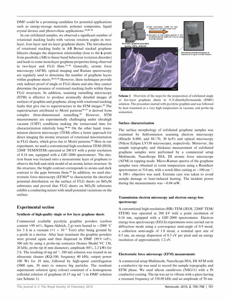
Scheme 1 Overview of the steps for the preparation of exfoliated single
or few-layer graphene sheets in N,N-dimethylformamide (DMF)
solution. The procedure started with pyrolytic graphite and was followed
by heat treatment at a very high temperature in vacuum, and probe-tip
sonication.
DMF could be a promising candidate for potential applications
such as energy-storage materials, polymer composites, liquid
crystal devices and photovoltaic applications.19,28–32
In our exfoliated samples, we observed a significant number of
rotational stacking faults with various rotation angles in two-
layer, four-layer and six-layer graphene sheets. The introduction
of rotational stacking faults in AB Bernal stacked graphene
bilayers changes the dispersion relationship close to the k-point
from parabolic (AB) to linear band behaviour (rotation disorder)
and leads to some monolayer graphene properties being observed
in two-layer and FLG films.13–16 Generally, atomic force
microscopy (AFM), optical imaging and Raman spectroscopy
are regularly used to determine the number of graphene layers
within graphene sheets.20,33,34 However, these techniques provide
only indirect proof of single or FLG sheets and also they cannot
determine the presence of rotational stacking faults within these
FLG structures. In addition, scanning tunnelling microscopy
(STM) is effective to produce atomically detailed images of
surfaces of graphite and graphene, along with rotational stacking
faults that give rise to superstructure in the STM images.35 The
superstructure attributed to Moir�e patterns35–37 is derived from
complex three-dimensional tunnelling.37 However, STM
measurements are experimentally challenging under ultrahigh
vacuum (UHV) conditions making the turnaround time for
characterization relatively long.38–41 On the other hand, trans-
mission electron microscopy (TEM) offers a faster approach for
direct imaging the atomic structure of rotational misorientation
in FLG sheets, which gives rise to Moir�e patterns.42 Here in our
experiment, we used a conventional high-resolution TEM (JEOL
2200F TEM/STEM) operated at 200 kV with a point resolution
of 0.16 nm, equipped with a GIF-2000 spectrometer. The elec-
tron beam was focused onto a monoatomic layer of graphene to
observe the ball-and-stick model of an atomic lattice structure. In
the structure, the bright contrast corresponds to atoms and dark
contrast to the gaps between them.43 In addition, we used elec-
trostatic force microscopy (EFM)44 to characterize the electrical
potential distribution on the surface of FLG sheets on SiO2/Si
substrates and proved that FLG sheets on SiO2/Si substrates
exhibit a conducting nature with small potential variations on the
surface.
Experimental section
Synthesis of high-quality single or few layer graphene sheets
Commercial available pyrolytic graphite powders (carbon
content >99 wt%, Sigma-Aldrich, 2 g) were heated to �2000 �C
for 3 h in a vacuum (<1 � 10�5 Torr) after being ground by
a pestle in a mortar. After heat treatment the graphite powders
were ground again and then dispersed in DMF (99.9 vol%,
500 ml) by using a probe-tip sonicator (Sonics Model VC 130,
20 kHz, probe tip (6 mm diameter), amplitude 80%, 2.2 kW) for
2 h. The resulting (4 mg ml�1, 100 ml) solution was treated in an
ultrasonic cleaner (KQ-100, frequency 40 kHz, output power
100 W) for 10 min, followed by high-speed centrifugation
(5000 rpm, 30 min) to remove big particles. The resultant
supernatant solution (gray colour) consisted of a homogenous
colloidal solution of graphene (0.15 mg ml�1) in DMF solution
(see Scheme 1).
This journal is ª The Royal Society of Chemistry 2010
Surface characterization
The surface morphology of exfoliated graphene samples was
examined by field-emission scanning electron microscopy
(Hitachi S-800, and SU-70, 30 keV) and optical microscopy
(Nikon Eclipse LV150 microscope), respectively. Moreover, the
sample topography and thickness measurement of exfoliated
graphene samples were performed by a commercial setup
Multimode, NanoScope IIIA, DI atomic force microscope
(AFM) in tapping mode. Micro-Raman spectra of the graphene
samples were obtained at room temperature using a Renishaw
spectrometer at 514 nm, with a notch filter cutting at �100 cm�1.
A 100� objective was used. Extreme care was taken to avoid
sample damage or laser-induced heating. The incident power
during the measurements was �0.04 mW.
Transmission electron microscopy and electron energy-loss
spectroscopy
A conventional high-resolution (HR) TEM (JEOL 2200F TEM/
STEM) was operated at 200 kV with a point resolution of
0.16 nm, equipped with a GIF-2000 spectrometer. Electron
energy-loss spectroscopy (EELS) experiments were carried out in
diffraction mode using a convergence semi-angle of 0.9 mrad,
a collection semi-angle of 1.8 mrad, a nominal spot size of
0.5 nm, an energy dispersion of 0.3 eV per pixel and an energy
resolution of approximately 1.2 eV.
Electrostatic force microscopy (EFM) measurements
A commercial setup Multimode, NanoScope IIIA, DI AFM with
a conductive tip was used to record the sample topography and
EFM phase. We used silicon cantilevers (NSG11) with a Pt
conductive coating. The tip was set to vibrate with a piezo having
a resonant frequency of 150.09 kHz and an amplitude of 30 nm.
Nanoscale, 2010, 2, 700–708 | 701
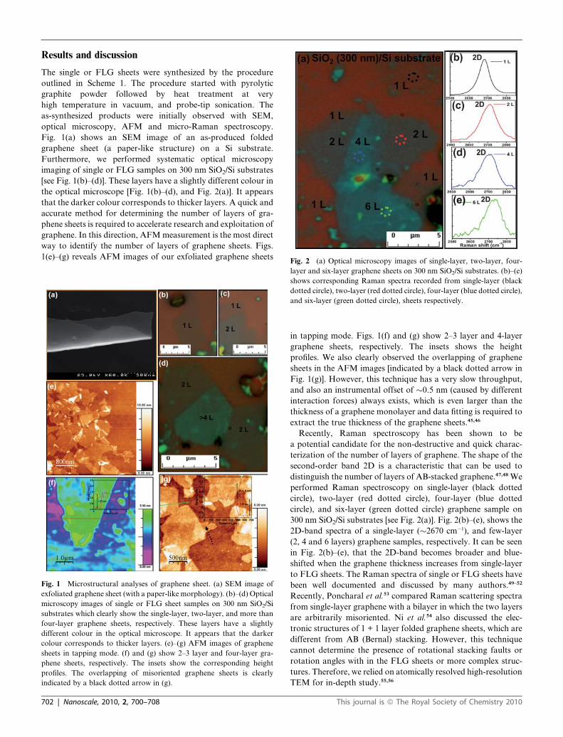
Fig. 2 (a) Optical microscopy images of single-layer, two-layer, four-
Results and discussion
The single or FLG sheets were synthesized by the procedure
outlined in Scheme 1. The procedure started with pyrolytic
graphite powder followed by heat treatment at very
high temperature in vacuum, and probe-tip sonication. The
as-synthesized products were initially observed with SEM,
optical microscopy, AFM and micro-Raman spectroscopy.
Fig. 1(a) shows an SEM image of an as-produced folded
graphene sheet (a paper-like structure) on a Si substrate.
Furthermore, we performed systematic optical microscopy
imaging of single or FLG samples on 300 nm SiO2/Si substrates
[see Fig. 1(b)–(d)]. These layers have a slightly different colour in
the optical microscope [Fig. 1(b)–(d), and Fig. 2(a)]. It appears
that the darker colour corresponds to thicker layers. A quick and
accurate method for determining the number of layers of gra-
phene sheets is required to accelerate research and exploitation of
graphene. In this direction, AFM measurement is the most direct
way to identify the number of layers of graphene sheets. Figs.
1(e)–(g) reveals AFM images of our exfoliated graphene sheets
Fig. 1 Microstructural analyses of graphene sheet. (a) SEM image of
exfoliated graphene sheet (with a paper-like morphology). (b)–(d) Optical
microscopy images of single or FLG sheet samples on 300 nm SiO2/Si
substrates which clearly show the single-layer, two-layer, and more than
four-layer graphene sheets, respectively. These layers have a slightly
different colour in the optical microscope. It appears that the darker
colour corresponds to thicker layers. (e)–(g) AFM images of graphene
sheets in tapping mode. (f) and (g) show 2–3 layer and four-layer gra-
phene sheets, respectively. The insets show the corresponding height
profiles. The overlapping of misoriented graphene sheets is clearly
indicated by a black dotted arrow in (g).
layer and six-layer graphene sheets on 300 nm SiO2/Si substrates. (b)–(e)
shows corresponding Raman spectra recorded from single-layer (black
dotted circle), two-layer (red dotted circle), four-layer (blue dotted circle),
and six-layer (green dotted circle), sheets respectively.
702 | Nanoscale, 2010, 2, 700–708
in tapping mode. Figs. 1(f) and (g) show 2–3 layer and 4-layer
graphene sheets, respectively. The insets shows the height
profiles. We also clearly observed the overlapping of graphene
sheets in the AFM images [indicated by a black dotted arrow in
Fig. 1(g)]. However, this technique has a very slow throughput,
and also an instrumental offset of �0.5 nm (caused by different
interaction forces) always exists, which is even larger than the
thickness of a graphene monolayer and data fitting is required to
extract the true thickness of the graphene sheets.45,46
Recently, Raman spectroscopy has been shown to be
a potential candidate for the non-destructive and quick charac-
terization of the number of layers of graphene. The shape of the
second-order band 2D is a characteristic that can be used to
distinguish the number of layers of AB-stacked graphene.47,48 We
performed Raman spectroscopy on single-layer (black dotted
circle), two-layer (red dotted circle), four-layer (blue dotted
circle), and six-layer (green dotted circle) graphene sample on
300 nm SiO2/Si substrates [see Fig. 2(a)]. Fig. 2(b)–(e), shows the
2D-band spectra of a single-layer (�2670 cm�1), and few-layer
(2, 4 and 6 layers) graphene samples, respectively. It can be seen
in Fig. 2(b)–(e), that the 2D-band becomes broader and blue-
shifted when the graphene thickness increases from single-layer
to FLG sheets. The Raman spectra of single or FLG sheets have
been well documented and discussed by many authors.49–52
Recently, Poncharal et al.53 compared Raman scattering spectra
from single-layer graphene with a bilayer in which the two layers
are arbitrarily misoriented. Ni et al.54 also discussed the elec-
tronic structures of 1 + 1 layer folded graphene sheets, which are
different from AB (Bernal) stacking. However, this technique
cannot determine the presence of rotational stacking faults or
rotation angles with in the FLG sheets or more complex struc-
tures. Therefore, we relied on atomically resolved high-resolution
TEM for in-depth study.55,56
This journal is ª The Royal Society of Chemistry 2010
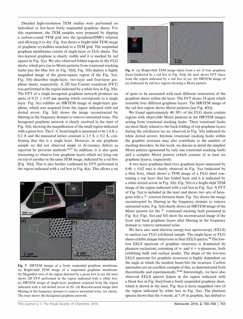
Fig. 4 (a) Bright-field TEM image taken from a set of four graphene
layers [indicated by a red box in Fig. 3(b)]; the inset shows FFT taken
from the region indicated by a red box in (a). (b) HRTEM image of
(a) (indicated by red box region) showing a Moir�e pattern.
Detailed high-resolution TEM studies were performed on
individual or few-layer freely suspended graphene sheets. For
this experiment, the TEM samples were prepared by dipping
a carbon-coated TEM grid into the (graphene/DMF) solution
and allowing it to dry. Fig. 3(a) shows a bright-field TEM image
of graphene crystallites attached to a TEM grid. The suspended
graphene membranes consist of single-layer or FLG sheets. The
two-layered graphene is clearly visible and it is marked by red
square in Fig. 3(a). We also observed folded regions in the FLG
sheets, which give rise to Moir�e patterns from rotational stacking
faults [see the blue box in Fig. 3(b)]. Fig. 3(b) depicts a highly
magnified image of the green-square region of the Fig. 3(a).
Fig. 3(b) describes single-layer, two-layer and four-layer gra-
phene sheets, respectively. A 2D fast Fourier transform (FFT)
was performed in the region indicated by a white box in Fig. 3(b).
The FFT of a single hexagonal graphene network produces six
spots of 0.21 � 0.05 nm spacing which corresponds to a single
layer. Fig. 3(c) exhibits an HRTEM image of single-layer gra-
phene, which was acquired from the region indicated with red
dotted arrow. Fig. 3(d) shows the image reconstructed by
filtering in the frequency domain to remove unwanted noise. The
hexagonal graphene network is clearly resolved in the inset of
Fig. 3(d), showing the magnification of the small region indicated
with a green box. The C–C bond length is measured to be 1.4 �A�0.2 �A and the measured lattice constant is 2.5 �A � 0.2 �A, con-
firming that this is a single layer. However, in our graphene
sample we did not observed single or di-vacancy defects as
reported by previous methods.43,57 In addition, it is also quite
interesting to observe four graphene layers which are lying one
on top of another in the same TEM image, indicated by a red box
[Fig. 3(b)]. This is also further confirmed by FFT performed in
the region indicated with a red box in Fig. 4(a). This allows a set
Fig. 3 HRTEM images of a freely suspended graphene membrane.
(a) Bright-field TEM image of a suspended graphene membrane.
(b) Magnified view of the region denoted by a green box in (a); the inset
shows 2D FFT performed in the region indicated with a white box.
(c) HRTEM image of single-layer graphene acquired from the region
indicated with a red dotted arrow in (b). (d) Reconstructed image after
filtering in the frequency domain to remove unwanted noise, for clarity.
The inset shows the hexagonal graphene network.
This journal is ª The Royal Society of Chemistry 2010
of spots to be associated with each different orientation of the
graphene sheets within the layer. The FFT shows 24 spots which
resemble four different graphene layers. The HRTEM image of
the red box region shows Moir�e patterns [see Fig. 4(b)].
We found approximately 40–50% of the FLG sheets contain
regions with observable Moir�e patterns in the HRTEM images
arising from rotational stacking faults. These rotational faults
are most likely related to the back-folding of top graphene layers
during the exfoliation (as we observed in Fig. 3(b) indicated by
white dotted arrow). Intrinsic rotational stacking faults within
the graphite structure may also contribute to the number of
stacking disorders. In this work, we discuss in detail the simplest
Moir�e pattern (generated by only one rotational stacking fault)
and a complex Moir�e pattern (which consists of at least six
graphene layers), respectively.
A two-layer graphene sheet (two graphene layers separated by
0.40 � 0.02 nm) is clearly observed in Fig. 5(a) (indicated by
a blue box), which shows a TEM image of a FLG sheet con-
taining a top layer that has folded back and it is indicated by
a white dotted arrow in Fig. 3(b). Fig. 5(b) is a bright-field TEM
image of the region indicated with a red box in Fig. 5(a). A FFT
of Fig. 5(a) is included in the inset and shows two sets of hexa-
gons with a 7� rotation between them. Fig. 5(c) shows the image
reconstructed by filtering in the frequency domain to remove
unwanted noise. Fig. 5(d) clearly shows an HRTEM image of the
Moir�e pattern for the 7� rotational stacking fault presented in
Fig. 5(c). Figs. 5(e) and 5(f) show the reconstructed image of the
front and back graphene layers after filtering in the frequency
domain to remove unwanted noise.
We have also used electron energy-loss spectroscopy (EELS)
to analyse our FLG exfoliated sample. The single-layer or FLG
sheets exhibit unique behaviour in their EELS spectra.58 The low-
loss EELS spectrum of graphitic structures is dominated by
plasmon excitations consisting of p- and p + s-plasmons, both
exhibiting bulk and surface modes. The shape of the low-loss
EELS spectrum for graphitic structures is highly dependent on
the angle at which the incident beam hits the structure. Carbon
nanotubes are an excellent example of this, as demonstrated both
theoretically and experimentally.59,60 Interestingly, we have also
observed EELS spectra [taken in the region indicated with
a black box in Fig. 6(a)] from a freely suspended graphene sheet,
which is shown in the inset. Fig. 6(a) is more magnified view of
the region indicated by white box in Fig. 3(a). The plasmon
spectra shows that the p-mode, at 7 eV in graphite, has shifted to
Nanoscale, 2010, 2, 700–708 | 703
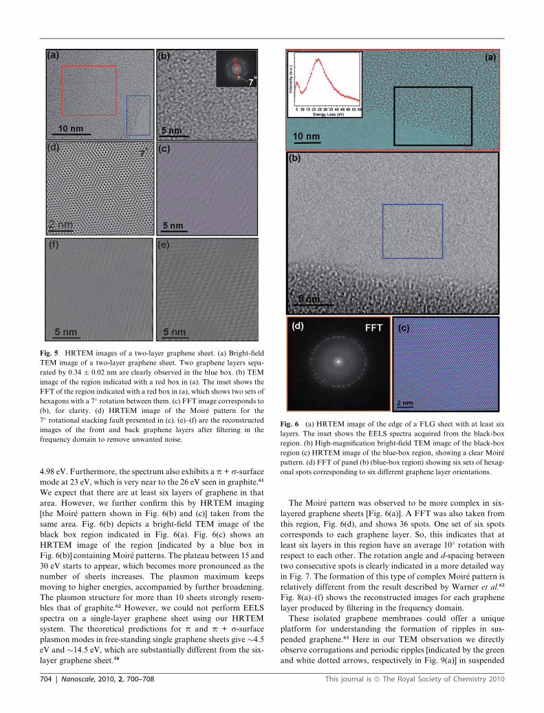
Fig. 5 HRTEM images of a two-layer graphene sheet. (a) Bright-field
TEM image of a two-layer graphene sheet. Two graphene layers sepa-
rated by 0.34 � 0.02 nm are clearly observed in the blue box. (b) TEM
image of the region indicated with a red box in (a). The inset shows the
FFT of the region indicated with a red box in (a), which shows two sets of
hexagons with a 7� rotation between them. (c) FFT image corresponds to
(b), for clarity. (d) HRTEM image of the Moir�e pattern for the
7� rotational stacking fault presented in (c). (e)–(f) are the reconstructed
images of the front and back graphene layers after filtering in the
frequency domain to remove unwanted noise.
Fig. 6 (a) HRTEM image of the edge of a FLG sheet with at least six
layers. The inset shows the EELS spectra acquired from the black-box
region. (b) High-magnification bright-field TEM image of the black-box
region (c) HRTEM image of the blue-box region, showing a clear Moir�e
pattern. (d) FFT of panel (b) (blue-box region) showing six sets of hexag-
onal spots corresponding to six different graphene layer orientations.
4.98 eV. Furthermore, the spectrum also exhibits a p + s-surfacemode at 23 eV, which is very near to the 26 eV seen in graphite.61
We expect that there are at least six layers of graphene in that
area. However, we further confirm this by HRTEM imaging
[the Moir�e pattern shown in Fig. 6(b) and (c)] taken from the
same area. Fig. 6(b) depicts a bright-field TEM image of the
black box region indicated in Fig. 6(a). Fig. 6(c) shows an
HRTEM image of the region [indicated by a blue box in
Fig. 6(b)] containing Moir�e patterns. The plateau between 15 and
30 eV starts to appear, which becomes more pronounced as the
number of sheets increases. The plasmon maximum keeps
moving to higher energies, accompanied by further broadening.
The plasmon structure for more than 10 sheets strongly resem-
bles that of graphite.62 However, we could not perform EELS
spectra on a single-layer graphene sheet using our HRTEM
system. The theoretical predictions for p and p + s-surface
plasmon modes in free-standing single graphene sheets give �4.5
eV and �14.5 eV, which are substantially different from the six-
layer graphene sheet.58
704 | Nanoscale, 2010, 2, 700–708
The Moir�e pattern was observed to be more complex in six-
layered graphene sheets [Fig. 6(a)]. A FFT was also taken from
this region, Fig. 6(d), and shows 36 spots. One set of six spots
corresponds to each graphene layer. So, this indicates that at
least six layers in this region have an average 10� rotation with
respect to each other. The rotation angle and d-spacing between
two consecutive spots is clearly indicated in a more detailed way
in Fig. 7. The formation of this type of complex Moir�e pattern is
relatively different from the result described by Warner et al.62
Fig. 8(a)–(f) shows the reconstructed images for each graphene
layer produced by filtering in the frequency domain.
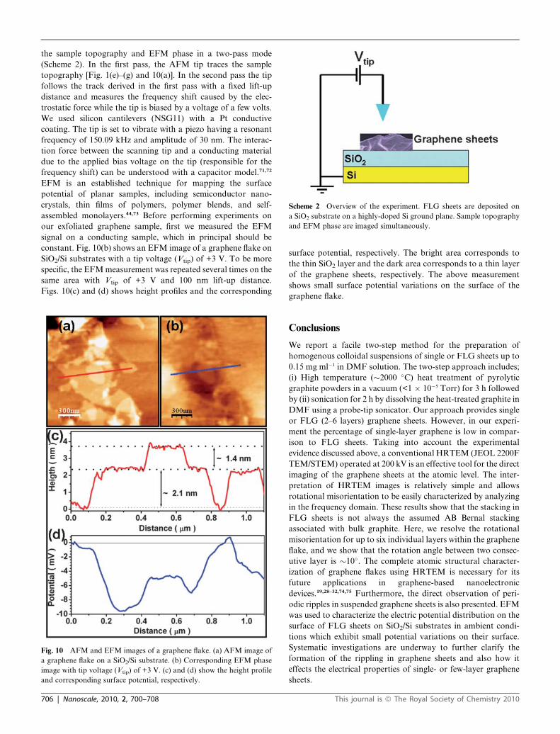
These isolated graphene membranes could offer a unique
platform for understanding the formation of ripples in sus-
pended graphene.63 Here in our TEM observation we directly
observe corrugations and periodic ripples [indicated by the green
and white dotted arrows, respectively in Fig. 9(a)] in suspended
This journal is ª The Royal Society of Chemistry 2010
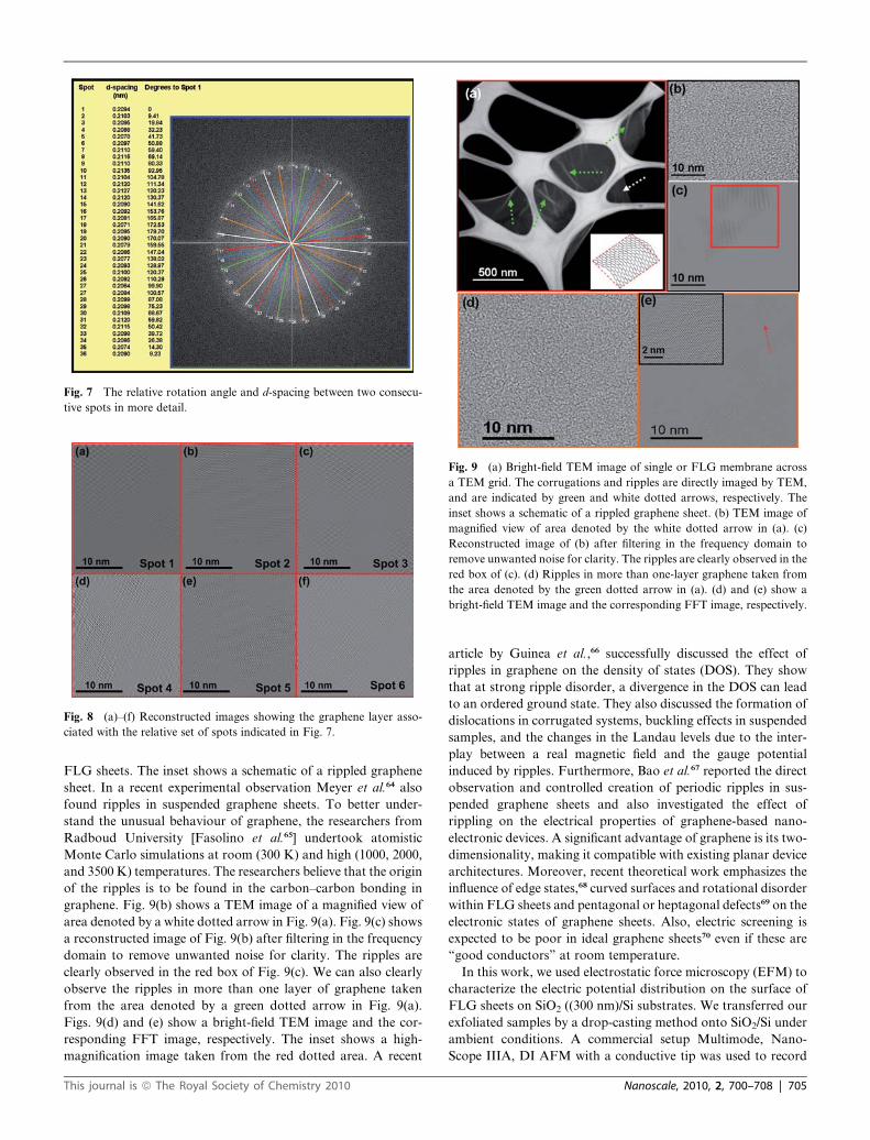
Fig. 7 The relative rotation angle and d-spacing between two consecu-
tive spots in more detail.
Fig. 8 (a)–(f) Reconstructed images showing the graphene layer asso-
ciated with the relative set of spots indicated in Fig. 7.
Fig. 9 (a) Bright-field TEM image of single or FLG membrane across
a TEM grid. The corrugations and ripples are directly imaged by TEM,
and are indicated by green and white dotted arrows, respectively. The
inset shows a schematic of a rippled graphene sheet. (b) TEM image of
magnified view of area denoted by the white dotted arrow in (a). (c)
Reconstructed image of (b) after filtering in the frequency domain to
remove unwanted noise for clarity. The ripples are clearly observed in the
red box of (c). (d) Ripples in more than one-layer graphene taken from
the area denoted by the green dotted arrow in (a). (d) and (e) show a
bright-field TEM image and the corresponding FFT image, respectively.
FLG sheets. The inset shows a schematic of a rippled graphene
sheet. In a recent experimental observation Meyer et al.64 also
found ripples in suspended graphene sheets. To better under-
stand the unusual behaviour of graphene, the researchers from
Radboud University [Fasolino et al.65] undertook atomistic
Monte Carlo simulations at room (300 K) and high (1000, 2000,
and 3500 K) temperatures. The researchers believe that the origin
of the ripples is to be found in the carbon–carbon bonding in
graphene. Fig. 9(b) shows a TEM image of a magnified view of
area denoted by a white dotted arrow in Fig. 9(a). Fig. 9(c) shows
a reconstructed image of Fig. 9(b) after filtering in the frequency
domain to remove unwanted noise for clarity. The ripples are
clearly observed in the red box of Fig. 9(c). We can also clearly
observe the ripples in more than one layer of graphene taken
from the area denoted by a green dotted arrow in Fig. 9(a).
Figs. 9(d) and (e) show a bright-field TEM image and the cor-
responding FFT image, respectively. The inset shows a high-
magnification image taken from the red dotted area. A recent
This journal is ª The Royal Society of Chemistry 2010
article by Guinea et al.,66 successfully discussed the effect of
ripples in graphene on the density of states (DOS). They show
that at strong ripple disorder, a divergence in the DOS can lead
to an ordered ground state. They also discussed the formation of
dislocations in corrugated systems, buckling effects in suspended
samples, and the changes in the Landau levels due to the inter-
play between a real magnetic field and the gauge potential
induced by ripples. Furthermore, Bao et al.67 reported the direct
observation and controlled creation of periodic ripples in sus-
pended graphene sheets and also investigated the effect of
rippling on the electrical properties of graphene-based nano-
electronic devices. A significant advantage of graphene is its two-
dimensionality, making it compatible with existing planar device
architectures. Moreover, recent theoretical work emphasizes the
influence of edge states,68 curved surfaces and rotational disorder
within FLG sheets and pentagonal or heptagonal defects69 on the
electronic states of graphene sheets. Also, electric screening is
expected to be poor in ideal graphene sheets70 even if these are
‘‘good conductors’’ at room temperature.
In this work, we used electrostatic force microscopy (EFM) to
characterize the electric potential distribution on the surface of
FLG sheets on SiO2 ((300 nm)/Si substrates. We transferred our
exfoliated samples by a drop-casting method onto SiO2/Si under
ambient conditions. A commercial setup Multimode, Nano-
Scope IIIA, DI AFM with a conductive tip was used to record
Nanoscale, 2010, 2, 700–708 | 705
Scheme 2 Overview of the experiment. FLG sheets are deposited on
a SiO2 substrate on a highly-doped Si ground plane. Sample topography
and EFM phase are imaged simultaneously.
the sample topography and EFM phase in a two-pass mode
(Scheme 2). In the first pass, the AFM tip traces the sample
topography [Fig. 1(e)–(g) and 10(a)]. In the second pass the tip
follows the track derived in the first pass with a fixed lift-up
distance and measures the frequency shift caused by the elec-
trostatic force while the tip is biased by a voltage of a few volts.
We used silicon cantilevers (NSG11) with a Pt conductive
coating. The tip is set to vibrate with a piezo having a resonant
frequency of 150.09 kHz and amplitude of 30 nm. The interac-
tion force between the scanning tip and a conducting material
due to the applied bias voltage on the tip (responsible for the
frequency shift) can be understood with a capacitor model.71,72
EFM is an established technique for mapping the surface
potential of planar samples, including semiconductor nano-
crystals, thin films of polymers, polymer blends, and self-
assembled monolayers.44,73 Before performing experiments on
our exfoliated graphene sample, first we measured the EFM
signal on a conducting sample, which in principal should be
constant. Fig. 10(b) shows an EFM image of a graphene flake on
SiO2/Si substrates with a tip voltage (Vtip) of +3 V. To be more
specific, the EFM measurement was repeated several times on the
same area with Vtip of +3 V and 100 nm lift-up distance.
Figs. 10(c) and (d) shows height profiles and the corresponding
Fig. 10 AFM and EFM images of a graphene flake. (a) AFM image of
a graphene flake on a SiO2/Si substrate. (b) Corresponding EFM phase
image with tip voltage (Vtip) of +3 V. (c) and (d) show the height profile
and corresponding surface potential, respectively.
706 | Nanoscale, 2010, 2, 700–708
surface potential, respectively. The bright area corresponds to
the thin SiO2 layer and the dark area corresponds to a thin layer
of the graphene sheets, respectively. The above measurement
shows small surface potential variations on the surface of the
graphene flake.
Conclusions
We report a facile two-step method for the preparation of
homogenous colloidal suspensions of single or FLG sheets up to
0.15 mg ml�1 in DMF solution. The two-step approach includes;
(i) High temperature (�2000 �C) heat treatment of pyrolytic
graphite powders in a vacuum (<1 � 10�5 Torr) for 3 h followed
by (ii) sonication for 2 h by dissolving the heat-treated graphite in
DMF using a probe-tip sonicator. Our approach provides single
or FLG (2–6 layers) graphene sheets. However, in our experi-
ment the percentage of single-layer graphene is low in compar-
ison to FLG sheets. Taking into account the experimental
evidence discussed above, a conventional HRTEM (JEOL 2200F
TEM/STEM) operated at 200 kV is an effective tool for the direct
imaging of the graphene sheets at the atomic level. The inter-
pretation of HRTEM images is relatively simple and allows
rotational misorientation to be easily characterized by analyzing
in the frequency domain. These results show that the stacking in
FLG sheets is not always the assumed AB Bernal stacking
associated with bulk graphite. Here, we resolve the rotational
misorientation for up to six individual layers within the graphene
flake, and we show that the rotation angle between two consec-
utive layer is �10�. The complete atomic structural character-
ization of graphene flakes using HRTEM is necessary for its
future applications in graphene-based nanoelectronic
devices.19,28–32,74,75 Furthermore, the direct observation of peri-
odic ripples in suspended graphene sheets is also presented. EFM
was used to characterize the electric potential distribution on the
surface of FLG sheets on SiO2/Si substrates in ambient condi-
tions which exhibit small potential variations on their surface.
Systematic investigations are underway to further clarify the
formation of the rippling in graphene sheets and also how it
effects the electrical properties of single- or few-layer graphene
sheets.
This journal is ª The Royal Society of Chemistry 2010
Acknowledgements
The authors M. K. Singh, E. Titus, P. A. A. P. Marques, and
G. Goncalves would like to thank the Ciencia 2007 Program,
Foundation of Science and Technology (FCT – Portugal), and
INL (International Iberian Nanotechnology Laboratory) for the
financial support of this work.
References
1 A. K. Geim and K. S. Novoselov, Nat. Mater., 2007, 6, 183.2 K. V. Emtsev, A. Bostwick, K. Horn, J. Jobst, G. L. Kellogg, L. Ley,
J. L. McChesney, T. Ohta, S. A. Reshanov, J. R€ohrl, E. Rotenberg,A. K. Schmid, D. Waldmann, H. B. Weber and T. Seyller, Nat.Mater., 2009, 8, 203.
3 S. Park and R. S. Ruoff, Nat. Nanotechnol., 2009, 4, 217.4 C. €O. Girit, J. C. Meyer, R. Erni, M. D. Rossell, C. Kisielowski,
L. Yang, C. Park, M. F. Crommie, M. L. Cohen, S. G. Louie andA. Zettl, Science, 2009, 323, 1705.
5 L. Jiao, L. Zhang, X. Wang, G. Diankov and H. Dai, Nature, 2009,458, 877.
6 K. S. Kim, Y. Zhao, H. Jang, S. Y. Lee, J. M. Kim, K. S. Kim,J.-H. Ahn, P. Kim, J.-Y. Choi and B. H. Hong, Nature, 2009, 457,706.
7 X. Li, W. Cai, J. An, S. Kim, J. Nah, D. Yang, R. Piner,A. Velamakanni, I. Jung, E. Tutuc, S. K. Banerjee, L. Colomboand R. S. Ruoff, Science, 2009, 324, 1312.
8 C. Lee, X. Wei, J. W. Kysar and J. Hone, Science, 2008, 321, 385.9 Y. Zhang, Y.-W. Tan, H. L. Stormer and P. Kim, Nature, 2005, 438,
201.10 A. A. Balandin, S. Ghosh, W. Bao, I. Calizo, D. Teweldebrhan,
F. Miao and C. N. Lau, Nano Lett., 2008, 8, 902.11 K. I. Bolotin, K. J. Sikes, Z. Jiang, M. Klima, G. Fudenberg, J. Hone,
P. Kim and H. L. Stormer, Solid State Commun., 2008, 146, 351.12 I. W. Frank, D. M. Tanenbauma, A. M. van der Zande and
P. L. McEuen, J. Vac. Sci. Technol., B, 2007, 25(6), 2558.13 S. Latil, V. Meunier and L. Henrard, Phys. Rev. B: Condens. Matter
Mater. Phys., 2007, 76, 201402.14 J. Hass, F. Varchon, J. E. Millan-Otoya, M. Spinkle, W. A. de Heer,
C. Berger, P. N. First, L. Magaud and E. H. Conrad, Phys. Rev. Lett.,2008, 100, 125504.
15 F. Varchon, P. Mallet, L. Magaud and J.-Y. Veuillen, Phys. Rev. B:Condens. Matter Mater. Phys., 2008, 77, 165415.
16 M. F. Craciun, S. Russo, M. Yamamoto, J. B. Oostinga,A. F. Morpurgo and S. Tarucha, Nat. Nanotechnol., 2009, 4, 383.
17 Y.-M. Lin, K. A. Jenkins, A. Valdes-Garcia, J. P. Small, D. B. Farmerand P. Avouris, Nano Lett., 2009, 9(1), 422.
18 X. Wang, Y. Ouyang, X. Li, H. Wang, J. Guo and H. Dai, Phys. Rev.Lett., 2008, 100, 206803.
19 P. Blake, P. D. Brimicombe, R. R. Nair, T. J. Booth, D. Jiang,F. Schedin, L. A. Ponomarenko, S. V. Morozov, H. F. Gleeson,E. W. Hill, A. K. Geim and K. S. Novoselov, Nano Lett., 2008,8(6), 1704.
20 K. S. Novoselov, A. K. Geim, S. V. Morozov, D. Jiang, Y. Zhang,S. V. Dubonos, I. V. Grigorieva and A. A. Firsov, Science, 2004,306, 666.
21 A. B. Bourlinos, V. Georgakilas, R. Zboril, T. A. Steriotis andA. K. Stub, Small, 2009, 5, 1841.
22 H. Zhao, W. Z. Yuan, L. Tang, J. Z. Sun, H. Xu, A. Qin, Y. Mao,J. K. Jin and B. Z. Tang, Macromolecules, 2008, 41, 8566.
23 I. Pastoriza-Santos and L. M. Liz-Marz�an, Adv. Funct. Mater., 2009,19, 679.
24 Y.-H. Liao, O. Marietta-Tondin, Z. Liang, C. Zhang and B. Wang,Mater. Sci. Eng., A, 2004, 385, 175.
25 Y. Hernandez, V. Nicolosi, M. Lotya, F. M. Blighe, Z. Sun, S. De,I. T. McGovern, B. Holland, M. Byrne, Y. K. Gun’Ko,J. J. Boland, P. Niraj, G. Duesberg, S. Krishnamurthy,R. Goodhue, J. Hutchison, V. Scardaci, A. C. Ferrari andJ. N. Coleman, Nat. Nanotechnol., 2008, 3, 563.
26 X. Li, X. Wang, L. Zhang, S. Lee and H. Dai, Science, 2008, 319,1229.
27 X. Li, G. Zhang, X. Bai, X. Sun, X. Wang, E. Wang and H. Dai, Nat.Nanotechnol., 2008, 3, 538.
This journal is ª The Royal Society of Chemistry 2010
28 S. Patchkovskii, J. S. Tse, S. N. Yurchenko, L. Zhechkov, T. Heineand G. Seifert, Proc. Natl. Acad. Sci. U. S. A., 2005, 102, 10439.
29 M. D. Stoller, S. Park, Y. Zhu, J. An and R. S. Ruoff, Nano Lett.,2008, 8, 3498.
30 S.-M. Paek, E. Yoo and I. Honma, Nano Lett., 2009, 9(1), 72.31 S. Stankovich, D. A. Dikin, G. H. B. Dommett, K. M. Kohlhaas,
E. J. Zimney, E. A. Stach, R. D. Piner, S. T. Nguyen andR. S. Ruoff, Nature, 2006, 442, 282.
32 T. Ramanathan, A. A. Abdala, S. Stankovich, D. A. Dikin,M. Herrera-Alonso, R. D. Piner, D. H. Adamson, H. C. Schniepp,X. Chen, R. S. Ruoff, S. T. Nguyen, I. A. Aksay,R. K. Prud’Homme and L. C. Brinson, Nat. Nanotechnol., 2008, 3,327.
33 I. Jung, M. Pelton, R. Piner, D. A. Dikin, S. Stankovich,S. Watcharotone, M. Hausner and R. S. Ruoff, Nano Lett., 2007, 7,3569.
34 A. C. Ferrari, J. C. Meyer, V. Scardaci, C. Casiraghi, M. Lazzeri,F. Mauri, S. Piscanec, D. Jiang, K. S. Novoselov, S. Roth andA. K. Geim, Phys. Rev. Lett., 2006, 97, 187401.
35 G. M. Rutter, N. P. Guisinger, J. N. Crain, E. A. A. Jarvis,M. D. Stiles, T. Li, P. N. First and J. A. Stroscio, Phys. Rev. B:Condens. Matter Mater. Phys., 2007, 76, 235416.
36 D. Martoccia, P. R. Willmott, T. Brugger, M. Bj€orck, S. G€unther,C. M. Schlep€utz, A. Cervellino, S. A. Pauli, B. D. Patterson,S. Marchini, J. Wintterlin, W. Moritz and T. Greber, Phys. Rev.Lett., 2008, 101, 126102.
37 J. M. Campanera, G. Savini, I. Suarez-Martinez and M. I. Heggie,Phys. Rev. B: Condens. Matter Mater. Phys., 2007, 75, 235449.
38 E. Stolyarova, K. T. Rim, S. Ryu, J. Maultzsch, P. Kim, L. E. Brus,T. F. Heinz, M. S. Hybertsen and G. W. Flynn, Proc. Natl. Acad. Sci.U. S. A., 2007, 104, 9209.
39 G. M. Rutter, J. N. Crain, N. P. Guisinger, T. Li, P. N. First andJ. A. Stroscio, Science, 2007, 317, 219.
40 K. A. Ritter and J. W. Lyding, Nat. Mater., 2009, 8, 235.41 J. W. G. Wild€oer, L. C. Venema, A. G. Rinzler, R. E. Smalley and
C. Dekker, Nature, 1998, 391, 59.42 H. Fujimoto, A. Mabuchi, K. Tokumitsu and T. Kasuh, Carbon,
1996, 34, 1115.43 J. C. Meyer, C. Kisielowski, R. Erni, M. D. Rossell, M. F. Crommie
and A. Zettl, Nano Lett., 2008, 8(11), 3582.44 D. C. Coffey and D. S. Ginger, Nat. Mater., 2006, 5, 735.45 A. Gupta, G. Chen, P. Joshi, S. Tadigadapa and P. C. Eklund, Nano
Lett., 2006, 6, 2667.46 P. Nemes-Incze, Z. Osvath, K. Kamar�as and L. P. Bir�o, Carbon, 2008,
46, 1435.47 D. Graf, F. Molitor, K. Ensslin, C. Stampfer, A. Jungen, C. Hierold
and L. Wirtz, Nano Lett., 2007, 7, 238.48 L. M. Malard, M. A. Pimenta, G. Dresselhaus and M. S. Dresselhaus,
Phys. Rep., 2009, 473, 51.49 R. P. Vidano, D. B. Fischbach, L. J. Willis and T. M. Loehr, Solid
State Commun., 1981, 39, 341.50 R. J. Nemanich and S. A. Solin, Phys. Rev. B: Condens. Matter, 1979,
20, 392.51 M. J. Matthews, M. A. Pimenta, G. Dresselhaus, M. S. Dresselhaus
and M. Endo, Phys. Rev. B: Condens. Matter Mater. Phys., 1999,59, R6585.
52 F. Tuinstra and J. L. Koenic, J. Chem. Phys., 1970, 53, 1126.53 P. Poncharal, A. Ayari, T. Michel and J.-L. Sauvajol, Phys. Rev. B:
Condens. Matter Mater. Phys., 2008, 78, 113407.54 Z. Ni, Y. Wang, T. Yu, Y. You and Z. Shen, Phys. Rev. B: Condens.
Matter Mater. Phys., 2008, 77, 235403.55 Z. Liu, K. Suenaga, P. J. F. Harris and S. Iijima, Phys. Rev. Lett.,
2009, 102, 015501.56 C. Jin, H. Lan, L. Peng, K. Suenaga and S. Iijima, Phys. Rev. Lett.,
2009, 102, 205501.57 M. H. Gass, U. Bangert, A. L. Bleloch, P. Wang, R. R. Nair and
A. K. Geim, Nat. Nanotechnol., 2008, 3, 676.58 U. Bangert, T. Eberlein, R. R. Nair, R. Jones, M. Gass, A. L. Bleloch,
K. S. Novoselov, A. K. Geim and P. R. Briddon, Phys. Status SolidiA, 2008, 205(9), 2265.
59 O. St�ephan, D. Taverna, M. Kociak, K. Suenaga, L. Henrard andC. Colliex, Phys. Rev. B: Condens. Matter Mater. Phys., 2002, 66,155422.
60 M. Kociak, L. Henrard, O. Stephan, K. Suenaga and C. Colliex,Phys. Rev. B: Condens. Matter Mater. Phys., 2000, 61, 13936.
Nanoscale, 2010, 2, 700–708 | 707

61 M. Filippi and L. Calliari, Surf. Interface Anal., 2006, 38, 595.62 J. H. Warner, M. H. Rummeli, T. Gemming, B. Buchner and
G. A. D. Briggs, Nano Lett., 2009, 9(1), 102.63 R. C. Thompson-Flagg, M. J. B. Moura and M. Marder, Europhys.
Lett., 2009, 85, 46002.64 J. C. Meyer, A. K. Geim, M. I. Katsnelson, K. S. Novoselov,
T. J. Booth and S. Roth, Nature, 2007, 446, 60.65 A. Fasolino, J. H. Los and M. I. Katsnelson, Nat. Mater., 2007, 6, 858.66 F. Guinea, B. Horovitz and P. L. Doussal, Phys. Rev. B: Condens.
Matter Mater. Phys., 2008, 77, 205421.67 W. Bao, F. Miao, Z. Chen, H. Zhang, W. Jang, C. Dames and
C. N. Lau, Nat. Nanotechnol., 2009, 562.68 M. Fujita, K. Wakabayashi, K. Nakada and K. Kusakabe, J. Phys.
Soc. Jpn., 1996, 65, 1920.
708 | Nanoscale, 2010, 2, 700–708
69 N. M. R. Peres, F. Guinea and A. H. C. Neto, Phys. Rev. B: Condens.Matter Mater. Phys., 2006, 73, 125411.
70 J. Gonz�alez, F. Guinea and M. A. H. Vozmediano, Phys. Rev. B:Condens. Matter Mater. Phys., 2001, 63, 134421.
71 C. Staii, A. T. Johnson and N. J. Pinto, Nano Lett., 2004, 4, 859.72 M. Bockrath, N. Markovic, A. Shepard, M. Tinkham, L. Gurevich,
L. P. Kouwenhoven, M. W. Wu and L. L. Sohn, Nano Lett., 2002,2(3), 187.
73 H. Takano, S.-S. Wong, J. A. Harnisch and M. D. Porter, Langmuir,2000, 16, 5231.
74 P. Avouris, Z. Chen and V. Perebeinos, Nat. Nanotechnol., 2007, 2,605.
75 J. C. Meyer, C. O. Girit, M. F. Crommie and A. Zettl, Nature, 2008,454, 319.
This journal is ª The Royal Society of Chemistry 2010
Related Documents