Atom Probe Tomography of Semiconductor Devices 3D Analysis of a 28nm Node S/D Region Atom Probe Tomography (APT) has seen recent expanding interest and use in the area of semiconductor device analysis. Ever smaller device technology nodes and increasing yield/performance requirements have resulted in growing demand for the type of data that the atom probe can provide: 3D distribution of isotopic species at the atomic scale with high detector efficiency (>75% of atoms identified in 3D) and high sensitivity. The LEAP is uniquely capable of providing isotopically sensitive information about buried interfaces - a capability that has been demonstrated with low ppm sensitivity. APT analyses of particular interest include dopant distribution in the source/drain, extension, and interfacial and channel regions of actual devices where other common analysis techniques lack sufficient spatial or compositional resolution. APT has been used for semiconductor materials research for almost 10 years, but for much of that time it primarily served research and development of blanket wafers, test structures, or model devices. More recently, successes on fully processed devices has led to quick adoption, such that now seven of the top 10 semiconductor manufactures have a LEAP system*. Analysis of a single, targeted device, such as failure analysis of a transistor with APT had rarely been performed due to the complicated sample preparation required and the relatively low data collection success rate on complex 3D structures with many interfaces. Continuing advances in APT and FIB/SEM techniques have rendered the previously slow and low quality efforts more routine, particularly for device specific analyses. With these new sample preparation techniques, and the latest hardware and software in the new LEAP 5000 atom probe model, it has been demonstrated that true failure analysis work with a LEAP system is possible. Other semiconductor applications include: • High-k dielectrics • Channel engineering • Silicides • Advanced metallization • Compound semiconductors • 3D device structures • Optoelectronics 10nm slice of 3D data from a AMD Radeon R7 GPU. FIB/SEM was used to select individual devices for liftout and LEAP analysis. The 3D analysis of the source-drain region reveals Titanium and Platinum doping in the Nickel Silicide to SiGe contact. The arrow denotes a region of quantitative analysis through the S/D region, into the channel (see below) www.cameca.com • www.atomprobe.com International Headquarters: 29 quai des Grésillons • 92622 Genevilliers • France • [email protected] Atom Probe Technology Center: 5500 Nobel Drive • WI-53711 Madison • USA • [email protected] *McClean Report, IC insights 17 (2013). Adapted from D.F. Lawrence et al., Routine Device-Level Atom Probe Analysis, Proceedings of the 40th ISTFA 2014, Houston. AN#APT-06 - Semi-28nm node - Jan 15 Si Ge B One-dimensional concentration profile from the source drain region into the channel. Application Note # APT-06

Welcome message from author
This document is posted to help you gain knowledge. Please leave a comment to let me know what you think about it! Share it to your friends and learn new things together.
Transcript

Atom Probe Tomography of Semiconductor Devices3D Analysis of a 28nm Node S/D Region
Atom Probe Tomography (APT) has seen recent expandinginterest and use in the area of semiconductor device analysis.Ever smaller device technology nodes and increasingyield/performance requirements have resulted in growingdemand for the type of data that the atom probe can provide:3D distribution of isotopic species at the atomic scale with highdetector efficiency (>75% of atoms identified in 3D) and highsensitivity. The LEAP is uniquely capable of providingisotopically sensitive information about buried interfaces - acapability that has been demonstrated with low ppm sensitivity.APT analyses of particular interest include dopant distribution inthe source/drain, extension, and interfacial and channelregions of actual devices where other common analysistechniques lack sufficient spatial or compositional resolution.
APT has been used for semiconductor materials research foralmost 10 years, but for much of that time it primarily servedresearch and development of blanket wafers, test structures, ormodel devices. More recently, successes on fully processeddevices has led to quick adoption, such that now seven of the top 10 semiconductor manufactures have a LEAP system*.
Analysis of a single, targeted device, such as failure analysis ofa transistor with APT had rarely been performed due to thecomplicated sample preparation required and the relatively lowdata collection success rate on complex 3D structures with manyinterfaces. Continuing advances in APT and FIB/SEM techniqueshave rendered the previously slow and low quality efforts moreroutine, particularly for device specific analyses.
With these new sample preparation techniques, and the latesthardware and software in the new LEAP 5000 atom probemodel, it has been demonstrated that true failure analysis workwith a LEAP system is possible.
Other semiconductor applications include: • High-k dielectrics• Channel engineering • Silicides• Advanced metallization• Compound semiconductors• 3D device structures• Optoelectronics
10nm slice of 3D data from a AMD Radeon R7 GPU. FIB/SEM was used to select individual devices
for liftout and LEAP analysis. The 3D analysis of the source-drain region reveals Titanium and
Platinum doping in the Nickel Silicide to SiGe contact.The arrow denotes a region of quantitative analysis
through the S/D region, into the channel (see below)
www.cameca.com • www.atomprobe.comInternational Headquarters: 29 quai des Grésillons • 92622 Genevilliers • France • [email protected] Probe Technology Center: 5500 Nobel Drive • WI-53711 Madison • USA • [email protected]
*McClean Report, IC insights 17 (2013).Adapted from D.F. Lawrence et al., Routine Device-Level Atom Probe Analysis, Proceedings of the 40th ISTFA 2014, Houston.
AN
#APT
-06
- Sem
i-28n
m n
ode
- Ja
n 15
Si
Ge
B
One-dimensional concentration profile from the source drain region into the channel.
Application Note #APT-06
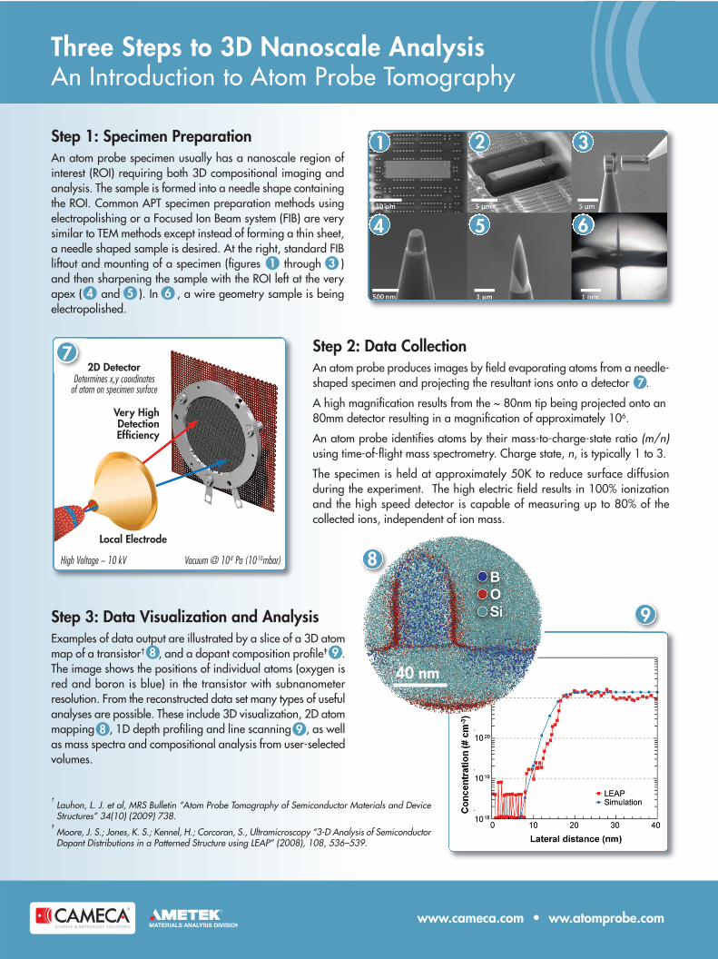
Step 3: Data Visualization and Analysis Examples of data output are illustrated by a slice of a 3D atommap of a transistor† , and a dopant composition profile‡ .The image shows the positions of individual atoms (oxygen isred and boron is blue) in the transistor with subnanometerresolution. From the reconstructed data set many types of usefulanalyses are possible. These include 3D visualization, 2D atommapping , 1D depth profiling and line scanning , as wellas mass spectra and compositional analysis from user-selectedvolumes.
Step 1: Specimen PreparationAn atom probe specimen usually has a nanoscale region ofinterest (ROI) requiring both 3D compositional imaging andanalysis. The sample is formed into a needle shape containingthe ROI. Common APT specimen preparation methods usingelectropolishing or a Focused Ion Beam system (FIB) are verysimilar to TEM methods except instead of forming a thin sheet,a needle shaped sample is desired. At the right, standard FIBliftout and mounting of a specimen (figures through )and then sharpening the sample with the ROI left at the veryapex ( and ). In , a wire geometry sample is beingelectropolished.
1
8 9
8 9
3
4 5 6
72D Detector
Determines x,y coordinates of atom on specimen surface
High Voltage ~ 10 kV Vacuum @ 10-8 Pa (10-10mbar)
Very High Detection Efficiency
Local Electrode
8
9
1 2 3
4 5 6
† Lauhon, L. J. et al, MRS Bulletin “Atom Probe Tomography of Semiconductor Materials and DeviceStructures” 34(10) (2009) 738.
‡ Moore, J. S.; Jones, K. S.; Kennel, H.; Corcoran, S., Ultramicroscopy “3-D Analysis of SemiconductorDopant Distributions in a Patterned Structure using LEAP” (2008), 108, 536–539.
Three Steps to 3D Nanoscale AnalysisAn Introduction to Atom Probe Tomography
www.cameca.com • ww.atomprobe.com
40 nm
Step 2: Data CollectionAn atom probe produces images by field evaporating atoms from a needle-shaped specimen and projecting the resultant ions onto a detector .
A high magnification results from the ~ 80nm tip being projected onto an80mm detector resulting in a magnification of approximately 106.
An atom probe identifies atoms by their mass-to-charge-state ratio (m/n)using time-of-flight mass spectrometry. Charge state, n, is typically 1 to 3.
The specimen is held at approximately 50K to reduce surface diffusionduring the experiment. The high electric field results in 100% ionizationand the high speed detector is capable of measuring up to 80% of thecollected ions, independent of ion mass.
7
Related Documents