Features • High-performance, Low-power AVR ® 8-bit Microcontroller • Advanced RISC Architecture – 131 Powerful Instructions – Most Single-clock Cycle Execution – 32 × 8 General Purpose Working Registers – Fully Static Operation – Up to 16 MIPS Throughput at 16 MHz – On-chip 2-cycle Multiplier • Nonvolatile Program and Data Memories – 16/32/64K Bytes of In-System Self-Programmable Flash Endurance: 10,000 Write/Erase Cycles – Optional Boot Code Section with Independent Lock Bits In-System Programming by On-chip Boot Program True Read-While-Write Operation – 512B/1K/2K Bytes EEPROM Endurance: 100,000 Write/Erase Cycles – 1/2/4K Bytes Internal SRAM – Programming Lock for Software Security • JTAG (IEEE std. 1149.1 Compliant) Interface – Boundary-scan Capabilities According to the JTAG Standard – Extensive On-chip Debug Support – Programming of Flash, EEPROM, Fuses, and Lock Bits through the JTAG Interface • Peripheral Features – Two 8-bit Timer/Counters with Separate Prescalers and Compare Modes – One 16-bit Timer/Counter with Separate Prescaler, Compare Mode, and Capture Mode – Real Time Counter with Separate Oscillator – Six PWM Channels – 8-channel, 10-bit ADC Differential mode with selectable gain at 1x, 10x or 200x (1) – Byte-oriented Two-wire Serial Interface – Two Programmable Serial USART – Master/Slave SPI Serial Interface – Programmable Watchdog Timer with Separate On-chip Oscillator – On-chip Analog Comparator – Interrupt and Wake-up on Pin Change • Special Microcontroller Features – Power-on Reset and Programmable Brown-out Detection – Internal Calibrated RC Oscillator – External and Internal Interrupt Sources – Six Sleep Modes: Idle, ADC Noise Reduction, Power-save, Power-down, Standby and Extended Standby • I/O and Packages – 32 Programmable I/O Lines – 44-lead TQFP, and 44-pad QFN/MLF • Operating Voltages – 2.7 - 5.5V for ATmega164P/324P/644P • Speed Grades – ATmega164P/324P/644P: 0 - 8MHz @ 2.7 - 5.5V, 0 - 16MHz @ 4.5 - 5.5V • Power Consumption at 8 MHz, 5V, 25°C for ATmega644P – Active mode: 8 mA – Idle mode: 2.4 mA – Power-down Mode: 0.8 μA 8-bit Microcontroller with 16/32/64K Bytes In-System Programmable Flash ATmega164P ATmega324P ATmega644P Automotive 7674F–AVR–09/09

Welcome message from author
This document is posted to help you gain knowledge. Please leave a comment to let me know what you think about it! Share it to your friends and learn new things together.
Transcript

8-bit Microcontroller with 16/32/64K Bytes In-SystemProgrammable Flash
ATmega164PATmega324PATmega644P
Automotive
7674F–AVR–09/09
Features• High-performance, Low-power AVR® 8-bit Microcontroller• Advanced RISC Architecture
– 131 Powerful Instructions – Most Single-clock Cycle Execution– 32 × 8 General Purpose Working Registers– Fully Static Operation– Up to 16 MIPS Throughput at 16 MHz– On-chip 2-cycle Multiplier
• Nonvolatile Program and Data Memories– 16/32/64K Bytes of In-System Self-Programmable Flash
Endurance: 10,000 Write/Erase Cycles– Optional Boot Code Section with Independent Lock Bits
In-System Programming by On-chip Boot ProgramTrue Read-While-Write Operation
– 512B/1K/2K Bytes EEPROMEndurance: 100,000 Write/Erase Cycles
– 1/2/4K Bytes Internal SRAM– Programming Lock for Software Security
• JTAG (IEEE std. 1149.1 Compliant) Interface– Boundary-scan Capabilities According to the JTAG Standard– Extensive On-chip Debug Support– Programming of Flash, EEPROM, Fuses, and Lock Bits through the JTAG Interface
• Peripheral Features– Two 8-bit Timer/Counters with Separate Prescalers and Compare Modes– One 16-bit Timer/Counter with Separate Prescaler, Compare Mode, and Capture
Mode– Real Time Counter with Separate Oscillator– Six PWM Channels– 8-channel, 10-bit ADC
Differential mode with selectable gain at 1x, 10x or 200x(1)
– Byte-oriented Two-wire Serial Interface– Two Programmable Serial USART– Master/Slave SPI Serial Interface– Programmable Watchdog Timer with Separate On-chip Oscillator– On-chip Analog Comparator– Interrupt and Wake-up on Pin Change
• Special Microcontroller Features– Power-on Reset and Programmable Brown-out Detection– Internal Calibrated RC Oscillator– External and Internal Interrupt Sources– Six Sleep Modes: Idle, ADC Noise Reduction, Power-save, Power-down, Standby
and Extended Standby• I/O and Packages
– 32 Programmable I/O Lines– 44-lead TQFP, and 44-pad QFN/MLF
• Operating Voltages– 2.7 - 5.5V for ATmega164P/324P/644P
• Speed Grades– ATmega164P/324P/644P: 0 - 8MHz @ 2.7 - 5.5V, 0 - 16MHz @ 4.5 - 5.5V
• Power Consumption at 8 MHz, 5V, 25°C for ATmega644P– Active mode: 8 mA– Idle mode: 2.4 mA– Power-down Mode: 0.8 µA
1. Pin Configurations
Figure 1-1. Pinout ATmega164P/324P/644P
Note: The large center pad underneath the QFN/MLF package should be soldered to ground on the board to ensure good mechanical stability.
PA4 (ADC4/PCINT4)
PA5 (ADC5/PCINT5)
PA6 (ADC6/PCINT6)
PA7 (ADC7/PCINT7)
AREF
GND
AVCC
PC7 (TOSC2/PCINT23)
PC6 (TOSC1/PCINT22)
PC5 (TDI/PCINT21)
PC4 (TDO/PCINT20)
(PCINT13/MOSI) PB5
(PCINT14/MISO) PB6
(PCINT15/SCK) PB7
RESET
VCC
GND
XTAL2
XTAL1
(PCINT24/RXD0) PD0
(PCINT25/TXD0) PD1
(PCINT/RXD1/26/INT0) PD2
(PC
INT
/TX
D1/2
7/IN
T1)
PD
3
(PC
INT
28/X
CK
1/O
C1B
) P
D4
(PC
INT
29/O
C1A
) P
D5
(PC
INT
30/O
C2B
/IC
P)
PD
6
(PC
INT
31/O
C2A
) P
D7
VC
C
GN
D
(PC
INT
16/S
CL)
PC
0
(PC
INT
17/S
DA
) P
C1
(PC
INT
18/T
CK
) P
C2
(PC
INT
19/T
MS
) P
C3
PB
4 (S
S/O
C0B
/PC
INT
12)
PB
3 (A
IN1/O
C0A
/PC
INT
11)
PB
2 (A
IN0/IN
T2/P
CIN
T10)
PB
1 (T
1/C
LK
O/P
CIN
T9)
PB
0 (X
CK
0/T
0/P
CIN
T8)
GN
D
VC
C
PA
0 (A
DC
0/P
CIN
T0)
PA
1 (A
DC
1/P
CIN
T1)
PA
2 (A
DC
2/P
CIN
T2)
PA
3 (A
DC
3/P
CIN
T3)
TQFP/QFN/MLF
27674F–AVR–09/09
ATmega164P/324P/644P
ATmega164P/324P/644P
2. Overview
The ATmega164P/324P/644P is a low-power CMOS 8-bit microcontroller based on the AVRenhanced RISC architecture. By executing powerful instructions in a single clock cycle, theATmega164P/324P/644P achieves throughputs approaching 1 MIPS per MHz allowing the sys-tem designer to optimize power consumption versus processing speed.
2.1 Block Diagram
Figure 2-1. Block Diagram
The AVR core combines a rich instruction set with 32 general purpose working registers. All the32 registers are directly connected to the Arithmetic Logic Unit (ALU), allowing two independentregisters to be accessed in one single instruction executed in one clock cycle. The resultingarchitecture is more code efficient while achieving throughputs up to ten times faster than con-ventional CISC microcontrollers.
CPU
GND
VCC
RESET
PowerSupervision
POR / BOD &RESET
WatchdogOscillator
WatchdogTimer
OscillatorCircuits /
ClockGeneration
XTAL1
XTAL2
PORT A (8)
PORT D (8)
PD7..0
PORT C (8)
PC5..0
TWI
SPIEEPROM
JTAG/OCD 16bit T/C 1
8bit T/C 2
8bit T/C 0
SRAMFLASH
USART 0
Internal Bandgap reference
Analog Comparator
A/DConverter
PA7..0
PORT B (8)
PB7..0
USART 1
TOSC1/PC6TOSC2/PC7
37674F–AVR–09/09
The ATmega164P/324P/644P provides the following features: 16/32/64K bytes of In-SystemProgrammable Flash with Read-While-Write capabilities, 512B/1K/2K bytes EEPROM, 1/2/4Kbytes SRAM, 32 general purpose I/O lines, 32 general purpose working registers, Real TimeCounter (RTC), three flexible Timer/Counters with compare modes and PWM, 2 USARTs, a byteoriented 2-wire Serial Interface, a 8-channel, 10-bit ADC with optional differential input stagewith programmable gain, programmable Watchdog Timer with Internal Oscillator, an SPI serialport, IEEE std. 1149.1 compliant JTAG test interface, also used for accessing the On-chipDebug system and programming and six software selectable power saving modes. The Idlemode stops the CPU while allowing the SRAM, Timer/Counters, SPI port, and interrupt systemto continue functioning. The Power-down mode saves the register contents but freezes theOscillator, disabling all other chip functions until the next interrupt or Hardware Reset. InPower-save mode, the asynchronous timer continues to run, allowing the user to maintain atimer base while the rest of the device is sleeping. The ADC Noise Reduction mode stops theCPU and all I/O modules except Asynchronous Timer and ADC, to minimize switching noiseduring ADC conversions. In Standby mode, the Crystal/Resonator Oscillator is running while therest of the device is sleeping. This allows very fast start-up combined with low power consump-tion. In Extended Standby mode, both the main Oscillator and the Asynchronous Timer continueto run.
The device is manufactured using Atmel’s high-density nonvolatile memory technology. TheOn-chip ISP Flash allows the program memory to be reprogrammed in-system through an SPIserial interface, by a conventional nonvolatile memory programmer, or by an On-chip Boot pro-gram running on the AVR core. The boot program can use any interface to download theapplication program in the application Flash memory. Software in the Boot Flash section willcontinue to run while the Application Flash section is updated, providing true Read-While-Writeoperation. By combining an 8-bit RISC CPU with In-System Self-Programmable Flash on amonolithic chip, the Atmel ATmega164P/324P/644P is a powerful microcontroller that provides ahighly flexible and cost effective solution to many embedded control applications.
The ATmega164P/324P/644P AVR is supported with a full suite of program and system devel-opment tools including: C compilers, macro assemblers, program debugger/simulators, in-circuitemulators, and evaluation kits.
2.2 Comparison Between ATmega164P, ATmega324P and ATmega644P
Table 2-1. Differences between ATmega164P and ATmega644P
Device Flash EEPROM RAM
ATmega164P 16 Kbyte 512 Bytes 1 Kbyte
ATmega324P 32 Kbyte 1 Kbyte 2 Kbyte
ATmega644P 64 Kbyte 2 Kbyte 4 Kbyte
47674F–AVR–09/09
ATmega164P/324P/644P
ATmega164P/324P/644P
2.2.1 Automotive Quality GradeThe ATmega164P/324P/644P have been developed and manufactured according to the moststringent requirements of the international standard ISO-TS-16949. This data sheet containslimit values extracted from the results of extensive characterization (Temperature and Voltage).The quality and reliability of the ATmega164P/324P/644P have been verified during regularproduct qualification as per AEC-Q100 grade 1 (–40°C to +125°C).
2.3 Pin Descriptions
2.3.1 VCC
Digital supply voltage.
2.3.2 GND
Ground.
2.3.3 Port A (PA7:PA0)
Port A serves as analog inputs to the Analog-to-digital Converter.
Port A also serves as an 8-bit bi-directional I/O port with internal pull-up resistors (selected foreach bit). The Port A output buffers have symmetrical drive characteristics with both high sinkand source capability. As inputs, Port A pins that are externally pulled low will source current ifthe pull-up resistors are activated. The Port A pins are tri-stated when a reset condition becomesactive, even if the clock is not running.
Port A also serves the functions of various special features of the ATmega164P/324P/644P aslisted on page 79.
2.3.4 Port B (PB7:PB0)
Port B is an 8-bit bi-directional I/O port with internal pull-up resistors (selected for each bit). ThePort B output buffers have symmetrical drive characteristics with both high sink and sourcecapability. As inputs, Port B pins that are externally pulled low will source current if the pull-upresistors are activated. The Port B pins are tri-stated when a reset condition becomes active,even if the clock is not running.
Port B also serves the functions of various special features of the ATmega164P/324P/644P aslisted on page 81.
Table 2-2. Temperature Grade Identification for Automotive Products
TemperatureTemperature
Identifier Comments
-40 ; +125 Z Full AutomotiveTemperature Range
57674F–AVR–09/09
2.3.5 Port C (PC7:PC0)Port C is an 8-bit bi-directional I/O port with internal pull-up resistors (selected for each bit). ThePort C output buffers have symmetrical drive characteristics with both high sink and sourcecapability. As inputs, Port C pins that are externally pulled low will source current if the pull-upresistors are activated. The Port C pins are tri-stated when a reset condition becomes active,even if the clock is not running.
Port C also serves the functions of the JTAG interface, along with special features of theATmega164P/324P/644P as listed on page 84.
2.3.6 Port D (PD7:PD0)
Port D is an 8-bit bi-directional I/O port with internal pull-up resistors (selected for each bit). ThePort D output buffers have symmetrical drive characteristics with both high sink and sourcecapability. As inputs, Port D pins that are externally pulled low will source current if the pull-upresistors are activated. The Port D pins are tri-stated when a reset condition becomes active,even if the clock is not running.
Port D also serves the functions of various special features of the ATmega164P/324P/644P aslisted on page 86.
2.3.7 RESET
Reset input. A low level on this pin for longer than the minimum pulse length will generate areset, even if the clock is not running. The minimum pulse length is given in “System and ResetCharacteristics” on page 332. Shorter pulses are not guaranteed to generate a reset.
2.3.8 XTAL1
Input to the inverting Oscillator amplifier and input to the internal clock operating circuit.
2.3.9 XTAL2
Output from the inverting Oscillator amplifier.
2.3.10 AVCC
AVCC is the supply voltage pin for Port F and the Analog-to-digital Converter. It should be exter-nally connected to VCC, even if the ADC is not used. If the ADC is used, it should be connectedto VCC through a low-pass filter.
2.3.11 AREF
This is the analog reference pin for the Analog-to-digital Converter.
67674F–AVR–09/09
ATmega164P/324P/644P
ATmega164P/324P/644P
3. Resources
A comprehensive set of development tools, application notes and datasheetsare available fordownload on http://www.atmel.com/avr.
77674F–AVR–09/09
4. About Code Examples
This documentation contains simple code examples that briefly show how to use various parts ofthe device. Be aware that not all C compiler vendors include bit definitions in the header filesand interrupt handling in C is compiler dependent. Please confirm with the C compiler documen-tation for more details.
The code examples assume that the part specific header file is included before compilation. ForI/O registers located in extended I/O map, "IN", "OUT", "SBIS", "SBIC", "CBI", and "SBI" instruc-tions must be replaced with instructions that allow access to extended I/O. Typically "LDS" and"STS" combined with "SBRS", "SBRC", "SBR", and "CBR".
87674F–AVR–09/09
ATmega164P/324P/644P
ATmega164P/324P/644P
5. AVR CPU Core
5.1 Overview
This section discusses the AVR core architecture in general. The main function of the CPU coreis to ensure correct program execution. The CPU must therefore be able to access memories,perform calculations, control peripherals, and handle interrupts.
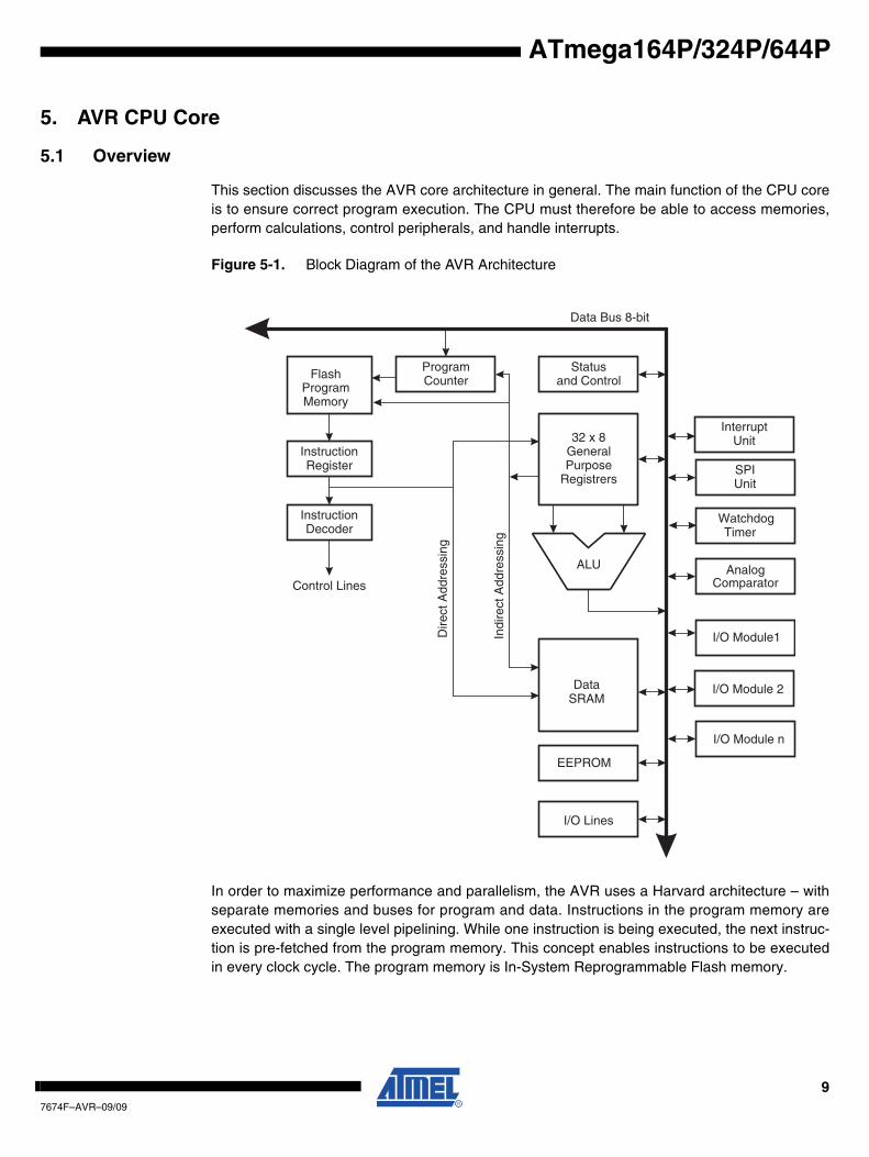
Figure 5-1. Block Diagram of the AVR Architecture
In order to maximize performance and parallelism, the AVR uses a Harvard architecture – withseparate memories and buses for program and data. Instructions in the program memory areexecuted with a single level pipelining. While one instruction is being executed, the next instruc-tion is pre-fetched from the program memory. This concept enables instructions to be executedin every clock cycle. The program memory is In-System Reprogrammable Flash memory.
FlashProgramMemory
InstructionRegister
InstructionDecoder
ProgramCounter
Control Lines
32 x 8GeneralPurpose
Registrers
ALU
Statusand Control
I/O Lines
EEPROM
Data Bus 8-bit
DataSRAM
Dire
ct A
ddre
ssin
g
Indi
rect
Add
ress
ing
InterruptUnit
SPIUnit
WatchdogTimer
AnalogComparator
I/O Module 2
I/O Module1
I/O Module n
97674F–AVR–09/09
The fast-access Register File contains 32 x 8-bit general purpose working registers with a singleclock cycle access time. This allows single-cycle Arithmetic Logic Unit (ALU) operation. In a typ-ical ALU operation, two operands are output from the Register File, the operation is executed,and the result is stored back in the Register File – in one clock cycle.
Six of the 32 registers can be used as three 16-bit indirect address register pointers for DataSpace addressing – enabling efficient address calculations. One of the these address pointerscan also be used as an address pointer for look up tables in Flash program memory. Theseadded function registers are the 16-bit X-, Y-, and Z-register, described later in this section.
The ALU supports arithmetic and logic operations between registers or between a constant anda register. Single register operations can also be executed in the ALU. After an arithmetic opera-tion, the Status Register is updated to reflect information about the result of the operation.
Program flow is provided by conditional and unconditional jump and call instructions, able todirectly address the whole address space. Most AVR instructions have a single 16-bit word for-mat. Every program memory address contains a 16- or 32-bit instruction.
Program Flash memory space is divided in two sections, the Boot Program section and theApplication Program section. Both sections have dedicated Lock bits for write and read/writeprotection. The SPM instruction that writes into the Application Flash memory section mustreside in the Boot Program section.
During interrupts and subroutine calls, the return address Program Counter (PC) is stored on theStack. The Stack is effectively allocated in the general data SRAM, and consequently the Stacksize is only limited by the total SRAM size and the usage of the SRAM. All user programs mustinitialize the SP in the Reset routine (before subroutines or interrupts are executed). The StackPointer (SP) is read/write accessible in the I/O space. The data SRAM can easily be accessedthrough the five different addressing modes supported in the AVR architecture.
The memory spaces in the AVR architecture are all linear and regular memory maps.
A flexible interrupt module has its control registers in the I/O space with an additional GlobalInterrupt Enable bit in the Status Register. All interrupts have a separate Interrupt Vector in theInterrupt Vector table. The interrupts have priority in accordance with their Interrupt Vector posi-tion. The lower the Interrupt Vector address, the higher the priority.
The I/O memory space contains 64 addresses for CPU peripheral functions as Control Regis-ters, SPI, and other I/O functions. The I/O Memory can be accessed directly, or as the DataSpace locations following those of the Register File, 0x20 - 0x5F. In addition, theATmega164P/324P/644P has Extended I/O space from 0x60 - 0xFF in SRAM where only theST/STS/STD and LD/LDS/LDD instructions can be used.
5.2 ALU – Arithmetic Logic Unit
The high-performance AVR ALU operates in direct connection with all the 32 general purposeworking registers. Within a single clock cycle, arithmetic operations between general purposeregisters or between a register and an immediate are executed. The ALU operations are dividedinto three main categories – arithmetic, logical, and bit-functions. Some implementations of thearchitecture also provide a powerful multiplier supporting both signed/unsigned multiplicationand fractional format. See the “Instruction Set” section for a detailed description.
107674F–AVR–09/09
ATmega164P/324P/644P
ATmega164P/324P/644P
5.3 Status Register
The Status Register contains information about the result of the most recently executed arithme-tic instruction. This information can be used for altering program flow in order to performconditional operations. Note that the Status Register is updated after all ALU operations, asspecified in the Instruction Set Reference. This will in many cases remove the need for using thededicated compare instructions, resulting in faster and more compact code.
The Status Register is not automatically stored when entering an interrupt routine and restoredwhen returning from an interrupt. This must be handled by software.
5.3.1 SREG – Status Register
The AVR Status Register – SREG – is defined as:
• Bit 7 – I: Global Interrupt EnableThe Global Interrupt Enable bit must be set for the interrupts to be enabled. The individual inter-rupt enable control is then performed in separate control registers. If the Global Interrupt EnableRegister is cleared, none of the interrupts are enabled independent of the individual interruptenable settings. The I-bit is cleared by hardware after an interrupt has occurred, and is set bythe RETI instruction to enable subsequent interrupts. The I-bit can also be set and cleared bythe application with the SEI and CLI instructions, as described in the instruction set reference.
• Bit 6 – T: Bit Copy StorageThe Bit Copy instructions BLD (Bit LoaD) and BST (Bit STore) use the T-bit as source or desti-nation for the operated bit. A bit from a register in the Register File can be copied into T by theBST instruction, and a bit in T can be copied into a bit in a register in the Register File by theBLD instruction.
• Bit 5 – H: Half Carry Flag The Half Carry Flag H indicates a Half Carry in some arithmetic operations. Half Carry Is usefulin BCD arithmetic. See the “Instruction Set Description” for detailed information.
• Bit 4 – S: Sign Bit, S = N ⊕ VThe S-bit is always an exclusive or between the Negative Flag N and the Two’s ComplementOverflow Flag V. See the “Instruction Set Description” for detailed information.
• Bit 3 – V: Two’s Complement Overflow FlagThe Two’s Complement Overflow Flag V supports two’s complement arithmetics. See the“Instruction Set Description” for detailed information.
• Bit 2 – N: Negative FlagThe Negative Flag N indicates a negative result in an arithmetic or logic operation. See the“Instruction Set Description” for detailed information.
• Bit 1 – Z: Zero Flag
Bit 7 6 5 4 3 2 1 0
0x3F (0x5F) I T H S V N Z C SREG
Read/Write R/W R/W R/W R/W R/W R/W R/W R/W
Initial Value 0 0 0 0 0 0 0 0
117674F–AVR–09/09
The Zero Flag Z indicates a zero result in an arithmetic or logic operation. See the “InstructionSet Description” for detailed information.
• Bit 0 – C: Carry FlagThe Carry Flag C indicates a carry in an arithmetic or logic operation. See the “Instruction SetDescription” for detailed information.
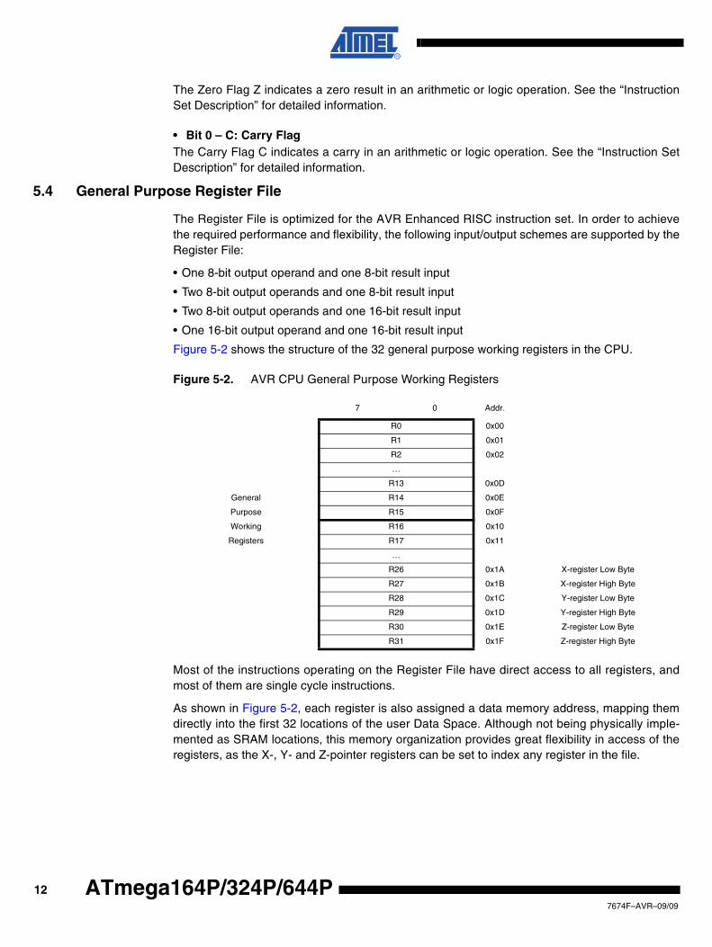
5.4 General Purpose Register File
The Register File is optimized for the AVR Enhanced RISC instruction set. In order to achievethe required performance and flexibility, the following input/output schemes are supported by theRegister File:
• One 8-bit output operand and one 8-bit result input
• Two 8-bit output operands and one 8-bit result input
• Two 8-bit output operands and one 16-bit result input
• One 16-bit output operand and one 16-bit result input
Figure 5-2 shows the structure of the 32 general purpose working registers in the CPU.
Figure 5-2. AVR CPU General Purpose Working Registers
Most of the instructions operating on the Register File have direct access to all registers, andmost of them are single cycle instructions.
As shown in Figure 5-2, each register is also assigned a data memory address, mapping themdirectly into the first 32 locations of the user Data Space. Although not being physically imple-mented as SRAM locations, this memory organization provides great flexibility in access of theregisters, as the X-, Y- and Z-pointer registers can be set to index any register in the file.
7 0 Addr.
R0 0x00
R1 0x01
R2 0x02
…
R13 0x0D
General R14 0x0E
Purpose R15 0x0F
Working R16 0x10
Registers R17 0x11
…
R26 0x1A X-register Low Byte
R27 0x1B X-register High Byte
R28 0x1C Y-register Low Byte
R29 0x1D Y-register High Byte
R30 0x1E Z-register Low Byte
R31 0x1F Z-register High Byte
127674F–AVR–09/09
ATmega164P/324P/644P
ATmega164P/324P/644P
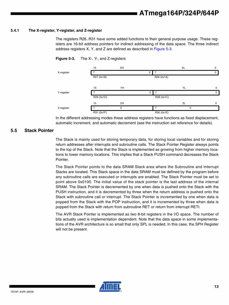
5.4.1 The X-register, Y-register, and Z-register
The registers R26..R31 have some added functions to their general purpose usage. These reg-isters are 16-bit address pointers for indirect addressing of the data space. The three indirectaddress registers X, Y, and Z are defined as described in Figure 5-3.
Figure 5-3. The X-, Y-, and Z-registers
In the different addressing modes these address registers have functions as fixed displacement,automatic increment, and automatic decrement (see the instruction set reference for details).
5.5 Stack Pointer
The Stack is mainly used for storing temporary data, for storing local variables and for storingreturn addresses after interrupts and subroutine calls. The Stack Pointer Register always pointsto the top of the Stack. Note that the Stack is implemented as growing from higher memory loca-tions to lower memory locations. This implies that a Stack PUSH command decreases the StackPointer.
The Stack Pointer points to the data SRAM Stack area where the Subroutine and InterruptStacks are located. This Stack space in the data SRAM must be defined by the program beforeany subroutine calls are executed or interrupts are enabled. The Stack Pointer must be set topoint above 0x0100. The initial value of the stack pointer is the last address of the internalSRAM. The Stack Pointer is decremented by one when data is pushed onto the Stack with thePUSH instruction, and it is decremented by three when the return address is pushed onto theStack with subroutine call or interrupt. The Stack Pointer is incremented by one when data ispopped from the Stack with the POP instruction, and it is incremented by three when data ispopped from the Stack with return from subroutine RET or return from interrupt RETI.
The AVR Stack Pointer is implemented as two 8-bit registers in the I/O space. The number ofbits actually used is implementation dependent. Note that the data space in some implementa-tions of the AVR architecture is so small that only SPL is needed. In this case, the SPH Registerwill not be present.
15 XH XL 0
X-register 7 0 7 0
R27 (0x1B) R26 (0x1A)
15 YH YL 0
Y-register 7 0 7 0
R29 (0x1D) R28 (0x1C)
15 ZH ZL 0
Z-register 7 0 7 0
R31 (0x1F) R30 (0x1E)
137674F–AVR–09/09
5.5.1 SPH and SPL – Stack Pointer High and Stack pointer Low
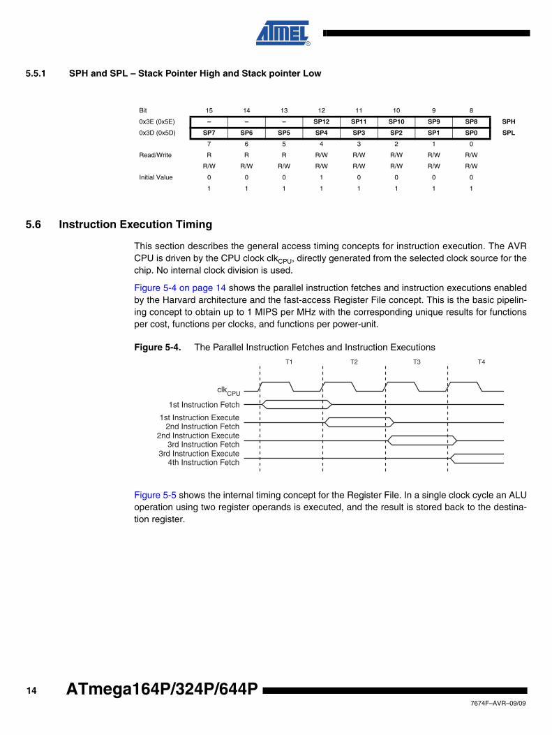
5.6 Instruction Execution Timing
This section describes the general access timing concepts for instruction execution. The AVRCPU is driven by the CPU clock clkCPU, directly generated from the selected clock source for thechip. No internal clock division is used.
Figure 5-4 on page 14 shows the parallel instruction fetches and instruction executions enabledby the Harvard architecture and the fast-access Register File concept. This is the basic pipelin-ing concept to obtain up to 1 MIPS per MHz with the corresponding unique results for functionsper cost, functions per clocks, and functions per power-unit.
Figure 5-4. The Parallel Instruction Fetches and Instruction Executions
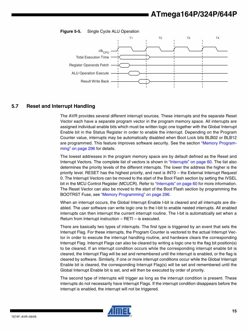
Figure 5-5 shows the internal timing concept for the Register File. In a single clock cycle an ALUoperation using two register operands is executed, and the result is stored back to the destina-tion register.
Bit 15 14 13 12 11 10 9 8
0x3E (0x5E) – – – SP12 SP11 SP10 SP9 SP8 SPH
0x3D (0x5D) SP7 SP6 SP5 SP4 SP3 SP2 SP1 SP0 SPL
7 6 5 4 3 2 1 0
Read/Write R R R R/W R/W R/W R/W R/W
R/W R/W R/W R/W R/W R/W R/W R/W
Initial Value 0 0 0 1 0 0 0 0
1 1 1 1 1 1 1 1
clk
1st Instruction Fetch
1st Instruction Execute2nd Instruction Fetch
2nd Instruction Execute3rd Instruction Fetch
3rd Instruction Execute4th Instruction Fetch
T1 T2 T3 T4
CPU
147674F–AVR–09/09
ATmega164P/324P/644P
ATmega164P/324P/644P
Figure 5-5. Single Cycle ALU Operation
5.7 Reset and Interrupt Handling
The AVR provides several different interrupt sources. These interrupts and the separate ResetVector each have a separate program vector in the program memory space. All interrupts areassigned individual enable bits which must be written logic one together with the Global InterruptEnable bit in the Status Register in order to enable the interrupt. Depending on the ProgramCounter value, interrupts may be automatically disabled when Boot Lock bits BLB02 or BLB12are programmed. This feature improves software security. See the section “Memory Program-ming” on page 296 for details.
The lowest addresses in the program memory space are by default defined as the Reset andInterrupt Vectors. The complete list of vectors is shown in “Interrupts” on page 60. The list alsodetermines the priority levels of the different interrupts. The lower the address the higher is thepriority level. RESET has the highest priority, and next is INT0 – the External Interrupt Request0. The Interrupt Vectors can be moved to the start of the Boot Flash section by setting the IVSELbit in the MCU Control Register (MCUCR). Refer to “Interrupts” on page 60 for more information.The Reset Vector can also be moved to the start of the Boot Flash section by programming theBOOTRST Fuse, see “Memory Programming” on page 296.
When an interrupt occurs, the Global Interrupt Enable I-bit is cleared and all interrupts are dis-abled. The user software can write logic one to the I-bit to enable nested interrupts. All enabledinterrupts can then interrupt the current interrupt routine. The I-bit is automatically set when aReturn from Interrupt instruction – RETI – is executed.
There are basically two types of interrupts. The first type is triggered by an event that sets theInterrupt Flag. For these interrupts, the Program Counter is vectored to the actual Interrupt Vec-tor in order to execute the interrupt handling routine, and hardware clears the correspondingInterrupt Flag. Interrupt Flags can also be cleared by writing a logic one to the flag bit position(s)to be cleared. If an interrupt condition occurs while the corresponding interrupt enable bit iscleared, the Interrupt Flag will be set and remembered until the interrupt is enabled, or the flag iscleared by software. Similarly, if one or more interrupt conditions occur while the Global InterruptEnable bit is cleared, the corresponding Interrupt Flag(s) will be set and remembered until theGlobal Interrupt Enable bit is set, and will then be executed by order of priority.
The second type of interrupts will trigger as long as the interrupt condition is present. Theseinterrupts do not necessarily have Interrupt Flags. If the interrupt condition disappears before theinterrupt is enabled, the interrupt will not be triggered.
Total Execution Time
Register Operands Fetch
ALU Operation Execute
Result Write Back
T1 T2 T3 T4
clkCPU
157674F–AVR–09/09
When the AVR exits from an interrupt, it will always return to the main program and execute onemore instruction before any pending interrupt is served.
Note that the Status Register is not automatically stored when entering an interrupt routine, norrestored when returning from an interrupt routine. This must be handled by software.
When using the CLI instruction to disable interrupts, the interrupts will be immediately disabled.No interrupt will be executed after the CLI instruction, even if it occurs simultaneously with theCLI instruction. The following example shows how this can be used to avoid interrupts during thetimed EEPROM write sequence..
When using the SEI instruction to enable interrupts, the instruction following SEI will be exe-cuted before any pending interrupts, as shown in this example.
Assembly Code Example
in r16, SREG ; store SREG value
cli ; disable interrupts during timed sequence
sbi EECR, EEMPE ; start EEPROM write
sbi EECR, EEPE
out SREG, r16 ; restore SREG value (I-bit)
C Code Example
char cSREG;
cSREG = SREG; /* store SREG value */
/* disable interrupts during timed sequence */
__disable_interrupt();
EECR |= (1<<EEMPE); /* start EEPROM write */
EECR |= (1<<EEPE);
SREG = cSREG; /* restore SREG value (I-bit) */
Assembly Code Example
sei ; set Global Interrupt Enable
sleep; enter sleep, waiting for interrupt
; note: will enter sleep before any pending
; interrupt(s)
C Code Example
__enable_interrupt(); /* set Global Interrupt Enable */
__sleep(); /* enter sleep, waiting for interrupt */
/* note: will enter sleep before any pending interrupt(s) */
167674F–AVR–09/09
ATmega164P/324P/644P
ATmega164P/324P/644P
5.7.1 Interrupt Response TimeThe interrupt execution response for all the enabled AVR interrupts is five clock cycles minimum.After five clock cycles the program vector address for the actual interrupt handling routine is exe-cuted. During these five clock cycle period, the Program Counter is pushed onto the Stack. Thevector is normally a jump to the interrupt routine, and this jump takes three clock cycles. If aninterrupt occurs during execution of a multi-cycle instruction, this instruction is completed beforethe interrupt is served. If an interrupt occurs when the MCU is in sleep mode, the interrupt exe-cution response time is increased by five clock cycles. This increase comes in addition to thestart-up time from the selected sleep mode.
A return from an interrupt handling routine takes five clock cycles. During these five clock cycles,the Program Counter (three bytes) is popped back from the Stack, the Stack Pointer is incre-mented by three, and the I-bit in SREG is set.
177674F–AVR–09/09
6. AVR Memories
6.1 Overview
This section describes the different memories in the ATmega164P/324P/644P. The AVR archi-tecture has two main memory spaces, the Data Memory and the Program Memory space. Inaddition, the ATmega164P/324P/644P features an EEPROM Memory for data storage. All threememory spaces are linear and regular.
6.2 In-System Reprogrammable Flash Program Memory
The ATmega164P/324P/644P contains 16/32/64K bytes On-chip In-System ReprogrammableFlash memory for program storage. Since all AVR instructions are 16 or 32 bits wide, the Flashis organized as 32/64 x 16. For software security, the Flash Program memory space is dividedinto two sections, Boot Program section and Application Program section.
The Flash memory has an endurance of at least 10,000 wri te/erase cycles. TheATmega164P/324P/644P Program Counter (PC) is 15/16 bits wide, thus addressing the 32/64Kprogram memory locations. The operation of Boot Program section and associated Boot Lockbits for software protection are described in detail in “Memory Programming” on page 296.“Memory Programming” on page 296 contains a detailed description on Flash data serial down-loading using the SPI pins or the JTAG interface.
Constant tables can be allocated within the entire program memory address space (see the LPM– Load Program Memory instruction description.
Timing diagrams for instruction fetch and execution are presented in “Instruction Execution Tim-ing” on page 14.
187674F–AVR–09/09
ATmega164P/324P/644P
ATmega164P/324P/644P
Figure 6-1. Program Memory Map
6.3 SRAM Data Memory
Figure 6-2 shows how the ATmega164P/324P/644P SRAM Memory is organized.
The ATmega164P/324P/644P is a complex microcontroller with more peripheral units than canbe supported within the 64 location reserved in the Opcode for the IN and OUT instructions. Forthe Extended I/O space from $060 - $FF in SRAM, only the ST/STS/STD and LD/LDS/LDDinstructions can be used.
The first 4,352 Data Memory locations address both the Register File, the I/O Memory,Extended I/O Memory, and the internal data SRAM. The first 32 locations address the Registerfile, the next 64 location the standard I/O Memory, then 160 locations of Extended I/O memoryand the next 4,096 locations address the internal data SRAM.
The five different addressing modes for the data memory cover: Direct, Indirect with Displace-ment, Indirect, Indirect with Pre-decrement, and Indirect with Post-increment. In the Register file,registers R26 to R31 feature the indirect addressing pointer registers.
The direct addressing reaches the entire data space.
The Indirect with Displacement mode reaches 63 address locations from the base address givenby the Y- or Z-register.
When using register indirect addressing modes with automatic pre-decrement and post-incre-ment, the address registers X, Y, and Z are decremented or incremented.
Application Flash Section
Boot Flash Section
Program Memory
0x1FFF
0x0000
197674F–AVR–09/09
The 32 general purpose working registers, 64 I/O registers, 160 Extended I/O Registers and the1024/2048/4096 bytes of internal data SRAM in the ATmega164P/324P/644P are all accessiblethrough all these addressing modes. The Register File is described in “General Purpose Regis-ter File” on page 12.
Figure 6-2. Data Memory Map
6.3.1 Data Memory Access Times
This section describes the general access timing concepts for internal memory access. Theinternal data SRAM access is performed in two clkCPU cycles as described in Figure 6-3.
Figure 6-3. On-chip Data SRAM Access Cycles
32 Registers64 I/O Registers
Internal SRAM(1024/2048/4096 x 8)
$0000 - $001F$0020 - $005F
$10FF
$0060 - $00FF
Data Memory
160 Ext I/O Reg.$0100
clk
WR
RD
Data
Data
Address Address valid
T1 T2 T3
Compute Address
Rea
dW
rite
CPU
Memory Access Instruction Next Instruction
207674F–AVR–09/09
ATmega164P/324P/644P
ATmega164P/324P/644P
6.4 EEPROM Data Memory
The ATmega164P/324P/644P contains 512B/1K/2K bytes of data EEPROM memory. It is orga-nized as a separate data space, in which single bytes can be read and written. The EEPROMhas an endurance of at least 100,000 write/erase cycles. The access between the EEPROM andthe CPU is described in the following, specifying the EEPROM Address Registers, the EEPROMData Register, and the EEPROM Control Register.
For a detailed description of SPI, JTAG and Parallel data downloading to the EEPROM, seepage 311, page 315, and page 300 respectively.
6.4.1 EEPROM Read/Write Access
The EEPROM Access Registers are accessible in the I/O space. See “Register Description” onpage 23 for details.
The write access time for the EEPROM is given in Table 6-2 on page 25. A self-timing function,however, lets the user software detect when the next byte can be written. If the user code con-tains instructions that write the EEPROM, some precautions must be taken. In heavily filteredpower supplies, VCC is likely to rise or fall slowly on power-up/down. This causes the device forsome period of time to run at a voltage lower than specified as minimum for the clock frequencyused. See “Preventing EEPROM Corruption” on page 21. for details on how to avoid problems inthese situations.
In order to prevent unintentional EEPROM writes, a specific write procedure must be followed.Refer to the description of the EEPROM Control Register for details on this.
When the EEPROM is read, the CPU is halted for four clock cycles before the next instruction isexecuted. When the EEPROM is written, the CPU is halted for two clock cycles before the nextinstruction is executed.
6.4.2 Preventing EEPROM Corruption
During periods of low VCC, the EEPROM data can be corrupted because the supply voltage istoo low for the CPU and the EEPROM to operate properly. These issues are the same as forboard level systems using EEPROM, and the same design solutions should be applied.
An EEPROM data corruption can be caused by two situations when the voltage is too low. First,a regular write sequence to the EEPROM requires a minimum voltage to operate correctly. Sec-ondly, the CPU itself can execute instructions incorrectly, if the supply voltage is too low.
EEPROM data corruption can easily be avoided by following this design recommendation:
Keep the AVR RESET active (low) during periods of insufficient power supply voltage. This canbe done by enabling the internal Brown-out Detector (BOD). If the detection level of the internalBOD does not match the needed detection level, an external low VCC reset Protection circuit canbe used. If a reset occurs while a write operation is in progress, the write operation will be com-pleted provided that the power supply voltage is sufficient.
217674F–AVR–09/09
6.5 I/O Memory
The I/O space definition of the ATmega164P/324P/644P is shown in “Register Summary” onpage 356.
All ATmega164P/324P/644P I/Os and peripherals are placed in the I/O space. All I/O locationsmay be accessed by the LD/LDS/LDD and ST/STS/STD instructions, transferring data betweenthe 32 general purpose working registers and the I/O space. I/O Registers within the addressrange 0x00 - 0x1F are directly bit-accessible using the SBI and CBI instructions. In these regis-ters, the value of single bits can be checked by using the SBIS and SBIC instructions. Refer tothe instruction set section for more details. When using the I/O specific commands IN and OUT,the I/O addresses 0x00 - 0x3F must be used. When addressing I/O Registers as data spaceus ing LD and ST ins t ruc t ions , 0x20 mus t be added to these addresses . TheATmega164P/324P/644P is a complex microcontroller with more peripheral units than can besupported within the 64 location reserved in Opcode for the IN and OUT instructions. For theExtended I/O space from 0x60 - 0xFF in SRAM, only the ST/STS/STD and LD/LDS/LDD instruc-tions can be used.
For compatibility with future devices, reserved bits should be written to zero if accessed.Reserved I/O memory addresses should never be written.
Some of the Status Flags are cleared by writing a logical one to them. Note that, unlike mostother AVRs, the CBI and SBI instructions will only operate on the specified bit, and can thereforebe used on registers containing such Status Flags. The CBI and SBI instructions work with reg-isters 0x00 to 0x1F only.
The I/O and peripherals control registers are explained in later sections.
The ATmega164P/324P/644P contains three General Purpose I/O Registers, see “RegisterDescription” on page 23. These registers can be used for storing any information, and they areparticularly useful for storing global variables and Status Flags. General Purpose I/O Registerswithin the address range 0x00 - 0x1F are directly bit-accessible using the SBI, CBI, SBIS, andSBIC instructions.
227674F–AVR–09/09
ATmega164P/324P/644P
ATmega164P/324P/644P
6.6 Register Description
6.6.1 EEARH and EEARL – The EEPROM Address Register
• Bits 15:12 – Res: Reserved BitsThese bits are reserved bits in the ATmega164P/324P/644P and will always read as zero.
• Bits 11:0 – EEAR8:0: EEPROM AddressThe EEPROM Address Registers – EEARH and EEARL specify the EEPROM address in the 4Kbytes EEPROM space. The EEPROM data bytes are addressed linearly between 0 and 4096.The initial value of EEAR is undefined. A proper value must be written before the EEPROM maybe accessed.
6.6.2 EEDR – The EEPROM Data Register
• Bits 7:0 – EEDR7:0: EEPROM DataFor the EEPROM write operation, the EEDR Register contains the data to be written to theEEPROM in the address given by the EEAR Register. For the EEPROM read operation, theEEDR contains the data read out from the EEPROM at the address given by EEAR.
6.6.3 EECR – The EEPROM Control Register
• Bits 7:6 – Res: Reserved BitsThese bits are reserved bits in the ATmega164P/324P/644P and will always read as zero.
• Bits 5:4 – EEPM1 and EEPM0: EEPROM Programming Mode BitsThe EEPROM Programming mode bit setting defines which programming action that will be trig-gered when writing EEPE. It is possible to program data in one atomic operation (erase the oldvalue and program the new value) or to split the Erase and Write operations in two differentoperations. The Programming times for the different modes are shown in Table 6-1 on page 24.
Bit 15 14 13 12 11 10 9 8
0x22 (0x42) – – – – EEAR11 EEAR10 EEAR9 EEAR8 EEARH
0x21 (0x41) EEAR7 EEAR6 EEAR5 EEAR4 EEAR3 EEAR2 EEAR1 EEAR0 EEARL
7 6 5 4 3 2 1 0
Read/Write R R R R R/W R/W R/W R/W
R/W R/W R/W R/W R/W R/W R/W R/W
Initial Value 0 0 0 0 X X X X
X X X X X X X X
Bit 7 6 5 4 3 2 1 0
0x20 (0x40) MSB LSB EEDR
Read/Write R/W R/W R/W R/W R/W R/W R/W R/W
Initial Value 0 0 0 0 0 0 0 0
Bit 7 6 5 4 3 2 1 0
0x1F (0x3F) – – EEPM1 EEPM0 EERIE EEMPE EEPE EERE EECR
Read/Write R R R/W R/W R/W R/W R/W R/W
Initial Value 0 0 X X 0 0 X 0
237674F–AVR–09/09
While EEPE is set, any write to EEPMn will be ignored. During reset, the EEPMn bits will bereset to 0b00 unless the EEPROM is busy programming.
• Bit 3 – EERIE: EEPROM Ready Interrupt EnableWriting EERIE to one enables the EEPROM Ready Interrupt if the I bit in SREG is set. WritingEERIE to zero disables the interrupt. The EEPROM Ready interrupt generates a constant inter-rupt when EEPE is cleared.
• Bit 2 – EEMPE: EEPROM Master Programming EnableThe EEMPE bit determines whether setting EEPE to one causes the EEPROM to be written.When EEMPE is set, setting EEPE within four clock cycles will write data to the EEPROM at theselected address If EEMPE is zero, setting EEPE will have no effect. When EEMPE has beenwritten to one by software, hardware clears the bit to zero after four clock cycles. See thedescription of the EEPE bit for an EEPROM write procedure.
• Bit 1 – EEPE: EEPROM Programming EnableThe EEPROM Write Enable Signal EEPE is the write strobe to the EEPROM. When addressand data are correctly set up, the EEPE bit must be written to one to write the value into theEEPROM. The EEMPE bit must be written to one before a logical one is written to EEPE, other-wise no EEPROM write takes place. The following procedure should be followed when writingthe EEPROM (the order of steps 3 and 4 is not essential):
1. Wait until EEPE becomes zero.
2. Wait until SELFPRGEN in SPMCSR becomes zero.
3. Write new EEPROM address to EEAR (optional).
4. Write new EEPROM data to EEDR (optional).
5. Write a logical one to the EEMPE bit while writing a zero to EEPE in EECR.
6. Within four clock cycles after setting EEMPE, write a logical one to EEPE.
The EEPROM can not be programmed during a CPU write to the Flash memory. The softwaremust check that the Flash programming is completed before initiating a new EEPROM write.Step 2 is only relevant if the software contains a Boot Loader allowing the CPU to program theFlash. If the Flash is never being updated by the CPU, step 2 can be omitted. See “Memory Pro-gramming” on page 296 for details about Boot programming.
Caution: An interrupt between step 5 and step 6 will make the write cycle fail, since theEEPROM Master Write Enable will time-out. If an interrupt routine accessing the EEPROM isinterrupting another EEPROM access, the EEAR or EEDR Register will be modified, causing theinterrupted EEPROM access to fail. It is recommended to have the Global Interrupt Flag clearedduring all the steps to avoid these problems.
Table 6-1. EEPROM Mode Bits
EEPM1 EEPM0Programming
Time Operation
0 0 3.4 ms Erase and Write in one operation (Atomic Operation)
0 1 1.8 ms Erase Only
1 0 1.8 ms Write Only
1 1 – Reserved for future use
247674F–AVR–09/09
ATmega164P/324P/644P
ATmega164P/324P/644P
When the write access time has elapsed, the EEPE bit is cleared by hardware. The user soft-ware can poll this bit and wait for a zero before writing the next byte. When EEPE has been set,the CPU is halted for two cycles before the next instruction is executed.
• Bit 0 – EERE: EEPROM Read EnableThe EEPROM Read Enable Signal EERE is the read strobe to the EEPROM. When the correctaddress is set up in the EEAR Register, the EERE bit must be written to a logic one to trigger theEEPROM read. The EEPROM read access takes one instruction, and the requested data isavailable immediately. When the EEPROM is read, the CPU is halted for four cycles before thenext instruction is executed.
The user should poll the EEPE bit before starting the read operation. If a write operation is inprogress, it is neither possible to read the EEPROM, nor to change the EEAR Register.
The calibrated Oscillator is used to time the EEPROM accesses. Table 6-2 on page 25 lists thetypical programming time for EEPROM access from the CPU.
Table 6-2. EEPROM Programming Time
Symbol Number of Calibrated RC Oscillator Cycles Typ Programming Time
EEPROM write (from CPU)
26,368 3.3 ms
257674F–AVR–09/09
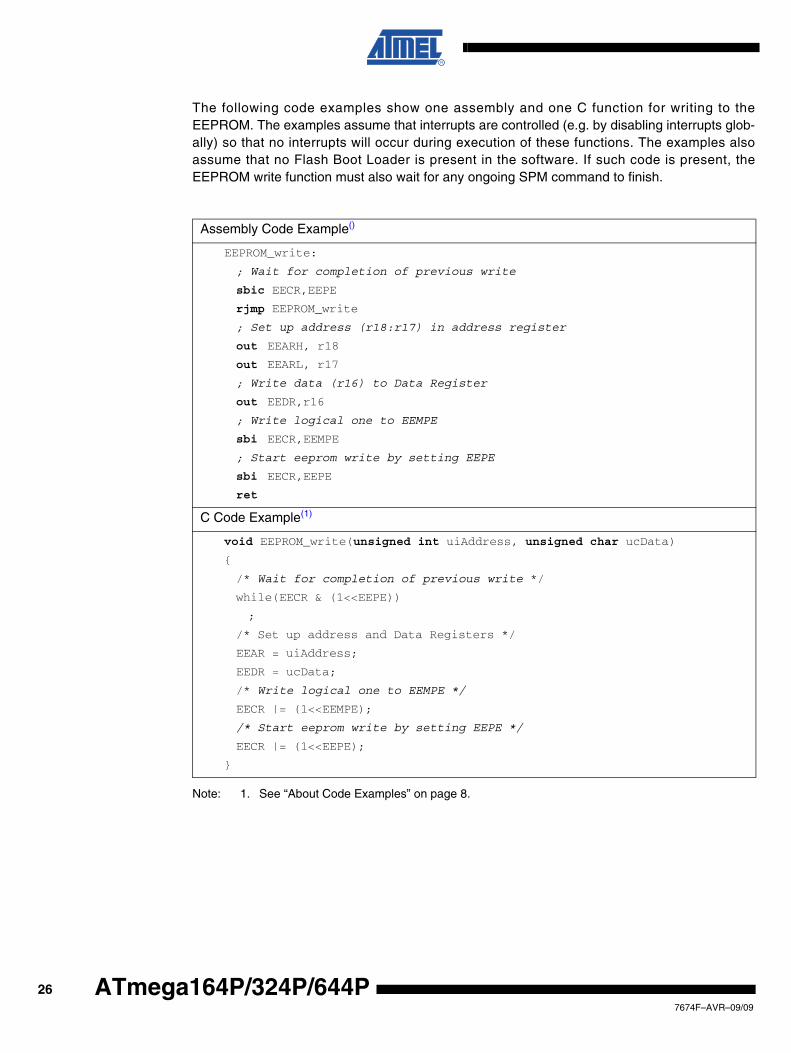
The following code examples show one assembly and one C function for writing to theEEPROM. The examples assume that interrupts are controlled (e.g. by disabling interrupts glob-ally) so that no interrupts will occur during execution of these functions. The examples alsoassume that no Flash Boot Loader is present in the software. If such code is present, theEEPROM write function must also wait for any ongoing SPM command to finish.
Note: 1. See “About Code Examples” on page 8.
Assembly Code Example()
EEPROM_write:
; Wait for completion of previous write
sbic EECR,EEPE
rjmp EEPROM_write
; Set up address (r18:r17) in address register
out EEARH, r18
out EEARL, r17
; Write data (r16) to Data Register
out EEDR,r16
; Write logical one to EEMPE
sbi EECR,EEMPE
; Start eeprom write by setting EEPE
sbi EECR,EEPE
ret
C Code Example(1)
void EEPROM_write(unsigned int uiAddress, unsigned char ucData)
{
/* Wait for completion of previous write */
while(EECR & (1<<EEPE))
;
/* Set up address and Data Registers */
EEAR = uiAddress;
EEDR = ucData;
/* Write logical one to EEMPE */
EECR |= (1<<EEMPE);
/* Start eeprom write by setting EEPE */
EECR |= (1<<EEPE);
}
267674F–AVR–09/09
ATmega164P/324P/644P
ATmega164P/324P/644P
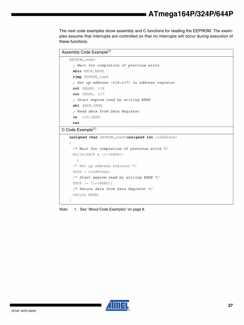
The next code examples show assembly and C functions for reading the EEPROM. The exam-ples assume that interrupts are controlled so that no interrupts will occur during execution ofthese functions.
Note: 1. See “About Code Examples” on page 8.
Assembly Code Example(1)
EEPROM_read:
; Wait for completion of previous write
sbic EECR,EEPE
rjmp EEPROM_read
; Set up address (r18:r17) in address register
out EEARH, r18
out EEARL, r17
; Start eeprom read by writing EERE
sbi EECR,EERE
; Read data from Data Register
in r16,EEDR
ret
C Code Example(1)
unsigned char EEPROM_read(unsigned int uiAddress)
{
/* Wait for completion of previous write */
while(EECR & (1<<EEPE))
;
/* Set up address register */
EEAR = uiAddress;
/* Start eeprom read by writing EERE */
EECR |= (1<<EERE);
/* Return data from Data Register */
return EEDR;
}
277674F–AVR–09/09
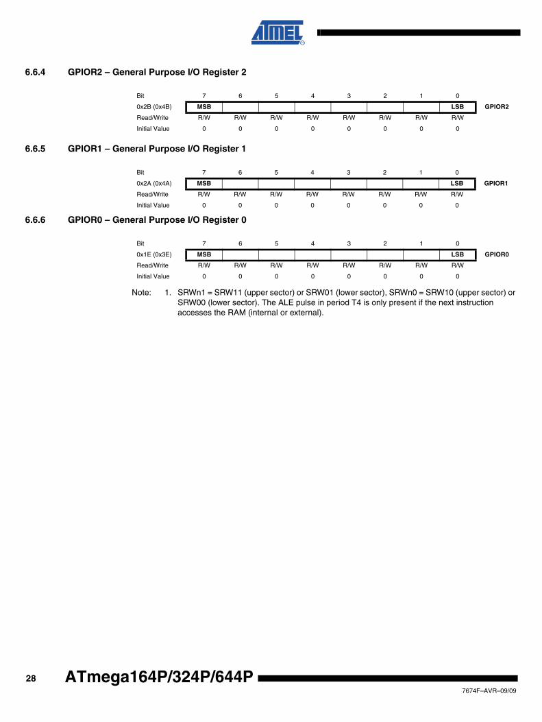
6.6.4 GPIOR2 – General Purpose I/O Register 2
6.6.5 GPIOR1 – General Purpose I/O Register 1
6.6.6 GPIOR0 – General Purpose I/O Register 0
Note: 1. SRWn1 = SRW11 (upper sector) or SRW01 (lower sector), SRWn0 = SRW10 (upper sector) or SRW00 (lower sector). The ALE pulse in period T4 is only present if the next instruction accesses the RAM (internal or external).
Bit 7 6 5 4 3 2 1 0
0x2B (0x4B) MSB LSB GPIOR2
Read/Write R/W R/W R/W R/W R/W R/W R/W R/W
Initial Value 0 0 0 0 0 0 0 0
Bit 7 6 5 4 3 2 1 0
0x2A (0x4A) MSB LSB GPIOR1
Read/Write R/W R/W R/W R/W R/W R/W R/W R/W
Initial Value 0 0 0 0 0 0 0 0
Bit 7 6 5 4 3 2 1 0
0x1E (0x3E) MSB LSB GPIOR0
Read/Write R/W R/W R/W R/W R/W R/W R/W R/W
Initial Value 0 0 0 0 0 0 0 0
287674F–AVR–09/09
ATmega164P/324P/644P
ATmega164P/324P/644P
7. System Clock and Clock Options
7.1 Clock Systems and their Distribution
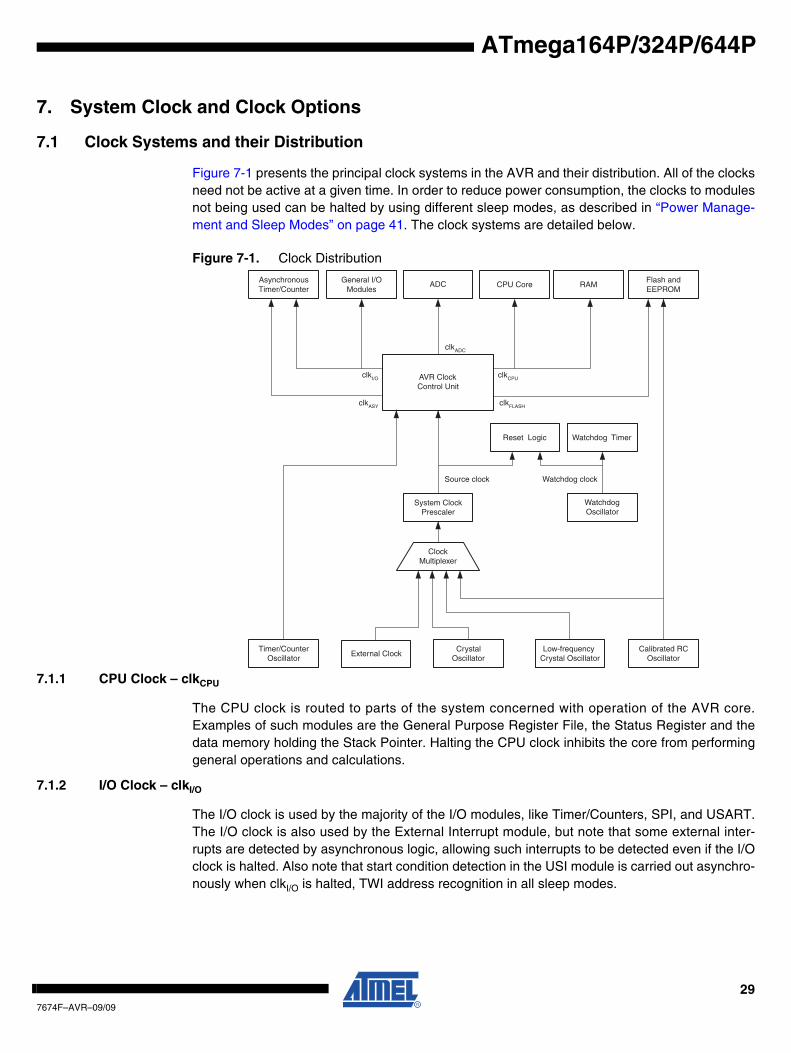
Figure 7-1 presents the principal clock systems in the AVR and their distribution. All of the clocksneed not be active at a given time. In order to reduce power consumption, the clocks to modulesnot being used can be halted by using different sleep modes, as described in “Power Manage-ment and Sleep Modes” on page 41. The clock systems are detailed below.
Figure 7-1. Clock Distribution
7.1.1 CPU Clock – clkCPU
The CPU clock is routed to parts of the system concerned with operation of the AVR core.Examples of such modules are the General Purpose Register File, the Status Register and thedata memory holding the Stack Pointer. Halting the CPU clock inhibits the core from performinggeneral operations and calculations.
7.1.2 I/O Clock – clkI/O
The I/O clock is used by the majority of the I/O modules, like Timer/Counters, SPI, and USART.The I/O clock is also used by the External Interrupt module, but note that some external inter-rupts are detected by asynchronous logic, allowing such interrupts to be detected even if the I/Oclock is halted. Also note that start condition detection in the USI module is carried out asynchro-nously when clkI/O is halted, TWI address recognition in all sleep modes.
General I/OModules
AsynchronousTimer/Counter
CPU Core RAM
clkI/O
clkASY
AVR ClockControl Unit
clkCPU
Flash andEEPROM
clkFLASH
Source clock
Watchdog Timer
WatchdogOscillator
Reset Logic
ClockMultiplexer
Watchdog clock
Calibrated RCOscillator
Timer/CounterOscillator
CrystalOscillator
Low-frequencyCrystal Oscillator
External Clock
ADC
clkADC
System ClockPrescaler
297674F–AVR–09/09
7.1.3 Flash Clock – clkFLASH
The Flash clock controls operation of the Flash interface. The Flash clock is usually active simul-taneously with the CPU clock.
7.1.4 Asynchronous Timer Clock – clkASY
The Asynchronous Timer clock allows the Asynchronous Timer/Counter to be clocked directlyfrom an external clock or an external 32 kHz clock crystal. The dedicated clock domain allowsusing this Timer/Counter as a real-time counter even when the device is in sleep mode.
7.1.5 ADC Clock – clkADC
The ADC is provided with a dedicated clock domain. This allows halting the CPU and I/O clocksin order to reduce noise generated by digital circuitry. This gives more accurate ADC conversionresults.
7.2 Clock Sources
The device has the following clock source options, selectable by Flash Fuse bits as shownbelow. The clock from the selected source is input to the AVR clock generator, and routed to theappropriate modules.
Note: 1. For all fuses “1” means unprogrammed while “0” means programmed.
7.2.1 Default Clock Source
The device is shipped with internal RC oscillator at 8.0MHz and with the fuse CKDIV8 pro-grammed, resulting in 1.0MHz system clock. The startup time is set to maximum and time-outperiod enabled. (CKSEL = "0010", SUT = "10", CKDIV8 = "0"). The default setting ensures thatall users can make their desired clock source setting using any available programming interface.
Table 7-1. Device Clocking Options Select(1)
Device Clocking Option CKSEL3..0
Low Power Crystal Oscillator 1111 - 1000
Full Swing Crystal Oscillator 0111 - 0110
Low Frequency Crystal Oscillator 0101 - 0100
Internal 128 kHz RC Oscillator 0011
Calibrated Internal RC Oscillator 0010
External Clock 0000
Reserved 0001
307674F–AVR–09/09
ATmega164P/324P/644P
ATmega164P/324P/644P
7.2.2 Clock Startup SequenceAny clock source needs a sufficient VCC to start oscillating and a minimum number of oscillatingcycles before it can be considered stable.
To ensure sufficient VCC, the device issues an internal reset with a time-out delay (tTOUT) afterthe device reset is released by all other reset sources. “On-chip Debug System” on page 45describes the start conditions for the internal reset. The delay (tTOUT) is timed from the WatchdogOscillator and the number of cycles in the delay is set by the SUTx and CKSELx fuse bits. Theselectable delays are shown in Table 7-2. The frequency of the Watchdog Oscillator is voltagedependent as shown in Section 27. “ATmega644P Typical Characteristics” on page 338.
Main purpose of the delay is to keep the AVR in reset until it is supplied with minimum Vcc. Thedelay will not monitor the actual voltage and it will be required to select a delay longer than theVcc rise time. If this is not possible, an internal or external Brown-Out Detection circuit should beused. A BOD circuit will ensure sufficient Vcc before it releases the reset, and the time-out delaycan be disabled. Disabling the time-out delay without utilizing a Brown-Out Detection circuit isnot recommended.
The oscillator is required to oscillate for a minimum number of cycles before the clock is consid-ered stable. An internal ripple counter monitors the oscillator output clock, and keeps the internalreset active for a given number of clock cycles. The reset is then released and the device willstart to execute. The recommended oscillator start-up time is dependent on the clock type, andvaries from 6 cycles for an externally applied clock to 32K cycles for a low frequency crystal.
The start-up sequence for the clock includes both the time-out delay and the start-up time whenthe device starts up from reset. When starting up from Power-save or Power-down mode, Vcc isassumed to be at a sufficient level and only the start-up time is included.
7.2.3 Clock Source Connections
The pins XTAL1 and XTAL2 are input and output, respectively, of an inverting amplifier whichcan be configured for use as an On-chip Oscillator, as shown in Figure 7-2 on page 32. Either aquartz crystal or a ceramic resonator may be used.
C1 and C2 should always be equal for both crystals and resonators. The optimal value of thecapacitors depends on the crystal or resonator in use, the amount of stray capacitance, and theelectromagnetic noise of the environment. For ceramic resonators, the capacitor values given bythe manufacturer should be used.
Table 7-2. Number of Watchdog Oscillator Cycles
Typ Time-out (VCC = 5.0V) Typ Time-out (VCC = 3.0V) Number of Cycles
0 ms 0 ms 0
4.1 ms 4.3 ms 512
65 ms 69 ms 8K (8,192)
317674F–AVR–09/09
Figure 7-2. Crystal Oscillator Connections
7.3 Low Power Crystal OscillatorThis Crystal Oscillator is a low power oscillator, with reduced voltage swing on the XTAL2 out-put. It gives the lowest power consumption, but is not capable of driving other clock inputs, andmay be more susceptible to noise in noisy environments. In these cases, refer to the “Full SwingCrystal Oscillator” on page 33.
Some initial guidelines for choosing capacitors for use with crystals are given in Table 7-3. Thecrystal should be connected as described in “Clock Source Connections” on page 31.
The Low Power Oscillator can operate in three different modes, each optimized for a specific fre-quency range. The operating mode is selected by the fuses CKSEL3..1 as shown in Table 7-3.
Notes: 1. The frequency ranges are preliminary values. Actual values are TBD.2. This option should not be used with crystals, only with ceramic resonators.3. If 8 MHz frequency exceeds the specification of the device (depends on VCC), the CKDIV8
Fuse can be programmed in order to divide the internal frequency by 8. It must be ensured that the resulting divided clock meets the frequency specification of the device.
The CKSEL0 Fuse together with the SUT1..0 Fuses select the start-up times as shown in Table7-4.
XTAL2
XTAL1
GND
C2
C1
Table 7-3. Low Power Crystal Oscillator Operating Modes(3)
Frequency Range(1) (MHz) CKSEL3..1Recommended Range for Capacitors C1
and C2 (pF)
0.4 - 0.9 100(2) –
0.9 - 3.0 101 12 - 22
3.0 - 8.0 110 12 - 22
8.0 - 16.0 111 12 - 22
327674F–AVR–09/09
ATmega164P/324P/644P
ATmega164P/324P/644P
Notes: 1. These options should only be used when not operating close to the maximum frequency of the device, and only if frequency stability at start-up is not important for the application. These options are not suitable for crystals.
2. These options are intended for use with ceramic resonators and will ensure frequency stability at start-up. They can also be used with crystals when not operating close to the maximum fre-quency of the device, and if frequency stability at start-up is not important for the application.
7.4 Full Swing Crystal Oscillator
This Crystal Oscillator is a full swing oscillator, with rail-to-rail swing on the XTAL2 output. This isuseful for driving other clock inputs and in noisy environments. The current consumption ishigher than the “Low Power Crystal Oscillator” on page 32. Note that the Full Swing CrystalOscillator will only operate for Vcc = 2.7 - 5.5 volts.
Some initial guidelines for choosing capacitors for use with crystals are given in Table 7-6. Thecrystal should be connected as described in “Clock Source Connections” on page 31.
The operating mode is selected by the fuses CKSEL3..1 as shown in Table 7-5.
Notes: 1. The frequency ranges are preliminary values. Actual values are TBD.2. If 8 MHz frequency exceeds the specification of the device (depends on VCC), the CKDIV8
Fuse can be programmed in order to divide the internal frequency by 8. It must be ensured that the resulting divided clock meets the frequency specification of the device.
Table 7-4. Start-up Times for the Low Power Crystal Oscillator Clock Selection
Oscillator Source / Power Conditions
Start-up Time from Power-down and
Power-save
Additional Delay from Reset (VCC = 5.0V) CKSEL0 SUT1..0
Ceramic resonator, fast rising power
258 CK 14CK + 4.1 ms(1) 0 00
Ceramic resonator, slowly rising power
258 CK 14CK + 65 ms(1) 0 01
Ceramic resonator, BOD enabled
1K CK 14CK(2) 0 10
Ceramic resonator, fast rising power
1K CK 14CK + 4.1 ms(2) 0 11
Ceramic resonator, slowly rising power
1K CK 14CK + 65 ms(2) 1 00
Crystal Oscillator, BOD enabled
16K CK 14CK 1 01
Crystal Oscillator, fast rising power
16K CK 14CK + 4.1 ms 1 10
Crystal Oscillator, slowly rising power
16K CK 14CK + 65 ms 1 11
Table 7-5. Full Swing Crystal Oscillator operating modes(2)
Frequency Range(1) (MHz) CKSEL3..1Recommended Range for Capacitors C1
and C2 (pF)
0.4 - 16 011 12 - 22
337674F–AVR–09/09
Notes: 1. These options should only be used when not operating close to the maximum frequency of the device, and only if frequency stability at start-up is not important for the application. These options are not suitable for crystals.
2. These options are intended for use with ceramic resonators and will ensure frequency stability at start-up. They can also be used with crystals when not operating close to the maximum fre-quency of the device, and if frequency stability at start-up is not important for the application.
7.5 Low Frequency Crystal Oscillator
The Low-frequency Crystal Oscillator is optimized for use with a 32.768 kHz watch crystal.When selecting crystals, load capasitance and crystal’s Equivalent Series Resistance, ESRmust be taken into consideration. Both values are specified by the crystal vendor.ATmega164P/324P/644P oscillator is optimized for very low power consumption, and thus whenselecting crystals, see Table 7-7 on page 34 for maximum ESR recommendations on 9 pF and12.5 pF crystals
Table 7-7. Maximum ESR Recommendation for 32.768 kHz Watch Crystal
Note: 1. Maximum ESR is typical value based on characterization
The Low-frequency Crystal Oscillator provides an internal load capacitance of typical 8.0 pF.Crystals with recommended 8.0 pF load capacitance can be without external capacitors asshown in Figure 7-3 on page 35.
Table 7-6. Start-up Times for the Full Swing Crystal Oscillator Clock Selection
Oscillator Source / Power Conditions
Start-up Time from Power-down and
Power-save
Additional Delay from Reset (VCC = 5.0V) CKSEL0 SUT1..0
Ceramic resonator, fast rising power
258 CK 14CK + 4.1 ms(1) 0 00
Ceramic resonator, slowly rising power
258 CK 14CK + 65 ms(1) 0 01
Ceramic resonator, BOD enabled
1K CK 14CK(2) 0 10
Ceramic resonator, fast rising power
1K CK 14CK + 4.1 ms(2) 0 11
Ceramic resonator, slowly rising power
1K CK 14CK + 65 ms(2) 1 00
Crystal Oscillator, BOD enabled
16K CK 14CK 1 01
Crystal Oscillator, fast rising power
16K CK 14CK + 4.1 ms 1 10
Crystal Oscillator, slowly rising power
16K CK 14CK + 65 ms 1 11
Crystal CL (pF) Max ESR [kΩ](1)
9.0 65
12.5 30
347674F–AVR–09/09
ATmega164P/324P/644P
ATmega164P/324P/644P
Figure 7-3. Crystal Oscillator Connections
Table 7-8. Low-frequency Crystal Oscillator Internal load Capacitance
Crystals specifying load capacitance (CL) higher than 8.0 pF, require external capacitors appliedas described in Figure 7-2 on page 32.
To find suitable load capacitance for a 32.768 kHz crysal, please consult the crystal datasheet.
When this oscillator is selected, start-up times are determined by the SUT Fuses and CKSEL0as shown in Table 7-9.
Note: 1. These options should only be used if frequency stability at start-up is not important for the application.
Min. (pF) Typ. (pF) Max. (pF)
TBD 8.0 TBD
Table 7-9. Start-up Times for the Low Frequency Crystal Oscillator Clock Selection
Power Conditions
Start-up Time from Power-down and
Power-save
Additional Delay from Reset (VCC = 5.0V) CKSEL0 SUT1..0
BOD enabled 1K CK 14CK(1) 0 00
Fast rising power 1K CK 14CK + 4.1 ms(1) 0 01
Slowly rising power 1K CK 14CK + 65 ms(1) 0 10
Reserved 0 11
BOD enabled 32K CK 14CK 1 00
Fast rising power 32K CK 14CK + 4.1 ms 1 01
Slowly rising power 32K CK 14CK + 65 ms 1 10
Reserved 1 11
TOSC2
TOSC1
357674F–AVR–09/09
7.6 Calibrated Internal RC Oscillator
By default, the Internal RC Oscillator provides an approximate 8 MHz clock. Though voltage andtemperature dependent, this clock can be very accurately calibrated by the the user. See Table26-2 on page 331 and Section 27.7 “Internal Oscillator Speed” on page 350 for more details.The device is shipped with the CKDIV8 Fuse programmed. See “System Clock Prescaler” onpage 38 for more details.
This clock may be selected as the system clock by programming the CKSEL Fuses as shown inTable 7-10. If selected, it will operate with no external components. During reset, hardware loadsthe pre-programmed calibration value into the OSCCAL Register and thereby automatically cal-ibrates the RC Oscillator. The accuracy of this calibration is shown as Factory calibration inTable 26-2 on page 331.
By changing the OSCCAL register from SW, see “OSCCAL – Oscillator Calibration Register” onpage 39, it is possible to get a higher calibration accuracy than by using the factory calibration.The accuracy of this calibration is shown as User calibration in Table 26-2 on page 331.
When this Oscillator is used as the chip clock, the Watchdog Oscillator will still be used for theWatchdog Timer and for the Reset Time-out. For more information on the pre-programmed cali-bration value, see the section “Calibration Byte” on page 299.
Notes: 1. The device is shipped with this option selected.2. Typical values.3. If 8 MHz frequency exceeds the specification of the device (depends on VCC), the CKDIV8
Fuse can be programmed in order to divide the internal frequency by 8.
When this Oscillator is selected, start-up times are determined by the SUT Fuses as shown inTable 7-11 on page 36.
Note: 1. The device is shipped with this option selected.
Table 7-10. Internal Calibrated RC Oscillator Operating Modes(1)(3)
Frequency Range(2) (MHz) CKSEL3..0
7.7 - 8.3 0010
Table 7-11. Start-up times for the Internal Calibrated RC Oscillator clock selection
Power ConditionsStart-up Time from
Power-down and Power-saveAdditional Delay from
Reset (VCC = 5.0V) SUT1..0
BOD enabled 6 CK 14CK 00
Fast rising power 6 CK 14CK + 4.1 ms 01
Slowly rising power 6 CK 14CK + 65 ms(1) 10
Reserved 11
367674F–AVR–09/09
ATmega164P/324P/644P
ATmega164P/324P/644P
7.7 128 kHz Internal Oscillator
The 128 kHz internal Oscillator is a low power Oscillator providing a clock of 128 kHz. The fre-quency is nominal at 3V and 25° C. This clock may be select as the system clock byprogramming the CKSEL Fuses to “0011” as shown in Table 7-12.
Note: 1. The frequency is preliminary value. Actual value is TBD.
When this clock source is selected, start-up times are determined by the SUT Fuses as shown inTable 7-13.
7.8 External Clock
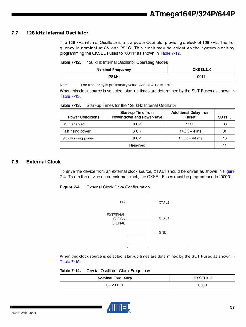
To drive the device from an external clock source, XTAL1 should be driven as shown in Figure7-4. To run the device on an external clock, the CKSEL Fuses must be programmed to “0000”.
Figure 7-4. External Clock Drive Configuration
When this clock source is selected, start-up times are determined by the SUT Fuses as shown inTable 7-15.
Table 7-12. 128 kHz Internal Oscillator Operating Modes
Nominal Frequency CKSEL3..0
128 kHz 0011
Table 7-13. Start-up Times for the 128 kHz Internal Oscillator
Power ConditionsStart-up Time from
Power-down and Power-saveAdditional Delay from
Reset SUT1..0
BOD enabled 6 CK 14CK 00
Fast rising power 6 CK 14CK + 4 ms 01
Slowly rising power 6 CK 14CK + 64 ms 10
Reserved 11
Table 7-14. Crystal Oscillator Clock Frequency
Nominal Frequency CKSEL3..0
0 - 20 kHz 0000
NC
EXTERNALCLOCKSIGNAL
XTAL2
XTAL1
GND
377674F–AVR–09/09
When applying an external clock, it is required to avoid sudden changes in the applied clock fre-quency to ensure stable operation of the MCU. A variation in frequency of more than 2% fromone clock cycle to the next can lead to unpredictable behavior. If changes of more than 2% isrequired, ensure that the MCU is kept in Reset during the changes.
Note that the System Clock Prescaler can be used to implement run-time changes of the internalclock frequency while still ensuring stable operation. Refer to “System Clock Prescaler” on page38 for details.
7.9 Timer/Counter Oscillator
ATmega164P/324P/644P uses the same type of crystal oscillator for Low-frequency CrystalOscillator and Timer/Counter Oscillator. See “Low Frequency Crystal Oscillator” on page 34 fordetails on the oscillator and crystal requirements.
The device can operate its Timer/Counter2 from an external 32.768 kHz watch crystal or a exter-nal clock source. See “Clock Source Connections” on page 31 for details.
Applying an external clock source to TOSC1 can be done if EXTCLK in the ASSR Register iswritten to logic one. See “The Output Compare Register B contains an 8-bit value that is contin-uously compared with the counter value (TCNT2). A match can be used to generate an OutputCompare interrupt, or to generate a waveform output on the OC2B pin.” on page 158 for furtherdescription on selecting external clock as input instead of a 32.768 kHz watch crystal.
7.10 Clock Output Buffer
The device can output the system clock on the CLKO pin. To enable the output, the CKOUTFuse has to be programmed. This mode is suitable when the chip clock is used to drive other cir-cuits on the system. The clock also will be output during reset, and the normal operation of I/Opin will be overridden when the fuse is programmed. Any clock source, including the internal RCOscillator, can be selected when the clock is output on CLKO. If the System Clock Prescaler isused, it is the divided system clock that is output.
7.11 System Clock Prescaler
The ATmega164P/324P/644P has a system clock prescaler, and the system clock can bedivided by setting the “CLKPR – Clock Prescale Register” on page 40. This feature can be usedto decrease the system clock frequency and the power consumption when the requirement forprocessing power is low. This can be used with all clock source options, and it will affect theclock frequency of the CPU and all synchronous peripherals. clkI/O, clkADC, clkCPU, and clkFLASH
are divided by a factor as shown in Table 7-16 on page 40.
Table 7-15. Start-up Times for the External Clock Selection
Power ConditionsStart-up Time from
Power-down and Power-saveAdditional Delay from
Reset (VCC = 5.0V) SUT1..0
BOD enabled 6 CK 14CK 00
Fast rising power 6 CK 14CK + 4.1 ms 01
Slowly rising power 6 CK 14CK + 65 ms 10
Reserved 11
387674F–AVR–09/09
ATmega164P/324P/644P
ATmega164P/324P/644P
When switching between prescaler settings, the System Clock Prescaler ensures that noglitches occurs in the clock system. It also ensures that no intermediate frequency is higher thanneither the clock frequency corresponding to the previous setting, nor the clock frequency corre-sponding to the new setting.
The ripple counter that implements the prescaler runs at the frequency of the undivided clock,which may be faster than the CPU's clock frequency. Hence, it is not possible to determine thestate of the prescaler - even if it were readable, and the exact time it takes to switch from oneclock division to the other cannot be exactly predicted. From the time the CLKPS values are writ-ten, it takes between T1 + T2 and T1 + 2 * T2 before the new clock frequency is active. In thisinterval, 2 active clock edges are produced. Here, T1 is the previous clock period, and T2 is theperiod corresponding to the new prescaler setting.
To avoid unintentional changes of clock frequency, a special write procedure must be followedto change the CLKPS bits:
1. Write the Clock Prescaler Change Enable (CLKPCE) bit to one and all other bits in CLKPR to zero.
2. Within four cycles, write the desired value to CLKPS while writing a zero to CLKPCE.
Interrupts must be disabled when changing prescaler setting to make sure the write procedure isnot interrupted.
7.12 Register Description7.12.1 OSCCAL – Oscillator Calibration Register
• Bits 7:0 – CAL7:0: Oscillator Calibration ValueThe Oscillator Calibration Register is used to trim the Calibrated Internal RC Oscillator toremove process variations from the oscillator frequency. A pre-programmed calibration value isautomatically written to this register during chip reset, giving the Factory calibrated frequency asspecified in Table 26-2 on page 331. The application software can write this register to changethe oscillator frequency. The oscillator can be calibrated to frequencies as specified in Table26-2 on page 331. Calibration outside that range is not guaranteed.
Note that this oscillator is used to time EEPROM and Flash write accesses, and these writetimes will be affected accordingly. If the EEPROM or Flash are written, do not calibrate to morethan 8.8 MHz. Otherwise, the EEPROM or Flash write may fail.
The CAL7 bit determines the range of operation for the oscillator. Setting this bit to 0 gives thelowest frequency range, setting this bit to 1 gives the highest frequency range. The two fre-quency ranges are overlapping, in other words a setting of OSCCAL = 0x7F gives a higherfrequency than OSCCAL = 0x80.
The CAL6..0 bits are used to tune the frequency within the selected range. A setting of 0x00gives the lowest frequency in that range, and a setting of 0x7F gives the highest frequency in therange.
Bit 7 6 5 4 3 2 1 0
(0x66) CAL7 CAL6 CAL5 CAL4 CAL3 CAL2 CAL1 CAL0 OSCCAL
Read/Write R/W R/W R/W R/W R/W R/W R/W R/W
Initial Value Device Specific Calibration Value
397674F–AVR–09/09
7.12.2 CLKPR – Clock Prescale Register
• Bit 7 – CLKPCE: Clock Prescaler Change EnableThe CLKPCE bit must be written to logic one to enable change of the CLKPS bits. The CLKPCEbit is only updated when the other bits in CLKPR are simultaneously written to zero. CLKPCE iscleared by hardware four cycles after it is written or when CLKPS bits are written. Rewriting theCLKPCE bit within this time-out period does neither extend the time-out period, nor clear theCLKPCE bit.
• Bits 3:0 – CLKPS3:0: Clock Prescaler Select Bits 3 - 0These bits define the division factor between the selected clock source and the internal systemclock. These bits can be written run-time to vary the clock frequency to suit the applicationrequirements. As the divider divides the master clock input to the MCU, the speed of all synchro-nous peripherals is reduced when a division factor is used. The division factors are given inTable 7-16 on page 40.
The CKDIV8 Fuse determines the initial value of the CLKPS bits. If CKDIV8 is unprogrammed,the CLKPS bits will be reset to “0000”. If CKDIV8 is programmed, CLKPS bits are reset to“0011”, giving a division factor of 8 at start up. This feature should be used if the selected clocksource has a higher frequency than the maximum frequency of the device at the present operat-ing conditions. Note that any value can be written to the CLKPS bits regardless of the CKDIV8Fuse setting. The Application software must ensure that a sufficient division factor is chosen ifthe selected clock source has a higher frequency than the maximum frequency of the device atthe present operating conditions. The device is shipped with the CKDIV8 Fuse programmed.
Bit 7 6 5 4 3 2 1 0
(0x61) CLKPCE – – – CLKPS3 CLKPS2 CLKPS1 CLKPS0 CLKPR
Read/Write R/W R R R R/W R/W R/W R/W
Initial Value 0 0 0 0 See Bit Description
Table 7-16. Clock Prescaler Select
CLKPS3 CLKPS2 CLKPS1 CLKPS0 Clock Division Factor
0 0 0 0 1
0 0 0 1 2
0 0 1 0 4
0 0 1 1 8
0 1 0 0 16
0 1 0 1 32
0 1 1 0 64
0 1 1 1 128
1 0 0 0 256
1 0 0 1 Reserved
1 0 1 0 Reserved
1 0 1 1 Reserved
1 1 0 0 Reserved
1 1 0 1 Reserved
1 1 1 0 Reserved
1 1 1 1 Reserved
407674F–AVR–09/09
ATmega164P/324P/644P
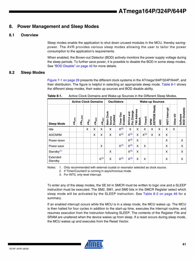
ATmega164P/324P/644P
8. Power Management and Sleep Modes
8.1 Overview
Sleep modes enable the application to shut down unused modules in the MCU, thereby saving-power. The AVR provides various sleep modes allowing the user to tailor the powerconsumption to the application’s requirements.
When enabled, the Brown-out Detector (BOD) actively monitors the power supply voltage duringthe sleep periods. To further save power, it is possible to disable the BOD in some sleep modes.See “BOD Disable” on page 42 for more details.
8.2 Sleep Modes
Figure 7-1 on page 29 presents the different clock systems in the ATmega164P/324P/644P, andtheir distribution. The figure is helpful in selecting an appropriate sleep mode. Table 8-1 showsthe different sleep modes, their wake up sources and BOD disable ability.
Notes: 1. Only recommended with external crystal or resonator selected as clock source.2. If Timer/Counter2 is running in asynchronous mode.3. For INT0, only level interrupt.
To enter any of the sleep modes, the SE bit in SMCR must be written to logic one and a SLEEPinstruction must be executed. The SM2, SM1, and SM0 bits in the SMCR Register select whichsleep mode will be activated by the SLEEP instruction. See Table 8-2 on page 46 for asummary.
If an enabled interrupt occurs while the MCU is in a sleep mode, the MCU wakes up. The MCUis then halted for four cycles in addition to the start-up time, executes the interrupt routine, andresumes execution from the instruction following SLEEP. The contents of the Register File andSRAM are unaltered when the device wakes up from sleep. If a reset occurs during sleep mode,the MCU wakes up and executes from the Reset Vector.
Table 8-1. Active Clock Domains and Wake-up Sources in the Different Sleep Modes.
Active Clock Domains Oscillators Wake-up Sources
So
ftw
are
BO
D D
isd
able
Sleep Mode clk C
PU
clk F
LA
SH
clk I
O
clk A
DC
clk A
SY
Mai
n C
lock
So
urc
e E
nab
led
Tim
er O
sc
En
able
d
INT
2:0
and
P
in C
han
ge
TW
I Ad
dre
ss
Mat
ch
Tim
er2
SP
M/
EE
PR
OM
Rea
dy
AD
C
WD
T In
terr
up
t
Oth
er I/
O
Idle X X X X X(2) X X X X X X X
ADCNRM X X X X(2) X(3) X X(2) X X X
Power-down X(3) X X X
Power-save X X(2) X(3) X X X X
Standby(1) X X(3) X X X
Extended Standby
X(2) X X(2) X(3) X X X X
417674F–AVR–09/09
8.3 BOD Disable
When the Brown-out Detector (BOD) is enabled by BODLEVEL fuses, Table 25-3 on page 297,the BOD is actively monitoring the power supply voltage during a sleep period. To save power, itis possible to disable the BOD by software for some of the sleep modes, see Table 8-1 on page41. The sleep mode power consumption will then be at the same level as when BOD is globallydisabled by fuses. If BOD is disabled in software, the BOD function is turned off immediatelyafter entering the sleep mode. Upon wake-up from sleep, BOD is automatically enabled again.This ensures safe operation in case the VCC level has dropped during the sleep period.
When the BOD has been disabled, the wake-up time from sleep mode will be approximately 60µs to ensure that the BOD is working correctly before the MCU continues executing code.
BOD disable is controlled by bit 6, BODS (BOD Sleep) in the control register MCUCR, see“MCUCR – MCU Control Register” on page 47. Writing this bit to one turns off the BOD in rele-vant sleep modes, while a zero in this bit keeps BOD active. Default setting keeps BOD active,i.e. BODS set to zero.
Writing to the BODS bit is controlled by a timed sequence and an enable bit, see “MCUCR –MCU Control Register” on page 47.
8.4 Idle Mode
When the SM2..0 bits are written to 000, the SLEEP instruction makes the MCU enter Idlemode, stopping the CPU but allowing the SPI, USART, Analog Comparator, ADC, 2-wire SerialInterface, Timer/Counters, Watchdog, and the interrupt system to continue operating. This sleepmode basically halts clkCPU and clkFLASH, while allowing the other clocks to run.
Idle mode enables the MCU to wake up from external triggered interrupts as well as internalones like the Timer Overflow and USART Transmit Complete interrupts. If wake-up from theAnalog Comparator interrupt is not required, the Analog Comparator can be powered down bysetting the ACD bit in the Analog Comparator Control and Status Register – ACSR. This willreduce power consumption in Idle mode. If the ADC is enabled, a conversion starts automati-cally when this mode is entered.
8.5 ADC Noise Reduction Mode
When the SM2..0 bits are written to 001, the SLEEP instruction makes the MCU enter ADCNoise Reduction mode, stopping the CPU but allowing the ADC, the external interrupts, 2-wireSerial Interface address match, Timer/Counter2 and the Watchdog to continue operating (ifenabled). This sleep mode basically halts clkI/O, clkCPU, and clkFLASH, while allowing theother clocks to run.
This improves the noise environment for the ADC, enabling higher resolution measurements. Ifthe ADC is enabled, a conversion starts automatically when this mode is entered. Apart form theADC Conversion Complete interrupt, only an External Reset, a Watchdog System Reset, aWatchdog interrupt, a Brown-out Reset, a 2-wire serial interface interrupt, a Timer/Counter2interrupt, an SPM/EEPROM ready interrupt, an external level interrupt on INT7:4 or a pinchange interrupt can wakeup the MCU from ADC Noise Reduction mode.
427674F–AVR–09/09
ATmega164P/324P/644P
ATmega164P/324P/644P
8.6 Power-down Mode
When the SM2..0 bits are written to 010, the SLEEP instruction makes the MCU enterPower-down mode. In this mode, the external Oscillator is stopped, while the external interrupts,the 2-wire Serial Interface, and the Watchdog continue operating (if enabled). Only an ExternalReset, a Watchdog Reset, a Brown-out Reset, 2-wire Serial Interface address match, an exter-nal level interrupt on INT7:4, an external interrupt on INT3:0, or a pin change interrupt can wakeup the MCU. This sleep mode basically halts all generated clocks, allowing operation of asyn-chronous modules only.
Note that if a level triggered interrupt is used for wake-up from Power-down mode, the changedlevel must be held for some time to wake up the MCU. Refer to “External Interrupts” on page 66for details.
When waking up from Power-down mode, there is a delay from the wake-up condition occursuntil the wake-up becomes effective. This allows the clock to restart and become stable afterhaving been stopped. The wake-up period is defined by the same CKSEL Fuses that define theReset Time-out period, as described in “Clock Sources” on page 30.
8.7 Power-save Mode
When the SM2:0 bits are written to 011, the SLEEP instruction makes the MCU enterPower-save mode. This mode is identical to Power-down, with one exception:
If Timer/Counter2 is enabled, it will keep running during sleep. The device can wake up fromeither Timer Overflow or Output Compare event from Timer/Counter2 if the correspondingTimer/Counter2 interrupt enable bits are set in TIMSK2, and the Global Interrupt Enable bit inSREG is set.
If Timer/Counter2 is not running, Power-down mode is recommended instead of Power-savemode.
The Timer/Counter2 can be clocked both synchronously and asynchronously in Power-savemode. If the Timer/Counter2 is not using the asynchronous clock, the Timer/Counter Oscillator isstopped during sleep. If the Timer/Counter2 is not using the synchronous clock, the clock sourceis stopped during sleep. Note that even if the synchronous clock is running in Power-save, thisclock is only available for the Timer/Counter2.
8.8 Standby Mode
When the SM2..0 bits are 110 and an external crystal/resonator clock option is selected, theSLEEP instruction makes the MCU enter Standby mode. This mode is identical to Power-downwith the exception that the Oscillator is kept running. From Standby mode, the device wakes upin six clock cycles.
8.9 Extended Standby Mode
When the SM2..0 bits are 111 and an external crystal/resonator clock option is selected, theSLEEP instruction makes the MCU enter Extended Standby mode. This mode is identical toPower-save mode with the exception that the Oscillator is kept running. From Extended Standbymode, the device wakes up in six clock cycles.
437674F–AVR–09/09
8.10 Power Reduction Register
The Power Reduction Register(PRR), see “PRR – Power Reduction Register” on page 47, pro-vides a method to stop the clock to individual peripherals to reduce power consumption. Thecurrent state of the peripheral is frozen and the I/O registers can not be read or written.Resources used by the peripheral when stopping the clock will remain occupied, hence theperipheral should in most cases be disabled before stopping the clock. Waking up a module,which is done by clearing the bit in PRR, puts the module in the same state as before shutdown.
Module shutdown can be used in Idle mode and Active mode to significantly reduce the overallpower consumption. In all other sleep modes, the clock is already stopped.
8.11 Minimizing Power Consumption
There are several issues to consider when trying to minimize the power consumption in an AVRcontrolled system. In general, sleep modes should be used as much as possible, and the sleepmode should be selected so that as few as possible of the device’s functions are operating. Allfunctions not needed should be disabled. In particular, the following modules may need specialconsideration when trying to achieve the lowest possible power consumption.
8.11.1 Analog to Digital Converter
If enabled, the ADC will be enabled in all sleep modes. To save power, the ADC should be dis-abled before entering any sleep mode. When the ADC is turned off and on again, the nextconversion will be an extended conversion. Refer to “ADC - Analog-to-digital Converter” on page243 for details on ADC operation.
8.11.2 Analog Comparator
When entering Idle mode, the Analog Comparator should be disabled if not used. When enteringADC Noise Reduction mode, the Analog Comparator should be disabled. In other sleep modes,the Analog Comparator is automatically disabled. However, if the Analog Comparator is set upto use the Internal Voltage Reference as input, the Analog Comparator should be disabled in allsleep modes. Otherwise, the Internal Voltage Reference will be enabled, independent of sleepmode. Refer to “AC - Analog Comparator” on page 240 for details on how to configure the Ana-log Comparator.
8.11.3 Brown-out Detector
If the Brown-out Detector is not needed by the application, this module should be turned off. Ifthe Brown-out Detector is enabled by the BODLEVEL Fuses, it will be enabled in all sleepmodes, and hence, always consume power. In the deeper sleep modes, this will contribute sig-nificantly to the total current consumption. Refer to “Brown-out Detection” on page 52 for detailson how to configure the Brown-out Detector.
8.11.4 Internal Voltage Reference
The Internal Voltage Reference will be enabled when needed by the Brown-out Detection, theAnalog Comparator or the ADC. If these modules are disabled as described in the sectionsabove, the internal voltage reference will be disabled and it will not be consuming power. Whenturned on again, the user must allow the reference to start up before the output is used. If thereference is kept on in sleep mode, the output can be used immediately. Refer to “Internal Volt-age Reference” on page 53 for details on the start-up time.
447674F–AVR–09/09
ATmega164P/324P/644P
ATmega164P/324P/644P
8.11.5 Watchdog Timer
If the Watchdog Timer is not needed in the application, the module should be turned off. If theWatchdog Timer is enabled, it will be enabled in all sleep modes, and hence, always consumepower. In the deeper sleep modes, this will contribute significantly to the total current consump-tion. Refer to “Interrupts” on page 60 for details on how to configure the Watchdog Timer.
8.11.6 Port Pins
When entering a sleep mode, all port pins should be configured to use minimum power. Themost important is then to ensure that no pins drive resistive loads. In sleep modes where boththe I/O clock (clkI/O) and the ADC clock (clkADC) are stopped, the input buffers of the device willbe disabled. This ensures that no power is consumed by the input logic when not needed. Insome cases, the input logic is needed for detecting wake-up conditions, and it will then beenabled. Refer to the section “Digital Input Enable and Sleep Modes” on page 75 for details onwhich pins are enabled. If the input buffer is enabled and the input signal is left floating or havean analog signal level close to VCC/2, the input buffer will use excessive power.
For analog input pins, the digital input buffer should be disabled at all times. An analog signallevel close to VCC/2 on an input pin can cause significant current even in active mode. Digitalinput buffers can be disabled by writing to the Digital Input Disable Registers (DIDR1 andDIDR0). Refer to “DIDR1 – Digital Input Disable Register 1” on page 242 and “DIDR0 – DigitalInput Disable Register 0” on page 262 for details.
8.11.7 On-chip Debug System
If the On-chip debug system is enabled by the OCDEN Fuse and the chip enters sleep mode,the main clock source is enabled, and hence, always consumes power. In the deeper sleepmodes, this will contribute significantly to the total current consumption.
There are three alternative ways to disable the OCD system:
• Disable the OCDEN Fuse.
• Disable the JTAGEN Fuse.
• Write one to the JTD bit in MCUCR.
457674F–AVR–09/09
8.12 Register Description
8.12.1 SMCR – Sleep Mode Control Register
The Sleep Mode Control Register contains control bits for power management.
• Bits 3, 2, 1 – SM2:0: Sleep Mode Select Bits 2, 1, and 0These bits select between the five available sleep modes as shown in Table 8-2.
Note: 1. Standby modes are only recommended for use with external crystals or resonators.
• Bit 0 – SE: Sleep EnableThe SE bit must be written to logic one to make the MCU enter the sleep mode when the SLEEPinstruction is executed. To avoid the MCU entering the sleep mode unless it is the programmer’spurpose, it is recommended to write the Sleep Enable (SE) bit to one just before the execution ofthe SLEEP instruction and to clear it immediately after waking up.
Bit 7 6 5 4 3 2 1 0
0x33 (0x53) – – – – SM2 SM1 SM0 SE SMCR
Read/Write R R R R R/W R/W R/W R/W
Initial Value 0 0 0 0 0 0 0 0
Table 8-2. Sleep Mode Select
SM2 SM1 SM0 Sleep Mode
0 0 0 Idle
0 0 1 ADC Noise Reduction
0 1 0 Power-down
0 1 1 Power-save
1 0 0 Reserved
1 0 1 Reserved
1 1 0 Standby(1)
1 1 1 Extended Standby(1)
467674F–AVR–09/09
ATmega164P/324P/644P
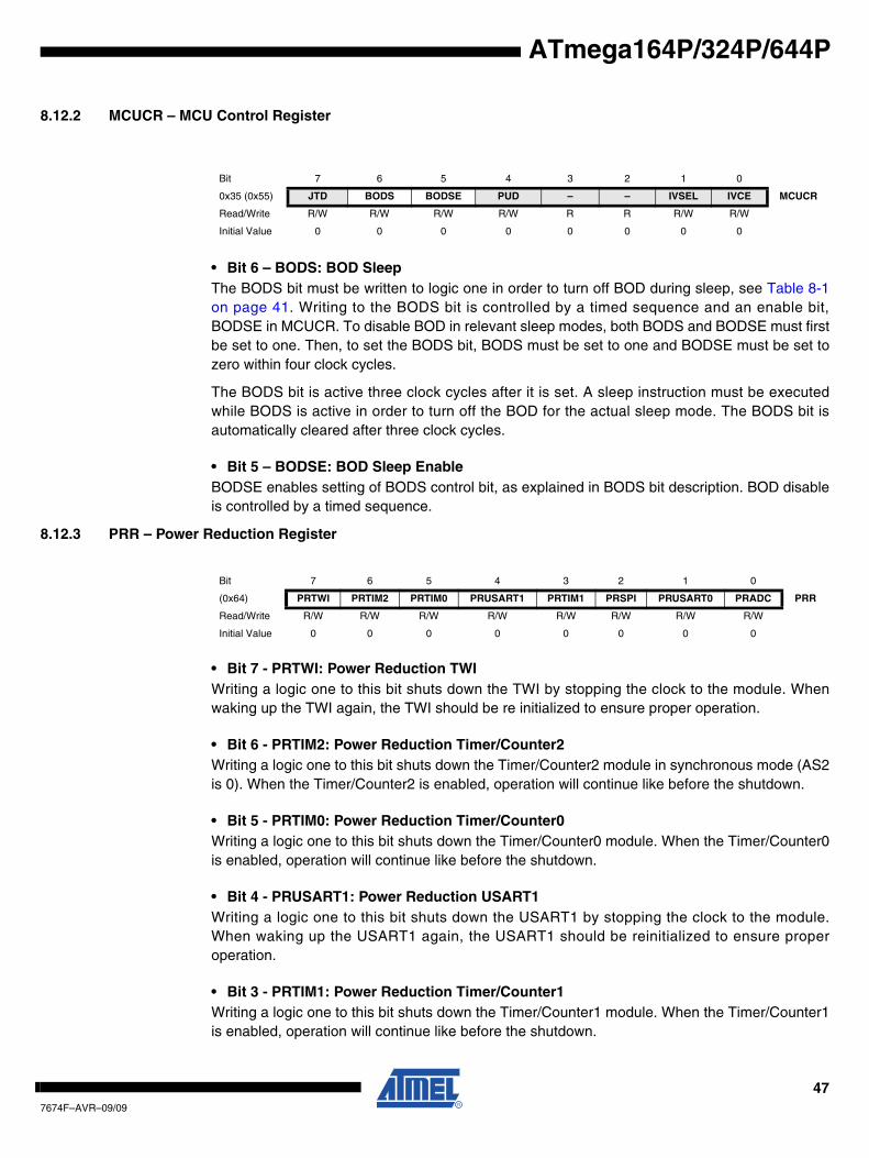
ATmega164P/324P/644P
8.12.2 MCUCR – MCU Control Register
• Bit 6 – BODS: BOD SleepThe BODS bit must be written to logic one in order to turn off BOD during sleep, see Table 8-1on page 41. Writing to the BODS bit is controlled by a timed sequence and an enable bit,BODSE in MCUCR. To disable BOD in relevant sleep modes, both BODS and BODSE must firstbe set to one. Then, to set the BODS bit, BODS must be set to one and BODSE must be set tozero within four clock cycles.
The BODS bit is active three clock cycles after it is set. A sleep instruction must be executedwhile BODS is active in order to turn off the BOD for the actual sleep mode. The BODS bit isautomatically cleared after three clock cycles.
• Bit 5 – BODSE: BOD Sleep EnableBODSE enables setting of BODS control bit, as explained in BODS bit description. BOD disableis controlled by a timed sequence.
8.12.3 PRR – Power Reduction Register
• Bit 7 - PRTWI: Power Reduction TWIWriting a logic one to this bit shuts down the TWI by stopping the clock to the module. Whenwaking up the TWI again, the TWI should be re initialized to ensure proper operation.
• Bit 6 - PRTIM2: Power Reduction Timer/Counter2Writing a logic one to this bit shuts down the Timer/Counter2 module in synchronous mode (AS2is 0). When the Timer/Counter2 is enabled, operation will continue like before the shutdown.
• Bit 5 - PRTIM0: Power Reduction Timer/Counter0Writing a logic one to this bit shuts down the Timer/Counter0 module. When the Timer/Counter0is enabled, operation will continue like before the shutdown.
• Bit 4 - PRUSART1: Power Reduction USART1Writing a logic one to this bit shuts down the USART1 by stopping the clock to the module.When waking up the USART1 again, the USART1 should be reinitialized to ensure properoperation.
• Bit 3 - PRTIM1: Power Reduction Timer/Counter1Writing a logic one to this bit shuts down the Timer/Counter1 module. When the Timer/Counter1is enabled, operation will continue like before the shutdown.
Bit 7 6 5 4 3 2 1 0
0x35 (0x55) JTD BODS BODSE PUD – – IVSEL IVCE MCUCR
Read/Write R/W R/W R/W R/W R R R/W R/W
Initial Value 0 0 0 0 0 0 0 0
Bit 7 6 5 4 3 2 1 0
(0x64) PRTWI PRTIM2 PRTIM0 PRUSART1 PRTIM1 PRSPI PRUSART0 PRADC PRR
Read/Write R/W R/W R/W R/W R/W R/W R/W R/W
Initial Value 0 0 0 0 0 0 0 0
477674F–AVR–09/09

• Bit 2 - PRSPI: Power Reduction Serial Peripheral InterfaceWriting a logic one to this bit shuts down the Serial Peripheral Interface by stopping the clock tothe module. When waking up the SPI again, the SPI should be re initialized to ensure properoperation.
• Bit 1 - PRUSART0: Power Reduction USART0Writing a logic one to this bit shuts down the USART0 by stopping the clock to the module.When waking up the USART0 again, the USART0 should be reinitialized to ensure properoperation.
• Bit 0 - PRADC: Power Reduction ADCWriting a logic one to this bit shuts down the ADC. The ADC must be disabled before shut down.The analog comparator cannot use the ADC input MUX when the ADC is shut down.
487674F–AVR–09/09
ATmega164P/324P/644P
ATmega164P/324P/644P
9. System Control and Reset
9.0.1 Resetting the AVR
During reset, all I/O Registers are set to their initial values, and the program starts executionfrom the Reset Vector. The instruction placed at the Reset Vector must be a JMP – AbsoluteJump – instruction to the reset handling routine. If the program never enables an interruptsource, the Interrupt Vectors are not used, and regular program code can be placed at theselocations. This is also the case if the Reset Vector is in the Application section while the InterruptVectors are in the Boot section or vice versa. The circuit diagram in Figure 9-1 on page 50shows the reset logic. “System and Reset Characteristics” on page 332 defines the electricalparameters of the reset circuitry.
The I/O ports of the AVR are immediately reset to their initial state when a reset source goesactive. This does not require any clock source to be running.
After all reset sources have gone inactive, a delay counter is invoked, stretching the internalreset. This allows the power to reach a stable level before normal operation starts. The time-outperiod of the delay counter is defined by the user through the SUT and CKSEL Fuses. The dif-ferent selections for the delay period are presented in “Clock Sources” on page 30.
9.0.2 Reset Sources
The ATmega164P/324P/644P has five sources of reset:
• Power-on Reset. The MCU is reset when the supply voltage is below the Power-on Reset threshold (VPOT).
• External Reset. The MCU is reset when a low level is present on the RESET pin for longer than the minimum pulse length.
• Watchdog Reset. The MCU is reset when the Watchdog Timer period expires and the Watchdog is enabled.
• Brown-out Reset. The MCU is reset when the supply voltage VCC is below the Brown-out Reset threshold (VBOT) and the Brown-out Detector is enabled.
• JTAG AVR Reset. The MCU is reset as long as there is a logic one in the Reset Register, one of the scan chains of the JTAG system. Refer to the section “IEEE 1149.1 (JTAG) Boundary-scan” on page 269 for details.
497674F–AVR–09/09
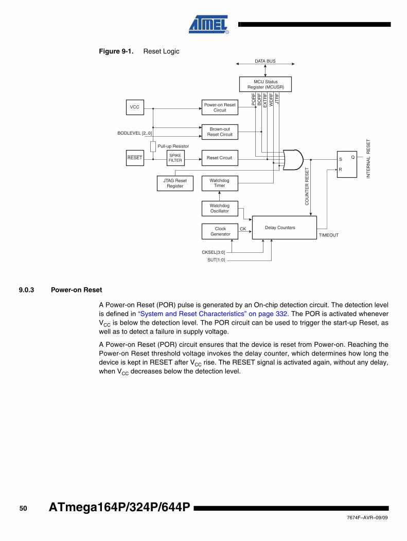
Figure 9-1. Reset Logic
9.0.3 Power-on Reset
A Power-on Reset (POR) pulse is generated by an On-chip detection circuit. The detection levelis defined in “System and Reset Characteristics” on page 332. The POR is activated wheneverVCC is below the detection level. The POR circuit can be used to trigger the start-up Reset, aswell as to detect a failure in supply voltage.
A Power-on Reset (POR) circuit ensures that the device is reset from Power-on. Reaching thePower-on Reset threshold voltage invokes the delay counter, which determines how long thedevice is kept in RESET after VCC rise. The RESET signal is activated again, without any delay,when VCC decreases below the detection level.
MCU StatusRegister (MCUSR)
Brown-outReset CircuitBODLEVEL [2..0]
Delay Counters
CKSEL[3:0]
CKTIMEOUT
WD
RF
BO
RF
EX
TR
F
PO
RF
DATA BUS
ClockGenerator
SPIKEFILTER
Pull-up Resistor
JTR
F
JTAG ResetRegister
WatchdogOscillator
SUT[1:0]
Power-on ResetCircuit
507674F–AVR–09/09
ATmega164P/324P/644P
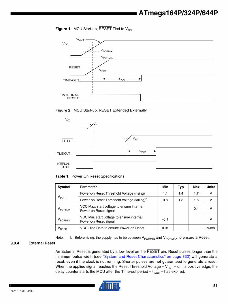
ATmega164P/324P/644P
Figure 1. MCU Start-up, RESET Tied to VCC
Figure 2. MCU Start-up, RESET Extended Externally
Table 1. Power On Reset Specifications
Note: 1. Before rising, the supply has to be between VPORMIN and VPORMAX to ensure a Reset.
9.0.4 External Reset
An External Reset is generated by a low level on the RESET pin. Reset pulses longer than theminimum pulse width (see “System and Reset Characteristics” on page 332) will generate areset, even if the clock is not running. Shorter pulses are not guaranteed to generate a reset.When the applied signal reaches the Reset Threshold Voltage – VRST – on its positive edge, thedelay counter starts the MCU after the Time-out period – tTOUT – has expired.
Symbol Parameter Min Typ Max Units
VPOT
Power-on Reset Threshold Voltage (rising) 1.1 1.4 1.7 V
Power-on Reset Threshold Voltage (falling)(1) 0.8 1.3 1.6 V
VPORMAXVCC Max. start voltage to ensure internal Power-on Reset signal
0.4 V
VPORMINVCC Min. start voltage to ensure internal Power-on Reset signal
-0.1 V
VCCRR VCC Rise Rate to ensure Power-on Reset 0.01 V/ms
RESET
TIME-OUT
INTERNALRESET
tTOUT
VRST
VPORMAX
VCC
CCRRV
VPORMIN
RESET
TIME-OUT
INTERNALRESET
tTOUT
VRST
VCC
517674F–AVR–09/09
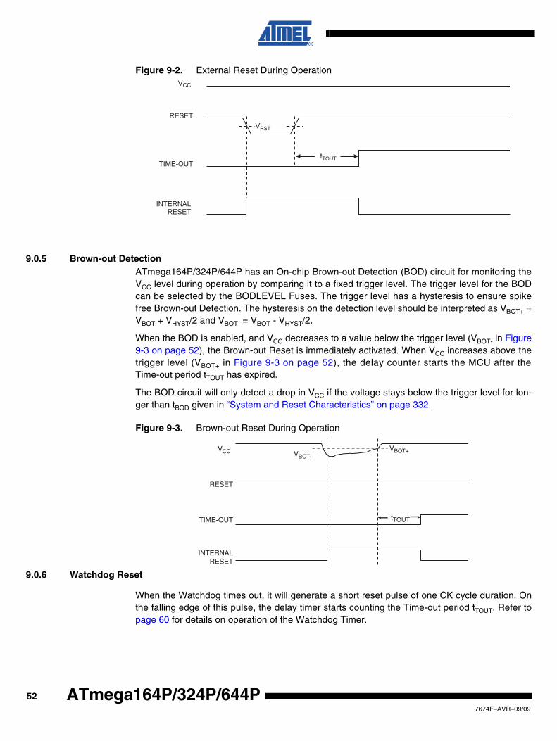
Figure 9-2. External Reset During Operation
9.0.5 Brown-out DetectionATmega164P/324P/644P has an On-chip Brown-out Detection (BOD) circuit for monitoring theVCC level during operation by comparing it to a fixed trigger level. The trigger level for the BODcan be selected by the BODLEVEL Fuses. The trigger level has a hysteresis to ensure spikefree Brown-out Detection. The hysteresis on the detection level should be interpreted as VBOT+ =VBOT + VHYST/2 and VBOT- = VBOT - VHYST/2.
When the BOD is enabled, and VCC decreases to a value below the trigger level (VBOT- in Figure9-3 on page 52), the Brown-out Reset is immediately activated. When VCC increases above thetrigger level (VBOT+ in Figure 9-3 on page 52), the delay counter starts the MCU after theTime-out period tTOUT has expired.
The BOD circuit will only detect a drop in VCC if the voltage stays below the trigger level for lon-ger than tBOD given in “System and Reset Characteristics” on page 332.
Figure 9-3. Brown-out Reset During Operation
9.0.6 Watchdog Reset
When the Watchdog times out, it will generate a short reset pulse of one CK cycle duration. Onthe falling edge of this pulse, the delay timer starts counting the Time-out period tTOUT. Refer topage 60 for details on operation of the Watchdog Timer.
CC
VCC
RESET
TIME-OUT
INTERNALRESET
VBOT-VBOT+
tTOUT
527674F–AVR–09/09
ATmega164P/324P/644P
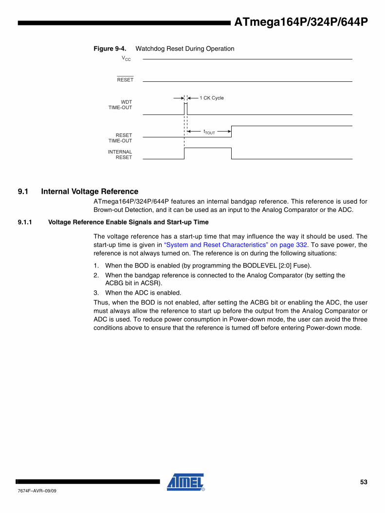
ATmega164P/324P/644P
Figure 9-4. Watchdog Reset During Operation
9.1 Internal Voltage ReferenceATmega164P/324P/644P features an internal bandgap reference. This reference is used forBrown-out Detection, and it can be used as an input to the Analog Comparator or the ADC.
9.1.1 Voltage Reference Enable Signals and Start-up Time
The voltage reference has a start-up time that may influence the way it should be used. Thestart-up time is given in “System and Reset Characteristics” on page 332. To save power, thereference is not always turned on. The reference is on during the following situations:
1. When the BOD is enabled (by programming the BODLEVEL [2:0] Fuse).
2. When the bandgap reference is connected to the Analog Comparator (by setting the ACBG bit in ACSR).
3. When the ADC is enabled.
Thus, when the BOD is not enabled, after setting the ACBG bit or enabling the ADC, the usermust always allow the reference to start up before the output from the Analog Comparator orADC is used. To reduce power consumption in Power-down mode, the user can avoid the threeconditions above to ensure that the reference is turned off before entering Power-down mode.
CK
CC
537674F–AVR–09/09
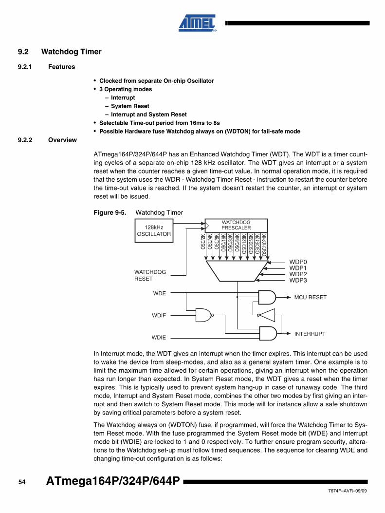
9.2 Watchdog Timer
9.2.1 Features
• Clocked from separate On-chip Oscillator• 3 Operating modes
– Interrupt– System Reset– Interrupt and System Reset
• Selectable Time-out period from 16ms to 8s• Possible Hardware fuse Watchdog always on (WDTON) for fail-safe mode
9.2.2 Overview
ATmega164P/324P/644P has an Enhanced Watchdog Timer (WDT). The WDT is a timer count-ing cycles of a separate on-chip 128 kHz oscillator. The WDT gives an interrupt or a systemreset when the counter reaches a given time-out value. In normal operation mode, it is requiredthat the system uses the WDR - Watchdog Timer Reset - instruction to restart the counter beforethe time-out value is reached. If the system doesn't restart the counter, an interrupt or systemreset will be issued.
Figure 9-5. Watchdog Timer
In Interrupt mode, the WDT gives an interrupt when the timer expires. This interrupt can be usedto wake the device from sleep-modes, and also as a general system timer. One example is tolimit the maximum time allowed for certain operations, giving an interrupt when the operationhas run longer than expected. In System Reset mode, the WDT gives a reset when the timerexpires. This is typically used to prevent system hang-up in case of runaway code. The thirdmode, Interrupt and System Reset mode, combines the other two modes by first giving an inter-rupt and then switch to System Reset mode. This mode will for instance allow a safe shutdownby saving critical parameters before a system reset.
The Watchdog always on (WDTON) fuse, if programmed, will force the Watchdog Timer to Sys-tem Reset mode. With the fuse programmed the System Reset mode bit (WDE) and Interruptmode bit (WDIE) are locked to 1 and 0 respectively. To further ensure program security, altera-tions to the Watchdog set-up must follow timed sequences. The sequence for clearing WDE andchanging time-out configuration is as follows:
128kHzOSCILLATOR
OSC
/2K
OSC
/4K
OSC
/8K
OSC
/16K
OSC
/32K
OSC
/64K
OSC
/128
KO
SC/2
56K
OSC
/512
KO
SC/1
024K
WDP0 WDP1WDP2WDP3
WATCHDOGRESET
WDE
WDIF
WDIE
MCU RESET
INTERRUPT
547674F–AVR–09/09
ATmega164P/324P/644P
ATmega164P/324P/644P
1. In the same operation, write a logic one to the Watchdog change enable bit (WDCE) and WDE. A logic one must be written to WDE regardless of the previous value of the WDE bit.
2. Within the next four clock cycles, write the WDE and Watchdog prescaler bits (WDP) as desired, but with the WDCE bit cleared. This must be done in one operation.
The following code example shows one assembly and one C function for turning off the Watch-dog Timer. The example assumes that interrupts are controlled (e.g. by disabling interruptsglobally) so that no interrupts will occur during the execution of these functions.
Note: 1. The example code assumes that the part specific header file is included.
Assembly Code Example(1)
WDT_off:
; Turn off global interrupt
cli
; Reset Watchdog Timer
wdr
; Clear WDRF in MCUSR
in r16, MCUSR
andi r16, (0xff & (0<<WDRF))
out MCUSR, r16
; Write logical one to WDCE and WDE
; Keep old prescaler setting to prevent unintentional time-out
in r16, WDTCSR
ori r16, (1<<WDCE) | (1<<WDE)
out WDTCSR, r16
; Turn off WDT
ldi r16, (0<<WDE)
out WDTCSR, r16
; Turn on global interrupt
sei
ret
C Code Example(1)
void WDT_off(void)
{
__disable_interrupt();
__watchdog_reset();
/* Clear WDRF in MCUSR */
MCUSR &= ~(1<<WDRF);
/* Write logical one to WDCE and WDE */
/* Keep old prescaler setting to prevent unintentional time-out */
WDTCSR |= (1<<WDCE) | (1<<WDE);
/* Turn off WDT */
WDTCSR = 0x00;
__enable_interrupt();
}
557674F–AVR–09/09
Note: If the Watchdog is accidentally enabled, for example by a runaway pointer or brown-outcondition, the device will be reset and the Watchdog Timer will stay enabled. If the code is notset up to handle the Watchdog, this might lead to an eternal loop of time-out resets. To avoid thissituation, the application software should always clear the Watchdog System Reset Flag(WDRF) and the WDE control bit in the initialisation routine, even if the Watchdog is not in use.
The following code example shows one assembly and one C function for changing the time-outvalue of the Watchdog Timer.
Note: 1. The example code assumes that the part specific header file is included.
Note: The Watchdog Timer should be reset before any change of the WDP bits, since a changein the WDP bits can result in a time-out when switching to a shorter time-out period.
Assembly Code Example(1)
WDT_Prescaler_Change:
; Turn off global interrupt
cli
; Reset Watchdog Timer
wdr
; Start timed sequence
in r16, WDTCSR
ori r16, (1<<WDCE) | (1<<WDE)
out WDTCSR, r16
; -- Got four cycles to set the new values from here -
; Set new prescaler(time-out) value = 64K cycles (~0.5 s)
ldi r16, (1<<WDE) | (1<<WDP2) | (1<<WDP0)
out WDTCSR, r16
; -- Finished setting new values, used 2 cycles -
; Turn on global interrupt
sei
ret
C Code Example(1)
void WDT_Prescaler_Change(void)
{
__disable_interrupt();
__watchdog_reset();
/* Start timed equence */
WDTCSR |= (1<<WDCE) | (1<<WDE);
/* Set new prescaler(time-out) value = 64K cycles (~0.5 s) */
WDTCSR = (1<<WDE) | (1<<WDP2) | (1<<WDP0);
__enable_interrupt();
}
567674F–AVR–09/09
ATmega164P/324P/644P
ATmega164P/324P/644P
9.3 Register Description
9.3.1 MCUSR – MCU Status Register
The MCU Status Register provides information on which reset source caused an MCU reset.
• Bit 4 – JTRF: JTAG Reset FlagThis bit is set if a reset is being caused by a logic one in the JTAG Reset Register selected bythe JTAG instruction AVR_RESET. This bit is reset by a Power-on Reset, or by writing a logiczero to the flag.
• Bit 3 – WDRF: Watchdog Reset FlagThis bit is set if a Watchdog Reset occurs. The bit is reset by a Power-on Reset, or by writing alogic zero to the flag.
• Bit 2 – BORF: Brown-out Reset FlagThis bit is set if a Brown-out Reset occurs. The bit is reset by a Power-on Reset, or by writing alogic zero to the flag.
• Bit 1 – EXTRF: External Reset FlagThis bit is set if an External Reset occurs. The bit is reset by a Power-on Reset, or by writing alogic zero to the flag.
• Bit 0 – PORF: Power-on Reset FlagThis bit is set if a Power-on Reset occurs. The bit is reset only by writing a logic zero to the flag.
To make use of the Reset Flags to identify a reset condition, the user should read and thenReset the MCUSR as early as possible in the program. If the register is cleared before anotherreset occurs, the source of the reset can be found by examining the Reset Flags.
Bit 7 6 5 4 3 2 1 0
0x34 (0x54) – – – JTRF WDRF BORF EXTRF PORF MCUSR
Read/Write R R R R/W R/W R/W R/W R/W
Initial Value 0 0 0 See Bit Description
577674F–AVR–09/09
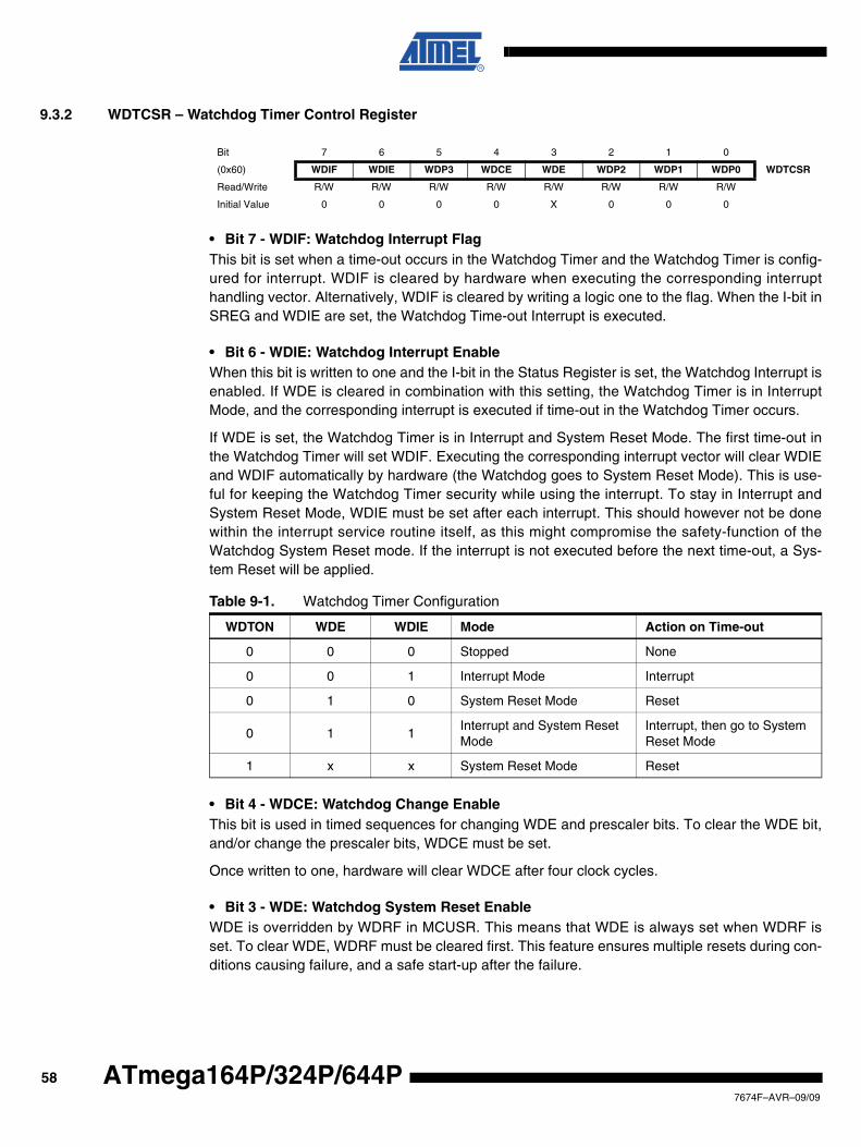
9.3.2 WDTCSR – Watchdog Timer Control Register
• Bit 7 - WDIF: Watchdog Interrupt FlagThis bit is set when a time-out occurs in the Watchdog Timer and the Watchdog Timer is config-ured for interrupt. WDIF is cleared by hardware when executing the corresponding interrupthandling vector. Alternatively, WDIF is cleared by writing a logic one to the flag. When the I-bit inSREG and WDIE are set, the Watchdog Time-out Interrupt is executed.
• Bit 6 - WDIE: Watchdog Interrupt EnableWhen this bit is written to one and the I-bit in the Status Register is set, the Watchdog Interrupt isenabled. If WDE is cleared in combination with this setting, the Watchdog Timer is in InterruptMode, and the corresponding interrupt is executed if time-out in the Watchdog Timer occurs.
If WDE is set, the Watchdog Timer is in Interrupt and System Reset Mode. The first time-out inthe Watchdog Timer will set WDIF. Executing the corresponding interrupt vector will clear WDIEand WDIF automatically by hardware (the Watchdog goes to System Reset Mode). This is use-ful for keeping the Watchdog Timer security while using the interrupt. To stay in Interrupt andSystem Reset Mode, WDIE must be set after each interrupt. This should however not be donewithin the interrupt service routine itself, as this might compromise the safety-function of theWatchdog System Reset mode. If the interrupt is not executed before the next time-out, a Sys-tem Reset will be applied.
• Bit 4 - WDCE: Watchdog Change EnableThis bit is used in timed sequences for changing WDE and prescaler bits. To clear the WDE bit,and/or change the prescaler bits, WDCE must be set.
Once written to one, hardware will clear WDCE after four clock cycles.
• Bit 3 - WDE: Watchdog System Reset EnableWDE is overridden by WDRF in MCUSR. This means that WDE is always set when WDRF isset. To clear WDE, WDRF must be cleared first. This feature ensures multiple resets during con-ditions causing failure, and a safe start-up after the failure.
Bit 7 6 5 4 3 2 1 0
(0x60) WDIF WDIE WDP3 WDCE WDE WDP2 WDP1 WDP0 WDTCSR
Read/Write R/W R/W R/W R/W R/W R/W R/W R/W
Initial Value 0 0 0 0 X 0 0 0
Table 9-1. Watchdog Timer Configuration
WDTON WDE WDIE Mode Action on Time-out
0 0 0 Stopped None
0 0 1 Interrupt Mode Interrupt
0 1 0 System Reset Mode Reset
0 1 1Interrupt and System Reset Mode
Interrupt, then go to System Reset Mode
1 x x System Reset Mode Reset
587674F–AVR–09/09
ATmega164P/324P/644P
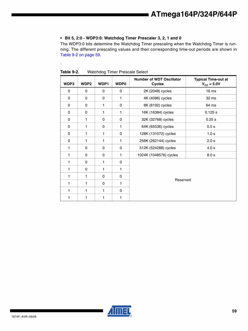
ATmega164P/324P/644P
• Bit 5, 2:0 - WDP3:0: Watchdog Timer Prescaler 3, 2, 1 and 0The WDP3:0 bits determine the Watchdog Timer prescaling when the Watchdog Timer is run-ning. The different prescaling values and their corresponding time-out periods are shown inTable 9-2 on page 59.
.
Table 9-2. Watchdog Timer Prescale Select
WDP3 WDP2 WDP1 WDP0Number of WDT Oscillator
CyclesTypical Time-out at
VCC = 5.0V
0 0 0 0 2K (2048) cycles 16 ms
0 0 0 1 4K (4096) cycles 32 ms
0 0 1 0 8K (8192) cycles 64 ms
0 0 1 1 16K (16384) cycles 0.125 s
0 1 0 0 32K (32768) cycles 0.25 s
0 1 0 1 64K (65536) cycles 0.5 s
0 1 1 0 128K (131072) cycles 1.0 s
0 1 1 1 256K (262144) cycles 2.0 s
1 0 0 0 512K (524288) cycles 4.0 s
1 0 0 1 1024K (1048576) cycles 8.0 s
1 0 1 0
Reserved
1 0 1 1
1 1 0 0
1 1 0 1
1 1 1 0
1 1 1 1
597674F–AVR–09/09
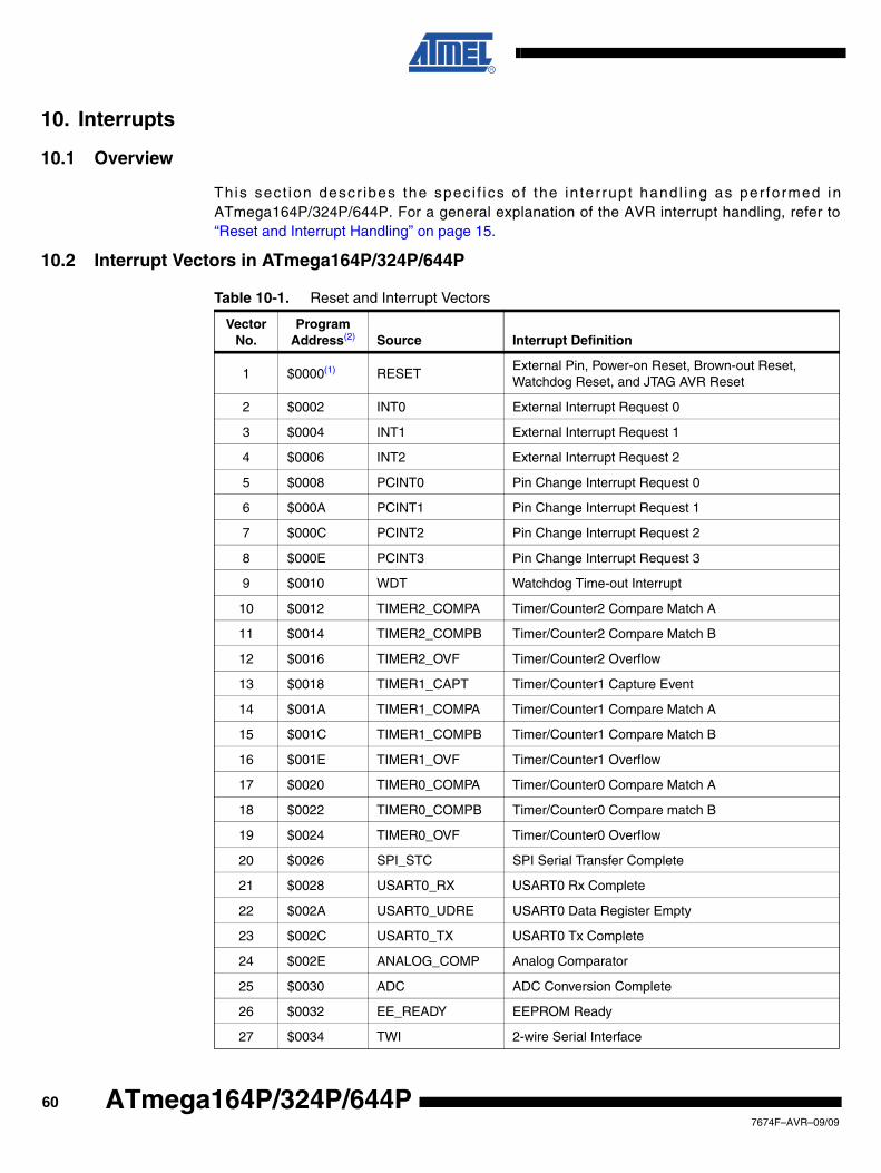
10. Interrupts
10.1 Overview
This sect ion descr ibes the spec i f ics o f the in terrupt handl ing as per formed inATmega164P/324P/644P. For a general explanation of the AVR interrupt handling, refer to“Reset and Interrupt Handling” on page 15.
10.2 Interrupt Vectors in ATmega164P/324P/644P
Table 10-1. Reset and Interrupt Vectors
VectorNo.
ProgramAddress(2) Source Interrupt Definition
1 $0000(1) RESETExternal Pin, Power-on Reset, Brown-out Reset, Watchdog Reset, and JTAG AVR Reset
2 $0002 INT0 External Interrupt Request 0
3 $0004 INT1 External Interrupt Request 1
4 $0006 INT2 External Interrupt Request 2
5 $0008 PCINT0 Pin Change Interrupt Request 0
6 $000A PCINT1 Pin Change Interrupt Request 1
7 $000C PCINT2 Pin Change Interrupt Request 2
8 $000E PCINT3 Pin Change Interrupt Request 3
9 $0010 WDT Watchdog Time-out Interrupt
10 $0012 TIMER2_COMPA Timer/Counter2 Compare Match A
11 $0014 TIMER2_COMPB Timer/Counter2 Compare Match B
12 $0016 TIMER2_OVF Timer/Counter2 Overflow
13 $0018 TIMER1_CAPT Timer/Counter1 Capture Event
14 $001A TIMER1_COMPA Timer/Counter1 Compare Match A
15 $001C TIMER1_COMPB Timer/Counter1 Compare Match B
16 $001E TIMER1_OVF Timer/Counter1 Overflow
17 $0020 TIMER0_COMPA Timer/Counter0 Compare Match A
18 $0022 TIMER0_COMPB Timer/Counter0 Compare match B
19 $0024 TIMER0_OVF Timer/Counter0 Overflow
20 $0026 SPI_STC SPI Serial Transfer Complete
21 $0028 USART0_RX USART0 Rx Complete
22 $002A USART0_UDRE USART0 Data Register Empty
23 $002C USART0_TX USART0 Tx Complete
24 $002E ANALOG_COMP Analog Comparator
25 $0030 ADC ADC Conversion Complete
26 $0032 EE_READY EEPROM Ready
27 $0034 TWI 2-wire Serial Interface
607674F–AVR–09/09
ATmega164P/324P/644P
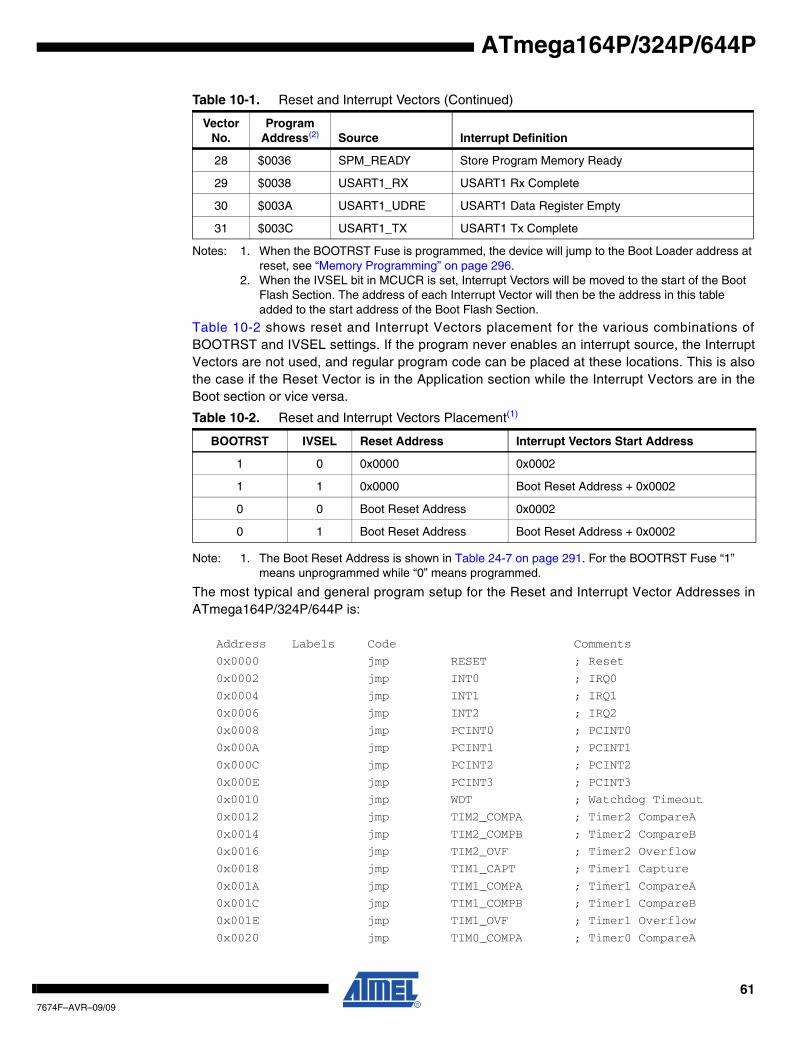
ATmega164P/324P/644P
Notes: 1. When the BOOTRST Fuse is programmed, the device will jump to the Boot Loader address at reset, see “Memory Programming” on page 296.
2. When the IVSEL bit in MCUCR is set, Interrupt Vectors will be moved to the start of the Boot Flash Section. The address of each Interrupt Vector will then be the address in this table added to the start address of the Boot Flash Section.
Table 10-2 shows reset and Interrupt Vectors placement for the various combinations ofBOOTRST and IVSEL settings. If the program never enables an interrupt source, the InterruptVectors are not used, and regular program code can be placed at these locations. This is alsothe case if the Reset Vector is in the Application section while the Interrupt Vectors are in theBoot section or vice versa.
Note: 1. The Boot Reset Address is shown in Table 24-7 on page 291. For the BOOTRST Fuse “1” means unprogrammed while “0” means programmed.
The most typical and general program setup for the Reset and Interrupt Vector Addresses inATmega164P/324P/644P is:
28 $0036 SPM_READY Store Program Memory Ready
29 $0038 USART1_RX USART1 Rx Complete
30 $003A USART1_UDRE USART1 Data Register Empty
31 $003C USART1_TX USART1 Tx Complete
Table 10-2. Reset and Interrupt Vectors Placement(1)
BOOTRST IVSEL Reset Address Interrupt Vectors Start Address
1 0 0x0000 0x0002
1 1 0x0000 Boot Reset Address + 0x0002
0 0 Boot Reset Address 0x0002
0 1 Boot Reset Address Boot Reset Address + 0x0002
Address Labels Code Comments
0x0000 jmp RESET ; Reset
0x0002 jmp INT0 ; IRQ0
0x0004 jmp INT1 ; IRQ1
0x0006 jmp INT2 ; IRQ2
0x0008 jmp PCINT0 ; PCINT0
0x000A jmp PCINT1 ; PCINT1
0x000C jmp PCINT2 ; PCINT2
0x000E jmp PCINT3 ; PCINT3
0x0010 jmp WDT ; Watchdog Timeout
0x0012 jmp TIM2_COMPA ; Timer2 CompareA
0x0014 jmp TIM2_COMPB ; Timer2 CompareB
0x0016 jmp TIM2_OVF ; Timer2 Overflow
0x0018 jmp TIM1_CAPT ; Timer1 Capture
0x001A jmp TIM1_COMPA ; Timer1 CompareA
0x001C jmp TIM1_COMPB ; Timer1 CompareB
0x001E jmp TIM1_OVF ; Timer1 Overflow
0x0020 jmp TIM0_COMPA ; Timer0 CompareA
Table 10-1. Reset and Interrupt Vectors (Continued)
VectorNo.
ProgramAddress(2) Source Interrupt Definition
617674F–AVR–09/09
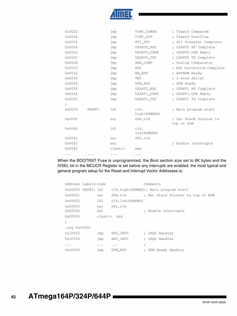
When the BOOTRST Fuse is unprogrammed, the Boot section size set to 8K bytes and theIVSEL bit in the MCUCR Register is set before any interrupts are enabled, the most typical andgeneral program setup for the Reset and Interrupt Vector Addresses is:
Address Labels Code Comments
0x00000 RESET: ldi r16,high(RAMEND); Main program start
0x00001 out SPH,r16 ; Set Stack Pointer to top of RAM
0x00002 ldi r16,low(RAMEND)
0x00003 out SPL,r160x00004 sei ; Enable interrupts
0x00005 <instr> xxx
;
.org 0x1F002
0x1F002 jmp EXT_INT0 ; IRQ0 Handler
0x1F004 jmp EXT_INT1 ; IRQ1 Handler
... ... ... ;
0x1FO36 jmp SPM_RDY ; SPM Ready Handler
0x0022 jmp TIM0_COMPB ; Timer0 CompareB
0x0024 jmp TIM0_OVF ; Timer0 Overflow
0x0026 jmp SPI_STC ; SPI Transfer Complete
0x0028 jmp USART0_RXC ; USART0 RX Complete
0x002A jmp USART0_UDRE ; USART0,UDR Empty
0x002C jmp USART0_TXC ; USART0 TX Complete
0x002E jmp ANA_COMP ; Analog Comparator
0x0030 jmp ADC ; ADC Conversion Complete
0x0032 jmp EE_RDY ; EEPROM Ready
0x0034 jmp TWI ; 2-wire Serial
0x0036 jmp SPM_RDY ; SPM Ready
0x0038 jmp USART1_RXC ; USART1 RX Complete
0x003A jmp USART1_UDRE ; USART1,UDR Empty
0x003C jmp USART1_TXC ; USART1 TX Complete
;
0x003E RESET: ldi r16,high(RAMEND)
; Main program start
0x003F out SPH,r16 ; Set Stack Pointer to top of RAM
0x0040 ldi r16,low(RAMEND)
0x0041 out SPL,r16
0x0042 sei ; Enable interrupts
0x0043 <instr> xxx
... ... ... ...
627674F–AVR–09/09
ATmega164P/324P/644P
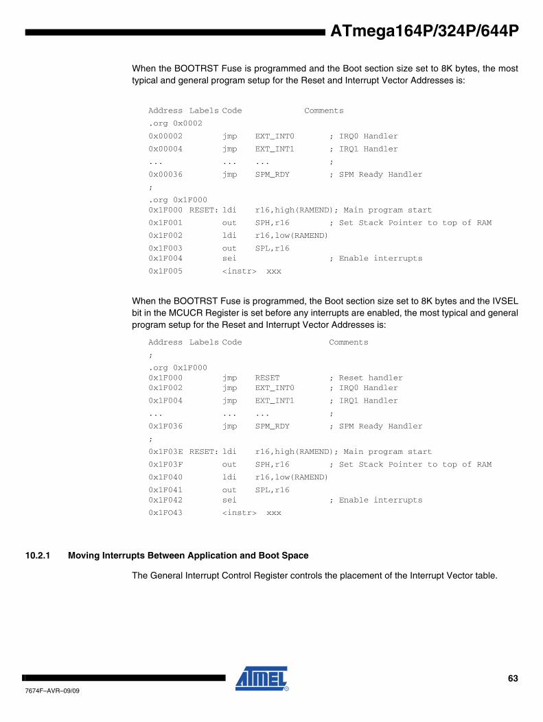
ATmega164P/324P/644P
When the BOOTRST Fuse is programmed and the Boot section size set to 8K bytes, the mosttypical and general program setup for the Reset and Interrupt Vector Addresses is:
Address Labels Code Comments
.org 0x0002
0x00002 jmp EXT_INT0 ; IRQ0 Handler
0x00004 jmp EXT_INT1 ; IRQ1 Handler
... ... ... ;
0x00036 jmp SPM_RDY ; SPM Ready Handler
;
.org 0x1F0000x1F000 RESET: ldi r16,high(RAMEND); Main program start
0x1F001 out SPH,r16 ; Set Stack Pointer to top of RAM
0x1F002 ldi r16,low(RAMEND)
0x1F003 out SPL,r160x1F004 sei ; Enable interrupts
0x1F005 <instr> xxx
When the BOOTRST Fuse is programmed, the Boot section size set to 8K bytes and the IVSELbit in the MCUCR Register is set before any interrupts are enabled, the most typical and generalprogram setup for the Reset and Interrupt Vector Addresses is:
Address Labels Code Comments
;
.org 0x1F0000x1F000 jmp RESET ; Reset handler0x1F002 jmp EXT_INT0 ; IRQ0 Handler
0x1F004 jmp EXT_INT1 ; IRQ1 Handler
... ... ... ;
0x1F036 jmp SPM_RDY ; SPM Ready Handler
;
0x1F03E RESET: ldi r16,high(RAMEND); Main program start
0x1F03F out SPH,r16 ; Set Stack Pointer to top of RAM
0x1F040 ldi r16,low(RAMEND)
0x1F041 out SPL,r160x1F042 sei ; Enable interrupts
0x1FO43 <instr> xxx
10.2.1 Moving Interrupts Between Application and Boot Space
The General Interrupt Control Register controls the placement of the Interrupt Vector table.
637674F–AVR–09/09
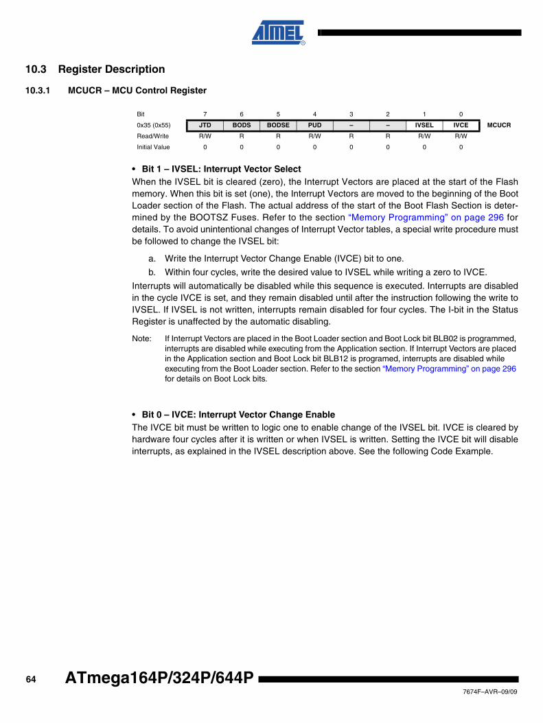
10.3 Register Description
10.3.1 MCUCR – MCU Control Register
• Bit 1 – IVSEL: Interrupt Vector SelectWhen the IVSEL bit is cleared (zero), the Interrupt Vectors are placed at the start of the Flashmemory. When this bit is set (one), the Interrupt Vectors are moved to the beginning of the BootLoader section of the Flash. The actual address of the start of the Boot Flash Section is deter-mined by the BOOTSZ Fuses. Refer to the section “Memory Programming” on page 296 fordetails. To avoid unintentional changes of Interrupt Vector tables, a special write procedure mustbe followed to change the IVSEL bit:
a. Write the Interrupt Vector Change Enable (IVCE) bit to one.
b. Within four cycles, write the desired value to IVSEL while writing a zero to IVCE.
Interrupts will automatically be disabled while this sequence is executed. Interrupts are disabledin the cycle IVCE is set, and they remain disabled until after the instruction following the write toIVSEL. If IVSEL is not written, interrupts remain disabled for four cycles. The I-bit in the StatusRegister is unaffected by the automatic disabling.
Note: If Interrupt Vectors are placed in the Boot Loader section and Boot Lock bit BLB02 is programmed, interrupts are disabled while executing from the Application section. If Interrupt Vectors are placed in the Application section and Boot Lock bit BLB12 is programed, interrupts are disabled while executing from the Boot Loader section. Refer to the section “Memory Programming” on page 296 for details on Boot Lock bits.
• Bit 0 – IVCE: Interrupt Vector Change EnableThe IVCE bit must be written to logic one to enable change of the IVSEL bit. IVCE is cleared byhardware four cycles after it is written or when IVSEL is written. Setting the IVCE bit will disableinterrupts, as explained in the IVSEL description above. See the following Code Example.
Bit 7 6 5 4 3 2 1 0
0x35 (0x55) JTD BODS BODSE PUD – – IVSEL IVCE MCUCR
Read/Write R/W R R R/W R R R/W R/W
Initial Value 0 0 0 0 0 0 0 0
647674F–AVR–09/09
ATmega164P/324P/644P
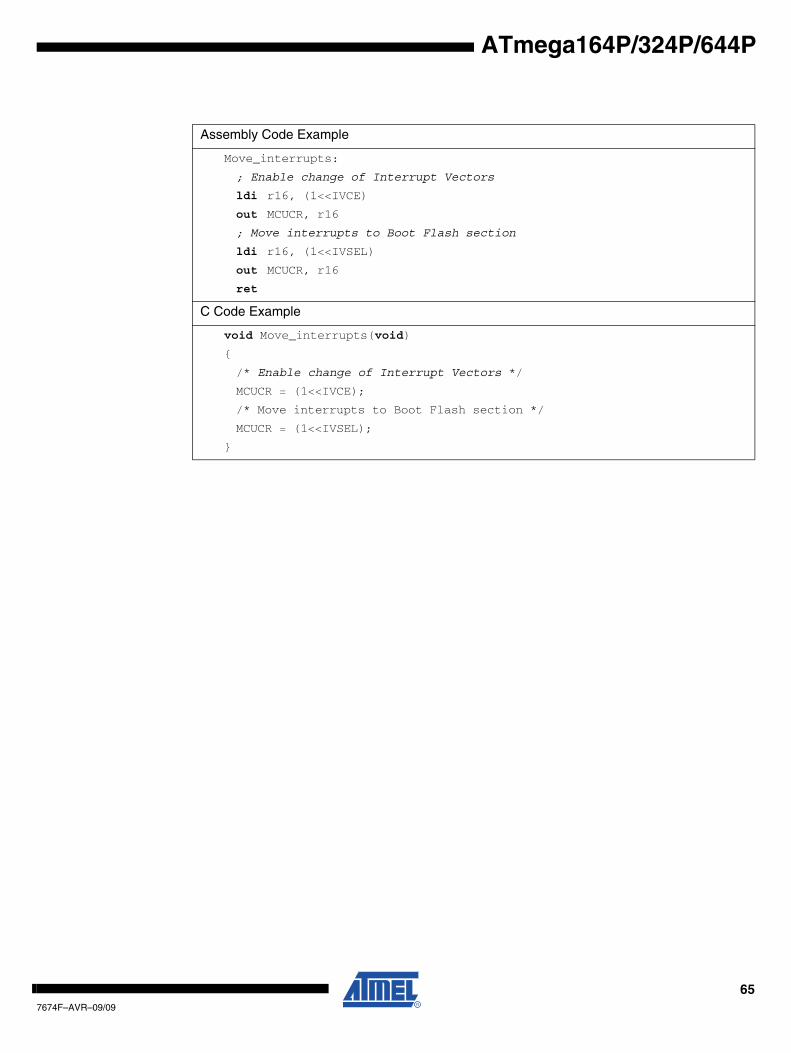
ATmega164P/324P/644P
Assembly Code Example
Move_interrupts:
; Enable change of Interrupt Vectors
ldi r16, (1<<IVCE)
out MCUCR, r16
; Move interrupts to Boot Flash section
ldi r16, (1<<IVSEL)
out MCUCR, r16
ret
C Code Example
void Move_interrupts(void)
{
/* Enable change of Interrupt Vectors */
MCUCR = (1<<IVCE);
/* Move interrupts to Boot Flash section */
MCUCR = (1<<IVSEL);
}
657674F–AVR–09/09
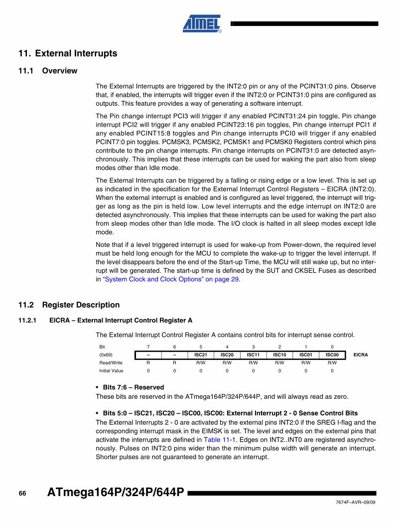
11. External Interrupts
11.1 Overview
The External Interrupts are triggered by the INT2:0 pin or any of the PCINT31:0 pins. Observethat, if enabled, the interrupts will trigger even if the INT2:0 or PCINT31:0 pins are configured asoutputs. This feature provides a way of generating a software interrupt.
The Pin change interrupt PCI3 will trigger if any enabled PCINT31:24 pin toggle, Pin changeinterrupt PCI2 will trigger if any enabled PCINT23:16 pin toggles, Pin change interrupt PCI1 ifany enabled PCINT15:8 toggles and Pin change interrupts PCI0 will trigger if any enabledPCINT7:0 pin toggles. PCMSK3, PCMSK2, PCMSK1 and PCMSK0 Registers control which pinscontribute to the pin change interrupts. Pin change interrupts on PCINT31:0 are detected asyn-chronously. This implies that these interrupts can be used for waking the part also from sleepmodes other than Idle mode.
The External Interrupts can be triggered by a falling or rising edge or a low level. This is set upas indicated in the specification for the External Interrupt Control Registers – EICRA (INT2:0).When the external interrupt is enabled and is configured as level triggered, the interrupt will trig-ger as long as the pin is held low. Low level interrupts and the edge interrupt on INT2:0 aredetected asynchronously. This implies that these interrupts can be used for waking the part alsofrom sleep modes other than Idle mode. The I/O clock is halted in all sleep modes except Idlemode.
Note that if a level triggered interrupt is used for wake-up from Power-down, the required levelmust be held long enough for the MCU to complete the wake-up to trigger the level interrupt. Ifthe level disappears before the end of the Start-up Time, the MCU will still wake up, but no inter-rupt will be generated. The start-up time is defined by the SUT and CKSEL Fuses as describedin “System Clock and Clock Options” on page 29.
11.2 Register Description
11.2.1 EICRA – External Interrupt Control Register A
The External Interrupt Control Register A contains control bits for interrupt sense control.
• Bits 7:6 – ReservedThese bits are reserved in the ATmega164P/324P/644P, and will always read as zero.
• Bits 5:0 – ISC21, ISC20 – ISC00, ISC00: External Interrupt 2 - 0 Sense Control BitsThe External Interrupts 2 - 0 are activated by the external pins INT2:0 if the SREG I-flag and thecorresponding interrupt mask in the EIMSK is set. The level and edges on the external pins thatactivate the interrupts are defined in Table 11-1. Edges on INT2..INT0 are registered asynchro-nously. Pulses on INT2:0 pins wider than the minimum pulse width will generate an interrupt.Shorter pulses are not guaranteed to generate an interrupt.
Bit 7 6 5 4 3 2 1 0
(0x69) – – ISC21 ISC20 ISC11 ISC10 ISC01 ISC00 EICRA
Read/Write R R R/W R/W R/W R/W R/W R/W
Initial Value 0 0 0 0 0 0 0 0
667674F–AVR–09/09
ATmega164P/324P/644P
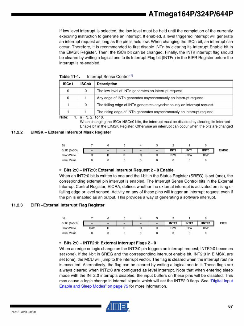
ATmega164P/324P/644P
If low level interrupt is selected, the low level must be held until the completion of the currentlyexecuting instruction to generate an interrupt. If enabled, a level triggered interrupt will generatean interrupt request as long as the pin is held low. When changing the ISCn bit, an interrupt canoccur. Therefore, it is recommended to first disable INTn by clearing its Interrupt Enable bit inthe EIMSK Register. Then, the ISCn bit can be changed. Finally, the INTn interrupt flag shouldbe cleared by writing a logical one to its Interrupt Flag bit (INTFn) in the EIFR Register before theinterrupt is re-enabled.
Note: 1. n = 3, 2, 1or 0.When changing the ISCn1/ISCn0 bits, the interrupt must be disabled by clearing its Interrupt Enable bit in the EIMSK Register. Otherwise an interrupt can occur when the bits are changed
11.2.2 EIMSK – External Interrupt Mask Register
• Bits 2:0 – INT2:0: External Interrupt Request 2 - 0 EnableWhen an INT2:0 bit is written to one and the I-bit in the Status Register (SREG) is set (one), thecorresponding external pin interrupt is enabled. The Interrupt Sense Control bits in the ExternalInterrupt Control Register, EICRA, defines whether the external interrupt is activated on rising orfalling edge or level sensed. Activity on any of these pins will trigger an interrupt request even ifthe pin is enabled as an output. This provides a way of generating a software interrupt.
11.2.3 EIFR –External Interrupt Flag Register
• Bits 2:0 – INTF2:0: External Interrupt Flags 2 - 0When an edge or logic change on the INT2:0 pin triggers an interrupt request, INTF2:0 becomesset (one). If the I-bit in SREG and the corresponding interrupt enable bit, INT2:0 in EIMSK, areset (one), the MCU will jump to the interrupt vector. The flag is cleared when the interrupt routineis executed. Alternatively, the flag can be cleared by writing a logical one to it. These flags arealways cleared when INT2:0 are configured as level interrupt. Note that when entering sleepmode with the INT2:0 interrupts disabled, the input buffers on these pins will be disabled. Thismay cause a logic change in internal signals which will set the INTF2:0 flags. See “Digital InputEnable and Sleep Modes” on page 75 for more information.
Table 11-1. Interrupt Sense Control(1)
ISCn1 ISCn0 Description
0 0 The low level of INTn generates an interrupt request.
0 1 Any edge of INTn generates asynchronously an interrupt request.
1 0 The falling edge of INTn generates asynchronously an interrupt request.
1 1 The rising edge of INTn generates asynchronously an interrupt request.
Bit 7 6 5 4 3 2 1 0
0x1D (0x3D) – – – – – INT2 INT1 IINT0 EIMSK
Read/Write R R R R R R/W R/W R/W
Initial Value 0 0 0 0 0 0 0 0
Bit 7 6 5 4 3 2 1 0
0x1C (0x3C) – – – – – INTF2 INTF1 IINTF0 EIFR
Read/Write R/W R R R R R/W R/W R/W
Initial Value 0 0 0 0 0 0 0 0
677674F–AVR–09/09
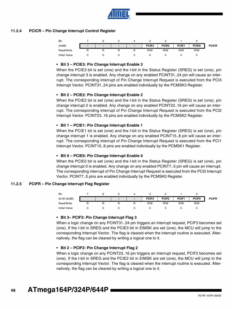
11.2.4 PCICR – Pin Change Interrupt Control Register
• Bit 3 – PCIE3: Pin Change Interrupt Enable 3When the PCIE3 bit is set (one) and the I-bit in the Status Register (SREG) is set (one), pinchange interrupt 3 is enabled. Any change on any enabled PCINT31..24 pin will cause an inter-rupt. The corresponding interrupt of Pin Change Interrupt Request is executed from the PCI3Interrupt Vector. PCINT31..24 pins are enabled individually by the PCMSK3 Register.
• Bit 2 – PCIE2: Pin Change Interrupt Enable 2When the PCIE2 bit is set (one) and the I-bit in the Status Register (SREG) is set (one), pinchange interrupt 2 is enabled. Any change on any enabled PCINT23..16 pin will cause an inter-rupt. The corresponding interrupt of Pin Change Interrupt Request is executed from the PCI2Interrupt Vector. PCINT23..16 pins are enabled individually by the PCMSK2 Register.
• Bit 1 – PCIE1: Pin Change Interrupt Enable 1When the PCIE1 bit is set (one) and the I-bit in the Status Register (SREG) is set (one), pinchange interrupt 1 is enabled. Any change on any enabled PCINT15..8 pin will cause an inter-rupt. The corresponding interrupt of Pin Change Interrupt Request is executed from the PCI1Interrupt Vector. PCINT15..8 pins are enabled individually by the PCMSK1 Register.
• Bit 0 – PCIE0: Pin Change Interrupt Enable 0When the PCIE0 bit is set (one) and the I-bit in the Status Register (SREG) is set (one), pinchange interrupt 0 is enabled. Any change on any enabled PCINT7..0 pin will cause an interrupt.The corresponding interrupt of Pin Change Interrupt Request is executed from the PCI0 InterruptVector. PCINT7..0 pins are enabled individually by the PCMSK0 Register.
11.2.5 PCIFR – Pin Change Interrupt Flag Register
• Bit 3– PCIF3: Pin Change Interrupt Flag 3When a logic change on any PCINT31..24 pin triggers an interrupt request, PCIF3 becomes set(one). If the I-bit in SREG and the PCIE3 bit in EIMSK are set (one), the MCU will jump to thecorresponding Interrupt Vector. The flag is cleared when the interrupt routine is executed. Alter-natively, the flag can be cleared by writing a logical one to it.
• Bit 2 – PCIF2: Pin Change Interrupt Flag 2When a logic change on any PCINT23..16 pin triggers an interrupt request, PCIF2 becomes set(one). If the I-bit in SREG and the PCIE2 bit in EIMSK are set (one), the MCU will jump to thecorresponding Interrupt Vector. The flag is cleared when the interrupt routine is executed. Alter-natively, the flag can be cleared by writing a logical one to it.
Bit 7 6 5 4 3 2 1 0
(0x68) – – – – PCIE3 PCIE2 PCIE1 PCIE0 PCICR
Read/Write R R R R R/W R/W R/W R/W
Initial Value 0 0 0 0 0 0 0 0
Bit 7 6 5 4 3 2 1 0
0x1B (0x3B) – – PCIF3 PCIF2 PCIF1 PCIF0 PCIFR
Read/Write R R R R R/W R/W R/W R/W
Initial Value 0 0 0 0 0 0 0 0
687674F–AVR–09/09
ATmega164P/324P/644P
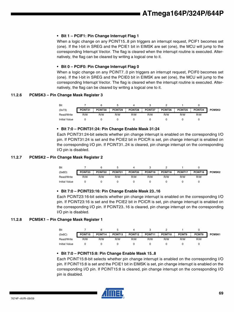
ATmega164P/324P/644P
• Bit 1 – PCIF1: Pin Change Interrupt Flag 1When a logic change on any PCINT15..8 pin triggers an interrupt request, PCIF1 becomes set(one). If the I-bit in SREG and the PCIE1 bit in EIMSK are set (one), the MCU will jump to thecorresponding Interrupt Vector. The flag is cleared when the interrupt routine is executed. Alter-natively, the flag can be cleared by writing a logical one to it.
• Bit 0 – PCIF0: Pin Change Interrupt Flag 0When a logic change on any PCINT7..0 pin triggers an interrupt request, PCIF0 becomes set(one). If the I-bit in SREG and the PCIE0 bit in EIMSK are set (one), the MCU will jump to thecorresponding Interrupt Vector. The flag is cleared when the interrupt routine is executed. Alter-natively, the flag can be cleared by writing a logical one to it.
11.2.6 PCMSK3 – Pin Change Mask Register 3
• Bit 7:0 – PCINT31:24: Pin Change Enable Mask 31:24Each PCINT31:24-bit selects whether pin change interrupt is enabled on the corresponding I/Opin. If PCINT31:24 is set and the PCIE2 bit in PCICR is set, pin change interrupt is enabled onthe corresponding I/O pin. If PCINT31..24 is cleared, pin change interrupt on the correspondingI/O pin is disabled.
11.2.7 PCMSK2 – Pin Change Mask Register 2
• Bit 7:0 – PCINT23:16: Pin Change Enable Mask 23..16Each PCINT23:16-bit selects whether pin change interrupt is enabled on the corresponding I/Opin. If PCINT23:16 is set and the PCIE2 bit in PCICR is set, pin change interrupt is enabled onthe corresponding I/O pin. If PCINT23..16 is cleared, pin change interrupt on the correspondingI/O pin is disabled.
11.2.8 PCMSK1 – Pin Change Mask Register 1
• Bit 7:0 – PCINT15:8: Pin Change Enable Mask 15..8Each PCINT15:8-bit selects whether pin change interrupt is enabled on the corresponding I/Opin. If PCINT15:8 is set and the PCIE1 bit in EIMSK is set, pin change interrupt is enabled on thecorresponding I/O pin. If PCINT15:8 is cleared, pin change interrupt on the corresponding I/Opin is disabled.
Bit 7 6 5 4 3 2 1 0
(0x73) PCINT31 PCINT30 PCINT29 PCINT28 PCINT27 PCINT26 PCINT25 PCINT24 PCMSK2
Read/Write R/W R/W R/W R/W R/W R/W R/W R/W
Initial Value 0 0 0 0 0 0 0 0
Bit 7 6 5 4 3 2 1 0
(0x6D) PCINT23 PCINT22 PCINT21 PCINT20 PCINT19 PCINT18 PCINT17 PCINT16 PCMSK2
Read/Write R/W R/W R/W R/W R/W R/W R/W R/W
Initial Value 0 0 0 0 0 0 0 0
Bit 7 6 5 4 3 2 1 0
(0x6C) PCINT15 PCINT14 PCINT13 PCINT12 PCINT11 PCINT10 PCINT9 PCINT8 PCMSK1
Read/Write R/W R/W R/W R/W R/W R/W R/W R/W
Initial Value 0 0 0 0 0 0 0 0
697674F–AVR–09/09
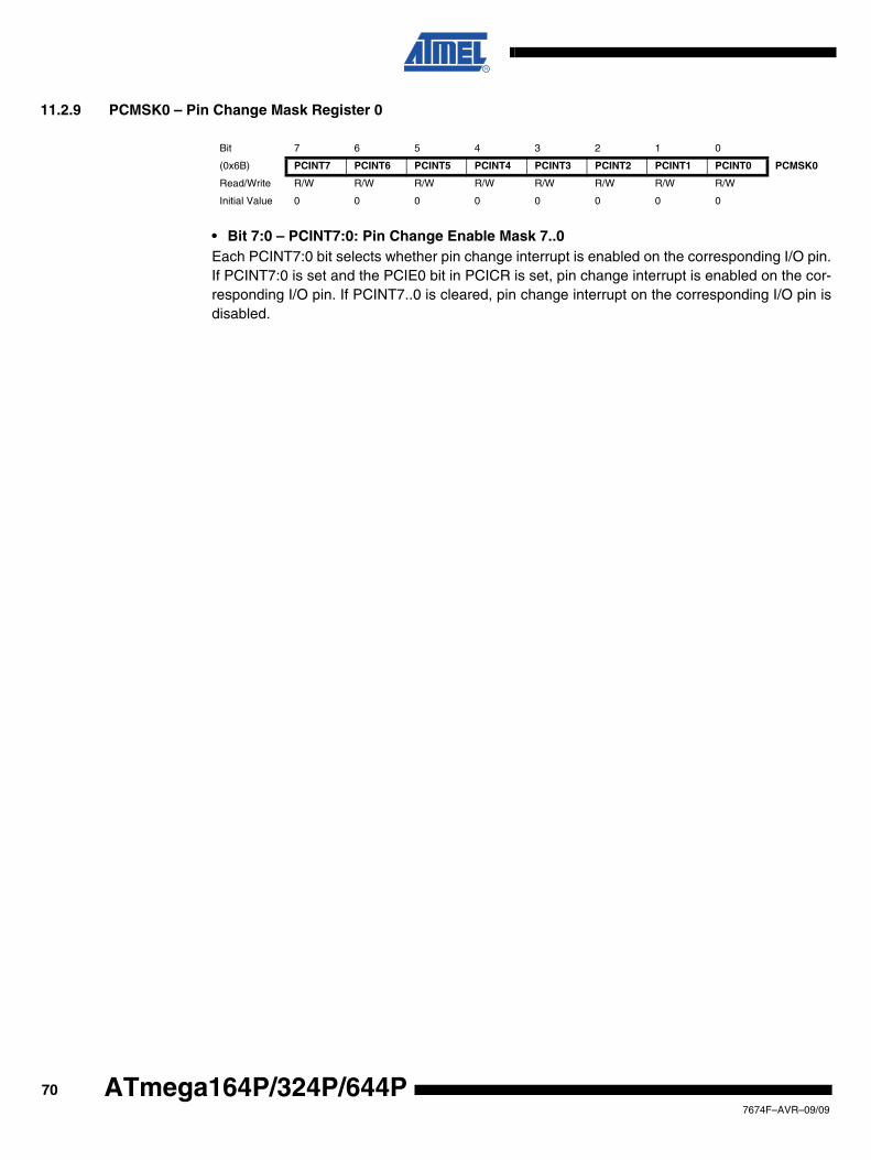
11.2.9 PCMSK0 – Pin Change Mask Register 0
• Bit 7:0 – PCINT7:0: Pin Change Enable Mask 7..0Each PCINT7:0 bit selects whether pin change interrupt is enabled on the corresponding I/O pin.If PCINT7:0 is set and the PCIE0 bit in PCICR is set, pin change interrupt is enabled on the cor-responding I/O pin. If PCINT7..0 is cleared, pin change interrupt on the corresponding I/O pin isdisabled.
Bit 7 6 5 4 3 2 1 0
(0x6B) PCINT7 PCINT6 PCINT5 PCINT4 PCINT3 PCINT2 PCINT1 PCINT0 PCMSK0
Read/Write R/W R/W R/W R/W R/W R/W R/W R/W
Initial Value 0 0 0 0 0 0 0 0
707674F–AVR–09/09
ATmega164P/324P/644P
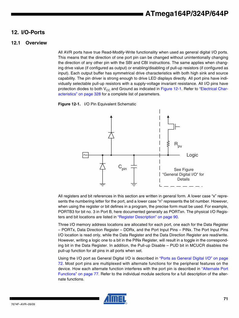
ATmega164P/324P/644P
12. I/O-Ports
12.1 Overview
All AVR ports have true Read-Modify-Write functionality when used as general digital I/O ports.This means that the direction of one port pin can be changed without unintentionally changingthe direction of any other pin with the SBI and CBI instructions. The same applies when chang-ing drive value (if configured as output) or enabling/disabling of pull-up resistors (if configured asinput). Each output buffer has symmetrical drive characteristics with both high sink and sourcecapability. The pin driver is strong enough to drive LED displays directly. All port pins have indi-vidually selectable pull-up resistors with a supply-voltage invariant resistance. All I/O pins haveprotection diodes to both VCC and Ground as indicated in Figure 12-1. Refer to “Electrical Char-acteristics” on page 328 for a complete list of parameters.
Figure 12-1. I/O Pin Equivalent Schematic
All registers and bit references in this section are written in general form. A lower case “x” repre-sents the numbering letter for the port, and a lower case “n” represents the bit number. However,when using the register or bit defines in a program, the precise form must be used. For example,PORTB3 for bit no. 3 in Port B, here documented generally as PORTxn. The physical I/O Regis-ters and bit locations are listed in “Register Description” on page 90.
Three I/O memory address locations are allocated for each port, one each for the Data Register– PORTx, Data Direction Register – DDRx, and the Port Input Pins – PINx. The Port Input PinsI/O location is read only, while the Data Register and the Data Direction Register are read/write.However, writing a logic one to a bit in the PINx Register, will result in a toggle in the correspond-ing bit in the Data Register. In addition, the Pull-up Disable – PUD bit in MCUCR disables thepull-up function for all pins in all ports when set.
Using the I/O port as General Digital I/O is described in “Ports as General Digital I/O” on page72. Most port pins are multiplexed with alternate functions for the peripheral features on thedevice. How each alternate function interferes with the port pin is described in “Alternate PortFunctions” on page 77. Refer to the individual module sections for a full description of the alter-nate functions.
Cpin
Logic
Rpu
See Figure"General Digital I/O" for
Details
Pxn
717674F–AVR–09/09
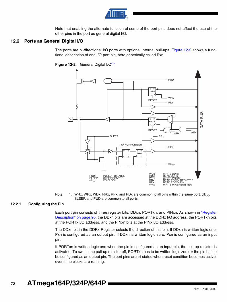
Note that enabling the alternate function of some of the port pins does not affect the use of theother pins in the port as general digital I/O.
12.2 Ports as General Digital I/O
The ports are bi-directional I/O ports with optional internal pull-ups. Figure 12-2 shows a func-tional description of one I/O-port pin, here generically called Pxn.
Figure 12-2. General Digital I/O(1)
Note: 1. WRx, WPx, WDx, RRx, RPx, and RDx are common to all pins within the same port. clkI/O, SLEEP, and PUD are common to all ports.
12.2.1 Configuring the Pin
Each port pin consists of three register bits: DDxn, PORTxn, and PINxn. As shown in “RegisterDescription” on page 90, the DDxn bits are accessed at the DDRx I/O address, the PORTxn bitsat the PORTx I/O address, and the PINxn bits at the PINx I/O address.
The DDxn bit in the DDRx Register selects the direction of this pin. If DDxn is written logic one,Pxn is configured as an output pin. If DDxn is written logic zero, Pxn is configured as an inputpin.
If PORTxn is written logic one when the pin is configured as an input pin, the pull-up resistor isactivated. To switch the pull-up resistor off, PORTxn has to be written logic zero or the pin has tobe configured as an output pin. The port pins are tri-stated when reset condition becomes active,even if no clocks are running.
clk
RPx
RRx
RDx
WDx
PUD
SYNCHRONIZER
WDx: WRITE DDRx
WRx: WRITE PORTxRRx: READ PORTx REGISTERRPx: READ PORTx PIN
PUD: PULLUP DISABLE
clkI/O: I/O CLOCK
RDx: READ DDRx
D
L
Q
Q
RESET
RESET
Q
QD
Q
Q D
CLR
PORTxn
Q
Q D
CLR
DDxn
PINxn
DAT
A B
US
SLEEP
SLEEP: SLEEP CONTROL
Pxn
I/O
WPx
0
1
WRx
WPx: WRITE PINx REGISTER
727674F–AVR–09/09
ATmega164P/324P/644P
ATmega164P/324P/644P
If PORTxn is written logic one when the pin is configured as an output pin, the port pin is drivenhigh (one). If PORTxn is written logic zero when the pin is configured as an output pin, the portpin is driven low (zero).
12.2.2 Toggling the Pin
Writing a logic one to PINxn toggles the value of PORTxn, independent on the value of DDRxn.Note that the SBI instruction can be used to toggle one single bit in a port.
12.2.3 Switching Between Input and Output
When switching between tri-state ({DDxn, PORTxn} = 0b00) and output high ({DDxn, PORTxn}= 0b11), an intermediate state with either pull-up enabled {DDxn, PORTxn} = 0b01) or outputlow ({DDxn, PORTxn} = 0b10) must occur. Normally, the pull-up enabled state is fully accept-able, as a high-impedant environment will not notice the difference between a strong high driverand a pull-up. If this is not the case, the PUD bit in the MCUCR Register can be set to disable allpull-ups in all ports.
Switching between input with pull-up and output low generates the same problem. The usermust use either the tri-state ({DDxn, PORTxn} = 0b00) or the output high state ({DDxn, PORTxn}= 0b11) as an intermediate step.
Table 12-1 summarizes the control signals for the pin value.
12.2.4 Reading the Pin Value
Independent of the setting of Data Direction bit DDxn, the port pin can be read through thePINxn Register bit. As shown in Figure 12-2, the PINxn Register bit and the preceding latch con-stitute a synchronizer. This is needed to avoid metastability if the physical pin changes valuenear the edge of the internal clock, but it also introduces a delay. Figure 12-3 shows a timing dia-gram of the synchronization when reading an externally applied pin value. The maximum andminimum propagation delays are denoted tpd,max and tpd,min respectively.
Table 12-1. Port Pin Configurations
DDxn PORTxnPUD
(in MCUCR) I/O Pull-up Comment
0 0 X Input No Tri-state (Hi-Z)
0 1 0 Input Yes Pxn will source current if ext. pulled low.
0 1 1 Input No Tri-state (Hi-Z)
1 0 X Output No Output Low (Sink)
1 1 X Output No Output High (Source)
737674F–AVR–09/09
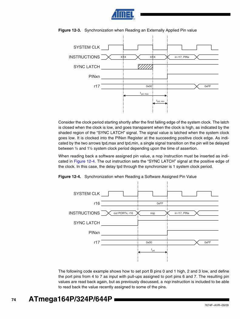
Figure 12-3. Synchronization when Reading an Externally Applied Pin value
Consider the clock period starting shortly after the first falling edge of the system clock. The latchis closed when the clock is low, and goes transparent when the clock is high, as indicated by theshaded region of the “SYNC LATCH” signal. The signal value is latched when the system clockgoes low. It is clocked into the PINxn Register at the succeeding positive clock edge. As indi-cated by the two arrows tpd,max and tpd,min, a single signal transition on the pin will be delayedbetween ½ and 1½ system clock period depending upon the time of assertion.
When reading back a software assigned pin value, a nop instruction must be inserted as indi-cated in Figure 12-4. The out instruction sets the “SYNC LATCH” signal at the positive edge ofthe clock. In this case, the delay tpd through the synchronizer is 1 system clock period.
Figure 12-4. Synchronization when Reading a Software Assigned Pin Value
The following code example shows how to set port B pins 0 and 1 high, 2 and 3 low, and definethe port pins from 4 to 7 as input with pull-ups assigned to port pins 6 and 7. The resulting pinvalues are read back again, but as previously discussed, a nop instruction is included to be ableto read back the value recently assigned to some of the pins.
xNIP ,71r niXXX
FFx000x0
INSTRUCTIONS
SYNC LATCH
PINxn
r17
XXX
SYSTEM CLK
tpd, max
tpd, min
out PORTx, r16 nop in r17, PINx
0xFF
0x00 0xFF
SYSTEM CLK
r16
INSTRUCTIONS
SYNC LATCH
PINxn
r17
tpd
747674F–AVR–09/09
ATmega164P/324P/644P
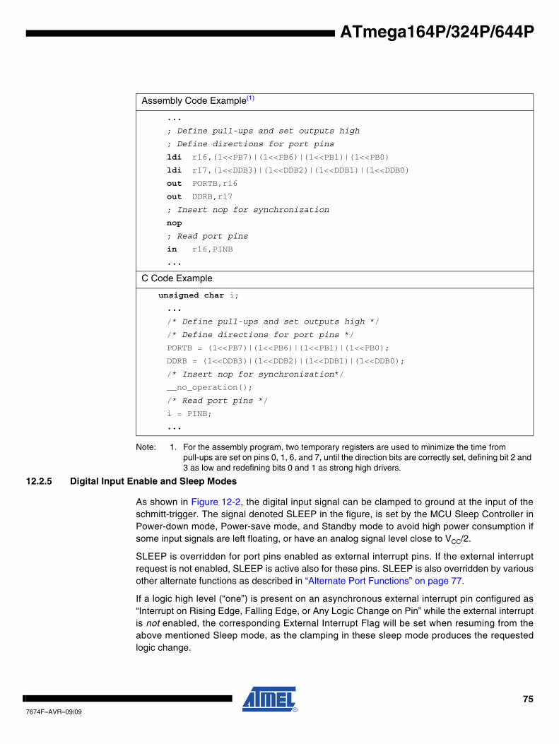
ATmega164P/324P/644P
Note: 1. For the assembly program, two temporary registers are used to minimize the time from pull-ups are set on pins 0, 1, 6, and 7, until the direction bits are correctly set, defining bit 2 and 3 as low and redefining bits 0 and 1 as strong high drivers.
12.2.5 Digital Input Enable and Sleep Modes
As shown in Figure 12-2, the digital input signal can be clamped to ground at the input of theschmitt-trigger. The signal denoted SLEEP in the figure, is set by the MCU Sleep Controller inPower-down mode, Power-save mode, and Standby mode to avoid high power consumption ifsome input signals are left floating, or have an analog signal level close to VCC/2.
SLEEP is overridden for port pins enabled as external interrupt pins. If the external interruptrequest is not enabled, SLEEP is active also for these pins. SLEEP is also overridden by variousother alternate functions as described in “Alternate Port Functions” on page 77.
If a logic high level (“one”) is present on an asynchronous external interrupt pin configured as“Interrupt on Rising Edge, Falling Edge, or Any Logic Change on Pin” while the external interruptis not enabled, the corresponding External Interrupt Flag will be set when resuming from theabove mentioned Sleep mode, as the clamping in these sleep mode produces the requestedlogic change.
Assembly Code Example(1)
...
; Define pull-ups and set outputs high
; Define directions for port pins
ldi r16,(1<<PB7)|(1<<PB6)|(1<<PB1)|(1<<PB0)
ldi r17,(1<<DDB3)|(1<<DDB2)|(1<<DDB1)|(1<<DDB0)
out PORTB,r16
out DDRB,r17
; Insert nop for synchronization
nop
; Read port pins
in r16,PINB
...
C Code Example
unsigned char i;
...
/* Define pull-ups and set outputs high */
/* Define directions for port pins */
PORTB = (1<<PB7)|(1<<PB6)|(1<<PB1)|(1<<PB0);
DDRB = (1<<DDB3)|(1<<DDB2)|(1<<DDB1)|(1<<DDB0);
/* Insert nop for synchronization*/
__no_operation();
/* Read port pins */
i = PINB;
...
757674F–AVR–09/09
12.2.6 Unconnected Pins
If some pins are unused, it is recommended to ensure that these pins have a defined level. Eventhough most of the digital inputs are disabled in the deep sleep modes as described above, float-ing inputs should be avoided to reduce current consumption in all other modes where the digitalinputs are enabled (Reset, Active mode and Idle mode).
The simplest method to ensure a defined level of an unused pin, is to enable the internal pull-up.In this case, the pull-up will be disabled during reset. If low power consumption during reset isimportant, it is recommended to use an external pull-up or pull-down. Connecting unused pinsdirectly to VCC or GND is not recommended, since this may cause excessive currents if the pin isaccidentally configured as an output.
767674F–AVR–09/09
ATmega164P/324P/644P
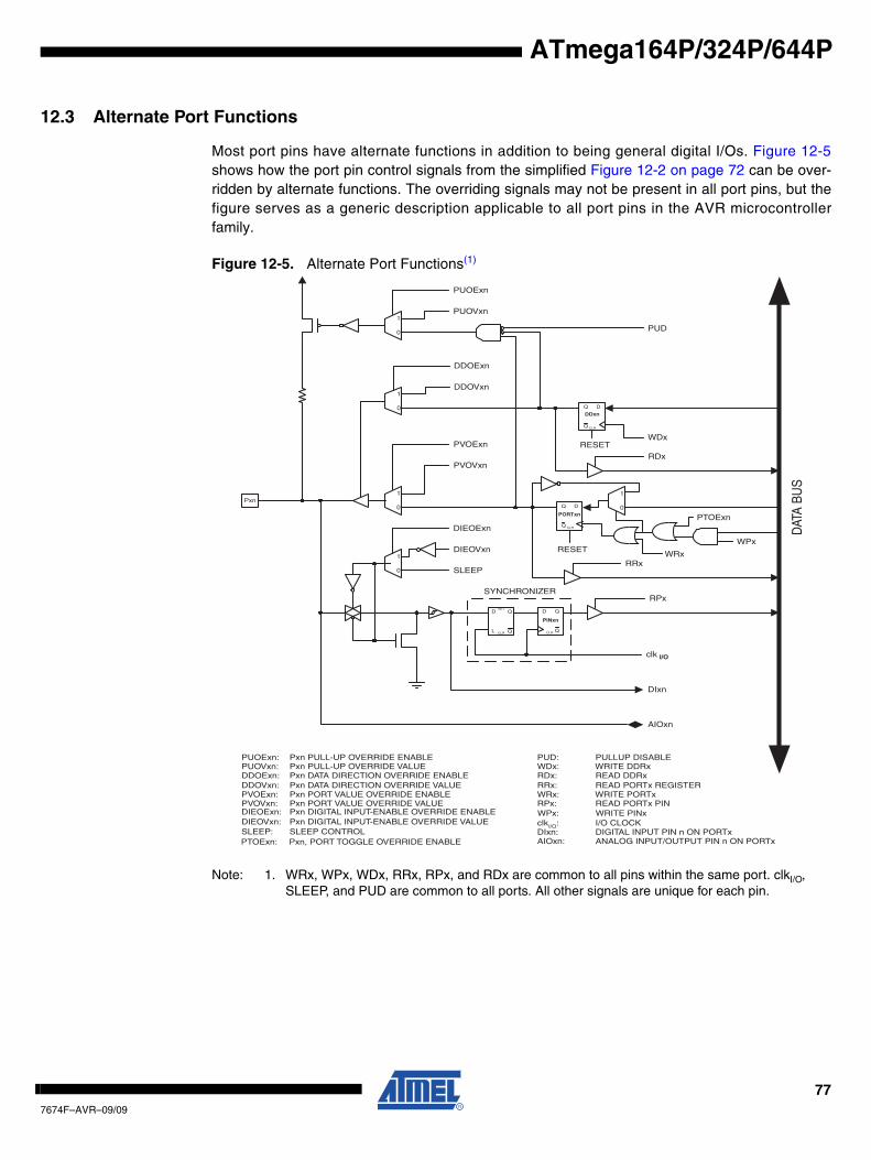
ATmega164P/324P/644P
12.3 Alternate Port Functions
Most port pins have alternate functions in addition to being general digital I/Os. Figure 12-5shows how the port pin control signals from the simplified Figure 12-2 on page 72 can be over-ridden by alternate functions. The overriding signals may not be present in all port pins, but thefigure serves as a generic description applicable to all port pins in the AVR microcontrollerfamily.
Figure 12-5. Alternate Port Functions(1)
Note: 1. WRx, WPx, WDx, RRx, RPx, and RDx are common to all pins within the same port. clkI/O, SLEEP, and PUD are common to all ports. All other signals are unique for each pin.
clk
RPx
RRxWRx
RDx
WDx
PUD
SYNCHRONIZER
WDx: WRITE DDRx
WRx: WRITE PORTxRRx: READ PORTx REGISTER
RPx: READ PORTx PIN
PUD: PULLUP DISABLE
clkI/O: I/O CLOCK
RDx: READ DDRx
D
L
Q
Q
SET
CLR
0
1
0
1
0
1
DIxn
AIOxn
DIEOExn
PVOVxn
PVOExn
DDOVxn
DDOExn
PUOExn
PUOVxn
PUOExn: Pxn PULL-UP OVERRIDE ENABLEPUOVxn: Pxn PULL-UP OVERRIDE VALUEDDOExn: Pxn DATA DIRECTION OVERRIDE ENABLEDDOVxn: Pxn DATA DIRECTION OVERRIDE VALUEPVOExn: Pxn PORT VALUE OVERRIDE ENABLEPVOVxn: Pxn PORT VALUE OVERRIDE VALUE
DIxn: DIGITAL INPUT PIN n ON PORTxAIOxn: ANALOG INPUT/OUTPUT PIN n ON PORTx
RESET
RESET
Q
Q D
CLR
Q
Q D
CLR
Q
QD
CLR
PINxn
PORTxn
DDxn
DAT
A B
US
0
1DIEOVxn
SLEEP
DIEOExn: Pxn DIGITAL INPUT-ENABLE OVERRIDE ENABLEDIEOVxn: Pxn DIGITAL INPUT-ENABLE OVERRIDE VALUESLEEP: SLEEP CONTROL
Pxn
I/O
0
1
PTOExn
PTOExn: Pxn, PORT TOGGLE OVERRIDE ENABLE
WPx: WRITE PINx
WPx
777674F–AVR–09/09
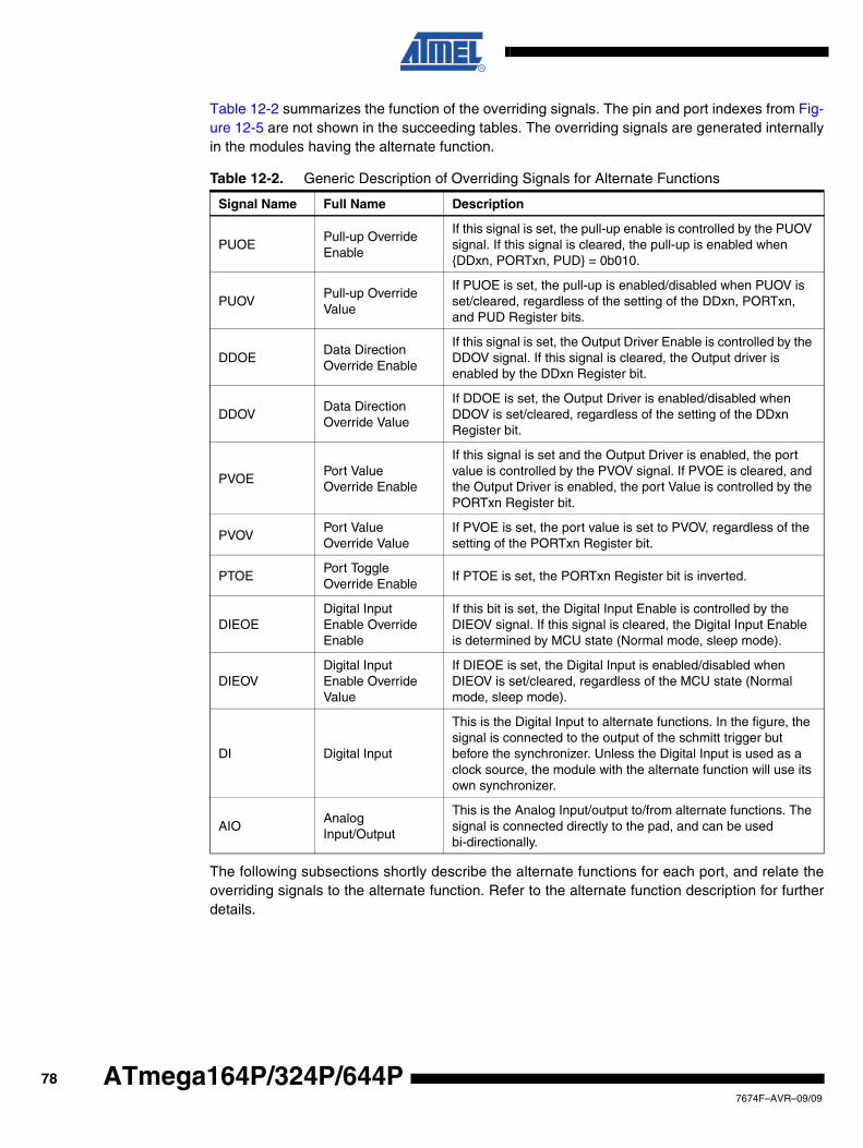
Table 12-2 summarizes the function of the overriding signals. The pin and port indexes from Fig-ure 12-5 are not shown in the succeeding tables. The overriding signals are generated internallyin the modules having the alternate function.
The following subsections shortly describe the alternate functions for each port, and relate theoverriding signals to the alternate function. Refer to the alternate function description for furtherdetails.
Table 12-2. Generic Description of Overriding Signals for Alternate Functions
Signal Name Full Name Description
PUOEPull-up Override Enable
If this signal is set, the pull-up enable is controlled by the PUOV signal. If this signal is cleared, the pull-up is enabled when {DDxn, PORTxn, PUD} = 0b010.
PUOVPull-up Override Value
If PUOE is set, the pull-up is enabled/disabled when PUOV is set/cleared, regardless of the setting of the DDxn, PORTxn, and PUD Register bits.
DDOEData Direction Override Enable
If this signal is set, the Output Driver Enable is controlled by the DDOV signal. If this signal is cleared, the Output driver is enabled by the DDxn Register bit.
DDOVData Direction Override Value
If DDOE is set, the Output Driver is enabled/disabled when DDOV is set/cleared, regardless of the setting of the DDxn Register bit.
PVOEPort Value Override Enable
If this signal is set and the Output Driver is enabled, the port value is controlled by the PVOV signal. If PVOE is cleared, and the Output Driver is enabled, the port Value is controlled by the PORTxn Register bit.
PVOVPort Value Override Value
If PVOE is set, the port value is set to PVOV, regardless of the setting of the PORTxn Register bit.
PTOEPort Toggle Override Enable
If PTOE is set, the PORTxn Register bit is inverted.
DIEOEDigital Input Enable Override Enable
If this bit is set, the Digital Input Enable is controlled by the DIEOV signal. If this signal is cleared, the Digital Input Enable is determined by MCU state (Normal mode, sleep mode).
DIEOVDigital Input Enable Override Value
If DIEOE is set, the Digital Input is enabled/disabled when DIEOV is set/cleared, regardless of the MCU state (Normal mode, sleep mode).
DI Digital Input
This is the Digital Input to alternate functions. In the figure, the signal is connected to the output of the schmitt trigger but before the synchronizer. Unless the Digital Input is used as a clock source, the module with the alternate function will use its own synchronizer.
AIOAnalog Input/Output
This is the Analog Input/output to/from alternate functions. The signal is connected directly to the pad, and can be used bi-directionally.
787674F–AVR–09/09
ATmega164P/324P/644P
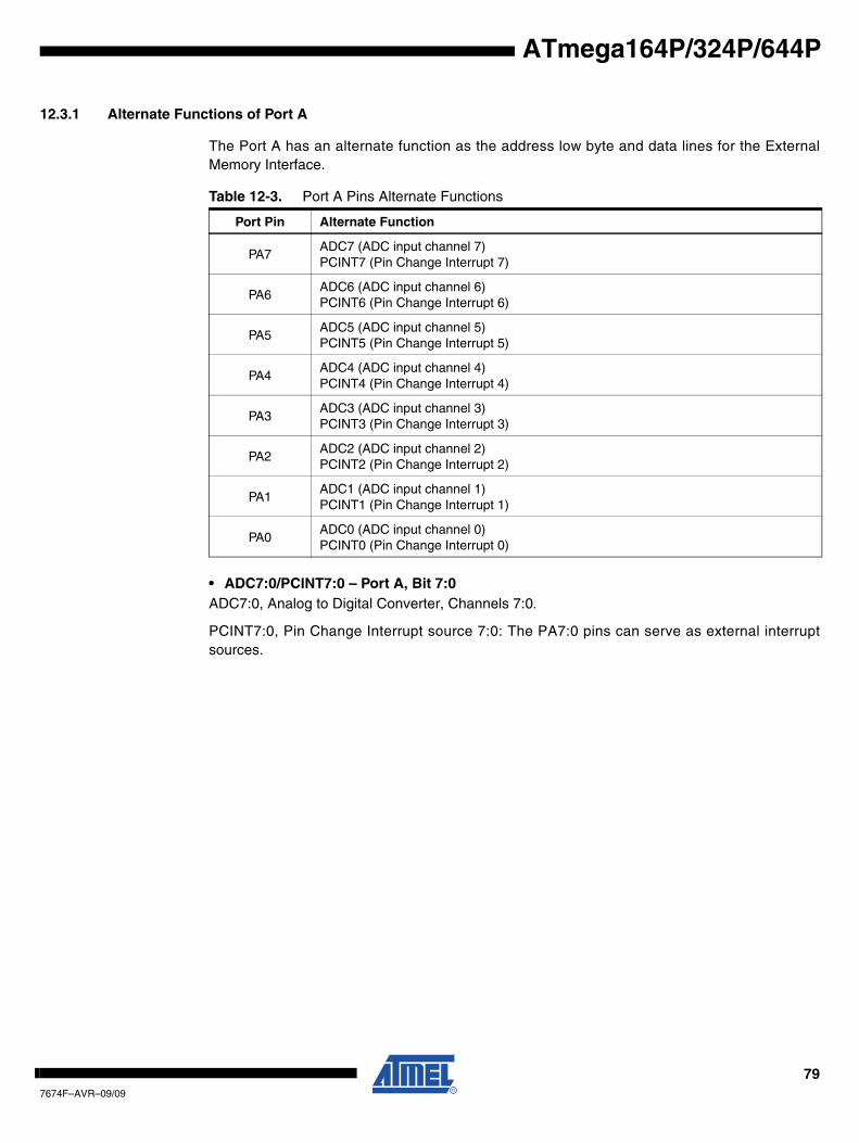
ATmega164P/324P/644P
12.3.1 Alternate Functions of Port A
The Port A has an alternate function as the address low byte and data lines for the ExternalMemory Interface.
• ADC7:0/PCINT7:0 – Port A, Bit 7:0ADC7:0, Analog to Digital Converter, Channels 7:0.
PCINT7:0, Pin Change Interrupt source 7:0: The PA7:0 pins can serve as external interruptsources.
Table 12-3. Port A Pins Alternate Functions
Port Pin Alternate Function
PA7ADC7 (ADC input channel 7)PCINT7 (Pin Change Interrupt 7)
PA6ADC6 (ADC input channel 6)PCINT6 (Pin Change Interrupt 6)
PA5ADC5 (ADC input channel 5)PCINT5 (Pin Change Interrupt 5)
PA4ADC4 (ADC input channel 4)PCINT4 (Pin Change Interrupt 4)
PA3ADC3 (ADC input channel 3)PCINT3 (Pin Change Interrupt 3)
PA2ADC2 (ADC input channel 2)PCINT2 (Pin Change Interrupt 2)
PA1ADC1 (ADC input channel 1)PCINT1 (Pin Change Interrupt 1)
PA0ADC0 (ADC input channel 0)PCINT0 (Pin Change Interrupt 0)
797674F–AVR–09/09
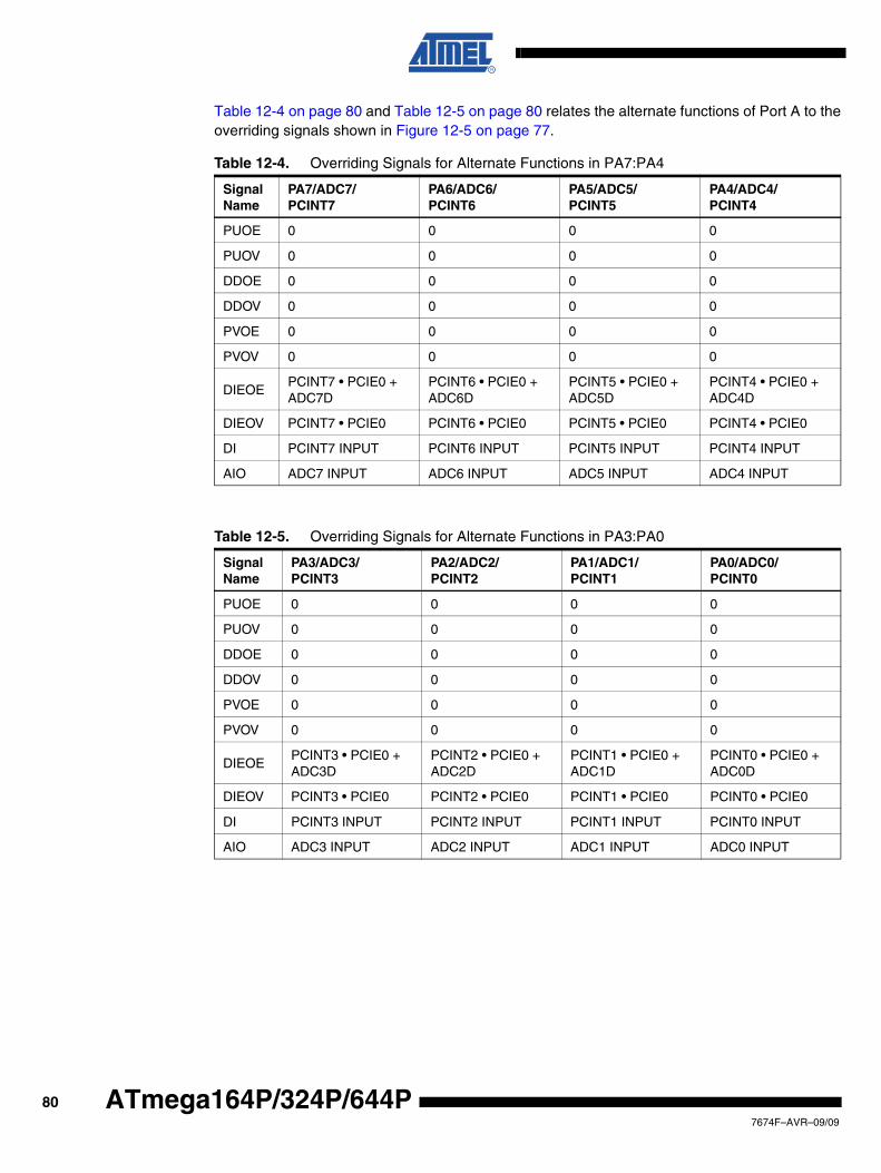
Table 12-4 on page 80 and Table 12-5 on page 80 relates the alternate functions of Port A to theoverriding signals shown in Figure 12-5 on page 77.
Table 12-4. Overriding Signals for Alternate Functions in PA7:PA4
SignalName
PA7/ADC7/PCINT7
PA6/ADC6/PCINT6
PA5/ADC5/PCINT5
PA4/ADC4/PCINT4
PUOE 0 0 0 0
PUOV 0 0 0 0
DDOE 0 0 0 0
DDOV 0 0 0 0
PVOE 0 0 0 0
PVOV 0 0 0 0
DIEOEPCINT7 • PCIE0 + ADC7D
PCINT6 • PCIE0 + ADC6D
PCINT5 • PCIE0 + ADC5D
PCINT4 • PCIE0 + ADC4D
DIEOV PCINT7 • PCIE0 PCINT6 • PCIE0 PCINT5 • PCIE0 PCINT4 • PCIE0
DI PCINT7 INPUT PCINT6 INPUT PCINT5 INPUT PCINT4 INPUT
AIO ADC7 INPUT ADC6 INPUT ADC5 INPUT ADC4 INPUT
Table 12-5. Overriding Signals for Alternate Functions in PA3:PA0
Signal Name
PA3/ADC3/PCINT3
PA2/ADC2/PCINT2
PA1/ADC1/PCINT1
PA0/ADC0/PCINT0
PUOE 0 0 0 0
PUOV 0 0 0 0
DDOE 0 0 0 0
DDOV 0 0 0 0
PVOE 0 0 0 0
PVOV 0 0 0 0
DIEOEPCINT3 • PCIE0 + ADC3D
PCINT2 • PCIE0 + ADC2D
PCINT1 • PCIE0 + ADC1D
PCINT0 • PCIE0 + ADC0D
DIEOV PCINT3 • PCIE0 PCINT2 • PCIE0 PCINT1 • PCIE0 PCINT0 • PCIE0
DI PCINT3 INPUT PCINT2 INPUT PCINT1 INPUT PCINT0 INPUT
AIO ADC3 INPUT ADC2 INPUT ADC1 INPUT ADC0 INPUT
807674F–AVR–09/09
ATmega164P/324P/644P
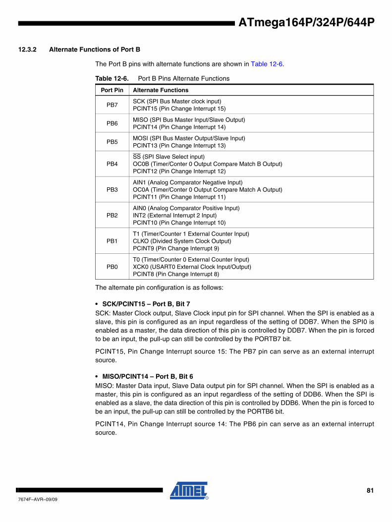
ATmega164P/324P/644P
12.3.2 Alternate Functions of Port B
The Port B pins with alternate functions are shown in Table 12-6.
The alternate pin configuration is as follows:
• SCK/PCINT15 – Port B, Bit 7SCK: Master Clock output, Slave Clock input pin for SPI channel. When the SPI is enabled as aslave, this pin is configured as an input regardless of the setting of DDB7. When the SPI0 isenabled as a master, the data direction of this pin is controlled by DDB7. When the pin is forcedto be an input, the pull-up can still be controlled by the PORTB7 bit.
PCINT15, Pin Change Interrupt source 15: The PB7 pin can serve as an external interruptsource.
• MISO/PCINT14 – Port B, Bit 6MISO: Master Data input, Slave Data output pin for SPI channel. When the SPI is enabled as amaster, this pin is configured as an input regardless of the setting of DDB6. When the SPI isenabled as a slave, the data direction of this pin is controlled by DDB6. When the pin is forced tobe an input, the pull-up can still be controlled by the PORTB6 bit.
PCINT14, Pin Change Interrupt source 14: The PB6 pin can serve as an external interruptsource.
Table 12-6. Port B Pins Alternate Functions
Port Pin Alternate Functions
PB7SCK (SPI Bus Master clock input)PCINT15 (Pin Change Interrupt 15)
PB6MISO (SPI Bus Master Input/Slave Output)PCINT14 (Pin Change Interrupt 14)
PB5MOSI (SPI Bus Master Output/Slave Input)PCINT13 (Pin Change Interrupt 13)
PB4SS (SPI Slave Select input)OC0B (Timer/Conter 0 Output Compare Match B Output)PCINT12 (Pin Change Interrupt 12)
PB3AIN1 (Analog Comparator Negative Input)OC0A (Timer/Conter 0 Output Compare Match A Output)PCINT11 (Pin Change Interrupt 11)
PB2AIN0 (Analog Comparator Positive Input)INT2 (External Interrupt 2 Input)PCINT10 (Pin Change Interrupt 10)
PB1T1 (Timer/Counter 1 External Counter Input)CLKO (Divided System Clock Output)PCINT9 (Pin Change Interrupt 9)
PB0T0 (Timer/Counter 0 External Counter Input)XCK0 (USART0 External Clock Input/Output)PCINT8 (Pin Change Interrupt 8)
817674F–AVR–09/09
• MOSI/PCINT13 – Port B, Bit 5MOSI: SPI Master Data output, Slave Data input for SPI channel. When the SPI is enabled as aslave, this pin is configured as an input regardless of the setting of DDB5. When the SPI isenabled as a master, the data direction of this pin is controlled by DDB5. When the pin is forcedto be an input, the pull-up can still be controlled by the PORTB5 bit.
PCINT13, Pin Change Interrupt source 13: The PB5 pin can serve as an external interruptsource.
• SS/OC0B/PCINT12 – Port B, Bit 4SS: Slave Port Select input. When the SPI is enabled as a slave, this pin is configured as aninput regardless of the setting of DDB4. As a slave, the SPI is activated when this pin is drivenlow. When the SPI is enabled as a master, the data direction of this pin is controlled by DDB4.When the pin is forced to be an input, the pull-up can still be controlled by the PORTB4 bit.
OC0B, Output Compare Match B output: The PB4 pin can serve as an external output for theTimer/Counter0 Output Compare. The pin has to be configured as an output (DDB4 set “one”) toserve this function. The OC0B pin is also the output pin for the PWM mode timer function.
PCINT12, Pin Change Interrupt source 12: The PB4 pin can serve as an external interruptsource.
• AIN1/OC0A/PCINT11, Bit 3AIN1, Analog Comparator Negative input. This pin is directly connected to the negative input ofthe Analog Comparator.
OC0A, Output Compare Match A output: The PB3 pin can serve as an external output for theTimer/Counter0 Output Compare. The pin has to be configured as an output (DDB3 set “one”) toserve this function. The OC0A pin is also the output pin for the PWM mode timer function.
PCINT11, Pin Change Interrupt source 11: The PB3 pin can serve as an external interruptsource.
• AIN0/INT2/PCINT10, Bit 2AIN0, Analog Comparator Positive input. This pin is directly connected to the positive input ofthe Analog Comparator.
INT2, External Interrupt source 2. The PB2 pin can serve as an External Interrupt source to theMCU.
PCINT10, Pin Change Interrupt source 10: The PB2 pin can serve as an external interruptsource.
• T1/CLKO/PCINT9, Bit 1T1, Timer/Counter1 counter source.
CLKO, Divided System Clock: The divided system clock can be output on the PB1 pin. Thedivided system clock will be output if the CKOUT Fuse is programmed, regardless of thePORTB1 and DDB1 settings. It will also be output during reset.
PCINT9, Pin Change Interrupt source 9: The PB1 pin can serve as an external interrupt source.
827674F–AVR–09/09
ATmega164P/324P/644P
ATmega164P/324P/644P
• T0/XCK0/PCINT8, Bit 0T0, Timer/Counter0 counter source.
XCK0, USART0 External clock. The Data Direction Register (DDB0) controls whether the clockis output (DDD0 set “one”) or input (DDD0 cleared). The XCK0 pin is active only when theUSART0 operates in Synchronous mode.
PCINT8, Pin Change Interrupt source 8: The PB0 pin can serve as an external interrupt source.
Table 12-7 and Table 12-8 relate the alternate functions of Port B to the overriding signalsshown in Figure 12-5 on page 77. SPI MSTR INPUT and SPI SLAVE OUTPUT constitute theMISO signal, while MOSI is divided into SPI MSTR OUTPUT and SPI SLAVE INPUT. .
Table 12-7. Overriding Signals for Alternate Functions in PB7:PB4
Signal Name
PB7/SCK/PCINT15
PB6/MISO/PCINT14
PB5/MOSI/PCINT13
PB4/SS/OC0B/PCINT12
PUOE SPE • MSTR SPE • MSTR SPE • MSTR SPE • MSTR
PUOV PORTB7 • PUD PORTB14 • PUD PORTB13 • PUD PORTB12 • PUD
DDOE SPE • MSTR SPE • MSTR SPE • MSTR SPE • MSTR
DDOV 0 0 0 0
PVOE SPE • MSTR SPE • MSTR SPE • MSTR OC0A ENABLE
PVOV SCK OUTPUTSPI SLAVE OUTPUT
SPI MSTR OUTPUT OC0A
DIEOE PCINT15 • PCIE1 PCINT14 • PCIE1 PCINT13 • PCIE1 PCINT4 • PCIE1
DIEOV 1 1 1 1
DISCK INPUTPCINT17 INPUT
SPI MSTR INPUTPCINT14 INPUT
SPI SLAVE INPUTPCINT13 INPUT
SPI SSPCINT12 INPUT
AIO – – – –
Table 12-8. Overriding Signals for Alternate Functions in PB3:PB0
Signal Name
PB3/AIN1/OC0B/PCINT11
PB2/AIN0/INT2/PCINT10
PB1/T1/CLKO/PCINT9
PB0/T0/XCK/PCINT8
PUOE 0 0 0 0
PUOV 0 0 0 0
DDOE 0 0 0 0
DDOV 0 0 0 0
PVOE OC0B ENABLE 0 0 0
PVOV OC0B 0 0 0
DIEOE PCINT11 • PCIE1INT2 ENABLEPCINT10 • PCIE1
PCINT9 • PCIE1 PCINT8 • PCIE1
DIEOV 1 1 1 1
DI PCINT11 INPUTINT2 INPUTPCINT10 INPUT
T1 INPUTPCINT9 INPUT
T0 INPUTPCINT8 INPUT
AIO – – – –
837674F–AVR–09/09
12.3.3 Alternate Functions of Port C
The Port C alternate function is as follows:
• TOSC2/PCINT23 – Port C, Bit7 TOSC2, Timer Oscillator pin 2. The PC7 pin can serve as an external interrupt source to theMCU.
PCINT23, Pin Change Interrupt source 23: The PC7 pin can serve as an external interruptsource.
• TOSC1/PCINT22 – Port C, Bit 6TOSC1, Timer Oscillator pin 1. The PC6 pin can serve as an external interrupt source to theMCU.
PCINT22, Pin Change Interrupt source 23: The PC6 pin can serve as an external interruptsource.
• TDI/PCINT21 – Port C, Bit 5TDI, JTAG Test Data Input.
PCINT21, Pin Change Interrupt source 21: The PC5 pin can serve as an external interruptsource.
• TDO/PCINT20 – Port C, Bit 4TDO, JTAG Test Data Output.
PCINT20, Pin Change Interrupt source 20: The PC4 pin can serve as an external interruptsource.
Table 12-9. Port C Pins Alternate Functions
Port Pin Alternate Function
PC7TOSC2 (Timer Oscillator pin 2)
PCINT23 (Pin Change Interrupt 23)
PC6TOSC1 (Timer Oscillator pin 1)PCINT22 (Pin Change Interrupt 22)
PC5TDI (JTAG Test Data Input)PCINT21 (Pin Change Interrupt 21)
PC4TDO (JTAG Test Data Output)PCINT20 (Pin Change Interrupt 20)
PC3TMS (JTAG Test Mode Select)PCINT19 (Pin Change Interrupt 19)
PC2TCK (JTAG Test Clock)PCINT18 (Pin Change Interrupt 18)
PC1SDA (2-wire Serial Bus Data Input/Output Line)PCINT17 (Pin Change Interrupt 17)
PC0SCL (2-wire Serial Bus Clock Line)PCINT16 (Pin Change Interrupt 16)
847674F–AVR–09/09
ATmega164P/324P/644P
ATmega164P/324P/644P
• TMS/PCINT19 – Port C, Bit 3TMS, JTAG Test Mode Select.
PCINT19, Pin Change Interrupt source 19: The PC3 pin can serve as an external interruptsource.
• TCK/PCINT18 – Port C, Bit 2TCK, JTAG Test Clock.
PCINT18, Pin Change Interrupt source 18: The PC2 pin can serve as an external interruptsource.
• SDA/PCINT17 – Port C, Bit 1SDA, 2-wire Serial Bus Data Input/Output Line.
PCINT17, Pin Change Interrupt source 17: The PC1 pin can serve as an external interruptsource.
• SCL/PCINT16 – Port C, Bit 0SCL, 2-wire Serial Busk Clock Line.
PCINT23, Pin Change Interrupt source 23: The PC0 pin can serve as an external interruptsource.
Table 12-10 and Table 12-11 relate the alternate functions of Port C to the overriding signalsshown in Figure 12-5 on page 77.
Table 12-10. Overriding Signals for Alternate Functions in PC7:PC4
Signal Name
PC7/TOSC2/PCINT23
PC6/TOSC1/PCINT22
PC5/TDI/PCINT21
PC4/TDO/PCINT20
PUOE AS2 • EXCLK AS2 JTAGEN JTAGEN
PUOV 0 0 1 1
DDOE AS2 • EXCLK AS2 JTAGEN JTAGEN
DDOV 0 0 0SHIFT_IR + SHIFT_DR
PVOE 0 0 0 JTAGEN
PVOV 0 0 0 TDO
DIEOEAS2 • EXCLK +PCINT23 • PCIE2
AS2 JTAGEN JTAGEN
DIEOV 0 EXCLK 0 0
DI PCINT23 INPUT PCINT22 INPUT PCINT21 INPUT PCINT20 INPUT
AIO T/C2 OSC OUTPUTT/C2 OSC INPUT
TDI INPUT –
857674F–AVR–09/09
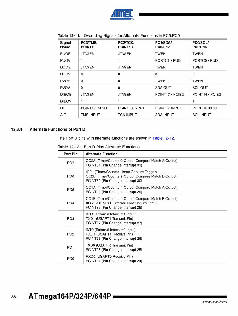
12.3.4 Alternate Functions of Port D
The Port D pins with alternate functions are shown in Table 12-12.
Table 12-11. Overriding Signals for Alternate Functions in PC3:PC0
Signal Name
PC3/TMS/PCINT19
PC2/TCK/PCINT18
PC1/SDA/PCINT17
PC0/SCL/PCINT16
PUOE JTAGEN JTAGEN TWEN TWEN
PUOV 1 1 PORTC1 • PUD PORTC0 • PUD
DDOE JTAGEN JTAGEN TWEN TWEN
DDOV 0 0 0 0
PVOE 0 0 TWEN TWEN
PVOV 0 0 SDA OUT SCL OUT
DIEOE JTAGEN JTAGEN PCINT17 • PCIE2 PCINT16 • PCIE2
DIEOV 1 1 1 1
DI PCINT19 INPUT PCINT18 INPUT PCINT17 INPUT PCINT16 INPUT
AIO TMS INPUT TCK INPUT SDA INPUT SCL INPUT
Table 12-12. Port D Pins Alternate Functions
Port Pin Alternate Function
PD7OC2A (Timer/Counter2 Output Compare Match A Output)PCINT31 (Pin Change Interrupt 31)
PD6ICP1 (Timer/Counter1 Input Capture Trigger)OC2B (Timer/Counter2 Output Compare Match B Output)PCINT30 (Pin Change Interrupt 30)
PD5OC1A (Timer/Counter1 Output Compare Match A Output)PCINT29 (Pin Change Interrupt 29)
PD4OC1B (Timer/Counter1 Output Compare Match B Output)XCK1 (USART1 External Clock Input/Output)PCINT28 (Pin Change Interrupt 28)
PD3INT1 (External Interrupt1 Input)TXD1 (USART1 Transmit Pin)PCINT27 (Pin Change Interrupt 27)
PD2INT0 (External Interrupt0 Input)RXD1 (USART1 Receive Pin)PCINT26 (Pin Change Interrupt 26)
PD1TXD0 (USART0 Transmit Pin)PCINT25 (Pin Change Interrupt 25)
PD0RXD0 (USART0 Receive Pin)PCINT24 (Pin Change Interrupt 24)
867674F–AVR–09/09
ATmega164P/324P/644P
ATmega164P/324P/644P
The alternate pin configuration is as follows:
• OC2A/PCINT31 – Port D, Bit 7OC2A, Output Compare Match A output: The PD7 pin can serve as an external output for theTimer/Counter2 Output Compare A. The pin has to be configured as an output (DDD7 set (one))to serve this function. The OC2A pin is also the output pin for the PWM mode timer function.
PCINT31, Pin Change Interrupt Source 31:The PD7 pin can serve as an external interruptsource.
• ICP1/OC2B/PCINT30 – Port D, Bit 6ICP1, Input Capture Pin 1: The PD6 pin can act as an input capture pin for Timer/Counter1.
OC2B, Output Compare Match B output: The PD6 pin can serve as an external output for theTimer/Counter2 Output Compare B. The pin has to be configured as an output (DDD6 set (one))to serve this function. The OC2B pin is also the output pin for the PWM mode timer function.
PCINT30, Pin Change Interrupt Source 30: The PD6 pin can serve as an external interruptsource.
• OC1A/PCINT29 – Port D, Bit 5OC1A, Output Compare Match A output: The PD5 pin can serve as an external output for theTimer/Counter1 Output Compare A. The pin has to be configured as an output (DDD5 set (one))to serve this function. The OC1A pin is also the output pin for the PWM mode timer function.
PCINT29, Pin Change Interrupt Source 29: The PD5 pin can serve as an external interruptsource.
• OC1B/XCK1/PCINT28 – Port D, Bit 4OC1B, Output Compare Match B output: The PB4 pin can serve as an external output for theTimer/Counter1 Output Compare B. The pin has to be configured as an output (DDD4 set (one))to serve this function. The OC1B pin is also the output pin for the PWM mode timer function.
XCK1, USART1 External clock. The Data Direction Register (DDB4) controls whether the clockis output (DDD4 set “one”) or input (DDD4 cleared). The XCK4 pin is active only when theUSART1 operates in Synchronous mode.
PCINT28, Pin Change Interrupt Source 28: The PD4 pin can serve as an external interruptsource.
• INT1/TXD1/PCINT27 – Port D, Bit 3INT1, External Interrupt source 1. The PD3 pin can serve as an external interrupt source to theMCU.
TXD1, Transmit Data (Data output pin for the USART1). When the USART1 Transmitter isenabled, this pin is configured as an output regardless of the value of DDD3.
PCINT27, Pin Change Interrupt Source 27: The PD3 pin can serve as an external interruptsource.
877674F–AVR–09/09
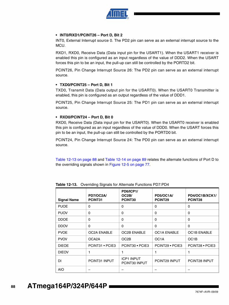
• INT0/RXD1/PCINT26 – Port D, Bit 2INT0, External Interrupt source 0. The PD2 pin can serve as an external interrupt source to theMCU.
RXD1, RXD0, Receive Data (Data input pin for the USART1). When the USART1 receiver isenabled this pin is configured as an input regardless of the value of DDD2. When the USARTforces this pin to be an input, the pull-up can still be controlled by the PORTD2 bit.
PCINT26, Pin Change Interrupt Source 26: The PD2 pin can serve as an external interruptsource.
• TXD0/PCINT25 – Port D, Bit 1TXD0, Transmit Data (Data output pin for the USART0). When the USART0 Transmitter isenabled, this pin is configured as an output regardless of the value of DDD1.
PCINT25, Pin Change Interrupt Source 25: The PD1 pin can serve as an external interruptsource.
• RXD0/PCINT24 – Port D, Bit 0RXD0, Receive Data (Data input pin for the USART0). When the USART0 receiver is enabledthis pin is configured as an input regardless of the value of DDD0. When the USART forces thispin to be an input, the pull-up can still be controlled by the PORTD0 bit.
PCINT24, Pin Change Interrupt Source 24: The PD0 pin can serve as an external interruptsource.
Table 12-13 on page 88 and Table 12-14 on page 89 relates the alternate functions of Port D tothe overriding signals shown in Figure 12-5 on page 77.
Table 12-13. Overriding Signals for Alternate Functions PD7:PD4
Signal NamePD7/OC2A/PCINT31
PD6/ICP1/OC2B/PCINT30
PD5/OC1A/PCINT29
PD4/OC1B/XCK1/PCINT28
PUOE 0 0 0 0
PUOV 0 0 0 0
DDOE 0 0 0 0
DDOV 0 0 0 0
PVOE OC2A ENABLE OC2B ENABLE OC1A ENABLE OC1B ENABLE
PVOV OCA2A OC2B OC1A OC1B
DIEOE PCINT31 • PCIE3 PCINT30 • PCIE3 PCINT29 • PCIE3 PCINT28 • PCIE3
DIEOV 1 1 1 1
DI PCINT31 INPUTICP1 INPUTPCINT30 INPUT
PCINT29 INPUT PCINT28 INPUT
AIO – – – –
887674F–AVR–09/09
ATmega164P/324P/644P
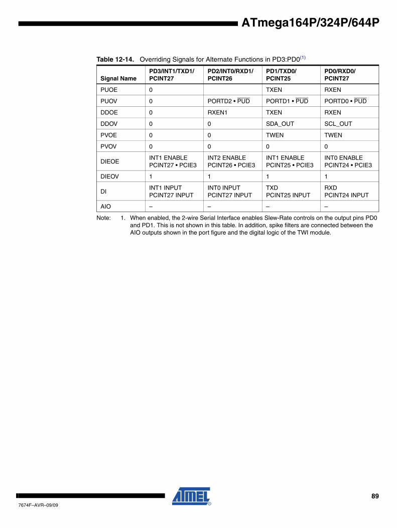
ATmega164P/324P/644P
Note: 1. When enabled, the 2-wire Serial Interface enables Slew-Rate controls on the output pins PD0 and PD1. This is not shown in this table. In addition, spike filters are connected between the AIO outputs shown in the port figure and the digital logic of the TWI module.
Table 12-14. Overriding Signals for Alternate Functions in PD3:PD0(1)
Signal NamePD3/INT1/TXD1/PCINT27
PD2/INT0/RXD1/PCINT26
PD1/TXD0/PCINT25
PD0/RXD0/PCINT27
PUOE 0 TXEN RXEN
PUOV 0 PORTD2 • PUD PORTD1 • PUD PORTD0 • PUD
DDOE 0 RXEN1 TXEN RXEN
DDOV 0 0 SDA_OUT SCL_OUT
PVOE 0 0 TWEN TWEN
PVOV 0 0 0 0
DIEOEINT1 ENABLEPCINT27 • PCIE3
INT2 ENABLEPCINT26 • PCIE3
INT1 ENABLEPCINT25 • PCIE3
INT0 ENABLEPCINT24 • PCIE3
DIEOV 1 1 1 1
DIINT1 INPUTPCINT27 INPUT
INT0 INPUTPCINT27 INPUT
TXDPCINT25 INPUT
RXDPCINT24 INPUT
AIO – – – –
897674F–AVR–09/09
Register Description
12.3.5 MCUCR – MCU Control Register
• Bit 4 – PUD: Pull-up DisableWhen this bit is written to one, the pull-ups in the I/O ports are disabled even if the DDxn andPORTxn Registers are configured to enable the pull-ups ({DDxn, PORTxn} = 0b01). See “Con-figuring the Pin” on page 72 for more details about this feature.
12.3.6 PORTA – Port A Data Register
12.3.7 DDRA – Port A Data Direction Register
12.3.8 PINA – Port A Input Pins Address
12.3.9 PORTB – Port B Data Register
12.3.10 DDRB – Port B Data Direction Register
12.3.11 PINB – Port B Input Pins Address
Bit 7 6 5 4 3 2 1 0
0x35 (0x55) JTD BODS BODSE PUD – – IVSEL IVCE MCUCR
Read/Write R/W R R R/W R R R/W R/W
Initial Value 0 0 0 0 0 0 0 0
Bit 7 6 5 4 3 2 1 0
0x02 (0x22) PORTA7 PORTA6 PORTA5 PORTA4 PORTA3 PORTA2 PORTA1 PORTA0 PORTA
Read/Write R/W R/W R/W R/W R/W R/W R/W R/W
Initial Value 0 0 0 0 0 0 0 0
Bit 7 6 5 4 3 2 1 0
0x01 (0x21) DDA7 DDA6 DDA5 DDA4 DDA3 DDA2 DDA1 DDA0 DDRA
Read/Write R/W R/W R/W R/W R/W R/W R/W R/W
Initial Value 0 0 0 0 0 0 0 0
Bit 7 6 5 4 3 2 1 0
0x00 (0x20) PINA7 PINA6 PINA5 PINA4 PINA3 PINA2 PINA1 PINA0 PINA
Read/Write R/W R/W R/W R/W R/W R/W R/W R/W
Initial Value N/A N/A N/A N/A N/A N/A N/A N/A
Bit 7 6 5 4 3 2 1 0
0x05 (0x25) PORTB7 PORTB6 PORTB5 PORTB4 PORTB3 PORTB2 PORTB1 PORTB0 PORTB
Read/Write R/W R/W R/W R/W R/W R/W R/W R/W
Initial Value 0 0 0 0 0 0 0 0
Bit 7 6 5 4 3 2 1 0
0x04 (0x24) DDB7 DDB6 DDB5 DDB4 DDB3 DDB2 DDB1 DDB0 DDRB
Read/Write R/W R/W R/W R/W R/W R/W R/W R/W
Initial Value 0 0 0 0 0 0 0 0
Bit 7 6 5 4 3 2 1 0
0x03 (0x23) PINB7 PINB6 PINB5 PINB4 PINB3 PINB2 PINB1 PINB0 PINB
Read/Write R/W R/W R/W R/W R/W R/W R/W R/W
Initial Value N/A N/A N/A N/A N/A N/A N/A N/A
907674F–AVR–09/09
ATmega164P/324P/644P
ATmega164P/324P/644P
12.3.12 PORTC – Port C Data Register
12.3.13 DDRC – Port C Data Direction Register
12.3.14 PINC – Port C Input Pins Address
12.3.15 PORTD – Port D Data Register
12.3.16 DDRD – Port D Data Direction Register
12.3.17 PIND – Port D Input Pins Address
Bit 7 6 5 4 3 2 1 0
0x08 (0x28) PORTC7 PORTC6 PORTC5 PORTC4 PORTC3 PORTC2 PORTC1 PORTC0 PORTC
Read/Write R/W R/W R/W R/W R/W R/W R/W R/W
Initial Value 0 0 0 0 0 0 0 0
Bit 7 6 5 4 3 2 1 0
0x07 (0x27) DDC7 DDC6 DDC5 DDC4 DDC3 DDC2 DDC1 DDC0 DDRC
Read/Write R/W R/W R/W R/W R/W R/W R/W R/W
Initial Value 0 0 0 0 0 0 0 0
Bit 7 6 5 4 3 2 1 0
0x06 (0x26) PINC7 PINC6 PINC5 PINC4 PINC3 PINC2 PINC1 PINC0 PINC
Read/Write R/W R/W R/W R/W R/W R/W R/W R/W
Initial Value N/A N/A N/A N/A N/A N/A N/A N/A
Bit 7 6 5 4 3 2 1 0
0x0B (0x2B) PORTD7 PORTD6 PORTD5 PORTD4 PORTD3 PORTD2 PORTD1 PORTD0 PORTD
Read/Write R/W R/W R/W R/W R/W R/W R/W R/W
Initial Value 0 0 0 0 0 0 0 0
Bit 7 6 5 4 3 2 1 0
0x0A (0x2A) DDD7 DDD6 DDD5 DDD4 DDD3 DDD2 DDD1 DDD0 DDRD
Read/Write R/W R/W R/W R/W R/W R/W R/W R/W
Initial Value 0 0 0 0 0 0 0 0
Bit 7 6 5 4 3 2 1 0
0x09 (0x29) PIND7 PIND6 PIND5 PIND4 PIND3 PIND2 PIND1 PIND0 PIND
Read/Write R/W R/W R/W R/W R/W R/W R/W R/W
Initial Value N/A N/A N/A N/A N/A N/A N/A N/A
917674F–AVR–09/09
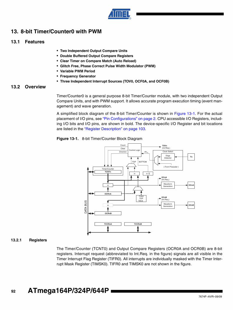
13. 8-bit Timer/Counter0 with PWM
13.1 Features
• Two Independent Output Compare Units• Double Buffered Output Compare Registers• Clear Timer on Compare Match (Auto Reload)• Glitch Free, Phase Correct Pulse Width Modulator (PWM)• Variable PWM Period• Frequency Generator• Three Independent Interrupt Sources (TOV0, OCF0A, and OCF0B)
13.2 Overview
Timer/Counter0 is a general purpose 8-bit Timer/Counter module, with two independent OutputCompare Units, and with PWM support. It allows accurate program execution timing (event man-agement) and wave generation.
A simplified block diagram of the 8-bit Timer/Counter is shown in Figure 13-1. For the actualplacement of I/O pins, see “Pin Configurations” on page 2. CPU accessible I/O Registers, includ-ing I/O bits and I/O pins, are shown in bold. The device-specific I/O Register and bit locationsare listed in the “Register Description” on page 103.
Figure 13-1. 8-bit Timer/Counter Block Diagram
13.2.1 Registers
The Timer/Counter (TCNT0) and Output Compare Registers (OCR0A and OCR0B) are 8-bitregisters. Interrupt request (abbreviated to Int.Req. in the figure) signals are all visible in theTimer Interrupt Flag Register (TIFR0). All interrupts are individually masked with the Timer Inter-rupt Mask Register (TIMSK0). TIFR0 and TIMSK0 are not shown in the figure.
Clock Select
Timer/Counter
DAT
A B
US
OCRnA
OCRnB
=
=
TCNTn
WaveformGeneration
WaveformGeneration
OCnA
OCnB
=
FixedTOP
Value
Control Logic
= 0
TOP BOTTOM
Count
Clear
Direction
TOVn(Int.Req.)
OCnA(Int.Req.)
OCnB(Int.Req.)
TCCRnA TCCRnB
TnEdge
Detector
( From Prescaler )
clkTn
927674F–AVR–09/09
ATmega164P/324P/644P
ATmega164P/324P/644P
The Timer/Counter can be clocked internally, via the prescaler, or by an external clock source onthe T0 pin. The Clock Select logic block controls which clock source and edge the Timer/Counteruses to increment (or decrement) its value. The Timer/Counter is inactive when no clock sourceis selected. The output from the Clock Select logic is referred to as the timer clock (clkT0).
The double buffered Output Compare Registers (OCR0A and OCR0B) are compared with theTimer/Counter value at all times. The result of the compare can be used by the Waveform Gen-erator to generate a PWM or variable frequency output on the Output Compare pins (OC0A andOC0B). See “Output Compare Unit” on page 94. for details. The Compare Match event will alsoset the Compare Flag (OCF0A or OCF0B) which can be used to generate an Output Compareinterrupt request.
13.2.2 Definitions
Many register and bit references in this section are written in general form. A lower case “n”replaces the Timer/Counter number, in this case 0. A lower case “x” replaces the Output Com-pare Unit, in this case Compare Unit A or Compare Unit B. However, when using the register orbit defines in a program, the precise form must be used, i.e., TCNT0 for accessingTimer/Counter0 counter value and so on.
The definitions in Table 13-1 are also used extensively throughout the document.
13.3 Timer/Counter Clock Sources
The Timer/Counter can be clocked by an internal or an external clock source. The clock sourceis selected by the Clock Select logic which is controlled by the Clock Select (CS02:0) bitslocated in the Timer/Counter Control Register (TCCR0B). For details on clock sources and pres-caler, see “Timer/Counter Prescaler” on page 153.
13.4 Counter Unit
The main part of the 8-bit Timer/Counter is the programmable bi-directional counter unit. Figure13-2 shows a block diagram of the counter and its surroundings.
Figure 13-2. Counter Unit Block Diagram
Table 13-1. Definitions
BOTTOM The counter reaches the BOTTOM when it becomes 0x00.
MAX The counter reaches its MAXimum when it becomes 0xFF (decimal 255).
TOP The counter reaches the TOP when it becomes equal to the highest value in thecount sequence. The TOP value can be assigned to be the fixed value 0xFF(MAX) or the value stored in the OCR0A Register. The assignment is depen-dent on the mode of operation.
DATA BUS
TCNTn Control Logic
count
TOVn(Int.Req.)
Clock Select
top
TnEdge
Detector
( From Prescaler )
clkTn
bottom
direction
clear
937674F–AVR–09/09
Signal description (internal signals):
count Increment or decrement TCNT0 by 1.
direction Select between increment and decrement.
clear Clear TCNT0 (set all bits to zero).
clkTn Timer/Counter clock, referred to as clkT0 in the following.
top Signalize that TCNT0 has reached maximum value.
bottom Signalize that TCNT0 has reached minimum value (zero).
Depending of the mode of operation used, the counter is cleared, incremented, or decrementedat each timer clock (clkT0). clkT0 can be generated from an external or internal clock source,selected by the Clock Select bits (CS02:0). When no clock source is selected (CS02:0 = 0) thetimer is stopped. However, the TCNT0 value can be accessed by the CPU, regardless ofwhether clkT0 is present or not. A CPU write overrides (has priority over) all counter clear orcount operations.
The counting sequence is determined by the setting of the WGM01 and WGM00 bits located inthe Timer/Counter Control Register (TCCR0A) and the WGM02 bit located in the Timer/CounterControl Register B (TCCR0B). There are close connections between how the counter behaves(counts) and how waveforms are generated on the Output Compare outputs OC0A and OC0B.For more details about advanced counting sequences and waveform generation, see “Modes ofOperation” on page 97.
The Timer/Counter Overflow Flag (TOV0) is set according to the mode of operation selected bythe WGM02:0 bits. TOV0 can be used for generating a CPU interrupt.
13.5 Output Compare Unit
The 8-bit comparator continuously compares TCNT0 with the Output Compare Registers(OCR0A and OCR0B). Whenever TCNT0 equals OCR0A or OCR0B, the comparator signals amatch. A match will set the Output Compare Flag (OCF0A or OCF0B) at the next timer clockcycle. If the corresponding interrupt is enabled, the Output Compare Flag generates an OutputCompare interrupt. The Output Compare Flag is automatically cleared when the interrupt is exe-cuted. Alternatively, the flag can be cleared by software by writing a logical one to its I/O bitlocation. The Waveform Generator uses the match signal to generate an output according tooperating mode set by the WGM02:0 bits and Compare Output mode (COM0x1:0) bits. The maxand bottom signals are used by the Waveform Generator for handling the special cases of theextreme values in some modes of operation (“Modes of Operation” on page 97).
Figure 13-3 shows a block diagram of the Output Compare unit.
947674F–AVR–09/09
ATmega164P/324P/644P
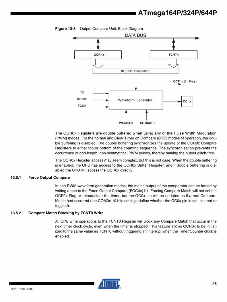
ATmega164P/324P/644P
Figure 13-3. Output Compare Unit, Block Diagram
The OCR0x Registers are double buffered when using any of the Pulse Width Modulation(PWM) modes. For the normal and Clear Timer on Compare (CTC) modes of operation, the dou-ble buffering is disabled. The double buffering synchronizes the update of the OCR0x CompareRegisters to either top or bottom of the counting sequence. The synchronization prevents theoccurrence of odd-length, non-symmetrical PWM pulses, thereby making the output glitch-free.
The OCR0x Register access may seem complex, but this is not case. When the double bufferingis enabled, the CPU has access to the OCR0x Buffer Register, and if double buffering is dis-abled the CPU will access the OCR0x directly.
13.5.1 Force Output Compare
In non-PWM waveform generation modes, the match output of the comparator can be forced bywriting a one to the Force Output Compare (FOC0x) bit. Forcing Compare Match will not set theOCF0x Flag or reload/clear the timer, but the OC0x pin will be updated as if a real CompareMatch had occurred (the COM0x1:0 bits settings define whether the OC0x pin is set, cleared ortoggled).
13.5.2 Compare Match Blocking by TCNT0 Write
All CPU write operations to the TCNT0 Register will block any Compare Match that occur in thenext timer clock cycle, even when the timer is stopped. This feature allows OCR0x to be initial-ized to the same value as TCNT0 without triggering an interrupt when the Timer/Counter clock isenabled.
OCFnx (Int.Req.)
= (8-bit Comparator )
OCRnx
OCnx
DATA BUS
TCNTn
WGMn1:0
Waveform Generator
top
FOCn
COMnX1:0
bottom
957674F–AVR–09/09
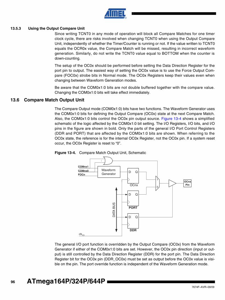
13.5.3 Using the Output Compare UnitSince writing TCNT0 in any mode of operation will block all Compare Matches for one timerclock cycle, there are risks involved when changing TCNT0 when using the Output CompareUnit, independently of whether the Timer/Counter is running or not. If the value written to TCNT0equals the OCR0x value, the Compare Match will be missed, resulting in incorrect waveformgeneration. Similarly, do not write the TCNT0 value equal to BOTTOM when the counter isdown-counting.
The setup of the OC0x should be performed before setting the Data Direction Register for theport pin to output. The easiest way of setting the OC0x value is to use the Force Output Com-pare (FOC0x) strobe bits in Normal mode. The OC0x Registers keep their values even whenchanging between Waveform Generation modes.
Be aware that the COM0x1:0 bits are not double buffered together with the compare value.Changing the COM0x1:0 bits will take effect immediately.
13.6 Compare Match Output Unit
The Compare Output mode (COM0x1:0) bits have two functions. The Waveform Generator usesthe COM0x1:0 bits for defining the Output Compare (OC0x) state at the next Compare Match.Also, the COM0x1:0 bits control the OC0x pin output source. Figure 13-4 shows a simplifiedschematic of the logic affected by the COM0x1:0 bit setting. The I/O Registers, I/O bits, and I/Opins in the figure are shown in bold. Only the parts of the general I/O Port Control Registers(DDR and PORT) that are affected by the COM0x1:0 bits are shown. When referring to theOC0x state, the reference is for the internal OC0x Register, not the OC0x pin. If a system resetoccur, the OC0x Register is reset to “0”.
Figure 13-4. Compare Match Output Unit, Schematic
The general I/O port function is overridden by the Output Compare (OC0x) from the WaveformGenerator if either of the COM0x1:0 bits are set. However, the OC0x pin direction (input or out-put) is still controlled by the Data Direction Register (DDR) for the port pin. The Data DirectionRegister bit for the OC0x pin (DDR_OC0x) must be set as output before the OC0x value is visi-ble on the pin. The port override function is independent of the Waveform Generation mode.
PORT
DDR
D Q
D Q
OCnxPinOCnx
D QWaveformGenerator
COMnx1
COMnx0
0
1
DAT
A B
US
FOCn
clkI/O
967674F–AVR–09/09
ATmega164P/324P/644P
ATmega164P/324P/644P
The design of the Output Compare pin logic allows initialization of the OC0x state before the out-put is enabled. Note that some COM0x1:0 bit settings are reserved for certain modes ofoperation. See “Register Description” on page 103.
13.6.1 Compare Output Mode and Waveform Generation
The Waveform Generator uses the COM0x1:0 bits differently in Normal, CTC, and PWM modes.For all modes, setting the COM0x1:0 = 0 tells the Waveform Generator that no action on theOC0x Register is to be performed on the next Compare Match. For compare output actions inthe non-PWM modes refer to Table 13-2 on page 103. For fast PWM mode, refer to Table 13-3on page 103, and for phase correct PWM refer to Table 13-4 on page 104.
A change of the COM0x1:0 bits state will have effect at the first Compare Match after the bits arewritten. For non-PWM modes, the action can be forced to have immediate effect by using theFOC0x strobe bits.
13.7 Modes of Operation
The mode of operation, i.e., the behavior of the Timer/Counter and the Output Compare pins, isdefined by the combination of the Waveform Generation mode (WGM02:0) and Compare Outputmode (COM0x1:0) bits. The Compare Output mode bits do not affect the counting sequence,while the Waveform Generation mode bits do. The COM0x1:0 bits control whether the PWM out-put generated should be inverted or not (inverted or non-inverted PWM). For non-PWM modesthe COM0x1:0 bits control whether the output should be set, cleared, or toggled at a CompareMatch (See “Compare Match Output Unit” on page 121.).
For detailed timing information see “Timer/Counter Timing Diagrams” on page 101.
13.7.1 Normal Mode
The simplest mode of operation is the Normal mode (WGM02:0 = 0). In this mode the countingdirection is always up (incrementing), and no counter clear is performed. The counter simplyoverruns when it passes its maximum 8-bit value (TOP = 0xFF) and then restarts from the bot-tom (0x00). In normal operation the Timer/Counter Overflow Flag (TOV0) will be set in the sametimer clock cycle as the TCNT0 becomes zero. The TOV0 Flag in this case behaves like a ninthbit, except that it is only set, not cleared. However, combined with the timer overflow interruptthat automatically clears the TOV0 Flag, the timer resolution can be increased by software.There are no special cases to consider in the Normal mode, a new counter value can be writtenanytime.
The Output Compare Unit can be used to generate interrupts at some given time. Using the Out-put Compare to generate waveforms in Normal mode is not recommended, since this willoccupy too much of the CPU time.
13.7.2 Clear Timer on Compare Match (CTC) Mode
In Clear Timer on Compare or CTC mode (WGM02:0 = 2), the OCR0A Register is used tomanipulate the counter resolution. In CTC mode the counter is cleared to zero when the countervalue (TCNT0) matches the OCR0A. The OCR0A defines the top value for the counter, hencealso its resolution. This mode allows greater control of the Compare Match output frequency. Italso simplifies the operation of counting external events.
The timing diagram for the CTC mode is shown in Figure 13-5. The counter value (TCNT0)increases until a Compare Match occurs between TCNT0 and OCR0A, and then counter(TCNT0) is cleared.
977674F–AVR–09/09
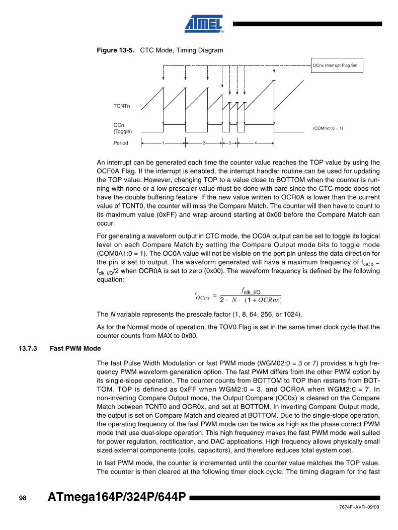
Figure 13-5. CTC Mode, Timing Diagram
An interrupt can be generated each time the counter value reaches the TOP value by using theOCF0A Flag. If the interrupt is enabled, the interrupt handler routine can be used for updatingthe TOP value. However, changing TOP to a value close to BOTTOM when the counter is run-ning with none or a low prescaler value must be done with care since the CTC mode does nothave the double buffering feature. If the new value written to OCR0A is lower than the currentvalue of TCNT0, the counter will miss the Compare Match. The counter will then have to count toits maximum value (0xFF) and wrap around starting at 0x00 before the Compare Match canoccur.
For generating a waveform output in CTC mode, the OC0A output can be set to toggle its logicallevel on each Compare Match by setting the Compare Output mode bits to toggle mode(COM0A1:0 = 1). The OC0A value will not be visible on the port pin unless the data direction forthe pin is set to output. The waveform generated will have a maximum frequency of fOC0 =fclk_I/O/2 when OCR0A is set to zero (0x00). The waveform frequency is defined by the followingequation:
The N variable represents the prescale factor (1, 8, 64, 256, or 1024).
As for the Normal mode of operation, the TOV0 Flag is set in the same timer clock cycle that thecounter counts from MAX to 0x00.
13.7.3 Fast PWM Mode
The fast Pulse Width Modulation or fast PWM mode (WGM02:0 = 3 or 7) provides a high fre-quency PWM waveform generation option. The fast PWM differs from the other PWM option byits single-slope operation. The counter counts from BOTTOM to TOP then restarts from BOT-TOM. TOP is defined as 0xFF when WGM2:0 = 3, and OCR0A when WGM2:0 = 7. Innon-inverting Compare Output mode, the Output Compare (OC0x) is cleared on the CompareMatch between TCNT0 and OCR0x, and set at BOTTOM. In inverting Compare Output mode,the output is set on Compare Match and cleared at BOTTOM. Due to the single-slope operation,the operating frequency of the fast PWM mode can be twice as high as the phase correct PWMmode that use dual-slope operation. This high frequency makes the fast PWM mode well suitedfor power regulation, rectification, and DAC applications. High frequency allows physically smallsized external components (coils, capacitors), and therefore reduces total system cost.
In fast PWM mode, the counter is incremented until the counter value matches the TOP value.The counter is then cleared at the following timer clock cycle. The timing diagram for the fast
TCNTn
OCn(Toggle)
OCnx Interrupt Flag Set
1 4Period 2 3
(COMnx1:0 = 1)
fOCnxfclk_I/O
2 N 1 OCRnx+( )⋅ ⋅-------------------------------------------------------=
987674F–AVR–09/09
ATmega164P/324P/644P
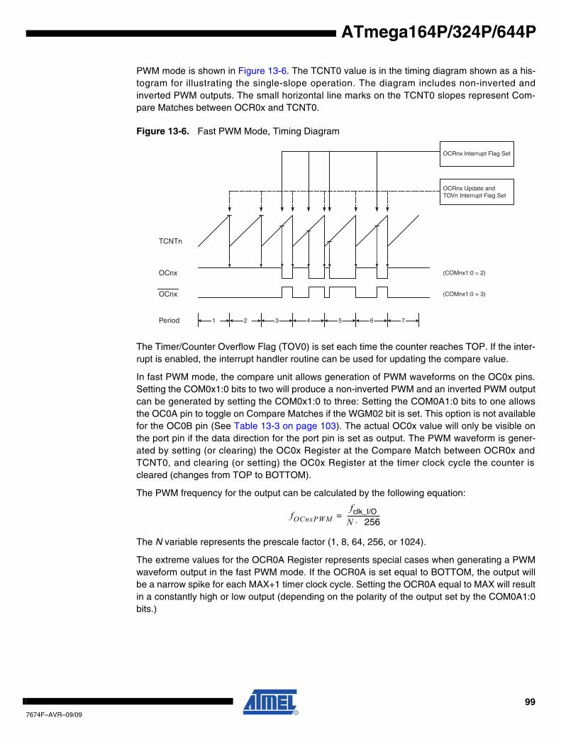
ATmega164P/324P/644P
PWM mode is shown in Figure 13-6. The TCNT0 value is in the timing diagram shown as a his-togram for illustrating the single-slope operation. The diagram includes non-inverted andinverted PWM outputs. The small horizontal line marks on the TCNT0 slopes represent Com-pare Matches between OCR0x and TCNT0.
Figure 13-6. Fast PWM Mode, Timing Diagram
The Timer/Counter Overflow Flag (TOV0) is set each time the counter reaches TOP. If the inter-rupt is enabled, the interrupt handler routine can be used for updating the compare value.
In fast PWM mode, the compare unit allows generation of PWM waveforms on the OC0x pins.Setting the COM0x1:0 bits to two will produce a non-inverted PWM and an inverted PWM outputcan be generated by setting the COM0x1:0 to three: Setting the COM0A1:0 bits to one allowsthe OC0A pin to toggle on Compare Matches if the WGM02 bit is set. This option is not availablefor the OC0B pin (See Table 13-3 on page 103). The actual OC0x value will only be visible onthe port pin if the data direction for the port pin is set as output. The PWM waveform is gener-ated by setting (or clearing) the OC0x Register at the Compare Match between OCR0x andTCNT0, and clearing (or setting) the OC0x Register at the timer clock cycle the counter iscleared (changes from TOP to BOTTOM).
The PWM frequency for the output can be calculated by the following equation:
The N variable represents the prescale factor (1, 8, 64, 256, or 1024).
The extreme values for the OCR0A Register represents special cases when generating a PWMwaveform output in the fast PWM mode. If the OCR0A is set equal to BOTTOM, the output willbe a narrow spike for each MAX+1 timer clock cycle. Setting the OCR0A equal to MAX will resultin a constantly high or low output (depending on the polarity of the output set by the COM0A1:0bits.)
TCNTn
OCRnx Update andTOVn Interrupt Flag Set
1Period 2 3
OCnx
OCnx
(COMnx1:0 = 2)
(COMnx1:0 = 3)
OCRnx Interrupt Flag Set
4 5 6 7
fOCnxPWMfclk_I/O
N 256⋅---------------------=
997674F–AVR–09/09
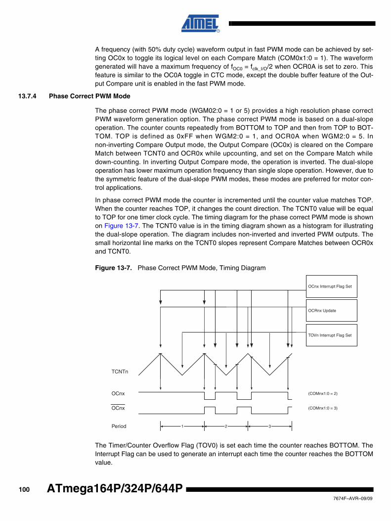
A frequency (with 50% duty cycle) waveform output in fast PWM mode can be achieved by set-ting OC0x to toggle its logical level on each Compare Match (COM0x1:0 = 1). The waveformgenerated will have a maximum frequency of fOC0 = fclk_I/O/2 when OCR0A is set to zero. Thisfeature is similar to the OC0A toggle in CTC mode, except the double buffer feature of the Out-put Compare unit is enabled in the fast PWM mode.
13.7.4 Phase Correct PWM Mode
The phase correct PWM mode (WGM02:0 = 1 or 5) provides a high resolution phase correctPWM waveform generation option. The phase correct PWM mode is based on a dual-slopeoperation. The counter counts repeatedly from BOTTOM to TOP and then from TOP to BOT-TOM. TOP is defined as 0xFF when WGM2:0 = 1, and OCR0A when WGM2:0 = 5. Innon-inverting Compare Output mode, the Output Compare (OC0x) is cleared on the CompareMatch between TCNT0 and OCR0x while upcounting, and set on the Compare Match whiledown-counting. In inverting Output Compare mode, the operation is inverted. The dual-slopeoperation has lower maximum operation frequency than single slope operation. However, due tothe symmetric feature of the dual-slope PWM modes, these modes are preferred for motor con-trol applications.
In phase correct PWM mode the counter is incremented until the counter value matches TOP.When the counter reaches TOP, it changes the count direction. The TCNT0 value will be equalto TOP for one timer clock cycle. The timing diagram for the phase correct PWM mode is shownon Figure 13-7. The TCNT0 value is in the timing diagram shown as a histogram for illustratingthe dual-slope operation. The diagram includes non-inverted and inverted PWM outputs. Thesmall horizontal line marks on the TCNT0 slopes represent Compare Matches between OCR0xand TCNT0.
Figure 13-7. Phase Correct PWM Mode, Timing Diagram
The Timer/Counter Overflow Flag (TOV0) is set each time the counter reaches BOTTOM. TheInterrupt Flag can be used to generate an interrupt each time the counter reaches the BOTTOMvalue.
TOVn Interrupt Flag Set
OCnx Interrupt Flag Set
1 2 3
TCNTn
Period
OCnx
OCnx
(COMnx1:0 = 2)
(COMnx1:0 = 3)
OCRnx Update
1007674F–AVR–09/09
ATmega164P/324P/644P
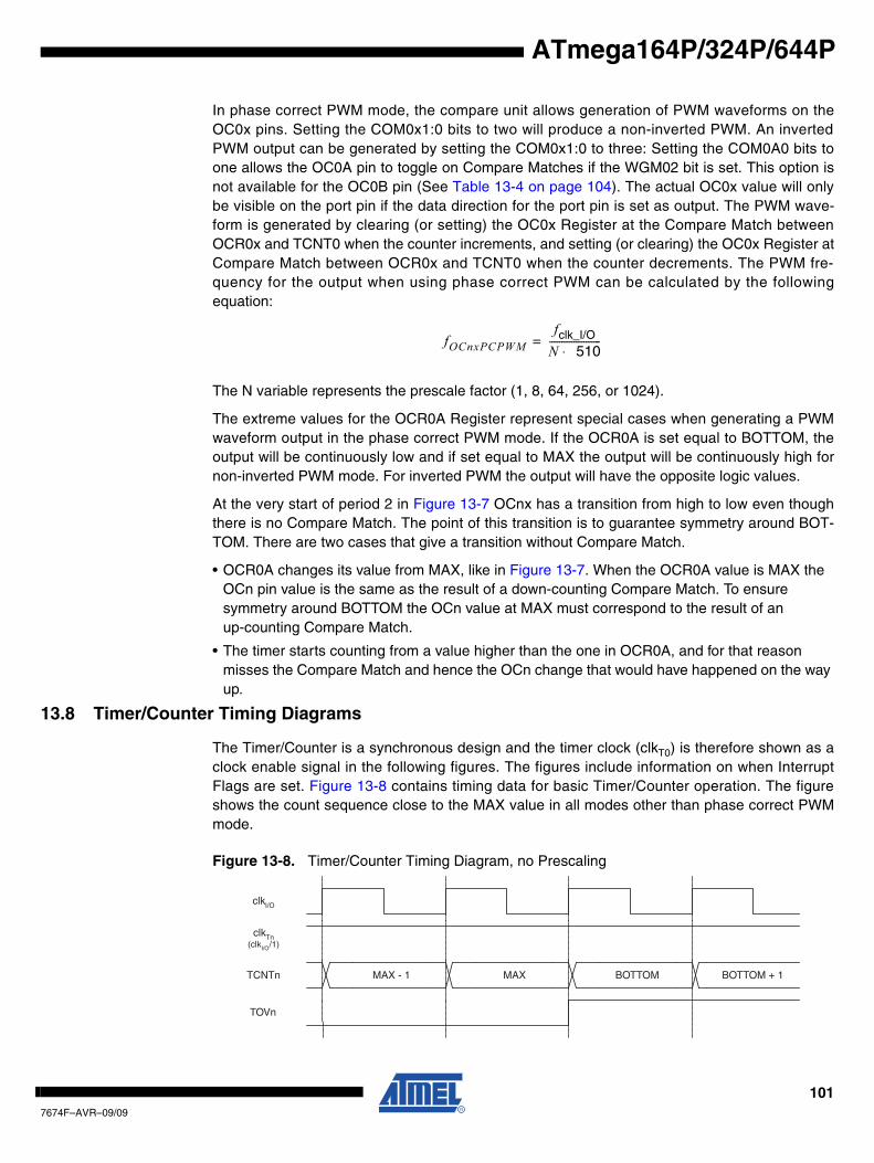
ATmega164P/324P/644P
In phase correct PWM mode, the compare unit allows generation of PWM waveforms on theOC0x pins. Setting the COM0x1:0 bits to two will produce a non-inverted PWM. An invertedPWM output can be generated by setting the COM0x1:0 to three: Setting the COM0A0 bits toone allows the OC0A pin to toggle on Compare Matches if the WGM02 bit is set. This option isnot available for the OC0B pin (See Table 13-4 on page 104). The actual OC0x value will onlybe visible on the port pin if the data direction for the port pin is set as output. The PWM wave-form is generated by clearing (or setting) the OC0x Register at the Compare Match betweenOCR0x and TCNT0 when the counter increments, and setting (or clearing) the OC0x Register atCompare Match between OCR0x and TCNT0 when the counter decrements. The PWM fre-quency for the output when using phase correct PWM can be calculated by the followingequation:
The N variable represents the prescale factor (1, 8, 64, 256, or 1024).
The extreme values for the OCR0A Register represent special cases when generating a PWMwaveform output in the phase correct PWM mode. If the OCR0A is set equal to BOTTOM, theoutput will be continuously low and if set equal to MAX the output will be continuously high fornon-inverted PWM mode. For inverted PWM the output will have the opposite logic values.
At the very start of period 2 in Figure 13-7 OCnx has a transition from high to low even thoughthere is no Compare Match. The point of this transition is to guarantee symmetry around BOT-TOM. There are two cases that give a transition without Compare Match.
• OCR0A changes its value from MAX, like in Figure 13-7. When the OCR0A value is MAX the OCn pin value is the same as the result of a down-counting Compare Match. To ensure symmetry around BOTTOM the OCn value at MAX must correspond to the result of an up-counting Compare Match.
• The timer starts counting from a value higher than the one in OCR0A, and for that reason misses the Compare Match and hence the OCn change that would have happened on the way up.
13.8 Timer/Counter Timing Diagrams
The Timer/Counter is a synchronous design and the timer clock (clkT0) is therefore shown as aclock enable signal in the following figures. The figures include information on when InterruptFlags are set. Figure 13-8 contains timing data for basic Timer/Counter operation. The figureshows the count sequence close to the MAX value in all modes other than phase correct PWMmode.
Figure 13-8. Timer/Counter Timing Diagram, no Prescaling
fOCnxPCPWMfclk_I/O
N 510⋅---------------------=
clkTn(clkI/O/1)
TOVn
clkI/O
TCNTn MAX - 1 MAX BOTTOM BOTTOM + 1
1017674F–AVR–09/09
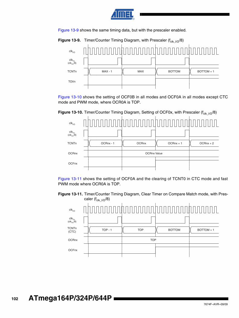
Figure 13-9 shows the same timing data, but with the prescaler enabled.
Figure 13-9. Timer/Counter Timing Diagram, with Prescaler (fclk_I/O/8)
Figure 13-10 shows the setting of OCF0B in all modes and OCF0A in all modes except CTCmode and PWM mode, where OCR0A is TOP.
Figure 13-10. Timer/Counter Timing Diagram, Setting of OCF0x, with Prescaler (fclk_I/O/8)
Figure 13-11 shows the setting of OCF0A and the clearing of TCNT0 in CTC mode and fastPWM mode where OCR0A is TOP.
Figure 13-11. Timer/Counter Timing Diagram, Clear Timer on Compare Match mode, with Pres-caler (fclk_I/O/8)
TOVn
TCNTn MAX - 1 MAX BOTTOM BOTTOM + 1
clkI/O
clkTn(clkI/O/8)
OCFnx
OCRnx
TCNTn
OCRnx Value
OCRnx - 1 OCRnx OCRnx + 1 OCRnx + 2
clkI/O
clkTn(clkI/O/8)
OCFnx
OCRnx
TCNTn(CTC)
TOP
TOP - 1 TOP BOTTOM BOTTOM + 1
clkI/O
clkTn(clkI/O/8)
1027674F–AVR–09/09
ATmega164P/324P/644P
ATmega164P/324P/644P
13.9 Register Description
13.9.1 TCCR0A – Timer/Counter Control Register A
• Bits 7:6 – COM0A1:0: Compare Match Output A ModeThese bits control the Output Compare pin (OC0A) behavior. If one or both of the COM0A1:0bits are set, the OC0A output overrides the normal port functionality of the I/O pin it is connectedto. However, note that the Data Direction Register (DDR) bit corresponding to the OC0A pinmust be set in order to enable the output driver.
When OC0A is connected to the pin, the function of the COM0A1:0 bits depends on theWGM02:0 bit setting. Table 13-2 shows the COM0A1:0 bit functionality when the WGM02:0 bitsare set to a normal or CTC mode (non-PWM).
Table 13-3 shows the COM0A1:0 bit functionality when the WGM01:0 bits are set to fast PWMmode.
Note: 1. A special case occurs when OCR0A equals TOP and COM0A1 is set. In this case, the Com-pare Match is ignored, but the set or clear is done at BOTTOM. See “Fast PWM Mode” on page 98 for more details.
Table 13-4 on page 104 shows the COM0A1:0 bit functionality when the WGM02:0 bits are setto phase correct PWM mode.
Bit 7 6 5 4 3 2 1 0
0x24 (0x44) COM0A1 COM0A0 COM0B1 COM0B0 – – WGM01 WGM00 TCCR0A
Read/Write R/W R/W R/W R/W R R R/W R/W
Initial Value 0 0 0 0 0 0 0 0
Table 13-2. Compare Output Mode, non-PWM Mode
COM0A1 COM0A0 Description
0 0 Normal port operation, OC0A disconnected.
0 1 Toggle OC0A on Compare Match
1 0 Clear OC0A on Compare Match
1 1 Set OC0A on Compare Match
Table 13-3. Compare Output Mode, Fast PWM Mode(1)
COM0A1 COM0A0 Description
0 0 Normal port operation, OC0A disconnected.
0 1WGM02 = 0: Normal Port Operation, OC0A Disconnected.WGM02 = 1: Toggle OC0A on Compare Match.
1 0Clear OC0A on Compare Match, set OC0A at BOTTOM,(non-inverting mode).
1 1Set OC0A on Compare Match, clear OC0A at BOTTOM,(inverting mode).
1037674F–AVR–09/09
Note: 1. A special case occurs when OCR0A equals TOP and COM0A1 is set. In this case, the Com-pare Match is ignored, but the set or clear is done at TOP. See “Phase Correct PWM Mode” on page 100 for more details.
• Bits 5:4 – COM0B1:0: Compare Match Output B ModeThese bits control the Output Compare pin (OC0B) behavior. If one or both of the COM0B1:0bits are set, the OC0B output overrides the normal port functionality of the I/O pin it is connectedto. However, note that the Data Direction Register (DDR) bit corresponding to the OC0B pinmust be set in order to enable the output driver.
When OC0B is connected to the pin, the function of the COM0B1:0 bits depends on theWGM02:0 bit setting. Table 13-2 on page 103 shows the COM0A1:0 bit functionality when theWGM02:0 bits are set to a normal or CTC mode (non-PWM).
Table 13-6 shows the COM0B1:0 bit functionality when the WGM02:0 bits are set to fast PWMmode.
Note: 1. A special case occurs when OCR0B equals TOP and COM0B1 is set. In this case, the Com-pare Match is ignored, but the set or clear is done atBOTTOM. See “Fast PWM Mode” on page 98 for more details.
Table 13-4. Compare Output Mode, Phase Correct PWM Mode(1)
COM0A1 COM0A0 Description
0 0 Normal port operation, OC0A disconnected.
0 1WGM02 = 0: Normal Port Operation, OC0A Disconnected.WGM02 = 1: Toggle OC0A on Compare Match.
1 0Clear OC0A on Compare Match when up-counting. Set OC0A on Compare Match when down-counting.
1 1Set OC0A on Compare Match when up-counting. Clear OC0A on Compare Match when down-counting.
Table 13-5. Compare Output Mode, non-PWM Mode
COM0B1 COM0B0 Description
0 0 Normal port operation, OC0B disconnected.
0 1 Toggle OC0B on Compare Match
1 0 Clear OC0B on Compare Match
1 1 Set OC0B on Compare Match
Table 13-6. Compare Output Mode, Fast PWM Mode(1)
COM0B1 COM0B0 Description
0 0 Normal port operation, OC0B disconnected.
0 1 Reserved
1 0Clear OC0B on Compare Match, set OC0B at BOTTOM,(non-inverting mode).
1 1Set OC0B on Compare Match, clear OC0B at BOTTOM,(inverting mode).
1047674F–AVR–09/09
ATmega164P/324P/644P
ATmega164P/324P/644P
Table 13-7 on page 105 shows the COM0B1:0 bit functionality when the WGM02:0 bits are setto phase correct PWM mode.
Note: 1. A special case occurs when OCR0B equals TOP and COM0B1 is set. In this case, the Com-pare Match is ignored, but the set or clear is done at TOP. See “Phase Correct PWM Mode” on page 100 for more details.
• Bits 3:2 – Res: Reserved BitsThese bits are reserved bits in the ATmega164P/324P/644P and will always read as zero.
• Bits 1:0 – WGM01:0: Waveform Generation ModeCombined with the WGM02 bit found in the TCCR0B Register, these bits control the countingsequence of the counter, the source for maximum (TOP) counter value, and what type of wave-form generation to be used, see Table 13-8 on page 105. Modes of operation supported by theTimer/Counter unit are: Normal mode (counter), Clear Timer on Compare Match (CTC) mode,and two types of Pulse Width Modulation (PWM) modes (see “Modes of Operation” on page122).
Notes: 1. MAX = 0xFF 2. BOTTOM = 0x00
Table 13-7. Compare Output Mode, Phase Correct PWM Mode(1)
COM0B1 COM0B0 Description
0 0 Normal port operation, OC0B disconnected.
0 1 Reserved
1 0Clear OC0B on Compare Match when up-counting. Set OC0B on Compare Match when down-counting.
1 1Set OC0B on Compare Match when up-counting. Clear OC0B on Compare Match when down-counting.
Table 13-8. Waveform Generation Mode Bit Description
Mode WGM2 WGM1 WGM0
Timer/Counter Mode of Operation TOP
Update ofOCRx at
TOV FlagSet on(1)(2)
0 0 0 0 Normal 0xFF Immediate MAX
1 0 0 1PWM, Phase Correct
0xFF TOP BOTTOM
2 0 1 0 CTC OCRA Immediate MAX
3 0 1 1 Fast PWM 0xFF BOTTOM MAX
4 1 0 0 Reserved – – –
5 1 0 1PWM, Phase Correct
OCRA TOP BOTTOM
6 1 1 0 Reserved – – –
7 1 1 1 Fast PWM OCRA BOTTOM TOP
1057674F–AVR–09/09
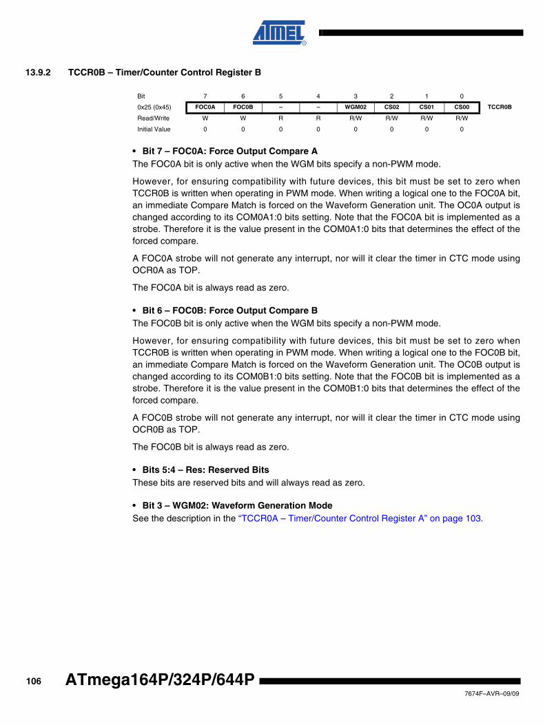
13.9.2 TCCR0B – Timer/Counter Control Register B
• Bit 7 – FOC0A: Force Output Compare AThe FOC0A bit is only active when the WGM bits specify a non-PWM mode.
However, for ensuring compatibility with future devices, this bit must be set to zero whenTCCR0B is written when operating in PWM mode. When writing a logical one to the FOC0A bit,an immediate Compare Match is forced on the Waveform Generation unit. The OC0A output ischanged according to its COM0A1:0 bits setting. Note that the FOC0A bit is implemented as astrobe. Therefore it is the value present in the COM0A1:0 bits that determines the effect of theforced compare.
A FOC0A strobe will not generate any interrupt, nor will it clear the timer in CTC mode usingOCR0A as TOP.
The FOC0A bit is always read as zero.
• Bit 6 – FOC0B: Force Output Compare BThe FOC0B bit is only active when the WGM bits specify a non-PWM mode.
However, for ensuring compatibility with future devices, this bit must be set to zero whenTCCR0B is written when operating in PWM mode. When writing a logical one to the FOC0B bit,an immediate Compare Match is forced on the Waveform Generation unit. The OC0B output ischanged according to its COM0B1:0 bits setting. Note that the FOC0B bit is implemented as astrobe. Therefore it is the value present in the COM0B1:0 bits that determines the effect of theforced compare.
A FOC0B strobe will not generate any interrupt, nor will it clear the timer in CTC mode usingOCR0B as TOP.
The FOC0B bit is always read as zero.
• Bits 5:4 – Res: Reserved BitsThese bits are reserved bits and will always read as zero.
• Bit 3 – WGM02: Waveform Generation ModeSee the description in the “TCCR0A – Timer/Counter Control Register A” on page 103.
Bit 7 6 5 4 3 2 1 0
0x25 (0x45) FOC0A FOC0B – – WGM02 CS02 CS01 CS00 TCCR0B
Read/Write W W R R R/W R/W R/W R/W
Initial Value 0 0 0 0 0 0 0 0
1067674F–AVR–09/09
ATmega164P/324P/644P
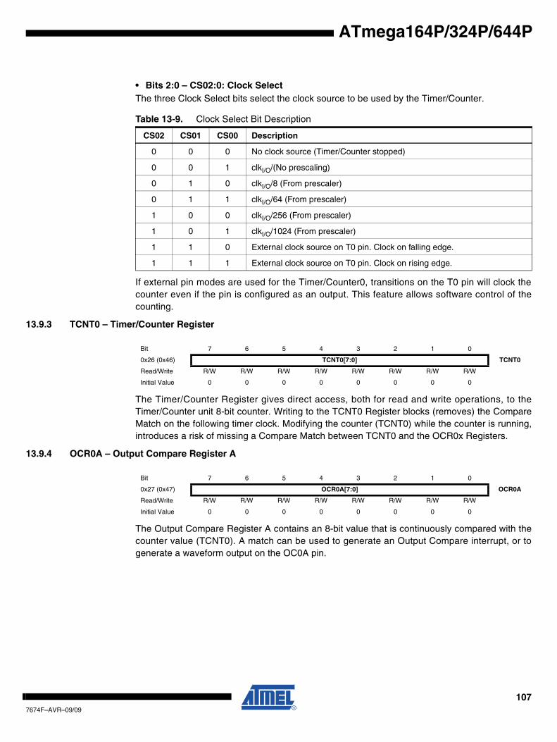
ATmega164P/324P/644P
• Bits 2:0 – CS02:0: Clock SelectThe three Clock Select bits select the clock source to be used by the Timer/Counter.
If external pin modes are used for the Timer/Counter0, transitions on the T0 pin will clock thecounter even if the pin is configured as an output. This feature allows software control of thecounting.
13.9.3 TCNT0 – Timer/Counter Register
The Timer/Counter Register gives direct access, both for read and write operations, to theTimer/Counter unit 8-bit counter. Writing to the TCNT0 Register blocks (removes) the CompareMatch on the following timer clock. Modifying the counter (TCNT0) while the counter is running,introduces a risk of missing a Compare Match between TCNT0 and the OCR0x Registers.
13.9.4 OCR0A – Output Compare Register A
The Output Compare Register A contains an 8-bit value that is continuously compared with thecounter value (TCNT0). A match can be used to generate an Output Compare interrupt, or togenerate a waveform output on the OC0A pin.
Table 13-9. Clock Select Bit Description
CS02 CS01 CS00 Description
0 0 0 No clock source (Timer/Counter stopped)
0 0 1 clkI/O/(No prescaling)
0 1 0 clkI/O/8 (From prescaler)
0 1 1 clkI/O/64 (From prescaler)
1 0 0 clkI/O/256 (From prescaler)
1 0 1 clkI/O/1024 (From prescaler)
1 1 0 External clock source on T0 pin. Clock on falling edge.
1 1 1 External clock source on T0 pin. Clock on rising edge.
Bit 7 6 5 4 3 2 1 0
0x26 (0x46) TCNT0[7:0] TCNT0
Read/Write R/W R/W R/W R/W R/W R/W R/W R/W
Initial Value 0 0 0 0 0 0 0 0
Bit 7 6 5 4 3 2 1 0
0x27 (0x47) OCR0A[7:0] OCR0A
Read/Write R/W R/W R/W R/W R/W R/W R/W R/W
Initial Value 0 0 0 0 0 0 0 0
1077674F–AVR–09/09
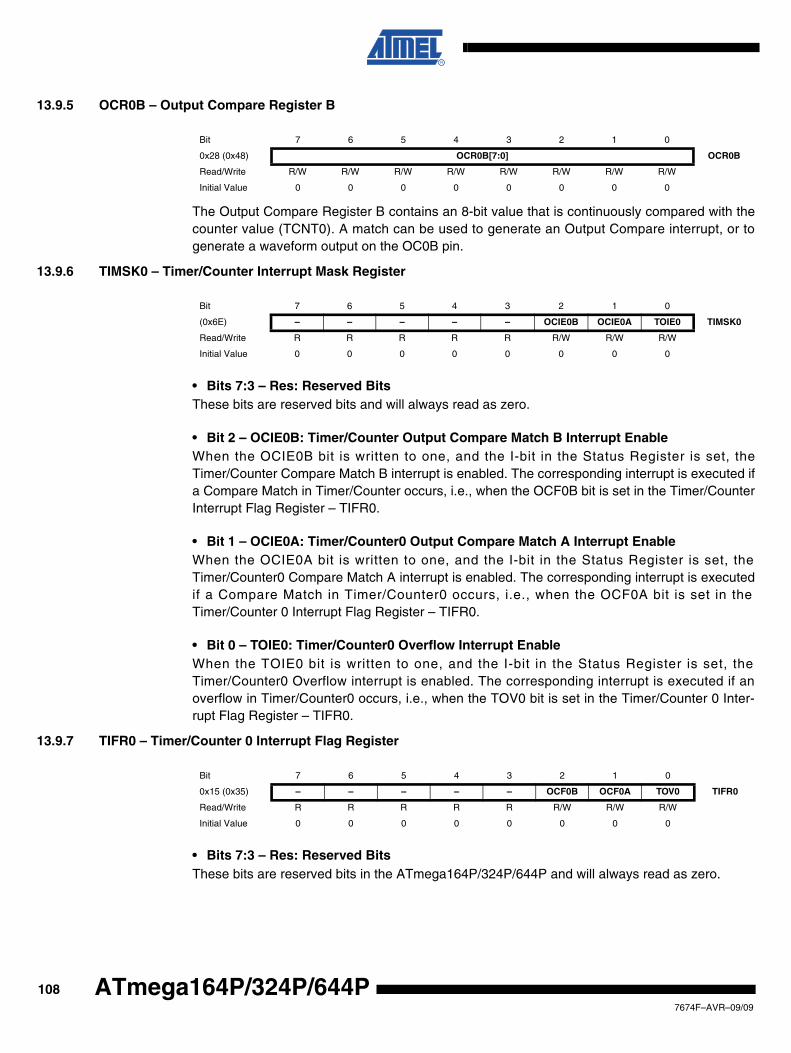
13.9.5 OCR0B – Output Compare Register B
The Output Compare Register B contains an 8-bit value that is continuously compared with thecounter value (TCNT0). A match can be used to generate an Output Compare interrupt, or togenerate a waveform output on the OC0B pin.
13.9.6 TIMSK0 – Timer/Counter Interrupt Mask Register
• Bits 7:3 – Res: Reserved BitsThese bits are reserved bits and will always read as zero.
• Bit 2 – OCIE0B: Timer/Counter Output Compare Match B Interrupt EnableWhen the OCIE0B bit is written to one, and the I-bit in the Status Register is set, theTimer/Counter Compare Match B interrupt is enabled. The corresponding interrupt is executed ifa Compare Match in Timer/Counter occurs, i.e., when the OCF0B bit is set in the Timer/CounterInterrupt Flag Register – TIFR0.
• Bit 1 – OCIE0A: Timer/Counter0 Output Compare Match A Interrupt EnableWhen the OCIE0A bit is written to one, and the I-bit in the Status Register is set, theTimer/Counter0 Compare Match A interrupt is enabled. The corresponding interrupt is executedif a Compare Match in Timer/Counter0 occurs, i.e., when the OCF0A bit is set in theTimer/Counter 0 Interrupt Flag Register – TIFR0.
• Bit 0 – TOIE0: Timer/Counter0 Overflow Interrupt EnableWhen the TOIE0 bit is written to one, and the I-bit in the Status Register is set, theTimer/Counter0 Overflow interrupt is enabled. The corresponding interrupt is executed if anoverflow in Timer/Counter0 occurs, i.e., when the TOV0 bit is set in the Timer/Counter 0 Inter-rupt Flag Register – TIFR0.
13.9.7 TIFR0 – Timer/Counter 0 Interrupt Flag Register
• Bits 7:3 – Res: Reserved BitsThese bits are reserved bits in the ATmega164P/324P/644P and will always read as zero.
Bit 7 6 5 4 3 2 1 0
0x28 (0x48) OCR0B[7:0] OCR0B
Read/Write R/W R/W R/W R/W R/W R/W R/W R/W
Initial Value 0 0 0 0 0 0 0 0
Bit 7 6 5 4 3 2 1 0
(0x6E) – – – – – OCIE0B OCIE0A TOIE0 TIMSK0
Read/Write R R R R R R/W R/W R/W
Initial Value 0 0 0 0 0 0 0 0
Bit 7 6 5 4 3 2 1 0
0x15 (0x35) – – – – – OCF0B OCF0A TOV0 TIFR0
Read/Write R R R R R R/W R/W R/W
Initial Value 0 0 0 0 0 0 0 0
1087674F–AVR–09/09
ATmega164P/324P/644P
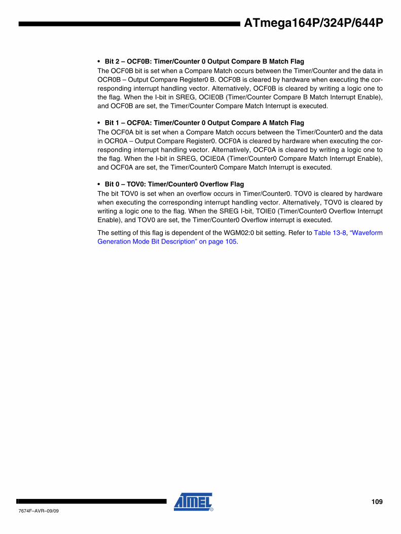
ATmega164P/324P/644P
• Bit 2 – OCF0B: Timer/Counter 0 Output Compare B Match FlagThe OCF0B bit is set when a Compare Match occurs between the Timer/Counter and the data inOCR0B – Output Compare Register0 B. OCF0B is cleared by hardware when executing the cor-responding interrupt handling vector. Alternatively, OCF0B is cleared by writing a logic one tothe flag. When the I-bit in SREG, OCIE0B (Timer/Counter Compare B Match Interrupt Enable),and OCF0B are set, the Timer/Counter Compare Match Interrupt is executed.
• Bit 1 – OCF0A: Timer/Counter 0 Output Compare A Match FlagThe OCF0A bit is set when a Compare Match occurs between the Timer/Counter0 and the datain OCR0A – Output Compare Register0. OCF0A is cleared by hardware when executing the cor-responding interrupt handling vector. Alternatively, OCF0A is cleared by writing a logic one tothe flag. When the I-bit in SREG, OCIE0A (Timer/Counter0 Compare Match Interrupt Enable),and OCF0A are set, the Timer/Counter0 Compare Match Interrupt is executed.
• Bit 0 – TOV0: Timer/Counter0 Overflow FlagThe bit TOV0 is set when an overflow occurs in Timer/Counter0. TOV0 is cleared by hardwarewhen executing the corresponding interrupt handling vector. Alternatively, TOV0 is cleared bywriting a logic one to the flag. When the SREG I-bit, TOIE0 (Timer/Counter0 Overflow InterruptEnable), and TOV0 are set, the Timer/Counter0 Overflow interrupt is executed.
The setting of this flag is dependent of the WGM02:0 bit setting. Refer to Table 13-8, “WaveformGeneration Mode Bit Description” on page 105.
1097674F–AVR–09/09

14. 16-bit Timer/Counter1 with PWM
14.1 Features
• True 16-bit Design (i.e., Allows 16-bit PWM)• Two independent Output Compare Units• Double Buffered Output Compare Registers• One Input Capture Unit• Input Capture Noise Canceler• Clear Timer on Compare Match (Auto Reload)• Glitch-free, Phase Correct Pulse Width Modulator (PWM)• Variable PWM Period• Frequency Generator• External Event Counter• Four independent interrupt Sources (TOV1, OCF1A, OCF1B, and ICF1)
14.2 Overview
The 16-bit Timer/Counter unit allows accurate program execution timing (event management),wave generation, and signal timing measurement.
Most register and bit references in this section are written in general form. A lower case “n”replaces the Timer/Counter number, and a lower case “x” replaces the Output Compare unitchannel. However, when using the register or bit defines in a program, the precise form must beused, i.e., TCNT1 for accessing Timer/Counter1 counter value and so on.
A simplified block diagram of the 16-bit Timer/Counter is shown in Figure 14-1. For the actualplacement of I/O pins, see “Pin Configurations” on page 2. CPU accessible I/O Registers, includ-ing I/O bits and I/O pins, are shown in bold. The device-specific I/O Register and bit locationsare listed in the “Register Description” on page 131.
The PRTIM1 bit in “PRR – Power Reduction Register” on page 47 must be written to zero toenable Timer/Counter1 module.
1107674F–AVR–09/09
ATmega164P/324P/644P
ATmega164P/324P/644P
Figure 14-1. 16-bit Timer/Counter Block Diagram(Note:)
Note: Refer to Figure 1-1 on page 2 and “Alternate Port Functions” on page 77 for Timer/Counter1 pin placement and description.
14.2.1 Registers
The Timer/Counter (TCNTn), Output Compare Registers (OCRnA/B/C), and Input Capture Reg-ister (ICRn) are all 16-bit registers. Special procedures must be followed when accessing the16-bit registers. These procedures are described in the section “Accessing 16-bit Registers” onpage 112. The Timer/Counter Control Registers (TCCRnA/B/C) are 8-bit registers and have noCPU access restrictions. Interrupt requests (abbreviated to Int.Req. in the figure) signals are allvisible in the Timer Interrupt Flag Register (TIFRn). All interrupts are individually masked withthe Timer Interrupt Mask Register (TIMSKn). TIFRn and TIMSKn are not shown in the figure.
The Timer/Counter can be clocked internally, via the prescaler, or by an external clock source onthe Tn pin. The Clock Select logic block controls which clock source and edge the Timer/Counteruses to increment (or decrement) its value. The Timer/Counter is inactive when no clock sourceis selected. The output from the Clock Select logic is referred to as the timer clock (clkTn).
The double buffered Output Compare Registers (OCRnA/B/C) are compared with theTimer/Counter value at all time. The result of the compare can be used by the Waveform Gener-ator to generate a PWM or variable frequency output on the Output Compare pin (OCnA/B/C).
Clock Select
Timer/CounterD
ATA
BU
S
OCRnA
OCRnB
ICRn
=
=
TCNTn
WaveformGeneration
WaveformGeneration
OCnA
OCnB
NoiseCanceler
ICPn
=
FixedTOP
Values
EdgeDetector
Control Logic
= 0
TOP BOTTOM
Count
Clear
Direction
TOVn(Int.Req.)
OCnA(Int.Req.)
OCnB(Int.Req.)
ICFn (Int.Req.)
TCCRnA TCCRnB
( From AnalogComparator Ouput )
TnEdge
Detector
( From Prescaler )
clkTn
1117674F–AVR–09/09
See “Output Compare Units” on page 119.. The compare match event will also set the CompareMatch Flag (OCFnA/B/C) which can be used to generate an Output Compare interrupt request.
The Input Capture Register can capture the Timer/Counter value at a given external (edge trig-gered) event on either the Input Capture pin (ICPn) or on the Analog Comparator pins (See “AC- Analog Comparator” on page 240.) The Input Capture unit includes a digital filtering unit (NoiseCanceler) for reducing the chance of capturing noise spikes.
The TOP value, or maximum Timer/Counter value, can in some modes of operation be definedby either the OCRnA Register, the ICRn Register, or by a set of fixed values. When usingOCRnA as TOP value in a PWM mode, the OCRnA Register can not be used for generating aPWM output. However, the TOP value will in this case be double buffered allowing the TOPvalue to be changed in run time. If a fixed TOP value is required, the ICRn Register can be usedas an alternative, freeing the OCRnA to be used as PWM output.
14.2.2 Definitions
The following definitions are used extensively throughout the section:
14.3 Accessing 16-bit Registers
The TCNTn, OCRnA/B/C, and ICRn are 16-bit registers that can be accessed by the AVR CPUvia the 8-bit data bus. The 16-bit register must be byte accessed using two read or write opera-tions. Each 16-bit timer has a single 8-bit register for temporary storing of the high byte of the16-bit access. The same temporary register is shared between all 16-bit registers within each16-bit timer. Accessing the low byte triggers the 16-bit read or write operation. When the lowbyte of a 16-bit register is written by the CPU, the high byte stored in the temporary register, andthe low byte written are both copied into the 16-bit register in the same clock cycle. When thelow byte of a 16-bit register is read by the CPU, the high byte of the 16-bit register is copied intothe temporary register in the same clock cycle as the low byte is read.
Not all 16-bit accesses uses the temporary register for the high byte. Reading the OCRnA/B/C16-bit registers does not involve using the temporary register.
To do a 16-bit write, the high byte must be written before the low byte. For a 16-bit read, the lowbyte must be read before the high byte.
The following code examples show how to access the 16-bit Timer Registers assuming that nointerrupts updates the temporary register. The same principle can be used directly for accessingthe OCRnA/B/C and ICRn Registers. Note that when using “C”, the compiler handles the 16-bitaccess.
Table 14-1. Definitions
BOTTOM The counter reaches the BOTTOM when it becomes 0x0000.
MAX The counter reaches its MAXimum when it becomes 0xFFFF (decimal 65535).
TOP
The counter reaches the TOP when it becomes equal to the highest value in the count sequence. The TOP value can be assigned to be one of the fixed values: 0x00FF, 0x01FF, or 0x03FF, or to the value stored in the OCRnA or ICRn Register. The assignment is dependent of the mode of operation.
1127674F–AVR–09/09
ATmega164P/324P/644P
ATmega164P/324P/644P
Note: 1. The example code assumes that the part specific header file is included.For I/O Registers located in extended I/O map, “IN”, “OUT”, “SBIS”, “SBIC”, “CBI”, and “SBI” instructions must be replaced with instructions that allow access to extended I/O. Typically “LDS” and “STS” combined with “SBRS”, “SBRC”, “SBR”, and “CBR”.
The assembly code example returns the TCNTn value in the r17:r16 register pair.
It is important to notice that accessing 16-bit registers are atomic operations. If an interruptoccurs between the two instructions accessing the 16-bit register, and the interrupt codeupdates the temporary register by accessing the same or any other of the 16-bit Timer Regis-ters, then the result of the access outside the interrupt will be corrupted. Therefore, when boththe main code and the interrupt code update the temporary register, the main code must disablethe interrupts during the 16-bit access.
Assembly Code Examples(1)
...
; Set TCNTn to 0x01FFldi r17,0x01
ldi r16,0xFF
out TCNTnH,r17out TCNTnL,r16; Read TCNTn into r17:r16in r16,TCNTnLin r17,TCNTnH...
C Code Examples(1)
unsigned int i;
...
/* Set TCNTn to 0x01FF */TCNTn = 0x1FF;/* Read TCNTn into i */i = TCNTn;...
1137674F–AVR–09/09
The following code examples show how to do an atomic read of the TCNTn Register contents.Reading any of the OCRnA/B/C or ICRn Registers can be done by using the same principle.
Note: 1. The example code assumes that the part specific header file is included.For I/O Registers located in extended I/O map, “IN”, “OUT”, “SBIS”, “SBIC”, “CBI”, and “SBI” instructions must be replaced with instructions that allow access to extended I/O. Typically “LDS” and “STS” combined with “SBRS”, “SBRC”, “SBR”, and “CBR”.
The assembly code example returns the TCNTn value in the r17:r16 register pair.
Assembly Code Example(1)
TIM16_ReadTCNTn:; Save global interrupt flag
in r18,SREG
; Disable interrupts
cli
; Read TCNTn into r17:r16in r16,TCNTnLin r17,TCNTnH; Restore global interrupt flag
out SREG,r18
ret
C Code Example(1)
unsigned int TIM16_ReadTCNTn( void ){
unsigned char sreg;
unsigned int i;
/* Save global interrupt flag */
sreg = SREG;
/* Disable interrupts */
_CLI();
/* Read TCNTn into i */i = TCNTn;/* Restore global interrupt flag */
SREG = sreg;
return i;
}
1147674F–AVR–09/09
ATmega164P/324P/644P
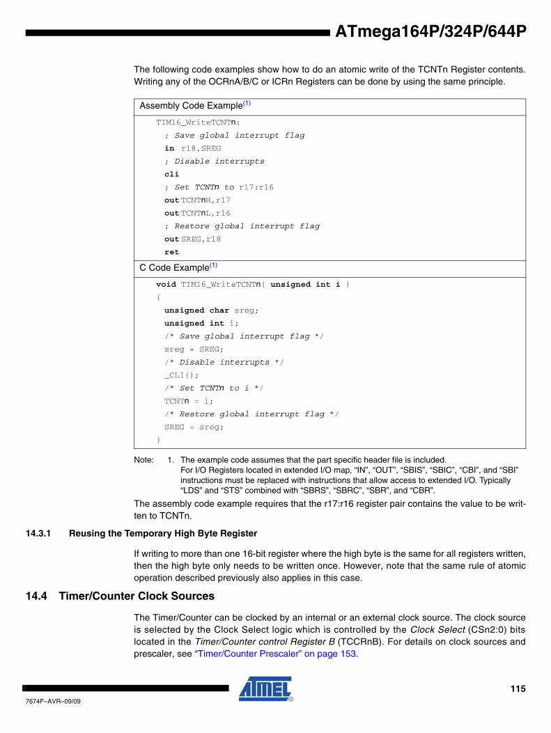
ATmega164P/324P/644P
The following code examples show how to do an atomic write of the TCNTn Register contents.Writing any of the OCRnA/B/C or ICRn Registers can be done by using the same principle.
Note: 1. The example code assumes that the part specific header file is included.For I/O Registers located in extended I/O map, “IN”, “OUT”, “SBIS”, “SBIC”, “CBI”, and “SBI” instructions must be replaced with instructions that allow access to extended I/O. Typically “LDS” and “STS” combined with “SBRS”, “SBRC”, “SBR”, and “CBR”.
The assembly code example requires that the r17:r16 register pair contains the value to be writ-ten to TCNTn.
14.3.1 Reusing the Temporary High Byte Register
If writing to more than one 16-bit register where the high byte is the same for all registers written,then the high byte only needs to be written once. However, note that the same rule of atomicoperation described previously also applies in this case.
14.4 Timer/Counter Clock Sources
The Timer/Counter can be clocked by an internal or an external clock source. The clock sourceis selected by the Clock Select logic which is controlled by the Clock Select (CSn2:0) bitslocated in the Timer/Counter control Register B (TCCRnB). For details on clock sources andprescaler, see “Timer/Counter Prescaler” on page 153.
Assembly Code Example(1)
TIM16_WriteTCNTn:; Save global interrupt flag
in r18,SREG
; Disable interrupts
cli
; Set TCNTn to r17:r16out TCNTnH,r17out TCNTnL,r16; Restore global interrupt flag
out SREG,r18
ret
C Code Example(1)
void TIM16_WriteTCNTn( unsigned int i ){
unsigned char sreg;
unsigned int i;
/* Save global interrupt flag */
sreg = SREG;
/* Disable interrupts */
_CLI();
/* Set TCNTn to i */TCNTn = i;/* Restore global interrupt flag */
SREG = sreg;
}
1157674F–AVR–09/09
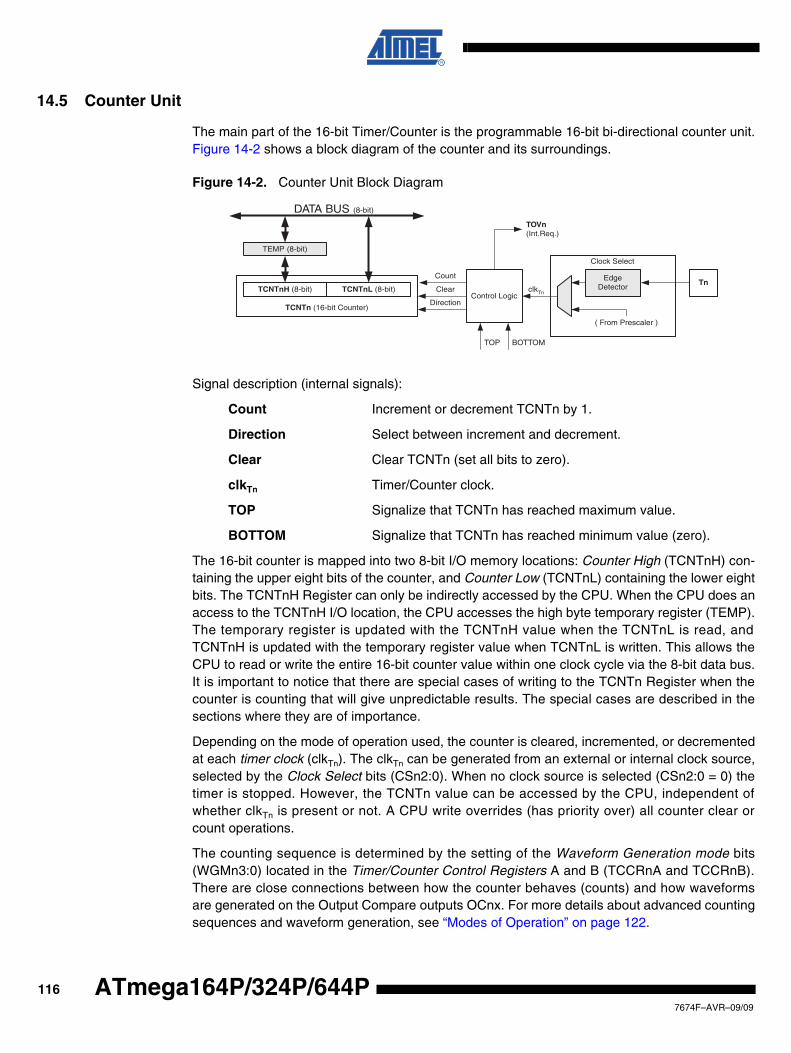
14.5 Counter Unit
The main part of the 16-bit Timer/Counter is the programmable 16-bit bi-directional counter unit.Figure 14-2 shows a block diagram of the counter and its surroundings.
Figure 14-2. Counter Unit Block Diagram
Signal description (internal signals):
Count Increment or decrement TCNTn by 1.
Direction Select between increment and decrement.
Clear Clear TCNTn (set all bits to zero).
clkTn Timer/Counter clock.
TOP Signalize that TCNTn has reached maximum value.
BOTTOM Signalize that TCNTn has reached minimum value (zero).
The 16-bit counter is mapped into two 8-bit I/O memory locations: Counter High (TCNTnH) con-taining the upper eight bits of the counter, and Counter Low (TCNTnL) containing the lower eightbits. The TCNTnH Register can only be indirectly accessed by the CPU. When the CPU does anaccess to the TCNTnH I/O location, the CPU accesses the high byte temporary register (TEMP).The temporary register is updated with the TCNTnH value when the TCNTnL is read, andTCNTnH is updated with the temporary register value when TCNTnL is written. This allows theCPU to read or write the entire 16-bit counter value within one clock cycle via the 8-bit data bus.It is important to notice that there are special cases of writing to the TCNTn Register when thecounter is counting that will give unpredictable results. The special cases are described in thesections where they are of importance.
Depending on the mode of operation used, the counter is cleared, incremented, or decrementedat each timer clock (clkTn). The clkTn can be generated from an external or internal clock source,selected by the Clock Select bits (CSn2:0). When no clock source is selected (CSn2:0 = 0) thetimer is stopped. However, the TCNTn value can be accessed by the CPU, independent ofwhether clkTn is present or not. A CPU write overrides (has priority over) all counter clear orcount operations.
The counting sequence is determined by the setting of the Waveform Generation mode bits(WGMn3:0) located in the Timer/Counter Control Registers A and B (TCCRnA and TCCRnB).There are close connections between how the counter behaves (counts) and how waveformsare generated on the Output Compare outputs OCnx. For more details about advanced countingsequences and waveform generation, see “Modes of Operation” on page 122.
TEMP (8-bit)
DATA BUS (8-bit)
TCNTn (16-bit Counter)
TCNTnH (8-bit) TCNTnL (8-bit)Control Logic
Count
Clear
Direction
TOVn(Int.Req.)
Clock Select
TOP BOTTOM
TnEdge
Detector
( From Prescaler )
clkTn
1167674F–AVR–09/09
ATmega164P/324P/644P
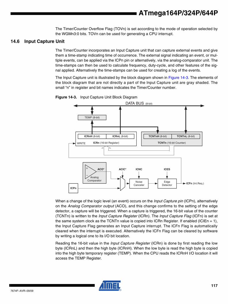
ATmega164P/324P/644P
The Timer/Counter Overflow Flag (TOVn) is set according to the mode of operation selected bythe WGMn3:0 bits. TOVn can be used for generating a CPU interrupt.
14.6 Input Capture Unit
The Timer/Counter incorporates an Input Capture unit that can capture external events and givethem a time-stamp indicating time of occurrence. The external signal indicating an event, or mul-tiple events, can be applied via the ICPn pin or alternatively, via the analog-comparator unit. Thetime-stamps can then be used to calculate frequency, duty-cycle, and other features of the sig-nal applied. Alternatively the time-stamps can be used for creating a log of the events.
The Input Capture unit is illustrated by the block diagram shown in Figure 14-3. The elements ofthe block diagram that are not directly a part of the Input Capture unit are gray shaded. Thesmall “n” in register and bit names indicates the Timer/Counter number.
Figure 14-3. Input Capture Unit Block Diagram
When a change of the logic level (an event) occurs on the Input Capture pin (ICPn), alternativelyon the Analog Comparator output (ACO), and this change confirms to the setting of the edgedetector, a capture will be triggered. When a capture is triggered, the 16-bit value of the counter(TCNTn) is written to the Input Capture Register (ICRn). The Input Capture Flag (ICFn) is set atthe same system clock as the TCNTn value is copied into ICRn Register. If enabled (ICIEn = 1),the Input Capture Flag generates an Input Capture interrupt. The ICFn Flag is automaticallycleared when the interrupt is executed. Alternatively the ICFn Flag can be cleared by softwareby writing a logical one to its I/O bit location.
Reading the 16-bit value in the Input Capture Register (ICRn) is done by first reading the lowbyte (ICRnL) and then the high byte (ICRnH). When the low byte is read the high byte is copiedinto the high byte temporary register (TEMP). When the CPU reads the ICRnH I/O location it willaccess the TEMP Register.
ICFn (Int.Req.)
AnalogComparator
WRITE ICRn (16-bit Register)
ICRnH (8-bit)
NoiseCanceler
ICPn
EdgeDetector
TEMP (8-bit)
DATA BUS (8-bit)
ICRnL (8-bit)
TCNTn (16-bit Counter)
TCNTnH (8-bit) TCNTnL (8-bit)
ACIC* ICNC ICESACO*
1177674F–AVR–09/09
The ICRn Register can only be written when using a Waveform Generation mode that utilizesthe ICRn Register for defining the counter’s TOP value. In these cases the Waveform Genera-tion mode (WGMn3:0) bits must be set before the TOP value can be written to the ICRnRegister. When writing the ICRn Register the high byte must be written to the ICRnH I/O locationbefore the low byte is written to ICRnL.
For more information on how to access the 16-bit registers refer to “Accessing 16-bit Registers”on page 112.
14.6.1 Input Capture Trigger Source
The main trigger source for the Input Capture unit is the Input Capture pin (ICPn).Timer/Counter1 can alternatively use the Analog Comparator output as trigger source for theInput Capture unit. The Analog Comparator is selected as trigger source by setting the AnalogComparator Input Capture (ACIC) bit in the Analog Comparator Control and Status Register(ACSR). Be aware that changing trigger source can trigger a capture. The Input Capture Flagmust therefore be cleared after the change.
Both the Input Capture pin (ICPn) and the Analog Comparator output (ACO) inputs are sampledusing the same technique as for the Tn pin (Figure 14-1 on page 111). The edge detector is alsoidentical. However, when the noise canceler is enabled, additional logic is inserted before theedge detector, which increases the delay by four system clock cycles. Note that the input of thenoise canceler and edge detector is always enabled unless the Timer/Counter is set in a Wave-form Generation mode that uses ICRn to define TOP.
An Input Capture can be triggered by software by controlling the port of the ICPn pin.
14.6.2 Noise Canceler
The noise canceler improves noise immunity by using a simple digital filtering scheme. Thenoise canceler input is monitored over four samples, and all four must be equal for changing theoutput that in turn is used by the edge detector.
The noise canceler is enabled by setting the Input Capture Noise Canceler (ICNCn) bit inTimer/Counter Control Register B (TCCRnB). When enabled the noise canceler introduces addi-tional four system clock cycles of delay from a change applied to the input, to the update of theICRn Register. The noise canceler uses the system clock and is therefore not affected by theprescaler.
14.6.3 Using the Input Capture Unit
The main challenge when using the Input Capture unit is to assign enough processor capacityfor handling the incoming events. The time between two events is critical. If the processor hasnot read the captured value in the ICRn Register before the next event occurs, the ICRn will beoverwritten with a new value. In this case the result of the capture will be incorrect.
When using the Input Capture interrupt, the ICRn Register should be read as early in the inter-rupt handler routine as possible. Even though the Input Capture interrupt has relatively highpriority, the maximum interrupt response time is dependent on the maximum number of clockcycles it takes to handle any of the other interrupt requests.
Using the Input Capture unit in any mode of operation when the TOP value (resolution) isactively changed during operation, is not recommended.
1187674F–AVR–09/09
ATmega164P/324P/644P
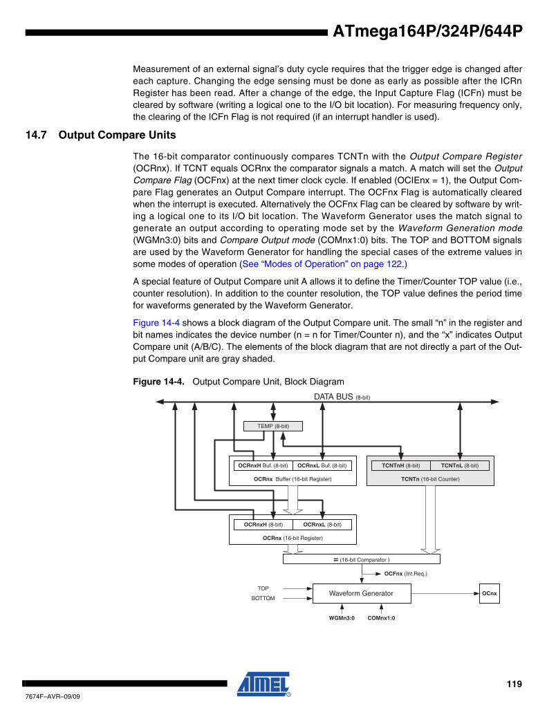
ATmega164P/324P/644P
Measurement of an external signal’s duty cycle requires that the trigger edge is changed aftereach capture. Changing the edge sensing must be done as early as possible after the ICRnRegister has been read. After a change of the edge, the Input Capture Flag (ICFn) must becleared by software (writing a logical one to the I/O bit location). For measuring frequency only,the clearing of the ICFn Flag is not required (if an interrupt handler is used).
14.7 Output Compare Units
The 16-bit comparator continuously compares TCNTn with the Output Compare Register(OCRnx). If TCNT equals OCRnx the comparator signals a match. A match will set the OutputCompare Flag (OCFnx) at the next timer clock cycle. If enabled (OCIEnx = 1), the Output Com-pare Flag generates an Output Compare interrupt. The OCFnx Flag is automatically clearedwhen the interrupt is executed. Alternatively the OCFnx Flag can be cleared by software by writ-ing a logical one to its I/O bit location. The Waveform Generator uses the match signal togenerate an output according to operating mode set by the Waveform Generation mode(WGMn3:0) bits and Compare Output mode (COMnx1:0) bits. The TOP and BOTTOM signalsare used by the Waveform Generator for handling the special cases of the extreme values insome modes of operation (See “Modes of Operation” on page 122.)
A special feature of Output Compare unit A allows it to define the Timer/Counter TOP value (i.e.,counter resolution). In addition to the counter resolution, the TOP value defines the period timefor waveforms generated by the Waveform Generator.
Figure 14-4 shows a block diagram of the Output Compare unit. The small “n” in the register andbit names indicates the device number (n = n for Timer/Counter n), and the “x” indicates OutputCompare unit (A/B/C). The elements of the block diagram that are not directly a part of the Out-put Compare unit are gray shaded.
Figure 14-4. Output Compare Unit, Block Diagram
OCFnx (Int.Req.)
= (16-bit Comparator )
OCRnx Buffer (16-bit Register)
OCRnxH Buf. (8-bit)
OCnx
TEMP (8-bit)
DATA BUS (8-bit)
OCRnxL Buf. (8-bit)
TCNTn (16-bit Counter)
TCNTnH (8-bit) TCNTnL (8-bit)
COMnx1:0WGMn3:0
OCRnx (16-bit Register)
OCRnxH (8-bit) OCRnxL (8-bit)
Waveform GeneratorTOP
BOTTOM
1197674F–AVR–09/09
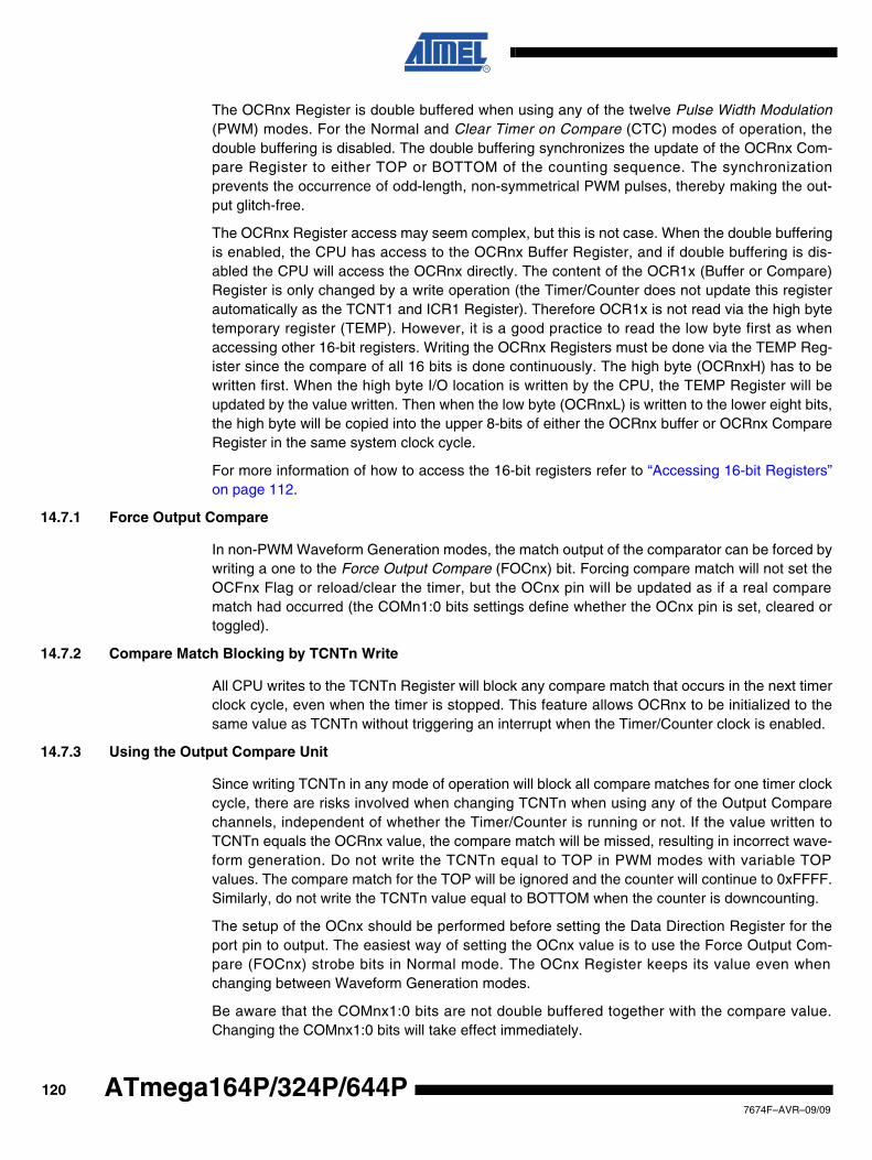
The OCRnx Register is double buffered when using any of the twelve Pulse Width Modulation(PWM) modes. For the Normal and Clear Timer on Compare (CTC) modes of operation, thedouble buffering is disabled. The double buffering synchronizes the update of the OCRnx Com-pare Register to either TOP or BOTTOM of the counting sequence. The synchronizationprevents the occurrence of odd-length, non-symmetrical PWM pulses, thereby making the out-put glitch-free.
The OCRnx Register access may seem complex, but this is not case. When the double bufferingis enabled, the CPU has access to the OCRnx Buffer Register, and if double buffering is dis-abled the CPU will access the OCRnx directly. The content of the OCR1x (Buffer or Compare)Register is only changed by a write operation (the Timer/Counter does not update this registerautomatically as the TCNT1 and ICR1 Register). Therefore OCR1x is not read via the high bytetemporary register (TEMP). However, it is a good practice to read the low byte first as whenaccessing other 16-bit registers. Writing the OCRnx Registers must be done via the TEMP Reg-ister since the compare of all 16 bits is done continuously. The high byte (OCRnxH) has to bewritten first. When the high byte I/O location is written by the CPU, the TEMP Register will beupdated by the value written. Then when the low byte (OCRnxL) is written to the lower eight bits,the high byte will be copied into the upper 8-bits of either the OCRnx buffer or OCRnx CompareRegister in the same system clock cycle.
For more information of how to access the 16-bit registers refer to “Accessing 16-bit Registers”on page 112.
14.7.1 Force Output Compare
In non-PWM Waveform Generation modes, the match output of the comparator can be forced bywriting a one to the Force Output Compare (FOCnx) bit. Forcing compare match will not set theOCFnx Flag or reload/clear the timer, but the OCnx pin will be updated as if a real comparematch had occurred (the COMn1:0 bits settings define whether the OCnx pin is set, cleared ortoggled).
14.7.2 Compare Match Blocking by TCNTn Write
All CPU writes to the TCNTn Register will block any compare match that occurs in the next timerclock cycle, even when the timer is stopped. This feature allows OCRnx to be initialized to thesame value as TCNTn without triggering an interrupt when the Timer/Counter clock is enabled.
14.7.3 Using the Output Compare Unit
Since writing TCNTn in any mode of operation will block all compare matches for one timer clockcycle, there are risks involved when changing TCNTn when using any of the Output Comparechannels, independent of whether the Timer/Counter is running or not. If the value written toTCNTn equals the OCRnx value, the compare match will be missed, resulting in incorrect wave-form generation. Do not write the TCNTn equal to TOP in PWM modes with variable TOPvalues. The compare match for the TOP will be ignored and the counter will continue to 0xFFFF.Similarly, do not write the TCNTn value equal to BOTTOM when the counter is downcounting.
The setup of the OCnx should be performed before setting the Data Direction Register for theport pin to output. The easiest way of setting the OCnx value is to use the Force Output Com-pare (FOCnx) strobe bits in Normal mode. The OCnx Register keeps its value even whenchanging between Waveform Generation modes.
Be aware that the COMnx1:0 bits are not double buffered together with the compare value.Changing the COMnx1:0 bits will take effect immediately.
1207674F–AVR–09/09
ATmega164P/324P/644P
ATmega164P/324P/644P
14.8 Compare Match Output Unit
The Compare Output mode (COMnx1:0) bits have two functions. The Waveform Generator usesthe COMnx1:0 bits for defining the Output Compare (OCnx) state at the next compare match.Secondly the COMnx1:0 bits control the OCnx pin output source. Figure 14-5 shows a simplifiedschematic of the logic affected by the COMnx1:0 bit setting. The I/O Registers, I/O bits, and I/Opins in the figure are shown in bold. Only the parts of the general I/O Port Control Registers(DDR and PORT) that are affected by the COMnx1:0 bits are shown. When referring to theOCnx state, the reference is for the internal OCnx Register, not the OCnx pin. If a system resetoccur, the OCnx Register is reset to “0”.
Figure 14-5. Compare Match Output Unit, Schematic
The general I/O port function is overridden by the Output Compare (OCnx) from the WaveformGenerator if either of the COMnx1:0 bits are set. However, the OCnx pin direction (input or out-put) is still controlled by the Data Direction Register (DDR) for the port pin. The Data DirectionRegister bit for the OCnx pin (DDR_OCnx) must be set as output before the OCnx value is visi-ble on the pin. The port override function is generally independent of the Waveform Generationmode, but there are some exceptions. Refer to Table 14-2, Table 14-3 and Table 14-4 fordetails.
The design of the Output Compare pin logic allows initialization of the OCnx state before the out-put is enabled. Note that some COMnx1:0 bit settings are reserved for certain modes ofoperation. See “Register Description” on page 131.
The COMnx1:0 bits have no effect on the Input Capture unit.
PORT
DDR
D Q
D Q
OCnxPinOCnx
D QWaveformGenerator
COMnx1
COMnx0
0
1
DAT
A B
US
FOCnx
clkI/O
1217674F–AVR–09/09
14.8.1 Compare Output Mode and Waveform Generation
The Waveform Generator uses the COMnx1:0 bits differently in normal, CTC, and PWM modes.For all modes, setting the COMnx1:0 = 0 tells the Waveform Generator that no action on theOCnx Register is to be performed on the next compare match. For compare output actions in thenon-PWM modes refer to Table 14-2 on page 132. For fast PWM mode refer to Table 14-3 onpage 132, and for phase correct and phase and frequency correct PWM refer to Table 14-4 onpage 133.
A change of the COMnx1:0 bits state will have effect at the first compare match after the bits arewritten. For non-PWM modes, the action can be forced to have immediate effect by using theFOCnx strobe bits.
14.9 Modes of Operation
The mode of operation, i.e., the behavior of the Timer/Counter and the Output Compare pins, isdefined by the combination of the Waveform Generation mode (WGMn3:0) and Compare Outputmode (COMnx1:0) bits. The Compare Output mode bits do not affect the counting sequence,while the Waveform Generation mode bits do. The COMnx1:0 bits control whether the PWM out-put generated should be inverted or not (inverted or non-inverted PWM). For non-PWM modesthe COMnx1:0 bits control whether the output should be set, cleared or toggle at a comparematch (See “Compare Match Output Unit” on page 121.)
For detailed timing information refer to “Timer/Counter Timing Diagrams” on page 129.
14.9.1 Normal Mode
The simplest mode of operation is the Normal mode (WGMn3:0 = 0). In this mode the countingdirection is always up (incrementing), and no counter clear is performed. The counter simplyoverruns when it passes its maximum 16-bit value (MAX = 0xFFFF) and then restarts from theBOTTOM (0x0000). In normal operation the Timer/Counter Overflow Flag (TOVn) will be set inthe same timer clock cycle as the TCNTn becomes zero. The TOVn Flag in this case behaveslike a 17th bit, except that it is only set, not cleared. However, combined with the timer overflowinterrupt that automatically clears the TOVn Flag, the timer resolution can be increased by soft-ware. There are no special cases to consider in the Normal mode, a new counter value can bewritten anytime.
The Input Capture unit is easy to use in Normal mode. However, observe that the maximuminterval between the external events must not exceed the resolution of the counter. If the intervalbetween events are too long, the timer overflow interrupt or the prescaler must be used toextend the resolution for the capture unit.
The Output Compare units can be used to generate interrupts at some given time. Using theOutput Compare to generate waveforms in Normal mode is not recommended, since this willoccupy too much of the CPU time.
14.9.2 Clear Timer on Compare Match (CTC) Mode
In Clear Timer on Compare or CTC mode (WGMn3:0 = 4 or 12), the OCRnA or ICRn Registerare used to manipulate the counter resolution. In CTC mode the counter is cleared to zero whenthe counter value (TCNTn) matches either the OCRnA (WGMn3:0 = 4) or the ICRn (WGMn3:0 =12). The OCRnA or ICRn define the top value for the counter, hence also its resolution. Thismode allows greater control of the compare match output frequency. It also simplifies the opera-tion of counting external events.
1227674F–AVR–09/09
ATmega164P/324P/644P
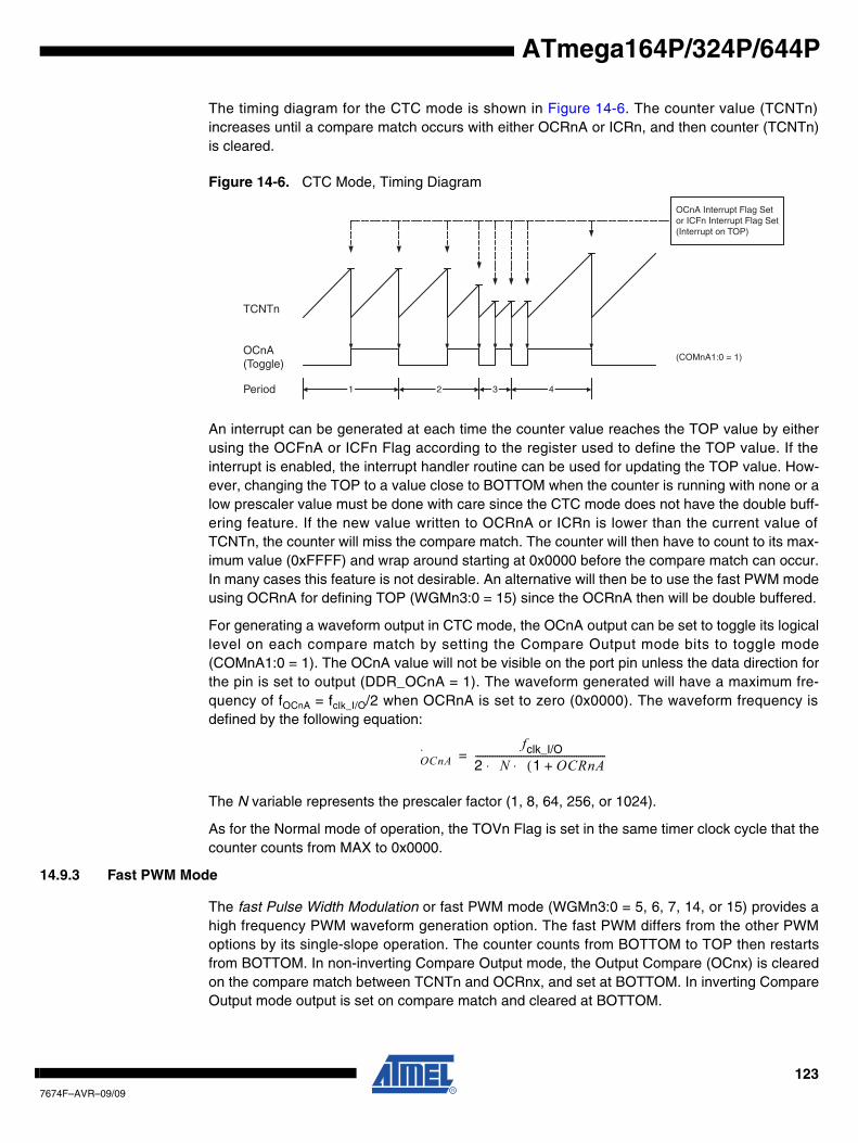
ATmega164P/324P/644P
The timing diagram for the CTC mode is shown in Figure 14-6. The counter value (TCNTn)increases until a compare match occurs with either OCRnA or ICRn, and then counter (TCNTn)is cleared.
Figure 14-6. CTC Mode, Timing Diagram
An interrupt can be generated at each time the counter value reaches the TOP value by eitherusing the OCFnA or ICFn Flag according to the register used to define the TOP value. If theinterrupt is enabled, the interrupt handler routine can be used for updating the TOP value. How-ever, changing the TOP to a value close to BOTTOM when the counter is running with none or alow prescaler value must be done with care since the CTC mode does not have the double buff-ering feature. If the new value written to OCRnA or ICRn is lower than the current value ofTCNTn, the counter will miss the compare match. The counter will then have to count to its max-imum value (0xFFFF) and wrap around starting at 0x0000 before the compare match can occur.In many cases this feature is not desirable. An alternative will then be to use the fast PWM modeusing OCRnA for defining TOP (WGMn3:0 = 15) since the OCRnA then will be double buffered.
For generating a waveform output in CTC mode, the OCnA output can be set to toggle its logicallevel on each compare match by setting the Compare Output mode bits to toggle mode(COMnA1:0 = 1). The OCnA value will not be visible on the port pin unless the data direction forthe pin is set to output (DDR_OCnA = 1). The waveform generated will have a maximum fre-quency of fOCnA = fclk_I/O/2 when OCRnA is set to zero (0x0000). The waveform frequency isdefined by the following equation:
The N variable represents the prescaler factor (1, 8, 64, 256, or 1024).
As for the Normal mode of operation, the TOVn Flag is set in the same timer clock cycle that thecounter counts from MAX to 0x0000.
14.9.3 Fast PWM Mode
The fast Pulse Width Modulation or fast PWM mode (WGMn3:0 = 5, 6, 7, 14, or 15) provides ahigh frequency PWM waveform generation option. The fast PWM differs from the other PWMoptions by its single-slope operation. The counter counts from BOTTOM to TOP then restartsfrom BOTTOM. In non-inverting Compare Output mode, the Output Compare (OCnx) is clearedon the compare match between TCNTn and OCRnx, and set at BOTTOM. In inverting CompareOutput mode output is set on compare match and cleared at BOTTOM.
TCNTn
OCnA(Toggle)
OCnA Interrupt Flag Setor ICFn Interrupt Flag Set(Interrupt on TOP)
1 4Period 2 3
(COMnA1:0 = 1)
fOCnAfclk_I/O
2 N 1 OCRnA+( )⋅ ⋅-------------------------------------------------------=
1237674F–AVR–09/09
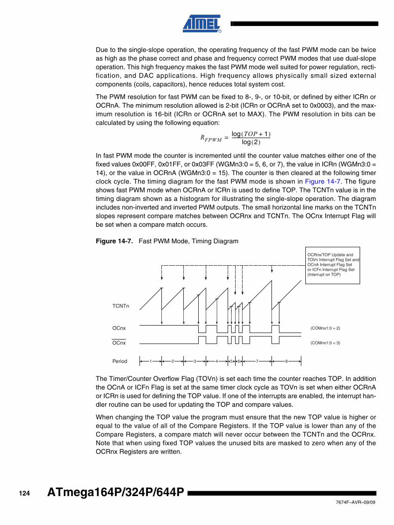
Due to the single-slope operation, the operating frequency of the fast PWM mode can be twiceas high as the phase correct and phase and frequency correct PWM modes that use dual-slopeoperation. This high frequency makes the fast PWM mode well suited for power regulation, recti-fication, and DAC applications. High frequency allows physically small sized externalcomponents (coils, capacitors), hence reduces total system cost.
The PWM resolution for fast PWM can be fixed to 8-, 9-, or 10-bit, or defined by either ICRn orOCRnA. The minimum resolution allowed is 2-bit (ICRn or OCRnA set to 0x0003), and the max-imum resolution is 16-bit (ICRn or OCRnA set to MAX). The PWM resolution in bits can becalculated by using the following equation:
In fast PWM mode the counter is incremented until the counter value matches either one of thefixed values 0x00FF, 0x01FF, or 0x03FF (WGMn3:0 = 5, 6, or 7), the value in ICRn (WGMn3:0 =14), or the value in OCRnA (WGMn3:0 = 15). The counter is then cleared at the following timerclock cycle. The timing diagram for the fast PWM mode is shown in Figure 14-7. The figureshows fast PWM mode when OCRnA or ICRn is used to define TOP. The TCNTn value is in thetiming diagram shown as a histogram for illustrating the single-slope operation. The diagramincludes non-inverted and inverted PWM outputs. The small horizontal line marks on the TCNTnslopes represent compare matches between OCRnx and TCNTn. The OCnx Interrupt Flag willbe set when a compare match occurs.
Figure 14-7. Fast PWM Mode, Timing Diagram
The Timer/Counter Overflow Flag (TOVn) is set each time the counter reaches TOP. In additionthe OCnA or ICFn Flag is set at the same timer clock cycle as TOVn is set when either OCRnAor ICRn is used for defining the TOP value. If one of the interrupts are enabled, the interrupt han-dler routine can be used for updating the TOP and compare values.
When changing the TOP value the program must ensure that the new TOP value is higher orequal to the value of all of the Compare Registers. If the TOP value is lower than any of theCompare Registers, a compare match will never occur between the TCNTn and the OCRnx.Note that when using fixed TOP values the unused bits are masked to zero when any of theOCRnx Registers are written.
RFPWMTOP 1+( )log
2( )log-----------------------------------=
TCNTn
OCRnx/TOP Update andTOVn Interrupt Flag Set andOCnA Interrupt Flag Setor ICFn Interrupt Flag Set(Interrupt on TOP)
1 7Period 2 3 4 5 6 8
OCnx
OCnx
(COMnx1:0 = 2)
(COMnx1:0 = 3)
1247674F–AVR–09/09
ATmega164P/324P/644P
ATmega164P/324P/644P
The procedure for updating ICRn differs from updating OCRnA when used for defining the TOPvalue. The ICRn Register is not double buffered. This means that if ICRn is changed to a lowvalue when the counter is running with none or a low prescaler value, there is a risk that the newICRn value written is lower than the current value of TCNTn. The result will then be that thecounter will miss the compare match at the TOP value. The counter will then have to count to theMAX value (0xFFFF) and wrap around starting at 0x0000 before the compare match can occur.The OCRnA Register however, is double buffered. This feature allows the OCRnA I/O locationto be written anytime. When the OCRnA I/O location is written the value written will be put intothe OCRnA Buffer Register. The OCRnA Compare Register will then be updated with the valuein the Buffer Register at the next timer clock cycle the TCNTn matches TOP. The update is doneat the same timer clock cycle as the TCNTn is cleared and the TOVn Flag is set.
Using the ICRn Register for defining TOP works well when using fixed TOP values. By usingICRn, the OCRnA Register is free to be used for generating a PWM output on OCnA. However,if the base PWM frequency is actively changed (by changing the TOP value), using the OCRnAas TOP is clearly a better choice due to its double buffer feature.
In fast PWM mode, the compare units allow generation of PWM waveforms on the OCnx pins.Setting the COMnx1:0 bits to two will produce a non-inverted PWM and an inverted PWM outputcan be generated by setting the COMnx1:0 to three (see Table on page 132). The actual OCnxvalue will only be visible on the port pin if the data direction for the port pin is set as output(DDR_OCnx). The PWM waveform is generated by setting (or clearing) the OCnx Register atthe compare match between OCRnx and TCNTn, and clearing (or setting) the OCnx Register atthe timer clock cycle the counter is cleared (changes from TOP to BOTTOM).
The PWM frequency for the output can be calculated by the following equation:
The N variable represents the prescaler divider (1, 8, 64, 256, or 1024).
The extreme values for the OCRnx Register represents special cases when generating a PWMwaveform output in the fast PWM mode. If the OCRnx is set equal to BOTTOM (0x0000) the out-put will be a narrow spike for each TOP+1 timer clock cycle. Setting the OCRnx equal to TOPwill result in a constant high or low output (depending on the polarity of the output set by theCOMnx1:0 bits.)
A frequency (with 50% duty cycle) waveform output in fast PWM mode can be achieved by set-ting OCnA to toggle its logical level on each compare match (COMnA1:0 = 1). This applies onlyif OCR1A is used to define the TOP value (WGM13:0 = 15). The waveform generated will havea maximum frequency of fOCnA = fclk_I/O/2 when OCRnA is set to zero (0x0000). This feature issimilar to the OCnA toggle in CTC mode, except the double buffer feature of the Output Com-pare unit is enabled in the fast PWM mode.
14.9.4 Phase Correct PWM Mode
The phase correct Pulse Width Modulation or phase correct PWM mode (WGMn3:0 = 1, 2, 3,10, or 11) provides a high resolution phase correct PWM waveform generation option. Thephase correct PWM mode is, like the phase and frequency correct PWM mode, based on adual-slope operation. The counter counts repeatedly from BOTTOM (0x0000) to TOP and thenfrom TOP to BOTTOM. In non-inverting Compare Output mode, the Output Compare (OCnx) iscleared on the compare match between TCNTn and OCRnx while upcounting, and set on thecompare match while downcounting.
fOCnxPWMfclk_I/O
N 1 TOP+( )⋅-------------------------------------=
1257674F–AVR–09/09
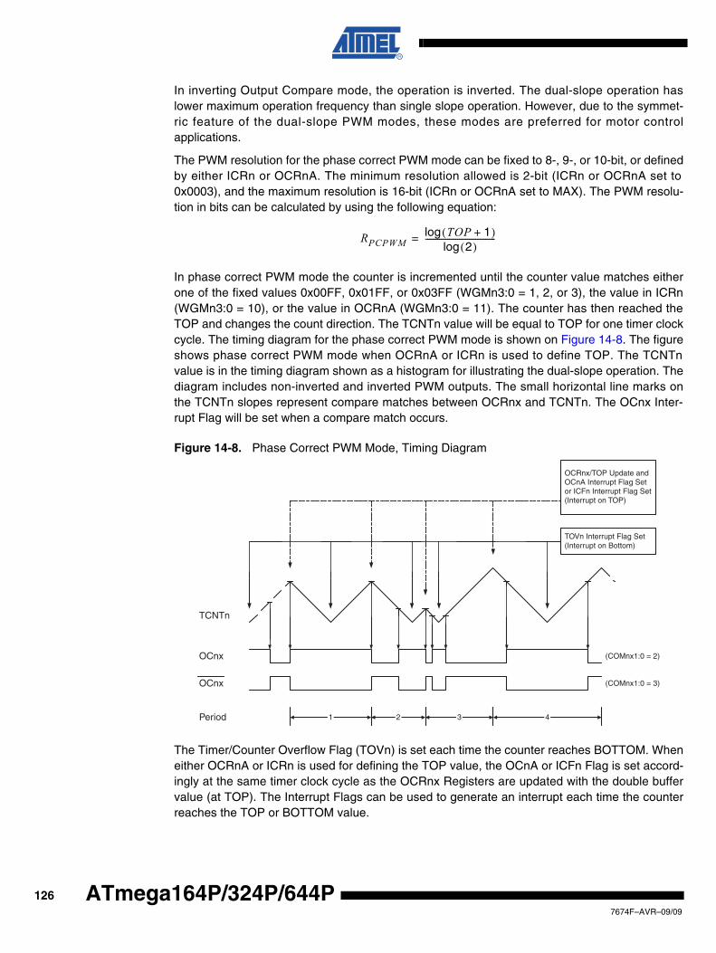
In inverting Output Compare mode, the operation is inverted. The dual-slope operation haslower maximum operation frequency than single slope operation. However, due to the symmet-ric feature of the dual-slope PWM modes, these modes are preferred for motor controlapplications.
The PWM resolution for the phase correct PWM mode can be fixed to 8-, 9-, or 10-bit, or definedby either ICRn or OCRnA. The minimum resolution allowed is 2-bit (ICRn or OCRnA set to0x0003), and the maximum resolution is 16-bit (ICRn or OCRnA set to MAX). The PWM resolu-tion in bits can be calculated by using the following equation:
In phase correct PWM mode the counter is incremented until the counter value matches eitherone of the fixed values 0x00FF, 0x01FF, or 0x03FF (WGMn3:0 = 1, 2, or 3), the value in ICRn(WGMn3:0 = 10), or the value in OCRnA (WGMn3:0 = 11). The counter has then reached theTOP and changes the count direction. The TCNTn value will be equal to TOP for one timer clockcycle. The timing diagram for the phase correct PWM mode is shown on Figure 14-8. The figureshows phase correct PWM mode when OCRnA or ICRn is used to define TOP. The TCNTnvalue is in the timing diagram shown as a histogram for illustrating the dual-slope operation. Thediagram includes non-inverted and inverted PWM outputs. The small horizontal line marks onthe TCNTn slopes represent compare matches between OCRnx and TCNTn. The OCnx Inter-rupt Flag will be set when a compare match occurs.
Figure 14-8. Phase Correct PWM Mode, Timing Diagram
The Timer/Counter Overflow Flag (TOVn) is set each time the counter reaches BOTTOM. Wheneither OCRnA or ICRn is used for defining the TOP value, the OCnA or ICFn Flag is set accord-ingly at the same timer clock cycle as the OCRnx Registers are updated with the double buffervalue (at TOP). The Interrupt Flags can be used to generate an interrupt each time the counterreaches the TOP or BOTTOM value.
RPCPWMTOP 1+( )log
2( )log-----------------------------------=
OCRnx/TOP Update andOCnA Interrupt Flag Setor ICFn Interrupt Flag Set(Interrupt on TOP)
1 2 3 4
TOVn Interrupt Flag Set(Interrupt on Bottom)
TCNTn
Period
OCnx
OCnx
(COMnx1:0 = 2)
(COMnx1:0 = 3)
1267674F–AVR–09/09
ATmega164P/324P/644P
ATmega164P/324P/644P
When changing the TOP value the program must ensure that the new TOP value is higher orequal to the value of all of the Compare Registers. If the TOP value is lower than any of theCompare Registers, a compare match will never occur between the TCNTn and the OCRnx.Note that when using fixed TOP values, the unused bits are masked to zero when any of theOCRnx Registers are written. As the third period shown in Figure 14-8 illustrates, changing theTOP actively while the Timer/Counter is running in the phase correct mode can result in anunsymmetrical output. The reason for this can be found in the time of update of the OCRnx Reg-ister. Since the OCRnx update occurs at TOP, the PWM period starts and ends at TOP. Thisimplies that the length of the falling slope is determined by the previous TOP value, while thelength of the rising slope is determined by the new TOP value. When these two values differ thetwo slopes of the period will differ in length. The difference in length gives the unsymmetricalresult on the output.
It is recommended to use the phase and frequency correct mode instead of the phase correctmode when changing the TOP value while the Timer/Counter is running. When using a staticTOP value there are practically no differences between the two modes of operation.
In phase correct PWM mode, the compare units allow generation of PWM waveforms on theOCnx pins. Setting the COMnx1:0 bits to two will produce a non-inverted PWM and an invertedPWM output can be generated by setting the COMnx1:0 to three (See Table on page 133). Theactual OCnx value will only be visible on the port pin if the data direction for the port pin is set asoutput (DDR_OCnx). The PWM waveform is generated by setting (or clearing) the OCnx Regis-ter at the compare match between OCRnx and TCNTn when the counter increments, andclearing (or setting) the OCnx Register at compare match between OCRnx and TCNTn whenthe counter decrements. The PWM frequency for the output when using phase correct PWM canbe calculated by the following equation:
The N variable represents the prescaler divider (1, 8, 64, 256, or 1024).
The extreme values for the OCRnx Register represent special cases when generating a PWMwaveform output in the phase correct PWM mode. If the OCRnx is set equal to BOTTOM theoutput will be continuously low and if set equal to TOP the output will be continuously high fornon-inverted PWM mode. For inverted PWM the output will have the opposite logic values. IfOCR1A is used to define the TOP value (WGM13:0 = 11) and COM1A1:0 = 1, the OC1A outputwill toggle with a 50% duty cycle.
14.9.5 Phase and Frequency Correct PWM Mode
The phase and frequency correct Pulse Width Modulation, or phase and frequency correct PWMmode (WGMn3:0 = 8 or 9) provides a high resolution phase and frequency correct PWM wave-form generation option. The phase and frequency correct PWM mode is, like the phase correctPWM mode, based on a dual-slope operation. The counter counts repeatedly from BOTTOM(0x0000) to TOP and then from TOP to BOTTOM. In non-inverting Compare Output mode, theOutput Compare (OCnx) is cleared on the compare match between TCNTn and OCRnx whileupcounting, and set on the compare match while downcounting. In inverting Compare Outputmode, the operation is inverted. The dual-slope operation gives a lower maximum operation fre-quency compared to the single-slope operation. However, due to the symmetric feature of thedual-slope PWM modes, these modes are preferred for motor control applications.
fOCnxPCPWMfclk_I/O
2 N TOP⋅ ⋅---------------------------------=
1277674F–AVR–09/09
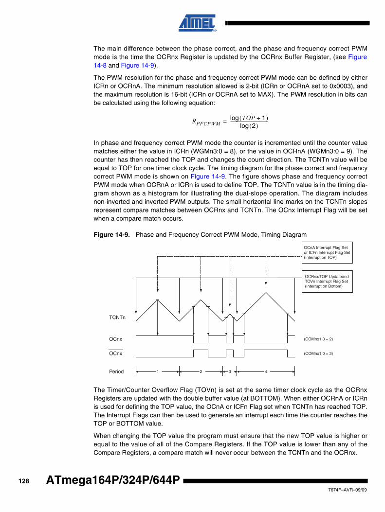
The main difference between the phase correct, and the phase and frequency correct PWMmode is the time the OCRnx Register is updated by the OCRnx Buffer Register, (see Figure14-8 and Figure 14-9).
The PWM resolution for the phase and frequency correct PWM mode can be defined by eitherICRn or OCRnA. The minimum resolution allowed is 2-bit (ICRn or OCRnA set to 0x0003), andthe maximum resolution is 16-bit (ICRn or OCRnA set to MAX). The PWM resolution in bits canbe calculated using the following equation:
In phase and frequency correct PWM mode the counter is incremented until the counter valuematches either the value in ICRn (WGMn3:0 = 8), or the value in OCRnA (WGMn3:0 = 9). Thecounter has then reached the TOP and changes the count direction. The TCNTn value will beequal to TOP for one timer clock cycle. The timing diagram for the phase correct and frequencycorrect PWM mode is shown on Figure 14-9. The figure shows phase and frequency correctPWM mode when OCRnA or ICRn is used to define TOP. The TCNTn value is in the timing dia-gram shown as a histogram for illustrating the dual-slope operation. The diagram includesnon-inverted and inverted PWM outputs. The small horizontal line marks on the TCNTn slopesrepresent compare matches between OCRnx and TCNTn. The OCnx Interrupt Flag will be setwhen a compare match occurs.
Figure 14-9. Phase and Frequency Correct PWM Mode, Timing Diagram
The Timer/Counter Overflow Flag (TOVn) is set at the same timer clock cycle as the OCRnxRegisters are updated with the double buffer value (at BOTTOM). When either OCRnA or ICRnis used for defining the TOP value, the OCnA or ICFn Flag set when TCNTn has reached TOP.The Interrupt Flags can then be used to generate an interrupt each time the counter reaches theTOP or BOTTOM value.
When changing the TOP value the program must ensure that the new TOP value is higher orequal to the value of all of the Compare Registers. If the TOP value is lower than any of theCompare Registers, a compare match will never occur between the TCNTn and the OCRnx.
RPFCPWMTOP 1+( )log
2( )log-----------------------------------=
OCRnx/TOP UpdateandTOVn Interrupt Flag Set(Interrupt on Bottom)
OCnA Interrupt Flag Setor ICFn Interrupt Flag Set(Interrupt on TOP)
1 2 3 4
TCNTn
Period
OCnx
OCnx
(COMnx1:0 = 2)
(COMnx1:0 = 3)
1287674F–AVR–09/09
ATmega164P/324P/644P
ATmega164P/324P/644P
As Figure 14-9 shows the output generated is, in contrast to the phase correct mode, symmetri-cal in all periods. Since the OCRnx Registers are updated at BOTTOM, the length of the risingand the falling slopes will always be equal. This gives symmetrical output pulses and is thereforefrequency correct.
Using the ICRn Register for defining TOP works well when using fixed TOP values. By usingICRn, the OCRnA Register is free to be used for generating a PWM output on OCnA. However,if the base PWM frequency is actively changed by changing the TOP value, using the OCRnA asTOP is clearly a better choice due to its double buffer feature.
In phase and frequency correct PWM mode, the compare units allow generation of PWM wave-forms on the OCnx pins. Setting the COMnx1:0 bits to two will produce a non-inverted PWM andan inverted PWM output can be generated by setting the COMnx1:0 to three (See Table onpage 133). The actual OCnx value will only be visible on the port pin if the data direction for theport pin is set as output (DDR_OCnx). The PWM waveform is generated by setting (or clearing)the OCnx Register at the compare match between OCRnx and TCNTn when the counter incre-ments, and clearing (or setting) the OCnx Register at compare match between OCRnx andTCNTn when the counter decrements. The PWM frequency for the output when using phaseand frequency correct PWM can be calculated by the following equation:
The N variable represents the prescaler divider (1, 8, 64, 256, or 1024).
The extreme values for the OCRnx Register represents special cases when generating a PWMwaveform output in the phase correct PWM mode. If the OCRnx is set equal to BOTTOM theoutput will be continuously low and if set equal to TOP the output will be set to high fornon-inverted PWM mode. For inverted PWM the output will have the opposite logic values. IfOCR1A is used to define the TOP value (WGM13:0 = 9) and COM1A1:0 = 1, the OC1A outputwill toggle with a 50% duty cycle.
14.10 Timer/Counter Timing Diagrams
The Timer/Counter is a synchronous design and the timer clock (clkTn) is therefore shown as aclock enable signal in the following figures. The figures include information on when InterruptFlags are set, and when the OCRnx Register is updated with the OCRnx buffer value (only formodes utilizing double buffering). Figure 14-10 shows a timing diagram for the setting of OCFnx.
fOCnxPFCPWMfclk_I/O
2 N TOP⋅ ⋅---------------------------------=
1297674F–AVR–09/09
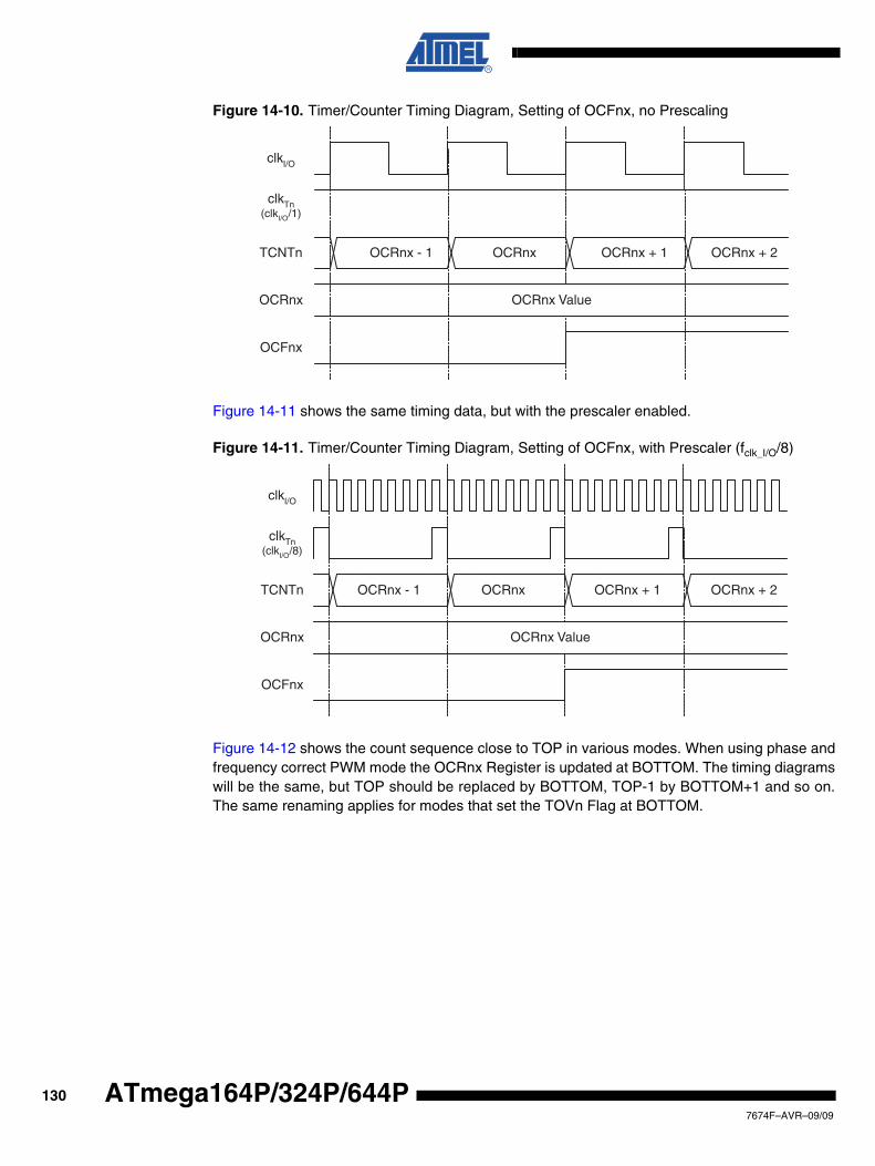
Figure 14-10. Timer/Counter Timing Diagram, Setting of OCFnx, no Prescaling
Figure 14-11 shows the same timing data, but with the prescaler enabled.
Figure 14-11. Timer/Counter Timing Diagram, Setting of OCFnx, with Prescaler (fclk_I/O/8)
Figure 14-12 shows the count sequence close to TOP in various modes. When using phase andfrequency correct PWM mode the OCRnx Register is updated at BOTTOM. The timing diagramswill be the same, but TOP should be replaced by BOTTOM, TOP-1 by BOTTOM+1 and so on.The same renaming applies for modes that set the TOVn Flag at BOTTOM.
clkTn(clkI/O/1)
OCFnx
clkI/O
OCRnx
TCNTn
OCRnx Value
OCRnx - 1 OCRnx OCRnx + 1 OCRnx + 2
OCFnx
OCRnx
TCNTn
OCRnx Value
OCRnx - 1 OCRnx OCRnx + 1 OCRnx + 2
clkI/O
clkTn(clkI/O/8)
1307674F–AVR–09/09
ATmega164P/324P/644P
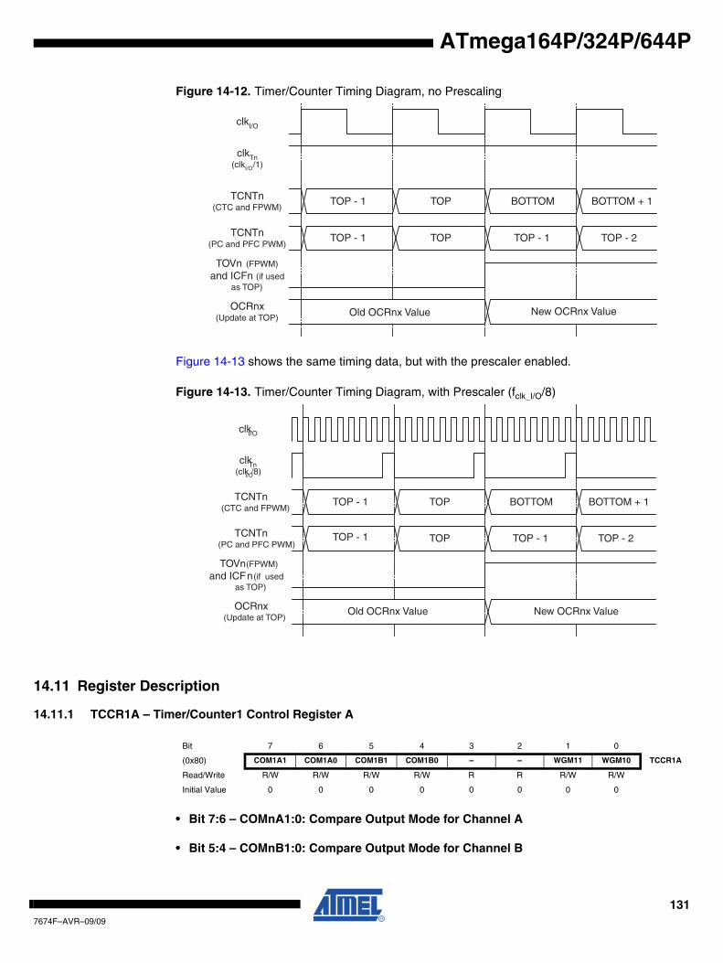
ATmega164P/324P/644P
Figure 14-12. Timer/Counter Timing Diagram, no Prescaling
Figure 14-13 shows the same timing data, but with the prescaler enabled.
Figure 14-13. Timer/Counter Timing Diagram, with Prescaler (fclk_I/O/8)
14.11 Register Description
14.11.1 TCCR1A – Timer/Counter1 Control Register A
• Bit 7:6 – COMnA1:0: Compare Output Mode for Channel A
• Bit 5:4 – COMnB1:0: Compare Output Mode for Channel B
TOVn (FPWM)and ICFn (if used
as TOP)
OCRnx(Update at TOP)
TCNTn(CTC and FPWM)
TCNTn(PC and PFC PWM)
TOP - 1 TOP TOP - 1 TOP - 2
Old OCRnx Value New OCRnx Value
TOP - 1 TOP BOTTOM BOTTOM + 1
clkTn(clkI/O/1)
clkI/O
TOVn (FPWM)and ICFn (if used
as TOP)
OCRnx(Update at TOP)
TCNTn(CTC and FPWM)
TCNTn(PC and PFC PWM)
TOP - 1 TOP TOP - 1 TOP - 2
Old OCRnx Value New OCRnx Value
TOP - 1 TOP BOTTOM BOTTOM + 1
clkI/O
clkTn(clkI/O/8)
Bit 7 6 5 4 3 2 1 0
(0x80) COM1A1 COM1A0 COM1B1 COM1B0 – – WGM11 WGM10 TCCR1A
Read/Write R/W R/W R/W R/W R R R/W R/W
Initial Value 0 0 0 0 0 0 0 0
1317674F–AVR–09/09
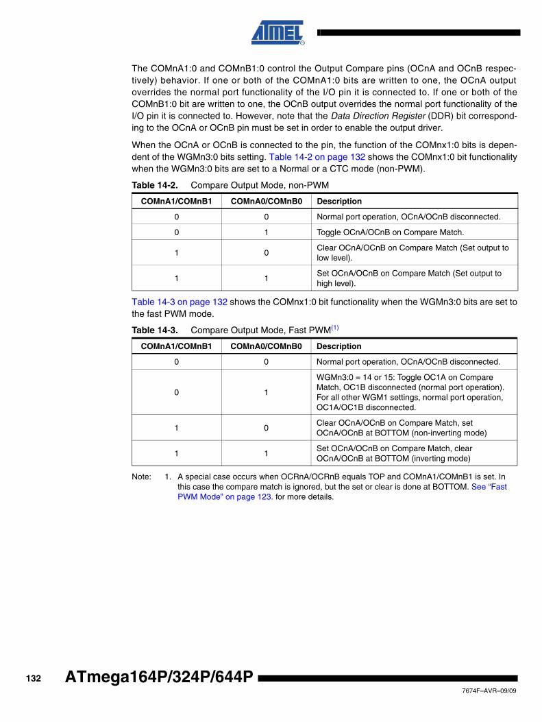
The COMnA1:0 and COMnB1:0 control the Output Compare pins (OCnA and OCnB respec-tively) behavior. If one or both of the COMnA1:0 bits are written to one, the OCnA outputoverrides the normal port functionality of the I/O pin it is connected to. If one or both of theCOMnB1:0 bit are written to one, the OCnB output overrides the normal port functionality of theI/O pin it is connected to. However, note that the Data Direction Register (DDR) bit correspond-ing to the OCnA or OCnB pin must be set in order to enable the output driver.
When the OCnA or OCnB is connected to the pin, the function of the COMnx1:0 bits is depen-dent of the WGMn3:0 bits setting. Table 14-2 on page 132 shows the COMnx1:0 bit functionalitywhen the WGMn3:0 bits are set to a Normal or a CTC mode (non-PWM).
Table 14-3 on page 132 shows the COMnx1:0 bit functionality when the WGMn3:0 bits are set tothe fast PWM mode.
Note: 1. A special case occurs when OCRnA/OCRnB equals TOP and COMnA1/COMnB1 is set. In this case the compare match is ignored, but the set or clear is done at BOTTOM. See “Fast PWM Mode” on page 123. for more details.
Table 14-2. Compare Output Mode, non-PWM
COMnA1/COMnB1 COMnA0/COMnB0 Description
0 0 Normal port operation, OCnA/OCnB disconnected.
0 1 Toggle OCnA/OCnB on Compare Match.
1 0Clear OCnA/OCnB on Compare Match (Set output to low level).
1 1Set OCnA/OCnB on Compare Match (Set output to high level).
Table 14-3. Compare Output Mode, Fast PWM(1)
COMnA1/COMnB1 COMnA0/COMnB0 Description
0 0 Normal port operation, OCnA/OCnB disconnected.
0 1
WGMn3:0 = 14 or 15: Toggle OC1A on Compare Match, OC1B disconnected (normal port operation). For all other WGM1 settings, normal port operation, OC1A/OC1B disconnected.
1 0Clear OCnA/OCnB on Compare Match, set OCnA/OCnB at BOTTOM (non-inverting mode)
1 1Set OCnA/OCnB on Compare Match, clear OCnA/OCnB at BOTTOM (inverting mode)
1327674F–AVR–09/09
ATmega164P/324P/644P
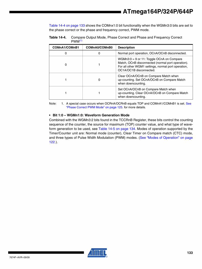
ATmega164P/324P/644P
Table 14-4 on page 133 shows the COMnx1:0 bit functionality when the WGMn3:0 bits are set tothe phase correct or the phase and frequency correct, PWM mode.
Note: 1. A special case occurs when OCRnA/OCRnB equals TOP and COMnA1/COMnB1 is set. See “Phase Correct PWM Mode” on page 125. for more details.
• Bit 1:0 – WGMn1:0: Waveform Generation ModeCombined with the WGMn3:2 bits found in the TCCRnB Register, these bits control the countingsequence of the counter, the source for maximum (TOP) counter value, and what type of wave-form generation to be used, see Table 14-5 on page 134. Modes of operation supported by theTimer/Counter unit are: Normal mode (counter), Clear Timer on Compare match (CTC) mode,and three types of Pulse Width Modulation (PWM) modes. (See “Modes of Operation” on page122.).
Table 14-4. Compare Output Mode, Phase Correct and Phase and Frequency Correct PWM(1)
COMnA1/COMnB1 COMnA0/COMnB0 Description
0 0 Normal port operation, OCnA/OCnB disconnected.
0 1
WGMn3:0 = 9 or 11: Toggle OCnA on Compare Match, OCnB disconnected (normal port operation). For all other WGM1 settings, normal port operation, OC1A/OC1B disconnected.
1 0Clear OCnA/OCnB on Compare Match when up-counting. Set OCnA/OCnB on Compare Match when downcounting.
1 1Set OCnA/OCnB on Compare Match when up-counting. Clear OCnA/OCnB on Compare Match when downcounting.
1337674F–AVR–09/09
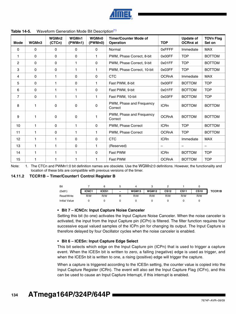
Note: 1. The CTCn and PWMn1:0 bit definition names are obsolete. Use the WGMn2:0 definitions. However, the functionality and location of these bits are compatible with previous versions of the timer.
14.11.2 TCCR1B – Timer/Counter1 Control Register B
• Bit 7 – ICNCn: Input Capture Noise CancelerSetting this bit (to one) activates the Input Capture Noise Canceler. When the noise canceler isactivated, the input from the Input Capture pin (ICPn) is filtered. The filter function requires foursuccessive equal valued samples of the ICPn pin for changing its output. The Input Capture istherefore delayed by four Oscillator cycles when the noise canceler is enabled.
• Bit 6 – ICESn: Input Capture Edge SelectThis bit selects which edge on the Input Capture pin (ICPn) that is used to trigger a captureevent. When the ICESn bit is written to zero, a falling (negative) edge is used as trigger, andwhen the ICESn bit is written to one, a rising (positive) edge will trigger the capture.
When a capture is triggered according to the ICESn setting, the counter value is copied into theInput Capture Register (ICRn). The event will also set the Input Capture Flag (ICFn), and thiscan be used to cause an Input Capture Interrupt, if this interrupt is enabled.
Table 14-5. Waveform Generation Mode Bit Description(1)
Mode WGMn3WGMn2(CTCn)
WGMn1(PWMn1)
WGMn0(PWMn0)
Timer/Counter Mode of Operation TOP
Update of OCRnx at
TOVn Flag Set on
0 0 0 0 0 Normal 0xFFFF Immediate MAX
1 0 0 0 1 PWM, Phase Correct, 8-bit 0x00FF TOP BOTTOM
2 0 0 1 0 PWM, Phase Correct, 9-bit 0x01FF TOP BOTTOM
3 0 0 1 1 PWM, Phase Correct, 10-bit 0x03FF TOP BOTTOM
4 0 1 0 0 CTC OCRnA Immediate MAX
5 0 1 0 1 Fast PWM, 8-bit 0x00FF BOTTOM TOP
6 0 1 1 0 Fast PWM, 9-bit 0x01FF BOTTOM TOP
7 0 1 1 1 Fast PWM, 10-bit 0x03FF BOTTOM TOP
8 1 0 0 0PWM, Phase and Frequency Correct
ICRn BOTTOM BOTTOM
9 1 0 0 1PWM, Phase and Frequency Correct
OCRnA BOTTOM BOTTOM
10 1 0 1 0 PWM, Phase Correct ICRn TOP BOTTOM
11 1 0 1 1 PWM, Phase Correct OCRnA TOP BOTTOM
12 1 1 0 0 CTC ICRn Immediate MAX
13 1 1 0 1 (Reserved) – – –
14 1 1 1 0 Fast PWM ICRn BOTTOM TOP
15 1 1 1 1 Fast PWM OCRnA BOTTOM TOP
Bit 7 6 5 4 3 2 1 0
(0x81) ICNC1 ICES1 – WGM13 WGM12 CS12 CS11 CS10 TCCR1B
Read/Write R/W R/W R R/W R/W R/W R/W R/W
Initial Value 0 0 0 0 0 0 0 0
1347674F–AVR–09/09
ATmega164P/324P/644P
ATmega164P/324P/644P
When the ICRn is used as TOP value (see description of the WGMn3:0 bits located in theTCCRnA and the TCCRnB Register), the ICPn is disconnected and consequently the Input Cap-ture function is disabled.
• Bit 5 – Reserved BitThis bit is reserved for future use. For ensuring compatibility with future devices, this bit must bewritten to zero when TCCRnB is written.
• Bit 4:3 – WGMn3:2: Waveform Generation ModeSee TCCRnA Register description.
• Bit 2:0 – CSn2:0: Clock SelectThe three Clock Select bits select the clock source to be used by the Timer/Counter, see Figure14-10 and Figure 14-11.
If external pin modes are used for the Timer/Countern, transitions on the Tn pin will clock thecounter even if the pin is configured as an output. This feature allows software control of thecounting.
14.11.3 TCCR1C – Timer/Counter1 Control Register C
• Bit 7 – FOCnA: Force Output Compare for Channel A
• Bit 6 – FOCnB: Force Output Compare for Channel BThe FOCnA/FOCnB bits are only active when the WGMn3:0 bits specifies a non-PWM mode.However, for ensuring compatibility with future devices, these bits must be set to zero whenTCCRnA is written when operating in a PWM mode. When writing a logical one to theFOCnA/FOCnB bit, an immediate compare match is forced on the Waveform Generation unit.The OCnA/OCnB output is changed according to its COMnx1:0 bits setting. Note that theFOCnA/FOCnB bits are implemented as strobes. Therefore it is the value present in theCOMnx1:0 bits that determine the effect of the forced compare.
Table 14-6. Clock Select Bit Description
CSn2 CSn1 CSn0 Description
0 0 0 No clock source (Timer/Counter stopped).
0 0 1 clkI/O/1 (No prescaling)
0 1 0 clkI/O/8 (From prescaler)
0 1 1 clkI/O/64 (From prescaler)
1 0 0 clkI/O/256 (From prescaler)
1 0 1 clkI/O/1024 (From prescaler)
1 1 0 External clock source on Tn pin. Clock on falling edge.
1 1 1 External clock source on Tn pin. Clock on rising edge.
Bit 7 6 5 4 3 2 1 0
(0x82) FOC1A FOC1B – – – – – – TCCR1C
Read/Write R/W R/W R R R R R R
Initial Value 0 0 0 0 0 0 0 0
1357674F–AVR–09/09
A FOCnA/FOCnB strobe will not generate any interrupt nor will it clear the timer in Clear Timeron Compare match (CTC) mode using OCRnA as TOP.
The FOCnA/FOCnB bits are always read as zero.
14.11.4 TCNT1H and TCNT1L –Timer/Counter1
The two Timer/Counter I/O locations (TCNTnH and TCNTnL, combined TCNTn) give directaccess, both for read and for write operations, to the Timer/Counter unit 16-bit counter. Toensure that both the high and low bytes are read and written simultaneously when the CPUaccesses these registers, the access is performed using an 8-bit temporary High Byte Register(TEMP). This temporary register is shared by all the other 16-bit registers. See “Accessing 16-bitRegisters” on page 112.
Modifying the counter (TCNTn) while the counter is running introduces a risk of missing a com-pare match between TCNTn and one of the OCRnx Registers.
Writing to the TCNTn Register blocks (removes) the compare match on the following timer clockfor all compare units.
14.11.5 OCR1AH and OCR1AL – Output Compare Register 1 A
14.11.6 OCR1BH and OCR1BL – Output Compare Register 1 B
The Output Compare Registers contain a 16-bit value that is continuously compared with thecounter value (TCNTn). A match can be used to generate an Output Compare interrupt, or togenerate a waveform output on the OCnx pin.
The Output Compare Registers are 16-bit in size. To ensure that both the high and low bytes arewritten simultaneously when the CPU writes to these registers, the access is performed using an8-bit temporary High Byte Register (TEMP). This temporary register is shared by all the other16-bit registers. See “Accessing 16-bit Registers” on page 112.
Bit 7 6 5 4 3 2 1 0
(0x85) TCNT1[15:8] TCNT1H
(0x84) TCNT1[7:0] TCNT1L
Read/Write R/W R/W R/W R/W R/W R/W R/W R/W
Initial Value 0 0 0 0 0 0 0 0
Bit 7 6 5 4 3 2 1 0
(0x89) OCR1A[15:8] OCR1AH
(0x88) OCR1A[7:0] OCR1AL
Read/Write R/W R/W R/W R/W R/W R/W R/W R/W
Initial Value 0 0 0 0 0 0 0 0
Bit 7 6 5 4 3 2 1 0
(0x8B) OCR1B[15:8] OCR1BH
(0x8A) OCR1B[7:0] OCR1BL
Read/Write R/W R/W R/W R/W R/W R/W R/W R/W
Initial Value 0 0 0 0 0 0 0 0
1367674F–AVR–09/09
ATmega164P/324P/644P
ATmega164P/324P/644P
14.11.7 ICR1H and ICR1L – Input Capture Register 1
The Input Capture is updated with the counter (TCNTn) value each time an event occurs on theICPn pin (or optionally on the Analog Comparator output for Timer/Counter1). The Input Capturecan be used for defining the counter TOP value.
The Input Capture Register is 16-bit in size. To ensure that both the high and low bytes are readsimultaneously when the CPU accesses these registers, the access is performed using an 8-bittemporary High Byte Register (TEMP). This temporary register is shared by all the other 16-bitregisters. See “Accessing 16-bit Registers” on page 112.
14.11.8 TIMSK1 – Timer/Counter1 Interrupt Mask Register
• Bit 7:6 – Res: Reserved BitsThese bits are unused bits in the ATmega164P/324P/644P, and will always read as zero.
• Bit 5 – ICIE1: Timer/Counter1, Input Capture Interrupt EnableWhen this bit is written to one, and the I-flag in the Status Register is set (interrupts globallyenabled), the Timer/Counter1 Input Capture interrupt is enabled. The corresponding InterruptVector (see “Interrupts” on page 60) is executed when the ICF1 Flag, located in TIFR1, is set.
• Bit 4:3 – Res: Reserved BitsThese bits are unused bits in the ATmega164P/324P/644P, and will always read as zero.
• Bit 2 – OCIE1B: Timer/Counter1, Output Compare B Match Interrupt EnableWhen this bit is written to one, and the I-flag in the Status Register is set (interrupts globallyenabled), the Timer/Counter1 Output Compare B Match interrupt is enabled. The correspondingInterrupt Vector (see “Interrupts” on page 60) is executed when the OCF1B Flag, located inTIFR1, is set.
• Bit 1 – OCIE1A: Timer/Counter1, Output Compare A Match Interrupt EnableWhen this bit is written to one, and the I-flag in the Status Register is set (interrupts globallyenabled), the Timer/Counter1 Output Compare A Match interrupt is enabled. The correspondingInterrupt Vector (see “Interrupts” on page 60) is executed when the OCF1A Flag, located inTIFR1, is set.
• Bit 0 – TOIE1: Timer/Counter1, Overflow Interrupt EnableWhen this bit is written to one, and the I-flag in the Status Register is set (interrupts globallyenabled), the Timer/Counter1 Overflow interrupt is enabled. The corresponding Interrupt Vector(See “Watchdog Timer” on page 54.) is executed when the TOV1 Flag, located in TIFR1, is set.
Bit 7 6 5 4 3 2 1 0
(0x87) ICR1[15:8] ICR1H
(0x86) ICR1[7:0] ICR1L
Read/Write R/W R/W R/W R/W R/W R/W R/W R/W
Initial Value 0 0 0 0 0 0 0 0
Bit 7 6 5 4 3 2 1 0
(0x6F) – – ICIE1 – – OCIE1B OCIE1A TOIE1 TIMSK1
Read/Write R R R/W R R R/W R/W R/W
Initial Value 0 0 0 0 0 0 0 0
1377674F–AVR–09/09
14.11.9 TIFR1 – Timer/Counter1 Interrupt Flag Register
• Bit 7:6 – Res: Reserved BitsThese bits are unused bits in the ATmega164P/324P/644P, and will always read as zero.
• Bit 5 – ICF1: Timer/Counter1, Input Capture FlagThis flag is set when a capture event occurs on the ICP1 pin. When the Input Capture Register(ICR1) is set by the WGMn3:0 to be used as the TOP value, the ICF1 Flag is set when the coun-ter reaches the TOP value.
ICF1 is automatically cleared when the Input Capture Interrupt Vector is executed. Alternatively,ICF1 can be cleared by writing a logic one to its bit location.
• Bit 4:3 – Res: Reserved BitsThese bits are unused bits in the ATmega164P/324P/644P, and will always read as zero.
• Bit 2 – OCF1B: Timer/Counter1, Output Compare B Match FlagThis flag is set in the timer clock cycle after the counter (TCNT1) value matches the OutputCompare Register B (OCR1B).
Note that a Forced Output Compare (FOC1B) strobe will not set the OCF1B Flag.
OCF1B is automatically cleared when the Output Compare Match B Interrupt Vector is exe-cuted. Alternatively, OCF1B can be cleared by writing a logic one to its bit location.
• Bit 1 – OCF1A: Timer/Counter1, Output Compare A Match FlagThis flag is set in the timer clock cycle after the counter (TCNT1) value matches the OutputCompare Register A (OCR1A).
Note that a Forced Output Compare (FOC1A) strobe will not set the OCF1A Flag.
OCF1A is automatically cleared when the Output Compare Match A Interrupt Vector is exe-cuted. Alternatively, OCF1A can be cleared by writing a logic one to its bit location.
• Bit 0 – TOV1: Timer/Counter1, Overflow FlagThe setting of this flag is dependent of the WGMn3:0 bits setting. In Normal and CTC modes,the TOV1 Flag is set when the timer overflows. Refer to Table 14-5 on page 134 for the TOV1Flag behavior when using another WGMn3:0 bit setting.
TOV1 is automatically cleared when the Timer/Counter1 Overflow Interrupt Vector is executed.Alternatively, TOV1 can be cleared by writing a logic one to its bit location.
Bit 7 6 5 4 3 2 1 0
0x16 (0x36) – – ICF1 – – OCF1B OCF1A TOV1 TIFR1
Read/Write R R R/W R R R/W R/W R/W
Initial Value 0 0 0 0 0 0 0 0
1387674F–AVR–09/09
ATmega164P/324P/644P
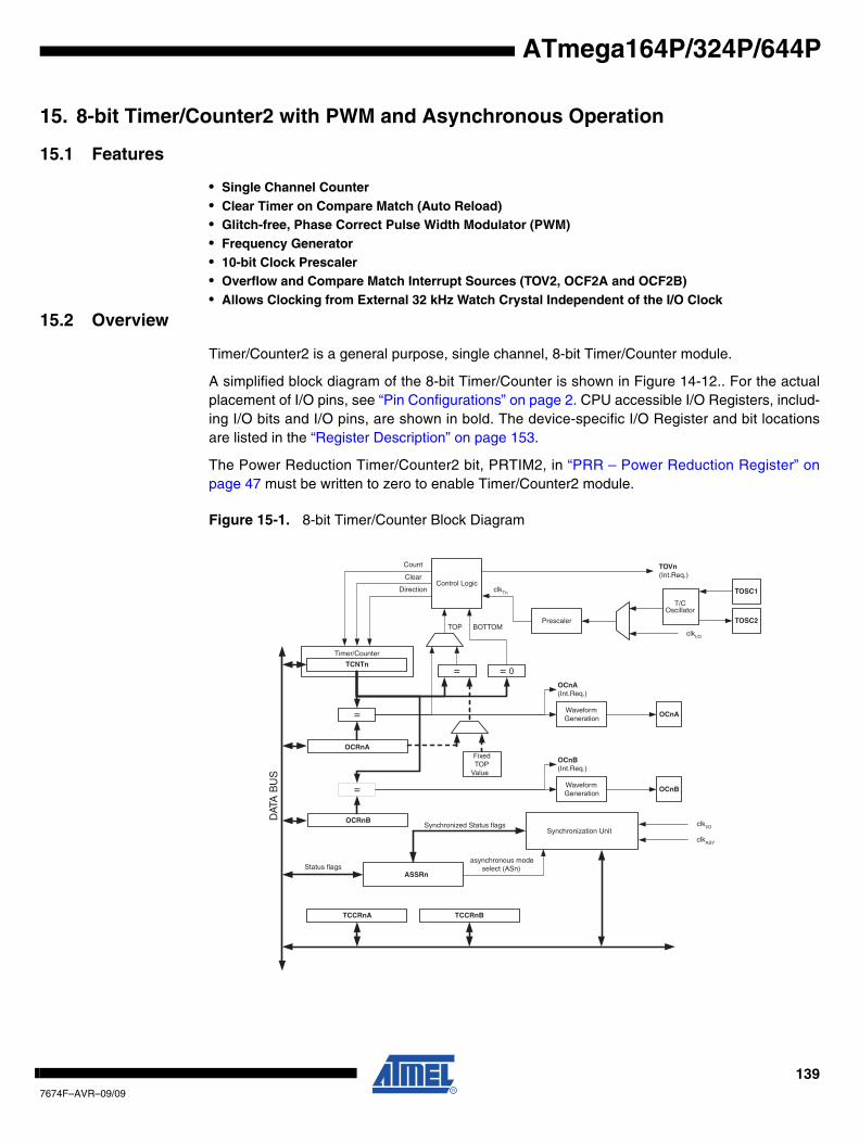
ATmega164P/324P/644P
15. 8-bit Timer/Counter2 with PWM and Asynchronous Operation
15.1 Features
• Single Channel Counter• Clear Timer on Compare Match (Auto Reload)• Glitch-free, Phase Correct Pulse Width Modulator (PWM)• Frequency Generator• 10-bit Clock Prescaler• Overflow and Compare Match Interrupt Sources (TOV2, OCF2A and OCF2B)• Allows Clocking from External 32 kHz Watch Crystal Independent of the I/O Clock
15.2 Overview
Timer/Counter2 is a general purpose, single channel, 8-bit Timer/Counter module.
A simplified block diagram of the 8-bit Timer/Counter is shown in Figure 14-12.. For the actualplacement of I/O pins, see “Pin Configurations” on page 2. CPU accessible I/O Registers, includ-ing I/O bits and I/O pins, are shown in bold. The device-specific I/O Register and bit locationsare listed in the “Register Description” on page 153.
The Power Reduction Timer/Counter2 bit, PRTIM2, in “PRR – Power Reduction Register” onpage 47 must be written to zero to enable Timer/Counter2 module.
Figure 15-1. 8-bit Timer/Counter Block Diagram
Timer/Counter
DAT
A B
US
OCRnA
OCRnB
=
=
TCNTn
WaveformGeneration
WaveformGeneration
OCnA
OCnB
=
FixedTOP
Value
Control Logic
= 0
TOP BOTTOM
Count
Clear
Direction
TOVn(Int.Req.)
OCnA(Int.Req.)
OCnB(Int.Req.)
TCCRnA TCCRnB
clkTn
ASSRn
Synchronization Unit
Prescaler
T/COscillator
clkI/O
clkASY
asynchronous mode select (ASn)
Synchronized Status flags
TOSC1
TOSC2
Status flags
clkI/O
1397674F–AVR–09/09
15.2.1 Registers
The Timer/Counter (TCNT2) and Output Compare Register (OCR2A and OCR2B) are 8-bit reg-isters. Interrupt request (abbreviated to Int.Req.) signals are all visible in the Timer Interrupt FlagRegister (TIFR2). All interrupts are individually masked with the Timer Interrupt Mask Register(TIMSK2). TIFR2 and TIMSK2 are not shown in the figure.
The Timer/Counter can be clocked internally, via the prescaler, or asynchronously clocked fromthe TOSC1/2 pins, as detailed later in this section. The asynchronous operation is controlled bythe Asynchronous Status Register (ASSR). The Clock Select logic block controls which clocksource the Timer/Counter uses to increment (or decrement) its value. The Timer/Counter is inac-tive when no clock source is selected. The output from the Clock Select logic is referred to as thetimer clock (clkT2).
The double buffered Output Compare Register (OCR2A and OCR2B) are compared with theTimer/Counter value at all times. The result of the compare can be used by the Waveform Gen-erator to generate a PWM or variable frequency output on the Output Compare pins (OC2A andOC2B). See “Output Compare Unit” on page 142. for details. The compare match event will alsoset the Compare Flag (OCF2A or OCF2B) which can be used to generate an Output Compareinterrupt request.
15.2.2 Definitions
Many register and bit references in this document are written in general form. A lower case “n”replaces the Timer/Counter number, in this case 2. However, when using the register or bitdefines in a program, the precise form must be used, i.e., TCNT2 for accessing Timer/Counter2counter value and so on.
The definitions in Table 15-1 are also used extensively throughout the section.
15.3 Timer/Counter Clock Sources
The Timer/Counter can be clocked by an internal synchronous or an external asynchronousclock source. The clock source clkT2 is by default equal to the MCU clock, clkI/O. When the AS2bit in the ASSR Register is written to logic one, the clock source is taken from the Timer/CounterOscillator connected to TOSC1 and TOSC2. For details on asynchronous operation, see “ASSR– Asynchronous Status Register” on page 158. For details on clock sources and prescaler, see“Timer/Counter Prescaler” on page 153.
Table 15-1. Definitions
BOTTOM The counter reaches the BOTTOM when it becomes zero (0x00).
MAX The counter reaches its MAXimum when it becomes 0xFF (decimal 255).
TOP The counter reaches the TOP when it becomes equal to the highest value in thecount sequence. The TOP value can be assigned to be the fixed value 0xFF(MAX) or the value stored in the OCR2A Register. The assignment is depen-dent on the mode of operation.
1407674F–AVR–09/09
ATmega164P/324P/644P
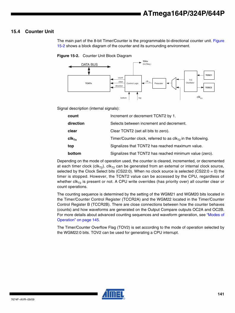
ATmega164P/324P/644P
15.4 Counter Unit
The main part of the 8-bit Timer/Counter is the programmable bi-directional counter unit. Figure15-2 shows a block diagram of the counter and its surrounding environment.
Figure 15-2. Counter Unit Block Diagram
Signal description (internal signals):
count Increment or decrement TCNT2 by 1.
direction Selects between increment and decrement.
clear Clear TCNT2 (set all bits to zero).
clkTn Timer/Counter clock, referred to as clkT2 in the following.
top Signalizes that TCNT2 has reached maximum value.
bottom Signalizes that TCNT2 has reached minimum value (zero).
Depending on the mode of operation used, the counter is cleared, incremented, or decrementedat each timer clock (clkT2). clkT2 can be generated from an external or internal clock source,selected by the Clock Select bits (CS22:0). When no clock source is selected (CS22:0 = 0) thetimer is stopped. However, the TCNT2 value can be accessed by the CPU, regardless ofwhether clkT2 is present or not. A CPU write overrides (has priority over) all counter clear orcount operations.
The counting sequence is determined by the setting of the WGM21 and WGM20 bits located inthe Timer/Counter Control Register (TCCR2A) and the WGM22 located in the Timer/CounterControl Register B (TCCR2B). There are close connections between how the counter behaves(counts) and how waveforms are generated on the Output Compare outputs OC2A and OC2B.For more details about advanced counting sequences and waveform generation, see “Modes ofOperation” on page 145.
The Timer/Counter Overflow Flag (TOV2) is set according to the mode of operation selected bythe WGM22:0 bits. TOV2 can be used for generating a CPU interrupt.
DATA BUS
TCNTn Control Logic
count
TOVn(Int.Req.)
topbottom
direction
clear
TOSC1
T/COscillator
TOSC2
Prescaler
clkI/O
clkTn
1417674F–AVR–09/09
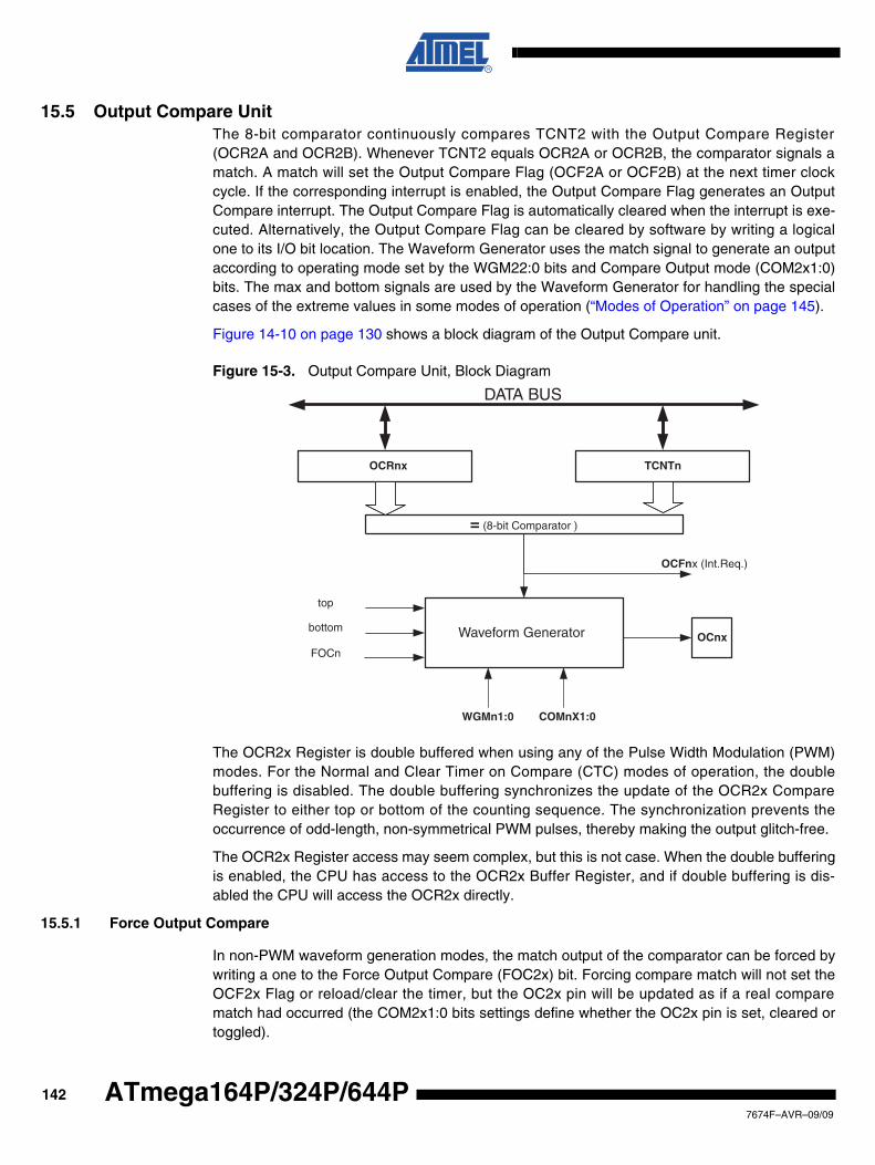
15.5 Output Compare UnitThe 8-bit comparator continuously compares TCNT2 with the Output Compare Register(OCR2A and OCR2B). Whenever TCNT2 equals OCR2A or OCR2B, the comparator signals amatch. A match will set the Output Compare Flag (OCF2A or OCF2B) at the next timer clockcycle. If the corresponding interrupt is enabled, the Output Compare Flag generates an OutputCompare interrupt. The Output Compare Flag is automatically cleared when the interrupt is exe-cuted. Alternatively, the Output Compare Flag can be cleared by software by writing a logicalone to its I/O bit location. The Waveform Generator uses the match signal to generate an outputaccording to operating mode set by the WGM22:0 bits and Compare Output mode (COM2x1:0)bits. The max and bottom signals are used by the Waveform Generator for handling the specialcases of the extreme values in some modes of operation (“Modes of Operation” on page 145).
Figure 14-10 on page 130 shows a block diagram of the Output Compare unit.
Figure 15-3. Output Compare Unit, Block Diagram
The OCR2x Register is double buffered when using any of the Pulse Width Modulation (PWM)modes. For the Normal and Clear Timer on Compare (CTC) modes of operation, the doublebuffering is disabled. The double buffering synchronizes the update of the OCR2x CompareRegister to either top or bottom of the counting sequence. The synchronization prevents theoccurrence of odd-length, non-symmetrical PWM pulses, thereby making the output glitch-free.
The OCR2x Register access may seem complex, but this is not case. When the double bufferingis enabled, the CPU has access to the OCR2x Buffer Register, and if double buffering is dis-abled the CPU will access the OCR2x directly.
15.5.1 Force Output Compare
In non-PWM waveform generation modes, the match output of the comparator can be forced bywriting a one to the Force Output Compare (FOC2x) bit. Forcing compare match will not set theOCF2x Flag or reload/clear the timer, but the OC2x pin will be updated as if a real comparematch had occurred (the COM2x1:0 bits settings define whether the OC2x pin is set, cleared ortoggled).
OCFnx (Int.Req.)
= (8-bit Comparator )
OCRnx
OCnx
DATA BUS
TCNTn
WGMn1:0
Waveform Generator
top
FOCn
COMnX1:0
bottom
1427674F–AVR–09/09
ATmega164P/324P/644P
ATmega164P/324P/644P
15.5.2 Compare Match Blocking by TCNT2 Write
All CPU write operations to the TCNT2 Register will block any compare match that occurs in thenext timer clock cycle, even when the timer is stopped. This feature allows OCR2x to be initial-ized to the same value as TCNT2 without triggering an interrupt when the Timer/Counter clock isenabled.
15.5.3 Using the Output Compare Unit
Since writing TCNT2 in any mode of operation will block all compare matches for one timer clockcycle, there are risks involved when changing TCNT2 when using the Output Compare channel,independently of whether the Timer/Counter is running or not. If the value written to TCNT2equals the OCR2x value, the compare match will be missed, resulting in incorrect waveformgeneration. Similarly, do not write the TCNT2 value equal to BOTTOM when the counter isdowncounting.
The setup of the OC2x should be performed before setting the Data Direction Register for theport pin to output. The easiest way of setting the OC2x value is to use the Force Output Com-pare (FOC2x) strobe bit in Normal mode. The OC2x Register keeps its value even whenchanging between Waveform Generation modes.
Be aware that the COM2x1:0 bits are not double buffered together with the compare value.Changing the COM2x1:0 bits will take effect immediately.
15.6 Compare Match Output Unit
The Compare Output mode (COM2x1:0) bits have two functions. The Waveform Generator usesthe COM2x1:0 bits for defining the Output Compare (OC2x) state at the next compare match.Also, the COM2x1:0 bits control the OC2x pin output source. Figure 15-4 shows a simplifiedschematic of the logic affected by the COM2x1:0 bit setting. The I/O Registers, I/O bits, and I/Opins in the figure are shown in bold. Only the parts of the general I/O Port Control Registers(DDR and PORT) that are affected by the COM2x1:0 bits are shown. When referring to theOC2x state, the reference is for the internal OC2x Register, not the OC2x pin.
1437674F–AVR–09/09
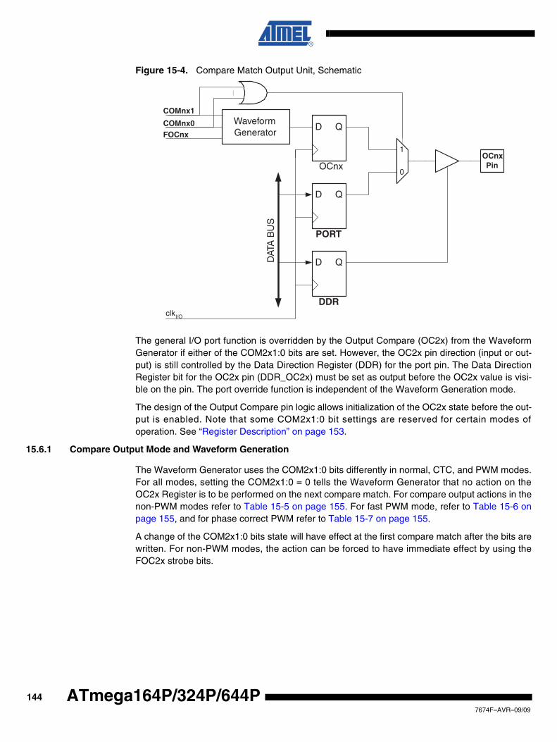
Figure 15-4. Compare Match Output Unit, Schematic
The general I/O port function is overridden by the Output Compare (OC2x) from the WaveformGenerator if either of the COM2x1:0 bits are set. However, the OC2x pin direction (input or out-put) is still controlled by the Data Direction Register (DDR) for the port pin. The Data DirectionRegister bit for the OC2x pin (DDR_OC2x) must be set as output before the OC2x value is visi-ble on the pin. The port override function is independent of the Waveform Generation mode.
The design of the Output Compare pin logic allows initialization of the OC2x state before the out-put is enabled. Note that some COM2x1:0 bit settings are reserved for certain modes ofoperation. See “Register Description” on page 153.
15.6.1 Compare Output Mode and Waveform Generation
The Waveform Generator uses the COM2x1:0 bits differently in normal, CTC, and PWM modes.For all modes, setting the COM2x1:0 = 0 tells the Waveform Generator that no action on theOC2x Register is to be performed on the next compare match. For compare output actions in thenon-PWM modes refer to Table 15-5 on page 155. For fast PWM mode, refer to Table 15-6 onpage 155, and for phase correct PWM refer to Table 15-7 on page 155.
A change of the COM2x1:0 bits state will have effect at the first compare match after the bits arewritten. For non-PWM modes, the action can be forced to have immediate effect by using theFOC2x strobe bits.
PORT
DDR
D Q
D Q
OCnxPinOCnx
D QWaveformGenerator
COMnx1
COMnx0
0
1
DAT
A B
US
FOCnx
clkI/O
1447674F–AVR–09/09
ATmega164P/324P/644P
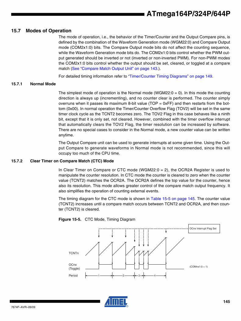
ATmega164P/324P/644P
15.7 Modes of OperationThe mode of operation, i.e., the behavior of the Timer/Counter and the Output Compare pins, isdefined by the combination of the Waveform Generation mode (WGM22:0) and Compare Outputmode (COM2x1:0) bits. The Compare Output mode bits do not affect the counting sequence,while the Waveform Generation mode bits do. The COM2x1:0 bits control whether the PWM out-put generated should be inverted or not (inverted or non-inverted PWM). For non-PWM modesthe COM2x1:0 bits control whether the output should be set, cleared, or toggled at a comparematch (See “Compare Match Output Unit” on page 143.).
For detailed timing information refer to “Timer/Counter Timing Diagrams” on page 149.
15.7.1 Normal Mode
The simplest mode of operation is the Normal mode (WGM22:0 = 0). In this mode the countingdirection is always up (incrementing), and no counter clear is performed. The counter simplyoverruns when it passes its maximum 8-bit value (TOP = 0xFF) and then restarts from the bot-tom (0x00). In normal operation the Timer/Counter Overflow Flag (TOV2) will be set in the sametimer clock cycle as the TCNT2 becomes zero. The TOV2 Flag in this case behaves like a ninthbit, except that it is only set, not cleared. However, combined with the timer overflow interruptthat automatically clears the TOV2 Flag, the timer resolution can be increased by software.There are no special cases to consider in the Normal mode, a new counter value can be writtenanytime.
The Output Compare unit can be used to generate interrupts at some given time. Using the Out-put Compare to generate waveforms in Normal mode is not recommended, since this willoccupy too much of the CPU time.
15.7.2 Clear Timer on Compare Match (CTC) Mode
In Clear Timer on Compare or CTC mode (WGM22:0 = 2), the OCR2A Register is used tomanipulate the counter resolution. In CTC mode the counter is cleared to zero when the countervalue (TCNT2) matches the OCR2A. The OCR2A defines the top value for the counter, hencealso its resolution. This mode allows greater control of the compare match output frequency. Italso simplifies the operation of counting external events.
The timing diagram for the CTC mode is shown in Table 15-5 on page 145. The counter value(TCNT2) increases until a compare match occurs between TCNT2 and OCR2A, and then coun-ter (TCNT2) is cleared.
Figure 15-5. CTC Mode, Timing Diagram
TCNTn
OCnx(Toggle)
OCnx Interrupt Flag Set
1 4Period 2 3
(COMnx1:0 = 1)
1457674F–AVR–09/09
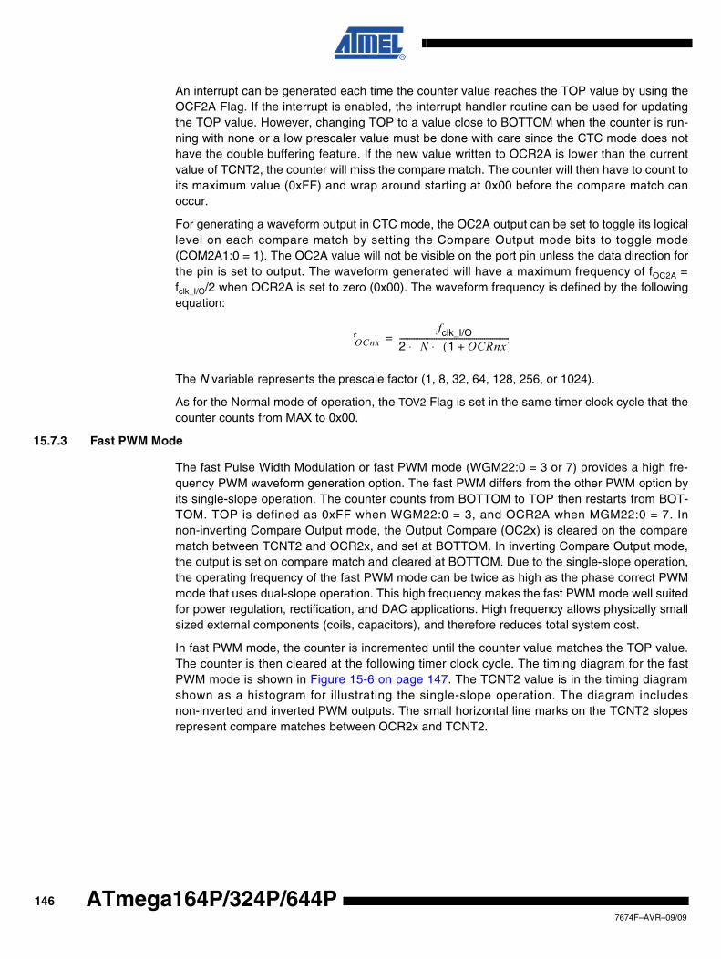
An interrupt can be generated each time the counter value reaches the TOP value by using theOCF2A Flag. If the interrupt is enabled, the interrupt handler routine can be used for updatingthe TOP value. However, changing TOP to a value close to BOTTOM when the counter is run-ning with none or a low prescaler value must be done with care since the CTC mode does nothave the double buffering feature. If the new value written to OCR2A is lower than the currentvalue of TCNT2, the counter will miss the compare match. The counter will then have to count toits maximum value (0xFF) and wrap around starting at 0x00 before the compare match canoccur.
For generating a waveform output in CTC mode, the OC2A output can be set to toggle its logicallevel on each compare match by setting the Compare Output mode bits to toggle mode(COM2A1:0 = 1). The OC2A value will not be visible on the port pin unless the data direction forthe pin is set to output. The waveform generated will have a maximum frequency of fOC2A =fclk_I/O/2 when OCR2A is set to zero (0x00). The waveform frequency is defined by the followingequation:
The N variable represents the prescale factor (1, 8, 32, 64, 128, 256, or 1024).
As for the Normal mode of operation, the TOV2 Flag is set in the same timer clock cycle that thecounter counts from MAX to 0x00.
15.7.3 Fast PWM Mode
The fast Pulse Width Modulation or fast PWM mode (WGM22:0 = 3 or 7) provides a high fre-quency PWM waveform generation option. The fast PWM differs from the other PWM option byits single-slope operation. The counter counts from BOTTOM to TOP then restarts from BOT-TOM. TOP is defined as 0xFF when WGM22:0 = 3, and OCR2A when MGM22:0 = 7. Innon-inverting Compare Output mode, the Output Compare (OC2x) is cleared on the comparematch between TCNT2 and OCR2x, and set at BOTTOM. In inverting Compare Output mode,the output is set on compare match and cleared at BOTTOM. Due to the single-slope operation,the operating frequency of the fast PWM mode can be twice as high as the phase correct PWMmode that uses dual-slope operation. This high frequency makes the fast PWM mode well suitedfor power regulation, rectification, and DAC applications. High frequency allows physically smallsized external components (coils, capacitors), and therefore reduces total system cost.
In fast PWM mode, the counter is incremented until the counter value matches the TOP value.The counter is then cleared at the following timer clock cycle. The timing diagram for the fastPWM mode is shown in Figure 15-6 on page 147. The TCNT2 value is in the timing diagramshown as a histogram for illustrating the single-slope operation. The diagram includesnon-inverted and inverted PWM outputs. The small horizontal line marks on the TCNT2 slopesrepresent compare matches between OCR2x and TCNT2.
fOCnxfclk_I/O
2 N 1 OCRnx+( )⋅ ⋅-------------------------------------------------------=
1467674F–AVR–09/09
ATmega164P/324P/644P
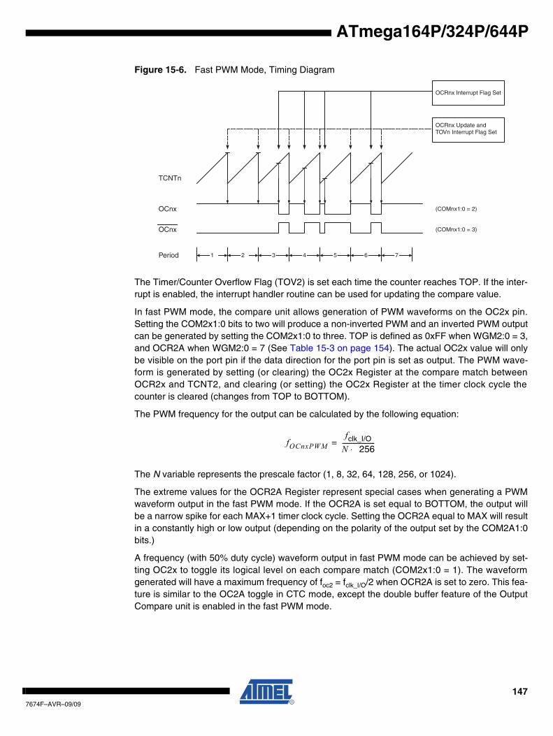
ATmega164P/324P/644P
Figure 15-6. Fast PWM Mode, Timing Diagram
The Timer/Counter Overflow Flag (TOV2) is set each time the counter reaches TOP. If the inter-rupt is enabled, the interrupt handler routine can be used for updating the compare value.
In fast PWM mode, the compare unit allows generation of PWM waveforms on the OC2x pin.Setting the COM2x1:0 bits to two will produce a non-inverted PWM and an inverted PWM outputcan be generated by setting the COM2x1:0 to three. TOP is defined as 0xFF when WGM2:0 = 3,and OCR2A when WGM2:0 = 7 (See Table 15-3 on page 154). The actual OC2x value will onlybe visible on the port pin if the data direction for the port pin is set as output. The PWM wave-form is generated by setting (or clearing) the OC2x Register at the compare match betweenOCR2x and TCNT2, and clearing (or setting) the OC2x Register at the timer clock cycle thecounter is cleared (changes from TOP to BOTTOM).
The PWM frequency for the output can be calculated by the following equation:
The N variable represents the prescale factor (1, 8, 32, 64, 128, 256, or 1024).
The extreme values for the OCR2A Register represent special cases when generating a PWMwaveform output in the fast PWM mode. If the OCR2A is set equal to BOTTOM, the output willbe a narrow spike for each MAX+1 timer clock cycle. Setting the OCR2A equal to MAX will resultin a constantly high or low output (depending on the polarity of the output set by the COM2A1:0bits.)
A frequency (with 50% duty cycle) waveform output in fast PWM mode can be achieved by set-ting OC2x to toggle its logical level on each compare match (COM2x1:0 = 1). The waveformgenerated will have a maximum frequency of foc2 = fclk_I/O/2 when OCR2A is set to zero. This fea-ture is similar to the OC2A toggle in CTC mode, except the double buffer feature of the OutputCompare unit is enabled in the fast PWM mode.
TCNTn
OCRnx Update andTOVn Interrupt Flag Set
1Period 2 3
OCnx
OCnx
(COMnx1:0 = 2)
(COMnx1:0 = 3)
OCRnx Interrupt Flag Set
4 5 6 7
fOCnxPWMfclk_I/O
N 256⋅---------------------=
1477674F–AVR–09/09
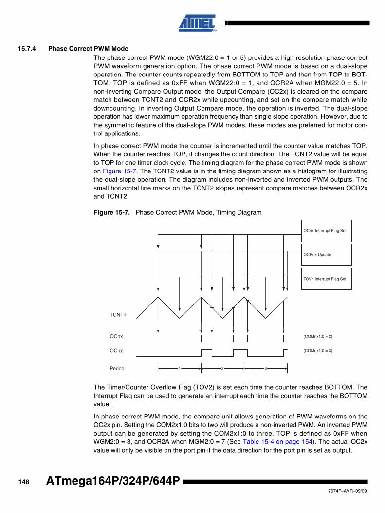
15.7.4 Phase Correct PWM ModeThe phase correct PWM mode (WGM22:0 = 1 or 5) provides a high resolution phase correctPWM waveform generation option. The phase correct PWM mode is based on a dual-slopeoperation. The counter counts repeatedly from BOTTOM to TOP and then from TOP to BOT-TOM. TOP is defined as 0xFF when WGM22:0 = 1, and OCR2A when MGM22:0 = 5. Innon-inverting Compare Output mode, the Output Compare (OC2x) is cleared on the comparematch between TCNT2 and OCR2x while upcounting, and set on the compare match whiledowncounting. In inverting Output Compare mode, the operation is inverted. The dual-slopeoperation has lower maximum operation frequency than single slope operation. However, due tothe symmetric feature of the dual-slope PWM modes, these modes are preferred for motor con-trol applications.
In phase correct PWM mode the counter is incremented until the counter value matches TOP.When the counter reaches TOP, it changes the count direction. The TCNT2 value will be equalto TOP for one timer clock cycle. The timing diagram for the phase correct PWM mode is shownon Figure 15-7. The TCNT2 value is in the timing diagram shown as a histogram for illustratingthe dual-slope operation. The diagram includes non-inverted and inverted PWM outputs. Thesmall horizontal line marks on the TCNT2 slopes represent compare matches between OCR2xand TCNT2.
Figure 15-7. Phase Correct PWM Mode, Timing Diagram
The Timer/Counter Overflow Flag (TOV2) is set each time the counter reaches BOTTOM. TheInterrupt Flag can be used to generate an interrupt each time the counter reaches the BOTTOMvalue.
In phase correct PWM mode, the compare unit allows generation of PWM waveforms on theOC2x pin. Setting the COM2x1:0 bits to two will produce a non-inverted PWM. An inverted PWMoutput can be generated by setting the COM2x1:0 to three. TOP is defined as 0xFF whenWGM2:0 = 3, and OCR2A when MGM2:0 = 7 (See Table 15-4 on page 154). The actual OC2xvalue will only be visible on the port pin if the data direction for the port pin is set as output.
TOVn Interrupt Flag Set
OCnx Interrupt Flag Set
1 2 3
TCNTn
Period
OCnx
OCnx
(COMnx1:0 = 2)
(COMnx1:0 = 3)
OCRnx Update
1487674F–AVR–09/09
ATmega164P/324P/644P
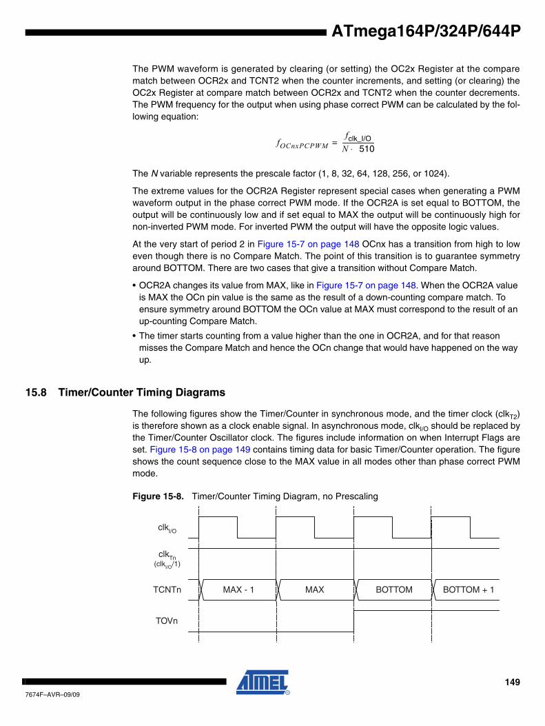
ATmega164P/324P/644P
The PWM waveform is generated by clearing (or setting) the OC2x Register at the comparematch between OCR2x and TCNT2 when the counter increments, and setting (or clearing) theOC2x Register at compare match between OCR2x and TCNT2 when the counter decrements.The PWM frequency for the output when using phase correct PWM can be calculated by the fol-lowing equation:
The N variable represents the prescale factor (1, 8, 32, 64, 128, 256, or 1024).
The extreme values for the OCR2A Register represent special cases when generating a PWMwaveform output in the phase correct PWM mode. If the OCR2A is set equal to BOTTOM, theoutput will be continuously low and if set equal to MAX the output will be continuously high fornon-inverted PWM mode. For inverted PWM the output will have the opposite logic values.
At the very start of period 2 in Figure 15-7 on page 148 OCnx has a transition from high to loweven though there is no Compare Match. The point of this transition is to guarantee symmetryaround BOTTOM. There are two cases that give a transition without Compare Match.
• OCR2A changes its value from MAX, like in Figure 15-7 on page 148. When the OCR2A value is MAX the OCn pin value is the same as the result of a down-counting compare match. To ensure symmetry around BOTTOM the OCn value at MAX must correspond to the result of an up-counting Compare Match.
• The timer starts counting from a value higher than the one in OCR2A, and for that reason misses the Compare Match and hence the OCn change that would have happened on the way up.
15.8 Timer/Counter Timing Diagrams
The following figures show the Timer/Counter in synchronous mode, and the timer clock (clkT2)is therefore shown as a clock enable signal. In asynchronous mode, clkI/O should be replaced bythe Timer/Counter Oscillator clock. The figures include information on when Interrupt Flags areset. Figure 15-8 on page 149 contains timing data for basic Timer/Counter operation. The figureshows the count sequence close to the MAX value in all modes other than phase correct PWMmode.
Figure 15-8. Timer/Counter Timing Diagram, no Prescaling
fOCnxPCPWMfclk_I/O
N 510⋅---------------------=
clkTn(clkI/O/1)
TOVn
clkI/O
TCNTn MAX - 1 MAX BOTTOM BOTTOM + 1
1497674F–AVR–09/09
Figure 15-9 on page 150 shows the same timing data, but with the prescaler enabled.
Figure 15-9. Timer/Counter Timing Diagram, with Prescaler (fclk_I/O/8)
Figure 15-10 on page 150 shows the setting of OCF2A in all modes except CTC mode.
Figure 15-10. Timer/Counter Timing Diagram, Setting of OCF2A, with Prescaler (fclk_I/O/8)
Figure 15-11 on page 151 shows the setting of OCF2A and the clearing of TCNT2 in CTC mode.
TOVn
TCNTn MAX - 1 MAX BOTTOM BOTTOM + 1
clkI/O
clkTn(clkI/O/8)
OCFnx
OCRnx
TCNTn
OCRnx Value
OCRnx - 1 OCRnx OCRnx + 1 OCRnx + 2
clkI/O
clkTn(clkI/O/8)
1507674F–AVR–09/09
ATmega164P/324P/644P
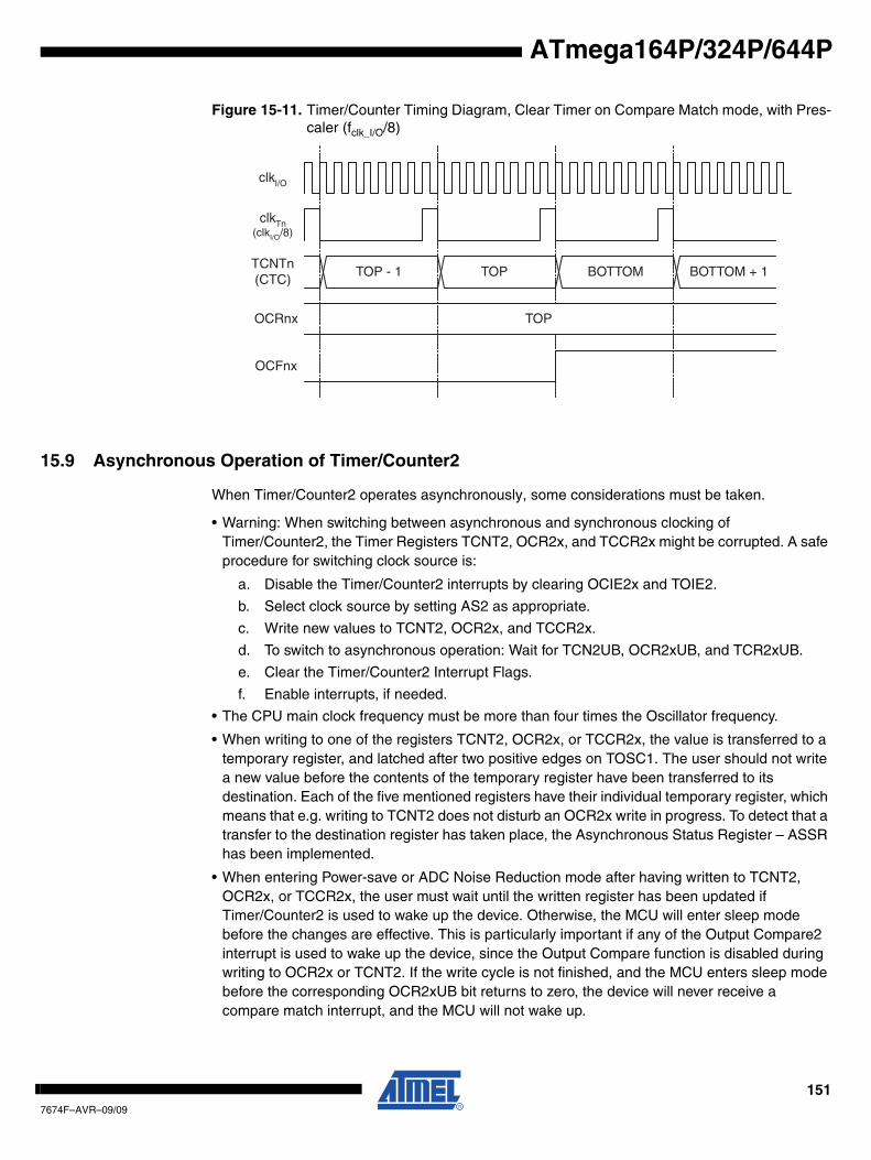
ATmega164P/324P/644P
Figure 15-11. Timer/Counter Timing Diagram, Clear Timer on Compare Match mode, with Pres-caler (fclk_I/O/8)
15.9 Asynchronous Operation of Timer/Counter2
When Timer/Counter2 operates asynchronously, some considerations must be taken.
• Warning: When switching between asynchronous and synchronous clocking of Timer/Counter2, the Timer Registers TCNT2, OCR2x, and TCCR2x might be corrupted. A safe procedure for switching clock source is:
a. Disable the Timer/Counter2 interrupts by clearing OCIE2x and TOIE2.
b. Select clock source by setting AS2 as appropriate.
c. Write new values to TCNT2, OCR2x, and TCCR2x.
d. To switch to asynchronous operation: Wait for TCN2UB, OCR2xUB, and TCR2xUB.
e. Clear the Timer/Counter2 Interrupt Flags.
f. Enable interrupts, if needed.
• The CPU main clock frequency must be more than four times the Oscillator frequency.
• When writing to one of the registers TCNT2, OCR2x, or TCCR2x, the value is transferred to a temporary register, and latched after two positive edges on TOSC1. The user should not write a new value before the contents of the temporary register have been transferred to its destination. Each of the five mentioned registers have their individual temporary register, which means that e.g. writing to TCNT2 does not disturb an OCR2x write in progress. To detect that a transfer to the destination register has taken place, the Asynchronous Status Register – ASSR has been implemented.
• When entering Power-save or ADC Noise Reduction mode after having written to TCNT2, OCR2x, or TCCR2x, the user must wait until the written register has been updated if Timer/Counter2 is used to wake up the device. Otherwise, the MCU will enter sleep mode before the changes are effective. This is particularly important if any of the Output Compare2 interrupt is used to wake up the device, since the Output Compare function is disabled during writing to OCR2x or TCNT2. If the write cycle is not finished, and the MCU enters sleep mode before the corresponding OCR2xUB bit returns to zero, the device will never receive a compare match interrupt, and the MCU will not wake up.
OCFnx
OCRnx
TCNTn(CTC)
TOP
TOP - 1 TOP BOTTOM BOTTOM + 1
clkI/O
clkTn(clkI/O/8)
1517674F–AVR–09/09
• If Timer/Counter2 is used to wake the device up from Power-save or ADC Noise Reduction mode, precautions must be taken if the user wants to re-enter one of these modes: The interrupt logic needs one TOSC1 cycle to be reset. If the time between wake-up and re-entering sleep mode is less than one TOSC1 cycle, the interrupt will not occur, and the device will fail to wake up. If the user is in doubt whether the time before re-entering Power-save or ADC Noise Reduction mode is sufficient, the following algorithm can be used to ensure that one TOSC1 cycle has elapsed:
a. Write a value to TCCR2x, TCNT2, or OCR2x.
b. Wait until the corresponding Update Busy Flag in ASSR returns to zero.
c. Enter Power-save or ADC Noise Reduction mode.
• When the asynchronous operation is selected, the 32.768 kHz Oscillator for Timer/Counter2 is always running, except in Power-down and Standby modes. After a Power-up Reset or wake-up from Power-down or Standby mode, the user should be aware of the fact that this Oscillator might take as long as one second to stabilize. The user is advised to wait for at least one second before using Timer/Counter2 after power-up or wake-up from Power-down or Standby mode. The contents of all Timer/Counter2 Registers must be considered lost after a wake-up from Power-down or Standby mode due to unstable clock signal upon start-up, no matter whether the Oscillator is in use or a clock signal is applied to the TOSC1 pin.
• Description of wake up from Power-save or ADC Noise Reduction mode when the timer is clocked asynchronously: When the interrupt condition is met, the wake up process is started on the following cycle of the timer clock, that is, the timer is always advanced by at least one before the processor can read the counter value. After wake-up, the MCU is halted for four cycles, it executes the interrupt routine, and resumes execution from the instruction following SLEEP.
• Reading of the TCNT2 Register shortly after wake-up from Power-save may give an incorrect result. Since TCNT2 is clocked on the asynchronous TOSC clock, reading TCNT2 must be done through a register synchronized to the internal I/O clock domain. Synchronization takes place for every rising TOSC1 edge. When waking up from Power-save mode, and the I/O clock (clkI/O) again becomes active, TCNT2 will read as the previous value (before entering sleep) until the next rising TOSC1 edge. The phase of the TOSC clock after waking up from Power-save mode is essentially unpredictable, as it depends on the wake-up time. The recommended procedure for reading TCNT2 is thus as follows:
a. Write any value to either of the registers OCR2x or TCCR2x.
b. Wait for the corresponding Update Busy Flag to be cleared.
c. Read TCNT2.
• During asynchronous operation, the synchronization of the Interrupt Flags for the asynchronous timer takes 3 processor cycles plus one timer cycle. The timer is therefore advanced by at least one before the processor can read the timer value causing the setting of the Interrupt Flag. The Output Compare pin is changed on the timer clock and is not synchronized to the processor clock.
1527674F–AVR–09/09
ATmega164P/324P/644P
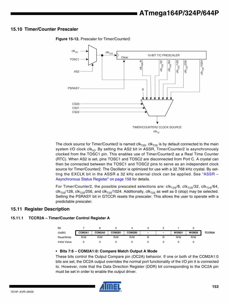
ATmega164P/324P/644P
15.10 Timer/Counter Prescaler
Figure 15-12. Prescaler for Timer/Counter2
The clock source for Timer/Counter2 is named clkT2S. clkT2S is by default connected to the mainsystem I/O clock clkIO. By setting the AS2 bit in ASSR, Timer/Counter2 is asynchronouslyclocked from the TOSC1 pin. This enables use of Timer/Counter2 as a Real Time Counter(RTC). When AS2 is set, pins TOSC1 and TOSC2 are disconnected from Port C. A crystal canthen be connected between the TOSC1 and TOSC2 pins to serve as an independent clocksource for Timer/Counter2. The Oscillator is optimized for use with a 32.768 kHz crystal. By set-ting the EXCLK bit in the ASSR a 32 kHz external clock can be applied. See “ASSR –Asynchronous Status Register” on page 158 for details.
For Timer/Counter2, the possible prescaled selections are: clkT2S/8, clkT2S/32, clkT2S/64,clkT2S/128, clkT2S/256, and clkT2S/1024. Additionally, clkT2S as well as 0 (stop) may be selected.Setting the PSRASY bit in GTCCR resets the prescaler. This allows the user to operate with apredictable prescaler.
15.11 Register Description
15.11.1 TCCR2A – Timer/Counter Control Register A
• Bits 7:6 – COM2A1:0: Compare Match Output A ModeThese bits control the Output Compare pin (OC2A) behavior. If one or both of the COM2A1:0bits are set, the OC2A output overrides the normal port functionality of the I/O pin it is connectedto. However, note that the Data Direction Register (DDR) bit corresponding to the OC2A pinmust be set in order to enable the output driver.
10-BIT T/C PRESCALER
TIMER/COUNTER2 CLOCK SOURCE
clkI/O clkT2S
TOSC1
AS2
CS20CS21CS22
clk T
2S/8
clk T
2S/6
4
clk T
2S/1
28
clk T
2S/1
024
clk T
2S/2
56
clk T
2S/3
2
0PSRASY
Clear
clkT2
Bit 7 6 5 4 3 2 1 0
(0xB0) COM2A1 COM2A0 COM2B1 COM2B0 – – WGM21 WGM20 TCCR2A
Read/Write R/W R/W R/W R/W R R R/W R/W
Initial Value 0 0 0 0 0 0 0 0
1537674F–AVR–09/09
When OC2A is connected to the pin, the function of the COM2A1:0 bits depends on theWGM22:0 bit setting. Table 15-2 shows the COM2A1:0 bit functionality when the WGM22:0 bitsare set to a normal or CTC mode (non-PWM).
Table 15-3 shows the COM2A1:0 bit functionality when the WGM21:0 bits are set to fast PWMmode.
Note: 1. A special case occurs when OCR2A equals TOP and COM2A1 is set. In this case, the Com-pare Match is ignored, but the set or clear is done at BOTTOM. See “Fast PWM Mode” on page 146 for more details.
Table 15-4 shows the COM2A1:0 bit functionality when the WGM22:0 bits are set to phase cor-rect PWM mode.
Note: 1. A special case occurs when OCR2A equals TOP and COM2A1 is set. In this case, the Com-pare Match is ignored, but the set or clear is done at TOP. See “Phase Correct PWM Mode” on page 148 for more details.
• Bits 5:4 – COM2B1:0: Compare Match Output B ModeThese bits control the Output Compare pin (OC2B) behavior. If one or both of the COM2B1:0bits are set, the OC2B output overrides the normal port functionality of the I/O pin it is connectedto. However, note that the Data Direction Register (DDR) bit corresponding to the OC2B pinmust be set in order to enable the output driver.
Table 15-2. Compare Output Mode, non-PWM Mode
COM2A1 COM2A0 Description
0 0 Normal port operation, OC0A disconnected.
0 1 Toggle OC2A on Compare Match
1 0 Clear OC2A on Compare Match
1 1 Set OC2A on Compare Match
Table 15-3. Compare Output Mode, Fast PWM Mode(1)
COM2A1 COM2A0 Description
0 0 Normal port operation, OC2A disconnected.
0 1WGM22 = 0: Normal Port Operation, OC0A Disconnected.WGM22 = 1: Toggle OC2A on Compare Match.
1 0Clear OC2A on Compare Match, set OC2A at BOTTOM,(non-inverting mode).
1 1Set OC2A on Compare Match, clear OC2A at BOTTOM,(inverting mode).
Table 15-4. Compare Output Mode, Phase Correct PWM Mode(1)
COM2A1 COM2A0 Description
0 0 Normal port operation, OC2A disconnected.
0 1WGM22 = 0: Normal Port Operation, OC2A Disconnected.WGM22 = 1: Toggle OC2A on Compare Match.
1 0Clear OC2A on Compare Match when up-counting. Set OC2A on Compare Match when down-counting.
1 1Set OC2A on Compare Match when up-counting. Clear OC2A on Compare Match when down-counting.
1547674F–AVR–09/09
ATmega164P/324P/644P
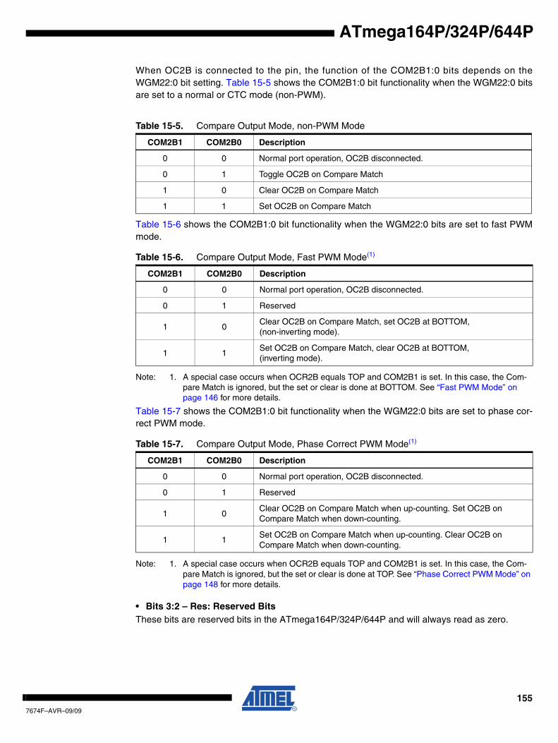
ATmega164P/324P/644P
When OC2B is connected to the pin, the function of the COM2B1:0 bits depends on theWGM22:0 bit setting. Table 15-5 shows the COM2B1:0 bit functionality when the WGM22:0 bitsare set to a normal or CTC mode (non-PWM).
Table 15-6 shows the COM2B1:0 bit functionality when the WGM22:0 bits are set to fast PWMmode.
Note: 1. A special case occurs when OCR2B equals TOP and COM2B1 is set. In this case, the Com-pare Match is ignored, but the set or clear is done at BOTTOM. See “Fast PWM Mode” on page 146 for more details.
Table 15-7 shows the COM2B1:0 bit functionality when the WGM22:0 bits are set to phase cor-rect PWM mode.
Note: 1. A special case occurs when OCR2B equals TOP and COM2B1 is set. In this case, the Com-pare Match is ignored, but the set or clear is done at TOP. See “Phase Correct PWM Mode” on page 148 for more details.
• Bits 3:2 – Res: Reserved BitsThese bits are reserved bits in the ATmega164P/324P/644P and will always read as zero.
Table 15-5. Compare Output Mode, non-PWM Mode
COM2B1 COM2B0 Description
0 0 Normal port operation, OC2B disconnected.
0 1 Toggle OC2B on Compare Match
1 0 Clear OC2B on Compare Match
1 1 Set OC2B on Compare Match
Table 15-6. Compare Output Mode, Fast PWM Mode(1)
COM2B1 COM2B0 Description
0 0 Normal port operation, OC2B disconnected.
0 1 Reserved
1 0Clear OC2B on Compare Match, set OC2B at BOTTOM,(non-inverting mode).
1 1Set OC2B on Compare Match, clear OC2B at BOTTOM,(inverting mode).
Table 15-7. Compare Output Mode, Phase Correct PWM Mode(1)
COM2B1 COM2B0 Description
0 0 Normal port operation, OC2B disconnected.
0 1 Reserved
1 0Clear OC2B on Compare Match when up-counting. Set OC2B on Compare Match when down-counting.
1 1Set OC2B on Compare Match when up-counting. Clear OC2B on Compare Match when down-counting.
1557674F–AVR–09/09
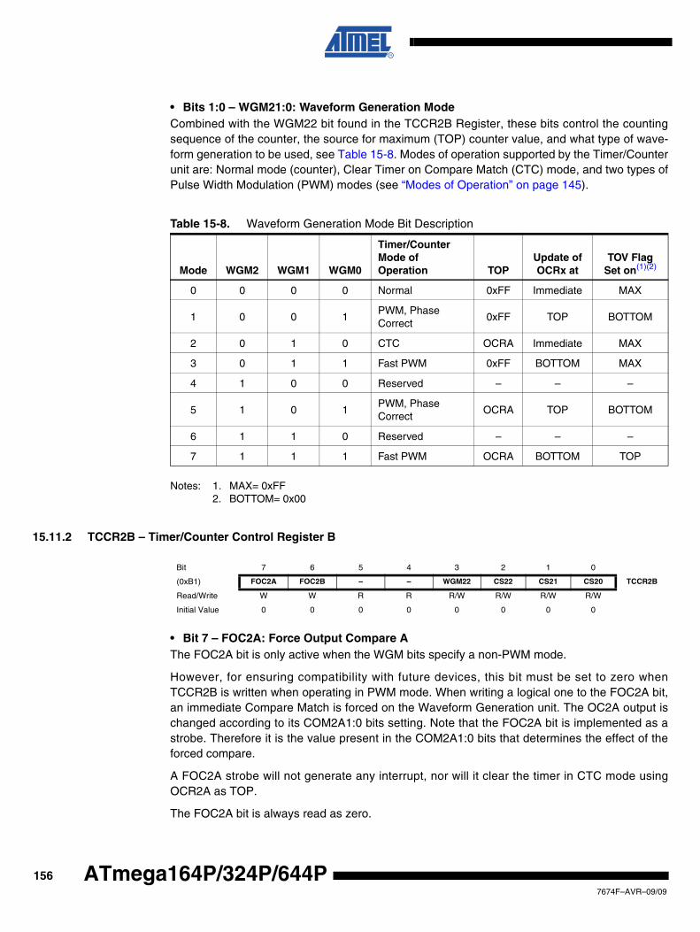
• Bits 1:0 – WGM21:0: Waveform Generation ModeCombined with the WGM22 bit found in the TCCR2B Register, these bits control the countingsequence of the counter, the source for maximum (TOP) counter value, and what type of wave-form generation to be used, see Table 15-8. Modes of operation supported by the Timer/Counterunit are: Normal mode (counter), Clear Timer on Compare Match (CTC) mode, and two types ofPulse Width Modulation (PWM) modes (see “Modes of Operation” on page 145).
Notes: 1. MAX= 0xFF2. BOTTOM= 0x00
15.11.2 TCCR2B – Timer/Counter Control Register B
• Bit 7 – FOC2A: Force Output Compare AThe FOC2A bit is only active when the WGM bits specify a non-PWM mode.
However, for ensuring compatibility with future devices, this bit must be set to zero whenTCCR2B is written when operating in PWM mode. When writing a logical one to the FOC2A bit,an immediate Compare Match is forced on the Waveform Generation unit. The OC2A output ischanged according to its COM2A1:0 bits setting. Note that the FOC2A bit is implemented as astrobe. Therefore it is the value present in the COM2A1:0 bits that determines the effect of theforced compare.
A FOC2A strobe will not generate any interrupt, nor will it clear the timer in CTC mode usingOCR2A as TOP.
The FOC2A bit is always read as zero.
Table 15-8. Waveform Generation Mode Bit Description
Mode WGM2 WGM1 WGM0
Timer/Counter Mode of Operation TOP
Update ofOCRx at
TOV FlagSet on(1)(2)
0 0 0 0 Normal 0xFF Immediate MAX
1 0 0 1PWM, Phase Correct
0xFF TOP BOTTOM
2 0 1 0 CTC OCRA Immediate MAX
3 0 1 1 Fast PWM 0xFF BOTTOM MAX
4 1 0 0 Reserved – – –
5 1 0 1PWM, Phase Correct
OCRA TOP BOTTOM
6 1 1 0 Reserved – – –
7 1 1 1 Fast PWM OCRA BOTTOM TOP
Bit 7 6 5 4 3 2 1 0
(0xB1) FOC2A FOC2B – – WGM22 CS22 CS21 CS20 TCCR2B
Read/Write W W R R R/W R/W R/W R/W
Initial Value 0 0 0 0 0 0 0 0
1567674F–AVR–09/09
ATmega164P/324P/644P
ATmega164P/324P/644P
• Bit 6 – FOC2B: Force Output Compare BThe FOC2B bit is only active when the WGM bits specify a non-PWM mode.
However, for ensuring compatibility with future devices, this bit must be set to zero whenTCCR2B is written when operating in PWM mode. When writing a logical one to the FOC2B bit,an immediate Compare Match is forced on the Waveform Generation unit. The OC2B output ischanged according to its COM2B1:0 bits setting. Note that the FOC2B bit is implemented as astrobe. Therefore it is the value present in the COM2B1:0 bits that determines the effect of theforced compare.
A FOC2B strobe will not generate any interrupt, nor will it clear the timer in CTC mode usingOCR2B as TOP.
The FOC2B bit is always read as zero.
• Bits 5:4 – Res: Reserved BitsThese bits are reserved bits in the ATmega164P/324P/644P and will always read as zero.
• Bit 3 – WGM22: Waveform Generation ModeSee the description in the “TCCR2A – Timer/Counter Control Register A” on page 153.
• Bit 2:0 – CS22:0: Clock SelectThe three Clock Select bits select the clock source to be used by the Timer/Counter, see Table15-9 on page 157.
If external pin modes are used for the Timer/Counter0, transitions on the T0 pin will clock thecounter even if the pin is configured as an output. This feature allows software control of thecounting.
15.11.3 TCNT2 – Timer/Counter Register
The Timer/Counter Register gives direct access, both for read and write operations, to theTimer/Counter unit 8-bit counter. Writing to the TCNT2 Register blocks (removes) the Compare
Table 15-9. Clock Select Bit Description
CS22 CS21 CS20 Description
0 0 0 No clock source (Timer/Counter stopped).
0 0 1 clkT2S/(No prescaling)
0 1 0 clkT2S/8 (From prescaler)
0 1 1 clkT2S/32 (From prescaler)
1 0 0 clkT2S/64 (From prescaler)
1 0 1 clkT2S/128 (From prescaler)
1 1 0 clkT2S/256 (From prescaler)
1 1 1 clkT2S/1024 (From prescaler)
Bit 7 6 5 4 3 2 1 0
(0xB2) TCNT2[7:0] TCNT2
Read/Write R/W R/W R/W R/W R/W R/W R/W R/W
Initial Value 0 0 0 0 0 0 0 0
1577674F–AVR–09/09
Match on the following timer clock. Modifying the counter (TCNT2) while the counter is running,introduces a risk of missing a Compare Match between TCNT2 and the OCR2x Registers.
15.11.4 OCR2A – Output Compare Register A
The Output Compare Register A contains an 8-bit value that is continuously compared with thecounter value (TCNT2). A match can be used to generate an Output Compare interrupt, or togenerate a waveform output on the OC2A pin.
15.11.5 OCR2B – Output Compare Register B
The Output Compare Register B contains an 8-bit value that is continuously compared with thecounter value (TCNT2). A match can be used to generate an Output Compare interrupt, or togenerate a waveform output on the OC2B pin.
15.11.6 ASSR – Asynchronous Status Register
• Bit 6 – EXCLK: Enable External Clock InputWhen EXCLK is written to one, and asynchronous clock is selected, the external clock input buf-fer is enabled and an external clock can be input on Timer Oscillator 1 (TOSC1) pin instead of a32 kHz crystal. Writing to EXCLK should be done before asynchronous operation is selected.Note that the crystal Oscillator will only run when this bit is zero.
• Bit 5 – AS2: Asynchronous Timer/Counter2When AS2 is written to zero, Timer/Counter2 is clocked from the I/O clock, clkI/O. When AS2 iswritten to one, Timer/Counter2 is clocked from a crystal Oscillator connected to the Timer Oscil-lator 1 (TOSC1) pin. When the value of AS2 is changed, the contents of TCNT2, OCR2A,OCR2B, TCCR2A and TCCR2B might be corrupted.
• Bit 4 – TCN2UB: Timer/Counter2 Update BusyWhen Timer/Counter2 operates asynchronously and TCNT2 is written, this bit becomes set.When TCNT2 has been updated from the temporary storage register, this bit is cleared by hard-ware. A logical zero in this bit indicates that TCNT2 is ready to be updated with a new value.
• Bit 3 – OCR2AUB: Output Compare Register2 Update BusyWhen Timer/Counter2 operates asynchronously and OCR2A is written, this bit becomes set.When OCR2A has been updated from the temporary storage register, this bit is cleared by hard-ware. A logical zero in this bit indicates that OCR2A is ready to be updated with a new value.
Bit 7 6 5 4 3 2 1 0
(0xB3) OCR2A[7:0] OCR2A
Read/Write R/W R/W R/W R/W R/W R/W R/W R/W
Initial Value 0 0 0 0 0 0 0 0
Bit 7 6 5 4 3 2 1 0
(0xB4) OCR2B[7:0] OCR2B
Read/Write R/W R/W R/W R/W R/W R/W R/W R/W
Initial Value 0 0 0 0 0 0 0 0
Bit 7 6 5 4 3 2 1 0
(0xB6) – EXCLK AS2 TCN2UB OCR2AUB OCR2BUB TCR2AUB TCR2BUB ASSR
Read/Write R R/W R/W R R R R R
Initial Value 0 0 0 0 0 0 0 0
1587674F–AVR–09/09
ATmega164P/324P/644P
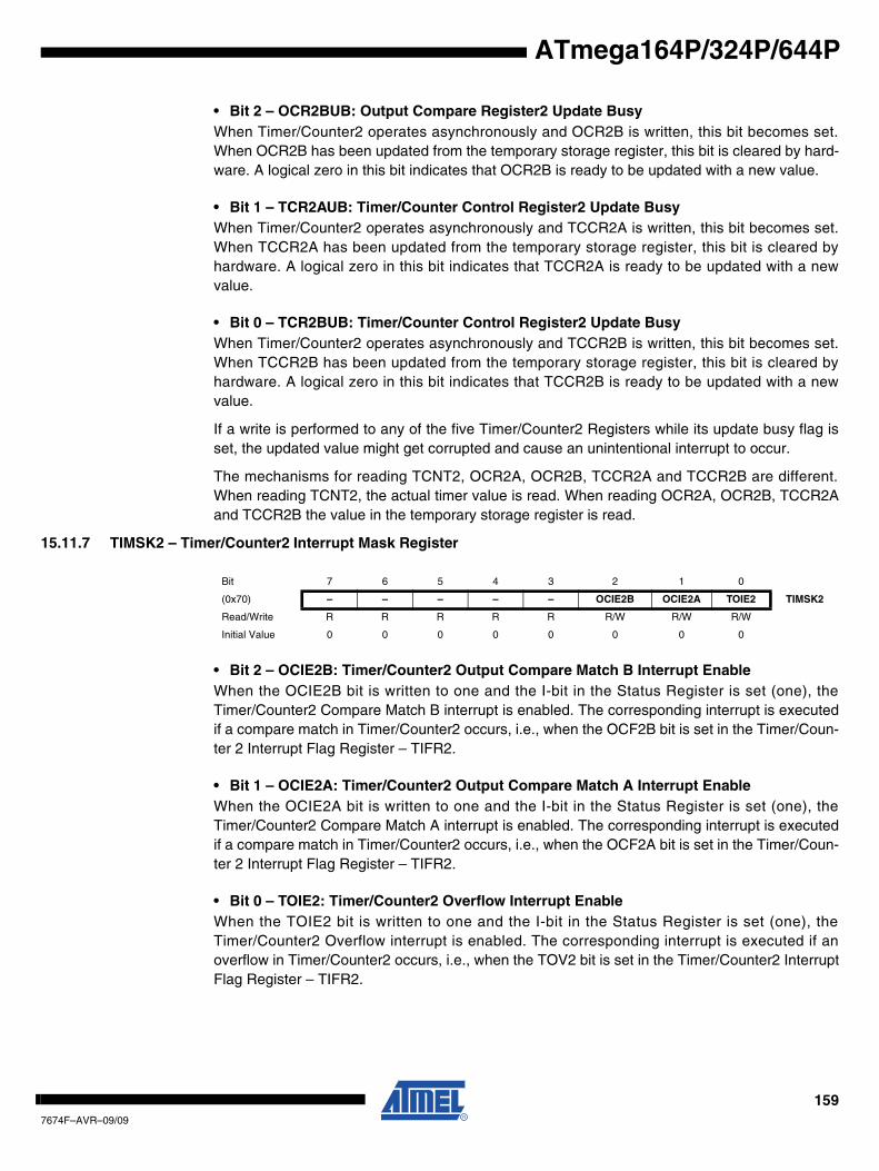
ATmega164P/324P/644P
• Bit 2 – OCR2BUB: Output Compare Register2 Update BusyWhen Timer/Counter2 operates asynchronously and OCR2B is written, this bit becomes set.When OCR2B has been updated from the temporary storage register, this bit is cleared by hard-ware. A logical zero in this bit indicates that OCR2B is ready to be updated with a new value.
• Bit 1 – TCR2AUB: Timer/Counter Control Register2 Update BusyWhen Timer/Counter2 operates asynchronously and TCCR2A is written, this bit becomes set.When TCCR2A has been updated from the temporary storage register, this bit is cleared byhardware. A logical zero in this bit indicates that TCCR2A is ready to be updated with a newvalue.
• Bit 0 – TCR2BUB: Timer/Counter Control Register2 Update BusyWhen Timer/Counter2 operates asynchronously and TCCR2B is written, this bit becomes set.When TCCR2B has been updated from the temporary storage register, this bit is cleared byhardware. A logical zero in this bit indicates that TCCR2B is ready to be updated with a newvalue.
If a write is performed to any of the five Timer/Counter2 Registers while its update busy flag isset, the updated value might get corrupted and cause an unintentional interrupt to occur.
The mechanisms for reading TCNT2, OCR2A, OCR2B, TCCR2A and TCCR2B are different.When reading TCNT2, the actual timer value is read. When reading OCR2A, OCR2B, TCCR2Aand TCCR2B the value in the temporary storage register is read.
15.11.7 TIMSK2 – Timer/Counter2 Interrupt Mask Register
• Bit 2 – OCIE2B: Timer/Counter2 Output Compare Match B Interrupt EnableWhen the OCIE2B bit is written to one and the I-bit in the Status Register is set (one), theTimer/Counter2 Compare Match B interrupt is enabled. The corresponding interrupt is executedif a compare match in Timer/Counter2 occurs, i.e., when the OCF2B bit is set in the Timer/Coun-ter 2 Interrupt Flag Register – TIFR2.
• Bit 1 – OCIE2A: Timer/Counter2 Output Compare Match A Interrupt EnableWhen the OCIE2A bit is written to one and the I-bit in the Status Register is set (one), theTimer/Counter2 Compare Match A interrupt is enabled. The corresponding interrupt is executedif a compare match in Timer/Counter2 occurs, i.e., when the OCF2A bit is set in the Timer/Coun-ter 2 Interrupt Flag Register – TIFR2.
• Bit 0 – TOIE2: Timer/Counter2 Overflow Interrupt EnableWhen the TOIE2 bit is written to one and the I-bit in the Status Register is set (one), theTimer/Counter2 Overflow interrupt is enabled. The corresponding interrupt is executed if anoverflow in Timer/Counter2 occurs, i.e., when the TOV2 bit is set in the Timer/Counter2 InterruptFlag Register – TIFR2.
Bit 7 6 5 4 3 2 1 0
(0x70) – – – – – OCIE2B OCIE2A TOIE2 TIMSK2
Read/Write R R R R R R/W R/W R/W
Initial Value 0 0 0 0 0 0 0 0
1597674F–AVR–09/09
15.11.8 TIFR2 – Timer/Counter2 Interrupt Flag Register
• Bit 2 – OCF2B: Output Compare Flag 2 BThe OCF2B bit is set (one) when a compare match occurs between the Timer/Counter2 and thedata in OCR2B – Output Compare Register2. OCF2B is cleared by hardware when executingthe corresponding interrupt handling vector. Alternatively, OCF2B is cleared by writing a logicone to the flag. When the I-bit in SREG, OCIE2B (Timer/Counter2 Compare match InterruptEnable), and OCF2B are set (one), the Timer/Counter2 Compare match Interrupt is executed.
• Bit 1 – OCF2A: Output Compare Flag 2 AThe OCF2A bit is set (one) when a compare match occurs between the Timer/Counter2 and thedata in OCR2A – Output Compare Register2. OCF2A is cleared by hardware when executingthe corresponding interrupt handling vector. Alternatively, OCF2A is cleared by writing a logicone to the flag. When the I-bit in SREG, OCIE2A (Timer/Counter2 Compare match InterruptEnable), and OCF2A are set (one), the Timer/Counter2 Compare match Interrupt is executed.
• Bit 0 – TOV2: Timer/Counter2 Overflow FlagThe TOV2 bit is set (one) when an overflow occurs in Timer/Counter2. TOV2 is cleared by hard-ware when executing the corresponding interrupt handling vector. Alternatively, TOV2 is clearedby writing a logic one to the flag. When the SREG I-bit, TOIE2A (Timer/Counter2 Overflow Inter-rupt Enable), and TOV2 are set (one), the Timer/Counter2 Overflow interrupt is executed. InPWM mode, this bit is set when Timer/Counter2 changes counting direction at 0x00.
15.11.9 GTCCR – General Timer/Counter Control Register
• Bit 1 – PSRASY: Prescaler Reset Timer/Counter2When this bit is one, the Timer/Counter2 prescaler will be reset. This bit is normally clearedimmediately by hardware. If the bit is written when Timer/Counter2 is operating in asynchronousmode, the bit will remain one until the prescaler has been reset. The bit will not be cleared byhardware if the TSM bit is set. Refer to the description of the “Bit 7 – TSM: Timer/Counter Syn-chronization Mode” on page 136 for a description of the Timer/Counter Synchronization mode.
Bit 7 6 5 4 3 2 1 0
0x17 (0x37) – – – – – OCF2B OCF2A TOV2 TIFR2
Read/Write R R R R R R/W R/W R/W
Initial Value 0 0 0 0 0 0 0 0
Bit 7 6 5 4 3 2 1 0
0x23 (0x43) TSM – – – – – PSRASY PSRSYNC GTCCR
Read/Write R/W R R R R R R/W R/W
Initial Value 0 0 0 0 0 0 0 0
1607674F–AVR–09/09
ATmega164P/324P/644P
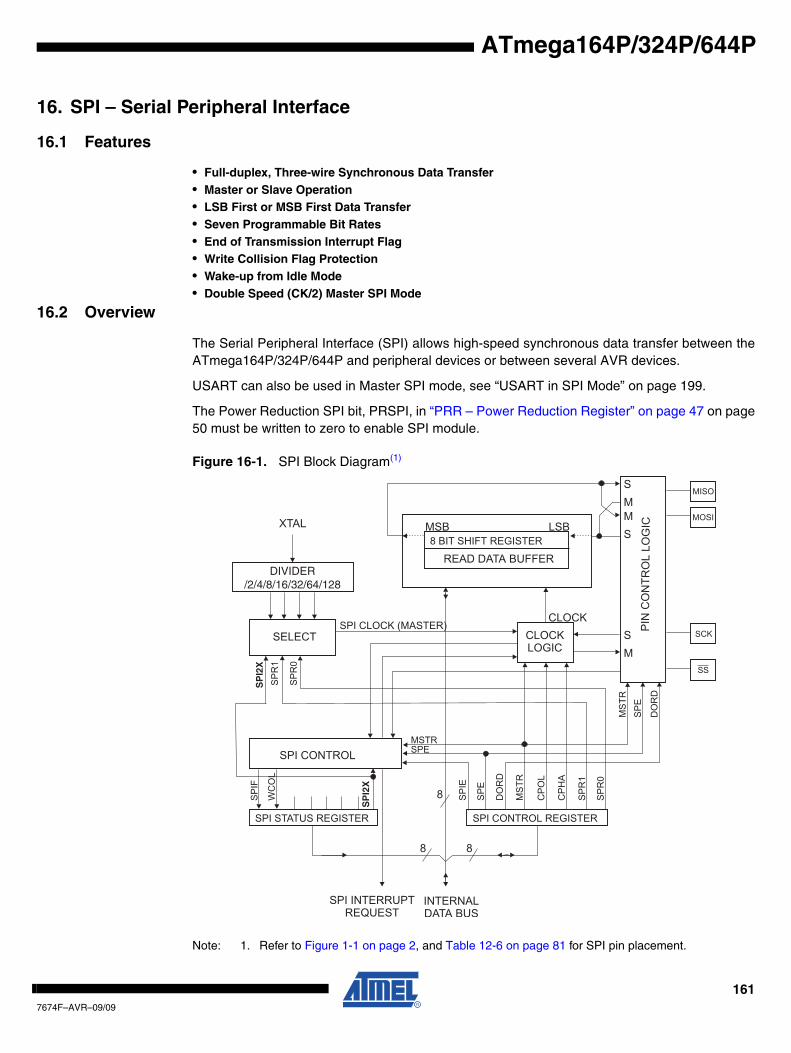
ATmega164P/324P/644P
16. SPI – Serial Peripheral Interface
16.1 Features
• Full-duplex, Three-wire Synchronous Data Transfer• Master or Slave Operation• LSB First or MSB First Data Transfer• Seven Programmable Bit Rates• End of Transmission Interrupt Flag• Write Collision Flag Protection• Wake-up from Idle Mode• Double Speed (CK/2) Master SPI Mode
16.2 Overview
The Serial Peripheral Interface (SPI) allows high-speed synchronous data transfer between theATmega164P/324P/644P and peripheral devices or between several AVR devices.
USART can also be used in Master SPI mode, see “USART in SPI Mode” on page 199.
The Power Reduction SPI bit, PRSPI, in “PRR – Power Reduction Register” on page 47 on page50 must be written to zero to enable SPI module.
Figure 16-1. SPI Block Diagram(1)
Note: 1. Refer to Figure 1-1 on page 2, and Table 12-6 on page 81 for SPI pin placement.
SP
I2X
SP
I2X
DIVIDER/2/4/8/16/32/64/128
1617674F–AVR–09/09
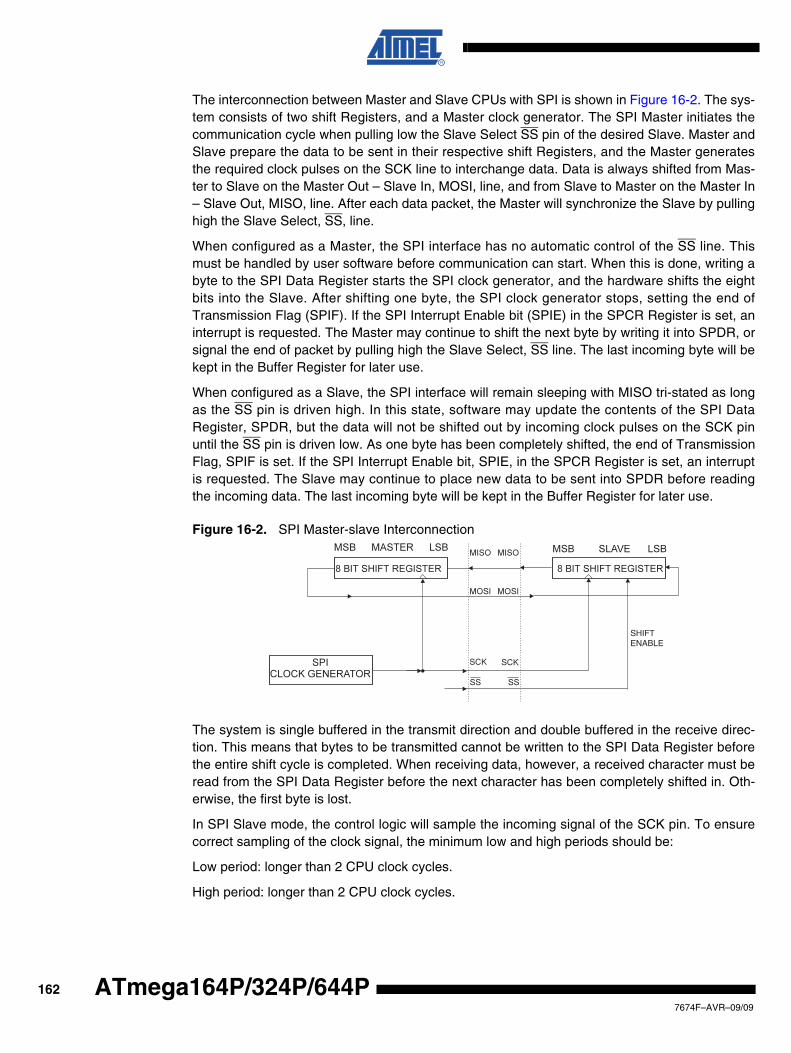
The interconnection between Master and Slave CPUs with SPI is shown in Figure 16-2. The sys-tem consists of two shift Registers, and a Master clock generator. The SPI Master initiates thecommunication cycle when pulling low the Slave Select SS pin of the desired Slave. Master andSlave prepare the data to be sent in their respective shift Registers, and the Master generatesthe required clock pulses on the SCK line to interchange data. Data is always shifted from Mas-ter to Slave on the Master Out – Slave In, MOSI, line, and from Slave to Master on the Master In– Slave Out, MISO, line. After each data packet, the Master will synchronize the Slave by pullinghigh the Slave Select, SS, line.
When configured as a Master, the SPI interface has no automatic control of the SS line. Thismust be handled by user software before communication can start. When this is done, writing abyte to the SPI Data Register starts the SPI clock generator, and the hardware shifts the eightbits into the Slave. After shifting one byte, the SPI clock generator stops, setting the end ofTransmission Flag (SPIF). If the SPI Interrupt Enable bit (SPIE) in the SPCR Register is set, aninterrupt is requested. The Master may continue to shift the next byte by writing it into SPDR, orsignal the end of packet by pulling high the Slave Select, SS line. The last incoming byte will bekept in the Buffer Register for later use.
When configured as a Slave, the SPI interface will remain sleeping with MISO tri-stated as longas the SS pin is driven high. In this state, software may update the contents of the SPI DataRegister, SPDR, but the data will not be shifted out by incoming clock pulses on the SCK pinuntil the SS pin is driven low. As one byte has been completely shifted, the end of TransmissionFlag, SPIF is set. If the SPI Interrupt Enable bit, SPIE, in the SPCR Register is set, an interruptis requested. The Slave may continue to place new data to be sent into SPDR before readingthe incoming data. The last incoming byte will be kept in the Buffer Register for later use.
Figure 16-2. SPI Master-slave Interconnection
The system is single buffered in the transmit direction and double buffered in the receive direc-tion. This means that bytes to be transmitted cannot be written to the SPI Data Register beforethe entire shift cycle is completed. When receiving data, however, a received character must beread from the SPI Data Register before the next character has been completely shifted in. Oth-erwise, the first byte is lost.
In SPI Slave mode, the control logic will sample the incoming signal of the SCK pin. To ensurecorrect sampling of the clock signal, the minimum low and high periods should be:
Low period: longer than 2 CPU clock cycles.
High period: longer than 2 CPU clock cycles.
SHIFTENABLE
1627674F–AVR–09/09
ATmega164P/324P/644P
ATmega164P/324P/644P
When the SPI is enabled, the data direction of the MOSI, MISO, SCK, and SS pins is overriddenaccording to Table 16-1. For more details on automatic port overrides, refer to “Alternate PortFunctions” on page 77.
Note: 1. See “Alternate Functions of Port B” on page 81 for a detailed description of how to define the direction of the user defined SPI pins.
The following code examples show how to initialize the SPI as a Master and how to perform asimple transmission. DDR_SPI in the examples must be replaced by the actual Data DirectionRegister controlling the SPI pins. DD_MOSI, DD_MISO and DD_SCK must be replaced by theactual data direction bits for these pins. E.g. if MOSI is placed on pin PB5, replace DD_MOSIwith DDB5 and DDR_SPI with DDRB.
Table 16-1. SPI Pin Overrides(1)
Pin Direction, Master SPI Direction, Slave SPI
MOSI User Defined Input
MISO Input User Defined
SCK User Defined Input
SS User Defined Input
1637674F–AVR–09/09
Note: 1. See “About Code Examples” on page 8.
Assembly Code Example(1)
SPI_MasterInit:
; Set MOSI and SCK output, all others input
ldi r17,(1<<DD_MOSI)|(1<<DD_SCK)
out DDR_SPI,r17
; Enable SPI, Master, set clock rate fck/16
ldi r17,(1<<SPE)|(1<<MSTR)|(1<<SPR0)
out SPCR,r17
ret
SPI_MasterTransmit:
; Start transmission of data (r16)
out SPDR,r16
Wait_Transmit:
; Wait for transmission complete
sbis SPSR,SPIF
rjmp Wait_Transmit
ret
C Code Example(1)
void SPI_MasterInit(void)
{
/* Set MOSI and SCK output, all others input */
DDR_SPI = (1<<DD_MOSI)|(1<<DD_SCK);
/* Enable SPI, Master, set clock rate fck/16 */
SPCR = (1<<SPE)|(1<<MSTR)|(1<<SPR0);
}
void SPI_MasterTransmit(char cData)
{
/* Start transmission */
SPDR = cData;
/* Wait for transmission complete */
while(!(SPSR & (1<<SPIF)))
;
}
1647674F–AVR–09/09
ATmega164P/324P/644P
ATmega164P/324P/644P
The following code examples show how to initialize the SPI as a Slave and how to perform asimple reception.
Note: 1. See “About Code Examples” on page 8.
Assembly Code Example(1)
SPI_SlaveInit:
; Set MISO output, all others input
ldi r17,(1<<DD_MISO)
out DDR_SPI,r17
; Enable SPI
ldi r17,(1<<SPE)
out SPCR,r17
ret
SPI_SlaveReceive:
; Wait for reception complete
sbis SPSR,SPIF
rjmp SPI_SlaveReceive
; Read received data and return
in r16,SPDR
ret
C Code Example(1)
void SPI_SlaveInit(void)
{
/* Set MISO output, all others input */
DDR_SPI = (1<<DD_MISO);
/* Enable SPI */
SPCR = (1<<SPE);
}
char SPI_SlaveReceive(void)
{
/* Wait for reception complete */
while(!(SPSR & (1<<SPIF)))
;
/* Return Data Register */
return SPDR;
}
1657674F–AVR–09/09
16.3 SS Pin Functionality
16.3.1 Slave Mode
When the SPI is configured as a Slave, the Slave Select (SS) pin is always input. When SS isheld low, the SPI is activated, and MISO becomes an output if configured so by the user. Allother pins are inputs. When SS is driven high, all pins are inputs, and the SPI is passive, whichmeans that it will not receive incoming data. Note that the SPI logic will be reset once the SS pinis driven high.
The SS pin is useful for packet/byte synchronization to keep the slave bit counter synchronouswith the master clock generator. When the SS pin is driven high, the SPI slave will immediatelyreset the send and receive logic, and drop any partially received data in the Shift Register.
16.3.2 Master Mode
When the SPI is configured as a Master (MSTR in SPCR is set), the user can determine thedirection of the SS pin.
If SS is configured as an output, the pin is a general output pin which does not affect the SPIsystem. Typically, the pin will be driving the SS pin of the SPI Slave.
If SS is configured as an input, it must be held high to ensure Master SPI operation. If the SS pinis driven low by peripheral circuitry when the SPI is configured as a Master with the SS pindefined as an input, the SPI system interprets this as another master selecting the SPI as aslave and starting to send data to it. To avoid bus contention, the SPI system takes the followingactions:
1. The MSTR bit in SPCR is cleared and the SPI system becomes a Slave. As a result of the SPI becoming a Slave, the MOSI and SCK pins become inputs.
2. The SPIF Flag in SPSR is set, and if the SPI interrupt is enabled, and the I-bit in SREG is set, the interrupt routine will be executed.
Thus, when interrupt-driven SPI transmission is used in Master mode, and there exists a possi-bility that SS is driven low, the interrupt should always check that the MSTR bit is still set. If theMSTR bit has been cleared by a slave select, it must be set by the user to re-enable SPI Mastermode.
16.4 Data Modes
There are four combinations of SCK phase and polarity with respect to serial data, which aredetermined by control bits CPHA and CPOL. The SPI data transfer formats are shown in Figure16-3 on page 167 and Figure 16-4 on page 167. Data bits are shifted out and latched in onopposite edges of the SCK signal, ensuring sufficient time for data signals to stabilize. This isclearly seen by summarizing Table 16-3 on page 168 and Table 16-4 on page 168, as done inTable 16-2 on page 167
1667674F–AVR–09/09
ATmega164P/324P/644P
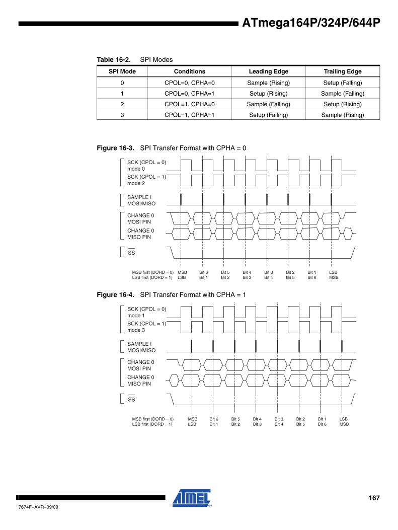
ATmega164P/324P/644P
Figure 16-3. SPI Transfer Format with CPHA = 0
Figure 16-4. SPI Transfer Format with CPHA = 1
Table 16-2. SPI Modes
SPI Mode Conditions Leading Edge Trailing Edge
0 CPOL=0, CPHA=0 Sample (Rising) Setup (Falling)
1 CPOL=0, CPHA=1 Setup (Rising) Sample (Falling)
2 CPOL=1, CPHA=0 Sample (Falling) Setup (Rising)
3 CPOL=1, CPHA=1 Setup (Falling) Sample (Rising)
Bit 1Bit 6
LSBMSB
SCK (CPOL = 0)mode 0
SAMPLE IMOSI/MISO
CHANGE 0MOSI PIN
CHANGE 0MISO PIN
SCK (CPOL = 1)mode 2
SS
MSBLSB
Bit 6Bit 1
Bit 5Bit 2
Bit 4Bit 3
Bit 3Bit 4
Bit 2Bit 5
MSB first (DORD = 0)LSB first (DORD = 1)
SCK (CPOL = 0)mode 1
SAMPLE IMOSI/MISO
CHANGE 0MOSI PIN
CHANGE 0MISO PIN
SCK (CPOL = 1)mode 3
SS
MSBLSB
Bit 6Bit 1
Bit 5Bit 2
Bit 4Bit 3
Bit 3Bit 4
Bit 2Bit 5
Bit 1Bit 6
LSBMSB
MSB first (DORD = 0)LSB first (DORD = 1)
1677674F–AVR–09/09
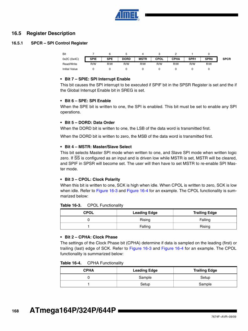
16.5 Register Description
16.5.1 SPCR – SPI Control Register
• Bit 7 – SPIE: SPI Interrupt EnableThis bit causes the SPI interrupt to be executed if SPIF bit in the SPSR Register is set and the ifthe Global Interrupt Enable bit in SREG is set.
• Bit 6 – SPE: SPI EnableWhen the SPE bit is written to one, the SPI is enabled. This bit must be set to enable any SPIoperations.
• Bit 5 – DORD: Data OrderWhen the DORD bit is written to one, the LSB of the data word is transmitted first.
When the DORD bit is written to zero, the MSB of the data word is transmitted first.
• Bit 4 – MSTR: Master/Slave SelectThis bit selects Master SPI mode when written to one, and Slave SPI mode when written logiczero. If SS is configured as an input and is driven low while MSTR is set, MSTR will be cleared,and SPIF in SPSR will become set. The user will then have to set MSTR to re-enable SPI Mas-ter mode.
• Bit 3 – CPOL: Clock PolarityWhen this bit is written to one, SCK is high when idle. When CPOL is written to zero, SCK is lowwhen idle. Refer to Figure 16-3 and Figure 16-4 for an example. The CPOL functionality is sum-marized below:
• Bit 2 – CPHA: Clock PhaseThe settings of the Clock Phase bit (CPHA) determine if data is sampled on the leading (first) ortrailing (last) edge of SCK. Refer to Figure 16-3 and Figure 16-4 for an example. The CPOLfunctionality is summarized below:
Bit 7 6 5 4 3 2 1 0
0x2C (0x4C) SPIE SPE DORD MSTR CPOL CPHA SPR1 SPR0 SPCR
Read/Write R/W R/W R/W R/W R/W R/W R/W R/W
Initial Value 0 0 0 0 0 0 0 0
Table 16-3. CPOL Functionality
CPOL Leading Edge Trailing Edge
0 Rising Falling
1 Falling Rising
Table 16-4. CPHA Functionality
CPHA Leading Edge Trailing Edge
0 Sample Setup
1 Setup Sample
1687674F–AVR–09/09
ATmega164P/324P/644P
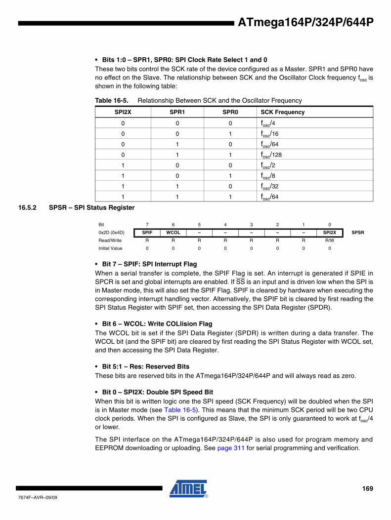
ATmega164P/324P/644P
• Bits 1:0 – SPR1, SPR0: SPI Clock Rate Select 1 and 0These two bits control the SCK rate of the device configured as a Master. SPR1 and SPR0 haveno effect on the Slave. The relationship between SCK and the Oscillator Clock frequency fosc isshown in the following table:
16.5.2 SPSR – SPI Status Register
• Bit 7 – SPIF: SPI Interrupt FlagWhen a serial transfer is complete, the SPIF Flag is set. An interrupt is generated if SPIE inSPCR is set and global interrupts are enabled. If SS is an input and is driven low when the SPI isin Master mode, this will also set the SPIF Flag. SPIF is cleared by hardware when executing thecorresponding interrupt handling vector. Alternatively, the SPIF bit is cleared by first reading theSPI Status Register with SPIF set, then accessing the SPI Data Register (SPDR).
• Bit 6 – WCOL: Write COLlision FlagThe WCOL bit is set if the SPI Data Register (SPDR) is written during a data transfer. TheWCOL bit (and the SPIF bit) are cleared by first reading the SPI Status Register with WCOL set,and then accessing the SPI Data Register.
• Bit 5:1 – Res: Reserved BitsThese bits are reserved bits in the ATmega164P/324P/644P and will always read as zero.
• Bit 0 – SPI2X: Double SPI Speed BitWhen this bit is written logic one the SPI speed (SCK Frequency) will be doubled when the SPIis in Master mode (see Table 16-5). This means that the minimum SCK period will be two CPUclock periods. When the SPI is configured as Slave, the SPI is only guaranteed to work at fosc/4or lower.
The SPI interface on the ATmega164P/324P/644P is also used for program memory andEEPROM downloading or uploading. See page 311 for serial programming and verification.
Table 16-5. Relationship Between SCK and the Oscillator Frequency
SPI2X SPR1 SPR0 SCK Frequency
0 0 0 fosc/4
0 0 1 fosc/16
0 1 0 fosc/64
0 1 1 fosc/128
1 0 0 fosc/2
1 0 1 fosc/8
1 1 0 fosc/32
1 1 1 fosc/64
Bit 7 6 5 4 3 2 1 0
0x2D (0x4D) SPIF WCOL – – – – – SPI2X SPSR
Read/Write R R R R R R R R/W
Initial Value 0 0 0 0 0 0 0 0
1697674F–AVR–09/09

16.5.3 SPDR – SPI Data Register
The SPI Data Register is a read/write register used for data transfer between the Register Fileand the SPI Shift Register. Writing to the register initiates data transmission. Reading the regis-ter causes the Shift Register Receive buffer to be read.
Bit 7 6 5 4 3 2 1 0
0x2E (0x4E) MSB LSB SPDR
Read/Write R/W R/W R/W R/W R/W R/W R/W R/W
Initial Value X X X X X X X X Undefined
1707674F–AVR–09/09
ATmega164P/324P/644P
ATmega164P/324P/644P
17. USART
17.1 Features
• Full Duplex Operation (Independent Serial Receive and Transmit Registers)• Asynchronous or Synchronous Operation• Master or Slave Clocked Synchronous Operation• High Resolution Baud Rate Generator• Supports Serial Frames with 5, 6, 7, 8, or 9 Data Bits and 1 or 2 Stop Bits• Odd or Even Parity Generation and Parity Check Supported by Hardware• Data OverRun Detection• Framing Error Detection• Noise Filtering Includes False Start Bit Detection and Digital Low Pass Filter• Three Separate Interrupts on TX Complete, TX Data Register Empty and RX Complete• Multi-processor Communication Mode• Double Speed Asynchronous Communication Mode
17.2 USART1 and USART0
The ATmega164P/324P/644P has two USART’s, USART0 and USART1.
The functionality for all USART’s is described below, most register and bit references in this sec-tion are written in general form. A lower case “n” replaces the USART number.
USART0 and USART1 have different I/O registers as shown in “Register Summary” on page356.
17.3 Overview
The Universal Synchronous and Asynchronous serial Receiver and Transmitter (USART) is ahighly flexible serial communication device.
A simplified block diagram of the USART Transmitter is shown in Figure 17-1 on page 172. CPUaccessible I/O Registers and I/O pins are shown in bold.
The Power Reducion USART0 bit, PRUSART0, in “PRR – Power Reduction Register” on page47 must be disabled by writing a logical zero to it.
The Power Reducion USART1 bit, PRUSART1, in “PRR – Power Reduction Register” on page47 must be disabled by writing a logical zero to it.
1717674F–AVR–09/09
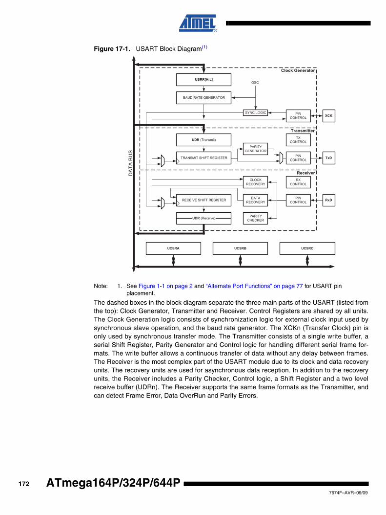
Figure 17-1. USART Block Diagram(1)
Note: 1. See Figure 1-1 on page 2 and “Alternate Port Functions” on page 77 for USART pin placement.
The dashed boxes in the block diagram separate the three main parts of the USART (listed fromthe top): Clock Generator, Transmitter and Receiver. Control Registers are shared by all units.The Clock Generation logic consists of synchronization logic for external clock input used bysynchronous slave operation, and the baud rate generator. The XCKn (Transfer Clock) pin isonly used by synchronous transfer mode. The Transmitter consists of a single write buffer, aserial Shift Register, Parity Generator and Control logic for handling different serial frame for-mats. The write buffer allows a continuous transfer of data without any delay between frames.The Receiver is the most complex part of the USART module due to its clock and data recoveryunits. The recovery units are used for asynchronous data reception. In addition to the recoveryunits, the Receiver includes a Parity Checker, Control logic, a Shift Register and a two levelreceive buffer (UDRn). The Receiver supports the same frame formats as the Transmitter, andcan detect Frame Error, Data OverRun and Parity Errors.
PARITYGENERATOR
UBRR[H:L]
UDR (Transmit)
UCSRA UCSRB UCSRC
BAUD RATE GENERATOR
TRANSMIT SHIFT REGISTER
RECEIVE SHIFT REGISTER RxD
TxDPINCONTROL
UDR (Receive)
PINCONTROL
XCK
DATARECOVERY
CLOCKRECOVERY
PINCONTROL
TXCONTROL
RXCONTROL
PARITYCHECKER
DAT
A BU
S
OSC
SYNC LOGIC
Clock Generator
Transmitter
Receiver
1727674F–AVR–09/09
ATmega164P/324P/644P
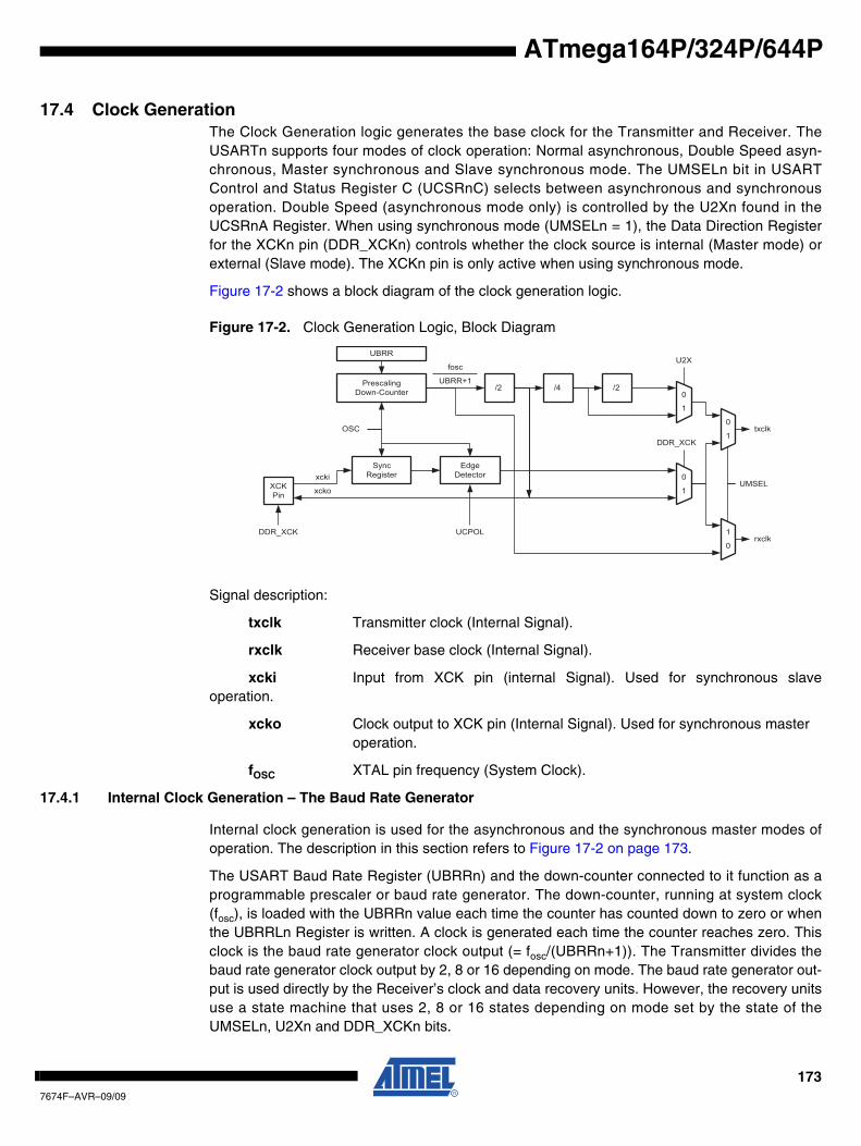
ATmega164P/324P/644P
17.4 Clock GenerationThe Clock Generation logic generates the base clock for the Transmitter and Receiver. TheUSARTn supports four modes of clock operation: Normal asynchronous, Double Speed asyn-chronous, Master synchronous and Slave synchronous mode. The UMSELn bit in USARTControl and Status Register C (UCSRnC) selects between asynchronous and synchronousoperation. Double Speed (asynchronous mode only) is controlled by the U2Xn found in theUCSRnA Register. When using synchronous mode (UMSELn = 1), the Data Direction Registerfor the XCKn pin (DDR_XCKn) controls whether the clock source is internal (Master mode) orexternal (Slave mode). The XCKn pin is only active when using synchronous mode.
Figure 17-2 shows a block diagram of the clock generation logic.
Figure 17-2. Clock Generation Logic, Block Diagram
Signal description:
txclk Transmitter clock (Internal Signal).
rxclk Receiver base clock (Internal Signal).
xcki Input from XCK pin (internal Signal). Used for synchronous slaveoperation.
xcko Clock output to XCK pin (Internal Signal). Used for synchronous masteroperation.
fOSC XTAL pin frequency (System Clock).
17.4.1 Internal Clock Generation – The Baud Rate Generator
Internal clock generation is used for the asynchronous and the synchronous master modes ofoperation. The description in this section refers to Figure 17-2 on page 173.
The USART Baud Rate Register (UBRRn) and the down-counter connected to it function as aprogrammable prescaler or baud rate generator. The down-counter, running at system clock(fosc), is loaded with the UBRRn value each time the counter has counted down to zero or whenthe UBRRLn Register is written. A clock is generated each time the counter reaches zero. Thisclock is the baud rate generator clock output (= fosc/(UBRRn+1)). The Transmitter divides thebaud rate generator clock output by 2, 8 or 16 depending on mode. The baud rate generator out-put is used directly by the Receiver’s clock and data recovery units. However, the recovery unitsuse a state machine that uses 2, 8 or 16 states depending on mode set by the state of theUMSELn, U2Xn and DDR_XCKn bits.
PrescalingDown-Counter /2
UBRR
/4 /2
fosc
UBRR+1
SyncRegister
OSC
XCKPin
txclk
U2X
UMSEL
DDR_XCK
0
1
0
1
xcki
xcko
DDR_XCKrxclk
0
1
1
0Edge
Detector
UCPOL
1737674F–AVR–09/09
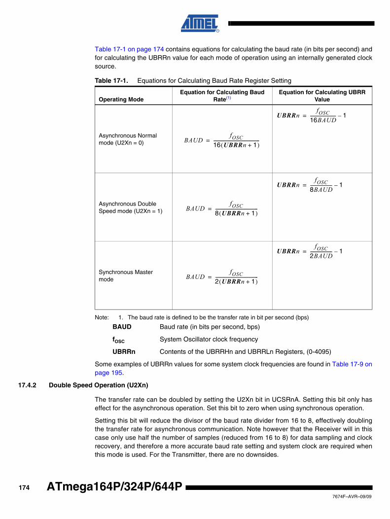
Table 17-1 on page 174 contains equations for calculating the baud rate (in bits per second) andfor calculating the UBRRn value for each mode of operation using an internally generated clocksource.
Note: 1. The baud rate is defined to be the transfer rate in bit per second (bps)
BAUD Baud rate (in bits per second, bps)
fOSC System Oscillator clock frequency
UBRRn Contents of the UBRRHn and UBRRLn Registers, (0-4095)
Some examples of UBRRn values for some system clock frequencies are found in Table 17-9 onpage 195.
17.4.2 Double Speed Operation (U2Xn)
The transfer rate can be doubled by setting the U2Xn bit in UCSRnA. Setting this bit only haseffect for the asynchronous operation. Set this bit to zero when using synchronous operation.
Setting this bit will reduce the divisor of the baud rate divider from 16 to 8, effectively doublingthe transfer rate for asynchronous communication. Note however that the Receiver will in thiscase only use half the number of samples (reduced from 16 to 8) for data sampling and clockrecovery, and therefore a more accurate baud rate setting and system clock are required whenthis mode is used. For the Transmitter, there are no downsides.
Table 17-1. Equations for Calculating Baud Rate Register Setting
Operating ModeEquation for Calculating Baud
Rate(1)Equation for Calculating UBRR
Value
Asynchronous Normal mode (U2Xn = 0)
Asynchronous Double Speed mode (U2Xn = 1)
Synchronous Master mode
BAUDfOSC
16 UBRRn 1+( )------------------------------------------=
UBRRnfOSC
16BAUD------------------------ 1–=
BAUDfOSC
8 UBRRn 1+( )---------------------------------------=
UBRRnfOSC
8BAUD-------------------- 1–=
BAUDfOSC
2 UBRRn 1+( )---------------------------------------=
UBRRnfOSC
2BAUD-------------------- 1–=
1747674F–AVR–09/09
ATmega164P/324P/644P
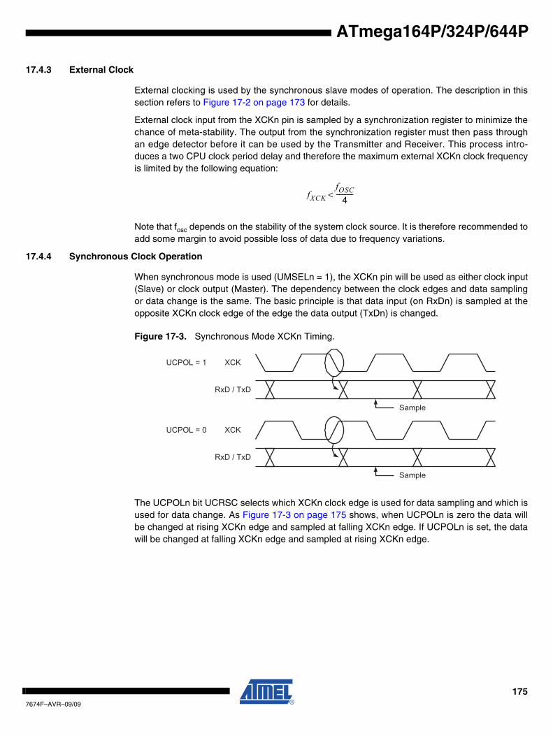
ATmega164P/324P/644P
17.4.3 External Clock
External clocking is used by the synchronous slave modes of operation. The description in thissection refers to Figure 17-2 on page 173 for details.
External clock input from the XCKn pin is sampled by a synchronization register to minimize thechance of meta-stability. The output from the synchronization register must then pass throughan edge detector before it can be used by the Transmitter and Receiver. This process intro-duces a two CPU clock period delay and therefore the maximum external XCKn clock frequencyis limited by the following equation:
Note that fosc depends on the stability of the system clock source. It is therefore recommended toadd some margin to avoid possible loss of data due to frequency variations.
17.4.4 Synchronous Clock Operation
When synchronous mode is used (UMSELn = 1), the XCKn pin will be used as either clock input(Slave) or clock output (Master). The dependency between the clock edges and data samplingor data change is the same. The basic principle is that data input (on RxDn) is sampled at theopposite XCKn clock edge of the edge the data output (TxDn) is changed.
Figure 17-3. Synchronous Mode XCKn Timing.
The UCPOLn bit UCRSC selects which XCKn clock edge is used for data sampling and which isused for data change. As Figure 17-3 on page 175 shows, when UCPOLn is zero the data willbe changed at rising XCKn edge and sampled at falling XCKn edge. If UCPOLn is set, the datawill be changed at falling XCKn edge and sampled at rising XCKn edge.
fXCKfOSC
4-----------<
RxD / TxD
XCK
RxD / TxD
XCKUCPOL = 0
UCPOL = 1
Sample
Sample
1757674F–AVR–09/09
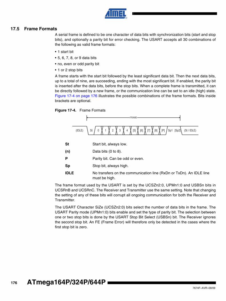
17.5 Frame FormatsA serial frame is defined to be one character of data bits with synchronization bits (start and stopbits), and optionally a parity bit for error checking. The USART accepts all 30 combinations ofthe following as valid frame formats:
• 1 start bit
• 5, 6, 7, 8, or 9 data bits
• no, even or odd parity bit
• 1 or 2 stop bits
A frame starts with the start bit followed by the least significant data bit. Then the next data bits,up to a total of nine, are succeeding, ending with the most significant bit. If enabled, the parity bitis inserted after the data bits, before the stop bits. When a complete frame is transmitted, it canbe directly followed by a new frame, or the communication line can be set to an idle (high) state.Figure 17-4 on page 176 illustrates the possible combinations of the frame formats. Bits insidebrackets are optional.
Figure 17-4. Frame Formats
St Start bit, always low.
(n) Data bits (0 to 8).
P Parity bit. Can be odd or even.
Sp Stop bit, always high.
IDLE No transfers on the communication line (RxDn or TxDn). An IDLE linemust be high.
The frame format used by the USART is set by the UCSZn2:0, UPMn1:0 and USBSn bits inUCSRnB and UCSRnC. The Receiver and Transmitter use the same setting. Note that changingthe setting of any of these bits will corrupt all ongoing communication for both the Receiver andTransmitter.
The USART Character SiZe (UCSZn2:0) bits select the number of data bits in the frame. TheUSART Parity mode (UPMn1:0) bits enable and set the type of parity bit. The selection betweenone or two stop bits is done by the USART Stop Bit Select (USBSn) bit. The Receiver ignoresthe second stop bit. An FE (Frame Error) will therefore only be detected in the cases where thefirst stop bit is zero.
10 2 3 4 [5] [6] [7] [8] [P]St Sp1 [Sp2] (St / IDLE)(IDLE)
FRAME
1767674F–AVR–09/09
ATmega164P/324P/644P
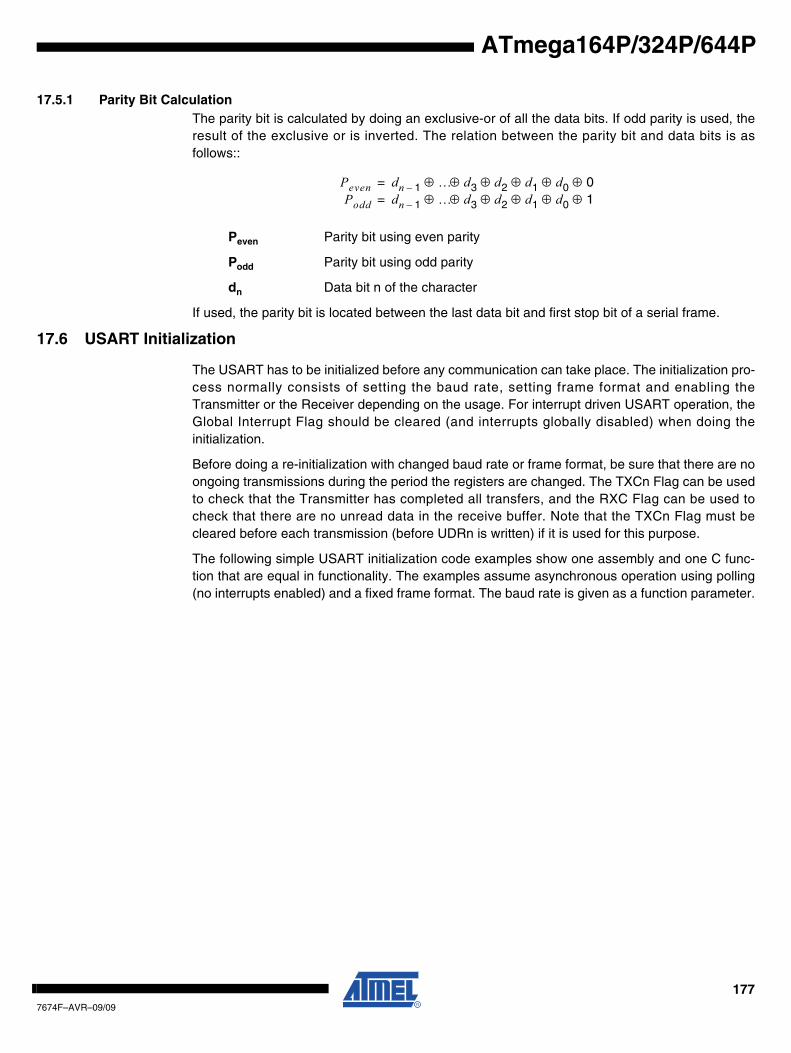
ATmega164P/324P/644P
17.5.1 Parity Bit CalculationThe parity bit is calculated by doing an exclusive-or of all the data bits. If odd parity is used, theresult of the exclusive or is inverted. The relation between the parity bit and data bits is asfollows::
Peven Parity bit using even parity
Podd Parity bit using odd parity
dn Data bit n of the character
If used, the parity bit is located between the last data bit and first stop bit of a serial frame.
17.6 USART Initialization
The USART has to be initialized before any communication can take place. The initialization pro-cess normally consists of setting the baud rate, setting frame format and enabling theTransmitter or the Receiver depending on the usage. For interrupt driven USART operation, theGlobal Interrupt Flag should be cleared (and interrupts globally disabled) when doing theinitialization.
Before doing a re-initialization with changed baud rate or frame format, be sure that there are noongoing transmissions during the period the registers are changed. The TXCn Flag can be usedto check that the Transmitter has completed all transfers, and the RXC Flag can be used tocheck that there are no unread data in the receive buffer. Note that the TXCn Flag must becleared before each transmission (before UDRn is written) if it is used for this purpose.
The following simple USART initialization code examples show one assembly and one C func-tion that are equal in functionality. The examples assume asynchronous operation using polling(no interrupts enabled) and a fixed frame format. The baud rate is given as a function parameter.
Peven dn 1– … d3 d2 d1 d0 0Podd
⊕ ⊕ ⊕ ⊕ ⊕ ⊕dn 1– … d3 d2 d1 d0 1⊕ ⊕ ⊕ ⊕ ⊕ ⊕
==
1777674F–AVR–09/09
For the assembly code, the baud rate parameter is assumed to be stored in the r17:r16Registers.
Note: 1. See “About Code Examples” on page 8.
More advanced initialization routines can be made that include frame format as parameters, dis-able interrupts and so on. However, many applications use a fixed setting of the baud andcontrol registers, and for these types of applications the initialization code can be placed directlyin the main routine, or be combined with initialization code for other I/O modules.
17.7 Data Transmission – The USART Transmitter
The USART Transmitter is enabled by setting the Transmit Enable (TXEN) bit in the UCSRnBRegister. When the Transmitter is enabled, the normal port operation of the TxDn pin is overrid-den by the USART and given the function as the Transmitter’s serial output. The baud rate,mode of operation and frame format must be set up once before doing any transmissions. If syn-chronous operation is used, the clock on the XCKn pin will be overridden and used astransmission clock.
Assembly Code Example(1)
USART_Init:
; Set baud rate
out UBRRHn, r17
out UBRRLn, r16
; Enable receiver and transmitter
ldi r16, (1<<RXENn)|(1<<TXENn)
out UCSRnB,r16
; Set frame format: 8data, 2stop bit
ldi r16, (1<<USBSn)|(3<<UCSZn0)
out UCSRnC,r16
ret
C Code Example(1)
void USART_Init( unsigned int baud )
{
/* Set baud rate */
UBRRHn = (unsigned char)(baud>>8);
UBRRLn = (unsigned char)baud;
/* Enable receiver and transmitter */
UCSRnB = (1<<RXENn)|(1<<TXENn);
/* Set frame format: 8data, 2stop bit */
UCSRnC = (1<<USBSn)|(3<<UCSZn0);
}
1787674F–AVR–09/09
ATmega164P/324P/644P
ATmega164P/324P/644P
17.7.1 Sending Frames with 5 to 8 Data BitA data transmission is initiated by loading the transmit buffer with the data to be transmitted. TheCPU can load the transmit buffer by writing to the UDRn I/O location. The buffered data in thetransmit buffer will be moved to the Shift Register when the Shift Register is ready to send a newframe. The Shift Register is loaded with new data if it is in idle state (no ongoing transmission) orimmediately after the last stop bit of the previous frame is transmitted. When the Shift Register isloaded with new data, it will transfer one complete frame at the rate given by the Baud Register,U2Xn bit or by XCKn depending on mode of operation.
The following code examples show a simple USART transmit function based on polling of theData Register Empty (UDREn) Flag. When using frames with less than eight bits, the most sig-nificant bits written to the UDRn are ignored. The USART has to be initialized before the functioncan be used. For the assembly code, the data to be sent is assumed to be stored in RegisterR16
Note: 1. See “About Code Examples” on page 8.
The function simply waits for the transmit buffer to be empty by checking the UDREn Flag,before loading it with new data to be transmitted. If the Data Register Empty interrupt is utilized,the interrupt routine writes the data into the buffer.
17.7.2 Sending Frames with 9 Data Bit
If 9-bit characters are used (UCSZn = 7), the ninth bit must be written to the TXB8 bit inUCSRnB before the low byte of the character is written to UDRn. The following code examplesshow a transmit function that handles 9-bit characters. For the assembly code, the data to besent is assumed to be stored in registers R17:R16.
Assembly Code Example(1)
USART_Transmit:
; Wait for empty transmit buffer
sbis UCSRnA,UDREn
rjmp USART_Transmit
; Put data (r16) into buffer, sends the data
out UDRn,r16
ret
C Code Example(1)
void USART_Transmit( unsigned char data )
{
/* Wait for empty transmit buffer */
while ( !( UCSRnA & (1<<UDREn)) )
;
/* Put data into buffer, sends the data */
UDRn = data;
}
1797674F–AVR–09/09
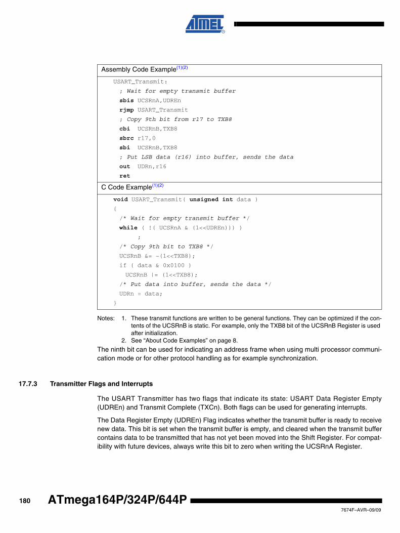
Notes: 1. These transmit functions are written to be general functions. They can be optimized if the con-tents of the UCSRnB is static. For example, only the TXB8 bit of the UCSRnB Register is used after initialization.
2. See “About Code Examples” on page 8.
The ninth bit can be used for indicating an address frame when using multi processor communi-cation mode or for other protocol handling as for example synchronization.
17.7.3 Transmitter Flags and Interrupts
The USART Transmitter has two flags that indicate its state: USART Data Register Empty(UDREn) and Transmit Complete (TXCn). Both flags can be used for generating interrupts.
The Data Register Empty (UDREn) Flag indicates whether the transmit buffer is ready to receivenew data. This bit is set when the transmit buffer is empty, and cleared when the transmit buffercontains data to be transmitted that has not yet been moved into the Shift Register. For compat-ibility with future devices, always write this bit to zero when writing the UCSRnA Register.
Assembly Code Example(1)(2)
USART_Transmit:
; Wait for empty transmit buffer
sbis UCSRnA,UDREn
rjmp USART_Transmit
; Copy 9th bit from r17 to TXB8
cbi UCSRnB,TXB8
sbrc r17,0
sbi UCSRnB,TXB8
; Put LSB data (r16) into buffer, sends the data
out UDRn,r16
ret
C Code Example(1)(2)
void USART_Transmit( unsigned int data )
{
/* Wait for empty transmit buffer */
while ( !( UCSRnA & (1<<UDREn))) )
;
/* Copy 9th bit to TXB8 */
UCSRnB &= ~(1<<TXB8);
if ( data & 0x0100 )
UCSRnB |= (1<<TXB8);
/* Put data into buffer, sends the data */
UDRn = data;
}
1807674F–AVR–09/09
ATmega164P/324P/644P
ATmega164P/324P/644P
When the Data Register Empty Interrupt Enable (UDRIEn) bit in UCSRnB is written to one, theUSART Data Register Empty Interrupt will be executed as long as UDREn is set (provided thatglobal interrupts are enabled). UDREn is cleared by writing UDRn. When interrupt-driven datatransmission is used, the Data Register Empty interrupt routine must either write new data toUDRn in order to clear UDREn or disable the Data Register Empty interrupt, otherwise a newinterrupt will occur once the interrupt routine terminates.
The Transmit Complete (TXCn) Flag bit is set one when the entire frame in the Transmit ShiftRegister has been shifted out and there are no new data currently present in the transmit buffer.The TXCn Flag bit is automatically cleared when a transmit complete interrupt is executed, or itcan be cleared by writing a one to its bit location. The TXCn Flag is useful in half-duplex commu-nication interfaces (like the RS-485 standard), where a transmitting application must enterreceive mode and free the communication bus immediately after completing the transmission.
When the Transmit Compete Interrupt Enable (TXCIEn) bit in UCSRnB is set, the USARTTransmit Complete Interrupt will be executed when the TXCn Flag becomes set (provided thatglobal interrupts are enabled). When the transmit complete interrupt is used, the interrupt han-dling routine does not have to clear the TXCn Flag, this is done automatically when the interruptis executed.
17.7.4 Parity Generator
The Parity Generator calculates the parity bit for the serial frame data. When parity bit is enabled(UPMn1 = 1), the transmitter control logic inserts the parity bit between the last data bit and thefirst stop bit of the frame that is sent.
17.7.5 Disabling the Transmitter
The disabling of the Transmitter (setting the TXEN to zero) will not become effective until ongo-ing and pending transmissions are completed, i.e., when the Transmit Shift Register andTransmit Buffer Register do not contain data to be transmitted. When disabled, the Transmitterwill no longer override the TxDn pin.
17.8 Data Reception – The USART Receiver
The USART Receiver is enabled by writing the Receive Enable (RXENn) bit in theUCSRnB Register to one. When the Receiver is enabled, the normal pin operation of the RxDnpin is overridden by the USART and given the function as the Receiver’s serial input. The baudrate, mode of operation and frame format must be set up once before any serial reception canbe done. If synchronous operation is used, the clock on the XCKn pin will be used as transferclock.
17.8.1 Receiving Frames with 5 to 8 Data Bits
The Receiver starts data reception when it detects a valid start bit. Each bit that follows the startbit will be sampled at the baud rate or XCKn clock, and shifted into the Receive Shift Registeruntil the first stop bit of a frame is received. A second stop bit will be ignored by the Receiver.When the first stop bit is received, i.e., a complete serial frame is present in the Receive ShiftRegister, the contents of the Shift Register will be moved into the receive buffer. The receivebuffer can then be read by reading the UDRn I/O location.
1817674F–AVR–09/09
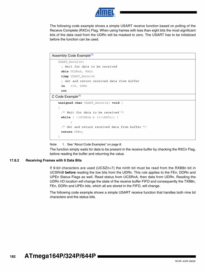
The following code example shows a simple USART receive function based on polling of theReceive Complete (RXCn) Flag. When using frames with less than eight bits the most significantbits of the data read from the UDRn will be masked to zero. The USART has to be initializedbefore the function can be used.
Note: 1. See “About Code Examples” on page 8.
The function simply waits for data to be present in the receive buffer by checking the RXCn Flag,before reading the buffer and returning the value.
17.8.2 Receiving Frames with 9 Data Bits
If 9-bit characters are used (UCSZn=7) the ninth bit must be read from the RXB8n bit inUCSRnB before reading the low bits from the UDRn. This rule applies to the FEn, DORn andUPEn Status Flags as well. Read status from UCSRnA, then data from UDRn. Reading theUDRn I/O location will change the state of the receive buffer FIFO and consequently the TXB8n,FEn, DORn and UPEn bits, which all are stored in the FIFO, will change.
The following code example shows a simple USART receive function that handles both nine bitcharacters and the status bits.
Assembly Code Example(1)
USART_Receive:
; Wait for data to be received
sbis UCSRnA, RXCn
rjmp USART_Receive
; Get and return received data from buffer
in r16, UDRn
ret
C Code Example(1)
unsigned char USART_Receive( void )
{
/* Wait for data to be received */
while ( !(UCSRnA & (1<<RXCn)) )
;
/* Get and return received data from buffer */
return UDRn;
}
1827674F–AVR–09/09
ATmega164P/324P/644P
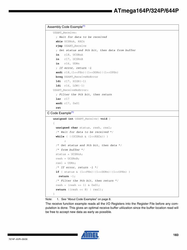
ATmega164P/324P/644P
Note: 1. See “About Code Examples” on page 8.
The receive function example reads all the I/O Registers into the Register File before any com-putation is done. This gives an optimal receive buffer utilization since the buffer location read willbe free to accept new data as early as possible.
Assembly Code Example(1)
USART_Receive:
; Wait for data to be received
sbis UCSRnA, RXCn
rjmp USART_Receive
; Get status and 9th bit, then data from buffer
in r18, UCSRnA
in r17, UCSRnB
in r16, UDRn
; If error, return -1
andi r18,(1<<FEn)|(1<<DORn)|(1<<UPEn)
breq USART_ReceiveNoError
ldi r17, HIGH(-1)
ldi r16, LOW(-1)
USART_ReceiveNoError:
; Filter the 9th bit, then return
lsr r17
andi r17, 0x01
ret
C Code Example(1)
unsigned int USART_Receive( void )
{
unsigned char status, resh, resl;
/* Wait for data to be received */
while ( !(UCSRnA & (1<<RXCn)) )
;
/* Get status and 9th bit, then data */
/* from buffer */
status = UCSRnA;
resh = UCSRnB;
resl = UDRn;
/* If error, return -1 */
if ( status & (1<<FEn)|(1<<DORn)|(1<<UPEn) )
return -1;
/* Filter the 9th bit, then return */
resh = (resh >> 1) & 0x01;
return ((resh << 8) | resl);
}
1837674F–AVR–09/09
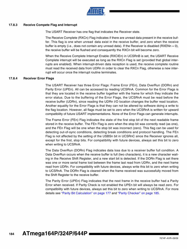
17.8.3 Receive Compete Flag and Interrupt
The USART Receiver has one flag that indicates the Receiver state.
The Receive Complete (RXCn) Flag indicates if there are unread data present in the receive buf-fer. This flag is one when unread data exist in the receive buffer, and zero when the receivebuffer is empty (i.e., does not contain any unread data). If the Receiver is disabled (RXENn = 0),the receive buffer will be flushed and consequently the RXCn bit will become zero.
When the Receive Complete Interrupt Enable (RXCIEn) in UCSRnB is set, the USART ReceiveComplete interrupt will be executed as long as the RXCn Flag is set (provided that global inter-rupts are enabled). When interrupt-driven data reception is used, the receive complete routinemust read the received data from UDRn in order to clear the RXCn Flag, otherwise a new inter-rupt will occur once the interrupt routine terminates.
17.8.4 Receiver Error Flags
The USART Receiver has three Error Flags: Frame Error (FEn), Data OverRun (DORn) andParity Error (UPEn). All can be accessed by reading UCSRnA. Common for the Error Flags isthat they are located in the receive buffer together with the frame for which they indicate theerror status. Due to the buffering of the Error Flags, the UCSRnA must be read before thereceive buffer (UDRn), since reading the UDRn I/O location changes the buffer read location.Another equality for the Error Flags is that they can not be altered by software doing a write tothe flag location. However, all flags must be set to zero when the UCSRnA is written for upwardcompatibility of future USART implementations. None of the Error Flags can generate interrupts.
The Frame Error (FEn) Flag indicates the state of the first stop bit of the next readable framestored in the receive buffer. The FEn Flag is zero when the stop bit was correctly read (as one),and the FEn Flag will be one when the stop bit was incorrect (zero). This flag can be used fordetecting out-of-sync conditions, detecting break conditions and protocol handling. The FEnFlag is not affected by the setting of the USBSn bit in UCSRnC since the Receiver ignores all,except for the first, stop bits. For compatibility with future devices, always set this bit to zerowhen writing to UCSRnA.
The Data OverRun (DORn) Flag indicates data loss due to a receiver buffer full condition. AData OverRun occurs when the receive buffer is full (two characters), it is a new character wait-ing in the Receive Shift Register, and a new start bit is detected. If the DORn Flag is set therewas one or more serial frame lost between the frame last read from UDRn, and the next frameread from UDRn. For compatibility with future devices, always write this bit to zero when writingto UCSRnA. The DORn Flag is cleared when the frame received was successfully moved fromthe Shift Register to the receive buffer.
The Parity Error (UPEn) Flag indicates that the next frame in the receive buffer had a ParityError when received. If Parity Check is not enabled the UPEn bit will always be read zero. Forcompatibility with future devices, always set this bit to zero when writing to UCSRnA. For moredetails see “Parity Bit Calculation” on page 177 and “Parity Checker” on page 185.
1847674F–AVR–09/09
ATmega164P/324P/644P
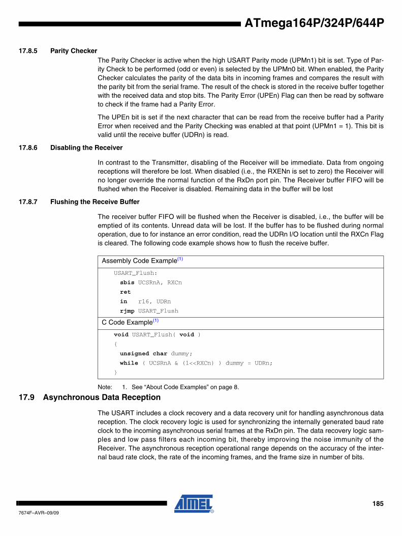
ATmega164P/324P/644P
17.8.5 Parity CheckerThe Parity Checker is active when the high USART Parity mode (UPMn1) bit is set. Type of Par-ity Check to be performed (odd or even) is selected by the UPMn0 bit. When enabled, the ParityChecker calculates the parity of the data bits in incoming frames and compares the result withthe parity bit from the serial frame. The result of the check is stored in the receive buffer togetherwith the received data and stop bits. The Parity Error (UPEn) Flag can then be read by softwareto check if the frame had a Parity Error.
The UPEn bit is set if the next character that can be read from the receive buffer had a ParityError when received and the Parity Checking was enabled at that point (UPMn1 = 1). This bit isvalid until the receive buffer (UDRn) is read.
17.8.6 Disabling the Receiver
In contrast to the Transmitter, disabling of the Receiver will be immediate. Data from ongoingreceptions will therefore be lost. When disabled (i.e., the RXENn is set to zero) the Receiver willno longer override the normal function of the RxDn port pin. The Receiver buffer FIFO will beflushed when the Receiver is disabled. Remaining data in the buffer will be lost
17.8.7 Flushing the Receive Buffer
The receiver buffer FIFO will be flushed when the Receiver is disabled, i.e., the buffer will beemptied of its contents. Unread data will be lost. If the buffer has to be flushed during normaloperation, due to for instance an error condition, read the UDRn I/O location until the RXCn Flagis cleared. The following code example shows how to flush the receive buffer.
Note: 1. See “About Code Examples” on page 8.
17.9 Asynchronous Data Reception
The USART includes a clock recovery and a data recovery unit for handling asynchronous datareception. The clock recovery logic is used for synchronizing the internally generated baud rateclock to the incoming asynchronous serial frames at the RxDn pin. The data recovery logic sam-ples and low pass filters each incoming bit, thereby improving the noise immunity of theReceiver. The asynchronous reception operational range depends on the accuracy of the inter-nal baud rate clock, the rate of the incoming frames, and the frame size in number of bits.
Assembly Code Example(1)
USART_Flush:
sbis UCSRnA, RXCn
ret
in r16, UDRn
rjmp USART_Flush
C Code Example(1)
void USART_Flush( void )
{
unsigned char dummy;
while ( UCSRnA & (1<<RXCn) ) dummy = UDRn;
}
1857674F–AVR–09/09
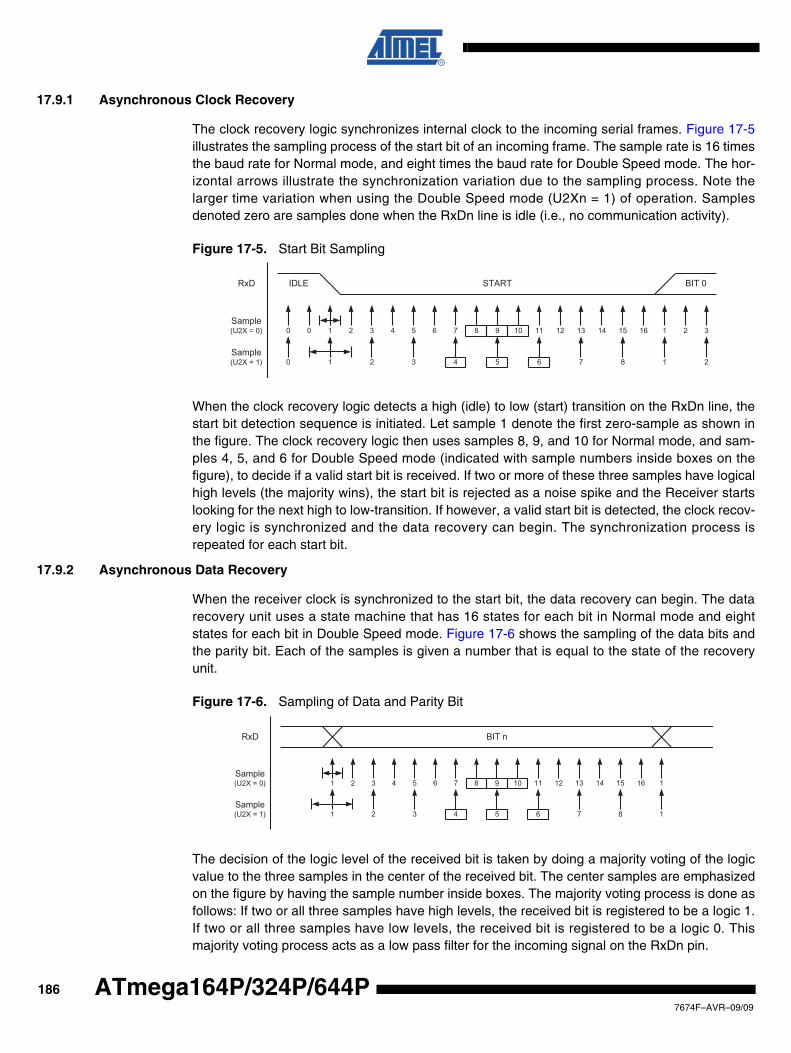
17.9.1 Asynchronous Clock Recovery
The clock recovery logic synchronizes internal clock to the incoming serial frames. Figure 17-5illustrates the sampling process of the start bit of an incoming frame. The sample rate is 16 timesthe baud rate for Normal mode, and eight times the baud rate for Double Speed mode. The hor-izontal arrows illustrate the synchronization variation due to the sampling process. Note thelarger time variation when using the Double Speed mode (U2Xn = 1) of operation. Samplesdenoted zero are samples done when the RxDn line is idle (i.e., no communication activity).
Figure 17-5. Start Bit Sampling
When the clock recovery logic detects a high (idle) to low (start) transition on the RxDn line, thestart bit detection sequence is initiated. Let sample 1 denote the first zero-sample as shown inthe figure. The clock recovery logic then uses samples 8, 9, and 10 for Normal mode, and sam-ples 4, 5, and 6 for Double Speed mode (indicated with sample numbers inside boxes on thefigure), to decide if a valid start bit is received. If two or more of these three samples have logicalhigh levels (the majority wins), the start bit is rejected as a noise spike and the Receiver startslooking for the next high to low-transition. If however, a valid start bit is detected, the clock recov-ery logic is synchronized and the data recovery can begin. The synchronization process isrepeated for each start bit.
17.9.2 Asynchronous Data Recovery
When the receiver clock is synchronized to the start bit, the data recovery can begin. The datarecovery unit uses a state machine that has 16 states for each bit in Normal mode and eightstates for each bit in Double Speed mode. Figure 17-6 shows the sampling of the data bits andthe parity bit. Each of the samples is given a number that is equal to the state of the recoveryunit.
Figure 17-6. Sampling of Data and Parity Bit
The decision of the logic level of the received bit is taken by doing a majority voting of the logicvalue to the three samples in the center of the received bit. The center samples are emphasizedon the figure by having the sample number inside boxes. The majority voting process is done asfollows: If two or all three samples have high levels, the received bit is registered to be a logic 1.If two or all three samples have low levels, the received bit is registered to be a logic 0. Thismajority voting process acts as a low pass filter for the incoming signal on the RxDn pin.
1 2 3 4 5 6 7 8 9 10 11 12 13 14 15 16 1 2
STARTIDLE
00
BIT 0
3
1 2 3 4 5 6 7 8 1 20
RxD
Sample(U2X = 0)
Sample(U2X = 1)
1 2 3 4 5 6 7 8 9 10 11 12 13 14 15 16 1
BIT n
1 2 3 4 5 6 7 8 1
RxD
Sample(U2X = 0)
Sample(U2X = 1)
1867674F–AVR–09/09
ATmega164P/324P/644P
ATmega164P/324P/644P
The recovery process is then repeated until a complete frame is received. Including the first stopbit. Note that the Receiver only uses the first stop bit of a frame.
Figure 17-7 on page 187 shows the sampling of the stop bit and the earliest possible beginningof the start bit of the next frame.
Figure 17-7. Stop Bit Sampling and Next Start Bit Sampling
The same majority voting is done to the stop bit as done for the other bits in the frame. If the stopbit is registered to have a logic 0 value, the Frame Error (FEn) Flag will be set.
A new high to low transition indicating the start bit of a new frame can come right after the last ofthe bits used for majority voting. For Normal Speed mode, the first low level sample can be atpoint marked (A) in Figure 17-7 on page 187. For Double Speed mode the first low level must bedelayed to (B). (C) marks a stop bit of full length. The early start bit detection influences theoperational range of the Receiver.
17.9.3 Asynchronous Operational Range
The operational range of the Receiver is dependent on the mismatch between the received bitrate and the internally generated baud rate. If the Transmitter is sending frames at too fast or tooslow bit rates, or the internally generated baud rate of the Receiver does not have a similar (seeTable 17-2 on page 188) base frequency, the Receiver will not be able to synchronize theframes to the start bit.
The following equations can be used to calculate the ratio of the incoming data rate and internalreceiver baud rate.
D Sum of character size and parity size (D = 5 to 10 bit)
S Samples per bit. S = 16 for Normal Speed mode and S = 8 for Double Speedmode.
SF First sample number used for majority voting. SF = 8 for normal speed and SF = 4for Double Speed mode.
SM Middle sample number used for majority voting. SM = 9 for normal speed andSM = 5 for Double Speed mode.
Rslow is the ratio of the slowest incoming data rate that can be accepted in relation to thereceiver baud rate. Rfast is the ratio of the fastest incoming data rate that can beaccepted in relation to the receiver baud rate.
1 2 3 4 5 6 7 8 9 10 0/1 0/1 0/1
STOP 1
1 2 3 4 5 6 0/1
RxD
Sample(U2X = 0)
Sample(U2X = 1)
(A) (B) (C)
RslowD 1+( )S
S 1– D S⋅ SF+ +---------------------------------------------= Rfast
D 2+( )SD 1+( )S SM+
-----------------------------------=
1877674F–AVR–09/09
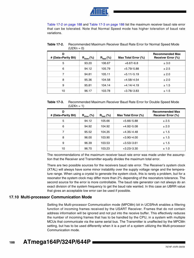
Table 17-2 on page 188 and Table 17-3 on page 188 list the maximum receiver baud rate errorthat can be tolerated. Note that Normal Speed mode has higher toleration of baud ratevariations.
The recommendations of the maximum receiver baud rate error was made under the assump-tion that the Receiver and Transmitter equally divides the maximum total error.
There are two possible sources for the receivers baud rate error. The Receiver’s system clock(XTAL) will always have some minor instability over the supply voltage range and the tempera-ture range. When using a crystal to generate the system clock, this is rarely a problem, but for aresonator the system clock may differ more than 2% depending of the resonators tolerance. Thesecond source for the error is more controllable. The baud rate generator can not always do anexact division of the system frequency to get the baud rate wanted. In this case an UBRR valuethat gives an acceptable low error can be used if possible.
17.10 Multi-processor Communication Mode
Setting the Multi-processor Communication mode (MPCMn) bit in UCSRnA enables a filteringfunction of incoming frames received by the USART Receiver. Frames that do not containaddress information will be ignored and not put into the receive buffer. This effectively reducesthe number of incoming frames that has to be handled by the CPU, in a system with multipleMCUs that communicate via the same serial bus. The Transmitter is unaffected by the MPCMnsetting, but has to be used differently when it is a part of a system utilizing the Multi-processorCommunication mode.
Table 17-2. Recommended Maximum Receiver Baud Rate Error for Normal Speed Mode (U2Xn = 0)
D# (Data+Parity Bit) Rslow (%) Rfast (%) Max Total Error (%)
Recommended Max Receiver Error (%)
5 93.20 106.67 +6.67/-6.8 ± 3.0
6 94.12 105.79 +5.79/-5.88 ± 2.5
7 94.81 105.11 +5.11/-5.19 ± 2.0
8 95.36 104.58 +4.58/-4.54 ± 2.0
9 95.81 104.14 +4.14/-4.19 ± 1.5
10 96.17 103.78 +3.78/-3.83 ± 1.5
Table 17-3. Recommended Maximum Receiver Baud Rate Error for Double Speed Mode (U2Xn = 1)
D# (Data+Parity Bit) Rslow (%) Rfast (%) Max Total Error (%)
Recommended Max Receiver Error (%)
5 94.12 105.66 +5.66/-5.88 ± 2.5
6 94.92 104.92 +4.92/-5.08 ± 2.0
7 95.52 104,35 +4.35/-4.48 ± 1.5
8 96.00 103.90 +3.90/-4.00 ± 1.5
9 96.39 103.53 +3.53/-3.61 ± 1.5
10 96.70 103.23 +3.23/-3.30 ± 1.0
1887674F–AVR–09/09
ATmega164P/324P/644P
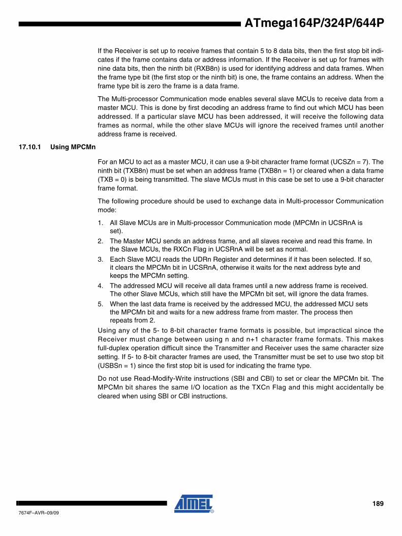
ATmega164P/324P/644P
If the Receiver is set up to receive frames that contain 5 to 8 data bits, then the first stop bit indi-cates if the frame contains data or address information. If the Receiver is set up for frames withnine data bits, then the ninth bit (RXB8n) is used for identifying address and data frames. Whenthe frame type bit (the first stop or the ninth bit) is one, the frame contains an address. When theframe type bit is zero the frame is a data frame.
The Multi-processor Communication mode enables several slave MCUs to receive data from amaster MCU. This is done by first decoding an address frame to find out which MCU has beenaddressed. If a particular slave MCU has been addressed, it will receive the following dataframes as normal, while the other slave MCUs will ignore the received frames until anotheraddress frame is received.
17.10.1 Using MPCMn
For an MCU to act as a master MCU, it can use a 9-bit character frame format (UCSZn = 7). Theninth bit (TXB8n) must be set when an address frame (TXB8n = 1) or cleared when a data frame(TXB = 0) is being transmitted. The slave MCUs must in this case be set to use a 9-bit characterframe format.
The following procedure should be used to exchange data in Multi-processor Communicationmode:
1. All Slave MCUs are in Multi-processor Communication mode (MPCMn in UCSRnA is set).
2. The Master MCU sends an address frame, and all slaves receive and read this frame. In the Slave MCUs, the RXCn Flag in UCSRnA will be set as normal.
3. Each Slave MCU reads the UDRn Register and determines if it has been selected. If so, it clears the MPCMn bit in UCSRnA, otherwise it waits for the next address byte and keeps the MPCMn setting.
4. The addressed MCU will receive all data frames until a new address frame is received. The other Slave MCUs, which still have the MPCMn bit set, will ignore the data frames.
5. When the last data frame is received by the addressed MCU, the addressed MCU sets the MPCMn bit and waits for a new address frame from master. The process then repeats from 2.
Using any of the 5- to 8-bit character frame formats is possible, but impractical since theReceiver must change between using n and n+1 character frame formats. This makesfull-duplex operation difficult since the Transmitter and Receiver uses the same character sizesetting. If 5- to 8-bit character frames are used, the Transmitter must be set to use two stop bit(USBSn = 1) since the first stop bit is used for indicating the frame type.
Do not use Read-Modify-Write instructions (SBI and CBI) to set or clear the MPCMn bit. TheMPCMn bit shares the same I/O location as the TXCn Flag and this might accidentally becleared when using SBI or CBI instructions.
1897674F–AVR–09/09
17.11 Register Description
17.11.1 UDRn – USART I/O Data Register n
The USART Transmit Data Buffer Register and USART Receive Data Buffer Registers share thesame I/O address referred to as USART Data Register or UDRn. The Transmit Data Buffer Reg-ister (TXB) will be the destination for data written to the UDRn Register location. Reading theUDRn Register location will return the contents of the Receive Data Buffer Register (RXB).
For 5-, 6-, or 7-bit characters the upper unused bits will be ignored by the Transmitter and set tozero by the Receiver.
The transmit buffer can only be written when the UDREn Flag in the UCSRnA Register is set.Data written to UDRn when the UDREn Flag is not set, will be ignored by the USART Transmit-ter. When data is written to the transmit buffer, and the Transmitter is enabled, the Transmitterwill load the data into the Transmit Shift Register when the Shift Register is empty. Then thedata will be serially transmitted on the TxDn pin.
The receive buffer consists of a two level FIFO. The FIFO will change its state whenever thereceive buffer is accessed. Due to this behavior of the receive buffer, do not use Read-Mod-ify-Write instructions (SBI and CBI) on this location. Be careful when using bit test instructions(SBIC and SBIS), since these also will change the state of the FIFO.
17.11.2 UCSRnA – USART Control and Status Register A
• Bit 7 – RXCn: USART Receive CompleteThis flag bit is set when there are unread data in the receive buffer and cleared when the receivebuffer is empty (i.e., does not contain any unread data). If the Receiver is disabled, the receivebuffer will be flushed and consequently the RXCn bit will become zero. The RXCn Flag can beused to generate a Receive Complete interrupt (see description of the RXCIEn bit).
• Bit 6 – TXCn: USART Transmit CompleteThis flag bit is set when the entire frame in the Transmit Shift Register has been shifted out andthere are no new data currently present in the transmit buffer (UDRn). The TXCn Flag bit is auto-matically cleared when a transmit complete interrupt is executed, or it can be cleared by writinga one to its bit location. The TXCn Flag can generate a Transmit Complete interrupt (seedescription of the TXCIEn bit).
Bit 7 6 5 4 3 2 1 0
RXB[7:0] UDRn (Read)
TXB[7:0] UDRn (Write)
Read/Write R/W R/W R/W R/W R/W R/W R/W R/W
Initial Value 0 0 0 0 0 0 0 0
Bit 7 6 5 4 3 2 1 0
RXCn TXCn UDREn FEn DORn UPEn U2Xn MPCMn UCSRnA
Read/Write R R/W R R R R R/W R/W
Initial Value 0 0 1 0 0 0 0 0
1907674F–AVR–09/09
ATmega164P/324P/644P
ATmega164P/324P/644P
• Bit 5 – UDREn: USART Data Register EmptyThe UDREn Flag indicates if the transmit buffer (UDRn) is ready to receive new data. If UDREnis one, the buffer is empty, and therefore ready to be written. The UDREn Flag can generate aData Register Empty interrupt (see description of the UDRIEn bit).UDREn is set after a reset toindicate that the Transmitter is ready.
• Bit 4 – FEn: Frame ErrorThis bit is set if the next character in the receive buffer had a Frame Error when received. I.e.,when the first stop bit of the next character in the receive buffer is zero. This bit is valid until thereceive buffer (UDRn) is read. The FEn bit is zero when the stop bit of received data is one.Always set this bit to zero when writing to UCSRnA.
• Bit 3 – DORn: Data OverRunThis bit is set if a Data OverRun condition is detected. A Data OverRun occurs when the receivebuffer is full (two characters), it is a new character waiting in the Receive Shift Register, and anew start bit is detected. This bit is valid until the receive buffer (UDRn) is read. Always set thisbit to zero when writing to UCSRnA.
• Bit 2 – UPEn: USART Parity ErrorThis bit is set if the next character in the receive buffer had a Parity Error when received and theParity Checking was enabled at that point (UPMn1 = 1). This bit is valid until the receive buffer(UDRn) is read. Always set this bit to zero when writing to UCSRnA.
• Bit 1 – U2Xn: Double the USART Transmission SpeedThis bit only has effect for the asynchronous operation. Write this bit to zero when using syn-chronous operation.
Writing this bit to one will reduce the divisor of the baud rate divider from 16 to 8 effectively dou-bling the transfer rate for asynchronous communication.
• Bit 0 – MPCMn: Multi-processor Communication ModeThis bit enables the Multi-processor Communication mode. When the MPCMn bit is written toone, all the incoming frames received by the USART Receiver that do not contain address infor-mation will be ignored. The Transmitter is unaffected by the MPCMn setting. For more detailedinformation see “Multi-processor Communication Mode” on page 188.
17.11.3 UCSRnB – USART Control and Status Register n B
• Bit 7 – RXCIEn: RX Complete Interrupt Enable nWriting this bit to one enables interrupt on the RXCn Flag. A USART Receive Complete interruptwill be generated only if the RXCIEn bit is written to one, the Global Interrupt Flag in SREG iswritten to one and the RXCn bit in UCSRnA is set.
Bit 7 6 5 4 3 2 1 0
RXCIEn TXCIEn UDRIEn RXENn TXENn UCSZn2 RXB8n TXB8n UCSRnB
Read/Write R/W R/W R/W R/W R/W R/W R R/W
Initial Value 0 0 0 0 0 0 0 0
1917674F–AVR–09/09
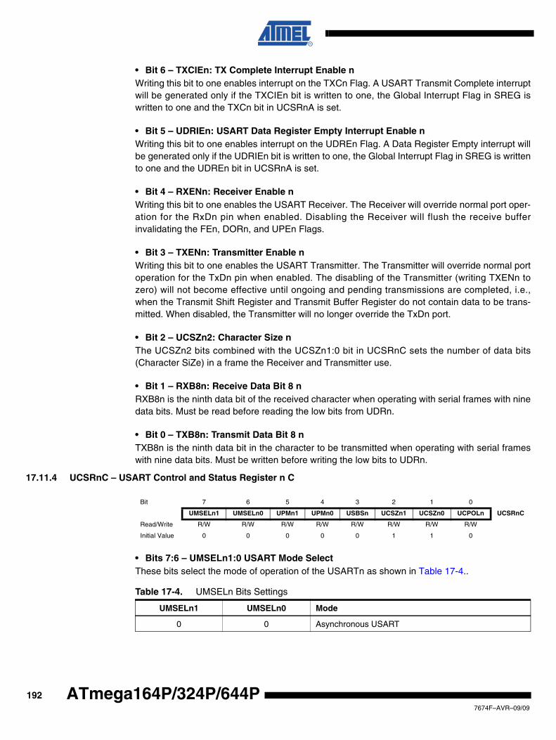
• Bit 6 – TXCIEn: TX Complete Interrupt Enable nWriting this bit to one enables interrupt on the TXCn Flag. A USART Transmit Complete interruptwill be generated only if the TXCIEn bit is written to one, the Global Interrupt Flag in SREG iswritten to one and the TXCn bit in UCSRnA is set.
• Bit 5 – UDRIEn: USART Data Register Empty Interrupt Enable nWriting this bit to one enables interrupt on the UDREn Flag. A Data Register Empty interrupt willbe generated only if the UDRIEn bit is written to one, the Global Interrupt Flag in SREG is writtento one and the UDREn bit in UCSRnA is set.
• Bit 4 – RXENn: Receiver Enable nWriting this bit to one enables the USART Receiver. The Receiver will override normal port oper-ation for the RxDn pin when enabled. Disabling the Receiver will flush the receive bufferinvalidating the FEn, DORn, and UPEn Flags.
• Bit 3 – TXENn: Transmitter Enable nWriting this bit to one enables the USART Transmitter. The Transmitter will override normal portoperation for the TxDn pin when enabled. The disabling of the Transmitter (writing TXENn tozero) will not become effective until ongoing and pending transmissions are completed, i.e.,when the Transmit Shift Register and Transmit Buffer Register do not contain data to be trans-mitted. When disabled, the Transmitter will no longer override the TxDn port.
• Bit 2 – UCSZn2: Character Size nThe UCSZn2 bits combined with the UCSZn1:0 bit in UCSRnC sets the number of data bits(Character SiZe) in a frame the Receiver and Transmitter use.
• Bit 1 – RXB8n: Receive Data Bit 8 nRXB8n is the ninth data bit of the received character when operating with serial frames with ninedata bits. Must be read before reading the low bits from UDRn.
• Bit 0 – TXB8n: Transmit Data Bit 8 nTXB8n is the ninth data bit in the character to be transmitted when operating with serial frameswith nine data bits. Must be written before writing the low bits to UDRn.
17.11.4 UCSRnC – USART Control and Status Register n C
• Bits 7:6 – UMSELn1:0 USART Mode SelectThese bits select the mode of operation of the USARTn as shown in Table 17-4..
Bit 7 6 5 4 3 2 1 0
UMSELn1 UMSELn0 UPMn1 UPMn0 USBSn UCSZn1 UCSZn0 UCPOLn UCSRnC
Read/Write R/W R/W R/W R/W R/W R/W R/W R/W
Initial Value 0 0 0 0 0 1 1 0
Table 17-4. UMSELn Bits Settings
UMSELn1 UMSELn0 Mode
0 0 Asynchronous USART
1927674F–AVR–09/09
ATmega164P/324P/644P
ATmega164P/324P/644P
Note: 1. See “USART in SPI Mode” on page 199 for full description of the Master SPI Mode (MSPIM) operation
• Bits 5:4 – UPMn1:0: Parity ModeThese bits enable and set type of parity generation and check. If enabled, the Transmitter willautomatically generate and send the parity of the transmitted data bits within each frame. TheReceiver will generate a parity value for the incoming data and compare it to the UPMn setting.If a mismatch is detected, the UPEn Flag in UCSRnA will be set.
• Bit 3 – USBSn: Stop Bit SelectThis bit selects the number of stop bits to be inserted by the Transmitter. The Receiver ignoresthis setting.
• Bit 2:1 – UCSZn1:0: Character SizeThe UCSZn1:0 bits combined with the UCSZn2 bit in UCSRnB sets the number of data bits(Character SiZe) in a frame the Receiver and Transmitter use.
0 1 Synchronous USART
1 0 (Reserved)
1 1 Master SPI (MSPIM)(1)
Table 17-5. UPMn Bits Settings
UPMn1 UPMn0 Parity Mode
0 0 Disabled
0 1 Reserved
1 0 Enabled, Even Parity
1 1 Enabled, Odd Parity
Table 17-6. USBS Bit Settings
USBSn Stop Bit(s)
0 1-bit
1 2-bit
Table 17-7. UCSZn Bits Settings
UCSZn2 UCSZn1 UCSZn0 Character Size
0 0 0 5-bit
0 0 1 6-bit
0 1 0 7-bit
0 1 1 8-bit
1 0 0 Reserved
Table 17-4. UMSELn Bits Settings
UMSELn1 UMSELn0 Mode
1937674F–AVR–09/09
• Bit 0 – UCPOLn: Clock PolarityThis bit is used for synchronous mode only. Write this bit to zero when asynchronous mode isused. The UCPOLn bit sets the relationship between data output change and data input sample,and the synchronous clock (XCKn).
17.11.5 UBRRnL and UBRRnH – USART Baud Rate Registers
• Bit 15:12 – Reserved BitsThese bits are reserved for future use. For compatibility with future devices, these bit must bewritten to zero when UBRRH is written.
• Bit 11:0 – UBRR11:0: USART Baud Rate RegisterThis is a 12-bit register which contains the USART baud rate. The UBRRH contains the fourmost significant bits, and the UBRRL contains the eight least significant bits of the USART baudrate. Ongoing transmissions by the Transmitter and Receiver will be corrupted if the baud rate ischanged. Writing UBRRL will trigger an immediate update of the baud rate prescaler.
1 0 1 Reserved
1 1 0 Reserved
1 1 1 9-bit
Table 17-8. UCPOLn Bit Settings
UCPOLnTransmitted Data Changed (Output of TxDn Pin)
Received Data Sampled (Input on RxDn Pin)
0 Rising XCKn Edge Falling XCKn Edge
1 Falling XCKn Edge Rising XCKn Edge
Table 17-7. UCSZn Bits Settings
UCSZn2 UCSZn1 UCSZn0 Character Size
Bit 15 14 13 12 11 10 9 8
– – – – UBRR[11:8] UBRRHn
UBRR[7:0] UBRRLn
7 6 5 4 3 2 1 0
Read/Write R R R R R/W R/W R/W R/W
R/W R/W R/W R/W R/W R/W R/W R/W
Initial Value 0 0 0 0 0 0 0 0
0 0 0 0 0 0 0 0
1947674F–AVR–09/09
ATmega164P/324P/644P
ATmega164P/324P/644P
17.12 Examples of Baud Rate Setting
For standard crystal and resonator frequencies, the most commonly used baud rates for asyn-chronous operation can be generated by using the UBRR settings in Table 17-9 to Table 17-12.UBRR values which yield an actual baud rate differing less than 0.5% from the target baud rate,are bold in the table. Higher error ratings are acceptable, but the Receiver will have less noiseresistance when the error ratings are high, especially for large serial frames (see “AsynchronousOperational Range” on page 187). The error values are calculated using the following equation:
Error[%]BaudRateClosest Match
BaudRate-------------------------------------------------------- 1–⎝ ⎠
⎛ ⎞ 100%•=
Table 17-9. Examples of UBRRn Settings for Commonly Used Oscillator Frequencies
Baud Rate (bps)
fosc = 1.0000 MHz fosc = 1.8432 MHz fosc = 2.0000 MHz
U2Xn = 0 U2Xn = 1 U2Xn = 0 U2Xn = 1 U2Xn = 0 U2Xn = 1
UBRR Error UBRR Error UBRR Error UBRR Error UBRR Error UBRR Error
2400 25 0.2% 51 0.2% 47 0.0% 95 0.0% 51 0.2% 103 0.2%
4800 12 0.2% 25 0.2% 23 0.0% 47 0.0% 25 0.2% 51 0.2%
9600 6 -7.0% 12 0.2% 11 0.0% 23 0.0% 12 0.2% 25 0.2%
14.4k 3 8.5% 8 -3.5% 7 0.0% 15 0.0% 8 -3.5% 16 2.1%
19.2k 2 8.5% 6 -7.0% 5 0.0% 11 0.0% 6 -7.0% 12 0.2%
28.8k 1 8.5% 3 8.5% 3 0.0% 7 0.0% 3 8.5% 8 -3.5%
38.4k 1 -18.6% 2 8.5% 2 0.0% 5 0.0% 2 8.5% 6 -7.0%
57.6k 0 8.5% 1 8.5% 1 0.0% 3 0.0% 1 8.5% 3 8.5%
76.8k – – 1 -18.6% 1 -25.0% 2 0.0% 1 -18.6% 2 8.5%
115.2k – – 0 8.5% 0 0.0% 1 0.0% 0 8.5% 1 8.5%
230.4k – – – – – – 0 0.0% – – – –
250k – – – – – – – – – – 0 0.0%
Max. (1) 62.5 kbps 125 kbps 115.2 kbps 230.4 kbps 125 kbps 250 kbps
1. UBRR = 0, Error = 0.0%
1957674F–AVR–09/09
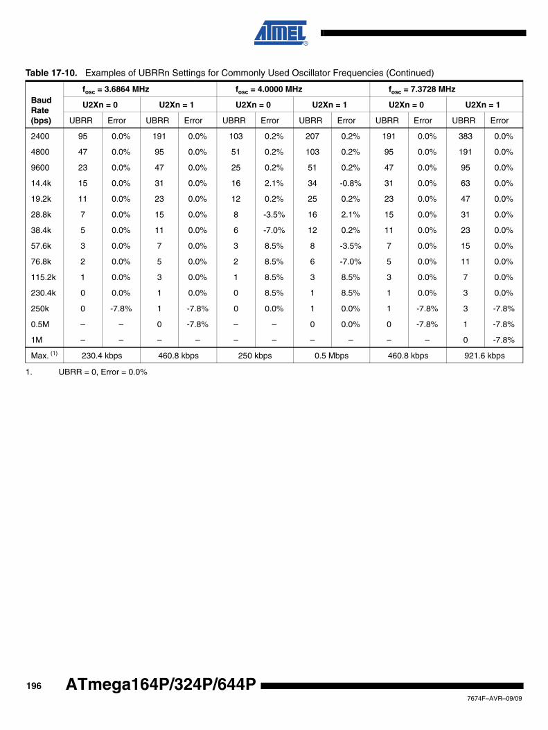
Table 17-10. Examples of UBRRn Settings for Commonly Used Oscillator Frequencies (Continued)
Baud Rate (bps)
fosc = 3.6864 MHz fosc = 4.0000 MHz fosc = 7.3728 MHz
U2Xn = 0 U2Xn = 1 U2Xn = 0 U2Xn = 1 U2Xn = 0 U2Xn = 1
UBRR Error UBRR Error UBRR Error UBRR Error UBRR Error UBRR Error
2400 95 0.0% 191 0.0% 103 0.2% 207 0.2% 191 0.0% 383 0.0%
4800 47 0.0% 95 0.0% 51 0.2% 103 0.2% 95 0.0% 191 0.0%
9600 23 0.0% 47 0.0% 25 0.2% 51 0.2% 47 0.0% 95 0.0%
14.4k 15 0.0% 31 0.0% 16 2.1% 34 -0.8% 31 0.0% 63 0.0%
19.2k 11 0.0% 23 0.0% 12 0.2% 25 0.2% 23 0.0% 47 0.0%
28.8k 7 0.0% 15 0.0% 8 -3.5% 16 2.1% 15 0.0% 31 0.0%
38.4k 5 0.0% 11 0.0% 6 -7.0% 12 0.2% 11 0.0% 23 0.0%
57.6k 3 0.0% 7 0.0% 3 8.5% 8 -3.5% 7 0.0% 15 0.0%
76.8k 2 0.0% 5 0.0% 2 8.5% 6 -7.0% 5 0.0% 11 0.0%
115.2k 1 0.0% 3 0.0% 1 8.5% 3 8.5% 3 0.0% 7 0.0%
230.4k 0 0.0% 1 0.0% 0 8.5% 1 8.5% 1 0.0% 3 0.0%
250k 0 -7.8% 1 -7.8% 0 0.0% 1 0.0% 1 -7.8% 3 -7.8%
0.5M – – 0 -7.8% – – 0 0.0% 0 -7.8% 1 -7.8%
1M – – – – – – – – – – 0 -7.8%
Max. (1) 230.4 kbps 460.8 kbps 250 kbps 0.5 Mbps 460.8 kbps 921.6 kbps
1. UBRR = 0, Error = 0.0%
1967674F–AVR–09/09
ATmega164P/324P/644P
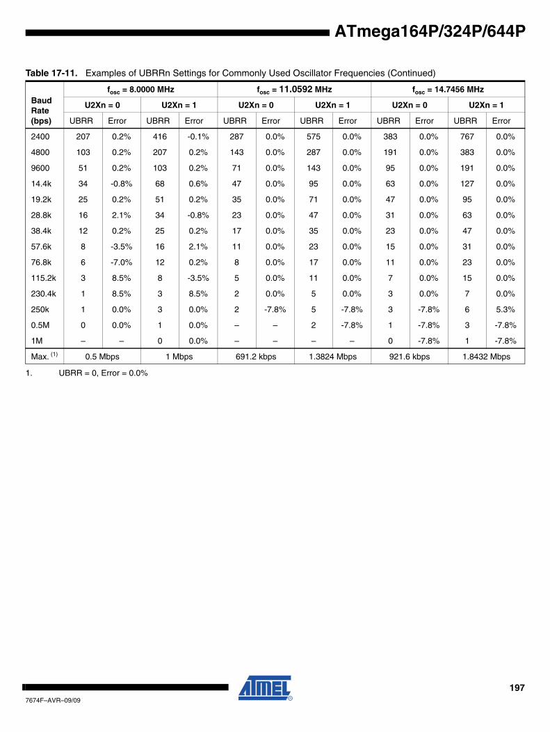
ATmega164P/324P/644P
Table 17-11. Examples of UBRRn Settings for Commonly Used Oscillator Frequencies (Continued)
Baud Rate (bps)
fosc = 8.0000 MHz fosc = 11.0592 MHz fosc = 14.7456 MHz
U2Xn = 0 U2Xn = 1 U2Xn = 0 U2Xn = 1 U2Xn = 0 U2Xn = 1
UBRR Error UBRR Error UBRR Error UBRR Error UBRR Error UBRR Error
2400 207 0.2% 416 -0.1% 287 0.0% 575 0.0% 383 0.0% 767 0.0%
4800 103 0.2% 207 0.2% 143 0.0% 287 0.0% 191 0.0% 383 0.0%
9600 51 0.2% 103 0.2% 71 0.0% 143 0.0% 95 0.0% 191 0.0%
14.4k 34 -0.8% 68 0.6% 47 0.0% 95 0.0% 63 0.0% 127 0.0%
19.2k 25 0.2% 51 0.2% 35 0.0% 71 0.0% 47 0.0% 95 0.0%
28.8k 16 2.1% 34 -0.8% 23 0.0% 47 0.0% 31 0.0% 63 0.0%
38.4k 12 0.2% 25 0.2% 17 0.0% 35 0.0% 23 0.0% 47 0.0%
57.6k 8 -3.5% 16 2.1% 11 0.0% 23 0.0% 15 0.0% 31 0.0%
76.8k 6 -7.0% 12 0.2% 8 0.0% 17 0.0% 11 0.0% 23 0.0%
115.2k 3 8.5% 8 -3.5% 5 0.0% 11 0.0% 7 0.0% 15 0.0%
230.4k 1 8.5% 3 8.5% 2 0.0% 5 0.0% 3 0.0% 7 0.0%
250k 1 0.0% 3 0.0% 2 -7.8% 5 -7.8% 3 -7.8% 6 5.3%
0.5M 0 0.0% 1 0.0% – – 2 -7.8% 1 -7.8% 3 -7.8%
1M – – 0 0.0% – – – – 0 -7.8% 1 -7.8%
Max. (1) 0.5 Mbps 1 Mbps 691.2 kbps 1.3824 Mbps 921.6 kbps 1.8432 Mbps
1. UBRR = 0, Error = 0.0%
1977674F–AVR–09/09
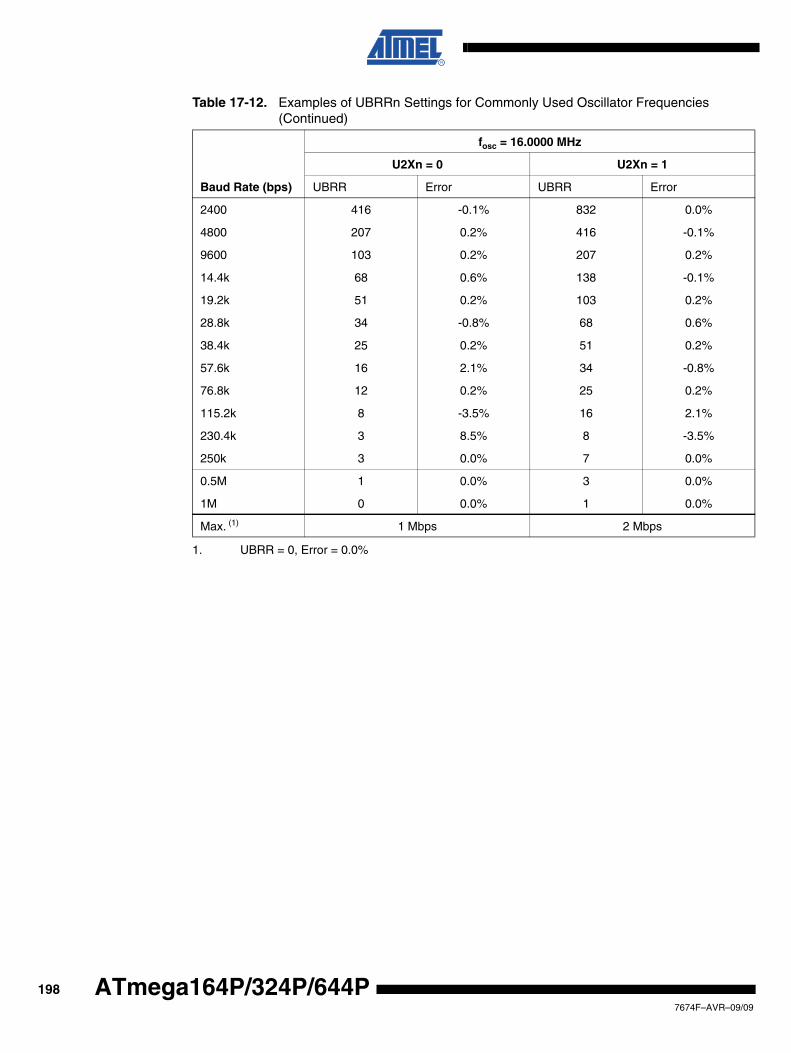
Table 17-12. Examples of UBRRn Settings for Commonly Used Oscillator Frequencies (Continued)
Baud Rate (bps)
fosc = 16.0000 MHz
U2Xn = 0 U2Xn = 1
UBRR Error UBRR Error
2400 416 -0.1% 832 0.0%
4800 207 0.2% 416 -0.1%
9600 103 0.2% 207 0.2%
14.4k 68 0.6% 138 -0.1%
19.2k 51 0.2% 103 0.2%
28.8k 34 -0.8% 68 0.6%
38.4k 25 0.2% 51 0.2%
57.6k 16 2.1% 34 -0.8%
76.8k 12 0.2% 25 0.2%
115.2k 8 -3.5% 16 2.1%
230.4k 3 8.5% 8 -3.5%
250k 3 0.0% 7 0.0%
0.5M 1 0.0% 3 0.0%
1M 0 0.0% 1 0.0%
Max. (1)
1. UBRR = 0, Error = 0.0%
1 Mbps 2 Mbps
1987674F–AVR–09/09
ATmega164P/324P/644P
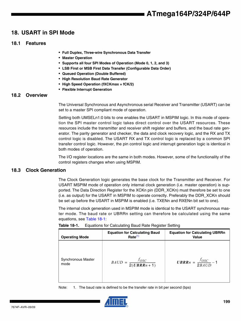
ATmega164P/324P/644P
18. USART in SPI Mode
18.1 Features
• Full Duplex, Three-wire Synchronous Data Transfer• Master Operation• Supports all four SPI Modes of Operation (Mode 0, 1, 2, and 3)• LSB First or MSB First Data Transfer (Configurable Data Order)• Queued Operation (Double Buffered)• High Resolution Baud Rate Generator• High Speed Operation (fXCKmax = fCK/2)• Flexible Interrupt Generation
18.2 Overview
The Universal Synchronous and Asynchronous serial Receiver and Transmitter (USART) can beset to a master SPI compliant mode of operation.
Setting both UMSELn1:0 bits to one enables the USART in MSPIM logic. In this mode of opera-tion the SPI master control logic takes direct control over the USART resources. Theseresources include the transmitter and receiver shift register and buffers, and the baud rate gen-erator. The parity generator and checker, the data and clock recovery logic, and the RX and TXcontrol logic is disabled. The USART RX and TX control logic is replaced by a common SPItransfer control logic. However, the pin control logic and interrupt generation logic is identical inboth modes of operation.
The I/O register locations are the same in both modes. However, some of the functionality of thecontrol registers changes when using MSPIM.
18.3 Clock Generation
The Clock Generation logic generates the base clock for the Transmitter and Receiver. ForUSART MSPIM mode of operation only internal clock generation (i.e. master operation) is sup-ported. The Data Direction Register for the XCKn pin (DDR_XCKn) must therefore be set to one(i.e. as output) for the USART in MSPIM to operate correctly. Preferably the DDR_XCKn shouldbe set up before the USART in MSPIM is enabled (i.e. TXENn and RXENn bit set to one).
The internal clock generation used in MSPIM mode is identical to the USART synchronous mas-ter mode. The baud rate or UBRRn setting can therefore be calculated using the sameequations, see Table 18-1:
Note: 1. The baud rate is defined to be the transfer rate in bit per second (bps)
Table 18-1. Equations for Calculating Baud Rate Register Setting
Operating ModeEquation for Calculating Baud
Rate(1)Equation for Calculating UBRRn
Value
Synchronous Master mode BAUD
fOSC2 UBRRn 1+( )---------------------------------------= UBRRn
fOSC2BAUD-------------------- 1–=
1997674F–AVR–09/09
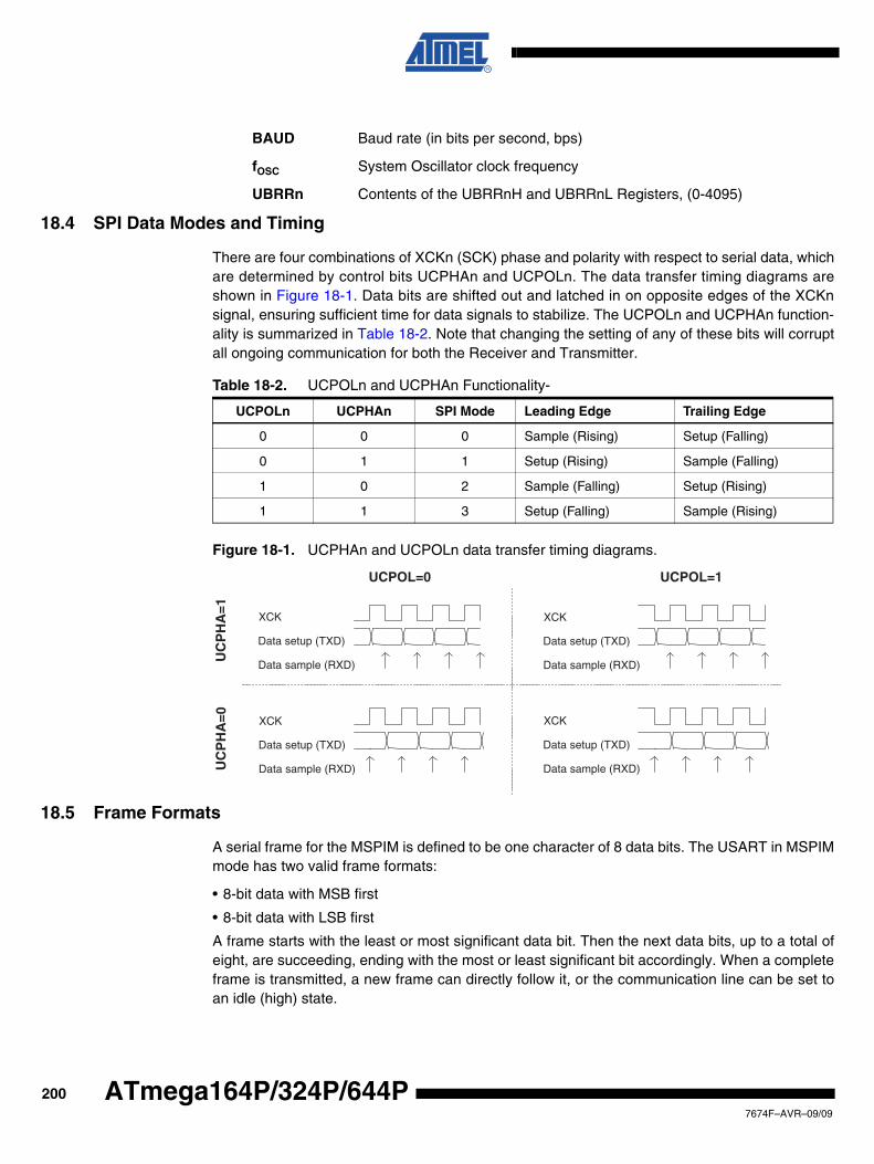
BAUD Baud rate (in bits per second, bps)
fOSC System Oscillator clock frequency
UBRRn Contents of the UBRRnH and UBRRnL Registers, (0-4095)
18.4 SPI Data Modes and Timing
There are four combinations of XCKn (SCK) phase and polarity with respect to serial data, whichare determined by control bits UCPHAn and UCPOLn. The data transfer timing diagrams areshown in Figure 18-1. Data bits are shifted out and latched in on opposite edges of the XCKnsignal, ensuring sufficient time for data signals to stabilize. The UCPOLn and UCPHAn function-ality is summarized in Table 18-2. Note that changing the setting of any of these bits will corruptall ongoing communication for both the Receiver and Transmitter.
Figure 18-1. UCPHAn and UCPOLn data transfer timing diagrams.
18.5 Frame Formats
A serial frame for the MSPIM is defined to be one character of 8 data bits. The USART in MSPIMmode has two valid frame formats:
• 8-bit data with MSB first
• 8-bit data with LSB first
A frame starts with the least or most significant data bit. Then the next data bits, up to a total ofeight, are succeeding, ending with the most or least significant bit accordingly. When a completeframe is transmitted, a new frame can directly follow it, or the communication line can be set toan idle (high) state.
Table 18-2. UCPOLn and UCPHAn Functionality-
UCPOLn UCPHAn SPI Mode Leading Edge Trailing Edge
0 0 0 Sample (Rising) Setup (Falling)
0 1 1 Setup (Rising) Sample (Falling)
1 0 2 Sample (Falling) Setup (Rising)
1 1 3 Setup (Falling) Sample (Rising)
XCK
Data setup (TXD)
Data sample (RXD)
XCK
Data setup (TXD)
Data sample (RXD)
XCK
Data setup (TXD)
Data sample (RXD)
XCK
Data setup (TXD)
Data sample (RXD)
UCPOL=0 UCPOL=1
UC
PH
A=0
UC
PH
A=1
2007674F–AVR–09/09
ATmega164P/324P/644P
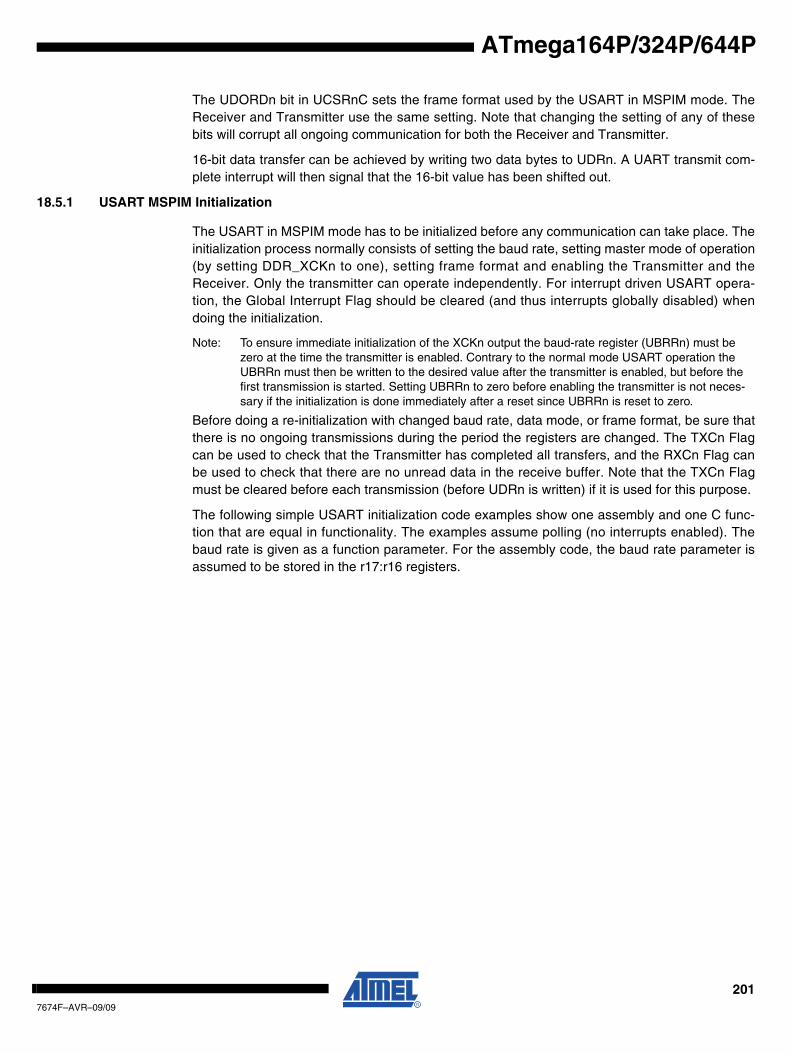
ATmega164P/324P/644P
The UDORDn bit in UCSRnC sets the frame format used by the USART in MSPIM mode. TheReceiver and Transmitter use the same setting. Note that changing the setting of any of thesebits will corrupt all ongoing communication for both the Receiver and Transmitter.
16-bit data transfer can be achieved by writing two data bytes to UDRn. A UART transmit com-plete interrupt will then signal that the 16-bit value has been shifted out.
18.5.1 USART MSPIM Initialization
The USART in MSPIM mode has to be initialized before any communication can take place. Theinitialization process normally consists of setting the baud rate, setting master mode of operation(by setting DDR_XCKn to one), setting frame format and enabling the Transmitter and theReceiver. Only the transmitter can operate independently. For interrupt driven USART opera-tion, the Global Interrupt Flag should be cleared (and thus interrupts globally disabled) whendoing the initialization.
Note: To ensure immediate initialization of the XCKn output the baud-rate register (UBRRn) must be zero at the time the transmitter is enabled. Contrary to the normal mode USART operation the UBRRn must then be written to the desired value after the transmitter is enabled, but before the first transmission is started. Setting UBRRn to zero before enabling the transmitter is not neces-sary if the initialization is done immediately after a reset since UBRRn is reset to zero.
Before doing a re-initialization with changed baud rate, data mode, or frame format, be sure thatthere is no ongoing transmissions during the period the registers are changed. The TXCn Flagcan be used to check that the Transmitter has completed all transfers, and the RXCn Flag canbe used to check that there are no unread data in the receive buffer. Note that the TXCn Flagmust be cleared before each transmission (before UDRn is written) if it is used for this purpose.
The following simple USART initialization code examples show one assembly and one C func-tion that are equal in functionality. The examples assume polling (no interrupts enabled). Thebaud rate is given as a function parameter. For the assembly code, the baud rate parameter isassumed to be stored in the r17:r16 registers.
2017674F–AVR–09/09
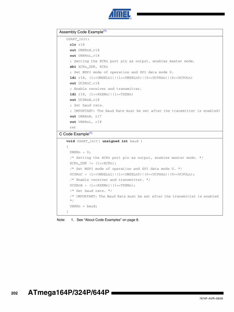
Note: 1. See “About Code Examples” on page 8.
Assembly Code Example(1)
USART_Init:
clr r18
out UBRRnH,r18
out UBRRnL,r18
; Setting the XCKn port pin as output, enables master mode.
sbi XCKn_DDR, XCKn
; Set MSPI mode of operation and SPI data mode 0.
ldi r18, (1<<UMSELn1)|(1<<UMSELn0)|(0<<UCPHAn)|(0<<UCPOLn)
out UCSRnC,r18
; Enable receiver and transmitter.
ldi r18, (1<<RXENn)|(1<<TXENn)
out UCSRnB,r18
; Set baud rate.
; IMPORTANT: The Baud Rate must be set after the transmitter is enabled!
out UBRRnH, r17
out UBRRnL, r18
ret
C Code Example(1)
void USART_Init( unsigned int baud )
{
UBRRn = 0;
/* Setting the XCKn port pin as output, enables master mode. */
XCKn_DDR |= (1<<XCKn);
/* Set MSPI mode of operation and SPI data mode 0. */
UCSRnC = (1<<UMSELn1)|(1<<UMSELn0)|(0<<UCPHAn)|(0<<UCPOLn);
/* Enable receiver and transmitter. */
UCSRnB = (1<<RXENn)|(1<<TXENn);
/* Set baud rate. */
/* IMPORTANT: The Baud Rate must be set after the transmitter is enabled */
UBRRn = baud;
}
2027674F–AVR–09/09
ATmega164P/324P/644P
ATmega164P/324P/644P
18.6 Data TransferUsing the USART in MSPI mode requires the Transmitter to be enabled, i.e. the TXENn bit inthe UCSRnB register is set to one. When the Transmitter is enabled, the normal port operationof the TxDn pin is overridden and given the function as the Transmitter's serial output. Enablingthe receiver is optional and is done by setting the RXENn bit in the UCSRnB register to one.When the receiver is enabled, the normal pin operation of the RxDn pin is overridden and giventhe function as the Receiver's serial input. The XCKn will in both cases be used as the transferclock.
After initialization the USART is ready for doing data transfers. A data transfer is initiated by writ-ing to the UDRn I/O location. This is the case for both sending and receiving data since thetransmitter controls the transfer clock. The data written to UDRn is moved from the transmit buf-fer to the shift register when the shift register is ready to send a new frame.
Note: To keep the input buffer in sync with the number of data bytes transmitted, the UDRn register must be read once for each byte transmitted. The input buffer operation is identical to normal USART mode, i.e. if an overflow occurs the character last received will be lost, not the first data in the buf-fer. This means that if four bytes are transferred, byte 1 first, then byte 2, 3, and 4, and the UDRn is not read before all transfers are completed, then byte 3 to be received will be lost, and not byte 1.
The following code examples show a simple USART in MSPIM mode transfer function based onpolling of the Data Register Empty (UDREn) Flag and the Receive Complete (RXCn) Flag. TheUSART has to be initialized before the function can be used. For the assembly code, the data tobe sent is assumed to be stored in Register R16 and the data received will be available in thesame register (R16) after the function returns.
The function simply waits for the transmit buffer to be empty by checking the UDREn Flag,before loading it with new data to be transmitted. The function then waits for data to be presentin the receive buffer by checking the RXCn Flag, before reading the buffer and returning thevalue..
2037674F–AVR–09/09
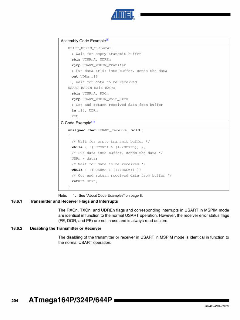
Note: 1. See “About Code Examples” on page 8.
18.6.1 Transmitter and Receiver Flags and Interrupts
The RXCn, TXCn, and UDREn flags and corresponding interrupts in USART in MSPIM modeare identical in function to the normal USART operation. However, the receiver error status flags(FE, DOR, and PE) are not in use and is always read as zero.
18.6.2 Disabling the Transmitter or Receiver
The disabling of the transmitter or receiver in USART in MSPIM mode is identical in function tothe normal USART operation.
Assembly Code Example(1)
USART_MSPIM_Transfer:
; Wait for empty transmit buffer
sbis UCSRnA, UDREn
rjmp USART_MSPIM_Transfer
; Put data (r16) into buffer, sends the data
out UDRn,r16
; Wait for data to be received
USART_MSPIM_Wait_RXCn:
sbis UCSRnA, RXCn
rjmp USART_MSPIM_Wait_RXCn
; Get and return received data from buffer
in r16, UDRn
ret
C Code Example(1)
unsigned char USART_Receive( void )
{
/* Wait for empty transmit buffer */
while ( !( UCSRnA & (1<<UDREn)) );
/* Put data into buffer, sends the data */
UDRn = data;
/* Wait for data to be received */
while ( !(UCSRnA & (1<<RXCn)) );
/* Get and return received data from buffer */
return UDRn;
}
2047674F–AVR–09/09
ATmega164P/324P/644P
ATmega164P/324P/644P
18.7 AVR USART MSPIM vs. AVR SPIThe USART in MSPIM mode is fully compatible with the AVR SPI regarding:
• Master mode timing diagram.
• The UCPOLn bit functionality is identical to the SPI CPOL bit.
• The UCPHAn bit functionality is identical to the SPI CPHA bit.
• The UDORDn bit functionality is identical to the SPI DORD bit.
However, since the USART in MSPIM mode reuses the USART resources, the use of theUSART in MSPIM mode is somewhat different compared to the SPI. In addition to differences ofthe control register bits, and that only master operation is supported by the USART in MSPIMmode, the following features differ between the two modules:
• The USART in MSPIM mode includes (double) buffering of the transmitter. The SPI has no buffer.
• The USART in MSPIM mode receiver includes an additional buffer level.
• The SPI WCOL (Write Collision) bit is not included in USART in MSPIM mode.
• The SPI double speed mode (SPI2X) bit is not included. However, the same effect is achieved by setting UBRRn accordingly.
• Interrupt timing is not compatible.
• Pin control differs due to the master only operation of the USART in MSPIM mode.
A comparison of the USART in MSPIM mode and the SPI pins is shown in Table 18-3 on page205.
Table 18-3. Comparison of USART in MSPIM mode and SPI pins.
USART_MSPIM SPI Comment
TxDn MOSI Master Out only
RxDn MISO Master In only
XCKn SCK (Functionally identical)
(N/A) SS Not supported by USART in MSPIM
2057674F–AVR–09/09
18.8 Register Description
The following section describes the registers used for SPI operation using the USART.
18.8.1 UDRn – USART MSPIM I/O Data Register
The function and bit description of the USART data register (UDRn) in MSPI mode is identical tonormal USART operation. See “UDRn – USART I/O Data Register n” on page 190.
18.8.2 UCSRnA – USART MSPIM Control and Status Register n A
• Bit 7 - RXCn: USART Receive CompleteThis flag bit is set when there are unread data in the receive buffer and cleared when the receivebuffer is empty (i.e., does not contain any unread data). If the Receiver is disabled, the receivebuffer will be flushed and consequently the RXCn bit will become zero. The RXCn Flag can beused to generate a Receive Complete interrupt (see description of the RXCIEn bit).
• Bit 6 - TXCn: USART Transmit CompleteThis flag bit is set when the entire frame in the Transmit Shift Register has been shifted out andthere are no new data currently present in the transmit buffer (UDRn). The TXCn Flag bit is auto-matically cleared when a transmit complete interrupt is executed, or it can be cleared by writinga one to its bit location. The TXCn Flag can generate a Transmit Complete interrupt (seedescription of the TXCIEn bit).
• Bit 5 - UDREn: USART Data Register EmptyThe UDREn Flag indicates if the transmit buffer (UDRn) is ready to receive new data. If UDREnis one, the buffer is empty, and therefore ready to be written. The UDREn Flag can generate aData Register Empty interrupt (see description of the UDRIE bit). UDREn is set after a reset toindicate that the Transmitter is ready.
• Bit 4:0 - Reserved Bits in MSPI modeWhen in MSPI mode, these bits are reserved for future use. For compatibility with future devices,these bits must be written to zero when UCSRnA is written.
Bit 7 6 5 4 3 2 1 0
RXCn TXCn UDREn - - - - - UCSRnA
Read/Write R/W R/W R/W R R R R R
Initial Value 0 0 0 0 0 1 1 0
2067674F–AVR–09/09
ATmega164P/324P/644P
ATmega164P/324P/644P
18.8.3 UCSRnB – USART MSPIM Control and Status Register n B
• Bit 7 - RXCIEn: RX Complete Interrupt EnableWriting this bit to one enables interrupt on the RXCn Flag. A USART Receive Complete interruptwill be generated only if the RXCIEn bit is written to one, the Global Interrupt Flag in SREG iswritten to one and the RXCn bit in UCSRnA is set.
• Bit 6 - TXCIEn: TX Complete Interrupt EnableWriting this bit to one enables interrupt on the TXCn Flag. A USART Transmit Complete interruptwill be generated only if the TXCIEn bit is written to one, the Global Interrupt Flag in SREG iswritten to one and the TXCn bit in UCSRnA is set.
• Bit 5 - UDRIE: USART Data Register Empty Interrupt EnableWriting this bit to one enables interrupt on the UDREn Flag. A Data Register Empty interrupt willbe generated only if the UDRIE bit is written to one, the Global Interrupt Flag in SREG is writtento one and the UDREn bit in UCSRnA is set.
• Bit 4 - RXENn: Receiver EnableWriting this bit to one enables the USART Receiver in MSPIM mode. The Receiver will overridenormal port operation for the RxDn pin when enabled. Disabling the Receiver will flush thereceive buffer. Only enabling the receiver in MSPI mode (i.e. setting RXENn=1 and TXENn=0)has no meaning since it is the transmitter that controls the transfer clock and since only mastermode is supported.
• Bit 3 - TXENn: Transmitter EnableWriting this bit to one enables the USART Transmitter. The Transmitter will override normal portoperation for the TxDn pin when enabled. The disabling of the Transmitter (writing TXENn tozero) will not become effective until ongoing and pending transmissions are completed, i.e.,when the Transmit Shift Register and Transmit Buffer Register do not contain data to be trans-mitted. When disabled, the Transmitter will no longer override the TxDn port.
• Bit 2:0 - Reserved Bits in MSPI modeWhen in MSPI mode, these bits are reserved for future use. For compatibility with future devices,these bits must be written to zero when UCSRnB is written.
Bit 7 6 5 4 3 2 1 0
RXCIEn TXCIEn UDRIE RXENn TXENn - - - UCSRnB
Read/Write R/W R/W R/W R/W R/W R R R
Initial Value 0 0 0 0 0 1 1 0
2077674F–AVR–09/09
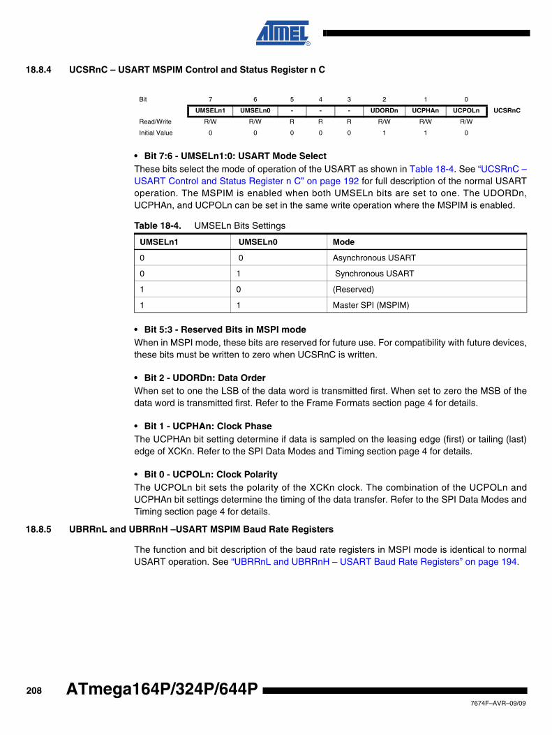
18.8.4 UCSRnC – USART MSPIM Control and Status Register n C
• Bit 7:6 - UMSELn1:0: USART Mode SelectThese bits select the mode of operation of the USART as shown in Table 18-4. See “UCSRnC –USART Control and Status Register n C” on page 192 for full description of the normal USARToperation. The MSPIM is enabled when both UMSELn bits are set to one. The UDORDn,UCPHAn, and UCPOLn can be set in the same write operation where the MSPIM is enabled.
• Bit 5:3 - Reserved Bits in MSPI modeWhen in MSPI mode, these bits are reserved for future use. For compatibility with future devices,these bits must be written to zero when UCSRnC is written.
• Bit 2 - UDORDn: Data OrderWhen set to one the LSB of the data word is transmitted first. When set to zero the MSB of thedata word is transmitted first. Refer to the Frame Formats section page 4 for details.
• Bit 1 - UCPHAn: Clock PhaseThe UCPHAn bit setting determine if data is sampled on the leasing edge (first) or tailing (last)edge of XCKn. Refer to the SPI Data Modes and Timing section page 4 for details.
• Bit 0 - UCPOLn: Clock PolarityThe UCPOLn bit sets the polarity of the XCKn clock. The combination of the UCPOLn andUCPHAn bit settings determine the timing of the data transfer. Refer to the SPI Data Modes andTiming section page 4 for details.
18.8.5 UBRRnL and UBRRnH –USART MSPIM Baud Rate Registers
The function and bit description of the baud rate registers in MSPI mode is identical to normalUSART operation. See “UBRRnL and UBRRnH – USART Baud Rate Registers” on page 194.
Bit 7 6 5 4 3 2 1 0
UMSELn1 UMSELn0 - - - UDORDn UCPHAn UCPOLn UCSRnC
Read/Write R/W R/W R R R R/W R/W R/W
Initial Value 0 0 0 0 0 1 1 0
Table 18-4. UMSELn Bits Settings
UMSELn1 UMSELn0 Mode
0 0 Asynchronous USART
0 1 Synchronous USART
1 0 (Reserved)
1 1 Master SPI (MSPIM)
2087674F–AVR–09/09
ATmega164P/324P/644P
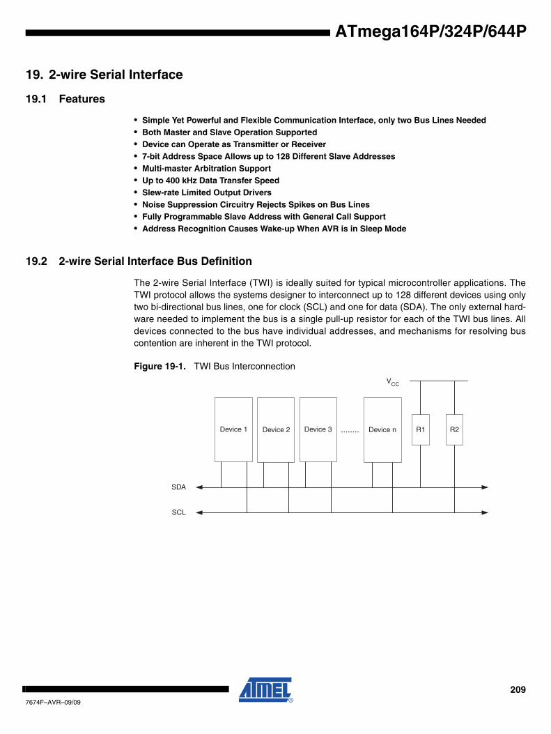
ATmega164P/324P/644P
19. 2-wire Serial Interface
19.1 Features
• Simple Yet Powerful and Flexible Communication Interface, only two Bus Lines Needed• Both Master and Slave Operation Supported• Device can Operate as Transmitter or Receiver• 7-bit Address Space Allows up to 128 Different Slave Addresses• Multi-master Arbitration Support• Up to 400 kHz Data Transfer Speed• Slew-rate Limited Output Drivers• Noise Suppression Circuitry Rejects Spikes on Bus Lines• Fully Programmable Slave Address with General Call Support• Address Recognition Causes Wake-up When AVR is in Sleep Mode
19.2 2-wire Serial Interface Bus Definition
The 2-wire Serial Interface (TWI) is ideally suited for typical microcontroller applications. TheTWI protocol allows the systems designer to interconnect up to 128 different devices using onlytwo bi-directional bus lines, one for clock (SCL) and one for data (SDA). The only external hard-ware needed to implement the bus is a single pull-up resistor for each of the TWI bus lines. Alldevices connected to the bus have individual addresses, and mechanisms for resolving buscontention are inherent in the TWI protocol.
Figure 19-1. TWI Bus Interconnection
Device 1 Device 2 Device 3 Device n
SDA
SCL
........ R1 R2
VCC
2097674F–AVR–09/09
19.2.1 TWI TerminologyThe following definitions are frequently encountered in this section.
The Power Reduction TWI bit, PRTWI bit in “PRR – Power Reduction Register” on page 47 mustbe written to zero to enable the 2-wire Serial Interface.
19.2.2 Electrical Interconnection
As depicted in Figure 19-1, both bus lines are connected to the positive supply voltage throughpull-up resistors. The bus drivers of all TWI-compliant devices are open-drain or open-collector.This implements a wired-AND function which is essential to the operation of the interface. A lowlevel on a TWI bus line is generated when one or more TWI devices output a zero. A high levelis output when all TWI devices trim-state their outputs, allowing the pull-up resistors to pull theline high. Note that all AVR devices connected to the TWI bus must be powered in order to allowany bus operation.
The number of devices that can be connected to the bus is only limited by the bus capacitancelimit of 400 pF and the 7-bit slave address space. A detailed specification of the electrical char-acteristics of the TWI is given in “SPI Timing Characteristics” on page 333. Two different sets ofspecifications are presented there, one relevant for bus speeds below 100 kHz, and one valid forbus speeds up to 400 kHz.
19.3 Data Transfer and Frame Format
19.3.1 Transferring Bits
Each data bit transferred on the TWI bus is accompanied by a pulse on the clock line. The levelof the data line must be stable when the clock line is high. The only exception to this rule is forgenerating start and stop conditions.
Table 19-1. TWI Terminology
Term Description
MasterThe device that initiates and terminates a transmission. The Master also generates the SCL clock.
Slave The device addressed by a Master.
Transmitter The device placing data on the bus.
Receiver The device reading data from the bus.
2107674F–AVR–09/09
ATmega164P/324P/644P
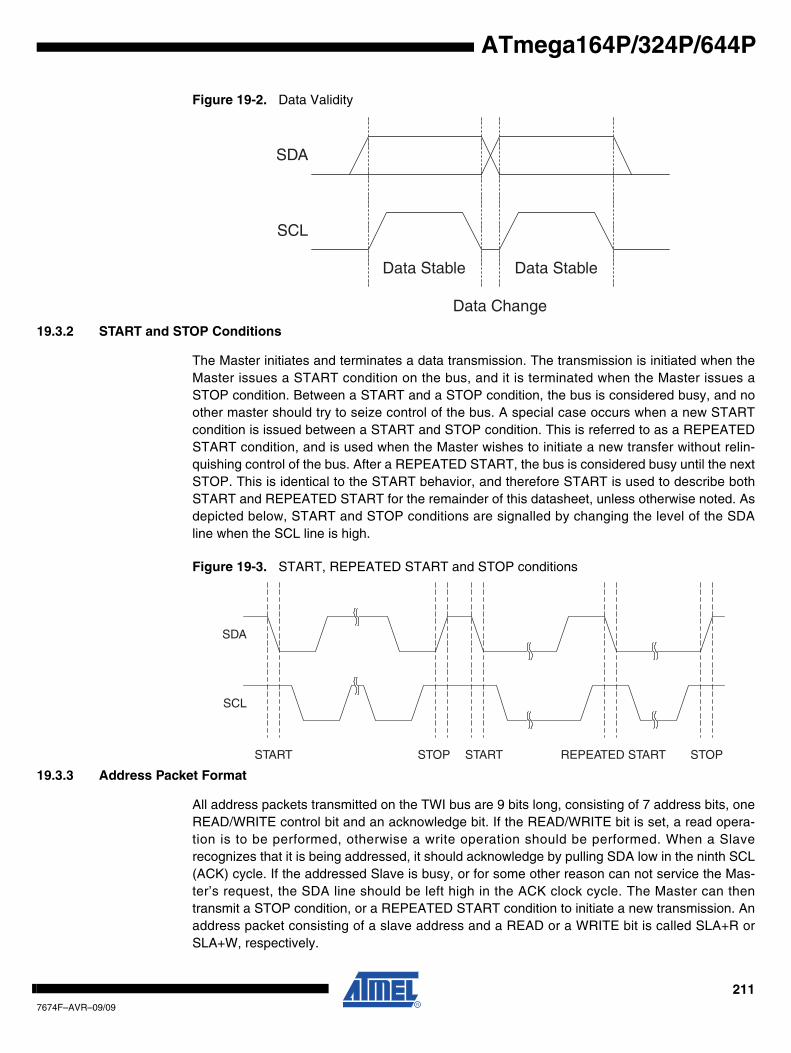
ATmega164P/324P/644P
Figure 19-2. Data Validity
19.3.2 START and STOP Conditions
The Master initiates and terminates a data transmission. The transmission is initiated when theMaster issues a START condition on the bus, and it is terminated when the Master issues aSTOP condition. Between a START and a STOP condition, the bus is considered busy, and noother master should try to seize control of the bus. A special case occurs when a new STARTcondition is issued between a START and STOP condition. This is referred to as a REPEATEDSTART condition, and is used when the Master wishes to initiate a new transfer without relin-quishing control of the bus. After a REPEATED START, the bus is considered busy until the nextSTOP. This is identical to the START behavior, and therefore START is used to describe bothSTART and REPEATED START for the remainder of this datasheet, unless otherwise noted. Asdepicted below, START and STOP conditions are signalled by changing the level of the SDAline when the SCL line is high.
Figure 19-3. START, REPEATED START and STOP conditions
19.3.3 Address Packet Format
All address packets transmitted on the TWI bus are 9 bits long, consisting of 7 address bits, oneREAD/WRITE control bit and an acknowledge bit. If the READ/WRITE bit is set, a read opera-tion is to be performed, otherwise a write operation should be performed. When a Slaverecognizes that it is being addressed, it should acknowledge by pulling SDA low in the ninth SCL(ACK) cycle. If the addressed Slave is busy, or for some other reason can not service the Mas-ter’s request, the SDA line should be left high in the ACK clock cycle. The Master can thentransmit a STOP condition, or a REPEATED START condition to initiate a new transmission. Anaddress packet consisting of a slave address and a READ or a WRITE bit is called SLA+R orSLA+W, respectively.
SDA
SCL
Data Stable Data Stable
Data Change
SDA
SCL
START STOPREPEATED STARTSTOP START
2117674F–AVR–09/09
The MSB of the address byte is transmitted first. Slave addresses can freely be allocated by thedesigner, but the address 0000 000 is reserved for a general call.
When a general call is issued, all slaves should respond by pulling the SDA line low in the ACKcycle. A general call is used when a Master wishes to transmit the same message to severalslaves in the system. When the general call address followed by a Write bit is transmitted on thebus, all slaves set up to acknowledge the general call will pull the SDA line low in the ack cycle.The following data packets will then be received by all the slaves that acknowledged the generalcall. Note that transmitting the general call address followed by a Read bit is meaningless, asthis would cause contention if several slaves started transmitting different data.
All addresses of the format 1111 xxx should be reserved for future purposes.
Figure 19-4. Address Packet Format
19.3.4 Data Packet Format
All data packets transmitted on the TWI bus are nine bits long, consisting of one data byte andan acknowledge bit. During a data transfer, the Master generates the clock and the START andSTOP conditions, while the Receiver is responsible for acknowledging the reception. AnAcknowledge (ACK) is signalled by the Receiver pulling the SDA line low during the ninth SCLcycle. If the Receiver leaves the SDA line high, a NACK is signalled. When the Receiver hasreceived the last byte, or for some reason cannot receive any more bytes, it should inform theTransmitter by sending a NACK after the final byte. The MSB of the data byte is transmitted first.
Figure 19-5. Data Packet Format
SDA
SCL
START
1 2 7 8 9
Addr MSB Addr LSB R/W ACK
1 2 7 8 9
Data MSB Data LSB ACK
AggregateSDA
SDA fromTransmitter
SDA fromReceiver
SCL fromMaster
SLA+R/W Data ByteSTOP, REPEATED
START or NextData Byte
2127674F–AVR–09/09
ATmega164P/324P/644P
ATmega164P/324P/644P
19.3.5 Combining Address and Data Packets into a TransmissionA transmission basically consists of a START condition, a SLA+R/W, one or more data packetsand a STOP condition. An empty message, consisting of a START followed by a STOP condi-tion, is illegal. Note that the Wired-ANDing of the SCL line can be used to implementhandshaking between the Master and the Slave. The Slave can extend the SCL low period bypulling the SCL line low. This is useful if the clock speed set up by the Master is too fast for theSlave, or the Slave needs extra time for processing between the data transmissions. The Slaveextending the SCL low period will not affect the SCL high period, which is determined by theMaster. As a consequence, the Slave can reduce the TWI data transfer speed by prolonging theSCL duty cycle.
Figure 19-6 on page 213 shows a typical data transmission. Note that several data bytes can betransmitted between the SLA+R/W and the STOP condition, depending on the software protocolimplemented by the application software.
Figure 19-6. Typical Data Transmission
19.4 Multi-master Bus Systems, Arbitration and Synchronization
The TWI protocol allows bus systems with several masters. Special concerns have been takenin order to ensure that transmissions will proceed as normal, even if two or more masters initiatea transmission at the same time. Two problems arise in multi-master systems:
• An algorithm must be implemented allowing only one of the masters to complete the transmission. All other masters should cease transmission when they discover that they have lost the selection process. This selection process is called arbitration. When a contending master discovers that it has lost the arbitration process, it should immediately switch to Slave mode to check whether it is being addressed by the winning master. The fact that multiple masters have started transmission at the same time should not be detectable to the slaves, i.e. the data being transferred on the bus must not be corrupted.
• Different masters may use different SCL frequencies. A scheme must be devised to synchronize the serial clocks from all masters, in order to let the transmission proceed in a lockstep fashion. This will facilitate the arbitration process.
The wired-ANDing of the bus lines is used to solve both these problems. The serial clocks fromall masters will be wired-ANDed, yielding a combined clock with a high period equal to the onefrom the Master with the shortest high period. The low period of the combined clock is equal tothe low period of the Master with the longest low period. Note that all masters listen to the SCLline, effectively starting to count their SCL high and low time-out periods when the combinedSCL line goes high or low, respectively.
1 2 7 8 9
Data Byte
Data MSB Data LSB ACK
1 2 7 8 9
Addr MSB Addr LSB R/W ACK
SLA+R/W
2137674F–AVR–09/09
Figure 19-7. SCL Synchronization Between Multiple Masters
Arbitration is carried out by all masters continuously monitoring the SDA line after outputtingdata. If the value read from the SDA line does not match the value the Master had output, it haslost the arbitration. Note that a Master can only lose arbitration when it outputs a high SDA valuewhile another Master outputs a low value. The losing Master should immediately go to Slavemode, checking if it is being addressed by the winning Master. The SDA line should be left high,but losing masters are allowed to generate a clock signal until the end of the current data oraddress packet. Arbitration will continue until only one Master remains, and this may take manybits. If several masters are trying to address the same Slave, arbitration will continue into thedata packet.
Figure 19-8. Arbitration Between Two Masters
TA low TA high
SCL fromMaster A
SCL fromMaster B
SCL BusLine
TBlow TBhigh
Masters StartCounting Low Period
Masters StartCounting High Period
SDA fromMaster A
SDA fromMaster B
SDA Line
SynchronizedSCL Line
START Master A LosesArbitration, SDAA SDA
2147674F–AVR–09/09
ATmega164P/324P/644P
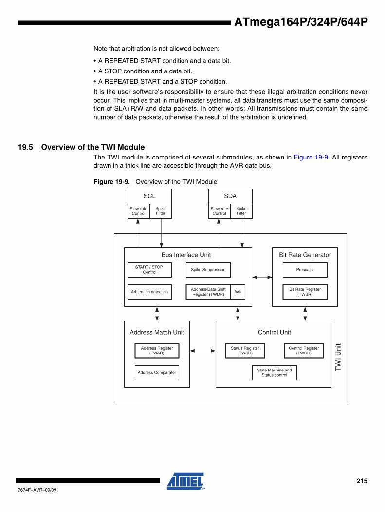
ATmega164P/324P/644P
Note that arbitration is not allowed between:
• A REPEATED START condition and a data bit.
• A STOP condition and a data bit.
• A REPEATED START and a STOP condition.
It is the user software’s responsibility to ensure that these illegal arbitration conditions neveroccur. This implies that in multi-master systems, all data transfers must use the same composi-tion of SLA+R/W and data packets. In other words: All transmissions must contain the samenumber of data packets, otherwise the result of the arbitration is undefined.
19.5 Overview of the TWI ModuleThe TWI module is comprised of several submodules, as shown in Figure 19-9. All registersdrawn in a thick line are accessible through the AVR data bus.
Figure 19-9. Overview of the TWI Module
TW
I Uni
tAddress Register
(TWAR)
Address Match Unit
Address Comparator
Control Unit
Control Register(TWCR)
Status Register(TWSR)
State Machine andStatus control
SCL
Slew-rateControl
SpikeFilter
SDA
Slew-rateControl
SpikeFilter
Bit Rate Generator
Bit Rate Register(TWBR)
Prescaler
Bus Interface Unit
START / STOPControl
Arbitration detection Ack
Spike Suppression
Address/Data ShiftRegister (TWDR)
2157674F–AVR–09/09
19.5.1 SCL and SDA PinsThese pins interface the AVR TWI with the rest of the MCU system. The output drivers contain aslew-rate limiter in order to conform to the TWI specification. The input stages contain a spikesuppression unit removing spikes shorter than 50 ns. Note that the internal pull-ups in the AVRpads can be enabled by setting the PORT bits corresponding to the SCL and SDA pins, asexplained in the I/O Port section. The internal pull-ups can in some systems eliminate the needfor external ones.
19.5.2 Bit Rate Generator Unit
This unit controls the period of SCL when operating in a Master mode. The SCL period is con-trolled by settings in the TWI Bit Rate Register (TWBR) and the Prescaler bits in the TWI StatusRegister (TWSR). Slave operation does not depend on Bit Rate or Prescaler settings, but theCPU clock frequency in the Slave must be at least 16 times higher than the SCL frequency. Notethat slaves may prolong the SCL low period, thereby reducing the average TWI bus clockperiod. The SCL frequency is generated according to the following equation:
• TWBR = Value of the TWI Bit Rate Register.
• TWPS = Value of the prescaler bits in the TWI Status Register.
Note: Pull-up resistor values should be selected according to the SCL frequency and the capacitive bus line load. See 2-wire Serial Bus Requirements in Table 26-7 on page 334 for value of pull-up resistor.
19.5.3 Bus Interface Unit
This unit contains the Data and Address Shift Register (TWDR), a START/STOP Controller andArbitration detection hardware. The TWDR contains the address or data bytes to be transmitted,or the address or data bytes received. In addition to the 8-bit TWDR, the Bus Interface Unit alsocontains a register containing the (N)ACK bit to be transmitted or received. This (N)ACK Regis-ter is not directly accessible by the application software. However, when receiving, it can be setor cleared by manipulating the TWI Control Register (TWCR). When in Transmitter mode, thevalue of the received (N)ACK bit can be determined by the value in the TWSR.
The START/STOP Controller is responsible for generation and detection of START, REPEATEDSTART, and STOP conditions. The START/STOP controller is able to detect START and STOPconditions even when the AVR MCU is in one of the sleep modes, enabling the MCU to wake upif addressed by a Master.
If the TWI has initiated a transmission as Master, the Arbitration Detection hardware continu-ously monitors the transmission trying to determine if arbitration is in process. If the TWI has lostan arbitration, the Control Unit is informed. Correct action can then be taken and appropriatestatus codes generated.
SCL frequency CPU Clock frequency
16 2(TWBR) 4TWPS⋅+
--------------------------------------------------------------=
2167674F–AVR–09/09
ATmega164P/324P/644P
ATmega164P/324P/644P
19.5.4 Address Match UnitThe Address Match unit checks if received address bytes match the seven-bit address in theTWI Address Register (TWAR). If the TWI General Call Recognition Enable (TWGCE) bit in theTWAR is written to one, all incoming address bits will also be compared against the General Calladdress. Upon an address match, the Control Unit is informed, allowing correct action to betaken. The TWI may or may not acknowledge its address, depending on settings in the TWCR.The Address Match unit is able to compare addresses even when the AVR MCU is in sleepmode, enabling the MCU to wake up if addressed by a Master. If another interrupt (e.g., INT0)occurs during TWI Power-down address match and wakes up the CPU, the TWI aborts opera-tion and return to it’s idle state. If this cause any problems, ensure that TWI Address Match is theonly enabled interrupt when entering Power-down.
19.5.5 Control Unit
The Control unit monitors the TWI bus and generates responses corresponding to settings in theTWI Control Register (TWCR). When an event requiring the attention of the application occurson the TWI bus, the TWI Interrupt Flag (TWINT) is asserted. In the next clock cycle, the TWI Sta-tus Register (TWSR) is updated with a status code identifying the event. The TWSR onlycontains relevant status information when the TWI Interrupt Flag is asserted. At all other times,the TWSR contains a special status code indicating that no relevant status information is avail-able. As long as the TWINT Flag is set, the SCL line is held low. This allows the applicationsoftware to complete its tasks before allowing the TWI transmission to continue.
The TWINT Flag is set in the following situations:
• After the TWI has transmitted a START/REPEATED START condition.
• After the TWI has transmitted SLA+R/W.
• After the TWI has transmitted an address byte.
• After the TWI has lost arbitration.
• After the TWI has been addressed by own slave address or general call.
• After the TWI has received a data byte.
• After a STOP or REPEATED START has been received while still addressed as a Slave.
• When a bus error has occurred due to an illegal START or STOP condition.
19.6 Using the TWI
The AVR TWI is byte-oriented and interrupt based. Interrupts are issued after all bus events, likereception of a byte or transmission of a START condition. Because the TWI is interrupt-based,the application software is free to carry on other operations during a TWI byte transfer. Note thatthe TWI Interrupt Enable (TWIE) bit in TWCR together with the Global Interrupt Enable bit inSREG allow the application to decide whether or not assertion of the TWINT Flag should gener-ate an interrupt request. If the TWIE bit is cleared, the application must poll the TWINT Flag inorder to detect actions on the TWI bus.
When the TWINT Flag is asserted, the TWI has finished an operation and awaits applicationresponse. In this case, the TWI Status Register (TWSR) contains a value indicating the currentstate of the TWI bus. The application software can then decide how the TWI should behave inthe next TWI bus cycle by manipulating the TWCR and TWDR Registers.
2177674F–AVR–09/09
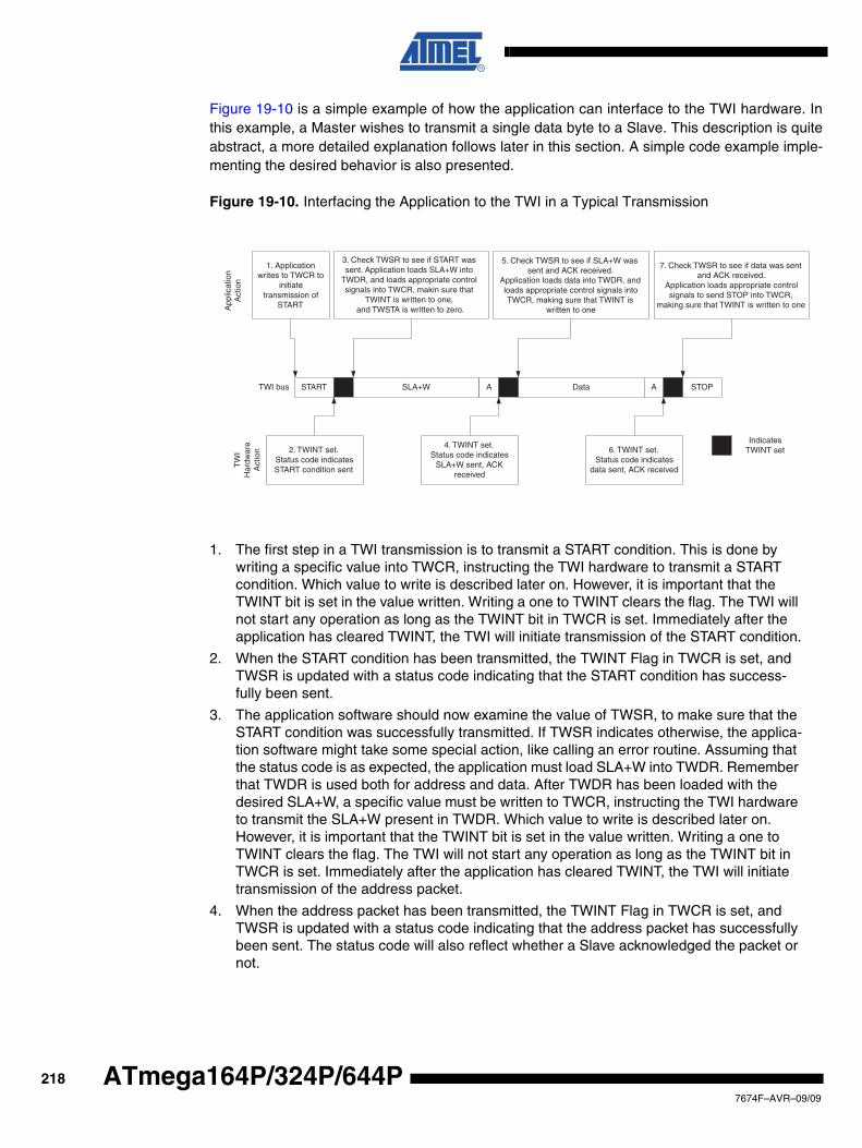
Figure 19-10 is a simple example of how the application can interface to the TWI hardware. Inthis example, a Master wishes to transmit a single data byte to a Slave. This description is quiteabstract, a more detailed explanation follows later in this section. A simple code example imple-menting the desired behavior is also presented.
Figure 19-10. Interfacing the Application to the TWI in a Typical Transmission
1. The first step in a TWI transmission is to transmit a START condition. This is done by writing a specific value into TWCR, instructing the TWI hardware to transmit a START condition. Which value to write is described later on. However, it is important that the TWINT bit is set in the value written. Writing a one to TWINT clears the flag. The TWI will not start any operation as long as the TWINT bit in TWCR is set. Immediately after the application has cleared TWINT, the TWI will initiate transmission of the START condition.
2. When the START condition has been transmitted, the TWINT Flag in TWCR is set, and TWSR is updated with a status code indicating that the START condition has success-fully been sent.
3. The application software should now examine the value of TWSR, to make sure that the START condition was successfully transmitted. If TWSR indicates otherwise, the applica-tion software might take some special action, like calling an error routine. Assuming that the status code is as expected, the application must load SLA+W into TWDR. Remember that TWDR is used both for address and data. After TWDR has been loaded with the desired SLA+W, a specific value must be written to TWCR, instructing the TWI hardware to transmit the SLA+W present in TWDR. Which value to write is described later on. However, it is important that the TWINT bit is set in the value written. Writing a one to TWINT clears the flag. The TWI will not start any operation as long as the TWINT bit in TWCR is set. Immediately after the application has cleared TWINT, the TWI will initiate transmission of the address packet.
4. When the address packet has been transmitted, the TWINT Flag in TWCR is set, and TWSR is updated with a status code indicating that the address packet has successfully been sent. The status code will also reflect whether a Slave acknowledged the packet or not.
START SLA+W A Data A STOP
1. Applicationwrites to TWCR to
initiatetransmission of
START
2. TWINT set.Status code indicatesSTART condition sent
4. TWINT set.Status code indicates
SLA+W sent, ACKreceived
6. TWINT set.Status code indicates
data sent, ACK received
3. Check TWSR to see if START was sent. Application loads SLA+W into
TWDR, and loads appropriate control signals into TWCR, makin sure that
TWINT is written to one, and TWSTA is written to zero.
5. Check TWSR to see if SLA+W wassent and ACK received.
Application loads data into TWDR, andloads appropriate control signals intoTWCR, making sure that TWINT is
written to one
7. Check TWSR to see if data was sentand ACK received.
Application loads appropriate controlsignals to send STOP into TWCR,
making sure that TWINT is written to one
TWI bus
IndicatesTWINT set
App
licat
ion
Act
ion
TW
IH
ardw
are
Act
ion
2187674F–AVR–09/09
ATmega164P/324P/644P
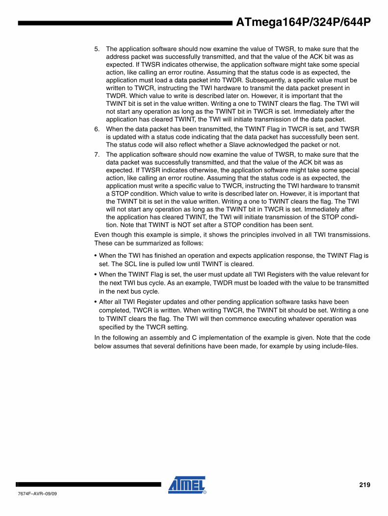
ATmega164P/324P/644P
5. The application software should now examine the value of TWSR, to make sure that the address packet was successfully transmitted, and that the value of the ACK bit was as expected. If TWSR indicates otherwise, the application software might take some special action, like calling an error routine. Assuming that the status code is as expected, the application must load a data packet into TWDR. Subsequently, a specific value must be written to TWCR, instructing the TWI hardware to transmit the data packet present in TWDR. Which value to write is described later on. However, it is important that the TWINT bit is set in the value written. Writing a one to TWINT clears the flag. The TWI will not start any operation as long as the TWINT bit in TWCR is set. Immediately after the application has cleared TWINT, the TWI will initiate transmission of the data packet.
6. When the data packet has been transmitted, the TWINT Flag in TWCR is set, and TWSR is updated with a status code indicating that the data packet has successfully been sent. The status code will also reflect whether a Slave acknowledged the packet or not.
7. The application software should now examine the value of TWSR, to make sure that the data packet was successfully transmitted, and that the value of the ACK bit was as expected. If TWSR indicates otherwise, the application software might take some special action, like calling an error routine. Assuming that the status code is as expected, the application must write a specific value to TWCR, instructing the TWI hardware to transmit a STOP condition. Which value to write is described later on. However, it is important that the TWINT bit is set in the value written. Writing a one to TWINT clears the flag. The TWI will not start any operation as long as the TWINT bit in TWCR is set. Immediately after the application has cleared TWINT, the TWI will initiate transmission of the STOP condi-tion. Note that TWINT is NOT set after a STOP condition has been sent.
Even though this example is simple, it shows the principles involved in all TWI transmissions.These can be summarized as follows:
• When the TWI has finished an operation and expects application response, the TWINT Flag is set. The SCL line is pulled low until TWINT is cleared.
• When the TWINT Flag is set, the user must update all TWI Registers with the value relevant for the next TWI bus cycle. As an example, TWDR must be loaded with the value to be transmitted in the next bus cycle.
• After all TWI Register updates and other pending application software tasks have been completed, TWCR is written. When writing TWCR, the TWINT bit should be set. Writing a one to TWINT clears the flag. The TWI will then commence executing whatever operation was specified by the TWCR setting.
In the following an assembly and C implementation of the example is given. Note that the codebelow assumes that several definitions have been made, for example by using include-files.
2197674F–AVR–09/09
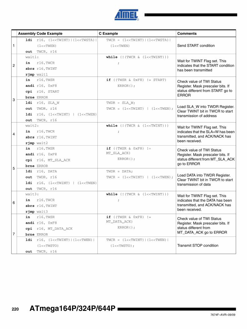
Assembly Code Example C Example Comments
1
ldi r16, (1<<TWINT)|(1<<TWSTA)|
(1<<TWEN)
out TWCR, r16
TWCR = (1<<TWINT)|(1<<TWSTA)|
(1<<TWEN) Send START condition
2
wait1:
in r16,TWCR
sbrs r16,TWINT
rjmp wait1
while (!(TWCR & (1<<TWINT)))
; Wait for TWINT Flag set. This indicates that the START condition has been transmitted
3
in r16,TWSR
andi r16, 0xF8
cpi r16, START
brne ERROR
if ((TWSR & 0xF8) != START)
ERROR();Check value of TWI Status Register. Mask prescaler bits. If status different from START go to ERROR
ldi r16, SLA_W
out TWDR, r16
ldi r16, (1<<TWINT) | (1<<TWEN)
out TWCR, r16
TWDR = SLA_W;
TWCR = (1<<TWINT) | (1<<TWEN); Load SLA_W into TWDR Register. Clear TWINT bit in TWCR to start transmission of address
4
wait2:
in r16,TWCR
sbrs r16,TWINT
rjmp wait2
while (!(TWCR & (1<<TWINT)))
;Wait for TWINT Flag set. This indicates that the SLA+W has been transmitted, and ACK/NACK has been received.
5
in r16,TWSR
andi r16, 0xF8
cpi r16, MT_SLA_ACK
brne ERROR
if ((TWSR & 0xF8) != MT_SLA_ACK)
ERROR();
Check value of TWI Status Register. Mask prescaler bits. If status different from MT_SLA_ACK go to ERROR
ldi r16, DATA
out TWDR, r16
ldi r16, (1<<TWINT) | (1<<TWEN)
out TWCR, r16
TWDR = DATA;
TWCR = (1<<TWINT) | (1<<TWEN); Load DATA into TWDR Register. Clear TWINT bit in TWCR to start transmission of data
6
wait3:
in r16,TWCR
sbrs r16,TWINT
rjmp wait3
while (!(TWCR & (1<<TWINT)))
;Wait for TWINT Flag set. This indicates that the DATA has been transmitted, and ACK/NACK has been received.
7
in r16,TWSR
andi r16, 0xF8
cpi r16, MT_DATA_ACK
brne ERROR
if ((TWSR & 0xF8) != MT_DATA_ACK)
ERROR();
Check value of TWI Status Register. Mask prescaler bits. If status different from MT_DATA_ACK go to ERROR
ldi r16, (1<<TWINT)|(1<<TWEN)|
(1<<TWSTO)
out TWCR, r16
TWCR = (1<<TWINT)|(1<<TWEN)|
(1<<TWSTO); Transmit STOP condition
2207674F–AVR–09/09
ATmega164P/324P/644P
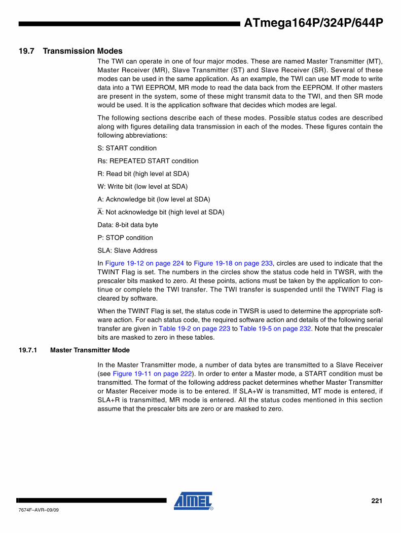
ATmega164P/324P/644P
19.7 Transmission ModesThe TWI can operate in one of four major modes. These are named Master Transmitter (MT),Master Receiver (MR), Slave Transmitter (ST) and Slave Receiver (SR). Several of thesemodes can be used in the same application. As an example, the TWI can use MT mode to writedata into a TWI EEPROM, MR mode to read the data back from the EEPROM. If other mastersare present in the system, some of these might transmit data to the TWI, and then SR modewould be used. It is the application software that decides which modes are legal.
The following sections describe each of these modes. Possible status codes are describedalong with figures detailing data transmission in each of the modes. These figures contain thefollowing abbreviations:
S: START condition
Rs: REPEATED START condition
R: Read bit (high level at SDA)
W: Write bit (low level at SDA)
A: Acknowledge bit (low level at SDA)
A: Not acknowledge bit (high level at SDA)
Data: 8-bit data byte
P: STOP condition
SLA: Slave Address
In Figure 19-12 on page 224 to Figure 19-18 on page 233, circles are used to indicate that theTWINT Flag is set. The numbers in the circles show the status code held in TWSR, with theprescaler bits masked to zero. At these points, actions must be taken by the application to con-tinue or complete the TWI transfer. The TWI transfer is suspended until the TWINT Flag iscleared by software.
When the TWINT Flag is set, the status code in TWSR is used to determine the appropriate soft-ware action. For each status code, the required software action and details of the following serialtransfer are given in Table 19-2 on page 223 to Table 19-5 on page 232. Note that the prescalerbits are masked to zero in these tables.
19.7.1 Master Transmitter Mode
In the Master Transmitter mode, a number of data bytes are transmitted to a Slave Receiver(see Figure 19-11 on page 222). In order to enter a Master mode, a START condition must betransmitted. The format of the following address packet determines whether Master Transmitteror Master Receiver mode is to be entered. If SLA+W is transmitted, MT mode is entered, ifSLA+R is transmitted, MR mode is entered. All the status codes mentioned in this sectionassume that the prescaler bits are zero or are masked to zero.
2217674F–AVR–09/09
Figure 19-11. Data Transfer in Master Transmitter Mode
A START condition is sent by writing the following value to TWCR:
TWEN must be set to enable the 2-wire Serial Interface, TWSTA must be written to one to trans-mit a START condition and TWINT must be written to one to clear the TWINT Flag. The TWI willthen test the 2-wire Serial Bus and generate a START condition as soon as the bus becomesfree. After a START condition has been transmitted, the TWINT Flag is set by hardware, and thestatus code in TWSR will be 0x08 (see Table 19-2 on page 223). In order to enter MT mode,SLA+W must be transmitted. This is done by writing SLA+W to TWDR. Thereafter the TWINT bitshould be cleared (by writing it to one) to continue the transfer. This is accomplished by writingthe following value to TWCR:
When SLA+W have been transmitted and an acknowledgement bit has been received, TWINT isset again and a number of status codes in TWSR are possible. Possible status codes in Mastermode are 0x18, 0x20, or 0x38. The appropriate action to be taken for each of these status codesis detailed in Table 19-2 on page 223.
When SLA+W has been successfully transmitted, a data packet should be transmitted. This isdone by writing the data byte to TWDR. TWDR must only be written when TWINT is high. If not,the access will be discarded, and the Write Collision bit (TWWC) will be set in the TWCR Regis-ter. After updating TWDR, the TWINT bit should be cleared (by writing it to one) to continue thetransfer. This is accomplished by writing the following value to TWCR:
This scheme is repeated until the last byte has been sent and the transfer is ended by generat-ing a STOP condition or a repeated START condition. A STOP condition is generated by writingthe following value to TWCR:
A REPEATED START condition is generated by writing the following value to TWCR:
TWCR TWINT TWEA TWSTA TWSTO TWWC TWEN – TWIEvalue 1 X 1 0 X 1 0 X
TWCR TWINT TWEA TWSTA TWSTO TWWC TWEN – TWIEvalue 1 X 0 0 X 1 0 X
TWCR TWINT TWEA TWSTA TWSTO TWWC TWEN – TWIEvalue 1 X 0 0 X 1 0 X
TWCR TWINT TWEA TWSTA TWSTO TWWC TWEN – TWIEvalue 1 X 0 1 X 1 0 X
TWCR TWINT TWEA TWSTA TWSTO TWWC TWEN – TWIEvalue 1 X 1 0 X 1 0 X
Device 1MASTER
TRANSMITTER
Device 2SLAVE
RECEIVERDevice 3 Device n
SDA
SCL
........ R1 R2
VCC
2227674F–AVR–09/09
ATmega164P/324P/644P
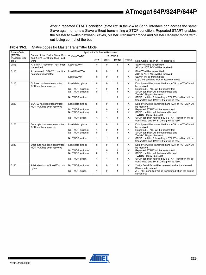
ATmega164P/324P/644P
After a repeated START condition (state 0x10) the 2-wire Serial Interface can access the sameSlave again, or a new Slave without transmitting a STOP condition. Repeated START enablesthe Master to switch between Slaves, Master Transmitter mode and Master Receiver mode with-out losing control of the bus.
Table 19-2. Status codes for Master Transmitter ModeStatus Code(TWSR)Prescaler Bitsare 0
Status of the 2-wire Serial Busand 2-wire Serial Interface Hard-ware
Application Software Response
Next Action Taken by TWI Hardware
To/from TWDR To TWCRSTA STO TWINT TWEA
0x08 A START condition has beentransmitted
Load SLA+W 0 0 1 X SLA+W will be transmitted;ACK or NOT ACK will be received
0x10 A repeated START conditionhas been transmitted
Load SLA+W or
Load SLA+R
0
0
0
0
1
1
X
X
SLA+W will be transmitted;ACK or NOT ACK will be receivedSLA+R will be transmitted;Logic will switch to Master Receiver mode
0x18 SLA+W has been transmitted;ACK has been received
Load data byte or
No TWDR action orNo TWDR action or
No TWDR action
0
10
1
0
01
1
1
11
1
X
XX
X
Data byte will be transmitted and ACK or NOT ACK will be receivedRepeated START will be transmittedSTOP condition will be transmitted andTWSTO Flag will be resetSTOP condition followed by a START condition will be transmitted and TWSTO Flag will be reset
0x20 SLA+W has been transmitted;NOT ACK has been received
Load data byte or
No TWDR action orNo TWDR action or
No TWDR action
0
10
1
0
01
1
1
11
1
X
XX
X
Data byte will be transmitted and ACK or NOT ACK will be receivedRepeated START will be transmittedSTOP condition will be transmitted andTWSTO Flag will be resetSTOP condition followed by a START condition will be transmitted and TWSTO Flag will be reset
0x28 Data byte has been transmitted;ACK has been received
Load data byte or
No TWDR action orNo TWDR action or
No TWDR action
0
10
1
0
01
1
1
11
1
X
XX
X
Data byte will be transmitted and ACK or NOT ACK will be receivedRepeated START will be transmittedSTOP condition will be transmitted andTWSTO Flag will be resetSTOP condition followed by a START condition will be transmitted and TWSTO Flag will be reset
0x30 Data byte has been transmitted;NOT ACK has been received
Load data byte or
No TWDR action orNo TWDR action or
No TWDR action
0
10
1
0
01
1
1
11
1
X
XX
X
Data byte will be transmitted and ACK or NOT ACK will be receivedRepeated START will be transmittedSTOP condition will be transmitted andTWSTO Flag will be resetSTOP condition followed by a START condition will be transmitted and TWSTO Flag will be reset
0x38 Arbitration lost in SLA+W or databytes
No TWDR action or
No TWDR action
0
1
0
0
1
1
X
X
2-wire Serial Bus will be released and not addressed Slave mode enteredA START condition will be transmitted when the bus be-comes free
2237674F–AVR–09/09
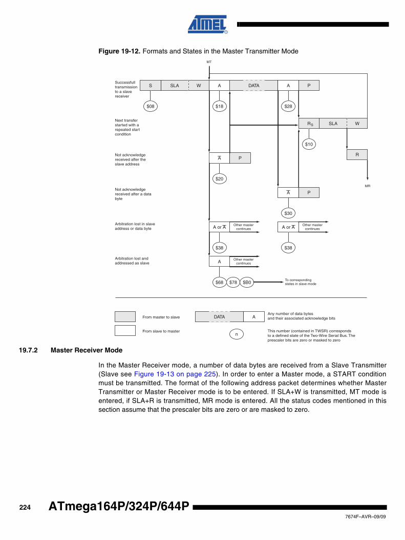
Figure 19-12. Formats and States in the Master Transmitter Mode
19.7.2 Master Receiver Mode
In the Master Receiver mode, a number of data bytes are received from a Slave Transmitter(Slave see Figure 19-13 on page 225). In order to enter a Master mode, a START conditionmust be transmitted. The format of the following address packet determines whether MasterTransmitter or Master Receiver mode is to be entered. If SLA+W is transmitted, MT mode isentered, if SLA+R is transmitted, MR mode is entered. All the status codes mentioned in thissection assume that the prescaler bits are zero or are masked to zero.
S SLA W A DATA A P
$08 $18 $28
R SLA W
$10
A P
$20
P
$30
A or A
$38
A
Other mastercontinues A or A
$38
Other mastercontinues
R
A
$68
Other mastercontinues
$78 $B0To correspondingstates in slave mode
MT
MR
Successfulltransmissionto a slavereceiver
Next transferstarted with arepeated startcondition
Not acknowledgereceived after theslave address
Not acknowledgereceived after a databyte
Arbitration lost in slaveaddress or data byte
Arbitration lost andaddressed as slave
DATA A
n
From master to slave
From slave to master
Any number of data bytesand their associated acknowledge bits
This number (contained in TWSR) correspondsto a defined state of the Two-Wire Serial Bus. Theprescaler bits are zero or masked to zero
S
2247674F–AVR–09/09
ATmega164P/324P/644P
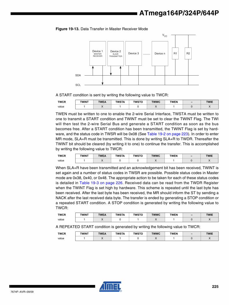
ATmega164P/324P/644P
Figure 19-13. Data Transfer in Master Receiver Mode
A START condition is sent by writing the following value to TWCR:
TWEN must be written to one to enable the 2-wire Serial Interface, TWSTA must be written toone to transmit a START condition and TWINT must be set to clear the TWINT Flag. The TWIwill then test the 2-wire Serial Bus and generate a START condition as soon as the busbecomes free. After a START condition has been transmitted, the TWINT Flag is set by hard-ware, and the status code in TWSR will be 0x08 (See Table 19-2 on page 223). In order to enterMR mode, SLA+R must be transmitted. This is done by writing SLA+R to TWDR. Thereafter theTWINT bit should be cleared (by writing it to one) to continue the transfer. This is accomplishedby writing the following value to TWCR:
When SLA+R have been transmitted and an acknowledgement bit has been received, TWINT isset again and a number of status codes in TWSR are possible. Possible status codes in Mastermode are 0x38, 0x40, or 0x48. The appropriate action to be taken for each of these status codesis detailed in Table 19-3 on page 226. Received data can be read from the TWDR Registerwhen the TWINT Flag is set high by hardware. This scheme is repeated until the last byte hasbeen received. After the last byte has been received, the MR should inform the ST by sending aNACK after the last received data byte. The transfer is ended by generating a STOP condition ora repeated START condition. A STOP condition is generated by writing the following value toTWCR:
A REPEATED START condition is generated by writing the following value to TWCR:
TWCR TWINT TWEA TWSTA TWSTO TWWC TWEN – TWIEvalue 1 X 1 0 X 1 0 X
TWCR TWINT TWEA TWSTA TWSTO TWWC TWEN – TWIEvalue 1 X 0 0 X 1 0 X
TWCR TWINT TWEA TWSTA TWSTO TWWC TWEN – TWIEvalue 1 X 0 1 X 1 0 X
TWCR TWINT TWEA TWSTA TWSTO TWWC TWEN – TWIEvalue 1 X 1 0 X 1 0 X
Device 1MASTER
RECEIVER
Device 2SLAVE
TRANSMITTERDevice 3 Device n
SDA
SCL
........ R1 R2
VCC
2257674F–AVR–09/09
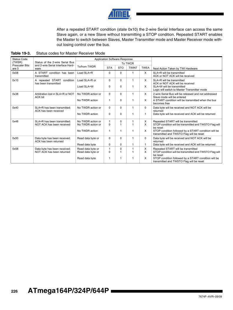
After a repeated START condition (state 0x10) the 2-wire Serial Interface can access the sameSlave again, or a new Slave without transmitting a STOP condition. Repeated START enablesthe Master to switch between Slaves, Master Transmitter mode and Master Receiver mode with-out losing control over the bus.
Table 19-3. Status codes for Master Receiver ModeStatus Code(TWSR)Prescaler Bitsare 0
Status of the 2-wire Serial Busand 2-wire Serial Interface Hard-ware
Application Software Response
Next Action Taken by TWI HardwareTo/from TWDR
To TWCRSTA STO TWINT TWEA
0x08 A START condition has beentransmitted
Load SLA+R 0 0 1 X SLA+R will be transmittedACK or NOT ACK will be received
0x10 A repeated START conditionhas been transmitted
Load SLA+R or
Load SLA+W
0
0
0
0
1
1
X
X
SLA+R will be transmittedACK or NOT ACK will be receivedSLA+W will be transmittedLogic will switch to Master Transmitter mode
0x38 Arbitration lost in SLA+R or NOTACK bit
No TWDR action or
No TWDR action
0
1
0
0
1
1
X
X
2-wire Serial Bus will be released and not addressed Slave mode will be enteredA START condition will be transmitted when the busbecomes free
0x40 SLA+R has been transmitted;ACK has been received
No TWDR action or
No TWDR action
0
0
0
0
1
1
0
1
Data byte will be received and NOT ACK will be returnedData byte will be received and ACK will be returned
0x48 SLA+R has been transmitted;NOT ACK has been received
No TWDR action orNo TWDR action or
No TWDR action
10
1
01
1
11
1
XX
X
Repeated START will be transmittedSTOP condition will be transmitted and TWSTO Flag will be resetSTOP condition followed by a START condition will be transmitted and TWSTO Flag will be reset
0x50 Data byte has been received;ACK has been returned
Read data byte or
Read data byte
0
0
0
0
1
1
0
1
Data byte will be received and NOT ACK will be returnedData byte will be received and ACK will be returned
0x58 Data byte has been received;NOT ACK has been returned
Read data byte orRead data byte or
Read data byte
10
1
01
1
11
1
XX
X
Repeated START will be transmittedSTOP condition will be transmitted and TWSTO Flag will be resetSTOP condition followed by a START condition will be transmitted and TWSTO Flag will be reset
2267674F–AVR–09/09
ATmega164P/324P/644P
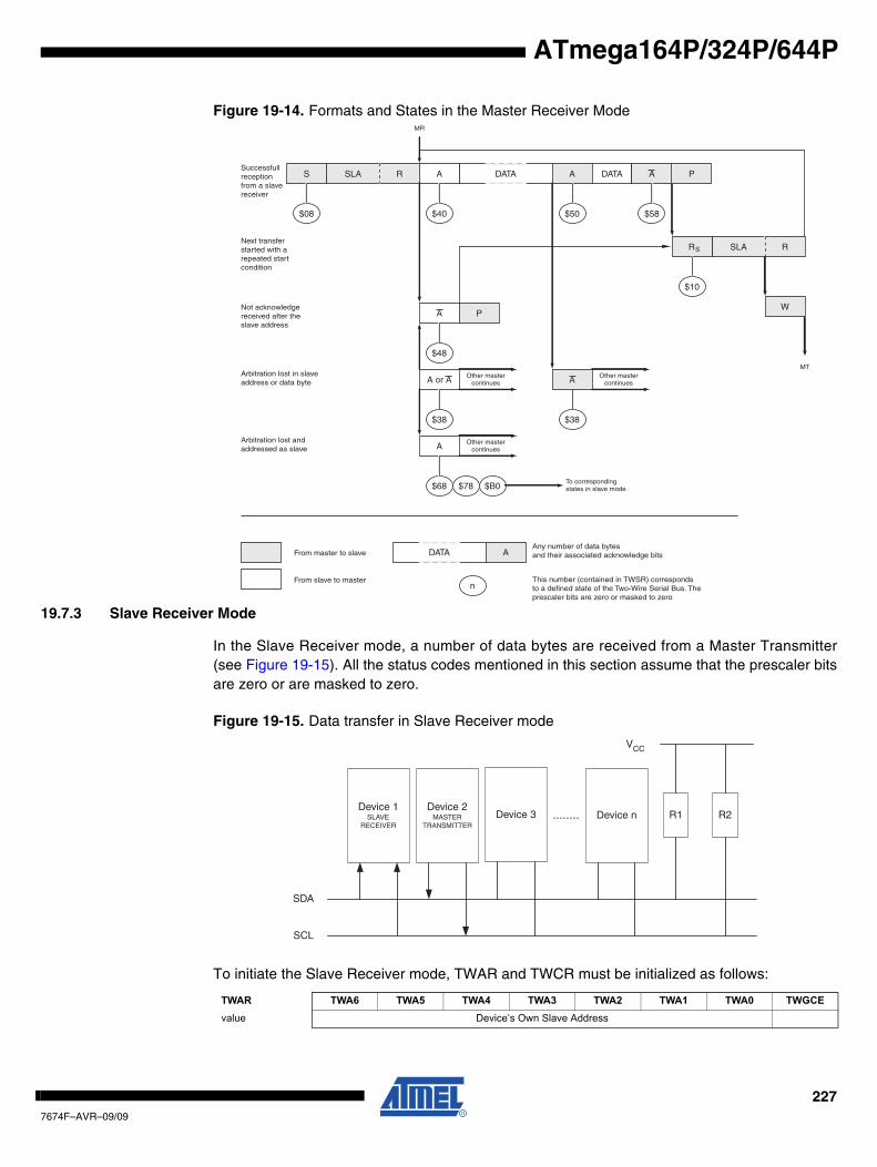
ATmega164P/324P/644P
Figure 19-14. Formats and States in the Master Receiver Mode
19.7.3 Slave Receiver Mode
In the Slave Receiver mode, a number of data bytes are received from a Master Transmitter(see Figure 19-15). All the status codes mentioned in this section assume that the prescaler bitsare zero or are masked to zero.
Figure 19-15. Data transfer in Slave Receiver mode
To initiate the Slave Receiver mode, TWAR and TWCR must be initialized as follows:
S SLA R A DATA A
$08 $40 $50
SLA R
$10
A P
$48
A or A
$38
Other mastercontinues
$38
Other mastercontinues
W
A
$68
Other mastercontinues
$78 $B0To correspondingstates in slave mode
MR
MT
Successfullreceptionfrom a slavereceiver
Next transferstarted with arepeated startcondition
Not acknowledgereceived after theslave address
Arbitration lost in slaveaddress or data byte
Arbitration lost andaddressed as slave
DATA A
n
From master to slave
From slave to master
Any number of data bytesand their associated acknowledge bits
This number (contained in TWSR) correspondsto a defined state of the Two-Wire Serial Bus. The prescaler bits are zero or masked to zero
PDATA A
$58
A
RS
TWAR TWA6 TWA5 TWA4 TWA3 TWA2 TWA1 TWA0 TWGCEvalue Device’s Own Slave Address
Device 3 Device n
SDA
SCL
........ R1 R2
VCC
Device 2MASTER
TRANSMITTER
Device 1SLAVE
RECEIVER
2277674F–AVR–09/09
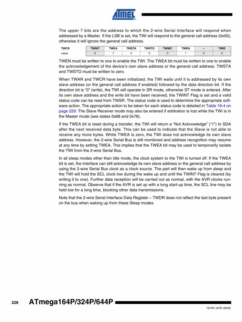
The upper 7 bits are the address to which the 2-wire Serial Interface will respond whenaddressed by a Master. If the LSB is set, the TWI will respond to the general call address (0x00),otherwise it will ignore the general call address.
TWEN must be written to one to enable the TWI. The TWEA bit must be written to one to enablethe acknowledgement of the device’s own slave address or the general call address. TWSTAand TWSTO must be written to zero.
When TWAR and TWCR have been initialized, the TWI waits until it is addressed by its ownslave address (or the general call address if enabled) followed by the data direction bit. If thedirection bit is “0” (write), the TWI will operate in SR mode, otherwise ST mode is entered. Afterits own slave address and the write bit have been received, the TWINT Flag is set and a validstatus code can be read from TWSR. The status code is used to determine the appropriate soft-ware action. The appropriate action to be taken for each status code is detailed in Table 19-4 onpage 229. The Slave Receiver mode may also be entered if arbitration is lost while the TWI is inthe Master mode (see states 0x68 and 0x78).
If the TWEA bit is reset during a transfer, the TWI will return a “Not Acknowledge” (“1”) to SDAafter the next received data byte. This can be used to indicate that the Slave is not able toreceive any more bytes. While TWEA is zero, the TWI does not acknowledge its own slaveaddress. However, the 2-wire Serial Bus is still monitored and address recognition may resumeat any time by setting TWEA. This implies that the TWEA bit may be used to temporarily isolatethe TWI from the 2-wire Serial Bus.
In all sleep modes other than Idle mode, the clock system to the TWI is turned off. If the TWEAbit is set, the interface can still acknowledge its own slave address or the general call address byusing the 2-wire Serial Bus clock as a clock source. The part will then wake up from sleep andthe TWI will hold the SCL clock low during the wake up and until the TWINT Flag is cleared (bywriting it to one). Further data reception will be carried out as normal, with the AVR clocks run-ning as normal. Observe that if the AVR is set up with a long start-up time, the SCL line may beheld low for a long time, blocking other data transmissions.
Note that the 2-wire Serial Interface Data Register – TWDR does not reflect the last byte presenton the bus when waking up from these Sleep modes.
TWCR TWINT TWEA TWSTA TWSTO TWWC TWEN – TWIEvalue 0 1 0 0 0 1 0 X
2287674F–AVR–09/09
ATmega164P/324P/644P
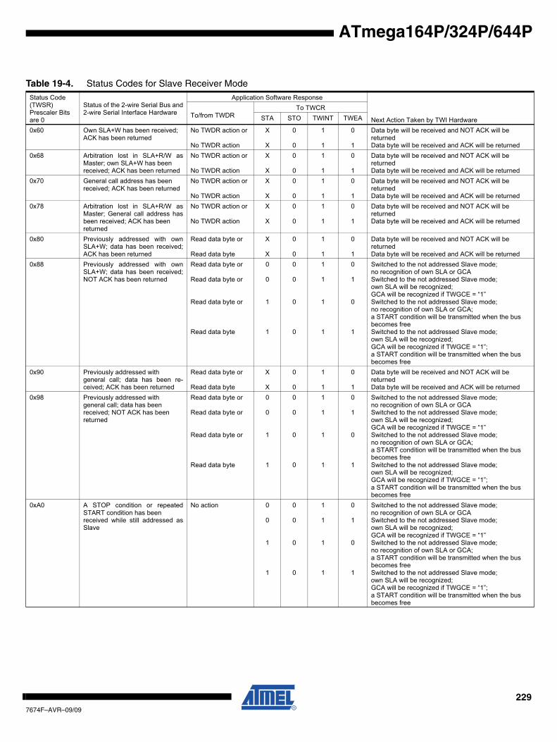
ATmega164P/324P/644P
Table 19-4. Status Codes for Slave Receiver ModeStatus Code(TWSR)Prescaler Bitsare 0
Status of the 2-wire Serial Bus and2-wire Serial Interface Hardware
Application Software Response
Next Action Taken by TWI HardwareTo/from TWDR
To TWCRSTA STO TWINT TWEA
0x60 Own SLA+W has been received;ACK has been returned
No TWDR action or
No TWDR action
X
X
0
0
1
1
0
1
Data byte will be received and NOT ACK will be returnedData byte will be received and ACK will be returned
0x68 Arbitration lost in SLA+R/W asMaster; own SLA+W has been received; ACK has been returned
No TWDR action or
No TWDR action
X
X
0
0
1
1
0
1
Data byte will be received and NOT ACK will be returnedData byte will be received and ACK will be returned
0x70 General call address has been received; ACK has been returned
No TWDR action or
No TWDR action
X
X
0
0
1
1
0
1
Data byte will be received and NOT ACK will be returnedData byte will be received and ACK will be returned
0x78 Arbitration lost in SLA+R/W asMaster; General call address hasbeen received; ACK has been returned
No TWDR action or
No TWDR action
X
X
0
0
1
1
0
1
Data byte will be received and NOT ACK will be returnedData byte will be received and ACK will be returned
0x80 Previously addressed with ownSLA+W; data has been received;ACK has been returned
Read data byte or
Read data byte
X
X
0
0
1
1
0
1
Data byte will be received and NOT ACK will be returnedData byte will be received and ACK will be returned
0x88 Previously addressed with ownSLA+W; data has been received;NOT ACK has been returned
Read data byte or
Read data byte or
Read data byte or
Read data byte
0
0
1
1
0
0
0
0
1
1
1
1
0
1
0
1
Switched to the not addressed Slave mode;no recognition of own SLA or GCASwitched to the not addressed Slave mode;own SLA will be recognized;GCA will be recognized if TWGCE = “1”Switched to the not addressed Slave mode;no recognition of own SLA or GCA;a START condition will be transmitted when the bus becomes freeSwitched to the not addressed Slave mode;own SLA will be recognized;GCA will be recognized if TWGCE = “1”;a START condition will be transmitted when the bus becomes free
0x90 Previously addressed with general call; data has been re-ceived; ACK has been returned
Read data byte or
Read data byte
X
X
0
0
1
1
0
1
Data byte will be received and NOT ACK will be returnedData byte will be received and ACK will be returned
0x98 Previously addressed with general call; data has been received; NOT ACK has been returned
Read data byte or
Read data byte or
Read data byte or
Read data byte
0
0
1
1
0
0
0
0
1
1
1
1
0
1
0
1
Switched to the not addressed Slave mode;no recognition of own SLA or GCASwitched to the not addressed Slave mode;own SLA will be recognized;GCA will be recognized if TWGCE = “1”Switched to the not addressed Slave mode;no recognition of own SLA or GCA;a START condition will be transmitted when the bus becomes freeSwitched to the not addressed Slave mode;own SLA will be recognized;GCA will be recognized if TWGCE = “1”;a START condition will be transmitted when the bus becomes free
0xA0 A STOP condition or repeatedSTART condition has been received while still addressed asSlave
No action 0
0
1
1
0
0
0
0
1
1
1
1
0
1
0
1
Switched to the not addressed Slave mode;no recognition of own SLA or GCASwitched to the not addressed Slave mode;own SLA will be recognized;GCA will be recognized if TWGCE = “1”Switched to the not addressed Slave mode;no recognition of own SLA or GCA;a START condition will be transmitted when the bus becomes freeSwitched to the not addressed Slave mode;own SLA will be recognized;GCA will be recognized if TWGCE = “1”;a START condition will be transmitted when the bus becomes free
2297674F–AVR–09/09
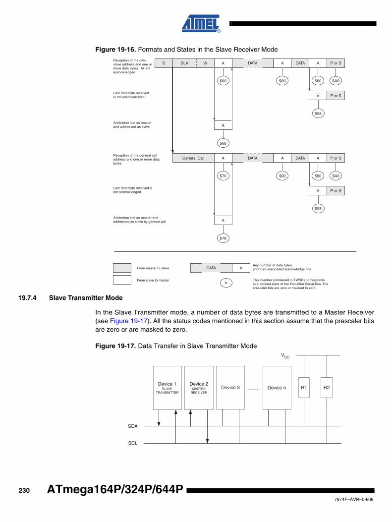
Figure 19-16. Formats and States in the Slave Receiver Mode
19.7.4 Slave Transmitter Mode
In the Slave Transmitter mode, a number of data bytes are transmitted to a Master Receiver(see Figure 19-17). All the status codes mentioned in this section assume that the prescaler bitsare zero or are masked to zero.
Figure 19-17. Data Transfer in Slave Transmitter Mode
S SLA W A DATA A
$60 $80
$88
A
$68
Reception of the ownslave address and one ormore data bytes. All areacknowledged
Last data byte receivedis not acknowledged
Arbitration lost as masterand addressed as slave
Reception of the general calladdress and one or more databytes
Last data byte received isnot acknowledged
n
From master to slave
From slave to master
Any number of data bytesand their associated acknowledge bits
This number (contained in TWSR) correspondsto a defined state of the Two-Wire Serial Bus. The prescaler bits are zero or masked to zero
P or SDATA A
$80 $A0
P or SA
A DATA A
$70 $90
$98
A
$78
P or SDATA A
$90 $A0
P or SA
General Call
Arbitration lost as master andaddressed as slave by general call
DATA A
Device 3 Device n
SDA
SCL
........ R1 R2
VCC
Device 2MASTER
RECEIVER
Device 1SLAVE
TRANSMITTER
2307674F–AVR–09/09
ATmega164P/324P/644P
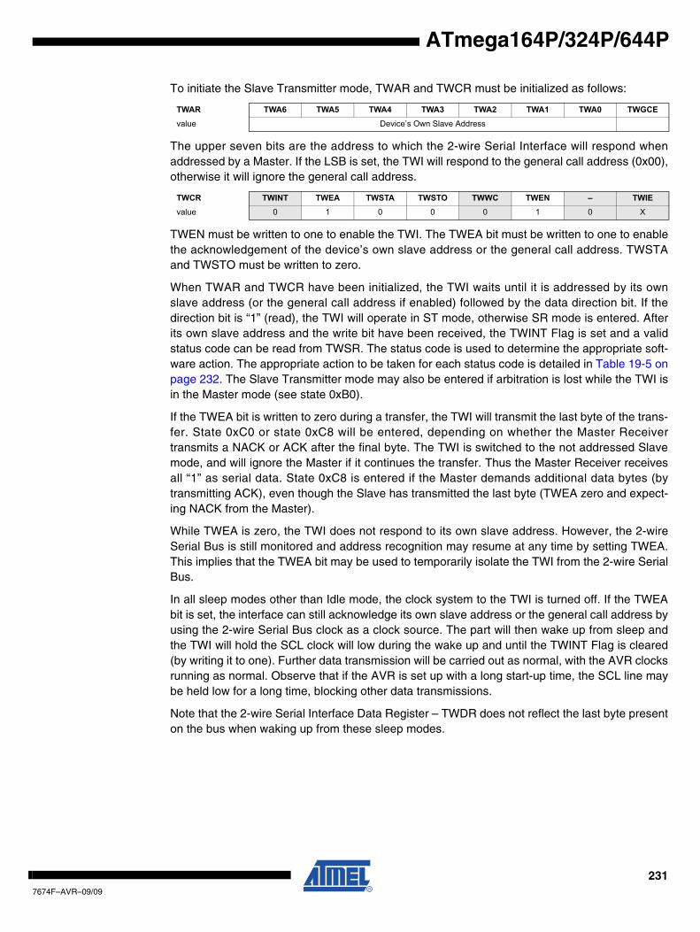
ATmega164P/324P/644P
To initiate the Slave Transmitter mode, TWAR and TWCR must be initialized as follows:
The upper seven bits are the address to which the 2-wire Serial Interface will respond whenaddressed by a Master. If the LSB is set, the TWI will respond to the general call address (0x00),otherwise it will ignore the general call address.
TWEN must be written to one to enable the TWI. The TWEA bit must be written to one to enablethe acknowledgement of the device’s own slave address or the general call address. TWSTAand TWSTO must be written to zero.
When TWAR and TWCR have been initialized, the TWI waits until it is addressed by its ownslave address (or the general call address if enabled) followed by the data direction bit. If thedirection bit is “1” (read), the TWI will operate in ST mode, otherwise SR mode is entered. Afterits own slave address and the write bit have been received, the TWINT Flag is set and a validstatus code can be read from TWSR. The status code is used to determine the appropriate soft-ware action. The appropriate action to be taken for each status code is detailed in Table 19-5 onpage 232. The Slave Transmitter mode may also be entered if arbitration is lost while the TWI isin the Master mode (see state 0xB0).
If the TWEA bit is written to zero during a transfer, the TWI will transmit the last byte of the trans-fer. State 0xC0 or state 0xC8 will be entered, depending on whether the Master Receivertransmits a NACK or ACK after the final byte. The TWI is switched to the not addressed Slavemode, and will ignore the Master if it continues the transfer. Thus the Master Receiver receivesall “1” as serial data. State 0xC8 is entered if the Master demands additional data bytes (bytransmitting ACK), even though the Slave has transmitted the last byte (TWEA zero and expect-ing NACK from the Master).
While TWEA is zero, the TWI does not respond to its own slave address. However, the 2-wireSerial Bus is still monitored and address recognition may resume at any time by setting TWEA.This implies that the TWEA bit may be used to temporarily isolate the TWI from the 2-wire SerialBus.
In all sleep modes other than Idle mode, the clock system to the TWI is turned off. If the TWEAbit is set, the interface can still acknowledge its own slave address or the general call address byusing the 2-wire Serial Bus clock as a clock source. The part will then wake up from sleep andthe TWI will hold the SCL clock will low during the wake up and until the TWINT Flag is cleared(by writing it to one). Further data transmission will be carried out as normal, with the AVR clocksrunning as normal. Observe that if the AVR is set up with a long start-up time, the SCL line maybe held low for a long time, blocking other data transmissions.
Note that the 2-wire Serial Interface Data Register – TWDR does not reflect the last byte presenton the bus when waking up from these sleep modes.
TWAR TWA6 TWA5 TWA4 TWA3 TWA2 TWA1 TWA0 TWGCEvalue Device’s Own Slave Address
TWCR TWINT TWEA TWSTA TWSTO TWWC TWEN – TWIEvalue 0 1 0 0 0 1 0 X
2317674F–AVR–09/09
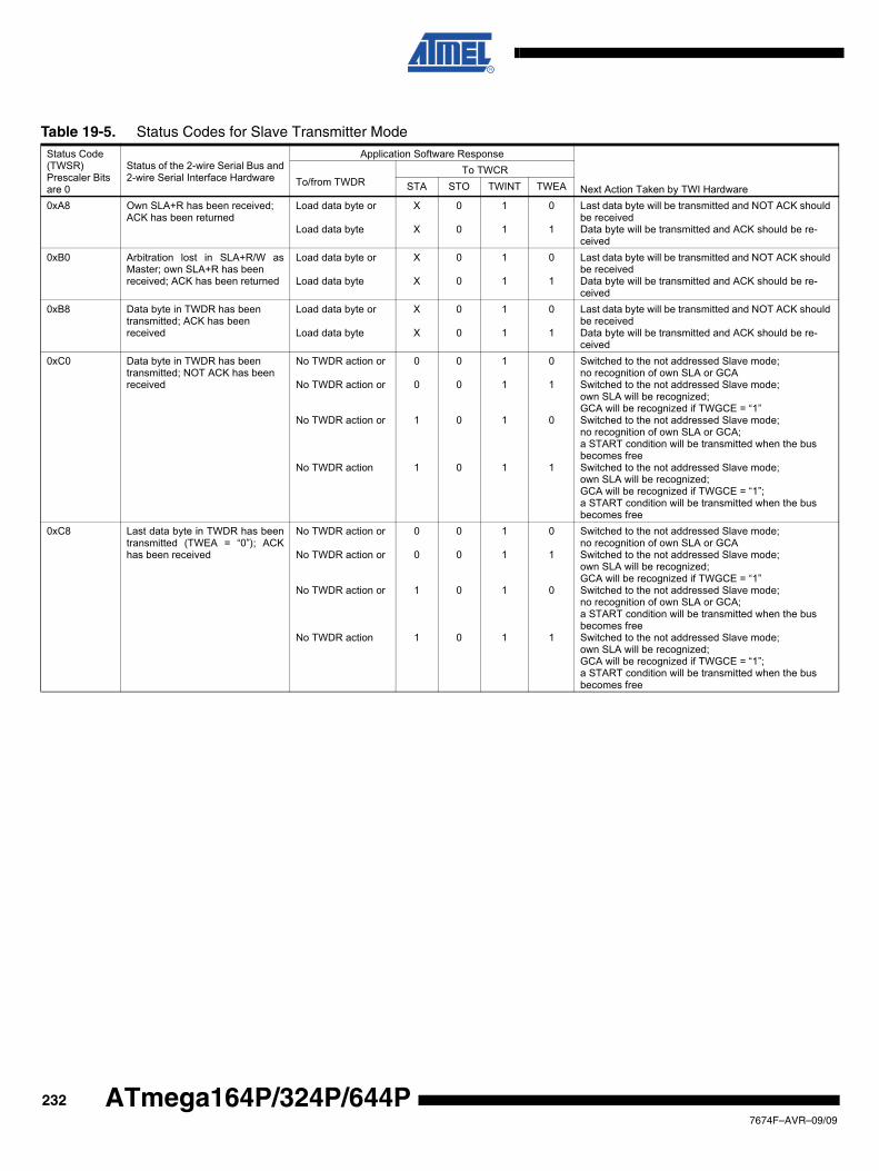
Table 19-5. Status Codes for Slave Transmitter ModeStatus Code(TWSR)Prescaler Bitsare 0
Status of the 2-wire Serial Bus and2-wire Serial Interface Hardware
Application Software Response
Next Action Taken by TWI HardwareTo/from TWDR
To TWCRSTA STO TWINT TWEA
0xA8 Own SLA+R has been received;ACK has been returned
Load data byte or
Load data byte
X
X
0
0
1
1
0
1
Last data byte will be transmitted and NOT ACK should be receivedData byte will be transmitted and ACK should be re-ceived
0xB0 Arbitration lost in SLA+R/W asMaster; own SLA+R has been received; ACK has been returned
Load data byte or
Load data byte
X
X
0
0
1
1
0
1
Last data byte will be transmitted and NOT ACK should be receivedData byte will be transmitted and ACK should be re-ceived
0xB8 Data byte in TWDR has been transmitted; ACK has been received
Load data byte or
Load data byte
X
X
0
0
1
1
0
1
Last data byte will be transmitted and NOT ACK should be receivedData byte will be transmitted and ACK should be re-ceived
0xC0 Data byte in TWDR has been transmitted; NOT ACK has been received
No TWDR action or
No TWDR action or
No TWDR action or
No TWDR action
0
0
1
1
0
0
0
0
1
1
1
1
0
1
0
1
Switched to the not addressed Slave mode;no recognition of own SLA or GCASwitched to the not addressed Slave mode;own SLA will be recognized;GCA will be recognized if TWGCE = “1”Switched to the not addressed Slave mode;no recognition of own SLA or GCA;a START condition will be transmitted when the bus becomes freeSwitched to the not addressed Slave mode;own SLA will be recognized;GCA will be recognized if TWGCE = “1”;a START condition will be transmitted when the bus becomes free
0xC8 Last data byte in TWDR has beentransmitted (TWEA = “0”); ACKhas been received
No TWDR action or
No TWDR action or
No TWDR action or
No TWDR action
0
0
1
1
0
0
0
0
1
1
1
1
0
1
0
1
Switched to the not addressed Slave mode;no recognition of own SLA or GCASwitched to the not addressed Slave mode;own SLA will be recognized;GCA will be recognized if TWGCE = “1”Switched to the not addressed Slave mode;no recognition of own SLA or GCA;a START condition will be transmitted when the bus becomes freeSwitched to the not addressed Slave mode;own SLA will be recognized;GCA will be recognized if TWGCE = “1”;a START condition will be transmitted when the bus becomes free
2327674F–AVR–09/09
ATmega164P/324P/644P
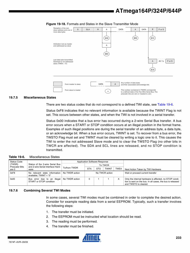
ATmega164P/324P/644P
Figure 19-18. Formats and States in the Slave Transmitter Mode
19.7.5 Miscellaneous States
There are two status codes that do not correspond to a defined TWI state, see Table 19-6.
Status 0xF8 indicates that no relevant information is available because the TWINT Flag is notset. This occurs between other states, and when the TWI is not involved in a serial transfer.
Status 0x00 indicates that a bus error has occurred during a 2-wire Serial Bus transfer. A buserror occurs when a START or STOP condition occurs at an illegal position in the format frame.Examples of such illegal positions are during the serial transfer of an address byte, a data byte,or an acknowledge bit. When a bus error occurs, TWINT is set. To recover from a bus error, theTWSTO Flag must set and TWINT must be cleared by writing a logic one to it. This causes theTWI to enter the not addressed Slave mode and to clear the TWSTO Flag (no other bits inTWCR are affected). The SDA and SCL lines are released, and no STOP condition istransmitted.
19.7.6 Combining Several TWI Modes
In some cases, several TWI modes must be combined in order to complete the desired action.Consider for example reading data from a serial EEPROM. Typically, such a transfer involvesthe following steps:
1. The transfer must be initiated.
2. The EEPROM must be instructed what location should be read.
3. The reading must be performed.
4. The transfer must be finished.
S SLA R A DATA A
$A8 $B8
A
$B0
Reception of the ownslave address and one ormore data bytes
Last data byte transmitted.Switched to not addressedslave (TWEA = '0')
Arbitration lost as masterand addressed as slave
n
From master to slave
From slave to master
Any number of data bytesand their associated acknowledge bits
This number (contained in TWSR) correspondsto a defined state of the Two-Wire Serial Bus. The prescaler bits are zero or masked to zero
P or SDATA
$C0
DATA A
A
$C8
P or SAll 1's
A
Table 19-6. Miscellaneous StatesStatus Code(TWSR)Prescaler Bitsare 0
Status of the 2-wire Serial Busand 2-wire Serial Interface Hard-ware
Application Software Response
Next Action Taken by TWI HardwareTo/from TWDR
To TWCRSTA STO TWINT TWEA
0xF8 No relevant state informationavailable; TWINT = “0”
No TWDR action No TWCR action Wait or proceed current transfer
0x00 Bus error due to an illegalSTART or STOP condition
No TWDR action 0 1 1 X Only the internal hardware is affected, no STOP condi-tion is sent on the bus. In all cases, the bus is released and TWSTO is cleared.
2337674F–AVR–09/09
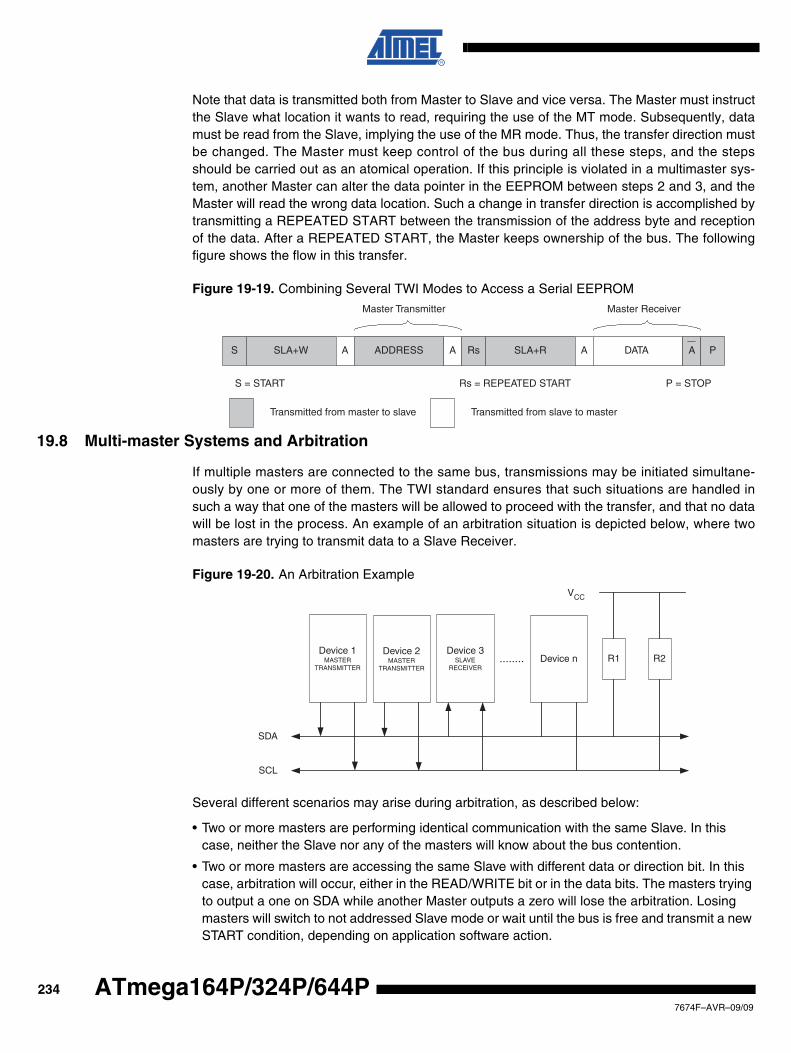
Note that data is transmitted both from Master to Slave and vice versa. The Master must instructthe Slave what location it wants to read, requiring the use of the MT mode. Subsequently, datamust be read from the Slave, implying the use of the MR mode. Thus, the transfer direction mustbe changed. The Master must keep control of the bus during all these steps, and the stepsshould be carried out as an atomical operation. If this principle is violated in a multimaster sys-tem, another Master can alter the data pointer in the EEPROM between steps 2 and 3, and theMaster will read the wrong data location. Such a change in transfer direction is accomplished bytransmitting a REPEATED START between the transmission of the address byte and receptionof the data. After a REPEATED START, the Master keeps ownership of the bus. The followingfigure shows the flow in this transfer.
Figure 19-19. Combining Several TWI Modes to Access a Serial EEPROM
19.8 Multi-master Systems and Arbitration
If multiple masters are connected to the same bus, transmissions may be initiated simultane-ously by one or more of them. The TWI standard ensures that such situations are handled insuch a way that one of the masters will be allowed to proceed with the transfer, and that no datawill be lost in the process. An example of an arbitration situation is depicted below, where twomasters are trying to transmit data to a Slave Receiver.
Figure 19-20. An Arbitration Example
Several different scenarios may arise during arbitration, as described below:
• Two or more masters are performing identical communication with the same Slave. In this case, neither the Slave nor any of the masters will know about the bus contention.
• Two or more masters are accessing the same Slave with different data or direction bit. In this case, arbitration will occur, either in the READ/WRITE bit or in the data bits. The masters trying to output a one on SDA while another Master outputs a zero will lose the arbitration. Losing masters will switch to not addressed Slave mode or wait until the bus is free and transmit a new START condition, depending on application software action.
Master Transmitter Master Receiver
S = START Rs = REPEATED START P = STOP
Transmitted from master to slave Transmitted from slave to master
S SLA+W A ADDRESS A Rs SLA+R A DATA A P
Device 1MASTER
TRANSMITTER
Device 2MASTER
TRANSMITTER
Device 3SLAVE
RECEIVERDevice n
SDA
SCL
........ R1 R2
VCC
2347674F–AVR–09/09
ATmega164P/324P/644P
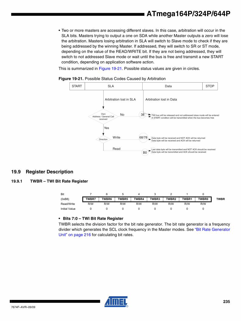
ATmega164P/324P/644P
• Two or more masters are accessing different slaves. In this case, arbitration will occur in the SLA bits. Masters trying to output a one on SDA while another Master outputs a zero will lose the arbitration. Masters losing arbitration in SLA will switch to Slave mode to check if they are being addressed by the winning Master. If addressed, they will switch to SR or ST mode, depending on the value of the READ/WRITE bit. If they are not being addressed, they will switch to not addressed Slave mode or wait until the bus is free and transmit a new START condition, depending on application software action.
This is summarized in Figure 19-21. Possible status values are given in circles.
Figure 19-21. Possible Status Codes Caused by Arbitration
19.9 Register Description
19.9.1 TWBR – TWI Bit Rate Register
• Bits 7:0 – TWI Bit Rate RegisterTWBR selects the division factor for the bit rate generator. The bit rate generator is a frequencydivider which generates the SCL clock frequency in the Master modes. See “Bit Rate GeneratorUnit” on page 216 for calculating bit rates.
OwnAddress / General Call
received
Arbitration lost in SLA
TWI bus will be released and not addressed slave mode will be enteredA START condition will be transmitted when the bus becomes free
No
Arbitration lost in Data
Direction
Yes
Write Data byte will be received and NOT ACK will be returnedData byte will be received and ACK will be returned
Last data byte will be transmitted and NOT ACK should be receivedData byte will be transmitted and ACK should be received
ReadB0
68/78
38
SLASTART Data STOP
Bit 7 6 5 4 3 2 1 0
(0xB8) TWBR7 TWBR6 TWBR5 TWBR4 TWBR3 TWBR2 TWBR1 TWBR0 TWBRRead/Write R/W R/W R/W R/W R/W R/W R/W R/W
Initial Value 0 0 0 0 0 0 0 0
2357674F–AVR–09/09
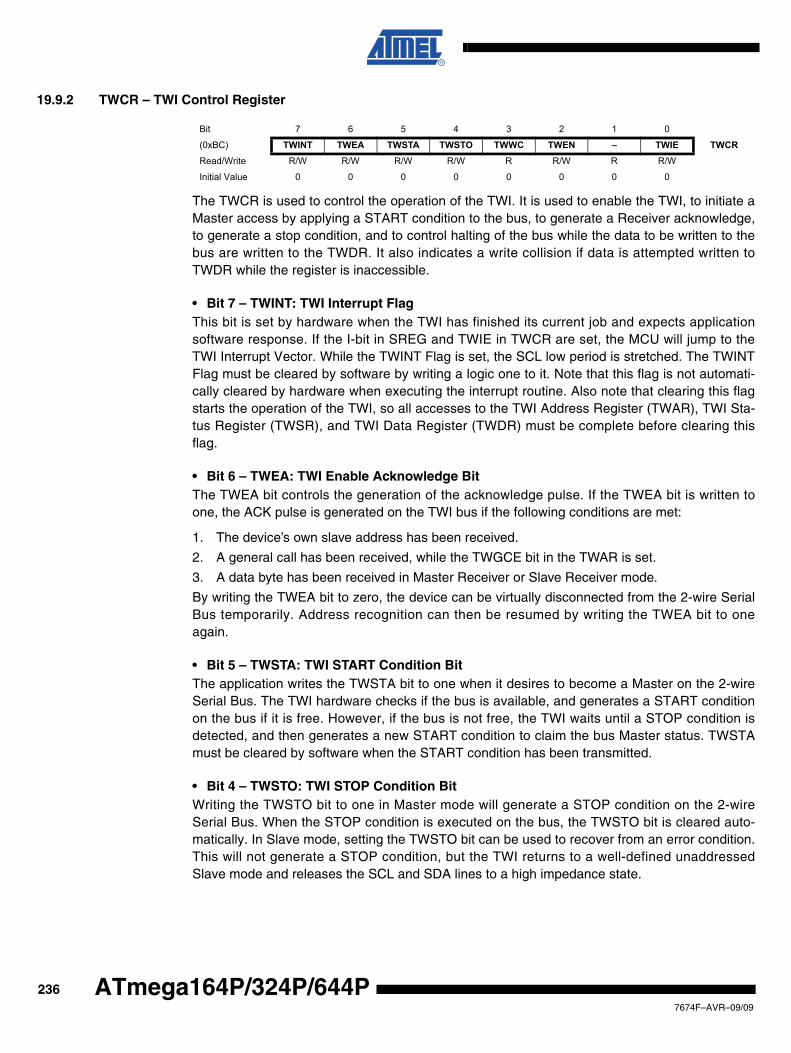
19.9.2 TWCR – TWI Control Register
The TWCR is used to control the operation of the TWI. It is used to enable the TWI, to initiate aMaster access by applying a START condition to the bus, to generate a Receiver acknowledge,to generate a stop condition, and to control halting of the bus while the data to be written to thebus are written to the TWDR. It also indicates a write collision if data is attempted written toTWDR while the register is inaccessible.
• Bit 7 – TWINT: TWI Interrupt FlagThis bit is set by hardware when the TWI has finished its current job and expects applicationsoftware response. If the I-bit in SREG and TWIE in TWCR are set, the MCU will jump to theTWI Interrupt Vector. While the TWINT Flag is set, the SCL low period is stretched. The TWINTFlag must be cleared by software by writing a logic one to it. Note that this flag is not automati-cally cleared by hardware when executing the interrupt routine. Also note that clearing this flagstarts the operation of the TWI, so all accesses to the TWI Address Register (TWAR), TWI Sta-tus Register (TWSR), and TWI Data Register (TWDR) must be complete before clearing thisflag.
• Bit 6 – TWEA: TWI Enable Acknowledge BitThe TWEA bit controls the generation of the acknowledge pulse. If the TWEA bit is written toone, the ACK pulse is generated on the TWI bus if the following conditions are met:
1. The device’s own slave address has been received.
2. A general call has been received, while the TWGCE bit in the TWAR is set.
3. A data byte has been received in Master Receiver or Slave Receiver mode.
By writing the TWEA bit to zero, the device can be virtually disconnected from the 2-wire SerialBus temporarily. Address recognition can then be resumed by writing the TWEA bit to oneagain.
• Bit 5 – TWSTA: TWI START Condition BitThe application writes the TWSTA bit to one when it desires to become a Master on the 2-wireSerial Bus. The TWI hardware checks if the bus is available, and generates a START conditionon the bus if it is free. However, if the bus is not free, the TWI waits until a STOP condition isdetected, and then generates a new START condition to claim the bus Master status. TWSTAmust be cleared by software when the START condition has been transmitted.
• Bit 4 – TWSTO: TWI STOP Condition BitWriting the TWSTO bit to one in Master mode will generate a STOP condition on the 2-wireSerial Bus. When the STOP condition is executed on the bus, the TWSTO bit is cleared auto-matically. In Slave mode, setting the TWSTO bit can be used to recover from an error condition.This will not generate a STOP condition, but the TWI returns to a well-defined unaddressedSlave mode and releases the SCL and SDA lines to a high impedance state.
Bit 7 6 5 4 3 2 1 0
(0xBC) TWINT TWEA TWSTA TWSTO TWWC TWEN – TWIE TWCRRead/Write R/W R/W R/W R/W R R/W R R/W
Initial Value 0 0 0 0 0 0 0 0
2367674F–AVR–09/09
ATmega164P/324P/644P
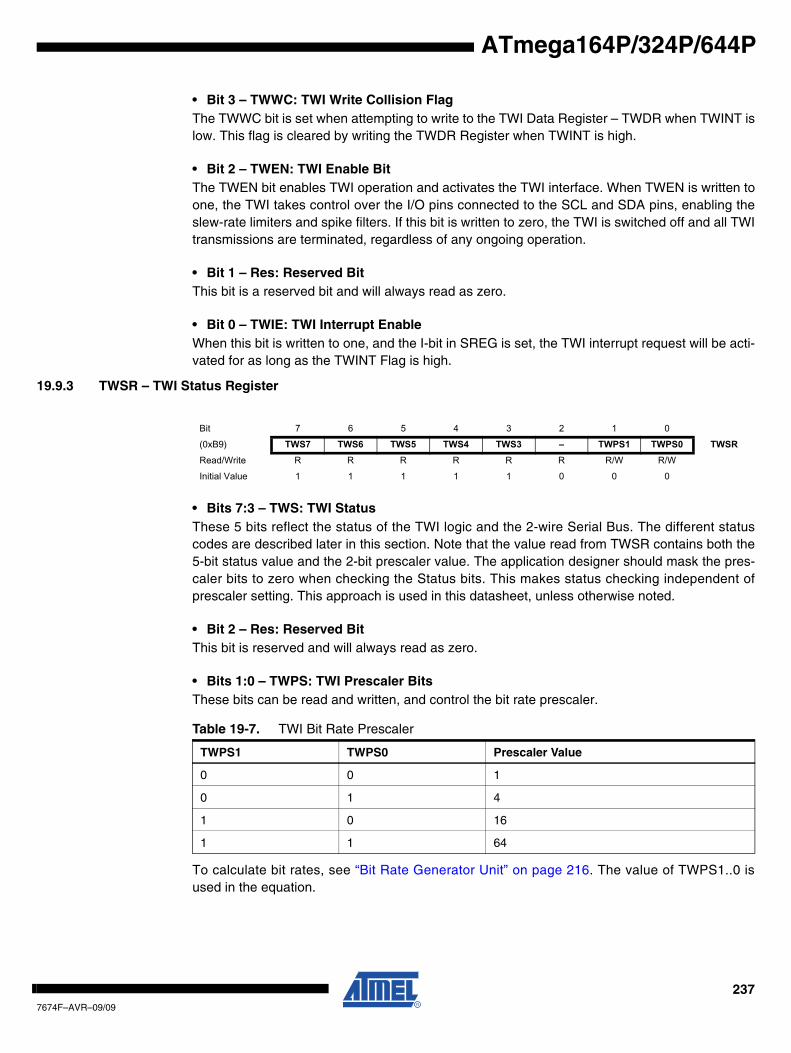
ATmega164P/324P/644P
• Bit 3 – TWWC: TWI Write Collision FlagThe TWWC bit is set when attempting to write to the TWI Data Register – TWDR when TWINT islow. This flag is cleared by writing the TWDR Register when TWINT is high.
• Bit 2 – TWEN: TWI Enable BitThe TWEN bit enables TWI operation and activates the TWI interface. When TWEN is written toone, the TWI takes control over the I/O pins connected to the SCL and SDA pins, enabling theslew-rate limiters and spike filters. If this bit is written to zero, the TWI is switched off and all TWItransmissions are terminated, regardless of any ongoing operation.
• Bit 1 – Res: Reserved BitThis bit is a reserved bit and will always read as zero.
• Bit 0 – TWIE: TWI Interrupt EnableWhen this bit is written to one, and the I-bit in SREG is set, the TWI interrupt request will be acti-vated for as long as the TWINT Flag is high.
19.9.3 TWSR – TWI Status Register
• Bits 7:3 – TWS: TWI StatusThese 5 bits reflect the status of the TWI logic and the 2-wire Serial Bus. The different statuscodes are described later in this section. Note that the value read from TWSR contains both the5-bit status value and the 2-bit prescaler value. The application designer should mask the pres-caler bits to zero when checking the Status bits. This makes status checking independent ofprescaler setting. This approach is used in this datasheet, unless otherwise noted.
• Bit 2 – Res: Reserved BitThis bit is reserved and will always read as zero.
• Bits 1:0 – TWPS: TWI Prescaler BitsThese bits can be read and written, and control the bit rate prescaler.
To calculate bit rates, see “Bit Rate Generator Unit” on page 216. The value of TWPS1..0 isused in the equation.
Bit 7 6 5 4 3 2 1 0
(0xB9) TWS7 TWS6 TWS5 TWS4 TWS3 – TWPS1 TWPS0 TWSRRead/Write R R R R R R R/W R/W
Initial Value 1 1 1 1 1 0 0 0
Table 19-7. TWI Bit Rate Prescaler
TWPS1 TWPS0 Prescaler Value
0 0 1
0 1 4
1 0 16
1 1 64
2377674F–AVR–09/09
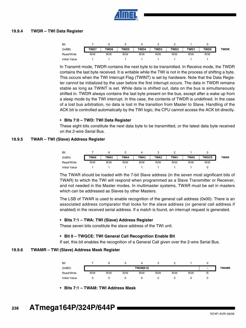
19.9.4 TWDR – TWI Data Register
In Transmit mode, TWDR contains the next byte to be transmitted. In Receive mode, the TWDRcontains the last byte received. It is writable while the TWI is not in the process of shifting a byte.This occurs when the TWI Interrupt Flag (TWINT) is set by hardware. Note that the Data Regis-ter cannot be initialized by the user before the first interrupt occurs. The data in TWDR remainsstable as long as TWINT is set. While data is shifted out, data on the bus is simultaneouslyshifted in. TWDR always contains the last byte present on the bus, except after a wake up froma sleep mode by the TWI interrupt. In this case, the contents of TWDR is undefined. In the caseof a lost bus arbitration, no data is lost in the transition from Master to Slave. Handling of theACK bit is controlled automatically by the TWI logic, the CPU cannot access the ACK bit directly.
• Bits 7:0 – TWD: TWI Data Register These eight bits constitute the next data byte to be transmitted, or the latest data byte receivedon the 2-wire Serial Bus.
19.9.5 TWAR – TWI (Slave) Address Register
The TWAR should be loaded with the 7-bit Slave address (in the seven most significant bits ofTWAR) to which the TWI will respond when programmed as a Slave Transmitter or Receiver,and not needed in the Master modes. In multimaster systems, TWAR must be set in masterswhich can be addressed as Slaves by other Masters.
The LSB of TWAR is used to enable recognition of the general call address (0x00). There is anassociated address comparator that looks for the slave address (or general call address ifenabled) in the received serial address. If a match is found, an interrupt request is generated.
• Bits 7:1 – TWA: TWI (Slave) Address Register These seven bits constitute the slave address of the TWI unit.
• Bit 0 – TWGCE: TWI General Call Recognition Enable Bit If set, this bit enables the recognition of a General Call given over the 2-wire Serial Bus.
19.9.6 TWAMR – TWI (Slave) Address Mask Register
• Bits 7:1 – TWAM: TWI Address Mask
Bit 7 6 5 4 3 2 1 0
(0xBB) TWD7 TWD6 TWD5 TWD4 TWD3 TWD2 TWD1 TWD0 TWDRRead/Write R/W R/W R/W R/W R/W R/W R/W R/W
Initial Value 1 1 1 1 1 1 1 1
Bit 7 6 5 4 3 2 1 0
(0xBA) TWA6 TWA5 TWA4 TWA3 TWA2 TWA1 TWA0 TWGCE TWAR
Read/Write R/W R/W R/W R/W R/W R/W R/W R/W
Initial Value 1 1 1 1 1 1 1 0
Bit 7 6 5 4 3 2 1 0
(0xBD) TWAM[6:0] – TWAMR
Read/Write R/W R/W R/W R/W R/W R/W R/W R
Initial Value 0 0 0 0 0 0 0 0
2387674F–AVR–09/09
ATmega164P/324P/644P
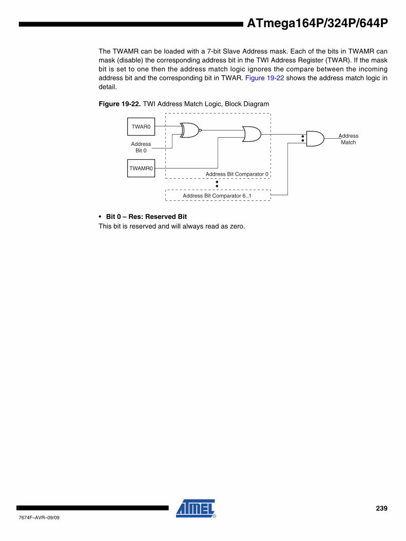
ATmega164P/324P/644P
The TWAMR can be loaded with a 7-bit Slave Address mask. Each of the bits in TWAMR canmask (disable) the corresponding address bit in the TWI Address Register (TWAR). If the maskbit is set to one then the address match logic ignores the compare between the incomingaddress bit and the corresponding bit in TWAR. Figure 19-22 shows the address match logic indetail.
Figure 19-22. TWI Address Match Logic, Block Diagram
• Bit 0 – Res: Reserved Bit This bit is reserved and will always read as zero.
AddressMatch
Address Bit Comparator 0
Address Bit Comparator 6..1
TWAR0
TWAMR0
AddressBit 0
2397674F–AVR–09/09
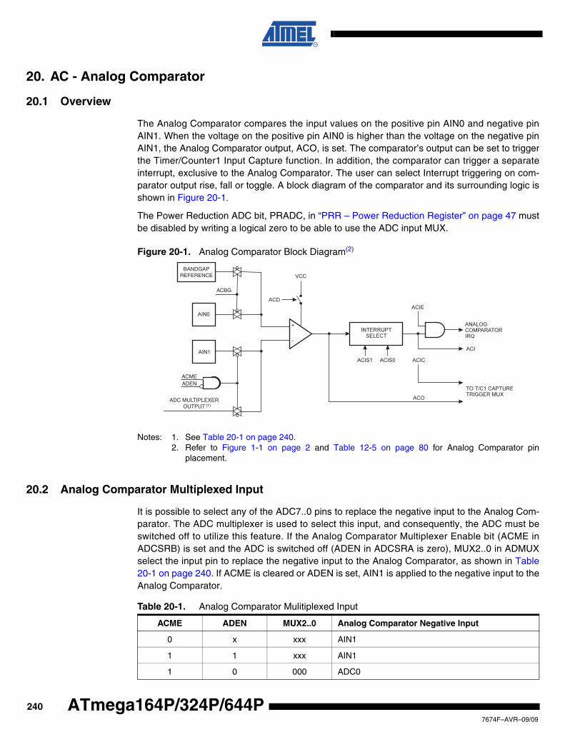
20. AC - Analog Comparator
20.1 Overview
The Analog Comparator compares the input values on the positive pin AIN0 and negative pinAIN1. When the voltage on the positive pin AIN0 is higher than the voltage on the negative pinAIN1, the Analog Comparator output, ACO, is set. The comparator’s output can be set to triggerthe Timer/Counter1 Input Capture function. In addition, the comparator can trigger a separateinterrupt, exclusive to the Analog Comparator. The user can select Interrupt triggering on com-parator output rise, fall or toggle. A block diagram of the comparator and its surrounding logic isshown in Figure 20-1.
The Power Reduction ADC bit, PRADC, in “PRR – Power Reduction Register” on page 47 mustbe disabled by writing a logical zero to be able to use the ADC input MUX.
Figure 20-1. Analog Comparator Block Diagram(2)
Notes: 1. See Table 20-1 on page 240.2. Refer to Figure 1-1 on page 2 and Table 12-5 on page 80 for Analog Comparator pin
placement.
20.2 Analog Comparator Multiplexed Input
It is possible to select any of the ADC7..0 pins to replace the negative input to the Analog Com-parator. The ADC multiplexer is used to select this input, and consequently, the ADC must beswitched off to utilize this feature. If the Analog Comparator Multiplexer Enable bit (ACME inADCSRB) is set and the ADC is switched off (ADEN in ADCSRA is zero), MUX2..0 in ADMUXselect the input pin to replace the negative input to the Analog Comparator, as shown in Table20-1 on page 240. If ACME is cleared or ADEN is set, AIN1 is applied to the negative input to theAnalog Comparator.
ACBG
BANDGAPREFERENCE
ADC MULTIPLEXEROUTPUT
ACMEADEN
(1)
Table 20-1. Analog Comparator Mulitiplexed Input
ACME ADEN MUX2..0 Analog Comparator Negative Input
0 x xxx AIN1
1 1 xxx AIN1
1 0 000 ADC0
2407674F–AVR–09/09
ATmega164P/324P/644P
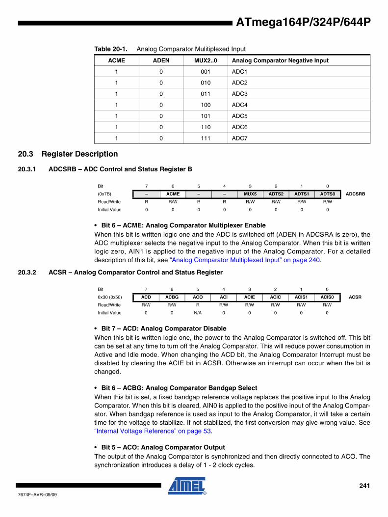
ATmega164P/324P/644P
20.3 Register Description
20.3.1 ADCSRB – ADC Control and Status Register B
• Bit 6 – ACME: Analog Comparator Multiplexer EnableWhen this bit is written logic one and the ADC is switched off (ADEN in ADCSRA is zero), theADC multiplexer selects the negative input to the Analog Comparator. When this bit is writtenlogic zero, AIN1 is applied to the negative input of the Analog Comparator. For a detaileddescription of this bit, see “Analog Comparator Multiplexed Input” on page 240.
20.3.2 ACSR – Analog Comparator Control and Status Register
• Bit 7 – ACD: Analog Comparator DisableWhen this bit is written logic one, the power to the Analog Comparator is switched off. This bitcan be set at any time to turn off the Analog Comparator. This will reduce power consumption inActive and Idle mode. When changing the ACD bit, the Analog Comparator Interrupt must bedisabled by clearing the ACIE bit in ACSR. Otherwise an interrupt can occur when the bit ischanged.
• Bit 6 – ACBG: Analog Comparator Bandgap SelectWhen this bit is set, a fixed bandgap reference voltage replaces the positive input to the AnalogComparator. When this bit is cleared, AIN0 is applied to the positive input of the Analog Compar-ator. When bandgap reference is used as input to the Analog Comparator, it will take a certaintime for the voltage to stabilize. If not stabilized, the first conversion may give wrong value. See“Internal Voltage Reference” on page 53.
• Bit 5 – ACO: Analog Comparator OutputThe output of the Analog Comparator is synchronized and then directly connected to ACO. Thesynchronization introduces a delay of 1 - 2 clock cycles.
1 0 001 ADC1
1 0 010 ADC2
1 0 011 ADC3
1 0 100 ADC4
1 0 101 ADC5
1 0 110 ADC6
1 0 111 ADC7
Table 20-1. Analog Comparator Mulitiplexed Input
ACME ADEN MUX2..0 Analog Comparator Negative Input
Bit 7 6 5 4 3 2 1 0
(0x7B) – ACME – – MUX5 ADTS2 ADTS1 ADTS0 ADCSRB
Read/Write R R/W R R R/W R/W R/W R/W
Initial Value 0 0 0 0 0 0 0 0
Bit 7 6 5 4 3 2 1 0
0x30 (0x50) ACD ACBG ACO ACI ACIE ACIC ACIS1 ACIS0 ACSR
Read/Write R/W R/W R R/W R/W R/W R/W R/W
Initial Value 0 0 N/A 0 0 0 0 0
2417674F–AVR–09/09
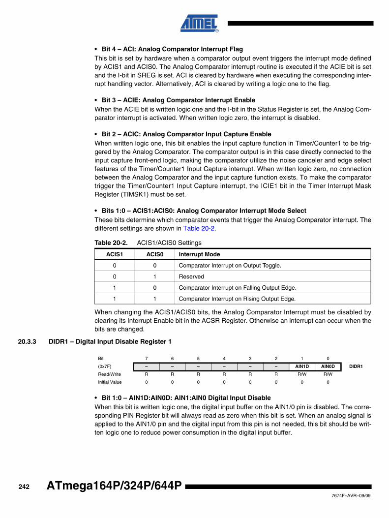
• Bit 4 – ACI: Analog Comparator Interrupt FlagThis bit is set by hardware when a comparator output event triggers the interrupt mode definedby ACIS1 and ACIS0. The Analog Comparator interrupt routine is executed if the ACIE bit is setand the I-bit in SREG is set. ACI is cleared by hardware when executing the corresponding inter-rupt handling vector. Alternatively, ACI is cleared by writing a logic one to the flag.
• Bit 3 – ACIE: Analog Comparator Interrupt EnableWhen the ACIE bit is written logic one and the I-bit in the Status Register is set, the Analog Com-parator interrupt is activated. When written logic zero, the interrupt is disabled.
• Bit 2 – ACIC: Analog Comparator Input Capture EnableWhen written logic one, this bit enables the input capture function in Timer/Counter1 to be trig-gered by the Analog Comparator. The comparator output is in this case directly connected to theinput capture front-end logic, making the comparator utilize the noise canceler and edge selectfeatures of the Timer/Counter1 Input Capture interrupt. When written logic zero, no connectionbetween the Analog Comparator and the input capture function exists. To make the comparatortrigger the Timer/Counter1 Input Capture interrupt, the ICIE1 bit in the Timer Interrupt MaskRegister (TIMSK1) must be set.
• Bits 1:0 – ACIS1:ACIS0: Analog Comparator Interrupt Mode SelectThese bits determine which comparator events that trigger the Analog Comparator interrupt. Thedifferent settings are shown in Table 20-2.
When changing the ACIS1/ACIS0 bits, the Analog Comparator Interrupt must be disabled byclearing its Interrupt Enable bit in the ACSR Register. Otherwise an interrupt can occur when thebits are changed.
20.3.3 DIDR1 – Digital Input Disable Register 1
• Bit 1:0 – AIN1D:AIN0D: AIN1:AIN0 Digital Input DisableWhen this bit is written logic one, the digital input buffer on the AIN1/0 pin is disabled. The corre-sponding PIN Register bit will always read as zero when this bit is set. When an analog signal isapplied to the AIN1/0 pin and the digital input from this pin is not needed, this bit should be writ-ten logic one to reduce power consumption in the digital input buffer.
Table 20-2. ACIS1/ACIS0 Settings
ACIS1 ACIS0 Interrupt Mode
0 0 Comparator Interrupt on Output Toggle.
0 1 Reserved
1 0 Comparator Interrupt on Falling Output Edge.
1 1 Comparator Interrupt on Rising Output Edge.
Bit 7 6 5 4 3 2 1 0
(0x7F) – – – – – – AIN1D AIN0D DIDR1
Read/Write R R R R R R R/W R/W
Initial Value 0 0 0 0 0 0 0 0
2427674F–AVR–09/09
ATmega164P/324P/644P
ATmega164P/324P/644P
21. ADC - Analog-to-digital Converter
21.1 Features
• 10-bit Resolution• 0.5 LSB Integral Non-linearity• ±2 LSB Absolute Accuracy• 65 - 260 µs Conversion Time• Up to 15 kSPS at Maximum Resolution• 8 Multiplexed Single Ended Input Channels• Differential mode with selectable gain at 1x, 10x or 200x(1)
• Optional Left adjustment for ADC Result Readout• 0 - VCC ADC Input Voltage Range• 2.7 - VCC Differential ADC Voltage Range• Selectable 2.56V or 1.1V ADC Reference Voltage• Free Running or Single Conversion Mode• ADC Start Conversion by Auto Triggering on Interrupt Sources• Interrupt on ADC Conversion Complete• Sleep Mode Noise Canceler
Note: 1. Differential Mode is not recommended above 85°C.
21.2 Overview
The ATmega164P/324P/644P features a 10-bit successive approximation ADC. The ADC isconnected to an 8-channel Analog Multiplexer which allows 8 single-ended voltage inputs con-structed from the pins of Port A. The single-ended voltage inputs refer to 0V (GND).
The device also supports 16 differential voltage input combinations. Two of the differential inputs(ADC1, ADC0 and ADC3, ADC2) are equipped with a programmable gain stage. This providesamplification steps of 0 dB (1x), 20 dB (10x), or 46 dB (200x) on the differential input voltagebefore the A/D conversion. Seven differential analog input channels share a common negativeterminal (ADC1), while any other ADC input can be selected as the positive input terminal. If 1xor 10x gain is used, 8-bit resolution can be expected. If 200x gain is used, 6-bit resolution can beexpected. Note that internal references of 1.1V should not be used on 200x gain.
The ADC contains a Sample and Hold circuit which ensures that the input voltage to the ADC isheld at a constant level during conversion. A block diagram of the ADC is shown in Figure 21-1on page 244.
The ADC has a separate analog supply voltage pin, AVCC. AVCC must not differ more than±0.3 V from VCC. See the paragraph “ADC Noise Canceler” on page 251 on how to connect thispin.
Internal reference voltages of nominally 1.1V, 2.56V or AVCC are provided On-chip. The voltagereference may be externally decoupled at the AREF pin by a capacitor for better noiseperformance.
2437674F–AVR–09/09
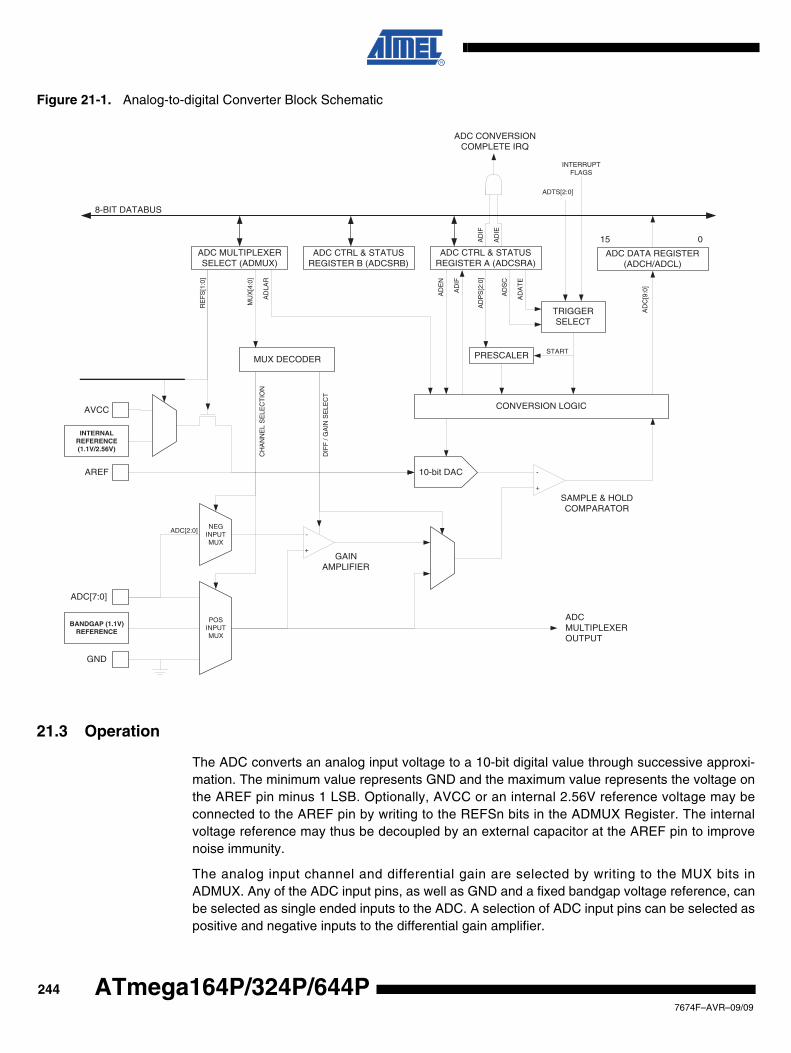
Figure 21-1. Analog-to-digital Converter Block Schematic
21.3 Operation
The ADC converts an analog input voltage to a 10-bit digital value through successive approxi-mation. The minimum value represents GND and the maximum value represents the voltage onthe AREF pin minus 1 LSB. Optionally, AVCC or an internal 2.56V reference voltage may beconnected to the AREF pin by writing to the REFSn bits in the ADMUX Register. The internalvoltage reference may thus be decoupled by an external capacitor at the AREF pin to improvenoise immunity.
The analog input channel and differential gain are selected by writing to the MUX bits inADMUX. Any of the ADC input pins, as well as GND and a fixed bandgap voltage reference, canbe selected as single ended inputs to the ADC. A selection of ADC input pins can be selected aspositive and negative inputs to the differential gain amplifier.
ADC CONVERSIONCOMPLETE IRQ
8-BIT DATABUS
15 0AD
IE
AD
AT
E
AD
SC
AD
EN
AD
IF
AD
IF
MU
X[4
:0]
AD
PS
[2:0
]
SAMPLE & HOLDCOMPARATOR
INTERNALREFERENCE(1.1V/2.56V)
AVCC
RE
FS
[1:0
]
AD
LAR
CH
AN
NE
L S
ELE
CT
ION
AD
C[9
:0]
ADCMULTIPLEXEROUTPUT
GAINAMPLIFIER
AREF
BANDGAP (1.1V)REFERENCE
GND
CONVERSION LOGIC
ADC CTRL & STATUSREGISTER B (ADCSRB)
ADC CTRL & STATUSREGISTER A (ADCSRA)
PRESCALER
ADC MULTIPLEXERSELECT (ADMUX)
MUX DECODER
DIF
F /
GA
IN S
ELE
CT
ADC DATA REGISTER(ADCH/ADCL)
ADC[2:0]
TRIGGERSELECT
START
INTERRUPTFLAGS
ADTS[2:0]
+
-NEG
INPUTMUX
POSINPUTMUX
ADC[7:0]
+
-10-bit DAC
2447674F–AVR–09/09
ATmega164P/324P/644P
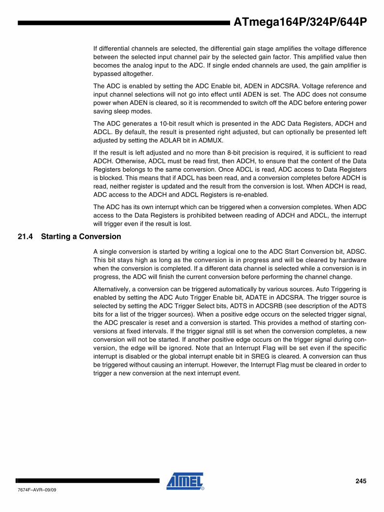
ATmega164P/324P/644P
If differential channels are selected, the differential gain stage amplifies the voltage differencebetween the selected input channel pair by the selected gain factor. This amplified value thenbecomes the analog input to the ADC. If single ended channels are used, the gain amplifier isbypassed altogether.
The ADC is enabled by setting the ADC Enable bit, ADEN in ADCSRA. Voltage reference andinput channel selections will not go into effect until ADEN is set. The ADC does not consumepower when ADEN is cleared, so it is recommended to switch off the ADC before entering powersaving sleep modes.
The ADC generates a 10-bit result which is presented in the ADC Data Registers, ADCH andADCL. By default, the result is presented right adjusted, but can optionally be presented leftadjusted by setting the ADLAR bit in ADMUX.
If the result is left adjusted and no more than 8-bit precision is required, it is sufficient to readADCH. Otherwise, ADCL must be read first, then ADCH, to ensure that the content of the DataRegisters belongs to the same conversion. Once ADCL is read, ADC access to Data Registersis blocked. This means that if ADCL has been read, and a conversion completes before ADCH isread, neither register is updated and the result from the conversion is lost. When ADCH is read,ADC access to the ADCH and ADCL Registers is re-enabled.
The ADC has its own interrupt which can be triggered when a conversion completes. When ADCaccess to the Data Registers is prohibited between reading of ADCH and ADCL, the interruptwill trigger even if the result is lost.
21.4 Starting a Conversion
A single conversion is started by writing a logical one to the ADC Start Conversion bit, ADSC.This bit stays high as long as the conversion is in progress and will be cleared by hardwarewhen the conversion is completed. If a different data channel is selected while a conversion is inprogress, the ADC will finish the current conversion before performing the channel change.
Alternatively, a conversion can be triggered automatically by various sources. Auto Triggering isenabled by setting the ADC Auto Trigger Enable bit, ADATE in ADCSRA. The trigger source isselected by setting the ADC Trigger Select bits, ADTS in ADCSRB (see description of the ADTSbits for a list of the trigger sources). When a positive edge occurs on the selected trigger signal,the ADC prescaler is reset and a conversion is started. This provides a method of starting con-versions at fixed intervals. If the trigger signal still is set when the conversion completes, a newconversion will not be started. If another positive edge occurs on the trigger signal during con-version, the edge will be ignored. Note that an Interrupt Flag will be set even if the specificinterrupt is disabled or the global interrupt enable bit in SREG is cleared. A conversion can thusbe triggered without causing an interrupt. However, the Interrupt Flag must be cleared in order totrigger a new conversion at the next interrupt event.
2457674F–AVR–09/09
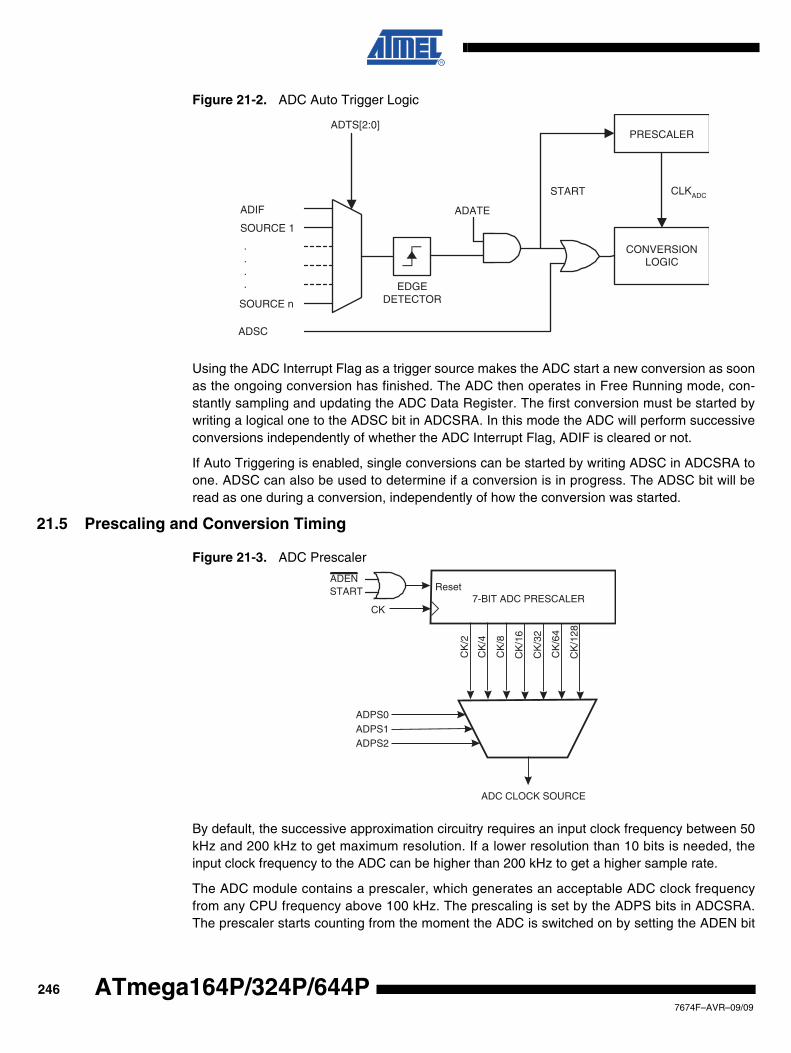
Figure 21-2. ADC Auto Trigger Logic
Using the ADC Interrupt Flag as a trigger source makes the ADC start a new conversion as soonas the ongoing conversion has finished. The ADC then operates in Free Running mode, con-stantly sampling and updating the ADC Data Register. The first conversion must be started bywriting a logical one to the ADSC bit in ADCSRA. In this mode the ADC will perform successiveconversions independently of whether the ADC Interrupt Flag, ADIF is cleared or not.
If Auto Triggering is enabled, single conversions can be started by writing ADSC in ADCSRA toone. ADSC can also be used to determine if a conversion is in progress. The ADSC bit will beread as one during a conversion, independently of how the conversion was started.
21.5 Prescaling and Conversion Timing
Figure 21-3. ADC Prescaler
By default, the successive approximation circuitry requires an input clock frequency between 50kHz and 200 kHz to get maximum resolution. If a lower resolution than 10 bits is needed, theinput clock frequency to the ADC can be higher than 200 kHz to get a higher sample rate.
The ADC module contains a prescaler, which generates an acceptable ADC clock frequencyfrom any CPU frequency above 100 kHz. The prescaling is set by the ADPS bits in ADCSRA.The prescaler starts counting from the moment the ADC is switched on by setting the ADEN bit
ADSC
ADIF
SOURCE 1
SOURCE n
ADTS[2:0]
CONVERSIONLOGIC
PRESCALER
START CLKADC
.
.
.
. EDGEDETECTOR
ADATE
7-BIT ADC PRESCALER
ADC CLOCK SOURCE
CK
ADPS0ADPS1ADPS2
CK
/128
CK
/2
CK
/4
CK
/8
CK
/16
CK
/32
CK
/64
ResetADENSTART
2467674F–AVR–09/09
ATmega164P/324P/644P
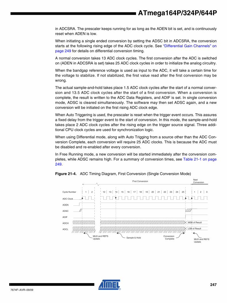
ATmega164P/324P/644P
in ADCSRA. The prescaler keeps running for as long as the ADEN bit is set, and is continuouslyreset when ADEN is low.
When initiating a single ended conversion by setting the ADSC bit in ADCSRA, the conversionstarts at the following rising edge of the ADC clock cycle. See “Differential Gain Channels” onpage 249 for details on differential conversion timing.
A normal conversion takes 13 ADC clock cycles. The first conversion after the ADC is switchedon (ADEN in ADCSRA is set) takes 25 ADC clock cycles in order to initialize the analog circuitry.
When the bandgap reference voltage is used as input to the ADC, it will take a certain time forthe voltage to stabilize. If not stabilized, the first value read after the first conversion may bewrong.
The actual sample-and-hold takes place 1.5 ADC clock cycles after the start of a normal conver-sion and 13.5 ADC clock cycles after the start of a first conversion. When a conversion iscomplete, the result is written to the ADC Data Registers, and ADIF is set. In single conversionmode, ADSC is cleared simultaneously. The software may then set ADSC again, and a newconversion will be initiated on the first rising ADC clock edge.
When Auto Triggering is used, the prescaler is reset when the trigger event occurs. This assuresa fixed delay from the trigger event to the start of conversion. In this mode, the sample-and-holdtakes place 2 ADC clock cycles after the rising edge on the trigger source signal. Three addi-tional CPU clock cycles are used for synchronization logic.
When using Differential mode, along with Auto Trigging from a source other than the ADC Con-version Complete, each conversion will require 25 ADC clocks. This is because the ADC mustbe disabled and re-enabled after every conversion.
In Free Running mode, a new conversion will be started immediately after the conversion com-pletes, while ADSC remains high. For a summary of conversion times, see Table 21-1 on page249.
Figure 21-4. ADC Timing Diagram, First Conversion (Single Conversion Mode)
MSB of Result
LSB of Result
ADC Clock
ADSC
Sample & Hold
ADIF
ADCH
ADCL
Cycle Number
ADEN
1 2 12 13 14 15 16 17 18 19 20 21 22 23 24 25 1 2
First ConversionNextConversion
3
MUX and REFSUpdate MUX and REFS
Update
ConversionComplete
2477674F–AVR–09/09
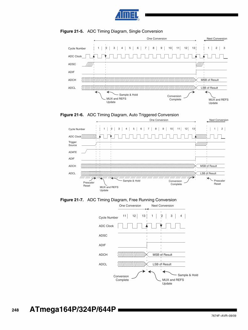
Figure 21-5. ADC Timing Diagram, Single Conversion
Figure 21-6. ADC Timing Diagram, Auto Triggered Conversion
Figure 21-7. ADC Timing Diagram, Free Running Conversion
1 2 3 4 5 6 7 8 9 10 11 12 13
MSB of Result
LSB of Result
ADC Clock
ADSC
ADIF
ADCH
ADCL
Cycle Number 1 2
One Conversion Next Conversion
3
Sample & HoldMUX and REFSUpdate
ConversionComplete MUX and REFS
Update
1 2 3 4 5 6 7 8 9 10 11 12 13
MSB of Result
LSB of Result
ADC Clock
TriggerSource
ADIF
ADCH
ADCL
Cycle Number 1 2
One Conversion Next Conversion
ConversionComplete
Prescaler Reset
ADATE
PrescalerReset
Sample & Hold
MUX and REFS Update
11 12 13
MSB of Result
LSB of Result
ADC Clock
ADSC
ADIF
ADCH
ADCL
Cycle Number1 2
One Conversion Next Conversion
3 4
ConversionComplete
Sample & Hold
MUX and REFSUpdate
2487674F–AVR–09/09
ATmega164P/324P/644P
ATmega164P/324P/644P
21.5.1 Differential Gain Channels
When using differential gain channels, certain aspects of the conversion need to be taken intoconsideration. Note that the differential channels should not be used with an AREF < 2V.
Differential conversions are synchronized to the internal clock CKADC2 equal to half the ADCclock. This synchronization is done automatically by the ADC interface in such a way that thesample-and-hold occurs at a specific phase of CKADC2. A conversion initiated by the user (i.e., allsingle conversions, and the first free running conversion) when CKADC2 is low will take the sameamount of time as a single ended conversion (13 ADC clock cycles from the next prescaledclock cycle). A conversion initiated by the user when CKADC2 is high will take 14 ADC clockcycles due to the synchronization mechanism. In Free Running mode, a new conversion is initi-ated immediately after the previous conversion completes, and since CKADC2 is high at this time,all automatically started (i.e., all but the first) free running conversions will take 14 ADC clockcycles.
The gain stage is optimized for a bandwidth of 4 kHz at all gain settings. Higher frequencies maybe subjected to non-linear amplification. An external low-pass filter should be used if the inputsignal contains higher frequency components than the gain stage bandwidth. Note that the ADCclock frequency is independent of the gain stage bandwidth limitation. For example, the ADCclock period may be 6 µs, allowing a channel to be sampled at 12 kSPS, regardless of the band-width of this channel.
If differential gain channels are used and conversions are started by Auto Triggering, the ADCmust be switched off between conversions. When Auto Triggering is used, the ADC prescaler isreset before the conversion is started. Since the gain stage is dependent of a stable ADC clockprior to the conversion, this conversion will not be valid. By disabling and then re-enabling theADC between each conversion (writing ADEN in ADCSRA to “0” then to “1”), only extended con-versions are performed. The result from the extended conversions will be valid. See “Prescalingand Conversion Timing” on page 246 for timing details.
21.6 Changing Channel or Reference Selection
The MUXn and REFS1:0 bits in the ADMUX Register are single buffered through a temporaryregister to which the CPU has random access. This ensures that the channels and referenceselection only takes place at a safe point during the conversion. The channel and referenceselection is continuously updated until a conversion is started. Once the conversion starts, thechannel and reference selection is locked to ensure a sufficient sampling time for the ADC. Con-tinuous updating resumes in the last ADC clock cycle before the conversion completes (ADIF inADCSRA is set). Note that the conversion starts on the following rising ADC clock edge afterADSC is written. The user is thus advised not to write new channel or reference selection valuesto ADMUX until one ADC clock cycle after ADSC is written.
Table 21-1. ADC Conversion Time
ConditionSample & Hold (Cycles
from Start of Conversion) Conversion Time (Cycles)
First conversion 14.5 25
Normal conversions, single ended 1.5 13
Auto Triggered conversions 2 13.5
Normal conversions, differential 1.5/2.5 13/14
2497674F–AVR–09/09
If Auto Triggering is used, the exact time of the triggering event can be indeterministic. Specialcare must be taken when updating the ADMUX Register, in order to control which conversionwill be affected by the new settings.
If both ADATE and ADEN is written to one, an interrupt event can occur at any time. If theADMUX Register is changed in this period, the user cannot tell if the next conversion is basedon the old or the new settings. ADMUX can be safely updated in the following ways:
1. When ADATE or ADEN is cleared.
2. During conversion, minimum one ADC clock cycle after the trigger event.
3. After a conversion, before the Interrupt Flag used as trigger source is cleared.
When updating ADMUX in one of these conditions, the new settings will affect the next ADCconversion.
Special care should be taken when changing differential channels. Once a differential channelhas been selected, the gain stage may take as much as 125 µs to stabilize to the new value.Thus conversions should not be started within the first 125 µs after selecting a new differentialchannel. Alternatively, conversion results obtained within this period should be discarded.
The same settling time should be observed for the first differential conversion after changingADC reference (by changing the REFS1:0 bits in ADMUX).
21.6.1 ADC Input Channels
When changing channel selections, the user should observe the following guidelines to ensurethat the correct channel is selected:
In Single Conversion mode, always select the channel before starting the conversion. The chan-nel selection may be changed one ADC clock cycle after writing one to ADSC. However, thesimplest method is to wait for the conversion to complete before changing the channel selection.
In Free Running mode, always select the channel before starting the first conversion. The chan-nel selection may be changed one ADC clock cycle after writing one to ADSC. However, thesimplest method is to wait for the first conversion to complete, and then change the channelselection. Since the next conversion has already started automatically, the next result will reflectthe previous channel selection. Subsequent conversions will reflect the new channel selection.
When switching to a differential gain channel, the first conversion result may have a poor accu-racy due to the required settling time for the automatic offset cancellation circuitry. The usershould preferably disregard the first conversion result.
21.6.2 ADC Voltage Reference
The reference voltage for the ADC (VREF) indicates the conversion range for the ADC. Singleended channels that exceed VREF will result in codes close to 0x3FF. VREF can be selected aseither AVCC, internal 2.56V reference, or external AREF pin.
AVCC is connected to the ADC through a passive switch. The internal 2.56V reference is gener-ated from the internal bandgap reference (VBG) through an internal amplifier. In either case, theexternal AREF pin is directly connected to the ADC, and the reference voltage can be mademore immune to noise by connecting a capacitor between the AREF pin and ground. VREF canalso be measured at the AREF pin with a high impedant voltmeter. Note that VREF is a highimpedant source, and only a capacitive load should be connected in a system.
2507674F–AVR–09/09
ATmega164P/324P/644P
ATmega164P/324P/644P
If the user has a fixed voltage source connected to the AREF pin, the user may not use the otherreference voltage options in the application, as they will be shorted to the external voltage. If noexternal voltage is applied to the AREF pin, the user may switch between AVCC and 2.56V asreference selection. The first ADC conversion result after switching reference voltage sourcemay be inaccurate, and the user is advised to discard this result.
If differential channels are used, the selected reference should not be closer to AVCC thanindicated in Table 26-8 on page 336.
21.7 ADC Noise Canceler
The ADC features a noise canceler that enables conversion during sleep mode to reduce noiseinduced from the CPU core and other I/O peripherals. The noise canceler can be used with ADCNoise Reduction and Idle mode. To make use of this feature, the following procedure should beused:
a. Make sure that the ADC is enabled and is not busy converting. Single Conversion Mode must be selected and the ADC conversion complete interrupt must be enabled.
b. Enter ADC Noise Reduction mode (or Idle mode). The ADC will start a conversion once the CPU has been halted.
c. If no other interrupts occur before the ADC conversion completes, the ADC interrupt will wake up the CPU and execute the ADC Conversion Complete interrupt routine. If another interrupt wakes up the CPU before the ADC conversion is complete, that interrupt will be executed, and an ADC Conversion Complete interrupt request will be generated when the ADC conversion completes. The CPU will remain in active mode until a new sleep command is executed.
Note that the ADC will not be automatically turned off when entering other sleep modes than Idlemode and ADC Noise Reduction mode. The user is advised to write zero to ADEN before enter-ing such sleep modes to avoid excessive power consumption. If the ADC is enabled in suchsleep modes and the user wants to perform differential conversions, the user is advised toswitch the ADC off and on after waking up from sleep to prompt an extended conversion to get avalid result.
21.7.1 Analog Input Circuitry
The Analog Input Circuitry for single ended channels is illustrated in Figure 21-8. An analogsource applied to ADCn is subjected to the pin capacitance and input leakage of that pin, regard-less of whether that channel is selected as input for the ADC. When the channel is selected, thesource must drive the S/H capacitor through the series resistance (combined resistance in theinput path).
The ADC is optimized for analog signals with an output impedance of approximately 10 kΩ orless. If such a source is used, the sampling time will be negligible. If a source with higher imped-ance is used, the sampling time will depend on how long time the source needs to charge theS/H capacitor, with can vary widely. The user is recommended to only use low impedant sourceswith slowly varying signals, since this minimizes the required charge transfer to the S/Hcapacitor.
If differential gain channels are used, the input circuitry looks somewhat different, althoughsource impedances of a few hundred kΩ or less is recommended.
2517674F–AVR–09/09
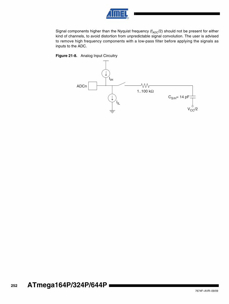
Signal components higher than the Nyquist frequency (fADC/2) should not be present for eitherkind of channels, to avoid distortion from unpredictable signal convolution. The user is advisedto remove high frequency components with a low-pass filter before applying the signals asinputs to the ADC.
Figure 21-8. Analog Input Circuitry
ADCn
IIH
1..100 kΩCS/H= 14 pF
VCC/2
IIL
2527674F–AVR–09/09
ATmega164P/324P/644P
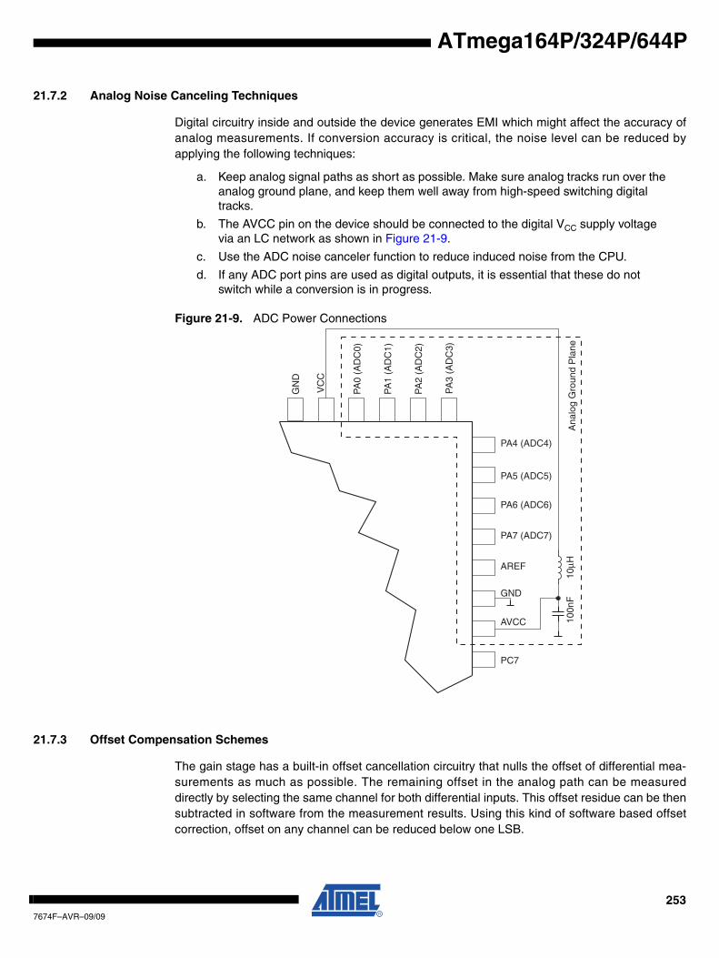
ATmega164P/324P/644P
21.7.2 Analog Noise Canceling Techniques
Digital circuitry inside and outside the device generates EMI which might affect the accuracy ofanalog measurements. If conversion accuracy is critical, the noise level can be reduced byapplying the following techniques:
a. Keep analog signal paths as short as possible. Make sure analog tracks run over the analog ground plane, and keep them well away from high-speed switching digital tracks.
b. The AVCC pin on the device should be connected to the digital VCC supply voltage via an LC network as shown in Figure 21-9.
c. Use the ADC noise canceler function to reduce induced noise from the CPU.
d. If any ADC port pins are used as digital outputs, it is essential that these do not switch while a conversion is in progress.
Figure 21-9. ADC Power Connections
21.7.3 Offset Compensation Schemes
The gain stage has a built-in offset cancellation circuitry that nulls the offset of differential mea-surements as much as possible. The remaining offset in the analog path can be measureddirectly by selecting the same channel for both differential inputs. This offset residue can be thensubtracted in software from the measurement results. Using this kind of software based offsetcorrection, offset on any channel can be reduced below one LSB.
GN
D
VC
C
PA
0 (A
DC
0)
PA
1 (A
DC
1)
PA
2 (A
DC
2)
PA
3 (A
DC
3)PA4 (ADC4)
PA5 (ADC5)
PA6 (ADC6)
PA7 (ADC7)
AREF
AVCC
GND
PC7
10μH
100n
FA
nalo
g G
roun
d P
lane
2537674F–AVR–09/09
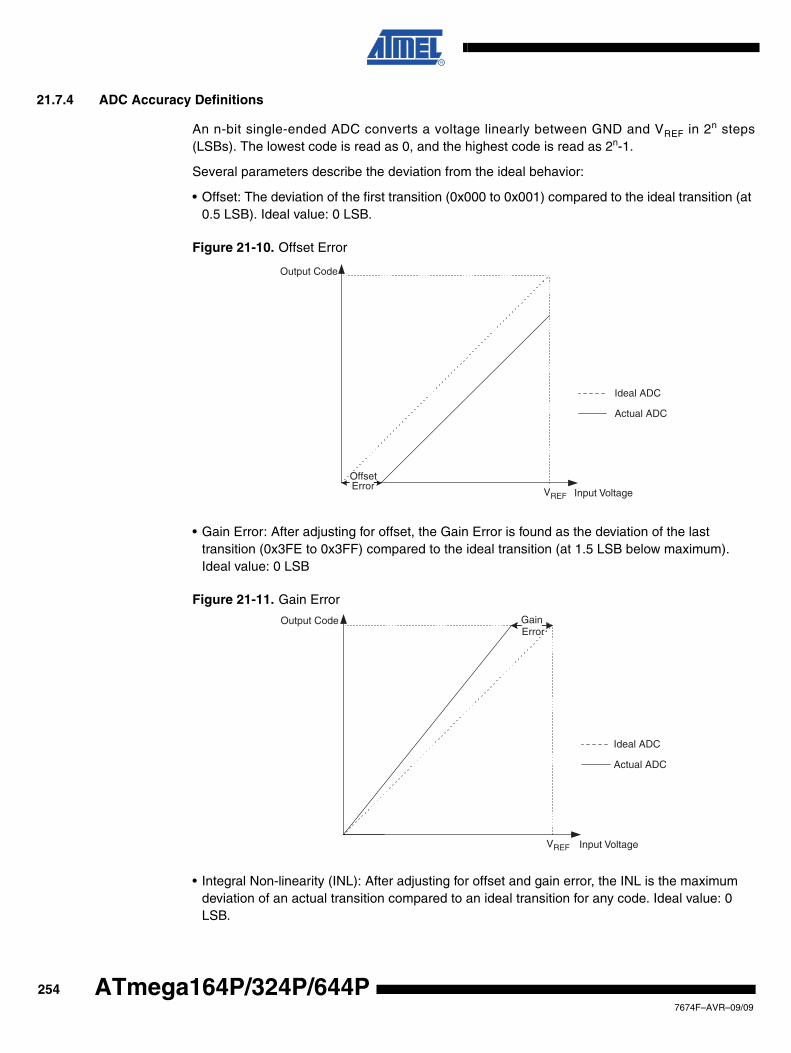
21.7.4 ADC Accuracy Definitions
An n-bit single-ended ADC converts a voltage linearly between GND and VREF in 2n steps(LSBs). The lowest code is read as 0, and the highest code is read as 2n-1.
Several parameters describe the deviation from the ideal behavior:
• Offset: The deviation of the first transition (0x000 to 0x001) compared to the ideal transition (at 0.5 LSB). Ideal value: 0 LSB.
Figure 21-10. Offset Error
• Gain Error: After adjusting for offset, the Gain Error is found as the deviation of the last transition (0x3FE to 0x3FF) compared to the ideal transition (at 1.5 LSB below maximum). Ideal value: 0 LSB
Figure 21-11. Gain Error
• Integral Non-linearity (INL): After adjusting for offset and gain error, the INL is the maximum deviation of an actual transition compared to an ideal transition for any code. Ideal value: 0 LSB.
Output Code
VREF Input Voltage
Ideal ADC
Actual ADC
OffsetError
Output Code
VREF Input Voltage
Ideal ADC
Actual ADC
GainError
2547674F–AVR–09/09
ATmega164P/324P/644P
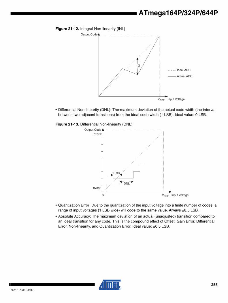
ATmega164P/324P/644P
Figure 21-12. Integral Non-linearity (INL)
• Differential Non-linearity (DNL): The maximum deviation of the actual code width (the interval between two adjacent transitions) from the ideal code width (1 LSB). Ideal value: 0 LSB.
Figure 21-13. Differential Non-linearity (DNL)
• Quantization Error: Due to the quantization of the input voltage into a finite number of codes, a range of input voltages (1 LSB wide) will code to the same value. Always ±0.5 LSB.
• Absolute Accuracy: The maximum deviation of an actual (unadjusted) transition compared to an ideal transition for any code. This is the compound effect of Offset, Gain Error, Differential Error, Non-linearity, and Quantization Error. Ideal value: ±0.5 LSB.
Output Code
VREF Input Voltage
Ideal ADC
Actual ADC
INL
Output Code
0x3FF
0x000
0 VREF Input Voltage
DNL
1 LSB
2557674F–AVR–09/09
21.8 ADC Conversion Result
After the conversion is complete (ADIF is high), the conversion result can be found in the ADCResult Registers (ADCL, ADCH).
For single ended conversion, the result is
where VIN is the voltage on the selected input pin and VREF the selected voltage reference (seeTable 21-3 on page 258 and Table 21-4 on page 259). 0x000 represents analog ground, and0x3FF represents the selected reference voltage minus one LSB.
If differential channels are used, the result is
where VPOS is the voltage on the positive input pin, VNEG the voltage on the negative input pin,GAIN the selected gain factor, and VREF the selected voltage reference. The result is presentedin two’s complement form, from 0x200 (-512d) through 0x1FF (+511d). Note that if the userwants to perform a quick polarity check of the results, it is sufficient to read the MSB of the result(ADC9 in ADCH). If this bit is one, the result is negative, and if this bit is zero, the result is posi-tive. Figure 21-14 on page 257 shows the decoding of the differential input range.
Table 21-2 on page 257 shows the resulting output codes if the differential input channel pair(ADCn - ADCm) is selected with a gain of GAIN and a reference voltage of VREF.
ADCVIN 1024⋅
VREF-----------------------------=
ADCVPOS VNEG–( ) GAIN 512⋅ ⋅
VREF------------------------------------------------------------------------------=
2567674F–AVR–09/09
ATmega164P/324P/644P
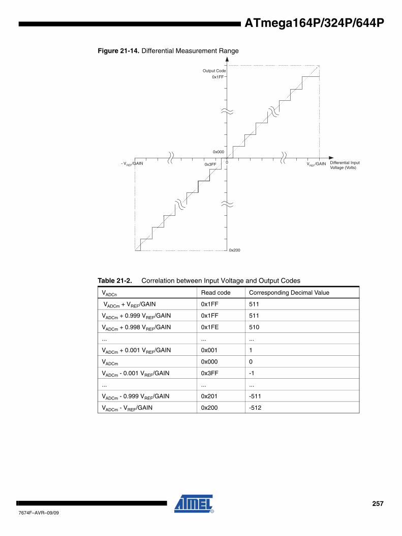
ATmega164P/324P/644P
Figure 21-14. Differential Measurement Range
Table 21-2. Correlation between Input Voltage and Output Codes
VADCn Read code Corresponding Decimal Value
VADCm + VREF/GAIN 0x1FF 511
VADCm + 0.999 VREF/GAIN 0x1FF 511
VADCm + 0.998 VREF/GAIN 0x1FE 510
... ... ...
VADCm + 0.001 VREF/GAIN 0x001 1
VADCm 0x000 0
VADCm - 0.001 VREF/GAIN 0x3FF -1
... ... ...
VADCm - 0.999 VREF/GAIN 0x201 -511
VADCm - VREF/GAIN 0x200 -512
0
Output Code
0x1FF
0x000
VREF/GAIN Differential InputVoltage (Volts)
0x3FF
0x200
- VREF/GAIN
2577674F–AVR–09/09
Example:
ADMUX = 0xED (ADC3 - ADC2, 10x gain, 2.56V reference, left adjusted result)
Voltage on ADC3 is 300 mV, voltage on ADC2 is 500 mV.
ADCR = 512 * 10 * (300 - 500) / 2560 = -400 = 0x270
ADCL will thus read 0x00, and ADCH will read 0x9C. Writing zero to ADLAR right adjusts theresult: ADCL = 0x70, ADCH = 0x02.
21.9 Register Description
21.9.1 ADMUX – ADC Multiplexer Selection Register
• Bit 7:6 – REFS1:0: Reference Selection BitsThese bits select the voltage reference for the ADC, as shown in Table 21-3. If these bits arechanged during a conversion, the change will not go in effect until this conversion is complete(ADIF in ADCSRA is set). The internal voltage reference options may not be used if an externalreference voltage is being applied to the AREF pin.
Note: If 10x og 200x gain is selected, only 2.56V should be used as Internal Voltage Reference.
• Bit 5 – ADLAR: ADC Left Adjust ResultThe ADLAR bit affects the presentation of the ADC conversion result in the ADC Data Register.Write one to ADLAR to left adjust the result. Otherwise, the result is right adjusted. Changing theADLAR bit will affect the ADC Data Register immediately, regardless of any ongoing conver-sions. For a complete description of this bit, see “ADCL and ADCH – The ADC Data Register” onpage 261.
• Bits 4:0 – MUX4:0: Analog Channel and Gain Selection BitsThe value of these bits selects which combination of analog inputs are connected to the ADC.These bits also select the gain for the differential channels. See Table 21-4 on page 259 fordetails. If these bits are changed during a conversion, the change will not go in effect until thisconversion is complete (ADIF in ADCSRA is set).
Bit 7 6 5 4 3 2 1 0
(0x7C) REFS1 REFS0 ADLAR MUX4 MUX3 MUX2 MUX1 MUX0 ADMUX
Read/Write R/W R/W R/W R/W R/W R/W R/W R/W
Initial Value 0 0 0 0 0 0 0 0
Table 21-3. Voltage Reference Selections for ADC
REFS1 REFS0 Voltage Reference Selection
0 0 AREF, Internal Vref turned off
0 1 AVCC with external capacitor at AREF pin
1 0 Internal 1.1V Voltage Reference with external capacitor at AREF pin
1 1 Internal 2.56V Voltage Reference with external capacitor at AREF pin
2587674F–AVR–09/09
ATmega164P/324P/644P
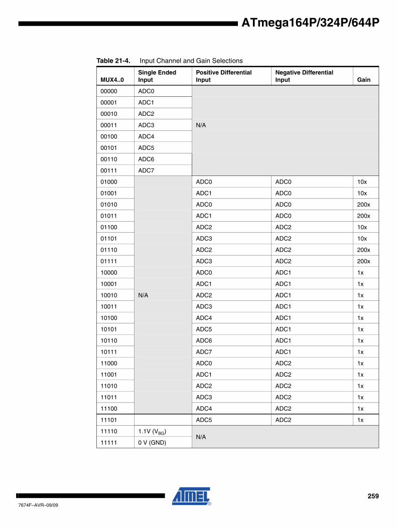
ATmega164P/324P/644P
Table 21-4. Input Channel and Gain Selections
MUX4..0Single Ended Input
Positive Differential Input
Negative Differential Input Gain
00000 ADC0
00001 ADC1
00010 ADC2
00011 ADC3 N/A
00100 ADC4
00101 ADC5
00110 ADC6
00111 ADC7
01000 ADC0 ADC0 10x
01001 ADC1 ADC0 10x
01010 ADC0 ADC0 200x
01011 ADC1 ADC0 200x
01100 ADC2 ADC2 10x
01101 ADC3 ADC2 10x
01110 ADC2 ADC2 200x
01111 ADC3 ADC2 200x
10000 ADC0 ADC1 1x
10001 ADC1 ADC1 1x
10010 N/A ADC2 ADC1 1x
10011 ADC3 ADC1 1x
10100 ADC4 ADC1 1x
10101 ADC5 ADC1 1x
10110 ADC6 ADC1 1x
10111 ADC7 ADC1 1x
11000 ADC0 ADC2 1x
11001 ADC1 ADC2 1x
11010 ADC2 ADC2 1x
11011 ADC3 ADC2 1x
11100 ADC4 ADC2 1x
11101 ADC5 ADC2 1x
11110 1.1V (VBG)N/A
11111 0 V (GND)
2597674F–AVR–09/09
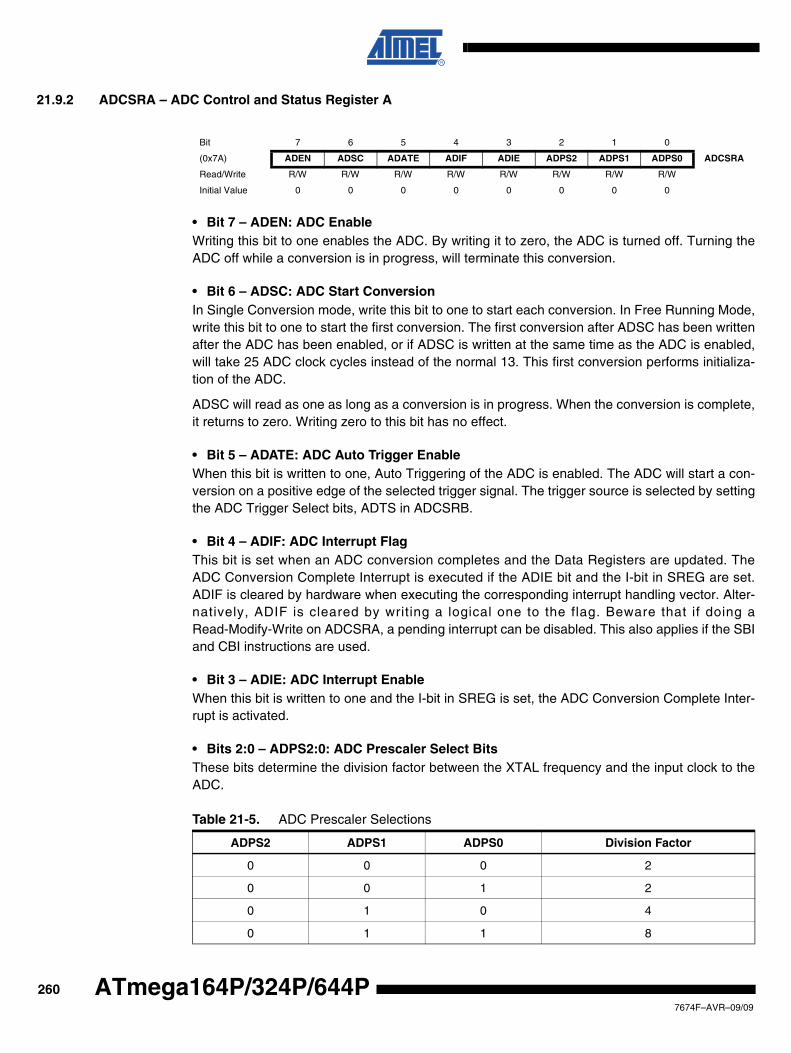
21.9.2 ADCSRA – ADC Control and Status Register A
• Bit 7 – ADEN: ADC EnableWriting this bit to one enables the ADC. By writing it to zero, the ADC is turned off. Turning theADC off while a conversion is in progress, will terminate this conversion.
• Bit 6 – ADSC: ADC Start ConversionIn Single Conversion mode, write this bit to one to start each conversion. In Free Running Mode,write this bit to one to start the first conversion. The first conversion after ADSC has been writtenafter the ADC has been enabled, or if ADSC is written at the same time as the ADC is enabled,will take 25 ADC clock cycles instead of the normal 13. This first conversion performs initializa-tion of the ADC.
ADSC will read as one as long as a conversion is in progress. When the conversion is complete,it returns to zero. Writing zero to this bit has no effect.
• Bit 5 – ADATE: ADC Auto Trigger EnableWhen this bit is written to one, Auto Triggering of the ADC is enabled. The ADC will start a con-version on a positive edge of the selected trigger signal. The trigger source is selected by settingthe ADC Trigger Select bits, ADTS in ADCSRB.
• Bit 4 – ADIF: ADC Interrupt FlagThis bit is set when an ADC conversion completes and the Data Registers are updated. TheADC Conversion Complete Interrupt is executed if the ADIE bit and the I-bit in SREG are set.ADIF is cleared by hardware when executing the corresponding interrupt handling vector. Alter-natively, ADIF is cleared by writing a logical one to the flag. Beware that if doing aRead-Modify-Write on ADCSRA, a pending interrupt can be disabled. This also applies if the SBIand CBI instructions are used.
• Bit 3 – ADIE: ADC Interrupt EnableWhen this bit is written to one and the I-bit in SREG is set, the ADC Conversion Complete Inter-rupt is activated.
• Bits 2:0 – ADPS2:0: ADC Prescaler Select BitsThese bits determine the division factor between the XTAL frequency and the input clock to theADC.
Bit 7 6 5 4 3 2 1 0
(0x7A) ADEN ADSC ADATE ADIF ADIE ADPS2 ADPS1 ADPS0 ADCSRA
Read/Write R/W R/W R/W R/W R/W R/W R/W R/W
Initial Value 0 0 0 0 0 0 0 0
Table 21-5. ADC Prescaler Selections
ADPS2 ADPS1 ADPS0 Division Factor
0 0 0 2
0 0 1 2
0 1 0 4
0 1 1 8
2607674F–AVR–09/09
ATmega164P/324P/644P
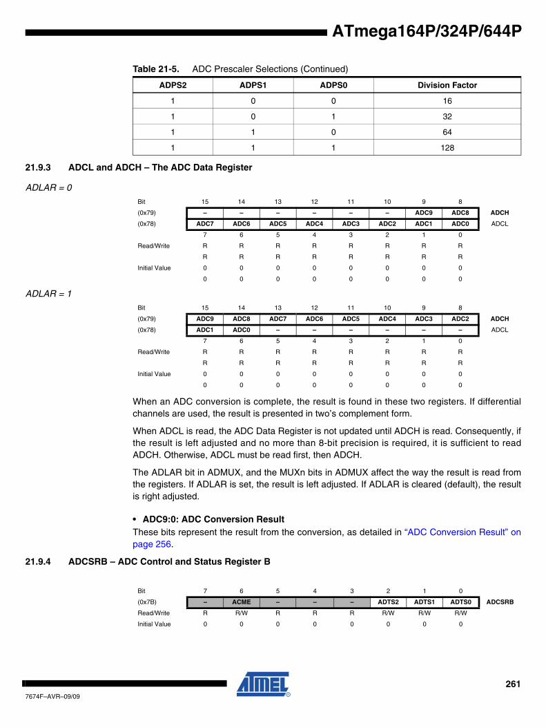
ATmega164P/324P/644P
21.9.3 ADCL and ADCH – The ADC Data Register
ADLAR = 0
ADLAR = 1
When an ADC conversion is complete, the result is found in these two registers. If differentialchannels are used, the result is presented in two’s complement form.
When ADCL is read, the ADC Data Register is not updated until ADCH is read. Consequently, ifthe result is left adjusted and no more than 8-bit precision is required, it is sufficient to readADCH. Otherwise, ADCL must be read first, then ADCH.
The ADLAR bit in ADMUX, and the MUXn bits in ADMUX affect the way the result is read fromthe registers. If ADLAR is set, the result is left adjusted. If ADLAR is cleared (default), the resultis right adjusted.
• ADC9:0: ADC Conversion ResultThese bits represent the result from the conversion, as detailed in “ADC Conversion Result” onpage 256.
21.9.4 ADCSRB – ADC Control and Status Register B
1 0 0 16
1 0 1 32
1 1 0 64
1 1 1 128
Table 21-5. ADC Prescaler Selections (Continued)
ADPS2 ADPS1 ADPS0 Division Factor
Bit 15 14 13 12 11 10 9 8
(0x79) – – – – – – ADC9 ADC8 ADCH
(0x78) ADC7 ADC6 ADC5 ADC4 ADC3 ADC2 ADC1 ADC0 ADCL
7 6 5 4 3 2 1 0
Read/Write R R R R R R R R
R R R R R R R R
Initial Value 0 0 0 0 0 0 0 0
0 0 0 0 0 0 0 0
Bit 15 14 13 12 11 10 9 8
(0x79) ADC9 ADC8 ADC7 ADC6 ADC5 ADC4 ADC3 ADC2 ADCH
(0x78) ADC1 ADC0 – – – – – – ADCL
7 6 5 4 3 2 1 0
Read/Write R R R R R R R R
R R R R R R R R
Initial Value 0 0 0 0 0 0 0 0
0 0 0 0 0 0 0 0
Bit 7 6 5 4 3 2 1 0
(0x7B) – ACME – – – ADTS2 ADTS1 ADTS0 ADCSRB
Read/Write R R/W R R R R/W R/W R/W
Initial Value 0 0 0 0 0 0 0 0
2617674F–AVR–09/09
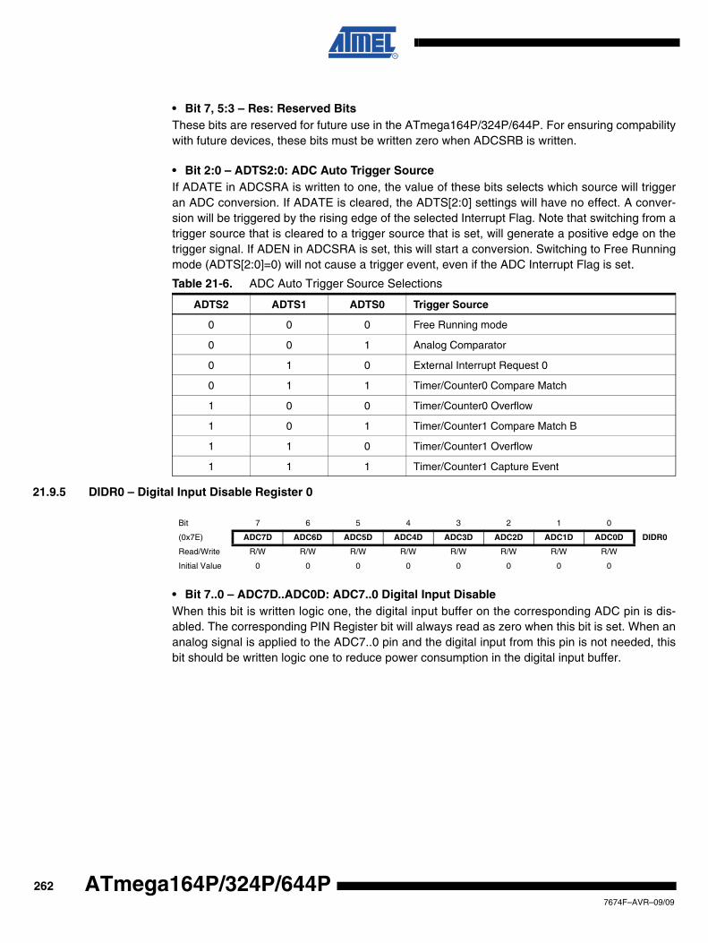
• Bit 7, 5:3 – Res: Reserved BitsThese bits are reserved for future use in the ATmega164P/324P/644P. For ensuring compabilitywith future devices, these bits must be written zero when ADCSRB is written.
• Bit 2:0 – ADTS2:0: ADC Auto Trigger SourceIf ADATE in ADCSRA is written to one, the value of these bits selects which source will triggeran ADC conversion. If ADATE is cleared, the ADTS[2:0] settings will have no effect. A conver-sion will be triggered by the rising edge of the selected Interrupt Flag. Note that switching from atrigger source that is cleared to a trigger source that is set, will generate a positive edge on thetrigger signal. If ADEN in ADCSRA is set, this will start a conversion. Switching to Free Runningmode (ADTS[2:0]=0) will not cause a trigger event, even if the ADC Interrupt Flag is set.
21.9.5 DIDR0 – Digital Input Disable Register 0
• Bit 7..0 – ADC7D..ADC0D: ADC7..0 Digital Input DisableWhen this bit is written logic one, the digital input buffer on the corresponding ADC pin is dis-abled. The corresponding PIN Register bit will always read as zero when this bit is set. When ananalog signal is applied to the ADC7..0 pin and the digital input from this pin is not needed, thisbit should be written logic one to reduce power consumption in the digital input buffer.
Table 21-6. ADC Auto Trigger Source Selections
ADTS2 ADTS1 ADTS0 Trigger Source
0 0 0 Free Running mode
0 0 1 Analog Comparator
0 1 0 External Interrupt Request 0
0 1 1 Timer/Counter0 Compare Match
1 0 0 Timer/Counter0 Overflow
1 0 1 Timer/Counter1 Compare Match B
1 1 0 Timer/Counter1 Overflow
1 1 1 Timer/Counter1 Capture Event
Bit 7 6 5 4 3 2 1 0
(0x7E) ADC7D ADC6D ADC5D ADC4D ADC3D ADC2D ADC1D ADC0D DIDR0
Read/Write R/W R/W R/W R/W R/W R/W R/W R/W
Initial Value 0 0 0 0 0 0 0 0
2627674F–AVR–09/09
ATmega164P/324P/644P
ATmega164P/324P/644P
22. JTAG Interface and On-chip Debug System
22.1 Features
• JTAG (IEEE std. 1149.1 Compliant) Interface• Boundary-scan Capabilities According to the IEEE std. 1149.1 (JTAG) Standard• Debugger Access to:
– All Internal Peripheral Units– Internal and External RAM– The Internal Register File– Program Counter– EEPROM and Flash Memories
• Extensive On-chip Debug Support for Break Conditions, Including– AVR Break Instruction– Break on Change of Program Memory Flow– Single Step Break– Program Memory Break Points on Single Address or Address Range– Data Memory Break Points on Single Address or Address Range
• Programming of Flash, EEPROM, Fuses, and Lock Bits through the JTAG Interface• On-chip Debugging Supported by AVR Studio®
22.2 Overview
The AVR IEEE std. 1149.1 compliant JTAG interface can be used for
• Testing PCBs by using the JTAG Boundary-scan capability
• Programming the non-volatile memories, Fuses and Lock bits
• On-chip debugging
A brief description is given in the following sections. Detailed descriptions for Programming viathe JTAG interface, and using the Boundary-scan Chain can be found in the sections “Program-ming via the JTAG Interface” on page 315 and “IEEE 1149.1 (JTAG) Boundary-scan” on page269, respectively. The On-chip Debug support is considered being private JTAG instructions,and distributed within ATMEL and to selected third party vendors only.
Figure 22-1 shows a block diagram of the JTAG interface and the On-chip Debug system. TheTAP Controller is a state machine controlled by the TCK and TMS signals. The TAP Controllerselects either the JTAG Instruction Register or one of several Data Registers as the scan chain(Shift Register) between the TDI – input and TDO – output. The Instruction Register holds JTAGinstructions controlling the behavior of a Data Register.
The ID-Register, Bypass Register, and the Boundary-scan Chain are the Data Registers usedfor board-level testing. The JTAG Programming Interface (actually consisting of several physicaland virtual Data Registers) is used for serial programming via the JTAG interface. The InternalScan Chain and Break Point Scan Chain are used for On-chip debugging only.
2637674F–AVR–09/09
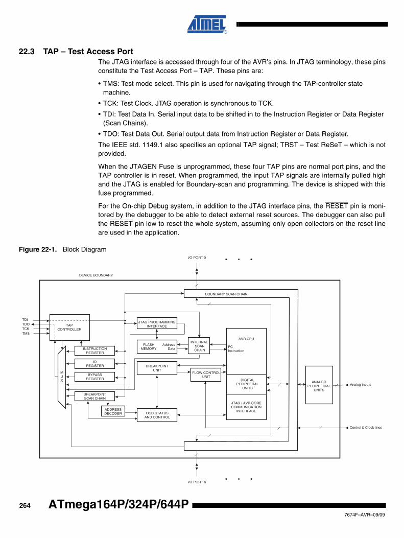
22.3 TAP – Test Access PortThe JTAG interface is accessed through four of the AVR’s pins. In JTAG terminology, these pinsconstitute the Test Access Port – TAP. These pins are:
• TMS: Test mode select. This pin is used for navigating through the TAP-controller state machine.
• TCK: Test Clock. JTAG operation is synchronous to TCK.
• TDI: Test Data In. Serial input data to be shifted in to the Instruction Register or Data Register (Scan Chains).
• TDO: Test Data Out. Serial output data from Instruction Register or Data Register.
The IEEE std. 1149.1 also specifies an optional TAP signal; TRST – Test ReSeT – which is notprovided.
When the JTAGEN Fuse is unprogrammed, these four TAP pins are normal port pins, and theTAP controller is in reset. When programmed, the input TAP signals are internally pulled highand the JTAG is enabled for Boundary-scan and programming. The device is shipped with thisfuse programmed.
For the On-chip Debug system, in addition to the JTAG interface pins, the RESET pin is moni-tored by the debugger to be able to detect external reset sources. The debugger can also pullthe RESET pin low to reset the whole system, assuming only open collectors on the reset lineare used in the application.
Figure 22-1. Block Diagram
TAPCONTROLLER
TDITDOTCKTMS
FLASHMEMORY
AVR CPU
DIGITALPERIPHERAL
UNITS
JTAG / AVR CORECOMMUNICATION
INTERFACE
BREAKPOINTUNIT
FLOW CONTROLUNIT
OCD STATUSAND CONTROL
INTERNAL SCANCHAIN
MUX
INSTRUCTIONREGISTER
IDREGISTER
BYPASSREGISTER
JTAG PROGRAMMINGINTERFACE
PCInstruction
AddressData
BREAKPOINTSCAN CHAIN
ADDRESSDECODER
ANALOGPERIPHERIAL
UNITS
I/O PORT 0
I/O PORT n
BOUNDARY SCAN CHAIN
Analog inputs
Control & Clock lines
DEVICE BOUNDARY
2647674F–AVR–09/09
ATmega164P/324P/644P
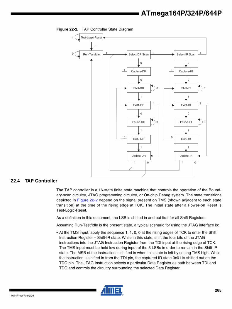
ATmega164P/324P/644P
Figure 22-2. TAP Controller State Diagram
22.4 TAP Controller
The TAP controller is a 16-state finite state machine that controls the operation of the Bound-ary-scan circuitry, JTAG programming circuitry, or On-chip Debug system. The state transitionsdepicted in Figure 22-2 depend on the signal present on TMS (shown adjacent to each statetransition) at the time of the rising edge at TCK. The initial state after a Power-on Reset isTest-Logic-Reset.
As a definition in this document, the LSB is shifted in and out first for all Shift Registers.
Assuming Run-Test/Idle is the present state, a typical scenario for using the JTAG interface is:
• At the TMS input, apply the sequence 1, 1, 0, 0 at the rising edges of TCK to enter the Shift Instruction Register – Shift-IR state. While in this state, shift the four bits of the JTAG instructions into the JTAG Instruction Register from the TDI input at the rising edge of TCK. The TMS input must be held low during input of the 3 LSBs in order to remain in the Shift-IR state. The MSB of the instruction is shifted in when this state is left by setting TMS high. While the instruction is shifted in from the TDI pin, the captured IR-state 0x01 is shifted out on the TDO pin. The JTAG Instruction selects a particular Data Register as path between TDI and TDO and controls the circuitry surrounding the selected Data Register.
Test-Logic-Reset
Run-Test/Idle
Shift-DR
Exit1-DR
Pause-DR
Exit2-DR
Update-DR
Select-IR Scan
Capture-IR
Shift-IR
Exit1-IR
Pause-IR
Exit2-IR
Update-IR
Select-DR Scan
Capture-DR
0
1
0 1 1 1
0 0
0 0
1 1
1 0
1
1
0
1
0
0
1 0
1
1
0
1
0
0
00
11
2657674F–AVR–09/09
• Apply the TMS sequence 1, 1, 0 to re-enter the Run-Test/Idle state. The instruction is latched onto the parallel output from the Shift Register path in the Update-IR state. The Exit-IR, Pause-IR, and Exit2-IR states are only used for navigating the state machine.
• At the TMS input, apply the sequence 1, 0, 0 at the rising edges of TCK to enter the Shift Data Register – Shift-DR state. While in this state, upload the selected Data Register (selected by the present JTAG instruction in the JTAG Instruction Register) from the TDI input at the rising edge of TCK. In order to remain in the Shift-DR state, the TMS input must be held low during input of all bits except the MSB. The MSB of the data is shifted in when this state is left by setting TMS high. While the Data Register is shifted in from the TDI pin, the parallel inputs to the Data Register captured in the Capture-DR state is shifted out on the TDO pin.
• Apply the TMS sequence 1, 1, 0 to re-enter the Run-Test/Idle state. If the selected Data Register has a latched parallel-output, the latching takes place in the Update-DR state. The Exit-DR, Pause-DR, and Exit2-DR states are only used for navigating the state machine.
As shown in the state diagram, the Run-Test/Idle state need not be entered between selectingJTAG instruction and using Data Registers, and some JTAG instructions may select certainfunctions to be performed in the Run-Test/Idle, making it unsuitable as an Idle state.
Note: Independent of the initial state of the TAP Controller, the Test-Logic-Reset state can always be entered by holding TMS high for five TCK clock periods.
For detailed information on the JTAG specification, refer to the literature listed in “Bibliography”on page 268.
22.5 Using the Boundary-scan Chain
A complete description of the Boundary-scan capabilities are given in the section “IEEE 1149.1(JTAG) Boundary-scan” on page 269.
22.6 Using the On-chip Debug System
As shown in Figure 22-1, the hardware support for On-chip Debugging consists mainly of
• A scan chain on the interface between the internal AVR CPU and the internal peripheral units.
• Break Point unit.
• Communication interface between the CPU and JTAG system.
All read or modify/write operations needed for implementing the Debugger are done by applyingAVR instructions via the internal AVR CPU Scan Chain. The CPU sends the result to an I/Omemory mapped location which is part of the communication interface between the CPU and theJTAG system.
The Break Point Unit implements Break on Change of Program Flow, Single Step Break, twoProgram Memory Break Points, and two combined Break Points. Together, the four BreakPoints can be configured as either:
• 4 single Program Memory Break Points.
• 3 Single Program Memory Break Point + 1 single Data Memory Break Point.
• 2 single Program Memory Break Points + 2 single Data Memory Break Points.
• 2 single Program Memory Break Points + 1 Program Memory Break Point with mask (“range Break Point”).
• 2 single Program Memory Break Points + 1 Data Memory Break Point with mask (“range Break Point”).
2667674F–AVR–09/09
ATmega164P/324P/644P
ATmega164P/324P/644P
A debugger, like the AVR Studio, may however use one or more of these resources for its inter-nal purpose, leaving less flexibility to the end-user.
A list of the On-chip Debug specific JTAG instructions is given in “On-chip Debug Specific JTAGInstructions” on page 267.
The JTAGEN Fuse must be programmed to enable the JTAG Test Access Port. In addition, theOCDEN Fuse must be programmed and no Lock bits must be set for the On-chip debug systemto work. As a security feature, the On-chip debug system is disabled when either of the LB1 orLB2 Lock bits are set. Otherwise, the On-chip debug system would have provided a back-doorinto a secured device.
The AVR Studio enables the user to fully control execution of programs on an AVR device withOn-chip Debug capability, AVR In-Circuit Emulator, or the built-in AVR Instruction Set Simulator.AVR Studio supports source level execution of Assembly programs assembled with Atmel Cor-poration’s AVR Assembler and C programs compiled with third party vendors’ compilers.
AVR Studio runs under Microsoft® Windows® 95/98/2000 and Microsoft Windows NT®.
For a full description of the AVR Studio, please refer to the AVR Studio User Guide. Only high-lights are presented in this document.
All necessary execution commands are available in AVR Studio, both on source level and ondisassembly level. The user can execute the program, single step through the code either bytracing into or stepping over functions, step out of functions, place the cursor on a statement andexecute until the statement is reached, stop the execution, and reset the execution target. Inaddition, the user can have an unlimited number of code Break Points (using the BREAKinstruction) and up to two data memory Break Points, alternatively combined as a mask (range)Break Point.
22.7 On-chip Debug Specific JTAG Instructions
The On-chip debug support is considered being private JTAG instructions, and distributed withinATMEL and to selected third party vendors only. Instruction opcodes are listed for reference.
22.7.1 PRIVATE0; 0x8
Private JTAG instruction for accessing On-chip debug system.
22.7.2 PRIVATE1; 0x9
Private JTAG instruction for accessing On-chip debug system.
22.7.3 PRIVATE2; 0xA
Private JTAG instruction for accessing On-chip debug system.
22.7.4 PRIVATE3; 0xB
Private JTAG instruction for accessing On-chip debug system.
2677674F–AVR–09/09
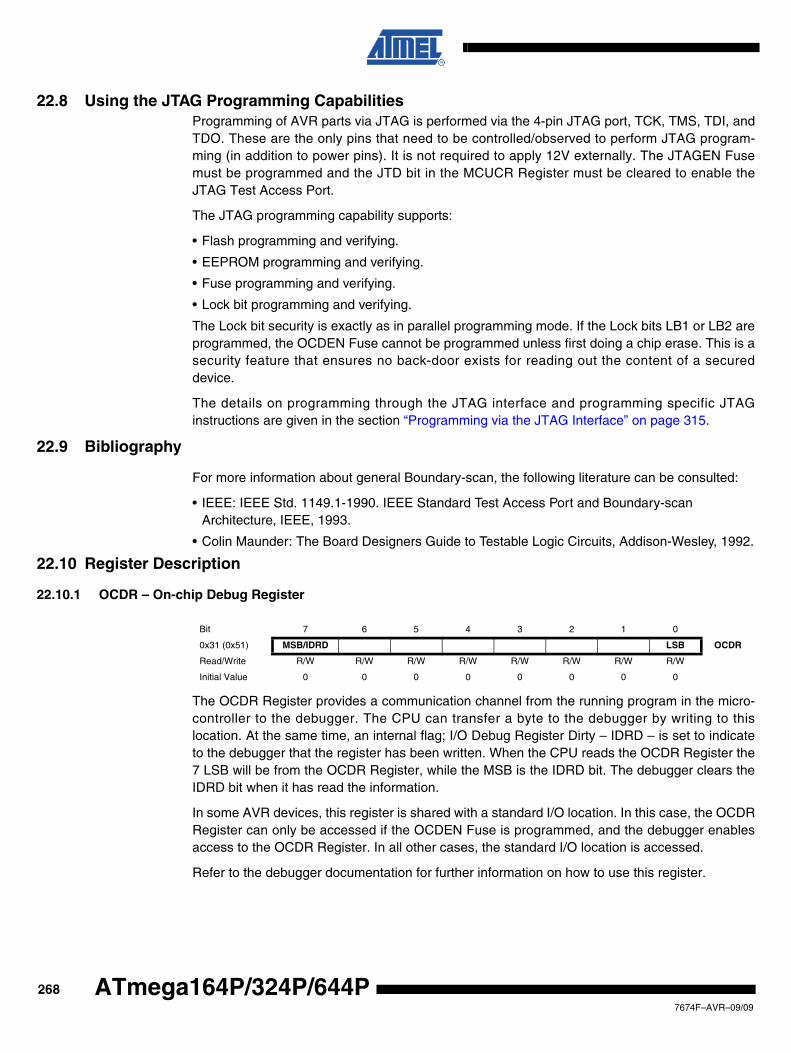
22.8 Using the JTAG Programming CapabilitiesProgramming of AVR parts via JTAG is performed via the 4-pin JTAG port, TCK, TMS, TDI, andTDO. These are the only pins that need to be controlled/observed to perform JTAG program-ming (in addition to power pins). It is not required to apply 12V externally. The JTAGEN Fusemust be programmed and the JTD bit in the MCUCR Register must be cleared to enable theJTAG Test Access Port.
The JTAG programming capability supports:
• Flash programming and verifying.
• EEPROM programming and verifying.
• Fuse programming and verifying.
• Lock bit programming and verifying.
The Lock bit security is exactly as in parallel programming mode. If the Lock bits LB1 or LB2 areprogrammed, the OCDEN Fuse cannot be programmed unless first doing a chip erase. This is asecurity feature that ensures no back-door exists for reading out the content of a secureddevice.
The details on programming through the JTAG interface and programming specific JTAGinstructions are given in the section “Programming via the JTAG Interface” on page 315.
22.9 Bibliography
For more information about general Boundary-scan, the following literature can be consulted:
• IEEE: IEEE Std. 1149.1-1990. IEEE Standard Test Access Port and Boundary-scan Architecture, IEEE, 1993.
• Colin Maunder: The Board Designers Guide to Testable Logic Circuits, Addison-Wesley, 1992.
22.10 Register Description
22.10.1 OCDR – On-chip Debug Register
The OCDR Register provides a communication channel from the running program in the micro-controller to the debugger. The CPU can transfer a byte to the debugger by writing to thislocation. At the same time, an internal flag; I/O Debug Register Dirty – IDRD – is set to indicateto the debugger that the register has been written. When the CPU reads the OCDR Register the7 LSB will be from the OCDR Register, while the MSB is the IDRD bit. The debugger clears theIDRD bit when it has read the information.
In some AVR devices, this register is shared with a standard I/O location. In this case, the OCDRRegister can only be accessed if the OCDEN Fuse is programmed, and the debugger enablesaccess to the OCDR Register. In all other cases, the standard I/O location is accessed.
Refer to the debugger documentation for further information on how to use this register.
Bit 7 6 5 4 3 2 1 0
0x31 (0x51) MSB/IDRD LSB OCDR
Read/Write R/W R/W R/W R/W R/W R/W R/W R/W
Initial Value 0 0 0 0 0 0 0 0
2687674F–AVR–09/09
ATmega164P/324P/644P
ATmega164P/324P/644P
23. IEEE 1149.1 (JTAG) Boundary-scan
23.1 Features
• JTAG (IEEE std. 1149.1 compliant) Interface• Boundary-scan Capabilities According to the JTAG Standard• Full Scan of all Port Functions as well as Analog Circuitry having Off-chip Connections• Supports the Optional IDCODE Instruction• Additional Public AVR_RESET Instruction to Reset the AVR
23.2 Overview
The Boundary-scan chain has the capability of driving and observing the logic levels on the digi-tal I/O pins, as well as the boundary between digital and analog logic for analog circuitry havingoff-chip connections. At system level, all ICs having JTAG capabilities are connected serially bythe TDI/TDO signals to form a long Shift Register. An external controller sets up the devices todrive values at their output pins, and observe the input values received from other devices. Thecontroller compares the received data with the expected result. In this way, Boundary-scan pro-vides a mechanism for testing interconnections and integrity of components on Printed CircuitsBoards by using the four TAP signals only.
The four IEEE 1149.1 defined mandatory JTAG instructions IDCODE, BYPASS, SAMPLE/PRE-LOAD, and EXTEST, as well as the AVR specific public JTAG instruction AVR_RESET can beused for testing the Printed Circuit Board. Initial scanning of the Data Register path will show theID-Code of the device, since IDCODE is the default JTAG instruction. It may be desirable tohave the AVR device in reset during test mode. If not reset, inputs to the device may be deter-mined by the scan operations, and the internal software may be in an undetermined state whenexiting the test mode. Entering reset, the outputs of any port pin will instantly enter the highimpedance state, making the HIGHZ instruction redundant. If needed, the BYPASS instructioncan be issued to make the shortest possible scan chain through the device. The device can beset in the reset state either by pulling the external RESET pin low, or issuing the AVR_RESETinstruction with appropriate setting of the Reset Data Register.
The EXTEST instruction is used for sampling external pins and loading output pins with data.The data from the output latch will be driven out on the pins as soon as the EXTEST instructionis loaded into the JTAG IR-Register. Therefore, the SAMPLE/PRELOAD should also be used forsetting initial values to the scan ring, to avoid damaging the board when issuing the EXTESTinstruction for the first time. SAMPLE/PRELOAD can also be used for taking a snapshot of theexternal pins during normal operation of the part.
The JTAGEN Fuse must be programmed and the JTD bit in the I/O Register MCUCR must becleared to enable the JTAG Test Access Port.
When using the JTAG interface for Boundary-scan, using a JTAG TCK clock frequency higherthan the internal chip frequency is possible. The chip clock is not required to run.
2697674F–AVR–09/09
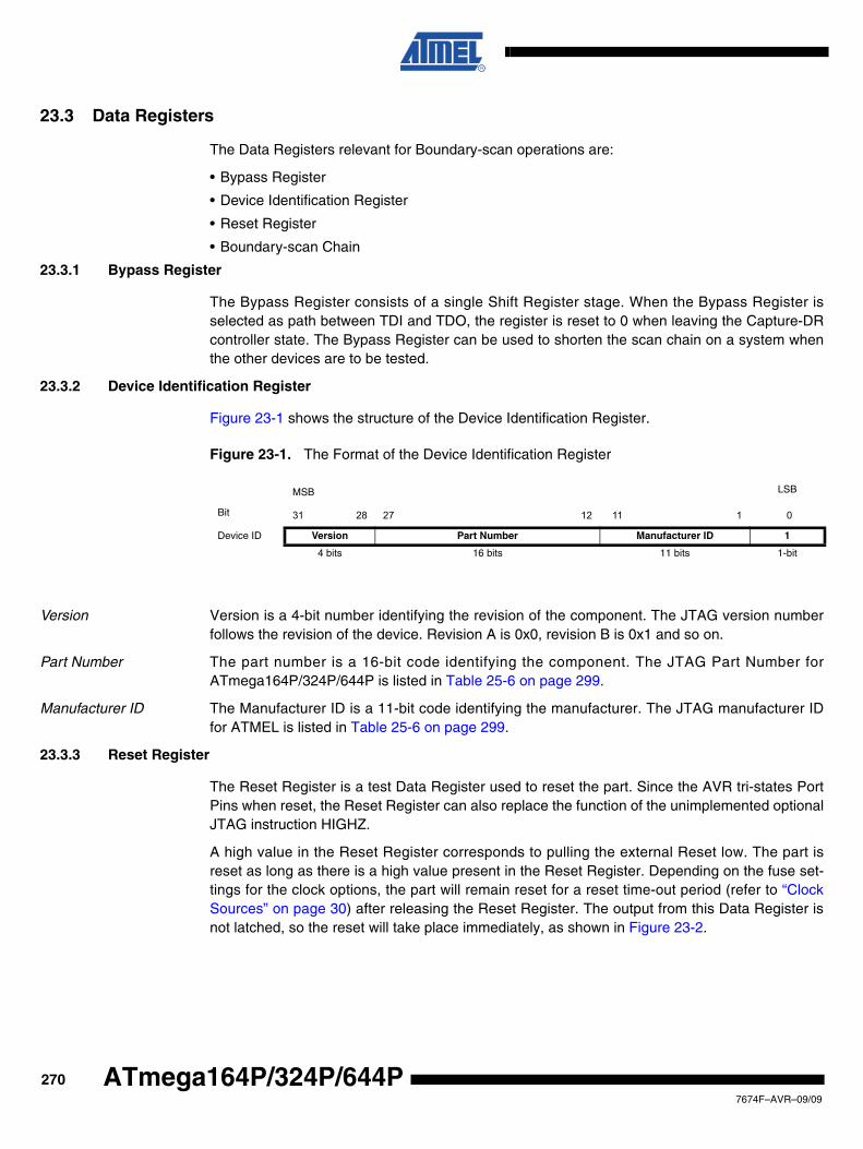
23.3 Data Registers
The Data Registers relevant for Boundary-scan operations are:
• Bypass Register
• Device Identification Register
• Reset Register
• Boundary-scan Chain
23.3.1 Bypass Register
The Bypass Register consists of a single Shift Register stage. When the Bypass Register isselected as path between TDI and TDO, the register is reset to 0 when leaving the Capture-DRcontroller state. The Bypass Register can be used to shorten the scan chain on a system whenthe other devices are to be tested.
23.3.2 Device Identification Register
Figure 23-1 shows the structure of the Device Identification Register.
Figure 23-1. The Format of the Device Identification Register
Version Version is a 4-bit number identifying the revision of the component. The JTAG version numberfollows the revision of the device. Revision A is 0x0, revision B is 0x1 and so on.
Part Number The part number is a 16-bit code identifying the component. The JTAG Part Number forATmega164P/324P/644P is listed in Table 25-6 on page 299.
Manufacturer ID The Manufacturer ID is a 11-bit code identifying the manufacturer. The JTAG manufacturer IDfor ATMEL is listed in Table 25-6 on page 299.
23.3.3 Reset Register
The Reset Register is a test Data Register used to reset the part. Since the AVR tri-states PortPins when reset, the Reset Register can also replace the function of the unimplemented optionalJTAG instruction HIGHZ.
A high value in the Reset Register corresponds to pulling the external Reset low. The part isreset as long as there is a high value present in the Reset Register. Depending on the fuse set-tings for the clock options, the part will remain reset for a reset time-out period (refer to “ClockSources” on page 30) after releasing the Reset Register. The output from this Data Register isnot latched, so the reset will take place immediately, as shown in Figure 23-2.
MSB LSB
Bit 31 28 27 12 11 1 0
Device ID Version Part Number Manufacturer ID 1
4 bits 16 bits 11 bits 1-bit
2707674F–AVR–09/09
ATmega164P/324P/644P
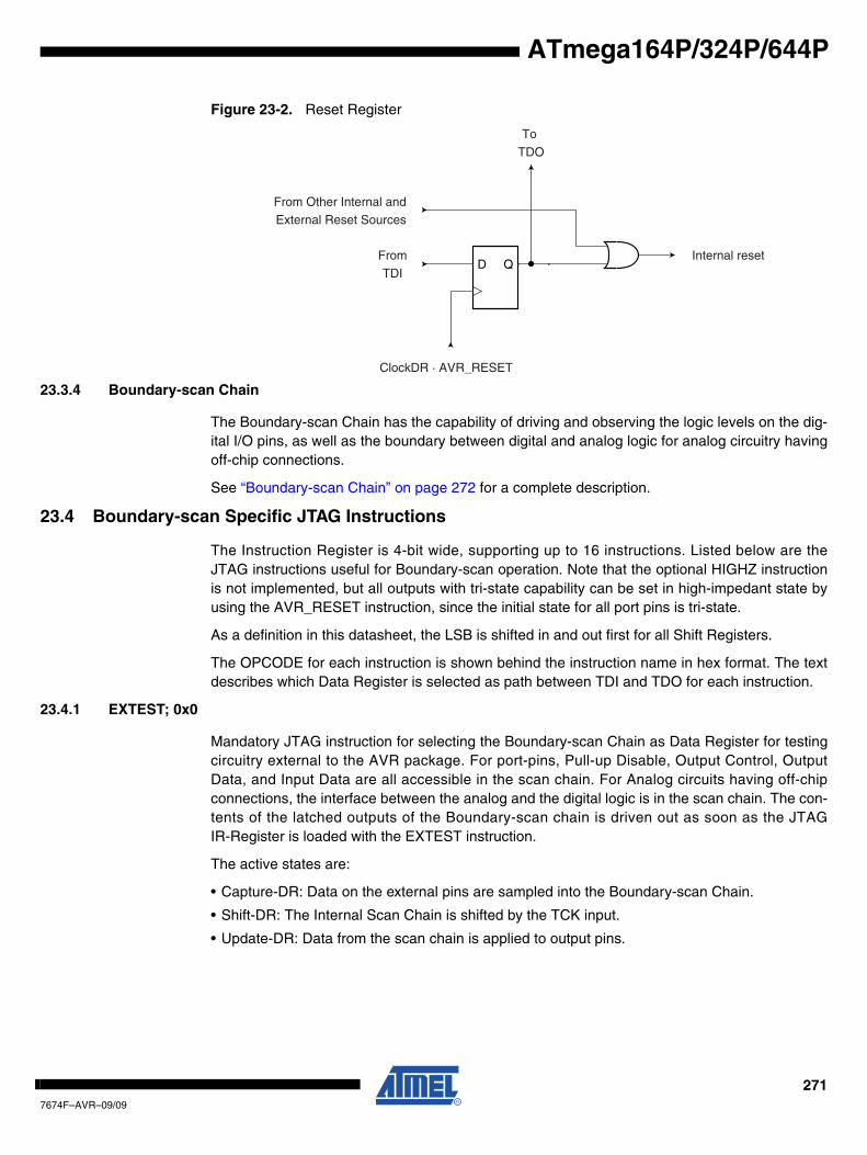
ATmega164P/324P/644P
Figure 23-2. Reset Register
23.3.4 Boundary-scan Chain
The Boundary-scan Chain has the capability of driving and observing the logic levels on the dig-ital I/O pins, as well as the boundary between digital and analog logic for analog circuitry havingoff-chip connections.
See “Boundary-scan Chain” on page 272 for a complete description.
23.4 Boundary-scan Specific JTAG Instructions
The Instruction Register is 4-bit wide, supporting up to 16 instructions. Listed below are theJTAG instructions useful for Boundary-scan operation. Note that the optional HIGHZ instructionis not implemented, but all outputs with tri-state capability can be set in high-impedant state byusing the AVR_RESET instruction, since the initial state for all port pins is tri-state.
As a definition in this datasheet, the LSB is shifted in and out first for all Shift Registers.
The OPCODE for each instruction is shown behind the instruction name in hex format. The textdescribes which Data Register is selected as path between TDI and TDO for each instruction.
23.4.1 EXTEST; 0x0
Mandatory JTAG instruction for selecting the Boundary-scan Chain as Data Register for testingcircuitry external to the AVR package. For port-pins, Pull-up Disable, Output Control, OutputData, and Input Data are all accessible in the scan chain. For Analog circuits having off-chipconnections, the interface between the analog and the digital logic is in the scan chain. The con-tents of the latched outputs of the Boundary-scan chain is driven out as soon as the JTAGIR-Register is loaded with the EXTEST instruction.
The active states are:
• Capture-DR: Data on the external pins are sampled into the Boundary-scan Chain.
• Shift-DR: The Internal Scan Chain is shifted by the TCK input.
• Update-DR: Data from the scan chain is applied to output pins.
D QFromTDI
ClockDR · AVR_RESET
To TDO
From Other Internal andExternal Reset Sources
Internal reset
2717674F–AVR–09/09
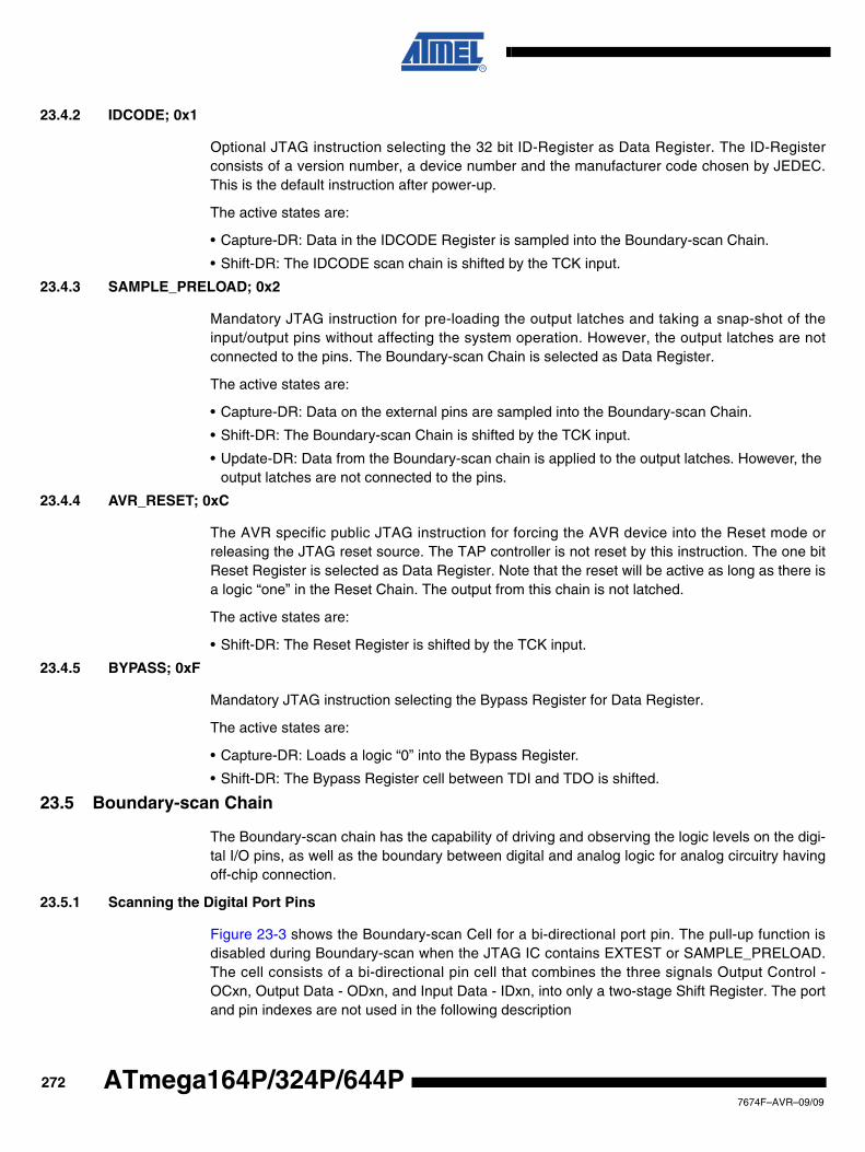
23.4.2 IDCODE; 0x1
Optional JTAG instruction selecting the 32 bit ID-Register as Data Register. The ID-Registerconsists of a version number, a device number and the manufacturer code chosen by JEDEC.This is the default instruction after power-up.
The active states are:
• Capture-DR: Data in the IDCODE Register is sampled into the Boundary-scan Chain.
• Shift-DR: The IDCODE scan chain is shifted by the TCK input.
23.4.3 SAMPLE_PRELOAD; 0x2
Mandatory JTAG instruction for pre-loading the output latches and taking a snap-shot of theinput/output pins without affecting the system operation. However, the output latches are notconnected to the pins. The Boundary-scan Chain is selected as Data Register.
The active states are:
• Capture-DR: Data on the external pins are sampled into the Boundary-scan Chain.
• Shift-DR: The Boundary-scan Chain is shifted by the TCK input.
• Update-DR: Data from the Boundary-scan chain is applied to the output latches. However, the output latches are not connected to the pins.
23.4.4 AVR_RESET; 0xC
The AVR specific public JTAG instruction for forcing the AVR device into the Reset mode orreleasing the JTAG reset source. The TAP controller is not reset by this instruction. The one bitReset Register is selected as Data Register. Note that the reset will be active as long as there isa logic “one” in the Reset Chain. The output from this chain is not latched.
The active states are:
• Shift-DR: The Reset Register is shifted by the TCK input.
23.4.5 BYPASS; 0xF
Mandatory JTAG instruction selecting the Bypass Register for Data Register.
The active states are:
• Capture-DR: Loads a logic “0” into the Bypass Register.
• Shift-DR: The Bypass Register cell between TDI and TDO is shifted.
23.5 Boundary-scan Chain
The Boundary-scan chain has the capability of driving and observing the logic levels on the digi-tal I/O pins, as well as the boundary between digital and analog logic for analog circuitry havingoff-chip connection.
23.5.1 Scanning the Digital Port Pins
Figure 23-3 shows the Boundary-scan Cell for a bi-directional port pin. The pull-up function isdisabled during Boundary-scan when the JTAG IC contains EXTEST or SAMPLE_PRELOAD.The cell consists of a bi-directional pin cell that combines the three signals Output Control -OCxn, Output Data - ODxn, and Input Data - IDxn, into only a two-stage Shift Register. The portand pin indexes are not used in the following description
2727674F–AVR–09/09
ATmega164P/324P/644P
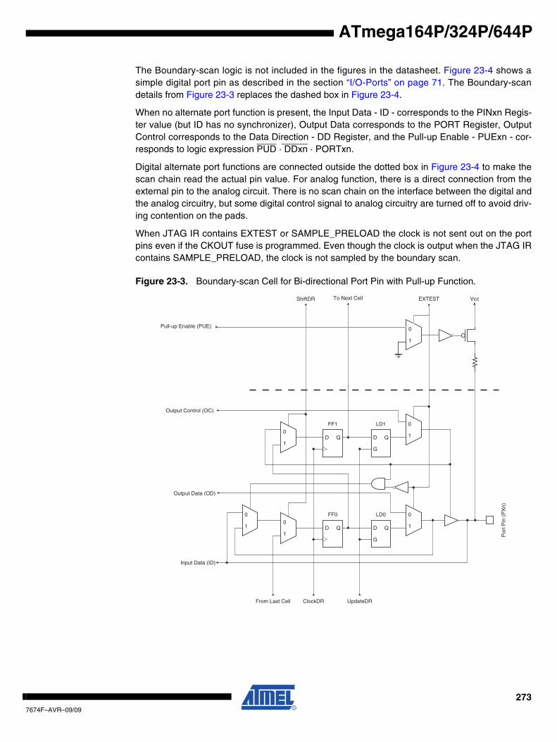
ATmega164P/324P/644P
The Boundary-scan logic is not included in the figures in the datasheet. Figure 23-4 shows asimple digital port pin as described in the section “I/O-Ports” on page 71. The Boundary-scandetails from Figure 23-3 replaces the dashed box in Figure 23-4.
When no alternate port function is present, the Input Data - ID - corresponds to the PINxn Regis-ter value (but ID has no synchronizer), Output Data corresponds to the PORT Register, OutputControl corresponds to the Data Direction - DD Register, and the Pull-up Enable - PUExn - cor-responds to logic expression PUD · DDxn · PORTxn.
Digital alternate port functions are connected outside the dotted box in Figure 23-4 to make thescan chain read the actual pin value. For analog function, there is a direct connection from theexternal pin to the analog circuit. There is no scan chain on the interface between the digital andthe analog circuitry, but some digital control signal to analog circuitry are turned off to avoid driv-ing contention on the pads.
When JTAG IR contains EXTEST or SAMPLE_PRELOAD the clock is not sent out on the portpins even if the CKOUT fuse is programmed. Even though the clock is output when the JTAG IRcontains SAMPLE_PRELOAD, the clock is not sampled by the boundary scan.
Figure 23-3. Boundary-scan Cell for Bi-directional Port Pin with Pull-up Function.
D Q D Q
G
0
10
1
D Q D Q
G
0
10
1
0
1
Por
t Pin
(P
Xn)
VccEXTESTTo Next CellShiftDR
Output Control (OC)
Output Data (OD)
Input Data (ID)
From Last Cell UpdateDRClockDR
FF1 LD1
LD0FF0
0
1
Pull-up Enable (PUE)
2737674F–AVR–09/09
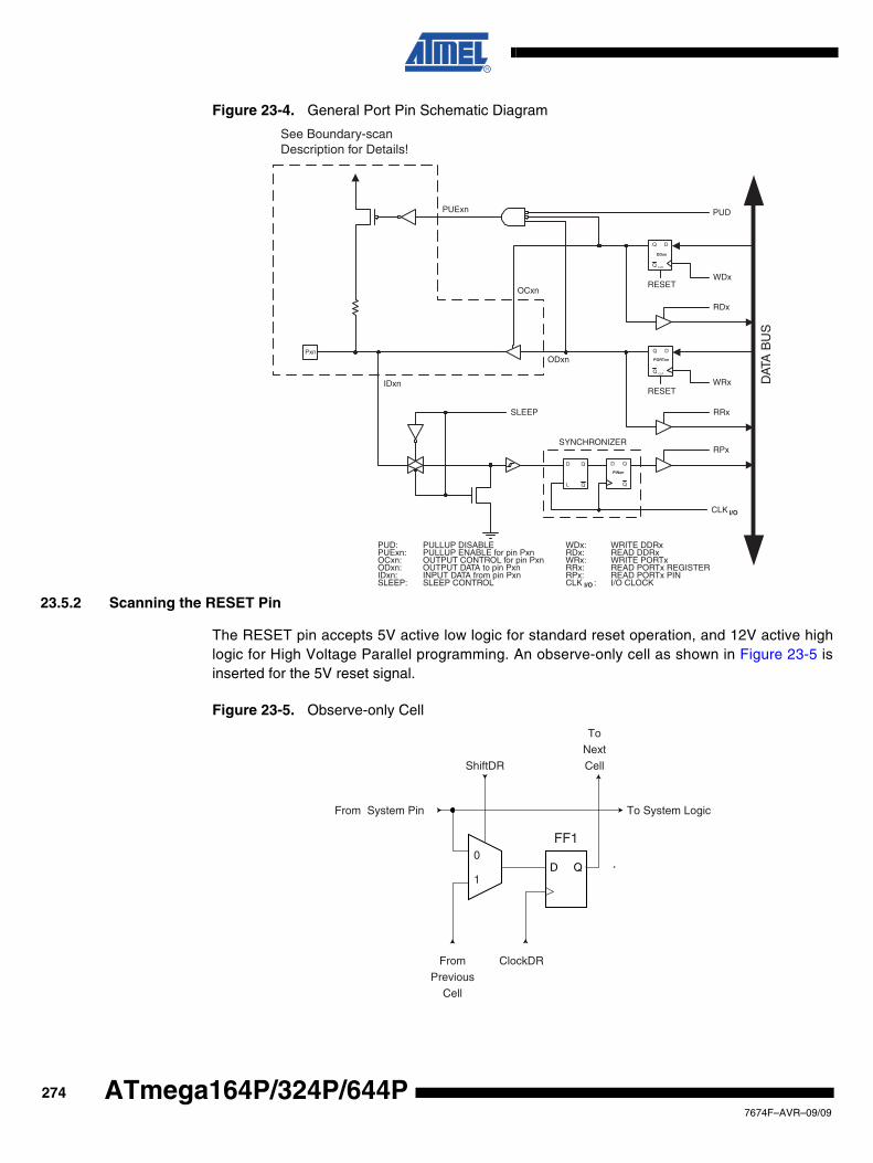
Figure 23-4. General Port Pin Schematic Diagram
23.5.2 Scanning the RESET Pin
The RESET pin accepts 5V active low logic for standard reset operation, and 12V active highlogic for High Voltage Parallel programming. An observe-only cell as shown in Figure 23-5 isinserted for the 5V reset signal.
Figure 23-5. Observe-only Cell
CLK
RPx
RRx
WRx
RDx
WDx
PUD
SYNCHRONIZER
WDx: WRITE DDRx
WRx: WRITE PORTxRRx: READ PORTx REGISTERRPx: READ PORTx PIN
PUD: PULLUP DISABLE
CLK : I/O CLOCK
RDx: READ DDRx
D
L
Q
Q
RESET
RESET
Q
QD
Q
Q D
CLR
PORTxn
Q
Q D
CLR
DDxn
PINxn
DAT
A B
US
SLEEP
SLEEP: SLEEP CONTROL
Pxn
I/O
I/O
See Boundary-scan Description for Details!
PUExn
OCxn
ODxn
IDxn
PUExn: PULLUP ENABLE for pin PxnOCxn: OUTPUT CONTROL for pin PxnODxn: OUTPUT DATA to pin PxnIDxn: INPUT DATA from pin Pxn
0
1D Q
FromPrevious
Cell
ClockDR
ShiftDR
ToNextCell
From System Pin To System Logic
FF1
2747674F–AVR–09/09
ATmega164P/324P/644P
ATmega164P/324P/644P
23.6 ATmega164P/324P/644P Boundary-scan Order
Table 23-1 shows the Scan order between TDI and TDO when the Boundary-scan chain isselected as data path. Bit 0 is the LSB; the first bit scanned in, and the first bit scanned out. Thescan order follows the pin-out order as far as possible. Therefore, the bits of Port A and Port K isscanned in the opposite bit order of the other ports. Exceptions from the rules are the Scanchains for the analog circuits, which constitute the most significant bits of the scan chain regard-less of which physical pin they are connected to. In Figure 23-3, PXn. Data corresponds to FF0,PXn. Control corresponds to FF1, PXn. Bit 4, 5, 6 and 7 of Port F is not in the scan chain, sincethese pins constitute the TAP pins when the JTAG is enabled.
Table 23-1. ATmega164P/324P/644P Boundary-scan Order
Bit Number Signal Name Module
56 PB0.Data
Port B
55 PB0.Control
54 PB1.Data
53 PB1.Control
52 PB2.Data
51 PB2.Control
50 PB3.Data
49 PB3.Control
48 PB4.Data
47 PB4.Control
46 PB5.Data
45 PB5.Control
44 PB6.Data
43 PB6.Control
42 PB7.Data
41 PB7.Control
40 RSTT Reset Logic (Observe Only)
2757674F–AVR–09/09
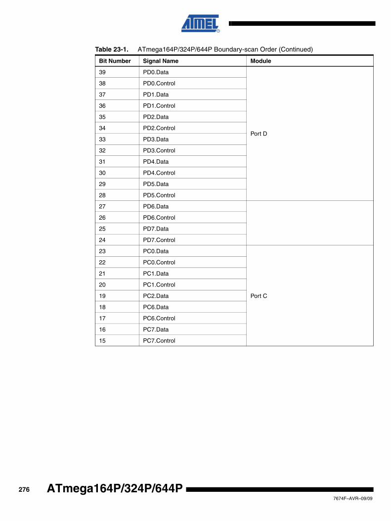
39 PD0.Data
Port D
38 PD0.Control
37 PD1.Data
36 PD1.Control
35 PD2.Data
34 PD2.Control
33 PD3.Data
32 PD3.Control
31 PD4.Data
30 PD4.Control
29 PD5.Data
28 PD5.Control
27 PD6.Data
26 PD6.Control
25 PD7.Data
24 PD7.Control
23 PC0.Data
Port C
22 PC0.Control
21 PC1.Data
20 PC1.Control
19 PC2.Data
18 PC6.Data
17 PC6.Control
16 PC7.Data
15 PC7.Control
Table 23-1. ATmega164P/324P/644P Boundary-scan Order (Continued)
Bit Number Signal Name Module
2767674F–AVR–09/09
ATmega164P/324P/644P
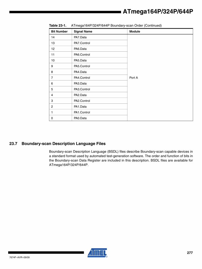
ATmega164P/324P/644P
23.7 Boundary-scan Description Language Files
Boundary-scan Description Language (BSDL) files describe Boundary-scan capable devices ina standard format used by automated test-generation software. The order and function of bits inthe Boundary-scan Data Register are included in this description. BSDL files are available forATmega164P/324P/644P.
14 PA7.Data
Port A
13 PA7.Control
12 PA6.Data
11 PA6.Control
10 PA5.Data
9 PA5.Control
8 PA4.Data
7 PA4.Control
6 PA3.Data
5 PA3.Control
4 PA2.Data
3 PA2.Control
2 PA1.Data
1 PA1.Control
0 PA0.Data
Table 23-1. ATmega164P/324P/644P Boundary-scan Order (Continued)
Bit Number Signal Name Module
2777674F–AVR–09/09
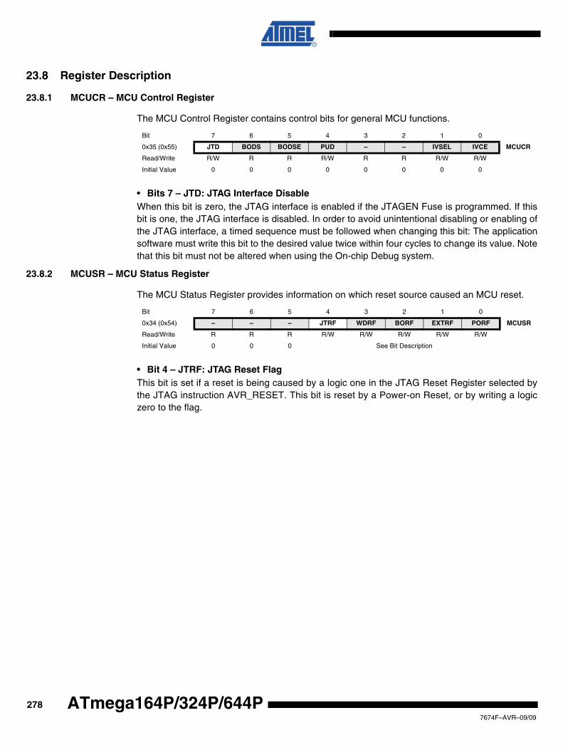
23.8 Register Description
23.8.1 MCUCR – MCU Control Register
The MCU Control Register contains control bits for general MCU functions.
• Bits 7 – JTD: JTAG Interface DisableWhen this bit is zero, the JTAG interface is enabled if the JTAGEN Fuse is programmed. If thisbit is one, the JTAG interface is disabled. In order to avoid unintentional disabling or enabling ofthe JTAG interface, a timed sequence must be followed when changing this bit: The applicationsoftware must write this bit to the desired value twice within four cycles to change its value. Notethat this bit must not be altered when using the On-chip Debug system.
23.8.2 MCUSR – MCU Status Register
The MCU Status Register provides information on which reset source caused an MCU reset.
• Bit 4 – JTRF: JTAG Reset FlagThis bit is set if a reset is being caused by a logic one in the JTAG Reset Register selected bythe JTAG instruction AVR_RESET. This bit is reset by a Power-on Reset, or by writing a logiczero to the flag.
Bit 7 6 5 4 3 2 1 0
0x35 (0x55) JTD BODS BODSE PUD – – IVSEL IVCE MCUCR
Read/Write R/W R R R/W R R R/W R/W
Initial Value 0 0 0 0 0 0 0 0
Bit 7 6 5 4 3 2 1 0
0x34 (0x54) – – – JTRF WDRF BORF EXTRF PORF MCUSR
Read/Write R R R R/W R/W R/W R/W R/W
Initial Value 0 0 0 See Bit Description
2787674F–AVR–09/09
ATmega164P/324P/644P
ATmega164P/324P/644P
24. Boot Loader Support – Read-While-Write Self-Programming
24.1 Features
• Read-While-Write Self-Programming• Flexible Boot Memory Size• High Security (Separate Boot Lock Bits for a Flexible Protection)• Separate Fuse to Select Reset Vector• Optimized Page(1) Size• Code Efficient Algorithm• Efficient Read-Modify-Write Support
Note: 1. A page is a section in the Flash consisting of several bytes (see Table 25-7 on page 299) used during programming. The page organization does not affect normal operation.
24.2 Overview
The Boot Loader Support provides a real Read-While-Write Self-Programming mechanism fordownloading and uploading program code by the MCU itself. This feature allows flexible applica-tion software updates controlled by the MCU using a Flash-resident Boot Loader program. TheBoot Loader program can use any available data interface and associated protocol to read codeand write (program) that code into the Flash memory, or read the code from the program mem-ory. The program code within the Boot Loader section has the capability to write into the entireFlash, including the Boot Loader memory. The Boot Loader can thus even modify itself, and itcan also erase itself from the code if the feature is not needed anymore. The size of the BootLoader memory is configurable with fuses and the Boot Loader has two separate sets of BootLock bits which can be set independently. This gives the user a unique flexibility to select differ-ent levels of protection.
24.3 Application and Boot Loader Flash Sections
The Flash memory is organized in two main sections, the Application section and the BootLoader section (see Figure 24-2 on page 282). The size of the different sections is configured bythe BOOTSZ Fuses as shown in Table 24-7 on page 291 and Figure 24-2. These two sectionscan have different level of protection since they have different sets of Lock bits.
24.3.1 Application Section
The Application section is the section of the Flash that is used for storing the application code.The protection level for the Application section can be selected by the application Boot Lock bits(Boot Lock bits 0), see Table 24-2 on page 283. The Application section can never store anyBoot Loader code since the SPM instruction is disabled when executed from the Applicationsection.
24.3.2 BLS – Boot Loader Section
While the Application section is used for storing the application code, the The Boot Loader soft-ware must be located in the BLS since the SPM instruction can initiate a programming whenexecuting from the BLS only. The SPM instruction can access the entire Flash, including theBLS itself. The protection level for the Boot Loader section can be selected by the Boot LoaderLock bits (Boot Lock bits 1), see Table 24-3 on page 283.
2797674F–AVR–09/09
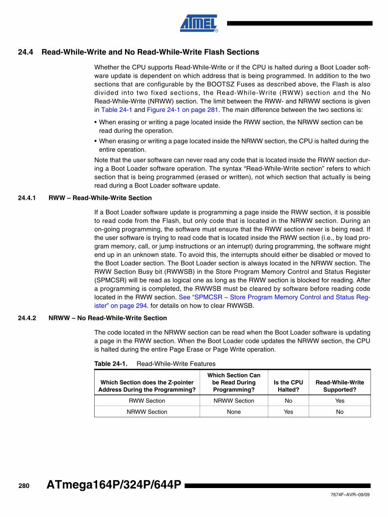
24.4 Read-While-Write and No Read-While-Write Flash Sections
Whether the CPU supports Read-While-Write or if the CPU is halted during a Boot Loader soft-ware update is dependent on which address that is being programmed. In addition to the twosections that are configurable by the BOOTSZ Fuses as described above, the Flash is alsodivided into two fixed sections, the Read-While-Write (RWW) section and the NoRead-While-Write (NRWW) section. The limit between the RWW- and NRWW sections is givenin Table 24-1 and Figure 24-1 on page 281. The main difference between the two sections is:
• When erasing or writing a page located inside the RWW section, the NRWW section can be read during the operation.
• When erasing or writing a page located inside the NRWW section, the CPU is halted during the entire operation.
Note that the user software can never read any code that is located inside the RWW section dur-ing a Boot Loader software operation. The syntax “Read-While-Write section” refers to whichsection that is being programmed (erased or written), not which section that actually is beingread during a Boot Loader software update.
24.4.1 RWW – Read-While-Write Section
If a Boot Loader software update is programming a page inside the RWW section, it is possibleto read code from the Flash, but only code that is located in the NRWW section. During anon-going programming, the software must ensure that the RWW section never is being read. Ifthe user software is trying to read code that is located inside the RWW section (i.e., by load pro-gram memory, call, or jump instructions or an interrupt) during programming, the software mightend up in an unknown state. To avoid this, the interrupts should either be disabled or moved tothe Boot Loader section. The Boot Loader section is always located in the NRWW section. TheRWW Section Busy bit (RWWSB) in the Store Program Memory Control and Status Register(SPMCSR) will be read as logical one as long as the RWW section is blocked for reading. Aftera programming is completed, the RWWSB must be cleared by software before reading codelocated in the RWW section. See “SPMCSR – Store Program Memory Control and Status Reg-ister” on page 294. for details on how to clear RWWSB.
24.4.2 NRWW – No Read-While-Write Section
The code located in the NRWW section can be read when the Boot Loader software is updatinga page in the RWW section. When the Boot Loader code updates the NRWW section, the CPUis halted during the entire Page Erase or Page Write operation.
Table 24-1. Read-While-Write Features
Which Section does the Z-pointer Address During the Programming?
Which Section Can be Read During Programming?
Is the CPU Halted?
Read-While-Write Supported?
RWW Section NRWW Section No Yes
NRWW Section None Yes No
2807674F–AVR–09/09
ATmega164P/324P/644P
ATmega164P/324P/644P
Figure 24-1. Read-While-Write vs. No Read-While-Write
Read-While-Write(RWW) Section
No Read-While-Write (NRWW) Section
Z-pointerAddresses RWWSection
Z-pointerAddresses NRWWSection
CPU is HaltedDuring the Operation
Code Located in NRWW SectionCan be Read Duringthe Operation
2817674F–AVR–09/09
Figure 24-2. Memory Sections
Note: 1. The parameters in the figure above are given in Table 24-7 on page 291.
24.5 Boot Loader Lock Bits
If no Boot Loader capability is needed, the entire Flash is available for application code. TheBoot Loader has two separate sets of Boot Lock bits which can be set independently. This givesthe user a unique flexibility to select different levels of protection.
The user can select:
• To protect the entire Flash from a software update by the MCU.
• To protect only the Boot Loader Flash section from a software update by the MCU.
• To protect only the Application Flash section from a software update by the MCU.
• Allow software update in the entire Flash.
See Table 24-2 on page 283 and Table 24-3 on page 283 for further details. The Boot Lock bitscan be set in software and in Serial or Parallel Programming mode, but they can be cleared by aChip Erase command only. The general Write Lock (Lock Bit mode 2) does not control the pro-gramming of the Flash memory by SPM instruction. Similarly, the general Read/Write Lock(Lock Bit mode 1) does not control reading nor writing by LPM/SPM, if it is attempted.
0x0000
Flashend
Program MemoryBOOTSZ = '11'
Application Flash Section
Boot Loader Flash SectionFlashend
Program MemoryBOOTSZ = '10'
0x0000
Program MemoryBOOTSZ = '01'
Program MemoryBOOTSZ = '00'
Application Flash Section
Boot Loader Flash Section
0x0000
Flashend
Application Flash Section
Flashend
End RWW
Start NRWW
Application Flash Section
Boot Loader Flash Section
Boot Loader Flash Section
End RWW
Start NRWW
End RWW
Start NRWW
0x0000
End RWW, End Application
Start NRWW, Start Boot Loader
Application Flash SectionApplication Flash Section
Application Flash Section
Rea
d-W
hile
-Writ
e S
ectio
nN
o R
ead-
Whi
le-W
rite
Sec
tion
Rea
d-W
hile
-Writ
e S
ectio
nN
o R
ead-
Whi
le-W
rite
Sec
tion
Rea
d-W
hile
-Writ
e S
ectio
nN
o R
ead-
Whi
le-W
rite
Sec
tion
Rea
d-W
hile
-Writ
e S
ectio
nN
o R
ead-
Whi
le-W
rite
Sec
tion
End Application
Start Boot Loader
End Application
Start Boot Loader
End Application
Start Boot Loader
2827674F–AVR–09/09
ATmega164P/324P/644P
ATmega164P/324P/644P
Note: 1. “1” means unprogrammed, “0” means programmed
Note: 1. “1” means unprogrammed, “0” means programmed
24.6 Entering the Boot Loader Program
Entering the Boot Loader takes place by a jump or call from the application program. This maybe initiated by a trigger such as a command received via USART, or SPI interface. Alternatively,the Boot Reset Fuse can be programmed so that the Reset Vector is pointing to the Boot Flashstart address after a reset. In this case, the Boot Loader is started after a reset. After the applica-tion code is loaded, the program can start executing the application code. Note that the fusescannot be changed by the MCU itself. This means that once the Boot Reset Fuse is pro-grammed, the Reset Vector will always point to the Boot Loader Reset and the fuse can only bechanged through the serial or parallel programming interface.
Note: 1. “1” means unprogrammed, “0” means programmed
Table 24-2. Boot Lock Bit0 Protection Modes (Application Section)(1)
BLB0 Mode BLB02 BLB01 Protection
1 1 1No restrictions for SPM or LPM accessing the Application section.
2 1 0 SPM is not allowed to write to the Application section.
3 0 0
SPM is not allowed to write to the Application section, and LPM executing from the Boot Loader section is not allowed to read from the Application section. If Interrupt Vectors are placed in the Boot Loader section, interrupts are disabled while executing from the Application section.
4 0 1
LPM executing from the Boot Loader section is not allowed to read from the Application section. If Interrupt Vectors are placed in the Boot Loader section, interrupts are disabled while executing from the Application section.
Table 24-3. Boot Lock Bit1 Protection Modes (Boot Loader Section)(1)
BLB1 Mode BLB12 BLB11 Protection
1 1 1No restrictions for SPM or LPM accessing the Boot Loader section.
2 1 0 SPM is not allowed to write to the Boot Loader section.
3 0 0
SPM is not allowed to write to the Boot Loader section, and LPM executing from the Application section is not allowed to read from the Boot Loader section. If Interrupt Vectors are placed in the Application section, interrupts are disabled while executing from the Boot Loader section.
4 0 1
LPM executing from the Application section is not allowed to read from the Boot Loader section. If Interrupt Vectors are placed in the Application section, interrupts are disabled while executing from the Boot Loader section.
Table 24-4. Boot Reset Fuse(1)
BOOTRST Reset Address
1 Reset Vector = Application Reset (address 0x0000)
0 Reset Vector = Boot Loader Reset (see Table 24-7 on page 291)
2837674F–AVR–09/09
24.7 Addressing the Flash During Self-Programming
The Z-pointer is used to address the SPM commands. The Z pointer consists of the Z-registersZL and ZH in the register file.
Since the Flash is organized in pages (see Table 25-7 on page 299), the Program Counter canbe treated as having two different sections. One section, consisting of the least significant bits, isaddressing the words within a page, while the most significant bits are addressing the pages.This is shown in Figure 24-3. Note that the Page Erase and Page Write operations areaddressed independently. Therefore it is of major importance that the Boot Loader softwareaddresses the same page in both the Page Erase and Page Write operation. Once a program-ming operation is initiated, the address is latched and the Z-pointer can be used for otheroperations.
The LPM instruction use the Z-pointer to store the address. Since this instruction addresses theFlash byte-by-byte, also bit Z0 of the Z-pointer is used.
Figure 24-3. Addressing the Flash During SPM(1)
Note: 1. The different variables used in Figure 24-3 are listed in Table 24-9 on page 291.
Bit 23 22 21 20 19 18 17 16
15 14 13 12 11 10 9 8
ZH (R31) Z15 Z14 Z13 Z12 Z11 Z10 Z9 Z8
ZL (R30) Z7 Z6 Z5 Z4 Z3 Z2 Z1 Z0
7 6 5 4 3 2 1 0
PROGRAM MEMORY
0115
Z - REGISTER
BIT
0
ZPAGEMSB
WORD ADDRESSWITHIN A PAGE
PAGE ADDRESSWITHIN THE FLASH
ZPCMSB
INSTRUCTION WORD
PAGE PCWORD[PAGEMSB:0]:
00
01
02
PAGEEND
PAGE
PCWORDPCPAGE
PCMSB PAGEMSBPROGRAMCOUNTER
2847674F–AVR–09/09
ATmega164P/324P/644P
ATmega164P/324P/644P
24.8 Self-Programming the FlashThe program memory is updated in a page by page fashion. Before programming a page withthe data stored in the temporary page buffer, the page must be erased. The temporary page buf-fer is filled one word at a time using SPM and the buffer can be filled either before the PageErase command or between a Page Erase and a Page Write operation:
Alternative 1, fill the buffer before a Page Erase
• Fill temporary page buffer
• Perform a Page Erase
• Perform a Page Write
Alternative 2, fill the buffer after Page Erase
• Perform a Page Erase
• Fill temporary page buffer
• Perform a Page Write
If only a part of the page needs to be changed, the rest of the page must be stored (for examplein the temporary page buffer) before the erase, and then be rewritten. When using alternative 1,the Boot Loader provides an effective Read-Modify-Write feature which allows the user softwareto first read the page, do the necessary changes, and then write back the modified data. If alter-native 2 is used, it is not possible to read the old data while loading since the page is alreadyerased. The temporary page buffer can be accessed in a random sequence. It is essential thatthe page address used in both the Page Erase and Page Write operation is addressing the samepage. See “Simple Assembly Code Example for a Boot Loader” on page 289 for an assemblycode example.
24.8.1 Performing Page Erase by SPM
To execute Page Erase, set up the address in the Z-pointer, write “X0000011” to SPMCSR andexecute SPM within four clock cycles after writing SPMCSR. The data in R1 and R0 is ignored.The page address must be written to PCPAGE in the Z-register. Other bits in the Z-pointer willbe ignored during this operation.
• Page Erase to the RWW section: The NRWW section can be read during the Page Erase.
• Page Erase to the NRWW section: The CPU is halted during the operation.
24.8.2 Filling the Temporary Buffer (Page Loading)
To write an instruction word, set up the address in the Z-pointer and data in R1:R0, write“00000001” to SPMCSR and execute SPM within four clock cycles after writing SPMCSR. Thecontent of PCWORD in the Z-register is used to address the data in the temporary buffer. Thetemporary buffer will auto-erase after a Page Write operation or by writing the RWWSRE bit inSPMCSR. It is also erased after a system reset. Note that it is not possible to write more thanone time to each address without erasing the temporary buffer.
If the EEPROM is written in the middle of an SPM Page Load operation, all data loaded will belost.
2857674F–AVR–09/09
24.8.3 Performing a Page WriteTo execute Page Write, set up the address in the Z-pointer, write “X0000101” to SPMCSR andexecute SPM within four clock cycles after writing SPMCSR. The data in R1 and R0 is ignored.The page address must be written to PCPAGE. Other bits in the Z-pointer must be written tozero during this operation.
• Page Write to the RWW section: The NRWW section can be read during the Page Write.
• Page Write to the NRWW section: The CPU is halted during the operation.
24.8.4 Using the SPM Interrupt
If the SPM interrupt is enabled, the SPM interrupt will generate a constant interrupt when theSPMEN bit in SPMCSR is cleared. This means that the interrupt can be used instead of pollingthe SPMCSR Register in software. When using the SPM interrupt, the Interrupt Vectors shouldbe moved to the BLS section to avoid that an interrupt is accessing the RWW section when it isblocked for reading. How to move the interrupts is described in “Interrupts” on page 60.
24.8.5 Consideration While Updating BLS
Special care must be taken if the user allows the Boot Loader section to be updated by leavingBoot Lock bit11 unprogrammed. An accidental write to the Boot Loader itself can corrupt theentire Boot Loader, and further software updates might be impossible. If it is not necessary tochange the Boot Loader software itself, it is recommended to program the Boot Lock bit11 toprotect the Boot Loader software from any internal software changes.
24.8.6 Prevent Reading the RWW Section During Self-Programming
During Self-Programming (either Page Erase or Page Write), the RWW section is alwaysblocked for reading. The user software itself must prevent that this section is addressed duringthe self programming operation. The RWWSB in the SPMCSR will be set as long as the RWWsection is busy. During Self-Programming the Interrupt Vector table should be moved to the BLSas described in “Interrupts” on page 60, or the interrupts must be disabled. Before addressingthe RWW section after the programming is completed, the user software must clear theRWWSB by writing the RWWSRE. See “Simple Assembly Code Example for a Boot Loader” onpage 289 for an example.
24.8.7 Setting the Boot Loader Lock Bits by SPM
To set the Boot Loader Lock bits and general lock bits, write the desired data to R0, write“X0001001” to SPMCSR and execute SPM within four clock cycles after writing SPMCSR.
See Table 24-2 and Table 24-3 for how the different settings of the Boot Loader bits affect theFlash access.
If bits 5..0 in R0 are cleared (zero), the corresponding Boot Lock bit will be programmed if anSPM instruction is executed within four cycles after BLBSET and SPMEN are set in SPMCSR.The Z-pointer is don’t care during this operation, but for future compatibility it is recommended toload the Z-pointer with 0x0001 (same as used for reading the lOck bits). For future compatibility itis also recommended to set bits 7 and 6 in R0 to “1” when writing the Lock bits. When program-ming the Lock bits the entire Flash can be read during the operation.
Bit 7 6 5 4 3 2 1 0
R0 1 1 BLB12 BLB11 BLB02 BLB01 LB2 LB1
2867674F–AVR–09/09
ATmega164P/324P/644P
ATmega164P/324P/644P
24.8.8 EEPROM Write Prevents Writing to SPMCSR
Note that an EEPROM write operation will block all software programming to Flash. Reading theFuses and Lock bits from software will also be prevented during the EEPROM write operation. Itis recommended that the user checks the status bit (EEPE) in the EECR Register and verifiesthat the bit is cleared before writing to the SPMCSR Register.
24.8.9 Reading the Fuse and Lock Bits from Software
It is possible to read both the Fuse and Lock bits from software. To read the Lock bits, load theZ-pointer with 0x0001 and set the BLBSET and SPMEN bits in SPMCSR. When an LPM instruc-tion is executed within three CPU cycles after the BLBSET and SPMEN bits are set in SPMCSR,the value of the Lock bits will be loaded in the destination register. The BLBSET and SPMENbits will auto-clear upon completion of reading the Lock bits or if no LPM instruction is executedwithin three CPU cycles or no SPM instruction is executed within four CPU cycles. When BLB-SET and SPMEN are cleared, LPM will work as described in the Instruction set Manual.
The algorithm for reading the Fuse Low byte is similar to the one described above for readingthe Lock bits. To read the Fuse Low byte, load the Z-pointer with 0x0000 and set the BLBSETand SPMEN bits in SPMCSR. When an LPM instruction is executed within three cycles after theBLBSET and SPMEN bits are set in the SPMCSR, the value of the Fuse Low byte (FLB) will beloaded in the destination register as shown below. Refer to Table 25-5 on page 298 for adetailed description and mapping of the Fuse Low byte.
Similarly, when reading the Fuse High byte, load 0x0003 in the Z-pointer. When an LPM instruc-tion is executed within three cycles after the BLBSET and SPMEN bits are set in the SPMCSR,the value of the Fuse High byte (FHB) will be loaded in the destination register as shown below.Refer to Table 25-4 on page 298 for detailed description and mapping of the Fuse High byte.
When reading the Extended Fuse byte, load 0x0002 in the Z-pointer. When an LPM instructionis executed within three cycles after the BLBSET and SPMEN bits are set in the SPMCSR, thevalue of the Extended Fuse byte (EFB) will be loaded in the destination register as shown below.Refer to Table 25-3 on page 297 for detailed description and mapping of the Extended Fusebyte.
Fuse and Lock bits that are programmed, will be read as zero. Fuse and Lock bits that areunprogrammed, will be read as one.
Bit 7 6 5 4 3 2 1 0
Rd – – BLB12 BLB11 BLB02 BLB01 LB2 LB1
Bit 7 6 5 4 3 2 1 0
Rd FLB7 FLB6 FLB5 FLB4 FLB3 FLB2 FLB1 FLB0
Bit 7 6 5 4 3 2 1 0
Rd FHB7 FHB6 FHB5 FHB4 FHB3 FHB2 FHB1 FHB0
Bit 7 6 5 4 3 2 1 0
Rd – – – – – EFB2 EFB1 EFB0
2877674F–AVR–09/09
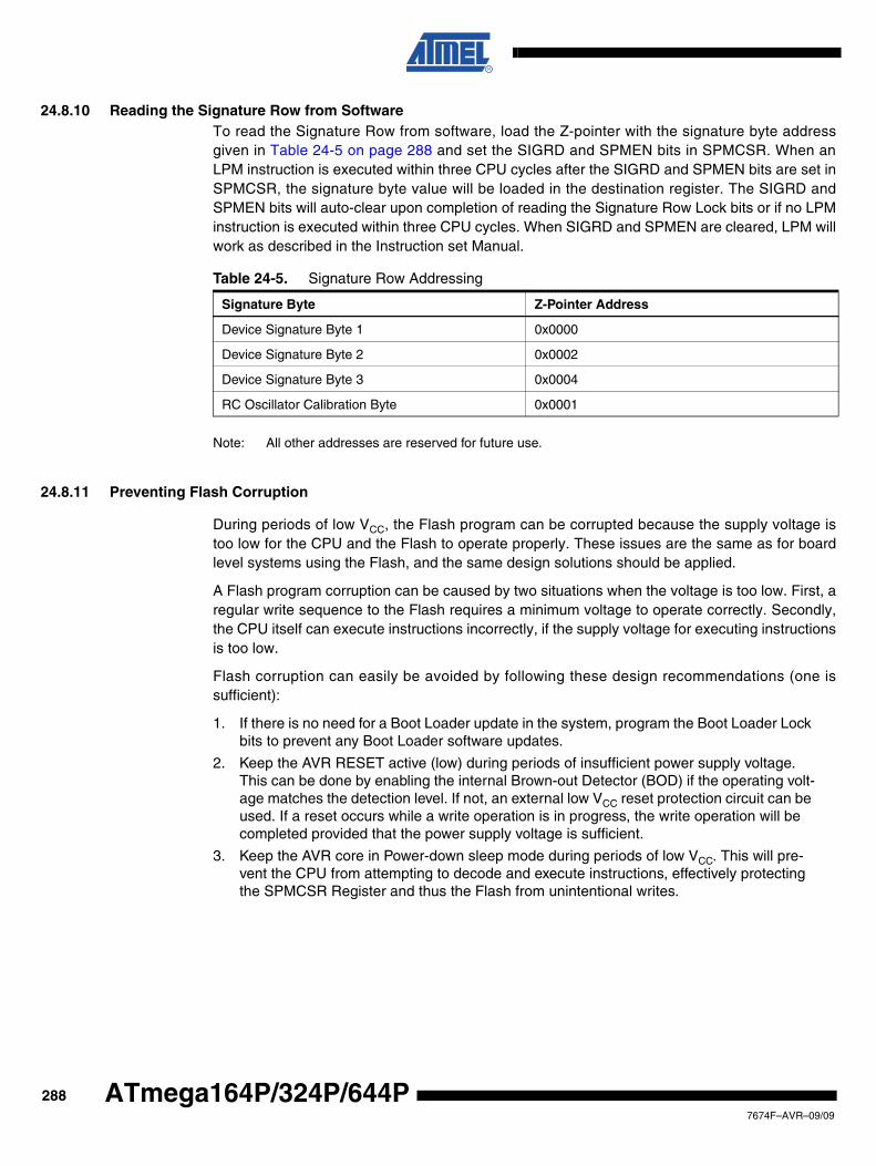
24.8.10 Reading the Signature Row from SoftwareTo read the Signature Row from software, load the Z-pointer with the signature byte addressgiven in Table 24-5 on page 288 and set the SIGRD and SPMEN bits in SPMCSR. When anLPM instruction is executed within three CPU cycles after the SIGRD and SPMEN bits are set inSPMCSR, the signature byte value will be loaded in the destination register. The SIGRD andSPMEN bits will auto-clear upon completion of reading the Signature Row Lock bits or if no LPMinstruction is executed within three CPU cycles. When SIGRD and SPMEN are cleared, LPM willwork as described in the Instruction set Manual.
Note: All other addresses are reserved for future use.
24.8.11 Preventing Flash Corruption
During periods of low VCC, the Flash program can be corrupted because the supply voltage istoo low for the CPU and the Flash to operate properly. These issues are the same as for boardlevel systems using the Flash, and the same design solutions should be applied.
A Flash program corruption can be caused by two situations when the voltage is too low. First, aregular write sequence to the Flash requires a minimum voltage to operate correctly. Secondly,the CPU itself can execute instructions incorrectly, if the supply voltage for executing instructionsis too low.
Flash corruption can easily be avoided by following these design recommendations (one issufficient):
1. If there is no need for a Boot Loader update in the system, program the Boot Loader Lock bits to prevent any Boot Loader software updates.
2. Keep the AVR RESET active (low) during periods of insufficient power supply voltage. This can be done by enabling the internal Brown-out Detector (BOD) if the operating volt-age matches the detection level. If not, an external low VCC reset protection circuit can be used. If a reset occurs while a write operation is in progress, the write operation will be completed provided that the power supply voltage is sufficient.
3. Keep the AVR core in Power-down sleep mode during periods of low VCC. This will pre-vent the CPU from attempting to decode and execute instructions, effectively protecting the SPMCSR Register and thus the Flash from unintentional writes.
Table 24-5. Signature Row Addressing
Signature Byte Z-Pointer Address
Device Signature Byte 1 0x0000
Device Signature Byte 2 0x0002
Device Signature Byte 3 0x0004
RC Oscillator Calibration Byte 0x0001
2887674F–AVR–09/09
ATmega164P/324P/644P
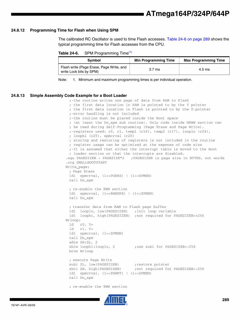
ATmega164P/324P/644P
24.8.12 Programming Time for Flash when Using SPM
The calibrated RC Oscillator is used to time Flash accesses. Table 24-6 on page 289 shows thetypical programming time for Flash accesses from the CPU.
Note: 1. Minimum and maximum programming times is per individual operation.
24.8.13 Simple Assembly Code Example for a Boot Loader;-the routine writes one page of data from RAM to Flash; the first data location in RAM is pointed to by the Y pointer; the first data location in Flash is pointed to by the Z-pointer;-error handling is not included;-the routine must be placed inside the Boot space; (at least the Do_spm sub routine). Only code inside NRWW section can; be read during Self-Programming (Page Erase and Page Write).;-registers used: r0, r1, temp1 (r16), temp2 (r17), looplo (r24), ; loophi (r25), spmcrval (r20); storing and restoring of registers is not included in the routine; register usage can be optimized at the expense of code size;-It is assumed that either the interrupt table is moved to the Boot; loader section or that the interrupts are disabled.
.equ PAGESIZEB = PAGESIZE*2 ;PAGESIZEB is page size in BYTES, not words
.org SMALLBOOTSTARTWrite_page:; Page Eraseldi spmcrval, (1<<PGERS) | (1<<SPMEN)call Do_spm
; re-enable the RWW sectionldi spmcrval, (1<<RWWSRE) | (1<<SPMEN)call Do_spm
; transfer data from RAM to Flash page bufferldi looplo, low(PAGESIZEB) ;init loop variableldi loophi, high(PAGESIZEB) ;not required for PAGESIZEB<=256
Wrloop:ld r0, Y+ld r1, Y+ldi spmcrval, (1<<SPMEN)call Do_spmadiw ZH:ZL, 2sbiw loophi:looplo, 2 ;use subi for PAGESIZEB<=256brne Wrloop
; execute Page Writesubi ZL, low(PAGESIZEB) ;restore pointersbci ZH, high(PAGESIZEB) ;not required for PAGESIZEB<=256ldi spmcrval, (1<<PGWRT) | (1<<SPMEN)call Do_spm
; re-enable the RWW section
Table 24-6. SPM Programming Time(1)
Symbol Min Programming Time Max Programming Time
Flash write (Page Erase, Page Write, and write Lock bits by SPM)
3.7 ms 4.5 ms
2897674F–AVR–09/09
ldi spmcrval, (1<<RWWSRE) | (1<<SPMEN)call Do_spm
; read back and check, optionalldi looplo, low(PAGESIZEB) ;init loop variableldi loophi, high(PAGESIZEB) ;not required for PAGESIZEB<=256subi YL, low(PAGESIZEB) ;restore pointersbci YH, high(PAGESIZEB)
Rdloop:lpm r0, Z+ld r1, Y+cpse r0, r1jmp Errorsbiw loophi:looplo, 1 ;use subi for PAGESIZEB<=256brne Rdloop
; return to RWW section; verify that RWW section is safe to read
Return:in temp1, SPMCSRsbrs temp1, RWWSB ; If RWWSB is set, the RWW section is not ready yetret; re-enable the RWW sectionldi spmcrval, (1<<RWWSRE) | (1<<SPMEN)call Do_spmrjmp Return
Do_spm:; check for previous SPM complete
Wait_spm:in temp1, SPMCSRsbrc temp1, SPMENrjmp Wait_spm; input: spmcrval determines SPM action; disable interrupts if enabled, store statusin temp2, SREGcli; check that no EEPROM write access is present
Wait_ee:sbic EECR, EEPErjmp Wait_ee; SPM timed sequenceout SPMCSR, spmcrvalspm; restore SREG (to enable interrupts if originally enabled)out SREG, temp2ret
2907674F–AVR–09/09
ATmega164P/324P/644P
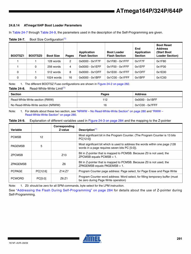
ATmega164P/324P/644P
24.8.14 ATmega164P Boot Loader Parameters
In Table 24-7 through Table 24-9, the parameters used in the description of the Self-Programming are given.
Note: 1. The different BOOTSZ Fuse configurations are shown in Figure 24-2 on page 282.
Note: 1. For details about these two section, see “NRWW – No Read-While-Write Section” on page 280 and “RWW – Read-While-Write Section” on page 280.
Note: 1. Z0: should be zero for all SPM commands, byte select for the LPM instruction.
See “Addressing the Flash During Self-Programming” on page 284 for details about the use of Z-pointer duringSelf-Programming.
Table 24-7. Boot Size Configuration(1)
BOOTSZ1 BOOTSZ0 Boot Size PagesApplication Flash Section
Boot Loader Flash Section
EndApplication Section
Boot Reset Address(Start Boot Loader Section)
1 1 128 words 2 0x0000 - 0x1F7F 0x1F80 - 0x1FFF 0x1F7F 0x1F80
1 0 256 words 4 0x0000 - 0x1EFF 0x1F00 - 0x1FFF 0x1EFF 0x1F00
0 1 512 words 8 0x0000 - 0x1DFF 0x1E00 - 0x1FFF 0x1DFF 0x1E00
0 0 1024 words 16 0x0000 - 0x1BFF 0x1C00 - 0x1FFF 0x1BFF 0x1C00
Table 24-8. Read-While-Write Limit(1)
Section Pages Address
Read-While-Write section (RWW) 112 0x0000 - 0x1BFF
No Read-While-Write section (NRWW) 16 0x1C00 - 0x7FFF
Table 24-9. Explanation of different variables used in Figure 24-3 on page 284 and the mapping to the Z-pointer
VariableCorresponding
Z-value Description(1)
PCMSB 12Most significant bit in the Program Counter. (The Program Counter is 13 bits PC[12:0])
PAGEMSB 5Most significant bit which is used to address the words within one page (128 words in a page requires seven bits PC [5:0]).
ZPCMSB Z13Bit in Z-pointer that is mapped to PCMSB. Because Z0 is not used, the ZPCMSB equals PCMSB + 1.
ZPAGEMSB Z6Bit in Z-pointer that is mapped to PCMSB. Because Z0 is not used, the ZPAGEMSB equals PAGEMSB + 1.
PCPAGE PC[12:6] Z14:Z7 Program Counter page address: Page select, for Page Erase and Page Write
PCWORD PC[5:0] Z6:Z1Program Counter word address: Word select, for filling temporary buffer (must be zero during Page Write operation)
2917674F–AVR–09/09
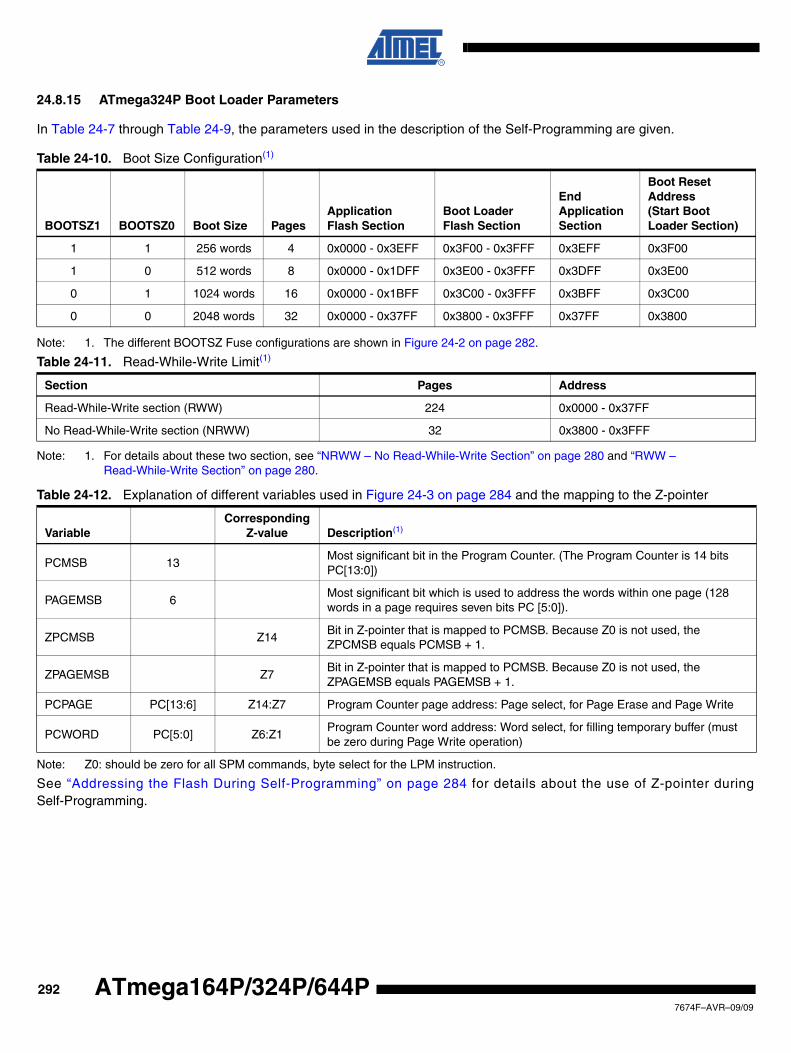
24.8.15 ATmega324P Boot Loader Parameters
In Table 24-7 through Table 24-9, the parameters used in the description of the Self-Programming are given.
Note: 1. The different BOOTSZ Fuse configurations are shown in Figure 24-2 on page 282.
Note: 1. For details about these two section, see “NRWW – No Read-While-Write Section” on page 280 and “RWW – Read-While-Write Section” on page 280.
Note: Z0: should be zero for all SPM commands, byte select for the LPM instruction.
See “Addressing the Flash During Self-Programming” on page 284 for details about the use of Z-pointer duringSelf-Programming.
Table 24-10. Boot Size Configuration(1)
BOOTSZ1 BOOTSZ0 Boot Size PagesApplication Flash Section
Boot Loader Flash Section
EndApplication Section
Boot Reset Address(Start Boot Loader Section)
1 1 256 words 4 0x0000 - 0x3EFF 0x3F00 - 0x3FFF 0x3EFF 0x3F00
1 0 512 words 8 0x0000 - 0x1DFF 0x3E00 - 0x3FFF 0x3DFF 0x3E00
0 1 1024 words 16 0x0000 - 0x1BFF 0x3C00 - 0x3FFF 0x3BFF 0x3C00
0 0 2048 words 32 0x0000 - 0x37FF 0x3800 - 0x3FFF 0x37FF 0x3800
Table 24-11. Read-While-Write Limit(1)
Section Pages Address
Read-While-Write section (RWW) 224 0x0000 - 0x37FF
No Read-While-Write section (NRWW) 32 0x3800 - 0x3FFF
Table 24-12. Explanation of different variables used in Figure 24-3 on page 284 and the mapping to the Z-pointer
VariableCorresponding
Z-value Description(1)
PCMSB 13Most significant bit in the Program Counter. (The Program Counter is 14 bits PC[13:0])
PAGEMSB 6Most significant bit which is used to address the words within one page (128 words in a page requires seven bits PC [5:0]).
ZPCMSB Z14Bit in Z-pointer that is mapped to PCMSB. Because Z0 is not used, the ZPCMSB equals PCMSB + 1.
ZPAGEMSB Z7Bit in Z-pointer that is mapped to PCMSB. Because Z0 is not used, the ZPAGEMSB equals PAGEMSB + 1.
PCPAGE PC[13:6] Z14:Z7 Program Counter page address: Page select, for Page Erase and Page Write
PCWORD PC[5:0] Z6:Z1Program Counter word address: Word select, for filling temporary buffer (must be zero during Page Write operation)
2927674F–AVR–09/09
ATmega164P/324P/644P
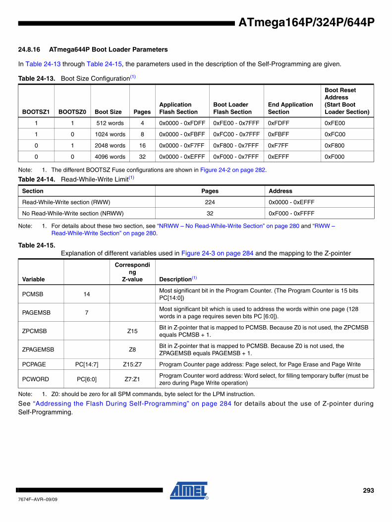
ATmega164P/324P/644P
24.8.16 ATmega644P Boot Loader Parameters
In Table 24-13 through Table 24-15, the parameters used in the description of the Self-Programming are given.
Note: 1. The different BOOTSZ Fuse configurations are shown in Figure 24-2 on page 282.
Note: 1. For details about these two section, see “NRWW – No Read-While-Write Section” on page 280 and “RWW – Read-While-Write Section” on page 280.
Note: 1. Z0: should be zero for all SPM commands, byte select for the LPM instruction.
See “Addressing the Flash During Self-Programming” on page 284 for details about the use of Z-pointer duringSelf-Programming.
Table 24-13. Boot Size Configuration(1)
BOOTSZ1 BOOTSZ0 Boot Size PagesApplication Flash Section
Boot Loader Flash Section
End Application Section
Boot Reset Address(Start Boot Loader Section)
1 1 512 words 4 0x0000 - 0xFDFF 0xFE00 - 0x7FFF 0xFDFF 0xFE00
1 0 1024 words 8 0x0000 - 0xFBFF 0xFC00 - 0x7FFF 0xFBFF 0xFC00
0 1 2048 words 16 0x0000 - 0xF7FF 0xF800 - 0x7FFF 0xF7FF 0xF800
0 0 4096 words 32 0x0000 - 0xEFFF 0xF000 - 0x7FFF 0xEFFF 0xF000
Table 24-14. Read-While-Write Limit(1)
Section Pages Address
Read-While-Write section (RWW) 224 0x0000 - 0xEFFF
No Read-While-Write section (NRWW) 32 0xF000 - 0xFFFF
Table 24-15.Explanation of different variables used in Figure 24-3 on page 284 and the mapping to the Z-pointer
Variable
Corresponding
Z-value Description(1)
PCMSB 14Most significant bit in the Program Counter. (The Program Counter is 15 bits PC[14:0])
PAGEMSB 7Most significant bit which is used to address the words within one page (128 words in a page requires seven bits PC [6:0]).
ZPCMSB Z15Bit in Z-pointer that is mapped to PCMSB. Because Z0 is not used, the ZPCMSB equals PCMSB + 1.
ZPAGEMSB Z8Bit in Z-pointer that is mapped to PCMSB. Because Z0 is not used, the ZPAGEMSB equals PAGEMSB + 1.
PCPAGE PC[14:7] Z15:Z7 Program Counter page address: Page select, for Page Erase and Page Write
PCWORD PC[6:0] Z7:Z1Program Counter word address: Word select, for filling temporary buffer (must be zero during Page Write operation)
2937674F–AVR–09/09
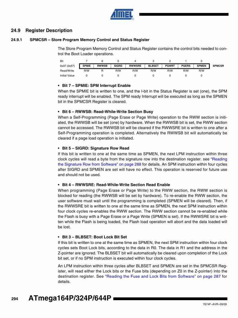
24.9 Register Description
24.9.1 SPMCSR – Store Program Memory Control and Status Register
The Store Program Memory Control and Status Register contains the control bits needed to con-trol the Boot Loader operations.
• Bit 7 – SPMIE: SPM Interrupt EnableWhen the SPMIE bit is written to one, and the I-bit in the Status Register is set (one), the SPMready interrupt will be enabled. The SPM ready Interrupt will be executed as long as the SPMENbit in the SPMCSR Register is cleared.
• Bit 6 – RWWSB: Read-While-Write Section BusyWhen a Self-Programming (Page Erase or Page Write) operation to the RWW section is initi-ated, the RWWSB will be set (one) by hardware. When the RWWSB bit is set, the RWW sectioncannot be accessed. The RWWSB bit will be cleared if the RWWSRE bit is written to one after aSelf-Programming operation is completed. Alternatively the RWWSB bit will automatically becleared if a page load operation is initiated.
• Bit 5 – SIGRD: Signature Row ReadIf this bit is written to one at the same time as SPMEN, the next LPM instruction within threeclock cycles will read a byte from the signature row into the destination register. see “Readingthe Signature Row from Software” on page 288 for details. An SPM instruction within four cyclesafter SIGRD and SPMEN are set will have no effect. This operation is reserved for future useand should not be used.
• Bit 4 – RWWSRE: Read-While-Write Section Read EnableWhen programming (Page Erase or Page Write) to the RWW section, the RWW section isblocked for reading (the RWWSB will be set by hardware). To re-enable the RWW section, theuser software must wait until the programming is completed (SPMEN will be cleared). Then, ifthe RWWSRE bit is written to one at the same time as SPMEN, the next SPM instruction withinfour clock cycles re-enables the RWW section. The RWW section cannot be re-enabled whilethe Flash is busy with a Page Erase or a Page Write (SPMEN is set). If the RWWSRE bit is writ-ten while the Flash is being loaded, the Flash load operation will abort and the data loaded willbe lost.
• Bit 3 – BLBSET: Boot Lock Bit SetIf this bit is written to one at the same time as SPMEN, the next SPM instruction within four clockcycles sets Boot Lock bits, according to the data in R0. The data in R1 and the address in theZ-pointer are ignored. The BLBSET bit will automatically be cleared upon completion of the Lockbit set, or if no SPM instruction is executed within four clock cycles.
An LPM instruction within three cycles after BLBSET and SPMEN are set in the SPMCSR Reg-ister, will read either the Lock bits or the Fuse bits (depending on Z0 in the Z-pointer) into thedestination register. See “Reading the Fuse and Lock Bits from Software” on page 287 fordetails.
Bit 7 6 5 4 3 2 1 0
0x37 (0x57) SPMIE RWWSB SIGRD RWWSRE BLBSET PGWRT PGERS SPMEN SPMCSR
Read/Write R/W R R/W R/W R/W R/W R/W R/W
Initial Value 0 0 0 0 0 0 0 0
2947674F–AVR–09/09
ATmega164P/324P/644P
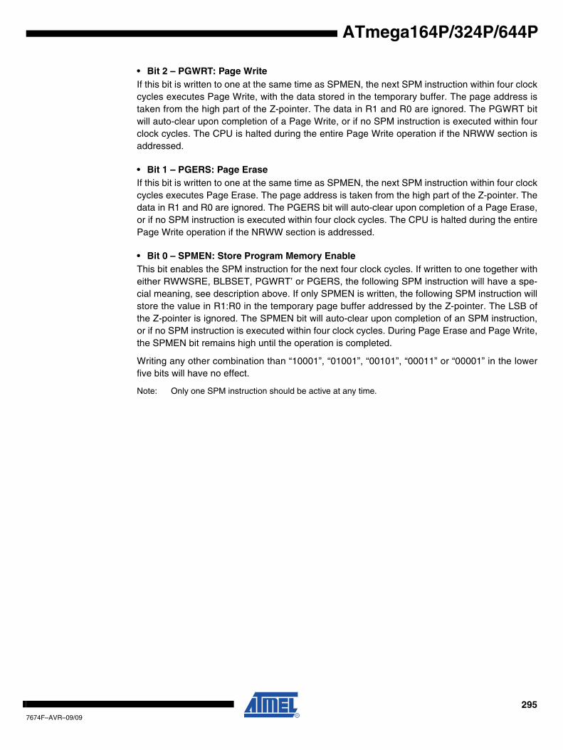
ATmega164P/324P/644P
• Bit 2 – PGWRT: Page WriteIf this bit is written to one at the same time as SPMEN, the next SPM instruction within four clockcycles executes Page Write, with the data stored in the temporary buffer. The page address istaken from the high part of the Z-pointer. The data in R1 and R0 are ignored. The PGWRT bitwill auto-clear upon completion of a Page Write, or if no SPM instruction is executed within fourclock cycles. The CPU is halted during the entire Page Write operation if the NRWW section isaddressed.
• Bit 1 – PGERS: Page EraseIf this bit is written to one at the same time as SPMEN, the next SPM instruction within four clockcycles executes Page Erase. The page address is taken from the high part of the Z-pointer. Thedata in R1 and R0 are ignored. The PGERS bit will auto-clear upon completion of a Page Erase,or if no SPM instruction is executed within four clock cycles. The CPU is halted during the entirePage Write operation if the NRWW section is addressed.
• Bit 0 – SPMEN: Store Program Memory EnableThis bit enables the SPM instruction for the next four clock cycles. If written to one together witheither RWWSRE, BLBSET, PGWRT’ or PGERS, the following SPM instruction will have a spe-cial meaning, see description above. If only SPMEN is written, the following SPM instruction willstore the value in R1:R0 in the temporary page buffer addressed by the Z-pointer. The LSB ofthe Z-pointer is ignored. The SPMEN bit will auto-clear upon completion of an SPM instruction,or if no SPM instruction is executed within four clock cycles. During Page Erase and Page Write,the SPMEN bit remains high until the operation is completed.
Writing any other combination than “10001”, “01001”, “00101”, “00011” or “00001” in the lowerfive bits will have no effect.
Note: Only one SPM instruction should be active at any time.
2957674F–AVR–09/09
25. Memory Programming
25.1 Program And Data Memory Lock Bits
The ATmega164P/324P/644P provides six Lock bits which can be left unprogrammed (“1”) orcan be programmed (“0”) to obtain the additional features listed in Table 25-2. The Lock bits canonly be erased to “1” with the Chip Erase command.
Note: 1. “1” means unprogrammed, “0” means programmed
Table 25-1. Lock Bit Byte(1)
Lock Bit Byte Bit No Description Default Value
7 – 1 (unprogrammed)
6 – 1 (unprogrammed)
BLB12 5 Boot Lock bit 1 (unprogrammed)
BLB11 4 Boot Lock bit 1 (unprogrammed)
BLB02 3 Boot Lock bit 1 (unprogrammed)
BLB01 2 Boot Lock bit 1 (unprogrammed)
LB2 1 Lock bit 1 (unprogrammed)
LB1 0 Lock bit 1 (unprogrammed)
Table 25-2. Lock Bit Protection Modes(1)(2)
Memory Lock Bits Protection Type
LB Mode LB2 LB1
1 1 1 No memory lock features enabled.
2 1 0Further programming of the Flash and EEPROM is disabled in Parallel and Serial Programming mode. The Fuse bits are locked in both Serial and Parallel Programming mode.(1)
3 0 0
Further programming and verification of the Flash and EEPROM is disabled in Parallel and Serial Programming mode. The Boot Lock bits and Fuse bits are locked in both Serial and Parallel Programming mode.(1)
BLB0 Mode BLB02 BLB01
1 1 1No restrictions for SPM or LPM accessing the Application section.
2 1 0 SPM is not allowed to write to the Application section.
3 0 0
SPM is not allowed to write to the Application section, and LPM executing from the Boot Loader section is not allowed to read from the Application section. If Interrupt Vectors are placed in the Boot Loader section, interrupts are disabled while executing from the Application section.
4 0 1
LPM executing from the Boot Loader section is not allowed to read from the Application section. If Interrupt Vectors are placed in the Boot Loader section, interrupts are disabled while executing from the Application section.
2967674F–AVR–09/09
ATmega164P/324P/644P
ATmega164P/324P/644P
Notes: 1. Program the Fuse bits and Boot Lock bits before programming the LB1 and LB2.2. “1” means unprogrammed, “0” means programmed
25.2 Fuse Bits
The ATmega164P/324P/644P has four Fuse bytes. Table 25-3 - Table 25-5 describe briefly thefunctionality of all the fuses and how they are mapped into the Fuse bytes. Note that the fusesare read as logical zero, “0”, if they are programmed.
Note: 1. See “System and Reset Characteristics” on page 332 for BODLEVEL Fuse decoding.
BLB1 Mode BLB12 BLB11
1 1 1No restrictions for SPM or LPM accessing the Boot Loader section.
2 1 0 SPM is not allowed to write to the Boot Loader section.
3 0 0
SPM is not allowed to write to the Boot Loader section, and LPM executing from the Application section is not allowed to read from the Boot Loader section. If Interrupt Vectors are placed in the Application section, interrupts are disabled while executing from the Boot Loader section.
4 0 1
LPM executing from the Application section is not allowed to read from the Boot Loader section. If Interrupt Vectors are placed in the Application section, interrupts are disabled while executing from the Boot Loader section.
Table 25-2. Lock Bit Protection Modes(1)(2) (Continued)
Memory Lock Bits Protection Type
Table 25-3. Extended Fuse Byte
Fuse Low Byte Bit No Description Default Value
– 7 – 1
– 6 – 1
– 5 – 1
– 4 – 1
– 3 – 1
BODLEVEL2(1) 2 Brown-out Detector trigger level 1 (unprogrammed)
BODLEVEL1(1) 1 Brown-out Detector trigger level 1 (unprogrammed)
BODLEVEL0(1) 0 Brown-out Detector trigger level 1 (unprogrammed)
2977674F–AVR–09/09
Note: 1. The SPIEN Fuse is not accessible in serial programming mode.
2. The default value of BOOTSZ1..0 results in maximum Boot Size. See Table 24-7 on page 291 for details.
3. See “WDTCSR – Watchdog Timer Control Register” on page 58 for details.4. Never ship a product with the OCDEN Fuse programmed regardless of the setting of Lock bits
and JTAGEN Fuse. A programmed OCDEN Fuse enables some parts of the clock system to be running in all sleep modes. This may increase the power consumption.
Note: 1. The default value of SUT1..0 results in maximum start-up time for the default clock source. See “System and Reset Characteristics” on page 332 for details.
2. The default setting of CKSEL3..0 results in internal RC Oscillator @ 8 MHz. See Table 7-1 on page 30 for details.
3. The CKOUT Fuse allow the system clock to be output on PORTB1. See “Clock Output Buffer” on page 38 for details.
4. See “System Clock Prescaler” on page 38 for details.
The status of the Fuse bits is not affected by Chip Erase. Note that the Fuse bits are locked ifLock bit1 (LB1) is programmed. Program the Fuse bits before programming the Lock bits.
Table 25-4. Fuse High Byte
Fuse High Byte Bit No Description Default Value
OCDEN(4) 7 Enable OCD1 (unprogrammed, OCD disabled)
JTAGEN 6 Enable JTAG 0 (programmed, JTAG enabled)
SPIEN(1) 5Enable Serial Program and Data Downloading
0 (programmed, SPI prog. enabled)
WDTON(3) 4 Watchdog Timer always on 1 (unprogrammed)
EESAVE 3EEPROM memory is preserved through the Chip Erase
1 (unprogrammed, EEPROM not preserved)
BOOTSZ1 2Select Boot Size (see Table 25-9 for details)
0 (programmed)(2)
BOOTSZ0 1Select Boot Size (see Table 25-9 for details)
0 (programmed)(2)
BOOTRST 0 Select Reset Vector 1 (unprogrammed)
Table 25-5. Fuse Low Byte
Fuse Low Byte Bit No Description Default Value
CKDIV8(4) 7 Divide clock by 8 0 (programmed)
CKOUT(3) 6 Clock output 1 (unprogrammed)
SUT1 5 Select start-up time 1 (unprogrammed)(1)
SUT0 4 Select start-up time 0 (programmed)(1)
CKSEL3 3 Select Clock source 0 (programmed)(2)
CKSEL2 2 Select Clock source 0 (programmed)(2)
CKSEL1 1 Select Clock source 1 (unprogrammed)(2)
CKSEL0 0 Select Clock source 0 (programmed)(2)
2987674F–AVR–09/09
ATmega164P/324P/644P
ATmega164P/324P/644P
25.2.1 Latching of Fuses
The fuse values are latched when the device enters programming mode and changes of thefuse values will have no effect until the part leaves Programming mode. This does not apply tothe EESAVE Fuse which will take effect once it is programmed. The fuses are also latched onPower-up in Normal mode.
25.3 Signature Bytes
All Atmel microcontrollers have a three-byte signature code which identifies the device. Thiscode can be read in both serial and parallel mode, also when the device is locked. The threebytes reside in a separate address space. For the ATmega164P/324P/644P the signature bytesare given in Table 25-6.
25.4 Calibration Byte
The ATmega164P/324P/644P has a byte calibration value for the internal RC Oscillator. Thisbyte resides in the high byte of address 0x000 in the signature address space. During reset, thisbyte is automatically written into the OSCCAL Register to ensure correct frequency of the cali-brated RC Oscillator.
25.5 Page Size
Table 25-6. Device and JTAG ID
Part
Signature Bytes Address JTAG
0x000 0x001 0x002 Part Number Manufacture ID
ATmega164P 0x1E 0x94 0x0A 940A 0x1F
ATmega324P 0x1E 0x95 0x08 9508 0x1F
ATmega644P 0x1E 0x96 0x0A 960A 0x1F
Table 25-7. No. of Words in a Page and No. of Pages in the Flash
Device Flash Size Page Size PCWORD No. of Pages PCPAGE PCMSB
ATmega164P 8K words (16 Kbytes) 64 words PC[5:0] 128 PC[12:6] 12
ATmega324P 16K words (32 Kbytes) 64 words PC[5:0] 256 PC[13:6] 13
ATmega644P 32K words (64 Kbytes) 128 words PC[6:0] 256 PC[14:7] 14
Table 25-8. No. of Words in a Page and No. of Pages in the EEPROM
Device EEPROM Size Page Size PCWORD No. of Pages PCPAGE EEAMSB
ATmega164P 512 bytes 4 bytes EEA[1:0] 128 EEA[8:2] 8
ATmega324P 1 Kbytes 4 bytes EEA[1:0] 256 EEA[9:2] 9
ATmega644P 2 Kbytes 8 bytes EEA[2:0] 256 EEA[10:3] 10
2997674F–AVR–09/09
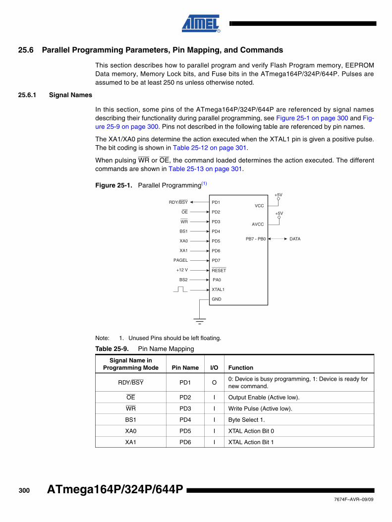
25.6 Parallel Programming Parameters, Pin Mapping, and Commands
This section describes how to parallel program and verify Flash Program memory, EEPROMData memory, Memory Lock bits, and Fuse bits in the ATmega164P/324P/644P. Pulses areassumed to be at least 250 ns unless otherwise noted.
25.6.1 Signal Names
In this section, some pins of the ATmega164P/324P/644P are referenced by signal namesdescribing their functionality during parallel programming, see Figure 25-1 on page 300 and Fig-ure 25-9 on page 300. Pins not described in the following table are referenced by pin names.
The XA1/XA0 pins determine the action executed when the XTAL1 pin is given a positive pulse.The bit coding is shown in Table 25-12 on page 301.
When pulsing WR or OE, the command loaded determines the action executed. The differentcommands are shown in Table 25-13 on page 301.
Figure 25-1. Parallel Programming(1)
Note: 1. Unused Pins should be left floating.
Table 25-9. Pin Name Mapping
Signal Name in Programming Mode Pin Name I/O Function
RDY/BSY PD1 O0: Device is busy programming, 1: Device is ready for new command.
OE PD2 I Output Enable (Active low).
WR PD3 I Write Pulse (Active low).
BS1 PD4 I Byte Select 1.
XA0 PD5 I XTAL Action Bit 0
XA1 PD6 I XTAL Action Bit 1
VCC
+5V
GND
XTAL1
PD1
PD2
PD3
PD4
PD5
PD6
PB7 - PB0 DATA
RESET
PD7
+12 V
BS1
XA0
XA1
OE
RDY/BSY
PAGEL
PA0
WR
BS2
AVCC
+5V
3007674F–AVR–09/09
ATmega164P/324P/644P
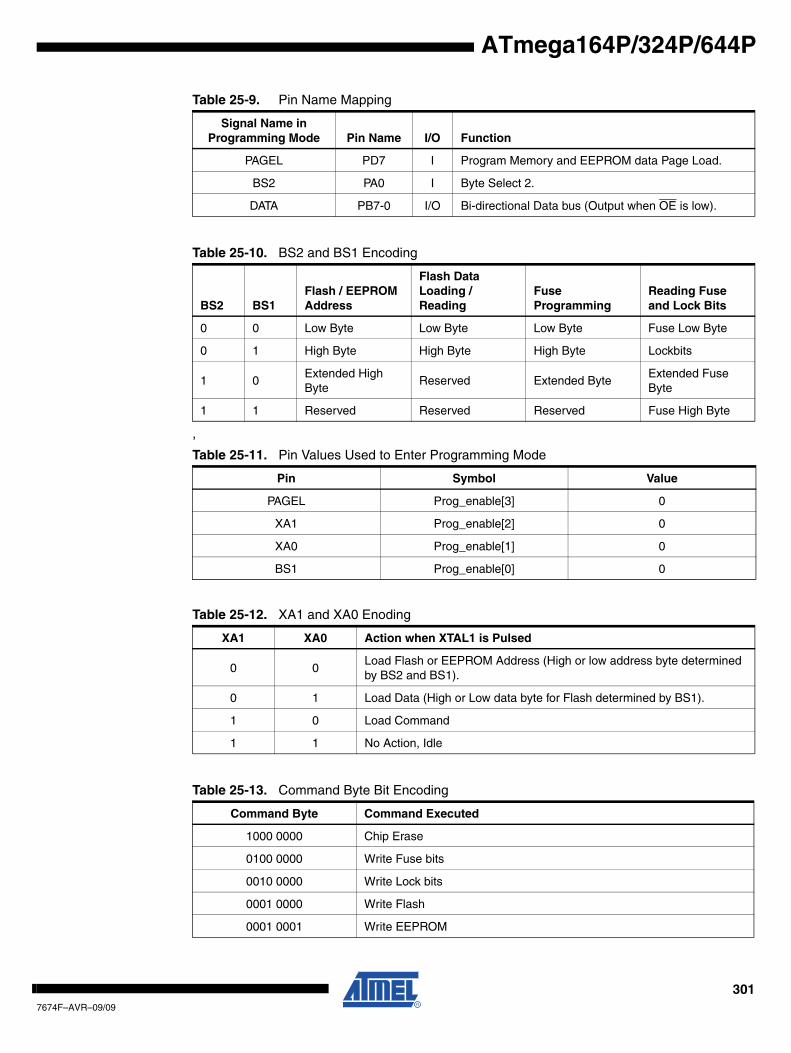
ATmega164P/324P/644P
,
PAGEL PD7 I Program Memory and EEPROM data Page Load.
BS2 PA0 I Byte Select 2.
DATA PB7-0 I/O Bi-directional Data bus (Output when OE is low).
Table 25-10. BS2 and BS1 Encoding
BS2 BS1Flash / EEPROM Address
Flash Data Loading / Reading
Fuse Programming
Reading Fuse and Lock Bits
0 0 Low Byte Low Byte Low Byte Fuse Low Byte
0 1 High Byte High Byte High Byte Lockbits
1 0Extended High Byte
Reserved Extended ByteExtended Fuse Byte
1 1 Reserved Reserved Reserved Fuse High Byte
Table 25-11. Pin Values Used to Enter Programming Mode
Pin Symbol Value
PAGEL Prog_enable[3] 0
XA1 Prog_enable[2] 0
XA0 Prog_enable[1] 0
BS1 Prog_enable[0] 0
Table 25-12. XA1 and XA0 Enoding
XA1 XA0 Action when XTAL1 is Pulsed
0 0Load Flash or EEPROM Address (High or low address byte determined by BS2 and BS1).
0 1 Load Data (High or Low data byte for Flash determined by BS1).
1 0 Load Command
1 1 No Action, Idle
Table 25-13. Command Byte Bit Encoding
Command Byte Command Executed
1000 0000 Chip Erase
0100 0000 Write Fuse bits
0010 0000 Write Lock bits
0001 0000 Write Flash
0001 0001 Write EEPROM
Table 25-9. Pin Name Mapping
Signal Name in Programming Mode Pin Name I/O Function
3017674F–AVR–09/09
25.7 Parallel Programming
25.7.1 Enter Programming Mode
The following algorithm puts the device in parallel programming mode:
1. Apply 4.5 - 5.5V between VCC and GND.
2. Set RESET to “0” and toggle XTAL1 at least six times.
3. Set the Prog_enable pins listed in Table 25-11 on page 301 to “0000” and wait at least 100 ns.
4. Apply 11.5 - 12.5V to RESET. Any activity on Prog_enable pins within 100 ns after +12V has been applied to RESET, will cause the device to fail entering programming mode.
5. Wait at least 50 µs before sending a new command.
25.7.2 Considerations for Efficient Programming
The loaded command and address are retained in the device during programming. For efficientprogramming, the following should be considered.
• The command needs only be loaded once when writing or reading multiple memory locations.
• Skip writing the data value 0xFF, that is the contents of the entire EEPROM (unless the EESAVE Fuse is programmed) and Flash after a Chip Erase.
• Address high byte needs only be loaded before programming or reading a new 256 word window in Flash or 256 byte EEPROM. This consideration also applies to Signature bytes reading.
25.7.3 Chip Erase
The Chip Erase will erase the Flash and EEPROM(1) memories plus Lock bits. The Lock bits arenot reset until the program memory has been completely erased. The Fuse bits are notchanged. A Chip Erase must be performed before the Flash and/or EEPROM arereprogrammed.
Note: 1. The EEPRPOM memory is preserved during Chip Erase if the EESAVE Fuse is programmed.
Load Command “Chip Erase”
1. Set XA1, XA0 to “10”. This enables command loading.
2. Set BS1 to “0”.
3. Set DATA to “1000 0000”. This is the command for Chip Erase.
4. Give XTAL1 a positive pulse. This loads the command.
5. Give WR a negative pulse. This starts the Chip Erase. RDY/BSY goes low.
6. Wait until RDY/BSY goes high before loading a new command.
0000 1000 Read Signature Bytes and Calibration byte
0000 0100 Read Fuse and Lock bits
0000 0010 Read Flash
0000 0011 Read EEPROM
Table 25-13. Command Byte Bit Encoding
Command Byte Command Executed
3027674F–AVR–09/09
ATmega164P/324P/644P

ATmega164P/324P/644P
25.7.4 Programming the Flash
The Flash is organized in pages, see Table 25-7 on page 299. When programming the Flash,the program data is latched into a page buffer. This allows one page of program data to be pro-grammed simultaneously. The following procedure describes how to program the entire Flashmemory:
A. Load Command “Write Flash”
1. Set XA1, XA0 to “10”. This enables command loading.
2. Set BS1 to “0”.
3. Set DATA to “0001 0000”. This is the command for Write Flash.
4. Give XTAL1 a positive pulse. This loads the command.
B. Load Address Low byte (Address bits 7..0)
1. Set XA1, XA0 to “00”. This enables address loading.
2. Set BS2, BS1 to “00”. This selects the address low byte.
3. Set DATA = Address low byte (0x00 - 0xFF).
4. Give XTAL1 a positive pulse. This loads the address low byte.
C. Load Data Low Byte
1. Set XA1, XA0 to “01”. This enables data loading.
2. Set DATA = Data low byte (0x00 - 0xFF).
3. Give XTAL1 a positive pulse. This loads the data byte.
D. Load Data High Byte
1. Set BS1 to “1”. This selects high data byte.
2. Set XA1, XA0 to “01”. This enables data loading.
3. Set DATA = Data high byte (0x00 - 0xFF).
4. Give XTAL1 a positive pulse. This loads the data byte.
E. Latch Data
1. Set BS1 to “1”. This selects high data byte.
2. Give PAGEL a positive pulse. This latches the data bytes. (See Figure 25-3 on page 305 for signal waveforms)
F. Repeat B through E until the entire buffer is filled or until all data within the page is loaded.
While the lower bits in the address are mapped to words within the page, the higher bits addressthe pages within the FLASH. This is illustrated in Figure 25-2 on page 304. Note that if less thaneight bits are required to address words in the page (pagesize < 256), the most significant bit(s)in the address low byte are used to address the page when performing a Page Write.
G. Load Address High byte (Address bits15..8)
1. Set XA1, XA0 to “00”. This enables address loading.
2. Set BS2, BS1 to “01”. This selects the address high byte.
3. Set DATA = Address high byte (0x00 - 0xFF).
4. Give XTAL1 a positive pulse. This loads the address high byte.
3037674F–AVR–09/09
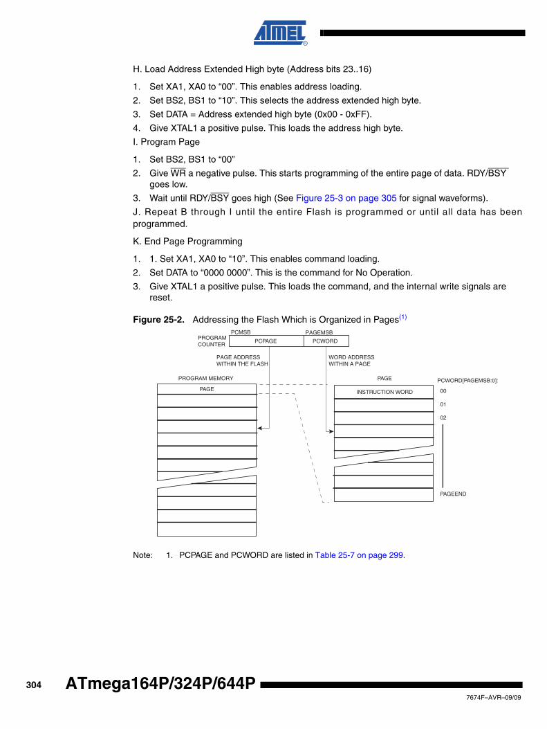
H. Load Address Extended High byte (Address bits 23..16)
1. Set XA1, XA0 to “00”. This enables address loading.
2. Set BS2, BS1 to “10”. This selects the address extended high byte.
3. Set DATA = Address extended high byte (0x00 - 0xFF).
4. Give XTAL1 a positive pulse. This loads the address high byte.
I. Program Page
1. Set BS2, BS1 to “00”
2. Give WR a negative pulse. This starts programming of the entire page of data. RDY/BSY goes low.
3. Wait until RDY/BSY goes high (See Figure 25-3 on page 305 for signal waveforms).
J. Repeat B through I until the entire Flash is programmed or until all data has beenprogrammed.
K. End Page Programming
1. 1. Set XA1, XA0 to “10”. This enables command loading.
2. Set DATA to “0000 0000”. This is the command for No Operation.
3. Give XTAL1 a positive pulse. This loads the command, and the internal write signals are reset.
Figure 25-2. Addressing the Flash Which is Organized in Pages(1)
Note: 1. PCPAGE and PCWORD are listed in Table 25-7 on page 299.
PROGRAM MEMORY
WORD ADDRESSWITHIN A PAGE
PAGE ADDRESSWITHIN THE FLASH
INSTRUCTION WORD
PAGE PCWORD[PAGEMSB:0]:
00
01
02
PAGEEND
PAGE
PCWORDPCPAGE
PCMSB PAGEMSBPROGRAMCOUNTER
3047674F–AVR–09/09
ATmega164P/324P/644P
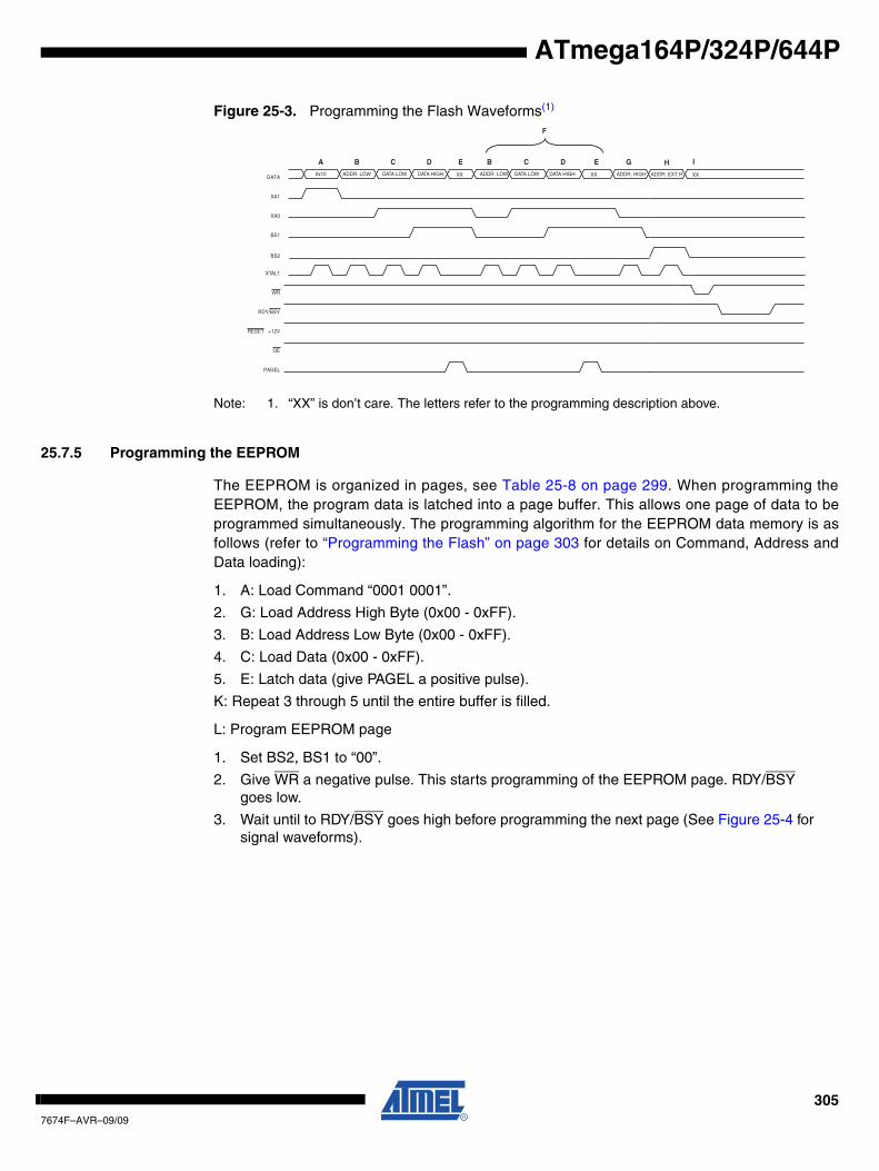
ATmega164P/324P/644P
Figure 25-3. Programming the Flash Waveforms(1)
Note: 1. “XX” is don’t care. The letters refer to the programming description above.
25.7.5 Programming the EEPROM
The EEPROM is organized in pages, see Table 25-8 on page 299. When programming theEEPROM, the program data is latched into a page buffer. This allows one page of data to beprogrammed simultaneously. The programming algorithm for the EEPROM data memory is asfollows (refer to “Programming the Flash” on page 303 for details on Command, Address andData loading):
1. A: Load Command “0001 0001”.
2. G: Load Address High Byte (0x00 - 0xFF).
3. B: Load Address Low Byte (0x00 - 0xFF).
4. C: Load Data (0x00 - 0xFF).
5. E: Latch data (give PAGEL a positive pulse).
K: Repeat 3 through 5 until the entire buffer is filled.
L: Program EEPROM page
1. Set BS2, BS1 to “00”.
2. Give WR a negative pulse. This starts programming of the EEPROM page. RDY/BSY goes low.
3. Wait until to RDY/BSY goes high before programming the next page (See Figure 25-4 for signal waveforms).
RDY/BSY
WR
OE
RESET +12V
PAGEL
BS2
0x10 ADDR. LOW ADDR. HIGHDATADATA LOW DATA HIGH ADDR. LOW DATA LOW DATA HIGH
XA1
XA0
BS1
XTAL1
XX XX XX
A B C D E B C D E G
F
ADDR. EXT.H
H I
3057674F–AVR–09/09
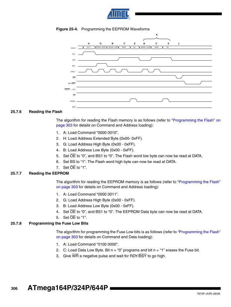
Figure 25-4. Programming the EEPROM Waveforms
25.7.6 Reading the Flash
The algorithm for reading the Flash memory is as follows (refer to “Programming the Flash” onpage 303 for details on Command and Address loading):
1. A: Load Command “0000 0010”.
2. H: Load Address Extended Byte (0x00- 0xFF).
3. G: Load Address High Byte (0x00 - 0xFF).
4. B: Load Address Low Byte (0x00 - 0xFF).
5. Set OE to “0”, and BS1 to “0”. The Flash word low byte can now be read at DATA.
6. Set BS to “1”. The Flash word high byte can now be read at DATA.
7. Set OE to “1”.
25.7.7 Reading the EEPROM
The algorithm for reading the EEPROM memory is as follows (refer to “Programming the Flash”on page 303 for details on Command and Address loading):
1. A: Load Command “0000 0011”.
2. G: Load Address High Byte (0x00 - 0xFF).
3. B: Load Address Low Byte (0x00 - 0xFF).
4. Set OE to “0”, and BS1 to “0”. The EEPROM Data byte can now be read at DATA.
5. Set OE to “1”.
25.7.8 Programming the Fuse Low Bits
The algorithm for programming the Fuse Low bits is as follows (refer to “Programming the Flash”on page 303 for details on Command and Data loading):
1. A: Load Command “0100 0000”.
2. C: Load Data Low Byte. Bit n = “0” programs and bit n = “1” erases the Fuse bit.
3. Give WR a negative pulse and wait for RDY/BSY to go high.
RDY/BSY
WR
OE
RESET +12V
PAGEL
BS2
0x11 ADDR. HIGHDATA
ADDR. LOW DATA ADDR. LOW DATA XX
XA1
XA0
BS1
XTAL1
XX
A G B C E B C E L
K
3067674F–AVR–09/09
ATmega164P/324P/644P
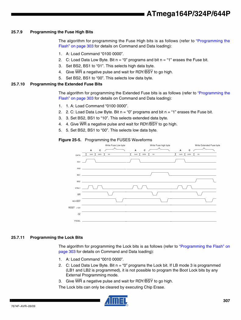
ATmega164P/324P/644P
25.7.9 Programming the Fuse High Bits
The algorithm for programming the Fuse High bits is as follows (refer to “Programming theFlash” on page 303 for details on Command and Data loading):
1. A: Load Command “0100 0000”.
2. C: Load Data Low Byte. Bit n = “0” programs and bit n = “1” erases the Fuse bit.
3. Set BS2, BS1 to “01”. This selects high data byte.
4. Give WR a negative pulse and wait for RDY/BSY to go high.
5. Set BS2, BS1 to “00”. This selects low data byte.
25.7.10 Programming the Extended Fuse Bits
The algorithm for programming the Extended Fuse bits is as follows (refer to “Programming theFlash” on page 303 for details on Command and Data loading):
1. 1. A: Load Command “0100 0000”.
2. 2. C: Load Data Low Byte. Bit n = “0” programs and bit n = “1” erases the Fuse bit.
3. 3. Set BS2, BS1 to “10”. This selects extended data byte.
4. 4. Give WR a negative pulse and wait for RDY/BSY to go high.
5. 5. Set BS2, BS1 to “00”. This selects low data byte.
Figure 25-5. Programming the FUSES Waveforms
25.7.11 Programming the Lock Bits
The algorithm for programming the Lock bits is as follows (refer to “Programming the Flash” onpage 303 for details on Command and Data loading):
1. A: Load Command “0010 0000”.
2. C: Load Data Low Byte. Bit n = “0” programs the Lock bit. If LB mode 3 is programmed (LB1 and LB2 is programmed), it is not possible to program the Boot Lock bits by any External Programming mode.
3. Give WR a negative pulse and wait for RDY/BSY to go high.
The Lock bits can only be cleared by executing Chip Erase.
RDY/BSY
WR
OE
RESET +12V
PAGEL
0x40DATA
DATA XX
XA1
XA0
BS1
XTAL1
A C
0x40 DATA XX
A C
Write Fuse Low byte Write Fuse high byte
0x40 DATA XX
A C
Write Extended Fuse byte
BS2
3077674F–AVR–09/09
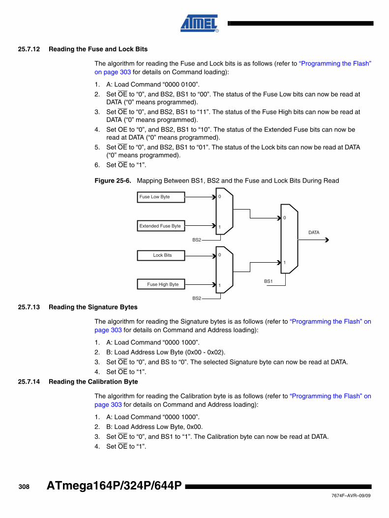
25.7.12 Reading the Fuse and Lock Bits
The algorithm for reading the Fuse and Lock bits is as follows (refer to “Programming the Flash”on page 303 for details on Command loading):
1. A: Load Command “0000 0100”.
2. Set OE to “0”, and BS2, BS1 to “00”. The status of the Fuse Low bits can now be read at DATA (“0” means programmed).
3. Set OE to “0”, and BS2, BS1 to “11”. The status of the Fuse High bits can now be read at DATA (“0” means programmed).
4. Set OE to “0”, and BS2, BS1 to “10”. The status of the Extended Fuse bits can now be read at DATA (“0” means programmed).
5. Set OE to “0”, and BS2, BS1 to “01”. The status of the Lock bits can now be read at DATA (“0” means programmed).
6. Set OE to “1”.
Figure 25-6. Mapping Between BS1, BS2 and the Fuse and Lock Bits During Read
25.7.13 Reading the Signature Bytes
The algorithm for reading the Signature bytes is as follows (refer to “Programming the Flash” onpage 303 for details on Command and Address loading):
1. A: Load Command “0000 1000”.
2. B: Load Address Low Byte (0x00 - 0x02).
3. Set OE to “0”, and BS to “0”. The selected Signature byte can now be read at DATA.
4. Set OE to “1”.
25.7.14 Reading the Calibration Byte
The algorithm for reading the Calibration byte is as follows (refer to “Programming the Flash” onpage 303 for details on Command and Address loading):
1. A: Load Command “0000 1000”.
2. B: Load Address Low Byte, 0x00.
3. Set OE to “0”, and BS1 to “1”. The Calibration byte can now be read at DATA.
4. Set OE to “1”.
Lock Bits 0
1
BS2
Fuse High Byte
0
1
BS1
DATA
Fuse Low Byte 0
1
BS2
Extended Fuse Byte
3087674F–AVR–09/09
ATmega164P/324P/644P
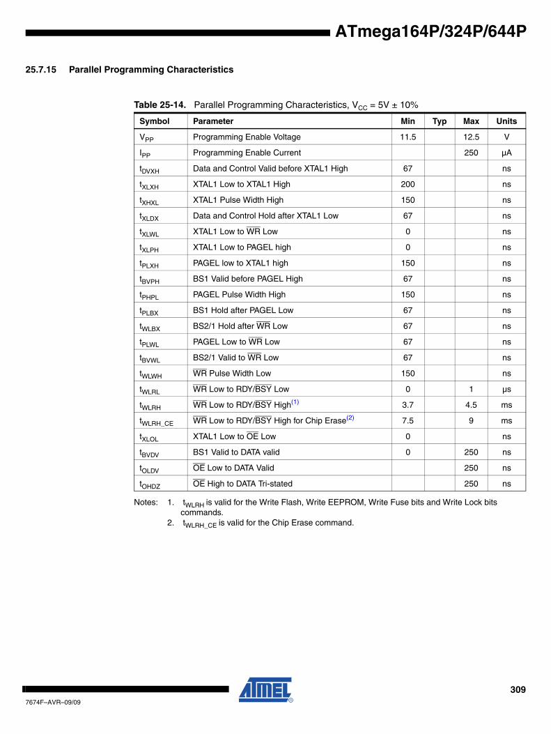
ATmega164P/324P/644P
25.7.15 Parallel Programming Characteristics
Notes: 1. tWLRH is valid for the Write Flash, Write EEPROM, Write Fuse bits and Write Lock bits commands.
2. tWLRH_CE is valid for the Chip Erase command.
Table 25-14. Parallel Programming Characteristics, VCC = 5V ± 10%
Symbol Parameter Min Typ Max Units
VPP Programming Enable Voltage 11.5 12.5 V
IPP Programming Enable Current 250 µA
tDVXH Data and Control Valid before XTAL1 High 67 ns
tXLXH XTAL1 Low to XTAL1 High 200 ns
tXHXL XTAL1 Pulse Width High 150 ns
tXLDX Data and Control Hold after XTAL1 Low 67 ns
tXLWL XTAL1 Low to WR Low 0 ns
tXLPH XTAL1 Low to PAGEL high 0 ns
tPLXH PAGEL low to XTAL1 high 150 ns
tBVPH BS1 Valid before PAGEL High 67 ns
tPHPL PAGEL Pulse Width High 150 ns
tPLBX BS1 Hold after PAGEL Low 67 ns
tWLBX BS2/1 Hold after WR Low 67 ns
tPLWL PAGEL Low to WR Low 67 ns
tBVWL BS2/1 Valid to WR Low 67 ns
tWLWH WR Pulse Width Low 150 ns
tWLRL WR Low to RDY/BSY Low 0 1 µs
tWLRH WR Low to RDY/BSY High(1) 3.7 4.5 ms
tWLRH_CE WR Low to RDY/BSY High for Chip Erase(2) 7.5 9 ms
tXLOL XTAL1 Low to OE Low 0 ns
tBVDV BS1 Valid to DATA valid 0 250 ns
tOLDV OE Low to DATA Valid 250 ns
tOHDZ OE High to DATA Tri-stated 250 ns
3097674F–AVR–09/09
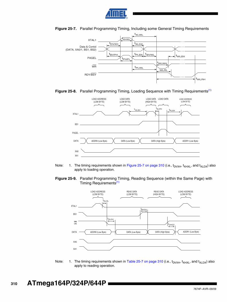
Figure 25-7. Parallel Programming Timing, Including some General Timing Requirements
Figure 25-8. Parallel Programming Timing, Loading Sequence with Timing Requirements(1)
Note: 1. The timing requirements shown in Figure 25-7 on page 310 (i.e., tDVXH, tXHXL, and tXLDX) also apply to loading operation.
Figure 25-9. Parallel Programming Timing, Reading Sequence (within the Same Page) with Timing Requirements(1)
Note: 1. The timing requirements shown in Table 25-7 on page 310 (i.e., tDVXH, tXHXL, and tXLDX) also apply to reading operation.
Data & Contol(DATA, XA0/1, BS1, BS2)
XTAL1tXHXL
tWLWH
tDVXH tXLDX
tPLWL
tWLRH
WR
RDY/BSY
PAGEL tPHPL
tPLBXtBVPH
tXLWL
tWLBXtBVWL
WLRL
XTAL1
PAGEL
tPLXHXLXHt tXLPH
ADDR0 (Low Byte) DATA (Low Byte) DATA (High Byte) ADDR1 (Low Byte)DATA
BS1
XA0
XA1
LOAD ADDRESS(LOW BYTE)
LOAD DATA (LOW BYTE)
LOAD DATA(HIGH BYTE)
LOAD DATA LOAD ADDRESS(LOW BYTE)
XTAL1
OE
ADDR0 (Low Byte) DATA (Low Byte) DATA (High Byte) ADDR1 (Low Byte)DATA
BS1
XA0
XA1
LOAD ADDRESS(LOW BYTE)
READ DATA (LOW BYTE)
READ DATA(HIGH BYTE)
LOAD ADDRESS(LOW BYTE)
tBVDV
tOLDV
tXLOL
tOHDZ
3107674F–AVR–09/09
ATmega164P/324P/644P
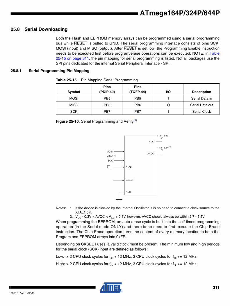
ATmega164P/324P/644P
25.8 Serial Downloading
Both the Flash and EEPROM memory arrays can be programmed using a serial programmingbus while RESET is pulled to GND. The serial programming interface consists of pins SCK,MOSI (input) and MISO (output). After RESET is set low, the Programming Enable instructionneeds to be executed first before program/erase operations can be executed. NOTE, in Table25-15 on page 311, the pin mapping for serial programming is listed. Not all packages use theSPI pins dedicated for the internal Serial Peripheral Interface - SPI.
25.8.1 Serial Programming Pin Mapping
Figure 25-10. Serial Programming and Verify(1)
Notes: 1. If the device is clocked by the internal Oscillator, it is no need to connect a clock source to theXTAL1 pin.
2. VCC - 0.3V < AVCC < VCC + 0.3V, however, AVCC should always be within 2.7 - 5.5V
When programming the EEPROM, an auto-erase cycle is built into the self-timed programmingoperation (in the Serial mode ONLY) and there is no need to first execute the Chip Eraseinstruction. The Chip Erase operation turns the content of every memory location in both theProgram and EEPROM arrays into 0xFF.
Depending on CKSEL Fuses, a valid clock must be present. The minimum low and high periodsfor the serial clock (SCK) input are defined as follows:
Low: > 2 CPU clock cycles for fck < 12 MHz, 3 CPU clock cycles for fck >= 12 MHz
High: > 2 CPU clock cycles for fck < 12 MHz, 3 CPU clock cycles for fck >= 12 MHz
Table 25-15. Pin Mapping Serial Programming
SymbolPins
(PDIP-40)Pins
(TQFP-44) I/O Description
MOSI PB5 PB5 I Serial Data in
MISO PB6 PB6 O Serial Data out
SCK PB7 PB7 I Serial Clock
VCC
GND
XTAL1
SCK
MISO
MOSI
RESET
+1.8 - 5.5V
AVCC
+1.8 - 5.5V(2)
3117674F–AVR–09/09
25.8.2 Serial Programming Algorithm
When writing serial data to the ATmega164P/324P/644P, data is clocked on the rising edge ofSCK.
When reading data from the ATmega164P/324P/644P, data is clocked on the falling edge ofSCK. See Figure 25-12 for timing details.
To program and verify the ATmega164P/324P/644P in the serial programming mode, the follow-ing sequence is recommended (See four byte instruction formats in Table 25-17):
1. Power-up sequence:Apply power between VCC and GND while RESET and SCK are set to “0”. In some sys-tems, the programmer can not guarantee that SCK is held low during power-up. In this case, RESET must be given a positive pulse of at least two CPU clock cycles duration after SCK has been set to “0”.
2. Wait for at least 20 ms and enable serial programming by sending the Programming Enable serial instruction to pin MOSI.
3. The serial programming instructions will not work if the communication is out of synchro-nization. When in sync. the second byte (0x53), will echo back when issuing the third byte of the Programming Enable instruction. Whether the echo is correct or not, all four bytes of the instruction must be transmitted. If the 0x53 did not echo back, give RESET a positive pulse and issue a new Programming Enable command.
4. The Flash is programmed one page at a time. The memory page is loaded one byte at a time by supplying the 7 LSB of the address and data together with the Load Program Memory Page instruction. To ensure correct loading of the page, the data low byte must be loaded before data high byte is applied for a given address. The Program Memory Page is stored by loading the Write Program Memory Page instruction with the address lines 15..8. Before issuing this command, make sure the instruction Load Extended Address Byte has been used to define the MSB of the address. The extended address byte is stored until the command is re-issued, i.e., the command needs only be issued for the first page, and when crossing the 64KWord boundary. If polling (RDY/BSY) is not used, the user must wait at least tWD_FLASH before issuing the next page. (See Table 25-16.) Accessing the serial programming interface before the Flash write operation completes can result in incorrect programming.
5. The EEPROM array is programmed one byte at a time by supplying the address and data together with the appropriate Write instruction. An EEPROM memory location is first automatically erased before new data is written. If polling is not used, the user must wait at least tWD_EEPROM before issuing the next byte. (See Table 25-16.) In a chip erased device, no 0xFFs in the data file(s) need to be programmed.
6. Any memory location can be verified by using the Read instruction which returns the con-tent at the selected address at serial output MISO. When reading the Flash memory, use the instruction Load Extended Address Byte to define the upper address byte, which is not included in the Read Program Memory instruction. The extended address byte is stored until the command is re-issued, i.e., the command needs only be issued for the first page, and when crossing the 64KWord boundary.
7. At the end of the programming session, RESET can be set high to commence normal operation.
8. Power-off sequence (if needed):Set RESET to “1”.Turn VCC power off.
3127674F–AVR–09/09
ATmega164P/324P/644P
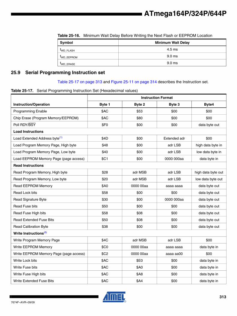
ATmega164P/324P/644P
25.9 Serial Programming Instruction set
Table 25-17 on page 313 and Figure 25-11 on page 314 describes the Instruction set.
Table 25-16. Minimum Wait Delay Before Writing the Next Flash or EEPROM Location
Symbol Minimum Wait Delay
tWD_FLASH 4.5 ms
tWD_EEPROM 9.0 ms
tWD_ERASE 9.0 ms
Table 25-17. Serial Programming Instruction Set (Hexadecimal values)
Instruction/Operation
Instruction Format
Byte 1 Byte 2 Byte 3 Byte4
Programming Enable $AC $53 $00 $00
Chip Erase (Program Memory/EEPROM) $AC $80 $00 $00
Poll RDY/BSY $F0 $00 $00 data byte out
Load Instructions
Load Extended Address byte(1) $4D $00 Extended adr $00
Load Program Memory Page, High byte $48 $00 adr LSB high data byte in
Load Program Memory Page, Low byte $40 $00 adr LSB low data byte in
Load EEPROM Memory Page (page access) $C1 $00 0000 000aa data byte in
Read Instructions
Read Program Memory, High byte $28 adr MSB adr LSB high data byte out
Read Program Memory, Low byte $20 adr MSB adr LSB low data byte out
Read EEPROM Memory $A0 0000 00aa aaaa aaaa data byte out
Read Lock bits $58 $00 $00 data byte out
Read Signature Byte $30 $00 0000 000aa data byte out
Read Fuse bits $50 $00 $00 data byte out
Read Fuse High bits $58 $08 $00 data byte out
Read Extended Fuse Bits $50 $08 $00 data byte out
Read Calibration Byte $38 $00 $00 data byte out
Write Instructions(6)
Write Program Memory Page $4C adr MSB adr LSB $00
Write EEPROM Memory $C0 0000 00aa aaaa aaaa data byte in
Write EEPROM Memory Page (page access) $C2 0000 00aa aaaa aa00 $00
Write Lock bits $AC $E0 $00 data byte in
Write Fuse bits $AC $A0 $00 data byte in
Write Fuse High bits $AC $A8 $00 data byte in
Write Extended Fuse Bits $AC $A4 $00 data byte in
3137674F–AVR–09/09
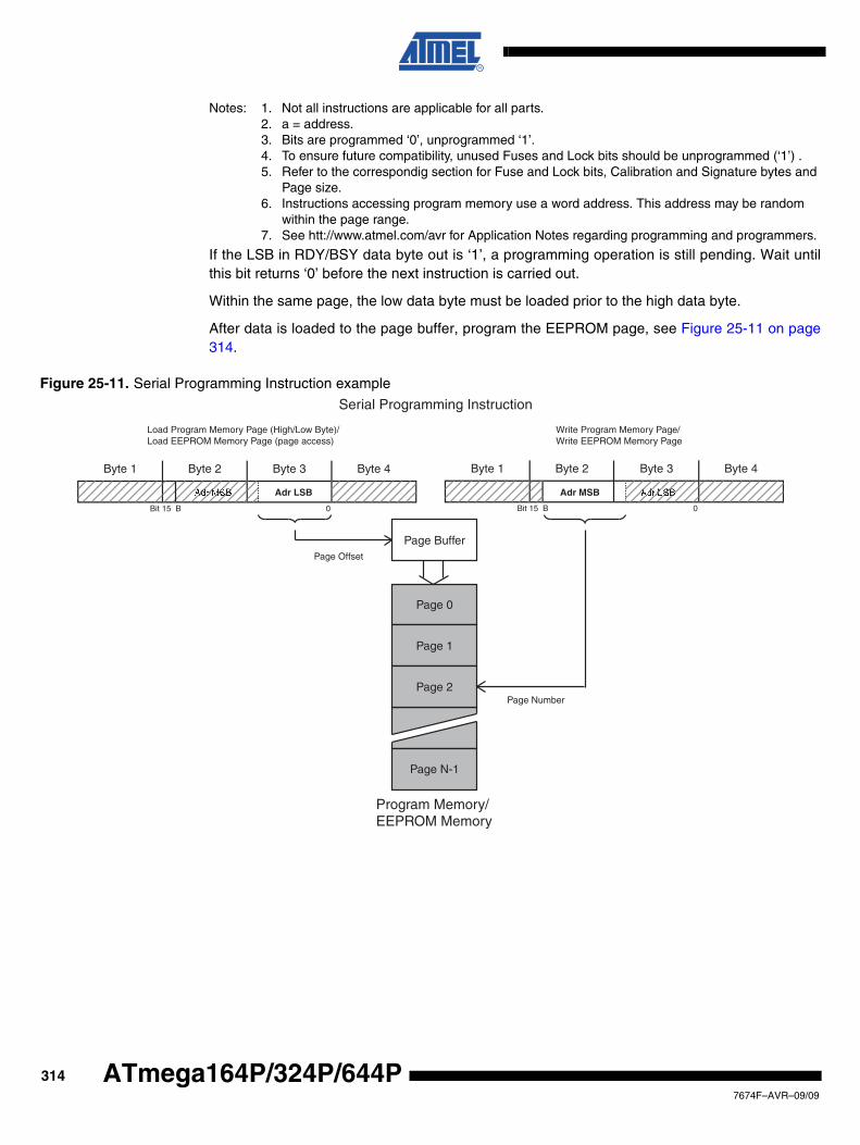
Notes: 1. Not all instructions are applicable for all parts.2. a = address.3. Bits are programmed ‘0’, unprogrammed ‘1’.4. To ensure future compatibility, unused Fuses and Lock bits should be unprogrammed (‘1’) .5. Refer to the correspondig section for Fuse and Lock bits, Calibration and Signature bytes and
Page size.6. Instructions accessing program memory use a word address. This address may be random
within the page range.7. See htt://www.atmel.com/avr for Application Notes regarding programming and programmers.
If the LSB in RDY/BSY data byte out is ‘1’, a programming operation is still pending. Wait untilthis bit returns ‘0’ before the next instruction is carried out.
Within the same page, the low data byte must be loaded prior to the high data byte.
After data is loaded to the page buffer, program the EEPROM page, see Figure 25-11 on page314.
Figure 25-11. Serial Programming Instruction example
Byte 1 Byte 2 Byte 3 Byte 4
Adr LSB
Bit 15 B 0
Serial Programming Instruction
Program Memory/EEPROM Memory
Page 0
Page 1
Page 2
Page N-1
Page Buffer
Write Program Memory Page/Write EEPROM Memory Page
Load Program Memory Page (High/Low Byte)/Load EEPROM Memory Page (page access)
Byte 1 Byte 2 Byte 3 Byte 4
Bit 15 B 0
Adr MSB
Page Offset
Page Number
Adr MMSSBA AAdrr LLSBB
3147674F–AVR–09/09
ATmega164P/324P/644P
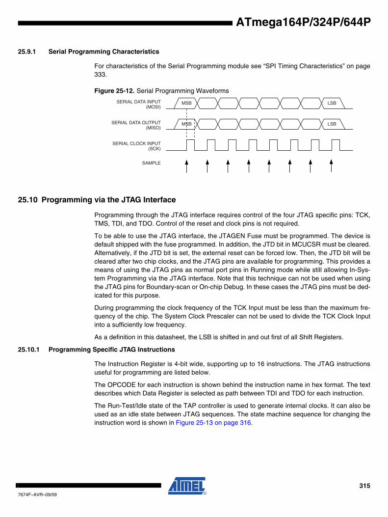
ATmega164P/324P/644P
25.9.1 Serial Programming Characteristics
For characteristics of the Serial Programming module see “SPI Timing Characteristics” on page333.
Figure 25-12. Serial Programming Waveforms
25.10 Programming via the JTAG Interface
Programming through the JTAG interface requires control of the four JTAG specific pins: TCK,TMS, TDI, and TDO. Control of the reset and clock pins is not required.
To be able to use the JTAG interface, the JTAGEN Fuse must be programmed. The device isdefault shipped with the fuse programmed. In addition, the JTD bit in MCUCSR must be cleared.Alternatively, if the JTD bit is set, the external reset can be forced low. Then, the JTD bit will becleared after two chip clocks, and the JTAG pins are available for programming. This provides ameans of using the JTAG pins as normal port pins in Running mode while still allowing In-Sys-tem Programming via the JTAG interface. Note that this technique can not be used when usingthe JTAG pins for Boundary-scan or On-chip Debug. In these cases the JTAG pins must be ded-icated for this purpose.
During programming the clock frequency of the TCK Input must be less than the maximum fre-quency of the chip. The System Clock Prescaler can not be used to divide the TCK Clock Inputinto a sufficiently low frequency.
As a definition in this datasheet, the LSB is shifted in and out first of all Shift Registers.
25.10.1 Programming Specific JTAG Instructions
The Instruction Register is 4-bit wide, supporting up to 16 instructions. The JTAG instructionsuseful for programming are listed below.
The OPCODE for each instruction is shown behind the instruction name in hex format. The textdescribes which Data Register is selected as path between TDI and TDO for each instruction.
The Run-Test/Idle state of the TAP controller is used to generate internal clocks. It can also beused as an idle state between JTAG sequences. The state machine sequence for changing theinstruction word is shown in Figure 25-13 on page 316.
MSB
MSB
LSB
LSB
SERIAL CLOCK INPUT(SCK)
SERIAL DATA INPUT (MOSI)
(MISO)
SAMPLE
SERIAL DATA OUTPUT
3157674F–AVR–09/09
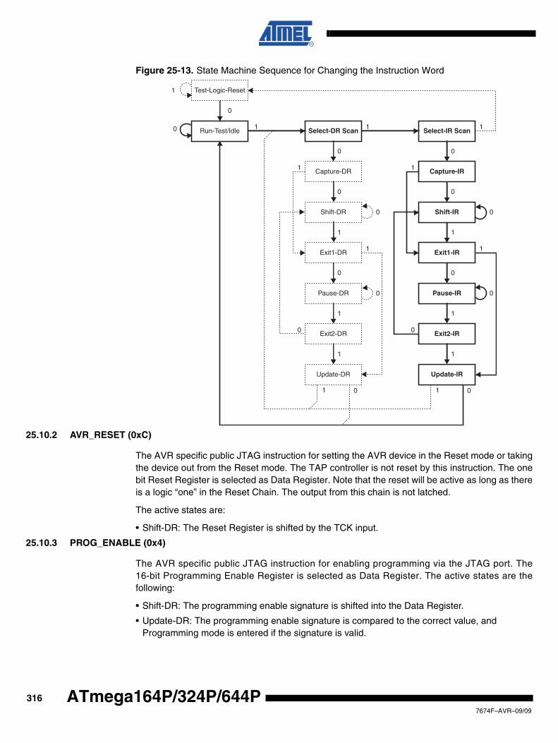
Figure 25-13. State Machine Sequence for Changing the Instruction Word
25.10.2 AVR_RESET (0xC)
The AVR specific public JTAG instruction for setting the AVR device in the Reset mode or takingthe device out from the Reset mode. The TAP controller is not reset by this instruction. The onebit Reset Register is selected as Data Register. Note that the reset will be active as long as thereis a logic “one” in the Reset Chain. The output from this chain is not latched.
The active states are:
• Shift-DR: The Reset Register is shifted by the TCK input.
25.10.3 PROG_ENABLE (0x4)
The AVR specific public JTAG instruction for enabling programming via the JTAG port. The16-bit Programming Enable Register is selected as Data Register. The active states are thefollowing:
• Shift-DR: The programming enable signature is shifted into the Data Register.
• Update-DR: The programming enable signature is compared to the correct value, and Programming mode is entered if the signature is valid.
Test-Logic-Reset
Run-Test/Idle
Shift-DR
Exit1-DR
Pause-DR
Exit2-DR
Update-DR
Select-IR Scan
Capture-IR
Shift-IR
Exit1-IR
Pause-IR
Exit2-IR
Update-IR
Select-DR Scan
Capture-DR
0
1
0 1 1 1
0 0
0 0
1 1
1 0
1
1
0
1
0
0
1 0
1
1
0
1
0
0
00
11
3167674F–AVR–09/09
ATmega164P/324P/644P
ATmega164P/324P/644P
25.10.4 PROG_COMMANDS (0x5)
The AVR specific public JTAG instruction for entering programming commands via the JTAGport. The 15-bit Programming Command Register is selected as Data Register. The activestates are the following:
• Capture-DR: The result of the previous command is loaded into the Data Register.
• Shift-DR: The Data Register is shifted by the TCK input, shifting out the result of the previous command and shifting in the new command.
• Update-DR: The programming command is applied to the Flash inputs
• Run-Test/Idle: One clock cycle is generated, executing the applied command
25.10.5 PROG_PAGELOAD (0x6)
The AVR specific public JTAG instruction to directly load the Flash data page via the JTAG port.An 8-bit Flash Data Byte Register is selected as the Data Register. This is physically the 8 LSBsof the Programming Command Register. The active states are the following:
• Shift-DR: The Flash Data Byte Register is shifted by the TCK input.
• Update-DR: The content of the Flash Data Byte Register is copied into a temporary register. A write sequence is initiated that within 11 TCK cycles loads the content of the temporary register into the Flash page buffer. The AVR automatically alternates between writing the low and the high byte for each new Update-DR state, starting with the low byte for the first Update-DR encountered after entering the PROG_PAGELOAD command. The Program Counter is pre-incremented before writing the low byte, except for the first written byte. This ensures that the first data is written to the address set up by PROG_COMMANDS, and loading the last location in the page buffer does not make the program counter increment into the next page.
25.10.6 PROG_PAGEREAD (0x7)
The AVR specific public JTAG instruction to directly capture the Flash content via the JTAG port.An 8-bit Flash Data Byte Register is selected as the Data Register. This is physically the 8 LSBsof the Programming Command Register. The active states are the following:
• Capture-DR: The content of the selected Flash byte is captured into the Flash Data Byte Register. The AVR automatically alternates between reading the low and the high byte for each new Capture-DR state, starting with the low byte for the first Capture-DR encountered after entering the PROG_PAGEREAD command. The Program Counter is post-incremented after reading each high byte, including the first read byte. This ensures that the first data is captured from the first address set up by PROG_COMMANDS, and reading the last location in the page makes the program counter increment into the next page.
• Shift-DR: The Flash Data Byte Register is shifted by the TCK input.
3177674F–AVR–09/09
25.10.7 Data RegistersThe Data Registers are selected by the JTAG instruction registers described in section “Pro-gramming Specific JTAG Instructions” on page 315. The Data Registers relevant forprogramming operations are:
• Reset Register
• Programming Enable Register
• Programming Command Register
• Flash Data Byte Register
25.10.8 Reset Register
The Reset Register is a Test Data Register used to reset the part during programming. It isrequired to reset the part before entering Programming mode.
A high value in the Reset Register corresponds to pulling the external reset low. The part is resetas long as there is a high value present in the Reset Register. Depending on the Fuse settingsfor the clock options, the part will remain reset for a Reset Time-out period (refer to “ClockSources” on page 30) after releasing the Reset Register. The output from this Data Register isnot latched, so the reset will take place immediately, as shown in Figure 23-2 on page 271.
25.10.9 Programming Enable Register
The Programming Enable Register is a 16-bit register. The contents of this register is comparedto the programming enable signature, binary code 0b1010_0011_0111_0000. When the con-tents of the register is equal to the programming enable signature, programming via the JTAGport is enabled. The register is reset to 0 on Power-on Reset, and should always be reset whenleaving Programming mode.
Figure 25-14. Programming Enable Register
25.10.10 Programming Command Register
The Programming Command Register is a 15-bit register. This register is used to serially shift inprogramming commands, and to serially shift out the result of the previous command, if any. TheJTAG Programming Instruction Set is shown in Table 25-18 on page 320. The state sequencewhen shifting in the programming commands is illustrated in Figure 25-16 on page 323.
TDI
TDO
DATA
= D Q
ClockDR & PROG_ENABLE
Programming Enable0xA370
3187674F–AVR–09/09
ATmega164P/324P/644P
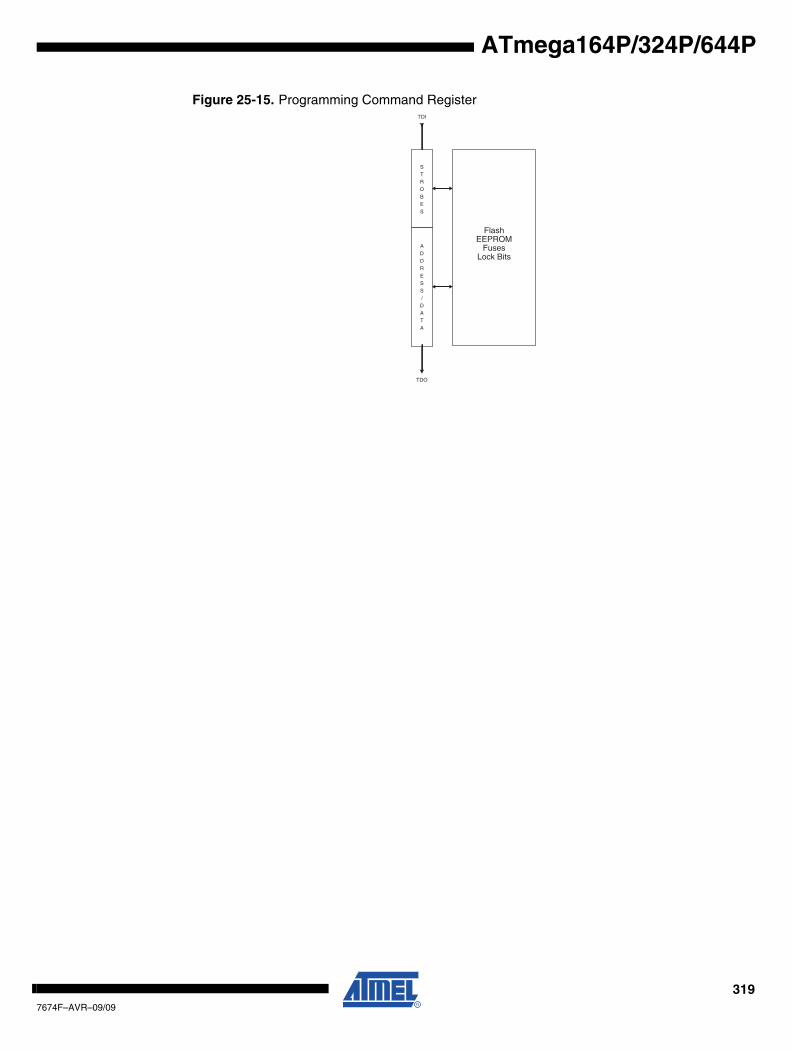
ATmega164P/324P/644P
Figure 25-15. Programming Command RegisterTDI
TDO
STROBES
ADDRESS/DATA
FlashEEPROM
FusesLock Bits
3197674F–AVR–09/09
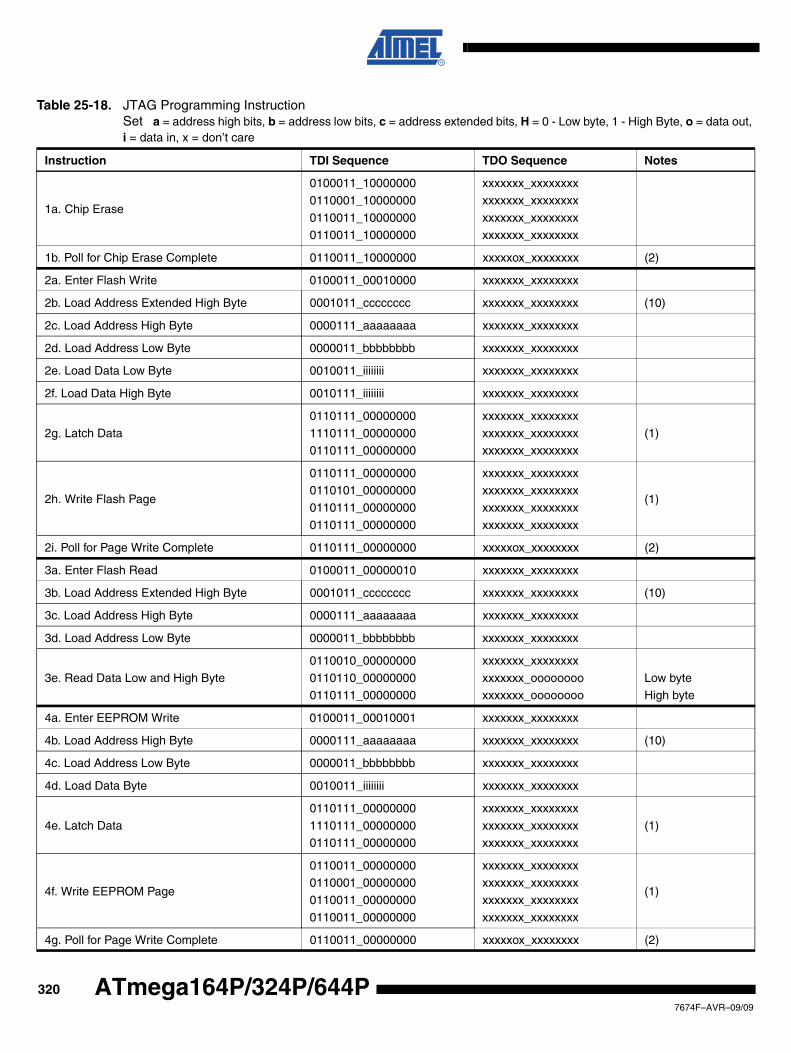
Table 25-18. JTAG Programming Instruction Set a = address high bits, b = address low bits, c = address extended bits, H = 0 - Low byte, 1 - High Byte, o = data out, i = data in, x = don’t care
Instruction TDI Sequence TDO Sequence Notes
1a. Chip Erase
0100011_10000000
0110001_10000000
0110011_100000000110011_10000000
xxxxxxx_xxxxxxxx
xxxxxxx_xxxxxxxx
xxxxxxx_xxxxxxxxxxxxxxx_xxxxxxxx
1b. Poll for Chip Erase Complete 0110011_10000000 xxxxxox_xxxxxxxx (2)
2a. Enter Flash Write 0100011_00010000 xxxxxxx_xxxxxxxx
2b. Load Address Extended High Byte 0001011_cccccccc xxxxxxx_xxxxxxxx (10)
2c. Load Address High Byte 0000111_aaaaaaaa xxxxxxx_xxxxxxxx
2d. Load Address Low Byte 0000011_bbbbbbbb xxxxxxx_xxxxxxxx
2e. Load Data Low Byte 0010011_iiiiiiii xxxxxxx_xxxxxxxx
2f. Load Data High Byte 0010111_iiiiiiii xxxxxxx_xxxxxxxx
2g. Latch Data
0110111_00000000
1110111_000000000110111_00000000
xxxxxxx_xxxxxxxx
xxxxxxx_xxxxxxxxxxxxxxx_xxxxxxxx
(1)
2h. Write Flash Page
0110111_000000000110101_00000000
0110111_00000000
0110111_00000000
xxxxxxx_xxxxxxxxxxxxxxx_xxxxxxxx
xxxxxxx_xxxxxxxx
xxxxxxx_xxxxxxxx
(1)
2i. Poll for Page Write Complete 0110111_00000000 xxxxxox_xxxxxxxx (2)
3a. Enter Flash Read 0100011_00000010 xxxxxxx_xxxxxxxx
3b. Load Address Extended High Byte 0001011_cccccccc xxxxxxx_xxxxxxxx (10)
3c. Load Address High Byte 0000111_aaaaaaaa xxxxxxx_xxxxxxxx
3d. Load Address Low Byte 0000011_bbbbbbbb xxxxxxx_xxxxxxxx
3e. Read Data Low and High Byte
0110010_00000000
0110110_000000000110111_00000000
xxxxxxx_xxxxxxxx
xxxxxxx_ooooooooxxxxxxx_oooooooo
Low byteHigh byte
4a. Enter EEPROM Write 0100011_00010001 xxxxxxx_xxxxxxxx
4b. Load Address High Byte 0000111_aaaaaaaa xxxxxxx_xxxxxxxx (10)
4c. Load Address Low Byte 0000011_bbbbbbbb xxxxxxx_xxxxxxxx
4d. Load Data Byte 0010011_iiiiiiii xxxxxxx_xxxxxxxx
4e. Latch Data
0110111_00000000
1110111_000000000110111_00000000
xxxxxxx_xxxxxxxx
xxxxxxx_xxxxxxxxxxxxxxx_xxxxxxxx
(1)
4f. Write EEPROM Page
0110011_000000000110001_00000000
0110011_00000000
0110011_00000000
xxxxxxx_xxxxxxxxxxxxxxx_xxxxxxxx
xxxxxxx_xxxxxxxx
xxxxxxx_xxxxxxxx
(1)
4g. Poll for Page Write Complete 0110011_00000000 xxxxxox_xxxxxxxx (2)
3207674F–AVR–09/09
ATmega164P/324P/644P
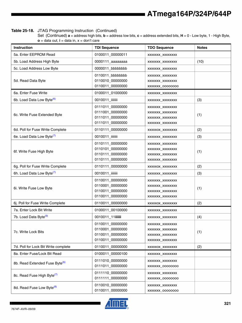
ATmega164P/324P/644P
5a. Enter EEPROM Read 0100011_00000011 xxxxxxx_xxxxxxxx
5b. Load Address High Byte 0000111_aaaaaaaa xxxxxxx_xxxxxxxx (10)
5c. Load Address Low Byte 0000011_bbbbbbbb xxxxxxx_xxxxxxxx
5d. Read Data Byte0110011_bbbbbbbb0110010_00000000
0110011_00000000
xxxxxxx_xxxxxxxxxxxxxxx_xxxxxxxx
xxxxxxx_oooooooo
6a. Enter Fuse Write 0100011_01000000 xxxxxxx_xxxxxxxx
6b. Load Data Low Byte(6) 0010011_iiiiiiii xxxxxxx_xxxxxxxx (3)
6c. Write Fuse Extended Byte
0111011_00000000
0111001_000000000111011_00000000
0111011_00000000
xxxxxxx_xxxxxxxx
xxxxxxx_xxxxxxxxxxxxxxx_xxxxxxxx
xxxxxxx_xxxxxxxx
(1)
6d. Poll for Fuse Write Complete 0110111_00000000 xxxxxox_xxxxxxxx (2)
6e. Load Data Low Byte(7) 0010011_iiiiiiii xxxxxxx_xxxxxxxx (3)
6f. Write Fuse High Byte
0110111_00000000
0110101_000000000110111_00000000
0110111_00000000
xxxxxxx_xxxxxxxx
xxxxxxx_xxxxxxxxxxxxxxx_xxxxxxxx
xxxxxxx_xxxxxxxx
(1)
6g. Poll for Fuse Write Complete 0110111_00000000 xxxxxox_xxxxxxxx (2)
6h. Load Data Low Byte(7) 0010011_iiiiiiii xxxxxxx_xxxxxxxx (3)
6i. Write Fuse Low Byte
0110011_00000000
0110001_00000000
0110011_000000000110011_00000000
xxxxxxx_xxxxxxxx
xxxxxxx_xxxxxxxx
xxxxxxx_xxxxxxxxxxxxxxx_xxxxxxxx
(1)
6j. Poll for Fuse Write Complete 0110011_00000000 xxxxxox_xxxxxxxx (2)
7a. Enter Lock Bit Write 0100011_00100000 xxxxxxx_xxxxxxxx
7b. Load Data Byte(9) 0010011_11iiiiii xxxxxxx_xxxxxxxx (4)
7c. Write Lock Bits
0110011_000000000110001_00000000
0110011_00000000
0110011_00000000
xxxxxxx_xxxxxxxxxxxxxxx_xxxxxxxx
xxxxxxx_xxxxxxxx
xxxxxxx_xxxxxxxx
(1)
7d. Poll for Lock Bit Write complete 0110011_00000000 xxxxxox_xxxxxxxx (2)
8a. Enter Fuse/Lock Bit Read 0100011_00000100 xxxxxxx_xxxxxxxx
8b. Read Extended Fuse Byte(6) 0111010_000000000111011_00000000
xxxxxxx_xxxxxxxxxxxxxxx_oooooooo
8c. Read Fuse High Byte(7) 0111110_000000000111111_00000000
xxxxxxx_xxxxxxxxxxxxxxx_oooooooo
8d. Read Fuse Low Byte(8) 0110010_000000000110011_00000000
xxxxxxx_xxxxxxxxxxxxxxx_oooooooo
Table 25-18. JTAG Programming Instruction (Continued)Set (Continued) a = address high bits, b = address low bits, c = address extended bits, H = 0 - Low byte, 1 - High Byte, o = data out, i = data in, x = don’t care
Instruction TDI Sequence TDO Sequence Notes
3217674F–AVR–09/09
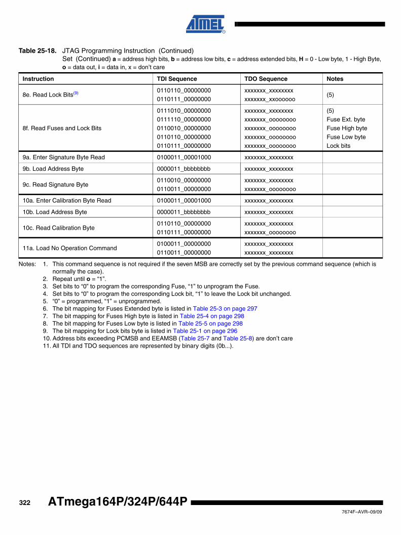
Notes: 1. This command sequence is not required if the seven MSB are correctly set by the previous command sequence (which is normally the case).
2. Repeat until o = “1”.3. Set bits to “0” to program the corresponding Fuse, “1” to unprogram the Fuse.4. Set bits to “0” to program the corresponding Lock bit, “1” to leave the Lock bit unchanged.5. “0” = programmed, “1” = unprogrammed.6. The bit mapping for Fuses Extended byte is listed in Table 25-3 on page 2977. The bit mapping for Fuses High byte is listed in Table 25-4 on page 2988. The bit mapping for Fuses Low byte is listed in Table 25-5 on page 2989. The bit mapping for Lock bits byte is listed in Table 25-1 on page 29610. Address bits exceeding PCMSB and EEAMSB (Table 25-7 and Table 25-8) are don’t care11. All TDI and TDO sequences are represented by binary digits (0b...).
8e. Read Lock Bits(9) 0110110_000000000110111_00000000
xxxxxxx_xxxxxxxxxxxxxxx_xxoooooo
(5)
8f. Read Fuses and Lock Bits
0111010_000000000111110_00000000
0110010_00000000
0110110_000000000110111_00000000
xxxxxxx_xxxxxxxxxxxxxxx_oooooooo
xxxxxxx_oooooooo
xxxxxxx_ooooooooxxxxxxx_oooooooo
(5)Fuse Ext. byte
Fuse High byte
Fuse Low byteLock bits
9a. Enter Signature Byte Read 0100011_00001000 xxxxxxx_xxxxxxxx
9b. Load Address Byte 0000011_bbbbbbbb xxxxxxx_xxxxxxxx
9c. Read Signature Byte0110010_00000000
0110011_00000000
xxxxxxx_xxxxxxxx
xxxxxxx_oooooooo
10a. Enter Calibration Byte Read 0100011_00001000 xxxxxxx_xxxxxxxx
10b. Load Address Byte 0000011_bbbbbbbb xxxxxxx_xxxxxxxx
10c. Read Calibration Byte0110110_00000000
0110111_00000000
xxxxxxx_xxxxxxxx
xxxxxxx_oooooooo
11a. Load No Operation Command0100011_00000000
0110011_00000000
xxxxxxx_xxxxxxxx
xxxxxxx_xxxxxxxx
Table 25-18. JTAG Programming Instruction (Continued)Set (Continued) a = address high bits, b = address low bits, c = address extended bits, H = 0 - Low byte, 1 - High Byte, o = data out, i = data in, x = don’t care
Instruction TDI Sequence TDO Sequence Notes
3227674F–AVR–09/09
ATmega164P/324P/644P
ATmega164P/324P/644P
Figure 25-16. State Machine Sequence for Changing/Reading the Data Word
25.10.11 Flash Data Byte Register
The Flash Data Byte Register provides an efficient way to load the entire Flash page bufferbefore executing Page Write, or to read out/verify the content of the Flash. A state machine setsup the control signals to the Flash and senses the strobe signals from the Flash, thus only thedata words need to be shifted in/out.
The Flash Data Byte Register actually consists of the 8-bit scan chain and a 8-bit temporary reg-ister. During page load, the Update-DR state copies the content of the scan chain over to thetemporary register and initiates a write sequence that within 11 TCK cycles loads the content ofthe temporary register into the Flash page buffer. The AVR automatically alternates betweenwriting the low and the high byte for each new Update-DR state, starting with the low byte for thefirst Update-DR encountered after entering the PROG_PAGELOAD command. The ProgramCounter is pre-incremented before writing the low byte, except for the first written byte. Thisensures that the first data is written to the address set up by PROG_COMMANDS, and loadingthe last location in the page buffer does not make the Program Counter increment into the nextpage.
Test-Logic-Reset
Run-Test/Idle
Shift-DR
Exit1-DR
Pause-DR
Exit2-DR
Update-DR
Select-IR Scan
Capture-IR
Shift-IR
Exit1-IR
Pause-IR
Exit2-IR
Update-IR
Select-DR Scan
Capture-DR
0
1
0 1 1 1
0 0
0 0
1 1
1 0
1
1
0
1
0
0
1 0
1
1
0
1
0
0
00
11
3237674F–AVR–09/09
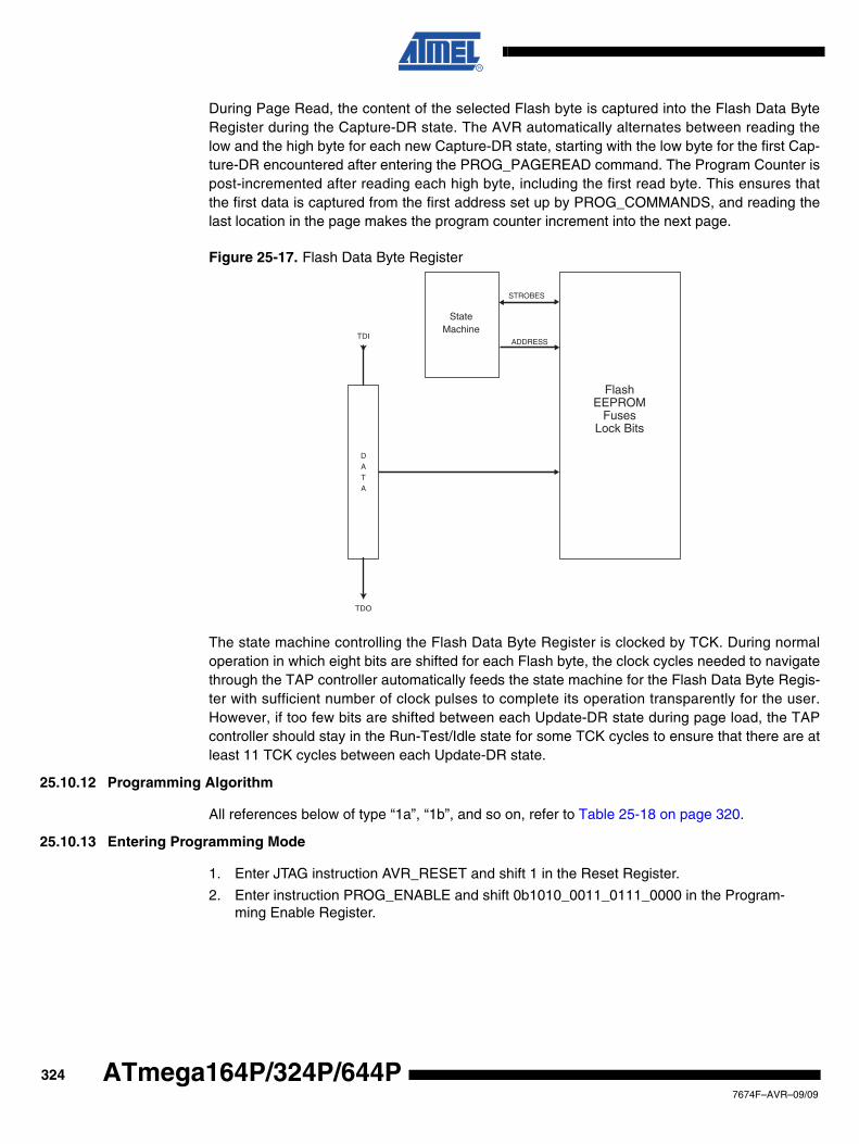
During Page Read, the content of the selected Flash byte is captured into the Flash Data ByteRegister during the Capture-DR state. The AVR automatically alternates between reading thelow and the high byte for each new Capture-DR state, starting with the low byte for the first Cap-ture-DR encountered after entering the PROG_PAGEREAD command. The Program Counter ispost-incremented after reading each high byte, including the first read byte. This ensures thatthe first data is captured from the first address set up by PROG_COMMANDS, and reading thelast location in the page makes the program counter increment into the next page.
Figure 25-17. Flash Data Byte Register
The state machine controlling the Flash Data Byte Register is clocked by TCK. During normaloperation in which eight bits are shifted for each Flash byte, the clock cycles needed to navigatethrough the TAP controller automatically feeds the state machine for the Flash Data Byte Regis-ter with sufficient number of clock pulses to complete its operation transparently for the user.However, if too few bits are shifted between each Update-DR state during page load, the TAPcontroller should stay in the Run-Test/Idle state for some TCK cycles to ensure that there are atleast 11 TCK cycles between each Update-DR state.
25.10.12 Programming Algorithm
All references below of type “1a”, “1b”, and so on, refer to Table 25-18 on page 320.
25.10.13 Entering Programming Mode
1. Enter JTAG instruction AVR_RESET and shift 1 in the Reset Register.
2. Enter instruction PROG_ENABLE and shift 0b1010_0011_0111_0000 in the Program-ming Enable Register.
TDI
TDO
DATA
FlashEEPROM
FusesLock Bits
STROBES
ADDRESS
StateMachine
3247674F–AVR–09/09
ATmega164P/324P/644P
ATmega164P/324P/644P
25.10.14 Leaving Programming Mode
1. Enter JTAG instruction PROG_COMMANDS.
2. Disable all programming instructions by using no operation instruction 11a.
3. Enter instruction PROG_ENABLE and shift 0b0000_0000_0000_0000 in the program-ming Enable Register.
4. Enter JTAG instruction AVR_RESET and shift 0 in the Reset Register.
25.10.15 Performing Chip Erase
1. Enter JTAG instruction PROG_COMMANDS.
2. Start Chip Erase using programming instruction 1a.
3. Poll for Chip Erase complete using programming instruction 1b, or wait for tWLRH_CE (refer to Table 25-14 on page 309).
25.10.16 Programming the Flash
Before programming the Flash a Chip Erase must be performed, see “Performing Chip Erase”on page 325.
1. Enter JTAG instruction PROG_COMMANDS.
2. Enable Flash write using programming instruction 2a.
3. Load address Extended High byte using programming instruction 2b.
4. Load address High byte using programming instruction 2c.
5. Load address Low byte using programming instruction 2d.
6. Load data using programming instructions 2e, 2f and 2g.
7. Repeat steps 5 and 6 for all instruction words in the page.
8. Write the page using programming instruction 2h.
9. Poll for Flash write complete using programming instruction 2i, or wait for tWLRH (refer to Table 25-14 on page 309).
10. Repeat steps 3 to 9 until all data have been programmed.
A more efficient data transfer can be achieved using the PROG_PAGELOAD instruction:
1. Enter JTAG instruction PROG_COMMANDS.
2. Enable Flash write using programming instruction 2a.
3. Load the page address using programming instructions 2b, 2c and 2d. PCWORD (refer to Table 25-7 on page 299) is used to address within one page and must be written as 0.
4. Enter JTAG instruction PROG_PAGELOAD.
5. Load the entire page by shifting in all instruction words in the page byte-by-byte, starting with the LSB of the first instruction in the page and ending with the MSB of the last instruction in the page. Use Update-DR to copy the contents of the Flash Data Byte Reg-ister into the Flash page location and to auto-increment the Program Counter before each new word.
6. Enter JTAG instruction PROG_COMMANDS.
7. Write the page using programming instruction 2h.
8. Poll for Flash write complete using programming instruction 2i, or wait for tWLRH (refer to Table 25-14 on page 309).
9. Repeat steps 3 to 8 until all data have been programmed.
3257674F–AVR–09/09
25.10.17 Reading the Flash
1. Enter JTAG instruction PROG_COMMANDS.
2. Enable Flash read using programming instruction 3a.
3. Load address using programming instructions 3b, 3c and 3d.
4. Read data using programming instruction 3e.
5. Repeat steps 3 and 4 until all data have been read.
A more efficient data transfer can be achieved using the PROG_PAGEREAD instruction:
1. Enter JTAG instruction PROG_COMMANDS.
2. Enable Flash read using programming instruction 3a.
3. Load the page address using programming instructions 3b, 3c and 3d. PCWORD (refer to Table 25-7 on page 299) is used to address within one page and must be written as 0.
4. Enter JTAG instruction PROG_PAGEREAD.
5. Read the entire page (or Flash) by shifting out all instruction words in the page (or Flash), starting with the LSB of the first instruction in the page (Flash) and ending with the MSB of the last instruction in the page (Flash). The Capture-DR state both captures the data from the Flash, and also auto-increments the program counter after each word is read. Note that Capture-DR comes before the shift-DR state. Hence, the first byte which is shifted out contains valid data.
6. Enter JTAG instruction PROG_COMMANDS.
7. Repeat steps 3 to 6 until all data have been read.
25.10.18 Programming the EEPROM
Before programming the EEPROM a Chip Erase must be performed, see “Performing ChipErase” on page 325.
1. Enter JTAG instruction PROG_COMMANDS.
2. Enable EEPROM write using programming instruction 4a.
3. Load address High byte using programming instruction 4b.
4. Load address Low byte using programming instruction 4c.
5. Load data using programming instructions 4d and 4e.
6. Repeat steps 4 and 5 for all data bytes in the page.
7. Write the data using programming instruction 4f.
8. Poll for EEPROM write complete using programming instruction 4g, or wait for tWLRH (refer to Table 25-14 on page 309).
9. Repeat steps 3 to 8 until all data have been programmed.
Note that the PROG_PAGELOAD instruction can not be used when programming the EEPROM.
25.10.19 Reading the EEPROM
1. Enter JTAG instruction PROG_COMMANDS.
2. Enable EEPROM read using programming instruction 5a.
3. Load address using programming instructions 5b and 5c.
4. Read data using programming instruction 5d.
5. Repeat steps 3 and 4 until all data have been read.
Note that the PROG_PAGEREAD instruction can not be used when reading the EEPROM.
3267674F–AVR–09/09
ATmega164P/324P/644P
ATmega164P/324P/644P
25.10.20 Programming the Fuses
1. Enter JTAG instruction PROG_COMMANDS.
2. Enable Fuse write using programming instruction 6a.
3. Load data high byte using programming instructions 6b. A bit value of “0” will program the corresponding fuse, a “1” will unprogram the fuse.
4. Write Fuse High byte using programming instruction 6c.
5. Poll for Fuse write complete using programming instruction 6d, or wait for tWLRH (refer to Table 25-14 on page 309).
6. Load data low byte using programming instructions 6e. A “0” will program the fuse, a “1” will unprogram the fuse.
7. Write Fuse low byte using programming instruction 6f.
8. Poll for Fuse write complete using programming instruction 6g, or wait for tWLRH (refer to Table 25-14 on page 309).
25.10.21 Programming the Lock Bits
1. Enter JTAG instruction PROG_COMMANDS.
2. Enable Lock bit write using programming instruction 7a.
3. Load data using programming instructions 7b. A bit value of “0” will program the corre-sponding lock bit, a “1” will leave the lock bit unchanged.
4. Write Lock bits using programming instruction 7c.
5. Poll for Lock bit write complete using programming instruction 7d, or wait for tWLRH (refer to Table 25-14 on page 309).
25.10.22 Reading the Fuses and Lock Bits
1. Enter JTAG instruction PROG_COMMANDS.
2. Enable Fuse/Lock bit read using programming instruction 8a.
3. To read all Fuses and Lock bits, use programming instruction 8e.To only read Fuse High byte, use programming instruction 8b.To only read Fuse Low byte, use programming instruction 8c.To only read Lock bits, use programming instruction 8d.
25.10.23 Reading the Signature Bytes
1. Enter JTAG instruction PROG_COMMANDS.
2. Enable Signature byte read using programming instruction 9a.
3. Load address 0x00 using programming instruction 9b.
4. Read first signature byte using programming instruction 9c.
5. Repeat steps 3 and 4 with address 0x01 and address 0x02 to read the second and third signature bytes, respectively.
25.10.24 Reading the Calibration Byte
1. Enter JTAG instruction PROG_COMMANDS.
2. Enable Calibration byte read using programming instruction 10a.
3. Load address 0x00 using programming instruction 10b.
4. Read the calibration byte using programming instruction 10c.
3277674F–AVR–09/09
26. Electrical Characteristics
Absolute Maximum Ratings*
Notes: 1. Maximum current per port = ±30mA
Operating Temperature................................. -55° C to +125° C *NOTICE: Stresses beyond those listed under “Absolute Maximum Ratings” may cause permanent dam-age to the device. This is a stress rating only and functional operation of the device at these or other conditions beyond those indicated in the operational sections of this specification is not implied. Exposure to absolute maximum rating conditions for extended periods may affect device reliability.
Storage Temperature ..................................... -65°C to +150°C
Voltage on any Pin except RESETwith respect to Ground ................................-0.5V to VCC+0.5V
Voltage on RESET with respect to Ground......-0.5V to +13.0V
Maximum Operating Voltage ............................................ 6.0V
DC Current per I/O Pin ............................................... 40.0 mA
DC Current VCC and GND Pins................................ 200.0 mA
Injection Current at VCC = 0V ................................... ±5.0mA(1)
Injection Current at VCC = 5V ...................................... ±1.0mA
3287674F–AVR–09/09
ATmega164P/324P/644P
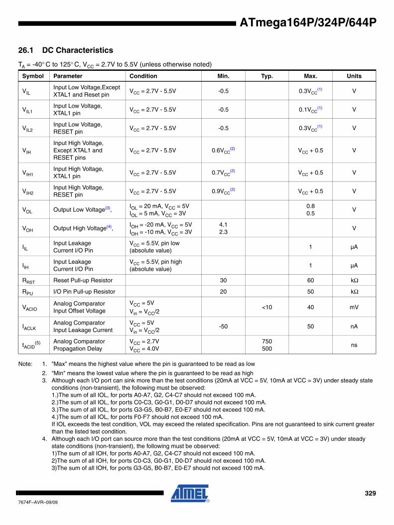
ATmega164P/324P/644P
26.1 DC Characteristics
Note: 1. "Max" means the highest value where the pin is guaranteed to be read as low
2. "Min" means the lowest value where the pin is guaranteed to be read as high3. Although each I/O port can sink more than the test conditions (20mA at VCC = 5V, 10mA at VCC = 3V) under steady state
conditions (non-transient), the following must be observed:1.)The sum of all IOL, for ports A0-A7, G2, C4-C7 should not exceed 100 mA.2.)The sum of all IOL, for ports C0-C3, G0-G1, D0-D7 should not exceed 100 mA.3.)The sum of all IOL, for ports G3-G5, B0-B7, E0-E7 should not exceed 100 mA.4.)The sum of all IOL, for ports F0-F7 should not exceed 100 mA.If IOL exceeds the test condition, VOL may exceed the related specification. Pins are not guaranteed to sink current greater than the listed test condition.
4. Although each I/O port can source more than the test conditions (20mA at VCC = 5V, 10mA at VCC = 3V) under steady state conditions (non-transient), the following must be observed:1)The sum of all IOH, for ports A0-A7, G2, C4-C7 should not exceed 100 mA.2)The sum of all IOH, for ports C0-C3, G0-G1, D0-D7 should not exceed 100 mA.3)The sum of all IOH, for ports G3-G5, B0-B7, E0-E7 should not exceed 100 mA.
TA = -40° C to 125° C, VCC = 2.7V to 5.5V (unless otherwise noted)
Symbol Parameter Condition Min. Typ. Max. Units
VILInput Low Voltage,Except XTAL1 and Reset pin
VCC = 2.7V - 5.5V -0.5 0.3VCC(1) V
VIL1Input Low Voltage,XTAL1 pin
VCC = 2.7V - 5.5V -0.5 0.1VCC(1) V
VIL2Input Low Voltage, RESET pin
VCC = 2.7V - 5.5V -0.5 0.3VCC(1) V
VIH
Input High Voltage, Except XTAL1 and RESET pins
VCC = 2.7V - 5.5V 0.6VCC(2) VCC + 0.5 V
VIH1Input High Voltage, XTAL1 pin
VCC = 2.7V - 5.5V 0.7VCC(2) VCC + 0.5 V
VIH2Input High Voltage, RESET pin
VCC = 2.7V - 5.5V 0.9VCC(2) VCC + 0.5 V
VOL Output Low Voltage(3), IOL = 20 mA, VCC = 5VIOL = 5 mA, VCC = 3V
0.80.5
V
VOH Output High Voltage(4), IOH = -20 mA, VCC = 5VIOH = -10 mA, VCC = 3V
4.12.3
V
IILInput LeakageCurrent I/O Pin
VCC = 5.5V, pin low(absolute value)
1 µA
IIHInput LeakageCurrent I/O Pin
VCC = 5.5V, pin high(absolute value)
1 µA
RRST Reset Pull-up Resistor 30 60 kΩ
RPU I/O Pin Pull-up Resistor 20 50 kΩ
VACIOAnalog Comparator Input Offset Voltage
VCC = 5V
Vin = VCC/2<10 40 mV
IACLKAnalog Comparator Input Leakage Current
VCC = 5VVin = VCC/2
-50 50 nA
tACID(5) Analog Comparator
Propagation DelayVCC = 2.7VVCC = 4.0V
750500
ns
3297674F–AVR–09/09
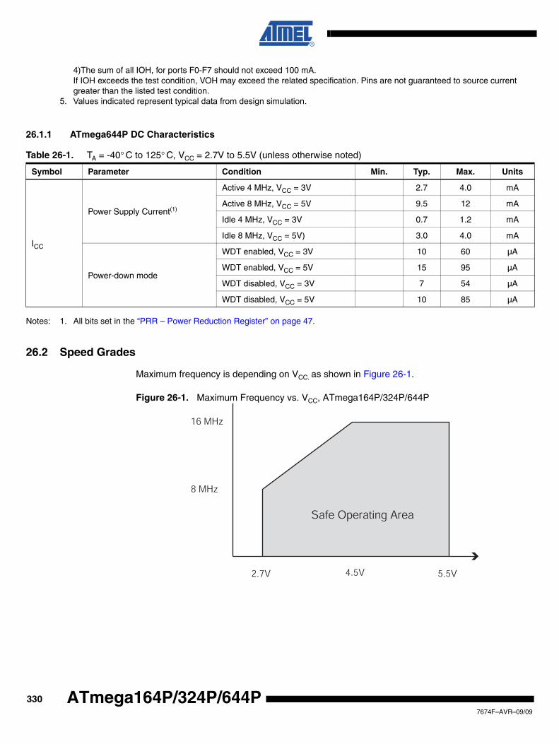
4)The sum of all IOH, for ports F0-F7 should not exceed 100 mA.If IOH exceeds the test condition, VOH may exceed the related specification. Pins are not guaranteed to source current greater than the listed test condition.
5. Values indicated represent typical data from design simulation.
Notes: 1. All bits set in the “PRR – Power Reduction Register” on page 47.
26.2 Speed Grades
Maximum frequency is depending on VCC. as shown in Figure 26-1.
Figure 26-1. Maximum Frequency vs. VCC, ATmega164P/324P/644P
26.1.1 ATmega644P DC Characteristics
Table 26-1. TA = -40° C to 125° C, VCC = 2.7V to 5.5V (unless otherwise noted)
Symbol Parameter Condition Min. Typ. Max. Units
ICC
Power Supply Current(1)
Active 4 MHz, VCC = 3V 2.7 4.0 mA
Active 8 MHz, VCC = 5V 9.5 12 mA
Idle 4 MHz, VCC = 3V 0.7 1.2 mA
Idle 8 MHz, VCC = 5V) 3.0 4.0 mA
Power-down mode
WDT enabled, VCC = 3V 10 60 µA
WDT enabled, VCC = 5V 15 95 µA
WDT disabled, VCC = 3V 7 54 µA
WDT disabled, VCC = 5V 10 85 µA
16 MHz
8 MHz
2.7V 4.5V 5.5V
Safe Operating Area
3307674F–AVR–09/09
ATmega164P/324P/644P
ATmega164P/324P/644P
26.3 Clock Characteristics
26.3.1 External Clock Drive Waveforms
Figure 26-2. External Clock Drive Waveforms
26.3.2 External Clock Drive
Note: 1. Values indicated represent typical data from design simulation.
Table 26-2. Calibration Accuracy of Internal RC Oscillator
Frequency VCC Temperature Calibration Accuracy
FactoryCalibration
8.0 MHz 3V 25° C ±2%
2.7V - 5.5V -40° C - 125° C ±14%
VIL1
VIH1
Table 26-3. External Clock Drive(1)
Symbol Parameter
VCC=2.7-5.5V VCC=4.5-5.5V
UnitsMin. Max. Min. Max.
1/tCLCLOscillator Frequency
0 8 0 16 MHz
tCLCL Clock Period 125 62.5 ns
tCHCX High Time 50 25 ns
tCLCX Low Time 50 25 ns
tCLCH Rise Time 1.6 0.5 µs
tCHCL Fall Time 1.6 0.5 µs
ΔtCLCL
Change in period from one clock cycle to the next
2 2 %
3317674F–AVR–09/09
26.4 System and Reset Characteristics
Notes: 1. Values indicated represent typical data from design simulation.2. The Power-on Reset will not work unless the supply voltage has been below VPOT (falling)3. This is the limit to which VDD can be lowered without losing RAM data.
Note: 1. VBOT may be below nominal minimum operating voltage for some devices. For devices where this is the case, the device is tested down to VCC = VBOT during the production test. This guarantees that a Brown-Out Reset will occur before VCC drops to a voltage where correct operation of the microcontroller is no longer guaranteed.
Table 26-4. Reset, Brown-out and Internal Voltage Reference Characteristics
Symbol Parameter Condition Min Typ Max Units
tRST(1) Minimum pulse width on RESET Pin 2.5 ns
VHYST Brown-out Detector Hysteresis 50 mV
VRAM(3) RAM Retention Voltage(1) 50 mV
tBOD(1) Min Pulse Width on Brown-out Reset 2 ns
VBG Bandgap reference voltage VC C= 2.7V, TA = 25° C 1.0 1.1 1.2 V
tBG(1) Bandgap reference start-up time VC C= 2.7V, TA = 25° C 40 70 µs
IBG(1) Bandgap reference current consumption VC C= 2.7V, TA = 25° C 10 µA
Table 26-5. BODLEVEL Fuse Coding(1)
BODLEVEL 2:0 Fuses Min VBOT Typ VBOT Max VBOT Units
111 BOD Disabled
110 Reserved
V
101 2.5 2.7 2.9
100 4.1 4.3 4.5
011
Reserved010
001
000
3327674F–AVR–09/09
ATmega164P/324P/644P
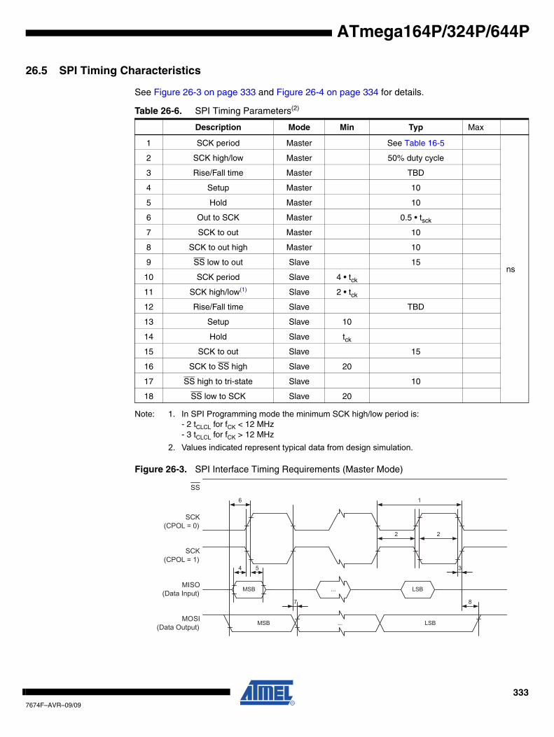
ATmega164P/324P/644P
26.5 SPI Timing Characteristics
See Figure 26-3 on page 333 and Figure 26-4 on page 334 for details.
Note: 1. In SPI Programming mode the minimum SCK high/low period is:- 2 tCLCL for fCK < 12 MHz- 3 tCLCL for fCK > 12 MHz
2. Values indicated represent typical data from design simulation.
Figure 26-3. SPI Interface Timing Requirements (Master Mode)
Table 26-6. SPI Timing Parameters(2)
Description Mode Min Typ Max
1 SCK period Master See Table 16-5
ns
2 SCK high/low Master 50% duty cycle
3 Rise/Fall time Master TBD
4 Setup Master 10
5 Hold Master 10
6 Out to SCK Master 0.5 • tsck
7 SCK to out Master 10
8 SCK to out high Master 10
9 SS low to out Slave 15
10 SCK period Slave 4 • tck
11 SCK high/low(1) Slave 2 • tck
12 Rise/Fall time Slave TBD
13 Setup Slave 10
14 Hold Slave tck
15 SCK to out Slave 15
16 SCK to SS high Slave 20
17 SS high to tri-state Slave 10
18 SS low to SCK Slave 20
MOSI(Data Output)
SCK(CPOL = 1)
MISO(Data Input)
SCK(CPOL = 0)
SS
MSB LSB
LSBMSB
...
...
6 1
2 2
34 5
87
3337674F–AVR–09/09
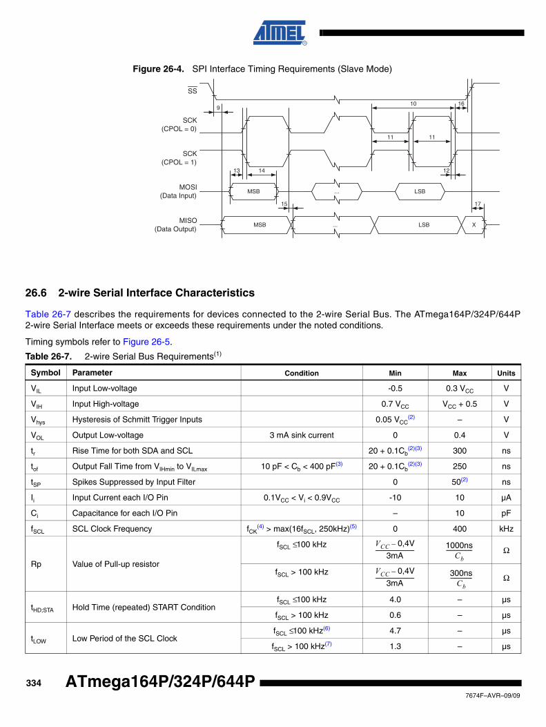
Figure 26-4. SPI Interface Timing Requirements (Slave Mode)
26.6 2-wire Serial Interface Characteristics
Table 26-7 describes the requirements for devices connected to the 2-wire Serial Bus. The ATmega164P/324P/644P2-wire Serial Interface meets or exceeds these requirements under the noted conditions.
Timing symbols refer to Figure 26-5.
MISO(Data Output)
SCK(CPOL = 1)
MOSI(Data Input)
SCK(CPOL = 0)
SS
MSB LSB
LSBMSB
...
...
10
11 11
1213 14
1715
9
X
16
Table 26-7. 2-wire Serial Bus Requirements(1)
Symbol Parameter Condition Min Max Units
VIL Input Low-voltage -0.5 0.3 VCC V
VIH Input High-voltage 0.7 VCC VCC + 0.5 V
Vhys Hysteresis of Schmitt Trigger Inputs 0.05 VCC(2) – V
VOL Output Low-voltage 3 mA sink current 0 0.4 V
tr Rise Time for both SDA and SCL 20 + 0.1Cb(2)(3) 300 ns
tof Output Fall Time from VIHmin to VILmax 10 pF < Cb < 400 pF(3) 20 + 0.1Cb(2)(3) 250 ns
tSP Spikes Suppressed by Input Filter 0 50(2) ns
Ii Input Current each I/O Pin 0.1VCC < Vi < 0.9VCC -10 10 µA
Ci Capacitance for each I/O Pin – 10 pF
fSCL SCL Clock Frequency fCK(4) > max(16fSCL, 250kHz)(5) 0 400 kHz
Rp Value of Pull-up resistor
fSCL ≤ 100 kHz
fSCL > 100 kHz
tHD;STA Hold Time (repeated) START ConditionfSCL ≤ 100 kHz 4.0 – µs
fSCL > 100 kHz 0.6 – µs
tLOW Low Period of the SCL ClockfSCL ≤ 100 kHz(6) 4.7 – µs
fSCL > 100 kHz(7) 1.3 – µs
VCC 0,4V–
3mA---------------------------- 1000ns
Cb------------------- Ω
VCC 0,4V–
3mA---------------------------- 300ns
Cb---------------- Ω
3347674F–AVR–09/09
ATmega164P/324P/644P
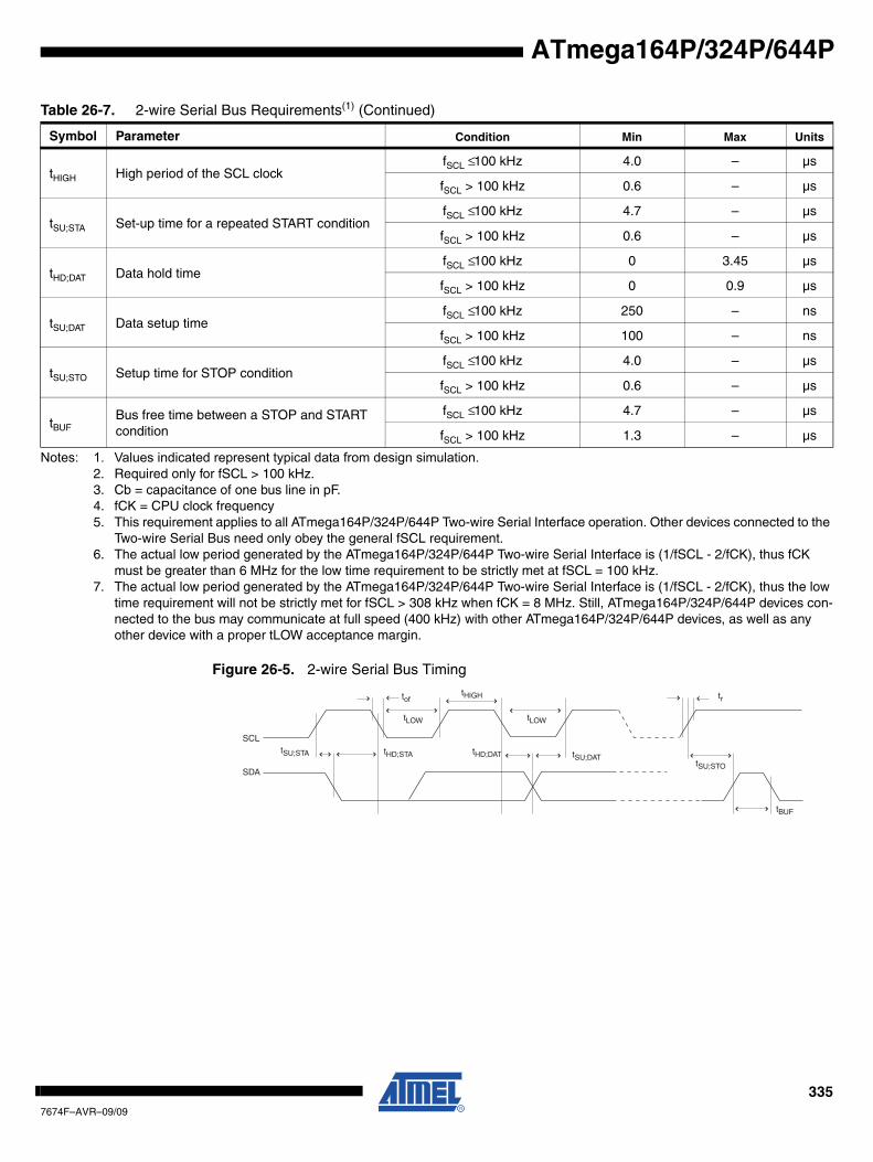
ATmega164P/324P/644P
Notes: 1. Values indicated represent typical data from design simulation.2. Required only for fSCL > 100 kHz.3. Cb = capacitance of one bus line in pF.4. fCK = CPU clock frequency5. This requirement applies to all ATmega164P/324P/644P Two-wire Serial Interface operation. Other devices connected to the
Two-wire Serial Bus need only obey the general fSCL requirement.6. The actual low period generated by the ATmega164P/324P/644P Two-wire Serial Interface is (1/fSCL - 2/fCK), thus fCK
must be greater than 6 MHz for the low time requirement to be strictly met at fSCL = 100 kHz.7. The actual low period generated by the ATmega164P/324P/644P Two-wire Serial Interface is (1/fSCL - 2/fCK), thus the low
time requirement will not be strictly met for fSCL > 308 kHz when fCK = 8 MHz. Still, ATmega164P/324P/644P devices con-nected to the bus may communicate at full speed (400 kHz) with other ATmega164P/324P/644P devices, as well as any other device with a proper tLOW acceptance margin.
Figure 26-5. 2-wire Serial Bus Timing
tHIGH High period of the SCL clockfSCL ≤ 100 kHz 4.0 – µs
fSCL > 100 kHz 0.6 – µs
tSU;STA Set-up time for a repeated START conditionfSCL ≤ 100 kHz 4.7 – µs
fSCL > 100 kHz 0.6 – µs
tHD;DAT Data hold timefSCL ≤ 100 kHz 0 3.45 µs
fSCL > 100 kHz 0 0.9 µs
tSU;DAT Data setup timefSCL ≤ 100 kHz 250 – ns
fSCL > 100 kHz 100 – ns
tSU;STO Setup time for STOP conditionfSCL ≤ 100 kHz 4.0 – µs
fSCL > 100 kHz 0.6 – µs
tBUFBus free time between a STOP and START condition
fSCL ≤ 100 kHz 4.7 – µs
fSCL > 100 kHz 1.3 – µs
Table 26-7. 2-wire Serial Bus Requirements(1) (Continued)
Symbol Parameter Condition Min Max Units
tSU;STA
tLOW
tHIGH
tLOW
tof
tHD;STA tHD;DAT tSU;DATtSU;STO
tBUF
SCL
SDA
tr
3357674F–AVR–09/09
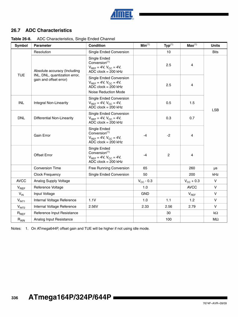
26.7 ADC Characteristics
Notes: 1. On ATmega644P, offset gain and TUE will be higher if not using idle mode.
Table 26-8. ADC Characteristics, Single Ended Channel
Symbol Parameter Condition Min(1) Typ(1) Max(1) Units
Resolution Single Ended Conversion 10 Bits
TUEAbsolute accuracy (Including INL, DNL, quantization error, gain and offset error)
Single Ended Conversion(1)
VREF = 4V, VCC = 4V,ADC clock = 200 kHz
2.5 4
LSB
Single Ended ConversionVREF = 4V, VCC = 4V,ADC clock = 200 kHz
Noise Reduction Mode
2.5 4
INL Integral Non-Linearity Single Ended ConversionVREF = 4V, VCC = 4V,ADC clock = 200 kHz
0.5 1.5
DNL Differential Non-Linearity Single Ended ConversionVREF = 4V, VCC = 4V,ADC clock = 200 kHz
0.3 0.7
Gain Error
Single Ended Conversion(1)
VREF = 4V, VCC = 4V,ADC clock = 200 kHz
-4 -2 4
Offset Error
Single Ended Conversion(1)
VREF = 4V, VCC = 4V,ADC clock = 200 kHz
-4 2 4
Conversion Time Free Running Conversion 65 260 µs
Clock Frequency Single Ended Conversion 50 200 kHz
AVCC Analog Supply Voltage VCC - 0.3 VCC + 0.3 V
VREF Reference Voltage 1.0 AVCC V
VIN Input Voltage GND VREF V
VINT1 Internal Voltage Reference 1.1V 1.0 1.1 1.2 V
VINT2 Internal Voltage Reference 2.56V 2.33 2.56 2.79 V
RREF Reference Input Resistance 30 kΩ
RAIN Analog Input Resistance 100 MΩ
3367674F–AVR–09/09
ATmega164P/324P/644P
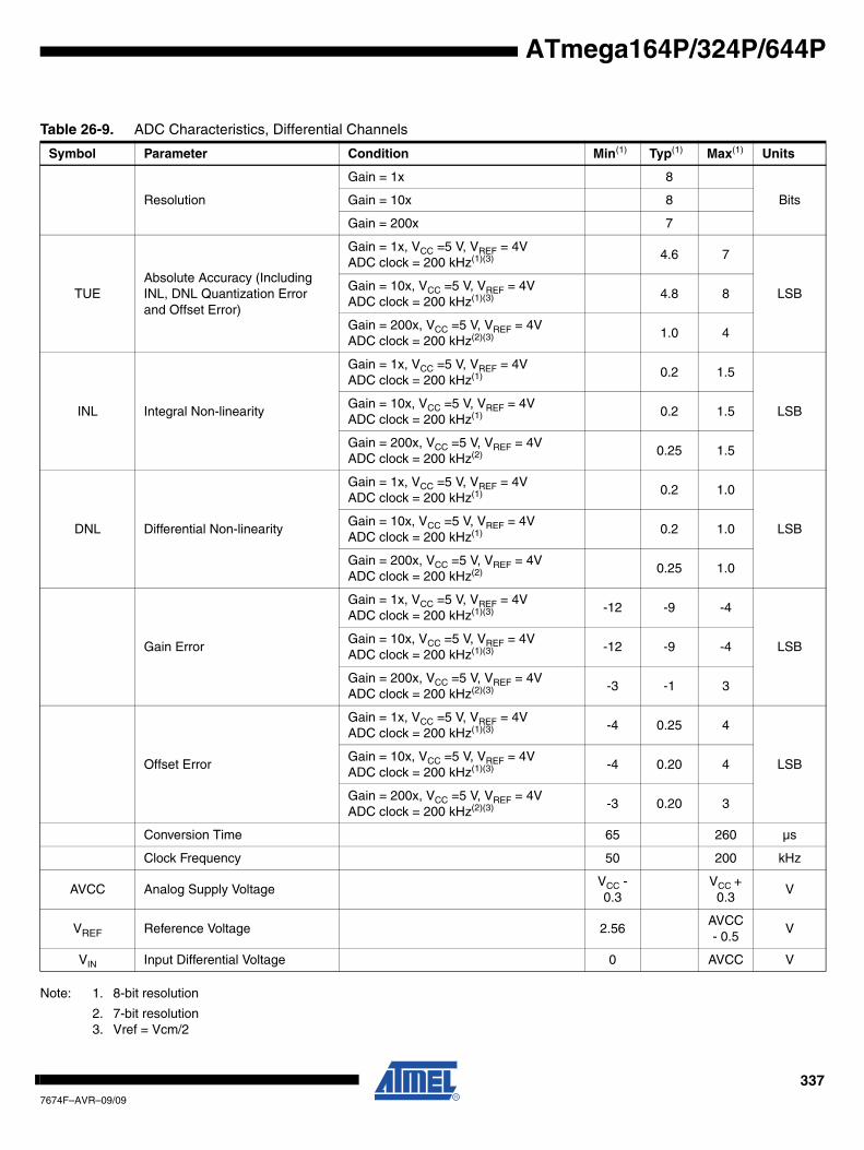
ATmega164P/324P/644P
Note: 1. 8-bit resolution
2. 7-bit resolution3. Vref = Vcm/2
Table 26-9. ADC Characteristics, Differential Channels
Symbol Parameter Condition Min(1) Typ(1) Max(1) Units
Resolution
Gain = 1x 8
BitsGain = 10x 8
Gain = 200x 7
TUEAbsolute Accuracy (Including INL, DNL Quantization Error and Offset Error)
Gain = 1x, VCC =5 V, VREF = 4VADC clock = 200 kHz(1)(3) 4.6 7
LSBGain = 10x, VCC =5 V, VREF = 4VADC clock = 200 kHz(1)(3) 4.8 8
Gain = 200x, VCC =5 V, VREF = 4VADC clock = 200 kHz(2)(3) 1.0 4
INL Integral Non-linearity
Gain = 1x, VCC =5 V, VREF = 4VADC clock = 200 kHz(1) 0.2 1.5
LSBGain = 10x, VCC =5 V, VREF = 4VADC clock = 200 kHz(1) 0.2 1.5
Gain = 200x, VCC =5 V, VREF = 4VADC clock = 200 kHz(2) 0.25 1.5
DNL Differential Non-linearity
Gain = 1x, VCC =5 V, VREF = 4VADC clock = 200 kHz(1) 0.2 1.0
LSBGain = 10x, VCC =5 V, VREF = 4VADC clock = 200 kHz(1) 0.2 1.0
Gain = 200x, VCC =5 V, VREF = 4VADC clock = 200 kHz(2) 0.25 1.0
Gain Error
Gain = 1x, VCC =5 V, VREF = 4VADC clock = 200 kHz(1)(3) -12 -9 -4
LSBGain = 10x, VCC =5 V, VREF = 4VADC clock = 200 kHz(1)(3) -12 -9 -4
Gain = 200x, VCC =5 V, VREF = 4VADC clock = 200 kHz(2)(3) -3 -1 3
Offset Error
Gain = 1x, VCC =5 V, VREF = 4VADC clock = 200 kHz(1)(3) -4 0.25 4
LSBGain = 10x, VCC =5 V, VREF = 4VADC clock = 200 kHz(1)(3) -4 0.20 4
Gain = 200x, VCC =5 V, VREF = 4VADC clock = 200 kHz(2)(3) -3 0.20 3
Conversion Time 65 260 µs
Clock Frequency 50 200 kHz
AVCC Analog Supply VoltageVCC - 0.3
VCC + 0.3
V
VREF Reference Voltage 2.56AVCC - 0.5
V
VIN Input Differential Voltage 0 AVCC V
3377674F–AVR–09/09
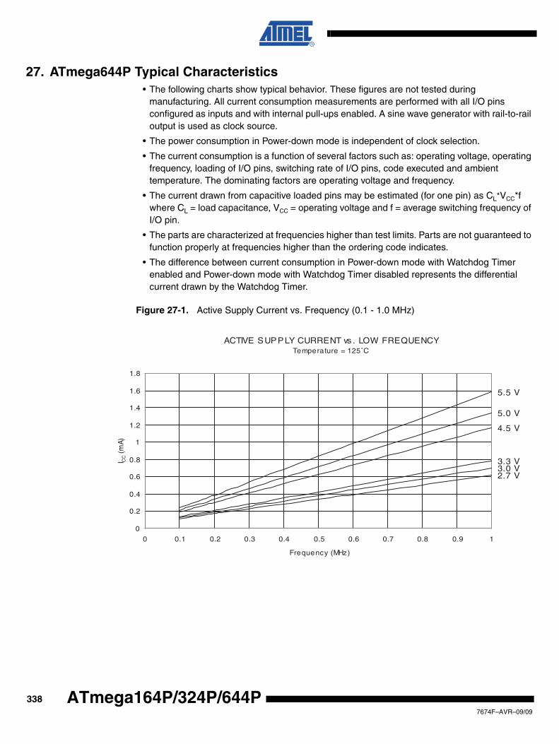
27. ATmega644P Typical Characteristics• The following charts show typical behavior. These figures are not tested during
manufacturing. All current consumption measurements are performed with all I/O pins configured as inputs and with internal pull-ups enabled. A sine wave generator with rail-to-rail output is used as clock source.
• The power consumption in Power-down mode is independent of clock selection.
• The current consumption is a function of several factors such as: operating voltage, operating frequency, loading of I/O pins, switching rate of I/O pins, code executed and ambient temperature. The dominating factors are operating voltage and frequency.
• The current drawn from capacitive loaded pins may be estimated (for one pin) as CL*VCC*f where CL = load capacitance, VCC = operating voltage and f = average switching frequency of I/O pin.
• The parts are characterized at frequencies higher than test limits. Parts are not guaranteed to function properly at frequencies higher than the ordering code indicates.
• The difference between current consumption in Power-down mode with Watchdog Timer enabled and Power-down mode with Watchdog Timer disabled represents the differential current drawn by the Watchdog Timer.
Figure 27-1. Active Supply Current vs. Frequency (0.1 - 1.0 MHz)
ACTIVE SUPPLY CURRENT vs . LOW FREQUENCYTemperature = 125˚C
5.5 V
5.0 V
4.5 V
3.3 V3.0 V2.7 V
0
0.2
0.4
0.6
0.8
1
1.2
1.4
1.6
1.8
0 0.1 0.2 0.3 0.4 0.5 0.6 0.7 0.8 0.9 1
Frequency (MHz)
I CC (
mA)
3387674F–AVR–09/09
ATmega164P/324P/644P
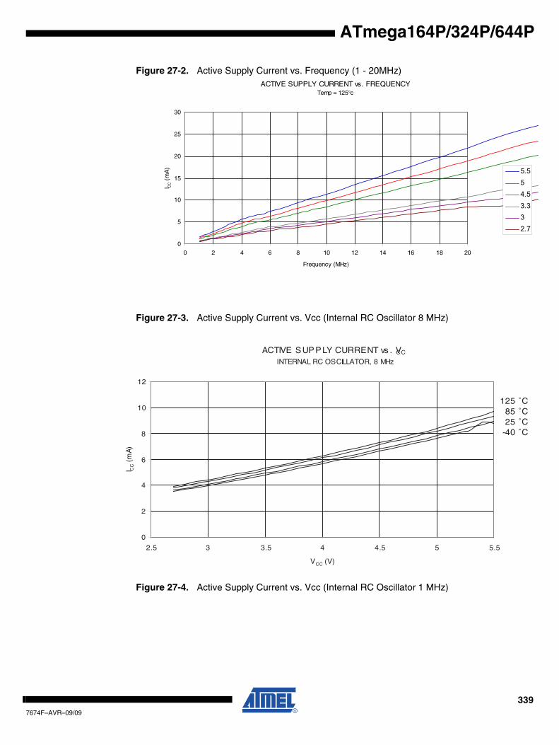
ATmega164P/324P/644P
Figure 27-2. Active Supply Current vs. Frequency (1 - 20MHz)
Figure 27-3. Active Supply Current vs. Vcc (Internal RC Oscillator 8 MHz)
Figure 27-4. Active Supply Current vs. Vcc (Internal RC Oscillator 1 MHz)
ACTIVE SUPPLY CURRENT vs. FREQUENCYTemp = 125°c
0
5
10
15
20
25
30
0 2 4 6 8 10 12 14 16 18 20
Frequency (MHz)
I CC (
mA
) 5.554.53.332.7
ACTIVE SUPPLY CURRENT vs . VCC
INTERNAL RC OSCILLATOR, 8 MHz
125 ˚C85 ˚C25 ˚C
-40 ˚C
0
2
4
6
8
10
12
2.5 3 3.5 4 4.5 5 5.5
VCC (V)
I CC (
mA)
3397674F–AVR–09/09
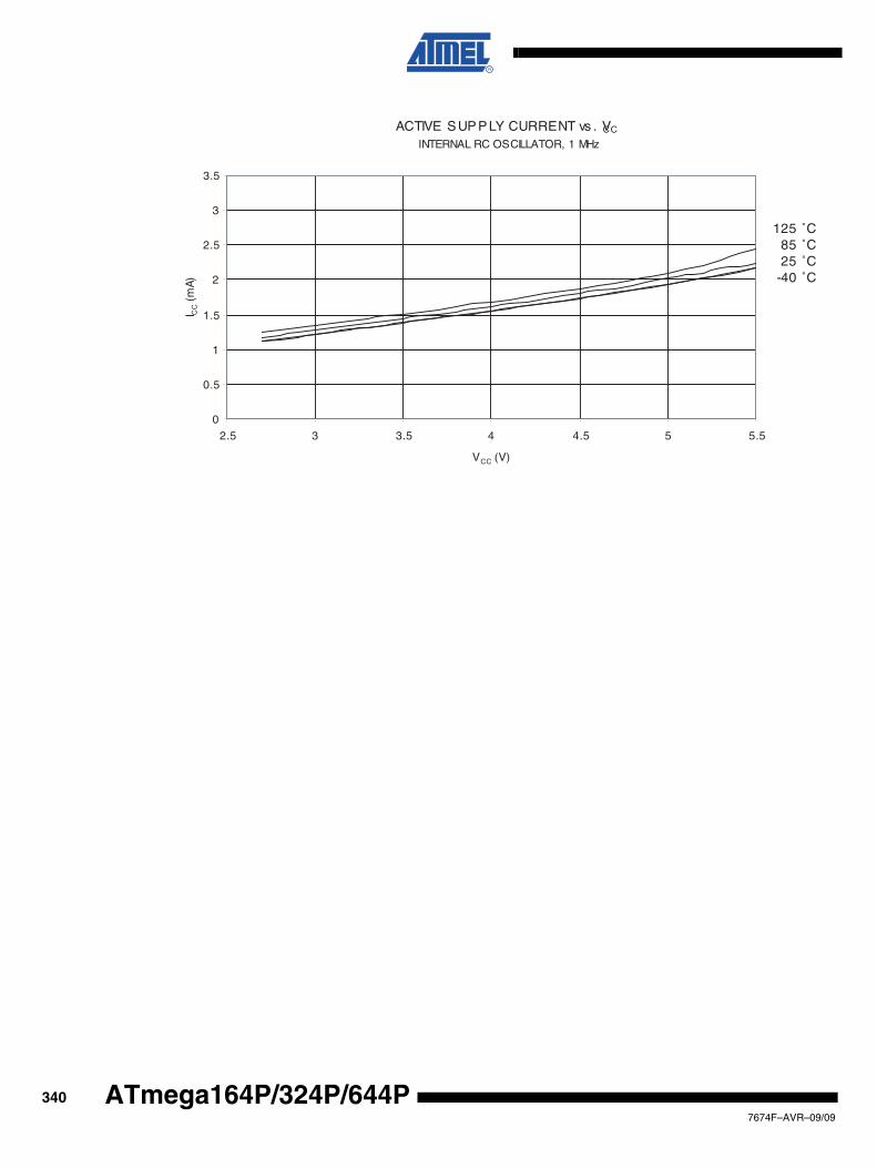
ACTIVE SUPPLY CURRENT vs . VCC
INTERNAL RC OSCILLATOR, 1 MHz
125 ˚C85 ˚C25 ˚C
-40 ˚C
0
0.5
1
1.5
2
2.5
3
3.5
2.5 3 3.5 4 4.5 5 5.5
VCC (V)
I CC (
mA)
3407674F–AVR–09/09
ATmega164P/324P/644P
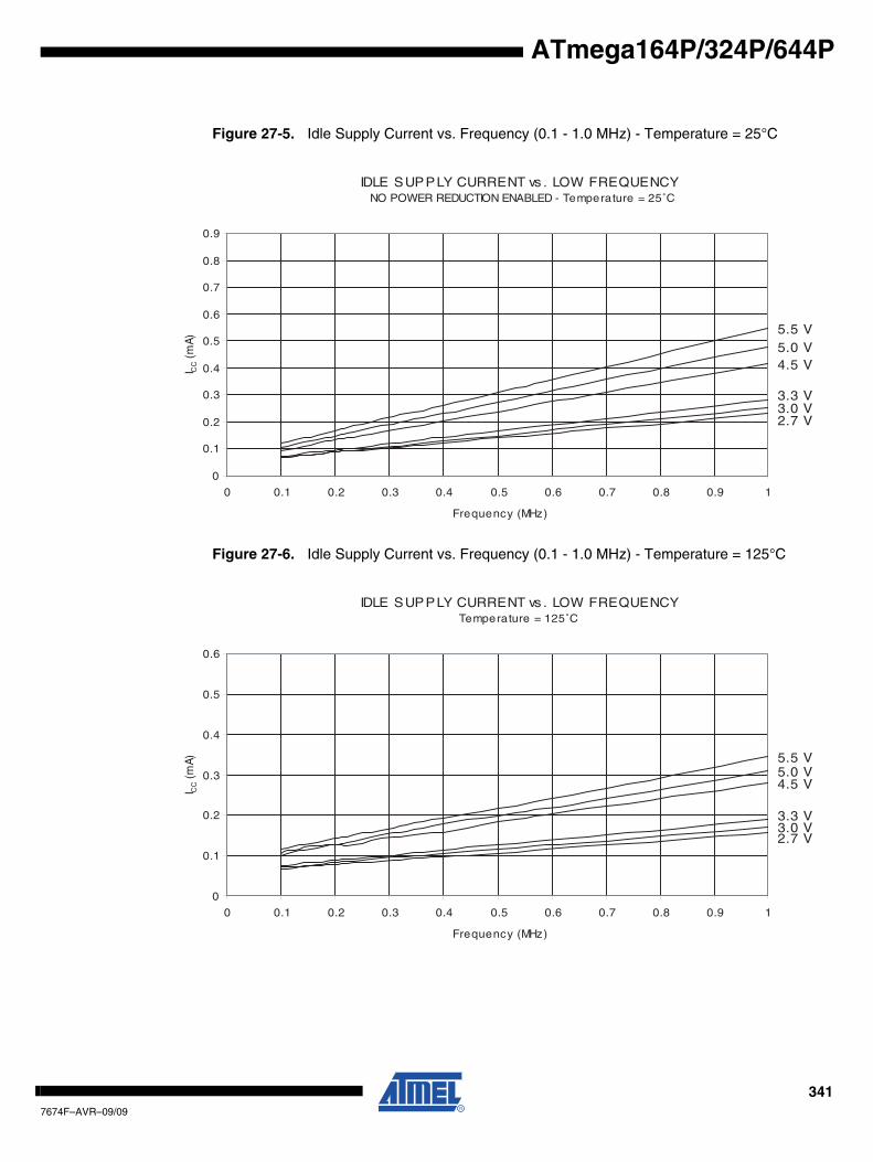
ATmega164P/324P/644P
Figure 27-5. Idle Supply Current vs. Frequency (0.1 - 1.0 MHz) - Temperature = 25°C
Figure 27-6. Idle Supply Current vs. Frequency (0.1 - 1.0 MHz) - Temperature = 125°C
IDLE SUPPLY CURRENT vs . LOW FREQUENCYNO POWER REDUCTION ENABLED - Temperature = 25˚C
5.5 V5.0 V4.5 V
3.3 V3.0 V2.7 V
0
0.1
0.2
0.3
0.4
0.5
0.6
0.7
0.8
0.9
0 0.1 0.2 0.3 0.4 0.5 0.6 0.7 0.8 0.9 1
Frequency (MHz)
I CC (
mA)
IDLE SUPPLY CURRENT vs . LOW FREQUENCYTemperature = 125˚C
5.5 V5.0 V4.5 V
3.3 V3.0 V2.7 V
0
0.1
0.2
0.3
0.4
0.5
0.6
0 0.1 0.2 0.3 0.4 0.5 0.6 0.7 0.8 0.9 1
Frequency (MHz)
I CC (
mA)
3417674F–AVR–09/09
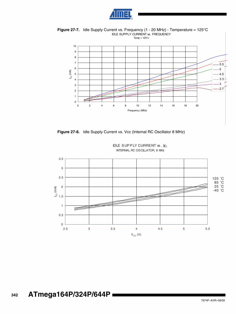
Figure 27-7. Idle Supply Current vs. Frequency (1 - 20 MHz) - Temperature = 125°C
Figure 27-8. Idle Supply Current vs. Vcc (Internal RC Oscillator 8 MHz)
IDLE SUPPLY CURRENT vs. FREQUENCYTemp = 125°c
0
1
2
3
4
5
6
7
8
9
10
0 2 4 6 8 10 12 14 16 18 20
Frequency (MHz)
I CC (
mA
)
5.554.53.332.7
IDLE SUPPLY CURRENT vs . VCC
INTERNAL RC OSCILLATOR, 8 MHz
125 ˚C85 ˚C25 ˚C
-40 ˚C
0
0.5
1
1.5
2
2.5
3
3.5
2.5 3 3.5 4 4.5 5 5.5
VCC (V)
I CC (
mA)
3427674F–AVR–09/09
ATmega164P/324P/644P
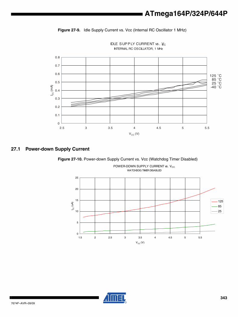
ATmega164P/324P/644P
Figure 27-9. Idle Supply Current vs. Vcc (Internal RC Oscillator 1 MHz)
27.1 Power-down Supply Current
Figure 27-10. Power-down Supply Current vs. Vcc (Watchdog Timer Disabled)
IDLE SUPPLY CURRENT vs . VCC
INTERNAL RC OSCILLATOR, 1 MHz
125 ˚C85 ˚C25 ˚C
-40 ˚C
0
0.1
0.2
0.3
0.4
0.5
0.6
0.7
0.8
2.5 3 3.5 4 4.5 5 5.5
VCC (V)
I CC (
mA)
POWER-DOWN SUPPLY CURRENT vs. VCC
WATCHDOG TIMER DISABLED
0
5
10
15
20
25
1.5 2 2.5 3 3.5 4 4.5 5 5.5
VCC (V)
I CC (
uA) 125
8525
3437674F–AVR–09/09
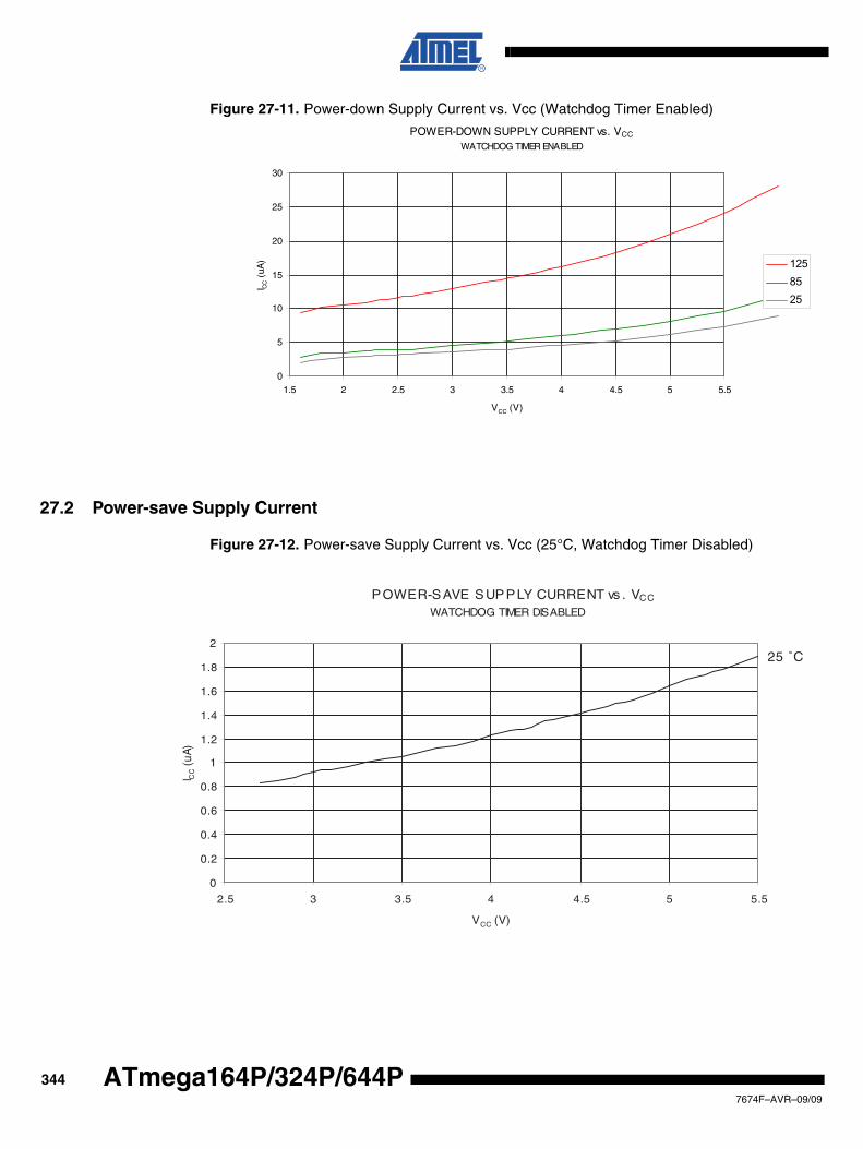
Figure 27-11. Power-down Supply Current vs. Vcc (Watchdog Timer Enabled)
27.2 Power-save Supply Current
Figure 27-12. Power-save Supply Current vs. Vcc (25°C, Watchdog Timer Disabled)
POWER-DOWN SUPPLY CURRENT vs. VCC
WATCHDOG TIMER ENABLED
0
5
10
15
20
25
30
1.5 2 2.5 3 3.5 4 4.5 5 5.5
VCC (V)
I CC (
uA) 125
8525
POWER-SAVE SUPPLY CURRENT vs . VCC
WATCHDOG TIMER DISABLED
25 ˚C
0
0.2
0.4
0.6
0.8
1
1.2
1.4
1.6
1.8
2
2.5 3 3.5 4 4.5 5 5.5
VCC (V)
I CC (
uA)
3447674F–AVR–09/09
ATmega164P/324P/644P
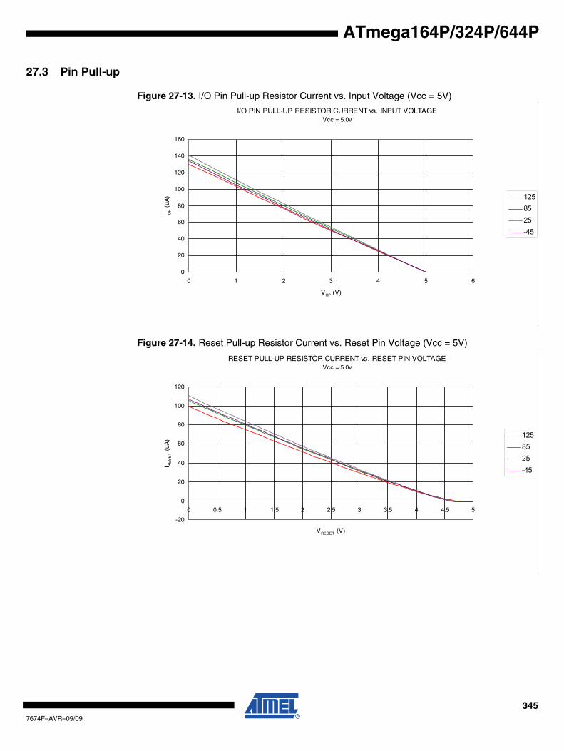
ATmega164P/324P/644P
27.3 Pin Pull-up
Figure 27-13. I/O Pin Pull-up Resistor Current vs. Input Voltage (Vcc = 5V)
Figure 27-14. Reset Pull-up Resistor Current vs. Reset Pin Voltage (Vcc = 5V)
I/O PIN PULL-UP RESISTOR CURRENT vs. INPUT VOLTAGEVcc = 5.0v
0
20
40
60
80
100
120
140
160
0 1 2 3 4 5 6
VOP (V)
I OP (
uA) 125
8525-45
RESET PULL-UP RESISTOR CURRENT vs. RESET PIN VOLTAGEVcc = 5.0v
-20
0
20
40
60
80
100
120
0 0.5 1 1.5 2 2.5 3 3.5 4 4.5 5
VRESET (V)
I RE
SE
T (
uA)
1258525-45
3457674F–AVR–09/09
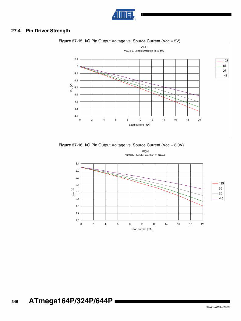
27.4 Pin Driver Strength
Figure 27-15. I/O Pin Output Voltage vs. Source Current (Vcc = 5V)
Figure 27-16. I/O Pin Output Voltage vs. Source Current (Vcc = 3.0V)
VOHVCC 5V, Load current up to 20 mA
4.3
4.4
4.5
4.6
4.7
4.8
4.9
5
5.1
0 2 4 6 8 10 12 14 16 18 20
Load current (mA)
VO
H (
V)
1258525-45
VOHVCC 3V, Load current up to 20 mA
1.5
1.7
1.9
2.1
2.3
2.5
2.7
2.9
3.1
0 2 4 6 8 10 12 14 16 18 20
Load current (mA)
VO
H (
V)
1258525-45
3467674F–AVR–09/09
ATmega164P/324P/644P
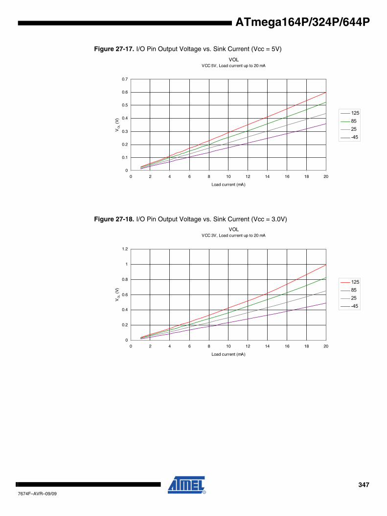
ATmega164P/324P/644P
Figure 27-17. I/O Pin Output Voltage vs. Sink Current (Vcc = 5V)
Figure 27-18. I/O Pin Output Voltage vs. Sink Current (Vcc = 3.0V)
VOLVCC 5V, Load current up to 20 mA
0
0.1
0.2
0.3
0.4
0.5
0.6
0.7
0 2 4 6 8 10 12 14 16 18 20
Load current (mA)
VO
L (
V)
1258525-45
VOLVCC 3V, Load current up to 20 mA
0
0.2
0.4
0.6
0.8
1
1.2
0 2 4 6 8 10 12 14 16 18 20
Load current (mA)
VO
L (
V)
1258525-45
3477674F–AVR–09/09
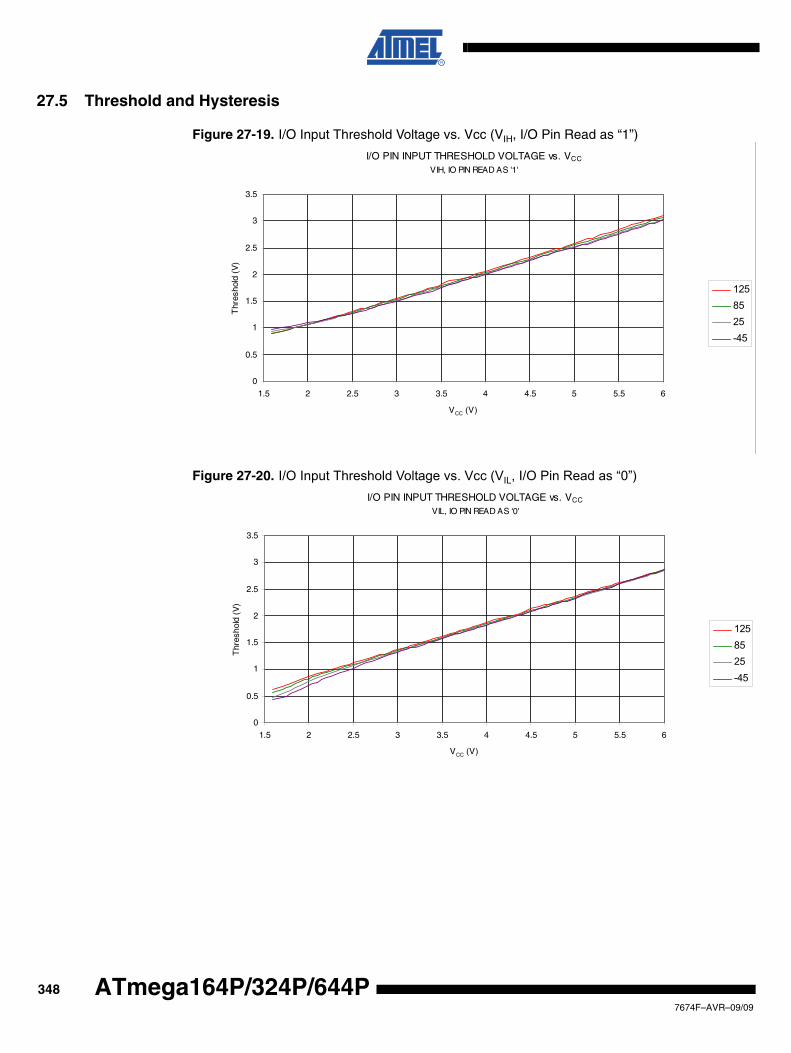
27.5 Threshold and Hysteresis
Figure 27-19. I/O Input Threshold Voltage vs. Vcc (VIH, I/O Pin Read as “1”)
Figure 27-20. I/O Input Threshold Voltage vs. Vcc (VIL, I/O Pin Read as “0”)
I/O PIN INPUT THRESHOLD VOLTAGE vs. VCC
VIH, IO PIN READ AS '1'
0
0.5
1
1.5
2
2.5
3
3.5
1.5 2 2.5 3 3.5 4 4.5 5 5.5 6
VCC (V)
Thr
esho
ld (
V)
1258525-45
I/O PIN INPUT THRESHOLD VOLTAGE vs. VCC
VIL, IO PIN READ AS '0'
0
0.5
1
1.5
2
2.5
3
3.5
1.5 2 2.5 3 3.5 4 4.5 5 5.5 6
VCC (V)
Thr
esho
ld (
V)
1258525-45
3487674F–AVR–09/09
ATmega164P/324P/644P
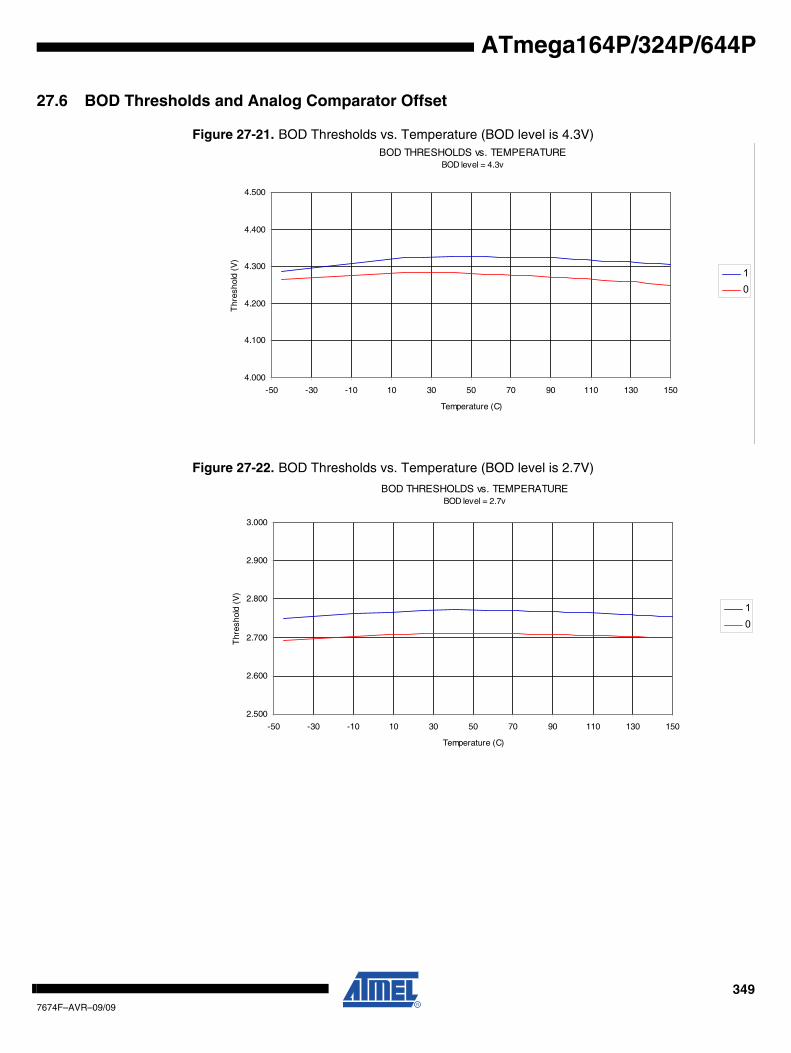
ATmega164P/324P/644P
27.6 BOD Thresholds and Analog Comparator Offset
Figure 27-21. BOD Thresholds vs. Temperature (BOD level is 4.3V)
Figure 27-22. BOD Thresholds vs. Temperature (BOD level is 2.7V)
BOD THRESHOLDS vs. TEMPERATUREBOD level = 4.3v
4.000
4.100
4.200
4.300
4.400
4.500
-50 -30 -10 10 30 50 70 90 110 130 150
Temperature (C)
Thr
esho
ld (
V)
10
BOD THRESHOLDS vs. TEMPERATUREBOD level = 2.7v
2.500
2.600
2.700
2.800
2.900
3.000
-50 -30 -10 10 30 50 70 90 110 130 150
Temperature (C)
Thr
esho
ld (
V)
10
3497674F–AVR–09/09
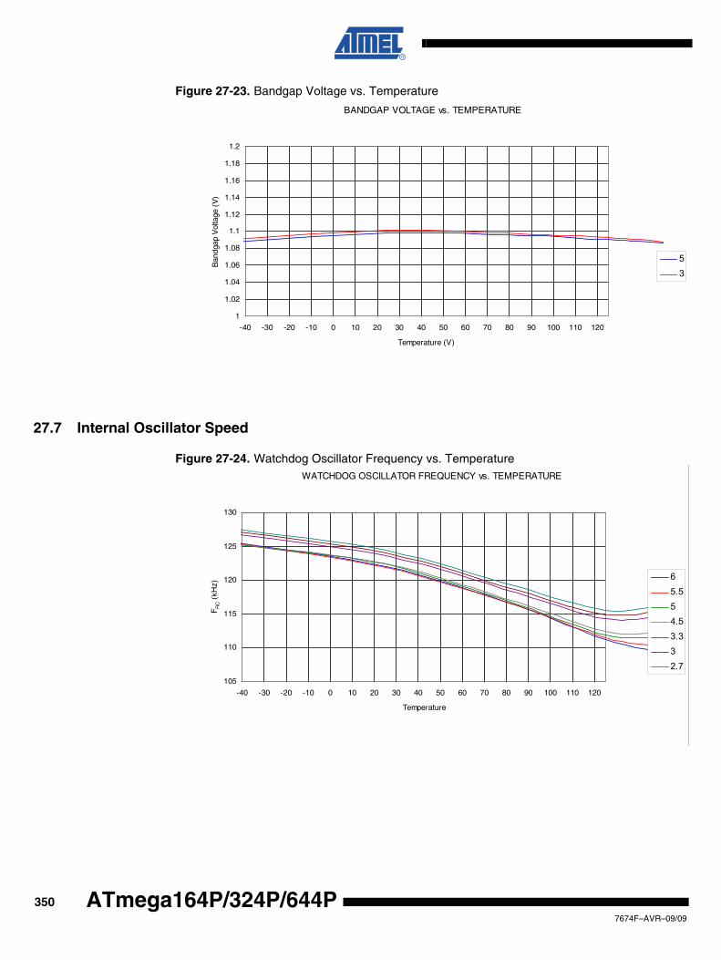
Figure 27-23. Bandgap Voltage vs. Temperature
27.7 Internal Oscillator Speed
Figure 27-24. Watchdog Oscillator Frequency vs. Temperature
BANDGAP VOLTAGE vs. TEMPERATURE
1
1.02
1.04
1.06
1.08
1.1
1.12
1.14
1.16
1.18
1.2
-40 -30 -20 -10 0 10 20 30 40 50 60 70 80 90 100 110 120
Temperature (V)
Ban
dgap
Vol
tage
(V
)
53
WATCHDOG OSCILLATOR FREQUENCY vs. TEMPERATURE
105
110
115
120
125
130
-40 -30 -20 -10 0 10 20 30 40 50 60 70 80 90 100 110 120
Temperature
F RC (
kHz)
65.554.53.332.7
3507674F–AVR–09/09
ATmega164P/324P/644P
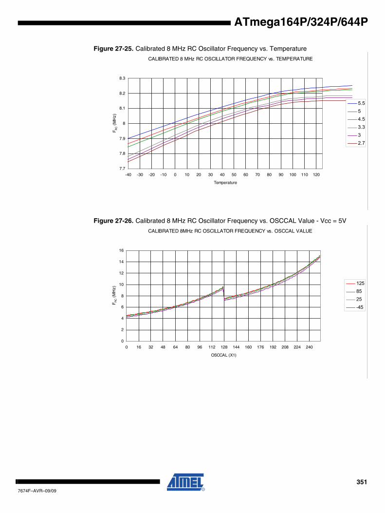
ATmega164P/324P/644P
Figure 27-25. Calibrated 8 MHz RC Oscillator Frequency vs. Temperature
Figure 27-26. Calibrated 8 MHz RC Oscillator Frequency vs. OSCCAL Value - Vcc = 5V
CALIBRATED 8 MHz RC OSCILLATOR FREQUENCY vs. TEMPERATURE
7.7
7.8
7.9
8
8.1
8.2
8.3
-40 -30 -20 -10 0 10 20 30 40 50 60 70 80 90 100 110 120
Temperature
F RC (
MH
z)
5.554.53.332.7
CALIBRATED 8MHz RC OSCILLATOR FREQUENCY vs. OSCCAL VALUE
0
2
4
6
8
10
12
14
16
0 16 32 48 64 80 96 112 128 144 160 176 192 208 224 240
OSCCAL (X1)
F RC (
MH
z)
1258525-45
3517674F–AVR–09/09
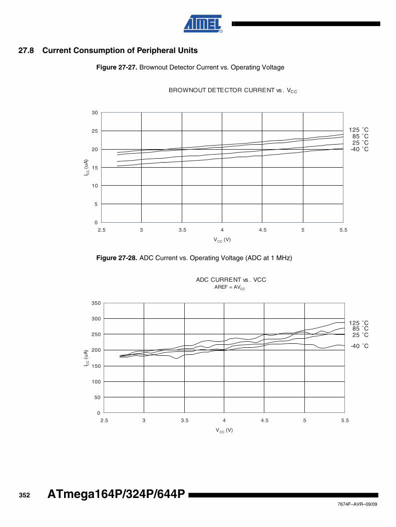
27.8 Current Consumption of Peripheral Units
Figure 27-27. Brownout Detector Current vs. Operating Voltage
Figure 27-28. ADC Current vs. Operating Voltage (ADC at 1 MHz)
BROWNOUT DETECTOR CURRENT vs . VCC
125 ˚C85 ˚C25 ˚C
-40 ˚C
0
5
10
15
20
25
30
2.5 3 3.5 4 4.5 5 5.5
VCC (V)
I CC (
uA)
ADC CURRENT vs . VCCAREF = AVCC
125 ˚C85 ˚C25 ˚C
-40 ˚C
0
50
100
150
200
250
300
350
2.5 3 3.5 4 4.5 5 5.5
VCC (V)
I CC (
uA)
3527674F–AVR–09/09
ATmega164P/324P/644P
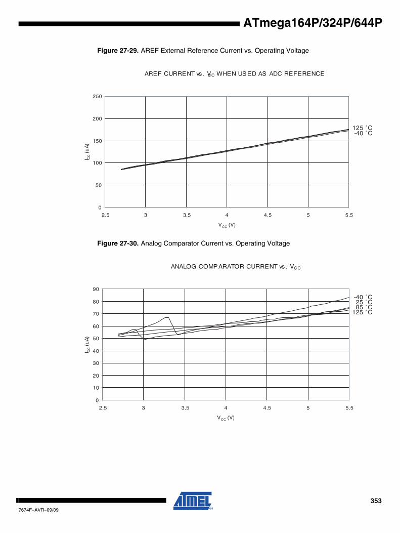
ATmega164P/324P/644P
Figure 27-29. AREF External Reference Current vs. Operating Voltage
Figure 27-30. Analog Comparator Current vs. Operating Voltage
AREF CURRENT vs . VCC WHEN USED AS ADC REFERENCE
125 ˚C-40 ˚C
0
50
100
150
200
250
2.5 3 3.5 4 4.5 5 5.5
VCC (V)
I CC (
uA)
ANALOG COMPARATOR CURRENT vs . VCC
125 ˚C85 ˚C25 ˚C
-40 ˚C
0
10
20
30
40
50
60
70
80
90
2.5 3 3.5 4 4.5 5 5.5
VCC (V)
I CC (
uA)
3537674F–AVR–09/09
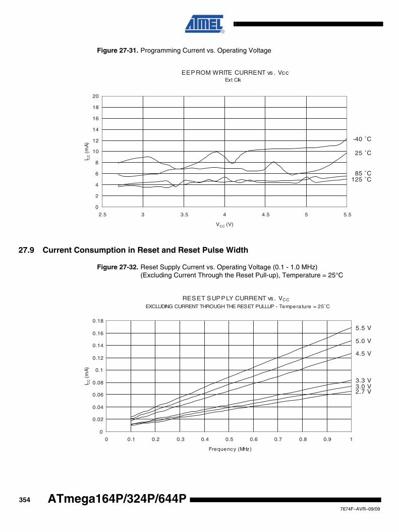
Figure 27-31. Programming Current vs. Operating Voltage
27.9 Current Consumption in Reset and Reset Pulse Width
Figure 27-32. Reset Supply Current vs. Operating Voltage (0.1 - 1.0 MHz)(Excluding Current Through the Reset Pull-up), Temperature = 25°C
EEPROM WRITE CURRENT vs . VccExt Clk
125 ˚C85 ˚C
25 ˚C
-40 ˚C
0
2
4
6
8
10
12
14
16
18
20
2.5 3 3.5 4 4.5 5 5.5
VCC (V)
I CC (
mA)
RESET SUPPLY CURRENT vs . VCC
EXCLUDING CURRENT THROUGH THE RESET PULLUP - Temperature = 25˚C
5.5 V
5.0 V
4.5 V
3.3 V3.0 V2.7 V
0
0.02
0.04
0.06
0.08
0.1
0.12
0.14
0.16
0.18
0 0.1 0.2 0.3 0.4 0.5 0.6 0.7 0.8 0.9 1
Frequency (MHz)
I CC (
mA)
3547674F–AVR–09/09
ATmega164P/324P/644P
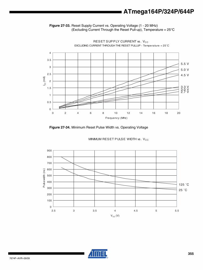
ATmega164P/324P/644P
Figure 27-33. Reset Supply Current vs. Operating Voltage (1 - 20 MHz)(Excluding Current Through the Reset Pull-up), Temperature = 25°C
Figure 27-34. Minimum Reset Pulse Width vs. Operating Voltage
RESET SUPPLY CURRENT vs . VCC
EXCLUDING CURRENT THROUGH THE RESET PULLUP - Temperature = 25˚C
5.5 V
5.0 V
4.5 V
3.3 V3.0 V2.7 V
0
0.5
1
1.5
2
2.5
3
3.5
4
0 2 4 6 8 10 12 14 16 18 20
Frequency (MHz)
I CC (
mA)
MINIMUM RESET PULSE WIDTH vs . VCC
125 ˚C
25 ˚C
0
100
200
300
400
500
600
700
800
900
2.5 3 3.5 4 4.5 5 5.5
VCC (V)
Pu
lse
wid
th (
ns
)
3557674F–AVR–09/09
28. Register Summary
Address Name Bit 7 Bit 6 Bit 5 Bit 4 Bit 3 Bit 2 Bit 1 Bit 0 Page
(0xFF) Reserved - - - - - - -
(0xFE) Reserved - - - - - - - -
(0xFD) Reserved - - - - - - - -
(0xFC) Reserved - - - - - - - -
(0xFB) Reserved - - - - - - -
(0xFA) Reserved - - - - - - - -
(0xF9) Reserved - - - - - - -
(0xF8) Reserved - - - - - - - -
(0xF7) Reserved - - - - - - - -
(0xF6) Reserved - - - - - - - -
(0xF5) Reserved - - - - - - -
(0xF4) Reserved - - - - - - - -
(0xF3) Reserved - - - - - - - -
(0xF2) Reserved - - - - - - - -
(0xF1) Reserved - - - - - - -
(0xF0) Reserved - - - - - - - -
(0xEF) Reserved - - - - - - -
(0xEE) Reserved - - - - - - - -
(0xED) Reserved - - - - - - - -
(0xEC) Reserved - - - - - - - -
(0xEB) Reserved - - - - - - -
(0xEA) Reserved - - - - - - - -
(0xE9) Reserved - - - - - - - -
(0xE8) Reserved - - - - - - - -
(0xE7) Reserved - - - - - - -
(0xE6) Reserved - - - - - - - -
(0xE5) Reserved - - - - - - - -
(0xE4) Reserved - - - - - - - -
(0xE3) Reserved - - - - - - -
(0xE2) Reserved - - - - - - - -
(0xE1) Reserved - - - - - - -
(0xE0) Reserved - - - - - - -
(0xDF) Reserved - - - - - - - -
(0xDE) Reserved - - - - - - - -
(0xDD) Reserved - - - - - - - -
(0xDC) Reserved - - - - - - -
(0xDB) Reserved - - - - - - - -
(0xDA) Reserved - - - - - - - -
(0xD9) Reserved - - - - - - - -
(0xD8) Reserved - - - - - - - -
(0xD7) Reserved - - - - - - - -
(0xD6) Reserved - - - - - - - -
(0xD5) Reserved - - - - - - - -
(0xD4) Reserved - - - - - - - -
(0xD3) Reserved - - - - - - - -
(0xD2) Reserved - - - - - - - -
(0xD1) Reserved - - - - - - - -
(0xD0) Reserved - - - - - - - -
(0xCF) Reserved - - - - - - - -
(0xCE) UDR1 USART1 I/O Data Register 190
(0xCD) UBRR1H - - - - USART1 Baud Rate Register High Byte 194/208
(0xCC) UBRR1L USART1 Baud Rate Register Low Byte 194/208
(0xCB) Reserved - - - - - - - -
(0xCA) UCSR1C UMSEL11 UMSEL10 UPM11 UPM10 USBS1 UCSZ11 UCSZ10 UCPOL1 192/208
(0xC9) UCSR1B RXCIE1 TXCIE1 UDRIE1 RXEN1 TXEN1 UCSZ12 RXB81 TXB81 191/207
(0xC8) UCSR1A RXC1 TXC1 UDRE1 FE1 DOR1 UPE1 U2X1 MPCM1 190/206
(0xC7) Reserved - - - - - - - -
(0xC6) UDR0 USART0 I/O Data Register 190
(0xC5) UBRR0H - - - - USART0 Baud Rate Register High Byte 194/208
(0xC4) UBRR0L USART0 Baud Rate Register Low Byte 194/208
(0xC3) Reserved - - - - - - - -
(0xC2) UCSR0C UMSEL01 UMSEL00 UPM01 UPM00 USBS0 UCSZ01 UCSZ00 UCPOL0 192/208
(0xC1) UCSR0B RXCIE0 TXCIE0 UDRIE0 RXEN0 TXEN0 UCSZ02 RXB80 TXB80 191/207
3567674F–AVR–09/09
ATmega164P/324P/644P
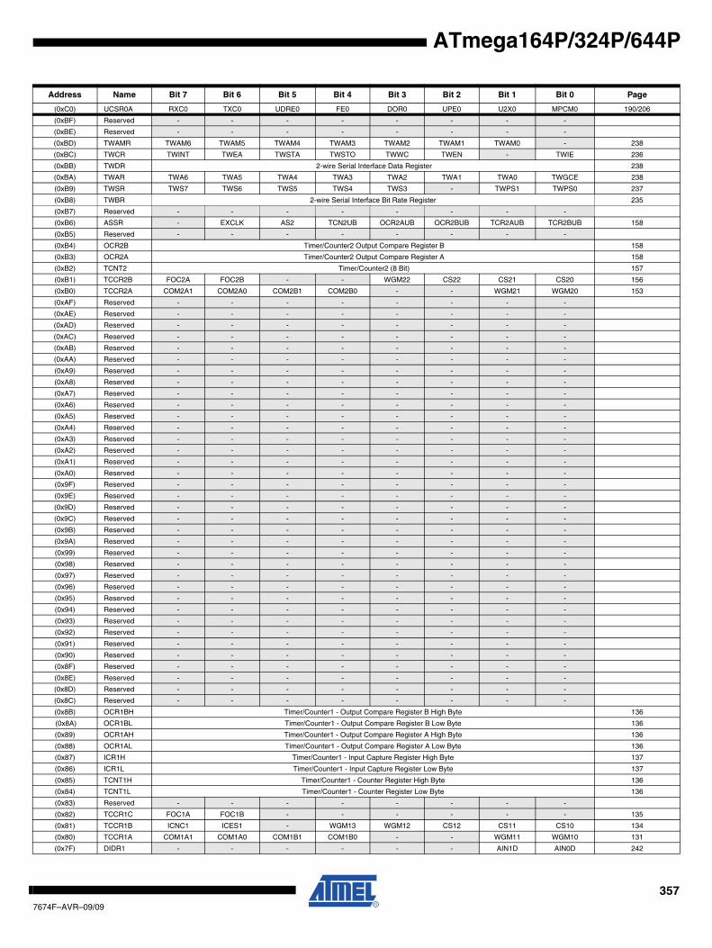
ATmega164P/324P/644P
(0xC0) UCSR0A RXC0 TXC0 UDRE0 FE0 DOR0 UPE0 U2X0 MPCM0 190/206
(0xBF) Reserved - - - - - - - -
(0xBE) Reserved - - - - - - - -
(0xBD) TWAMR TWAM6 TWAM5 TWAM4 TWAM3 TWAM2 TWAM1 TWAM0 - 238
(0xBC) TWCR TWINT TWEA TWSTA TWSTO TWWC TWEN - TWIE 236
(0xBB) TWDR 2-wire Serial Interface Data Register 238
(0xBA) TWAR TWA6 TWA5 TWA4 TWA3 TWA2 TWA1 TWA0 TWGCE 238
(0xB9) TWSR TWS7 TWS6 TWS5 TWS4 TWS3 - TWPS1 TWPS0 237
(0xB8) TWBR 2-wire Serial Interface Bit Rate Register 235
(0xB7) Reserved - - - - - - - -
(0xB6) ASSR - EXCLK AS2 TCN2UB OCR2AUB OCR2BUB TCR2AUB TCR2BUB 158
(0xB5) Reserved - - - - - - - -
(0xB4) OCR2B Timer/Counter2 Output Compare Register B 158
(0xB3) OCR2A Timer/Counter2 Output Compare Register A 158
(0xB2) TCNT2 Timer/Counter2 (8 Bit) 157
(0xB1) TCCR2B FOC2A FOC2B - - WGM22 CS22 CS21 CS20 156
(0xB0) TCCR2A COM2A1 COM2A0 COM2B1 COM2B0 - - WGM21 WGM20 153
(0xAF) Reserved - - - - - - - -
(0xAE) Reserved - - - - - - - -
(0xAD) Reserved - - - - - - - -
(0xAC) Reserved - - - - - - - -
(0xAB) Reserved - - - - - - - -
(0xAA) Reserved - - - - - - - -
(0xA9) Reserved - - - - - - - -
(0xA8) Reserved - - - - - - - -
(0xA7) Reserved - - - - - - - -
(0xA6) Reserved - - - - - - - -
(0xA5) Reserved - - - - - - - -
(0xA4) Reserved - - - - - - - -
(0xA3) Reserved - - - - - - - -
(0xA2) Reserved - - - - - - - -
(0xA1) Reserved - - - - - - - -
(0xA0) Reserved - - - - - - - -
(0x9F) Reserved - - - - - - - -
(0x9E) Reserved - - - - - - - -
(0x9D) Reserved - - - - - - - -
(0x9C) Reserved - - - - - - - -
(0x9B) Reserved - - - - - - - -
(0x9A) Reserved - - - - - - - -
(0x99) Reserved - - - - - - - -
(0x98) Reserved - - - - - - - -
(0x97) Reserved - - - - - - - -
(0x96) Reserved - - - - - - - -
(0x95) Reserved - - - - - - - -
(0x94) Reserved - - - - - - - -
(0x93) Reserved - - - - - - - -
(0x92) Reserved - - - - - - - -
(0x91) Reserved - - - - - - - -
(0x90) Reserved - - - - - - - -
(0x8F) Reserved - - - - - - - -
(0x8E) Reserved - - - - - - - -
(0x8D) Reserved - - - - - - - -
(0x8C) Reserved - - - - - - - -
(0x8B) OCR1BH Timer/Counter1 - Output Compare Register B High Byte 136
(0x8A) OCR1BL Timer/Counter1 - Output Compare Register B Low Byte 136
(0x89) OCR1AH Timer/Counter1 - Output Compare Register A High Byte 136
(0x88) OCR1AL Timer/Counter1 - Output Compare Register A Low Byte 136
(0x87) ICR1H Timer/Counter1 - Input Capture Register High Byte 137
(0x86) ICR1L Timer/Counter1 - Input Capture Register Low Byte 137
(0x85) TCNT1H Timer/Counter1 - Counter Register High Byte 136
(0x84) TCNT1L Timer/Counter1 - Counter Register Low Byte 136
(0x83) Reserved - - - - - - - -
(0x82) TCCR1C FOC1A FOC1B - - - - - - 135
(0x81) TCCR1B ICNC1 ICES1 - WGM13 WGM12 CS12 CS11 CS10 134
(0x80) TCCR1A COM1A1 COM1A0 COM1B1 COM1B0 - - WGM11 WGM10 131
(0x7F) DIDR1 - - - - - - AIN1D AIN0D 242
Address Name Bit 7 Bit 6 Bit 5 Bit 4 Bit 3 Bit 2 Bit 1 Bit 0 Page
3577674F–AVR–09/09
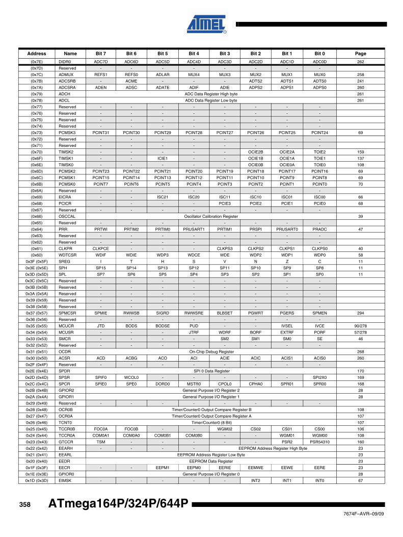
(0x7E) DIDR0 ADC7D ADC6D ADC5D ADC4D ADC3D ADC2D ADC1D ADC0D 262
(0x7D) Reserved - - - - - - - -
(0x7C) ADMUX REFS1 REFS0 ADLAR MUX4 MUX3 MUX2 MUX1 MUX0 258
(0x7B) ADCSRB - ACME - - - ADTS2 ADTS1 ADTS0 241
(0x7A) ADCSRA ADEN ADSC ADATE ADIF ADIE ADPS2 ADPS1 ADPS0 260
(0x79) ADCH ADC Data Register High byte 261
(0x78) ADCL ADC Data Register Low byte 261
(0x77) Reserved - - - - - - - -
(0x76) Reserved - - - - - - - -
(0x75) Reserved - - - - - - - -
(0x74) Reserved - - - - - - - -
(0x73) PCMSK3 PCINT31 PCINT30 PCINT29 PCINT28 PCINT27 PCINT26 PCINT25 PCINT24 69
(0x72) Reserved - - - - - - - -
(0x71) Reserved - - - - - - - -
(0x70) TIMSK2 - - - - - OCIE2B OCIE2A TOIE2 159
(0x6F) TIMSK1 - - ICIE1 - - OCIE1B OCIE1A TOIE1 137
(0x6E) TIMSK0 - - - - - OCIE0B OCIE0A TOIE0 108
(0x6D) PCMSK2 PCINT23 PCINT22 PCINT21 PCINT20 PCINT19 PCINT18 PCINT17 PCINT16 69
(0x6C) PCMSK1 PCINT15 PCINT14 PCINT13 PCINT12 PCINT11 PCINT10 PCINT9 PCINT8 69
(0x6B) PCMSK0 PCINT7 PCINT6 PCINT5 PCINT4 PCINT3 PCINT2 PCINT1 PCINT0 70
(0x6A) Reserved - - - - - - - -
(0x69) EICRA - - ISC21 ISC20 ISC11 ISC10 ISC01 ISC00 66
(0x68) PCICR - - - - PCIE3 PCIE2 PCIE1 PCIE0 68
(0x67) Reserved - - - - - - - -
(0x66) OSCCAL Oscillator Calibration Register 39
(0x65) Reserved - - - - - - - -
(0x64) PRR PRTWI PRTIM2 PRTIM0 PRUSART1 PRTIM1 PRSPI PRUSART0 PRADC 47
(0x63) Reserved - - - - - - - -
(0x62) Reserved - - - - - - - -
(0x61) CLKPR CLKPCE - - - CLKPS3 CLKPS2 CLKPS1 CLKPS0 40
(0x60) WDTCSR WDIF WDIE WDP3 WDCE WDE WDP2 WDP1 WDP0 58
0x3F (0x5F) SREG I T H S V N Z C 11
0x3E (0x5E) SPH SP15 SP14 SP13 SP12 SP11 SP10 SP9 SP8 11
0x3D (0x5D) SPL SP7 SP6 SP5 SP4 SP3 SP2 SP1 SP0 11
0x3C (0x5C) Reserved - - - - - - - -
0x3B (0x5B) Reserved - - - - - - - -
0x3A (0x5A) Reserved - - - - - - - -
0x39 (0x59) Reserved - - - - - - - -
0x38 (0x58) Reserved - - - - - - - -
0x37 (0x57) SPMCSR SPMIE RWWSB SIGRD RWWSRE BLBSET PGWRT PGERS SPMEN 294
0x36 (0x56) Reserved - - - - - - - -
0x35 (0x55) MCUCR JTD BODS BODSE PUD - - IVSEL IVCE 90/278
0x34 (0x54) MCUSR - - - JTRF WDRF BORF EXTRF PORF 57/278
0x33 (0x53) SMCR - - - - SM2 SM1 SM0 SE 46
0x32 (0x52) Reserved - - - - - - - -
0x31 (0x51) OCDR On-Chip Debug Register 268
0x30 (0x50) ACSR ACD ACBG ACO ACI ACIE ACIC ACIS1 ACIS0 260
0x2F (0x4F) Reserved - - - - - - - -
0x2E (0x4E) SPDR SPI 0 Data Register 170
0x2D (0x4D) SPSR SPIF0 WCOL0 - - - - - SPI2X0 169
0x2C (0x4C) SPCR SPIE0 SPE0 DORD0 MSTR0 CPOL0 CPHA0 SPR01 SPR00 168
0x2B (0x4B) GPIOR2 General Purpose I/O Register 2 28
0x2A (0x4A) GPIOR1 General Purpose I/O Register 1 28
0x29 (0x49) Reserved - - - - - - - -
0x28 (0x48) OCR0B Timer/Counter0 Output Compare Register B 108
0x27 (0x47) OCR0A Timer/Counter0 Output Compare Register A 107
0x26 (0x46) TCNT0 Timer/Counter0 (8 Bit) 107
0x25 (0x45) TCCR0B FOC0A FOC0B - - WGM02 CS02 CS01 CS00 106
0x24 (0x44) TCCR0A COM0A1 COM0A0 COM0B1 COM0B0 - - WGM01 WGM00 108
0x23 (0x43) GTCCR TSM - - - - - PSR2 PSR54310 160
0x22 (0x42) EEARH - - - - EEPROM Address Register High Byte 23
0x21 (0x41) EEARL EEPROM Address Register Low Byte 23
0x20 (0x40) EEDR EEPROM Data Register 23
0x1F (0x3F) EECR - - EEPM1 EEPM0 EERIE EEMWE EEWE EERE 23
0x1E (0x3E) GPIOR0 General Purpose I/O Register 0 28
0x1D (0x3D) EIMSK - - - - - INT2 INT1 INT0 67
Address Name Bit 7 Bit 6 Bit 5 Bit 4 Bit 3 Bit 2 Bit 1 Bit 0 Page
3587674F–AVR–09/09
ATmega164P/324P/644P
ATmega164P/324P/644P
Notes: 1. For compatibility with future devices, reserved bits should be written to zero if accessed. Reserved I/O memory addresses should never be written.
2. I/O registers within the address range $00 - $1F are directly bit-accessible using the SBI and CBI instructions. In these reg-isters, the value of single bits can be checked by using the SBIS and SBIC instructions.
3. Some of the status flags are cleared by writing a logical one to them. Note that the CBI and SBI instructions will operate on all bits in the I/O register, writing a one back into any flag read as set, thus clearing the flag. The CBI and SBI instructions work with registers 0x00 to 0x1F only.
4. When using the I/O specific commands IN and OUT, the I/O addresses $00 - $3F must be used. When addressing I/O regis-ters as data space using LD and ST instructions, $20 must be added to these addresses. The ATmega164P/324P/644P is a complex microcontroller with more peripheral units than can be supported within the 64 location reserved in Opcode for the IN and OUT instructions. For the Extended I/O space from $60 - $FF, only the ST/STS/STD and LD/LDS/LDD instructions can be used.
0x1C (0x3C) EIFR - - - - - INTF2 INTF1 INTF0 67
0x1B (0x3B) PCIFR - - - - PCIF3 PCIF2 PCIF1 PCIF0 68
0x1A (0x3A) Reserved - - - - - - - -
0x19 (0x39) Reserved - - - - - - - -
0x18 (0x38) Reserved - - - - - - - -
0x17 (0x37) TIFR2 - - - - - OCF2b OCF2A TOV2 160
0x16 (0x36) TIFR1 - - ICF1 - - OCF1B OCF1A TOV1 138
0x15 (0x35) TIFR0 - - - - - OCF0B OCF0A TOV0 108
0x14 (0x34) Reserved - - - - - - - -
0x13 (0x33) Reserved - - - - - - - -
0x12 (0x32) Reserved - - - - - - - -
0x11 (0x31) Reserved - - - - - - - -
0x10 (0x30) Reserved - - - - - - - -
0x0F (0x2F) Reserved - - - - - - - -
0x0E (0x2E) Reserved - - - - - - - -
0x0D (0x2D) Reserved - - - - - - - -
0x0C (0x2C) Reserved - - - - - - - -
0x0B (0x2B) PORTD PORTD7 PORTD6 PORTD5 PORTD4 PORTD3 PORTD2 PORTD1 PORTD0 91
0x0A (0x2A) DDRD DDD7 DDD6 DDD5 DDD4 DDD3 DDD2 DDD1 DDD0 91
0x09 (0x29) PIND PIND7 PIND6 PIND5 PIND4 PIND3 PIND2 PIND1 PIND0 91
0x08 (0x28) PORTC PORTC7 PORTC6 PORTC5 PORTC4 PORTC3 PORTC2 PORTC1 PORTC0 91
0x07 (0x27) DDRC DDC7 DDC6 DDC5 DDC4 DDC3 DDC2 DDC1 DDC0 91
0x06 (0x26) PINC PINC7 PINC6 PINC5 PINC4 PINC3 PINC2 PINC1 PINC0 91
0x05 (0x25) PORTB PORTB7 PORTB6 PORTB5 PORTB4 PORTB3 PORTB2 PORTB1 PORTB0 90
0x04 (0x24) DDRB DDB7 DDB6 DDB5 DDB4 DDB3 DDB2 DDB1 DDB0 90
0x03 (0x23) PINB PINB7 PINB6 PINB5 PINB4 PINB3 PINB2 PINB1 PINB0 90
0x02 (0x22) PORTA PORTA7 PORTA6 PORTA5 PORTA4 PORTA3 PORTA2 PORTA1 PORTA0 90
0x01 (0x21) DDRA DDA7 DDA6 DDA5 DDA4 DDA3 DDA2 DDA1 DDA0 90
0x00 (0x20) PINA PINA7 PINA6 PINA5 PINA4 PINA3 PINA2 PINA1 PINA0 90
Address Name Bit 7 Bit 6 Bit 5 Bit 4 Bit 3 Bit 2 Bit 1 Bit 0 Page
3597674F–AVR–09/09
29. Instruction Set Summary
Mnemonics Operands Description Operation Flags #Clocks
ARITHMETIC AND LOGIC INSTRUCTIONS
ADD Rd, Rr Add two Registers Rd ← Rd + Rr Z,C,N,V,H 1
ADC Rd, Rr Add with Carry two Registers Rd ← Rd + Rr + C Z,C,N,V,H 1
ADIW Rdl,K Add Immediate to Word Rdh:Rdl ← Rdh:Rdl + K Z,C,N,V,S 2
SUB Rd, Rr Subtract two Registers Rd ← Rd - Rr Z,C,N,V,H 1
SUBI Rd, K Subtract Constant from Register Rd ← Rd - K Z,C,N,V,H 1
SBC Rd, Rr Subtract with Carry two Registers Rd ← Rd - Rr - C Z,C,N,V,H 1
SBCI Rd, K Subtract with Carry Constant from Reg. Rd ← Rd - K - C Z,C,N,V,H 1
SBIW Rdl,K Subtract Immediate from Word Rdh:Rdl ← Rdh:Rdl - K Z,C,N,V,S 2
AND Rd, Rr Logical AND Registers Rd ← Rd • Rr Z,N,V 1
ANDI Rd, K Logical AND Register and Constant Rd ← Rd • K Z,N,V 1
OR Rd, Rr Logical OR Registers Rd ← Rd v Rr Z,N,V 1
ORI Rd, K Logical OR Register and Constant Rd ← Rd v K Z,N,V 1
EOR Rd, Rr Exclusive OR Registers Rd ← Rd ⊕ Rr Z,N,V 1
COM Rd One’s Complement Rd ← 0xFF − Rd Z,C,N,V 1
NEG Rd Two’s Complement Rd ← 0x00 − Rd Z,C,N,V,H 1
SBR Rd,K Set Bit(s) in Register Rd ← Rd v K Z,N,V 1
CBR Rd,K Clear Bit(s) in Register Rd ← Rd • (0xFF - K) Z,N,V 1
INC Rd Increment Rd ← Rd + 1 Z,N,V 1
DEC Rd Decrement Rd ← Rd − 1 Z,N,V 1
TST Rd Test for Zero or Minus Rd ← Rd • Rd Z,N,V 1
CLR Rd Clear Register Rd ← Rd ⊕ Rd Z,N,V 1
SER Rd Set Register Rd ← 0xFF None 1
MUL Rd, Rr Multiply Unsigned R1:R0 ← Rd x Rr Z,C 2
MULS Rd, Rr Multiply Signed R1:R0 ← Rd x Rr Z,C 2
MULSU Rd, Rr Multiply Signed with Unsigned R1:R0 ← Rd x Rr Z,C 2
FMUL Rd, Rr Fractional Multiply Unsigned R1:R0 ← (Rd x Rr) << 1 Z,C 2
FMULS Rd, Rr Fractional Multiply Signed R1:R0 ← (Rd x Rr) << 1 Z,C 2
FMULSU Rd, Rr Fractional Multiply Signed with Unsigned R1:R0 ← (Rd x Rr) << 1 Z,C 2
BRANCH INSTRUCTIONS
RJMP k Relative Jump PC ← PC + k + 1 None 2
IJMP Indirect Jump to (Z) PC ← Z None 2
JMP k Direct Jump PC ← k None 3
RCALL k Relative Subroutine Call PC ← PC + k + 1 None 4
ICALL Indirect Call to (Z) PC ← Z None 4
CALL k Direct Subroutine Call PC ← k None 5
RET Subroutine Return PC ← STACK None 5
RETI Interrupt Return PC ← STACK I 5
CPSE Rd,Rr Compare, Skip if Equal if (Rd = Rr) PC ← PC + 2 or 3 None 1/2/3
CP Rd,Rr Compare Rd − Rr Z, N,V,C,H 1
CPC Rd,Rr Compare with Carry Rd − Rr − C Z, N,V,C,H 1
CPI Rd,K Compare Register with Immediate Rd − K Z, N,V,C,H 1
SBRC Rr, b Skip if Bit in Register Cleared if (Rr(b)=0) PC ← PC + 2 or 3 None 1/2/3
SBRS Rr, b Skip if Bit in Register is Set if (Rr(b)=1) PC ← PC + 2 or 3 None 1/2/3
SBIC P, b Skip if Bit in I/O Register Cleared if (P(b)=0) PC ← PC + 2 or 3 None 1/2/3
SBIS P, b Skip if Bit in I/O Register is Set if (P(b)=1) PC ← PC + 2 or 3 None 1/2/3
BRBS s, k Branch if Status Flag Set if (SREG(s) = 1) then PC←PC+k + 1 None 1/2
BRBC s, k Branch if Status Flag Cleared if (SREG(s) = 0) then PC←PC+k + 1 None 1/2
BREQ k Branch if Equal if (Z = 1) then PC ← PC + k + 1 None 1/2
BRNE k Branch if Not Equal if (Z = 0) then PC ← PC + k + 1 None 1/2
BRCS k Branch if Carry Set if (C = 1) then PC ← PC + k + 1 None 1/2
BRCC k Branch if Carry Cleared if (C = 0) then PC ← PC + k + 1 None 1/2
BRSH k Branch if Same or Higher if (C = 0) then PC ← PC + k + 1 None 1/2
BRLO k Branch if Lower if (C = 1) then PC ← PC + k + 1 None 1/2
BRMI k Branch if Minus if (N = 1) then PC ← PC + k + 1 None 1/2
BRPL k Branch if Plus if (N = 0) then PC ← PC + k + 1 None 1/2
BRGE k Branch if Greater or Equal, Signed if (N ⊕ V= 0) then PC ← PC + k + 1 None 1/2
BRLT k Branch if Less Than Zero, Signed if (N ⊕ V= 1) then PC ← PC + k + 1 None 1/2
BRHS k Branch if Half Carry Flag Set if (H = 1) then PC ← PC + k + 1 None 1/2
BRHC k Branch if Half Carry Flag Cleared if (H = 0) then PC ← PC + k + 1 None 1/2
BRTS k Branch if T Flag Set if (T = 1) then PC ← PC + k + 1 None 1/2
BRTC k Branch if T Flag Cleared if (T = 0) then PC ← PC + k + 1 None 1/2
BRVS k Branch if Overflow Flag is Set if (V = 1) then PC ← PC + k + 1 None 1/2
3607674F–AVR–09/09
ATmega164P/324P/644P
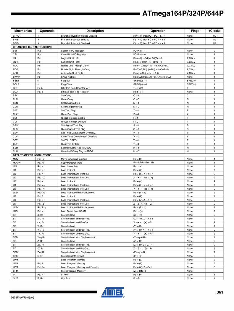
ATmega164P/324P/644P
BRVC k Branch if Overflow Flag is Cleared if (V = 0) then PC ← PC + k + 1 None 1/2
BRIE k Branch if Interrupt Enabled if ( I = 1) then PC ← PC + k + 1 None 1/2
BRID k Branch if Interrupt Disabled if ( I = 0) then PC ← PC + k + 1 None 1/2
BIT AND BIT-TEST INSTRUCTIONS
SBI P,b Set Bit in I/O Register I/O(P,b) ← 1 None 2
CBI P,b Clear Bit in I/O Register I/O(P,b) ← 0 None 2
LSL Rd Logical Shift Left Rd(n+1) ← Rd(n), Rd(0) ← 0 Z,C,N,V 1
LSR Rd Logical Shift Right Rd(n) ← Rd(n+1), Rd(7) ← 0 Z,C,N,V 1
ROL Rd Rotate Left Through Carry Rd(0)←C,Rd(n+1)← Rd(n),C←Rd(7) Z,C,N,V 1
ROR Rd Rotate Right Through Carry Rd(7)←C,Rd(n)← Rd(n+1),C←Rd(0) Z,C,N,V 1
ASR Rd Arithmetic Shift Right Rd(n) ← Rd(n+1), n=0..6 Z,C,N,V 1
SWAP Rd Swap Nibbles Rd(3..0)←Rd(7..4),Rd(7..4)←Rd(3..0) None 1
BSET s Flag Set SREG(s) ← 1 SREG(s) 1
BCLR s Flag Clear SREG(s) ← 0 SREG(s) 1
BST Rr, b Bit Store from Register to T T ← Rr(b) T 1
BLD Rd, b Bit load from T to Register Rd(b) ← T None 1
SEC Set Carry C ← 1 C 1
CLC Clear Carry C ← 0 C 1
SEN Set Negative Flag N ← 1 N 1
CLN Clear Negative Flag N ← 0 N 1
SEZ Set Zero Flag Z ← 1 Z 1
CLZ Clear Zero Flag Z ← 0 Z 1
SEI Global Interrupt Enable I ← 1 I 1
CLI Global Interrupt Disable I ← 0 I 1
SES Set Signed Test Flag S ← 1 S 1
CLS Clear Signed Test Flag S ← 0 S 1
SEV Set Twos Complement Overflow. V ← 1 V 1
CLV Clear Twos Complement Overflow V ← 0 V 1
SET Set T in SREG T ← 1 T 1
CLT Clear T in SREG T ← 0 T 1
SEH Set Half Carry Flag in SREG H ← 1 H 1
CLH Clear Half Carry Flag in SREG H ← 0 H 1
DATA TRANSFER INSTRUCTIONS
MOV Rd, Rr Move Between Registers Rd ← Rr None 1
MOVW Rd, Rr Copy Register Word Rd+1:Rd ← Rr+1:Rr None 1
LDI Rd, K Load Immediate Rd ← K None 1
LD Rd, X Load Indirect Rd ← (X) None 2
LD Rd, X+ Load Indirect and Post-Inc. Rd ← (X), X ← X + 1 None 2
LD Rd, - X Load Indirect and Pre-Dec. X ← X - 1, Rd ← (X) None 2
LD Rd, Y Load Indirect Rd ← (Y) None 2
LD Rd, Y+ Load Indirect and Post-Inc. Rd ← (Y), Y ← Y + 1 None 2
LD Rd, - Y Load Indirect and Pre-Dec. Y ← Y - 1, Rd ← (Y) None 2
LDD Rd,Y+q Load Indirect with Displacement Rd ← (Y + q) None 2
LD Rd, Z Load Indirect Rd ← (Z) None 2
LD Rd, Z+ Load Indirect and Post-Inc. Rd ← (Z), Z ← Z+1 None 2
LD Rd, -Z Load Indirect and Pre-Dec. Z ← Z - 1, Rd ← (Z) None 2
LDD Rd, Z+q Load Indirect with Displacement Rd ← (Z + q) None 2
LDS Rd, k Load Direct from SRAM Rd ← (k) None 2
ST X, Rr Store Indirect (X) ← Rr None 2
ST X+, Rr Store Indirect and Post-Inc. (X) ← Rr, X ← X + 1 None 2
ST - X, Rr Store Indirect and Pre-Dec. X ← X - 1, (X) ← Rr None 2
ST Y, Rr Store Indirect (Y) ← Rr None 2
ST Y+, Rr Store Indirect and Post-Inc. (Y) ← Rr, Y ← Y + 1 None 2
ST - Y, Rr Store Indirect and Pre-Dec. Y ← Y - 1, (Y) ← Rr None 2
STD Y+q,Rr Store Indirect with Displacement (Y + q) ← Rr None 2
ST Z, Rr Store Indirect (Z) ← Rr None 2
ST Z+, Rr Store Indirect and Post-Inc. (Z) ← Rr, Z ← Z + 1 None 2
ST -Z, Rr Store Indirect and Pre-Dec. Z ← Z - 1, (Z) ← Rr None 2
STD Z+q,Rr Store Indirect with Displacement (Z + q) ← Rr None 2
STS k, Rr Store Direct to SRAM (k) ← Rr None 2
LPM Load Program Memory R0 ← (Z) None 3
LPM Rd, Z Load Program Memory Rd ← (Z) None 3
LPM Rd, Z+ Load Program Memory and Post-Inc Rd ← (Z), Z ← Z+1 None 3
SPM Store Program Memory (Z) ← R1:R0 None -
IN Rd, P In Port Rd ← P None 1
OUT P, Rr Out Port P ← Rr None 1
Mnemonics Operands Description Operation Flags #Clocks
3617674F–AVR–09/09

PUSH Rr Push Register on Stack STACK ← Rr None 2
POP Rd Pop Register from Stack Rd ← STACK None 2
MCU CONTROL INSTRUCTIONS
NOP No Operation None 1
SLEEP Sleep (see specific descr. for Sleep function) None 1
WDR Watchdog Reset (see specific descr. for WDR/timer) None 1
BREAK Break For On-chip Debug Only None N/A
Mnemonics Operands Description Operation Flags #Clocks
3627674F–AVR–09/09
ATmega164P/324P/644P
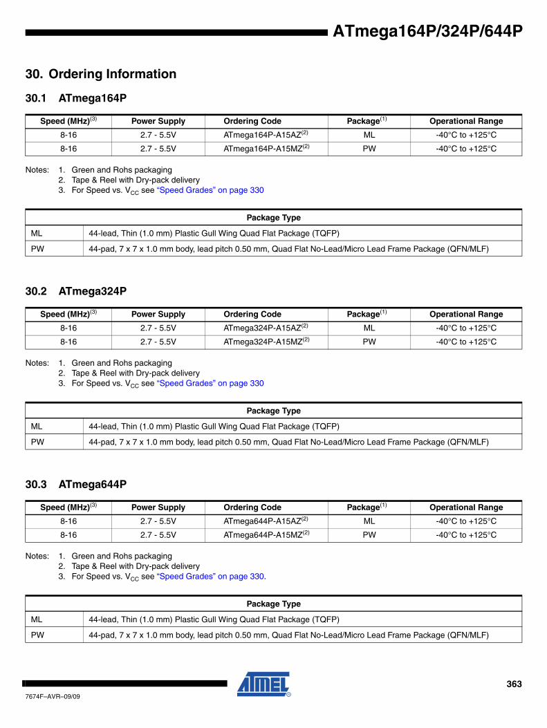
ATmega164P/324P/644P
30. Ordering Information
30.1 ATmega164P
Notes: 1. Green and Rohs packaging2. Tape & Reel with Dry-pack delivery3. For Speed vs. VCC see “Speed Grades” on page 330
30.2 ATmega324P
Notes: 1. Green and Rohs packaging2. Tape & Reel with Dry-pack delivery3. For Speed vs. VCC see “Speed Grades” on page 330
30.3 ATmega644P
Notes: 1. Green and Rohs packaging2. Tape & Reel with Dry-pack delivery3. For Speed vs. VCC see “Speed Grades” on page 330.
Speed (MHz)(3) Power Supply Ordering Code Package(1) Operational Range
8-16 2.7 - 5.5V ATmega164P-A15AZ(2) ML -40°C to +125°C
8-16 2.7 - 5.5V ATmega164P-A15MZ(2) PW -40°C to +125°C
Package Type
ML 44-lead, Thin (1.0 mm) Plastic Gull Wing Quad Flat Package (TQFP)
PW 44-pad, 7 x 7 x 1.0 mm body, lead pitch 0.50 mm, Quad Flat No-Lead/Micro Lead Frame Package (QFN/MLF)
Speed (MHz)(3) Power Supply Ordering Code Package(1) Operational Range
8-16 2.7 - 5.5V ATmega324P-A15AZ(2) ML -40°C to +125°C
8-16 2.7 - 5.5V ATmega324P-A15MZ(2) PW -40°C to +125°C
Package Type
ML 44-lead, Thin (1.0 mm) Plastic Gull Wing Quad Flat Package (TQFP)
PW 44-pad, 7 x 7 x 1.0 mm body, lead pitch 0.50 mm, Quad Flat No-Lead/Micro Lead Frame Package (QFN/MLF)
Speed (MHz)(3) Power Supply Ordering Code Package(1) Operational Range
8-16 2.7 - 5.5V ATmega644P-A15AZ(2) ML -40°C to +125°C
8-16 2.7 - 5.5V ATmega644P-A15MZ(2) PW -40°C to +125°C
Package Type
ML 44-lead, Thin (1.0 mm) Plastic Gull Wing Quad Flat Package (TQFP)
PW 44-pad, 7 x 7 x 1.0 mm body, lead pitch 0.50 mm, Quad Flat No-Lead/Micro Lead Frame Package (QFN/MLF)
3637674F–AVR–09/09
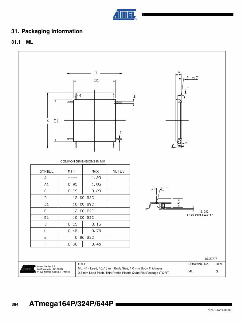
31. Packaging Information
31.1 ML
3647674F–AVR–09/09
ATmega164P/324P/644P
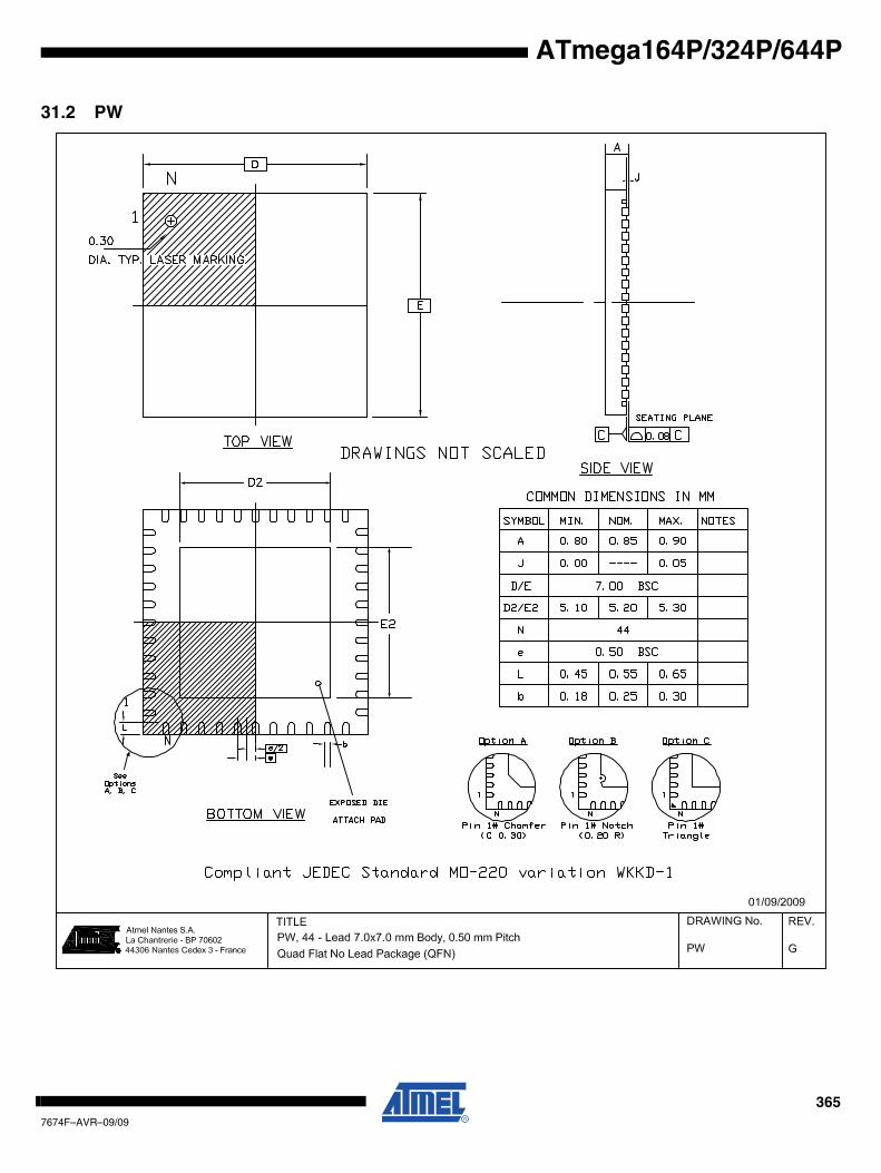
ATmega164P/324P/644P
31.2 PW
3657674F–AVR–09/09
Notes: 1. Dimensioning and tolerancing conform to ASME Y14.5M. - 1994.
2. Dimensions b applies to metallized terminal and is measured between 0.15 and 0.30 mm from terminal TIP. If the terminal has the optional radius on the other end of the terminal, the dimen-sion b should not be measured in that radius area.
3. Maximum package warpage is 0.05 mm.
4. Maximum allowable burrs is 0.076 mm in all directions.
5. Pin #1 ID on top will be laser marked.
6. This drawing conforms to JEDEC registered outline M0-220.
7. A maximum 0.15 mm pull back (L1) may be present.L minus L1 to be equal to or greater than 0.30 mm.
8. The terminal #1 identifier are optional but must be located within the zone indicated the termi-nal #1 identifier be either a mold or marked feature.
3667674F–AVR–09/09
ATmega164P/324P/644P
ATmega164P/324P/644P
32. Errata ATmega164P
32.1 ATmega164P Rev. BNo known Errata.
32.2 ATmega164P Rev. AADC differential mode not recommended above 85°C.
33. Errata ATmega324P
33.1 ATmega324P Rev. BNo known Errata.
33.2 ATmega324P Rev. AADC differential mode not recommended above 85°C.
34. Errata ATmega644P
34.1 ATmega644P Rev. BNo known Errata.
34.2 ATmega644P Rev. AADC differential mode not recommended above 85°.
3677674F–AVR–09/09
35. Datasheet Revision History
Please note that the referring page numbers in this section are referred to this document. Thereferring revision in this section are referring to the document revision.
35.1 Rev. 7674F-AVR-09/09
1. PW packaging information updated
35.2 Rev. 7674E-AVR-02/09
1. Note page 1 is removed: Differential Mode is not recommended above 85°C
2. Section 2.2.1 “Automotive Quality Grade” on page 5:Temperature range -40 to +85°C identifier T and Temperature range -40 to +105°C identifier T1 not supported anymore. Temperature range -40 to +125°C (AEC-Q100 grade1) identifier Z replace all 3 previous ranges (T, T1, Z)
3. ADC Characterisitics Differential Channels Table 26-9 on page 337 updated to reflect new improvements and removal of temperature limitation.
4. Section 30. “Ordering Information” on page 363:Section 30.1 on page 363, Section 30.2 on page 363 and Section 30.3 on page 363:Ordering code T and T1 have been removed for the 3 parts ATmega164P, ATmega324P, ATmega644P respectively in the 2 package options (Package ML and PW)New Part Number change to reflect the new die revisionATmega164P-A15AZ replaces ATmega164P-15AZATmega164P-A15MZ replaces ATmega164P-15MZATmega324P-A15AZ replaces ATmega324P-15AZATmega324P-A15MZ replaces ATmega324P-15MZATmega644P-A15AZ replaces ATmega644P-15AZATmega644P-A15MZ replaces ATmega644P-15MZ
35.3 Rev. 7674D-AVR-07/08
1. Added ADC differential mode electrical characteristics for ATMega164.
2. Removed Ramp Z register.
35.4 Rev. 7674C-AVR-05/08
1. VIL reset pin update. Section 26.1 on page 329.
2. Updated EEPROM endurance. See “Features” on page 1.
35.5 Rev. 7674B-AVR-01/08
1. Update to electrical characteristics after product characterization.
35.6 Rev. 7674A-AVR-04/07
1. Initial Automotive revision
2. Insertion of specific § for automative quality references
3. DC and Frequency adapted to Automotive temperature range
4. Part numbering and package selection according to Automotive rules
5. Current Consumption adapted based on Industrial electrical characterization.
3687674F–AVR–09/09
ATmega164P/324P/644P
ATmega164P/324P/644P
36. Table of Contents
Features ..................................................................................................... 1
1 Pin Configurations ................................................................................... 2
2 Overview ................................................................................................... 3
2.1 Block Diagram ...................................................................................................3
2.2 Comparison Between ATmega164P, ATmega324P and ATmega644P ...........4
2.3 Pin Descriptions .................................................................................................5
3 Resources ................................................................................................. 7
4 About Code Examples ............................................................................. 8
5 AVR CPU Core .......................................................................................... 9
5.1 Overview ............................................................................................................9
5.2 ALU – Arithmetic Logic Unit .............................................................................10
5.3 Status Register ................................................................................................11
5.4 General Purpose Register File ........................................................................12
5.5 Stack Pointer ...................................................................................................13
5.6 Instruction Execution Timing ...........................................................................14
5.7 Reset and Interrupt Handling ...........................................................................15
6 AVR Memories ........................................................................................ 18
6.1 Overview ..........................................................................................................18
6.2 In-System Reprogrammable Flash Program Memory .....................................18
6.3 SRAM Data Memory ........................................................................................19
6.4 EEPROM Data Memory ..................................................................................21
6.5 I/O Memory ......................................................................................................22
6.6 Register Description ........................................................................................23
7 System Clock and Clock Options ......................................................... 29
7.1 Clock Systems and their Distribution ...............................................................29
7.2 Clock Sources .................................................................................................30
7.3 Low Power Crystal Oscillator ...........................................................................32
7.4 Full Swing Crystal Oscillator ............................................................................33
7.5 Low Frequency Crystal Oscillator ....................................................................34
7.6 Calibrated Internal RC Oscillator .....................................................................36
7.7 128 kHz Internal Oscillator ..............................................................................37
7.8 External Clock .................................................................................................37
3697674F–AVR–09/09
7.9 Timer/Counter Oscillator ..................................................................................38
7.10 Clock Output Buffer .........................................................................................38
7.11 System Clock Prescaler ..................................................................................38
7.12 Register Description ........................................................................................39
8 Power Management and Sleep Modes ................................................. 41
8.1 Overview ..........................................................................................................41
8.2 Sleep Modes ....................................................................................................41
8.3 BOD Disable ....................................................................................................42
8.4 Idle Mode .........................................................................................................42
8.5 ADC Noise Reduction Mode ............................................................................42
8.6 Power-down Mode ...........................................................................................43
8.7 Power-save Mode ............................................................................................43
8.8 Standby Mode .................................................................................................43
8.9 Extended Standby Mode .................................................................................43
8.10 Power Reduction Register ...............................................................................44
8.11 Minimizing Power Consumption ......................................................................44
8.12 Register Description ........................................................................................46
9 System Control and Reset .................................................................... 49
9.1 Internal Voltage Reference ..............................................................................53
9.2 Watchdog Timer ..............................................................................................54
9.3 Register Description ........................................................................................57
10 Interrupts ................................................................................................ 60
10.1 Overview ..........................................................................................................60
10.2 Interrupt Vectors in ATmega164P/324P/644P ................................................60
10.3 Register Description ........................................................................................64
11 External Interrupts ................................................................................. 66
11.1 Overview ..........................................................................................................66
11.2 Register Description ........................................................................................66
12 I/O-Ports .................................................................................................. 71
12.1 Overview ..........................................................................................................71
12.2 Ports as General Digital I/O .............................................................................72
12.3 Alternate Port Functions ..................................................................................77
12.4 Register Description ........................................................................................90
3707674F–AVR–09/09
ATmega164P/324P/644P
ATmega164P/324P/644P
13 8-bit Timer/Counter0 with PWM ............................................................ 92
13.1 Features ..........................................................................................................92
13.2 Overview ..........................................................................................................92
13.3 Timer/Counter Clock Sources .........................................................................93
13.4 Counter Unit ....................................................................................................93
13.5 Output Compare Unit .......................................................................................94
13.6 Compare Match Output Unit ............................................................................96
13.7 Modes of Operation .........................................................................................97
13.8 Timer/Counter Timing Diagrams ...................................................................101
13.9 Register Description ......................................................................................103
14 16-bit Timer/Counter1 with PWM ........................................................ 110
14.1 Features ........................................................................................................110
14.2 Overview ........................................................................................................110
14.3 Accessing 16-bit Registers ............................................................................112
14.4 Timer/Counter Clock Sources .......................................................................115
14.5 Counter Unit ..................................................................................................116
14.6 Input Capture Unit .........................................................................................117
14.7 Output Compare Units ...................................................................................119
14.8 Compare Match Output Unit ..........................................................................121
14.9 Modes of Operation .......................................................................................122
14.10 Timer/Counter Timing Diagrams ...................................................................129
14.11 Register Description ......................................................................................131
15 8-bit Timer/Counter2 with PWM and Asynchronous Operation ...... 139
15.1 Features ........................................................................................................139
15.2 Overview ........................................................................................................139
15.3 Timer/Counter Clock Sources .......................................................................140
15.4 Counter Unit ..................................................................................................141
15.5 Output Compare Unit .....................................................................................142
15.6 Compare Match Output Unit ..........................................................................143
15.7 Modes of Operation .......................................................................................145
15.8 Timer/Counter Timing Diagrams ...................................................................149
15.9 Asynchronous Operation of Timer/Counter2 .................................................151
15.10 Timer/Counter Prescaler ...............................................................................153
15.11 Register Description ......................................................................................153
3717674F–AVR–09/09
16 SPI – Serial Peripheral Interface ......................................................... 161
16.1 Features ........................................................................................................161
16.2 Overview ........................................................................................................161
16.3 SS Pin Functionality ......................................................................................166
16.4 Data Modes ...................................................................................................166
16.5 Register Description ......................................................................................168
17 USART ................................................................................................... 171
17.1 Features ........................................................................................................171
17.2 USART1 and USART0 ..................................................................................171
17.3 Overview ........................................................................................................171
17.4 Clock Generation ...........................................................................................173
17.5 Frame Formats ..............................................................................................176
17.6 USART Initialization .......................................................................................177
17.7 Data Transmission – The USART Transmitter ..............................................178
17.8 Data Reception – The USART Receiver .......................................................181
17.9 Asynchronous Data Reception ......................................................................185
17.10 Multi-processor Communication Mode ..........................................................188
17.11 Register Description ......................................................................................190
17.12 Examples of Baud Rate Setting .....................................................................195
18 USART in SPI Mode ............................................................................. 199
18.1 Features ........................................................................................................199
18.2 Overview ........................................................................................................199
18.3 Clock Generation ...........................................................................................199
18.4 SPI Data Modes and Timing ..........................................................................200
18.5 Frame Formats ..............................................................................................200
18.6 Data Transfer .................................................................................................203
18.7 AVR USART MSPIM vs. AVR SPI ................................................................205
18.8 Register Description ......................................................................................206
19 2-wire Serial Interface .......................................................................... 209
19.1 Features ........................................................................................................209
19.2 2-wire Serial Interface Bus Definition ............................................................209
19.3 Data Transfer and Frame Format ..................................................................210
19.4 Multi-master Bus Systems, Arbitration and Synchronization .........................213
19.5 Overview of the TWI Module .........................................................................215
19.6 Using the TWI ................................................................................................217
3727674F–AVR–09/09
ATmega164P/324P/644P
ATmega164P/324P/644P
19.7 Transmission Modes .....................................................................................221
19.8 Multi-master Systems and Arbitration ............................................................234
19.9 Register Description ......................................................................................235
20 AC - Analog Comparator ..................................................................... 240
20.1 Overview ........................................................................................................240
20.2 Analog Comparator Multiplexed Input ...........................................................240
20.3 Register Description ......................................................................................241
21 ADC - Analog-to-digital Converter ..................................................... 243
21.1 Features ........................................................................................................243
21.2 Overview ........................................................................................................243
21.3 Operation .......................................................................................................244
21.4 Starting a Conversion ....................................................................................245
21.5 Prescaling and Conversion Timing ................................................................246
21.6 Changing Channel or Reference Selection ...................................................249
21.7 ADC Noise Canceler .....................................................................................251
21.8 ADC Conversion Result .................................................................................256
21.9 Register Description ......................................................................................258
22 JTAG Interface and On-chip Debug System ..................................... 263
22.1 Features ........................................................................................................263
22.2 Overview ........................................................................................................263
22.3 TAP – Test Access Port ................................................................................264
22.4 TAP Controller ...............................................................................................265
22.5 Using the Boundary-scan Chain ....................................................................266
22.6 Using the On-chip Debug System .................................................................266
22.7 On-chip Debug Specific JTAG Instructions ...................................................267
22.8 Using the JTAG Programming Capabilities ...................................................268
22.9 Bibliography ...................................................................................................268
22.10 Register Description ......................................................................................268
23 IEEE 1149.1 (JTAG) Boundary-scan ................................................... 269
23.1 Features ........................................................................................................269
23.2 Overview ........................................................................................................269
23.3 Data Registers ...............................................................................................270
23.4 Boundary-scan Specific JTAG Instructions ...................................................271
23.5 Boundary-scan Chain ....................................................................................272
23.6 ATmega164P/324P/644P Boundary-scan Order ..........................................275
3737674F–AVR–09/09
23.7 Boundary-scan Description Language Files ..................................................277
23.8 Register Description ......................................................................................278
24 Boot Loader Support – Read-While-Write Self-Programming ......... 279
24.1 Features ........................................................................................................279
24.2 Overview ........................................................................................................279
24.3 Application and Boot Loader Flash Sections .................................................279
24.4 Read-While-Write and No Read-While-Write Flash Sections ........................280
24.5 Boot Loader Lock Bits ...................................................................................282
24.6 Entering the Boot Loader Program ................................................................283
24.7 Addressing the Flash During Self-Programming ...........................................284
24.8 Self-Programming the Flash ..........................................................................285
24.9 Register Description ......................................................................................294
25 Memory Programming ......................................................................... 296
25.1 Program And Data Memory Lock Bits ...........................................................296
25.2 Fuse Bits ........................................................................................................297
25.3 Signature Bytes .............................................................................................299
25.4 Calibration Byte .............................................................................................299
25.5 Page Size ......................................................................................................299
25.6 Parallel Programming Parameters, Pin Mapping, and Commands ...............300
25.7 Parallel Programming ....................................................................................302
25.8 Serial Downloading ........................................................................................311
25.9 Serial Programming Instruction set ...............................................................313
25.10 Programming via the JTAG Interface ............................................................315
26 Electrical Characteristics .................................................................... 328
26.1 DC Characteristics .........................................................................................329
26.2 Speed Grades ...............................................................................................330
26.3 Clock Characteristics .....................................................................................331
26.4 System and Reset Characteristics ................................................................332
26.5 SPI Timing Characteristics ............................................................................333
26.6 2-wire Serial Interface Characteristics ...........................................................334
26.7 ADC Characteristics ......................................................................................336
27 ATmega644P Typical Characteristics ................................................ 338
27.1 Power-down Supply Current ..........................................................................343
27.2 Power-save Supply Current ...........................................................................344
27.3 Pin Pull-up .....................................................................................................345
3747674F–AVR–09/09
ATmega164P/324P/644P
ATmega164P/324P/644P
27.4 Pin Driver Strength ........................................................................................346
27.5 Threshold and Hysteresis ..............................................................................348
27.6 BOD Thresholds and Analog Comparator Offset ..........................................349
27.7 Internal Oscillator Speed ...............................................................................350
27.8 Current Consumption of Peripheral Units ......................................................352
27.9 Current Consumption in Reset and Reset Pulse Width .................................354
28 Register Summary ............................................................................... 356
29 Instruction Set Summary .................................................................... 360
30 Ordering Information ........................................................................... 363
30.1 ATmega164P .................................................................................................363
30.2 ATmega324P .................................................................................................363
30.3 ATmega644P .................................................................................................363
31 Packaging Information ........................................................................ 364
31.1 ML ..................................................................................................................364
31.2 PW .................................................................................................................365
32 Errata ATmega164P ............................................................................. 367
32.1 ATmega164P Rev. B .....................................................................................367
32.2 ATmega164P Rev. A .....................................................................................367
33 Errata ATmega324P ............................................................................. 367
33.1 ATmega324P Rev. B .....................................................................................367
33.2 ATmega324P Rev. A .....................................................................................367
34 Errata ATmega644P ............................................................................. 367
34.1 ATmega644P Rev. B .....................................................................................367
34.2 ATmega644P Rev. A .....................................................................................367
35 Datasheet Revision History ................................................................ 368
35.1 Rev. 7674E-AVR-02/09 .................................................................................368
35.2 Rev. 7674D-AVR-07/08 .................................................................................368
35.3 Rev. 7674C-AVR-05/08 .................................................................................368
35.4 Rev. 7674B-AVR-01/08 .................................................................................368
35.5 Rev. 7674A-AVR-04/07 .................................................................................368
36 Table of Contents ................................................................................. 369
3757674F–AVR–09/09

3767674F–AVR–09/09
ATmega164P/324P/644P
7674F–AVR–09/09
Headquarters International
Atmel Corporation2325 Orchard ParkwaySan Jose, CA 95131USATel: 1(408) 441-0311Fax: 1(408) 487-2600
Atmel AsiaUnit 1-5 & 16, 19/FBEA Tower, Millennium City 5418 Kwun Tong RoadKwun Tong, KowloonHong KongTel: (852) 2245-6100Fax: (852) 2722-1369
Atmel EuropeLe Krebs8, Rue Jean-Pierre TimbaudBP 30978054 Saint-Quentin-en-Yvelines CedexFranceTel: (33) 1-30-60-70-00 Fax: (33) 1-30-60-71-11
Atmel Japan9F, Tonetsu Shinkawa Bldg.1-24-8 ShinkawaChuo-ku, Tokyo 104-0033JapanTel: (81) 3-3523-3551Fax: (81) 3-3523-7581
Product Contact
Web Sitewww.atmel.com
Technical [email protected]
Sales Contactwww.atmel.com/contacts
Literature Requestswww.atmel.com/literature
Disclaimer: The information in this document is provided in connection with Atmel products. No license, express or implied, by estoppel or otherwise, to anyintellectual property right is granted by this document or in connection with the sale of Atmel products. EXCEPT AS SET FORTH IN ATMEL’S TERMS AND CONDI-TIONS OF SALE LOCATED ON ATMEL’S WEB SITE, ATMEL ASSUMES NO LIABILITY WHATSOEVER AND DISCLAIMS ANY EXPRESS, IMPLIED OR STATUTORYWARRANTY RELATING TO ITS PRODUCTS INCLUDING, BUT NOT LIMITED TO, THE IMPLIED WARRANTY OF MERCHANTABILITY, FITNESS FOR A PARTICULARPURPOSE, OR NON-INFRINGEMENT. IN NO EVENT SHALL ATMEL BE LIABLE FOR ANY DIRECT, INDIRECT, CONSEQUENTIAL, PUNITIVE, SPECIAL OR INCIDEN-TAL DAMAGES (INCLUDING, WITHOUT LIMITATION, DAMAGES FOR LOSS OF PROFITS, BUSINESS INTERRUPTION, OR LOSS OF INFORMATION) ARISING OUT OFTHE USE OR INABILITY TO USE THIS DOCUMENT, EVEN IF ATMEL HAS BEEN ADVISED OF THE POSSIBILITY OF SUCH DAMAGES. Atmel makes norepresentations or warranties with respect to the accuracy or completeness of the contents of this document and reserves the right to make changes to specificationsand product descriptions at any time without notice. Atmel does not make any commitment to update the information contained herein. Unless specifically providedotherwise, Atmel products are not suitable for, and shall not be used in, automotive applications. Atmel’s products are not intended, authorized, or warranted for useas components in applications intended to support or sustain life.
© 2009 Atmel Corporation. All rights reserved. Atmel®, Atmel logo and combinations thereof, AVR®, AVR® logo, AVR Studio® and others are reg-istered trademarks or trademarks of Atmel Corporation or its subsidiaries. Windows® and others are registered trademarks or trademarks ofMicrosoft Corporation in US and/or other countries. Other terms and product names may be trademarks of others.
Related Documents