ABSTRACT Objective: The objective of this project is to monitor and track the Mobile using Global Positioning System. Scope: The Global Positioning System is a space age navigational system that can pinpoint your position anywhere on the globe, usually within a few yards or meters. This amazing technology is available to everyone, everywhere, day and night, and best of all, at no cost for use of the navigational data. GPS uses a constellation of 24 satellites in precise orbits approximately 11,000 miles above the earth. The satellites transmit data via high frequency radio waves back to Earth and, by locking onto these signals; a GPS receiver can process this data to triangulate its precise location on the globe. GPS operates 24 hours a day, in all weather conditions, and can be used worldwide for precise navigation on land, on water and even in the air. Some

Welcome message from author
This document is posted to help you gain knowledge. Please leave a comment to let me know what you think about it! Share it to your friends and learn new things together.
Transcript
ABSTRACT
Objective:
The objective of this project is to monitor and track the Mobile using
Global Positioning System.
Scope:
The Global Positioning System is a space age navigational system that can
pinpoint your position anywhere on the globe, usually within a few yards or
meters. This amazing technology is available to everyone, everywhere, day and
night, and best of all, at no cost for use of the navigational data. GPS uses a
constellation of 24 satellites in precise orbits approximately 11,000 miles above
the earth. The satellites transmit data via high frequency radio waves back to
Earth and, by locking onto these signals; a GPS receiver can process this data to
triangulate its precise location on the globe.
GPS operates 24 hours a day, in all weather conditions, and can be used
worldwide for precise navigation on land, on water and even in the air. Some of
its many current applications include: boating, fishing, hunting, scouting on land
or from the air, hiking, camping, biking, rafting, pack trips by horseback, hot air
ballooning, general aviation, snowmobiling and skiing, search and rescue,
emergency vehicle tracking, 4 wheeling, highway driving and a host of other
outdoor activities where accurate positioning is required.

Brief methodology:
This project is designed with
GPS antenna
GPS receiver
Microcontroller
Vibration sensor
RS232
Mobile or GSM modem
PC
In this project GPS is used to monitor the Mobile position anywhere in the
earth. The Mobile who wants to monitor has to have the GPS sensor. The GPS
sensor consists of GPS antenna and GPS receiver. GPS uses satellite ranging to
triangulate your position. In other words, the GPS unit simply measures the travel
time of the signals transmitted from the satellites, then multiplies them by the
speed of light to determine exactly how far the unit is from every satellite its
sampling. By locking onto the signals from a minimum of three different satellites,
a GPS receiver can calculate a 2D (two-dimensional) positional fix, consisting of
your latitude and longitude.
GPS receiver received human latitude and longitude from satellite through
GPS antenna. GPS receiver is interfaced with the microcontroller through RS232
converter. RS 232 converter is used to convert RS232 logic to TTL logic vice versa
because GPS receiver is the RS232 logic and microcontroller is the TTL logic. Then
the receiver sends the received signal to microcontroller. Here the
microcontroller is the flash type reprogrammable microcontroller in which we

have already programmed. Now the microcontroller displays the latitude and
longitude on the LCD display.
Then position information signal is transmitted through GSM network or mobile.
The mobile is interfaced with the microcontroller through data cable.
Data cable is the special type of cable which is available with mobile phone. In
the receiver section the mobile or GSM network is interfaced with PC. In PC we
can monitor the Mobile current position on the earth.

INTRODUCTION
Present industry is increasingly shifting towards automation. Two
principle components of today’s industrial automations are programmable
controllers and robots. In order to aid the tedious work and to serve the
mankind, today there is a general tendency to develop an intelligent
operation.
.
ATMEGA Microcontroller is the heart of the device which handles all the
sub devices connected across it. It has flash type reprogrammable
memory. It has some peripheral devices to play this project perform.
It also provides sufficient power to inbuilt peripheral devices. We need not
give individually to all devices. The peripheral devices also activates as low
power operation mode. These are the advantages are appear here.

BLOCK DIAGRAM

BLOCK DIAGRAM DESCRIPTION
ATMEGA
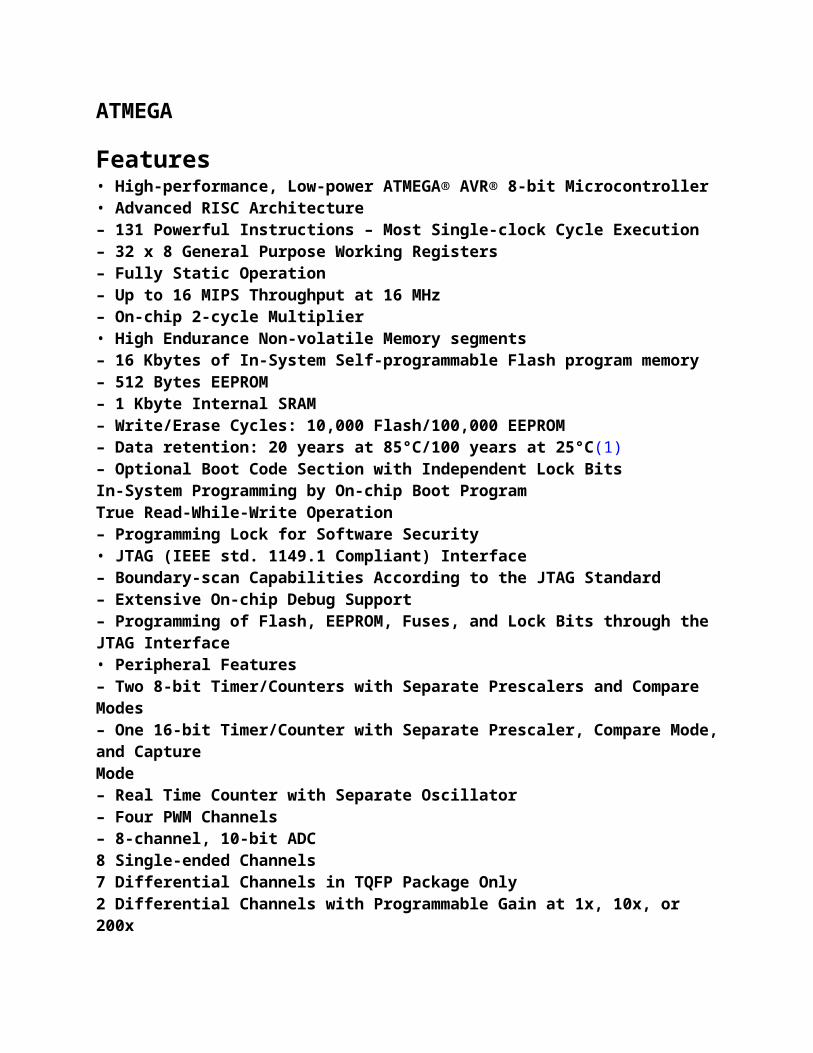
Features• High-performance, Low-power ATMEGA® AVR® 8-bit Microcontroller• Advanced RISC Architecture– 131 Powerful Instructions – Most Single-clock Cycle Execution– 32 x 8 General Purpose Working Registers– Fully Static Operation– Up to 16 MIPS Throughput at 16 MHz– On-chip 2-cycle Multiplier• High Endurance Non-volatile Memory segments– 16 Kbytes of In-System Self-programmable Flash program memory– 512 Bytes EEPROM– 1 Kbyte Internal SRAM– Write/Erase Cycles: 10,000 Flash/100,000 EEPROM– Data retention: 20 years at 85°C/100 years at 25°C(1)– Optional Boot Code Section with Independent Lock BitsIn-System Programming by On-chip Boot ProgramTrue Read-While-Write Operation– Programming Lock for Software Security• JTAG (IEEE std. 1149.1 Compliant) Interface– Boundary-scan Capabilities According to the JTAG Standard– Extensive On-chip Debug Support– Programming of Flash, EEPROM, Fuses, and Lock Bits through the JTAG Interface• Peripheral Features– Two 8-bit Timer/Counters with Separate Prescalers and Compare Modes– One 16-bit Timer/Counter with Separate Prescaler, Compare Mode, and CaptureMode– Real Time Counter with Separate Oscillator– Four PWM Channels– 8-channel, 10-bit ADC8 Single-ended Channels7 Differential Channels in TQFP Package Only2 Differential Channels with Programmable Gain at 1x, 10x, or 200x– Byte-oriented Two-wire Serial Interface– Programmable Serial USART– Master/Slave SPI Serial Interface– Programmable Watchdog Timer with Separate On-chip Oscillator– On-chip Analog Comparator• Special Microcontroller Features– Power-on Reset and Programmable Brown-out Detection– Internal Calibrated RC Oscillator– External and Internal Interrupt Sources


INTERRUPT
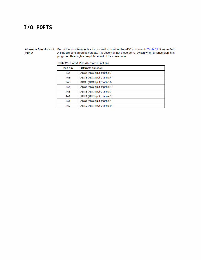
I/O PORTS


LCD DISPLAY
INTRODUCTION:
Liquid crystal displays (LCDs) have materials which combine the properties
of both liquids and crystals. Rather than having a melting point, they have a
temperature range within which the molecules are almost as mobile as they would
be in a liquid, but are grouped together in an ordered form similar to a crystal.
An LCD consists of two glass panels, with the liquid crystal material sand
witched in between them. The inner surface of the glass plates are coated with
transparent electrodes which define the character, symbols or patterns to be
displayed polymeric layers are present in between the electrodes and the liquid
crystal, which makes the liquid crystal molecules to maintain a defined orientation
angle.
One each polarisers are pasted outside the two glass panels. These polarisers
would rotate the light rays passing through them to a definite angle, in a particular
direction
When the LCD is in the off state, light rays are rotated by the two polarisers
and the liquid crystal, such that the light rays come out of the LCD without any
orientation, and hence the LCD appears transparent.
When sufficient voltage is applied to the electrodes, the liquid crystal
molecules would be aligned in a specific direction. The light rays passing through
the LCD would be rotated by the polarisers, which would result in activating /
highlighting the desired characters.

The LCD’s are lightweight with only a few millimeters thickness. Since the
LCD’s consume less power, they are compatible with low power electronic
circuits, and can be powered for long durations.
The LCD’s don’t generate light and so light is needed to read the display. By
using backlighting, reading is possible in the dark. The LCD’s have long life and a
wide operating temperature range.
Changing the display size or the layout size is relatively simple which makes
the LCD’s more customer friendly.
The LCDs used exclusively in watches, calculators and measuring
instruments are the simple seven-segment displays, having a limited amount of
numeric data. The recent advances in technology have resulted in better legibility,
more information displaying capability and a wider temperature range. These have
resulted in the LCDs being extensively used in telecommunications and
entertainment electronics. The LCDs have even started replacing the cathode ray
tubes (CRTs) used for the display of text and graphics, and also in small TV
applications.
POWERSUPPLY:
The power supply should be of +5V, with maximum allowable transients of
10mv. To achieve a better / suitable contrast for the display, the voltage (VL) at pin
3 should be adjusted properly.
A module should not be inserted or removed from a live circuit. The ground
terminal of the power supply must be isolated properly so that no voltage is
induced in it. The module should be isolated from the other circuits, so that stray
voltages are not induced, which could cause a flickering display.
HARDWARE:
Develop a uniquely decoded ‘E’ strobe pulse, active high, to accompany
each module transaction. Address or control lines can be assigned to drive the RS
and R/W inputs.
Utilize the Host’s extended timing mode, if available, when transacting with
the module. Use instructions, which prolong the Read and Write or other
appropriate data strobes, so as to realize the interface timing requirements.
If a parallel port is used to drive the RS, R/W and ‘E’ control lines, setting
the ‘E’ bit simultaneously with RS and R/W would violate the module’s set up
time. A separate instruction should be used to achieve proper interfacing timing
requirements.
MOUNTING:
Cover the display surface with a transparent protective plate, to protect the
polarizer.

Don’t touch the display surface with bare hands or any hard materials. This
will stain the display area and degrade the insulation between terminals.
Do not use organic solvents to clean the display panel as these may
adversely affect tape or with absorbant cotton and petroleum benzene.
The processing or even a slight deformation of the claws of the metal frame
will have effect on the connection of the output signal and cause an abnormal
display.
Do not damage or modify the pattern wiring, or drill attachment holes in the
PCB. When assembling the module into another equipment, the space between the
module and the fitting plate should have enough height, to avoid causing stress to
the module surface.
Make sure that there is enough space behind the module, to dissipate the
heat generated by the ICs while functioning for longer durations.
When an electrically powered screwdriver is used to install the module,
ground it properly.
While cleaning by a vacuum cleaner, do not bring the sucking mouth near
the module. Static electricity of the electrically powered driver or the vacuum
cleaner may destroy the module.
ENVIRONMENTAL PRECAUTIONS:
Operate the LCD module under the relative condition of 40C and 50%
relative humidity. Lower temperature can cause retardation of the blinking speed
of the display, while higher temperature makes the overall display discolor.

When the temperature gets to be within the normal limits, the display will be
normal. Polarization degradation, bubble generation or polarizer peel-off may
occur with high temperature and humidity.
Contact with water or oil over a long period of time may cause deformation
or colour fading of the display. Condensation on the terminals can cause electro-
chemical reaction disrupting the terminal circuit.
TROUBLE SHOOTING
INTRODUCTION:
When the power supply is given to the module, with the pin 3 (VL)
connected to ground, all the pixels of a character gets activated in the following
manner:
All the characters of a single line display, as in CDM 16108.
The first eight characters of a single line display, operated in the two-line
display mode, as in CDM 16116.
The first line of characters of a two-line display as in CDM 16216 and
40216. The first and third line of characters of a four-line display operated in the
two-line display mode, as in CDM 20416.

If the above mentioned does not occur, the module should be initialized by
software.
Make sure that the control signals ‘E’ , R/W and RS are according to the
interface timing requirements.
IMPROPER CHARACTER DISPLAY:
When the characters to be displayed are missing between, the data read/write
is too fast. A slower interfacing frequency would rectify the problem.
When uncertainty is there in the start of the first characters other than the
specified ones are rewritten, check the initialization and the software routine.
In a multi-line display, if the display of characters in the subsequent lines
does’nt take place properly, check the DD RAM addresses set for the
corresponding display lines.
When it is unable to display data, even though it is present in the DD RAM,
either the display on/off flag is in the off state or the display shift function is not set
properly. When the display shift is done simultaneous with the data writa
operation, the data may not be visible on the display.
If a character not found in the font table is displayed, or a character is
missing, the CG ROM is faulty and the controller IC have to be changed
If particular pixels of the characters are missing, or not getting activated
properly, there could be an assembling problem in the module.

In case any other problems are encountered you could send the module to
our factory for testing and evaluation.
CRYSTALONICS DISPLAY
INTRODUCTION:
Crystalonics dot –matrix (alphanumeric) liquid crystal displays are available
in TN, STN types, with or without backlight. The use of C-MOS LCD controller
and driver ICs result in low power consumption. These modules can be interfaced
with a 4-bit or 8-bit micro processor /Micro controller.
The built-in controller IC has the following features:
Correspond to high speed MPU interface (2MHz)
80 x 8 bit display RAM (80 Characters max)
9,920 bit character generator ROM for a total of 240 character fonts. 208
character fonts (5 x 8 dots) 32 character fonts (5 x 10 dots)
64 x 8 bit character generator RAM 8 character generator RAM 8 character
fonts (5 x 8 dots) 4 characters fonts (5 x 10 dots)
Programmable duty cycles
1/8 – for one line of 5 x 8 dots with cursor
1/11 – for one line of 5 x 10 dots with cursor
1/16 – for one line of 5 x 8 dots with cursor
Wide range of instruction functions display clear, cursor home, display
on/off, cursor on/off, display character blink, cursor shift, display shift.

FUNCTIONAL DESCRIPTION OF THE CONTROLLER IC
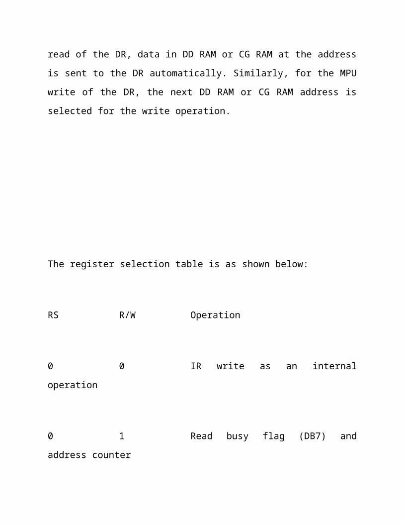
REGISTERS:
The controller IC has two 8 bit registers, an instruction register (IR) and a
data register (DR). The IR stores the instruction codes and address information for
display data RAM (DD RAM) and character generator RAM (CG RAM). The IR
can be written, but not read by the MPU.
The DR temporally stores data to be written to /read from the DD RAM or
CG RAM. The data written to DR by the MPU, is automatically written to the DD
RAM or CG RAM as an internal operation.
When an address code is written to IR, the data is automatically transferred
from the DD RAM or CG RAM to the DR. data transfer between the MPU is then
completed when the MPU reads the DR. likewise, for the next MPU read of the
DR, data in DD RAM or CG RAM at the address is sent to the DR automatically.
Similarly, for the MPU write of the DR, the next DD RAM or CG RAM address is
selected for the write operation.

The register selection table is as shown below:
RS R/W Operation
0 0 IR write as an internal operation
0 1 Read busy flag (DB7) and address counter
(DB0 to DB6)
1 0 DR write as an internal operation (DR to DD
RAM or CG RAM)
1 1 DR read as an internal operation (DD RAM
or CG RAM to DR)
BUSY FLAG:
When the busy flag is1, the controller is in the internal operation mode, and
the next instruction will not be accepted.
When RS = 0 and R/W = 1, the busy flag is output to DB7.
The next instruction must be written after ensuring that the busy flag is 0.
ADDRESS COUNTER:
The address counter allocates the address for the DD RAM and CG RAM
read/write operation when the instruction code for DD RAM address or CG RAM
address setting, is input to IR, the address code is transferred from IR to the
address counter. After writing/reading the display data to/from the DD RAM or
CG RAM, the address counter increments/decrements by one the address, as an
internal operation. The data of the address counter is output to DB0 to DB6 while
R/W = 1 and RS = 0.
DISPLAY DATA RAM (DD RAM)
The characters to be displayed are written into the display data RAM (DD
RAM), in the form of 8 bit character codes present in the character font table. The
extended capacity of the DD RAM is 80 x 8 bits i.e. 80 characters.
CHARATCER GENERATOR ROM (CG ROM)
The character generator ROM generates 5 x 8 dot 5 x 10 dot character
patterns from 8 bit character codes. It generates 208, 5 x 8 dot character patterns
and 32, 5 x 10 dot character patterns.
CHARACTER GENERATOR RAM (CG RAM)
In the character generator RAM, the user can rewrite character patterns by
program. For 5 x 8 dots, eight character patterns can be written, and for 5 x 10
dots, four character patterns can be written.
INTERFACING THE MICROPROCESSOR / CONTROLLER:
The module, interfaced to the system, can be treated as RAM input/output,
expanded or parallel I/O.
Since there is no conventional chip select signal, developing a strobe signal for the
enable signal (E) and applying appropriate signals to the register select (RS) and
read/write (R/W) signals are important.
The module is selected by gating a decoded module – address with the host –
processor’s read/write strobe. The resultant signal, applied to the LCDs enable (E)
input, clocks in the data.
The ‘E’ signal must be a positive going digital strobe, which is active while data
and control information are stable and true. The falling edge of the enable signal
enables the data / instruction register of the controller. All module timings are
referenced to specific edges of the ‘E’ signal. The ‘E’ signal is applied only when a
specific module transaction is desired.
The read and write strobes of the host, which provides the ‘E’ signals, should not
be linked to the module’s R/W line. An address bit which sets up earlier in the
host’s machine cycle can be used as R/W.
When the host processor is so fast that the strobes are too narrow to serve as the
‘E’ pulse
a. Prolong these pulses by using the hosts ‘Ready’ input
b. Prolong the host by adding wait states
c. Decrease the Hosts Crystal frequency.
Inspite of doing the above mentioned, if the problem continues, latch both the data
and control information and then activate the ‘E’ signal
When the controller is performing an internal operation he busy flag (BF) will set
and will not accept any instruction. The user should check the busy flag or should
provide a delay of approximately 2ms after each instruction.
The module presents no difficulties while interfacing slower MPUs.
The liquid crystal display module can be interfaced, either to 4-bit or 8-bit MPUs.
For 4-bit data interface, the bus lines DB4 to DB7 are used for data transfer, while
DB0 to DB3 lines are disabled. The data transfer is complete when the 4-bit data
has been transferred twice.
The busy flag must be checked after the 4-bit data has been transferred twice. Two
more 4-bit operations then transfer the busy flag and address counter data.
For 8-bit data interface, all eight-bus lines (DB0 to DB7) are used.
GPS
GLOBAL POSITIONING SYSTEM:
Of all the applications of GPS, vehicle tracking and navigational systems have brought this technology to the day-to-day life of the common man. Today GPS fitted cars; ambulances, fleets and police vehicles are common sights on the roads of developed countries. Known by many names such as Automatic Vehicle Locating System (AVLS), Vehicle Tracking and Information System (VTIS), Mobile Asset Management System (MAMS), these systems offer an effective tool for improving the operational efficiency and utilization of vehicles.
The switching off of SA has improved the accuracy of GPS to better than 30 meters, which makes it an ideal position sensor for vehicle tracking systems without the overhead of DGPS. Fig. 1 gives the block diagram of a DGPS based VTIS.
GPS is used in vehicles for both tracking and navigation. Tracking systems enable a base station to keep track of the vehicles without the intervention of the driver where, as navigation system helps the driver to reach the destination. Whether navigation system or tracking system, the architecture is more or less similar. The navigation system will have convenient, usually a graphic, display for the driver which is not needed for a tracking system. Vehicle Tracking Systems combine a number of well-developed technologies. Irrespective of the technology being used, VTS consist of three subsystems: a) In-vehicle unit (IVU), b) Base station and c) Communication link. The IVU includes a suitable position sensor and an intelligent controller together with an appropriate interface to the communication link. Thanks to the US Government announcement of 911E regulation, radio based position technology has witnessed a spurt of developmental activities.
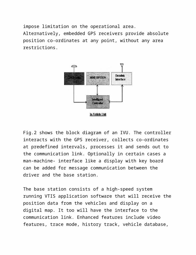
Network Overlay Systems use cell phone infrastructure for locating vehicles. The cell centers with additional hardware and software assess the time of arrival (TOA) and angle of arrival (AOA) of radio signals from vehicles to compute the position of the vehicles. This information is sent to the tracking centre through the cell link or conventional link. Another technique used for locating vehicles computes the time difference for signals from two cell centers to reach the vehicle. This computation is made in the IVU and the position information is sent to the tracking centre through the cell phone link. A more common technique used is direct radio link (DRL). In this system dedicated radio infrastructure is used along with special IVU to compute vehicle location. However all these techniques impose limitation on the operational area. Alternatively, embedded GPS receivers provide absolute position co-ordinates at any point, without any area restrictions.

Fig.2 shows the block diagram of an IVU. The controller interacts with the GPS receiver, collects co-ordinates at predefined intervals, processes it and sends out to the communication link. Optionally in certain cases a man-machine- interface like a display with key board can be added for message communication between the driver and the base station.
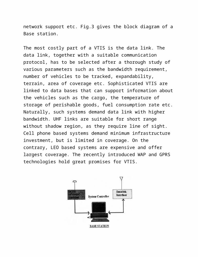
The base station consists of a high-speed system running VTIS application software that will receive the position data from the vehicles and display on a digital map. It too will have the interface to the communication link. Enhanced features include video features, trace mode, history track, vehicle database, network support etc. Fig.3 gives the block diagram of a Base station.
The most costly part of a VTIS is the data link. The data link, together with a suitable communication protocol, has to be selected after a thorough study of various parameters such as the bandwidth requirement, number of vehicles to be tracked, expandability, terrain, area of coverage etc. Sophisticated VTIS are linked to data bases that can support information about the vehicles such as the cargo, the temperature of storage of perishable goods, fuel consumption rate etc. Naturally, such systems demand data link with higher bandwidth. UHF links are suitable for short range without shadow region, as they require line of sight. Cell phone based systems demand minimum infrastructure investment, but is limited

in coverage. On the contrary, LEO based systems are expensive and offer largest coverage. The recently introduced WAP and GPRS technologies hold great promises for VTIS.
When multiple vehicles are being tracked, a suitable communication protocol need to be established to avoid collision of radio signal. The simple technique is TDMA, where each IVU communicates during predefined time slots. This synchronization is easy in a GPS based IVU as the GPS receiver provides very precise time reference signal. However, TDMA based systems have limited expandability, flexibility and are known for under-utilization of bandwidth.
The alternative is polling technique. Here each vehicle is addressed by the control station and in response the IVU sends the information. This arrangement enables variable polling rate for different vehicles, non-polling of specific vehicles and expansion of polling list as new vehicles are added.
The relatively large investment needed for the communication link, makes VTIS an opportunity area for service providers. Fig. 4 shows the global market for GPS based VTIS in the next three years. In US and Europe many vehicle tracking service providers are already in operation. In a large country like India with a very long network of roads and long coastline, this opportunity area is yet to be exploited.

The Global Positioning System (GPS) is the only fully functional Global Navigation
Satellite System (GNSS). Utilizing a constellation of at least 24 Medium Earth Orbit
satellites that transmit precise microwave signals, the system enables a GPS
receiver to determine its location, speed, direction, and time. Other similar
systems are the Russian GLONASS (incomplete as of 2007) and the upcoming
European Galileo positioning system
Developed by the United States Department of Defense, GPS is officially named
NAVSTAR GPS (Contrary to popular belief, NAVSTAR is not an acronym, but simply
a name given by Mr. John Walsh, a key decision maker when it came to the
budget for the GPS program[1]). The satellite constellation is managed by the
United States Air Force 50th Space Wing. The cost of maintaining the system is
approximately US$750 million per year,[2] including the replacement of aging
satellites, and research and development
Following the shootdown of Korean Air Lines Flight 007 in 1983, President
Ronald Reagan issued a directive making the system available for free for civilian
use as a common good.[3] Since then, GPS has become a widely used aid to
navigation worldwide, and a useful tool for map-making, land surveying,
commerce, and scientific uses. GPS also provides a precise time reference used in
many applications including scientific study of earthquakes, and synchronization of
telecommunications networks.

The current GPS consists of three major segments. These are the space segment
(SS), a control segment (CS), and a user segment
Figure 1
visual example of the GPS constellation in motion with the Earth rotating. Notice
how the number of satellites in view from a given point on the Earth's surface, in
this example at 45°N, changes with time.
The space segment (SS) comprises the orbiting GPS satellites or Space Vehicles
(SV) in GPS parlance. The GPS design originally called for 24 SVs, 8 each in three
circular orbital planes, but this was modified to 6 planes with 4 satellites each. The
orbital planes are centered on the Earth, not rotating with respect to the distant
stars. The six planes have approximately 55° inclination (tilt relative to Earth's
equator) and are separated by 60° right ascension of the ascending node (angle
along the equator from a reference point to the orbit's intersection). ] The orbits
are arranged so that at least six satellites are always within line of sight from
almost everywhere on Earth's surface.
Orbiting at an altitude of approximately 20,200 kilometers (12,600 miles or
10,900 nautical miles; orbital radius of 26,600 km (16,500 mi or 14,400 NM)),
each SV makes two complete orbits each sidereal day. The ground track of each

satellite therefore repeats each (sidereal) day. This was very helpful during
development, since even with just 4 satellites, correct alignment means all 4 are
visible from one spot for a few hours each day. For military operations, the
ground track repeat can be used to ensure good coverage in combat zones.
As of September 2007, there are 31 actively broadcasting satellites in the GPS
constellation. The additional satellites improve the precision of GPS receiver
calculations by providing redundant measurements. With the increased number
of satellites, the constellation was changed to a nonuniform arrangement. Such
an arrangement was shown to improve reliability and availability of the system,
relative to a uniform system, when multiple satellites fail.
GPS broadcast signal
Each GPS satellite continuously broadcasts a Navigation Message at 50 bit/s
giving the time-of-day, GPS week number and satellite health information (all
transmitted in the first part of the message), an ephemeris (transmitted in the
second part of the message) and an almanac (later part of the message). The
messages are sent in frames, each taking 30 seconds to transmit 1500 bits.
The first 6 seconds of every frame contains data describing the satellite clock and
its relationship to GPS system time. The next 12 seconds contain the ephemeris
data, giving the satellite's own precise orbit. The ephemeris is updated every 2
hours and is generally valid for 4 hours, with provisions for updates every 6 hours
or longer in non-nominal conditions. The time needed to acquire the ephemeris is

becoming a significant element of the delay to first position fix, because, as the
hardware becomes more capable, the time to lock onto the satellite signals
shrinks, but the ephemeris data requires 30 seconds (worst case) before it is
received, due to the low data transmission rate.
GPS ANTENNA
We're interested in designing, building, and testing a GPS antenna that would be
implemented on the body or inside of a vehicle. This antenna would be different
than others on the market in that it would not only utilize the L1 frequency
(1575.42 MHz), but also the L5 frequency (1176.45 MHz) to be introduced in the
future. Our goal is to also make it interoperable with the European counterpart to
GPS, Galileo which uses 1164–1214 MHz and 1563–1591 MHz bands. In addition,
we intend to gather the specifications for the LNA that would be needed for our
specific antenna based on its gain, impedance, and other characteristics. If time
allows, we intend to design and simulate the LNA using Agilent's Advanced Design
System software package at the end as well.

Benefits:
Antenna could be used presently because it would be utilizing the
presently available L1 frequency
L5 frequency will allow compatibility with the modernized GPS
system in the future
Be interoperable with the Galileo system so receiver would be
capable of working with that system once it’s fully online and
functional
Receiver would need only one antenna for both L1 and L5
frequencies
Features:
Ability to receive both the presently available L1 frequency and the
L5 frequency to be introduced in the future
Interoperability with the Galileo system would allow receiver
manufacturer to utilize this antenna
Vehicle mounting of antenna would allow navigational tracking capability for any vehicle

VIBRATION SENSOR
PIEZOELECTRIC SENSOR
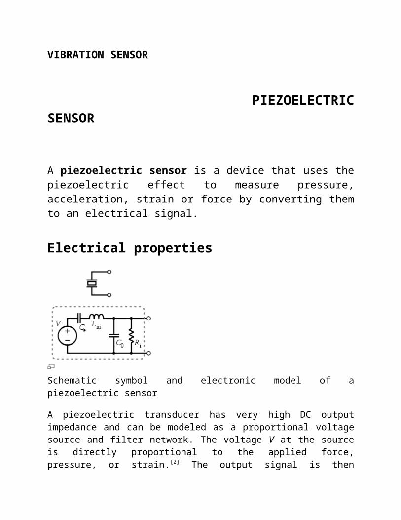
A piezoelectric sensor is a device that uses the piezoelectric effect to measure pressure, acceleration, strain or force by converting them to an electrical signal.
Electrical properties
Schematic symbol and electronic model of a piezoelectric sensor
A piezoelectric transducer has very high DC output impedance and can be modeled as a proportional voltage source and filter network. The voltage V at the source is directly proportional to the applied force, pressure, or strain.[2] The output signal is then related to this mechanical force as if it had passed through the equivalent circuit.
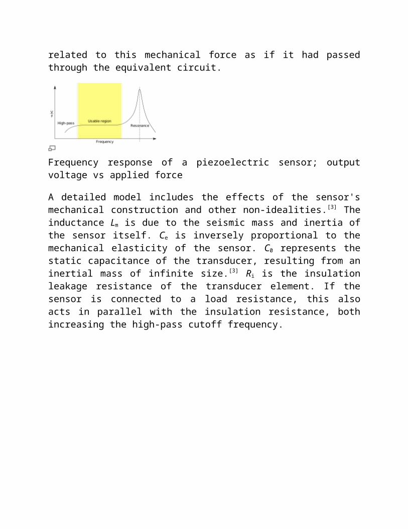
Frequency response of a piezoelectric sensor; output voltage vs applied force
A detailed model includes the effects of the sensor's mechanical construction and other non-idealities.[3] The inductance Lm is due to the seismic mass and inertia of the sensor itself. Ce is inversely proportional to the mechanical elasticity of the sensor. C0 represents the static capacitance of the transducer, resulting from an inertial mass of infinite size.[3] Ri is the insulation leakage resistance of the transducer element. If the sensor is connected to a load resistance, this also acts in parallel with the insulation resistance, both increasing the high-pass cutoff frequency.
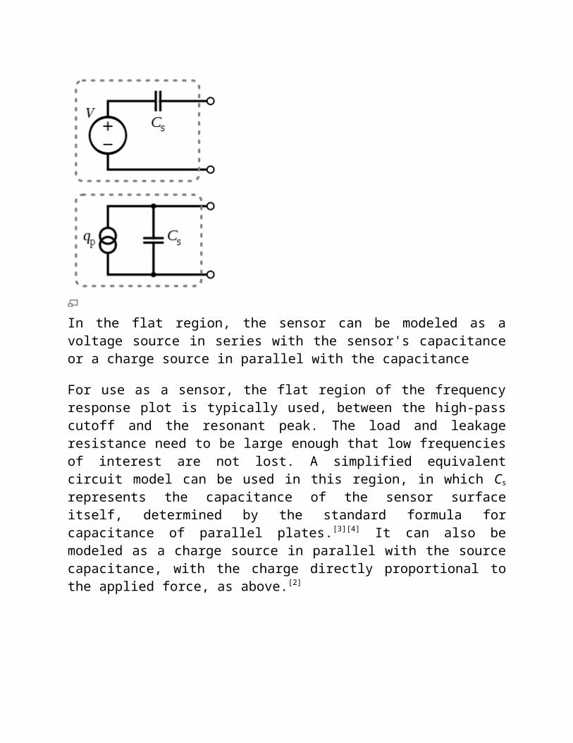
In the flat region, the sensor can be modeled as a voltage source in series with the sensor's capacitance or a charge source in parallel with the capacitance
For use as a sensor, the flat region of the frequency response plot is typically used, between the high-pass cutoff and the resonant peak. The load and leakage resistance need to be large enough that low frequencies of interest are not lost. A simplified equivalent circuit model can be used in this region, in which Cs
represents the capacitance of the sensor surface itself, determined by the standard formula for capacitance of parallel plates.[3][4] It can also be modeled as a charge source in parallel with the source capacitance, with the charge directly proportional to the applied force, as above.[2]
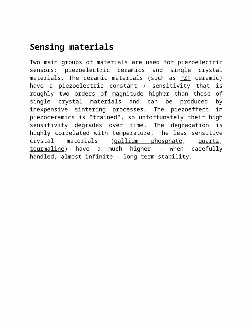
Sensing materials
Two main groups of materials are used for piezoelectric sensors: piezoelectric ceramics and single crystal materials. The ceramic materials (such as PZT ceramic) have a piezoelectric constant / sensitivity that is roughly two orders of magnitude higher than those of single crystal materials and can be produced by inexpensive sintering processes. The piezoeffect in piezoceramics is "trained", so unfortunately their high sensitivity degrades over time. The degradation is highly correlated with temperature. The less sensitive crystal materials (gallium phosphate, quartz, tourmaline) have a much higher – when carefully handled, almost infinite – long term stability.
SCU
Signal conditioning unit
The signal conditioning unit accepts input signals from the analog sensors and
gives a conditioned output of 0-5V DC corresponding to the entire range of each
parameter. This unit also accepts the digital sensor inputs and gives outputs in 10
bit binary with a positive logic level of +5V. The calibration voltages* (0, 2.5 and
5V) and the health bits are also generated in this unit.
Microcontrollers are widely used for control in power electronics. They provide
real time control by processing analog signals obtained from the system. A suitable
isolation interface needs to be designed for interaction between the control circuit
and high voltage hardware. A signal conditioning unit which provides necessary
interface between a high power grid inverter and a low voltage controller unit.

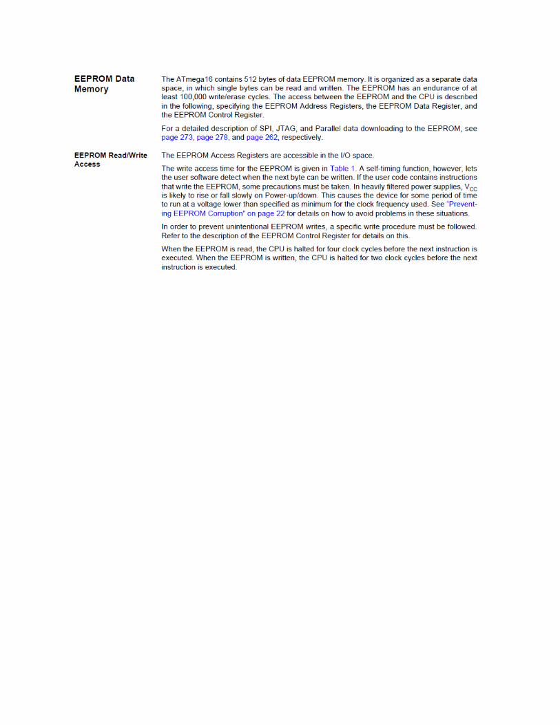
EEPROM
EEPROM:
EEPROM (Electrically Erasable Programmable Read Only Memory) is a
storage device of sorts. The 28c64 is right out of the ATMEGA Workshop. The
28c64 is accessed like a static RAM for the read or write cycles without the need
for external components. During a “byte write” the address and data are latched
internally, feeing the microprocessor address and the data bus for various other
operations.
Following the initiation of the write cycle, the device will go to a busy state
and automatically clear and write the latch data using an internal control
timer. To determine when the write cycle is complete, the user has a chance of
monitoring the Ready/Busy output or using data polling. The Ready/Busy pin
is an open drain output, which allows easy configuration in wired-or systems.
Alternatively data polling allows the user to read the location last written to
when the write operation is complete. CMOS design and processing enables
this part to be used in systems where reduced power consumption and
reliability are required.
The device has 4 standard modes of operation, which are
1) Read mode

A12
DATA PROTECTION SYSTEM
CONTROL ENABLE/OUTPUT ENABLE CONTROL LOGIC
AUTO ERASE/ WRITE TIMING
DATA POLL
INPUT/OUTPUTBUFFERS
YDECODER
Y GATINGLATCHES
16 KBCELL MATRIX
XDECODER
A1
||||||||||
------------------I/O7
PROGRAM VOLTAGE GENERATION
2) Standby mode
3) Write inhibit
4) Byte write.
5)
6)
A complete family of packages is offered to provide utmost flexibility in
operation.
I/O 1
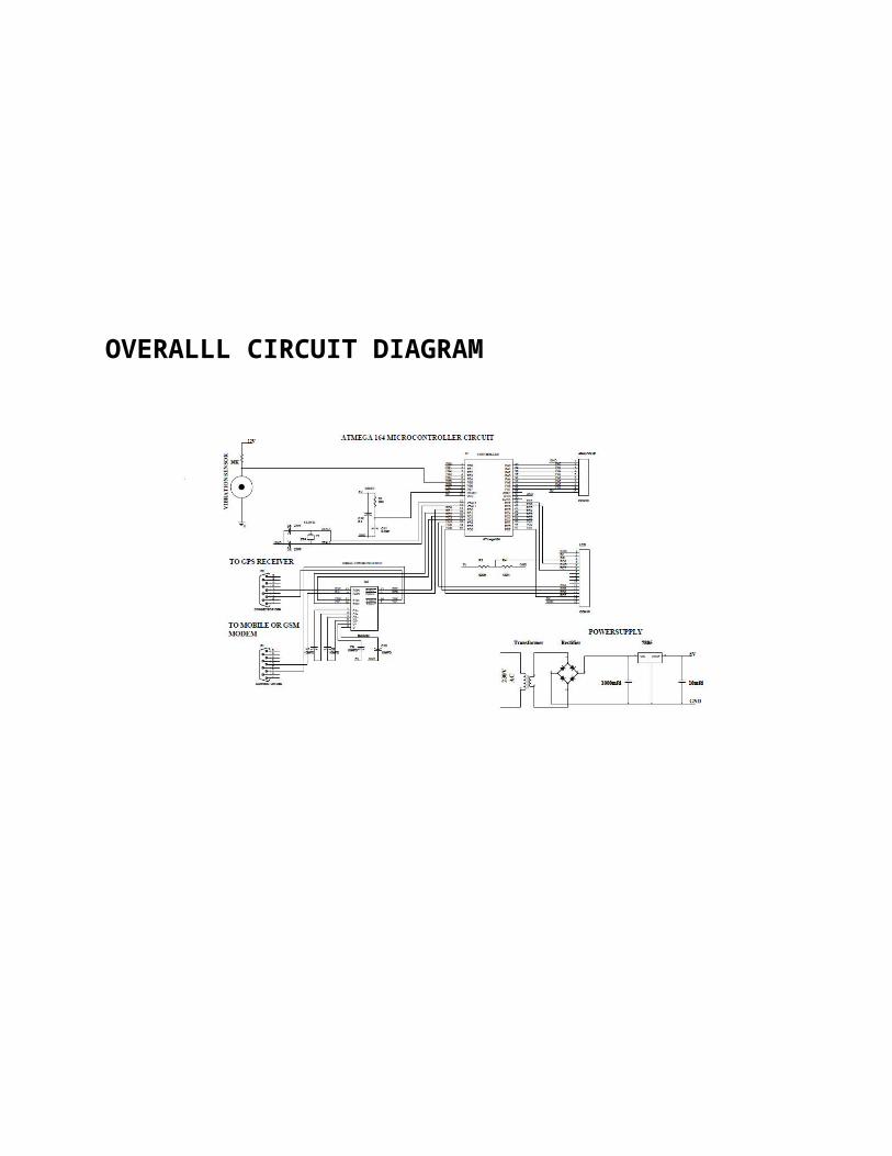
OVERALLL CIRCUIT DIAGRAM
OVERALL CIRCUIT DIAGRAM DESCRIPTION
POWER SUPPLY
Block diagram
The ac voltage, typically 220V rms, is connected to a transformer, which
steps that ac voltage down to the level of the desired dc output. A diode rectifier
then provides a full-wave rectified voltage that is initially filtered by a simple
capacitor filter to produce a dc voltage. This resulting dc voltage usually has some
ripple or ac voltage variation.
A regulator circuit removes the ripples and also remains the same dc value
even if the input dc voltage varies, or the load connected to the output dc voltage
changes. This voltage regulation is usually obtained using one of the popular
voltage regulator IC units.
: Block diagram (Power supply)
TRANSFORMER RECTIFIER FILTER IC REGULATOR LOAD
Working principle
Transformer
The potential transformer will step down the power supply voltage (0-
230V) to (0-6V) level. Then the secondary of the potential transformer will be
connected to the precision rectifier, which is constructed with the help of op–
amp. The advantages of using precision rectifier are it will give peak voltage
output as DC, rest of the circuits will give only RMS output.
Bridge rectifier
When four diodes are connected as shown in figure, the circuit is called as
bridge rectifier. The input to the circuit is applied to the diagonally opposite
corners of the network, and the output is taken from the remaining two corners.
Let us assume that the transformer is working properly and there is a
positive potential, at point A and a negative potential at point B. the positive
potential at point A will forward bias D3 and reverse bias D4.
The negative potential at point B will forward bias D1 and reverse D2. At
this time D3 and D1 are forward biased and will allow current flow to pass
through them; D4 and D2 are reverse biased and will block current flow.
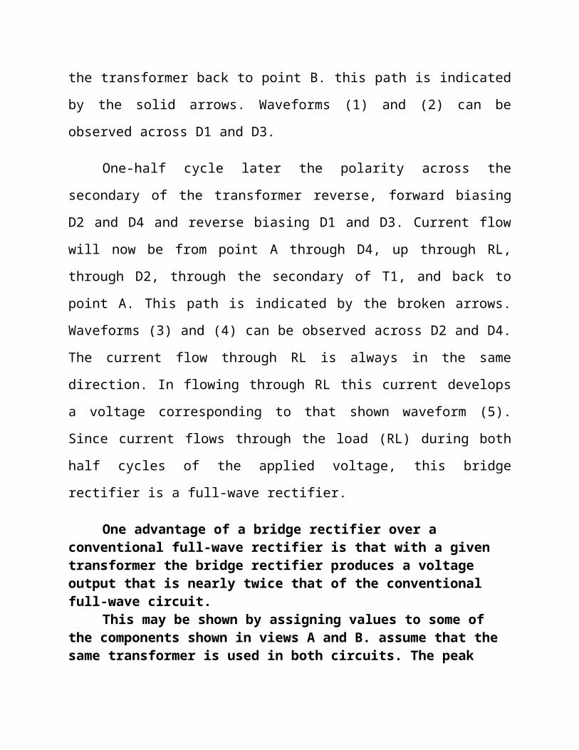
The path for current flow is from point B through D1, up through RL,
through D3, through the secondary of the transformer back to point B. this path is

indicated by the solid arrows. Waveforms (1) and (2) can be observed across D1
and D3.
One-half cycle later the polarity across the secondary of the transformer
reverse, forward biasing D2 and D4 and reverse biasing D1 and D3. Current flow
will now be from point A through D4, up through RL, through D2, through the
secondary of T1, and back to point A. This path is indicated by the broken arrows.
Waveforms (3) and (4) can be observed across D2 and D4. The current flow
through RL is always in the same direction. In flowing through RL this current
develops a voltage corresponding to that shown waveform (5). Since current
flows through the load (RL) during both half cycles of the applied voltage, this
bridge rectifier is a full-wave rectifier.
One advantage of a bridge rectifier over a conventional full-wave rectifier is that with a given transformer the bridge rectifier produces a voltage output that is nearly twice that of the conventional full-wave circuit.
This may be shown by assigning values to some of the components shown in views A and B. assume that the same transformer is used in both circuits. The peak voltage developed between points X and y is 1000 volts in both circuits. In the conventional full-wave circuit shown—in view A, the peak voltage from the center tap to either X or Y is 500 volts. Since only one diode can conduct at any instant, the maximum voltage that can be rectified at any instant is 500 volts. The maximum voltage that appears across the load resistor is nearly-but never exceeds-500 v0lts, as result of the small voltage drop across the diode. In the bridge rectifier shown in view B, the maximum voltage that can be rectified is the full secondary voltage, which is 1000 volts. Therefore, the peak output voltage across the load resistor is nearly 1000 volts. With both circuits using the same transformer, the bridge rectifier circuit produces a higher output voltage than the conventional full-wave rectifier circuit.
IC voltage regulators

Voltage regulators comprise a class of widely used ICs. Regulator IC
units contain the circuitry for reference source, comparator amplifier, control
device, and overload protection all in a single IC. IC units provide regulation of
either a fixed positive voltage, a fixed negative voltage, or an adjustably set
voltage. The regulators can be selected for operation with load currents from
hundreds of milli amperes to tens of amperes, corresponding to power ratings
from milli watts to tens of watts.
: Circuit diagram (Power supply)
A fixed three-terminal voltage regulator has an unregulated dc input
voltage, Vi, applied to one input terminal, a regulated dc output voltage, Vo, from
a second terminal, with the third terminal connected to ground.
The series 78 regulators provide fixed positive regulated voltages from 5 to
24 volts. Similarly, the series 79 regulators provide fixed negative regulated
voltages from 5 to 24 volts.
For ICs, microcontroller, LCD --------- 5 volts
For alarm circuit, op-amp, relay circuits ---------- 12 volts
RS 232 COMMUNICATION CIRCUIT
RS232 COMMUNICATION
RS232:
In telecommunications, RS-232 is a standard for serial binary data
interconnection between a DTE (Data terminal equipment) and a DCE
(Data Circuit-terminating Equipment). It is commonly used in computer
serial ports.
Scope of the Standard:
The Electronic Industries Alliance (EIA) standard RS-232-C [3] as of 1969
defines:
Electrical signal characteristics such as voltage levels, signaling
rate, timing and slew-rate of signals, voltage withstand level,
short-circuit behavior, maximum stray capacitance and cable
length
Interface mechanical characteristics, pluggable connectors and
pin identification
Functions of each circuit in the interface connector
Standard subsets of interface circuits for selected telecom
applications
The standard does not define such elements as character encoding
(for example, ASCII, Baudot or EBCDIC), or the framing of characters in
the data stream (bits per character, start/stop bits, parity). The
standard does not define protocols for error detection or algorithms for
data compression.
The standard does not define bit rates for transmission, although the
standard says it is intended for bit rates lower than 20,000 bits per
second. Many modern devices can exceed this speed (38,400 and
57,600 bit/s being common, and 115,200 and 230,400 bit/s making
occasional appearances) while still using RS-232 compatible signal
levels.
Details of character format and transmission bit rate are controlled by
the serial port hardware, often a single integrated circuit called a UART
that converts data from parallel to serial form. A typical serial port
includes specialized driver and receiver integrated circuits to convert
between internal logic levels and RS-232 compatible signal levels.
Circuit working Description:
In this circuit the MAX 232 IC used as level logic converter. The
MAX232 is a dual driver/receiver that includes a capacive voltage
generator to supply EIA 232 voltage levels from a single 5v supply. Each
receiver converts EIA-232 to 5v TTL/CMOS levels. Each driver converts
TLL/CMOS input levels into EIA-232 levels.

In this circuit the microcontroller transmitter pin is connected in
the MAX232 T2IN pin which converts input 5v TTL/CMOS level to RS232
level. Then T2OUT pin is connected to reviver pin of 9 pin D type serial
connector which is directly connected to PC.
In PC the transmitting data is given to R2IN of MAX232 through
transmitting pin of 9 pin D type connector which converts the RS232
level to 5v TTL/CMOS level. The R2OUT pin is connected to receiver pin
of the microcontroller. Likewise the data is transmitted and received
between the microcontroller and PC or other device vice versa.

PCB DESIGNING
Design and Fabrication of Printed circuit boards
INTRODUCTION:
Printed circuit boards, or PCBs, form the core of electronic equipment
domestic and industrial. Some of the areas where PCBs are intensively used are
computers, process control, telecommunications and instrumentation.
MANUFATCURING:
The manufacturing process consists of two methods; print and etch, and
print, plate and etch. The single sided PCBs are usually made using the print and
etch method. The double sided plate through – hole (PTH) boards are made by the
print plate and etch method.

The production of multi layer boards uses both the methods. The inner layers
are printed and etch while the outer layers are produced by print, plate and etch
after pressing the inner layers.
SOFTWARE:
The software used in our project to obtain the schematic layout is
MICROSIM.
PANELISATION:
Here the schematic transformed in to the working positive/negative films. The circuit is repeated conveniently to accommodate economically as many circuits as possible in a panel, which can be operated in every sequence of subsequent steps in the PCB process. This is called penalization. For the PTH boards, the next operation is drilling.
DRILLING:
PCB drilling is a state of the art operation. Very small holes are drilled with
high speed CNC drilling machines, giving a wall finish with less or no smear or
epoxy, required for void free through hole plating.
PLATING:
The heart of the PCB manufacturing process. The holes drilled in the board
are treated both mechanically and chemically before depositing the copper by the
electro less copper platting process.

ETCHING:
Once a multiplayer board is drilled and electro less copper deposited, the
image available in the form of a film is transferred on to the out side by photo
printing using a dry film printing process. The boards are then electrolytic plated
on to the circuit pattern with copper and tin. The tin-plated deposit serves an etch
resist when copper in the unwanted area is removed by the conveyor’s spray
etching machines with chemical etch ants. The etching machines are attached to an
automatic dosing equipment, which analyses and controls etch ants concentrations
SOLDERMASK:
Since a PCB design may call for very close spacing between conductors, a
solder mask has to be applied on the both sides of the circuitry to avoid the
bridging of conductors. The solder mask ink is applied by screening. The ink is
dried, exposed to UV, developed in a mild alkaline solution and finally cured by
both UV and thermal energy.
HOT AIR LEVELLING:
After applying the solder mask, the circuit pads are soldered using the hot air
leveling process. The bare bodies fluxed and dipped in to a molten solder bath.
While removing the board from the solder bath, hot air is blown on both sides of
the board through air knives in the machines, leaving the board soldered and
leveled. This is one of the common finishes given to the boards. Thus the double
sided plated through whole printed circuit board is manufactured and is now ready
for the components to be soldered.
SOFTWARE TOOLS
KEIL C COMPILER:
Keil development tools for the 8051 Microcontroller Architecture support every
level of software developer from the professional applications engineer to the
student just learning about embedded software development.
The industry-standard Keil C Compilers, Macro Assemblers, Debuggers, Real-time
Kernels, Single-board Computers, and Emulators support all 8051 derivatives and
help you get your projects completed on schedule
The Keil 8051 Development Tools are designed to solve the complex
problems facing embedded software developers.
When starting a new project, simply select the microcontroller you use from
the Device Database and the µVision IDE sets all compiler, assembler, linker,
and memory options for you.

Numerous example programs are included to help you get started with the most
popular embedded 8051 devices.
The Keil µVision Debugger accurately simulates on-chip peripherals (I²C,
CAN, UART, SPI, Interrupts, I/O Ports, A/D Converter, D/A Converter, and
PWM Modules) of your 8051 device.
Simulation helps you understand hardware configurations and avoids time
wasted on setup problems. Additionally, with simulation, you can write and
test applications before target hardware is available.
When you are ready to begin testing your software application with target
hardware, use the MON51, MON390, MONADI, or FlashMON51 Target
Monitors, the ISD51 In-System Debugger, or the ULINK USB-JTAG Adapter
to download and test program code on your target system.
It's been suggested that there are now as many embedded systems in everyday use
as there are people on planet Earth. Domestic appliances from washing machines
to TVs, video recorders and mobile phones, now include at least one embedded
processor. They are also vital components in a huge variety of automotive,
medical, aerospace and military systems. As a result, there is strong demand for
programmers with 'embedded' skills, and many desktop developers are moving into
this area.

Embedded C is designed for programmers with desktop experience in C, C++ or
Java who want to learn the skills required for the unique challenges of embedded
systems.
The book and CD-ROM include the following key features:
Simulator:
The Keil hardware simulator for the popular 8051 microcontroller is on the CD-
ROM so that readers can try out examples from the book - and create new ones -
without requiring additional hardware.
All code is written in C, so no assembly language is required. Industry-standard C
compiler from Keil software is included on the CD-ROM, along with copies of
code examples from the book to get you up and running very quickly.
Key techniques required in all embedded systems are covered in detail, including
the control of port pins and the reading of switches.
A complete embedded operating system is presented, with full source code on the
CD-ROM.
Achieve outstanding application performance on Intel processors using Intel® C
Compiler for Windows*, including support for the latest Intel multi-core

processors. For out-of-the-box productivity, Intel C Compiler plugs into the
Microsoft Visual Studio* development environment for IA-32 and features a
preview plug-in to the Microsoft Visual Studio .NET environment
This chapter provides information about the C compiler, including operating
environments, standards conformance, organization of the compiler, and C-related
programming tools.
There are a number of tools available to aid in developing, maintaining, and
improving your C programs. The two most closely tied to C, c scope and lint, are
described in this book. In addition, a man page exists for each of these tools. Refer
to the preface of this book for a list of all the associated man pages.
ADVANTAGE:
1. Low power consumption.
2. We can easily monitor the human any where in the earth
3. Very high accuracy.
APPLICATIONS:
Using the GPS receiver, you can determine your location with great
precision GPS receivers can be hand carried or installed on aircraft,
ships, tanks, submarines, cars, and trucks. These receivers detect,
decode, and process GPS satellite signals.
1. This project is mainly used for military application in order to find
the terrorist activities.
2. In Police department to find the thieves.
3. Detective department.
CONCLUSION

The progress in science & technology is a non-stop process. New things
and new technology are being invented. As the technology grows day by
day, we can imagine about the future in which thing we may occupy
every place.
The proposed system based on ATMEGA microcontroller is found to be more compact, user friendly and less complex, which can readily be used in order to perform. Several tedious and repetitive tasks. Though it is designed keeping in mind about the need for industry, it can extended for other purposes such as commercial & research applications. Due to the probability of high technology (ATMEGA microcontroller) used this “MOBILE TRACKING SYSTEM BY USING GPS AND GSM” system is fully software controlled with less hardware circuit. The feature makes this system is the base for future systems.
The principle of the development of science is that “nothing
is impossible”. So we shall look forward to a bright & sophisticated
world.
REFERENCES

MILL MAN J and HAWKIES C.C. “INTEGRATED
ELECTRONICS” MCGRAW HILL, 1972
ROY CHOUDHURY D, SHAIL JAIN, “ LINEAR INTEGRATED
CIRCUIT”, New Age International Publishers, New
Delhi,2000
“THE 8051 MICROCONTROLLER AND EMBEDDED SYSTEM”
by Mohammad Ali Mazidi.
WEBSITES:

http://www.ATMEGA.com/
http://www.microchip.com/
www.8051.com
http://www.beyondlogic.org
http://www.ctv.es/pckits/home.html
http://www.aimglobal.org/
Related Documents