Asymmetric-access Aware Optimization for STT-RAM Caches with Process Variations ∗ Yi Zhou Beijing Institute of Technology [email protected] Chao Zhang Peking University [email protected] Guangyu Sun Peking University [email protected] Kun Wang IBM Research - China [email protected] Yu Zhang IBM Research - China [email protected] ABSTRACT STT-RAM (Spin Transfer Torque Random Access Memory) has been extensively researched as a potential replacement of SRAM (Static RAM) as on-chip caches. Prior work has shown that STT-RAM caches can improve performance and reduce power consumption because of its advantages of high density, fast read speed, low standby power, etc. However, under the impact of process variations, using worst-case design can in- duce significant performance and power overhead in STT-RAM caches. In order to overcome the problem of process varia- tions, we propose to apply the variable-latency access method to STT-RAM caches by introducing a variation-aware LRU (Least Recently Used) policy. Moreover, we show that simply applying traditional variable-latency access method is ineffi- cient due to the read/write asymmetry. First, we demonstrate that a write-oriented data migration is preferred. Second, a block remapping is necessary to prevent some cache sets from being significantly affected by process variations. After using our techniques, the experimental results show that the perfor- mance can be improved by 13.8% and power consumption can be reduced by 14.1% compared to a prior approach [3]. Categories and Subject Descriptors B.3.2 [Memory Structures]: Design Styles–Cache memories Keywords STT-RAM caches, process variations, asymmetric-access 1. INTRODUCTION As the mainstream of computer system moves to the regime of multi-/many-core designs, the number of processing cores in- tegrated on the same chip has been increasing. It also results in an increasing requirement for on-chip memory capacity to bridge the gap between processors and off-chip main memo- ry. The traditional SRAM technology, however, cannot satisfy ∗ This work is supported by the National Natural Science Foun- dation of China 61202072. Permission to make digital or hard copies of all or part of this work for personal or classroom use is granted without fee provided that copies are not made or distributed for profit or commercial advantage and that copies bear this notice and the full citation on the first page. To copy otherwise, to republish, to post on servers or to redistribute to lists, requires prior specific permission and/or a fee. GLSVLSI’13, May 2–3, 2013, Paris, France. Copyright 2013 ACM 978-1-4503-1902-7/13/05 ...$15.00. the requirement due to its problems of low cell density, high standby power, and vulnerable to soft errors [4], which lead to the well-known problem ”memory wall”[14]. In order to attack this problem, STT-RAM has been extensively proposed to re- place SRAM as on-chip memory because of its advantages of high cell density and immunity to soft errors [12, 13, 11]. Prior research has shown that replacing SRAM with STT- RAM in various levels of on-chip caches can help improve per- formance, reduce power consumption, and achieve a better re- liability. Yet the main focus of prior research of STT-RAM is on how to leverage the density, power consumption advantages and try to mitigate the well-known issue of asymmetric-access. The impact of process variations on STT-RAM caches and corresponding optimization techniques, however, are not well studied at the architectural level. In fact, since STT-RAM is normally employed as lower level caches (e.g. L2) with large ca- pacity, process variations have a significant impact STT-RAM caches. Moreover, it becomes more complicated when the char- acter of asymmetric read/write access is considered. For the popular one-transistor-one-MTJ (Magnetic Tunnel- ing Junction) based STT-RAM cell, various design parame- ters, such as MTJ shape, MgO thickness, access transistor’s gate length/width, etc., can be affected by process variation- s. Consequently, the characteristics of STT-RAM cells in an STT-RAM cache can be quite different from each other. In the simple worst-case design employed for STT-RAM caches, a large overhead can be induced for access latency and power consumption due to process variations. Sun et al proposed a process-variation aware data management for non-uniform ac- cess STT-RAM caches [12]. In their work, the write latency variation is comparable to that consumed on data movemen- t among different banks. Thus, the data migration policy is tailored to adapt the variable write latency caused by process variations. However, their approach is not feasible for uniform access STT-RAM cache, especially when the read-write asym- metric access is considered. In this work, we apply the variable-latency access method to uniform access STT-RAM caches by introducing a novel variation-aware LRU policy. Moreover, we show that simply applying traditional variable-latency access method is ineffi- cient due to the read/write asymmetry. First, we demonstrate a write-oriented data migration is preferred. Second, a block remapping is necessary to prevent some cache sets from be- ing significantly affected by process variations. After using our techniques, the experimental results show that the perfor- mance can be improved by 13.8% and power consumption can be reduced by 14.1%. The rest of the paper is organized as follows. In the next sec- tion, we will give a brief review of STT-RAM and the impact of 143

Welcome message from author
This document is posted to help you gain knowledge. Please leave a comment to let me know what you think about it! Share it to your friends and learn new things together.
Transcript
Asymmetric-access Aware Optimization for STT-RAM Cacheswith Process Variations∗
Yi ZhouBeijing Institute of [email protected]
Chao ZhangPeking University
Guangyu SunPeking University
Kun WangIBM Research - China
Yu ZhangIBM Research - [email protected]
ABSTRACTSTT-RAM (Spin Transfer Torque Random Access Memory)has been extensively researched as a potential replacement ofSRAM (Static RAM) as on-chip caches. Prior work has shownthat STT-RAM caches can improve performance and reducepower consumption because of its advantages of high density,fast read speed, low standby power, etc. However, under theimpact of process variations, using worst-case design can in-duce significant performance and power overhead in STT-RAMcaches. In order to overcome the problem of process varia-tions, we propose to apply the variable-latency access methodto STT-RAM caches by introducing a variation-aware LRU(Least Recently Used) policy. Moreover, we show that simplyapplying traditional variable-latency access method is ineffi-cient due to the read/write asymmetry. First, we demonstratethat a write-oriented data migration is preferred. Second, ablock remapping is necessary to prevent some cache sets frombeing significantly affected by process variations. After usingour techniques, the experimental results show that the perfor-mance can be improved by 13.8% and power consumption canbe reduced by 14.1% compared to a prior approach [3].
Categories and Subject DescriptorsB.3.2 [Memory Structures]: Design Styles–Cache memories
KeywordsSTT-RAM caches, process variations, asymmetric-access
1. INTRODUCTIONAs the mainstream of computer system moves to the regime
of multi-/many-core designs, the number of processing cores in-tegrated on the same chip has been increasing. It also resultsin an increasing requirement for on-chip memory capacity tobridge the gap between processors and off-chip main memo-ry. The traditional SRAM technology, however, cannot satisfy
∗This work is supported by the National Natural Science Foun-dation of China 61202072.
Permission to make digital or hard copies of all or part of this work forpersonal or classroom use is granted without fee provided that copies arenot made or distributed for profit or commercial advantage and that copiesbear this notice and the full citation on the first page. To copy otherwise, torepublish, to post on servers or to redistribute to lists, requires prior specificpermission and/or a fee.GLSVLSI’13, May 2–3, 2013, Paris, France.Copyright 2013 ACM 978-1-4503-1902-7/13/05 ...$15.00.
the requirement due to its problems of low cell density, highstandby power, and vulnerable to soft errors [4], which lead tothe well-known problem ”memory wall” [14]. In order to attackthis problem, STT-RAM has been extensively proposed to re-place SRAM as on-chip memory because of its advantages ofhigh cell density and immunity to soft errors [12, 13, 11].
Prior research has shown that replacing SRAM with STT-RAM in various levels of on-chip caches can help improve per-formance, reduce power consumption, and achieve a better re-liability. Yet the main focus of prior research of STT-RAM ison how to leverage the density, power consumption advantagesand try to mitigate the well-known issue of asymmetric-access.The impact of process variations on STT-RAM caches andcorresponding optimization techniques, however, are not wellstudied at the architectural level. In fact, since STT-RAM isnormally employed as lower level caches (e.g. L2) with large ca-pacity, process variations have a significant impact STT-RAMcaches. Moreover, it becomes more complicated when the char-acter of asymmetric read/write access is considered.
For the popular one-transistor-one-MTJ (Magnetic Tunnel-ing Junction) based STT-RAM cell, various design parame-ters, such as MTJ shape, MgO thickness, access transistor’sgate length/width, etc., can be affected by process variation-s. Consequently, the characteristics of STT-RAM cells in anSTT-RAM cache can be quite different from each other. Inthe simple worst-case design employed for STT-RAM caches,a large overhead can be induced for access latency and powerconsumption due to process variations. Sun et al proposed aprocess-variation aware data management for non-uniform ac-cess STT-RAM caches [12]. In their work, the write latencyvariation is comparable to that consumed on data movemen-t among different banks. Thus, the data migration policy istailored to adapt the variable write latency caused by processvariations. However, their approach is not feasible for uniformaccess STT-RAM cache, especially when the read-write asym-metric access is considered.
In this work, we apply the variable-latency access methodto uniform access STT-RAM caches by introducing a novelvariation-aware LRU policy. Moreover, we show that simplyapplying traditional variable-latency access method is ineffi-cient due to the read/write asymmetry. First, we demonstratea write-oriented data migration is preferred. Second, a blockremapping is necessary to prevent some cache sets from be-ing significantly affected by process variations. After usingour techniques, the experimental results show that the perfor-mance can be improved by 13.8% and power consumption canbe reduced by 14.1%.
The rest of the paper is organized as follows. In the next sec-tion, we will give a brief review of STT-RAM and the impact of
143

process variations on STT-RAM cache cells as well as the basicidea of variable-latency access method. Then, we will presentour variation-aware LRU policy that can achieve a variable-latency access STT-RAM cache in Section 3. In addition, wewill discuss the impact of asymmetric access and show that theremapping technique is necessary. The evaluation results areshown in Section 4, followed by a conclusion.
2. PRELIMINARIESIn this section, we first give a review of STT-RAM tech-
nology and how to model the effect of process variations onSTT-RAM. Then, we introduce the method of variable-latencyaccess to caches under process variations.
2.1 STT-RAM BasicsDifferent from traditional CMOS based SRAM, STT-RAM
uses MTJ devices to store the information. A MTJ has two fer-romagnetic layers (FL) and one oxide barrier layer (BL). Theresistance of MTJ, which is used to represent information s-tored, is decided by the relative magnetization directions (MD-s) of the two FLs. When the MDs are parallel or anti-parallel,the MTJ is in low (bit ’0’) or high resistance state (bit ’1’). Rh
and Rl are usually used to denote the high and the low MTJresistance, respectively. In a MTJ, the MD of one FL (refer-ence layer) is pinned while the one of the other FL (free layer)can be flipped by applying a polarized write current thoughthe MTJ. In the ”1T1J” cell structure, the MTJ write currentis supplied by a NMOS transistor [11, 10].
2.2 Modeling of Process Variations of STT-RAMIn the popular ”1T1J” STT-RAM cell, the transistor is used
to control the access to the MTJ while the MTJ is used tostory data. Both access transistor and MTJ can be affected byprocess variations. Due to different access mechanisms in readand write operations, the process variations of these two com-ponents have different impact on read and write to STT-RAMcells. Note that in this subsection, the read/write latency isjust for a single STT-RAM cell, which should be differentiatedfrom the cache access latency for a whole STT-RAM cache. Inaddition, we find that variation of a STT-RAM cell is signif-icantly larger than that of the peripheral circuitry. Thus, wefocus on the variation of the STT-RAM cell in this work.
The read variation is mostly determined by variations on pa-rameters of the access transistor, which include effective chan-nel length/width, threshold voltage, oxide thickness, etc. Sim-ilar to prior research, variations of these parameters of tran-sistors can be modeled with normal distributions using a well-know method [1, 9, 2]. Having distributions of these parame-ters, we can run Monte-Carlo based simulation to model thecharacters of all access transistors in a STT-RAM cache. Then,these numbers can be used to calculate the access latency andenergy consumption of a read operation to cells in a STT-RAMcache. Obviously, these cells will demonstrate different accesslatency and energy, which are projected in the variable-latencyaccess method in the next subsection.
Compared to read, the write operation of STT-RAM canhave even lager variances of latency and energy consumptiondue to process variations of both the access transistor andMTJ. For the MTJ, the process variations have effects on sev-eral design parameters, such as MTJ shape, MgO thickness,and the localized fluctuation of magnetic anisotropy [11, 13].All these parameters are related to the programming current,which is key factor for access latency and energy of a write op-eration. Wen et al and Sun et al investigated the typical distri-butions in various STT-RAM cell designs. A dual-exponentialfunction about programming current is used to provide an ex-
cellent accuracy, which can be described in equation (1) [13].Due to page limitation, the detailed relationship among thosedesign parameters and characters of write operation is not p-resented in this paper. For those readers who are interestedin the model details, please refer to Wen’s and Sun’ work forreference.
f(I) =
{a1e
b1(I−µ) I ≤ μ
a2eb2(µ−I) I > μ
(1)
2.3 Variable-latency Cache AccessVariable-latency access is an effective method to mitigate
the impact of process variations on caches [3, 8, 11, 7]. In acache using variable-latency access technique, the cache accesslatency is no longer a fixed value as in a traditional worst-case cache design. Instead, the access latency has a variancedepending on the affect of process variations on STT-RAMcells. In other words, the access to some parts of the caches canbe faster than the rest parts due to different effects of processvariations on the STT-RAM cells. Since the access granularityis a cache line, the access latency of a cache line is decidedby the slowest STT-RAM cell belonging to the cache line. Itshould be addressed that the energy consumption to a cacheline also varies in a cache because the energy consumptionis related to both access latency and current. Note that thedefinition of variable-latency access cache is different from thatof a Non-uniform cache architecture (NUCA). For the laterone, the non-uniform access latency is caused by the specificarchitecture design (e.g. network-on-chip) and also exists evenwhen there are no any process variations.
Extensive research has been done on the variable-latencycache architecture. One variable-latency cache architectureuses a delay storage to record the delay time for each cacheline [3]. In another variable-latency cache design, they en-abled the variable access cache by modifying the function u-nits and adding special queues to store the dependent instruc-tions [8]. Similarly, a LA (Latency Aware)-LRU policy is putforward to mitigate the process variation [7]. They also us-es the delay-storage architecture, and dynamically swappingdata using the LA-LRU policy. The optimization targets inthese works are traditional SRAM caches so that the asym-metric read/write access to STT-RAM caches are not consid-ered. Sun et al proposed a variation aware data managementfor non-uniform cache architectures. They compensate writetime variations via dynamic data migration [11]. Their datamigration method, however, is not feasible for uniform caches.Considering the limitation of prior works, we propose a novelLRU policy with consideration of data migrations for asym-metric access STT-RAM caches, which will be introduced innext section.
3. VARIABLE-LATENCY ACCESS STT-RAMCACHE DESIGN
In this section, we first introduce the basic structure of ourSTT-RAM cache that can support variable-latency access. Then,we propose a novel LRU policy tailored to enable the data mi-grations in the variable-latency access cache. Finally, we willdiscuss the impact of cache line remapping and analyze designoverhead.
3.1 Basic StructureWith the process variations, the caches lines in a STT-RAM
cache demonstrate various access latency, in respect of read andwrite operations. For example, the distribution of write latencyfor a STT-RAM cache with 512 cache lines are shown in Fig-
144
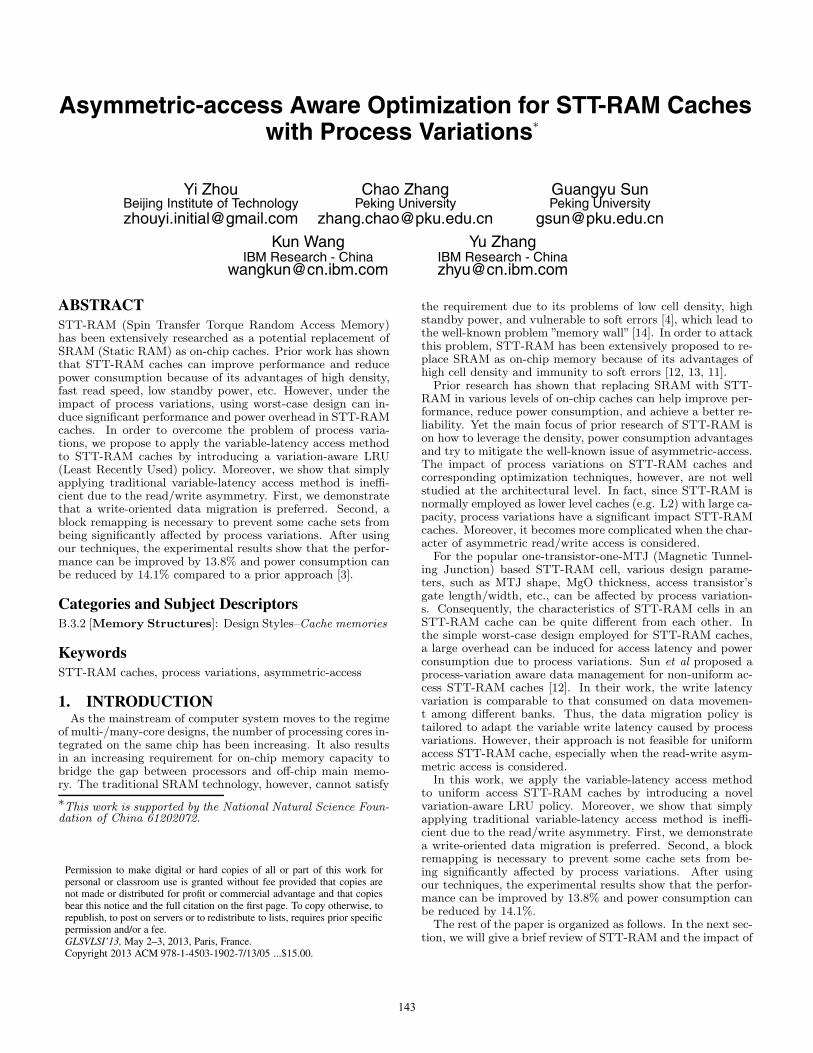
ure 1. In our variable latency cache, we partition these cachelines into two parts, which are called the fast-access part (FAP)and the slow-access part (SAP). The partitioning is based onthe distribution of the access latency to different cache lines.Since the STT-RAM cache has asymmetric read/write accesslatency, we can have different partitioning policies based onread latency, write latency, or a combination of them. The im-pact of partitioning policies is discussed later in subsection 3.3.
Figure 1: An example of distribution for cache writelatency.
In the example of Figure 1, we partition the STT-RAM cachebased on write latency and set 21 clock cycles as the thresholdto differentiate SAP from FAP. In other words, for the cachelines that can be written within 21 cycles, they are groupedtogether as the FAP of the STT-RAM cache. The rest cacheslines, which have the longer write latency than 21 cycles, areorganized as the SAP of the STT-RAM. The discussion of se-lecting a proper threshold will be introduced in subsection 3.3.For each part of the STT-RAM cache, the write latency is fixedand determined by the longest access latency of the cache linein the part. For the same example in Figure 1, the write laten-cy to SAP and FAP are 21 cycles and 35 cycles, respectively.
The organization of FAP and SAP for STT-RAM cache isdifferent from traditional variable-access latency cache struc-ture in prior work [3, 8, 7]. In prior work, the access latency isidentified with a fine granularity, which is a single cache line.It means that the access to each cache line can be finished assoon as possible. For our variable-latency access STT-RAMcache, however, the cache is partitioned with a coarse granu-larity (e.g. SAP and FAP), and the access latency to a cacheline is decided by the slowest cache line in the same part.
It is easy to find that the traditional fine granularity basedstructure can achieve a better performance than ours for thestatic data allocation. Static data allocation means that a dataare placed in fixed positions (cache blocks) before they are e-victed. On the contrary, a dynamic data allocation means thatdata can be moved from SAP to FAP if they are frequent-ly accessed so that the performance is improved. It shouldbe addressed that a dynamic data allocation is necessary forvariable-latency access cache due to temporal data locality.Otherwise, if most frequently accessed data are always allo-cated in the cache lines with slow access latency, we may gainlittle benefits of using variable latency access cache.
When the dynamic data allocation is employed, our variable-latency access cache structure can outperform those in priorwork for three reasons [3, 8, 7]. First, data migration is feasibleto be realized when there are only SAP and FAP. On the con-trary, in the traditional structure, there will be many differentlevels of access latency, which can significantly increase the de-sign complexity since data migration can happen between anytwo cache lines with different access latency. Moreover, when
the cache remapping technique is applied (introduced later inthe paper), design complexity of a fine granularity policy isfurther significantly increased. In fact, the dynamic allocationpolicy is not introduced in most of traditional structures [3,8]. Second, a coarse partitioning granularity can help reducethe overhead of tracing access latency of different cache lines.In traditional structure, a table is needed to record the ac-cess latency of each individual cache line. Such a table caninduce non-trivial overhead, especially for STT-RAM cachewhich normally has the large capacity and significant varianceof write latency. Third, the design complexity for variable-access latency control can be reduced. For example, as intro-duced in Bennaser’s work [3], a buffer is needed to enable thevariable-latency access. The design complexity of such a bufferand related control logic increases with the total number of d-ifferent access latency. Since we only have two different accesslatency for SAP and FAP, the design can be really simple.
3.2 A Novel LRU Policy for Data MigrationAs discussed in the last subsection, a dynamic data alloca-
tion is critical to exploit the benefits of using variable-latencyaccess cache. In Sun’s work, dynamic data allocation is en-abled through data migration among different cache banks inthe NUCA [11]. This data migration method, however, is notfeasible for the uniform cache architecture. First, the datamigration technique in NUCA can be enabled without the ex-istence of process variations. Sometimes, the migration mayeven depends on the infrastructure of the NUCA (e.g. network-on-chip). When we apply the data migration in uniform cache,the extra design overhead must be considered. Second, thedata locality is not considered in their approach, which maydestroy the LRU replacement policy. Third, using the DPVA-NUVA-2 policy, both read and write operations can trigger thedata migration. We will discuss in next subsection that such acombination of migration technique can harm the performancein uniform cache. Thus, we propose a new LRU policy, whichcan also enables the data migration at the same time.
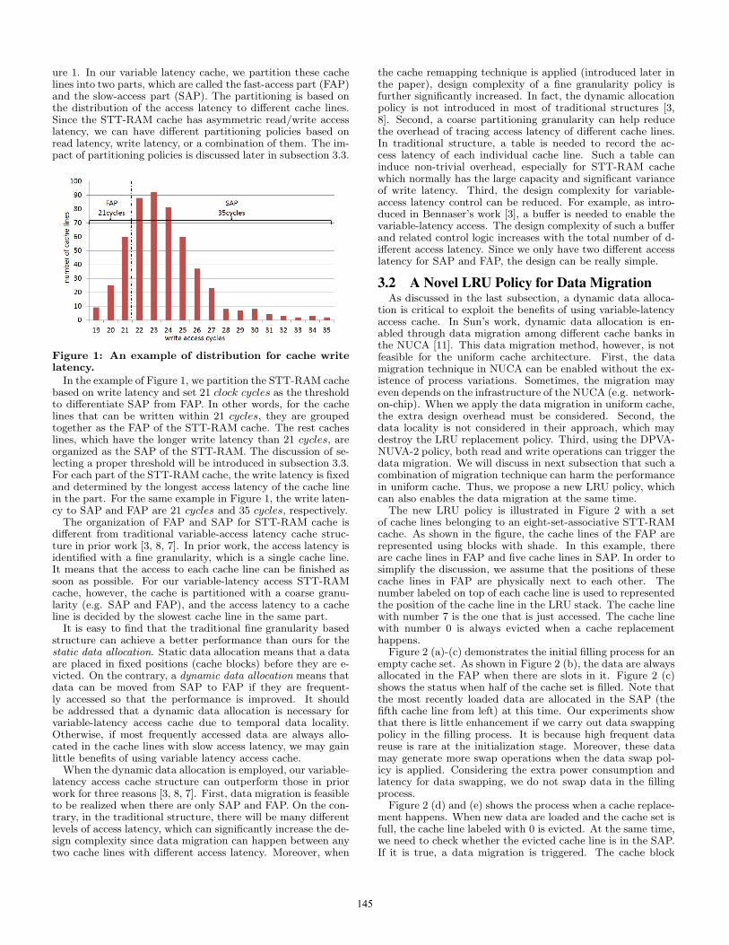
The new LRU policy is illustrated in Figure 2 with a setof cache lines belonging to an eight-set-associative STT-RAMcache. As shown in the figure, the cache lines of the FAP arerepresented using blocks with shade. In this example, thereare cache lines in FAP and five cache lines in SAP. In order tosimplify the discussion, we assume that the positions of thesecache lines in FAP are physically next to each other. Thenumber labeled on top of each cache line is used to representedthe position of the cache line in the LRU stack. The cache linewith number 7 is the one that is just accessed. The cache linewith number 0 is always evicted when a cache replacementhappens.
Figure 2 (a)-(c) demonstrates the initial filling process for anempty cache set. As shown in Figure 2 (b), the data are alwaysallocated in the FAP when there are slots in it. Figure 2 (c)shows the status when half of the cache set is filled. Note thatthe most recently loaded data are allocated in the SAP (thefifth cache line from left) at this time. Our experiments showthat there is little enhancement if we carry out data swappingpolicy in the filling process. It is because high frequent datareuse is rare at the initialization stage. Moreover, these datamay generate more swap operations when the data swap pol-icy is applied. Considering the extra power consumption andlatency for data swapping, we do not swap data in the fillingprocess.
Figure 2 (d) and (e) shows the process when a cache replace-ment happens. When new data are loaded and the cache set isfull, the cache line labeled with 0 is evicted. At the same time,we need to check whether the evicted cache line is in the SAP.If it is true, a data migration is triggered. The cache block
145
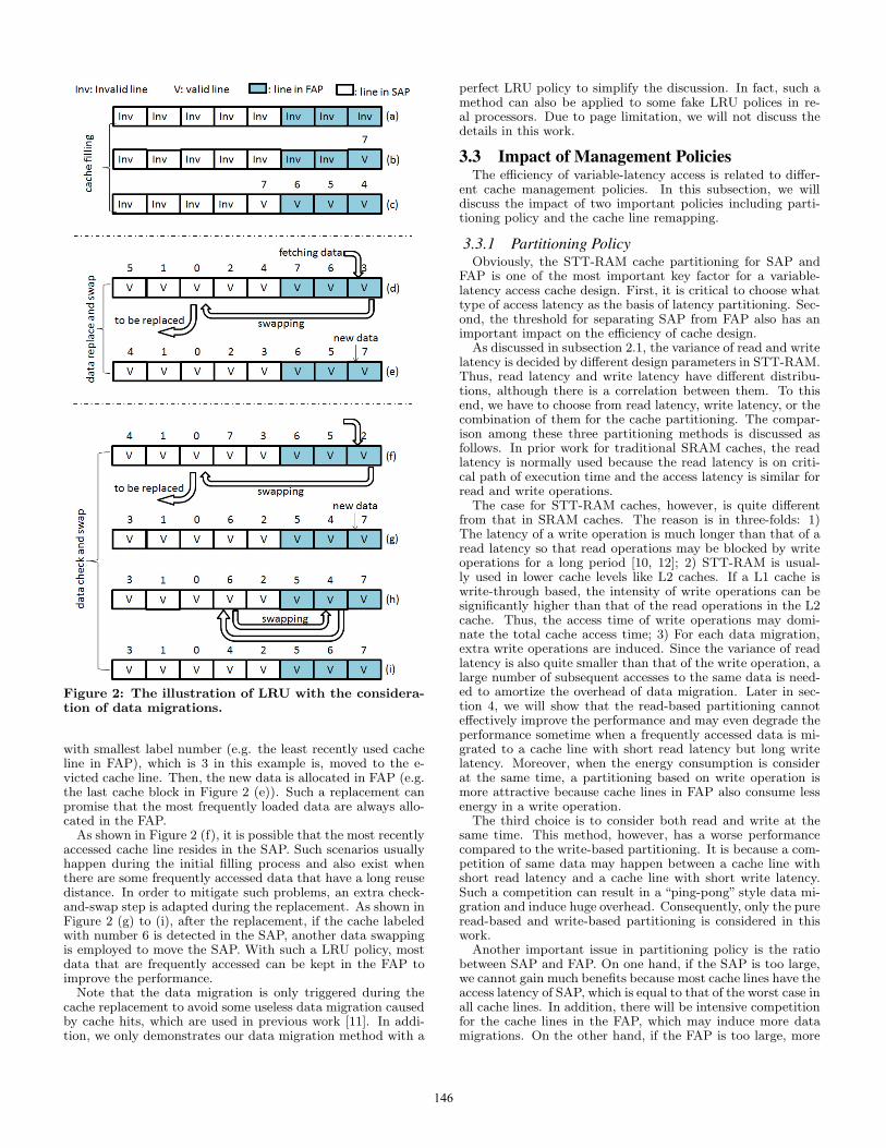
Figure 2: The illustration of LRU with the considera-tion of data migrations.
with smallest label number (e.g. the least recently used cacheline in FAP), which is 3 in this example is, moved to the e-victed cache line. Then, the new data is allocated in FAP (e.g.the last cache block in Figure 2 (e)). Such a replacement canpromise that the most frequently loaded data are always allo-cated in the FAP.
As shown in Figure 2 (f), it is possible that the most recentlyaccessed cache line resides in the SAP. Such scenarios usuallyhappen during the initial filling process and also exist whenthere are some frequently accessed data that have a long reusedistance. In order to mitigate such problems, an extra check-and-swap step is adapted during the replacement. As shown inFigure 2 (g) to (i), after the replacement, if the cache labeledwith number 6 is detected in the SAP, another data swappingis employed to move the SAP. With such a LRU policy, mostdata that are frequently accessed can be kept in the FAP toimprove the performance.
Note that the data migration is only triggered during thecache replacement to avoid some useless data migration causedby cache hits, which are used in previous work [11]. In addi-tion, we only demonstrates our data migration method with a
perfect LRU policy to simplify the discussion. In fact, such amethod can also be applied to some fake LRU polices in re-al processors. Due to page limitation, we will not discuss thedetails in this work.
3.3 Impact of Management PoliciesThe efficiency of variable-latency access is related to differ-
ent cache management policies. In this subsection, we willdiscuss the impact of two important policies including parti-tioning policy and the cache line remapping.
3.3.1 Partitioning PolicyObviously, the STT-RAM cache partitioning for SAP and
FAP is one of the most important key factor for a variable-latency access cache design. First, it is critical to choose whattype of access latency as the basis of latency partitioning. Sec-ond, the threshold for separating SAP from FAP also has animportant impact on the efficiency of cache design.
As discussed in subsection 2.1, the variance of read and writelatency is decided by different design parameters in STT-RAM.Thus, read latency and write latency have different distribu-tions, although there is a correlation between them. To thisend, we have to choose from read latency, write latency, or thecombination of them for the cache partitioning. The compar-ison among these three partitioning methods is discussed asfollows. In prior work for traditional SRAM caches, the readlatency is normally used because the read latency is on criti-cal path of execution time and the access latency is similar forread and write operations.
The case for STT-RAM caches, however, is quite differentfrom that in SRAM caches. The reason is in three-folds: 1)The latency of a write operation is much longer than that of aread latency so that read operations may be blocked by writeoperations for a long period [10, 12]; 2) STT-RAM is usual-ly used in lower cache levels like L2 caches. If a L1 cache iswrite-through based, the intensity of write operations can besignificantly higher than that of the read operations in the L2cache. Thus, the access time of write operations may domi-nate the total cache access time; 3) For each data migration,extra write operations are induced. Since the variance of readlatency is also quite smaller than that of the write operation, alarge number of subsequent accesses to the same data is need-ed to amortize the overhead of data migration. Later in sec-tion 4, we will show that the read-based partitioning cannoteffectively improve the performance and may even degrade theperformance sometime when a frequently accessed data is mi-grated to a cache line with short read latency but long writelatency. Moreover, when the energy consumption is considerat the same time, a partitioning based on write operation ismore attractive because cache lines in FAP also consume lessenergy in a write operation.
The third choice is to consider both read and write at thesame time. This method, however, has a worse performancecompared to the write-based partitioning. It is because a com-petition of same data may happen between a cache line withshort read latency and a cache line with short write latency.Such a competition can result in a “ping-pong” style data mi-gration and induce huge overhead. Consequently, only the pureread-based and write-based partitioning is considered in thiswork.
Another important issue in partitioning policy is the ratiobetween SAP and FAP. On one hand, if the SAP is too large,we cannot gain much benefits because most cache lines have theaccess latency of SAP, which is equal to that of the worst case inall cache lines. In addition, there will be intensive competitionfor the cache lines in the FAP, which may induce more datamigrations. On the other hand, if the FAP is too large, more
146
cache lines with long access latency will be included in the FAPso that the access latency to FAP will be increased. Thus,the benefits of data migration will also be reduced becausethe gap of access latency between SAP and FAP is shrunk.The optimized ratio between SAP and FAP is related to thedistribution of process variations on STT-RAM cells and thedata access pattern. For the STT-RAM cache and workloadsin section 4, the results show that the optimized ratio is in therange of 4 to 7. Thus, the threshold 21 cycles in subsection 3.1is plausible, for the ratio between SAP and FAP is nearly 4.
3.3.2 Cache Line RemappingDue to the correlation of process variations, the physical po-
sition allocation of cache lines in FAP or SAP can be quite non-uniform. It means that the ratio between SAP and FAP canvary a lot all through the whole cache. Consequently, the effi-ciency of using variable-latency access cache will be decreased.In order to mitigate this problem, a cache remapping methodintroduced in prior research need to be adopted to achieve auniform distribution of ratio between SAP and FAP [6]. Fig-ure 3 shows an example of such a remapping method. Notethat the number labeled on the cache lines represent the indexof cache set that those cache lines belong to. The cache lineswith shade color represent the cache lines in FAP. We can findthat, after remapping, the ratio between SAP and FAP becomeuniform among different cache sets.
Figure 3: An example of cache line remapping.
4. EVALUATIONIn this section, we first evaluate our variable-latency access
cache with different management policies. Then, we compareour optimization design to the worst case design and an ap-proach from prior work [3], in respect of performance and en-ergy consumption.
4.1 Experiment SetupFor system level simulation, we use SIMICS simulator to e-
valuate performance. It is configured to model an eight-coreprocessor. Each core is Ultra-SPARC-like with a 2GHz fre-quency. There are three levels of caches. The IL1/DL1 cachesare SRAM based and the capacities are set to 64KB/64KB.The L2 cache is a 16-way 4MB STT-RAM cache. The simula-tor captures data addresses from all loads, stores, and prefetchoperations. We use the information to calculate the memo-ry access intensity, and use that to compute the energy con-sumption of the cache hierarchy. Our workloads are sets ofmulti-threaded benchmarks from PARSEC.
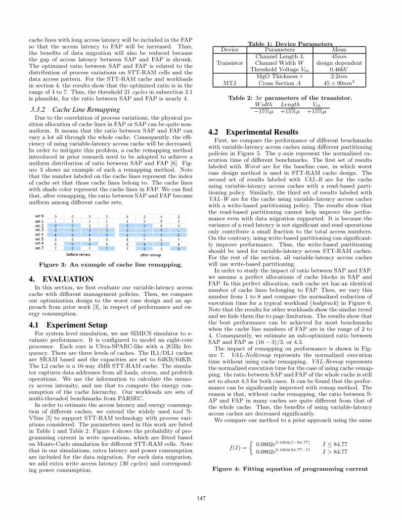
In order to estimate the access latency and energy consump-tion of different caches, we extend the widely used tool N-VSim [5] to support STT-RAM technology with process vari-ations considered. The parameters used in this work are listedin Table 1 and Table 2. Figure 4 shows the probability of pro-gramming current in write operations, which are fitted basedon Monte-Carlo simulation for different STT-RAM cells. Notethat in our simulations, extra latency and power consumptionare included for the data migration. For each data migration,we add extra write access latency (30 cycles) and correspond-ing power consumption.
Table 1: Device ParametersDevice Parameters Mean
Channel Length L 45nmTransistor Channel Width W design dependent
Threshold Voltage Vth 0.466VMgO Thickness τ 2.2nm
MTJ Cross Section A 45× 90nm2
Table 2: 3σ parameters of the transistor.Width Length Vth
−15%μ +15%μ +15%μ
4.2 Experimental ResultsFirst, we compare the performance of different benchmarks
with variable-latency access caches using different partitioningpolicies in Figure 5. The y-axis represent the normalized ex-ecution time of different benchmarks. The first set of resultslabeled with Worst are for the baseline case, in which worstcase design method is used in STT-RAM cache design. Thesecond set of results labeled with VAL-R are for the cacheusing variable-latency access caches with a read-based parti-tioning policy. Similarly, the third set of results labeled withVAL-W are for the cache using variable-latency access cacheswith a write-based partitioning policy. The results show thatthe read-based partitioning cannot help improve the perfor-mance even with data migration supported. It is because thevariance of a read latency is not significant and read operationsonly contribute a small fraction to the total access numbers.On the contrary, using write-based partitioning can significant-ly improve performance. Thus, the write-based partitioningshould be used for variable-latency access STT-RAM caches.For the rest of the section, all variable-latency access cacheswill use write-based partitioning.
In order to study the impact of ratio between SAP and FAP,we assume a perfect allocations of cache blocks in SAP andFAP. In this perfect allocation, each cache set has an identicalnumber of cache lines belonging to FAP. Then, we vary thisnumber from 1 to 8 and compare the normalized reduction ofexecution time for a typical workload (bodytrack) in Figure 6.Note that the results for other workloads show the similar trendand we hide them due to page limitation. The results show thatthe best performance can be achieved for most benchmarkswhen the cache line numbers of FAP are in the range of 2 to4. Consequently, we estimate an sub-optimized ratio betweenSAP and FAP as (16− 3)/3, or 4.3.
The impact of remapping on performance is shown in Fig-ure 7. VAL-NoRemap represents the normalized executiontime without using cache remapping. VAL-Remap representsthe normalized execution time for the case of using cache remap-ping. the ratio between SAP and FAP of the whole cache is stillset to about 4.3 for both cases. It can be found that the perfor-mance can be significantly improved with remap method. Thereason is that, without cache remapping, the ratio between S-AP and FAP in many caches are quite different from that ofthe whole cache. Thus, the benefits of using variable-latencyaccess caches are decreased significantly.
We compare our method to a prior approach using the same
f(I) =
{0.0802e0.1604(I−84.77) I ≤ 84.77
0.0802e0.1604(84.77−I) I > 84.77
Figure 4: Fitting equation of programming current
147
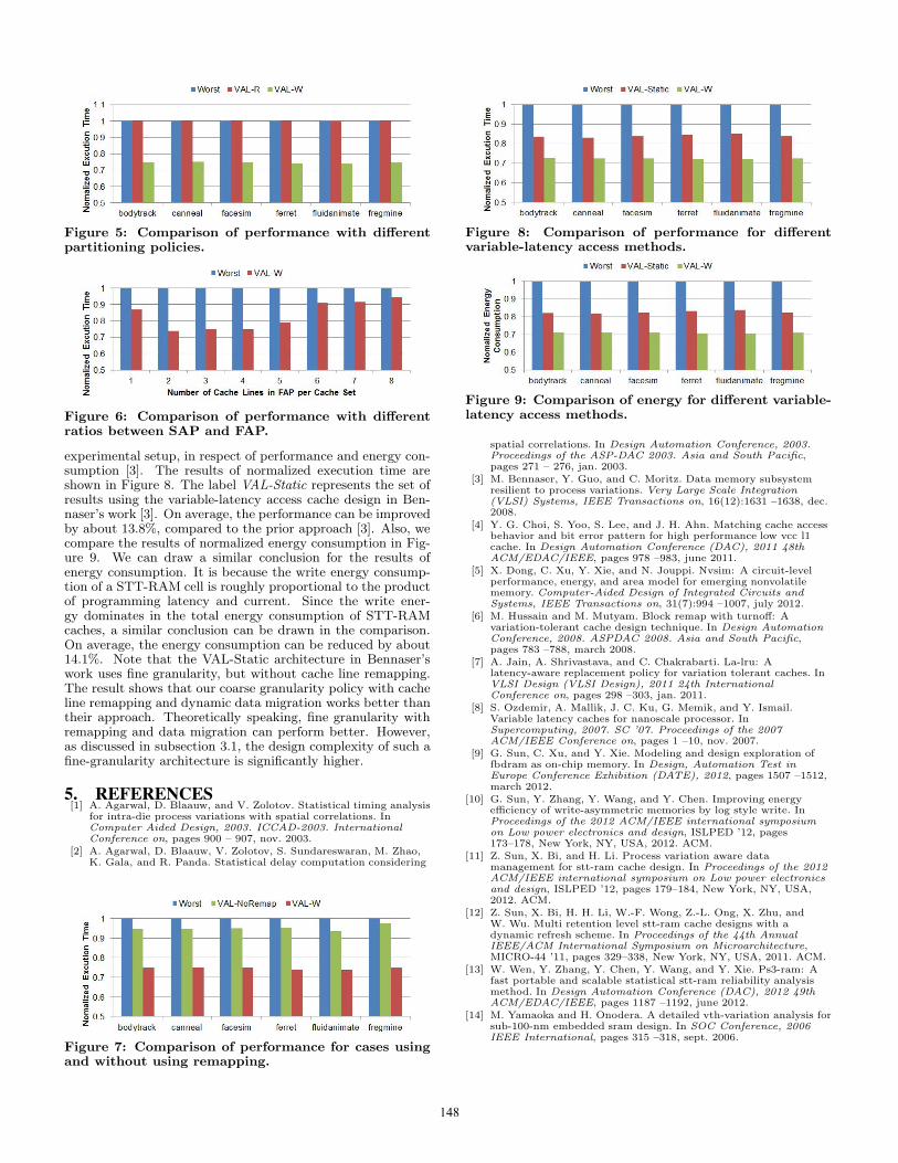
Figure 5: Comparison of performance with differentpartitioning policies.
Figure 6: Comparison of performance with differentratios between SAP and FAP.
experimental setup, in respect of performance and energy con-sumption [3]. The results of normalized execution time areshown in Figure 8. The label VAL-Static represents the set ofresults using the variable-latency access cache design in Ben-naser’s work [3]. On average, the performance can be improvedby about 13.8%, compared to the prior approach [3]. Also, wecompare the results of normalized energy consumption in Fig-ure 9. We can draw a similar conclusion for the results ofenergy consumption. It is because the write energy consump-tion of a STT-RAM cell is roughly proportional to the productof programming latency and current. Since the write ener-gy dominates in the total energy consumption of STT-RAMcaches, a similar conclusion can be drawn in the comparison.On average, the energy consumption can be reduced by about14.1%. Note that the VAL-Static architecture in Bennaser’swork uses fine granularity, but without cache line remapping.The result shows that our coarse granularity policy with cacheline remapping and dynamic data migration works better thantheir approach. Theoretically speaking, fine granularity withremapping and data migration can perform better. However,as discussed in subsection 3.1, the design complexity of such afine-granularity architecture is significantly higher.
5. REFERENCES[1] A. Agarwal, D. Blaauw, and V. Zolotov. Statistical timing analysis
for intra-die process variations with spatial correlations. InComputer Aided Design, 2003. ICCAD-2003. InternationalConference on, pages 900 – 907, nov. 2003.
[2] A. Agarwal, D. Blaauw, V. Zolotov, S. Sundareswaran, M. Zhao,K. Gala, and R. Panda. Statistical delay computation considering
Figure 7: Comparison of performance for cases usingand without using remapping.
Figure 8: Comparison of performance for differentvariable-latency access methods.
Figure 9: Comparison of energy for different variable-latency access methods.
spatial correlations. In Design Automation Conference, 2003.Proceedings of the ASP-DAC 2003. Asia and South Pacific,pages 271 – 276, jan. 2003.
[3] M. Bennaser, Y. Guo, and C. Moritz. Data memory subsystemresilient to process variations. Very Large Scale Integration(VLSI) Systems, IEEE Transactions on, 16(12):1631 –1638, dec.2008.
[4] Y. G. Choi, S. Yoo, S. Lee, and J. H. Ahn. Matching cache accessbehavior and bit error pattern for high performance low vcc l1cache. In Design Automation Conference (DAC), 2011 48thACM/EDAC/IEEE, pages 978 –983, june 2011.
[5] X. Dong, C. Xu, Y. Xie, and N. Jouppi. Nvsim: A circuit-levelperformance, energy, and area model for emerging nonvolatilememory. Computer-Aided Design of Integrated Circuits andSystems, IEEE Transactions on, 31(7):994 –1007, july 2012.
[6] M. Hussain and M. Mutyam. Block remap with turnoff: Avariation-tolerant cache design technique. In Design AutomationConference, 2008. ASPDAC 2008. Asia and South Pacific,pages 783 –788, march 2008.
[7] A. Jain, A. Shrivastava, and C. Chakrabarti. La-lru: Alatency-aware replacement policy for variation tolerant caches. InVLSI Design (VLSI Design), 2011 24th InternationalConference on, pages 298 –303, jan. 2011.
[8] S. Ozdemir, A. Mallik, J. C. Ku, G. Memik, and Y. Ismail.Variable latency caches for nanoscale processor. InSupercomputing, 2007. SC ’07. Proceedings of the 2007ACM/IEEE Conference on, pages 1 –10, nov. 2007.
[9] G. Sun, C. Xu, and Y. Xie. Modeling and design exploration offbdram as on-chip memory. In Design, Automation Test inEurope Conference Exhibition (DATE), 2012, pages 1507 –1512,march 2012.
[10] G. Sun, Y. Zhang, Y. Wang, and Y. Chen. Improving energyefficiency of write-asymmetric memories by log style write. InProceedings of the 2012 ACM/IEEE international symposiumon Low power electronics and design, ISLPED ’12, pages173–178, New York, NY, USA, 2012. ACM.
[11] Z. Sun, X. Bi, and H. Li. Process variation aware datamanagement for stt-ram cache design. In Proceedings of the 2012ACM/IEEE international symposium on Low power electronicsand design, ISLPED ’12, pages 179–184, New York, NY, USA,2012. ACM.
[12] Z. Sun, X. Bi, H. H. Li, W.-F. Wong, Z.-L. Ong, X. Zhu, andW. Wu. Multi retention level stt-ram cache designs with adynamic refresh scheme. In Proceedings of the 44th AnnualIEEE/ACM International Symposium on Microarchitecture,MICRO-44 ’11, pages 329–338, New York, NY, USA, 2011. ACM.
[13] W. Wen, Y. Zhang, Y. Chen, Y. Wang, and Y. Xie. Ps3-ram: Afast portable and scalable statistical stt-ram reliability analysismethod. In Design Automation Conference (DAC), 2012 49thACM/EDAC/IEEE, pages 1187 –1192, june 2012.
[14] M. Yamaoka and H. Onodera. A detailed vth-variation analysis forsub-100-nm embedded sram design. In SOC Conference, 2006IEEE International, pages 315 –318, sept. 2006.
148
Related Documents