1 | Page ANALOG SIGNAL PROCESSING A SUMMER INTERN PROJECT REPORT Submitted by Mohit Lamba Roll No. 06514802812 in fulfillment of Summer Internship for the award of the degree of BACHELOR OF TECHNOLOGY in ELECTRONICS AND COMMUNICATION ENGINEERING Maharaja Agrasen Institute of Technology Guru Gobind Singh Indraprastha University, Delhi

Welcome message from author
This document is posted to help you gain knowledge. Please leave a comment to let me know what you think about it! Share it to your friends and learn new things together.
Transcript

1 | P a g e
ANALOG SIGNAL PROCESSING
A SUMMER INTERN PROJECT REPORT
Submitted by
Mohit Lamba
Roll No. 06514802812
in fulfillment of Summer Internship for the award of the degree of
BACHELOR OF TECHNOLOGY
in
ELECTRONICS AND COMMUNICATION ENGINEERING
Maharaja Agrasen Institute of Technology
Guru Gobind Singh Indraprastha University, Delhi
2 | P a g e
Maharaja Agrasen Institute of Technology
To Whom It May Concern I Mohit Lamba, Enrolment No. 06514802812 from a student of Bachelor of Technology
(ECE), a class of 2012-16, Maharaja Agrasen Institute of Technology, Delhi hereby
declare that the Summer Training entitled ANALOG SIGNAL PROCESSING at
Radiance Edutech is an original work and the same has not been submitted to any other
Institute for the award of any other degree.
Date: Signature of the Student

3 | P a g e
Abstract
Although the world is today moving vastly towards digitisation of everything,
the signals actually present around us are analog in nature. Furthermore our five
senses also perceive analog signals only.
Hence Analog signal Processing is an integral part of complete design. My
report gives many convincing reasons for understanding well analog signal
processing and some of their techniques.
4 | P a g e
CONTENTS
1. Title page i
2. Certificate by the Supervisor ii
3. Acknowledgement iii
4. Abstract iv
5. List of figures v
6. Introduction 5
7. A universal filter using OTA 8
8. Wien bridge oscillator using OTA 12
9. Wien bridge oscillator using op-amp 16
10. An oscillator using CFOA 20
11. Amplitude modulator using OTA 23
12. Translinear circuits 26
13. Redesign of a OTA 30
14. References 35
5 | P a g e
Since all natural signals are analog, the analog circuits and techniques to process them arc unavoidable in spite of almost everything going digital. In particular, several analog functions/circuits such as amplification, rectification, continuous-time liltering, analog-to-digital (A/D) and digital-to-analog (D/A) conversion are impossible to be performed by digital circuits regardless of the advances made in the digital circuits and techniques. Thus, analog circuits arc indispensable in many applications. Further some applications like image processing and speech recognition are better carried out by analog VLSI or mixed signal VLSIs than digital circuits.
The Ubiquitous Op-amp
In the world of analog circuits, it is widely believed that almost any function can be performed using the classical voltage-mode op-amp (VOA). Thus, on one hand, one can realize using op-amps, all linear circuits such as the four controlled sources (VCVS, VCCS, CCVS and CCCS), integrators, differentiators, summing and differencing amplifiers, variable-gain differential/instrumentation amplifiers, filters, oscillators etc. On the other hand, op-amps can also be used to realize a variety of non-linear functional circuits such as comparators, Schmitt trigger, sample and hold circuits, precision rectifiers, multivibrators, log-antilog amplifiers and a variety of relaxation oscillators.
Short comings of Op-amp
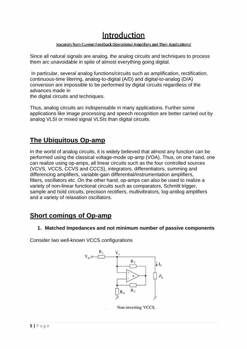
1. Matched Impedances and not minimum number of passive components
Consider Iwo well-known VCCS configurations
6 | P a g e
A straight forward analysis of the circuit shows that the relation between the output current and input voltage (assuming ideal op-amp) for the circuit is given by
From the above, it may be seen that to realize a VCCS. the op-amp circuits not only require more than the minimum number of resistances necessary' but also require that all the four resistors should have either a relationship R1 = R2R4/R3 or else all the four resistors be equal-valued and matched so that the output current becomes independent of the output voltage and depends only on the input voltage, as required. Thus, any mismatch in resistor values from the intended ones would degrade the performance of the circuit.
2. The Gain-Bandwidth Conflict
The gain and the bandwidth cannot be set independent of each other i.e. there is a gain-bandwidth conflict.
3. Slew-Rate Based Limitations
At large input voltages or high frequencies or a combination of the two, the output voltage fails to respond with the same speed as the input (due to finite maximum SR) and this results in slew-induced distortion. Conversely, to avoid slew-induced distortion, the input voltages and their frequencies are constrained to be kept small. Thus, the finite slew rate affects both the dynamic range of the op-amp circuits as well as the maximum frequency of the input signal which can be applied without causing noticeable distortion in the output waveform.
ADVANTAGES OF OTA
1. Less Passive components count
2. Also full active active circuits can be made as resistors, inductors and
capacitors all can be simulated using OTA
3. So fully integrated IC components can be made
4. Electronically controllable

7 | P a g e
However when larger circuit design became even difficult with OTA, current conveyors proposed by Sedra and Smith in 1968 gained a lot of popularity especially since 2000s.
8 | P a g e
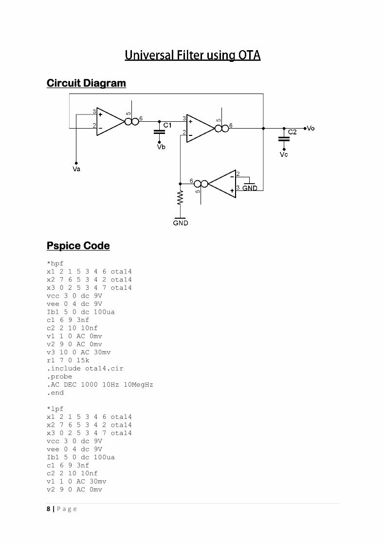
Circuit Diagram
Pspice Code
*hpf
x1 2 1 5 3 4 6 ota14
x2 7 6 5 3 4 2 ota14
x3 0 2 5 3 4 7 ota14
vcc 3 0 dc 9V
vee 0 4 dc 9V
Ib1 5 0 dc 100ua
c1 6 9 3nf
c2 2 10 10nf
v1 1 0 AC 0mv
v2 9 0 AC 0mv
v3 10 0 AC 30mv
r1 7 0 15k
.include ota14.cir
.probe
.AC DEC 1000 10Hz 10MegHz
.end
*lpf
x1 2 1 5 3 4 6 ota14
x2 7 6 5 3 4 2 ota14
x3 0 2 5 3 4 7 ota14
vcc 3 0 dc 9V
vee 0 4 dc 9V
Ib1 5 0 dc 100ua
c1 6 9 3nf
c2 2 10 10nf
v1 1 0 AC 30mv
v2 9 0 AC 0mv

9 | P a g e
v3 10 0 AC 0mv
r1 7 0 15k
.include ota14.cir
.probe
.AC DEC 1000 10Hz 10MegHz
.end
*bpf
x1 2 1 5 3 4 6 ota14
x2 7 6 5 3 4 2 ota14
x3 0 2 5 3 4 7 ota14
vcc 3 0 dc 9V
vee 0 4 dc 9V
Ib1 5 0 dc 100ua
c1 6 9 3nf
c2 2 10 10nf
v1 1 0 AC 0mv
v2 9 0 AC 30mv
v3 10 0 AC 0mv
r1 7 0 4.86k
.include ota14.cir
.probe
.AC DEC 1000 10Hz 10MegHz
.end
*apf
x1 2 1 5 3 4 6 ota14
x2 7 6 5 3 4 2 ota14
x3 0 2 5 3 4 7 ota14
vcc 3 0 dc 9V
vee 0 4 dc 9V
Ib1 5 0 dc 100ua
c1 6 9 3nf
c2 2 10 10nf
v1 1 0 AC 30mv
v2 0 9 AC 30mv
v3 10 0 AC 30mv
r1 7 0 4.86k
.include ota14.cir
.probe
.AC DEC 1000 10Hz 10MegHz
.end
10 | P a g e
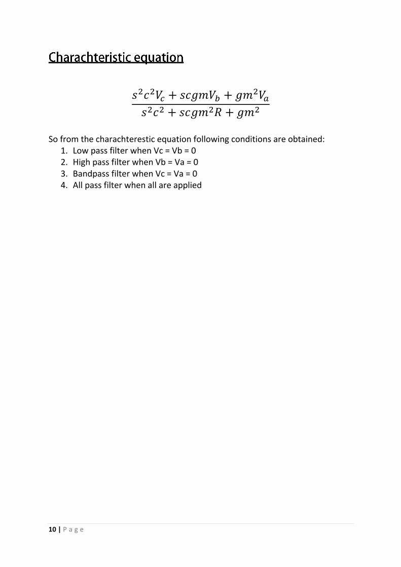
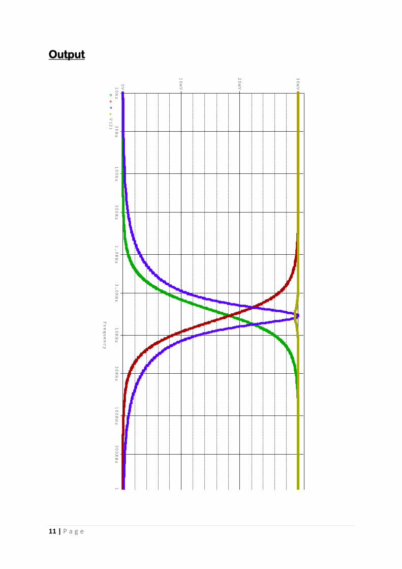
So from the charachterestic equation following conditions are obtained:
1. Low pass filter when Vc = Vb = 0 2. High pass filter when Vb = Va = 0 3. Bandpass filter when Vc = Va = 0 4. All pass filter when all are applied
11 | P a g e
Output
Frequency
10Hz
30Hz
100Hz
300Hz
1.0KHz
3.0KHz
10KHz
30KHz
100KHz
300KHz
1.0MHz
3.0MHz
10MHz
V(2)
0V
10mV
20mV
30mV

12 | P a g e
Circuit Diagram :
Pspice Code :
X1 1 2 4 1 ota
X2 0 1 5 1 ota
X3 1 0 3 2 ota
c1 2 0 0.1uf
c2 1 0 0.1uf
Ib1 4 0 122.5ua
.param val=117ua
*Ib2 5 0 119.3ua
Ib2 5 0 {val}
Ib3 3 0 100ua
.include ota.cir
.four 3.38khz 11 v(1)
*.step param val 117ua 120ua 1ua
.tran 1ms 500ms 0.01ms 0.01ms
.probe
.end

13 | P a g e
Transient Response :
Time
10.0ms
20.0ms
30.0ms
40.0ms
50.0ms
60.0ms
70.0ms
80.0ms
90.0ms
100.0ms
0.8msV(1)
-20mV
-10mV
0V
10mV
20mV
14 | P a g e
Steady State Response (10x Zoom)
Time
60.600ms
60.800ms
61.000ms
61.200ms
61.400ms
61.600ms
61.800ms
62.000ms
62.200ms
62.400ms
62.600ms
62.800ms
60.428ms
V(1)
-10.0mV
0V
10.0mV
20.0mV
-19.9mV

15 | P a g e
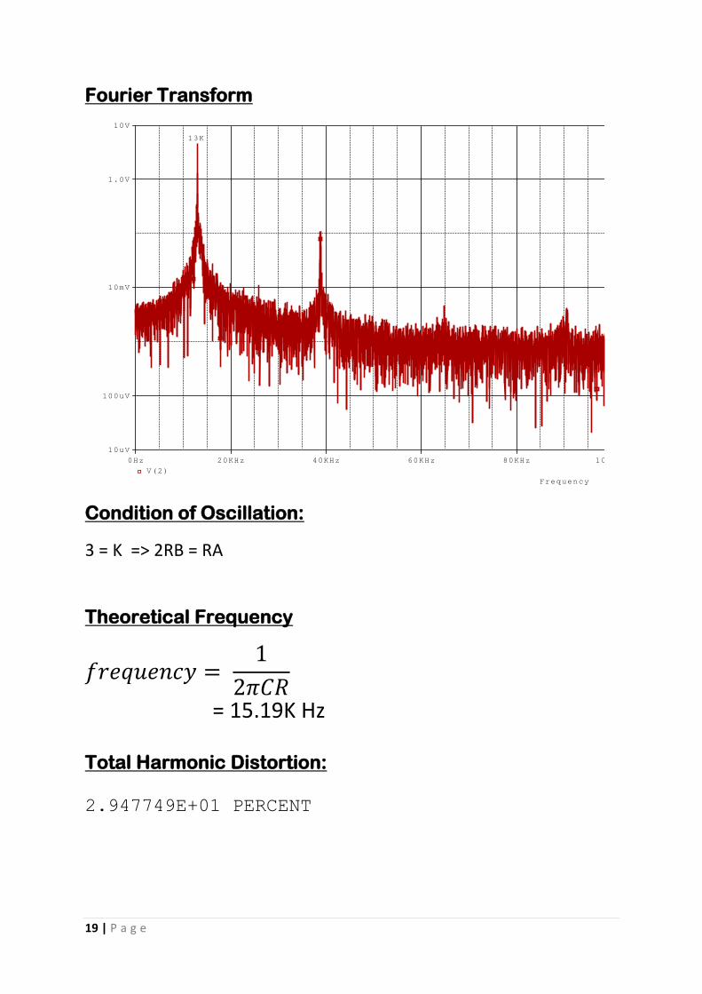
Fourier Transform
Theoretical Frequency :
= 3.38 KHz
Total Harmonic Distortion: 1.311593E+01 PERCENT
Frequency
0Hz 5KHz 10KHz 15KHz 20KHz 25KHz 30KHz 35KHz 40KHz 45KHz 50KHz 55KHz 60KHz 65KHz 70KHz
V(1)
10nV
1.0uV
100uV
10mV
1.0nV
100mV
3.1 K

16 | P a g e
Circuit Diagram :
Pspice Code : x1 1 5 3 4 2 ua741
r1 1 0 1k
c1 1 0 0.01uf
r2 1 6 1k
c2 6 2 0.01uf
ra 5 2 10.29k
rb 5 0 5k
vcc 3 0 dc 50
vee 4 0 dc -50
.include opamp.cir
.tran 0 50ms 0.01ms 0.01ms
.four 15.19khz 11 v(2)
.probe v(2)
.end
Charachteristic Equation :
S2C2R2 + SCR(3-k)+1 = 0, where k= 1 +

17 | P a g e
Transient Response :
Time
2.00ms
4.00ms
6.00ms
8.00ms
10.00ms
12.00ms
14.00ms
16.00ms
18.00ms
20.00ms
22.00ms
24.00ms
0.04ms
V(2)
-4.00V
0V
4.00V
-7.34V
7.27V

18 | P a g e
Steady State Response (10x Zoom) :
Time
19.40ms
19.50ms
19.60ms
19.70ms
19.80ms
19.90ms
20.00ms
20.10ms
20.20ms
20.27ms
V(2)
-4.00V
0V
4.00V
-7.55V
7.38V
19 | P a g e
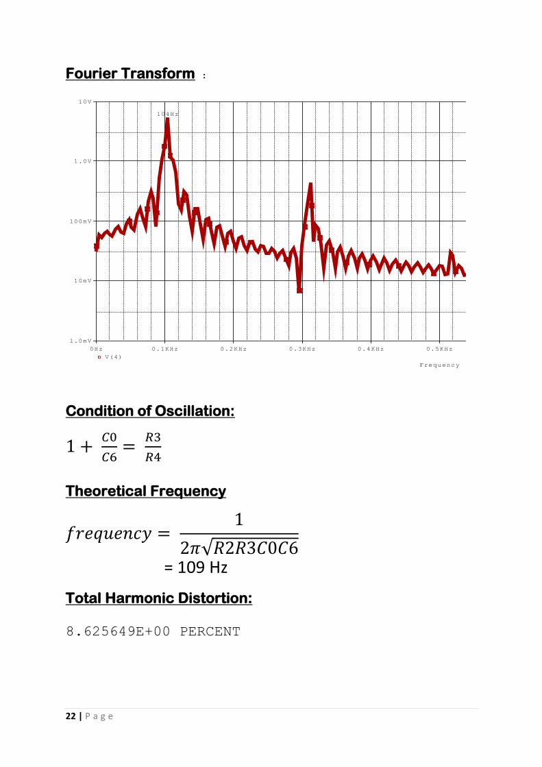
Fourier Transform
Condition of Oscillation:
3 = K => 2RB = RA
Theoretical Frequency
= 15.19K Hz
Total Harmonic Distortion: 2.947749E+01 PERCENT
Frequency
0Hz 20KHz 40KHz 60KHz 80KHz 100KHz 120KHz 140KHz 160KHz 180KHz
V(2)
100uV
10mV
1.0V
10uV
10V
13K

20 | P a g e
Circuit Diagram :
Pspice Code :
x1 1 3 5 6 4 2 AD844/AD
.param val=2.64k
.param vall=1uf
r3 1 0 {val}
c6 1 2 {vall} ic=1ua
*r10 1 2 11k
r4 3 0 1k
c 2 0 .8uf ic=1ua
*r11 2 0 11k
r2 3 4 1k
vcc 5 0 dc 10v
vee 6 0 dc -10v
.tran 30ms 250ms 0.01ms 0.01ms uic
*.step param vall .79uf .81uf 0.001uf
.probe v(4)
.four 0.109khz 11 v(4)
.include cfoa.cir
.end
Charachteristic Equation : S2[R2R3R4C0C6] + S[-R2R3C6+R2R4C0+C6R2R4] + R4 = 0

21 | P a g e
TOTAL RESPONSE (NO ZOOM) :
Time
0s
20ms
40ms
60ms
80ms
100ms
120ms
140ms
160ms
180ms
200ms
220ms
240ms
260ms
V(4)
-8.0V
-4.0V
0V
4.0V
8.0V
22 | P a g e
Fourier Transform :
Condition of Oscillation:
Theoretical Frequency
= 109 Hz
Total Harmonic Distortion: 8.625649E+00 PERCENT
Frequency
0Hz 0.1KHz 0.2KHz 0.3KHz 0.4KHz 0.5KHz 0.6KHz 0.7KHz 0.8KHz 0.9KHz 1.0KHz
V(4)
1.0mV
10mV
100mV
1.0V
10V
104Hz

23 | P a g e
Circuit Diagram :
Pspice Code :
X1 3 2 5 60 70 6 ota14
.param val=100k
R1 3 0 51
R2 2 0 51
R3 2 7 47k
R4 6 0 5.1k
R5 5 1 {val}
v 7 0 dc 1v
V1 1 0 sin(0 1v 5khz)
V2 3 0 sin(0 .5v 10khz)
vcc 60 0 dc 3V
vee 70 0 dc -3V
.include ota14.cir
*.step param val 90k 100k 5k
.tran 0 100ms .1ms .1ms
.probe
.end
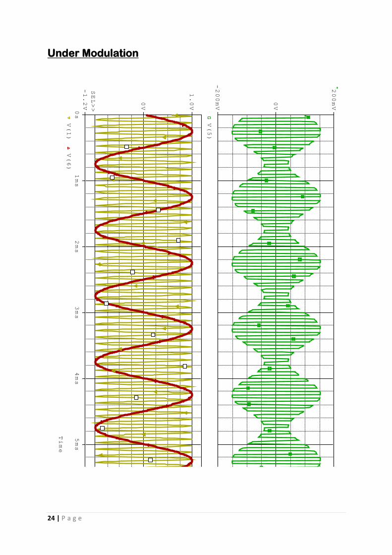
24 | P a g e
Under Modulation
Time
0s
1ms
2ms
3ms
4ms
5ms
6ms
7ms
8ms
9ms
10ms
V(1)
V(6)
0V
1.0V
-1.2V
SEL>>
V(5)
-200mV
0V
200mV

25 | P a g e
Over Modulation (DISTORTION IS CLEARLY SEEN)
Time
0s
1ms
2ms
3ms
4ms
5ms
6ms
7ms
8ms
9ms
10ms
V(1)
V(6)
-2.0V
0V
2.0V
V(5)
-400mV
0V
400mV
SEL>>
26 | P a g e
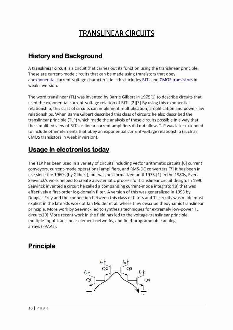
History and Background A translinear circuit is a circuit that carries out its function using the translinear principle. These are current-mode circuits that can be made using transistors that obey anexponential current-voltage characteristic—this includes BJTs and CMOS transistors in weak inversion. The word translinear (TL) was invented by Barrie Gilbert in 1975[1] to describe circuits that used the exponential current-voltage relation of BJTs.[2][3] By using this exponential relationship, this class of circuits can implement multiplication, amplification and power-law relationships. When Barrie Gilbert described this class of circuits he also described the translinear principle (TLP) which made the analysis of these circuits possible in a way that the simplified view of BJTs as linear current amplifiers did not allow. TLP was later extended to include other elements that obey an exponential current-voltage relationship (such as CMOS transistors in weak inversion).
Usage in electronics today The TLP has been used in a variety of circuits including vector arithmetic circuits,[6] current conveyors, current-mode operational amplifiers, and RMS-DC converters.[7] It has been in use since the 1960s (by Gilbert), but was not formalized until 1975.[1] In the 1980s, Evert Seevinck's work helped to create a systematic process for translinear circuit design. In 1990 Seevinck invented a circuit he called a companding current-mode integrator[8] that was effectively a first-order log-domain filter. A version of this was generalized in 1993 by Douglas Frey and the connection between this class of filters and TL circuits was made most explicit in the late 90s work of Jan Mulder et al. where they describe thedynamic translinear principle. More work by Seevinck led to synthesis techniques for extremely low-power TL circuits.[9] More recent work in the field has led to the voltage-translinear principle, multiple-input translinear element networks, and field-programmable analog arrays (FPAAs).
Principle

27 | P a g e
Here each BJT is considered to be identical with large β. So,
ICO1 = ICO2 = ICO3 = ICO4 and ic = Ico eVBE/ηVT
=> VBE = ηVT ln (ic / ICO) Now applying KVL,
VBE1 + VBE2 = VBE3 + VBE4 ...2
So using 1 and 2 we get
ic1 * ic2 = ic3 * ic4 The next section shows an application of this principle
... 1

28 | P a g e
Circuit Diagram :
Pspice Code :
vx 1 0 sin(0 .5v 10khz)
rx 1 2 1k
q1 2 0 3 n
x1 0 2 3 ua741
*vy 9 0 sin(1.5 1v 8khz 0 0 0DEG)
vy 9 0 pulse(0 1 0 0 0 1ms 2ms)
ry 9 4 1k
x2 0 4 5 ua741
q2 4 3 5 n
ro 11 6 1k
x3 0 6 11 ua741
q3 6 7 5 n
q4 8 0 7 n
x4 0 8 7 ua741
vw 10 0 dc 1v
rw 10 8 1k
.include opampvcc.cir
.MODEL n NPN(BF=300 VJE=0.7V)
.tran 0.1ms 4ms 0.01ms 0.01ms
.probe v(1) v(9) v(11) v(10)
.end
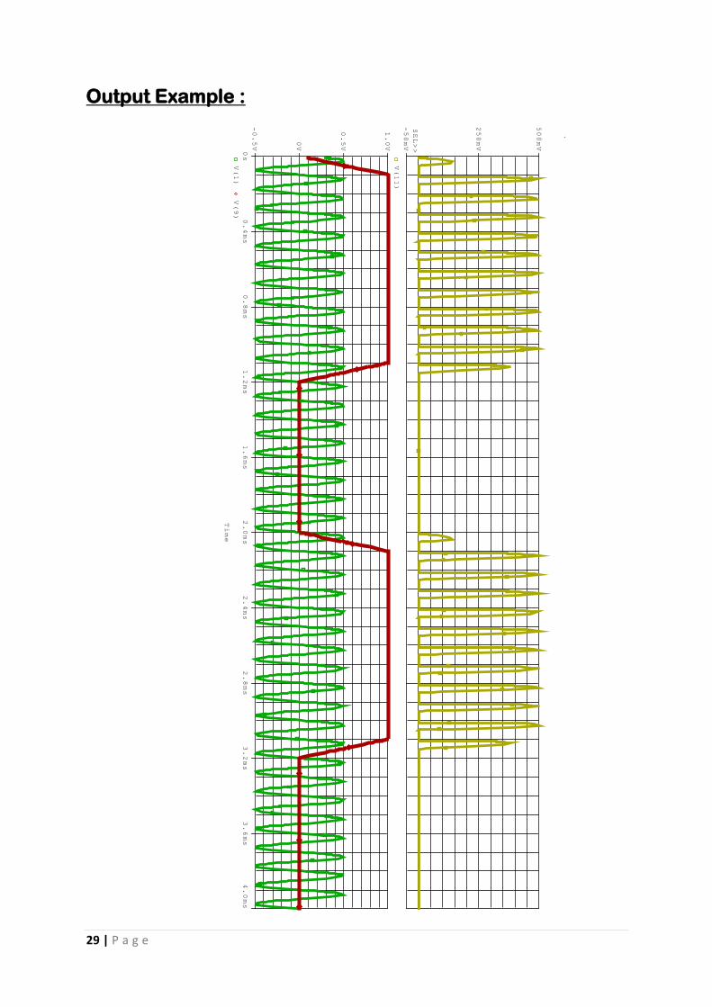
29 | P a g e
Output Example :
Time
0s
0.4ms
0.8ms
1.2ms
1.6ms
2.0ms
2.4ms
2.8ms
3.2ms
3.6ms
4.0ms
V(1)
V(9)
-0.5V
0V
0.5V
1.0V
V(11)
250mV
500mV
-50mV
SEL>>
30 | P a g e
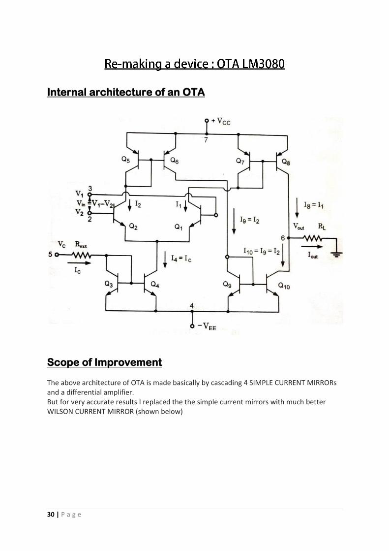
Internal architecture of an OTA
Scope of Improvement The above architecture of OTA is made basically by cascading 4 SIMPLE CURRENT MIRRORs and a differential amplifier. But for very accurate results I replaced the the simple current mirrors with much better WILSON CURRENT MIRROR (shown below)

31 | P a g e
My modified INTERNAL STRUCTURE of OTA now looks as below
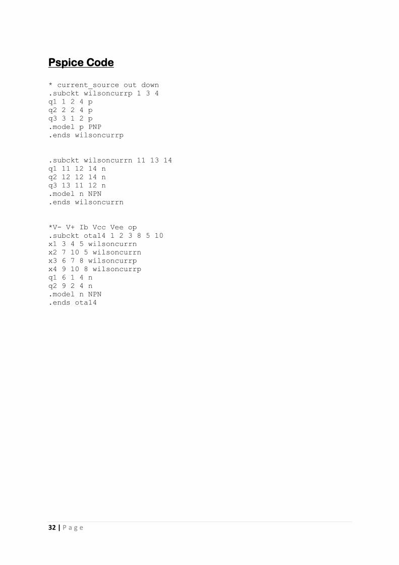
32 | P a g e
Pspice Code * current_source out down
.subckt wilsoncurrp 1 3 4
q1 1 2 4 p
q2 2 2 4 p
q3 3 1 2 p
.model p PNP
.ends wilsoncurrp
.subckt wilsoncurrn 11 13 14
q1 11 12 14 n
q2 12 12 14 n
q3 13 11 12 n
.model n NPN
.ends wilsoncurrn
*V- V+ Ib Vcc Vee op
.subckt ota14 1 2 3 8 5 10
x1 3 4 5 wilsoncurrn
x2 7 10 5 wilsoncurrn
x3 6 7 8 wilsoncurrp
x4 9 10 8 wilsoncurrp
q1 6 1 4 n
q2 9 2 4 n
.model n NPN
.ends ota14

33 | P a g e
TESTING THE DEVICE :
1. Testing the current mirrors used
Pspice Test Code
x1 1 3 4 wilsoncurrn
vin 1 0 dc 1a
v2 3 10 dc 0
r1 10 0 1k
r2 4 0 1000mega
x2 11 13 14 wilsoncurrp
vinn 11 0 dc -1a
v22 13 110 dc 0
r11 110 0 1k
r22 14 0 1000mega
.include wilson_current.cir
.end
A section of the output file
2. Testing the overall device
Pspice code for integrator
* inverting noninverting ib Vcc Vee o/p
x1 1 0 3 8 5 10 ota14
v1 1 0 PULSE(-1mv 1mv 1s 0 0 1s 2s)
ib 3 0 dc 920ua
vcc 8 0 dc 3
vee 5 0 dc -3
c 10 11 1uf ic=100ua
r 11 0 1000
.include ota14.cir
.tran 0.1s 20s 0.01s 0.01s uic
.probe .end
Note : All the currents are equal.

34 | P a g e
Integrator Output
Time
0s
2s
4s
6s
8s
10s
12s
14s
16s
18s
20s
1
V(10)
2
V(1)
-3.0V
-2.0V
-1.0V
-0.0V
1.0V
2.0V
3.0V
1
-1.0mV
-0.5mV
0V
0.5mV
1.0mV
2
>>
35 | P a g e
1. Current Feedback Operational Amplifiers and Their Applications By Raj Senani, Data Bhaskar, A. K. Singh, V. K. Singh.
2. Current Conveyors: Variants, Applications and Hardware Implementations By Raj Senani, D. R. Bhaskar, A. K. Singh
3. Op-amps and Linear Integrated Circuits by Ramakant A. Gayakwad.
4. Spice For Circuits And Electronics Using Pspice by Rashid Muhammad H
Related Documents