ASIAEM 2015 Conference Proceedings August 2-7, 2015, ICC, Jeju Island, Republic of Korea Conference General Chair: Prof. Yanzhao Xie, Xi'an Jiaotong University, China Co-Chair: Prof. Chang Su Huh, Inha University, Republic of Korea Technical Program Committee Chair: Dr. Dave Giri, Pro-Tech, U.S.A. Co-Chair: Dr. William Radasky, Metatech, U.S.A. Co-Chair: Prof. Lihua Shi, Key Lab. on E3OE, China Organized by : Xi’an Jiaotong University (XJTU) The Korean Institute of Electrical and Electronic Material Engineers (KIEEME) Supported by : State Key Laboratory of Electrical Inha University The SUMMA Foundation Insulation and Power Equipment Co-Organized by : State Key Laboratory of Intense Pulsed Radiation Simulation and Effect, China State Laboratory on Environmental Electromagnetic Effects and Electro-optic Engineering, China Science and Technology on High Power Microwave Laboratory, China State Key Laboratory of Applied Physics-Chemistry Research, China Agency for Defense Development(ADD), Republic of Korea The Media Partner :

Welcome message from author
This document is posted to help you gain knowledge. Please leave a comment to let me know what you think about it! Share it to your friends and learn new things together.
Transcript

ASIAEM 2015
Conference Proceedings
August 2-7, 2015, ICC, Jeju Island, Republic of Korea
Conference General Chair: Prof. Yanzhao Xie, Xi'an Jiaotong University, China
Co-Chair: Prof. Chang Su Huh, Inha University, Republic of Korea
Technical Program Committee Chair: Dr. Dave Giri, Pro-Tech, U.S.A.
Co-Chair: Dr. William Radasky, Metatech, U.S.A.
Co-Chair: Prof. Lihua Shi, Key Lab. on E3OE, China
Organized by:
Xi’an Jiaotong University (XJTU) The Korean Institute of Electrical and
Electronic Material Engineers (KIEEME)
Supported by:
State Key Laboratory of Electrical Inha University The SUMMA Foundation
Insulation and Power Equipment
Co-Organized by:
State Key Laboratory of Intense Pulsed Radiation Simulation and Effect, China
State Laboratory on Environmental Electromagnetic Effects and Electro-optic Engineering, China
Science and Technology on High Power Microwave Laboratory, China
State Key Laboratory of Applied Physics-Chemistry Research, China
Agency for Defense Development(ADD), Republic of Korea
The Media Partner:

Contents
I. TC01 Sources, Antennas and Facilities…………………………………………...1
A. The Effect of Conductor Size on Helical Antennas, D. V. Giri, F. M. Tesche………..1
B. Optimization of a Virtual Cathode Oscillator Using NSGA-II Evolutionary
Algorithm, E. Neira, F. Vega, J.J. Pantoja……………………………………..………3
C. High-power sources of ultra-wideband radiation pulses with elliptic polarization,
V. I. Koshelev, Yu. A. Andreev, A. M. Efremov, B. M. Kovalchuk, A. A. Petkun, V. V.
Plisko, K. N. Sukhushin, M. Yu. Zorkaltseva………………………………………...….6
D. UWB HPEM generator with changeable pulse waveform for IEMI testing, Jin-Ho
Shin, Young-Kyung Jeong, Dong-Gi Youn………………………………………………8
E. Design of a Portable Rectangular Generator Based on MOSFET and Avalanche
Transistor, QIAO Bing-bing, GUO Jie, LI Ke-lun..………………………………..…..9
F. Frequency, Time, and Thermal Domain Analysis of Planar Bi-Directional
Log-Periodic Antenna, J. Ha, M.A. Elmansouri, D.S. Filipovic……………………..12
G. A Compact Relativistic Magnetron with an Axial Output of TE11 Mode, Di-Fu Shi,
Bao-Liang Qian, Yi Yin, Hong-Gang Wang, Wei Li……………………………………15
H. A Miniature Pulse Generator, Xing Zhou, Min Zhao, Qingxi Yang..……………..…18
I. Comparative analysis of directivity and gain in according to Antenna’s
dielectric-shape, Ruck-Woan Kim, Jin-Wook Park, Seung-Moon Han, Chang-su
Huh…………………………………………………………………………………….20
J. Design Consideration of Marx Generator for a Continuous Operation at a High
Repetition Rate, Jeong-Hyeon Kuk, Dong-Woo Yim, Jin-Soo Choi, Sun-Mook Hwang,
Tae-Hyun Lim………………………………………………………………………….21
K. Design of a smart phased array antenna for IEMI applications, Jinwoo Shin, Junho
Choi, Woosang Lee, Joonho So……………...………………………………………...24
L. Effects of the Earth Ground on the Radiation Performance of Log-Periodic Dipole
Antennas, Xiang Gao, Zhongxiang Shen…………………………..…………………26
M. E-shaped Patch Antennas Fed with Ultra-short Pulses for Radiating High-power
Mesoband Pulses, Kiho Kim, Jiheon Ryu, Jin Soo Choi………..................………….28
N. Experiment of a Ku-band Gyro-BWO on Square waveguide, K. H. Jang, J. J. Choi,
S. W. Jung…………………………………………………………………………...…30
II. TC02 Applications of Coupling to Structures and Cables ……………………32
A. HEMP Conducted Environment Analysis for Cable Lying on Ground, Sun Beiyun,
Yang Jing........................................................................................................................32
B. Nonlinear and Short-Orbit Time-Reversal in a Wave Chaotic System, Bo Xiao,
Thomas Antonsen, Edward Ott, Steven M. Anlage………………………………….....35
C. A study for the effect of external incident wave on the simplified vehicle model,
Wonjune Kang, Junho Choi, Joonho So, Kangin Lee, Youngseek Chung......................37
D. Analysis of the Compromising Electromagnetic Emanations of PS/2 Keyboards,
Ho Seong Lee, Dong-Joo Sim, Kyuhong Sim, Jong-Gwan Yook………………………39
E. Ultra-wideband Electromagnetic Band-gap Structure with Multi-slot for
Simultaneous Switching Noise Suppression, J. H. Choi, J. W Shin, J. H. So.....…...41
III. TC03 Measurement Techniques……………………………………………….43
A. Design of a compact free-field sensor with fiber-optic link for EMP measurement,
Lihua Shi, Rongen Si, Yinghui Zhou……………………………………..…………….43
B. Determination of Q-value of an Avionics Bay or Other Multi-resonant Cavity by
Measurements in Time and Frequency Domain, with One or Two Antennas, B.
Vallhagen, C. Samuelsson, M. Bäckström…………………………………………..…45
C. Experimental comparison of mode-stirrer geometries for EMC, V. Houchouas, C.
Kasmi, J. Lopes Esteves, D. Coiffard………………………………………………….48
D. Destructive High-Power Microwave Testing of Electronic Circuits using a
Reverberation Chamber, Tomas Hurtig, Leif Adelöw, Mose Akyuz, Mattias Elfsberg,
Anders Larsson, Sten E. Nyholm…………………………………..…………………..51
E. Effect of Different Factors on Parameters in Noncontacted Electrostatic
Discharge, Fangming Ruan, Wenjun Xiao, Hu Shengbo, Xiaohong Yang………..…..54
F. Vectorial analysis of intense electromagnetic field using a noninvasive optical
probe, G. Gaborit, L. Gillette, P. Jarrige, J. Dahdah, T. Trève, L. Duvillaret…....…..57
G. Cutting-off Coupling Effects caused by Coaxial Cables while measuring Electric
Field with ROD Antennas, Michele Zingarelli, Roberto Grego……………..………59
IV. TC04 IEMI Threats, Effects and Protection…………………………...……..62
A. The detector of dangerous pulse electromagnetic interferences: conception of
creation, Yury V. Parfenov, Boris A. Titov, Leonid N. Zdoukhov, Xie Yanzhao..............62
B. Breakdown Characteristics of Si Bipolar Junction Transistor Injected with
Microwave Pulses, Cunbo Zhang, Honggang Wang, Jiande Zhang, Baoliang Qian,
Guangxing Du……………………...………………………………………………….65
C. Frequency Response Analysis of IEMI in Different Types of Electrical Networks,
Bing Li, Daniel Månsson……………………………………………………………...68
D. Analysis of Transmission Characteristic of Composite Material with Wire Mesh
and Honeycomb Core in Aircraft, Se-Young Hyun, Ic-Pyo Hong, Chilsung Jung,
Eung-Jo Kim, Jong-Gwan Yook………………………..……………………..……….71
E. On the Applicability of the Transmission Line Theory for the Analysis of
Common-Mode IEMI-Induced Signals, G. Lugrin, N. Mora, F. Rachidi, M. Nyffeler,
P. Bertholet, M. Rubinstein, S. Tkachenko…………………………………...………..73
F. Test of Surge Protective Devices to Mitigate Intentional Electromagnetic
Interferences (IEMI), G. Lugrin, N. Mora, F. Rachidi, P. Bertholet, M. Nyffeler, A.
Kälin, S. Sliman, M. Rubinstein……………….………………………………………75
G. High Power Microwave Effects on Coated Window Panes, P. Ängskog, M.
Bäckström, B. Vallhagen………………………………………………..……………..77
H. IEMI and Smartphone Security: a smart use of front door coupling for remote

command execution, C. Kasmi, J. Lopes-Esteves……..……………………………..80
I. A survey of typical sudden commencement geomagnetic storm environments, W. A.
Radasky, E. B. Savage………………………………………………………………....83
J. Failure Rate Analysis of Solid State Device Caused by Repeated Pulse
Characteristics, Ki-Hoon Park, Kwan-Sik Kim, Chang-Su Huh, Jin-Soo Choi,
Jong-Won Lee………………………………………………………………………….85
K. Destruction Characteristic of CMOS AND gate by Variable Pulse repetition rate,
Jeong-Ju Bang, Sun-Ho Choi, Chang-Su Huh, Jin-Soo Choi, Jong-Won Lee………...86
L. A Method to Design a New Kind Active Frequency Selective Surface which has
the Ability of HPM Protection, Deng Feng, Wang Dongdong, Ding Fan…..............87
M. Reflection and transmission of microwaves by a modern glass window, P. Ragulis,
Ž. Kancleris, R. Simniškis, M. Dagys………………………………………………….90
N. Coupling Effects According to the Orientations of Multi-layered PCB and
Aperture inside a Metallic Enclosure, Jin-Kyoung Du, Yuna Kim, Jongwon Lee, Jin
Soo Choi, Jong-Gwan Yook………………………...………………………………….93
V. TC05 System Level Protection and Testing........................................................95
A. Assessment of HEMP-survivability of Photovoltaic Generators, Markus Nyffeler,
Armin W. Kaelin…….....................................................................................................95
B. Threat-level HEMP-tests of Photovoltaic Panels and Components, Markus Nyffeler,
Armin W. Kaelin, Alex Hauser……...............................................................................98
C. Experiment research on response of typical SPD to different EMP, Zhou Ying-hui,
Du Mingxin, Shi Lihua, Zeng Jie………………………………………………...…..101
D. Frequency Domain Analysis of Penetrated Ultra Wideband Signal in Large Scale
Structure, Jongwon Lee, Seungho Han, Jin Soo Choi………………………………103
VI. TC06 Lightning EM Effects…..........................................................................105
A. FDTD simulation of lightning-induced currents on a buried cable with a shield
wire, Hiroki Tanaka, Yoshihiro Baba, Celio Fonseca Barbosa……………………...105
B. Lightning occurrence data observed with lightning location systems of electric
power companies in Japan: 2009-2013, Takatoshi Shindo, Hideki Motoyama, Toru
Miki, Mikihisa Saito, Akiyori Matsueda, Noriyasu Honma, Akira Matsumoto, Kazuo
Shinjo, Kiyotaka Hayashi, Hayato Awazu, Katsuhisa Makabe, Masato Fujikawa,
Satoshi Kurihara, Masashi Sato..................................................................................107
C. Influence of Grounding Device Models on Lightning Protection Characteristics of
Transmission lines with Different Rated Voltages, Jinliang He, Jinpeng Wu, Bo
Zhang…………………………………………………………………………………110
D. Correlation between air surface temperature and lightning events in Colombia
during the last 15 years, F. Diaz, F. Roman………………..……………………….112
E. Effect of Nearby Building on Horizontal Electric Field from Lightning Return
Strokes, Fei Guo, Zhi-dong Jiang, Bi-hua Zhou…….………………………………115
F. On the Classification of Tower Flashes as Self-Initiated and Other-Triggered, M.
Rubinstein, Alexander Smorgonskiy, F. Rachidi, J. Zuber……………….…………..118

G. Lightning Protection Design Based on Energy Calculation, John J. Pantoja,
Francisco Roman, Francisco Amórtegui……………………………………..……...120
VII. TC07 Analytical and Numerical Modeling……............................................123
A. On the Unconditionally Stable FDTD Method Based on Associated Hermite
Functions, Huang Zhengyu, Shi Lihua, Zhang Zhixin……………..………………..123
B. Transient response prediction using minimum phase method based on system
simulation, Chen Peng, Sun Dongyang, Wu Gang, Chen Weiqing………..………...126
C. Shielding Effect Analysis to Square Waves of Slotted Cavity Based on Shielding
Effectiveness Curves, HU Xiao-feng , Liu Weidong, Chen Xiang,Wei Ming……..129
D. Fourier-Collocation Method for the Surface Current Distribution On the Thin
Antenna, H. K. Lin, J. S. Luo, L. Sun, W. X. Hou……………………..……………..132
E. Transient Voltage Responses of Multilayered PCBs in Metallic Enclosure
Illuminated by Periodic Electromagnetic Pulse, Yuna Kim, Jin-Kyoung Du,
Se-Young Hyun, Jong-Gwan Yook, Jongwon Lee, Jin Soo Choi…………...………...135
F. Parallelization of QR Decomposition Algorithm in Multi-conductor Transmission
Line Equation Based on CUDA, Yao Liu, Min Zhou, Yang Cai…………...……….138
G. A methodology for numerical calculation of isotropic aperture transmission cross
section, R. Gunnarsson, M. Bäckström……..……………………………………….140
H. Time Marching Method Instability: a Deconvolution Approach, Juan Miguel
David Becerra Tobar, Jose Félix Vega Stravo, John Jairo Pantoja Acosta……..…...143
I. Development of the HEMP Propagation Analysis and Optimal Hardening Shelter
Design, Simulation Tool "KTI HEMP CORD", GyungChan, Min, YeongKwan,
Jung…………………………………………………………………………………..146
J. Electromagnetic Simulation Models for Wideband Pulse Generators Driven By a
High-voltage Spark-gap Switch, Jiheon Ryu, Jaimin Lee, Jin Soo Choi, Sung-Hyun
Baek, Jin Kyung Jung………………………………………………………………...149
K. Particle Simulation of Coaxial VIRCATOR, S. H. Han, J. S. Choi, S. H. Baek, T.
Hurtig………………………………………………………………………………...151
L. Prediction of EMP Coupling to Multi-conductor Transmission Lines by Using
Different Iteration Methods, Jun Guo, Yan-zhao Xie………...……………………152
M. Propagation Characteristics of the UWB EM Wave in Soil Media and its
Influence on the Detection of Buried Unexploded Ordnance, S. Vijayakumar, M.
Joy Thomas……………………………………………………………………….….154
VIII. TC08 Bio Effects and Medical Applications.................................................157
A. Recent Research Activities to Investigate the Interaction of Electromagnetic
Waves and Cells of the Haematopoietic System, Lars Ole Fichte, Marcus
Stiemer……………………………………………………………………………….157
B. The effect of standard cell culture environment on cellular electromagnetic effects
study, Wen-yu Peng, Jian-gang Ma, Xiao-yun LU, Yan-zhao XIE…………………..159
IX. TC09 Antenna Design, Radiation and Propagation…....................................161

A. Examples of the Power Wave Theory of Antennas, E. G. Farr…………………..161
B. Radiation characteristics of a high-power ultra-wideband pulse radiating antenna,
Jae Sik Kim, Young Joong Yoon, Jiheon Ryu, Jin Soo Choi………………………….164
C. On the characteristic impedance of parallel-plate transmission line with plates of
unequal breadths, Wang Shaofei, Xie Yanzhao, Du Leiming, Li Kejie………….….166
D. Modified two-element TEM horn array for radiating UWB electromagnetic pulses,
Chunming Tian, Peiwu Qiao, Yanzhao Xie and Juan Chen……………….…………168
E. Optimization of HEMP Simulator Antenna for Improving Test Area Field
Distribution, Zheng Sheng-quan, Deng Feng, Wang Dong-dong, Hou Dong-yun….170
F. Miniaturized COBRA for HPEM System, Jihwan Ahn, Young Joong Yoon……...173
G. Optimization of Offset Parabolic Antennas based on Genetic Algorithm, Junggeun
Park, Young-seek Chung, Wonjune Kang, Kang-in Lee, Hojun Yoon……………….175
H. Experimental Verification of a Wideband Patch Antenna for Application to
High-power Wideband Radiators, Taehyun Lim, Haeok Kwon, Jiheon Ryu, Dong
Woo Yim, Jin Soo Choi……………………………………………………………….178
I. Low-Frequency-Compensated Horn Antenna: for the Simulation of HEMP,
Shaofei Wang, Yanzhao Xie…………………………………………………………..180
J. Analysis of the Induced Electromagnetic Field in the Surroundings of a NEMP
Simulator, B. Daout, N. Mora, M. Sallin, C. Romero, F. Vega, F. Rachidi……….…182
X. TC11 Target Detection, Discrimination and Imaging......................................184
A. Detection of metal objects by ultra-wideband pulses with different polarization, V.
I. Koshelev, E. V. Balzovsky, Yu. I. Buyanov, E. S. Nekrasov, A. A. Petkun, V. M.
Tarnovsky…………………………………………………………………………….184
B. Pulse Compression for OFDM based Ground Penetrating Radar, Shi Zheng, Wen
Huang, Xuehan Pan, Anxue Zhang……………………………………………..……187
C. A Valentine Antenna Working in 150 MHz – 350 MHz Band for UWB Application,
Xuehan Pan, Shi Zheng, Anxue Zhang……………………...………………………..189
D. A new design of TEM UWB antenna for ISAR imaging, Shitao Zhu, Anxue Zhang,
Zhuo Xu, Xiaoli Dong…………………………………………………..……………191
E. Active Detection of Fissile Materials via Laser-Induced Ionization-Seeded
Plasmas, Geehyun Kim, Mark Hammig………………………………..……………194
XI. TC12 Landmine & IED Detection and Neutralization...................................196
A. The effect of ANFO on the Complex Resonance Frequencies of an IED, S. A.
Gutierrez, E. Neira, J. J. Pantoja, F. Vega……………………………….…………..196
XII. TC13 Electromagnetic Transients in UHV/EHV Transmission Lines and
Substations ……………………………………………...........................................199
A. Study on Statistical Characteristic of Transient Disturbances and Correlation
with Immunity Waveform, Zhang Weidong, Zhang Xiaoli, Luo Guangxiao………199
B. Modelling and analyzing of HEMP coupling to overhead multi-conductor
transmission lines, Ni LI, Jun GUO, Jian-gong ZHANG, Qing LIU, Yan-zhao
XIE…………………………………………………………………………………...201
C. Simulation Research of Offshore Wind Farm Lightning Intruding Overvoltage
Based on ATP/EMTP, XU Yang, LIU Wenbo, WANG Yu, LAN Lei, ZHU Sheng…...204
D. Calculation and Analysis on Transient Induced Voltage of Multiple Parallel UHV
Transmission Lines, ZHANG Gongda, ZHOU Peihong, ZHANG Xiaoqing, YUE
Lingping……………………………………………………………………………...207
E. Study of Influence Factors of Transient Enclosure Voltages in GIS, CHEN Shu,
GUO Jie , LI Kelun…………………………………………………………………..210
F. Characteristics Analysis of Metal Oxide Arresters in GIS Excited by Very Fast
Impulse, Jie Chen, Jie Guo, Ai-ci Qiu……….………………………………………213
G. Influence of Ground Wires on Ion Flow Field around HVDC Transmission Lines,
Bo Zhang, Jinliang He……………………………………………………………….216
H. Transient Electric Field Caused by High-voltage Circuit Breaker’s Switching
Operation, Xu Kong, Yan-zhao Xie, Qing Liu, Shao-Fei Wang, Xue-mei Sun, Yu-Hao
Chen……………………………………………………………………………….....219
XIII. SS01 Design of Protective Devices and Test Methods..................................222
A. Characterization of Limiters for HPM and UWB Front-Door Protection, T.
Nilsson, M. Bäckström………………………………………….……………………222
B. Low Insertion Loss Energy Sensitive Bandpass Filter to Protect Ku-Band
Receivers from HPEM Threats, W. A. Arriola, T. H. Jang, J. Y. Ahn, I. S. Kim…...224
C. Reliable HEMP Protective Devices for the Power Line, Joon-Hyuck Kwon,
Ki-Hwan Song, Jong-Gwan Yook………………………………………………...…..227
D. Key Design Technologies of RF Front-end Protection Module with Ultra-low
Limited Output Power, Dongdong Wang, Lan Gao, Shengquan Zheng, Feng Deng,
Dongyun Hou………………………………………………………………….……..229
E. Simple printed structures for low-cost and effective protection against UWB
pulses, A.T. Gazizov………………………………………………………………….232
F. Overview of test methods for HEMP protective filters in Korea, Tae Heon Jang,
Hyo Sik Choi, Won Seo Cho……………………………………………………….....235
XIV. SS02 HPEM Impacts on Critical Infrastructure.........................................237
A. Laboratory test of the IEMI vulnerability of a security surveillance camera, E. B.
Savage, W. A. Radasky……………………………………………………………….237
B. Laboratory tests of the IEMI/HEMP vulnerability of some low power
switched-mode power supplies (SMPS), E. B. Savage, W. A. Radasky……………239
C. IEMI laboratory tests of network line protectors: vulnerability and protection
ability, E. B. Savage, W. A. Radasky………………...……………………………….241
D. Study of the Propagation of IEMI Signals along Power and Communication Lines,
N. Mora, G. Lugrin, F. Rachidi, M. Nyffeler, P. Bertholet, M. Rubinstein…………...243
E. Effect of the Penetration through a Concrete Wall on the Propagation of Common
Mode IEMI Signals, N. Mora, G. Lugrin, F. Rachidi, M. Nyffeler, P. Bertholet, M.
Rubinstein…………………………………………………………………………….245

XV. SS03 Explosive Devices Effects and Protection for HPEM..........................248
A. Application of varistor for RF protection of semiconductor bridge, Bin Zhou, Jun
Wang, Pei-kang Du, Yong Li………………………………………………………....248
B. Simulation of protective effect of several protective devices to sensitive EED under
extreme ESD environment, Zhixing Lv, Nan Yan, Wei Ren, Yingwei Bai…………..252
C. Wideband Differential Technique to Measure the Input Impedance of
Electro-Explosive Devices, John J. Pantoja, Néstor Peña, Ernesto Neira, Félix Vega,
Francisco Roman…………………………………………………………………….255
D. Research on Induction Current of Bridge Wire of Industrial Electric Caps using
FDTD Arithmetic, DU Bin, Luan Ying……………………………………………...258
XVI. SS04 Statistical Tools in HPEM…………………………………….............261
A. Application of the Random Coupling Model to Statistical Properties of Complex
Enclosures, Bo Xiao, Thomas Antonsen, Edward Ott, Steven M. Anlage…………...261
B. Real-Time Radiated tests optimization using a bootstrap module, C. Kasmi, S.
Lalléchère, S. Girard, P. Bonnet, F. Paladian………………………………………..263
C. Threshold Probability Model for EMP Effects Evaluation, Kejie LI, Yanzhao XIE,
Yury V. Parfenov………………………………………………………………...……266
D. On the Statistical Validity of HEPM Field Tests, Lars Ole Fichte, Sven Knoth,
Marcus Stiemer…………………………………………………...………………….268
XVII. SS05 HPEM Standards………………………………………………….....271
A. Some standardization problems of high power electromagnetic pulses, formed by
test facilities, Yury V. Parfenov, Boris A. Titov, Leonid N. Zdoukhov, William A.
Radasky……………………………………………………………………………....271
B. Overview of HPEM Standards Produced by IEC SC 77C, Richard Hoad, William A.
Radasky…………………………………………………………………………...….272
C. An overview of two recent IEMI publications: IEEE Std 1642 and Cigré Technical
Brochure 600, W. A. Radasky………………………………………………………..274
D. Field uniformity area assessment using a hyper-band HIRA, Tae Heon Jang, Jae
Han Cho, Won Seo Cho………………………………………………………………276
E. A brief review of the root action norm for waveform analysis, E. Schamiloglu....278
XVIII. SS06 Vulnerability of Aircraft to EM Threats............…………………...280
A. The Discrete Method of BLT Equation on Non-parallel Two-Wire Transmission
Line, Mengshi Zhang, Guyan Ni, Min Zhou…………………..………………..……280
B. The tensor field equation of systematic electromagnetism and its exterior form
representation, Shaorong Chen, Xiang Li, Xishun Liu, Jianshu Luo, Zhuangzhuang
Tian, Jun Zhang………………………………………………………………………283
C. Measurement result and analysis of aeronautical cables at high frequency range, Z.
L. Tong, J. S. Luo, H. Lei, Y. F. Liu, X. S. Liu, C. X. Tang……………………………286

D. Crosstalk analysis of PCB traces based on BLT equations and equivalent
multi-conductor transmission line mode, Y. Li, G. Y. Ni, X. D. Chen…………......289
E. Electromagnetic topology analysis and Simulation of electromagnetic coupling of
cable bundle of aircraft platform system, J. S. Luo, H. Wang………………….…292
F. Iterative QR Method for Multi-conductor Transmission Line Equation, H. Wang, J.
S. Luo………………………………………………………………………………...295
XIX. SS07 Pulse Power for Electromagnetic Launch…………………………...298
A. Experimental Research on Rod-shaped Triggered Gas Switch, Chen Jingliang, Lei
Wanglong, Yao Xueling…………………………………………………………...….298
B. An automatic fragmenting and triggering method for capacitive pulse forming
units of the electromagnetic railgun, Xukun Liu, Xinjie Yu, Xiucheng Liu, Zanji
Wang……………………………………………………………………………….....301
C. Transient Analysis Method of Pulsed Power Circuit, Seong-Ho Kim, Young-Hyun
Lee, Byungha Lee, Jin Hyuk Chung, Sanghyuk An…………………………………..305
D. Development of small electromagnetic railgun launch device for inductive pulsed
power supply, Rui Ban, Xinjie Yu, Zhen Li, Zanji Wang……………………..…...…308
E. Performance Evaluation of an Experimental Railgun, Young-Hyun Lee, Seong-Ho
Kim, Byungha Lee, Jin Hyuk Chung, Sanghyuk An……………………….…………310
F. Saturation of Amorphous-Core Tesla Transformer Applied to Pulsed
High-Voltage Generator, C. H. Kim, H. O. Kwon, J. S. Choi……………..………..312
G. Parametric analysis of STRETCH meat grinder circuit based on equivalent
induction theory, Jianmin Ding, Xinjie Yu, Zanji Wang………………...………..…314
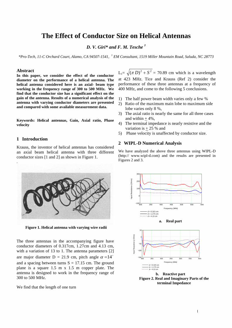
The Effect of Conductor Size on Helical Antennas D. V. Giri* and F. M. Tesche †
*Pro-Tech, 11-C Orchard Court, Alamo, CA 94507-1541, † EM Consultant, 1519 Miller Mountain Road, Saluda, NC 28773
Abstract In this paper, we consider the effect of the conductor diameter on the performance of a helical antenna. The helical antenna considered here is an axial- beam type working in the frequency range of 300 to 500 MHz. We find that the conductor size has a significant effect on the gain of the antenna. Results of a numerical analysis of the antenna with varying conductor diameters are presented and compared with some available measurement data. Keywords: Helical antennas, Gain, Axial ratio, Phase velocity
1 Introduction
Krauss, the inventor of helical antennas has considered an axial beam helical antenna with three different conductor sizes [1 and 2] as shown in Figure 1. .
Figure 1. Helical antenna with varying wire radii The three antennas in the accompanying figure have conductor diameters of 0.317cm, 1.27cm and 4.13 cm, with a variation of 13 to 1. The antenna parameters [2] are major diameter D = 21.9 cm, pitch angle 14=α and a spacing between turns S = 17.15 cm. The ground plane is a square 1.5 m x 1.5 m copper plate. The antenna is designed to work in the frequency range of 300 to 500 MHz. We find that the length of one turn
L1= 22)( SD +π = 70.89 cm which is a wavelength at 423 MHz. Tice and Krauss (Ref 2) consider the performance of these three antennas at a frequency of 400 MHz, and come to the following 5 conclusions. 1) The half power beam width varies only a few % 2) Ratio of the maximum main lobe to maximum side
lobe varies only 8 %, 3) The axial ratio is nearly the same for all three cases
and within + 4%, 4) The terminal impedance is nearly resistive and the
variation is + 25 % and 5) Phase velocity is unaffected by conductor size.
2 WIPL-D Numerical Analysis We have analyzed the above three antennas using WIPL-D (http:// www.wipl-d.com) and the results are presented in Figures 2 and 3.
a. Real part
b. Reactive part
Figure 2. Real and Imaginary Parts of the terminal Impedance
300 350 400 450 500 550 600100
0
100
200
300
d = 0.315 cmd = 1.275 cmd = 4.13 cm
Frequency (MHz)
Inpu
t Res
ista
nce
(Ohm
s)
300 350 400 450 500 550 600150
100
50
0
50
d = 0.315 cmd = 1.275 cmd = 4.13 cm
Frequency (MHz)
Inpu
t Rea
catn
ce (j
Ohm
s)
1
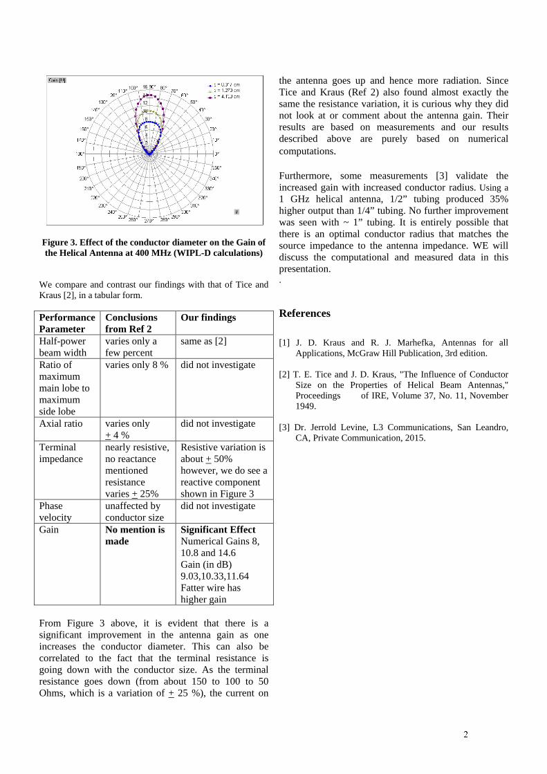
Figure 3. Effect of the conductor diameter on the Gain of the Helical Antenna at 400 MHz (WIPL-D calculations)
We compare and contrast our findings with that of Tice and Kraus [2], in a tabular form. Performance Parameter
Conclusions from Ref 2
Our findings
Half-power beam width
varies only a few percent
same as [2]
Ratio of maximum main lobe to maximum side lobe
varies only 8 % did not investigate
Axial ratio varies only + 4 %
did not investigate
Terminal impedance
nearly resistive, no reactance mentioned resistance varies + 25%
Resistive variation is about + 50% however, we do see a reactive component shown in Figure 3
Phase velocity
unaffected by conductor size
did not investigate
Gain No mention is made
Significant Effect Numerical Gains 8, 10.8 and 14.6 Gain (in dB) 9.03,10.33,11.64 Fatter wire has higher gain
From Figure 3 above, it is evident that there is a significant improvement in the antenna gain as one increases the conductor diameter. This can also be correlated to the fact that the terminal resistance is going down with the conductor size. As the terminal resistance goes down (from about 150 to 100 to 50 Ohms, which is a variation of + 25 %), the current on
the antenna goes up and hence more radiation. Since Tice and Kraus (Ref 2) also found almost exactly the same the resistance variation, it is curious why they did not look at or comment about the antenna gain. Their results are based on measurements and our results described above are purely based on numerical computations. Furthermore, some measurements [3] validate the increased gain with increased conductor radius. Using a 1 GHz helical antenna, 1/2” tubing produced 35% higher output than 1/4” tubing. No further improvement was seen with ~ 1” tubing. It is entirely possible that there is an optimal conductor radius that matches the source impedance to the antenna impedance. WE will discuss the computational and measured data in this presentation. .
References [1] J. D. Kraus and R. J. Marhefka, Antennas for all
Applications, McGraw Hill Publication, 3rd edition. [2] T. E. Tice and J. D. Kraus, "The Influence of Conductor
Size on the Properties of Helical Beam Antennas," Proceedings of IRE, Volume 37, No. 11, November 1949.
[3] Dr. Jerrold Levine, L3 Communications, San Leandro,
CA, Private Communication, 2015.
2
1
2 2 29.05 296.8 67.67
614.43 82.7 23.75(t) ( 0.4789 1.148 10 8767 )
t t t
v V e x e e
Optimization of a Virtual Cathode Oscillator Using NSGA-II
Evolutionary Algorithm
E. Neira*, F. Vega† J.J. Pantoja
‡
Electromagnetic Compability Group, Universidad Nacional de Colombia, *[email protected]
Abstract
This paper presents an optimization of a virtual cathode
oscillator (Vircator) with axial extraction using the multi-
objective Non-dominated Sorting Genetic Algorithm II
(NSGA-II) evolutionary algorithm. The optimization was
implemented with two objective functions to maximize the
radiated energy and to tune the resonance frequency at
5GHz. The simulations were made on CST Particle
Studio. The evolutionary algorithm was programed in
Matlab. An interface between CST and Matlab was
implemented. At the end, the algorithm produced a set of
the best individuals.
Keywords: Optimization, Vircator, NSGA-II, Matlab – CST
PS interface.
1 Introduction
A Vircator is a High Power Microwave Source (HPMS).
Vircators are able to generate microwaves power above 1 GW
during tens or hundreds of ns and their typical radiation
frequencies are between 1 GHz to 10 GHz. Vircator can be
constructed with different geometries and the most used are
[1,2]. Vircator of axial extraction (Fig. 1), Vircator with
transverse extraction, Reditron, Reflex Triode and the
Vircator Coaxial. Some applications of Vircators are
experimentation, electronic warfare, particle accelerators and
breakdown experiment. The most relevant advantages are
easy construction, low maintaining prices, low cost, relative
small size, [1,3]. On the other side, the main constrain is the
low efficiency. The Vircator operation theory can be
consulted in [2,4].
The design of HPMS can be oriented to achieve different
optimization objectives as: energy, power, power efficiency,
energy efficiency, specific frequency response, and sizes.
Depending on the application, a multi-objective optimization
is required. For example, an application that requires a small
size Vircator, a specific frequency response and a determined
power level.
A lot of experimental and numerical optimization efforts have
been made to improve the Vircator response in some specific
objectives. Research oriented to the optimization of cathode
and anode materials can be consulted in [5]–[7]. In these
studies, the behaviour of a set of different materials on the
electron emission has been studied. A work about the cathode
sizes and anode-cathode distance variation have been reported
in [8]. In [9], a study of the anode-cathode distance effect over
the frequency response and the energy efficiency is presented.
In [10], the anode-cathode distance variation is studied in
order to improve the power efficiency on a Reflex Triode.
Most of the previous works have been focused on the study of
effects on just one response due to the variation of one or two
parameters. Due to the variety of objectives that can be
required in Vircators design, optimal parameters for an
objective can impair the response to another important
objective.
In this paper, we present the implementation of the
multiobjective algorithm NSGA-II [11] in order to find a way
to design a Vircator with a specific frequency response, while
is maximized the radiated energy. This implementation was
developed in Matlab. FDTD-PIC simulations were performed
using CST–PS. An interface between Matlab and CST-PS was
developed using the methodology presented in [12]. Next
chapter presents simulation details and the method to calculate
the radiated energy.
2 Simulations
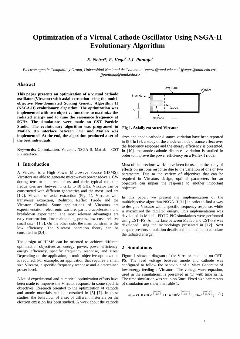
Figure 1 shows a diagram of the Vircator modelled on CST-
PS. The feed voltage between anode and cathode was
configured to follow the behaviour of a Marx Generator of
low energy feeding a Vircator. The voltage wave equation,
used in the simulations, is presented in (1) with time in ns.
The time simulation was setup on 50ns. Fixed size parameters
of simulation are shown in Table 1.
(1)
Fig 1. Axially extracted Vircator
2
'fP S ds E H ds
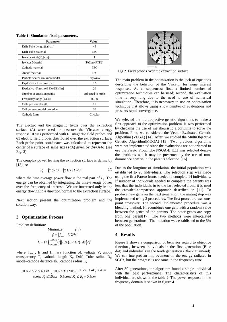
The electric and the magnetic fields over the extraction
surface (A) were used to measure the Vircator energy
response. It was performed with 61 magnetic field probes and
61 electric field probes distributed over the extraction surface.
Each probe point coordinates was calculated to represent the
center of a surface of same sizes (dA) given by dA=A/61 (see
Fig. 2).
The complex power leaving the extraction surface is define by
[13] as:
(2)
where the time-average power flow is the real part of Pf. The
energy can be obtained by integrating the time-average power
over the frequency of interest. We are interested only in the
energy flowing in a direction normal to the extraction surface.
Next section present the optimization problem and the
solution way.
3 Optimization Process
Problem definition:
Minimize f1,f2
1 max 5f f GHz
5.05
24.95
1/ Re 'GHz
GHzf E H ds df
where fmax , E and H are function of: voltage V, anode
transparency T, cathode length Kl, Drift Tube radius Rb,
anode–cathode distance akd ,cathode radius Kr
100 400kV V kV , 10% 90%T , 0.3 4dcm ak cm
,
3 10bcm R cm ,
0.5 0.5r bcm K R cm
The main problem in the optimization is the lack of equations
describing the behavior of the Vircator for some interest
responses. As consequences: first, a limited number of
optimization techniques can be used; second, the evaluation
time is very long due to the need to use of numerical
simulation. Therefore, it is necessary to use an optimization
technique that allows using a low number of evaluations and
presents rapid convergence.
We selected the multiobjective genetic algorithms to make a
first approach to the optimization problem. It was performed
by checking the use of metaheuristic algorithms to solve the
problem. First, we considered the Vector Evaluated Genetic
Algorithm (VEGA) [14]. After, we studied the MultiObjective
Genetic Algorithm(MOGA) [15]. Two previous algorithms
were not implemented since the evaluations are not oriented to
use the Pareto Front. The NSGA-II [11] was selected despite
the problems which may be presented by the use of non-
dominance criteria in the parents selection [16].
Due to the longtime of simulation, the initial population was
established to 28 individuals. The selection step was made
using the first Pareto fronts needed to complete 14 individuals.
If number of individuals needed to complete the parents was
less that the individuals in to the last selected front, it is used
the crowded-comparison approach described in [11]. To
produce new gens on the next generation, the mating step was
implemented using 2 procedures. The first procedure was one-
point crossover. The second implemented procedure was a
blending method. It recombines one gen, with a random value
between the genes of the parents. The other genes are copy
from one parent[17]. The two methods were intercalated
between generations. The mutation was established to the 5%
of the population.
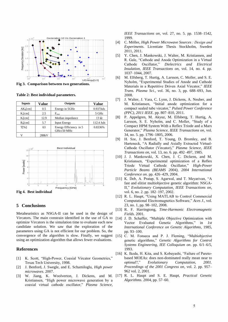
4 Results
Figure 3 shows a comparison of behavior regard to objective
functions, between individuals in the first generation (Blue
dot) and individuals in the tenth generation (Black Diamond).
We can interpret an improvement on the energy radiated in
5GHz, but the progress is not same in the frequency tune.
After 30 generations, the algorithm found a single individual
with the best performance. The characteristics of this
individual are shown in the table 2. The power response in the
frequency domain is shown in figure 4.
Parameter Value
Drift Tube Length(L) [cm] 45
Drift Tube Material PEC
Isolator width(iL)[cm] 1
Isolator Material Teflon (PTFE)
Cathode material PEC
Anode material PEC
Particle Source emission model Explosive
Explosive - Rise time [ns] 0.5
Explosive -Threshold Field[kV/m] 20
Number of emission points Adjusted to mesh
Frequency range [GHz] 0.5-8
Cells per wavelength 10
Cell per max model box edge 20
Cathode form Circular
Table 1: Simulation fixed parameters.
Rb Fig 2. Field probes over the extraction surface
3
5 Conclusions
Metaheuristics as NSGA-II can be used in the design of
Vircators. The main constrain identified in the use of GA to
optimize Vircators is the simulation time to evaluate each new
candidate solution. We saw that the exploration of the
parameters using GA is not efficient for our problem. So, the
convergence of the algorithm is slow. Finally, we suggest
using an optimization algorithm that allows fewer evaluations.
References
[1] K. Scott, “High-Power, Coaxial Vircator Geometries,”
Texas Tech University, 1998.
[2] J. Benford, J. Swegle, and E. Schamiloglu, High power
microwaves. 2007.
[3] W. Jiang, K. Woolverton, J. Dickens, and M.
Kristiansen, “High power microwave generation by a
coaxial virtual cathode oscillator,” Plasma Science,
IEEE Transactions on, vol. 27, no. 5. pp. 1538–1542,
1999.
[4] C. Möller, High Power Microwave Sources : Design and
Experiments. Licentiate Thesis Stockholm, Sweden
2011, 2011.
[5] Y. Chen, J. Mankowski, J. Walter, M. Kristiansen, and
R. Gale, “Cathode and Anode Optimization in a Virtual
Cathode Oscillator,” Dielectrics and Electrical
Insulation, IEEE Transactions on, vol. 14, no. 4. pp.
1037–1044, 2007.
[6] M. Elfsberg, T. Hurtig, A. Larsson, C. Moller, and S. E.
Nyholm, “Experimental Studies of Anode and Cathode
Materials in a Repetitive Driven Axial Vircator,” IEEE
Trans. Plasma Sci., vol. 36, no. 3, pp. 688–693, Jun.
2008.
[7] J. Walter, J. Vara, C. Lynn, J. Dickens, A. Neuber, and
M. Kristiansen, “Initial anode optimization for a
compact sealed tube vircator,” Pulsed Power Conference
(PPC), 2011 IEEE. pp. 807–810, 2011.
[8] P. Appelgren, M. Akyuz, M. Elfsberg, T. Hurtig, A.
Larsson, S. E. Nyholm, and C. Moller, “Study of a
Compact HPM System With a Reflex Triode and a Marx
Generator,” Plasma Science, IEEE Transactions on, vol.
34, no. 5. pp. 1796–1805, 2006.
[9] H. Sze, J. Benford, T. Young, D. Bromley, and B.
Harteneck, “A Radially and Axially Extracted Virtual-
Cathode Oscillator (Vircator),” Plasma Science, IEEE
Transactions on, vol. 13, no. 6. pp. 492–497, 1985.
[10] J. J. Mankowski, X. Chen, J. C. Dickens, and M.
Kristiansen, “Experimental optimization of a Reflex
Triode Virtual Cathode Oscillator,” High-Power
Particle Beams (BEAMS 2004), 2004 International
Conference on. pp. 426–429, 2004.
[11] K. Deb, A. Pratap, S. Agarwal, and T. Meyarivan, “A
fast and elitist multiobjective genetic algorithm: NSGA-
II,” Evolutionary Computation, IEEE Transactions on,
vol. 6, no. 2. pp. 182–197, 2002.
[12] R. L. Haupt, “Using MATLAB to Control Commercial
Computational Electromagnetics Software,” Aces J., vol.
23, no. 1, pp. 98–102, 2008.
[13] R. F. Harringtong, Time-Harmonic Electromagnetic
Fields. 2001.
[14] J. D. Schaffer, “Multiple Objective Optimization with
Vector Evaluated Genetic Algorithms,” in 1st
International Conference on Genetic Algorithms, 1985,
pp. 93–100.
[15] C. M. Fonseca and P. J. Fleming, “Multiobjective
genetic algorithms,” Genetic Algorithms for Control
Systems Engineering, IEE Colloquium on. pp. 6/1–6/5,
1993.
[16] K. Ikeda, H. Kita, and S. Kobayashi, “Failure of Pareto-
based MOEAs: does non-dominated really mean near to
optimal?,” Evolutionary Computation, 2001.
Proceedings of the 2001 Congress on, vol. 2. pp. 957–
962 vol. 2, 2001.
[17] R. L. Haupt and S. E. Haupt, Practical Genetic
Algorithms. 2004, pp. 57–60.
100
101
102
103
104
105
0
0.5
1
1.5
2
2.5
3x 10
9 Generation 10 Vs Generation 1
1/Energy[1/J]
Freq
uenc
y D
evia
tion
[Hz]
Fig 3. Comparison between two generations.
Table 2: Best individual parameters.
Inputs Value Outputs Value
AKd[cm] 0.5 Energy in 5GHz 0.937Juls
Kr[cm] 2.5 Fmax 5 GHz
Kl[cm] 12.9 Median impedance 13 Ω
Rb[cm] 5.7 Input Energy 112.4 Juls
T[%] 63 Energy Efficiency in 5 GHz±50 MHz
0.8336%
V 288kV
0 1 2 3 4 5 6 7 80
2
4
6
8
10
12x 10
6
Frequency [GHz]
Po
we
r [w
atts
]
Best Individual
Fig 4. Best individual
High-power sources of ultrawideband radiation pulses with elliptic polarization
V. I. Koshelev, Yu. A. Andreev, A. M. Efremov, B. M. Kovalchuk, A. A. Petkun,
V. V. Plisko, K. N. Sukhushin, M. Yu. Zorkaltseva
Institute of High Current Electronics SB RAS 2/3, Akademichesky Ave., Tomsk 634055, Russia
Abstract The paper generalizes the results of investigations of high-power sources of ultrawideband (UWB) radiation with elliptical polarization developed at the Institute of High Current Electronics. In the UWB sources, both single cylindrical and conical helical antennas and a 2×2 array were used. To increase the energy efficiency of the sources, the radiators were excited by bipolar voltage pulses. In the experiments, the bipolar voltage pulses of the amplitude 200 kV and length of 1 and 2 ns were used. At the pulse rate of 100 Hz, radiation pulses with effective potential of up to 300 kV and 440 kV were obtained for the sources with a single antenna and antenna array, respectively. Methods for estimation of the radiation center and the far-field boundary of the elliptically polarized electromagnetic field were suggested. Keywords: Ultrawideband radiation, helical antennas, elliptic polarization, bipolar pulses.
1 Introduction
In recent years, intensive investigations and development of high-power UWB radiation sources with linear and elliptical polarization for solution of various problems have been carried out. Previously, at the Institute of High Current Electronics, we realized a program on the development of high-power UWB radiation sources with linear polarization based on the excitation of single combined antennas and multielement arrays (2×2, 4×4, and 8×8) by bipolar voltage pulses of the amplitude up to 200 kV and length of 0.25-3 ns. These experiments resulted in obtaining radiation pulses with the effective potential (the product of the peak electric field strength Ep by the distance r in the far-field zone) of 0.4-4.3 MV at the pulse rate of 100 Hz [1].
At the present time, our research team realizes the program on the development of high-power UWB radiation sources with elliptic polarization [2] based on the excitation of single helical antennas and antenna arrays by nanosecond bipolar pulses of the amplitude up to 200 kV. In all the experiments, a bipolar pulse generator consisting of the SINUS-160 monopolar pulse generator and open-circuit bipolar pulse former firstly suggested in [3] were used. The output impedance of the bipolar pulse generator was equal to 50 Ohm. Helical antennas were used in the axial mode of radiation. The number of turns N in the antennas varied in the limits of 4-7. The antennas were made of a copper tube. To prevent the electrical breakdown, the antennas were placed into radiotransparent containers filled with SF6-gas at a gauge pressure of up to 2 atm. The performed investigations have shown that dielectric containers practically have no influence on the radiation characteristics. To measure the radiation characteristics, it is necessary to know the position of the radiation center and the boundary of the far-field zone. To estimate the position of the radiation center, we suggested to use a criterium rEp = const, and to estimate the boundary of the far-field zone, а criterium p = const is used, where p is the ellipticity coefficient or for its inverse value (axial ratio) AR = const.
2 UWB radiation sources with single antennas
Three high-power sources of UWB radiation based on the excitation of cylindrical helical antennas (N = 4 and 4.5) by bipolar voltage pulses of the length
1 ns and 2 ns as well as of a conical helical antenna (N = 7) excited by a bipolar voltage pulse of the length 1 ns have been developed and investigated. The amplitude of the bipolar pulses reached 200 kV. The energy efficiency of the radiators reached 0.8. The ellipticity coefficient of radiation was of 0.75-0.8 (AR = 1.3). In the experiments, at a pulse repetition rate of 100 Hz, the radiation pulses with the effective potential of 250-300 kV were obtained at a continuous operation during 1 hour. The root-mean-square deviation of the field amplitude per 100 pulses was = 0.03-0.06. The boundary of the far-field zone determined by the suggested criteria was shown to be located at larger distances than at the evaluations using standard approaches.
3 Ultrawideband radiation source with a 4-element array
A high-power source of UWB radiation has been developed and investigated. The scheme of the source is the following: a monopolar pulse generator – a bipolar pulse former – a wave impedance transformer (50/12.5) – a 4-channel power divider – coaxial 50 Ohm cables with cord insulation filled with SF6 gas at a gauge pressure of up to 4 atm – a square 2×2 array of cylindrical helical antennas (N=4.5). The antennas were located on a metal plate at a 21-cm distance from each other. Bipolar voltage pulses of the length 1 ns and amplitude of 225 kV were applied to the input of the wave transformer. In the experiments, the radiation pulses with the effective potential of 440 kV and high stability ( = 0.02-0.05) at the pulse repetition rate of 100 Hz were obtained at a continuous operation during 1 hour. The ellipticity coefficient is 0.7 (AR = 1.4). FWHM of the pattern by peak power is 30. Using the suggested methods, the location of the array radiation center and the boundary of the far-field zone of the elliptically polarized radiation were estimated.
Acknowledgements
The work was supported by the Basic Research Program of the Presidium of Russian Academy of Sciences “Fundamental problems of pulsed high-current electronics”.
References
[1] A. M. Efremov, V. I. Koshelev, B. M. Kovalchuk, V. V. Plisko, and K. N. Sukhushin. “Generation and radiation of ultra-wideband electromagnetic pulses with high stability and effective potential”, Laser Part. Beams, 32, pp. 413-418, (2014).
[2] Yu. A. Andreev, A. M. Efremov, V. I. Koshelev, B. M. Kovalchuk, A. A. Petkun, K. N. Sukhushin, and M. Yu. Zorkaltseva. “A source of high-power pulses of elliptically polarized ultrawideband radiation”, Rev. Sci. Instrum., 85, 104703, (2014).
[3] Yu. A. Andreev, V. P. Gubanov, A. M. Efremov, V. I. Koshelev, S. D. Korovin, B. M. Kovalchuk, V. V. Kremnev, V. V. Plisko, A. S. Stepchenko, and K. N. Sukhushin. “High-power ultrawideband radiation source”, Laser Part. Beams, 21, pp. 211-217, (2003).
1
UWB HPEM generator with changeable pulse waveform
for IEMI testing
Jin-Ho Shin*, Young-Kyung Jeong*, Dong-Gi Youn*
* Replex Co., Ltd, Republic of Korea and [email protected], [email protected], [email protected]
Abstract
This paper presents UWB HPEM generator with
changeable waveform for IEMI testing. Generally, for
wide bandwidth and high power requirements, the
systems use high voltage monopolar or bipolar pulse as
antenna input. In order to satisfy various pulse waveform
requirements above, the proposed pulse generator can
produce 338kVp monopolar pulse or 504kVp-p bipolar
pulse with controlling knob simply.
Keywords: UWB HPEM, High-power electromagnetic, Pulse
forming, Tesla transformer
1 Introduction
UWB HPEM systems have bandwidth from several hundreds
of MHz to several GHz and high peak power to be capable of
IEMI testing. The pulse waveform of these systems can be
selected which antenna is adopted or what frequency content
is preferable [1][2]. In the interest of various pulse waveforms
like these, the designed pulse generator has changeable pulse
waveform function by mechanical structure. Pulse waveform
can change easily by external control knob without
depressurizing. This UWB HPEM generator with changeable
pulse waveform can apply various types of antenna also
investigate IEMI effect for different bandwidth or frequency
content.
2 Measurement results
The UWB HPEM generator consists of power supply, high
voltage (HV) generator and pulse forming line (PFL) and is
shown in Fig. 1.
Figure 1. UWB HPEM generator.
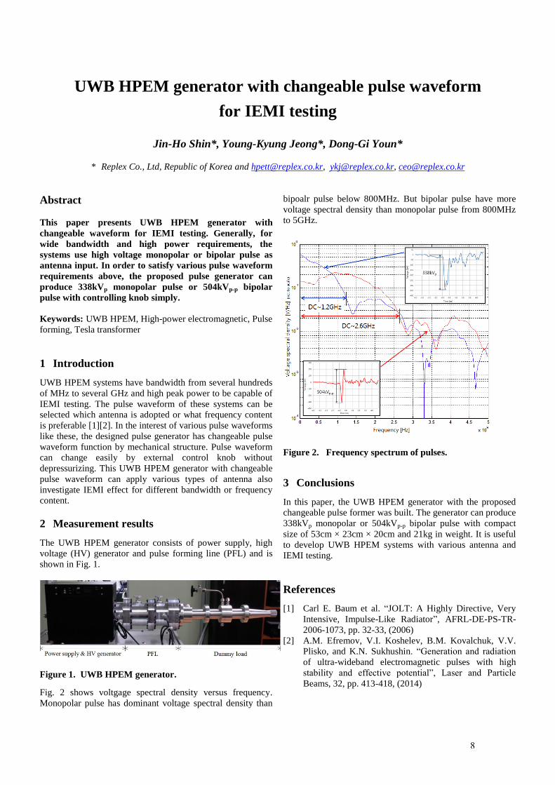
Fig. 2 shows voltgage spectral density versus frequency.
Monopolar pulse has dominant voltage spectral density than
bipoalr pulse below 800MHz. But bipolar pulse have more
voltage spectral density than monopolar pulse from 800MHz
to 5GHz.
Figure 2. Frequency spectrum of pulses.
3 Conclusions
In this paper, the UWB HPEM generator with the proposed
changeable pulse former was built. The generator can produce
338kVp monopolar or 504kVp-p bipolar pulse with compact
size of 53cm × 23cm × 20cm and 21kg in weight. It is useful
to develop UWB HPEM systems with various antenna and
IEMI testing.
References
[1] Carl E. Baum et al. “JOLT: A Highly Directive, Very
Intensive, Impulse-Like Radiator”, AFRL-DE-PS-TR-
2006-1073, pp. 32-33, (2006)
[2] A.M. Efremov, V.I. Koshelev, B.M. Kovalchuk, V.V.
Plisko, and K.N. Sukhushin. “Generation and radiation
of ultra-wideband electromagnetic pulses with high
stability and effective potential”, Laser and Particle
Beams, 32, pp. 413-418, (2014)
1
Design of a Portable Rectangular Generator Based on
MOSFET and Avalanche Transistor
QIAO Bing-bing, GUO Jie, LI Ke-lun
School of Electrical Engineering , Xi’an Jiaotong University , Xi’an, China
Abstract This paper describes a portable rectangular impulse
generator based on MOSFET and serial connection of
avalanche transistors. The characteristics of power
MOSFET and avalanche transistor, and co–operation
between them are studied. Then the compact circuit is
designed. A rectangular impulse with amplitude over 1kV
is acquired, with a few hundreds of nanoseconds rising
time and less than 8ns fall time. The device is tested on
capacitive load less than 300pF and resistive load greater
than 3kΩ .
Keywords: rectangular impulse generator, electronic
circuit; power MOSFET; avalanche transistor;
nanosecond fall time
1 Introduction
With the development of electromagnetic pulse
technology, impulse bandwidth concerned recently is much
wider, such as nuclear electromagnetic pulse,electro-static
discharge and electromagnetic pulse caused by lightning or
switching operation [1-2]. Voltage transducer is used to
measure the voltage impulse. The transducer should have a
good high-frequency response charaeteristics to insure the
measurement results are accurate and reliable. Thus it is
necessary to calibrate high-frequency response charaeteristics
of the transducer, and other capacitive or resistive load.
Rectangular impulse voltage generator is used widely to
calibrate high-frequency response charaeteristics of transdu-
cers [3-4].
There are kinds of impulse voltage generators like spark
gap rectangular impulse generator which can output
rectangular impulse with high amplitude and fast rising time,
but the device is often ponderous and operated complicatedly.
Recently many scholars do some research on impulse
generator based on solid-state switch mainly include power
MOSFET, IGBT and avalanche transistor, instead of spark
gap switch. The rectangular impulse generated by MOSFET
and IGBT impulse generator has slow slope, because of its
relatively slow switching speed compared with avalanche
transistor. Impulse generator based on only avalanche
transistor can only output narrow-width rectangular impulse,
restricted by its current capacity. The portable rectangular
impulse generator proposed in this paper, fully integrating
power MOSFET’s heavy current capacity and avalanche
transistor’s fast switching speed [5-6]. So that the generator
can output rectangular impulse with amplitude over 1kV and
less than 8ns fall time. The generator can be used to calibrate
high-frequency response charaeteristics of voltage transducer,
and other capacitive load, resistive load and RC load (parallel
connect).
2 The Circuit Design and Implementation
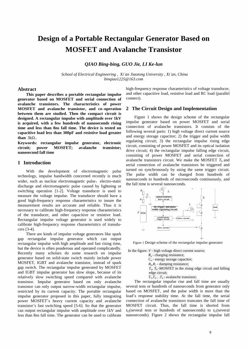
Figure 1 shows the design scheme of the rectangular
impulse generator based on power MOSFET and serial
connection of avalanche transistors. It consists of the
following several parts: 1) high voltage direct current source
and energy storage capacitor; 2) the trigger and pulse width
regulating circuit; 3) the rectangular impulse rising edge
circuit, consisting of power MOSFET and its optical isolation
drive circuit; 4) the rectangular impulse falling edge circuit,
consisting of power MOSFET and serial connection of
avalanche transistors circuit. We make the MOSFET Tb and
serial connection of avalanche transistors be triggered and
turned on synchronously by using the same trigger circuit.
The pulse width can be changed from hundreds of
nanoseconds to hundreds of microseconds continuously, and
the fall time is several nanoseconds.
Figure 1 Design scheme of the rectangular impulse generator
In the figure: V - high voltage direct current source;
Ra - charging resistance;
Ca - energy storage capacitor;
Rb,Rc - damping resistance;
Ta, Tb -MOSFET in the rising edge circuit and falling
edge circuit;
T1,T2…Tn - avalanche transistor; The rectangular impulse rise and fall time are usually
several tens or hundreds of nanoseconds from generator only
based on MOSFET, and the pulse width is more than the
load’s response stability time. At the fall time, the serial
connection of avalanche transistors truncates the fall time of
MOSFET circuit. Thus, the fall time is shorted from
tf2(several tens or hundreds of nanoseconds) to tf1(several
nanoseconds). Figure 2 shows the rectangular impulse fall
2
time shorten from tf2 to tf1. The circuit can solve the problem
of MOSFET’s slow switching speed and deficiency of
avalanche transistor’s current capacity. Meanwhile the
MOSFET Tb keeps on continuously to stabilize the voltage at
about 0V after the rectangular falling edge.
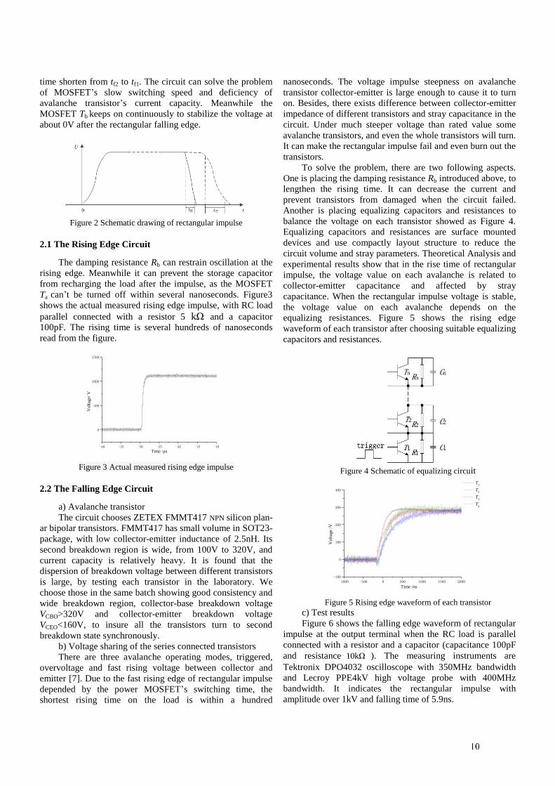
Figure 2 Schematic drawing of rectangular impulse
2.1 The Rising Edge Circuit
The damping resistance Rb can restrain oscillation at the
rising edge. Meanwhile it can prevent the storage capacitor
from recharging the load after the impulse, as the MOSFET
Ta can’t be turned off within several nanoseconds. Figure3
shows the actual measured rising edge impulse, with RC load
parallel connected with a resistor 5 kΩ and a capacitor
100pF. The rising time is several hundreds of nanoseconds
read from the figure.
-40 -35 -30 -25 -20 -15 -10
0
500
1000
1500
Volt
age/
V
Time /μs
Figure 3 Actual measured rising edge impulse
2.2 The Falling Edge Circuit
a) Avalanche transistor
The circuit chooses ZETEX FMMT417 NPN silicon plan-
ar bipolar transistors. FMMT417 has small volume in SOT23-
package, with low collector-emitter inductance of 2.5nH. Its
second breakdown region is wide, from 100V to 320V, and
current capacity is relatively heavy. It is found that the
dispersion of breakdown voltage between different transistors
is large, by testing each transistor in the laboratory. We
choose those in the same batch showing good consistency and
wide breakdown region, collector-base breakdown voltage
VCBO>320V and collector-emitter breakdown voltage
VCEO<160V, to insure all the transistors turn to second
breakdown state synchronously.
b) Voltage sharing of the series connected transistors
There are three avalanche operating modes, triggered,
overvoltage and fast rising voltage between collector and
emitter [7]. Due to the fast rising edge of rectangular impulse
depended by the power MOSFET’s switching time, the
shortest rising time on the load is within a hundred
nanoseconds. The voltage impulse steepness on avalanche
transistor collector-emitter is large enough to cause it to turn
on. Besides, there exists difference between collector-emitter
impedance of different transistors and stray capacitance in the
circuit. Under much steeper voltage than rated value some
avalanche transistors, and even the whole transistors will turn.
It can make the rectangular impulse fail and even burn out the
transistors.
To solve the problem, there are two following aspects.
One is placing the damping resistance Rb introduced above, to
lengthen the rising time. It can decrease the current and
prevent transistors from damaged when the circuit failed.
Another is placing equalizing capacitors and resistances to
balance the voltage on each transistor showed as Figure 4.
Equalizing capacitors and resistances are surface mounted
devices and use compactly layout structure to reduce the
circuit volume and stray parameters. Theoretical Analysis and
experimental results show that in the rise time of rectangular
impulse, the voltage value on each avalanche is related to
collector-emitter capacitance and affected by stray
capacitance. When the rectangular impulse voltage is stable,
the voltage value on each avalanche depends on the
equalizing resistances. Figure 5 shows the rising edge
waveform of each transistor after choosing suitable equalizing
capacitors and resistances.
Figure 4 Schematic of equalizing circuit
-1000 -500 0 500 1000 1500 2000-100
0
100
200
300
400
T1
T2
T3
T4
Vo
ltag
e /V
Time /ns
Figure 5 Rising edge waveform of each transistor
c) Test results
Figure 6 shows the falling edge waveform of rectangular
impulse at the output terminal when the RC load is parallel
connected with a resistor and a capacitor (capacitance 100pF
and resistance 10kΩ ). The measuring instruments are
Tektronix DPO4032 oscilloscope with 350MHz bandwidth
and Lecroy PPE4kV high voltage probe with 400MHz
bandwidth. It indicates the rectangular impulse with
amplitude over 1kV and falling time of 5.9ns.
3
-400 -200 0 200 400 600
0
500
1000
1500
Vo
ltag
e /V
Time /ns
Figure 6 Actual measured falling edge at the output terminal
3 Results
The voltage can keep at 0V stably after falling edge
through controlling avalanche transistors and power
MOSFET Tb to operate synchronously, and turning off the
MOSFET Ta in the rising edge circuit timely. Pulse
waveforms are measured with different loads. The results
show that fall time (10%~90%) is less than 8ns and amplitude
is over 1kV, with a RC load parallel connected with the
resistor and capacitor (capacitance less than 300pF, and
resistance load greater than 3kΩ ), or a single capacitive load
or resistive load.The rise time is hundreds of nanoseconds,
and the pulse width can range from hundreds of nanoseconds
to hundreds of microseconds continuously.
Figure 7 shows an actual measured waveform of
rectangular impulse at the output terminal, with capacitive
load 200pF. It can be seen that fall time is 7.2ns.
Figure 7 Actual measured waveform of rectangular impulse at the
output terminal
4. Conclusion
By designing a portable rectangular impulse generator
based on MOSFET and serial connection of avalanche
transistors, the following conclusion can be drawn.
1) Solid-state switch avalanche transistor and power
MOSFET is used to replace the spark gap switch to design a
compact and portable rectangle impulse generator with all
devices electronic;
2) In the synchronous trigger circuit, the MOSFET and
serial connection of avalanche transistors can be triggered and
switch on synchronously. The circuit can solve the problem of
MOSFET’s slow switching speed and deficiency of avalanche
transistor’s current capacity. Thus, it can output rectangle
impulse with several nanoseconds fall time.
3) Use compactly layout structure to reduce the circuit
volume and stray parameters, and choose suitable equalizing
capacitors and resistances. Voltage on each avalanche
transistor is basically identical at the rising edge of the
rectangle impulse, which can avoid avalanche transistors
operating incorrectly.
Acknowledgements
We are grateful to professor Ding Wei-dong for
guidance and many suggestions. We also express gratitude to
Zhong Xu for providing the high-voltage attenuator probe and
advice in the electronic circuit design. Thank you for your
instructions and help.
References
[1] ZHOU Bi-hua, CHEN Bin, SHI Li-hua et al. EMP and
EMP Protection[M]. Beijing, National Defence Industry
Press, 2003, pp. 99-104.
[2] Tesche F M, Barnes P R. A multi-conductor model for
determining the response of power transmission and
distribution lines to a high altitude electromagnetic pulse
(HEMP)[J]. Power Engineering Review, IEEE, 1989,
9(7): 82-82.
[3] MA Guo-ming, LI Cheng-rong, QUAN Jiang-tao et al.
Portable High Voltage Square Generator for Calibrating
Voltage Divider[J], High Voltage and Insulation
Technology, 2008 pp, 1479-1484
[4] ZHANG Ren-yu, CHEN Chang-yu, WANG Chang-
chang et al. High-voltage Testing Technology[M],
Beijing, Tsinghua University Press, 2003, pp 131-166.
[5] Chakera J A, Naik P A, Kumbhare S R, et al. A
VARIABLE NANO-SECOND PULSE DURATION
LASER PULSE SLICER BASED ON HIGH-
VOLTAGE AVALANCHE TRANSISTOR SWITCH[J].
Journal of the Indian Institute of Sciences, 1996, 76(2):
pp 273-278.
[6] Davis S.J, Murray J.E, Downs D.C, et al. High
performance avalanche transistor switch out for external
pulse selection at 1.06 µm[J]. Applied Optics, 1978,
17(19), pp 3184-3186.
[7] Oldham W G, Samuelson R R, Antognetti P. Triggering
Phenomena in Avalanche Diodes[J]. IEEE Transactions
on Electron Devices, 1972, 19 (9), pp 1056-1060.
1
Frequency, Time, and Thermal Domain Analysis of Planar Bi-Directional Log-Periodic Antenna
J. Ha, M.A. Elmansouri, and D.S. Filipovic
Department of Electrical, Computer, and Energy Engineering University of Colorado, Boulder
Boulder, CO, USA Jaegeun.Ha, Mohamed.Elmansouri, [email protected]
Abstract Planar bi-directional log-periodic (LP) antennas with different design parameters are analysed in frequency, time, and thermal domains to assess their possible use in high power short pulse applications. The boom of an LP arm is widened by moving its virtual apex into the next arm. This modification provides wide-enough ground plane for the microstrip feed line and results in improved impedance match and gain. The effect of the boom width is also analysed in thermal domain using linked electro-thermal multiphysics simulation. Results show that the widened boom reduces the maximum temperature developed on the antenna. The effect of LP growth rate is also studied. In time domain, the small growth rate mitigates the inherent dispersive characteristic of the LP antenna, while frequency domain performance is somewhat sacrificed. Moreover, the small growth rate can relieve the undesirable temperature peaks in thermal domain, thus making the planar LP antenna an attractive candidate for high power short pulse applications requiring a bi-directional radiator. Keywords: Electro-thermal multiphysics, log-periodic antennas, time domain antennas
1 Introduction
It is a commonly accepted belief that the log-periodic (LP) antennas are highly dispersive, therefore they are usually not considered for short pulse systems despite the good frequency domain (FD) performance. To mitigate the dispersion, pre-distortion of the input pulse [1], metamaterial phase shifter between radiating elements [2], and a small growth rate [3] have been considered. Small growth rate offers the simplest method, though the gain and pattern are somewhat compromised. In addition, the power handling capability of planar LP antennas is generally low, but more importantly, there is a lack of understanding of their thermal behaviour. Recent developments of multiphysics simulation tools enable engineers to reliably analyse electromagnetic, thermal, and mechanical characteristics of antennas and other components.
In this paper, a planar bi-directional LP antenna fed by a microstrip impedance transformer is analysed in frequency, time, and thermal domain. A modification of a conventional
planar LP aperture is proposed and effects on impedance, gain, and temperature are determined. To improve the time domain (TD) performance, the growth rate is reduced resulting in a significant improvement in thermal domain.
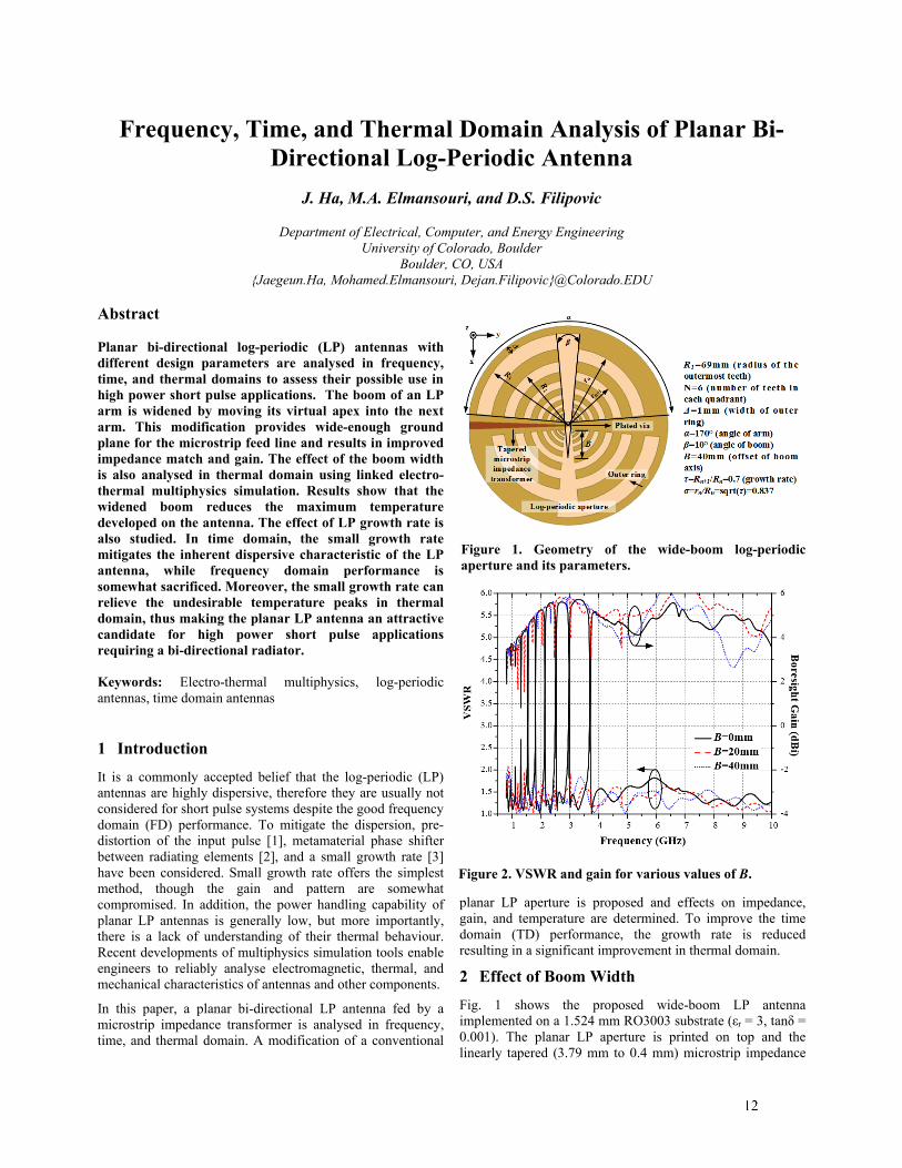
2 Effect of Boom Width
Fig. 1 shows the proposed wide-boom LP antenna implemented on a 1.524 mm RO3003 substrate (εr = 3, tanδ = 0.001). The planar LP aperture is printed on top and the linearly tapered (3.79 mm to 0.4 mm) microstrip impedance
Figure 1. Geometry of the wide-boom log-periodic aperture and its parameters.
Figure 2. VSWR and gain for various values of B.
2
transformer is on the bottom of the substrate. The feeding microstrip line is connected to the right arm of the LP aperture through a plated via. The boom of the left arm functions as a ground plane for the microstrip line. The boom angle β is fixed at 10° in order to lower the turn-on frequency [3]. However, the smaller boom angle gives rise to a narrow ground plane for the microstrip line, especially around the centre, in which the line impedance becomes higher than it is designed for. To provide wide ground plane while keeping small boom angle, axis of the boom (fan-shaped) is offset by 20 mm. Fig. 2 shows the effect of the offset distance B in impedance match and gain. The simulation is performed in Ansys HFSS 2014. As seen, VSWR of the microstrip-fed LP antenna is improved as B increases because the wider boom enables stable characteristic impedance. Not only the impedance match is improved, but also the gain and overall pattern performances are enhanced with the wider boom. This is because the widening reduces the radiation loss associated with the leaking the guided wave on the transmission line into the teeth before the feed via.
The simulated field data in HFSS are used to calculate the RF heat generation in the antenna that are mainly composed of conduction and dielectric losses as given in Equation (1).
2 21
'' .2 2sQ J E
(1)
The generated RF heat is imported into Ansys Mechanics thermal solver and the temperature distribution of the antenna
is obtained based on the Fourier heat conduction equation and the Newton’s law of cooling as given in Equations (2) and (3), respectively.
2 / .p
TT Q C
t
(2)
0 .sQ hA T T (3)
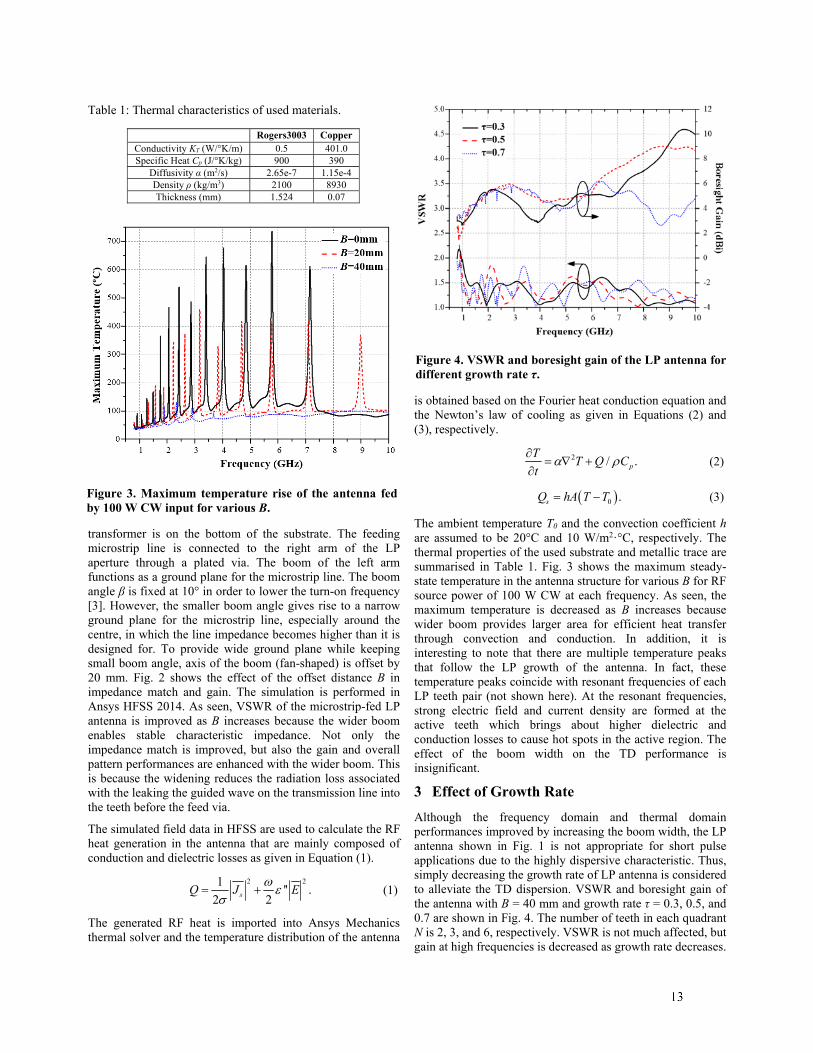
The ambient temperature T0 and the convection coefficient h are assumed to be 20°C and 10 W/m2·°C, respectively. The thermal properties of the used substrate and metallic trace are summarised in Table 1. Fig. 3 shows the maximum steady-state temperature in the antenna structure for various B for RF source power of 100 W CW at each frequency. As seen, the maximum temperature is decreased as B increases because wider boom provides larger area for efficient heat transfer through convection and conduction. In addition, it is interesting to note that there are multiple temperature peaks that follow the LP growth of the antenna. In fact, these temperature peaks coincide with resonant frequencies of each LP teeth pair (not shown here). At the resonant frequencies, strong electric field and current density are formed at the active teeth which brings about higher dielectric and conduction losses to cause hot spots in the active region. The effect of the boom width on the TD performance is insignificant.
3 Effect of Growth Rate
Although the frequency domain and thermal domain performances improved by increasing the boom width, the LP antenna shown in Fig. 1 is not appropriate for short pulse applications due to the highly dispersive characteristic. Thus, simply decreasing the growth rate of LP antenna is considered to alleviate the TD dispersion. VSWR and boresight gain of the antenna with B = 40 mm and growth rate τ = 0.3, 0.5, and 0.7 are shown in Fig. 4. The number of teeth in each quadrant N is 2, 3, and 6, respectively. VSWR is not much affected, but gain at high frequencies is decreased as growth rate decreases.
Figure 4. VSWR and boresight gain of the LP antenna for different growth rate τ.
Figure 3. Maximum temperature rise of the antenna fedby 100 W CW input for various B.
Table 1: Thermal characteristics of used materials.
Rogers3003 Copper Conductivity KT (W/°K/m) 0.5 401.0 Specific Heat Cp (J/°K/kg) 900 390
Diffusivity α (m2/s) 2.65e-7 1.15e-4 Density ρ (kg/m3) 2100 8930 Thickness (mm) 1.524 0.07
3
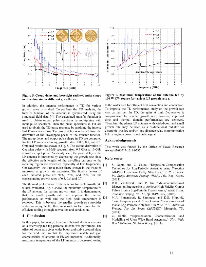
In addition, the antenna performance in TD for various growth rates is studied. To perform the TD analysis, the transfer function of the antenna is synthesized using the simulated field data [4]. The calculated transfer function is used to obtain output pulse spectrum by multiplying with input pulse spectrum. Then the pulse spectrums in FD are used to obtain the TD pulse response by applying the inverse fast Fourier transform. The group delay is obtained from the derivative of the unwrapped phase of the transfer function. The group delay and output pulse shape in TD are computed for the LP antennas having growth rates of 0.3, 0.5, and 0.7. Obtained results are shown in Fig. 5. The second derivative of Gaussian pulse with 10dB spectrum from 0.9 GHz to 10 GHz is used as input pulse. As clearly seen, the group delay of the LP antenna is improved by decreasing the growth rate since the effective path lengths of the travelling currents to the radiating region are decreased especially at low frequencies. Consequently, the output pulse shape shown in the insets is improved as growth rate decreases. The fidelity factors of each radiated pulse are 91%, 79%, and 70% for the corresponding growth rates of 0.3, 0.5, and 0.7.
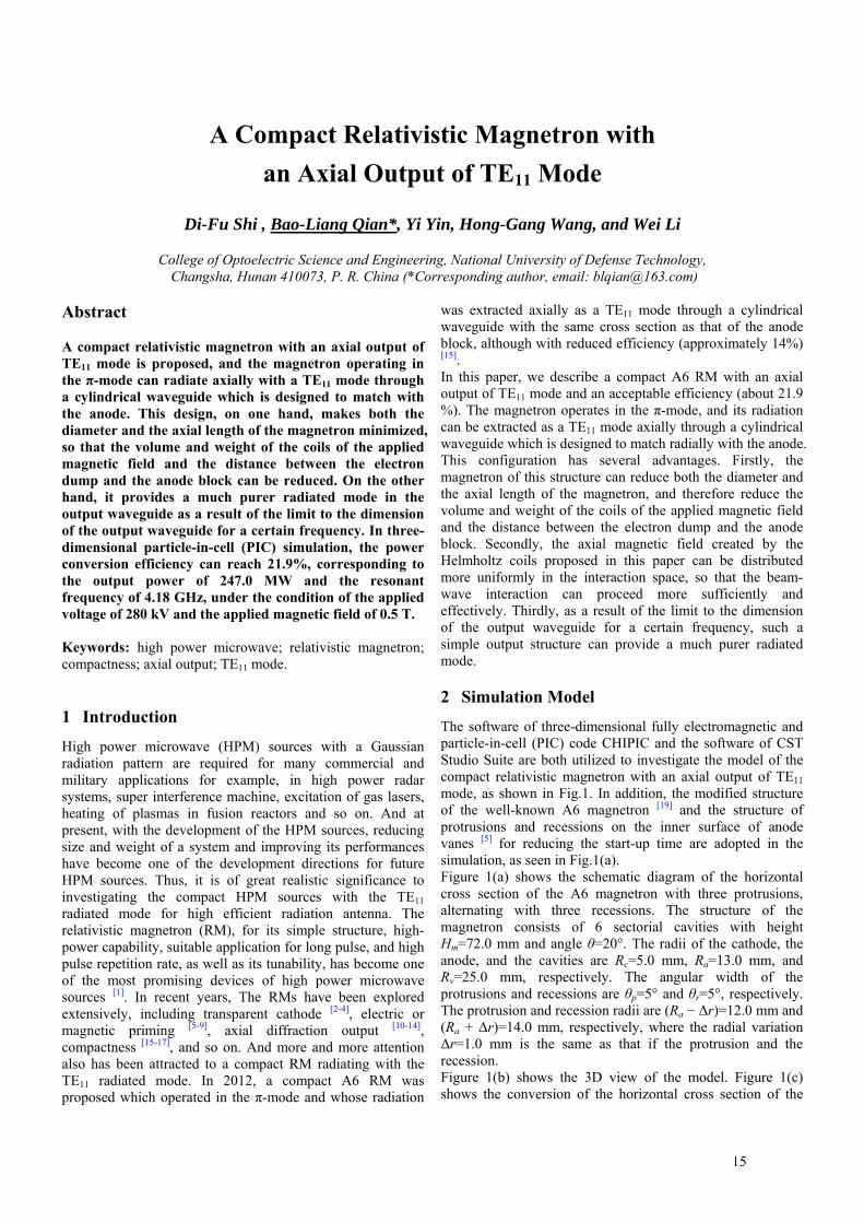
The thermal performance of the antenna for each growth rate is also evaluated. Fig. 6 shows the maximum temperature of the LP antenna for various growth rates. It is demonstrated that the small growth rate can improve the thermal performance as well and the high peak temperature is removed. This is because the smaller growth rate provides wider radiating teeth, thus increased surface area for the efficient cooling through convection and conduction.
4 Conclusion
In this paper, frequency, time, and thermal domain analysis on a microstrip-fed log-periodic antenna was performed. The offset of boom axis gives wider boom and stable ground plane for the feed line, so that the impedance match and gain characteristics of antenna in FD are improved. Additionally, maximum temperature of the LP antenna is decreased owing
to the wider area for efficient heat convection and conduction. To improve the TD performance, study on the growth rate was carried out. In FD, the gain at high frequencies is compromised for smaller growth rate; however, improved time and thermal domain performances are achieved. Therefore, the planar LP antenna with wide-boom and small growth rate may be used as a bi-directional radiator for electronic warfare and/or long distance relay communication link using high power short pulse signal.
Acknowledgements
This work was funded by the Office of Naval Research Award #N00014-13-1-0537.
References
[1] S. Gupta and C. Caloz, “Dispersion-Compensation Technique for Log-Periodic Antennas using C-section All-Pass Dispersive Delay Structures,” in Proc. IEEE Int. Symp. Antennas Propag. (ISAP), Jeju, Rep. Korea, (2011).
[2] R.W. Ziolkowski and P. Jin, “Metamaterial-Based Dispersion Engineering to Achieve High Fidelity Output Pulses From a Log-Periodic Dipole Array,” IEEE Trans. Antennas Propag., vol. 56, pp. 3619-3629, (2008).
[3] M.A. Elmansouri, R. Sammeta, and D.S. Filipović, “Joint Frequency- and Time-Domain Characterization of Planar Log-Periodic Antennas,” in Proc. IEEE Antennas Propag. Soc. Int. Symp. (APSURSI), Memphis, TN, (2014).
[4] C. Roblin, “Representation, Characterization, and Modelling of Ultra Wide Band Antennas,” Ultra Wide Band Antennas, NJ: John Wiley, (2011).
Figure 6. Maximum temperature of the antenna fed by 100 W CW source for various LP growth rate τ.
Figure 5. Group delay and boresight radiated pulse shape in time domain for different growth rate.
1
A Compact Relativistic Magnetron with an Axial Output of TE11 Mode
Di-Fu Shi , Bao-Liang Qian*, Yi Yin, Hong-Gang Wang, and Wei Li
College of Optoelectric Science and Engineering, National University of Defense Technology, Changsha, Hunan 410073, P. R. China (*Corresponding author, email: [email protected])
Abstract A compact relativistic magnetron with an axial output of TE11 mode is proposed, and the magnetron operating in the π-mode can radiate axially with a TE11 mode through a cylindrical waveguide which is designed to match with the anode. This design, on one hand, makes both the diameter and the axial length of the magnetron minimized, so that the volume and weight of the coils of the applied magnetic field and the distance between the electron dump and the anode block can be reduced. On the other hand, it provides a much purer radiated mode in the output waveguide as a result of the limit to the dimension of the output waveguide for a certain frequency. In three-dimensional particle-in-cell (PIC) simulation, the power conversion efficiency can reach 21.9%, corresponding to the output power of 247.0 MW and the resonant frequency of 4.18 GHz, under the condition of the applied voltage of 280 kV and the applied magnetic field of 0.5 T. Keywords: high power microwave; relativistic magnetron; compactness; axial output; TE11 mode.
1 Introduction
High power microwave (HPM) sources with a Gaussian radiation pattern are required for many commercial and military applications for example, in high power radar systems, super interference machine, excitation of gas lasers, heating of plasmas in fusion reactors and so on. And at present, with the development of the HPM sources, reducing size and weight of a system and improving its performances have become one of the development directions for future HPM sources. Thus, it is of great realistic significance to investigating the compact HPM sources with the TE11 radiated mode for high efficient radiation antenna. The relativistic magnetron (RM), for its simple structure, high-power capability, suitable application for long pulse, and high pulse repetition rate, as well as its tunability, has become one of the most promising devices of high power microwave sources [1]. In recent years, The RMs have been explored extensively, including transparent cathode [2-4], electric or magnetic priming [5-9], axial diffraction output [10-14], compactness [15-17], and so on. And more and more attention also has been attracted to a compact RM radiating with the TE11 radiated mode. In 2012, a compact A6 RM was proposed which operated in the π-mode and whose radiation
was extracted axially as a TE11 mode through a cylindrical waveguide with the same cross section as that of the anode block, although with reduced efficiency (approximately 14%) [15]. In this paper, we describe a compact A6 RM with an axial output of TE11 mode and an acceptable efficiency (about 21.9 %). The magnetron operates in the π-mode, and its radiation can be extracted as a TE11 mode axially through a cylindrical waveguide which is designed to match radially with the anode. This configuration has several advantages. Firstly, the magnetron of this structure can reduce both the diameter and the axial length of the magnetron, and therefore reduce the volume and weight of the coils of the applied magnetic field and the distance between the electron dump and the anode block. Secondly, the axial magnetic field created by the Helmholtz coils proposed in this paper can be distributed more uniformly in the interaction space, so that the beam-wave interaction can proceed more sufficiently and effectively. Thirdly, as a result of the limit to the dimension of the output waveguide for a certain frequency, such a simple output structure can provide a much purer radiated mode.
2 Simulation Model
The software of three-dimensional fully electromagnetic and particle-in-cell (PIC) code CHIPIC and the software of CST Studio Suite are both utilized to investigate the model of the compact relativistic magnetron with an axial output of TE11 mode, as shown in Fig.1. In addition, the modified structure of the well-known A6 magnetron [19] and the structure of protrusions and recessions on the inner surface of anode vanes [5] for reducing the start-up time are adopted in the simulation, as seen in Fig.1(a). Figure 1(a) shows the schematic diagram of the horizontal cross section of the A6 magnetron with three protrusions, alternating with three recessions. The structure of the magnetron consists of 6 sectorial cavities with height Hm=72.0 mm and angle θ=20°. The radii of the cathode, the anode, and the cavities are Rc=5.0 mm, Ra=13.0 mm, and Rv=25.0 mm, respectively. The angular width of the protrusions and recessions are θp=5° and θr=5°, respectively. The protrusion and recession radii are (Ra − Δr)=12.0 mm and (Ra + Δr)=14.0 mm, respectively, where the radial variation Δr=1.0 mm is the same as that if the protrusion and the recession. Figure 1(b) shows the 3D view of the model. Figure 1(c) shows the conversion of the horizontal cross section of the
2
device along the axial direction. At the end of the A6 magnetron along the axial direction, two diametrically opposite cavities are gradually changed to an approximately rectangular waveguide with length L1=50.0 mm and width W1=10.0 mm. In the rest of the cavities, every two neighbouring cavities are gradually changed to an approximately rectangular waveguide with length L2=50.0 mm and width W2=20.0 mm. And the interaction space of the magnetron is gradually changed to a cylindrical waveguide with radius Rt=13.0 mm. In addition, all the three transition sections mentioned above are of the same height Ht=50.0 mm. Then the cylindrical waveguide with radius Rt=13.0 mm is gradually changed to the next cylindrical waveguide with radius Ro=25.0 mm, while the other two approximately rectangular waveguides keep their shape and size along the axial direction. The distance between the A6 magnetron and the cylindrical waveguide with radius Ro=25.0 mm is Ho=100.0 mm. In our simulations, the applied voltage has a rise time of 3 ns after which it maintained a constant amplitude of 280 kV for a duration of 40 ns, and the applied axial magnetic field created by Helmholtz coils for interaction region is 0.5 T.
(a) (b)
(c)
Figure 1. (a) Schematic diagram of the horizontal cross section of the A6 magnetron with three protrusions alternating and three recessions. (b) 3D view of the whole inner space of the device. (c) Conversion of the horizontal cross section of the device along the axial direction.
3 Simulation Results
According to the model described in Section 2, the performance of the compact relativistic magnetron with an axial output of TE11 mode is investigated by the software of
3D PIC, CHIPIC, and Fig.2 and Fig.3 give the simulation results. Figure 2(a) indicates that the input electron beam power maintains a constant amplitude of 1.13 GW after 20 ns. Figure 2(b) indicates that the output microwave power of 247.0 MW reaches to saturation at 20 ns, corresponding to an power conversion efficiency of 21.9%. It takes a little long time for both the input power and output power to start up, because the electron spokes in the A6 magnetron have three azimuthally symmetric periods while the TE11 radiated mode in the cylindrical waveguide has one azimuthally symmetric period, and this contradiction is not helpful to reduce the start-up time. However, we believe that further design and optimization could reduce the start-up time and increase the power conversion efficiency. Figure 2(c) shows the spectrum of the electric field in the resonant cavity from 0 to 40 ns, and at least it consists of the frequency of the fundamental harmonic of π mode, fπ , and the frequency of the 2nd harmonic of π mode, 2fπ. The frequency of fundamental harmonic of π mode, fπ , as the main operating frequency is 4.18 GHz, which is higher than the cutoff frequency (3.52 GHz) of the TE11 mode in the cylindrical waveguide. This condition guarantees that the microwave of 4.18 GHz could propagate in this device. In addition, higher order harmonics with competing modes may cause the impurity of the radiated mode in the cylindrical waveguide, but the fundamental harmonic of π mode with the largest growth rate can eventually dominate. It indicates that the resonant system of the magnetron could operate in the π mode properly as expected, and better results may be obtained by further optimization. Figure 2(d) indicates that the radiated mode in the output port is TE11 mode, which is the lowest order mode in the cylindrical waveguide.
(a) (b)
(c) (d)
Figure 2. (a) Input electron beam power versus time. (b) Output microwave power versus time. (c) Spectrum of electric field in resonant cavity from 0 to 40 ns. (d) Radiated mode TE11 in the output port. Compared with the magnetron of diffraction output (MDO), the magnetron of this paper can reduce the dimension of the output port, and therefore reduce the volume and weight of the coils of the applied magnetic field, and also reduce the distance between the electron dump and the anode block, so
Ho
HmHt
A
B
C
3
that both the diameter and the axial length of the magnetron can be minimized. In addition, since the output structure of this compact magnetron has a cylindrical shell with the same cross section as that of the anode block, it is more convenient for the Helmholtz coils to wrap around the body of the magnetron and the axial magnetic field created by this kind of Helmholtz coils can be distributed more uniformly in the interaction region, so that the beam-wave interaction can proceed more sufficiently and effectively. Such a simple output structure investigated in this paper is able to guarantee that only the TE11 mode can propagate in the cylindrical waveguide for the dominant frequency of fundamental harmonic of π mode (fπ=4.18 GHz), although higher order harmonics of π mode may have some influence on the purity of the radiated mode.
4 Conclusion
In conclusion, a compact relativistic magnetron with an axial output of TE11 mode is proposed in this paper. The magnetron operating in the π-mode can radiate axially with a TE11 mode through a cylindrical waveguide which is designed to match with the anode. This design not only makes both the diameter and the axial length of the magnetron minimized, but also provides a much purer radiated mode in the output waveguide, and the magnetron can operate with acceptable efficiency (about 21.9%), although we think some performances of the magnetron need to be further improved, such as reducing the start-up time of microwave, reducing the leakage electrons from the interaction region, suppressing the undesired modes and increasing the power conversion efficiency.
References
[1] J. Benford, J. Swegle, and E. Schamiloglu, “High-Power Microwaves 2nd ed.” (Artech House, Norwood, MA, 2006), Chap. 7, pp. 259-320.
[2] M. Fuks, S. Prasad, and E. Schamiloglu, “Increased efficiency and faster turn-on in magnetrons using the transparent cathode,” in Proc. Int. Conf. CAVMAG, 2010, pp. 76–81.
[3] E. Schamiloglu and M. I. Fuks, “The transparent cathode: Rejuvenator of magnetrons and inspiration for new RF sources,” in Proc. IET Conf. High Power RF Technol., 2009, pp. 1–5.
[4] M. I. Fuks and E. Schamiloglu, “70% efficient relativistic magnetron with axial extraction of radiation through a horn antenna,” IEEE Trans. Plasma Sci., vol. 38, no. 6, pp. 1302–1312, Jun. 2010.
[5] J. I. Kim, J. H. Won, and G. S. Park, “Electron prebunching in microwave magnetron by electric priming using anode shape modification,” Appl. Phys. Lett., vol. 86, no. 17, pp. 171501-1–171501-3, Apr. 2005.
[6] V. B. Baiburin and K. V. Kaminskii, “Effect of an azimuthally varying magnetic field on the noise level in a multicavity magnetron,” Tech. Phys. Lett., vol. 35, no. 6, pp. 582–584, Jun. 2009.
[7] V. B. Neculaes, M. C. Jones, R. M. Gilgenbach, Y. Y. Lau, J. W. Luginsland, B. W. Hoff, W. M. White, N. M. Jordan, P. Pengvanich, Y. Hidaka, and H. L. Bosman,
“Magnetic priming effects on noise, startup, and mode competition in magnetrons,” IEEE Trans. Plasma Sci., vol. 33, no. 1, pp. 94–101, Feb. 2005.
[8] B. W. Hoff, R. M. Gilgenbach, N. M. Jordan, Y. Y. Lau, E. J. Cruz, D. M. French, M. R. Gomez, J. C. Zier, T. A. Spencer, and D. Price, “Magnetic priming at the cathode of a relativistic magnetron,” IEEE Trans. Plasma Sci., vol. 36, no. 3, pp. 710–717, Jun. 2008.
[9] Shivendra Maurya, V. V. P. Singh, and P. K. Jain, “Three-Dimensional Particle-in-Cell Simulation of Fast Oscillation Startup and Efficiency Improvement in a Relativistic Magnetron With Electric Priming,” IEEE Trans. Plasma Sci., vol. 40, no. 10, pp. 2686–2692, Oct. 2012.
[10] M. I. Fuks, N. F. Kovalev, A. D. Andreev, and E. Schamiloglu, “Mode conversion in a magnetron with axial extraction of radiation,” IEEE Trans. Plasma Sci., vol. 34, no. 3, pp. 620–626, Jun. 2006.
[11] M. Daimon and W. Jiang, “Modified configuration of relativistic magnetron with diffraction output for efficiency improvement,” Appl. Phys. Lett., vol. 91, no. 19, pp. 191 503-1–191 503-3, Nov. 2007.
[12] M. Daimon, K. Itoh, G. Imada, and W. Jiang, “Experimental demonstration of relativistic magnetron with modified output configuration,” Appl. Phys. Lett., vol. 92, no. 19, pp. 191 504-1–191 504-3, May 2008.
[13] W. Li and Y.-G. Liu, “An efficient mode conversion configuration in relativistic magnetron with axial diffraction output,” J. Appl. Phys., vol. 106, no. 5, pp. 053 303-1–053 303-3, Sep. 2009.
[14] Wei Li, Yong-gui Liu, Jun Zhang, Di-fu Shi, and Wei-qi Zhang, “Experimental investigations on the relations between configurations and radiation patterns of a relativistic magnetron with diffraction output,” J. Appl. Phys., vol. 113, no. 2, pp. 023 304-1–023 304-4, Jan. 2013.
[15] C. Leach, S. Prasad, M. Fuks, and E. Schamiloglu, “Compact relativistic magnetron with Gaussian radiation pattern,” IEEE Trans. Plasma Sci., vol. 40, no. 11, pp. 3116–3120, Nov. 2012.
[16] Wei Li, Yong-gui Liu, Ting Shu, Han-wu Yang, Yu-wei Fan et al, “Experimental demonstration of a compact high efficient relativistic magnetron with directly axial radiation,” Phys. Plasmas, vol. 19, no. 1, pp. 013 105-1–013 105-4, Jan. 2012.
[17] W. Li and Y. G. Liu, “Modified magnetic field distribution in relativistic magnetron with diffraction output for compact operation,” Phys. Plasmas, vol. 18, no. 2, pp. 023103-1–023103-4, Feb. 2011.
[18] J. Zhou, D. Liu, C. Liao, and Z. Li, “CHIPIC: An Efficient Code for Electromagnetic PIC Modeling and Simulation,” IEEE Trans. Plasma Sci., vol. 37, no. 10, pp. 2002–2011, Oct. 2009.
[19] A. Palevsky and G. Bekefi, “Microwave emission from pulsed, relativistic e-beam diodes. II. The multiresonator magnetron,” Phys. Fluids, vol. 22, no. 5, pp. 986–996, May 1979.
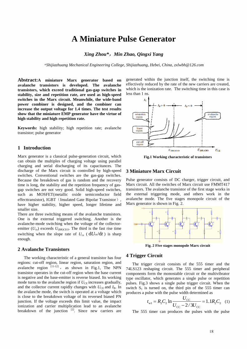
A Miniature Pulse Generator
Xing Zhou*,Min Zhao, Qingxi Yang
*Shijiazhuang Mechanical Engineering College, Shijiazhuang, Hebei, China, [email protected]
Abstract:A miniature Marx generator based on
avalanche transistors is developed. The avalanche
transistors, which exceed traditional gas-gap switches in
stability, size and repetition rate, are used as high-speed
switches in the Marx circuit. Meanwhile, the wide-band
power combiner is designed, and the combiner can
increase the output voltage for 1.4 times. The test results
show that the miniature EMP generator have the virtue of
high stability and high repetition rate.
Keywords: high stability; high repetition rate; avalanche
transistor; pulse generator
1 Introduction
Marx generator is a classical pulse-generation circuit, which
can obtain the multiples of charging voltage using parallel
charging and serial discharging of its capacitances. The
discharge of the Marx circuit is controlled by high-speed
switches. Conventional switches are the gas-gap switches.
Because the breakdown of gas is random and the recovery
time is long, the stability and the repetition frequency of gas-
gap switches are not very good. Solid high-speed switches,
such as MOSFET(metallic oxide semiconductor field
effecttransistor), IGBT(Insulated Gate Bipolar Transistor),
have higher stability, higher speed, longer lifetime and
smaller size.
There are three switching means of the avalanche transistors.
One is the external triggered switching. Another is the
avalanche-mode switching when the voltage of the collector-
emitter (Uce) exceeds U(BR)CEO. The third is the fast rise time
switching when the slope rate of Uce ( ced /dU t ) is sharp
enough.
2 Avalanche Transistors
The working characteristic of a general transistor has four
regions: cut-off region, linear region, saturation region, and
avalanche region [11-12] , as shown in Fig.1, The NPN
transistor operates in the cut-off region when the base current
is negative and the base-emitter is reverse biased. Its working
mode turns to the avalanche region if UCE increases gradually,
and the collector current rapidly changes with UCE and IB. In
the avalanche mode, the switch is operated at a voltage which
is close to the breakdown voltage of its reversed biased PN
junction. If the voltage exceeds this limit value, the impact
ionization and carrier multiplication lead to an avalanche
breakdown of the junction [2]
. Since new carriers are
generated within the junction itself, the switching time is
effectively reduced by the rate of the new carriers are created,
which is the ionization rate. The switching time in this case is
less than 1 ns.
Fig.1 Working characteristic of transistors
3 Miniature Marx Circuit
Pulse generator consists of DC charger, trigger circuit, and
Marx circuit. All the switches of Marx circuit use FMMT417
transistors. The avalanche transistor of the first stage works in
the external triggering mode, and others work in the
avalanche mode. The five stages monopole circuit of the
Marx generator is shown in Fig. 2.
Fig. 2 Five stages monopole Marx circuit
4 Trigger Circuit
The trigger circuit consists of the 555 timer and the
74LS123 reshaping circuit. The 555 timer and peripheral
components form the monostable circuit or the multivibrator
type oscillator, which generates a single pulse or repetition
pulses. Fig.3 shows a single pulse trigger circuit. When the
switch S1 is turned on, the third pin of the 555 timer can
produces a pulse with the pulse width determined as
CCw1 2 2 2 2
CC CC
ln 1.12 / 3
Ut R C R C
U U
(1)
The 555 timer can produces the pulses with the pulse
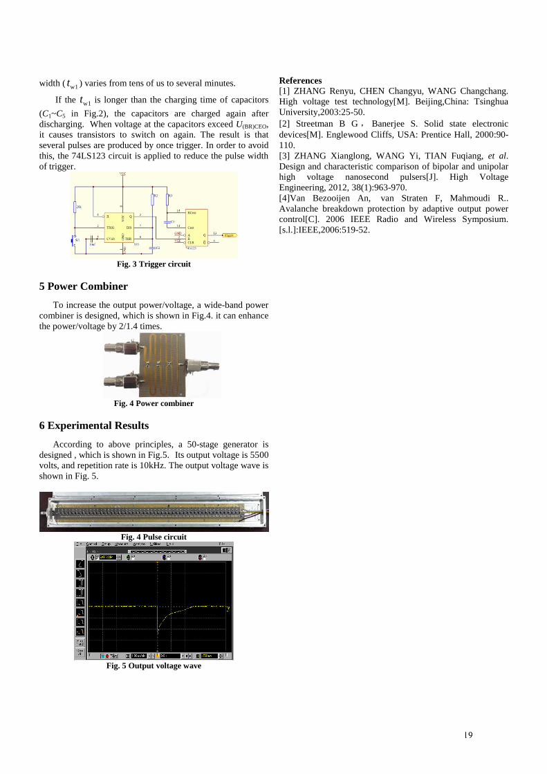
width ( w1t ) varies from tens of us to several minutes.
If the w1t is longer than the charging time of capacitors
(C1~C5 in Fig.2), the capacitors are charged again after
discharging. When voltage at the capacitors exceed U(BR)CEO,
it causes transistors to switch on again. The result is that
several pulses are produced by once trigger. In order to avoid
this, the 74LS123 circuit is applied to reduce the pulse width
of trigger.
Fig. 3 Trigger circuit
5 Power Combiner
To increase the output power/voltage, a wide-band power
combiner is designed, which is shown in Fig.4. it can enhance
the power/voltage by 2/1.4 times.
Fig. 4 Power combiner
6 Experimental Results
According to above principles, a 50-stage generator is
designed , which is shown in Fig.5. Its output voltage is 5500
volts, and repetition rate is 10kHz. The output voltage wave is
shown in Fig. 5.
Fig. 4 Pulse circuit
Fig. 5 Output voltage wave
References
[1] ZHANG Renyu, CHEN Changyu, WANG Changchang.
High voltage test technology[M]. Beijing,China: Tsinghua
University,2003:25-50.
[2] Streetman B G , Banerjee S. Solid state electronic
devices[M]. Englewood Cliffs, USA: Prentice Hall, 2000:90-
110.
[3] ZHANG Xianglong, WANG Yi, TIAN Fuqiang, et al.
Design and characteristic comparison of bipolar and unipolar
high voltage nanosecond pulsers[J]. High Voltage
Engineering, 2012, 38(1):963-970.
[4]Van Bezooijen An, van Straten F, Mahmoudi R..
Avalanche breakdown protection by adaptive output power
control[C]. 2006 IEEE Radio and Wireless Symposium.
[s.l.]:IEEE,2006:519-52.
Comparative analysis of directivity and gain in according to
Antenna’s dielectric- shape
Ruck-Woan Kim*, Jin-Wook Park*, Seung-Moon Han* , Chang-su
Huh* †
*Department of Electrical Engineering, Inha University, Incheon 402-751
Abstract
This paper compares the results by executing the
simulation in order to analyse the antenna characteristics
depending on the shape of dielectric to be applied to the
opening of the TEM horn antenna. Dielectric of opening
of the antenna is two type of Fresnel and hemispherical.
Fresnel and hemispherical lens are made with Teflon.
Directivity and radiation efficiency at the central
frequency is not much difference. However, it is
confirmed that a Fresnel lens is more efficient in total
efficiency.
Keywords: Dielectric antenna, Fresnel lens,
Hemispherical lens, TEM antenna.
1 Introduction
According to the shape of the opening antenna, Lens antennas
can change characteristics of directivity and gain of antenna.
Dielectric lenses have been suggested as an alternative
solution to offset dual reflector system for scientific space
applications. [1] To optimize Directivity and gain of a TEM
antenna used for EMP radiation experiments, this paper
compares with a Fresnel lens and a hemispherical lens and
analyses the results.
2 Manuscript preparation
Unlike normal horn antenna, TEM horn antenna is fed to the
two separating conductive plates. when electromagnetic
waves are generated from the power of the two parallel
conductive plates, they are copied into the air via the antenna
aperture. Current flowed through a coaxial line is transformed
to the energy because of impedance match between the inner
conductor of the coaxial line and the antenna conductor
plate.[2] The generated electromagnetic wave will have a
TEM characteristics by flowing current and the voltage
difference in the two conductive plates and proceeds between
the two conductive plates. The directivity and gain of the
electromagnetic wave emitted through the Fresnel type and
hemispherical type was analyzed by simulation.
Figure 1. Directivity of hemispherical lens
Figure 2. Directivity of Fresnel lens
dBi value of the hemispheric and Fresnel type as shown in the
figure above does not show much of a difference but shows
greater overall efficiency in fresnel lens than in hemispherical
lens. In addition, Fresnel lens are more easily manufactured
because the amount of the material reduced.
References
[1] P. C. Hargrave, G. Savini, N. Trappe, A. Challinor, S. B.
Sørensen,P. A. R. Ade, R. V. Sudiwala, I. K. Walker, M.
Gradziel, N. Tynan,and M. van der Vorst, “Coated dielectric
lens design, modeling andmeasurements for future CMB
polarimetry missions,” in Proc. EuCAP, Gothenburg, Sweden,
2013.
[2] J. Wang, C. Tian, G. Luo and Y. Chen, D. Ge, "Four-
element TEM horn array for radiatingultra-wideband
electromagnetic pulses", Microwave and Optical Technology
Letters, vol. 31,no. 3, pp. 190-194, Nov. 5 2001.
† Corresponding author; [email protected] 1
Design Consideration of Marx Generator for a Continuous Operation at a High Repetition Rate
Jeong-Hyeon Kuk*†, Dong-Woo Yim*, Jin-Soo Choi*, Sun-Mook Hwang**, Tae-Hyun Lim**
*Agency for Defense Development, Korea, **Hanwha Corporation, Korea
Abstract
In order to develop a compact and repetitive pulse power supply by using a Marx generator, variations of temperature and resistance of all the resistors installed in a Marx generator were measured and investigated during a continuous operation at a high repetition rate. In the experiments, two kinds of resistors were attached to and detached from the Marx generator fabricated previously, respectively. The repetition rate of the Marx generator’s operation was 100 Hz and the continuous working time was arbitrarily determined under consideration of the resistor’s heating. The experimental results were analysed in comparison with the simulation results of the Marx generator. These analyses will be applied to design and manufacture of a compact and high repetitive Marx generator. Keywords: Marx Generator, Repetition Rate, Resistor
1. Introduction A Marx generator is a capacitive energy storage circuit which
consists of resistors, capacitors and spark gap switches. In the circuit, resistors control the charging and the discharging current of capacitors and capacitors are charged to a given voltage level in parallel and then quickly discharged in series by triggering spark gap switches. When the spark gap switches are triggered, the energies stored in the capacitors are delivered to a load at a very high power level. If a Marx generator is made up of N capacitors charged to a voltage V in parallel through resistors, the voltage pulse delivered to a load by triggering spark gap switches is theoretically NÍV [1].
This study has been carried out because several resistors of Marx circuit were heated and then deformed due to the breakdown between two terminals of the resistors when the Marx generator fabricated previously [2] was repetitively operated. In this study, high repetition tests of the Marx generator fabricated previously were continuously performed and the temperature and the resistance of each resistor were measured while the resistors of the Marx circuit were changed in two kinds of resistors. The analyses of the test results will be applied to design and manufacture of a compact and high repetitive Marx generator.
2. Experimental Setup The Marx generator fabricated previously and the setup for high
repetition test in succession are illustrated in Figure 1 and Figure 2, respectively. The attached power supply in Figure 1 was replaced
with a portable power supply for the convenience of the test. The resistors applied to the test are 3RLab’s model HTE44C-BC 10 kΩ used in the Marx generator fabricated previously and TKK’s model ER5AS 1 kΩ. In the test, the resistors were selected in three types of one 10 kΩ, two 10 kΩ in parallel and one 1 kΩ. The Marx generator was charged to 50 kV by using power supply in all the tests and then its output pulse power was discharged into the load resistor of 100 Ω when a resistor was 10 k Ω and the load resistor of 25 Ω when 1 k Ω. The repetition rate was 100 Hz and the continuous operating time was gradually increased under consideration of the resistor’s heating. There was pausing time of one minute to measure the temperature and the resistance of every resistor whenever a continuous operating time was increased. The resistance and the temperature of all the resistors were measured by using commercial resistance tester and Raytec Company’s model MX-6 that is an untouched IR thermometer, respectively.
Figure. Marx generator fabricated previously.
Figure 2. Setup for high repetition test.
In order to measure and analyse a resistance and a temperature of a test resistor when a Marx generator is charged in a high repetition rate, a simple test setup comprised of a power supply to flow a constant current into a resistor, an oscilloscope and a high voltage
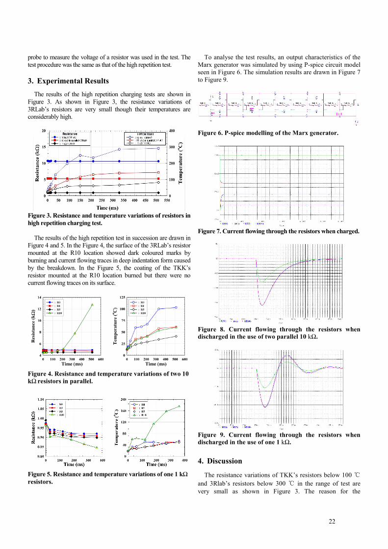
2
probe to measure the voltage of a resistor was used in the test. The test procedure was the same as that of the high repetition test.
3. Experimental Results The results of the high repetition charging tests are shown in
Figure 3. As shown in Figure 3, the resistance variations of 3RLab’s resistors are very small though their temperatures are considerably high.
Figure 3. Resistance and temperature variations of resistors in high repetition charging test.
The results of the high repetition test in succession are drawn in
Figure 4 and 5. In the Figure 4, the surface of the 3RLab’s resistor mounted at the R10 location showed dark coloured marks by burning and current flowing traces in deep indentation form caused by the breakdown. In the Figure 5, the coating of the TKK’s resistor mounted at the R10 location burned but there were no current flowing traces on its surface.
Figure 4. Resistance and temperature variations of two 10 kΩ resistors in parallel.
Figure 5. Resistance and temperature variations of one 1 kΩ resistors.
To analyse the test results, an output characteristics of the Marx generator was simulated by using P-spice circuit model seen in Figure 6. The simulation results are drawn in Figure 7 to Figure 9.
Figure 6. P-spice modelling of the Marx generator.
Figure 7. Current flowing through the resistors when charged.
Figure 8. Current flowing through the resistors when discharged in the use of two parallel 10 kΩ.
Figure 9. Current flowing through the resistors when discharged in the use of one 1 kΩ.
4. Discussion
The resistance variations of TKK’s resistors below 100 and 3Rlab’s resistors below 300 in the range of test are very small as shown in Figure 3. The reason for the
3
temperature of the R0 resistor to be the highest in Figure 4 is that the charging current is the highest in Figure 7 and the time for the capacitors to be charged into 50 kV is approximately required 6 ms. The current flowing through the R5 resistor is higher than the R10 resistor in Figure 7 and 8, however the temperature of the R5 resistor is lower than the R10 resistor in Figure 4. To understand the phenomena, the P-spice circuit modelling to put the trigger time of the tenth spark gap switch off 0.2 ns was carried out. The simulation result is shown in Figure 10. As shown in Figure 10, the reason why the temperature of the R10 resistor is higher than the R5 resistor seems to be an excessive current caused by the trigger time discrepancies of the spark gap switches. The resistance of the R10 resistor in comparison with the R0 resistor is rapidly increased though the temperature of the R0 resistor is higher than the R10 resistor in Figure 4. That is why the surface of the R10 resistor melted or burned due to a high temperature and was repetitively damaged by the breakdown as mentioned in the experimental results. The voltage of the R10 resistor is about 80 kV when discharged. The temperature of the R10 resistor in Figure 5 is the highest unlike Figure 4. That seems to be why the current flowing through the R10 resistor is very high of about 43 A when discharged as shown in Figure 9. The resistance of TKK’s R10 resistor in Figure 5 is not increased unlike 3Rlab’s R10 resistor in Figure 4 though the temperature of TKK’s R10 resistor is three times as high as 3Rlab’s R10 resistor. On the contrary, the resistance of TKK’s R10 resistor is decreased in small amounts. That seems to be why there was no physical damage by the breakdown on the surface of TKK’s R10 resistor and the coating of TKK’s R10 resistor was carbonized by burning. The voltage of 3Rlab’s R10 resistor is about 80 kV, but the voltage of TKK’s R10 resistor is about 43 kV.
Figure 10. Current flowing through the resistors when the trigger time of the tenth spark gap switch is delayed 0.2 ns unlike the other switches.
From the test results, the voltages between two terminals of
resistors are more considered than temperatures for a high repetitive and continuous operation of Marx generator in a stable state. The allowed voltages of resistors used in manufacture of Marx generator should be determined in the early design stage in consideration of resistor’s working properties. According to the situation, a new resistor should be designed and manufactured on the basis of the experimental results. The 3Rlab’s 10 kΩ resistor can be
possibly used in manufacture of Marx generator for a high repetitive and continuous operation in a stable state if the voltage below 50 kV is applied to the resistor. A new type of resistor should be designed and fabricated in the way to lengthen the distance between two terminals of resistor if the voltage of 80 kV is applied to a resistor as this experiment.
5. Conclusion In order to fabricate a compact and repetitive pulse power
supply by using a Marx generator, not only numerical analyses but also operating characteristics of circuit elements should be analysed on the basis of experiment. From the test and the simulation results, the Marx generator fabricated previously was improved and its operating condition was determined for a continuous operation at a high repetition rate in a stable state.
References [1] W. J. Carey and J. R. Mayes, “Marx Generator Design
and Performance”, IEEE Power Modulator Symposium 2002, pp. 625-628, (2002).
[2] D. Yim, C. Kim and J. Choi, “Design of a Compact and Repetitive Pulse Generator”, Agency for Defense Development Report, ADDR-410-091771, 2009.
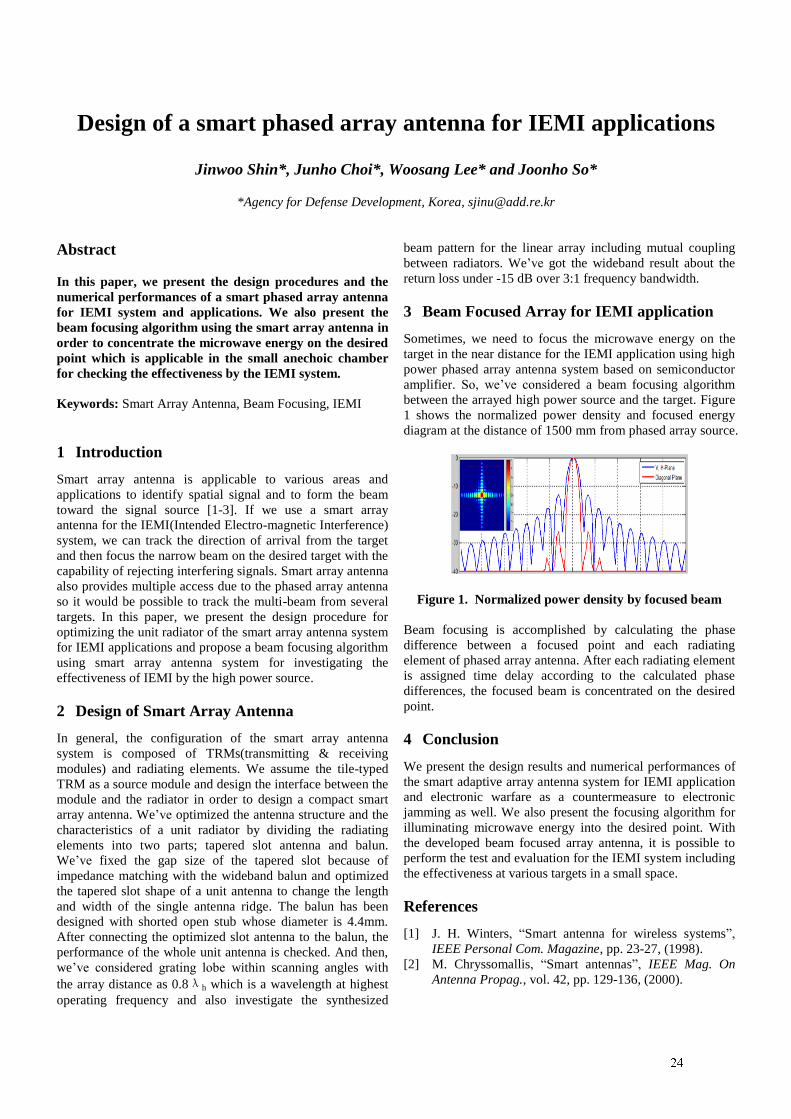
Design of a smart phased array antenna for IEMI applications
Jinwoo Shin*, Junho Choi*, Woosang Lee* and Joonho So*
*Agency for Defense Development, Korea, [email protected]
Abstract
In this paper, we present the design procedures and the
numerical performances of a smart phased array antenna
for IEMI system and applications. We also present the
beam focusing algorithm using the smart array antenna in
order to concentrate the microwave energy on the desired
point which is applicable in the small anechoic chamber
for checking the effectiveness by the IEMI system.
Keywords: Smart Array Antenna, Beam Focusing, IEMI
1 Introduction
Smart array antenna is applicable to various areas and
applications to identify spatial signal and to form the beam
toward the signal source [1-3]. If we use a smart array
antenna for the IEMI(Intended Electro-magnetic Interference)
system, we can track the direction of arrival from the target
and then focus the narrow beam on the desired target with the
capability of rejecting interfering signals. Smart array antenna
also provides multiple access due to the phased array antenna
so it would be possible to track the multi-beam from several
targets. In this paper, we present the design procedure for
optimizing the unit radiator of the smart array antenna system
for IEMI applications and propose a beam focusing algorithm
using smart array antenna system for investigating the
effectiveness of IEMI by the high power source.
2 Design of Smart Array Antenna
In general, the configuration of the smart array antenna
system is composed of TRMs(transmitting & receiving
modules) and radiating elements. We assume the tile-typed
TRM as a source module and design the interface between the
module and the radiator in order to design a compact smart
array antenna. We’ve optimized the antenna structure and the
characteristics of a unit radiator by dividing the radiating
elements into two parts; tapered slot antenna and balun.
We’ve fixed the gap size of the tapered slot because of
impedance matching with the wideband balun and optimized
the tapered slot shape of a unit antenna to change the length
and width of the single antenna ridge. The balun has been
designed with shorted open stub whose diameter is 4.4mm.
After connecting the optimized slot antenna to the balun, the
performance of the whole unit antenna is checked. And then,
we’ve considered grating lobe within scanning angles with
the array distance as 0.8λh which is a wavelength at highest
operating frequency and also investigate the synthesized
beam pattern for the linear array including mutual coupling
between radiators. We’ve got the wideband result about the
return loss under -15 dB over 3:1 frequency bandwidth.
3 Beam Focused Array for IEMI application
Sometimes, we need to focus the microwave energy on the
target in the near distance for the IEMI application using high
power phased array antenna system based on semiconductor
amplifier. So, we’ve considered a beam focusing algorithm
between the arrayed high power source and the target. Figure
1 shows the normalized power density and focused energy
diagram at the distance of 1500 mm from phased array source.
Figure 1. Normalized power density by focused beam
Beam focusing is accomplished by calculating the phase
difference between a focused point and each radiating
element of phased array antenna. After each radiating element
is assigned time delay according to the calculated phase
differences, the focused beam is concentrated on the desired
point.
4 Conclusion
We present the design results and numerical performances of
the smart adaptive array antenna system for IEMI application
and electronic warfare as a countermeasure to electronic
jamming as well. We also present the focusing algorithm for
illuminating microwave energy into the desired point. With
the developed beam focused array antenna, it is possible to
perform the test and evaluation for the IEMI system including
the effectiveness at various targets in a small space.
References
[1] J. H. Winters, “Smart antenna for wireless systems”,
IEEE Personal Com. Magazine, pp. 23-27, (1998).
[2] M. Chryssomallis, “Smart antennas”, IEEE Mag. On
Antenna Propag., vol. 42, pp. 129-136, (2000).

[3] M. Rivas, S. Xie, D. Su, “A review of adaptive
beamforming techniques for wideband smart antennas”,
6th
Intl. Conference on WiCOM, pp. 1-7, (2010).
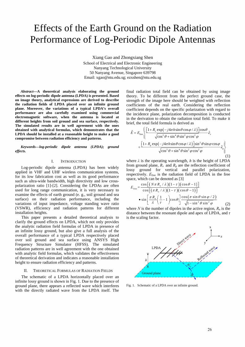
Effects of the Earth Ground on the Radiation Performance of Log-Periodic Dipole Antennas
Xiang Gao and Zhongxiang Shen School of Electrical and Electronic Engineering
Nanyang Technological University 50 Nanyang Avenue, Singapore 639798
Email: [email protected]; [email protected]
Abstract—A theoretical analysis elaborating the ground effects on log-periodic dipole antenna (LPDA) is presented. Based on image theory, analytical expressions are derived to describe the radiation fields of LPDA placed over an infinite ground plane. Moreover, the variations of a typical LPDA’s overall performance are also carefully examined using commercial electromagnetic software, when the antenna is located at different heights from soil ground and sea surface, respectively. The simulated results are in well agreement with the ones obtained with analytical formulas, which demonstrates that the LPDA should be installed at a reasonable height to make a good compromise between radiation efficiency and patterns.
Keywords—log-periodic dipole antenna (LPDA); ground effects.
I. INTRODUCTION Log-periodic dipole antenna (LPDA) has been widely applied in VHF and UHF wireless communication systems, for its low fabrication cost as well as its good performance such as ultra-wide bandwidth, high directivity and low cross-polarization ratio [1]-[2]. Considering the LPDAs are often used for long range communication, it is very necessary to examine the effects of earth ground (e. g., soil ground and sea surface) on their radiation performance, including the variations of input impedance, voltage standing wave ratio (VSWR), efficiency and radiation patterns for different installation heights. This paper presents a detailed theoretical analysis to clarify the ground effects on LPDA, which not only provides the analytic radiation field formulas of LPDA in presence of an infinite lossy ground, but also give a full analysis of the overall performance of a typical LPDA respectively placed over soil ground and sea surface using ANSYS High Frequency Structure Simulator (HFSS). The simulated radiation patterns are in well agreement with the one obtained with analytic field formulas, which validates the effectiveness of theoretical derivation and indicates a reasonable installation height to ensure radiation efficiency and patterns.
II. THEORETICAL FORMULAS OF RADIATION FIELDS The schematic of a LPDA horizontally placed over an infinite lossy ground is shown in Fig. 1. Due to the presence of ground plane, there appears a reflected wave which interferes with the directly radiated wave from the LPDA itself. The
final radiation total field can be obtained by using image theory. To be different from the perfect ground case, the strength of the image here should be weighted with reflection coefficients of the real earth. Considering the reflection coefficient depends on the specific polarization with regard to the incidence plane, polarization decomposition is conducted in the derivation to obtain the radiation total field. To make it brief, the total field formula is derived as
vfree v2 4 2 2
2p
p2 4 2 2
1 exp 4 sin cos / cosˆ ˆcos sin sin cos
1 exp 4 sin cos / sin sin cosˆ
cos sin sin cos
R j hE E e
R j he
(1) where λ is the operating wavelength, h is the height of LPDA from ground plane, Rv and Rp are the reflection coefficient of lossy ground for vertical and parallel polarization, respectively. Efree is the radiation field of LPDA in the free space, which can be denoted as [3]
free
2 2
cos / 1 cos 1=
cos / 1 cos 1
cos sin sin / 21sin 1 cos1 sin sin
n
n
n
N RE
R
R
(2) where N is the number of dipoles in the active region, Rn is the distance between the resonant dipole and apex of LPDA, and τ is the scaling factor.
Fig. 1. Schematic of a LPDA over an infinite ground.
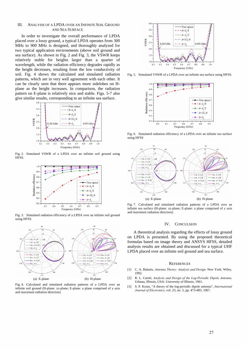
III. ANALYSIS OF A LPDA OVER AN INFINITE SOIL GROUND AND SEA SURFACE
In order to investigate the overall performance of LPDA placed over a lossy ground, a typical LPDA operates from 300 MHz to 900 MHz is designed, and thoroughly analyzed for two typical application environments (above soil ground and sea surface). As shown in Fig. 2 and Fig. 3, the VSWR keeps relatively stable for heights larger than a quarter of wavelength, while the radiation efficiency degrades rapidly as the height decreases, resulting from the low conductivity of soil. Fig. 4 shows the calculated and simulated radiation patterns, which are in very well agreement with each other. It can be clearly seen that there appears more sidelobes on H-plane as the height increases. In comparison, the radiation pattern on E-plane is relatively nice and stable. Figs. 5-7 also give similar results, corresponding to an infinite sea surface.
Fig. 2. Simulated VSWR of a LPDA over an infinite soil ground using HFSS.
Fig. 3. Simulated radiation efficiency of a LPDA over an infinite soil ground using HFSS.
(a) E-plane (b) H-plane
Fig. 4. Calculated and simulated radiation patterns of a LPDA over an infinite soil ground (H-plane: xz-plane; E-plane: a plane comprised of y axis and maximum radiation direction)
Fig. 5. Simulated VSWR of a LPDA over an infinite sea surface using HFSS.
Fig. 6. Simulated radiation efficiency of a LPDA over an infinite sea surface using HFSS
(a) E-plane (b) H-plane
Fig. 7. Calculated and simulated radiation patterns of a LPDA over an infinite sea surface (H-plane: xz-plane; E-plane: a plane comprised of y axis and maximum radiation direction).
IV. CONCULSION
A theoretical analysis regarding the effects of lossy ground on LPDA is presented. By using the proposed theoretical formulas based on image theory and ANSYS HFSS, detailed analysis results are obtained and discussed for a typical UHF LPDA placed over an infinite soil ground and sea surface.
REFERENCES [1] C. A. Balanis, Antenna Theory: Analysis and Design. New York: Wiley,
1992. [2] R. L. Carrel, Analysis and Design of the Log-Periodic Dipole Antenna.
Urbana, Illinois, USA: University of Illinois, 1961. [3] S. P. Kosta, “A theory of the log-periodic dipole antenna”, International
Journal of Electronics, vol. 23, no. 5, pp. 473-483, 1967.
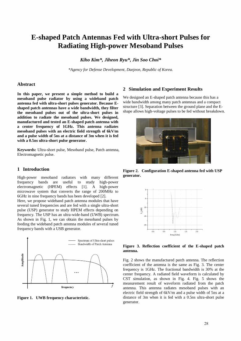
1
E-shaped Patch Antennas Fed with Ultra-short Pulses for
Radiating High-power Mesoband Pulses
Kiho Kim*, Jiheon Ryu*, Jin Soo Choi*
*Agency for Defense Development, Daejeon, Republic of Korea.
Abstract
In this paper, we present a simple method to build a
mesoband pulse radiator by using a wideband patch
antenna fed with ultra-short pulses generator. Because E-
shaped patch antennas have a wide bandwidth, they filter
the mesoband pulses out of the ultra-short pulses in
addition to radiate the mesoband pulses. We designed,
manufactured and tested an E-shaped patch antenna with
a center frequency of 1GHz. This antenna radiates
mesoband pulses with an electric field strength of 6kV/m
and a pulse width of 5ns at a distance of 3m when it is fed
with a 0.5ns ultra-short pulse generator.
Keywords: Ultra-short pulse, Mesoband pulse, Patch antenna,
Electromagnetic pulse.
1 Introduction
High-power mesoband radiators with many different
frequency bands are useful to study high-power
electromagnetic (HPEM) effects [1]. A high-power
microwave system that converts the range of 200MHz to
6GHz in nine frequency bands has been developed [2].
Here, we propose wideband patch antenna modules that have several tuned frequencies and are fed with a single ultra-short
pulse (USP) generator to study HPEM effects depending on
frequency. The USP has an ultra-wide-band (UWB) spectrum.
As shown in Fig. 1, we can obtain the mesoband pulses by
feeding the wideband patch antenna modules of several tuned
frequency bands with a USB generator.
Figure 1. UWB frequency characteristic.
2 Simulation and Experiment Results
We designed an E-shaped patch antenna because this has a
wide bandwidth among many patch antennas and a compact structure [3]. Separation between the ground plane and the E-
shape allows high-voltage pulses to be fed without breakdown.
Figure 2. Configuration E-shaped antenna fed with USP
generator.
0.0 0.5 1.0 1.5 2.0
-20
-15
-10
-5
0
S11[d
B]
Freq.[GHz]
Figure 3. Reflection coefficient of the E-shaped patch
antenna.
Fig. 2 shows the manufactured patch antenna. The reflection
coefficient of the antenna is the same as Fig. 3. The center
frequency is 1GHz. The fractional bandwidth is 30% at the
center frequency. A radiated field waveform is calculated by
CST simulation, as shown in Fig. 4. Fig. 5 shows the measurement result of waveform radiated from the patch
antenna. This antenna radiates mesoband pulses with an
electric field strength of 6kV/m and a pulse width of 5ns at a
distance of 3m when it is fed with a 0.5ns ultra-short pulse
generator.
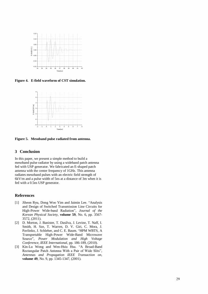
2
32 33 34 35 36 37 38 39 40 41 42
-0.15
-0.10
-0.05
0.00
0.05
0.10
0.15
E-f
ield
[A.U
.]
Time[ns]
Figure 4. E-field waveform of CST simulation.
-2 -1 0 1 2 3 4 5 6 7 8
-9
-6
-3
0
3
6
9
E-f
ield
[k
V/m
]
Time[ns]
Figure 5. Mesoband pulse radiated from antenna.
3 Conclusion
In this paper, we present a simple method to build a
mesoband pulse radiator by using a wideband patch antenna
fed with USP generator. We fabricated an E-shaped patch
antenna with the center frequency of 1GHz. This antenna
radiates mesoband pulses with an electric field strength of
6kV/m and a pulse width of 5ns at a distance of 3m when it is
fed with a 0.5ns USP generator.
References
[1] Jiheon Ryu, Dong Woo Yim and Jaimin Lee. “Analysis
and Design of Switched Transmission Line Circuits for
High-Power Wide-band Radiation”, Journal of the
Korean Physical Society, volume 59, No. 6, pp. 3567-
3572, (2011).
[2] D. Morton, J. Banister, T. Dasilva, J. Levine, T. Naff, I. Smith, H. Sze, T. Warren, D. V. Giri, C. Mora, J.
Pavlinko, J. Schleher, and C. E. Baum. “HPM WBTS, A
Transportable High-Power Wide-Band Microwave
Source”, Power Modulation and High Voltage
Conference, IEEE International, pp. 186-189, (2010).
[3] Kin-Lu Wong and Wen-Hsiu Hsu. “A Broad-Band
Rectangular Patch Antenna With a Pair of Wide Slits”,
Antennas and Propagation IEEE Transaction on, volume 49, No. 9, pp. 1345-1347, (2001).
Experiment of a Ku-band Gyro-BWO on Square waveguide
K. H. Jang*, J. J. Choi* and S. W. Jung †
*Kwangwoon university, Korea and High Power Microwave Engineering Laboratory, †National Fusion Research Institute, Korea
Abstract
A Ku-band gyrotron backward wave oscillator (gyro-
BWO) operating in the TE10 square waveguide mode at
the fundamental cyclotron frequency was designed. The
circuit performance was predicted by MAGIC code.
Initial experiments operating condition at -18.9kV and 1A
have demonstrated output power of 316W and efficiency
of 2%. In the future, we will proceed with the detail study
of experiment.
Keywords: Square waveguide, Gyro-BWO, Ku-band, BWO.
1 Introduction
Vacuum electron devices are important sources of high
power microwave radiation for use in industrial heating,
plasma heating in magnetic confinement fusion experiments
radar, communications, driving accelerators and many other
applications [1]. There are many high power microwave
devices, [2], [3] (such as twts, vircator, extended interaction
klystron-EIKS, gyrotrons, free electron lasers-FELS etc.)
which are capable to produce the frequency in Ku-band but the
requirement of a proper combination of frequency, power,
efficiency and compactness of the device is the problem of
research [4].
In this paper, we designed a Ku-band gyro-BWO as
interaction circuit of square waveguide. The characteristic of
interaction circuit predict by MAGIC code. The designed
circuit was manufactured. The fabricated circuit composed
experiment setup and we performed experiments of gyro-BWO.
2 The gyro-BWO setup
Figure 1 shows the layout of a Gyro-BWO. It consists of a
double anode MIG (Magnetron-Injection-Gun), a beam tunnel,
an interaction circuit, a collector, a window and an electro
magnet. The MIG has been performed the simulation that it
could to operate in Ku-band by controlling magnetic field, a
beam voltage and the modulating anode voltage. The beam
tunnel is designed circular type. Its cut off frequency is
12.87GHz at TE11 mode. The beam tunnel protects the MIG by
the oscillation power. Next part is interaction circuit. The
circuit of square waveguide was designed to operate the output
power more than 300W in TE10 mode. The operating
conditions are the velocity ratio of 0.6 to 0.8, a cathode voltage
of -18kV and magnetic field of 4.3kG. Its performance predict
by the MAGIC code. The dimension of square waveguide
width and height is respectively 13.7mm. Also a length of the
circuit is 550mm. The electron beam passing through the
interaction circuit is collected in the collector. The collector
structure is a tapered rectangular waveguide which changes to
the WR-62 in the square waveguide. Next, the vacuum window
was designed with a ceramic of stepped alumina for the broad
band performance. Finally, the electromagnet used a solenoid
coil type.
Figure 1. The gyro-BWO experiment setup
3 Experimental
The test of gyro-BWO is performed using the solenoid coil
and a high voltage modulator. Diagnostic apparatus was used
for a detector, a spectrum analyzer, a power meter. The detector
and the spectrum analyzer is finding of oscillated signal and
frequency respectively. The output power was measured by the
power meter.
The operating conditions of the gyro-BWO are cathode
voltage of -18.9kV, a mod-anode voltage of -5.66kV and the
beam current 1A. The initial magnetic field is flat field of
4.3kG. However, this condition was not occurred the
oscillation. So we found the optimization of the oscillation
condition by adjusting the magnetic field. As a result, the
output power is 316W at 11.69GHz and the magnetic field
profile has a slop of 4.3kG to 4.7kG in interaction circuit region.
At this time, the efficiency is 2%. Figure 2 is signal of appeared
oscillation by spectrum analyzer.
The next experiment is finding of a starting oscillation
condition. The test conditions were the same as previous. Only
the variable parameter is beam current. Figure 3 appear the
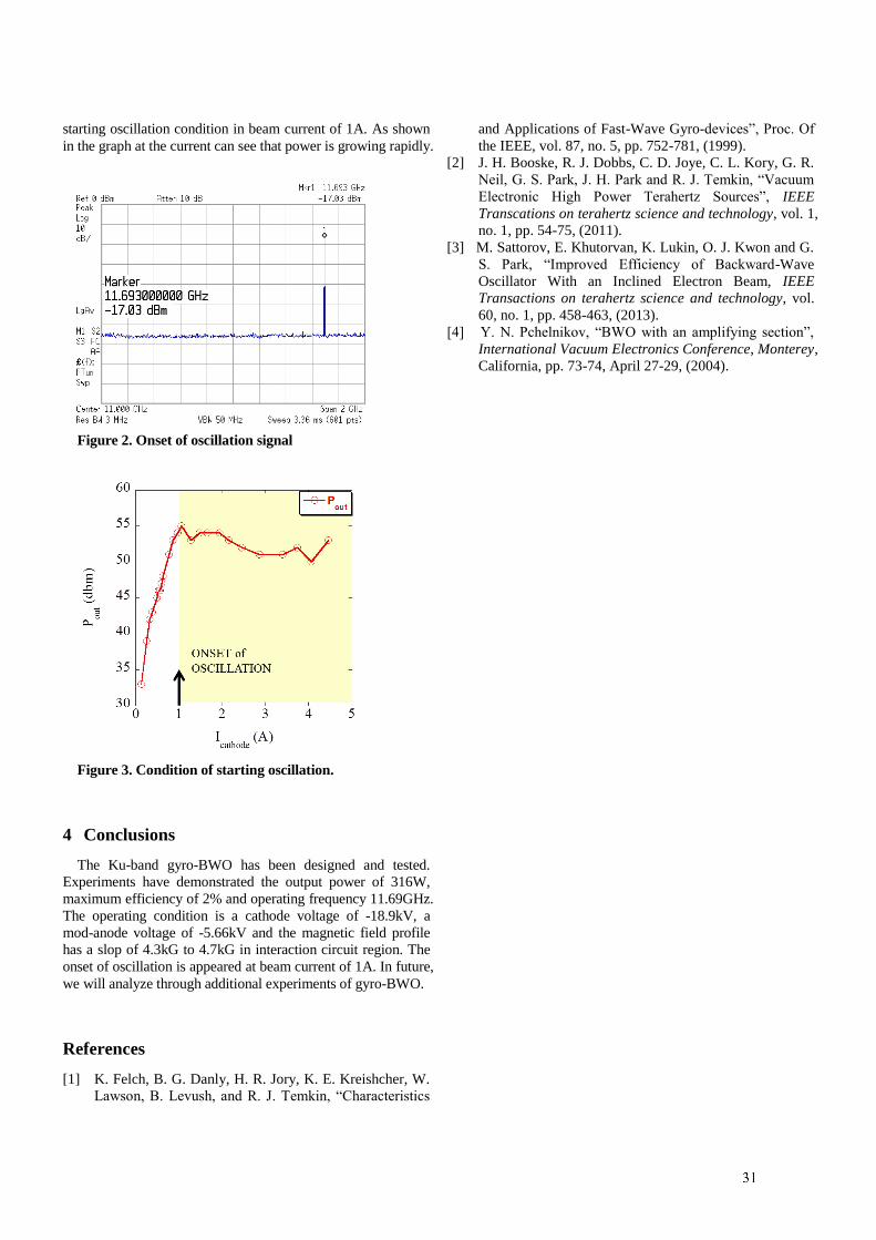
starting oscillation condition in beam current of 1A. As shown
in the graph at the current can see that power is growing rapidly.
Figure 2. Onset of oscillation signal
Figure 3. Condition of starting oscillation.
4 Conclusions
The Ku-band gyro-BWO has been designed and tested.
Experiments have demonstrated the output power of 316W,
maximum efficiency of 2% and operating frequency 11.69GHz.
The operating condition is a cathode voltage of -18.9kV, a
mod-anode voltage of -5.66kV and the magnetic field profile
has a slop of 4.3kG to 4.7kG in interaction circuit region. The
onset of oscillation is appeared at beam current of 1A. In future,
we will analyze through additional experiments of gyro-BWO.
References
[1] K. Felch, B. G. Danly, H. R. Jory, K. E. Kreishcher, W.
Lawson, B. Levush, and R. J. Temkin, “Characteristics
and Applications of Fast-Wave Gyro-devices”, Proc. Of
the IEEE, vol. 87, no. 5, pp. 752-781, (1999).
[2] J. H. Booske, R. J. Dobbs, C. D. Joye, C. L. Kory, G. R.
Neil, G. S. Park, J. H. Park and R. J. Temkin, “Vacuum
Electronic High Power Terahertz Sources”, IEEE
Transcations on terahertz science and technology, vol. 1,
no. 1, pp. 54-75, (2011).
[3] M. Sattorov, E. Khutorvan, K. Lukin, O. J. Kwon and G.
S. Park, “Improved Efficiency of Backward-Wave
Oscillator With an Inclined Electron Beam, IEEE
Transactions on terahertz science and technology, vol.
60, no. 1, pp. 458-463, (2013).
[4] Y. N. Pchelnikov, “BWO with an amplifying section”,
International Vacuum Electronics Conference, Monterey,
California, pp. 73-74, April 27-29, (2004).
1
HEMP Conducted Environment Analysis for Cable Lying on Ground
Sun Beiyun, Yang Jing
Northwest Institute of Nuclear Technology, China, 710024
Abstract The induced current for cable lying on ground illuminated by four kinds of HEMP radiation environment is investigated. By analyzing the calculated results, the relationship between the HEMP radiated environment prescribed in IEC61000-2-9 and the HEMP conducted environment prescribed in MIL-STD-188-125-2 is shown. Keywords: HEMP, radiated environment, conducted environment, cable, induced current
1 Introduction As we well known, radiated disturbance protection and conducted disturbance protection are necessary to ensure the HEMP survivability of weapons. Before a weapon with HEMP protection is designed, the designer needs to know the HEMP radiated environment and the HEMP conducted environment. MIL-STD-2169 and MIL-STD-188-125-1/2([1], [2]) prescribe the HEMP radiated environment and the HEMP conducted environment for the U.S. military systems. For MIL-STD-2169 is classified, we do not known how the HEMP conducted environment in MIL-STD-188-125-1/2 is deduced. However, MIL-STD-464 [3] indicates if the HEMP radiated environment is not defined, the IEC HEMP radiated environment [4] can be used. Then there is a problem that if the HEMP conducted environment in MIL-STD-188-125-1/2 can be used under the IEC HEMP radiated environment. The definition of an intrasite cable can be found in MIL-STD-188-125-2. The HEMP conducted environment for the intrasite cable is expressed by an induced current whose waveform is double exponential wave with 1000A amplitude,less than 20ns rise time and 500~550ns pulse width. In order to show the relationship between the IEC HEMP radiated environment and the HEMP conducted environment in MIL-STD-188-125-2, the induced current for a cable with length of 200m lying on ground illuminated by four kinds of radiated HEMP environment is calculated.
2 Computational model
In fig.1, a cable is illuminated by HEMP, where ψ is incident angle, and φ is azimuth angle. The induced current along the cable can be calculated by transmission line equations
presented in reference[5], which is closely relative to the HEMP radiated environment, the structure of cable and the electrical parameter of the ground.
ψ
φ
Ev
Hv
kv
Ev
Hv
kv
Fig.1 A cable illuminated by HEMP
The HEMP radiated environment can be expressed by double exponential wave:
( ) ( )0 >0t tE t kE e e tα β− −= − (1)
The values of k, E0, α and β are given in table.1 for four kinds of HEMP with 23ns,50ns,75ns and 184ns pulse width respectively, and the time-domain waveforms can be seen in fig.2, where the first is IEC HEMP environment, the second and the third are assumed HEMP environment, and the fourth is Bell Laboratory environment. Table 1:The parameters of HEMP environment
HEMP E0 k α β 1 50kV/m 1.30 4.00×10⁷ 6.00×10⁸ 2 50kV/m 1.12 1.58×10⁷ 6.98×10⁸ 3 50kV/m 1.08 1.02×10⁷ 7.36×10⁸
4 50kV/m 1.05 4.00×10⁶ 4.76×10⁸
0 100 200 300 400 5 00
0
10
20
30
40
50
4
3
2
E/(k
V/m
)
t/ns
1
Fig.2 The four kinds of HEMP
The ground parameters are chosen as: relative permittivity εrg=10 and conductivity σg=0.01, 0.001, 0.0001S/m. The cable parameters are chosen as: length l=200m, height h=0.1m, cable radius a=1cm and terminal impedance Z1=Z2=0Ω.
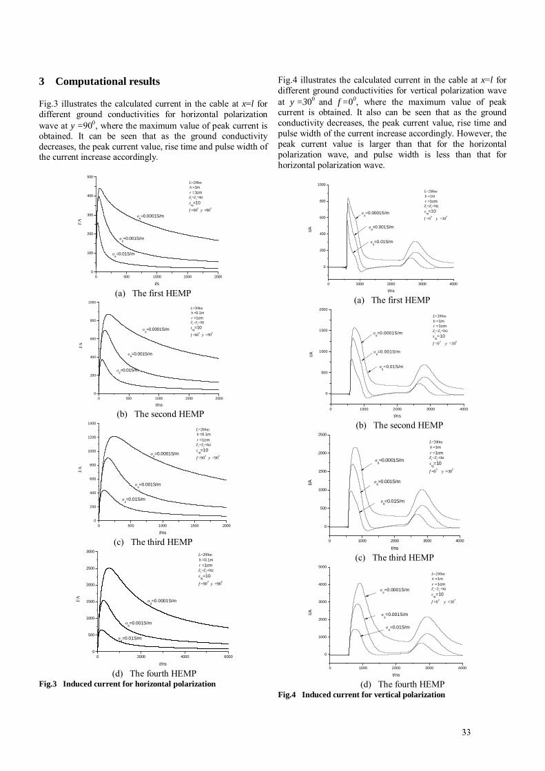
2
3 Computational results
Fig.3 illustrates the calculated current in the cable at x=l for different ground conductivities for horizontal polarization wave at ψ=900, where the maximum value of peak current is obtained. It can be seen that as the ground conductivity decreases, the peak current value, rise time and pulse width of the current increase accordingly.
0 500 1000 1500 2000
0
100
200
300
400
500
σg=0.001S/m
σg=0.01S/m
ψ =900
I/A
t/s
Z1=Z
2=0Ω
L=200m
r =1cm
σg=0.0001S/m
h =1m
φ=900
εrg=10
(a) The first HEMP
0 500 1000 1500 2000
0
200
400
600
800
1000
σg=0.001S/m
σg=0.01S/m
ψ =900
I/A
t/ns
Z1=Z
2=0Ω
L=200m
r =1cm
σg=0.0001S/m
h =0.1m
φ=900
εrg=10
(b) The second HEMP
0 500 1000 1500 2000
0
200
400
600
800
1000
1200
1400
σg=0.001S/m
σg=0.01S/m
ψ =900
I/A
t/ns
Z1=Z2=0Ω
L=200m
r =1cm
σg=0.0001S/m
h =0.1m
φ=900
εrg=10
(c) The third HEMP
0 2000 4000 6000
0
500
1000
1500
2000
2500
3000
σg=0.001S/m
σg=0.01S/m
ψ =900
I/A
t/ns
Z1=Z2=0Ω
L=200m
r =1cm
σg=0.0001S/m
h =0.1m
φ=900
εrg=10
(d) The fourth HEMP
Fig.3 Induced current for horizontal polarization
Fig.4 illustrates the calculated current in the cable at x=l for different ground conductivities for vertical polarization wave at ψ=300 and φ=00, where the maximum value of peak current is obtained. It also can be seen that as the ground conductivity decreases, the peak current value, rise time and pulse width of the current increase accordingly. However, the peak current value is larger than that for the horizontal polarization wave, and pulse width is less than that for horizontal polarization wave.
0 1000 2000 3000 4000
0
200
400
600
800
1000
σg=0.01S/m
σg=0.001S/m
σg=0.0001S/m
I/A
t/ns
ψ =300
Z1=Z
2=0Ω
L=200m
r =1cm
h =1m
φ=00
εrg=10
(a) The first HEMP
0 1000 2000 3000 4000
0
500
1000
1500
2000
σg=0.01S/m
σg=0.001S/m
σg=0.0001S/m
I/A
t/ns
ψ =300
Z1=Z2=0Ω
L=200m
r =1cm
h =1m
φ=00
εrg=10
(b) The second HEMP
0 1000 2000 3000 4000
0
500
1000
1500
2000
2500
σg=0.01S/m
σg=0.001S/m
σg=0.0001S/m
I/A
t/ns
ψ =300
Z1=Z2=0Ω
L=200m
r =1cm
h =1m
φ=00
εrg=10
(c) The third HEMP
0 1000 2000 3000 4000
0
1000
2000
3000
4000
5000
σg=0.01S/m
σg=0.001S/m
σg=0.0001S/m
I/A
t/ns
ψ =300
Z1=Z
2=0Ω
L=200m
r =1cm
h =1m
φ=00
εrg=10
(d) The fourth HEMP
Fig.4 Induced current for vertical polarization
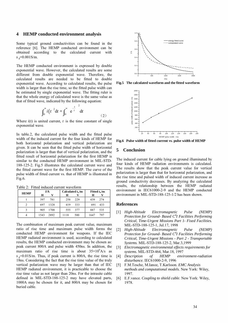
3
4 HEMP conducted environment analysis
Some typical ground conductivities can be found in the reference [6]. The HEMP conducted environment can be obtained according to the calculated current with σg=0.001S/m. The HEMP conducted environment is expressed by double exponential wave. However, the calculated results are some different from double exponential wave. Therefore, the calculated results are needed to be fitted to double exponential wave. According to calculated results, the pulse width is larger than the rise time, so the fitted pulse width can be estimated by single exponential wave. The fitting ruler is that the whole energy of calculated wave is the same value as that of fitted wave, indicated by the following equation:
( )2
2
0 0d e d
t
i t t tτ−∞ ∞
=
∫ ∫ (2)
Where i(t) is united current, τ is the time constant of single exponential wave. In table.2, the calculated pulse width and the fitted pulse width of the induced current for the four kinds of HEMP for both horizontal polarization and vertical polarization are given. It can be seen that the fitted pulse width of horizontal polarization is larger than that of vertical polarization, and the fitted result of horizontal polarization for the first HEMP is similar to the conducted HEMP environment in MIL-STD-188-125-2. Fig.5 illustrates the calculated current wave and the fitted current wave for the first HEMP. The curve of the pulse width of fitted current vs. that of HEMP is illustrated in Fig.6. Table 2: Fitted induced current waveform
HEMP I/A H V
Calculated tw/ns H V
Fitted tw/ns H V
1 397 781 258 229 439 274
2 697 1328 419 333 691 433
3 905 1700 555 377 887 535
4 1543 2892 1118 500 1647 797
The combination of maximum peak current value, maximum ratio of rise time and maximum pulse width forms the conducted HEMP environment for weapons. If the IEC HEMP radiated environment is used, according to calculated results, the HEMP conducted environment may be chosen as: peak current 800A and pulse width 450ns. In addition, the maximum ratio of rise time is about 35×109A/s as σg=0.01S/m. Thus, if peak current is 800A, the rise time is 18ns. Considering the fact that the rise time value of the truly vertical polarization wave may be larger than that of IEC HEMP radiated environment, it is practicable to choose the rise time value as not larger than 20ns. For the intrasite cable defined in MIL-STD-188-125-2 may have elevated parts, 1000A may be chosen for it, and 800A may be chosen for buried cable.
0 500 1000 1500 2000
0.0
0.2
0.4
0.6
0.8
1.0
energy fitted curve
computated curve
I/A
t/ns Fig.5 The calculated waveform and the fitted waveform
20 40 60 80 100 120 140 160 180 200
200
400
600
800
1000
1200
1400
1600
1800
2000
puls
e w
idth
of i
nduc
ed c
urre
nt t
/ns
HEMP pulse width t/ns Fig.6 Pulse width of fitted current vs. pulse width of HEMP
5 Conclusion
The induced current for cable lying on ground illuminated by four kinds of HEMP radiation environments is calculated. The results show that the peak current value for vertical polarization is larger than that for horizontal polarization, and the rise time and pulsed width of induced current increase as ground conductivity decreases. By analyzing the calculated results, the relationship between the HEMP radiated environment in IEC61000-2-9 and the HEMP conducted environment in MIL-STD-188-125-1/2 has been shown.
References [1] High-Altitude Electromagnetic Pulse (NEMP)
Protection for Ground- Based C4I Facilities Performing Critical, Time-Urgent Missions Part 1- Fixed Facilities. MIL-STD-188-125-1, Jul.17, 1998
[2] High-Altitude Electromagnetic Pulse (NEMP) Protection for Ground- Based C4I Facilities Performing Critical, Time-Urgent Missions - Part 2 - Transportable Systems. MIL-STD-188-125-2, Mar.3,1999
[3] Electromagnetic environmental effects requirements for systems. MIL-STD-464, Mar.18, 1997
[4] Description of HEMP environment-radiation disturbance. IEC61000-2-9, 1996
[5] F.M.Tesche, M.Ianoz, T.Karlsson. EMC Analysis methods and computational models. New York: Wiley, 1997.
[6] E.F.vance. Coupling to shield cable. New York: Wiley, 1978.
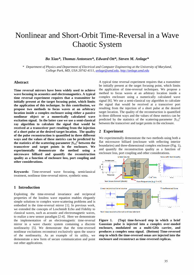
Nonlinear and Short-Orbit Time-Reversal in a Wave
Chaotic System
Bo Xiao*, Thomas Antonsen*, Edward Ott*, Steven M. Anlage*
* Department of Physics and Department of Electrical and Computer Engineering at the University of Maryland,
College Park, MD, USA 20742-4111, [email protected], http://anlage.umd.edu
Abstract
Time reversal mirrors have been widely used to achieve
wave focusing in acoustics and electromagnetics. A typical
time reversal experiment requires that a transmitter be
initially present at the target focusing point, which limits
the application of this technique. In this contribution, we
propose two methods to focus waves at an arbitrary
location inside a complex enclosure using either a passive
nonlinear object or a numerically calculated wave
excitation signal. In the latter case we use a semi-classical
ray algorithm to calculate the signal that would be
received at a transceiver port resulting from the injection
of a short pulse at the desired target location. The quality
of the pulse reconstruction is quantified in three different
ways and the values of these metrics can be predicted by
the statistics of the scattering-parameter |S21|2 between the
transceiver and target points in the enclosure. We
experimentally demonstrate the method using a
microwave billiard and quantify the reconstruction
quality as a function of enclosure loss, port coupling and
other considerations.
Keywords: Time-reversed wave focusing, semiclassical
treatment, nonlinear time-reversal mirror, synthetic sona.
1 Introduction
Exploiting the time-reversal invariance and reciprocal
properties of the lossless wave equation enables elegantly
simple solutions to complex wave-scattering problems and is
embodied in the time-reversal mirror [1]. In previous work,
we extended the concepts of Loschmidt Echo and Fidelity to
classical waves, such as acoustic and electromagnetic waves,
to realize a new sensor paradigm [2-4]. Here we demonstrate
the implementation of an electromagnetic time-reversal
mirror in a wave chaotic system containing a discrete
nonlinearity [5]. We demonstrate that the time-reversed
nonlinear excitations reconstruct exclusively upon the source
of the nonlinearity. As an example of its utility, we
demonstrate a new form of secure communication and point
out other applications.
A typical time reversal experiment requires that a transmitter
be initially present at the target focusing point, which limits
the application of time-reversal techniques. We propose a
method to focus waves at an arbitrary location inside a
complex enclosure using a numerically calculated wave
signal [6]. We use a semi-classical ray algorithm to calculate
the signal that would be received at a transceiver port
resulting from the injection of a short pulse at the desired
target location. The quality of the reconstruction is quantified
in three different ways and the values of these metrics can be
predicted by the statistics of the scattering-parameter |S21|2
between the transceiver and target points in the enclosure.
2 Experiment
We experimentally demonstrate the two methods using both a
flat microwave billiard (enclosure with reflecting interior
boundaries) and three-dimensional complex enclosure (Fig. 1),
and quantify the reconstruction quality as a function of
enclosure loss, port coupling and other considerations.
Figure 1. (Top) time-forward step in which a brief
Gaussian pulse is injected into a complex over-moded
enclosure, modulated on a multi-GHz carrier, and
produces a complex sona signal. (Bottom) Time-reversed
step in which the time-reversed sonas are injected into the
enclosure and reconstruct as time-reversed replicas.
The first experiment is schematically illustrated in Fig. 1.
We utilize a passive nonlinear source (a diode in this case) to
respond to an interrogation pulse (~ few ns duration Gaussian
of a microwave carrier signal) by creating a second harmonic
sona signal. (We use the word ‘sona’ to represent the entire
waveform produced by the complex enclosure, as opposed to
‘coda’ which refers to just the end of the waveform.) Both
the linear and nonlinear sona signals are collected at a third
port. In the second step, the two sonas are time-reversed and
injected into the same port in which they were measured. The
linear sona reconstructs as a time-reversed replica of the
original pulse at the linear source. The nonlinear sona
reconstructs as a time-reversed replica of the up-converted
interrogation pulse, and a few of its echoes, at the nonlinear
element. This demonstrates a selective reconstruction at an
arbitrary location in the enclosure, and requires only the
initial presence of a passive nonlinear object [5, 7].
Applications include exclusive communications and wireless
power transfer. As discussed in detail elsewhere [7] we have
sent images from the third port to either the linear or
nonlinear port. The image sent to one port is not visible at the
other port, demonstrating the exclusivity of the information
transfer.
A second experiment utilizes the synthetic sona technique to
create a purely theoretical waveform that, when time-reversed
and injected into a physical two-dimensional microwave
billiard, will reconstruct as a short pulse at a precise (and
arbitrarily chosen) location in the billiard. This method
exploits ‘short orbits’ [8, 9] between the injection point and
reconstruction point to perform a semi-classical calculation of
the synthetic sona [6]. The experimental reconstructions are
successful for billiards in which the interior geometry is
known. We find that the quality of the synthetic sona
reconstructions correlates strongly with the transmission S-
parameter over the bandwidth of the pulse.
Acknowledgements
This work was funded by the AFOSR (No. FA95500710049),
the Office of Naval Research (contract No. N00014130474),
and the Center for Nanophysics and Advanced Materials
(CNAM).
References
[1] S. M. Anlage, J. Rodgers, S. Hemmady, J. Hart, T. M.
Antonsen, E. Ott, Acta Physica Polonica A vol. 112, pp. 569-
574, 2007.
[2] B. T. Taddese, J. Hart, T. M. Antonsen, E. Ott, and S. M.
Anlage, Applied Physics Letters vol. 95, 114103, 2009.
[3] B. T. Taddese, T. M. Antonsen, E. Ott, and S. M. Anlage,
Journal of Applied Physics vol. 108, 114911, 2010.
[4] B. T. Taddese, G. Gradoni, F. Moglie, T. M Antonsen, E.
Ott, S. M. Anlage, New Journal of Physics vol. 15, 023025,
2013.
[5] M. Frazier, B. Taddese, T. Antonsen, S. M. Anlage,
Physical Review Letters vol. 110, 063902, 2013. See "Alice
and Bob Go Nonlinear" Synopsis on Physics.APS.org
(http://physics.aps.org/synopsis-
for/10.1103/PhysRevLett.110.063902).
[6] Bo Xiao, Thomas M. Antonsen, Edward Ott, Steven M.
Anlage, Focusing Waves at Arbitrary Locations in a Ray-
Chaotic Enclosure Using Time-Reversed Synthetic Sonas,
http://arxiv.org/abs/1409.3850.
[7] Matthew Frazier, Biniyam Taddese, Bo Xiao, Thomas
Antonsen, Edward Ott, Steven M. Anlage, “Nonlinear Time-
Reversal of Classical Waves: Experiment and Model,” Phys.
Rev. E vol. 88, 062910, 2013.
[8] James A. Hart, T. M. Antonsen, E. Ott, "The effect of
short ray trajectories on the scattering statistics of wave
chaotic systems," Phys. Rev. E vol. 80, 041109, 2009.
[9] Jen-Hao Yeh, James Hart, Elliott Bradshaw, Thomas
Antonsen, Edward Ott, Steven M. Anlage, “Experimental
Examination of the Effect of Short Ray Trajectories in Two-
port Wave-Chaotic Scattering Systems,” Phys. Rev. E vol. 82,
041114, 2010.
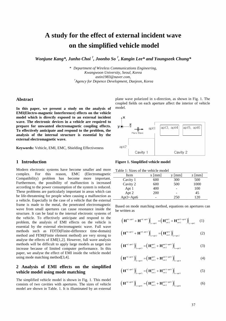
A study for the effect of external incident wave
on the simplified vehicle model
Wonjune Kang*, Junho Choi †, Joonho So
†, Kangin Lee* and Youngseek Chung*
* Department of Wireless Communications Engineering,
Kwangwoon University, Seoul, Korea
†Agency for Depence Development, Daejeon, Korea
Abstract
In this paper, we present a study on the analysis of
EMI(Electro-magnetic Interference) effects on the vehicle
model which is directly exposed to an external incident
wave. The electronic devices in a vehicle are required to
prepare for unwanted electromagnetic coupling effects.
To effectively anticipate and respond to the problem, the
analysis of the internal structure is essential by the
external electromagnetic wave.
Keywords: Vehicle, EMI, EMC, Shielding Effectiveness
1 Introduction
Modern electronic systems have become smaller and more
complex. For this reason, EMC (Electromagnetic
Compatibility) problem has become more important.
Furthermore, the possibility of malfunction is increased
according to the power consumption of the system is reduced.
These problems are particularly important in areas which can
be life-threatening for people when causing a malfunction as
a vehicle. Especially in the case of a vehicle that the external
frame is made to the metal, the penetrated electromagnetic
wave from small apertures can cause resonance inside the
structure. It can be fatal to the internal electronic systems of
the vehicle. To effectively anticipate and respond to the
problem, the analysis of EMI effects on the vehicle is
essential by the external electromagnetic wave. Full wave
methods such as FDTD(Finite-difference time-domain)
method and FEM(Finite element method) are very strong to
analyse the effects of EMI[1,2]. However, full wave analysis
methods will be difficult to apply large models as target size
increase because of limited computer performance. In this
paper, we analyse the effect of EMI inside the vehicle model
using mode matching method[3,4].
2 Analysis of EMI effects on the simplified
vehicle model using mode matching
The simplified vehicle model is shown in Fig. 1. This model
consists of two cavities with apertures. The sizes of vehicle
model are shown in Table. 1. It is illuminated by an external
plane wave polarized in x-direction, as shown in Fig. 1. The
coupled fields on each aperture affect the interior of vehicle
model.
Figure 1. Simplified vehicle model
Table 1: Sizes of the vehicle model
Item x [mm] y [mm] z [mm]
Cavity 1 600 300 500
Cavity 2 600 500 1000
Apt 1 400 - 100
Apt 2 200 - 45
Apt3~Apt6 - 250 120
Based on mode matching method, equations on apertures can
be written as
, 1 , 1 1 3~ 6
2 21 1
inc apt ref apt apt apt apt
cav cavy apt y apt H H H H (1)
, 2 , 2 2
12 2
inc apt ref apt apt
cavy apt y apt H H H (2)
, 3 1 3~ 6
2 23 3
ref apt apt apt apt
cav cavz apt z apt H H H (3)
, 4 1 3~ 6
2 24 4
ref apt apt apt apt
cav cavz apt z apt H H H (4)
, 5 1 3~ 6
2 25 5
ref apt apt apt apt
cav cavz apt z apt H H H (5)
, 6 1 3~ 6
2 26 6
ref apt apt apt apt
cav cavz apt z apt H H H (6)
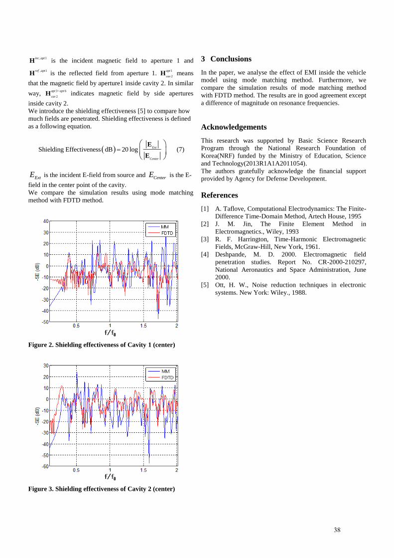
, 1inc aptH is the incident magnetic field to aperture 1 and
, 1ref aptH is the reflected field from aperture 1.
1
2
apt
cavH means
that the magnetic field by aperture1 inside cavity 2. In similar
way, 3~ 6
2
apt apt
cavH indicates magnetic field by side apertures
inside cavity 2.
We introduce the shielding effectiveness [5] to compare how
much fields are penetrated. Shielding effectiveness is defined
as a following equation.
Shielding Effectiveness dB 20 logExt
Center
E
E (7)
ExtE is the incident E-field from source and CenterE is the E-
field in the center point of the cavity.
We compare the simulation results using mode matching
method with FDTD method.
Figure 2. Shielding effectiveness of Cavity 1 (center)
Figure 3. Shielding effectiveness of Cavity 2 (center)
3 Conclusions
In the paper, we analyse the effect of EMI inside the vehicle
model using mode matching method. Furthermore, we
compare the simulation results of mode matching method
with FDTD method. The results are in good agreement except
a difference of magnitude on resonance frequencies.
Acknowledgements
This research was supported by Basic Science Research
Program through the National Research Foundation of
Korea(NRF) funded by the Ministry of Education, Science
and Technology(2013R1A1A2011054).
The authors gratefully acknowledge the financial support
provided by Agency for Defense Development.
References
[1] A. Taflove, Computational Electrodynamics: The Finite-
Difference Time-Domain Method, Artech House, 1995
[2] J. M. Jin, The Finite Element Method in
Electromagnetics., Wiley, 1993
[3] R. F. Harrington, Time-Harmonic Electromagnetic
Fields, McGraw-Hill, New York, 1961.
[4] Deshpande, M. D. 2000. Electromagnetic field
penetration studies. Report No. CR-2000-210297,
National Aeronautics and Space Administration, June
2000.
[5] Ott, H. W., Noise reduction techniques in electronic
systems. New York: Wiley., 1988.
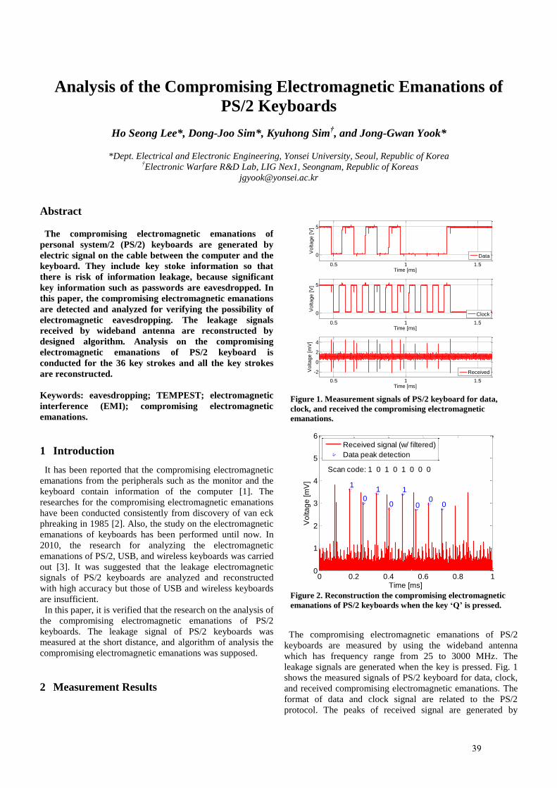
1
Analysis of the Compromising Electromagnetic Emanations of
PS/2 Keyboards
Ho Seong Lee*, Dong-Joo Sim*, Kyuhong Sim†, and Jong-Gwan Yook*
*Dept. Electrical and Electronic Engineering, Yonsei University, Seoul, Republic of Korea
†Electronic Warfare R&D Lab, LIG Nex1, Seongnam, Republic of Koreas
Abstract
The compromising electromagnetic emanations of
personal system/2 (PS/2) keyboards are generated by
electric signal on the cable between the computer and the
keyboard. They include key stoke information so that
there is risk of information leakage, because significant
key information such as passwords are eavesdropped. In
this paper, the compromising electromagnetic emanations
are detected and analyzed for verifying the possibility of
electromagnetic eavesdropping. The leakage signals
received by wideband antenna are reconstructed by
designed algorithm. Analysis on the compromising
electromagnetic emanations of PS/2 keyboard is
conducted for the 36 key strokes and all the key strokes
are reconstructed.
Keywords: eavesdropping; TEMPEST; electromagnetic
interference (EMI); compromising electromagnetic
emanations.
1 Introduction
It has been reported that the compromising electromagnetic
emanations from the peripherals such as the monitor and the
keyboard contain information of the computer [1]. The
researches for the compromising electromagnetic emanations
have been conducted consistently from discovery of van eck
phreaking in 1985 [2]. Also, the study on the electromagnetic
emanations of keyboards has been performed until now. In
2010, the research for analyzing the electromagnetic
emanations of PS/2, USB, and wireless keyboards was carried
out [3]. It was suggested that the leakage electromagnetic
signals of PS/2 keyboards are analyzed and reconstructed
with high accuracy but those of USB and wireless keyboards
are insufficient.
In this paper, it is verified that the research on the analysis of
the compromising electromagnetic emanations of PS/2
keyboards. The leakage signal of PS/2 keyboards was
measured at the short distance, and algorithm of analysis the
compromising electromagnetic emanations was supposed.
2 Measurement Results
The compromising electromagnetic emanations of PS/2
keyboards are measured by using the wideband antenna
which has frequency range from 25 to 3000 MHz. The
leakage signals are generated when the key is pressed. Fig. 1
shows the measured signals of PS/2 keyboard for data, clock,
and received compromising electromagnetic emanations. The
format of data and clock signal are related to the PS/2
protocol. The peaks of received signal are generated by
Figure 1. Measurement signals of PS/2 keyboard for data,
clock, and received the compromising electromagnetic
emanations.
Figure 2. Reconstruction the compromising electromagnetic
emanations of PS/2 keyboards when the key ‘Q’ is pressed.
0.5 1 1.5
0
5
Time [ms]
Vo
lta
ge
[V
]
Data
0.5 1 1.5
0
5
Time [ms]
Vo
lta
ge
[V
]
Clock
0.5 1 1.5
-2
0
2
4
Time [ms]
Vo
lta
ge
[m
V]
Received
0 0.2 0.4 0.6 0.8 10
1
2
3
4
5
6
Time [ms]
Vo
lta
ge
[m
V]
Scan code: 1 0 1 0 1 0 0 0
1
0
1
0
1
00
0
Received signal (w/ filtered)
Data peak detection
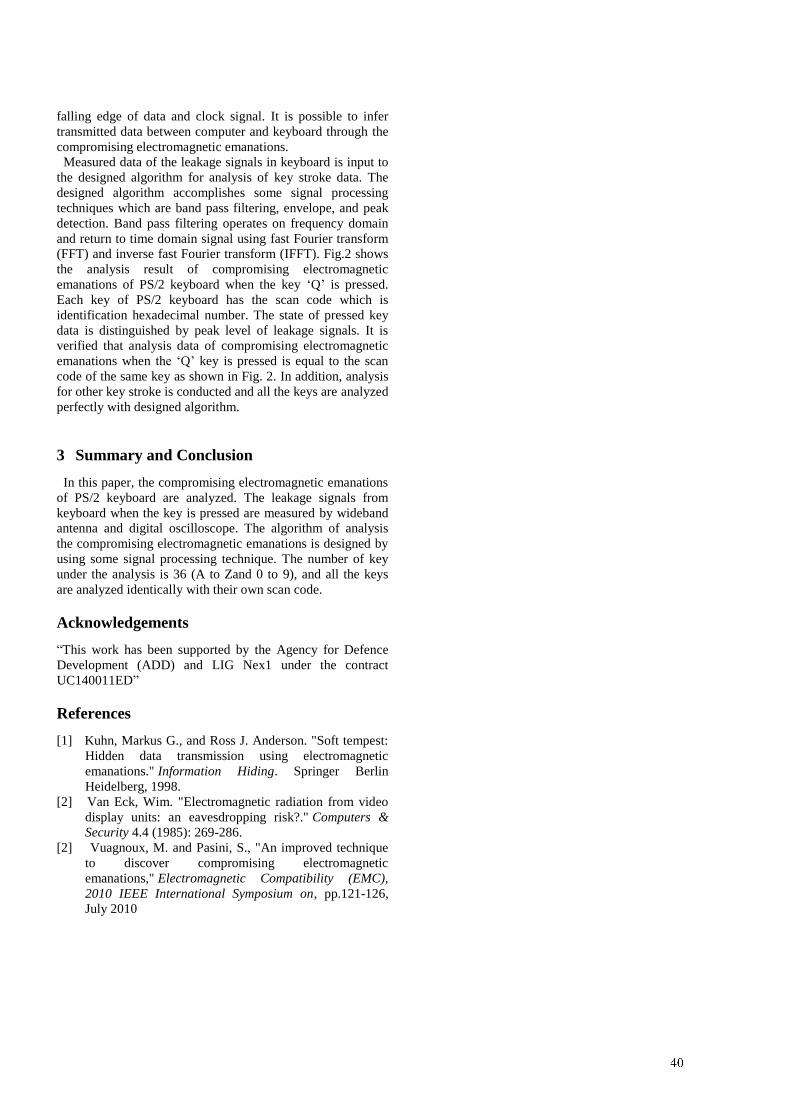
2
falling edge of data and clock signal. It is possible to infer
transmitted data between computer and keyboard through the
compromising electromagnetic emanations.
Measured data of the leakage signals in keyboard is input to
the designed algorithm for analysis of key stroke data. The
designed algorithm accomplishes some signal processing
techniques which are band pass filtering, envelope, and peak
detection. Band pass filtering operates on frequency domain
and return to time domain signal using fast Fourier transform
(FFT) and inverse fast Fourier transform (IFFT). Fig.2 shows
the analysis result of compromising electromagnetic
emanations of PS/2 keyboard when the key ‘Q’ is pressed.
Each key of PS/2 keyboard has the scan code which is
identification hexadecimal number. The state of pressed key
data is distinguished by peak level of leakage signals. It is
verified that analysis data of compromising electromagnetic
emanations when the ‘Q’ key is pressed is equal to the scan
code of the same key as shown in Fig. 2. In addition, analysis
for other key stroke is conducted and all the keys are analyzed
perfectly with designed algorithm.
3 Summary and Conclusion
In this paper, the compromising electromagnetic emanations
of PS/2 keyboard are analyzed. The leakage signals from
keyboard when the key is pressed are measured by wideband
antenna and digital oscilloscope. The algorithm of analysis
the compromising electromagnetic emanations is designed by
using some signal processing technique. The number of key
under the analysis is 36 (A to Zand 0 to 9), and all the keys
are analyzed identically with their own scan code.
Acknowledgements
“This work has been supported by the Agency for Defence
Development (ADD) and LIG Nex1 under the contract
UC140011ED”
References
[1] Kuhn, Markus G., and Ross J. Anderson. "Soft tempest:
Hidden data transmission using electromagnetic
emanations." Information Hiding. Springer Berlin
Heidelberg, 1998.
[2] Van Eck, Wim. "Electromagnetic radiation from video
display units: an eavesdropping risk?." Computers &
Security 4.4 (1985): 269-286.
[2] Vuagnoux, M. and Pasini, S., "An improved technique
to discover compromising electromagnetic
emanations," Electromagnetic Compatibility (EMC),
2010 IEEE International Symposium on, pp.121-126,
July 2010
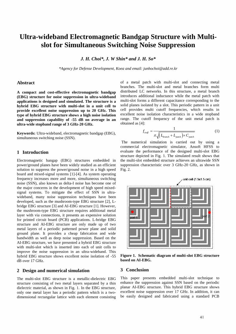
Ultra-wideband Electromagnetic Bandgap Structure with Multi-
slot for Simultaneous Switching Noise Suppression
J. H. Choi*, J. W Shin* and J. H. So*
*Agency for Defense Development, Koea and email: [email protected]
Abstract
A compact and cost-effective electromagnetic bandgap
(EBG) structure for noise suppression in ultra-wideband
applications is designed and simulated. The structure is a
hybrid EBG structure with multi-slot in a unit cell to
provide excellent noise suppression up to 20 GHz. This
type of hybrid EBG structure shows a high noise isolation
and suppression capability of -55 dB on average in an
ultra-wide stopband range of 3 GHz-20 GHz.
Keywords: Ultra-wideband, electromagnetic bandgap (EBG),
simultaneous switching noise (SSN).
1 Introduction
Electromagnetic bangap (EBG) structures embedded in
power/ground planes have been widely studied as an efficient
solution to suppress the power/ground noise in a high speed
board and mixed-signal systems [1]-[4]. As system operating
frequency increases more and more, simultaneous switching
noise (SSN), also known as delta-I noise has become one of
the major concerns in the development of high speed mixed-
signal systems. To mitigate the effect of SSN in ultra-
wideband, many noise suppression techniques have been
developed, such as the mushroom-type EBG structure [2], L-
bridge EBG structure [3] and AI-EBG structure [1]. However,
the mushroom-type EBG structure requires additional metal
layer with via connections, it presents an expensive solution
for printed circuit board (PCB) applications. L-bridge EBG
structure and AI-EBG structure are only made up of two
metal layers of a periodic patterned power plane and solid
ground plane. It provides a cheap fabrication and wide
bandwidth as well as deep noise suppression. Based on the
AI-EBG structure, we have presented a hybrid EBG structure
with multi-slot which is inserted into each of unit cells to
improve the noise suppression in an ultra-wideband. This
hybrid EBG structure shows excellent noise isolation of -55
dB over 17 GHz.
2 Design and numerical simulation
The multi-slot EBG structure is a metallic-dielectric EBG
structure consisting of two metal layers separated by a thin
dielectric material, as shown in Fig. 1. In the EBG structure,
only one metal layer has a periodic pattern which is a two-
dimensional rectangular lattice with each element consisting
of a metal patch with multi-slot and connecting metal
branches. The multi-slot and metal branches form multi
distributed LC networks. In this structure, a metal branch
introduces additional inductance while the metal patch with
multi-slot forms a different capacitance corresponding to the
solid planes isolated by a slot. This periodic pattern in a unit
cell provides multi cutoff frequencies, which results in
excellent noise isolation characteristics in a wide stopband
range. The cutoff frequency of the unit metal patch is
obtained as [4]:
1
ctoff
branch patch patch
fL L C
(1)
The numerical simulation is carried out by using a
commercial electromagnetic simulator, Ansoft HFSS to
evaluate the performance of the designed multi-slot EBG
structure depicted in Fig. 1. The simulated result shows that
the multi-slot embedded structure achieves an ultrawide SSN
suppression characteristic over 3 GHz-20 GHz, as shown in
Fig. 2.
Figure 1. Schematic diagram of multi-slot EBG structure
based on AI-EBG.
3 Conclusion
This paper presents embedded multi-slot technique to
enhance the suppression against SSN based on the periodic
planar AI-EBG structure. This hybrid EBG structure shows
excellent noise suppression over 17 GHz. In addition, it can
be easily designed and fabricated using a standard PCB
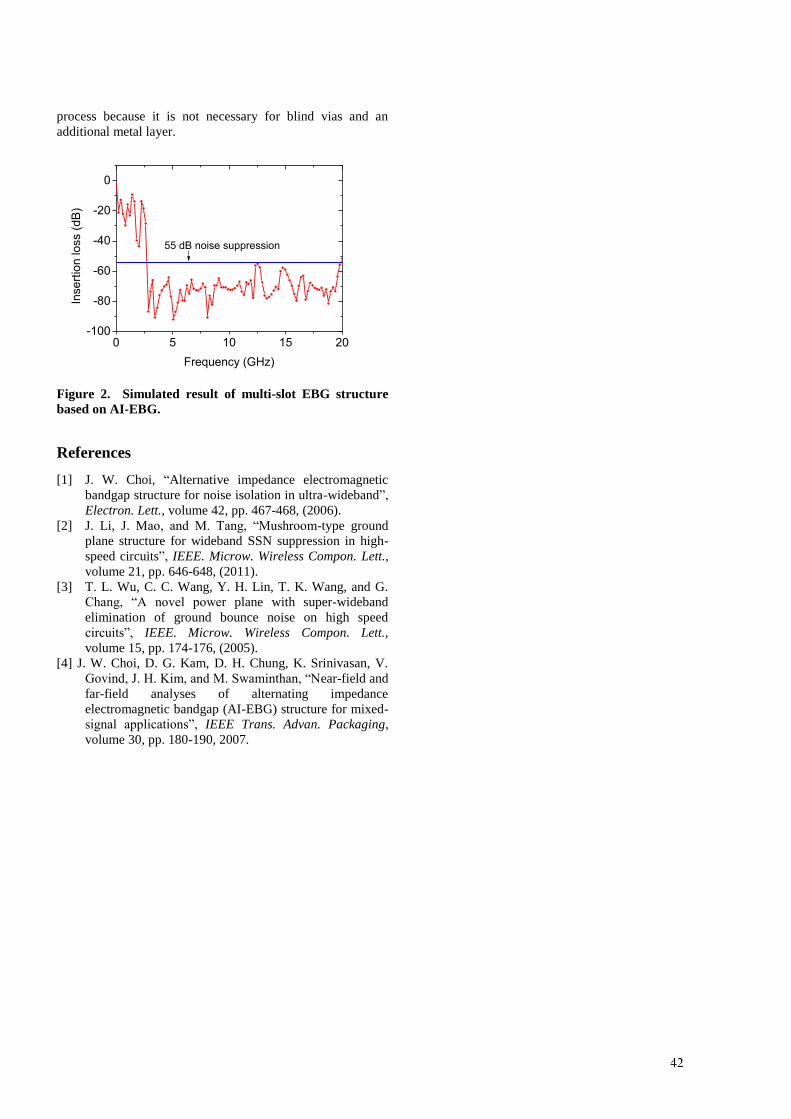
process because it is not necessary for blind vias and an
additional metal layer.
0 5 10 15 20-100
-80
-60
-40
-20
0
Inse
rtio
n lo
ss (
dB
)
Frequency (GHz)
55 dB noise suppression
Figure 2. Simulated result of multi-slot EBG structure
based on AI-EBG.
References
[1] J. W. Choi, “Alternative impedance electromagnetic
bandgap structure for noise isolation in ultra-wideband”,
Electron. Lett., volume 42, pp. 467-468, (2006).
[2] J. Li, J. Mao, and M. Tang, “Mushroom-type ground
plane structure for wideband SSN suppression in high-
speed circuits”, IEEE. Microw. Wireless Compon. Lett.,
volume 21, pp. 646-648, (2011).
[3] T. L. Wu, C. C. Wang, Y. H. Lin, T. K. Wang, and G.
Chang, “A novel power plane with super-wideband
elimination of ground bounce noise on high speed
circuits”, IEEE. Microw. Wireless Compon. Lett.,
volume 15, pp. 174-176, (2005).
[4] J. W. Choi, D. G. Kam, D. H. Chung, K. Srinivasan, V.
Govind, J. H. Kim, and M. Swaminthan, “Near-field and
far-field analyses of alternating impedance
electromagnetic bandgap (AI-EBG) structure for mixed-
signal applications”, IEEE Trans. Advan. Packaging,
volume 30, pp. 180-190, 2007.
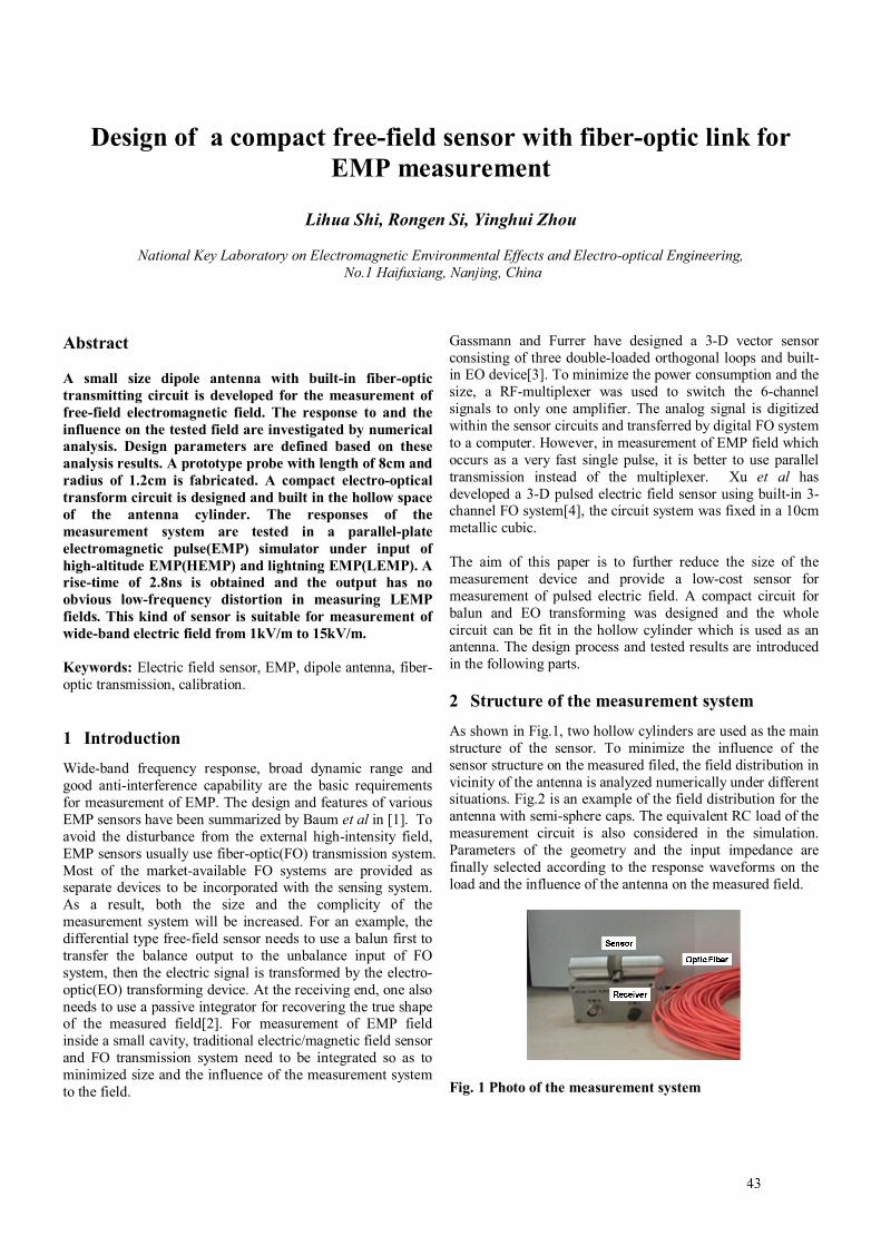
1
Design of a compact free-field sensor with fiber-optic link for EMP measurement
Lihua Shi, Rongen Si, Yinghui Zhou
National Key Laboratory on Electromagnetic Environmental Effects and Electro-optical Engineering, No.1 Haifuxiang, Nanjing, China
Abstract A small size dipole antenna with built-in fiber-optic transmitting circuit is developed for the measurement of free-field electromagnetic field. The response to and the influence on the tested field are investigated by numerical analysis. Design parameters are defined based on these analysis results. A prototype probe with length of 8cm and radius of 1.2cm is fabricated. A compact electro-optical transform circuit is designed and built in the hollow space of the antenna cylinder. The responses of the measurement system are tested in a parallel-plate electromagnetic pulse(EMP) simulator under input of high-altitude EMP(HEMP) and lightning EMP(LEMP). A rise-time of 2.8ns is obtained and the output has no obvious low-frequency distortion in measuring LEMP fields. This kind of sensor is suitable for measurement of wide-band electric field from 1kV/m to 15kV/m. Keywords: Electric field sensor, EMP, dipole antenna, fiber-optic transmission, calibration.
1 Introduction Wide-band frequency response, broad dynamic range and good anti-interference capability are the basic requirements for measurement of EMP. The design and features of various EMP sensors have been summarized by Baum et al in [1]. To avoid the disturbance from the external high-intensity field, EMP sensors usually use fiber-optic(FO) transmission system. Most of the market-available FO systems are provided as separate devices to be incorporated with the sensing system. As a result, both the size and the complicity of the measurement system will be increased. For an example, the differential type free-field sensor needs to use a balun first to transfer the balance output to the unbalance input of FO system, then the electric signal is transformed by the electro-optic(EO) transforming device. At the receiving end, one also needs to use a passive integrator for recovering the true shape of the measured field[2]. For measurement of EMP field inside a small cavity, traditional electric/magnetic field sensor and FO transmission system need to be integrated so as to minimized size and the influence of the measurement system to the field.
Gassmann and Furrer have designed a 3-D vector sensor consisting of three double-loaded orthogonal loops and built-in EO device[3]. To minimize the power consumption and the size, a RF-multiplexer was used to switch the 6-channel signals to only one amplifier. The analog signal is digitized within the sensor circuits and transferred by digital FO system to a computer. However, in measurement of EMP field which occurs as a very fast single pulse, it is better to use parallel transmission instead of the multiplexer. Xu et al has developed a 3-D pulsed electric field sensor using built-in 3-channel FO system[4], the circuit system was fixed in a 10cm metallic cubic. The aim of this paper is to further reduce the size of the measurement device and provide a low-cost sensor for measurement of pulsed electric field. A compact circuit for balun and EO transforming was designed and the whole circuit can be fit in the hollow cylinder which is used as an antenna. The design process and tested results are introduced in the following parts.
2 Structure of the measurement system As shown in Fig.1, two hollow cylinders are used as the main structure of the sensor. To minimize the influence of the sensor structure on the measured filed, the field distribution in vicinity of the antenna is analyzed numerically under different situations. Fig.2 is an example of the field distribution for the antenna with semi-sphere caps. The equivalent RC load of the measurement circuit is also considered in the simulation. Parameters of the geometry and the input impedance are finally selected according to the response waveforms on the load and the influence of the antenna on the measured field.
Fig. 1 Photo of the measurement system
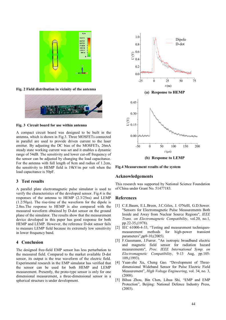
2
Fig. 2 Field distribution in vicinity of the antenna
Fig. 3 Circuit board for use within antenna
A compact circuit board was designed to be built in the antenna, which is shown in Fig.3. Three MOSFETs connected in parallel are used to provide driven current to the laser emitter. By adjusting the DC bias of the MOSFETs, 26mA steady state working current was set and it enables a dynamic range of 54dB. The sensitivity and lower cut-off frequency of the sensor can be adjusted by changing the load capacitance. For the antenna with full length of 8cm and radius of 1.2cm, the sensitivity to HEMP field is 19kV/m per volt when the load capacitance is 50pF.
3 Test results A parallel plate electromagnetic pulse simulator is used to verify the characteristics of the developed sensor. Fig.4 is the responses of the antenna to HEMP (2.3/25ns) and LEMP (1.2/50μs). The rise-time of the waveform for the dipole is 2.8ns.The response to HEMP is also compared with the measured waveform obtained by D-dot sensor on the ground plane of the simulator. The results show that the measurement device developed in this paper has good response for both HEMP and LEMP. However, the reference D-dot sensor fails to measure LEMP field because its extremely low sensitivity in lower frequency band.
4 Conclusion The designed free-field EMP sensor has less perturbation to the measured field. Compared to the market available D-dot sensor, its output is the true waveform of the electric field. Experimental research in the EMP simulator has verified that the sensor can be used for both HEMP and LEMP measurement. Presently, the proto-type sensor is only for one dimensional measurement, a three-dimensional sensor in a spherical structure is under development.
-25 0 25 50 75
0.0
0.2
0.4
0.6
0.8
1.0
U (V
)
t (ns)
偶极子传感器 D-dot
(a) Response to HEMP
-50 0 50 100 150 200
0.00
0.15
0.30
0.45
U (
V)
t s
(b) Response to LEMP
Fig.4 Measurement results of the system
Acknowledgements This research was supported by National Science Foundation of China under Grant No. 51477183.
References [1] C.E.Baum, E.L.Breen, J.C.Giles, J. O'Nelll, G.D.Sower.
"Sensors for Electromagnetic Pulse Measurements Both Inside and Away from Nuclear Source Regions", IEEE Trans. on Electromagnetic Compatibility, vol.20, no.1, pp.22-35,(1978).
[2] IEC 61000-4-33, “Testing and measurement techniques-measurement methods for high-power transient parameters”,pp9-10,(2005).
[3] F.Gassmann, J.Furrer. "An isotropic broadband electric and magnetic field sensor for radiation hazard measurements", Proc. IEEE International Symp. on Electromagnetic Compatibility, 9-13 Aug, pp.105-109,(1993).
[4] Yuan-zhe Xu, Cheng Gao. “Development of Three-dimensional Wideband Sensor for Pulse Electric Field Measurement”, High Voltage Engineering, vol. 34, no. 3, (2008).
[5] Bihua Zhou, Bin Chen, Lihua Shi, “EMP and EMP Protection”, Beijing: National Defence Industry Press, (2003).
Dipole D-dot
1
Determination of Q-value of an Avionics Bay or Other
Multiresonant Cavity by Measurements in Time- and Frequency-
Domain, with One or Two Antennas
B Vallhagen*, C Samuelsson*, M Bäckström*
*SAAB Aeronautics, SAAB AB, Linköping, Sweden, [email protected]
Abstract
A study consisting of several experimental measurement
campaigns have been performed, with aim to verify a way
of determining the Q-value of multiresonant cavities, such
as avionic bays in aircraft. Measurements have been
performed in two reverberation chambers of difference
size – of which one with approximate volume as an
avionics bay – as well as in avionic bays of an aircraft.
Besides the relatively well-known methods of
measurements in frequency-domain, refined methods of
measurements in time-domain have been verified,
including a technique with only one antenna – operating
in both transmitting and receiving mode. Use of a single
antenna may be crucial for measurements in bays of small
volume.
Keywords: Q-value, multiresonant, avionic bays,
measurements, time-domain.
1 Introduction
It is vitally important in the design of modern aircraft to
protect its equipment against High Intensity Radiated Fields
(HIRF), i.e. man-made electromagnetic fields in the radio and
microwave frequency range, from transmitters such as radio
or radar. Vulnerable aircraft electronics – avionics – may be
placed in well-shielded bays as part of this protection. The
average Shielding Effectiveness (SE) of such a bay can be
expressed [1,2] as:
⟨𝑆𝐸⟩ =2𝜋𝑉
𝜎𝑎𝜆𝑄 (1)
… where V is the cavity volume, λ is wavelength. Equation
(1) also clearly shows that σa (the aperture transmission cross
section) and Q (the cavity quality factor) have impact on the
SE. Thus; it is important to know Q.
The main scope for the actual measurement campaign(s) has
been to verify a useful method of determining the Q-value in
multiresonant rooms such as avionic bays. Parts of this main
scope has been to:
Reproduce and possibly refine lab measurements
performed by other labs [1,4]
Qualitatively compare measurements in time- and
frequency-domain
Perform and evaluate measurements with a single
antenna
Perform and evaluate measurements in time-domain,
with frequency stirring
… and finally
Compare said lab measurements with measurements
performed on a “real” test object, i.e. aircraft.
This paper includes brief descriptions of the test methods
used and extracts from the measured results from time-
domain measurements in the lab and on the aircraft.
2 Laboratory Measurements
Laboratory measurements were performed in two different
reverberation chambers (RC), one “main” which measure 35
m3, and one smaller (nicknamed “Akilles”) which measure 1
m3. Basic setup with two antennas is shown in Fig. 1:
Figure 1. Principle test setup in RC, frequency-domain
measurements shown. For two-antenna measurements
in time-domain, the network analyser (NA) is replaced
by a signal generator feeding the Tx antenna, and a
digital oscilloscope connected to the Rx antenna. The
setup is also valid for measurements in avionic bays,
though with no paddle present.
2.1 Frequency-Domain
In frequency-domain, the Q-value is determined by measuring
the S21-parameter:
𝑄 =16𝜋2𝑉
𝜆3 ⟨𝑃𝑅𝑥
𝑃𝑇𝑥⟩
1
𝜂𝑅𝑥𝜂𝑇𝑥𝑞𝑅𝑥𝑞𝑇𝑥 (2)
⟨𝑃𝑅𝑥
𝑃𝑇𝑥⟩ = ⟨|𝑆21|2⟩ (2’)
2
…where S21 is measured complex data from the NA, η
represents the ohmic losses and q is the impedance mismatch
factor. The brackets in Equation (2, 2’) indicates averaging
over a number of uncorrelated paddle positions in an isotropic
environment. The method is well established, see e.g. [1,2].
The disadvantage of the method is the uncertainty in
mentioned antenna parameters; q can be derived from S11-
measurements, but η has to be assumed (usually – as for
actual measurements – set to 0.9 for horn antennas, cf. [3]).
2.2 Time-Domain
For measurements in time-domain, the resonant cavity is
excited by a pulse modulated signal. Ideally, the pulse decay
shall be decided by [1]:
𝑈 = 𝑈𝑠𝑒−𝑡/𝜏 (3)
…where t is time (set to t0=0 at the start of the decay), τ is the
time constant and Us is the steady state energy in the cavity.
t=τ will occur when 𝑈 = 𝑒−1𝑈𝑠 ≈ 0.37𝑈𝑠 , and with τ
measured, Q can be decided from the relation
𝑄 = 𝜔𝜏 (4)
… where ω is angular frequency. For each frequency, data is
measured and averaged over a large number of uncorrelated
paddle positions or adjacent frequencies – mechanical or
frequency stirring – where the latter is preferred in small
cavities. Time-domain measurements are time-consuming. It
is practically impossible to include as many frequency-points
as with frequency-domain measurements.
2.3 The Circulator Method
An innovative method for measurements in time-domain is to
use only a single antenna and add a circulator to the
measurement setup, see Fig. 2.
Figure 2. Principle test setup for time-domain
measurements with the “Circulator Method”, in RC or
avionic bay (though without paddle).
Here the antenna acts as both a receiver and transmitter;
during the generator pulse time, both the incident and the
reflected pulse will be present at port 3 of the circulator; but
as the pulse shuts off (t=0 in Equation (3)), only the reflected
decay will remain on the circulator port 3.
Practically, all time-domain measurements were performed
with continuous (frequency or mechanical) stirring and
continuous sampling oscilloscope sweeps. With a fast modern
digital oscilloscope with built-in average function this is a
convenient (and also reliable, see results further down) way to
collect and process a large amount of data, guaranteeing
enough uncorrelated stirrer positions. As a comparison, in [1]
average were taken over 200 fixed paddle positions, while we
average over 1024 or 4096 oscilloscope sweeps with the
paddle in continuous movement (or frequency saw-tooth
swept in a narrow band surrounding the frequency of
interest). A snapshot example is shown in Fig. 3:
Figure 3. Recreated oscilloscope snapshot from
measurements with the circulator method, paddle
stirring in Akilles. Blue curve is raw data (voltage), red
curve is voltage squared (corresponding to the
measured energy). Green curve corresponds to
continuous averaging. Note the striking visual
irregularity in the raw data, which is smoothed out
nicely with averaging. Note also that the decay of
interest starts about t=2.2μs, ampl=0.7 div. With the
used oscilloscope, it takes roughly a minute to collect
an average over 1024 sample sweeps, each consisting of
20000 points.
3 Results in Time-domain
To verify the reliability of the measurements, comparison
between measurements performed with the slightly different
methods (two antennas vs the circulator method, frequency vs
paddle stirring, and also time- vs frequency-domain
measurements) shall have good correlation. Also, time-
domain measured data shall have good correlation with a
fitted exponential function (cf. Equation (3)). Fig. 4 shows
examples from the RC, and similar results can be shown from
measurements in Akilles. It may be noted that in the examples
shown, τ is in the μs range, corresponding to fairly high Q-
values (Equation (4)) in – the 103–10
4 range; Avionic bays
have magnitudes lower Q-values.
Well-correlated comparisons between measurements in time-
and frequency-domain can also be shown, but is left out of
this paper.
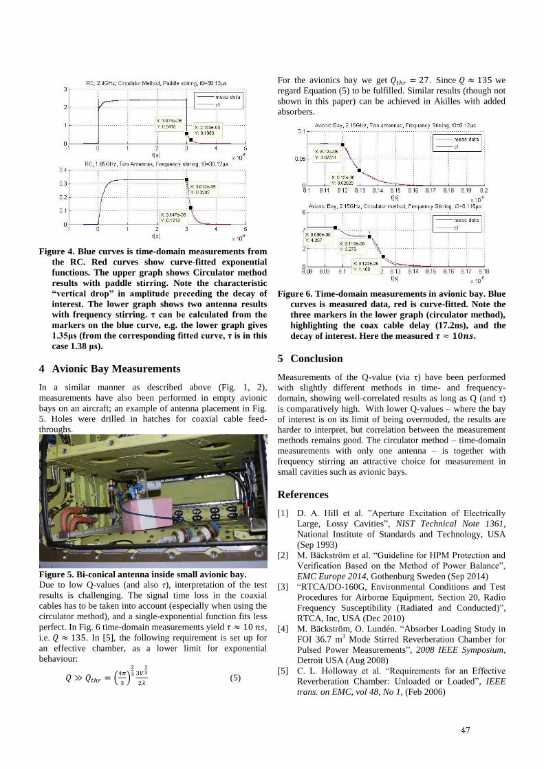
3
Figure 4. Blue curves is time-domain measurements from
the RC. Red curves show curve-fitted exponential
functions. The upper graph shows Circulator method
results with paddle stirring. Note the characteristic
“vertical drop” in amplitude preceding the decay of
interest. The lower graph shows two antenna results
with frequency stirring. τ can be calculated from the
markers on the blue curve, e.g. the lower graph gives
1.35μs (from the corresponding fitted curve, τ is in this
case 1.38 μs).
4 Avionic Bay Measurements
In a similar manner as described above (Fig. 1, 2),
measurements have also been performed in empty avionic
bays on an aircraft; an example of antenna placement in Fig.
5. Holes were drilled in hatches for coaxial cable feed-
throughs.
Figure 5. Bi-conical antenna inside small avionic bay.
Due to low Q-values (and also τ), interpretation of the test
results is challenging. The signal time loss in the coaxial
cables has to be taken into account (especially when using the
circulator method), and a single-exponential function fits less
perfect. In Fig. 6 time-domain measurements yield 𝜏 ≈ 10 𝑛𝑠,
i.e. 𝑄 ≈ 135. In [5], the following requirement is set up for
an effective chamber, as a lower limit for exponential
behaviour:
𝑄 ≫ 𝑄𝑡ℎ𝑟 = (4𝜋
3)
2
3 3𝑉13
2𝜆 (5)
For the avionics bay we get 𝑄𝑡ℎ𝑟 = 27. Since 𝑄 ≈ 135 we
regard Equation (5) to be fulfilled. Similar results (though not
shown in this paper) can be achieved in Akilles with added
absorbers.
Figure 6. Time-domain measurements in avionic bay. Blue
curves is measured data, red is curve-fitted. Note the
three markers in the lower graph (circulator method),
highlighting the coax cable delay (17.2ns), and the
decay of interest. Here the measured 𝝉 ≈ 𝟏𝟎𝒏𝒔.
5 Conclusion
Measurements of the Q-value (via τ) have been performed
with slightly different methods in time- and frequency-
domain, showing well-correlated results as long as Q (and τ)
is comparatively high. With lower Q-values – where the bay
of interest is on its limit of being overmoded, the results are
harder to interpret, but correlation between the measurement
methods remains good. The circulator method – time-domain
measurements with only one antenna – is together with
frequency stirring an attractive choice for measurement in
small cavities such as avionic bays.
References
[1] D. A. Hill et al. ”Aperture Excitation of Electrically
Large, Lossy Cavities”, NIST Technical Note 1361,
National Institute of Standards and Technology, USA
(Sep 1993)
[2] M. Bäckström et al. “Guideline for HPM Protection and
Verification Based on the Method of Power Balance”,
EMC Europe 2014, Gothenburg Sweden (Sep 2014)
[3] “RTCA/DO-160G, Environmental Conditions and Test
Procedures for Airborne Equipment, Section 20, Radio
Frequency Susceptibility (Radiated and Conducted)”,
RTCA, Inc, USA (Dec 2010)
[4] M. Bäckström, O. Lundén. “Absorber Loading Study in
FOI 36.7 m3 Mode Stirred Reverberation Chamber for
Pulsed Power Measurements”, 2008 IEEE Symposium,
Detroit USA (Aug 2008)
[5] C. L. Holloway et al. “Requirements for an Effective
Reverberation Chamber: Unloaded or Loaded”, IEEE
trans. on EMC, vol 48, No 1, (Feb 2006)
1
Experimental comparison of mode-stirrer geometries for EMC
V. Houchouas*, C. Kasmi*, J. Lopes Esteves*, D. Coiffard*
*Wireless Security Lab,French Network and Information Security Agency, 51 bvd de la Tour Maubourg, 75007 Paris, France
Abstract
During the last decades, the EMC community has shown
a high interest in the use of reverberating chambers for
the immunity testing of electronic devices. Standards have
been published so that the compliance of test facilities can
be checked. One of the remaining open questions is the
efficiency of a mode-stirrer depending on the used
material, its shape and its location within the cavity. In
this paper, a description of the three main geometries
found in the literature is given. A practical comparison of
the mode-stirrers is proposed based on the Pearson
correlation coefficient, the electric field distribution inside
a computer and the results of the immunity testing of the
same device.
Keywords: Reverberating chambers, Mode-stirrer, Statistics,
Immunity.
1 Introduction
The immunity testing of electronic devices used in critical
infrastructures is of fundamental interest to define adequate
protections to be inserted in the facilities in order to improve
the availability of services provided to users. The EMC
community has shown a high interest for reverberation
chambers (RC) for performing radiated immunity tests. One
can consider the possible electromagnetic (EM) attack
scenarios and apply them by generating an EM field with
well-known magnitude, direction and polarization and
moving the device under test (DUT) relative to the fixed
source. Another way for performing immunity testing is the
use of a RC where the DUT is placed in a fixed position in
the working volume. For overmoded RC equipped with a
moving mode-stirrer, the statistic of the field is supposed to
be uniform. Thus, a quick statistic estimation of the
susceptibility of the DUT can be performed. One of the
remaining open questions, as far as we know, is the definition
of an efficient geometry of the mode-stirrer for a given
facility. Based on the last remark, a large review of the
published academic and technical papers as well as the
pictures available on the web has been conducted.
Considering, the most commonly used geometries; it has
been decided to design and build the three most used mode-
stirrers and to compare their stirring efficiency for a given
Faraday cage thanks to the statistical tools recommended by
standards. A comparison of the stirring efficiency is proposed
in this paper.
Recently, a health monitoring software was proposed in [1] to
characterize the effects of intentional electromagnetic
interference (IEMI) on a DUT by analysing drivers and
operating system logs, in real-time operation. Thus, such a
software is used in order to validate the statistical analysis of
the stirring efficiency of the three mode-stirrers.
The paper is organized as follows: in Section 2, the procedure
for characterizing the efficiency of mode-stirrers in
reverberation chambers is summarized. In Section 3, the
benefits of the immunity testing of a commercial off the shelf
(COTS) computer using the mode-stirrers is discussed.
2 Analysis of mode-stirrers
The aim of mode-stirring is to produce inside a RC a
statistically uniform electromagnetic field in terms of field
homogeneity and isotropy [2]. This property directly depends
on the number of significantly excited modes (bounded to the
mode density at the considered frequency of operation), their
quality factor Q (often estimated as a composite Q factor)
which quantifies the amount of energy stored in the RC, their
bandwidth BWQ=f/Q and finally the stirred efficiency rN (see
Section 3). While setting up a RC with a mode-stirrer, one
has to choose its shape. Unfortunately there is no theory, but
only general guidelines [3], which provide an optimal
geometry for an optimal stirring efficiency. First of all we
determine the location and the maximum dimensions of the
stirring volume given a required working volume (a computer
45.3 cm x 20.3 cm x 45.7 cm in what follows) in the RC. The
RC we are working with is 43 cm high, 72 cm wide and 92
cm long. The lowest usable frequency LUF as defined by [3]
is included in [3 fTE011, 7 fTE011], in our case LUF ∈
[794 MHz, 1.85 GHz]. Another estimation from [4] links the
LUF to the volume V of the RC as follows LUF =
c(90/(4πV))1/3
= 879 MHz. Therefore we fixed the minimum
frequency of operation fMIN = 2 GHz (which corresponds to a
maximum wavelength λMAX = 15 cm), i.e. well above these
estimations of the LUF. It is commonly admitted that the
working volume must be λMAX/4 = 3.75 cm apart from the
Figure 1: Schematic representing the RC
2
enclosure walls, and λMAX/2= 7.5 cm apart from the emitting
antenna to ensure a uniform distribution of the field around
the DUT. Finally we get the stirrer’s volume dimensions of
30 cm wide, 30 cm long and 34 cm high. The environment
(Fig. 1) is composed of a working volume, a stirring volume
and an excitation volume.
2.1 Review of the proposed geometries
To find the adequate shape of the mode-stirrer one can
simulate different shapes [5-7], or design a stirrer by trial and
error, minimising the symmetries and then choose the more
appropriate, based on their characterization. Due to the large
open literature on RCs and mode-stirrers, it could be also
possible to rely on the existing shapes. In this work, it has
been decided to select shapes from a review of commonly
chosen ones in the literature (see for example [2, 7, 8, 9]).
The three shapes (quoted as S1, S2 then S3) depicted in Fig. 2
have been selected from an analysis of more than 200
references. Note that even though we selected common stirrer
shapes, this does not ensure that those are the most efficient
ones.
2.2 Statistical tools
The stirred efficiency is commonly [9, 3] characterised by the
Pearson correlation coefficient defined as:
(1)
where X = [x0,..., xN-1] is a series of measurements at a fixed
frequency, for N consecutive mode-stirrer positions. Y is the
same series rotated from one position i.e.: Y = [xN-1 , x0 ,..., xN-
2]. µx is the X series mean.
In our case, X is a series of magnitude of scattering
parameters |S21| measurements between ports 1 and 2 of a
VNA connected to the transmitting and receiving antennas
respectively. rN reveals the capacity of the stirrer to lead to a
non-correlated field distribution in the RC for different stirrer
positions. A high number of positions N is likely to create
highly correlated distributions, as the angle between two
positions is small. According to [3], for uncorrelated data the
estimated rN should be lower than the threshold ρ
(ρ = 1/e ≈ 0.37 for N = 30). This assumption is not relevant
for N ≠ 30 as highlighted in [10].
2.3 Measurement description and results
The stirring efficiency of each tested mode-stirrer shape is
depicted in Fig. 2. The transmission parameter |S21| is
aggregated along a full rotation of the stirrer with N = 30
steps in a bandwidth of [2 GHz, 6 GHz] with a resolution of
150 kHz using a vector network analyser (VNA). A
resolution bandwidth slightly greater than BWQ has been
chosen while minimizing the noise floor. For graph
readability, the mean, the first and the third quartiles have
been estimated from the obtained rN on blocks of 300
consecutive points of frequency. As highlighted by Fig. 2, the
ranking based on rN of mode-stirrers is: S1, S2 then S3.
According to this autocorrelation function criterion S1
appears to be much more efficient than the two others as its
associated rN is (mostly) below the threshold ρ. For shapes S2
and S3, it can be mentioned that rN decreases with the
frequency at least in the half lower bandwidth under
investigation, unlike S1 which seems to be less sensitive to the
working wavelength. This tends to prove that this stirrer
provides uncorrelated realizations almost all over the
considered bandwidth.
3 Immunity testing of electronic device
RCs are well-suited for immunity testing of information
systems (IS) for EMC or security. Indeed, in one
measurement it is theoretically possible to simulate an large
number of different aggressions due to the statistic of the
field: uniform distribution of the EM wave direction and
polarization. Doing so, using a stirrer in an RC can lead to a
simple, cheap and fast method for the immunity testing of an
IS. To evaluate the immunity of IS, different techniques can
be applied. One can either measure the field inside a
computer, measure induced voltages in circuits, or record the
number of faults on a running system. In this Section, the
electric field distributions at the points of interest in the
computer are discussed. Then, a brief overview of observable
Shape S1
Shape S2
Shape S3
Figure 2: Comparison of the three selected stirrers
3
faults induced on the computer by parasitic fields is
presented.
3.1 Mode-stirrers classification thanks to the induced
electric field
The three positions, depicted in Fig. 3, are of high interest as
susceptible components [1] are placed in these parts of the
computer (P1: hard-disk drive, P2: CD player and P3: CPU
cooling fan). In order to analyse the contribution of the
different mode-stirrers, the distribution of the electric field
along x, y and z in the computer has been compared for the
three mode-stirrers. While the homogeneity of the field inside
the computer is not guaranteed, it has been observed that S3
allows a better excitation of the field along the three axes
inside the computer in contrary to S1 and S2 which don’t
stimulate the component along y.
Figure 3: Electric field probe inside the computer box at
the three chosen positions
3.2 Mode-stirrers classification based on fault detection
and analysis
Linux has been installed on the computer in order to gain
easy access to drivers and operating system logs. Faults [1]
(ex. USB, PS2 and temperature sensors) induced by IEMI
can be detected. The computer was tested using the
descripted approach and, as for example, it has been observed
that the I7 CPU clock balancing was highly deteriorated.
Moreover, it has been observed that the effects (ex. clock
balancing deterioration, temperature sensors errors) were
induced at different levels of criticality depending on the
mode-stirrer and the frequency. It can be mentioned that the
mode-stirrers S1 and S2 don’t stimulate the electric field along
the y axis. In this case, the criticality of the induced errors is
higher while the number of type of errors is small. On the
contrary, the mode-stirrer S3 excites the three components of
the field in the computer. In this case, it induces faults with
less criticality levels but broadens the type of perturbations.
4 Conclusion
An exhaustive review of mode-stirrers geometry has been
performed leading to the study of more than 100 conference
and journal papers, 25 PhD theses and a large number of
pictures available on the Internet. The three most common
shapes have been designed and tested in order to have a clue
on their stirring efficiency for a given reverberating chamber.
It has been observed that for three positions of interest in the
computer, using a mode-stirrer allows to better evaluate the
susceptibility of the critical components. During the
presentation, the faults induced by parasitic fields will be
presented. The contribution of mode-stirrers for information
systems immunity testing will be discussed.
Acknowledgements
The present work results from the MS Degree training period
of Valentin Houchouas, student at the National Institute for
Applied Science (INSA) Rennes, at the Wireless Security
Lab of the French Network and Information Security
(ANSSI). The authors would like to thank Dr. Philippe
Besnier from IETR/INSA and Dr. Benoit Martin from
Nuclétudes for their valuable advices.
References
[1] C. Kasmi, J. Lopes Esteves, and M. Renard. Automation
of the immunity testing of COTS computers by the
instrumentation of the internal sensors and involving the
operating system logs - technical report. System Design
and assessment Note 44, Nov 2014.
[2] J.-I. Hong and C.-S. Huh. Optimization of stirrer with
various parameters in reverberation chamber. Progress
In Electromagnetics Research, 104:15-30, (2010).
[3] IEC 61000-4-21, Electromagnetic Compatibility (EMC)
— Part 4-21: Testing and Measurement Techniques
Reverberation Chamber Test Methods, (2003).
[4] IEEE 299.1, IEEE standard method for measuring the
shielding effectiveness of enclosures and boxes having
all dimensions between 0.1 m and 2 m. (2013).
[5] K. Selemani, J.-B. Gros, E. Richalot, et al. Comparison
of reverberation chamber shapes inspired from chaotic
cavities. IEEE Transactions on EMC, (2014).
[6] J.-S. Kim and R. Mittra. Numerical study of stirring
effects in a mode-stirred reverberation chamber by using
the finite difference time domain simulation. Forum for
Electromagnetic Research Methods and Application
Technologies (FERMAT).
[7] J. Clegg, A. Marvin, J. Dawson, et al. Optimization of
stirrer designs in a reverberation chamber. IEEE
Transactions on EMC, 47(4):824-832, (Nov 2005).
[8] Y. Huang, N. Abumustafa, Q. Wang, et al. Comparison
of two stirrer designs for a new reverberation chamber.
In Environmental Electromagnetics, The 2006 4th
Asia-Pacific Conference, pp. 450-453, (Aug 2006).
[9] N. Wellander, O. Lundén, M. Bäckström, “Experimental
Investigation and Mathematical Modeling of Design
Parameters for Efficient Stirrers in Mode Stirred
Reverberation Chambers”, IEEE Transactions on EMC,
Vol. 49, No. 1, February 2007, pp. 94 – 103
[10] C. Lemoine. Contribution to the statistical analysis of
measurements data in mode-stirred reverberation
chamber. Applications for the evaluation of stirring
efficiency and measurements uncertainty in the context
of radiofrequencies and EMC. Theses, INSA de Rennes,
(Jul. 2008).
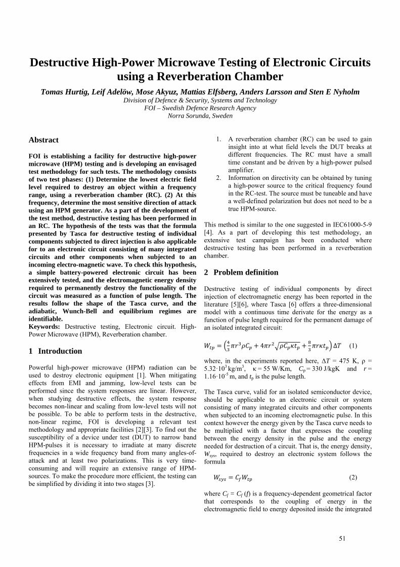
1
Destructive High-Power Microwave Testing of Electronic Circuits using a Reverberation Chamber
Tomas Hurtig, Leif Adelöw, Mose Akyuz, Mattias Elfsberg, Anders Larsson and Sten E Nyholm Division of Defence & Security, Systems and Technology
FOI – Swedish Defence Research Agency Norra Sorunda, Sweden
Abstract FOI is establishing a facility for destructive high-power microwave (HPM) testing and is developing an envisaged test methodology for such tests. The methodology consists of two test phases: (1) Determine the lowest electric field level required to destroy an object within a frequency range, using a reverberation chamber (RC). (2) At this frequency, determine the most sensitive direction of attack using an HPM generator. As a part of the development of the test method, destructive testing has been performed in an RC. The hypothesis of the tests was that the formula presented by Tasca for destructive testing of individual components subjected to direct injection is also applicable for to an electronic circuit consisting of many integrated circuits and other components when subjected to an incoming electro-magnetic wave. To check this hypothesis, a simple battery-powered electronic circuit has been extensively tested, and the electromagnetic energy density required to permanently destroy the functionality of the circuit was measured as a function of pulse length. The results follow the shape of the Tasca curve, and the adiabatic, Wunch-Bell and equilibrium regimes are identifiable. Keywords: Destructive testing, Electronic circuit. High-Power Microwave (HPM), Reverberation chamber.
1 Introduction
Powerful high-power microwave (HPM) radiation can be used to destroy electronic equipment [1]. When mitigating effects from EMI and jamming, low-level tests can be performed since the system responses are linear. However, when studying destructive effects, the system response becomes non-linear and scaling from low-level tests will not be possible. To be able to perform tests in the destructive, non-linear regime, FOI is developing a relevant test methodology and appropriate facilities [2][3]. To find out the susceptibility of a device under test (DUT) to narrow band HPM-pulses it is necessary to irradiate at many discrete frequencies in a wide frequency band from many angles-of-attack and at least two polarizations. This is very time-consuming and will require an extensive range of HPM-sources. To make the procedure more efficient, the testing can be simplified by dividing it into two stages [3].
1. A reverberation chamber (RC) can be used to gain insight into at what field levels the DUT breaks at different frequencies. The RC must have a small time constant and be driven by a high-power pulsed amplifier.
2. Information on directivity can be obtained by tuning a high-power source to the critical frequency found in the RC-test. The source must be tuneable and have a well-defined polarization but does not need to be a true HPM-source.
This method is similar to the one suggested in IEC61000-5-9 [4]. As a part of developing this test methodology, an extensive test campaign has been conducted where destructive testing has been performed in a reverberation chamber.
2 Problem definition
Destructive testing of individual components by direct injection of electromagnetic energy has been reported in the literature [5][6], where Tasca [6] offers a three-dimensional model with a continuous time derivate for the energy as a function of pulse length required for the permanent damage of an isolated integrated circuit:
4 Δ (1)
where, in the experiments reported here, ΔT = 475 K, ρ = 5.32·103 kg/m3, κ = 55 W/Km, Cp = 330 J/kgK and r = 1.16·10-5 m, and tp is the pulse length. The Tasca curve, valid for an isolated semiconductor device, should be applicable to an electronic circuit or system consisting of many integrated circuits and other components when subjected to an incoming electromagnetic pulse. In this context however the energy given by the Tasca curve needs to be multiplied with a factor that expresses the coupling between the energy density in the pulse and the energy needed for destruction of a circuit. That is, the energy density, Wsys, required to destroy an electronic system follows the formula
(2) where Cf = Cf (f) is a frequency-dependent geometrical factor that corresponds to the coupling of energy in the electromagnetic field to energy deposited inside the integrated
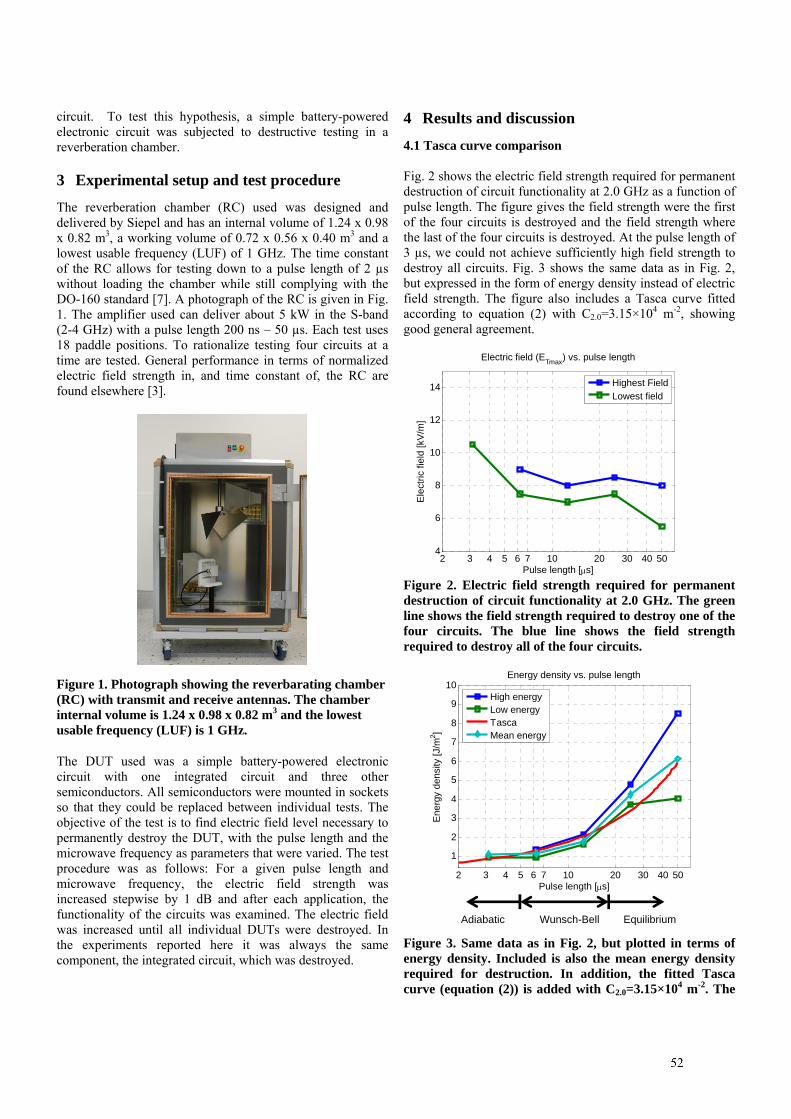
2
circuit. To test this hypothesis, a simple battery-powered electronic circuit was subjected to destructive testing in a reverberation chamber.
3 Experimental setup and test procedure The reverberation chamber (RC) used was designed and delivered by Siepel and has an internal volume of 1.24 x 0.98 x 0.82 m3, a working volume of 0.72 x 0.56 x 0.40 m3 and a lowest usable frequency (LUF) of 1 GHz. The time constant of the RC allows for testing down to a pulse length of 2 µs without loading the chamber while still complying with the DO-160 standard [7]. A photograph of the RC is given in Fig. 1. The amplifier used can deliver about 5 kW in the S-band (2-4 GHz) with a pulse length 200 ns – 50 µs. Each test uses 18 paddle positions. To rationalize testing four circuits at a time are tested. General performance in terms of normalized electric field strength in, and time constant of, the RC are found elsewhere [3].
Figure 1. Photograph showing the reverbarating chamber (RC) with transmit and receive antennas. The chamber internal volume is 1.24 x 0.98 x 0.82 m3 and the lowest usable frequency (LUF) is 1 GHz.
The DUT used was a simple battery-powered electronic circuit with one integrated circuit and three other semiconductors. All semiconductors were mounted in sockets so that they could be replaced between individual tests. The objective of the test is to find electric field level necessary to permanently destroy the DUT, with the pulse length and the microwave frequency as parameters that were varied. The test procedure was as follows: For a given pulse length and microwave frequency, the electric field strength was increased stepwise by 1 dB and after each application, the functionality of the circuits was examined. The electric field was increased until all individual DUTs were destroyed. In the experiments reported here it was always the same component, the integrated circuit, which was destroyed.
4 Results and discussion
4.1 Tasca curve comparison Fig. 2 shows the electric field strength required for permanent destruction of circuit functionality at 2.0 GHz as a function of pulse length. The figure gives the field strength were the first of the four circuits is destroyed and the field strength where the last of the four circuits is destroyed. At the pulse length of 3 µs, we could not achieve sufficiently high field strength to destroy all circuits. Fig. 3 shows the same data as in Fig. 2, but expressed in the form of energy density instead of electric field strength. The figure also includes a Tasca curve fitted according to equation (2) with C2.0=3.15×10⁴ m-2, showing good general agreement.
Figure 2. Electric field strength required for permanent destruction of circuit functionality at 2.0 GHz. The green line shows the field strength required to destroy one of the four circuits. The blue line shows the field strength required to destroy all of the four circuits.
Figure 3. Same data as in Fig. 2, but plotted in terms of energy density. Included is also the mean energy density required for destruction. In addition, the fitted Tasca curve (equation (2)) is added with C2.0=3.15×10⁴ m-2. The
2 3 4 5 6 7 10 20 30 40 504
6
8
10
12
14
Ele
ctric
fiel
d [k
V/m
]
Pulse length [s]
Electric field (ETmax) vs. pulse length
Highest FieldLowest field
2 3 4 5 6 7 10 20 30 40 50
1
2
3
4
5
6
7
8
9
10
Ene
rgy
dens
ity [J
/m2 ]
Pulse length [s]
Energy density vs. pulse length
High energyLow energyTascaMean energy
Wunsch-Bell Equilibrium Adiabatic
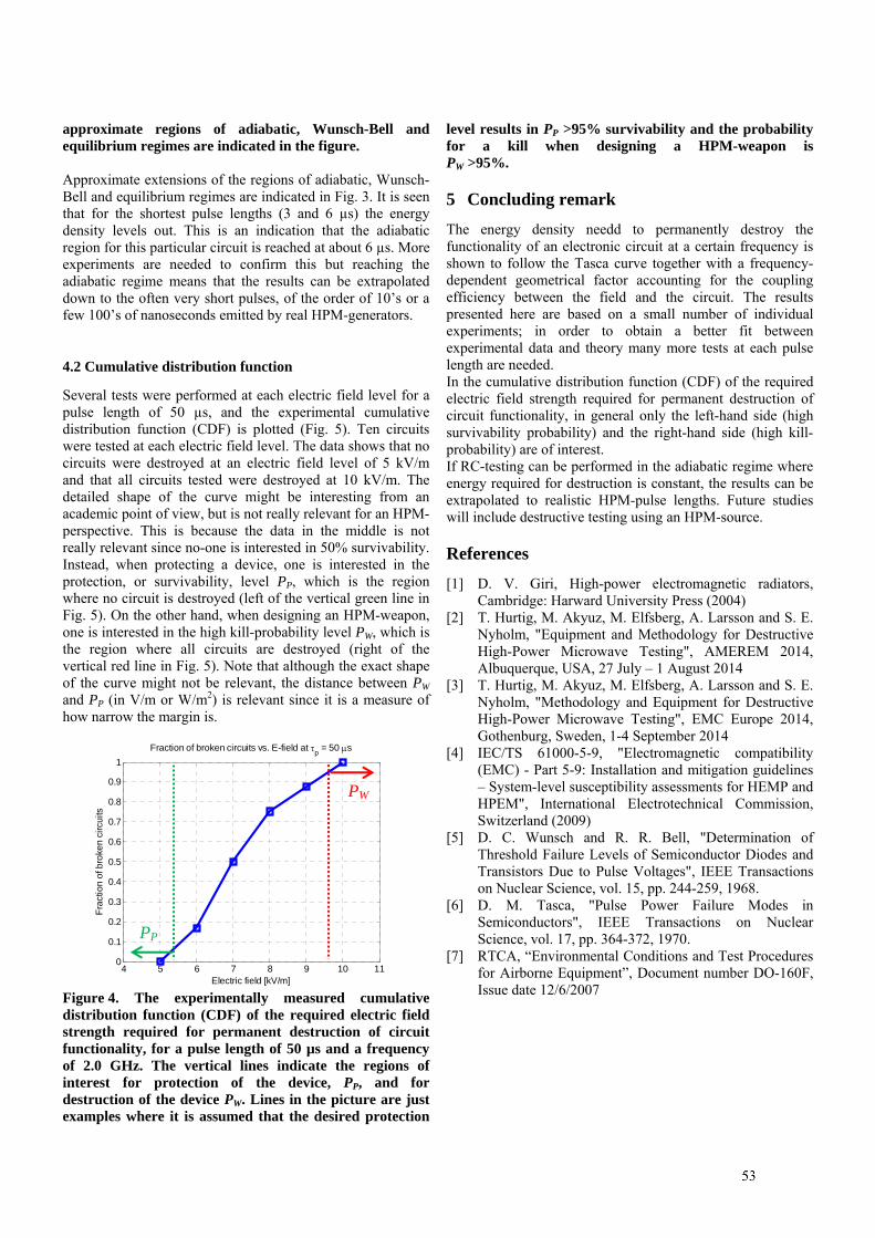
3
approximate regions of adiabatic, Wunsch-Bell and equilibrium regimes are indicated in the figure. Approximate extensions of the regions of adiabatic, Wunsch-Bell and equilibrium regimes are indicated in Fig. 3. It is seen that for the shortest pulse lengths (3 and 6 µs) the energy density levels out. This is an indication that the adiabatic region for this particular circuit is reached at about 6 µs. More experiments are needed to confirm this but reaching the adiabatic regime means that the results can be extrapolated down to the often very short pulses, of the order of 10’s or a few 100’s of nanoseconds emitted by real HPM-generators.
4.2 Cumulative distribution function
Several tests were performed at each electric field level for a pulse length of 50 µs, and the experimental cumulative distribution function (CDF) is plotted (Fig. 5). Ten circuits were tested at each electric field level. The data shows that no circuits were destroyed at an electric field level of 5 kV/m and that all circuits tested were destroyed at 10 kV/m. The detailed shape of the curve might be interesting from an academic point of view, but is not really relevant for an HPM-perspective. This is because the data in the middle is not really relevant since no-one is interested in 50% survivability. Instead, when protecting a device, one is interested in the protection, or survivability, level PP, which is the region where no circuit is destroyed (left of the vertical green line in Fig. 5). On the other hand, when designing an HPM-weapon, one is interested in the high kill-probability level PW, which is the region where all circuits are destroyed (right of the vertical red line in Fig. 5). Note that although the exact shape of the curve might not be relevant, the distance between PW and PP (in V/m or W/m2) is relevant since it is a measure of how narrow the margin is.
Figure 4. The experimentally measured cumulative distribution function (CDF) of the required electric field strength required for permanent destruction of circuit functionality, for a pulse length of 50 µs and a frequency of 2.0 GHz. The vertical lines indicate the regions of interest for protection of the device, PP, and for destruction of the device PW. Lines in the picture are just examples where it is assumed that the desired protection
level results in PP >95% survivability and the probability for a kill when designing a HPM-weapon is PW >95%.
5 Concluding remark The energy density needd to permanently destroy the functionality of an electronic circuit at a certain frequency is shown to follow the Tasca curve together with a frequency-dependent geometrical factor accounting for the coupling efficiency between the field and the circuit. The results presented here are based on a small number of individual experiments; in order to obtain a better fit between experimental data and theory many more tests at each pulse length are needed. In the cumulative distribution function (CDF) of the required electric field strength required for permanent destruction of circuit functionality, in general only the left-hand side (high survivability probability) and the right-hand side (high kill-probability) are of interest. If RC-testing can be performed in the adiabatic regime where energy required for destruction is constant, the results can be extrapolated to realistic HPM-pulse lengths. Future studies will include destructive testing using an HPM-source.
References [1] D. V. Giri, High-power electromagnetic radiators,
Cambridge: Harward University Press (2004) [2] T. Hurtig, M. Akyuz, M. Elfsberg, A. Larsson and S. E.
Nyholm, "Equipment and Methodology for Destructive High-Power Microwave Testing", AMEREM 2014, Albuquerque, USA, 27 July – 1 August 2014
[3] T. Hurtig, M. Akyuz, M. Elfsberg, A. Larsson and S. E. Nyholm, "Methodology and Equipment for Destructive High-Power Microwave Testing", EMC Europe 2014, Gothenburg, Sweden, 1-4 September 2014
[4] IEC/TS 61000-5-9, "Electromagnetic compatibility (EMC) - Part 5-9: Installation and mitigation guidelines – System-level susceptibility assessments for HEMP and HPEM", International Electrotechnical Commission, Switzerland (2009)
[5] D. C. Wunsch and R. R. Bell, "Determination of Threshold Failure Levels of Semiconductor Diodes and Transistors Due to Pulse Voltages", IEEE Transactions on Nuclear Science, vol. 15, pp. 244-259, 1968.
[6] D. M. Tasca, "Pulse Power Failure Modes in Semiconductors", IEEE Transactions on Nuclear Science, vol. 17, pp. 364-372, 1970.
[7] RTCA, “Environmental Conditions and Test Procedures for Airborne Equipment”, Document number DO-160F, Issue date 12/6/2007
4 5 6 7 8 9 10 110
0.1
0.2
0.3
0.4
0.5
0.6
0.7
0.8
0.9
1
Electric field [kV/m]
Frac
tion
of b
roke
n ci
rcui
ts
Fraction of broken circuits vs. E-field at p = 50 s
PP
PW
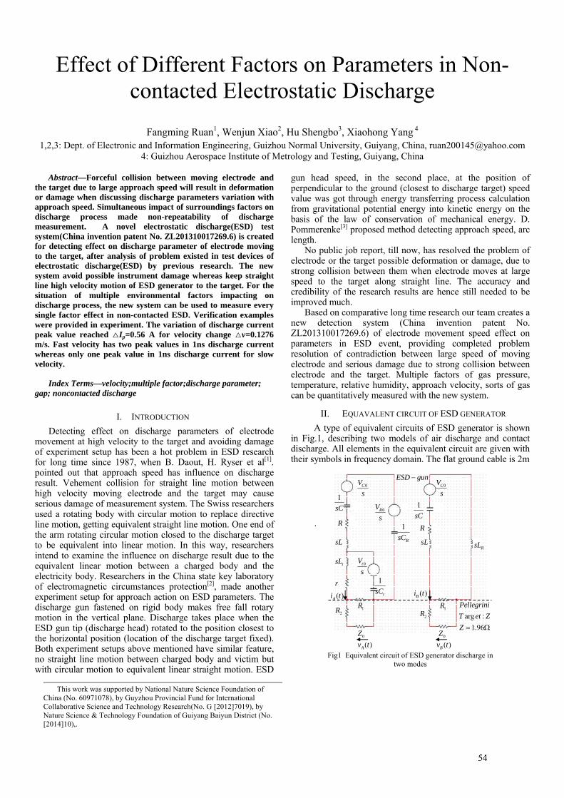
Effect of Different Factors on Parameters in Non-contacted Electrostatic Discharge
Fangming Ruan1, Wenjun Xiao2, Hu Shengbo3, Xiaohong Yang 4 1,2,3: Dept. of Electronic and Information Engineering, Guizhou Normal University, Guiyang, China, [email protected]
4: Guizhou Aerospace Institute of Metrology and Testing, Guiyang, China
Abstract—Forceful collision between moving electrode and the target due to large approach speed will result in deformation or damage when discussing discharge parameters variation with approach speed. Simultaneous impact of surroundings factors on discharge process made non-repeatability of discharge measurement. A novel electrostatic discharge(ESD) test system(China invention patent No. ZL201310017269.6) is created for detecting effect on discharge parameter of electrode moving to the target, after analysis of problem existed in test devices of electrostatic discharge(ESD) by previous research. The new system avoid possible instrument damage whereas keep straight line high velocity motion of ESD generator to the target. For the situation of multiple environmental factors impacting on discharge process, the new system can be used to measure every single factor effect in non-contacted ESD. Verification examples were provided in experiment. The variation of discharge current peak value reached Ip=0.56 A for velocity change v=0.1276 m/s. Fast velocity has two peak values in 1ns discharge current whereas only one peak value in 1ns discharge current for slow velocity.
Index Terms—velocity;multiple factor;discharge parameter; gap; noncontacted discharge
I. INTRODUCTION
Detecting effect on discharge parameters of electrode movement at high velocity to the target and avoiding damage of experiment setup has been a hot problem in ESD research for long time since 1987, when B. Daout, H. Ryser et al[1]. pointed out that approach speed has influence on discharge result. Vehement collision for straight line motion between high velocity moving electrode and the target may cause serious damage of measurement system. The Swiss researchers used a rotating body with circular motion to replace directive line motion, getting equivalent straight line motion. One end of the arm rotating circular motion closed to the discharge target to be equivalent into linear motion. In this way, researchers intend to examine the influence on discharge result due to the equivalent linear motion between a charged body and the electricity body. Researchers in the China state key laboratory of electromagnetic circumstances protection[2], made another experiment setup for approach action on ESD parameters. The discharge gun fastened on rigid body makes free fall rotary motion in the vertical plane. Discharge takes place when the ESD gun tip (discharge head) rotated to the position closest to the horizontal position (location of the discharge target fixed). Both experiment setups above mentioned have similar feature, no straight line motion between charged body and victim but with circular motion to equivalent linear straight motion. ESD
gun head speed, in the second place, at the position of perpendicular to the ground (closest to discharge target) speed value was got through energy transferring process calculation from gravitational potential energy into kinetic energy on the basis of the law of conservation of mechanical energy. D. Pommerenke[3] proposed method detecting approach speed, arc length.
No public job report, till now, has resolved the problem of electrode or the target possible deformation or damage, due to strong collision between them when electrode moves at large speed to the target along straight line. The accuracy and credibility of the research results are hence still needed to be improved much.
Based on comparative long time research our team creates a new detection system (China invention patent No. ZL201310017269.6) of electrode movement speed effect on parameters in ESD event, providing completed problem resolution of contradiction between large speed of moving electrode and serious damage due to strong collision between electrode and the target. Multiple factors of gas pressure, temperature, relative humidity, approach velocity, sorts of gas can be quantitatively measured with the new system.
II. EQUAVALENT CIRCUIT OF ESD GENERATOR
A type of equivalent circuits of ESD generator is shown in Fig.1, describing two models of air discharge and contact discharge. All elements in the equivalent circuit are given with their symbols in frequency domain. The flat ground cable is 2m
.
This work was supported by National Nature Science Foundation of China (No. 60971078), by Guyzhou Provincial Fund for International Collaborative Science and Technology Research(No. G [2012]7019), by Nature Science & Technology Foundation of Guiyang Baiyun District (No. [2014]10),.
0CVs1
sC
R R
1
sC
0CVs
sL sL
tsL
r( )Ai t
2R 1R
0Z( )Av t
0Z( )Bv t
2R1R
( )Bi t
1
tsC
0tVs
0RVs
1
RsCRsL
ESD gun−
arg :
1.96
PellegriniT et ZZ = Ω
Fig1 Equivalent circuit of ESD generator discharge in
two modes
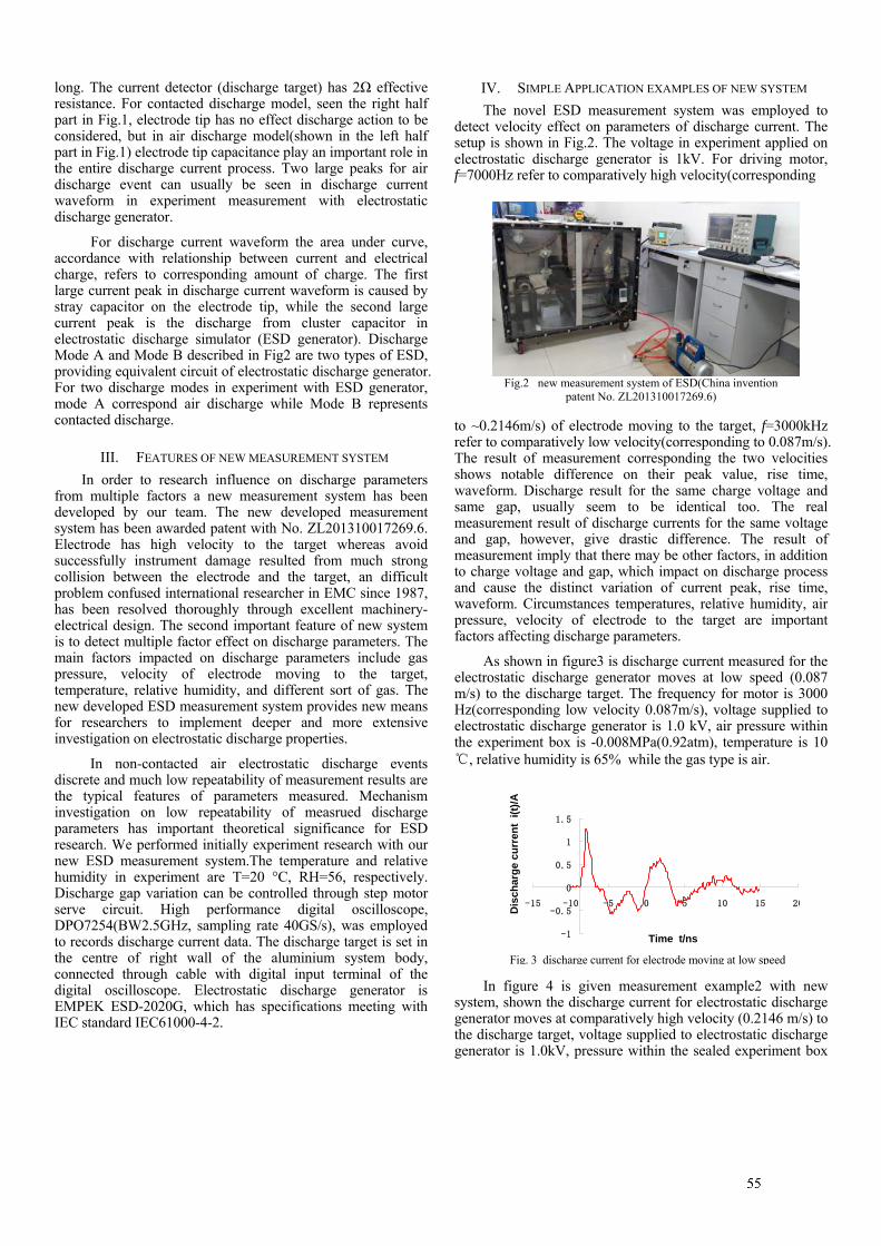
long. The current detector (discharge target) has 2Ω effective resistance. For contacted discharge model, seen the right half part in Fig.1, electrode tip has no effect discharge action to be considered, but in air discharge model(shown in the left half part in Fig.1) electrode tip capacitance play an important role in the entire discharge current process. Two large peaks for air discharge event can usually be seen in discharge current waveform in experiment measurement with electrostatic discharge generator.
For discharge current waveform the area under curve, accordance with relationship between current and electrical charge, refers to corresponding amount of charge. The first large current peak in discharge current waveform is caused by stray capacitor on the electrode tip, while the second large current peak is the discharge from cluster capacitor in electrostatic discharge simulator (ESD generator). Discharge Mode A and Mode B described in Fig2 are two types of ESD, providing equivalent circuit of electrostatic discharge generator. For two discharge modes in experiment with ESD generator, mode A correspond air discharge while Mode B represents contacted discharge.
III. FEATURES OF NEW MEASUREMENT SYSTEM
In order to research influence on discharge parameters from multiple factors a new measurement system has been developed by our team. The new developed measurement system has been awarded patent with No. ZL201310017269.6. Electrode has high velocity to the target whereas avoid successfully instrument damage resulted from much strong collision between the electrode and the target, an difficult problem confused international researcher in EMC since 1987, has been resolved thoroughly through excellent machinery-electrical design. The second important feature of new system is to detect multiple factor effect on discharge parameters. The main factors impacted on discharge parameters include gas pressure, velocity of electrode moving to the target, temperature, relative humidity, and different sort of gas. The new developed ESD measurement system provides new means for researchers to implement deeper and more extensive investigation on electrostatic discharge properties.
In non-contacted air electrostatic discharge events discrete and much low repeatability of measurement results are the typical features of parameters measured. Mechanism investigation on low repeatability of measrued discharge parameters has important theoretical significance for ESD research. We performed initially experiment research with our new ESD measurement system.The temperature and relative humidity in experiment are T=20 °C, RH=56, respectively. Discharge gap variation can be controlled through step motor serve circuit. High performance digital oscilloscope, DPO7254(BW2.5GHz, sampling rate 40GS/s), was employed to records discharge current data. The discharge target is set in the centre of right wall of the aluminium system body, connected through cable with digital input terminal of the digital oscilloscope. Electrostatic discharge generator is EMPEK ESD-2020G, which has specifications meeting with IEC standard IEC61000-4-2.
IV. SIMPLE APPLICATION EXAMPLES OF NEW SYSTEM
The novel ESD measurement system was employed to detect velocity effect on parameters of discharge current. The setup is shown in Fig.2. The voltage in experiment applied on electrostatic discharge generator is 1kV. For driving motor, f=7000Hz refer to comparatively high velocity(corresponding
to ~0.2146m/s) of electrode moving to the target, f=3000kHz refer to comparatively low velocity(corresponding to 0.087m/s). The result of measurement corresponding the two velocities shows notable difference on their peak value, rise time, waveform. Discharge result for the same charge voltage and same gap, usually seem to be identical too. The real measurement result of discharge currents for the same voltage and gap, however, give drastic difference. The result of measurement imply that there may be other factors, in addition to charge voltage and gap, which impact on discharge process and cause the distinct variation of current peak, rise time, waveform. Circumstances temperatures, relative humidity, air pressure, velocity of electrode to the target are important factors affecting discharge parameters.
As shown in figure3 is discharge current measured for the electrostatic discharge generator moves at low speed (0.087 m/s) to the discharge target. The frequency for motor is 3000 Hz(corresponding low velocity 0.087m/s), voltage supplied to electrostatic discharge generator is 1.0 kV, air pressure within the experiment box is -0.008MPa(0.92atm), temperature is 10, relative humidity is 65% while the gas type is air.
In figure 4 is given measurement example2 with new system, shown the discharge current for electrostatic discharge generator moves at comparatively high velocity (0.2146 m/s) to the discharge target, voltage supplied to electrostatic discharge generator is 1.0kV, pressure within the sealed experiment box
-1
-0.5
0
0.5
1
1.5
-15 -10 -5 0 5 10 15 20
Time t/ns
Dis
char
ge c
urre
nt i
(t)/A
Fig. 3 discharge current for electrode moving at low speed
Fig.2 new measurement system of ESD(China invention patent No. ZL201310017269.6)
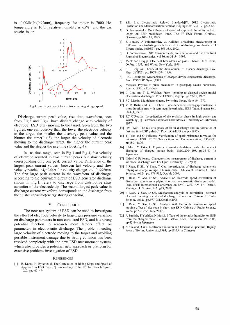
is -0.008MPa(0.92atm), frequency for motor is 7000 Hz, temperature is 10, relative humidity is 65% and the gas species is air.
Discharge current peak value, rise time, waveform, seen from Fig.3 and Fig.4, have distinct change with velocity of electrode (ESD gun) moving to the target. Seen from the two figures, one can observe that, the lower the electrode velocity to the target, the smaller the discharge peak value and the blunter rise time(Fig.3); the larger the velocity of electrode moving to the discharge target, the higher the current peak value and the steeper the rise time slope(Fig.4).
In 1ns time range, seen in Fig.3 and Fig.4, fast velocity of electrode resulted in two current peaks but slow velocity corresponding only one peak current value. Difference of the largest peak current values between fast velocity and slow velocity reached Ip=0.56A for velocity change v=0.1276m/s. The first large peak current in the waveform of discharge, according to the equivalent circuit of ESD generator discharge shown in Fig.1, refers to discharge from distributive stray capacitor of the electrode tip. The second largest peak value in discharge current waveform corresponds to the discharge from the cluster capacitor(energy storing capacitor).
V. CONCLUSSION
The new test system of ESD can be used to investigate the effect of electrode velocity to target, gas pressure variation on discharge parameters in non-contacted ESD, and has strong potential function to research more factors effect on parameters in electrostatic discharge. The problem needing large velocity of electrode moving to the target and avoiding possible instrument damage due to strong collision has been resolved completely with the new ESD measurement system, which also provides a potential new approach or platform for extensive problems investigation of ESD.
REFERENCES [1] B. Daout, H. Ryser et al. The Correlation of Rising Slope and Speed of
Approach in ESD Tests[C]. Proceedings of the 12th Int. Zurich Symp., 1987, pp.467–474.
[2] S.H. Liu. Electrostatic Related Standards[R]. 2012 Electrostatic Protection and Standardization Seminar, Beijing,Nov.12,2012: pp35-56.
[3] D. Pommerenke. On influence of speed of approach, humidity and arc length on ESD breakdown. Proc. The 3rd ESD Forum, Grainau, Germany,pp.103-111, 1993.
[4] S. Bonish, D. Pommerenke, W. Kalkner. Broadband measurement of ESD risetimes to distinguish between different discharge mechanisms. J. Electrostatics, vol56(3), pp. 363-383, 2002.
[5] D. Pommerenke. ESD: transient fields, arc simulation and rise time limit. Journal of Electrostatics, vol 36, pp.31-54, 1995.
[6] Meek and Craggs. Electrical breakdown of gases. Oxford Univ. Press, Oxford, 1953, and Wiley, New York, 1978.
[7] S. I. Bragiski. Theory of the development of a spark discharge. Sov. Phys, JETP(7), pp. 1068–1074, 1958.
[8] R.G. Renninger. Mechanisms of charged-device electrostatic discharge. Proc. EOS/ESD Symp.,1991.
[9] Mesyats. Physics of pulse breakdown in gases[M]. Nauka Publishers, Russia, 1991(in Russian)
[10] L. Lind and T. L. Welsher. From lightning to charged-device model electrostatic discharges. Proc. EOS/ESD Symp., pp.67-75, 1992.
[11] J.C. Martin. Multichannel gaps. Switching Notes, Note 10, 1970.
[12] V. M. Ristic and G. R. Dubois. Time dependent spark-gap resistance in short duration arcs with semimetallic cathodes. IEEE Trans. Plasma Sci., PS-6(4),1978.
[13] RC O’Rourke. Investigation of the resistive phase in high power gas switching[R]. Lawrence Livemore Laboratories, University of California, 1977.
[14] HM Hyatt. The resistive phase of an air discharge and the formation of fast rise time ESD pulse[C]. Proc. EOS/ESD Symp. (1992).
[15] Y Taka and O Fujiwara. Verification of spark-resistance formulae for micro-gap ESD. IEICE Transactions on Communication, E93-B(7), pp.1801-1806.
[16] I Mori, Y Taka, O Fujiwara. Current calculation model for contact discharge of charged human body. EMCJ2004-108, pp.35-40 (in Japanese).
[17] I Mori, O Fujiwara. Characteristics measurement of discharge current in air model discharge with ESD gun. Electricity B,122(11).
[18] F Ruan, D Shi, Y Shen, Y Gao. Investigation of discharge parameters relying on charge voltage in human-metal ESD event. Chinese J. Radio Science, vol 24, pp. 979-982, Octable 2009.
[19] F Ruan, Y Gao, D Shi. Analysis on electrode speed correlation of discharge parameters applying short-gap electrostatic discharge model. Proc. IEEE International Conference on EMC, WED-AM-4-4, Detroit, Michigan, U.S., Aug19-Aug23, 2008.
[20] F Ruan, Y Gao, D Shi. Mechanism analysis of correlation between electrode moving speed and discharge parameters. Chinese J. Radio Science, vol 23, pp.977-981,Octable 2008.
[21] F Ruan, Y Gao, D Shi. Analysis with Bernoulli theorem on speed moving effect of electrode in short-gap ESD. Chinese J. Radio Science, vol24, pp.551-555, June 2009.
[22] A Sumida, T Yoshida, N Masui. Effects of the relative humidity on ESD from the charged metal. Seidenki Gakkai Koen Ronbunshu, Vol.2006, pp.43-44 (in Japanese)
[23] Z Xue and D Wu. Electronic Emission and Electronic Spectrum. Bejing: Press of Beijing University,1993, pp.68-75.(in Chinese)
-2
-1
0
1
2
3
4
-5 0 5 10 15 20 25 30
-0.5
0
0.5
1
1.5
2
2.5
3
3.5
4
-2 0 2 4 6
Time t/ns
Dis
char
ge c
urre
nt i
(t)/A
Fig.4 discharge current for electrode moving at high speed
Vectorial analysis of intense electromagnetic field using a non-invasive optical probe
G. Gaborit*,†, L. Gillette*,†, P. Jarrige†, J. Dahdah†, T. Trève† and L. Duvillaret†
*IMEP-LAHC, Université Savoie Mont Blanc, 73 376 Le Bourget-du-Lac, France;
†Kapteos, Alpespace, bât. Cleanpsace, 354 voie Magellan, F-73800 Sainte-Hélène du Lac, France
Abstract
We here present our latest developments concerningelectro-optic sensors dedicated to ultra-wide band (>9decades of frequency) and high dynamics range (130 dB)characterization of electric fields. Such dielectric probesact as fully uncoupled and orthogonal to each otherreceiving dipole antennas; they allow to perform avectorial analysis of the transient evolution of each electricfield component. Furthermore, they present a very lowinvasiveness due to their low permittivity (<4), their verysmall size (measurement volume <1 cm3), and theirpractically unlimited optical fiber link (>100 m). Thesesensors give access to metrologic measurements (absolutestrength of electric field) in harsh environments as themeasurements are fully independent of temperaturevariations, fiber link mechanical vibrations, EMI,magnetic field and pressure variations.
Keywords: Electromagnetic measurement, Optical probe,Electro-optic effect, Electric field, Fiber optic sensor.
1 Introduction
Among the numerous solutions to characterize radiated andevanescent electric (E) fields, the use of antennas remains themost widespread experimental technique. In the case ofguided E-field, contact probe are mainly used. The maindrawback of such sensors lies in their metallic structure thatcould induce strong perturbation of the field to be measured.Moreover, their size is linked to the lower bound of theirfrequency bandwidth, this latter being intrinsically limited.Finally, while their measurement dynamics is rather large, theexperimental analysis of intense field may lead to partial oreven total discharges, which are critical for the downstreaminstrumentation. In this context, we here propose fullydielectric pigtailed optical sensors as an alternative for thenon-invasive and ultra wide band vectorial electric fieldcharacterization.
2 Electric field sensor principle
These optical sensors are based on the linear electro-optic(EO) effect (also Pockels effect). This effect occurs in non-
linear optical crystals for which the eigen refractive indicesare modified by the applied electric field vector to bemeasured. Experimentally, a laser beam is used to probe theEO crystal which acts as a phase, amplitude or polarizationstate [1] modulator. Then, the phase, amplitude orpolarization state of the laser carries out the real timeevolution of a given component of the field vector [2].
3 Optical probe description
The structure of the sensors consists in an optical arrangementinvolving micro-lenses to collimate the laser beam inside theEO crystal transducer and wave plates to control itspolarization state. The packaging of the probe is based on amulti-layered dielectric coating ensuring both mechanicalprobe integrity and permittivity matching between theambient medium in which the measurement is carried out (air,water, plasmas, …) and the EO crystal transducer. The fieldcharacterization can be remoted up to several tens metersthanks to an optical fibre. This fibre links the sensors to anoptoelectronic unit which includes both laser feeding andoptical treatment. This unit delivers finally an electrical signaldirectly proportional to each of the three components of theE-field vector.
4 Electro-optic probe features and potentialities
The whole system has been exhaustively characterized and itsintrinsic performances are summarized in Table 1.
Table 1: Performances of the EO system.
Minimum detectable field < 1 V.m-1.Hz-1/2
Maximum measurable field > 3 MV.m-1
Measurement dynamics > 130 dB
Vectorial selectivity > 40 dB
Freq. bandwidth (EO probe) 30 Hz → 10 or 50 GHz
Spatial resolution < 3 x 3 x 5 mm3
Thanks to their above-mentioned features, to their millimetricsize, the EO probes are suitable for metrological E-fieldassessment either in free-space or for guided waves. Thepotentialities of such a technique has already been
1
demonstrated for various applications: vectorial near fieldmapping [3], E-field assessment in liquids (water, biologicalmedia, …) [4], high power microwave, electromagneticinterference, intense field analysis, electric discharge orplasma studies [5,6], and energy diagnostic [7].As an example, Fig.1 presents the transient response of onecomponent of the E field in the reactive region of an ultrawideband antenna fed by nanosecond pulses.
Figure 1. Top: Photography of the EO probe located inthe vicinity of a shark antenna. The antenna is fed by aKentech generator delivering nanosecond pulses (5 kVpeak volatge). The probe is orientated to measure thevertical component of the field. Bottom: absolutemeasurement (left scale) of the vertical E field componentand associated spectrum.
5 Conclusion
The EO technique allows to measured electric field in harshenvironments, and leads to a comprehensive analysis of thespatio-temporal distribution of the E field in almost anyconfiguration, wherever measurements performed in air,gases, vacuum or liquids. The associated performances makethem suitable for many applications, and fulfill very well therequirements for non invasive and remoted intense fieldmeasurements. Basic principles of the EO technique will beexplained during the conference. The advantages and
limitations of the EO technique will be also presentedtogether with a benchmark of other available metrologicaltechniques. Additionally, experimental electric fieldcharacterizations, in various conditions, will be presented andcompared to theoretical and/or numerical simulation.
Acknowledgements
The authors would like to acknowledge ANR (FrenchNational Research Agency) for the funded CHIC (programEESI 2010), the DGA (French Military ProgramsManagement and Procurement Agency) for the fundedSNIFER project (program RAPID), DGCIS for financialsupport. They also would like to thank the French NationalResearch Program for Environmental and OccupationalHealth of Anses (2013/2/20). Finally, the authors would liketo thanks the CEA Gramat for the experimentalcollaborations.
References
[1] L. Duvillaret, S. Rialland, and J.-L. Coutaz, “Electro-opticsensors for electric field measurements. I. Theoreticalcomparison among different modulation techniques”, JOSAB, Vol. 19, 11, pp. 2692-2703, 2002.[2] G. Gaborit, J.-L. Coutaz, and L. Duvillaret, “Vectorialelectric field measurement using isotropic electro-opticcrystals”, Appl. Phys. Lett., Vol. 90, pp. 241118-1-3, 2007.[3] K. Yang, G. David, J.-G. Yook, I. Papapolymerou, L. P. B.Katehi, and J. F.Whitaker, “Electrooptic mapping and finite-element modeling of the near-field pattern of a microstrippatch antenna”, IEEE Trans. Microwave Theory Tech., Vol.48, pp. 288-294, 2000.[4] N. Ticaud, S. Kohler, P. Jarrige, L. Duvillaret, G. Gaborit,R. P O'Connor, D. Arnaud-Cormos, and P. Leveque, “Specificabsorption rate assessment using simultaneous electric fieldand temperature measurements”, IEEE Antennas WirelessPropag. Lett., Vol. 11, pp. 252-255, 2012.[5] G. Gaborit, J. Dahdah, F. Lecoche, P. Jarrige, Y.Gaeremynck, E. Duraz, and L. Duvillaret, “Nonperturbativeelectro-optic sensor for in-situ electric dischargecharacterization”, IEEE Trans. Plasm. Sci., Vol. 41, pp. 2851-2857, 2013.[6] G. Gaborit, P. Jarrige, F. Lecoche, J. Dahdah, E. Duraz, C.Volat, and L. Duvillaret, “Single shot and vectorialcharacterization of intense electric field in variousenvironments with pigtailed electrooptic probe”, IEEE Trans.Plasm. Sci., Vol. 42, pp. 1265-1273, 2014.[7] J. E. Toney, A. T. Tarditi, P. Pontius and A. Pollick,“Detection of energized structures with an electro-opticelectric field sensor”, IEEE Sens. Journal, Vol. 14, pp. 1364-1369, 2014.
2
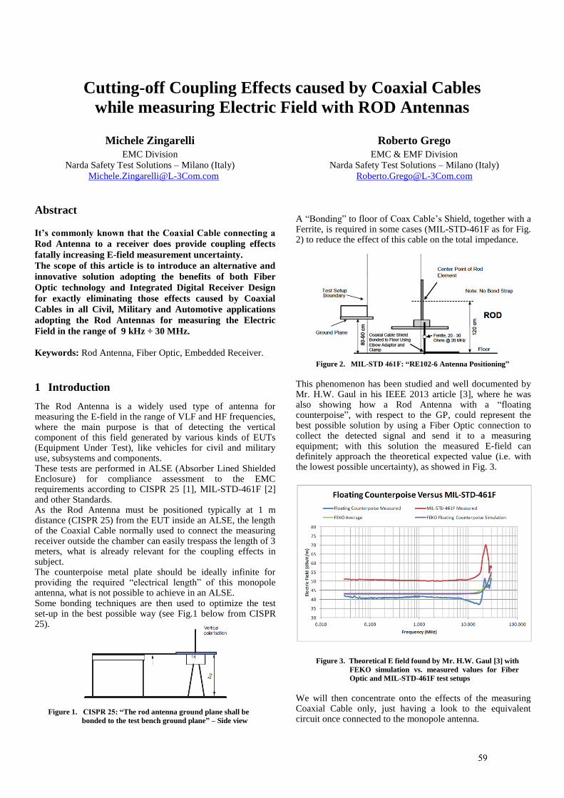
Cutting-off Coupling Effects caused by Coaxial Cables
while measuring Electric Field with ROD Antennas
Michele Zingarelli
EMC Division
Narda Safety Test Solutions – Milano (Italy)
Roberto Grego
EMC & EMF Division
Narda Safety Test Solutions – Milano (Italy)
Abstract
It’s commonly known that the Coaxial Cable connecting a
Rod Antenna to a receiver does provide coupling effects
fatally increasing E-field measurement uncertainty.
The scope of this article is to introduce an alternative and
innovative solution adopting the benefits of both Fiber
Optic technology and Integrated Digital Receiver Design
for exactly eliminating those effects caused by Coaxial
Cables in all Civil, Military and Automotive applications
adopting the Rod Antennas for measuring the Electric
Field in the range of 9 kHz ÷ 30 MHz.
Keywords: Rod Antenna, Fiber Optic, Embedded Receiver.
1 Introduction
The Rod Antenna is a widely used type of antenna for measuring the E-field in the range of VLF and HF frequencies, where the main purpose is that of detecting the vertical component of this field generated by various kinds of EUTs (Equipment Under Test), like vehicles for civil and military use, subsystems and components. These tests are performed in ALSE (Absorber Lined Shielded Enclosure) for compliance assessment to the EMC requirements according to CISPR 25 [1], MIL-STD-461F [2] and other Standards. As the Rod Antenna must be positioned typically at 1 m distance (CISPR 25) from the EUT inside an ALSE, the length of the Coaxial Cable normally used to connect the measuring receiver outside the chamber can easily trespass the length of 3 meters, what is already relevant for the coupling effects in subject. The counterpoise metal plate should be ideally infinite for providing the required “electrical length” of this monopole antenna, what is not possible to achieve in an ALSE. Some bonding techniques are then used to optimize the test set-up in the best possible way (see Fig.1 below from CISPR 25).
Figure 1. CISPR 25: “The rod antenna ground plane shall be
bonded to the test bench ground plane” – Side view
A “Bonding” to floor of Coax Cable’s Shield, together with a Ferrite, is required in some cases (MIL-STD-461F as for Fig. 2) to reduce the effect of this cable on the total impedance.
Figure 2. MIL-STD 461F: “RE102-6 Antenna Positioning”
This phenomenon has been studied and well documented by Mr. H.W. Gaul in his IEEE 2013 article [3], where he was also showing how a Rod Antenna with a “floating counterpoise”, with respect to the GP, could represent the best possible solution by using a Fiber Optic connection to collect the detected signal and send it to a measuring equipment; with this solution the measured E-field can definitely approach the theoretical expected value (i.e. with the lowest possible uncertainty), as showed in Fig. 3.
Figure 3. Theoretical E field found by Mr. H.W. Gaul [3] with
FEKO simulation vs. measured values for Fiber
Optic and MIL-STD-461F test setups
We will then concentrate onto the effects of the measuring Coaxial Cable only, just having a look to the equivalent circuit once connected to the monopole antenna.
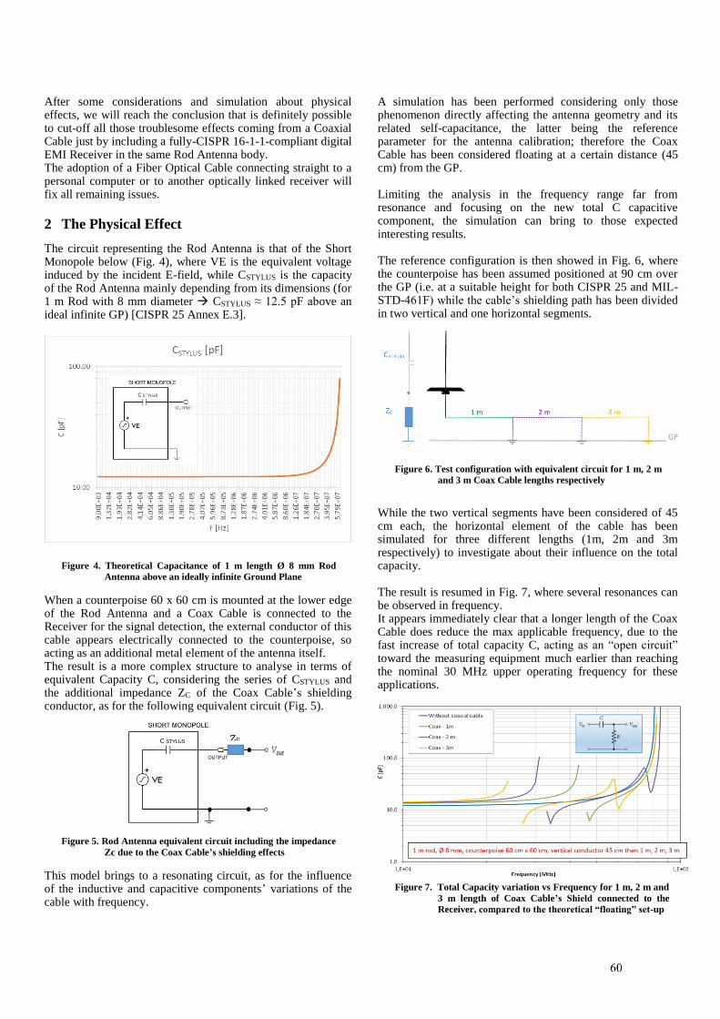
After some considerations and simulation about physical effects, we will reach the conclusion that is definitely possible to cut-off all those troublesome effects coming from a Coaxial Cable just by including a fully-CISPR 16-1-1-compliant digital EMI Receiver in the same Rod Antenna body. The adoption of a Fiber Optical Cable connecting straight to a personal computer or to another optically linked receiver will fix all remaining issues.
2 The Physical Effect
The circuit representing the Rod Antenna is that of the Short Monopole below (Fig. 4), where VE is the equivalent voltage induced by the incident E-field, while CSTYLUS is the capacity of the Rod Antenna mainly depending from its dimensions (for 1 m Rod with 8 mm diameter CSTYLUS ≈ 12.5 pF above an ideal infinite GP) [CISPR 25 Annex E.3].
Figure 4. Theoretical Capacitance of 1 m length Ø 8 mm Rod
Antenna above an ideally infinite Ground Plane
When a counterpoise 60 x 60 cm is mounted at the lower edge of the Rod Antenna and a Coax Cable is connected to the Receiver for the signal detection, the external conductor of this cable appears electrically connected to the counterpoise, so acting as an additional metal element of the antenna itself. The result is a more complex structure to analyse in terms of equivalent Capacity C, considering the series of CSTYLUS and the additional impedance ZC of the Coax Cable’s shielding conductor, as for the following equivalent circuit (Fig. 5).
Figure 5. Rod Antenna equivalent circuit including the impedance
Zc due to the Coax Cable’s shielding effects
This model brings to a resonating circuit, as for the influence of the inductive and capacitive components’ variations of the cable with frequency.
A simulation has been performed considering only those phenomenon directly affecting the antenna geometry and its related self-capacitance, the latter being the reference parameter for the antenna calibration; therefore the Coax Cable has been considered floating at a certain distance (45 cm) from the GP. Limiting the analysis in the frequency range far from resonance and focusing on the new total C capacitive component, the simulation can bring to those expected interesting results. The reference configuration is then showed in Fig. 6, where the counterpoise has been assumed positioned at 90 cm over the GP (i.e. at a suitable height for both CISPR 25 and MIL-STD-461F) while the cable’s shielding path has been divided in two vertical and one horizontal segments.
Figure 6. Test configuration with equivalent circuit for 1 m, 2 m
and 3 m Coax Cable lengths respectively
While the two vertical segments have been considered of 45 cm each, the horizontal element of the cable has been simulated for three different lengths (1m, 2m and 3m respectively) to investigate about their influence on the total capacity. The result is resumed in Fig. 7, where several resonances can be observed in frequency. It appears immediately clear that a longer length of the Coax Cable does reduce the max applicable frequency, due to the fast increase of total capacity C, acting as an “open circuit” toward the measuring equipment much earlier than reaching the nominal 30 MHz upper operating frequency for these applications.
Figure 1. Compliance evaluation by ULAB
Figure 7. Total Capacity variation vs Frequency for 1 m, 2 m and
3 m length of Coax Cable’s Shield connected to the
Receiver, compared to the theoretical “floating” set-up
On the contrary, the “floating condition without the Coaxial Cable” does show exactly the same behaviour of the pure CSTYLUS capacity, therefore the usage of a Fiber Optical connection appears extremely helpful in reducing differences between the various Labs, i.e. reducing the uncertainty just related to the test set-up.
3 Innovative “Embedded Receiver” Solution
As aforementioned, an embedded fully-CISPR 16-1-1-compliant receiver would represent the best solution to detect and adapt the signal received from the Rod Antenna immediately at the monopole output, with the additional benefits we’ll describe in this section, hence transfering the measured output directly through a Fiber Optic Cable to a personal computer or to the optical input of a perfectly matched receiver. The embedded receiving part can definitely help in overcoming the following usual limitations of a classical Rod Antenna:
- easy Saturation of the broadband active input stage;
- weakness of the FET-based high-impedance stage;
- missing of automatic variable Attenuators;
- limited Sensitivity due to the high noise figure of input stage;
- “Antenna Factor” variation due to the CSTYLUS changes with the set-up (grounding).
Figure 8. Block diagram of the “Embedded Receiver” solution
The innovative concept briefly sketched in Fig. 8 shows the meaningful blocks defined for the scope and detailed hereinafter:
a. the first stage connected to the Rod element provides a High-Impedance Band-Pass Filtering divided in the two commonly used ranges of 9 kHz ÷ 30 MHz and 150 kHz ÷ 30 MHz, exactly to reduce potential saturation caused by broadband input signals;
b. a selectable 20 dB Attenuator is then inserted before the usual high-impedance FET stage to protect it by possible saturation or damage;
c. another 10 dB selectable attenuator can play a relevant role in the delicate balance between prevention of saturation after the FET, maximum sensitivity and highest achievable dynamic range; for instance, a Sensitivity of at least -22 dBµV/m @ 1 MHz with 200 Hz RBW and a Dynamic
Range of up to 175 dB are considered match able;
d. the following five Preselector Filters can guarantee the Full-Compliance to CISPR 16-1-1 requirements for low PRF signals at the EMI receiving section:
9 kHz ÷ 5.67 MHz
5.67 MHz ÷ 11.19 MHz
11.19 MHz ÷ 16.71 MHz
16.71 MHz ÷ 22.23 MHz
22.23 MHz ÷ 30.00 MHz
e. finally a 30 MHz Low-Pass Filter cuts-off any possible inter-modulated out-of-band signal contribution before accessing the digital detecting part of the embedded EMI Receiver or the standard 50 Ω Analog Output (Fig. 9);
f. the Optical Digital Output of the embedded receiver does provide all those relevant benefits in completely cutting-off both “coupling to GP” and “Coax Cable resonances” extensively described before.
Figure 9. Possible connections for the Rod Antenna with
“embedded receiver” (Coax and Fiber Optic)
4 Conclusions
The evidence of all the advantages offered by this innovative approach, matching the ideal achievement of a “Floating Counterpoise” (previously studied by Mr. Gaul [3]) to the Cut-Off of Coax Cables Coupling Effects, should definitely pose a thread for including it in the most relevant Standards adopting the Rod Antenna as a “sensing probe” for E-field in the VLF and HF ranges. A prototype of “Field Receiving Rod Antenna” is being actually tested to provide practical demonstration of its effectiveness in the field.
References
[1] CISPR 25 Ed.3 (2008) – “Vehicles, boats and internal
combustion engines - Radio disturbance characteristics -
Limits and methods of measurement for the protection of on-
board receivers”
[2] MIL-STD-461F (2007) – “DEPARTMENT OF DEFENSE
INTERFACE STANDARD – Requirements for the control
of electromagnetic interference characteristics of subsystems
and equipment”
[3] Harry W. Gaul (2013) – “Electromagnetic Modeling and
Measurements of the 104 cm Rod and Biconical Antenna for
Radiated Emissions Testing Below 30 MHz” – 978-1-4799-
0409-9/13/$31.00@2013 IEEE
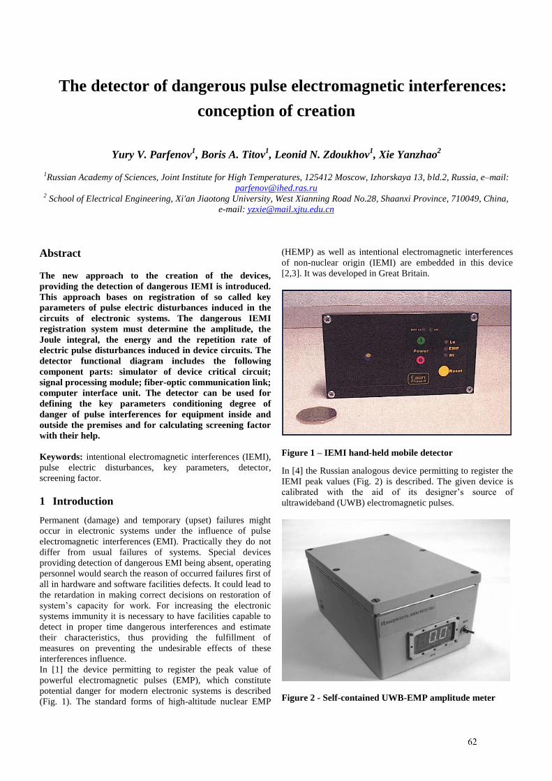
1
The detector of dangerous pulse electromagnetic interferences:
conception of creation
Yury V. Parfenov1, Boris A. Titov
1, Leonid N. Zdoukhov
1, Xie Yanzhao
2
1Russian Academy of Sciences, Joint Institute for High Temperatures, 125412 Moscow, Izhorskaya 13, bld.2, Russia, e–mail:
[email protected] 2 School of Electrical Engineering, Xi'an Jiaotong University, West Xianning Road No.28, Shaanxi Province, 710049, China,
e-mail: [email protected]
Abstract
The new approach to the creation of the devices,
providing the detection of dangerous IEMI is introduced.
This approach bases on registration of so called key
parameters of pulse electric disturbances induced in the
circuits of electronic systems. The dangerous IEMI
registration system must determine the amplitude, the
Joule integral, the energy and the repetition rate of
electric pulse disturbances induced in device circuits. The
detector functional diagram includes the following
component parts: simulator of device critical circuit;
signal processing module; fiber-optic communication link;
computer interface unit. The detector can be used for
defining the key parameters conditioning degree of
danger of pulse interferences for equipment inside and
outside the premises and for calculating screening factor
with their help.
Keywords: intentional electromagnetic interferences (IEMI),
pulse electric disturbances, key parameters, detector,
screening factor.
1 Introduction
Permanent (damage) and temporary (upset) failures might
occur in electronic systems under the influence of pulse
electromagnetic interferences (EMI). Practically they do not
differ from usual failures of systems. Special devices
providing detection of dangerous EMI being absent, operating
personnel would search the reason of occurred failures first of
all in hardware and software facilities defects. It could lead to
the retardation in making correct decisions on restoration of
system’s capacity for work. For increasing the electronic
systems immunity it is necessary to have facilities capable to
detect in proper time dangerous interferences and estimate
their characteristics, thus providing the fulfillment of
measures on preventing the undesirable effects of these
interferences influence.
In [1] the device permitting to register the peak value of
powerful electromagnetic pulses (EMP), which constitute
potential danger for modern electronic systems is described
(Fig. 1). The standard forms of high-altitude nuclear EMP
(HEMP) as well as intentional electromagnetic interferences
of non-nuclear origin (IEMI) are embedded in this device
[2,3]. It was developed in Great Britain.
Figure 1 – IEMI hand-held mobile detector
In [4] the Russian analogous device permitting to register the
IEMI peak values (Fig. 2) is described. The given device is
calibrated with the aid of its designer’s source of
ultrawideband (UWB) electromagnetic pulses.
Figure 2 - Self-contained UWB-EMP amplitude meter
2
It should be noted that EMP forms, created by real sources,
differ from above mentioned recommended standard forms
[2,3]. Moreover, pulses forms, radiated by different sources,
differ from each other. For these reasons the results of IEMI
registration with the use of devices shown on fig. 1, 2,
apparently, are not exactly correct. We should add one more
disadvantage to the mentioned above one. In this case
amplitude values of pulse disturbances registration results do
not permit to estimate the real danger of registered pulses, as
the IEMI danger for electronic systems depends not only on
influencing these systems pulses amplitude, but also on
timing data (spectral range) and repetition rate. In many
practical cases, small-amplitude pulses, repeating with high
frequency, will more seriously affect the devices’ functioning
than higher amplitude pulses of small repetition rate. In
absence of criteria of dangerous IEMI it is necessary to adjust
detectors to EMPs’ minimum level, only slightly exceeding
the electromagnetic environment. But in such a case detectors
will produce frequent unfounded alarm signals. Therefore, the
only one reasonable sphere of applying the device under
consideration, is the registration of amplitude values of
standard pulses formed by test simulators.
Below, the new approach to the creation of the devices,
providing the detection of dangerous IEMI is introduced. This
approach bases on registration of so called key parameters of
pulse electric disturbances induced in the circuits of electronic
systems.
2 Key parameters of pulse electric disturbances
The mechanism of powerful electromagnetic pulses influence
on electronic devices is in forming in circuits of these devices
pulse electric disturbances, which cause different failures
(breakdowns) of their operating capacity. Such failures,
which are sometimes called universal, might be as follows:
irreversible (permanent) failure of some elements; transition
of active elements to the saturation mode; incorrect transfer of
data between digital devices. The possibility of failures
occurrence depends on disturbances key parameters. The list
of key parameters stipulating the possibility of the occurrence
of frequently observed electronic devices failures is given
below.
The condition of electronic device element irreversible failure
is the simultaneous performing of the following conditions
(criteria): ; . Here is the
amplitude of pulse voltage induced at the input of the given
element. is the voltage value of electric breakdown
initiation; is the Joule integral; is
the pulse of current, flowing through the element after electric
breakdown occurrence, is the duration of this pulse;
is the Joule integral minimum value providing
thermal breakdown.
For stable transition of active elements to saturation mode the
performing of the following conditions is necessary: .
; ; . Here: and
are respectively, the minimum voltage value under reaching
which the transition of active elements to saturation mode
makes start, Joule integral minimum value, providing stable
elements transition to this mode and duration of process of
going out from saturation mode after cut off current flow
through elements. As the criteria of digital devices failure caused by occurrences
of errors in data packets transmission, the following
inequalities can be accepted: ; ;
Here: and are the numbers of data
packets containing errors, and data transmission rate under
conditions of repeated pulse disturbance influence, is the
probability of errors occurrence in data packets transmission
as a result of disturbance influence, , and
are critical values of these parameters. In turn,
, and depend on such parameters of
induced pulse disturbance as pulse energy and its repetition
rate.
Listed above parameters of the induced pulse disturbance are
key parameters and their values characterize danger of the
electromagnetic influence.
It should be said that the induced electric disturbance energy
is not definitely connected with the energy of electromagnetic
pulse influencing electronic device. Of course, it depends on
amplitude-time characteristics of EMP, but it also depends on
geometric and electric characteristics of influenced device
electric circuits. In addition, under real conditions of
electromagnetic wave propagation, for example, in the
building as a result of pulse reflection from the walls, it is
being transformed into complex pulse signal, the duration of
which can considerably exceed the duration of initial signal.
Correspondingly, the energy of the induced electric
disturbance is being changed.
Thus, the dangerous IEMI registration system must determine
the amplitude, the Joule integral, the energy and the repetition
rate of electric pulse disturbances induced in device circuits.
Sometimes, it is convenient to accept as the key parameter of
the pulse electric disturbance average power, which is equal
to pulse energy and its repetition rate product .
3 Dangerous IEMI detector structure
As it was mentioned before, under influence of EMPs pulse
electric disturbances are being induced on communication
and power supply lines of electronic device and are capable to
obstruct its normal functioning. In this connection the
simulator of typical communication or electric power supply
line could be one of the detector elements. As the simulator of
the typical circuit for defining the IEMI key parameters one
of the paths in printed circuit boards could be taken [Fig. 3].
Electric dipole could also be the convenient simulator.
Simulator design and characteristics depend on the features of
the device under influence of EMPs, but this is the subject of
separate justification and goes beyond the theme of this paper.
The detector functional diagram includes the following
component parts: simulator of device critical circuit; signal
processing module; fiber-optic communication link; computer
interface unit. The detector functions in the following way.
Simulator of device critical circuit senses influencing EMP,
transforms it into pulse voltage and delivers the latest on
signal processing unit.
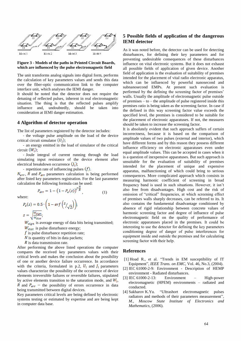
3
Figure 3 - Models of the paths in Printed Circuit Boards,
which are influenced by the pulse electromagnetic field
The unit transforms analog signals into digital form, performs
the calculation of key parameters values and sends this data
over the fiber-optic communication link to the computer
interface unit, which analyses the IEMI danger.
It should be noted that the detector does not require the
detuning of reflected pulses, inherent in real electromagnetic
situation. The thing is that the reflected pulses amplify
influence and, undoubtedly, should be taken into
consideration at IEMI danger estimation.
4 Algorithm of detector operation
The list of parameters registered by the detector includes:
- the voltage pulse amplitude on the load of the device
critical circuit simulator ;
- an energy emitted in the load of simulator of the critical
circuit ;
- Joule integral of current running through the load
simulating input resistance of the device element after
electrical breakdown occurrence ;
- repetition rate of influencing pulses .
, and parameters calculation is being performed
after listed key parameters registration. For the last parameter
calculation the following formula can be used:
, (1) where:
;
;
is average energy of data bits being transmitted;
is pulse disturbance energy;
is pulse disturbance repetition rate;
is quantity of bits in data packets;
is data transmission rate.
After performing the above listed operations the computer
compares the received key parameters values with their
critical levels and makes the conclusion about the possibility
of one or another device failure occurrence. In accordance
with the criteria, formulated in p.2, and parameters
values characterize the possibility of the occurrence of device
elements irreversible failures or reversible failures, stipulated
by active elements transition to the saturation mode, and ,
and the possibility of errors occurrence in data
being transmitted between digital devices.
Key parameters critical levels are being defined by electronic
systems testing or estimated by expertise and are being kept
in computer data base.
5 Possible fields of application of the dangerous
IEMI detector
As it was noted before, the detector can be used for detecting
disturbances, for defining their key parameters and for
preventing undesirable consequences of these disturbances
influence on vital electronic systems. But it does not exhaust
all possible fields of application of given device. Another
field of application is the evaluation of suitability of premises
intended for the placement of vital radio electronic apparatus,
which can be influenced by powerful nanosecond and
subnanosecond EMPs. At present such evaluation is
performed by the defining the screening factor of premises’
walls. Usually the amplitude of electromagnetic pulse outside
of premises – to – the amplitude of pulse registered inside this
premises ratio is being taken as the screening factor. In case if
the defined in this way screening factor value exceeds the
specified level, the premises is considered to be suitable for
the placement of electronic apparatuses. If not, the measures
should be taken to increase the screening factor.
It is absolutely evident that such approach suffers of certain
incorrectness, because it is based on the comparison of
amplitude values of two pulses (external and interior), which
have different forms and by this reason they possess different
influence efficiency on electronic apparatuses even under
equal amplitude values. This can be accepted in cases when it
is a question of inexpensive apparatuses. But such approach is
unsuitable for the evaluation of suitability of premises
intended for the placement of unique and expensive
apparatus, malfunctioning of which could bring to serious
consequences. More complicated approach which consists in
measuring harmonic coefficient of screening in broad
frequency band is used in such situations. However, it isn’t
also free from disadvantages. High cost and the risk of
omission of “critical” frequencies, at which screening effect
of premises walls sharply decreases, can be referred to its. It
also contains the fundamental disadvantage conditioned by
absence of rigid relationship between concrete values of
harmonic screening factor and degree of influence of pulse
electromagnetic field on the quality of performance of
electronic apparatuses placed in the premises. It could be
interesting to use the detector for defining the key parameters
conditioning degree of danger of pulse interferences for
equipment inside and outside the premises and for calculating
screening factor with their help.
References
[1] Hoad R., et al. “Trends in EM susceptibility of IT
Equipment”, IEEE Trans. on EMC, Vol. 46, No.3, (2004).
[2] IEC 61000-2-9: Environment - Description of HEMP
environment - Radiated disturbances.
[3] IEC 61000-2-13: Environment – High-power
electromagnetic (HPEM) environments – radiated and
conducted.
[4] Sakharov K.Yu. “Ultrashort electromagnetic pulses
radiators and methods of their parameters measurement”,
M., Moscow State Institute of Electronics and
Mathematics, (2006).
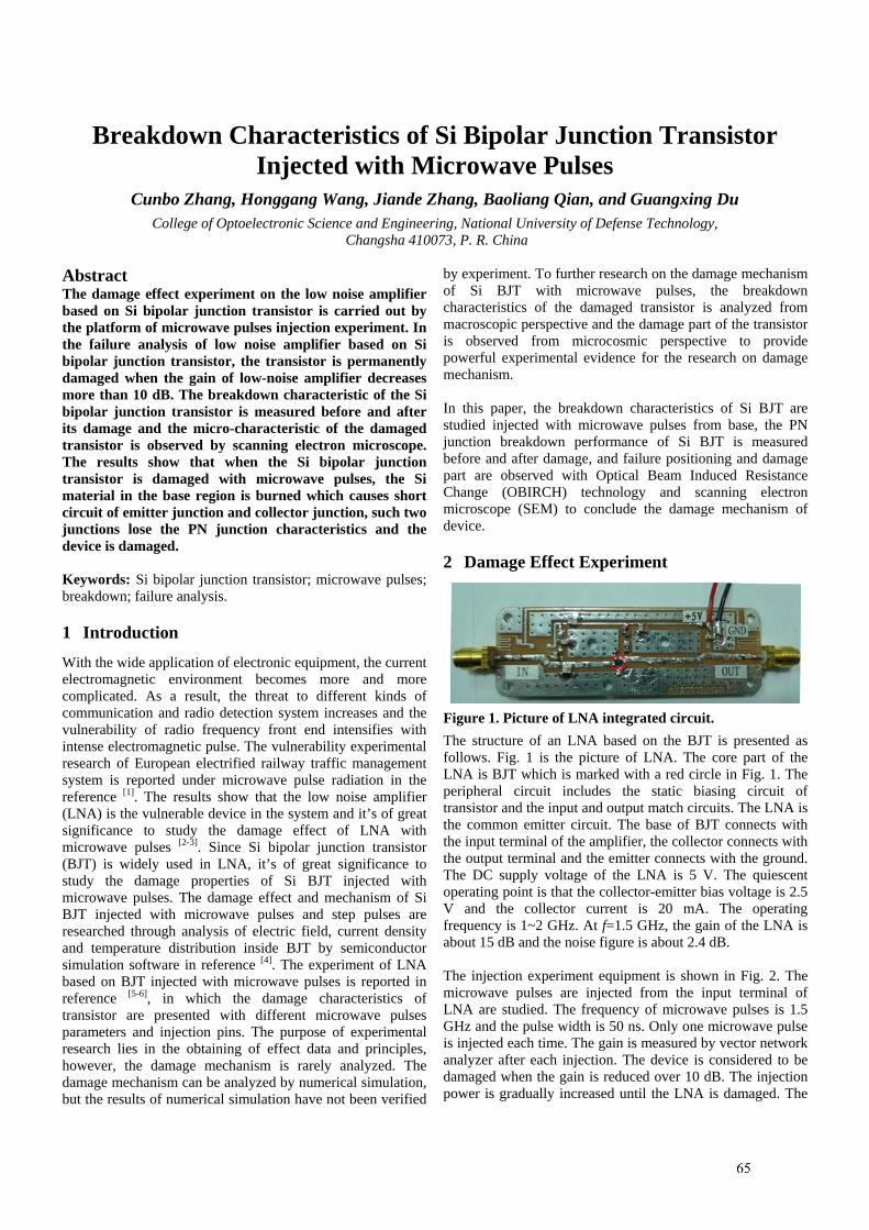
1
Breakdown Characteristics of Si Bipolar Junction Transistor Injected with Microwave Pulses
Cunbo Zhang, Honggang Wang, Jiande Zhang, Baoliang Qian, and Guangxing Du College of Optoelectronic Science and Engineering, National University of Defense Technology,
Changsha 410073, P. R. China
Abstract The damage effect experiment on the low noise amplifier based on Si bipolar junction transistor is carried out by the platform of microwave pulses injection experiment. In the failure analysis of low noise amplifier based on Si bipolar junction transistor, the transistor is permanently damaged when the gain of low-noise amplifier decreases more than 10 dB. The breakdown characteristic of the Si bipolar junction transistor is measured before and after its damage and the micro-characteristic of the damaged transistor is observed by scanning electron microscope. The results show that when the Si bipolar junction transistor is damaged with microwave pulses, the Si material in the base region is burned which causes short circuit of emitter junction and collector junction, such two junctions lose the PN junction characteristics and the device is damaged. Keywords: Si bipolar junction transistor; microwave pulses; breakdown; failure analysis.
1 Introduction With the wide application of electronic equipment, the current electromagnetic environment becomes more and more complicated. As a result, the threat to different kinds of communication and radio detection system increases and the vulnerability of radio frequency front end intensifies with intense electromagnetic pulse. The vulnerability experimental research of European electrified railway traffic management system is reported under microwave pulse radiation in the reference [1]. The results show that the low noise amplifier (LNA) is the vulnerable device in the system and it’s of great significance to study the damage effect of LNA with microwave pulses [2-3]. Since Si bipolar junction transistor (BJT) is widely used in LNA, it’s of great significance to study the damage properties of Si BJT injected with microwave pulses. The damage effect and mechanism of Si BJT injected with microwave pulses and step pulses are researched through analysis of electric field, current density and temperature distribution inside BJT by semiconductor simulation software in reference [4]. The experiment of LNA based on BJT injected with microwave pulses is reported in reference [5-6], in which the damage characteristics of transistor are presented with different microwave pulses parameters and injection pins. The purpose of experimental research lies in the obtaining of effect data and principles, however, the damage mechanism is rarely analyzed. The damage mechanism can be analyzed by numerical simulation, but the results of numerical simulation have not been verified
by experiment. To further research on the damage mechanism of Si BJT with microwave pulses, the breakdown characteristics of the damaged transistor is analyzed from macroscopic perspective and the damage part of the transistor is observed from microcosmic perspective to provide powerful experimental evidence for the research on damage mechanism. In this paper, the breakdown characteristics of Si BJT are studied injected with microwave pulses from base, the PN junction breakdown performance of Si BJT is measured before and after damage, and failure positioning and damage part are observed with Optical Beam Induced Resistance Change (OBIRCH) technology and scanning electron microscope (SEM) to conclude the damage mechanism of device.
2 Damage Effect Experiment
Figure 1. Picture of LNA integrated circuit. The structure of an LNA based on the BJT is presented as follows. Fig. 1 is the picture of LNA. The core part of the LNA is BJT which is marked with a red circle in Fig. 1. The peripheral circuit includes the static biasing circuit of transistor and the input and output match circuits. The LNA is the common emitter circuit. The base of BJT connects with the input terminal of the amplifier, the collector connects with the output terminal and the emitter connects with the ground. The DC supply voltage of the LNA is 5 V. The quiescent operating point is that the collector-emitter bias voltage is 2.5 V and the collector current is 20 mA. The operating frequency is 1~2 GHz. At f=1.5 GHz, the gain of the LNA is about 15 dB and the noise figure is about 2.4 dB. The injection experiment equipment is shown in Fig. 2. The microwave pulses are injected from the input terminal of LNA are studied. The frequency of microwave pulses is 1.5 GHz and the pulse width is 50 ns. Only one microwave pulse is injected each time. The gain is measured by vector network analyzer after each injection. The device is considered to be damaged when the gain is reduced over 10 dB. The injection power is gradually increased until the LNA is damaged. The
2
gain of the amplifier can be recovered to normal status by replacing BJT of LNA, so it implies that the essence of LNA damage with microwave pulses is the damage to BJT.
Figure 2. Testing system.
3 Failure Analysis
To analyze the damage properties of BJT with microwave pulses, 8 damaged BJTs were randomly selected for electric characteristics test and failure positioning analysis. The electric characteristics are measured before and after BJT damage for comparison. The failure positioning and damage part of damaged BJT are observed with OBIRCH technology and SEM.
3.1 Electric characteristics test
The purpose of electric characteristics test is to determine the PN junction performance before and after damage by measuring the avalanche breakdown voltage VCBO of collector junction in common base circuit and VCEO in common emitter circuit and breakdown voltage VEBO of emitter junction [7].
Figure 3. Breakdown characteristics of collector junction in common base. The common base reverse cut-off current (ICBO) refers to the collector current when the emitter is open circuit (IE=0) and the collector junction is reversed (VCB>0). When the emitter is open circuit and the ICBO tends to be infinite, the reverse voltage VCB of collector junction is called as VCBO. The VCBO before and after BJT damage is shown in Fig. 3, among which the horizontal coordinate shows the collector junction voltage VCB when the emitter is open circuit and the vertical coordinate shows the collector current. When VCB>0, the collector junction is reversely biased; when VCB<0, the collector junction is positively biased. From Fig. 3, the collector junction of good transistor has normal PN junction properties such as breakover in positively biased state and cut-off in reversely biased state. The VCBO is more than 10 V.
The VCBO of damaged transistor approximates to 0V. The collector junction is short circuit and loses PN junction properties. The common emitter reverse cut-off current (ICEO) refers to the current penetrating from emitter to collector when the base is open circuit (IB=0) and the collector junction is reversed (VCB>0). When the base is open circuit and the ICEO tends to be infinite, the voltage VCE between the collector and emitter is called as VCEO. The VCEO is much lower than VCBO. The VCEO before and after BJT damage is shown in Fig. 4, among which the horizontal coordinate shows the voltage VCE between the collector and emitter when the base is open circuit and the vertical coordinate shows the collector current. When VCE>0, the collector junction is reversely biased; when VCE<0, the collector junction is positively biased. From Fig. 4, the VCEO of good transistor is more than 4.5 V and the VCEO of damaged transistor approximates to 0 V. We can get the same results as mentioned above: the collector junction is short circuit and loses PN junction properties as well.
Figure 4. Breakdown characteristics of collector junction in common emitter.
Figure 5. Breakdown characteristics of emitter junction IEBO refers to the emitter current when the collector is open circuit (IC=0) and the emitter junction is reversed (VEB>0). When the IEBO tends to be infinite, the reverse voltage of emitter junction is called as VEBO. The VEBO before and after BJT damage is shown in Fig. 5, among which the horizontal coordinate shows the voltage VEB of emitter junction when the collector is open circuit and the vertical coordinate shows the emitter current. When VEB>0, the emitter junction is reversely biased; when VEB<0, the emitter junction is positively biased. From Fig. 5, the emitter junction of good transistor has normal PN junction properties. The VEBO is more than 1 V. The emitter junction of damaged 1#~7# transistors is short circuit and
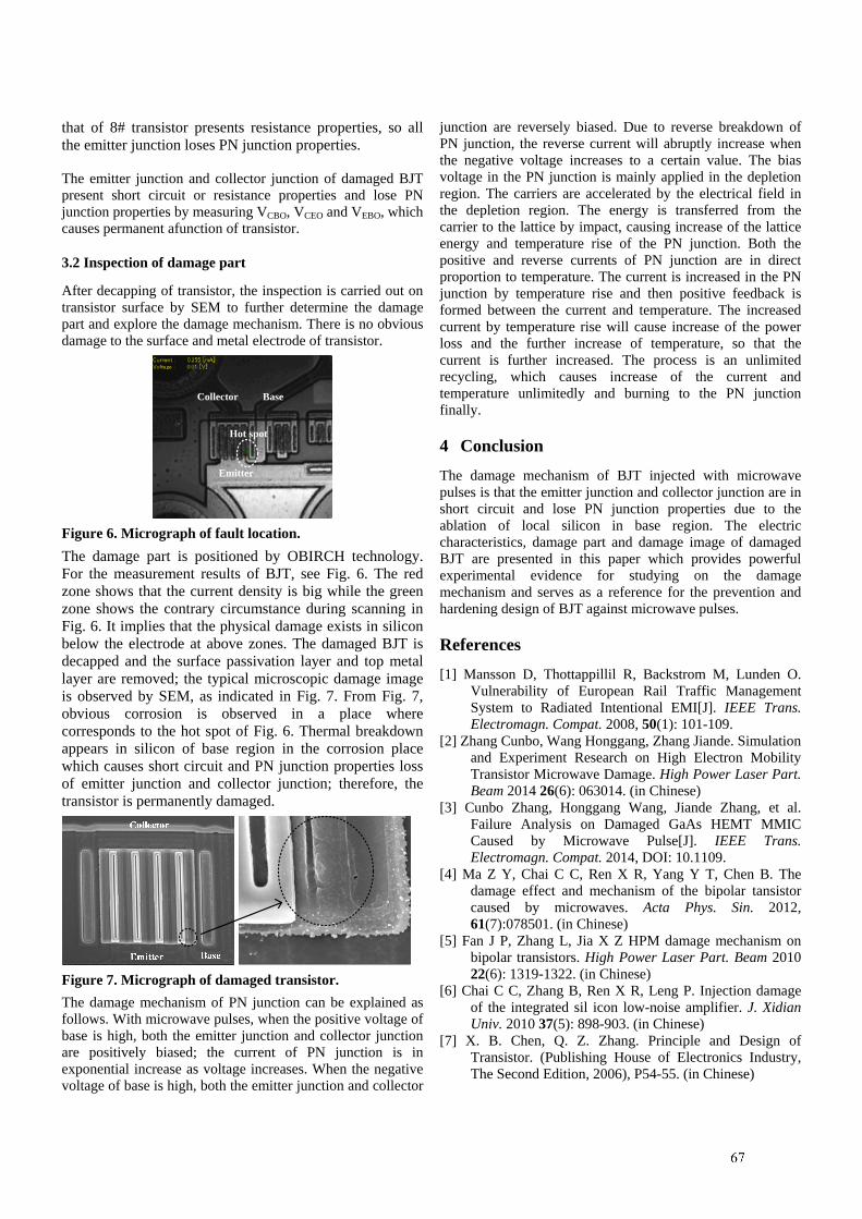
3
that of 8# transistor presents resistance properties, so all the emitter junction loses PN junction properties. The emitter junction and collector junction of damaged BJT present short circuit or resistance properties and lose PN junction properties by measuring VCBO, VCEO and VEBO, which causes permanent afunction of transistor.
3.2 Inspection of damage part
After decapping of transistor, the inspection is carried out on transistor surface by SEM to further determine the damage part and explore the damage mechanism. There is no obvious damage to the surface and metal electrode of transistor.
Emitter
BaseCollector
Hot spot
Figure 6. Micrograph of fault location. The damage part is positioned by OBIRCH technology. For the measurement results of BJT, see Fig. 6. The red zone shows that the current density is big while the green zone shows the contrary circumstance during scanning in Fig. 6. It implies that the physical damage exists in silicon below the electrode at above zones. The damaged BJT is decapped and the surface passivation layer and top metal layer are removed; the typical microscopic damage image is observed by SEM, as indicated in Fig. 7. From Fig. 7, obvious corrosion is observed in a place where corresponds to the hot spot of Fig. 6. Thermal breakdown appears in silicon of base region in the corrosion place which causes short circuit and PN junction properties loss of emitter junction and collector junction; therefore, the transistor is permanently damaged.
Figure 7. Micrograph of damaged transistor. The damage mechanism of PN junction can be explained as follows. With microwave pulses, when the positive voltage of base is high, both the emitter junction and collector junction are positively biased; the current of PN junction is in exponential increase as voltage increases. When the negative voltage of base is high, both the emitter junction and collector
junction are reversely biased. Due to reverse breakdown of PN junction, the reverse current will abruptly increase when the negative voltage increases to a certain value. The bias voltage in the PN junction is mainly applied in the depletion region. The carriers are accelerated by the electrical field in the depletion region. The energy is transferred from the carrier to the lattice by impact, causing increase of the lattice energy and temperature rise of the PN junction. Both the positive and reverse currents of PN junction are in direct proportion to temperature. The current is increased in the PN junction by temperature rise and then positive feedback is formed between the current and temperature. The increased current by temperature rise will cause increase of the power loss and the further increase of temperature, so that the current is further increased. The process is an unlimited recycling, which causes increase of the current and temperature unlimitedly and burning to the PN junction finally.
4 Conclusion The damage mechanism of BJT injected with microwave pulses is that the emitter junction and collector junction are in short circuit and lose PN junction properties due to the ablation of local silicon in base region. The electric characteristics, damage part and damage image of damaged BJT are presented in this paper which provides powerful experimental evidence for studying on the damage mechanism and serves as a reference for the prevention and hardening design of BJT against microwave pulses.
References [1] Mansson D, Thottappillil R, Backstrom M, Lunden O.
Vulnerability of European Rail Traffic Management System to Radiated Intentional EMI[J]. IEEE Trans. Electromagn. Compat. 2008, 50(1): 101-109.
[2] Zhang Cunbo, Wang Honggang, Zhang Jiande. Simulation and Experiment Research on High Electron Mobility Transistor Microwave Damage. High Power Laser Part. Beam 2014 26(6): 063014. (in Chinese)
[3] Cunbo Zhang, Honggang Wang, Jiande Zhang, et al. Failure Analysis on Damaged GaAs HEMT MMIC Caused by Microwave Pulse[J]. IEEE Trans. Electromagn. Compat. 2014, DOI: 10.1109.
[4] Ma Z Y, Chai C C, Ren X R, Yang Y T, Chen B. The damage effect and mechanism of the bipolar tansistor caused by microwaves. Acta Phys. Sin. 2012, 61(7):078501. (in Chinese)
[5] Fan J P, Zhang L, Jia X Z HPM damage mechanism on bipolar transistors. High Power Laser Part. Beam 2010 22(6): 1319-1322. (in Chinese)
[6] Chai C C, Zhang B, Ren X R, Leng P. Injection damage of the integrated sil icon low-noise amplifier. J. Xidian Univ. 2010 37(5): 898-903. (in Chinese)
[7] X. B. Chen, Q. Z. Zhang. Principle and Design of Transistor. (Publishing House of Electronics Industry, The Second Edition, 2006), P54-55. (in Chinese)
1
Frequency Response Analysis of IEMI in Different Types of Electrical Networks
Bing Li and Daniel Månsson
KTH Royal Institute of Technology, School of Electrical Engineering Department of Electromagnetic Engineering
Stockholm, Sweden [email protected], [email protected]
Abstract In this paper, the frequency responses of the loads in different types of electrical networks subjected to intentional electromagnetic interference (IEMI), are analysed with a method based on the Baum-Liu-Tesche (BLT) equation. The networks can be multi-conductor systems with multiple junctions and branches. To verify the calculation results, a commercial electromagnetic simulator based on electromagnetic topology was used. The calculation results agree well with the numerical simulations. Keywords: Electrical network, multiple junctions, intentional electromagnetic interference (IEMI), frequency responses.
1 Introduction Recently, in modern society, intentional electromagnetic interference (IEMI) appears more frequently in threat analyses. Because of the sophistication of electrotechnical and electronic systems the harmfulness of malicious manipulation should be easily understood. Different groups and scholars have contributed in the past to this field (e.g. [1, 2]). Here, in this paper, we investigate the effects on the frequency response characteristics of different loads in networks with different structures as they are subjected to intentional electromagnetic interference (IEMI).
2 The BLT Equation For a simple electrical network, as shown in Fig. 1, to solve the frequency responses for each load, the BLT approach [3, 4] is applied. In this simple network, we suppose that the length of the transmission line is L, with propagation constant γ and characteristic impedance Zc. The load impedances are ZL1 and ZL2, respectively. The excitation source consists of a lumped voltage (Vs) and current (Is) source, located xs from the left load. The application of BLT equation is described as follows;
inc ref1 1 1inc ref
22 2
00
L
L
V V SeSV e V
γ
γ
−
−
= +
, (1)
where the excitation vector is
Vs
ZL1 ZL2Is
1refV
1incV 2
incV
2refV
Figure 1. A simple electrical network.
( )
( ) ( )
s
s
s c s1
2s c s
12
12
x
L x
V Z I eSS V Z I e
γ
γ
−
− −
− − = +
.
At the terminals, the reflected voltage can be expressed as ref inc
1 1 1ref inc
22 2
00
V VV V
rr
= ⋅
, (2)
where ρ1 and ρ2 are the reflection coefficients, defined by L c
L c
, ( 1, 2)ii
i
Z Zi
Z Zr
−= =
+.
Plugging (2) into (1), we obtain the vector of the incident voltages by
1inc1 1 1inc
2 22
01 0 00 1 00
L
L
V SeSV e
γ
γ
rr
−−
−
= − ⋅ ⋅
. (3)
The frequency response at each load is the superposition of the incident and reflected voltages
inc ref1 1 1 1
inc ref2 22 2
1
1 1
2 2
1 00 1
01 0 00 1 00
L
L
V V VV V V
SeSe
γ
γ
rr
rr
−−
−
+ = + = +
⋅ − ⋅ ⋅
. (4)
In addition, if TEM is the main mode of voltage wave propagation, then for any existing junctions in the electrical network, the reflection coefficients can be calculated according to the transmission line theory. If the transmission line parameters are the same for all branches of a junction (e.g. same type of cables used) and if the load connected to each branch is, electrically, far away from the junction, then the current is equally divided between the branches. For a
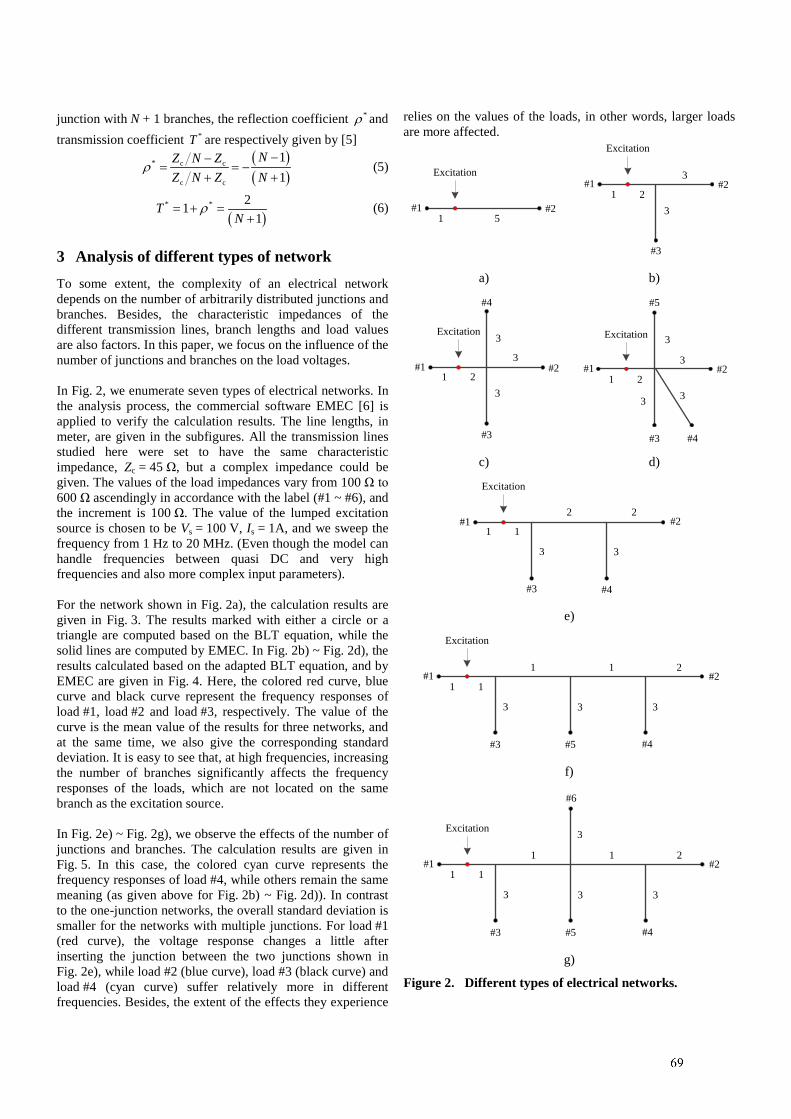
2
junction with N + 1 branches, the reflection coefficient *r and transmission coefficient *T are respectively given by [5]
( )( )
* c c
c c
11
NZ N ZZ N Z N
r−−
= = −+ +
(5)
( )* * 21
1T
Nr= + =
+ (6)
3 Analysis of different types of network To some extent, the complexity of an electrical network depends on the number of arbitrarily distributed junctions and branches. Besides, the characteristic impedances of the different transmission lines, branch lengths and load values are also factors. In this paper, we focus on the influence of the number of junctions and branches on the load voltages. In Fig. 2, we enumerate seven types of electrical networks. In the analysis process, the commercial software EMEC [6] is applied to verify the calculation results. The line lengths, in meter, are given in the subfigures. All the transmission lines studied here were set to have the same characteristic impedance, Zc = 45 Ω, but a complex impedance could be given. The values of the load impedances vary from 100 Ω to 600 Ω ascendingly in accordance with the label (#1 ~ #6), and the increment is 100 Ω. The value of the lumped excitation source is chosen to be Vs = 100 V, Is = 1A, and we sweep the frequency from 1 Hz to 20 MHz. (Even though the model can handle frequencies between quasi DC and very high frequencies and also more complex input parameters). For the network shown in Fig. 2a), the calculation results are given in Fig. 3. The results marked with either a circle or a triangle are computed based on the BLT equation, while the solid lines are computed by EMEC. In Fig. 2b) ~ Fig. 2d), the results calculated based on the adapted BLT equation, and by EMEC are given in Fig. 4. Here, the colored red curve, blue curve and black curve represent the frequency responses of load #1, load #2 and load #3, respectively. The value of the curve is the mean value of the results for three networks, and at the same time, we also give the corresponding standard deviation. It is easy to see that, at high frequencies, increasing the number of branches significantly affects the frequency responses of the loads, which are not located on the same branch as the excitation source. In Fig. 2e) ~ Fig. 2g), we observe the effects of the number of junctions and branches. The calculation results are given in Fig. 5. In this case, the colored cyan curve represents the frequency responses of load #4, while others remain the same meaning (as given above for Fig. 2b) ~ Fig. 2d)). In contrast to the one-junction networks, the overall standard deviation is smaller for the networks with multiple junctions. For load #1 (red curve), the voltage response changes a little after inserting the junction between the two junctions shown in Fig. 2e), while load #2 (blue curve), load #3 (black curve) and load #4 (cyan curve) suffer relatively more in different frequencies. Besides, the extent of the effects they experience
relies on the values of the loads, in other words, larger loads are more affected.
#2#1
Excitation
1 5
#1
#3
#2
Excitation
1 2
3
3
a) b)
#1
#3
#2
#4
Excitation
1 2
3
3
3
#1 #2
#3 #4
#5
Excitation
1 2
3
3 3
3
c) d)
#1
#3 #4
#2
Excitation
1 1
2
3 3
2
e)
#1
#3 #5 #4
Excitation
#21 1
1
3 3
1
3
2
f)
#1
#3 #5 #4
Excitation
#21 1
1
3 3
1
3
2
3
#6
g)
Figure 2. Different types of electrical networks.
3
0 0.5 1 1.5 2
x 107
20
40
60
80
100
120
140
160Load response
Frequency [Hz]
Vol
tage
[V]
#1 (M)#2 (M)#1 (E)#2 (E)
Figure 3. Results of the network shown in Fig. 2a).
0 0.5 1 1.5 2
x 107
0
20
40
60
80
100
120
140Load response
Frequency [Hz]
Vol
tage
[V]
a) MATLAB
0 0.5 1 1.5 2
x 107
0
20
40
60
80
100
120
140Load response
Frequency [Hz]
Vol
tage
[V]
b) EMEC
Figure 4. Results of one-junction networks.
4 Conclusions In this paper, for the electrical networks that may suffer from IEMI attacks, we calculated the frequency responses of several different types of networks, and analyzed the effects of the number of junctions and branches. The results show that, increasing the number of branches at a junction has a great effect on the frequency responses of the loads connected to the different branches, while increasing the number of
junctions does not. The calculation results employed in the analysis were verified by the commercial software EMEC, and they agree well with each other.
0 0.5 1 1.5 2
x 107
0
50
100
150
Load response
Frequency [Hz]
Vol
tage
[V]
a) MATLAB
0 0.5 1 1.5 2
x 107
0
50
100
150
Load response
Frequency [Hz]
Vol
tage
[V]
b) EMEC
Figure 5. Results of multi-junction networks.
References [1] D. V. Giri, F. M. Tesche. “Classification of intentional
electromagnetic environments”, IEEE Trans. EMP, vol. 46, pp. 322-328, (2004).
[2] D. Månsson, R. Thottappillil, and M. Bäckström. “Methodology for classifying facilities with respect to Intentional EMI”, IEEE Trans. EMC, vol. 51, pp. 46-52, (2009).
[3] C. E. Baum. “Generalization of the BLT equation”, Proc. 13th Zurich EMC Symp., pp. 131-136, (1999).
[4] F. M. Tesche. “Development and use of the BLT equation in the time domain as applied to a coaxial cable”, IEEE Trans. EMC, vol. 49, pp. 3-11, (2007).
[5] D. Månsson, R. Thottappillil, and M. Bäckström. “Propagation of UWB transients in low-voltage power installation networks”, IEEE Trans. EMC, vol. 50, pp. 619-629, (2008).
[6] J. Carlsson, T. Karlsson, and G. Undén. “EMEC—An EM Simulator Based on Topology”, IEEE Trans. EMC, vol. 46, pp. 353-358, (2004).
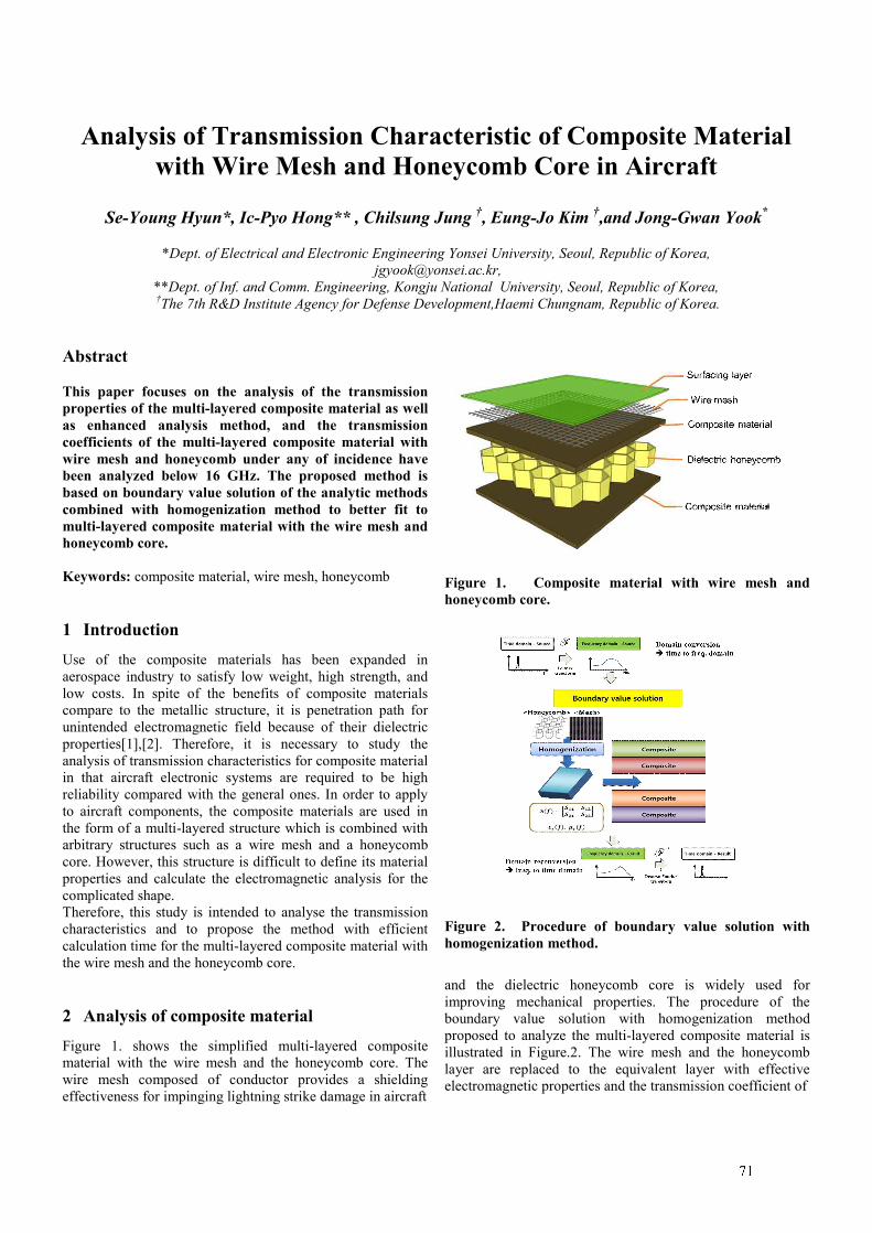
1
Analysis of Transmission Characteristic of Composite Material with Wire Mesh and Honeycomb Core in Aircraft
Se-Young Hyun*, Ic-Pyo Hong** , Chilsung Jung †, Eung-Jo Kim †,and Jong-Gwan Yook*
*Dept. of Electrical and Electronic Engineering Yonsei University, Seoul, Republic of Korea, [email protected],
**Dept. of Inf. and Comm. Engineering, Kongju National University, Seoul, Republic of Korea, †The 7th R&D Institute Agency for Defense Development,Haemi Chungnam, Republic of Korea.
Abstract This paper focuses on the analysis of the transmission properties of the multi-layered composite material as well as enhanced analysis method, and the transmission coefficients of the multi-layered composite material with wire mesh and honeycomb under any of incidence have been analyzed below 16 GHz. The proposed method is based on boundary value solution of the analytic methods combined with homogenization method to better fit to multi-layered composite material with the wire mesh and honeycomb core. Keywords: composite material, wire mesh, honeycomb
1 Introduction Use of the composite materials has been expanded in aerospace industry to satisfy low weight, high strength, and low costs. In spite of the benefits of composite materials compare to the metallic structure, it is penetration path for unintended electromagnetic field because of their dielectric properties[1],[2]. Therefore, it is necessary to study the analysis of transmission characteristics for composite material in that aircraft electronic systems are required to be high reliability compared with the general ones. In order to apply to aircraft components, the composite materials are used in the form of a multi-layered structure which is combined with arbitrary structures such as a wire mesh and a honeycomb core. However, this structure is difficult to define its material properties and calculate the electromagnetic analysis for the complicated shape. Therefore, this study is intended to analyse the transmission characteristics and to propose the method with efficient calculation time for the multi-layered composite material with the wire mesh and the honeycomb core.
2 Analysis of composite material Figure 1. shows the simplified multi-layered composite material with the wire mesh and the honeycomb core. The wire mesh composed of conductor provides a shielding effectiveness for impinging lightning strike damage in aircraft
Figure 1. Composite material with wire mesh and honeycomb core.
Figure 2. Procedure of boundary value solution with homogenization method.
and the dielectric honeycomb core is widely used for improving mechanical properties. The procedure of the boundary value solution with homogenization method proposed to analyze the multi-layered composite material is illustrated in Figure.2. The wire mesh and the honeycomb layer are replaced to the equivalent layer with effective electromagnetic properties and the transmission coefficient of
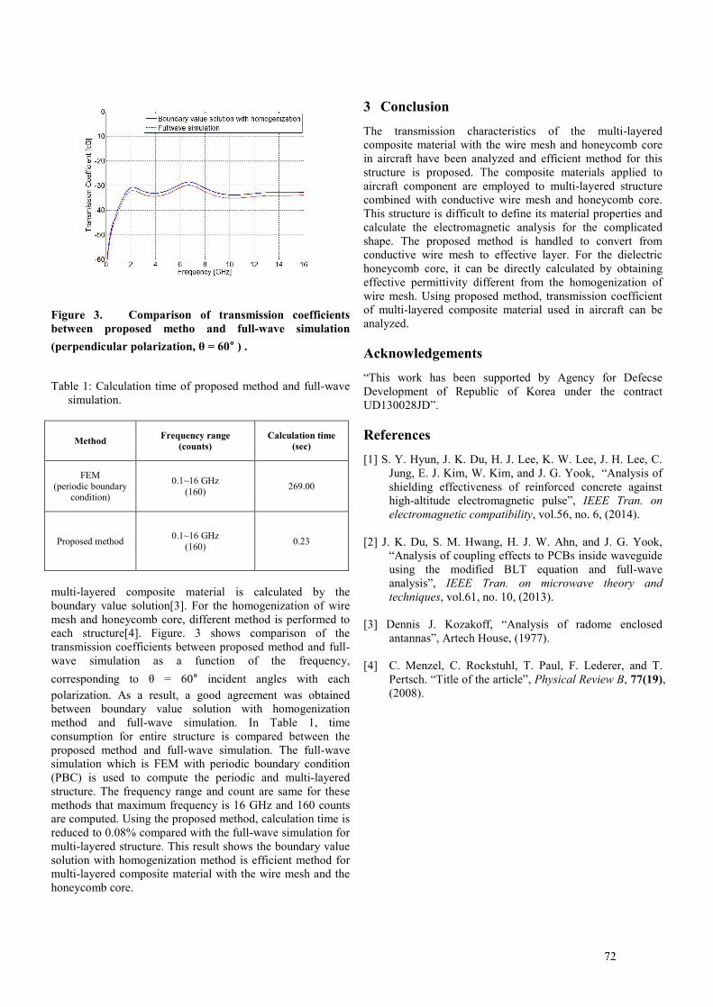
2
Figure 3. Comparison of transmission coefficients between proposed metho and full-wave simulation (perpendicular polarization, θ = 60° ) .
Table 1: Calculation time of proposed method and full-wave
simulation.
Method Frequency range (counts)
Calculation time (sec)
FEM (periodic boundary
condition)
0.1~16 GHz (160) 269.00
Proposed method 0.1~16 GHz (160) 0.23
multi-layered composite material is calculated by the boundary value solution[3]. For the homogenization of wire mesh and honeycomb core, different method is performed to each structure[4]. Figure. 3 shows comparison of the transmission coefficients between proposed method and full-wave simulation as a function of the frequency, corresponding to θ = 60° incident angles with each polarization. As a result, a good agreement was obtained between boundary value solution with homogenization method and full-wave simulation. In Table 1, time consumption for entire structure is compared between the proposed method and full-wave simulation. The full-wave simulation which is FEM with periodic boundary condition (PBC) is used to compute the periodic and multi-layered structure. The frequency range and count are same for these methods that maximum frequency is 16 GHz and 160 counts are computed. Using the proposed method, calculation time is reduced to 0.08% compared with the full-wave simulation for multi-layered structure. This result shows the boundary value solution with homogenization method is efficient method for multi-layered composite material with the wire mesh and the honeycomb core.
3 Conclusion The transmission characteristics of the multi-layered composite material with the wire mesh and honeycomb core in aircraft have been analyzed and efficient method for this structure is proposed. The composite materials applied to aircraft component are employed to multi-layered structure combined with conductive wire mesh and honeycomb core. This structure is difficult to define its material properties and calculate the electromagnetic analysis for the complicated shape. The proposed method is handled to convert from conductive wire mesh to effective layer. For the dielectric honeycomb core, it can be directly calculated by obtaining effective permittivity different from the homogenization of wire mesh. Using proposed method, transmission coefficient of multi-layered composite material used in aircraft can be analyzed.
Acknowledgements “This work has been supported by Agency for Defecse Development of Republic of Korea under the contract UD130028JD”.
References [1] S. Y. Hyun, J. K. Du, H. J. Lee, K. W. Lee, J. H. Lee, C.
Jung, E. J. Kim, W. Kim, and J. G. Yook, “Analysis of shielding effectiveness of reinforced concrete against high-altitude electromagnetic pulse”, IEEE Tran. on electromagnetic compatibility, vol.56, no. 6, (2014).
[2] J. K. Du, S. M. Hwang, H. J. W. Ahn, and J. G. Yook,
“Analysis of coupling effects to PCBs inside waveguide using the modified BLT equation and full-wave analysis”, IEEE Tran. on microwave theory and techniques, vol.61, no. 10, (2013).
[3] Dennis J. Kozakoff, “Analysis of radome enclosed
antannas”, Artech House, (1977). [4] C. Menzel, C. Rockstuhl, T. Paul, F. Lederer, and T.
Pertsch. “Title of the article”, Physical Review B, 77(19), (2008).
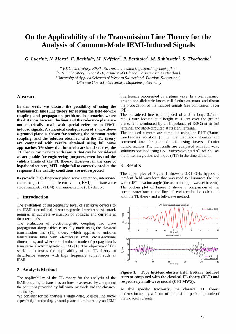
1
On the Applicability of the Transmission Line Theory for the
Analysis of Common-Mode IEMI-Induced Signals
G. Lugrin*, N. Mora*, F. Rachidi*, M. Nyffeler†, P. Bertholet
†, M. Rubinstein
‡, S. Tkachenko
+
* EMC Laboratory, EPFL, Switzerland, contact: [email protected] †HPE Laboratory, Federal Department of Defence – Armasuisse, Switzerland
‡University of Applied Sciences of Western Switzerland, Yverdon, Switzerland. +Otto-von Guericke University, Magdeburg, Germany
Abstract
In this work, we discuss the possibility of using the
transmission line (TL) theory for solving the field-to-wire
coupling and propagation problems in scenarios where
the distances between the lines and the reference plane are
not electrically small, with special reference to IEMI-
induced signals. A canonical configuration of a wire above
a ground plane is chosen for studying the common mode
coupling, and the solution obtained with the TL theory
are compared with results obtained using full wave
approaches. We show that for moderate band sources, the
TL theory can provide with results that can be considered
as acceptable for engineering purposes, even beyond the
validity limits of the TL theory. However, in the case of
hypoband sources, MTL might fail to correctly predict the
response if the validity conditions are not respected.
Keywords: high-frequency plane wave excitation, intentional
electromagnetic interferences (IEMI), transverse
electromagnetic (TEM), transmission line (TL) theory.
1 Introduction
The evaluation of susceptibility level of sensitive devices to
an IEMI (intentional electromagnetic interferences) attack
requires an accurate evaluation of voltages and currents at
their terminals.
The evaluation of electromagnetic coupling and wave
propagation along cables is usually made using the classical
transmission line (TL) theory which applies to uniform
transmission lines with electrically small cross-sectional
dimensions, and where the dominant mode of propagation is
transverse electromagnetic (TEM) [1]. The objective of this
work is to assess the applicability of the TL theory to
disturbance sources with high frequency content such as
IEMI.
2 Analysis Method
The applicability of the TL theory for the analysis of the
IEMI coupling to transmission lines is assessed by comparing
the solutions provided by full wave methods and the classical
TL theory.
We consider for the analysis a single-wire, lossless line above
a perfectly conducting ground plane illuminated by an IEMI
interference represented by a plane wave. In a real scenario,
ground and dielectric losses will further attenuate and distort
the propagation of the induced signals (see companion paper
[2]).
The considered line is composed of a 3-m long, 0.7-mm
radius wire located at a height of 10 cm over the ground
plane. It is terminated by an impedance of 339 Ω at its left
terminal and short-circuited at its right terminal.
The induced currents are computed using the BLT (Baum-
Liu-Tesche) equation [3] in the frequency domain and
converted into the time domain using inverse Fourier
transformation. The TL results are compared with full-wave
solutions obtained using CST Microwave Studio®, which uses
the finite integration technique (FIT) in the time domain.
3 Results
The upper plot of Figure 1 shows a 2.01 GHz hypoband
incident field waveform that was used to illuminate the line
with a 45o elevation angle (the azimuth angle was set to zero).
The bottom plot of Figure 2 shows a comparison of the
current waveform at the line left-end termination calculated
with the TL theory and a full-wave method.
Figure 1. Top: Incident electric field. Bottom: Induced
current computed with the classical TL theory (BLT) and
respectively a full-wave model (CST MWS).
At this specific frequency, the classical TL theory
underestimates by a factor of about 4 the peak amplitude of
the induced currents.
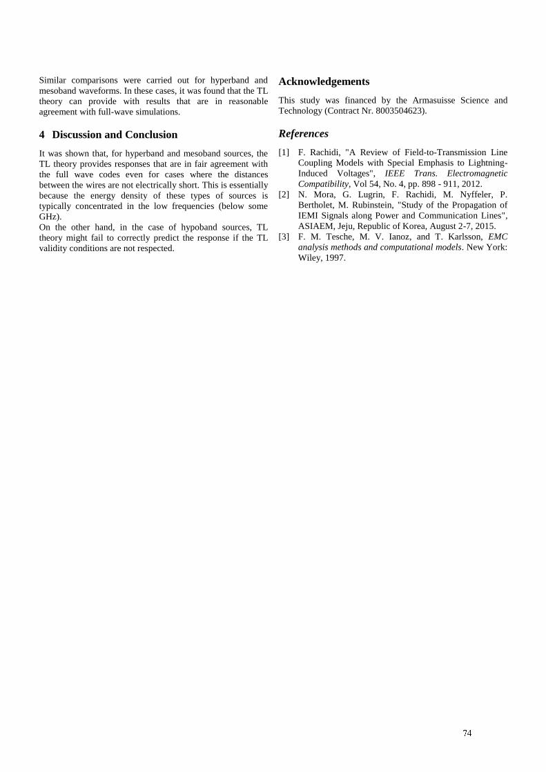
2
Similar comparisons were carried out for hyperband and
mesoband waveforms. In these cases, it was found that the TL
theory can provide with results that are in reasonable
agreement with full-wave simulations.
4 Discussion and Conclusion
It was shown that, for hyperband and mesoband sources, the
TL theory provides responses that are in fair agreement with
the full wave codes even for cases where the distances
between the wires are not electrically short. This is essentially
because the energy density of these types of sources is
typically concentrated in the low frequencies (below some
GHz).
On the other hand, in the case of hypoband sources, TL
theory might fail to correctly predict the response if the TL
validity conditions are not respected.
Acknowledgements
This study was financed by the Armasuisse Science and
Technology (Contract Nr. 8003504623).
References
[1] F. Rachidi, "A Review of Field-to-Transmission Line
Coupling Models with Special Emphasis to Lightning-
Induced Voltages", IEEE Trans. Electromagnetic
Compatibility, Vol 54, No. 4, pp. 898 - 911, 2012.
[2] N. Mora, G. Lugrin, F. Rachidi, M. Nyffeler, P.
Bertholet, M. Rubinstein, "Study of the Propagation of
IEMI Signals along Power and Communication Lines",
ASIAEM, Jeju, Republic of Korea, August 2-7, 2015.
[3] F. M. Tesche, M. V. Ianoz, and T. Karlsson, EMC
analysis methods and computational models. New York:
Wiley, 1997.
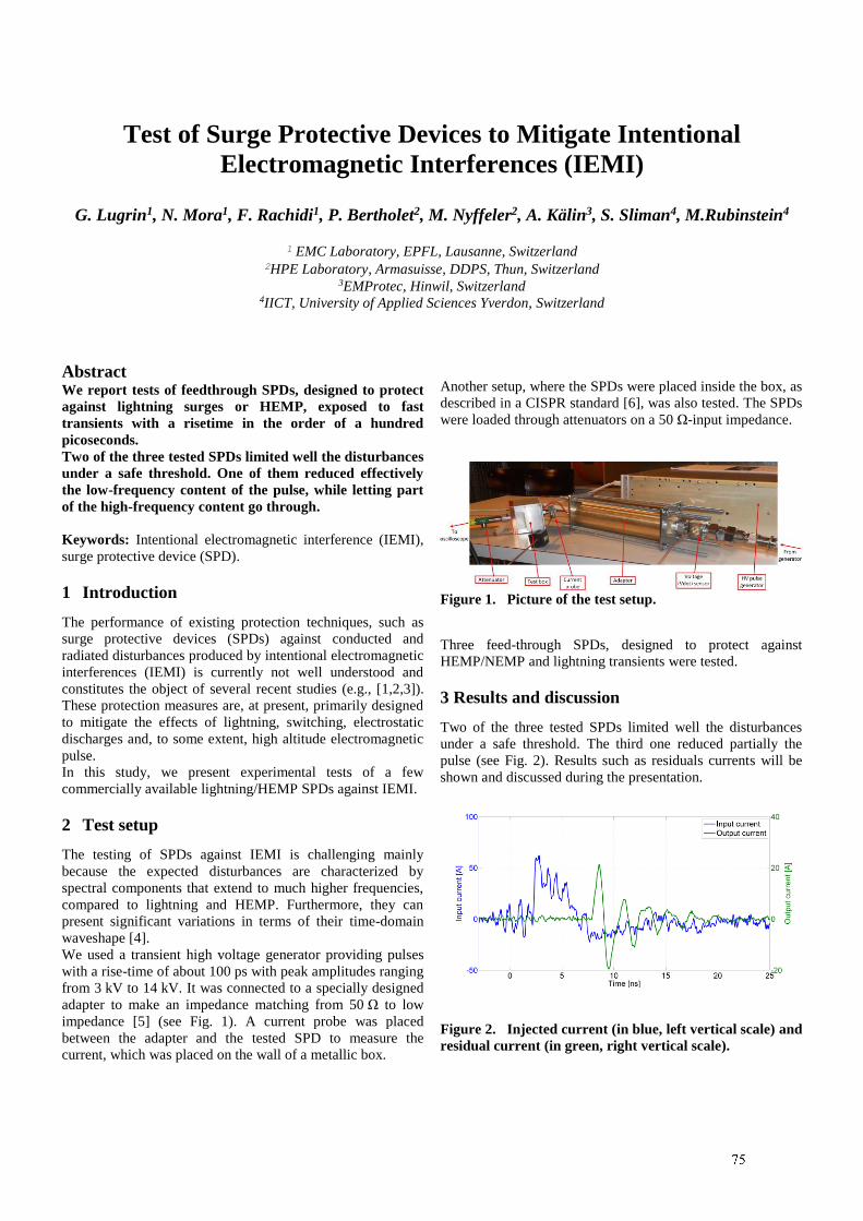
1
Test of Surge Protective Devices to Mitigate Intentional
Electromagnetic Interferences (IEMI)
G. Lugrin1, N. Mora1, F. Rachidi1, P. Bertholet2, M. Nyffeler2, A. Kälin3, S. Sliman4, M.Rubinstein4
1 EMC Laboratory, EPFL, Lausanne, Switzerland 2HPE Laboratory, Armasuisse, DDPS, Thun, Switzerland
3EMProtec, Hinwil, Switzerland 4IICT, University of Applied Sciences Yverdon, Switzerland
Abstract We report tests of feedthrough SPDs, designed to protect
against lightning surges or HEMP, exposed to fast
transients with a risetime in the order of a hundred
picoseconds.
Two of the three tested SPDs limited well the disturbances
under a safe threshold. One of them reduced effectively
the low-frequency content of the pulse, while letting part
of the high-frequency content go through.
Keywords: Intentional electromagnetic interference (IEMI),
surge protective device (SPD).
1 Introduction
The performance of existing protection techniques, such as
surge protective devices (SPDs) against conducted and
radiated disturbances produced by intentional electromagnetic
interferences (IEMI) is currently not well understood and
constitutes the object of several recent studies (e.g., [1,2,3]).
These protection measures are, at present, primarily designed
to mitigate the effects of lightning, switching, electrostatic
discharges and, to some extent, high altitude electromagnetic
pulse.
In this study, we present experimental tests of a few
commercially available lightning/HEMP SPDs against IEMI.
2 Test setup
The testing of SPDs against IEMI is challenging mainly
because the expected disturbances are characterized by
spectral components that extend to much higher frequencies,
compared to lightning and HEMP. Furthermore, they can
present significant variations in terms of their time-domain
waveshape [4].
We used a transient high voltage generator providing pulses
with a rise-time of about 100 ps with peak amplitudes ranging
from 3 kV to 14 kV. It was connected to a specially designed
adapter to make an impedance matching from 50 Ω to low
impedance [5] (see Fig. 1). A current probe was placed
between the adapter and the tested SPD to measure the
current, which was placed on the wall of a metallic box.
Another setup, where the SPDs were placed inside the box, as
described in a CISPR standard [6], was also tested. The SPDs
were loaded through attenuators on a 50 Ω-input impedance.
Figure 1. Picture of the test setup.
Three feed-through SPDs, designed to protect against
HEMP/NEMP and lightning transients were tested.
3 Results and discussion
Two of the three tested SPDs limited well the disturbances
under a safe threshold. The third one reduced partially the
pulse (see Fig. 2). Results such as residuals currents will be
shown and discussed during the presentation.
Figure 2. Injected current (in blue, left vertical scale) and
residual current (in green, right vertical scale).
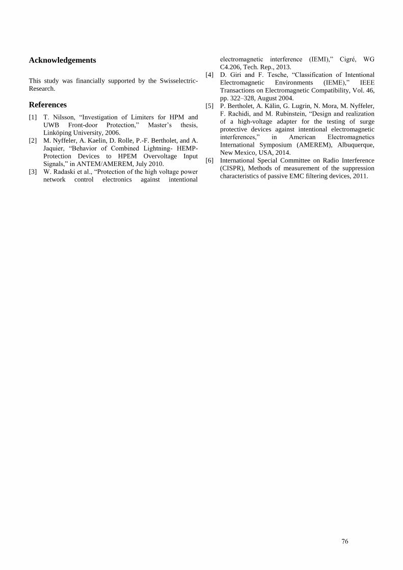
2
Acknowledgements
This study was financially supported by the Swisselectric-
Research.
References
[1] T. Nilsson, “Investigation of Limiters for HPM and
UWB Front-door Protection,” Master’s thesis,
Linköping University, 2006.
[2] M. Nyffeler, A. Kaelin, D. Rolle, P.-F. Bertholet, and A.
Jaquier, “Behavior of Combined Lightning- HEMP-
Protection Devices to HPEM Overvoltage Input
Signals,” in ANTEM/AMEREM, July 2010.
[3] W. Radaski et al., “Protection of the high voltage power
network control electronics against intentional
electromagnetic interference (IEMI),” Cigré, WG
C4.206, Tech. Rep., 2013.
[4] D. Giri and F. Tesche, “Classification of Intentional
Electromagnetic Environments (IEME),” IEEE
Transactions on Electromagnetic Compatibility, Vol. 46,
pp. 322–328, August 2004.
[5] P. Bertholet, A. Kälin, G. Lugrin, N. Mora, M. Nyffeler,
F. Rachidi, and M. Rubinstein, “Design and realization
of a high-voltage adapter for the testing of surge
protective devices against intentional electromagnetic
interferences,” in American Electromagnetics
International Symposium (AMEREM), Albuquerque,
New Mexico, USA, 2014.
[6] International Special Committee on Radio Interference
(CISPR), Methods of measurement of the suppression
characteristics of passive EMC filtering devices, 2011.
1
Reverberation chamber
Glass sample, aperture approx. 300x300 mm
VNA R&S ZVA40
Nested Chamber
Tx
Rx
Rx
High Power Microwave Effects on Coated Window Panes P Ängskog*†, M Bäckström*#, B Vallhagen#
*Electromagnetic Engineering Lab, KTH Royal Institute of Technology, Sweden, [email protected], †Department of Electronics, Mathematics and Natural Sciences, University of Gävle, Sweden
#SAAB Aeronautics, SAAB AB, Sweden, [email protected]
Abstract Today window panes are usually coated with at least one metal or metal oxide layer to prevent heat energy of the light spectrum from propagating to the other side. This has given problems regarding radio propagation through windows, which might be utilized as a part of a buildings IEMI protection. This paper reports the results from measurements of the shielding effectiveness of a selection of modern window panes before and after irradiation with high power electromagnetic waves. The shielding effectiveness measurements are made in a nested reverberation chamber covering the range 1 – 18 GHz; both before and after high power irradiation at 1.3 GHz. The results show that the shielding effectiveness of window panes may be severely impaired due to thermal stress effects on the coatings during the irradiation, depending of the type of coating. Keywords: HPM; window panes; glass; transmission; propagation.
1 Introduction Today window panes usually are coated with at least one layer of metal or metal oxide to prevent heat energy from propagating through a window. In cold climate the purpose is to contain the long-wave infra-red light inside a building while in hot climates the needs are similar; only the direction is opposite, the infra-red waves should be kept on the outside. Furthermore, the high-energy, short wavelength ultra-violet rays should preferably be blocked by the window preventing them from reaching objects on the inside and thus converting to heat. The coatings of the panes are optimized with infra-red or ultra-violet radiation in mind while no attention is paid to the radio and microwave parts of the electromagnetic spectrum. This has proven to give problems in modern communication systems since radio signals are efficiently blocked by modern energy saving windows [1] - [5]. With the purpose to determine the effects from high power microwave (HPM) irradiation this paper examines the shielding effectiveness (SE) of single window panes with different coatings. A comparison of SE results before and after the high power exposure is presented.
2 Method The high power effects are determined using a comparative method where first the SE is measured before high power irradiation, as a reference, and then re-measured to reveal any effects of the irradiation. The SE measurements conducted to determine the shielding properties of the panes where made in a nested reverberation chamber (RC), Figure 1. In the RC a mode stirrer is employed to create a mode stirred incident field impinging on the sample mounted over an aperture in the nested chamber. Inside the nested chamber a second mode stirrer revolves to change the mode of the field incident on the receiver antenna. For each frequency 252 different combinations of stirrer positions are used when measuring the isotropic transmission cross section, ⟨𝜎𝑎⟩, of the test object. From ⟨𝜎𝑎⟩ the SE is calculated [6]-[7]. In the present case the reference aperture is a square opening with an area, A, 300 x 300 mm2. For a reference aperture with such a simple geometry one may express the result above in terms of shielding effectiveness, i.e. in terms of a dimensionless quantity, simply by comparing the power transmitted through the unshielded opening (i.e. the square opening) with the power transmitted through the opening when the shielded structure is mounted on it, i.e.
⟨𝑆𝑆𝑎𝑎𝑎𝑎𝑎,𝑖𝑖𝑖⟩ = 𝐴 4⁄⟨𝜎𝑎⟩
. (1)
Figure 1. Simplified block diagram showing the reverberation chamber.

2
In (1) we approximate the transmission cross section of the unshielded opening by A/4 which is exactly true only at frequencies where the opening is electrically large. For frequencies above 1 GHz the error is less than 1 dB. The HPM exposure was carried out in the Microwave Test Facility (MTF) at SAAB Aeronautics in Sweden. The MTF was set to work in the L-band giving the field strength 28 kV/m in 5 µs long pulses with a pulse repetition frequency of 390 Hz during a 10 s burst.
3 Measurement Samples The measurement samples were four single window panes, as tabulated in Table 1. The specimen code found in the first column is an identifier for each sample; the second column explains of what specific glass type that specimen is. Soft coated and hard coated low-emission glass are intended to reflect infrared light (i.e. heat) back while letting day-light pass through them. The difference between the two is the composition and method used for deposition of the coating layer. Soft coating is deposited on pre-cut float glass in tens of nanometers thick layers using sputtering, a physical vapor deposition (PVD) where the layers consist of various metal oxides, typically tin-dioxide (SnO2), interleaved with one or more layers of silver. Other metal oxides such as ZnO and TiO3 may also be used. The more silver layers the lower emissivity and the better the reflection of ultra-violet rays. Hard coating is applied on semi-molten glass in the production line using chemical vapor deposition (CVD) and typically consists of only one a few hundreds of nm thick layer of SnO2.
Table 1. List of measurement samples – single window panes. Single Panes, Standard Types
Specimen Code Specimen type HC1-5 Solar Control, Soft Coated, Low-e glass; 1 Silver Layer SC-5 Hard Coated, Low-e glass Sp-5 Spandrel glass
2Ag-5 Solar Control, Soft Coated, Low-e glass; 2 Silver Layers A spandrel pane is an opaque glass often placed as cladding element between clear-view windows to hide construction elements, insulation and building infrastructure installations. The opacity is achieved by adding coatings of metal, metal oxides or enamel on the rear (inner) side of the pane.
4 Results
4.1 Visual Effects
A visual inspection of the samples after the HPM exposure gave at hand that the two silver coated samples, HC1-5 and 2Ag-5, exhibited visually clear cracks looking like Lichtenberg figures indicating an electrical breakdown process due to thermal stress from the very strong electric field, see Figure 2 and Figure 3. However, the other two samples, the hard coated (SC-5) and the spandrel (Sp-5) glasses showed no visual deterioration.
4.2 Shielding Effectiveness Effects
Consequently, the SE measurements of the SC-5 and Sp-5 samples did not reveal any changes in SE at all. On the other hand, the two samples with cracked coatings the changes were evident. The deterioration for the 2Ag-5 pane was approximately 5 dB between 1 and 1.8 GHz and from 6 GHz to 18 GHz while in the 2-5 GHz range there is no noticeable reduction in SE at all, cf. Figure 4. For the HC1-5 pane SE is on average
Figure 2. Cracks in the coating of the 2Ag pane resulting from HPM exposure.
Figure 3. Cracks in the coating of the HC1 pane resulting from HPM exposure.
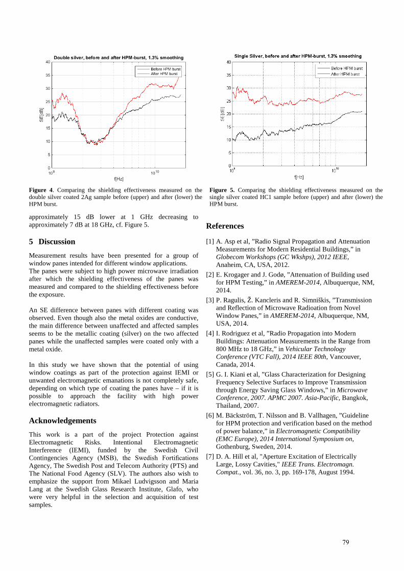
3
approximately 15 dB lower at 1 GHz decreasing to approximately 7 dB at 18 GHz, cf. Figure 5.
5 Discussion Measurement results have been presented for a group of window panes intended for different window applications. The panes were subject to high power microwave irradiation after which the shielding effectiveness of the panes was measured and compared to the shielding effectiveness before the exposure. An SE difference between panes with different coating was observed. Even though also the metal oxides are conductive, the main difference between unaffected and affected samples seems to be the metallic coating (silver) on the two affected panes while the unaffected samples were coated only with a metal oxide. In this study we have shown that the potential of using window coatings as part of the protection against IEMI or unwanted electromagnetic emanations is not completely safe, depending on which type of coating the panes have – if it is possible to approach the facility with high power electromagnetic radiators.
Acknowledgements This work is a part of the project Protection against Electromagnetic Risks. Intentional Electromagnetic Interference (IEMI), funded by the Swedish Civil Contingencies Agency (MSB), the Swedish Fortifications Agency, The Swedish Post and Telecom Authority (PTS) and The National Food Agency (SLV). The authors also wish to emphasize the support from Mikael Ludvigsson and Maria Lang at the Swedish Glass Research Institute, Glafo, who were very helpful in the selection and acquisition of test samples.
References
[1] A. Asp et al, ”Radio Signal Propagation and Attenuation Measurements for Modern Residential Buildings,” in Globecom Workshops (GC Wkshps), 2012 IEEE, Anaheim, CA, USA, 2012.
[2] E. Krogager and J. Godø, ”Attenuation of Building used for HPM Testing,” in AMEREM-2014, Albuquerque, NM, 2014.
[3] P. Ragulis, Ž. Kancleris and R. Simniškis, ”Transmission and Reflection of Microwave Radioation from Novel Window Panes,” in AMEREM-2014, Albuquerque, NM, USA, 2014.
[4] I. Rodriguez et al, ”Radio Propagation into Modern Buildings: Attenuation Measurements in the Range from 800 MHz to 18 GHz,” in Vehicular Technology Conference (VTC Fall), 2014 IEEE 80th, Vancouver, Canada, 2014.
[5] G. I. Kiani et al, ”Glass Characterization for Designing Frequency Selective Surfaces to Improve Transmission through Energy Saving Glass Windows,” in Microwave Conference, 2007. APMC 2007. Asia-Pacific, Bangkok, Thailand, 2007.
[6] M. Bäckström, T. Nilsson and B. Vallhagen, ”Guideline for HPM protection and verification based on the method of power balance,” in Electromagnetic Compatibility (EMC Europe), 2014 International Symposium on, Gothenburg, Sweden, 2014.
[7] D. A. Hill et al, "Aperture Excitation of Electrically Large, Lossy Cavities," IEEE Trans. Electromagn. Compat., vol. 36, no. 3, pp. 169-178, August 1994.
Figure 4. Comparing the shielding effectiveness measured on the double silver coated 2Ag sample before (upper) and after (lower) the HPM burst.
Figure 5. Comparing the shielding effectiveness measured on the single silver coated HC1 sample before (upper) and after (lower) the HPM burst.
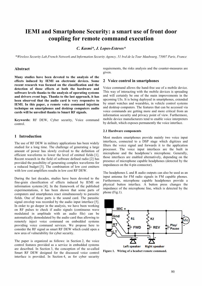
1
IEMI and Smartphone Security: a smart use of front door
coupling for remote command execution
C. Kasmi*, J. Lopes-Esteves*
*Wireless Security Lab,French Network and Information Security Agency, 51 bvd de la Tour Maubourg, 75007 Paris, France
Abstract
Many studies have been devoted to the analysis of the
effects induced by IEMI on electronic devices. Some
recent research was focused on the classification and the
detection of those effects at both the hardware and
software levels thanks to the analysis of operating systems
and drivers event logs. Thanks to the last approach, it has
been observed that the audio card is very responsive to
IEMI. In this paper, a remote voice command injection
technique on smartphones and desktop computers audio
cards will be unveiled thanks to Smart RF signals.
Keywords: RF DEW, Cyber security, Voice command
control.
1 Introduction
The use of RF DEW in military applications has been widely
studied for a long time. The challenge of generating a large
amount of power has slowly evolved to the definition of
efficient waveforms to lower the level of emitted fields [1].
Recent research in the field of software defined radio [2] has
provided the possibility of generating complex waveforms for
a reduced budget [3]. The combination of low cost emitters
with low cost amplifiers results in low cost RF DEW.
During the last decades, studies have been devoted to the
fine-grain classification of effects induced by IEMI on
information systems [4]. In the framework of the published
experimentations, it has been shown that some parts of
computers and smartphones react simultaneously to parasitic
fields. One of these parts is the sound card. The parasitic
signal envelop was recorded by the audio input interface [5].
In order to go deeper in the analysis, we have been working
on RF pulses to check if audio signals (continuous wave
modulated in amplitude with an audio file) can be
automatically demodulated by the audio card thus allowing to
remotely inject voice command on embedded systems
providing voice command services. We propose here to
consider the RF signal as smart RF DEW which could open a
new area of vulnerability for cyber security.
The paper is organized as follows: in Section 2, the voice
control features provided as a service in embedded systems
are described. In Section 3, the conception of the so-called
Smart RF DEW designed for the discussed voice control
interface is provided. In Section 4, as for cyber security
requirements, the risks analysis and the counter-measures are
given.
2 Voice control in smartphones
Voice command allows the hand-free use of a mobile device.
This way of interacting with the mobile devices is spreading
and will certainly be one of the main improvements in the
upcoming UIs. It is being deployed in smartphones, extended
by smart watches and wearables, in vehicle control systems
and desktop computers. The features that can be accessed via
voice commands are getting more and more critical from an
information security and privacy point of view. Furthermore,
mobile device manufacturers tend to enable voice interpreters
by default, which exposes permanently the voice interface.
2.1 Hardware components
Most modern smartphones provide mainly two voice input
interfaces, connected to a DSP stage which digitizes and
filters the voice signal and forwards it to the application
processor. The voice input interfaces are the built in
microphone and the headphone’s microphone. Generally,
those interfaces are enabled alternatively, depending on the
presence of microphone capable headphones (detected by the
impedances on the 4-pin connector).
The headphones L and R audio outputs can also be used as an
input antenna for FM radio signals in FM capable phones.
Furthermore, microphone capable headphones provide a
physical button interface. A button press changes the
impedance of the microphone line, which is detected by the
phone (Fig.1).
Figure 1. Wiring of a headset remote command.
2
2.2 Software services and features
Nowadays, a lot of features can be accessed by voice,
depending on the device and the operating system. Some of
them can be considered from a security point of view as
critical. In this study, we focused on three cases: an Apple
iPhone, a Google Nexus phone and a vendor customized
Android phone (Samsung).
In the following, we shortly describe the voice services and
the features exposed:
- Samsung [6]: Samsung voice control system is called S-
Voice. It is a vendor software layer that is natively
included in the Android core;
- Apple [7]: two services provide a voice command
interface, namely Voice Control and Siri. On the latest
versions of iOS, Siri completely replaced Voice Control;
- Google [8]: Google Voice Search is the original voice
command interface and was merged to Google Now since
Android Jelly Bean.
When the voice command interpreter is not enabled
permanently, it is generally activated by a long hardware
button press or by launching the aforementioned software
applications. Then, the user must say a keyword followed by
the voice command. The main features than can be accessed
via the voice command interface are listed below:
- Telephony services: sending text messages, placing calls,
answering calls;
- Internet services: visiting web pages, sending emails,
posting on social networks, launching web searches,
maps and positioning;
- Local services: launching applications, changing phone
settings, creating calendar entries, notes, setting alarms...
The voice and speech recognition is generally performed on a
remote server, except for the keyword. This means that voice
command cannot be used without internet connectivity trough
Wi-Fi or mobile network.
3 RF DEW conception for data injection
The test phase aimed to validate the following hypothesis: as
the headphones act as a FM antenna, it should be possible to
use them as a front door coupling interface for voice
command injection. To achieve this verification, the
experimental setup consisted in placing the phones, with
headphones plugged in, in a Faraday cage with a wireless
access point relaying the IP traffic to a computer outside the
cage via optical fibre. Additionally, an E-field probe was also
installed next to the target so that we are able to link the
trigger of the voice command controller and the required
minimal field level. On the phones, we installed an
application which records sound from the microphone. This
application streams the recorded sound on the network in
real-time to the computer, which can store and play the sound
samples.
For voice emission, we used a music player as a voice signal
source which modulated a continuous wave produced by a RF
synthesizer. During our experiments, the two following
scenarios were considered:
1. The voice control command has been activated by default
by the user: this means that the voice command service
starts as soon as a key word was pronounced by the user.
The experiments demonstrated that it is possible to
trigger voice commands remotely by emitting an AM
modulation of the keyword followed by some voice
commands at FM radio frequencies. This signal is
received by the headphone, as it is designed to act as an
antenna for the FM radios. The resulting electric signal
that is induced in the microphone cable of the
headphones is really close to voice signal and is correctly
interpreted by the voice command interface.
2. The voice command is not activated by default and a
long hardware button press is required for launching the
service: in this case, we have worked on injecting a
specially crafted radio signal to trigger the activation of
the voice command interpreter by emulating a
headphone's command button press. It was shown that
thanks to an FM modulated signal, we were able to
launch the voice command service and to inject the voice
command. To perform the emission of both the FM and
AM modulated signals, we come up with the use of
software defined radio tools [2-3].
It was observed that the minimal field required around the
target was in the range of 25 – 30 V/m at 103 MHz, which is
close to the limit accepted for human safety.
While voice command control becomes more and more
powerful, we have shown that it also becomes a critical
interface. In the next Section, we will provide a security
analysis with the related countermeasures.
4 Security analysis
Being able to execute voice commands remotely on a system
can be critical from an information security point of view.
Furthermore, potentially all voice control capable systems can
be vulnerable to this kind of attack. The attacker profile
required for this attack can be considered as “proficient”
(according to the Common Criteria), and involves publicly
available RF equipment. A basic knowledge in software
defined radio and some information about the target operating
system and user settings is also necessary. The EM field
levels required have a significant impact on the equipment
needed by an attacker depending on the desired range he
wants to operate from. The following table summarizes the
attacker profile according to the range.
3
To understand the impact such an attack can have on a target,
some attack scenarios have been considered:
- Tracking and spying: the attacker activates the wireless
interfaces of the target for enabling mid-range tracking.
He also can place a call to his own phone to capture the
surrounding sounds;
- Paid SMS services: the attacker targets all the users in
range and forces them to send a SMS to a paid service;
- Drive-by malware download: the attacker can force the
target to visit a malicious web page which exploits a
vulnerability to compromise the targets operating system.
In order to mitigate this attack vector, some countermeasures
could be applied. Unfortunately, there is always a trade-off
between security and usability:
- Some modifications on the audio front-end can be done
in order to reduce the sensitivity of the input interface.
This would force the attacker to reach higher EM field
levels to achieve the attack. A better shielding of the
headphones cable would also contribute to this
mitigation.
- Voice and speech recognition improvements can also be
part of the solution. Indeed, better recognizing the voice
of the legit user would force the attacker to forge the
commands with the user’s voice signature. One could
think of some techniques to detect if the voice has been
digitized and replayed or if it comes from a physical
speaker.
- A better granularity in the user settings could be a great
improvement: letting the user choose his own keyword
(already possible on most of devices but a few users are
doing so), disabling the voice interface by default,
allowing the user to choose the authorized actions via this
interface would be interesting options.
7 Conclusion
In this paper we discussed the possibility to use low cost RF
equipments and software defined radio to design an efficient
low cost RF DEW. To demonstrate this, we introduced a new
technique for remote voice command injection in
smartphones. A security analysis has been performed and
some possible countermeasures have been proposed.
The main contribution of this research is threefold: first, the
reduction of the attacker costs for conceiving RF DEWs is
illustrated. This should be taken into account in risks analysis.
Secondly, a smart use of IEMI, which is not only focused on
denial of service attacks or equipment disabling, is
enlightened. Finally, we attract the attention of the vendors on
the possibility to use the voice command interface as an
attack vector, so that they can take it into account and
improve the security of their products.
During the presentation, a set of videos showing the induction
and the execution of voice commands on a set of targets will
be displayed.
Acknowledgements
The authors would like to thank the editors, the vendors and
manufacturers of the devices that have been tested, namely
Apple, Google and Samsung, for their reactivity after the
responsible vulnerability disclosure process and for accepting
the publication of this research.
References
[1] N. Mora, F. Vega, G. Lugrin, F. Rachidi, System Design
& Assessment Note SDAN 41, “Study and Classification
of Potential IEMI Sources”, July 2014.
[2] GNU Radio is a free & open-source software
development toolkit, online:
http://gnuradio.org/redmine/projects/gnuradio/wiki
[3] Universal Software Radio Peripheral, online:
http://www.ettus.com/
[4] C. Kasmi, J. Lopes-Esteves, N. Picard, et al. “Event Logs
Generated by an Operating System Running on a COTS
Computer During HPEM Exposure,” Electromagnetic
Compatibility, IEEE Transactions on, vol., no.99, pp.1,4,
2014.
[5] C. Kasmi, J. Lopes-Esteves, M. Renard, System Design
& Assessment Note SDAN 44, “Automation of the
Immunity testing of COTS computers by the
instrumentation of the internal sensors and involving the
operating system logs – Technical report”, November
2014.
[6] Samsung, “How do I Use Samsung S Voice”, online
description:
http://www.samsung.com/us/support/supportOwnersHow
ToGuidePopup.do?howto_guide_seq=7061&prd_ia_cd=
N0000003&map_seq=54784
[7] Google, “Ok Google”, online description:
https://support.google.com/websearch/answer/2940021?h
l=en
[8] Apple, “Siri”, online description:
https://www.apple.com/ios/siri/
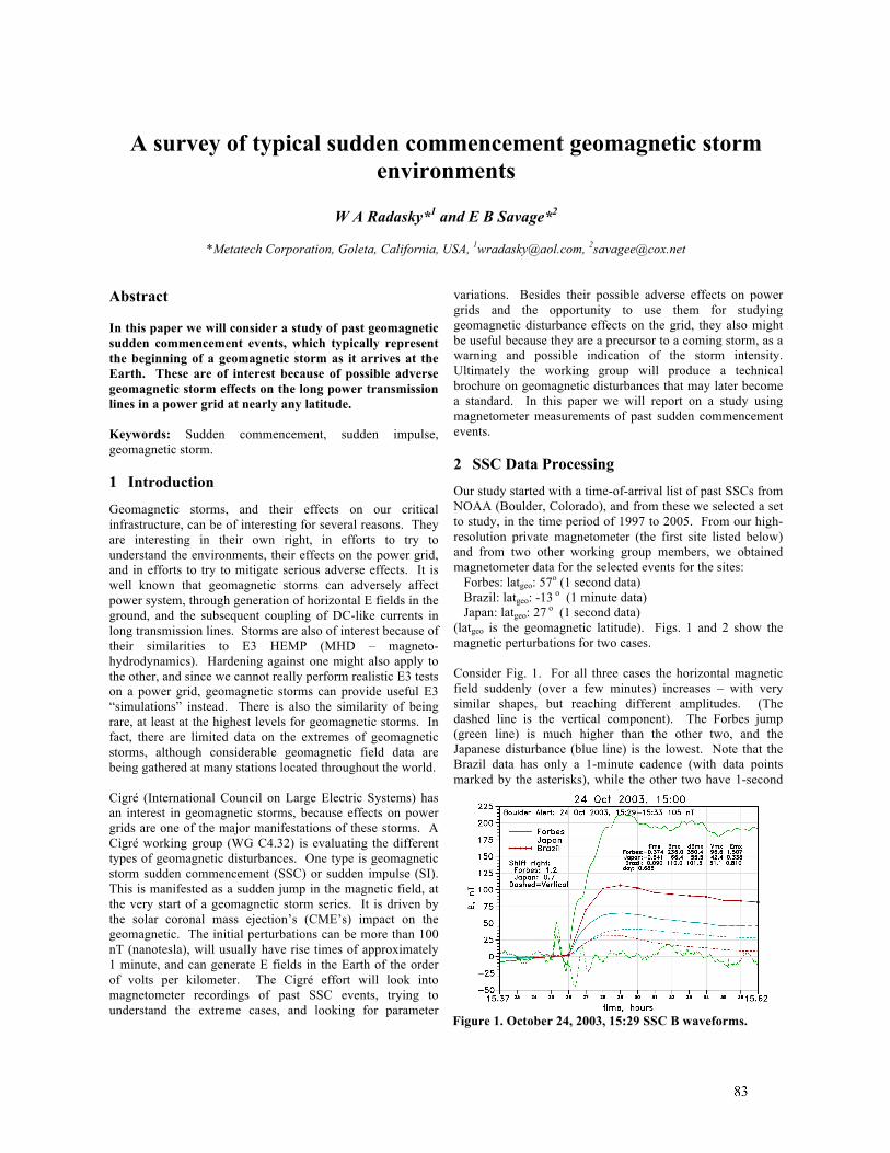
1
A survey of typical sudden commencement geomagnetic storm environments
W A Radasky*1 and E B Savage*2
*Metatech Corporation, Goleta, California, USA, [email protected], [email protected]
Abstract In this paper we will consider a study of past geomagnetic sudden commencement events, which typically represent the beginning of a geomagnetic storm as it arrives at the Earth. These are of interest because of possible adverse geomagnetic storm effects on the long power transmission lines in a power grid at nearly any latitude. Keywords: Sudden commencement, sudden impulse, geomagnetic storm.
1 Introduction
Geomagnetic storms, and their effects on our critical infrastructure, can be of interesting for several reasons. They are interesting in their own right, in efforts to try to understand the environments, their effects on the power grid, and in efforts to try to mitigate serious adverse effects. It is well known that geomagnetic storms can adversely affect power system, through generation of horizontal E fields in the ground, and the subsequent coupling of DC-like currents in long transmission lines. Storms are also of interest because of their similarities to E3 HEMP (MHD – magneto-hydrodynamics). Hardening against one might also apply to the other, and since we cannot really perform realistic E3 tests on a power grid, geomagnetic storms can provide useful E3 “simulations” instead. There is also the similarity of being rare, at least at the highest levels for geomagnetic storms. In fact, there are limited data on the extremes of geomagnetic storms, although considerable geomagnetic field data are being gathered at many stations located throughout the world. Cigré (International Council on Large Electric Systems) has an interest in geomagnetic storms, because effects on power grids are one of the major manifestations of these storms. A Cigré working group (WG C4.32) is evaluating the different types of geomagnetic disturbances. One type is geomagnetic storm sudden commencement (SSC) or sudden impulse (SI). This is manifested as a sudden jump in the magnetic field, at the very start of a geomagnetic storm series. It is driven by the solar coronal mass ejection’s (CME’s) impact on the geomagnetic. The initial perturbations can be more than 100 nT (nanotesla), will usually have rise times of approximately 1 minute, and can generate E fields in the Earth of the order of volts per kilometer. The Cigré effort will look into magnetometer recordings of past SSC events, trying to understand the extreme cases, and looking for parameter
variations. Besides their possible adverse effects on power grids and the opportunity to use them for studying geomagnetic disturbance effects on the grid, they also might be useful because they are a precursor to a coming storm, as a warning and possible indication of the storm intensity. Ultimately the working group will produce a technical brochure on geomagnetic disturbances that may later become a standard. In this paper we will report on a study using magnetometer measurements of past sudden commencement events.
2 SSC Data Processing Our study started with a time-of-arrival list of past SSCs from NOAA (Boulder, Colorado), and from these we selected a set to study, in the time period of 1997 to 2005. From our high-resolution private magnetometer (the first site listed below) and from two other working group members, we obtained magnetometer data for the selected events for the sites:
Forbes: latgeo: 57o (1 second data) Brazil: latgeo: -13 o (1 minute data) Japan: latgeo: 27 o (1 second data)
(latgeo is the geomagnetic latitude). Figs. 1 and 2 show the magnetic perturbations for two cases. Consider Fig. 1. For all three cases the horizontal magnetic field suddenly (over a few minutes) increases – with very similar shapes, but reaching different amplitudes. (The dashed line is the vertical component). The Forbes jump (green line) is much higher than the other two, and the Japanese disturbance (blue line) is the lowest. Note that the Brazil data has only a 1-minute cadence (with data points marked by the asterisks), while the other two have 1-second
Figure 1. October 24, 2003, 15:29 SSC B waveforms.
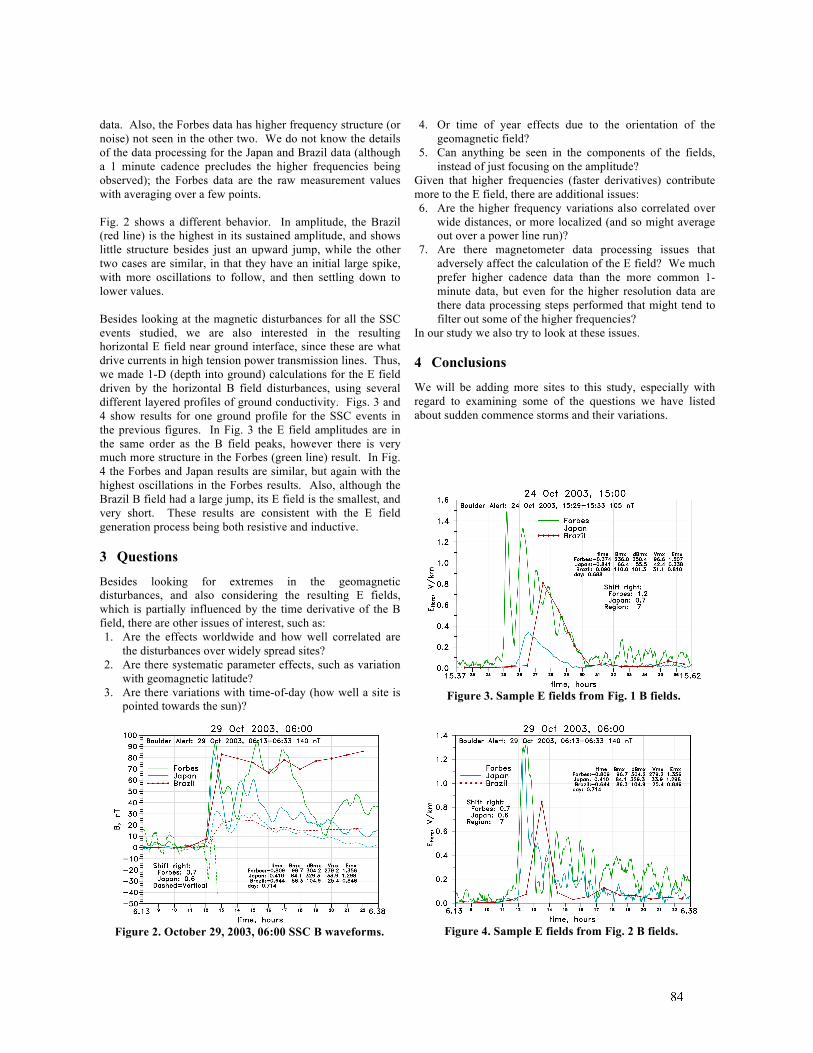
2
data. Also, the Forbes data has higher frequency structure (or noise) not seen in the other two. We do not know the details of the data processing for the Japan and Brazil data (although a 1 minute cadence precludes the higher frequencies being observed); the Forbes data are the raw measurement values with averaging over a few points. Fig. 2 shows a different behavior. In amplitude, the Brazil (red line) is the highest in its sustained amplitude, and shows little structure besides just an upward jump, while the other two cases are similar, in that they have an initial large spike, with more oscillations to follow, and then settling down to lower values. Besides looking at the magnetic disturbances for all the SSC events studied, we are also interested in the resulting horizontal E field near ground interface, since these are what drive currents in high tension power transmission lines. Thus, we made 1-D (depth into ground) calculations for the E field driven by the horizontal B field disturbances, using several different layered profiles of ground conductivity. Figs. 3 and 4 show results for one ground profile for the SSC events in the previous figures. In Fig. 3 the E field amplitudes are in the same order as the B field peaks, however there is very much more structure in the Forbes (green line) result. In Fig. 4 the Forbes and Japan results are similar, but again with the highest oscillations in the Forbes results. Also, although the Brazil B field had a large jump, its E field is the smallest, and very short. These results are consistent with the E field generation process being both resistive and inductive.
3 Questions
Besides looking for extremes in the geomagnetic disturbances, and also considering the resulting E fields, which is partially influenced by the time derivative of the B field, there are other issues of interest, such as: 1. Are the effects worldwide and how well correlated are
the disturbances over widely spread sites? 2. Are there systematic parameter effects, such as variation
with geomagnetic latitude? 3. Are there variations with time-of-day (how well a site is
pointed towards the sun)?
4. Or time of year effects due to the orientation of the geomagnetic field?
5. Can anything be seen in the components of the fields, instead of just focusing on the amplitude?
Given that higher frequencies (faster derivatives) contribute more to the E field, there are additional issues: 6. Are the higher frequency variations also correlated over
wide distances, or more localized (and so might average out over a power line run)?
7. Are there magnetometer data processing issues that adversely affect the calculation of the E field? We much prefer higher cadence data than the more common 1-minute data, but even for the higher resolution data are there data processing steps performed that might tend to filter out some of the higher frequencies?
In our study we also try to look at these issues.
4 Conclusions
We will be adding more sites to this study, especially with regard to examining some of the questions we have listed about sudden commence storms and their variations.
Figure 2. October 29, 2003, 06:00 SSC B waveforms.
Figure 3. Sample E fields from Fig. 1 B fields.
Figure 4. Sample E fields from Fig. 2 B fields.
Failure Rate Analysis of Solid State Device Caused by Repeated
Pulse Characteristics
Ki-Hoon Park*, Kwan-Sik Kim*, Chang-Su Huh* †,
Jin-Soo Choi**, Jong-Won Lee**
*Department of Electrical Engineering, Inha University, Incheon 402-751, Korea
**Agency for Defence Development, Dajeon 305-152, Korea
Abstract
If the electronic systems are exposed to HPEM, the systems
will be destroyed by the coupling effects of electromagnetic
waves. The semiconductors are vulnerable to various pulse
parameters such as frequency, voltage, and rise time of the
pulse. Among those the parameters, the pulse repetition rate is
a primary consideration about malfunction properties of the
semiconductor. In this paper we designed an EUT for the
pulse injection test in order to investigate destructive
characteristics of semiconductor caused by pulse of 30, 60,
120 [Hz], and analyzed the destruction failure rate accordance
with on/off-state of the general purpose IC. As a result, the
injected pulses have changed to amplitude, duty ratio, and
period of output generated by Timer IC. Also, they are
susceptible to influence at the off-state IC. Finally, As the
pulse repetition rate increases the breakdown threshold point
of the Timer IC was reduced.
Keywords: Solid state device, HPEM, Pulse injection test,
Electromagnetic waves, Failure rate
1 Introduction
Electronic systems consist of resistor, capacitor, inductor, and
active devices. Among those the components, based on
semiconductor is especially susceptible to a minimal change
in electromagnetic waves. They often causes malfunction of
system. However, It has not been enough research to solve
problems such as Electromagnetic Interference (EMI).
Therefore we discuss about malfunction mode and DFR
(Destruction Failure Rate) of the semiconductor by amplitude
and repetition rate of the pulse[1]. The pulses were injected
into the VCC pin of general purpose IC. These pulses were
produced by pulse generator and their characteristics are 2.1
[ns] of pulse width and 1.1 [ns] of pulse rise time.
2 Test setup
The Timer IC can work in monostable, bistable, and astable
mode operations. It had wide range of applications like lamp
dimmers and motor control. The astable multivibrator mode
was used for the pulse injection test. The circuit generates a
continuous pulse of rectangular. The Timer IC consists of
eight pins as Ground, Trigger, Output, Reset, Control Voltage,
Threshold, Discharge, VCC. The pulses inject into pins of IC
through a coaxial cable. Figure 1 shows the injected pulse.
The pulses have repetition rate of 30, 60, 90 [Hz].
Figure 1. Injected pulse waveform of pulse generator.
3 Result
Figure 3-(a) and figure 3-(b) show on-state IC and off-state IC
for Vcc pin with pulse injection. It shows the DFR due to the
injected pulse of 30, 60, 120 [Hz] in accordance with on/off
state. As a result, It can be noticed that the failure rate of the
on-state IC is much sharper than the off-state IC. The on-state
ICs will be destruction more than off-state ICs. Also, as the
pulse repetition rate increases, it was reduced to breakdown
threshold point of the timer IC
3040
5060
7080
90
800
1000
1200
1400
1600
1800
2000
22000
0.2
0.4
0.6
0.8
1
PRF [Hz]Voltage [V]
DF
R
(a) On-state IC
3040
5060
7080
90
800
1000
1200
1400
1600
1800
2000
22000
0.2
0.4
0.6
0.8
1
PRF [Hz]Voltage [V]
DF
R
(b) Off-state IC
Figure 3. DFR due to the change in the PRR and Voltage
References
[1] M. Camp, IEEE Trans. on EMC, Vol. 1, 87-92, (2002).
Destruction Characteristic of CMOS AND gate by Variable Pulse
repetition rate
Jeong-Ju Bang*, Sun-Ho Choi*, Chang-Su Huh*†, Jin-Soo Choi**, Jong-Won Lee**
* Department of Electrical Engineering, Inha University, Incheon, Korea
**Agency for Defence Development, Dajeon 305-152, Korea
Abstract
This study examined the destruction effect of CMOS
AND gates by injecting repetitive pulses. Pulses are
injected to the input pin of the AND gate. The pulse has a
rise time of 1.0~2.1ns and a maximum peak voltage of 2
kV. In this study, destruction effect of semiconductor
device by repetitive electromagnetic pulses was analyzed.
When AND gate is injected pulse, the AND gate
destructed. Because AND gate protection diode destructed
by injected pulses. The voltage of 50% destruction failure
rate at which AND gate is destructed decreases as the
repetition rate of pulse increases.
Keywords: repetition pulse, CMOS, pulse injection,
1 Introduction
The modern electronic devices are very vulnerable to high
power electromagnetic pulses because semiconductor
elements are designed for low power and smaller size.
Therefore, semiconductor elements become more susceptible
to undesired noise. If high power electromagnetic waves pass
through aperture of electronic device, the electromagnetic
wave is coupled to the electronics device and generates a
current in the circuit board. The coupled current causes a
malfunction or failure of the electronic systems[1].
Research on effect analysis of high power electromagnetic
on electronic devices and developing high power
electromagnetic generators have been performed in the world.
Recently, repetitive electromagnetic pulse generators have
been developed. Therefore, in this study, destruction effect of
semiconductor device by repetitive electromagnetic pulses
was analyzed.
2 Experimental Setup
In this study, three pulses are injected to the AND gate. Table
1 indicates that the injected pulses rise time and pulse width.
The waveforms of the pulses are shown in Fig 1.
Table 1: Injected pulses
Pulse1 Pulse2 Pulse3
Rise time(ns) 0.75 0.75 1.10
Pulse width(ns) 1.1 1.2 2.1
Figure 1. Waveforms of applied pulses
3 Result
Figure 2 show the destruction voltage of 50%
destruction failure rate by different pulse repetitions. As
shown in Figure 3, the destruction voltage of 50%
destruction failure rate at which AND gate is destructed
decreases as the repetition rate of pulse increases.
Figure 2. destruction voltage of 50% destruction failure
rate
References
[1] Hwang, S. M., J. I. Hong, S.-M. Han, C. S. Huh, and J.-S.
Choi, "Susceptibility and coupled waveform of
microcontroller device by impact of UWB-HPEM," Journal
of Electromagnetic Waves and Applications, vol. 24, no.8-9,
1059-1067, 2010
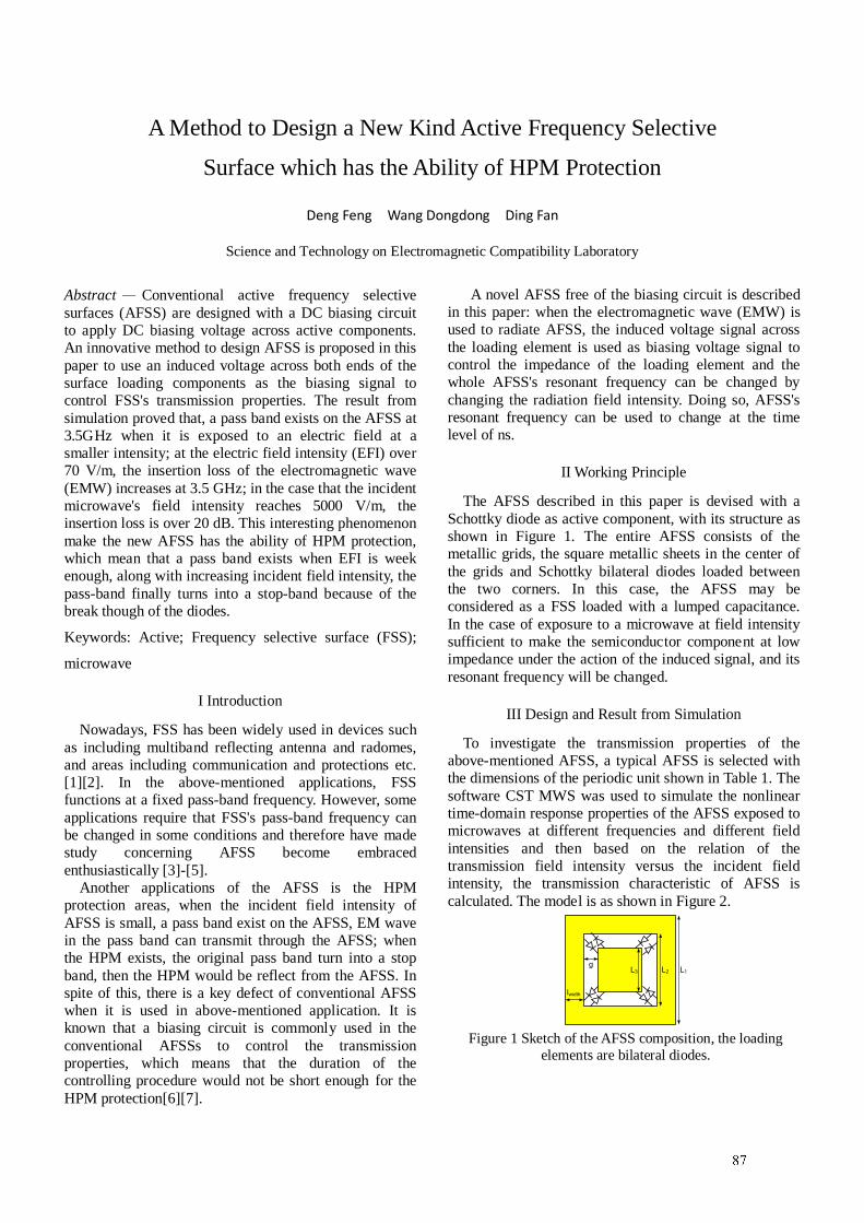
A Method to Design a New Kind Active Frequency Selective
Surface which has the Ability of HPM Protection
Deng Feng Wang Dongdong Ding Fan
Science and Technology on Electromagnetic Compatibility Laboratory
Abstract — Conventional active frequency selective surfaces (AFSS) are designed with a DC biasing circuit to apply DC biasing voltage across active components. An innovative method to design AFSS is proposed in this paper to use an induced voltage across both ends of the surface loading components as the biasing signal to control FSS's transmission properties. The result from simulation proved that, a pass band exists on the AFSS at 3.5GHz when it is exposed to an electric field at a smaller intensity; at the electric field intensity (EFI) over 70 V/m, the insertion loss of the electromagnetic wave (EMW) increases at 3.5 GHz; in the case that the incident microwave's field intensity reaches 5000 V/m, the insertion loss is over 20 dB. This interesting phenomenon make the new AFSS has the ability of HPM protection, which mean that a pass band exists when EFI is week enough, along with increasing incident field intensity, the pass-band finally turns into a stop-band because of the break though of the diodes.
Keywords: Active; Frequency selective surface (FSS);
microwave
I Introduction
Nowadays, FSS has been widely used in devices such as including multiband reflecting antenna and radomes, and areas including communication and protections etc. [1][2]. In the above-mentioned applications, FSS functions at a fixed pass-band frequency. However, some applications require that FSS's pass-band frequency can be changed in some conditions and therefore have made study concerning AFSS become embraced enthusiastically [3]-[5].
Another applications of the AFSS is the HPM protection areas, when the incident field intensity of AFSS is small, a pass band exist on the AFSS, EM wave in the pass band can transmit through the AFSS; when the HPM exists, the original pass band turn into a stop band, then the HPM would be reflect from the AFSS. In spite of this, there is a key defect of conventional AFSS when it is used in above-mentioned application. It is known that a biasing circuit is commonly used in the conventional AFSSs to control the transmission properties, which means that the duration of the controlling procedure would not be short enough for the HPM protection[6][7].
A novel AFSS free of the biasing circuit is described in this paper: when the electromagnetic wave (EMW) is used to radiate AFSS, the induced voltage signal across the loading element is used as biasing voltage signal to control the impedance of the loading element and the whole AFSS's resonant frequency can be changed by changing the radiation field intensity. Doing so, AFSS's resonant frequency can be used to change at the time level of ns.
II Working Principle
The AFSS described in this paper is devised with a Schottky diode as active component, with its structure as shown in Figure 1. The entire AFSS consists of the metallic grids, the square metallic sheets in the center of the grids and Schottky bilateral diodes loaded between the two corners. In this case, the AFSS may be considered as a FSS loaded with a lumped capacitance. In the case of exposure to a microwave at field intensity sufficient to make the semiconductor component at low impedance under the action of the induced signal, and its resonant frequency will be changed.
III Design and Result from Simulation
To investigate the transmission properties of the above-mentioned AFSS, a typical AFSS is selected with the dimensions of the periodic unit shown in Table 1. The software CST MWS was used to simulate the nonlinear time-domain response properties of the AFSS exposed to microwaves at different frequencies and different field intensities and then based on the relation of the transmission field intensity versus the incident field intensity, the transmission characteristic of AFSS is calculated. The model is as shown in Figure 2.
lwidth
gL3 L2 L1
Figure 1 Sketch of the AFSS composition, the loading elements are bilateral diodes.
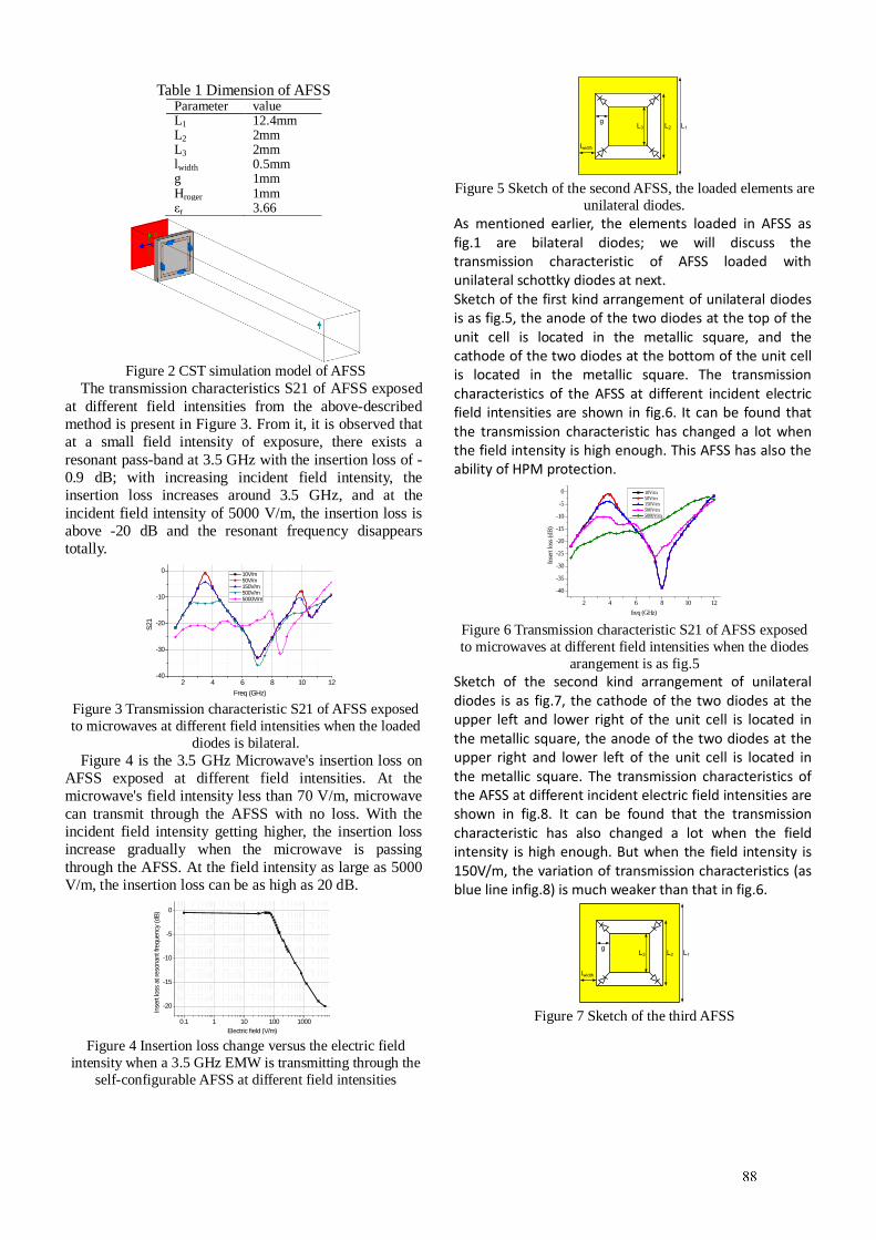
Table 1 Dimension of AFSS Parameter value L1 12.4mm L2 2mm L3 2mm lwidth 0.5mm g 1mm Hroger 1mm εr 3.66
Figure 2 CST simulation model of AFSS
The transmission characteristics S21 of AFSS exposed at different field intensities from the above-described method is present in Figure 3. From it, it is observed that at a small field intensity of exposure, there exists a resonant pass-band at 3.5 GHz with the insertion loss of - 0.9 dB; with increasing incident field intensity, the insertion loss increases around 3.5 GHz, and at the incident field intensity of 5000 V/m, the insertion loss is above -20 dB and the resonant frequency disappears totally.
2 4 6 8 10 12-40
-30
-20
-10
0
S21
Freq (GHz)
10V/m 50V/m 150V/m 500V/m 5000V/m
Figure 3 Transmission characteristic S21 of AFSS exposed to microwaves at different field intensities when the loaded
diodes is bilateral. Figure 4 is the 3.5 GHz Microwave's insertion loss on
AFSS exposed at different field intensities. At the microwave's field intensity less than 70 V/m, microwave can transmit through the AFSS with no loss. With the incident field intensity getting higher, the insertion loss increase gradually when the microwave is passing through the AFSS. At the field intensity as large as 5000 V/m, the insertion loss can be as high as 20 dB.
0.1 1 10 100 1000
-20
-15
-10
-5
0
Inse
rt lo
ss a
t re
sonant frequency
(dB
)
Electric field (V/m)
Figure 4 Insertion loss change versus the electric field intensity when a 3.5 GHz EMW is transmitting through the
self-configurable AFSS at different field intensities
lwidth
gL3 L2 L1
Figure 5 Sketch of the second AFSS, the loaded elements are
unilateral diodes. As mentioned earlier, the elements loaded in AFSS as fig.1 are bilateral diodes; we will discuss the transmission characteristic of AFSS loaded with unilateral schottky diodes at next. Sketch of the first kind arrangement of unilateral diodes is as fig.5, the anode of the two diodes at the top of the unit cell is located in the metallic square, and the cathode of the two diodes at the bottom of the unit cell is located in the metallic square. The transmission characteristics of the AFSS at different incident electric field intensities are shown in fig.6. It can be found that the transmission characteristic has changed a lot when the field intensity is high enough. This AFSS has also the ability of HPM protection.
2 4 6 8 10 12
-40
-35
-30
-25
-20
-15
-10
-5
0
Inse
rt lo
ss (d
B)
freq (GHz)
10V/m 50V/m 150V/m 500V/m 5000V/m
Figure 6 Transmission characteristic S21 of AFSS exposed to microwaves at different field intensities when the diodes
arangement is as fig.5 Sketch of the second kind arrangement of unilateral diodes is as fig.7, the cathode of the two diodes at the upper left and lower right of the unit cell is located in the metallic square, the anode of the two diodes at the upper right and lower left of the unit cell is located in the metallic square. The transmission characteristics of the AFSS at different incident electric field intensities are shown in fig.8. It can be found that the transmission characteristic has also changed a lot when the field intensity is high enough. But when the field intensity is 150V/m, the variation of transmission characteristics (as blue line infig.8) is much weaker than that in fig.6.
lwidth
gL3 L2 L1
Figure 7 Sketch of the third AFSS
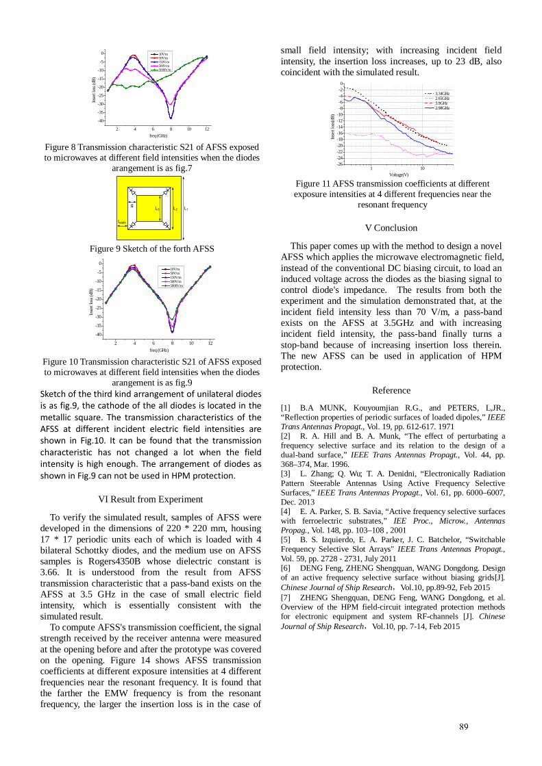
2 4 6 8 10 12
-40
-35
-30
-25
-20
-15
-10
-5
0
Inse
rt lo
ss (d
B)
freq (GHz)
10V/m 50V/m 150V/m 500V/m 5000V/m
Figure 8 Transmission characteristic S21 of AFSS exposed to microwaves at different field intensities when the diodes
arangement is as fig.7
lwidth
gL3 L2 L1
Figure 9 Sketch of the forth AFSS
2 4 6 8 10 12
-40
-35
-30
-25
-20
-15
-10
-5
0
Inse
rt lo
ss (d
B)
freq (GHz)
10V/m 50V/m 150V/m 500V/m 5000V/m
Figure 10 Transmission characteristic S21 of AFSS exposed to microwaves at different field intensities when the diodes
arangement is as fig.9 Sketch of the third kind arrangement of unilateral diodes is as fig.9, the cathode of the all diodes is located in the metallic square. The transmission characteristics of the AFSS at different incident electric field intensities are shown in Fig.10. It can be found that the transmission characteristic has not changed a lot when the field intensity is high enough. The arrangement of diodes as shown in Fig.9 can not be used in HPM protection.
VI Result from Experiment
To verify the simulated result, samples of AFSS were developed in the dimensions of 220 * 220 mm, housing 17 * 17 periodic units each of which is loaded with 4 bilateral Schottky diodes, and the medium use on AFSS samples is Rogers4350B whose dielectric constant is 3.66. It is understood from the result from AFSS transmission characteristic that a pass-band exists on the AFSS at 3.5 GHz in the case of small electric field intensity, which is essentially consistent with the simulated result.
To compute AFSS's transmission coefficient, the signal strength received by the receiver antenna were measured at the opening before and after the prototype was covered on the opening. Figure 14 shows AFSS transmission coefficients at different exposure intensities at 4 different frequencies near the resonant frequency. It is found that the farther the EMW frequency is from the resonant frequency, the larger the insertion loss is in the case of
small field intensity; with increasing incident field intensity, the insertion loss increases, up to 23 dB, also coincident with the simulated result.
1 10-26-24-22-20-18-16-14-12-10-8-6-4-20
3.34GHz 2.65GHz 3.9GHz 2.98GHz
Inse
rt lo
ss(d
B)
Voltage(V) Figure 11 AFSS transmission coefficients at different exposure intensities at 4 different frequencies near the
resonant frequency
V Conclusion
This paper comes up with the method to design a novel AFSS which applies the microwave electromagnetic field, instead of the conventional DC biasing circuit, to load an induced voltage across the diodes as the biasing signal to control diode's impedance. The results from both the experiment and the simulation demonstrated that, at the incident field intensity less than 70 V/m, a pass-band exists on the AFSS at 3.5GHz and with increasing incident field intensity, the pass-band finally turns a stop-band because of increasing insertion loss therein. The new AFSS can be used in application of HPM protection.
Reference
[1] B.A MUNK, Kouyoumjian R.G., and PETERS, L,JR., “Reflection properties of periodic surfaces of loaded dipoles,” IEEE Trans Antennas Propagt., Vol. 19, pp. 612-617. 1971 [2] R. A. Hill and B. A. Munk, “The effect of perturbating a frequency selective surface and its relation to the design of a dual-band surface,” IEEE Trans Antennas Propagt., Vol. 44, pp. 368–374, Mar. 1996. [3] L. Zhang; Q. Wu; T. A. Denidni, “Electronically Radiation Pattern Steerable Antennas Using Active Frequency Selective Surfaces,” IEEE Trans Antennas Propagt., Vol. 61, pp. 6000–6007, Dec. 2013 [4] E. A. Parker, S. B. Savia, “Active frequency selective surfaces with ferroelectric substrates,” IEE Proc., Microw., Antennas Propag., Vol. 148, pp. 103–108 , 2001 [5] B. S. Izquierdo, E. A. Parker, J. C. Batchelor, “Switchable Frequency Selective Slot Arrays" IEEE Trans Antennas Propagt., Vol. 59, pp. 2728 - 2731, July 2011 [6] DENG Feng, ZHENG Shengquan, WANG Dongdong. Design of an active frequency selective surface without biasing grids[J]. Chinese Journal of Ship Research,Vol.10, pp.89-92, Feb 2015 [7] ZHENG Shengquan, DENG Feng, WANG Dongdong, et al. Overview of the HPM field-circuit integrated protection methods for electronic equipment and system RF-channels [J]. Chinese Journal of Ship Research,Vol.10, pp. 7-14, Feb 2015
Reflection and transmission of microwaves by a modern glass window
P. Ragulis, Ž. Kancleris, R. Simniškis and M. Dagys
Microwave Laboratory of Physical Technology Department Centre for Physical Sciences and Technology
Vilnius, Lithuania [email protected]
Abstract The reflection and transmission of a microwave by samples of the regular glass and multiple pane modern windows are investigated in a frequency range of 2.6-12.5 GHz. The influence of a surface conductivity of a metal layer on the reflection and transmission coefficients is considered for a single sheet of metalized glass. The shift and elimination of Fabry-Perot resonances are analyzed as a function of metal layer conductivity. Properties of a thin metal layer are accounted for when modeling the transmission and reflections coefficients of the windows under test. The experimental measurements of a shielding effectiveness of the modern multiple pane windows are performed. Keywords: microwave transmission and reflection measurements; window panes; coated window glass.
1 Introduction State of the art multiple pane windows uses high-performance heat reflected glass. This glass is usually flat sheet of soda–lime–silicate glass covered with a thin layer of electrically conductive film. This thin and transparent to a visible light coating effectively reflects far infrared radiation. In this way it protects a house from overheating by the solar radiation during summer and from cooling during winter [1]. The metallic layer appearing on a window glass should influence the transmission of microwave radiation through it, but we did not found detailed investigation of such phenomenon in a scientific literature. It is worth mentioning that the investigations presented here were motivated by the not planned measurement of attenuation during 2013 RAID trials at Horten, Norway. During them microwave attenuation of a newly installed double pane window in the building under test was measured. It was found that behind the window the microwave pulse at 5.7 GHz was attenuated by 23 dB.
Here we present a theoretical consideration of the influence of a thin metal coating of the glass on the transmission and reflection of microwaves. The transmission and reflection coefficients in a frequency range 2.6-12.5 GHz have been measured on a regular glass and glass coated with a thin metal
layer samples. Double and triple pane window samples were also investigated.
2 Calculation of reflection and transmission To calculate the reflection and transmission coefficients we consider a plane electromagnetic wave impinging perpendicularly to the dielectric plate as it is shown in Figure 1. The plate is infinite in x and y directions. The width of the plate is d and relative dielectric constant is ε. The back surface of the plate is coated with a thin metallic layer. A surface conductivity of this layer is denoted as σs and measured in units of [S]. As follows from the figure, there are falling and reflected waves before the plate. Two waves moving left and right appear inside the dielectric plate as well. Finally, behind the plate the only wave moving right remains. The interference of the waves moving left and right in the dielectric initiates so-called Fabry-Perot resonances or bleaching when the width of the plate becomes an integer number of half wavelengths in it.
The preceding theoretical consideration of the metalized layer deposited on the dielectric plate [2, 3] is based on the transmission line theory. The layer was treated as a finite length section of transmission line appearing as a shunt resistance. On the one hand, the conductivity of the line should
Figure 1. Electromagnetic waves interacting with a dielectric plate. On the back surface of the plate a thin metal coating, characterized by the surface conductivity σs, is deposited.
1
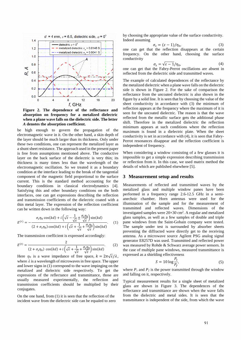
be high enough to govern the propagation of the electromagnetic wave in it. On the other hand, a skin depth of the layer should be much larger than its thickness. Only under these two conditions, one can represent the metalized layer as a shunt sheet resistance. The approach used in the present paper is free from assumptions mentioned above. The conductive layer on the back surface of the dielectric is very thin; its thickness is many times less than the wavelength of the electromagnetic oscillation. So we treated it as a boundary condition at the interface leading to the break of the tangential component of the magnetic field proportional to the surface current. This is the standard method accounting for the boundary conditions in classical electrodynamics [4]. Satisfying this and other boundary conditions on the both interfaces, one can get expressions describing the reflection and transmission coefficients of the dielectric coated with a thin metal layer. The expression of the reflection coefficient can be written down in the following way:
𝐸𝐸(𝑟𝑟) = −𝜎𝜎𝑠𝑠𝜂𝜂0 cos(𝑘𝑘𝑘𝑘) + 𝑖𝑖 √𝜀𝜀 −
1√𝜀𝜀
± 𝜎𝜎𝑠𝑠𝜂𝜂0√𝜀𝜀
sin(𝑘𝑘𝑘𝑘)
(2 + 𝜎𝜎𝑠𝑠𝜂𝜂0) cos(𝑘𝑘𝑘𝑘) + 𝑖𝑖 √𝜀𝜀 + 1√𝜀𝜀
+ 𝜎𝜎𝑠𝑠𝜂𝜂0√𝜀𝜀
sin(𝑘𝑘𝑘𝑘). (1)
The transmission coefficient is expressed accordingly:
𝐸𝐸(𝑡𝑡) =2
(2 + 𝜎𝜎𝑠𝑠𝜂𝜂0) cos(𝑘𝑘𝑘𝑘) + 𝑖𝑖 √𝜀𝜀 + 1√𝜀𝜀
+ 𝜎𝜎𝑠𝑠𝜂𝜂0√𝜀𝜀
sin(𝑘𝑘𝑘𝑘). (2)
Here η0 is a wave impedance of free space, 𝑘𝑘 = 2𝜋𝜋√𝜀𝜀/𝜆𝜆 , where λ is a wavelength of microwaves in free space. The upper and lower signs in (1) correspond to the wave impinging on the metalized and dielectric side respectively. To get the expressions of the reflectance and transmittance, those are usually measured experimentally, the reflection and transmission coefficients should be multiplied by their conjugates.
On the one hand, from (1) it is seen that the reflection of the incident wave from the dielectric side can be equaled to zero
by choosing the appropriate value of the surface conductivity. Indeed assuming
𝜎𝜎𝑠𝑠 = (𝜀𝜀 − 1)/𝜂𝜂0, (3) one can get that the reflection disappears at the certain frequency. On the other hand, choosing the surface conductivity
𝜎𝜎𝑠𝑠 = √𝜀𝜀 − 1/𝜂𝜂0, (4) one can get that the Fabry-Perrot oscillations are absent in reflected from the dielectric side and transmitted waves.
The example of calculated dependences of the reflectance by the metalized dielectric when a plane wave falls on the dielectric side is shown in Figure 2. For the sake of comparison the reflectance from the uncoated dielectric is also shown in the figure by a solid line. It is seen that by choosing the value of the sheet conductivity in accordance with (3) the minimum of reflection appears at the frequency where the maximum of it is seen for the uncoated dielectric. The reason is that the wave reflected from the metallic surface gets the additional phase shift. Therefore in the metalized dielectric the reflection minimum appears at such conditions where the reflection maximum is found in a dielectric plate. When the sheet conductivity is set in accordance with (4), it is seen that Fabry-Perrot resonances disappear and the reflection coefficient is independent of frequency.
When considering a window consisting of a few glasses it is impossible to get a simple expression describing transmission or reflection from it. In this case, we used matrix method the details of which are published elsewhere [5].
3 Measurement setup and results Measurements of reflected and transmitted waves by the metalized glass and multiple window panes have been performed in a frequency range 2.6-12.5 GHz in a semi-anechoic chamber. Horn antennas were used for the illumination of the sample and for the measurement of transmitted and reflected waves. Dimensions of the investigated samples were 20×30 cm2. A regular and metalized glass samples, as well as a few samples of double and triple pane windows from the Saint-Gobain company were tested. The sample under test is surrounded by absorber sheets preventing the diffracted wave directly get to the receiving antenna. As a microwave source Agilent PSG analog signal generator E8257D was used. Transmitted and reflected power was measured by Rohde & Schwarz average power sensors. In the case of multiple pane windows, measured transmittance is expressed as a shielding effectiveness
𝑆𝑆 = 10 log𝑃𝑃𝑡𝑡𝑃𝑃𝑓𝑓
, (5)
where Pt and Pf is the power transmitted through the window and falling on it, respectively.
Typical measurement results for a single sheet of metalized glass are shown in Figure 3. The dependences of the reflectance and transmittance are shown when the wave falls from the dielectric and metal sides. It is seen that the transmittance is independent of the side, from which the wave
Figure 2. The dependence of the reflectance and absorption on frequency for a metalized dielectric when a plane wave falls on the dielectric side. The letter A denotes the absorption coefficient.
2
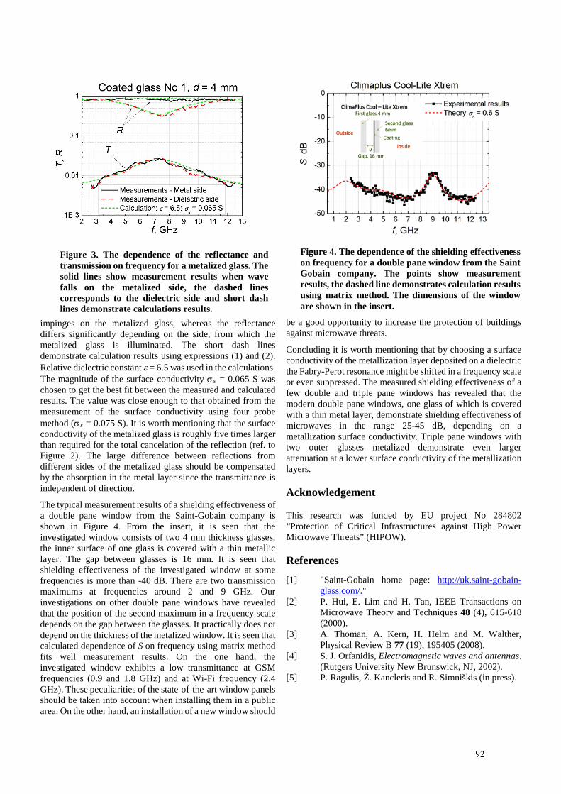
impinges on the metalized glass, whereas the reflectance differs significantly depending on the side, from which the metalized glass is illuminated. The short dash lines demonstrate calculation results using expressions (1) and (2). Relative dielectric constant ε = 6.5 was used in the calculations. The magnitude of the surface conductivity σs = 0.065 S was chosen to get the best fit between the measured and calculated results. The value was close enough to that obtained from the measurement of the surface conductivity using four probe method (σs = 0.075 S). It is worth mentioning that the surface conductivity of the metalized glass is roughly five times larger than required for the total cancelation of the reflection (ref. to Figure 2). The large difference between reflections from different sides of the metalized glass should be compensated by the absorption in the metal layer since the transmittance is independent of direction.
The typical measurement results of a shielding effectiveness of a double pane window from the Saint-Gobain company is shown in Figure 4. From the insert, it is seen that the investigated window consists of two 4 mm thickness glasses, the inner surface of one glass is covered with a thin metallic layer. The gap between glasses is 16 mm. It is seen that shielding effectiveness of the investigated window at some frequencies is more than -40 dB. There are two transmission maximums at frequencies around 2 and 9 GHz. Our investigations on other double pane windows have revealed that the position of the second maximum in a frequency scale depends on the gap between the glasses. It practically does not depend on the thickness of the metalized window. It is seen that calculated dependence of S on frequency using matrix method fits well measurement results. On the one hand, the investigated window exhibits a low transmittance at GSM frequencies (0.9 and 1.8 GHz) and at Wi-Fi frequency (2.4 GHz). These peculiarities of the state-of-the-art window panels should be taken into account when installing them in a public area. On the other hand, an installation of a new window should
be a good opportunity to increase the protection of buildings against microwave threats.
Concluding it is worth mentioning that by choosing a surface conductivity of the metallization layer deposited on a dielectric the Fabry-Perot resonance might be shifted in a frequency scale or even suppressed. The measured shielding effectiveness of a few double and triple pane windows has revealed that the modern double pane windows, one glass of which is covered with a thin metal layer, demonstrate shielding effectiveness of microwaves in the range 25-45 dB, depending on a metallization surface conductivity. Triple pane windows with two outer glasses metalized demonstrate even larger attenuation at a lower surface conductivity of the metallization layers.
Acknowledgement
This research was funded by EU project No 284802 “Protection of Critical Infrastructures against High Power Microwave Threats” (HIPOW).
References [1] "Saint-Gobain home page: http://uk.saint-gobain-
glass.com/." [2] P. Hui, E. Lim and H. Tan, IEEE Transactions on
Microwave Theory and Techniques 48 (4), 615-618 (2000).
[3] A. Thoman, A. Kern, H. Helm and M. Walther, Physical Review B 77 (19), 195405 (2008).
[4] S. J. Orfanidis, Electromagnetic waves and antennas. (Rutgers University New Brunswick, NJ, 2002).
[5] P. Ragulis, Ž. Kancleris and R. Simniškis (in press).
Figure 4. The dependence of the shielding effectiveness on frequency for a double pane window from the Saint Gobain company. The points show measurement results, the dashed line demonstrates calculation results using matrix method. The dimensions of the window are shown in the insert.
Figure 3. The dependence of the reflectance and transmission on frequency for a metalized glass. The solid lines show measurement results when wave falls on the metalized side, the dashed lines corresponds to the dielectric side and short dash lines demonstrate calculations results.
3
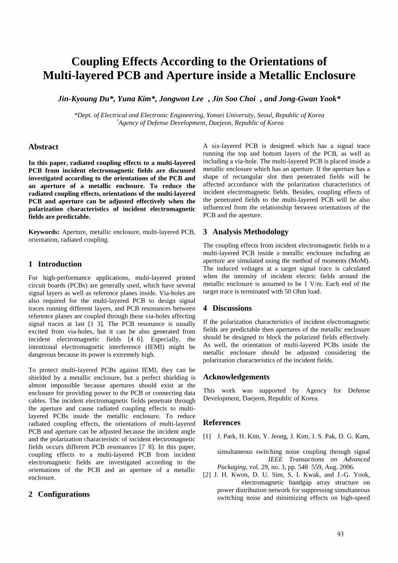
1
Coupling Effects According to the Orientations of
Multi-layered PCB and Aperture inside a Metallic Enclosure
Jin-Kyoung Du*, Yuna Kim*, Jongwon Lee †, Jin Soo Choi
†, and Jong-Gwan Yook*
*Dept. of Electrical and Electronic Engineering, Yonsei University, Seoul, Republic of Korea
†Agency of Defense Development, Daejeon, Republic of Korea
Abstract
In this paper, radiated coupling effects to a multi-layered
PCB from incident electromagnetic fields are discussed
investigated according to the orientations of the PCB and
an aperture of a metallic enclosure. To reduce the
radiated coupling effects, orientations of the multi-layered
PCB and aperture can be adjusted effectively when the
polarization characteristics of incident electromagnetic
fields are predictable.
Keywords: Aperture, metallic enclosure, multi-layered PCB,
orientation, radiated coupling.
1 Introduction
For high-performance applications, multi-layered printed
circuit boards (PCBs) are generally used, which have several
signal layers as well as reference planes inside. Via-holes are
also required for the multi-layered PCB to design signal
traces running different layers, and PCB resonances between
reference planes are coupled through these via-holes affecting
signal traces at last [1–3]. The PCB resonance is usually
excited from via-holes, but it can be also generated from
incident electromagnetic fields [4–6]. Especially, the
intentional electromagnetic interference (IEMI) might be
dangerous because its power is extremely high.
To protect multi-layered PCBs against IEMI, they can be
shielded by a metallic enclosure, but a perfect shielding is
almost impossible because apertures should exist at the
enclosure for providing power to the PCB or connecting data
cables. The incident electromagnetic fields penetrate through
the aperture and cause radiated coupling effects to multi-
layered PCBs inside the metallic enclosure. To reduce
radiated coupling effects, the orientations of multi-layered
PCB and aperture can be adjusted because the incident angle
and the polarization characteristic of incident electromagnetic
fields occurs different PCB resonances [7–8]. In this paper,
coupling effects to a multi-layered PCB from incident
electromagnetic fields are investigated according to the
orientations of the PCB and an aperture of a metallic
enclosure.
2 Configurations
A six-layered PCB is designed which has a signal trace
running the top and bottom layers of the PCB, as well as
including a via-hole. The multi-layered PCB is placed inside a
metallic enclosure which has an aperture. If the aperture has a
shape of rectangular slot then penetrated fields will be
affected accordance with the polarization characteristics of
incident electromagnetic fields. Besides, coupling effects of
the penetrated fields to the multi-layered PCB will be also
influenced from the relationship between orientations of the
PCB and the aperture.
3 Analysis Methodology
The coupling effects from incident electromagnetic fields to a
multi-layered PCB inside a metallic enclosure including an
aperture are simulated using the method of moments (MoM).
The induced voltages at a target signal trace is calculated
when the intensity of incident electric fields around the
metallic enclosure is assumed to be 1 V/m. Each end of the
target trace is terminated with 50 Ohm load.
4 Discussions
If the polarization characteristics of incident electromagnetic
fields are predictable then apertures of the metallic enclosure
should be designed to block the polarized fields effectively.
As well, the orientation of multi-layered PCBs inside the
metallic enclosure should be adjusted considering the
polarization characteristics of the incident fields.
Acknowledgements
This work was supported by Agency for Defense
Development, Daejeon, Republic of Korea.
References
[1] J. Park, H. Kim, Y. Jeong, J. Kim, J. S. Pak, D. G. Kam,
and J. Kim, “Modeling and measurement of
simultaneous switching noise coupling through signal
via transition,” IEEE Transactions on Advanced
Packaging, vol. 29, no. 3, pp. 548–559, Aug. 2006.
[2] J. H. Kwon, D. U. Sim, S. I. Kwak, and J.-G. Yook,
“Novel electromagnetic bandgap array structure on
power distribution network for suppressing simultaneous
switching noise and minimizing effects on high-speed
2
signals,” IEEE Transactions on Electromagnetic
Compatibility, vol. 52, no. 2, pp. 365–372, May 2010.
[3] H.-D. Kang, H. Kim, S.-G. Kim, and J.-G. Yook, “A
localized enhanced power plane topology for wideband
suppression of simultaneous switching noise,” IEEE
Transactions on Electromagnetic Compatibility, vol. 52,
no. 2, pp. 373–380, May 2010.
[4] J. S. Pak, H. Kim, J. Kim, and H. Lee, “PCB
power/ground plane edge radiation excited by high-
frequency clock,” in Proceedings of International
Symposium on Electromagnetic Compatibility, vol. 1, pp.
197–202, Aug. 2004.
[5] J. Kim, J. Pak, J. Pak, and H. Kim, “Noise generation,
coupling, isolation, and EM radiation in high-speed
package and PCB,” in Proceedings of IEEE
International Symposium on Circuits Systems, vol. 6, pp.
5766–5769, May 2005.
[6] J. S. Pak, H. Kim, J. Lee, and J. Kim, “Modeling and
measurement of radiated field emission from a
power/ground plane cavity edge excited by a through-
hole signal via based on a balanced TLM and via
coupling model,” IEEE Transactions on Advanced
Packaging, vol. 30, no. 1, pp. 73–85, Feb. 2007.
[7] J.-K. Du, S.-Y Hyun, J.-G. Yook, J. Lee, and J. S. Choi,
“Coupling effects according to PCB orientations,” in
Proceedings of American Electromagnetics, vol. 1, p. 1
(ID 150), Jul. 2014.
[8] J.-K. Du, Analysis of Coupling Effects from IEMI to
Multilayered PCBs in Metallic Enclosures, Ph.D. thesis,
Dept. of Electrical and Electronic Engineering, Yonsei
University, Seoul, Republic of Korea, 2015.
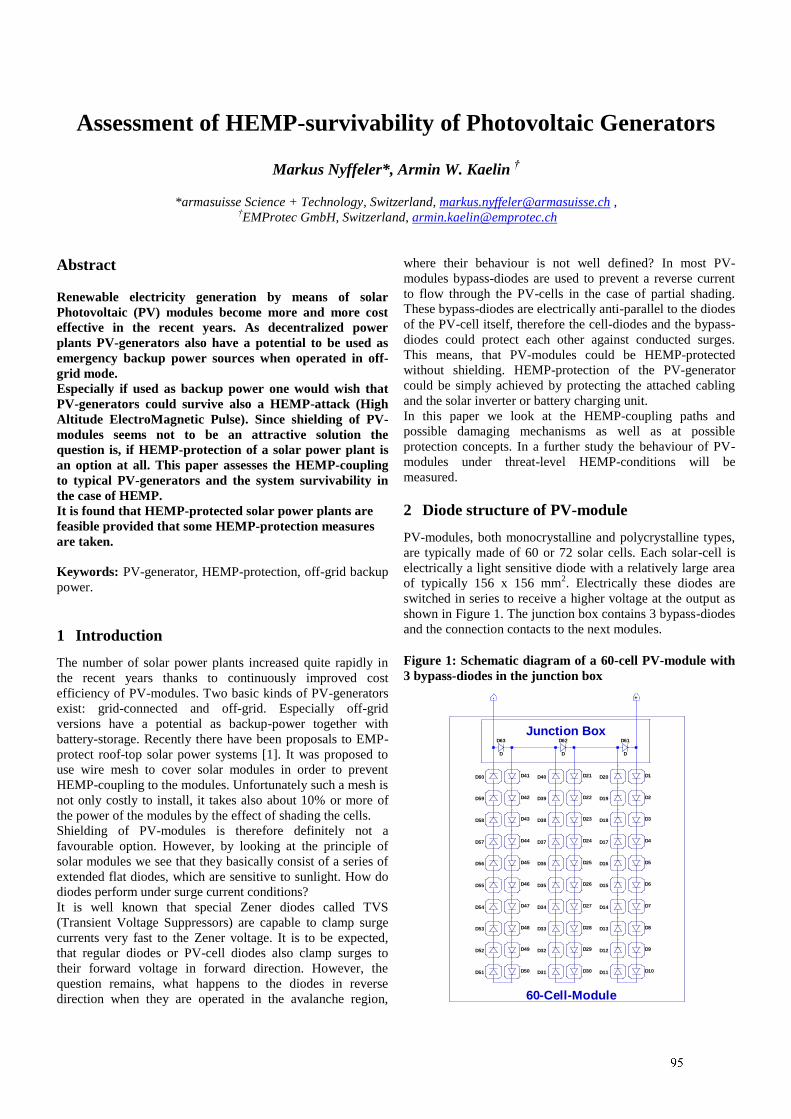
1
Assessment of HEMP-survivability of Photovoltaic Generators
Markus Nyffeler*, Armin W. Kaelin †
*armasuisse Science + Technology, Switzerland, [email protected] ,
†EMProtec GmbH, Switzerland, [email protected]
Abstract
Renewable electricity generation by means of solar
Photovoltaic (PV) modules become more and more cost
effective in the recent years. As decentralized power
plants PV-generators also have a potential to be used as
emergency backup power sources when operated in off-
grid mode.
Especially if used as backup power one would wish that
PV-generators could survive also a HEMP-attack (High
Altitude ElectroMagnetic Pulse). Since shielding of PV-
modules seems not to be an attractive solution the
question is, if HEMP-protection of a solar power plant is
an option at all. This paper assesses the HEMP-coupling
to typical PV-generators and the system survivability in
the case of HEMP.
It is found that HEMP-protected solar power plants are
feasible provided that some HEMP-protection measures
are taken.
Keywords: PV-generator, HEMP-protection, off-grid backup
power.
1 Introduction
The number of solar power plants increased quite rapidly in
the recent years thanks to continuously improved cost
efficiency of PV-modules. Two basic kinds of PV-generators
exist: grid-connected and off-grid. Especially off-grid
versions have a potential as backup-power together with
battery-storage. Recently there have been proposals to EMP-
protect roof-top solar power systems [1]. It was proposed to
use wire mesh to cover solar modules in order to prevent
HEMP-coupling to the modules. Unfortunately such a mesh is
not only costly to install, it takes also about 10% or more of
the power of the modules by the effect of shading the cells.
Shielding of PV-modules is therefore definitely not a
favourable option. However, by looking at the principle of
solar modules we see that they basically consist of a series of
extended flat diodes, which are sensitive to sunlight. How do
diodes perform under surge current conditions?
It is well known that special Zener diodes called TVS
(Transient Voltage Suppressors) are capable to clamp surge
currents very fast to the Zener voltage. It is to be expected,
that regular diodes or PV-cell diodes also clamp surges to
their forward voltage in forward direction. However, the
question remains, what happens to the diodes in reverse
direction when they are operated in the avalanche region,
where their behaviour is not well defined? In most PV-
modules bypass-diodes are used to prevent a reverse current
to flow through the PV-cells in the case of partial shading.
These bypass-diodes are electrically anti-parallel to the diodes
of the PV-cell itself, therefore the cell-diodes and the bypass-
diodes could protect each other against conducted surges.
This means, that PV-modules could be HEMP-protected
without shielding. HEMP-protection of the PV-generator
could be simply achieved by protecting the attached cabling
and the solar inverter or battery charging unit.
In this paper we look at the HEMP-coupling paths and
possible damaging mechanisms as well as at possible
protection concepts. In a further study the behaviour of PV-
modules under threat-level HEMP-conditions will be
measured.
2 Diode structure of PV-module
PV-modules, both monocrystalline and polycrystalline types,
are typically made of 60 or 72 solar cells. Each solar-cell is
electrically a light sensitive diode with a relatively large area
of typically 156 x 156 mm2. Electrically these diodes are
switched in series to receive a higher voltage at the output as
shown in Figure 1. The junction box contains 3 bypass-diodes
and the connection contacts to the next modules.
Figure 1: Schematic diagram of a 60-cell PV-module with
3 bypass-diodes in the junction box
D1
D2
D3
D4
D5
D6
D7
D8
D9
D10D11
D12
D13
D14
D15
D16
D17
D18
D19
D20D21
D22
D23
D24
D25
D26
D27
D28
D29
D30D31
D32
D33
D34
D35
D36
D37
D38
D39
D40D41
D42
D43
D44
D45
D46
D47
D48
D49
D50D51
D52
D53
D54
D55
D56
D57
D58
D59
D60
D61
D
D62
D
D63
D
+-
Junction Box
60-Cell-Module
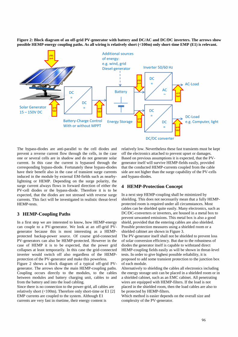
2
Figure 2: Block diagram of an off-grid PV-generator with battery and DC/AC and DC/DC inverters. The arrows show
possible HEMP-energy coupling paths. As all wiring is relatively short (<100m) only short-time EMP (E1) is relevant.
DC=
Battery-Charge ControlWith or without MPPT
Solar Generator15 – 150V DC
DC=
Battery
Energy StorageDC-Loade.g. Computer, light
DC=
DC=
DC=
AC~
DC/DC converter
Inverter 50/60 Hz
AC-Load
Additional sourcesof energy:e.g. wind, gridDiesel-generator
E1
E1 E1
E1E1
E1
E1
The bypass-diodes are anti-parallel to the cell diodes and
prevent a reverse current flow through the cells, in the case
one or several cells are in shadow and do not generate solar
current. In this case the current is bypassed through the
corresponding bypass-diode. Fortunately these bypass-diodes
have their benefit also in the case of transient surge currents
induced in the module by external EM-fields such as nearby-
lightning or HEMP. Depending on the surge polarity, the
surge current always flows in forward direction of either the
PV-cell diodes or the bypass-diode. Therefore it is to be
expected, that the diodes are not stressed with reverse surge
currents. This fact will be investigated in realistic threat-level
HEMP-tests.
3 HEMP-Coupling Paths
In a first step we are interested to know, how HEMP-energy
can couple to a PV-generator. We look at an off-grid PV-
generator because this is most interesting as a HEMP-
protected backup-power source. Of course grid-connected
PV-generators can also be HEMP-protected. However in the
case of HEMP it is to be expected, that the power grid
collapses at least temporarily. In this case the grid-connected
inverter would switch off also regardless of the HEMP-
protection of the PV-generator and make this powerless.
Figure 2 shows a block diagram of a typical off-grid PV-
generator. The arrows show the main HEMP-coupling paths.
Coupling occurs directly to the modules, to the cables
between modules and battery charging unit, cables to and
from the battery and into the load cabling.
Since there is no connection to the power-grid, all cables are
relatively short (<100m). Therefore only short-time or E1 [2]
EMP currents are coupled to the system. Although E1
currents are very fast in risetime, their energy content is
relatively low. Nevertheless these fast transients must be kept
off the electronics attached to prevent upset or damages.
Based on previous assumptions it is expected, that the PV-
generator itself will survive HEMP-fields easily, provided
that the conducted HEMP-currents coupled from the cable
side are not higher than the surge capability of the PV-cells
and bypass-diodes.
4 HEMP-Protection Concept
In a next step HEMP-coupling shall be minimized by
shielding. This does not necessarily mean that a fully HEMP-
protected room is required under all circumstances. Most
cables can be shielded quite easily. Many electronics, such as
DC/DC-converters or inverters, are housed in a metal box to
prevent unwanted emissions. This metal box is also a good
shield, provided that the entering cables are also shielded.
Possible protection measures using a shielded room or a
shielded cabinet are shown in Figure 3.
The PV-generator itself shall not be shielded to prevent loss
of solar conversion efficiency. But due to the robustness of
diodes the generator itself is capable to withstand direct
HEMP-coupling fields easily as will be shown in threat-level
tests. In order to give highest possible reliability, it is
proposed to add some transient protection to the junction box
of each module.
Alternatively to shielding the cables all electronics including
the energy storage unit can be placed in a shielded room or in
a shielded cabinet, such as an EMC cabinet. All penetrating
wires are equipped with HEMP-filters. If the load is not
placed in the shielded room, then the load cables are also to
be protected by HEMP-filters.
Which method is easier depends on the overall size and
complexity of the PV-generator.
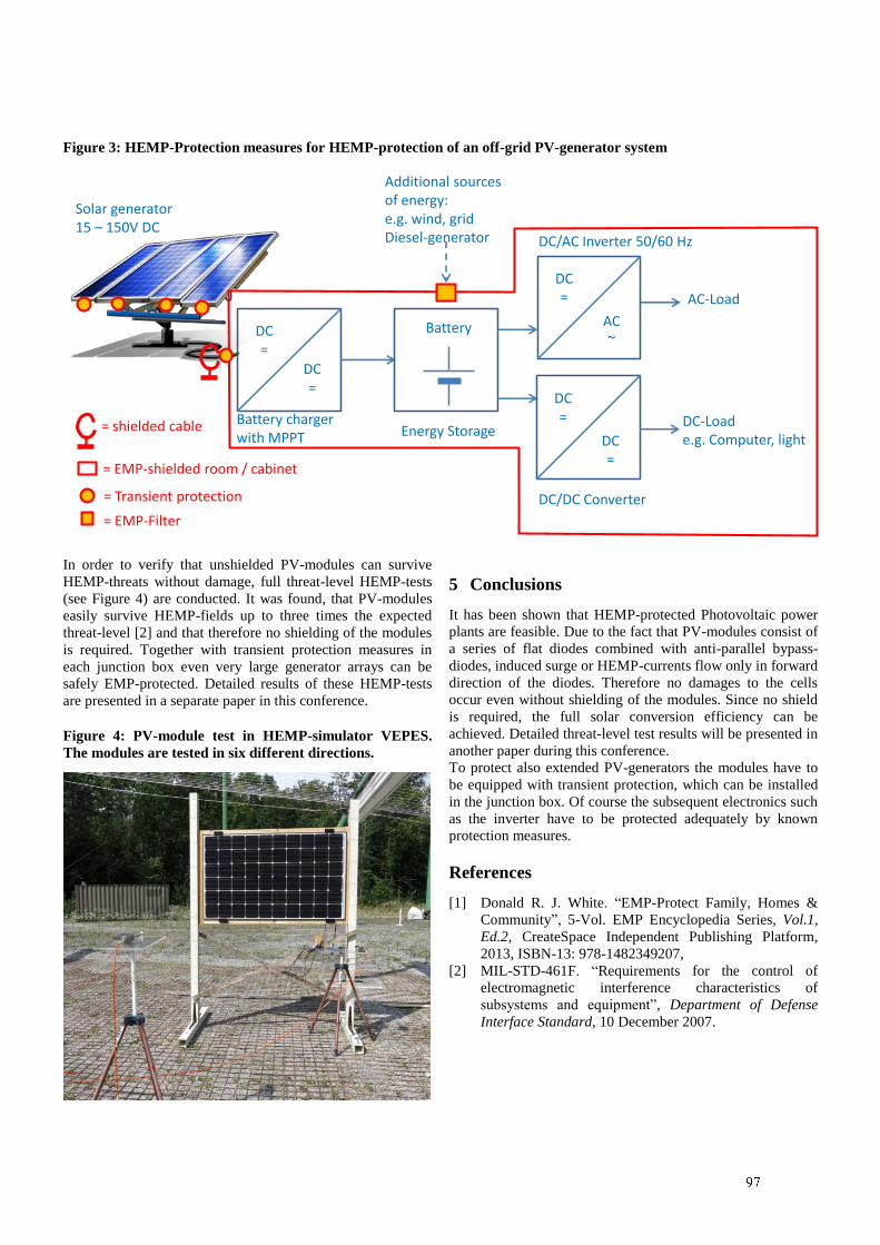
3
Figure 3: HEMP-Protection measures for HEMP-protection of an off-grid PV-generator system
DC=
Battery chargerwith MPPT
Solar generator15 – 150V DC
DC=
Battery
Energy StorageDC-Loade.g. Computer, light
DC=
DC=
DC=
AC~
DC/DC Converter
DC/AC Inverter 50/60 Hz
AC-Load
Additional sourcesof energy:e.g. wind, gridDiesel-generator
= shielded cable
= EMP-shielded room / cabinet
= Transient protection
= EMP-Filter
In order to verify that unshielded PV-modules can survive
HEMP-threats without damage, full threat-level HEMP-tests
(see Figure 4) are conducted. It was found, that PV-modules
easily survive HEMP-fields up to three times the expected
threat-level [2] and that therefore no shielding of the modules
is required. Together with transient protection measures in
each junction box even very large generator arrays can be
safely EMP-protected. Detailed results of these HEMP-tests
are presented in a separate paper in this conference.
Figure 4: PV-module test in HEMP-simulator VEPES.
The modules are tested in six different directions.
5 Conclusions
It has been shown that HEMP-protected Photovoltaic power
plants are feasible. Due to the fact that PV-modules consist of
a series of flat diodes combined with anti-parallel bypass-
diodes, induced surge or HEMP-currents flow only in forward
direction of the diodes. Therefore no damages to the cells
occur even without shielding of the modules. Since no shield
is required, the full solar conversion efficiency can be
achieved. Detailed threat-level test results will be presented in
another paper during this conference.
To protect also extended PV-generators the modules have to
be equipped with transient protection, which can be installed
in the junction box. Of course the subsequent electronics such
as the inverter have to be protected adequately by known
protection measures.
References
[1] Donald R. J. White. “EMP-Protect Family, Homes &
Community”, 5-Vol. EMP Encyclopedia Series, Vol.1,
Ed.2, CreateSpace Independent Publishing Platform,
2013, ISBN-13: 978-1482349207,
[2] MIL-STD-461F. “Requirements for the control of
electromagnetic interference characteristics of
subsystems and equipment”, Department of Defense
Interface Standard, 10 December 2007.
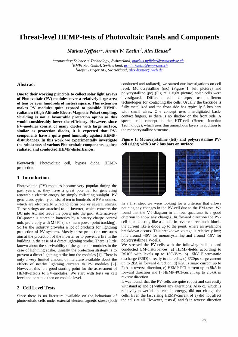
1
Threat-level HEMP-tests of Photovoltaic Panels and Components
Markus Nyffeler*, Armin W. Kaelin †, Alex Hauser
§
*armasuisse Science + Technology, Switzerland, [email protected] ,
†EMProtec GmbH, Switzerland, [email protected]
§Meyer Burger AG, Switzerland, [email protected]
Abstract
Due to their working principle to collect solar light arrays
of Photovoltaic (PV) modules cover a relatively large area
of tens or even hundreds of meters square. This extension
makes PV modules quite exposed to possible HEMP-
radiation (High Altitude ElectroMagnetic Pulse) coupling.
Shielding is not a favourable protection option as this
would considerably lower the efficiency. However, since
PV-modules consist of many diodes with large surface,
similar as protection diodes, it is expected that PV-
components have a quite good immunity against HEMP-
disturbances. In this work we experimentally investigate
the robustness of various Photovoltaic components against
radiated and conducted HEMP-disturbances.
Keywords: Photovoltaic cell, bypass diode, HEMP-
protection
1 Introduction
Photovoltaic (PV) modules became very popular during the
past years, as they have a great potential for generating
renewable electric energy by simply collecting sunlight. PV
generators typically consist of ten to hundreds of PV modules,
which are electrically wired to form one or several strings.
These strings are attached to an inverter, which converts the
DC into AC and feeds the power into the grid. Alternatively
DC-power is stored in batteries by a battery charge control
unit, preferably with MPPT (maximum power point tracking).
So far the industry provides a lot of products for lightning
protection of PV systems. Mostly these protection measures
aim at the protection of the inverter or to prevent a fire in the
building in the case of a direct lightning stroke. There is little
known about the survivability of the generator modules in the
case of lightning strike. Usually the protection strategy is to
prevent a direct lightning strike into the modules [1]. There is
only a very limited amount of literature available about the
effects of nearby lightning currents to PV modules [2].
However, this is a good starting point for the assessment of
HEMP-effects to PV-modules. We start with tests on cell
level and continue then on module level.
2 Cell Level Tests
Since there is no literature available on the behaviour of
photovoltaic cells under external electromagnetic stress (both
conducted and radiated), we started our investigations on cell
level. Monocrystalline (mc) (Figure 1, left picture) and
polycrystalline (pc) (Figure 1 right picture) solar cells were
investigated. Different cell concepts use different
technologies for contacting the cells. Usually the backside is
fully metallized and the front side has typically 3 bus bars
with small wires. One concept uses interdigitated back-
contact fingers, so there is no shadow on the front side. A
special cell concept is the HJT-cell (Hetero Junction
Technology), which uses thin amorphous layers in addition to
the monocrystalline structure.
Figure 1: Monocrystalline (left) and polycrystalline PV-
cell (right) with 3 or 2 bus bars on surface
In a first step, we were looking for a criterion that allows
noticing any changes in the PV-cell due to the EM-tests. We
found that the V-I-diagram in all four quadrants is a good
criterion to show any changes. In forward direction the PV-
cell is conducting like a diode. In reverse direction it blocks
the current like a diode up to the point, where an avalanche
breakdown occurs. This breakdown voltage is relatively low;
it is around -40V for monocrystalline and around -15V for
polycrystalline PV-cells.
We stressed the PV-cells with the following radiated and
conducted EM-disturbances: a) HEMP-fields according to
RS105 with levels up to 150kV/m, b) 15kV Electrostatic
discharge (ESD) directly to the cells, c) 8/20μs surge current
up to 2kA in forward direction, d) 8/20μs surge current up to
2kA in reverse direction, e) HEMP-PCI-current up to 5kA in
forward direction and f) HEMP-PCI-current up to 2.5kA in
reverse direction.
It was found, that the PV-cells are quite robust and can easily
withstand a) and b) without any alterations. Also c), which is
relatively powerful and rich in energy, did not change the
cells. Even the fast rising HEMP-current of e) did not affect
the cells at all. However, tests d) and f) in reverse direction
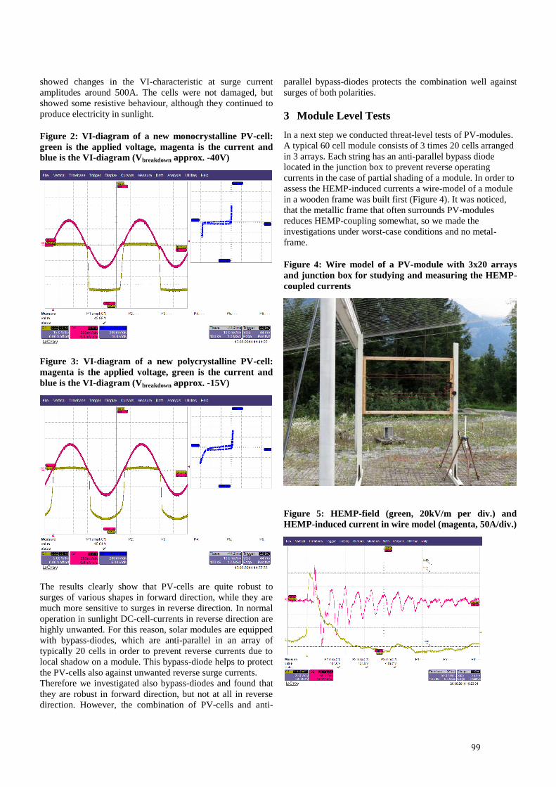
2
showed changes in the VI-characteristic at surge current
amplitudes around 500A. The cells were not damaged, but
showed some resistive behaviour, although they continued to
produce electricity in sunlight.
Figure 2: VI-diagram of a new monocrystalline PV-cell:
green is the applied voltage, magenta is the current and
blue is the VI-diagram (Vbreakdown approx. -40V)
Figure 3: VI-diagram of a new polycrystalline PV-cell:
magenta is the applied voltage, green is the current and
blue is the VI-diagram (Vbreakdown approx. -15V)
The results clearly show that PV-cells are quite robust to
surges of various shapes in forward direction, while they are
much more sensitive to surges in reverse direction. In normal
operation in sunlight DC-cell-currents in reverse direction are
highly unwanted. For this reason, solar modules are equipped
with bypass-diodes, which are anti-parallel in an array of
typically 20 cells in order to prevent reverse currents due to
local shadow on a module. This bypass-diode helps to protect
the PV-cells also against unwanted reverse surge currents.
Therefore we investigated also bypass-diodes and found that
they are robust in forward direction, but not at all in reverse
direction. However, the combination of PV-cells and anti-
parallel bypass-diodes protects the combination well against
surges of both polarities.
3 Module Level Tests
In a next step we conducted threat-level tests of PV-modules.
A typical 60 cell module consists of 3 times 20 cells arranged
in 3 arrays. Each string has an anti-parallel bypass diode
located in the junction box to prevent reverse operating
currents in the case of partial shading of a module. In order to
assess the HEMP-induced currents a wire-model of a module
in a wooden frame was built first (Figure 4). It was noticed,
that the metallic frame that often surrounds PV-modules
reduces HEMP-coupling somewhat, so we made the
investigations under worst-case conditions and no metal-
frame.
Figure 4: Wire model of a PV-module with 3x20 arrays
and junction box for studying and measuring the HEMP-
coupled currents
Figure 5: HEMP-field (green, 20kV/m per div.) and
HEMP-induced current in wire model (magenta, 50A/div.)
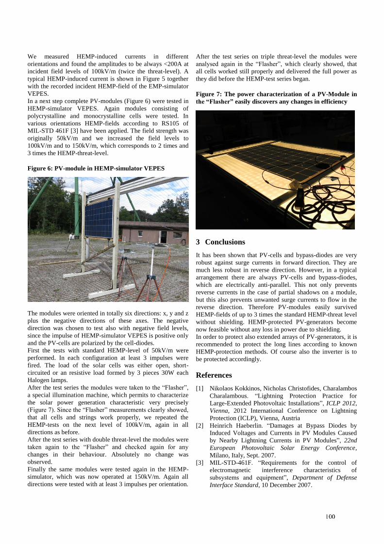
3
We measured HEMP-induced currents in different
orientations and found the amplitudes to be always <200A at
incident field levels of 100kV/m (twice the threat-level). A
typical HEMP-induced current is shown in Figure 5 together
with the recorded incident HEMP-field of the EMP-simulator
VEPES.
In a next step complete PV-modules (Figure 6) were tested in
HEMP-simulator VEPES. Again modules consisting of
polycrystalline and monocrystalline cells were tested. In
various orientations HEMP-fields according to RS105 of
MIL-STD 461F [3] have been applied. The field strength was
originally 50kV/m and we increased the field levels to
100kV/m and to 150kV/m, which corresponds to 2 times and
3 times the HEMP-threat-level.
Figure 6: PV-module in HEMP-simulator VEPES
The modules were oriented in totally six directions: x, y and z
plus the negative directions of these axes. The negative
direction was chosen to test also with negative field levels,
since the impulse of HEMP-simulator VEPES is positive only
and the PV-cells are polarized by the cell-diodes.
First the tests with standard HEMP-level of 50kV/m were
performed. In each configuration at least 3 impulses were
fired. The load of the solar cells was either open, short-
circuited or an resistive load formed by 3 pieces 30W each
Halogen lamps.
After the test series the modules were taken to the “Flasher”,
a special illumination machine, which permits to characterize
the solar power generation characteristic very precisely
(Figure 7). Since the “Flasher” measurements clearly showed,
that all cells and strings work properly, we repeated the
HEMP-tests on the next level of 100kV/m, again in all
directions as before.
After the test series with double threat-level the modules were
taken again to the “Flasher” and checked again for any
changes in their behaviour. Absolutely no change was
observed.
Finally the same modules were tested again in the HEMP-
simulator, which was now operated at 150kV/m. Again all
directions were tested with at least 3 impulses per orientation.
After the test series on triple threat-level the modules were
analysed again in the “Flasher”, which clearly showed, that
all cells worked still properly and delivered the full power as
they did before the HEMP-test series began.
Figure 7: The power characterization of a PV-Module in
the “Flasher” easily discovers any changes in efficiency
3 Conclusions
It has been shown that PV-cells and bypass-diodes are very
robust against surge currents in forward direction. They are
much less robust in reverse direction. However, in a typical
arrangement there are always PV-cells and bypass-diodes,
which are electrically anti-parallel. This not only prevents
reverse currents in the case of partial shadows on a module,
but this also prevents unwanted surge currents to flow in the
reverse direction. Therefore PV-modules easily survived
HEMP-fields of up to 3 times the standard HEMP-threat level
without shielding. HEMP-protected PV-generators become
now feasible without any loss in power due to shielding.
In order to protect also extended arrays of PV-generators, it is
recommended to protect the long lines according to known
HEMP-protection methods. Of course also the inverter is to
be protected accordingly.
References
[1] Nikolaos Kokkinos, Nicholas Christofides, Charalambos
Charalambous. “Lightning Protection Practice for
Large-Extended Photovoltaic Installations”, ICLP 2012,
Vienna, 2012 International Conference on Lightning
Protection (ICLP), Vienna, Austria
[2] Heinrich Haeberlin. “Damages at Bypass Diodes by
Induced Voltages and Currents in PV Modules Caused
by Nearby Lightning Currents in PV Modules”, 22nd
European Photovoltaic Solar Energy Conference,
Milano, Italy, Sept. 2007.
[3] MIL-STD-461F. “Requirements for the control of
electromagnetic interference characteristics of
subsystems and equipment”, Department of Defense
Interface Standard, 10 December 2007.
1
Experiment research on response of typical SPD to different EMP
Zhou Ying-hui *, Du Mingxin †, Shi Lihua †, Zeng Jie *
*State Key Laboratory of Mechanics and Control of Mechanical Structures, NUAA, Nanjing 210007, China, †National Key Laboratory on Electromagnetic Environmental Effects and Electro-optical Engineering, Nanjing Jiangsu 210007, China
Abstract In this paper, the study of protection effectiveness of typical surge protective devices (SPD) to electromagnetic pulse is developed, an SPD test fixture is designed and the test setup is built based on a pulse generator. Different kinds of pulses have been injected to some typical SPDs respectively, test results show that the protection effectiveness is correlated with rise time of injected pulse. According to the test result, relationship of SPD’s response character with injected pulse rise time can be fitted. Then, some benefit reference is given to choose protective device against EMP disturbance. Keywords: Surge protective device (SPD); Electromagnetic Pulse (EMP); protected effect; rise time; experiment research.
1 Introduction
SPD includes of some kinds of device which protect the equipment by limiting the transient over voltage or surge current. They are always used for lightning protection in transmission line or conducted circuit, protective characteristics of these devices to EMP are still not sure. In order to discuss the protection effectiveness of typical SPD to injected EMP voltage, and the test setup is built according the renewed criterion -- IEC 61000-4-24. Effects of variable EMP voltage with different rise time and half width are tested and described in the following experiment research.
2 SPD test setup
A universal test fixture is designed to fix all kinds of two- and four-terminal SPDs in accordance with [1] (see Fig. 1). Insert attenuation of this fixture is measured by an Agilent-4396B
analyzer, the result is about 9dB in range of 100k~1GHz and the transfer character is smooth in this frequency range.
Figure 1. SPD test fixture
The test setup consists of pulse generators, launching lines, test fixture and oscilloscope. The two lightning surge generators can output three kinds of voltages waveform, the rise time/half width are (3/25) ns, (10/100) ns and (10/700) μs, respectively.
3 EMP Response of typical SPD
By the test setup mentioned above, several kinds of typical SPDs are tested to obtain their response characteristics. Wide pulse (10/700µs) and narrow pulse (3/25ns or 10/100ns) are injected to each kind of device under tested (DUT). Representative test results are shown in the follow.
3.1 Coaxial gas charge tube
According to IEC 61000-4-24, a kind of CMTZ-50 model coaxial gas tube is tested by the setup, the protection effectiveness to wide and narrow injected pulses is analyzed. Test results show that these devices start to response when the injected voltage enhanced to certain amplitude, and the response effect varied with scale-up injected pulse.
(a) Uin=1430V(3/25ns) (b) Uin=1240V(10/100ns)
(c) Uin=298V (10/700μs)
Figure 2. Response of coaxial gas charge tube to different injected pulse
Fig.2 shows response of the coaxial gas charge tubes to different injected pulse. It can be found that response voltage of this SPD is closely related to the rise time of injected pulse. The shorter rise time leads to the higher response voltage amplitude. In order to investigate the device response action to the rise time of injected pulse, the pulse generator impedances and inductances were adjusted to get output
Vol
tage
(V
)
Injected
Time (ms)
Vol
tage
(V
)
Response
Time (ms)
DUT
Unprotedted Protected
Injected signal
Response signal
Injected signal
Response signal
2
signal with different rise time. The rise time of generator output is turned up from 3ns to about 30ns, and the response voltage is decrease from 1kV to 361V with the decline of injected pulse rise time. For sake of estimating the relationship of device response voltage level, the 1st order exponential fitting model is adopted here and the expression is shown as (1).
0.1915U=1127.6 + 415rte (3ns≤tr≤30ns) (1)
Here U is the device response voltage; tr is the injected pulse rise time. Then, the coaxial gas tube response character can be estimated by (1) under different injected pulse, and the applicability to protected equipment can be estimated by this expression.
2.2 Metal oxide varistor (MOV)
MOV is tested by the setup and method mentioned above, test result indicated that MOV can clamp injected wide pulse obviously. But it cannot clamp the narrow injected pulse instead of decrease its peak value. Under wide pulse injected
pulse, the highest clamp voltage value of MOV is about 1.6~1.8 times higher than its nominal value. While to narrow
injected pulse, the constrained voltage value is about 1.4~2 times higher than its nominal value. The rise time of narrow
pulse injected is about (3~10ns) , which means it has abundant high frequency components. Then, MOV appear lower impedance under higher frequency pulse, the energy of injected pulse is absorbed and constrained by this way.
2.3 Transient voltage suppress (TVS) tube
Similar test has been done to TVS tube, and test results show its restrain ability to both wide and narrow injected pulse. The action character is comparable with MOV. The highest clamp
voltage to wide injected pulse is about 1.2~1.6 times higher than its nominal value, and the constrained voltage is about
3~4 times higher than its nominal value.
3 Conclusions
In this paper, experimental research has been developed to several types of SPDs under injected pulse with different rise time. Test results indicate the common SPDs applied in lightning surge protection also have constrained ability to EMP in a certain extent. Because of the different rise time and half width between lightning and EMP waveform, the response characters have great distance with their nominal values. Although many SPD’s components nominal values is in nano second, the test results show they barely response to injected pulse of 10ns (3ns) rise time waveform. According to the tested protective character, the relationship of SPD’s response voltage with injected pulse rise time can be fitted by mathematic functions. This research provides some benefit reference to choose of protective component against EMP disturbance.
Acknowledgements
This work was supported by NSFC under Grant No. 51407198 and 51477183.
References
[1] Jinliang He; Zhiyong Yuan; Shunchao Wang, et. al., “Effective Protection Distances of Low-Voltage SPD With Different Voltage Protection Levels”. IEEE Trans. on Power Delivery. 2010. vol.25 (1), 187-195.
[2] Long duration impulse withstand capability of SPD. Zhang Nanfa; Kang Guoyao; Guo Yaping. Asia-Pacific Symposium on EMC. 2010. 1510 – 1513.
[3] Analysis of additional tests for SPD's failure mode in IEC61643.11. Yang Guohua; Wang Chongling; Dai Dezhi; Wan Kaili. International Conference on Lightning Protection. 2014. 1083 - 1086
[4] Overcurrent protection function for SPD disconnectors. Sato, A.; Morii, N.; Sato, H. The 7th Asia-Pacific International Conference on Lightning. 2011. 586 – 589.
[5] IEC 61000-4-24: 2013, Testing and measurement techniques - Test methods for protective devices for HEMP conducted disturbance[S].
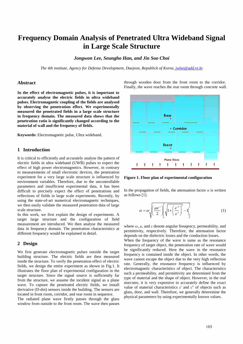
Frequency Domain Analysis of Penetrated Ultra Wideband Signal
in Large Scale Structure
Jongwon Lee, Seungho Han, and Jin Soo Choi
The 4th institute, Agency for Defense Development, Daejeon, Republick of Korea, [email protected]
Abstract
In the effect of electromagnetic pulses, it is important to
accurately analyse the electric fields in ultra wideband
pulses. Electromagnetic coupling of the fields are analysed
by observing the penetration effect. We experimentally
measured the penetrated fields in a large scale structure
in frequency domain. The measured data shows that the
penetration ratio is significantly changed according to the
material of wall and the frequency of fields.
Keywords: Electromagnetic pulse, Ultra wideband.
1 Introduction
It is critical to efficiently and accurately analyse the pattern of
electric fields in ultra wideband (UWB) pulses to expect the
effect of high power electromagnetics. However, in contrary
to measurements of small electronic devices, the penetration
experiment for a very large scale structure is influenced by
environment variables. Therefore, due to the uncontrollable
parameters and insufficient experimental data, it has been
difficult to precisely expect the effect of penetrations and
reflections of fields in large scale experiments. Recently, by
using the state-of-art numerical electromagnetic techniques,
we then easily validate the measured penetration data of large
scale structure.
In this work, we first explain the design of experiments. A
target large structure and the configuration of field
measurement are introduced. We then analyse the measured
data in frequency domain. The penetration characteristics at
different frequency would be explained in detail.
2 Design
We first generate electromagnetic pulses outside the target
building structure. The electric fields are then measured
inside the structure. To verify the penetration effect of electric
fields, we design the entire experiment as shown in Fig.1. It
illustrates the floor plan of experimental configuration in the
target structure. Since the signal source is sufficiently far
from the structure, we assume the incident signal as a plane
wave. To capture the penetrated electric fields, we install
derivative (D-dot) sensors inside the building. The sensors are
located in front room, corridor, and rear room in sequence.
The radiated plane wave firstly passes through the glass
window from outside to the front room. The wave then passes
through wooden door from the front room to the corridor.
Finally, the wave reaches the rear room through concrete wall.
Figure 1. Floor plan of experimental configuration
In the propagation of fields, the attenuation factor α is written
as follows [1].
2' ''
1 12 '
(1)
where ω, μ, and ε denote angular freuqency, permeability, and
permittivity, respectively. Therefore, the attenuation factor
depends on the dielectric losses and the conduction losses.
When the frequency of the wave is same as the resonance
frequency of target object, the penetration rate of wave would
be significantly reduced. Here the wave in the resonance
frequency is contained inside the object. In other words, the
wave cannot escape the object due to the very high reflection
rate. Generally, the resonance frequency is influenced by
electromagnetic characteristics of object. The characteristics
such a permeability, and permittivity are determined from the
type of material and the shape of object. However, in the real
sturcutre, it is very expensive to accurately define the exact
value of material characteristics ε' and ε'' of objects such as
glass, door, and wall. Therefore, we generally deteremine the
physical parameters by using experimentally known values.
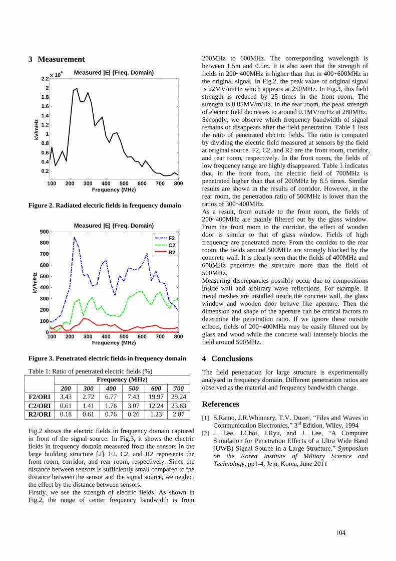
3 Measurement
Figure 2. Radiated electric fields in frequency domain
Figure 3. Penetrated electric fields in frequency domain
Table 1: Ratio of penetrated electric fields (%)
Frequency (MHz)
200 300 400 500 600 700
F2/ORI 3.43 2.72 6.77 7.43 19.97 29.24
C2/ORI 0.61 1.41 1.76 3.07 12.24 23.63
R2/ORI 0.18 0.61 0.76 0.26 1.23 2.87
Fig.2 shows the electric fields in frequency domain captured
in front of the signal source. In Fig.3, it shows the electric
fields in frequency domain measured from the sensors in the
large building structure [2]. F2, C2, and R2 represents the
front room, corridor, and rear room, respectively. Since the
distance between sensors is sufficiently small compared to the
distance between the sensor and the signal source, we neglect
the effect by the distance between sensors.
Firstly, we see the strength of electric fields. As shown in
Fig.2, the range of center frequency bandwidth is from
200MHz to 600MHz. The corresponding wavelength is
between 1.5m and 0.5m. It is also seen that the strength of
fields in 200~400MHz is higher than that in 400~600MHz in
the original signal. In Fig.2, the peak value of original signal
is 22MV/m/Hz which appears at 250MHz. In Fig.3, this field
strength is reduced by 25 times in the front room. The
strength is 0.85MV/m/Hz. In the rear room, the peak strength
of electric field decreases to around 0.1MV/m/Hz at 280MHz.
Secondly, we observe which frequency bandwidth of signal
remains or disappears after the field penetration. Table 1 lists
the ratio of penetrated electric fields. The ratio is computed
by dividing the electric field measured at sensors by the field
at original source. F2, C2, and R2 are the front room, corridor,
and rear room, respectively. In the front room, the fields of
low frequency range are highly disappeared. Table 1 indicates
that, in the front from, the electric field of 700MHz is
penetrated higher than that of 200MHz by 8.5 times. Similar
results are shown in the results of corridor. However, in the
rear room, the penetration ratio of 500MHz is lower than the
ratios of 300~400MHz.
As a result, from outside to the front room, the fields of
200~400MHz are mainly filtered out by the glass window.
From the front room to the corridor, the effect of wooden
door is similar to that of glass window. Fields of high
frequency are penetrated more. From the corridor to the rear
room, the fields around 500MHz are strongly blocked by the
concrete wall. It is clearly seen that the fields of 400MHz and
600MHz penetrate the structure more than the field of
500MHz.
Measuring discrepancies possibly occur due to compositions
inside wall and arbitrary wave reflections. For example, if
metal meshes are installed inside the concrete wall, the glass
window and wooden door behave like aperture. Then the
dimension and shape of the aperture can be critical factors to
determine the penetration ratio. If we ignore these outside
effects, fields of 200~400MHz may be easily filtered out by
glass and wood while the concrete wall intensely blocks the
field around 500MHz.
4 Conclusions
The field penetration for large structure is experimentally
analysed in frequency domain. Different penetration ratios are
observed as the material and frequency bandwidth change.
References
[1] S.Ramo, J.R.Whinnery, T.V. Duzer, “Files and Waves in
Communication Electronics,” 3rd
Edition, Wiley, 1994
[2] J. Lee, J.Choi, J.Ryu, and J. Lee, “A Computer
Simulation for Penetration Effects of a Ultra Wide Band
(UWB) Signal Source in a Large Structure,” Symposium
on the Korea Institute of Military Science and
Technology, pp1-4, Jeju, Korea, June 2011
100 200 300 400 500 600 700 800
0.2
0.4
0.6
0.8
1
1.2
1.4
1.6
1.8
2
2.2x 10
4 Measured |E| (Freq. Domain)
Frequency (MHz)
kV
/m/H
z
100 200 300 400 500 600 700 8000
100
200
300
400
500
600
700
800
900
kV
/m/H
z
Measured |E| (Freq. Domain)
Frequency (MHz)
F2
C2
R2
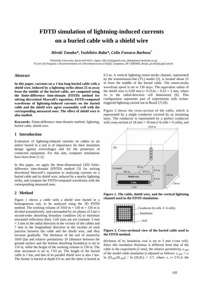
1
FDTD simulation of lightning-induced currents
on a buried cable with a shield wire
Hiroki Tanaka*, Yoshihiro Baba*, Celio Fonseca Barbosa†
*Doshisha University, Kyoto-610-0321, Japan, [email protected], [email protected] †Centro de Pesquisa e Desenvolvimento em Telecomunicacoes (CPqD), Campinas, SP 13083060, Brazil, [email protected]
Abstract
In this paper, currents on a 1-km long buried cable with a
shield wire, induced by a lightning strike about 25 m away
from the middle of the buried cable, are computed using
the finite-difference time-domain (FDTD) method for
solving discretized Maxwell’s equations. FDTD-computed
waveforms of lightning-induced currents on the buried
cable and the shield wire agree reasonably well with the
corresponding measured ones. The effect of shield wire is
also studied. Keywords: Finite-difference time-domain method, lightning,
buried cable, shield wire.
1 Introduction
Evaluation of lightning-induced currents on cables in air
and/or buried in a soil is of importance for their insulation
design against overvoltages and for the protection of
connected equipment. For this aim, computer simulations
have been done [1-2].
In this paper, we apply the three-dimensional (3D) finite-
difference time-domain (FDTD) method [3] for solving
discretized Maxwell’s equations to analyzing currents on a
buried cable and its shield wire, induced by a nearby lightning
strike, and compare the FDTD-computed waveforms with the
corresponding measured ones.
2 Method
Figure 1 shows a cable with a shield wire buried in a
homogeneous soil, to be analyzed using the 3D FDTD
method. The working volume of 1010 m × 150 m × 150 m is
divided nonuniformly, and surrounded by six planes of Liao’s
second-order absorbing boundary condition [4] to minimize
unwanted reflections there. Cell sizes are not constant: 3 mm
× 3 mm in the radial direction in the vicinity of the cables and
7 mm in the longitudinal direction in the vicinity of each
junction between the cable and the shield wire, and they
increase gradually. The thickness of the soil of resistivity
1850 m and relative permittivity 10 (distance between the
ground surface and the bottom absorbing boundary) is set to
110 m, while the height of the working volume is 150 m. The
time increment is set to 7.03 ps. The length of the buried
cable is 1 km, and that of its parallel shield wire is also 1 km.
The former is buried at depth 0.6 m, and the latter is buried at
0.3 m. A vertical lightning return-stroke channel, represented
by the transmission-line (TL) model [5], is located about 25
m from the middle of the buried cable. The return-stroke
wavefront speed is set to 130 m/s. The equivalent radius of
the shield wire is 0.69 mm (≈ 0.23Δs = 0.23 × 3 mm, where
Δs is the radial-direction cell dimension) [6]. This
configuration represents part of experiments with rocket-
triggered lightning carried out in Brazil [7]-[8].
Figure 2 shows the cross-section of the cable, which is
represented by a single conductor covered by an insulating
layer. The conductor is represented by a perfect conductor
with cross-section of 18 mm × 18 mm (=6 cells × 6 cells), and
Air
1010 m
150 m
110 m
Ground
585 m 415 m
1 km
0.3 m
0.3 m
Cable
Shield wire
25 m
Figure 1. The cable, shield wire, and the vertical lightning
channel used in the FDTD simulation.
Conductor (6 cells × 6 cells)
Insulation
Soil
Figure 2. Cross-sectional view of the buried cable used in
the FDTD method.
thickness of its insulation coat is set to 3 mm (=one cell).
Since this insulation thickness is different from that of the
cable in the experiment (2 mm), the relative permittivity r.fdtd
of the model cable insulation is adjusted as follows: r.fdtd = r
ln (Di.fdtd/Dc.fdtd) / ln (Di/Dc) = 3.7, where ris the
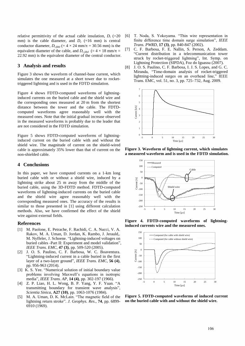
2
relative permittivity of the actual cable insulation, Di (=20
mm) is the cable diameter, and Dc (=16 mm) is central
conductor diameter, Di.fdtd (= 4 × 24 mm/ = 30.56 mm) is the
equivalent diameter of the cable, and Dc.fdtd (= 4 × 18 mm/ =
22.92 mm) is the equivalent diameter of the central conductor.
3 Analysis and results
Figure 3 shows the waveform of channel-base current, which
simulates the one measured at a short tower due to rocket-
triggered lightning and is used in the FDTD simulation.
Figure 4 shows FDTD-computed waveforms of lightning-
induced currents on the buried cable and the shield wire and
the corresponding ones measured at 20 m from the shortest
distance between the tower and the cable. The FDTD-
computed waveforms agree reasonably well with the
measured ones. Note that the initial gradual increase observed
in the measured waveforms is probably due to the leader that
are not considered in the FDTD simulation.
Figure 5 shows FDTD-computed waveforms of lightning-
induced current on the buried cable with and without the
shield wire. The magnitude of current on the shield-wired
cable is approximately 35% lower than that of current on the
non-shielded cable.
4 Conclusions
In this paper, we have computed currents on a 1-km long
buried cable with or without a shield wire, induced by a
lightning strike about 25 m away from the middle of the
buried cable, using the 3D-FDTD method. FDTD-computed
waveforms of lightning-induced currents on the buried cable
and the shield wire agree reasonably well with the
corresponding measured ones. The accuracy of the results is
similar to those presented in [1] using different calculation
methods. Also, we have confirmed the effect of the shield
wire against external fields.
References
[1] M. Paolone, E. Petrache, F. Rachidi, C. A. Nucci, V. A. Rakov, M. A. Uman, D. Jordan, K. Rambo, J. Jerauld,. M. Nyffeler, J. Schoene. “Lightning-induced voltages on buried cables -Part II: Experiment and model validation”, IEEE Trans. EMC, 47 (3), pp. 509-520 (2005).
[2] J. O. S. Paulino, C. F. Barbosa, W. C. Boaventura. “Lightning-induced current in a cable buried in the first layer of a two-layer ground”, IEEE Trans. EMC, 56 (4), pp. 956-963 (2014).
[3] K. S. Yee. “Numerical solution of initial boundary value problems involving Maxwell’s equations in isotropic media”, IEEE Trans. AP, 14 (4), pp. 302-197 (1966).
[4] Z. P. Liao, H. L. Wong, B. P. Yang, Y. F. Yuan. “A transmitting boundary for transient wave analysis”, Scientia Sinica, A27 (10), pp. 1063-1076 (1984).
[5] M. A. Uman, D. K. McLain. “The magnetic field of the lightning return stroke”. J. Geophys. Res., 74, pp. 6899-6910 (1969).
[6] T. Noda, S. Yokoyama. “Thin wire representation in finite difference time domain surge simulation”, IEEE Trans. PWRD, 17 (3), pp. 840-847 (2002).
[7] C. F. Barbosa, F. E. Nallin, S. Person, A. Zeddam. “Current distribution in a telecommunication tower struck by rocket-triggered lightning”, Int. Symp. on Lightning Protection (SIPDA), Foz do Iguassu (2007).
[8] J. O. S. Paulino, C. F. Barbosa, I. J. S. Lopes, and G. C. Miranda, “Time-domain analysis of rocket-triggered lightning-induced surges on an overhead line,” IEEE Trans. EMC, vol. 51, no. 3, pp. 725–732, Aug. 2009.
0
1
2
3
4
5
6
7
-5 0 5 10 15 20 25 30C
urr
ent
[kA
]
Time [s]
Figure 3. Waveform of lightning current, which simulates
a measured waveform and is used in the FDTD simulation.
-250
-200
-150
-100
-50
0
50
100
150
-5 0 5 10 15 20 25 30
Curr
ent
[A]
Time [s]
Measured
Computed
Cable
Shield wire
Figure 4. FDTD-computed waveforms of lightning-
induced currents wire and the measured ones.
-250
-200
-150
-100
-50
0
50
100
150
-5 0 5 10 15 20 25 30
Cu
rren
t [A
]
Time [s]
Computed (for cable with shield wire)
Computed (for cable without shield wire)
Figure 5. FDTD-computed waveforms of induced current
on the buried cable with and without the shield wire.
1
Lightning occurrence data observed with lightning location systems of electric power companies in Japan: 2009-2013
Takatoshi Shindo*1, Hideki Motoyama*1, Toru Miki*1, Mikihisa Saito*1, Akiyori Matsueda*2, Noriyasu Honma*3, Akira Matsumoto*4, Kazuo Shinjo*5, Kiyotaka Hayashi*6, Hayato Awazu*7 , Katsuhisa
Makabe*8, Masato Fujikawa*9, Satoshi Kurihara*10, Masashi Sato*11
*1CRIEPI, 2-6-1, Nagasaka, Yokosuka-shi, Kanagawa-ken, Japan, [email protected], *2Hokkaido Electric Power Company, Japan, *3Tohoku Electric Power Company, Japan,*4Tokyo Electric Power Company,
Japan, *5Hokuriku Electric Power Company, Japan, *6Chubu Electric Power Company, Japan, *7Kansai Electric Power Company, Japan, *8Chugoku Electric Power Company, Japan,*9Shikoku Electric Power Company, Japan, *10Kyushu Electric
Power Company, Japan, *11J-Power, Japan
Abstract
5 years of lightning data from 2009 to 2013 obtained with lightning location system of 9 electric power companies in Japan have been summarized and analyzed. The recent annual number of lightning flashes of which current is more than 10 kA in Japan is around one million. The variations of lightning occurrence characteristics by areas, seasons and so on are clarified. Keywords: Lightning, Database, Lightning location system, Lightning current
1 Introduction Cloud-to-ground lightning flash frequency is one of the important factors for rational insulation design of power transmission systems. Recently, lightning location system have been widely used and lightning data with such systems have been collected and summarized all over the world [1-9]. In Japan, nine electric power companies have their own lightning location systems and lightning data have been collected. The Central Research Institute of Electric Power Industry (CRIEPI) has carried out fundamental researches on the construction of a lightning frequency map in cooperation with electric power companies in Japan [10-12]. The lightning location systems of Japanese electric companies have been improved and most of them have introduced the LS 7000 or LS8000 version of lightning location systems at present. In this paper, based on the 5 years of lightning data from 2009 to 2013 observed with the lightning location systems, characteristics of lightning occurrence frequency and lightning currents have been summarized.
2 Lightning location systems of Japanese electric power companies Fig. 1 shows the location of Direction Finders (DFs) of lightning location systems of the nine Japanese electric power companies as of 2013. In order to make a lightning frequency map in Japan, nine subdivisions were determined considering the service area of each electric power company as shown in Fig. 2. Lightning data in each subdivision were provided by the lightning location system of each electric power company located in the same subdivision and summarized in meshes of 0.25 degree (latitude) by 0.25 degree (longitude). The actual size of each mesh is not exactly same but it is about 23 km by 27 km. Lightning data are summarized as flash data and the data whose current is more than 10 kA are used in this analysis according to the previous analysis [10-12].
Figure 1 Locations of DFs of lightning location systems of Japanese electric power companies as of 2013.
Pacific Ocean
The Sea of Japan
2
Figure 2 The subdivisions used in the analysis.
3 Lightning data Basically lightning data are summarized in two seasons which are summer (from April to October) and winter (from November to March). The year shown hereafter is the fiscal year (from April to March of the next year) unless otherwise stated.
3.1 Number of lightning occurrence
Fig. 3 shows the variation of annual number of lightning flashes in Japan. The variation of number of lightning flashes in winter is also shown in Fig. 4.
Figure 3 Annual number of lightning flashes.
Figure 4 Number of flashes in winter season.
From Figs. 3 and 4, it seems that number of lightning occurrence is increasing. However we should note that the detection efficiency of lightning location systems may have been improved in recent systems.
3.2 Lightning density map in Japan
Fig. 5 shows lightning flash density maps in summer and winter. Not only the 5-year average from 2009 to 2013 but 7-year average from 2002-2008 are shown for reference. In summer, we have lot of lightning flashes in the north part of Kanto plain (subdivion C in Fig. 2) and the central area of Japan. On the other hand, we have lightning flashes in the coastal area along the Sea of Japan in winter. The regional lightning occurrence characteristics stated above are almost same as those from 1992 to 2008, which was reported in [12].
3.3 Lightning current
We summarized the 50% value and 5% value of the cumulative lightning current distribution in Table 1, assuming the log-normal distribution for lightning current. It seems that there is a tendency of decrease of current values recently.
a) Summer b) Winter
(Average: 2002-2008)
a) Summer b) Winter
(Average: 2009-2013)
Figure 5 Lightning flash density map in summer and in winter.
Pacific Ocean Pacific Ocean
The Sea of Japan
The Sea of Japan
The Sea of Japan
Pacific Ocean 30°
35°
40°
45°
146° 140° 135° 130°
A
B
C D
E F G
H I
The Sea of Japan
The Sea of Japan
Pacific Ocean Pacific Ocean
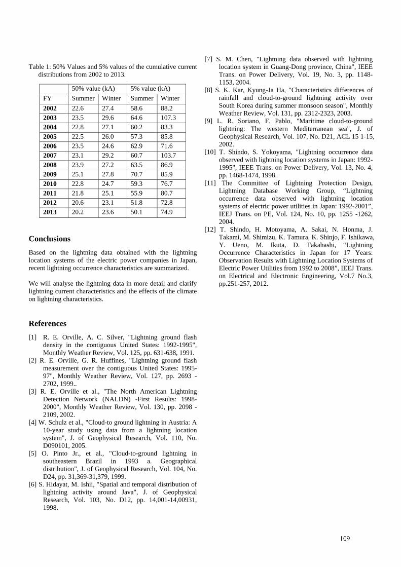
3
Table 1: 50% Values and 5% values of the cumulative current
distributions from 2002 to 2013.
Conclusions Based on the lightning data obtained with the lightning location systems of the electric power companies in Japan, recent lightning occurrence characteristics are summarized. We will analyse the lightning data in more detail and clarify lightning current characteristics and the effects of the climate on lightning characteristics.
References [1] R. E. Orville, A. C. Silver, "Lightning ground flash
density in the contiguous United States: 1992-1995", Monthly Weather Review, Vol. 125, pp. 631-638, 1991.
[2] R. E. Orville, G. R. Huffines, "Lightning ground flash measurement over the contiguous United States: 1995-97", Monthly Weather Review, Vol. 127, pp. 2693 -2702, 1999..
[3] R. E. Orville et al., "The North American Lightning Detection Network (NALDN) -First Results: 1998-2000", Monthly Weather Review, Vol. 130, pp. 2098 -2109, 2002.
[4] W. Schulz et al., "Cloud-to ground lightning in Austria: A 10-year study using data from a lightning location system", J. of Geophysical Research, Vol. 110, No. D090101, 2005.
[5] O. Pinto Jr., et al., "Cloud-to-ground lightning in southeastern Brazil in 1993 a. Geographical distribution", J. of Geophysical Research, Vol. 104, No. D24, pp. 31,369-31,379, 1999.
[6] S. Hidayat, M. Ishii, "Spatial and temporal distribution of lightning activity around Java", J. of Geophysical Research, Vol. 103, No. D12, pp. 14,001-14,00931, 1998.
[7] S. M. Chen, "Lightning data observed with lightning location system in Guang-Dong province, China", IEEE Trans. on Power Delivery, Vol. 19, No. 3, pp. 1148-1153, 2004.
[8] S. K. Kar, Kyung-Ja Ha, "Characteristics differences of rainfall and cloud-to-ground lightning activity over South Korea during summer monsoon season", Monthly Weather Review, Vol. 131, pp. 2312-2323, 2003.
[9] L. R. Soriano, F. Pablo, "Maritime cloud-to-ground lightning: The western Mediterranean sea", J. of Geophysical Research, Vol. 107, No. D21, ACL 15 1-15, 2002.
[10] T. Shindo, S. Yokoyama, "Lightning occurrence data observed with lightning location systems in Japan: 1992-1995", IEEE Trans. on Power Delivery, Vol. 13, No. 4, pp. 1468-1474, 1998.
[11] The Committee of Lightning Protection Design, Lightning Database Working Group, “Lightning occurrence data observed with lightning location systems of electric power utilities in Japan: 1992-2001”, IEEJ Trans. on PE, Vol. 124, No. 10, pp. 1255 -1262, 2004.
[12] T. Shindo, H. Motoyama, A. Sakai, N. Honma, J. Takami, M. Shimizu, K. Tamura, K. Shinjo, F. Ishikawa, Y. Ueno, M. Ikuta, D. Takahashi, “Lightning Occurrence Characteristics in Japan for 17 Years: Observation Results with Lightning Location Systems of Electric Power Utilities from 1992 to 2008”, IEEJ Trans. on Electrical and Electronic Engineering, Vol.7 No.3, pp.251-257, 2012.
50% value (kA) 5% value (kA) FY Summer Winter Summer Winter 2002 22.6 27.4 58.6 88.2 2003 23.5 29.6 64.6 107.3 2004 22.8 27.1 60.2 83.3 2005 22.5 26.0 57.3 85.8 2006 23.5 24.6 62.9 71.6 2007 23.1 29.2 60.7 103.7 2008 23.9 27.2 63.5 86.9 2009 25.1 27.8 70.7 85.9 2010 22.8 24.7 59.3 76.7 2011 21.8 25.1 55.9 80.7 2012 20.6 23.1 51.8 72.8 2013 20.2 23.6 50.1 74.9
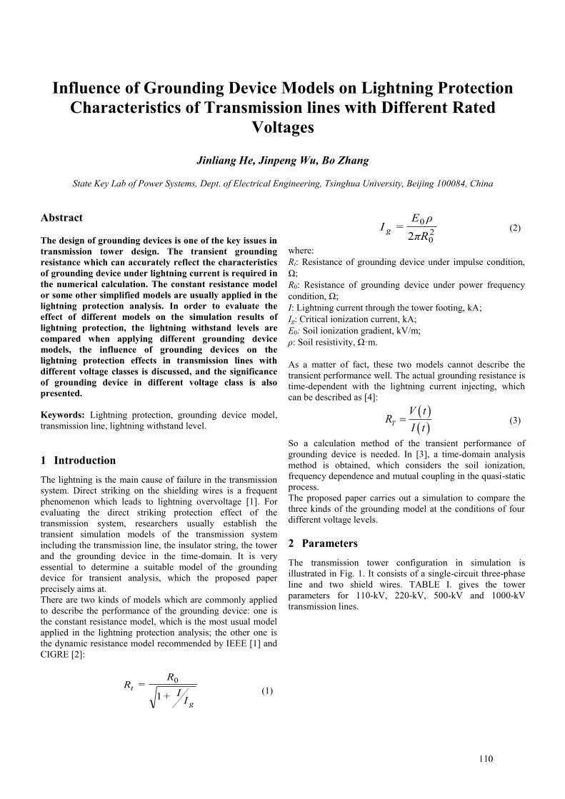
1
Influence of Grounding Device Models on Lightning Protection
Characteristics of Transmission lines with Different Rated
Voltages
Jinliang He, Jinpeng Wu, Bo Zhang
State Key Lab of Power Systems, Dept. of Electrical Engineering, Tsinghua University, Beijing 100084, China
Abstract
The design of grounding devices is one of the key issues in
transmission tower design. The transient grounding
resistance which can accurately reflect the characteristics
of grounding device under lightning current is required in
the numerical calculation. The constant resistance model
or some other simplified models are usually applied in the
lightning protection analysis. In order to evaluate the
effect of different models on the simulation results of
lightning protection, the lightning withstand levels are
compared when applying different grounding device
models, the influence of grounding devices on the
lightning protection effects in transmission lines with
different voltage classes is discussed, and the significance
of grounding device in different voltage class is also
presented.
Keywords: Lightning protection, grounding device model,
transmission line, lightning withstand level.
1 Introduction
The lightning is the main cause of failure in the transmission
system. Direct striking on the shielding wires is a frequent
phenomenon which leads to lightning overvoltage [1]. For
evaluating the direct striking protection effect of the
transmission system, researchers usually establish the
transient simulation models of the transmission system
including the transmission line, the insulator string, the tower
and the grounding device in the time-domain. It is very
essential to determine a suitable model of the grounding
device for transient analysis, which the proposed paper
precisely aims at.
There are two kinds of models which are commonly applied
to describe the performance of the grounding device: one is
the constant resistance model, which is the most usual model
applied in the lightning protection analysis; the other one is
the dynamic resistance model recommended by IEEE [1] and
CIGRE [2]:
g
t
II
RR
+1
=0
(1)
20
0
2=
Rπ
ρEI g (2)
where:
Rt: Resistance of grounding device under impulse condition,
Ω;
R0: Resistance of grounding device under power frequency
condition, Ω;
I: Lightning current through the tower footing, kA;
Ig: Critical ionization current, kA;
E0: Soil ionization gradient, kV/m;
ρ: Soil resistivity, Ω·m.
As a matter of fact, these two models cannot describe the
transient performance well. The actual grounding resistance is
time-dependent with the lightning current injecting, which
can be described as [4]:
T
V tR
I t (3)
So a calculation method of the transient performance of
grounding device is needed. In [3], a time-domain analysis
method is obtained, which considers the soil ionization,
frequency dependence and mutual coupling in the quasi-static
process.
The proposed paper carries out a simulation to compare the
three kinds of the grounding model at the conditions of four
different voltage levels.
2 Parameters
The transmission tower configuration in simulation is
illustrated in Fig. 1. It consists of a single-circuit three-phase
line and two shield wires. TABLE I. gives the tower
parameters for 110-kV, 220-kV, 500-kV and 1000-kV
transmission lines.
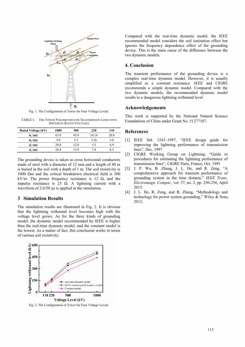
2
d1
d2
d1
h1
h2
Rb
Shield Wire
Phase
Conductor
Lighting Striking
Point
Lin
d2
Fig. 1. The Configuration of Tower for Four Voltage Levels.
TABLE I. THE TOWER PARAMETERS FOR TRANSMISSION LINES WITH
DIFFERENT RATED VOLTAGES
Rated Voltage (kV) 1000 500 220 110
h1 (m) 63.0 45.0 24.14 20.0
h2 (m) 5.0 5.5 3.26 3.0
d1 (m) 28.8 12.0 5.5 4.9
d2 (m) 26.8 13.9 7.0 6.5
The grounding device is taken as cross horizontal conductors
made of steel with a diameter of 12 mm and a length of 40 m
is buried in the soil with a depth of 1 m. The soil resistivity is
1000 Ωm and the critical breakdown electrical field is 300
kV/m. The power frequency resistance is 12 Ω, and the
impulse resistance is 25 Ω. A lightning current with a
waveform of 2.6/50 μs is applied in the simulation.
3 Simulation Results
The simulation results are illustrated in Fig. 2. It is obvious
that the lightning withstand level becomes high with the
voltage level grows. As for the three kinds of grounding
model, the dynamic model recommended by IEEE is higher
than the real-time dynamic model, and the constant model is
the lowest. As a matter of fact, this conclusion works in terms
of various soil resistivity.
Fig. 2. The Configuration of Tower for Four Voltage Levels.
Compared with the real-time dynamic model, the IEEE
recommended model considers the soil ionization effect but
ignores the frequency dependence effect of the grounding
device. This is the main cause of the difference between the
two dynamic models.
4. Conclusion
The transient performance of the grounding device is a
complex real-time dynamic model. However, it is usually
simplified as a constant resistance. IEEE and CIGRE
recommends a simple dynamic model. Compared with the
two dynamic models, the recommended dynamic model
results to a dangerous lightning withstand level.
Acknowledgements
This work is supported by the National Natural Science
Foundations of China under Grant No. 51277107.
References
[1] IEEE Std. 1243–1997, “IEEE design guide for
improving the lightning performance of transmission
lines”, Dec. 1997
[2] CIGRE Working Group on Lightning, “Guide to
procedures for estimating the lightning performance of
transmission lines”, CIGRE Paris, France, Oct. 1991
[3] J. P. Wu, B. Zhang, J. L. He, and R. Zeng, “A
comprehensive approach for transient performance of
grounding system in the time domain,” IEEE Trans.
Electromagn. Compat., vol. 57, no. 2, pp. 250-256, April
2015.
[4] J. L. He, R. Zeng, and B. Zhang, “Methodology and
technology for power system grounding,” Wiley & Sons,
2012.
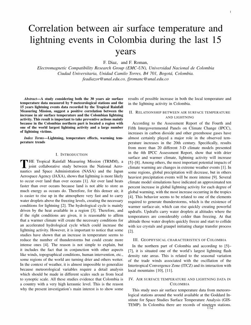
1
Correlation between air surface temperature andlightning events in Colombia during the last 15
yearsF. Diaz, and F. Roman,
Electromagnetic Compatibility Research Group (EMC-UN), Universidad Nacional de ColombiaCiudad Universitaria, Unidad Camilo Torres, B4 701, Bogota, Colombia.
[email protected], [email protected]
Abstract—A study considering both the 30 years air surfacetemperature data measured by 9 meteorological stations and the15 years lightning events data recorded by the Tropical RainfallMeasuring Mission, suggest a positive correlation between theincrease in air surface temperature and the Colombian lightningactivity. This result is important to take preventive actions mainlybecause in the Colombias northern part is located a region withone of the world largest lightning activity and a large numberof lightning victims.
Index Terms—Lightning, temperature effects, warming tem-perature trends
I. INTRODUCTION
THE Tropical Rainfall Measuring Mission (TRMM), ajoint collaborative study between the National Aero-
nautics and Space Administration (NASA) and the JapanAerospace Agency (JAXA), shows that lightning is more likelyto occur over land than over oceans [1]. Air over land heatsfaster than over oceans because land is not able to store asmuch energy as oceans do. Therefore, for this denser air, itis easier to rise up in the atmosphere very fast and to carrywater droplets above the freezing levels, creating the necessaryconditions for lightning [2]. The hydrological cycle is mainlydriven by the heat available in a region [3]. Therefore, andif the right conditions are given, it is reasonable to affirmthat a warmer climate will create the necessary conditions foran accelerated hydrological cycle which could increase thelightning activity. However, it is important to notice that somestudies have shown that an increase in temperature seems toreduce the number of thunderstorms but could create moreintense ones [4]. The reason is not simple to explain, butit includes the fact that in conjunction with other aspectslike winds, topographical conditions, human intervention, etc.,some regions of the world are turning drier and others wetter.In the context of weather, it is almost impossible to generalizebecause meteorological variables require a detail analysiswhich should be made in different scales such as from localto synoptic scale. All these studies evidence that Colombia isa country with a very high keraunic level. This is the reasonwhy the present investigation’s main interest is to show some
results of possible increase in both the local temperature andin the lightning activity in Colombia.
II. RELATIONSHIP BETWEEN AIR SURFACE TEMPERATUREAND LIGHTNING
According to the Assessment Report of the Fourth andFifth Intergovernmental Panels on Climate Change (IPCC),increases in carbon dioxide and other greenhouse gases havealmost certainly played a major role in the observed tem-perature increases in the 20th century. Specifically, resultsfrom more than 20 different 3-D climate models presentedin the 4th IPCC Assessment Report, show that with driersurface and warmer climate, lightning activity will increase[5]–[8]. Among others, the most important potential impacts ofclimate warming are changes in extreme weather events [1]. Insome regions, global precipitation will decrease, but in othersheaviest precipitation events will be more intense [9]. Severalclimate model simulations have indicated an approximated tenpercent increase in global lightning activity for each degree ofglobal warming, with the most increase occurring in the tropics[4]. This behavior seems to be related to one of the elementsrequired to generate thunderstorms, which is the existence ofwarmer surface-air, which can rise quickly creating powerfulupdrafts. Updrafts carry water droplets at altitudes where thetemperatures are considerably colder than freezing. At thataltitude those water droplets quickly freeze and start to collidewith ice crystals and graupel initiating charge transfer process[2].
III. GEOPHYSICAL CHARACTERISTICS OF COLOMBIA
In the northern part of Colombia and according to [5]–[7], it is situated one of the world’s largest lightning flashdensity rate areas. This is related to the seasonal variationof the trade winds associated with the oscillation of theIntertropical Convergence Zone (ITCZ) and its interaction withlocal mountains [10], [11].
IV. AIR SURFACE TEMPERATURE AND LIGHTNING DATA INCOLOMBIA
This study uses air surface temperature data from meteoro-logical stations around the world available at the Goddard In-stitute for Space Studies Surface Temperature Analysis (GIS-TEMP). In Colombia there are records of nineteen stations.
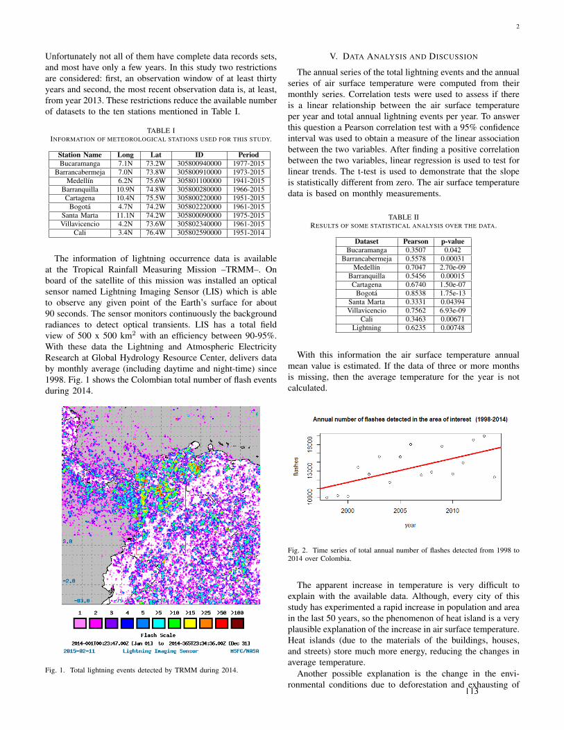
2
Unfortunately not all of them have complete data records sets,and most have only a few years. In this study two restrictionsare considered: first, an observation window of at least thirtyyears and second, the most recent observation data is, at least,from year 2013. These restrictions reduce the available numberof datasets to the ten stations mentioned in Table I.
TABLE IINFORMATION OF METEOROLOGICAL STATIONS USED FOR THIS STUDY.
Station Name Long Lat ID PeriodBucaramanga 7.1N 73.2W 305800940000 1977-2015
Barrancabermeja 7.0N 73.8W 305800910000 1973-2015Medellın 6.2N 75.6W 305801100000 1941-2015
Barranquilla 10.9N 74.8W 305800280000 1966-2015Cartagena 10.4N 75.5W 305800220000 1951-2015
Bogota 4.7N 74.2W 305802220000 1961-2015Santa Marta 11.1N 74.2W 305800090000 1975-2015Villavicencio 4.2N 73.6W 305802340000 1961-2015
Cali 3.4N 76.4W 305802590000 1951-2014
The information of lightning occurrence data is availableat the Tropical Rainfall Measuring Mission –TRMM–. Onboard of the satellite of this mission was installed an opticalsensor named Lightning Imaging Sensor (LIS) which is ableto observe any given point of the Earth’s surface for about90 seconds. The sensor monitors continuously the backgroundradiances to detect optical transients. LIS has a total fieldview of 500 x 500 km2 with an efficiency between 90-95%.With these data the Lightning and Atmospheric ElectricityResearch at Global Hydrology Resource Center, delivers databy monthly average (including daytime and night-time) since1998. Fig. 1 shows the Colombian total number of flash eventsduring 2014.
Fig. 1. Total lightning events detected by TRMM during 2014.
V. DATA ANALYSIS AND DISCUSSION
The annual series of the total lightning events and the annualseries of air surface temperature were computed from theirmonthly series. Correlation tests were used to assess if thereis a linear relationship between the air surface temperatureper year and total annual lightning events per year. To answerthis question a Pearson correlation test with a 95% confidenceinterval was used to obtain a measure of the linear associationbetween the two variables. After finding a positive correlationbetween the two variables, linear regression is used to test forlinear trends. The t-test is used to demonstrate that the slopeis statistically different from zero. The air surface temperaturedata is based on monthly measurements.
TABLE IIRESULTS OF SOME STATISTICAL ANALYSIS OVER THE DATA.
Dataset Pearson p-valueBucaramanga 0.3507 0.042
Barrancabermeja 0.5578 0.00031Medellın 0.7047 2.70e-09
Barranquilla 0.5456 0.00015Cartagena 0.6740 1.50e-07
Bogota 0.8538 1.75e-13Santa Marta 0.3331 0.04394Villavicencio 0.7562 6.93e-09
Cali 0.3463 0.00671Lightning 0.6235 0.00748
With this information the air surface temperature annualmean value is estimated. If the data of three or more monthsis missing, then the average temperature for the year is notcalculated.
Fig. 2. Time series of total annual number of flashes detected from 1998 to2014 over Colombia.
The apparent increase in temperature is very difficult toexplain with the available data. Although, every city of thisstudy has experimented a rapid increase in population and areain the last 50 years, so the phenomenon of heat island is a veryplausible explanation of the increase in air surface temperature.Heat islands (due to the materials of the buildings, houses,and streets) store much more energy, reducing the changes inaverage temperature.
Another possible explanation is the change in the envi-ronmental conditions due to deforestation and exhausting of
3
Fig. 3. Time series air surface temperature with its corresponding simple linear regression model.
water supplies, turning these areas in drier places. Thereforeto have a general confirmation of the increase of air surfacetemperature it is necessary to consider data from small townand rural areas in order to confirm the hypothesis. The authorsof this study are working now in this issue in order to get morereliable conclusions.
VI. CONCLUSION
Results obtained suggest a warming process in the nineColombia’s largest cities [12], represented in an increase ofabout 0.64 C over the last 40 years. The causes and itsimplications will remain a topic for research and discussion.The apparent increase in lightning activity represents a threatfor the potential lightning damages on human lives, facilitiesand infrastructure, especially in the Colombian regions withthe highest density flash rate. In this context power lines,transformers, and other electric utility equipment are at highrisk in Colombia, with its corresponding economic impact.
REFERENCES
[1] A. Del Genio. (2012) Will a warmer world be stormier?NASA, Goddard Institute for Space Studies. [Online]. Available:www.giss.nasa.gov/research/briefs/delgenio
[2] J. Dwyer and M. Uman, “The physics of lightning,” Physics Reports,vol. 534, no. 4, pp. 147–241, 2014.
[3] T. Oki and S. Kanae, “Global hydrological cycles and world waterresources,” Scie, vol. 313, no. 5790, pp. 1068–1072, 2006.
[4] C. Price, “Will a drier climate result in more lightning?” AtmosphericResearch, vol. 91, no. 2, pp. 479–484, 2009.
[5] J. Grenfell, D. Shindell, and V. Grewe, “Sensitivity studies of oxidativechanges in the troposphere in 2100 using giss gcm,” AtmosphericChemistry and Physics, vol. 3, no. 5, pp. 1267–1283, 2003.
[6] C. Price and D. Rind, “A simple lightning parameterization for calcu-lating global lightning distributions,” Journal of Geophysical Research:Atmospheres, vol. 97, no. D9, pp. 9919–9933, 1992.
[7] D. Shindell, G. Faluvegi, N. Unger, E. Aguilar, G. Koch, and D. Schmidt,“Simulations of preindustrial, present-day, and 2100 conditions in thenasa giss composition climate model g-puccini,” Atmospheric Chemistryand Physics, vol. 6, no. 12, pp. 4427–4459, 2006.
[8] C. Price, “Global surface temperatures and the atmospheric electriccircuit,” Geophysical Research Letters, vol. 20, no. 13, pp. 1363–1366,July 1993.
[9] S. Min, X. Zhang, F. Zwiers, and G. Hegerl, “Human contribuition tomore-intense precipitation extremes,” Nature, vol. 470, pp. 378–381, Feb2011.
[10] H. Christian and et al., “Global frequency and distribution of lightningas observed from space by the optical transient detector,” Journal ofGeophysical Research: Atmospheres, vol. 108, pp. ACL–4, 2003.
[11] O. Pinto, I. Pinto, and K. Naccarato, “Maximum cloud to groundlightning flash densities observed by lightning location systems in thetropical region: A review,” Atmospheric Research, vol. 84, no. 3, pp.189–200, 2007.
[12] DANE. (2013) Poblacin colombiana. Departamento Adminis-trativo Nacional de Estadstica DANE. [Online]. Available:http://www.banrep.gov.co/es/poblacion
Effect of Nearby Building on Horizontal Electric Field from
Lightning Return Strokes
Fei Guo, Zhi-dong Jiang, Bi-hua Zhou
National Key laboratory on Electromagnetic Environment and Electro-optical Engineering, PLA University of Science and
Technology, Nanjing, 210007, China
Abstract
The effect of nearby building on the horizontal electric
field radiated by lightning is discussed by a two-step
finite-difference time-domain (FDTD) method. The
enhancement or attenuation effect of the building on the
horizontal electric field is analyzed as well. The horizontal
electric field , which is located in front and behind the
building, will be enhanced significantly, and the polarity is
opposite for different sides of the building. The vertical
electric field on the sides of the building will decrease,
while the vertical electric field on the roof will be
enhanced.
Keywords: horizontal electric field, FDTD, Lightning Return
Strokes.
1 Introduction
In order to optimize lightning protection means of tall
buildings, it is important to know the change of the electric
field at the top of the building due to lightning strikes nearby.
Further, lightning electric field measurement is often carried
out on the roof of tall buildings [1-2], so the effect due to the
presence of tall buildings is needed for guiding and
interpreting the measurement of the electric field.
Enhancement or attenuation effects caused by metallic beams
and other conducting parts of the building on the vertical
electric field and azimuthal magnetic field have been reported
in previous studies [3-6]. To the best of our knowledge, those
works have focused on the vertical electric field and magnetic
field. The influence of the nearby building on the horizontal
electric field has not been dealt with in previous studies. In [3]
and [4], the ground and building were assumed to be perfectly
conducting. However, the conductivity of the ground and
building has a significant effect on the horizontal electric field.
In addition, the velocities of the current propagation and
corresponding lightning return stroke models cannot be
considered and realized in the CST model [6].
The horizontal electric field due to lightning return strokes is
related to the assessment of lightning induced overvoltages.
However, there are many difficulties and restrictions for the
measurement of the horizontal electric field [7-8]. So
evaluation the effects of nearby buildings on the horizontal
electric field will benefit for optimizing lightning protection
means of nearby telecommunication and power distribution
lines. In this paper, we present a two-step FDTD method for
the evaluation of the enhancement or attenuation effect
introduced by a nearby building on the horizontal electric
field. The proposed two-step FDTD method can greatly
reduce the calculation scale, making the calculation time
much less. For comparison purposes, the effect on the vertical
electric field at the same field point is also presented. The
horizontal electric field and vertical electric field are
compared in the presence of building with their counterparts
in the absence of the building, both investigated by the
proposed two-step FDTD method.
2 Methodology
The configuration of the calculation model is presented in Fig.
1. The electromagnetic fields near the lightning channel are
calculated in the 2-D cylindrical coordinates, and then the
electromagnetic fields calculated in the former step can be
added into the 3-D working volume at the total field-scattered
field connecting boundary. In addition, a sub-grid technology
is used in 2-D Cylindrical coordinate model for precision
consideration of the building structure on the ground. The
dimension of the building structure is smaller than the
corresponding wavelength of the main spectra of cloud-to-
ground lightning return stroke, which is below 1 MHz, the
scatter radiation fields and fine structure of the building are
ignored.
In this study, the TL model is adopted. In order to reproduce a
typical return stroke current of a negative downward flash, the
channel base current I(t) at the ground level is described by a
double exponential functions as follows: 4 73.0 10 1.0 10
01.1 (e e )t tI I ( )t (1)
Where:
I0 is the peak value of the first lightning current, and the
return-stroke speed v is 1.3×10⁸ m/s.
The conductivity of the ground and building is 1×10⁻³
S/m
and the relative permittivity is assumed to be equal to 10. To
avoid reflections, the working volume is surrounded by
absorbing boundary, and the convolutional perfect matched
layer (CPML) is used in this paper.
The horizontal distance from the centre of the building to the
lightning channel is set to 100 m. The point C is located at the
centre point on the flat roof of the building having a plan area
Sb=20×20 m2, and the point C
* is located on the same location
in the absence of building. The point A and B are located at
ground level closer to or further from the lightning channel,
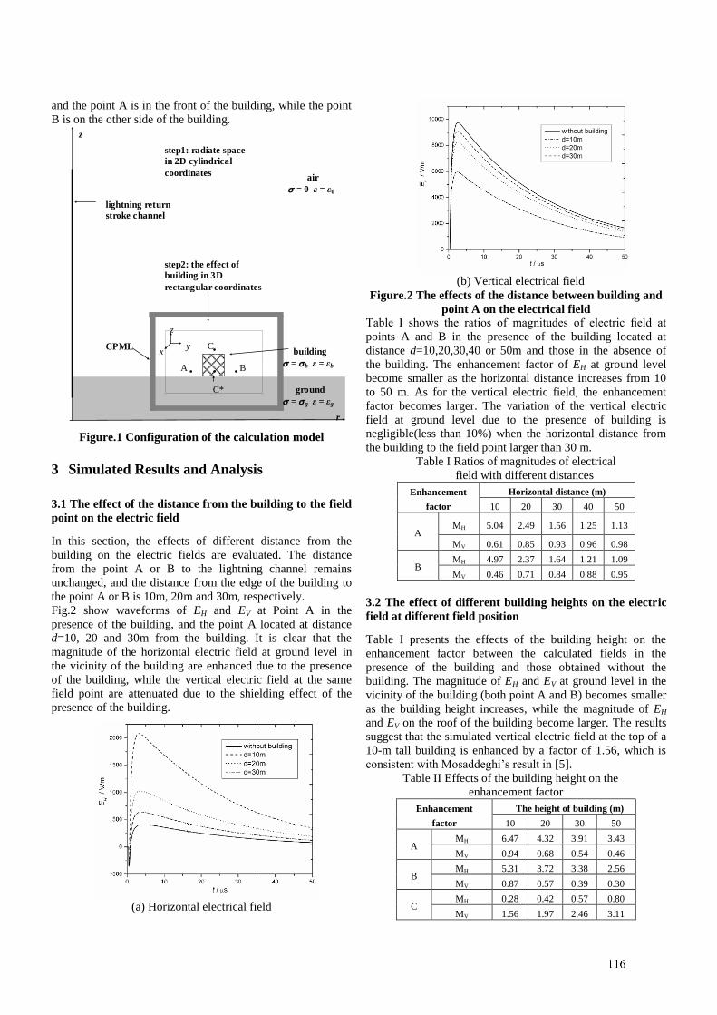
and the point A is in the front of the building, while the point
B is on the other side of the building.
B A
air
= 0 ε = ε0
lightning return
stroke channel
building
= b ε = εb
ground
= g ε = εg
C
C*
step1: radiate space
in 2D cylindrical
coordinates
step2: the effect of
building in 3D
rectangular coordinates
CPML
z
r
z
y x
Figure.1 Configuration of the calculation model
3 Simulated Results and Analysis
3.1 The effect of the distance from the building to the field
point on the electric field
In this section, the effects of different distance from the
building on the electric fields are evaluated. The distance
from the point A or B to the lightning channel remains
unchanged, and the distance from the edge of the building to
the point A or B is 10m, 20m and 30m, respectively.
Fig.2 show waveforms of EH and EV at Point A in the
presence of the building, and the point A located at distance
d=10, 20 and 30m from the building. It is clear that the
magnitude of the horizontal electric field at ground level in
the vicinity of the building are enhanced due to the presence
of the building, while the vertical electric field at the same
field point are attenuated due to the shielding effect of the
presence of the building.
(a) Horizontal electrical field
(b) Vertical electrical field
Figure.2 The effects of the distance between building and
point A on the electrical field
Table I shows the ratios of magnitudes of electric field at
points A and B in the presence of the building located at
distance d=10,20,30,40 or 50m and those in the absence of
the building. The enhancement factor of EH at ground level
become smaller as the horizontal distance increases from 10
to 50 m. As for the vertical electric field, the enhancement
factor becomes larger. The variation of the vertical electric
field at ground level due to the presence of building is
negligible(less than 10%) when the horizontal distance from
the building to the field point larger than 30 m.
Table I Ratios of magnitudes of electrical
field with different distances
Enhancement
factor
Horizontal distance (m)
10 20 30 40 50
A MH 5.04 2.49 1.56 1.25 1.13
MV 0.61 0.85 0.93 0.96 0.98
B MH 4.97 2.37 1.64 1.21 1.09
MV 0.46 0.71 0.84 0.88 0.95
3.2 The effect of different building heights on the electric
field at different field position
Table I presents the effects of the building height on the
enhancement factor between the calculated fields in the
presence of the building and those obtained without the
building. The magnitude of EH and EV at ground level in the
vicinity of the building (both point A and B) becomes smaller
as the building height increases, while the magnitude of EH
and EV on the roof of the building become larger. The results
suggest that the simulated vertical electric field at the top of a
10-m tall building is enhanced by a factor of 1.56, which is
consistent with Mosaddeghi’s result in [5].
Table II Effects of the building height on the
enhancement factor
Enhancement
factor
The height of building (m)
10 20 30 50
A MH 6.47 4.32 3.91 3.43
MV 0.94 0.68 0.54 0.46
B MH 5.31 3.72 3.38 2.56
MV 0.87 0.57 0.39 0.30
C MH 0.28 0.42 0.57 0.80
MV 1.56 1.97 2.46 3.11
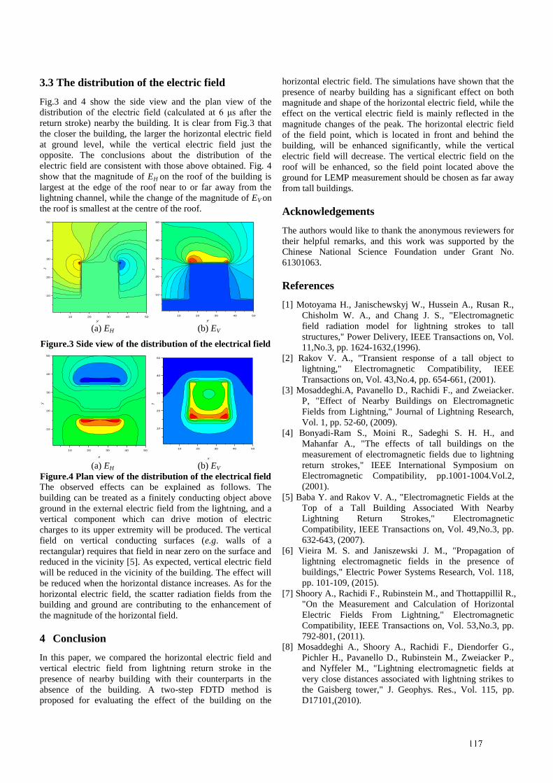
3.3 The distribution of the electric field
Fig.3 and 4 show the side view and the plan view of the
distribution of the electric field (calculated at 6 μs after the
return stroke) nearby the building. It is clear from Fig.3 that
the closer the building, the larger the horizontal electric field
at ground level, while the vertical electric field just the
opposite. The conclusions about the distribution of the
electric field are consistent with those above obtained. Fig. 4
show that the magnitude of EH on the roof of the building is
largest at the edge of the roof near to or far away from the
lightning channel, while the change of the magnitude of EV on
the roof is smallest at the centre of the roof.
10 20 30 40 50
10
20
30
40
50
y
z
10 20 30 40 50
10
20
30
40
50
y
z
(a) EH (b) EV
Figure.3 Side view of the distribution of the electrical field
10 20 30 40 50
10
20
30
40
50
x
y
10 20 30 40 50
10
20
30
40
50
x
y
(a) EH (b) EV
Figure.4 Plan view of the distribution of the electrical field
The observed effects can be explained as follows. The
building can be treated as a finitely conducting object above
ground in the external electric field from the lightning, and a
vertical component which can drive motion of electric
charges to its upper extremity will be produced. The vertical
field on vertical conducting surfaces (e.g. walls of a
rectangular) requires that field in near zero on the surface and
reduced in the vicinity [5]. As expected, vertical electric field
will be reduced in the vicinity of the building. The effect will
be reduced when the horizontal distance increases. As for the
horizontal electric field, the scatter radiation fields from the
building and ground are contributing to the enhancement of
the magnitude of the horizontal field.
4 Conclusion
In this paper, we compared the horizontal electric field and
vertical electric field from lightning return stroke in the
presence of nearby building with their counterparts in the
absence of the building. A two-step FDTD method is
proposed for evaluating the effect of the building on the
horizontal electric field. The simulations have shown that the
presence of nearby building has a significant effect on both
magnitude and shape of the horizontal electric field, while the
effect on the vertical electric field is mainly reflected in the
magnitude changes of the peak. The horizontal electric field
of the field point, which is located in front and behind the
building, will be enhanced significantly, while the vertical
electric field will decrease. The vertical electric field on the
roof will be enhanced, so the field point located above the
ground for LEMP measurement should be chosen as far away
from tall buildings.
Acknowledgements
The authors would like to thank the anonymous reviewers for
their helpful remarks, and this work was supported by the
Chinese National Science Foundation under Grant No.
61301063.
References
[1] Motoyama H., Janischewskyj W., Hussein A., Rusan R.,
Chisholm W. A., and Chang J. S., "Electromagnetic
field radiation model for lightning strokes to tall
structures," Power Delivery, IEEE Transactions on, Vol.
11,No.3, pp. 1624-1632,(1996).
[2] Rakov V. A., "Transient response of a tall object to
lightning," Electromagnetic Compatibility, IEEE
Transactions on, Vol. 43,No.4, pp. 654-661, (2001).
[3] Mosaddeghi.A, Pavanello D., Rachidi F., and Zweiacker.
P, "Effect of Nearby Buildings on Electromagnetic
Fields from Lightning," Journal of Lightning Research,
Vol. 1, pp. 52-60, (2009).
[4] Bonyadi-Ram S., Moini R., Sadeghi S. H. H., and
Mahanfar A., "The effects of tall buildings on the
measurement of electromagnetic fields due to lightning
return strokes," IEEE International Symposium on
Electromagnetic Compatibility, pp.1001-1004.Vol.2,
(2001).
[5] Baba Y. and Rakov V. A., "Electromagnetic Fields at the
Top of a Tall Building Associated With Nearby
Lightning Return Strokes," Electromagnetic
Compatibility, IEEE Transactions on, Vol. 49,No.3, pp.
632-643, (2007).
[6] Vieira M. S. and Janiszewski J. M., "Propagation of
lightning electromagnetic fields in the presence of
buildings," Electric Power Systems Research, Vol. 118,
pp. 101-109, (2015).
[7] Shoory A., Rachidi F., Rubinstein M., and Thottappillil R.,
"On the Measurement and Calculation of Horizontal
Electric Fields From Lightning," Electromagnetic
Compatibility, IEEE Transactions on, Vol. 53,No.3, pp.
792-801, (2011).
[8] Mosaddeghi A., Shoory A., Rachidi F., Diendorfer G.,
Pichler H., Pavanello D., Rubinstein M., Zweiacker P.,
and Nyffeler M., "Lightning electromagnetic fields at
very close distances associated with lightning strikes to
the Gaisberg tower," J. Geophys. Res., Vol. 115, pp.
D17101,(2010).
1
On the Classification of Tower Flashes as Self-Initiated and Other-Triggered
M Rubinstein*, Alexander Smorgonskiy †, F Rachidi †, J Zuber*
* University of Applied Sciences of Western Switzerland, Yverdon, Switzerland, [email protected] † EMC Laboratory, Swiss Federal Institute of Technology (EPFL), Switzerland, [email protected]
Abstract Tower lightning has been classified into “other-triggered” and “self-initiated” lightning based on whether or not the tower flash is preceded by natural lightning activity in the vicinity of the tower location. The causality relation between other-triggered flashes and the preceding activity has not been established. In this paper, we use a probabilistic model to show that it is possible to explain at least some of the lightning activity prior to tower flashes as being the result of chance. Keywords: Lightning, self-initiated, other-triggered.
1 Introduction
Lightning flashes to towers have been classified into “other-triggered” lightning and “self-initiated” lightning based, respectively, on the presence or the absence of other lightning activity in the geographical vicinity and within a temporal interval preceding the tower flash (e.g., [1,2,3]). Smorgonskiy et al. [4] remarked that the causality relation for other-triggered flashes has not been established. The name “other-triggered” could thus be misleading if the causality does not exist for any or for some of the flashes. In this paper, we study the so-called other-triggered flashes and show that it is possible to explain the occurrence of flashes shortly before tower lightning by way of a simple probabilistic model. It is important to note that this study shows that causality is not the only possible explanation for the succession of natural and tower flashes but it does not reject the possibility of causality. This paper is organized as follows: In Section 2, we present a probabilistic model based on a number of simplifying assumptions regarding the lightning flash density over the area of a storm and the lightning flash frequency over the duration of the storm. In Section 3, we use simulations to verify the model. Section 4 contains a discussion and conclusions.
2 Probabilistic Model In this section, we propose a probabilistic model for the time and location of flashes in a storm over a tower. The model is
T"
Δt Δt Δt
Figure 1. Time axis with three flashes striking a tower and Δt time bins before them. If at least one natural flash strikes within a given bin, the tower flash associated with that bin is classified as an “other-triggered” flash. based on the following assumptions: 1. The storm is confined to an area As and the lightning flash density is uniform over it. 2. The storm area contains one tower. 3. The storm lasts T seconds, it has specific start and end times and the probability that a flash will occur at any time during the storm is the same. We also assume that a total of Ntower + Nnatural flashes occur during the storm. Of these, Ntower flashes strike the tower and Nnatural flashes strike in the area of the storm but not the tower. Note that we have called the flashes that do not strike the tower “natural flashes” to distinguish them from those striking the tower, which we call “tower flashes”. An example showing 3 tower flashes occurring over a time period T is shown for illustrative purposes in Figure 1. A time interval Δt immediately before each tower strike is also shown in the figure. Tower flashes for which there is at least one natural flash within its associated Δt and which strike within a radius “a” of the tower are considered to belong to the other-triggered category. Under these assumptions, the expected value for the percentage of other-triggered flashes is given by
Other − triggered% =100 1− 1− ΔtT
#
$%
&
'(
Nnaturalπa2
As
#
$
%%%
&
'
(((
(1)
where all the parameters have been defined in the text above.
3 Simulations
Using Matlab®, we calculated Ntower random real numbers from 0 to T with a uniform probability density function. This set of Ntower random numbers corresponds to the times of strikes to the tower. Using, again, a random number function in Matlab®, we generated a set of Nnatural random real numbers from 0 to T, which represent random times at which the natural flashes occur according to the uniform-probability
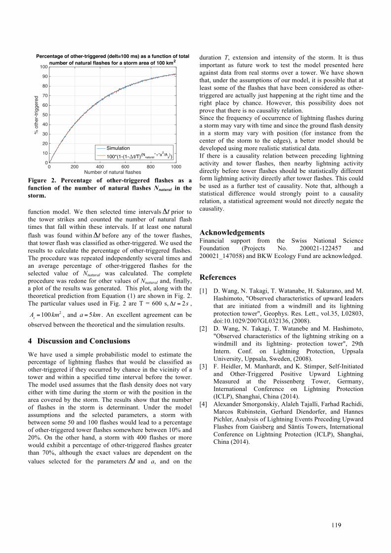
2
Number of natural flashes0 200 400 600 800 1000
% o
ther
-trig
gere
d
0
10
20
30
40
50
60
70
80
90
100
Percentage of other-triggered (delt=100 ms) as a function of totalnumber of natural flashes for a storm area of 100 km2
Simulation100*(1-(1-∆t/T)(N
natural*π*a2/A
s))
Figure 2. Percentage of other-triggered flashes as a function of the number of natural flashes Nnatural in the storm. function model. We then selected time intervals Δt prior to the tower strikes and counted the number of natural flash times that fall within these intervals. If at least one natural flash was found within Δt before any of the tower flashes, that tower flash was classified as other-triggered. We used the results to calculate the percentage of other-triggered flashes. The procedure was repeated independently several times and an average percentage of other-triggered flashes for the selected value of Nnatural was calculated. The complete procedure was redone for other values of Nnatural and, finally, a plot of the results was generated. This plot, along with the theoretical prediction from Equation (1) are shown in Fig. 2. The particular values used in Fig. 2 are T = 600 s, Δt = 2s ,
As =100km2 , and a = 5km . An excellent agreement can be observed between the theoretical and the simulation results.
4 Discussion and Conclusions
We have used a simple probabilistic model to estimate the percentage of lightning flashes that would be classified as other-triggered if they occurred by chance in the vicinity of a tower and within a specified time interval before the tower. The model used assumes that the flash density does not vary either with time during the storm or with the position in the area covered by the storm. The results show that the number of flashes in the storm is determinant. Under the model assumptions and the selected parameters, a storm with between some 50 and 100 flashes would lead to a percentage of other-triggered tower flashes somewhere between 10% and 20%. On the other hand, a storm with 400 flashes or more would exhibit a percentage of other-triggered flashes greater than 70%, although the exact values are dependent on the values selected for the parameters Δt and a, and on the
duration T, extension and intensity of the storm. It is thus important as future work to test the model presented here against data from real storms over a tower. We have shown that, under the assumptions of our model, it is possible that at least some of the flashes that have been considered as other-triggered are actually just happening at the right time and the right place by chance. However, this possibility does not prove that there is no causality relation. Since the frequency of occurrence of lightning flashes during a storm may vary with time and since the ground flash density in a storm may vary with position (for instance from the center of the storm to the edges), a better model should be developed using more realistic statistical data. If there is a causality relation between preceding lightning activity and tower flashes, then nearby lightning activity directly before tower flashes should be statistically different form lightning activity directly after tower flashes. This could be used as a further test of causality. Note that, although a statistical difference would strongly point to a causality relation, a statistical agreement would not directly negate the causality.
Acknowledgements Financial support from the Swiss National Science Foundation (Projects No. 200021-122457 and 200021_147058) and BKW Ecology Fund are acknowledged.
References
[1] D. Wang, N. Takagi, T. Watanabe, H. Sakurano, and M. Hashimoto, "Observed characteristics of upward leaders that are initiated from a windmill and its lightning protection tower", Geophys. Res. Lett., vol.35, L02803, doi:10.1029/2007GL032136, (2008).
[2] D. Wang, N. Takagi, T. Watanebe and M. Hashimoto, "Observed characteristics of the lightning striking on a windmill and its lightning- protection tower", 29th Intern. Conf. on Lightning Protection, Uppsala University, Uppsala, Sweden, (2008).
[3] F. Heidler, M. Manhardt, and K. Stimper, Self-Initiated and Other-Triggered Positive Upward Lightning Measured at the Peissenberg Tower, Germany, International Conference on Lightning Protection (ICLP), Shanghai, China (2014).
[4] Alexander Smorgonskiy, Alaleh Tajalli, Farhad Rachidi, Marcos Rubinstein, Gerhard Diendorfer, and Hannes Pichler, Analysis of Lightning Events Preceding Upward Flashes from Gaisberg and Säntis Towers, International Conference on Lightning Protection (ICLP), Shanghai, China (2014).
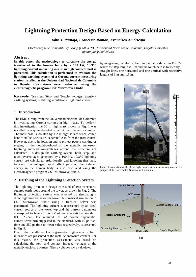
Lightning Protection Design Based on Energy Calculation
John J. Pantoja, Francisco Roman, Francisco Amórtegui
Electromagnetic Compatibility Group (EMC-UN), Universidad Nacional de Colombia, Bogotá, Colombia
Abstract
In this paper the methodology to calculate the energy
transferred to the human body by a 100 kA, 10/350
lightning current impacting in a 30 m high earthed mast is
presented. This calculation is performed to evaluate the
lightning earthing system of a Corona current measuring
station installed at the Universidad Nacional de Colombia
in Bogotá. Calculations were performed using the
electromagnetic program CST Microwave Studio.
Keywords- Transient Step- and Touch- voltages, transient
earthing systems, Lightning simulations, Lightning current.
1 Introduction
The EMC-Group from the Universidad Nacional de Colombia
is investigating Corona currents in high masts. To perform
this investigation the 30 m high mast shown in Fig. 1 was
installed in a quite deserted street at the university campus.
The mast base is isolated by a 2 m high square fence, called
here Metallic Enclosure, separated 2 m from the mast centre.
However, due to its location and to protect people walking or
staying in the neighbourhood of the metallic enclosure,
lightning induced overvoltages around the structure are
calculated. To design the earthing system, both, step- and
touch-overvoltages generated by a 100 kA, 10/350 lightning
current are calculated. Additionally and knowing that these
transient overvoltages could affect persons, the induced
energy in the human body is also calculated using the
electromagnetic program CST Microwave Studio.
2 Earthing of the Lightning Protection System
The lightning protection design consisted of two concentric
squared earth loops around the tower, as shown in Fig. 2. The
lightning protection system was assessed by simulating a
direct lightning strike on the tower. A numerical simulation in
CST Microwave Studio using a transient solver was
performed. The lightning current is represented by an ideal
current source at the tower top and the current parameters
correspond to levels III or IV of the international standard
IEC 62305-1. The required 100 kA double exponential
current waveform suggested in the standard, with 10 μs rise-
time and 350 μs time-to-mean-value respectively, is presented
in Fig. 3.
Due to the metallic enclosure geometry, higher electric field
intensities are presented at the metallic enclosure corners. For
this reason, the protection assessment was based on
calculating the step- and contact- induced voltages at the
metallic enclosure corners. These voltages were calculated
by integrating the electric field in the paths shown in Fig. 2a;
where the step length is 1 m and the touch path is formed by 2
straight lines, one horizontal and one vertical with respective
lengths of 1 m and 1.5 m.
Figure 1.Installation of the 30 m high Corona current measuring mast in the
campus of the Universidad Nacional de Colombia.
(a)
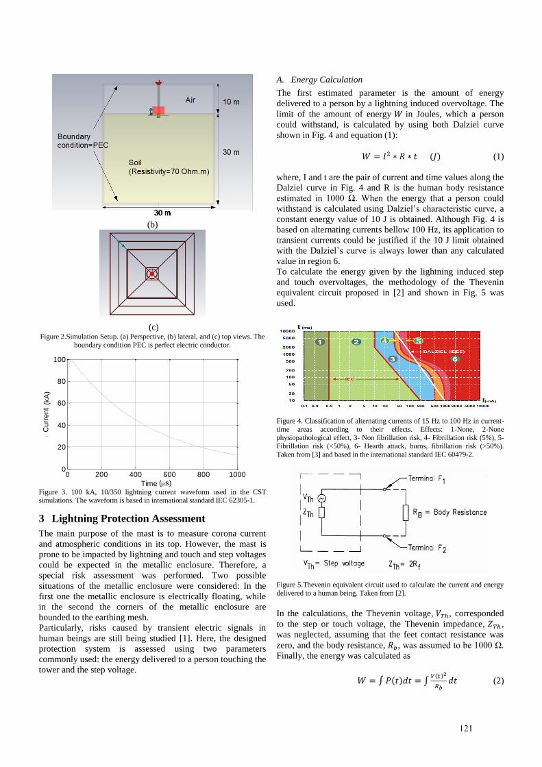
(b)
(c)
Figure 2.Simulation Setup. (a) Perspective, (b) lateral, and (c) top views. The
boundary condition PEC is perfect electric conductor.
Figure 3. 100 kA, 10/350 lightning current waveform used in the CST simulations. The waveform is based in international standard IEC 62305-1.
3 Lightning Protection Assessment
The main purpose of the mast is to measure corona current
and atmospheric conditions in its top. However, the mast is
prone to be impacted by lightning and touch and step voltages
could be expected in the metallic enclosure. Therefore, a
special risk assessment was performed. Two possible
situations of the metallic enclosure were considered: In the
first one the metallic enclosure is electrically floating, while
in the second the corners of the metallic enclosure are
bounded to the earthing mesh.
Particularly, risks caused by transient electric signals in
human beings are still being studied [1]. Here, the designed
protection system is assessed using two parameters
commonly used: the energy delivered to a person touching the
tower and the step voltage.
A. Energy Calculation
The first estimated parameter is the amount of energy
delivered to a person by a lightning induced overvoltage. The
limit of the amount of energy 𝑊 in Joules, which a person
could withstand, is calculated by using both Dalziel curve
shown in Fig. 4 and equation (1):
𝑊 = 𝐼2 ∗ 𝑅 ∗ 𝑡 (𝐽) (1)
where, I and t are the pair of current and time values along the
Dalziel curve in Fig. 4 and R is the human body resistance
estimated in 1000 Ω. When the energy that a person could
withstand is calculated using Dalziel’s characteristic curve, a
constant energy value of 10 J is obtained. Although Fig. 4 is
based on alternating currents bellow 100 Hz, its application to
transient currents could be justified if the 10 J limit obtained
with the Dalziel’s curve is always lower than any calculated
value in region 6.
To calculate the energy given by the lightning induced step
and touch overvoltages, the methodology of the Thevenin
equivalent circuit proposed in [2] and shown in Fig. 5 was
used.
Figure 4. Classification of alternating currents of 15 Hz to 100 Hz in current-
time areas according to their effects. Effects: 1-None, 2-None physiopathological effect, 3- Non fibrillation risk, 4- Fibrillation risk (5%), 5-
Fibrillation risk (<50%), 6- Hearth attack, burns, fibrillation risk (>50%).
Taken from [3] and based in the international standard IEC 60479-2.
Figure 5.Thevenin equivalent circuit used to calculate the current and energy
delivered to a human being. Taken from [2].
In the calculations, the Thevenin voltage, 𝑉𝑇ℎ, corresponded
to the step or touch voltage, the Thevenin impedance, 𝑍𝑇ℎ ,
was neglected, assuming that the feet contact resistance was
zero, and the body resistance, 𝑅𝑏, was assumed to be 1000 Ω.
Finally, the energy was calculated as
𝑊 = ∫ 𝑃(𝑡)𝑑𝑡 = ∫𝑉(𝑡)2
𝑅𝑏𝑑𝑡 (2)
0 200 400 600 800 10000
20
40
60
80
100
Tiempo (s)
Co
rrie
nte
(kA
)
Time
Curr
ent
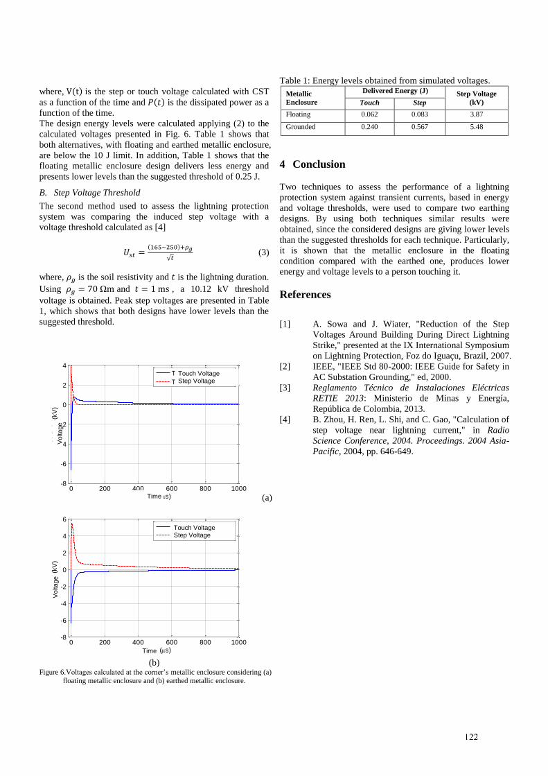
where, V(t) is the step or touch voltage calculated with CST
as a function of the time and 𝑃(𝑡) is the dissipated power as a
function of the time.
The design energy levels were calculated applying (2) to the
calculated voltages presented in Fig. 6. Table 1 shows that
both alternatives, with floating and earthed metallic enclosure,
are below the 10 J limit. In addition, Table 1 shows that the
floating metallic enclosure design delivers less energy and
presents lower levels than the suggested threshold of 0.25 J.
B. Step Voltage Threshold
The second method used to assess the lightning protection
system was comparing the induced step voltage with a
voltage threshold calculated as [4]
𝑈𝑠𝑡 =(165~250)+𝜌𝑔
√𝑡 (3)
where, 𝜌𝑔 is the soil resistivity and 𝑡 is the lightning duration.
Using 𝜌𝑔 = 70 Ωm and 𝑡 = 1 ms , a 10.12 kV threshold
voltage is obtained. Peak step voltages are presented in Table
1, which shows that both designs have lower levels than the
suggested threshold.
(a)
(b) Figure 6.Voltages calculated at the corner’s metallic enclosure considering (a)
floating metallic enclosure and (b) earthed metallic enclosure.
Table 1: Energy levels obtained from simulated voltages.
Metallic
Enclosure
Delivered Energy (J) Step Voltage
(kV) Touch Step
Floating 0.062 0.083 3.87
Grounded 0.240 0.567 5.48
4 Conclusion
Two techniques to assess the performance of a lightning
protection system against transient currents, based in energy
and voltage thresholds, were used to compare two earthing
designs. By using both techniques similar results were
obtained, since the considered designs are giving lower levels
than the suggested thresholds for each technique. Particularly,
it is shown that the metallic enclosure in the floating
condition compared with the earthed one, produces lower
energy and voltage levels to a person touching it.
References
[1] A. Sowa and J. Wiater, "Reduction of the Step
Voltages Around Building During Direct Lightning
Strike," presented at the IX International Symposium
on Lightning Protection, Foz do Iguaçu, Brazil, 2007.
[2] IEEE, "IEEE Std 80-2000: IEEE Guide for Safety in
AC Substation Grounding," ed, 2000.
[3] Reglamento Técnico de Instalaciones Eléctricas
RETIE 2013: Ministerio de Minas y Energía,
República de Colombia, 2013.
[4] B. Zhou, H. Ren, L. Shi, and C. Gao, "Calculation of
step voltage near lightning current," in Radio
Science Conference, 2004. Proceedings. 2004 Asia-
Pacific, 2004, pp. 646-649.
0 200 400 600 800 1000-8
-6
-4
-2
0
2
4
Tiempo (s)
Vo
lta
je (
kV
)
Tensión de Contacto
Tensión de Paso
0 200 400 600 800 1000-8
-6
-4
-2
0
2
4
6
Tiempo (s)
Vo
lta
je (
kV
)
Tensión de Contacto
Tensión de Paso
Voltag
e
Voltag
e
Time
Time
Touch Voltage Step Voltage
Touch Voltage Step Voltage
1
On the Unconditionally Stable FDTD Method Based on Associated Hermite Functions
Huang Zhengyu, Shi Lihua, Zhang Zhixin
National Key Laboratory on Electromagnetic Environmental Effects and Electro-optical Engineering, No.1 Haifuxiang, Nanjing, China
Abstract This paper introduces developments of the unconditionally stable finite-difference time-domain (FDTD) method based on the Associated Hermite (AH) orthogonal functions. This method has renewed the category of orthogonal-functions-based unconditionally stable FDTD method, which is dominated by Weighted Laguerre Polynomials (WLP) FDTD method previously. Comparison of the proposed method with FDTD in analysing fine structures, as well as the application in dispersive medium are given in this paper. Keywords: Associated Hermite functions, finite difference time domain (FDTD), and unconditional stability.
1 Introduction
The finite-difference time-domain (FDTD) method has been widely used to analyse transient electromagnetic scattering problems. In the cases of fine geometric structures, the time step should be limited by the Courant–Friedrich–Levy (CFL) stability condition. To deal with this problem, orthogonal decomposition of Maxwell’s equations by basis functions attracts attention in recent years. The dominated method in this area is Weighted Laguerre Polynomials (WLP) FDTD method [1], which shows relatively less numerical dispersion error when larger time step is used. Inspired by Weighted Laguerre Polynomials, we have explored Associated Hermite (AH) functions [2] as another possible orthogonal basis to incorporate with FDTD to form an unconditionally stable scheme [3]. Recently, two main progresses have been achieved. The one is its extension to the frequency-dependent dispersive problems and the other is the improvement of memory storage reduction by using the eigenvalue transformation.
2 Methodologies
Associated Hermite basis functions are an orthonormal set of basis functions
φq t( ) = 12q q! π
e− t2 /2Hq t( ) q = 0, 1, !( ) (1)
where Hq t( ) = −1( )q et2 dq
dt qe− t
2( ) is Hermite polynomials. The
time derivation of the q-th order AH function is
ddtφq t( ) = q
2φq−1 t( )− q +1
2φq+1 t( ) (2)
The main ideal of AH-FDTD is to use a finite Q-dimensional AH expansion as temporal testing functions to span the time-domain Maxwell’s equations and calculate the expansion coefficients of electromagnetic fields in AH domain; the time-domain results can be reconstructed from these expansion coefficients. There are two main interesting properties for AH functions: the most compact time-frequency support (TFSs) and the unique isomorphism of the AH function with its Fourier transform. The former can expand the transient signals with less orders of polynomials, which means relative fewer unknowns to calculation for AH FDTD scheme and the latter can make the time or frequency domain results can both be directly reconstructed from the expansion coefficients in AH domain. The key step for its implementation is how to solve the implicit equations to obtain the EM filed expansion coefficients in order. For it cannot be calculated from the march-on-in-order scheme like the WLP method, instead, we establish a set of nested matrix equations with Q-tuple variables in whole computational domains to obtain the expansion coefficients.
A[ ] P[ ] = J[ ] (3)
where P[ ] is an unknown Q-tuple field variable. J[ ] is a Q-tuple item included with excitation source coefficients. A[ ] is a nested banded coefficient matrix. A numerical experiment
the eigenvalue transformation
the direct LU decomposition
one nested matrix equation
the inverse eigenvalue transformation
the expansion coefficients in AH domain
the timedomain results
the frequencydomain results
Q decoupled equations
the transformed expansion coefficients
the paraelling-in-order LU decomposition
AH FDTD AH FDTD for paralleling-in-order solution
Figure 1. The framework of AH FDTD and its implementation of paralleling–in-order solution.
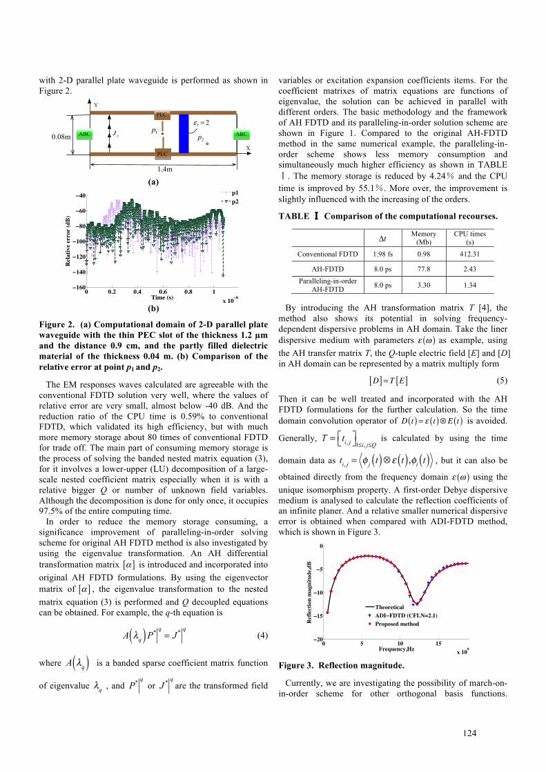
2
with 2-D parallel plate waveguide is performed as shown in Figure 2.
ABC ABC
PEC
PECX
Y
Jyp1
p20.08m
1.4m
εr = 2
(a)
0 0.2 0.4 0.6 0.8 1x 10ï8
ï160
ï140
ï120
ï100
ï80
ï60
ï40
Time (s)
Rel
ativ
e er
ror
(dB)
p1p2
(b)
Figure 2. (a) Computational domain of 2-D parallel plate waveguide with the thin PEC slot of the thickness 1.2 µm and the distance 0.9 cm, and the partly filled dielectric material of the thickness 0.04 m. (b) Comparison of the relative error at point p1 and p2.
The EM responses waves calculated are agreeable with the conventional FDTD solution very well, where the values of relative error are very small, almost below -40 dB. And the reduction ratio of the CPU time is 0.59% to conventional FDTD, which validated its high efficiency, but with much more memory storage about 80 times of conventional FDTD for trade off. The main part of consuming memory storage is the process of solving the banded nested matrix equation (3), for it involves a lower-upper (LU) decomposition of a large-scale nested coefficient matrix especially when it is with a relative bigger Q or number of unknown field variables. Although the decomposition is done for only once, it occupies 97.5% of the entire computing time. In order to reduce the memory storage consuming, a significance improvement of paralleling-in-order solving scheme for original AH FDTD method is also investigated by using the eigenvalue transformation. An AH differential transformation matrix α[ ] is introduced and incorporated into original AH FDTD formulations. By using the eigenvector matrix of α[ ] , the eigenvalue transformation to the nested matrix equation (3) is performed and Q decoupled equations can be obtained. For example, the q-th equation is
A λq( )P* q
= J * q (4)
where A λq( ) is a banded sparse coefficient matrix function
of eigenvalue λq , and
P* q
or J * q
are the transformed field
variables or excitation expansion coefficients items. For the coefficient matrixes of matrix equations are functions of eigenvalue, the solution can be achieved in parallel with different orders. The basic methodology and the framework of AH FDTD and its paralleling-in-order solution scheme are shown in Figure 1. Compared to the original AH-FDTD method in the same numerical example, the paralleling-in-order scheme shows less memory consumption and simultaneously much higher efficiency as shown in TABLEⅠ. The memory storage is reduced by 4.24% and the CPU time is improved by 55.1%. More over, the improvement is slightly influenced with the increasing of the orders.
TABLE Ⅰ Comparison of the computational recourses.
Δt Memory (Mb)
CPU times (s)
Conventional FDTD 1.98 fs 0.98 412.31
AH-FDTD 8.0 ps 77.8 2.43 Paralleling-in-order
AH-FDTD 8.0 ps 3.30 1.34 By introducing the AH transformation matrix T [4], the method also shows its potential in solving frequency-dependent dispersive problems in AH domain. Take the liner dispersive medium with parameters ε ω( ) as example, using the AH transfer matrix T, the Q-tuple electric field [E] and [D] in AH domain can be represented by a matrix multiply form
D[ ] = T E[ ] (5)
Then it can be well treated and incorporated with the AH FDTD formulations for the further calculation. So the time domain convolution operator of D t( ) = ε t( )⊗E t( ) is avoided.
Generally, T = ti, j
⎡⎣ ⎤⎦1≤i, j≤Q is calculated by using the time
domain data as ti, j = φ j t( )⊗ε t( ),φi t( ) , but it can also be
obtained directly from the frequency domain ε ω( ) using the unique isomorphism property. A first-order Debye dispersive medium is analysed to calculate the reflection coefficients of an infinite planer. And a relative smaller numerical dispersive error is obtained when compared with ADI-FDTD method, which is shown in Figure 3.
0 5 10 15x 109
ï20
ï15
ï10
ï5
0
Frequency,Hz
Ref
lect
ion
mag
nitu
de,d
B
TheoreticalADIïFDTD (CFLN=2.1)Proposed method
Figure 3. Reflection magnitude.
Currently, we are investigating the possibility of march-on-in-order scheme for other orthogonal basis functions.
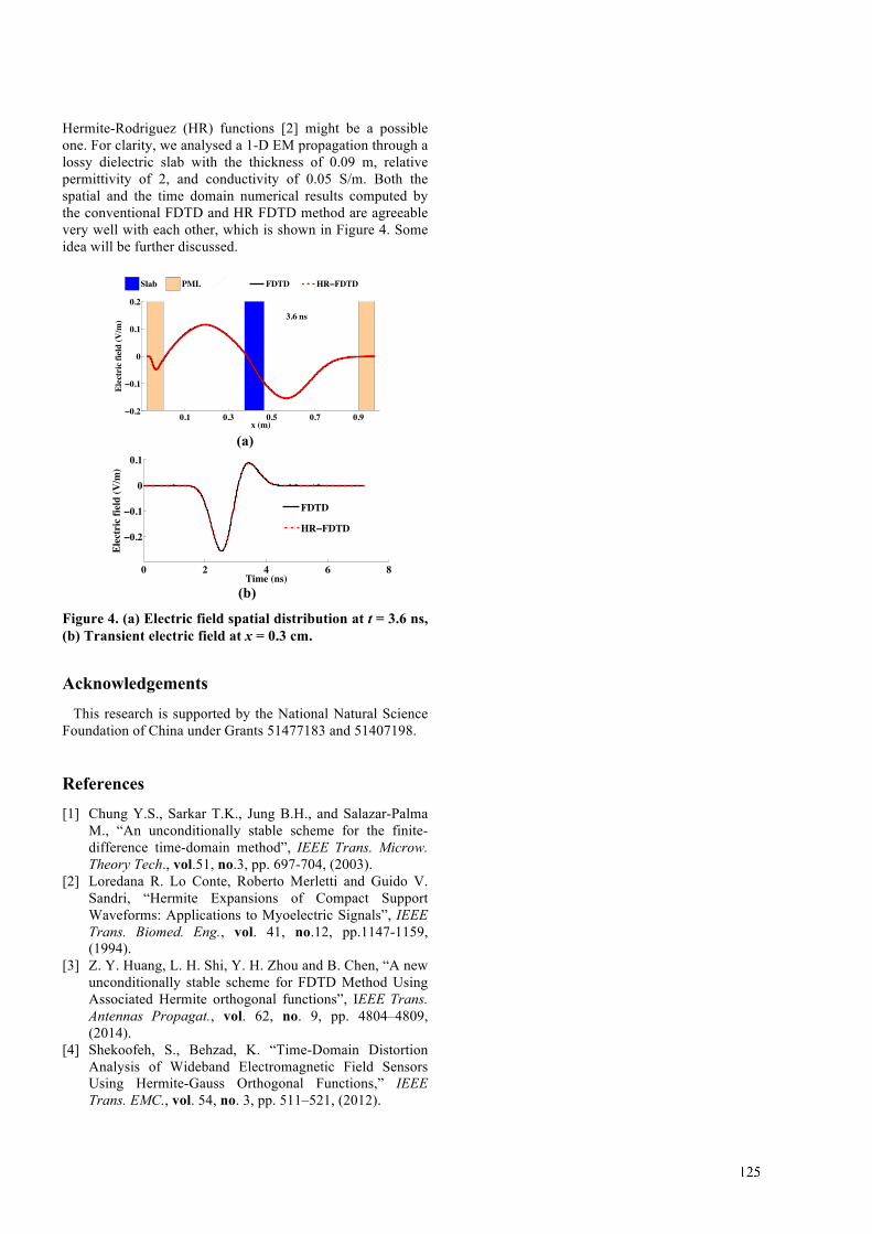
3
Hermite-Rodriguez (HR) functions [2] might be a possible one. For clarity, we analysed a 1-D EM propagation through a lossy dielectric slab with the thickness of 0.09 m, relative permittivity of 2, and conductivity of 0.05 S/m. Both the spatial and the time domain numerical results computed by the conventional FDTD and HR FDTD method are agreeable very well with each other, which is shown in Figure 4. Some idea will be further discussed.
0.1 0.3 0.5 0.7 0.9ï0.2
ï0.1
0
0.1
0.2
x (m)
Elec
tric
fiel
d (V
/m) 3.6 ns
Slab PML FDTD HRïFDTD
(a)
0 2 4 6 8
ï0.2
ï0.1
0
0.1
Time (ns)
Elec
tric
fiel
d (V
/m)
FDTD
HRïFDTD
(b)
Figure 4. (a) Electric field spatial distribution at t = 3.6 ns, (b) Transient electric field at x = 0.3 cm.
Acknowledgements
This research is supported by the National Natural Science Foundation of China under Grants 51477183 and 51407198.
References [1] Chung Y.S., Sarkar T.K., Jung B.H., and Salazar-Palma
M., “An unconditionally stable scheme for the finite-difference time-domain method”, IEEE Trans. Microw. Theory Tech., vol.51, no.3, pp. 697-704, (2003).
[2] Loredana R. Lo Conte, Roberto Merletti and Guido V. Sandri, “Hermite Expansions of Compact Support Waveforms: Applications to Myoelectric Signals”, IEEE Trans. Biomed. Eng., vol. 41, no.12, pp.1147-1159, (1994).
[3] Z. Y. Huang, L. H. Shi, Y. H. Zhou and B. Chen, “A new unconditionally stable scheme for FDTD Method Using Associated Hermite orthogonal functions”, IEEE Trans. Antennas Propagat., vol. 62, no. 9, pp. 4804–4809, (2014).
[4] Shekoofeh, S., Behzad, K. “Time-Domain Distortion Analysis of Wideband Electromagnetic Field Sensors Using Hermite-Gauss Orthogonal Functions,” IEEE Trans. EMC., vol. 54, no. 3, pp. 511–521, (2012).
Transient response prediction using minimum phase method
based on system simulation
Chen Peng*†, Sun Dongyang*
†, Wu Gang*
†, Chen Weiqing*
†
*Northwest Institute of Nuclear Technology, P.O.Box 69-20, Xi an,710024, China
†State Key Laboratory of Intense Pulsed Radiation Simulation and Effect,Xi’an,ShanXi,710024,China
Abstract
In the area of electromagnetic pulse(EMP) technology,the
transfer function is usually used to predict the transient
response when a system is radiated by EMP.The complex
spectrum is needed in the prediction while the measured
continuous wave(CW) transfer function data is usually
magnitude-only.If the system is a minimum phase system,
its phase can be estimated by Hilbert transform,but it’s
difficult to judge whether a system is minimum phase in
actual cases.In this paper, four types of systems which
may exist in actual cases are simulated. The transient
responses calculated by circuit software and predicted by
minimum phase method are almost identical. The
transient response in the center of a shielding box is
calculated by a electromagnetic field software, and is
predicted by minimum phase method. The predicted
response is almost the same with that simulated by
software.
Keywords: Minimum phase Transient response Prediction
1 Introduction
In the research of system-level susceptibility assessments for
EMP,it is frequently desired to abtain a knowledge of the
transient response of a system.Most data can be measured
directly,but it is impossible to test evry system in a EMP
facility.A alternative way is to abtain the system transfer
function and predict the transient response.
The minimum phase system,whose reverse system can be
realized physically,is commonly used in system identification
and deconvolution.The logarithm of spectral of a minimum
phase system is analytical,so the real and imaginary parts are
not independent.The two components are related by Hilbert
transform which can be derived from an integral in the
analytical complex frequency plane using the Cauchy residue
theorem.[1][2].Some research indicate that probes for
measuring electric or magnetic field are minimum phase
system,and the transfer function can be reconstructed from
magnitude only[3][4].In another research,the double
exponential waveform and damped oscillating waveform are
reconstructed respectively using the cepstrum[5].
In this paper,the transient responses of lowpass, highpass,ban-
dpass and bandstop systems are calculated and predicted,bas-
ed on the research above.In addition, a 3-D model of a
shielding box with a circular hole is built in a computational
electromagnetic software, and the transient response is
calculated. The magnitude of the transfer function is abtained
by minimum phase method, and the prediction of response is
illustrated.
2 Transient response prediction based on
circuit simulation
There are many different systems in the area of EMP. For
example, a shielding cable excited by EMP field can be seen
as a system. The response current is the output of the system
and the field is the input. These various systems can be
simulated in softwares or programmes.
2.1 Phase reconstruction from magnitude of a minimum
phase system
Considering a minimum phase sequence x(n), if the
magnitude is known,then it can be reconstructed without the
phase as follows[6]:
Firstly, get the natural logarithm of the magnitude |X(k)|,and
symmetrise the sequence
X_ln(k) = ln|X(k)|, k = 1,2, … N/2. (1)
X_ln(N/2 + j) = ln|X(N/2 − j)|, j = 1,2, … N/2 − 2 (2)
where N = 2n ,and n is a integer.The IFFT of X_ln can be
written as
x_ln(n) = IFFT(X_ln) (3)
then a new sequence xnew(n) can be set as
xnew(n) = x_ln (n)
2x_ln (n)0
n = 1,N/2 n = 2, … N/2 − 1
n = N/2 + 1, … N − 2(4)
the minimum phase sequence is expressed as
xmin(n) = IFFT(eFFT(xnew (n))) (5)
2.2 Results comparison between the circuit simulation and
transfer function prediction
There are upper limits in frequency domain of the probes used
in EMP measurement,so the similarity between probes and
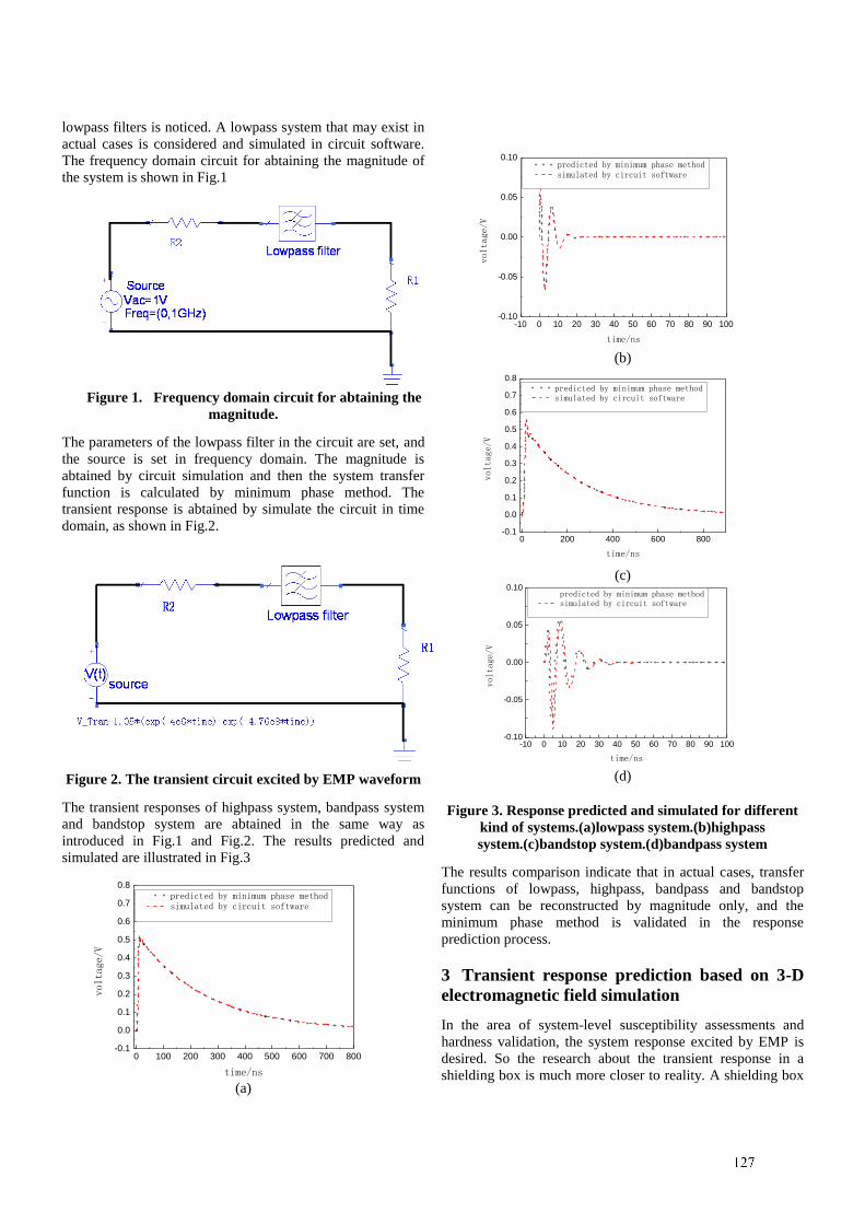
lowpass filters is noticed. A lowpass system that may exist in
actual cases is considered and simulated in circuit software.
The frequency domain circuit for abtaining the magnitude of
the system is shown in Fig.1
Figure 1. Frequency domain circuit for abtaining the
magnitude.
The parameters of the lowpass filter in the circuit are set, and
the source is set in frequency domain. The magnitude is
abtained by circuit simulation and then the system transfer
function is calculated by minimum phase method. The
transient response is abtained by simulate the circuit in time
domain, as shown in Fig.2.
Figure 2. The transient circuit excited by EMP waveform
The transient responses of highpass system, bandpass system
and bandstop system are abtained in the same way as
introduced in Fig.1 and Fig.2. The results predicted and
simulated are illustrated in Fig.3
(a)
(b)
(c)
(d)
Figure 3. Response predicted and simulated for different
kind of systems.(a)lowpass system.(b)highpass
system.(c)bandstop system.(d)bandpass system
The results comparison indicate that in actual cases, transfer
functions of lowpass, highpass, bandpass and bandstop
system can be reconstructed by magnitude only, and the
minimum phase method is validated in the response
prediction process.
3 Transient response prediction based on 3-D
electromagnetic field simulation
In the area of system-level susceptibility assessments and
hardness validation, the system response excited by EMP is
desired. So the research about the transient response in a
shielding box is much more closer to reality. A shielding box
0 100 200 300 400 500 600 700 800-0.1
0.0
0.1
0.2
0.3
0.4
0.5
0.6
0.7
0.8
volt
age/
V
time/ns
predicted by minimum phase method simulated by circuit software
-10 0 10 20 30 40 50 60 70 80 90 100-0.10
-0.05
0.00
0.05
0.10
voltage/V
time/ns
predicted by minimum phase method simulated by circuit software
0 200 400 600 800-0.1
0.0
0.1
0.2
0.3
0.4
0.5
0.6
0.7
0.8
voltage/V
time/ns
predicted by minimum phase method simulated by circuit software
-10 0 10 20 30 40 50 60 70 80 90 100-0.10
-0.05
0.00
0.05
0.10
voltage/V
time/ns
predicted by minimum phase method simulated by circuit software
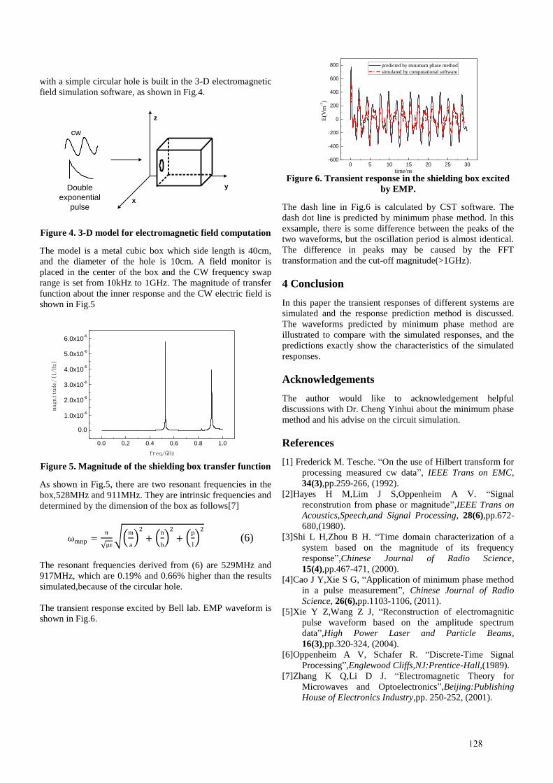
with a simple circular hole is built in the 3-D electromagnetic
field simulation software, as shown in Fig.4.
Figure 4. 3-D model for electromagnetic field computation
The model is a metal cubic box which side length is 40cm,
and the diameter of the hole is 10cm. A field monitor is
placed in the center of the box and the CW frequency swap
range is set from 10kHz to 1GHz. The magnitude of transfer
function about the inner response and the CW electric field is
shown in Fig.5
Figure 5. Magnitude of the shielding box transfer function
As shown in Fig.5, there are two resonant frequencies in the
box,528MHz and 911MHz. They are intrinsic frequencies and
determined by the dimension of the box as follows[7]
ωmnp =π
√με√(
m
a)
2
+ (n
b)
2
+ (p
l)
2
(6)
The resonant frequencies derived from (6) are 529MHz and
917MHz, which are 0.19% and 0.66% higher than the results
simulated,because of the circular hole.
The transient response excited by Bell lab. EMP waveform is
shown in Fig.6.
Figure 6. Transient response in the shielding box excited
by EMP.
The dash line in Fig.6 is calculated by CST software. The
dash dot line is predicted by minimum phase method. In this
exsample, there is some difference between the peaks of the
two waveforms, but the oscillation period is almost identical.
The difference in peaks may be caused by the FFT
transformation and the cut-off magnitude(>1GHz).
4 Conclusion
In this paper the transient responses of different systems are
simulated and the response prediction method is discussed.
The waveforms predicted by minimum phase method are
illustrated to compare with the simulated responses, and the
predictions exactly show the characteristics of the simulated
responses.
Acknowledgements
The author would like to acknowledgement helpful
discussions with Dr. Cheng Yinhui about the minimum phase
method and his advise on the circuit simulation.
References
[1] Frederick M. Tesche. “On the use of Hilbert transform for
processing measured cw data”, IEEE Trans on EMC,
34(3),pp.259-266, (1992).
[2]Hayes H M,Lim J S,Oppenheim A V. “Signal
reconstrution from phase or magnitude”,IEEE Trans on
Acoustics,Speech,and Signal Processing, 28(6),pp.672-
680,(1980).
[3]Shi L H,Zhou B H. “Time domain characterization of a
system based on the magnitude of its frequency
response”,Chinese Journal of Radio Science,
15(4),pp.467-471, (2000).
[4]Cao J Y,Xie S G, “Application of minimum phase method
in a pulse measurement”, Chinese Journal of Radio
Science, 26(6),pp.1103-1106, (2011).
[5]Xie Y Z,Wang Z J, “Reconstruction of electromagnitic
pulse waveform based on the amplitude spectrum
data”,High Power Laser and Particle Beams,
16(3),pp.320-324, (2004).
[6]Oppenheim A V, Schafer R. “Discrete-Time Signal
Processing”,Englewood Cliffs,NJ:Prentice-Hall,(1989).
[7]Zhang K Q,Li D J. “Electromagnetic Theory for
Microwaves and Optoelectronics”,Beijing:Publishing
House of Electronics Industry,pp. 250-252, (2001).
cw
Double
exponential
pulse
y
x
z
0.0 0.2 0.4 0.6 0.8 1.0
0.0
1.0x10⁻⁶
2.0x10⁻⁶
3.0x10⁻⁶
4.0x10⁻⁶
5.0x10⁻⁶
6.0x10⁻⁶
magnitude/(1/Hz)
freq/GHz
0 5 10 15 20 25 30-600
-400
-200
0
200
400
600
800
E(V
m-1
)
time/ns
predicted by minimum phase method
simulated by computational software
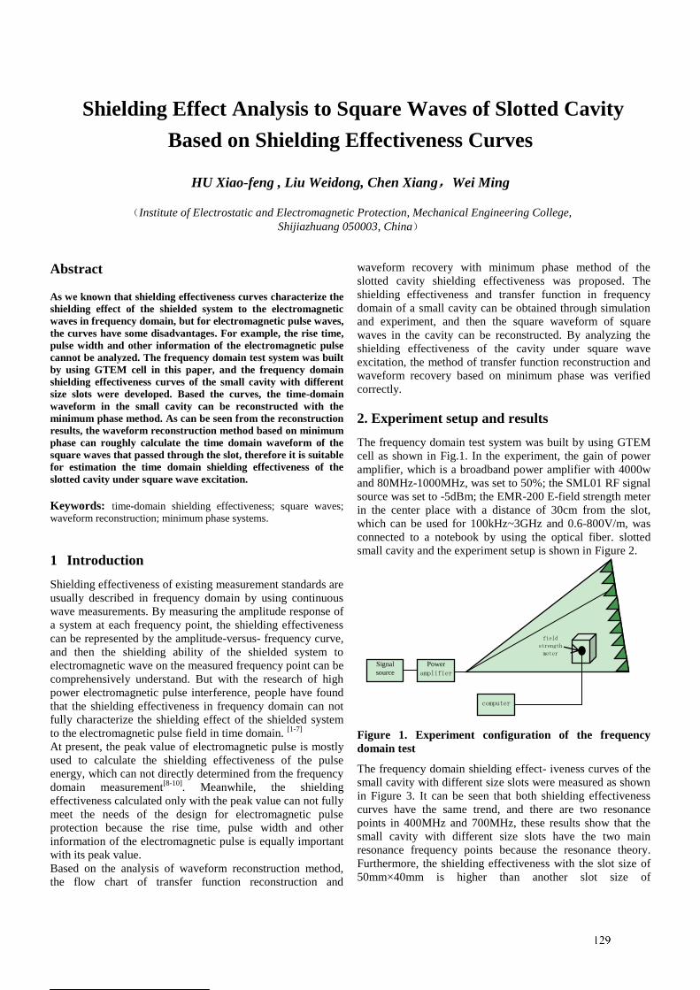
Shielding Effect Analysis to Square Waves of Slotted Cavity
Based on Shielding Effectiveness Curves
HU Xiao-feng , Liu Weidong, Chen Xiang,Wei Ming
(Institute of Electrostatic and Electromagnetic Protection, Mechanical Engineering College,
Shijiazhuang 050003, China)
Abstract As we known that shielding effectiveness curves characterize the
shielding effect of the shielded system to the electromagnetic
waves in frequency domain, but for electromagnetic pulse waves,
the curves have some disadvantages. For example, the rise time,
pulse width and other information of the electromagnetic pulse
cannot be analyzed. The frequency domain test system was built
by using GTEM cell in this paper, and the frequency domain
shielding effectiveness curves of the small cavity with different
size slots were developed. Based the curves, the time-domain
waveform in the small cavity can be reconstructed with the
minimum phase method. As can be seen from the reconstruction
results, the waveform reconstruction method based on minimum
phase can roughly calculate the time domain waveform of the
square waves that passed through the slot, therefore it is suitable
for estimation the time domain shielding effectiveness of the
slotted cavity under square wave excitation.
Keywords: time-domain shielding effectiveness; square waves;
waveform reconstruction; minimum phase systems.
1 Introduction
Shielding effectiveness of existing measurement standards are
usually described in frequency domain by using continuous
wave measurements. By measuring the amplitude response of
a system at each frequency point, the shielding effectiveness
can be represented by the amplitude-versus- frequency curve,
and then the shielding ability of the shielded system to
electromagnetic wave on the measured frequency point can be
comprehensively understand. But with the research of high
power electromagnetic pulse interference, people have found
that the shielding effectiveness in frequency domain can not
fully characterize the shielding effect of the shielded system
to the electromagnetic pulse field in time domain. [1-7]
At present, the peak value of electromagnetic pulse is mostly
used to calculate the shielding effectiveness of the pulse
energy, which can not directly determined from the frequency
domain measurement[8-10]
. Meanwhile, the shielding
effectiveness calculated only with the peak value can not fully
meet the needs of the design for electromagnetic pulse
protection because the rise time, pulse width and other
information of the electromagnetic pulse is equally important
with its peak value.
Based on the analysis of waveform reconstruction method,
the flow chart of transfer function reconstruction and
waveform recovery with minimum phase method of the
slotted cavity shielding effectiveness was proposed. The
shielding effectiveness and transfer function in frequency
domain of a small cavity can be obtained through simulation
and experiment, and then the square waveform of square
waves in the cavity can be reconstructed. By analyzing the
shielding effectiveness of the cavity under square wave
excitation, the method of transfer function reconstruction and
waveform recovery based on minimum phase was verified
correctly.
2. Experiment setup and results
The frequency domain test system was built by using GTEM
cell as shown in Fig.1. In the experiment, the gain of power
amplifier, which is a broadband power amplifier with 4000w
and 80MHz-1000MHz, was set to 50%; the SML01 RF signal
source was set to -5dBm; the EMR-200 E-field strength meter
in the center place with a distance of 30cm from the slot,
which can be used for 100kHz~3GHz and 0.6-800V/m, was
connected to a notebook by using the optical fiber. slotted
small cavity and the experiment setup is shown in Figure 2.
Figure 1. Experiment configuration of the frequency
domain test
The frequency domain shielding effect- iveness curves of the
small cavity with different size slots were measured as shown
in Figure 3. It can be seen that both shielding effectiveness
curves have the same trend, and there are two resonance
points in 400MHz and 700MHz, these results show that the
small cavity with different size slots have the two main
resonance frequency points because the resonance theory.
Furthermore, the shielding effectiveness with the slot size of
50mm×40mm is higher than another slot size of
Signal
source
Power
amplifier
computer
field
strength
meter
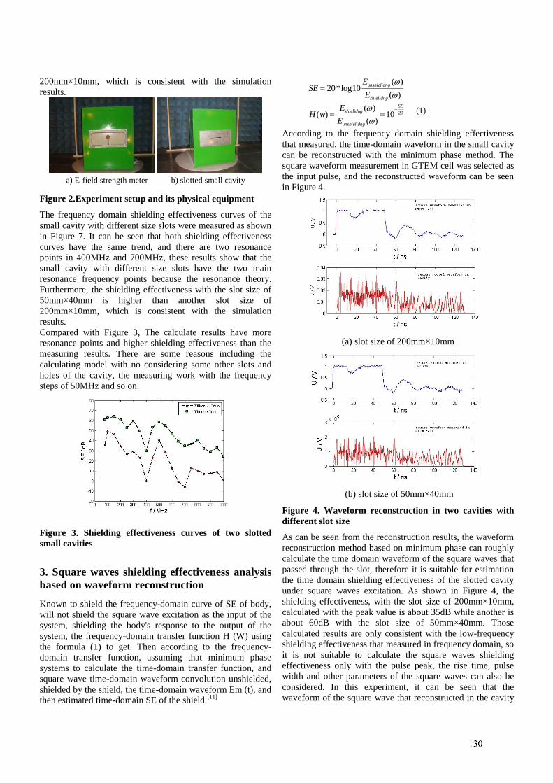
200mm×10mm, which is consistent with the simulation
results.
a) E-field strength meter b) slotted small cavity
Figure 2.Experiment setup and its physical equipment
The frequency domain shielding effectiveness curves of the
small cavity with different size slots were measured as shown
in Figure 7. It can be seen that both shielding effectiveness
curves have the same trend, and there are two resonance
points in 400MHz and 700MHz, these results show that the
small cavity with different size slots have the two main
resonance frequency points because the resonance theory.
Furthermore, the shielding effectiveness with the slot size of
50mm×40mm is higher than another slot size of
200mm×10mm, which is consistent with the simulation
results.
Compared with Figure 3, The calculate results have more
resonance points and higher shielding effectiveness than the
measuring results. There are some reasons including the
calculating model with no considering some other slots and
holes of the cavity, the measuring work with the frequency
steps of 50MHz and so on.
Figure 3. Shielding effectiveness curves of two slotted
small cavities
3. Square waves shielding effectiveness analysis
based on waveform reconstruction
Known to shield the frequency-domain curve of SE of body,
will not shield the square wave excitation as the input of the
system, shielding the body's response to the output of the
system, the frequency-domain transfer function H (W) using
the formula (1) to get. Then according to the frequency-
domain transfer function, assuming that minimum phase
systems to calculate the time-domain transfer function, and
square wave time-domain waveform convolution unshielded,
shielded by the shield, the time-domain waveform Em (t), and
then estimated time-domain SE of the shield.[11]
( )20*log10
( )
unshielidng
shielidng
ESE
E
20( )
( ) 10( )
SEshielidng
unshielidng
EH w
E
(1)
According to the frequency domain shielding effectiveness
that measured, the time-domain waveform in the small cavity
can be reconstructed with the minimum phase method. The
square waveform measurement in GTEM cell was selected as
the input pulse, and the reconstructed waveform can be seen
in Figure 4.
(a) slot size of 200mm×10mm
(b) slot size of 50mm×40mm
Figure 4. Waveform reconstruction in two cavities with
different slot size
As can be seen from the reconstruction results, the waveform
reconstruction method based on minimum phase can roughly
calculate the time domain waveform of the square waves that
passed through the slot, therefore it is suitable for estimation
the time domain shielding effectiveness of the slotted cavity
under square waves excitation. As shown in Figure 4, the
shielding effectiveness, with the slot size of 200mm×10mm,
calculated with the peak value is about 35dB while another is
about 60dB with the slot size of 50mm×40mm. Those
calculated results are only consistent with the low-frequency
shielding effectiveness that measured in frequency domain, so
it is not suitable to calculate the square waves shielding
effectiveness only with the pulse peak, the rise time, pulse
width and other parameters of the square waves can also be
considered. In this experiment, it can be seen that the
waveform of the square wave that reconstructed in the cavity
have some differences with the input square wave, which
indicated that the rise time and pulse width of the pulse
should be considered in the square waves shielding
effectiveness calculation. In addition, the reconstruction
algorithm used in this paper assumes the system is minimum
phase systems, which is not suitable for every shielded system,
and it is also unable to reconstruct the time domain waveform
of the square waves in a slotted cavity with strong
resonance.[12,13]
4. Conclusions
Some conclusions are showed as follows: (1)The waveform
reconstruction method based on minimum phase, can roughly
calculate the time domain waveform of square waves through
the slotted small cavity, and it is suitable to estimation the
time domain shielding effectiveness of slotted small cavity
with square waves excitation; (2)while it is not suitable to the
slotted cavity with strong resonance; (3)the time domain
response of the mixed-phase shielded system under pulse
excitation should be researched in future. Meanwhile, by
using the frequency domain transfer function fitting with
rational function and the inverse Laplace transform, a new
method to calculate the time domain impulse response can be
studied based on the recursive convolution algorithm.
Acknowledgements This work was financially supported by the National Natural
Science Foundation of China.(61001050)
References [1] BAO Yongfang, LU Yinghua, ZHANG Hongxin, HAN
Chunyuan. The Analysis of Shielding Effectiveness of
Negative Permittivity Composite Materials to Different
EMP. IEEE International Symposium on Microwave,
Propagation and EMC Technologies for Wireless
Communications Proceedings,pp.635-638(2005).
[2] Special issue on high-power electromagnetic (HPEM)
and intentional electromagnetic interference (IEMI).
IEEE Trans. EMC. 46,pp.314-496,(2004).
[3] Andrew C. Marvin, John F. Dawson and Simon Ward,
et al. A Proposed New Definition and Measurement of
the Shielding Effect of Equipment Enclosures. IEEE
Trans. On Electromagnetic Compatibility,46, pp. 459-
468, (2004).
[4] MICHEL AGUET, MIRCEA IANOVICI, and
CHUNG-CHI LIN. Transient Electromagnetic Field
Coupling to Long Shielded Cables. IEEE Trans. On
Electromagnetic Compatibility, 22, pp. 276-282, (1980).
[5] M. P. Robinson, T.M.Benson and C. Christopoulos.
Analytical formulation for the Shielding Effectiveness
of Enclosures with Apertures. IEEE Trans. on
Electromagnetic Compatibility, 40,pp.240-248,(1998).
[6] David W P Thomas. Alan C Demon. Tadeusz
Konefal,et al. Model of the electromagnetic fields
inside a cuboidal enclosure populated with conducting
planes or printed circuit board. IEEE Trans. on EMC,,
43, pp.161-169,(2001).
[7] LI MIN, James L Drewniak, Sergin Radu, et al. An EMI
estimate for shielding-enclosure evaluation. IEEE Trans.
on EMC, 43,pp.295-304,(2001).
[8] ZHOU Bihua, GAO Cheng, REN Heming. The
Definition of EMP Shielding Effectiveness. Asia-Pacific
Conference on Environmental Electromagnetics,pp.562-
565,(2003).
[9] ZHOU Bihua, GAO Cheng, CHEN Bin, CHEN Ziming.
Experimental Investigation of EMP Shielding
Effectiveness of Reinforced-Concrete Cell Model. Asia-
Pacific Conference on Environmental Electromagnetics,
pp.296-300,(2000).
[10] J. P Bruhin. Shielding Effectiveness of Reinforcement
Concrete against Electromagnetic Wave. EMP 84 Parts
2, pp.597-605.
[11] HU Xiaofeng, CHEN xiang, WEI Ming. Time-Domain
Simulation and Waveform Reconstruction for Shielding
Effectiveness of Materials against Electromagnetic
Pulse, the 7th International conference on applied
electerostatics, Dalian,China,83-84,(2012)
[12] SHI Lihua, ZHOU Bihua, CHEN Bin, GAO Cheng.
Time domain characterization of a system based on the
magnitude of its frequency reponse. Chinese journal of
radio science, 15, pp.467-471 (2000).
[13] CHEN Xiang, CHEN Yongguang,WEI Ming,HU
Xiaofeng. Time Domain Testing Methods of Material'
s Shielding Effectiveness of Electromagnetic Pulse
Using Flange Coaxial, High Voltage Engineering,
28,pp.594-600, (2012).
HU Xiao-feng was born in Jixi city, Anhui
Province, China, in 1977. He received the B.Sc,
M.Sc and Ph.D. degree in Mechanical Engineering
College. He is a vice-professor in Mechanical
Engineering College now and studies
electromagnetic pulse measurement and
electromagnetic protection to electronic systems.
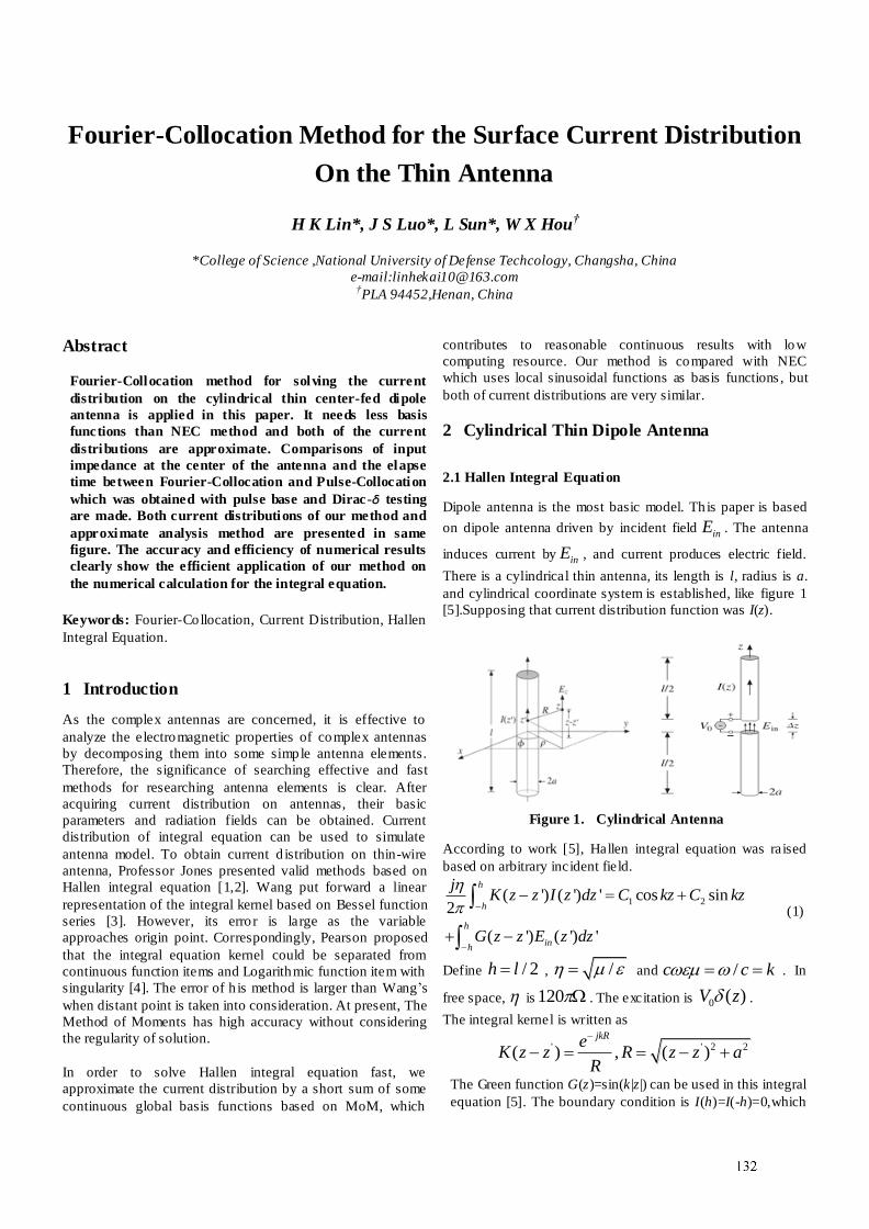
1
Fourier-Collocation Method for the Surface Current Distribution
On the Thin Antenna
H K Lin*, J S Luo*, L Sun*, W X Hou†
*College of Science ,National University of Defense Techcology, Changsha, China
e-mail:[email protected] †PLA 94452,Henan, China
Abstract
Fourier-Collocation method for solving the current
distribution on the cylindrical thin center-fed dipole
antenna is applied in this paper. It needs less basis
functions than NEC method and both of the current
distributions are approximate. Comparisons of input
impedance at the center of the antenna and the elapse
time between Fourier-Collocation and Pulse-Collocation
which was obtained with pulse base and Dirac- testing
are made. Both current distributions of our method and
approximate analysis method are presented in same
figure. The accuracy and efficiency of numerical results
clearly show the efficient application of our method on
the numerical calculation for the integral equation.
Keywords: Fourier-Collocation, Current Distribution, Hallen
Integral Equation.
1 Introduction
As the complex antennas are concerned, it is effective to
analyze the electromagnetic properties of complex antennas
by decomposing them into some simple antenna elements.
Therefore, the significance of searching effective and fast
methods for researching antenna elements is clear. After
acquiring current distribution on antennas, their basic
parameters and radiation fields can be obtained. Current
distribution of integral equation can be used to simulate
antenna model. To obtain current d istribution on thin-wire
antenna, Professor Jones presented valid methods based on
Hallen integral equation [1,2]. Wang put forward a linear
representation of the integral kernel based on Bessel function
series [3]. However, its erro r is large as the variable
approaches origin point. Correspondingly, Pearson proposed
that the integral equation kernel could be separated from
continuous function items and Logarithmic function item with
singularity [4]. The error of h is method is larger than Wang’s
when distant point is taken into consideration. At present, The
Method of Moments has high accuracy without considering
the regularity of solution.
In order to solve Hallen integral equation fast, we
approximate the current distribution by a short sum of some
continuous global basis functions based on MoM, which
contributes to reasonable continuous results with low
computing resource. Our method is compared with NEC
which uses local sinusoidal functions as basis functions , but
both of current distributions are very similar.
2 Cylindrical Thin Dipole Antenna
2.1 Hallen Integral Equation
Dipole antenna is the most basic model. Th is paper is based
on dipole antenna driven by incident field inE . The antenna
induces current by inE , and current produces electric field.
There is a cylindrical thin antenna, its length is l, radius is a.
and cylindrical coordinate system is established, like figure 1
[5].Supposing that current distribution function was I(z).
Figure 1. Cylindrical Antenna
According to work [5], Hallen integral equation was raised
based on arbitrary incident field.
1 2( ') ( ') ' cos sin2
( ') ( ') '
h
h
h
inh
jK z z I z dz C kz C kz
G z z E z dz
(1)
Define / 2h l , / and /c c k . In
free space, is 120 . The excitation is 0 ( )V z .
The integral kernel is written as
' ' 2 2( ) , ( )jkRe
K z z R z z aR
The Green function G(z)=sin(k |z |) can be used in this integral
equation [5]. The boundary condition is I(h)=I(-h)=0,which
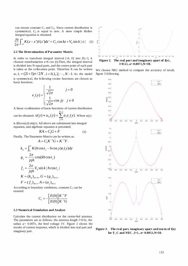
2
can ensure constant C1 and C2. Since current distribution is
symmetrical, C2 is equal to zero. A more simple Hallen
integral equation is obtained.
1 0( ') ( ') ' cos sin | |2
h
h
jK z z I z dz C kz V k z
(2)
2.2 The Determination of Parameter Matrix
In order to transform integral interval [-h, h] into [0,], it
chooses transformat ion z=h cos (t).Then, the integral interval
is divided into N equal parts, and the center point of each part
is taken as the co llocation point. Therefore It can be written
as, (2 1) / 2it i N , 0,1,2, , 1i N .As the model
is symmetrical, the fo llowing cosine functions are chosen as
basis functions.
10
2( )
1cos 0
2
j
j
e y
jy j
A linear combination of basis functions of current distribution
can be obtained.
1
0
( ) ( ) ( )N
N j j
j
u y u y a e y
. Where u(y)
is I(hcos(y)) sin(y). All above are substituted into integral
equation, and algebraic equation is presented.
1KA C G F (3)
Finally, The Parameter Matrix can be written as. 1 1
1A C K G K F .
0( cos cos ) ( )ij j ik K h t h y e y dy
2cos( cos )j jg kh t
j h
0
2sin | cos |j jf V k h t
j h
( )ij N NK k , 1( )j NG g ,
1( )j NF f , 1( )j NA a
According to boundary conditions, constant C1 can be
ensured.
1
1 1
(0)
(0)
E K FC
E K G
2.3 Numerical Simulation and Analyze
Calculate the current distribution on the center-fed antenna.
The parameters are as follows: the antenna length l=0.5, the
radius a= 0.007, the feed voltage 1V. Figure 2 shows the
results of current response, which is d ivided into real part and
imaginary part .
-0.25 -0.2 -0.15 -0.1 -0.05 0 0.05 0.1 0.15 0.2 0.250
1
2
3
4
5
6
7
8
9x 10
-3
z(m)
Re(I
(z))
-0.25 -0.2 -0.15 -0.1 -0.05 0 0.05 0.1 0.15 0.2 0.25-6
-5
-4
-3
-2
-1
0x 10
-3
Im(I
(z))
z(m) Figure 2. The real part and imaginary apart of I(z) ,
l=0.5, a= 0.007,N=30.
We choose NEC method to compare the accuracy of result,
figure 3 following.
-0.5 -0.4 -0.3 -0.2 -0.1 0 0.1 0.2 0.3 0.4 0.50
0.1
0.2
0.3
0.4
0.5
0.6
0.7
0.8
0.9
z(m)
Re|I(z
)|
F-C
NEC
-0.5 -0.4 -0.3 -0.2 -0.1 0 0.1 0.2 0.3 0.4 0.5-2.5
-2
-1.5
-1
-0.5
0
0.5
1
1.5
2
z(m)
Im|I(z
)|
F-C
NEC
-0.5 -0.4 -0.3 -0.2 -0.1 0 0.1 0.2 0.3 0.4 0.50
0.5
1
1.5
2
2.5
z(m)
|I(z
)|
F-C
NEC
Figure 3. The real part, imaginary apart and norm of I(z)
for F_C and NEC , l= , a= 0.005,N=50.
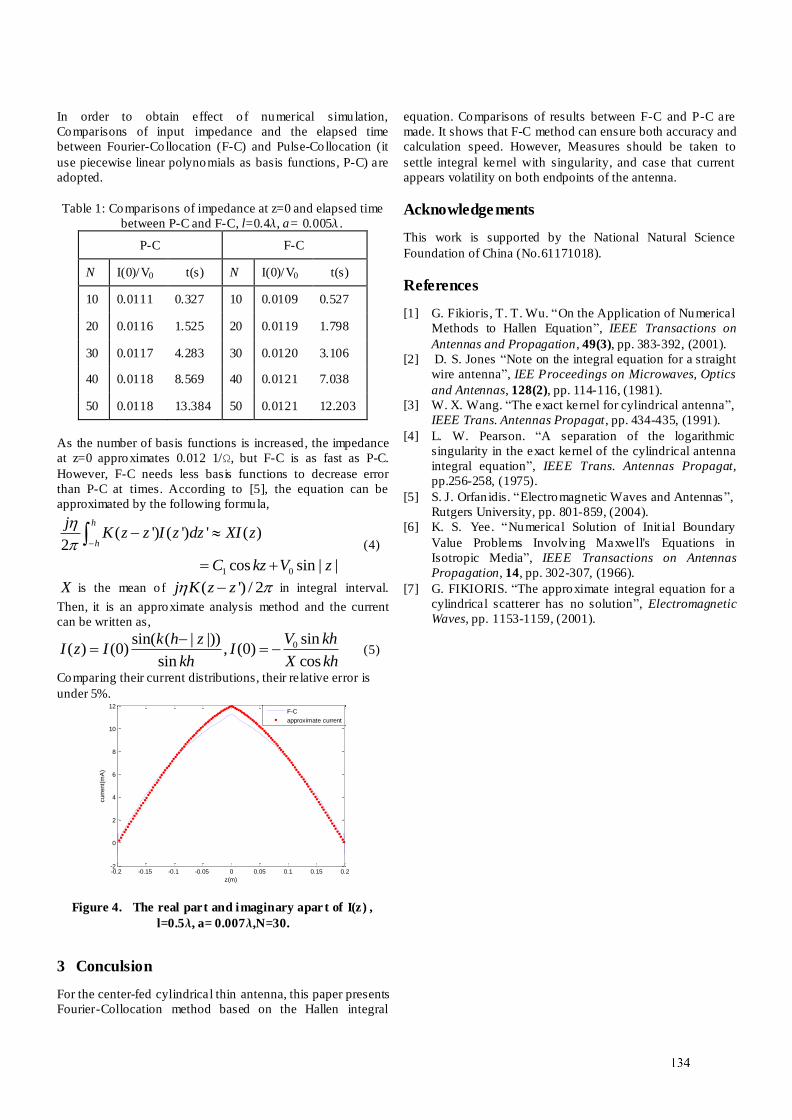
3
In order to obtain effect o f numerical simulation,
Comparisons of input impedance and the elapsed time
between Fourier-Collocation (F-C) and Pulse-Collocation (it
use piecewise linear polynomials as basis functions, P-C) are
adopted.
Table 1: Comparisons of impedance at z=0 and elapsed time
between P-C and F-C, l=0.4, a= 0.005 .
P-C F-C
N I(0)/V0 t(s) N I(0)/V0 t(s)
10 0.0111 0.327 10 0.0109 0.527
20 0.0116 1.525 20 0.0119 1.798
30 0.0117 4.283 30 0.0120 3.106
40 0.0118 8.569 40 0.0121 7.038
50 0.0118 13.384 50 0.0121 12.203
As the number of basis functions is increased, the impedance
at z=0 approximates 0.012 1/, but F-C is as fast as P-C.
However, F-C needs less basis functions to decrease error
than P-C at times. According to [5], the equation can be
approximated by the following formula,
1 0
( ') ( ') ' ( )2
cos sin | |
h
h
jK z z I z dz XI z
C kz V z
(4)
X is the mean of ( ') / 2j K z z in integral interval.
Then, it is an approximate analysis method and the current
can be written as,
0 sinsin( ( | |))( ) (0) , (0)
sin cos
V khk h zI z I I
kh X kh
(5)
Comparing their current distributions, their relative error is
under 5%.
-0.2 -0.15 -0.1 -0.05 0 0.05 0.1 0.15 0.2-2
0
2
4
6
8
10
12
curr
ent(
mA
)
z(m)
F-C
approximate current
Figure 4. The real part and imaginary apar t of I(z) ,
l=0.5, a= 0.007,N=30.
3 Conculsion
For the center-fed cylindrical thin antenna, this paper presents
Fourier-Collocation method based on the Hallen integral
equation. Comparisons of results between F-C and P-C are
made. It shows that F-C method can ensure both accuracy and
calculation speed. However, Measures should be taken to
settle integral kernel with singularity, and case that current
appears volatility on both endpoints of the antenna.
Acknowledgements
This work is supported by the National Natural Science
Foundation of China (No.61171018).
References
[1] G. Fikioris, T. T. Wu. “On the Application of Numerical
Methods to Hallen Equation”, IEEE Transactions on
Antennas and Propagation, 49(3), pp. 383-392, (2001).
[2] D. S. Jones “Note on the integral equation for a straight
wire antenna”, IEE Proceedings on Microwaves, Optics
and Antennas, 128(2), pp. 114-116, (1981).
[3] W. X. Wang. “The exact kernel for cylindrical antenna”,
IEEE Trans. Antennas Propagat, pp. 434-435, (1991).
[4] L. W. Pearson. “A separation of the logarithmic
singularity in the exact kernel of the cylindrical antenna
integral equation”, IEEE Trans. Antennas Propagat,
pp.256-258, (1975).
[5] S. J. Orfan idis. “Electromagnetic Waves and Antennas”,
Rutgers University, pp. 801-859, (2004).
[6] K. S. Yee. “Numerical Solution of Init ial Boundary
Value Problems Involv ing Maxwell's Equations in
Isotropic Media”, IEEE Transactions on Antennas
Propagation, 14, pp. 302-307, (1966).
[7] G. FIKIORIS. “The approximate integral equation for a
cylindrical scatterer has no solution”, Electromagnetic
Waves, pp. 1153-1159, (2001).
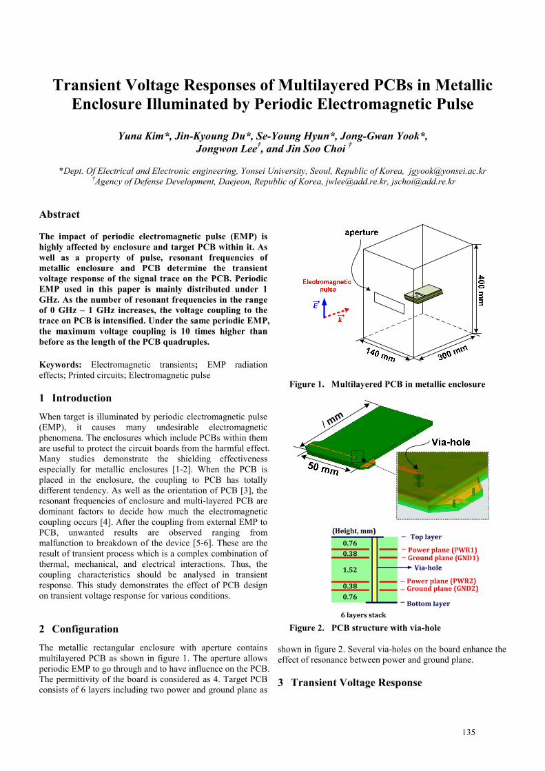
1
Transient Voltage Responses of Multilayered PCBs in Metallic Enclosure Illuminated by Periodic Electromagnetic Pulse
Yuna Kim*, Jin-Kyoung Du*, Se-Young Hyun*, Jong-Gwan Yook*, Jongwon Lee†, and Jin Soo Choi †
*Dept. Of Electrical and Electronic engineering, Yonsei University, Seoul, Republic of Korea, [email protected] †Agency of Defense Development, Daejeon, Republic of Korea, [email protected], [email protected]
Abstract The impact of periodic electromagnetic pulse (EMP) is highly affected by enclosure and target PCB within it. As well as a property of pulse, resonant frequencies of metallic enclosure and PCB determine the transient voltage response of the signal trace on the PCB. Periodic EMP used in this paper is mainly distributed under 1 GHz. As the number of resonant frequencies in the range of 0 GHz – 1 GHz increases, the voltage coupling to the trace on PCB is intensified. Under the same periodic EMP, the maximum voltage coupling is 10 times higher than before as the length of the PCB quadruples. Keywords: Electromagnetic transients; EMP radiation effects; Printed circuits; Electromagnetic pulse
1 Introduction When target is illuminated by periodic electromagnetic pulse (EMP), it causes many undesirable electromagnetic phenomena. The enclosures which include PCBs within them are useful to protect the circuit boards from the harmful effect. Many studies demonstrate the shielding effectiveness especially for metallic enclosures [1-2]. When the PCB is placed in the enclosure, the coupling to PCB has totally different tendency. As well as the orientation of PCB [3], the resonant frequencies of enclosure and multi-layered PCB are dominant factors to decide how much the electromagnetic coupling occurs [4]. After the coupling from external EMP to PCB, unwanted results are observed ranging from malfunction to breakdown of the device [5-6]. These are the result of transient process which is a complex combination of thermal, mechanical, and electrical interactions. Thus, the coupling characteristics should be analysed in transient response. This study demonstrates the effect of PCB design on transient voltage response for various conditions.
2 Configuration The metallic rectangular enclosure with aperture contains multilayered PCB as shown in figure 1. The aperture allows periodic EMP to go through and to have influence on the PCB. The permittivity of the board is considered as 4. Target PCB consists of 6 layers including two power and ground plane as
shown in figure 2. Several via-holes on the board enhance the effect of resonance between power and ground plane.
3 Transient Voltage Response
Figure 1. Multilayered PCB in metallic enclosure
l mm
Figure 2. PCB structure with via-hole
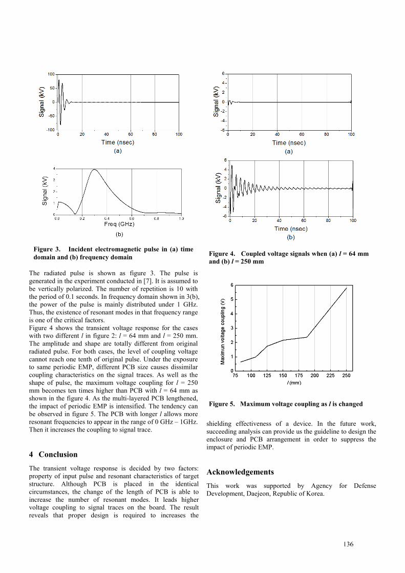
2
The radiated pulse is shown as figure 3. The pulse is generated in the experiment conducted in [7]. It is assumed to be vertically polarized. The number of repetition is 10 with the period of 0.1 seconds. In frequency domain shown in 3(b), the power of the pulse is mainly distributed under 1 GHz. Thus, the existence of resonant modes in that frequency range is one of the critical factors. Figure 4 shows the transient voltage response for the cases with two different l in figure 2: l = 64 mm and l = 250 mm. The amplitude and shape are totally different from original radiated pulse. For both cases, the level of coupling voltage cannot reach one tenth of original pulse. Under the exposure to same periodic EMP, different PCB size causes dissimilar coupling characteristics on the signal traces. As well as the shape of pulse, the maximum voltage coupling for l = 250 mm becomes ten times higher than PCB with l = 64 mm as shown in the figure 4. As the multi-layered PCB lengthened, the impact of periodic EMP is intensified. The tendency can be observed in figure 5. The PCB with longer l allows more resonant frequencies to appear in the range of 0 GHz – 1GHz. Then it increases the coupling to signal trace.
4 Conclusion The transient voltage response is decided by two factors: property of input pulse and resonant characteristics of target structure. Although PCB is placed in the identical circumstances, the change of the length of PCB is able to increase the number of resonant modes. It leads higher voltage coupling to signal traces on the board. The result reveals that proper design is required to increases the
shielding effectiveness of a device. In the future work, succeeding analysis can provide us the guideline to design the enclosure and PCB arrangement in order to suppress the impact of periodic EMP.
Acknowledgements This work was supported by Agency for Defense Development, Daejeon, Republic of Korea.
Figure 3. Incident electromagnetic pulse in (a) time domain and (b) frequency domain
Figure 4. Coupled voltage signals when (a) l = 64 mm and (b) l = 250 mm
Figure 5. Maximum voltage coupling as l is changed
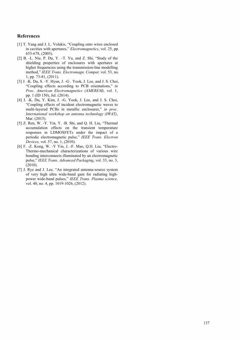
3
References [1] T. Yang and J. L. Volakis, “Coupling onto wires enclosed
in cavities with apertures,” Electromagnetics, vol. 25, pp. 655-678, (2005).
[2] B. -L. Nie, P. Du, Y. –T. Yu, and Z. Shi, “Study of the shielding properties of enclosures with apertures at higher frequencies using the transmission-line modelling method,” IEEE Trans. Electromagn. Compat. vol. 53, no. 1, pp. 73-81, (2011).
[3] J. -K. Du, S. -Y. Hyun, J. -G . Yook, J. Lee, and J. S. Choi, “Coupling effects according to PCB orientations,” in Proc. American Electromagnetics (AMEREM), vol. 1, pp. 1 (ID 150), Jul. (2014).
[4] J. -K. Du, Y. Kim, J. -G. Yook, J. Lee, and J. S. Choi, “Coupling effects of incident electromagnetic waves to multi-layered PCBs in metallic enclosures,” in proc. International workshop on antenna technology (IWAT), Mar. (2015).
[5] Z. Ren, W. -Y. Yin, Y. -B. Shi, and Q. H. Liu, “Thermal accumulation effects on the transient temperature responses in LDMOSFETs under the impact of a periodic electromagnetic pulse,” IEEE Trans. Electron Devices, vol. 57, no. 1, (2010).
[6] F. -Z. Kong, W. -Y Yin, J. -F. Mao, Q.H. Liu, “Electro-Thermo-mechanical characterizations of various wire bonding interconnects illuminated by an electromagnetic pulse,” IEEE Trans. Advanced Packaging, vol. 33, no. 3, (2010).
[7] J. Rye and J. Lee, “An integrated antenna-source system of very high ultra wide-band gain for radiating high-power wide-band pulses,” IEEE Trans. Plasma science, vol. 40, no. 4, pp. 1019-1026, (2012).
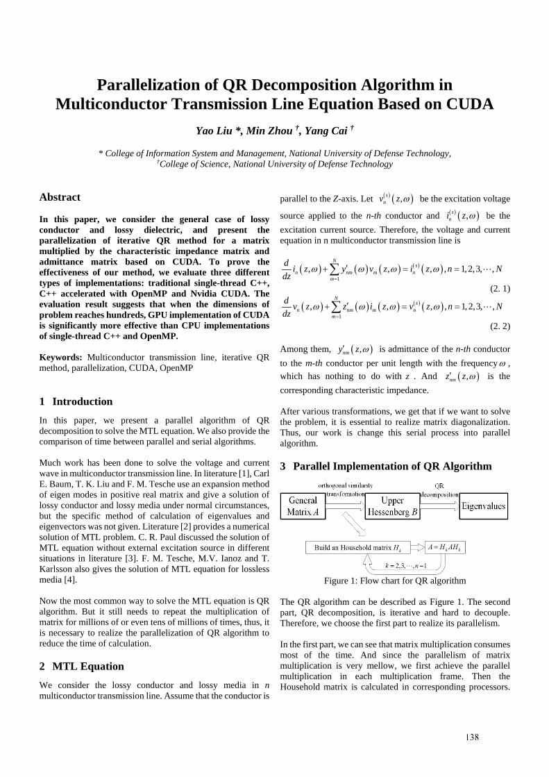
Parallelization of QR Decomposition Algorithm in Multiconductor Transmission Line Equation Based on CUDA
Yao Liu *, Min Zhou †, Yang Cai †
* College of Information System and Management, National University of Defense Technology, †College of Science, National University of Defense Technology
Abstract In this paper, we consider the general case of lossy conductor and lossy dielectric, and present the parallelization of iterative QR method for a matrix multiplied by the characteristic impedance matrix and admittance matrix based on CUDA. To prove the effectiveness of our method, we evaluate three different types of implementations: traditional single-thread C++, C++ accelerated with OpenMP and Nvidia CUDA. The evaluation result suggests that when the dimensions of problem reaches hundreds, GPU implementation of CUDA is significantly more effective than CPU implementations of single-thread C++ and OpenMP. Keywords: Multiconductor transmission line, iterative QR method, parallelization, CUDA, OpenMP
1 Introduction In this paper, we present a parallel algorithm of QR decomposition to solve the MTL equation. We also provide the comparison of time between parallel and serial algorithms. Much work has been done to solve the voltage and current wave in multiconductor transmission line. In literature [1], Carl E. Baum, T. K. Liu and F. M. Tesche use an expansion method of eigen modes in positive real matrix and give a solution of lossy conductor and lossy media under normal circumstances, but the specific method of calculation of eigenvalues and eigenvectors was not given. Literature [2] provides a numerical solution of MTL problem. C. R. Paul discussed the solution of MTL equation without external excitation source in different situations in literature [3]. F. M. Tesche, M.V. Ianoz and T. Karlsson also gives the solution of MTL equation for lossless media [4]. Now the most common way to solve the MTL equation is QR algorithm. But it still needs to repeat the multiplication of matrix for millions of or even tens of millions of times, thus, it is necessary to realize the parallelization of QR algorithm to reduce the time of calculation.
2 MTL Equation We consider the lossy conductor and lossy media in n multiconductor transmission line. Assume that the conductor is
parallel to the Z-axis. Let ( ) ( ),snv z ω be the excitation voltage
source applied to the n-th conductor and ( ) ( ),sni z ω be the
excitation current source. Therefore, the voltage and current equation in n multiconductor transmission line is
( ) ( ) ( ) ( ) ( )1
, , , , 1, 2,3, ,N
sn nm m n
m
d i z y v z i z n Ndz
ω ω ω ω=
′+ = =∑
(2. 1)
( ) ( ) ( ) ( ) ( )1
, , , , 1, 2,3, ,N
sn nm m n
m
d v z z i z v z n Ndz
ω ω ω ω=
′+ = =∑
(2. 2)
Among them, ( ),nmy z ω′ is admittance of the n-th conductor to the m-th conductor per unit length with the frequencyω , which has nothing to do with z . And ( ),nmz z ω′ is the corresponding characteristic impedance. After various transformations, we get that if we want to solve the problem, it is essential to realize matrix diagonalization. Thus, our work is change this serial process into parallel algorithm.
3 Parallel Implementation of QR Algorithm
Figure 1: Flow chart for QR algorithm
The QR algorithm can be described as Figure 1. The second part, QR decomposition, is iterative and hard to decouple. Therefore, we choose the first part to realize its parallelism. In the first part, we can see that matrix multiplication consumes most of the time. And since the parallelism of matrix multiplication is very mellow, we first achieve the parallel multiplication in each multiplication frame. Then the Household matrix is calculated in corresponding processors.
1
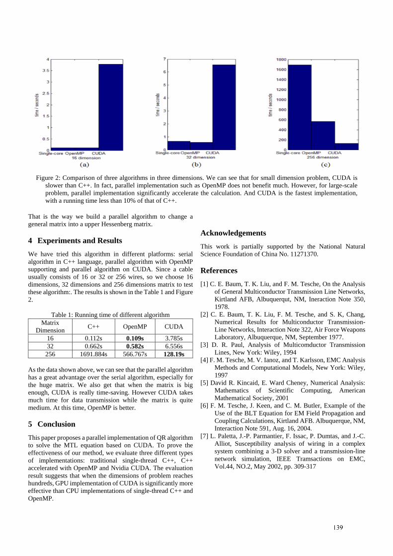
That is the way we build a parallel algorithm to change a general matrix into a upper Hessenberg matrix.
4 Experiments and Results We have tried this algorithm in different platforms: serial algorithm in C++ language, parallel algorithm with OpenMP supporting and parallel algorithm on CUDA. Since a cable usually consists of 16 or 32 or 256 wires, so we choose 16 dimensions, 32 dimensions and 256 dimensions matrix to test these algorithm:. The results is shown in the Table 1 and Figure 2.
Table 1: Running time of different algorithm Matrix
Dimension C++ OpenMP CUDA
16 0.112s 0.109s 3.785s 32 0.662s 0.582s 6.556s 256 1691.884s 566.767s 128.19s
As the data shown above, we can see that the parallel algorithm has a great advantage over the serial algorithm, especially for the huge matrix. We also get that when the matrix is big enough, CUDA is really time-saving. However CUDA takes much time for data transmission while the matrix is quite medium. At this time, OpenMP is better.
5 Conclusion This paper proposes a parallel implementation of QR algorithm to solve the MTL equation based on CUDA. To prove the effectiveness of our method, we evaluate three different types of implementations: traditional single-thread C++, C++ accelerated with OpenMP and Nvidia CUDA. The evaluation result suggests that when the dimensions of problem reaches hundreds, GPU implementation of CUDA is significantly more effective than CPU implementations of single-thread C++ and OpenMP.
Acknowledgements This work is partially supported by the National Natural Science Foundation of China No. 11271370.
References [1] C. E. Baum, T. K. Liu, and F. M. Tesche, On the Analysis
of General Multiconductor Transmission Line Networks, Kirtland AFB, Albuquerqut, NM, Ineraction Note 350, 1978.
[2] C. E. Baum, T. K. Liu, F. M. Tesche, and S. K, Chang, Numerical Results for Multiconductor Transmission-Line Networks, Interaction Note 322, Air Force Weapons Laboratory, Albuquerque, NM, September 1977.
[3] D. R. Paul, Analysis of Multicomductor Transmission Lines, New York: Wiley, 1994
[4] F. M. Tesche, M. V. Ianoz, and T. Karlsson, EMC Analysis Methods and Computational Models, New York: Wiley, 1997
[5] David R. Kincaid, E. Ward Cheney, Numerical Analysis: Mathematics of Scientific Computing, American Mathematical Society, 2001
[6] F. M. Tesche, J. Keen, and C. M. Butler, Example of the Use of the BLT Equation for EM Field Propagation and Coupling Calculations, Kirtland AFB. Albuquerque, NM, Interaction Note 591, Aug. 16, 2004.
[7] L. Paletta, J.-P. Parmantier, F. Issac, P. Dumtas, and J.-C. Alliot, Susceptibility analysis of wiring in a complex system combining a 3-D solver and a transmission-line network simulation, IEEE Tramsactions on EMC, Vol.44, NO.2, May 2002, pp. 309-317
Figure 2: Comparison of three algorithms in three dimensions. We can see that for small dimension problem, CUDA is slower than C++. In fact, parallel implementation such as OpenMP does not benefit much. However, for large-scale problem, parallel implementation significantly accelerate the calculation. And CUDA is the fastest implementation, with a running time less than 10% of that of C++.
2
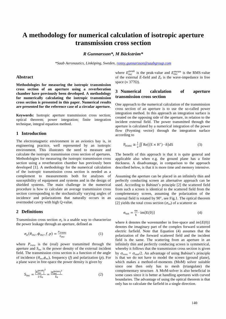
1
A methodology for numerical calculation of isotropic aperture
transmission cross section
R Gunnarsson*, M Bäckström*
*Saab Aeronautics, Linköping, Sweden, [email protected]
Abstract
Methodologies for measuring the isotropic transmission
cross section of an aperture using a reverberation
chamber have previously been developed. A methodology
for numerically calculating the isotropic transmission
cross section is presented in this paper. Numerical results
are presented for the reference case of a circular aperture.
Keywords: Isotropic aperture transmission cross section;
optical theorem; power integration; finite integration
technique, integral equation method.
1 Introduction
The electromagnetic environment in an avionics bay is, in
engineering practice, well represented by an isotropic
environment. This illustrates the need to measure and
calculate the isotropic transmission cross section of apertures.
Methodologies for measuring the isotropic transmission cross
section using a reverberation chamber has previously been
developed [1]. A methodology for the numerical calculation
of the isotropic transmission cross section is needed as a
complement to measurements both for analyses of
susceptibility of equipment and systems and in the design of
shielded systems. The main challenge in the numerical
procedure is how to calculate an average transmission cross
section corresponding to the stochastically varying angles of
incidence and polarizations that naturally occurs in an
overmoded cavity with high Q-value.
2 Definitions
Transmission cross section a is a usable way to characterize
the power leakage through an aperture, defined as
𝜎𝑎(𝜃𝑖𝑛𝑐 , 𝜙𝑖𝑛𝑐 , 𝑓, 𝑝) =𝑃𝑡𝑟𝑎𝑛𝑠
𝑆𝑖𝑛𝑐 (1)
where Ptrans is the (real) power transmitted through the
aperture and Sinc is the power density of the external incident
field. The transmission cross section is a function of the angle
of incidence (inc,inc), frequency (f) and polarization (p). For
a plane wave in free-space the power density is given by
Sinc =|Einc
peak|2
2∙Z0=
|Eincmean|
2
Z0 (2)
where 𝐸𝑖𝑛𝑐𝑝𝑒𝑎𝑘
is the peak-value and 𝐸𝑖𝑛𝑐𝑚𝑒𝑎𝑛 is the RMS-value
of the external E-field and Z0 is the wave-impedance in free
space ( 377).
3 Numerical calculation of aperture
transmission cross section
One approach to the numerical calculation of the transmission
cross section of an aperture is to use the so-called power
integration method. In this approach an integration surface is
created on the opposing side of the aperture, in relation to the
incident external field. The power transmitted through the
aperture is calculated by a numerical integration of the power
flow (Poynting vector) through the integration surface
according to
Ptrans ≅1
2∬ Re(E × H∗) ∙ ndS (3)
The benefit of this approach is that it is quite general and
applicable also when e.g. the ground plane has a finite
thickness. A disadvantage, in comparison to the approach
described below, is that it is more time and memory intensive.
Assuming the aperture can be placed in an infinitely thin and
perfectly conducting screen an alternative approach can be
used. According to Babinet’s principle [2] the scattered field
from such a screen is identical to the scattered field from the
complementary screen, assuming the polarization of the
external field is rotated by 90, see Fig.1. The optical theorem
[2] yields the total cross section (tot) of a scatterer as
σtot =4π
k∙ imE(0) (4)
where k denotes the wavenumber in free-space and imE(0)
denotes the imaginary part of the complex forward scattered
electric farfield. Note that Equation (4) assumes that the
polarization of the forward scattered field and the incident
field is the same. The scattering from an aperture in an
infinitely thin and perfectly conducing screen is symmetrical,
whereby it follows that the transmission cross section is given
by trans = total/2. An advantage of using Babinet’s principle
is that we do not have to model the screen (ground plane),
which makes a method-of-moments (MoM) solver suitable
since one then only has to mesh (triangulate) the
complementary structure. A MoM-solver is also beneficial in
some cases since it is better at handling apertures with curved
boundaries. The advantage of using the optical theorem is that
only has to calculate the farfield in a single direction.
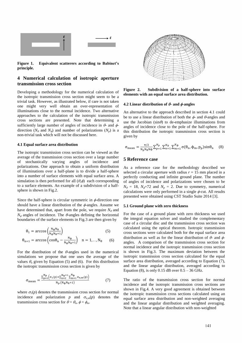
2
Figure 1. Equivalent scatterers according to Babinet’s
principle.
4 Numerical calculation of isotropic aperture
transmission cross section
Developing a methodology for the numerical calculation of
the isotropic transmission cross section might seem to be a
trivial task. However, as illustrated below, if care is not taken
one might very well obtain an over-representation of
illuminations close to the normal incidence. Two alternative
approaches to the calculation of the isotropic transmission
cross sections are presented. Note that determining a
sufficiently large number of angles of incidence in - and -
direction (N and N) and number of polarizations (Np) is a
non-trivial task which will not be discussed here.
4.1 Equal surface area distribution
The isotropic transmission cross section can be viewed as the
average of the transmission cross section over a large number
of stochastically varying angles of incidence and
polarizations. One approach to obtain a uniform distribution
of illuminations over a half-plane is to divide a half-sphere
into a number of surface elements with equal surface area. A
simulation is then performed for all (,) each corresponding
to a surface elements. An example of a subdivision of a half-
sphere is shown in Fig.2.
Since the half-sphere is circular symmetric in -direction one
should have a linear distribution of the -angles. Assume we
have determined that, apart from the pole, we require N and
N angles of incidence. The -angles defining the horizontal
boundaries of the surface elements in Fig.3 are then given by
θ1 = arccos (NϕNθ
NϕNθ+1) (5)
θn+1 = arccos (cosθn −Nϕ
NϕNθ+1) n = 1, . . , Nθ (6)
For the distribution of the -angles used in the numerical
simulations we propose that one uses the average of the
values n given by Equation (5) and (6). For this distribution
the isotropic transmission cross section is given by
σmean =∑ (σ1(p)+∑ ∑ σn,m(p)
Nϕm=1
Nθ+1n=2 )
Npp=1
Np∙(NϕNθ+1) (7)
where 1(p) denotes the transmission cross section for normal
incidence and polarization p and n,m(p) denotes the
transmission cross section for = n, = m.
Figure 2. Subdivision of a half-sphere into surface
elements with an equal surface area distribution.
4.2 Linear distribution of - and -angles
An alternative to the approach described in section 4.1 could
be to use a linear distribution of both the - and -angles and
use the Jacobian (sin) to de-emphasize illuminations from
angles of incidence close to the pole of the half-sphere. For
this distribution the isotropic transmission cross section is
given by
σmean =π/2
NpNθNϕ∑ ∑ ∑ σ(θn, ϕm, pp)sinθn
𝑁𝜙
𝑚=1
𝑁𝜃𝑛=1
𝑁𝑝
𝑝=1 (8)
5 Reference case
As a reference case for the methodology described we
selected a circular aperture with radius r = 15 mm placed in a
perfectly conducting and infinite ground plane. The number
of angles of incidence and polarizations were chosen to be
N = 18, N=72 and Np = 2. Due to symmetry, numerical
calculations were only performed in a single -cut. All results
presented were obtained using CST Studio Suite 2014 [3].
5.1 Ground plane with zero thickness
For the case of a ground plane with zero thickness we used
the integral equation solver and studied the complementary
case of a circular disc and the transmission cross section was
calculated using the optical theorem. Isotropic transmission
cross sections were calculated both for the equal surface area
distribution as well as for the linear distribution of - and -
angles. A comparison of the transmission cross section for
normal incidence and the isotropic transmission cross section
is shown in Fig.3. The maximum deviation between the
isotropic transmission cross section calculated for the equal
surface area distribution, averaged according to Equation (7),
and the linear angular distribution, averaged according to
Equation (8), is only 0.15 dB over 0.5 – 36 GHz.
The ratio of the transmission cross section for normal
incidence and the isotropic transmission cross sections are
shown in Fig.4. A very good agreement is obtained between
the isotropic transmission cross sections calculated using an
equal surface area distribution and non-weighted averaging
and the linear angular distribution and weighted averaging.
Note that a linear angular distribution with non-weighted
3
Figure 3. Transmission cross section (dBm2) for normal
incidence (black). Isotropic results for equal surface area
distribution (red) and non-weighted (green) and weighted
(blue) averaging for linear angular distribution. t = 0 mm.
averaging results in considerably higher average transmission
cross section. Note also that the ratio for the correctly
calculated isotropic transmission cross sections tends to 4/3 at
low frequencies and 2 at high frequencies, which agrees with
the analytical results given in [4].
5.2 Ground plane with finite thickness
For the case of a ground plane with finite thickness (t = 2
mm) the transmission cross section for the ground plane
aperture was calculated using a time-domain solver and the
power integration method. Here we only performed
simulations for the case of an equal surface area distribution.
The ratio of the transmission cross section for normal
incidence and the isotropic transmission cross section is
shown in Fig.5. The isotropic transmission cross section again
tends to the expected low and high frequency limits, see [4].
Visual inspection of the results reveals that the relation
between the transmission cross section for t = 0 mm and t = 2
mm for normal incidence is very similar to the corresponding
relation between the isotropic transmission cross sections for
normal incidence. It therefore follows that test, given by
Equation (9), should provide a good approximation to the
isotropic transmission cross section for the case of finite
ground plane thickness, see Fig.6. In particular, the
approximation works very well below the first resonance
frequency of the aperture. The benefit of this approach is that
one can perform the major part of simulations studying the
complementary structure and using the optical theorem,
thereby reducing the time and memory requirements.
σtest = σmeant=0mm ∙
σ0d=2mm
σ0d=0mm ≅ σmean
t=2mm (9)
6 Conclusions
A methodology for the numerical calculation of isotropic
aperture transmission cross section has been proposed.
Presented numerically calculated isotropic transmission cross
sections for the reference case of a circular aperture has been
presented and shown to be in excellent agreement with
previously reported analytical results.
Figure 4. Ratio of the transmission cross section for
normal incidence (0) and isotropic transmission cross
section (mean) for an equal surface area distribution
(black) and linear angular distribution and non-weighted
(green) and weighted (red) averaging. t = 0 mm.
Figure 5. Ratio of transmission cross section for normal
incidence (0) and isotropic transmission cross section
(mean) for an equal surface area distribution. t = 2 mm.
Figure 6. Ratio (dB) of 𝛔𝐦𝐞𝐚𝐧𝐭=𝟎𝐦𝐦 and 𝛔𝐦𝐞𝐚𝐧
𝐭=𝟐𝐦𝐦 (black) and of
𝛔𝐭𝐞𝐬𝐭 and 𝛔𝐦𝐞𝐚𝐧𝐭=𝟐𝐦𝐦 (red).
References
[1] M. Bäckström, T. Nilsson, and B. Vallhagen, ”Guideline
for HPM protection and verification based on the method
of power balance”, EMC Europe 2014, Gothenburg,
Sweden, 1 – 4 September 2014.
[2] John David Jackson, Classical electrodynamics, Third
edition, John Wiley & Sons, Inc., New York, 1998.
[3] https://www.cst.com/Products/CSTS2
[4] D. A. Hill, “Electromagnetic fields in cavities”, The
IEEE Press Series on Electromagnetic Wave Theory,
John Wiley & Sons, Inc., 2009.
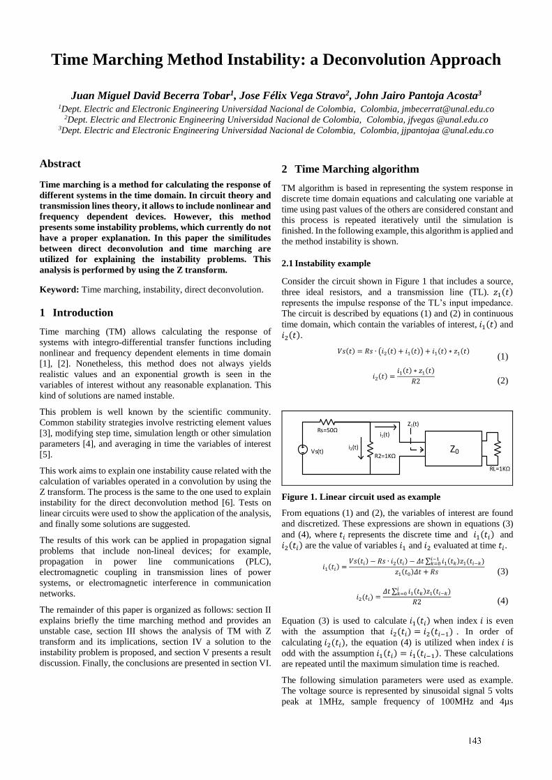
1
Time Marching Method Instability: a Deconvolution Approach
Juan Miguel David Becerra Tobar1, Jose Félix Vega Stravo2, John Jairo Pantoja Acosta3
1Dept. Electric and Electronic Engineering Universidad Nacional de Colombia, Colombia, [email protected] 2Dept. Electric and Electronic Engineering Universidad Nacional de Colombia, Colombia, jfvegas @unal.edu.co
3Dept. Electric and Electronic Engineering Universidad Nacional de Colombia, Colombia, jjpantojaa @unal.edu.co
Abstract
Time marching is a method for calculating the response of
different systems in the time domain. In circuit theory and
transmission lines theory, it allows to include nonlinear and
frequency dependent devices. However, this method
presents some instability problems, which currently do not
have a proper explanation. In this paper the similitudes
between direct deconvolution and time marching are
utilized for explaining the instability problems. This
analysis is performed by using the Z transform.
Keyword: Time marching, instability, direct deconvolution.
1 Introduction
Time marching (TM) allows calculating the response of
systems with integro-differential transfer functions including
nonlinear and frequency dependent elements in time domain
[1], [2]. Nonetheless, this method does not always yields
realistic values and an exponential growth is seen in the
variables of interest without any reasonable explanation. This
kind of solutions are named instable.
This problem is well known by the scientific community.
Common stability strategies involve restricting element values
[3], modifying step time, simulation length or other simulation
parameters [4], and averaging in time the variables of interest
[5].
This work aims to explain one instability cause related with the
calculation of variables operated in a convolution by using the
Z transform. The process is the same to the one used to explain
instability for the direct deconvolution method [6]. Tests on
linear circuits were used to show the application of the analysis,
and finally some solutions are suggested.
The results of this work can be applied in propagation signal
problems that include non-lineal devices; for example,
propagation in power line communications (PLC),
electromagnetic coupling in transmission lines of power
systems, or electromagnetic interference in communication
networks.
The remainder of this paper is organized as follows: section II
explains briefly the time marching method and provides an
unstable case, section III shows the analysis of TM with Z
transform and its implications, section IV a solution to the
instability problem is proposed, and section V presents a result
discussion. Finally, the conclusions are presented in section VI.
2 Time Marching algorithm
TM algorithm is based in representing the system response in
discrete time domain equations and calculating one variable at
time using past values of the others are considered constant and
this process is repeated iteratively until the simulation is
finished. In the following example, this algorithm is applied and
the method instability is shown.
2.1 Instability example
Consider the circuit shown in Figure 1 that includes a source,
three ideal resistors, and a transmission line (TL). 𝑧1(𝑡) represents the impulse response of the TL’s input impedance.
The circuit is described by equations (1) and (2) in continuous
time domain, which contain the variables of interest, 𝑖1(𝑡) and
𝑖2(𝑡).
𝑉𝑠(𝑡) = 𝑅𝑠 ∙ (𝑖2(𝑡) + 𝑖1(𝑡)) + 𝑖1(𝑡) ∗ 𝑧1(𝑡) (1)
𝑖2(𝑡) =𝑖1(𝑡) ∗ 𝑧1(𝑡)
𝑅2
(2)
Vs(t)
Rs=50
R2=1K
i2(t)
i1(t)
Z0
RL=1K
Z1(t)
Figure 1. Linear circuit used as example
From equations (1) and (2), the variables of interest are found
and discretized. These expressions are shown in equations (3)
and (4), where 𝑡𝑖 represents the discrete time and 𝑖1(𝑡𝑖) and
𝑖2(𝑡𝑖) are the value of variables 𝑖1 and 𝑖2 evaluated at time 𝑡𝑖.
𝑖1(𝑡𝑖) =𝑉𝑠(𝑡𝑖) − 𝑅𝑠 ∙ 𝑖2(𝑡𝑖) − 𝛥𝑡 ∑ 𝑖1(𝑡𝑘)𝑧1(𝑡𝑖−𝑘)
𝑖−1𝑘=0
𝑧1(𝑡0)𝛥𝑡 + 𝑅𝑠
(3)
𝑖2(𝑡𝑖) =𝛥𝑡 ∑ 𝑖1(𝑡𝑘)𝑧1(𝑡𝑖−𝑘)
𝑖𝑘=0
𝑅2
(4)
Equation (3) is used to calculate 𝑖1(𝑡𝑖) when index 𝑖 is even
with the assumption that 𝑖2(𝑡𝑖) = 𝑖2(𝑡𝑖−1) . In order of
calculating 𝑖2(𝑡𝑖), the equation (4) is utilized when index 𝑖 is odd with the assumption 𝑖1(𝑡𝑖) = 𝑖1(𝑡𝑖−1). These calculations
are repeated until the maximum simulation time is reached.
The following simulation parameters were used as example.
The voltage source is represented by sinusoidal signal 5 volts
peak at 1MHz, sample frequency of 100MHz and 4µs
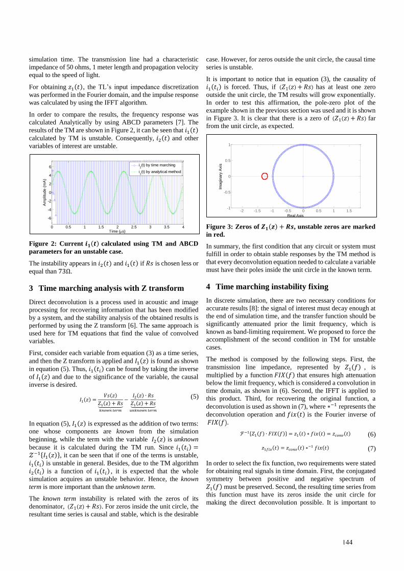
2
simulation time. The transmission line had a characteristic
impedance of 50 ohms, 1 meter length and propagation velocity
equal to the speed of light.
For obtaining 𝑧1(𝑡), the TL’s input impedance discretization
was performed in the Fourier domain, and the impulse response
was calculated by using the IFFT algorithm.
In order to compare the results, the frequency response was
calculated Analytically by using ABCD parameters [7]. The
results of the TM are shown in Figure 2, it can be seen that 𝑖1(𝑡) calculated by TM is unstable. Consequently, 𝑖2(𝑡) and other
variables of interest are unstable.
Figure 2: Current 𝒊𝟏(𝒕) calculated using TM and ABCD
parameters for an unstable case.
The instability appears in 𝑖2(𝑡) and 𝑖1(𝑡) if 𝑅𝑠 is chosen less or
equal than 73Ω.
3 Time marching analysis with Z transform
Direct deconvolution is a process used in acoustic and image
processing for recovering information that has been modified
by a system, and the stability analysis of the obtained results is
performed by using the Z transform [6]. The same approach is
used here for TM equations that find the value of convolved
variables.
First, consider each variable from equation (3) as a time series,
and then the Z transform is applied and 𝐼1(𝑧) is found as shown
in equation (5). Thus, 𝑖1(𝑡𝑖) can be found by taking the inverse
of 𝐼1(𝑧) and due to the significance of the variable, the causal
inverse is desired.
𝐼1(𝑧) =𝑉𝑠(𝑧)
𝑍1(𝑧) + 𝑅𝑠⏟ 𝑘𝑛𝑜𝑤𝑛 𝑡𝑒𝑟𝑚
−𝐼2(𝑧) ∙ 𝑅𝑠
𝑍1(𝑧) + 𝑅𝑠⏟ 𝑢𝑛𝑘𝑛𝑜𝑤𝑛 𝑡𝑒𝑟𝑚
(5)
In equation (5), 𝐼1(𝑧) is expressed as the addition of two terms:
one whose components are known from the simulation
beginning, while the term with the variable 𝐼2(𝑧) is unknown
because it is calculated during the TM run. Since 𝑖1(𝑡𝑖) =𝒵−1𝐼1(𝑧), it can be seen that if one of the terms is unstable,
𝑖1(𝑡𝑖) is unstable in general. Besides, due to the TM algorithm
𝑖2(𝑡𝑖) is a function of 𝑖1(𝑡𝑖) , it is expected that the whole
simulation acquires an unstable behavior. Hence, the known
term is more important than the unknown term.
The known term instability is related with the zeros of its
denominator, (𝑍1(𝑧)+𝑅𝑠). For zeros inside the unit circle, the
resultant time series is causal and stable, which is the desirable
case. However, for zeros outside the unit circle, the causal time
series is unstable.
It is important to notice that in equation (3), the causality of
𝑖1(𝑡𝑖) is forced. Thus, if (𝑍1(𝑧)+𝑅𝑠) has at least one zero
outside the unit circle, the TM results will grow exponentially.
In order to test this affirmation, the pole-zero plot of the
example shown in the previous section was used and it is shown
in Figure 3. It is clear that there is a zero of (𝑍1(𝑧)+𝑅𝑠) far
from the unit circle, as expected.
Figure 3: Zeros of 𝒁𝟏(𝒛) + 𝑹𝒔, unstable zeros are marked
in red.
In summary, the first condition that any circuit or system must
fulfill in order to obtain stable responses by the TM method is
that every deconvolution equation needed to calculate a variable
must have their poles inside the unit circle in the known term.
4 Time marching instability fixing
In discrete simulation, there are two necessary conditions for
accurate results [8]: the signal of interest must decay enough at
the end of simulation time, and the transfer function should be
significantly attenuated prior the limit frequency, which is
known as band-limiting requirement. We proposed to force the
accomplishment of the second condition in TM for unstable
cases.
The method is composed by the following steps. First, the
transmission line impedance, represented by 𝑍1(𝑓) , is
multiplied by a function 𝐹𝐼𝑋(𝑓) that ensures high attenuation
below the limit frequency, which is considered a convolution in
time domain, as shown in (6). Second, the IFFT is applied to
this product. Third, for recovering the original function, a
deconvolution is used as shown in (7), where ∗−1 represents the
deconvolution operation and 𝑓𝑖𝑥(𝑡) is the Fourier inverse of
𝐹𝐼𝑋(𝑓).
ℱ−1𝑍1(𝑓) ∙ 𝐹𝐼𝑋(𝑓) = 𝑧1(𝑡) ∗ 𝑓𝑖𝑥(𝑡) = 𝑧𝑐𝑜𝑛𝑣(𝑡) (6)
𝑧1𝑓𝑖𝑥(𝑡) = 𝑧𝑐𝑜𝑛𝑣(𝑡) ∗−1 𝑓𝑖𝑥(𝑡) (7)
In order to select the fix function, two requirements were stated
for obtaining real signals in time domain. First, the conjugated
symmetry between positive and negative spectrum of
𝑍1(𝑓) must be preserved. Second, the resulting time series from
this function must have its zeros inside the unit circle for
making the direct deconvolution possible. It is important to
0 0.5 1 1.5 2 2.5 3 3.5 4
-6
-4
-2
0
2
4
6
Time (s)
Am
plit
ude (
mA
)
i1(t) by time marching
i1(t) by analytical method
Real AxisIm
agin
ary
Axis
-2 -1.5 -1 -0.5 0 0.5 1 1.5-1
-0.5
0
0.5
1
3
notice that the last condition only can be tested once an IFFT is
applied to the fix function spectrum.
A function of the form 𝑒−𝑎𝑓2
fulfill all the previous
restrictions, where alpha is a constant. In equation (8) a
complete expression for 𝐹𝐼𝑋(𝑓) is shown. The parameter 𝑘
allows selecting the desirable attenuation at limit frequency,
which is equal to a half of sampling frequency. The Fourier
inverse transform of the function 𝐹𝐼𝑋(𝑓) is shown in (9).
𝐹𝐼𝑋(𝑓) = 𝑒−4𝑘
𝐹𝑠2𝑓2
(8)
ℱ−1𝐹𝐼𝑋(𝑓) =𝐹𝑠
4√𝜋𝑘∙ 𝑒−
𝐹𝑠2
16𝑘𝑡2 (9)
For the simulation’s parameters used in the previous section and
𝑘 = 10, the fix function fulfill the second selection condition.
The result of the fix application over the zeros of (𝑍1(𝑧)+𝑅𝑠) are shown in Figure 4. Since all zeros are inside the unit circle,
the TM will yield a stable response as shown in Figure 5. It can
be seen that the response is stable, but there is magnitude error
in 𝑖1(𝑡𝑖).
Figure 4: zeros of fixed 𝒁𝟏(𝒛) + 𝑹𝒔
Figure 5: TM results for fixed impulse response
Low values of k will produce high frequency oscillations in the
early response. In our tests, a minimum value of five was found
to be effective against instability.
5 Results disscusion
The method proposed here solves the TM unstable behavior,
with a magnitude error, which is a good start for solving the
instability problem. However, some comments about this
solution are relevant.
The known term unstable poles are related to the transfer
functions impulse responses used in the deconvolution
equations, but what cause them during the discretization process
is unknown. Thus, the relationship between the band limiting
condition and the apparition of unstable poles in z domain is
hard to determine, which also hampers finding a solution for the
magnitude error.
6 Conclusions
The application of Z transform stability criterion over the
deconvolution equations needed in the TM helps to develop a
solution for the instability problem of TM. In summary, any
method, that introduces the known term poles inside the unit
circle can solve this problem.
The proposed fixing method aims to force high attenuation on
the transfer function prior half of the sampling frequency in
order to fulfill the band-limiting requirement in discrete
simulations.
The method for fixing the instability presented here accomplish
its objective but it produces error in magnitude.
7 References
[1] J. F. Vega Stavro, “Analytical Methods for the Study and
Design of Integrated Switched Oscillators and Antennas
for Mesoband Radiation,” EPFL, Lausanne, 2013.
[2] F. M. Tesche, “On the Analysis of a Transmission Line
With Nonlinear Terminations Using the Time-Dependent
BLT Equation,” IEEE Transactions on Electromagnetic
Compatibility, vol. 49, no. 2, pp. 427–433, May 2007.
[3] P. J. Davies, “On the stability of time-marching schemes
for the general surface electric-field integral equation,”
IEEE Transactions on Antennas and Propagation, vol. 44,
no. 11, pp. 1467–1473, Nov. 1996.
[4] S. E. Bayer and A. A. A. Ergin, “A Stable Marching on
Time scheme for Wire Scatterers Using a Newmark-Beta
Formulation,” Progress In Electromagnetics Research B,
vol. 6, pp. 337–360, 2008.
[5] S. M. Rao, Time Domain Electromagnetics. Academic
Press, 1999.
[6] J. E. Michaels, “Fundamentals of deconvolution with
applications to ultrasonics and accoustic emission,”
Cornell, 1982.
[7] R. E. Collin, Foundations for Microwave Engineering,
2nd Edition - Robert E. Collin. Wiley-IEEE Press.
[8] P. J. Pupalaikis, “The Relationship Between Discrete-
Frequency S-parameters and Continuous-Frequency
Responses,” in DesignCon, Santa Clara, CA, 2012, pp. 1–
28.
Real Axis
Imagin
ary
Axis
-2 -1.5 -1 -0.5 0 0.5 1 1.5 2-1
-0.5
0
0.5
1
0 0.5 1 1.5 2 2.5 3 3.5 4
-6
-4
-2
0
2
4
6
Time (s)
Am
plit
ude (
mA
)
i2(t) by time marching
i2(t) by analytical method
i1(t) by time marching
i1(t) by analytical method

Development of the HEMP Propagation Analysis and
Optimal Hardening Shelter Design, Simulation Tool "KTI HEMP CORD"
† GyungChan, Min, YeongKwan, Jung
Korea Technology Institute Co. Ltd. 58-10, Sagisogil, Dochuckmyeon,
Gwangju, Gyeonggi-do, Korea(ROK). [email protected]
Abstract
High Altitudes Electro-Magnetic Pulse (HEMP) caused by nuclear bomb explosion had been tested during last 1960-1975 by the USA, Russia and other countries. But all of related simulation tools, documents are strongly classified and impossible to use it even, thus IEC and ITU had published the related standards and recommended its protection against HEMP and HPEM. Also, Middle East countries and Far East countries including South Korea are directly vulnerable against HEMP threat. Now we, KTI had developed the HEMP simulation and optimal shelter design tool named by “KTI HEMP
CORD” Keywords; High Altitudes Electro-Magnetic Pulse(HEMP), High Power Electro-Magnetic(HPEM), Height of Blast(HOB), Ground Zero(GZ). Shielding Effectiveness(SE)
1 Introduction
The HEMP threat[1] may have acquired new, urgent and relevance
as the proliferation of nuclear weapons and missile technology
accelerates of the North Korea, for example, is assessed as already
having developed few atomic weapons, and is on the verge of North
Korea already has missiles capable of delivering a nuclear warhead
over the South Korea. ITU K.78, K81 and IEC recommended its
counter-measuring for the industrial facilities. HEMP test and
estimation must only be done by the computer simulation which was
studied on the 1960-1990 years USA/AFWL papers. This result has
significant activities to the South Korea, Japan and China being
under the North Korea nuclear bomb threat because all of HEMP
related products was strongly limited for export. This KTI newly
developed HEMP cord included the HEMP generation & propagation
analysis, optimal shelter design tool, essential EM energy
attenuation in multi-layered various soils and rocks with HEMP filter
design tool of considering the high frequency equivalent circuits.
Specially, this study adapted the least square fitting method for the
EM energy attenuation in the soils and rocks because it has a
various characteristics so, it based on many times field test reports.
This paper were proven with the EXEMP CORD developed at 1992
by K.D. Leuth user[2] and other verification test done by our self and
developed the HEMP filters.
2. General of the developing procedure 2.1 HEMP generation and propagation.
This study needs a variety of HEMP test report with theories
[2],[3],[4],[5][6] and papers to understand the HEMP generation,
propagation and the coupling mechanism analysis. Specially, we
had fallen in difficulties and muddle through the bitters on the unit
unification of the mathematical formulas from the atom engineering,
physics, aerologic, electron mobility, earth magnetic field, vector
direction to the Maxwell equations.
HEMP generation and propagation theories were based on the Ref.
[2] –[6] and HEMP wave form adapted DEXP. Simulation and
analysis were done by a formal theory and practice.
2.2 Analysis of the EM energy attenuation in the multilayer soils and rocks[7][8] It has a following functions and applied theory;
- Computer simulation of EM energy attenuation in the multilayer
soils and rocks.
- Very high accuracy for computer simulation using the statistical
least square methods.
2.3 HEMP Hardening Shelter Design Tool This simulation tool can calculate the effective shield effectiveness
based on the following algorithms;
-Shielding effectiveness calculation without slots and holes for the
welding type shielding cavity using pure material constants
-Shielding effectiveness calculation with gap for the PAN and panel
type shielding cavity.
-Shielding effectiveness calculation with various waveguides and pin
holes on the shielding wall considering the filter attenuation
characteristics.
-Considering the shielding cavity resonant.
2.4 HEMP filter design tool Basically, we adapted the normal low pass filter design concepts
even, thus it has specialties to consider a contact resistance, stray
capacitance, stray inductance and the conductivity of inductor of a
high frequency equivalent circuit.
3. Related theories 3.1. Brief theory of the E1 generation, smile diagram. According to the Karzas-Latter-Longmire theory and K.D.
Leuth user, gamma ( ) ray be assumed to be produced at
approximately an exponentially increasing rate after the course of the nuclear explosion. When a gamma ray of energy emitted by nuclear burst interacts
with an electron of the air molecules in a Compton collision,
Compton recoil electrons is created at an angle with respect to the direction of the incident gamma ray. So we called the E1 field for the first electrons creation, E2 field created by the gamma ray nth scattering collision and E3 field created by the geomagnetic field
stabilization which was disturbed by E1 and E2. If is the time at which the explosion starts, then the number of gamma rays
produced up to time which is given by , where called by a
shake is about . If gamma ray reaches to maximum, it decreases to zero exponentially as a slower rate than starting built
up, on condition . HEMP pulse waveform was defined on the IEC 61000-2-13 and MIL STD 188-125. Gamma rays have an average energy of about 1Mev, and there are
gamma rays produced per kiloton ( of yield.
(1)
Here, = Total yield of the explosion in the form of gamma rays
expressed in kTon, E is the mean gamma rays and is a expression the time variation of the gamma rays. According to the Ref.[4], the number of gamma rays emitted by a nuclear explosion per unite time is
(2)
If we normalized expression of the
The rate at which primary Compton recoils electrons are produced at
a distance r in direction from the explosion is
(3)
Term of is known as a retarded time and it is related with
the electron traveled time since the creation of the Compton electron. Understanding of the retarded time from the source to observer locations described more details on Ref.[6] using the Jefimenko equation[6] .
Here, new important function is a number of gammas which interact to produce Compton electrons,
(4)
Where, is the mean free paths of gamma rays to produce Compton electrons, Y has a actual meaning, the gamma yield of the weapon in electron volt (eV), E is the mean gamma energy in eV and c is light velocity. Equation (4) may also be called the radial distribution function or an
attenuation function for interacting gamma rays. The term is the
total number of gamma rays available from the nuclear burst.
term accounts for the divergence of the gamma rays as the radius r is increased while the remaining term account for the reduction in gammas due to the air absorption in the atmosphere based on the mean free path.
Applying a small angle approximation by the Taylor series
expansion; sin = , cos = 1 and high frequency
condition, then we could find a simplified equation. Also we could get the electric field strength from the relation between current
density and medium conductivity of the air density in the height of the atmospheres. Our basic model of the analysis underlying on the
Karzas-Latter-Longmire theory and K.D. Leuth user’s EXEMP. There are many limitations to describe on these papers for all of them, so refer to the references for the more detailed theories. Finally, we calculate the electric field strength at the observer location as a following procedure in order to find out the field distribution on the earth without HEMP test.
1) Generation of the Compton recoil electrons and propagation analysis
Figure 1. Gamma rays scattering and the elliptic analysis of the source range 2) Coordinate system change from the spherical coordinates to
rectangular of the earth surface and atmosphere.
Figure 2. Coordinate system conversion and Earth magnetic field calculation at some location.
3) Survival probability of the one gamma ray and electrons
distributions depend on the height from the sea level.
4) Wave polarization 5) Contour plot of the electromagnetic magnitudes on the map.
3.2. Brief analysis algorism of the EM energy attenuation into
the soils and rocks
We need to simulate the natural attenuation in the multi-layered
soils and rocks when HEMP shelter is installed in the underground
tunnel. In this case, finding the ideal material constants of the soils
and rock are very important to reduce the uncertainty because these
Figure 3. The electromagnetic field distribution on the earth. materials has a various characteristics. So, this tool optimized its effectiveness using a least square method from the much field test result of the electromagnetic power attenuation in soils and rocks. 3.3 Shielding effectiveness estimations of the HEMP shelter and HEMP filter design tool Shielding effectiveness could be calculated if material constants was given as the well known theory but theoretically calculated result has not corresponded to the shielding effectiveness test on the site. So, this study proposed the ideal estimated solutions for the HEMP shelter design and construction by way of adapting a effective permeability, conductivity and a number of wave guides.
4. Verifications 4.1 HEMP simulation tool[9] Our simulation results come to have an exact consistency with the EXEMP CORD at the same geometric condition. Our main goal to develop the electric field distribution, smile diagram is just to know the field strength without actual HEMP test used for the optimal shelter design and provided the enough margins between HEMP field strength and EM sensitive system. The contour plot of peak E-field are simulated and compared with EXEMP results when burst at GZ N37.56, E126.97 (Seoul, Gwoang whoa mum) and 10kt, HOB 75km. It's results are well corresponding to the EXEP results. We could get a field strength 2.60kV/m at Seoul, 48.22kV/m at Whoa sung, 28.82kV/m at Pyongyang, 17.74kV/m at Shanghai in China and 21.20kV/m at Hiroshima in Japan. Therefore, we realized that all of main cities in the Far East Asia should be under the threaten if North Korea carries out the HEMP test over the Korea peninsula. Here, HEMP is defined as nuclear bomb busted in the higher height than minimum 40km. 4.2 Estimation of the EM energy attenuation in the multilayer soils and rocks[9][10] 4.3 HEMP shelter Design Tool [10],[11] On the view of our experience, the shield effectiveness written on the text formulas are not corresponding to the hardening shelter on site SE test. Our developed simulation tool come to the well corresponding result between the simulation and site SE test when
we considered an effective material constants variation, shelter mechanical slots and wave guide physical dimensions. 4.4 HEMP filter design tool[9] A simulation results when π type filter consist of 500uH inductor with stray capacitance 0.1pF, the feed through capacitor 2 uF with the stray inductance 0.1pH and load resistance is a 2Ω. This tool is very useful to confirm an important of the contact resistance, stray capacitance and inductance, load impedance and to choose the optimal LPF components.
5. Conclusion
This tool provided the estimation of the HEMP field distribution on the earth, analysis of the EM energy attenuation in the multilayer soils and rocks, optimal HEMP hardening shelter and filter design in accordance with the commercial standard ITU, IEC recommendation and MIL STD 188-125. All of the simulation cord and tools related to HEMP are strongly classified by HEMP technology advanced countries that already had high altitude test experiences. Also, very limited papers are available in the open literature to the 3rd countries. Now, we are getting in the new nuclear cold threat since North Korea has successes to develop the nuclear bomb and long distant missile over the Far East Asia and Middle East area. So, we are looking forward to using this study result for the improving the nuclear hazards without classified notice in future. References [1] Clay Wilson " High altitude electromagnetic (HEMP) and high
power microwave (HPM) devices: Threat assessments", CRS report
for congress, July 21, 2008.
[2] K.D Leuth usser “A complete EMP environment generated by
high altitude nuclear bursts”,TN 363 10.1992.
[3] Louis W. Seiler, Jr “A calculation model for high altitude EMP”,
Air force institute of technology, Mar. 1975.
[4] W.J. Karzas and Richard Latter “Electromagnetic radiation from a
nuclear explosion in space” The Physical Review, Vol. 126, No 6,
June. 15, 1962.
[5] W.J. Karzas and Richard Latter “Detection of the electromagnetic
radiation from nuclear explosions in space”, TN 40, Oct. 1964.
[6] Chester D. Eng, “The development of the time dependence of the
nuclear EMP electric field” LLNL-TR-420285. Nov. 16. 2009
[7] John O. Curtis, "Electromagnetic power attenuation in soils",
Environment laboratory U.S army engineer research and
development center. ERDC/EL TR-05-5, August 2005.
[8] Smith, S. S. and Arunlanandan, K. “Relationship of electrical
dispersion to soil properties", Journal of the geotechnical
engineering division, proceedings of the American society of civil
engineers GT5, 591-604. 1981.
[9] G.C. Min “ IWIT 2011 HEMP Workshop” Mar. 10, 2011
[10]G.C. Min, D.I. Kim “Design tool development of the effective
HEMP hardening shelter” Institute of Webcasting Internet and
Telecommunication” Vol. 10(4). pp.121-126. Sep. 2010
[11] G.C. Min “Development of the HEMP hardening technology”.
Weekly Technical Trends” No.1491, Focus, April. 15, 2012
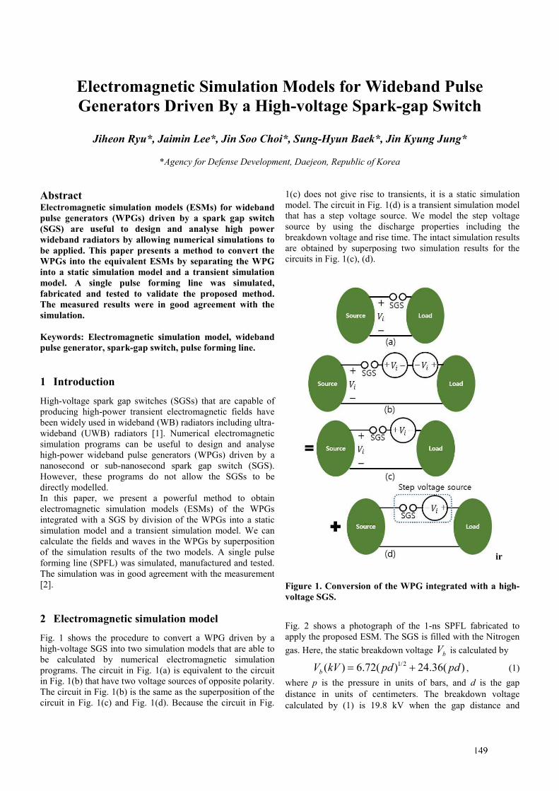
1
Electromagnetic Simulation Models for Wideband Pulse Generators Driven By a High-voltage Spark-gap Switch
Jiheon Ryu*, Jaimin Lee*, Jin Soo Choi*, Sung-Hyun Baek*, Jin Kyung Jung*
*Agency for Defense Development, Daejeon, Republic of Korea
Abstract Electromagnetic simulation models (ESMs) for wideband pulse generators (WPGs) driven by a spark gap switch (SGS) are useful to design and analyse high power wideband radiators by allowing numerical simulations to be applied. This paper presents a method to convert the WPGs into the equivalent ESMs by separating the WPG into a static simulation model and a transient simulation model. A single pulse forming line was simulated, fabricated and tested to validate the proposed method. The measured results were in good agreement with the simulation. Keywords: Electromagnetic simulation model, wideband pulse generator, spark-gap switch, pulse forming line.
1 Introduction
High-voltage spark gap switches (SGSs) that are capable of producing high-power transient electromagnetic fields have been widely used in wideband (WB) radiators including ultra-wideband (UWB) radiators [1]. Numerical electromagnetic simulation programs can be useful to design and analyse high-power wideband pulse generators (WPGs) driven by a nanosecond or sub-nanosecond spark gap switch (SGS). However, these programs do not allow the SGSs to be directly modelled. In this paper, we present a powerful method to obtain electromagnetic simulation models (ESMs) of the WPGs integrated with a SGS by division of the WPGs into a static simulation model and a transient simulation model. We can calculate the fields and waves in the WPGs by superposition of the simulation results of the two models. A single pulse forming line (SPFL) was simulated, manufactured and tested. The simulation was in good agreement with the measurement [2].
2 Electromagnetic simulation model
Fig. 1 shows the procedure to convert a WPG driven by a high-voltage SGS into two simulation models that are able to be calculated by numerical electromagnetic simulation programs. The circuit in Fig. 1(a) is equivalent to the circuit in Fig. 1(b) that have two voltage sources of opposite polarity. The circuit in Fig. 1(b) is the same as the superposition of the circuit in Fig. 1(c) and Fig. 1(d). Because the circuit in Fig.
1(c) does not give rise to transients, it is a static simulation model. The circuit in Fig. 1(d) is a transient simulation model that has a step voltage source. We model the step voltage source by using the discharge properties including the breakdown voltage and rise time. The intact simulation results are obtained by superposing two simulation results for the circuits in Fig. 1(c), (d).
ir
Figure 1. Conversion of the WPG integrated with a high-voltage SGS.
Fig. 2 shows a photograph of the 1-ns SPFL fabricated to apply the proposed ESM. The SGS is filled with the Nitrogen
gas. Here, the static breakdown voltage bV is calculated by
1/2( ) 6.72( ) 24.36( )bV kV pd pd= + , (1)
where p is the pressure in units of bars, and d is the gap distance in units of centimeters. The breakdown voltage calculated by (1) is 19.8 kV when the gap distance and
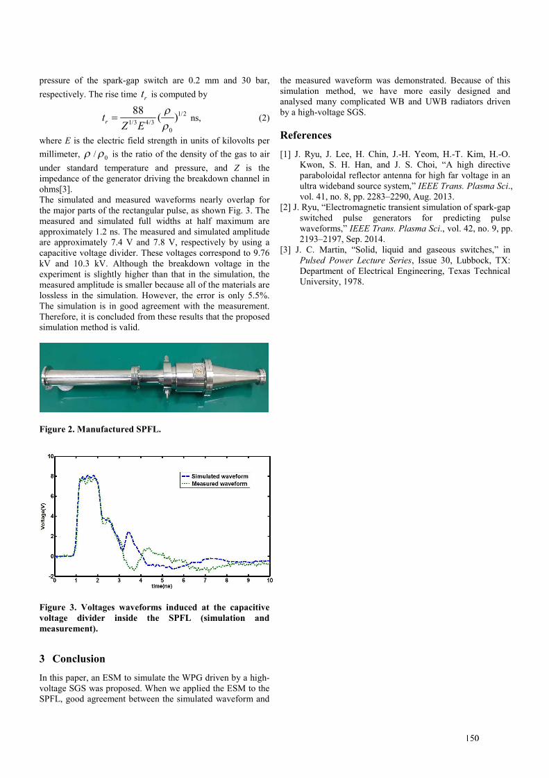
2
pressure of the spark-gap switch are 0.2 mm and 30 bar,
respectively. The rise time rt is computed by
1/2
1/3 4/30
88( )rt
Z E
r
r= ns, (2)
where E is the electric field strength in units of kilovolts per
millimeter, r / 0r is the ratio of the density of the gas to air
under standard temperature and pressure, and Z is the impedance of the generator driving the breakdown channel in ohms[3]. The simulated and measured waveforms nearly overlap for the major parts of the rectangular pulse, as shown Fig. 3. The measured and simulated full widths at half maximum are approximately 1.2 ns. The measured and simulated amplitude are approximately 7.4 V and 7.8 V, respectively by using a capacitive voltage divider. These voltages correspond to 9.76 kV and 10.3 kV. Although the breakdown voltage in the experiment is slightly higher than that in the simulation, the measured amplitude is smaller because all of the materials are lossless in the simulation. However, the error is only 5.5%. The simulation is in good agreement with the measurement. Therefore, it is concluded from these results that the proposed simulation method is valid.
Figure 2. Manufactured SPFL.
Figure 3. Voltages waveforms induced at the capacitive voltage divider inside the SPFL (simulation and measurement).
3 Conclusion
In this paper, an ESM to simulate the WPG driven by a high-voltage SGS was proposed. When we applied the ESM to the SPFL, good agreement between the simulated waveform and
the measured waveform was demonstrated. Because of this simulation method, we have more easily designed and analysed many complicated WB and UWB radiators driven by a high-voltage SGS.
References
[1] J. Ryu, J. Lee, H. Chin, J.-H. Yeom, H.-T. Kim, H.-O. Kwon, S. H. Han, and J. S. Choi, “A high directive paraboloidal reflector antenna for high far voltage in an ultra wideband source system,” IEEE Trans. Plasma Sci., vol. 41, no. 8, pp. 2283–2290, Aug. 2013.
[2] J. Ryu, “Electromagnetic transient simulation of spark-gap switched pulse generators for predicting pulse waveforms,” IEEE Trans. Plasma Sci., vol. 42, no. 9, pp. 2193–2197, Sep. 2014.
[3] J. C. Martin, “Solid, liquid and gaseous switches,” in Pulsed Power Lecture Series, Issue 30, Lubbock, TX: Department of Electrical Engineering, Texas Technical University, 1978.
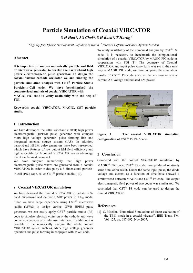
Particle Simulation of Coaxial VIRCATOR
S H Han*, J S Choi*, S H Baek*, T Hurtig †
*Agency for Defense Development, Republic of Korea, † Swedish Defense Research Agency, Sweden
Abstract
It is important to analyze numerically particle and field
of microwave generator to develop the narrowband high
power electromagnetic pulse generator. To design the
coaxial virtual cathode oscillator we are running the
particle simulation analysis with CST® Particle Studio
Particle-in-Cell code. We have benchmarked the
computerized analysis of coaxial VIRCATOR with
MAGIC PIC code to verify availability with the help of
FOI.
Keywords: coaxial VIRCATOR, MAGIC, CST particle
studio.
1 Introduction
We have developed the Ultra wideband (UWB) high power
electromagnetic (HPEM) pulse generator with compact
Marx high voltage generator, pulse forming line and
integrated antenna source system (IAS). In addition,
narrowband HPEM pulse generators have been researched,
which have features of low output EM field efficiency and
high susceptibility. A coaxial VIRCATOR has an advantage
that it can be made compact.
We have analyzed numerically that high power
electromagnetic pulse waves are generated from a coaxial
VIRCATOR in order to design by a 3 dimensional particle-
in-cell (PIC) code, called CST® particle studio (PS).
2 Coaxial VIRCATOR simulation
We have designed the coaxial VIRCATOR to radiate in S-
band microwave and deliver a MW power in TE11 mode.
Since we have large experience using CST® microwave
studio (MWS) to design various UWB HPEM pulse
generator, we can easily apply CST® particle studio (PS)
code to simulate electron emission at the cathode and wave
conversion because of similar user interface. In addition, it is
possible to be numerically analyze the whole coaxial
VIRCATOR system such as, Marx high voltage generator
operation and pulse forming in conjugate with MWS code.
To verify availability of the numerical analysis by CST® PS
code, it is necessary to benchmark the computational
simulation of a coaxial VIRCATOR by MAGIC PIC code in
cooperation with FOI [1]. The geometry of Coaxial
VIRCATOR and input pulse wave form was set in the same
way as MAGIC PIC code, we have compared the simulation
results of CST® PS code such as the electron emission
current, AK voltage and radiated EM power.
Figure 1. The coaxial VIRCATOR simulation
configuration of CST® PS PIC code.
3 Conclusion
Compared with the coaxial VIRCATOR simulation by
MAGIC® PIC code, CST® PS code have produced relatively
same simulation result. Under the same input pulse, the diode
voltage and current as a function of time have showed a
similar trend between MAGIC and CST® PS code. The output
electromagnetic field power of two codes was similar too. We
concluded that CST® PS code can be used to design the
coaxial VIRCATOR.
References
[1] C. Moeller. “Numerical Simulations of direct excitation of
the TE11 mode in a coaxial vircator”, IEEJ Trans. FM,
Vol. 127, pp. 687-692, Nov 2007.
1
Prediction of EMP Coupling to Multi-conductor Transmission
Lines by Using Different Iteration Methods.
Jun Guo, Yan-zhao Xie
State Key laboratory of Electrical Insulation and Power Equipment
Electrical Engineering College, Xi’an Jiaotong University
Xi’an, Shannxi, China
[email protected], [email protected]
Abstract
The distributed analytical representation and iterative
technique (DARIT) has been proposed for the calculation
of electromagnetic pulse (EMP) radiated field coupling to
multi-conductor transmission lines (MTLs). At first, this
technique adopts the Jacobi iteration scheme (Jacobi-
DARIT-field) or the Gauss-Seidel iteration scheme
(Seidel-DARIT-field). More recently, based on these two
methods, the JOR-DARIT-field and SOR-DARIT-field
methods have been developed as well. This paper
compares these four methods from the points of view of
the accuracy and convergence speed, etc.
Keywords: analytical solution; electromagnetic pulse;
iterative method; transient analysis; transmission line
modeling; waveform relaxation.
1 Introduction
To predict the effects of EMP coupling to multi-conductor
transmission lines (MTLs), many researchers have proposed
the method of modeling of EMP coupling to MTLs [1]-[2].
To increase the computational speed, an approach using the
distributed analytical representation and Jacobi iterative
technique method which is based on the Waveform
Relaxation and Transverse Partitioning (WR-TP) for the
response computation between multi-conductor transmission
lines illuminated by the incident EMP field (Jacobi-DARIT-
field) [3] was proposed. The algorithm can avoid the need for
inversing the matrix when solving MTLs equations and
leading to high computational efficiency. To increase the
convergence rate, another DARIT-field method employing the
Gauss-Seidel Iteration Algorithm (Seidel-DARIT-field) has
been developed [4].
As we know, the Jacobi iteration and the Gauss-Seidel
iteration are the special case of JOR and SOR, respectively.
This paper aims to compare the performance between the
different iterative methods.
2 Outline of the methods
By applying waveform relaxation techniques [3] to the
Telegrapher's equations, a recursive set of decoupled
differential equations was obtained: ( 1)
' ( 1) ' ( 1) '
1,
( 1)
' ( 1) ' ( 1) '
1,
( , )( ) ( ) ( , ) ( , )
( , )( ) ( ) ( , ) ( , )
rN
r ri
ii i ij j i
j j i
rN
r ri
ii i ij j i
j j i
dv x sz i x z i x s V x s
dx
di x sy v x y v x s I x s
dx
The Jacobi iteration and Gauss-Seidel iteration schemes are
shown in [3]-[4] in detail. The JOR iteration method and SOR
iteration method are extended from the Jacobi iteration and
Gauss-Seidel iteration, respectively. The iteration schemes are
as follow: ( 1) ( 1) ( )
, , ,
( 1) ( 1) ( )
, , ,
( , ) ( , ) (1 ) ( , )
( , ) ( , ) (1 ) ( , )
r r r
JOR i J i J i
r r r
JOR i J i J i
JOR JOR
JOR JOR
v x s v x s v x s
i x s i x s i x s
( 1) ( 1) ( )
, , ,
( 1) ( 1) ( )
, , ,
( , ) ( , ) (1 ) ( , )
( , ) ( , ) (1 ) ( , )
r r r
SOR i GS i GS i
r r r
SOR i GS i GS i
SOR SOR
SOR SOR
v x s v x s v x s
i x s i x s i x s
where the vj,i and ij,i are the voltage response and current
response of line i by Jacobi method, ωJOR is the relaxation
factor (RF) for JOR method, the vGS,i and iGS,i are the voltage
response and current response of line i by Gauss-Seidel
method, ωSOR is the RF for SOR method.
The algorithms of iteration 1 of the four methods are the same,
it only takes the illuminating EMP wave into account. At
iteration 2, each line is excited not only by the incoming EMP
wave but also by the coupling effects of all the other adjacent
lines. The details of the Jacobi method and Seidel method are
proposed in [3]-[4].
3 Validation of the proposed algorithm
A validation example is proposed to give a comparison
between the four methods. In the example, a symmetrical and
lossy three wires with the length of 50 cm, height of 1 cm,
diameter of 1 mm and distances between lines of 1 cm which
above the lossy ground is considered. The loads on both sides
are 50 Ω. Fig. 1 shows the response of wire #1 obtained with
the conventional method (Chain Parameters Matrix method)
and with the four methods with the RF for JOR method and
SOR method equal to 0.52 and 0.8, respectively. The results
of the relative errors ε are presented in Table I. It can be seen
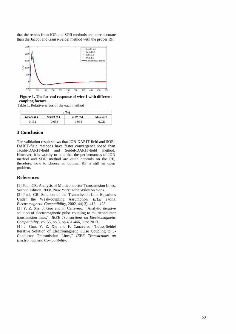
2
that the results from JOR and SOR methods are more accurate
than the Jacobi and Gauss-Seidel method with the proper RF.
0 50 100 150 200 250 300 350 400 450 500-500
0
500
1000
1500
2000
2500
t/n
U/V
Jacobi.It.4
Seidel.It.3
JOR.It.4
SOR.It.3
Conventional method
Figure 1. The far-end response of wire 1 with different coupling factors.
Table 1. Relative errors of the each method
ε (%)
Jacobi.It.4 Seidel.It.3 JOR.It.4 SOR.It.3
0.152 0.053 0.034 0.021
3 Conclusion
The validation result shows that JOR-DARIT-field and SOR-DARIT-field methods have faster convergence speed than Jacobi-DARIT-field and Seidel-DARIT-field method. However, it is worthy to note that the performances of JOR method and SOR method are quite depends on the RF, therefore, how to choose an optimal RF is still an open problem.
References
[1] Paul, CR. Analysis of Multiconductor Transmission Lines,
Second Edition. 2008, New York: John Wiley \& Sons.
[2] Paul, CR. Solution of the Transmission-Line Equations
Under the Weak-coupling Assumption. IEEE Trans.
Electromagnetic Compatibility, 2002, 44( 3): 413—423.
[3] Y. Z. Xie, J. Guo and F. Canavero, ``Analytic iterative
solution of electromagnetic pulse coupling to multiconductor
transmission lines,'' IEEE Transactions on Electromagnetic
Compatibility, vol.55, no.3, pp.451-466, June 2013.
[4] J. Guo, Y. Z. Xie and F. Canavero, ``Gauss-Seidel
Iterative Solution of Electromagnetic Pulse Coupling to 3-
Conductor Transmission Lines,'' IEEE Transactions on
Electromagnetic Compatibility.
1
Propagation Characteristics of the UWB EM Wave in Soil Media and its
Influence on the Detection of Buried Unexploded Ordnance
S . Vijayakumar1 and M. Joy Thomas
2
Pulsed Power and EMC Lab, Dept. of Electrical Engineering,
Indian Institute of Science, Bangalore, India [email protected],
Abstract Threat posed by the Unexploded Ordnance (UXO) is
well known and is felt across all the conflict affected
countries. At present there exists no equipment/system to
detect the unexploded buried ordnance (UXO), which
satisfies United Nations Main Action Standard (UNMAS)
for the safe removal and disposal of such UXO.
Considerable research work is carried out on the Ultra-
Wide Band (short pulse) ground penetrating imaging of
buried mine. This paper deals with the influence of the
soil medium and the incident Electromagnetic (EM) wave
frequencies on the landmine detection range and its
resolution. Studies were carried out for different soil type
as well as varying moisture content. Raleigh criterion
minimum resolvable time is calculated for different
buried soil depth and soil moisture for various incident
EM wave bandwidths. For a moist soil, it is found that
incident EM wave of 3 to 5 GHz is having a better range
and resolution. One dimensional Finite Difference Time
Domain (FDTD) method with piecewise linear recursive
convolution (PLRC) technique is used to study the EM
wave propagation in the soil media.
Keywords: Unexploded Ordnance (UXO), Ultra-wide Band
(UWB), Ground Penetrating Radar (GPR), Electromagnetic
(EM) wave.
1 Introduction
Past conflicts have left behind around 160 million landmines
buried in the ground, killing or injuring more than 4,000
people every year. Geneva International Centre for
Humanitarian Demining (GICHD) in its report on mine action
equipment has commented on the lack of R&D in landmine
detection technology. The report also provides important
capability area, which can significantly improve the detection
of buried landmines. GICHD has identified that
improvements in close in detection and detecting outer edge
of the landmine leads to more than 10% improvement in
landmine detection. This calls for a better theoretical
understanding of every important element in the detection
system.
1.1 UWB GPR Imaging of Buried Landmine
To achieve the stringent UN requirement of 99.96% landmine
detection, advanced detection systems with capability of
target identification and classification is required. Buried
landmines are detected based on reflected EM wave due to
difference in the permittivity of the landmine and its host soil
medium. It is shown that GPR using EM wave of frequency
spectrum up to 2GHz has very low depth resolution, but offer
better detection range. Remote sensing satellites operating in
Ku, K and Ka band incident EM wave offer better depth
resolution but have very low detection range and are mainly
used for earth surface imaging. Many works have been
carried out to use frequency spectrum in-between normal
GPR and UWB imaging GPR, which has a range of around
15-20 cm to detect the anti-personal mines. To arrive at an
optimum frequency for all weather buried landmine detection
system, detailed study of the soil medium is required.
Estimation of soil depth at which landmine is buried is really
difficult due to the variability of the soil media. This paper
deals with the resolution involved in estimating the depth of
burial of landmine. Selection of incident EM wave parameters
like bandwidth, field intensity, polarization, incident angle are
very important to achieve the required range and depth
resolution. In this work, computer simulation has been carried
out to study the EM wave propagation in the soil medium and
the influence of incident EM wave bandwidth and its
magnitude on the detection range and resolution.
2. Electrical Properties of the Soil
In-depth knowledge of electrical and physical property of the
soil medium is very important for the design of land mine
detection system. Soil is a multi-phase medium with the
significant moisture content. Important electrical properties of
the soil include DC conductivity and the complex
dielectric permittivity ( . Effect of DC conductivity on EM
wave attenuation is negligible at higher frequencies, but for a
soil with the nominal moisture content and for the
conductivity above 6mS/m, considerable attenuation is
observed for frequencies in the range of 300MHz to 5GHz.
2.1 Electromagnetic Modelling of the Soil
Many researchers have attempted to find a suitable dielectric
model for the soil, considering its texture, temperature,
moisture content and organic materials. Deloor [1] has shown
that, it is impossible to find an exact dielectric model for the
soil and proposes bounds for dielectric permittivity of the soil.
Available theoretical mixing model of the soil is very difficult
to implement in FDTD method. Also exact mixing models for
the frequency of interest are not available. In this paper
Double Debye model [2] as given in eq.1 with six unknown
parameters namely static permittivity ( , high frequency
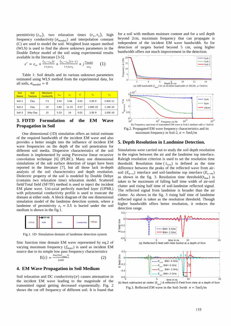
2
permittivity , two relaxation times ( , high
frequency conductivity and interpolation constant
(C) are used to model the soil. Weighted least square method
(WLS) is used to find the above unknown parameters in the
Double Debye model of the soil using experimental results
available in the literature [3-5].
(1)
Table 1: Soil details and its various unknown parameters
estimated using WLS method from the experimental data, for all soils,
3. FDTD Formulation of the EM Wave
Propagation in Soil
One dimensional (1D) simulation offers an initial estimate of the required bandwidth of the incident EM wave and also provides a better insight into the influence of incident EM wave frequencies on the depth of the soil penetration for different soil media. Dispersive characteristics of the soil medium is implemented by using Piecewise linear recursive convolution technique [6] (PLRC). Many one dimensional simulations of the sub surface detection of target have been reported in the literature [7], but all those lack in-depth analysis of the soil characteristics and depth resolution. Dielectric property of the soil is modeled by Double Debye (contains two relaxation time) relaxation model. Scattered field/Total field (SF/TF) method is used to inject the incident EM plane wave. Uni-axial perfectly matched layer (UPML) with polynomial conductivity profile is used to truncate the domain at either ends. A block diagram of the one dimensional simulation model of the landmine detection system, where a landmine of permittivity is buried under the soil medium is shown in the fig.1.
Fig.1. 1D- Simulation domain of landmine detection system
Sinc function time domain EM wave represented by eq.2 of
varying maximum frequency ( ) is used as incident EM
source due to its simple low pass frequency characteristics
(2)
4. EM Wave Propagation in Soil Medium
Soil relaxation and DC conductivity causes attenuation in
the incident EM wave leading to the magnitude of the
transmitted signal getting decreased exponentially. Fig. 2
shows the cut off frequency of different soil. It is found that
for a soil with medium moisture content and for a soil depth
beyond 2cm, maximum frequency that can propagate is
independent of the incident EM wave bandwidth. So for
detection of targets buried beyond 5 cm, using higher
bandwidth offers not much improvement in the detection.
Fig.2. Propagated EM wave frequency characteristics and its
maximum frequency in Soil-2,
5. Depth Resolution in Landmine Detection.
Simulations were carried out to study the soil depth resolution
in the region between the air and the landmine top interface.
Raleigh resolution criterion is used to set the resolution time
threshold. Resolution time ) is defined as the time
difference between the peaks of the reflected wave from air-
soil ( interface and soil-landmine top interface as shown in the fig. 3. Resolution time threshold is
taken to be maximum of falling half time width of air-soil
clutter and rising half time of soil-landmine reflected signal.
The reflected signal from landmine is broader than the air
clutter. As shown in the fig. 3 rising half time of landmine
reflected signal is taken as the resolution threshold. Though
higher bandwidth offers better resolution, it reduces the
detection range.
Fig.3. Reflected EM wave in the Soil-3with
2 4 6 8 10 12 140
5
10
15
20
Depth in cm
Fre
qu
ency
in
GH
z
Soil-1
Soil-2
Soil-3
108
109
1010
1011
0
0.5
1
1.5
2x 10
-3
Frequency in HzE
Sp
ectr
um V
/m
1cm
5cm
15cm
(a) 3dB bandwidth (fmax
) for an incident bandwidth of 20GHz ,=5mS/m
(b) Frequency spectrum of transmitted EM wave in Soil-2 medium with =5mS/m
0 5 10 15-0.6
-0.4
-0.2
0
0.2
time in ns
E f
ield
V/m
(a) Reflected E-field with mine buried at a depth of 5cm
BW= 5 GHz
BW= 2 GHz
0 5 10 15-0.6
-0.4
-0.2
0
0.2
time in ns
E f
ield
V/m
(b) Back subtracted air clutter (Ea-s
) & reflected E-Field from mine at a depth of 5cm
Es-m
, BW= 5 GHz
Ea-s
, BW= 5 GHz
Es-m
, BW= 2 GHz
Ea-s
, BW= 2 GHz
time in ns
time in ns
thw
tres
Soil Name
Soil Texture
Moisture Content%
C
Soil-1 Clay 7.5 3.53 5.66 0.01 2.0E-9 5.81E-11
Soil-2 Clay 14 5.82 11.15 0.57 1.04E-10 1.14E-10
Soil-3 Silty Clay 15 5.53 14 0.01 2.0E-9 1.03E-10
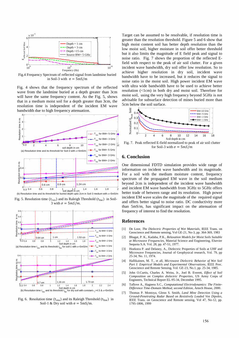
3
Fig.4 Frequency Spectrum of reflected signal from landmine buried
in Soil-3 with
Fig. 4 shows that the frequency spectrum of the reflected
wave from the landmine buried at a depth greater than 3cm
will have the same frequency content. As the Fig. 5, shows
that in a medium moist soil for a depth greater than 3cm, the
resolution time is independent of the incident EM wave
bandwidth due to high frequency attenuation.
Fig. 5. Resolution time and its Raleigh Threshold ( in Soil-
3 with .
Fig. 6. Resolution time and its Raleigh Threshold ( in
Soil-1 & Dry soil with .
Target can be assumed to be resolvable, if resolution time is
greater than the resolution threshold. Figure 5 and 6 show that
high moist content soil has better depth resolution than the
low moist soil, higher moisture in soil offer better threshold
but it also limits the magnitude of E field peak and signal to
noise ratio. Fig. 7 shows the proportion of the reflected E-
field with respect to the peak of air soil clutter. For a given
incident wave bandwidth, dry soil offer low resolution. So to
achieve higher resolution in dry soil, incident wave
bandwidth have to be increased, but it reduces the signal to
noise ratio in the moist soil. High power incident EM wave
with ultra wide bandwidth have to be used to achieve better
resolution (<1cm) in both dry and moist soil. Therefore for
moist soil, using the very high frequency beyond 5GHz is not
advisable for subsurface detection of mines buried more than
5cm below the soil surface.
Fig. 7. Peak reflected E-field normalized to peak of air soil clutter
for Soil-3 with
6. Conclusion
One dimensional FDTD simulation provides wide range of
information on incident wave bandwidth and its magnitude.
For a soil with the medium moisture content, frequency
spectrum of the propagated EM wave in the soil medium
beyond 2cm is independent of the incident wave bandwidth
and incident EM wave bandwidth from 3GHz to 5GHz offers
better trade of between range and its resolution. High power
incident EM wave scales the magnitude of the required signal
and offers better signal to noise ratio. DC conductivity more
than 5mS/m, has significant impact on the attenuation of
frequency of interest to find the resolution.
References
[1] De Loor, The Dielectric Properties of Wet Materials, IEEE Trans. on Geoscience and Remote sensing, Vol GE-21, No-3, pp. 364-369, 1983
[2] Bhagat, P. K., Kadaba, P.K., Relaxation Models for Moist Soils Suitable at Microwave Frequencies, Material Science and Engineering, Elsevier Sequoia S.A. Vol. 28, pp. 47-51, 1977.
[3] Hoekstra P. and Delaney, A., Dielectric Properties of Soils at UHF and Microwave Frequencies, Journal of Geophysical research, Vol. 79, pp 25-34, No. 11, 1974.
[4] Hallikainen, M. T., et all, Microwave Dielectric Behavior of Wet Soil Part I: Empirical Models and Experimental Observations, IEEE Proc. Geoscience and Remote Sensing, Vol. GE-23, No.1, pp. 25-34, 1985.
[5] John O.Curtis, Charles A. Weiss, Jr., Joel B. Everett, Effect of Soil Composition on Complex dielectric Properties, US Army Corps of Engineers, Technical Report EL-95-34, December 1995.
[6] Taflove A., Hagness S.C., Computational Electrodynamics: The Finite-Difference Time-Domain Method, second Edition, Artech House, 2000.
[7] Thomas P. Montoya, Glenn S. Smith, Land Mine Detection Using a Ground-Penetrating Radar Based on Resistively Loaded Vee Dipoles, IEEE Trans. on Geoscience and Remote sensing, Vol 47, No-12, pp. 1795-1806, 1999
108
109
1010
1
2
3
4
5
x 10-3
Frequency (Hz)
Ere
flec
ted
So
il M
ine
(a) Frequency Spectrum of Reflected E field at Depth =5cm
BW=10 GHz
BW= 5 GHz
BW= 3 GHz
BW= 2 GHz
108
109
1010
0
2
4
6x 10
-3
Frequency (Hz)
Ere
flecte
d S
oil
Min
e
Frequency spectrum of reflected E field for incident EM wave bandwidth of 5 GHz
Depth = 1 cm
Depth = 3 cm
Depth =15 cm
Source BW= 5 GHz
2 4 6 8 10 12 14 160
1
2
3
4
soil depth in cm
Re
so
lutio
n t
ime
in
ns
0.4 0.6 0.8 1 1.2 1.4 1.6 1.8 20
0.2
0.4
soil depth in cm
Re
so
lutio
n t
ime
in
ns
Tres
for BW= 5 GHz
Tres
for BW= 3 GHz
Tres
for BW= 2 GHz
Thw
for BW= 5 GHz
Thw
for BW= 3 GHz
Thw
for BW= 2 GHz
0.3
0.3
0.6 cm 0.9 cm 1.24 cm
(b) Resolution time and its threshold for buried depth upto 2cm in Soil-3 medium with =5mS/m
(a) Resolution time and its threshold for Soil-3 with =5mS/m
0.4 0.6 0.8 1 1.2 1.4 1.6 1.8 2 2.2 2.40
0.1
0.2
0.3
0.4
0.5
Soil depth in cm
Re
so
lutio
n t
ime
in
ns
0.4 0.6 0.8 1 1.2 1.4 1.6 1.8 2 2.2 2.40
0.1
0.2
0.3
0.4
Soil depth in cm
Re
so
lutio
n t
ime
in n
s
Tres
for BW= 5 GHz
Tres
for BW= 3 GHz
Tres
for BW= 2 GHz
Thw
for BW= 5 GHz
Thw
for BW= 3 GHz
Thw
for BW= 2 GHz
0.7 cm
0.3
0.3
(b) Resolution time tres
and its threshold thw
for dry soil with constant 'r=4.5 &
=5mS/m
1.53 cm1 cm0.64 cm
1.16 cm 1.73 cm
(b) Resolution time tres
and its threshold thw
for dry soil with constant r=4.5 & =5mS/m
(a) Resolution time tres
and its threshold thw
for soil-1 with =5mS/m
2 4 6 8 10 12 14 16 180
0.05
0.1
0.15
0.2
0.25
0.3
Soil depth in cm
Pea
k E
fie
ld V
/m
(a) Peak E field reflected from Soil-Mine top interface for Soil-3 with =5mS/m
BW=10 GHz
BW= 5 GHz
BW= 3 GHz
BW= 2 GHz
BW= 1 GHz
2 4 6 8 10 12 14 16 180
0.1
0.2
0.3
0.4
Soil depth in cm
No
rmal
ized
EP
eak f
ield
Peak E field normalized to Air-soil Clutter peak for Soil-3 with =5mS/m
BW=10 GHz
BW= 5 GHz
BW= 2 GHz
BW= 1 GHz
Recent Research Activities to Investigate the Interaction of
Electromagnetic Waves and Cells of the Haematopoietic System
Lars Ole Fichte, Marcus Stiemer
Helmut Schmidt University, Faculty of Electrical Engineering, Hamburg, Germany
Abstract
Investigations of the reaction of biologic tissue to external
electromagnetic fields is becoming more and more important
in modern day signal environment with its evergrowing
number of electromagnetic emissions, both intended (i.e.
cellphones, WLAN-routers, microwave transmission lines)
and unintended (i.e. power leakage from apertures in
computer casing, magnetic fields from power lines, stray
fields from inductive battery charging stations). However,
fundamental properties of cell tissue combined with the
characteristics of electromagnetic waves make experiments
rather difficult, since a large variety of different test setups
with a large number of samples have to be taken into
consideration. This paper discusses recent approaches to
investigate the interactions between electromagnetic waves
and cell of the haematopoietic system, which is believed to be
easily exposed to external field. Ongoing tests are discussed
with a focus on test setups , as well as intermediate results.
Keywords: Cell Damages, Haematopoietic System, Terahertz
waves, GSM signal, Microwaves.
1 Introduction
The effects of external stress on biological tissue by any kind
of external phenomena (be electric, magnetic, electro-
magnetic, radiating or toxic) is usually investigated by setting
up a rigid test, i.e. by defining an environment with fixed
conditions for all parameters. For all phenomena mentioned
1. temperature,
2. (relative) humidity (and, sometimes, barometric
pressure),
3. dimensions of the test setup (including if any
physical boundaries exists with the surroundings),
4. magnitude of the external stress on the tissue under
test.
In case the tissue exposed to an external electromagnetic
wave, we must add three parameters which make a complete
test rather difficult:
1. frequency of the electromagnetic field,
2. direction of the electromagnetic wave,
3. polarization of the electromagnetic wave.
These parameters must be give extra thought, because
biological tissue has a permittivity which is depending on the
frequency [1] and has been found to show anisotropic
characteristics [2].
2 Possible test setups
The complicated nature of the "devices" under test (i.e. the
biological samples) leave a multitude of possibilities to setup
an exposure test. The most common way is to use a test
device which allows to generate an electromagnetic field with
well defined parameters. This approach is very demanding to
the scientist and will result in a experimental setup with a
very small test volume (i.e. the volume in which the
electromagnetic field has the specified parameters). The
reasons for both difficulties is that the wavelength for signals
in the RF range is quite small and defined field magnitude can
be guaranteed only in a small volume. Primary setup for the
tests will use a TEM cell
Another possibility is the use of an electromagnetic
reverberation chamber. An reverberation chamber is an
overmoded resonator with a metallic stirrer inside, which is
turned (continuously or stepwise; stepwise has become
standard in the last years) to effect the field inside the
resonator. If the stirrer is efficient enough and an sufficient
number of stirrer positions were chosen, the electric field in
circa 10 percent of the volume of the resonator (called the test
volume) shows three properties which can be used for testing
(both electric devices and biological tissue):
The expectancy of the mean of the magnitude of the
field when averaged over the stirrer positions is
constant.
The direction of the electromagnetic wave is
homogenously distributed.
The polarization of the electromagnetic wave is
homogenously distributed.
These characteristics apply for all frequencies above a
minimum frequency, which is called lowest usable frequency
(LUF) and which is near the frequency of the 60-th
eigenmode of the resonator. If those conditions are met, an
MSC provides a very large test volume at for comparatively
low efforts.
3 Assessment of cellular damage Cell culture is understood as a complex process, by which
cells of different origin (for example multi-cellular eukaryotes,
especially animal cells but also plants, fungi and microbes)
are grown under controlled conditions, generally outside of
their natural environment. different cell culture techniques
(especially the advancement of culture medium, appropriate
temperatures and gas mixtures for growing in a cell incubator)
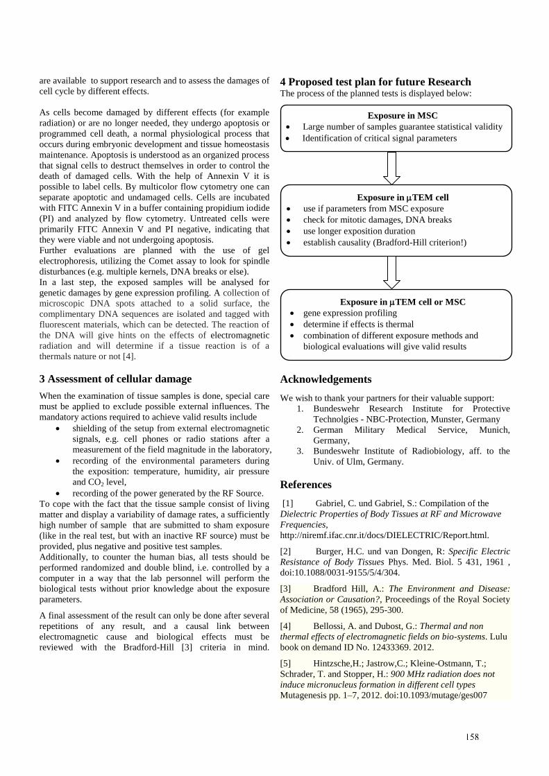
are available to support research and to assess the damages of
cell cycle by different effects.
As cells become damaged by different effects (for example
radiation) or are no longer needed, they undergo apoptosis or
programmed cell death, a normal physiological process that
occurs during embryonic development and tissue homeostasis
maintenance. Apoptosis is understood as an organized process
that signal cells to destruct themselves in order to control the
death of damaged cells. With the help of Annexin V it is
possible to label cells. By multicolor flow cytometry one can
separate apoptotic and undamaged cells. Cells are incubated
with FITC Annexin V in a buffer containing propidium iodide
(PI) and analyzed by flow cytometry. Untreated cells were
primarily FITC Annexin V and PI negative, indicating that
they were viable and not undergoing apoptosis.
Further evaluations are planned with the use of gel
electrophoresis, utilizing the Comet assay to look for spindle
disturbances (e.g. multiple kernels, DNA breaks or else).
In a last step, the exposed samples will be analysed for
genetic damages by gene expression profiling. A collection of
microscopic DNA spots attached to a solid surface, the
complimentary DNA sequences are isolated and tagged with
fluorescent materials, which can be detected. The reaction of
the DNA will give hints on the effects of electromagnetic
radiation and will determine if a tissue reaction is of a
thermals nature or not [4].
3 Assessment of cellular damage
When the examination of tissue samples is done, special care
must be applied to exclude possible external influences. The
mandatory actions required to achieve valid results include
shielding of the setup from external electromagnetic
signals, e.g. cell phones or radio stations after a
measurement of the field magnitude in the laboratory,
recording of the environmental parameters during
the exposition: temperature, humidity, air pressure
and CO2 level,
recording of the power generated by the RF Source.
To cope with the fact that the tissue sample consist of living
matter and display a variability of damage rates, a sufficiently
high number of sample that are submitted to sham exposure
(like in the real test, but with an inactive RF source) must be
provided, plus negative and positive test samples.
Additionally, to counter the human bias, all tests should be
performed randomized and double blind, i.e. controlled by a
computer in a way that the lab personnel will perform the
biological tests without prior knowledge about the exposure
parameters.
A final assessment of the result can only be done after several
repetitions of any result, and a causal link between
electromagnetic cause and biological effects must be
reviewed with the Bradford-Hill [3] criteria in mind.
4 Proposed test plan for future Research The process of the planned tests is displayed below:
Acknowledgements
We wish to thank your partners for their valuable support:
1. Bundeswehr Research Institute for Protective
Technolgies - NBC-Protection, Munster, Germany
2. German Military Medical Service, Munich,
Germany,
3. Bundeswehr Institute of Radiobiology, aff. to the
Univ. of Ulm, Germany.
References
[1] Gabriel, C. und Gabriel, S.: Compilation of the
Dielectric Properties of Body Tissues at RF and Microwave
Frequencies,
http://niremf.ifac.cnr.it/docs/DIELECTRIC/Report.html.
[2] Burger, H.C. und van Dongen, R: Specific Electric
Resistance of Body Tissues Phys. Med. Biol. 5 431, 1961 ,
doi:10.1088/0031-9155/5/4/304.
[3] Bradford Hill, A.: The Environment and Disease:
Association or Causation?, Proceedings of the Royal Society
of Medicine, 58 (1965), 295-300.
[4] Bellossi, A. and Dubost, G.: Thermal and non
thermal effects of electromagnetic fields on bio-systems. Lulu
book on demand ID No. 12433369. 2012.
[5] Hintzsche,H.; Jastrow,C.; Kleine-Ostmann, T.;
Schrader, T. and Stopper, H.: 900 MHz radiation does not
induce micronucleus formation in different cell types
Mutagenesis pp. 1–7, 2012. doi:10.1093/mutage/ges007
Exposure in TEM cell or MSC
gene expression profiling
determine if effects is thermal
combination of different exposure methods and
biological evaluations will give valid results
Exposure in MSC
Large number of samples guarantee statistical validity
Identification of critical signal parameters
Exposure in TEM cell
use if parameters from MSC exposure
check for mitotic damages, DNA breaks
use longer exposition duration
establish causality (Bradford-Hill criterion!)
The effect of standard cell culture environment on cellular
electromagnetic effects study
Wen-yu Peng*, Jian-gang Ma*, Xiao-yun LU*, Yan-zhao XIE †
* Xi’an Jiaotong University, School of Life Science and Technology, Xi’an 710049, Shaanxi, China. † Xi’an Jiaotong University, School of Electrical Engineering, Xi’an 710049, Shaanxi, China.
Abstract Biological effects of electromagnetic radiation are drawing
increasing attentions nowadays. To facilitate the cell based
molecular mechanism study of EMF bio-effects, an
integrated system combined a cell incubator with a TEM-
cell was developed which shows a very good performance.
In this study, the cell viability, ROS production and
mitochondrial membrane potential of PC3 cells with or
without EMP treatment were determined and the results
demonstrated the cell responses to EMP radiation were
different in the TEM cell combined-incubator or in the open
area. Therefore, it’s necessary to standardize the culture
condition coordinate with the EMP intervention to illustrate
the bioeffects from solo EMP radiation without the
interference from other environmental factors.
Keywords: incubator with TEM-cell, cell viability, ROS,
mitochondrial membrane potential
1 Introduction
Nowadays, the biological effects of electromagnetic
radiation draw more and more attentions from both physicists
and biologists. Many studies have been carried out to
investigate the cellular response to various electromagnetic
radiations. While in vitro cell cultivation requires standard
culture conditions such as temperature of 37°C and 95%
humidified environment with 5% CO2 [1]. Change of the
temperature or the pH of medium could activate or inhibit many
cell signaling pathway and result in the cell behavior alternation.
Therefore, maintain the standard cultivation environment
during EMF treatment is of great importance to obtain the
precise results for cell based study.
In our previous study, an incubator combined with TEM-cell
has been constructed to establish the identical cell culture
condition with electromagnetic radiation [2]. In this study, we
compared the cell response to EMP stimulation in the standard
culture condition with that in the open area and reveal that the
culture environment during EMP treatment could result in
significant difference of some biological analysis and therefore
could led to controversial data. This study demonstrate that for
the bioelectromagnetic effects study in cell-based level, it’s
necessary to carry out the electromagnetic radiation under the
standard cell culture condition to coordinate with biological
analysis.
2 Material and method
Human prostate cancer cell line PC3 was used to evaluate the
cell response to EMP treatment in the open area and in the
incubator. PC3 cells were maintained in RPMI 1640 which was
supplemented with 10% fetal bovine serum (Gibico) and 1%
penicillin-streptomycin in humidified environment of 5% CO2.
Cells were seeded in triplicate at 1×10⁴ cells/well in 96-well
culture plates and treated under pulsed EMF (30kV/m, 25
pulse/min) for 1.5h at open area and in the incubator,
respectively. Cell viability was quantified by cell counting kit-8
(CCK-8) assay and the intracellular reactive oxygen species
(ROS) level was determined by fluorescence analysis with
dichlorodihydrofluorescein diacetate (H2DCFDA) as the
indicator. JC-1 staining method was used to reveal the
mitochondrial membrane potential. Relative cell viability, ROS
production and mitochondrial membrane potential were
calculated with regard to that of the control group at 37°C in the
incubator, which was set to 100% viability.
3 Result
EMP radiation decreased the PC3 cell viability when cells
were treated in the open area. But when cells received the EMP
radiation inside the incubator, the effect of electromagnetic
treatment on the cell viability was not significant. Although the
EMP radiation increased the ROS production no matter cells
were treated inside the incubator or in the open area (Fig. 2), but
the degree of variations were 2.48 times and 1.44 times in the
incubator and in the open area, respectively. For the
mitochondrial membrane potential analysis, there was no
significant difference between the EMP treated and non-treated
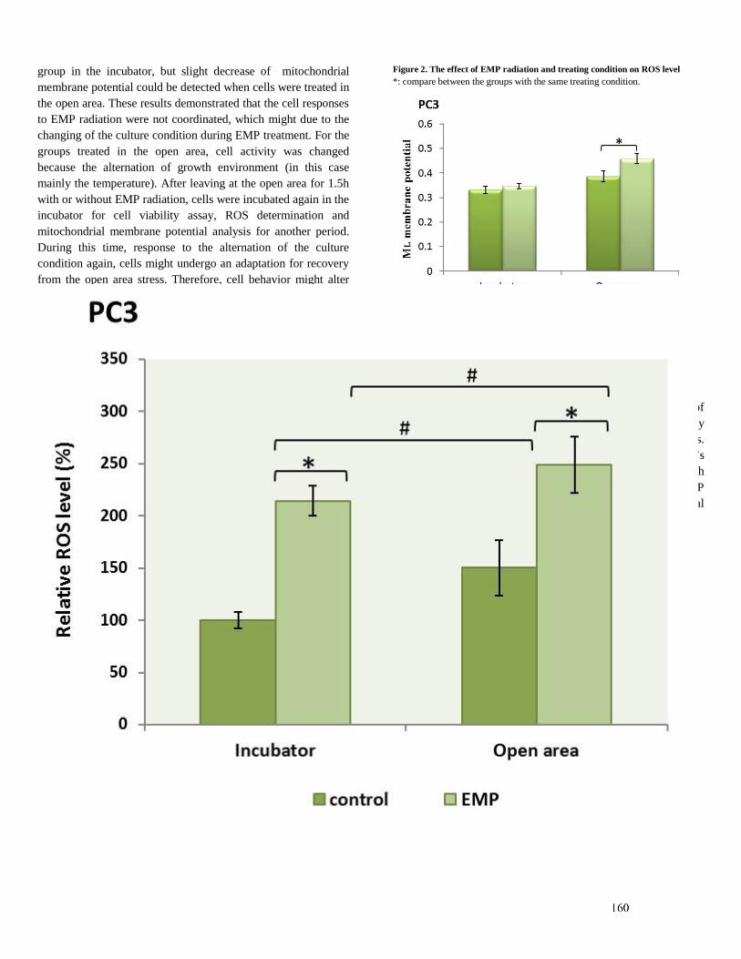
group in the incubator, but slight decrease of mitochondrial
membrane potential could be detected when cells were treated in
the open area. These results demonstrated that the cell responses
to EMP radiation were not coordinated, which might due to the
changing of the culture condition during EMP treatment. For the
groups treated in the open area, cell activity was changed
because the alternation of growth environment (in this case
mainly the temperature). After leaving at the open area for 1.5h
with or without EMP radiation, cells were incubated again in the
incubator for cell viability assay, ROS determination and
mitochondrial membrane potential analysis for another period.
During this time, response to the alternation of the culture
condition again, cells might undergo an adaptation for recovery
from the open area stress. Therefore, cell behavior might alter
again compensatory which resulted in the difference with that of
the incubator-cultured groups.
Figure 1. The effect of EMP radiation and treating condition on cell viabilities
*: compare between the groups with the same treating condition.
Figure 2. The effect of EMP radiation and treating condition on ROS level
*: compare between the groups with the same treating condition.
Figure 1. The effect of EMP radiation and treating condition on mitochondrial
membrane potential
*: compare between the groups with the same treating condition.
4 Conclusion
The results from this study indicated that the alternation of
growth environment during EMP radiation could significantly
affect the cell behavior and the following biological analysis.
For the cell-based bioelectromagnetic effects study, it’s
necessary to standardize the culture condition coordinate with
the EMP intervention to illustrate the bioeffects from solo EMP
radiation without the interference from other environmental
factors.
REFERENCES
[1] Davis, J. M. (ed.) “Basic Cell Culture”, 2nd ed., IRL, Oxford, (2002).
[1] X. Y. Lu, K. J. Li, Y. Z. Xie. “An Incubator Combined with TEM-cell for
Cellular Electromagnetic Effects Study”, AMEREM, (2014).
1
Examples of the Power Wave Theory of Antennas
E. G. Farr
Farr Fields, LC, 1801 Count Fleet St, Albuquerque, NM, USA, [email protected]
Abstract
Power wave theory provides a complete and simple
description of antenna performance in both the frequency
and time domains. To clarify its usefulness, we provide
here a number of examples. First, we show how the theory
can be used to describe the performance of electrically
small electric and magnetic dipoles; the so-called D-dot
and B-dot sensors. We calculate the antenna transfer
function, and then provide standard antenna parameters,
including gain, realized gain, effective length, and effective
area. Second, we show how a matching circuit can be
combined with an antenna to form a combined
Generalized Antenna Scattering Matrix. With this, we
show how two common matching circuits affect antenna
performance.
Keywords: Power wave theory of antennas, electrically small
electric and magnetic dipoles, D-dot and B-dot antennas,
matching circuit, generalized antenna scattering matrix.
1 Introduction
In our papers on the power wave theory of antennas [1, 2], we
showed a complete description of antenna performance in
both the frequency and time domains. This fills a gap in
current antenna theory by providing the simplest possible
description of antenna performance in the time domain. It also
fills a gap in the frequency domain, since neither antenna gain
nor radar cross section include phase information.
Some reviewers of [1, 2] have requested examples of power
waves applied to common antennas. We therefore provide
here a series of examples that expand upon these ideas. First,
we review the definitions of terms. Next, we show how the
theory of power waves applies to electrically small electric
and magnetic dipoles; or D-dot and B-dot sensors. Third, we
show how to add a matching circuit to an antenna, and
incorporate its scattering parameters into the Generalized
Antenna Scattering Matrix. Finally, we show how some
common matching circuits affect antenna performance. We
begin now with a review of the definitions. This paper is a
summary of material covered in [3].
2 Review of Power Waves Applied to Antennas
We summarize here the power wave theory of antennas [1, 2].
In those two papers, we argued that an antenna can be
reduced to a 3-port network. One port is the antenna port, and
the second and third ports are the θ− and φ−polarizations of
the incident and scattered fields. We define the following
parameters relating to far-field performance as
r
o
radrad
r
o
radrad
o
incinc
o
incinc
o
recrec
o
srcsrc
eZ
Ere
Z
Er
Z
E
Z
E
VV
γφφ
γθθ
φφ
θθ
ΥΥ
φθ
ΣΣ
φθ
ΖΠ
ΖΠ
2
,,
2
,,
2
,,
2
,,
11
~~
~~
onspolarizati & , waveintensity radiation Radiated
~~
~~
onspolarizati & ve,density waflux power Incident
~~
~~
power wave ReceivedPower Wave Source
==
==
==
. (1)
Here, radE~
is the radiated far field, jkvs == /γ , s = jω, and
vfvk /2/ πω == is the propagation constant in the
surrounding medium. Furthermore, v is the velocity of
propagation in the surrounding medium, and r is the distance
from the antenna to the observation point in the far field. In
addition, Zo1 and Zo2 are the real reference impedances
associated with the antenna port and the surrounding medium
– most commonly, Zo1 = 50 Ω and Zo2 = 120 π Ω. The tilde
indicates that we are operating in the Laplace domain.
The symbols Π, Υ, and Σ are Greek versions of P, U, and S,
which are the commonly used symbols for power, radiation
intensity, and power flux density, respectively. Thus, to
convert the symbol for a “power” quantity to that of a “power
wave” quantity, we make the symbol Greek.
The above quantities are assembled into the antenna equation,
which is a 3x3 matrix equation. We can express these two
different ways, leading to
Γ
=
inc
inc
src
rad
rad
rec
vhs
vhs
hh
,
,
,
,~
~
~
~~)2/(
~
~~)2/(
~
~~~
~
~
~
θ
θ
φφφθφ
θφθθθ
φθ
φ
θΣΣΠ
π
πΥΥΠ
ll
ll , (2)
where Γ~
is the reflection coefficient looking into the antenna
port, the two components of h~
represent the vector transfer
function, and the four components of l~
represent the dyadic
scattering coefficient.
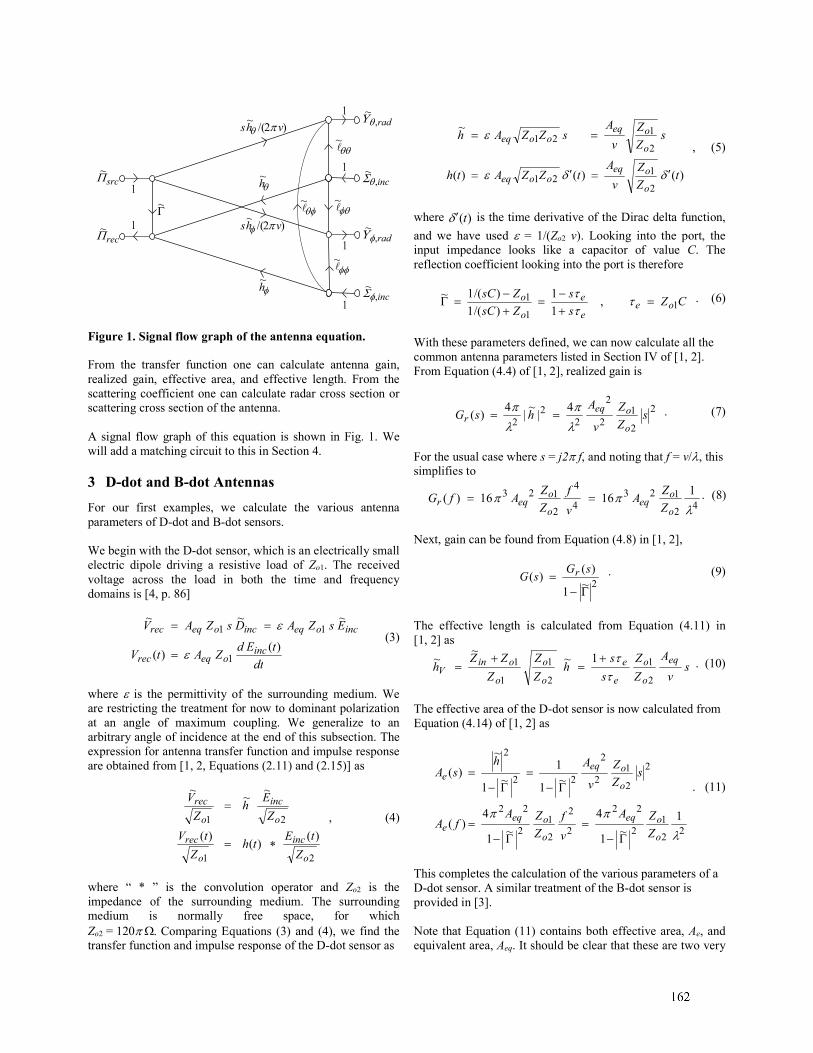
2
recΠ~
srcΠ~
Γ~
θh~
θθl~
)2/(~
vhs πθ
1
1
rad,~θΥ
inc,~θΣ
1
1
φφl~
rad,~φΥ
inc,~φΣ
1
1
φθl~
)2/(~
vhs πφ
φh~
θφl~
Figure 1. Signal flow graph of the antenna equation.
From the transfer function one can calculate antenna gain,
realized gain, effective area, and effective length. From the
scattering coefficient one can calculate radar cross section or
scattering cross section of the antenna.
A signal flow graph of this equation is shown in Fig. 1. We
will add a matching circuit to this in Section 4.
3 D-dot and B-dot Antennas
For our first examples, we calculate the various antenna
parameters of D-dot and B-dot sensors.
We begin with the D-dot sensor, which is an electrically small
electric dipole driving a resistive load of Zo1. The received
voltage across the load in both the time and frequency
domains is [4, p. 86]
dt
tEdZAtV
EsZADsZAV
incoeqrec
incoeqincoeqrec
)()(
~~~
1
11
ε
ε
=
== (3)
where ε is the permittivity of the surrounding medium. We
are restricting the treatment for now to dominant polarization
at an angle of maximum coupling. We generalize to an
arbitrary angle of incidence at the end of this subsection. The
expression for antenna transfer function and impulse response
are obtained from [1, 2, Equations (2.11) and (2.15)] as
21
21
)()(
)(
~~
~
o
inc
o
rec
o
inc
o
rec
Z
tEth
Z
tV
Z
Eh
Z
V
∗=
= , (4)
where “ * ” is the convolution operator and Zo2 is the
impedance of the surrounding medium. The surrounding
medium is normally free space, for which
Zo2 = 120π Ω. Comparing Equations (3) and (4), we find the
transfer function and impulse response of the D-dot sensor as
)()()(
~
2
121
2
121
tZ
Z
v
AtZZAth
sZ
Z
v
AsZZAh
o
oeqooeq
o
oeqooeq
δδε
ε
′=′=
== , (5)
where )(tδ ′ is the time derivative of the Dirac delta function,
and we have used ε = 1/(Zo2 v). Looking into the port, the
input impedance looks like a capacitor of value C. The
reflection coefficient looking into the port is therefore
CZs
s
ZsC
ZsCoe
e
e
o
o1
1
1 ,1
1
)/(1
)/(1~=
+−
=+−
=Γ τττ . (6)
With these parameters defined, we can now calculate all the
common antenna parameters listed in Section IV of [1, 2].
From Equation (4.4) of [1, 2], realized gain is
2
2
12
2
2
2
2
4|
~|
4)( s
Z
Z
v
AhsG
o
oeqr
λ
π
λ
π== . (7)
For the usual case where s = j2π f, and noting that f = v/λ, this
simplifies to
42
123
4
4
2
123 11616)(
λππ
o
oeq
o
oeqr
Z
ZA
v
f
Z
ZAfG == . (8)
Next, gain can be found from Equation (4.8) in [1, 2],
2~1
)()(
Γ−=
sGsG r . (9)
The effective length is calculated from Equation (4.11) in
[1, 2] as
sv
A
Z
Z
s
sh
Z
Z
Z
ZZh
eq
o
o
e
e
o
o
o
oinV
2
1
2
1
1
1 1~~
~
ττ+
=+
= . (10)
The effective area of the D-dot sensor is now calculated from
Equation (4.14) of [1, 2] as
22
12
22
2
2
2
12
22
2
2
12
2
22
2
1
~1
4
~1
4)(
~1
1
~1
~
)(
λ
ππ
o
oeq
o
oeqe
o
oeqe
Z
ZA
v
f
Z
ZAfA
sZ
Z
v
AhsA
Γ−=
Γ−=
Γ−=
Γ−=
. (11)
This completes the calculation of the various parameters of a
D-dot sensor. A similar treatment of the B-dot sensor is
provided in [3].
Note that Equation (11) contains both effective area, Ae, and
equivalent area, Aeq. It should be clear that these are two very
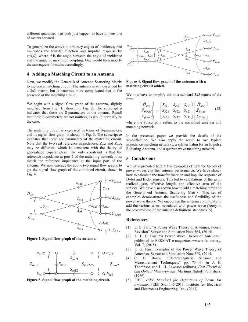
3
different quantities that both just happen to have dimensions
of meters squared.
To generalize the above to arbitrary angles of incidence, one
multiplies the transfer function and impulse response by
cos(θ), where θ is the angle between the angle of incidence
and the angle of maximum coupling. One would then modify
the subsequent formulas accordingly.
4 Adding a Matching Circuit to an Antenna
Next, we modify the Generalized Antenna Scattering Matrix
to include a matching circuit. The antenna is still described by
a 3x3 matrix, but it becomes more complicated due to the
presence of the matching circuit.
We begin with a signal flow graph of the antenna, slightly
modified from Fig. 1, shown in Fig. 2. The subscript a
indicates that these are S-parameters of the antenna. Recall
that these S-parameters are not unitless, as would normally be
the case.
The matching circuit is expressed in terms of S-parameters,
and its signal flow graph is shown in Fig. 3. The subscript m
indicates that these are parameters of the matching circuit.
Note that the two real reference impedances, Zmo1 and Zmo2,
may be different, which is consistent with the theory of
generalized S-parameters. The only constraint is that the
reference impedance at port 2 of the matching network must
match the reference impedance at the input port of the
antenna. We now cascade the above two signal flow graphs to
get the signal flow graph of the combined circuit, shown in
Fig. 4.
recΠ~
srcΠ~
11aS
12aS
22aS
21aS
1
1
rad,~
θΥ
inc,~
θΣ
1
1
33aS
rad,~
φΥ
inc,~
φΣ
1
1
32aS
31aS
13aS
23aS
Figure 2. Signal flow graph of the antenna.
1ma
21mS 1
1
1
1 1mb
12mS11mS 22mS
2ma
2mb
2moZ1moZ
Figure 3. Signal flow graph of the matching circuit.
recΠ~
srcΠ~
11aS
12aS
22aS
21aS rad,~
θΥ
inc,~
θΣ
1
1
33aS
rad,~
φΥ
inc,~
φΣ
1
1
32aS
31aS
13aS
23aS21mS 1
1
1
1 12mS11mS 22mS
Figure 4. Signal flow graph of the antenna with a
matching circuit added.
We now have to simplify this to a standard 3x3 matrix of the
form
=
inc
inc
src
ccc
ccc
ccc
rad
rad
rec
SSS
SSS
SSS
,
,
333231
232221
131211
,
,~
~
~
~
~
~
θ
θ
φ
θΣΣΠ
ΥΥ
Π (12)
where the subscript c refers to the combined antenna and
matching network.
In the presented paper we provide the details of the
simplification. We also apply the result to two typical
impedance matching networks; a splitter balun for an Impulse
Radiating Antenna, and a quarter-wave matching network.
5 Conclusions
We have provided here a few examples of how the theory of
power waves clarifies antenna performance. We have shown
how to calculate the transfer function and impulse response of
D-dot and B-dot sensors. This led to calculations of the gain,
realized gain, effective length, and effective area of the
sensors. We have also shown how to add a matching circuit to
the Generalized Antenna Scattering Matrix. This set of
examples demonstrates the usefulness and flexibility of the
power wave theory. We encourage the antenna community to
add the various terms associated with power wave theory to
the next revision of the antenna definitions standards [5].
References
[1] E. G. Farr, “A Power Wave Theory of Antennas, Fourth
Revision” Sensor and Simulation Note 564, (2014).
[2] 2. E. G. Farr, “A Power Wave Theory of Antennas,”
published in FERMAT e-magazine, www.e-fermat.org,
Vol. 7, (2015).
[3] E. G. Farr, Examples of the Power Wave Theory of
Antennas, Sensor and Simulation Note 569, (2014.
[4] C. E. Baum, “Electromagnetic Sensors and
Meausurement Techniques,” pp. 73-144 in J. E.
Thompson and L. H. Lewison (editors), Fast Electrical
and Optical Measurements, Martinus Nijhoff Publishers,
(1986).
[5] IEEE, IEEE Standard for Definitions of Terms for
Antennas, IEEE Std. 145-2013, Institute for Electrical
and Electronics Engineering, Inc., (2013).
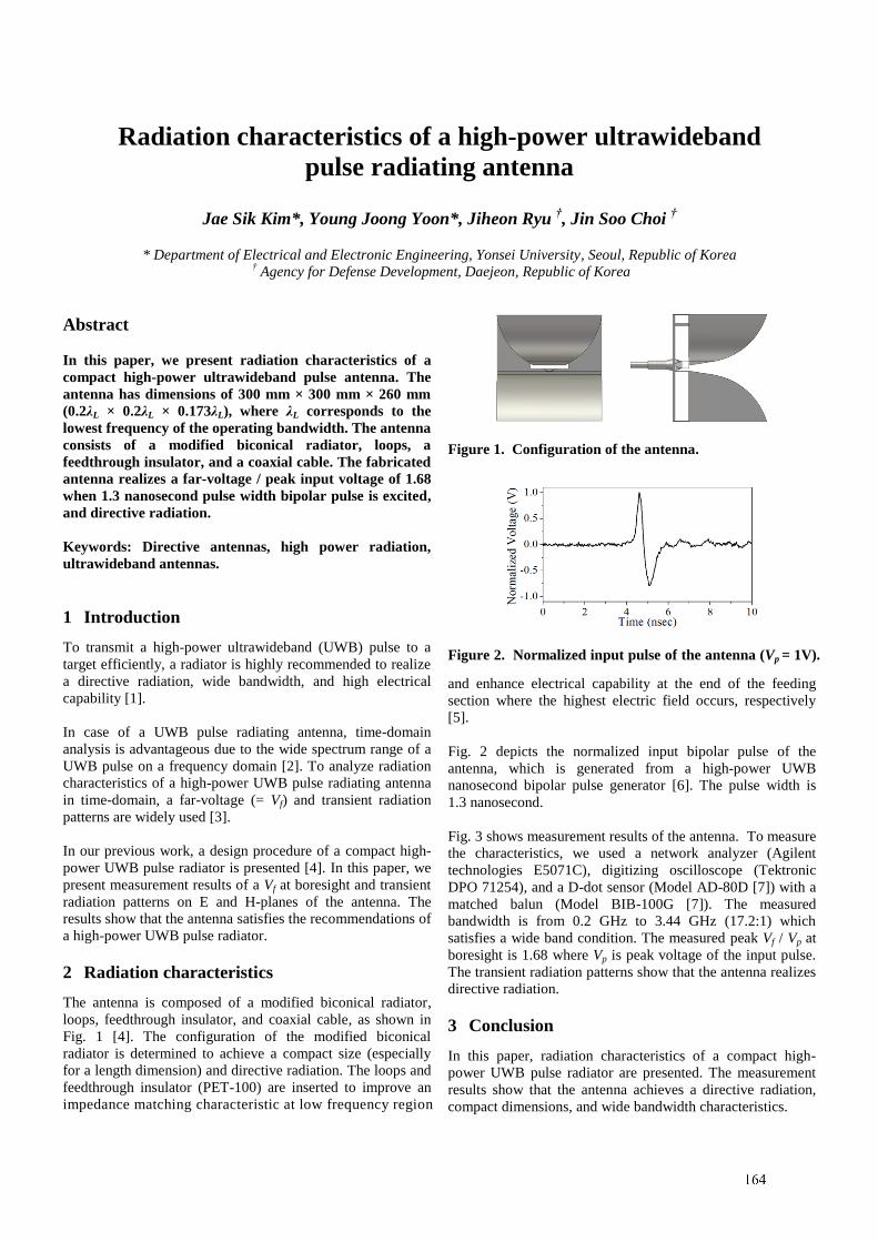
1
Radiation characteristics of a high-power ultrawideband
pulse radiating antenna
Jae Sik Kim*, Young Joong Yoon*, Jiheon Ryu †, Jin Soo Choi
†
* Department of Electrical and Electronic Engineering, Yonsei University, Seoul, Republic of Korea
† Agency for Defense Development, Daejeon, Republic of Korea
Abstract
In this paper, we present radiation characteristics of a
compact high-power ultrawideband pulse antenna. The
antenna has dimensions of 300 mm × 300 mm × 260 mm
(0.2λL × 0.2λL × 0.173λL), where λL corresponds to the
lowest frequency of the operating bandwidth. The antenna
consists of a modified biconical radiator, loops, a
feedthrough insulator, and a coaxial cable. The fabricated
antenna realizes a far-voltage / peak input voltage of 1.68
when 1.3 nanosecond pulse width bipolar pulse is excited,
and directive radiation.
Keywords: Directive antennas, high power radiation,
ultrawideband antennas.
1 Introduction
To transmit a high-power ultrawideband (UWB) pulse to a
target efficiently, a radiator is highly recommended to realize
a directive radiation, wide bandwidth, and high electrical
capability [1].
In case of a UWB pulse radiating antenna, time-domain
analysis is advantageous due to the wide spectrum range of a
UWB pulse on a frequency domain [2]. To analyze radiation
characteristics of a high-power UWB pulse radiating antenna
in time-domain, a far-voltage (= Vf) and transient radiation
patterns are widely used [3].
In our previous work, a design procedure of a compact high-
power UWB pulse radiator is presented [4]. In this paper, we
present measurement results of a Vf at boresight and transient
radiation patterns on E and H-planes of the antenna. The
results show that the antenna satisfies the recommendations of
a high-power UWB pulse radiator.
2 Radiation characteristics
The antenna is composed of a modified biconical radiator,
loops, feedthrough insulator, and coaxial cable, as shown in
Fig. 1 [4]. The configuration of the modified biconical
radiator is determined to achieve a compact size (especially
for a length dimension) and directive radiation. The loops and
feedthrough insulator (PET-100) are inserted to improve an
impedance matching characteristic at low frequency region
Figure 1. Configuration of the antenna.
Figure 2. Normalized input pulse of the antenna (Vp = 1V).
and enhance electrical capability at the end of the feeding
section where the highest electric field occurs, respectively
[5].
Fig. 2 depicts the normalized input bipolar pulse of the
antenna, which is generated from a high-power UWB
nanosecond bipolar pulse generator [6]. The pulse width is
1.3 nanosecond.
Fig. 3 shows measurement results of the antenna. To measure
the characteristics, we used a network analyzer (Agilent
technologies E5071C), digitizing oscilloscope (Tektronic
DPO 71254), and a D-dot sensor (Model AD-80D [7]) with a
matched balun (Model BIB-100G [7]). The measured
bandwidth is from 0.2 GHz to 3.44 GHz (17.2:1) which
satisfies a wide band condition. The measured peak Vf / Vp at
boresight is 1.68 where Vp is peak voltage of the input pulse.
The transient radiation patterns show that the antenna realizes
directive radiation.
3 Conclusion
In this paper, radiation characteristics of a compact high-
power UWB pulse radiator are presented. The measurement
results show that the antenna achieves a directive radiation,
compact dimensions, and wide bandwidth characteristics.
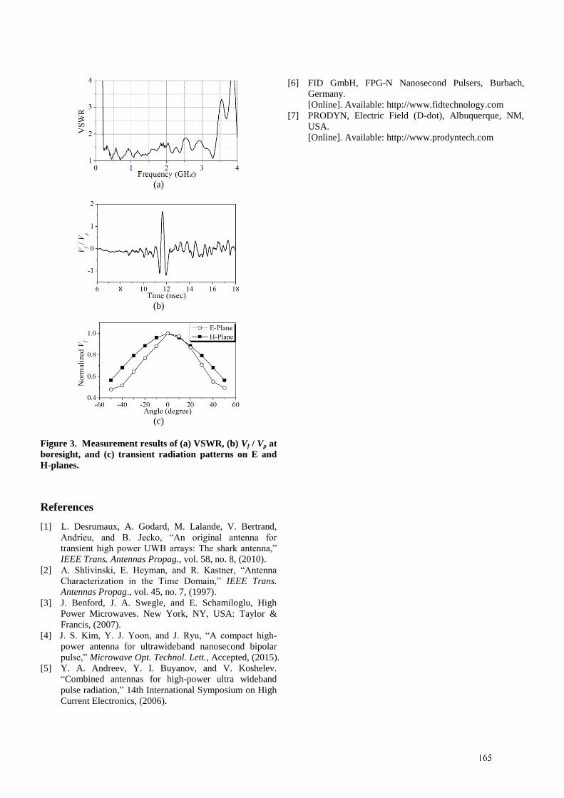
2
(a)
(b)
(c)
Figure 3. Measurement results of (a) VSWR, (b) Vf / Vp at
boresight, and (c) transient radiation patterns on E and
H-planes.
References
[1] L. Desrumaux, A. Godard, M. Lalande, V. Bertrand,
Andrieu, and B. Jecko, “An original antenna for
transient high power UWB arrays: The shark antenna,”
IEEE Trans. Antennas Propag., vol. 58, no. 8, (2010).
[2] A. Shlivinski, E. Heyman, and R. Kastner, “Antenna
Characterization in the Time Domain,” IEEE Trans.
Antennas Propag., vol. 45, no. 7, (1997).
[3] J. Benford, J. A. Swegle, and E. Schamiloglu, High
Power Microwaves. New York, NY, USA: Taylor &
Francis, (2007).
[4] J. S. Kim, Y. J. Yoon, and J. Ryu, “A compact high-
power antenna for ultrawideband nanosecond bipolar
pulse,” Microwave Opt. Technol. Lett., Accepted, (2015).
[5] Y. A. Andreev, Y. I. Buyanov, and V. Koshelev.
“Combined antennas for high-power ultra wideband
pulse radiation,” 14th International Symposium on High
Current Electronics, (2006).
[6] FID GmbH, FPG-N Nanosecond Pulsers, Burbach,
Germany.
[Online]. Available: http://www.fidtechnology.com
[7] PRODYN, Electric Field (D-dot), Albuquerque, NM,
USA.
[Online]. Available: http://www.prodyntech.com
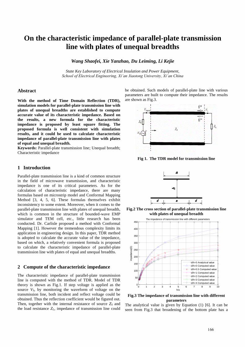
1
On the characteristic impedance of parallel-plate transmission
line with plates of unequal breadths
Wang Shaofei, Xie Yanzhao, Du Leiming, Li Kejie
State Key Laboratory of Electrical Insulation and Power Equipment,
School of Electrical Engineering, Xi’an Jiaotong University, Xi’an China
Abstract
With the method of Time Domain Reflection (TDR),
simulation models for parallel-plate transmission line with
plates of unequal breadths are established to compute
accurate value of its characteristic impedance. Based on
the results, a new formula for the characteristic
impedance is proposed by least square fitting. The
proposed formula is well consistent with simulation
results, and it could be used to calculate characteristic
impedance of parallel-plate transmission line with plates
of equal and unequal breadth. Keywords: Parallel-plate transmission line; Unequal breadth;
Characteristic impedance
1 Introduction
Parallel-plate transmission line is a kind of common structure
in the field of microwave transmission, and characteristic
impedance is one of its critical parameters. As for the
calculation of characteristic impedance, there are many
formulas based on microstrip model and Conformal Mapping
Method [3, 4, 5, 6]. These formulas themselves exhibit
inconsistency to some extent. Moreover, when it comes to the
parallel-plate transmission line with plates of unequal breadth,
which is common in the structure of bounded-wave EMP
simulator and TEM cell, etc., little research has been
conducted. Dr. Carlisle proposed a method with Conformal
Mapping [1]. However the tremendous complexity limits its
application in engineering design. In this paper, TDR method
is adopted to calculate the accurate value of the impedance,
based on which, a relatively convenient formula is proposed
to calculate the characteristic impedance of parallel-plate
transmission line with plates of equal and unequal breadths.
2 Compute of the characteristic impedance
The characteristic impedance of parallel-plate transmission
line is computed with the method of TDR. Model of TDR
theory is shown as Fig.1. If step voltage is applied as the
source VS, by monitoring the waveform of voltage on the
transmission line, both incident and reflect voltage could be
obtained. Thus the reflection coefficient would be figured out.
Then, together with the internal resistance of source ZS and
the load resistance ZL, impedance of transmission line could
be obtained. Such models of parallel-plate line with various
parameters are built to compute their impedance. The results
are shown as Fig.3.
Fig 1. The TDR model for transmission line
a
a dd
h
Fig.2 The cross section of parallel-plate transmission line
with plates of unequal breadth
0 1 2 3 4 5 6 7 8 9 100
50
100
150
200
250
300
350
400
450The impedence of transmission line with different parameters
h/a
impedance(Ω
)
d/h=0 Analytical value
d/h=0 Computed value
d/h=0.5 Computed value
d/h=1 Computed value
d/h=2 Computed value
d/h=3 Computed value
d/h=4 Computed value
Fig.3 The impedance of transmission line with different
parameters
The analytical value is given by Equation (1) [6]. It can be
seen from Fig.3 that broadening of the bottom plate has a
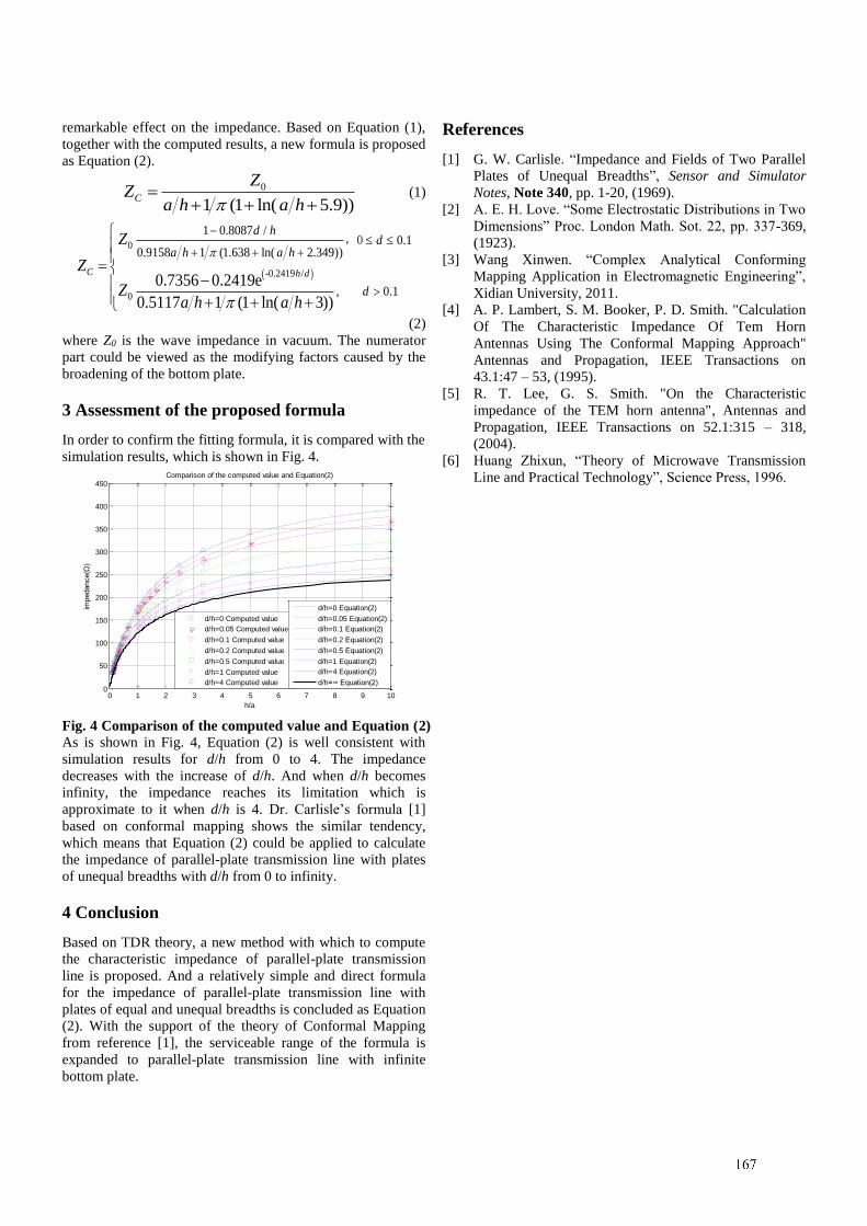
2
remarkable effect on the impedance. Based on Equation (1),
together with the computed results, a new formula is proposed
as Equation (2).
0 1 (1 ln( 5.9))
C
ZZ
a h a h
(1)
-0.2419
0
0
/
0.9158 1 (1.638 ln( 2.349))
1 0
, 0.
.8087 /0.1
1
0.7356 0
0.5117 1 (1 ln( 3)
.241 e
)
9C h d
a h a h
d h
d
dZ
Z
Za h a h
,0
(2)
where Z0 is the wave impedance in vacuum. The numerator
part could be viewed as the modifying factors caused by the
broadening of the bottom plate.
3 Assessment of the proposed formula
In order to confirm the fitting formula, it is compared with the
simulation results, which is shown in Fig. 4.
0 1 2 3 4 5 6 7 8 9 100
50
100
150
200
250
300
350
400
450Comparison of the computed value and Equation(2)
h/a
impedance(Ω
)
d/h=0 Computed value
d/h=0.05 Computed value
d/h=0.1 Computed value
d/h=0.2 Computed value
d/h=0.5 Computed value
d/h=1 Computed value
d/h=4 Computed value
d/h=0 Equation(2)
d/h=0.05 Equation(2)
d/h=0.1 Equation(2)
d/h=0.2 Equation(2)
d/h=0.5 Equation(2)
d/h=1 Equation(2)
d/h=4 Equation(2)
d/h=∞ Equation(2)
Fig. 4 Comparison of the computed value and Equation (2) As is shown in Fig. 4, Equation (2) is well consistent with
simulation results for d/h from 0 to 4. The impedance
decreases with the increase of d/h. And when d/h becomes
infinity, the impedance reaches its limitation which is
approximate to it when d/h is 4. Dr. Carlisle’s formula [1]
based on conformal mapping shows the similar tendency,
which means that Equation (2) could be applied to calculate
the impedance of parallel-plate transmission line with plates
of unequal breadths with d/h from 0 to infinity.
4 Conclusion
Based on TDR theory, a new method with which to compute
the characteristic impedance of parallel-plate transmission
line is proposed. And a relatively simple and direct formula
for the impedance of parallel-plate transmission line with
plates of equal and unequal breadths is concluded as Equation
(2). With the support of the theory of Conformal Mapping
from reference [1], the serviceable range of the formula is
expanded to parallel-plate transmission line with infinite
bottom plate.
References
[1] G. W. Carlisle. “Impedance and Fields of Two Parallel
Plates of Unequal Breadths”, Sensor and Simulator
Notes, Note 340, pp. 1-20, (1969).
[2] A. E. H. Love. “Some Electrostatic Distributions in Two
Dimensions” Proc. London Math. Sot. 22, pp. 337-369,
(1923).
[3] Wang Xinwen. “Complex Analytical Conforming
Mapping Application in Electromagnetic Engineering”,
Xidian University, 2011.
[4] A. P. Lambert, S. M. Booker, P. D. Smith. "Calculation
Of The Characteristic Impedance Of Tem Horn
Antennas Using The Conformal Mapping Approach"
Antennas and Propagation, IEEE Transactions on
43.1:47 – 53, (1995).
[5] R. T. Lee, G. S. Smith. "On the Characteristic
impedance of the TEM horn antenna", Antennas and
Propagation, IEEE Transactions on 52.1:315 – 318,
(2004).
[6] Huang Zhixun, “Theory of Microwave Transmission
Line and Practical Technology”, Science Press, 1996.
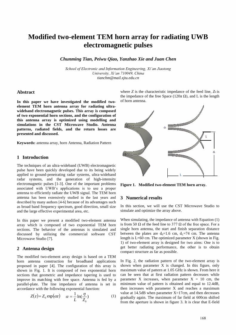
Modified two-element TEM horn array for radiating UWB
electromagnetic pulses
Chunming Tian, Peiwu Qiao, Yanzhao Xie and Juan Chen
School of Electronic and Information Engineering, Xi’an Jiaotong
University, Xi’an 710049, China
Abstract
In this paper we have investigated the modified two-
element TEM horn antenna array for radiating ultra-
wideband electromagnetic pulses. This array is composed
of two exponential horn sections, and the configuration of
this antenna array is optimized using modelling and
simulations in the CST Microwave Studio. Antenna
patterns, radiated fields, and the return losses are
presented and discussed.
Keywords: antenna array, horn Antenna, Radiation Pattern
1 Introduction
The techniques of an ultra-wideband (UWB) electromagnetic
pulse have been quickly developed due to its being widely
applied to ground-penetrating radar systems, ultra-wideband
radar systems, and the generation of high-intensity
electromagnetic pulses [1-3]. One of the important problems
associated with UWB’s applications is to use a proper
antenna to efficiently radiate the UWB signal. The TEM horn
antenna has been extensively studied in the last years and
described by many authors [4-6] because of its advantages such
as broad band frequency spectrum, good direction, small size
and the large effective experimental area, etc.
In this paper we present a modified two-element antenna
array which is composed of two exponential TEM horn
sections. The behavior of the antennas is simulated and
discussed by utilizing the commercial software CST
Microwave Studio [7].
2 Antenna design
The modified two-element array design is based on a TEM
horn antenna construction for broadband applications
proposed in paper [4]. The configuration of this array is
shown in Fig. 1. It is composed of two exponential horn
sections that geometric and impedance tapering is used to
improve its matching with free space. Antenna is fed by a
parallel-plate. The line impedance of antenna is set in
accordance with the following exponential function:
zZzZ exp0
0
1ln( )
L Z
(1)
where Z is the characteristic impedance of the feed line, Z0 is
the impedance of the free Space (120π Ω), and L is the length
of horn antenna.
Figure 1. Modified two-element TEM horn array.
3 Numerical results
In this section, we will use the CST Microwave Studio to
simulate and optimize the array above.
When simulating, the impedance of antenna with Equation (1)
is from 50 Ω of the feed line to 377 Ω of the free space. For a
single horn antenna, the start and finish separation distance
between the plates are d0=1.6 cm, dL=74 cm. The antenna
length is L=60 cm. The optimized parameter X (shown in Fig.
1) of two-element array is designed for two aims: One is to
get better radiating performance, the other is to obtain
compact structure as far as possible.
In Fig. 2, the radiation pattern of the two-element array is
shown when parameter X is changed. In this figure, only
maximum value of pattern at 1.05 GHz is shown. From here it
can be seen that at first radiation pattern decreases while
parameter X increases, when parameter X = 10 cm, the
minimum value of pattern is obtained and equal to 12.4dB,
then increases with parameter X and reaches a maximum
value at 14.5dB when parameter X=17cm, and then decreases
gradually again. The maximum of far field at 600cm shifted
from the aperture is shown in figure 3. It is clear that E-field
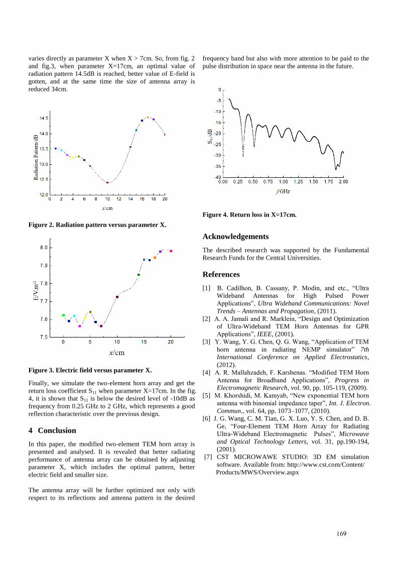
varies directly as parameter X when X > 7cm. So, from fig. 2
and fig.3, when parameter X=17cm, an optimal value of
radiation pattern 14.5dB is reached, better value of E-field is
gotten, and at the same time the size of antenna array is
reduced 34cm.
Figure 2. Radiation pattern versus parameter X.
Figure 3. Electric field versus parameter X.
Finally, we simulate the two-element horn array and get the
return loss coefficient S11 when parameter X=17cm. In the fig.
4, it is shown that S11 is below the desired level of -10dB as
frequency from 0.25 GHz to 2 GHz, which represents a good
reflection characteristic over the previous design.
4 Conclusion
In this paper, the modified two-element TEM horn array is
presented and analysed. It is revealed that better radiating
performance of antenna array can be obtained by adjusting
parameter X, which includes the optimal pattern, better
electric field and smaller size.
The antenna array will be further optimized not only with
respect to its reflections and antenna pattern in the desired
frequency band but also with more attention to be paid to the
pulse distribution in space near the antenna in the future.
Figure 4. Return loss in X=17cm.
Acknowledgements
The described research was supported by the Fundamental
Research Funds for the Central Universities.
References
[1] B. Cadilhon, B. Cassany, P. Modin, and etc., “Ultra
Wideband Antennas for High Pulsed Power
Applications”, Ultra Wideband Communications: Novel
Trends – Antennas and Propagation, (2011).
[2] A. A. Jamali and R. Marklein, “Design and Optimization
of Ultra-Wideband TEM Horn Antennas for GPR
Applications”, IEEE, (2001).
[3] Y. Wang, Y. G. Chen, Q. G. Wang, “Application of TEM
horn antenna in radiating NEMP simulator” 7th
International Conference on Applied Electrostatics,
(2012).
[4] A. R. Mallahzadeh, F. Karshenas. “Modified TEM Horn
Antenna for Broadband Applications”, Progress in
Electromagnetic Research, vol. 90, pp. 105-119, (2009).
[5] M. Khorshidi, M. Kamyab, “New exponential TEM horn
antenna with binomial impedance taper”, Int. J. Electron.
Commun., vol. 64, pp. 1073–1077, (2010).
[6] J. G. Wang, C. M. Tian, G. X. Luo, Y. S. Chen, and D. B.
Ge, “Four-Element TEM Horn Array for Radiating
Ultra-Wideband Electromagnetic Pulses”, Microwave
and Optical Technology Letters, vol. 31, pp.190-194,
(2001).
[7] CST MICROWAWE STUDIO: 3D EM simulation
software. Available from: http://www.cst.com/Content/
Products/MWS/Overview.aspx
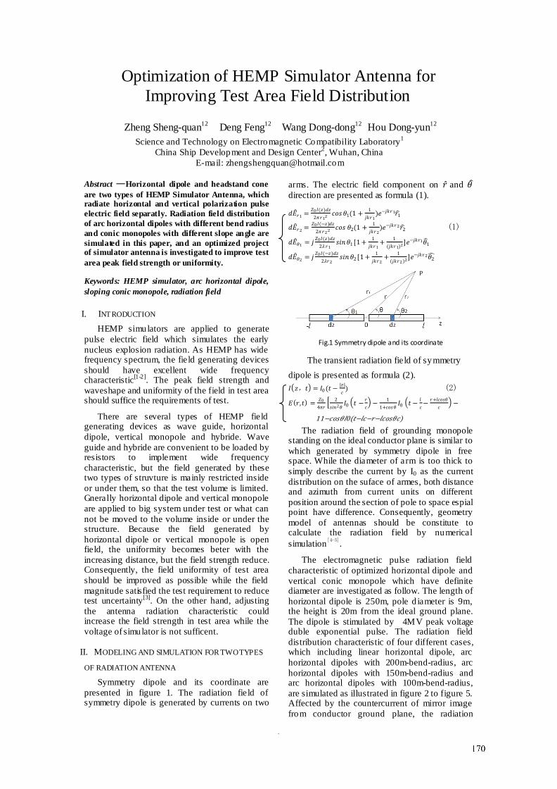
1
Optimization of HEMP Simulator Antenna for Improving Test Area Field Distribution
Zheng Sheng-quan12 Deng Feng12 Wang Dong-dong12 Hou Dong-yun12 Science and Technology on Electromagnetic Compatibility Laboratory1
China Ship Development and Design Center2, Wuhan, China E-mail: [email protected]
Abstract —Horizontal dipole and headstand cone are two types of HEMP Simulator Antenna, which radiate horizontal and vertical polarization pulse electric field separatly. Radiation field distribution of arc horizontal dipoles with different bend radius and conic monopoles with different slope angle are simulated in this paper, and an optimized project of simulator antenna is investigated to improve test area peak field strength or uniformity.
Keywords: HEMP simulator, arc horizontal dipole, sloping conic monopole, radiation field
I. INTRODUCTION HEMP simulators are applied to generate
pulse electric field which simulates the early nucleus explosion radiation. As HEMP has wide frequency spectrum, the field generating devices should have excellent wide frequency characteristic[1-2]. The peak field strength and waveshape and uniformity of the field in test area should suffice the requirements of test.
There are several types of HEMP field generating devices as wave guide, horizontal dipole, vertical monopole and hybride. Wave guide and hybride are convenient to be loaded by resistors to implement wide frequency characteristic, but the field generated by these two types of struvture is mainly restricted inside or under them, so that the test volume is limited. Gnerally horizontal dipole and vertical monopole are applied to big system under test or what can not be moved to the volume inside or under the structure. Because the field generated by horizontal dipole or vertical monopole is open field, the uniformity becomes beter with the increasing distance, but the field strength reduce. Consequently, the field uniformity of test area should be improved as possible while the field magnitude satisfied the test requirement to reduce test uncertainty[3]. On the other hand, adjusting the antenna radiation characteristic could increase the field strength in test area while the voltage of simulator is not sufficent.
II. MODELING AND SIMULATION FOR TWO TYPES
OF RADIATION ANTENNA Symmetry dipole and its coordinate are
presented in figure 1. The radiation field of symmetry dipole is generated by currents on two
arms. The electric field component on 𝑟 and 𝜃𝜃 direction are presented as formula (1).
𝑑𝑑𝐸𝐸𝑟𝑟1 = 𝑍𝑍0𝐼𝐼(𝑧𝑧)𝑑𝑑𝑧𝑧2𝜋𝜋𝑟𝑟12 𝑐𝑐𝑐𝑐𝑐𝑐𝜃𝜃1(1 + 1
𝑗𝑗𝑗𝑗𝑟𝑟1)𝑒𝑒−𝑗𝑗𝑗𝑗𝑟𝑟1𝑟𝑟1
𝑑𝑑𝐸𝐸𝑟𝑟2 = 𝑍𝑍0𝐼𝐼(−𝑧𝑧)𝑑𝑑𝑧𝑧2𝜋𝜋𝑟𝑟2 2 𝑐𝑐𝑐𝑐𝑐𝑐 𝜃𝜃2(1 + 1
𝑗𝑗𝑗𝑗𝑟𝑟2)𝑒𝑒−𝑗𝑗𝑗𝑗𝑟𝑟2𝑟𝑟2 (1)
𝑑𝑑𝐸𝐸𝜃𝜃1 = 𝑗𝑗 𝑍𝑍0𝐼𝐼(𝑧𝑧)𝑑𝑑𝑧𝑧2𝜆𝜆 𝑟𝑟1
𝑐𝑐𝑠𝑠𝑠𝑠𝜃𝜃1 [1 + 1𝑗𝑗𝑗𝑗𝑟𝑟1
+ 1(𝑗𝑗𝑗𝑗𝑟𝑟1)2]𝑒𝑒−𝑗𝑗𝑗𝑗𝑟𝑟1𝜃𝜃1
𝑑𝑑𝐸𝐸𝜃𝜃2 = 𝑗𝑗 𝑍𝑍0𝐼𝐼(−𝑧𝑧)𝑑𝑑𝑧𝑧2𝜆𝜆𝑟𝑟2
𝑐𝑐𝑠𝑠𝑠𝑠𝜃𝜃2 [1 + 1𝑗𝑗𝑗𝑗𝑟𝑟2
+ 1(𝑗𝑗𝑗𝑗𝑟𝑟2)2]𝑒𝑒−𝑗𝑗𝑗𝑗𝑟𝑟2𝜃𝜃2
Fig.1 Symmetry dipole and its coordinate
The transient radiation field of symmetry dipole is presented as formula (2). 𝐼𝐼𝑧𝑧,𝑡𝑡 = 𝐼𝐼0 (𝑡𝑡 − |𝑧𝑧|
𝑐𝑐) (2)
𝐸𝐸(𝑟𝑟,𝑡𝑡) = 𝑍𝑍04𝜋𝜋𝑟𝑟
2𝑐𝑐𝑠𝑠𝑠𝑠2𝜃𝜃
𝐼𝐼0 𝑡𝑡 −𝑟𝑟𝑐𝑐 − 1
1+𝑐𝑐𝑐𝑐𝑐𝑐𝜃𝜃𝐼𝐼0 𝑡𝑡 −
𝑙𝑙𝑐𝑐− 𝑟𝑟+𝑙𝑙𝑐𝑐𝑐𝑐𝑐𝑐𝜃𝜃
𝑐𝑐 −
11−𝑐𝑐𝑐𝑐𝑐𝑐𝜃𝜃𝐼𝐼0(𝑡𝑡−𝑙𝑙𝑐𝑐−𝑟𝑟−𝑙𝑙𝑐𝑐𝑐𝑐𝑐𝑐𝜃𝜃𝑐𝑐)
The radiation field of grounding monopole standing on the ideal conductor plane is similar to which generated by symmetry dipole in free space. While the diameter of arm is too thick to simply describe the current by I0 as the current distribution on the suface of armes, both distance and azimuth from current units on different position around the section of pole to space espial point have difference. Consequently, geometry model of antennas should be constitute to calculate the radiation field by numerical simulation[4-5].
The electromagnetic pulse radiation field characteristic of optimized horizontal dipole and vertical conic monopole which have definite diameter are investigated as follow. The length of horizontal dipole is 250m, pole d iameter is 9m, the height is 20m from the ideal ground plane. The dipole is stimulated by 4MV peak voltage duble exponential pulse. The radiation field distribution characteristic of four different cases, which including linear horizontal dipole, arc horizontal dipoles with 200m-bend-radius, arc horizontal dipoles with 150m-bend-radius and arc horizontal dipoles with 100m-bend-radius, are simulated as illustrated in figure 2 to figure 5. Affected by the countercurrent of mirror image from conductor ground plane, the radiation
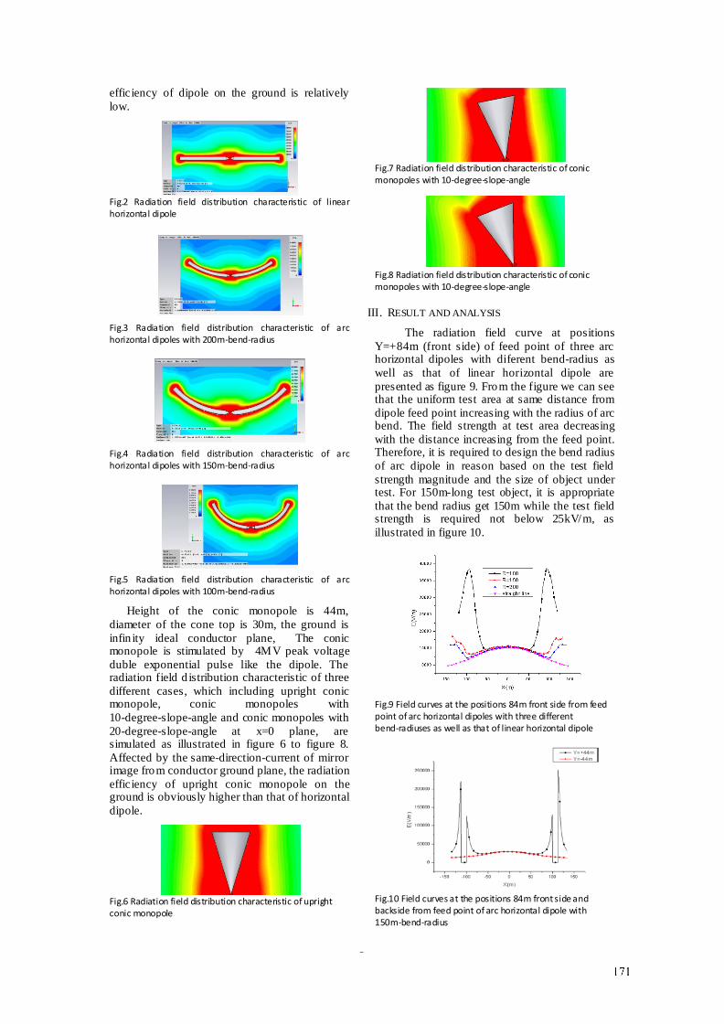
2
efficiency of dipole on the ground is relatively low.
Fig.2 Radiation field distribution characteristic of linear horizontal dipole
Fig.3 Radiation field distribution characteristic of arc horizontal dipoles with 200m-bend-radius
Fig.4 Radiation field distribution characteristic of arc horizontal dipoles with 150m-bend-radius
Fig.5 Radiation field distribution characteristic of arc horizontal dipoles with 100m-bend-radius
Height of the conic monopole is 44m, diameter of the cone top is 30m, the ground is infin ity ideal conductor plane, The conic monopole is stimulated by 4MV peak voltage duble exponential pulse like the dipole. The radiation field d istribution characteristic of three different cases, which including upright conic monopole, conic monopoles with 10-degree-slope-angle and conic monopoles with 20-degree-slope-angle at x=0 plane, are simulated as illustrated in figure 6 to figure 8. Affected by the same-direction-current of mirror image from conductor ground plane, the radiation efficiency of upright conic monopole on the ground is obviously higher than that of horizontal dipole.
Fig.6 Radiation field distribution characteristic of upright conic monopole
Fig.7 Radiation field distribution characteristic of conic monopoles with 10-degree-slope-angle
Fig.8 Radiation field distribution characteristic of conic monopoles with 10-degree-slope-angle
III. RESULT AND ANALYSIS
The radiation field curve at positions Y=+84m (front side) of feed point of three arc horizontal dipoles with diferent bend-radius as well as that of linear horizontal dipole are presented as figure 9. From the figure we can see that the uniform test area at same distance from dipole feed point increasing with the radius of arc bend. The field strength at test area decreasing with the distance increasing from the feed point. Therefore, it is required to design the bend radius of arc dipole in reason based on the test field strength magnitude and the size of object under test. For 150m-long test object, it is appropriate that the bend radius get 150m while the test field strength is required not below 25kV/m, as illustrated in figure 10.
Fig.9 Field curves at the positions 84m front side from feed point of arc horizontal dipoles with three different bend-radiuses as well as that of linear horizontal dipole
Fig.10 Field curves at the positions 84m front side and backside from feed point of arc horizontal dipole with 150m-bend-radius
3
The radiation field curves of upright conic monopole, conic monopoles with 10-degree -slope-angle and conic monopoles with 20 -degree-slope-angle at x=0 plane,the heigth of 2m, 5m, 10m and 20m are presented as figure 11 to figure 14. Comparing curves of these figures, we can see that the field strength at slope side of the cone is obviously higher than that at reverse side of the cone while the conic antenna slope to a definite angle. The radiation field strength increase at slope side of 20-degree-slope-angle is more than that of 10-degree-slope-angle. The simulated peak field strength at slope side of conic antennas with diffenent slope angele, 50m from the feed point and different height, are presented as table 1. From table 1 we can see that the uniformities of peak field at height from 2m to 20m are fairly good. Comparing with upright case, the field strength increase about 14%~19% for 10-degree-slope-angle cone, and 40%~46% for 20-degree-slope-angle cone at slope side, as presented in table 2. Considering the height of objectes under test, the slope angle should not be too big.
Fig.11 Field curves at the height of 2m, front side and backside from feed point of conic monopoles with different slope-angle
Fig.12 Field curves at the height of 5m, front side and backside from feed point of conic monopoles with different slope-angle
Fig.13 Field curves at the height of 10m, front side and backside from feed point of conic monopoles with different slope-angle
Fig.14 Field curves at the height of 20m, front side and backside from feed point of conic monopoles with different slope-angle
Table 1: Simulated peak fields of conic monopoles with different slope-angle on slope side at 50m from the feed point, at different height (kV/m)
Height(m) 0-degree
slope 10-degree
slope 20-degree
slope
2 466 550 655
5 469 535 657
10 468 548 656
20 459 547 672
Table 2: Field increase percent of conic monopoles with three different slope-angle on slope side at 50m from the feed point, at different height
Height(m) 0-degree
slope 10-degree
slope 20-degree
slope
2 0 +18% +40%
5 0 +14% +40%
10 0 +17% +40%
20 0 +19% +46%
IV. CONCLUSION Large size horizontal dipole and vertical
conic monopole which applied to HEMP simulators could be improved on their radiation fields at test area by changing shape or installation angle properly. Arc shaping horizontal dipole may improve the field uniformity at test area, and the field strength magnitude increase slightly. Sloping conic monopole may obviously increase the field strength at test area on the side of slope, what improves the efficiency of simulator.
REFERENCE [1] Electromagnetic compatibility (EMC) –Part 2-9:
Environment-Description of HEMP Environment –Radiated Disturbance.
[2] W. D. Prather, C.E. Baum, R.J. Torres, F. Sabath, and D. Nitsch, “Survey of worldwide high-power wideband capabilities”, IEEE Trans. Electromagn. Compat, vol.46, pp.335-344, Aug. 2004.
[3] Zheng sheng-quan, Hou Dong-yun, Wang Dong-dong, Deng Feng, “Electromagnetic Pulse Protection Requirements and Test Methods for Systems”, ISAPE 2012: pp.857-860.
[4] H. Wong, K. M. Mak, and K. M. Luk, “Wideband shorted bowtie patch antenna with electric dipole,” IEEE Trans. Antenna Propagat, vol. 56, no.7,pp.2098-2101, Jul. 2008.
[5] K. L. Lau, P. Li and K. M. Luk, “A monopolar patch antenna with very wide impedance bandwidth,” IEEE Trans. Antennas Propagat, vol. 53, no. 2, pp. 655-661, 2005.
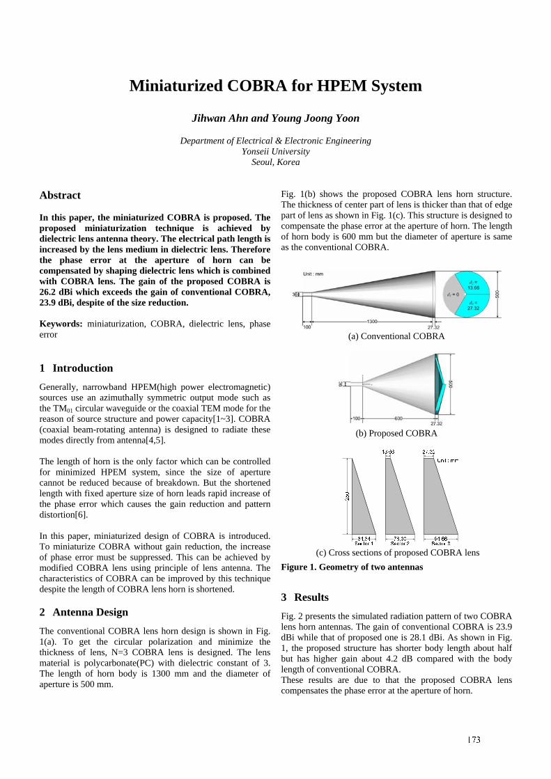
1
Miniaturized COBRA for HPEM System
Jihwan Ahn and Young Joong Yoon
Department of Electrical & Electronic Engineering Yonseii University
Seoul, Korea
Abstract In this paper, the miniaturized COBRA is proposed. The proposed miniaturization technique is achieved by dielectric lens antenna theory. The electrical path length is increased by the lens medium in dielectric lens. Therefore the phase error at the aperture of horn can be compensated by shaping dielectric lens which is combined with COBRA lens. The gain of the proposed COBRA is 26.2 dBi which exceeds the gain of conventional COBRA, 23.9 dBi, despite of the size reduction. Keywords: miniaturization, COBRA, dielectric lens, phase error
1 Introduction Generally, narrowband HPEM(high power electromagnetic) sources use an azimuthally symmetric output mode such as the TM01 circular waveguide or the coaxial TEM mode for the reason of source structure and power capacity[1~3]. COBRA (coaxial beam-rotating antenna) is designed to radiate these modes directly from antenna[4,5]. The length of horn is the only factor which can be controlled for minimized HPEM system, since the size of aperture cannot be reduced because of breakdown. But the shortened length with fixed aperture size of horn leads rapid increase of the phase error which causes the gain reduction and pattern distortion[6]. In this paper, miniaturized design of COBRA is introduced. To miniaturize COBRA without gain reduction, the increase of phase error must be suppressed. This can be achieved by modified COBRA lens using principle of lens antenna. The characteristics of COBRA can be improved by this technique despite the length of COBRA lens horn is shortened.
2 Antenna Design The conventional COBRA lens horn design is shown in Fig. 1(a). To get the circular polarization and minimize the thickness of lens, N=3 COBRA lens is designed. The lens material is polycarbonate(PC) with dielectric constant of 3. The length of horn body is 1300 mm and the diameter of aperture is 500 mm.
Fig. 1(b) shows the proposed COBRA lens horn structure. The thickness of center part of lens is thicker than that of edge part of lens as shown in Fig. 1(c). This structure is designed to compensate the phase error at the aperture of horn. The length of horn body is 600 mm but the diameter of aperture is same as the conventional COBRA.
Figure 1. Geometry of two antennas
3 Results Fig. 2 presents the simulated radiation pattern of two COBRA lens horn antennas. The gain of conventional COBRA is 23.9 dBi while that of proposed one is 28.1 dBi. As shown in Fig. 1, the proposed structure has shorter body length about half but has higher gain about 4.2 dB compared with the body length of conventional COBRA. These results are due to that the proposed COBRA lens compensates the phase error at the aperture of horn.
(a) Conventional COBRA
(b) Proposed COBRA
(c) Cross sections of proposed COBRA lens
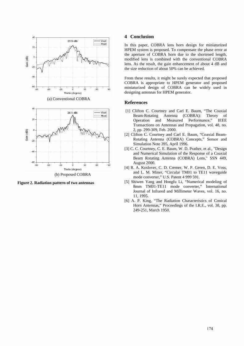
2
Figure 2. Radiation pattern of two antennas
4 Conclusion In this paper, COBRA lens horn design for miniaturized HPEM system is proposed. To compensate the phase error at the aperture of COBRA horn due to the shortened length, modified lens is combined with the conventional COBRA lens. As the result, the gain enhancement of about 4 dB and the size reduction of about 50% can be achieved. From these results, it might be surely expected that proposed COBRA is appropriate to HPEM generator and proposed miniaturized design of COBRA can be widely used in designing antennas for HPEM generator.
References [1] Clifton C. Courtney and Carl E. Baum, “The Coaxial
Beam-Rotating Antenna (COBRA): Theory of Operation and Measured Performance,” IEEE Transactions on Antennas and Propagation, vol. 48, no. 2, pp. 299-309, Feb. 2000.
[2] Clifton C. Courtney and Carl E. Baum, “Coaxial Beam-Rotating Antenna (COBRA) Concepts,” Sensor and Simulation Note 395, April 1996.
[3] C. C. Courtney, C. E. Baum, W. D. Prather, et al., "Design and Numerical Simulation of the Response of a Coaxial Beam Rotating Antenna (COBRA) Lens," SSN 449, August 2000.
[4] R. A. Koslover, C. D. Cremer, W. P. Geren, D. E. Voss, and L. M. Miner, “Circular TM01 to TE11 waveguide mode converter,” U.S. Patent 4 999 591.
[5] Shiwen Yang and Hongfu Li, “Numerical modeling of 8mm TM01-TE11 mode converter,” International Journal of Infrared and Millimeter Waves, vol. 16, no. 11, 1995.
[6] A. P. King, “The Radiation Characteristics of Conical Horn Antennas,” Proceedings of the I.R.E., vol. 38, pp. 249-251, March 1950.
(a) Conventional COBRA
(b) Proposed COBRA
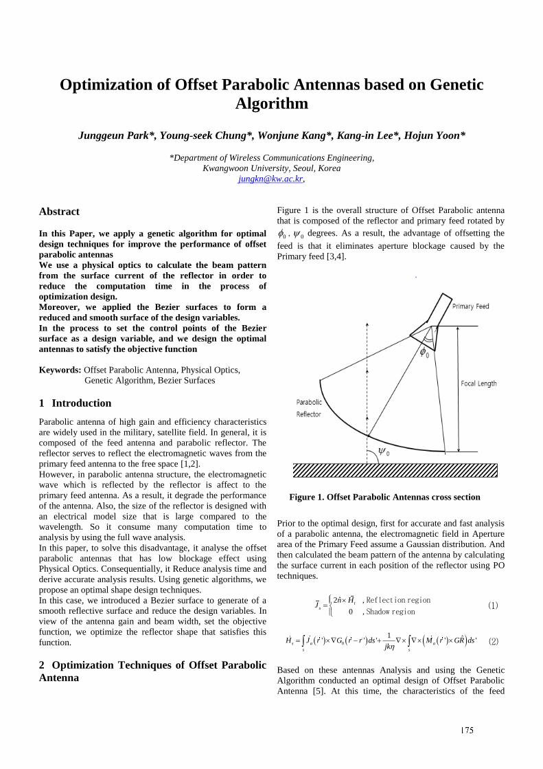
1
Optimization of Offset Parabolic Antennas based on Genetic
Algorithm
Junggeun Park*, Young-seek Chung*, Wonjune Kang*, Kang-in Lee*, Hojun Yoon*
*Department of Wireless Communications Engineering,
Kwangwoon University, Seoul, Korea
Abstract
In this Paper, we apply a genetic algorithm for optimal
design techniques for improve the performance of offset
parabolic antennas
We use a physical optics to calculate the beam pattern
from the surface current of the reflector in order to
reduce the computation time in the process of
optimization design.
Moreover, we applied the Bezier surfaces to form a
reduced and smooth surface of the design variables.
In the process to set the control points of the Bezier
surface as a design variable, and we design the optimal
antennas to satisfy the objective function
Keywords: Offset Parabolic Antenna, Physical Optics,
Genetic Algorithm, Bezier Surfaces
1 Introduction
Parabolic antenna of high gain and efficiency characteristics
are widely used in the military, satellite field. In general, it is
composed of the feed antenna and parabolic reflector. The
reflector serves to reflect the electromagnetic waves from the
primary feed antenna to the free space [1,2].
However, in parabolic antenna structure, the electromagnetic
wave which is reflected by the reflector is affect to the
primary feed antenna. As a result, it degrade the performance
of the antenna. Also, the size of the reflector is designed with
an electrical model size that is large compared to the
wavelength. So it consume many computation time to
analysis by using the full wave analysis.
In this paper, to solve this disadvantage, it analyse the offset
parabolic antennas that has low blockage effect using
Physical Optics. Consequentially, it Reduce analysis time and
derive accurate analysis results. Using genetic algorithms, we
propose an optimal shape design techniques.
In this case, we introduced a Bezier surface to generate of a
smooth reflective surface and reduce the design variables. In
view of the antenna gain and beam width, set the objective
function, we optimize the reflector shape that satisfies this
function.
2 Optimization Techniques of Offset Parabolic
Antenna
Figure 1 is the overall structure of Offset Parabolic antenna
that is composed of the reflector and primary feed rotated by
0 , 0 degrees. As a result, the advantage of offsetting the
feed is that it eliminates aperture blockage caused by the
Primary feed [3,4].
Prior to the optimal design, first for accurate and fast analysis
of a parabolic antenna, the electromagnetic field in Aperture
area of the Primary Feed assume a Gaussian distribution. And
then calculated the beam pattern of the antenna by calculating
the surface current in each position of the reflector using PO
techniques.
ˆ2 ,
0 ,
ts
n HJ
Reflection region
Shadow region
(1)
0
1 ˆ' ' ' ' 's a a
s s
H J r G r r ds M r GR dsjk
(2)
Based on these antennas Analysis and using the Genetic
Algorithm conducted an optimal design of Offset Parabolic
Antenna [5]. At this time, the characteristics of the feed
Figure 1. Offset Parabolic Antennas cross section
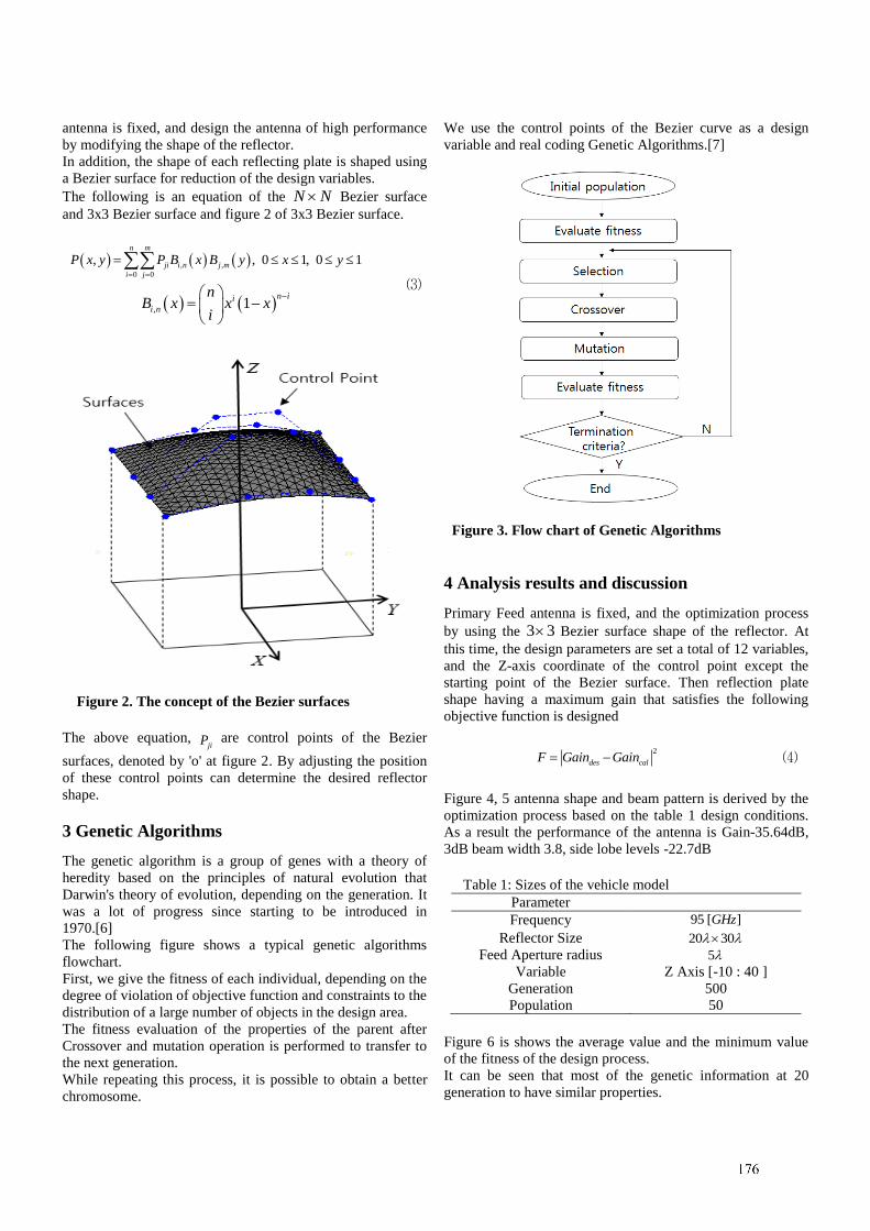
2
antenna is fixed, and design the antenna of high performance
by modifying the shape of the reflector.
In addition, the shape of each reflecting plate is shaped using
a Bezier surface for reduction of the design variables.
The following is an equation of the N N Bezier surface
and 3x3 Bezier surface and figure 2 of 3x3 Bezier surface.
, ,
0 0
, , 0 1, 0 1n m
ji i n j m
i j
P x y P B x B y x y
, 1n ii
i n
nB x x x
i
(3)
Figure 2. The concept of the Bezier surfaces
The above equation,
jiP are control points of the Bezier
surfaces, denoted by 'o' at figure 2. By adjusting the position
of these control points can determine the desired reflector
shape.
3 Genetic Algorithms
The genetic algorithm is a group of genes with a theory of
heredity based on the principles of natural evolution that
Darwin's theory of evolution, depending on the generation. It
was a lot of progress since starting to be introduced in
1970.[6]
The following figure shows a typical genetic algorithms
flowchart.
First, we give the fitness of each individual, depending on the
degree of violation of objective function and constraints to the
distribution of a large number of objects in the design area.
The fitness evaluation of the properties of the parent after
Crossover and mutation operation is performed to transfer to
the next generation.
While repeating this process, it is possible to obtain a better
chromosome.
We use the control points of the Bezier curve as a design
variable and real coding Genetic Algorithms.[7]
Figure 3. Flow chart of Genetic Algorithms
4 Analysis results and discussion
Primary Feed antenna is fixed, and the optimization process
by using the 3 3 Bezier surface shape of the reflector. At
this time, the design parameters are set a total of 12 variables,
and the Z-axis coordinate of the control point except the
starting point of the Bezier surface. Then reflection plate
shape having a maximum gain that satisfies the following
objective function is designed
2
des calF Gain Gain (4)
Figure 4, 5 antenna shape and beam pattern is derived by the
optimization process based on the table 1 design conditions.
As a result the performance of the antenna is Gain-35.64dB,
3dB beam width 3.8, side lobe levels -22.7dB
Table 1: Sizes of the vehicle model
Parameter
Frequency 95 [ ]GHz
Reflector Size 20 30
Feed Aperture radius 5
Variable Z Axis [-10 : 40 ]
Generation 500
Population 50
Figure 6 is shows the average value and the minimum value
of the fitness of the design process.
It can be seen that most of the genetic information at 20
generation to have similar properties.
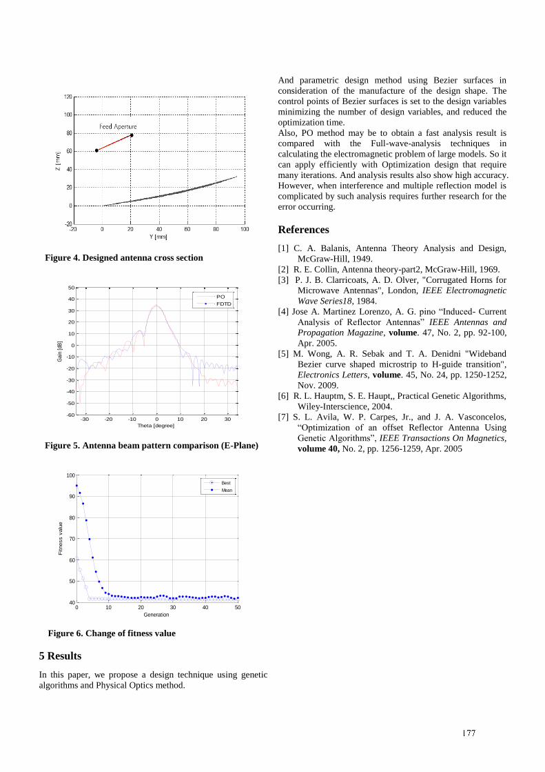
3
Figure 4. Designed antenna cross section
-30 -20 -10 0 10 20 30-60
-50
-40
-30
-20
-10
0
10
20
30
40
50
Theta [degree]
Gai
n [d
B]
PO
FDTD
Figure 5. Antenna beam pattern comparison (E-Plane)
0 10 20 30 40 5040
50
60
70
80
90
100
Generation
Fitness v
alu
e
Best
Mean
Figure 6. Change of fitness value
5 Results
In this paper, we propose a design technique using genetic
algorithms and Physical Optics method.
And parametric design method using Bezier surfaces in
consideration of the manufacture of the design shape. The
control points of Bezier surfaces is set to the design variables
minimizing the number of design variables, and reduced the
optimization time.
Also, PO method may be to obtain a fast analysis result is
compared with the Full-wave-analysis techniques in
calculating the electromagnetic problem of large models. So it
can apply efficiently with Optimization design that require
many iterations. And analysis results also show high accuracy.
However, when interference and multiple reflection model is
complicated by such analysis requires further research for the
error occurring.
References
[1] C. A. Balanis, Antenna Theory Analysis and Design,
McGraw-Hill, 1949.
[2] R. E. Collin, Antenna theory-part2, McGraw-Hill, 1969.
[3] P. J. B. Clarricoats, A. D. Olver, "Corrugated Horns for
Microwave Antennas", London, IEEE Electromagnetic
Wave Series18, 1984.
[4] Jose A. Martinez Lorenzo, A. G. pino “Induced- Current
Analysis of Reflector Antennas” IEEE Antennas and
Propagation Magazine, volume. 47, No. 2, pp. 92-100,
Apr. 2005.
[5] M. Wong, A. R. Sebak and T. A. Denidni "Wideband
Bezier curve shaped microstrip to H-guide transition",
Electronics Letters, volume. 45, No. 24, pp. 1250-1252,
Nov. 2009.
[6] R. L. Hauptm, S. E. Haupt,, Practical Genetic Algorithms,
Wiley-Interscience, 2004.
[7] S. L. Avila, W. P. Carpes, Jr., and J. A. Vasconcelos,
“Optimization of an offset Reflector Antenna Using
Genetic Algorithms”, IEEE Transactions On Magnetics,
volume 40, No. 2, pp. 1256-1259, Apr. 2005
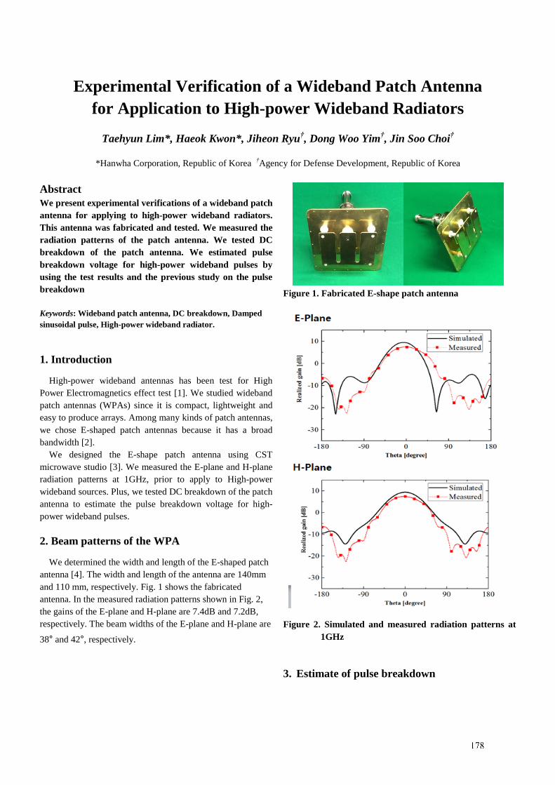
Experimental Verification of a Wideband Patch Antenna
for Application to High-power Wideband Radiators
Taehyun Lim*, Haeok Kwon*, Jiheon Ryu†, Dong Woo Yim
†, Jin Soo Choi
†
*Hanwha Corporation, Republic of Korea †Agency for Defense Development, Republic of Korea
Abstract
We present experimental verifications of a wideband patch
antenna for applying to high-power wideband radiators.
This antenna was fabricated and tested. We measured the
radiation patterns of the patch antenna. We tested DC
breakdown of the patch antenna. We estimated pulse
breakdown voltage for high-power wideband pulses by
using the test results and the previous study on the pulse
breakdown
Keywords: Wideband patch antenna, DC breakdown, Damped
sinusoidal pulse, High-power wideband radiator.
1. Introduction
High-power wideband antennas has been test for High
Power Electromagnetics effect test [1]. We studied wideband
patch antennas (WPAs) since it is compact, lightweight and
easy to produce arrays. Among many kinds of patch antennas,
we chose E-shaped patch antennas because it has a broad
bandwidth [2].
We designed the E-shape patch antenna using CST
microwave studio [3]. We measured the E-plane and H-plane
radiation patterns at 1GHz, prior to apply to High-power
wideband sources. Plus, we tested DC breakdown of the patch
antenna to estimate the pulse breakdown voltage for high-
power wideband pulses.
2. Beam patterns of the WPA
We determined the width and length of the E-shaped patch
antenna [4]. The width and length of the antenna are 140mm
and 110 mm, respectively. Fig. 1 shows the fabricated
antenna. In the measured radiation patterns shown in Fig. 2,
the gains of the E-plane and H-plane are 7.4dB and 7.2dB,
respectively. The beam widths of the E-plane and H-plane are
38° and 42°, respectively.
Figure 1. Fabricated E-shape patch antenna
Figure 2. Simulated and measured radiation patterns at
1GHz
3. Estimate of pulse breakdown
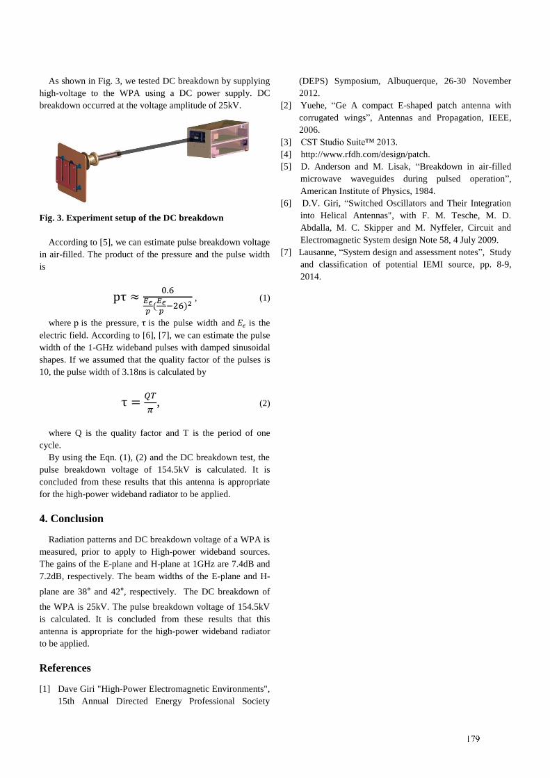
As shown in Fig. 3, we tested DC breakdown by supplying
high-voltage to the WPA using a DC power supply. DC
breakdown occurred at the voltage amplitude of 25kV.
Fig. 3. Experiment setup of the DC breakdown
According to [5], we can estimate pulse breakdown voltage
in air-filled. The product of the pressure and the pulse width
is
pτ ≈0.6
𝐸𝜖𝑝(𝐸𝜖𝑝−26)2
, (1)
where p is the pressure, τ is the pulse width and 𝐸𝜖 is the
electric field. According to [6], [7], we can estimate the pulse
width of the 1-GHz wideband pulses with damped sinusoidal
shapes. If we assumed that the quality factor of the pulses is
10, the pulse width of 3.18ns is calculated by
τ =𝑄𝑇
𝜋, (2)
where Q is the quality factor and T is the period of one
cycle.
By using the Eqn. (1), (2) and the DC breakdown test, the
pulse breakdown voltage of 154.5kV is calculated. It is
concluded from these results that this antenna is appropriate
for the high-power wideband radiator to be applied.
4. Conclusion
Radiation patterns and DC breakdown voltage of a WPA is
measured, prior to apply to High-power wideband sources.
The gains of the E-plane and H-plane at 1GHz are 7.4dB and
7.2dB, respectively. The beam widths of the E-plane and H-
plane are 38° and 42°, respectively. The DC breakdown of
the WPA is 25kV. The pulse breakdown voltage of 154.5kV
is calculated. It is concluded from these results that this
antenna is appropriate for the high-power wideband radiator
to be applied.
References
[1] Dave Giri "High-Power Electromagnetic Environments",
15th Annual Directed Energy Professional Society
(DEPS) Symposium, Albuquerque, 26-30 November
2012.
[2] Yuehe, “Ge A compact E-shaped patch antenna with
corrugated wings”, Antennas and Propagation, IEEE,
2006.
[3] CST Studio Suite™ 2013.
[4] http://www.rfdh.com/design/patch.
[5] D. Anderson and M. Lisak, “Breakdown in air-filled
microwave waveguides during pulsed operation”,
American Institute of Physics, 1984.
[6] D.V. Giri, “Switched Oscillators and Their Integration
into Helical Antennas", with F. M. Tesche, M. D.
Abdalla, M. C. Skipper and M. Nyffeler, Circuit and
Electromagnetic System design Note 58, 4 July 2009.
[7] Lausanne, “System design and assessment notes”, Study
and classification of potential IEMI source, pp. 8-9,
2014.
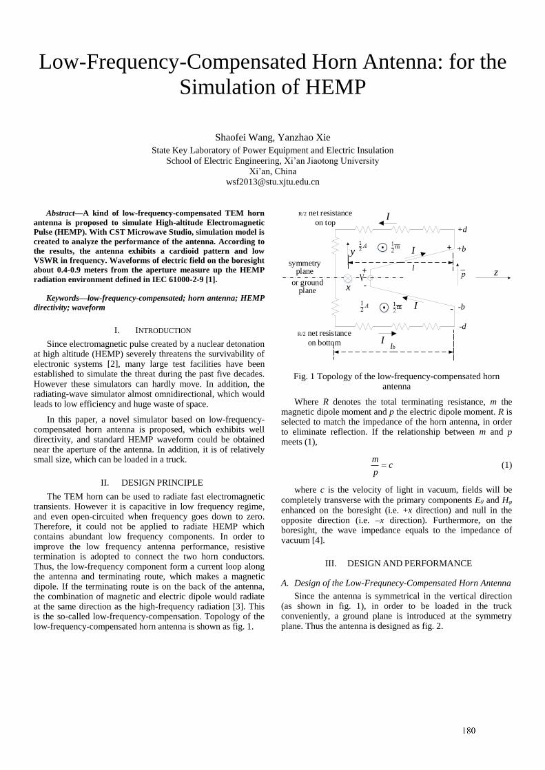
Low-Frequency-Compensated Horn Antenna: for the
Simulation of HEMP
Shaofei Wang, Yanzhao Xie
State Key Laboratory of Power Equipment and Electric Insulation
School of Electric Engineering, Xi’an Jiaotong University
Xi’an, China
Abstract—A kind of low-frequency-compensated TEM horn
antenna is proposed to simulate High-altitude Electromagnetic
Pulse (HEMP). With CST Microwave Studio, simulation model is
created to analyze the performance of the antenna. According to
the results, the antenna exhibits a cardioid pattern and low
VSWR in frequency. Waveforms of electric field on the boresight
about 0.4-0.9 meters from the aperture measure up the HEMP
radiation environment defined in IEC 61000-2-9 [1].
Keywords—low-frequency-compensated; horn antenna; HEMP
directivity; waveform
I. INTRODUCTION
Since electromagnetic pulse created by a nuclear detonation at high altitude (HEMP) severely threatens the survivability of electronic systems [2], many large test facilities have been established to simulate the threat during the past five decades. However these simulators can hardly move. In addition, the radiating-wave simulator almost omnidirectional, which would leads to low efficiency and huge waste of space.
In this paper, a novel simulator based on low-frequency-compensated horn antenna is proposed, which exhibits well directivity, and standard HEMP waveform could be obtained near the aperture of the antenna. In addition, it is of relatively small size, which can be loaded in a truck.
II. DESIGN PRINCIPLE
The TEM horn can be used to radiate fast electromagnetic transients. However it is capacitive in low frequency regime, and even open-circuited when frequency goes down to zero. Therefore, it could not be applied to radiate HEMP which contains abundant low frequency components. In order to improve the low frequency antenna performance, resistive termination is adopted to connect the two horn conductors. Thus, the low-frequency component form a current loop along the antenna and terminating route, which makes a magnetic dipole. If the terminating route is on the back of the antenna, the combination of magnetic and electric dipole would radiate at the same direction as the high-frequency radiation [3]. This is the so-called low-frequency-compensation. Topology of the low-frequency-compensated horn antenna is shown as fig. 1.
Vz
I
I
I
I
y
+
-
+
-
x
symmetryplane
or groundplane
+d
+b
l
lb
-d
-b
R/2 net resistance
on top
R/2 net resistance
on bottom
Fig. 1 Topology of the low-frequency-compensated horn antenna
Where R denotes the total terminating resistance, m the magnetic dipole moment and p the electric dipole moment. R is selected to match the impedance of the horn antenna, in order to eliminate reflection. If the relationship between m and p meets (1),
mc
p (1)
where c is the velocity of light in vacuum, fields will be completely transverse with the primary components Eθ and Hφ
enhanced on the boresight (i.e. +x direction) and null in the opposite direction (i.e. –x direction). Furthermore, on the boresight, the wave impedance equals to the impedance of vacuum [4].
III. DESIGN AND PERFORMANCE
A. Design of the Low-Frequnecy-Compensated Horn Antenna
Since the antenna is symmetrical in the vertical direction (as shown in fig. 1), in order to be loaded in the truck conveniently, a ground plane is introduced at the symmetry plane. Thus the antenna is designed as fig. 2.
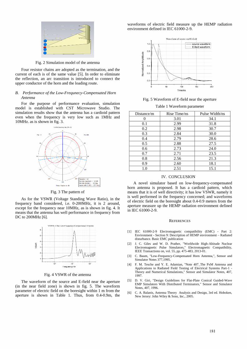
Fig. 2 Simulation model of the antenna
Four resistor chains are adopted as the termination, and the current of each is of the same value [5]. In order to eliminate the reflection, an arc transition is introduced to connect the upper conductor of the horn and the loading route.
B. Performance of the Low-Frequnecy-Compensated Horn
Antenna
For the purpose of performance evaluation, simulation model is established with CST Microwave Studio. The simulation results show that the antenna has a cardioid pattern even when the frequency is very low such as 1MHz and 10MHz. as is shown in fig. 3.
Fig. 3 The pattern of
As for the VSWR (Voltage Standing Wave Ratio), in the frequency band considered, i.e. 0-200MHz, it is 2 around, except for the frequency near 10MHz, as is shown in fig. 4. It means that the antenna has well performance in frequency from DC to 200MHz [6].
Fig. 4 VSWR of the antenna
The waveform of the source and E-field near the aperture (in the near field zone) is shown in fig. 5. The waveform parameter of electric field on the boresight within 1 m from the aperture is shown in Table 1. Thus, from 0.4-0.9m, the
waveforms of electric field measure up the HEMP radiation environment defined in IEC 61000-2-9.
Fig. 5 Waveform of E-field near the aperture
Table 1 Waveform parameter
Distance/m Rise Time/ns Pulse Width/ns
0 3.01 34.1
0.1 2.99 31.8
0.2 2.98 30.7
0.3 2.84 30.0
0.4 2.79 28.6
0.5 2.88 27.5
0.6 2.73 24.0
0.7 2.71 23.5
0.8 2.56 21.3
0.9 2.60 18.1
1.0 2.51 15.1
IV. CONCLUSION
A novel simulator based on low-frequency-compensated horn antenna is proposed. It has a cardioid pattern, which means that it is of well directivity; it has low VSWR, namely it is well performed in the frequency concerned; and waveforms of electric field on the boresight about 0.4-0.9 meters from the aperture measure up the HEMP radiation environment defined in IEC 61000-2-9.
REFERENCES
[1] IEC 61000-2-9 Electromagnetic compatibility (EMC) - Part 2:
Environment - Section 9: Description of HEMP environment – Radiated disturbance. Basic EMC publication
[2] J. C. Giles and W. D. Prather, "Worldwide High-Altitude Nuclear Electromagnetic Pulse Simulators," Electromagnetic Compatibility, IEEE Transactions on, vol. 55, pp. 475-483, 2013-01.
[3] C. Baum, "Low-Frequency-Compensated Horn Antenna,", Sensor and Simulator Notes 377,1995.
[4] F. M. Tesche and Y. E. Adamian, "Note 407_The PxM Antenna and Applications to Radiated Field Testing of Electrical Systems Part-1 - Theory and Numerical Simulations," Sensor and Simulator Notes, 407, 1997.
[5] D. V. Giri, "Design Guidelines for Flat-Plate Conical Guided-Wave EMP Simulators With Distributed Terminators," Sensor and Simulator Notes, 407, 1996.
[6] C. A. Balanis, Antenna Theory Analysis and Design, 3rd ed. Hoboken, New Jersey: John Wiley & Sons, Inc., 2005.
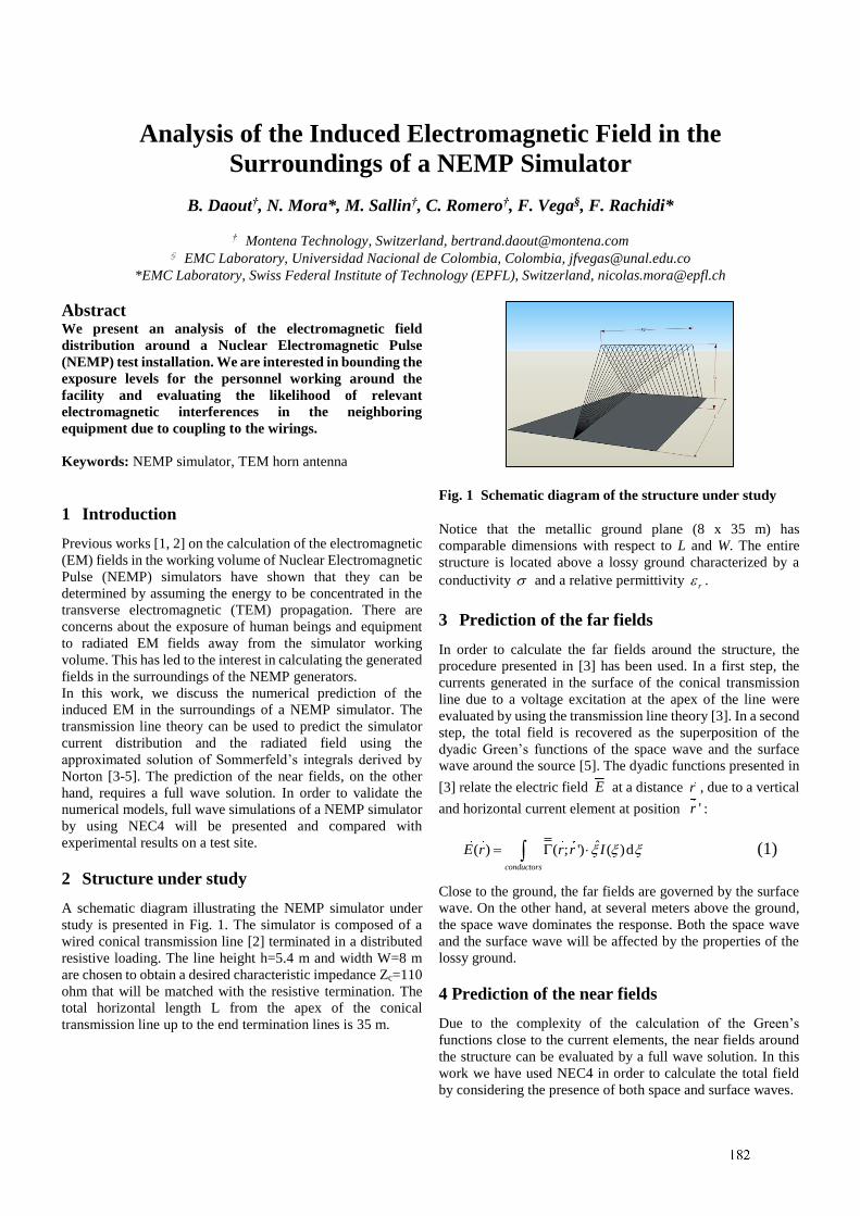
1
Analysis of the Induced Electromagnetic Field in the
Surroundings of a NEMP Simulator
B. Daout†, N. Mora*, M. Sallin†, C. Romero†, F. Vega§, F. Rachidi*
† Montena Technology, Switzerland, [email protected] § EMC Laboratory, Universidad Nacional de Colombia, Colombia, [email protected]
*EMC Laboratory, Swiss Federal Institute of Technology (EPFL), Switzerland, [email protected]
Abstract We present an analysis of the electromagnetic field
distribution around a Nuclear Electromagnetic Pulse
(NEMP) test installation. We are interested in bounding the
exposure levels for the personnel working around the
facility and evaluating the likelihood of relevant
electromagnetic interferences in the neighboring
equipment due to coupling to the wirings.
Keywords: NEMP simulator, TEM horn antenna
1 Introduction
Previous works [1, 2] on the calculation of the electromagnetic
(EM) fields in the working volume of Nuclear Electromagnetic
Pulse (NEMP) simulators have shown that they can be
determined by assuming the energy to be concentrated in the
transverse electromagnetic (TEM) propagation. There are
concerns about the exposure of human beings and equipment
to radiated EM fields away from the simulator working
volume. This has led to the interest in calculating the generated
fields in the surroundings of the NEMP generators.
In this work, we discuss the numerical prediction of the
induced EM in the surroundings of a NEMP simulator. The
transmission line theory can be used to predict the simulator
current distribution and the radiated field using the
approximated solution of Sommerfeld’s integrals derived by
Norton [3-5]. The prediction of the near fields, on the other
hand, requires a full wave solution. In order to validate the
numerical models, full wave simulations of a NEMP simulator
by using NEC4 will be presented and compared with
experimental results on a test site.
2 Structure under study
A schematic diagram illustrating the NEMP simulator under
study is presented in Fig. 1. The simulator is composed of a
wired conical transmission line [2] terminated in a distributed
resistive loading. The line height h=5.4 m and width W=8 m
are chosen to obtain a desired characteristic impedance Zc=110
ohm that will be matched with the resistive termination. The
total horizontal length L from the apex of the conical
transmission line up to the end termination lines is 35 m.
Fig. 1 Schematic diagram of the structure under study
Notice that the metallic ground plane (8 x 35 m) has
comparable dimensions with respect to L and W. The entire
structure is located above a lossy ground characterized by a
conductivity and a relative permittivity r .
3 Prediction of the far fields
In order to calculate the far fields around the structure, the
procedure presented in [3] has been used. In a first step, the
currents generated in the surface of the conical transmission
line due to a voltage excitation at the apex of the line were
evaluated by using the transmission line theory [3]. In a second
step, the total field is recovered as the superposition of the
dyadic Green’s functions of the space wave and the surface
wave around the source [5]. The dyadic functions presented in
[3] relate the electric field E at a distance r , due to a vertical
and horizontal current element at position 'r :
ˆ( ) ( ; ') ( )dconductors
E r r r I (1)
Close to the ground, the far fields are governed by the surface
wave. On the other hand, at several meters above the ground,
the space wave dominates the response. Both the space wave
and the surface wave will be affected by the properties of the
lossy ground.
4 Prediction of the near fields
Due to the complexity of the calculation of the Green’s
functions close to the current elements, the near fields around
the structure can be evaluated by a full wave solution. In this
work we have used NEC4 in order to calculate the total field
by considering the presence of both space and surface waves.
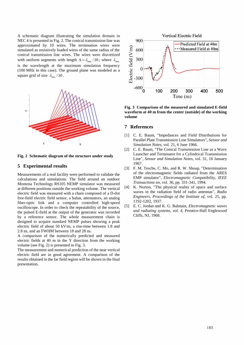
2
A schematic diagram illustrating the simulation domain in
NEC 4 is presented in Fig. 2. The conical transmission line was
approximated by 10 wires. The termination wires were
simulated as resistively loaded wires of the same radius of the
conical transmission line wires. The wires were discretized
with uniform segments with length min /10 ; where
min
is the wavelength at the maximum simulation frequency
(100 MHz in this case). The ground plane was modeled as a
square grid of size min /10 .
Fig. 2 Schematic diagram of the structure under study
5 Experimental results
Measurements of a real facility were performed to validate the
calculations and simulations. The field around an outdoor
Montena Technology RS105 NEMP simulator was measured
at different positions outside the working volume. The vertical
electric field was measured with a chain composed of a D-dot
free-field electric field sensor, a balun, attenuators, an analog
fiber-optic link and a computer controlled high-speed
oscilloscope. In order to check the repeatability of the source,
the pulsed E-field at the output of the generator was recorded
by a reference sensor. The whole measurement chain is
designed to acquire standard NEMP pulses showing a peak
electric field of about 50 kV/m, a rise-time between 1.8 and
2.8 ns, and an FWHM between 18 and 28 ns.
A comparison of the numerically predicted and measured
electric fields at 40 m in the Y direction from the working
volume (see Fig. 2) is presented in Fig. 3.
The measurement and numerical prediction of the near vertical
electric field are in good agreement. A comparison of the
results obtained in the far field region will be shown in the final
presentation.
Fig. 3 Comparison of the measured and simulated E-field
waveform at 40 m from the center (outside) of the working
volume
7 References
[1] C. E. Baum, "Impedances and Field Distributions for
Parallel Plate Transmission Line Simulators", Sensor and
Simulation Notes, vol. 21, 6 June 1966.
[2] C. E. Baum, "The Conical Transmission Line as a Wave
Launcher and Terminator for a Cylindrical Transmission
Line", Sensor and Simulation Notes, vol. 31, 16 January
1967.
[3] F. M. Tesche, C. Mo, and R. W. Shoup, "Determination
of the electromagnetic fields radiated from the ARES
EMP simulator", Electromagnetic Compatibility, IEEE
Transactions on, vol. 36, pp. 331-341, 1994.
[4] K. Norton, "The physical reality of space and surface
waves in the radiation field of radio antennas", Radio
Engineers, Proceedings of the Institute of, vol. 25, pp.
1192-1202, 1937.
[5] E. C. Jordan and K. G. Balmain, Electromagnetic waves
and radiating systems, vol. 4, Prentice-Hall Englewood
Cliffs, NJ, 1968.
Detection of metal objects by ultrawideband pulses with different polarization
V.I. Koshelev, E.V. Balzovsky, Yu.I. Buyanov, E.S. Nekrasov,
A.A. Petkun and V.M. Tarnovsky
Institute of High Current Electronics SB RAS 2/3, Akademichesky Ave., Tomsk 634055, Russia
Abstract The paper presents the results of the investigations on metal object detection under two different conditions united by a general approach to use ultrawideband (UWB) pulses with different polarization. In the first task, using the developed computer code, a possibility to detect an ideally conducting cross-shaped object located over a randomly nonuiniform surface of the dielectric medium, when sounding by two orthogonally polarized UWB pulses, has been investigated. In the second task, as applied to the radar through a wall, a polarization structure of the pulses reflected from metal plates when sounding the objects by UWB pulses with linear and elliptical polarization has been studied. Keywords: Ultrawideband radiation, detection, polarization structure.
1 Introduction
In recent years, investigations of possibility to detect the objects located near a randomly nonuniform reflecting surface using UWB electromagnetic radiation have been carried out. To increase the effectiveness, the successive sounding by the orthogonally polarized radiation pulses is used as a rule. Previously [1], a high-power UWB radiation source has been developed. In the source two orthogonally polarized pulses were radiated by the antenna array excited from one generator. It was interesting to consider a possibility to use the similar pulses for the metal object detection against the background of a randomly nonuniform ground surface. For this purpose, we used the numerical simulation methods.
Presently, intensive investigations of the object detection behind the optically opaque obstacles are conducted using short UWB electromagnetic pulses. The essential informative feature for recognition of the sounding objects is a polarization structure (PS) of the reflected pulses [2]. To investigate the PS of the pulses reflected from metal objects, we have developed a receiving antenna array. The array provides recording two orthogonal components of the scattered field from seven horizontal fixed directions in the range of ±40°.
2 Object detection over a randomly nonuniform surface
To investigate the UWB pulse reflections from a randomly nonuniform medium surface having fixed electrical properties and containing metal objects, a computer code has been developed. The code is based on the finite-difference time-domain method for Maxwell equations. The geometry of the problem presents a three-dimensional parallelepiped partially filled with the medium having the conductance σ and relative dielectric permeability ε. Parameters of the dry (ε = 4, σ = 0.002 Sm/m) and moist (ε = 10, σ = 0.07 Sm/m) sandy ground have been chosen for the dielectric medium. A plane wave is incident normally on the surface from free space. A cross-shaped object was located near the dielectric medium having a randomly nonuniform surface. The reflected signal accumulated in 25 receiving points located as a 5×5-array opposite the metal object at a distance of 6.5 τpc, where τp is the sounding pulse length, and c is the velocity of light. The root-mean-square deviation of the surface from the
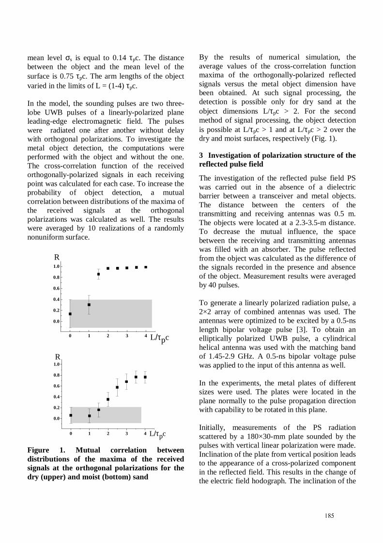
mean level σs is equal to 0.14 τpc. The distance between the object and the mean level of the surface is 0.75 τpc. The arm lengths of the object varied in the limits of L = (1-4) τpc. In the model, the sounding pulses are two three-lobe UWB pulses of a linearly-polarized plane leading-edge electromagnetic field. The pulses were radiated one after another without delay with orthogonal polarizations. To investigate the metal object detection, the computations were performed with the object and without the one. The cross-correlation function of the received orthogonally-polarized signals in each receiving point was calculated for each case. To increase the probability of object detection, a mutual correlation between distributions of the maxima of the received signals at the orthogonal polarizations was calculated as well. The results were averaged by 10 realizations of a randomly nonuniform surface.
0 1 2 3 4
0.0
0.2
0.4
0.6
0.8
1.0
L/τpc
R
0 1 2 3 4
0.0
0.2
0.4
0.6
0.8
1.0
L/τpc
R
Figure 1. Mutual correlation between distributions of the maxima of the received signals at the orthogonal polarizations for the dry (upper) and moist (bottom) sand
By the results of numerical simulation, the average values of the cross-correlation function maxima of the orthogonally-polarized reflected signals versus the metal object dimension have been obtained. At such signal processing, the detection is possible only for dry sand at the object dimensions L/τpc > 2. For the second method of signal processing, the object detection is possible at L/τpc > 1 and at L/τpc > 2 over the dry and moist surfaces, respectively (Fig. 1).
3 Investigation of polarization structure of the reflected pulse field
The investigation of the reflected pulse field PS was carried out in the absence of a dielectric barrier between a transceiver and metal objects. The distance between the centers of the transmitting and receiving antennas was 0.5 m. The objects were located at a 2.3-3.5-m distance. To decrease the mutual influence, the space between the receiving and transmitting antennas was filled with an absorber. The pulse reflected from the object was calculated as the difference of the signals recorded in the presence and absence of the object. Measurement results were averaged by 40 pulses. To generate a linearly polarized radiation pulse, a 2×2 array of combined antennas was used. The antennas were optimized to be excited by a 0.5-ns length bipolar voltage pulse [3]. To obtain an elliptically polarized UWB pulse, a cylindrical helical antenna was used with the matching band of 1.45-2.9 GHz. A 0.5-ns bipolar voltage pulse was applied to the input of this antenna as well. In the experiments, the metal plates of different sizes were used. The plates were located in the plane normally to the pulse propagation direction with capability to be rotated in this plane. Initially, measurements of the PS radiation scattered by a 180×30-mm plate sounded by the pulses with vertical linear polarization were made. Inclination of the plate from vertical position leads to the appearance of a cross-polarized component in the reflected field. This results in the change of the electric field hodograph. The inclination of the
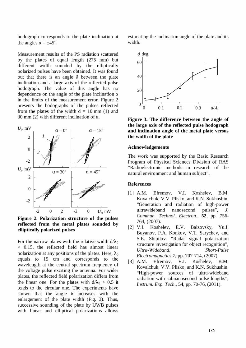
hodograph corresponds to the plate inclination at the angles α = ±45°. Measurement results of the PS radiation scattered by the plates of equal length (275 mm) but different width sounded by the elliptically polarized pulses have been obtained. It was found out that there is an angle δ between the plate inclination and a large axis of the reflected pulse hodograph. The value of this angle has no dependence on the angle of the plate inclination α in the limits of the measurement error. Figure 2 presents the hodographs of the pulses reflected from the plates of the width d = 10 mm (1) and 30 mm (2) with different inclination of α.
-2
0
2
-2 0 2
-2
0
2
-2 0
Uy, mV
α = 30° α = 45°
α = 0° α = 15°
Uy, mV
1
2
Ux, mV Figure 2. Polarization structure of the pulses reflected from the metal plates sounded by elliptically polarized pulses For the narrow plates with the relative width d/λ0 < 0.15, the reflected field has almost linear polarization at any positions of the plates. Here, λ0 equals to 15 cm and corresponds to the wavelength at the central spectrum frequency of the voltage pulse exciting the antenna. For wider plates, the reflected field polarization differs from the linear one. For the plates with d/λ0 > 0.5 it tends to the circular one. The experiments have shown that the angle δ increases with the enlargement of the plate width (Fig. 3). Thus, successive sounding of the plate by UWB pulses with linear and elliptical polarizations allows
estimating the inclination angle of the plate and its width.
0 0.1 0.2 0.3 d/λ0
0
20
40
60
δ, deg.
Figure 3. The difference between the angle of the large axis of the reflected pulse hodograph and inclination angle of the metal plate versus the width of the plate
Acknowledgements
The work was supported by the Basic Research Program of Physical Sciences Division of RAS “Radioelectronic methods in research of the natural environment and human subject”.
References
[1] A.M. Efremov, V.I. Koshelev, B.M. Kovalchuk, V.V. Plisko, and K.N. Sukhushin. “Generation and radiation of high-power ultrawideband nanosecond pulses”, J. Commun. Technol. Electron., 52, pp. 756-764, (2007).
[2] V.I. Koshelev, E.V. Balzovsky, Yu.I. Buyanov, P.A. Konkov, V.T. Sarychev, and S.E. Shipilov. “Radar signal polarization structure investigation for object recognition”, Ultra-Wideband, Short-Pulse Electromagnetics 7, pp. 707-714, (2007).
[3] A.M. Efremov, V.I. Koshelev, B.M. Kovalchuk, V.V. Plisko, and K.N. Sukhushin. “High-power sources of ultra-wideband radiation with subnanosecond pulse lengths”, Instrum. Exp. Tech., 54, pp. 70-76, (2011).
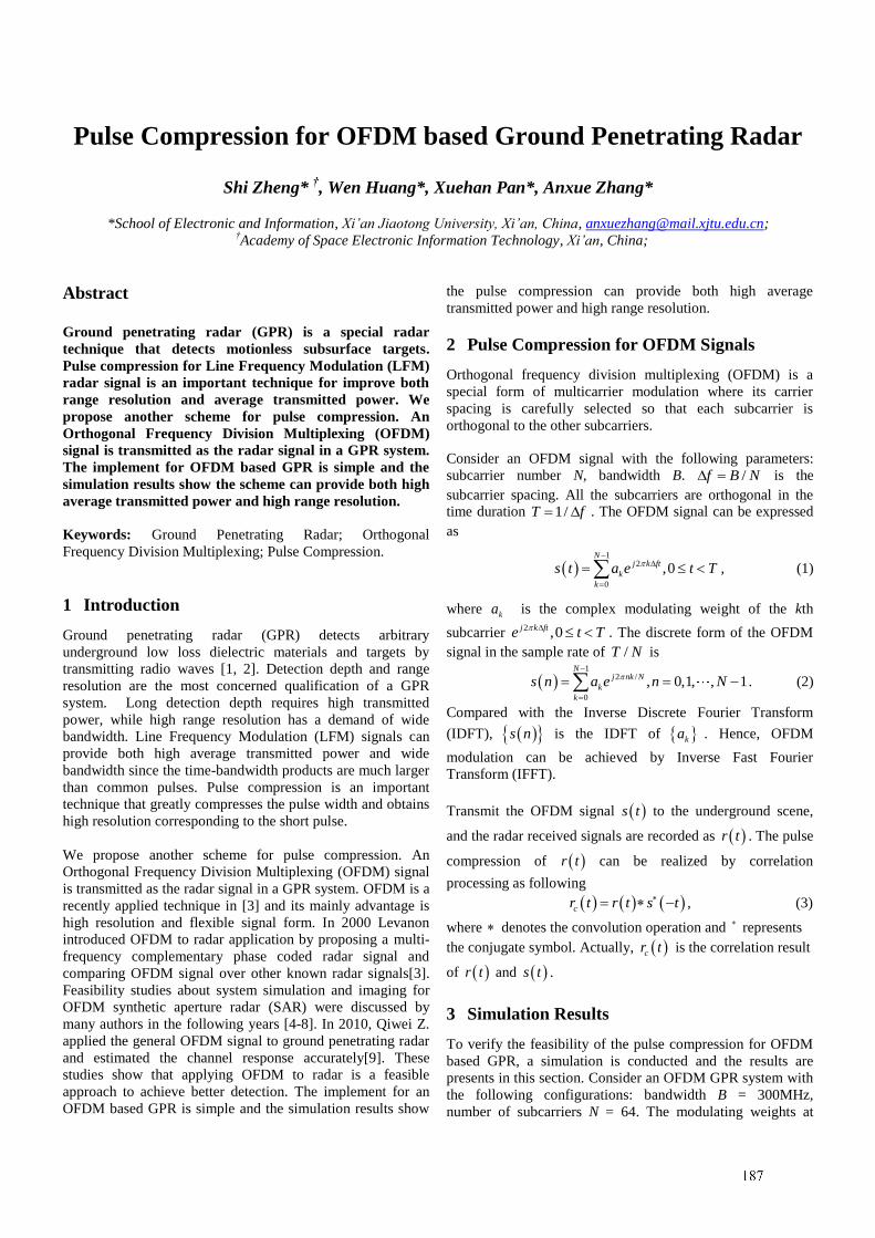
Pulse Compression for OFDM based Ground Penetrating Radar
Shi Zheng* †, Wen Huang*, Xuehan Pan*, Anxue Zhang*
*School of Electronic and Information, Xi’an Jiaotong University, Xi’an, China, [email protected];
†Academy of Space Electronic Information Technology, Xi’an, China;
Abstract
Ground penetrating radar (GPR) is a special radar
technique that detects motionless subsurface targets.
Pulse compression for Line Frequency Modulation (LFM)
radar signal is an important technique for improve both
range resolution and average transmitted power. We
propose another scheme for pulse compression. An
Orthogonal Frequency Division Multiplexing (OFDM)
signal is transmitted as the radar signal in a GPR system.
The implement for OFDM based GPR is simple and the
simulation results show the scheme can provide both high
average transmitted power and high range resolution.
Keywords: Ground Penetrating Radar; Orthogonal
Frequency Division Multiplexing; Pulse Compression.
1 Introduction
Ground penetrating radar (GPR) detects arbitrary
underground low loss dielectric materials and targets by
transmitting radio waves [1, 2]. Detection depth and range
resolution are the most concerned qualification of a GPR
system. Long detection depth requires high transmitted
power, while high range resolution has a demand of wide
bandwidth. Line Frequency Modulation (LFM) signals can
provide both high average transmitted power and wide
bandwidth since the time-bandwidth products are much larger
than common pulses. Pulse compression is an important
technique that greatly compresses the pulse width and obtains
high resolution corresponding to the short pulse.
We propose another scheme for pulse compression. An
Orthogonal Frequency Division Multiplexing (OFDM) signal
is transmitted as the radar signal in a GPR system. OFDM is a
recently applied technique in [3] and its mainly advantage is
high resolution and flexible signal form. In 2000 Levanon
introduced OFDM to radar application by proposing a multi-
frequency complementary phase coded radar signal and
comparing OFDM signal over other known radar signals[3].
Feasibility studies about system simulation and imaging for
OFDM synthetic aperture radar (SAR) were discussed by
many authors in the following years [4-8]. In 2010, Qiwei Z.
applied the general OFDM signal to ground penetrating radar
and estimated the channel response accurately[9]. These
studies show that applying OFDM to radar is a feasible
approach to achieve better detection. The implement for an
OFDM based GPR is simple and the simulation results show
the pulse compression can provide both high average
transmitted power and high range resolution.
2 Pulse Compression for OFDM Signals
Orthogonal frequency division multiplexing (OFDM) is a
special form of multicarrier modulation where its carrier
spacing is carefully selected so that each subcarrier is
orthogonal to the other subcarriers.
Consider an OFDM signal with the following parameters:
subcarrier number N, bandwidth B. /f B N is the
subcarrier spacing. All the subcarriers are orthogonal in the time duration 1/T f . The OFDM signal can be expressed
as
1
2
0
,0N
j k ft
k
k
s t a e t T
, (1)
where ka is the complex modulating weight of the kth
subcarrier 2 ,0j k fte t T . The discrete form of the OFDM
signal in the sample rate of /T N is
1
2 /
0
, 0,1, , 1N
j nk N
k
k
s n a e n N
. (2)
Compared with the Inverse Discrete Fourier Transform
(IDFT), s n is the IDFT of ka . Hence, OFDM
modulation can be achieved by Inverse Fast Fourier
Transform (IFFT).
Transmit the OFDM signal s t to the underground scene,
and the radar received signals are recorded as r t . The pulse
compression of r t can be realized by correlation
processing as following
cr t r t s t , (3)
where denotes the convolution operation and represents
the conjugate symbol. Actually, cr t is the correlation result
of r t and s t .
3 Simulation Results
To verify the feasibility of the pulse compression for OFDM
based GPR, a simulation is conducted and the results are
presents in this section. Consider an OFDM GPR system with
the following configurations: bandwidth B = 300MHz,
number of subcarriers N = 64. The modulating weights at
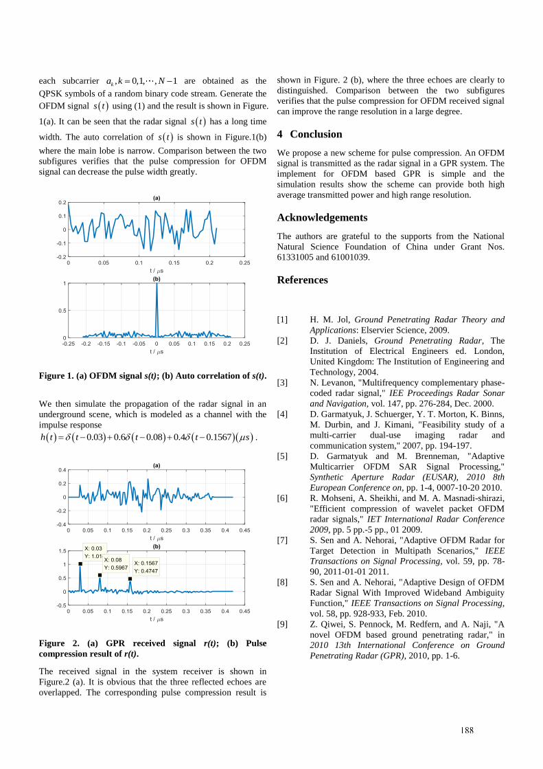
each subcarrier , 0,1, , 1ka k N are obtained as the
QPSK symbols of a random binary code stream. Generate the
OFDM signal s t using (1) and the result is shown in Figure.
1(a). It can be seen that the radar signal s t has a long time
width. The auto correlation of s t is shown in Figure.1(b)
where the main lobe is narrow. Comparison between the two
subfigures verifies that the pulse compression for OFDM
signal can decrease the pulse width greatly.
Figure 1. (a) OFDM signal s(t); (b) Auto correlation of s(t).
We then simulate the propagation of the radar signal in an
underground scene, which is modeled as a channel with the
impulse response
0.03 0.6 0.08 0.4 0.1567h t t t t s .
Figure 2. (a) GPR received signal r(t); (b) Pulse
compression result of r(t).
The received signal in the system receiver is shown in
Figure.2 (a). It is obvious that the three reflected echoes are
overlapped. The corresponding pulse compression result is
shown in Figure. 2 (b), where the three echoes are clearly to
distinguished. Comparison between the two subfigures
verifies that the pulse compression for OFDM received signal
can improve the range resolution in a large degree.
4 Conclusion
We propose a new scheme for pulse compression. An OFDM
signal is transmitted as the radar signal in a GPR system. The
implement for OFDM based GPR is simple and the
simulation results show the scheme can provide both high
average transmitted power and high range resolution.
Acknowledgements
The authors are grateful to the supports from the National
Natural Science Foundation of China under Grant Nos.
61331005 and 61001039.
References
[1] H. M. Jol, Ground Penetrating Radar Theory and
Applications: Elservier Science, 2009.
[2] D. J. Daniels, Ground Penetrating Radar, The
Institution of Electrical Engineers ed. London,
United Kingdom: The Institution of Engineering and
Technology, 2004.
[3] N. Levanon, "Multifrequency complementary phase-
coded radar signal," IEE Proceedings Radar Sonar
and Navigation, vol. 147, pp. 276-284, Dec. 2000.
[4] D. Garmatyuk, J. Schuerger, Y. T. Morton, K. Binns,
M. Durbin, and J. Kimani, "Feasibility study of a
multi-carrier dual-use imaging radar and
communication system," 2007, pp. 194-197.
[5] D. Garmatyuk and M. Brenneman, "Adaptive
Multicarrier OFDM SAR Signal Processing,"
Synthetic Aperture Radar (EUSAR), 2010 8th
European Conference on, pp. 1-4, 0007-10-20 2010.
[6] R. Mohseni, A. Sheikhi, and M. A. Masnadi-shirazi,
"Efficient compression of wavelet packet OFDM
radar signals," IET International Radar Conference
2009, pp. 5 pp.-5 pp., 01 2009.
[7] S. Sen and A. Nehorai, "Adaptive OFDM Radar for
Target Detection in Multipath Scenarios," IEEE
Transactions on Signal Processing, vol. 59, pp. 78-
90, 2011-01-01 2011.
[8] S. Sen and A. Nehorai, "Adaptive Design of OFDM
Radar Signal With Improved Wideband Ambiguity
Function," IEEE Transactions on Signal Processing,
vol. 58, pp. 928-933, Feb. 2010.
[9] Z. Qiwei, S. Pennock, M. Redfern, and A. Naji, "A
novel OFDM based ground penetrating radar," in
2010 13th International Conference on Ground
Penetrating Radar (GPR), 2010, pp. 1-6.
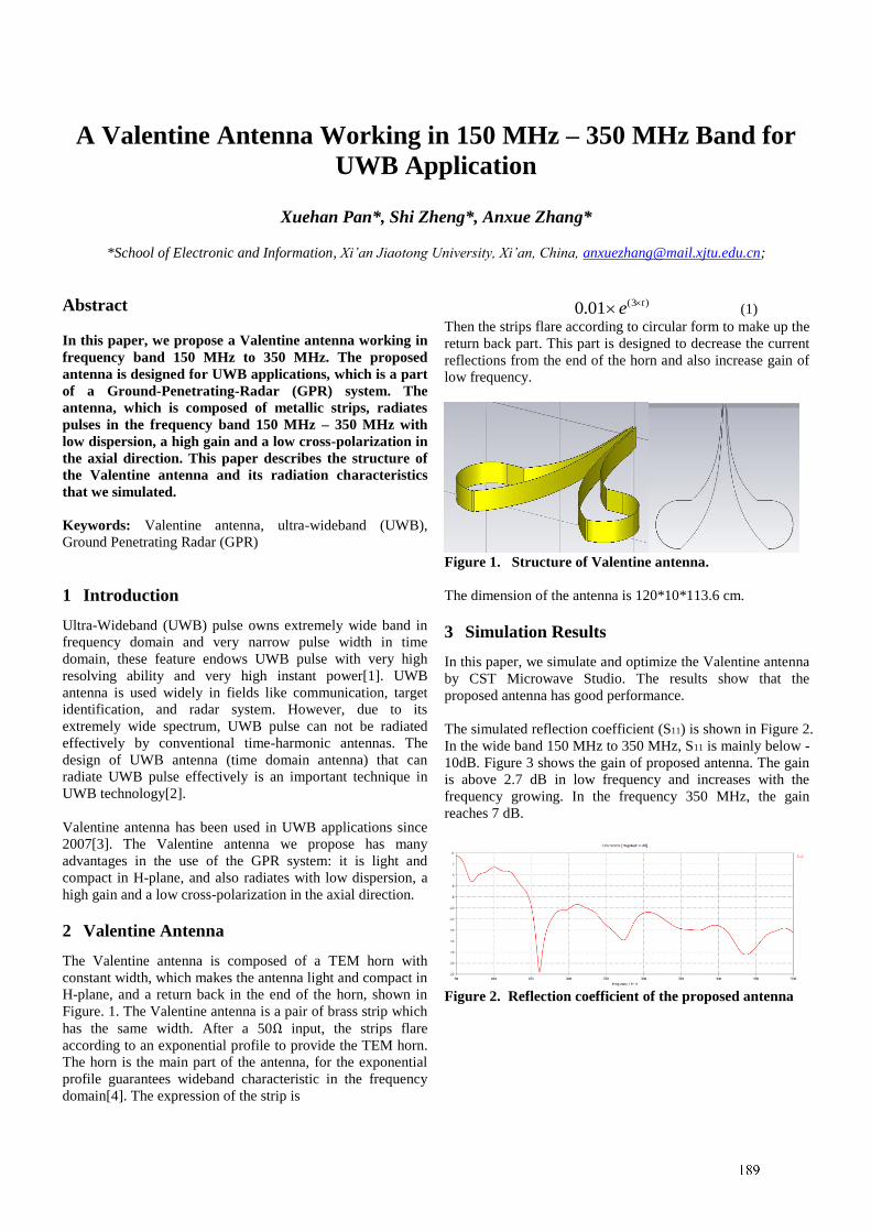
A Valentine Antenna Working in 150 MHz – 350 MHz Band for
UWB Application
Xuehan Pan*, Shi Zheng*, Anxue Zhang*
*School of Electronic and Information, Xi’an Jiaotong University, Xi’an, China, [email protected];
Abstract
In this paper, we propose a Valentine antenna working in
frequency band 150 MHz to 350 MHz. The proposed
antenna is designed for UWB applications, which is a part
of a Ground-Penetrating-Radar (GPR) system. The
antenna, which is composed of metallic strips, radiates
pulses in the frequency band 150 MHz – 350 MHz with
low dispersion, a high gain and a low cross-polarization in
the axial direction. This paper describes the structure of
the Valentine antenna and its radiation characteristics
that we simulated.
Keywords: Valentine antenna, ultra-wideband (UWB),
Ground Penetrating Radar (GPR)
1 Introduction
Ultra-Wideband (UWB) pulse owns extremely wide band in
frequency domain and very narrow pulse width in time
domain, these feature endows UWB pulse with very high
resolving ability and very high instant power[1]. UWB
antenna is used widely in fields like communication, target
identification, and radar system. However, due to its
extremely wide spectrum, UWB pulse can not be radiated
effectively by conventional time-harmonic antennas. The
design of UWB antenna (time domain antenna) that can
radiate UWB pulse effectively is an important technique in
UWB technology[2].
Valentine antenna has been used in UWB applications since
2007[3]. The Valentine antenna we propose has many
advantages in the use of the GPR system: it is light and
compact in H-plane, and also radiates with low dispersion, a
high gain and a low cross-polarization in the axial direction.
2 Valentine Antenna
The Valentine antenna is composed of a TEM horn with
constant width, which makes the antenna light and compact in
H-plane, and a return back in the end of the horn, shown in
Figure. 1. The Valentine antenna is a pair of brass strip which
has the same width. After a 50Ω input, the strips flare
according to an exponential profile to provide the TEM horn.
The horn is the main part of the antenna, for the exponential
profile guarantees wideband characteristic in the frequency
domain[4]. The expression of the strip is
(3 )0.01 te (1)
Then the strips flare according to circular form to make up the
return back part. This part is designed to decrease the current
reflections from the end of the horn and also increase gain of
low frequency.
Figure 1. Structure of Valentine antenna.
The dimension of the antenna is 120*10*113.6 cm.
3 Simulation Results
In this paper, we simulate and optimize the Valentine antenna
by CST Microwave Studio. The results show that the
proposed antenna has good performance.
The simulated reflection coefficient (S11) is shown in Figure 2.
In the wide band 150 MHz to 350 MHz, S11 is mainly below -
10dB. Figure 3 shows the gain of proposed antenna. The gain
is above 2.7 dB in low frequency and increases with the
frequency growing. In the frequency 350 MHz, the gain
reaches 7 dB.
Figure 2. Reflection coefficient of the proposed antenna
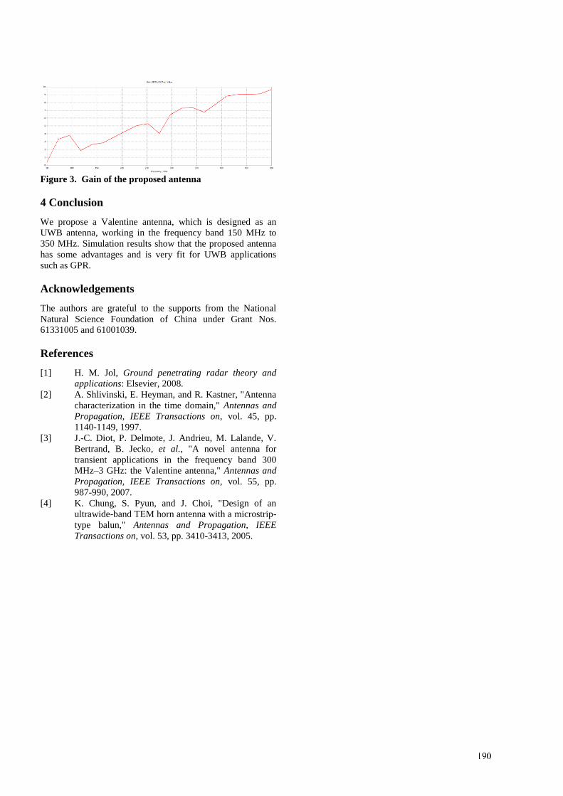
Figure 3. Gain of the proposed antenna
4 Conclusion
We propose a Valentine antenna, which is designed as an
UWB antenna, working in the frequency band 150 MHz to
350 MHz. Simulation results show that the proposed antenna
has some advantages and is very fit for UWB applications
such as GPR.
Acknowledgements
The authors are grateful to the supports from the National
Natural Science Foundation of China under Grant Nos.
61331005 and 61001039.
References
[1] H. M. Jol, Ground penetrating radar theory and
applications: Elsevier, 2008.
[2] A. Shlivinski, E. Heyman, and R. Kastner, "Antenna
characterization in the time domain," Antennas and
Propagation, IEEE Transactions on, vol. 45, pp.
1140-1149, 1997.
[3] J.-C. Diot, P. Delmote, J. Andrieu, M. Lalande, V.
Bertrand, B. Jecko, et al., "A novel antenna for
transient applications in the frequency band 300
MHz–3 GHz: the Valentine antenna," Antennas and
Propagation, IEEE Transactions on, vol. 55, pp.
987-990, 2007.
[4] K. Chung, S. Pyun, and J. Choi, "Design of an
ultrawide-band TEM horn antenna with a microstrip-
type balun," Antennas and Propagation, IEEE
Transactions on, vol. 53, pp. 3410-3413, 2005.
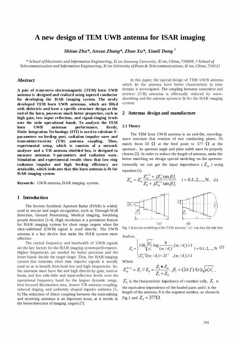
1
A new design of TEM UWB antenna for ISAR imaging
Shitao Zhu*, Anxue Zhang*, Zhuo Xu*, Xiaoli Dong †
* School of Electronic and Information Engineering, Xi’an Jiaotong University, Xi’an, China, 710049, † School of
Telecommunication and Information Engineering, Xi’an University of Posts & Telecommunications, Xi’an, China, 710121
Abstract
A pair of trans verse electromagnetic (TEM) horn UWB
antenna is designed and realized using tapered conductor
for developing the ISAR imaging system. The newly
developed TEM horn UWB antennas, which are filled
with dielectric and have a s pecific structure design at the
end of the horn, possesses much better properties, such as
high gain, low input reflection, and signal-ringing levels
over the wide operational bands. To analysis the TEM
horn UWB antennas performance, firstly,
Finite Integration Technology (FIT) is used to calculate S-
parameters on feeding port, radiation impulse wave and
trans mitter/receiver (T/R) antenna coupling. Then,
experimental setup, which is consists of a network
analyzer and a T/R antenna shielded box, is designed to
measure antennas S-parameters and radiation wave.
Simulation and experimental results show that low ring
radiation impulse and high feeding efficiency are
attainable, which indicates that this horn antenna is fit for
ISAR imaging system.
Keywords: UWB antenna, ISAR imaging system.
1 Introduction
The Inverse Synthetic Aperture Radar (ISAR) is widely
used in rescue and target recognition, such as Through-Wall
detection, Ground Penetrating, Medical imaging, breathing
people detection [1-4]. High resolution is a prominent feature
for ISAR imaging system for short range targets when the
ultra-wideband (UW B) signal is used directly. The UW B
antenna is a key device that make the ISAR system more
effective.
The central frequency and bandwidth of UWB signals
are the key factors for the ISAR imaging system performance.
Higher frequencies are needed for better precision and the
lower bands decide the target shape. Thus, the ISAR imaging
system that transmits short time impulse signals is usually
used so as to benefit from both low and high frequencies. So,
the antennas must have flat and high directiv ity gain, narrow
beam, and low side-lobe and input-reflect ion levels over the
operational frequency band for the largest dynamic range,
best focused illumination area, lowest T/R antenna coupling,
reduced ringing, and uniformly shaped impulse radiation [5,
6].The reduction of d irect coupling between the trans mitting
and receiving antennas is an important issue, as it results in
the better detection of imaging targets [7].
In this paper, the special design of TEM UW B antenna
which let the antenna have better characteristic in time
domain is investigated. The coupling between transmitter and
receiver (T/R) antennas is effectually reduced by wave-
absorbing and the antenna system is fit fo r the ISAR imaging
system.
2 Antenna design and manufacture
2.1 Theory
The TEM horn UW B antenna is an end-fire, traveling-
wave structure that consists of two conducting plates. To
match from 50 at the feed point to 377 at the
aperture,its aperture angle and plate width must be properly
chosen [5]. In order to reduce the length of antenna, make the
better matching we design special modeling on the aperture.
Generally we can get the input impendence ( inZ ) using
equation (1). 1
00 1
0
tan0 1 2,..., N
tan
i ii i in i iin i i
in i i
Z jZ lZ Z i
Z jZ l
、、 , (1)
(a) (b)
Fig. 1 Staircase modelling of the TEM antenna(a)top face (b) side face
And so,
0
1 1
8138 log , ( / ) 1
0 1 2,..., N( / )
[( / ) 2] , ( / ) 1
i
ri ii i
r i i
i
in i i i i
w dZ iw d
Z w d w d
、、 (2)
Where
1 00
0
//N lin l
l
Z ZZ Z Z
Z Z
(2 ) /( ) i i
i r rf c ,
0
iZ is the characteristic impedance of i number cells, lZ is
the equivalent impendence of the loaded parts and L is the
length of the antenna, N is the segment number, as shown in
Fig.1 and 0 377Z .
2
lZ is simulated using Finite Integration Technology (FIT)
and the numerical value displays in Fig. 2.
0 500 1000 1500 2000
-400
-300
-200
-100
0
100
200
Y im
pe
nd
ece
/oh
m
X frequence/MHz
resistance
reactance
Figure 2 Numerical value of
lZ
Solid line= real component. Dotted line = imaginary component
2.2 Antenna design
The antenna is manufactured using the parameter from
computation and simulation as shown in figure 3. The
motherboard material is polyethylene 2.25r and the
conducting plates material is copper ( 7=5.81 10 [S/m]σ ).The
antenna length is 210 mm with the center frequency about
1000 MHz and the antenna is fed with the SMA connector.
The parallel plate part of the feeding point has the dimension
of 17 6 mm with 10-mm length as shown in Fig.3.
Figure 3 the antenna
The S11 of the antenna are measured by the AV3618A
integrative net analyzer. Fig.4(a) shows the measured
reflection coefficient characteristic of the TEM horn UW B
antenna in the frequency band of 400MHz to 2000MHz for
the S11 less then -10dB.
0 500 1000 1500 2000
-60
-50
-40
-30
-20
-10
0
S-Parameter Magnitude in dB
frequence/MHz-2 0 2 4 6 8 10 12 14
-20
-10
0
10
20
30
time/ns
excitation signal
radiation signal
Excitation and Probe time signals in V/m
(a) (b)
Fig. 4 measured parameter of the antenna, (a) S11,(b) Wave shape of the
antenna in free space,Solid line=excitation signal. Dotted line = radiation signal
Fig. 4(b) illuminates that the TEM horn antenna has low
signal-ring ing characteristic and uniformly shaped impulse
radiation in time domain and high feeding efficiency in the
feeding port.
2.3 R/T array design
The simulation modeling, which composed of
transmitter and receiver (T&R) antennas in shielded box, is
shown in Fig.5(a) and Fig.5(b) interprets low mutual coupling
characteristic of the T&R antennas system.
(a) (b)
Fig. 5 the Simulation of the (T&R) antennas, (a) Simulation model, (b)
the S21
3 Experiments
The experiment setting is shown in Fig.6. the
transmitting antenna and the receiving antenna is deployed as
shown in Fig.5.
Foam pylon
UWB Pulse
Generater
Oscilloscope
synchronizin
g signal
PC
Object
Under test
Control
signal
Transmitting
antenna
receiving
antenna
Fig.6 The basic architecture of UWB measurement system
A triple of identical metal rods separated by 20cm and
5cm, respectively, are tested in the UWB ISAR imaging
system. The reconstructed images using the method in [8] and
the antenna proposed in this paper are shown in Fig.7. The
super-resolution image are well reconstructed.
x (m)
y (
m)
-10 -5 0 5 10 15
-1.5
-1
-0.5
0
0.5
1
1.5
Fig.7 the reconstructed image
3
3 Conclusion
Special design for the TEM horn antenna and coupling
simulation are p resented in this paper. The VSW R and wave
shape measurements have proved that the proposed design
technique is successful. This addition tapered structure
improves the impedance characteristics of the antenna,
enlarges the bandwidth and reduces ring radiation impulse.
The coupling characteristic of T&R antennas and the
performance of the TRM antenna in time domain tell us the
antenna system is fit for the GPR detection system.
Acknowledgements
The authors are grateful to the supports from the Nationa
l Natural Science Foundation of China under Grant Nos. 6133
1005 and 61001039.
References
[1] Rovnakova J and Kocur D., “UWB radar signal processing for through wall tracking of multip le moving targets,” European Radar conference, Paris, France, Sept. 30-Oct. 1, 2010, pp. 372-375.
[2] Immoreev I.m “Practical applicat ion of ult ra-wideband radars,” The Third International Conference on Ultra-wideband and Ultra -short Impulse Signals, Sevastopol, Ukraine, Sept. 18-22, 2006, pp. 44-49.
[3] Sakkila L, Rivenq A, and Tatkeu C, “Methods of target recognition for UW B radar,” IEEE Intelligent Vehicles Symposium, San Diego, CA, June 21-24, 2010, pp. 949-954.
[4] Egor Z., “UWB radar for detection and localization of trapped people,” International Radar Symposium, Viln ius, Lithuania, June 16-18, 2010, pp. 1-4.
[5] D.J. Daniels, Surface penetrating radar, IEE, London, 1996.
[6] A.S. Turk, Ultra -wideband TEM horn design for ground-penetrating impulse radar systems, Microwave Opt Technol Lett 41 (2004), 333–336.
[7] Dong I. Yang, Hyo J. Eom, and Jung W. Ra, Microwave and Optical Technology Letters, Microwave Opt Technol Lett 36 (2003): 285–289.
[8] Shitao Zhu,Anxue Zhang,Zhuo Xu,Xiaoli Dong,UWB ISAR h igh resolution imaging using near field for rotating target ,Antennas and Propagation (APCAP), 2014 3rd Asia-Pacific Conferenceon , 2014.7.26-2016.7.29.
1
Active Detection of Fissile Materials via Laser-Induced
Ionization-Seeded Plasmas
Geehyun Kim*, Mark Hammig †
*Department of Nuclear Engineering, Sejong University, South Korea, email: [email protected]
†Department of Nuclear Engineering and Radiological Sciences, University of Michigan – Ann Arbor, USA,
email:[email protected]
Abstract
This work is to develop a method to detect special nuclear
materials at long stand-off distances, that do not depend
on directly sensing the gamma-ray and neutron radiation
emitted by the source. The excitation of electrons and the
secondary ionization in the air that surrounds the
radioactive materials were studied as an indirect measure
of their presence. The fast electrons and ions facilitate the
formation of the weak plasma, the density of which
increases when radiation-induced tracks are present,
compared to their formation in the pristine or polluted air.
We established the conditions under which it is feasible to
detect SNM at long range, and we conducted experiments
to probe the ionization environment. Various probe-and-
detect modalities, in which high electric fields are
delivered at long range to enhance the ionization signal,
were investigated, and the method using fast laser pulses
to induce intensely bright plasma sparks detectable at
long range were attempted. The presence and properties
of the signal showed evidences of ionization in the air,
which implies the existence of ionizing sources in vicinity.
Keywords: Laser-induced plasma, ionization-seeded,
special nuclear materials (SNM), nuclear safeguards,
long-range detection
1 Introduction
The challenge of highly specific long-range detection of
special nuclear materials (SNM) requires the development of
alternative technologies to those typically deployed in the
nuclear radiation detection field. The standard method of
sensing nuclear materials is to detect the ionizing nuclear
emissions from the source. However, the direct detection of
gamma rays and neutrons is infeasible not only for the
geometric attenuation at long range, but also for the scatter
attenuation, which markedly reduces the transmitted flux.
Instead, one can probe the effect of those emissions in order
to assay a larger volumetric region of space, as will be
reported in following sections. In this study, we attempted to
detect the sources of ionizing radiation via the air ionization
created in the surrounding air. Experiments were conducted to
study the viability of deriving the signature from the ionized
space about the SNM.
2 Methods and Experiments
The ionization of the air around a radioactive source increases
as has been previously studied [1]. One can further enhance
the signal-to-noise ratio of the SNM detection by creating an
electron avalanche, or cascade, which is enabled by applying
a large electric field in order to activate a few electrons which
are then accelerated by the electric field.
With the extra energy imparted to a few free electrons they
will soon impact upon other atoms and molecules to knock
off more electrons. These secondary events are sufficient
even if there is only a small number of free electrons since
these can liberate new electrons after being accelerated by the
field. In this way, the electron multiplication proceeds is a
geometrical progression, and the radiation-induced plasma is
constantly replenished by the radiation from the SNM [2], [3].
In order to cause the avalanche, we employed an ultrafast
pulsed laser interrogation system to induce the formation of
enhanced air ionization when there are free electrons present
– such as those that accompany the air surrounding SNM, but
to not induce photon-induced ionization, thereby creating a
probe that is selective to ionization sources. The theoretical
calculations showed that the onset of collisional cascading (i.e.
forming an avalanche from an existing electron density)
requires an order of magnitude or more less power density
than does photoionization. The breakdown behavior at the
vicinity of known radiation source was studied and compared
with results obtained without the source.
A schematic of the experimental setup using the pulsed laser
was shown in Fig. 1. The beam was focused with either a 10
or 30 cm focal length to increase the probability of
intersection between radiation-induced tracks and the high-
field region. As shown from the source-beam arrangement
schematic in Fig. 1, disk sources of alphas (241Am, 210Po),
betas (90Sr, 36Cl), and gamma-rays (133Ba, 60Co, 137Cs) were
placed (nominally) less than 1 cm away from the laser focal
spot. We also employed both photodiode-based measures and
spectral measurements of the optical output in order to more
sensitively detect the presence of the plasma. Visually
brighter plasma sparks were observed (or as buzzing) when
radiation is present and the secondary ionization intersects the
confocal length. In addition, the spectra obtained from the
plasma discharge spark showed differences depending on the
source existence.
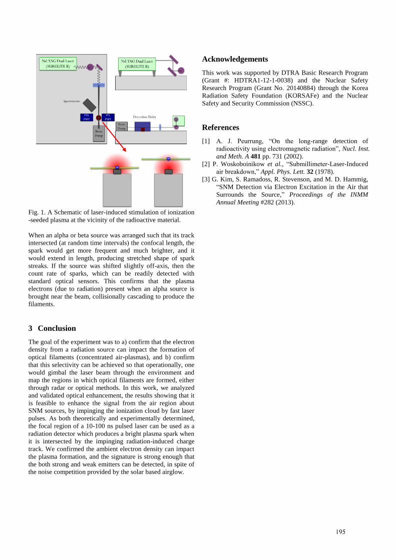
2
Fig. 1. A Schematic of laser-induced stimulation of ionization
-seeded plasma at the vicinity of the radioactive material.
When an alpha or beta source was arranged such that its track
intersected (at random time intervals) the confocal length, the
spark would get more frequent and much brighter, and it
would extend in length, producing stretched shape of spark
streaks. If the source was shifted slightly off-axis, then the
count rate of sparks, which can be readily detected with
standard optical sensors. This confirms that the plasma
electrons (due to radiation) present when an alpha source is
brought near the beam, collisionally cascading to produce the
filaments.
3 Conclusion
The goal of the experiment was to a) confirm that the electron
density from a radiation source can impact the formation of
optical filaments (concentrated air-plasmas), and b) confirm
that this selectivity can be achieved so that operationally, one
would gimbal the laser beam through the environment and
map the regions in which optical filaments are formed, either
through radar or optical methods. In this work, we analyzed
and validated optical enhancement, the results showing that it
is feasible to enhance the signal from the air region about
SNM sources, by impinging the ionization cloud by fast laser
pulses. As both theoretically and experimentally determined,
the focal region of a 10-100 ns pulsed laser can be used as a
radiation detector which produces a bright plasma spark when
it is intersected by the impinging radiation-induced charge
track. We confirmed the ambient electron density can impact
the plasma formation, and the signature is strong enough that
the both strong and weak emitters can be detected, in spite of
the noise competition provided by the solar based airglow.
Acknowledgements
This work was supported by DTRA Basic Research Program
(Grant #: HDTRA1-12-1-0038) and the Nuclear Safety
Research Program (Grant No. 20140884) through the Korea
Radiation Safety Foundation (KORSAFe) and the Nuclear
Safety and Security Commission (NSSC).
References
[1] A. J. Peurrung, “On the long-range detection of
radioactivity using electromagnetic radiation”, Nucl. Inst.
and Meth. A 481 pp. 731 (2002).
[2] P. Woskoboinikow et al., “Submillimeter-Laser-Induced
air breakdown,” Appl. Phys. Lett. 32 (1978).
[3] G. Kim, S. Ramadoss, R. Stevenson, and M. D. Hammig,
“SNM Detection via Electron Excitation in the Air that
Surrounds the Source,” Proceedings of the INMM
Annual Meeting #282 (2013).
1
The effect of ANFO on the Complex Resonance Frequencies of an IED
S A Gutierrez*, E Neira₰, J J Pantoja£, F Vega †
*₰ Doctoral student at Universidad Nacional de Colombia, Bogotá *[email protected],₰ [email protected], *₰£ † Researcher at EMC-UN, Universidad Nacional de Colombia Bogotá [email protected], †Professor at Universidad
Nacional de Colombia, Bogotá [email protected]
Abstract This paper is focused on describing how the resonance poles of an IED are modified by the dielectric constant of the explosive material used as main charge. Additionally, the extraction of complex resonance poles is used to evaluate the electromagnetic response of an electro explosive device (EED) inside of an explosive charge such as ammonium nitrate and fuel-oil (ANFO). Keywords: Improvised explosive device, Backscattering, Resonance poles, ANFO, Electro explosive device.
1 Introduction Antipersonnel landmines problem in Colombia is the result of armed internal conflict. The integral action program against the antipersonnel landmines PAICMA (by the Spanish: Programa de Acción Integral Contra las Minas Antipersonal) reported nearly of 11043 victims since 1990 until February of 2015. However not all victims report the landmines accidents. Therefore, actual victim’s numbers are difficult to be established. Additionally, PAICMA show that 31 of 32 Colombian departments have had events associated to improvised explosive devices (IEDs) or unexploded ordnance (UXO) in the same time period [1]. Colombia’s illegal groups built and bury different models of IEDs. Usually these explosive devices act as a personal landmine. Their design was made to hurt, delay military action and take control of territories considered strategic zones. Nevertheless, civilians have been affected with injuries, deaths and forced displacement [1]. A typical IED is composed of a main explosive, an electric detonator, a switch (victim activated or remotely controlled) a casing (that can be a plastic pipe, a wooden case, a glass bottle or a plastic can). Additionally, these devices can have significant amounts of dielectric material, such as plastic beads, stones, bamboo, glass and other nonmetallic parts used as shrapnel. The randomness of the IED's made demining process a difficult task. Additionally, Colombian soils have high ferrous content. Therefore, detection systems based on metal detector have high rates of false alarm and the demining effectiveness
and its performance can vary with the deminer’s expertise. In that way, metal detectors are not a useful tool to recognize if a buried object is hazardous or safely [2]. Related with landmine’s activation mechanism, reports of demining activities, news and military information show that IED activation mechanism used by illegal groups in Colombia can vary between electronic, chemical and non-electric activation mechanism. Researchers have found that electro explosive device (EED) is a common element in the IED activation mechanism and the IED’s main charge usually is ammonium nitrate and fuel-oil ANFO [1,2]. EED activation is based on the current flow through a bridge-wire that increases its temperature until a critical value to triggering the explosive inside the EED and the main IED's explosive charge. The feeding current is produced when anyone, usually the victim, closes the circuit that is connected to a battery placed near to the IED [3]. In Colombia there are a huge variability on IED’s shapes, materials and triggering methods. However, most of IEDs have two common factors: ANFO used as the main explosive charge and EED used as trigger of the IED. Therefore, backscattering signals analyses using the above cited characteristics are a useful way to understand the electromagnetic behavior of these explosive devices. Since IEDs have a complex structure and they have many composition materials, it is required full-wave simulations in order to model and understand the Colombian IED’s backscattering. In this paper, an analysis of the electromagnetic plane wave’s propagation in media with different permittivities is carried out with CST Microwave Studio and the resonance frequencies are calculated for the IED's elements.
2 IED model The IED model used in here is based on a small common explosive artifact, M type, as shown in Fig 1. The M type name is due to the IED’s switch surface shape. Usually IEDs battery is interchangeable and it is placed close to the explosive device. So, EED’s wires are connected to the mechanical switch and to the battery in an open circuit. This circuit is closed when the victim activate the M type switch.
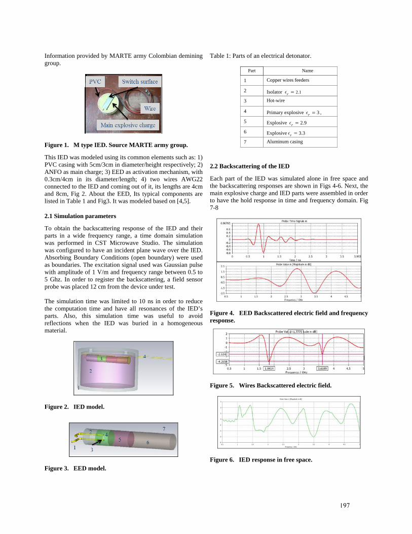
2
Information provided by MARTE army Colombian demining group.
Figure 1. M type IED. Source MARTE army group.
This IED was modeled using its common elements such as: 1) PVC casing with 5cm/3cm in diameter/height respectively; 2) ANFO as main charge; 3) EED as activation mechanism, with 0.3cm/4cm in its diameter/length; 4) two wires AWG22 connected to the IED and coming out of it, its lengths are 4cm and 8cm, Fig 2. About the EED, Its typical components are listed in Table 1 and Fig3. It was modeled based on [4,5].
2.1 Simulation parameters
To obtain the backscattering response of the IED and their parts in a wide frequency range, a time domain simulation was performed in CST Microwave Studio. The simulation was configured to have an incident plane wave over the IED. Absorbing Boundary Conditions (open boundary) were used as boundaries. The excitation signal used was Gaussian pulse with amplitude of 1 V/m and frequency range between 0.5 to 5 Ghz. In order to register the backscattering, a field sensor probe was placed 12 cm from the device under test. The simulation time was limited to 10 ns in order to reduce the computation time and have all resonances of the IED’s parts. Also, this simulation time was useful to avoid reflections when the IED was buried in a homogeneous material.
Figure 2. IED model.
Figure 3. EED model.
Table 1: Parts of an electrical detonator.
Part Name
1 Copper wires feeders
2 Isolator 2.1r
3 Hot-wire
4 Primary explosive 3r ,
5 Explosive 2.9r
6 Explosive 3.3r
7 Aluminum casing
2.2 Backscattering of the IED
Each part of the IED was simulated alone in free space and the backscattering responses are shown in Figs 4-6. Next, the main explosive charge and IED parts were assembled in order to have the hold response in time and frequency domain. Fig 7-8
Figure 4. EED Backscattered electric field and frequency response.
Figure 5. Wires Backscattered electric field.
Figure 6. IED response in free space.
3
Figure 7. IED surrounded with sand soil.
2.3 Resonance frequency
The complex resonance poles were extracted of the backscattering signals applying the algorithm proposed in [6,7]. Due to the resonances poles that appear in the resonance region or late time, the backscattering signal should be truncated in early time response and late time response [6]. Additionally, the resonance frequency could be verified using
2 d
cL
F (1)
Where c is the light speed and dF is the frequency of resonance and L is the length of the resonance object. Thus, the length L calculated for EED was 5.06 cm and the two wires have 8.69 cm and 3.56 cm. Its values are too close to the length calculated using the information of Fig 4 and Fig 5. Resonance frequency of an IED without ANFO placed in free space and an IED buried in sandy soil was calculated too, Fig 8. There are similarities between the resonance poles simulated and calculated for each IED; however, these poles appear attenuated due to the explosive dielectric material and their resonance frequency change slightly.
Figure 8. Resonance poles with IED in free space without explosive (plus). IED resonance poles with the EED inside ANFO and bottom of the PVC casing (asterisk).
3 Conclusions The complex resonance poles could be a useful feature to identify the EED inside the IEDs or buried in the soil.
Using full-wave simulations, it was verified that the electrical length of the EED is modified when it is buried on a material such as ANFO. However more work needs to be done and a broader range of scenarios should be simulated in order to draw clearer conclusions of the extracted EED resonance poles and knowing if other resonant parts of the IED hide the EED response.
References [1] PAICMA. (2015, February) Víctimas de minas
antipersonal. [Online]. Available: http://-www.accioncontraminas.gov.co/estadisticas/Paginas/-victimas-minas-antipersonal.aspx
[2] J. M. H. Hendrickx, A. Molina, D. Diaz, M. Grasmueck, H. A. Moreno, and R. D. Hernández, “Humanitarian ied clearance in colombia,” Proc. SPIE, vol. 6953, pp. 69530C–69530C–9, 2008. [Online]. Available: http://-dx.doi.org/10.1117/12.782303
[3] J. Pantoja, N. Pena, F. Rachidi, F. Vega, and F. Roman, “Characterization, modeling, and statistical analysis of the electromagnetic response of inert improvised explosive devices,” Electromagnetic Compatibility, IEEE Transactions on, vol. 56, no. 2, pp. 393–403, April 2014.
[4] J. J. Pantoja, N. Pena, F. Rachidi, F. Vega, and F. Roman, “Susceptibility of electro-explosive devices to microwave interference,” Defence Science Journal, vol. 63, no. 4, pp. 386–392, 2013.
[5] M. R. Lambrecht, K. L. Cartwright, C. E. Baum, and E. Schamiloglu, “Electromagnetic modeling of hot-wire detonators,” Microwave Theory and Techniques, IEEE Transactions on, vol. 57, no. 7, pp. 1707–1713, 2009.
[6] J. Chauveau, N. De Beaucoudrey, and J. Saillard, “Selection of contributing natural poles for the characterization of perfectly conducting targets in resonance region,” Antennas and Propagation, IEEE Transactions on, vol. 55, no. 9, pp. 2610–2617, Sept 2007.
[7] W. Lee, T. K. Sarkar, H. Moon, and M. Salazar-Palma, “Computation of the natural poles of an object in the frequency domain using the cauchy method,” Antennas and Wireless Propagation Letters, IEEE, vol. 11, pp. 1137–1140, 2012.
Study on Statistical Characteristic of Transient Disturbances and Correlation with Immunity Waveform
Zhang Weidong*, Zhang Xiaoli †, Luo Guangxiao* *Beijing Key Lab of High Voltage and Electromagnetic Compatibility, North China Electric Power University, Beijing 102206, China. [email protected]; †China Electric Power Research Institute, Beijing 100192, China,
Abstract In order to get the statistical characteristic of transient disturbances while the measured data number is small, two small sample statistical methods are introduced and applied in this paper. The correlation theory was used to express the consistency about the immunity test waveform and measured waveform quantitatively. Keywords: transient disturbances, statistical characteristic, correlation theory, immunity test
1 Introduction
Recently, more and more electronics equipments were used in electric power system for relay protection, control systems and communications. These systems may be interfered by many transient disturbances such as lightning, switch operation, short-circuit faults and other EMP [1]. Because the randomicity of the transient phenomenon and the number of the measured data is limited, we use small sample statistic method to get the statistical characteristic of the transient disturbances [2]. At present, there is no explicit standard for immunity test of the electronics equipment. In order to estimate the relevancy between actual disturbance characteristics and existed standard, the correlation theory was used to express the consistency about the immunity test waveform and measured waveform quantitatively. The analysis results can be used to modify and add existed standards or develop more suitable standards [3].
2 Two small sample statistic methods
The Bayes bootstrap method and stochastic weighted method were more widely applied in dealing with small sample statistical issues. Its basic idea is using the statistic characteristics of experimental data instead of the fact [4].
2.1 Basic principle
We suppose that: ( ) is the sample, . The
1 2, , ......, nX X X ~ ( )iX F x
( )Fθ θ= is the unknown number of population distribution. nF is the sampling distribution function of
( 1 2, , ......, nX X X ),^ ^
( )nFθ θ= , ^θ is the estimator of θ ,
.Sampling from ( ), we can
get regeneration sample . is the sampling
distribution function of regeneration sample,
^( ) ( )n nT F Fθ θ= − 1 2, , ......, nX X X
* * * *1 2( , ,......, )nX X X X=
*nF
^*( )nFθ is also the
estimator of θ , . Using the distribution of
^ ^* *( ) ( )n nR F Fθ θ= − n
*nR to approximate is the central idea of bootstrap and
stochastic weighted method. nT
We can make the regeneration samples repeatedly and get *( )*( ) *( ) *( )1 2( , , ......, ), ( 1,......, )
jj j jnX X X X j N= (1)
^ ^*( ) *( )( ) ( ),( 1,......, )j jn n nR F F jθ θ= − = N (2)
Finally we can get ^ ^ ^ ^
( ) *( ) *( )( ) ( ) ( ) 2 ( ) ( )j j jn n n n n nF F T F R F Fθ θ θ θ θ= − ≈ − = − (3)
Gain N possible values of ( )Fθ by (3), make them as the samples, which we can used to get the sampling distribution * ( )F θ of ( )Fθ . Thus we can make statistical inference aboutθ .
2.2 Basic characteristics calculation
The characteristics of the transient disturbances are mainly included: rise time, duration, peak to peak value, energy, rising rate, DC component, the mean square value of AC, bandwidth and dominant frequency. Take the substation transient measurement as an example. We can get its basic characteristics in Table 1.
2.3 Statistical characteristics calculation
Statistic analysis has important meaning in evaluating general level of transient electromagnetic disturbance in substation. Apply the stochastic weighted method on basic characteristics to getting statistical characteristics in Table 2.
3 Waveform consistency
We supposed that test waveform is 1( )x t , the measured waveform is 2 ( )x t , the expression of correlation coefficient is [5]
1 21 212 1/ 2
2 21 22 21 2
( ) ( )( ), ( )( ) ( ) ( ) ( )
x t x t dtx t x tx t x t x t dt x t dt
ρ
∞
−∞
∞ ∞
−∞ −∞
⟨ ⟩= =
⎡ ⎤⎢ ⎥⎣ ⎦
∫
∫ ∫ (4)
1
Table 1: Basic characteristics
No. Rise time
( sμ ) Duration
( sμ ) Peak to peak
value ( V ) Energy ( 2
V sμi )
Rising rate
( /kV sμ )
DC component ( ) V
Mean square value of AC( V )
0 0.0178 15.46 19.2 174.96 4.494 0.018 3.499
1 0.0246 15.46 21.8 200 3.902 0.021 4.000
2 0.0272 24.02 43.2 315.83 6.765 0.051 6.317
… … … … … … … …
66 0.069 39.7 53.6 702.49 3.107 0.184 14.050
69 0.0383 45.04 32.8 165.15 3.676 -0.029 3.303
70 0.0301 49.34 27.2 139.99 4.040 0.501 2.800
Table 2: Statistical characteristics μ σ
Rise time ( sμ ) 0.0236 0.0169,0.0257 0.0165 0.0134,0.0218 Duration( sμ ) 21.281 17.64,24.692 18.451 16.3797,19.2984
Peak to peak value ( V ) 18.38 14.4556,22.3050 16.581 14.2315,19.8676
Energy( 2V sμ ) 166.74 165.79, 166.85 297.73 282.54, 306.92
Rising rate( /kV sμ ) 6.566 6.518, 6.584 14.43 14.369, 14.541 DC component( ) V 0.0225 0.2223, 0.2228 0.1115 0.1110, 0.1118
Mean square value of AC( ) V 3.436 3.422, 3.45 5.990 5.966, 6.034 In Equation (4), < > is for inner product, i i is for norm. If
the waveforms are same or converse, the value of 12ρ is +1 or -1, else its value is between +1 and -1. In order to keep the objectivity of 12ρ , it is necessary to calculate the correlation function with time-variation
∫∞
∞−τ−ττ= d)t(x)(x)t(R 2112 (5)
-15 -10 -5 0 5 10 150
0.1
0.2
0.3
0.4
0.5
0.6
0.7
0.8
0.9
1
t (μ s)
Rn
-100 -80 -60 -40 -20 0 20 40 60 80 1000
0.1
0.2
0.3
0.4
0.5
0.6
0.7
0.8
0.9
1
t (ms)
Rn2
(a) (b)
(a) Measured transient magnetic field with IEC61000-4-10 test waveform (b) Measured transient voltage with IEC61000-4-11 test waveform Fig.1. Normalized correlation function
-15 -10 -5 0 5 10 150
0.1
0.2
0.3
0.4
0.5
0.6
0.7
0.8
0.9
1
t (μ s)
Rn
Fig.2. Normalized correlation function of measured transient voltage with IEC61000-4-12 test waveform In the Fig.1 (a), the maximum of 12ρ is 0.59. In the Fig.1 (b), the maximum of 12ρ is 0.17. In the Fig.2, the maximum of
12ρ is 0.06. It is seen that the consistency of the immunity test waveform and measured waveform is highest for magnetic field and lowest for the transient voltage.
4 Conclusion
The Bayes bootstrap was used to analyze the statistical characteristics of transient electromagnetic disturbance due to switching operation in substations. The characteristics parameters were obtained based on the small sample statistical methods from 70 samples. The consistency of the immunity test waveform and measured waveform was analyzed using correlation analysis method. The result shows that the correlation factor of transient magnetic field is higher than transient voltage.
Acknowledgement
This paper is supported by State Grad Corporation project No. DZ71-12-19.
References [1] Wu Wen, Jun Jia, “Overview of electromagnetic compatibility in
electric power system,” Journal of Changsha University of Electric Power, vol. 18, pp. 42-46, 2003.
[2] Haijun Deng, Yabing Zha, “A research on the application of bootstrap method and its application in the accuracy assessment,” Journal of Spacecraft TT&C Technology, vol. 24, no.1, pp. 59-63, 2005.
[3] Yufeng Wang, Jiyan Zou, Minfu Liao, “EMC Prediction and Analysis in Power System Based on Data Mining Technology,” High Voltage Apparatus, Vol.43, No.3, pp.183-185, 2007.
[4] B. Efron, “The bootstrap and modern statistics,” Journal of the American Statistical Association., vol. 95, no. 452, pp. 1293–1296, 2000.
[5] Junli Zheng, Qiheng Ying, Weili Yang, Signal and System, 2nd ed., Beijing: Higher Education Press, 2000.
2
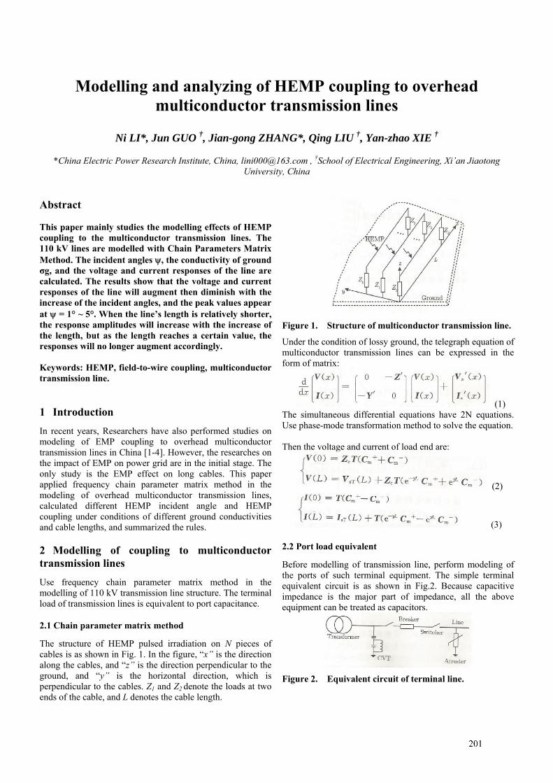
1
Modelling and analyzing of HEMP coupling to overhead multiconductor transmission lines
Ni LI*, Jun GUO †, Jian-gong ZHANG*, Qing LIU †, Yan-zhao XIE †
*China Electric Power Research Institute, China, [email protected] , †School of Electrical Engineering, Xi’an Jiaotong University, China
Abstract This paper mainly studies the modelling effects of HEMP coupling to the multiconductor transmission lines. The 110 kV lines are modelled with Chain Parameters Matrix Method. The incident angles ψ, the conductivity of ground σg, and the voltage and current responses of the line are calculated. The results show that the voltage and current responses of the line will augment then diminish with the increase of the incident angles, and the peak values appear at ψ = 1° ~ 5°. When the line’s length is relatively shorter, the response amplitudes will increase with the increase of the length, but as the length reaches a certain value, the responses will no longer augment accordingly. Keywords: HEMP, field-to-wire coupling, multiconductor transmission line.
1 Introduction
In recent years, Researchers have also performed studies on modeling of EMP coupling to overhead multiconductor transmission lines in China [1-4]. However, the researches on the impact of EMP on power grid are in the initial stage. The only study is the EMP effect on long cables. This paper applied frequency chain parameter matrix method in the modeling of overhead multiconductor transmission lines, calculated different HEMP incident angle and HEMP coupling under conditions of different ground conductivities and cable lengths, and summarized the rules.
2 Modelling of coupling to multiconductor transmission lines
Use frequency chain parameter matrix method in the modelling of 110 kV transmission line structure. The terminal load of transmission lines is equivalent to port capacitance.
2.1 Chain parameter matrix method
The structure of HEMP pulsed irradiation on N pieces of cables is as shown in Fig. 1. In the figure, “x” is the direction along the cables, and “z” is the direction perpendicular to the ground, and “y” is the horizontal direction, which is perpendicular to the cables. Z1 and Z2 denote the loads at two ends of the cable, and L denotes the cable length.
Figure 1. Structure of multiconductor transmission line.
Under the condition of lossy ground, the telegraph equation of multiconductor transmission lines can be expressed in the form of matrix:
(1) The simultaneous differential equations have 2N equations. Use phase-mode transformation method to solve the equation. Then the voltage and current of load end are:
(2)
(3)
2.2 Port load equivalent
Before modelling of transmission line, perform modeling of the ports of such terminal equipment. The simple terminal equivalent circuit is as shown in Fig.2. Because capacitive impedance is the major part of impedance, all the above equipment can be treated as capacitors.
Figure 2. Equivalent circuit of terminal line.
2
3 HEMP coupling to overhead transmission line under condition of different parameters
Take the structure of 110 kV line as an example, and the incident waveform applies IEC standard HEMP waveform, the polarizing angle α = 0°, and the azimuth angle ϕ = 0°. Same loads are connected to the two ends of the line in the model, as shown in Fig. 3. The equivalent impedances at two ends of the line are as calculated in the port impedance structure of Fig. 2.
Figure 3. Model of line.
3.1 Relationship between incident angle ψ and coupling to transmission line
Fig. 4 indicates that when the incident angle is 0° ~ 90°, the pulse of line end lasts for 0 ns to10 μs. The response amplitude increases and then decreases. When incident angle is around 10°, the response is the maximum.
Figure 4. Current responses under different incident angles.
Figure 5. Peak of voltage response under different incident angles (σg = 0.01 s·m-1).
Figure 6. Peak of current response under different incident angles (σg = 0.01 s·m-1).
Fig.5 and Fig.6 indicate that, as mentioned above, when the incident angle increases from 1° to 90°, the voltage or current
response at end of power line increases and then decreases. When ψ = 4° ~ 5°, the maximum value appears. The maximum value is nearly 50% larger than the response when ψ = 10°. Fig.7 and Fig.8 indicate that when the ground conductivity is in the range of actual ground conductivity, the response of power line increases and then decreases as the incident angle increases. Under different ground conductivities, the maximum response appears at different incident angle. In the range of common ground conductivity, the maximum response appears when the incident angle is 1° ~ 5°.
Figure 7. Peak of voltage response under different incident angles (σg = 0.1 ms·m-1, 1 s·m-1).
Figure 8. Peak of current response under different incident angles (σg = 0.1 ms·m-1, 1 s·m-1).
3.2 Relationship between line length L and response
Fig.9 and Fig.10 indicate that when the line length is short, as the line length increases, the peak voltage and peak current at ends of power lines increase. When the line length is larger than a certain value, as the line length increases, the peak voltage and peak current at ends of power lines do not increase any more. The critical length is about 2 km.
Figure 9. Peak of voltage response under different line lengths.
3
Figure 10. Peak of current response under different line lengths.
3.3 The relationship between ground parameters and coupling to power line
Fig.11 and Fig.12 indicate that when ground dielectric constant increases, the response at ends of line increases, but the growths of peak voltage and peak current are negligible.
Figure 11. Peak of voltage response under different relative dielectric constants.
Figure 12. Amplitude of current responses under different relative dielectric constants.
Fig.13 and Fig.14 indicate that when ground conductivity is 0.0001, 0.001 and 0.01 s·m-1, the change of response at ends of power line is not big. But when the ground conductivity is 0.1 and 1 s·m-1, the voltage and current responses at ends of power line decrease dramatically.
Figure 13. Peak of voltage response under different conductivities.
Figure 14. Peak of current response under different conductivities.
Fig.15 indicates that different ground conditions have obvious influence on response waveform.
Figure 15. Voltage responses under different ground parameters.
4 Conclusions
Based on modelling of an 110 kV power line, the results indicate that as the incident angle increases, the response amplitudes at ends of power lines increase and then decrease, and reach the maximum value when ψ = 1° ~ 5°. When the line length is relatively shorter, the response amplitudes will increase with the increase of line length, but when the length exceeds a certain value, the responses will no longer augment accordingly. Parameters of ground conditions can also have significant influence on the responses.
References
[1] XIE Y Z, GUO J. “Analytical approach for the prediction of EMP coupling to multiconductor transmission lines” [C]//Asia-Pacific International Symposium and Exhibition on Electromagnetic Compatibility (APEMC), Melbourne, 2013.
[2] ZHAI Ai-bin, XIE Yan-zhao, HAN Jun et al. Effect of high altitude nuclear electromagnetic pulse upon phone call [J]. High Power Laser and Particle Beams, 2009, 21(10): 1529-1533.
[3] ZHOU Ying-hui, SHI Li-hua, GAO Cheng. A time-domain method to calculate EMP coupling of buried cables based on transmission line model [J]. High Power Laser and Particle Beams, 2006, 18(7): 1163-1166.
[4] XIE Yan-zhao, SUN Bei-yun, ZHOU Hui, et al. High altitude electromagnetic pulse environment over the lossy ground [J]. High Power Laser and Particle Beams, 2003, 15(7): 680-684.
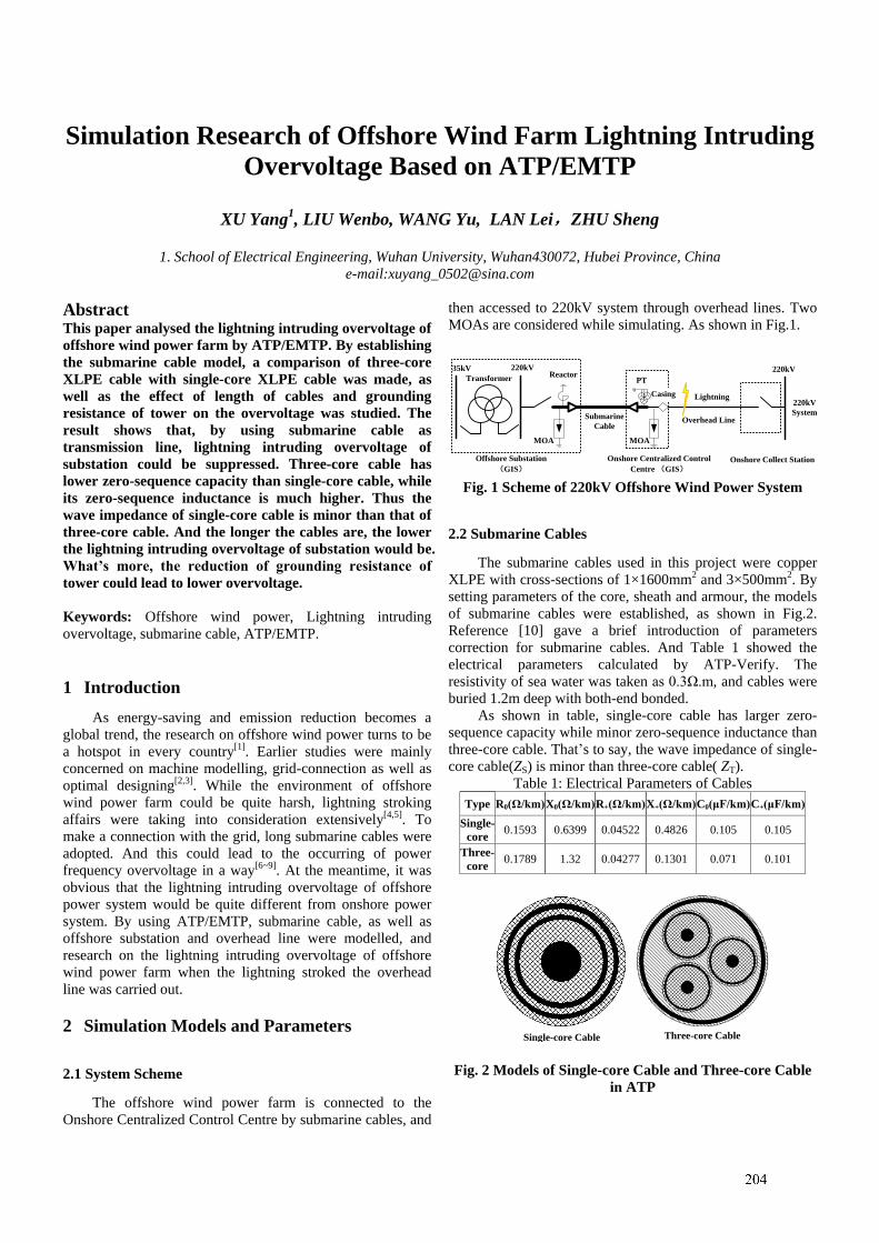
1
Simulation Research of Offshore Wind Farm Lightning Intruding
Overvoltage Based on ATP/EMTP
XU Yang1, LIU Wenbo, WANG Yu, LAN Lei,ZHU Sheng
1. School of Electrical Engineering, Wuhan University, Wuhan430072, Hubei Province, China
e-mail:[email protected]
Abstract This paper analysed the lightning intruding overvoltage of
offshore wind power farm by ATP/EMTP. By establishing
the submarine cable model, a comparison of three-core
XLPE cable with single-core XLPE cable was made, as
well as the effect of length of cables and grounding
resistance of tower on the overvoltage was studied. The
result shows that, by using submarine cable as
transmission line, lightning intruding overvoltage of
substation could be suppressed. Three-core cable has
lower zero-sequence capacity than single-core cable, while
its zero-sequence inductance is much higher. Thus the
wave impedance of single-core cable is minor than that of
three-core cable. And the longer the cables are, the lower
the lightning intruding overvoltage of substation would be.
What’s more, the reduction of grounding resistance of
tower could lead to lower overvoltage.
Keywords: Offshore wind power, Lightning intruding
overvoltage, submarine cable, ATP/EMTP.
1 Introduction
As energy-saving and emission reduction becomes a
global trend, the research on offshore wind power turns to be
a hotspot in every country[1]. Earlier studies were mainly
concerned on machine modelling, grid-connection as well as
optimal designing[2,3]. While the environment of offshore
wind power farm could be quite harsh, lightning stroking
affairs were taking into consideration extensively[4,5]. To
make a connection with the grid, long submarine cables were
adopted. And this could lead to the occurring of power
frequency overvoltage in a way[6~9]. At the meantime, it was
obvious that the lightning intruding overvoltage of offshore
power system would be quite different from onshore power
system. By using ATP/EMTP, submarine cable, as well as
offshore substation and overhead line were modelled, and
research on the lightning intruding overvoltage of offshore
wind power farm when the lightning stroked the overhead
line was carried out.
2 Simulation Models and Parameters
2.1 System Scheme
The offshore wind power farm is connected to the
Onshore Centralized Control Centre by submarine cables, and
then accessed to 220kV system through overhead lines. Two
MOAs are considered while simulating. As shown in Fig.1.
Submarine
CableOverhead Line
35kV 220kV
Offshore Substation
(GIS)Onshore Collect Station
220kV
Onshore Centralized Control
Centre (GIS)
220kV
System
MOAMOA
Casing Lightning
ReactorPTTransformer
Fig. 1 Scheme of 220kV Offshore Wind Power System
2.2 Submarine Cables
The submarine cables used in this project were copper
XLPE with cross-sections of 1×1600mm2 and 3×500mm2. By
setting parameters of the core, sheath and armour, the models
of submarine cables were established, as shown in Fig.2.
Reference [10] gave a brief introduction of parameters
correction for submarine cables. And Table 1 showed the
electrical parameters calculated by ATP-Verify. The
resistivity of sea water was taken as 0.3Ω.m, and cables were
buried 1.2m deep with both-end bonded.
As shown in table, single-core cable has larger zero-
sequence capacity while minor zero-sequence inductance than
three-core cable. That’s to say, the wave impedance of single-
core cable(ZS) is minor than three-core cable( ZT).
Table 1: Electrical Parameters of Cables
Type R0(Ω/km) X0(Ω/km) R+(Ω/km) X+(Ω/km) C0(μF/km) C+(μF/km)
Single-
core 0.1593 0.6399 0.04522 0.4826 0.105 0.105
Three-
core 0.1789 1.32 0.04277 0.1301 0.071 0.101
Single-core Cable Three-core Cable
Fig. 2 Models of Single-core Cable and Three-core Cable
in ATP
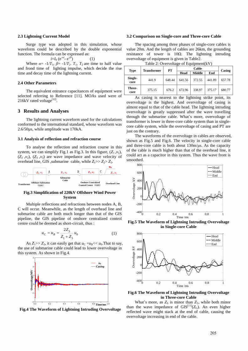
2
2.3 Lightning Current Model
Surge type was adopted in this simulation, whose
waveform could be described by the double exponential
function. The formula can be expressed as:
i=I0 (e-αt- e-βt) (1)
Where α= -1/T1, β= -1/T2. T1, T2 are time to half value
and frond time of lighting impulse, which decide the rise
time and decay time of the lightning current.
2.4 Other Parameters
The equivalent entrance capacitances of equipment were
selected referring to Reference [11]. MOAs used were of
216kV rated voltage[12].
3 Results and Analyses
The lightning current waveform used for the calculations
conformed to the international standard, whose waveform was
2.6/50µs, while amplitude was 170kA.
3.1 Analysis of reflection and refraction course
To analyse the reflection and refraction course in this
system, we can simplify Fig.1 as Fig.3. In this figure, (Z1 ,v1),
(Z2 ,v2), (Z3 ,v3) are wave impedance and wave velocity of
overhead line, GIS ,submarine cable, while Z1>> Z2> Z3.
Z2,v2 Z2,v2Z3,v3 Z1,v1
u0
A B C
Offshore Substation
(GIS)Transformer
Submarine
CableOnshore Centralized
Control Centre (GIS)Overhead Line
Fig.3 Simplification of 220kV Offshore Wind Power
System
Multiple reflections and refractions between nodes A, B,
C will occur. Meanwhile, as the length of overhead line and
submarine cable are both much longer than that of the GIS
pipeline, the GIS pipeline of onshore centralized control
centre could be deemed as short-circuit, thus :
30
1 3
2C B
Zu u u
Z Z
(1)
As Z1>> Z3, it can easily get that uC =uB<< u0.That to say,
the use of submarine cable could lead to lower overvoltage in
this system. As shown in Fig.4.
(f ile 雷击侵入三芯500.pl4; x-var t) v:U0A v:SDA v:TG1A
0.0 0.2 0.4 0.6 0.8 1.0[ms]
-2
-1
0
1
2
3
[MV]
u0
Casing
Over
volt
age/
MV
Time/ms Fig.4 The Waveform of Lightning Intruding Overvoltage
3.2 Comparison on Single-core and Three-core Cable
The spacing among three phases of single-core cables is
value 20m. And the length of cables are 26km, the grounding
resistance of tower is 10Ω. The lightning intruding
overvoltage of equipment is given in Table2.
Table 2: Overvoltage of Equipment(kV)
Type Transformer PT Cable
Casing Head Middle End
Single-
core 441.9 648.44 641.56 372.55 441.89 657.78
Three-
core 375.15 676.2 672.96 338.97 375.17 680.77
As casing is nearest to the lightning strike point, its
overvoltage is the highest. And overvoltage of casing is
almost equal to that of the cable head. The lightning intruding
overvoltage is greatly suppressed after the wave travelling
through the submarine cable. What’s more, overvoltage of
transformer is lower in three-core cable system than in single-
core cable system, while the overvoltage of casing and PT are
just on the contrary.
The waveforms of the overvoltage in cables are observed,
shown as Fig.5 and Fig.6. The velocity in single-core cable
and three-core cable is both about 130m/μs. As the capacity
of the cable is much higher than that of the overhead line, it
could act as a capacitor in this system. Thus the wave front is
smoothed.
0 0.2 0.4 0.6 0.8 1-400
-200
0
200
400
600
800
Time /ms
Ov
erv
olt
ag
e /
kV
Head
Middle
End
Fig.5 The Waveform of Lightning Intruding Overvoltage
in Single-core Cable
0 0.2 0.4 0.6 0.8 1-400
-200
0
200
400
600
800
Time /ms
Ov
erv
olt
age
/kV
Head
Middle
End
Fig.6 The Waveform of Lightning Intruding Overvoltage
in Three-core Cable
What’s more, as ZS is minor than ZT, while both minor
than the wave impedance of GIS[11](ZG). An even higher
reflected wave might stack at the end of cable, causing the
overvoltage increasing in end of the cable.
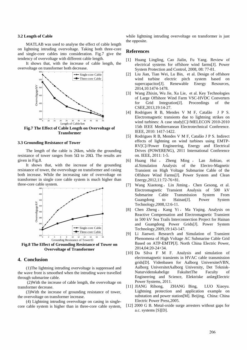
3
3.2 Length of Cable
MATLAB was used to analyse the effect of cable length
on lightning intruding overvoltage. Taking both three-core
and single-core cables into consideration. Fig.7 give the
tendency of overvoltage with different cable length.
It shows that, with the increase of cable length, the
overvoltage on transformer both decrease.
5 10 15 20 25 30 35 40 45 50 55300
350
400
450
500
550
600
Length of Cable/km
Ov
erv
olt
gag
e/k
V
Single-core Cable
Three-core Cable
Fig.7 The Effect of Cable Length on Overvoltage of
Transformer
3.3 Grounding Resistance of Tower
The length of the cable is 26km, while the grounding
resistance of tower ranges from 5Ω to 20Ω. The results are
given in Fig.8.
It shows that, with the increase of the grounding
resistance of tower, the overvoltage on transformer and casing
both increase. While the increasing rate of overvoltage on
transformer in single core cable system is much higher than
three-core cable system.
0 2 4 6 8 10 12 14 16 18 20320
340
360
380
400
420
440
460
480
Grounding Resistance of Tower/
Ov
erv
olt
gag
e/k
V
Single-core Cable
Three-core Cable
Fig.8 The Effect of Grounding Resistance of Tower on
Overvoltage of Transformer
4. Conclusion
(1)The lightning intruding overvoltage is suppressed and
the wave front is smoothed when the intruding wave travelled
through submarine cable.
(2)With the increase of cable length, the overvoltage on
transformer decrease.
(3)With the increase of grounding resistance of tower,
the overvoltage on transformer increase.
(4) Lightning intruding overvoltage on casing in single-
core cable system is higher than in three-core cable system,
while lightning intruding overvoltage on transformer is just
the opposite.
References
[1] Huang Lingling, Cao Jialin, Fu Yang. Review of
electrical systems for offshore wind farms[J]. Power
System Protection and Control, 2008, 08: 77-81.
[2] Liu Jian, Tian Wei, Lu Bin, et al. Design of offshore
wind turbine electric pitch system based on
supercapacitor[J]. Renewable Energy Resources,
2014,10:1474-1478.
[3] Wang Zhixin, Wu Jie, Xu Lie, et al. Key Technologies
of Large Offshore Wind Farm VSC-HVDC Converters
for Grid Integration[J]. Proceedings of the
CSEE,2013,19:14-27.
[4] Rodrigues R B, Mendes V M F, Catalão J P S.
Electromagnetic transients due to lightning strikes on
wind turbines: A case study[C]//MELECON 2010-2010
15th IEEE Mediterranean Electrotechnical Conference.
IEEE, 2010: 1417-1422.
[5] Rodrigues R B, Mendes V M F, Catalão J P S. Indirect
effects of lightning on wind turbines using EMTP-
RV[C]//Power Engineering, Energy and Electrical
Drives (POWERENG), 2011 International Conference
on. IEEE, 2011: 1-5.
[6] Huang Hui , Zheng Ming , Lan Jinbiao, et
al.Simulation Analysis of the Electro-Magnetic
Transient on High Voltage Submarine Cable of the
Offshore Wind Farms[J]. Power System and Clean
Energy,2012,11:72-76+81.
[7] Wang Xiaotong,Lin Jiming,Chen Gesong, et al.
Electromagnetic Transient Analysis of 500 kV
Submarine Cable Transmission System From
Guangdong to Hainan[J]. Power System
Technology,2008,12:6-11.
[8] Chen Zheng , Kang Yi , Ma Yiqing. Analysis on
Reactive Compensation and Electromagnetic Transient
in 500 kV Sea Trails Interconnection Project for Hainan
and Guangdong Power Grids[J]. Power System
Technology,2009,19:143-147.
[9] Li Jianwei. Research and Simulation of Transient
Phenomena of High Voltage AC Submarine Cable Grid
Based on ATP-EMTP[J]. North China Electric Power,
2014,04:20-24+34.
[10] Da Silva F M F. Analysis and simulation of
electromagnetic transients in HVAC cable transmission
grids[D]. Videnbasen for Aalborg UniversitetVBN,
Aalborg UniversitetAalborg University, Det Teknisk-
Naturvidenskabelige FakultetThe Faculty of
Engineering and Science, Elektriske anlægElectric
Power Systems, 2011.
[11] JIANG Rihong, ZHANG Bing, LUO Xiaoyu.
Lightning protection and application example on
substation and power station[M]. Beijing, China: China
Electric Power Press,2005.
[12] 2000 G B. Metal-oxide surge arresters without gaps for
a.c. systems [S][D].
1
Calculation and Analysis on Transient Induced Voltage of
Multiple Parallel UHV Transmission Lines
ZHANG Gongda 1, ZHOU Peihong
2, ZHANG Xiaoqing
2, YUE Lingping
3
1. School of Electrical Engineering, Wuhan University, China, Email: [email protected]
2. State Grid Electric Power Research Institute, China 3. State Grid Huzhou Power Supply Company, China
Abstract
It has transient electromagnetic induction between
parallel lines as coupling effects. The magnitude and
characteristics of induced voltage on sound circuits is
worth studying for improving system operation and
insulation configuration. In this paper, the simulate
models of six parallel circuits in one corridor around
HuZhou city were set up in power system electromagnetic
transient program to calculate the coupling effects. The
magnitude and distribution of switching induced voltage
caused by permanent single phase grounding fault in
UHVAC system and monopolar grounding fault in
UHVDC system was calculated. The characteristics of
induced voltage on sound circuits nearby fault circuit
were analysed. The results show that maximum transient
induced voltage caused by UHVAC fault on UHVDC
sound circuits is lower than it caused by UHVDC fault.
The most serious induced voltage caused by monopolar
grounding fault is still on the antipode circuit. The
magnitude of induced voltage caused by both AC and DC
switching overvoltage does not pose risks to the people on
line working comply with the current standard.
Keywords: multi-parallel, UHV, switching overvoltage,
transient induction.
1 Introduction
The transient induced voltage on low-medium voltage
transmission lines, or communication lines is an inducement
of network instability and device damage. The interactions
caused by the transient electromagnetic induction on several
nearby parallel overhead lines may cause some significant
problems to the operation and maintenance especially in the
UHV(Ultra High Voltage) / EHV(Extra High Voltage)
system.[1-4]
The space of lines corridor has become valuable more and
more in the eastern china, the phenomenon of several AC/DC
transmission lines erected in one corridor has become
widespread. Under extremely circumstance, six transmission
circuits parallel with each other adjacently in HuZhou city,
Zhejiang province. The magnitude and characteristics of
transient induced voltage generated by switching overvoltage
on sound circuits is worth studying for improving system
operation and insulation configuration of UHV/EHV lines.
2 Parameters of multiple parallel lines
2.1 Overview of parallel lines
1000kV HuaiShang line is a dual circuit in same tower
system, the length is 656km. ±800kV JinSu project has
2100km bipolar line, and 7200MW transmission power.
±800kV FuFeng project has 1906km bipolar line, and
6400MW transmission power. ±500kV GeNan/LinFeng
project has two bipolar lines and 2 × 3000MW transmission
power, GeNan line 1114km, LinFeng line 976km.
The route map of these parallel lines in HuZhou city is shown
in Fig. 1. The arrangement of four circuits in one corridor
west of ZheBei station is shown in Fig. 2, the arrangement of
six circuits in one corridor east of ZheBei station is shown in
Fig. 3. The segment of HuaiShang west of ZheBei station is
called WanZhe line; the segment east of ZheBei station is
called ZheHu line.
2.2 Coupling parameters for simulation
For considering the electromagnetic coupling effect, the
parallel spacing of four whole lines was measured and
classified by using tower’s GPS coordinate, thus the coupling
lines models were built. Around HuZhou, the segment data
points were also established for getting the information of
induced voltage along this several parallel circuits corridor.
The length of this corridor in HuZhou is about 263km,
including UHV four circuits coupling segment 124km,
UHV/EHV six circuits coupling segment 72km, and UHV
three circuits coupling segment 67km[5]
. The spacing of
parallel lines distance between the centres of tower is about
70m to 80m. The sketch of parallel relationship and data
points is shown in Fig. 4.
The rule of HVDC system operation which is constant current
control of converter, constant voltage control of inverter was
adopted in the simulation. It has DC voltage drop about 6% of
rated voltage on the side of inverter.
2
安徽
省
江苏
AnHui
Province
ChangXing
AnJi
Taihu Lake
NanXun
WuXing
±800 kV JinSu;
1000 kV HuaiShang;
±800 kV FuFeng;
±500 kV GeNan /LinFeng;
JiangSu
Province
DeQing
ZheBei Station
Figure 1. Route map of EHV/UHV lines in HuZhou.
P1
+800 kV
WanZhe
JinSuFuFeng
C
B
A
A
B
C
P2
-800 kV
P2
-800 kV
P1
+800 kV
III
Figure 2. Arrangement diagram of four circuits in same
corridor.
P1
+800 kV
ZheHu
JinSuFuFeng GeNan LinFeng
C
B
A
A
B
C
P2
-800 kV
P2
-800 kV
P1
+800 kV
P2
-500 kV
P1
+500 kV
P1
+500 kV
P2
-500 kVII I
Figure 3. Arrangement diagram of six circuits in same
corridor.
Point 0
Point 1
HuaiShang FuFeng GeNan/LinFengJinSu
124km
HuaiShang,FuFeng,
JinSu coupling
Point 2
Point 372km
6 circuits coupling 67km
HuaiShang,
FuFeng coupling
Figure 4. Parallel relationship and induced voltage data
points of six circuits.
3 Simulation Results
3.1 Induced voltage caused by AC switching overvoltage
According to the previous AC overvoltage studies [6-7]
, the
magnitude of switching overvoltage due to the permanent
single phase grounding fault is more than the line energizing
overvoltage and single-phase automatic reclosing overvoltage.
And then the transient induced voltage on the sound phases is
stimulated more severely.
The maximum transient voltage in AC system caused by
permanent single phase grounding fault on WanZhe II circuit
is 1480kV be equal to 1.65 p.u.(1 p.u.=816kV). The transient
induced voltage on the JinSu positive circuit which is closest
to WanZhe II circuit is 883kV (1.08 p.u.), but the highest
induced voltage is 889kV (1.09 p.u.) on the FuFeng negative
circuit. The refraction, reflection and addition of travelling
wave induced on FuFeng negative circuit is a reason for the
phenomenon. As the permanent single phase grounding fault
occurring on ZheHu I circuit, the highest induced voltage is
889kV (1.09 p.u.) on the FuFeng negative circuit which is
closest to ZheHu I circuit. The calculation results of transient
induced voltage on each DC circuits are shown in Table 1 and
Table 2 (P1 stands for positive circuit, P2 stands for negative
circuit).
Table 1: Induced voltage on DC circuits under the permanent
single phase grounding fault of WanZhe II circuit (kV)
Data
Point
JinSu FuFeng GeNan LinFeng
P1 P2 P1 P2 P1 P2 P1 P2
Point 0 883 873 881 889 - - - -
Point 1 843 831 873 873 506 489 490 499
Point 2 822 801 837 847 506 480 490 487
Point 3 821 800 832 845 - - - -
Maximum 883 873 881 889 506 489 490 499
Table 2: Induced voltage on DC circuits under the permanent
single phase grounding fault of ZheHu I circuit (kV)
Data
Point
JinSu FuFeng GeNan LinFeng
P1 P2 P1 P2 P1 P2 P1 P2
Point 0 838 826 876 872 - - - -
Point 1 843 834 876 889 511 491 501 503
Point 2 814 804 835 851 517 483 503 489
Point 3 805 801 869 846 - - - -
Maximum 843 834 876 889 517 491 503 503
3.2 Induced voltage caused by DC switching overvoltage
Previous studies indicated that monopolar grounding fault at
the middle of whole line is a major cause of most serious
switching overvoltage that is on the antipode circuit around
fault point. The transfer overvoltage on the parts of four DC
lines in HuZhou city far away from the middle of whole line
is much lower than occurring local monopolar grounding fault.
In the simulation, local fault at the point 0 was set up to
analyse the characteristics of maximum induced voltage.
As JinSu monopolar grounding, calculation results of
transient induced voltage on each DC circuits are shown in
Table 3 and Table 4. The induced voltage 1078kV (1.32 p.u.)
on sound circuit is higher than on each other parallel circuits.
Occurring monopolar grounding fault on JinSu P1, the
induced voltage on FuFeng P1 is higher than on FuFeng P2,
the induced voltage on ±500kV negative circuits such as
GeNan P2, LinFeng P2, is higher than on their antipode
circuits (GeNan P1, LinFeng P1). As FuFeng monopolar
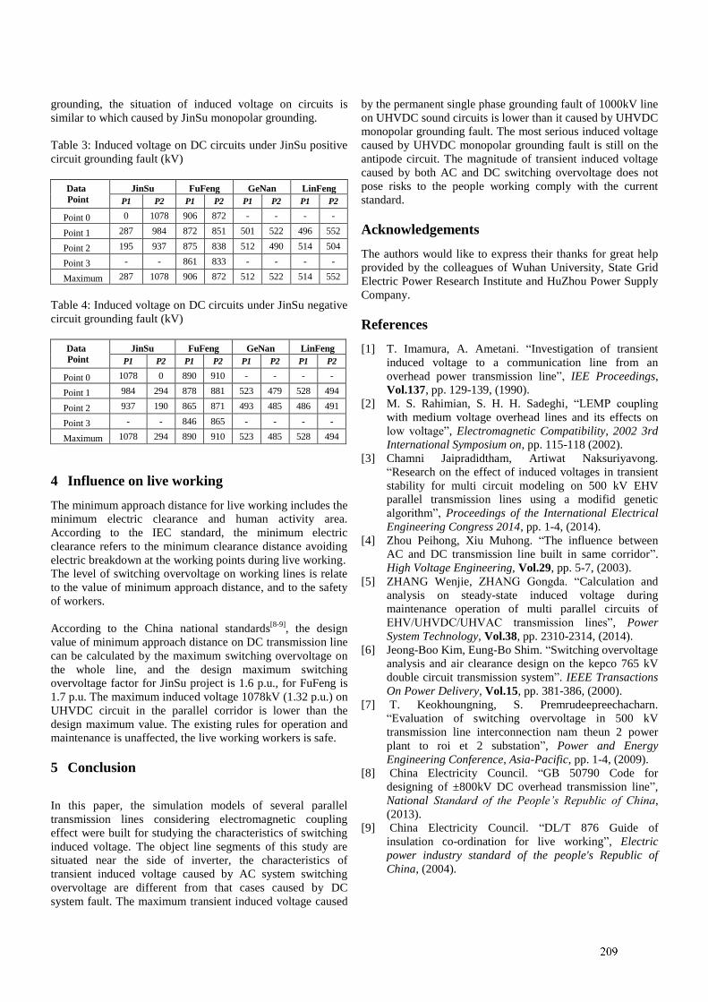
3
grounding, the situation of induced voltage on circuits is
similar to which caused by JinSu monopolar grounding.
Table 3: Induced voltage on DC circuits under JinSu positive
circuit grounding fault (kV)
Data
Point
JinSu FuFeng GeNan LinFeng
P1 P2 P1 P2 P1 P2 P1 P2
Point 0 0 1078 906 872 - - - -
Point 1 287 984 872 851 501 522 496 552
Point 2 195 937 875 838 512 490 514 504
Point 3 - - 861 833 - - - -
Maximum 287 1078 906 872 512 522 514 552
Table 4: Induced voltage on DC circuits under JinSu negative
circuit grounding fault (kV)
Data
Point
JinSu FuFeng GeNan LinFeng
P1 P2 P1 P2 P1 P2 P1 P2
Point 0 1078 0 890 910 - - - -
Point 1 984 294 878 881 523 479 528 494
Point 2 937 190 865 871 493 485 486 491
Point 3 - - 846 865 - - - -
Maximum 1078 294 890 910 523 485 528 494
4 Influence on live working
The minimum approach distance for live working includes the
minimum electric clearance and human activity area.
According to the IEC standard, the minimum electric
clearance refers to the minimum clearance distance avoiding
electric breakdown at the working points during live working.
The level of switching overvoltage on working lines is relate
to the value of minimum approach distance, and to the safety
of workers.
According to the China national standards[8-9]
, the design
value of minimum approach distance on DC transmission line
can be calculated by the maximum switching overvoltage on
the whole line, and the design maximum switching
overvoltage factor for JinSu project is 1.6 p.u., for FuFeng is
1.7 p.u. The maximum induced voltage 1078kV (1.32 p.u.) on
UHVDC circuit in the parallel corridor is lower than the
design maximum value. The existing rules for operation and
maintenance is unaffected, the live working workers is safe.
5 Conclusion
In this paper, the simulation models of several parallel
transmission lines considering electromagnetic coupling
effect were built for studying the characteristics of switching
induced voltage. The object line segments of this study are
situated near the side of inverter, the characteristics of
transient induced voltage caused by AC system switching
overvoltage are different from that cases caused by DC
system fault. The maximum transient induced voltage caused
by the permanent single phase grounding fault of 1000kV line
on UHVDC sound circuits is lower than it caused by UHVDC
monopolar grounding fault. The most serious induced voltage
caused by UHVDC monopolar grounding fault is still on the
antipode circuit. The magnitude of transient induced voltage
caused by both AC and DC switching overvoltage does not
pose risks to the people working comply with the current
standard.
Acknowledgements
The authors would like to express their thanks for great help
provided by the colleagues of Wuhan University, State Grid
Electric Power Research Institute and HuZhou Power Supply
Company.
References
[1] T. Imamura, A. Ametani. “Investigation of transient
induced voltage to a communication line from an
overhead power transmission line”, IEE Proceedings,
Vol.137, pp. 129-139, (1990).
[2] M. S. Rahimian, S. H. H. Sadeghi, “LEMP coupling
with medium voltage overhead lines and its effects on
low voltage”, Electromagnetic Compatibility, 2002 3rd
International Symposium on, pp. 115-118 (2002).
[3] Chamni Jaipradidtham, Artiwat Naksuriyavong.
“Research on the effect of induced voltages in transient
stability for multi circuit modeling on 500 kV EHV
parallel transmission lines using a modifid genetic
algorithm”, Proceedings of the International Electrical
Engineering Congress 2014, pp. 1-4, (2014).
[4] Zhou Peihong, Xiu Muhong. “The influence between
AC and DC transmission line built in same corridor”.
High Voltage Engineering, Vol.29, pp. 5-7, (2003).
[5] ZHANG Wenjie, ZHANG Gongda. “Calculation and
analysis on steady-state induced voltage during
maintenance operation of multi parallel circuits of
EHV/UHVDC/UHVAC transmission lines”, Power
System Technology, Vol.38, pp. 2310-2314, (2014).
[6] Jeong-Boo Kim, Eung-Bo Shim. “Switching overvoltage
analysis and air clearance design on the kepco 765 kV
double circuit transmission system”. IEEE Transactions
On Power Delivery, Vol.15, pp. 381-386, (2000).
[7] T. Keokhoungning, S. Premrudeepreechacharn.
“Evaluation of switching overvoltage in 500 kV
transmission line interconnection nam theun 2 power
plant to roi et 2 substation”, Power and Energy
Engineering Conference, Asia-Pacific, pp. 1-4, (2009).
[8] China Electricity Council. “GB 50790 Code for
designing of ±800kV DC overhead transmission line”,
National Standard of the People’s Republic of China,
(2013).
[9] China Electricity Council. “DL/T 876 Guide of
insulation co-ordination for live working”, Electric
power industry standard of the people's Republic of
China, (2004).
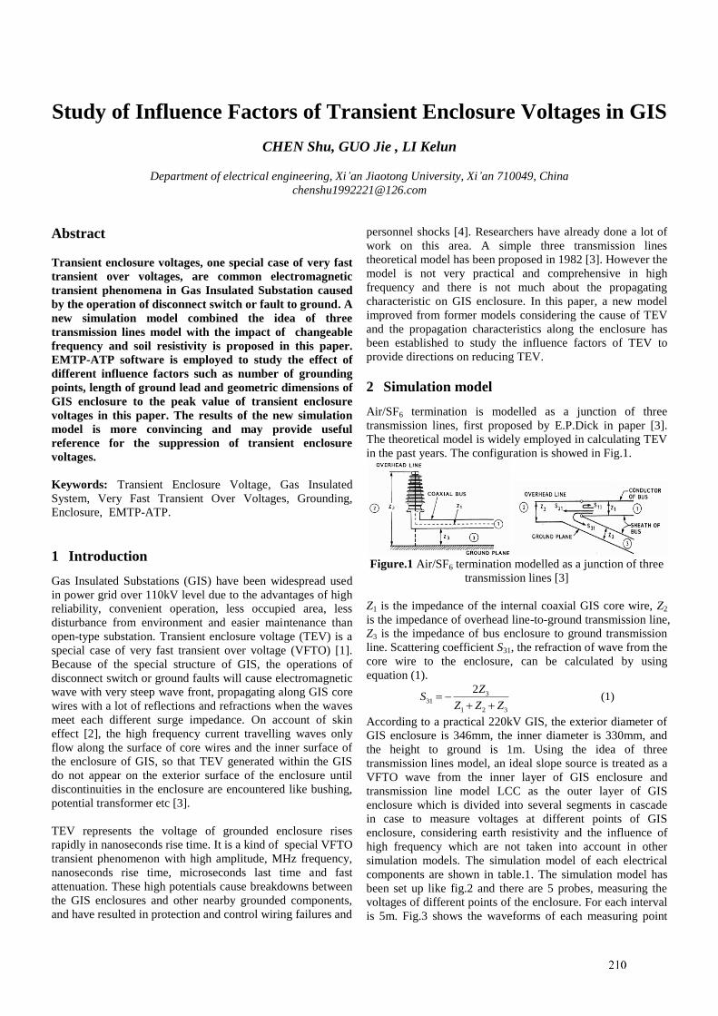
1
Study of Influence Factors of Transient Enclosure Voltages in GIS
CHEN Shu, GUO Jie , LI Kelun
Department of electrical engineering, Xi’an Jiaotong University, Xi’an 710049, China
Abstract
Transient enclosure voltages, one special case of very fast
transient over voltages, are common electromagnetic
transient phenomena in Gas Insulated Substation caused
by the operation of disconnect switch or fault to ground. A
new simulation model combined the idea of three
transmission lines model with the impact of changeable
frequency and soil resistivity is proposed in this paper.
EMTP-ATP software is employed to study the effect of
different influence factors such as number of grounding
points, length of ground lead and geometric dimensions of
GIS enclosure to the peak value of transient enclosure
voltages in this paper. The results of the new simulation
model is more convincing and may provide useful
reference for the suppression of transient enclosure
voltages.
Keywords: Transient Enclosure Voltage, Gas Insulated
System, Very Fast Transient Over Voltages, Grounding,
Enclosure, EMTP-ATP.
1 Introduction
Gas Insulated Substations (GIS) have been widespread used
in power grid over 110kV level due to the advantages of high
reliability, convenient operation, less occupied area, less
disturbance from environment and easier maintenance than
open-type substation. Transient enclosure voltage (TEV) is a
special case of very fast transient over voltage (VFTO) [1].
Because of the special structure of GIS, the operations of
disconnect switch or ground faults will cause electromagnetic
wave with very steep wave front, propagating along GIS core
wires with a lot of reflections and refractions when the waves
meet each different surge impedance. On account of skin
effect [2], the high frequency current travelling waves only
flow along the surface of core wires and the inner surface of
the enclosure of GIS, so that TEV generated within the GIS
do not appear on the exterior surface of the enclosure until
discontinuities in the enclosure are encountered like bushing,
potential transformer etc [3].
TEV represents the voltage of grounded enclosure rises
rapidly in nanoseconds rise time. It is a kind of special VFTO
transient phenomenon with high amplitude, MHz frequency,
nanoseconds rise time, microseconds last time and fast
attenuation. These high potentials cause breakdowns between
the GIS enclosures and other nearby grounded components,
and have resulted in protection and control wiring failures and
personnel shocks [4]. Researchers have already done a lot of
work on this area. A simple three transmission lines
theoretical model has been proposed in 1982 [3]. However the
model is not very practical and comprehensive in high
frequency and there is not much about the propagating
characteristic on GIS enclosure. In this paper, a new model
improved from former models considering the cause of TEV
and the propagation characteristics along the enclosure has
been established to study the influence factors of TEV to
provide directions on reducing TEV.
2 Simulation model
Air/SF6 termination is modelled as a junction of three
transmission lines, first proposed by E.P.Dick in paper [3].
The theoretical model is widely employed in calculating TEV
in the past years. The configuration is showed in Fig.1.
Figure.1 Air/SF6 termination modelled as a junction of three
transmission lines [3]
Z1 is the impedance of the internal coaxial GIS core wire, Z2
is the impedance of overhead line-to-ground transmission line,
Z3 is the impedance of bus enclosure to ground transmission
line. Scattering coefficient S31, the refraction of wave from the
core wire to the enclosure, can be calculated by using
equation (1).
331
1 2 3
2 (1)
ZS
Z Z Z
According to a practical 220kV GIS, the exterior diameter of
GIS enclosure is 346mm, the inner diameter is 330mm, and
the height to ground is 1m. Using the idea of three
transmission lines model, an ideal slope source is treated as a
VFTO wave from the inner layer of GIS enclosure and
transmission line model LCC as the outer layer of GIS
enclosure which is divided into several segments in cascade
in case to measure voltages at different points of GIS
enclosure, considering earth resistivity and the influence of
high frequency which are not taken into account in other
simulation models. The simulation model of each electrical
components are shown in table.1. The simulation model has
been set up like fig.2 and there are 5 probes, measuring the
voltages of different points of the enclosure. For each interval
is 5m. Fig.3 shows the waveforms of each measuring point
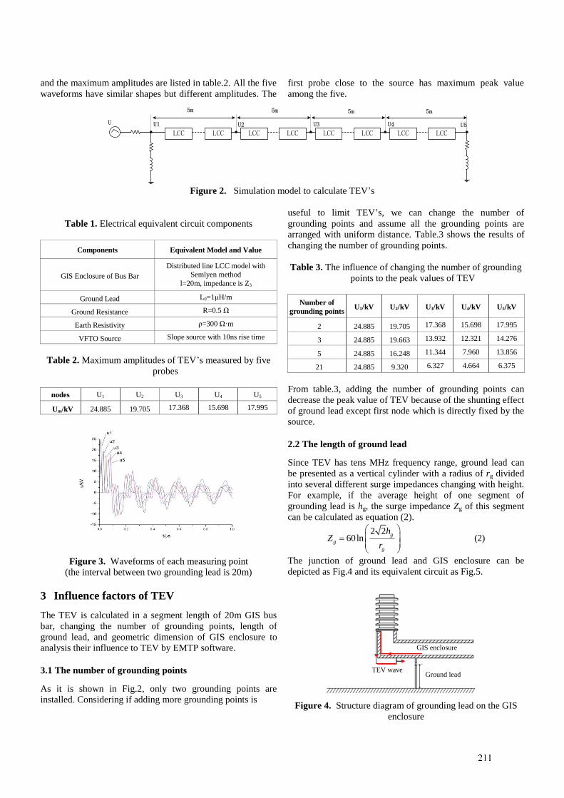
2
and the maximum amplitudes are listed in table.2. All the five
waveforms have similar shapes but different amplitudes. The
first probe close to the source has maximum peak value
among the five.
LCCU1U U5
LCC LCC LCCU2
LCC LCCU3
LCC LCCU4
5m 5m 5m 5m
Figure 2. Simulation model to calculate TEV’s
Table 1. Electrical equivalent circuit components
Components Equivalent Model and Value
GIS Enclosure of Bus Bar
Distributed line LCC model with
Semlyen method
l=20m, impedance is Z3
Ground Lead L0=1μH/m
Ground Resistance R=0.5 Ω
Earth Resistivity ρ=300 Ω·m
VFTO Source Slope source with 10ns rise time
Table 2. Maximum amplitudes of TEV’s measured by five
probes
nodes U1 U2 U3 U4 U5
Um/kV 24.885 19.705 17.368 15.698 17.995
Figure 3. Waveforms of each measuring point
(the interval between two grounding lead is 20m)
3 Influence factors of TEV
The TEV is calculated in a segment length of 20m GIS bus
bar, changing the number of grounding points, length of
ground lead, and geometric dimension of GIS enclosure to
analysis their influence to TEV by EMTP software.
3.1 The number of grounding points
As it is shown in Fig.2, only two grounding points are
installed. Considering if adding more grounding points is
useful to limit TEV’s, we can change the number of
grounding points and assume all the grounding points are
arranged with uniform distance. Table.3 shows the results of
changing the number of grounding points.
Table 3. The influence of changing the number of grounding
points to the peak values of TEV
Number of
grounding points U1/kV U2/kV U3/kV U4/kV U5/kV
2 24.885 19.705 17.368 15.698 17.995
3 24.885 19.663 13.932 12.321 14.276
5 24.885 16.248 11.344 7.960 13.856
21 24.885 9.320 6.327 4.664 6.375
From table.3, adding the number of grounding points can
decrease the peak value of TEV because of the shunting effect
of ground lead except first node which is directly fixed by the
source.
2.2 The length of ground lead
Since TEV has tens MHz frequency range, ground lead can
be presented as a vertical cylinder with a radius of rg divided
into several different surge impedances changing with height.
For example, if the average height of one segment of
grounding lead is hg, the surge impedance Zg of this segment
can be calculated as equation (2).
2 260ln (2)
g
g
g
hZ
r
The junction of ground lead and GIS enclosure can be
depicted as Fig.4 and its equivalent circuit as Fig.5.
GIS enclosure
TEV waveGround lead
Figure 4. Structure diagram of grounding lead on the GIS
enclosure
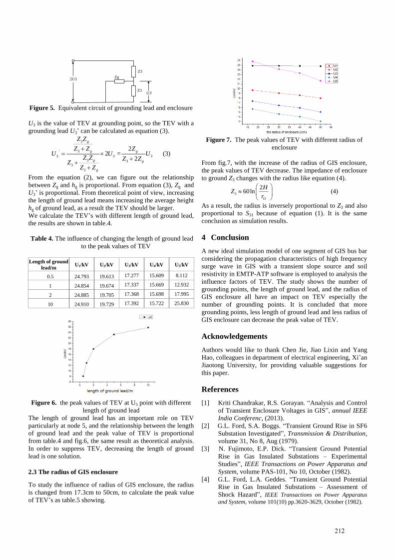
3
Z3
Zg
Z3
2U3
U3'
Figure 5. Equivalent circuit of grounding lead and enclosure
U3 is the value of TEV at grounding point, so the TEV with a
grounding lead U3’ can be calculated as equation (3).
3
3'
3 3 33 3
3
3
22 = (3)
2
g
g g
g g
g
Z Z
Z Z ZU U U
Z Z Z ZZ
Z Z
From the equation (2), we can figure out the relationship
between Zg and hg is proportional. From equation (3), Zg and
U3’ is proportional. From theoretical point of view, increasing
the length of ground lead means increasing the average height
hg of ground lead, as a result the TEV should be larger.
We calculate the TEV’s with different length of ground lead,
the results are shown in table.4.
Table 4. The influence of changing the length of ground lead
to the peak values of TEV
Length of ground
lead/m U1/kV U2/kV U3/kV U4/kV U5/kV
0.5 24.793 19.613 17.277 15.609 8.112
1 24.854 19.674 17.337 15.669 12.932
2 24.885 19.705 17.368 15.698 17.995
10 24.910 19.729 17.392 15.722 25.830
Figure 6. the peak values of TEV at U5 point with different
length of ground lead
The length of ground lead has an important role on TEV
particularly at node 5, and the relationship between the length
of ground lead and the peak value of TEV is proportional
from table.4 and fig.6, the same result as theoretical analysis.
In order to suppress TEV, decreasing the length of ground
lead is one solution.
2.3 The radius of GIS enclosure
To study the influence of radius of GIS enclosure, the radius
is changed from 17.3cm to 50cm, to calculate the peak value
of TEV’s as table.5 showing.
Figure 7. The peak values of TEV with different radius of
enclosure
From fig.7, with the increase of the radius of GIS enclosure,
the peak values of TEV decrease. The impedance of enclosure
to ground Z3 changes with the radius like equation (4).
3
260ln (4)
O
HZ
r
As a result, the radius is inversely proportional to Z3 and also
proportional to S31 because of equation (1). It is the same
conclusion as simulation results.
4 Conclusion
A new ideal simulation model of one segment of GIS bus bar
considering the propagation characteristics of high frequency
surge wave in GIS with a transient slope source and soil
resistivity in EMTP-ATP software is employed to analysis the
influence factors of TEV. The study shows the number of
grounding points, the length of ground lead, and the radius of
GIS enclosure all have an impact on TEV especially the
number of grounding points. It is concluded that more
grounding points, less length of ground lead and less radius of
GIS enclosure can decrease the peak value of TEV.
Acknowledgements
Authors would like to thank Chen Jie, Jiao Lixin and Yang
Hao, colleagues in department of electrical engineering, Xi’an
Jiaotong University, for providing valuable suggestions for
this paper.
References
[1] Kriti Chandrakar, R.S. Gorayan. “Analysis and Control
of Transient Enclosure Voltages in GIS”, annual IEEE
India Conferenc, (2013).
[2] G.L. Ford, S.A. Boggs. “Transient Ground Rise in SF6
Substation Investigated”, Transmission & Distribution,
volume 31, No 8, Aug (1979).
[3] N. Fujimoto, E.P. Dick. “Transient Ground Potential
Rise in Gas Insulated Substations – Experimental
Studies”, IEEE Transactions on Power Apparatus and
System, volume PAS-101, No 10, October (1982).
[4] G.L. Ford, L.A. Geddes. “Transient Ground Potential
Rise in Gas Insulated Substations – Assessment of
Shock Hazard”, IEEE Transactions on Power Apparatus
and System, volume 101(10) pp.3620-3629, October (1982).
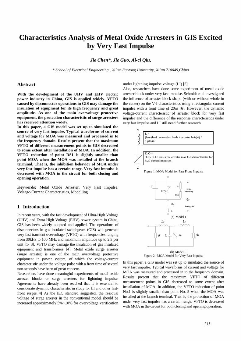
1
Characteristics Analysis of Metal Oxide Arresters in GIS Excited
by Very Fast Impulse
Jie Chen*, Jie Guo, Ai-ci Qiu,
* School of Electrical Engineering , Xi’an Jiaotong University, Xi’an 710049,China
Abstract
With the development of the UHV and EHV electric
power industry in China, GIS is applied widely. VFTO
caused by disconnector operations in GIS may damage the
insulation of equipment for its high frequency and great
amplitude. As one of the main overvoltage protective
equipment, the protection characteristic of surge arresters
has received attention widely.
In this paper, a GIS model was set up to simulated the
source of very fast impulse. Typical waveforms of current
and voltage for MOA was measured and processed in to
the frequency domain. Results present that the maximum
VFTO of different measurement points in GIS decreased
to some extent after installation of MOA. In addition, the
VFTO reduction of point DS1 is slightly smaller than
point MOA when the MOA was installed at the branch
terminal. That is, the inhibition behavior of MOA under
very fast impulse has a certain range. Very fast impulse is
decreased with MOA in the circuit for both closing and
opening operation.
Keywords: Metal Oxide Arrester, Very Fast Impulse,
Voltage-Current Characteristics, Modelling
1 Introduction
In recent years, with the fast development of Ultra-High Voltage
(UHV) and Extra-High Voltage (EHV) power system in China,
GIS has been widely adopted and applied. The operations of
disconnectors in gas insulated switchgears (GIS) will generate
very fast transient overvoltage (VFTO) with frequencies ranging
from 30kHz to 100 MHz and maximum amplitude up to 2.5 per
unit [1- 3]. VFTO may damage the insulation of gas insulated
equipment and transformers [4]. Metal oxide surge arrester
(surge arrester) is one of the main overvoltage protective
equipment in power system, of which the voltage-current
characteristic under the voltage pulse with a front time of several
non-seconds have been of great concern.
Researchers have done meaningful experiments of metal oxide
arrester blocks or surge arresters for lightning impulse.
Agreements have already been reached that it is essential to
considerate dynamic characteristic in study for LI and other fast-
front surges.[4] As the IEC standard suggested, the residual
voltage of surge arrester in the conventional model should be
increased approximately 5%~10% for overvoltage verification
under lightning impulse voltage (LI) [5].
Also, researchers have done some experiment of metal oxide
arrester block under very fast impulse. Schmidt et al investigated
the influence of arrester block shape (with or without whole in
the center) on the V-I characteristics using a rectangular current
impulse with a front time of 20ns [6]. However, the dynamic
voltage-current characteristic of arrester block for very fast
impulse and the difference of the response characteristics under
very fast impulse and LI still need further research.
L =
(length of connection leads + arrester height) *
1 mH/m
ZnO =
1.05 to 1.1 times the arrester max U-I characteristic for
8/20 current impulses
Figure 1. MOA Model for Fast Front Impulse
C
R0
L
Agrain
boundary
ZnO-grain
R(T)
R(t)
(a) Model I
L1L0
A0 A1R C
(b) Model II
Figure 2. MOA Model for Very Fast Impulse
In this paper, a GIS model was set up to simulated the source of
very fast impulse. Typical waveforms of current and voltage for
MOA was measured and processed in to the frequency domain.
Results present that the maximum VFTO of different
measurement points in GIS decreased to some extent after
installation of MOA. In addition, the VFTO reduction of point
No.1 is slightly smaller than point No. 5 when the MOA was
installed at the branch terminal. That is, the protection of MOA
under very fast impulse has a certain range. VFTO is decreased
with MOA in the circuit for both closing and opening operation.
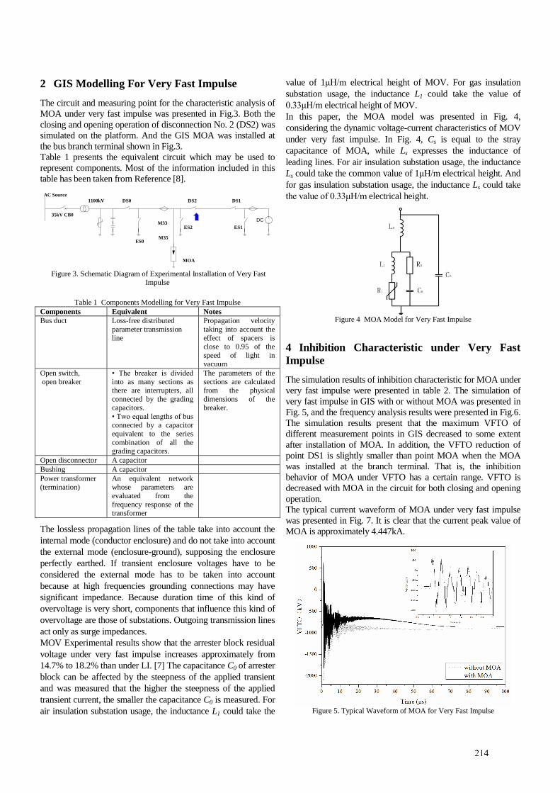
2
2 GIS Modelling For Very Fast Impulse
The circuit and measuring point for the characteristic analysis of
MOA under very fast impulse was presented in Fig.3. Both the
closing and opening operation of disconnection No. 2 (DS2) was
simulated on the platform. And the GIS MOA was installed at
the bus branch terminal shown in Fig.3.
Table 1 presents the equivalent circuit which may be used to
represent components. Most of the information included in this
table has been taken from Reference [8].
AC Source
35kV CB0
DS0
ES0
1100kV
ES2
DS2 DS1
ES1
DC
MOA
M33
M35
Figure 3. Schematic Diagram of Experimental Installation of Very Fast Impulse
Table 1 Components Modelling for Very Fast Impulse
Components Equivalent Notes
Bus duct Loss-free distributed
parameter transmission
line
Propagation velocity
taking into account the
effect of spacers is close to 0.95 of the
speed of light in vacuum
Open switch,
open breaker
• The breaker is divided
into as many sections as there are interrupters, all
connected by the grading capacitors.
• Two equal lengths of bus
connected by a capacitor equivalent to the series
combination of all the grading capacitors.
The parameters of the
sections are calculated from the physical
dimensions of the breaker.
Open disconnector A capacitor
Bushing A capacitor
Power transformer (termination)
An equivalent network whose parameters are
evaluated from the
frequency response of the transformer
The lossless propagation lines of the table take into account the
internal mode (conductor enclosure) and do not take into account
the external mode (enclosure-ground), supposing the enclosure
perfectly earthed. If transient enclosure voltages have to be
considered the external mode has to be taken into account
because at high frequencies grounding connections may have
significant impedance. Because duration time of this kind of
overvoltage is very short, components that influence this kind of
overvoltage are those of substations. Outgoing transmission lines
act only as surge impedances.
MOV Experimental results show that the arrester block residual
voltage under very fast impulse increases approximately from
14.7% to 18.2% than under LI. [7] The capacitance C0 of arrester
block can be affected by the steepness of the applied transient
and was measured that the higher the steepness of the applied
transient current, the smaller the capacitance C0 is measured. For
air insulation substation usage, the inductance L1 could take the
value of 1μH/m electrical height of MOV. For gas insulation
substation usage, the inductance L1 could take the value of
0.33μH/m electrical height of MOV.
In this paper, the MOA model was presented in Fig. 4,
considering the dynamic voltage-current characteristics of MOV
under very fast impulse. In Fig. 4, Cs is equal to the stray
capacitance of MOA, while Ls expresses the inductance of
leading lines. For air insulation substation usage, the inductance
Ls could take the common value of 1μH/m electrical height. And
for gas insulation substation usage, the inductance Ls could take
the value of 0.33μH/m electrical height.
Figure 4 MOA Model for Very Fast Impulse
4 Inhibition Characteristic under Very Fast
Impulse
The simulation results of inhibition characteristic for MOA under
very fast impulse were presented in table 2. The simulation of
very fast impulse in GIS with or without MOA was presented in
Fig. 5, and the frequency analysis results were presented in Fig.6.
The simulation results present that the maximum VFTO of
different measurement points in GIS decreased to some extent
after installation of MOA. In addition, the VFTO reduction of
point DS1 is slightly smaller than point MOA when the MOA
was installed at the branch terminal. That is, the inhibition
behavior of MOA under VFTO has a certain range. VFTO is
decreased with MOA in the circuit for both closing and opening
operation.
The typical current waveform of MOA under very fast impulse
was presented in Fig. 7. It is clear that the current peak value of
MOA is approximately 4.447kA.
Figure 5. Typical Waveform of MOA for Very Fast Impulse
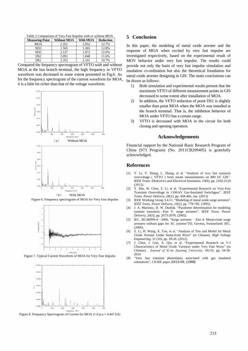
3
Table 2 Comparison of Very Fast Impulse with or without MOA
Measuring Point Without MOA With MOA Reduction
MOA 2.351 2.052 12.7% M33 1.565 1.365 12.8% M35 2.127 1.872 12.0% DS2 2.091 1.848 11.6% DS1 2.352 2.101 10.7%
Compared the frequency spectrogram of VFTO with and without
MOA at the bus branch terminal, the high frequency in VFTO
waveform was decreased to some extent presented in Fig.6. As
for the frequency spectrogram of the current waveform for MOA,
it is a little bit richer than that of the voltage waveform.
(a) Without MOA
(b) With MOA
Figure 6. Frequency spectrogram of MOA for Very Fast Impulse
Figure 7. Typical Current Waveform of MOA for Very Fast Impulse
Figure 8. Frequency Spectrogram of Current for MOA (1.0 p.u.= 4.447 kA)
5 Conclusion
In this paper, the modeling of metal oxide arrester and the
response of MOA when excited by very fast impulse are
investigated respectively, based on the experimental result of
MOV behavior under very fast impulse. The results could
provide not only the basis of very fast impulse simulation and
insulation co-ordination but also the theoretical foundation for
metal oxide arrester designing in GIS. The main conclusions can
be drawn as follows:
1) Both simulation and experimental results present that the
maximum VFTO of different measurement points in GIS
decreased to some extent after installation of MOA.
2) In addition, the VFTO reduction of point DS1 is slightly
smaller than point MOA when the MOA was installed at
the branch terminal. That is, the inhibition behavior of
MOA under VFTO has a certain range.
3) VFTO is decreased with MOA in the circuit for both
closing and opening operation.
Acknowledgements
Financial support by the National Basic Research Program of
China (973 Program) (No. 2011CB209405) is gratefully
acknowledged.
References
[1] Y. Li, Y. Shang, L. Zhang, et al. “Analysis of very fast transient
overvoltage ( VFTO ) from onsite measurements on 800 kV GIS”. IEEE Trans. Dielectrics and Electrical Insulation, 19(6), pp. 2102-2110.
(2012). [2] Y. Shu, W. Chen, Z. Li, et al. “Experimental Research on Very-Fast
Transient Overvoltage in 1100-kV Gas-Insulated Switchgear”. IEEE
Trans. Power Delivery, 28(1), pp. 458-466. Jan. (2013) [3] IEEE Working Group 3.4.11. “Modeling of metal oxide surge arresters”.
IEEE Trans. Power Delivery, 10(2), pp. 778-785. (1995). [4] J. A. Martinez, D. W. Durbak. “Parameter determination for modeling
systems transients—Part V: surge arresters”. IEEE Trans. Power
Delivery, 20(3), pp. 2073-2078. (2005).
[5] IEC. IEC60099-4—2006, “Surge arresters – Part 4: Metal-oxide surge
arresters without gaps for AC systems”[S]. Gevena, Switzerland: IEC,
(2006). [6] Z. Li, H. Wang, X. Yan, et al. “Analysis of Test and Model for Metal
Oxide Arrester Under Steep-front Wave” (in Chinese). High Voltage Engineering, 31 (10), pp. 18-20. (2012).
[7] J. Chen, J. Guo, A. Qiu, et al. “Experimental Research on V-I
Characteristics of Metal Oxide Varistors under Very Fast Wave” (in Chinese) . Journal of Xi’an Jiaotong University, 48(10), pp. 54-59.
2014 [8] "Very fast transient phenomena associated with gas insulated
substations", CIGRE paper.33/13-09, (1988)
Influence of Ground Wires on Ion Flow Field around HVDC
Transmission Lines
Bo Zhang, Jinliang He
State Key Lab of Power Systems, Dept. of Electrical Engineering, Tsinghua University, Beijing 100084, China
Abstract
The electric field is one of the most important factors to be
considered in the design of a transmission line. Due to
corona, there are ions in the space around HVDC
transmission lines, which makes the electric field more
complex. The ground wires of the transmission line will
enhance the corona on the conductors but will absorb
more ions from the space at the same time. In this paper,
the ion flow fields are simulated by a numerical method.
The influence of the height and the number of the ground
wires on the ion flow field around HVDC transmission
lines is also discussed.
Keywords: Corona, electric field, ions, HVDC Transmission
Lines.
1 Introduction
There are space charges around HVDC transmission lines due
to corona discharge which forms ion flow field. The ion flow
field on the ground is one of the special parameters compared
with the HVAC transmission lines. The total electric field in
the ion flow field is composed of two parts. One is that from
the charged transmission line itself. The other is that from the
space charge. As the space charge will move with the electric
field, the ion flow field is nonlinear.
There have already been some methods to evaluate the ion
flow field near the transmission lines, such as the analytic
methods, semi-analytical methods, and numerical methods.
Sometimes, some methods do not take the ground wires into
account. However, on one hand, the ground wires of the
transmission line will increase the electric field on the surface
of the conductors, and then enhance the corona discharge,
which will increase the ions in the space. On the other hand,
the ground wires can absorb the space charges. Thus, whether
the ground wires will increase or decrease the electric field on
the ground is an interesting problem.
In this paper, the ion flow fields are simulated by a numerical
method. The influence of the height and the number of the
ground wires on the ion flow field around HVDC
transmission lines is also discussed. The results would be
useful for design of HVDC transmission lines.
2 Numerical Method
The equations which rule the bipolar ion field are [1]:
0/)( E (1)
)(),( WEJWEJ kk , (2)
,/,/ eReR JJ (3)
where J, ρ, k, R, e, and W are ion current density, ion density,
ion mobility, ion recombination coefficient, electron charge,
and wind velocity respectively. Superscripts “+” and “-”
indicate that corresponding variables are for positive or
negative ion. Because the electric fields and the ions affect
each other naturally, iterative method is used. The main
process of the method in this paper is as follows:
1) Simulating charges in the conductors are calculated based
on the applied voltages at conductor surfaces and ground
by ignoring the existence of the ions in the air. The region
of interest is subdivided in to small triangular elements.
The iterative process is started by assigning initial vales to
ρ+ and ρ
- around the grid nodes.
2) The electric fields at the middle points of the sides of
triangular elements are calculated based on the Gauss’ law.
3) The equations for calculating the ion densities around the
grid nodes are set up based on the integral form of the
current continuity equation.
4) Setp 2 and step 3 will be repeated until the ion densities
obtained in two consecutive iterations differ from each
other by amounts smaller than specified tolerances.
The ground wires can be regarded as special conductors on
which the potential is zero. And then, they can be taken into
account by above method.
3 Influence of the Position and the Number of
the Ground Wires
In order to obtain the effect of the ground wires on the ion
flow field on the ground, the ion flow fields near the ±800-kV
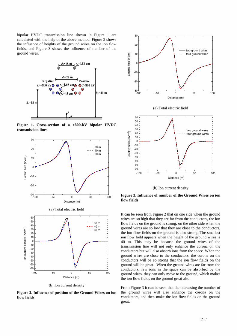
bipolar HVDC transmission line shown in Figure 1 are
calculated with the help of the above method. Figure 2 shows
the influence of heights of the ground wires on the ion flow
fields, and Figure 3 shows the influence of number of the
ground wires.
Figure 1. Cross-section of a ±800-kV bipolar HVDC
transmission lines.
-100 -50 0 50 100-30
-20
-10
0
10
20
30
Ele
ctr
ic f
ield
(kV
/m)
Distance (m)
30 m
40 m
60 m
(a) Total electric field
-100 -50 0 50 100
-70
-60
-50
-40
-30
-20
-10
0
10
20
30
40
50
60
Ion c
urr
ent
den
sity (
nA
/m2)
Distance (m)
30 m
40 m
60 m
(b) Ion current density
Figure 2. Influence of position of the Ground Wires on ion
flow fields
-100 -50 0 50 100-30
-20
-10
0
10
20
30
Ele
ctr
ic f
ield
(kV
/m)
Distance (m)
two ground wires
four ground wires
(a) Total electric field
-100 -50 0 50 100
-70
-60
-50
-40
-30
-20
-10
0
10
20
30
40
50
60
Ion f
low
fie
ld (
nA
/m2)
Distance (m)
two ground wires
four ground wires
(b) Ion current density
Figure 3. Influence of number of the Ground Wires on ion
flow fields
It can be seen from Figure 2 that on one side when the ground
wires are so high that they are far from the conductors, the ion
flow fields on the ground is strong, on the other side when the
ground wires are so low that they are close to the conductors,
the ion flow fields on the ground is also strong. The smallest
ion flow field appears when the height of the ground wires is
40 m. This may be because the ground wires of the
transmission line will not only enhance the corona on the
conductors but will also absorb ions from the space. When the
ground wires are close to the conductors, the corona on the
conductors will be so strong that the ion flow fields on the
ground will be great. When the ground wires are far from the
conductors, few ions in the space can be absorbed by the
ground wires, they can only move to the ground, which makes
the ion flow fields on the ground great also.
From Figure 3 it can be seen that the increasing the number of
the ground wires will also enhance the corona on the
conductors, and then make the ion flow fields on the ground
great.

However, no matter what mechanism the influence is, for the
parameters used in the paper, the influence of the ground
wires on the ion flow fields on the ground is small.
4. Conclusion
In this paper, the influence of the height and the number of
the ground wires on the ion flow field around HVDC
transmission lines is discussed. The ground wires of the
transmission line will not only enhance the corona on the
conductors but will also absorb ions from the space. However,
no matter what mechanism the influence is, the influence of
the ground wires on the ion flow fields on the ground is small.
Acknowledgements
This work was supported in part by the National Natural
Science Foundations of China under Grant 51322703, and in
part by the Basic Research Program of China National Basic
Research Program of China (973 Program) under Grant
2011CB2094-01.
References
[1] Bo Zhang, Jinliang He, Rong Zeng, et al., “Calculation
of ion flow field under HVdc bipolar transmission lines
by integral equation method,” IEEE Transactions on
Magnetics, Vol. 43, No. 4, pp. 1237–1240, July 2007.
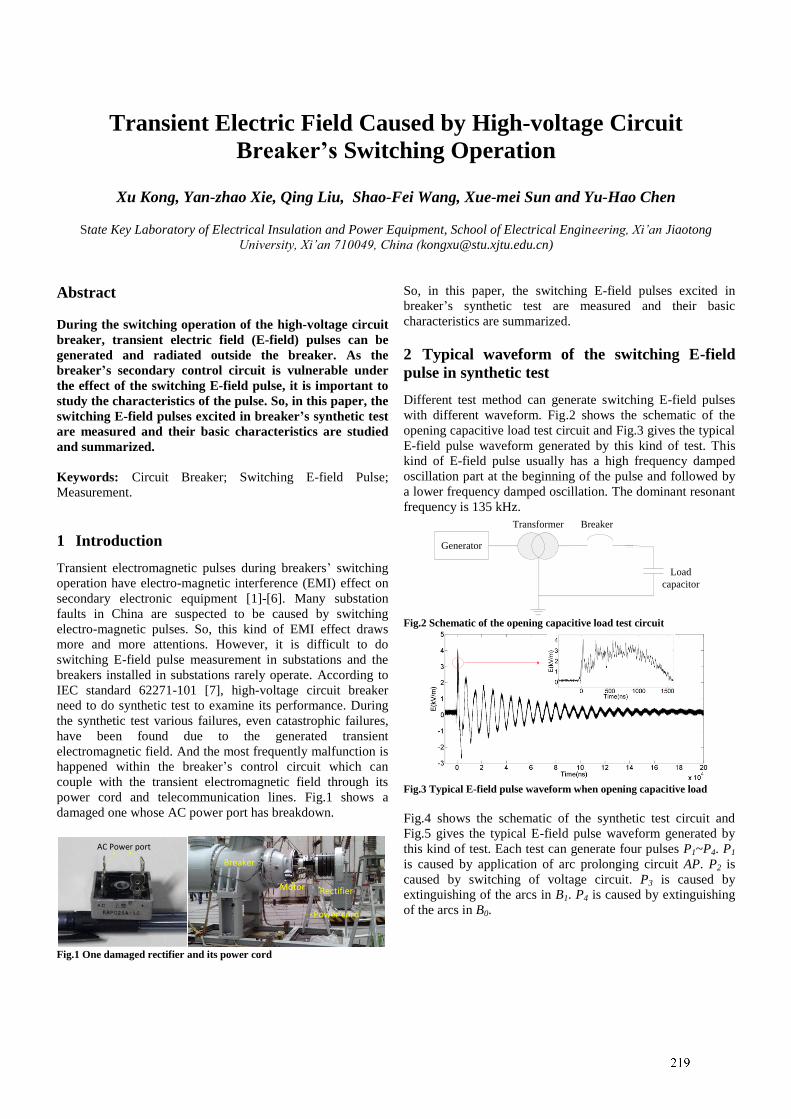
1
Transient Electric Field Caused by High-voltage Circuit
Breaker’s Switching Operation
Xu Kong, Yan-zhao Xie, Qing Liu, Shao-Fei Wang, Xue-mei Sun and Yu-Hao Chen
State Key Laboratory of Electrical Insulation and Power Equipment, School of Electrical Engineering, Xi’an Jiaotong
University, Xi’an 710049, China ([email protected])
Abstract
During the switching operation of the high-voltage circuit
breaker, transient electric field (E-field) pulses can be
generated and radiated outside the breaker. As the
breaker’s secondary control circuit is vulnerable under
the effect of the switching E-field pulse, it is important to
study the characteristics of the pulse. So, in this paper, the
switching E-field pulses excited in breaker’s synthetic test
are measured and their basic characteristics are studied
and summarized.
Keywords: Circuit Breaker; Switching E-field Pulse;
Measurement.
1 Introduction
Transient electromagnetic pulses during breakers’ switching
operation have electro-magnetic interference (EMI) effect on
secondary electronic equipment [1]-[6]. Many substation
faults in China are suspected to be caused by switching
electro-magnetic pulses. So, this kind of EMI effect draws
more and more attentions. However, it is difficult to do
switching E-field pulse measurement in substations and the
breakers installed in substations rarely operate. According to
IEC standard 62271-101 [7], high-voltage circuit breaker
need to do synthetic test to examine its performance. During
the synthetic test various failures, even catastrophic failures,
have been found due to the generated transient
electromagnetic field. And the most frequently malfunction is
happened within the breaker’s control circuit which can
couple with the transient electromagnetic field through its
power cord and telecommunication lines. Fig.1 shows a
damaged one whose AC power port has breakdown.
AC Power port
Power cord
RectifierMotor
Breaker
Fig.1 One damaged rectifier and its power cord
So, in this paper, the switching E-field pulses excited in
breaker’s synthetic test are measured and their basic
characteristics are summarized.
2 Typical waveform of the switching E-field
pulse in synthetic test
Different test method can generate switching E-field pulses
with different waveform. Fig.2 shows the schematic of the
opening capacitive load test circuit and Fig.3 gives the typical
E-field pulse waveform generated by this kind of test. This
kind of E-field pulse usually has a high frequency damped
oscillation part at the beginning of the pulse and followed by
a lower frequency damped oscillation. The dominant resonant
frequency is 135 kHz.
Generator
Transformer
Load
capacitor
Breaker
Fig.2 Schematic of the opening capacitive load test circuit
Fig.3 Typical E-field pulse waveform when opening capacitive load
Fig.4 shows the schematic of the synthetic test circuit and
Fig.5 gives the typical E-field pulse waveform generated by
this kind of test. Each test can generate four pulses P1~P4. P1
is caused by application of arc prolonging circuit AP. P2 is
caused by switching of voltage circuit. P3 is caused by
extinguishing of the arcs in B1. P4 is caused by extinguishing
of the arcs in B0.
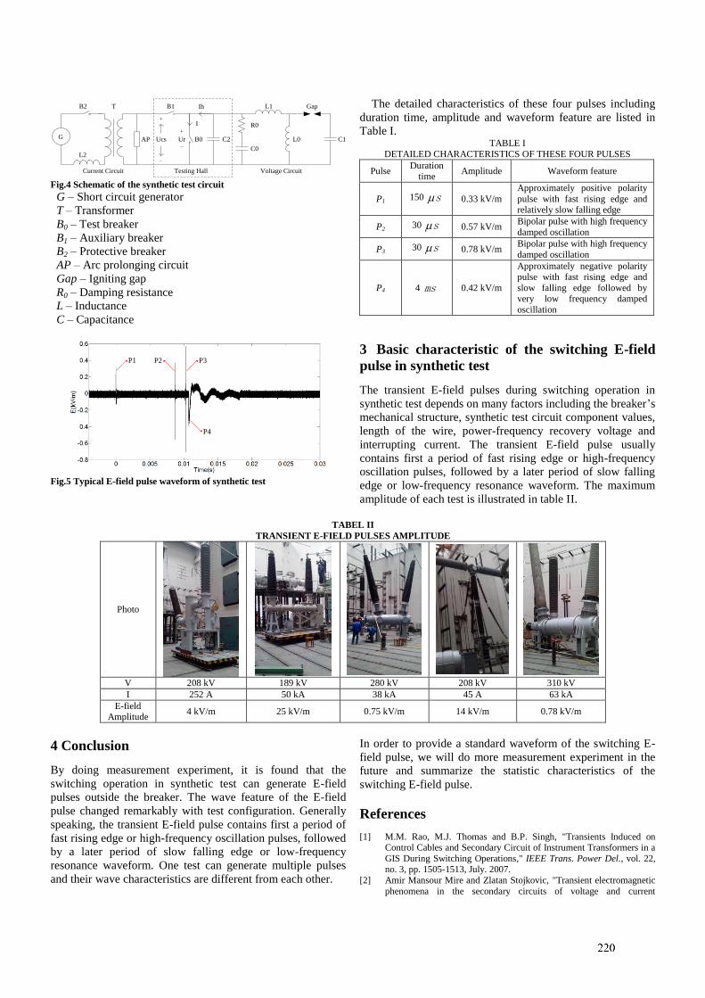
2
G C1
GapL1
L0
R0
C0
B0
B1B2
L2
T
AP C2
I
Ih
UrUcs
Testing Hall Current Circuit Voltage Circuit
Fig.4 Schematic of the synthetic test circuit
G – Short circuit generator
T – Transformer
B0 – Test breaker
B1 – Auxiliary breaker
B2 – Protective breaker
AP – Arc prolonging circuit
Gap – Igniting gap
R0 – Damping resistance
L – Inductance
C – Capacitance
P1 P2 P3
P4
Fig.5 Typical E-field pulse waveform of synthetic test
The detailed characteristics of these four pulses including
duration time, amplitude and waveform feature are listed in
Table I. TABLE I
DETAILED CHARACTERISTICS OF THESE FOUR PULSES
Pulse Duration
time Amplitude Waveform feature
P1 150 s 0.33 kV/m
Approximately positive polarity
pulse with fast rising edge and relatively slow falling edge
P2 30 s 0.57 kV/m Bipolar pulse with high frequency
damped oscillation
P3 30 s 0.78 kV/m Bipolar pulse with high frequency
damped oscillation
P4 4 ms 0.42 kV/m
Approximately negative polarity pulse with fast rising edge and
slow falling edge followed by very low frequency damped
oscillation
3 Basic characteristic of the switching E-field
pulse in synthetic test
The transient E-field pulses during switching operation in
synthetic test depends on many factors including the breaker’s
mechanical structure, synthetic test circuit component values,
length of the wire, power-frequency recovery voltage and
interrupting current. The transient E-field pulse usually
contains first a period of fast rising edge or high-frequency
oscillation pulses, followed by a later period of slow falling
edge or low-frequency resonance waveform. The maximum
amplitude of each test is illustrated in table II.
TABEL II
TRANSIENT E-FIELD PULSES AMPLITUDE
Photo
V 208 kV 189 kV 280 kV 208 kV 310 kV
I 252 A 50 kA 38 kA 45 A 63 kA
E-field Amplitude
4 kV/m 25 kV/m 0.75 kV/m 14 kV/m 0.78 kV/m
4 Conclusion
By doing measurement experiment, it is found that the
switching operation in synthetic test can generate E-field
pulses outside the breaker. The wave feature of the E-field
pulse changed remarkably with test configuration. Generally
speaking, the transient E-field pulse contains first a period of
fast rising edge or high-frequency oscillation pulses, followed
by a later period of slow falling edge or low-frequency
resonance waveform. One test can generate multiple pulses
and their wave characteristics are different from each other.
In order to provide a standard waveform of the switching E-
field pulse, we will do more measurement experiment in the
future and summarize the statistic characteristics of the
switching E-field pulse.
References
[1] M.M. Rao, M.J. Thomas and B.P. Singh, "Transients Induced on Control Cables and Secondary Circuit of Instrument Transformers in a
GIS During Switching Operations," IEEE Trans. Power Del., vol. 22, no. 3, pp. 1505-1513, July. 2007.
[2] Amir Mansour Mire and Zlatan Stojkovic, "Transient electromagnetic
phenomena in the secondary circuits of voltage and current
3
transformers in GIS (measurements and calculations)," IEEE Trans.
Power Del., vol. 16, no. 4, pp. 571-575, Oct. 2001. [3] Qi Huang, Xiao-hua Wang, Wei Zhen and Philip W. T. Pong,
"Broadband point measurement of transient magnetic interference in substations with magnetoresistive sensors," IEEE Trans. Magn., vol.
50, no. 7, pp. 1-5, July. 2014.
[4] Jin-liang He, Zhan-qing Yu, Rong Zeng, Bo Zhang Shui-ming Chen and Jun Hu, "Power-Frequency Voltage Withstand Characteristics of
Insulations of Substation Secondary Systems," IEEE Trans. Power Del., vol. 25, no. 2, pp. 734-746, Apr. 2010.
[5] Y. V. Parfenov, L. N. Zdoukhov, A. V. Shurupov and A. V. Kozlov,
"Research of Flashover of Power Line Insulators Due to High-Voltage Pulses With Power ON and Power OFF," IEEE Trans. Electromagn.
Compat., vol. 55, no. 3, pp. 467-474, June. 2013. [6] C.M. Wiggins and S.E. Wright, "Switching transient fields in
substations", IEEE Trans. Power Del., vol. 6, no. 2, pp. 591-600, Apr.
1991. [7] High-voltage switchgear and controlgear – Part 101: Synthetic testing,
IEC Standard 62271-101, 2012.
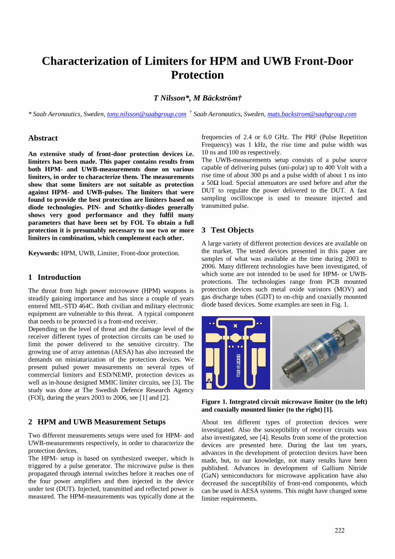
1
Characterization of Limiters for HPM and UWB Front-DoorProtection
T Nilsson*, M Bäckström†
* Saab Aeronautics, Sweden, [email protected] † Saab Aeronautics, Sweden, [email protected]
Abstract
An extensive study of front-door protection devices i.e.limiters has been made. This paper contains results fromboth HPM- and UWB-measurements done on variouslimiters, in order to characterize them. The measurementsshow that some limiters are not suitable as protectionagainst HPM- and UWB-pulses. The limiters that werefound to provide the best protection are limiters based ondiode technologies. PIN- and Schottky-diodes generallyshows very good performance and they fulfil manyparameters that have been set by FOI. To obtain a fullprotection it is presumably necessary to use two or morelimiters in combination, which complement each other.
Keywords: HPM, UWB, Limiter, Front-door protection.
1 IntroductionThe threat from high power microwave (HPM) weapons issteadily gaining importance and has since a couple of yearsentered MIL-STD 464C. Both civilian and military electronicequipment are vulnerable to this threat. A typical componentthat needs to be protected is a front-end receiver.Depending on the level of threat and the damage level of thereceiver different types of protection circuits can be used tolimit the power delivered to the sensitive circuitry. Thegrowing use of array antennas (AESA) has also increased thedemands on miniaturization of the protection devices. Wepresent pulsed power measurements on several types ofcommercial limiters and ESD/NEMP, protection devices aswell as in-house designed MMIC limiter circuits, see [3]. Thestudy was done at The Swedish Defence Research Agency(FOI), during the years 2003 to 2006, see [1] and [2].
2 HPM and UWB Measurement SetupsTwo different measurements setups were used for HPM- andUWB-measurements respectively, in order to characterize theprotection devices.The HPM- setup is based on synthesized sweeper, which istriggered by a pulse generator. The microwave pulse is thenpropagated through internal switches before it reaches one ofthe four power amplifiers and then injected in the deviceunder test (DUT). Injected, transmitted and reflected power ismeasured. The HPM-measurements was typically done at the
frequencies of 2.4 or 6.0 GHz. The PRF (Pulse RepetitionFrequency) was 1 kHz, the rise time and pulse width was10 ns and 100 ns respectively.The UWB-measurements setup consists of a pulse sourcecapable of delivering pulses (uni-polar) up to 400 Volt with arise time of about 300 ps and a pulse width of about 1 ns intoa 50Ω load. Special attenuators are used before and after theDUT to regulate the power delivered to the DUT. A fastsampling oscilloscope is used to measure injected andtransmitted pulse.
3 Test ObjectsA large variety of different protection devices are available onthe market. The tested devices presented in this paper aresamples of what was available at the time during 2003 to2006. Many different technologies have been investigated, ofwhich some are not intended to be used for HPM- or UWB-protections. The technologies range from PCB mountedprotection devices such metal oxide varistors (MOV) andgas discharge tubes (GDT) to on-chip and coaxially mounteddiode based devices. Some examples are seen in Fig. 1.
Figure 1. Integrated circuit microwave limiter (to the left)and coaxially mounted limier (to the right) [1].
About ten different types of protection devices wereinvestigated. Also the susceptibility of receiver circuits wasalso investigated, see [4]. Results from some of the protectiondevices are presented here. During the last ten years,advances in the development of protection devices have beenmade, but, to our knowledge, not many results have beenpublished. Advances in development of Gallium Nitride(GaN) semiconductors for microwave application have alsodecreased the susceptibility of front-end components, whichcan be used in AESA systems. This might have changed somelimiter requirements.
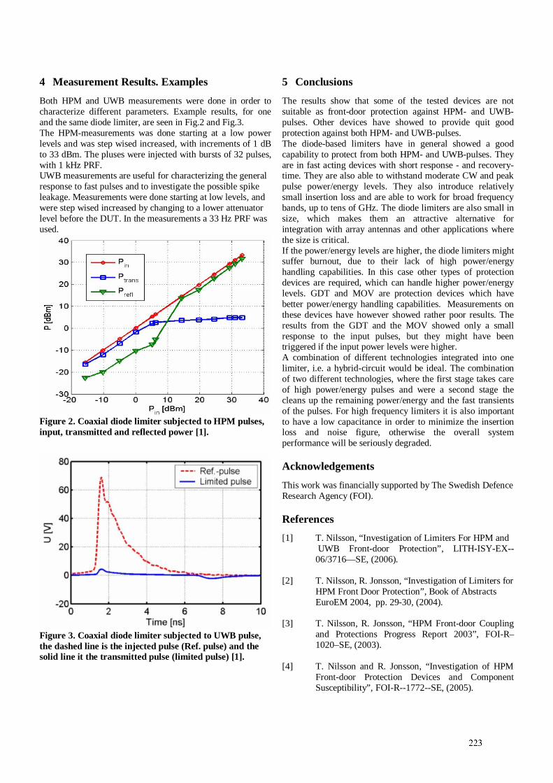
2
4 Measurement Results. ExamplesBoth HPM and UWB measurements were done in order tocharacterize different parameters. Example results, for oneand the same diode limiter, are seen in Fig.2 and Fig.3.The HPM-measurements was done starting at a low powerlevels and was step wised increased, with increments of 1 dBto 33 dBm. The pluses were injected with bursts of 32 pulses,with 1 kHz PRF.UWB measurements are useful for characterizing the generalresponse to fast pulses and to investigate the possible spikeleakage. Measurements were done starting at low levels, andwere step wised increased by changing to a lower attenuatorlevel before the DUT. In the measurements a 33 Hz PRF wasused.
Figure 2. Coaxial diode limiter subjected to HPM pulses,input, transmitted and reflected power [1].
Figure 3. Coaxial diode limiter subjected to UWB pulse,the dashed line is the injected pulse (Ref. pulse) and thesolid line it the transmitted pulse (limited pulse) [1].
5 ConclusionsThe results show that some of the tested devices are notsuitable as front-door protection against HPM- and UWB-pulses. Other devices have showed to provide quit goodprotection against both HPM- and UWB-pulses.The diode-based limiters have in general showed a goodcapability to protect from both HPM- and UWB-pulses. Theyare in fast acting devices with short response - and recovery-time. They are also able to withstand moderate CW and peakpulse power/energy levels. They also introduce relativelysmall insertion loss and are able to work for broad frequencybands, up to tens of GHz. The diode limiters are also small insize, which makes them an attractive alternative forintegration with array antennas and other applications wherethe size is critical.If the power/energy levels are higher, the diode limiters mightsuffer burnout, due to their lack of high power/energyhandling capabilities. In this case other types of protectiondevices are required, which can handle higher power/energylevels. GDT and MOV are protection devices which havebetter power/energy handling capabilities. Measurements onthese devices have however showed rather poor results. Theresults from the GDT and the MOV showed only a smallresponse to the input pulses, but they might have beentriggered if the input power levels were higher.A combination of different technologies integrated into onelimiter, i.e. a hybrid-circuit would be ideal. The combinationof two different technologies, where the first stage takes careof high power/energy pulses and were a second stage thecleans up the remaining power/energy and the fast transientsof the pulses. For high frequency limiters it is also importantto have a low capacitance in order to minimize the insertionloss and noise figure, otherwise the overall systemperformance will be seriously degraded.
AcknowledgementsThis work was financially supported by The Swedish DefenceResearch Agency (FOI).
References[1] T. Nilsson, “Investigation of Limiters For HPM and
UWB Front-door Protection”, LITH-ISY-EX--06/3716—SE, (2006).
[2] T. Nilsson, R. Jonsson, “Investigation of Limiters forHPM Front Door Protection”, Book of AbstractsEuroEM 2004, pp. 29-30, (2004).
[3] T. Nilsson, R. Jonsson, “HPM Front-door Couplingand Protections Progress Report 2003”, FOI-R–1020–SE, (2003).
[4] T. Nilsson and R. Jonsson, “Investigation of HPMFront-door Protection Devices and ComponentSusceptibility”, FOI-R--1772--SE, (2005).
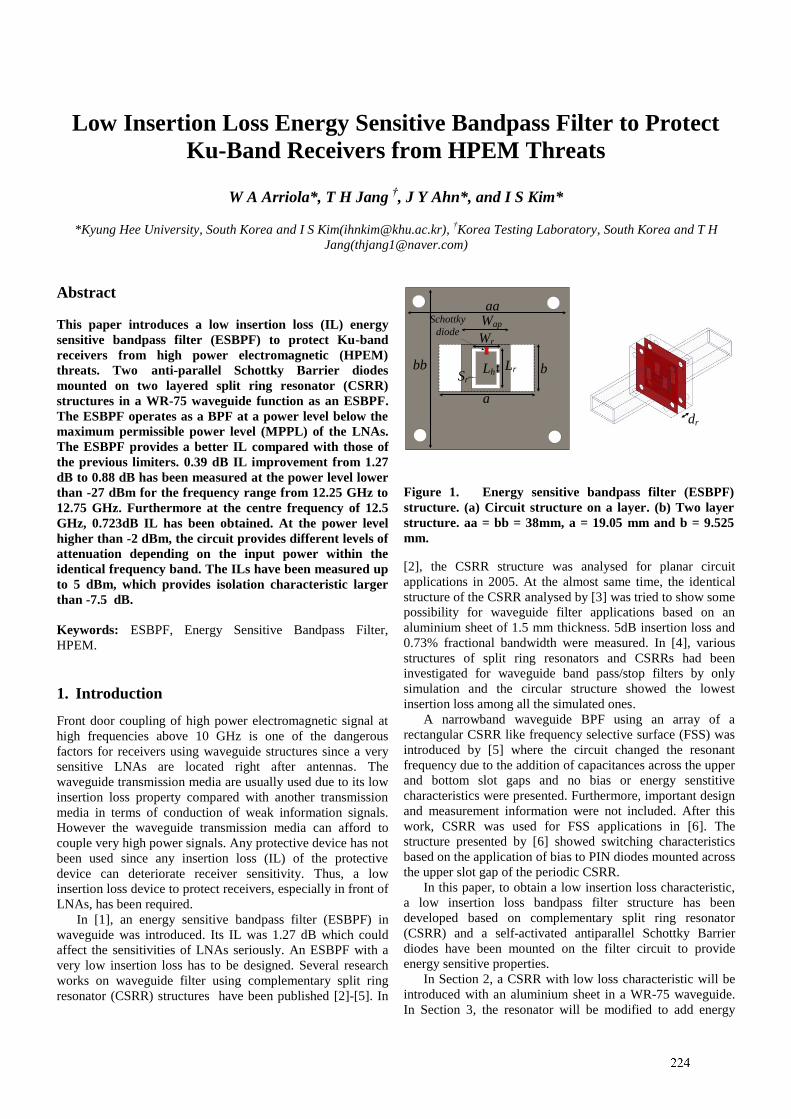
1
Low Insertion Loss Energy Sensitive Bandpass Filter to Protect
Ku-Band Receivers from HPEM Threats
W A Arriola*, T H Jang †, J Y Ahn*, and I S Kim*
*Kyung Hee University, South Korea and I S Kim([email protected]), †Korea Testing Laboratory, South Korea and T H
Jang([email protected])
Abstract
This paper introduces a low insertion loss (IL) energy
sensitive bandpass filter (ESBPF) to protect Ku-band
receivers from high power electromagnetic (HPEM)
threats. Two anti-parallel Schottky Barrier diodes
mounted on two layered split ring resonator (CSRR)
structures in a WR-75 waveguide function as an ESBPF.
The ESBPF operates as a BPF at a power level below the
maximum permissible power level (MPPL) of the LNAs.
The ESBPF provides a better IL compared with those of
the previous limiters. 0.39 dB IL improvement from 1.27
dB to 0.88 dB has been measured at the power level lower
than -27 dBm for the frequency range from 12.25 GHz to
12.75 GHz. Furthermore at the centre frequency of 12.5
GHz, 0.723dB IL has been obtained. At the power level
higher than -2 dBm, the circuit provides different levels of
attenuation depending on the input power within the
identical frequency band. The ILs have been measured up
to 5 dBm, which provides isolation characteristic larger
than -7.5 dB.
Keywords: ESBPF, Energy Sensitive Bandpass Filter,
HPEM.
1. Introduction
Front door coupling of high power electromagnetic signal at
high frequencies above 10 GHz is one of the dangerous
factors for receivers using waveguide structures since a very
sensitive LNAs are located right after antennas. The
waveguide transmission media are usually used due to its low
insertion loss property compared with another transmission
media in terms of conduction of weak information signals.
However the waveguide transmission media can afford to
couple very high power signals. Any protective device has not
been used since any insertion loss (IL) of the protective
device can deteriorate receiver sensitivity. Thus, a low
insertion loss device to protect receivers, especially in front of
LNAs, has been required.
In [1], an energy sensitive bandpass filter (ESBPF) in
waveguide was introduced. Its IL was 1.27 dB which could
affect the sensitivities of LNAs seriously. An ESBPF with a
very low insertion loss has to be designed. Several research
works on waveguide filter using complementary split ring
resonator (CSRR) structures have been published [2]-[5]. In
[2], the CSRR structure was analysed for planar circuit
applications in 2005. At the almost same time, the identical
structure of the CSRR analysed by [3] was tried to show some
possibility for waveguide filter applications based on an
aluminium sheet of 1.5 mm thickness. 5dB insertion loss and
0.73% fractional bandwidth were measured. In [4], various
structures of split ring resonators and CSRRs had been
investigated for waveguide band pass/stop filters by only
simulation and the circular structure showed the lowest
insertion loss among all the simulated ones.
A narrowband waveguide BPF using an array of a
rectangular CSRR like frequency selective surface (FSS) was
introduced by [5] where the circuit changed the resonant
frequency due to the addition of capacitances across the upper
and bottom slot gaps and no bias or energy senstitive
characteristics were presented. Furthermore, important design
and measurement information were not included. After this
work, CSRR was used for FSS applications in [6]. The
structure presented by [6] showed switching characteristics
based on the application of bias to PIN diodes mounted across
the upper slot gap of the periodic CSRR.
In this paper, to obtain a low insertion loss characteristic,
a low insertion loss bandpass filter structure has been
developed based on complementary split ring resonator
(CSRR) and a self-activated antiparallel Schottky Barrier
diodes have been mounted on the filter circuit to provide
energy sensitive properties.
In Section 2, a CSRR with low loss characteristic will be
introduced with an aluminium sheet in a WR-75 waveguide.
In Section 3, the resonator will be modified to add energy
a
b
Wr
Lr
aa
Sr
bb
Wap
Lh
Schottky
diode
dr
Figure 1. Energy sensitive bandpass filter (ESBPF)
structure. (a) Circuit structure on a layer. (b) Two layer
structure. aa = bb = 38mm, a = 19.05 mm and b = 9.525
mm.
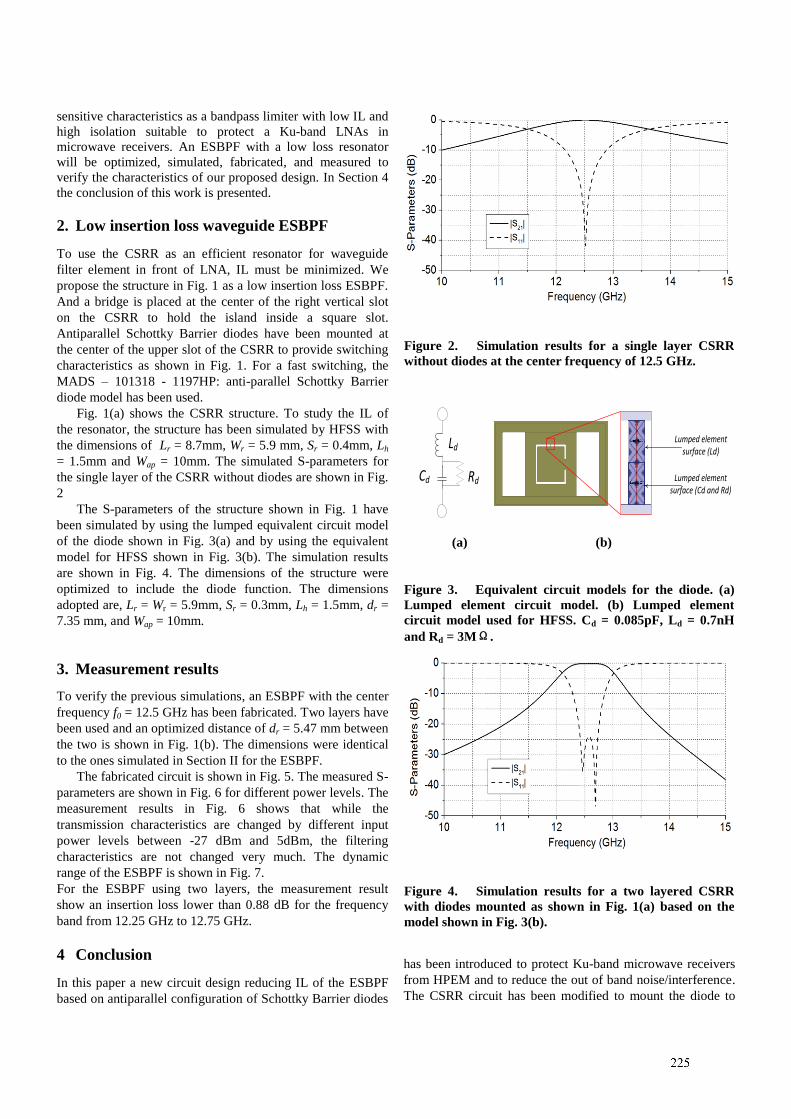
2
sensitive characteristics as a bandpass limiter with low IL and
high isolation suitable to protect a Ku-band LNAs in
microwave receivers. An ESBPF with a low loss resonator
will be optimized, simulated, fabricated, and measured to
verify the characteristics of our proposed design. In Section 4
the conclusion of this work is presented.
2. Low insertion loss waveguide ESBPF
To use the CSRR as an efficient resonator for waveguide
filter element in front of LNA, IL must be minimized. We
propose the structure in Fig. 1 as a low insertion loss ESBPF.
And a bridge is placed at the center of the right vertical slot
on the CSRR to hold the island inside a square slot.
Antiparallel Schottky Barrier diodes have been mounted at
the center of the upper slot of the CSRR to provide switching
characteristics as shown in Fig. 1. For a fast switching, the
MADS – 101318 - 1197HP: anti-parallel Schottky Barrier
diode model has been used.
Fig. 1(a) shows the CSRR structure. To study the IL of
the resonator, the structure has been simulated by HFSS with
the dimensions of Lr = 8.7mm, Wr = 5.9 mm, Sr = 0.4mm, Lh
= 1.5mm and Wap = 10mm. The simulated S-parameters for
the single layer of the CSRR without diodes are shown in Fig.
2
The S-parameters of the structure shown in Fig. 1 have
been simulated by using the lumped equivalent circuit model
of the diode shown in Fig. 3(a) and by using the equivalent
model for HFSS shown in Fig. 3(b). The simulation results
are shown in Fig. 4. The dimensions of the structure were
optimized to include the diode function. The dimensions
adopted are, Lr = Wr = 5.9mm, Sr = 0.3mm, Lh = 1.5mm, dr =
7.35 mm, and Wap = 10mm.
3. Measurement results
To verify the previous simulations, an ESBPF with the center
frequency f0 = 12.5 GHz has been fabricated. Two layers have
been used and an optimized distance of dr = 5.47 mm between
the two is shown in Fig. 1(b). The dimensions were identical
to the ones simulated in Section II for the ESBPF.
The fabricated circuit is shown in Fig. 5. The measured S-
parameters are shown in Fig. 6 for different power levels. The
measurement results in Fig. 6 shows that while the
transmission characteristics are changed by different input
power levels between -27 dBm and 5dBm, the filtering
characteristics are not changed very much. The dynamic
range of the ESBPF is shown in Fig. 7.
For the ESBPF using two layers, the measurement result
show an insertion loss lower than 0.88 dB for the frequency
band from 12.25 GHz to 12.75 GHz.
4 Conclusion
In this paper a new circuit design reducing IL of the ESBPF
based on antiparallel configuration of Schottky Barrier diodes
has been introduced to protect Ku-band microwave receivers
from HPEM and to reduce the out of band noise/interference.
The CSRR circuit has been modified to mount the diode to
Figure 2. Simulation results for a single layer CSRR
without diodes at the center frequency of 12.5 GHz.
Cd
Ld
Rd
Lumped element surface (Ld)
Lumped element surface (Cd and Rd)
(a) (b)
Figure 3. Equivalent circuit models for the diode. (a)
Lumped element circuit model. (b) Lumped element
circuit model used for HFSS. Cd = 0.085pF, Ld = 0.7nH
and Rd = 3MΩ.
Figure 4. Simulation results for a two layered CSRR
with diodes mounted as shown in Fig. 1(a) based on the
model shown in Fig. 3(b).
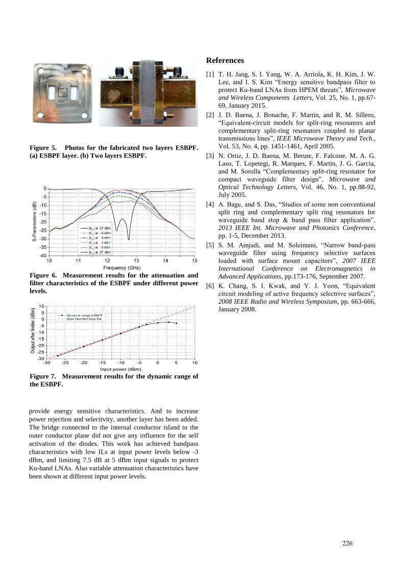
3
provide energy sensitive characteristics. And to increase
power rejection and selectivity, another layer has been added.
The bridge connected to the internal conductor island to the
outer conductor plane did not give any influence for the self
activation of the diodes. This work has achieved bandpass
characteristics with low ILs at input power levels below -3
dBm, and limiting 7.5 dB at 5 dBm input signals to protect
Ku-band LNAs. Also variable attenuation characteristics have
been shown at different input power levels.
References
[1] T. H. Jang, S. I. Yang, W. A. Arriola, K. H. Kim, J. W.
Lee, and I. S. Kim “Energy sensitive bandpass filter to
protect Ku-band LNAs from HPEM threats”, Microwave
and Wireless Components Letters, Vol. 25, No. 1, pp.67-
69, January 2015.
[2] J. D. Baena, J. Bonache, F. Martin, and R. M. Sillero,
“Equivalent-circuit models for split-ring resonators and
complementary split-ring resonators coupled to planar
transmissions lines”, IEEE Microwave Theory and Tech.,
Vol. 53, No. 4, pp. 1451-1461, April 2005.
[3] N. Ortiz, J. D. Baena, M. Berute, F. Falcone. M. A. G.
Laso, T. Lopetegi, R. Marques, F. Martin, J. G. Garcia,
and M. Sorolla “Complementary split-ring resonator for
compact waveguide filter design”, Microwave and
Optical Technology Letters, Vol. 46, No. 1, pp.88-92,
July 2005.
[4] A. Bage, and S. Das, “Studies of some non conventional
split ring and complementary split ring resonators for
waveguide band stop & band pass filter application”,
2013 IEEE Int. Microwave and Photonics Conference,
pp. 1-5, December 2013.
[5] S. M. Amjadi, and M. Soleimani, “Narrow band-pass
waveguide filter using frequency selective surfaces
loaded with surface mount capacitors”, 2007 IEEE
International Conference on Electromagnetics in
Advanced Applications, pp.173-176, September 2007.
[6] K. Chang, S. I. Kwak, and Y. J. Yoon, “Equivalent
circuit modeling of active frequency selectrive surfaces”,
2008 IEEE Radio and Wireless Symposium, pp. 663-666,
January 2008.
Figure 5. Photos for the fabricated two layers ESBPF.
(a) ESBPF layer. (b) Two layers ESBPF.
Figure 6. Measurement results for the attenuation and
filter characteristics of the ESBPF under different power
levels.
Figure 7. Measurement results for the dynamic range of
the ESBPF.
1
Reliable HEMP Protective Devices for the Power Line
Joon-Hyuck Kwon*†, Ki-Hwan Song*, Jong-Gwan Yook †
*Agency for Defense Development, Republic of KOREA, †Yonsei University, Republic of KOREA
[email protected], [email protected], [email protected]
Abstract This paper introduces the reliable HEMP protective devices for the AC power line. Two types of devices are designed, the first device utilizes CM inductor-based circuit and the second device utilizes DM inductor-based circuit. The results of reliability test and MIL-188-125-1 PCI test for the proposed devices are discussed. Keywords: Power line, Protective device, Reliability, PCI.
1 Introduction High-altitude electromagnetic pulse (HEMP) is generated by a nuclear burst above the atmosphere which produces coverage over large areas and can affect electric/electronic systems. The HEMP-induced current may flow into internal portions of a system by the direct conduction on the electrical wiring which penetrates the external structure, and can damage PCB boards and electric circuits in a system. To protect equipment and/or systems against the HEMP-induced current, protective devices installed at the point of entry (POE) must limit residual current and transient pulse energy. In general, the pulsed current injection (PCI) test based on MIL-STD-188-125-1/2 is carried out to evaluate performances of the protective devices. This paper introduces two types of reliable HEMP protective devices for the power line. The first one is the device utilizing common mode (CM) inductor-based circuit and the second one is the device utilizing the differential mode (DM) inductor-based circuit. The proposed devices comply with the reliability standard as well as MIL-STD-188-125-1 PCI standard [1-2].
2 Protective circuit design In this paper, two types of protective devices for the AC power line are introduced.
2.1 CM inductor circuit-based device
CM inductor arranges the lines to share the core to remove common mode signals. It makes high inductance value so that low value capacitors can be mounted in the device. As the result, the size of the device is smaller than the DM inductor circuit-based device [3]. However, because all the lines share one inductor core, it is hard to apply this type of device to high current applications. So this device is suitable for the
low current power line. Figure 1 shows the circuit diagram of the proposed protective device based on the CM inductor to apply low current power line (< 100A).
Figure 1. Circuit diagram of the protective device based on CM inductor.
2.2 DM inductor circuit-based device
Each line has individual inductor cores in this device. Also higher capacitors are installed to have higher insertion loss characteristics. Generally, the size of the DM inductor-based device is larger than that of CM inductor-based device [3]. But manufacturing DM inductor-based device, especially in the high current applications, is simpler than that of CM inductor-based device because each line in the DM inductor circuit is independent to be made. Figure 2 shows the circuit diagram of the proposed protective device based on DM inductor elements for the high current power line application (≥ 100A).
Figure zing 2. Circuit diagram of the protective device based on DM inductors.
2.3 Considerations for the reliability
Protective circuits and components were designed to be satisfied with the PCI test criteria on the short pulse and intermediate pulse in MIL-STD-188-125-1. Moreover, the reliability standard was applied to the proposed devices to have the proper performances even under the rough conditions [2]. This standard classifies three categories consisting of the
2
performance, environment, and life time test. Each category is presented in Table 1 in detail. Only the case that five samples of each device have no failure is in conformity with the reliability criteria. Table 1: Test conditions and criteria for the power line
protective devices [2].
Categories Test items Test conditions Pass/Fail criteria
Perform-ance test PCI MIL-STD-188-125-1 MIL-STD-188-125-1
Insertion loss MIL-STD-220C Refer Figure 3 (red line)
Voltage drop
50% of maximum load or 100A, whichever is lower
≤ 2% @ rated current
≤50A device,
≤ 3% @ rated current 100-200A device
Leakage current
Rated Voltage
< 1.8A @ rated current ≤50A device <6A @ rated current 100-200A device
Environ-ment test
Low Temp.
Storage : -40, 16hr
Operating:-40, 2hr
During testing : voltage drop and rated current After testing :
PCI, insertion loss and voltage drop
High Temp.
Storage : +85, 16hr
Operating:+50, 2hr
Thermal Shock
-40 ~ +85, 5 cycles After testing :
PCI, insertion loss and voltage drop Overload
140% of rated current, 15 minute
Life time test
Accelerated-life
(85±2) , 1000hr After testing : PCI, insertion loss and
voltage drop
Pulse repetition
Short pulse : 2,500A, 40 pulses Intermediate pulse:
250A, 203 pulses The components such as GDTs, MOVs, inductors, and capacitors in the protective device were selected and designed to guarantee those performances under reliability test conditions. The MTBF (Mean Time Between Failure) for the devices was calculated at 228,000 hours.
3 Test results and conclusion Two types of HEMP protective devices (CM inductor circuit for 50A, DM inductor circuit for 200A) were evaluated in accordance with PCI and relevant reliability standard. The test results of PCI and performance are shown in Table 2 and those of insertion loss are shown in Figure 3 and 4, respectively. It is shown that proposed protective devices comply with PCI and performance requirements. Also proposed devices were fully satisfied with all environment and life time criteria.
Table 2: Typical PCI and performance test results
Test items Norms Criteria Measured values
PCI Short pulse
Peak current(A)
≤ 10 ≤ 1.95 @50A device
≤ 2.42 @200A device Peak rate of rise (A/s)
≤ 1 ⅹ 107 ≤ 6.45 ⅹ 104 @50A device
≤ 1.20 ⅹ 105 @200A device
Root action (A-√s)
≤ 1.6 ⅹ 10-1 ≤ 1.58 ⅹ 10-2 @50A device
≤ 2.05 ⅹ 10-2 @200A device
PCI Intermediate pulse
No damage or performance degradation (Measured MOV voltage before testing : 558~682V)
No damage or performance degradation (MOV voltage after testing : 654~665V)
Voltage drop
≤ 5V @ 50A device
≤ 7.5V @ 200A device
≤ 0.3V @ 50A device
≤ 1.4V @ 200A device
Leakage current
≤ 1.8A @ 50A device
≤ 6A @ 200A device
≤ 1.47A @ 50A device
≤ 1.45A @ 200A device
Figure 3. Measured insertion loss for 50A device.
Figure 4. Measured insertion loss for 200A device.
References [1] MIL-STD-188-125-1, “High-altitude electromagnetic
pulse (HEMP) protection for ground-based C4I facilities performing critical, time urgent missions, Part 1, Fixed facilities”, 17 July 1998.
[2] RS-KTL-2012-0018 “Reliability assessment specification for HEMP protection filter”, Korea Testing Laboratory, 28 December 2012.
[3] www.incompliancemag.com, “Facility power filters: Symmetric vs. asymmetric performance”, September 2013.
Key Design Technologies of RF Front-end Protection Module with Ultra-low Limited Output Power
Dongdong Wang1,2, Lan Gao2, Shengquan Zheng1,2, Feng Deng1,2, and Dongyun Hou1,2 1Science and Technology on Electromagnetic Compatibility Laboratory
2China Ship Development and Design Center Wuhan, China
Abstract—Existing technologies employed by RF limiters played the role of preventing physical damage to RF front-end circuits caused by HIRF and EMP radiation. However, saturation of the receiving channel in the presence of HIRF or EMP was always ignored and few researches were made. In this paper, the design methods and tested results of a kind of RF front-end protection module with ultra-low limited output power were presented. The module consisted of an active biasing circuit and a passive limiter circuit, and it featured rather low on-state impedance and high isolation degree in comparison with commonly utilized passive limiter. The output power of the module was generally less than 0 dBm, which was smaller than the saturation threshold power of sensitive amplifying devices in the receiving channel.
Keywords- RF front end, Biasing circuit, Limiter circuit
I. INTRODUCTION
Although physical damage of transceiver RF front-end circuits caused by HIRF (high-intensity radiation field) and EMP (Electromagnetic Pulse) radiation has been widely reported and investigated, another important phenomenon, i.e., saturation of the receiving channel, was always ignored and few researches were made [1]. Experimental results obtained from typical RF receiving channels tests showed that if the amplitude of the input EMP power reached 0 dBm or larger, and its duration was at the level of tens of nanoseconds, LNAs (low noise amplifiers) in the receiver would be in saturation state about hundreds of microseconds, and that would decreased the channel gain and resulted in disfunction in amplifying normal injected signals. If the P.R.F (pulse repetition frequency) of the EMP were as high as several kilohertz, serious suppression effects would be induced. It is thus necessary to design RF front-end protection module with output limiting power level less than 0 dBm to prevent the receiver from entering deep saturation status.
II. TECHNICAL INDEXEX OF THE LIMITER
The limiter’s technical indexes were as follows:
a) Maximum input power, 30 dBm. According to the HIRF and EMP protection requirements of vulnerable RF electronic systems, the functional orientation of the anti-saturation limiting module was as the second-stage protective measure. The leakage power of the first-stage module was generally no more than 30 dBm.
b) output power: less than 0 dBm while the input was 30 dBm. The above demand was based on the fact that if the output power was higher than 0 dBm, the receiver would be saturated.
c) input limiting threshold: less than 0dBm. If the module did not play its limiting role when the input RF signal power was higher than 0 dBm, the receiver would be saturated.
d) spike leakage energy: less than 10 nanojoule. GaAs MOSFET was as the first-stage active amplifying device in the front-end LNA, and the MOSFET’s damage energy threshold in adiabatic state was at the range of 50~100 nanojoule. Considering that the volume of GaAs MOSFET would be smaller in the future as improvement of the fabrication technology, the damage threshold would further decrease, so that the spike leakage energy was demanded to be no more than 10 nanojoule [2-4].
III. TECHNICAL DESIGN OF THE PROTECTION MODULE
1) General design method
The protection module consisted of two parts, the active biasing circuit and the passive limiting circuit. The active was composed of a peak value detector and a high-speed comparator, while the passive contained multi-stage pin diodes. The input RF signal was first injected into the active circuit through a directional RF coupler, and its output was then transformed into video signal by Schottky-diode peak value detector. If the amplitude of the detected video signal exceeded the comparator’s threshold value set in advance, the comparator’s output would be the high value, which drove the passive limiting circuit into low-impedance state.
For the realization of the above demanded technical indexes, it was necessary to analyze the main influencing factors related with each parameter.
a) Maximum input power: It depended on the width of the intrinsic layer the first-stage PIN diodes.
b) output power: It was determined by the on-state impedance of the limiter at certain input power level. To be specific, the on-sate impedance was related with several factors, including the number of stages of the limiter, the value of the distributed inductance, width of the diodes’ intrinsic layers, as well as the current value provided by the active biasing circuit.
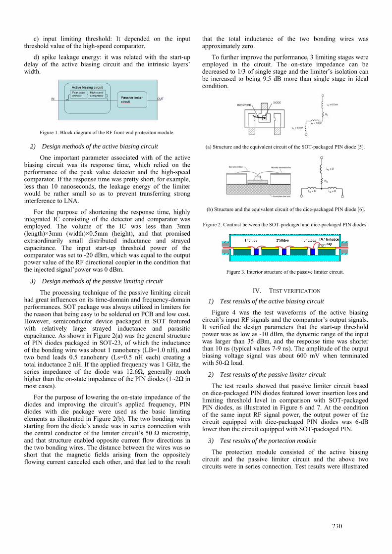
c) input limiting threshold: It depended on the input threshold value of the high-speed comparator.
d) spike leakage energy: it was related with the start-up delay of the active biasing circuit and the intrinsic layers’ width.
Figure 1. Block diagram of the RF front-end proteciton module.
2) Design methods of the active biasing circuit
One important parameter associated with of the active biasing circuit was its response time, which relied on the performance of the peak value detector and the high-speed comparator. If the response time was pretty short, for example, less than 10 nanoseconds, the leakage energy of the limiter would be rather small so as to prevent transferring strong interference to LNA.
For the purpose of shortening the response time, highly integrated IC consisting of the detector and comparator was employed. The volume of the IC was less than 3mm (length)×3mm (width)×0.5mm (height), and that promised extraordinarily small distributed inductance and strayed capacitance. The input start-up threshold power of the comparator was set to -20 dBm, which was equal to the output power value of the RF directional coupler in the condition that the injected signal’power was 0 dBm.
3) Design methods of the passive limiting circuit
The processing technique of the passive limiting circuit had great influences on its time-domain and frequency-domain performances. SOT package was always utilized in limiters for the reason that being easy to be soldered on PCB and low cost. However, semiconductor device packaged in SOT featured with relatively large strayed inductance and parasitic capacitance. As shown in Figure 2(a) was the general structure of PIN diodes packaged in SOT-23, of which the inductance of the bonding wire was about 1 nanohenry (LB=1.0 nH), and two bend leads 0.5 nanohenry (Ls=0.5 nH each) creating a total inductance 2 nH. If the applied frequency was 1 GHz, the series impedance of the diode was 12.6Ω, generally much higher than the on-state impedance of the PIN diodes (1~2Ω in most cases).
For the purpose of lowering the on-state impedance of the diodes and improving the circuit’s applied frequency, PIN diodes with die package were used as the basic limiting elements as illustrated in Figure 2(b). The two bonding wires starting from the diode’s anode was in series connection with the central conductor of the limiter circuit’s 50 Ω microstrip, and that structure enabled opposite current flow directions in the two bonding wires. The distance between the wires was so short that the magnetic fields arising from the oppositely flowing current canceled each other, and that led to the result
that the total inductance of the two bonding wires was approximately zero.
To further improve the performance, 3 limiting stages were employed in the circuit. The on-state impedance can be decreased to 1/3 of single stage and the limiter’s isolation can be increased to being 9.5 dB more than single stage in ideal condition.
(a) Structure and the equivalent circuit of the SOT-packaged PIN diode [5].
(b) Structure and the equivalent circuit of the dice-packaged PIN diode [6].
Figure 2. Contrast between the SOT-packaged and dice-packaged PIN diodes.
Figure 3. Interior structure of the passive limiter circuit.
IV. TEST VERIFICATION
1) Test results of the active biasing circuit
Figure 4 was the test waveforms of the active biasing circuit’s input RF signals and the comparator’s output signals. It verified the design parameters that the start-up threshold power was as low as -10 dBm, the dynamic range of the input was larger than 35 dBm, and the response time was shorter than 10 ns (typical values 7-9 ns). The amplitude of the output biasing voltage signal was about 600 mV when terminated with 50-Ω load.
2) Test results of the passive limiter circuit
The test results showed that passive limiter circuit based on dice-packaged PIN diodes featured lower insertion loss and limiting threshold level in comparison with SOT-packaged PIN diodes, as illustrated in Figure 6 and 7. At the condition of the same input RF signal power, the output power of the circuit equipped with dice-packaged PIN diodes was 6-dB lower than the circuit equipped with SOT-packaged PIN.
3) Test results of the portection module
The protection module consisted of the active biasing circuit and the passive limiter circuit and the above two circuits were in series connection. Test results were illustrated
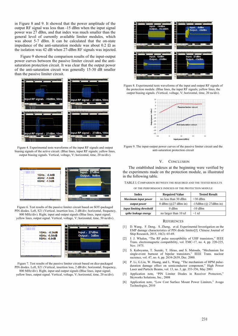
in Figure 8 and 9. It showed that the power amplitude of the output RF signal was less than -15 dBm when the input signal power was 27 dBm, and that index was much smaller than the general level of currently available limiter modules, which was about 5-7 dBm. It can be calculated that the on-state impedance of the anti-saturation module was about 0.2 Ω as the isolation was 42 dB when 27-dBm RF signals was injected.
Figure 9 showed the comparison results of the input-output power curves between the passive limiter circuit and the anti-saturation protection circuit. It was clear that the output power of the anti-saturation circuit was generally 15-30 dB smaller than the passive limiter circuit.
Figure 4. Experimental tests waveforms of the input RF signals and output biasing signals of the active circuit. (Blue lines, input RF signals; yellow lines,
output biasing signals. Vertical, voltage, V; horizontal, time, 20 ns/div).
Figure 6. Test results of the passive limiter circuit based on SOT-packaged PIN diodes. Left, S21 (Vertical, insertion loss, 2 dB/div; horizontal, frequency,
800 MHz/div). Right, input and output signals (Blue lines, input signal; yellow lines, output signal. Vertical, voltage, V; horizontal, time, 50 ns/div).
Figure 7. Test results of the passive limiter circuit based on dice-packaged PIN diodes. Left, S21 (Vertical, insertion loss, 2 dB/div; horizontal, frequency,
800 MHz/div). Right, input and output signals (Blue lines, input signal; yellow lines, output signal. Vertical, voltage, V; horizontal, time, 20 ns/div).
Figure 8. Experimental tests waveforms of the input and output RF signals of the protection module. (Blue lines, the input RF signals; yellow lines, the output biasing signals. (Vertical, voltage, V; horizontal, time, 20 ns/div).
Figure 9. The input-output power curves of the passive limiter circuit and the anti-saturation protection circuit
V. CONCLUSION
The established indexes at the beginning were verified by the experiments made on the protection module, as illustrated in the following table.
TABLE I. COMPARISON BETWEEN THE REQUIRED AND THE TESTED RESULTS
OF THE PERFORMANCE INDEXES OF THE PROTECTION MODULE Index Required Value Tested Result
Maximum input power no less than 30 dBm >30 dBm
output power 0 dBm (@27 dBm in) -15dBm (@ 27dBm in)
input limiting threshold 0 dBm -10 dBm
spike leakage energy no larger than 10 nJ ~1 nJ
REFERENCES [1] D. Wang,F. Deng,S. Zheng,et al. Experimental Investigation on the
EMP damage characteristics of PIN diode limiter[J]. Chinese Journal of Ship Research, 2015, 10(2): 65-69.
[2] J. J. Whalen, “The RF pulse susceptibility of UHF transistors,” IEEE Trans. electromagnetic compatibility, vol. EMC-17, no. 4, pp. 220-225, Nov. 1975.
[3] S. Kuboyama, T. Suzuki, T. Hirao, and S. Matsuda, “Mechanism for single-event burnout of bipolar transistors,” IEEE Trans. nuclear sucience, vol. 47, no. 6, pp. 2634-2639, Dec. 2000.
[4] P. Li, G.Liu, W. Huang, and L. Wang, “The mechanism of HPM pulse-duration damage effect on semiconductor component,” High Power Laser and Particle Beams, vol. 13, no. 3, pp. 353-356, May 2001
[5] Application note, “PIN Limiter Diodes in Receiver Protectors,” Skyworks Solutions, Inc., 2008
[6] Application note, “Low Cost Surface Mount Power Limiters,” Avago Technologies, 2010
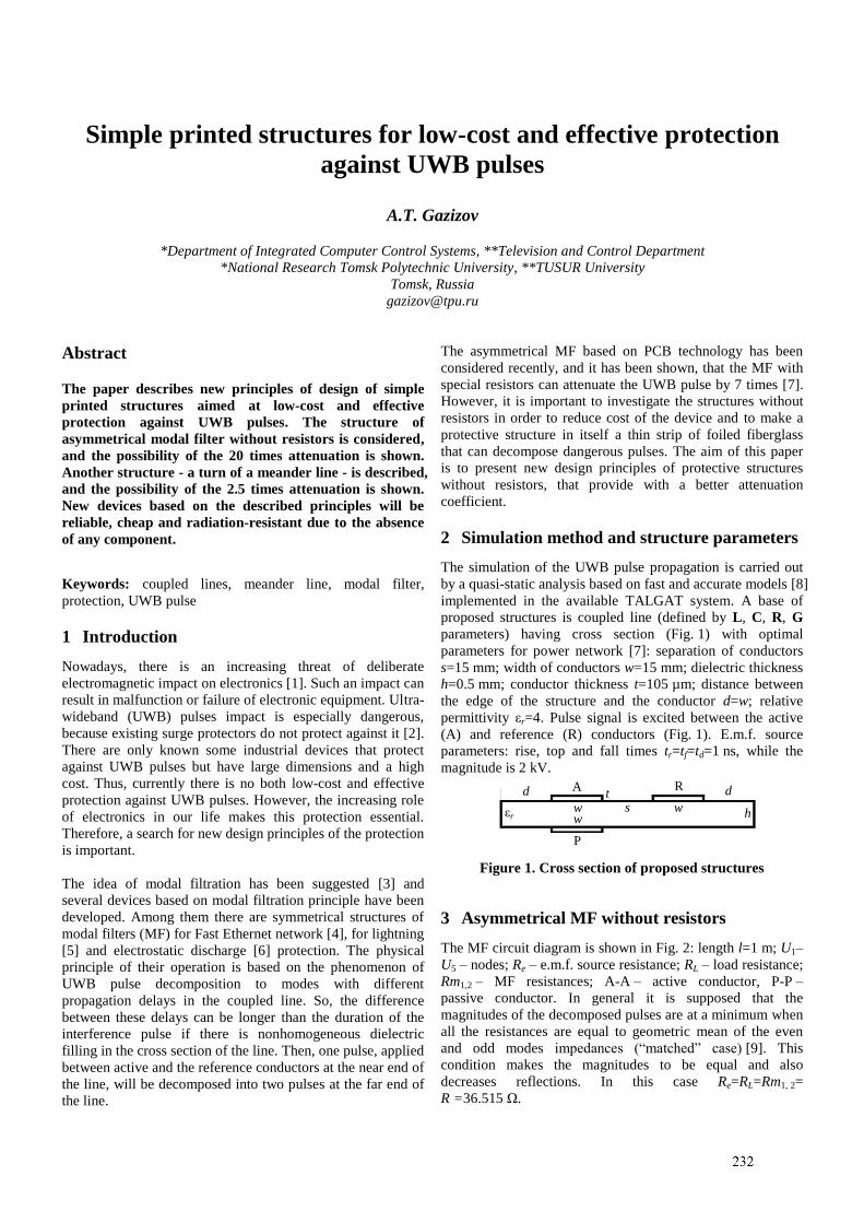
Simple printed structures for low-cost and effective protection
against UWB pulses
A.T. Gazizov
*Department of Integrated Computer Control Systems, **Television and Control Department
*National Research Tomsk Polytechnic University, **TUSUR University
Tomsk, Russia
Abstract
The paper describes new principles of design of simple
printed structures aimed at low-cost and effective
protection against UWB pulses. The structure of
asymmetrical modal filter without resistors is considered,
and the possibility of the 20 times attenuation is shown.
Another structure - a turn of a meander line - is described,
and the possibility of the 2.5 times attenuation is shown.
New devices based on the described principles will be
reliable, cheap and radiation-resistant due to the absence
of any component.
Keywords: coupled lines, meander line, modal filter,
protection, UWB pulse
1 Introduction
Nowadays, there is an increasing threat of deliberate
electromagnetic impact on electronics [1]. Such an impact can
result in malfunction or failure of electronic equipment. Ultra-
wideband (UWB) pulses impact is especially dangerous,
because existing surge protectors do not protect against it [2].
There are only known some industrial devices that protect
against UWB pulses but have large dimensions and a high
cost. Thus, currently there is no both low-cost and effective
protection against UWB pulses. However, the increasing role
of electronics in our life makes this protection essential.
Therefore, a search for new design principles of the protection
is important.
The idea of modal filtration has been suggested [3] and
several devices based on modal filtration principle have been
developed. Among them there are symmetrical structures of
modal filters (MF) for Fast Ethernet network [4], for lightning
[5] and electrostatic discharge [6] protection. The physical
principle of their operation is based on the phenomenon of
UWB pulse decomposition to modes with different
propagation delays in the coupled line. So, the difference
between these delays can be longer than the duration of the
interference pulse if there is nonhomogeneous dielectric
filling in the cross section of the line. Then, one pulse, applied
between active and the reference conductors at the near end of
the line, will be decomposed into two pulses at the far end of
the line.
The asymmetrical MF based on PCB technology has been
considered recently, and it has been shown, that the MF with
special resistors can attenuate the UWB pulse by 7 times [7].
However, it is important to investigate the structures without
resistors in order to reduce cost of the device and to make a
protective structure in itself a thin strip of foiled fiberglass
that can decompose dangerous pulses. The aim of this paper
is to present new design principles of protective structures
without resistors, that provide with a better attenuation
coefficient.
2 Simulation method and structure parameters
The simulation of the UWB pulse propagation is carried out
by a quasi-static analysis based on fast and accurate models [8]
implemented in the available TALGAT system. A base of
proposed structures is coupled line (defined by L, C, R, G
parameters) having cross section (Fig. 1) with optimal
parameters for power network [7]: separation of conductors
s=15 mm; width of conductors w=15 mm; dielectric thickness
h=0.5 mm; conductor thickness t=105 µm; distance between
the edge of the structure and the conductor d=w; relative
permittivity εr=4. Pulse signal is excited between the active
(A) and reference (R) conductors (Fig. 1). E.m.f. source
parameters: rise, top and fall times tr=tf=td=1 ns, while the
magnitude is 2 kV.
εr
A
P
R d d t s h w
w w
Figure 1. Cross section of proposed structures
3 Asymmetrical MF without resistors
The MF circuit diagram is shown in Fig. 2: length l=1 m; U1–
U5 – nodes; Re – e.m.f. source resistance; RL – load resistance;
Rm1,2 – MF resistances; A-A – active conductor, P-P –
passive conductor. In general it is supposed that the
magnitudes of the decomposed pulses are at a minimum when
all the resistances are equal to geometric mean of the even
and odd modes impedances (“matched” case) [9]. This
condition makes the magnitudes to be equal and also
decreases reflections. In this case Re=RL=Rm1, 2=
R =36.515 Ω.
Re
Rm1
RL
Rm2
U2
U3
U4
U5
L, C, R, G, l e
U1 A
A
P
P
Figure 2. Circuit diagram of MF
The output (U4 in Fig. 2) waveform of the MF for the
“matched” case is shown in Fig. 3. The maximum magnitude
is 0.14 kV and attenuation coefficient is 7 (relative to 1 kV).
0
0.05
0.1
0.15
0 3 6 9 12 15 18 21 24 27 30 33 36 39
t, ns
U , kV
Figure 3. Output waveform of MF for “matched” case
In order to simulate the MF without resistors, Rm1 and Rm2
should have limit in values corresponding to the open-circuit
and the short-circuit modes. Waveforms at the output of the
MF were calculated for different combinations of limit Rm1
and Rm2 values. The highest attenuation coefficient was
obtained in the case when one of the resistors simulated open-
circuit mode and another – short-circuit. It was revealed that
the order of resistors does not influence the output waveform.
Waveform at the output of MF with Rm1 =1000R and
Rm2 =0.001R is shown in Fig. 4. The obtained waveform
shows that the maximum magnitude is 0.084 kV and
attenuation coefficient is 12.
0
0.02
0.04
0.06
0.08
0 3 6 9 12 15 18 21 24 27 30 33 36 39
t, ns
U , kV
Figure 4. Output waveform of MF without resistors
It is worth noting that in Fig. 4 the maximum magnitude is
defined not by the first two pulses, as in Fig. 3, but by the
fifth pulse. It also can be seen that the fifth pulse in Fig. 4 is a
superposition of two pulses, so its magnitude can be reduced
by changing the parameters of the structure. For example, we
can increase the length of the MF in order to increase the time
interval between pulses. Output waveform of the MF with
increased length (l=2.5 m) is shown in Fig. 5. Note that the
magnitude of the fifth pulse (the maximum magnitude)
decreased down to 0.062 kV (attenuation coefficient
increased up to 16), because the fifth pulse is no longer a
complete superposition of the two pulses.
0
0.035
0.07
0 6 12 18 24 30 36 42 48 54 60
t, ns
U , kV
Figure 5. Output waveform of MF (l=2.5 m)
without resistors
However, the maximum magnitude can be further decreased
by increasing the εr value which previously was equal to 4
according to the dielectric substrate material (cheap and
widely used FR-4). Output waveform of MF, with increased l
and εr values, is shown in Fig. 6. It can be seen that the
maximum magnitude decreased down to 0.05 kV (attenuation
coefficient increased up to 20).
0
0.025
0.05
0 6 12 18 24 30 36 42 48 54 60
t, ns
U , kV
Figure 6. Output waveform of MF (l=2.5 m, εr=8)
without resistors
4 Turn of meander line
Consider the structure having the same cross section (Fig. 1)
but another circuit diagram, which is shown in Fig. 7.
Essentially, it is a turn of a meander line (ML) but here it
represents another approach to UWB pulses protection. The
output of the structure corresponds to the U3 node.
Re
RL
U2
U3
U4
U5
L, C, R, G, l
e U1
Figure 7. Circuit diagram of ML
Output waveform of the ML with initial parameters of the
cross section (s=15 mm, h=0.5 mm, εr=4, l=1 m) is shown in
Fig. 8a. The obtained waveform is a sum of the signal itself,
passed along the first and the second half-turns of ML, and
the crosstalk from the signal rise and fall at the input of the
ML. Initial s and h values provide a close coupling and that is
why the maximum magnitude at the output (0.85 kV) is close
to the input pulse magnitude (1 kV). In order to reduce the
coupling we can increase the h value and decrease the s value.
For example, output waveform of the ML with changed
parameters (s=1 mm, h=6 mm) is shown in Fig. 8b.
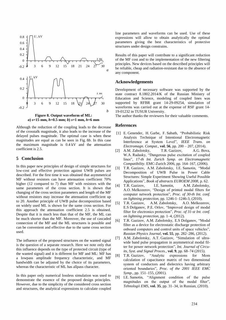
-0.2
0
0.2
0.4
0.6
0.8
0 3 6 9 12 15 18 21 24 27 30
t, ns
U , kV
a
-0.2
0
0.2
0.4
0 3 6 9 12 15 18 21 24 27 30
t, ns
U , kV
b
Figure 8. Output waveform of ML:
a) s=15 mm, h=0.5 mm; b) s=1 mm, h=6 mm
Although the reduction of the coupling leads to the decrease
of the crosstalk magnitude, it also leads to the increase of the
delayed pulses magnitude. The optimal case is when these
magnitudes are equal as can be seen in Fig. 8b. In this case
the maximum magnitude is 0.4 kV and the attenuation
coefficient is 2.5.
5 Conclusion
In this paper new principles of design of simple structures for
low-cost and effective protection against UWB pulses are
described. For the first time it was obtained that asymmetrical
MF without resistors can have attenuation coefficient 70%
higher (12 compared to 7) than MF with resistors with the
same parameters of the cross section. It is shown that
changing of the cross section parameters and length of the MF
without resistors may increase the attenuation coefficient up
to 20. Another principle of UWB pulse decomposition based
on widely used ML is shown for the same cross section. For
this approach the attenuation coefficient 2.5 is obtained.
Despite that it is much less than that of the MF, the ML can
be much shorter than the MF. Moreover, the use of cascaded
connection of the MF and the ML structures is possible and
can be convenient and effective due to the same cross section
used.
The influence of the proposed structures on the wanted signal
is the question of a separate research. Here we note only that
this influence depends on the type of protected circuit (type of
the wanted signal) and it is different for MF and ML: MF has
a lowpass amplitude frequency characteristic, and MF
bandwidth can be adjusted by the choice of its parameters,
whereas the characteristic of ML has allpass character.
In this paper only numerical lossless simulation was used to
demonstrate the essence of the proposed design principles.
However, due to the simplicity of the considered cross section
and structures, the analytical expressions to calculate coupled
line parameters and waveforms can be used. Use of these
expressions will allow to obtain analytically the optimal
parameters giving the best characteristics of protective
structures under design constrains.
Results of this paper will contribute to a significant reduction
of the MF cost and to the implementation of the new filtering
principles. New devices based on the described principles will
be reliable, cheap and radiation-resistant due to the absence of
any component.
Acknowledgements
Development of necessary software was supported by the
state contract 8.1802.2014/K of the Russian Ministry of
Education and Science, modeling of coupled lines was
supported by RFBR grant 14-29-09254, simulation of
waveforms was carried out at the expense of RSF grant 14-
19-01232 in TUSUR University.
The author thanks the reviewers for their valuable comments.
References
[1] E. Genender, H. Garbe, F. Sabath, “Probabilistic Risk
Analysis Technique of Intentional Electromagnetic
Interference at System Level”, IEEE Trans. on
Electromagn. Compat., vol. 56, pp. 200 – 207, (2014).
[2] A.M. Zabolotsky, T.R. Gazizov, A.G. Bova,
W.A. Radasky, “Dangerous pulse excitation of coupled
lines”, 17-th Int. Zurich Symp. on Electromagnetic
Compatibility. EMC-Zurich 2006, pp. 164–167, (2006).
[3] Т.R. Gazizov, А.М. Zabolotsky, I.E. Samotin, “Modal
Decomposition of UWB Pulse in Power Cable
Structures: Simple Experiment Showing Useful Possible
Applications”, Book of abstracts EUROEM 2008, p. 62.
[4] T.R. Gazizov, I.E. Samotin, A.M. Zabolotsky,
A.O. Melkozerov, “Design of printed modal filters for
computer network protection”, Proc. of 30-th Int. conf.
on lightning protection, pp. 1246-1–1246-3, (2010).
[5] T.R. Gazizov, A.M. Zabolotsky, A.O. Melkozerov,
E.S Dolganov, P.E. Orlov, “Improved design of modal
filter for electronics protection”, Proc. of 31-st Int. conf.
on lightning protection, pp. 1–4, (2012).
[6] T.R. Gazizov, A.M. Zabolotsky, E.S Dolganov, “Modal
filter as a device for electrostatic discharge protection of
onboard computers and control units of space vehicles”,
Russian Physics Journal, vol. 55, pp. 282–286, (2012).
[7] A.M. Zabolotsky, A.T. Gazizov, “Simulation of ultra-
wide band pulse propagation in asymmetrical modal fil-
ter for power network protection”, Int. Journal of Circu-
its, Syst. and Signal Proces., vol. 9, pp. 68–74 (2015).
[8] T.R. Gazizov, “Analytic expressions for Mom
calculation of capacitance matrix of two dimensional
system of conductors and dielectrics having arbitrary
oriented boundaries”, Proc. of the 2001 IEEE EMC
Symp., pp. 151–155, (2001).
[9] I.E. Samotin, “Alignment condition of the pulse
magnitudes on the output of the modal filter”,
Tehnologii EMS, vol. 35, pp. 31–34, in Russian, (2010).
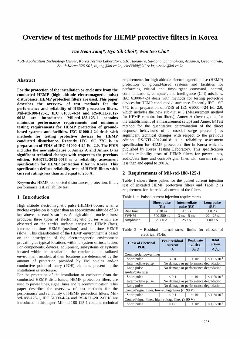
1
Overview of test methods for HEMP protective filters in Korea
Tae Heon Jang*, Hyo Sik Choi*, Won Seo Cho*
* RF Application Technology Center, Korea Testing Laboratory, 516 Haean-ro, Sa-dong, Sangnok-gu, Ansan-si, Gyeonggi-do,
South Korea 326-901, [email protected], [email protected], [email protected]
Abstract
For the protection of the installation or enclosure from the
conducted HEMP (high altitude electromagnetic pulse)
disturbance, HEMP protection filters are used. This paper
describes the overview of test methods for the
performance and reliability of HEMP protection filters.
Mil-std-188-125-1, IEC 61000-4-24 and RS-KTL-2012-
0018 are introduced: Mil-std-188-125-1 contains
minimum performance requirements and minimum
testing requirements for HEMP protection of ground-
based systems and facilities. IEC 61000-4-24 deals with
methods for testing protective devices for HEMP
conducted disturbance. Recently IEC SC 77C is in
preparation of FDIS of IEC 61000-4-24 Ed. 2.0. The FDIS
includes the new sub-clause 5, Annex A and Annex B as
significant technical changes with respect to the previous
edition. RS-KTL-2012-0018 is a reliability assessment
specification for HEMP protection filter in Korea. This
specification defines reliability tests of HEMP filters with
current ratings less than and equal to 200 A.
Keywords: HEMP, conducted disturbances, protection, filter,
performance test, reliability test.
1 Introduction
High altitude electromagnetic pulse (HEMP) occurs when a
nuclear explosion is higher than an approximate altitude of 30
km above the earth's surface. A high-altitude nuclear burst
produces three types of electromagnetic pulses which are
observed on the earth's surface: early-time HEMP (fast),
intermediate-time HEMP (medium) and late-time HEMP
(slow). This classification of the HEMP environment is based
on the description of the electromagnetic environment
prevailing at typical locations within a system of installation.
For components, devices, equipment, subsystems or systems
located within an installation, the conducted and radiated
environment incident at their locations are determined by the
amount of protection provided by EM shields and/or
conductive point of entry (POE) elements present in the
installation or enclosure.
For the protection of the installation or enclosure from the
conducted HEMP disturbance, HEMP protection filters are
used to power lines, signal lines and telecommunication. This
paper describes the overview of test methods for the
performance and reliability of HEMP protection filters. Mil-
std-188-125-1, IEC 61000-4-24 and RS-KTL-2012-0018 are
introduced in this paper: Mil-std-188-125-1 contains technical
requirements for high altitude electromagnetic pulse (HEMP)
protection of ground-based systems and facilities for
performing critical and time-urgent command, control,
communications, computer, and intelligence (C4I) missions.
IEC 61000-4-24 deals with methods for testing protective
devices for HEMP conducted disturbance. Recently IEC SC
77C is in preparation of FDIS of IEC 61000-4-24 Ed. 2.0,
which includes the new sub-clause 5 (Measurement method
for HEMP combination filters), Annex A (Investigation for
the establishment of a measurement setup) and Annex B(Test
method for the quantitative determination of the direct
response behaviours of a coaxial surge protector) as
significant technical changes with respect to the previous
edition. RS-KTL-2012-0018 is a reliability assessment
specification for HEMP protection filter in Korea which is
published by Korea Testing Laboratory. This specification
defines reliability tests of HEMP filters for power lines,
audio/data lines and control/signal lines with current ratings
less than and equal to 200 A.
2 Requirements of Mil-std-188-125-1
Table 1 shows three pulses for the pulsed current injection
test of installed HEMP protection filters and Table 2 is
requirement for the residual current of the filters.
Table 1 – Pulsed current injection requirements
Short pulse
(E1)
Intermediate
pulse (E2)
Long pulse
(E3)
Rise time 20 ns 1 us 0.2 s
FWHM 500-550 ns 3 ms - 5 ms 20 – 25 s
Amplitude 2 500 A 250 A 1 000 A
Table 2 – Residual internal stress limits for classes of
electrical POEs
Class of electrical
POE
Peak residual
current
A
Peak rate
of rise
sA /
Root
action
sA
Commercial power lines
Short pulse 10 107 1,610-1
Intermediate pulse No damage or performance degradation
Long pulse No damage or performance degradation
Audio/data lines
Short pulse 0,1 107 1,610-3
Intermediate pulse No damage or performance degradation
Long pulse No damage or performance degradation
Control/signal lines, low-voltage lines ( 90 V)
Short pulse 0,1 107 1,610-3
Control/signal lines, high-voltage lines ( 90 V)
Short pulse 1,0 107 1,610-2
2
3 IEC 61000-4-24: setup and requirements
Figure 4 shows a typical measurement setup using shielded
enclosures included in FDIS for IEC 61000-4-24 Ed.2.0. The
required performance criteria are given in Table 3 to Table 5
for the early-time HEMP test.
Figure 1 – Example of test setup using shielded enclosures
Table 3 – Performance criteria of filter against early-time HEMP,
AC power port with nominal load 2
Severity
Level
Protection
Concepts
Peak residual current
or voltage
Peak rate
of rise
Root
action
ILoad, A ULoad, V sA / sA
Level 1 IEC 61000-6-2
(industrial) ULoad / RLoad Nom
ˆ2 U 2108 3,2
Level 2 Critical
infrastructures 50 100 5107 8,010-1
Level 3 Special case
(Mil-Std-188-125) 10 20 107 1,610-1
Level X User defined UD UD UD UD
Table 4 – Performance criteria of filter against early-time HEMP,
DC power port with nominal load 2
Severity
Level
Protection
Concepts
Peak residual current
or voltage
Peak rate
of rise
Root
action
ILoad, A ULoad, V sA / sA
Level 1 IEC 61000-6-2
(industrial) ULoad / RLoad NomU 2108 3,2
Level 2 Critical
infrastructures 50 100 5107 8,010-1
Level 3 Special case
(Mil-Std-188-125) Not defined
Level X User defined UD UD UD UD
Table 5 – Performance criteria of filter against early-time HEMP,
Signal, data and control port with nominal load 50
Severity
Level
Protection
Concepts
Peak residual current
or voltage
Peak rate
of rise
Root
action
ILoad, A ULoad, V sA / sA
Level 1 IEC 61000-6-2
(industrial) ULoad / RLoad NomU 2 108 3,2
Level 2 Critical
infrastructures 1 50 5107 8,010-1
Level 3 Special case
(Mil-Std-188-125)
0.1a
1 b
5 a
50 b 107
1,610-3 a
1,610-2 b
Level X User defined UD UD UD UD a applies to the device with operating voltage less than 90 V b applies to the device with operating voltage of 90 V and greater.
4 Reliability tests by RS-KTL-2012-0018:2012
RS-KTL-2012-0018 is a reliability assessment specification
for HEMP filter and contains performance tests,
environmental tests and lift tests as shown in Table 6 to Table
8. This specification is used to R-mark certification for
HEMP protection filters in Korea as a reference specification.
Table 6 – Performance tests and criteria
Performance tests Test condition Criteria
Insertion loss 10 kHz to 10 MHz 20log(f)-60, in dB
10 MHz to 1 GHz 80, in dB
PCI test Mil-Std-188-125-1 Mil-Std-188-125-1
Voltage drop 50 % of rated load, or
100 A (the less)
If 50A, 2 %
If 50A, 3 %
Leakage current With rated voltages Manufacturer Spec.
Table 7 – Environmental tests and performance criteria
Test items Test condition Criteria
Low
temperature
Storage : -40C, 16H
Operating: -40C, 2H Voltage drop, rating
currents and operation
during the test
After the test, Table 6 High
temperature
Storage : +85C, 16H
Operating: +50C, 2H
Thermal
shock -40C ~ 85C, rapid
Repeat 5 cycles After the test, Table 6
Over loads 140 % of the rated, 15M
Table 8 – Life tests and performance criteria
Test items Test condition Criteria
High
temperature
For three test samples operating,
+85 C 2 C
Test time: 1 000 H
After the test,
Table 6
PCI Test
Power lines 40 E1 2500 A
203 E2 250 A After the test,
Table 6 Audio/data
Control/signal 196 E1 2500 A
References
[1] Mil-Std-188-125-1, "High-Altitude Electromagnetic
Pulse (HEMP) protection for ground-based c4i facilities
performing critical, time-urgent missions, Part I - fixed
facilities"(2005).
[2] IEC 61000-4-24, Electromagnetic compatibility (EMC)-
Part 4: Testing and measurement techniques-Section 24:
Test methods for protective devices for HEMP
conducted disturbance (1997).
[3] Tae Heon Jang, “Analysis of PCI Cable Effects in
HEMP Conducted Disturbance”, The Journal of KIEES.
2013 Aug. (2013)
[4] RS-KTL-2012-0018, “Reliability assessment
specification for HEMP Protection Filter” (2012)
[5] Jin ho Lee, Gi Hwan Song, Hyo Sik Choi and Tae Heon
Jang, "Performance verification of HEMP protection
devices using the Reliability assessment specification
for HEMP protection filters", The conference of the
Korean Reliability Society (2013)
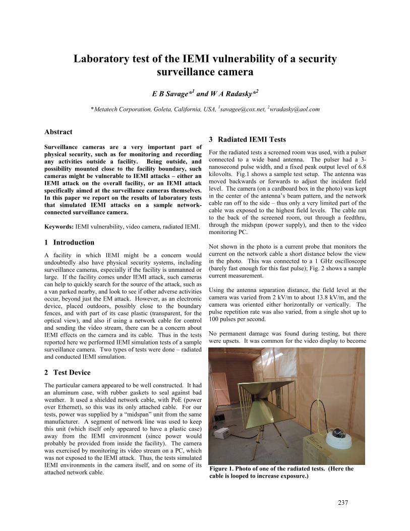
1
Laboratory test of the IEMI vulnerability of a security surveillance camera
E B Savage*1 and W A Radasky*2
*Metatech Corporation, Goleta, California, USA, [email protected], [email protected]
Abstract Surveillance cameras are a very important part of physical security, such as for monitoring and recording any activities outside a facility. Being outside, and possibility mounted close to the facility boundary, such cameras might be vulnerable to IEMI attacks – either an IEMI attack on the overall facility, or an IEMI attack specifically aimed at the surveillance cameras themselves. In this paper we report on the results of laboratory tests that simulated IEMI attacks on a sample network-connected surveillance camera. Keywords: IEMI vulnerability, video camera, radiated IEMI.
1 Introduction
A facility in which IEMI might be a concern would undoubtedly also have physical security systems, including surveillance cameras, especially if the facility is unmanned or large. If the facility comes under IEMI attack, such cameras can help to quickly search for the source of the attack, such as a van parked nearby, and look to see if other adverse activities occur, beyond just the EM attack. However, as an electronic device, placed outdoors, possibly close to the boundary fences, and with part of its case plastic (transparent, for the optical view), and also if using a network cable for control and sending the video stream, there can be a concern about IEMI effects on the camera and its cable. Thus in the tests reported here we performed IEMI simulation tests of a sample surveillance camera. Two types of tests were done – radiated and conducted IEMI simulation.
2 Test Device
The particular camera appeared to be well constructed. It had an aluminum case, with rubber gaskets to seal against bad weather. It used a shielded network cable, with PoE (power over Ethernet), so this was its only attached cable. For our tests, power was supplied by a “midspan” unit from the same manufacturer. A segment of network line was used to keep this unit (which itself only appeared to have a plastic case) away from the IEMI environment (since power would probably be provided from inside the facility). The camera was exercised by monitoring its video stream on a PC, which was not exposed to the IEMI attack. Thus, the tests simulated IEMI environments in the camera itself, and on some of its attached network cable.
3 Radiated IEMI Tests
For the radiated tests a screened room was used, with a pulser connected to a wide band antenna. The pulser had a 3-nanosecond pulse width, and a fixed peak output level of 6.8 kilovolts. Fig.1 shows a sample test setup. The antenna was moved backwards or forwards to adjust the incident field level. The camera (on a cardboard box in the photo) was kept in the center of the antenna’s beam pattern, and the network cable ran off to the side – thus only a very limited part of the cable was exposed to the highest field levels. The cable ran to the back of the screened room, out through a feedthru, through the midspan (power supply), and then to the video monitoring PC. Not shown in the photo is a current probe that monitors the current on the network cable a short distance below the view in the photo. This was connected to a 1 GHz oscilloscope (barely fast enough for this fast pulse); Fig. 2 shows a sample current measurement. Using the antenna separation distance, the field level at the camera was varied from 2 kV/m to about 13.8 kV/m, and the camera was oriented either horizontally or vertically. The pulse repetition rate was also varied, from a single shot up to 100 pulses per second. No permanent damage was found during testing, but there were upsets. It was common for the video display to become
Figure 1. Photo of one of the radiated tests. (Here the cable is looped to increase exposure.)
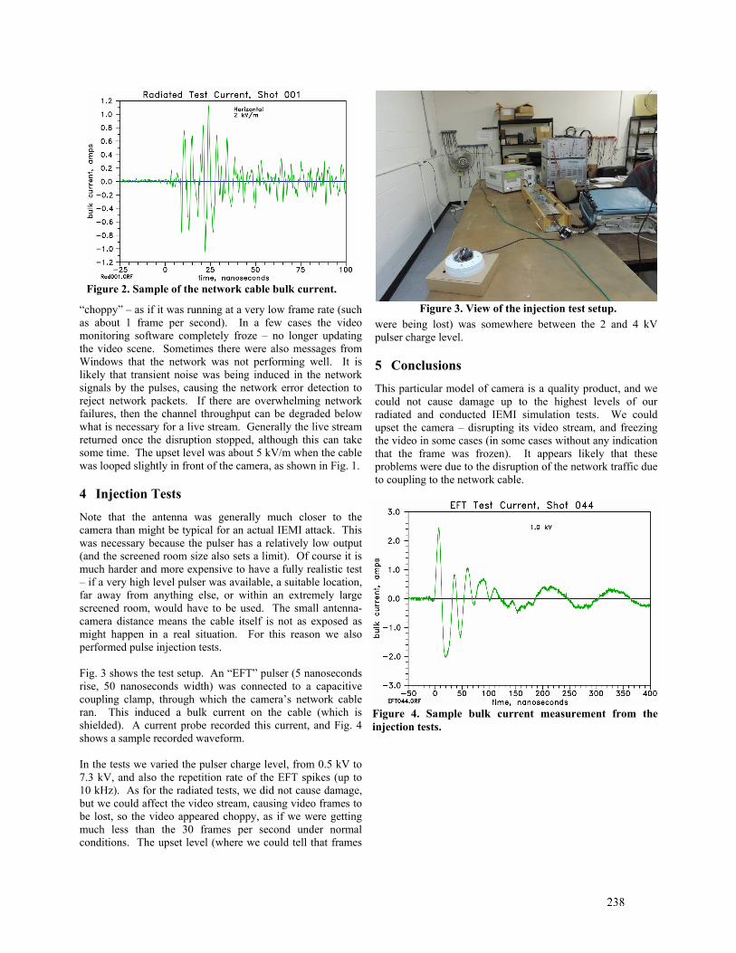
2
“choppy” – as if it was running at a very low frame rate (such as about 1 frame per second). In a few cases the video monitoring software completely froze – no longer updating the video scene. Sometimes there were also messages from Windows that the network was not performing well. It is likely that transient noise was being induced in the network signals by the pulses, causing the network error detection to reject network packets. If there are overwhelming network failures, then the channel throughput can be degraded below what is necessary for a live stream. Generally the live stream returned once the disruption stopped, although this can take some time. The upset level was about 5 kV/m when the cable was looped slightly in front of the camera, as shown in Fig. 1.
4 Injection Tests
Note that the antenna was generally much closer to the camera than might be typical for an actual IEMI attack. This was necessary because the pulser has a relatively low output (and the screened room size also sets a limit). Of course it is much harder and more expensive to have a fully realistic test – if a very high level pulser was available, a suitable location, far away from anything else, or within an extremely large screened room, would have to be used. The small antenna-camera distance means the cable itself is not as exposed as might happen in a real situation. For this reason we also performed pulse injection tests. Fig. 3 shows the test setup. An “EFT” pulser (5 nanoseconds rise, 50 nanoseconds width) was connected to a capacitive coupling clamp, through which the camera’s network cable ran. This induced a bulk current on the cable (which is shielded). A current probe recorded this current, and Fig. 4 shows a sample recorded waveform. In the tests we varied the pulser charge level, from 0.5 kV to 7.3 kV, and also the repetition rate of the EFT spikes (up to 10 kHz). As for the radiated tests, we did not cause damage, but we could affect the video stream, causing video frames to be lost, so the video appeared choppy, as if we were getting much less than the 30 frames per second under normal conditions. The upset level (where we could tell that frames
were being lost) was somewhere between the 2 and 4 kV pulser charge level.
5 Conclusions
This particular model of camera is a quality product, and we could not cause damage up to the highest levels of our radiated and conducted IEMI simulation tests. We could upset the camera – disrupting its video stream, and freezing the video in some cases (in some cases without any indication that the frame was frozen). It appears likely that these problems were due to the disruption of the network traffic due to coupling to the network cable.
Figure 2. Sample of the network cable bulk current.
Figure 4. Sample bulk current measurement from the injection tests.
Figure 3. View of the injection test setup.
Figure 2. Sample of the network cable bulk current.
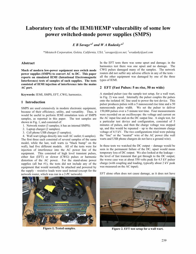
1
Laboratory tests of the IEMI/HEMP vulnerability of some low power switched-mode power supplies (SMPS)
E B Savage*1 and W A Radasky*2
*Metatech Corporation, Goleta, California, USA, [email protected], [email protected]
Abstract Much of modern low-power equipment uses switch mode power supplies (SMPS) to convert AC to DC. This paper reports on simulated IEMI (Intentional Electromagnetic Interference) tests of samples of such supplies. The tests consisted of IEMI injection of interference into the mains AC port. Keywords: IEMI, SMPS, EFT, CWG, harmonics.
1 Introduction
SMPS are used extensively in modern electronic equipment, because of their efficiency, utility, and versatility. Thus, it would be useful to perform IEMI simulation tests of SMPS samples, as reported in this paper. The test samples are shown in Fig. 1, and consisted of:
1. Network router (3 samples; it has an internal SMPS). 2. Laptop charger (2 samples). 3. Cell phone USB charger (3 samples). 4. Wall wart (plugs directly into wall AC outlet; 6 samples).
The first three each consisted of several samples of the same model, while the last, wall warts (a “black bump” on the wall), had five different models. All of the tests were for injection of interference into the AC power line of the equipment. This consisted of high level transient pulses, either fast (EFT) or slower (CWG) pulses or harmonic distortion of the AC power. For the stand-alone power supplies (all but #1), the tests did not include any of the equipment that would normally be attached and powered by the supply – resistive loads were used instead (except for the network router, which was run in a 2-PC network).
In the EFT tests there was some upset and damage; in the harmonics test there was one upset and no damage. The CWG pulses damaged many of the samples. The network routers did not suffer any adverse effects in any of the tests – all the other equipment was damaged by one of the three types of IEMI.
2 EFT (Fast Pulses: 5 ns rise, 50 ns wide)
A standard pulser (see the sample test setup, for a wall wart, in Fig. 2) was used. Internally the pulser couples the pulses onto the isolated AC line used to power the test device. This pulser produces pulses with a 5 nanosecond rise time and a 50 nanoseconds pulse width. We set the pulser to deliver 150,000 pulses over a 5 minute test time. Four measurements were recorded on an oscilloscope: the voltage and current on the AC input line and on the DC output line. A single test, for a particular test device and configuration, consisted of 5 minutes of pulses, and then the charge voltage was stepped up, and this would be repeated – up to the maximum charge voltage of 4.5 kV. The two configurations tried were pulsing the “line” or the “neutral” wire of the AC power (the wall warts and USB phone chargers do not have a ground wire). In these tests we watched the DC output – damage would be seen in the permanent failure of the DC, upset would mean temporary loss of DC output. We also looked at the leakage – the level of fast transient that got through to the DC output; the worse case was at about 550 volts peak for 4.5 kV pulser charge (with coupling and loading, typically about 2 kV peak was measured on the AC input). EFT alone often does not cause damage, as it does not have
Figure 2. EFT test setup for a wall wart. Figure 1. Tested samples.
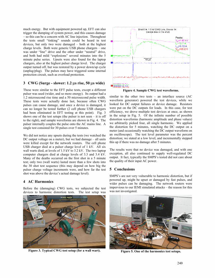
2
much energy. But with equipment powered up, EFT can also trigger the dumping of system power, and this causes damage – so this can be a concern with AC line injection. Throughout the tests small “tinking” sounds could be heard in test devices, but only two were damaged – both at the highest charge levels. Both were generic USB phone chargers – one was under “line” drive and the other under “neutral” drive, and both had mild “explosions” several minutes into the 5 minute pulse series. Upsets were also found for the laptop chargers, also at the highest pulser charge level. The charger output turned off, but was restored by a power down/up cycle (unplug/plug). The pulses may have triggered some internal protection circuit, such as overload protection.
3 CWG (Surge - slower: 1.2 µs rise, 50 µs wide)
These were similar to the EFT pulse tests, except a different pulser was used (wider, and so more energy). Its output had a 1.2 microsecond rise time and a 50 microsecond pulse width. These tests were actually done last, because often CWG pulses can cause damage, and once a device is damaged, it can no longer be tested further (2 cell phone USB chargers had been eliminated in EFT testing at this point). Fig. 3 shows one of the test setups (the pulser is not seen – it is off to the right), and sample waveforms are shown in Fig. 4. The pulser internally couples the pulse onto the AC mains line. A single test consisted for 30 pulses over 5 minutes. We did not notice any upsets during the tests (we watched the DC output voltage on a meter), but we had damage – all units were killed except for the network routers. The cell phone USB charger died at a pulser charge level of 1 kV. All six wall warts died, at levels of 1.5 kV to 3.2 kV. The two laptop computer chargers died at charge levels of 3.3 and 3.4 kV. Many of the deaths occurred on the first shot in a 5 minute test; only two (wall warts) lasted more than a few shots into the 30 shot test sequence (this may depend on how big the pulser charge voltage increments were, and how far the test shot was above the device’s actual damage level).
4 AC Harmonics
Before the (damaging) CWG tests, we subjected the test devices to harmonic distortion tests. The test setup was
similar to the other two tests – an interface source (AC waveform generator) powered the test devices, while we looked for DC output failures or device damage. Resistors were put on the DC outputs for loads. In this case, for test efficiency, we drove multiple test devices at once, as shown in the setup in Fig. 5. Of the infinite number of possible distortion waveforms (harmonic amplitude and phase values) we arbitrarily picked four, all single harmonic. We applied the distortion for 5 minutes, watching the DC output on a meter (and occasionally watching the DC output waveform on an oscilloscope). The test level parameter was the percent distortion; we stated at a low level, and incrementally stepped this up if there was no damage after 5 minutes. The results were that no device was damaged, and with one exception, all also continued to supply well-regulated DC output. It fact, typically the SMPS’s tested did not care about the quality of their input AC power.
5 Conclusions
SMPS’s are not very vulnerable to harmonic distortion, but if powered up, might be upset or damaged by fast pulses, and wider pulses can be damaging. The network routers were impervious to our IEMI simulated attacks – the reason for this was not investigated.
Figure 3. Typical CWG test setup (for a wall wart). Figure 5. One of the harmonics test setups.
Figure 4. Sample CWG test waveforms.
1
IEMI laboratory tests of network line protectors: vulnerability and protection ability
E B Savage*1 and W A Radasky*2
*Metatech Corporation, Goleta, California, USA, [email protected], [email protected]
Abstract An important response mode for an IEMI attack on a facility is coupling into network cables, with resulting damage to the network equipment. Thus, a possible IEMI defense is the use of pulse suppression devices on the network cables. In this paper we look at the vulnerability and protection performance of some network cable protectors. We preformed laboratory tests on eight samples (all from the same manufacturer) with surge protection, and on one sample (much more expensive) that includes additional protection features. Tests were done with standard high-level pulses: EFT (50 nanoseconds wide) and Telecom (700 microseconds wide). Keywords: Network vulnerability, surge protectors, TPD.
1 Introduction
In this paper we are concerned with an IEMI (Intentional Electromagnetic Interference) attack on a modern facility – one with an important function performed using modern electronics. For many cases, such a facility is highly dependent on internal data communication over standard network cabling. EM assaults, such as IEMI, or the similar attack of HEMP (high-altitude electromagnetic pulse), involve the coupling of transient signals (“pulses”) into such cabling, and then those signals propagate along the wires and into equipment, where they may cause damage or upset – see Fig. 1. Various approaches may be used in “hardening” a facility (building in protection) against such attacks. One
very standard approach is to use what might be generically called TPDs (terminal protection devices) or specially SPDs (surge protection devices) where nonlinearity characteristics limit high-level pulses, to prevent transient pulses on the cables from getting into the vulnerable attached equipment. SPDs have been used for a very long time (lightning arrestors are a type of such devices), but their protective behavior can vary significantly. It is not common to find such devices built specifically for IEMI protection. Some protective devices do advertise protection against EMP, or fast turn-on times, and thus possibly might have some usefulness for IEMI. Generally sufficient information is not provided to evaluate such devices as IEMI protectors, and instead laboratory tests must be used to evaluate their performance. Two input features are looked for in such tests. First, for nonlinear surge protection devices, the devices must turn on (generally shorting the line to ground) fast when the voltage starts to get high, so the high level surge is prevented from getting to the protected equipment. Secondly, the protective device should not itself be damaged by the pulse (and if it is damaged, it should be left shorted to ground, to prevent further pulses from getting past). Here we report on pulse response tests on six types of protective devices (see Fig. 2), in which we looked for such adverse effects.
2 Experiments
The experimental setup consisted of feeding the pulser output into the input side of the protective device, with a resistive load on the output side. An oscilloscope was used to record the voltages and currents on both sides of the protector. Fig. 3 shows a typical result for the fast pulse (5 ns rise, 50 ns
Figure 1. Damage occurring from high-level pulse injection into the network interface of power substation
iFigure 2. The devices tested.
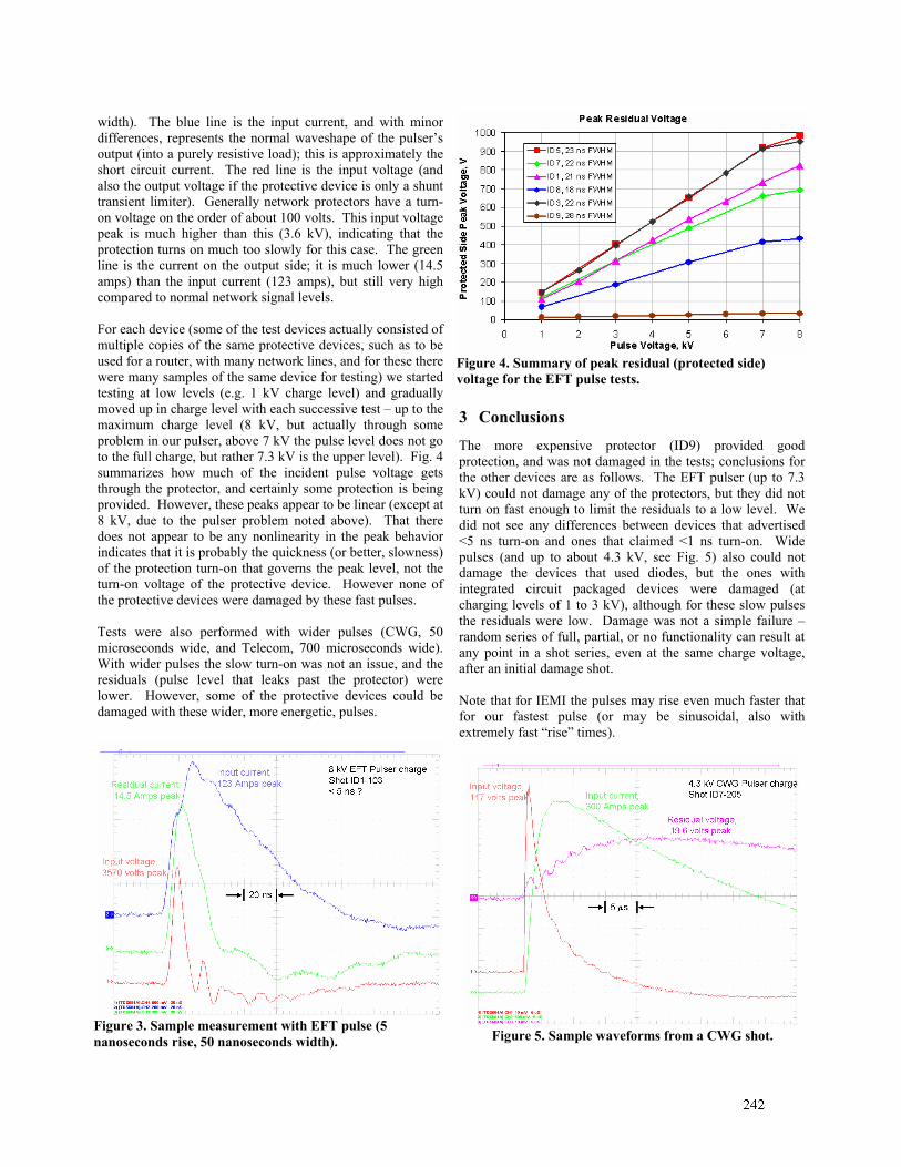
2
width). The blue line is the input current, and with minor differences, represents the normal waveshape of the pulser’s output (into a purely resistive load); this is approximately the short circuit current. The red line is the input voltage (and also the output voltage if the protective device is only a shunt transient limiter). Generally network protectors have a turn-on voltage on the order of about 100 volts. This input voltage peak is much higher than this (3.6 kV), indicating that the protection turns on much too slowly for this case. The green line is the current on the output side; it is much lower (14.5 amps) than the input current (123 amps), but still very high compared to normal network signal levels. For each device (some of the test devices actually consisted of multiple copies of the same protective devices, such as to be used for a router, with many network lines, and for these there were many samples of the same device for testing) we started testing at low levels (e.g. 1 kV charge level) and gradually moved up in charge level with each successive test – up to the maximum charge level (8 kV, but actually through some problem in our pulser, above 7 kV the pulse level does not go to the full charge, but rather 7.3 kV is the upper level). Fig. 4 summarizes how much of the incident pulse voltage gets through the protector, and certainly some protection is being provided. However, these peaks appear to be linear (except at 8 kV, due to the pulser problem noted above). That there does not appear to be any nonlinearity in the peak behavior indicates that it is probably the quickness (or better, slowness) of the protection turn-on that governs the peak level, not the turn-on voltage of the protective device. However none of the protective devices were damaged by these fast pulses. Tests were also performed with wider pulses (CWG, 50 microseconds wide, and Telecom, 700 microseconds wide). With wider pulses the slow turn-on was not an issue, and the residuals (pulse level that leaks past the protector) were lower. However, some of the protective devices could be damaged with these wider, more energetic, pulses.
3 Conclusions
The more expensive protector (ID9) provided good protection, and was not damaged in the tests; conclusions for the other devices are as follows. The EFT pulser (up to 7.3 kV) could not damage any of the protectors, but they did not turn on fast enough to limit the residuals to a low level. We did not see any differences between devices that advertised <5 ns turn-on and ones that claimed <1 ns turn-on. Wide pulses (and up to about 4.3 kV, see Fig. 5) also could not damage the devices that used diodes, but the ones with integrated circuit packaged devices were damaged (at charging levels of 1 to 3 kV), although for these slow pulses the residuals were low. Damage was not a simple failure – random series of full, partial, or no functionality can result at any point in a shot series, even at the same charge voltage, after an initial damage shot. Note that for IEMI the pulses may rise even much faster that for our fastest pulse (or may be sinusoidal, also with extremely fast “rise” times).
Figure 3. Sample measurement with EFT pulse (5 nanoseconds rise, 50 nanoseconds width).
Figure 4. Summary of peak residual (protected side) voltage for the EFT pulse tests.
Figure 5. Sample waveforms from a CWG shot.
Study of the Propagation of IEMI Signals along Power and Communication Lines
N. Mora*, G. Lugrin*, F. Rachidi*, M. Nyffeler†, P. Bertholet†, M. Rubinstein+
*EMC Laboratory, Swiss Federal Institute of Technology (EPFL), Switzerland, [email protected] †HPE Laboratory, Federal Department of Defence – Armasuisse, Switzerland
+ University of Applied Sciences of Western Switzerland, Yverdon, Switzerland
Abstract This work studies the propagation of IEMI (Intentional Electromagnetic Interference) signals along power/communication cables. Specifically, the attenuation and distortion of the IEMI signals resulting from conductive and dielectric losses are studied. Keywords: Intentional electromagnetic interferences (IEMI), field coupling into transmission lines, power lines, communication lines
1 Introduction This work deals with the evaluation of voltages and currents at equipment terminals that are sensitive to an IEMI attack [1]. IEMI stresses on a system can be applied either through conducted coupling or radiated electromagnetic coupling [2]. In both cases, interferences (either induced or directly injected) will reach the sensitive devices through connected cables. This work studies the attenuation and distortion of IEMI signals along power and communication cables. The analysis is based on the Transmission Line (TL) theory [3].
2 Modeling considerations The propagation of IEMI signals along power and communication lines will be affected by (i) conductive losses and dielectric losses, and (ii) radiation losses. The distorted transmission will result in the modification of the amplitudes and the rise time of the original induced waveform. In this study, we assess the attenuation and distortion of the signals through a simplified TL analysis considering uniform lines with conductive and dielectric losses. The radiation losses and reflection due to non-uniformities will not be considered in this work. Consider the coupling of an electromagnetic disturbance onto a lossy uniform transmission line of finite length L. The electromagnetic disturbance is represented as an equivalent lumped source at a given position along the line. In order to simplify the analysis, we will assume that the line is matched at both ends and an equivalent voltage source is used to excite the line at one of the ends, as schematically shown in Fig. 1. The transmission line is characterized by its characteristic impedance 0Z and its complex propagation constant γ . The
propagation transfer function H relating the voltages at both ends of the line can be expressed as:
- - -( )(0)
L L j LV LH e e eV
γ α β= = = (1)
where the complex propagation constant γ has been decomposed into the attenuation constant α and the phase constant β .
Fig. 1 Schematic diagram of a uniform two-wire transmission
line excited by an equivalent voltage source representing the field-to-wire coupling from an external source.
The complex propagation constant of a transmission line can be calculated from its per-unit-length RLGC parameters as [3]:
2
' ' ' '(1 ) ( )' '
R G R Gj LC jLC L C
γ ωω ω ω
= − − + (2)
For lines using good conductors such as copper or aluminium (as in communication and power cables), the attenuation should be governed by the conductance of the line, which is directly related to the dielectric losses. However, for lines with very small cross-section, the skin effect plays an important role in the attenuation of the signals.
4 Overview of the parametric analysis and results The per-unit-length parameters of several power and communication lines were extracted in order to assess the significance of the conductive and dielectric losses at the expected frequencies of IEMI perturbations. The p.u.l. parameters of each of the lines were calculated by considering a finite conductivity of the conductors and the presence of a dielectric with known complex permittivity (assuming a constant tangent loss of the dielectric). The p.u.l. resistance of
0Z 0Z
L
V0
0 ,Z γ ( )V L(0)V
1
the lines was calculated by including the frequency variation due to the skin effect. The results for a 10-m low voltage power cable are presented in Fig. 2. The top plot shows the injected signal (black line) which is representative of a hyperband IEMI waveform with a risetime of 229 ps. The lower panel presents the propagated signals at the other end of the line. The blue curve corresponds to the calculated signal when no losses are included. If the conductive losses are included (green curve), there is an attenuation of about 10% for the peak amplitude, and an increase in the signal risetime. On the other hand, if only the dielectric losses are considered (cyan curve), the peak attenuation is about 40% and a more significant increase is observed for the risetime. Finally, the red curve shows the results obtained when both losses are included. In this case, the overall peak attenuation is about 50% and the obtained risetime is comparable to the one obtained if only dielectric losses are included.
Fig. 2 Propagation along a 10-m long low voltage power
cable. (a) Injected signal. (b) Propagated signal at the right end of the line.
A similar study was carried out considering a network cable (Cat 5). The simulation results are shown in Fig. 3. Unlike the case of the power cable for which the dielectric losses were predominant, in this case, the conductive losses prevail. This is essentially due to (i) smaller cross section, and (ii) thinner dielectric coating, of the twisted wires in the network cable in comparison with the power cable.
Fig. 3 Propagation along a 10-m long network (Cat 5) twisted
pair. (a) Injected signal. (b) Propagated signal at the right end of the line.
5 Conclusions
The differential mode propagation of very fast injected transients can be significantly affected by the presence of losses in power and communication lines, resulting in an attenuation of the peak and an increase of the risetime. Similar results were obtained in [4-7]where the propagation of IEMI signals in low voltage power networks was assessed from experimental point of view.
Traditional surge protection devices (SPDs) are used to protect from overvoltages and overcurrents originated by signals that are slower than the expected IEMI signals (e.g., those originated from ESD, NEMP, or lightning). The presented analysis allows the evaluation of the required propagation distance at which the attenuation and distortion of IEMI signals are such that traditional SPDs can be effectively used to protect sensitive devices connected at the end of the lines.
Acknowledgements This study was financed by the Armasuisse Science and Technology (Contract Nr. 8003504623).
References
[1] W. A. Radasky, C. E. Baum, and M. W. Wik, "Introduction to the special issue on high-power electromagnetics (HPEM) and intentional electromagnetic interference (IEMI)," Electromagnetic Compatibility, IEEE Transactions on, vol. 46, pp. 314-321, 2004.
[2] D. V. Giri and F. M. Tesche, "Classification of intentional electromagnetic environments (IEME)," Electromagnetic Compatibility, IEEE Transactions on, vol. 46, pp. 322-328, 2004.
[3] C. R. Paul, Analysis of multiconductor transmission lines. Hoboken, N.J.: Wiley-Interscience : IEEE Press, 2008.
[4] D. Mansson, T. Nilsson, R. Thottappillil, and M. Backstrom, "Propagation of UWB Transients in Low-Voltage Installation Power Cables," Electromagnetic Compatibility, IEEE Transactions on, vol. 49, pp. 585-592, 2007.
[5] D. Mansson, R. Thottappillil, and M. Backstrom, "Propagation of UWB Transients in Low-Voltage Power Installation Networks," Electromagnetic Compatibility, IEEE Transactions on, vol. 50, pp. 619-629, 2008.
[6] N. Mora, C. Kasmi, F. Rachidi, M. Darces, and M. Helier, "Modeling of the propagation along low voltage power networks for IEMI studies," in Electromagnetics in Advanced Applications (ICEAA), 2013 International Conference on, 2013, pp. 436-439.
[7] N. Mora, C. Kasmi, F. Rachidi, M. Darces, M. Hélier, and M. Rubinstein, "Analysis of the Propagation of High Frequency Disturbances along Low-Voltage Test Raceway," presented at the American Electromagnetics International Symposium (AMEREM), Albuquerque, New Mexico, USA, 2014.
2
Effect of the Penetration through a Concrete Wall on the Propagation of Common Mode IEMI Signals
N. Mora*, G. Lugrin*, F. Rachidi*, M. Nyffeler†, P. Bertholet†, M. Rubinstein+
*EMC Laboratory, Swiss Federal Institute of Technology (EPFL), Switzerland, [email protected] †HPE Laboratory, Federal Department of Defence – Armasuisse, Switzerland +University of Applied Sciences of Western Switzerland, Yverdon, Switzerland
Abstract We present a study on the effect of the penetration of transmission lines through concrete walls on the attenuation and distortion of common mode IEMI signals. The propagation of high frequency signals along a transmission line passing through a concrete wall is analyzed as a function of the concrete electrical parameters, thickness of the wall and the frequency of the signal. Keywords: Intentional Electromagnetic Interference (IEMI), Transmission lines, Debye model
1 Introduction This work deals with the evaluation of voltages and currents at equipment terminals that are sensitive to an IEMI attack [1] [2]. Outdoor power or communication cables, on which disturbance signals could be injected or induced, pass through concrete walls. It can be expected that the concrete structure of the wall has a beneficial effect on the attenuation of propagating signals. In this work, we present a study of the effect of the penetration of transmission lines through concrete walls on the propagation of common mode IEMI signals. The propagation of high frequency signals along a transmission line will be analyzed as a function of the electrical parameters of the concrete, the thickness of the wall and the frequency of the signal. The study will be based on the Transmission Line (TL) theory.
2 Modeling considerations
2.1 TL equivalent
We will model the penetration of the conductor into a concrete slab as a transmission line surrounded by a homogeneous lossy dielectric. Consider the propagation of a signal along a transmission line composed of a single bare wire located at a height h above a ground plane that penetrates a concrete wall of thickness L as schematically shown in Fig. 1. The voltage source at the input of the line represents the injection or coupling of a common mode signal onto the outdoor cabling that will propagate to the interior of a
building passing across the wall. The penetration of the wire into the concrete wall will introduce a discontinuity in the propagation of the signal in free space and it can be represented as a separate transmission line cascaded with the outdoor and indoor portions of the line. The cross sections of the outdoor and indoor transmission line sections are shown at the bottom left and right panels of Fig. 1. The outdoor and indoor portions of the line are assumed to be in free space. On the other hand, the cross section of the portion of the line inside the concrete wall is shown in the bottom-middle panel of Fig. 1. The transmission line inside the wall is assumed to be surrounded by a homogeneous dielectric characterized by its relative permittivity rε and the loss tangent tanδ . Notice that for the considered example, the line is a bare wire (no dielectric coating) and is in direct contact with the concrete.
Fig. 1 Schematic diagram of a transmission line penetrating a concrete wall
2.2 Two-port network representation of the wall
A two-port network representation of the concrete transmission line can be used in order to calculate the reflected and transmitted signals at the line interface (see Fig. 2). The transmission matrix (ABCD parameters) of the two-port network relates the input and output voltages and currents as [3]:
1 2
1 2
V VA BI IC D
=
(1)
L
x
V0
Cross-sectionfree space
h
Ground Plane
2 wr
Cross-sectionfree space
h
Ground Plane
2 wr
Cross-sectionConcrete
h
Ground Plane
2 wr
, tanrε δ
Outdoor Concrete wall Indoor
1
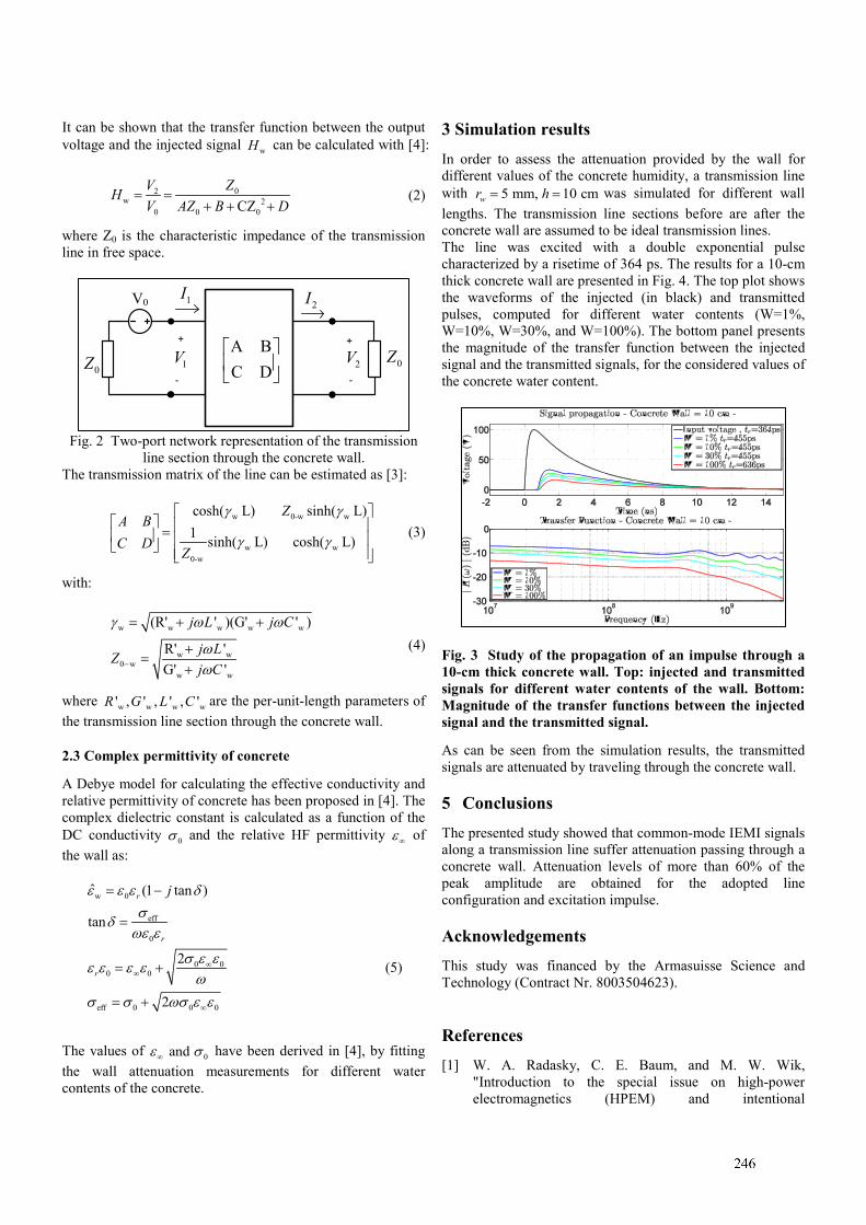
It can be shown that the transfer function between the output voltage and the injected signal wH can be calculated with [4]:
02w 2
0 0 0CZZVH
V AZ B D= =
+ + + (2)
where Z0 is the characteristic impedance of the transmission line in free space.
Fig. 2 Two-port network representation of the transmission
line section through the concrete wall. The transmission matrix of the line can be estimated as [3]:
w 0-w w
w w0-w
cosh( L) sinh( L)1 sinh( L) cosh( L)
ZA BC D
Z
γ γ
γ γ
=
(3)
with:
w w w w w
w w0 w
w w
(R' ' )(G' ' )
R' 'G' '
j L j C
j LZj C
γ w w
ww−
= + +
+=
+
(4)
where w w w w' , ' , ' , 'R G L C are the per-unit-length parameters of the transmission line section through the concrete wall.
2.3 Complex permittivity of concrete
A Debye model for calculating the effective conductivity and relative permittivity of concrete has been proposed in [4]. The complex dielectric constant is calculated as a function of the DC conductivity 0σ and the relative HF permittivity ε∞ of the wall as:
w 0
eff
0
0 00 0
eff 0 0 0
ˆ (1 tan )
tan
2
2
r
r
r
jε ε ε δσδwε ε
σ ε εε ε ε εw
σ σ wσ ε ε
∞∞
∞
= −
=
= +
= +
(5)
The values of 0 and ε σ∞ have been derived in [4], by fitting the wall attenuation measurements for different water contents of the concrete.
3 Simulation results In order to assess the attenuation provided by the wall for different values of the concrete humidity, a transmission line with 5 mm, 10 cmwr h= = was simulated for different wall lengths. The transmission line sections before are after the concrete wall are assumed to be ideal transmission lines. The line was excited with a double exponential pulse characterized by a risetime of 364 ps. The results for a 10-cm thick concrete wall are presented in Fig. 4. The top plot shows the waveforms of the injected (in black) and transmitted pulses, computed for different water contents (W=1%, W=10%, W=30%, and W=100%). The bottom panel presents the magnitude of the transfer function between the injected signal and the transmitted signals, for the considered values of the concrete water content.
Fig. 3 Study of the propagation of an impulse through a 10-cm thick concrete wall. Top: injected and transmitted signals for different water contents of the wall. Bottom: Magnitude of the transfer functions between the injected signal and the transmitted signal.
As can be seen from the simulation results, the transmitted signals are attenuated by traveling through the concrete wall.
5 Conclusions The presented study showed that common-mode IEMI signals along a transmission line suffer attenuation passing through a concrete wall. Attenuation levels of more than 60% of the peak amplitude are obtained for the adopted line configuration and excitation impulse.
Acknowledgements This study was financed by the Armasuisse Science and Technology (Contract Nr. 8003504623).
References [1] W. A. Radasky, C. E. Baum, and M. W. Wik,
"Introduction to the special issue on high-power electromagnetics (HPEM) and intentional
0Z 0Z
V0
1V 2V
1I 2I
+
-
+
-
A BC D
2
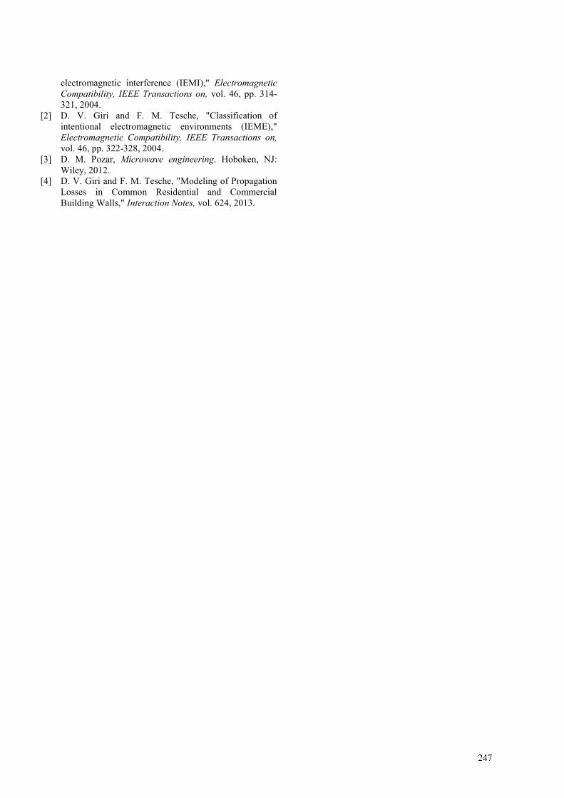
electromagnetic interference (IEMI)," Electromagnetic Compatibility, IEEE Transactions on, vol. 46, pp. 314-321, 2004.
[2] D. V. Giri and F. M. Tesche, "Classification of intentional electromagnetic environments (IEME)," Electromagnetic Compatibility, IEEE Transactions on, vol. 46, pp. 322-328, 2004.
[3] D. M. Pozar, Microwave engineering. Hoboken, NJ: Wiley, 2012.
[4] D. V. Giri and F. M. Tesche, "Modeling of Propagation Losses in Common Residential and Commercial Building Walls," Interaction Notes, vol. 624, 2013.
3
1
Application of varistor for RF protection of semiconductor bridge
Bin Zhou*, Jun Wang † Pei-kang Du
†Yong Li
†
*School of Chemical Engineering, Nanjing University of Science and Technology, Nanjing 210094, Jiangsu, CHINA.
(e-mail:[email protected])
Abstract
The principle of varistor which was used in radio
frequency (RF) protection of semiconductor bridge (SCB)
was investigated in this paper. According to the RF
injection experiment, electro-explosive performances of
SCB with or without varistor were studied. The results
showed that the ability of SCB to anti-RF had
dramatically improved by varistor and there was no
significant difference of SCB performances which was
protected by varistor after 20W RF injection experiment.
Therefore, the varistor had no influences on
electro-explosive of SCB and could provide RF protection
to SCB when in parallel with SCB.
Keywords: initiator, semiconductor bridge, radio frequency
protection.
1 Introduction
Semiconductor bridge (SCB) is a kind of electro-explosive
device which use it semiconductor film to ignite primary
explosive. It has advantages of small, safety, ESD and RF
tolerant. At the same time, it can operate at low energies and
function very quickly. However, the electromagnetic
environment is becoming more and more complex with the
use of radar and other electromagnetic weapons. So there is a
demand for ammunition to anti-RF. The electromagnetic
environmental compatibility of initiator catches much
attention for its characteristic of sensitive. Although SCB is
insensitive to RF, but we still need to strengthen its ability of
anti-RF.
The researchers had provide many ways to strengthen SCB,
like changing the structure of SCB or adding external
components. Ensign-Bickford company designed a new SCB
structure that added a layer of dielectric material to top and
bottom of SCB. There was no current in SCB when the
voltage of SCB below the threshold voltage of dielectric
material. But the dielectric material would be breakdown in
nanosecond when giving the SCB all-fire voltage, the SCB
would fire at the same time. The capacitor that formed by
dielectric material could shunt high-frequency AC and
suppressed voltage caused by ESD. This structure had a good
performance of immunity to ESD and RF hazards[1]. L. Dow
Robert added ferrite element to EED to absorb energy on
bridgewire caused by RF. It could withstand high RF power
levels or electromagnetic pulse by radar.[2] Re-Long Chiu
provided a new kind of explosive device initiator. They
designed a multilayer semiconductor structure and supplied a
MOS capacitor on the substrate. This structure could use the
chemical reaction between metal and silicon to generate
plasma. It showed excellent no-fire levels.[3] John H
Henderson mounted the filter and EED on the same substrate.
The filter was made of one capacitor and two ferrite beads.[4]
Thomas A baginski designed a semiconductor junction igniter
which had characteristics of immunity to ESD and RF.[5] Fei
Chen[6] investigated the damage mechanism of SCB under
RF and set up mathematical model and physical model under
RF. In this paper, the mechanism of SCB that protected by
varistor was studied by theoretical analysis and experiments.
2 The principle of varistor for RF protection
Generally, the SMD varistor is mounted in parallel with other
device. The varistor will show open state with 100 MΩ
resistance when there is no voltage coupled into the device,
therefore it has no influence on the normal function of device.
But the resistance of SMD varistor will change from 100MΩ
to 100mΩ in nanosecond (<0.5 nS) when coupled into any
power. So the voltage of the device can be controlled in a low
level. Thus the varistor protects the device from voltage pulse
by absorb the large energy that flow through itself. However,
the resistance of varistor will return back after the voltage
disappearing. The capacitance of varistor can reach 1000pF
for its multilayer structure. When in low-frequency RF
environment, the SMD varistor shows open state and has no
influence on the normal operate of device. While in
high-frequency RF environment, the SMD varistor forms a
low-impedence bypass in nanosecond to shunt induced
current to protect the device form the impact of
electromagnetic radiation.
The equivalent circuit model of SMD varistor that used to
protect SCB initiator was shown in Fig. 1. In this paper, we
chose A-type SMD varistor with 8V breakdown voltage and
the actual picture was shown in Fig 2.
Figure 1. The equivalent model of varistor with SCB
2
Figure 2. Photography of varistor
Under the condition of high RF, the varistor shows a
conducting state. The equivalent series resistance(Ri) and
inductance(Li) also exist in the circuit, thus the actual
situation can be expressed as Equation (1).
1Z = R + j 2πfL -
2πfC
(1)
1
2f
LC, the impedance will decrease with the increasing
frequency.
1
2f
LC , the impedance reaches minimum. The
frequency is the resonant frequency and the resistance value
of varistor is the parasitic resistance.
1
2f
LC , the impedance will increase with the increasing
frequency.
So the dynamic impedance of varistor is much less than
SCB’s. The capacitance can shunt current caused by high
frequency for low impedance. Thus, the current that flows
through SCB will decrease. The capacitance will not dissipate
the energy, so most coupling energy will be absorbed by
resistance. Meanwhile the parasitic resistance is very small
and the area of SCB is large, the Joule heat caused by current
can be dissipated soon. So it protects SCB from high RF.
3 Samples and experiment devices
3.1 Samples
SCB chip is the most crucial element in SCB initiator. Fig. 3
is the structure of heavily doped polysilicon SCB (H shape).
Between the silicon substrate and Aluminum pad is the
heavily doped polysilicon and the doping concentration is 7×10
19atoms/cm
3. We have two kinds of chips that one is D-type
with the size of 400m(L)×100m(W)×2m(T) and another
is X-type with 80m(L)×20m(W)×2m(T). The resistance
and all-fire energy of D-type is 1.0Ω and 10mJ, while
X-type is 1.3~1.7Ω and 3mJ. The chip was packaged in ceramic plug as is shown in Fig. 4.
The chip was adhered to ceramic plug with 4.5mm diameter
by epoxy. Bonding the pins and chip with Si-Al wire and
coating the Lead styphnate (LTNR) to the top of chip. While
the varistor was assembled on the bottom of ceramic plug and
electric contracted to pins which meant in parallel with SCB
chip. The experiment samples were shown in Table 1.
Figure 3. SCB chip
Figure 4. Ceramic plug package structure
Table 1: experiment samples
sample State of sample
D-type D-type SCB initiator without any
protection
A-D-type D-type SCB initiator being protected
by A-type varistor
X-type X-type SCB initiator without any
protection
A-X-type X-type SCB initiator being protected
by A-type varistor
3.2 The principle of capacitor discharge experiment
Figure 5. Schematic of capacitor discharge experiment
Capacitor discharge experiment was adopted to test the SCB
initiator and the schematic diagram was shown in Fig. 5. We
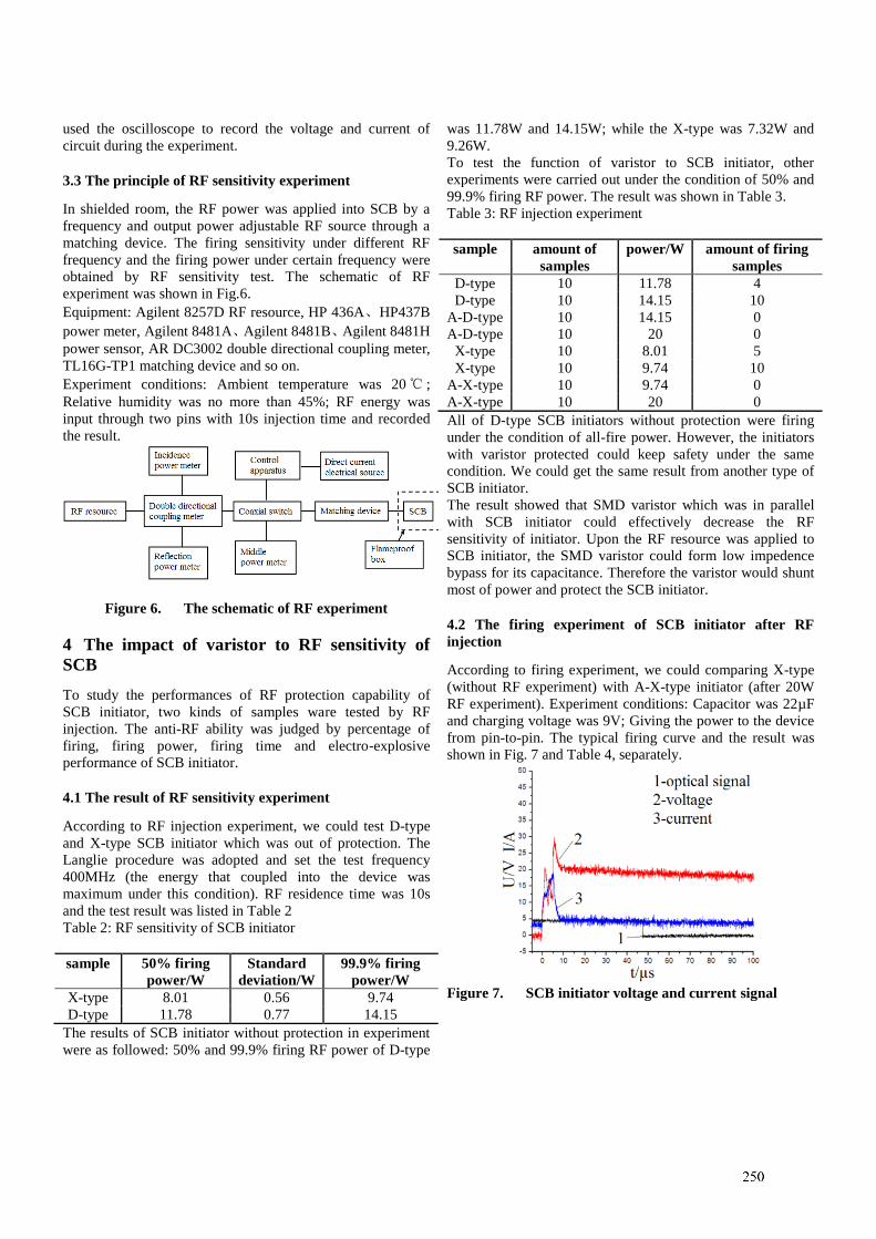
3
used the oscilloscope to record the voltage and current of
circuit during the experiment.
3.3 The principle of RF sensitivity experiment
In shielded room, the RF power was applied into SCB by a
frequency and output power adjustable RF source through a
matching device. The firing sensitivity under different RF
frequency and the firing power under certain frequency were
obtained by RF sensitivity test. The schematic of RF
experiment was shown in Fig.6.
Equipment: Agilent 8257D RF resource, HP 436A、HP437B
power meter, Agilent 8481A、Agilent 8481B、Agilent 8481H
power sensor, AR DC3002 double directional coupling meter,
TL16G-TP1 matching device and so on.
Experiment conditions: Ambient temperature was 20 ;
Relative humidity was no more than 45%; RF energy was
input through two pins with 10s injection time and recorded
the result.
Figure 6. The schematic of RF experiment
4 The impact of varistor to RF sensitivity of
SCB
To study the performances of RF protection capability of
SCB initiator, two kinds of samples ware tested by RF
injection. The anti-RF ability was judged by percentage of
firing, firing power, firing time and electro-explosive
performance of SCB initiator.
4.1 The result of RF sensitivity experiment
According to RF injection experiment, we could test D-type
and X-type SCB initiator which was out of protection. The
Langlie procedure was adopted and set the test frequency
400MHz (the energy that coupled into the device was
maximum under this condition). RF residence time was 10s
and the test result was listed in Table 2
Table 2: RF sensitivity of SCB initiator
sample 50% firing
power/W
Standard
deviation/W
99.9% firing
power/W
X-type 8.01 0.56 9.74
D-type 11.78 0.77 14.15
The results of SCB initiator without protection in experiment
were as followed: 50% and 99.9% firing RF power of D-type
was 11.78W and 14.15W; while the X-type was 7.32W and
9.26W.
To test the function of varistor to SCB initiator, other
experiments were carried out under the condition of 50% and
99.9% firing RF power. The result was shown in Table 3.
Table 3: RF injection experiment
sample amount of
samples
power/W amount of firing
samples
D-type 10 11.78 4
D-type 10 14.15 10
A-D-type 10 14.15 0
A-D-type 10 20 0
X-type 10 8.01 5
X-type 10 9.74 10
A-X-type 10 9.74 0
A-X-type 10 20 0
All of D-type SCB initiators without protection were firing
under the condition of all-fire power. However, the initiators
with varistor protected could keep safety under the same
condition. We could get the same result from another type of
SCB initiator.
The result showed that SMD varistor which was in parallel
with SCB initiator could effectively decrease the RF
sensitivity of initiator. Upon the RF resource was applied to
SCB initiator, the SMD varistor could form low impedence
bypass for its capacitance. Therefore the varistor would shunt
most of power and protect the SCB initiator.
4.2 The firing experiment of SCB initiator after RF
injection
According to firing experiment, we could comparing X-type
(without RF experiment) with A-X-type initiator (after 20W
RF experiment). Experiment conditions: Capacitor was 22µF
and charging voltage was 9V; Giving the power to the device
from pin-to-pin. The typical firing curve and the result was
shown in Fig. 7 and Table 4, separately.
Figure 7. SCB initiator voltage and current signal
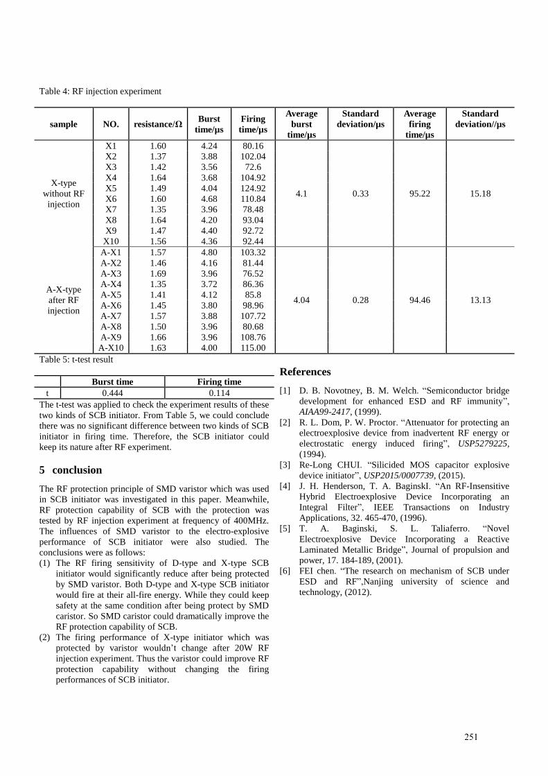
4
Table 4: RF injection experiment
sample NO. resistance/Ω Burst
time/µs
Firing
time/µs
Average
burst
time/µs
Standard
deviation/µs
Average
firing
time/µs
Standard
deviation//µs
X-type
without RF
injection
X1 1.60 4.24 80.16
4.1 0.33 95.22 15.18
X2 1.37 3.88 102.04
X3 1.42 3.56 72.6
X4 1.64 3.68 104.92
X5 1.49 4.04 124.92
X6 1.60 4.68 110.84
X7 1.35 3.96 78.48
X8 1.64 4.20 93.04
X9 1.47 4.40 92.72
X10 1.56 4.36 92.44
A-X-type
after RF
injection
A-X1 1.57 4.80 103.32
4.04 0.28 94.46 13.13
A-X2 1.46 4.16 81.44
A-X3 1.69 3.96 76.52
A-X4 1.35 3.72 86.36
A-X5 1.41 4.12 85.8
A-X6 1.45 3.80 98.96
A-X7 1.57 3.88 107.72
A-X8 1.50 3.96 80.68
A-X9 1.66 3.96 108.76
A-X10 1.63 4.00 115.00
Table 5: t-test result
Burst time Firing time
t 0.444 0.114
The t-test was applied to check the experiment results of these
two kinds of SCB initiator. From Table 5, we could conclude
there was no significant difference between two kinds of SCB
initiator in firing time. Therefore, the SCB initiator could
keep its nature after RF experiment.
5 conclusion
The RF protection principle of SMD varistor which was used
in SCB initiator was investigated in this paper. Meanwhile,
RF protection capability of SCB with the protection was
tested by RF injection experiment at frequency of 400MHz.
The influences of SMD varistor to the electro-explosive
performance of SCB initiator were also studied. The
conclusions were as follows:
(1) The RF firing sensitivity of D-type and X-type SCB
initiator would significantly reduce after being protected
by SMD varistor. Both D-type and X-type SCB initiator
would fire at their all-fire energy. While they could keep
safety at the same condition after being protect by SMD
caristor. So SMD caristor could dramatically improve the
RF protection capability of SCB.
(2) The firing performance of X-type initiator which was
protected by varistor wouldn’t change after 20W RF
injection experiment. Thus the varistor could improve RF
protection capability without changing the firing
performances of SCB initiator.
References
[1] D. B. Novotney, B. M. Welch. “Semiconductor bridge
development for enhanced ESD and RF immunity”,
AIAA99-2417, (1999).
[2] R. L. Dom, P. W. Proctor. “Attenuator for protecting an
electroexplosive device from inadvertent RF energy or
electrostatic energy induced firing”, USP5279225,
(1994).
[3] Re-Long CHUI. “Silicided MOS capacitor explosive
device initiator”, USP2015/0007739, (2015).
[4] J. H. Henderson, T. A. BaginskI. “An RF-Insensitive
Hybrid Electroexplosive Device Incorporating an
Integral Filter”, IEEE Transactions on Industry
Applications, 32. 465-470, (1996).
[5] T. A. Baginski, S. L. Taliaferro. “Novel
Electroexplosive Device Incorporating a Reactive
Laminated Metallic Bridge”, Journal of propulsion and
power, 17. 184-189, (2001).
[6] FEI chen. “The research on mechanism of SCB under
ESD and RF”,Nanjing university of science and
technology, (2012).
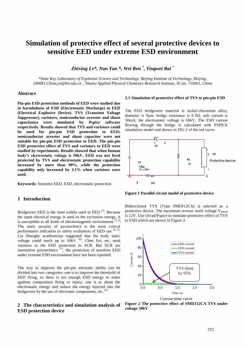
1
Simulation of protective effect of several protective devices to
sensitive EED under extreme ESD environment
Zhixing Lv*, Nan Yan *, Wei Ren †, Yingwei Bai
†
*State Key Laboratory of Explosion Science and Technology, Beijing Institute of Technology, Beijing,
100081,China,[email protected] , †Shanxi Applied Physical Chemistry Research Institute, Xi’an, 710061, China
Abstract
Pin-pin ESD protection methods of EED were studied due
to harmfulness of ESD (Electrostatic Discharge) to EED
(Electrical Explosive Device). TVS (Transient Voltage
Suppressor), varistors, semiconductor arrester and shunt
capacitance were simulated by Pspice software
respectively. Results showed that TVS and varistors could
be used for pin-pin ESD protection to EED;
semiconductor arrester and shunt capacitor were not
suitable for pin-pin ESD protection to EED. The pin-pin
ESD protective effect of TVS and varistors to EED were
studied by experiments. Results showed that when human
body’s electrostatic voltage is 50kV, EED was not fired
protected by TVS and electrostatic protection capability
increased by more than 90%, while the protection
capability only increased by 3.1% when varistors were
used.
Keywords: Sensitive EED, ESD, electrostatic protection
1 Introduction
Bridgewire EED is the most widely used in EED [1]
. Because
the input electrical energy is used as the excitation energy, it
is susceptible to all kinds of electromagnetic environment [2, 3]
.
The static security of pyrotechnics is the most critical
performance indicators in safety evaluation of EED use [4, 5]
.
Liu Shanghe academician suggested that the body static
voltage could reach up to 50kV [6]
. Chen Fei, etc. used
varistors in the ESD protection to SCB. But SCB are
insensitive pyrotechnics [7]
, the protection of sensitive EED
under extreme ESD environment have not been reported.
The way to improve the pin-pin antistatic ability can be
divided into two categories: one is to improve the threshold of
EED firing, so there is not enough ESD energy to make
ignition composition firing or injury; one is to shunt the
electrostatic energy and reduce the energy injected into the
bridgewire by the use of electronic components, etc. [8]
2 The characteristics and simulation analysis of
ESD protection device
2.1 Simulation of protective effect of TVS to pin-pin ESD
The EED bridgewire material is nickel-chromium alloy;
diameter is 9μm; bridge resistance is 6.5Ω; safe current is
50mA; the electrostatic voltage is 50kV. The ESD current
flowing through the bridge is calculated with PSPICE
simulation model and shown in FIG 2 of the red curve.
Figure 1 Parallel circuit model of protective device
Bidirectional TVS (Type SMDJ12CA) is selected as a
protective device. The maximum reverse work voltage VRWM
is 12V. Use Orcad/Pspice to simulate protective effect of TVS
to ESD which are shown in Figure 2.
0.0 0.5 1.0 1.5 2.00
20
40
60
80
100
Cu
rren
t /A
Time /us
ESD current
EED current
TVS current
Current-time curve
Figure 2 The protective effect of SMDJ12CA TVS under
voltage 50kV
TVS shunt
by 95%
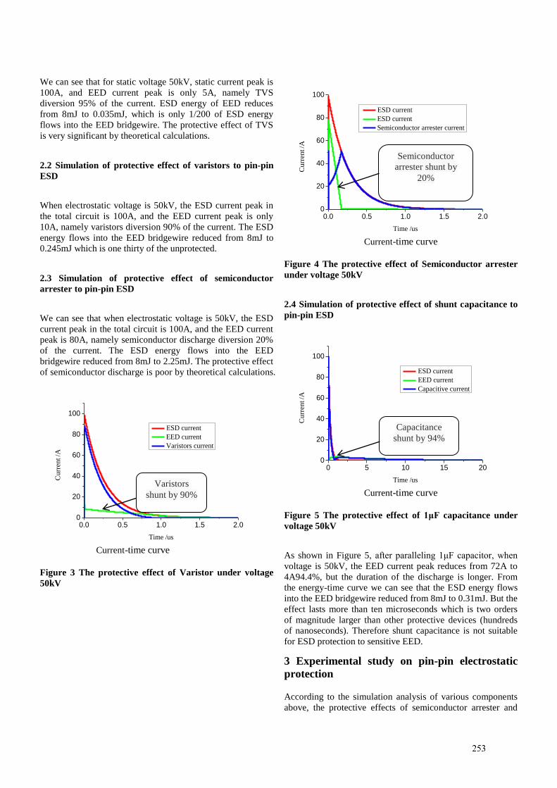
2
We can see that for static voltage 50kV, static current peak is
100A, and EED current peak is only 5A, namely TVS
diversion 95% of the current. ESD energy of EED reduces
from 8mJ to 0.035mJ, which is only 1/200 of ESD energy
flows into the EED bridgewire. The protective effect of TVS
is very significant by theoretical calculations.
2.2 Simulation of protective effect of varistors to pin-pin
ESD
When electrostatic voltage is 50kV, the ESD current peak in
the total circuit is 100A, and the EED current peak is only
10A, namely varistors diversion 90% of the current. The ESD
energy flows into the EED bridgewire reduced from 8mJ to
0.245mJ which is one thirty of the unprotected.
2.3 Simulation of protective effect of semiconductor
arrester to pin-pin ESD
We can see that when electrostatic voltage is 50kV, the ESD
current peak in the total circuit is 100A, and the EED current
peak is 80A, namely semiconductor discharge diversion 20%
of the current. The ESD energy flows into the EED
bridgewire reduced from 8mJ to 2.25mJ. The protective effect
of semiconductor discharge is poor by theoretical calculations.
0.0 0.5 1.0 1.5 2.00
20
40
60
80
100
Cu
rren
t /A
Time /us
ESD current
EED current
Varistors current
Current-time curve
Figure 3 The protective effect of Varistor under voltage
50kV
0.0 0.5 1.0 1.5 2.00
20
40
60
80
100
Cu
rren
t /A
Time /us
ESD current
ESD current
Semiconductor arrester current
Current-time curve
Figure 4 The protective effect of Semiconductor arrester
under voltage 50kV
2.4 Simulation of protective effect of shunt capacitance to
pin-pin ESD
0 5 10 15 200
20
40
60
80
100
Cu
rren
t /A
Time /us
ESD current
EED current
Capacitive current
Current-time curve
Figure 5 The protective effect of 1μF capacitance under
voltage 50kV
As shown in Figure 5, after paralleling 1μF capacitor, when
voltage is 50kV, the EED current peak reduces from 72A to
4A94.4%, but the duration of the discharge is longer. From
the energy-time curve we can see that the ESD energy flows
into the EED bridgewire reduced from 8mJ to 0.31mJ. But the
effect lasts more than ten microseconds which is two orders
of magnitude larger than other protective devices (hundreds
of nanoseconds). Therefore shunt capacitance is not suitable
for ESD protection to sensitive EED.
3 Experimental study on pin-pin electrostatic
protection
According to the simulation analysis of various components
above, the protective effects of semiconductor arrester and
Varistors
shunt by 90%
Capacitance
shunt by 94%
Semiconductor
arrester shunt by
20%
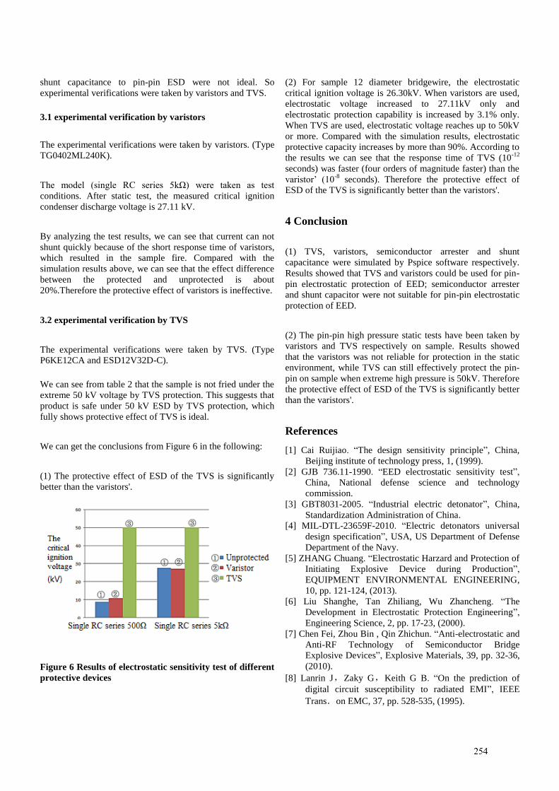
3
shunt capacitance to pin-pin ESD were not ideal. So
experimental verifications were taken by varistors and TVS.
3.1 experimental verification by varistors
The experimental verifications were taken by varistors. (Type
TG0402ML240K).
The model (single RC series 5kΩ) were taken as test
conditions. After static test, the measured critical ignition
condenser discharge voltage is 27.11 kV.
By analyzing the test results, we can see that current can not
shunt quickly because of the short response time of varistors,
which resulted in the sample fire. Compared with the
simulation results above, we can see that the effect difference
between the protected and unprotected is about
20%.Therefore the protective effect of varistors is ineffective.
3.2 experimental verification by TVS
The experimental verifications were taken by TVS. (Type
P6KE12CA and ESD12V32D-C).
We can see from table 2 that the sample is not fried under the
extreme 50 kV voltage by TVS protection. This suggests that
product is safe under 50 kV ESD by TVS protection, which
fully shows protective effect of TVS is ideal.
We can get the conclusions from Figure 6 in the following:
(1) The protective effect of ESD of the TVS is significantly
better than the varistors'.
Figure 6 Results of electrostatic sensitivity test of different
protective devices
(2) For sample 12 diameter bridgewire, the electrostatic
critical ignition voltage is 26.30kV. When varistors are used,
electrostatic voltage increased to 27.11kV only and
electrostatic protection capability is increased by 3.1% only.
When TVS are used, electrostatic voltage reaches up to 50kV
or more. Compared with the simulation results, electrostatic
protective capacity increases by more than 90%. According to
the results we can see that the response time of TVS (10-12
seconds) was faster (four orders of magnitude faster) than the
varistor’ (10-8
seconds). Therefore the protective effect of
ESD of the TVS is significantly better than the varistors'.
4 Conclusion
(1) TVS, varistors, semiconductor arrester and shunt
capacitance were simulated by Pspice software respectively.
Results showed that TVS and varistors could be used for pin-
pin electrostatic protection of EED; semiconductor arrester
and shunt capacitor were not suitable for pin-pin electrostatic
protection of EED.
(2) The pin-pin high pressure static tests have been taken by
varistors and TVS respectively on sample. Results showed
that the varistors was not reliable for protection in the static
environment, while TVS can still effectively protect the pin-
pin on sample when extreme high pressure is 50kV. Therefore
the protective effect of ESD of the TVS is significantly better
than the varistors'.
References
[1] Cai Ruijiao. “The design sensitivity principle”, China,
Beijing institute of technology press, 1, (1999).
[2] GJB 736.11-1990. “EED electrostatic sensitivity test”,
China, National defense science and technology
commission.
[3] GBT8031-2005. “Industrial electric detonator”, China,
Standardization Administration of China.
[4] MIL-DTL-23659F-2010. “Electric detonators universal
design specification”, USA, US Department of Defense
Department of the Navy.
[5] ZHANG Chuang. “Electrostatic Harzard and Protection of
Initiating Explosive Device during Production”,
EQUIPMENT ENVIRONMENTAL ENGINEERING,
10, pp. 121-124, (2013).
[6] Liu Shanghe, Tan Zhiliang, Wu Zhancheng. “The
Development in Electrostatic Protection Engineering”,
Engineering Science, 2, pp. 17-23, (2000).
[7] Chen Fei, Zhou Bin , Qin Zhichun. “Anti-electrostatic and
Anti-RF Technology of Semiconductor Bridge
Explosive Devices”, Explosive Materials, 39, pp. 32-36,
(2010).
[8] Lanrin J,Zaky G,Keith G B. “On the prediction of
digital circuit susceptibility to radiated EMI”, IEEE
Trans.on EMC, 37, pp. 528-535, (1995).
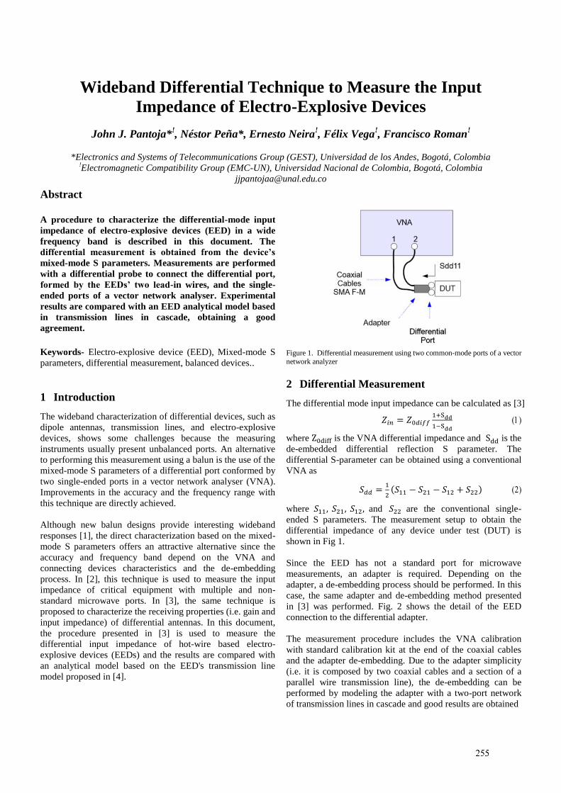
Wideband Differential Technique to Measure the Input
Impedance of Electro-Explosive Devices
John J. Pantoja*!, Néstor Peña*, Ernesto Neira
!, Félix Vega
!, Francisco Roman
!
*Electronics and Systems of Telecommunications Group (GEST), Universidad de los Andes, Bogotá, Colombia !Electromagnetic Compatibility Group (EMC-UN), Universidad Nacional de Colombia, Bogotá, Colombia
Abstract
A procedure to characterize the differential-mode input
impedance of electro-explosive devices (EED) in a wide
frequency band is described in this document. The
differential measurement is obtained from the device’s
mixed-mode S parameters. Measurements are performed
with a differential probe to connect the differential port,
formed by the EEDs’ two lead-in wires, and the single-
ended ports of a vector network analyser. Experimental
results are compared with an EED analytical model based
in transmission lines in cascade, obtaining a good
agreement.
Keywords- Electro-explosive device (EED), Mixed-mode S
parameters, differential measurement, balanced devices..
1 Introduction
The wideband characterization of differential devices, such as
dipole antennas, transmission lines, and electro-explosive
devices, shows some challenges because the measuring
instruments usually present unbalanced ports. An alternative
to performing this measurement using a balun is the use of the
mixed-mode S parameters of a differential port conformed by
two single-ended ports in a vector network analyser (VNA).
Improvements in the accuracy and the frequency range with
this technique are directly achieved.
Although new balun designs provide interesting wideband
responses [1], the direct characterization based on the mixed-
mode S parameters offers an attractive alternative since the
accuracy and frequency band depend on the VNA and
connecting devices characteristics and the de-embedding
process. In [2], this technique is used to measure the input
impedance of critical equipment with multiple and non-
standard microwave ports. In [3], the same technique is
proposed to characterize the receiving properties (i.e. gain and
input impedance) of differential antennas. In this document,
the procedure presented in [3] is used to measure the
differential input impedance of hot-wire based electro-
explosive devices (EEDs) and the results are compared with
an analytical model based on the EED's transmission line
model proposed in [4].
Figure 1. Differential measurement using two common-mode ports of a vector network analyzer
2 Differential Measurement
The differential mode input impedance can be calculated as [3]
𝑍𝑖𝑛 = 𝑍0𝑑𝑖𝑓𝑓1+Sdd
1−Sdd
where Z0diff is the VNA differential impedance and Sdd is the
de-embedded differential reflection S parameter. The
differential S-parameter can be obtained using a conventional
VNA as
𝑆𝑑𝑑 =1
2(𝑆11 − 𝑆21 − 𝑆12 + 𝑆22)
where 𝑆11, 𝑆21, 𝑆12, and 𝑆22 are the conventional single-
ended S parameters. The measurement setup to obtain the
differential impedance of any device under test (DUT) is
shown in Fig 1.
Since the EED has not a standard port for microwave
measurements, an adapter is required. Depending on the
adapter, a de-embedding process should be performed. In this
case, the same adapter and de-embedding method presented
in [3] was performed. Fig. 2 shows the detail of the EED
connection to the differential adapter.
The measurement procedure includes the VNA calibration
with standard calibration kit at the end of the coaxial cables
and the adapter de-embedding. Due to the adapter simplicity
(i.e. it is composed by two coaxial cables and a section of a
parallel wire transmission line), the de-embedding can be
performed by modeling the adapter with a two-port network
of transmission lines in cascade and good results are obtained
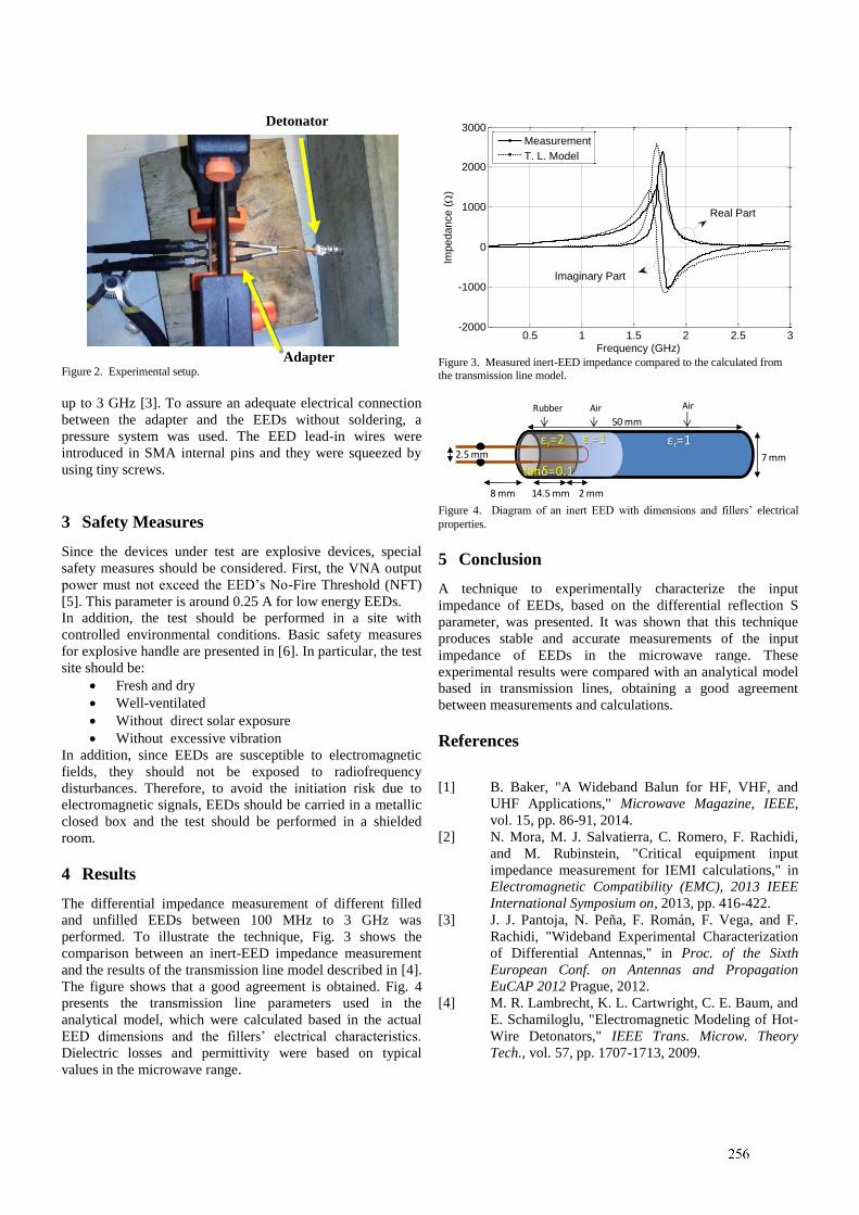
Figure 2. Experimental setup.
up to 3 GHz [3]. To assure an adequate electrical connection
between the adapter and the EEDs without soldering, a
pressure system was used. The EED lead-in wires were
introduced in SMA internal pins and they were squeezed by
using tiny screws.
3 Safety Measures
Since the devices under test are explosive devices, special
safety measures should be considered. First, the VNA output
power must not exceed the EED’s No-Fire Threshold (NFT)
[5]. This parameter is around 0.25 A for low energy EEDs.
In addition, the test should be performed in a site with
controlled environmental conditions. Basic safety measures
for explosive handle are presented in [6]. In particular, the test
site should be:
Fresh and dry
Well-ventilated
Without direct solar exposure
Without excessive vibration
In addition, since EEDs are susceptible to electromagnetic
fields, they should not be exposed to radiofrequency
disturbances. Therefore, to avoid the initiation risk due to
electromagnetic signals, EEDs should be carried in a metallic
closed box and the test should be performed in a shielded
room.
4 Results
The differential impedance measurement of different filled
and unfilled EEDs between 100 MHz to 3 GHz was
performed. To illustrate the technique, Fig. 3 shows the
comparison between an inert-EED impedance measurement
and the results of the transmission line model described in [4].
The figure shows that a good agreement is obtained. Fig. 4
presents the transmission line parameters used in the
analytical model, which were calculated based in the actual
EED dimensions and the fillers’ electrical characteristics.
Dielectric losses and permittivity were based on typical
values in the microwave range.
Figure 3. Measured inert-EED impedance compared to the calculated from the transmission line model.
Figure 4. Diagram of an inert EED with dimensions and fillers’ electrical
properties.
5 Conclusion
A technique to experimentally characterize the input
impedance of EEDs, based on the differential reflection S
parameter, was presented. It was shown that this technique
produces stable and accurate measurements of the input
impedance of EEDs in the microwave range. These
experimental results were compared with an analytical model
based in transmission lines, obtaining a good agreement
between measurements and calculations.
References
[1] B. Baker, "A Wideband Balun for HF, VHF, and
UHF Applications," Microwave Magazine, IEEE,
vol. 15, pp. 86-91, 2014.
[2] N. Mora, M. J. Salvatierra, C. Romero, F. Rachidi,
and M. Rubinstein, "Critical equipment input
impedance measurement for IEMI calculations," in
Electromagnetic Compatibility (EMC), 2013 IEEE
International Symposium on, 2013, pp. 416-422.
[3] J. J. Pantoja, N. Peña, F. Román, F. Vega, and F.
Rachidi, "Wideband Experimental Characterization
of Differential Antennas," in Proc. of the Sixth
European Conf. on Antennas and Propagation
EuCAP 2012 Prague, 2012.
[4] M. R. Lambrecht, K. L. Cartwright, C. E. Baum, and
E. Schamiloglu, "Electromagnetic Modeling of Hot-
Wire Detonators," IEEE Trans. Microw. Theory
Tech., vol. 57, pp. 1707-1713, 2009.
0.5 1 1.5 2 2.5 3-2000
-1000
0
1000
2000
3000
Frequency (GHz)
Imp
ed
an
ce (
)
Measurement
T. L. Model
Real Part
Imaginary Part
Rubber Air
14.5 mm
50 mm
2.5 mm
εr=2 εr=1 εr=1
2 mm8 mm
7 mm
tanδ=0.1
Air
Adapter
Detonator
[5] Ministry of Defence Explosives Regulations (JSP
482), Chapter 24, Ministry of Defence, UK
Government, DSEA-DOSR-Policy, Edition 4, 2013.
[6] United Nations Mine Action Office, "National
Technical Standards and Guidelines Sudan," in Part
1,Chapter 12, ed, 2007.
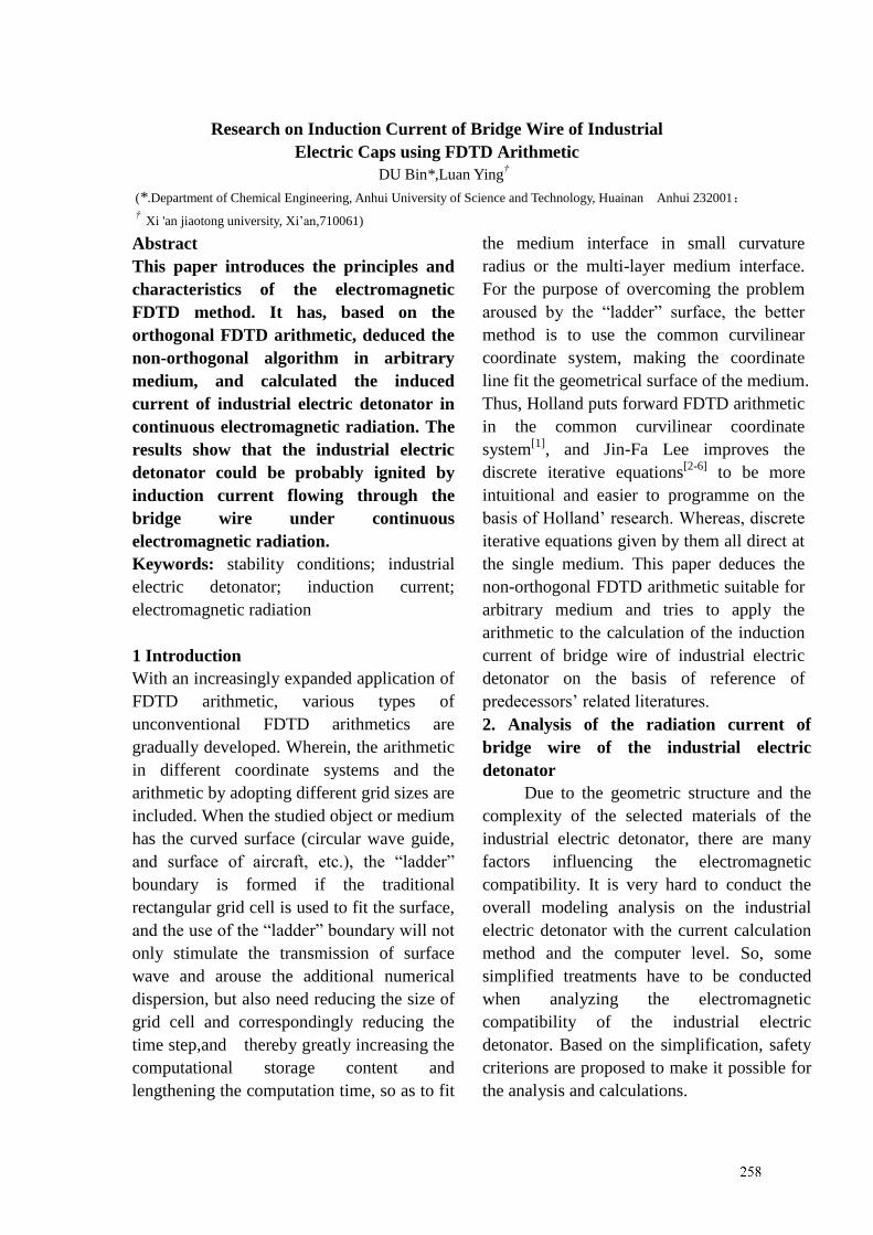
Research on Induction Current of Bridge Wire of Industrial
Electric Caps using FDTD Arithmetic
DU Bin*,Luan Ying†
(*.Department of Chemical Engineering, Anhui University of Science and Technology, Huainan Anhui 232001;
† Xi 'an jiaotong university, Xi’an,710061)
Abstract
This paper introduces the principles and
characteristics of the electromagnetic
FDTD method. It has, based on the
orthogonal FDTD arithmetic, deduced the
non-orthogonal algorithm in arbitrary
medium, and calculated the induced
current of industrial electric detonator in
continuous electromagnetic radiation. The
results show that the industrial electric
detonator could be probably ignited by
induction current flowing through the
bridge wire under continuous
electromagnetic radiation.
Keywords: stability conditions; industrial
electric detonator; induction current;
electromagnetic radiation
1 Introduction
With an increasingly expanded application of
FDTD arithmetic, various types of
unconventional FDTD arithmetics are
gradually developed. Wherein, the arithmetic
in different coordinate systems and the
arithmetic by adopting different grid sizes are
included. When the studied object or medium
has the curved surface (circular wave guide,
and surface of aircraft, etc.), the “ladder”
boundary is formed if the traditional
rectangular grid cell is used to fit the surface,
and the use of the “ladder” boundary will not
only stimulate the transmission of surface
wave and arouse the additional numerical
dispersion, but also need reducing the size of
grid cell and correspondingly reducing the
time step,and thereby greatly increasing the
computational storage content and
lengthening the computation time, so as to fit
the medium interface in small curvature
radius or the multi-layer medium interface.
For the purpose of overcoming the problem
aroused by the “ladder” surface, the better
method is to use the common curvilinear
coordinate system, making the coordinate
line fit the geometrical surface of the medium.
Thus, Holland puts forward FDTD arithmetic
in the common curvilinear coordinate
system[1]
, and Jin-Fa Lee improves the
discrete iterative equations[2-6]
to be more
intuitional and easier to programme on the
basis of Holland’ research. Whereas, discrete
iterative equations given by them all direct at
the single medium. This paper deduces the
non-orthogonal FDTD arithmetic suitable for
arbitrary medium and tries to apply the
arithmetic to the calculation of the induction
current of bridge wire of industrial electric
detonator on the basis of reference of
predecessors’ related literatures.
2. Analysis of the radiation current of
bridge wire of the industrial electric
detonator
Due to the geometric structure and the
complexity of the selected materials of the
industrial electric detonator, there are many
factors influencing the electromagnetic
compatibility. It is very hard to conduct the
overall modeling analysis on the industrial
electric detonator with the current calculation
method and the computer level. So, some
simplified treatments have to be conducted
when analyzing the electromagnetic
compatibility of the industrial electric
detonator. Based on the simplification, safety
criterions are proposed to make it possible for
the analysis and calculations.
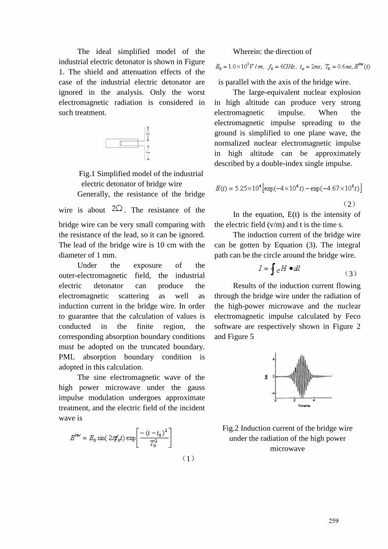
The ideal simplified model of the
industrial electric detonator is shown in Figure
1. The shield and attenuation effects of the
case of the industrial electric detonator are
ignored in the analysis. Only the worst
electromagnetic radiation is considered in
such treatment.
Fig.1 Simplified model of the industrial
electric detonator of bridge wire
Generally, the resistance of the bridge
wire is about . The resistance of the
bridge wire can be very small comparing with
the resistance of the lead, so it can be ignored.
The lead of the bridge wire is 10 cm with the
diameter of 1 mm.
Under the exposure of the
outer-electromagnetic field, the industrial
electric detonator can produce the
electromagnetic scattering as well as
induction current in the bridge wire. In order
to guarantee that the calculation of values is
conducted in the finite region, the
corresponding absorption boundary conditions
must be adopted on the truncated boundary.
PML absorption boundary condition is
adopted in this calculation.
The sine electromagnetic wave of the
high power microwave under the gauss
impulse modulation undergoes approximate
treatment, and the electric field of the incident
wave is
(1)
Wherein: the direction of
is parallel with the axis of the bridge wire.
The large-equivalent nuclear explosion
in high altitude can produce very strong
electromagnetic impulse. When the
electromagnetic impulse spreading to the
ground is simplified to one plane wave, the
normalized nuclear electromagnetic impulse
in high altitude can be approximately
described by a double-index single impulse.
(2)
In the equation, E(t) is the intensity of
the electric field (v/m) and t is the time s.
The induction current of the bridge wire
can be gotten by Equation (3). The integral
path can be the circle around the bridge wire.
(3)
Results of the induction current flowing
through the bridge wire under the radiation of
the high-power microwave and the nuclear
electromagnetic impulse calculated by Feco
software are respectively shown in Figure 2
and Figure 5
Fig.2 Induction current of the bridge wire
under the radiation of the high power
microwave
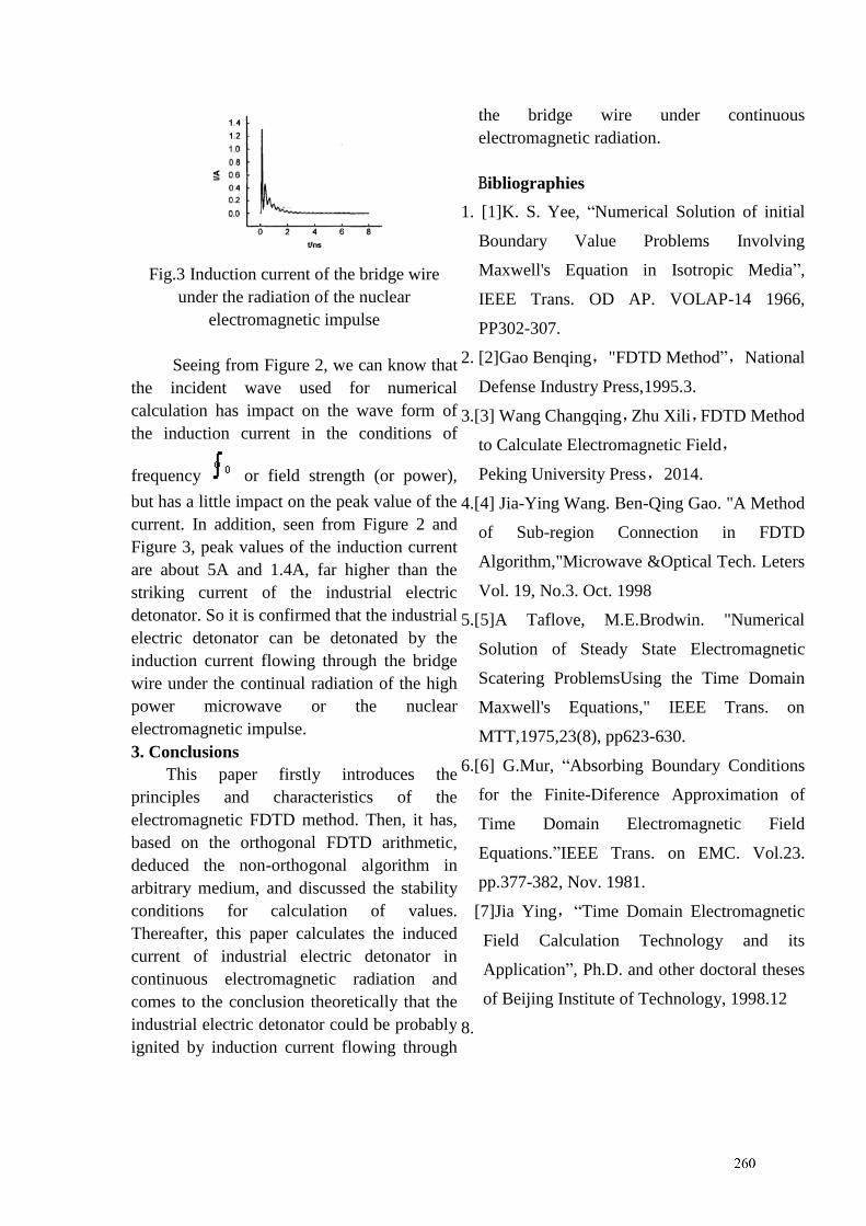
Fig.3 Induction current of the bridge wire
under the radiation of the nuclear
electromagnetic impulse
Seeing from Figure 2, we can know that
the incident wave used for numerical
calculation has impact on the wave form of
the induction current in the conditions of
frequency or field strength (or power),
but has a little impact on the peak value of the
current. In addition, seen from Figure 2 and
Figure 3, peak values of the induction current
are about 5A and 1.4A, far higher than the
striking current of the industrial electric
detonator. So it is confirmed that the industrial
electric detonator can be detonated by the
induction current flowing through the bridge
wire under the continual radiation of the high
power microwave or the nuclear
electromagnetic impulse.
3. Conclusions
This paper firstly introduces the
principles and characteristics of the
electromagnetic FDTD method. Then, it has,
based on the orthogonal FDTD arithmetic,
deduced the non-orthogonal algorithm in
arbitrary medium, and discussed the stability
conditions for calculation of values.
Thereafter, this paper calculates the induced
current of industrial electric detonator in
continuous electromagnetic radiation and
comes to the conclusion theoretically that the
industrial electric detonator could be probably
ignited by induction current flowing through
the bridge wire under continuous
electromagnetic radiation.
Bibliographies
1. [1]K. S. Yee, “Numerical Solution of initial
Boundary Value Problems Involving
Maxwell's Equation in Isotropic Media”,
IEEE Trans. OD AP. VOLAP-14 1966,
PP302-307.
2. [2]Gao Benqing,"FDTD Method”,National
Defense Industry Press,1995.3.
3.[3] Wang Changqing,Zhu Xili,FDTD Method
to Calculate Electromagnetic Field,
Peking University Press,2014.
4.[4] Jia-Ying Wang. Ben-Qing Gao. "A Method
of Sub-region Connection in FDTD
Algorithm,"Microwave &Optical Tech. Leters
Vol. 19, No.3. Oct. 1998
5.[5]A Taflove, M.E.Brodwin. "Numerical
Solution of Steady State Electromagnetic
Scatering ProblemsUsing the Time Domain
Maxwell's Equations," IEEE Trans. on
MTT,1975,23(8), pp623-630.
6.[6] G.Mur, “Absorbing Boundary Conditions
for the Finite-Diference Approximation of
Time Domain Electromagnetic Field
Equations.”IEEE Trans. on EMC. Vol.23.
pp.377-382, Nov. 1981.
[7]Jia Ying,“Time Domain Electromagnetic
Field Calculation Technology and its
Application”, Ph.D. and other doctoral theses
of Beijing Institute of Technology, 1998.12
8.
Application of the Random Coupling Model to
Statistical Properties of Complex Enclosures
Bo Xiao*, Thomas Antonsen*, Edward Ott*, Steven M. Anlage*
* Department of Physics and Department of Electrical and Computer Engineering at the University of Maryland,
College Park, MD, USA 20742-4111, [email protected], http://anlage.umd.edu
Abstract
The effectiveness of the Random Coupling Model (RCM)
in predicting electromagnetic wave coupling to electronic
components within a complex enclosure is examined. In
the short wavelength limit with respect to the
characteristic length of the enclosure, electromagnetic
wave propagation within a large enclosure is sensitive to
small changes to the interior, or to the boundaries of the
enclosure. Such changes can reduce or invalidate the
applicability of deterministic predictions of the
electromagnetic fields at radiofrequencies (RF) in large
enclosures. Under such circumstances, a statistical
approach is needed to provide a better understanding of
RF coupling to components within large enclosures. In
this contribution, we experimentally demonstrate the
applicability of the RCM to estimate the probabilistic
magnitudes of RF fields on a variety of components that
are partially shielded within a complex, three-dimensional
enclosure.
Keywords: Overmoded enclosures, statistical
electromagnetism, electromagnetic compatibility, Random
Coupling Model, wave scattering.
1 Introduction
There is practical interest in the statistics of electromagnetic
radiation affecting sensitive electronics that are shielded
within a large enclosure, especially for electromagnetic
compatibility (EMC) [1-3]. The radiofrequency (RF) coupling
to electronics within a large enclosure can be studied by
considering a wave scattering problem in the short
wavelength limit. While the applied wavelength is short with
respect to the characteristic length of the wave enclosure,
electromagnetic field distributions in electrically large
enclosures can vary dramatically even with a small
rearrangement of the internal objects, a small change in the
enclosure boundaries, or a change in frequency of the
excitation waveform. Coupling of electromagnetic fields to a
component, such as a conductor or an electronic device, in
one enclosure may be quite different in another nearly
identical enclosure. Therefore, deterministic calculations are
valid only for the particular situation modeled. Under such
circumstances, analysis of the statistical properties of
electromagnetic fields in these complex environments is
necessary, and the statistical predictions can better represent
the properties of complex enclosures.
In this work, the statistical treatment we employ is the
Random Coupling Model (RCM) which is based on wave
chaos and has been successfully applied to describe the
statistics of many wave scattering properties [4-8]. In a wave
chaotic system, the statistical features of the scattering or
impedance matrix has a universal fluctuating part and a
system-specific deterministic part. The universal fluctuation
part is well predicted by Random Matrix Theory (RMT) [7],
and the Random Coupling Model combines the system-
specific deterministic part with the universal fluctuation part
in an impedance approach [4-8].
2 Experiment
We test the application of the RCM in modeling the wave
coupling to electronic components within a complex
enclosure (see Fig. 1). The complex enclosure is a
reverberation chamber (rectangular aluminum box with
dimensions of 1.22 m × 1.27 m × 0.65 m) with internal
stirrers. We consider 2-port systems in which one port acts as
a source of radiation (which can include, for example, open
apertures on the wall of the enclosure), and the second port is
considered a target and can take the form of a monopole or
electrically-large object (such as a wire bundle). We measure
the scattering matrix between these two ports as a function of
frequency and configuration details of the box (typically
many stirrer locations).
We treat the data statistically according to the RCM
prescription as,
Zcav = j Im[‹Zcav ›] + Re[‹Zcav ›]1/2
z Re[‹Zcav ›]1/2
, (1)
where z is the normalized (universally fluctuating) impedance
matrix (predicted by RMT and the losses in the system), Zcav
is the cavity impedance matrix, and ‹Zcav› is the ensemble
and/or frequency averaged cavity impedance matrix. An
example of the use of this equation to extract the universally
fluctuating impedance for a 1-port system is shown in Fig. 2
[4].
We present data on induced-voltage pdfs for target ports in
complex enclosures which are illuminated either internally or
through an open aperture. The RCM predictions are found to
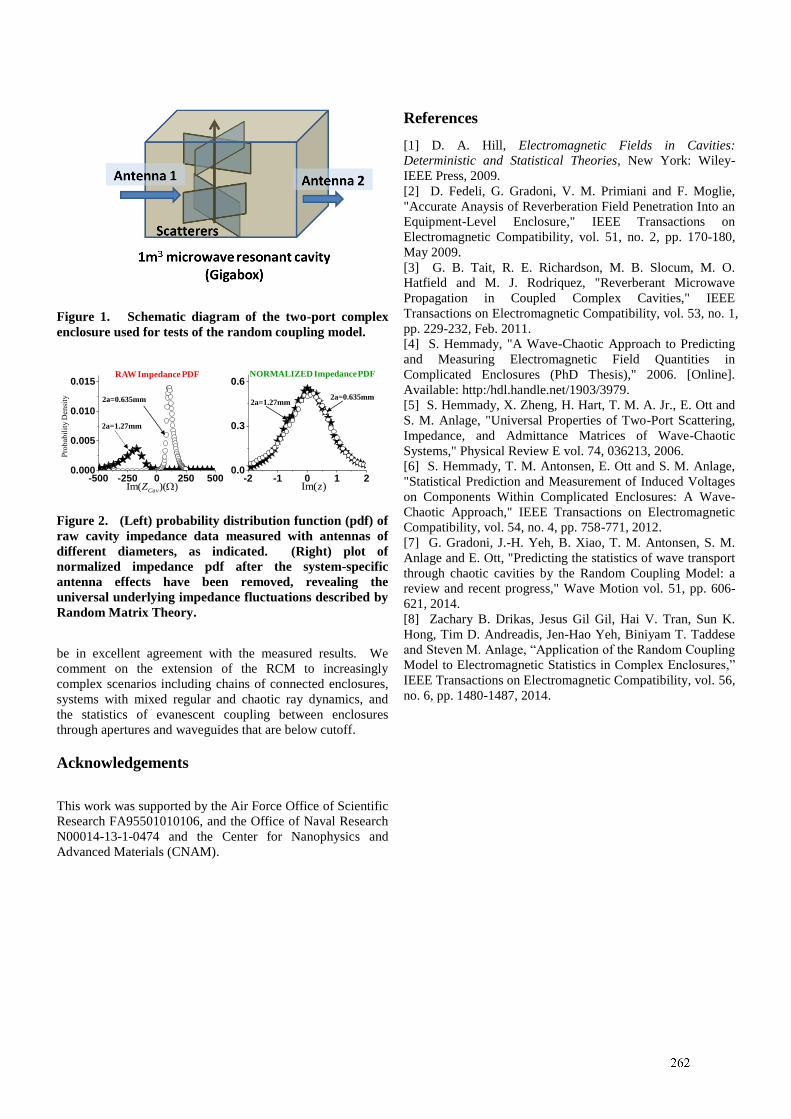
Figure 1. Schematic diagram of the two-port complex
enclosure used for tests of the random coupling model.
Pro
bab
ilit
y D
en
sity
-2 -1 0 1 20.0
0.3
0.6
2a=0.635mm2a=1.27mm
)Im(z-500 -250 0 250 500
0.000
0.005
0.010
0.015
2a=1.27mm
2a=0.635mm
))(Im( CavZ
RAW Impedance PDF NORMALIZED Impedance PDF
Figure 2. (Left) probability distribution function (pdf) of
raw cavity impedance data measured with antennas of
different diameters, as indicated. (Right) plot of
normalized impedance pdf after the system-specific
antenna effects have been removed, revealing the
universal underlying impedance fluctuations described by
Random Matrix Theory.
be in excellent agreement with the measured results. We
comment on the extension of the RCM to increasingly
complex scenarios including chains of connected enclosures,
systems with mixed regular and chaotic ray dynamics, and
the statistics of evanescent coupling between enclosures
through apertures and waveguides that are below cutoff.
Acknowledgements
This work was supported by the Air Force Office of Scientific
Research FA95501010106, and the Office of Naval Research
N00014-13-1-0474 and the Center for Nanophysics and
Advanced Materials (CNAM).
References
[1] D. A. Hill, Electromagnetic Fields in Cavities:
Deterministic and Statistical Theories, New York: Wiley-
IEEE Press, 2009.
[2] D. Fedeli, G. Gradoni, V. M. Primiani and F. Moglie,
"Accurate Anaysis of Reverberation Field Penetration Into an
Equipment-Level Enclosure," IEEE Transactions on
Electromagnetic Compatibility, vol. 51, no. 2, pp. 170-180,
May 2009.
[3] G. B. Tait, R. E. Richardson, M. B. Slocum, M. O.
Hatfield and M. J. Rodriquez, "Reverberant Microwave
Propagation in Coupled Complex Cavities," IEEE
Transactions on Electromagnetic Compatibility, vol. 53, no. 1,
pp. 229-232, Feb. 2011.
[4] S. Hemmady, "A Wave-Chaotic Approach to Predicting
and Measuring Electromagnetic Field Quantities in
Complicated Enclosures (PhD Thesis)," 2006. [Online].
Available: http:/hdl.handle.net/1903/3979.
[5] S. Hemmady, X. Zheng, H. Hart, T. M. A. Jr., E. Ott and
S. M. Anlage, "Universal Properties of Two-Port Scattering,
Impedance, and Admittance Matrices of Wave-Chaotic
Systems," Physical Review E vol. 74, 036213, 2006.
[6] S. Hemmady, T. M. Antonsen, E. Ott and S. M. Anlage,
"Statistical Prediction and Measurement of Induced Voltages
on Components Within Complicated Enclosures: A Wave-
Chaotic Approach," IEEE Transactions on Electromagnetic
Compatibility, vol. 54, no. 4, pp. 758-771, 2012.
[7] G. Gradoni, J.-H. Yeh, B. Xiao, T. M. Antonsen, S. M.
Anlage and E. Ott, "Predicting the statistics of wave transport
through chaotic cavities by the Random Coupling Model: a
review and recent progress," Wave Motion vol. 51, pp. 606-
621, 2014.
[8] Zachary B. Drikas, Jesus Gil Gil, Hai V. Tran, Sun K.
Hong, Tim D. Andreadis, Jen-Hao Yeh, Biniyam T. Taddese
and Steven M. Anlage, “Application of the Random Coupling
Model to Electromagnetic Statistics in Complex Enclosures,”
IEEE Transactions on Electromagnetic Compatibility, vol. 56,
no. 6, pp. 1480-1487, 2014.
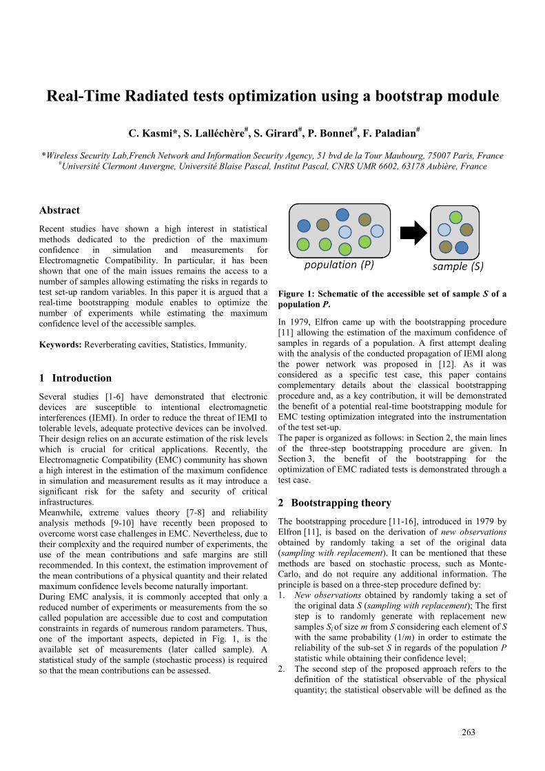
1
Real-Time Radiated tests optimization using a bootstrap module
C. Kasmi*, S. Lalléchère#, S. Girard
#, P. Bonnet
#, F. Paladian
#
*Wireless Security Lab,French Network and Information Security Agency, 51 bvd de la Tour Maubourg, 75007 Paris, France #Université Clermont Auvergne, Université Blaise Pascal, Institut Pascal, CNRS UMR 6602, 63178 Aubière, France
Abstract
Recent studies have shown a high interest in statistical
methods dedicated to the prediction of the maximum
confidence in simulation and measurements for
Electromagnetic Compatibility. In particular, it has been
shown that one of the main issues remains the access to a
number of samples allowing estimating the risks in regards to
test set-up random variables. In this paper it is argued that a
real-time bootstrapping module enables to optimize the
number of experiments while estimating the maximum
confidence level of the accessible samples.
Keywords: Reverberating cavities, Statistics, Immunity.
1 Introduction
Several studies [1-6] have demonstrated that electronic
devices are susceptible to intentional electromagnetic
interferences (IEMI). In order to reduce the threat of IEMI to
tolerable levels, adequate protective devices can be involved.
Their design relies on an accurate estimation of the risk levels
which is crucial for critical applications. Recently, the
Electromagnetic Compatibility (EMC) community has shown
a high interest in the estimation of the maximum confidence
in simulation and measurement results as it may introduce a
significant risk for the safety and security of critical
infrastructures.
Meanwhile, extreme values theory [7-8] and reliability
analysis methods [9-10] have recently been proposed to
overcome worst case challenges in EMC. Nevertheless, due to
their complexity and the required number of experiments, the
use of the mean contributions and safe margins are still
recommended. In this context, the estimation improvement of
the mean contributions of a physical quantity and their related
maximum confidence levels become naturally important.
During EMC analysis, it is commonly accepted that only a
reduced number of experiments or measurements from the so
called population are accessible due to cost and computation
constraints in regards of numerous random parameters. Thus,
one of the important aspects, depicted in Fig. 1, is the
available set of measurements (later called sample). A
statistical study of the sample (stochastic process) is required
so that the mean contributions can be assessed.
Figure 1: Schematic of the accessible set of sample S of a
population P.
In 1979, Elfron came up with the bootstrapping procedure
[11] allowing the estimation of the maximum confidence of
samples in regards of a population. A first attempt dealing
with the analysis of the conducted propagation of IEMI along
the power network was proposed in [12]. As it was
considered as a specific test case, this paper contains
complementary details about the classical bootstrapping
procedure and, as a key contribution, it will be demonstrated
the benefit of a potential real-time bootstrapping module for
EMC testing optimization integrated into the instrumentation
of the test set-up.
The paper is organized as follows: in Section 2, the main lines
of the three-step bootstrapping procedure are given. In
Section 3, the benefit of the bootstrapping for the
optimization of EMC radiated tests is demonstrated through a
test case.
2 Bootstrapping theory
The bootstrapping procedure [11-16], introduced in 1979 by
Elfron [11], is based on the derivation of new observations
obtained by randomly taking a set of the original data
(sampling with replacement). It can be mentioned that these
methods are based on stochastic process, such as Monte-
Carlo, and do not require any additional information. The
principle is based on a three-step procedure defined by:
1. New observations obtained by randomly taking a set of
the original data S (sampling with replacement); The first
step is to randomly generate with replacement new
samples Si of size m from S considering each element of S
with the same probability (1/m) in order to estimate the
reliability of the sub-set S in regards of the population P
statistic while obtaining their confidence level;
2. The second step of the proposed approach refers to the
definition of the statistical observable of the physical
quantity; the statistical observable will be defined as the
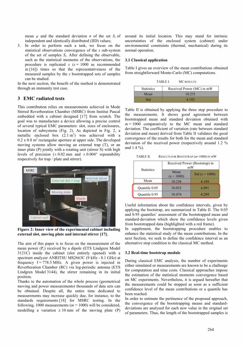
2
mean µ and the standard deviation σ of the set Si of
independent and identically distributed (IID) values;
3. In order to perform such a task, we focus on the
statistical observations convergence of the s sub-system
of the set of samples Si. After defining the observable,
such as the statistical moments of the observations, the
procedure is replicated s (s = 1000 as recommended
in [16]) times so that the representativeness of the
measured samples by the s bootstrapped sets of samples
can be studied.
In the next section, the benefit of the method is demonstrated
through an immunity test case.
3 EMC radiated tests
This contribution relies on measurements achieved in Mode
Stirred Reverberation Chamber (MSRC) from Institut Pascal
embedded with a cabinet designed [17] from scratch. The
goal was to manufacture a device allowing a precise control
of several typical EMC parameters: slot, sizes of enclosures,
location of subsystems (Fig. 2). As depicted in Fig. 2, a
metallic enclosed box (2.1 m3) was achieved with a
0.2 x 0.8 m2 rectangular aperture at upper side. The developed
moving systems allow moving an external trap (T), or an
inner plate (P) jointly with a rotating unit (stirrer S) with high
levels of precision (± 0.02 mm and ± 0.004° repeatability
respectively for trap / plate and stirrer).
Figure 2: Inner view of the experimental cabinet including
external slot, moving plate and internal stirrer [17].
The aim of this paper is to focus on the measurement of the
mean power (Pr) received by a dipole (ETS Lindgren Model
3121C) inside the cabinet (slot entirely opened) with a
spectrum analyzer ANRITSU MS2663C (9 kHz - 8.1 GHz) at
frequency f = 778.5 MHz. A given power is injected in
Reverberation Chamber (RC) via log-periodic antenna (ETS
Lindgren Model 3144), the stirrer remaining in its initial
position.
Thanks to the automation of the whole process (geometrical
moving and power measurements) thousands of data sets can
be obtained. Despite all, the entire time dedicated to
measurements may increase quickly due, for instance, to the
standards requirements [18] for MSRC testing. In the
following, 1000 measurements (m = 1000) will be considered,
modelling a variation 10 mm of the moving plate (P)
around its initial location. This may stand for intrinsic
uncertainties of the enclosed system (cabinet) under
environmental constraints (thermal, mechanical) during its
normal operation.
3.1 Classical application
Table I gives an overview of the mean contributions obtained
from straightforward Monte-Carlo (MC) computations.
TABLE I. MC RESULTS
Statistics Received Power (MC) in mW
Mean 10.251
Std 4.192
Table II is obtained by applying the three step procedure to
the measurements. It shows good agreement between
bootstrapped mean and standard deviation obtained with
m = 1000 comparatively to the MC mean and standard
deviation. The coefficient of variation (rate between standard
deviation and mean) derived from Table II validates the good
convergence of the results for both for the mean and standard
deviation of the received power (respectively around 1.2 %
and 1.4 %).
TABLE II. RESULTS FOR BOOTSTRAP (m=1000) IN MW
Statistics
Received Power (Bootstrap) in
mW
Mean
(s = 1000) Std (s = 1000)
Mean 10.258 4.189
Quantile 0.05 10.052 4.091
Quantile 0.95 10.474 4.289
Useful information about the confidence intervals, given by
applying the bootstrap, are summarized in Table II. The 0.05
and 0.95 quantiles’ assessment of the bootstrapped mean and
standard-deviation which show the confidence levels given
from bootstrapped data (highlighted with a red frame).
In supplement, the bootstrapping procedure enables to
enhance the statistical study of the mean contributions. In the
next Section, we seek to define the confidence interval as an
alternative stop condition to the classical MC method.
3.2 Real-time bootstrap module
During classical EMC analysis, the number of experiments
either simulated or measurements are known to be a challenge
for computation and time costs. Classical approaches impose
the estimation of the statistical moments convergence based
on MC experiments. Nevertheless, it is argued hereafter that
the measurements could be stopped as soon as a sufficient
confidence level of the mean contributions or a quantile has
been reached.
In order to estimate the pertinence of the proposed approach,
the convergence of the bootstrapping means and standard-
deviations are analysed for each new value in the original set
of parameters. Thus, the length of the bootstrapped samples is
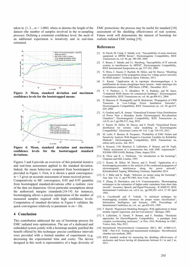
3
taken in 1, 2.., m = 1,000 where m denotes the length of the
dataset (the number of samples involved in the re-sampling
process). Defining a constraint confidence level, the need of
an additional experiment is iteratively and in real-time
estimated.
Figure 3: Mean, standard deviation and maximum
confidence levels for the bootstrapped means.
Figure 4: Mean, standard deviation and maximum
confidence levels for the bootstrapped standard
deviations.
Figures 3 and 4 provide an overview of this potential iterative
and real-time assessment applied to the standard deviation.
Indeed, the mean behaviour computed from bootstrapped is
provided in Figure 3. First, it is shown a quick convergence:
m = 3 gives an accurate assessment of mean received power.
Comparatively to MC convergence, 0.05 and 0.95 quantiles
from bootstrapped standard-deviations offer a realistic view
of the data set dispersion. Given particular assumptions about
the authorized margins (standards [18-19] for instance),
bootstrapping allows a precise optimization of the number of
measured samples required with high confidence levels.
Computation of standard deviation in Figure 4 validates the
quick convergence relatively to parameter m (m = 20).
4 Conclusion
This contribution addressed the use of bootstrap process for
EMC radiated tests optimization. The use of a dedicated and
embedded system jointly with a bootstrap module justified the
benefit offered by this technique: precise confidence intervals
were provided with a limited number of experiments (e.g.
decreasing the experimental time and costs). The device
designed in this work is representative of a huge diversity of
EMC protections: the process may be useful for standard [18]
assessment of the shielding effectiveness of real systems.
Future work will demonstrate the interest of bootstrap for
realistic radiated EMC testing [19].
References
[1] D. Nitsch, M. Camp, F. Sabath, et al., “Susceptibility of some electronic equipment to HPEM threats”, Electromagnetic Compatibility, IEEE Transactions on, vol. 46, pp. 380-389, 2004.
[2] F. Brauer, F. Sabath, and J.L. Haseborg, “Susceptibility of IT network systems to interferences by HPEM”, Electromagnetic Compatibility, IEEE International Symposium on, pp. 237-242, 2009.
[3] N. Mora, C. Kasmi, F. Rachidi, M. Hélier, and M. Darces, “Modeling and measurement of the propagation along low voltage power networks for IEMI studies”, Technical report, February, 2013.
[4] C. Kasmi, “Application de la topologie électromagnétique à la modélisation du réseau énergétique basse tension : étude statistique des perturbations conduites”, PhD thesis, UPMC, December, 2013.
[5] Y. V. Parfenov, L. N. Zdoukhov, W. A. Radasky, and M. Ianoz, “Conducted IEMI threats for commercial buildings”, Electromagnetic Compatibility, IEEE Transactions on, vol. 46, pp.404-411, 2004.
[6] D. Mansson, R. Thottappillil, and M. Backstrom, “Propagation of UWB Transients in Low-Voltage Power Installation Networks”, Electromagnetic Compatibility, IEEE Transactions on, vol. 50, pp.619-629, 2008.
[7] G. Gradoni and L.R. Arnaut, “Generalized Extreme-Value Distributions of Power Near a Boundary Inside Electromagnetic Reverberation Chambers”, Electromagnetic Compatibility, IEEE Transactions on, vol.52, no.3, pp.506,515, Aug. 2010.
[8] C. Kasmi, M. Hélier, M. Darces, and E. Prouff, “Generalised Pareto distribution for extreme value modelling in Electromagnetic Compatibility”, Electronics Letters 49, Vol. 5, pp. 334-335, 2013.
[9] M. Larbi, P. Besnier, B. Pecqueux, “Probability of EMC Failure and Sensitivity Analysis With Regard to Uncertain Variables by Reliability Methods”, Electromagnetic Compatibility, IEEE Transactions on, online early access., Jan. 2015.
[10] A. Kouassi, J-M. Bourinet, S. Lalléchère, P. Bonnet, and M. Fogli, “Safety assessment of a transmission line with EMC requirements”, XXXIth URSI GASS, Beijing, China, August 2014.
[11] B. Efron and R. J. Tibshirani, “An introduction to the bootstrap”, Chapman and Hall, London, 1993.
[12] C. Kasmi, M. Hélier, M. Darces, and E. Prouff, “Application of a bootstrapping procedure to the analysis of the conducted propagation of electromagnetic interferences along the power network”, Kleineheubach Tagung, Miltenberg, Germany, September 2014.
[13] G. J. Babu and K. Singh, “Inference on means using the bootstrap”, Ann. Stat. Vol. 11, pp.9 99-1003, New-York, 1983.
[14] Y. Zhang, D. Hatzinakos, and A.N. Venetsanopoulos, “Bootstrapping techniques in the estimation of higher-order cumulants from short data records”, Acoustics, Speech, and Signal Processing - ICASSP-93, IEEE International Conference on, vol.4, no., pp.200,203 vol.4, 27-30 April 1993.
[15] A. Cucchiarelli and P. Velardi, “A statistical technique for bootstrapping available resources for proper nouns classification”, Information Intelligence and Systems, 1999. Proceedings of International Conference on, vol., no., pp.429-435, 1999.
[16] F. Harrell, “Regression Modeling Strategies: With applications to linear models, logistic regression, and survival analysis”, Springer, 2001.
[17] S. Lalléchère, S. Girard, P. Bonnet, and F. Paladian, “Stochastic approaches for ElectroMagnetic Compatibility: a paradigm from complex reverberating enclosures”, in Proc. ESA Workshop on EMC, Venice, Italy, May 2012.
[18] International Electrotechnical Commission (IEC), IEC 61000-4-21, EMC - Part 4-21: Testing and measurement techniques - Reverberation chamber test methods, 2003.
[19] IEEE standard method for measuring the shielding effectiveness of enclosures and boxes having all dimensions between 0.1 m and 2 m, 2013.
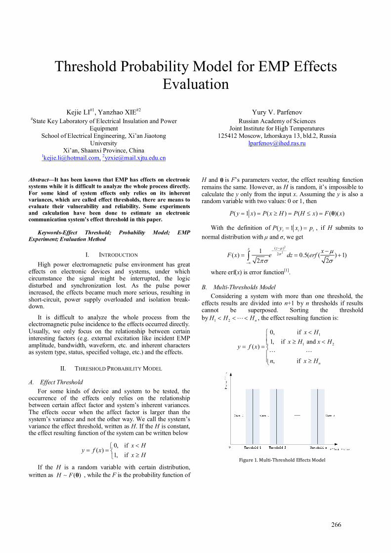
Threshold Probability Model for EMP Effects Evaluation
Kejie LI#1, Yanzhao XIE#2 #State Key Laboratory of Electrical Insulation and Power
Equipment School of Electrical Engineering, Xi’an Jiaotong
University Xi’an, Shaanxi Province, China
[email protected], [email protected]
Yury V. Parfenov Russian Academy of Sciences
Joint Institute for High Temperatures 125412 Moscow, Izhorskaya 13, bld.2, Russia
Abstract—It has been known that EMP has effects on electronic systems while it is difficult to analyze the whole process directly. For some kind of system effects only relies on its inherent variances, which are called effect thresholds, there are means to evaluate their vulnerability and reliability. Some experiments and calculation have been done to estimate an electronic communication system’s effect threshold in this paper.
Keywords-Effect Threshold; Probability Model; EMP Experiment; Evaluation Method
I. INTRODUCTION
High power electromagnetic pulse environment has great effects on electronic devices and systems, under which circumstance the signal might be interrupted, the logic disturbed and synchronization lost. As the pulse power increased, the effects became much more serious, resulting in short-circuit, power supply overloaded and isolation break-down.
It is difficult to analyze the whole process from the electromagnetic pulse incidence to the effects occurred directly. Usually, we only focus on the relationship between certain interesting factors (e.g. external excitation like incident EMP amplitude, bandwidth, waveform, etc. and inherent characters as system type, status, specified voltage, etc.) and the effects.
II. THRESHOLD PROBABILITY MODEL
A. Effect Threshold
For some kinds of device and system to be tested, the occurrence of the effects only relies on the relationship between certain affect factor and system’s inherent variances. The effects occur when the affect factor is larger than the system’s variance and not the other way. We call the system’s variance the effect threshold, written as H. If the H is constant, the effect resulting function of the system can be written below
0, if ( )
1, if
x Hy f x
x H
If the H is a random variable with certain distribution, written as ( )H F θ , while the F is the probability function of
H and θ is F’s parameters vector, the effect resulting function remains the same. However, as H is random, it’s impossible to calculate the y only from the input x. Assuming the y is also a random variable with two values: 0 or 1, then
( 1 ) ( ) ( ) ( )( )P y x P x H P H x F x θ
With the definition of ( 1 )i i iP y x p , if H submits to
normal distribution with μ and σ, we get
2
2
( )
21
( ) 0.5( ( ) 1)2 2
zx xF x e dz erf
where erf(x) is error function[1].
B. Multi-Thresholds Model
Considering a system with more than one threshold, the effects results are divided into n+1 by n thresholds if results cannot be superposed. Sorting the threshold by 1 2 nH H H , the effect resulting function is:
1
1 2
0, if
1, if and ( )
, if n
x H
x H x Hy f x
n x H
Figure 1. Multi-Threshold Effects Model
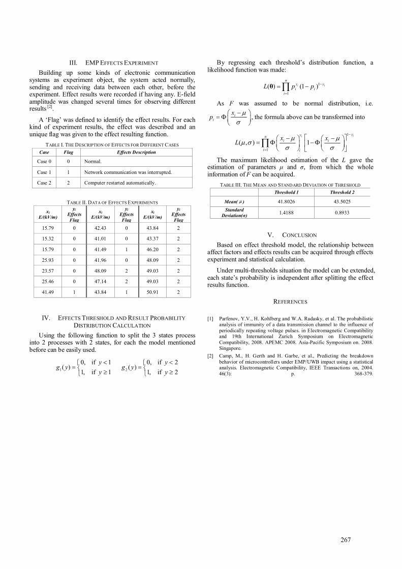
III. EMP EFFECTS EXPERIMENT
Building up some kinds of electronic communication systems as experiment object, the system acted normally, sending and receiving data between each other, before the experiment. Effect results were recorded if having any. E-field amplitude was changed several times for observing different results [2].
A ‘Flag’ was defined to identify the effect results. For each kind of experiment results, the effect was described and an unique flag was given to the effect resulting function.
TABLE I. THE DESCRIPTION OF EFFECTS FOR DIFFERENT CASES
Case Flag Effects Description
Case 0 0 Normal.
Case 1 1 Network communication was interrupted.
Case 2 2 Computer restarted automatically.
TABLE II. DATA OF EFFECTS EXPERIMENTS
xi E/(kV/m)
yi Effects Flag
xi E/(kV/m)
yi Effects Flag
xi E/(kV/m)
yi Effects Flag
15.79 0 42.43 0 43.84 2
15.32 0 41.01 0 43.37 2
15.79 0 41.49 1 46.20 2
25.93 0 41.96 0 48.09 2
23.57 0 48.09 2 49.03 2
25.46 0 47.14 2 49.03 2
41.49 1 43.84 1 50.91 2
IV. EFFECTS THRESHOLD AND RESULT PROBABILITY
DISTRIBUTION CALCULATION
Using the following function to split the 3 states process into 2 processes with 2 states, for each the model mentioned before can be easily used.
1
0, if 1( )
1, if 1
yg y
y
2
0, if 2( )
1, if 2
yg y
y
By regressing each threshold’s distribution function, a likelihood function was made:
1
1
( ) (1 )i i
ny y
i ii
L p p
θ
As F was assumed to be normal distribution, i.e.
ii
xp
, the formula above can be transformed into
1
1
( , ) 1ii
yyni i
i i
x xL
The maximum likelihood estimation of the L gave the estimation of parameters μ and σ, from which the whole information of F can be acquired.
TABLE III. THE MEAN AND STANDARD DEVIATION OF THRESHOLD
Threshold 1 Threshold 2
Mean(μ) 41.8026 43.5025
Standard Deviation(σ)
1.4188 0.8933
V. CONCLUSION
Based on effect threshold model, the relationship between affect factors and effects results can be acquired through effects experiment and statistical calculation.
Under multi-thresholds situation the model can be extended, each state’s probability is independent after splitting the effect results function.
REFERENCES
[1] Parfenov, Y.V., H. Kohlberg and W.A. Radasky, et al. The probabilistic
analysis of immunity of a data transmission channel to the influence of periodically repeating voltage pulses. in Electromagnetic Compatibility and 19th International Zurich Symposium on Electromagnetic Compatibility, 2008. APEMC 2008. Asia-Pacific Symposium on. 2008. Singapore.
[2] Camp, M., H. Gerth and H. Garbe, et al., Predicting the breakdown behavior of microcontrollers under EMP/UWB impact using a statistical analysis. Electromagnetic Compatibility, IEEE Transactions on, 2004. 46(3): p. 368-379.
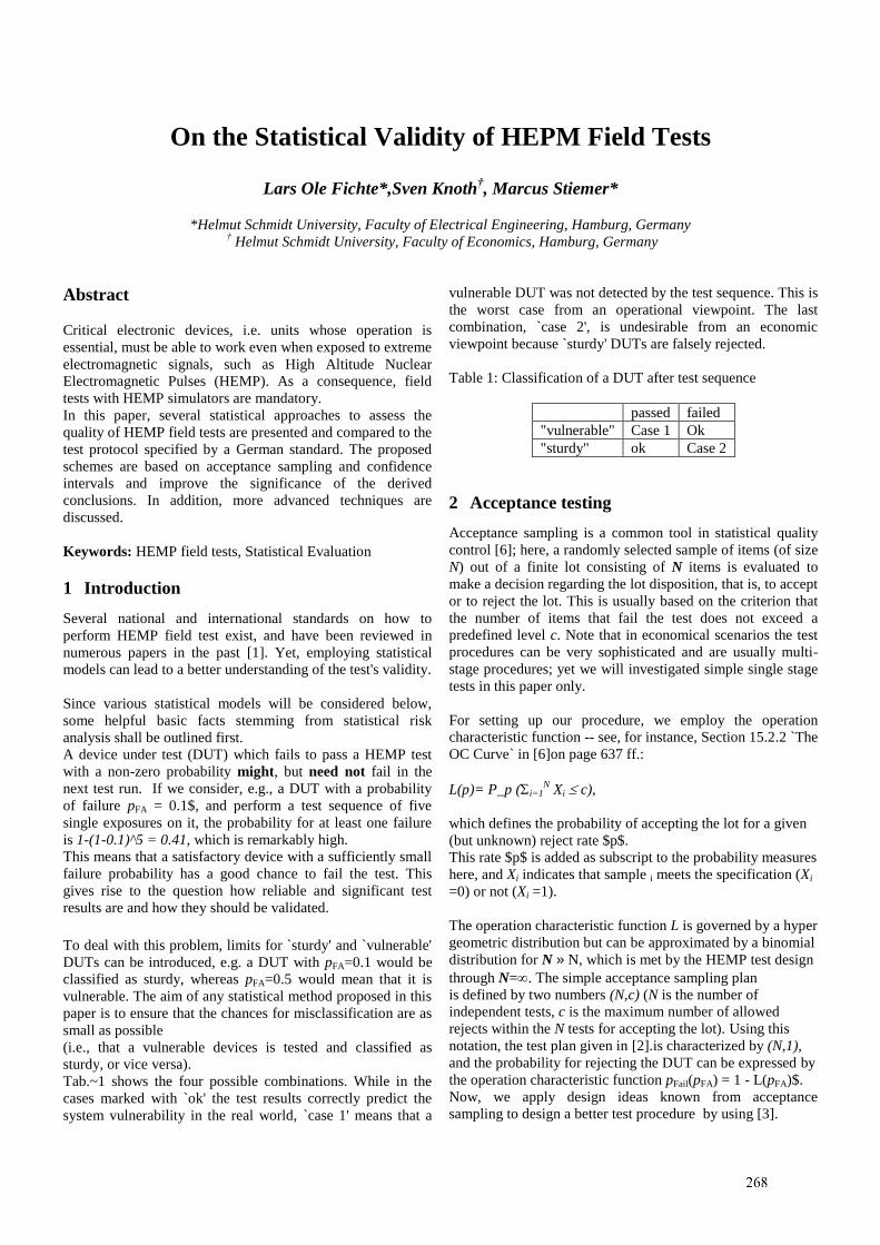
1
On the Statistical Validity of HEPM Field Tests
Lars Ole Fichte*,Sven Knoth†, Marcus Stiemer*
*Helmut Schmidt University, Faculty of Electrical Engineering, Hamburg, Germany
† Helmut Schmidt University, Faculty of Economics, Hamburg, Germany
Abstract
Critical electronic devices, i.e. units whose operation is
essential, must be able to work even when exposed to extreme
electromagnetic signals, such as High Altitude Nuclear
Electromagnetic Pulses (HEMP). As a consequence, field
tests with HEMP simulators are mandatory.
In this paper, several statistical approaches to assess the
quality of HEMP field tests are presented and compared to the
test protocol specified by a German standard. The proposed
schemes are based on acceptance sampling and confidence
intervals and improve the significance of the derived
conclusions. In addition, more advanced techniques are
discussed.
Keywords: HEMP field tests, Statistical Evaluation
1 Introduction
Several national and international standards on how to
perform HEMP field test exist, and have been reviewed in
numerous papers in the past [1]. Yet, employing statistical
models can lead to a better understanding of the test's validity.
Since various statistical models will be considered below,
some helpful basic facts stemming from statistical risk
analysis shall be outlined first.
A device under test (DUT) which fails to pass a HEMP test
with a non-zero probability might, but need not fail in the
next test run. If we consider, e.g., a DUT with a probability
of failure pFA = 0.1$, and perform a test sequence of five
single exposures on it, the probability for at least one failure
is 1-(1-0.1)^5 = 0.41, which is remarkably high.
This means that a satisfactory device with a sufficiently small
failure probability has a good chance to fail the test. This
gives rise to the question how reliable and significant test
results are and how they should be validated.
To deal with this problem, limits for `sturdy' and `vulnerable'
DUTs can be introduced, e.g. a DUT with pFA=0.1 would be
classified as sturdy, whereas pFA=0.5 would mean that it is
vulnerable. The aim of any statistical method proposed in this
paper is to ensure that the chances for misclassification are as
small as possible
(i.e., that a vulnerable devices is tested and classified as
sturdy, or vice versa).
Tab.~1 shows the four possible combinations. While in the
cases marked with `ok' the test results correctly predict the
system vulnerability in the real world, `case 1' means that a
vulnerable DUT was not detected by the test sequence. This is
the worst case from an operational viewpoint. The last
combination, `case 2', is undesirable from an economic
viewpoint because `sturdy' DUTs are falsely rejected.
Table 1: Classification of a DUT after test sequence
passed failed
"vulnerable" Case 1 Ok
"sturdy" ok Case 2
2 Acceptance testing
Acceptance sampling is a common tool in statistical quality
control [6]; here, a randomly selected sample of items (of size
N) out of a finite lot consisting of N items is evaluated to
make a decision regarding the lot disposition, that is, to accept
or to reject the lot. This is usually based on the criterion that
the number of items that fail the test does not exceed a
predefined level c. Note that in economical scenarios the test
procedures can be very sophisticated and are usually multi-
stage procedures; yet we will investigated simple single stage
tests in this paper only.
For setting up our procedure, we employ the operation
characteristic function -- see, for instance, Section 15.2.2 `The
OC Curve` in [6]on page 637 ff.:
L(p)= P_p (i=1N Xi c),
which defines the probability of accepting the lot for a given
(but unknown) reject rate $p$.
This rate $p$ is added as subscript to the probability measures
here, and Xi indicates that sample i meets the specification (Xi
=0) or not (Xi =1).
The operation characteristic function L is governed by a hyper
geometric distribution but can be approximated by a binomial
distribution for N » N, which is met by the HEMP test design
through N=. The simple acceptance sampling plan
is defined by two numbers (N,c) (N is the number of
independent tests, c is the maximum number of allowed
rejects within the N tests for accepting the lot). Using this
notation, the test plan given in [2].is characterized by (N,1),
and the probability for rejecting the DUT can be expressed by
the operation characteristic function pFail(pFA) = 1 - L(pFA)$.
Now, we apply design ideas known from acceptance
sampling to design a better test procedure by using [3].
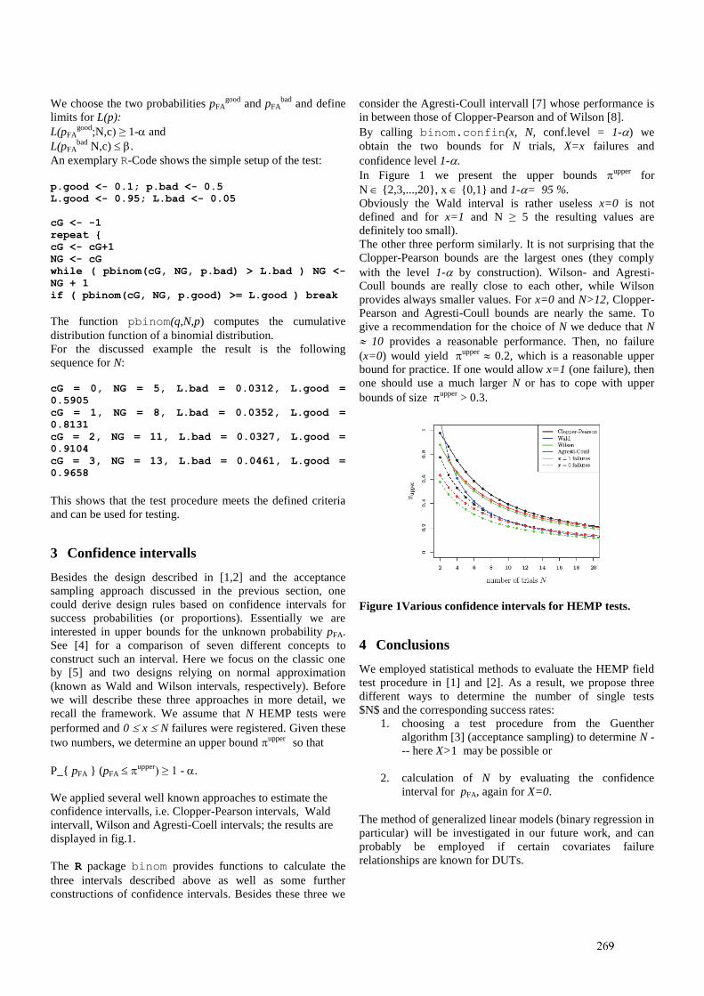
2
We choose the two probabilities pFAgood
and pFAbad
and define
limits for L(p):
L(pFAgood
;N,c) ≥ 1- and
L(pFAbad
N,c) .
An exemplary R-Code shows the simple setup of the test:
p.good <- 0.1; p.bad <- 0.5
L.good <- 0.95; L.bad <- 0.05
cG <- -1
repeat
cG <- cG+1
NG <- cG
while ( pbinom(cG, NG, p.bad) > L.bad ) NG <-
NG + 1
if ( pbinom(cG, NG, p.good) >= L.good ) break
The function pbinom(q,N,p) computes the cumulative
distribution function of a binomial distribution.
For the discussed example the result is the following
sequence for N:
cG = 0, NG = 5, L.bad = 0.0312, L.good =
0.5905
cG = 1, NG = 8, L.bad = 0.0352, L.good =
0.8131
cG = 2, NG = 11, L.bad = 0.0327, L.good =
0.9104
cG = 3, NG = 13, L.bad = 0.0461, L.good =
0.9658
This shows that the test procedure meets the defined criteria
and can be used for testing.
3 Confidence intervalls
Besides the design described in [1,2] and the acceptance
sampling approach discussed in the previous section, one
could derive design rules based on confidence intervals for
success probabilities (or proportions). Essentially we are
interested in upper bounds for the unknown probability pFA.
See [4] for a comparison of seven different concepts to
construct such an interval. Here we focus on the classic one
by [5] and two designs relying on normal approximation
(known as Wald and Wilson intervals, respectively). Before
we will describe these three approaches in more detail, we
recall the framework. We assume that N HEMP tests were
performed and 0 x N failures were registered. Given these
two numbers, we determine an upper bound upper so that
P_ pFA (pFA upper
) ≥ 1 - .
We applied several well known approaches to estimate the
confidence intervalls, i.e. Clopper-Pearson intervals, Wald
intervall, Wilson and Agresti-Coell intervals; the results are
displayed in fig.1.
The R package binom provides functions to calculate the
three intervals described above as well as some further
constructions of confidence intervals. Besides these three we
consider the Agresti-Coull intervall [7] whose performance is
in between those of Clopper-Pearson and of Wilson [8].
By calling binom.confin(x, N, conf.level = 1-) we
obtain the two bounds for N trials, X=x failures and
confidence level 1-.
In Figure 1 we present the upper bounds upper
for
N 2,3,...,20, x 0,1 and 1-= 95 %.
Obviously the Wald interval is rather useless x=0 is not
defined and for x=1 and N ≥ 5 the resulting values are
definitely too small).
The other three perform similarly. It is not surprising that the
Clopper-Pearson bounds are the largest ones (they comply
with the level 1- by construction). Wilson- and Agresti-
Coull bounds are really close to each other, while Wilson
provides always smaller values. For x=0 and N>12, Clopper-
Pearson and Agresti-Coull bounds are nearly the same. To
give a recommendation for the choice of N we deduce that N
10 provides a reasonable performance. Then, no failure
(x=0) would yield upper
0.2, which is a reasonable upper
bound for practice. If one would allow x=1 (one failure), then
one should use a much larger N or has to cope with upper
bounds of size upper
> 0.3.
Figure 1Various confidence intervals for HEMP tests.
4 Conclusions
We employed statistical methods to evaluate the HEMP field
test procedure in [1] and [2]. As a result, we propose three
different ways to determine the number of single tests
$N$ and the corresponding success rates:
1. choosing a test procedure from the Guenther
algorithm [3] (acceptance sampling) to determine N -
-- here X>1 may be possible or
2. calculation of N by evaluating the confidence
interval for pFA, again for X=0.
The method of generalized linear models (binary regression in
particular) will be investigated in our future work, and can
probably be employed if certain covariates failure
relationships are known for DUTs.

3
References
[1] Sabath, F.; Potthast, S. (2013). ''Tolerance Values
and the Confidence Level for High-Altitude Electromagnetic
Pulse (HEMP) Field Tests''. IEEE Transactions on
Electromagnetic Compatibility, 55(3), pp. 518 -“525.
[2] VG 96903-50 Beiblatt 1, Normenstelle
Elektrotechnik (NE) im DIN (2012). ''Nuclear
electromagnetic pulse (NEMP) and lightning protection, Test
methods, test equipment and limiting values''.
[3] Guenther, W. C. (1977). "Sampling Inspection in
Statistical Quality Control'', Griffin, London, UK.
[4] Newcombe, R.G. (1998). ''Two-sided confidence
intervals for the single proportion: comparison of seven
methods''. Statistics in Medicine, 17(8), pp. 857 - 872.
[5] Clopper, C.J.; Pearson, E.S. (1934). ''The use of
confidence or fiducial limits illustrated in the case of the
binomial''. Biometrika, 26(4), pp. 404-413.
[6] Montgomery, D. C. (2009). 'Statistical quality
control: A Modern Introduction'', 6th ed., John Wiley & Sons
(Asia), Pte. Ltd.
[7] Agresti, A. (2013). "Categorical Data Analysis".
Wiley, Hoboken, N. J., 3rd ed.
[8] Agresti, A.; Coull, B.A. (1998). ''Approximate Is
Better than ``Exact'' for Interval Estimation of Binomial
Proportions''. The American Statistician, 52(2), pp. 119.
1
Some standardization problems of high power electromagnetic pulses, formed by test facilities
Yury V. Parfenov1, Boris A. Titov1, Leonid N. Zdoukhov1, William A. Radasky2 1Russian Academy of Sciences, Joint Institute for High Temperatures, 125412 Moscow, Izhorskaya 13, bld.2, Russia, e–mail:
[email protected] 2Metatech, Corp, 358 S. Fairview Ave, Suite E, Goleta, CA, USA, 93117, e-mail: [email protected]
There are two kinds of high power electromagnetic pulses: high altitude electromagnetic pulses (HEMPs) and ultrashort (wideband) electromagnetic pulses (typically hyperband), having peak amplitudes above 100 V/m [1]. It is important to evaluate the immunity of electronic devices to the action of similar pulse test facilities (simulators), which have been created in many countries. Availability of the normative documents containing data on amplitudes and waveforms of reproduced pulses was one of conditions of their creation. The international standards [2, 3] concerned provide this type of information. The first of the named documents is devoted to HEMP and represents it in a form of a unipolar pulse having 10-90% rise time of 2.5 nanoseconds and the duration at 50% of the peak value of 23 nanoseconds. The peak of the standard pulse is equal to 50 kV/m. HEMP standardization in the IEC has collected the developed experimental base [4] used to perform tests of a considerable quantity of objects. Application of the HEMP simulators has revealed some of their shortcomings. One of the shortcomings is analyzed in [5]. The authors of the paper ascertain that features of the waveforms over the test volumes of HEMP simulators differ from features of the pulse set by the standard [2]. They fear that the noted differences can decrease the reliability of the results of electronic devices tests to their immunity to HEMP fields. To eliminate the possible shortcomings they offer to restrict the deflections of pulsed electromagnetic fields in the test volumes of HEMP simulators from the standard HEMP in the frequency domain (similar restrictions in the time domain already are present in existing standards). A high-priced modernization will be necessary for realization of these considerations with reference to existing HEMP simulators. Before making a decision about modernization of simulators, it is useful to get the answer to the following question: whether modernization will lead to a real increase of reliability of results of testing electronic devices of immunity to HEMP action? In formulating the answer to this question one must take into account that the reliability of test results depends not only on the degree of conformity of EMPs in test volumes of HEMP simulators to a standard HEMP, but also from degree of conformity of EMPs formed by simulators to real HEMPs. It is necessary to say here that the recommended standard [2] HEMP waveform is idealized and differs from forms of real HEMPs (and this is mentioned in [2]). Moreover, the standard HEMP waveform could be not registered from a real high nuclear explosion in principle,
since such pulse is not capable to spread over free space because its spectrum includes the zero frequency. The next aspect follows from the aforesaid. It is possible that frequencies being minimized in the spectrum of pulses in test volumes of HEMP simulators can be present in spectrum of real HEMPs. Also introduction to the spectrum of the standard HEMP of the zero frequency in some cases can bring about a result, which cannot be observed in reality. Therefore, we plan to analyze the role of the assumptions, which were accepted at the development of the standard HEMP form several dozens years ago. Only after that it will be possible to formulate trends of HEMP simulators modernization. It is also possible that the analysis of these aspects could result in a modification of the IEC HEMP standard waveform [2]. Now the similar problem is also observed in the field of hyperband EMPs. A lot of sources of powerful hyperband EMPs exist in many countries. Examples of such sources are presented in [6]. They radiate their pulses with differing features (pulse peak, spectrum, pulse repetition rate and others). At present standards similar to the standards in the field of HEMP including the standard containing hyperband EMP waveforms has recently been developed [7]. We will present some evaluations of this standard in our report. Perhaps, this analysis will be useful in developing new hyperband sources, as well as at making a decision about the trends of HEMP simulator modernization.
References
[1] IEC/TR 61000-1-5 Ed. 1.0 (2004-11): High power electromagnetic (HPEM) effects on civil systems. [2] IEC 61000-2-9 Ed. 1.0 (1996-02): Description of HEMP environment - Radiated disturbance. [3] IEC 61000-2-13 Ed. 1.0 (2005-03): High-power electromagnetic (HPEM) environments - Radiated and conducted. [4] IEC/TR 61000-4-32 Ed. 1.0 (2002-10): HEMP simulator compendium. [5] Giri D.V., Prather W.D. High-Altitude Electromagnetic Pulse (HEMP) Rise time Evolution of Technology and Standards, IEEE Trans on EMC, Special Issue on HEMP, June 2013. [6] IEC/TR 61000-4-35 Ed. 1.0 (2009-07): High power electromagnetic (HPEM) simulator compendium. [7] IEC 61000-4-36 Ed. 1.0 (2014-11): IEMI immunity test methods for equipment and systems.
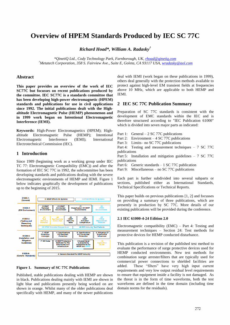
1
Overview of HPEM Standards Produced by IEC SC 77C
Richard Hoad*, William A. Radasky†
*QinetiQ Ltd., Cody Technology Park, Farnborough, UK, [email protected]
†Metatech Corporation, 358 S. Fairview Ave., Suite E, Goleta, CA 93117 USA, [email protected]
Abstract
This paper provides an overview of the work of IEC
SC77C but focusses on recent publications produced by
the committee. IEC SC77C is a standards committee that
has been developing high-power electromagnetic (HPEM)
standards and publications for use in civil applications
since 1992. The initial publications dealt with the High-
altitude Electromagnetic Pulse (HEMP) phenomenon and
in 1999 work began on Intentional Electromagnetic
Interference (IEMI).
Keywords: High-Power Electromagnetics (HPEM); High-
altitude Electromagnetic Pulse (HEMP); Intentional
Electromagnetic Interference (IEMI); International
Electrotechnical Commission (IEC).
1 Introduction
Since 1989 (beginning work as a working group under IEC
TC 77: Electromagnetic Compatibility (EMC)) and after the
formation of IEC SC 77C in 1992, the subcommittee has been
developing standards and publications dealing with the severe
electromagnetic environments of HEMP and IEMI. Figure 1
below indicates graphically the development of publications
up to the beginning of 2015.
Figure 1. Summary of SC 77C Publications
Published, stable publications dealing with HEMP are shown
in black. Publications dealing mainly with IEMI are shown in
light blue and publications presently being worked on are
shown in orange. Whilst many of the older publications deal
specifically with HEMP, and many of the newer publications
deal with IEMI (work began on these publications in 1999),
others deal generally with the protection methods available to
protect against high-level EM transient fields at frequencies
above 10 MHz, which are applicable to both HEMP and
IEMI.
2 IEC SC 77C Publication Summary
Preparation of SC 77C standards is consistent with the
development of EMC standards within the IEC and is
therefore structured according to "IEC Publication 61000"
which is divided into seven major parts as indicated:
Part 1: General – 2 SC 77C publications
Part 2: Environment – 4 SC 77C publications
Part 3: Limits– no SC 77C publications
Part 4: Testing and measurement techniques – 7 SC 77C
publications
Part 5: Installation and mitigation guidelines – 7 SC 77C
publications
Part 6: Generic standards – 1 SC 77C publication
Part 9: Miscellaneous – no SC 77C publications
Each part is further subdivided into several subparts or
sections, published either as International Standards,
Technical Specifications or Technical Reports.
This paper builds on previous publications [1, 2] and focusses
on providing a summary of three publications, which are
presently in production by SC 77C. More details of our
existing publications will be provided during the conference.
2.1 IEC 61000-4-24 Edition 2.0
Electromagnetic compatibility (EMC) – Part 4: Testing and
measurement techniques – Section 24: Test methods for
protective devices for HEMP conducted disturbance.
This publication is a revision of the published test method to
evaluate the performance of surge protective devices used for
HEMP conducted environments. New test methods for
combination surge arrester/filters that are typically used for
commercial power connections to shielded facilities are
added. These “filters” have very high input current
requirements and very low output residual level requirements
to ensure that equipment inside a facility is not damaged. As
the threat is in the form of time waveforms, both the test
waveforms are defined in the time domain (including time
domain norms for the residuals).

2
The pass/fail requirements for residuals are given for different
levels of protection desired including industrial applications,
critical infrastructure applications and military applications.
The residuals for military applications are based on [3].
2.2 IEC 61000-4-23 Edition 2.0
Electromagnetic compatibility (EMC) – Part 4-23: Testing
and measurement techniques – Test methods for protective
devices for HEMP and other radiated disturbances.
This standard is undergoing a revision to allow the shielding
effectiveness of a shielded volume to be evaluated with the
transmitter in the inside of the facility in addition to being on
the outside. This is due to the fact that some underground
facilities do not have much space on the outside for a
transmitter. In addition, this standard is being harmonized
with IEEE 299-2006 [4] as much as possible, especially with
regard to the number of frequencies tested and the separation
distances.
2.3 New Project IEC 61000-5-10
This is a new project begun at the end of 2014 that is intended
to provide guidance for the application of the entire body of
IEC SC 77C publications. It is considered that a
comprehensive guide to consolidate this work will be of great
help to industry.
The publication will include several specific examples of how
to apply the publications in the IEC SC 77C series. The
sample problems will include:
1) Application of a protection and testing scheme for a
new facility
2) Application of a protection and testing scheme for an
existing facility
For both applications, protection and testing schemes need to
be identified for three cases: a HEMP environment protection
and testing scheme; an IEMI environment protection and
testing scheme; and a HEMP+IEMI protection and testing
scheme. This means there will be 6 schemes covered in this
publication.
3 Conclusion
This paper has introduced IEC SC 77C publications that deal
with high power transient phenomena. The SC 77C
Committee members produce standards and other
publications dealing with the protection from severe
electromagnetic threats for use in civil applications.
References
[1] R. Hoad and W. A. Radasky, “Progress in IEC SC 77C
high-power electromagnetics publications in 2009,”
Asia-Pacific EMC Symposium, 2010, pp. 762-765.
[2] W. A. Radasky, “Status of IEC SC 77C high-power
electromagnetics publications in 2012,” 6th Asia
Conference on Environmental Electromagnetics
(CEEM), Shanghai, 2012, pp. 1-4.
[3] MIL-STD-188-125-1, “High-Altitude EMP Protection
for Fixed Ground-Based Facilities," Department of
Defense, 2005.
[4] IEEE 299-2006, “IEEE Standard Method for Measuring
the Effectiveness of Electromagnetic Shielding
Enclosures,” February 2007.
1
An overview of two recent IEMI publications: IEEE Std 1642 and Cigré Technical Brochure 600
W A Radasky*
*Metatech Corporation, Goleta, California, USA, [email protected]
Abstract In this paper two important and recent IEMI publications are reviewed. One is an IEEE standard practice dealing with the protection of computer systems that are easily accessible to the public. The second is a Cigré Technical Brochure that describes the threat of IEMI to low voltage control electronics found in high voltage power substations throughout the world. Both of these publications were developed with strong reliance on the basic IEMI standards published by the International Electrotechnical Commission (IEC). This paper will review the scope of each document and provide a summary of the content to make the technical community aware of the standardization progress of work in these areas. Keywords: Intentional Electromagnetic Interference (IEMI), EMC standards, high-power electromagnetic (HPEM) fields, Cigré, IEEE, EMC, IEC
1 IEEE Std 1642-2015
IEEE Std 1642-2015, “Recommended Practice for Protecting Public Accessible Computer Systems from Intentional Electromagnetic Interference (IEMI),” January 2015 [1]. 1.1 Working Group Information: Chairman of the working group – William Radasky Members of the working group – Mats Bäckström, William Croisant, Sven Fisahn, Heyno Garbe, Richard Hoad, Daniel Månsson, Michael McInerney, Yury Parfenov, Frank Sabath, Edward Savage, Kwok Soohoo, Rajeev Thottappillil, Holger Thye, Anthony Wraight, and Perry Wilson. 1.2 Scope and Purpose: This recommended practice establishes appropriate electromagnetic (EM) threat levels, protection methods, monitoring techniques, and test techniques for specific classes of computer equipment. This equipment is expected to be accessible to the public at ranges less than 100 meters, and the loss of operation of the equipment due to intentional electromagnetic interference (IEMI) is expected to cause losses (both financial and of confidence) to businesses
operating computer equipment, which are providing services to the public or to private companies. The principle class of equipment to be considered in this recommended practice includes fixed (non-mobile) computer equipment. Examples include automated teller machines (ATMs), electronic cash registers at stores, computer equipment in banks and at airports, computer equipment controlling traffic flow, computer equipment controlling communications or allowing Internet access, computer equipment providing police, fire and security services, computer equipment controlling the operation of the power grid (including smart meters), computer equipment operating in hospitals, etc. The purpose of this document is to provide information for manufacturers and users to specify the EMC requirements for computer equipment and systems that can be used by the public or businesses, which require a high-level of security to prevent intentional electromagnetic fields from interfering with the operation of these computers.
2 Cigré TB 600
Cigré (International Council on Large Electric Systems) is an international organization that focuses on the design and protection of high-voltage (V > 100 kV) power grids throughout the world. They produced technical reports that often serve as pre-standards especially due to their close relationship with the International Electrotechnical Commission (IEC). Cigré Study Committee 4 (SC 4) has within its scope work on electromagnetic compatibility (EMC). Cigré Technical Brochure 600, “Protection of High Voltage Power Network Control Electronics Against Intentional Electromagnetic Interference (IEMI),” prepared by WG C4.206, November 2014 [2]. 2.1 Working Group Information: Convener of the working group – William Radasky Members of the working group – Mats Bäckström (SE), Haeivelto de Souza Bronzeado (BR), Darren Carpenter (UK), Jinliang He (CN), Richard Hoad (UK), Masaru Ishii (JP), Armin Kälin (CH), Daniel Månsson (SE), Yury Parfenov (RU), Leonid Siniy (RU), Yasunao Suzuki (JP)
2
Corresponding members of the working group – Hideki Motoyama (JP), Farhad Rachidi (CH), W. H. Siew (UK), Tetsuya Tominaga (JP) 2.2 Introduction to the Technical Brochure Electromagnetic compatibility (EMC) has been a very important aspect of protecting modern electronic equipment from accidental exposure from fixed and mobile transmitters and from the emissions of nearby electronic equipment. Unfortunately with the advancements of solid-state technology (which has allowed the development of small powerful generators), it is possible for hackers, criminals and terrorists to intentionally generate high levels of electromagnetic fields for which commercial equipment is not protected. It is therefore crucial to understand this new threat of intentional electromagnetic interference (IEMI), especially with regard to the critical infrastructures. In particular the electric power grid is one of the most important of the critical infrastructures, as most of the other infrastructures depend on the consistent flow of electrical power. This technical brochure reviews the threat that electromagnetic (EM) weapons may pose to high voltage substation control electronics. This particular set of electronics is selected as significant levels of power flows through high voltage substations, and over the past 2 decades most of the control electronics used have changed from analog to digital, making them more sensitive to fast transient disturbances. In addition, most substation electronics (e.g., relays) operate automatically without the influence of operators and are hence vulnerable to serious electronic upsets in addition to damage.
This brochure reviews potential electromagnetic threat weapons, the factors that influence the exposure of equipment to high levels of high-frequency fields and induced voltages, the levels of susceptibility of equipment to these types of induced transients, and the protection methods that could be applied to reduce the threat. As part of this work, basic standards produced by IEC SC 77C (EMC: High Power Transient Phenomena) have been referenced. ITU-T has already adapted the IEC basic standards for their application to communications facilities. This brochure specifically adapts the IEC standards to the protection of substation electronics.
3 Discussion and Conclusion
This paper will review this new IEEE Standard Practice and will highlight the basic approach for the protection of computer equipment from IEMI. This paper will also review this new Cigré Technical Brochure and will highlight the basic approach for the protection of substation electronic equipment from IEMI.
References
[1] IEEE Std 1642-2015, “Recommended Practice for Protecting Public Accessible Computer Systems from Intentional Electromagnetic Interference (IEMI),” January 2015. [2] Cigré Technical Brochure 600, “Protection of High Voltage Power Network Control Electronics Against Intentional Electromagnetic Interference (IEMI),” prepared by WG C4.206, November 2014.
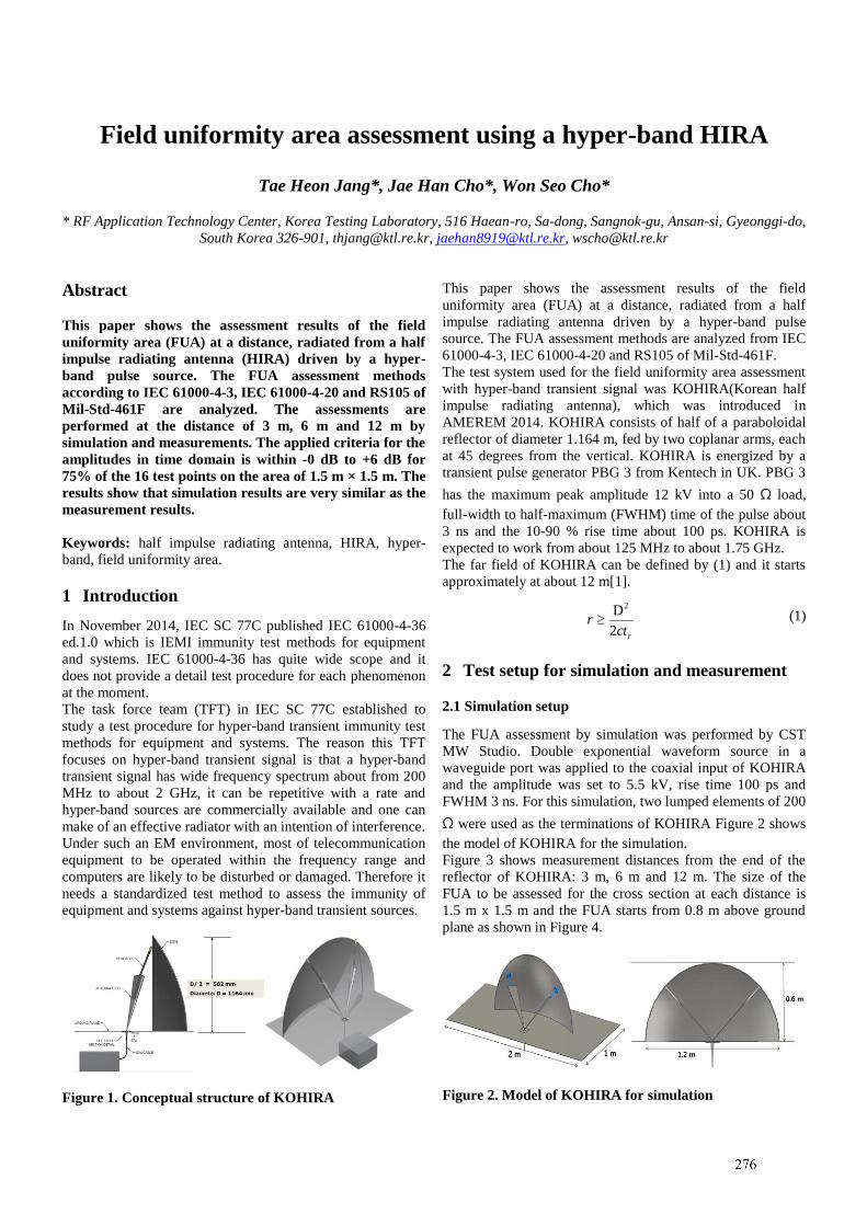
1
Field uniformity area assessment using a hyper-band HIRA
Tae Heon Jang*, Jae Han Cho*, Won Seo Cho*
* RF Application Technology Center, Korea Testing Laboratory, 516 Haean-ro, Sa-dong, Sangnok-gu, Ansan-si, Gyeonggi-do,
South Korea 326-901, [email protected], [email protected], [email protected]
Abstract
This paper shows the assessment results of the field
uniformity area (FUA) at a distance, radiated from a half
impulse radiating antenna (HIRA) driven by a hyper-
band pulse source. The FUA assessment methods
according to IEC 61000-4-3, IEC 61000-4-20 and RS105 of
Mil-Std-461F are analyzed. The assessments are
performed at the distance of 3 m, 6 m and 12 m by
simulation and measurements. The applied criteria for the
amplitudes in time domain is within -0 dB to +6 dB for
75% of the 16 test points on the area of 1.5 m × 1.5 m. The
results show that simulation results are very similar as the
measurement results.
Keywords: half impulse radiating antenna, HIRA, hyper-
band, field uniformity area.
1 Introduction
In November 2014, IEC SC 77C published IEC 61000-4-36
ed.1.0 which is IEMI immunity test methods for equipment
and systems. IEC 61000-4-36 has quite wide scope and it
does not provide a detail test procedure for each phenomenon
at the moment.
The task force team (TFT) in IEC SC 77C established to
study a test procedure for hyper-band transient immunity test
methods for equipment and systems. The reason this TFT
focuses on hyper-band transient signal is that a hyper-band
transient signal has wide frequency spectrum about from 200
MHz to about 2 GHz, it can be repetitive with a rate and
hyper-band sources are commercially available and one can
make of an effective radiator with an intention of interference.
Under such an EM environment, most of telecommunication
equipment to be operated within the frequency range and
computers are likely to be disturbed or damaged. Therefore it
needs a standardized test method to assess the immunity of
equipment and systems against hyper-band transient sources.
Figure 1. Conceptual structure of KOHIRA
This paper shows the assessment results of the field
uniformity area (FUA) at a distance, radiated from a half
impulse radiating antenna driven by a hyper-band pulse
source. The FUA assessment methods are analyzed from IEC
61000-4-3, IEC 61000-4-20 and RS105 of Mil-Std-461F.
The test system used for the field uniformity area assessment
with hyper-band transient signal was KOHIRA(Korean half
impulse radiating antenna), which was introduced in
AMEREM 2014. KOHIRA consists of half of a paraboloidal
reflector of diameter 1.164 m, fed by two coplanar arms, each
at 45 degrees from the vertical. KOHIRA is energized by a
transient pulse generator PBG 3 from Kentech in UK. PBG 3
has the maximum peak amplitude 12 kV into a 50 Ω load,
full-width to half-maximum (FWHM) time of the pulse about
3 ns and the 10-90 % rise time about 100 ps. KOHIRA is
expected to work from about 125 MHz to about 1.75 GHz.
The far field of KOHIRA can be defined by (1) and it starts
approximately at about 12 m[1].
rctr
2
D2
(1)
2 Test setup for simulation and measurement
2.1 Simulation setup
The FUA assessment by simulation was performed by CST
MW Studio. Double exponential waveform source in a
waveguide port was applied to the coaxial input of KOHIRA
and the amplitude was set to 5.5 kV, rise time 100 ps and
FWHM 3 ns. For this simulation, two lumped elements of 200
Ω were used as the terminations of KOHIRA Figure 2 shows
the model of KOHIRA for the simulation.
Figure 3 shows measurement distances from the end of the
reflector of KOHIRA: 3 m, 6 m and 12 m. The size of the
FUA to be assessed for the cross section at each distance is
1.5 m x 1.5 m and the FUA starts from 0.8 m above ground
plane as shown in Figure 4.
Figure 2. Model of KOHIRA for simulation
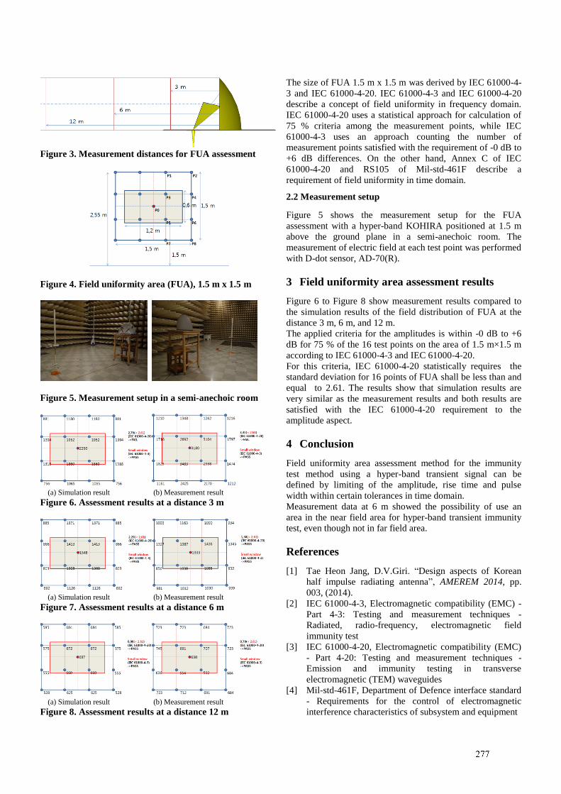
2
Figure 3. Measurement distances for FUA assessment
Figure 4. Field uniformity area (FUA), 1.5 m x 1.5 m
Figure 5. Measurement setup in a semi-anechoic room
(a) Simulation result (b) Measurement result
Figure 6. Assessment results at a distance 3 m
(a) Simulation result (b) Measurement result
Figure 7. Assessment results at a distance 6 m
(a) Simulation result (b) Measurement result
Figure 8. Assessment results at a distance 12 m
The size of FUA 1.5 m x 1.5 m was derived by IEC 61000-4-
3 and IEC 61000-4-20. IEC 61000-4-3 and IEC 61000-4-20
describe a concept of field uniformity in frequency domain.
IEC 61000-4-20 uses a statistical approach for calculation of
75 % criteria among the measurement points, while IEC
61000-4-3 uses an approach counting the number of
measurement points satisfied with the requirement of -0 dB to
+6 dB differences. On the other hand, Annex C of IEC
61000-4-20 and RS105 of Mil-std-461F describe a
requirement of field uniformity in time domain.
2.2 Measurement setup
Figure 5 shows the measurement setup for the FUA
assessment with a hyper-band KOHIRA positioned at 1.5 m
above the ground plane in a semi-anechoic room. The
measurement of electric field at each test point was performed
with D-dot sensor, AD-70(R).
3 Field uniformity area assessment results
Figure 6 to Figure 8 show measurement results compared to
the simulation results of the field distribution of FUA at the
distance 3 m, 6 m, and 12 m.
The applied criteria for the amplitudes is within -0 dB to +6
dB for 75 % of the 16 test points on the area of 1.5 m×1.5 m
according to IEC 61000-4-3 and IEC 61000-4-20.
For this criteria, IEC 61000-4-20 statistically requires the
standard deviation for 16 points of FUA shall be less than and
equal to 2.61. The results show that simulation results are
very similar as the measurement results and both results are
satisfied with the IEC 61000-4-20 requirement to the
amplitude aspect.
4 Conclusion
Field uniformity area assessment method for the immunity
test method using a hyper-band transient signal can be
defined by limiting of the amplitude, rise time and pulse
width within certain tolerances in time domain.
Measurement data at 6 m showed the possibility of use an
area in the near field area for hyper-band transient immunity
test, even though not in far field area.
References
[1] Tae Heon Jang, D.V.Giri. “Design aspects of Korean
half impulse radiating antenna”, AMEREM 2014, pp.
003, (2014).
[2] IEC 61000-4-3, Electromagnetic compatibility (EMC) -
Part 4-3: Testing and measurement techniques -
Radiated, radio-frequency, electromagnetic field
immunity test
[3] IEC 61000-4-20, Electromagnetic compatibility (EMC)
- Part 4-20: Testing and measurement techniques -
Emission and immunity testing in transverse
electromagnetic (TEM) waveguides
[4] Mil-std-461F, Department of Defence interface standard
- Requirements for the control of electromagnetic
interference characteristics of subsystem and equipment
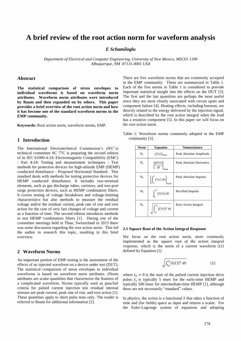
A brief review of the root action norm for waveform analysis
E Schamiloglu
Department of Electrical and Computer Engineering, University of New Mexico, MSC01 1100
Albuquerque, NM 87131-0001 USA
Abstract
The statistical comparison of stress envelopes to
individual waveforms is based on waveform norm
attributes. Waveform norm attributes were introduced
by Baum and then expanded on by others. This paper
provides a brief overview of the root action norm and how
it has become one of the standard waveform norms in the
EMP community.
Keywords: Root action norm, waveform norms, EMP.
1 Introduction
The International Electrotechnical Commission’s (IEC’s)
technical committee SC 77C is preparing the second edition
of its IEC 61000-4-24: Electromagnetic Compatibility (EMC)
- Part 4-24: Testing and measurement techniques - Test
methods for protective devices for high-altitude EMP (HEMP)
conducted disturbance - Proposed Horizontal Standard. This
standard deals with methods for testing protective devices for
HEMP conducted disturbance. It includes two-terminal
elements, such as gas discharge tubes, varistors, and two-port
surge protection devices, such as HEMP combination filters.
It covers testing of voltage breakdown and voltage-limiting
characteristics but also methods to measure the residual
voltage and/or the residual current, peak rate of rise and root
action for the case of very fast changes of voltage and current
as a function of time. The second edition introduces methods
to test HEMP combination filters [1]. During one of the
committee meetings held in Thun, Switzerland in 2013 there
was some discussion regarding the root action norm. This led
the author to research this topic, resulting in this brief
overview.
2 Waveform Norms
An important portion of EMP testing is the assessment of the
effects of an injected waveform on a device under test (DUT).
The statistical comparison of stress envelopes to individual
waveforms is based on waveform norm attributes. (Norm
attributes are scalar quantities that characterize the features of
a complicated waveform. Norms typically used as pass/fail
criteria for pulsed current injection test residual internal
stresses are peak current, peak rate of rise, and root action [1].
These quantities apply to short pulse tests only. The reader is
referred to Baum for additional information [2].
There are five waveform norms that are commonly accepted
in the EMP community. These are summarized in Table 1.
Each of the five norms in Table 1 is considered to provide
important statistical insight into the effects on the DUT [3].
The first and the last quantities are perhaps the most useful
since they are most closely associated with circuit upset and
component failure [4]. Heating effects, including burnout, are
directly related to the energy delivered by the injection signal,
which is described by the root action integral when the load
has a resistive component [5]. In this paper we will focus on
the root action norm.
Table 1: Waveform norms commonly adopted in the EMP
community [3].
Norm Equation Nomenclature
N1 |𝑓(𝑡)|max Peak Absolute Amplitude
N2 |𝑑𝑓(𝑡)
𝑑𝑡|
max
Peak Absolute Derivative
N3 |∫ 𝑓(𝑥) 𝑑𝑥
𝑡
0
|max
Peak Absolute Impulse
N4 ∫ |𝑓(𝑡)|
∞
0
𝑑𝑡 Rectified Impulse
N5
√∫ |𝑓(𝑡)|2 𝑑𝑡𝑡1
𝑡0
Root Action Integral
2.1 Square Root of the Action Integral Response
We focus on the root action norm, more commonly
implemented as the square root of the action integral
response, which is the norm of a current waveform 𝑖(𝑡)
defined by Equation (1)
√∫ |𝑖(𝑡)|2 𝑑𝑡𝑡1
𝑡0 (1)
where 𝑡0 = 0 is the start of the pulsed current injection drive
pulse; 𝑡1 is typically 5 msec for the early-time HEMP and
typically 500 msec for intermediate-time HEMP [1], although
these are not necessarily “standard” values.
In physics, the action is a functional 𝑆 that takes a function of
time and (for fields) space as input and returns a scalar. For
the Euler-Lagrange system of equations and adopting
Hamilton’s principle, we assume that the Lagrangian ℒ (the
integrand of the action integral) depends only on the
coordinate 𝑥(𝑡) and its time derivative 𝑑𝑥(𝑡)/𝑑𝑡 , and may
also depend explicitly on time. In that case, the action integral
can be written [6]
𝑆 = ∫ ℒ(𝑥, , 𝑡)𝑡2
𝑡1 𝑑𝑡 (2)
For an electrical network comprising inductors and ignoring
capacitors, it can be shown that the Lagrangian can be
expressed as [7]
ℒ =1
2𝑖𝑇𝐿𝑖 (3)
where 𝑖𝑇 is the transpose of the current matrix. Thus the root
action integral is a measure of the injected energy in a pulsed
current injection experiment. Normalized to inductance it
yields the square root of the action integral response, whose
dimensions are [Ampere ∙ sec1/2].
Thus the root action integral is directly related to the energy
delivered by the injection signal – it is nothing other than the
square root of the action integral where the Lagrangian ℒ
describing the circuit is the integrand.
References
[1] High-Altitude Electromagnetic Pulse (HEMP)
Protection for Ground-Based C41 Facilities Performing
Critical, Time-Urgent Missions Part 1: Fixed Facilities
(MIL-STD-188-125-1 Notice 1, 7 April 2005).
[2] C.E. Baum, “Norms of Time-Domain Functions and
Convolution Operators,” in H.N. Kritikos and D.L.
Jaggard, Eds., Recent Advances in Electromagnetic
Theory (Springer-Verlag, New York, NY, 1990), Chap.
2, and references therein.
[3] J. Beilfuss and R. Gray, “Source Selection Techniques
for EMP Direct Drive Simulation,” IEEE National
Symposium on Electromagnetic Compatibility (Denver,
CO, May 23-25, 1989), pp. 93-96.
[4] C.E. Baum, “Black Box Bounds,” Interaction Note 429,
19 May 1983 (available at the Summa Notes website:
http://ece-research.unm.edu/summa/notes/In/0429.pdf.
[5] D.V. Giri, High-Power Electromagnetic Radiators
(Harvard University Press, Cambridge, MA, 2004), p.
73.
[6] H. Goldstein, Classical Mechanics (Addison-Wesley,
Reading, MA, 1965).
[7] L.O. Chua and J.D. McPherson, “Explicit Topological
Formulations of Lagrangian and Hamiltonian Equations
for Nonlinear Networks,” IEEE Trans. Circuits Syst.
Vol. 21, pp. 277-285 (1974).
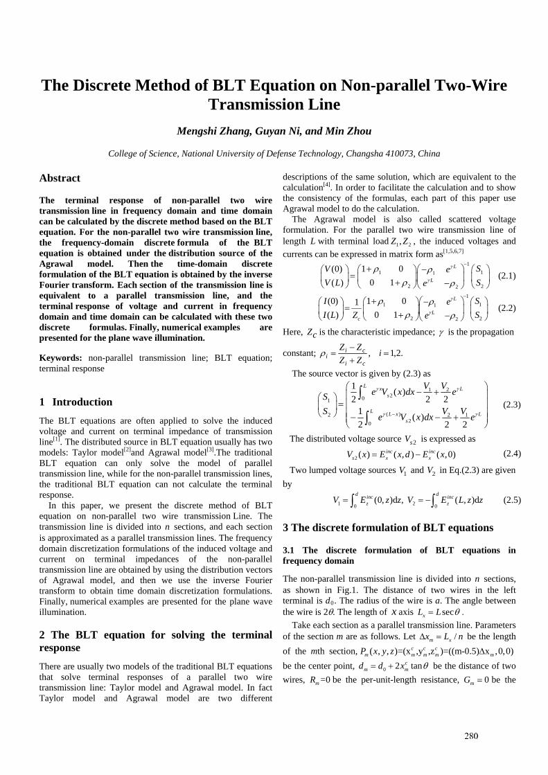
The Discrete Method of BLT Equation on Non-parallel Two-Wire Transmission Line
Mengshi Zhang, Guyan Ni, and Min Zhou
College of Science, National University of Defense Technology, Changsha 410073, China
Abstract The terminal response of non-parallel two wire transmission line in frequency domain and time domain can be calculated by the discrete method based on the BLT equation. For the non-parallel two wire transmission line, the frequency-domain discrete formula of the BLT equation is obtained under the distribution source of the Agrawal model. Then the time-domain discrete formulation of the BLT equation is obtained by the inverse Fourier transform. Each section of the transmission line is equivalent to a parallel transmission line, and the terminal response of voltage and current in frequency domain and time domain can be calculated with these two discrete formulas. Finally, numerical examples are presented for the plane wave illumination. Keywords: non-parallel transmission line; BLT equation; terminal response
1 Introduction The BLT equations are often applied to solve the induced voltage and current on terminal impedance of transmission line[1]. The distributed source in BLT equation usually has two models: Taylor model[2]and Agrawal model[3].The traditional BLT equation can only solve the model of parallel transmission line, while for the non-parallel transmission lines, the traditional BLT equation can not calculate the terminal response.
In this paper, we present the discrete method of BLT equation on non-parallel two wire transmission Line. The transmission line is divided into n sections, and each section is approximated as a parallel transmission lines. The frequency domain discretization formulations of the induced voltage and current on terminal impedances of the non-parallel transmission line are obtained by using the distribution vectors of Agrawal model, and then we use the inverse Fourier transform to obtain time domain discretization formulations. Finally, numerical examples are presented for the plane wave illumination.
2 The BLT equation for solving the terminal response There are usually two models of the traditional BLT equations that solve terminal responses of a parallel two wire transmission line: Taylor model and Agrawal model. In fact Taylor model and Agrawal model are two different
descriptions of the same solution, which are equivalent to the calculation[4]. In order to facilitate the calculation and to show the consistency of the formulas, each part of this paper use Agrawal model to do the calculation.
The Agrawal model is also called scattered voltage formulation. For the parallel two wire transmission line of length with terminal loadL 1 2,Z Z , the induced voltages and currents can be expressed in matrix form as[1,5,6,7]
(2.1) 1
11 1
2 22
1 0(0)0 1( )
L
L
SV eV L Se
1
11 1
2 22
1 0(0) 10 1( )
L
Lc
SI eI L SZ e
(2.2)
Here, Zc is the characteristic impedance; is the propagation
constant; .2,1,
iZZZZ
ci
cii
The source vector is given by (2.3) as
1 2201
( )2 220
1 ( )2 2 2
1 ( )2 2
L x Ls
L L x Ls
V Ve V x dx eSS Ve V x dx e
1
2V
(2.3)
The distributed voltage source 2sV is expressed as (2.4) 2 ( ) ( , ) ( ,0)inc inc
s x xV x E x d E x
Two lumped voltage sources and in Eq.(2.3) are given by
1V 2V
(2.5) 1 20 0(0, )d , ( , )d
d dinc incz zV E z z V E L z z
3 The discrete formulation of BLT equations
3.1 The discrete formulation of BLT equations in frequency domain
The non-parallel transmission line is divided into n sections, as shown in Fig.1. The distance of two wires in the left terminal is d0. The radius of the wire is a. The angle between the wire is 2. The length of x axis secxL L .
Take each section as a parallel transmission line. Parameters of the section m are as follows. Let /m xx L n
,y ,z )=((m-0c c cm m
anm
be the length of the mth section, be the center point, d d
( , , )=(x .5) x ,0,0)m m mP x y z
0 2 tcm x
0m
be the distance of two wires, be the per-unit-length resistance, =0mR G be the
1
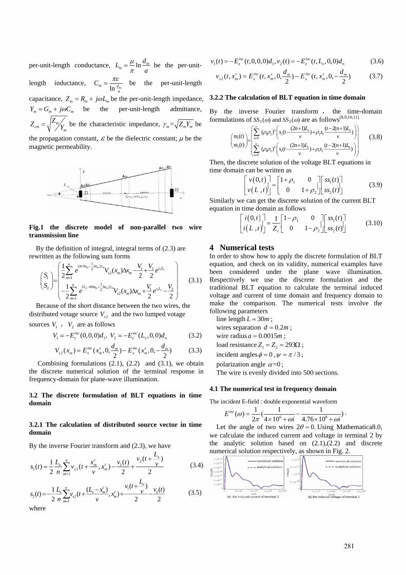
per-unit-length conductance, ln mm
dLa
be the per-unit-
length inductance, ln mm d
a
C be the per-unit-length
capacitance, m m mZ R j L
mj Cbe the per-unit-length impedance,
m mY G be the per-unit-length admittance,
mcm
m
ZZ Y be the characteristic impedance, =m m mZ Y be
the propagation constant, be the dielectric constant; be the magnetic permeability.
Fig.1 the discrete model of non-parallel two wire transmission line
By the definition of integral, integral terms of (2.3) are rewritten as the following sum forms
1
11 22
211
2 1 22
1
1 ( )2 2
1 ( )2 2
m mn x
x m m mx
n m x x Ls m m
m
n L m x Ls m m
m
V Vx x eSS V Ve V x x e
( )
1( )2
2
2
m
x
e V
(3.1)
Because of the short distance between the two wires, the distributed votage source 2sV and the two lumped votage sources V ,V are as follows 1 2
1 1 2(0,0,0) , ( ,0,0)inc incz z xV E d V E L d n (3.2)
2 ( ) ( ,0, ) ( ,0, )2 2
inc c inc cm ms m x m x m
d dV (3.3) x E x E x
Combining formulations (2.1), (2.2) and (3.1), we obtain the discrete numerical solution of the terminal response in frequency-domain for plane-wave illumination.
3.2 The discrete formulation of BLT equations in time domain
3.2.1 The calculation of distributed source vector in time domain
By the inverse Fourier transform and (2.3), we have
21
1 21
( )( )1( ) ( , )2 2 2
xcn
cx ms m
m
Lv tL x v t vs t v t xn v
(3.4)
12
2 21
( )( ) ( )1( ) ( , )2 2
xcn
cx x ms m
m
Lv tL L x v tvs t v t xn v
2
(3.5)
where
1 1 2( ) ( ,0,0,0) , ( ) ( , ,0,0)inc incz z xv t E t d v t E t L d n (3.6)
2 ( , ) ( , , 0, ) ( , , 0, )2 2
c inc c inc cms m x m x m
dv t x E t x E t x md (3.7)
3.2.2 The calculation of BLT equation in time domain
By the inverse Fourier transform , the time-domain formulations of SS1() and SS2() are as follows[8,9,10,11]
1 2 2 2 101
2 01 2 1 1 2
0
(2 1) ( 2( 1)( ) ( ) )( )( ) (2 1) ( 2( 1)( ) ( ) )
n x x
n
n x
n
n L t n Ls t sss t v vss t n L t n Ls t s
v v
(3.8)
Then, the discrete solution of the voltage BLT equations in time domain can be written as
1
2 2
0, 1 0 ( ), 0 1
v t ss tv L t ss t
1
( )
(3.9)
Similarly we can get the discrete solution of the current BLT equation in time domain as follows
1
2 2
0, 1 0 ( )1, 0 1c
i t ss ti L t ss tZ
1
( )
(3.10)
4 Numerical tests In order to show how to apply the discrete formulation of BLT equation, and check on its validity, numerical examples have been considered under the plane wave illumination. Respectively we use the discrete formulation and the traditional BLT equation to calculate the terminal induced voltage and current of time domain and frequency domain to make the comparison. The numerical tests involve the following parameters
line length 30L m ; wires separation 0.2d m ; wire radius 0.0015a m ; load resistance 1 2 293Z Z ; incident angles 0 , / 3 ; polarization angle =0 ; The wire is evenly divided into 500 sections.
4.1 The numerical test in frequency domain
The incident E-field : double exponential waveform
6 8
1 1 1( ) ( )2 4 10 4.76 10
incEi i
.
Let the angle of two wires 2 0. Using Mathematica8.0, we calculate the induced current and voltage in terminal 2 by the analytic solution based on (2.1),(2.2) and discrete numerical solution respectively, as shown in Fig. 2.
2
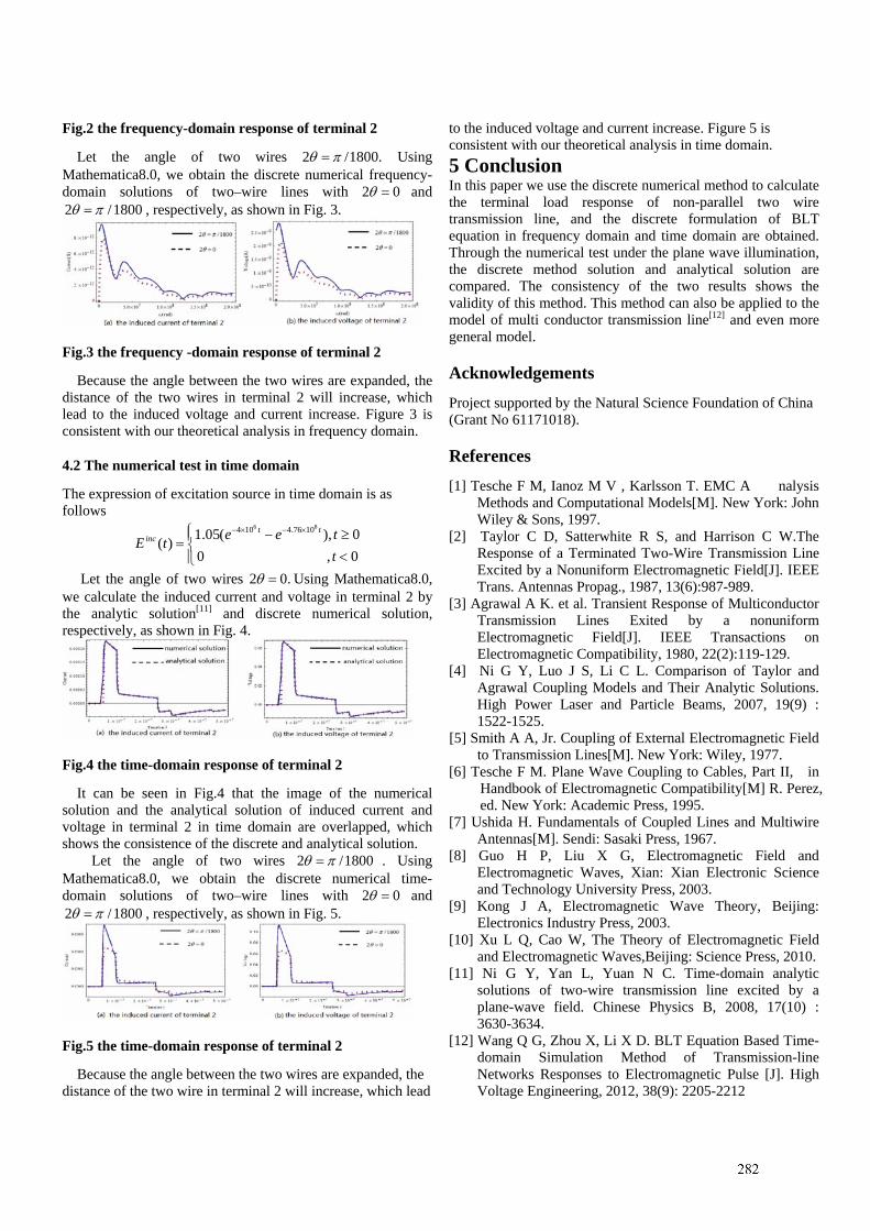
Fig.2 the frequency-domain response of terminal 2
Let the angle of two wires 2 /1800. Using Mathematica8.0, we obtain the discrete numerical frequency-domain solutions of two–wire lines with 2
3
0 and 2 /1800 , respectively, as shown in Fig. 3.
Fig.3 the frequency -domain response of terminal 2
Because the angle between the two wires are expanded, the distance of the two wires in terminal 2 will increase, which lead to the induced voltage and current increase. Figure 3 is consistent with our theoretical analysis in frequency domain.
4.2 The numerical test in time domain
The expression of excitation source in time domain is as follows
6 84 10 4.76 101.05( ), 0( )0 ,
t tinc e e tE t
t
0
Let the angle of two wires 2 0. Using Mathematica8.0, we calculate the induced current and voltage in terminal 2 by the analytic solution[11] and discrete numerical solution, respectively, as shown in Fig. 4.
Fig.4 the time-domain response of terminal 2
It can be seen in Fig.4 that the image of the numerical solution and the analytical solution of induced current and voltage in terminal 2 in time domain are overlapped, which shows the consistence of the discrete and analytical solution.
Let the angle of two wires 2 /1800 . Using Mathematica8.0, we obtain the discrete numerical time-domain solutions of two–wire lines with 2 0 and 2 /1800 , respectively, as shown in Fig. 5.
Fig.5 the time-domain response of terminal 2
Because the angle between the two wires are expanded, the distance of the two wire in terminal 2 will increase, which lead
to the induced voltage and current increase. Figure 5 is consistent with our theoretical analysis in time domain. 5 Conclusion In this paper we use the discrete numerical method to calculate the terminal load response of non-parallel two wire transmission line, and the discrete formulation of BLT equation in frequency domain and time domain are obtained. Through the numerical test under the plane wave illumination, the discrete method solution and analytical solution are compared. The consistency of the two results shows the validity of this method. This method can also be applied to the model of multi conductor transmission line[12] and even more general model.
Acknowledgements Project supported by the Natural Science Foundation of China (Grant No 61171018).
References [1] Tesche F M, Ianoz M V , Karlsson T. EMC A nalysis
Methods and Computational Models[M]. New York: John Wiley & Sons, 1997.
[2] Taylor C D, Satterwhite R S, and Harrison C W.The Response of a Terminated Two-Wire Transmission Line Excited by a Nonuniform Electromagnetic Field[J]. IEEE Trans. Antennas Propag., 1987, 13(6):987-989.
[3] Agrawal A K. et al. Transient Response of Multiconductor Transmission Lines Exited by a nonuniform Electromagnetic Field[J]. IEEE Transactions on Electromagnetic Compatibility, 1980, 22(2):119-129.
[4] Ni G Y, Luo J S, Li C L. Comparison of Taylor and Agrawal Coupling Models and Their Analytic Solutions. High Power Laser and Particle Beams, 2007, 19(9) : 1522-1525.
[5] Smith A A, Jr. Coupling of External Electromagnetic Field to Transmission Lines[M]. New York: Wiley, 1977.
[6] Tesche F M. Plane Wave Coupling to Cables, Part II, in Handbook of Electromagnetic Compatibility[M] R. Perez, ed. New York: Academic Press, 1995.
[7] Ushida H. Fundamentals of Coupled Lines and Multiwire Antennas[M]. Sendi: Sasaki Press, 1967.
[8] Guo H P, Liu X G, Electromagnetic Field and Electromagnetic Waves, Xian: Xian Electronic Science and Technology University Press, 2003.
[9] Kong J A, Electromagnetic Wave Theory, Beijing: Electronics Industry Press, 2003.
[10] Xu L Q, Cao W, The Theory of Electromagnetic Field and Electromagnetic Waves,Beijing: Science Press, 2010.
[11] Ni G Y, Yan L, Yuan N C. Time-domain analytic solutions of two-wire transmission line excited by a plane-wave field. Chinese Physics B, 2008, 17(10) : 3630-3634.
[12] Wang Q G, Zhou X, Li X D. BLT Equation Based Time-domain Simulation Method of Transmission-line Networks Responses to Electromagnetic Pulse [J]. High Voltage Engineering, 2012, 38(9): 2205-2212
The tensor field equation of systematic electromagnetism
and its exterior form representation
Shaorong Chen*, Xiang Li*, Xishun Liu*, Jianshu Luo†, Zhuangzhuang Tian*, Jun Zhang*
*College of Electronic Science and Engineering, †College of Science;
National University of Defense Technology, Changsha 410073, China.
Abstract
When the input of system is ‘four-dimensional electroma-
gnetic potential’, the exterior form of tensor field equation
of electromagnetic system can be obtained by
manipulating the existing theory. The expansion sets of
the equation in space contains 8 sub-equations. Four of
them have already included in the Maxwell equations set.
The fifth is time-varying equation about electric field curl,
the sixth is equation about half of magnetic field 6
symmetry tensor (each set contains three components), the
other two parts are mutual-dual equations of the charge
conservation law that have been known.
Keywords: systematic electromagnetism, exterior form,
Maxwell equations, magnetic monopole, Yang-Mills field.
1 Introduction
Maxwell’s equation are traditionally thought as four indepen-
dent axioms, but, remarkably, here says that this is not so.
They are just explicit expressions in different observation
conditions by the same field equation of electromagnetism
system, and the coefficients and in equations set can
just be determined from metric uniformity.
We always think that when more equations set up, the
solution is certainly more difficult. But in actuality, the cause
of complexity and difficulty is the lack of equations rather
than an excess. Maybe solution will be easy when the
quantity of equations is enough, and makes varieties and
relation complete and systematic. Just like electromagnetism
system can be described simply by one field equation, while
any combinations of component equations set (including
Maxwell equations) are complex.
Making use of some theories about signals and systems
(Deducing process is omitted, in other paper later), the tensor
field equation of systematic electromagnetism is constructed:
0
w w
v w w
w
v w
x A dx dx A dx dx
x A dx dx
(0)
In the formula, , , 0,1,2,3v w and wA is so-called “4-
dimensional electromagnetic potential”; the superscript
“ ' ”and“ '' ” in equation are used for connection[1][2]
a ,
b ,
c located in a different position , ,a b c in
4 space, i.e. 0 1 2 3, , ,A A A A A means the descriptions of
electromagnetic potential in position b with variable
0 1 2 3, , ,x x x x x , and the 1-form base in position b is
dx , etc., the wedge product “ ” in w
wA dx dx
expanded betweena and
b .
2 Tensor field equation’s expansion sets of
electromagnetism system in space.
The deducing process is omitted, and there are 8 equations
in total
2.1 The condition of field equation’s expansion
Condition a: when coordinate connections , , are
different.
Condition b: when is the same with one of and ,
namely there is not third coordinate connection. (Making
means c b )
Condition c: when all 3 coordinate connections are same, or
there is a mutual translation matrix between them.
2.2 Field equation’s expansion sets
2.2.1 Field equation can get 0w v wv
v w
F F F
x x x
after
using “condition a”, so deducing:
a. Tensor Equation:
3 3
2 1 0R R
d d (1)
its vector version is 0B
b. Tensor Equation:
30
2 2 0xRd d (2)
its vector version is 4 3
21
R Rd d j
t
.
c. Tensor Equation:
30
2 2 0xRd d (3)

its vector version is 0B
Et
.
d. Tensor Equation:
40
2 0xd (4)
its vector version is 0Et
.
2.2.2 Field equation can get b v
w ab v wx F A dx after
using “condition b”, so deducing:
e. Tensor Equation:
3
2d
(5)
its vector version is 4
E
.
f. Tensor Equation:
3
1 2
R
Ed j
t
(6)
its vector version is E
J Bt
.
2.2.3 Field equation can get 0wwAdx dx
x
after using
“condition c”, so deducing:
g. Tensor Equation:
1 0d j (7)
its vector version is 01j
t
.
(In formula0
0 v , 0v is 4-dimensional velocity’ s
component in time axis.)
h. Tensor Equation:
1 0d j (8)
its vector version is Jt
.
2.3 Annotation
a. In above Tensor field equations, “*” is “Hodge operator”.
b. Vector expansions of Equation (1) and equation (3) can
only be true when they satisfy Abel condition, the complete
expansions in vector version are:
B iq A B B A
0 0
BE iq A E E A A B BA
t
Namely “magnetism charge density” can naturally exist in
Yang-Mills field when it does not satisfy Abel condition,
while this is a basic condition hypothesis that Yang
ZhenNing and Mills deduced “Yang-Mills action functional”.
3 The relations between the expansions and the
Maxwell equation
Equation (1),(3), (5) and (6) are Maxwell equations set. They
are classified according to the form dimension to further
explain their relationship. The red equations shown in Table 1
are new equations, they are not included in Maxwell’s.
Table 1: The exterior form representation from equation (1) to
equation (8)
3-form equation 2-form equation Annotation
1 3
2 0R
d 3
1 0R
d
0B
Absence of Magnetic
Charges
2
30
2 2 0xRd d
4 3
21
R Rd d j
t
May named:
Magnetic Charges
3
3
0
2
2 0
R
x
d
d
0
BE
t
Faraday’s Law
4
40
2 0xd
0Et
May named:
Absence of Electronic
Charges
5 3
2d
4
E
Gauss’s Law
6
3
1 2
R
Ed j
t
EJ B
t
Ampere-Maxwell law
7
1 0d j
01jt
Law of Charge conservation
8
1 0d j
Jt
Law of Charge conservation
3.1 About the proving experiments
In Table 1, equation (1), (3), (5) and (6) are Maxwell
equations set, they are authentic. Equation (2), (4) and (7) are
new equations that are waiting to test. Equation (7) can be
verified by equation (8), and the meaning of equation (8) is
obvious.
Equation (4) can be verified by equation (3). For example,
when 0Et
, we can get
2
20
B
t
after substituting
equation (4) into equation (3).
2
20
B
t
means that magnetic
field does not exist “acceleration”. It shows that magnetic
field does not exist “acceleration” because of equation (4),
instead of the contrary. So we can verify that magnetic field
has no “acceleration” to learn that equation (4) is true. We
affirm that the none-acceleration phenomenon of magnetic
must exist. The current electromagnetism theorem can’t
deduce this phenomenon.
Because equation (2) just contain any one of the two
equivalence sets of 6 tensor components of magnetic field. Its
proving is more complex. We need to comprehend the
complexity by the form dimensionality which constitute the
equations.
3.2 Form dimensionality and the meaning of
electromagnetism equation
TABLE 1 shows that equation (1), (3) and (5) are both 2-form
equation and 3-form equation, and they are homotopy
equality! According to meaning of homotopy equality,
homotopy invariant establish whether in high-dimension or
low-dimension. It may tell us electromagnetism existential
form and the reason of electromagnetism can propagate
wirelessly (While putting actual thing in 4M , according
to Hopf map and Hopf fiberation, it’s logical to regard
4M as increase or decrease of thing’s dimension).
a. Equation (1) tells us, pure magnetism in 3
space can
reside in space and the inner thing. It appears as 2-form
quantity in the inner thing, while manifest as 1-form
quantity in 4M space.
b. Equation (3) tells us, electromagnetism can propagate
whether in space or the inner thing. It manifest as 2-form
quantity in the inner thing, and manifest as 1-form quantity
in 4M space.
c. Equation (5) tells us, electric density can exist in 3-form
quantity in the inner thing . It exist in 2-form quantity in
4M space, and manifest as 1-form electric field!
Consent to item a, b and c, pure 3-form equation (2), (4)
and 2-form equation (6), (7), (8) could tell us:
d. Equation (7) and equation (8) tell us, 2-form electric in the
inner thing equal to the form value of mapping 1-form
electric current in the same place.
e. Equation (6) tells us, 1-form electric field and 1-form
magnetic field are generated by 2-form electric current in
the inner thing . Consenting to item a, b, c, it shows that
the oncoming electric field and magnetic field can only
exist in space, not the inner thing .
f. Equation (4) tells us, 2-form electric field is a stable
quantity, and 3-form electric field does not exist.
g. Equation (2) tells us, 2-form magnetism are generated by
1-form electric current with mapping twice, and only exist
in the inner thing and cannot propagate in space, which
consent to item a, b and c. And because magnetic
monopole just exist in the inner thing, may it be the basic
reason why magnetic field in space always appear both
south and north poles. It also points out the proving
direction of this project, metering “magnetic monopole”
must be in the inner side, while metering process can be got
from the deducing process of equation (2).
From above analysis, we work out that electric field and
magnetic field existing in space are only 1-form quantity.
When transforming into 2-form quantity, they can only be
stable and existed in the inner thing!
Equation (1), (3), (4), (5)and(8) are pseudo-form equations
(namely their plus-minus relates to coordinate system
direction). Equation (2), (6), (7) are truth-form equations.
Truth-form equation (2), (6) are pure 2-form or 3-form
equations. It means that transformation and mutual influence
proceed with the same form dimension. It is their own
properties and a stable state. The pseudo-form equation
(1),(3),(4),(5) always connect with form quantity of different
dimension.
Only equation (7)’s property is very special. From
deducing process, we can know that equation (7) is in accord
with truth-form’s definition. But, according to pseudo-form
definition, equation (7) is also a pseudo-form equation. So
equation (7) and (8) are on equal footing, they are equivalent
to each other. In fact, they both describe attribute of “Charge
conservation”!
4 Summary and conclusions
From the existing electromagnetism theory, the viewpoint of
deducing Maxwell equations set based on “Law of Charge
conservation” seemed to be wrong (there are more basic
conditions or postulations, it will be discussed in other paper).
Because the result what we got shows that “Law of charge
conservation” and Maxwell equations set are equal, not that
one is more basic and essential than the other one.
The magnetic field is 2-form quantity in 3
space, the
electric field is 2-form quantity in 4M . The Maxwell
equations set are incomplete on the fiber bundle 4M .
Four-dimensional electromagnetic potential w wA j ,
wj
is 1-form electric current
1j
component on fiber bundle
4 3ictM e T ( 3T is the 3-torus ) when pseudo-metric 31: vol (R) is defined in space
3.
One of new equations may concerns about the generation
or excitation equation of “magnetic monopole”, because the
equation relates to the covariant component of 4-dimensional
electric current. The other one of new equations can give a
reason why magnetic field is without “acceleration” (If
“acceleration of magnetic field” or definition like this is
existing, then the new equation asserts that this phenomenon
is existing).
References
[1] Theodore Frankel. “The Geometry of Physics: an
introduction 2nd
ed.”, Cambridge University Press,
(2004).
[2] John E. Gilbert. “Clifford Algebras and Dirac Operator
in Harmonic Analysis”, Cambridge University Press,
(1991).
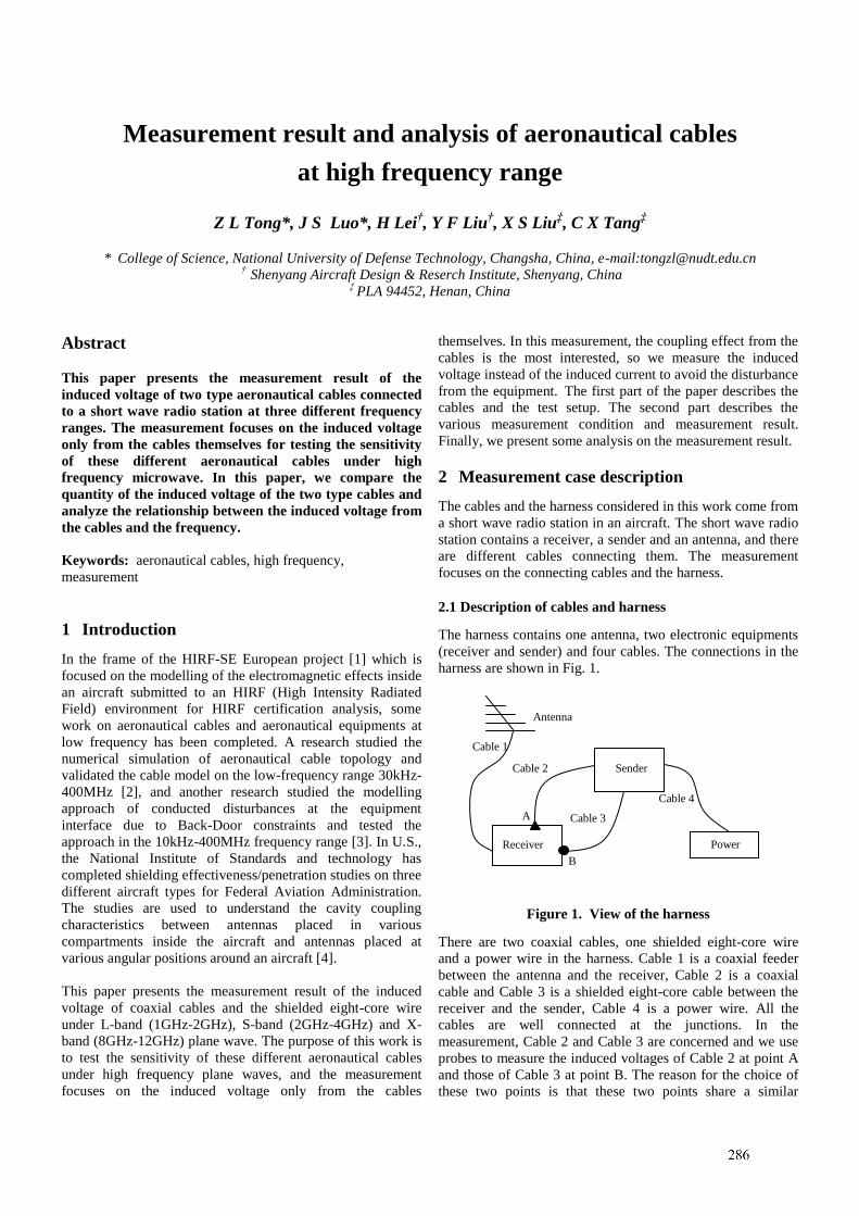
Measurement result and analysis of aeronautical cables
at high frequency range
Z L Tong*, J S Luo*, H Lei†, Y F Liu
†, X S Liu
‡, C X Tang
‡
* College of Science, National University of Defense Technology, Changsha, China, e-mail:[email protected]
†
Shenyang Aircraft Design & Reserch Institute, Shenyang, China ‡ PLA 94452, Henan, China
Abstract
This paper presents the measurement result of the
induced voltage of two type aeronautical cables connected
to a short wave radio station at three different frequency
ranges. The measurement focuses on the induced voltage
only from the cables themselves for testing the sensitivity
of these different aeronautical cables under high
frequency microwave. In this paper, we compare the
quantity of the induced voltage of the two type cables and
analyze the relationship between the induced voltage from
the cables and the frequency.
Keywords: aeronautical cables, high frequency,
measurement
1 Introduction
In the frame of the HIRF-SE European project [1] which is
focused on the modelling of the electromagnetic effects inside
an aircraft submitted to an HIRF (High Intensity Radiated
Field) environment for HIRF certification analysis, some
work on aeronautical cables and aeronautical equipments at
low frequency has been completed. A research studied the
numerical simulation of aeronautical cable topology and
validated the cable model on the low-frequency range 30kHz-
400MHz [2], and another research studied the modelling
approach of conducted disturbances at the equipment
interface due to Back-Door constraints and tested the
approach in the 10kHz-400MHz frequency range [3]. In U.S.,
the National Institute of Standards and technology has
completed shielding effectiveness/penetration studies on three
different aircraft types for Federal Aviation Administration.
The studies are used to understand the cavity coupling
characteristics between antennas placed in various
compartments inside the aircraft and antennas placed at
various angular positions around an aircraft [4].
This paper presents the measurement result of the induced
voltage of coaxial cables and the shielded eight-core wire
under L-band (1GHz-2GHz), S-band (2GHz-4GHz) and X-
band (8GHz-12GHz) plane wave. The purpose of this work is
to test the sensitivity of these different aeronautical cables
under high frequency plane waves, and the measurement
focuses on the induced voltage only from the cables
themselves. In this measurement, the coupling effect from the
cables is the most interested, so we measure the induced
voltage instead of the induced current to avoid the disturbance
from the equipment. The first part of the paper describes the
cables and the test setup. The second part describes the
various measurement condition and measurement result.
Finally, we present some analysis on the measurement result.
2 Measurement case description
The cables and the harness considered in this work come from
a short wave radio station in an aircraft. The short wave radio
station contains a receiver, a sender and an antenna, and there
are different cables connecting them. The measurement
focuses on the connecting cables and the harness.
2.1 Description of cables and harness
The harness contains one antenna, two electronic equipments
(receiver and sender) and four cables. The connections in the
harness are shown in Fig. 1.
Figure 1. View of the harness
There are two coaxial cables, one shielded eight-core wire
and a power wire in the harness. Cable 1 is a coaxial feeder
between the antenna and the receiver, Cable 2 is a coaxial
cable and Cable 3 is a shielded eight-core cable between the
receiver and the sender, Cable 4 is a power wire. All the
cables are well connected at the junctions. In the
measurement, Cable 2 and Cable 3 are concerned and we use
probes to measure the induced voltages of Cable 2 at point A
and those of Cable 3 at point B. The reason for the choice of
these two points is that these two points share a similar
Cable 1
Cable 4
Antenna
Receiver
Sender
Power
Cable 2
Cable 3 A
B
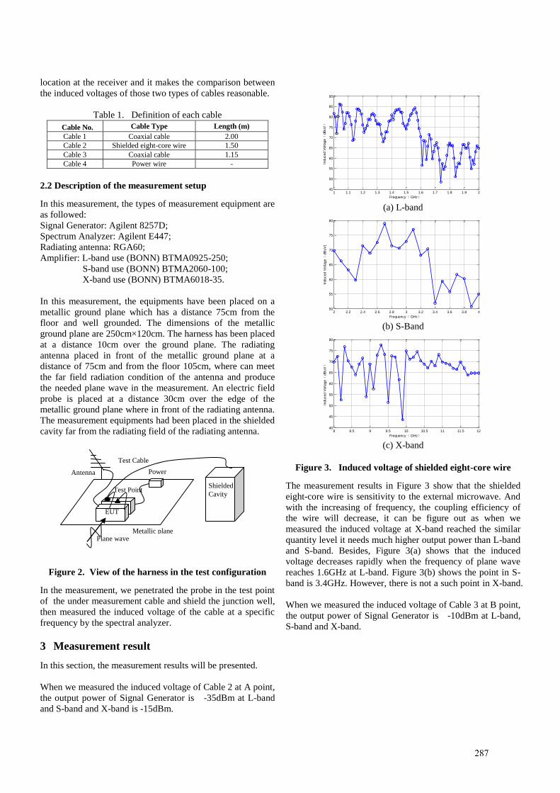
location at the receiver and it makes the comparison between
the induced voltages of those two types of cables reasonable.
Table 1. Definition of each cable
Cable No. Cable Type Length (m)
Cable 1 Coaxial cable 2.00
Cable 2 Shielded eight-core wire 1.50
Cable 3 Coaxial cable 1.15
Cable 4 Power wire -
2.2 Description of the measurement setup
In this measurement, the types of measurement equipment are
as followed:
Signal Generator: Agilent 8257D;
Spectrum Analyzer: Agilent E447;
Radiating antenna: RGA60;
Amplifier: L-band use (BONN) BTMA0925-250;
S-band use (BONN) BTMA2060-100;
X-band use (BONN) BTMA6018-35.
In this measurement, the equipments have been placed on a
metallic ground plane which has a distance 75cm from the
floor and well grounded. The dimensions of the metallic
ground plane are 250cm×120cm. The harness has been placed
at a distance 10cm over the ground plane. The radiating
antenna placed in front of the metallic ground plane at a
distance of 75cm and from the floor 105cm, where can meet
the far field radiation condition of the antenna and produce
the needed plane wave in the measurement. An electric field
probe is placed at a distance 30cm over the edge of the
metallic ground plane where in front of the radiating antenna.
The measurement equipments had been placed in the shielded
cavity far from the radiating field of the radiating antenna.
Figure 2. View of the harness in the test configuration
In the measurement, we penetrated the probe in the test point
of the under measurement cable and shield the junction well,
then measured the induced voltage of the cable at a specific
frequency by the spectral analyzer.
3 Measurement result
In this section, the measurement results will be presented.
When we measured the induced voltage of Cable 2 at A point,
the output power of Signal Generator is -35dBm at L-band
and S-band and X-band is -15dBm.
1 1.1 1.2 1.3 1.4 1.5 1.6 1.7 1.8 1.9 245
50
55
60
65
70
75
80
85
90
Frequency( GHz)
Induced V
oltage(
dB
uV)
(a) L-band
2 2.2 2.4 2.6 2.8 3 3.2 3.4 3.6 3.8 450
55
60
65
70
75
80
Frequency( GHz)
Induced V
oltage(
dB
uV
)
(b) S-Band
8 8.5 9 9.5 10 10.5 11 11.5 1240
45
50
55
60
65
70
75
80
Frequency( GHz)
Induced V
oltage(
dB
uV)
(c) X-band
Figure 3. Induced voltage of shielded eight-core wire
The measurement results in Figure 3 show that the shielded
eight-core wire is sensitivity to the external microwave. And
with the increasing of frequency, the coupling efficiency of
the wire will decrease, it can be figure out as when we
measured the induced voltage at X-band reached the similar
quantity level it needs much higher output power than L-band
and S-band. Besides, Figure 3(a) shows that the induced
voltage decreases rapidly when the frequency of plane wave
reaches 1.6GHz at L-band. Figure 3(b) shows the point in S-
band is 3.4GHz. However, there is not a such point in X-band.
When we measured the induced voltage of Cable 3 at B point,
the output power of Signal Generator is -10dBm at L-band,
S-band and X-band.
Test Cable
Antenna
EUT
Power
Metallic plane
Shielded
Cavity Test Point
Plane wave
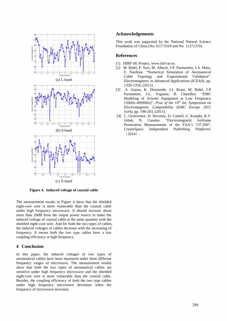
1 1.1 1.2 1.3 1.4 1.5 1.6 1.7 1.8 1.9 260
65
70
75
80
85
90
95
Frequency(GHz)
Induced V
oltage(d
BuV
)
(a) L-band
2 2.2 2.4 2.6 2.8 3 3.2 3.4 3.6 3.8 445
50
55
60
65
70
75
80
85
90
Frequency(GHz)
Induced V
oltage(d
BuV
)
(b) S-band
8 8.5 9 9.5 10 10.5 11 11.5 1240
45
50
55
60
65
70
Frequency(GHz)
Induced V
oltage(d
BuV
)
(c) X-band
Figure 4. Induced voltage of coaxial cable
The measurement results in Figure 4 show that the shielded
eight-core wire is more vulnerable than the coaxial cable
under high frequency microwave. It should increase about
more than 20dB from the output power source to make the
induced voltage of coaxial cable at the same quantity with the
shielded eight-core wire. And for both the two types of cables,
the induced voltages of cables decrease with the increasing of
frequency. It means both the two type cables have a low
coupling efficiency at high frequency.
4 Conclusion
In this paper, the induced voltages of two types of
aeronautical cables have been measured under three different
frequency ranges of microwave. The measurement results
show that both the two types of aeronautical cables are
sensitive under high frequency microwave and the shielded
eight-core wire is more vulnerable than the coaxial cable.
Besides, the coupling efficiency of both the two type cables
under high frequency microwave decreases when the
frequency of microwave increases.
Acknowledgements
This work was supported by the National Natural Science
Foundation of China (No. 61171018 and No. 11271370).
References
[1] HIRF-SE Project, www.hirf-se.eu
[2] M. Ridel, P. Savi, M. Alberti, J-P. Parmantier, I.A. Maio,
F. Nardone. “Numerical Simulation of Aeronautical
Cable Topology and Experimental Validation”.
Electromagnetic in Advanced Applications (ICEAA), pp.
1356-1359, (2011).
[3] A. Guena, K. Diomande, J-L Braut, M. Ridel, J-P
Parmantier, J-L. Vagneur, B. Chatellier. “EMC
Modeling of Avionic Equipment at Low Frequency
[10kHz-400MHz]”, Proc of the 10th
Int. Symposium on
Electromagnetic Compatibility (EMC Europe 2011
York), pp. 198-203, (2011).
[4] C. Grosventor, D. Novotny, D. Camell, G. Koepke, R.T.
Johnk, N. Canales. “Electromagnetic Airframe
Penetration Measurements of the FAA’s 737-200”,
CreateSpace Independent Publishing Platforml,
(2014).
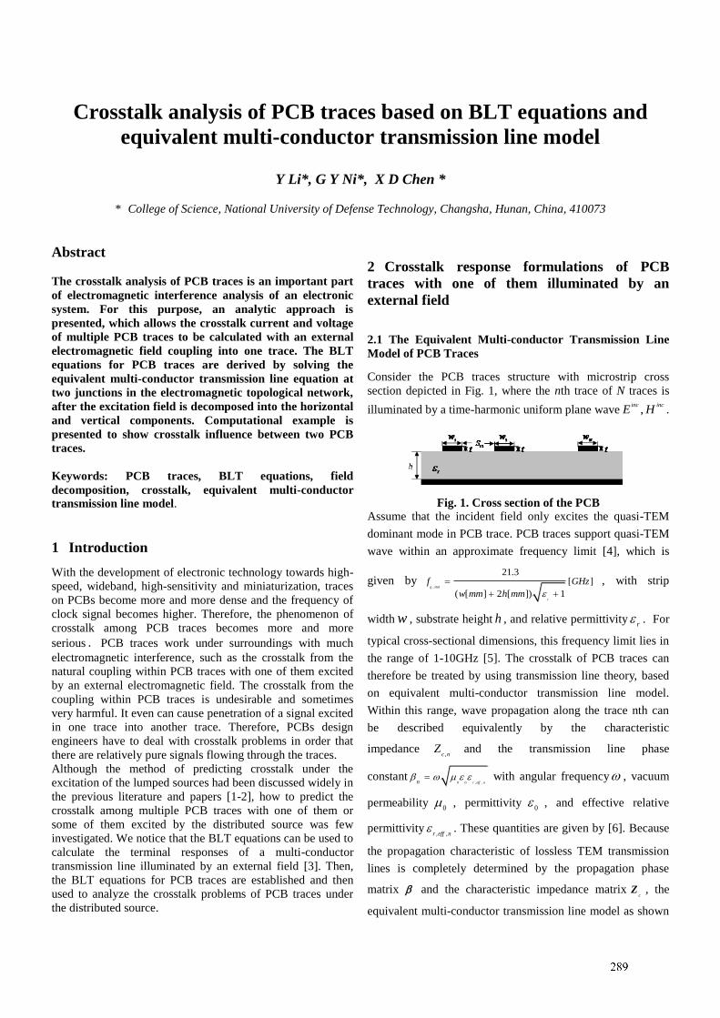
Crosstalk analysis of PCB traces based on BLT equations and
equivalent multi-conductor transmission line model
Y Li*, G Y Ni*, X D Chen *
* College of Science, National University of Defense Technology, Changsha, Hunan, China, 410073
Abstract
The crosstalk analysis of PCB traces is an important part
of electromagnetic interference analysis of an electronic
system. For this purpose, an analytic approach is
presented, which allows the crosstalk current and voltage
of multiple PCB traces to be calculated with an external
electromagnetic field coupling into one trace. The BLT
equations for PCB traces are derived by solving the
equivalent multi-conductor transmission line equation at
two junctions in the electromagnetic topological network,
after the excitation field is decomposed into the horizontal
and vertical components. Computational example is
presented to show crosstalk influence between two PCB
traces.
Keywords: PCB traces, BLT equations, field
decomposition, crosstalk, equivalent multi-conductor
transmission line model.
1 Introduction
With the development of electronic technology towards high-
speed, wideband, high-sensitivity and miniaturization, traces
on PCBs become more and more dense and the frequency of
clock signal becomes higher. Therefore, the phenomenon of
crosstalk among PCB traces becomes more and more
serious.PCB traces work under surroundings with much
electromagnetic interference, such as the crosstalk from the
natural coupling within PCB traces with one of them excited
by an external electromagnetic field. The crosstalk from the
coupling within PCB traces is undesirable and sometimes
very harmful. It even can cause penetration of a signal excited
in one trace into another trace. Therefore, PCBs design
engineers have to deal with crosstalk problems in order that
there are relatively pure signals flowing through the traces.
Although the method of predicting crosstalk under the
excitation of the lumped sources had been discussed widely in
the previous literature and papers [1-2], how to predict the
crosstalk among multiple PCB traces with one of them or
some of them excited by the distributed source was few
investigated. We notice that the BLT equations can be used to
calculate the terminal responses of a multi-conductor
transmission line illuminated by an external field [3]. Then,
the BLT equations for PCB traces are established and then
used to analyze the crosstalk problems of PCB traces under
the distributed source.
2 Crosstalk response formulations of PCB
traces with one of them illuminated by an
external field
2.1 The Equivalent Multi-conductor Transmission Line
Model of PCB Traces
Consider the PCB traces structure with microstrip cross
section depicted in Fig. 1, where the nth trace of N traces is
illuminated by a time-harmonic uniform plane wave ,inc inc
E H .
Fig. 1. Cross section of the PCB
Assume that the incident field only excites the quasi-TEM
dominant mode in PCB trace. PCB traces support quasi-TEM
wave within an approximate frequency limit [4], which is
given by,
21.3[ ]
( [ ] 2 [ ]) 1g stat
r
f GHz
w mm h mm
, with strip
width w , substrate height h , and relative permittivityr
. For
typical cross-sectional dimensions, this frequency limit lies in
the range of 1-10GHz [5]. The crosstalk of PCB traces can
therefore be treated by using transmission line theory, based
on equivalent multi-conductor transmission line model.
Within this range, wave propagation along the trace nth can
be described equivalently by the characteristic
impedance,c n
Z and the transmission line phase
constant0 0 , ,r eff nn
with angular frequency , vacuum
permeability0
, permittivity0 , and effective relative
permittivity, ,r eff n
. These quantities are given by [6]. Because
the propagation characteristic of lossless TEM transmission
lines is completely determined by the propagation phase
matrix and the characteristic impedance matrixc
Z , the
equivalent multi-conductor transmission line model as shown
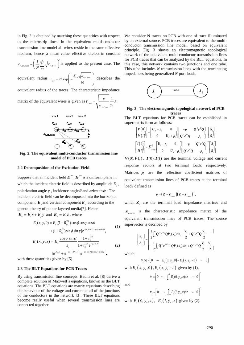
in Fig. 2 is obtained by matching these quantities with respect
to the microstrip lines. In the equivalent multi-conductor
transmission line model all wires reside in the same effective
medium, hence a mean-value effective dielectric constant
2
, , , ,
1
1 N
r eff mean r eff n
nN
is applied to the present case. The
equivalent radius , , ,
,2 exp
60
c n r eff mean
eq n
Zr h
describes the
equivalent radius of the traces. The characteristic impedance
matrix of the equivalent wires is given as,
, ,
1
2c wires
r eff mean
Z F .
Fig. 2. The equivalent multi-conductor transmission line
model of PCB traces
2.2 Decomposition of the Excitation Field
Suppose that an incident field ,inc inc
E H is a uniform plane in
which the incident electric field is described by amplitude0
E ,
polarization angle , incidence angle and azimuth . The
incident electric field can be decomposed into the horizontal
component h
E and vertical componentv
E according to the
general theory of planar layered media[7]. Hence
ˆ ˆh x y
E x E y E and ˆv z
E zE , where
0
0 12
sin ( cos sin )
12
( , , 0) [(1 ) cos cos cos
(1 ) sin sin ] ,
TM
x
jk x yTE
E x y E R
R e
(1)
2
02 2
12
0 2
12
sin ( cos sin )( 2 )
1cos sin( , , )
1
[ ] ,
z
z z
TM
z j k hTM
r
jk x yjk z jk h z
rE x y z E
r e
e e e
(2)
with these quantities given by [5].
2.3 The BLT Equations for PCB Traces
By using transmission line concepts, Baum et al. [8] derive a
complete solution of Maxwell’s equations, known as the BLT
equations. The BLT equations are matrix equations describing
the behaviour of the voltage and current at all of the junctions
of the conductors in the network [3]. These BLT equations
become really useful when several transmission lines are
connected together.
We consider N traces on PCB with one of trace illuminated
by an external source. PCB traces are equivalent to the multi-
conductor transmission line model, based on equivalent
principle. Fig. 3 shows an electromagnetic topological
network of the equivalent multi-conductor transmission lines
for PCB traces that can be analyzed by the BLT equations. In
this case, this network contains two junctions and one tube.
This tube includes N transmission lines with the terminating
impedances being generalized N-port loads.
Fig. 3. The electromagnetic topological network of PCB
traces
The BLT equations for PCB traces can be established in
supermatrix form as follows:
11
1 11
1
2 22
0 0
0
l
N
l
N
e
l e
V U ρ Sρ Q Q
V U ρ SQ Q ρ
11
1 11
1
2 22
,
10 0
0
l
N
l
N
c wires
e
l e
I U ρ Sρ Q Q
I U ρ SQ Q ρZ
(0), ( )lV V , (0), ( )lI I are the terminal voltage and current
response vectors at two terminal loads, respectively.
Matricesi are the reflection coefficient matrices of
equivalent transmission lines of PCB traces at the terminal
load i defined as
1
, ,i i c wires i c wires
ρ Z Z Z Z ,
whichi
Z are the terminal load impedance matrices and
,c wiresZ is the characteristic impedance matrix of the
equivalent transmission lines of PCB traces. The source
supervector is decribed by
1 11 2
01
( )1 12 1 2
0
1( )
2 2 2
1( )
2 2 2
s
s
lx l
s s s
ll x l
s s s
e x dx e
e x dx e
V VQ QV Q Q
S
S V VQ QV Q Q
which
( ) 0 , , 0 , , 0T
s x n x nx E x y E x y h V
with , , 0nxE x y , , ,
x nE x y h given by (1),
1
0
0 (0, , )d 0T
z nhE y z z
V
and
2
0
0 ( , , )d 0T
z nhE l y z z
V
with 0, ,z n
E y z , , ,z n
E l y z given by (2).
Tube 1J
2J
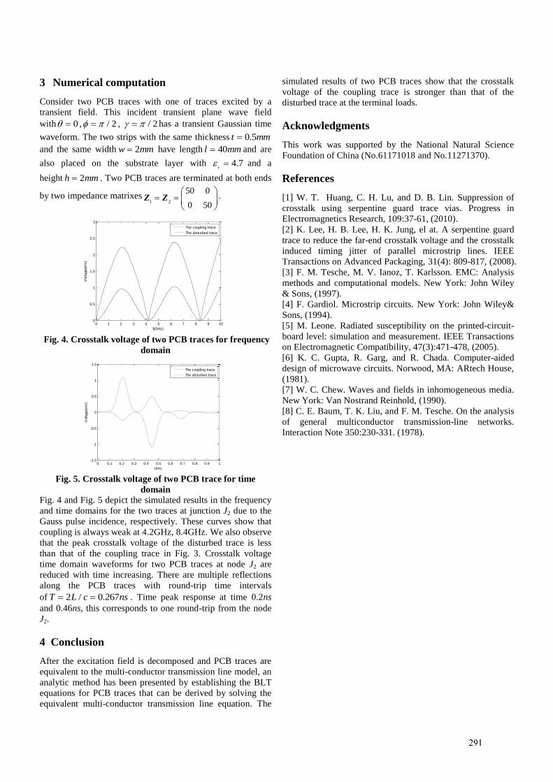
3 Numerical computation
Consider two PCB traces with one of traces excited by a
transient field. This incident transient plane wave field
with 0 , / 2 , / 2 has a transient Gaussian time
waveform. The two strips with the same thickness 0.5t mm
and the same width 2w mm have length 40l mm and are
also placed on the substrate layer with 4.7r and a
height 2h mm . Two PCB traces are terminated at both ends
by two impedance matrixes1 2
50 0
0 50
Z Z .
0 1 2 3 4 5 6 7 8 9 100
0.5
1
1.5
2
2.5
3
f(GHz)
Voltage(m
V)
The coupling trace
The disturbed trace
Fig. 4. Crosstalk voltage of two PCB traces for frequency
domain
0 0.1 0.2 0.3 0.4 0.5 0.6 0.7 0.8 0.9 1-1.5
-1
-0.5
0
0.5
1
1.5
t(ns)
Voltage(m
V)
The coupling trace
The disturbed trace
Fig. 5. Crosstalk voltage of two PCB trace for time
domain
Fig. 4 and Fig. 5 depict the simulated results in the frequency
and time domains for the two traces at junction J2 due to the
Gauss pulse incidence, respectively. These curves show that
coupling is always weak at 4.2GHz, 8.4GHz. We also observe
that the peak crosstalk voltage of the disturbed trace is less
than that of the coupling trace in Fig. 3. Crosstalk voltage
time domain waveforms for two PCB traces at node J2 are
reduced with time increasing. There are multiple reflections
along the PCB traces with round-trip time intervals
of 2 / 0.267T L c ns . Time peak response at time 0.2ns
and 0.46ns, this corresponds to one round-trip from the node
J2.
4 Conclusion
After the excitation field is decomposed and PCB traces are
equivalent to the multi-conductor transmission line model, an
analytic method has been presented by establishing the BLT
equations for PCB traces that can be derived by solving the
equivalent multi-conductor transmission line equation. The
simulated results of two PCB traces show that the crosstalk
voltage of the coupling trace is stronger than that of the
disturbed trace at the terminal loads.
Acknowledgments
This work was supported by the National Natural Science
Foundation of China (No.61171018 and No.11271370).
References
[1] W. T. Huang, C. H. Lu, and D. B. Lin. Suppression of
crosstalk using serpentine guard trace vias. Progress in
Electromagnetics Research, 109:37-61, (2010).
[2] K. Lee, H. B. Lee, H. K. Jung, el at. A serpentine guard
trace to reduce the far-end crosstalk voltage and the crosstalk
induced timing jitter of parallel microstrip lines. IEEE
Transactions on Advanced Packaging, 31(4): 809-817, (2008).
[3] F. M. Tesche, M. V. Ianoz, T. Karlsson. EMC: Analysis
methods and computational models. New York: John Wiley
& Sons, (1997).
[4] F. Gardiol. Microstrip circuits. New York: John Wiley&
Sons, (1994).
[5] M. Leone. Radiated susceptibility on the printed-circuit-
board level: simulation and measurement. IEEE Transactions
on Electromagnetic Compatibility, 47(3):471-478, (2005).
[6] K. C. Gupta, R. Garg, and R. Chada. Computer-aided
design of microwave circuits. Norwood, MA: ARtech House,
(1981).
[7] W. C. Chew. Waves and fields in inhomogeneous media.
New York: Van Nostrand Reinhold, (1990).
[8] C. E. Baum, T. K. Liu, and F. M. Tesche. On the analysis
of general multiconductor transmission-line networks.
Interaction Note 350:230-331. (1978).
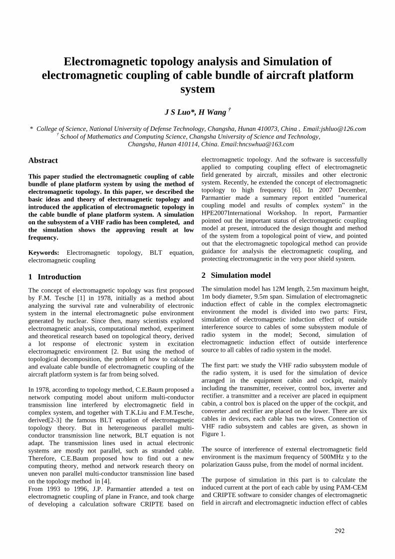
Electromagnetic topology analysis and Simulation of
electromagnetic coupling of cable bundle of aircraft platform
system
J S Luo*, H Wang †
* College of Science, National University of Defense Technology, Changsha, Hunan 410073, China. Email:[email protected]
† School of Mathematics and Computing Science, Changsha University of Science and Technology,
Changsha, Hunan 410114, China. Email:[email protected]
Abstract
This paper studied the electromagnetic coupling of cable
bundle of plane platform system by using the method of
electromagnetic topology. In this paper, we described the
basic ideas and theory of electromagnetic topology and
introduced the application of electromagnetic topology in
the cable bundle of plane platform system. A simulation
on the subsystem of a VHF radio has been completed, and
the simulation shows the approving result at low
frequency.
Keywords: Electromagnetic topology, BLT equation,
electromagnetic coupling
1 Introduction
The concept of electromagnetic topology was first proposed
by F.M. Tesche [1] in 1978, initially as a method about
analyzing the survival rate and vulnerability of electronic
system in the internal electromagnetic pulse environment
generated by nuclear. Since then, many scientists explored
electromagnetic analysis, computational method, experiment
and theoretical research based on topological theory, derived
a lot response of electronic system in excitation
electromagnetic environment [2. But using the method of
topological decomposition, the problem of how to calculate
and evaluate cable bundle of electromagnetic coupling of the
aircraft platform system is far from being solved.
In 1978, according to topology method, C.E.Baum proposed a
network computing model about uniform multi-conductor
transmission line interfered by electromagnetic field in
complex system, and together with T.K.Liu and F.M.Tesche,
derived[2-3] the famous BLT equation of electromagnetic
topology theory. But in heterogeneous parallel multi-
conductor transmission line network, BLT equation is not
adapt. The transmission lines used in actual electronic
systems are mostly not parallel, such as stranded cable.
Therefore, C.E.Baum proposed how to find out a new
computing theory, method and network research theory on
uneven non parallel multi-conductor transmission line based
on the topology method in [4].
From 1993 to 1996, J.P. Parmantier attended a test on
electromagnetic coupling of plane in France, and took charge
of developing a calculation software CRIPTE based on
electromagnetic topology. And the software is successfully
applied to computing coupling effect of electromagnetic
field generated by aircraft, missiles and other electronic
system. Recently, he extended the concept of electromagnetic
topology to high frequency [6]. In 2007 December,
Parmantier made a summary report entitled "numerical
coupling model and results of complex system” in the
HPE2007International Workshop. In report, Parmantier
pointed out the important status of electromagnetic coupling
model at present, introduced the design thought and method
of the system from a topological point of view, and pointed
out that the electromagnetic topological method can provide
guidance for analysis the electromagnetic coupling, and
protecting electromagnetic in the very poor shield system.
2 Simulation model
The simulation model has 12M length, 2.5m maximum height,
1m body diameter, 9.5m span. Simulation of electromagnetic
induction effect of cable in the complex electromagnetic
environment the model is divided into two parts: First,
simulation of electromagnetic induction effect of outside
interference source to cables of some subsystem module of
radio system in the model; Second, simulation of
electromagnetic induction effect of outside interference
source to all cables of radio system in the model.
The first part: we study the VHF radio subsystem module of
the radio system, it is used for the simulation of device
arranged in the equipment cabin and cockpit, mainly
including the transmitter, receiver, control box, inverter and
rectifier. a transmitter and a receiver are placed in equipment
cabin, a control box is placed on the upper of the cockpit, and
converter .and rectifier are placed on the lower. There are six
cables in devices, each cable has two wires. Connection of
VHF radio subsystem and cables are given, as shown in
Figure 1.
The source of interference of external electromagnetic field
environment is the maximum frequency of 500MHz y to the
polarization Gauss pulse, from the model of normal incident.
The purpose of simulation in this part is to calculate the
induced current at the port of each cable by using PAM-CEM
and CRIPTE software to consider changes of electromagnetic
field in aircraft and electromagnetic induction effect of cables
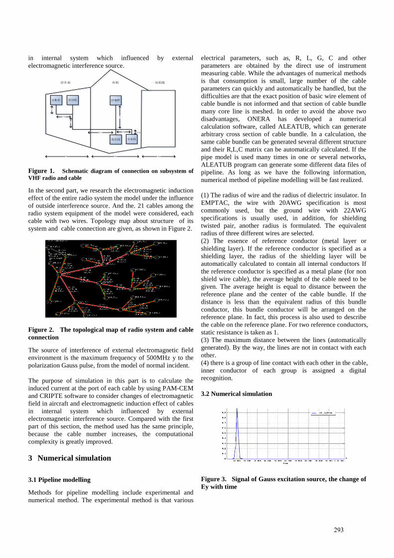
in internal system which influenced by external
electromagnetic interference source.
Figure 1. Schematic diagram of connection on subsystem of
VHF radio and cable
In the second part, we research the electromagnetic induction
effect of the entire radio system the model under the influence
of outside interference source. And the. 21 cables among the
radio system equipment of the model were considered, each
cable with two wires. Topology map about structure of its
system and cable connection are given, as shown in Figure 2.
Figure 2. The topological map of radio system and cable
connection
The source of interference of external electromagnetic field
environment is the maximum frequency of 500MHz y to the
polarization Gauss pulse, from the model of normal incident.
The purpose of simulation in this part is to calculate the
induced current at the port of each cable by using PAM-CEM
and CRIPTE software to consider changes of electromagnetic
field in aircraft and electromagnetic induction effect of cables
in internal system which influenced by external
electromagnetic interference source. Compared with the first
part of this section, the method used has the same principle,
because the cable number increases, the computational
complexity is greatly improved.
3 Numerical simulation
3.1 Pipeline modelling
Methods for pipeline modelling include experimental and
numerical method. The experimental method is that various
electrical parameters, such as, R, L, G, C and other
parameters are obtained by the direct use of instrument
measuring cable. While the advantages of numerical methods
is that consumption is small, large number of the cable
parameters can quickly and automatically be handled, but the
difficulties are that the exact position of basic wire element of
cable bundle is not informed and that section of cable bundle
many core line is meshed. In order to avoid the above two
disadvantages, ONERA has developed a numerical
calculation software, called ALEATUB, which can generate
arbitrary cross section of cable bundle. In a calculation, the
same cable bundle can be generated several different structure
and their R,L,C matrix can be automatically calculated. If the
pipe model is used many times in one or several networks,
ALEATUB program can generate some different data files of
pipeline. As long as we have the following information,
numerical method of pipeline modelling will be fast realized.
(1) The radius of wire and the radius of dielectric insulator. In
EMPTAC, the wire with 20AWG specification is most
commonly used, but the ground wire with 22AWG
specifications is usually used, in addition, for shielding
twisted pair, another radius is formulated. The equivalent
radius of three different wires are selected.
(2) The essence of reference conductor (metal layer or
shielding layer). If the reference conductor is specified as a
shielding layer, the radius of the shielding layer will be
automatically calculated to contain all internal conductors If
the reference conductor is specified as a metal plane (for non
shield wire cable), the average height of the cable need to be
given. The average height is equal to distance between the
reference plane and the center of the cable bundle. If the
distance is less than the equivalent radius of this bundle
conductor, this bundle conductor will be arranged on the
reference plane. In fact, this process is also used to describe
the cable on the reference plane. For two reference conductors,
static resistance is taken as 1.
(3) The maximum distance between the lines (automatically
generated). By the way, the lines are not in contact with each
other.
(4) there is a group of line contact with each other in the cable,
inner conductor of each group is assigned a digital
recognition.
3.2 Numerical simulation
Figure 3. Signal of Gauss excitation source, the change of
Ey with time
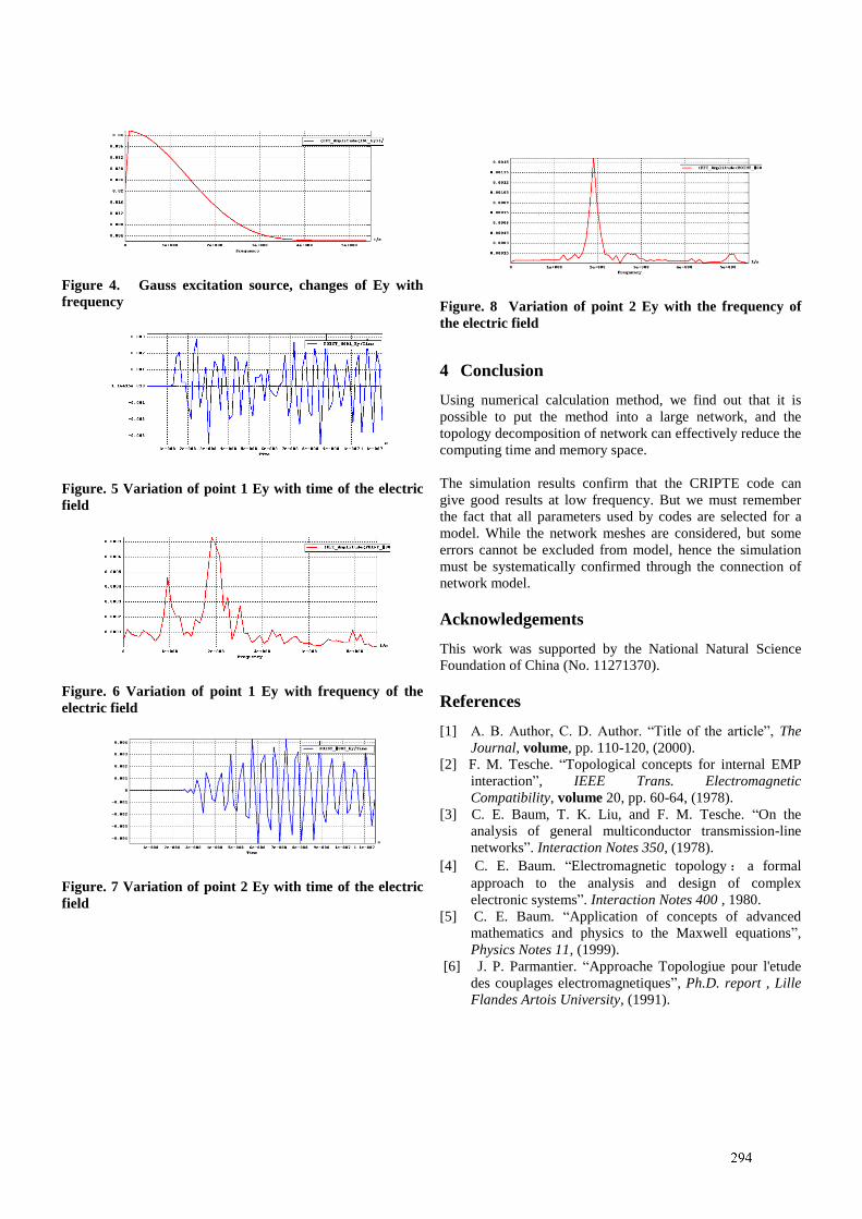
Figure 4. Gauss excitation source, changes of Ey with
frequency
Figure. 5 Variation of point 1 Ey with time of the electric
field
Figure. 6 Variation of point 1 Ey with frequency of the
electric field
Figure. 7 Variation of point 2 Ey with time of the electric
field
Figure. 8 Variation of point 2 Ey with the frequency of
the electric field
4 Conclusion
Using numerical calculation method, we find out that it is
possible to put the method into a large network, and the
topology decomposition of network can effectively reduce the
computing time and memory space.
The simulation results confirm that the CRIPTE code can
give good results at low frequency. But we must remember
the fact that all parameters used by codes are selected for a
model. While the network meshes are considered, but some
errors cannot be excluded from model, hence the simulation
must be systematically confirmed through the connection of
network model.
Acknowledgements
This work was supported by the National Natural Science
Foundation of China (No. 11271370).
References
[1] A. B. Author, C. D. Author. “Title of the article”, The
Journal, volume, pp. 110-120, (2000).
[2] F. M. Tesche. “Topological concepts for internal EMP
interaction”, IEEE Trans. Electromagnetic
Compatibility, volume 20, pp. 60-64, (1978).
[3] C. E. Baum, T. K. Liu, and F. M. Tesche. “On the
analysis of general multiconductor transmission-line
networks”. Interaction Notes 350, (1978).
[4] C. E. Baum. “Electromagnetic topology : a formal
approach to the analysis and design of complex
electronic systems”. Interaction Notes 400 , 1980.
[5] C. E. Baum. “Application of concepts of advanced
mathematics and physics to the Maxwell equations”,
Physics Notes 11, (1999).
[6] J. P. Parmantier. “Approache Topologiue pour l'etude
des couplages electromagnetiques”, Ph.D. report , Lille
Flandes Artois University, (1991).
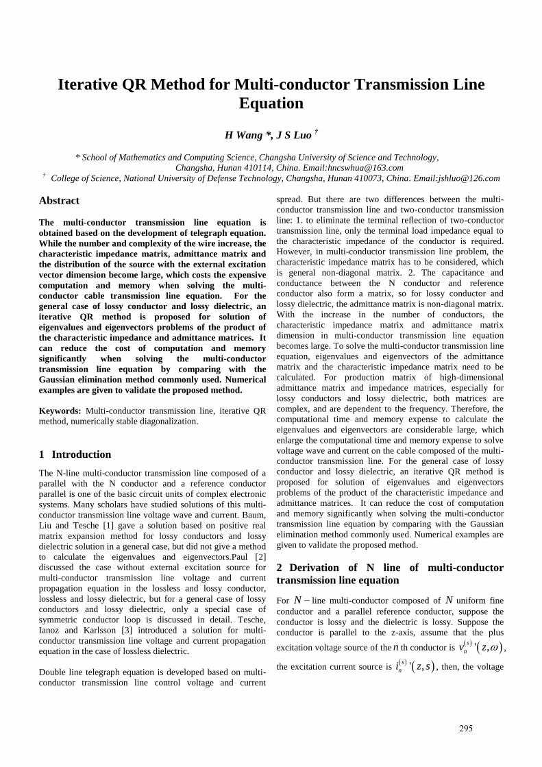
Iterative QR Method for Multi-conductor Transmission Line
Equation
H Wang *, J S Luo †
* School of Mathematics and Computing Science, Changsha University of Science and Technology,
Changsha, Hunan 410114, China. Email:[email protected] † College of Science, National University of Defense Technology, Changsha, Hunan 410073, China. Email:[email protected]
Abstract
The multi-conductor transmission line equation is
obtained based on the development of telegraph equation.
While the number and complexity of the wire increase, the
characteristic impedance matrix, admittance matrix and
the distribution of the source with the external excitation
vector dimension become large, which costs the expensive
computation and memory when solving the multi-
conductor cable transmission line equation. For the
general case of lossy conductor and lossy dielectric, an
iterative QR method is proposed for solution of
eigenvalues and eigenvectors problems of the product of
the characteristic impedance and admittance matrices. It
can reduce the cost of computation and memory
significantly when solving the multi-conductor
transmission line equation by comparing with the
Gaussian elimination method commonly used. Numerical
examples are given to validate the proposed method.
Keywords: Multi-conductor transmission line, iterative QR
method, numerically stable diagonalization.
1 Introduction
The N-line multi-conductor transmission line composed of a
parallel with the N conductor and a reference conductor
parallel is one of the basic circuit units of complex electronic
systems. Many scholars have studied solutions of this multi-
conductor transmission line voltage wave and current. Baum,
Liu and Tesche [1] gave a solution based on positive real
matrix expansion method for lossy conductors and lossy
dielectric solution in a general case, but did not give a method
to calculate the eigenvalues and eigenvectors.Paul [2]
discussed the case without external excitation source for
multi-conductor transmission line voltage and current
propagation equation in the lossless and lossy conductor,
lossless and lossy dielectric, but for a general case of lossy
conductors and lossy dielectric, only a special case of
symmetric conductor loop is discussed in detail. Tesche,
Ianoz and Karlsson [3] introduced a solution for multi-
conductor transmission line voltage and current propagation
equation in the case of lossless dielectric.
Double line telegraph equation is developed based on multi-
conductor transmission line control voltage and current
spread. But there are two differences between the multi-
conductor transmission line and two-conductor transmission
line: 1. to eliminate the terminal reflection of two-conductor
transmission line, only the terminal load impedance equal to
the characteristic impedance of the conductor is required.
However, in multi-conductor transmission line problem, the
characteristic impedance matrix has to be considered, which
is general non-diagonal matrix. 2. The capacitance and
conductance between the N conductor and reference
conductor also form a matrix, so for lossy conductor and
lossy dielectric, the admittance matrix is non-diagonal matrix.
With the increase in the number of conductors, the
characteristic impedance matrix and admittance matrix
dimension in multi-conductor transmission line equation
becomes large. To solve the multi-conductor transmission line
equation, eigenvalues and eigenvectors of the admittance
matrix and the characteristic impedance matrix need to be
calculated. For production matrix of high-dimensional
admittance matrix and impedance matrices, especially for
lossy conductors and lossy dielectric, both matrices are
complex, and are dependent to the frequency. Therefore, the
computational time and memory expense to calculate the
eigenvalues and eigenvectors are considerable large, which
enlarge the computational time and memory expense to solve
voltage wave and current on the cable composed of the multi-
conductor transmission line. For the general case of lossy
conductor and lossy dielectric, an iterative QR method is
proposed for solution of eigenvalues and eigenvectors
problems of the product of the characteristic impedance and
admittance matrices. It can reduce the cost of computation
and memory significantly when solving the multi-conductor
transmission line equation by comparing with the Gaussian
elimination method commonly used. Numerical examples are
given to validate the proposed method.
2 Derivation of N line of multi-conductor
transmission line equation
For N line multi-conductor composed of N uniform fine
conductor and a parallel reference conductor, suppose the
conductor is lossy and the dielectric is lossy. Suppose the
conductor is parallel to the z-axis, assume that the plus
excitation voltage source of the n th conductor is ' ,s
nv z ,
the excitation current source is ' ,s
ni z s , then, the voltage

and current propagation equations controlled by the N line
multi-conductor transmission line are
1
d, , ' , , 1,2, ,
d
Ns
n nm m n
m
i z y v z I z n Nz
(1)
1
d, , ' , , 1,2,3, ,
d
Ns
n nm m n
m
v z z i z v z n Nz
(2)
Where, 'nmy is the unit length admittance of the th
uniform conductor corresponding to the th uniform
conductor with frequency , which is independent to z.
nmz is the corresponding eigen -impedance.
By use of matrix form, the N line multi-conductor
transmission line equations (1), (2) can be expressed as:
d
, , ' ,d
sI z Y V z I z
z (3)
d
, , ' ,d
sV z Z I z V z
z (4)
Equations (3), (4) are the general form of N line multi-
conductor transmission line equations with excitation source,
where the excitation source can be divided into the antenna
mode and transmission line mode. Due to the antenna mode
in the transmission terminal is zero, only the terminal
response of transmission line is considered, and the antenna
mode is often ignored. Here, sinusoidal excitation source is
considered.
To solve equations (3), (4), the coupling between '( , )I z
and '( , )V z is supposed to be removed. Therefore,
equation (3) is left multiplied by non-singular
matrix ( ) ( )nm N NT t
on both sides, and is added
by equation (4) on both sides, so
( )
,, ,
d, , ' ,
d
s
T qT q q T qV z B V z V zz
(5)
Where, 1q corresponds to the wave along a positive
direction of the z axis, 1q corresponds to the wave
along a negative direction of the z axis. , , , 1T qV z q is
called the combination voltage wave. From equation system
(5), , , , 1T qV z q can be solved, then, from the
following equation, ,qI z and ,qV z can be solved.
1
,, , ,q q T q qI z T V z V z (6)
, ,q q qV z Z I z (7)
where
1
q qZ B Z (8)
[1] used eigenvector expansion of positive real matrix to
discuss the diagonalization problem and the solution of
equation system (5), but did not give method to calculate the
eigenvalue and eigenvector of ' 'Z Y . And for
lossless dielectric and lossless conductor, and lossy conductor
and lossless dielectric, the diagonalization transform matrix of
' 'Z Y is independent of the frequency , so using
eigenvector expansion method increase the computational
cost and memory expense.
To reduce the computational and memory expense, we will
discuss two cases, lossy conductor and lossless dielectric case,
and lossy conductor and lossy dielectric case, to sovle the
diagonalization of ' 'Z Y and equation system (5)
using iterative QR method.
3 Iterative QR algorithm for matrix
Denote ( )A Z Y of degree N, by Alston
Householder theorem [5], there exist an unitary matrix
( )Q of degree N and an upper triangular matrices ( )R
such that
A Q R (9)
Householder transform algorithm is as follows: denote 1A to
be the first column of A
11 11 1 2
1
1
2
1
2
N
a a A
y A e
y
v y
Q I vv
where 1
22
1 121
N
i
i
A a
, and so forth, we have
1 2, 1, , NQ Q Q , denote 1 1NQ Q Q , then
*( )Q A R (10)
( )R is an upper triangular matrix. However, the diagonal
elements of ( )R are not necessarily the eigenvalues of
( )A .
Francis proposed an iteration algorithm to solve the
eigenvalues of ( )A using QR decomposition of ( )A [5].
Without loss of generality, suppose ( )R has non-negative
diagonal elements. The algorithm to calculate the eigenvalues
of ( )A is as follows:
A w A w
For 1k to M do
( ) ( ) ( )k k kA Q R , ( )kQ is U matrix, ( )kR
is upper triangular matrix with nonnegative diagonal
elements.

1( ) ( ) ( )k k kA R Q
end do
To reduce computational time and speed up the convergence
rate, Shifted QR algorithm [5] can be employed to calculate
the eigenvalues of ( )A .
(1) Use Alston Householder transform 1 2, 1, , NQ Q Q to
get Hessenberg matrix ij N NH h
, where
0, 1ijh i j . Let 1A H .
(2) Take the diagonal elements on lower right of 1( )A as
kz , and perform QR decomposition on ( )k k NA z I , we
have
( ) ( )k k N k kA z I Q R
Denote the last row of ( )kR to be 0,0, ,0,T
NY ,
then is an eigenvalue of ( )A .
(3) Assign ( ) ( )k k k NQ R z I to 1( )kA . The
computational procedure is as follows:
1A H
For 1k to M do
For kA , diagonal element of lower right of kA
is chosen as kz
k k N k kA z I Q R
1k k k k NA Q R z I
end do
4 Examples and analysis
Model I: The cables are composed by nine parallel conductors.
The center conductor is the reference conductor, and the
conductor radius is 0.3cm. The distance between the
conductor and the reference conductor is 1cm. The
conductors are filled with dielectric material. The lossy
conductor and lossy medium are selected, as shown in Fig. 2.
Figure 3 cables composed by nine parallel conductors
The selected parameters:
r = 1;% the distance from the wire to the reference
conductor
a = pi / 4;% the conductor angle difference
d = 0.3;% the conductor radius
l = 10;% the wire length
a1 = 1.5e7;% the conductor conductivity (where the
selected conductor material is copper)
a2 = 1;% the conductivity of dielectric materials
b1 = 4 * pi * 1e-7;% the conductor permeability
c0 = 8.85 * 1e-12;% the vacuum dielectric constant
c1 = 2.3 * c0;% the dielectric permittivity (PE)
w = 1e8;% the frequency
A diagonal matrix is obtained as follows: 13 . 128 6.31 7i, . 4 .2165i, . 4 .2165i, . 2 . 895i,
. 1 . 693i, . 1 . 693i, . 3i, . 3i
10 diag 0 0 0 0 000 0 0 000 0 0 000 0 0
0 000 0 0 0 000 0 0 0 00 0 00
Acknowledgements
This work was supported by the National Natural Science
Foundation of China (no. 11271370)
References
[1] C. E. Baum, T. K. Liu, F. M. Tesche. "On the Analysis of
General Multiconductor Transmission Line Networks",
Kirtland AFB, Albuquerqut, NM, Ineraction Note 350,
(1978).
[2] D. R. Paul. "Analysis of Multicomductor Transmission
Lines", New York: Wiley, (1994).
[3] F. M. Tesche, M. V. Ianoz, T. Karlsson. "EMC Analysis
Methods and Computational Models", New York: Wiley,
(1997).
[4] D. R. Kincaid, E. W. Cheney. "Numerical Analysis:
Mathematics of Scientific Computing", American
Mathematical Society, (2001).
[5] F. M. Tesche, J. Keen, C. M. Butler. "Example of the Use
of the BLT Equation for EM Field Propagation and
Coupling Calculations", Kirtland AFB. Albuquerque,
NM, Interaction Note 591, (2004).
Experimental Research on Rod-shaped Triggered Gas Switch
Chen Jingliang, Lei Wanglong, Yao Xueling †
State Key Laboratory of Electrical Insulation and Power Equipment, Xi’an Jiaotong University, Xi’an 710049, China †[email protected]
Abstract
The rod-shaped triggered gas switch was designed in the
paper, with the two main electrodes are placed in parallel
and the trigger electrode is located in the orthogonal plane
to the main electrodes and mounted between two main
electrodes. The experimental circuit is setup and the
trigger characteristics are researched. The experimental
results show that when the gap distance is 6.65 mm, the
self-breakdown voltage is 10.2 kV. When trigger pulse
voltage is 14.6 kV, the operating voltage scope of the
switch is from 48.0% to 85.7%, and the discharging delay
time d changes from 21.6 µs to 2.66 µs and the delay jitter
j changes from 4.25 µs to 0.49 µs accordingly. At the
same time, the pulse arc running and electrode erosion are
also observed. It is found that the electrode erosion
tracking is mainly decided by the amplitude of the pulse
current, and with the increase of the pulse current, the
erosion spots change from round to ellipse and the erosion
track gets longer along the inner electrode orientation,
and the erosion spots cover the whole electrode surface.
Keywords: Rod-shaped gas switch, Self-breakdown voltage,
Operating range, Arc running and arc erosion track
1 Introduction
Discharging switches were the most important components in
pulsed power systems including plasma physics, controlled
nuclear fusion, nuclear explosion, electromagnetic pulse,
electromagnetic launch and beam of particles. The
characteristics of the discharging switch had direct influence
on the pulse current waveform. The common discharging
switches included ignitron, gas switch, semiconductor switch
and magnetic rotating arc switch[1-4]
.
Triggered gas switches (TGS) were widely used in pulsed
power system because of its simple structure and excellent
characteristics such as high voltage and high current
endurance. The triggering characteristics were the important
parameters of the TGS. When the high current passed through,
the TGS will cause electrode erosion[5, 6]
. Electrode erosion
was the important factor that impacts the static and dynamic
characteristics, which changed the self-breakdown voltage,
the jitter and the performance parameters by changing electric
field strength near the etch pit [7–9]
.
In this paper, the TGS with rod-shaped electrodes was
designed and the experimental setups of the trigger device
were introduced. The trigger characteristics were researched
and the cathode erosion spots and anode erosion spots were
observed when the impulse current with different transfer
charge passed through TGS.
2 The Structure and Experimental Circuit of
TGS
2.1 The structure of TGS
The spatial layout of the TGS was shown in Fig.1. Cathode
Tri
gger
Ele
ctro
d
e
Connection
RodConnection
Rod
Anode
(a)
Anode
Electrode
Cathode
Electrode
Trigger
Electrode
d1
d2
(b)
Fig.1 The structure of the triggered gas switch (a) Electrode Front View/Top View, (b) Electrode Top View/Front View/
The TGS consisted of an anode, a cathode and a trigger
electrode in the middle. Two main electrodes were all made
from copper with a diameter of 40mm and placed in parallel.
The trigger electrode, which was also made from copper, has
a diameter of 10mm and is placed in the orthogonal plane to
the plane of the two main electrodes. The distance between
the end of the trigger electrode and the central line of the two
main electrodes was d1, and the closest distance between the
trigger electrode and the cathode was d2.
2.2 The experimental circuit of TGS
The experimental circuit of the TGS was showed in Fig.2.
Fig.2 Experimental circuit
where S1 was the control switches, T1 was the voltage
regulator, T2 was the transformer, D was rectification diode,
R0 was charging resistance, C was storage capacitor, resistor
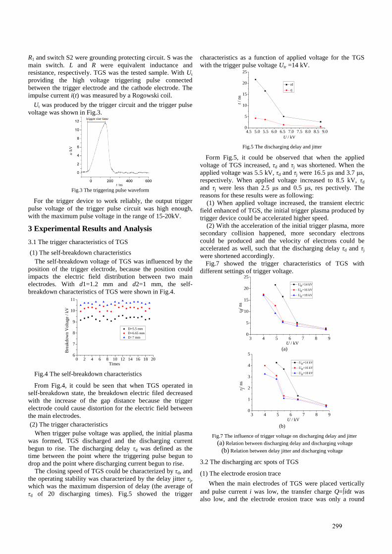
R1 and switch S2 were grounding protecting circuit. S was the
main switch. L and R were equivalent inductance and
resistance, respectively. TGS was the tested sample. With Ut
providing the high voltage triggering pulse connected
between the trigger electrode and the cathode electrode. The
impulse current i(t) was measured by a Rogowski coil.
Ut was produced by the trigger circuit and the trigger pulse
voltage was shown in Fig.3.
Fig.3 The triggering pulse waveform
For the trigger device to work reliably, the output trigger
pulse voltage of the trigger pulse circuit was high enough,
with the maximum pulse voltage in the range of 15-20kV.
3 Experimental Results and Analysis
3.1 The trigger characteristics of TGS
(1) The self-breakdown characteristics
The self-breakdown voltage of TGS was influenced by the
position of the trigger electrode, because the position could
impacts the electric field distribution between two main
electrodes. With d1=1.2 mm and d2=1 mm, the self-
breakdown characteristics of TGS were shown in Fig.4.
0 2 4 6 8 10 12 14 16 18 206
7
8
9
10
11
D=5.5 mm
D=6.65 mm
D=7 mm
Bre
akd
ow
n V
olt
age
/ k
V
Times
Fig.4 The self-breakdown characteristics
From Fig.4, it could be seen that when TGS operated in
self-breakdown state, the breakdown electric filed decreased
with the increase of the gap distance because the trigger
electrode could cause distortion for the electric field between
the main electrodes.
(2) The trigger characteristics
When trigger pulse voltage was applied, the initial plasma
was formed, TGS discharged and the discharging current
begun to rise. The discharging delay τd was defined as the
time between the point where the triggering pulse begun to
drop and the point where discharging current begun to rise.
The closing speed of TGS could be characterized by τd, and
the operating stability was characterized by the delay jitter τj,
which was the maximum dispersion of delay (the average of
τd of 20 discharging times). Fig.5 showed the trigger
characteristics as a function of applied voltage for the TGS
with the trigger pulse voltage Utr =14 kV.
4.5 5.0 5.5 6.0 6.5 7.0 7.5 8.0 8.5 9.00
5
10
15
20
25
U / kV
t /
ns
td
tj
Fig.5 The discharging delay and jitter
Form Fig.5, it could be observed that when the applied
voltage of TGS increased, τd and τj was shortened. When the
applied voltage was 5.5 kV, τd and τj were 16.5 μs and 3.7 μs,
respectively. When applied voltage increased to 8.5 kV, τd
and τj were less than 2.5 μs and 0.5 μs, res pectively. The
reasons for these results were as following:
(1) When applied voltage increased, the transient electric
field enhanced of TGS, the initial trigger plasma produced by
trigger device could be accelerated higher speed.
(2) With the acceleration of the initial trigger plasma, more
secondary collision happened, more secondary electrons
could be produced and the velocity of electrons could be
accelerated as well, such that the discharging delay τd and τj
were shortened accordingly.
Fig.7 showed the trigger characteristics of TGS with
different settings of trigger voltage.
3 4 5 6 7 8 90
5
10
15
20
25
Utr=14 kV
Utr=16 kV
Utr=18 kV
U / kV
d/
ns
(a)
3 4 5 6 7 8 90
1
2
3
4
5
U / kV
j/
ns
Utr=14 kV
Utr=16 kV
Utr=18 kV
(b)
Fig.7 The influence of trigger voltage on discharging delay and jitter
(a) Relation between discharging delay and discharging voltage
(b) Relation between delay jitter and discharging voltage
3.2 The discharging arc spots of TGS
(1) The electrode erosion trace
When the main electrodes of TGS were placed vertically
and pulse current i was low, the transfer charge Q=idt was
also low, and the electrode erosion trace was only a round
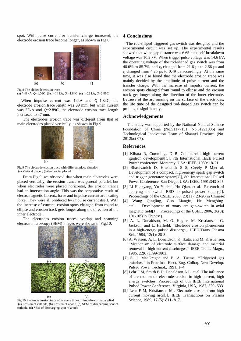
spot. With pulse current or transfer charge increased, the
electrode erosion trace become longer, as shown in Fig.8.
(a) (b) (c)
Fig.8 The electrode erosion trace
(a) i =8 kA, Q=1.06C (b) i =14 kA, Q =1.84C, (c) i =22 kA, Q=2.89C
When impulse current was 14kA and Q=1.84C, the
electrode erosion trace length was 39 mm, but when current
was 22kA and Q=2.89C, the electrode erosion trace length
increased to 47 mm.
The electrodes erosion trace was different from that of
main electrodes placed vertically, as shown in Fig.9.
(a) (b)
Fig.9 The electrode erosion trace with different place situation (a) Vertical placed, (b) horizontal placed
From Fig.9, we observed that when main electrodes were
placed vertically, the erosion trance was general parallel, but
when electrodes were placed horizontal, the erosion trance
had an intersection angle. This was the corporative result of
electromagnetic Lorentz force and impulse current arc heating
force. They were all produced by impulse current itself. With
the increase of current, erosion spots changed from round to
ellipse and erosion track gets longer along the direction of the
inner electrode.
The electrodes erosion traces overlap and scanning
electron microscopy (SEM) images were shown in Fig.10.
(a) (b)
(c) (d)
Fig.10 Electrode erosion trace after many times of impulse current applied
(a) Erosion of cathode, (b) Erosion of anode, (c) SEM of discharging spot of cathode, (d) SEM of discharging spot of anode
4 Conclusions
The rod-shaped triggered gas switch was designed and the
experimental circuit was set up. The experimental results
showed that when gap distance was 6.65 mm, self-breakdown
voltage was 10.2 kV. When trigger pulse voltage was 14.6 kV,
the operating voltage of the rod-shaped gas switch was from
48.0% to 85.7%, and τd changed from 21.6 µs to 2.66 µs and
τj changed from 4.25 µs to 0.49 µs accordingly. At the same
time, it was also found that the electrode erosion trace was
mainly decided by the amplitude of pulse current and the
transfer charge. With the increase of impulse current, the
erosion spots changed from round to ellipse and the erosion
track get longer along the direction of the inner electrode.
Because of the arc running on the surface of the electrodes,
the life time of the designed rod-shaped gas switch can be
prolonged significantly.
Acknowledgements
The study was supported by the National Natural Science
Foundation of China (No.51177131, No.51221005) and
Technological Innovation Team of Shaanxi Province (No.
2012kct-07).
References
[1] Kihara R, Cummings D B. Commercial high current
ignitron development[C], 7th International IEEE Pulsed
Power conference. Monterey, USA: IEEE, 1989: 18-21
[2] Bhasavanich D, Hitchcock S S, Creely P M,et al.
Development of a compact, high-energy spark gap switch
and trigger generator system[C], 8th International Pulsed
Power Conference. San Diego, USA: IEEE, 1991:343-345
[3] Li Huanyang, Yu Yuehui, Hu Qian, et al.Research of
applying the switch RSD to pulsed power supply[J].
Proceedings of the CSEE, 2003, 23(11): 23-28(in Chinese)
[4] Wang Qingling, Guo Liangfu, He Mengbing.
etal. Development of rotary arc gap-switch in axial
magnetic field[J].Proceedings of the CSEE, 2006, 26(3):
101-105(in Chinese).
[5] A. L. Donaldson, M. O. Hagler, M. Kristiansen, G.
Jackson, and L. Hatfield, “Electrode erosion phenomena
in a high-energy pulsed discharge,” IEEE Trans. Plasma
Sci., 1984, 12(1): 28-3.
[6] A. Watson, A. L. Donaldson, K. Ikuta, and M. Kristiansen,
“Mechanism of electrode surface damage and material
removal in high-current discharges,” IEEE Trans. Magn.,
1986, 22(6):1799-1803.
[7] S. J. MacGregor and F. A. Tuema, “Triggered gas
switches,” in Proc.Inst. Elect. Eng. Colloq. New Develop.
Pulsed Power Technol., 1991, 1–4.
[8] Lehr F M, Smith B D, Donaldson A L, et al. The influence
of arc motion on electrode erosion in high current, high
energy switches. Proceedings of 6th IEEE International
Pulsed Power Conference, Virginia, USA, 1987, 529- 533
[9] Lehr F M, Kristiansen M.. Electrode erosion from high
current moving arcs[J]. IEEE Transactions on Plasma
Science, 1989, 17 (5): 811- 817.
1
An automatic fragmenting and triggering method for capacitive
pulse forming units of the electromagnetic railgun
Xukun Liu, Xinjie Yu, Xiucheng Liu and Zanji Wang*
* State Key Lab of Power System, Department of Electrical Engineering, Tsinghua University, Beijing 10084, China
Abstract
This paper proposes an automatic fragmenting
and triggering calculation method for capacitive
pulse forming units (PFUs). As to each segment
of PFUs, the triggering time is determined by
the time that the rail current decreases to the
minimum limit, the number of PFUs is then
determined by the maximum possible values of
the peak rail current after triggering this
segment. Based on a representative example, the
validity of this method is proven through
comparisons with Simplorer® simulation
software.
Keywords: automatic fragmenting and triggering, PFU.
1 Introduction
Electromagnetic launching technology has been the a research
focus in the area of military equipment. With the advantages
of low control difficulty and high reliability, capacitive
pulsed-power supply (CPPS) has become the most prevailing
form of energy storage in the electromagnetic railgun system.
In actual railgun systems, however, the peak value of the rail
current must be limited below the maximum allowable value
in order to prevent the rail from ablation. The demand for
higher armature velocity leads to the application of the
multiple-triggered system. Previous studies are based mainly
on experiments or simulations, both of which consume a large
amount of time and effort. Calculation of the automatic
fragmenting and triggering strategy is less involved and
concerned.
However, this calculation is of great significance. On one
hand, it could free us from unwieldy system simulation and
inefficient parameter tuning. On the other hand, it could
provide solutions to further studies on multiple-triggered
systems, such as the optimization of system parameters. This
paper fills the blank in the field of multiple-triggered system
analysis, by proposing an automatic fragmenting and
triggering method.
2 Model of the Electromagnetic Railgun System
The analytical model of CPPS-based electromagnetic railgun
system is mainly composed of two primary parts, namely
CPPS with initial energy storage and the railgun load [1].
The basic module of CPPS is the pulse forming unit (PFU).
The topology of PFU is demonstrated in Fig 1.C is energy
storage capacitor, L is pulse forming inductor, R is the sum of
the inductor resistance and the lead resistance. A cluster of
PFUs, which are in parallel and share the same triggering
time, compose a segment. A cluster of segments, which are in
parallel but hold different triggering time, compose a set of
CPPS. The configuration of CPPS is demonstrated in Fig 2.
Figure 1. Topology of PFU.
Figure 2. Configuration of CPPS.
Intensive Studies on the railgun model have been conducted
[2]. However, in this analytical model, it is more appropriate
to simplify the railgun load into a model of constant
resistance. The aim of this simplification is to gain wider
applicability with an acceptable tolerance of error.
3 Method of Automatic Fragmenting and
Triggering
This method is a combination of theoretical analysis and
numerical computation. Logically, it can be divided into three
parts: calculation of PFU state, calculation of load waveforms
and calculation of strategy. It is worth mentioning that these
parts are closely intertwined and are a whole entity in essence.
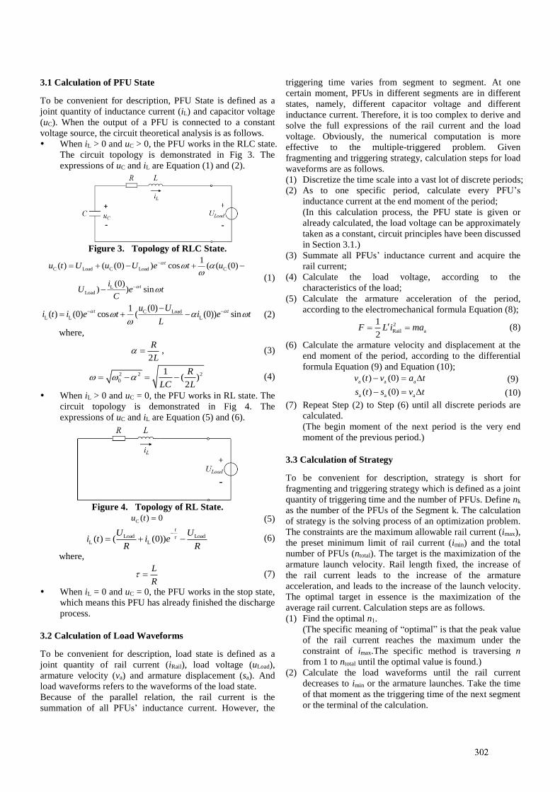
2
3.1 Calculation of PFU State
To be convenient for description, PFU State is defined as a
joint quantity of inductance current (iL) and capacitor voltage
(uC). When the output of a PFU is connected to a constant
voltage source, the circuit theoretical analysis is as follows.
When iL > 0 and uC > 0, the PFU works in the RLC state.
The circuit topology is demonstrated in Fig 3. The
expressions of uC and iL are Equation (1) and (2).
Figure 3. Topology of RLC State.
C Load C Load C
L
Load
1( ) ( (0) ) cos ( ( (0)
(0)) ) sin
t
t
u t U u U e t u
iU e t
C
(1)
C Load
L L L
(0)1( ) (0) cos ( (0)) sint tu U
i t i e t i e tL
(2)
where,
2
R
L , (3)
2 2 2
0
1( )2
R
LC L (4)
When iL > 0 and uC = 0, the PFU works in RL state. The
circuit topology is demonstrated in Fig 4. The
expressions of uC and iL are Equation (5) and (6).
Figure 4. Topology of RL State.
C ( ) 0u t (5)
Load Load
L L( ) ( (0))t
U Ui t i e
R R
(6)
where,
L
R (7)
When iL = 0 and uC = 0, the PFU works in the stop state,
which means this PFU has already finished the discharge
process.
3.2 Calculation of Load Waveforms
To be convenient for description, load state is defined as a
joint quantity of rail current (iRail), load voltage (uLoad),
armature velocity (va) and armature displacement (sa). And
load waveforms refers to the waveforms of the load state.
Because of the parallel relation, the rail current is the
summation of all PFUs’ inductance current. However, the
triggering time varies from segment to segment. At one
certain moment, PFUs in different segments are in different
states, namely, different capacitor voltage and different
inductance current. Therefore, it is too complex to derive and
solve the full expressions of the rail current and the load
voltage. Obviously, the numerical computation is more
effective to the multiple-triggered problem. Given
fragmenting and triggering strategy, calculation steps for load
waveforms are as follows.
(1) Discretize the time scale into a vast lot of discrete periods;
(2) As to one specific period, calculate every PFU’s
inductance current at the end moment of the period;
(In this calculation process, the PFU state is given or
already calculated, the load voltage can be approximately
taken as a constant, circuit principles have been discussed
in Section 3.1.)
(3) Summate all PFUs’ inductance current and acquire the
rail current;
(4) Calculate the load voltage, according to the
characteristics of the load;
(5) Calculate the armature acceleration of the period,
according to the electromechanical formula Equation (8);
2
Rail a
1
2F L i ma (8)
(6) Calculate the armature velocity and displacement at the
end moment of the period, according to the differential
formula Equation (9) and Equation (10);
a a a( ) (0)v t v a t (9)
a a a( ) (0)s t s v t (10)
(7) Repeat Step (2) to Step (6) until all discrete periods are
calculated.
(The begin moment of the next period is the very end
moment of the previous period.)
3.3 Calculation of Strategy
To be convenient for description, strategy is short for
fragmenting and triggering strategy which is defined as a joint
quantity of triggering time and the number of PFUs. Define nk
as the number of the PFUs of the Segment k. The calculation
of strategy is the solving process of an optimization problem.
The constraints are the maximum allowable rail current (imax),
the preset minimum limit of rail current (imin) and the total
number of PFUs (ntotal). The target is the maximization of the
armature launch velocity. Rail length fixed, the increase of
the rail current leads to the increase of the armature
acceleration, and leads to the increase of the launch velocity.
The optimal target in essence is the maximization of the
average rail current. Calculation steps are as follows.
(1) Find the optimal n1.
(The specific meaning of “optimal” is that the peak value
of the rail current reaches the maximum under the
constraint of imax.The specific method is traversing n
from 1 to ntotal until the optimal value is found.)
(2) Calculate the load waveforms until the rail current
decreases to imin or the armature launches. Take the time
of that moment as the triggering time of the next segment
or the terminal of the calculation.
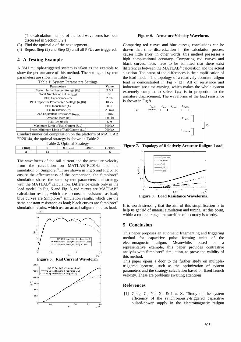
3
(The calculation method of the load waveforms has been
discussed in Section 3.2.)
(3) Find the optimal n of the next segment.
(4) Repeat Step (2) and Step (3) until all PFUs are triggered.
4 A Testing Example
A 3MJ multiple-triggered system is taken as the example to
show the performance of this method. The settings of system
parameters are shown in Table 1.
Table 1: System Parameters Settings Parameters Value
System Initial Energy Storage (E0) 3 MJ
Total Number of PFUs (ntotal) 30
PFU Capacitance (C) 2 mF
PFU Capacitor Pre-charged Voltage (uC(0)) 10 kV
PFU Inductance (L) 50 μH
PFU Resistance (R) 20 mΩ
Load Equivalent Resistance (RLoad) 1 mΩ
Armature Mass (m) 0.05 kg
Rail Length (s) 6 m
Maximum Limit of Rail Current (imax) 800 kA
Preset Minimum Limit of Rail Current (imin) 700 kA
Conduct numerical computation on the platform of MATLAB ®R2014a, the optimal strategy is shown in Table 2.
Table 2: Optimal Strategy t (ms) 0 0.61253 1.19071 1.71005
n 14 5 5 6
The waveforms of the rail current and the armature velocity
from the calculation on MATLAB®R2014a and the
simulation on Simplorer®11 are shown in Fig 5 and Fig 6. To
ensure the effectiveness of the comparison, the Simplorer®
simulation shares the same system parameters and strategy
with the MATLAB® calculation. Difference exists only in the
load model. In Fig. 5 and Fig. 6, red curves are MATLAB®
calculation results, which use a constant resistance as load;
blue curves are Simplorer® simulation results, which use the
same constant resistance as load; black curves are Simplorer®
simulation results, which use an actual railgun model as load.
Figure 5. Rail Current Waveform.
Figure 6. Armature Velocity Waveform.
Comparing red curves and blue curves, conclusions can be
drawn that time discretization in the calculation process
causes little error, in other words, this method possesses a
high computational accuracy. Comparing red curves and
black curves, facts have to be admitted that there exist
differences between the MATLAB® calculation and the actual
situation. The cause of the differences is the simplification of
the load model. The topology of a relatively accurate railgun
load is demonstrated in Fig 7 [2]. All of resistance and
inductance are time-varying, which makes the whole system
extremely complex to solve. LRail is in proportion to the
armature displacement. The waveforms of the load resistance
is shown in Fig 8.
Figure 7. Topology of Relatively Accurate Railgun Load.
Figure 8. Load Resistance Waveforms.
It is worth stressing that the aim of this simplification is to
help us get rid of manual simulation and tuning. At this point,
within a rational range, the sacrifice of accuracy is worthy.
5 Conclusion
This paper proposes an automatic fragmenting and triggering
method for capacitive pulse forming units of the
electromagnetic railgun. Meanwhile, based on a
representative example, this paper provides contrastive
analysis with Simplorer® simulation, to prove the validity of
this method.
This paper opens a door to the further study on multiple-
triggered systems, such as the optimization of system
parameters and the strategy calculation based on fixed launch
velocity. These are problems awaiting attentions.
References
[1] Gong, C., Yu, X., & Liu, X. “Study on the system
efficiency of the synchronously-triggered capacitive
pulsed-power supply in the electromagnetic railgun
4
system”, Electromagnetic Launch Technology (EML),
17th International Symposium, pp. 1-6, (2014).
[2] Yu X, Fan Z. “Simulation and two-objective
optimization of the electromagnetic-railgun model
considering VSEC resistance and contact resistance.”
Plasma Science, IEEE Transactions on, 39(1),pp. 405-
410, (2011).
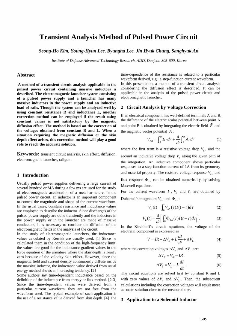
1
Transient Analysis Method of Pulsed Power Circuit
Seong-Ho Kim, Young-Hyun Lee, Byungha Lee, Jin Hyuk Chung, Sanghyuk An
Institute of Defense Advanced Technology Research, ADD, Daejeon 305-600, Korea
Abstract
A method of a transient circuit analysis applicable in the
pulsed power circuit containing massive inductors is
described. The electromagnetic launcher system consisting
of a pulsed power supply and a launcher has many
massive inductors in the power supply and an inductive
load of rails. Though the system can be analyzed well by
using constant resistance R and inductance L, another
correction method can be employed if the result using
constant values is not satisfactory by the magnetic
diffusion effect. The method is based on the correction of
the voltages obtained from constant R and L. When a
situation requiring the magnetic diffusion or the skin
depth effect arises, this correction method will play a good
role to reach the accurate solution.
Keywords: transient circuit analysis, skin effect, diffusion,
electromagnetic launcher, railgun.
1 Introduction
Usually pulsed power supplies delivering a large current of
several hundred or MA during a few ms are used for the study
of electromagnetic acceleration of a metal armature. In the
pulsed power circuit, an inductor is an important component
to control the magnitude and shape of the current waveform.
In the usual cases, constant resistance and inductance values
are employed to describe the inductor. Since discharges of the
pulsed power supply are done transiently and the inductors in
the power supply or in the launcher are made of massive
conductors, it is necessary to consider the diffusion of the
electromagnetic fields in the analysis of the circuit.
In the study of electromagnetic launchers, the inductance
values calculated by Kerrisk are usually used. [1] Since he
calculated them in the condition of the high-frequency limit,
the values are good for the inductance gradient values in the
force equation of the armature where the skin depth is nearly
zero because of the velocity skin effect. However, since the
magnetic field and current density continuously diffuse inside
the massive inductor, the inductance value derived from usual
energy method shows an increasing tendency. [2]
Some authors say time-dependent inductance based on the
definition of the inductance from energy or flux method. [2-3]
Since the time-dependent values were derived from a
particular current waveform, they are not free from the
waveform used. The typical example of such application is
the use of a resistance value derived from skin depth. [4] The
time-dependence of the resistance is related to a particular
waveform derived, e.g. a step-function current waveform.
In this presentation, a method of a transient circuit analysis
considering the diffusion effect is described. It can be
applicable in the analysis of the pulsed power circuit and
electromagnetic launcher.
2 Circuit Analysis by Voltage Correction
If an electrical component has well-defined terminals A and B,
the difference of the electric scalar potential between point A
and point B is obtained by integrating the electric field E and
the magnetic vector potential A :
B B
ABA A
dV E dr A dr
dt (1)
where the first term is a resistive voltage drop R
V , and the
second an inductive voltage drop L
V along the given path of
the integration. An inductive component shows particular
responses to a step-function current of 1A from its geometry
and material property. The resistive voltage response RS
V and
flux response LS
can be obtained numerically by solving
Maxwell equations.
For the current waveform I , R
V and L
V are obtained by
Duhamel’s integration RS
V and LS
:
0
( ) ( ) ( )t
R RSV t V I t d (2)
0
( ) ( ) ( )t
L LS
dV t I t d
dt
. (3)
In the Kirchhoff’s circuit equations, the voltage of the
electrical component is expressed as
R L
dIV IR V L V
dt . (4)
where the correction voltages R
V and L
V are:
R RV V IR , (5)
L L
dIV V L
dt . (6)
The circuit equations are solved first by constant R and L
with zero values of R
V and L
V . Then, the subsequent
calculations including the correction voltages will result more
accurate solution close to the measured one.
3 Application to a Solenoid Inductor
2
A solenoid is a typical example of inductor made by winding
coils on the tube of a cylindrical geometry. In the case using a
filamentary coil, the inductance is well defined for all
frequency regions. However, when the cross-sectional area of
the coil is large for a low resistance, the inductance varies
with the frequency. It is mainly due to the magnetic diffusion
effect.
Fig. 1 shows the distribution of the current density of a
solenoid coil used in a high current circuit. The width of the
winding coil is 4 mm, and the height of the coil is 10 mm.
The inner diameter of the solenoid is 80 mm. It consists of 2
layers of 8 turns. The gap between each ring is 1 mm.
Fig. 1. Current density distribution of a solenoid at 1 kHz
current waveform
The inductance of the solenoid at 1 kHz was calculated to be
about 38.1 H with a resistance of 11.36 m. Since the skin
depth is 2.1 mm, the current distribution shown in Fig. 1 is
not uniform. Those impedance values are also can be used to
describe a circuit of transient current pulse of sub-millisecond
duration.
To see the details, the current density distribution at 0.4 ms
after a step-function current waveform was calculated, and
shown in Fig. 2. The upper coils show very non-uniform
current distributions.
Fig. 2. Current density distribution of a solenoid at 0.4 ms
after a step-function current waveform.
By using the finite element method the resistive voltage
response RS
V and flux response LS
along the center line of
each coil were calculated.
Fig. 3. Resistive voltage response RS
V for the step-function
current of 1 A.
Fig. 3 shows the voltage response obtained by integrating the
electric filed along the center line of the coils. Since initially
the electric field cannot penetrate inside the conductor, the
voltage starts with a zero value. The later voltage response
value 3.54 mV corresponds to the DC resistance value
3.54 m of the solenoid.
Fig. 4. Magnetic flux response LS
for the step-function
current of 1 A.
Fig. 4. Shows increasing inductance with the magnetic
diffusion. The initial flux response value 36 Wb corresponds
to the inductance value at high frequency limit 36 H of the
solenoid. It also shows a zero penetration depth of magnetic
field at starting time. After about 1 ms, the solenoid shows
DC behaviour. The inductance at DC reaches 39.7 H, which
is 10 % larger than the initial value.
From the temporal behaviour of the response curves shown in
Fig. 3 and Fig. 4, the solenoid circuit producing sub-
millisecond pulse are more accurately described by the
3
voltage correction method introduced in Section 2. More
detailed example of a calculation compared with the
measurement is shown in [5]. The method of transient circuit
analysis considering the magnetic diffusion effect was
employed successfully in the analysis of the RLC circuit
module containing a massive inductor [5], and the rail pair of
an electromagnetic launcher system. [6]
4 Summary
To explain the voltage correction method, the calculation of
the responses for the step-function current in a solenoid
inductor was done as an example. In this paper, the increasing
duration of the response curves is lower than 1 millisecond.
However, if the geometry of the inductor becomes more
massive, the temporal duration of the increasing response
becomes longer, and may takes several milliseconds. When
the duration of the transient current is comparable to the
increasing duration of the response curves, the voltage
correction method describes the circuit behavior more
accurately than the method using constant impedances.
References
[1] J. F. Kerrisk, “Current Distribution and Inductance
Calculations for Rail-gun Conductors,” LA-9092-MS,
Technical Report, Los Alamos National Lab., NM, USA,
(1981).
[2] J. F. Kerrisk, “Current Diffusion in Rail-gun Conductors,”
LA-9401-MS, Technical Report, Los Alamos National
Lab., NM, USA, (1982).
[3] K. Moyama and H. Fukumoto, “Evaluation of Railgun
Inductance by 2-D Transient FE Analysis,” IEEE Trans.
on Magn., 33(1), pp. 260 – 265, (1997).
[4] A. N. Smith, R. L. Ellis, and J. S. Bernardes. “Thermal
Management and Resistive Rail Heating of a Large-
scale Naval Electromagnetic Launcher,” IEEE Trans. on
Magn., 41(1), pp. 235-240, (2005).
[5] Seong-Ho Kim et al., “Transient Analysis of Circuit
Containing Massive Conductors,” IEEE Trans. on
Plasma Sci., 42(3), pp. 853 – 858, (2014).
[6] Seong-Ho Kim et al., “Modeling and Circuit Analysis of
an Electromagnetic Launcher System for a Transient
Current,” IEEE Trans. on Plasma Sci., published online,
(2015).
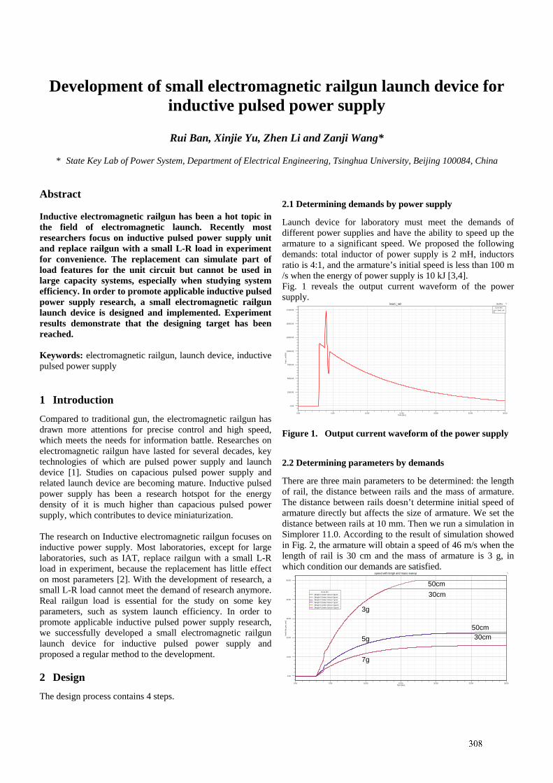
1
Development of small electromagnetic railgun launch device for inductive pulsed power supply
Rui Ban, Xinjie Yu, Zhen Li and Zanji Wang*
* State Key Lab of Power System, Department of Electrical Engineering, Tsinghua University, Beijing 100084, China
Abstract Inductive electromagnetic railgun has been a hot topic in the field of electromagnetic launch. Recently most researchers focus on inductive pulsed power supply unit and replace railgun with a small L-R load in experiment for convenience. The replacement can simulate part of load features for the unit circuit but cannot be used in large capacity systems, especially when studying system efficiency. In order to promote applicable inductive pulsed power supply research, a small electromagnetic railgun launch device is designed and implemented. Experiment results demonstrate that the designing target has been reached. Keywords: electromagnetic railgun, launch device, inductive pulsed power supply
1 Introduction Compared to traditional gun, the electromagnetic railgun has drawn more attentions for precise control and high speed, which meets the needs for information battle. Researches on electromagnetic railgun have lasted for several decades, key technologies of which are pulsed power supply and launch device [1]. Studies on capacious pulsed power supply and related launch device are becoming mature. Inductive pulsed power supply has been a research hotspot for the energy density of it is much higher than capacious pulsed power supply, which contributes to device miniaturization. The research on Inductive electromagnetic railgun focuses on inductive power supply. Most laboratories, except for large laboratories, such as IAT, replace railgun with a small L-R load in experiment, because the replacement has little effect on most parameters [2]. With the development of research, a small L-R load cannot meet the demand of research anymore. Real railgun load is essential for the study on some key parameters, such as system launch efficiency. In order to promote applicable inductive pulsed power supply research, we successfully developed a small electromagnetic railgun launch device for inductive pulsed power supply and proposed a regular method to the development.
2 Design The design process contains 4 steps.
2.1 Determining demands by power supply
Launch device for laboratory must meet the demands of different power supplies and have the ability to speed up the armature to a significant speed. We proposed the following demands: total inductor of power supply is 2 mH, inductors ratio is 4:1, and the armature’s initial speed is less than 100 m /s when the energy of power supply is 10 kJ [3,4]. Fig. 1 reveals the output current waveform of the power supply.
0.00 5.00 10.00 15.00 20.00 25.00 30.00Time [ms]
-0.00
2500.00
5000.00
7500.00
10000.00
12500.00
15000.00
17500.00
load
.i_ra
il [A
]
BanRuiload.i_railCurve Info
load.i_railTR
Figure 1. Output current waveform of the power supply
2.2 Determining parameters by demands
There are three main parameters to be determined: the length of rail, the distance between rails and the mass of armature. The distance between rails doesn’t determine initial speed of armature directly but affects the size of armature. We set the distance between rails at 10 mm. Then we run a simulation in Simplorer 11.0. According to the result of simulation showed in Fig. 2, the armature will obtain a speed of 46 m/s when the length of rail is 30 cm and the mass of armature is 3 g, in which condition our demands are satisfied.
0.00 5.00 10.00 15.00 20.00 25.00 30.00Time [ms]
0.00
10.00
20.00
30.00
40.00
50.00
load
.v [m
_per
_sec
]
speed with lengh and mass sweep
3g
5g
7g
50cm30cm
50cm30cmCurve Info
$length='0.3meter' $mass='3gram'$length='0.5meter' $mass='3gram'$length='0.3meter' $mass='7gram'$length='0.5meter' $mass='7gram'$length='0.3meter' $mass='10gram'$length='0.5meter' $mass='10gram'

2
Figure 2. Simulation result
2.3 Designing model by parameters
There is no need to consider erosion and machining but the distance between rails must be exactly 10 cm and the whole device need firm fixation. As a result, we designed the model in Fig. 3. Armature is the core of railgun launch device. The most common design is C-shaped armature, whose tail is slightly wider than the distance between rails [5]. The width should be properly designed to keep a balance between contact resistance and friction. We designed 4 kinds of armatures with different size and each made of pure aluminium and aluminium alloy.
Figure 3. The design of railgun model
2.4 Designing speed measurement device
We use optical fiber sensors to measure initial velocity. The armature passes through two sensors successively. The sensor will form a pulse signal when covered. Armature speed can be calculated by measuring the time between two rising edge.
3 Implementation By putting rails, armature, fixed gear and sensors together, a small electromagnetic railgun launch device for inductive pulsed power supply was assembled. Fig. 4 and Fig.5 show the real railgun device and different kinds of armatures.
Figure 4. 4 kinds of armatures
Figure 5. 4 kinds of armatures
4 Conclusion and Discussion A small electromagnetic railgun was developed in order to meet the demands of inductive pulsed power supply. The distance between rails is 10 cm and the length of rail is 30 cm. The mass of armature is about 2.7 g and the expected speed is 46m/s. According to system test results, the designing targets have been reached. Based on our existing design, more railguns with different length will be developed and experiments with armatures of different materials, sizes and shapes will be finished. Also, a more accurate method to measure speed should be studied as armature speed rising up.
References [1] Fair, H.D., “Guest Editorial The Past, Present, and
Future of Electromagnetic Launch Technology and the IEEE International EML Symposia”, IEEE Transactions on Plasma Science, vol.41, no.5, pp.1024-1027, (2013)
[2] J. D. Powell and K. A. Jamison, “Analysis of an inverse railgun power source,” IEEE Transactions on Magnetics, vol. 22, no. 6, pp. 1669–1674, (1986).
[3] A. Sitzman, D. Surls, and J. Mallick, “Design, Construction, and Testing of an Inductive Pulsed-Power Supply for a Small Railgun”, IEEE Transactions on Magnetics, vol. 43, no. 1, pp. 270–274, (2007).
[4] Z. Li, X. Yu, S. Ma, and Y. Sha, “Structural Parameter Optimization of Inductors Used in Inductive Pulse Power Supply,” in Proc.17th IEEE Int. Symp. Electromagnetic Launch (EML), San Diego, CA, Jul. 7-11, 2014.
[5] L. Rip, S. Satapathy, and K.-T. Hsieh, “Effect of geometry change on the current density distribution in C-shaped armatures,” IEEE Transactions on Magnetics, vol. 39, no. 1, pp. 72–75, (2003).
1
Performance Evaluation of an Experimental Railgun
Young-Hyun Lee, Seong-Ho Kim, Byungha Lee, Jin Hyuk Chung, Sanghyuk An
Institute of Defense Advanced Technology Research, ADD, Daejeon 305-600, Korea
Abstract
An experimental railgun was fabricated to study physical
phenomena being developed when accelerating a solid
armature by electromagnetic force. Main dimensions of
the launcher and the pulse forming network were
determined based on the mechanical and electrical
analysis to achieve the required muzzle velocity.
Experimental tests were carried out to evaluate the
railgun performance. In this paper, dynamic
characteristics of the railgun are described by comparing
the results of analysis and measurements.
Keywords: railgun, circuit analysis, rail vibration.
1 Introduction
There might be some mechanical and electrical problems
during launching an armature in a railgun. It is important to
compare and analyse the measured signals and the analysis
results to identify the causes of these problems. An
experimental railgun was fabricated to study what
technologies are required to accelerate an armature safely and
what problems are produced. We measured current into the
rails, voltage at the breech and muzzle, armature passing time
through the specified positions and dynamic strains at the
several locations along the rail. The measured current, breech
voltage and armature passing time were utilized to evaluate
the overall performance of the railgun and to correct the
mathematical model developed to predict the launch
performance. The muzzle voltage signal was used to
investigate contact conditions between the armature and the
rails. We could explain the high frequency of rail vibration
depending on the armature velocity by comparing the analysis
results with the strain signals.
2 Modelling for analysis
The capacitor based PFN is connected to the railgun with
power cables. An Electrical circuit diagram of the whole
system is shown in Fig. 1. We have to establish the motion
coupled circuit equations because armature motion depends
on current. One dimensional armature motion is assumed. The
circuit equation can be written as second-order differential
equations of the following matrix form [1]:
[ ] [ ] [ ] 0M V D V K V (1)
where V is the voltage on each capacitor [1]. All the
constant and time-varying impedance parameters of the PFN
and railgun are included in the matrix [ ]M , [ ]D and [ ]K of
Eq. (1). The armature motion governed by current can be
described using the following equation:
, ,
( )p N me N em
m F F Fx (2)
where m , x , , ,N me
F , and .N em
F are the armature mass and
position, friction coefficient, mechanical normal force, and
electromagnetic normal force, respectively [1].
Figure 1. Circuit diagram of the PFN and railgun.
We can design the main dimensions of the railgun and the
PFN required to satisfy the target performance by solving the
coupled Eq (1) and (2).
It is important to consider the rail vibration because armature
velocity during launching phase grows up to hypervelocity.
Its vibration shapes are strongly dependant on the zones of
moving velocities divided by the characteristic velocities of
elastic waves. The vibrating structure is simplified as shown
Fig. 2. Governing equations based on Timoshenko beam
theory are established as Eq. (3) and analysed using the
moving repulsive force that can be calculated from above
circuit analysis. These vibration analysis can provide deep
insight into real vibration induced during firing the railgun.
Figure 2. Simplified vibration model of a railgun.
( )p tfx
0x fx x
2
( - ) ( )[1 ( )]fAw GA w kw p t H x x (3-1)
- - ( - ) 0I EI GA w (3-2)
where w is the transverse deflection, is the bending
rotation angle, is the mass density per unit volume, A is
the cross sectional area, is the shear correction factor, k is
the stiffness per unit length of the elastic foundation, ( )p t is a
moving force per unit length, H is a Heaviside step function,
fx is the armature position. Moreover, I is the area moment
of inertia, E is Young’s modulus, and G is the shear modulus
[2].
3 experimental tests
The mathematical models were verified experimentally.
Fig. 3 shows the current, breech voltage, armature position
and velocity measured when discharging 24 modules
simultaneously at initial time and 2 modules apiece at a
specified time of a total 48 capacitive modules of PFN. The
armature exits the muzzle at 4.5 ms. It is shown that the
calculated current does not match the measured one well from
around 3.8 ms. Furthermore there is a spike of breech voltage
at that time. These indicate that the transition meaning arcing
contact occurs at around 3.8 ms. The breech voltage rises up
again because the armature loses the metal contacts with the
rails and arc is produced just after the armature departure
from the muzzle.
The muzzle velocity is estimated indirectly. Based on the
correspondence of the simulated data to measurements on the
trajectory and time information of the armature, the muzzle
velocity can be calculated.
Figure 3. Comparison of experiment and simulation.
Fig. 4 and Fig. 5 show the strains measured at 1.1 m and 3.3
m location from breech end. There is a high amplitude but
rapidly decaying motion near the armature passing time as
shown in Fig. 4. Fig. 5 shows a small amplitude but high
frequency motion propagated forward and backward the
armature position. Decaying motion is induced because the
armature velocity at 1.1 m is lower than the critical velocity
that elastic waves can propagate over. The elastic waves
propagate around the armature because the armature velocity
goes over the critical velocity at 3.3 m location.
Figure 4. Rail vibration at 1.1 m location.
Figure 5. Rail vibration at 3.3 m location.
4 Conclusions
The performance of an experimental railgun was evaluated.
We verified the design adequacy of the railgun through
dynamic measurements. Further researches are required to
study hypervelocity contacts engaged under high current.
Solving the problems related to such contacts will play a key
role to build railguns for practise use.
References
[1] Y. H. Lee, S. H Kim, B. H. Lee, S. An, K. S. Yang.
“Experimental Tests of a 25mm Square-bore Railgun”,
16th
International Symposium on Electromagnetic
Launch Technology, (2012).
[2] Y. H. Lee, S. S. Kim. “Combined analytical and
numerical solution for an elastically supported
Timoshenko beam to a moving load”, Journal of
Mechanical Science and Technology, 28(7), pp. 2549-
2559, (2014).
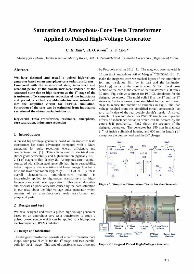
1
Saturation of Amorphous-Core Tesla Transformer
Applied to Pulsed High-Voltage Generator
C. H. Kim*, H. O. Kwon†, J. S. Choi*
*Agency for Defense Development, Republic of Korea, Tel.: +82-42-821-2754 , † Hanwha Corporation, Republic of Korea
Abstract
We have designed and tested a pulsed high-voltage
generator based on an amorphous-core tesla transformer.
Compared with the unsaturated state, inductance and
resonant period of the transformer were reduced at the
saturated state due to high-current at the 1st stage of the
transformer. To compensate reduction of the inductance
and period, a virtual variable-inductor was introduced
into the simplified circuit for PSPICE simulation.
Saturation of the core can be estimated from inductance
variation of the virtual variable-inductor.
Keywords: Tesla transformer, resonance, amorphous,
core saturation, inductance reduction
1 Introduction
A pulsed high-voltage generator based on an iron-core tesla
transformer has some advantages compared with a Marx
generator; for pulse repetition, energy efficiency, and
compactness, etc. [1]. Thin silicon steel or electrical steel
shows good permeability and high-saturation (typically 1.6 ~
2 T) of magnetic flux density B. Amorphous-core material,
compared with silicon steel, generally has higher permeability,
better frequency characteristics and lower energy loss but a
little bit lower saturation (typically 1.5 T) of B. By these
overall characteristics, amorphous-core material is
increasingly applied to high-power transformers for high-
frequency or short pulse application. This paper describes
and discusses a peculiarity that caused by the core saturation
in our tests about the high-voltage pulse generator which
consists of an amorphous-core tesla transformer and
peripheral parts.
2 Design and test
We have designed and tested a pulsed high-voltage generator
based on an amorphous-core tesla transformer to study a
pulsed power source which can be applied to a high-power
electromagnetic (HPEM) radiator.
2.1 Design and fabrication
The designed transformer consists of a pair of magnetic core
loops, four parallel coils for the 1st stage, and two parallel
coils for the 2nd
stage. This type of transformer was presented
by Pecquois et al. in 2012 [2]. The magnetic core material is
25 μm thick amorphous foil of MetglasTM
2605SA1 [3]. To
make the magnetic core we stacked layers of the amorphous
foil and insulation film by in turn and the lamination
(stacking) factor of the core is about 50 %. Total cross
section of the core at the centre of the transformer is 38 mm x
30 mm. Fig.1 shows a circuit for PSPICE simulation for the
designed generator. The multi coils [2] at the 1st and the 2
nd
stages of the transformer were simplified to one coil in each
stage to reduce the number of variables in Fig.1. The load
voltage resulted from this simplified circuit corresponds just
to a half value of the real double-circuit’s result. A virtual
variable L1 was introduced for PSPICE simulation to predict
effects of inductance variation which can be derived by the
core’s B-H peculiarity. Fig.2 shows the structure of the
designed generator. The generator has 280 mm in diameter
(Φ) of inside cylindrical housing and 600 mm in length ( l )
except for the dummy load and the DC charger.
Figure 1. Simplified Simulation Circuit for the Generator
Figure 2. Designed Pulsed High-Voltage Generator
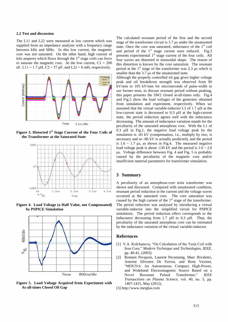
2
2.2 Test and discussion
The L11 and L22 were measured at low current which was
supplied from an impedance analyser with a frequency range
between kHz and MHz. In this low current, the magnetic
core was not saturated. On the other hand, high current of
kilo amperes which flows through the 1st stage coils can force
to saturate the magnetic core. At the low current, C1 = 200
nF, L11 = 1.7 μH, C2 = 57 pF, and L22 = 6 mH, respectively.
Figure 3. Distorted 1st Stage Current of the Four Coils of
the Transformer at the Saturated State
Figure 4. Load Voltage (a Half Value, not Compensated)
by PSPICE Simulation
Figure 5. Load Voltage Acquired from Experiment with
At-all-times Closed Oil Gap
The calculated resonant period of the first and the second
stage of the transformer circuit is 3.7 μs under the unsaturated
state. Once the core was saturated, inductance of the 1st coil
and period of the 1st stage current were reduced. Fig.3
presents experimental 1st stage current of the four coils. All
four waves are distorted in sinusoidal shape. The reason of
this distortion is known by the core saturation. The resonant
period at the 1st stage of the transformer was 2.3 μs which is
smaller than the 3.7 μs of the unsaturated state.
Although the properly controlled oil gap gives higher voltage
peak and oil breakdown strength was observed from 90
kV/mm to 105 kV/mm for microseconds of pulse-width in
our former tests, to discuss resonant period without peaking,
this paper presents the SW2 closed at-all-times only. Fig.4
and Fig.5 show the load voltages of the generator obtained
from simulation and experiment, respectively. When we
assumed that the virtual variable-inductor L1 of 1.7 μH at the
low-current state is decreased to 0.3 μH at the high-current
state, the period reduction agrees well with the inductance
decreasing. The amount of inductance variation stands for the
peculiarity of the saturated amorphous core. With the L1 of
0.3 μH in Fig.1, the negative load voltage peak by the
simulation is -43 kV (compensation, i.e., multiply by two, is
necessary and so -86 kV is actually predicted), and the period
is 1.6 ~ 1.7 μs, as shown in Fig.4. The measured negative
load voltage peak is about -130 kV and the period is 1.6 ~ 2.0
μs. Voltage difference between Fig. 4 and Fig. 5 is probably
caused by the peculiarity of the magnetic core and/or
insufficient material parameters for transformer simulation.
3 Summary
A peculiarity of an amorphous-core tesla transformer was
shown and discussed. Compared with unsaturated condition,
resonant period reduction in the current and the voltage waves
occurred at the saturated core. The core saturation was
caused by the high current of the 1st stage of the transformer.
The period reduction was analysed by introducing a virtual
variable-inductor into the simplified circuit for PSPICE
simulation. The period reduction effect corresponds to the
inductance decreasing from 1.7 μH to 0.3 μH. Thus, the
peculiarity of the saturated amorphous core can be estimated
by the inductance variation of the virtual variable-inductor.
References
[1] V.A. Kolchanova, “On Calculation of the Tesla Coil with
Iron Core,” Modern Technique and Technologies, IEEE,
pp. 40-41, (2003).
[2] Romain Pecquois, Laurent Pecastaing, Marc Rivaletto,
Antoine Silvestre De Ferron, and Rene Vezinet,
“MOUNA: An Autonomous, Compact, High-Power,
and Wideband Electromagnetic Source Based on a
Novel Resonant Pulsed Transformer,” IEEE
Transactions on Plasma Science, vol. 40, no. 5, pp.
1407-1415, May (2012).
[3] http://www.metglas.com
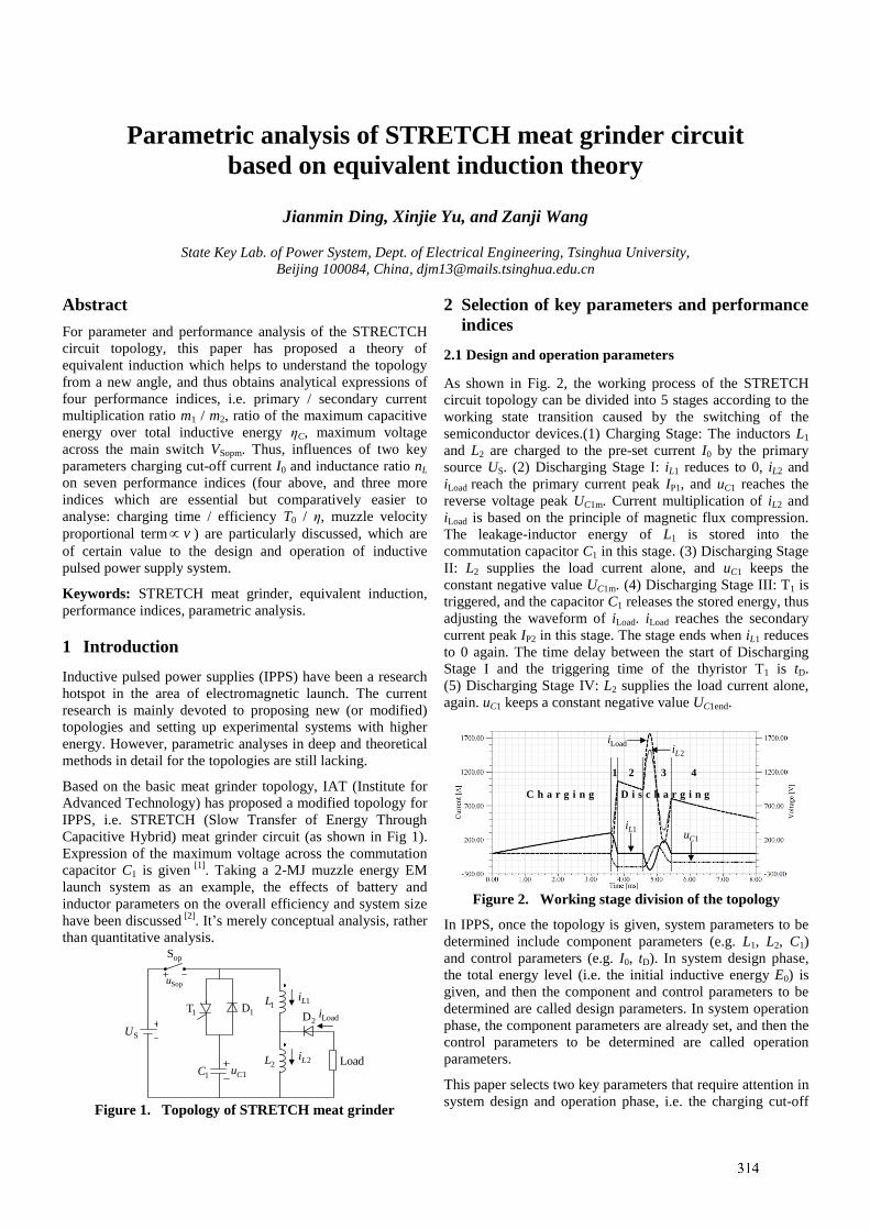
1
Parametric analysis of STRETCH meat grinder circuit
based on equivalent induction theory
Jianmin Ding, Xinjie Yu, and Zanji Wang
State Key Lab. of Power System, Dept. of Electrical Engineering, Tsinghua University,
Beijing 100084, China, [email protected]
Abstract
For parameter and performance analysis of the STRECTCH
circuit topology, this paper has proposed a theory of
equivalent induction which helps to understand the topology
from a new angle, and thus obtains analytical expressions of
four performance indices, i.e. primary / secondary current
multiplication ratio m1 / m2, ratio of the maximum capacitive
energy over total inductive energy ηC, maximum voltage
across the main switch VSopm. Thus, influences of two key
parameters charging cut-off current I0 and inductance ratio nL
on seven performance indices (four above, and three more
indices which are essential but comparatively easier to
analyse: charging time / efficiency T0 / η, muzzle velocity
proportional term v ) are particularly discussed, which are
of certain value to the design and operation of inductive
pulsed power supply system.
Keywords: STRETCH meat grinder, equivalent induction,
performance indices, parametric analysis.
1 Introduction
Inductive pulsed power supplies (IPPS) have been a research
hotspot in the area of electromagnetic launch. The current
research is mainly devoted to proposing new (or modified)
topologies and setting up experimental systems with higher
energy. However, parametric analyses in deep and theoretical
methods in detail for the topologies are still lacking.
Based on the basic meat grinder topology, IAT (Institute for
Advanced Technology) has proposed a modified topology for
IPPS, i.e. STRETCH (Slow Transfer of Energy Through
Capacitive Hybrid) meat grinder circuit (as shown in Fig 1).
Expression of the maximum voltage across the commutation
capacitor C1 is given [1]
. Taking a 2-MJ muzzle energy EM
launch system as an example, the effects of battery and
inductor parameters on the overall efficiency and system size
have been discussed [2]
. It’s merely conceptual analysis, rather
than quantitative analysis.
SU
1T 1D
1C
opS
1L
2L Load
2D
1Li
2Li
Loadi
1Cu
Sopu
Figure 1. Topology of STRETCH meat grinder
2 Selection of key parameters and performance
indices
2.1 Design and operation parameters
As shown in Fig. 2, the working process of the STRETCH
circuit topology can be divided into 5 stages according to the
working state transition caused by the switching of the
semiconductor devices.(1) Charging Stage: The inductors L1
and L2 are charged to the pre-set current I0 by the primary
source US. (2) Discharging Stage I: iL1 reduces to 0, iL2 and
iLoad reach the primary current peak IP1, and uC1 reaches the
reverse voltage peak UC1m. Current multiplication of iL2 and
iLoad is based on the principle of magnetic flux compression.
The leakage-inductor energy of L1 is stored into the
commutation capacitor C1 in this stage. (3) Discharging Stage
II: L2 supplies the load current alone, and uC1 keeps the
constant negative value UC1m. (4) Discharging Stage III: T1 is
triggered, and the capacitor C1 releases the stored energy, thus
adjusting the waveform of iLoad. iLoad reaches the secondary
current peak IP2 in this stage. The stage ends when iL1 reduces
to 0 again. The time delay between the start of Discharging
Stage I and the triggering time of the thyristor T1 is tD.
(5) Discharging Stage IV: L2 supplies the load current alone,
again. uC1 keeps a constant negative value UC1end.
Loadi
1Li1Cu
2Li
C h a r g i n g
1 2 3 4
D i s c h a r g i n g
Figure 2. Working stage division of the topology
In IPPS, once the topology is given, system parameters to be
determined include component parameters (e.g. L1, L2, C1)
and control parameters (e.g. I0, tD). In system design phase,
the total energy level (i.e. the initial inductive energy E0) is
given, and then the component and control parameters to be
determined are called design parameters. In system operation
phase, the component parameters are already set, and then the
control parameters to be determined are called operation
parameters.
This paper selects two key parameters that require attention in
system design and operation phase, i.e. the charging cut-off
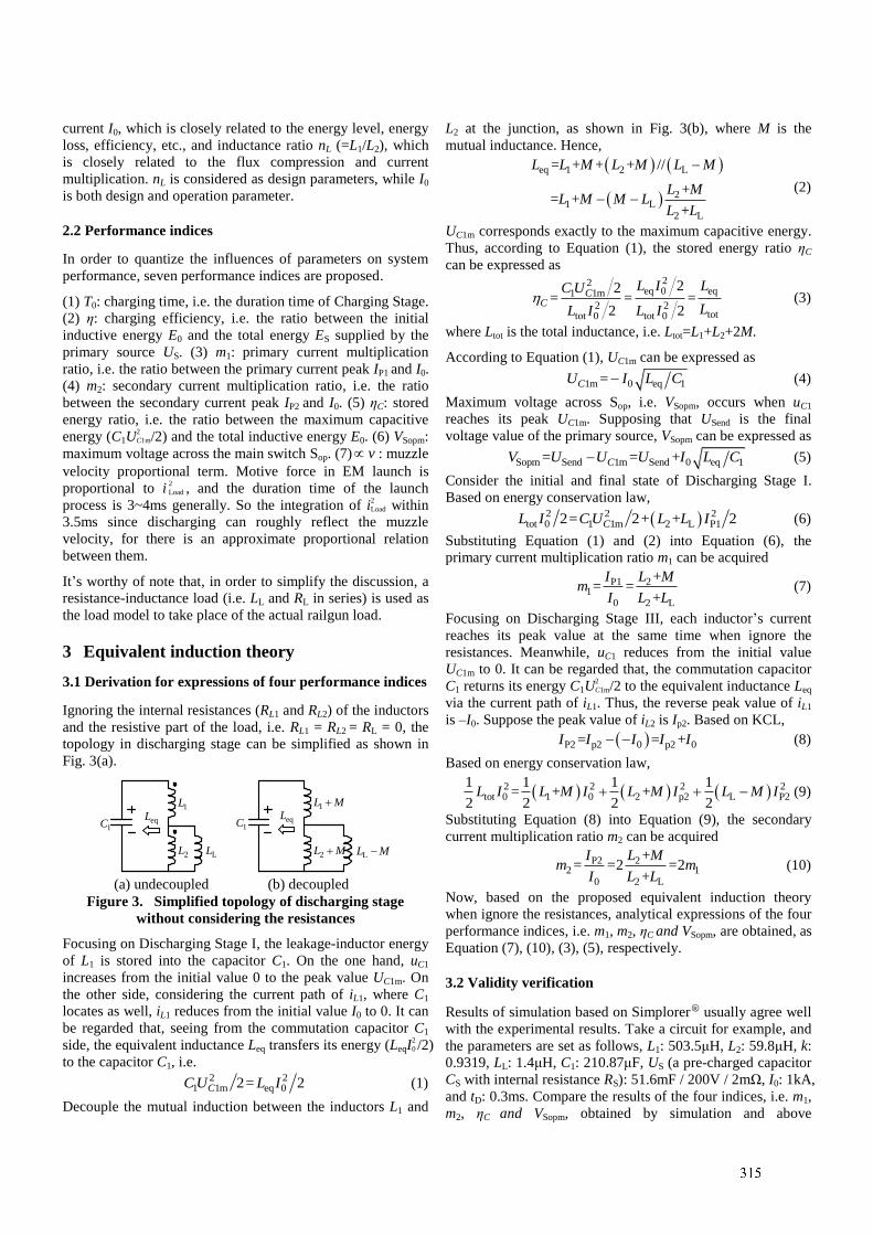
2
current I0, which is closely related to the energy level, energy
loss, efficiency, etc., and inductance ratio nL (=L1/L2), which
is closely related to the flux compression and current
multiplication. nL is considered as design parameters, while I0
is both design and operation parameter.
2.2 Performance indices
In order to quantize the influences of parameters on system
performance, seven performance indices are proposed.
(1) T0: charging time, i.e. the duration time of Charging Stage.
(2) η: charging efficiency, i.e. the ratio between the initial
inductive energy E0 and the total energy ES supplied by the
primary source US. (3) m1: primary current multiplication
ratio, i.e. the ratio between the primary current peak IP1 and I0.
(4) m2: secondary current multiplication ratio, i.e. the ratio
between the secondary current peak IP2 and I0. (5) ηC: stored
energy ratio, i.e. the ratio between the maximum capacitive
energy (C1U2
C1m/2) and the total inductive energy E0. (6) VSopm:
maximum voltage across the main switch Sop. (7) v : muzzle
velocity proportional term. Motive force in EM launch is
proportional to i2
Load , and the duration time of the launch
process is 3~4ms generally. So the integration of i2
Load within
3.5ms since discharging can roughly reflect the muzzle
velocity, for there is an approximate proportional relation
between them.
It’s worthy of note that, in order to simplify the discussion, a
resistance-inductance load (i.e. LL and RL in series) is used as
the load model to take place of the actual railgun load.
3 Equivalent induction theory
3.1 Derivation for expressions of four performance indices
Ignoring the internal resistances (RL1 and RL2) of the inductors
and the resistive part of the load, i.e. RL1 = RL2 = RL = 0, the
topology in discharging stage can be simplified as shown in
Fig. 3(a).
1C
1L
2L LL
eqL
1C eqL1L M
2L M LL M
(a) undecoupled (b) decoupled
Figure 3. Simplified topology of discharging stage
without considering the resistances
Focusing on Discharging Stage I, the leakage-inductor energy
of L1 is stored into the capacitor C1. On the one hand, uC1
increases from the initial value 0 to the peak value UC1m. On
the other side, considering the current path of iL1, where C1
locates as well, iL1 reduces from the initial value I0 to 0. It can
be regarded that, seeing from the commutation capacitor C1
side, the equivalent inductance Leq transfers its energy (LeqI2
0 /2)
to the capacitor C1, i.e.
2 2
1 1m eq 02= 2CC U L I (1)
Decouple the mutual induction between the inductors L1 and
L2 at the junction, as shown in Fig. 3(b), where M is the
mutual inductance. Hence,
eq 1 2 L
21 L
2 L
= + + + //
+= +
+
L L M L M L M
L ML M M L
L L
(2)
UC1m corresponds exactly to the maximum capacitive energy.
Thus, according to Equation (1), the stored energy ratio ηC
can be expressed as
22eq 0 eq1 1m
2 2tottot 0 tot 0
22= = =
2 2
CC
L I LC U
LL I L I (3)
where Ltot is the total inductance, i.e. Ltot=L1+L2+2M.
According to Equation (1), UC1m can be expressed as
1m 0 eq 1=CU I L C (4)
Maximum voltage across Sop, i.e. VSopm, occurs when uC1
reaches its peak UC1m. Supposing that USend is the final
voltage value of the primary source, VSopm can be expressed as
Sopm Send 1m Send 0 eq 1= = +CV U U U I L C (5)
Consider the initial and final state of Discharging Stage I.
Based on energy conservation law,
2 2 2tot 0 1 1m 2 L P12= 2+ + 2CL I C U L L I (6)
Substituting Equation (1) and (2) into Equation (6), the
primary current multiplication ratio m1 can be acquired
P1 21
0 2 L
+= =
+
I L Mm
I L L (7)
Focusing on Discharging Stage III, each inductor’s current
reaches its peak value at the same time when ignore the
resistances. Meanwhile, uC1 reduces from the initial value
UC1m to 0. It can be regarded that, the commutation capacitor
C1 returns its energy C1U2
C1m/2 to the equivalent inductance Leq
via the current path of iL1. Thus, the reverse peak value of iL1
is –I0. Suppose the peak value of iL2 is Ip2. Based on KCL,
P2 p2 0 p2 0= = +I I I I I (8)
Based on energy conservation law,
2 2 2 2tot 0 1 0 2 p2 L P2
1 1 1 1= + +
2 2 2 2L I L M I L M I L M I (9)
Substituting Equation (8) into Equation (9), the secondary
current multiplication ratio m2 can be acquired
P2 22 1
0 2 L
+= =2 =2
+
I L Mm m
I L L (10)
Now, based on the proposed equivalent induction theory
when ignore the resistances, analytical expressions of the four
performance indices, i.e. m1, m2, ηC and VSopm, are obtained, as
Equation (7), (10), (3), (5), respectively.
3.2 Validity verification
Results of simulation based on SimplorerR usually agree well
with the experimental results. Take a circuit for example, and
the parameters are set as follows, L1: 503.5μH, L2: 59.8μH, k:
0.9319, LL: 1.4μH, C1: 210.87μF, US (a pre-charged capacitor
CS with internal resistance RS): 51.6mF / 200V / 2mΩ, I0: 1kA,
and tD: 0.3ms. Compare the results of the four indices, i.e. m1,
m2, ηC and VSopm, obtained by simulation and above
3
mentioned expressions, respectively. As listed in Table 1, the
results of theory method are quite close to those of simulation.
Slight differences are due to regarding the semiconductor
devices as ideal switches without considering the switching
losses in the above derivation. Generally speaking, the
validity of the proposed theory and expressions of the four
indices are confirmed.
There will be analysis deviations caused by ignoring the
resistances. However, according to the proposed theory and
analytical expressions above, general relationships between
the performance indices and system parameters could be
obtained directly and clearly. This is of certain value to the
design and operation of IPPS.
Table 1: Results comparison between simulation and
theory method
Indices m1 m2 ηC VSopm / V
Simulation method 3.61 7.07 9.71% 788.6
Theory method 3.62 7.24 9.59% 784.5
4 Analysis on design and operation parameters
4.1 Influences of operation parameter I0 on indices
As a single-parameter problem, it is easier to discuss. In
system operation phase, component and control parameters
are determined except I0. It’s obvious that, the expressions of
the indices m1, m2, and ηC, are irrelevant with I0. So these
three indices stay unchanged when the value of operation
parameter I0 varies.
As mentioned above, VSopm=USend-UC1m. USend decreases when
I0 increases, due to an increase of ES, i.e. energy supplied by
the primary source. UC1m is proportional to I0, so it increases
in reverse when I0 increases, which is usually more significant
than the reduction of USend. Thus, VSopm increases on the
whole when I0 increases.
The changing trends of T0, η, and v with I0 are easy to
analyse, so the influences of operation parameter I0 on indices
are listed directly here in Table 2. According to the results,
once the index v is large enough to meet the requirement of
the muzzle velocity, it’s not suggested that the system
operates at a high level of I0.
Table 2: Influences of operation parameter I0 on indices
Indices T0 η m1 m2 ηC VSopm v
I0↑ ↑ ↓ - - - ↑ ↑
Effect* × × - - - × √ * √: positive, ×: negative, -: no influence
4.2 Influences of design parameters I0 and nL on indices
This is a multi-parameter problem. In system design phase,
the total energy level E0 is given, meanwhile, component
parameters except the inductors’ parameters, and control
parameters except I0, are already determined. One term of the
inductors’ parameters, i.e. coupling coefficient k, is a given
constant value. The inductance L1 and L2 can be uniquely
determined by I0 and nL, as Equation (11)~(13). Now, all the
system parameters are already given, or can be determined by
I0 and nL.
2
tot 0 0= 2L E I (11)
2 tot= +1+2L LL L n k n (12)
1 2= LL n L (13)
During charging stage, the inductors act as a whole Ltot, which
is only related to I0. Thus, T0 and η are independent of nL.
Ltot and Leq both decrease when I0 increases. Leq increases
when nL increases. In both cases, the ratio Leq/Ltot increases, so
ηC increases, thus VSopm increases as well.
The ratio (L2+M)/(L2+LL) decreases when I0 increases, so m1
and m2 decrease. However, the reference of the multiplication,
i.e. I0 increases, so the total current level rises, thus v
increases. The ratio (L2+M)/(L2+LL) increases when nL
increases, so m1 and m2 increases. It’s obvious that I0 and nL
have different influences on m1 and m2, there is a tradeoff
between them.
The influences of design parameter I0 and nL on indices are
listed in Table 3. The results show that influences of I0 and nL
on indices are not always the same. In system design phase,
suitable I0 and nL should be selected according to the indices
on which your attention is focused.
Table 3: Influences of design parameters I0 and nL
on indices Indices T0 η m1 m2 ηC VSopm v
I0↑ ↓ ↓ ↓ ↓ ↑ ↑ ↑
nL↑ - - ↑ ↑ ↑ ↑ ↑
Total ↓ ↓ TBD TBD ↑ ↑ ↑
Effect* √ × TBD TBD × × √ * √: positive, ×: negative, -: no influence, TBD: To be determined.
5 Conclusions
During parametric analysis, performance indices T0, η, and
v can be analysed intuitively in general, but not the same
case with the four indices m1, m2, ηC and VSopm. Based on the
proposed equivalent induction theory, and concise
expressions of these four indices, the above problems are well
solved. The theory helps to understand the STRETCH circuit
topology from a new point of view as well.
Acknowledgements
This work is supported in part by the NSFC under Project
51377087 and in part by the Tsinghua University Initiative
Scientific Research Program.
References
[1] Sitzman A, Surls D, Mallick J. “Stretch meat grinder: a
novel circuit topology for reducing opening switch
voltage stress”, IEEE Pulsed Power Conference, pp.
493-496, (2005).
[2] Dierks E, McNab I R, et al. “Battery–Inductor
Parametric System Analysis for Electromagnetic Guns”,
IEEE Trans. Plasma Sci., 39(1), pp. 268-274, (2011).

Gold Sponsors:
http://www.metatechcorp.com/ http://www.montena.com/system/home/
http://highpower.co.kr/ http://english.hanwhacorp.co.kr/index.jsp
Silver Sponsors:
http://www.narda-sts.it/narda/default_en.asp http://www.i-spec.co.kr/
http://www.ker.ne.kr/ www.eretec.com
Exhibitors:
OMNI LPS Kapteos
EMI Solutions
Pvt Ltd
ETS.LINDGREN
& GTL(API)
Related Documents