ASCENT Overview MOS-AK Workshop, Infineon, Munich, 13 th March 2018 European Nanoelectronics Infrastructure Access Paul Roseingrave

Welcome message from author
This document is posted to help you gain knowledge. Please leave a comment to let me know what you think about it! Share it to your friends and learn new things together.
Transcript

ASCENT Overview MOS-AK Workshop, Infineon, Munich, 13th March 2018
European Nanoelectronics Infrastructure Access
Paul Roseingrave
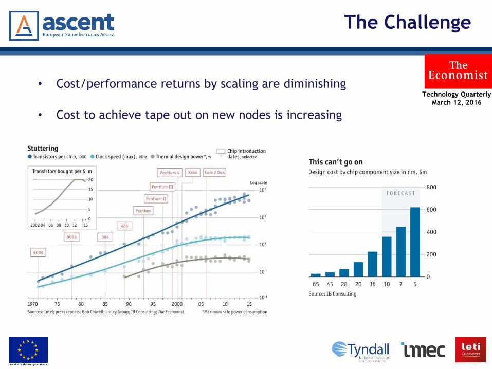
Technology Quarterly
March 12, 2016
The Challenge
• Cost/performance returns by scaling are diminishing
• Cost to achieve tape out on new nodes is increasing
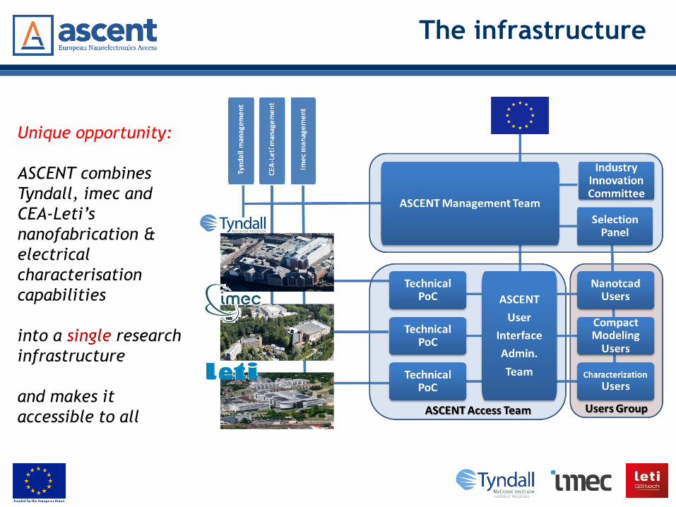
The infrastructure
Unique opportunity:
ASCENT combines
Tyndall, imec and
CEA-Leti’s
nanofabrication &
electrical
characterisation
capabilities
into a single research
infrastructure
and makes it
accessible to all
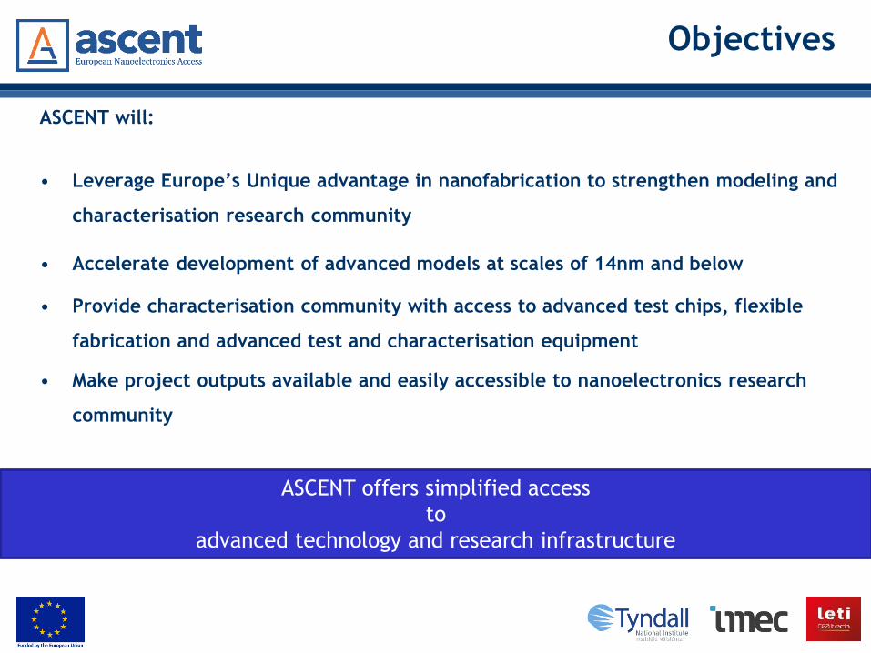
Objectives
ASCENT will:
• Leverage Europe’s Unique advantage in nanofabrication to strengthen modeling and
characterisation research community
• Accelerate development of advanced models at scales of 14nm and below
• Provide characterisation community with access to advanced test chips, flexible
fabrication and advanced test and characterisation equipment
• Make project outputs available and easily accessible to nanoelectronics research
community
ASCENT offers simplified access
to
advanced technology and research infrastructure
Access Provided
State-of-the-art 14 nm FinFET
CMOS
Advanced transistor and
interconnect test structures
Electrical & nano-
characterisation platforms
State-of-the-art 14 nm bulk
FDSOI CMOS
Advanced transistor and
interconnect test structures
Electrical & nano-
characterisation platforms
Fabrication facilities for
nanowires & 2D materials
Advanced nanowire and
nano- electrode test
structures
Electrical & nano-
characterisation platforms
www.ascent.network
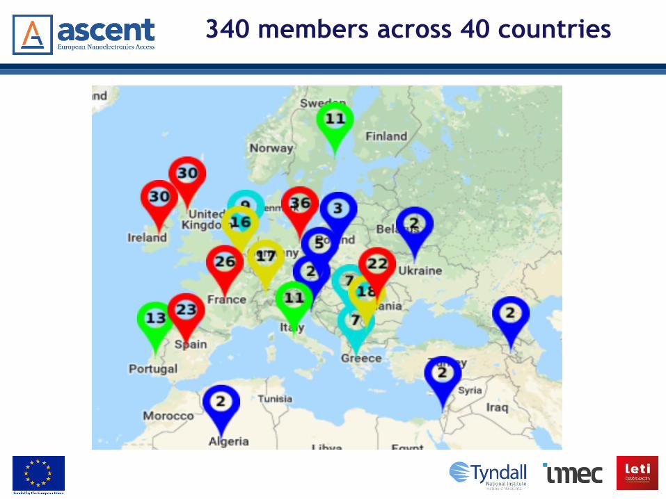
340 members across 40 countries
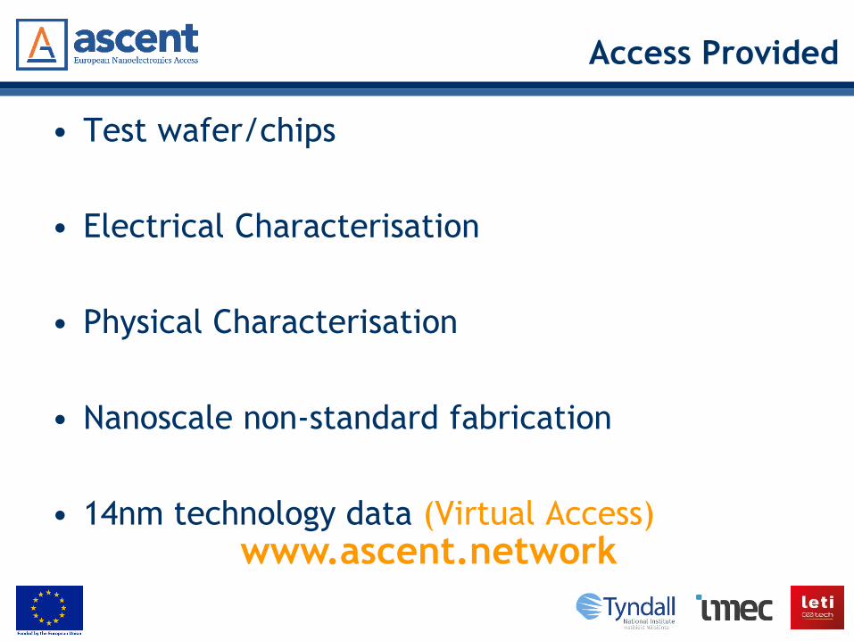
Access Provided
• Test wafer/chips
• Electrical Characterisation
• Physical Characterisation
• Nanoscale non-standard fabrication
• 14nm technology data (Virtual Access) www.ascent.network

FinFET 14/28nm Material for Device Analysis
• Test chips/wafers
– 300mm wafers with Bulk FinFET devices (14nm)
– 300mm wafers with Planar Metal Gate devices (28nm)
• Digital and Analog/RF existing test chips
• Complete suite of test structures for
Reliability/ESD/Matching/Local Layout effects/...
• Standard devices up to circuit level [Ring-Oscillators, ...]
• State-of-the-art bulk FinFET device baseline

FDSOI 14/28nm Material for Device Analysis
• 300mm wafers with planar FDSOI and Nanowire devices
• SPICE models and model cards for digital: target and preliminary
– 14nm FDSOI
– 10nm FDSOI
– 10nm FFSOI
• TCAD decks
– FDSOI MOSFET
– Trigate SOI Nanowire
– GAA Nanowire MOSFET (mainly electrostatics)
• To come in the near future:
– Spice model for Stacked NWs (7nm tech. node)
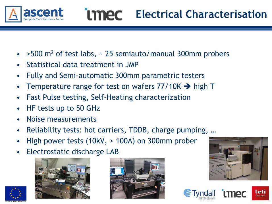
Electrical Characterisation
• >500 m2 of test labs, ~ 25 semiauto/manual 300mm probers
• Statistical data treatment in JMP
• Fully and Semi-automatic 300mm parametric testers
• Temperature range for test on wafers 77/10K high T
• Fast Pulse testing, Self-Heating characterization
• HF tests up to 50 GHz
• Noise measurements
• Reliability tests: hot carriers, TDDB, charge pumping, …
• High power tests (10kV, > 100A) on 300mm prober
• Electrostatic discharge LAB

Electrical Characterisation Labs
Open Access Test Lab
Wide range of test equipment for device and wafer
testing
e.g.: impedance, capacitance, voltage, current,
spectrum analysers, …
Nanoscale Test Lab Variable Temperature, Micromanipulator Probe Stations
Reliability Test Lab Wide range of test equipment for packaged devices

Physical Characterisation
• Atomic Force Microscopy
– Dimension AFM Icon/Fast Scan Bruker working under glovebox (O2, H2O < 1 ppm)
• High Resolution Transmission Electron Microscopy
– FEI TECNAI G2 F 20
– FEI TITAN THEMIS 80-200 kV
• ToF-SIMS
– ION TOF ToF SIMS 5
• Atom Probe Tomography
– CAMECA FlexTAP Atom probe
• XRD (X-ray Diffraction)
– Diffractometer – Smartlab RIGAKU – 5 circles
• XPS (X-ray Photoelectron Spectroscopy)
– Spectrometer/microscope – PHI VERSA PROBE II
• Ellipsometer
– Ultraviolet-visible ellipsometer - HORIBA JOBIN YVON UVISEL
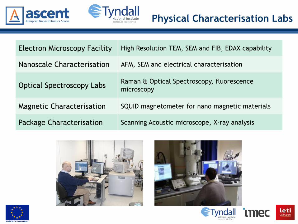
Physical Characterisation Labs
Electron Microscopy Facility High Resolution TEM, SEM and FIB, EDAX capability
Nanoscale Characterisation AFM, SEM and electrical characterisation
Optical Spectroscopy Labs Raman & Optical Spectroscopy, fluorescence
microscopy
Magnetic Characterisation SQUID magnetometer for nano magnetic materials
Package Characterisation Scanning Acoustic microscope, X-ray analysis

Nanoscale fabrication
Range of cleanrooms designed for flexible process & product development
• Silicon MOS Fabrication
• MEMS Fabrication
• Compound Semiconductor Fabrication
• Photonics Fab Training Facility
• e-beam Lithography
• Non-standard nano-processing
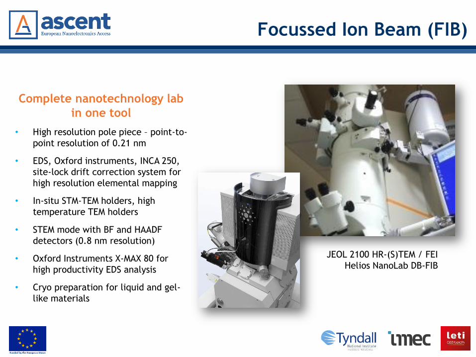
Focussed Ion Beam (FIB)
Complete nanotechnology lab
in one tool
• High resolution pole piece – point-to-
point resolution of 0.21 nm
• EDS, Oxford instruments, INCA 250,
site-lock drift correction system for
high resolution elemental mapping
• In-situ STM-TEM holders, high
temperature TEM holders
• STEM mode with BF and HAADF
detectors (0.8 nm resolution)
• Oxford Instruments X-MAX 80 for
high productivity EDS analysis
• Cryo preparation for liquid and gel-
like materials
JEOL 2100 HR-(S)TEM / FEI
Helios NanoLab DB-FIB
Nanoscale Technology Data
• FinFET Characterisation Data (imec)
– FinFET and GAA test chip documentation and DATA (14nm)
• Documentation of process assumptions for the test chips
• Inventory of test structure types available on the test chips
• Access to test structures data
– PLANAR test chip documentation and DATA (28nm)
• Documentation of process assumptions for the test chips
• Inventory of test structure types available on the test chips
• Access to test structures data
• FDSOI: PDK for Full custom IC design
– 14nm planar FDSOI technology
– 10nm planar FDSOI technology (preliminary)
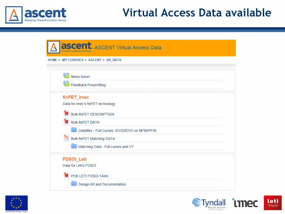
Virtual Access Data available
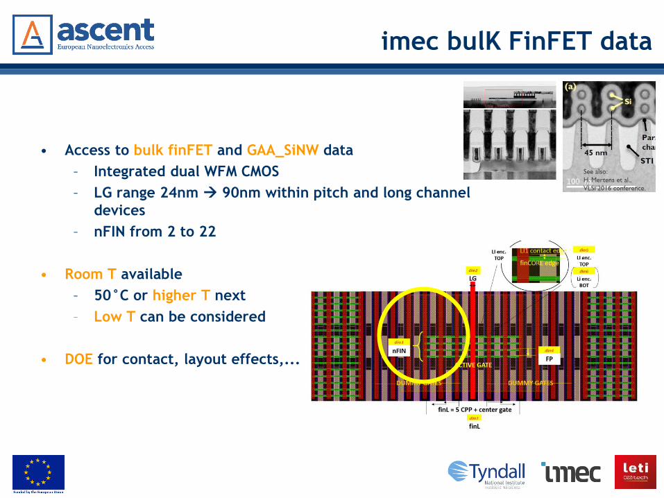
imec bulK FinFET data
• Access to bulk finFET and GAA_SiNW data
– Integrated dual WFM CMOS
– LG range 24nm 90nm within pitch and long channel
devices
– nFIN from 2 to 22
• Room T available
– 50°C or higher T next
– Low T can be considered
• DOE for contact, layout effects,...

imec bulK FinFET data
• Access to raw data and extracted FoM’s
– Threshold Voltage, Mismatch
– DC metrics and ID-VD, ID-VG characteristics
– FEOL/BEOL R/C and Ring-Oscillator circuits
• Full sweep data in VA
– Covers range of VG/VD and LG/nFin
• Analog FoM, Reliability testing, ESD,...
• Available for subsequent model validation
ID[A
] ID
[A]
VG[V]
VD[V]
VG[V]
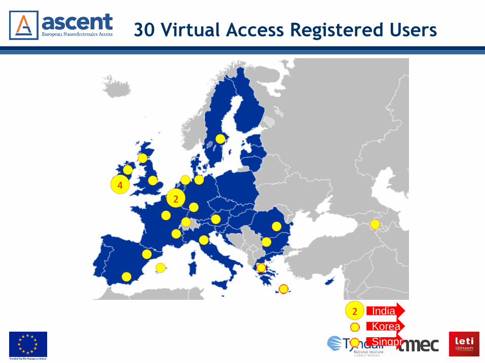
30 Virtual Access Registered Users
4
India 2
2
Korea
Singpr

New initiative: PhD Accelerator Prog.
imec Reliability and failure mechanisms in advanced CMOS technologies
20th-23rd November 2017 6 places
Outcome: Very successful + led to a number of enquiries
CEA Leti Reliability & Defects in Advanced Technologies…from Theory to practice
5th-7th March 2018 6 places
Outcome:
Tyndall National Institute Hands on nanoelectronics fabrication & characterisation
24th-26th April 2018 6 places

How to engage
Please join us in this exciting opportunity for nanoelectronics research
Any enquiries? Email Paul – [email protected]
Sign up:
www.ascent.network
Phone: +353-21-2346268
Sign up and find out more online
Related Documents
![ASM International 2015 Q4 results.pptx [Read-Only] 2015 2016 2017 2018 2019 7nm and below 10nm 14nm 22nm 32nm 45nm 65nm and above WAFER FAB EQUIPMENT SPENDING BY NODE Advanced nodes:](https://static.cupdf.com/doc/110x72/5ab50d2b7f8b9adc638ca001/asm-international-2015-q4-read-only-2015-2016-2017-2018-2019-7nm-and-below-10nm.jpg)