ADVERTIMENT. Lʼaccés als continguts dʼaquesta tesi queda condicionat a lʼacceptació de les condicions dʼús establertes per la següent llicència Creative Commons: http://cat.creativecommons.org/?page_id=184 ADVERTENCIA. El acceso a los contenidos de esta tesis queda condicionado a la aceptación de las condiciones de uso establecidas por la siguiente licencia Creative Commons: http://es.creativecommons.org/blog/licencias/ WARNING. The access to the contents of this doctoral thesis it is limited to the acceptance of the use conditions set by the following Creative Commons license: https://creativecommons.org/licenses/?lang=en 3 3

Welcome message from author
This document is posted to help you gain knowledge. Please leave a comment to let me know what you think about it! Share it to your friends and learn new things together.
Transcript
ADVERTIMENT. Lʼaccés als continguts dʼaquesta tesi queda condicionat a lʼacceptació de les condicions dʼúsestablertes per la següent llicència Creative Commons: http://cat.creativecommons.org/?page_id=184
ADVERTENCIA. El acceso a los contenidos de esta tesis queda condicionado a la aceptación de las condiciones de usoestablecidas por la siguiente licencia Creative Commons: http://es.creativecommons.org/blog/licencias/
WARNING. The access to the contents of this doctoral thesis it is limited to the acceptance of the use conditions setby the following Creative Commons license: https://creativecommons.org/licenses/?lang=en
3 3

UNIVERSITAT AUTÒNOMA DE BARCELONA (UAB)
DOCTORAL THESIS
Artificial Synapses based on thePhotoconductance of LaAlO3/SrTiO3
Quantum Wells
Author:Yu CHEN
Supervisor:Dr. Gervasi HERRANZ CASABONA
Tutor:Prof. Javier Rodrìguez Viejo
A thesis submitted in fulfillment of the requirementsfor the degree of Doctor in Materials Science
in the
Laboratory of Multifunctional Oxides and Complex Structures (MULFOX)Institut de Ciència de Materials de Barcelona (ICMAB-CSIC)
September 19, 2019


iii
Declaration of AuthorshipDr. Gervasi HERRANZ CASABONA, Tenured Scientist at the Institut de Ciencia de Materials deBarcelona (ICMAB-CSIC) and Prof. Javier Rodrìguez Viejo, Professor at Universitat Autònomade Barcelona (UAB).
Certify,
that Yu CHEN , with a Master in Condensed Matter Physics from the Shanghai University, car-ried out, under their supervision, the thesis entitled “Artificial Synapses based on the Photo-conductance of LaAlO3/SrTiO3 Quantum Wells”. This work has been developed within a Ph.D.program in Materials Science at the Universitat Autònoma de Barcelona at the department ofPhysics.For that record they sign the certificate.
Signed (Dr. Gervasi HERRANZ CASABONA):
Signed (Prof. Javier Rodrìguez Viejo):
Signed (Yu CHEN ):
Bellaterra, September 2019:


v
UNIVERSITAT AUTÒNOMA DE BARCELONA (UAB)
AbstractUniversitat Autònoma de Barcelona
Institut de Ciència de Materials de Barcelona (ICMAB-CSIC)
Doctor in Materials Science
Artificial Synapses based on the Photoconductance of LaAlO3/SrTiO3 Quantum Wells
by Yu CHEN
Recently, inspired by neurobiology, researchers have investigated systems that process in-formation based on spiking neural networks where synaptic plasticity is the kernel of calcula-tion, communication, or even storage of information. In this area, neuromorphic computing isproposed to cope with complex cognitional tasks through emulating spiking neural networksconsisting of artificial synapses, aiming at overcoming the von Neumann bottleneck in conven-tional computational paradigms. In this Thesis, we have investigated the optical properties ofthe LaAlO3/SrTiO3 interfaces, which can be exploited as artificial optical synapses due to theirpersistent photoconductance. In particular, we find that the conductance of these interfaces canbe increased or decreased plastically depending on the time order of arrival of optical pulsesof different wavelengths. The observed plastic photoresponse, which depends on the order oftime arrival of optical stimuli, paves the way to the implementation of spike-timing dependentplasticity (STDP) using light as external stimulus.
In the Thesis we discuss the origin of the observed wavelength-dependent time-correlatedphotoresponse in epitaxial LaAlO3/SrTiO3 quantum wells. We conclude that the photoresponseinvolves two photoexcitation processes, namely, the excitation of electrons located at defect-related DX centers and the photoexcitation to surface states via quantum tunneling. As afore-mentioned, it is shown that this photoresponse can be adapted to achieve STDP, using the con-ductance of epitaxial LaAlO3/SrTiO3 quantum wells as optical synapses. The possibility of ex-ploiting the photoconductance of LaAlO3/SrTiO3 to emulate some basic cognitive tasks is alsoexplored. Additionally, we have explored the photoconductance of amorphous LaAlO3/SrTiO3
interfaces, where the conductance is sensitive to illumination conditions in well-lighted environ-ments. We include a discussion about the perspective of using the persistence photoconductanceof LaAlO3/SrTiO3 quantum wells to applications in neuromorphic vision.


vii
Acknowledgements
As the studied artificial synapses are reconfigurable under external stimulus, I am shaping mymind to be a better person under all the experiences. Especially, as the artificial synapses baseon the photoconductance of LaAlO3/SrTiO3 interfaces, I reinforce my knowledge at this doc-toral interface – ICMAB. I would like to acknowledge the China Scholarship Council grant no
201506890029 for supporting me study in ICMAB, and the Spanish Government for the sup-ported projects.
The completion of the thesis is attributed to the valuable and helpful collaborations. I wouldlike to express my deepest gratitude to: Dr. Florencio Sánchez from ICMAB for growing LaAlO3
films, Dr. Blai Casals and Dr.Rafael Cichelero from ICMAB for giving countless scientific andtechnological suggestions, Dr. Bernat Bozzo Closas from ICMAB for taking Hall-effect measure-ments, Dr. Laurence Mechin from CNRS - GREYC Caen for the measurements of Deep-LevelTransient Spectroscopy, Dr. Mariona Coll from ICMAB for growing AlOx with ALD, Dr. JaumeGazquez from ICMAB for supporting the STEM measurements, Dr. Ignasi Fina from ICMABfor developing measurement software, and Prof.Josep Fontcuberta from ICMAB for useful aca-demic suggestions.
A special thanks to Dr. Gervasi HERRANZ CASABONA, it is an impressive and rewardingexperience to work with you. I benefit a lot from not only your research methods or academicthoughts but also the approachable and patient personality. As the artificial synapses mimicthe biological synapses to achieve strong functionalities, I am trying to emulate you to be a nicescholar in the future academic life.
I am really glad to work at our Laboratory of Multifunctional Oxides and Complex Struc-tures (MULFOX) group, a special thanks to group mates: Dr. Ignasi Fina, Dr. Mikko Kataja, Dr.Blai Casals, Dr. Liu Fanmao, Dr.Mateusz Scigaj, Dr. Qian Mengdi, Dr. Rafael Cichelero, Dr. LyuJike, Dr. Morteza Alizadeh, Dr. Nico Dix, Mathieu, Saúl, Milena, Marc, Sheng Yunwei, LongXiao, Song Tingfeng and Jia Jiahui. And I wish Sheng Yunwei, Long Xiao, Song Tingfeng andJia JiaHui, who join in MULFOX group later than me, can enjoy the PhD study, of course, some-times which may be hard or even frustrated for seeing few output, but you will learn much morethan you expected, e.g., you would be inspired by Pep who is an interpreter of Fourier transfor-mation to teach you how to look at a physical problem in a view of band structures instead ofonly real space, you can learn how to program from the coding wizard Ignasi, or you can feelthe scholar charm like Gervasi.
I also would like to acknowledge my office mates: Fu Can, Ma Zheng and Jan. I also thanksto the nice friends at ICMAB: Miquel, Irene, Alejandro, Juri, and Artur.

viii
A special thanks to ICMAB staff. A special mention to Luigi Morrone and Raúl Solanas.
In the past four years, I am also grateful to all my Chinese friends Li Zhi, Lyu Jike, TanFangchang, Zhang Qianzhe, Fu Can, Zhang Qiaoming, Liu Daijun, Zhang Chao, Qian Mengdi,Liu Fanmao, Xu Heng, Li Ziliang, Qian Wenjie, Lu Changyong, Sheng Yunwei, Long Xiao, SongTingfeng, Liu Zhao, Su Huanhuan, Gan Lei, Yu Pengmei, Ma Zheng, Wang Haining, Zhang Xi-aodong, Zhang Songbai and others I cannot list explicitly, with whom I have extremely goodtime. I am really happy to share some moments with Su Huanhuan, Liu Zhao and Gan Lei,who have enriched my experience and mind. A special thanks to Sheng Yunwei, who is alwaysraising questions that inspired me to look deeply into the physical mechanism. I also expressmy special thanks to Yu Pengmei for growing AlOx film.
Last but not least, no word can express my gratitude to my parents, who make me want tobe myself. Thank you, Papa and Mama.

ix
Contents
Declaration of Authorship iii
Abstract v
Acknowledgements vii
1 Introduction 11.1 Background . . . . . . . . . . . . . . . . . . . . . . . . . . . . . . . . . . . . . . . . . 11.2 Spiking neural networks . . . . . . . . . . . . . . . . . . . . . . . . . . . . . . . . . . 5
1.2.1 Physical implementation of plastic synapses . . . . . . . . . . . . . . . . . . 7Electronic memristor . . . . . . . . . . . . . . . . . . . . . . . . . . . . . . . . 8Photonic synapses . . . . . . . . . . . . . . . . . . . . . . . . . . . . . . . . . 9
1.3 LaAlO3/SrTiO3 interface . . . . . . . . . . . . . . . . . . . . . . . . . . . . . . . . . . 101.3.1 Perovskite oxides LaAlO3 and SrTiO3 . . . . . . . . . . . . . . . . . . . . . . 11
LaAlO3 . . . . . . . . . . . . . . . . . . . . . . . . . . . . . . . . . . . . . . . . 11SrTiO3 . . . . . . . . . . . . . . . . . . . . . . . . . . . . . . . . . . . . . . . . 12
1.3.2 Conductivity mechanism of LaAlO3/SrTiO3 interface . . . . . . . . . . . . . 121.3.3 Persistent photoconductance . . . . . . . . . . . . . . . . . . . . . . . . . . . 13
1.4 Outline of the thesis . . . . . . . . . . . . . . . . . . . . . . . . . . . . . . . . . . . . . 14
2 Methods: experiments and simulations 172.1 Sample fabrication . . . . . . . . . . . . . . . . . . . . . . . . . . . . . . . . . . . . . 17
2.1.1 Deposition . . . . . . . . . . . . . . . . . . . . . . . . . . . . . . . . . . . . . . 17Pulsed laser deposition . . . . . . . . . . . . . . . . . . . . . . . . . . . . . . 17Metal evaporation . . . . . . . . . . . . . . . . . . . . . . . . . . . . . . . . . 19Atomic Layer Deposition . . . . . . . . . . . . . . . . . . . . . . . . . . . . . 19
2.1.2 Lithography . . . . . . . . . . . . . . . . . . . . . . . . . . . . . . . . . . . . 202.2 Photoresponse measurement . . . . . . . . . . . . . . . . . . . . . . . . . . . . . . . 21
2.2.1 Confocal microscopy system . . . . . . . . . . . . . . . . . . . . . . . . . . . 212.2.2 Controllable Laser source . . . . . . . . . . . . . . . . . . . . . . . . . . . . . 22
Laser Irradiance regulation . . . . . . . . . . . . . . . . . . . . . . . . . . . . 22Laser bandwidth . . . . . . . . . . . . . . . . . . . . . . . . . . . . . . . . . . 23Measurements under low irradiance . . . . . . . . . . . . . . . . . . . . . . . 24
2.3 Simulations: Brain simulator . . . . . . . . . . . . . . . . . . . . . . . . . . . . . . . 252.3.1 Biological neurons . . . . . . . . . . . . . . . . . . . . . . . . . . . . . . . . . 252.3.2 Description of basic instructions of the Brian simulator . . . . . . . . . . . . 26

x
Neuron network . . . . . . . . . . . . . . . . . . . . . . . . . . . . . . . . . . 26Synapse . . . . . . . . . . . . . . . . . . . . . . . . . . . . . . . . . . . . . . . 27
2.3.3 An example of Brian simulation . . . . . . . . . . . . . . . . . . . . . . . . . 28
3 Photoinduced tunable carrier accumulation and depletion in a quantum well 313.1 Abstract . . . . . . . . . . . . . . . . . . . . . . . . . . . . . . . . . . . . . . . . . . . 313.2 Experimental observations . . . . . . . . . . . . . . . . . . . . . . . . . . . . . . . . . 323.3 Theoretical model . . . . . . . . . . . . . . . . . . . . . . . . . . . . . . . . . . . . . . 323.4 Conclusion . . . . . . . . . . . . . . . . . . . . . . . . . . . . . . . . . . . . . . . . . . 39
4 Wavelength-Sensitive Temporal Correlations at the epitaxial LaAlO3/SrTiO3 414.1 Abstract . . . . . . . . . . . . . . . . . . . . . . . . . . . . . . . . . . . . . . . . . . . 414.2 Introduction . . . . . . . . . . . . . . . . . . . . . . . . . . . . . . . . . . . . . . . . . 424.3 Results . . . . . . . . . . . . . . . . . . . . . . . . . . . . . . . . . . . . . . . . . . . . 434.4 Discussion of the potential for neuromorphic engineering . . . . . . . . . . . . . . . 474.5 Conclusion . . . . . . . . . . . . . . . . . . . . . . . . . . . . . . . . . . . . . . . . . . 494.6 Sample preparation and simulations . . . . . . . . . . . . . . . . . . . . . . . . . . . 50
4.6.1 Sample Preparation . . . . . . . . . . . . . . . . . . . . . . . . . . . . . . . . 504.6.2 Simulations of neural networks . . . . . . . . . . . . . . . . . . . . . . . . . . 50
4.7 Supporting Information . . . . . . . . . . . . . . . . . . . . . . . . . . . . . . . . . . 514.7.1 Structural characterization of epitaxial LaAlO3/SrTiO3 samples . . . . . . . 514.7.2 Long-term depression of photoconductance induced by illumination with
two-pulse sequences . . . . . . . . . . . . . . . . . . . . . . . . . . . . . . . . 514.7.3 Simulations of neural networks . . . . . . . . . . . . . . . . . . . . . . . . . . 534.7.4 Emulation of inhibitory synapses with two-pulse sequences . . . . . . . . . 564.7.5 Photoconductive spectral response of epitaxial versus amorphous interfaces 564.7.6 Reproducibility of photoconductance response . . . . . . . . . . . . . . . . . 574.7.7 Time relaxation of conductance after photoexcitation . . . . . . . . . . . . . 584.7.8 Voltage readouts in photoconductance measurements . . . . . . . . . . . . . 594.7.9 Conductance modulation under multiple-pulse sequences . . . . . . . . . . 59
5 Plasticity of amorphous LaAlO3/SrTiO3 615.1 Abstract . . . . . . . . . . . . . . . . . . . . . . . . . . . . . . . . . . . . . . . . . . . 615.2 Introduction . . . . . . . . . . . . . . . . . . . . . . . . . . . . . . . . . . . . . . . . . 625.3 Experiment . . . . . . . . . . . . . . . . . . . . . . . . . . . . . . . . . . . . . . . . . . 635.4 Plastic photoresponse of amorphous LaAlO3/SrTiO3 interfaces . . . . . . . . . . . 645.5 Conclusion . . . . . . . . . . . . . . . . . . . . . . . . . . . . . . . . . . . . . . . . . . 705.6 Supporting information . . . . . . . . . . . . . . . . . . . . . . . . . . . . . . . . . . 70
5.6.1 Measurement noise and thermal noise . . . . . . . . . . . . . . . . . . . . . . 705.6.2 Dependence of the resistance and photoconductance on growth conditions 71

xi
6 Outlook and Perspectives 736.1 Artificial synapses and neurons for vision . . . . . . . . . . . . . . . . . . . . . . . . 73
6.1.1 Photoreceptor and ganglion cells . . . . . . . . . . . . . . . . . . . . . . . . . 746.1.2 Electric vision . . . . . . . . . . . . . . . . . . . . . . . . . . . . . . . . . . . . 75
6.2 Complex oxide device based on 2DES . . . . . . . . . . . . . . . . . . . . . . . . . . 76
A Optical lithography protocols 77
B Photoconductance Calculation Details 79B.1 Photoexcitation via DX-resonance states . . . . . . . . . . . . . . . . . . . . . . . . . 79B.2 Calculation of the density of states (DOS) . . . . . . . . . . . . . . . . . . . . . . . . 80
B.2.1 Quantum well states . . . . . . . . . . . . . . . . . . . . . . . . . . . . . . . . 80B.2.2 DX-center states . . . . . . . . . . . . . . . . . . . . . . . . . . . . . . . . . . . 83B.2.3 Surface states . . . . . . . . . . . . . . . . . . . . . . . . . . . . . . . . . . . . 84
B.3 Deep-level transient spectroscopy (DLTS) . . . . . . . . . . . . . . . . . . . . . . . . 84B.4 Calculation of the photoconductance . . . . . . . . . . . . . . . . . . . . . . . . . . . 85
B.4.1 Photoexcitation with single pulses . . . . . . . . . . . . . . . . . . . . . . . . 85B.4.2 Photoexcitation with two-pulse sequences . . . . . . . . . . . . . . . . . . . 85
B.5 Photoexcitation without DX-centers . . . . . . . . . . . . . . . . . . . . . . . . . . . 87B.6 Configuration-coordinate model . . . . . . . . . . . . . . . . . . . . . . . . . . . . . 87
C Calculation of bulk band structure with matlab 91
List of publications and communications 95
Bibliography 97

xiii
List of Figures
1.1 Development of the computer down for Moore’s law . . . . . . . . . . . . . . . . . 31.2 Speed and efficiency of neuromorphic hardware platforms . . . . . . . . . . . . . . 41.3 Brain inspiration and neuromorphic neural networks . . . . . . . . . . . . . . . . . 51.4 The address-event representation . . . . . . . . . . . . . . . . . . . . . . . . . . . . . 61.5 Spike Timing-Dependent Plasticity modes . . . . . . . . . . . . . . . . . . . . . . . . 71.6 Electronic memristors . . . . . . . . . . . . . . . . . . . . . . . . . . . . . . . . . . . . 81.7 Emulation of symmetric spike-timing-dependent plasticity (STDP) . . . . . . . . . 101.8 Conducting LaAlO3/SrTiO3 interface . . . . . . . . . . . . . . . . . . . . . . . . . . 101.9 Schematic sketch of The polar catastrophe. . . . . . . . . . . . . . . . . . . . . . . . 111.10 Schematic illustration of the perovskite structure. . . . . . . . . . . . . . . . . . . . 121.11 configuration-coordination (c-c) diagram . . . . . . . . . . . . . . . . . . . . . . . . 14
2.1 Sketch of pulsed laser deposition (PLD) setup . . . . . . . . . . . . . . . . . . . . . 182.2 Sketch of metal deposition . . . . . . . . . . . . . . . . . . . . . . . . . . . . . . . . . 192.3 Sketch of atomic layer deposition . . . . . . . . . . . . . . . . . . . . . . . . . . . . . 202.4 Schematics of the lithography process . . . . . . . . . . . . . . . . . . . . . . . . . . 212.5 Schematics of photoresponse measurement . . . . . . . . . . . . . . . . . . . . . . . 222.6 Schematics of the irradiance measurement . . . . . . . . . . . . . . . . . . . . . . . . 232.7 The bandwidth of the laser . . . . . . . . . . . . . . . . . . . . . . . . . . . . . . . . . 242.8 Light intensity attenuated by polarizer . . . . . . . . . . . . . . . . . . . . . . . . . . 252.9 The dependence of action potential on the level of depolarization . . . . . . . . . . 272.10 Simulation of persistence photoconductance based on photo-spikes . . . . . . . . . 28
3.1 Photoexcitation of carriers into or out of the quantum well via DX-centers andquantum tunneling . . . . . . . . . . . . . . . . . . . . . . . . . . . . . . . . . . . . . 33
3.2 Time-asymmetric photoexcitation . . . . . . . . . . . . . . . . . . . . . . . . . . . . . 373.3 Electrostatic boundary conditions and carrier depletion . . . . . . . . . . . . . . . . 38
4.1 Schematics of Configurational coordinates . . . . . . . . . . . . . . . . . . . . . . . . 424.2 PPC and Schematic depiction of the Hall-bar geometry . . . . . . . . . . . . . . . . 434.3 Photoconductive response of the epitaxial LaAlO3/SrTiO3 . . . . . . . . . . . . . . 444.4 Tunability of the photoconductance of the epitaxial LaAlO3/SrTiO3 . . . . . . . . . 454.5 Photoconductance to single pulse/two-pulse sequence of light . . . . . . . . . . . . 464.6 Photoconductance to the two-pulse sequences . . . . . . . . . . . . . . . . . . . . . 484.7 Movement simulation . . . . . . . . . . . . . . . . . . . . . . . . . . . . . . . . . . . 494.8 Temperature dependence of the sheet resistance of LaAlO3/SrTiO3 interface . . . 50

xiv
4.9 Structural characterization of epitaxial LaAlO3/SrTiO3 samples . . . . . . . . . . . 514.10 Depression of PPC under illumination with V+R/G/B . . . . . . . . . . . . . . . . 524.11 Depression of PPC under illumination with G+R and B+R/G . . . . . . . . . . . . . 534.12 Radial and linear plots of the synaptic strengths . . . . . . . . . . . . . . . . . . . . 554.13 Simulation of the decay or depression of the synaptic strength excited by violet
light (∆Tv = 40 ms) . . . . . . . . . . . . . . . . . . . . . . . . . . . . . . . . . . . . . 564.14 Spectral photoconductance of an amorphous LaAlO3/SrTiO3 . . . . . . . . . . . . 574.15 Reproducibility of photoconductance response . . . . . . . . . . . . . . . . . . . . . 584.16 Conductance changes after photoexcitation with a single violet pulse and a two-
pulse sequence of violet plus red . . . . . . . . . . . . . . . . . . . . . . . . . . . . . 584.17 Relative changes of conductance after two two-pulse sequences consisting . . . . . 594.18 Relative changes of conductance after two two-pulse sequences consisting . . . . . 60
5.1 Experimental setup and crossectional view of the amorphous-LaAlO3/SrTiO3 in-terface . . . . . . . . . . . . . . . . . . . . . . . . . . . . . . . . . . . . . . . . . . . . 63
5.2 Nonlinear increase of resistance and photoconductance is related to the aging ofthe amorphous LaAlO3/SrTiO3 interface . . . . . . . . . . . . . . . . . . . . . . . . 65
5.3 Plastic response of the amorphous LaAlO3/SrTiO3 interface. . . . . . . . . . . . . . 665.4 Photoconductance under low irradiance at amorphous LaAlO3/SrTiO3 interface. . 675.5 The power spectral density and spectral density of thermal noise. . . . . . . . . . . 715.6 Normalized photoconductance and resistance of two a-LaAlO3/SrTiO3 sample
with thickness 3 and 6 nm. . . . . . . . . . . . . . . . . . . . . . . . . . . . . . . . . . 71
6.1 Biological vision and its simulation in 2DES systems . . . . . . . . . . . . . . . . . . 74
B.1 The total density of states (DOS) of the π band and σ band in bulk SrTiO3. . . . . . 81B.2 Wedge model for quantum well LaAlO3/SrTiO3 . . . . . . . . . . . . . . . . . . . . 82B.3 Density of states (DOS) of LaAlO3/SrTiO3 interface . . . . . . . . . . . . . . . . . . 83B.4 Schematics of DLTS measurement . . . . . . . . . . . . . . . . . . . . . . . . . . . . 84B.5 Photoexcitation with two-pulse sequences . . . . . . . . . . . . . . . . . . . . . . . . 86B.6 Photoexcitation with two-pulse sequences . . . . . . . . . . . . . . . . . . . . . . . . 88B.7 Large-lattice-relaxation of the DX-centers . . . . . . . . . . . . . . . . . . . . . . . . 89
C.1 Energy Band of bulk SrTiO3 . . . . . . . . . . . . . . . . . . . . . . . . . . . . . . . . 91

xv
List of Abbreviations
PLD Pulsed Laser DepositionALD Atomic Laser DepositionSrTiO3 Strontium TitanateLaAlO3 Lanthanum Aluminate2DES 2 Dimensional Electron SystemQW Quantum WellPPC Persistent PhotoconductanceDX Donor combine with unknown (X) lattice defectsDOS Density of StateCMOS Complementary Metal-Oxide-SemiconductorANNs Artificial Neural NetworksAER Address-Event RepresentationSNNs Spiking Neural NetworksSTDP Spike Timing-Dependent PlasticityEPSP Excitatory Postsynaptic PotentialIPSP Inhibitory Postsynaptic PotentialRAM Random Access MemoryPCM Phase Change MemoryHRS High Resistance StateLRS Low Resistance Stateu.c. Unit CellVB Valence BandCB Conduction BandDB Defect BandDLTS Deep-Level Transient Spectroscopy


xvii
Dedicated to my parents. . .


1
Chapter 1
Introduction
"We humans are neural nets. What we can do, machines can do... Neural networks have con-nections. Each connection has a weight on it and that weight can be changed through learning.What a neural net does is take activity from the connection times weights and sum them up anddecide whether to send outputs."
Geoffrey Hinton
Soma
Axon
Output
Dendrites
Synpases
Input
SrTiO3
2DESLaAlO3
Inspired by neurobiology, we developed Ar-tificial Synapses based on the Photoconductanceof LaAlO3/SrTiO3 Quantum Wells. An introduc-tory background (see Section 1.1) is introduced topresent the advantages of information processingbased on spiking neural networks (see Section 1.2).Then, the following Section 1.3 describes the prop-erties of LaAlO3/SrTiO3, with emphasis on thepersistent photoconductance, which can be poten-tially applied to develop artificial synapses. At theend, the outline of this Thesis is given.
1.1 Background
It is the era fed with big-data, it is the era runningin micro-chips. It is the society benefited from information, it is the society polluted by informa-tion. It is the world in pursue of efficiency, it is the world consuming time in waiting. It is theplanet hungry for energy, it is the planet wasting in energy. Presently scientific and technologicalprogress promotes solutions as well as questions, offers benefits as well as challenges, presentslimitations as well as breakthroughs. Today it is on the way towards a fantastic future with astrong intelligence!
In present era of big-data and microprocessor, there are massive achievements always rela-tive to large-scale data processing, such as, the first spectacular image of the black hole captured,which required gathering a big amount of data, about 5 petabyes [1]. As described by Dan Mar-rone [2], ’it is equivalent to 5000 years of mp3 files’ ( at the National Science Foundation/EHT Press

2 Chapter 1. Introduction
Conference Revealing First Image of Black Hole). Additionally, the recent developments of thedata-centric machine learning have been successfully applied in many domains [3], e.g., pat-tern recognition with much lower error rate [4], speech recognition with industrial application[5], state-of-the-art machine translation [6], natural language understanding [7] and questionanswering [8], or winning Go game against the world champion [9]. All these astonishing tri-umphs are based on the machine learning in neural networks, which have the property that ’ifyou feed it more data, it gets better and better’ notes Andrew Ng [10].
Actually, back in the 1980s and 1990s, many conceptions and algorithms of the machine neu-ral learning have been developed to achieve brain-like function using brain-inspired mechanics[11–13], such as handwritten recognition developed by LeCun [12]. However, rare applicationswere realized till the last decade. The revival of computing in neural network extremely relieson powerful digital computers, which can operate complex tasks with many parameters andlarge databases, taking advantage of the enormous progress in technologies based on digitaltransistors and complementary metal-oxide-semiconductor (CMOS) devices. [14].
To improve the performance and speed of computers, researchers usually attempt to de-crease the size of transistors and integrate more transistors per area, sustaining an exponentialincrease of operation frequency and device density [15]. However, as shown in Figure 1.1 (a), thepower density is also increasing with the increasing frequency, finally resulting in large powerdissipation that may damage the chip, the so-called thermal wall [16] (seen in Figure 1.1 (b)) .That’s the one of the downscaling limitations. Another one is memory wall [17], also known asVon Neumann bottleneck. In the modern computer based on the von Neumann architecture,the central processing units (CPU) and main memory are separated physically and connectedby a central bus consisting of a collection of wires [18] (shown in Figure 1.1 (c)). The data andmachine instructions shuttle back and forth over a central bus between the CPU and the mainmemory, resulting in an bottleneck in multi-task devices that compete simultaneously for busaccess, leading to performance degradation with increasing dissipation of the power. Thus, thisarchitecture is time- and energy- consuming in the data movement rather than computation.
The performance can be improved through re-engineering the individual components, e.g.,making an extensive use of parallelism including, for instance, graphic processing units (GPU),specific processors like Eyeriss as accelerators [20], tensor processing units (TPU) [21] or the in-troduction of enhanced bandwidth memory [22, 23]. In any case, the main inefficiency of thevon Neumann architecture, related to shared interconnections which cannot be accessed simul-taneously, has to be overcome. For instance, the supercomputer Titan capable for around 20petaFLOPS (2 × 10¹⁶ floating-ponit operations per second) tackles a complex pattern recogni-tion with an energy consumption as high as ∼ 106 W [24]. To perform a cognitive task beyondcurrent supercomputers, astonishingly, human brain just cost roughly 20 W of power [25, 26],relying on a massively parallel and reconfigurable neural network with ∼ 1011 neurons and∼ 1015 synapses [27] (seen Section 1.2). Inspired by the brain, which operates complex tasksefficiently and effectively without any separation between processor and main memory [28], theneuromorphic computing is proposed to process information in situ, where computation anddata storage are collocated [29], aiming at mimicking the networks of neurons and synapses inthe brain to surpass the von Neumann paradigm.

1.1. Background 3
(a)
101 102 103 104 105 106 107 108 109
Clock Frequency (Hz)
Pow
er D
ensi
ty (
W/c
m2 )
0.01
0.1
1
10
100
1960 1974 1988 2002 201610-2
1
102
104
106
108
1010
Transistors per chip
Clock Frequency (Hz)
MainmemoryCPU
Bus
Fet
ch
Decode
Excute
1950 1970 1990 20100.1
10
103
105
107
109
1011
1013
Mainframe
Minicomputer
Computer
Personal
Laptop
Smartphone
Embeded
Porcessors
(b)
(c)
Siz
e (m
m3 )
IBMAMD
Intel
FIGURE 1.1: (a) The trend of increasing clock frequency and power density of to-day’s computers with the sequential and centralized Von Neumann architecturefrom IBM, Incorporated; Advanced Micro Devices (AMD), Incorporated; Intel, In-corporated. In contrast, the brain, with a parallel, distributed architecture, is moreeffective and efficient in terms of low power density and operation frequency(adopted from Ref. [19] ). The inset shows the size reduction in computer andthe different computing architectures evolving with time. (b) Increase of densityof transistors and clock frequencies. The latter show a slowdown in 2004, dueto increased heat dissipation (adopted from Ref. [17]). (c) Von Neumann archi-tecture of the modern computer with a bus connected between the CPU and mainmemory. A circle of executing instructions includes fetch (retrieve instruction frommemory to CPU), decode (decode the bit pattern in the instruction resister of CPU)and execute (perform the action required by the decoded instruction in CPU). Dur-ing operating a task, a considerable amount of data and instruction are fetched
back and forth between CPU and the main memory [18].
As an the attempt to develop a hardware implementation of artificial neural networks (ANNs),a team of researchers at IBM built a famous system named TrueNorth [19], which integrateda million silicon spiking-neurons to emulate a neurological system where information is pro-cessed in an address-event representation (AER). Running a standard benchmark, at the op-erating point where neurons fire at 20 Hz and have 128 active synapses, TrueNorth consumes72 mW, which is 176000 times less than a modern general-purpose microprocessor [19]. Besidesthe IBM TrueNorth via the DARPA SyNAPSE program [19], more and more projects are makingvigorous efforts toward neuromorphic hardware [30], e.g., neuristor built with Mott memristorsfrom HP [31], Loihi system from Intel [32], differentiable neural computer from Google [33],Heidelberg HICANN chip via the FACETS/BrainScaleS projects [34], Stanfords Neurogrid [35],or the SpiNNaker Project [36].
These large-scale spiking neural networks (SNNs) implemented in electronics achieve highpower efficiency, orders of magnitude better than standard digital computers with point-to-point links between memory and CPU. However, a neuromorphic processor typically requires
4 Chapter 1. Introduction
NeuroGrid
Hybrid SI/III-V
Sub-
SpiNNaker
Future trend
Computational speed (MMAC/s/cm2)
Effi
cien
cy (
GM
AC
/J)
Brain
Supercomputer
Digital CPUEfficiency wall
10-2
1
102
104
106
1010
1012
1 102 104 106 108 1010
Neuromorphic
Photonics
Neuromorphic
electronics
TrueNorth
HICANN
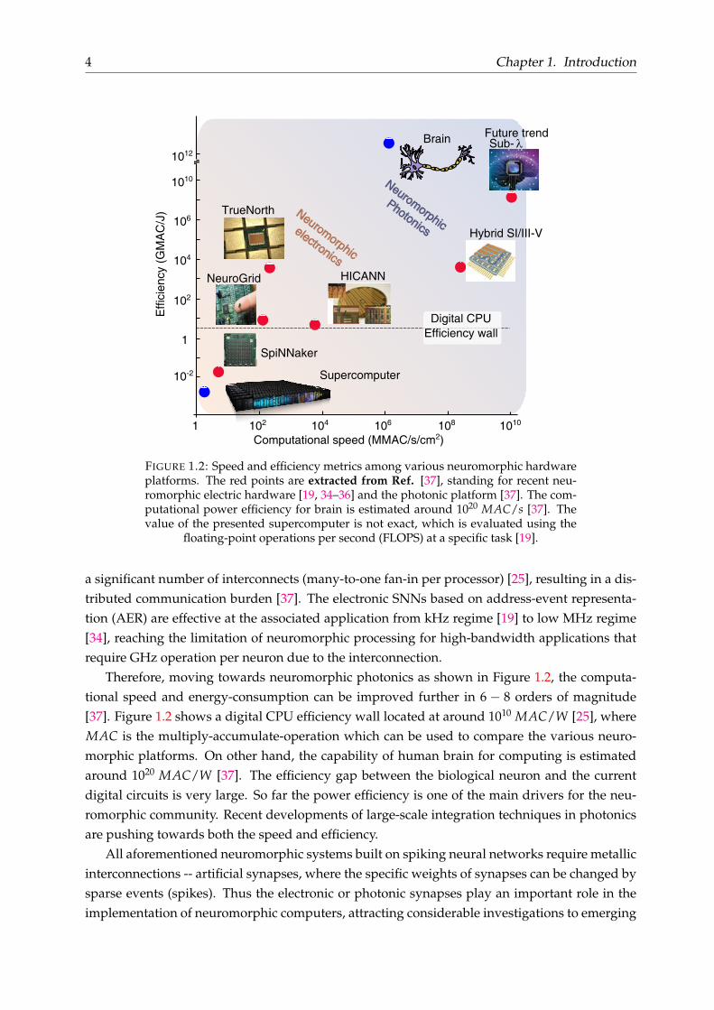
FIGURE 1.2: Speed and efficiency metrics among various neuromorphic hardwareplatforms. The red points are extracted from Ref. [37], standing for recent neu-romorphic electric hardware [19, 34–36] and the photonic platform [37]. The com-putational power efficiency for brain is estimated around 1020 MAC/s [37]. Thevalue of the presented supercomputer is not exact, which is evaluated using the
floating-point operations per second (FLOPS) at a specific task [19].
a significant number of interconnects (many-to-one fan-in per processor) [25], resulting in a dis-tributed communication burden [37]. The electronic SNNs based on address-event representa-tion (AER) are effective at the associated application from kHz regime [19] to low MHz regime[34], reaching the limitation of neuromorphic processing for high-bandwidth applications thatrequire GHz operation per neuron due to the interconnection.
Therefore, moving towards neuromorphic photonics as shown in Figure 1.2, the computa-tional speed and energy-consumption can be improved further in 6 − 8 orders of magnitude[37]. Figure 1.2 shows a digital CPU efficiency wall located at around 1010 MAC/W [25], whereMAC is the multiply-accumulate-operation which can be used to compare the various neuro-morphic platforms. On other hand, the capability of human brain for computing is estimatedaround 1020 MAC/W [37]. The efficiency gap between the biological neuron and the currentdigital circuits is very large. So far the power efficiency is one of the main drivers for the neu-romorphic community. Recent developments of large-scale integration techniques in photonicsare pushing towards both the speed and efficiency.
All aforementioned neuromorphic systems built on spiking neural networks require metallicinterconnections -- artificial synapses, where the specific weights of synapses can be changed bysparse events (spikes). Thus the electronic or photonic synapses play an important role in theimplementation of neuromorphic computers, attracting considerable investigations to emerging

1.2. Spiking neural networks 5
memory devices. The following subsections discuss the spiking neural network and artificialsynapses implemented by electronics and photonics (Section 1.2), including the optical synapsesproposed in this Thesis, based on the phototransport properties of a specific two-dimensionalelectron system (2DES), located at the LaAlO3/SrTiO3 interface (Section 1.3). The last section(Section 1.4) gives the outline of this thesis.
1.2 Spiking neural networks
The human brain possesses massively parallel and reconfigurable neural networks of ∼ 1011
neurons and ∼ 1015 synapses, operating at ultralow power consumption [27]. The basic unitof the neural network is composed of different parts, as shown in Figure 1.3 (a), including theneuron body soma, dendrites responsible for receiving signal, and axon for transmitting signalout (output). Synapses are located at the junction between the axon and dendrites. Synapticplasticity is the capability to change the weight of the synapse, so that the connection strengthcan be enhanced or weakened, and is believed to be responsible for the learning and memoryprocess in the brain. Synapses play the role of adaptable valves at the network nodes. When asignal is excited in a neuron and travels to the axon, it causes the synapses to update the weightand decide (through a threshold value) if the signal must propagate (by firing a spike) into thedendrites of the next neurons. That’s the plastic connections driven by spikes, as summarizedby Lowel and Singer - ’neurons that fire together, wire together’ [38].
Soma
Axon
Output
Dendrites
Synpases
InputVin,1
Vin,2
Vin,M
Vout,1 Vout,2 Vout,N
W1j
W2j
WMj
Vin,1
Vin,2
Vin,M
Vout,j
(a) (b)
(c)
f
FIGURE 1.3: Brain inspiration and neuromorphic neural networks. (a) Unit neuronand neuromorphic neuron [39]. (b) Schematic of artificial neural networks. (c)
Schematic of accumulating weight and threshold operation.
Inspired by biological neural networks, spiking neural networks (seen in Figure 1.3) are em-ployed in neuromorphic computers, where massive metallic devices are linked up in decentral-ized networks with communication lines between components rather than through a central

6 Chapter 1. Introduction
processor with digital operation [39], mimicking the brain’s low-power processing. In the stan-dard computer, a large enough voltage is applied to flip the states representing ’0’ and ’1’. How-ever, small voltages, even lower than the threshold to flip a state, can be used to gather smallamount of electrons, which could be accumulated and change some physical property. Based onthat, Carver Mead put forward the neuromorphic idea [40]. Under the stimuli with electric oroptic pulses, the neuromorphic device receives the input signals through the artificial synapses,which allows the incoming signals to modulate some device properties, e.g., voltage or resis-tance. If the accumulating states reach a certain threshold, the neuromorphic neuron ’fires’ aseries of spikes that travel along the wires as electric impulses or as electromagnetic waves [41]or waveguides [42] in photonic neuromorphic devices, which perform the role of axons and den-drites, enabling the communication between neurons. During the process, spikes are either firedor unfired like ’digital’, while the fire condition is achieved by integrating inputs in a non-digitalway using very low energy. By contrast, a digital computer needs a constant flow of energy torun an internal clock to restricted voltages and currents to a few discrete value as bits, whetheror not the chips are computing anything [39].
In other words, a great number of synapses are able to accumulatively pre-process the rawinput signal, forming ’digital’ spikes of the useful data, resulting in minimizing the amount ofdata that has to be transmitted and processed. That’s the efficiency of the computing drivenby event (spike). On the other hand, the speed of the neural/neuromorphic operation is fastdue to massive parallel neural networks. The spare events (spikes) are transmitted betweenneurons via an asynchronous communication protocol -- address-event representation (AER)[43]. As shown in Figure 1.4, the events containing the timing of the spike can be packaged witha sender/receiver neurons address headers, forming a temporal stream to transmit through ashared bus. Then the temporal information is decoded by the postsynaptic neurons and thespike timing is preserved [44].
3
2
1
3 2 1 3 2 1 2 1 2 3
timeEnc
oder
Sender
Dec
oder
ReceiverOutputInput
Adress-Event Bus 3
2
1
FIGURE 1.4: The address-event representation (reproduced from Ref. [44]).
The neural or neuromorphic spike timing is critical for coding or decoding not only in thecomputing operation but also in the learning process. From the phenomenological point ofview, the most promising of the unsupervised learning mechanisms based on synaptic plastic-ity is Spike Timing-Dependent Plasticity (STDP), where the timing between the spikes actuallygoverns the learning. Lets consider pre-spike neurons with synaptic connections to post-spikeneurons (Figure 1.5 (a)). In the case that the pre-synaptic spike is taking place before the post-synaptic spike, it causes an increase of the synaptic weight. This can be understood as implyinga "causal relation", so that the system reinforces the synaptic connections whenever pre-synaptic

1.2. Spiking neural networks 7
neurons fire before post-synaptic neurons. In the opposite case, if the post-synaptic spike isexcited before the pre-synaptic spike, the synaptic weight decreases, implying an anti-causalrelation. The connection between two neurons can be strengthened by the causality of the in-put signals, leading to long-term potentiation of synapses. On the contrary, synaptic strength isweakened by "anti-causal" sequences of inputs, causing long-term depression of synaptic con-nections. Such delay between the spikes controls the synaptic plasticity to change the interac-tion, forming various forms of STDP curves, as shown in Figure 1.5 (b), where the rightmost isexactly found in vivo like Hippocampus [45] (seen in Figure 1.5 (c)). STDP can be consideredas an adaptable classification function in the unsupervised learning. As Prof. Daniele Ielminicommented, ’You don’t really need to elaborate the shape and get the exponential shape thatis observed in the biology. What is really needed is just that you have potentiation for positivespike and depression for negative spike’. (At first edition of Artificial Intelligence InternationalConference [46])
t
- t
Pre-synaptic Neuron Post-synaptic Neuron(a)
(b) (c)
t
W
t
W
t
W
FIGURE 1.5: (a) Schematic of pre-synaptic neuron and post-synaptic neuron. (b)Different forms of the STDP [47]. (c) STDP found in Hippocampus. The EPSP
represents excitatory postsynaptic potential (adapted from Ref. [45]).
Therefore, building artificial synapses based on devices that simulate plastic connectionweights is the core of neuromorphic computing. Interestingly, as discussed in Section 1.2.1,recent developments rely on non-volatile memories that exhibit adjustable physical states byexternal stimuli. These new memories can remain in the state that is written or erased for longtime without external voltage applied, which is similar to the long-term memory in the brain.
1.2.1 Physical implementation of plastic synapses
Based on the biological neuron, the artificial neuron comprises the aforementioned basic com-ponents: first, the soma, which operates on the summation. A threshold for neuron firing can berealized using variety of electronic or photonic circuits. Finally, axons and dendrites always actas interconnections, so that simple electronic wires or waveguides [42] can be used to replicatethe action of axons and dendrites. The central function of the synaptic weight can be achievedby synaptic devices, which can be implemented via changes of the electric resistance driven by,

8 Chapter 1. Introduction
e.g., electric fields. This subsection discusses electronic memristors and neuromorphic devicesthat replicate plastic synapses.
Electronic memristor
With electrical stimuli, the in-memory computing can be implemented on a variety of mem-ristors, such as resistance switching random access memory (RRAM), phase change memory(PCM), magnetoresistive RAM (MRAM) and ferroelectric RAM (FrRAM), as shown in Figure1.6 [14]. These memristors facilitate reading and programing by electric pulses and retention ofinformation for long-term through changing the state, e.g., transport resistance or charge distri-bution.
FIGURE 1.6: (a), (c), (e) and (g) Structure of RRAM, PCM, MRAM and FrRAM,respectively. (b) Currentvoltage characteristic of RRAM. (d) and (f) the resistancechange characteristic of PCM and MRAM, respectively. (h) Polarizationvoltage
hysteretic characteristic of FrRAM (adapted from Ref. [14]).
Basically, the RRAM comprises two electrodes and a dielectric where the resistance statecan be reversibly switched. As in Figure 1.6 (b), when a positive voltage exceeds a thresholdvalue, the device is switched from the high resistance state (HRS) to low resistance state (LRS),due to the formation of conductive filaments [48] driven by the field-induced migration anddiffusion of defects, e.g., oxygen vacancies causing reproducible resistance switching [49]. Whenthe opposite field is applied, the reverse migration of defects disconnects the filaments, resultingin a transition from HRS to LRS. Additionally, other devices relying on voltage-induced defectmigration, such as Schottky or tunneling barriers [50], also can be considered resistor switchingmemories.
Another route is using PCM. Phase change material, such as Ge2Sb2Te5 [51], can be reversiblychanged from the crystalline phase (LRS) to the amorphous phase (HRS) induced by Joule heat-ing, as shown in Figure 1.6 (d). Compared to RSM devices, which may involve chemical processdue to redox reactions and migration, PCM emerges only under physical phase changes.
Artificial synapses can be also built using magnetic tunnel junction (MTJ). As shown schemat-ically in Figure 1.6 (e), the ferromagnetic polarization in the free layer can be flipped so that itcan be parallel or antiparallel with respect to the ferromagnetic polarization in the fixed layer,resulting in a low or high resistance of the MTJ, respectively. Based on the MTJ with control on

1.2. Spiking neural networks 9
the ferromagnetic polarization, the device can also use spin transfer torque magnetic randomaccess memory (STT-MRAM), achieving high switching speed, and low-energy operation [52].Based on STT-MRAM, recently, nanoscale spintronic oscillators were created to mimic neuralnetworks and achieve spoken-digit recognition [53].
In contrast to transport resistance changing in the RRAM, PCM and MRAM, the electricpolarization is switched in the FeRAM (seen in Figure 1.6 (g)), which reduces charge distributionin the electrodes, causing changes in capacitance. Instead of two-terminal devices, the resistancechange can be achieved via building a ferroelectric field-effect transir (FeFET) [54] where thechannel resistance can be altered by the varying polarization controlled by the gate field.
Photonic synapses
As discussed above, the physical implementation of synaptic plasticity is nowadays done withelectronic memristors, using electrical stimuli as inputs. However, the electronic interconnectiv-ity could still limit the bandwidth. Photonic neuromorphic devices can display significant ad-vantages, e.g., larger bandwidth, faster propagation and processing, multiplexing (time, space,polarization, angular momentum, wavelength) and lower power computation stimulus. What’smore, photonic synapses can be directly applied to visual sensors. Therefore, the future’s de-mand for neuromorphic computers with high speed and performance should benefit from pho-tonic synapses stimulated by light.
As early as in 1980s, neural networks were most readily implemented using optoelectronicneurons with architectures of holographic combinations acting as artificial synapses [55] be-tween light sources (input) and photodetectors with electronic circuits processing threshold(output). Afterwards, uisng photonic circuits on a chip with lasers and photodetectors, variousapproaches were developed to achieve reconfigurable photonic connectors that could replicatesynaptic plasticity, using Mach-Zehnder interferometers (MZI) [42] and micro-ring resonator(MRR) [56]. Yet, such kind of photonic synapses are difficult to be integrated densely on chipsto build large-scale neural networks, owing to the size of reconfigurable devices ranging from625 to 20, 000 µm2 [57].
Thus, instead of structure-dependent photonic synapses, alternative solutions are suggestedto realize artificial synapses. For instance, based on photon-assisted vacancy migration, similarto memristor filaments driven by electric fields, optogenetics-inspired tunable synaptic func-tions are reported in the CH3NH3PbI3 (MAPbI3)-based memristor [59]. On the other hand,recently, optical synapses have been proposed based on the phenomenon of persistent photo-conductance (PPC), where carriers can remain for long periods in photoexcited states (moredetails will be presented in the following Section 1.3). Based on PPC, photonic synapses havebeen proposed using amorphous oxide semiconductors (Figure 1.7) [58]. In the same vein, aphototransistor synapse has been implemented in heterostructures integrating graphene withsingle-walled carbon nanutubes [60].
In this Thesis we propose that the persistent photoconductive properties of the LaAlO3/SrTiO3
interface can be also applied to build artifical optical synapses. In particular, we find that photo-transport at the LaAlO3/SrTiO3 interface is sensitive to wavelength-dependent time-correlatedoptical pulses in a way that can replicate STDP using optical stimuli instead of electrical (Chaper

10 Chapter 1. Introduction
(a) (b)
FIGURE 1.7: (a) A schematic of lateral synpase and (b) emulation of spike-timing-dependent plasticity in the IGZO (indium-strontium-zinc-oxide) synaptic devices
(adapted from Ref. [58] ).
4). In Chapter 3 we give a physical explanation of the observed wavelength-dependent time-correlated phototransport. Finally, we show that amorphous LaAlO3/SrTiO3 interfaces are sen-sitive to illumination conditions comparable to sunlight environments (Chapter 5). Before pro-ceeding, the following section will briefly present the properties of the LaAlO3/SrTiO3 interface.
1.3 LaAlO3/SrTiO3 interface
FIGURE 1.8: Conducting LaAlO3/SrTiO3 in-terface Image: J. MANNHART (MPI-FKF) &A. HERRNBERGER (UNIV. AUGSBURG) [61].Thin film LaAlO3 (denoted as the light blue)grows on the substrate SrTiO3 (denoted asthe dark blue), yielding a conducting interface
shown in the highlighted area.
Symmetry breaking always offers a fertile play-ground to explore emerging phenomena absentin high symmetry systems and utilized to designnovel devices with multiple functionalities. Morespecifically, atomic and electronic reconstructionscan appear at the interface between two differentmaterials, promoting the emergence of new prop-erties. Along these lines, the Nobel laureate Her-bert Kroemer coined the sharp and precise phrasethat ’The interface is the device’, referring to theastonishing success of semiconductor devices [62].
Over the past decades, advances in complexthin film growth have enabled atomic-scale con-tol of heterostructures and interfaces, resulting ina considerable number of breakthroughs. Oneparticularly relevant discovery was made by A.Ohtomo and H.Y. Hwang [63], who found aconducting interface between the two insulators(SrTiO3 and LaAlO3), as shown in Figure 1.8. This interface supports a two-dimension elec-tron system (2DES), with carrier densities around 3 × 10¹³/cm2 and a mobility that may exceed

1.3. LaAlO3/SrTiO3 interface 11
104 cm2V−1s−1 at low temperature. In addition, a variety of physical properties and phenomenaemerge, such as the coexistence of superconductivity and magnetism [64, 65], large spin-orbitcoupling [66], or, more relevant in the context of this Thesis, persistence photoconductance [67].The following subsections will briefly discuss the properties of LaAlO3/SrTiO3 heterostructure.
1.3.1 Perovskite oxides LaAlO3 and SrTiO3
Perovskite oxides refer to a kind of ceramic oxides with the structure formula ABO3, where ’A’cations are larger than ’B’ cations, and both of them are bonded to ’O’ -- oxygen anions. Theideal cubic perovskite (shown in Figure 1.9 (a) ) contains A ions at the corners in 12-fold coordi-nated by oxygen anions, a B ion in the center in 6-fold coordination surrounded by the in oxygenanions in the middle of the faces. Additionally, depending on external parameters like temper-ature or pressure and internal parameters like cation substitution, pervoskites can experiencedifferent structure phases, such as orthorhombic, tetragonal, rhombohedral and monoclinic. Ex-tended to periodic structure, the perovskite can be considered as a BO6 octahedra network, asshown in Figure 1.9 (b). Along (001) direction, ABO3 compounds can also be seen as a sequenceof alternating AO and BO2 layers (shown in 1.9 (C)) .
ABO
(a) (b) (c)
FIGURE 1.9: (a) A cubic unit cell of perovskite structure. (b) a periodic perovskitenetwork of corner-sharing BO6 octahedra. (c) Alternative AO and BO2 layers
stacking along the (001) direction.
As the blocks of the LaAlO3/SrTiO3 heterostructure, the perovskite oxides both LaAlO3 andSrTiO3 are band insulators with energy gap ∆E =∼ 3 eV and ∆E = 5.6 eV, respectively.
LaAlO3
LaAlO3 has been extensively studied as a substrate material for the good lattice matching withmany oxide materials [68]. In our thesis, the LaAlO3 was a thin film grown on the substrateSrTiO3. At high temperature LaAlO3 crystallizes in the cubic perovskite structure with spacegroup Pm3m, and at ∼ 813 K undergoes transition to a rhombohedral structure with space groupR3c [69, 70]. Through the thesis, the measurements were carried out at room temperature, wherethe LaAlO3 can be considered as a pseudo-cubic perovskite with a lattice constant of 3.791Å [70].Compared with SrTiO3, lattice mismatch is relatively small and thermal expansion coefficientsare similar [71], enabling LaAlO3 films to epitaxially grow on the SrTiO3. In addition, the highvalue of the dielectric constant ∼ 25 at temperature between 300 K and 4 K [68, 72], enables theuse of LaAlO3 as thin dielectric films in field effect devices [64, 73].

12 Chapter 1. Introduction
SrTiO3
SrTiO3 has long captured considerable attention last decades for its attractive physical prop-erties. As a substrate, SrTiO3 can be used to epitaxially grow many other perovskite oxides.SrTiO3 itself also arouses scientific interest, e.g., remarkably, two-dimensional electron is foundat the vacuum-cleaved surface of SrTiO3 [74], and SrTiO3 can become superconducting at 0.3 K,as Bednorz and Muller described at 1987 Nobel Prize lecture [75], ’The key material, pure SrTiO3,could even be turned into a superconductor if it were reduced, i.e. if oxygen were partially removed fromits lattice...’. Many of these properties are related to the different possible valences of the Ti ion,and sensitivity of the extrinsic doping.
At room temperature SrTiO3 is cubic (space group Pm3m) with a lattice constant of 3.905 Å.The intrinsic SrTiO3 with an indirect band gap of 3.25 eV, but it becomes metallic when it isdoped with oxygen vacancies [76, 77] or substituting small amounts of the cations [77].
1.3.2 Conductivity mechanism of LaAlO3/SrTiO3 interface
FIGURE 1.10: Schematic illustration of the perovskite structure (adapted from Ref.[63]). Superscripts denote the oxidation numbers. ρ represents the net charge ofthe layers which reduces an electric field E, resulting in an electric potential V. (a)and (b) The unreconstructed n-type and p-type interface, respectively, lead to adiverging potential – polar catastrophe. (c) The transfer of half an electron canavoid the potential divergence, causing a n-type conducting interface. (d) Transfer
of half a hole or removal of half an electron can prevent the divergence.
The origin of the 2DES at the LaAlO3/SrTiO3 interface is commonly accepted to be relatedto the so-called "polar catastrophe" [63, 78]. Along the [001] orientation, the interface is at theboundary between a polar LaAlO3 layer with non-polar SrTiO3. As a result, a series of alter-nating atomic planes, i.e., La3+O2− and Al3+O4−
2 are grown on Ti4+O−42 -terminated SrTiO3 sub-
strates. The termination of the SrTiO3 substrate is relevant, as SrO-termination does not yielda 2DES, see Figures 1.10 (a,b). The atomic planes of LaAlO3 consist, therefore, of layers withalternating formal charges +1 and -1 per unit cell, leading to a built-in electric field E. Withoutreconstruction or uncompensated electric fields, this built-in electric field diverges as the LaAlO3
thickness increases, which is the so-call polar catastrophe. To prevent a diverging potential, 0.5

1.3. LaAlO3/SrTiO3 interface 13
electrons per unit cell are transfered from the LaAlO3 surface valence band (oxygen 2p bands)to the interface of TiO2-termined SrTiO3 substrates (Ti 3d states with t2g symmetry), resultingin a conducting interface (Figure 1.10 (c)). The transfer of electrons from the LaAlO3 surface tothe interface occurs at a critical thickness of 4 u.c.∼ 1.5 nm, causing an insulator-to-metal tran-sition. In the case of SrO-termination, half a hole (p-type) is required to be transferred and thenis counteracted by oxygen vacancies, causing an insulating interface [63] (shown in Figure 1.10(d)).
The polar catastrophe scenario is valid for crystalline LaAlO3 layers, where the epitaxial ar-rangement of ions in the lattice structure allows the existence of a built-in electric field. However,it is also found the the interface between amorphous LaAlO3 layers and SrTiO3 substrates canalso sustain 2DES [79, 80]. In the case of amorphous interfaces, the mechanism for interfaceconduction is related to the generation of oxygen vacancies, which dope the interface with car-riers [81]. Amorphous LaAlO3 layers are grown at room temperature and low oxygen partialpressures, enabling conditions where oxygen vacancies are formed as n-type doping [81].
Finally, we mention that electronic states at the LaAlO3 surface can influence profoundly theinterface properties. As a significant result, a metal to insulator transition can be controlled usingvoltage applied by conductive AFM on top of LaAlO3 [82]. This metal-to-insulator transition isbelieved to be related to the disassociation of water which forms protonated surfaces that actas an electrostatic gate that modulates the interface conduction [83–85]. Along the same lines,capping the LaAlO3 surface with metals of different work functions has a strong influence onthe interface transport, to the point that the critical thickness for interface conduction can bechanged depending on the capping metal [86].
In relation to these observations, we will see in Chapter 3, that photoexcitation of carriersto surface states has a deep impact on the interface properties and is one of the key mecha-nisms that explain the observed wavelength-dependent time-correlated photoresponses of theLaAlO3/SrTiO3 interface. Next subsection overviews briefly the phenomenon of persistent pho-toconductance.
1.3.3 Persistent photoconductance
Persistent photoconductance (PPC) has been extensively investigated since the mid-20th cen-tury. A variety of systems exhibit PPC, including III-V semiconductors, such as AlxGa1−xAs [87],Ga1xInxNyAs1−y [88] , 2DES at oxide interfaces, such as NdGaO3/SrTiO3 [89], LaAlO3/SrTiO3
[67, 90], or graphene [91]. The origin of PPC has been debated in several studies, and sometimesit has been ascribed to the separation of photoexcited electron-hole pairs by macroscopic electricfields, such as those appearing in junctions and surface barriers or microscopic electric fieldsintroduced by impurity atoms with large lattice relaxations [92, 93]. Yet, alternative scenarioshave been suggested. One examples is the mechanism of photoexcitation via DX-centers, whichhas gained wide acceptance [87], and will be described briefly in the following.
DX-centers are point defects, related to insterstitials or ionic substitutions. DX-centers havetwo possible states that, depending on their charge state, can form either a shallow level withno structural relaxation or a deeper level with structural lattice relaxation around the defect,which traps electrons. As pointed out above, there is a wide consensus that the photoexcitation

14 Chapter 1. Introduction
of trapped electrons in DX-centers is at the origin of persistent photoconductance in many semi-conductors. Reported cases are related to anion vacancies (e.g., As vacancy in AlGaAs, oxygenvacancies in ZnO [93]).
Lattice coordinate Q
Ele
ctro
nic
+ E
last
ic E
0 Qs
CBDB
FIGURE 1.11: The total energyof electronic and elastic energiesagainst Q. Curve CB corresponds tothe total energy of an unoccupied de-fect. Curve DB represents the vi-brations of an occupied defect whichcaptures an electron, causing a latticedistortion Q = 0. A photoexcitedelectron from DB to CB undergoes alarge lattice relaxation with a barrier
to recover, resulting in PPC.
The description of DX-centers is facilitated by configuration-coordination (c-c) diagrams [92, 94] as those shown in Fig-ure 1.11. In cc-diagrams, the energy of the electronic statesare plotted against the configurational coordinate Q, which,when different from zero, relates to a structural relaxationthat deforms locally the lattice, while when Q = 0 refers to anundeformed lattice. Then, in this model, the occupied statewhich captures an electron is represented as the defect band(DB) with configurational coordinate Q = Qs = 0. When anelectron is photoexcited leaving behind the DB band, there isa change in the configuration coordinate to Q = 0 and, as aresult, the lattice relaxation prevents the return of the carrierback to the initial state after photoexcitation, since the elec-tron has to overcome an energy barrier to come back to theoriginal state (Figure 1.11). Consequently, the photoexcitedstate is long-lived, giving way to a conductance change thatpersists over extended periods.
As described in Chapter 3, there is a second photoexcita-tion mechanism, relying on the excitation of carriers to sur-face states via quantum tunneling, which allows to counter-act the increased conductivity caused by PPC. The combined action of PPC plus photoexcitationto surface statesis at the origin of the observed wavelength-dependent time-correlated photore-sponses at the LaAlO3/SrTiO3 interface, which pave the way to optical synapses with STDP.More details are given in Chapter 3.
1.4 Outline of the thesis
This chapter has given a brief introduction to artificial synapses. In this Thesis, the physicalimplementation of artificial optical synapses is based on the persistent photoconductance of theLaAlO3/SrTiO3 interface. The following chapters present the studied methods, discussing someresults and providing explanations, which are organized as follows:
Chapter 2 describes the methods of device fabrication. Samples of epitaxial and amorphousLaAlO3 films are grown on SrTiO3 substrates by pulsed laser deposition, and devices are definedwith lithography. The measurements of electric transport under illumination with different vis-ible wavelengths are carried out by advanced programmable spectrometers at the confocal mi-croscopy system. Chapter 2 ends with a brief description of simulations of artificial neuronnetworks using the Brian simulator [95].
Chapter 3 presents the wavelength-dependent time-correlated photoresponses of the epitaialLaAlO3/SrTiO3 interface, and a physical explanation is provided to describe these observations.
1.4. Outline of the thesis 15
A Green’s function formalism is used to interpret the physical processes, providing insights intothe observed asymmetric photoexcitation.
Chapter 4 explores time correlated photoresponses down to the millisecond regime at theepitaxial LaAlO3/SrTiO3 interface. The wavelength-sensitivity time correlations are proved bya series of detailed experiments and data analysis. Based on the data of the observed novel PPC,simulations of neural networks emulating spatial memory and navigation maps inspired fromneurobiological systems is performed with the Brian simulator. We suggest that the observedphotoresponse paves the way to an optical implementation of optical artificial spiking neuronnetworks.
Chapter 5 investigates the sensitivity to the light stimuli at the amorphous LaAlO3/SrTiO3
interface. As the amorphous LaAlO3/SrTiO3 interface is getting more insulating from conduct-ing state, the relative photoconductance increases abruptly, even to 1000% under violet light.On the basis of the insulating state, the photoconductance profoundly improves the sensitiv-ity to the light with intensity decreasing to as weak as the sunlight environments, which is ofpotential interest for the sensor application.
Chapter 6 provides perspectives and outlook on the physical mechanisms of the correlative2DES and the potential applications on the artificial synapses. The multiple photo-excitationprocesses provide insight into the distinct properties found in the complex oxide interfaces.
Our brain is definitely as complex as our cosmos. As Carl Sagan said, ‘the cosmos is withinus. We are made of star-stuff. We are a way for the universe to know itself.’ We are also a way forovercoming the limitation of modern computer or other technology and science. When we arelooking upon the star, we are looking into ourselves as well. When we feel confused, why notfocus on our inner world, including the miracle organic system and unique thought. Because --
We are living in the cosmos with imaginary and curiosity,Cosmos is spiraling inside us within brain and body.Creating stars, subsequently, Cosmos created us with star dust,Exploring Cosmos, can we construct a cosmos, and us?Our cosmos is complex and elegant,
coordinating with sparkle body and dark matter.Our brain is sophisticated and intelligent,
operating with spiking neuron and hidden consciousness.Cosmos here, therefore we are being.We here, therefore cosmos is seeing.Cosmos is unbounded, we are unlimited.


17
Chapter 2
Methods: experiments and simulations
To analyze the photoconductive response of the LaAlO3/SrTiO3 interface and its potential ap-plication to artificial synapses, we have prepared a variety of samples and performed on them aseries of phototransport experiments that have been analyzed and simulated. This chapter willpresent the sample fabrication, optical characterization, theoretical background and simulationsof the time-dependent photoconductance response.
ts
Preperation Measurement
from brian2 import *start_scope ( )
eqs = '''
dv /dt = -v /tau : 1
'''N =NeuroGroup( 1 , eqs , threshold= ’v>0.8 ’ , method= ’ exact ’ )
threshold= ’v>0.2 ’ , method= ’ exact ’ )
Simulation
This chapter starts with the description of samplefabrication in Section 2.1, including deposition tech-niques in Subsection 2.1.1 and lithography in Subsec-tion 2.1.2. Then the optical characterizations are carriedout (see Section 2.2). Finally, simulation is describedsuccinctly in Section 2.3.
2.1 Sample fabrication
The measurements of the electric transport and photo-conductance were carried out in Hall-bar geometry [96, 97]. Alternatively, other geometries werealso defined to measure the capacitance of the LaAlO3/SrTiO3 interface, using the interface asone of electrodes [98–101]. With this purpose, the sample fabrication encompassed a series oftechniques including thin film deposition and lithography. We start describing the pulsed laserdeposition (PLD) for the growth of LaAlO3/SrTiO3, metal evaporation for the deposition ofmetallic layers and atom layer deposition (ALD) to deposit amorphous AlOx as a hard mask todefine the devices. Finally we present the lithography process.
2.1.1 Deposition
Pulsed laser deposition
Pulsed laser deposition is a physical vapor deposition (PVD) technique that uses a high-powerlaser to vaporize a ceramic target. In our lab, a 248 nm KrF excimer is employed to ablate a targetwith the required chemical composition located in the chamber with controllable gas pressure

18 Chapter 2. Methods: experiments and simulations
and temperature. Then the material plume resulting from the ablation is deposited on the sub-strate, as shown in Figure 2.1.
For the preparation of the LaAlO3/SrTiO3 interfaces we benefited from the collaborationwith Dr. F. Sanchez (ICMAB). Two types of interfaces were grown, depending on whetherLaAlO3 films were grown epitaxially or amorphously on top of as-received SrTiO3 substrates.As discussed in Section 1.3.2, the formation of 2DES in epitaxial films is driven by an electronicreconstruction caused by electrostatic boundary conditions, whereas for amorphous films themobile carriers come from oxygen vacancies. We will see that these two different mechanismsfor conduction have important consequences on the properties of the photoconductive response,an issue that is discussed in detail in Chapter 3.
FIGURE 2.1: Sketch of pulsed laser depo-sition setup. The target material is ab-lated by laser and the material plume is
deposited on the substrate.
For both epitaxial and amorphous films, the growthwas done by pulsed laser deposition under oxygen par-tial pressure PO2 = 10−4 mbar, substrate-target distance55 mm, repetition rate 1 Hz, pulse energy about 26 mJ,fluence 1.5 J/cm2. The thickness of the films was con-trolled by varying the number of pulses. For that pur-pose, a calibration sample of thickness about 50 nmwas grown, for which the thickness could be estab-lished by X-ray reflectometry. Epitaxial films were de-posited at a temperature T = 725 oC and cooled downat 15 oC/min in oxygen rich atmosphere (PO2200 mbar,maintained at 600 oC for 1 hour and then cooled downto room temperature at 15 oC/min ) to minimize the for-mation of oxygen vacancies, which provide an extrinsic contribution to transport in epitaxialLaAlO3/SrTiO3 interfaces [66, 81].
Similar growth conditions were used for amorphous LaAlO3/SrTiO3 interfaces except forthe deposition temperature. In this case, the LaAlO3 films were grown on top of the SrTiO3
substrates at room temperature, which precludes the formation of epitaxial films, and formsLaAlO3 amorphous layers. The low-pressure conditions (PO2 = 10−4 mbar) drive the formationof oxygen vacancies that act as donors and generate the carriers that form the conducting layerat this interface [102].
As discussed in Section 1.3.2, the formation of 2DES at epitaxial and amorphous interfacesis driven by different mechanisms. This observation leads to important properties that are usedfor device fabrication. In particular, under rich-oxygen atmospheres and high enough tempera-tures, the vacancies formed at the amorphous LaAlO3/SrTiO3 interface are annealed away andthe samples become insulating. On the contrary, the 2DES at epitaxial layers cannot be annealedaway. This property enables using annealed amorphous LaAlO3 as a hard mask to isolate elec-trically Hall-bar devices to measure the electric transport in epitaxial LaAlO3/SrTiO3. For Hallbars defined in amorphous LaAlO3/SrTiO3, photoresist or amorphous AlOx was used as a hardmask to isolate the devices (details about device fabrication are given in Section 2.1.2).

2.1. Sample fabrication 19
Metal evaporation
Metal/LaAlO3/SrTiO3 structures were prepared to measure the capacitance and also to carryout deep-level transient spectroscopy (DLTS) in collaboration with Dr.Laurence Mechin (GREY-CNRS, University of Caen, France). For that purpose, a variety of metals, including Au andPt, were grown on the surface of LaAlO3 forming top electrodes. The metal deposition wasperformed by using thermal evaporation or electron-beam evaporation, which both are physicaldeposition methods with high quality vacuum system, as seen in Figure 2.2.
FIGURE 2.2: Sketch of metal deposition through (a) Resistance evaporation and (b)e-beam evaporation.
The Auto 306 Vacuum Coating system was employed to perform thermal evaporation whichis a simple and cost-effective deposition method based on heating the target to be evaporatedcondensing on the substrate in a high vacuum chamber. In contrast, electron-beam evaporationexploits the high kinetic energy of electrons colliding with the target materials, so that theirenergies are transferred to thermal energy to evaporate the material. In the process, electronsare generated in high vacuum by an electron gun and are accelerated by potentials in the orderof 10 kV then are injected into the target located in a crucible so that the material is gainingthe thermal energy to the melting point, as a result, the material is evaporated and coats thesubstrate.
Atomic Layer Deposition
Atomic Layer Deposition (ALD) is a chemical deposition technique that uses discrete pulses ofchemical precursors to grow films homogeneous over large areas (more than 5 × 5 cm2). Depo-sition of aluminum oxide (AlOx), using trimethyaluminum (TMA) and water by ALD [103, 104]was used as an alternative to the amorphous LaAlO3 to define the hard mask used to isolatedifferent Hall bar devices of epitaxial LaAlO3/SrTiO3.
Firstly, pulses of TMA were injected and delivered into the substrate (polydimethylglutarim-ide (PGMI) S1813 photoresist (PR)/SrTiO3 in our case) with native hydroxyl layer (∗OH, * de-notes the surface) generated by pulses of O3, as seen in Figure 2.3 (a) where the TMA combinewith ∗OH to form bimethylaluminum bound to oxygen (O − ∗Al(CH3)2) and methane (step

20 Chapter 2. Methods: experiments and simulations
(b)). Then N2 was pulsed to purge the excess TMA and methane when the surface is saturatedwith O−∗Al(CH3)2 (step (c)). In the next step (d) , the counter precursor H2O was pumped intothe reactor to forms ∗Al − OH and then was purged by N2 again (step (e)). The circle from step(b) to step (e) was completed and repeated until the desired thickness by controlling the numberof cycles (Figure 2.3 (e)), e.g., the AlOx with 50 nm corresponding to about 625 cycles.
FIGURE 2.3: Sketch of atomic layer deposition. (a) substrate with patterned phore-sist/STO, (b) pulsing of TMA , (c) purging of excess TMA and methane, (d) pulsing
of H2O , (e) purging of excess H2O and methane, and (f) repeating ALD cycles.
The deposition of AlOx should be conducted in a temperature lower than the stability tem-perature of our photoresist (S1813). However, there is a compromise, since if the temperatureis too low, the reaction is incomplete, so that vapor deposition may occur causing poor qualityof AlOx film. In collaboration with Dr. Mariona Coll (ICMAB) we carried out a study to op-timize the growth of AlOx constrained the aforementioned conditions, and found that the bestcompromise is to deposit AlOx at a temperature of 100oC and the photoresist should be treatedwith post-heating at 95 − 100oC for 5min to prevent volatilizing the photoresist during growthof AlOx film.
2.1.2 Lithography
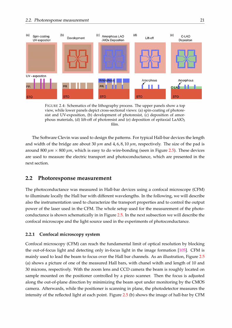
Devices with Hall-bar geometry were fabricated through optical lithography using the proce-dure shown schematically in Figure 2.4. First of all, a layer of polydimethylglutarimide (PGMI)S1813 photoresist (PR) was spin-coated on the surface of as-received SrTiO3 crystals (CrystecGmbh) forming a PGMI layer of thickness 1100 nm at the spin-coating speed of 5000 rpm andangular acceleration 0.7 s, which was then soft-baked at 95oC to solidify the photoresist. Sub-sequently, a Micro-Writer ML3 lithography system (Durham Magneto Optics Ltd.) was usedto expose the PGMI layer by writing directly on it the Hall bar pattern with a 1 µm laser spotof wavelength λ = 385 nm and energy fluence 200 mJ/cm2 (Figure 2.4 (a)). The exposed areaswere then dissolved away by a Shipley MF319 developer to form the Hall bar boundary, leavingbehind the unexposed resist with the shape of the Hall bar as shown in Figure 2.4 (b). Then theamorphous LaAlO3 was deposited by PLD or AlOx by ALD (Figure 2.4 (c)). In the final stageof lithography, a lift-off was done with hot acetone to remove the remaining resist together withthe portion of amorphous LaAlO3 on top of it (Figure 2.4 (d)). The gap left behind was thenfilled up by growing an epitaxial LaAlO3 layer of various thicknesses (2.4 (e)).
2.2. Photoresponse measurement 21
FIGURE 2.4: Schematics of the lithography process. The upper panels show a topview, while lower panels depict cross-sectional views: (a) spin-coating of photore-sist and UV-exposition, (b) development of photoresist, (c) deposition of amor-phous materials, (d) lift-off of photoresist and (e) deposition of epitaxial LaAlO3
film.
The Software Clevin was used to design the patterns. For typical Hall-bar devices the lengthand width of the bridge are about 30 µm and 4, 6, 8, 10 µm, respectively. The size of the pad isaround 800 µm × 800 µm, which is easy to do wire-bonding (seen in Figure 2.5). These devicesare used to measure the electric transport and photoconductance, which are presented in thenext section.
2.2 Photoresponse measurement
The photoconductance was measured in Hall-bar devices using a confocal microscope (CFM)to illuminate locally the Hall bar with different wavelengths. In the following, we will describealso the instrumentation used to characterize the transport properties and to control the outputpower of the laser used in the CFM. The whole setup used for the measurement of the photo-conductance is shown schematically in in Figure 2.5. In the next subsection we will describe theconfocal microscope and the light source used in the experiments of photoconductance.
2.2.1 Confocal microscopy system
Confocal microscopy (CFM) can reach the fundamental limit of optical resolution by blockingthe out-of-focus light and detecting only in-focus light in the image formation [105]. CFM ismainly used to lead the beam to focus over the Hall bar channels. As an illustration, Figure 2.5(a) shows a picture of one of the measured Hall bars, with chanel witdh and length of 10 and30 microns, respectively. With the zoom lens and CCD camera the beam is roughly located onsample mounted on the positioner controlled by a piezo scanner. Then the focus is adjustedalong the out-of-plane direction by minimizing the beam spot under monitoring by the CMOScamera. Afterwards, while the positioner is scanning in plane, the photodetector measures theintensity of the reflected light at each point. Figure 2.5 (b) shows the image of hall-bar by CFM

22 Chapter 2. Methods: experiments and simulations
FIGURE 2.5: Schematics of photoresponse measurement: (a) confocal microscopysystem used to locate the sample and guide light with micron-scale spot focus onthe surface of sample. (b) Images of a typical Hall-bar device where the photocon-ductance is measured. (c) The laser used to illuminate the samples is controlled byan eletrometer (Tektronix co. Kethley 2611B for pulse or Aim-TTi co. CPX400SAfor DC Power Supply ) . In the measurements, the current was applied by Keithley2400 sourcemeter, while the voltage is measured by a lock-in amplifier (AMETEK
co. Model 7270) used as a DC voltmeter with millisecond precision in (d).
in the top-left panel and the photo of the device by optical microscopy in the bottom and itsmagnification in the top-right.
2.2.2 Controllable Laser source
For the illumination of the samples we used a SpectraTec X system, which includes four lasersof wavelengths 405, 450, 520 and 638 nm (Figure 2.5 (c)). In this equipment, the irradiance ofthe light at the source output can be regulated electronically, for instance, using a CPX 400SA420wDC power supply (Aimtti Co.). The light can be controlled by voltage pulses supplied bya Keithley 2611B instrument. The width and periodicity of the train of pulses can be regulateddown to the limit of 5 µs with the script written by Keithley TSP Express software.
Laser Irradiance regulation
In order to study photoresponse to varying values of irradiance, the power of light reachingthe sample has to be estimated when the light goes through the whole optical path. For thispurpose, the relation between the real power reaching the sample through the CFM systemand the laser power at the output of the source is determined as shown in Figure 2.6. Morespecifically, the irradiance can be adjusted by an electrometer (Kethley 2611B) according to thetabulated voltage values to the irradiance at each wavelength at the exit of the laser source,which is provided by the manufacturer. The first step is to measure the intensity of the signals

2.2. Photoresponse measurement 23
reaching the photodetector directly from the laser source, regulated at different power outputs(Figure 2.6 (a)). The data measured at wavelength 638 nm is plotted in (Figure 2.6 (d)). Such alinear relation between the detector signal (VPD) and the power density at the exit of the lasersource can be used to extrapolate the real irradiance that reaches the sample through the CFMsystem (Figure 2.6(c)) and the result data is shown in Figure 2.6(e). From these experiments wefound that the real power density reaching the samples is almost almost 1/10th of the irradiancethat comes out directly from the laser source, see Figure 2.6 (f).
(a)
(b)
(c)
(d) (e)
(f)
t
v
Keithley2611B
Controller Laser
ON
OFF
t
I
V input
V
Laser Detector CFM sample
t
I
Laser CFM Detector sample
tI
VP
D (
V)
CFM (W/cm2)
CF
M(W
/cm
2 )
VP
D (
V)
Input (W/cm2)
Input (W/cm2)
FIGURE 2.6: (a) Schematic representation for the generation of optical pulses. (b)Idem for transport measurements of Hall bars. (c) Schematic representation of themeasurement of the real irradiance reaching the sample. (d) Relation between thedetector signal and input light irradiance coming directly from the laser sourceat 638 nm. (e) Detector signal when light goes through the CFM lens system. (f)From these experiments we found that the real power density is almost 1/10 of the
irradiance of the light that comes out directly from the laser source.
Laser bandwidth
The light at the output of the laser source is not perfectly monochromatic. Instead, the intensityis distributed within a certain bandwidth, in a range of wavelengths around a central value. Wedetermined the output bandwidth of the laser sources for every wavelength (λ = 405, 450, 520and 638 nm) using a StellarNet BLACK-Comet concave grating spectrometer. The results of thesemeasurements are shown in Figure 2.7 (a). The bandwidths defined by the full width at halfmaximum (FWHM) determined by this procedure are shown in 2.7 (b) for the four wavelengthsin the visible. This allows to calculate the values of the illuminance in units of W · nm−1 · m−2 ,which were obtained after dividing the irradiance measured as described above by the FWHMobtained from these measurements.

24 Chapter 2. Methods: experiments and simulations
FIGURE 2.7: (a) Measurements of the spectral distribution of intensity collectedfrom the lasers at every wavelength and for different irradiance values at the exitof the source. From these experiments, the output bandwidth was determined,shown in the table of panel (b). FWHM is the full width at half maximum and WL
is wavelength and I(W/cm2) is the irradiance at the exit of the laser source.
Measurements under low irradiance
The achievement of small values of irradiance on the samples cannot be done by controlling thelaser source electrically since a threshold voltage is necessary to activate the laser. Therefore weattenuated the intensity by adjusting the orientation of a polarizer at the exit of the laser source(Figure 2.8 ) .
We used a similar protocol to calibrate the irradiance that reaches the sample after attenua-tion with a crossed polarizer. Thus, under direct illumination with a laser λ = 450 nm the signalsare captured by the detector after direct illumination of the photo-sensor with a laser beam of dif-ferent irradiance values at the output source in the range Pw = 0.25 − 0.75 × 10³ W · nm−1 · m−2
(Figure 2.8 (a)). Afterwards, the beam with almost minimum irradiance controlled by electrom-eter goes through a polarizer. Figure 2.8 (c) shows the voltage recorded by the photodetectorafter sensing light pulses of blue light ( λ = 450 nm) of irradiance Pw = 0.75× 10³W · nm−1 · m−2
at the exit of the laser source for different settings of the polarizer within the range of anglesθ = 0 − 80o.
The data displayed in Figure 2.8 (b) (showing the linear relation between the voltage settingVset at the laser source and irradiance Pw,set tabulated by the manufacturer) was fitted to a lineardependence as:
Pw,set = kset × Vset + ρ0 (2.1)
Where kset = 3694.1 and ρ0 = 114.1.We then proceeded to use the value of kset to obtain a relationship between the irradiance
and the voltage VPD sensed by the photodetector:
Pw = kPD × VPD + σ0 (2.2)
from where we obtained kPD = 2058.8 and σ0 = 870.6.Next, the values of VPD sensed at the photoconductor where plotted against the different ori-
entations of the polarizer (θ) (Figure 2.8 (c) ), so that a relationship could be established between

2.3. Simulations: Brain simulator 25
irradiance and the polarization setting:
Pw = a × cos(θ)s + b (2.3)
where a = 7551 , s = 2.1 and b = 839 .Eq. 2.3 was used to calculate the real irradiance Pw for polar orientations of the polarizer
ranging in the interval θ = 0 − 80o. This procedure allowed us to vary the illuminance in therange Pw ≈ 2.5 − 15000 W · nm−1 · m−2.
2.3 Simulations: Brain simulator
In this Thesis the simulations of neuromorphic devices were performed using the Brian sim-ulator [95, 106]. As mentioned in Chapter 1, some of the neurocomputational approches usespiking neural networks. This section describes briefly some concepts and functions of biologi-cal neurons (Subsection 2.3.1). Modules are developed in Brian simulator to mimic some of thefunctions of biological neurons (subsection 2.3.2). Finally, a simple example (subsection 2.3.3) isgiven to illustrate the simulation performed in Brian (a simulation based on the data measuredfrom epitaxial LaAlO3/SrTiO3 interface is exhibited in Chapter 4).
2.3.1 Biological neurons
As we know, neurons conduct information using electrical signals carried by ions along ax-ons, which unavoidably confront leakages over long distances. To overcome these constraints,
(a) (b)
(d)(c)
FIGURE 2.8: (a) Signal as measured by the photodetector for direct illuminationwith a laser (λ = 450mn) of Pw = 0.75 × 10³W · nm−1 · m−2 at the exit of the lasersource for different settings of the polarizer within the range of angles θ = 0− 80o.
(b) Values of irradiance as a function of the angle of the polarized.

26 Chapter 2. Methods: experiments and simulations
excitable membranes are able to generate and conduct action potentials (also called spikes) forlong-distance neural communications. Spikes represent sudden, brief changes in membrane po-tential which is the voltage difference between the inside and outside of the neural cells. In theresting neuron without any action potential, the inside surface of the membrane has a negativecharge with respect to the outside, resulting in a resting membrane potential Vm ≈ −65 mV.Upon the arrival of a given stimulus, positive ions cross the membranes in specific channels,causing polarized membranes to be less negative. When the depolarization achieves a criticallevel – threshold–, the membrane will generate an action potential. Once a spike is fired, anotherspike has to wait for a refractory period to be fired (Figure 2.9).
Neurons are connected through synapses through which presynaptic neurotransmitters areconveyed to the postsynaptic neurotransmitter receptors. If neurotransmitters depolarize orhyperpolarize membranes, the membrane potential increases toward or decreases away fromthreshold for generating action potentials, which is said to be excitatory or inhibitory, respec-tively. An excitatory postsynaptic potential (EPSP) or inhibitory postsynaptic potential (IPSP)means that the presynaptic release of neurotransmitter causes the postsynaptic membrane de-polarization or hypolarization, respectively [107].
2.3.2 Description of basic instructions of the Brian simulator
Here we introduce a few basic concepts and syntax related to the simulations using Brian, suchas the definitions of the neuron network and synapse. More descriptions can be find in Briansimulators website [95, 106].
Neuron network
Brian simulator allows to define differential equations that characterize the dynamical behaviorof spiking neurons [108–110]. A first parameter is the membrane potential related to synap-tic plasticity. As described above, once the membrane potential of a given neuron is above agiven threshold, a spike is generated by that neuron. Another relevant parameters are the timeconstants τm, τn ... that describe the accumulation or decay of membrane potential with time,which correspond to time evolution of the photoconductance of the 2DES at the LaAlO3/SrTiO3
interface.In the Brian simulator, neuron networks can be built by commands such as NeuronGroup,
which represents a group of neurons that share properties defined by same equations and sameconditions to emit spikes. The NeuronGroup command has a syntax of the type neurons like:neurons = NeuronGroup(N, eqs_neurons, threshold=’v>vt’, reset=’v = vr’, method=’exact’) , where Nis the number of the neurons; eqs_neurons is the differential equations that describe the dynamicsof membrane potential, e.g., eqs_neurons = ”’ dv/dt = (I-v)/tau : 1 I : 1 tau : second ”’, where tau isthe characteristic time of the dynamics, for which a unit has to be defined (e.g., second); thresholdand reset are used to define the condition for the emission of spikes and then reset the membranepotential. The command also can add refractory = 10*ms to define a refractory time where theneurons cannot fire a spike for a certain period, which in biological neurons is typical of order10 ms.

2.3. Simulations: Brain simulator 27
(a) (b)
(c)
FIGURE 2.9: (a) Schematic illuminations of the injecting positive charge into a neu-ron and the measuring the membrane potential. (b) Membrane is depolarizedsufficiently to fire action potentials. (c) Action potential depends on the level of
depolarization (adapted from Ref. [107]).
Synapse
Brian also contains instructions that define the characteristics of synapses. The syntax is of thetype like S = Synapses(Npre, Npost, on_pre=v_post += 1*mV, on_pre=v_post += 1*mV) , wherethe parameters Npre and Npost are the pre- and post- Neurongroups defined previously. Thefollowing statements define the actions at the defined conditions, here, on_pre=v_post += 1*mVmeans that when pre-neurons emit a spike, the variable of post-neurons increases by 1 mV,similarly, on_pre=v_post += 1*mV means the pre-neurons spike causes a increase in the post-neurons.
After building a neuron network, synapses can be connected by instructions like S.connect(i=2,j=3), which means that a synapse is created between the second neuron of the pre-neuronsgroup and the third of post-neurons group. The condition of connection can be complex andprobabilistic by adding a p argument like S.connect(i=2,j=3,p=0.1).

28 Chapter 2. Methods: experiments and simulations
During run (time) of a Brian code, the state of the neural network can be tracked by State-Monitor to monitor the neuron or synapse variables and information about generated spikesinformation by SpikeMonitor. After running the codes, the relative values of the stats monitoredcan be obtain.
2.3.3 An example of Brian simulation
In Brian simulations, special attention has to be paid to the consistency of the used units. Allvariables or equations have to be expressed in physical units that enforce dimensional consis-tency. In the following, we give en example of a Brian simulation that uses some parametersextracted from photoconductance experiments. In particular, we consider the excitation of apost-synaptic neuron as a function of synaptic changes made by incoming pulses of light. Theinput optical pulses are formally considered as spikes of a pre-synaptic neuron which, con-sequently, modulate the synapse connecting pre- and post-synaptic neurons. The changes ofsynaptic weight induced by light pulses are extracted from experiments of photoconductance,where the relative photoconductance is defined as (σph/σ0(%) = δ(σ − σ0)/σ0 × 100%). Box2.1 shows the Brian code used to model a firing post-synaptic neuron that spikes regularly as afunction of the pulsed photoexcitation (Figure 2.10).
15 20 25 30 35 40Time (ms)
0.0
0.2
0.4
0.6
0.8
1.0
Ynorm
0.0
0.1
0.2
0.3
0.4
0.5
0.6
ph/
0(%
)0 50 100 150 200 250 300
Time (ms)
0.0
0.2
0.4
0.6
0.8
1.0
Ynorm
0.0
0.1
0.2
0.3
0.4
0.5
0.6
ph/
0(%
) Pre-Vth
Pre-Spikes
(a) (b)
Post-Spikes
Post-Vth
FIGURE 2.10: Simulation of persistence photoconductance based on photo-spikes:(a) The input optical pulse acting as pre-synaptic spikes with 2 ms refractory pe-riod and 1 : ms width per pulse, and the threshold value is set as 0.8. The summedspikes causes increase in the photoconductance of the post-synaptic neurons, andthe enhancement decreases slowly after termination of the spikes. (b) is the mag-nification of the square in (a). The post-synaptic threshold value is set as 0.1, whenthe increasing photoconductance surpasses the threshold, post-spikes are emittedand after a refractory period 10 ms repeat again til the photoconductance decreas-
ing below the post-threshold.
Section #1 in Brian Code 2.1 contains the instructions that generate the pulses with the samewidth and frequency as the real optical pulses used in experiments. The parameter P defines theperiodicity of pulsing; t_on and t_off define the time that light is switched on and off, respec-tively, thus giving the range of the pulse train r = 20 - 100 ms; The expression Y =t % P < r*ms: 1 means the remainder is taken from the evolving time t(ms) divided by P = 2 ms during thepulse train r = 20 - 100 ms, yielding the train of pulses and width of each pulse is 1 ms.
Section #2 in Code 2.1 contains the instructions that simulate the synaptic changes triggeredby the optical pulses. The synaptic weight is linked to the changes of conductances induced

2.3. Simulations: Brain simulator 29
by light expressed by δσph/σ0(%). The rising time of (δσph/σ0(%)) is ruled by two time con-stants, tau_1 and tau_2 which are extracted from the photoconductance experiments. In partic-ular, the rising time is modeled by a bi-exponential function [90]: s = s0[aexp(−t/τ1) + (1 −a)exp(−t/τ2)], where, s is the relative photo-conductance σph(t)/σ0(%), s0 is the initial valueσph(t = 0)/σ0(%). The last part of section #2 of Box 2.1 defines the relaxation decay time ofphotoconductance after the light is switched off, which is also inferred from experiments.
Finally, Section #3 of Code 2.1 contains the instructions that define the set of pre- and post-synaptic neurons and the synapses that connect them, with the rules that udpate the synapticweigth after the pre-synaptic neuron spikes.
1 from brian2 import *2 s t a r t _ s c o p e ( )3 #−−−− pre−neruon s e t t i n g−−−−4 P = 2 *ms # period5 t_on = 20 *ms # l i g h t on6 t _ o f f = 100*ms # l i g h t o f f7 # pulse generat ion8 eqs1= ’ ’ ’9 r = t < t _ o f f and t >t_on : 1
10 Y = t % P < r *ms : 111 ’ ’ ’12 #−−−− post−neruon s e t t i n g−−−−13 a = 0 . 614 w = 0.52515 tau1 =50*ms16 tau2 =5 * second17 eqs2 = ’ ’ ’18 ds1/dt = −s1/tau1 : 119 ds2/dt = −s2/tau2 : 120 s = s1+s2 : 121 ’ ’ ’22 #−−−− weight s e t t i n g−−−−23 tau3 = 100*ms24 weight= ’ ’ ’25 w: 126 ’ ’ ’27 #−−−− neuron defined−−−−28 # when l i g h t i s switched on , the spikes are f i r i n g per 0 . 1 ms29 Pre = NeuronGroup ( 1 , eqs1 , threshold= ’Y>0.8 ’ , method= ’ exac t ’ )30 Post = NeuronGroup ( 1 , eqs2 , threshold= ’ s >0.1 ’ , r e f r a c t o r y =10*ms , method= ’ exac t ’ )31
32 #−−−− Synapes−−−−33 # when a spike i s produced by pre−neuron , the parameter l i k e weight , amplitude are
updated .34 S = Synapses ( Pre , Post , weight , on_pre= ’ ’ ’35 s1_post += w* 0 . 5 2 536 s2_post += w*(1 −0 .525)37 w = 0 . 0 0 4 * exp(− t /tau3 )38 ’ ’ ’ )39 S . connect ( i =0 , j =0)40 #−−−−s t a t e s and spikes monitor−−−−

30 Chapter 2. Methods: experiments and simulations
41 M1 = StateMonitor ( Pre , ’Y ’ , record= t _ o f f u e )42 M2 = StateMonitor ( Post , ’ s ’ , record= t _ o f f u e )43 Sp = SpikeMonitor ( Pre )44 #−−−− Run and plot−−−−45 run ( 3 0 0 *ms)46 f i g u r e47 p l o t (M1. t /ms, M1. Y [ 0 ] , l a b e l = ’ Input ’ )48 p l o t (M2. t /ms, M2. s [ 0 ] , l a b e l = ’ Output ’ )
CODE 2.1: Simulation of photoconductance under a train of pulses

31
Chapter 3
Photoinduced tunable carrieraccumulation and depletion in aquantum well
Here we show that the epitaxial LaAlO3/SrTiO3 interface exhibits photoresponses that dependon the time order of the arrival of optical pulses of different wavelengths. As a result, the con-ductance is altered by sequences of pairs of pulses, so that its value with respect to single-pulseexcitation can increase or decrease depending on the relative arrival time of photons of differ-ent frequencies. In this chapter, we give a physical explanation of the observed photoresponse,which, as developed in Chapter 4, paves the way to the use of the LaAlO3/SrTiO3 phototrans-port for optical synapses with spiking-time dependent plasticity.
3.1 Abstract
EQT
t
sIntuitively, processes towards equilibrium speedup when they become more favorable energeti-cally. Yet, there are exceptions. For instance,according to Marcus theory, electron transfer inchemical reactions may slow down for particu-lar solvent/reactant configurations, in spite of theenergy drop between excited and ground states[111–114]. Persistent carrier photoexcitation viaDX-centers bears some parallelism, as the interac-tion of electrons with phonons defines a configura-tional coordinate region where the decay of carri-ers to the ground state is precluded for long peri-ods [87, 92, 115–119]. Here we present a quantum well (QW) where a secondary photoexcitationcouples to QW states via quantum tunneling, enabling electrons to scatter into or out of theQW in an asymmetric manner, so that the conductance increases or decreases depending on therelative arrival time of photons of different frequencies. We use Green’s function formalism to

32 Chapter 3. Photoinduced tunable carrier accumulation and depletion in a quantum well
describe this asymmetric photoexcitation, which paves the way to an optical implementation ofneurobiologically inspired spike-timing-dependent plasticity [120–122].
3.2 Experimental observations
The system under study is the interface between two wide-bandgap insulators, SrTiO3 andLaAlO3, where an electronic reconstruction, driven by electrostatic boundary conditions, drivesthe formation of the QW [63, 64] (seen Section 1.3.2). Briefly, LaAlO3 is a polar material witha built-in electric field that needs compensation to reach stability [123, 124]. Below a criticalthickness (tc ≈ 1.5 nm), the interface is insulating and counteracting dipoles created by chargedsurface and interface sates balance the internal electric field (Figure 3.1a). At thickness tc, surfacestates transfer electrons to the LaAlO3/SrTiO3 interface forming the QW (Figure 3.1b). There-fore, two mechanisms underpin the stability of the system: at t < tc, oppositely charged surfaceand interface states compensate the internal field and the interface is insulating, while at t ≥ tc
the charge distributed across the QW also contributes to the field compensation (Figure 3.1a - b).A perturbation of this subtle electrostatic balance should drive changes in the QW population
and, therefore, changes in the transport properties. For instance, interaction with photons maychange the occupancy of the QW. In particular, two photoconductive processes may occur inparallel that, as we will see in the following, can increase or deplete the occupancy. On the onehand, a photon can induce a transition from an interface state to the QW (Hamiltonian H1 inEquation 3.1), which increases the occupancy of the QW (Figure 3.1c). Alternatively, a photonmay trigger a transition to a surface state via quantum tunneling across the LaAlO3 barrier(Hamiltonian H2 in Equation 3.2), which changes the charge of the surface state, breaking thefield compensation and leading to carrier depletion (Figure 3.1d).
3.3 Theoretical model
Let us describe the first phototransport process, which increases the QW occupancy and inducesa positive persistent photoconductance. The Hamiltonian is:
H1 = Σqωqa+q aq + ∑c
εcb+c bc + ΣqΣc Mqb+c bc[aq + a+q ] + ∑k
εkc+k ck (3.1)
where the successive terms describe, respectively, lattice modes of vibration (a+q aq), interfacestates (b+c bc) , the coupling of phonons to interface states (Mqb+c bc[aq + a+q ]) and QW states(c+k ck
). For simplicity, we ignore the polarization of phonons. A canonical transformation
H1 = eSH1eS with S = ∑c b+c bc ∑qMqωg
[aq + a+q ] simplifies the Hamiltonian to:
H1 = ∑q
ωqa+q aq + ∑k
εkc+k ck + ∑c(εc − ∆) b+c bc (3.2)
with ∆ = ΣqMqωq
, where Mq is the dimensionless electron-phonon coupling parameter (see Ap-pendix B.1). We assume that annihilation and creation operators bc and b+c refer specifically toDX-center states located at the interface. DX-centers have two possible states c ∈ (c0, c1) that,
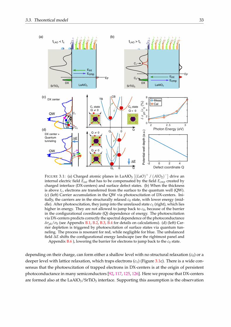
3.3. Theoretical model 33
(a) (b)
EF
EintEcmp
tLAO < tc
SrTiO3LaAlO3
0QsQ
Q ≠ 0
0Qs Q
Q = 0
Q ≠ 0
Q ≠ 0
2 2 .5 3
Photon Energy (eV)
0
2
4
6
8
ph/
0(%
) MeasCal
Defect coordinate Q-2 0 2 4P
oten
tial-w
ell d
epth
(a.
u.)
CBTBDX center
DX center +Quantum tunneling
(c)
(d)
C1 state C0 state
E
E
QW
QW
DX
C0
C1
TiO
20
LaO+1
AlO
2-1
LaO+1
AlO
2-1
LaO+1
AlO
2-1
EFEintEcmp
tLAO > tc
SrTiO3LaAlO3
DX
TiO
20
LaO+1
AlO
2-1
LaO+1
AlO
2-1
LaO+1
AlO
2-1
LaO+1
AlO
2-1
C1
C0
FIGURE 3.1: (a) Charged atomic planes in LaAlO3 [(LaO)+ / (AlO2)−] drive an
internal electric field Eint that has to be compensated by the field Ecmp created bycharged interface (DX-centers) and surface defect states. (b) When the thicknessis above tc, electrons are transferred from the surface to the quantum well (QW).(c) (left) Carrier accumulation in the QW via photoexcitation of DX-centers. Ini-tially, the carriers are in the structurally relaxed c0 state, with lower energy (mid-dle). After photoexcitation, they jump into the unrelaxed state c1 (right), which lieshigher in energy. They are not allowed to jump back to c0, because of the barrierin the configurational coordinate (Q) dependence of energy. The photoexcitationvia DX-centers predicts correctly the spectral dependence of the photoconductanceδσph/σ0 (see Appendix B.1, B.2, B.3, B.4 for details on calculations). (d) (left) Car-rier depletion is triggered by photoexcitation of surface states via quantum tun-neling. The process is resonant for red, while negligible for blue. The unbalancedfield ∆E shifts the configurational energy landscape (see the rightmost panel and
Appendix B.6 ), lowering the barrier for electrons to jump back to the c0 state.
depending on their charge, can form either a shallow level with no structural relaxation (c0) or adeeper level with lattice relaxation, which traps electrons (c1) (Figure 3.1c). There is a wide con-sensus that the photoexcitation of trapped electrons in DX-centers is at the origin of persistentphotoconductance in many semiconductors [92, 117, 125, 126]. Here we propose that DX-centersare formed also at the LaAlO3/SrTiO3 interface. Supporting this assumption is the observation

34 Chapter 3. Photoinduced tunable carrier accumulation and depletion in a quantum well
that ignoring the mediation of DX-centers leads to a spectral photoresponse in complete dis-agreement with experiments (Appendix B.5), while models assuming DX-centers describe cor-rectly the experiments (Figure. 3.1c). From deep-level transient spectroscopy (DLTS), we foundtrap energies located at ∼ (0.125 − 0.250) eV below the conduction band, which we relate toDX-centers (see Appendix B.3).
In the ground state (bc0 , b+c0) the ions surrounding the DX-center are in an equilibrium con-
figuration coordinate given by
Q0 ≈ Mq
(h
2Mωq
)1/2
(3.3)
where M is the ionic mass density, and h the Planck’s constant. Thus, Q0 = 0 relates to astructural relaxation that deform locally the lattice (Figure 3.1c). We assume further that thespectrum of excited quasi-particles of the unrelaxed DX-center related to operators (bc1 , b+c1
) andconfiguration coordinate Q1 = 0 lies within the QW. Therefore, in going from the ground to thephotoexcited state there is a change in the configuration coordinate ∆Q = Q0 − Q1 = 0 and,as a result, the lattice relaxation prevents the return of the carrier back to the initial state afterphotoexcitation (Figure. 3.1c). Consequently, the photoexcited state is long-lived, giving way toa conductance change that persists over extended periods. This phenomenon bears resemblancewith inverted kinetic theory, where chemical processes slow down even when they are ener-getically favorable [111–114]. In Marcus theory, the deceleration of charge-transfer depends onthe solvent/reaction configuration space, which plays the role of the configurational parameterspace in persistence photoconductance.
A second mechanism relies on photoexcitation via quantum tunneling described by theHamiltonian:
H1 = ∑cl
Tclb+c dl + h.c. (3.4)
where d+l , dl are creation and annihilation operators of surface states. Note that charged surfacestates break the interface-surface electrostatic balance, so that photoexcited surface states inducea charge depletion of the QW to restore electrostatic balance (Figure 3.1d) and this entails a re-duction of conductance. We will see below that the excitation of surface states is resonant at redand vanishingly small at shorter frequencies (blue and violet). We have therefore two mecha-nisms that have opposite effects on the conductance, so that the electron occupancy increasesor decreases depending on the prevalent mechanism. To describe these counterbalancing pro-cesses, we define in-scattering Σin(x, t) and out-scattering Σout(x, t) functions that give account,respectively, of the inward and outward flux of particles. These functions are assumed to be pro-portional to differential scattering cross-sections d2σ
dΩdω ∼ S(x, t) = ⟨A(x, t)A(0)⟩, where S(x, t) isthe autocorrelation function of an appropriate field operator A(x, t) [127]. For the in-scatteringfunction, A(x, t) we use the current operator j(x, t), so that Σin(x, t) ∝ ⟨Tj(x, t)j(0)⟩, where Tis the Wick’s time-ordering operator and finite-temperature Green’s functions are used to calcu-late the correlation function (see Appendix B.1, B.2, B.3, B.4). The reason of using j(x, t) is thatthe increase of electrons in the QW is proportional to the optical absorption rate given by the

3.3. Theoretical model 35
current-current correlation function [127, 128]. At the end, we arrive at the expression:
Σin(ω) ∝ P πω
[∫δ
hω −(
ε∗jX − εDX
)(1−
n∗DX (ε∗DX)) nDX (εDX) dεDXdε†
DX]
e−g(2Nq+1) ∑m δ h (ω − ωm) Im(γ) emhω0 /2kBT(3.5)
Where ω is the frequency of light, P is the transition element assumed to be energy-independent,kB the Boltzmann’s constant, n∗
DX(ε∗DX) and nDX(εDX) are, respectively, the density of states
of unrelaxed and structurally relaxed DX-center states, g is the electron-phonon coupling andNq = N0 =
[ehω0/kBT − 1
]−1gives the phonon occupation assuming an Einstein model where
all phonons have the same energy ω0. The physical interpretation of Equation 3.5 is that thetransition from relaxed (εDX) to unrelaxed (ε∗DX) DX-center states involves around m phonons,so that hωm = ε∗DX − εDX − (g − m)hω0. As a consequence, the amplitude of this transition ismodulated for different values of m, which is accounted for by the Bessel function Im(γ), whereγ = 2g
√N0 (N0 + 1).
On the other hand, the out-scattering function (describing the outward flux of particles) isproportional to the differential cross-section for tunneling across the insulating LaAlO3 barrier(described by Equation 3.4). In this case, we require that
Σout(ω) ∝ II−S = 4πeT0
∫dεni(ε)ns(ε + hω) (3.6)
where I(I−S) is the net current from interface to surface states, e is the electron charge, ϵ is theenergy, ns is the density of surface states T0 is the tunneling matrix assumed to be independentof ϵ− and ω is the frequency of light.
We use non-equilibrium formalism, where Green’s functions G< = −i⟨ck(t)c+k (0)
⟩and
G> = −i⟨c+k (t)ck(0)
⟩describe how the system responds, respectively, to the addition and re-
moval of electrons in QW states. These functions relate to the in- and out- scattering functions as−iG< + iG> = GR [Σin(ω) + Σout(ω)] GA, where GR, GA are the retarded and advanced Green’sfunctions, respectively. In the following, we demonstrate that the photoexcitation process de-scribed by Γ (ω2,ω1) = [Σin (ω2,ω1) + Σout (ω2,ω1)] is asymmetric, where a pair of short- andlong- wavelength pulses of frequencies ω2 = ω1 excites the system at two different times. Wecan formally describe the whole process by establishing a binary relation between frequency andtime ωi ↔ ti, so that the asymmetric scattering function is:
Γ (ω2,ω1)t2>t1= Γ (ω1,ω2)t2<t1
; ω2 > ω1 (3.7)
Let us first consider the process described by Γ (ω2,ω1)t2>t1. First, a pulse of light of lower
frequency excites electrons to the QW via the unrelaxed DX-center (Figure 3.1c), as well as tosurface states (Figure 3.1d). Photoexcitation via DX-centers prevails and the global effect is anincrease of electrons in the QW. Subsequently, a second pulse of higher frequency leads to astronger increase of the QW population. Now we consider the process described by the right-hand side of Equation 3.7, i.e., Γ (ω1, ω2)t2<t1
. Now a first pulse of higher frequency leads to anincrease of the QW population. However, a subsequent pulse of lower frequency decreases thepopulation of the QW (Figure 3.1d), because of the excitation of surface states resonant at longer

36 Chapter 3. Photoinduced tunable carrier accumulation and depletion in a quantum well
wavelengths, which induces a depletion of the QW population. Therefore, time order in pulsedsequences of photoexcitation matters, as it determines whether the QW occupancy increases ordecreases.
The data shown in Figure 3.2a-b validate the asymmetric photoresponse described by Equa-tion 3.7 (see Chapter 4, for further experimental details). We first discuss the experiments de-scribed by the left-hand side of Equation 3.7, Γ (ω2, ω1)t2>t1
(ω2 > ω1). A first pulse of redlight (λ1 = 632 nm) and duration ∆τ1 = 10 seconds precedes a second pulse of blue light (λ1 = 450 nm) and duration ∆τ2 = 10 seconds. At the end of this two-pulse sequence, the conduc-tance increases by an amount ∆σ1→2 = σ (t2)− σ (t1) ≈ 0.05 µS which is almost 2% of the initialconductance (Figure 3.2a). Now, we consider the reverse process, i.e., Γ (ω1, ω2)t2<t1
(ω2 > ω1),where the timing of pulses is inverted with respect to the previous two-pulse sequence. In thiscase, a first pulse of blue light reaches the sample, followed by a red pulse, both of them ofsame duration as before, so that only their relative timing is inverted. Now, we observe thatthe conductance resets to the initial value, before illumination with the first pulse (Figure. 3.2b).This observation shows that resonant photoexcitation to surface states via quantum tunnelingleads to carrier depletion. We further observe that the depletion depends on the wavelengthof the second pulse, being strongest for red and absent for blue (Figure 3.2c-d), indicating thatthe excitation is resonant near red light. This wavelength-dependent asymmetric photoexcita-tion enables the modulation of the QW conductance through sequences of multiple short-/long-frequency pulses, depending on the relative time arrival of photons of different wavelengths(Figure 3.2g), which we further discuss below in the context of neuromorphic computation.
Two further experiments confirm the relevance of balanced electrostatic boundary conditionsin the photoinduced carrier accumulation and depletion. First, we note that the internal electricfield exists as long as the LaAlO3 is epitaxial, while it should be absent in amorphous layers[63, 123, 124]. Therefore, the photoexcitation to surface states of amorphous LaAlO3 should notaffect the QW population because there is no field to compensate inside the barrier layer. Wechecked this prediction by measuring the photoconductance of devices defined on interfacesbetween amorphous LaAlO3 films (t ≈ 3 nm) and SrTiO3 (see Figure 3.3a-b). The experiments,shown in Figure 3.3c, confirm that the mechanism for carrier depletion is absent in this case.
Secondly, quantum tunneling decays exponentially with the barrier thickness, so that carrierdepletion caused by excitation to surface states should drop fast as the thickness of LaAlO3
increases. To verify it, we measured the difference ∆Ξ ≡ [∆σ1→2 − ∆σ2→1] in devices definedwith variable LaAlO3 thickness. Figure 3.3c displays the results for t ≈ 5uc ≈ 2nm and t ≈14 uc ≈ 5 nm, confirming the strong reduction of ∆Ξ with barrier thickness.
The asymmetric photoexcitation described by Equation 3.7 is of potential interest for neu-romorphic engineering, which aims at designing physical systems inspired by neurobiology. Inparticular, spike-timing-dependent plasticity (STDP), where the relative timing of neuron spikesrules the increase or decrease of plastic synaptic strength, is fundamental to achieve unsuper-vised learning [120–122]. Inspired by these principles, there has been multiple efforts to im-plement STDP in physical systems, with a particular success using memristors, where electricimpulses mimic the action of neuron spikes [119, 121].
In this work, we show that the asymmetric photoexcitation of the LaAlO3/SrTiO3 QW may

3.3. Theoretical model 37
10 20 30 40 50 60Time (s)
0
0.05
0.1
ph-
0(
S)
0 20 40 60 80 100Time (s)
0
0.05
0.1
0.15
ph-
0(
S)
0 20 40 60 80 100Time (s)
0
0.05
0.1
0.15
ph-
0(
S)
(b)
( 1, 2)t2<t1
(a)
( 2, 1)t2>t1
0 20 40 60Time (s)
0
2
4
6
8
ph/
0(%
)
RR+RR+GR+BR+V
0 20 40 60Time (s)
-2
0
2
4
6
8
ph/
0(%
)
VV+RV+GV+BV+V
0 20 40 60Time (s)
-2
0
2
4
6
8
ph/
0(%
)
RR+RR+GR+BR+V
0 20 40 60Time (s)
-2
0
2
4
6
8
ph/
0(%
)
VV+RV+GV+BV+V
(c) (d)
(e) (f)
(g)
FIGURE 3.2: (a) Photoconductance measured in a two-pulse sequence, where ared pulse comes first, followed by a blue pulse. The situation corresponds toΓ (ω2, ω1)t2>t1
in Equation 3.7. (b) Photoconductance measured after a first bluepulse, followed by a red pulse, corresponding to Γ (ω1,ω2)t2<t1
. Note that whenred follows blue, there is a decrease of conductance, instead of an increase. (c)Photoconductance measured after a red pulse followed by green, blue and violetpulses. In all cases, there is an increase of conductance after the second pulse. (d)The situation is reversed when red follows a violet pulse. In this case, the con-ductance decreases after the second pulse. The effect is resonant with red, andnegligible for blue. Relative changes of conductance after different multiple-pulsesequences. We represent the timing in the upper part of the figure. The blue curvein the figure corresponds to conductance changes induced by multiple an all-blue-pulse sequence, while the red curves displays the photoconductance measuredunder multiple blue/red-pulse sequence. The whole sequence shows that time-correlated arrival of pulses of different frequencies increase or decrease plastically
the conductance.

38 Chapter 3. Photoinduced tunable carrier accumulation and depletion in a quantum well
FIGURE 3.3: (a) Hall devices, pictured here, were used to measure the photo-conductance. We fabricated devices with epitaxial (c-LaAlO3) and amorphous(a-LaAlO3) LaAlO3 layers (see the STEM images). In (b) we show a schematicdepiction of the corresponding atomic arrangements. (c) Illumination with blueplus red pulses induces carrier depletion in the sample with thin epitaxial LaAlO3(t = 5 uc ≈ 1.9 nm). However, the depletion is much smaller when the thick-ness increases to t = 14 uc ≈ 5.6nm. Likewise, carrier depletion is absent in thesample with amorphous LaAlO3 layer. Therefore, carrier depletion via quantum
tunneling photoexcitation requires thin epitaxial layers of LaAlO3.
implement STDP using optical stimulation instead of electric inputs. More specifically, wedemonstrate that multiple-pulse sequences increase or decrease the conductance depending onthe relative timing of long- and short-wavelength pulses in a way that is comparable to mem-ristive STDP devices [121], paving the way to optical STDP synapses. To illustrate this point,we refer to the data displayed in Figure 3.2e, which corresponds to a sequence of blue and redpulses. We observe that illumination with red after the first blue pulse entails a significant de-crease of conductance, which in this context plays the role of the synapse. A subsequent redpulse decreases even more the conductance with respect to the first red pulse, showing a cu-mulative effect. The next two blue pulses increase substantially the conductance and, finally,

3.4. Conclusion 39
the third and last red pulse decreases once more the conductance. Therefore, appropriate timedcombinations of short-/long- wavelength pulses can fine-tune the conductance, featuring spike-timing-dependent plasticity using optical inputs in a similar way as memristive synapses repli-cate STDP using electric stimuli [121].
3.4 Conclusion
We have explored the persistent photoconductance at the epitaxial LaAlO3/SrTiO3 interface,which is interpreted with a large lattice relaxation model. Furthermore, we have demonstrateda wavelength-dependent time-correlated photoresponse. This asymmetric photoresponse in-volves photoexcitation of electrons from defect-related DX-centres at the interface, plus a pho-toexcitation to surface states via quantum tunneling. The observed photoresponses can be ex-ploited for optical synapses with STDP, which will be developed and explained in Chapter 4. Onthe other hand, STDP cannot be implemented in amorphous LaAlO3/SrTiO3 interfaces, due totheir non-epitaxial microstructure. However, the relatively large sensitivity of the photoconduc-tance of amorphous LaAlO3/SrTiO3 interfaces may make them interesting for neuromorphicapllications that do not require STDP, which is discussed in Chapter 5.


41
Chapter 4
Solid-State Synapses Modulated byWavelength-Sensitive TemporalCorrelations in Optic Sensory Inputs
In Chapter 3, we have given a physical explanation of the photoconductance with wavelengthcorrelations at the epitaxial LaAlO3/SrTiO3 interface. In this chapter, we study in detail thewavelength-dependent time-correlated photoresponses and show that they can be exploited foroptical synapses with wavelength-sensitive STDP. Finally, simulations suggest that this capa-bility may stimulate neuromorphic hybrid electronic/photonic systems to construct biomimeticspatial memory and navigation maps inspired from neurobiology.
4.1 Abstract
Recently, inspired by neurobiological infor-mation processing, correlation-based learn-ing has been expressed physically in nonbi-ological systems by exploiting time causal-ity of electric signals. Yet, the capabilityto learn from visual events requires extend-ing these concepts to optical stimuli. Herewe show a solid-state system (the epitaxialLaAlO3/SrTiO3 interface) that is sensitive to100-millisecond-scale timing of pairs of lightstimuli with complementary short/long visi-ble wavelengths, causing asymmetric changesof photoconductance. This property endowsoptical signals with time causality, leading towavelength-sensitive time correlations withtimescales comparable with those of percep-tual recognition. Based on these observations, we propose that complex information can be

42 Chapter 4. Wavelength-Sensitive Temporal Correlations at the epitaxial LaAlO3/SrTiO3
extracted from visual patterns imprinted as spatiotemporal modulations of persistent photocon-ductance. We suggest that this capability may stimulate neuromorphic hybrid electronic/pho-tonic systems to construct biomimetic spatial memory and navigation maps inspired from neu-robiology.
4.2 Introduction
V
D
O Q
Ea
C
FIGURE 4.1: The persistence photocon-ductance in terms of the space of config-urational coordinates [92]. Before pho-toexcitation, the electron is in a deep DXcenter (D). When D is occupied, thestrong coupling to the lattice induces arearrangement of the ion positions in itsimmediate vicinity, and the strain as-sociated with such distortion is repre-sented by Q = 0. An incident photoninduces an electronic transition from Dto the 2DES (C), while a structural lat-tice relaxation drives a change of the DXcenter to Q = 0. The irreversible shiftin Q implies an energy barrier (Ea), pre-cluding the return of the electron backto the initial state. The energy levels ofthe vibronic state of D corresponding toquantum levels of a harmonic oscillator
are graphically depicted.
In nervous systems, sensory neurons convert stimuliinto action potentials that send information to the brain.Inspired by these neurobiological processes, neuromor-phic engineering has emulated cognitive functionalityin several nonbiological systems, including memristors[129, 130], phase-change materials [131], spin oscillators[53, 132] or ferroelectric junctions [122]. Similarly, bio-logical transduction has inspired technological develop-ments, e.g., the emergence of neuromorphic vision chips[133, 134], which enable real-time analysis of high-speedmovements unattainable by conventional technologies[135, 136]. Underlying brain cognitive capabilities is theconcept of synaptic plasticity [121], whereby the strengthof excitatory (inhibitory) synapses can increase (decrease)over time in response to changes in neuron activity. Aparticularly relevant case occurs when synaptic modu-lation is driven by the correlated activity of pre- andpostsynaptic neurons, which was initially postulated tostabilize neuronal activity patterns in the brain that im-ply learning [137]. Inspired by such principles, time-correlated synaptic changes in the form of spike-time-dependent-plasticity (STDP) was first suggested in com-putational neuroscience [121] and experimental evidenceaccumulated in biological systems [138–140]. Along theselines, solid-state synapses based on memristors have beendemonstrated to exploit causality of electric signals andenabling unsupervised learning [122]. Yet, the develop-ment of artificial neural networks interacting with a va-riety of environmental inputs requires the extension oftime-correlations beyond electric signals. Particularly, correlated timing of optical stimuli wouldenable a whole new perspective on biomimetic artificial vision, where learning rules could beapplied to complex visual events [141].
In this work we show that causally correlated potentiation and depression of synaptic plas-ticity can be replicated in a solid-state system that exhibits persistent photoconductance (PPC)[58, 92], where the conductance suddenly changes after illumination with visible, or ultraviolet

4.3. Results 43
light or X-rays [142] and the effect persists over long periods after the light is off. This phe-nomenon, observed in many semiconductors, is generally caused by DX centers [87], wherebyshallow donors undergo a large lattice relaxation, thus preventing the return of the carrier backto the initial state after photoexcitation [92] (Figure 4.1). Our study reveals that the conductanceof the PPC system can be increased or decreased in a controlled way by external optical stim-uli formed by combinations of short-/ long-wavelength pairs of visible light pulses, where thecontrol is done at 100 millisecond-scales, comparable with timescales for perceptual recognition.The synaptic modulation can be fine-tuned by the order of the time arrivals of the light pulses aswell as by their duration and, most remarkably, it is wavelength-sensitive, namely, the particularselection of the wavelengths of the light pulses is critical to the synaptic modulation. We positthat wavelength-sensitive time-correlations in optical stimuli can be exploited to use informa-tion encoded in light to build spatial memory and navigation maps akin to processes occurringin brains, with timescales comparable with cognitive processes.
The system under study is the interface between SrTiO3 and LaAlO3 , two wide-bandgapsemiconductors. As described in Chapters 1 and 3, despite the insulating character of the con-stituent materials, a highly-conductive two-dimensional electron system (2DES) develops acrossan nm-thick region around the interface [63]. This 2DES hosts a number of properties includingsuperconductivity [64], large spin-orbit fields [66] and, importantly for the context of this work,PPC [67].
4.3 Results
2DES
I (uA)
VSrTiO3
500 um
50 um
A-LaAlO3
LaAlO3
0 80 160 0 80 160 0 80 160 80 16000
2
3
4
Time (s)
I Nor
mph
/0
(%)
0.5
1.0 w/cm2
638 nm 520 nm 450 nm
405
(a) (b)
FIGURE 4.2: a) The upper panels show optical micrographs of a Hall bar. Thelower panels show a schematic depiction of the Hall-bar geometry (left) and across-sectional graphic view of the LaAlO3/SrTiO3 device used in the experiments.A-LaAlO3 and C-LaAlO3 stand, respectively, for amorphous and epitaxial LaAlO3(right) (see Methods for details on sample and device preparation). b) Schematic
depiction of the Hall-bar geometry.
Our study comprises epitaxial LaAlO3 thin films with thickness t ≈ 1.1 − 5.3 nm ( 3 − 14unit cells, u.c.) grown on (001)-oriented SrTiO3 crystals. By way of illustration, Figure 4.2asummarizes the main features of PPC by displaying data extracted from measurements donewith wide pulses (tens of seconds in contrast to millisecond-range pulses studied below) at fourwavelengths in the visible red (λ = 638 nm), green (λ = 520 nm), blue (λ = 450 nm) and violet

44 Chapter 4. Wavelength-Sensitive Temporal Correlations at the epitaxial LaAlO3/SrTiO3
(λ = 405 nm) and different irradiance values. In these experiments, Hall-bar devices where de-fined by optical lithography (Figure 4.2b). The transport was characterized by injecting currents(typically I ≈ 1 µA) along two contacts, and measuring the longitudinal resistance by probingthe voltage on two other contacts (typical resistance values were R ≈ 100 − 500 kΩ, see alsoSupporting Information Section 4.7.8 for more details on the voltage readout). Photoexcitationexperiments were carried out at room temperature using high-numerical-aperture (high-NA)focusing. After switching the light on, there is a sudden increase of conductance (Figure 4.2a)
that we quantify asδσph(t)
σ0=
σph − σ0
σ0, where σ0 is the conductance prior to switching the light
on and σph is the time-dependent conductance.
Time (s)
638 nm 520 nm 450nm 405 nm
0.05
0.1
0.25
0.5
1
5
10
Pul
se W
idth
(m
s)
Power Density (W/cm2)0.25 0.5 0.75 1.0 1.25 1.5
638 nm 520 nm 450 nm 405 nm
638 nm 520 nm 450 nm405 nm
(a) (b)
ph/
0 (%
)
ph(peak)
0 (%)
0
0.3
0.6
0.9
1.2
Wavelength and duration
FIGURE 4.3: a) Photoconductance measured under illumination with trains ofpulses of different wavelength (638, 520, 450 and 405 nm), width ( Wp ≈ 0.05 −10 ms) and irradiance (0.25 − 1.25 W/cm2). b) Two-dimensional maps where thephotoconductive response is mapped against wavelength, irradiance and pulse
width.
The analysis of the time-dependent response shows that light stimuli can be detected downto milliseconds for visible wavelengths (Figure 4.2 and Figure 4.3 ). The photoconductance wasmeasured under illumination with different wavelength, width and irradiance (Figure 4.3a),
and the photoconductive responseδσph(t)
σ0is mapped against wavelength, irradiance and pulse
width in the 2-dimensional maps shown in Figure 4.3b.
Furthermore, measurements ofδσph(t)
σ0after illumination with light pulses of varying du-
rations and different illumination conditions demonstrate a plastic PPC response that can befine-tuned by controlling the cumulated illumination time (Figure 4.4a,b). This is also shown inFigure 4.4c,d. In particular, Figure 4.4c displays the reflected intensity measured by the photode-tector replicating the shape of the incoming light pulses of cumulated times spanning the rangeof 5 − 250 milliseconds. In Figure 4.4d we plot the full time evolution of the photoconductanceover the whole period of analyzed time, after illumination with light pulses of cumulated timesspanning the range 5 − 250 milliseconds. The middle panel shows a zoom of the data aroundthe initial times, while the right panel displays the data for a time interval ≈ 156 − 160 afterthe light is switched off. As Figure 4.4d shows, in spite of some occasional irregularity (see,e.g., right panel of Figure 4.4d corresponding to data indicated by the arrow in Figure 4.4b), thephotoconductance response can be fine-tuned by the cumulated time, as can be seen in Figure

4.3. Results 45
4.98 5 5.02 5.04 5.06 5.08 5 5.1 5.2 5.3 5.4 5.5 7
Inte
nsity
ph/
0 (%
) 1 25 75 150 ON
1 25 75 150 ON
(c)
ph/
0 (%
)
ph/
0 (%
)
Time (s)
Time (s) Time (s) Time (s)
(d)
(a) (b)
5 ms
25 ms
125 ms
250 ms 2 s
FIGURE 4.4: (a) and (b) show the tunability of the photoconductance by exposingthe sample to violet (λ = 405nm) light pulses of different timespans. In particular,
(b) shows the changes in photoconductanceδσph(t)
σ0measured at different probe
times ( τ = 0, 15, 30 and 45 s) as a function of the cumulated illumination time. Inparticular, (c) displays the reflected intensity measured by the photodetector repli-cating the shape of the incoming light pulses of cumulated times spanning therange of 5 − 2000 ms. In (d). we plot the full time evolution of the photoconduc-tance over the whole period of analyzed time, after illumination with light pulsesof cumulated times spanning the range of 5 − 250 ms. The color code identifyingthe cumulated time in the 5 − 250 ms range is the same as in panel (c). The middlepanel shows a zoomed-in portion of the data around the initial times, whereas theright panel displays the data for a time interval of ∼ 155 − 160s after the light is
switched off.
4.4c. We also note that the photoconductive response shows an uneven dependence on wave-length, with an apparent unexpected smaller responsiveness to green light (Figure 4.3b). Wesuggest that the particulars of the spectral response are related to the details of the density ofstates linked to the energy landscape of the involved defects, as well as to the features of theconduction band. Below we elaborate further on these aspects in connection with the plausiblemicroscopic mechanisms at work for the observed PPC response.
Motivated by computational approaches to use visual patterns for learning similar to timecorrelations observed in biological systems [141, 144], we explored the possibility to expressphysically such concepts using persistent photoconductance. The basic idea is to combine lightpulses (sensory inputs) of two complementary wavelengths that have opposite effects on the

46 Chapter 4. Wavelength-Sensitive Temporal Correlations at the epitaxial LaAlO3/SrTiO3
(a) (b)
0
0.2
0.4
0.6
0.8
1
(+)
5 5.5 6Time (s)
t=0 ms t=40 mst=100 mst=200 ms
ph/
0 (%
)
-100 -50 0 50 100t (ms)
-0.6
-0.4
-0.2
0
0.2
0.4
0.6
6.5
- tpre-
t+
post-
0
0
(-)
(+)
0-
(-)
0
-
5 5.5 6
w wpre-
post-
FIGURE 4.5: a) (Left upper panel) Photoconductance measured after a single pulseof red (δTr = 60 ms, red line) and after a two-pulse sequence of red ( δTr = 60 ms)plus violet (δTv = 40 ms), purple line. The two-pulse sequence increases the pho-toconductance from Σ0 to Σ0 + |∆Σ(+)|. (Right upper panel) The order of thepulse timing is reversed: violet pulses (δTv = 40 ms) are followed by red pulses(δTv = 0 − 200 ms); the conductance now decreases from Σ0 to Σ0 − |∆Σ(−)|. Theresults displayed in a) enable a formal equivalence between red/violet pulse tim-ing and causality of pre- and post-synaptic neurons, as shown schematically inthe lower panels. b) Plots the causal (|∆Σ(+)(∆t)|) and anti-casual (|∆Σ(−)(∆t)|)branches of the learning curve derived from experiments in a). For clarity, thedata of the branch is magnified by 5. Dashed lines in b) are a fitting to Equation4.1 . Two-pulse sequences are used to simulate a map model for head direction[143]. At every orientation, just a small number of synapses are potentiated, while
synapses unrelated to that orientation are depressed.
plasticity of PPC. With this in mind, we tried different combinations of wavelengths in the visi-ble. First, we consider the illumination with short pulses of red, green or blue followed by violet.In this case, in agreement with the cumulative effect discussed in the previous discussion, illu-mination with the second pulse just increases the photoconductance above the value set by thefirst pulse (see the left upper panel of Figure 4.5a for red followed by violet). However, the out-come is different when we reverse the timing: if violet pulses are followed by green or red, thephotoconductance is decreased with respect to the first pulse (right upper panel of Figure 4.5aand Chapter 3). These observations are in line with the time-correlated wavelength-dependentphotoresponses discussed in Chapter 3. The decrease after the second pulse depends on thewavelength used for the the second pulse: the suppression of photoconductance is the largestfor red and diminishes progressively towards blue (Figure 4.10 and Chapter 3). This observa-tion hints at the use of time correlations between long and short wavelengths to drive synapticchanges. Indeed, multiple-pulse sequences of long-/short- wavelength timed pulses can beused to modulate the conductance enabling spike-timing-dependent plasticicity (see Figure 4.18in Supporting Information Section 4.7.9 ). To exemplify this approach, we select red and violetwavelengths to establish a formal equivalence with pre- and post-synaptic neurons [121], respec-tively (see the sketches in Figure 4.5a). The first pulse, red or violet, sets the initial photocon-
ductance Σ0 ≡δσph(∆t0)
σ0. Subsequently, depending on the relative timing of the short-/long-
wavelength in the two-pulse sequence, the second pulse either increases (Σ(+) ≡ Σ0 + |∆Σ+|,Figure 4.5a left upper panel or decreases the conductance (Σ(−) ≡ Σ0 − |∆Σ(−)|, Figure 4.5aright upper panel). This allows defining causal (Σ(+)) and anti-causal (Σ(−)) learning branches,

4.4. Discussion of the potential for neuromorphic engineering 47
respectively, using sub-100 millisecond pulses (Figure 4.5b) that, in our case, can be describedapproximately by:
∆Σ(±)(∆t) =
∝ [+|A+,0| − |A+|e+δt
τ+ ] for ∆t > 0
∝ [−|A−,0|+ |A+|e−−δtτ− ] for ∆t < 0
(4.1)
where A+,o, A+, A−,o, A− reflect, respectively, the amplitudes of potentiation and depressionand τ+,τ− are the corresponding time constants.
Summarizing, our study reveals that the conductance can be accurately increased or de-creased by a combination of three basic factors: (i) time arrival: if short-wavelength pulses arriveearlier than long-wavelength pulses, the conductance increases with respect to the first pulse(case i.1), while the conductance decreases with respect to the first pulse if short-wavelengthpulses arrive later than long-wavelength pulses (case i.2), (4.6a,b); (ii) cumulated time: the in-crease of conductance case i.1 or its decrease case i.2 is modulated by the cumulated time ofthe light pulses. This is shown in 4.6a,b where the precise amount of decrease or increase ofconductance depends on the duration of the combined pair of pulse trains; (iii) wavelength: asshown in 4.6c-e, for fixed cumulated times, the decrease of conductance in short-/long- wave-length pairs is modulated by the wavelength of the second train of pulses. In particular, thedecrease of conductance is largest for second pulses of red light, smaller for green and negligi-ble for blue.
Before proceeding, we make an important observation regarding our approach to time cor-relations using optical inputs. Our work reveals that if we consider time correlations of opticalstimuli that change the synaptic weight between a first (pre-synaptic pulse) and a second (post-synaptic) pulse, a new concept that uses also the wavelength of light can be exploited to achievespiking time dependence plasticity. This concept enables the replication of inhibitory or excita-tory synapses encompassing a wide diversity of functional dependences [143, 145]. As describedbelow, we propose that this these wavelength.-sensitive time correlations can be also exploitedto use information encoded in light to build spatial memory and navigation maps akin to pro-cesses occurring in biological brains, with timescales comparable with biological processes.
4.4 Discussion of the potential for neuromorphic engineering
The application of correlation-based rules for synaptic update is interesting, as it enables unsu-pervised learning [141], which in this case would apply to visual inputs [141, 144]. Indeed, neu-ron models based on memristive devices that implement STDP have been already demonstratedto show unsupervised learning [122, 146]. Here we shifted our attention away from known ap-plications of time-correlated synaptic changes to explore alternative possible implementationsinto new domains. More specifically, we explored the feasibility of exploiting the observed phe-nomenon to emulate the coexistence of excitatory and inhibitory synapses which is indispens-able to build brain-like cognitive maps [147–149]. As an exemplary illustration, we considerthe construction of one-dimensional attractor map models for head direction, in which neuronfiring rates evoke the direction along which the head is facing [147]. With this in mind, we

48 Chapter 4. Wavelength-Sensitive Temporal Correlations at the epitaxial LaAlO3/SrTiO3
0
(-)
d e
638 nm 520 nm 450 nm
(+)
0
ph/
0 (%
)
ph/
0 (%
)
ph/
0 (%
)
Time (s) Time (s) Time (s)
Time (s) Time (s)
(b)
(c) (d) (e)
(a)
FIGURE 4.6: The ensemble of panels display the changes Σ0 ± |∆Σ(±)| of the con-ductance measured after two-pulse sequences of red (∆Tr = 0 − 95 ms) plus vi-olet (∆Tv = 0 − 95 ms).The value of is set after the first pulse. a) The two-pulsesequence Σ0 increases the photoconductance from Σ0 to Σ0 + |∆Σ(+)| when redpulses come before violet. b) When the order of the pulse timing is reversed, i.e.,violet pulses are followed by red pulses, the conductance decreases from Σ0 toΣ0 − |∆Σ(−)|. The timing and duration of the first and second pulses determinequantitatively the increase or decrease of conductance. Labels R(X)V(Y)/V(Y)R(X)in panels a) and b) display the conductance changes after combined pulses of redand violet light of duration X and Y milliseconds. The measured changes in pho-toconductance (±|∆Σ(±)| ) are used to plot the causal and anti-causal branches ofthe plot shown in Figure 4.5. Panels c)-e) show the photoconductance measuredafter a single pulse of violet (∆Tv = 40 ms) followed by red, green and blue pulsesof varying duration ∆T(r,g,b) = 0 − 200ms . Since longer-wavelength pulses comeafter short-wavelength pulses, the synaptic strength is decreased with respect tothe first pulse (we are in the Σ0 − |∆Σ(−)| anti-causal branch of Figure 4.7 a. Yet,the value of the decrease of conductance (−|∆Σ(−)| ) depends on wavelength: the
suppression is the largest for red, smaller for green and negligible for blue.
simulated leaky integrate-and-fire neurons driven asynchronously by two input sensory cells,corresponding to red and violet stimuli (see Experimental Section 4.6 and Supporting Informa-tion Section 4.7.3 for extensive details). Figure 4.7a shows graphically the time evolution of thesynaptic strengths of selected neurons for two simulated consecutive head movements alongtwo orientations in space. We stress that for the sake of realistic modeling, the calculations takecare of the experimental decay times of conductance after photoexcitation with red or violet lightpulses (Figure 4.5a and Supporting Information at the end of this Chapter). In the simulated pro-cess, illumination with violet pulses potentiates the synaptic strength of the small neuron clusterconnected to a particular orientation in timescales shorter than 200 ms (Figure 4.7b). Note thatduring the transient to a new orientation, red pulses are indispensable to inhibit the strengthof synapses unrelated to the new position. Indeed, as shown in Figure 4.7b (middle panel) andFigure 4.11 (Supporting Information Sections 4.7.2, 4.7.3) the use of red pulses is crucial to speedup the inhibition of firing activity to timescales of a few 100s ms. Finally, Figure 4.7b displays

4.5. Conclusion 49
the firing activity of the simulated neurons for the given threshold of synaptic strength. Westress that although we focus our discussion to two specific wavelengths, our results suggestthat the full spectrum can be exploited to achieve causality between pairs of short-/long- wave-length pulses, with varying degrees of intensity of potentiation and depression (Figure 4.10 andSupporting Information Sections 4.7.2). Based on these observations, we propose that the tran-scription of optical flow from scenes captured in silicon retinas [135, 136] may be used in theLaAlO3/SrTiO3 system to emulate cognitive maps from temporally-correlated sensory inputson the 100s millisecond range, comparable to timescales for perceptual recognition [150].
0 250 400 t (ms)900 1200
N-6: V
N-6: V+R
N-21
msmsmsmsms
ms
(V+R)(V)
(a)
(b)
ph/
0 (%
)ph
/0 (%
)
O1 O2
ph/
0 (%
)
FIGURE 4.7: a) Radial and linear plots of the calculated synaptic strengths for twohead movements (O1 and O2). c) Firing activity (vertical dashed lines) of selectedsimulated neurons for orientation O1, given the threshold of synaptic strength(dotted horizontal line), stimulated either using a single violet pulse (upper panel)or two-pulse sequences (middle panel). The lower panel displays the activity of a
selected neuron for orientation O2.
4.5 Conclusion
We conclude by stressing that the results described here may profit from recent developments inartificial vision that, inspired by neurobiology, rely on image acquisition triggered asynchronouslyby per-pixel log-scale changes in brightness, which increase dramatically the dynamic perfor-mance by suppressing data redundancy [135, 136]. We envision that this progress, together with

50 Chapter 4. Wavelength-Sensitive Temporal Correlations at the epitaxial LaAlO3/SrTiO3
outstanding advances in silicon integrated photonics including the development of on-chip op-tical modulators and laser sources [151] provides a unique opportunity to use the kind of time-correlated plasticity described here to expand todays neuromorphic vision technologies. Inter-estingly for this context, the creation of two-dimensional electron systems in LaAlO3/SrTiO3
has been demonstrated on top of silicon [152]. Bearing these advances in mind, we envision thatintegrated electronic/photonic circuitry can be purposely designed to encode optic flow fromneuromorphic retinas that can be used to build representation maps reminiscent of those thatunderpin the ability of self-localization and object motion detection in the brain [147].
4.6 Sample preparation and simulations
4.6.1 Sample Preparation
FIGURE 4.8: Temperature dependence of the sheetresistance measured along the Hall-bar of a 5 uc
thick epitaxial LaAlO3/SrTiO3 interface.
Using the aforementioned lithography pro-cesses (Chapter 2), Hall bars were definedwith channel widths typically in the range∼ 5 − 10 µm and lengths ∼ 80 − 100 µm (Fig-ure 2.4). The conductive 2DES at the interfaceonly emerges when LaAlO3 films are above acritical value [153, 154]. Indeed, the lithogra-phy process is designed so that the 2DES isconstrained within the Hall bars and, there-fore, different Hall bridges defined in a samesample should be ideally isolated electrically.This point was checked out by measuring theresistance between contacts of different Hallbars. We also measured the temperature de-pendence of the resistance in the Hall bars, showing a metallic behavior all the way down tolow temperatures (see one representative data in Figure 4.8). The measurements of the carrierdensity and mobility yielded values ns ≈ 1013 cm−2 and µ ≈ 1400 cm−2/s(at 4 K), respectively,comparable to those reported in the literature [153].
4.6.2 Simulations of neural networks
The simulations of temporally correlated input sensory neurons (Figure 4.13 ) were performedusing the Brian Simulator open source code, which is written in the Python programming lan-guage [95]. We considered the problem of replicating the firing activity patterns of neuronsbuilding cognitive maps in the brain. In particular, we focused on attractor map models forheads direction, where a small cluster of neurons spike at a given head orientation. Crucialto this point is the fact that the formation of cognitive maps in biological brains related to, e.g.,spatial memory, self-location and self-motion in the environment require imperatively both exci-tatory and inhibitory actions on the synaptic strength [122, 133, 150]. This prerequisite suits well

4.7. Supporting Information 51
to the sort of potentiation and depression observed in our experiments using time correlatedoptical inputs.
4.7 Supporting Information
4.7.1 Structural characterization of epitaxial LaAlO3/SrTiO3 samples
We collaborate with J. Gazquez for structural measurements using transmission electron mi-croscopy. Figure 4.9 shows an image captured using scanning transmission electron microscopy(STEM) from an epitaxial LaAlO3/SrTiO3 layer grown under identical conditions as the onesreported in the manuscript. This image was obtained using a high angle annular detector, giv-ing Z-contrast imaging. Additionally, we acquired images from an annular bright field (ABF)detector, which allows the imaging of lighter elements, such as oxygen. With this technique wehave been able to probe the distortions of A, B and O sub-lattices across the heterostructure.Figures S1a and S1b show a simultaneously acquired Zcontrast and ABF images of a 7 u.c thickLaAlO3 layer grown on SrTiO3, respectively. Both images were acquired along the [110]-zoneaxis in order to view the characteristic O octahedra rotation of the LaAlO3 layer. The arrowsmark the interface, formed at the boundary between the last TiO2 plane of the SrTiO3 substrate.A schematic view of LaAlO3/SrTiO3 interface with La in green, Al in blue, Sr in red and Ti inellow is shown in Figure 4.9c.
FIGURE 4.9: (a) and (b) show simultaneously acquired Z-contrast and annularbright field (ABF) images of a 7 u.c thick LaAlO3 layer grown on SrTiO3, respec-tively. Both images were acquired along the [110]-zone axis in order to viewthe characteristic O octahedra rotation of the LaAlO3. Along this zone axis, theprojection of this rotation appears as a O sub-lattice rippling, as can be seen inthe ABF image. The arrows mark the interface, corresponding to the last TiO2plane of the SrTiO3 substrate. (c) Schematic view along the [110]-zone axis of theLaAlO3/SrTiO3 interface with La in green, Al in blue, Sr in red and Ti in yellow.
4.7.2 Long-term depression of photoconductance induced by illumination with two-pulse sequences
As discussed in Section 4.3, the observed two-pulse temporal correlations depend critically onthe inhibitory action of illumination with second pulses of wavelength longer (e.g., red) than theone used in the first pulse (violet). In these conditions, the measurements of the conductance

52 Chapter 4. Wavelength-Sensitive Temporal Correlations at the epitaxial LaAlO3/SrTiO3
after the second pulse show a decrease (Σ0 − |∆Σ(−)|) with respect to the conductance measuredafter the first pulse (Σ0). This decrease depends on the wavelength used for the second pulse:the suppression of photoconductance is the largest for red, smaller for green and vanishinglysmall for blue (Figure 4.10a). As discussed in Chapter 3, this spectral dependence is assigned toresonant photoexcitation of surface states with red light, while blue or violet are off-resonance.
0 100 200Timer/g/v (ms)
-0.25
-0.2
-0.15
-0.1
-0.05
(a) (b) (c)
(-) (t
0)-
0
FIGURE 4.10: (a) Photoconductance measured after a single pulse of violet (∆Tv =40 ms) followed by red, green and blue pulses of varying duration (∆Tr,g,b =
0 − 200 ms). The conductance is decreased after the second pulse from Σ0 (justafter the first pulse of violet) to Σ0 − |∆Σ(−)| after the second pulse. The decreasein conductance, quantified by ∆Σ(−)| measured at time t0 = 500 ms after switch-ing off the second pulse. We see that ∆Σ(−)| depends on wavelength: the sup-pression is the largest for red, smaller for green and negligible for blue. (b) Timedependence of the photoconductance change obtained after a single pulse of vi-olet (∆Tv = 40 ms) and also after a two-pulse sequence of violet (∆Tv = 40 ms)followed by red (∆Tr = 60 ms). (c) The data shown in (b) are zoomed in around
the initial time lapse after switching off the second pulse.
Figure 4.10b shows the time dependences of the photoconductance measured after a singlepulse of violet (∆Tv = 40 ms) and also after a two-pulse sequence of violet (∆Tv = 40 ms) fol-lowed by red (∆Tr = 40 ms). When we compare both curves we see that the illumination with redin the last step of the two-pulse sequence suppresses the conductance with respect to the valueobtained with the one-pulse sequence. Figure 4.10c shows a zoom of the data displayed in Fig-ure 4.10b around the initial time lapse after switching off the second pulse. We observe that afteran initial overshoot, the conductance is steadily decreasing for time lapses ∆t > 300 ms. The data
in Figure 4.10c is fitted to biexponential functions σ = σ0[Aexp(− tτdec,1
) + (1 − A)exp(− tτdec,2
)]
used to fit the decay time of the photoconductance after illumination with violet or red light.The values of τdec,1 and τdec,2 are used for the simulations of leaky integrate-and-fire neuronsdescribed below.
The potentiation/depression caused by complementary pairs of short-/long-wavelength twosequence pulses is a phenomenon observed across the visible spectrum. To show this point,we carried measurements of the conductance after combinations of light pulses other than vio-let/red pairs. Figure 4.11 shows the change of photoconductance after one single pulse of greenand after a two-pulse sequence of green followed by red. Figure 4.11b displays the change ofphotoconductance after a single pulse of blue and after two-pulse sequences of blue + greenand blue + red. The data in Figure 4.11 shows that the two-pulse sequences of green + red andblue + red cause a strong suppression of conductance. Therefore, we conclude that the effect oftime correlations of optical stimuli can be observed for a wide range of wavelengths across thespectrum, provided that appropriate pairs of short-/long-wavelength pulses are used.

4.7. Supporting Information 53
(a) (b)
FIGURE 4.11: (a) Photoconductance measured after a single pulse of green (solidgreen line) and after a two-pulse sequence of green followed by red (solid red line).(b) Photoconductance after a single pulse of blue (blue line) and after two-pulse
sequences of blue + green (green line) and blue-red (red line).
Note that the data of Figure 4.11 shows that wavelength-sensitive temporal correlations en-able resetting the value of the conductance to the initial pristine state. This strategy can be alsoapplied using shorter pulses, as shown in Figure 4.10b.
4.7.3 Simulations of neural networks
The simulations of temporally correlated input sensory neurons (shown in Figure 4.7) were per-formed using the Brian Simulator open source code, which is written in the Python program-ming language [95]. We considered the problem of replicating the firing activity patterns of neu-rons building cognitive maps in the brain. In particular, we focused on attractor map modelsfor heads direction, where a small cluster of neurons spike at a given head orientation. Crucialto this point is the fact that the formation of cognitive maps in biological brains related to, e.g.,spatial memory, self-location and self-motion in the environment require imperatively both exci-tatory and inhibitory actions on the synaptic strength [122, 133, 146]. This prerequisite suits wellto the sort of potentiation and depression observed in our experiments using time correlatedoptical inputs.
The purpose of the simulations is to show that, based on the experimental data, causallycorrelated optical stimuli of violet and red pulses can be exploited to excite or inhibit selectivelya collection of neurons that constitute the cognitive map. By way of exemplary illustration, weconsidered two consecutive neuronal firing patterns corresponding to successive head move-ments along two different orientations. The models are built on spiking input and output neu-rons. Two input neurons i = 1, 2 [corresponding to the causally correlated optical stimuli] sendspikes at times t(n)i to an output neuron O [linked to cognitive neural network]. By sendingspikes, the input neurons modulate the output potential synaptic strength as follows:
u0(t) = ∑n
ϵoi(t − t(n)i ) (4.2)
where ϵoi is the contribution of input neurons i to the output potential strength of neuron O.Note that the value of ϵoi is related to changes in conductance after consecutive pulses of red and
54 Chapter 4. Wavelength-Sensitive Temporal Correlations at the epitaxial LaAlO3/SrTiO3
violet, and its value can be increased or decreased depending on their relative timings (Figure4.6a in Section 4.4). Firing occurs whenever the strength u0(t f ) reaches a threshold value θfrombelow at time t f
u0(t f ) = θ (4.3)
whereby the output neuron O sends a spike at that time. In Figure 4.13 spike events are sep-arated by 20 ms, which is comparable to the refractory time found in biological neurons. Animportant point is that calculations take care of the time dependence of the conductance afterphotoexcitation. As shown in Figure 4.6a in Section 4.4, after photoexcitation the conductancedecays with time, which has to be taken into account in the calculations. This is done by fittingthe experimental data as shown in Figure 4.10c. In our case, we use bi-exponential functions
σ = σ0[Aexp(− tτdec,1
) + (1 − A)exp(− tτdec,2
)] to fit the decay time and the values of τdec,1 and
τdec,2 are used for the simulations of leaky integrate-and-fire neurons.The simulations of two consecutive head movements (O1 and O2) are encoded as follows:(1) All synaptic strengths are set initially to an arbitrary random noise level, well below the
threshold θ (2) A small cluster collection of synaptic strengths are selectively excited with shortpulses of violet to raise their value above the threshold θ (so that they indicate the heads directionalong O1), while the rest remain with the initial random values. The long-term potentiation isbased on the experimental data obtained from the changes of conductance after illuminationwith violet pulses (upper panel of Figure 4.6a in Section 4.4), and is mathematically expressedas:
ϵoi(t) = apot[bpotexp(t
τpot,1) + (1 − bpot)cos(
tτpot,2
)] (4.4)
where apot, bpot , τpot,1 and τpot,2 are determined from fittings to the experimental data. Theparameters are a bit different for the varying duration of violet pulses (Figure 4.12c). The cosinefunction is considered due to the application of the periodic pulsed light. In the simulation,neuron-6 is excited by 40 ms violet pulses, while the neurons 5 and 7 are excited by 20 ms violetpulses. In this way, we end up with a small cluster of firing neurons with their synaptic strengthabove threshold, signalling orientation O1 (Figure 4.12).
(3) At the end of the short violet pulses, the excited synaptic strengths evolve with time,decaying in intensity according to:
ϵoi(t) = adec
[bdece−t/τdec,1 + (1 − bdec) e−t/τdec,2
](4.5)
where adec, bdec , τdec,1 and τdec,2 are determined from fittings to the experimental data.(4) After exciting the neuron cluster for orientation O1, the following steps are taken to de-
press the synaptic strengths related to orientation O1 so that their firing activity ceases and toexcite the cluster corresponding to orientation O2. This is done by the action of two serial ac-tions:
(4a) Red pulses are applied to those synapses that were excited for the orientation along O1.The timings of red pulses required to depress the synapse strength are taken from experiments

4.7. Supporting Information 55
ph/
0 (%
)(a)
0 250 t (ms)
t=0 ms: Noise
t=250 ms: O1
ph/
0 (%
)
(b)
(c)
Nor
m. I
Nor
m. I
FIGURE 4.12: (a) and (b) show the synaptic strengths in radial and linear plots, re-spectively, of the simulated neurons for orientation O1 on the timescale of 250 ms.(c) The upper panel shows the normalized intensity after reflection on the samplesurface (Norm. I) measured for a train of violet pulses with different durations,40 ms (red) and 20 ms (blue). The lower panel shows the corresponding photocon-ductance changes over time, with a fitting to Equation 4.4. The results of this fittingare used in the simulations to calculate the photoconductance evolution over time.
(lower panel of Figure 4.5a in Section 4.4). The depression process is based on:
ϵoi(t) = adep + bdep,1e−t/τdep,1 + bdep,2et/τdep,2 (4.6)
where adep, bdep,1, bdep,2 , τdep,1 and τdep,2 are determined from fittings to the experimental data ofviolet plus red pulses. We stress the extreme relevance of using the depression of conductanceinduced by red pulses after violet. Without this time causality it would not be possible to quenchrapidly the synaptic strength below the threshold value. This is visualized in Figure 4.13, whichshows the firing activity of one of the spiking O1 output neurons. If not depressed by the actionof red pulses, the synaptic strength only decays to the threshold value after periods of time ≫ 1second. On the contrary, after pulsing with red light, the firing activity of the O1 neuron canbe stopped in the range of 100s milliseconds, providing the means of exciting and inhibiting thesynaptic strengths on timescales comparable to those of biological perceptual recognition.
(4b) The output neuron cluster related to orientation O2 is excited according to the equation4.5. Finally we end up with a small output neuron cluster corresponding to heads directionalong O2.
Firing activity patterns resulting from these simulations are displayed in Figure 4.7b in Sec-tion 4.4.

56 Chapter 4. Wavelength-Sensitive Temporal Correlations at the epitaxial LaAlO3/SrTiO3
4.7.4 Emulation of inhibitory synapses with two-pulse sequences
After photoexcitation with a single pulse of violet light, the conductance decays slowly withtime, which typically would require timescales of several seconds to suppress the firing activity(Figure 4.13a). To emulate the coexistence of excitatory and inhibitory synapses we thus needto speed up significantly the suppression of conductance. This can be achieved by illuminatingwith red pulses after violet. Figure 4.13b shows that, for the given threshold of synaptic strength,the suppression of the firing activity of neurons can be achieved on the scale of a few 100’s ofmillisecond, much faster than it would be just relying on the time decay of photoexcitation of asingle pulse of violet (Figure 4.13a).
(a) (b)
FIGURE 4.13: Here we represent over time the firing activity of a selected simu-lated neuron in two situations: (a) the synaptic strength is excited with a singlepulse of violet light (∆Tv = 40 ms) and it decays slowly after photoexcitation.Correspondingly, the firing activity persists for timescales of many seconds; (b)the synapse is illuminated with a two-pulse sequence of violet followed by red(∆Tv = 40 ms, ∆Tr = 60 ms), which enables stopping the firing activity within a fewhundreds of milliseconds. The solid lines show the evolution of synaptic strength.The horizontal dotted lines indicate the threshold value of synaptic strength to
trigger the firing activity. The vertical dashed lines represent the spiking times.
4.7.5 Photoconductive spectral response of epitaxial versus amorphous interfaces
We have measured the spectral photoconductive response of amorphous LaAlO3/SrTiO3 in-terfaces using the same method used for epitaxial interfaces. This way, Hall bar devices wereprepared using an optical lithography process similar to that described for epitaxial samples.For that purpose, a layer of photoresist S1813 was spin-coated on as-received (001) orientedSrTiO3 substrates, using the same conditions of exposure and the same developer as describedfor the epitaxial interfaces (see the Experimental Section 4.3 and Figure 4.10). The main differ-ence is that the exposed areas were defined as Hall-bar shapes instead of boundaries. At thelast stage amorphous LaAlO3 layers of thickness 3 − 6 nm were deposited at room temperatureby pulsed laser deposition with oxygen partial pressure PO2 = 104 mbar, laser repetition rate1 Hz, substrate-target distance 55 mm, and laser pulse energy and fluence of about 26 mJ2 and1.5 J/cm2, respectively. Note that in this process the photoresist surrounding the Hall bars wasnot removed. In these samples, two dimensional maps where acquired, where the photoconduc-tive response was mapped against wavelength, irradiance and pulse width. Figure 4.14 b showsthe tunability of the photoconductance by exposing the sample to light pulses of different times-pans. In particular, Figure 4.14b shows the changes in photoconductance δσph(t)/σ0 measured
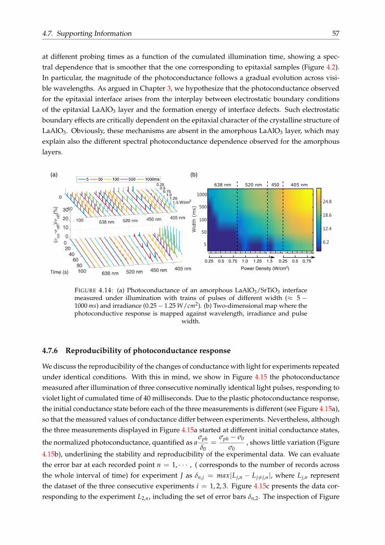
4.7. Supporting Information 57
at different probing times as a function of the cumulated illumination time, showing a spec-tral dependence that is smoother that the one corresponding to epitaxial samples (Figure 4.2).In particular, the magnitude of the photoconductance follows a gradual evolution across visi-ble wavelengths. As argued in Chapter 3, we hypothesize that the photoconductance observedfor the epitaxial interface arises from the interplay between electrostatic boundary conditionsof the epitaxial LaAlO3 layer and the formation energy of interface defects. Such electrostaticboundary effects are critically dependent on the epitaxial character of the crystalline structure ofLaAlO3. Obviously, these mechanisms are absent in the amorphous LaAlO3 layer, which mayexplain also the different spectral photoconductance dependence observed for the amorphouslayers.
Power Density (W/cm2)
0.25 0.5 0.75 1.0 1.25 1.5 0.25 0.5 0.75
(a) (b)
5
50
100
500
1000W
idth
(m
s)
6.2
12.4
18.6
24.8
638 nm 520 nm 450 405 nm
FIGURE 4.14: (a) Photoconductance of an amorphous LaAlO3/SrTiO3 interfacemeasured under illumination with trains of pulses of different width (≈ 5 −1000 ms) and irradiance (0.25 − 1.25 W/cm2). (b) Two-dimensional map where thephotoconductive response is mapped against wavelength, irradiance and pulse
width.
4.7.6 Reproducibility of photoconductance response
We discuss the reproducibility of the changes of conductance with light for experiments repeatedunder identical conditions. With this in mind, we show in Figure 4.15 the photoconductancemeasured after illumination of three consecutive nominally identical light pulses, responding toviolet light of cumulated time of 40 milliseconds. Due to the plastic photoconductance response,the initial conductance state before each of the three measurements is different (see Figure 4.15a),so that the measured values of conductance differ between experiments. Nevertheless, althoughthe three measurements displayed in Figure 4.15a started at different initial conductance states,
the normalized photoconductance, quantified as aσph
δ0=
σph − σ0
σ0, shows little variation (Figure
4.15b), underlining the stability and reproducibility of the experimental data. We can evaluatethe error bar at each recorded point n = 1, · · · , ( corresponds to the number of records acrossthe whole interval of time) for experiment J as δn,j = max|Lj,n − Lj =j,n|, where Lj,n representthe dataset of the three consecutive experiments i = 1, 2, 3. Figure 4.15c presents the data cor-responding to the experiment L2,n, including the set of error bars δn,2. The inspection of Figure
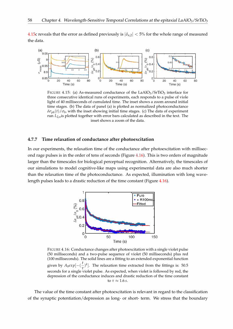
58 Chapter 4. Wavelength-Sensitive Temporal Correlations at the epitaxial LaAlO3/SrTiO3
4.15c reveals that the error as defined previously is |δn,2| < 5% for the whole range of measuredthe data.
(a) (b) (c)
FIGURE 4.15: (a) As-measured conductance of the LaAlO3/SrTiO3 interface forthree consecutive identical runs of experiments, each responds to a pulse of violelight of 40 milliseconds of cumulated time. The inset shows a zoom around initialtime stages. (b) The data of panel (a) is plotted as normalized photoconductanceδσph(t)/σ0, with the inset showing initial time stages. (c) The data of experimentrun L2,nis plotted together with error bars calculated as described in the text. The
inset shows a zoom of the data.
4.7.7 Time relaxation of conductance after photoexcitation
In our experiments, the relaxation time of the conductance after photoexcitation with millisec-ond rage pulses is in the order of tens of seconds (Figure 4.16). This is two orders of magnitudelarger than the timescales for biological perceptual recognition. Alternatively, the timescales ofour simulations to model cognitive-like maps using experimental data are also much shorterthan the relaxation time of the photoconductance. As expected, illumination with long wave-length pulses leads to a drastic reduction of the time constant (Figure 4.16).
FIGURE 4.16: Conductance changes after photoexcitation with a single violet pulse(50 milliseconds) and a two-pulse sequence of violet (50 milliseconds) plus red(100 milliseconds). The solid lines are a fitting to an extended exponential function
given by A0exp[−(tτ)k]. The relaxation time extracted from the fittings is: 50.5
seconds for a single violet pulse. As expected, when violet is followed by red, thedepression of the conductance induces and drastic reduction of the time constant
to τ ≈ 1.6 s.
The value of the time constant after photoexcitation is relevant in regard to the classificationof the synaptic potentiation/depression as long- or short- term. We stress that the boundary

4.7. Supporting Information 59
classification into long-term and short-term effects in synaptic weight is not well-defined andshould be considered with respect to the timescale required for a specific task [121]. If changesin synaptic weights are much longer than timescales necessary to do a specific task, then thepotentiation/depression of synapses can be considered effectively long-term. In this respect, asthe observed relaxation times observed in the photoconductance are typically above two ordersof magnitude longer than specific tasks (e.g., perceptual recognition or formation of cognitivemaps), we can consider that the changes of the synaptic strength driven by wavelength-sensitivetime-correlations of the optical pulses are effectively long-term.
4.7.8 Voltage readouts in photoconductance measurements
The conductance was measured by injecting currents, typically I ≈ 1µA, and changes in conduc-tance were inferred from changes measured in the output voltage. Figure 4.17 shows a typicalexperiment in which two datasets are displayed, corresponding to two two-pulse sequences,namely, (violet 95 ms + red 5 ms) and (violet 20 ms + red 80 ms). As expected from the stud-ied wavelength-correlated photoresponses, longer exposure to red light after illumination withviolet leads to a lower value of the relative photoconductance (Figure 4.17a). Relative changesin conductance are in the order of 1%. As mentioned above, the changes in conductance aredetected by measuring changes of the output voltage, which are shown in Figure 4.17b for thedata displayed in Figure 4.17a. We see that voltage readings vary in the millivolt range, and thenoise is much smaller than the detected changes in voltage.
FIGURE 4.17: (a) Relative changes of conductance after two two-pulse sequencesconsisting, respectively, of (violet 95 ms + red 5 ms) and (violet 20 ms + red 80 ms).
(b) Voltage output detected in the experiments displayed in panel (a).
4.7.9 Conductance modulation under multiple-pulse sequences
The data displayed in Figure 4.18 corresponds to a sequence of blue and red pulses of width50 ms and irradiance 1 W/cm2. The blue curve shows the changes of conductance after a se-quence of multiple blue pulses, leading to a global increase of conductance at the end of thewhole sequence. We repeated the experiment, but now combining blue and red pulses with thesame width and timing as the all-blue pulse sequence (red curve in Figure 4.18). We observein this Figure that the illumination of the first red pulse after the first blue pulse entails a sig-nificant decrease of conductance with respect to the first blue pulse, in agreement with all theexperiments described in the manuscript. Interestingly, a subsequent red pulse decreases even

60 Chapter 4. Wavelength-Sensitive Temporal Correlations at the epitaxial LaAlO3/SrTiO3
more the conductance with respect to the first red pulse. Therefore, the decrease after differ-ent red pulses is cumulative. As expected, the next two blue pulses increase substantially theconductance and, finally, the third and last red pulse decreases once more the conductance. Acomparison between the multiple all-blue and blue/red pulses (blue and red curves in Figure4.18, respectively) shows that appropriate combinations of short-/long- wavelength pulses canfine-tune the conductance.
Pulse input
FIGURE 4.18: Relative changes of conductance after two different multiple-pulsesequences. All pulses have a width of 50 ms, and the irradiance is 1 W/cm2 andtheir timing is represented schematically in the upper part of the figure. The bluecurve in the figure corresponds to conductance changes induced by multiple anall-blue-pulse sequence, while the red curves displays the photoconductance mea-
sured under multiple blue/red-pulse sequence.

61
Chapter 5
Plasticity of persistentphotoconductance of amorphousLaAlO3/SrTiO3 interfaces under varyingillumination conditions
In Chapters 3 and 4 we have analyzed the wavelength-dependent time-correlated photore-sponses of the epitaxial LaAlO3/SrTiO3 interface. In Chapter 4, we have explored the poten-tial of these responses to emulate some brain-inspired functionality based on the spiking time-dependent plasticity model (STDP). Understandably, a large sensitivity to enviromental illumi-nation conditions is desirable for any application. Facing this issue, we have explored the sen-sitivity of amorphous LaAlO3/SrTiO3 interfaces to different luminance conditions, as generally,photoresponses of amorphous layers are larger than those of epitaxial interfaces. We note that,although STDP-like photoresponses are absent in amorphous layers, the plasticity is nonethelessstill present, and could find interest for some applications.
5.1 Abstract
We report on electric transport measurementsunder optical stimulation of the persistentphotoconductance (PPC) at the interface be-tween amorphous LaAlO3 thin films andSrTiO3 single crystals. The spectral responseof PPC in the visible was analyzed undervarying illumination conditions and exposuretimes down to the milliseconds range. ThePPC is plastically modulated by optical stim-uli of varying strength and duration, demonstrating fine-tuned photoconductive responsivityover a diversity of cumulated timespans. Interestingly, under optimal conditions, illumination

62 Chapter 5. Plasticity of amorphous LaAlO3/SrTiO3
over periods on the second timescale the photoconductance is sensitive to intensity contrastsunder conditions comparable to bright-sunlight environments. The prospects of exploiting pho-toconductance − including potential strategies to reach higher sensitivity to dimmer environ-mental conditions− are discussed in this chapter.
5.2 Introduction
As discussed in Chapter 1, Section , the two-dimensional electron system (2DES) emerging atthe LaAlO3/SrTiO3 interface shows a variety of properties, including high electrical mobility[63], two-dimensional superconductivity [64] and strong Rashba spin-orbit fields [155]. The epi-taxial LaAlO3/SrTiO3 heterostructure, where the mechanism for the generation of the metallicinterface is driven by electrostatic boundary conditions [123] , has grabbed most of the atten-tion. Interestingly, a 2DES can be also generated at the interface between amorphous LaAlO3
(a-LaAlO3) films and SrTiO3 single crystals due to the creation of oxygen vacancies which actas electron donors under the reductive conditions during the growth [156–158]. In spite of thedifferent origins, similar transport properties are observed in both systems, e.g., the values ofelectron mobility are comparable for both epitaxial and a-LaAlO3/SrTiO3 interfaces [159] . Thisraises the interest in amorphous interfaces, as the sample preparation can be done at room tem-perature, enabling an easier integration into well-developed semiconductor technologies.
In this chapter, we analyze the properties of a-LaAlO3/SrTiO3 interfaces in relation to itspersistent photoconductance (PPC) [67]. As presented in Subsection 1.3.3, this is a phenomenonobserved in many other semiconductors and two-dimensional systems [91, 160], whereby theconductance is increased after excitation with visible or ultraviolet light, so that the initial valueprior to the photoexcitation is only fully recovered after prolonged periods of time [87, 92].PPC has been studied in both epitaxial [67, 161–163] and amorphous interfaces [90], and dif-ferent physical mechanisms have been proposed for each type of interface, being oxygen va-cancies suggested playing a fundamental role in a-LaAlO3/SrTiO3 interfaces[90]. In Chapter 4we have explored the potential to exploit the PPC modulation to emulate the plasticity of bio-logical synapses using optical inputs as stimuli, as proposed for other materials [58, 164–166].This would be of interest in photonic circuits where integrated light sources may be exploitedto drive plastic photoresponses. Alternatively, artificial retinas [167] would also benefit from in-corporating plastic photoresponses [168]. In contrast to other neuromorphic developments, thisparticular application would require sensitivity to ambient illumination in visual scenes.
Here we focus our study to the a-LaAlO3/SrTiO3 interface to seek the sensitive thresholdand find that, under optimal conditions, this system is sensitive to contrasts approaching thepeak of solar terrestrial irradiance. Although this threshold forbids the application in dynamicsensing of natural scenes, it could be of interest for other applications where this limitation is lesssevering, as in recognition of quasi-static visual patterns of large enough irradiance or as pho-toresponsive synaptic elements in integrated photonic systems, where non-natural light sourcesare used for optical stimulation. In this respect, the simplicity of a-LaAlO3/SrTiO3 sample prepa-ration can be an important asset for its integration into existent semiconductor technologies.

5.3. Experiment 63
5.3 Experiment
FIGURE 5.1: (a) Sketch of the experimental setup used to measure the photocon-ductance of a-LaAlO3/SrTiO3 under direct illumination. Appropriate instrumen-tation is used to generate short pulses of light of different wavelengths (violet,blue, green, red). The polarizer is used to vary the illumination on the sample. Thevoltage is measured under illumination. The intensity of reflected light is mea-sured by a photodetector. (b) In some experiments, the photoconductance is alsomeasured by illuminating the sample through a high-numerical-aperture lens. TheCCD camera is used to locate the beam spot on the sample, while a CMOS detectoris used to adjust the focus location along the out-of-plane direction. (c) Crosssec-
tional view of the amorphous LaAlO3/SrTiO3 interface.
All things considered, this work is intended to explore the sensitivity of the PPC in a-LaAlO3/SrTiO3 to short pulses of light down to millisecond timescales under varying illumination condi-tions approaching terrestrial conditions of solar irradiance. The tunability of the conductance isalso analyzed by measuring the cumulative effect of optical stimuli on the plastic PPC response.With this in mind, we contacted the interface between the amorphous LaAlO3 layer and theSrTiO3 substrate by Al wire bonding (Figure 5.1 (c)). Amorphous layers with thickness 3− 6 nmwere deposited at room temperature by pulsed laser deposition in an oxygen partial pressurePO2 = 104 mbar. The conductance was measured with injected currents typically in the range ofI ≈ 1 µA for lower resistance devices (R < 106 Ω) or I ≈ 1nA for higher resistance (R > 106 Ω) .The photoexcitation experiments were carried out at room temperature using lasers of differentwavelengths in the visible red (λ = 638 nm), green (λ = 520 nm), blue (λ = 450 nm) and violet(λ = 405 nm). Under direct illumination conditions (Figure 5.1 (a)), the laser beam was steeredvia a mirror directly towards the sample, illuminating an area of size 1cm2 and the irradianceon the sample was varied in a range of values down to Pw ≈ 2.5W · nm−1 · m−2 (see Section 2.2.2for the determination of the output bandwidth of the laser source and the illuminance in unitsof nm−1 · m−2). This value is relatively close to the peak of solar spectral irradiance in the visible
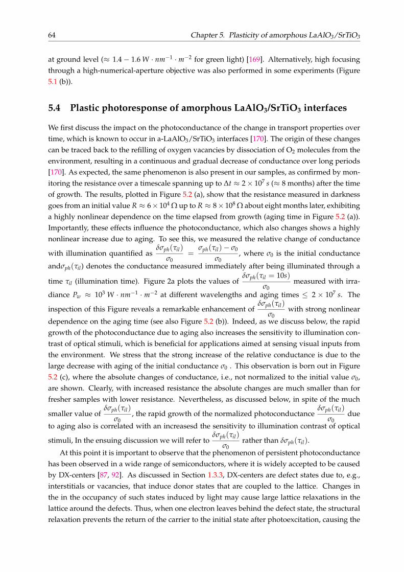
64 Chapter 5. Plasticity of amorphous LaAlO3/SrTiO3
at ground level (≈ 1.4 − 1.6 W · nm−1 · m−2 for green light) [169]. Alternatively, high focusingthrough a high-numerical-aperture objective was also performed in some experiments (Figure5.1 (b)).
5.4 Plastic photoresponse of amorphous LaAlO3/SrTiO3 interfaces
We first discuss the impact on the photoconductance of the change in transport properties overtime, which is known to occur in a-LaAlO3/SrTiO3 interfaces [170]. The origin of these changescan be traced back to the refilling of oxygen vacancies by dissociation of O2 molecules from theenvironment, resulting in a continuous and gradual decrease of conductance over long periods[170]. As expected, the same phenomenon is also present in our samples, as confirmed by mon-itoring the resistance over a timescale spanning up to ∆t ≈ 2 × 10⁷ s (≈ 8 months) after the timeof growth. The results, plotted in Figure 5.2 (a), show that the resistance measured in darknessgoes from an initial value R ≈ 6× 10⁴ Ω up to R ≈ 8× 10⁸ Ω about eight months later, exhibitinga highly nonlinear dependence on the time elapsed from growth (aging time in Figure 5.2 (a)).Importantly, these effects influence the photoconductance, which also changes shows a highlynonlinear increase due to aging. To see this, we measured the relative change of conductance
with illumination quantified asδσph(τil)
σ0=
σph(τil)− σ0
σ0, where σ0 is the initial conductance
andσph(τil) denotes the conductance measured immediately after being illuminated through a
time τil (illumination time). Figure 2a plots the values ofδσph(τil = 10s)
σ0measured with irra-
diance Pw ≈ 103 W · nm−1 · m−2 at different wavelengths and aging times ≤ 2 × 10⁷ s. The
inspection of this Figure reveals a remarkable enhancement ofδσph(τil)
σ0with strong nonlinear
dependence on the aging time (see also Figure 5.2 (b)). Indeed, as we discuss below, the rapidgrowth of the photoconductance due to aging also increases the sensitivity to illumination con-trast of optical stimuli, which is beneficial for applications aimed at sensing visual inputs fromthe environment. We stress that the strong increase of the relative conductance is due to thelarge decrease with aging of the initial conductance σ0 . This observation is born out in Figure5.2 (c), where the absolute changes of conductance, i.e., not normalized to the initial value σ0,are shown. Clearly, with increased resistance the absolute changes are much smaller than forfresher samples with lower resistance. Nevertheless, as discussed below, in spite of the much
smaller value ofδσph(τil)
σ0, the rapid growth of the normalized photoconductance
δσph(τil)
σ0due
to aging also is correlated with an increasesd the sensitivity to illumination contrast of optical
stimuli, In the ensuing discussion we will refer toδσph(τil)
σ0rather than δσph(τil).
At this point it is important to observe that the phenomenon of persistent photoconductancehas been observed in a wide range of semiconductors, where it is widely accepted to be causedby DX-centers [87, 92]. As discussed in Section 1.3.3, DX-centers are defect states due to, e.g.,interstitials or vacancies, that induce donor states that are coupled to the lattice. Changes inthe in the occupancy of such states induced by light may cause large lattice relaxations in thelattice around the defects. Thus, when one electron leaves behind the defect state, the structuralrelaxation prevents the return of the carrier to the initial state after photoexcitation, causing the
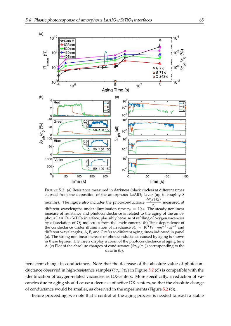
5.4. Plastic photoresponse of amorphous LaAlO3/SrTiO3 interfaces 65
FIGURE 5.2: (a) Resistance measured in darkness (black circles) at different timeselapsed from the deposition of the amorphous LaAlO3 layer (up to roughly 8
months). The figure also includes the photoconductanceδσph(τil)
σ0measured at
different wavelengths under illumination time τil = 10 s. The steady nonlinearincrease of resistance and photoconductance is related to the aging of the amor-phous LaAlO3/SrTiO3 interface, plausibly because of refilling of oxygen vacanciesby dissociation of O2 molecules from the environment. (b) Time dependence ofthe conductance under illumination of irradiance Pw ≈ 103 W · nm−1 · m−2 anddifferent wavelengths. A, B, and C refer to different aging times indicated in panel(a). The strong nonlinear increase of photoconductance caused by aging is shownin these figures. The insets display a zoom of the photoconductance at aging timeA. (c) Plot of the absolute changes of conductance (δσph(τil)) corresponding to the
data in (b).
persistent change in conductance. Note that the decrease of the absolute value of photocon-ductance observed in high-resistance samples (δσph(τil) in Figure 5.2 (c)) is compatible with theidentification of oxygen-related vacancies as DX-centers. More specifically, a reduction of va-cancies due to aging should cause a decrease of active DX-centers, so that the absolute changeof conductance would be smaller, as observed in the experiments (Figure 5.2 (c)).
Before proceeding, we note that a control of the aging process is needed to reach a stable

66 Chapter 5. Plasticity of amorphous LaAlO3/SrTiO3
state, preventing further evolution of the transport properties with time. Interestingly, a possiblestrategy towards this objective may be provided by the observation that the deposition of anadditional a-LaAlO3 film grown at a O2 pressure higher than that used for the first a-LaAlO3
layer reduces the aging process by orders of magnitude [170], which could be a promising routeto achieve the required stability. Importantly, growth conditions e.g., oxygen pressure or thethickness of the amorphous layer can be used to control the resistance state of the sample.
FIGURE 5.3: (a) Photoconductive response of the amorphous LaAlO3/SrTiO3 in-terface under illumination time τil = 25 − 200 ms with violet light (λ = 405 nm )and irradiance Pw ≈ 103 W · nm−1 · m−2. The lower graph displays the detectedintensity (arbitrary units) of light reflected from the sample during the illumina-tion with the light pulses. The illumination time is defined by τil = Np × Wp,where Np is the number of pulses, and Wp is the width of every individual pulse(W p ≈ 5 ms in the data shown in this panel). The figure also indicates differ-ent probe times τpr where the photoconductance is measured, which are used indata presented in panel (c). (b) The upper panel displays the detected intensityof light reflected from the sample after illumination with pulse trains defined byNp = 5 − 100 and Wp ≈ 0.5 − 5 ms, resulting in illumination times spanning theinterval τil = 2.5 − 1000 ms . The lower graph displays the time evolution of pho-toconductance corresponding to the response to every particular pulse train. (c)Photoconductance measured at different probe times (τpr = 0, 15, 30, and 45 s) as a
function of the illumination time.
Now we address the potential for neuromorphic applications, which requires a functionalresponse that emulates the plasticity of biological synapses [150]. To analyze this aspect, we
measuredδσph(τil)
σ0after impinging the samples with trains of light pulses of irradiance Pw ≈
(150 − 1000) W · nm−1 · m−2 , defined by the number of pulses (Np = 1 − 10) and the width ofevery single pulse Wp ≈ 0.5, 1, 5 ms (Figure 5.3b). In this case, the illumination time is defined asthe cumulated time resulting from all light pulses, i.e., τil = Np ×Wp. Since we need to quantifythe plasticity of the PPC response, we define an additional parameter, the probe time τpr at which
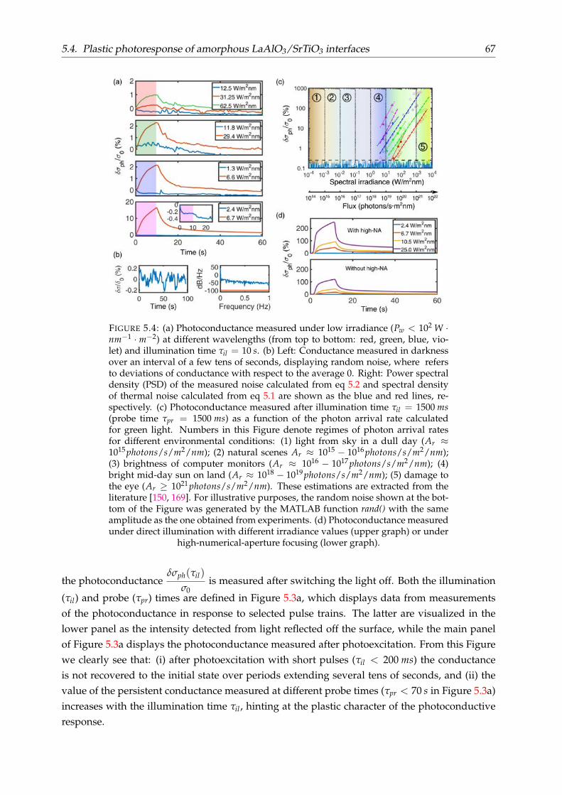
5.4. Plastic photoresponse of amorphous LaAlO3/SrTiO3 interfaces 67
FIGURE 5.4: (a) Photoconductance measured under low irradiance (Pw < 102 W ·nm−1 · m−2) at different wavelengths (from top to bottom: red, green, blue, vio-let) and illumination time τil = 10 s. (b) Left: Conductance measured in darknessover an interval of a few tens of seconds, displaying random noise, where refersto deviations of conductance with respect to the average 0. Right: Power spectraldensity (PSD) of the measured noise calculated from eq 5.2 and spectral densityof thermal noise calculated from eq 5.1 are shown as the blue and red lines, re-spectively. (c) Photoconductance measured after illumination time τil = 1500 ms(probe time τpr = 1500 ms) as a function of the photon arrival rate calculatedfor green light. Numbers in this Figure denote regimes of photon arrival ratesfor different environmental conditions: (1) light from sky in a dull day (Ar ≈1015 photons/s/m2/nm); (2) natural scenes Ar ≈ 1015 − 1016 photons/s/m2/nm);(3) brightness of computer monitors (Ar ≈ 1016 − 1017 photons/s/m2/nm); (4)bright mid-day sun on land (Ar ≈ 1018 − 1019 photons/s/m2/nm); (5) damage tothe eye (Ar ≥ 1021 photons/s/m2/nm). These estimations are extracted from theliterature [150, 169]. For illustrative purposes, the random noise shown at the bot-tom of the Figure was generated by the MATLAB function rand() with the sameamplitude as the one obtained from experiments. (d) Photoconductance measuredunder direct illumination with different irradiance values (upper graph) or under
high-numerical-aperture focusing (lower graph).
the photoconductanceδσph(τil)
σ0is measured after switching the light off. Both the illumination
(τil) and probe (τpr) times are defined in Figure 5.3a, which displays data from measurementsof the photoconductance in response to selected pulse trains. The latter are visualized in thelower panel as the intensity detected from light reflected off the surface, while the main panelof Figure 5.3a displays the photoconductance measured after photoexcitation. From this Figurewe clearly see that: (i) after photoexcitation with short pulses (τil < 200 ms) the conductanceis not recovered to the initial state over periods extending several tens of seconds, and (ii) thevalue of the persistent conductance measured at different probe times (τpr < 70 s in Figure 5.3a)increases with the illumination time τil , hinting at the plastic character of the photoconductiveresponse.

68 Chapter 5. Plasticity of amorphous LaAlO3/SrTiO3
To have a complete picture of the plastic response, we extended these results to all wave-lengths and a wide range of illumination times. Accounting for the number of pulses and theirindividual width, the ensemble of our measurements covered cumulated illumination timesthat spanned over almost three orders of magnitude (τil ≈ 2.5 − 1000 ms). The results of thisextensive study are summarized in Figure 5.3c, which plots the values of the photoconductanceδσph(τil)
σ0measured at different probe times (τpr = 0 s, i.e., immediately after switching the
light off and at τpr = 15, 30 and 45 s). The outcome of this study reveals that the photoconduc-
tanceδσph(τil)
σ0can be modulated over two decades for the cumulated illumination timespan
τil ≈ 2.5 − 1000 ms (Figure 5.3c). Therefore, the data shown in Figure 5.3 demonstrates that thecumulated illumination time in pulse trains can be used to fine-tune the plastic PPC response inthe a-LaAlO3/SrTiO3 system.
Now, can this fine-tunability be used under conditions approaching ambient illuminationenvironments? To gauge this possibility, we have to tackle the responsiveness of the system toillumination conditions that imply low enough irradiance (Pw ≪ 102 W · nm−1 · m−2, see Fig-ure 5.4c). In this context it is relevant to quantify the noise level and estimate the sensitivitythreshold for a detectable change in conductance. For that purpose, we measured the photocon-ductive signal after photoexcitation with irradiance Pw < 102 W · nm−1 · m−2 and illuminationtime τil = 1500 ms see Figure 5.4a for data acquired in a sample about 106 s after its growth,when its resistance was R ≈ 8 × 10⁵ Ω(see Figure 2a). The results show that the photoconduc-
tance is larger at short wavelengths, i.e.,δσph(τil)
σ0> 15% at λ = 405 nm , while
δσph(τil)
σ0≈ 1%
at λ = 638 nm, see Figure 5.4a. It is also observed that the photoconductance is not increasinglinearly with irradiance, and it appears to show a sudden increase at a threshold value that forblue-violet light is Pw . 6W · nm−1 · m−2 (Figure 5.4a). To evaluate the noise amplitude, wemeasured the conductance in darkness for periods of several tens of seconds (Figure 5.4b). We
see that the random fluctuations in conductance give rise to noise amplitudeδσph(τil)
σ0≈ 4%,
as calculated from the root mean square value over the analyzed time interval. This value has
to be compared with the amplitude of the photoconductanceδσph(τil)
σ0≈ (0.4 − 900)% under
illumination time τil = 1500 ms for a sample of aging time 2 × 10⁷ s (Figure 5.4c).We compared the observed noise amplitude with the noise due to thermal motion of elec-
trons in conducting media. The spectral density of thermal noise is given by [171]
Gv( f ) =2Rh| f |
exp(h| f |/kBT)− 1≈ 2RkBT (5.1)
where f is the frequency, R the resistance, T the temperature and h and kB are the Planck andBoltzmann constants, respectively. The right hand of Equation 5.1 is valid for frequencies| f | ≪kBT
h , which is fulfilled at room temperature up to f ≈ 1012Hz , well above the bandwidth of

5.4. Plastic photoresponse of amorphous LaAlO3/SrTiO3 interfaces 69
conventional electrical instrumentation. The spectral density prnd( f ) was calculated via discrete-time Fourier transform as
prnd( f ) =1
L fs|
L−1
∑n=0
vL(n)e−j2πn f / fs |2 (5.2)
for a signal vL(n), corresponding to a finite number of L voltage readings and fs is the sam-pling frequency ( fs = 2 Hz in our measurements). The spectral density calculated from Equa-tion 5.2 is displayed in Figure 5.4b, yielding a value prnd( f ) ≈ −45 dB/Hz. The spectral densityof thermal noise associated with the resistance R ≈ 8 × 10⁸ Ω calculated from Equation 5.1 isGv ≈ −99 dB/Hz, see Figure 5.4b. Therefore, for the highest resistance state which, as discussedabove, has the largest sensitivity to photoconductance the spectral density of the random signalsmeasured with the used instrumentation (described in Supporting information Section 5.6.1) isconsiderably larger than the intrinsic thermal noise of the device resistance (Figure 5.4b, rightpanel). This is an important observation towards optimizing the signal-to-noise ratio. Indeed,we show that the use of lock-in amplifiers for voltage detection -using phase-sensitive detec-tion to single out signals at specific frequencies results in noise amplitude much closer to thetheoretical estimation for thermal noise (see Supporting information Section 5.6.1).
We address now the sensitivity of photoconductance to different illumination conditions.The discussion is focused on data extracted from experiments carried out with resistance R ≈8108 Ω after photoexcitation with illumination time τil = 1500 ms and varying illuminanceconditions spanning a broad range Pw ≈ 2.5 − 15000 W · nm−1 · m−2. This range of illumi-nance can be translated into a range of photon arrival rates Ar that, for the case of green light(λ = 520 nm), is equivalent to Ar ≈ 6.6 × 10¹⁸ − 3.95 × 10²² photons/s/m2/nm. To put thesevalues in context, we note that photon arrival times in the visible can be estimated for dif-ferent habitat illuminance conditions from references in the literature, such as light from skyin a bright midday sun on land (Ar ≈ 1018 − 1019 photons/s/m2/nm), brightness of a com-puter monitor (Ar ≈ 1016 − 1017 photons/s/m2/nm), brightness from natural scenes (Ar ≈1015 − 1016 photons/s/m2/nm), light from sky in a dull-day (Ar ≈ 1015 photons/s/m2/nm) ormid-dusk on land (Ar ≈ 1013 − 1014 photons/s/m2/nm), while the damage to the eye happensabove Ar ≈ 1021 photons/s/m2/nm [150, 169]. These different illumination environments areindicated across the range of arrival photon rates shown in Figure 5.4c.
To evaluate the responsiveness of the photoconductance of the a-LaAlO3/SrTiO3 interface
to a diversity of environmental conditions, the values ofδσph(τil)
σ0were measured at different
wavelengths under illumination time τil = 1500 ms (Figure 5.4c). The data reported in this Fig-ure was acquired immediately after switching off light (τpr = 0 s). Empty symbols correspond todirect illumination, while solid symbols represent the data acquired under focusing conditions.For the latter, the value of the illuminance is determined at the back aperture of the objectivelens. The data displayed in Figure 5.4c shows that high-NA focusing increases substantially thesensitivity to varying illumination conditions (Figure 5.4d). This is not unexpected since thestrong reduction of the spot size is overcompensated by the strong increase of photon flux overthe reduced illuminated area, resulting in larger changes of conductance. We also observe that

70 Chapter 5. Plasticity of amorphous LaAlO3/SrTiO3
the photoconductive response is highly nonlinear with wavelength, with values that go fromδσph(τil)
σ0≈ (0.3 − 30)% for red to
δσph(τil)
σ0≈ (3 − 900)% for violet. Interestingly, the data dis-
played in the low irradiance region demonstrate that the photoconductance of the amorphousLaAlO3/SrTiO3 system is sensitive to changes in brightness comparable to bright day condi-tions (Ar ≈ 1018 − 1019 photons/s/m2/nm). Attempts to measure the photoconductance forlower rates, i.e., Ar < 1018 photons/s/m2/nm, give values that are too low to be detected abovethe noise level (Figure 5.4c). This is partly accounted for by the sheer drop of photoconduc-tance that occurs for irradiance below Pw < 6 W · nm−1 · m−2 , especially noticeable for blue andviolet, which limits the sensitivity at the low end of irradiance. Further studies are needed tounderstand this observation.
5.5 Conclusion
Summing up, our research gives a perspective on the use of persistent photoconductance of theamorphous LaAlO3/SrTiO3 interface for neuromorphic vision applications through the detec-tion of ambient conditions potentially found in natural scenes. As a general rule, we find thathighly-resistive states are desirable for optimal sensitivity. This, in turn, may require finding ap-propriate conditions for materials preparation, especially regarding the stability of the transportproperties and oxygen stoichiometry, which is discussed in this Chapter. Also, our study revealsthat sensitivity to visual contrasts in bright day conditions is feasible with a-LaAlO3/SrTiO3, al-beit the sensitivity required for scenes under more demanding conditions, such as dull-day ordusk ambient light, is far more challenging and calls for other approaches to increase the re-sponsiveness. This sensitivity threshold is certainly a limitation for applications demandingdynamical sensing of visual scenes, but it could afford an alternative for image acquisition andrecognition of visual patterns of large enough intensity. Another relevant interesting aspect isthat measurements of photoconductance carried out at the lowest irradiance conditions weredone after relatively long illumination times (τil = 1500 ms), roughly one order of magnitudeabove the timescales typical for perceptual cognition (on the scale of 100′s of ms) [150], Onepossible way to improve the performance may be with the help of plasmonics. Indeed, thesame principles that enable plasmonics to improve absorption in photovoltaic devices and solarcells [172], or to boost surface-enhanced Raman spectroscopy [173],may serve well the purposeto increase the photoconductance sensitivity to lower photon arrival rates. Further studies arerequired to explore this possibility.
5.6 Supporting information
5.6.1 Measurement noise and thermal noise
During the measurement of the electronic transport, the voltage is measured with a lock-in am-plifier (Ametek model 7270 R⃝) with sampling frequency 2 kHz and injected dc currents of ≈ 1 Afor devices with resistance R ≤ 106 Ω. Alternatively, the voltage across samples with higherresistance is measured with a Keithley 2611B instrument with sampling frequency 2 Hz and dc

5.6. Supporting information 71
(a) (b)
FIGURE 5.5: The power spectral density (PSD, blue line) and spectral density ofthermal noise Gυ( f ) (red line) from lock-in amplifier (a) and Keithley 2611B (b).
The zooms in both panels show the Gυ( f ).
current of ≈ 1 nA. We measured random signals by recording the conductance in darkness forgiven periods of time. The corresponding power spectral densities (PSD) were calculated fromEquation 5.2 of the main text, which are shown in Figure 5.5 for measurements done with thelock-in amplifier Ametek model 7270 panel (a) and Keithley 2611B panel (b). The data measuredfor the lock-in amplifier gives an average value PSD ≈ −132.23 dB at frequencies > 200 Hz (notethat the sampling frequency is 2 kHz), which is relatively close to the theoretical value of thermalnoise PSD -140.65 dB calculated from Equation 1 for R ≤ 106 Ω (Figure 5.5a).
5.6.2 Dependence of the resistance and photoconductance on growth conditions
FIGURE 5.6: Normalized photoconductance and resistance of two a-LaAlO3/SrTiO3 samples grown under identical conditions with thickness 3(panels (a) and (c)) and 6nm (panels (b) and (d)), respectively. The data were
measured at different aging times, as indicated in the figures..
72 Chapter 5. Plasticity of amorphous LaAlO3/SrTiO3
The transport properties of the amorphous LaAlO3/SrTiO3 interfaces depend on the growthparameters. We illustrate this observation by plotting the evolution of the transport proper-ties and photoconductance as a function of the thickness of the deposited LaAlO3 film, keep-ing the deposition pressure fixed. In previous works, we have demonstrated that the vacancyconcentration in LaAlO3/SrTiO3 can be controllably tuned by changing the thickness of oxidefilms [80]. The same trend is observed for many amorphous films grown on SrTiO3 crystals[158]. Therefore, the amount of oxygen vacancies (and, therefore, of carriers) can be modulatedby changing the thickness, whereby larger concentrations of vacancies are attained in sampleswith thicker deposited overlayers. We consider now the samples that were analysed in thepresent study. In Figure 5.6 we compare the resistance and photoconductance of two amor-phous LaAlO3/SrTiO3 interfaces grown under identical conditions but with different thicknessof the LaAlO3 layer, namely, 3 and 6 nm, respectively. As we see in Figure 5.6, in agreement withthe above-mentioned reports, increasing the thickness of the amorphous LaAlO3 layer causesa decrease of the resistance and, correspondingly, the relative change of photoconductance islarger for the thinner film. This observation provides a strategy to achieve the highest possi-ble resistance state, based on decreasing the thickness as closer as possible to the critical valueneeded for the conductive interface.

73
Chapter 6
Outlook and Perspectives
In this thesis, we have analyzed the wavelength-dependent time-correlated photoresponses ofthe epitaxial LaAlO3/SrTiO3 interface (Chapter 3), which can be extended to neuromorphic pho-tonics based on spiking time-dependent plasticity model (Chapter 4). Furthermore, we haveexplored the sensitivity of the photoconductance of amorphous LaAlO3/SrTiO3 interfaces toenvironmental illumination conditions (Chapter 5). This chapter provides perspectives and out-look on potential applications of the studied photoresponses to neuron networks consisting ofLaAlO3/SrTiO3 interfaces as synapses and physical mechanisms of the interplay between the2DES and other functional oxides , e.g., ferroelectric oxides.
While we are watching around this moment, a remarkable and sophisticated show is playingin our brains. Is it possible to emulate the complicated and fast biological vision system? Letssee how can we see and how can electronics emulate basic features of vision.
6.1 Artificial synapses and neurons for vision
Biological vision is a sophisticated process of image formation performed by several varieties ofneuronal cells. A beam of photons coming out of an object enters the eye and is absorbed by thephotoreceptors, by which the photons are converted into electric current via a phototransductionprocess. The information contained in such input signals is redundant and some reduction isrequired before proceeding towards the brain. For this purpose, the retina performs low-levelinformation processing as follows , see also Figure 6.1: before the signal flows into the bipolarcells, the horizontal cells modulate it, so that, instead of absolute levels of light, the informa-tion is coded by the difference in the values between the received light and the surroundinglight detected by the photoreceptors. This involves signal subtraction from the surroundingcells and, therefore, the global signal processing in the retina requires both excitatory and in-hibitory synapses. Subsequently, the modulated signal travels through the ganglion cells andis modulated further by amacrine cells using a similar protocol, so that the surrounding exci-tation is subtracted from the central excitation of illumination for bipolar cell inputs [107, 174].In the following, photoreceptor and ganglion cells are described briefly, as well as their imple-mentation of artifical vision using the persistent photoconductance observed in the 2DES at theLaAlO3/SrTiO3 interface.

74 Chapter 6. Outlook and Perspectives
Rod/ConePhotoreceptor
HorizontalCell
BipolarCell
AmacrineCell
Ganglion Cells
Amorphous LAO/STO
EpitaxialLAO/STO
Threshold
Cop-amp
V
tVth
V
tVth
V
Rod/ConePhotoreceptor
(a) (b)
Is Is
FIGURE 6.1: (a) schematic diagram showing retinal information processing. In-formation carried by light reaches the photoreceptors and flows to bipolar cellsand then ganglion cells which are connected to the optic nerve. During the infor-mation flowing, horizontal cells and amacrine cells adjust the actions of bipolarcells and ganglion cells. (b) Proposed artificial retina based on the photoconduc-tance of LaAlO3/SrTiO3. An LaAlO3/SrTiO3 system may be used to adjust thethreshold value on one of the inputs to an operational amplifier. Conversely, otherLaAlO3/SrTiO3 systems are coupled to the other input of the operational amplifierand produce an output spike whenever the photoresponse crosses the thershold.
6.1.1 Photoreceptor and ganglion cells
There are two main types of photoreceptors in the retina, namely, rods and cones, which bothcontain disk membranes where photopigments absorb light, resulting in changes of the mem-brane potential that lead to conversion from light to electric signals. Only rods play a major rolein detecting the shape and movement in very dim light. That is because there is a large numberof rods (about 92 million rods and 5 million cones in the human retina [107]) and inside of themthere are much more disks and much higher concentration of photopigments, which make themmore sensitive to the light intensity (but not wavelength). On the other hand, cones contributeto vision in photopic conditions, i.e., well-lit environments with large enough luminance levels,and also are responsible for discriminating colors. The reason of the color perception is that thebright light can activate the three kinds of cones which are sensitive to red, green and blue light,respectively, and then the brain deduces the signal of wavelength-dependence to reproduce thecolorful picture.
The photoreceptor is a key element in the design of a non-biological vision system that aimsat replicating the basic features of a biological retina. In this respect, it is important to replicatethe synaptic plasticity found in biological systems which, as mentioned above, has to includeboth excitatory and inhibitory synapses. In excitatory synapses, the external stimuli (light inour case) increase the synaptic weight, so that the likelihood to trigger a neuron spike increases.

6.1. Artificial synapses and neurons for vision 75
Conversely, the synaptic strength is decreased in inhibitory synapses, thus decreasing the likeli-hood for neuron firing. As described in previous chapters, the photoconductance of the epitax-ial LaAlO3/SrTiO3 interface can be increased or decreased depending on the frequency and thetime arrival of optical pulses, endowing these systems with the capability to replicate excitatoryand inhibitory synapses.
Furthermore, synaptic plasticity in biological vision is relevant to ganglion cells, which are atype of spiking neuron cells that project axons through the optic nerves, which can be consideredas ports where the information is transmitted to the brain in the form of action potentials. Wediscuss in the next section how an artificical spiking neuron can be built from the photoresponseof the LaAlO3/SrTiO3 interface.
6.1.2 Electric vision
Retina forms images through transmitting in spikes carried the encoded information by rela-tive changes. This property allows encoding information from an external image only whenan event causes a change in the light intensity, e.g., caused by a movement of an object, savinga huge amount of redundant information. In contrast, a common camera captures images atperiodic framed times, recording the whole ensemble of infomation at every clock time. Theredundant information recorded and transmitted consumes much energy, time and memory. Asaformentioned, the neuromorphic retina can save a lot of time and energy by capturing imagesby refreshing pixel by pixel only when a change of light intensity is produced, which is at thebasis of the so-called event-based vision sensors. Along these lines, Carver Mead and his col-leagues proposed 1990s, to build a silicon retina with asynchronous digital output [40]. Theymodeled the silicon retina through combining silicon photoreceptors and designing adaptivecircuitry to calculate the changing light level [175].
Our observations that the wavelength-dependent time-correlated photoresponses at the epi-taxial LaAlO3/SrTiO3 interface (Chapters 3 , 4) and the profound sensitivity at the amorphousLaAlO3/SrTiO3 interface (Chapter 5), potentially provide an alternate approach to implementthe artificial retina. As illustrated in Figure 6.1b, the LaAlO3/SrTiO3 systems, acting as synapses,can be integrated in a circuitry, which can be designed to act as artificial neurons that can gener-ate spikes in responses to changes of the photoresponse. In Figure 6.1b, a group of LaAlO3/SrTiO3
systems are used to set the firing thresholds Vth of the artificial spiking neurons, whose value canbe adjusted by light (6.1b left). Another group of LaAlO3/SrTiO3 systems respond to the opticpulses, causing to decrease in the voltage. Once the decreasing voltage reaches the thresholdVth, the operational-amplifier produces a sudden change of output voltage. In this model, boththe synaptic threshold and synaptic plasticity are suggested to be replicated by LaAlO3/SrTiO3
systems, which may mimic the computation of the light difference through Horizontal cell andAmacrine cells of biological vision (see above). This implementation would be a step beyond thisThesis, which would represent replicating physically a spiking neuron from the photoresponseof the LaAlO3/SrTiO3 interface.

76 Chapter 6. Outlook and Perspectives
6.2 Complex oxide device based on 2DES
Here we discuss another perspective beyond the work presented in this Thesis, which aims attaking advantage of the large variety of physical properties of transition metal complex oxides,which arise from the narrow bandwidths dominated by d-orbitals where strongly correlatedelectrons intrinsically compete or cooperate in the charge, spin and orbital degrees of freedom[176]. Such interaction induces kinds of symmetry breaking, resulting in a variety of astoundingproperties, such as superconductivity, multiferroics, Mott insulators and metal-insulator tran-sitions [177]. Due to their structural compability, these complex oxides can combine with the2DES at the LaAlO3/SrTiO3 interface, offering multiple functionality that can be useful for neu-romorphic devices.
For instance, as we discussed in Chapter 3, the properties of the 2DES can be modified byelectronic states at the LaAlO3 surface. This can be also achieved by using some functionaloxides that can be epitaxially grown on the surface of LaAlO3/SrTiO3, such as ferroelectrics [178,179]. This would enable the ferroelectric polarization to modulate the charge of surface states.One the other hand, capping the LaAlO3 surface with metals can also modify the properties of2DES, providing additional routes to modulate the conductance externally [180].

77
Appendix A
Optical lithography protocols
Micro-Writer ML3 from Durham Magneto Optics Ltd. (DMO) is used to directly write the pat-terns onto the photoresist (PR), which is polydimethylglutarimide (PGMI) Shipley S1813 duringcurrent study. The software CleWin4 is recommended to design the patterns.
• Rinsing the substrate with acetone and isopropanol. Then blowing with Nitrogen gun
• Dehydration bake to remove water 95C
• Spin coating of S1813, with 5500 rpm and acceleration of 0.7 s
• Soft baking at 95C for 60 − 90 s
• Exposure with 385 nm lightsource (i-line) with fluency around 200 mJ/cm
• Develop for 60 s
• Deposition
• Liftoff of S1813 through immersing in the acetone

79
Appendix B
Photoconductance Calculation Details
B.1 Photoexcitation via DX-resonance states
The in-scattering Σin(x, t) and out-scattering Σout(x, t) functions described in this chapter giveaccount, respectively, of the inward and outward flux of particles in the quantum well. For thefunction Σin(x, t) we assume that it is proportional to the differential scattering cross-section ofthe optical absorption process, which is proportional to the current-current operator, i.e.,
d2σ
dΩdω∼ ⟨Tj(x, t)j(0)⟩ (B.1)
We solve the current-current autocorrelation function ⟨Tj(x, t)j(0)⟩ using finite-temperatureGreen’s functions following the procedure described in chapter 4 Ref [128]. We assume that thecurrent operator is given by
j(x, t) = P ∑c,c′
b+c bc′ (B.2)
where, for simplicity, we consider the matrix element P constant. In Equation B.2, the oper-ators (b+c bc′) refer to DX-center states. Then, we compute Equation B.1 using finite-temperatureGreen’s functions:
⟨Tj(x, t)j(0)⟩ = P ∑c2,c′1,c1,c′1
⟨Tb+c2
(t)bc′2(t)b+c1
bc′1
⟩=
PeβΩ ∑c2,c′2,c1,c′1Tr
e−βH1 eiH1tb+c2
bc′2e−iH1tb+c1
bc′1
(B.3)
where H1 is the Hamiltonian described in Equation 3.1 , β = 1/kBT (defined in terms of thetemperature T and Boltzmann constant kB), Tr is the trace over the complete set of states and Ωis defined as e−βΩ = e−β[H1−µN] , with µ the chemical potential and N the number operator. Thecanonical transformation S = ∑c b+c bc ∑ q Mq
ωq
[aq + a+q
]changes the Hamiltonian to H1 = eSH1eS
(Equation 3.1). Then, Equation B.3 can be rewritten as
⟨Tj(x, t)j(0)⟩ = PeβΩ ∑c2,c′2,c1,c′1Tr
e−βH1 eiH1tX+
c2X′
c2b+c2
bc′2e−iH′
1 X+c1
X+c1
b+c1bc′1
bc′1
= PeβΩ ∑c2,c′2,c1,c′1
eit(
εc2−εc′2−∆
)Tr
e−βH1 X+
c2(t)Xc′2
(t)X+c1
Xc′1b′c2
bc′2b+c1
bc′1
= PeβΩ ∑c2,c′2,c1,c′1
eit(
εc2−εc′2−∆
)Tr
e−βH1 b+c2
bc′2b+c1
bc′1
Tr
e−βH1 X+
c2(t)Xc′2
(t)X+c1
Xc′1
(B.4)
80 Appendix B. Photoconductance Calculation Details
where Xci = exp[−∑q
Mqωq
[a+q − aq]], with Mq the dimensionless electron-phonon coupling
parameter, (aq, a+q ) the annihilation and creation operators for phonons and ∆ = ∑qMqωq
. InEquation B.4, the electronic part of the trace can be calculated as:
Tr
e−βH1 b+c2bc′2
bc′1bc′1
= Tr
e−βH1 b+c2
bc1 b+c1bc2
= (1 − n∗
DX (ε∗DX)) nDX (εDX) (B.5)
In Equation B.5 we make use of Wick’s theorem, so that the subscripts in the operators(bci , b+ci
) must be paired up, and thus, c′2 = c1 andc′1 = c2. The terms nDX (DX ) and nDX∗
(DX∗ ) refer, to the density of states of DX centers in the ground and excited state, respectively.The phonon part of the trace in Equation B.4 can be evaluated following the procedure de-
scribed in chapter 4 of Reference [128], so that
Tr
e−βH1 X+c2(t)Xc′2
(t)X+c1
Xc′1
= exp
[−
Mq0
ω0
[(N0 + 1)
(1 − e−iω0t
)N0
(1 − e+iω0t
)]](B.6)
where we consider an Einstein model for phonons with ωq = ω0, and N0 is the phononoccupation number.
We end up with the following expression for the optical absorption process,
d2σ
dΩdω∝
P2ω
[∫ ∫δ hω − (ε∗DX − εDX) (1 −n∗
DX (ε∗DX)) nDX (εDX) dεDXdε∗DX]∫ +∞
−∞dt exp
it[[(ω + ε∗DX − εDX − ∆)]−
Mq0
ω0
[(N0 + 1)
(1 − e−iω0t
)N0
(1 − e+iω0t
)]](B.7)
An expansion can be used to simplify Equation B.7 using Bessel functions of the first kind andcomplex argument, so that finally the expression can be rewritten as
d2σdΩdω ∝ P
2ω
[∫∫δ hω − (ε∗DX − εDX) (1 − n∗
DX (ε∗DX)) nDX (εDX) dεDXdε∗DX]
e−g(2Nq+1) ∑m δ h (ω − ωm) Im(γ) emhω0/2kBT(B.8)
which is Equation 3.4. The expression includes the Bessel function Im(γ), where γ = 2g√
N0(N0 + 1),g is the electron-phonon coupling and m is the number of phonons has to be emitted so thathwm = ε∗DX − εDX − (g − m)hω0.
B.2 Calculation of the density of states (DOS)
B.2.1 Quantum well states
I. DOS for π bands of bulk SrTiO3
Due to the symmetry of the wavefunction, the overlaps of O − 2p orbits and Ti − 3d orbitsonly permit two types of bands: t2g orbits and p orbits form π bands, or eg orbits and p orbitsform σ bands. For the t2g states coming from π-type bonds, the following dispersion relation(Ref. [181] ) is used

B.2. Calculation of the density of states (DOS) 81
Ekπ(αβ) =12 (Et + E⊥) +
√[ 12 (Et − E⊥)
]2+ 4(pdπ)2
(S2
α + S2β
)(αβ = xy, xz, or yz)
(B.9)
and the density of states is given by the expression ( Ref. [181]).
ρπ(E) =1
π2
∣∣∣∣∣E − 12 (Et + E⊥)
(pdπ)2
∣∣∣∣∣ K(√
1 − (επ(E)/2)2)Θ[1 − (επ(E)/2)2
](B.10)
where K(k) =∫ π/2
0dθ√
1−k2 sin2 θis the complete elliptical integral of the first kind and Θ[x]
is the Heaviside function. επ(E) ≡ [Ekv−12 (Et+E⊥)]
2−[ 12 (Et−E⊥)]
2
2(pdπ)2 − 2 is deduced from the EquationB.9, and Sα ≡ sin kαa. That the DOS of the π band bulk SrTiO3 can be calculated, as shown inFigure B.1 The initiate values are chosen from the literature (Ref. [182] ) and adjusted accordingto the density functional theory calculation (Ref. [183]), as shown in Figure B.1b. Therefore theparameters are obtained as: Et = 0, pd = 1.29 eV, E⊥ = −3.36 eV, which gives the Energy gap.The lattice constant a is set as 1.
-5 0 5E-EC (eV)
0
5
10
N(E
) (s
tate
s/ce
ll/eV
) Total--
0 2 4 6E-EC (eV)
0
5
10
N(E
) (s
tate
s/ce
ll/eV
) PRB 81, 153414Sci. Rep. 6, 34667Caculation
(a) (b)
FIGURE B.1: (a) The total density of states (DOS) of the π band and σ bandin bulk SrTiO3. The energy gap between conduction band and valance band is∆E = 3.36 eV . (b) Comparison of conduction band DOS between the analytical
calculation and DFT calculations [183, 184].
II. DOS for σ bands of bulk SrTiO3
For the eg states coming from σ-type bonds, we considered these expressions (Ref. [181])
ρ (εσ) =
ρ1 (εσ) for |εσ| ≤ 1ρ2 (εσ) for 1 ≤ |εσ| ≤ 3
(B.11)
with
ρ1 (εσ) = A + B√
1 − ε2σ + F (1 − |εσ|) |εσ|
ρ2 (εσ) = C + Dx2 + F(1 − x)√
x
x ≡ (3 − |εσ|) /2
(B.12)
In the calculations, we used these values taken from Ref. [181]:

82 Appendix B. Photoconductance Calculation Details
A = ρNum(±1) ≈ 0.432B = −0.1646
C = 1π = 0.3183
D = A − C ≈ 0.1136F = −0.0151
(B.13)
We calculated the density of states of eg states using
ρσ(E) =
∣∣∣∣∣E − 12
(Ee + E∥
)(pdσ)2
∣∣∣∣∣ ρ (εσ(E)) (B.14)
Where we used the values Ee = 2.34 eV, E∥ = −6 eV pdσ = −2.23 eV taken from Ref. [181].The total DOS of t2g and eg is shown in Figure B.1.
III. Wedge model for quantum well LaAlO3/SrTiO3
We use a wedge model to calculate the energy of the quantum well EnΓ at the Γ point in the
reciprocal space, using the expression (Ref. [74] )
EnΓ = V0 + 9 × 10⁻⁷
(me
m∗z
)1/3 (n − 1
4
)2/3
F2/3 (B.15)
where the superscript n refers to the different subband states of the quantum well. In ourmodel, we use seven subbands n = 1, · · · , 7. for each quantum well state (see Figure B.2a). Thecalculation considers the effective masses along the out-of-plane direction of t2g states, wherem∗
z = 0.75me for d(yz/xz) states and m∗z = 25me for dxy states, and V0 = −0.25 eV, F = 120 MV/m.
-0.4 -0.2 0 0.2 0.4
kx
(Å-1)
0
0.5
1
Ene
rgy(
eV)
dxy
dxz
dyz
1 3 5 7n
-0.2
0
0.2
0.4
0.6
0.8
E(e
V)
dxz/yz
dxy
(a) (b)
0 5 10N(E) (states/cell/eV)
0
1
2
3
Ene
rgy(
eV)
(E)
(E-Ea)
(E-Eb)
(c)
a
bb+
+
+
+a a
b
+
+
FIGURE B.2: (a) Energy levels at the Γpoint for different subbands n = 1, · · · , 7,obtained through Equation B.8.(b) Energy dispersion of the subbands along theΓ − X direction in reciprocal space. (c) Bulk density states used in Eqs. S10 withWedge potential applied, the Ea and Eb correspond to the minimal and maximal
energy of the quantum well in (a).
IV. Total quantum well statesAssuming the wedge potential of the quantum well lifts the degeneration of the bulk states,
the approximate formula of the subbands (n = 1, · · · , 7 for each of dxy and d(yz/xz)) can bewritten as:
Enkπ(αβ)
= Ekπ(αβ) − EnΓ (B.16)

B.2. Calculation of the density of states (DOS) 83
That, the subbands of dxy and d(yz/xz)) states are separated, as Figure B.2b shows the depen-dence of the different quantum well states as a function of the wavevector along Γ − X. FigureB.2c shows the bulk density of states with any potential applied ρπ(E) and density of states witha minimum or maximum of En
Γ , which are notated as ρπ(E − Ea) and ρπ(E − Eb), respectively.Similarly, for each π−type subband with potential applied, we calculated the density of
states from the Equation B.9 replacing E with E − EnΓ .
ρnπ(E) = ρn
π(E − EnΓ) (B.17)
and for each σ-type subband has,
ρnσ(E) = ρn
σ(E − EnΓ) (B.18)
The average total density of the states is obtained from the summation of all the subbandsover the number:
ρtotal(E) =3N
∑n=1
[ρnπ(E) + ρn
σ(E)] /3N (B.19)
Thus we get the approximate DOS of quantum well, as shown in the Figure B.3(a). Thefollowing sections will present the DOS of Excited DX, Ground DX, surface (Figure B.3(b)).
FIGURE B.3: (a) shows the total density of states (DOS) of the quantum well, aver-age all the states derived from t2g and eg states per unit cell. For comparison, thefigure also includes the DOS from DFT studies. (b) Density of states of structurallyrelaxed (c0) DX-center states (inferred from DLTS) and unrelaxed DX-center states(c1). The DOS of the QW are derived from t2g and eg states, as well as of surface
states.
B.2.2 DX-center states
We introduce a localized DX-center excited state described by the spectral function:
ρL =2CΘ
(w2 − E2)
√w2 − E2
[E2 + C2
w2−E2
] (B.20)
where the C is coupling strength, w is the width and Θ is step function. To fit the data (asshown Figure B.4c), the parameters is: C = 0.65, W = 1.85, and the center of the localized stateis at 2.85 eV.

84 Appendix B. Photoconductance Calculation Details
For the ground DX-center state we used the normalized expression:
ρIi (E) ∼=
a1
a1 + a2
√wπ
e−w(E−E01)
2
+a2
a1 + a2e−w(E−E0
2)2
(B.21)
where E01 = −0.17 eV and E0
2 = −0.26 eV from the bottom of conduction band, w = 3.09 ×10³, a1 = 2.4 × 10⁻¹⁴ , a2 = 3.3 × 10⁻¹⁴. These parameters are determined through fitting thedata measured by deep-level transient spectroscopy (DLTS).
D f it(E) = a1e−w(E−E01)
2
+ a2e−w(E−E02)
2
(B.22)
B.2.3 Surface states
For the surface states we introduce a single Gaussian function:
ρIs(E) ∼=
√wπ
e−Ws(E−E0s )
2
(B.23)
where E0s = 1.77 eV; Ws = 3. We assume the density of the surface states ρs = 0.5ρI
s(E).The assumptions of the occupancy of the defects and surface states do not affect the distributionof the DOS, but they influence the ratio of the transition probability. Including the trap states(inferred from DLTS), all the density of states can be profiled, as shown in Figure B.3b.
B.3 Deep-level transient spectroscopy (DLTS)
Vg EF
EF
EF
EF
EC
ED
EF
EC
ED
EF
EC
ED
EF
EC
ED
EF
EC
ED
EF
EC
ED
DLTS
Time
Cap
acita
nce
Time
A
B
C
A
B
C
Tem
pera
ture T (K)100 200 300
DLT
S (
arb.
uni
ts)
-0.8 -0.6 -0.4 -0.2 0E (eV)
01234
(cm
2)
10-14
DLTS dataGaussian fit
(a) (b) (c)
(d)
E1/2/3D
E4D E5/6
D
Vr
Vr + Vp
FIGURE B.4: (a) Schematics of DLTS measurement. The capacitance is measured atthe reversal voltage. Then a transient pulse is added to charge the trap, resultingin a decrease in capacitance. After the pulse, the capacitance is recovering basedon the temperature. (b) Schematics of de-charging and charging process in traps.
(c) DLST signal vs temperature. (d) DLTS data and a bi-Gaussian fitting.
We carried out deep-level transient spectroscopy (DLTS) to detect trap levels below the Fermienergy. In the experiments, we grow samples with M/I/QW structure (Au [ 10 nm ]/LaAlO3 [

B.4. Calculation of the photoconductance 85
∼ 4 nm ]/STO). To observe a transient transition of electrons from trap levels to the conductionlevel, we measured the capacitance after a pulse of gate voltage (Figure B.4a top). At the reversebias Vr , the trap levels are partly filled. Then a pulse Vp with hundred milliseconds widthis applied, so that nearly all traps are occupied. Subsequently, after the end of the pulse, thetrapped electrons are emitted into the conduction band (Figure B.4b). This recovery processdepends on temperature, which can be measured by DLTS (Figure B.4a bottom). The trap levelscan be extracted from the DLTS analysis (relative details can refer Ref. [185] ). As shown inFigure B.4c, the peak is located at the E4
D ∼ −0.195 eV and E5/6D ∼ −0.250 eV. A bi-Gaussian
function is used to fit the data of capture cross section vs energy (Figure B.4d). The parametersare used to profile the DOS of DX-centers.
B.4 Calculation of the photoconductance
B.4.1 Photoexcitation with single pulses
The photoexcitation can proceed by either excitation of the DX-center or excitation towards sur-face states via quantum tunneling. In the former case, we calculate the photoconductance viaDX-center excitation using the Einstein model:
Σin = pπ
hw
∫∫ m=∞
∑m=−∞
δ [hw − hwm] ρL (ϵL) ρi (ϵi) e−g
2N +Im(γ)emhw0kBT
dϵLdϵi (B.24)
where we used the following values, hwm = (ϵL − ϵi) + hw0, g = 1, γ = 4.97g, N = 2,hw0 = 10 meV ; kBT = 25 meV; The Im(γ) is modified Bessel function. The value of p is adjustedbased on the data.
The photoexcitation towards surface states via quantum tunneling is calculated using
Σout = T∫
dϵρL(ϵ)ρi(ϵ) = 4πT∫∫
dϵLdϵiρL (ϵs) ρiδ (ϵs − ϵi − hw) (B.25)
The total scattering function is calculated as ∑tot = ∑in −∑out. The photoconductancechange against the photo-energy (shown in Figure 3.1c) is used to examine and decide the pa-rameters including the DOS, transition, quantum tunneling probability.
B.4.2 Photoexcitation with two-pulse sequences
We carry out the simulations of two-pulse sequences according to the steps described in thefollowing. The conductance increases under the illumination with the first pulse, which wecalculate using the total scattering function ∑tot. Subsequently, after the first pulse switchesoff, the conductance decreases. Such decay process is characterized using the bi-exponentialfunction to fit the data (see Figure B.5a).
Fλ = A(
w exp(− t
τ1
)+ (1 − w) exp (−t/τ2)
)(B.26)
where A is the excitation state, τ1 and τ2 are characteristic time, and the w is weight for thetwo different characteristic time. We give the parameters in Table B.1:

86 Appendix B. Photoconductance Calculation Details
TABLE B.1: The parameters of the recovery fitting
λ(nm) A w τ1(s) τ2(s)
638 (R) 1.529 0.8751 0.871 4.1e4
520 (G) 2.197 0.8156 1.008 30.09
450 (B) 2.796 0.6907 0.665 19.26
405 (V) 7.523 0.797 1.172 22.29
The final of the population of the quantum well after the second pulse depends on the bal-ance between photoexcitation of DX-centers and wavelength-dependent quantum tunneling(QT). As illustrated in Figure B.5(b), the incorporation of photoexcitation via QT is essentialto understand the depletion of carriers after a second pulse of red light. We give more detailsabout these calculations in the following.
0 10 20 30 40 50 60Time (s)
0
2
4
6
ph/
0(%
)Single VQT: No
QT:outV
QT:outV (t)
(b)
0 10 20 30 40 50Time (s)
0
2
4
6
8
ph/
0(%
)
Fitted RMeas RFitted GMeas GFitted BMeas BFitted VMeas V
(a)
FIGURE B.5: (a) The data and fitted lines of the recovery from the excitation underthe illumination with different wavelengths (see Table T1 for reference of fittedparameters). (b) The simulation of the conductance recovery based on differentmodels, where the first pulse is violet and the second one is red. As a reference, thedashed blue line shows the recovery after a single pulse of violet light. The dottedred line presents the calculation based on the model without photoexcitation viaquantum tunneling (QT), while the line-doted yellow line (which considers theQT process is time-independent) and purple line (the QT process is relative to the
decay process from the first pulse) are resulted from the model with QT.
The models with or without quantum tunneling are compared in the Table B.2Under the illumination with the first violet pulse, the photoconductance is ∑V
No = ∑VQT for
the model with or without QT. The excitation values are same and then decay at same rate, that is
∑D1No = ∑D1
QT = FV(AD1, tVo f f − tR
on), where tVo f f − tR
on means the duration started from the momentthe violet is switched off to the moment the red is switched on, and AD1 = ∑V
No = ∑VQT.
Considering the second pulse of the red light, for the model without QT, ∑RNo = ∑R′
in +FV(AD1,tRon − tR
o f f ), which is simply treated as the addition of the increment excited by the red and decre-ment from the first pulse of violet during the red light is keeping on. For the model with QT,whereas, ∑R
QT = ∑Rin +∑R
out(t) + FV(AD1, tRon − tR
o f f ) , where ∑Rin describes the electrons excited
towards the quantum well. The surface charges from the QT not only are depleting partial num-ber of the interface electrons but also are enhancing the attractive of the trap centers resultingin barrier shift (seen in the Figure 2). Hence, the quantity of the quantum tunneling ∑V
out(t) issimply assumed as ∑V
out(t) = ∑Vout(1 + AQT(∑Q TD1(tR
on − ∑D1QT(t
Ron − tR
o f f )) , the second term

B.5. Photoexcitation without DX-centers 87
means that as more electrons travel back the ground state, and more electrons quantum-tunnelto the surface, where parameter AQT = 5 in the simulation based on the data.
After the second pulse of red light is switched off, the decaying process can be fitted byadding the recovery from the first pulse of violet and that of red, although the real physicalprocess cannot differentiate them. For the model without QT, ∑D2
No = FV(AD1, tRo f f − tend) +
FR(AD2No, tR
o f f − tend), while for the model with QT, ∑D2QT = FV(AD1, tR
o f f − tend) + FR(tRo f f − tend)−
∑Rout(end), where the amplitude AD2
No = ∑RQT and AD2
QT = ∑Rin +FV(AD1, tR
on − tRo f f ) = ∑R
QT −∑Vout(t).
We assume only the electrons in the quantum well are jumping back to the ground state, so thefitting function should exclude the final surface electrons ∑V
out(end).
TABLE B.2: Comparison of model with or without quantum tunneling
Process No QT QT
Violet on ∑VNo = ∑V′
in ∑VQT = ∑V
in −∑Vout
Decay ∑D1No = FV(AD1, tV
o f f − tRon) ∑D1
No = ∑D1QT = FV(AD1, tV
o f f − tRon)
Red on ΣRNo = ΣR′
in + Fv(tRon − tR
off
)ΣR
QT = ΣRin + ΣV
out(t) + FV(tRon − tR
off
)Decay ΣD2
No = FV(tRoff − tend
)ΣD2
QT = FV(tRoff − tend
)+FR
(tRoff − tend
)+FR
(tRoff − end
)− ΣV
out(end)
B.5 Photoexcitation without DX-centers
If we only consider the conduction band of the quantum well without a localized DX-centerexcited state (Figure S6(a)), the density of states is given by:
ρc = ρnπ(E > 0) + ρn
σ(E > 0) (B.27)
According to Equation 3.4, the photoexcitation can be calculated in this case by replacingnDX with ρc of Equation 3.5. As shown in Figure B.6b, if we assume photoexcitation without DX-centers, the photoconductance should decrease with increasing photon energy, in contradictionwith experiments.
B.6 Configuration-coordinate model
The persistent photoconductance can be interpret using the configuration-coordinate model(Refs. [87, 92, 94]), which takes the couple of electronic and vibrational system of the neutralDX centers into account. We assume that the lattice vibrations do not change the electronicstates, so that the Hamiltonian is as follows (Ref 9):
H = HE + HEL + HL
=[p2
e /2m∗ + VDX(r)]
+BQVDX(r) +(
P2L/2M∗ + 1
2 M∗ω2Q2) (B.28)

88 Appendix B. Photoconductance Calculation Details
FIGURE B.6: (a) Schematic depiction of photoexcitation without DX-centers, underillumination with different wavelengths (638, 520, 450 and 405 nm ) . (b) Calculatedphotoconductance using Equation 3.5. Assuming a model based on photoexcita-tion without DX-centers leads to a wrong prediction of the spectral response of the
photoconductance.
where, the single lattice coordinate Q denotes for the vibrations of the DX centers. Withoutconsidering vibrations Q = 0, the term HE = p2
e /2m∗+VDX(r) describes the electronic behaviorwith an effective mass m∗ at the potential-well VDX(r), HEL = BQVDX(r) defines the shift of thepotential-well depth by a lattice displacement Q, and the vibration of the DX system can beapproximately considered as a harmonic oscillator along Q = 0 , which can be described asHL = P2
L/2M∗ + 1/2M∗ω2Q2.The eigenfunctions are supported as |c⟩, |v⟩ and |D⟩ for the de-trapped states at the bottom
of the valence band (VB) and conduction band (CB), and a trapped state (DB). Concerning thelattice coordinate Q, the value of VDX(r) is approximate to a constant. Neglecting the probability⟨c|VDX|c⟩ = 0 and ⟨v|VDX|v⟩ = 0, the energies of the free states are independent of Q, whileprobability ⟨D|VDX|D⟩ = 0 causes the VDX change. Hence, the Hamiltonian matrix withoutconsidering any off-diagonal elements is written:
H = [Ev0 + Ui 0 00 Ec0 + Ui 00 0 Ed0 + VDX + Ui + HEL]
(B.29)
where, the energies at the bottom of the VB and CB are Ev0 = p2e /2m∗
VB and Ec0 = p2e /2m∗
CB,respectively. The energy at the trapped state without vibration is Ed0 = p2
e /2m∗DB, the oscillation
Hamiltonian Ui = P2L/2M∗ + 1/2M∗ω2Q2 = 0.2Q2. To fit the description of the large-lattice-
relaxation model ( Ref 8 ) and our measurement, the parameters are chose as: Ev0 = 0, Ec0 = 3 eV,Et0 = 4.48 eV, VDX = −0.8 eV, Ui = 0.2Q2 and HEL = QVDX. Substituting them into the Equa-tion B.29, the relation of the bands vs Q is obtained (Figure B.7b). For simplicity, we only focusthe electronic state without considering the lattice oscillation, approximately, the electronic en-ergy isn’t changed by the lattice vibration (see in Figure B.7a). Notably, the equilibrium positionsare different in the de-trapped state and trapped state of the DX-centers. At the such differentequilibrium the thermal vibrations of the electrons approximate to be identical, which is shown

B.6. Configuration-coordinate model 89
by the amplitude of the smaller arrows in the Figure B.7a. The equilibrium changed by the lat-tice vibrations which is presented by the large arrow in Figure B.7a. The detailed discussion canbe found in the reference Ref [94].
If the DX center is ionized or external field is applied, the potential VDX will be altered:VDX = VDX + Eext (Eext denotes external energy), i.e., the positive DX centers tend to attractan electrons or, in our case, the electric field produced by the negative electrons at the sur-face of LaAlO3 will push the electrons towards the DX center almost located at the SrTiO3
side. Therefore creations of the positive DX centers and negative surface charges by the quan-tum tunneling can increase the depth of trapped potential, we assume the potential change toVDX = −0.8 − 0.1 eV = −0.9 eV (seen in Figure B.7(c)).
0Lattice coordinate Q
0
1
2
3
4E
lect
roni
c +
Ela
stic
E (
eV)
QS
CB
VB
DB
02.5
3
3.5
4
4.5
Ele
ctro
nic
+ E
last
ic E
(eV
)
QS
+ 0.1
- 0.1
Lattice coordinate Q
Qs
De-trapped
Trapped
-2
0
2
4
6
Ele
ctro
nic
Ene
rgy
(eV
)
De-trappedTrapped
+
0 QS
Q
CB
VB
DB
(a) (b) (c)
FIGURE B.7: (a) The electronic energy is assumed to be unchanged by the latticevibrations (reproduced the figure in the Ref. [94]), which is represented by thelarge arrow. The DX-center with unoccupied state or occupied state vibrate alongdifferent equilibrium position denoted as Q = 0 and Q = QS, respectively, alongthe equilibrium the electrons thermally vibrate, which is denoted by the smallerarrows. The right panel shows the sketch illustrating the vibrations. (b) The totalenergy vs lattice coordinate, the CB and VB are separated by energy gap ∆E =3 eV, and the bottom of the DB is located slightly below the bottom of the CB(seen in Ref. [92]). (c) The shift of the DB caused by ionizing of electric field with
respective to adding the positive or negative energy.


91
Appendix C
Calculation of bulk band structure withmatlab
The Hamiltonian of perovskite is given by the Ref. [181].
H(r) = − h2
2m∇2 + veff(r) (C.1)
The elements of the Hamiltonian are written using Linear combination of atomic orbitals(LCAO) methods.There are 14 orbitals used to calculate the bandstructure:
dz2 (r) ⇒ 1 pz (r − aez) ⇒ 2 dx2−y2 (r) ⇒ 3
px (r − aex) ⇒ 4 py(r − aey
)⇒ 5
dxy (r) ⇒ 6 px(r − aey
)⇒ 7 py (r − aex) ⇒ 8
dxz (r) ⇒ 9 px (r − aez) ⇒ 10 pz (r − aex) ⇒ 11
dyz (r) ⇒ 12 py (r − aez) ⇒ 13 pz(r − aey
)⇒ 14
(C.2)
These 14 orbitals comprise 14 × 14 matrix with H − Ekv I with vanishing determinat. To calculate
X M Rk-vector
-5
0
5
Ene
rgy
(eV
)
FIGURE C.1: Energy Band of bulk SrTiO3 for the parameters (all in eV),E∥ = −6 ;E⊥ = −3.36 ; Ee = 2.34; pdσ = −2.23; pdπ = 1.29

92 Appendix C. Calculation of bulk band structure with matlab
the SrTiO3 band structure, the main parameters are adjusted according the DFT data [183]: E∥ =
−6 ; E⊥ = −3.36 ; Ee = 2.34; pdσ = −2.23; pdπ = 1.29;
1 % −−−−−−−−−−−−−−−−−−−−−−−−−−−−−−−−−−−−−−−−−−−−−−−−−−−−−−−−−−−−−−−−−−−−−−−−−−−−−−−−2 % Perovski te Band s t r u c t u r e3 % 2019−7−24 % −−−−−−−−−−−−−−−−−−−−−−−−−−−−−−−−−−−−−−−−−−−−−−−−−−−−−−−−−−−−−−−−−−−−−−−−−−−−−−−−5 % Copyright ( c ) 2019 Chen Yu6 % −−−−−−−−−−−−−−−−−−−−−−−−−−−−−−−−−−−−−−−−−−−−−−−−−−−−−−−−−−−−−−−−−−−−−−−−−−−−−−−−7
8 c l e a r a l l9 c l o s e a l l
10
11 % parameters12 Ep =−3.36; E11 = −6; Et =0; Ee = 2 . 3 4 ;13 pds = −2.23; pdp = 1 . 2 9 ;14 ppp = 0 . 0 5 ; pps = −0.2;15 b = pps − ppp ; c = pps+ ppp ; a = 1 ; % Angstrom16
17 % k v e c t o r s18 kmax=pi /2/a ; Nt=51;%X−d i r e c t i o n19 K1 = l i n s p a c e ( 0 , kmax , Nt ) . * [ 1 0 0 ] ’ ;20 K2 = l i n s p a c e ( 0 , kmax , Nt ) . * [ 0 1 0 ] ’ +[kmax , 0 , 0 ] ’ ;21 K3 = l i n s p a c e ( 0 , kmax , Nt ) . * [ 0 0 1 ] ’ + [kmax , kmax , 0 ] ’ ;22
23 K = [K1 K2 K3 ] ;24
25 % Hamiltonian26 f o r Nk= 1 : 3 * Nt27 k=K ( : , Nk) ;28 Sx = s i n ( k ( 1 ) * a ) ; Sy = s i n ( k ( 2 ) * a ) ; Sz = s i n ( k ( 3 ) * a ) ;29 Cx = cos ( k ( 1 ) * a ) ; Cy = cos ( k ( 2 ) * a ) ; Cz = cos ( k ( 3 ) * a ) ;30
31 h=[ Ee/2 2* j * pds * Sz 0 − j * pds * Sx − j * pds * Sy 0 0 0 0 0 0 0 0 0 ;32 0 E11/2 0 −2*b * Sx * Sz −2*b * Sy * Sz 0 0 0 0 0 2* c *Cx*Cz 0 0 2* c *Cy*Cz33 0 0 Ee/2 s q r t ( 3 ) * j * pds * Sx −s q r t ( 3 ) * j * pds * Sy 0 0 0 0 2* c *Cz*Cx 0 0 0 0 ;34 0 0 0 E11/2 −2*b * Sx * Sy 0 2* c *Cx*Cy 0 0 2* c *Cz*Cx 0 0 0 0 ;35 0 0 0 0 E11/2 0 0 2* c *Cx*Cy 0 0 0 0 2* c *Cy*Cz 0 ;36 0 0 0 0 0 Et/2 2* j *pdp* Sy 2* j *pdp* Sx 0 0 0 0 0 0 ;37 0 0 0 0 0 0 Ep/2 −2*b * Sx * Sy 0 4*ppp*Cy*Cz 0 0 0 0 ;38 0 0 0 0 0 0 0 Ep/2 0 0 0 0 4*ppp*Cx*Cz 0 ;39 0 0 0 0 0 0 0 0 Et/2 2* j *pdp* Sz 2* j *pdp* Sx 0 0 0 ;40 0 0 0 0 0 0 0 0 0 Ep/2 −2*b * Sx * Sz 0 0 0 ;41 0 0 0 0 0 0 0 0 0 0 Ep/2 0 0 4*ppp*Cx*Cy ;42 0 0 0 0 0 0 0 0 0 0 0 Et/2 2* j *pdp* Sz 2* j *pdp* Sy ;43 0 0 0 0 0 0 0 0 0 0 0 0 Ep/2 −2*b * Sy * Sz ;44 0 0 0 0 0 0 0 0 0 0 0 0 0 Ep / 2 ] ;45 H=h+h ’ ;46 [V,D]= eig (H) ;47 e i g l s t = sum(D) ;48 E (Nk , : ) = s o r t ( r e a l ( e i g l s t ) ) ;49 % X(Nk) =−(Nk−1)/(Nt−1);%L−d i r e c t i o n

Appendix C. Calculation of bulk band structure with matlab 93
50 X1 (Nk) =(Nk−1)/(Nt−1) ;%X−d i r e c t i o n51 end52
53 f i g u r e54 hold on55 h= p l o t ( X1 , E , ’ b ’ , ’ l inewidth ’ , LineWidth ) ;56 s e t ( gca , ’ l inewidth ’ , LineWidth , ’ f o n t s i z e ’ , FontSize ) ;57 s e t ( gca , ’ x t i c k ’ , [ 0 1 2 3 ] , ’ x t i c k l a b e l ’ , ’\Gamma ’ , ’X ’ , ’M’ , ’R ’ )58 l i n e ( [ 1 1] ,[ −9 6 ] , ’ LineWidth ’ , LineWidth , ’ Color ’ , ’ k ’ , ’ L i n e S t y l e ’ , ’ : ’ ) ;59 l i n e ( [ 2 2] ,[ −9 6 ] , ’ LineWidth ’ , LineWidth , ’ Color ’ , ’ k ’ , ’ L i n e S t y l e ’ , ’ : ’ ) ;60 x l a b e l ( ’k−vector ’ )61 y l a b e l ( ’ Energy ( eV ) ’ , ’ f o n t s i z e ’ , FontSize ) ;62 grid o f f63 box on64 ylim ([ −9.5 6 ] )65
66 % f i g u r e i s saved as pdf67 f i g = gcf ;68 f i g . PaperUnits = ’ inches ’ ;69 f i g . PaperPosi t ion = [0 0 10 6 . 1 6 ] ;70 f i g . PaperSize = [10 6 . 1 6 ] ;71 p r i n t ( [ ’E ( k ) _STO_CB_Long ’ ] , ’−dpdf ’ , ’−r0 ’ )
CODE C.1: Bulk band structure of SrTiO3


95
List of publications andcommunications
List of scientific publications:
• Chen, Y., Casals, B. & Herranz, G. Plasticity of Persistent Photoconductance of AmorphousLaAlO3/SrTiO3 Interfaces under Varying Illumination Conditions. ACS Appl. Electron. Mater.1, 810816 (2019).
• Chen, Y., Casals, B., Sánchez, F. & Herranz, G. Solid-State Synapses Modulated by Wavelength-Sensitive Temporal Correlations in Optic Sensory Inputs. ACS Appl. Electron. Mater. 1,11891197 (2019).
• Chen, Y., et al., Photoinduced tunable carrier accumulation and depletion in a quantum well (Inpreparation, to be submitted)
List of conferences:
• Poster presentation at 25th International Workshop on Oxide Electronics, Les Diablerets,Switzerland, October 1, 2018
• Poster Presentation at TO-BE cost action, spring meeting, Sant Feliu de Guixols - Spain,March 12, 2018
• Poster Presentation at Nanoselect NOE-Annual Meeting, Sant Feliu de Guixols - Spain,July 10, 2017
• Poster Presentation at International School of Oxide Electronics (ISOE2017), Corsica - France,April 11, 2017
• Poster Presentation at Nanoselect NOE-Annual Meeting, Sant Feliu de Guixols - Spain,June 8, 2016


97
Bibliography
[1] D. Castelvecchi. “Black hole pictured for first time in spectacular detail”. In: Nature 568(Apr. 2019), pp. 284–285. DOI: 10.1038/d41586-019-01155-0.
[2] EHT Press Conference. National Science Foundation/EHT Press Conference Revealing FirstImage of Black Hole - YouTube. 2019.
[3] Y. LeCun, Y. Bengio, and G. Hinton. “Deep learning”. In: Nature 521.7553 (May 2015),pp. 436–444. ISSN: 0028-0836. DOI: 10.1038/nature14539.
[4] A. Krizhevsky, I. Sutskever, and G. E. Hinton. “ImageNet Classification with Deep Con-volutional Neural Networks”. In: Proceedings of the 25th International Conference on NeuralInformation Processing Systems - Volume 1. NIPS’12. Lake Tahoe, Nevada: Curran Asso-ciates Inc., 2012, pp. 1097–1105.
[5] G. Hinton et al. “Deep Neural Networks for Acoustic Modeling in Speech Recognition:The Shared Views of Four Research Groups”. In: IEEE Signal Processing Magazine 29.6(Nov. 2012), pp. 82–97. ISSN: 1053-5888. DOI: 10.1109/MSP.2012.2205597.
[6] I. Sutskever, O. Vinyals, and Q. V. Le. “Sequence to sequence learning with neural net-works”. In: Advances in neural information processing systems. 2014, pp. 3104–3112.
[7] R. Collobert et al. “Natural language processing (almost) from scratch”. In: Journal ofmachine learning research 12.Aug (2011), pp. 2493–2537.
[8] A. Bordes, S. Chopra, and J. Weston. “Question Answering with Subgraph Embeddings”.In: Proceedings of the 2014 Conference on Empirical Methods in Natural Language Processing(EMNLP). Doha, Qatar: Association for Computational Linguistics, Oct. 2014, pp. 615–620. DOI: 10.3115/v1/D14-1067.
[9] T. Chouard. “The Go Files: AI computer wraps up 4-1 victory against human champion”.In: Nature (Mar. 2016). ISSN: 0028-0836. DOI: 10.1038/nature.2016.19575.
[10] N. Jones. “Computer science: The learning machines”. In: Nature 505.7482 (Jan. 2014),pp. 146–148. ISSN: 0028-0836. DOI: 10.1038/505146a.
[11] D. E. Rumelhart, G. E. Hinton, and R. J. Williams. “Learning representations by back-propagating errors”. In: Nature 323.6088 (Oct. 1986), pp. 533–536. ISSN: 0028-0836. DOI:10.1038/323533a0.
[12] Y. LeCun et al. “Handwritten digit recognition with a back-propagation network”. In:Advances in neural information processing systems. 1990, pp. 396–404.
[13] Y. Lecun et al. “Gradient-based learning applied to document recognition”. In: Proceed-ings of the IEEE 86.11 (1998), pp. 2278–2324. ISSN: 00189219. DOI: 10.1109/5.726791.

98 Bibliography
[14] D. Ielmini and H. S. Wong. “In-memory computing with resistive switching devices”. In:Nature Electronics 1.6 (2018), pp. 333–343. ISSN: 25201131. DOI: 10.1038/s41928- 018-0092-2.
[15] G. E. Moore. “Cramming more components onto integrated circuits, Electronics, 38 (8),S. 114-117,(1965) oder: GE Moore”. In: Electronics 38 (1965), pp. 114–117.
[16] W. A. Wulf and S. A. McKee. “Hitting the memory wall”. In: ACM SIGARCH ComputerArchitecture News 23.1 (Mar. 1995), pp. 20–24. ISSN: 01635964. DOI: 10.1145/216585.216588.
[17] M. M. Waldrop. “The chips are down for Moore’s law”. In: Nature 530.7589 (Feb. 2016),pp. 144–147. ISSN: 0028-0836. DOI: 10.1038/530144a.
[18] J. G. Brookshear. Computer science: an overview. Addison-Wesley Publishing Company,2008.
[19] P. A. Merolla et al. “A million spiking-neuron integrated circuit with a scalable commu-nication network and interface”. In: Science 345.6197 (2014), pp. 668–673. ISSN: 10959203.DOI: 10.1126/science.1254642.
[20] Y.-H. Chen et al. “Eyeriss: An Energy-Efficient Reconfigurable Accelerator for Deep Con-volutional Neural Networks”. In: IEEE Journal of Solid-State Circuits 52.1 (Jan. 2017), pp. 127–138. ISSN: 0018-9200. DOI: 10.1109/JSSC.2016.2616357.
[21] N. P. Jouppi et al. “In-Datacenter Performance Analysis of a Tensor Processing Unit”. In:Proc. 44th Int. Symp. Comp. Architecture (2017). DOI: 10.1145/3079856.3080246.
[22] J. T. Pawlowski. “Hybrid memory cube (HMC)”. In: 2011 IEEE Hot Chips 23 Symposium(HCS). IEEE, Aug. 2011, pp. 1–24. ISBN: 978-1-4673-8877-1. DOI: 10 . 1109 / HOTCHIPS .2011.7477494.
[23] D. U. Lee et al. “25.2 A 1.2V 8Gb 8-channel 128GB/s high-bandwidth memory (HBM)stacked DRAM with effective microbump I/O test methods using 29nm process andTSV”. In: 2014 IEEE International Solid-State Circuits Conference Digest of Technical Papers(ISSCC). IEEE, Feb. 2014, pp. 432–433. ISBN: 978-1-4799-0920-9. DOI: 10.1109/ISSCC.2014.6757501.
[24] Q. Wan et al. “Emerging Artificial Synaptic Devices for Neuromorphic Computing”. In:Advanced Materials Technologies 4.4 (2019), pp. 1–34. ISSN: 2365709X. DOI: 10.1002/admt.201900037.
[25] J. Hasler and B. Marr. “Finding a roadmap to achieve large neuromorphic hardware sys-tems”. In: Frontiers in Neuroscience 7 (Sept. 2013), p. 118. ISSN: 1662-453X. DOI: 10.3389/fnins.2013.00118.
[26] I. Boybat et al. “Neuromorphic computing with multi-memristive synapses”. In: NatureCommunications 9.1 (2018), pp. 1–12. ISSN: 20411723. DOI: 10.1038/s41467-018-04933-y.
[27] E. R. Kandel et al. Principles of neural science. Vol. 4. McGraw-hill New York, 2000.

Bibliography 99
[28] G. Indiveri and S.-C. Liu. “Memory and Information Processing in Neuromorphic Sys-tems”. In: Proceedings of the IEEE 103.8 (Aug. 2015), pp. 1379–1397. ISSN: 0018-9219. DOI:10.1109/JPROC.2015.2444094.
[29] M. Di Ventra and Y. V. Pershin. “The parallel approach”. In: Nature Physics 9.4 (Apr. 2013),pp. 200–202. ISSN: 1745-2473. DOI: 10.1038/nphys2566.
[30] A. N. Tait et al. “Silicon Photonic Modulator Neuron”. In: Physical Review Applied 11.6(2019), p. 1. ISSN: 23317019. DOI: 10.1103/PhysRevApplied.11.064043.
[31] M. D. Pickett, G. Medeiros-Ribeiro, and R. S. Williams. “A scalable neuristor built withMott memristors”. In: Nature Materials 12.2 (Feb. 2013), pp. 114–117. ISSN: 1476-1122. DOI:10.1038/nmat3510.
[32] M. Davies et al. “Loihi: A Neuromorphic Manycore Processor with On-Chip Learning”.In: IEEE Micro 38.1 (Jan. 2018), pp. 82–99. ISSN: 0272-1732. DOI: 10 . 1109 / MM . 2018 .112130359.
[33] A. Graves et al. “Hybrid computing using a neural network with dynamic external mem-ory”. In: Nature 538.7626 (Oct. 2016), pp. 471–476. ISSN: 0028-0836. DOI: 10.1038/nature20101.
[34] J. Schemmel et al. “A wafer-scale neuromorphic hardware system for large-scale neuralmodeling”. In: Proceedings of 2010 IEEE International Symposium on Circuits and Systems.IEEE, May 2010, pp. 1947–1950. ISBN: 978-1-4244-5308-5. DOI: 10.1109/ISCAS.2010.5536970.
[35] B. V. Benjamin et al. “Neurogrid: A Mixed-Analog-Digital Multichip System for Large-Scale Neural Simulations”. In: Proceedings of the IEEE 102.5 (May 2014), pp. 699–716. ISSN:0018-9219. DOI: 10.1109/JPROC.2014.2313565.
[36] S. B. Furber et al. “The SpiNNaker Project”. In: Proceedings of the IEEE 102.5 (May 2014),pp. 652–665. ISSN: 0018-9219. DOI: 10.1109/JPROC.2014.2304638.
[37] T. Ferreira de Lima et al. “Progress in neuromorphic photonics”. In: Nanophotonics 6.3(Jan. 2017), pp. 577–599. ISSN: 2192-8614. DOI: 10.1515/nanoph-2016-0139.
[38] S Löwel and W Singer. “Selection of intrinsic horizontal connections in the visual cortexby correlated neuronal activity.” In: Science (New York, N.Y.) 255.5041 (Jan. 1992), pp. 209–12. ISSN: 0036-8075. DOI: 10.1126/science.1372754.
[39] M. M. Waldrop. “Neuroelectronics: Smart connections”. In: Nature 503.7474 (2013), pp. 22–24. ISSN: 00280836. DOI: 10.1038/503022a.
[40] C. Mead. “Analog VLSI and neutral systems”. In: NASA STI/Recon Technical Report A 90(1989).
[41] D. Psaltis et al. “Holography in artificial neural networks”. In: Nature 343.6256 (Jan. 1990),pp. 325–330. ISSN: 0028-0836. DOI: 10.1038/343325a0.
[42] Y. Shen et al. “Deep learning with coherent nanophotonic circuits”. In: Nature Photonics11.7 (July 2017), pp. 441–446. ISSN: 1749-4885. DOI: 10.1038/nphoton.2017.93.

100 Bibliography
[43] J. Lazzaro et al. “Silicon auditory processors as computer peripherals”. In: IEEE Transac-tions on Neural Networks 4.3 (May 1993), pp. 523–528. ISSN: 10459227. DOI: 10.1109/72.217193.
[44] M. Mahowald. “VLSI analogs of neuronal visual processing: a synthesis of form andfunction”. In: (1992).
[45] G.-q. Bi and M.-m. Poo. “Synaptic Modifications in Cultured Hippocampal Neurons: De-pendence on Spike Timing, Synaptic Strength, and Postsynaptic Cell Type”. In: The Jour-nal of Neuroscience 18.24 (Dec. 1998), pp. 10464–10472. ISSN: 0270-6474. DOI: 10.1523/JNEUROSCI.18-24-10464.1998.
[46] Daniele Ielmini. Neuromorphic computing with emerging memory devices - YouTube. 2018.
[47] M. T. Sharbati et al. “Low-Power, Electrochemically Tunable Graphene Synapses for Neu-romorphic Computing”. In: Advanced Materials 30.36 (Sept. 2018), p. 1802353. ISSN: 09359648.DOI: 10.1002/adma.201802353.
[48] D. Ielmini. “Modeling the Universal Set/Reset Characteristics of Bipolar RRAM by Field-and Temperature-Driven Filament Growth”. In: IEEE Transactions on Electron Devices 58.12(Dec. 2011), pp. 4309–4317. ISSN: 0018-9383. DOI: 10.1109/TED.2011.2167513.
[49] A. Beck et al. “Reproducible switching effect in thin oxide films for memory applica-tions”. In: Applied Physics Letters 77.1 (July 2000), pp. 139–141. ISSN: 0003-6951. DOI: 10.1063/1.126902.
[50] A. Sawa. “Resistive switching in transition metal oxides”. In: Materials Today 11.6 (June2008), pp. 28–36. ISSN: 1369-7021. DOI: 10.1016/S1369-7021(08)70119-6.
[51] N. Yamada et al. “Rapidphase transitions of GeTeSb 2Te 3pseudobinary amorphous thinfilms for an optical disk memory”. In: Journal of Applied Physics 69.5 (Mar. 1991), pp. 2849–2856. ISSN: 0021-8979. DOI: 10.1063/1.348620.
[52] N. Locatelli, V. Cros, and J. Grollier. “Spin-torque building blocks”. In: Nature Materials13.1 (Jan. 2014), pp. 11–20. ISSN: 1476-1122. DOI: 10.1038/nmat3823.
[53] J. Torrejon et al. “Neuromorphic computing with nanoscale spintronic oscillators”. In:Nature 547.7664 (2017), pp. 428–431. ISSN: 14764687. DOI: 10.1038/nature23011. arXiv:1701.07715.
[54] M. Trentzsch et al. “A 28nm HKMG super low power embedded NVM technology basedon ferroelectric FETs”. In: 2016 IEEE International Electron Devices Meeting (IEDM). IEEE,Dec. 2016, pp. 11.5.1–11.5.4. ISBN: 978-1-5090-3902-9. DOI: 10.1109/IEDM.2016.7838397.
[55] D. Psaltis et al. “Holography in artificial neural networks”. In: Nature 343.6256 (Jan. 1990),pp. 325–330. ISSN: 0028-0836. DOI: 10.1038/343325a0.
[56] A. N. Tait et al. “Neuromorphic photonic networks using silicon photonic weight banks”.In: Scientific Reports 7.1 (Dec. 2017), p. 7430. ISSN: 2045-2322. DOI: 10.1038/s41598-017-07754-z.
[57] Q. Zhang et al. “Artificial neural networks enabled by nanophotonics”. In: Light: Scienceand Applications 8.1 (2019). ISSN: 20477538. DOI: 10.1038/s41377-019-0151-0.

Bibliography 101
[58] M. Lee et al. “Brain-Inspired Photonic Neuromorphic Devices using Photodynamic Amor-phous Oxide Semiconductors and their Persistent Photoconductivity”. In: Advanced Ma-terials 29.28 (July 2017), p. 1700951. ISSN: 15214095. DOI: 10.1002/adma.201700951.
[59] X. Zhu and W. D. Lu. “Optogenetics-Inspired Tunable Synaptic Functions in Memris-tors”. In: ACS Nano 12.2 (2018), pp. 1242–1249. ISSN: 1936086X. DOI: 10.1021/acsnano.7b07317.
[60] S. Qin et al. “A light-stimulated synaptic device based on graphene hybrid phototransis-tor”. In: 2D Materials 4.3 (Aug. 2017), p. 035022. ISSN: 2053-1583. DOI: 10.1088/2053-1583/aa805e.
[61] Editorials. “The interface is still the device”. In: Nature Materials 11.2 (Feb. 2012), pp. 91–91. ISSN: 1476-1122. DOI: 10.1038/nmat3244.
[62] H. Kroemer. “Nobel Lecture: Quasielectric fields and band offsets: teaching electrons newtricks”. In: Reviews of Modern Physics 73.3 (Oct. 2001), pp. 783–793. ISSN: 0034-6861. DOI:10.1103/RevModPhys.73.783.
[63] A Ohtomo and H. Y. Hwang. “A high-mobility electron gas at the LAO/STO heterointer-face.” In: Nature 427.6973 (2004), pp. 423–426. ISSN: 0028-0836. DOI: 10.1038/nature04773.arXiv: arXiv:1011.1669v3.
[64] N Reyren et al. “Superconducting interfaces between insulating oxides.” In: Science (NewYork, N.Y.) 317.5842 (Aug. 2007), pp. 1196–9. ISSN: 1095-9203. DOI: 10.1126/science.1146006.
[65] W. Meevasana et al. “Creation and control of a two-dimensional electron liquid at thebare SrTiO3 surface”. In: Nature Materials 10.2 (2011), pp. 114–118. ISSN: 14764660. DOI:10.1038/nmat2943.
[66] “Engineering two-dimensional superconductivity and Rashba spin-orbit coupling in LaAlO3
/ SrTiO3 quantum wells by selective orbital occupancy”. In: Nature Communications 6.1(Dec. 2015), p. 6028. ISSN: 20411723. DOI: 10.1038/ncomms7028.
[67] A. Tebano et al. “Room-Temperature Giant Persistent Photoconductivity in SrTiO 3/LaAlO3
Heterostructures”. In: ACS Nano 6.2 (Feb. 2012), pp. 1278–1283. ISSN: 1936-0851. DOI:10.1021/nn203991q.
[68] R. W. Simon et al. “Lowloss substrate for epitaxial growth of hightemperature super-conductor thin films”. In: Applied Physics Letters 53.26 (Dec. 1988), pp. 2677–2679. ISSN:0003-6951. DOI: 10.1063/1.100543.
[69] H. Lehnert et al. “A powder diffraction study of the phase transition in LaAlO3”. In:Zeitschrift für Kristallographie - Crystalline Materials 215.9 (Jan. 2000), pp. 536–541. ISSN:2196-7105. DOI: 10.1524/zkri.2000.215.9.536.
[70] S. A. Hayward et al. “Transformation processes in LaAlO3: Neutron diffraction, dielectric,thermal, optical, and Raman studies”. In: Phys. Rev. B 72 (5 Aug. 2005), p. 054110. DOI:10.1103/PhysRevB.72.054110.
102 Bibliography
[71] D. de Ligny and P. Richet. “High-temperature heat capacity and thermal expansion ofSrTiO3 and SrZrO3 perovskites”. In: Phys. Rev. B 53 (6 Feb. 1996), pp. 3013–3022. DOI:10.1103/PhysRevB.53.3013.
[72] P. Delugas, V. Fiorentini, and A. Filippetti. “Dielectric properties and long-wavelengthoptical modes of the high-κ oxide LaAlO3”. In: Phys. Rev. B 71 (13 Apr. 2005), p. 134302.DOI: 10.1103/PhysRevB.71.134302.
[73] S. Thiel et al. “Tunable Quasi-Two-Dimensional Electron Gases in Oxide Heterostrustures”.In: Science 313.August (2006), p. 1942.
[74] A. F. Santander-Syro et al. “Two-dimensional electron gas with universal subbands atthe surface of SrTiO3”. In: Nature 469.7329 (Jan. 2011), pp. 189–194. ISSN: 14764687. DOI:10.1038/nature09720.
[75] J. G. Bednorz and K. A. Müller. “Perovskite-Type Oxidesthe New Approach to High-TcSuperconductivity. Nobel Lecture”. In: Angewandte Chemie International Edition in English27.5 (1988), pp. 735–748.
[76] H. P. R. Frederikse, W. R. Thurber, and W. R. Hosler. “Electronic Transport in StrontiumTitanate”. In: Phys. Rev. 134 (2A Apr. 1964), A442–A445. DOI: 10.1103/PhysRev.134.A442.
[77] W. Luo et al. “Structural and electronic properties of n-doped and p-doped SrTiO3”. In:Phys. Rev. B 70 (21 Dec. 2004), p. 214109. DOI: 10.1103/PhysRevB.70.214109.
[78] N. Nakagawa, H. Y. Hwang, and D. A. Muller. “Why some interfaces cannot be sharp”.In: Nature Materials 5.3 (2006), pp. 204–209. ISSN: 1476-1122. DOI: 10.1038/nmat1569.
[79] G. Herranz et al. “High mobility conduction at (110) and (111) LaAlO3/SrTiO3 inter-faces”. In: Scientific Reports 2.110 (2012), pp. 3–7. ISSN: 20452322. DOI: 10.1038/srep00758.arXiv: 1210.7955.
[80] G. Herranz et al. “Controlling high-mobility conduction in SrTiO3 by oxide thin filmdeposition”. In: Applied Physics Letters 94.1 (Jan. 2009), p. 012113. ISSN: 00036951. DOI:10.1063/1.3063026.
[81] G. Herranz et al. “High Mobility in LaAlO3/SrTiO3 Heterostructures: Origin, Dimension-ality, and Perspectives”. In: Phys. Rev. Lett. 98 (21 May 2007), p. 216803. DOI: 10.1103/PhysRevLett.98.216803.
[82] C. Cen et al. “Oxide nanoelectronics on demand.” In: Science (New York, N.Y.) 323.5917(Feb. 2009), pp. 1026–30. ISSN: 1095-9203. DOI: 10.1126/science.1168294.
[83] F. Bi et al. “Water-cycle mechanism for writing and erasing nanostructures at the LaAlO3
/ SrTiO3 interface”. In: Applied Physics Letters 97.17 (Oct. 2010), p. 173110. ISSN: 0003-6951.DOI: 10.1063/1.3506509.
[84] K. A. Brown et al. “Giant conductivity switching of LaAlO$_3$/SrTiO$_3$ heterointer-faces governed by surface protonation”. In: Nature Communications 7 (2016), pp. 1–6. ISSN:20411723. DOI: 10.1038/ncomms10681.

Bibliography 103
[85] W. Dai et al. “Tailoring LaAlO3/SrTiO3Interface Metallicity by Oxygen Surface Adsor-bates”. In: Nano Letters 16.4 (Apr. 2016), pp. 2739–2743. ISSN: 1530-6984. DOI: 10.1021/acs.nanolett.6b00421.
[86] E. Lesne et al. “Suppression of the critical thickness threshold for conductivity at theLaAlO3/SrTiO3interface”. In: Nature Communications 5 (2014), pp. 1–7. ISSN: 20411723.DOI: 10.1038/ncomms5291.
[87] T. N. Morgan. “The DX centre”. In: Semiconductor Science and Technology 6.10 B (Oct. 1991),B23–B26. ISSN: 02681242. DOI: 10.1088/0268-1242/6/10B/004.
[88] J. Z. Li et al. “Persistent photoconductivity in Ga1xInxNyAs1y”. In: Applied Physics Letters75.13 (Sept. 1999), pp. 1899–1901. ISSN: 0003-6951. DOI: 10.1063/1.124865.
[89] U Scotti di Uccio et al. “Reversible and Persistent Photoconductivity at the NdGaO3/SrTiO3
Conducting Interface”. In: Arxiv preprint arXiv: (2012), p. 24. arXiv: 1206.5083.
[90] E. Di Gennaro et al. “Photoresponse dynamics in amorphous-LaAlO3/SrTiO3 interfaces”.In: Scientific Reports 5 (2015), pp. 1–6. ISSN: 20452322. DOI: 10.1038/srep08393.
[91] C. Biswas et al. “Negative and Positive Persistent Photoconductance in Graphene”. In:Nano Letters 11.11 (Nov. 2011), pp. 4682–4687. ISSN: 1530-6984. DOI: 10.1021/nl202266h.
[92] D. V. Lang and R. A. Logan. “Large-Lattice-Relaxation Model for Persistent Photocon-ductivity in Compound Semiconductors”. In: Physical Review Letters 39.10 (Sept. 1977),pp. 635–639. ISSN: 0031-9007. DOI: 10.1103/PhysRevLett.39.635.
[93] Y. Kang, H.-h. Nahm, and S. Han. “Light-Induced Peroxide Formation in ZnO : Origin ofPersistent Photoconductivity”. In: Nature Publishing Group October (2016), pp. 1–7. DOI:10.1038/srep35148.
[94] C. H. Henry and D. V. Lang. “Nonradiative capture and recombination by multiphononemission in GaAs and GaP”. In: Phys. Rev. B 15 (2 Jan. 1977), pp. 989–1016. DOI: 10.1103/PhysRevB.15.989.
[95] D. F. M. Goodman. “The Brian simulator”. In: Frontiers in Neuroscience 3.2 (2010), pp. 192–197. ISSN: 16624548. DOI: 10.3389/neuro.01.026.2009.
[96] C. W. Schneider et al. “Microlithography of electron gases formed at interfaces in oxideheterostructures”. In: Applied physics letters 89.12 (2006), p. 122101.
[97] T. S. Jespersen et al. “Patterning of high mobility electron gases at complex oxide inter-faces”. In: Applied Physics Letters 107.19 (2015), p. 191604. ISSN: 0003-6951. DOI: 10.1063/1.4935553.
[98] L. Li et al. “Very large capacitance enhancement in a two-demensional electron system”.In: Science (New York, N.Y.) 332.May (2011), pp. 825–829.
[99] S. K. Kim et al. “Electric-field-induced Shift in the Threshold Voltage in LaAlO3/SrTiO3
Heterostructures”. In: Scientific Reports 5.1 (July 2015), p. 8023. ISSN: 2045-2322. DOI: 10.1038/srep08023.
[100] S. K. Kim et al. “Capacitance-voltage analysis of LaAlO3/SrTiO3 heterostructures”. In:Applied Physics Letters 102.11 (2013). ISSN: 00036951. DOI: 10.1063/1.4798334.

104 Bibliography
[101] G. Wu et al. “Electrically induced colossal capacitance enhancement in LaAlO3/SrTiO3
heterostructures”. In: NPG Asia Materials 5.10 (2013), e65–e65. ISSN: 1884-4049. DOI: 10.1038/am.2013.48.
[102] G Herranz et al. “High mobility conduction at (110) and (111) LaAlO3/SrTiO3 interfaces”.In: Scientific Reports 2 (2012). ISSN: 20452322. DOI: 10.1038/srep00758.
[103] B. J. Oneill et al. “Catalyst design with atomic layer deposition”. In: ACS Catalysis 5.3(2015), pp. 1804–1825. ISSN: 21555435. DOI: 10.1021/cs501862h.
[104] S. Shi et al. “ Structural and Optical Properties of Amorphous Al2O3 Thin Film Depositedby Atomic Layer Deposition ”. In: Advances in Condensed Matter Physics 2018 (2018), pp. 1–10. ISSN: 1687-8108. DOI: 10.1155/2018/7598978.
[105] O. Vlasin et al. “Optical Imaging of Nonuniform Ferroelectricity and Strain at the Diffrac-tion Limit”. In: Scientific Reports 5.1 (Dec. 2015), p. 15800. ISSN: 2045-2322. DOI: 10.1038/srep15800.
[106] B. Romain and F. G. Dan. https://brian2.readthedocs.io/en/stable/index.html – Brian Simulator.
[107] M. F. Bear, B. W. Connors, and M. A. Paradiso. Neuroscience: Exploring the brain. Vol. 2.Lippincott Williams & Wilkins, 2007.
[108] S. Song, K. D. Miller, and L. F. Abbott. “Competitive Hebbian learning through spike-timing-dependent synaptic plasticity”. In: Nature Neuroscience 3.9 (Sept. 2000), pp. 919–926. ISSN: 1097-6256. DOI: 10.1038/78829.
[109] M. V. M. H. Tsodyks. “The neural code between neocortical pyramidal neurons depends”.In: Proceedings of the National Academy of Sciences of the United States of America 94.January(1997), pp. 719–723.
[110] A. L. HODGKIN and A. F. HUXLEY. “A quantitative description of membrane currentand its application to conduction and excitation in nerve.” In: The Journal of physiology117.4 (Aug. 1952), pp. 500–44. ISSN: 0022-3751.
[111] R. A. Marcus. “Exchange reactions and electron transfer reactions including isotopicexchange. Theory of oxidation-reduction reactions involving electron transfer. Part 4.Astatistical-mechanical basis for treating contributions from solvent, ligands, and inertsalt”. In: Discuss. Faraday Soc. 29.0 (Jan. 1960), pp. 21–31. ISSN: 0366-9033. DOI: 10.1039/DF9602900021.
[112] J. R. Miller, L. T. Calcaterra, and G. L. Closs. “Intramolecular long-distance electron trans-fer in radical anions. The effects of free energy and solvent on the reaction rates”. In:Journal of the American Chemical Society 106.10 (May 2002), pp. 3047–3049. DOI: 10.1021/ja00322a058.
[113] P. L. Houston. Chemical Kinetics and Reaction Dynamics. Dover Publications, 2012. ISBN:9780486131696.
[114] G. A. Parada et al. “Concerted proton-electron transfer reactions in the Marcus invertedregion.” In: Science (New York, N.Y.) 364.6439 (May 2019), pp. 471–475. ISSN: 1095-9203.DOI: 10.1126/science.aaw4675.

Bibliography 105
[115] J. C. Bourgoin and A. Mauger. “Physical origin of the DX center”. In: Applied PhysicsLetters 53.9 (Aug. 1988), pp. 749–751. DOI: 10.1063/1.99821.
[116] T. Ihn. Semiconductor nanostructures: quantum states and electronic transport. Oxford Uni-versity Press, 2010, p. 552. ISBN: 9780199534425.
[117] S. Lany and A. Zunger. “Intrinsic DX Centers in Ternary Chalcopyrite Semiconductors”.In: Phys. Rev. Lett. 100 (1 Jan. 2008), p. 016401. DOI: 10.1103/PhysRevLett.100.016401.
[118] M. C. Tarun, F. A. Selim, and M. D. McCluskey. “Persistent Photoconductivity in Stron-tium Titanate”. In: Phys. Rev. Lett. 111 (18 Oct. 2013), p. 187403. DOI: 10.1103/PhysRevLett.111.187403.
[119] D. Eom, C.-Y. Moon, and J.-Y. Koo. “Switching the Charge State of Individual SurfaceAtoms at Si(111)-
√3 ×
√3:B Surfaces”. In: Nano Letters 15.1 (Jan. 2015), pp. 398–402. DOI:
10.1021/nl503724x.
[120] B. Linares-Barranco et al. “On Spike-Timing-Dependent-Plasticity, Memristive Devices,and Building a Self-Learning Visual Cortex”. In: Frontiers in Neuroscience 5 (2011), p. 26.ISSN: 1662-453X. DOI: 10.3389/fnins.2011.00026.
[121] “Plasticity in memristive devices for spiking neural networks”. In: Frontiers in Neuro-science 9.MAR (Mar. 2015), pp. 1–16. ISSN: 1662453X. DOI: 10.3389/fnins.2015.00051.
[122] “Learning through ferroelectric domain dynamics in solid-state synapses”. In: NatureCommunications 8.1 (Apr. 2017), p. 14736. ISSN: 2041-1723. DOI: 10.1038/ncomms14736.
[123] N. Nakagawa, H. Y. Hwang, and D. A. Muller. “Why some interfaces cannot be sharp”.In: Nature Materials 5.3 (2006), pp. 204–209. ISSN: 14764660. DOI: 10.1038/nmat1569.
[124] J. Gazquez et al. “Competition between Polar and Nonpolar Lattice Distortions in OxideQuantum Wells: New Critical Thickness at Polar Interfaces”. In: Physical Review Letters119.10 (Sept. 2017), p. 106102. ISSN: 0031-9007. DOI: 10.1103/PhysRevLett.119.106102.
[125] C. Wetzel et al. “Pressure Induced Deep Gap State of Oxygen in GaN”. In: Phys. Rev. Lett.78 (20 May 1997), pp. 3923–3926. DOI: 10.1103/PhysRevLett.78.3923.
[126] T. Thio et al. “DX centers in II-VI semiconductors and heterojunctions”. In: Journal ofelectronic materials 25.2 (1996), pp. 229–233.
[127] P. Coleman. Introduction to many-body physics. Cambridge University Press, 2015.
[128] G. D. Mahan. Many-particle physics. Springer Science & Business Media, 2013.
[129] Z. Wang et al. “Memristors with diffusive dynamics as synaptic emulators for neuro-morphic computing”. In: Nature Materials 16.1 (2017), pp. 101–108. ISSN: 14764660. DOI:10.1038/nmat4756.
[130] M. Ignatov et al. “Memristive stochastic plasticity enables mimicking of neural syn-chrony: Memristive circuit emulates an optical illusion”. In: Science Advances 3.10 (2017),pp. 1–10. ISSN: 23752548. DOI: 10.1126/sciadv.1700849.
[131] T. Tuma et al. “Stochastic phase-change neurons”. In: Nature Nanotechnology 11.8 (2016),pp. 693–699. ISSN: 17483395. DOI: 10.1038/nnano.2016.70.

106 Bibliography
[132] “Neural-like computing with populations of superparamagnetic basis functions”. In: Na-ture Communications 9.1 (2018), p. 1. ISSN: 20411723. DOI: 10.1038/s41467-018-03963-w.
[133] C. Mead. “Neuromorphic Electronic Systems”. In: Proceedings of the IEEE 78.10 (1990),pp. 1629–1636.
[134] K. Aizawa. “Computational Sensors--Vision VLSI”. In: IEICE TRANSACTIONS on Infor-mation and Systems 82.3 (1999), pp. 580–588.
[135] C. Simon Chane et al. “Event-Based Tone Mapping for Asynchronous Time-Based ImageSensor”. In: Frontiers in Neuroscience 10 (Aug. 2016), p. 391. ISSN: 1662-453X. DOI: 10.3389/fnins.2016.00391.
[136] M. Osswald et al. “A spiking neural network model of 3D perception for event-basedneuromorphic stereo vision systems”. In: Scientific Reports 7.1 (Feb. 2017), p. 40703. ISSN:2045-2322. DOI: 10.1038/srep40703.
[137] D. Hebb. “The Organization of Behavior”. In: Brain research bulletin 50.5-6 (1949), p. 437.ISSN: 0361-9230.
[138] H Markram et al. “Regulation of synaptic efficacy by coincidence of postsynaptic APsand EPSPs.” In: Science (New York, N.Y.) 275.5297 (Jan. 1997), pp. 213–5. ISSN: 0036-8075.DOI: 10.1126/SCIENCE.275.5297.213.
[139] G. Q. Bi and M. M. Poo. “Synaptic modifications in cultured hippocampal neurons: de-pendence on spike timing, synaptic strength, and postsynaptic cell type.” In: The Journalof neuroscience : the official journal of the Society for Neuroscience 18.24 (Dec. 1998), pp. 10464–72. ISSN: 0270-6474. DOI: 10.1523/JNEUROSCI.18-24-10464.1998.
[140] C. Zamarreño-Ramos et al. “On Spike-Timing-Dependent-Plasticity, Memristive Devices,and Building a Self-Learning Visual Cortex”. In: Frontiers in Neuroscience 5 (Mar. 2011),p. 26. ISSN: 1662-4548. DOI: 10.3389/fnins.2011.00026.
[141] O. Bichler et al. “Extraction of temporally correlated features from dynamic vision sen-sors with spike-timing-dependent plasticity”. In: Neural Networks 32 (Aug. 2012), p. 339.ISSN: 0893-6080. DOI: 10.1016/J.NEUNET.2012.02.022.
[142] W. J. Hu et al. “Colossal X-Ray-Induced Persistent Photoconductivity in Current Per-pendicular - to - Plane Ferroelectric/Semiconductor Junctions”. In: Advanced FunctionalMaterials 28.6 (Feb. 2018), p. 1704337. ISSN: 1616301X. DOI: 10.1002/adfm.201704337.
[143] H. Z. Shouval, M. F. Bear, and L. N. Cooper. “A unified model of NMDA receptor-dependent bidirectional synaptic plasticity.” In: Proceedings of the National Academy of Sci-ences of the United States of America 99.16 (Aug. 2002), pp. 10831–6. ISSN: 0027-8424. DOI:10.1073/pnas.152343099.
[144] S. R. Kheradpisheh, M. Ganjtabesh, and T. Masquelier. “Bio-inspired unsupervised learn-ing of visual features leads to robust invariant object recognition”. In: Neurocomputing 205(Sept. 2016), pp. 382–392. ISSN: 0925-2312. DOI: 10.1016/J.NEUCOM.2016.04.029.
[145] L. F. Abbott and S. B. Nelson. “Synaptic plasticity: taming the beast”. In: Nature Neuro-science 3.S11 (Nov. 2000), pp. 1178–1183. ISSN: 1097-6256. DOI: 10.1038/81453.

Bibliography 107
[146] Z. Wang et al. “Fully memristive neural networks for pattern classification with unsuper-vised learning”. In: Nature Electronics 1.2 (Feb. 2018), pp. 137–145. ISSN: 2520-1131. DOI:10.1038/s41928-018-0023-2.
[147] A. Banino et al. “Vector-based navigation using grid-like representations in artificial agents”.In: Nature 557.7705 (May 2018), pp. 429–433. ISSN: 0028-0836. DOI: 10.1038/s41586-018-0102-6.
[148] A. D. Lien and M. Scanziani. “Cortical direction selectivity emerges at convergence ofthalamic synapses”. In: Nature 558.7708 (June 2018), pp. 80–86. ISSN: 0028-0836. DOI: 10.1038/s41586-018-0148-5.
[149] B. L. McNaughton et al. “Path integration and the neural basis of the ’cognitive map’”.In: Nature Reviews Neuroscience 7.8 (Aug. 2006), pp. 663–678. ISSN: 1471-003X. DOI: 10.1038/nrn1932.
[150] P. Nelson. From photon to neuron: Light, imaging, vision. Princeton University Press, 2017.
[151] D. Thomson et al. “Roadmap on silicon photonics”. In: Journal of Optics 18.7 (July 2016),p. 073003. ISSN: 2040-8978. DOI: 10.1088/2040-8978/18/7/073003.
[152] J. Park et al. “Creation of a two-dimensional electron gas at an oxide interface on sili-con”. In: Nature Communications 1.1 (Dec. 2010), p. 94. ISSN: 2041-1723. DOI: 10.1038/ncomms1096.
[153] S. Thiel et al. “Tunable Quasi-Two-Dimensional Electron Gases in Oxide Heterostruc-tures”. In: Science 313.5795 (Sept. 2006), pp. 1942–1945. ISSN: 0036-8075. DOI: 10.1126/SCIENCE.1131091.
[154] M. Scigaj et al. “Conducting interfaces between amorphous oxide layers and SrTiO3(110)and SrTiO3(111)”. In: Solid State Ionics 281 (Nov. 2015), pp. 68–72. ISSN: 01672738. DOI:10.1016/j.ssi.2015.09.002.
[155] G. Herranz et al. “Engineering two-dimensional superconductivity and Rashba spin-orbit coupling in LaAlO3 / SrTiO3 quantum wells by selective orbital occupancy”. In: Na-ture Communications 6.1 (Dec. 2015), p. 6028. ISSN: 20411723. DOI: 10.1038/ncomms7028.
[156] Y. Chen et al. “Metallic and insulating interfaces of amorphous SrTiO3-based oxide het-erostructures”. In: Nano Letters 11.9 (2011), pp. 3774–3778. ISSN: 15306984. DOI: 10.1021/nl201821j.
[157] Z. Q. Liu et al. “Origin of the Two-Dimensional Electron Gas at LaAlO3/SrTiO3 Inter-faces: The Role of Oxygen Vacancies and Electronic Reconstruction”. In: Physical ReviewX 3.2 (2013). ISSN: 21603308. DOI: 10.1103/PhysRevX.3.021010.
[158] M. Scigaj et al. “Conducting interfaces between amorphous oxide layers and SrTiO3(110)and SrTiO3(111)”. In: Solid State Ionics 281 (Nov. 2015), pp. 68–72. ISSN: 01672738. DOI:10.1016/j.ssi.2015.09.002.
[159] G. Herranz et al. “High mobility conduction at (110) and (111) LaAlO3/SrTiO3 inter-faces”. In: Scientific Reports 2 (2012). ISSN: 20452322. DOI: 10.1038/srep00758.

108 Bibliography
[160] Y.-C. Wu et al. “Extrinsic Origin of Persistent Photoconductivity in Monolayer MoS2 FieldEffect Transistors”. In: Scientific Reports 5.1 (Sept. 2015), p. 11472. ISSN: 2045-2322. DOI:10.1038/srep11472.
[161] A. Rastogi et al. “Photoconducting state and its perturbation by electrostatic fields inoxide-based two-dimensional electron gas”. In: Physical Review B - Condensed Matter andMaterials Physics 86.7 (Aug. 2012), p. 075127. ISSN: 10980121. DOI: 10.1103/PhysRevB.86.075127.
[162] H. L. Lu et al. “Reversible insulator-metal transition of LaAlO3/SrTiO3 interface for non-volatile memory”. In: Scientific Reports 3.1 (Dec. 2013), p. 2870. ISSN: 20452322. DOI: 10.1038/srep02870.
[163] K. X. Jin et al. “Photoinduced modulation and relaxation characteristics in LaAlO3/SrTiO3
heterointerface”. In: Scientific Reports 5.1 (Aug. 2015), p. 8778. ISSN: 20452322. DOI: 10.1038/srep08778.
[164] J. Sun et al. “Optoelectronic Synapse Based on IGZO-Alkylated Graphene Oxide HybridStructure”. In: Advanced Functional Materials 28.47 (Nov. 2018), p. 1804397. ISSN: 1616301X.DOI: 10.1002/adfm.201804397.
[165] M. Kumar, S. Abbas, and J. Kim. “All-Oxide-Based Highly Transparent Photonic Synapsefor Neuromorphic Computing”. In: ACS Applied Materials and Interfaces 10.40 (Oct. 2018),pp. 34370–34376. ISSN: 19448252. DOI: 10.1021/acsami.8b10870.
[166] Y. Yang et al. “Light stimulated IGZO-based electric-double-layer transistors for photo-electric neuromorphic devices”. In: IEEE Electron Device Letters 39.6 (June 2018), pp. 897–900. ISSN: 07413106. DOI: 10.1109/LED.2018.2824339.
[167] C. S. Chane et al. “Event-based tone mapping for asynchronous time-based image sen-sor”. In: Frontiers in Neuroscience 10.AUG (Aug. 2016), p. 391. ISSN: 1662453X. DOI: 10.3389/fnins.2016.00391.
[168] O. Bichler et al. “Extraction of temporally correlated features from dynamic vision sen-sors with spike-timing-dependent plasticity”. In: Neural Networks 32 (Aug. 2012), pp. 339–348. ISSN: 0893-6080. DOI: 10.1016/J.NEUNET.2012.02.022.
[169] M. Tawfik, X. Tonnellier, and C. Sansom. Light source selection for a solar simulator for ther-mal applications: A review. July 2018. DOI: 10.1016/j.rser.2018.03.059.
[170] F. Trier et al. “Degradation of the interfacial conductivity in LaAlO3 /SrTiO3 heterostruc-tures during storage at controlled environments”. In: Solid State Ionics 230.C (2013), pp. 12–15. ISSN: 01672738. DOI: 10.1016/j.ssi.2012.08.005.
[171] A. B. Carlson and A Bruce. “An Introduction to Signals and Noise in Electrical Commu-nication”. In: Printed in Singapore, McGraw-Hill Communication Systems (2002).
[172] H. A. Atwater and A. Polman. “Plasmonics for improved photovoltaic devices.” In: Na-ture materials 9.3 (Mar. 2010), pp. 205–13. ISSN: 1476-1122. DOI: 10.1038/nmat2629.
[173] D. Cialla-May et al. Recent progress in surface-enhanced Raman spectroscopy for biological andbiomedical applications: From cells to clinics. July 2017. DOI: 10.1039/c7cs00172j.

Bibliography 109
[174] F. Amthor. Neuroscience for dummies. John Wiley & Sons, 2016.
[175] K. Boahen. “Retinomorphic vision systems”. In: Proceedings of Fifth International Confer-ence on Microelectronics for Neural Networks. IEEE. 1996, pp. 2–14.
[176] M. Coll et al. “Towards Oxide Electronics: a Roadmap”. In: Applied Surface Science 482(2019), pp. 1–93. ISSN: 01694332. DOI: 10.1016/j.apsusc.2019.03.312.
[177] M. Imada, A. Fujimori, and Y. Tokura. “Metal-insulator transitions”. In: Reviews of ModernPhysics 70.4 (Oct. 1998), pp. 1039–1263. ISSN: 0034-6861. DOI: 10.1103/RevModPhys.70.1039. arXiv: arXiv:1208.0637v1.
[178] S.-I. Kim et al. “Giant electroresistive ferroelectric diode on 2DEG”. In: Scientific reports 5(2015), p. 10548.
[179] S. Wang et al. “Ferroelectric Polarization-Modulated Interfacial Fine Structures InvolvingTwo-Dimensional Electron Gases in Pb (Zr, Ti) O3/LaAlO3/SrTiO3 Heterostructures”. In:ACS applied materials & interfaces 10.1 (2017), pp. 1374–1382.
[180] E Lesne et al. “Suppression of the critical thickness threshold for conductivity at theLaAlO3/SrTiO3 interface”. In: Nature communications 5 (2014), p. 4291.
[181] T. Wolfram and S. Ellialtioglu. Electronic and Optical Properties of D -Band Perovskites. Cam-bridge: Cambridge University Press, 2006, p. 315. ISBN: 9780511541292. DOI: 10.1017/CBO9780511541292.
[182] T. Wolfram. “Two-Dimensional Character of the Conduction Bands of d-Band Perovskites”.In: Phys. Rev. Lett. 29 (20 Nov. 1972), pp. 1383–1387. DOI: 10.1103/PhysRevLett.29.1383.
[183] M. Breitschaft et al. “Two-dimensional electron liquid state at LaAlO3-SrTiO3 interfaces”.In: Phys. Rev. B 81 (15 Apr. 2010), p. 153414. DOI: 10.1103/PhysRevB.81.153414.
[184] K. Yang et al. “High-Throughput Design of Two-Dimensional Electron Gas Systems Basedon Polar/Nonpolar Perovskite Oxide Heterostructures”. In: Scientific Reports 6.September(2016), pp. 1–9. ISSN: 20452322. DOI: 10.1038/srep34667.
[185] J. V. Li and G. Ferrari. Capacitance Spectroscopy of Semiconductors. 2018. ISBN: 9789814774543.DOI: 10.1201/b22451.
Related Documents


