Copyright © 2001, 2006, 2010, 2015 ARM Limited or its affiliates. All rights reserved. ARM IHI 0033B.b (ID102715) ARM ® AMBA ® 5 AHB Protocol Specification AHB5, AHB-Lite

Welcome message from author
This document is posted to help you gain knowledge. Please leave a comment to let me know what you think about it! Share it to your friends and learn new things together.
Transcript
ARM® AMBA® 5 AHB ProtocolSpecification
AHB5, AHB-Lite
Copyright © 2001, 2006, 2010, 2015 ARM Limited or its affiliates. All rights reserved.ARM IHI 0033B.b (ID102715)
ARM AMBA 5 AHB Protocol SpecificationAHB5, AHB-Lite
Copyright © 2001, 2006, 2010, 2015 ARM Limited or its affiliates. All rights reserved.
Release Information
Proprietary Notice
This document is NON-CONFIDENTIAL and any use by you is subject to the terms of this notice and the ARM AMBA Specification Licence set about below.
This document is protected by copyright and other related rights and the practice or implementation of the information contained in this document may be protected by one or more patents or pending patent applications. No part of this document may be reproduced in any form by any means without the express prior written permission of ARM Limited (“ARM”). No license, express or implied, by estoppel or otherwise to any intellectual property rights is granted by this document unless specifically stated.
Your access to the information in this document is conditional upon your acceptance that you will not use or permit others to use the information for the purposes of determining whether implementations infringe any patents.
THIS DOCUMENT IS PROVIDED “AS IS”. ARM PROVIDES NO REPRESENTATIONS AND NO WARRANTIES, EXPRESS, IMPLIED OR STATUTORY, INCLUDING, WITHOUT LIMITATION, THE IMPLIED WARRANTIES OF MERCHANTABILITY, SATISFACTORY QUALITY, NON-INFRINGEMENT OR FITNESS FOR A PARTICULAR PURPOSE WITH RESPECT TO THE DOCUMENT. For the avoidance of doubt, ARM makes no representation with respect to, and has undertaken no analysis to identify or understand the scope and content of, third party patents, copyrights, trade secrets, or other rights.
This document may include technical inaccuracies or typographical errors.
This document may be translated into other languages for convenience, and you agree that if there is any conflict between the English version of this document and any translation, the terms of the English version shall prevail.
TO THE EXTENT NOT PROHIBITED BY LAW, IN NO EVENT WILL ARM BE LIABLE FOR ANY DAMAGES, INCLUDING WITHOUT LIMITATION ANY DIRECT, INDIRECT, SPECIAL, INCIDENTAL, PUNITIVE, OR CONSQUENTIAL DAMAGES, HOWEVER CAUSED AND REGARDLESS OF THE THEORY OF LIABILITY, ARISING OUT OF ANY USE OF THIS DOCUMENT, EVEN IF ARM HAS BEEN ADVISED OF THE POSSIBILITY OF SUCH DAMAGES.
This document consists solely of commercial items. You shall be responsible for ensuring that any use, duplication or disclosure of this document complies fully with any relevant export laws and regulations to assure that this document or any portion thereof is not exported, directly or indirectly, in violation of such export laws. Use of the word “partner” in reference to ARM’s customers is not intended to create or refer to any partnership relationship with any other company. ARM may make changes to this document at any time and without notice.
If any of the provisions contained in these terms conflict with any of the provisions of any signed written agreement specifically covering this document with ARM, then the signed written agreement prevails over and supersedes the conflicting provisions of these terms.
Words and logos marked with ™ or ® are registered trademarks or trademarks of ARM Limited or its affiliates in the EU and/or elsewhere. All rights reserved. Other brands and names mentioned in this document may be the trademarks of their respective owners. Please follow ARM’s trademark usage guidelines http://www.arm.com/about/trademark-usage-guidelines.php.
Copyright © 2001, 2006, 2010, 2015 ARM Limited or its affiliates. All rights reserved.
ARM Limited. Company 02557590 registered in England.110 Fulbourn Road, Cambridge, England CB1 9NJ.
In this document, where the term ARM is used to refer to the company it means “ARM or any of its subsidiaries as appropriate”.
Change history
Date Issue Confidentiality Change
06 June 2006 A Non-Confidential First release for v1.0
25 June 2015 B.a Confidential Update for AMBA 5 AHB Protocol Specification
30 October 2015 B.b Non-Confidential Confidential to Non-Confidential Release
ii Copyright © 2001, 2006, 2010, 2015 ARM Limited or its affiliates. All rights reserved. ARM IHI 0033B.bNon-Confidential ID102715

ARM AMBA SPECIFICATION LICENCE
THIS END USER LICENCE AGREEMENT (“LICENCE”) IS A LEGAL AGREEMENT BETWEEN YOU (EITHER A SINGLE INDIVIDUAL, OR SINGLE LEGAL ENTITY) AND ARM LIMITED (“ARM”) FOR THE USE OF THE RELEVANT AMBA SPECIFICATION ACCOMPANYING THIS LICENCE. ARM IS ONLY WILLING TO LICENSE THE RELEVANT AMBA SPECIFICATION TO YOU ON CONDITION THAT YOU ACCEPT ALL OF THE TERMS IN THIS LICENCE. BY CLICKING “I AGREE” OR OTHERWISE USING OR COPYING THE RELEVANT AMBA SPECIFICATION YOU INDICATE THAT YOU AGREE TO BE BOUND BY ALL THE TERMS OF THIS LICENCE. IF YOU DO NOT AGREE TO THE TERMS OF THIS LICENCE, ARM IS UNWILLING TO LICENSE THE RELEVANT AMBA SPECIFICATION TO YOU AND YOU MAY NOT USE OR COPY THE RELEVANT AMBA SPECIFICATION AND YOU SHOULD PROMPTLY RETURN THE RELEVANT AMBA SPECIFICATION TO ARM.
“LICENSEE” means You and your Subsidiaries.
“Subsidiary” means, if You are a single entity, any company the majority of whose voting shares is now or hereafter owned or controlled, directly or indirectly, by You. A company shall be a Subsidiary only for the period during which such control exists.
1. Subject to the provisions of Clauses 2, 3 and 4, ARM hereby grants to LICENSEE a perpetual, non-exclusive, non-transferable, royalty free, worldwide licence to:
(i) use and copy the relevant AMBA Specification for the purpose of developing and having developed products that comply with the relevant AMBA Specification;
(ii) manufacture and have manufactured products which either: (a) have been created by or for LICENSEE under the licence granted in Clause 1(i); or (b) incorporate a product(s) which has been created by a third party(s) under a licence granted by ARM in Clause 1(i) of such third party’s ARM AMBA Specification Licence; and
(iii) offer to sell, sell, supply or otherwise distribute products which have either been (a) created by or for LICENSEE under the licence granted in Clause 1(i); or (b) manufactured by or for LICENSEE under the licence granted in Clause 1(ii).
2. LICENSEE hereby agrees that the licence granted in Clause 1 is subject to the following restrictions:
(i) where a product created under Clause 1(i) is an integrated circuit which includes a CPU then either: (a) such CPU shall only be manufactured under licence from ARM; or (b) such CPU is neither substantially compliant with nor marketed as being compliant with the ARM instruction sets licensed by ARM from time to time;
(ii) the licences granted in Clause 1(iii) shall not extend to any portion or function of a product that is not itself compliant with part of the relevant AMBA Specification; and
(iii) no right is granted to LICENSEE to sublicense the rights granted to LICENSEE under this Agreement.
3. Except as specifically licensed in accordance with Clause 1, LICENSEE acquires no right, title or interest in any ARM technology or any intellectual property embodied therein. In no event shall the licences granted in accordance with Clause 1 be construed as granting LICENSEE, expressly or by implication, estoppel or otherwise, a licence to use any ARM technology except the relevant AMBA Specification.
4. THE RELEVANT AMBA SPECIFICATION IS PROVIDED “AS IS” WITH NO REPRESENTATION OR WARRANTIES EXPRESS, IMPLIED OR STATUTORY, INCLUDING BUT NOT LIMITED TO ANY WARRANTY OF SATISFACTORY QUALITY, MERCHANTABILITY, NON-INFRINGEMENT OR FITNESS FOR A PARTICULAR PURPOSE, OR THAT ANY USE OR IMPLEMENTATION OF SUCH ARM TECHNOLOGY WILL NOT INFRINGE ANY THIRD PARTY PATENTS, COPYRIGHTS, TRADE SECRETS OR OTHER INTELLECTUAL PROPERTY RIGHTS.
5. NOTWITHSTANDING ANYTHING TO THE CONTRARY CONTAINED IN THIS AGREEMENT, TO THE FULLEST EXTENT PETMITTED BY LAW, THE MAXIMUM LIABILITY OF ARM IN AGGREGATE FOR ALL CLAIMS MADE AGAINST ARM, IN CONTRACT, TORT OR OTHERWISE, IN CONNECTION WITH THE SUBJECT MATTER OF THIS AGREEMENT (INCLUDING WITHOUT LIMITATION (I) LICENSEE’S USE OF THE ARM TECHNOLOGY; AND (II) THE IMPLEMENTATION OF THE ARM TECHNOLOGY IN ANY PRODUCT CREATED BY LICENSEE UNDER THIS AGREEMENT) SHALL NOT EXCEED THE FEES PAID (IF ANY) BY LICENSEE TO ARM UNDER THIS AGREEMENT. THE EXISTENCE OF MORE THAN ONE CLAIM OR SUIT WILL NOT ENLARGE OR EXTEND THE LIMIT. LICENSEE RELEASES ARM FROM ALL OBLIGATIONS, LIABILITY, CLAIMS OR DEMANDS IN EXCESS OF THIS LIMITATION.
6. No licence, express, implied or otherwise, is granted to LICENSEE, under the provisions of Clause 1, to use the ARM tradename, or AMBA trademark in connection with the relevant AMBA Specification or any products based thereon. Nothing in Clause 1 shall be construed as authority for LICENSEE to make any representations on behalf of ARM in respect of the relevant AMBA Specification.
ARM IHI 0033B.b Copyright © 2001, 2006, 2010, 2015 ARM Limited or its affiliates. All rights reserved. iiiID102715 Non-Confidential

7. This Licence shall remain in force until terminated by you or by ARM. Without prejudice to any of its other rights if LICENSEE is in breach of any of the terms and conditions of this Licence then ARM may terminate this Licence immediately upon giving written notice to You. You may terminate this Licence at any time. Upon expiry or termination of this Licence by You or by ARM LICENSEE shall stop using the relevant AMBA Specification and destroy all copies of the relevant AMBA Specification in your possession together with all documentation and related materials. Upon expiry or termination of this Licence, the provisions of clauses 6 and 7 shall survive.
8. The validity, construction and performance of this Agreement shall be governed by English Law.
Confidentiality Status
This document is Non-Confidential. The right to use, copy and disclose this document may be subject to license restrictions in accordance with the terms of the agreement entered into by ARM and the party that ARM delivered this document to.
Product Status
The information in this document is final, that is for a developed product.
Web Address
http://www.arm.com
iv Copyright © 2001, 2006, 2010, 2015 ARM Limited or its affiliates. All rights reserved. ARM IHI 0033B.bNon-Confidential ID102715
ContentsARM AMBA 5 AHB Protocol Specification AHB5, AHB-Lite
PrefaceAbout this specification ............................................................................................. viiiFeedback .................................................................................................................... xi
Chapter 1 Introduction1.1 About the protocol .................................................................................................. 1-141.2 AHB revisions ........................................................................................................ 1-171.3 Operation ............................................................................................................... 1-18
Chapter 2 Signal Descriptions2.1 Global signals ........................................................................................................ 2-202.2 Master signals ........................................................................................................ 2-212.3 Slave signals .......................................................................................................... 2-232.4 Decoder signals ..................................................................................................... 2-242.5 Multiplexor signals ................................................................................................. 2-25
Chapter 3 Transfers3.1 Basic transfers ....................................................................................................... 3-283.2 Transfer types ........................................................................................................ 3-303.3 Locked transfers .................................................................................................... 3-323.4 Transfer size .......................................................................................................... 3-333.5 Burst operation ...................................................................................................... 3-343.6 Waited transfers ..................................................................................................... 3-393.7 Protection control ................................................................................................... 3-443.8 Memory types ........................................................................................................ 3-453.9 Secure transfers .................................................................................................... 3-50
ARM IHI 0033B.b Copyright © 2001, 2006, 2010, 2015 ARM Limited or its affiliates. All rights reserved. vID102715 Non-Confidential
Contents
Chapter 4 Bus Interconnection4.1 Interconnect ........................................................................................................... 4-524.2 Address decoding .................................................................................................. 4-534.3 Read data and response multiplexor ..................................................................... 4-54
Chapter 5 Slave Response Signaling5.1 Slave transfer responses ....................................................................................... 5-56
Chapter 6 Data Buses6.1 Data buses ............................................................................................................. 6-606.2 Endianness ............................................................................................................ 6-616.3 Data bus width ....................................................................................................... 6-65
Chapter 7 Clock and Reset7.1 Clock and reset requirements ................................................................................ 7-68
Chapter 8 Exclusive Transfers8.1 Introduction ............................................................................................................ 8-708.2 Exclusive Access Monitor ...................................................................................... 8-718.3 Exclusive access signaling .................................................................................... 8-728.4 Exclusive Transfer restrictions ............................................................................... 8-73
Chapter 9 Atomicity9.1 Single-copy atomicity size ..................................................................................... 9-769.2 Multi-copy atomicity ............................................................................................... 9-77
Chapter 10 User Signaling10.1 User signal description ........................................................................................ 10-8010.2 User signal interconnect recommendations ......................................................... 10-81
Appendix A Revisions
Glossary
ARM IHI 0033B.b Copyright © 2001, 2006, 2010, 2015 ARM Limited or its affiliates. All rights reserved. viID102715 Non-Confidential

Preface
This preface introduces the AMBA 5 AHB Protocol Specification. It contains the following sections:• About this specification on page viii.• Feedback on page xi.
ARM IHI 0033B.b Copyright © 2001, 2006, 2010, 2015 ARM Limited or its affiliates. All rights reserved. viiID102715 Non-Confidential
Preface About this specification
About this specificationThis specification describes the AMBA 5 AHB protocol.
Intended audience
This specification is written for hardware and software engineers who want to become familiar with the AHB protocol and design systems and modules that are compatible with the AHB protocol.
Using this specification
This specification is organized into the following chapters:
Chapter 1 Introduction
Read this chapter for an overview of the AMBA 5 AHB protocol.
Chapter 2 Signal Descriptions
Read this chapter for descriptions of the signals.
Chapter 3 Transfers
Read this chapter for information about the different types of transfer initiated by a master.
Chapter 4 Bus Interconnection
Read this chapter for information about the interconnect logic required for AHB systems.
Chapter 5 Slave Response Signaling
Read this chapter for information about the slave response signaling.
Chapter 6 Data Buses
Read this chapter for information about the read and write data buses and how to interface to different data bus widths.
Chapter 7 Clock and Reset
Read this chapter for information about the clock and reset signals.
Chapter 8 Exclusive Transfers
Read this chapter for information about Exclusive transfers, the Exclusive Access Monitor, and the additional signals associated with Exclusive transfers.
Chapter 9 Atomicity
Read this chapter for information on the atomic properties that this specification defines.
Chapter 10 User Signaling
Read this chapter for a description of the set of optional user defined signals, on each channel, called User signals.
Appendix A Revisions
Read this appendix for a description of the technical changes between released issues of this specification.
Glossary
Read the Glossary for definitions of terms used in this specification.
viii Copyright © 2001, 2006, 2010, 2015 ARM Limited or its affiliates. All rights reserved. ARM IHI 0033B.bNon-Confidential ID102715
Preface About this specification
Conventions
This section describes the conventions that this specification uses:• Typographical• Timing diagrams• Signals on page x.
Typographical
The typographical conventions are:
italic Highlights important notes, introduces special terminology, and denotes internal cross-references and citations.
bold Denotes signal names, and is used for terms in descriptive lists, where appropriate.
monospace Used for assembler syntax descriptions, pseudocode, and source code examples.
Also used in the main text for instruction mnemonics and for references to other items appearing in assembler syntax descriptions, pseudocode, and source code examples.
SMALL CAPITALS Used for a few terms that have specific technical meanings.
Timing diagrams
The Key to timing diagram conventions explains the components used in timing diagrams. Variations, when they occur, have clear labels. You must not assume any timing information that is not explicit in the diagrams.
Shaded bus and signal areas are undefined so the bus or signal can assume any value that the shaded area represents. The actual level is unimportant and does not affect normal operation.
Key to timing diagram conventions
Timing diagrams sometimes show single-bit signals as HIGH and LOW at the same time and they look similar to the bus change that the Key to timing diagram conventions figure shows. If a timing diagram shows a single-bit signal in this way then its value does not affect the accompanying description.
Clock
HIGH to LOW
Transient
HIGH/LOW to HIGH
Bus stable
Bus to high impedance
Bus change
High impedance to stable bus
ARM IHI 0033B.b Copyright © 2001, 2006, 2010, 2015 ARM Limited or its affiliates. All rights reserved. ixID102715 Non-Confidential
Preface About this specification
Signals
The signal conventions are:
Signal level The level of an asserted signal depends on whether the signal is active-HIGH or active-LOW. Asserted means:• HIGH for active-HIGH signals.• LOW for active-LOW signals.
Lower-case n At the start or end of a signal name denotes an active-LOW signal.
Prefix H Denotes an Advanced High-performance Bus (AHB) signal.
Prefix P Denotes an Advanced Peripheral Bus (APB) signals.
Numbers
Numbers are normally written in decimal. Binary numbers are preceded by 0b, and hexadecimal numbers by 0x. Both are written in a monospace font.
Additional reading
This section lists relevant publications from ARM.
See the Infocenter http://infocenter.arm.com for access to ARM documentation.
ARM publications• ARM® AMBA® APB Protocol Specification (ARM IHI 0024).• ARM® AMBA® AXI and ACE Protocol Specification (ARM IHI 0022).• Multi-layer AHB Overview (ARM DVI 0045).
x Copyright © 2001, 2006, 2010, 2015 ARM Limited or its affiliates. All rights reserved. ARM IHI 0033B.bNon-Confidential ID102715
Preface Feedback
FeedbackARM welcomes feedback on its documentation.
Feedback on this specification
If you have any comments on this specification, send an email to [email protected] giving:• The title, ARM® AMBA® 5 AHB Protocol Specification.• The number, ARM IHI 0033B.b.• The page numbers to which your comments apply.• A concise explanation of your comments.
ARM also welcomes general suggestions for additions and improvements.
ARM IHI 0033B.b Copyright © 2001, 2006, 2010, 2015 ARM Limited or its affiliates. All rights reserved. xiID102715 Non-Confidential

Preface Feedback
xii Copyright © 2001, 2006, 2010, 2015 ARM Limited or its affiliates. All rights reserved. ARM IHI 0033B.bNon-Confidential ID102715
Chapter 1 Introduction
This chapter provides an overview of the AHB protocol. It contains the following sections:• About the protocol on page 1-14.• AHB revisions on page 1-17.• Operation on page 1-18.
Note For illustrative purposes, a 32-bit data bus is used in this specification. Additional data bus widths are permitted, as Data bus width on page 6-65 shows.
ARM IHI 0033B.b Copyright © 2001, 2006, 2010, 2015 ARM Limited or its affiliates. All rights reserved. 1-13ID102715 Non-Confidential
1 Introduction 1.1 About the protocol
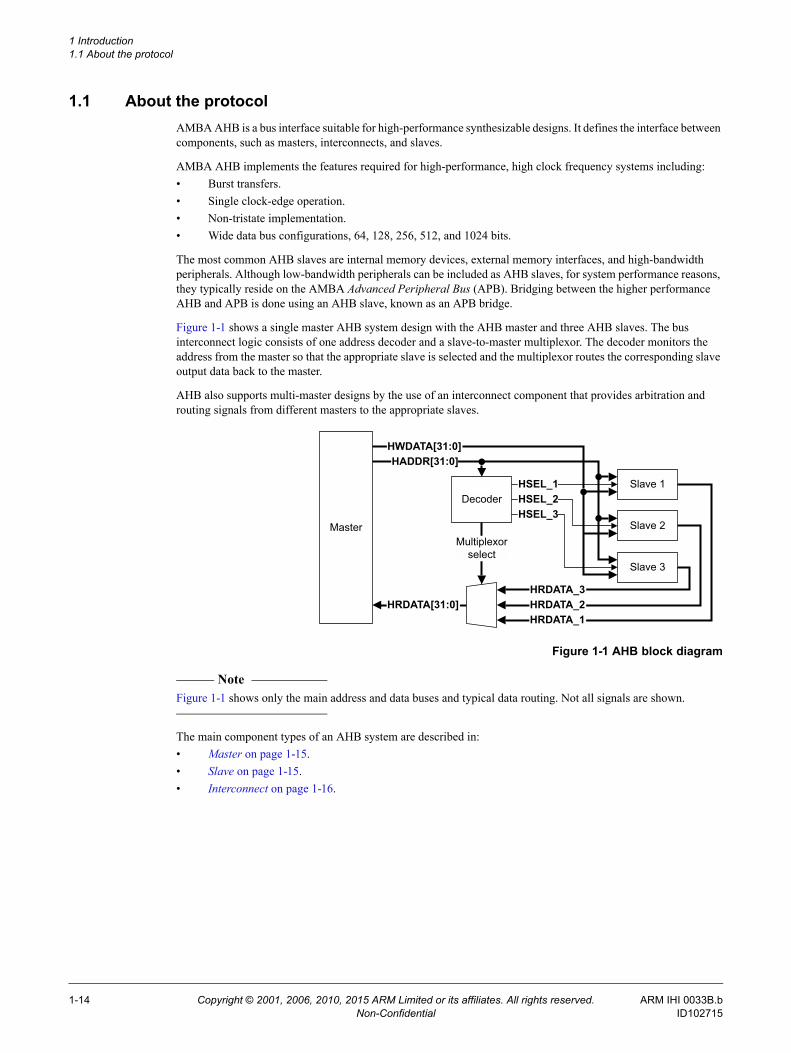
1.1 About the protocolAMBA AHB is a bus interface suitable for high-performance synthesizable designs. It defines the interface between components, such as masters, interconnects, and slaves.
AMBA AHB implements the features required for high-performance, high clock frequency systems including:• Burst transfers.• Single clock-edge operation.• Non-tristate implementation.• Wide data bus configurations, 64, 128, 256, 512, and 1024 bits.
The most common AHB slaves are internal memory devices, external memory interfaces, and high-bandwidth peripherals. Although low-bandwidth peripherals can be included as AHB slaves, for system performance reasons, they typically reside on the AMBA Advanced Peripheral Bus (APB). Bridging between the higher performance AHB and APB is done using an AHB slave, known as an APB bridge.
Figure 1-1 shows a single master AHB system design with the AHB master and three AHB slaves. The bus interconnect logic consists of one address decoder and a slave-to-master multiplexor. The decoder monitors the address from the master so that the appropriate slave is selected and the multiplexor routes the corresponding slave output data back to the master.
AHB also supports multi-master designs by the use of an interconnect component that provides arbitration and routing signals from different masters to the appropriate slaves.
Figure 1-1 AHB block diagram
Note Figure 1-1 shows only the main address and data buses and typical data routing. Not all signals are shown.
The main component types of an AHB system are described in:• Master on page 1-15.• Slave on page 1-15.• Interconnect on page 1-16.
Master
Slave 1
Slave 2
Slave 3
Decoder
HRDATA[31:0]HRDATA_3
HRDATA_1HRDATA_2
Multiplexorselect
HWDATA[31:0]HADDR[31:0]
HSEL_1HSEL_2HSEL_3
1-14 Copyright © 2001, 2006, 2010, 2015 ARM Limited or its affiliates. All rights reserved. ARM IHI 0033B.bNon-Confidential ID102715
1 Introduction 1.1 About the protocol
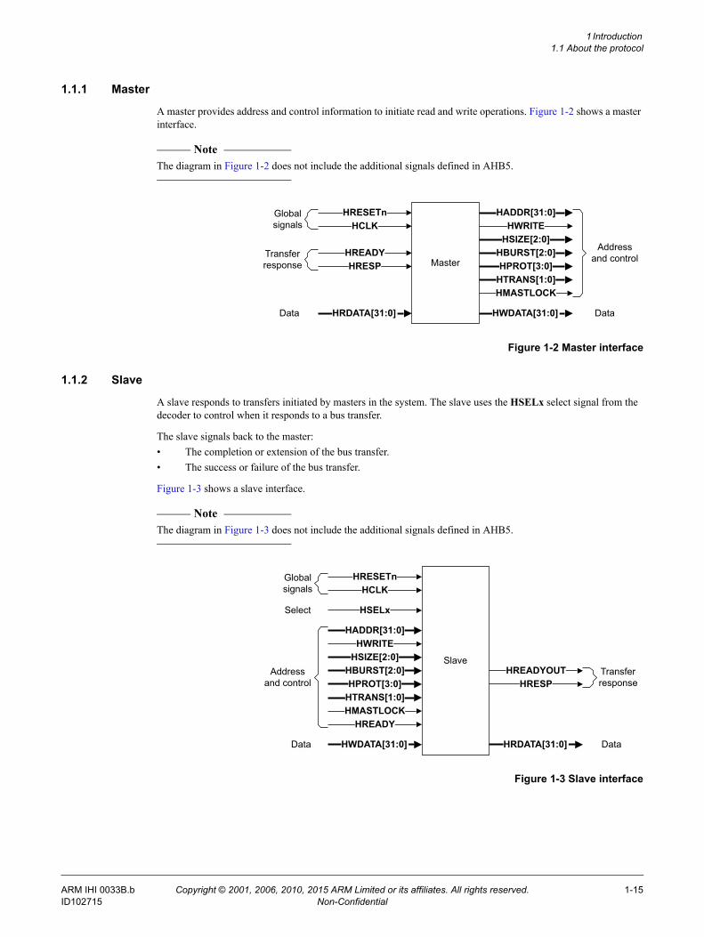
1.1.1 Master
A master provides address and control information to initiate read and write operations. Figure 1-2 shows a master interface.
Note The diagram in Figure 1-2 does not include the additional signals defined in AHB5.
Figure 1-2 Master interface
1.1.2 Slave
A slave responds to transfers initiated by masters in the system. The slave uses the HSELx select signal from the decoder to control when it responds to a bus transfer.
The slave signals back to the master:• The completion or extension of the bus transfer.• The success or failure of the bus transfer.
Figure 1-3 shows a slave interface.
Note The diagram in Figure 1-3 does not include the additional signals defined in AHB5.
Figure 1-3 Slave interface
MasterHREADY
HRESETnHCLK
HRESP
HRDATA[31:0]
HTRANS[1:0]
HADDR[31:0]
HSIZE[2:0]HBURST[2:0]HPROT[3:0]
HWDATA[31:0]
HWRITE
HMASTLOCK
Data
Transfer response
Global signals
Addressand control
Data
Slave
HSELx
HREADY
HADDR[31:0]HWRITE
HTRANS[1:0]
HSIZE[2:0]HBURST[2:0]HPROT[3:0]
HMASTLOCK
HRESETnHCLK
HWDATA[31:0]
HREADYOUT
HRDATA[31:0]
Transfer response
Global signals
Data
Addressand control
Data
Select
HRESP
ARM IHI 0033B.b Copyright © 2001, 2006, 2010, 2015 ARM Limited or its affiliates. All rights reserved. 1-15ID102715 Non-Confidential
1 Introduction 1.1 About the protocol
1.1.3 Interconnect
An interconnect component provides the connection between masters and slaves in a system.
A single master system only requires the use of a Decoder and Multiplexor, as described in the following sections.
A multi-master system requires the use of an interconnect that provides arbitration and the routing of signals from different masters to the appropriate slaves. This routing is required for address, control, and write data signaling. Further details of the different approaches used for multi-master systems, such as single layer or multi-layer interconnects, are not provided within this specification.
See Multi-layer AHB Technical Overview (ARM DVI 0045) for more information about implementing a multi-layer AHB-Lite interconnect.
Decoder
This component decodes the address of each transfer and provides a select signal for the slave that is involved in the transfer. It also provides a control signal to the multiplexor.
A single centralized decoder is required in all implementations that use two or more slaves. See Address decoding on page 4-53 for more information.
Multiplexor
A slave-to-master multiplexor is required to multiplex the read data bus and response signals from the slaves to the master. The decoder provides control for the multiplexor.
A single centralized multiplexor is required in all implementations that use two or more slaves. See Read data and response multiplexor on page 4-54 for more information.
1-16 Copyright © 2001, 2006, 2010, 2015 ARM Limited or its affiliates. All rights reserved. ARM IHI 0033B.bNon-Confidential ID102715
1 Introduction 1.2 AHB revisions
1.2 AHB revisionsThe previous issue of this specification is referred to as Issue A and describes the version that is called AHB-Lite.
This issue of the document is Issue B and describes:
AHB-Lite This version is the same as defined in Issue A.
AHB5 This version provides additional capabilities, and a property is used to declare a new capability. If a property is not declared, it is considered False.
The new properties are:• Extended_Memory_Types. See Memory types on page 3-45.• Secure_Transfers. See Secure transfers on page 3-50.• Endian. See Endianness on page 6-61.• Stable_Between_Clock. See Clock on page 7-68.• Exclusive_Transfers. See Chapter 8 Exclusive Transfers.• Multi_Copy_Atomicity. See Multi-copy atomicity on page 9-77.
This revision of the specification also contains additional information on the following topics:• Locked transfers. See Locked transfers on page 3-32.• Multiple slave select. See Multiple slave select on page 4-53.• Single-copy atomicity size. See Single-copy atomicity size on page 9-76.• User signaling. See Chapter 10 User Signaling.
In this specification, the term AHB is used to refer to both AHB-Lite and AHB5.
Unless stated, signals are common to both AHB-Lite and AHB5.
ARM IHI 0033B.b Copyright © 2001, 2006, 2010, 2015 ARM Limited or its affiliates. All rights reserved. 1-17ID102715 Non-Confidential
1 Introduction 1.3 Operation
1.3 OperationThe master starts a transfer by driving the address and control signals. These signals provide information about the address, direction, width of the transfer, and indicate if the transfer forms part of a burst. Transfers can be:• Single.• Incrementing bursts that do not wrap at address boundaries.• Wrapping bursts that wrap at particular address boundaries.
The write data bus moves data from the master to a slave, and the read data bus moves data from a slave to the master.
Every transfer consists of:
Address phase One address and control cycle.
Data phase One or more cycles for the data.
A slave cannot request that the address phase is extended and therefore all slaves must be capable of sampling the address during this time. However, a slave can request that the master extends the data phase by using HREADY. This signal, when LOW, causes wait states to be inserted into the transfer and enables the slave to have extra time to provide or sample data.
The slave uses HRESP to indicate the success or failure of a transfer.
1-18 Copyright © 2001, 2006, 2010, 2015 ARM Limited or its affiliates. All rights reserved. ARM IHI 0033B.bNon-Confidential ID102715
Chapter 2 Signal Descriptions
This chapter describes the protocol signals. It contains the following sections:• Global signals on page 2-20.• Master signals on page 2-21.• Slave signals on page 2-23.• Decoder signals on page 2-24.• Multiplexor signals on page 2-25.
Note All AHB-Lite and AHB5 signals are prefixed with the letter H to differentiate them from other similarly named signals in a system design.
ARM IHI 0033B.b Copyright © 2001, 2006, 2010, 2015 ARM Limited or its affiliates. All rights reserved. 2-19ID102715 Non-Confidential
2 Signal Descriptions 2.1 Global signals
2.1 Global signalsTable 2-1 lists the protocol global signals.
Table 2-1 Global signals
Name Source Description
HCLK Clock source The bus clock times all bus transfers. All signal timings are related to the rising edge of HCLK.See Clock on page 7-68.
HRESETn Reset controller The bus reset signal is active LOW and resets the system and the bus. This is the only active LOW signal.See Reset on page 7-68.
2-20 Copyright © 2001, 2006, 2010, 2015 ARM Limited or its affiliates. All rights reserved. ARM IHI 0033B.bNon-Confidential ID102715
2 Signal Descriptions 2.2 Master signals
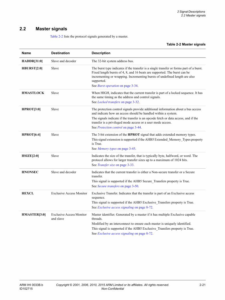
2.2 Master signalsTable 2-2 lists the protocol signals generated by a master.
Table 2-2 Master signals
Name Destination Description
HADDR[31:0] Slave and decoder The 32-bit system address bus.
HBURST[2:0] Slave The burst type indicates if the transfer is a single transfer or forms part of a burst. Fixed length bursts of 4, 8, and 16 beats are supported. The burst can be incrementing or wrapping. Incrementing bursts of undefined length are also supported.See Burst operation on page 3-34.
HMASTLOCK Slave When HIGH, indicates that the current transfer is part of a locked sequence. It has the same timing as the address and control signals.See Locked transfers on page 3-32.
HPROT[3:0] Slave The protection control signals provide additional information about a bus access and indicate how an access should be handled within a system.The signals indicate if the transfer is an opcode fetch or data access, and if the transfer is a privileged mode access or a user mode access.See Protection control on page 3-44.
HPROT[6:4] Slave The 3-bit extension of the HPROT signal that adds extended memory types.This signal extension is supported if the AHB5 Extended_Memory_Types property is True.See Memory types on page 3-45.
HSIZE[2:0] Slave Indicates the size of the transfer, that is typically byte, halfword, or word. The protocol allows for larger transfer sizes up to a maximum of 1024 bits.See Transfer size on page 3-33.
HNONSEC Slave and decoder Indicates that the current transfer is either a Non-secure transfer or a Secure transfer.This signal is supported if the AHB5 Secure_Transfers property is True.See Secure transfers on page 3-50.
HEXCL Exclusive Access Monitor Exclusive Transfer. Indicates that the transfer is part of an Exclusive access sequence.This signal is supported if the AHB5 Exclusive_Transfers property is True.See Exclusive access signaling on page 8-72.
HMASTER[3:0] Exclusive Access Monitor and slave
Master identifier. Generated by a master if it has multiple Exclusive capable threads.Modified by an interconnect to ensure each master is uniquely identified.This signal is supported if the AHB5 Exclusive_Transfers property is True.See Exclusive access signaling on page 8-72.
ARM IHI 0033B.b Copyright © 2001, 2006, 2010, 2015 ARM Limited or its affiliates. All rights reserved. 2-21ID102715 Non-Confidential
2 Signal Descriptions 2.2 Master signals
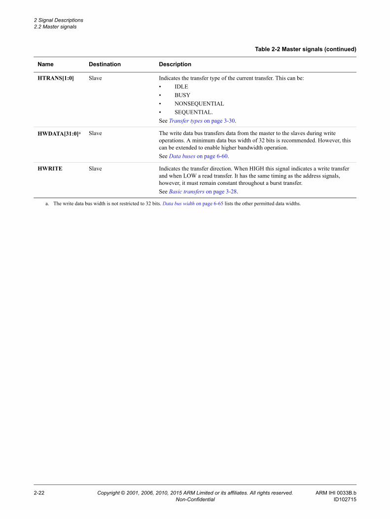
HTRANS[1:0] Slave Indicates the transfer type of the current transfer. This can be:• IDLE• BUSY• NONSEQUENTIAL• SEQUENTIAL.See Transfer types on page 3-30.
HWDATA[31:0]a Slave The write data bus transfers data from the master to the slaves during write operations. A minimum data bus width of 32 bits is recommended. However, this can be extended to enable higher bandwidth operation.See Data buses on page 6-60.
HWRITE Slave Indicates the transfer direction. When HIGH this signal indicates a write transfer and when LOW a read transfer. It has the same timing as the address signals, however, it must remain constant throughout a burst transfer.See Basic transfers on page 3-28.
a. The write data bus width is not restricted to 32 bits. Data bus width on page 6-65 lists the other permitted data widths.
Table 2-2 Master signals (continued)
Name Destination Description
2-22 Copyright © 2001, 2006, 2010, 2015 ARM Limited or its affiliates. All rights reserved. ARM IHI 0033B.bNon-Confidential ID102715
2 Signal Descriptions 2.3 Slave signals
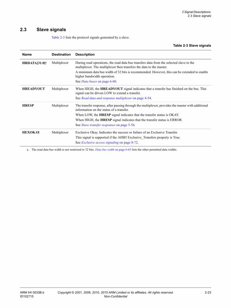
2.3 Slave signalsTable 2-3 lists the protocol signals generated by a slave.
Table 2-3 Slave signals
Name Destination Description
HRDATA[31:0]a Multiplexor During read operations, the read data bus transfers data from the selected slave to the multiplexor. The multiplexor then transfers the data to the master.A minimum data bus width of 32 bits is recommended. However, this can be extended to enable higher bandwidth operation.See Data buses on page 6-60.
HREADYOUT Multiplexor When HIGH, the HREADYOUT signal indicates that a transfer has finished on the bus. This signal can be driven LOW to extend a transfer.See Read data and response multiplexor on page 4-54.
HRESP Multiplexor The transfer response, after passing through the multiplexor, provides the master with additional information on the status of a transfer.When LOW, the HRESP signal indicates that the transfer status is OKAY.When HIGH, the HRESP signal indicates that the transfer status is ERROR.See Slave transfer responses on page 5-56.
HEXOKAY Multiplexor Exclusive Okay. Indicates the success or failure of an Exclusive Transfer.This signal is supported if the AHB5 Exclusive_Transfers property is True.See Exclusive access signaling on page 8-72.
a. The read data bus width is not restricted to 32 bits. Data bus width on page 6-65 lists the other permitted data widths.
ARM IHI 0033B.b Copyright © 2001, 2006, 2010, 2015 ARM Limited or its affiliates. All rights reserved. 2-23ID102715 Non-Confidential
2 Signal Descriptions 2.4 Decoder signals
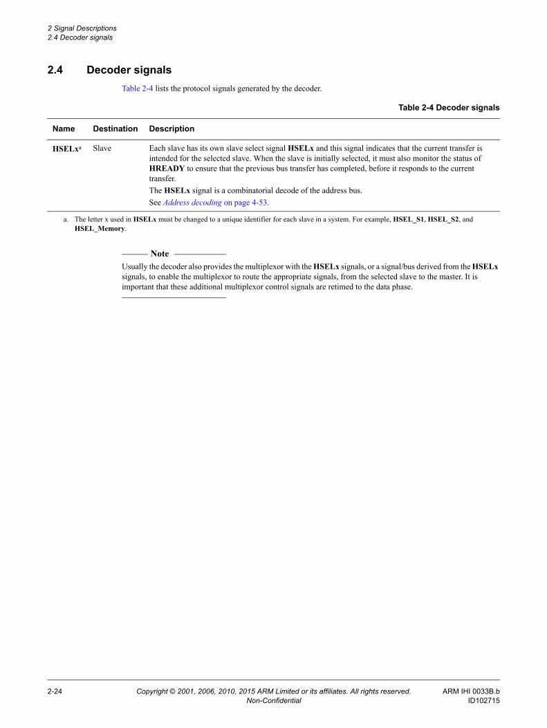
2.4 Decoder signalsTable 2-4 lists the protocol signals generated by the decoder.
Note Usually the decoder also provides the multiplexor with the HSELx signals, or a signal/bus derived from the HSELx signals, to enable the multiplexor to route the appropriate signals, from the selected slave to the master. It is important that these additional multiplexor control signals are retimed to the data phase.
Table 2-4 Decoder signals
Name Destination Description
HSELxa Slave Each slave has its own slave select signal HSELx and this signal indicates that the current transfer is intended for the selected slave. When the slave is initially selected, it must also monitor the status of HREADY to ensure that the previous bus transfer has completed, before it responds to the current transfer.The HSELx signal is a combinatorial decode of the address bus.See Address decoding on page 4-53.
a. The letter x used in HSELx must be changed to a unique identifier for each slave in a system. For example, HSEL_S1, HSEL_S2, and HSEL_Memory.
2-24 Copyright © 2001, 2006, 2010, 2015 ARM Limited or its affiliates. All rights reserved. ARM IHI 0033B.bNon-Confidential ID102715
2 Signal Descriptions 2.5 Multiplexor signals
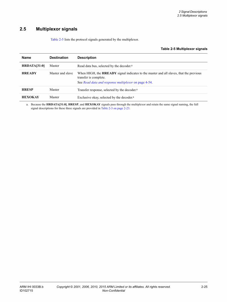
2.5 Multiplexor signals
Table 2-5 lists the protocol signals generated by the multiplexor.
Table 2-5 Multiplexor signals
Name Destination Description
HRDATA[31:0] Master Read data bus, selected by the decoder.a
HREADY Master and slave When HIGH, the HREADY signal indicates to the master and all slaves, that the previous transfer is complete.See Read data and response multiplexor on page 4-54.
HRESP Master Transfer response, selected by the decoder.a
HEXOKAY Master Exclusive okay, selected by the decoder.a
a. Because the HRDATA[31:0], HRESP, and HEXOKAY signals pass through the multiplexor and retain the same signal naming, the full signal descriptions for these three signals are provided in Table 2-3 on page 2-23.
ARM IHI 0033B.b Copyright © 2001, 2006, 2010, 2015 ARM Limited or its affiliates. All rights reserved. 2-25ID102715 Non-Confidential

2 Signal Descriptions 2.5 Multiplexor signals
2-26 Copyright © 2001, 2006, 2010, 2015 ARM Limited or its affiliates. All rights reserved. ARM IHI 0033B.bNon-Confidential ID102715
Chapter 3 Transfers
This chapter describes read and write transfers. It contains the following sections:• Basic transfers on page 3-28.• Transfer types on page 3-30.• Locked transfers on page 3-32.• Transfer size on page 3-33.• Burst operation on page 3-34.• Waited transfers on page 3-39.• Protection control on page 3-44.• Memory types on page 3-45.
ARM IHI 0033B.b Copyright © 2001, 2006, 2010, 2015 ARM Limited or its affiliates. All rights reserved. 3-27ID102715 Non-Confidential
3 Transfers 3.1 Basic transfers
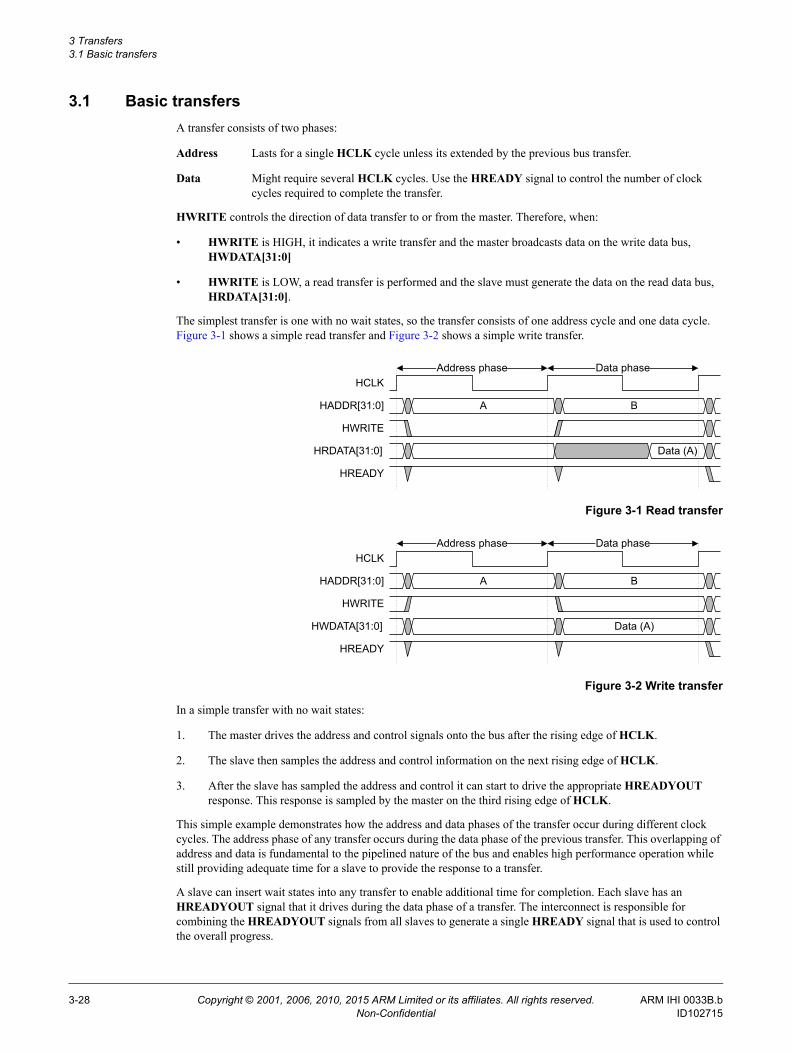
3.1 Basic transfersA transfer consists of two phases:
Address Lasts for a single HCLK cycle unless its extended by the previous bus transfer.
Data Might require several HCLK cycles. Use the HREADY signal to control the number of clock cycles required to complete the transfer.
HWRITE controls the direction of data transfer to or from the master. Therefore, when:
• HWRITE is HIGH, it indicates a write transfer and the master broadcasts data on the write data bus, HWDATA[31:0]
• HWRITE is LOW, a read transfer is performed and the slave must generate the data on the read data bus, HRDATA[31:0].
The simplest transfer is one with no wait states, so the transfer consists of one address cycle and one data cycle. Figure 3-1 shows a simple read transfer and Figure 3-2 shows a simple write transfer.
Figure 3-1 Read transfer
Figure 3-2 Write transfer
In a simple transfer with no wait states:
1. The master drives the address and control signals onto the bus after the rising edge of HCLK.
2. The slave then samples the address and control information on the next rising edge of HCLK.
3. After the slave has sampled the address and control it can start to drive the appropriate HREADYOUT response. This response is sampled by the master on the third rising edge of HCLK.
This simple example demonstrates how the address and data phases of the transfer occur during different clock cycles. The address phase of any transfer occurs during the data phase of the previous transfer. This overlapping of address and data is fundamental to the pipelined nature of the bus and enables high performance operation while still providing adequate time for a slave to provide the response to a transfer.
A slave can insert wait states into any transfer to enable additional time for completion. Each slave has an HREADYOUT signal that it drives during the data phase of a transfer. The interconnect is responsible for combining the HREADYOUT signals from all slaves to generate a single HREADY signal that is used to control the overall progress.
HADDR[31:0] A
HCLK
B
Address phase Data phase
HWRITE
HRDATA[31:0] Data (A)
HREADY
HADDR[31:0] A
HCLK
B
Address phase Data phase
HWRITE
HWDATA[31:0] Data (A)
HREADY
3-28 Copyright © 2001, 2006, 2010, 2015 ARM Limited or its affiliates. All rights reserved. ARM IHI 0033B.bNon-Confidential ID102715
3 Transfers 3.1 Basic transfers
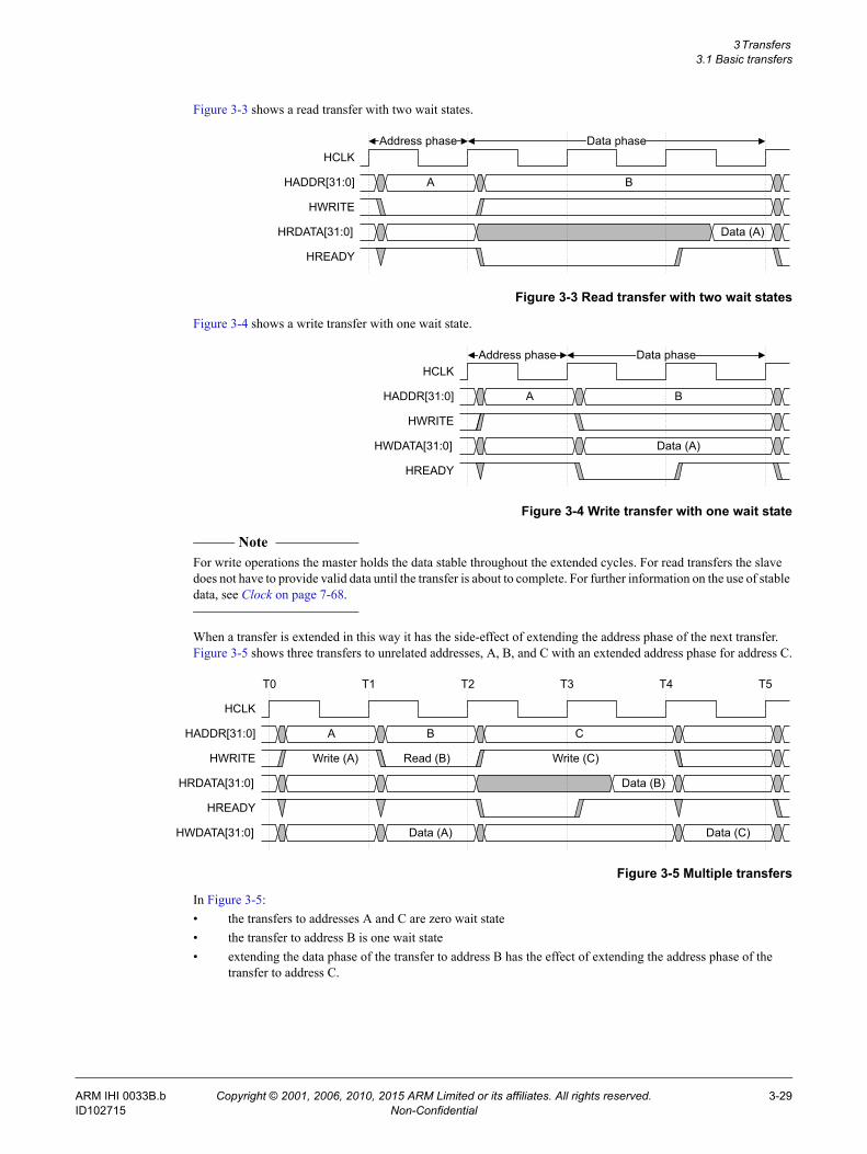
Figure 3-3 shows a read transfer with two wait states.
Figure 3-3 Read transfer with two wait states
Figure 3-4 shows a write transfer with one wait state.
Figure 3-4 Write transfer with one wait state
Note For write operations the master holds the data stable throughout the extended cycles. For read transfers the slave does not have to provide valid data until the transfer is about to complete. For further information on the use of stable data, see Clock on page 7-68.
When a transfer is extended in this way it has the side-effect of extending the address phase of the next transfer. Figure 3-5 shows three transfers to unrelated addresses, A, B, and C with an extended address phase for address C.
Figure 3-5 Multiple transfers
In Figure 3-5:• the transfers to addresses A and C are zero wait state• the transfer to address B is one wait state• extending the data phase of the transfer to address B has the effect of extending the address phase of the
transfer to address C.
HADDR[31:0] A
HCLK
B
Address phase Data phase
HWRITE
HRDATA[31:0] Data (A)
HREADY
HADDR[31:0] A
HCLK
B
Address phase Data phase
HWRITE
HWDATA[31:0] Data (A)
HREADY
HADDR[31:0] A
HCLK
B
HWRITE Write (A)
HRDATA[31:0] Data (B)
HREADY
Read (B)
C
HWDATA[31:0] Data (A)
Write (C)
Data (C)
T5T4T3T2T1T0
ARM IHI 0033B.b Copyright © 2001, 2006, 2010, 2015 ARM Limited or its affiliates. All rights reserved. 3-29ID102715 Non-Confidential
3 Transfers 3.2 Transfer types
3.2 Transfer typesTransfers can be classified into one of four types, as controlled by HTRANS[1:0]. Table 3-1 lists these.
Table 3-1 Transfer type encoding
HTRANS[1:0] Type Description
0b00 IDLE Indicates that no data transfer is required. A master uses an IDLE transfer when it does not want to perform a data transfer. It is recommended that the master terminates a locked transfer with an IDLE transfer.Slaves must always provide a zero wait state OKAY response to IDLE transfers and the transfer must be ignored by the slave.
0b01 BUSY The BUSY transfer type enables masters to insert idle cycles in the middle of a burst. This transfer type indicates that the master is continuing with a burst but the next transfer cannot take place immediately.When a master uses the BUSY transfer type the address and control signals must reflect the next transfer in the burst.Only undefined length bursts can have a BUSY transfer as the last cycle of a burst. See Burst termination after a BUSY transfer on page 3-35.Slaves must always provide a zero wait state OKAY response to BUSY transfers and the transfer must be ignored by the slave.
0b10 NONSEQ Indicates a single transfer or the first transfer of a burst.The address and control signals are unrelated to the previous transfer.Single transfers on the bus are treated as bursts of length one and therefore the transfer type is NONSEQUENTIAL.
0b11 SEQ The remaining transfers in a burst are SEQUENTIAL and the address is related to the previous transfer.The control information is identical to the previous transfer.The address is equal to the address of the previous transfer plus the transfer size, in bytes, with the transfer size being signaled by the HSIZE[2:0] signals. In the case of a wrapping burst the address of the transfer wraps at the address boundary.
3-30 Copyright © 2001, 2006, 2010, 2015 ARM Limited or its affiliates. All rights reserved. ARM IHI 0033B.bNon-Confidential ID102715
3 Transfers 3.2 Transfer types
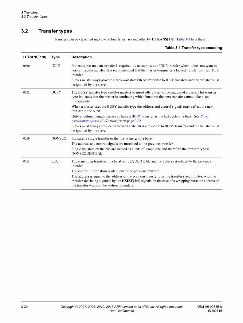
Figure 3-6 shows the use of the NONSEQ, BUSY, and SEQ transfer types.
Figure 3-6 Transfer type examples
In Figure 3-6:
T0-T1 The 4-beat read starts with a NONSEQ transfer.
T1-T2 The master is unable to perform the second beat and inserts a BUSY transfer to delay the start of the second beat.
The slave provides the read data for the first beat.
T2-T3 The master is now ready to start the second beat, so a SEQ transfer is signaled. The master ignores any data that the slave provides on the read data bus.
T3-T4 The master performs the third beat.
The slave provides the read data for the second beat.
T4-T5 The master performs the last beat.
The slave is unable to complete the transfer and uses HREADYOUT to insert a single wait state.
T5-T6 The slave provides the read data for the third beat.
T6-T7 The slave provides the read data for the last beat.
HADDR[31:0] 0x20
HCLK
0x24
HWRITE
HBURST[2:0] INCR
HREADY
0x2C
HRDATA[31:0]Data (0x20)
Data (0x28)
HTRANS[1:0] NONSEQ BUSY SEQSEQ SEQ
0x24 0x28
Data (0x24) Data (0x2C)
T0 T2 T3T1 T4 T7T6T5
ARM IHI 0033B.b Copyright © 2001, 2006, 2010, 2015 ARM Limited or its affiliates. All rights reserved. 3-31ID102715 Non-Confidential
3 Transfers 3.3 Locked transfers
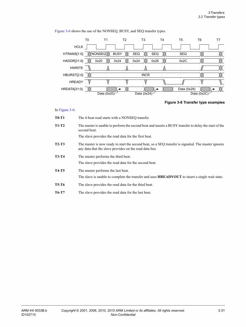
3.3 Locked transfersIf the master requires locked accesses then it must also assert the HMASTLOCK signal. This signal indicates to any slave that the current transfer sequence is indivisible and must therefore be processed before any other transfers are processed.
Typically the locked transfer is used to maintain the integrity of a semaphore, by ensuring that the slave does not perform other operations between the read and write phases of a microprocessor SWP instruction.
Figure 3-7 shows the HMASTLOCK signal with a microprocessor SWP instruction.
Figure 3-7 Locked transfer
Note After a locked transfer, it is recommended that the master inserts an IDLE transfer.
Most slaves have no requirement to implement HMASTLOCK because they are only capable of performing transfers in the order they are received. Slaves that can be accessed by more than one master, for example, a Multi-Port Memory Controller (MPMC) must implement the HMASTLOCK signal.
It is permitted for a master to assert HMASTLOCK for IDLE transfers at the beginning, in the middle, or at the end of a sequence of locked transfers. Using locked IDLE transfers at the start or end of a locked transfer sequence is permitted, but not recommended, as this behavior can adversely affect the arbitration of the system.
It is also permitted, but not recommended, for a master to assert HMASTLOCK for a number IDLE transfers and then deasserted HMASTLOCK without performing a non-IDLE transfer. This behavior can adversely affect the arbitration of the system.
It is required that all transfers in a locked sequence are to the same slave address region.
Note The requirement to ensure that all transfers in a locked sequence are to the same slave address region did not exist in Issue A of this specification. A legacy component must be verified to ensure that it does not exhibit this behavior.
HADDR[31:0] A
HCLK
HWRITE Read (A)
HRDATA[31:0] Data (A)
HTRANS[1:0] NONSEQ NONSEQ IDLE
Write (A)
A
HWDATA[31:0] Data (A)
HMASTLOCK
3-32 Copyright © 2001, 2006, 2010, 2015 ARM Limited or its affiliates. All rights reserved. ARM IHI 0033B.bNon-Confidential ID102715
3 Transfers 3.4 Transfer size
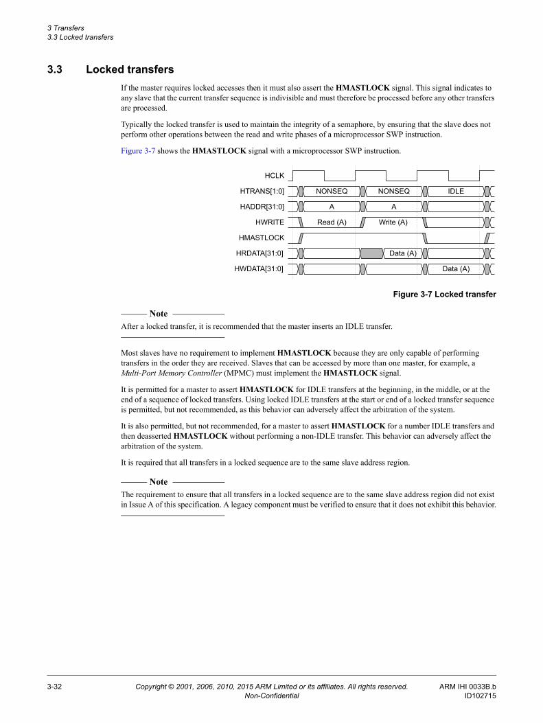
3.4 Transfer sizeHSIZE[2:0] indicates the size of a data transfer. Table 3-2 lists the possible transfer sizes.
Note The transfer size set by HSIZE must be less than or equal to the width of the data bus. For example, with a 32-bit data bus, HSIZE must only use the values 0b000, 0b001, or 0b010.
Use HSIZE in conjunction with HBURST, to determine the address boundary for wrapping bursts.
The HSIZE signals have exactly the same timing as the address bus. However, they must remain constant throughout a burst transfer.
Table 3-2 Transfer size encoding
HSIZE[2] HSIZE[1] HSIZE[0]Size(bits)
Description
0 0 0 8 Byte
0 0 1 16 Halfword
0 1 0 32 Word
0 1 1 64 Doubleword
1 0 0 128 4-word line
1 0 1 256 8-word line
1 1 0 512 -
1 1 1 1024 -
ARM IHI 0033B.b Copyright © 2001, 2006, 2010, 2015 ARM Limited or its affiliates. All rights reserved. 3-33ID102715 Non-Confidential
3 Transfers 3.5 Burst operation
3.5 Burst operationBursts of 4, 8, and 16-beats, undefined length bursts, and single transfers are defined in this protocol. It supports incrementing and wrapping bursts:
• Incrementing bursts access sequential locations and the address of each transfer in the burst is an increment of the previous address.
• Wrapping bursts wrap when they cross an address boundary. The address boundary is calculated as the product of the number of beats in a burst and the size of the transfer. The number of beats are controlled by HBURST and the transfer size is controlled by HSIZE.
For example, a four-beat wrapping burst of word (4-byte) accesses wraps at 16-byte boundaries. Therefore, if the start address of the burst is 0x34, then it consists of four transfers to addresses 0x34, 0x38, 0x3C, and 0x30.
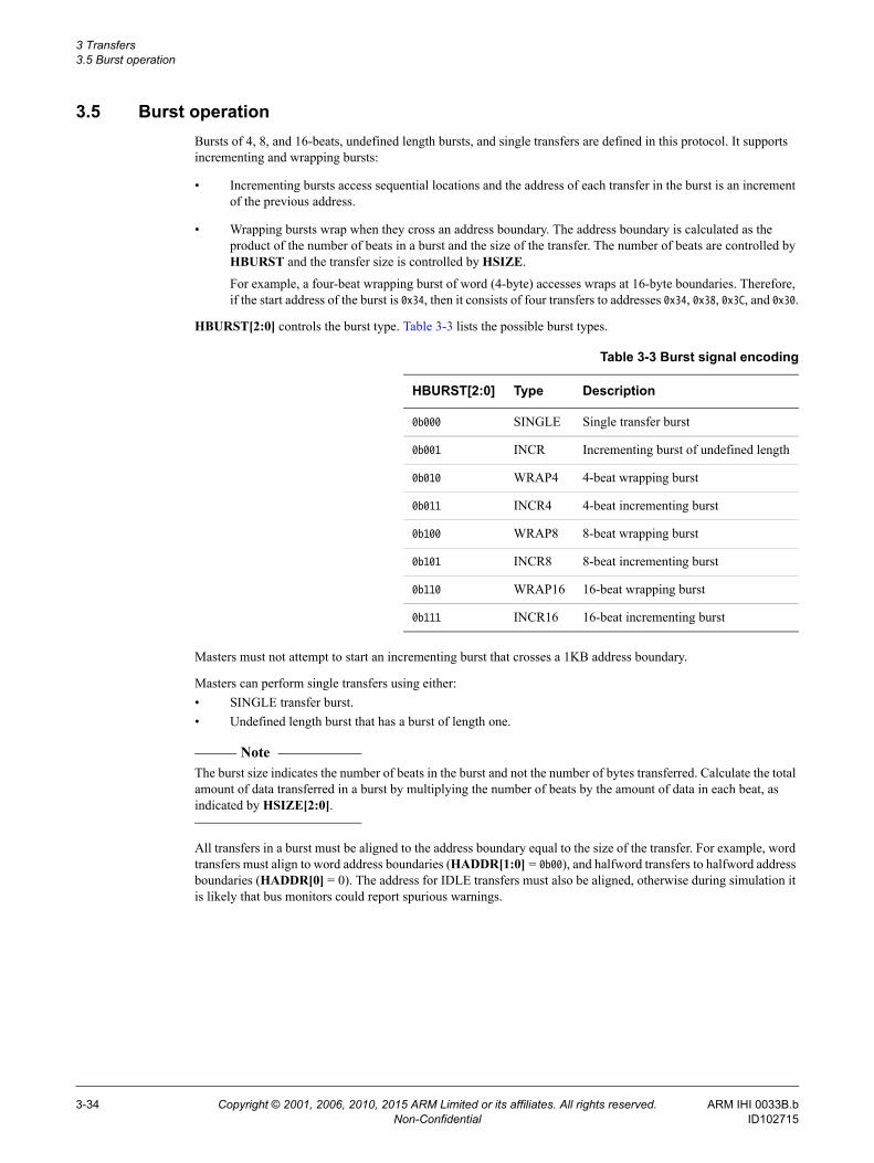
HBURST[2:0] controls the burst type. Table 3-3 lists the possible burst types.
Masters must not attempt to start an incrementing burst that crosses a 1KB address boundary.
Masters can perform single transfers using either:• SINGLE transfer burst.• Undefined length burst that has a burst of length one.
Note The burst size indicates the number of beats in the burst and not the number of bytes transferred. Calculate the total amount of data transferred in a burst by multiplying the number of beats by the amount of data in each beat, as indicated by HSIZE[2:0].
All transfers in a burst must be aligned to the address boundary equal to the size of the transfer. For example, word transfers must align to word address boundaries (HADDR[1:0] = 0b00), and halfword transfers to halfword address boundaries (HADDR[0] = 0). The address for IDLE transfers must also be aligned, otherwise during simulation it is likely that bus monitors could report spurious warnings.
Table 3-3 Burst signal encoding
HBURST[2:0] Type Description
0b000 SINGLE Single transfer burst
0b001 INCR Incrementing burst of undefined length
0b010 WRAP4 4-beat wrapping burst
0b011 INCR4 4-beat incrementing burst
0b100 WRAP8 8-beat wrapping burst
0b101 INCR8 8-beat incrementing burst
0b110 WRAP16 16-beat wrapping burst
0b111 INCR16 16-beat incrementing burst
3-34 Copyright © 2001, 2006, 2010, 2015 ARM Limited or its affiliates. All rights reserved. ARM IHI 0033B.bNon-Confidential ID102715
3 Transfers 3.5 Burst operation
3.5.1 Burst termination after a BUSY transfer
After a burst has started, the master uses BUSY transfers if it requires more time before continuing with the next transfer in the burst.
During an undefined length burst, INCR, the master might insert BUSY transfers and then decide that no more data transfers are required. Under these circumstances, it is acceptable for the master to then perform a NONSEQ or IDLE transfer that then effectively terminates the undefined length burst.
The protocol does not permit a master to end a burst with a BUSY transfer for fixed length bursts of type:• Incrementing INCR4, INCR8, and INCR16.• Wrapping WRAP4, WRAP8, and WRAP16.
These fixed length burst types must terminate with a SEQ transfer.
The master is not permitted to perform a BUSY transfer immediately after a SINGLE burst. SINGLE bursts must be followed by an IDLE transfer or a NONSEQ transfer.
3.5.2 Early burst termination
Bursts can be terminated by either:• Slave error response.• Multi-layer interconnect termination.
Slave error response
If a slave provides an ERROR response then the master can cancel the remaining transfers in the burst. However, this is not a strict requirement and it is also acceptable for the master to continue the remaining transfers in the burst.
If the master cancels the remaining transfers in the burst then it must change HTRANS to indicate IDLE during the two-cycle Error response.
If the master does not complete that burst then there is no requirement for it to rebuild the burst when it next accesses that slave. For example, if a master only completes three beats of an eight-beat burst then it does not have to complete the remaining five transfers when it next accesses that slave.
Multi-layer interconnect termination
Although masters are not permitted to terminate a burst request early, slaves must be designed to work correctly if the burst is not completed.
When a multi-layer interconnect component is used in a multi-master system then it can terminate a burst so that another master can gain access to the slave. The slave must terminate the burst from the original master and then respond appropriately to the new master if this occurs.
ARM IHI 0033B.b Copyright © 2001, 2006, 2010, 2015 ARM Limited or its affiliates. All rights reserved. 3-35ID102715 Non-Confidential
3 Transfers 3.5 Burst operation
3.5.3 Burst examples
Examples of various bursts are shown in the following sections:• Four-beat wrapping burst, WRAP4.• Four-beat incrementing burst, INCR4 on page 3-37.• Eight-beat wrapping burst, WRAP8 on page 3-37.• Eight-beat incrementing burst, INCR8 on page 3-38.• Undefined length bursts, INCR on page 3-38.
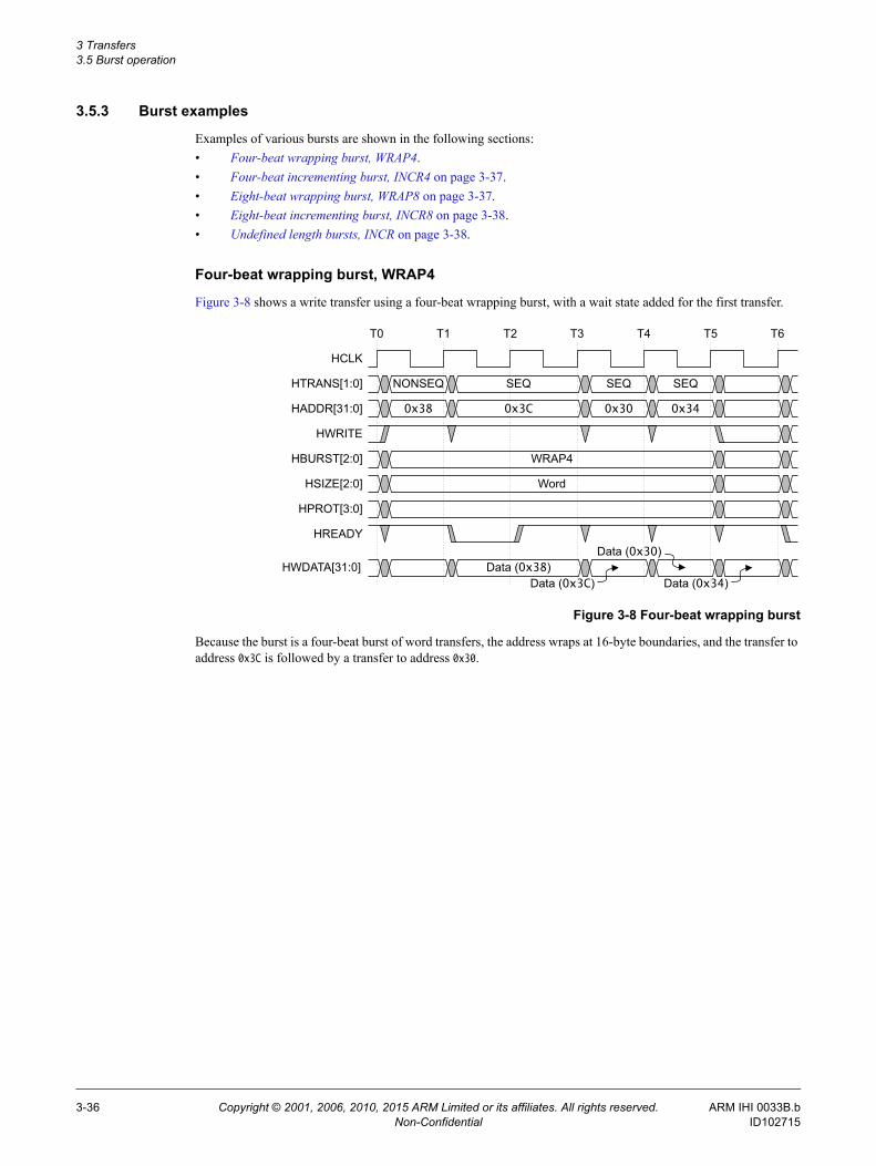
Four-beat wrapping burst, WRAP4
Figure 3-8 shows a write transfer using a four-beat wrapping burst, with a wait state added for the first transfer.
Figure 3-8 Four-beat wrapping burst
Because the burst is a four-beat burst of word transfers, the address wraps at 16-byte boundaries, and the transfer to address 0x3C is followed by a transfer to address 0x30.
HADDR[31:0] 0x38
HCLK
0x34
HWRITE
HBURST[2:0] WRAP4
HREADY
0x3C
HWDATA[31:0]Data (0x30)
Data (0x38)
T3
HTRANS[1:0] NONSEQ SEQSEQ SEQ
0x30
Data (0x3C) Data (0x34)
HSIZE[2:0] Word
HPROT[3:0]
T0 T1 T2 T4 T5 T6
3-36 Copyright © 2001, 2006, 2010, 2015 ARM Limited or its affiliates. All rights reserved. ARM IHI 0033B.bNon-Confidential ID102715
3 Transfers 3.5 Burst operation
Four-beat incrementing burst, INCR4
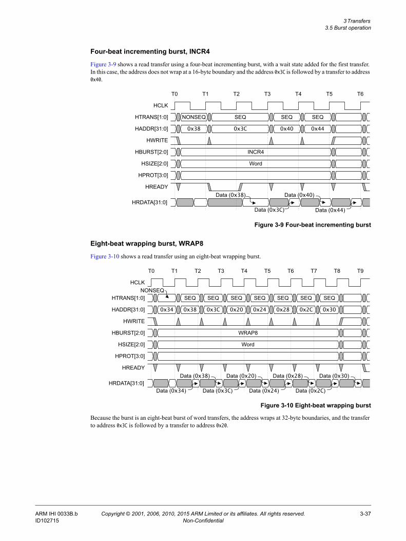
Figure 3-9 shows a read transfer using a four-beat incrementing burst, with a wait state added for the first transfer. In this case, the address does not wrap at a 16-byte boundary and the address 0x3C is followed by a transfer to address 0x40.
Figure 3-9 Four-beat incrementing burst
Eight-beat wrapping burst, WRAP8
Figure 3-10 shows a read transfer using an eight-beat wrapping burst.
Figure 3-10 Eight-beat wrapping burst
Because the burst is an eight-beat burst of word transfers, the address wraps at 32-byte boundaries, and the transfer to address 0x3C is followed by a transfer to address 0x20.
HADDR[31:0] 0x38
HCLK
0x44
HWRITE
HBURST[2:0] INCR4
HREADY
0x3C
HRDATA[31:0]Data (0x40)
HTRANS[1:0] NONSEQ SEQSEQ SEQ
0x40
Data (0x3C) Data (0x44)
HSIZE[2:0] Word
HPROT[3:0]
Data (0x38)
T3T0 T1 T2 T4 T5 T6
T0
HCLK
T4T3T2T1 T5 T6 T7 T8 T9
HADDR[31:0]
HWRITE
HBURST[2:0] WRAP8
HREADY
HRDATA[31:0]Data (0x20)
HTRANS[1:0] SEQ SEQSEQ
Data (0x3C)
HSIZE[2:0] Word
HPROT[3:0]
SEQSEQ SEQ SEQ
0x34 0x24 0x280x200x3C0x38 0x2C 0x30
Data (0x38)
Data (0x34)
Data (0x28)
Data (0x24)
Data (0x30)
Data (0x2C)
NONSEQ
ARM IHI 0033B.b Copyright © 2001, 2006, 2010, 2015 ARM Limited or its affiliates. All rights reserved. 3-37ID102715 Non-Confidential
3 Transfers 3.5 Burst operation
Eight-beat incrementing burst, INCR8
Figure 3-11 shows a write transfer using an eight-beat incrementing burst.
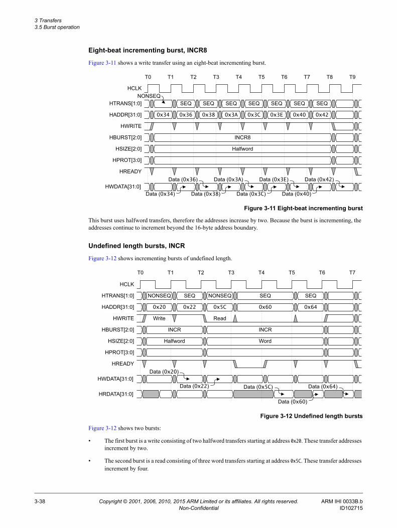
Figure 3-11 Eight-beat incrementing burst
This burst uses halfword transfers, therefore the addresses increase by two. Because the burst is incrementing, the addresses continue to increment beyond the 16-byte address boundary.
Undefined length bursts, INCR
Figure 3-12 shows incrementing bursts of undefined length.
Figure 3-12 Undefined length bursts
Figure 3-12 shows two bursts:
• The first burst is a write consisting of two halfword transfers starting at address 0x20. These transfer addresses increment by two.
• The second burst is a read consisting of three word transfers starting at address 0x5C. These transfer addresses increment by four.
T0
HADDR[31:0]
HCLK
HWRITE
HBURST[2:0] INCR8
HREADY
HWDATA[31:0]Data (0x3A)
T4T3T2T1 T5
HTRANS[1:0] SEQ SEQSEQ
T6
Data (0x38)
HSIZE[2:0] Halfword
HPROT[3:0]
T7 T8 T9
SEQSEQ SEQ SEQ
0x34 0x3C 0x3E0x3A0x380x36 0x40 0x42
Data (0x36)
Data (0x34)
Data (0x3E)
Data (0x3C)
Data (0x42)
Data (0x40)
NONSEQ
HADDR[31:0] 0x20
HCLK
0x60
HWRITE
HBURST[2:0] INCR
HREADY
0x22
HWDATA[31:0]
T3
HTRANS[1:0] NONSEQ SEQSEQ
0x640x5C
HSIZE[2:0] Halfword
HPROT[3:0]
Data (0x20)
SEQ NONSEQ
INCR
Word
Data (0x22)HRDATA[31:0]
Data (0x5C)
Data (0x60)
Data (0x64)
T4 T6T5T2T1T0 T7
Write Read
3-38 Copyright © 2001, 2006, 2010, 2015 ARM Limited or its affiliates. All rights reserved. ARM IHI 0033B.bNon-Confidential ID102715
3 Transfers 3.6 Waited transfers
3.6 Waited transfersSlaves use HREADYOUT to insert wait states if they require more time to provide or sample the data. During a waited transfer, the master is restricted to what changes it can make to the transfer type and address. These restrictions are described in the following sections:• Transfer type changes during wait states.• Address changes during wait states on page 3-42.
3.6.1 Transfer type changes during wait states
When the slave is requesting wait states, the master must not change the transfer type, except as described in:• IDLE transfer.• BUSY transfer, fixed length burst on page 3-40.• BUSY transfer, undefined length burst on page 3-41.
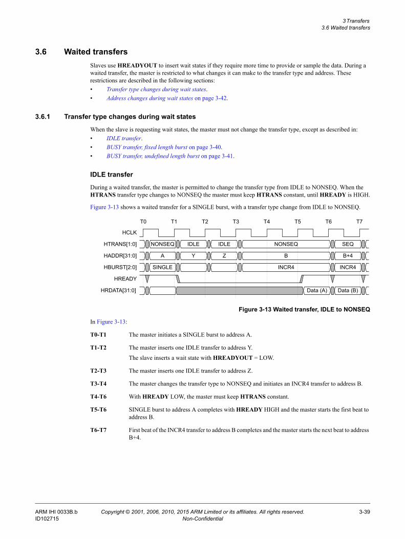
IDLE transfer
During a waited transfer, the master is permitted to change the transfer type from IDLE to NONSEQ. When the HTRANS transfer type changes to NONSEQ the master must keep HTRANS constant, until HREADY is HIGH.
Figure 3-13 shows a waited transfer for a SINGLE burst, with a transfer type change from IDLE to NONSEQ.
Figure 3-13 Waited transfer, IDLE to NONSEQ
In Figure 3-13:
T0-T1 The master initiates a SINGLE burst to address A.
T1-T2 The master inserts one IDLE transfer to address Y.
The slave inserts a wait state with HREADYOUT = LOW.
T2-T3 The master inserts one IDLE transfer to address Z.
T3-T4 The master changes the transfer type to NONSEQ and initiates an INCR4 transfer to address B.
T4-T6 With HREADY LOW, the master must keep HTRANS constant.
T5-T6 SINGLE burst to address A completes with HREADY HIGH and the master starts the first beat to address B.
T6-T7 First beat of the INCR4 transfer to address B completes and the master starts the next beat to address B+4.
HADDR[31:0] A
HCLK
Y
HBURST[2:0] SINGLE
HREADY
B B+4
HRDATA[31:0]
INCR4
HTRANS[1:0] NONSEQ IDLE SEQNONSEQ
Data (A)
T0 T2 T3T1 T4 T7T6T5
Data (B)
INCR4
IDLE
Z
ARM IHI 0033B.b Copyright © 2001, 2006, 2010, 2015 ARM Limited or its affiliates. All rights reserved. 3-39ID102715 Non-Confidential
3 Transfers 3.6 Waited transfers
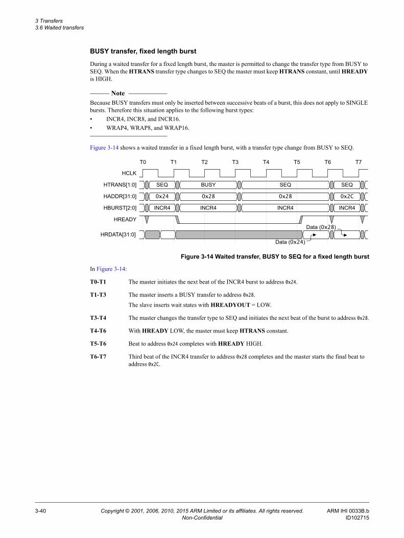
BUSY transfer, fixed length burst
During a waited transfer for a fixed length burst, the master is permitted to change the transfer type from BUSY to SEQ. When the HTRANS transfer type changes to SEQ the master must keep HTRANS constant, until HREADY is HIGH.
Note Because BUSY transfers must only be inserted between successive beats of a burst, this does not apply to SINGLE bursts. Therefore this situation applies to the following burst types:• INCR4, INCR8, and INCR16.• WRAP4, WRAP8, and WRAP16.
Figure 3-14 shows a waited transfer in a fixed length burst, with a transfer type change from BUSY to SEQ.
Figure 3-14 Waited transfer, BUSY to SEQ for a fixed length burst
In Figure 3-14:
T0-T1 The master initiates the next beat of the INCR4 burst to address 0x24.
T1-T3 The master inserts a BUSY transfer to address 0x28.
The slave inserts wait states with HREADYOUT = LOW.
T3-T4 The master changes the transfer type to SEQ and initiates the next beat of the burst to address 0x28.
T4-T6 With HREADY LOW, the master must keep HTRANS constant.
T5-T6 Beat to address 0x24 completes with HREADY HIGH.
T6-T7 Third beat of the INCR4 transfer to address 0x28 completes and the master starts the final beat to address 0x2C.
HADDR[31:0] 0x24
HCLK
0x28
HBURST[2:0] INCR4
HREADY
0x28 0x2C
HRDATA[31:0]
INCR4
HTRANS[1:0] SEQ BUSY SEQSEQ
T0 T2 T3T1 T4 T7T6T5
INCR4 INCR4
Data (0x24)
Data (0x28)
3-40 Copyright © 2001, 2006, 2010, 2015 ARM Limited or its affiliates. All rights reserved. ARM IHI 0033B.bNon-Confidential ID102715
3 Transfers 3.6 Waited transfers
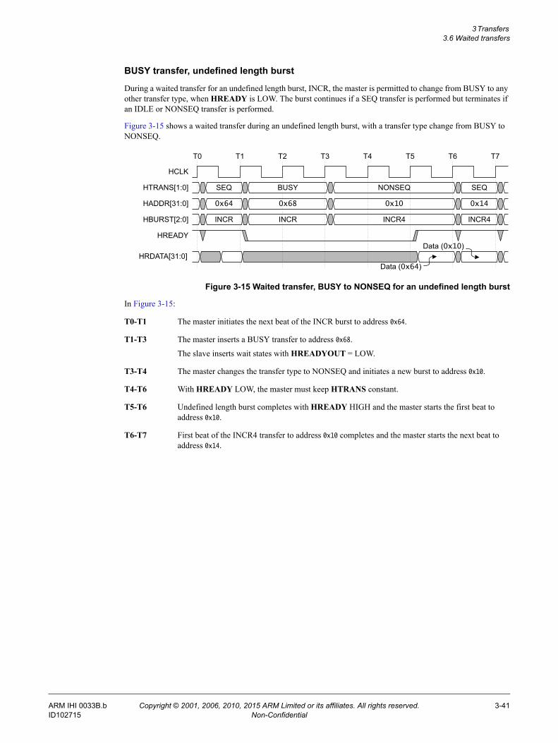
BUSY transfer, undefined length burst
During a waited transfer for an undefined length burst, INCR, the master is permitted to change from BUSY to any other transfer type, when HREADY is LOW. The burst continues if a SEQ transfer is performed but terminates if an IDLE or NONSEQ transfer is performed.
Figure 3-15 shows a waited transfer during an undefined length burst, with a transfer type change from BUSY to NONSEQ.
Figure 3-15 Waited transfer, BUSY to NONSEQ for an undefined length burst
In Figure 3-15:
T0-T1 The master initiates the next beat of the INCR burst to address 0x64.
T1-T3 The master inserts a BUSY transfer to address 0x68.
The slave inserts wait states with HREADYOUT = LOW.
T3-T4 The master changes the transfer type to NONSEQ and initiates a new burst to address 0x10.
T4-T6 With HREADY LOW, the master must keep HTRANS constant.
T5-T6 Undefined length burst completes with HREADY HIGH and the master starts the first beat to address 0x10.
T6-T7 First beat of the INCR4 transfer to address 0x10 completes and the master starts the next beat to address 0x14.
HADDR[31:0] 0x64
HCLK
0x68
HBURST[2:0] INCR
HREADY
0x10 0x14
HRDATA[31:0]
INCR4
HTRANS[1:0] SEQ BUSY SEQNONSEQ
T0 T2 T3T1 T4 T7T6T5
INCR INCR4
Data (0x64)
Data (0x10)
ARM IHI 0033B.b Copyright © 2001, 2006, 2010, 2015 ARM Limited or its affiliates. All rights reserved. 3-41ID102715 Non-Confidential
3 Transfers 3.6 Waited transfers
3.6.2 Address changes during wait states
When the slave is requesting wait states, the master can only change the address once, except as described in:• During an IDLE transfer.• After an ERROR response on page 3-43.
During an IDLE transfer
During a waited transfer, the master is permitted to change the address for IDLE transfers. When the HTRANS transfer type changes to NONSEQ the master must keep the address constant, until HREADY is HIGH.
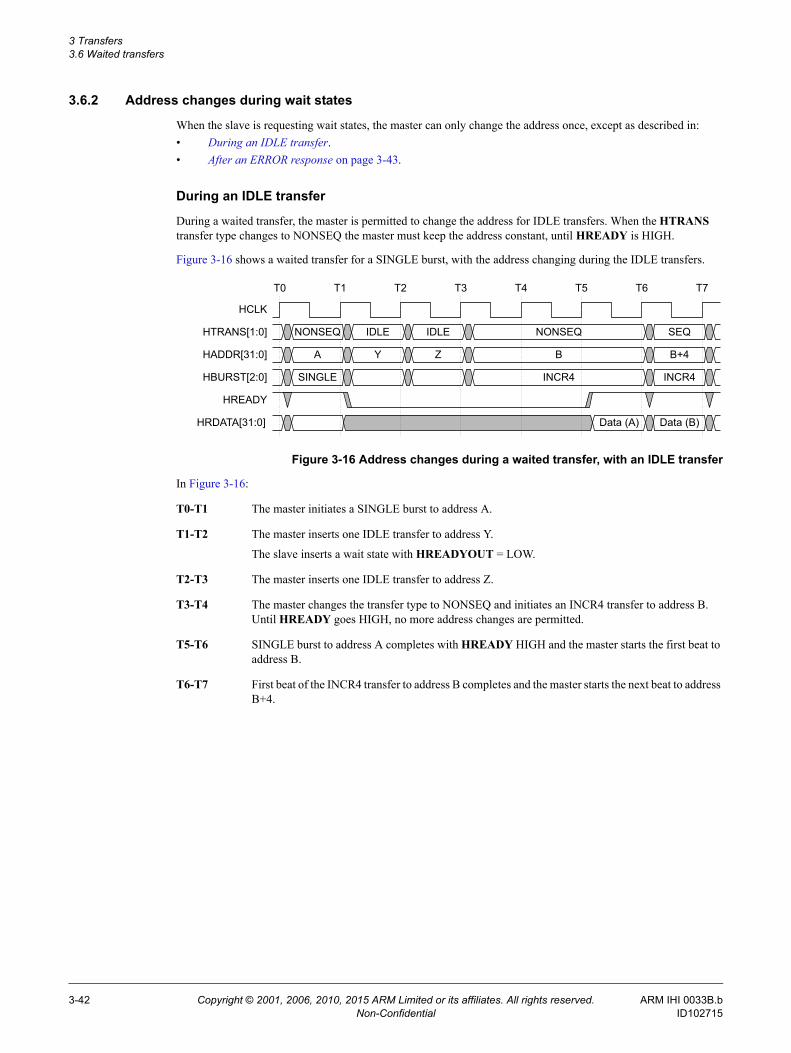
Figure 3-16 shows a waited transfer for a SINGLE burst, with the address changing during the IDLE transfers.
Figure 3-16 Address changes during a waited transfer, with an IDLE transfer
In Figure 3-16:
T0-T1 The master initiates a SINGLE burst to address A.
T1-T2 The master inserts one IDLE transfer to address Y.
The slave inserts a wait state with HREADYOUT = LOW.
T2-T3 The master inserts one IDLE transfer to address Z.
T3-T4 The master changes the transfer type to NONSEQ and initiates an INCR4 transfer to address B. Until HREADY goes HIGH, no more address changes are permitted.
T5-T6 SINGLE burst to address A completes with HREADY HIGH and the master starts the first beat to address B.
T6-T7 First beat of the INCR4 transfer to address B completes and the master starts the next beat to address B+4.
HADDR[31:0] A
HCLK
Y
HBURST[2:0] SINGLE
HREADY
B B+4
HRDATA[31:0]
INCR4
HTRANS[1:0] NONSEQ IDLE SEQNONSEQ
Data (A)
T0 T2 T3T1 T4 T7T6T5
Data (B)
INCR4
IDLE
Z
3-42 Copyright © 2001, 2006, 2010, 2015 ARM Limited or its affiliates. All rights reserved. ARM IHI 0033B.bNon-Confidential ID102715
3 Transfers 3.6 Waited transfers
After an ERROR response
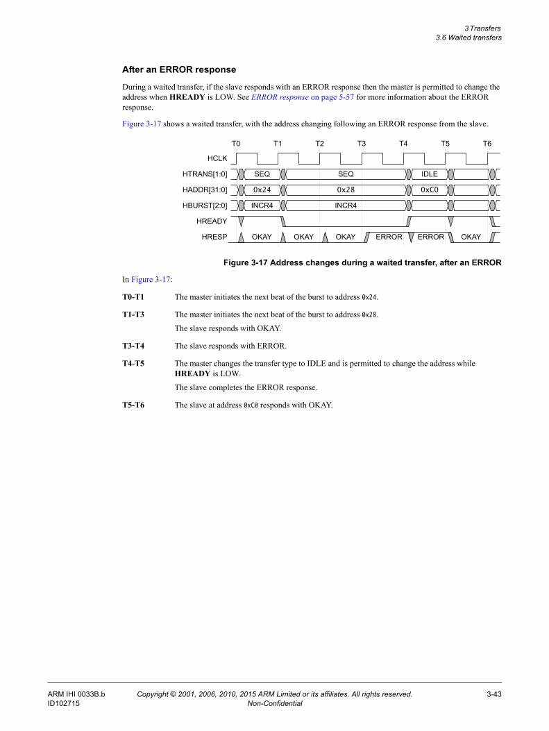
During a waited transfer, if the slave responds with an ERROR response then the master is permitted to change the address when HREADY is LOW. See ERROR response on page 5-57 for more information about the ERROR response.
Figure 3-17 shows a waited transfer, with the address changing following an ERROR response from the slave.
Figure 3-17 Address changes during a waited transfer, after an ERROR
In Figure 3-17:
T0-T1 The master initiates the next beat of the burst to address 0x24.
T1-T3 The master initiates the next beat of the burst to address 0x28.
The slave responds with OKAY.
T3-T4 The slave responds with ERROR.
T4-T5 The master changes the transfer type to IDLE and is permitted to change the address while HREADY is LOW.
The slave completes the ERROR response.
T5-T6 The slave at address 0xC0 responds with OKAY.
HADDR[31:0] 0x24
HCLK
0x28
HBURST[2:0] INCR4
HREADY
0xC0
HTRANS[1:0] SEQ SEQ IDLE
T0 T2 T3T1 T4 T6T5
INCR4
OKAY ERRORERRORHRESP OKAYOKAY OKAY
ARM IHI 0033B.b Copyright © 2001, 2006, 2010, 2015 ARM Limited or its affiliates. All rights reserved. 3-43ID102715 Non-Confidential
3 Transfers 3.7 Protection control
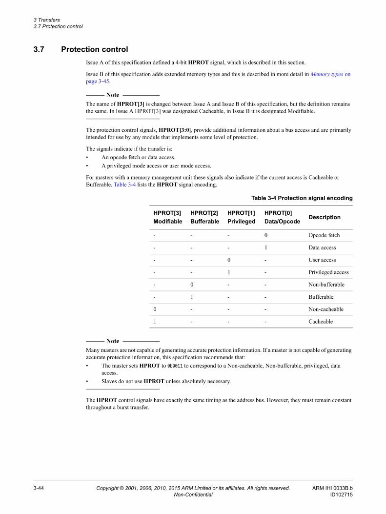
3.7 Protection controlIssue A of this specification defined a 4-bit HPROT signal, which is described in this section.
Issue B of this specification adds extended memory types and this is described in more detail in Memory types on page 3-45.
Note The name of HPROT[3] is changed between Issue A and Issue B of this specification, but the definition remains the same. In Issue A HPROT[3] was designated Cacheable, in Issue B it is designated Modifiable.
The protection control signals, HPROT[3:0], provide additional information about a bus access and are primarily intended for use by any module that implements some level of protection.
The signals indicate if the transfer is:• An opcode fetch or data access.• A privileged mode access or user mode access.
For masters with a memory management unit these signals also indicate if the current access is Cacheable or Bufferable. Table 3-4 lists the HPROT signal encoding.
Note Many masters are not capable of generating accurate protection information. If a master is not capable of generating accurate protection information, this specification recommends that:• The master sets HPROT to 0b0011 to correspond to a Non-cacheable, Non-bufferable, privileged, data
access.• Slaves do not use HPROT unless absolutely necessary.
The HPROT control signals have exactly the same timing as the address bus. However, they must remain constant throughout a burst transfer.
Table 3-4 Protection signal encoding
HPROT[3]Modifiable
HPROT[2]Bufferable
HPROT[1]Privileged
HPROT[0]Data/Opcode
Description
- - - 0 Opcode fetch
- - - 1 Data access
- - 0 - User access
- - 1 - Privileged access
- 0 - - Non-bufferable
- 1 - - Bufferable
0 - - - Non-cacheable
1 - - - Cacheable
3-44 Copyright © 2001, 2006, 2010, 2015 ARM Limited or its affiliates. All rights reserved. ARM IHI 0033B.bNon-Confidential ID102715
3 Transfers 3.8 Memory types
3.8 Memory typesAHB5 defines the Extended_Memory_Types property. This property defines whether an interface supports the extended memory types described in this section. If this property is not defined, then the interface does not support the extended memory types.
This issue of the specification adds additional HPROT signaling and provides a more detailed list of requirements for each of the memory types.
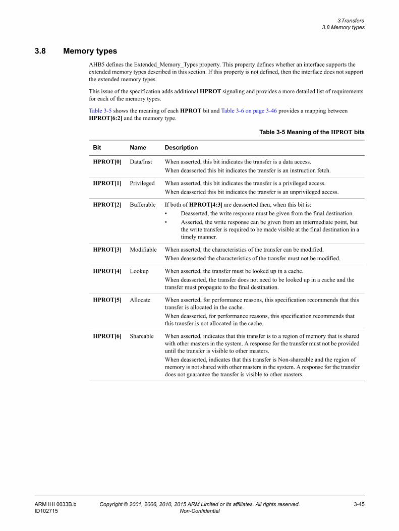
Table 3-5 shows the meaning of each HPROT bit and Table 3-6 on page 3-46 provides a mapping between HPROT[6:2] and the memory type.
Table 3-5 Meaning of the HPROT bits
Bit Name Description
HPROT[0] Data/Inst When asserted, this bit indicates the transfer is a data access.When deasserted this bit indicates the transfer is an instruction fetch.
HPROT[1] Privileged When asserted, this bit indicates the transfer is a privileged access.When deasserted this bit indicates the transfer is an unprivileged access.
HPROT[2] Bufferable If both of HPROT[4:3] are deasserted then, when this bit is:• Deasserted, the write response must be given from the final destination.• Asserted, the write response can be given from an intermediate point, but
the write transfer is required to be made visible at the final destination in a timely manner.
HPROT[3] Modifiable When asserted, the characteristics of the transfer can be modified.When deasserted the characteristics of the transfer must not be modified.
HPROT[4] Lookup When asserted, the transfer must be looked up in a cache.When deasserted, the transfer does not need to be looked up in a cache and the transfer must propagate to the final destination.
HPROT[5] Allocate When asserted, for performance reasons, this specification recommends that this transfer is allocated in the cache.When deasserted, for performance reasons, this specification recommends that this transfer is not allocated in the cache.
HPROT[6] Shareable When asserted, indicates that this transfer is to a region of memory that is shared with other masters in the system. A response for the transfer must not be provided until the transfer is visible to other masters.When deasserted, indicates that this transfer is Non-shareable and the region of memory is not shared with other masters in the system. A response for the transfer does not guarantee the transfer is visible to other masters.
ARM IHI 0033B.b Copyright © 2001, 2006, 2010, 2015 ARM Limited or its affiliates. All rights reserved. 3-45ID102715 Non-Confidential
3 Transfers 3.8 Memory types
3.8.1 Data or Instruction
All transfers include the Data or Instruction protection bit HPROT[0]:• When asserted, this bit indicates the transfer is a data access.• When deasserted this bit indicates the transfer is an instruction fetch.
The protocol defines this indication as a hint. It is not accurate in all cases, for example, where a transaction contains a mix of instruction and data items.
This specification recommends that a master sets HPROT[0] HIGH, to indicate a data access unless the access is specifically known to be an instruction access.
3.8.2 Unprivileged or Privileged
All transfers include the Privileged or Unprivileged protection bit, HPROT[1]:• When asserted, this bit indicates the transfer is a Privileged access.• When deasserted this bit indicates the transfer is an Unprivileged access.
Note Some processors support multiple levels of privilege, see the documentation for the selected processor to determine the mapping to AHB privilege levels. The only distinction provided is between Privileged and Unprivileged access.
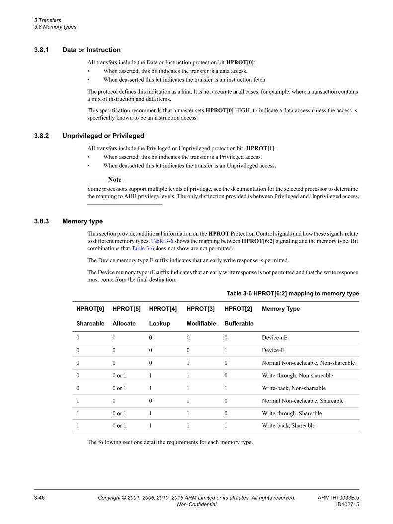
3.8.3 Memory type
This section provides additional information on the HPROT Protection Control signals and how these signals relate to different memory types. Table 3-6 shows the mapping between HPROT[6:2] signaling and the memory type. Bit combinations that Table 3-6 does not show are not permitted.
The Device memory type E suffix indicates that an early write response is permitted.
The Device memory type nE suffix indicates that an early write response is not permitted and that the write response must come from the final destination.
The following sections detail the requirements for each memory type.
Table 3-6 HPROT[6:2] mapping to memory type
HPROT[6] HPROT[5] HPROT[4] HPROT[3] HPROT[2] Memory Type
Shareable Allocate Lookup Modifiable Bufferable
0 0 0 0 0 Device-nE
0 0 0 0 1 Device-E
0 0 0 1 0 Normal Non-cacheable, Non-shareable
0 0 or 1 1 1 0 Write-through, Non-shareable
0 0 or 1 1 1 1 Write-back, Non-shareable
1 0 0 1 0 Normal Non-cacheable, Shareable
1 0 or 1 1 1 0 Write-through, Shareable
1 0 or 1 1 1 1 Write-back, Shareable
3-46 Copyright © 2001, 2006, 2010, 2015 ARM Limited or its affiliates. All rights reserved. ARM IHI 0033B.bNon-Confidential ID102715
3 Transfers 3.8 Memory types
3.8.4 Device memory requirements
For all Device memory, that is Device-nE and Device-E, the required behavior is:
• Read data must be obtained from the final destination.
• Transfers must not be split into multiple transfers or merged with other transfers.
• Reads must not be prefetched or performed speculatively.
• Writes must not be merged.
• All read and write transfers from the same master to the same slave must remain ordered.
• The size of the transfer, as indicated by HSIZE, must not be changed.
• A burst of transfers is permitted to be broken into a number of smaller bursts. However, the total number of NONSEQ and SEQ transfers in the original burst must be the same as the total number of NONSEQ and SEQ transfers in the resultant smaller bursts.
• The only change permitted to HPROT is to convert a transfer from Bufferabe to Non-bufferable.
Additionally, for Device-nE:• Write response must be obtained from the final destination.
Additionally, for Device-E:• The write response can be obtained from an intermediate point.• Write transfers must be observable to all other masters at the point that a write response is given.• Write transfers must arrive at the final destination in a timely manner.
3.8.5 Normal memory requirements
For all Normal memory, that is, Normal Non-cacheable memory, Write-through, and Write-back, the required behavior is:• Reads can be speculative.• Reads can fetch more data than required.• Writes can be merged.• The characteristics of the transfer, as indicated by HBURST and HSIZE can be changed.• Read and write transfers from the same master to addresses that overlap must remain ordered.• For Shareable transactions the response must only be given when the transfer is visible to all other masters.
Additionally, for Normal Non-cacheable memory:
• Write transfers must be made visible at the final destination in a timely manner.
Note There is no mechanism to determine when a write transfer has reached its final destination.
• Read data must be obtained either from:— The final destination.— A write transfer that is progressing to its final destination.
• If read data is obtained from a write transfer:— It must be obtained from the most recent version of the write.— The data must not be cached to service a later read.
• Reads must not cache the data obtained for later use.
ARM IHI 0033B.b Copyright © 2001, 2006, 2010, 2015 ARM Limited or its affiliates. All rights reserved. 3-47ID102715 Non-Confidential
3 Transfers 3.8 Memory types
Note For a Normal Non-cacheable Memory, read data can be obtained from a write transfer that is still progressing to its final destination, this is indistinguishable from the read and write transfers propagating to arrive at the final destination at the same time. Read data returned in this manner does not indicate that the write transfer is visible at the final destination.
Additionally, for Write-through:• The write response can be obtained from an intermediate cache or buffer.• Read data can be cached in an intermediate cache or buffer.• A cache lookup is required for read and write transfers.• Write transactions must be made visible at the final destination in a timely manner.
Note There is no mechanism to determine when a write transaction is visible at the final destination.
Additionally, for Write-back:• The write response can be obtained from an intermediate cache or buffer.• Read data can be cached in an intermediate cache or buffer.• A cache lookup is required for read and write transfers.• Write transactions are not required to be made visible at the final destination.
3.8.6 Allocate attribute
Write-through and Write-back transfers include an Allocate attribute, HPROT[5]:
• When asserted this specification recommends, for performance reasons, that this transfer is allocated in the cache.
• When deasserted this specification recommends, for performance reasons, that this transfer is not allocated in the cache.
3.8.7 Legacy Considerations
Table 3-7 shows the mapping that this specification recommends to provide HPROT[6:0] signaling for a component that only includes HPROT[3:0] signaling.
Table 3-7 Mapping of an HPROT[3:0] signaling component to provide HPROT[6:0] signaling
Original Signaling Mapping for extended memory type
HPROT Definition Expected use HPROT Maps to memory type
[3] [2] [6] [4] [3] [2]
0 0 Non-cacheable,Non-bufferable
Strongly ordered 0 0 0 0 Device-nE
0 1 Non-cacheable,Bufferable
Device 0 0 0 1 Device-E
1 0 Cacheable,Non-bufferable
Write-through 1 1 1 0 Write-through,Shareable
1 1 Cacheable,Bufferable
Write-back 1 1 1 1 Write-back,Shareable
3-48 Copyright © 2001, 2006, 2010, 2015 ARM Limited or its affiliates. All rights reserved. ARM IHI 0033B.bNon-Confidential ID102715

3 Transfers 3.8 Memory types
When using components that support HPROT[6:0] in a system that only includes HPROT[3:0] then the higher order HPROT bits can be removed.
Note This approach results in the mapping of Write-through to Non-cacheable memory. However, an alternative scheme can be used, in particular, if additional information is provided to determine a more appropriate mapping.
ARM IHI 0033B.b Copyright © 2001, 2006, 2010, 2015 ARM Limited or its affiliates. All rights reserved. 3-49ID102715 Non-Confidential
3 Transfers 3.9 Secure transfers
3.9 Secure transfersAHB5 defines the Secure_Transfers property. This property defines whether an interface supports the concept of Secure and Non-secure transfers. If this property is not defined then the interface does not support Secure transfers.
An interface that supports Secure transfers has an additional signal, HNONSEC. This signal is asserted for a Non-secure transfer and deasserted for a Secure transfer.
HNONSEC is an address phase signal and has the same validity constraints as HADDR.
Care must be taken when interfacing between components that do not support Secure transfers.
Note This signal is defined so that when it is asserted the transfer is identified as Non-secure. This is consistent with other signaling in implementations of the ARM Security Extensions.
3-50 Copyright © 2001, 2006, 2010, 2015 ARM Limited or its affiliates. All rights reserved. ARM IHI 0033B.bNon-Confidential ID102715
Chapter 4 Bus Interconnection
This chapter describes the additional interconnect logic required for AHB systems. It contains the following sections:• Interconnect on page 4-52.• Address decoding on page 4-53.• Read data and response multiplexor on page 4-54.
ARM IHI 0033B.b Copyright © 2001, 2006, 2010, 2015 ARM Limited or its affiliates. All rights reserved. 4-51ID102715 Non-Confidential
4 Bus Interconnection 4.1 Interconnect
4.1 InterconnectAn interconnect component provides the connection between masters and slaves in a system.
A single master system only requires the use of a Decoder and Multiplexor, as described in the following sections.
A multi-master system requires the use of an interconnect that provides arbitration and the routing of signals from different masters to the appropriate slaves. This routing is required for address, control, and write data signaling. Further details of the different approaches used for multi-master systems, such as single layer or multi-layer interconnects, are not provided within this specification.
See Multi-layer AHB Technical Overview (ARM DVI 0045) for more information about implementing a multi-layer AHB-Lite interconnect.
4-52 Copyright © 2001, 2006, 2010, 2015 ARM Limited or its affiliates. All rights reserved. ARM IHI 0033B.bNon-Confidential ID102715
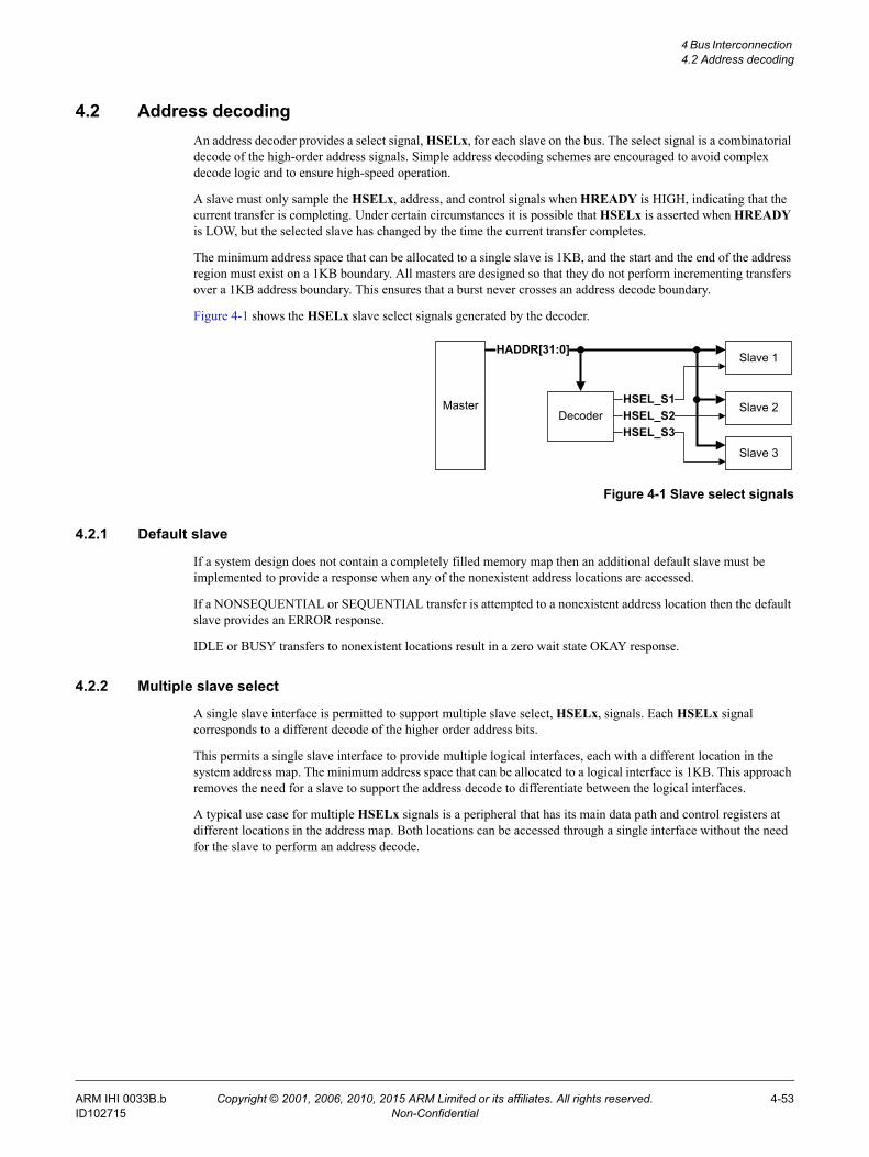
4 Bus Interconnection 4.2 Address decoding
4.2 Address decodingAn address decoder provides a select signal, HSELx, for each slave on the bus. The select signal is a combinatorial decode of the high-order address signals. Simple address decoding schemes are encouraged to avoid complex decode logic and to ensure high-speed operation.
A slave must only sample the HSELx, address, and control signals when HREADY is HIGH, indicating that the current transfer is completing. Under certain circumstances it is possible that HSELx is asserted when HREADY is LOW, but the selected slave has changed by the time the current transfer completes.
The minimum address space that can be allocated to a single slave is 1KB, and the start and the end of the address region must exist on a 1KB boundary. All masters are designed so that they do not perform incrementing transfers over a 1KB address boundary. This ensures that a burst never crosses an address decode boundary.
Figure 4-1 shows the HSELx slave select signals generated by the decoder.
Figure 4-1 Slave select signals
4.2.1 Default slave
If a system design does not contain a completely filled memory map then an additional default slave must be implemented to provide a response when any of the nonexistent address locations are accessed.
If a NONSEQUENTIAL or SEQUENTIAL transfer is attempted to a nonexistent address location then the default slave provides an ERROR response.
IDLE or BUSY transfers to nonexistent locations result in a zero wait state OKAY response.
4.2.2 Multiple slave select
A single slave interface is permitted to support multiple slave select, HSELx, signals. Each HSELx signal corresponds to a different decode of the higher order address bits.
This permits a single slave interface to provide multiple logical interfaces, each with a different location in the system address map. The minimum address space that can be allocated to a logical interface is 1KB. This approach removes the need for a slave to support the address decode to differentiate between the logical interfaces.
A typical use case for multiple HSELx signals is a peripheral that has its main data path and control registers at different locations in the address map. Both locations can be accessed through a single interface without the need for the slave to perform an address decode.
MasterDecoder
HADDR[31:0]
HSEL_S2
Slave 1
Slave 2
Slave 3
HSEL_S1
HSEL_S3
ARM IHI 0033B.b Copyright © 2001, 2006, 2010, 2015 ARM Limited or its affiliates. All rights reserved. 4-53ID102715 Non-Confidential
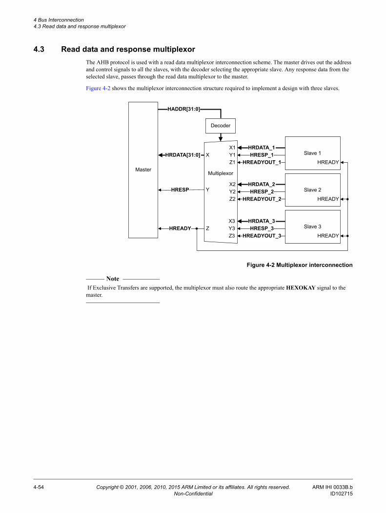
4 Bus Interconnection 4.3 Read data and response multiplexor
4.3 Read data and response multiplexorThe AHB protocol is used with a read data multiplexor interconnection scheme. The master drives out the address and control signals to all the slaves, with the decoder selecting the appropriate slave. Any response data from the selected slave, passes through the read data multiplexor to the master.
Figure 4-2 shows the multiplexor interconnection structure required to implement a design with three slaves.
Figure 4-2 Multiplexor interconnection
Note If Exclusive Transfers are supported, the multiplexor must also route the appropriate HEXOKAY signal to the master.
Master
Slave 1
Decoder
HRDATA[31:0]
HADDR[31:0]
HRESP_2 Slave 2
Slave 3
HRESP
HREADY
HREADYOUT_2
HRDATA_2
HRESP_1HREADYOUT_1
HRDATA_1
HRESP_3HREADYOUT_3
HRDATA_3
HREADY
HREADY
HREADY
Multiplexor
X1Y1Z1
X2Y2Z2
X3Y3Z3
X
Y
Z
4-54 Copyright © 2001, 2006, 2010, 2015 ARM Limited or its affiliates. All rights reserved. ARM IHI 0033B.bNon-Confidential ID102715

Chapter 5 Slave Response Signaling
This chapter describes the slave response signaling. It contains the following section:• Slave transfer responses on page 5-56.
ARM IHI 0033B.b Copyright © 2001, 2006, 2010, 2015 ARM Limited or its affiliates. All rights reserved. 5-55ID102715 Non-Confidential
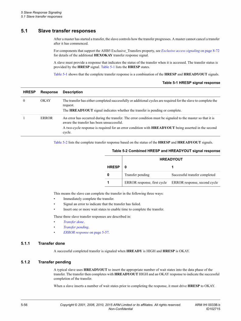
5 Slave Response Signaling 5.1 Slave transfer responses
5.1 Slave transfer responsesAfter a master has started a transfer, the slave controls how the transfer progresses. A master cannot cancel a transfer after it has commenced.
For components that support the AHB5 Exclusive_Transfers property, see Exclusive access signaling on page 8-72 for details of the additional HEXOKAY transfer response signal.
A slave must provide a response that indicates the status of the transfer when it is accessed. The transfer status is provided by the HRESP signal. Table 5-1 lists the HRESP states.
Table 5-1 shows that the complete transfer response is a combination of the HRESP and HREADYOUT signals.
Table 5-2 lists the complete transfer response based on the status of the HRESP and HREADYOUT signals.
This means the slave can complete the transfer in the following three ways:• Immediately complete the transfer.• Signal an error to indicate that the transfer has failed.• Insert one or more wait states to enable time to complete the transfer.
These three slave transfer responses are described in:• Transfer done.• Transfer pending.• ERROR response on page 5-57.
5.1.1 Transfer done
A successful completed transfer is signaled when HREADY is HIGH and HRESP is OKAY.
5.1.2 Transfer pending
A typical slave uses HREADYOUT to insert the appropriate number of wait states into the data phase of the transfer. The transfer then completes with HREADYOUT HIGH and an OKAY response to indicate the successful completion of the transfer.
When a slave inserts a number of wait states prior to completing the response, it must drive HRESP to OKAY.
Table 5-1 HRESP signal response
HRESP Response Description
0 OKAY The transfer has either completed successfully or additional cycles are required for the slave to complete the request.The HREADYOUT signal indicates whether the transfer is pending or complete.
1 ERROR An error has occurred during the transfer. The error condition must be signaled to the master so that it is aware the transfer has been unsuccessful.A two-cycle response is required for an error condition with HREADYOUT being asserted in the second cycle.
Table 5-2 Combined HRESP and HREADYOUT signal response
HREADYOUT
HRESP 0 1
0 Transfer pending Successful transfer completed
1 ERROR response, first cycle ERROR response, second cycle
5-56 Copyright © 2001, 2006, 2010, 2015 ARM Limited or its affiliates. All rights reserved. ARM IHI 0033B.bNon-Confidential ID102715
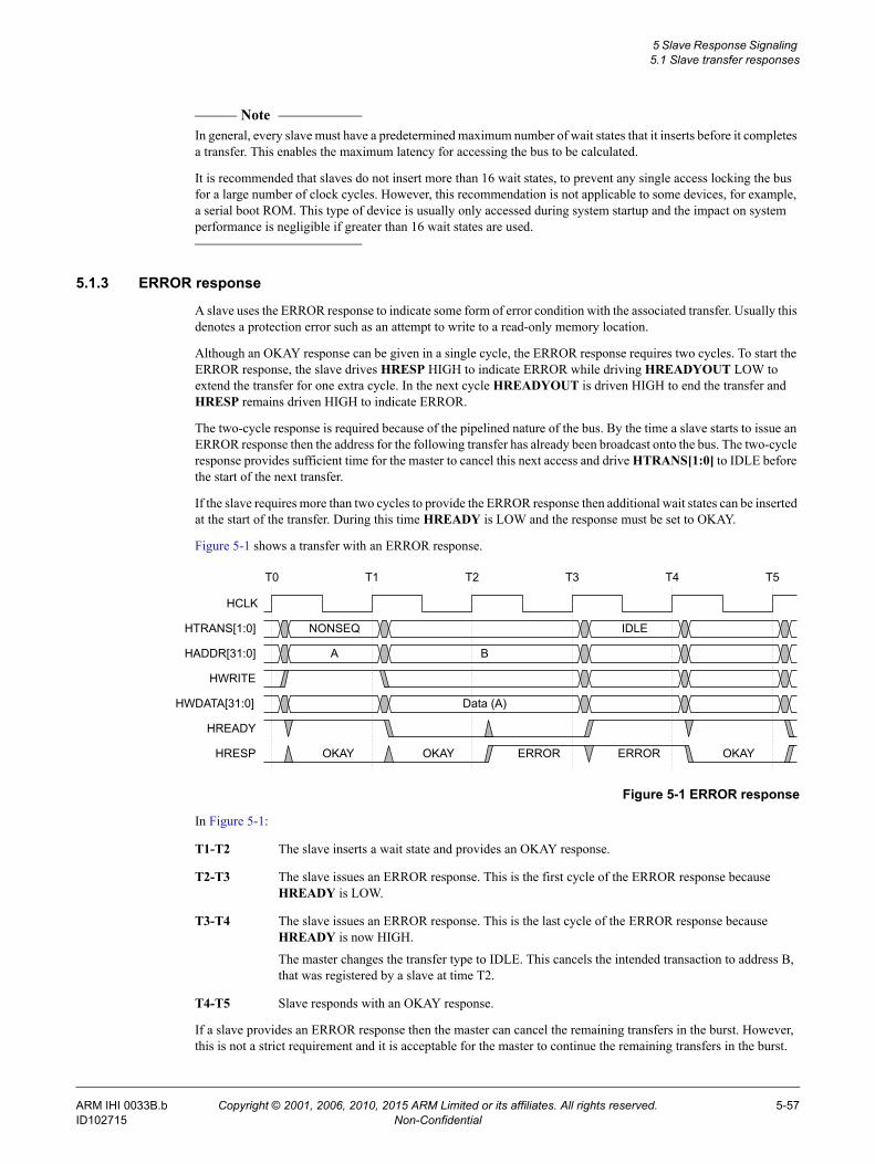
5 Slave Response Signaling 5.1 Slave transfer responses
Note In general, every slave must have a predetermined maximum number of wait states that it inserts before it completes a transfer. This enables the maximum latency for accessing the bus to be calculated.
It is recommended that slaves do not insert more than 16 wait states, to prevent any single access locking the bus for a large number of clock cycles. However, this recommendation is not applicable to some devices, for example, a serial boot ROM. This type of device is usually only accessed during system startup and the impact on system performance is negligible if greater than 16 wait states are used.
5.1.3 ERROR response
A slave uses the ERROR response to indicate some form of error condition with the associated transfer. Usually this denotes a protection error such as an attempt to write to a read-only memory location.
Although an OKAY response can be given in a single cycle, the ERROR response requires two cycles. To start the ERROR response, the slave drives HRESP HIGH to indicate ERROR while driving HREADYOUT LOW to extend the transfer for one extra cycle. In the next cycle HREADYOUT is driven HIGH to end the transfer and HRESP remains driven HIGH to indicate ERROR.
The two-cycle response is required because of the pipelined nature of the bus. By the time a slave starts to issue an ERROR response then the address for the following transfer has already been broadcast onto the bus. The two-cycle response provides sufficient time for the master to cancel this next access and drive HTRANS[1:0] to IDLE before the start of the next transfer.
If the slave requires more than two cycles to provide the ERROR response then additional wait states can be inserted at the start of the transfer. During this time HREADY is LOW and the response must be set to OKAY.
Figure 5-1 shows a transfer with an ERROR response.
Figure 5-1 ERROR response
In Figure 5-1:
T1-T2 The slave inserts a wait state and provides an OKAY response.
T2-T3 The slave issues an ERROR response. This is the first cycle of the ERROR response because HREADY is LOW.
T3-T4 The slave issues an ERROR response. This is the last cycle of the ERROR response because HREADY is now HIGH.
The master changes the transfer type to IDLE. This cancels the intended transaction to address B, that was registered by a slave at time T2.
T4-T5 Slave responds with an OKAY response.
If a slave provides an ERROR response then the master can cancel the remaining transfers in the burst. However, this is not a strict requirement and it is acceptable for the master to continue the remaining transfers in the burst.
HWRITE
HWDATA[31:0] Data (A)
HADDR[31:0] A
HCLK
B
HREADY
T0
HRESP
T1 T2 T3 T4
HTRANS[1:0] NONSEQ IDLE
T5
OKAY OKAYOKAY ERROR ERROR
ARM IHI 0033B.b Copyright © 2001, 2006, 2010, 2015 ARM Limited or its affiliates. All rights reserved. 5-57ID102715 Non-Confidential

5 Slave Response Signaling 5.1 Slave transfer responses
5-58 Copyright © 2001, 2006, 2010, 2015 ARM Limited or its affiliates. All rights reserved. ARM IHI 0033B.bNon-Confidential ID102715

Chapter 6 Data Buses
This chapter describes the data buses. It contains the following sections:• Data buses on page 6-60.• Endianness on page 6-61.• Data bus width on page 6-65.
ARM IHI 0033B.b Copyright © 2001, 2006, 2010, 2015 ARM Limited or its affiliates. All rights reserved. 6-59ID102715 Non-Confidential
6 Data Buses 6.1 Data buses
6.1 Data busesSeparate read and write data buses are required to implement an AHB system. Although the recommended minimum data bus width is specified as 32-bits, this can be changed as described in Data bus width on page 6-65. The data buses are described in:• HWDATA.• HRDATA.• Endianness on page 6-61.
6.1.1 HWDATA
The master drives the write data bus during write transfers. If the transfer is extended then the master must hold the data valid until the transfer completes, as indicated by HREADY HIGH. See Clock on page 7-68 for details on holding signals valid across multiple cycles.
For transfers that are narrower than the width of the bus, for example a 16-bit transfer on a 32-bit bus, the master only has to drive the appropriate byte lanes. The slave selects the write data from the correct byte lanes. See Endianness on page 6-61 for details of the byte lanes that are active for a little-endian and big-endian system.
6.1.2 HRDATA
The appropriate slave drives the read data bus during read transfers. If the slave extends the read transfer by holding HREADY LOW, then the slave only has to provide valid data in the final cycle of the transfer, as indicated by HREADY HIGH.
For transfers that are narrower than the width of the bus, the slave is only required to provide valid data on the active byte lanes. The master selects the data from the correct byte lanes.
A slave only has to provide valid data when a transfer completes with an OKAY response. ERROR responses do not require valid read data.
6-60 Copyright © 2001, 2006, 2010, 2015 ARM Limited or its affiliates. All rights reserved. ARM IHI 0033B.bNon-Confidential ID102715
6 Data Buses 6.2 Endianness
6.2 EndiannessAHB supports both big-endian and little-endian systems. Two approaches to big-endian data storage are supported.
AHB5 introduces the Endian property to define which form of big-endian data access is supported.
BE8 Byte-invariant big-endian. The term, byte-invariant big-endian, is derived from the fact that a byte access (8-bit) uses the same data bus bits as a little-endian access to the same address.
BE32 Word-invariant big-endian. The term, word-invariant big-endian, is derived from the fact that a word access (32-bit) uses the same data bus bits for the Most Significant (MS) and the Least Significant (LS) bytes as a little-endian access to the same address.
Additional information on byte-invariant big-endian can be found in the section Byte invariance on page 6-63.
The following set of equations defines which data bits are used for little-endian, byte-invariant big-endian, and word- invariant big-endian accesses.
The equations use the following variables:address The address of the transfer.Data_Bus_Bytes The number of 8-bit data bus byte lanes.INT(x) Rounded down integer value of x.
6.2.1 Little endian
When a little-endian component accesses a byte, the following equation shows which data bus bits are used:
Byte_Lane = Address –(INT(Address / Data_bus_Bytes)) × Data_Bus_Bytes
Data is transferred on DATA[(8 × Byte_Lane) + 7 : (8 × Byte_Lane)]
When larger little-endian transfers occur, data is transferred such that:• The LS byte is transferred to the transfer address.• Increasingly significant bytes are transferred to sequentially incrementing addresses.
6.2.2 Byte-invariant big-endian
When a byte-invariant big-endian component accesses a byte, the following equation shows which data bus bits are used:
Byte_Lane = Address –(INT(Address / Data_bus_Bytes)) × Data_Bus_Bytes
Data is transferred on DATA[(8 × Byte_lane) + 7 : (8 × Byte_lane)]
Note These equations are identical to those for little-endian. Because big-endian and little-endian accesses are identical for byte transfers, the term byte-invariant is used for these transfers.
When larger byte-invariant big-endian transfers occur, data is transferred such that:• The MS byte is transferred to the transfer address.• Decreasingly significant bytes are transferred to sequentially incrementing addresses.
Note This is the key difference between byte-invariant big-endian and little-endian components.
ARM IHI 0033B.b Copyright © 2001, 2006, 2010, 2015 ARM Limited or its affiliates. All rights reserved. 6-61ID102715 Non-Confidential
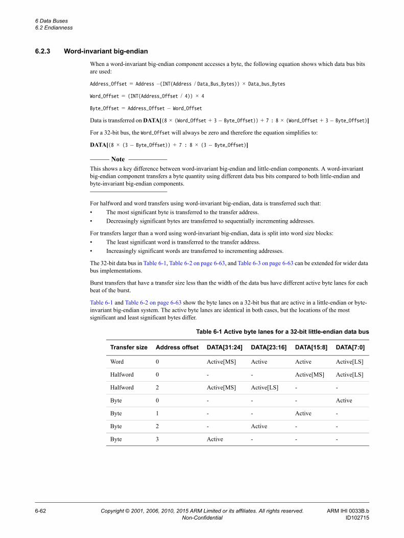
6 Data Buses 6.2 Endianness
6.2.3 Word-invariant big-endian
When a word-invariant big-endian component accesses a byte, the following equation shows which data bus bits are used:
Address_Offset = Address –(INT(Address / Data_Bus_Bytes)) × Data_bus_Bytes
Word_Offset = (INT(Address_Offset / 4)) × 4
Byte_Offset = Address_Offset – Word_Offset
Data is transferred on DATA[(8 × (Word_Offset + 3 – Byte_Offset)) + 7 : 8 × (Word_Offset + 3 – Byte_Offset)]
For a 32-bit bus, the Word_Offset will always be zero and therefore the equation simplifies to:
DATA[(8 × (3 – Byte_Offset)) + 7 : 8 × (3 – Byte_Offset)]
Note This shows a key difference between word-invariant big-endian and little-endian components. A word-invariant big-endian component transfers a byte quantity using different data bus bits compared to both little-endian and byte-invariant big-endian components.
For halfword and word transfers using word-invariant big-endian, data is transferred such that:• The most significant byte is transferred to the transfer address.• Decreasingly significant bytes are transferred to sequentially incrementing addresses.
For transfers larger than a word using word-invariant big-endian, data is split into word size blocks:• The least significant word is transferred to the transfer address.• Increasingly significant words are transferred to incrementing addresses.
The 32-bit data bus in Table 6-1, Table 6-2 on page 6-63, and Table 6-3 on page 6-63 can be extended for wider data bus implementations.
Burst transfers that have a transfer size less than the width of the data bus have different active byte lanes for each beat of the burst.
Table 6-1 and Table 6-2 on page 6-63 show the byte lanes on a 32-bit bus that are active in a little-endian or byte- invariant big-endian system. The active byte lanes are identical in both cases, but the locations of the most significant and least significant bytes differ.
Table 6-1 Active byte lanes for a 32-bit little-endian data bus
Transfer size Address offset DATA[31:24] DATA[23:16] DATA[15:8] DATA[7:0]
Word 0 Active[MS] Active Active Active[LS]
Halfword 0 - - Active[MS] Active[LS]
Halfword 2 Active[MS] Active[LS] - -
Byte 0 - - - Active
Byte 1 - - Active -
Byte 2 - Active - -
Byte 3 Active - - -
6-62 Copyright © 2001, 2006, 2010, 2015 ARM Limited or its affiliates. All rights reserved. ARM IHI 0033B.bNon-Confidential ID102715
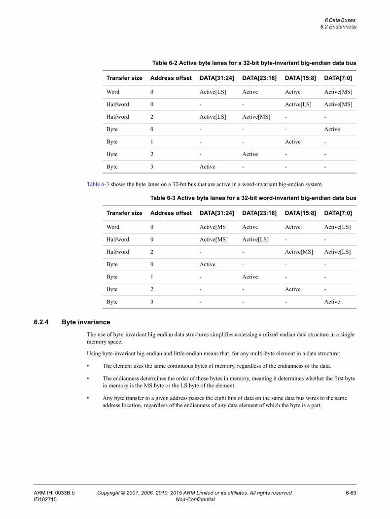
6 Data Buses 6.2 Endianness
Table 6-3 shows the byte lanes on a 32-bit bus that are active in a word-invariant big-endian system.
6.2.4 Byte invariance
The use of byte-invariant big-endian data structures simplifies accessing a mixed-endian data structure in a single memory space.
Using byte-invariant big-endian and little-endian means that, for any multi-byte element in a data structure:
• The element uses the same continuous bytes of memory, regardless of the endianness of the data.
• The endianness determines the order of those bytes in memory, meaning it determines whether the first byte in memory is the MS byte or the LS byte of the element.
• Any byte transfer to a given address passes the eight bits of data on the same data bus wires to the same address location, regardless of the endianness of any data element of which the byte is a part.
Table 6-2 Active byte lanes for a 32-bit byte-invariant big-endian data bus
Transfer size Address offset DATA[31:24] DATA[23:16] DATA[15:8] DATA[7:0]
Word 0 Active[LS] Active Active Active[MS]
Halfword 0 - - Active[LS] Active[MS]
Halfword 2 Active[LS] Active[MS] - -
Byte 0 - - - Active
Byte 1 - - Active -
Byte 2 - Active - -
Byte 3 Active - - -
Table 6-3 Active byte lanes for a 32-bit word-invariant big-endian data bus
Transfer size Address offset DATA[31:24] DATA[23:16] DATA[15:8] DATA[7:0]
Word 0 Active[MS] Active Active Active[LS]
Halfword 0 Active[MS] Active[LS] - -
Halfword 2 - - Active[MS] Active[LS]
Byte 0 Active - - -
Byte 1 - Active - -
Byte 2 - - Active -
Byte 3 - - - Active
ARM IHI 0033B.b Copyright © 2001, 2006, 2010, 2015 ARM Limited or its affiliates. All rights reserved. 6-63ID102715 Non-Confidential
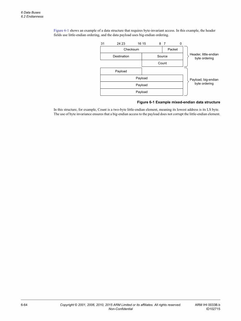
6 Data Buses 6.2 Endianness
Figure 6-1 shows an example of a data structure that requires byte-invariant access. In this example, the header fields use little-endian ordering, and the data payload uses big-endian ordering.
Figure 6-1 Example mixed-endian data structure
In this structure, for example, Count is a two-byte little-endian element, meaning its lowest address is its LS byte. The use of byte invariance ensures that a big-endian access to the payload does not corrupt the little-endian element.
Packet
SourceDestination
Checksum
Count
Payload
Payload
Payload
Payload
Header, little-endianbyte ordering
Payload, big-endianbyte ordering
31 24 23 16 15 8 7 0
6-64 Copyright © 2001, 2006, 2010, 2015 ARM Limited or its affiliates. All rights reserved. ARM IHI 0033B.bNon-Confidential ID102715
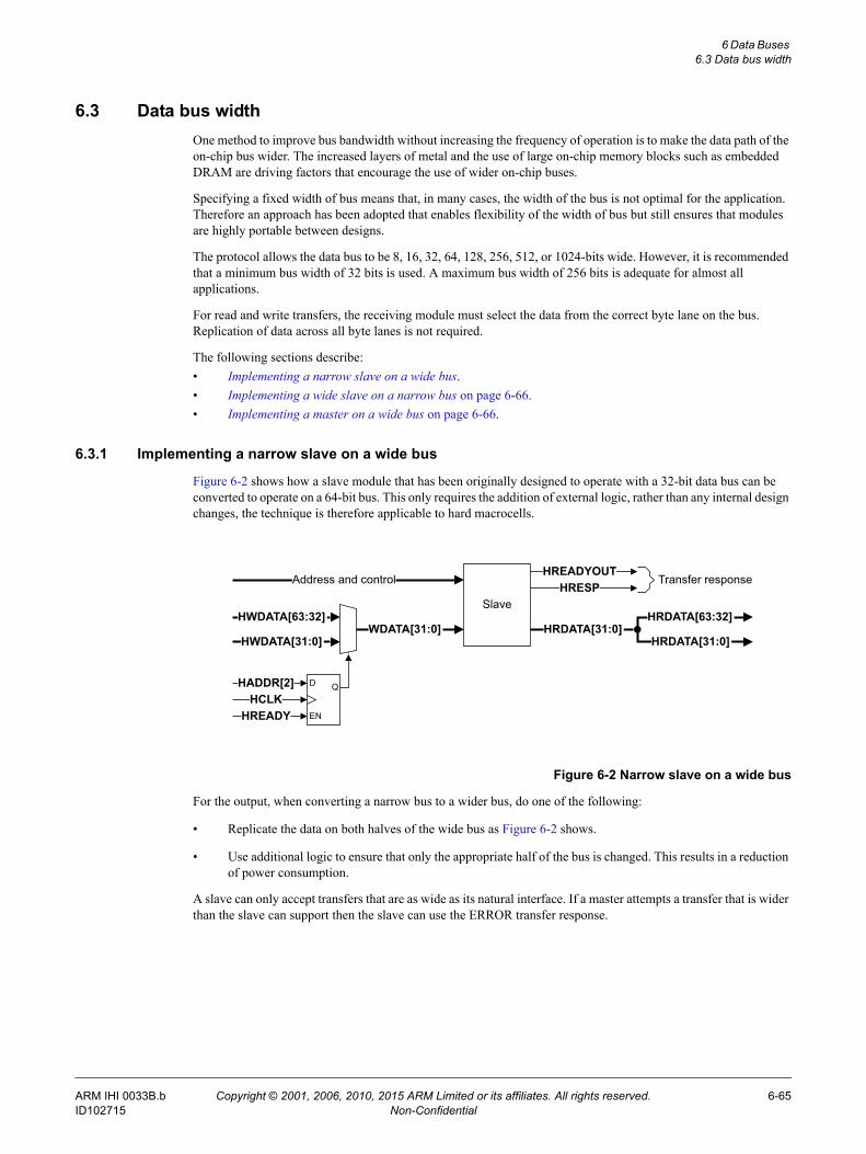
6 Data Buses 6.3 Data bus width
6.3 Data bus widthOne method to improve bus bandwidth without increasing the frequency of operation is to make the data path of the on-chip bus wider. The increased layers of metal and the use of large on-chip memory blocks such as embedded DRAM are driving factors that encourage the use of wider on-chip buses.
Specifying a fixed width of bus means that, in many cases, the width of the bus is not optimal for the application. Therefore an approach has been adopted that enables flexibility of the width of bus but still ensures that modules are highly portable between designs.
The protocol allows the data bus to be 8, 16, 32, 64, 128, 256, 512, or 1024-bits wide. However, it is recommended that a minimum bus width of 32 bits is used. A maximum bus width of 256 bits is adequate for almost all applications.
For read and write transfers, the receiving module must select the data from the correct byte lane on the bus. Replication of data across all byte lanes is not required.
The following sections describe:• Implementing a narrow slave on a wide bus.• Implementing a wide slave on a narrow bus on page 6-66.• Implementing a master on a wide bus on page 6-66.
6.3.1 Implementing a narrow slave on a wide bus
Figure 6-2 shows how a slave module that has been originally designed to operate with a 32-bit data bus can be converted to operate on a 64-bit bus. This only requires the addition of external logic, rather than any internal design changes, the technique is therefore applicable to hard macrocells.
Figure 6-2 Narrow slave on a wide bus
For the output, when converting a narrow bus to a wider bus, do one of the following:
• Replicate the data on both halves of the wide bus as Figure 6-2 shows.
• Use additional logic to ensure that only the appropriate half of the bus is changed. This results in a reduction of power consumption.
A slave can only accept transfers that are as wide as its natural interface. If a master attempts a transfer that is wider than the slave can support then the slave can use the ERROR transfer response.
D Q
EN
HCLKHADDR[2]
HREADY
Slave
Address and control
HRDATA[63:32]
HRDATA[31:0]HRDATA[31:0]
HREADYOUTHRESP
HWDATA[63:32]
HWDATA[31:0]WDATA[31:0]
Transfer response
ARM IHI 0033B.b Copyright © 2001, 2006, 2010, 2015 ARM Limited or its affiliates. All rights reserved. 6-65ID102715 Non-Confidential
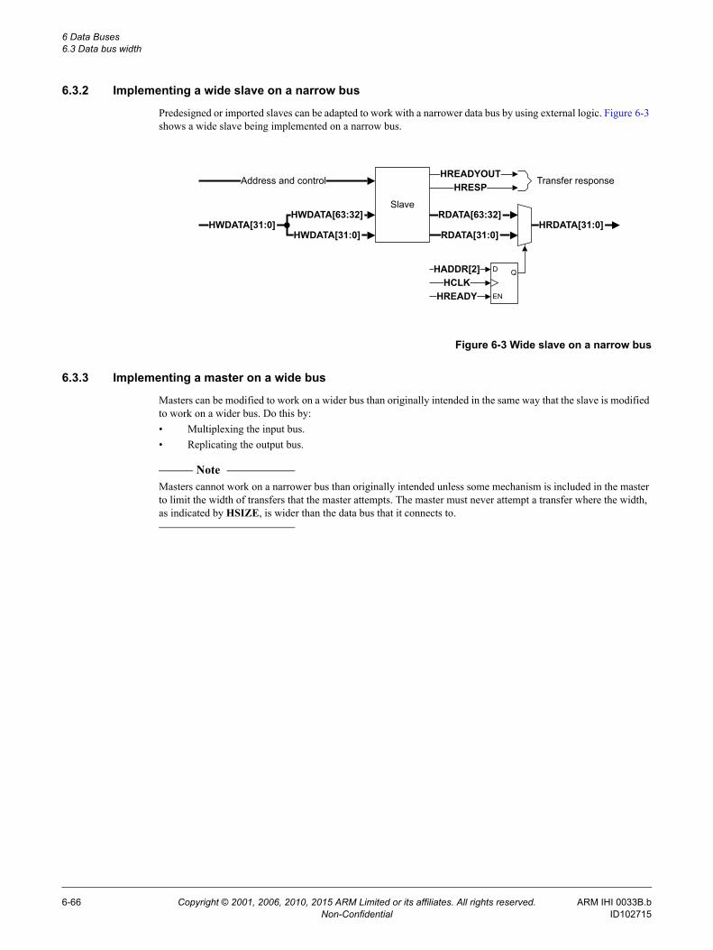
6 Data Buses 6.3 Data bus width
6.3.2 Implementing a wide slave on a narrow bus
Predesigned or imported slaves can be adapted to work with a narrower data bus by using external logic. Figure 6-3 shows a wide slave being implemented on a narrow bus.
Figure 6-3 Wide slave on a narrow bus
6.3.3 Implementing a master on a wide bus
Masters can be modified to work on a wider bus than originally intended in the same way that the slave is modified to work on a wider bus. Do this by:• Multiplexing the input bus.• Replicating the output bus.
Note Masters cannot work on a narrower bus than originally intended unless some mechanism is included in the master to limit the width of transfers that the master attempts. The master must never attempt a transfer where the width, as indicated by HSIZE, is wider than the data bus that it connects to.
D Q
EN
HCLKHADDR[2]
HREADY
Slave
Address and control
HWDATA[63:32]
HWDATA[31:0]HWDATA[31:0]
HREADYOUTHRESP
RDATA[63:32]
RDATA[31:0]HRDATA[31:0]
Transfer response
6-66 Copyright © 2001, 2006, 2010, 2015 ARM Limited or its affiliates. All rights reserved. ARM IHI 0033B.bNon-Confidential ID102715

Chapter 7 Clock and Reset
This chapter describes the timing of the protocol clock and reset signals. It contains the following section:• Clock and reset requirements on page 7-68.
ARM IHI 0033B.b Copyright © 2001, 2006, 2010, 2015 ARM Limited or its affiliates. All rights reserved. 7-67ID102715 Non-Confidential
7 Clock and Reset 7.1 Clock and reset requirements
7.1 Clock and reset requirementsThis section describes the requirements for implementing the HCLK and HRESETn signals.
7.1.1 Clock
Each component uses a single clock signal, HCLK. All input signals are sampled on the rising edge of HCLK. All output signal changes must occur after the rising edge of HCLK.
Signals that are described as being stable are required to remain at the same value when sampled at different rising clock edges in an extended transfer. However, it is possible that these signals can glitch after clock edges, returning to the same value as previously driven.
Note It is possible to observe this behavior when using a typical synthesis design flow, where the control signals for an output multiplexor can change during an extended transfer, but they result in the same output value being used.
It is IMPLEMENTATION DEFINED whether an interface is glitch free between rising clock edges.
AHB5 defines the Stable_Between_Clock property. This property is defined to determine if an interface guarantees that signals that are required to be stable remain stable between rising clock edges.
If this property is True, it is guaranteed that signals that are required to be stable remain stable and glitch free between rising clock edges.
If this property is False, or is not defined, signals can glitch between rising clock edges.
7.1.2 Reset
The reset signal, HRESETn, is the only active LOW signal in the protocol and is the primary reset for all bus elements. The reset can be asserted asynchronously, but is deasserted synchronously after the rising edge of HCLK.
A component must define a minimum number of cycles for which the reset signal must be asserted to ensure that the component is fully reset and the outputs are at the required reset values.
During reset all masters must ensure the address and control signals are at valid levels and that HTRANS[1:0] indicates IDLE.
During reset all slaves must ensure that HREADYOUT is HIGH.
7-68 Copyright © 2001, 2006, 2010, 2015 ARM Limited or its affiliates. All rights reserved. ARM IHI 0033B.bNon-Confidential ID102715

Chapter 8 Exclusive Transfers
This chapter describes the concept of Exclusive Transfers. It contains the following sections:• Introduction on page 8-70.• Exclusive Access Monitor on page 8-71.• Exclusive access signaling on page 8-72.• Exclusive Transfer restrictions on page 8-73.
ARM IHI 0033B.b Copyright © 2001, 2006, 2010, 2015 ARM Limited or its affiliates. All rights reserved. 8-69ID102715 Non-Confidential
8 Exclusive Transfers 8.1 Introduction
8.1 IntroductionAHB5 defines the Exclusive_Transfers property. This property defines whether an interface supports the concept of Exclusive Transfers. If this property is not defined then the interface does not support Exclusive Transfers.
Exclusive Transfers provide a mechanism to support semaphore-type operations.
An Exclusive access sequence is a sequence of Exclusive Transfers from a single master that operate using the following steps:
1. Perform an Exclusive Read transfer from an address.
2. Calculate a new data value to store to that address that is based on the data value obtained from the Exclusive Read.
3. Between the Exclusive Read and the Exclusive Write there can be other Non-exclusive transfers.
4. Perform an Exclusive Write transfer to the same address, with the new data value:
• If no other master has written to that location since the Exclusive Read transfer, the Exclusive Write transfer is successful and updates memory.
• If another master has written to that location since the Exclusive Read transfer, the Exclusive Write transfer is failed and the memory location is not updated.
5. The response to the Exclusive Write transfer indicates if the transfer was successful or if it failed.
This sequence ensures that the memory location is only updated if, at the point of the store to memory, the location still holds the same value that was used to calculate the new value to be written to the location.
If the Exclusive Write transfer fails, it is expected that the master will repeat the entire Exclusive access sequence.
It is IMPLEMENTATION DEFINED whether an update of the same, or overlapping, location by the same master after an Exclusive Read transfer will cause the associated Exclusive Write transfer to succeed or fail.
8-70 Copyright © 2001, 2006, 2010, 2015 ARM Limited or its affiliates. All rights reserved. ARM IHI 0033B.bNon-Confidential ID102715
8 Exclusive Transfers 8.2 Exclusive Access Monitor
8.2 Exclusive Access MonitorAn Exclusive Access Monitor is required to support an Exclusive access sequence and this monitor must determine if an Exclusive Write transfer succeeds or fails.
The Exclusive Access Monitor must be capable of concurrently monitoring at least one address location for each Exclusive access capable master in the system.
The position of the Exclusive Access Monitor in the system is not defined. However, it must be positioned such that it can observe accesses to all address locations that are used for Exclusive access sequences. For example, if a system includes multiple memory controllers, either all accesses are routed through a central point that contains the Exclusive Access Monitor or a separate Exclusive Access Monitor is required at each memory controller.
It is not required that a system supports an Exclusive access sequence to all address locations. A fail-safe mechanism is provided for accesses to locations that do not support an Exclusive access sequence. Typically, it would be expected that a system would support Exclusive access sequences to main memory, but not to any peripheral device.
ARM IHI 0033B.b Copyright © 2001, 2006, 2010, 2015 ARM Limited or its affiliates. All rights reserved. 8-71ID102715 Non-Confidential
8 Exclusive Transfers 8.3 Exclusive access signaling
8.3 Exclusive access signalingThe additional signals associated with Exclusive Transfers are:
HEXCL Exclusive Transfer. Indicates that the transfer is part of an Exclusive access sequence. This signal is an address phase signal and has the same validity constraints as HADDR.
HMASTER[m:0] Master Identifier. A master that has multiple Exclusive capable threads must generate this signal to differentiate between the threads.
The HMASTER value generated by the master will be combined with an interconnect generated value to ensure the resultant HMASTER value presented to the Exclusive Access Monitor is unique.
This signal is an address phase signal and has the same validity constraints as HADDR.
HEXOKAY Exclusive Okay. An additional response signal is added to indicate the success or failure of an Exclusive Transfer.
The width of the HMASTER[m:0] signal is IMPLEMENTATION DEFINED. However, this specification recommends the following widths:
• For master components, implement the number of bits required for the number of Exclusive capable threads supported.
• For an interconnect port where a master connects, implement 4-bits. Optionally, an interconnect can support a configuration of a larger bit width.
• For a slave or monitor component, implement 8-bits. Optionally, a slave or monitor component can support a configuration of a larger bit width.
HMASTER signaling is permitted to be used for purposes other than Exclusive Transfers. It is permitted for the interconnect and slave components in a system to use this signaling to distinguish between different masters in the system and adapt their behavior appropriately. Therefore, a valid HMASTER indication must be provided for all transfers, not only Exclusive Transfers.
8.3.1 Response signaling
The HEXOKAY signal is used to indicate the success or failure of an Exclusive Transfer:
• When asserted, HEXOKAY indicates that the Exclusive Transfer has been successful and for an Exclusive Write transfer the memory location has been updated.
• When deasserted HEXOKAY indicates that the Exclusive Transfer has failed. This can be because either:
— An Exclusive Transfer has been attempted to an address location that does not support Exclusive Transfers.
— An Exclusive Write transfer has failed because the memory location has not remained unchanged since a matching Exclusive Read transfer. In this scenario the memory location is not updated.
A master can ensure that it does not attempt to perform an Exclusive Write transfer to an address location that does not support Exclusive Transfers by ensuring that it always performs an Exclusive Read transfer to that location first.
The following constraints apply to HEXOKAY:• HEXOKAY must only be asserted in the same cycle as HREADY is asserted.• HEXOKAY must not be asserted in the same cycle as HRESP is asserted.
8-72 Copyright © 2001, 2006, 2010, 2015 ARM Limited or its affiliates. All rights reserved. ARM IHI 0033B.bNon-Confidential ID102715
8 Exclusive Transfers 8.4 Exclusive Transfer restrictions
8.4 Exclusive Transfer restrictionsThe following restrictions apply to an Exclusive Transfer:• Must have a single data transfer.• Must be indicated as burst type SINGLE or burst type INCR.• Must not include a BUSY transfer.• The address must be aligned to data size as indicated by HSIZE.• The value of the HPROT signals must guarantee that the Exclusive Access Monitor has visibility of the
transfer.
Note The HPROT signals must guarantee that the Exclusive Access Monitor has visibility of the transfer. If the Exclusive Access Monitor is located downstream of a system cache, then the transfer must be Non-cacheable. If the Exclusive Access Monitor is located upstream of a system cache, then it is permitted for the transfer to be Cacheable.
For an Exclusive Read transfer and an Exclusive Write transfer to be considered part of the same Exclusive access sequence, the following signals must be the same for both transfers:• HADDR, Address.• HSIZE, Data Size.• HPROT, Protection Control.• HBURST, Burst Type.• HMASTER, Master Identifier.• HNONSEC, Non-secure, if applicable.
It is permitted for a master to issue an Exclusive Read transfer and never follow it with an Exclusive Write transfer in the same Exclusive access sequence.
It is permitted for a master to issue an Exclusive Write transfer, which has not been preceded by an Exclusive Read transfer in the same Exclusive access sequence. In this case, the Exclusive Write transfer must fail and the HEXOKAY response signal must be deasserted.
A master must not have two Exclusive Transfers outstanding at the same point in time. The address phase of an Exclusive Transfer must not be issued while the data phase of an earlier Exclusive Transfer is in progress. This applies whether the transfers are part of the same Exclusive access sequence or not.
It is permitted for the address phase of an Exclusive Transfer with a particular HMASTER value to be issued while the data phase of an earlier Exclusive Transfer with a different HMASTER value is in progress.
Note The address phase of an Exclusive Transfer is defined as being when HEXCL is asserted and HTRANS indicates NONSEQ. The assertion of HEXCL when HTRANS indicates IDLE is not defined as the address phase of an Exclusive Transfer.
ARM IHI 0033B.b Copyright © 2001, 2006, 2010, 2015 ARM Limited or its affiliates. All rights reserved. 8-73ID102715 Non-Confidential

8 Exclusive Transfers 8.4 Exclusive Transfer restrictions
8-74 Copyright © 2001, 2006, 2010, 2015 ARM Limited or its affiliates. All rights reserved. ARM IHI 0033B.bNon-Confidential ID102715

Chapter 9 Atomicity
This chapter defines two atomic properties. It contains the following sections:• Single-copy atomicity size on page 9-76.• Multi-copy atomicity on page 9-77.
ARM IHI 0033B.b Copyright © 2001, 2006, 2010, 2015 ARM Limited or its affiliates. All rights reserved. 9-75ID102715 Non-Confidential

9 Atomicity 9.1 Single-copy atomicity size
9.1 Single-copy atomicity sizeThe single-copy atomicity size defines the number of data bytes that a transfer is guaranteed to update atomically.
The single-copy atomicity size is defined for a group of components that are communicating. For example:
• A processor, DSP, and DRAM controller are in a 64-bit single-copy atomic group.
• A larger group, including a processor, DSP, DMA, DRAM, SRAM, and peripherals are in a 32-bit single-copy atomic group.
A transfer never has a single-copy atomicity guarantee greater than the alignment of its start address. For example, a burst in a 64-bit single-copy atomic group that is not aligned to an 8-byte boundary does not have any 64-bit single-copy atomicity guarantee.
When a write transfer updates a memory location, it must be guaranteed that an observer will see either:• No update to the location.• An update to at least a single-copy atomicity size amount of data.
It is not permitted for another observer to see some data bytes updated within the single-copy atomicity size at one point in time, and then other data bytes within the same single-copy atomicity size at a later point in time.
Byte strobes associated with a transfer do not affect the single-copy atomicity size.
It is required that a transfer that is larger than the single-copy atomicity size must update memory in blocks of at least the single-copy atomicity size.
Note When determining the single-copy atomicity size the exact instant when the data value is updated is not considered.What must be ensured is that no master can ever observe a partially updated form of the atomic data.
For example, in many systems data structures such as linked lists are made up of 32-bit atomic elements. An atomic update of one of these elements requires that the entire 32-bit value is updated at the same time. It is not acceptable for any master to observe an update of only 16-bits at one point in time, and then the update of the other 16-bits at a later point in time.
More complex systems require support for larger atomic elements, in particular 64-bit atomic elements, so that masters can communicate using data structures that are based on these larger atomic elements.
9-76 Copyright © 2001, 2006, 2010, 2015 ARM Limited or its affiliates. All rights reserved. ARM IHI 0033B.bNon-Confidential ID102715
9 Atomicity 9.2 Multi-copy atomicity
9.2 Multi-copy atomicityAHB5 defines the Multi_Copy_Atomicity property. This property is defined to specify that a system provides multi-copy atomicity.
A system is defined as having this property if the Multi_Copy_Atomicity property is set to True.
A system that does not support the Multi_Copy_Atomicity property has the default value of False.
A system is defined as being multi-copy atomic if:• Writes to the same location are observed in the same order by all agents.• A write to a location that is observable by an agent, other than the issuer, is observable by all agents.
Multi-copy atomicity can be ensured by avoiding the use of forwarding buffers, which can make a transfer visible to some agents in a system, but not visible to all.
Note Additional requirements exist to ensure multi-copy atomicity in systems that include some form of hardware cache coherency. These additional requirements are not discussed in further detail in this specification.
ARM IHI 0033B.b Copyright © 2001, 2006, 2010, 2015 ARM Limited or its affiliates. All rights reserved. 9-77ID102715 Non-Confidential

9 Atomicity 9.2 Multi-copy atomicity
9-78 Copyright © 2001, 2006, 2010, 2015 ARM Limited or its affiliates. All rights reserved. ARM IHI 0033B.bNon-Confidential ID102715
Chapter 10 User Signaling
This chapter describes the set of optional user defined signals, on each channel, called the User signals. It contains the following sections:• User signal description on page 10-80.• User signal interconnect recommendations on page 10-81.
Note Generally, this specification recommends that the User signals are not used. The AHB protocol does not define the function of these signals and this can lead to interoperability issues if two components use the same User signals in an incompatible way.
ARM IHI 0033B.b Copyright © 2001, 2006, 2010, 2015 ARM Limited or its affiliates. All rights reserved. 10-79ID102715 Non-Confidential
10 User Signaling 10.1 User signal description
10.1 User signal descriptionThe User signal names defined for each channel are:HAUSER Address channel User signals.HWUSER Write data channel User signals.HRUSER Read data channel User signals.
These signals have the same timing and validity requirements as the associated channel.
For data channel User signals, this specification recommends that:• The number of User bits is an integer multiple of the width of the interface in bytes.• The User bits for each byte are packed together in adjacent bits.
The location of the User bits for a data channel is defined as:• Each data byte has m User signals associated with it.• The data bus width is n bytes.• The total number of User bits is u where u = m × n.
The user signals for byte y, where y = 0 ... (n – 1), are located at:• HWUSER[((y × m) + (m – 1)):(y × m)]• HRUSER[((y × m) + (m – 1)):(y × m)]
This specification recommends including User signals on an interconnect, however, there is no requirement to include them on masters or slaves.
This specification recommends that interconnect components include support for User signals so that they can be passed between master and slave components. The width of the User defined signals is IMPLEMENTATION DEFINED and can be different for each of the channels.
10-80 Copyright © 2001, 2006, 2010, 2015 ARM Limited or its affiliates. All rights reserved. ARM IHI 0033B.bNon-Confidential ID102715
10 User Signaling 10.2 User signal interconnect recommendations
10.2 User signal interconnect recommendationsFor transfers that are not modified by the interconnect, the User signals associated with the transfer can be transported across the interconnect unmodified.
For transfers that are modified by the interconnect, the information in this section provides guidelines for the generation of User signals associated with generated transfers.
Where a single transfer is converted to multiple transfers:
• The HAUSER signal of the original transfer is replicated into each generated transfer.
• For each generated transfer that contains some of the data bytes of the original transfer, the HWUSER and HRUSER signals of the generated transfer use the User bits for the data bytes contained in the transfer.
Where multiple transfers are converted to a single transfer:
• The HAUSER signal of the first transfer is used to generate the HAUSER signal of the generated transfer. The HAUSER signals of subsequent transfers are discarded.
• The HWUSER and HRUSER signals for the generated transfer use the combined User bits for the associated data bytes in the original transfers.
ARM IHI 0033B.b Copyright © 2001, 2006, 2010, 2015 ARM Limited or its affiliates. All rights reserved. 10-81ID102715 Non-Confidential

10 User Signaling 10.2 User signal interconnect recommendations
10-82 Copyright © 2001, 2006, 2010, 2015 ARM Limited or its affiliates. All rights reserved. ARM IHI 0033B.bNon-Confidential ID102715
Appendix A Revisions
This appendix describes the technical changes between released issues of this specification.
Table A-1 Issue A
Change Location Affects
First release. − −
Table A-2 Differences between issue A and issue B
Change Location Affects
Additional section describing revisions, which include new properties, clarifications and recommendations.
AHB revisions on page 1-17. All revisions
Clarification of the HPROT[3:0] protection control signal. Master signals on page 2-21. All revisions
Additional table entry for the HPROT[6:4] signal that adds extended memory types. Applicable only to Issue B of this specification.
Master signals on page 2-21. All revisions
Additional table entry for the HNONSEC signal required for Secure transfers. Master signals on page 2-21. All revisions
Additional table entries for the HEXCL and HMASTER[3:0] signals required for Exclusive Transfers.
Master signals on page 2-21. All revisions
Additional table entry describing the HEXOKAY signal required for Exclusive Transfers.
Slave signals on page 2-23. All revisions
Additional details on the use of HMASTLOCK for IDLE transfers. Locked transfers on page 3-32. All revisions
ARM IHI 0033B.b Copyright © 2001, 2006, 2010, 2015 ARM Limited or its affiliates. All rights reserved. A-83ID102715 Non-Confidential
Appendix A Revisions
Additional section that describes AHB5 Extended Memory Types. Memory types on page 3-45. All revisions
Additional section that describes AHB5 Secure Transfers. Secure transfers on page 3-50. All revisions
Additional section that describes AHB5 Multiple Slave Select. Multiple slave select on page 4-53. All revisions
Additional section that describes the AHB5 Endian property. Endianness on page 6-61. All revisions
Additional chapter that describes AHB5 Exclusive Transfers. Chapter 8 Exclusive Transfers. All revisions
Additional section that describes the AHB5 Stable_Between_Clock property. Clock on page 7-68. All revisions
Additional chapter that describes AHB5 Atomicity. Chapter 9 Atomicity. All revisions
Additional chapter that describes the optional user defined signals on each channel called the User signals.
Chapter 10 User Signaling. All revisions
Table A-2 Differences between issue A and issue B (continued)
Change Location Affects
A-84 Copyright © 2001, 2006, 2010, 2015 ARM Limited or its affiliates. All rights reserved. ARM IHI 0033B.bNon-Confidential ID102715
Glossary
This glossary describes some of the technical terms used in AMBA 5 AHB documentation.
AHB An AMBA bus protocol that defines the interface between system components, including masters, interconnects, and slaves. AMBA AHB supports high clock frequency, single clock-edge operation, burst transfers, and non-tristate implementation. It can support wide data bus configurations.
See also AHB-Lite.
AHB-Lite A subset of the full AMBA AHB protocol specification. It provides all of the basic functions required by the majority of AMBA AHB slave and master designs, particularly when used with a multi-layer AMBA interconnect.
Aligned A data item stored at an address that is exactly divisible by the highest power of 2 that divides exactly into its size in bytes. Aligned halfwords, words, and doublewords therefore have addresses that are divisible by 2, 4, and 8 respectively.
APB An AMBA bus protocol for ancillary or general-purpose peripherals such as timers, interrupt controllers, UARTs, and I/O ports. Using APB to connect to the main system bus through a system-to-peripheral bus bridge can help reduce system power consumption.
AXI An AMBA bus protocol that supports:• Separate phases for address or control and data.• Unaligned data transfers using byte lane strobes.• Burst-based transactions with only the start address issued.• Separate read and write data channels.• Issuing multiple outstanding addresses.• Out-of-order transaction completion.• Optional addition of register stages to meet timing or repropagation requirements.
The AXI protocol includes optional signaling extensions for low-power operation.
ARM IHI 0033B.b Copyright © 2001, 2006, 2010, 2015 ARM Limited or its affiliates. All rights reserved. Glossary-85ID102715 Non-Confidential
Glossary
Beat An alternative term for an individual transfer within a burst. For example, in AMBA 5 AHB, an INCR4 burst comprises four beats.
See also Burst.
Burst A group of transfers to consecutive addresses. In an AMBA protocol, a burst is controlled by signals that indicate the length of the burst and how the address is incremented.
See also Beat.
Doubleword A 64-bit data item. Doublewords are normally at least word-aligned in ARM systems.
Endianness The scheme that determines the order of successive bytes of data in a data structure when that structure is stored in memory.
See also Little-endian and Big-endian.
Halfword A 16-bit data item. Halfwords are normally halfword-aligned in ARM systems.
Processor A general term for an entity that performs processing.
Word A 32-bit data item. Words are normally word-aligned in ARM systems.
Glossary-86 Copyright © 2001, 2006, 2010, 2015 ARM Limited or its affiliates. All rights reserved. ARM IHI 0033B.bNon-Confidential ID102715
Related Documents

![Design and Implementation of Efficient FSM for AHB Master and … · 2017-07-22 · [1] AMBA specification, version 2.0 [2] “AHB Example AMBA System”, Technical Reference Manual,](https://static.cupdf.com/doc/110x72/5e8ff8e85e980155c60fde82/design-and-implementation-of-efficient-fsm-for-ahb-master-and-2017-07-22-1-amba.jpg)


