1 ECE 261 Krish Chakrabarty 1 Arithmetic Building Blocks • Datapath elements • Adder design – Static adder – Dynamic adder • Multiplier design – Array multipliers • Shifters, Parity circuits ECE 261 Krish Chakrabarty 2 A Generic Digital Processor MEMORY DATAPATH CONTROL Input-Output

Welcome message from author
This document is posted to help you gain knowledge. Please leave a comment to let me know what you think about it! Share it to your friends and learn new things together.
Transcript
1
ECE 261 Krish Chakrabarty 1
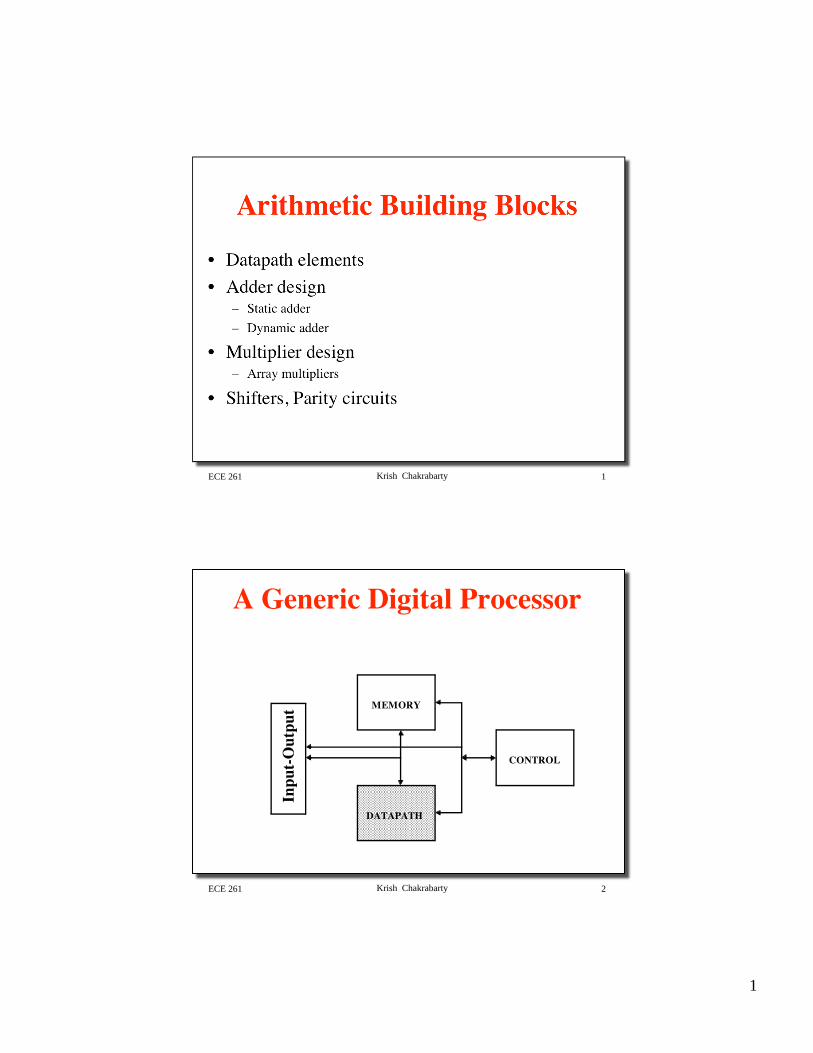
Arithmetic Building Blocks
• Datapath elements
• Adder design– Static adder
– Dynamic adder
• Multiplier design– Array multipliers
• Shifters, Parity circuits
ECE 261 Krish Chakrabarty 2
A Generic Digital Processor
MEMORY
DATAPATH
CONTROL
Inpu
t-O
utpu
t
2
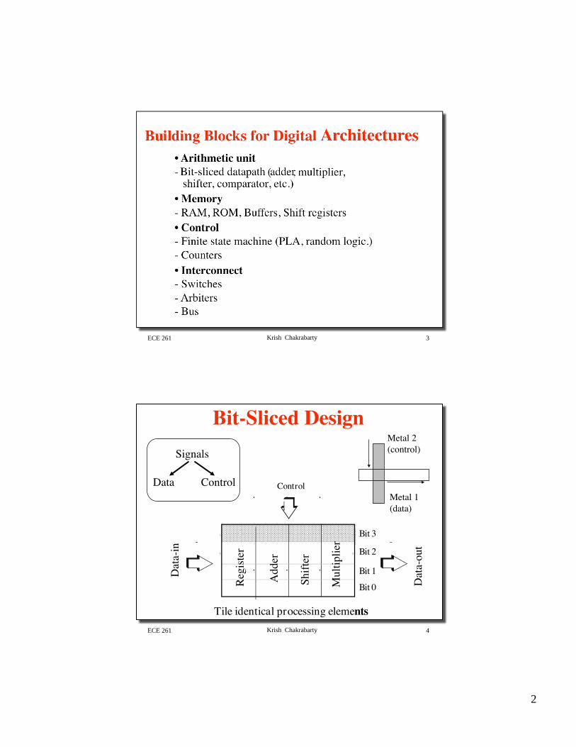
ECE 261 Krish Chakrabarty 3
Building Blocks for Digital Architectures• Arithmetic unit- Bit-sliced datapath ( adder, multiplier,
shifter, comparator, etc.)• Memory- RAM, ROM, Buffers, Shift registers• Control- Finite state machine (PLA, random logic.)- Counters• Interconnect- Switches- Arbiters- Bus
ECE 261 Krish Chakrabarty 4
Bit-Sliced Design
Bit 3
Bit 2
Bit 1
Bit 0
Control
Tile identical processing elements
Dat
a-in
Dat
a-ou
t
Reg
iste
r
Add
er
Shif
ter
Mul
tiplie
r
Signals
Data Control
Metal 2(control)
Metal 1(data)
3
ECE 261 Krish Chakrabarty 5
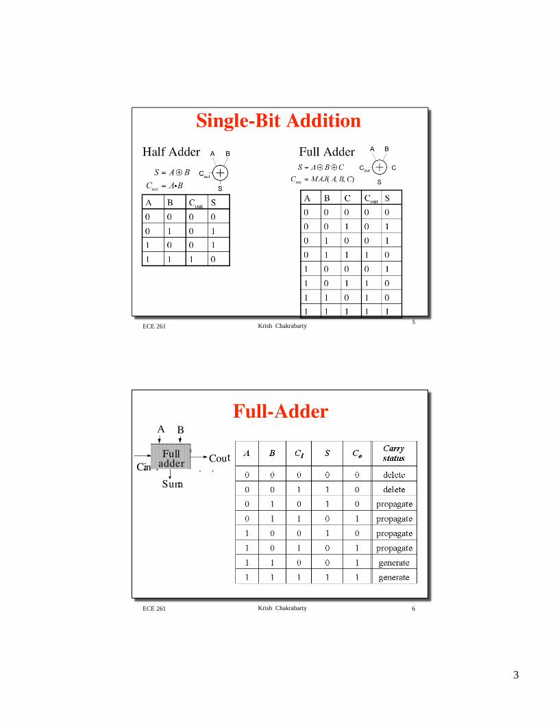
Single-Bit AdditionHalf Adder Full Adder
A B Cout S
0 0 0 0
0 1 0 1
1 0 0 1
1 1 1 0
A B C Cout S
0 0 0 0 0
0 0 1 0 1
0 1 0 0 1
0 1 1 1 0
1 0 0 0 1
1 0 1 1 0
1 1 0 1 0
1 1 1 1 1
ECE 261 Krish Chakrabarty 6
Full-AdderA B
Cout
Sum
CinFull
adder
4
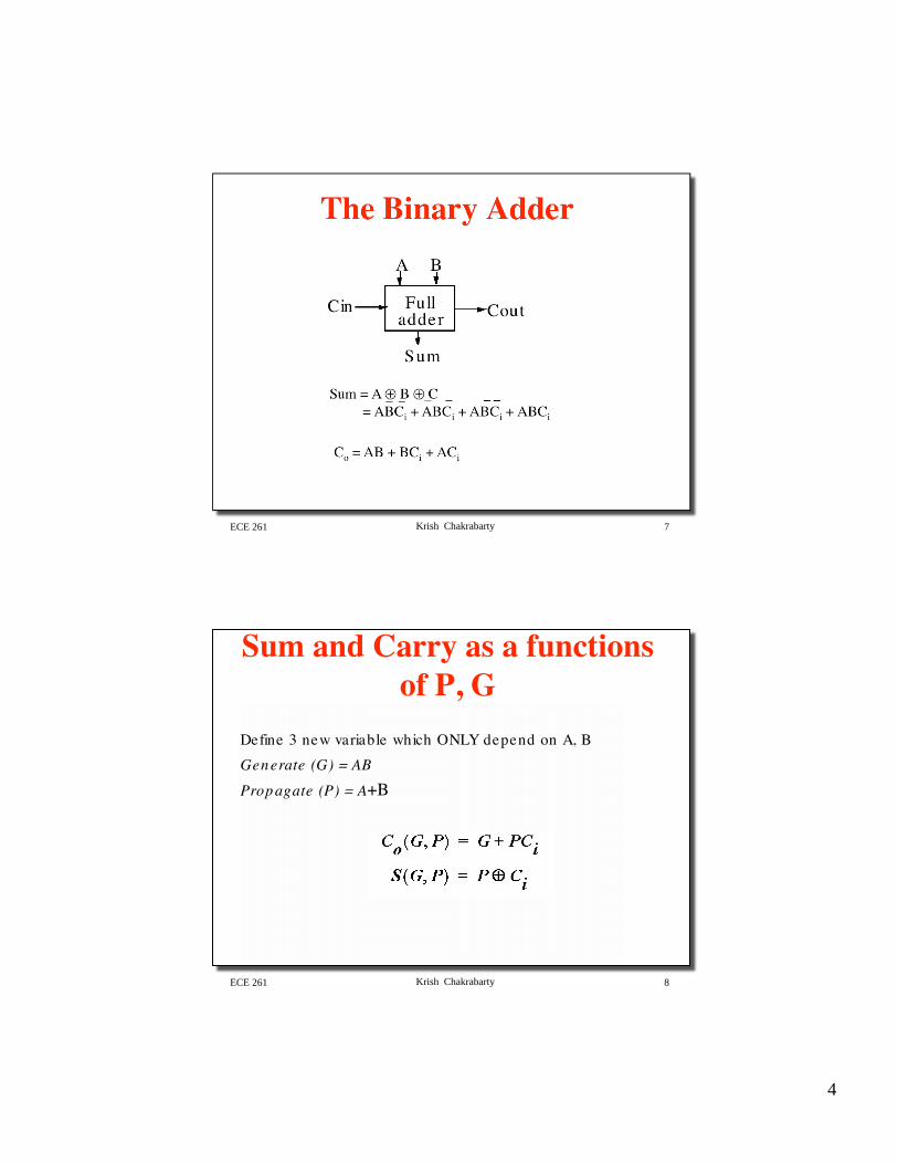
ECE 261 Krish Chakrabarty 7
The Binary Adder
A B
Cout
Sum
Cin Fulladder
Sum = A B C = ABCi + ABCi + ABCi + ABCi
Co = AB + BCi + ACi
ECE 261 Krish Chakrabarty 8
Sum and Carry as a functions of P, G
Define 3 new variable which ONLY depend on A, B
Generate (G) = AB
Propagate (P) = A+B
5
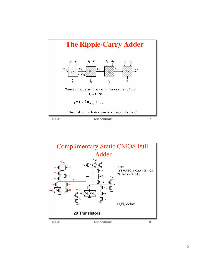
ECE 261 Krish Chakrabarty 9
The Ripple-Carry Adder
A0 B0
S0
Co,0Ci,0
A1 B1
S1
Co,1
A2 B2
S2
Co,2
A3 B3
S3
Co,3
(= Ci,1)FA FA FA FA
Wors t cas e delay linear with the number o f b its
td = O(N)
Goal: Make the fas tes t poss ible carry path circuit
td = (N-1)tcarry + tsum
ECE 261 Krish Chakrabarty 10
Complimentary Static CMOS Full Adder
Note:1) S = ABCi + Co(A + B + Ci)2) Placement of Ci
O(N) delay
6
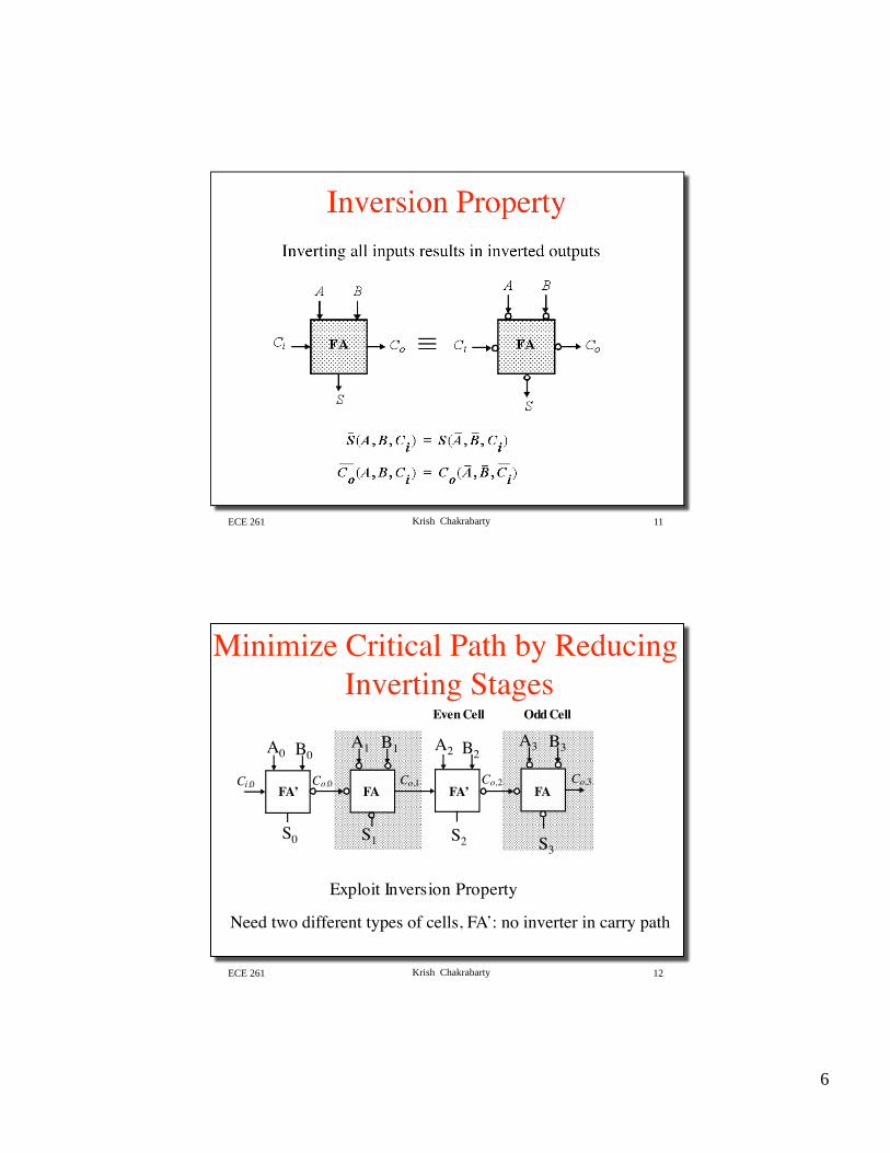
ECE 261 Krish Chakrabarty 11
Inversion PropertyInverting all inputs results in inverted outputs
ECE 261 Krish Chakrabarty 12
Minimize Critical Path by Reducing Inverting Stages
Co,0Ci,0 Co,1 Co,2 Co,3FA’ FA FA’ FA
OddCellEvenCell
Exploit Inversion Property
Need two different types of cells, FA’: no inverter in carry path
A0A1B0
A2B1 B2
B3A3
S0 S1 S2 S3
7
ECE 261 Krish Chakrabarty 13
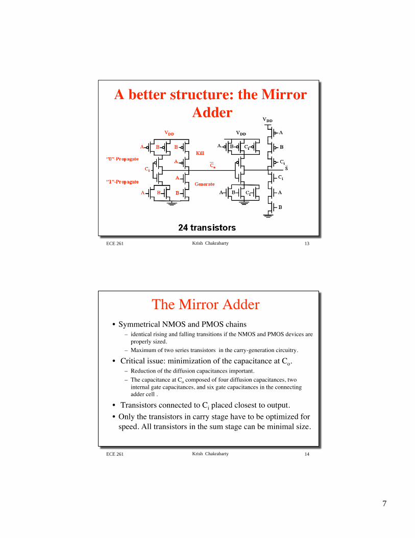
A better structure: the Mirror Adder
ECE 261 Krish Chakrabarty 14
The Mirror Adder• Symmetrical NMOS and PMOS chains
– identical rising and falling transitions if the NMOS and PMOS devices are properly sized.
– Maximum of two series transistors in the carry-generation circuitry.
• Critical issue: minimization of the capacitance at Co. – Reduction of the diffusion capacitances important.
– The capacitance at Co composed of four diffusion capacitances, two internal gate capacitances, and six gate capacitances in the connecting adder cell .
• Transistors connected to Ci placed closest to output.
• Only the transistors in carry stage have to be optimized for speed. All transistors in the sum stage can be minimal size.
8
ECE 261 Krish Chakrabarty 15
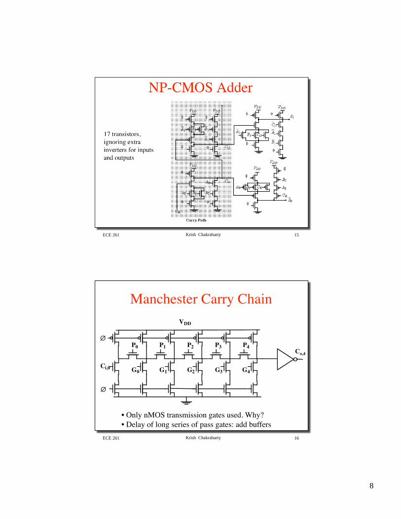
NP-CMOS Adder
17 transistors,ignoring extra inverters for inputsand outputs
ECE 261 Krish Chakrabarty 16
Manchester Carry Chain
P0
Ci,0
P1
G0
P2
G1
P3
G2
P4
G3 G4
VDD
Co,4
• Only nMOS transmission gates used. Why?• Delay of long series of pass gates: add buffers
9
ECE 261 Krish Chakrabarty 17
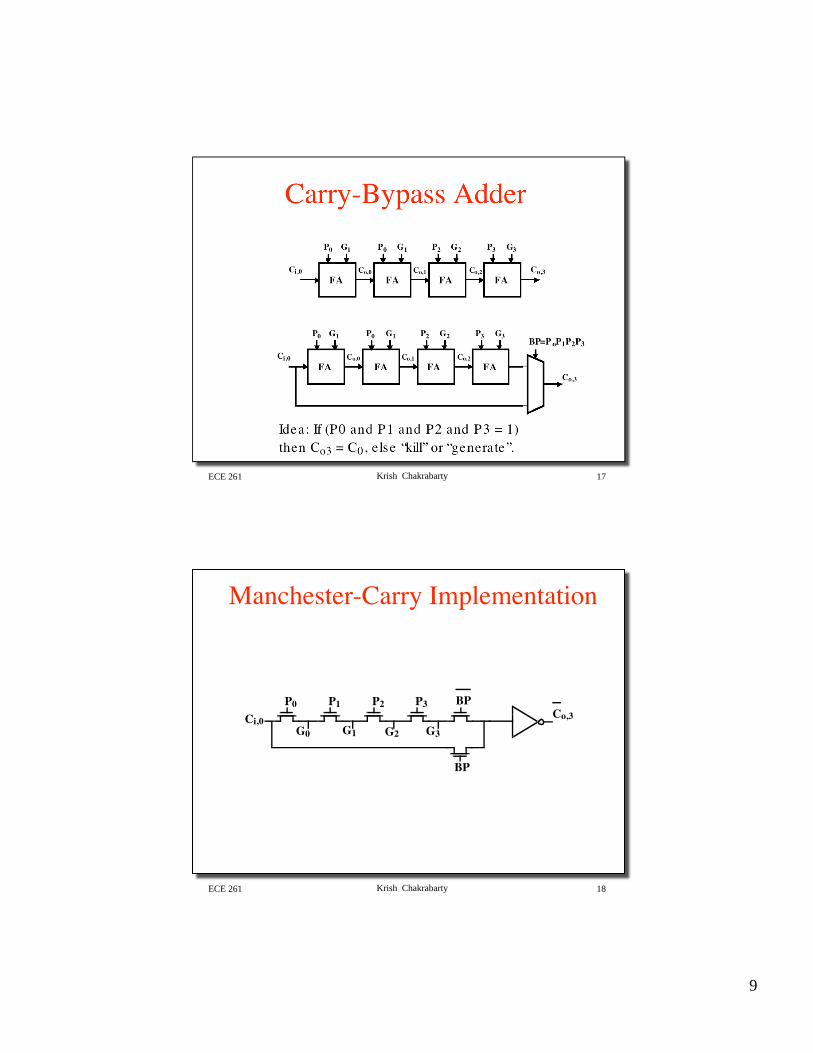
Carry-Bypass Adder
FA FA FA FA
P0 G1 P0 G1 P2 G2 P3 G3
Co,3Co,2Co,1Co,0Ci,0
FA FA FA FA
P0 G1 P0 G1 P2 G2 P3 G3
Co,2Co,1Co,0Ci,0
Co,3
BP=PoP1P2P3
Idea: If (P0 and P1 and P2 and P3 = 1)then Co3 = C0, else “kill” or “generate”.
ECE 261 Krish Chakrabarty 18
Manchester-Carry Implementation
P0Ci,0
P1
G0
P2
G1
P3
G2
BP
G3
BP
Co,3
10
ECE 261 Krish Chakrabarty 19
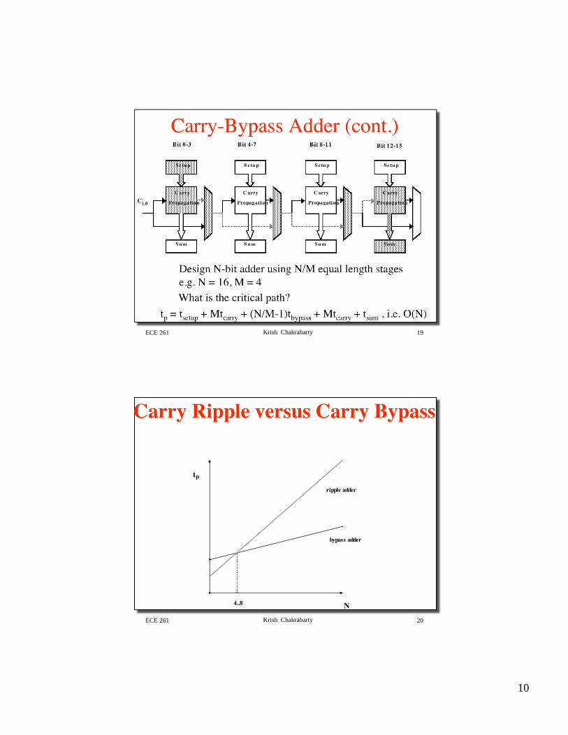
Carry-Bypass Adder (cont.)
S e tu p
C arry
Propagation
S u m
S e tu p
C arry
Propagation
S u m
S e tu p
C arry
Propagation
S um
S e tu p
C arry
Propagation
S u m
Bit 0-3 Bit 4-7 Bit 8-11 Bit 12-15
Ci,0
Design N-bit adder using N/M equal length stagese.g. N = 16, M = 4What is the critical path?
tp = tsetup + Mtcarry + (N/M-1)tbypass + Mtcarry + tsum , i.e. O(N)
ECE 261 Krish Chakrabarty 20
Carry Ripple versus Carry Bypass
N
tp
ripple adder
bypass adder
4..8
11
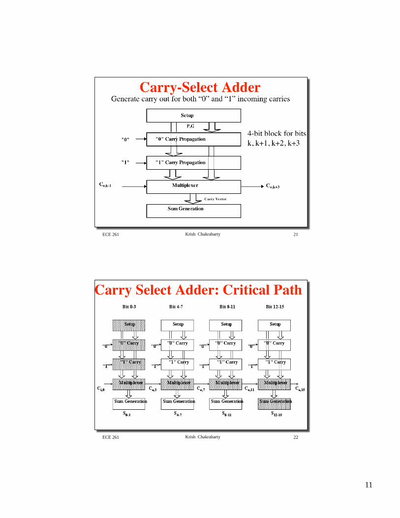
ECE 261 Krish Chakrabarty 21
Carry-Select Adder
Setup
"0" Carry Propagation
"1" Carry Propagation
Multiplexer
Sum Generation
Co,k-1 Co,k+3
"0"
"1"
P,G
Carry Vector
Generate carry out for both “0” and “1” incoming carries
4-bit block for bitsk, k+1, k+2, k+3
ECE 261 Krish Chakrabarty 22
Carry Select Adder: Critical Path
12
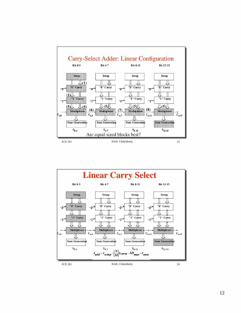
ECE 261 Krish Chakrabarty 23
Carry-Select Adder: Linear Configuration
(1)
(5)(5)(5)(6)
(1)
(7) (8)(5)(5)
Are equal-sized blocks best?
ECE 261 Krish Chakrabarty 24
Linear Carry Select
Setup
"0" Carry
"1" Carry
Multiplexer
Sum Generation
"0"
"1"
Setup
"0" Carry
"1" Carry
Multiplexer
Sum Generation
"0"
"1"
Setup
"0" Carry
"1" Carry
Multiplexer
Sum Generation
"0"
"1"
Setup
"0" Carry
"1" Carry
Multiplexer
Sum Generation
"0"
"1"
Bit 0-3 Bit 4-7 Bit 8-11 Bit 12-15
S0-3 S4-7 S8-11 S12-15
Co,15Co,11Co,7Co,3Ci,0
13
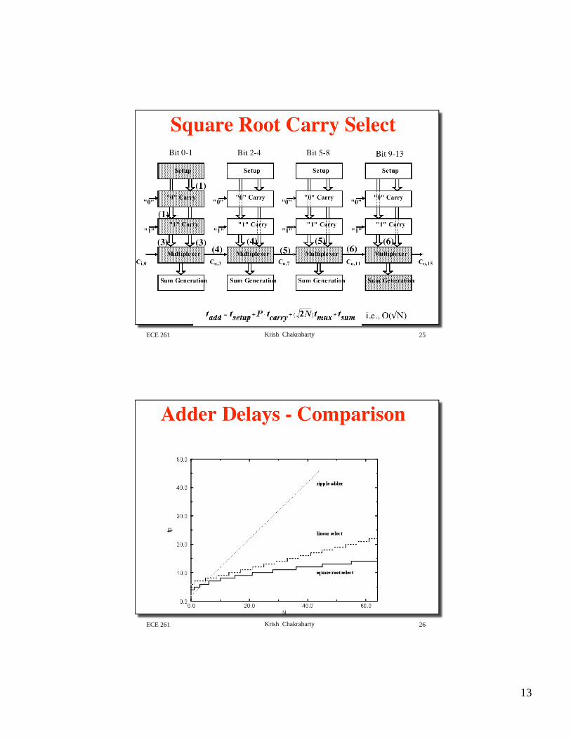
ECE 261 Krish Chakrabarty 25
Square Root Carry Select
Setup
"0" Carry
"1" Carry
Multiplexer
Sum Generation
"0"
"1"
Setup
"0" Carry
"1" Carry
Multiplexer
Sum Generation
"0"
"1"
Setup
"0" Carry
"1" Carry
Multiplexer
Sum Generation
"0"
"1"
Setup
"0" Carry
"1" Carry
Multiplexer
Sum Generation
"0"
"1"
Co,15Co,11Co,7Co,3Ci,0
(1)
(4)(3)(3)(4)
(1)
(5) (6)(6)(5)
Bit 0-1 Bit 2-4 Bit 5-8 Bit 9-13
i.e., O( N)
ECE 261 Krish Chakrabarty 26
Adder Delays - Comparison
14
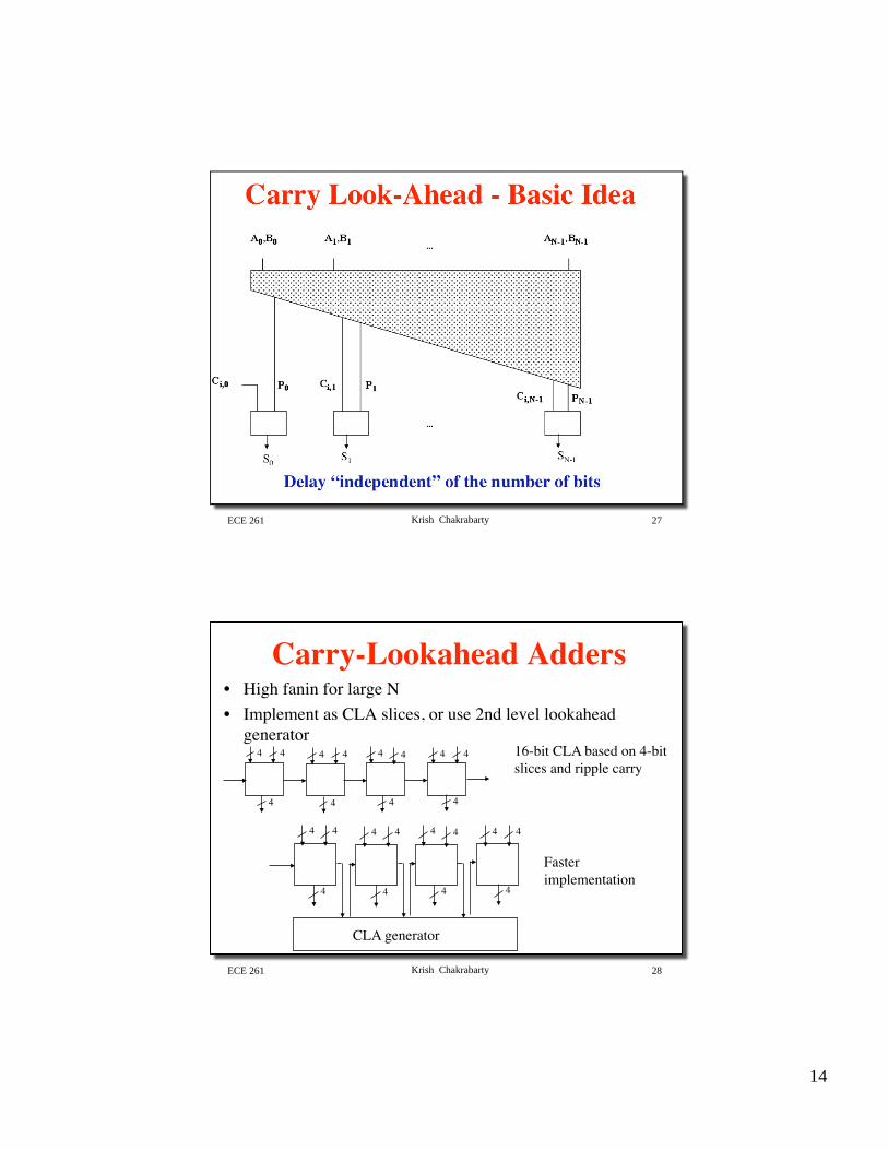
ECE 261 Krish Chakrabarty 27
Carry Look-Ahead - Basic Idea
Delay “independent” of the number of bitsS0
S1 SN-1
ECE 261 Krish Chakrabarty 28
Carry-Lookahead Adders• High fanin for large N
• Implement as CLA slices, or use 2nd level lookahead generator
4
4
4 4 4
4 4 4 4 4 4 4 16-bit CLA based on 4-bitslices and ripple carry
4
4
4 4 4
4 4 4 4 4 4 4
CLA generator
Faster implementation
15
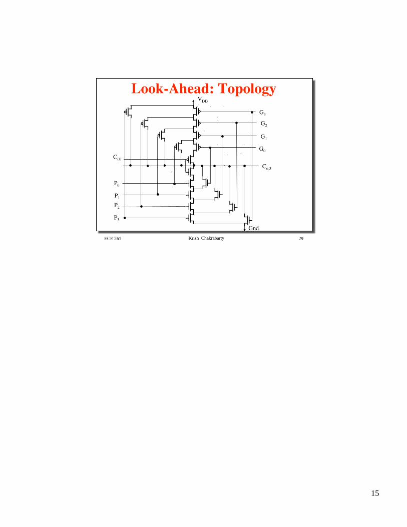
ECE 261 Krish Chakrabarty 29
Look-Ahead: TopologyVDD
Gnd
G3
G2
G1
G0
P0
P3
P2
P1
Ci,0Co,3
Related Documents