2146 JOURNAL OF LIGHTWAVE TECHNOLOGY, VOL. 16, NO. 12, DECEMBER 1998 Architectures and Technologies for High-Speed Optical Data Networks Vincent W. S. Chan, Fellow, IEEE, Katherine L. Hall, Senior Member, IEEE, Member OSA, Eytan Modiano, Member, IEEE, and Kristin A. Rauschenbach, Member, IEEE (Invited Paper) Abstract— Current optical networks are migrating to wave- length division multiplexing (WDM)-based fiber transport be- tween traditional electronic multiplexers/demultiplexers, routers, and switches. Passive optical add–drop WDM networks have emerged but an optical data network that makes full use of the technologies of dynamic optical routing and switching exists only in experimental test-beds. This paper will discuss architecture and technology issues for the design of high performance optical data networks with two classes of technologies, WDM and time division multiplexing (TDM). The WDM network architecture presented will stress WDM aware internet protocol (IP), taking full advantage of optical reconfiguration, optical protection and restoration, traffic grooming to minimize electronics costs, and optical flow-switching for large transactions. Special attention is paid to the access network where innovative approaches to archi- tecture may have a significant cost benefit. In the more distant future, ultrahigh-speed optical TDM networks, operating at single stream data rates of 100 Gb/s, may offer unique advantages over WDM networks. These advantages may include the ability to provide integrated services to high-end users, multiple quality- of-service (QoS) levels, and truly flexible bandwidth-on-demand. We will give an overview of an ultrahigh-speed TDM network architecture and describe recent key technology developments such as high-speed sources, switches, buffers, and rate converters. Index Terms—Optical data processing, optical fiber communi- cation, optical fiber LAN, optical signal processing, time division multiaccess, time division multiplexing, wavelength division mul- tiplexing. I. INTRODUCTION C OMMUNICATIONS networks are undergoing rapid de- velopments. In the past, the largest networks were elec- tronic, circuit switched networks providing plain-old telephone service (POTS), and carrying mostly voice traffic. Starting with the ARPANET and the explosive growth of the Internet and the worldwide web, electronic packet switched networks have become ubiquitous. The rapid growth of these packet networks can be attributed to the efficiency of the internet protocol (IP) in servicing bursty traffic or computer users. At the same time, we have seen a revolution in the transport technology that is used to interconnect nodes in a network. Specifically, fiber optic transmission technology has advanced Manuscript received August 27, 1998; revised September 22, 1998. This work was supported by the Consortium on Wideband All-Optical Networks and the Defense Advanced Research Projects Agency (DARPA). The authors are with the Lincoln Laboratory, Massachusetts Institute of Technology, Lexington, MA 02420 USA. Publisher Item Identifier S 0733-8724(98)09304-9. from lower rate multimode fiber links to singlemode amplified fiber links capable of carrying multiple 10 Gb/s channels per fiber. Still, the incredible bandwidth offered by optical transmission technology has only been used as a very high- speed replacement of copper cables. The routing and switching technologies used are currently still electronic based. With the advent of advanced optical devices such as integrated tunable lasers, optical grating routers, and cross-connect switches, a new class of optically routed and switched wavelength division multiplexing (WDM) network is feasible. One reason that optical data networking is still in its infancy is that optical transport alone has provided an incredible increase in available bandwidth that exceeds any present day demand. It is hard to find applications other than aggregated traffic trunking, that can take advantage of a 10-Gb/s data channel. To date, optical technology has been inserted at the physical layer (bottom layer) of the typical multilayer protocol stack. One reason for this application is that it allows straightforward extension of existing networks into the optical regime, without any modification of the higher layers. However, such an architecture does not maximally utilize the advantages offered by optical networking. We will propose a new architecture with a simplified protocol stack that takes advantage of the unique capabilities of WDM optical routing and switching technologies. We believe the first commercial true optical data networks will employ WDM because the technologies needed to implement these networks are now commercially available. The nature of WDM technology suggests a network man- agement and control scheme that uses off-band signaling, and network resource scheduling that is either centralized or distributed but coordinated. Tight coordination is required due to the lack of optical buffers that can temporarily store packets before processing and routing. This property is key to optical WDM data network protocol designs and presents interesting and sometimes severe constraints on network synchronization and end-to-end routing. With the availability of buffering at routers internal to the network, higher network efficiencies in terms of throughputs and delays can be achieved with a time division multiplexing (TDM) scheme where the medium bandwidth is available to the packet in one large channel ( 100 Gb/s) instead of fragmented (WDM) channels. The signaling information required for switching packets in this network would be 0733–8724/98$10.00 1998 IEEE

Welcome message from author
This document is posted to help you gain knowledge. Please leave a comment to let me know what you think about it! Share it to your friends and learn new things together.
Transcript

2146 JOURNAL OF LIGHTWAVE TECHNOLOGY, VOL. 16, NO. 12, DECEMBER 1998
Architectures and Technologies for High-SpeedOptical Data Networks
Vincent W. S. Chan,Fellow, IEEE,Katherine L. Hall,Senior Member, IEEE, Member OSA,Eytan Modiano,Member, IEEE,and Kristin A. Rauschenbach,Member, IEEE
(Invited Paper)
Abstract—Current optical networks are migrating to wave-length division multiplexing (WDM)-based fiber transport be-tween traditional electronic multiplexers/demultiplexers, routers,and switches. Passive optical add–drop WDM networks haveemerged but an optical data network that makes full use of thetechnologies of dynamic optical routing and switching exists onlyin experimental test-beds. This paper will discuss architectureand technology issues for the design of high performance opticaldata networks with two classes of technologies, WDM and timedivision multiplexing (TDM). The WDM network architecturepresented will stress WDM aware internet protocol (IP), takingfull advantage of optical reconfiguration, optical protection andrestoration, traffic grooming to minimize electronics costs, andoptical flow-switching for large transactions. Special attention ispaid to the access network where innovative approaches to archi-tecture may have a significant cost benefit. In the more distantfuture, ultrahigh-speed optical TDM networks, operating at singlestream data rates of 100 Gb/s, may offer unique advantages overWDM networks. These advantages may include the ability toprovide integrated services to high-end users, multiple quality-of-service (QoS) levels, and truly flexible bandwidth-on-demand.We will give an overview of an ultrahigh-speed TDM networkarchitecture and describe recent key technology developmentssuch as high-speed sources, switches, buffers, and rate converters.
Index Terms—Optical data processing, optical fiber communi-cation, optical fiber LAN, optical signal processing, time divisionmultiaccess, time division multiplexing, wavelength division mul-tiplexing.
I. INTRODUCTION
COMMUNICATIONS networks are undergoing rapid de-velopments. In the past, the largest networks were elec-
tronic, circuit switched networks providing plain-old telephoneservice (POTS), and carrying mostly voice traffic. Startingwith the ARPANET and the explosive growth of the Internetand the worldwide web, electronic packet switched networkshave become ubiquitous. The rapid growth of these packetnetworks can be attributed to the efficiency of the internetprotocol (IP) in servicing bursty traffic or computer users. Atthe same time, we have seen a revolution in the transporttechnology that is used to interconnect nodes in a network.Specifically, fiber optic transmission technology has advanced
Manuscript received August 27, 1998; revised September 22, 1998. Thiswork was supported by the Consortium on Wideband All-Optical Networksand the Defense Advanced Research Projects Agency (DARPA).
The authors are with the Lincoln Laboratory, Massachusetts Institute ofTechnology, Lexington, MA 02420 USA.
Publisher Item Identifier S 0733-8724(98)09304-9.
from lower rate multimode fiber links to singlemode amplifiedfiber links capable of carrying multiple 10 Gb/s channelsper fiber. Still, the incredible bandwidth offered by opticaltransmission technology has only been used as a very high-speed replacement of copper cables. The routing and switchingtechnologies used are currently still electronic based. With theadvent of advanced optical devices such as integrated tunablelasers, optical grating routers, and cross-connect switches, anew class of optically routed and switched wavelength divisionmultiplexing (WDM) network is feasible.
One reason that optical data networking is still in its infancyis that optical transport alone has provided an incredibleincrease in available bandwidth that exceeds any present daydemand. It is hard to find applications other than aggregatedtraffic trunking, that can take advantage of a 10-Gb/s datachannel. To date, optical technology has been inserted atthe physical layer (bottom layer) of the typical multilayerprotocol stack. One reason for this application is that itallows straightforward extension of existing networks into theoptical regime, without any modification of the higher layers.However, such an architecture does not maximally utilize theadvantages offered by optical networking. We will propose anew architecture with a simplified protocol stack that takesadvantage of the unique capabilities of WDM optical routingand switching technologies. We believe the first commercialtrue optical data networks will employ WDM because thetechnologies needed to implement these networks are nowcommercially available.
The nature of WDM technology suggests a network man-agement and control scheme that uses off-band signaling,and network resource scheduling that is either centralized ordistributed but coordinated. Tight coordination is required dueto the lack of optical buffers that can temporarily store packetsbefore processing and routing. This property is key to opticalWDM data network protocol designs and presents interestingand sometimes severe constraints on network synchronizationand end-to-end routing.
With the availability of buffering at routers internal to thenetwork, higher network efficiencies in terms of throughputsand delays can be achieved with a time division multiplexing(TDM) scheme where the medium bandwidth is availableto the packet in one large channel (100 Gb/s) insteadof fragmented (WDM) channels. The signaling informationrequired for switching packets in this network would be
0733–8724/98$10.00 1998 IEEE

CHAN et al.: TECHNOLOGIES FOR HIGH-SPEED OPTICAL NETWORKS 2147
contained in the packet header and no centralized or highlycoordinated scheduler is required. Network management andcontrol could be simpler and more efficient, especially ina bursty data environment with many users attempting toshare the same medium. However, the technology neededto implement a network of this type is still in the researchstage and some typical networking components may not befeasible at ultrafast rates. At a minimum, optical logic gatesand buffering at the channel rate are necessary architecturalbuilding blocks. In the second half of this paper, we willdescribe a novel architecture that takes advantage of theultrafast components that have been developed to date. Atestbed demonstration of this TDM network architecture inthe next few years is feasible.
In this paper, we will present what we believe will be theevolution of optical data networks over the next few years.Beginning with WDM networks, we will describe services thatmay be offered as well as the advantages and tradeoffs thataccompany optical networking. In the second major section,we will describe the more futuristic TDM network that mayprovide enhanced digital services to ultrahigh-speed users.The WDM networking section concentrates mainly on newarchitectures as many of the components needed to imple-ment such a network are currently commercially available.The TDM section describes both the novel architecture aswell as component development, as many of the necessarycomponents are still being designed and demonstrated.
II. WDM OPTICAL DATA NETWORKS
In order to design a WDM optical data network for thefuture that represents a major improvement in performance,substantially lower cost and offerings of new high-end ser-vices, it is important to speculate on the type of services thatthis network may offer and then optimize the network designfor these services. Past forecasts of new applications have notbeen terribly accurate. In fact, the worldwide web applicationwas not in anyone’s predictions much before its appearance.Hence, we will not attempt to foretell any specific futureapplications but rather try to provide an abstraction of the typeof services that can be offered in the future. We believe thereare four classes of services that can be characterized abstractlyand not specifically tied to particular applications.
1) Transparent Optical Services to Support ConventionalElectronic Network Services as Overlays:For example,the network should be able to provide optical transportfor all the usual services in present day networks, suchas SONET, ATM, frame relay, and IP services.
2) Large Point-to-Point Circuit-Switched Trunks on De-mand: OC-48, OC-192, and above to deal with streamtraffic but with much less set-up time (of the order oftens of milliseconds) than current networks.
3) Efficient Very High-Speed “IP” Packet Service IncludingMulticast: For bursty, unscheduled large file transfers(100 Mbyte–10 Gbyte) at high access rates (2 Gb/s).
4) Analog Services:narrow- and broad-band analog ser-vices with good amplitude, phase, and timing fidelitypreserving features.
Fig. 1. Partitioning of a WDM optical data network into access and backbonenetworks (CO= central office, AN= access node, NIU= network interfaceunit).
In addition, differentiated quality-of-service (QoS) is highlydesirable. We will show in the Section II how these servicescan be addressed by a combination of physical architecture,protocol design, and network management and control.
One way of viewing WDM optical data networks is througha physical and logical partitioning of the network into theaccess network and the backbone network, as shown in Fig. 1.Thus, local area networks (LAN’s) are naturally part of theaccess network and wide area networks (WAN’s) are part ofthe backbone network. This position emphasizes the strongeconomic reasons why these two classes of networks shouldbe considered separately and designed and optimized basedon very different performance metrics and goals. Thougharchitects usually arrive at radically different designs for thetwo classes of networks, the two would have to seamlesslyinterconnect. Long-haul fiber cost (fiber, installation, and pass-through-fees) dominates backbone network total costs. Nodeequipment costs in that case, though not totally insignificant,are considerably less, especially when optical routing andswitching are deployed in the future. Most backbone designswould treat fiber as the precious commodity and try to makemaximum use of the capacity. Hence, network topology andscheduling algorithms for optimizing wavelength usage inWDM backbone networks is an area of intense research. Onthe other hand, in the access network, the tail fiber links havelittle opportunity to aggregate enough users to require veryefficient multiplexing. Connectivity is more important thanhigh throughput, and with the vast bandwidth available to theuser at the entrance to the network, fiber bandwidth utilizationcan be readily and even freely traded for low-cost accessequipment and network hardware. WDM optically routedmetropolitan area networks (MAN’s) should be considered aspart of the access network though its design goals would besomewhere between the extreme cases of LAN’s and WAN’s.
One primary distinction between the two classes of networksis the way passive and active network components are chosenas the architectural building blocks of the networks. Forexample, to lower access costs, passive optical componentswithout a lot of diagnostics and monitoring are often usedfor the access network. Broadcast stars, buses and trees, andpassively routed optical networks such as the AON (all-optical-network), Level-0 (LAN), and Level-1 (MAN), [11],and the IBM rainbow network are prime examples. In thebackbone, higher cost active optical components such as the

2148 JOURNAL OF LIGHTWAVE TECHNOLOGY, VOL. 16, NO. 12, DECEMBER 1998
frequency sensitive switch of the MONET network, [49], andfrequency changers can also be used.
The LAN is an important part of the access network. Mostwork on WDM-based LAN’s assume the use of a broadcastarchitecture and focus on the development of medium accesscontrol (MAC) protocols for sharing wavelengths among thedifferent nodes in the network. While the broadcast nature ofoptical LAN’s allows the communication to remain all-optical,it also limits the scalability of the solution. The broadcastarchitecture, with constraints on the number of availablewavelengths, limits the network both in the number of usersand in geographic extent and is only practical for networkssupporting at most hundreds of users over short distances. Inorder to extend WDM optical data networks to the backboneand the wide area, some form of electronic packet switchingand buffering, or a new all-optical data flow mechanism arenecessary. We will discuss some of these concepts in the nextfew sections.
A. WDM LAN’s
In recent years, there has been a wave of research towardthe development of WDM-based LAN’s [1]–[10]. Most of theproposed protocols and architectures are based on a broadcastnetwork architecture. Some of the protocols are based onrandom access and consequently result in low throughput dueto contention [3], [4]. Other protocols that attempt to minimizecontention, through the use of some form of reservationscheme, require that the system be synchronized and slottedand many require multiple transceivers per node [5]–[8].Despite the added complexity of these systems, most stillfail to achieve high levels of utilization due to the use ofinefficient scheduling schemes that often fail to deal withreceiver contention, or ignore the effects of propagation delaysin a high latency, high data rate network. A survey of WDMmultiaccess protocols and their properties can be found in [1]and [2].
The purpose of the strawman system described in this paperis to achieve good throughput-delay characteristics, whilemaintaining simple user terminals. Previous efforts to simplifyuser terminals involved protocols that use fixed tuned receiversor transmitters [9], [10]. However, those protocols limit thenumber of users to the number of available wavelengths. Also,protocols using only a single fixed tuned device are oftenlimited to the use of random access protocols that result inlow channel utilization.
The system described here is novel in a number of ways.First, it uses an unslotted MAC protocol, yet results in highefficiency even in high latency environments. The choice ofan unslotted protocol is driven by a desire, for simplicity, toeliminate the requirement to maintain slotting in the network.This is especially important during cold-start of a terminal.Unfortunately, unslotted MAC protocols such as carrier sensemultiple access (CSMA) result in very low utilization in high-latency environments. Alternatively, high-latency protocolssuch as unslotted Aloha are limited in throughput to less than18% [3], [5]. Another new attribute of our system is that it usesa centralized master/slave scheduler for each access network
Fig. 2. Scheduler based LAN.
Fig. 3. Optical terminal (OT) with a tunable receiver (TR) and a tunabletransmitter (TT).
for efficient resource allocation and network management. Toovercome the effects of propagation delays, the schedulermeasures the delays between the terminals and the hub andtakes that delay into account when scheduling transmissions.
1) LAN Architecture: In the LAN, optical terminals (OT’s)are connected via a simple broadcast medium such as a star-coupler located at a hub. As shown in Fig. 2, each OT isconnected to the star using two fibers, one in each direction.Transmissions from all OT’s on all wavelengths are combinedat the star and broadcast to the OT’s on the downlink fibers.Each OT is equipped with a single transmitter and receiver,both of which are tunable to all wavelengths, as shown inFig. 3. This star based architecture has been proposed in thepast for use in WDM LAN’s [3].
2) MAC Protocol: The proposed protocol is based on asimple master/slave scheduler. All OT’s send their requeststo the scheduler, which schedules the requests and informsthe OT’s when and on which wavelength to transmit. Uponreceiving their assignments, OT’s immediately tune to thatwavelength and transmit. Hence, OT’s do not need to maintainany synchronization or timing information. There are threemajor aspects to the protocol. First, the protocol uses rangingto overcome the effects of propagation delays. Second, theprotocol uses random access for the control channel andthird, the protocol uses a simple scheduling algorithm withfirst-come–first-serve (FCFS) input queues and a look-aheadwindow to overcome head-of-line (HOL) blocking. These aredescribed in more detail below.
a) Ranging: The protocol is able to overcome the effectsof propagation delays by measuring the round-trip delay ofeach OT to the hub and using that information to informthe OT’s of their turn to transmit in a timely manner. As anillustration, consider the timing sequence depicted in Fig. 4.In order for OT B’s transmission to arrive at the hub attime , the scheduler must send the assignment to OT B attime , where is OT B’s round-trip delay to the hub(including tuning delays). In this way the transmissions ofdifferent terminals can be scheduled back-to-back, with littledead-time between transmissions.

CHAN et al.: TECHNOLOGIES FOR HIGH-SPEED OPTICAL NETWORKS 2149
Fig. 4. Use of ranging to overcome propagation delays.
b) Access to the control channel:Reservations are madeusing a random access protocol in the control channel whereterminals send reservation requests periodically and updatetheir requests after waiting a random delay. These reservationmessages contain the state of the queues at the requestingterminal. For example, each reservation message can containthe destinations with which the terminal wants to communicateand the duration of the requested transmissions.
Since reservation requests are sent on the control channelat random, it is possible for two or more terminals to sendtheir request during overlapping time intervals. In which casetheir transmissions would “collide” and not be received bythe scheduler. However, since reservation messages containingthe state of the queue are sent periodically, all requests willeventually be received by the scheduler. As requests areanswered by the scheduler, terminals update their requests toreflect the changes in their request queue. The random accessprotocol for accessing the control channel is described andanalyzed in [18].
c) Scheduling algorithm:In a WDM system with a sin-gle transmitter and receiver per node, scheduling is constrainedby the number of wavelengths which limits the number ofrequests served during a slot to. It is also constrained bythe fact that each node has a single transmitter and a singlereceiver. Therefore, during a given slot, each node can bescheduled for at most one transmission and one reception.This, in fact, is a very similar problem to that of schedulingtransmissions in an input queued switch. In the case of an inputqueued switch it is known that when a FCFS service disciplineis employed, under uniform traffic, throughput is limited to
[13]. This throughput limitation is due to thehead-of-line (HOL) blocking effect, where transmissions areprevented because the packet at the head of the queue cannotbe scheduled due to a receiver conflict. It is also known that ifnodes are allowed to look-ahead into their buffers and transmita packet other than the one at the head of the queue, the effectof HOL blocking can be significantly reduced [14]. Schedulingalgorithms based on bipartite graph matching algorithms havebeen proposed that achieve full utilization under uniform andnonuniform traffic conditions [15], [16]. However, it is alsoknown that these algorithms are computationally intensive andrequire O( ) operations to be implemented, where isthe number of input and output ports on the switch [17].
To simplify the implementation of the scheduler we proposethe following simple algorithm for scheduling traffic. Thealgorithm is based on input queues and is made efficient
through the use of a “look-ahead” window that allows thescheduler to look-ahead into each input queue and schedulerequests that are not necessarily at the head of their queue. Alook-ahead capability of , allows the scheduler to look as faras the th request in the queue. The algorithm is implementedon a slot-by-slot basis to form a schedule for the given slot.The algorithm works by maintaining request queues, eachcontaining the transmission requests from one of thenodesin the network. The algorithm visits every node in randomorder and starting with the first request in the queue it searchesfor a request that can be scheduled. That is, it searches fora request for a transmission to a receiver that has not beenassigned yet. The algorithm searches the queue until depthhas been reached. If a request has been found, a wavelength isassigned to it. This process is continued until either all of therequest queues have been visited or allwavelengths havebeen assigned. During the next slot, the algorithm starts anewwith the first request in each queue.
Table I shows the maximum achievable throughput underuniform traffic, with 30 data wavelengths. When the numberof nodes is equal to the number of channels and no look-aheadis employed (i.e., ), HOL blocking limits throughput to59% as predicted in [13]. However, a look-ahead window ofjust four packets can increase throughput to over 80%. Asthe number of nodes exceeds the number of channels, theeffect of HOL blocking is drastically reduced. This is due totwo factors. First, the probability that multiple nodes have apacket at the HOL to the same destination is reduced dueto the increase in the number of destinations, and second,with fewer channels than nodes the algorithm has many morerequests from which to choose a schedule oftransmissions.As can be seen from the table, the combination of morenodes than channels and a look-ahead window of four or fivepackets virtually eliminates the effects of HOL blocking onthroughput, under uniform traffic. Scheduling multicast trafficin a WDM broadcast-and-select system is even more of achallenge because multicast messages have multiple intendedreceivers and trying to schedule transmissions in order to avoidreceiver conflicts can be very inefficient. Simple and efficientmulticast scheduling algorithms, based on random scheduling,are presented in [12].
In order to analyze the average queuing delay in thissystem we assume that packets arrive to each of thenodesaccording to a Poisson random process of rate. We alsoassume that all packets are of the same length and takeone slot to transmit and that the scheduler uses the slottedscheduling algorithm described in the previous section andthat all transmissions are scheduled to occur at the beginningof a time slot.
Shown in Fig. 5 is the simulated delay for a system with 100nodes and 30 wavelengths. Notice that with these values thearrival rate of new packets to a user cannot exceed 0.3 due tothe channel constraint. Also notice from the figure that a look-ahead of just two packets can significantly help in reducingdelays. However, a larger look-ahead window does not reducedelay any further because for these values ofand , alook-ahead of just two packets essentially eliminates the HOLblocking effect.

2150 JOURNAL OF LIGHTWAVE TECHNOLOGY, VOL. 16, NO. 12, DECEMBER 1998
TABLE ITHE MAXIMUM ACHIEVABLE THROUGHPUT FOR ANETWORK WITH 30 WAVELENGTHS, N NODES, AND A LOOK-AHEAD WINDOW k
Fig. 5. Delay versus load for a system with 100 nodes and 30 wavelengthsand a look-ahead capability(k).
The algorithms described can be readily applied to passivelyrouted optical networks such as the Level-1 MAN of the AON,[11], where the only dynamically tunable optical elementsare lasers and receivers at the user terminals. Applicationsto networks with dynamically reconfigurable elements suchas the frequency-sensitive-switch (FSS’s) of MONET, [49],will require additional timing measurements to these elementsand command and telemetry to reconfigure these elements for“just in time” service.
B. WDM Data Networks Beyond LAN—WDM Aware IP
The MAC protocol described in the previous section can beused to efficiently statistically multiplex packets from burstydata users in splitting losses and the broadcast LAN. Theprotocol limits this solution to relatively short distances andthe number of available wavelengths also limits scalability tolarger user populations. In order to efficiently extend WDM toWAN’s, mechanisms are needed for statistically multiplexingbursty data in wide areas that cannot be spanned with abroadcast architecture. The approach we will describe in thissection consists of putting more intelligence at the IP layer torecognize the resources available at the WDM layer that canbe put to bear in the efficient delivery of data.
1) IP over WDM: Present internet IP services are providedusing a wide range of electronic multiplexing and switch-ing equipment. A typical network may include as many asthree or four different electronic multiplexing and switchinglayers. For example, as shown in Fig. 6, internet packetsmay be carried using frame relay where the IP packets areencapsulated in frames that are sometimes mapped into ATM
(a) (b)
Fig. 6. (a) Typical protocol stack and (b) simplified protocol stack.
cells, which, in turn, are carried over synchronous optical net-working (SONET) transport frames. This multitude of layersproduces bandwidth inefficiencies, adds to the latencies of con-nections, and inhibits providing quality of service assurances.Worse, the layers are largely unaware of each other, causingduplication of network services and, in some scenarios, unco-ordinated network management and control algorithms at thedifferent layers acting against each other creating oscillationsand further degrading network performance. Alternatively, onecould use the simplified protocol stack shown in Fig. 6(b),where the IP traffic is carried directly by a simplified electroniclayer. Such an arrangement would not only reduce the over-head associated with the different layers but would also allowthe electronic layer to be “WDM-aware” and take advantage ofnetwork services offered at the optical layer. For the remainderof this section we will describe optical layer services andalgorithms that can significantly improve the performance ofthe network and simplify the design of the electronic layer.
2) Flow-Switching/Multilayer-Switching:One of the mainbottlenecks in the present Internet is routing at the IP layer.Several methods have been proposed to alleviate this bottle-neck by switching long duration flows at lower layers [44],[46], [48], [56]. Tag switching uses routing protocols to pre-define routes within the network; tags are then used to quicklyassign flows to these routes. IP switching dynamically sets uplayer-2 (e.g., ATM) virtual circuits for those connections thatare perceived to be long.

CHAN et al.: TECHNOLOGIES FOR HIGH-SPEED OPTICAL NETWORKS 2151
This concept of lower layer switching can be extendedto switching large volume and/or long duration flows at theoptical layer. That is, a light-path can be established forlarge data transactions such as the transfer of large filesor long duration and high bandwidth streams across thenetwork. To achieve ultimate efficiencies, an optical flowswitching protocol may need to aggregate flows with similarcharacteristics in order to switch them together. The simplestform of this technique is to use an entire wavelength atany given time for a single transaction. This concept cangive rise to a hybrid multilayer switching approach wherelong duration sessions are switched at the ATM layer, andeven longer duration and higher bandwidth flows are switchedoptically. While it appears that such a multilayer switchingapproach can reduce computation loads and processing delaysin networks, many issues in the design of such a protocolremain to be resolved. While the detailed protocol is yetto be developed, there are some properties this protocol islikely to possess. For example, it is highly desirable forthe application layer and the transport layer to inform theIP layer of the arrival and characteristics of large flows forswitching. This can be done via an augmentation of thetransport control protocol (TCP) layer. Predictions by the IPlayer without higher layer inputs as is sometimes done todaycan be inaccurate and lead to inefficiencies. Since opticalflows require several round-trips for setup and are likely tobe assigned an entire wavelength for each transaction, the sizeof the flows should be at least of the order of the productof the physical propagation delay and the highest data rateof each wavelength for high throughput operations. Any finergrain assignment of network resources for flows such as thescheduled time division multiplexed WDM “B” service of theAON, [11], would require substantially more complexity andprobably is hard to justify, especially if flow switching at theATM layer is also available. Also, the point of electronic tooptical conversion will most likely occur at the user interfaceto the network such as the network interface card of a high-endworkstation. Thus, the WDM optical data network will almostappear to provide an all-optical service to the user except for anintimate dialogue and timed handshake between the networkand the user terminal.
3) Virtual Topology Reconfiguration:In WDM networks,the physical topology is the one seen by the optical layer. Itconsists of passive or dynamically configurable optical nodesinterconnected by fiber. The virtual topology, seen by theelectronic layer, consists of a set of nodes interconnected bylight-paths and in some cases time-shared light-paths. In thisway, WDM networks provide a way to interconnect electronicswitches with high bandwidth bit pipes without dedicating afiber pair between each pair of switches. The design of staticnetwork topologies has been studied extensively in the past[19], [51]. However, the configurable nature of WDM alsoallows the logical topology to be dynamically reconfigured inresponse to changes in traffic conditions.
WDM networks can reconfigure light-paths, providing theability to dynamically optimize the network for changingpatterns of externally offered traffic, subject to availability ofwavelengths and node equipment. This is achieved by chang-
Fig. 7. Using WDM to reconfigure the electronic topology.
ing the light-path connectivity between electronic switches androuters, thereby reconfiguring the electronic virtual topology.Light-paths can be changed via tuning of the transmitterwavelengths in combination with wavelength sensitive passiverouting elements such as a grating router or reconfigurationsvia commands of internal network element such as cross-bar switches and frequency-sensitive-switches. For example,consider a WDM ring network with one transceiver per node.Shown in Fig. 7 are two of the many ways in which the ringcan be configured: on the left, nodes are connected in sequenceusing a single wavelength that is dropped at every node; onthe right, nodes are connected in a different order using threewavelengths. Notice that the connectivity on the left does notallow both calls 1 and 2 to be admitted simultaneously, whilethe one on the right allows both.
Reconfiguration effectively increases the overall systemcapacity by allocating bandwidth only where it is needed.However, there is an overhead associated with reconfigurationin that signaling messages need to be sent between switchesto coordinate topology changes. In addition, reconfigurationmay impact existing connections and these connections mayneed to be rerouted in the virtual topology. However, it shouldbe possible to design a reconfiguration strategy that does notrequire the rearranging of existing calls. Such strategies mayprovide fewer benefits but would be simpler to implementand eliminate many coordination and network managementproblems.
Preliminary studies on reconfiguration of a WDM ringshow significant promise [21]. Fig. 8 shows the call blockingprobability versus call arrival rate for a WDM ring with 20nodes and a bandwidth granularity of one call per wavelength.As can be seen from the figure, a reconfigurable WDMtopology can support six times the traffic of a fixed WDMtopology for the same blocking probability. Similar resultswere found for other topologies.
4) Traffic Grooming: Consider the situation where the op-tical data network is providing a multitude of point-to-pointstream connections among routers, switches, and even endusers. Unless these “users” require full wavelength connec-tions, subwavelength capacity connections need to be allo-cated. This can be accomplished through the use of electronicmultiplexing equipment that can aggregate low rate calls on toa higher rate channel (e.g., SONET multiplexers). However,if calls are indiscriminately multiplexed on to wavelengths,then each wavelength entering or leaving a node will needto be converted to electronics to make drop/forwarding deci-sions. Alternatively, if calls are groomed with foresight ontowavelengths, then the number of wavelengths that need to beprocessed at each node can be significantly reduced [40], [41].
2152 JOURNAL OF LIGHTWAVE TECHNOLOGY, VOL. 16, NO. 12, DECEMBER 1998
Fig. 8. Performance of reconfiguration in a WDM ring network.
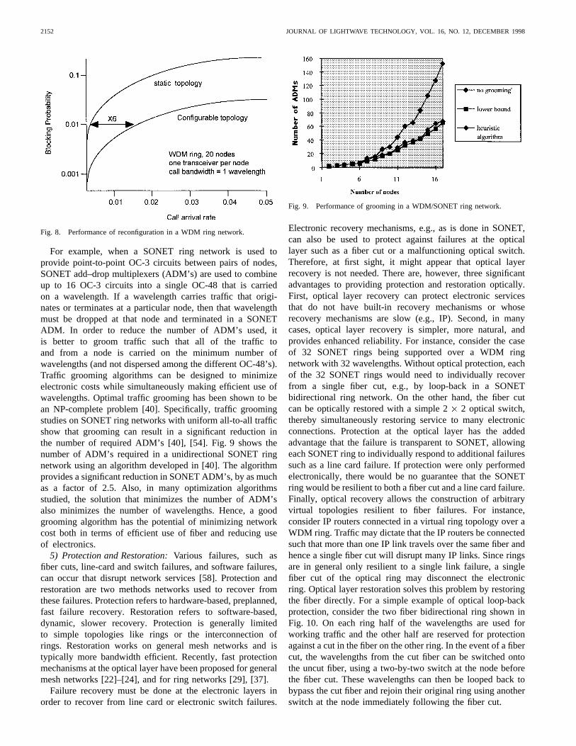
For example, when a SONET ring network is used toprovide point-to-point OC-3 circuits between pairs of nodes,SONET add–drop multiplexers (ADM’s) are used to combineup to 16 OC-3 circuits into a single OC-48 that is carriedon a wavelength. If a wavelength carries traffic that origi-nates or terminates at a particular node, then that wavelengthmust be dropped at that node and terminated in a SONETADM. In order to reduce the number of ADM’s used, itis better to groom traffic such that all of the traffic toand from a node is carried on the minimum number ofwavelengths (and not dispersed among the different OC-48’s).Traffic grooming algorithms can be designed to minimizeelectronic costs while simultaneously making efficient use ofwavelengths. Optimal traffic grooming has been shown to bean NP-complete problem [40]. Specifically, traffic groomingstudies on SONET ring networks with uniform all-to-all trafficshow that grooming can result in a significant reduction inthe number of required ADM’s [40], [54]. Fig. 9 shows thenumber of ADM’s required in a unidirectional SONET ringnetwork using an algorithm developed in [40]. The algorithmprovides a significant reduction in SONET ADM’s, by as muchas a factor of 2.5. Also, in many optimization algorithmsstudied, the solution that minimizes the number of ADM’salso minimizes the number of wavelengths. Hence, a goodgrooming algorithm has the potential of minimizing networkcost both in terms of efficient use of fiber and reducing useof electronics.
5) Protection and Restoration:Various failures, such asfiber cuts, line-card and switch failures, and software failures,can occur that disrupt network services [58]. Protection andrestoration are two methods networks used to recover fromthese failures. Protection refers to hardware-based, preplanned,fast failure recovery. Restoration refers to software-based,dynamic, slower recovery. Protection is generally limitedto simple topologies like rings or the interconnection ofrings. Restoration works on general mesh networks and istypically more bandwidth efficient. Recently, fast protectionmechanisms at the optical layer have been proposed for generalmesh networks [22]–[24], and for ring networks [29], [37].
Failure recovery must be done at the electronic layers inorder to recover from line card or electronic switch failures.
Fig. 9. Performance of grooming in a WDM/SONET ring network.
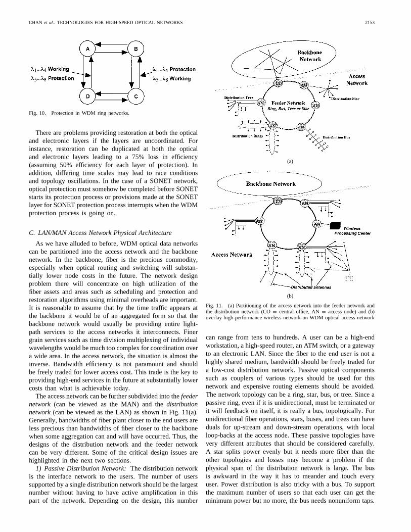
Electronic recovery mechanisms, e.g., as is done in SONET,can also be used to protect against failures at the opticallayer such as a fiber cut or a malfunctioning optical switch.Therefore, at first sight, it might appear that optical layerrecovery is not needed. There are, however, three significantadvantages to providing protection and restoration optically.First, optical layer recovery can protect electronic servicesthat do not have built-in recovery mechanisms or whoserecovery mechanisms are slow (e.g., IP). Second, in manycases, optical layer recovery is simpler, more natural, andprovides enhanced reliability. For instance, consider the caseof 32 SONET rings being supported over a WDM ringnetwork with 32 wavelengths. Without optical protection, eachof the 32 SONET rings would need to individually recoverfrom a single fiber cut, e.g., by loop-back in a SONETbidirectional ring network. On the other hand, the fiber cutcan be optically restored with a simple 22 optical switch,thereby simultaneously restoring service to many electronicconnections. Protection at the optical layer has the addedadvantage that the failure is transparent to SONET, allowingeach SONET ring to individually respond to additional failuressuch as a line card failure. If protection were only performedelectronically, there would be no guarantee that the SONETring would be resilient to both a fiber cut and a line card failure.Finally, optical recovery allows the construction of arbitraryvirtual topologies resilient to fiber failures. For instance,consider IP routers connected in a virtual ring topology over aWDM ring. Traffic may dictate that the IP routers be connectedsuch that more than one IP link travels over the same fiber andhence a single fiber cut will disrupt many IP links. Since ringsare in general only resilient to a single link failure, a singlefiber cut of the optical ring may disconnect the electronicring. Optical layer restoration solves this problem by restoringthe fiber directly. For a simple example of optical loop-backprotection, consider the two fiber bidirectional ring shown inFig. 10. On each ring half of the wavelengths are used forworking traffic and the other half are reserved for protectionagainst a cut in the fiber on the other ring. In the event of a fibercut, the wavelengths from the cut fiber can be switched ontothe uncut fiber, using a two-by-two switch at the node beforethe fiber cut. These wavelengths can then be looped back tobypass the cut fiber and rejoin their original ring using anotherswitch at the node immediately following the fiber cut.
CHAN et al.: TECHNOLOGIES FOR HIGH-SPEED OPTICAL NETWORKS 2153
Fig. 10. Protection in WDM ring networks.
There are problems providing restoration at both the opticaland electronic layers if the layers are uncoordinated. Forinstance, restoration can be duplicated at both the opticaland electronic layers leading to a 75% loss in efficiency(assuming 50% efficiency for each layer of protection). Inaddition, differing time scales may lead to race conditionsand topology oscillations. In the case of a SONET network,optical protection must somehow be completed before SONETstarts its protection process or provisions made at the SONETlayer for SONET protection process interrupts when the WDMprotection process is going on.
C. LAN/MAN Access Network Physical Architecture
As we have alluded to before, WDM optical data networkscan be partitioned into the access network and the backbonenetwork. In the backbone, fiber is the precious commodity,especially when optical routing and switching will substan-tially lower node costs in the future. The network designproblem there will concentrate on high utilization of thefiber assets and areas such as scheduling and protection andrestoration algorithms using minimal overheads are important.It is reasonable to assume that by the time traffic appears atthe backbone it would be of an aggregated form so that thebackbone network would usually be providing entire light-path services to the access networks it interconnects. Finergrain services such as time division multiplexing of individualwavelengths would be much too complex for coordination overa wide area. In the access network, the situation is almost theinverse. Bandwidth efficiency is not paramount and shouldbe freely traded for lower access cost. This trade is the key toproviding high-end services in the future at substantially lowercosts than what is achievable today.
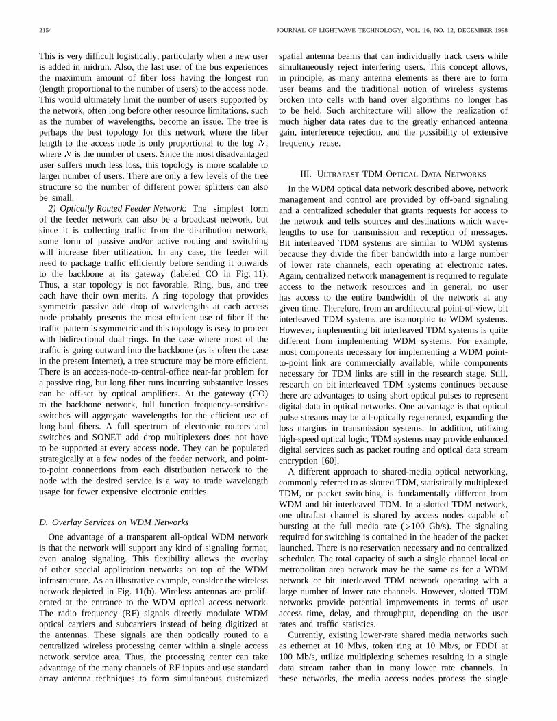
The access network can be further subdivided into thefeedernetwork (can be viewed as the MAN) and thedistributionnetwork(can be viewed as the LAN) as shown in Fig. 11(a).Generally, bandwidths of fiber plant closer to the end users areless precious than bandwidths of fiber closer to the backbonewhen some aggregation can and will have occurred. Thus, thedesigns of the distribution network and the feeder networkcan be very different. Some of the critical design issues arehighlighted in the next two sections.
1) Passive Distribution Network:The distribution networkis the interface network to the users. The number of userssupported by a single distribution network should be the largestnumber without having to have active amplification in thispart of the network. Depending on the design, this number
(a)
(b)
Fig. 11. (a) Partitioning of the access network into the feeder network andthe distribution network (CO= central office, AN= access node) and (b)overlay high-performance wireless network on WDM optical access network
can range from tens to hundreds. A user can be a high-endworkstation, a high-speed router, an ATM switch, or a gatewayto an electronic LAN. Since the fiber to the end user is not ahighly shared medium, bandwidth should be freely traded fora low-cost distribution network. Passive optical componentssuch as couplers of various types should be used for thisnetwork and expensive routing elements should be avoided.The network topology can be a ring, star, bus, or tree. Since apassive ring, even if it is unidirectional, must be terminated orit will feedback on itself, it is really a bus, topologically. Forunidirectional fiber operations, stars, buses, and trees can haveduals for up-stream and down-stream operations, with localloop-backs at the access node. These passive topologies havevery different attributes that should be considered carefully.A star splits power evenly but it needs more fiber than theother topologies and losses may become a problem if thephysical span of the distribution network is large. The busis awkward in the way it has to meander and touch everyuser. Power distribution is also tricky with a bus. To supportthe maximum number of users so that each user can get theminimum power but no more, the bus needs nonuniform taps.
2154 JOURNAL OF LIGHTWAVE TECHNOLOGY, VOL. 16, NO. 12, DECEMBER 1998
This is very difficult logistically, particularly when a new useris added in midrun. Also, the last user of the bus experiencesthe maximum amount of fiber loss having the longest run(length proportional to the number of users) to the access node.This would ultimately limit the number of users supported bythe network, often long before other resource limitations, suchas the number of wavelengths, become an issue. The tree isperhaps the best topology for this network where the fiberlength to the access node is only proportional to the log,where is the number of users. Since the most disadvantageduser suffers much less loss, this topology is more scalable tolarger number of users. There are only a few levels of the treestructure so the number of different power splitters can alsobe small.
2) Optically Routed Feeder Network:The simplest formof the feeder network can also be a broadcast network, butsince it is collecting traffic from the distribution network,some form of passive and/or active routing and switchingwill increase fiber utilization. In any case, the feeder willneed to package traffic efficiently before sending it onwardsto the backbone at its gateway (labeled CO in Fig. 11).Thus, a star topology is not favorable. Ring, bus, and treeeach have their own merits. A ring topology that providessymmetric passive add–drop of wavelengths at each accessnode probably presents the most efficient use of fiber if thetraffic pattern is symmetric and this topology is easy to protectwith bidirectional dual rings. In the case where most of thetraffic is going outward into the backbone (as is often the casein the present Internet), a tree structure may be more efficient.There is an access-node-to-central-office near-far problem fora passive ring, but long fiber runs incurring substantive lossescan be off-set by optical amplifiers. At the gateway (CO)to the backbone network, full function frequency-sensitive-switches will aggregate wavelengths for the efficient use oflong-haul fibers. A full spectrum of electronic routers andswitches and SONET add–drop multiplexers does not haveto be supported at every access node. They can be populatedstrategically at a few nodes of the feeder network, and point-to-point connections from each distribution network to thenode with the desired service is a way to trade wavelengthusage for fewer expensive electronic entities.
D. Overlay Services on WDM Networks
One advantage of a transparent all-optical WDM networkis that the network will support any kind of signaling format,even analog signaling. This flexibility allows the overlayof other special application networks on top of the WDMinfrastructure. As an illustrative example, consider the wirelessnetwork depicted in Fig. 11(b). Wireless antennas are prolif-erated at the entrance to the WDM optical access network.The radio frequency (RF) signals directly modulate WDMoptical carriers and subcarriers instead of being digitized atthe antennas. These signals are then optically routed to acentralized wireless processing center within a single accessnetwork service area. Thus, the processing center can takeadvantage of the many channels of RF inputs and use standardarray antenna techniques to form simultaneous customized
spatial antenna beams that can individually track users whilesimultaneously reject interfering users. This concept allows,in principle, as many antenna elements as there are to formuser beams and the traditional notion of wireless systemsbroken into cells with hand over algorithms no longer hasto be held. Such architecture will allow the realization ofmuch higher data rates due to the greatly enhanced antennagain, interference rejection, and the possibility of extensivefrequency reuse.
III. U LTRAFAST TDM OPTICAL DATA NETWORKS
In the WDM optical data network described above, networkmanagement and control are provided by off-band signalingand a centralized scheduler that grants requests for access tothe network and tells sources and destinations which wave-lengths to use for transmission and reception of messages.Bit interleaved TDM systems are similar to WDM systemsbecause they divide the fiber bandwidth into a large numberof lower rate channels, each operating at electronic rates.Again, centralized network management is required to regulateaccess to the network resources and in general, no userhas access to the entire bandwidth of the network at anygiven time. Therefore, from an architectural point-of-view, bitinterleaved TDM systems are isomorphic to WDM systems.However, implementing bit interleaved TDM systems is quitedifferent from implementing WDM systems. For example,most components necessary for implementing a WDM point-to-point link are commercially available, while componentsnecessary for TDM links are still in the research stage. Still,research on bit-interleaved TDM systems continues becausethere are advantages to using short optical pulses to representdigital data in optical networks. One advantage is that opticalpulse streams may be all-optically regenerated, expanding theloss margins in transmission systems. In addition, utilizinghigh-speed optical logic, TDM systems may provide enhanceddigital services such as packet routing and optical data streamencryption [60].
A different approach to shared-media optical networking,commonly referred to as slotted TDM, statistically multiplexedTDM, or packet switching, is fundamentally different fromWDM and bit interleaved TDM. In a slotted TDM network,one ultrafast channel is shared by access nodes capable ofbursting at the full media rate (100 Gb/s). The signalingrequired for switching is contained in the header of the packetlaunched. There is no reservation necessary and no centralizedscheduler. The total capacity of such a single channel local ormetropolitan area network may be the same as for a WDMnetwork or bit interleaved TDM network operating with alarge number of lower rate channels. However, slotted TDMnetworks provide potential improvements in terms of useraccess time, delay, and throughput, depending on the userrates and traffic statistics.
Currently, existing lower-rate shared media networks suchas ethernet at 10 Mb/s, token ring at 10 Mb/s, or FDDI at100 Mb/s, utilize multiplexing schemes resulting in a singledata stream rather than in many lower rate channels. Inthese networks, the media access nodes process the single

CHAN et al.: TECHNOLOGIES FOR HIGH-SPEED OPTICAL NETWORKS 2155
stream data at the full media rate electronically. However,extensive data processing at 100 Gb/s rates is currently notfeasible. Therefore, much of the data processing in a high-speed optical network will be performed at the slot rate,10–100 Mslot/s, with some rudimentary processing, such asaddress recognition, performed by optical logic at the bus rate.As the high-speed optical processing components mature, webelieve that slotted TDM networks will be the obvious choiceto provide packet service in networks where users are capableof bursting at very high data rates. However, even if the usersof the optical network are operating at lower data rates, themedia access control (MAC) protocol is simpler in a slottedTDM system and may be able to more efficiently providebandwidth-on-demand (BOD) services to a set of lower-rateusers. In the following sections of this paper, we will describeour work on architecture and technology development for anultrafast, slotted TDM multiaccess network.
A. HLAN Architecture
The optical TDM network we envision will run at a bus rateof at least 100 Gb/s but will serve a heterogeneous populationof users such as high-end single users, high speed videoservers, terabyte media banks and networks of supercomputers,operating at speeds from 1 to 100 Gb/s. The most importantfeatures of the network are to provide a backbone to intercon-nect high-speed networks, to transfer quickly very large datablocks, to switch large aggregations of traffic, and to provideflexible, lower-rate access to users. Although we are designinga 100 Gb/s network, the architecture will be scalable to muchhigher rates.
There are two characteristics of these 100 Gb/s slotted TDMnetworks that significantly impact the architectural design.First, they operate with long propagation delays, i.e., there aremany data packets in flight at one time in the network, a high-latency environment. The well-known protocols governingtoday’s electronic packet networks, where a typical latency “”may range from – , were never designed to operatein high-latency networks. Here, “” is the packet propagationtime divided by the packet transmission time. For example, inethernet-based networks, “” must remain much less than onein order to maintain reasonably high throughputs. In extendingthe operating rate of standard (10 Mb/s) ethernet to 100 Mb/sand Gigabit speeds, certain restrictions are necessary. For 100Mb/s ethernet, the physical length of the data bus is limitedto spans less than 100 m. Alternatively, a switch may beinserted in the bus that gives each transmitter its own line, sothat collisions are impossible. For Gigabit ethernet, to assurecollisions could be detected a data bus of 10 m is required.This length is not practical so the Gigabit ethernet bus iskept at 100 m but he minimum packet length is extended.Alternatively, a switch may be inserted in the bus as in the100 Mb/s ethernet case. Clearly, these extension techniqueswill not scale gracefully to 100 Gb/s.
The optical TDM network we envision will have thousandsof packets of data in flight in the network at any given moment( ). To study how standard protocols would performin this high latency environment, we performed simulations to
Fig. 12. Network utilization as a function of latency for ethernet, token ring,FDDI, and HLAN protocols. This calculation assumes a 10-Kb message sizeand a 100-km network.
predict the network utilization as a function of the latency inthe network for a 1-Mb/s ethernet protocol, a 10 Mb/s tokenring protocol and a 15-Mb/s FDDI protocol. The results, shownin Fig. 12, indicate that existing protocols will not scale toultrahigh speed optical TDM networks.
Second, there is a limited amount of processing that canbe performed at the 100 Gb/s rate. These two characteristics,high latency and limited processing, make it difficult to providesimultaneously guaranteed bandwidth (GBW) and bandwidth-on-demand (BOD) services. Also, it is difficult to insureboth efficient and “fair” bandwidth sharing in the presence ofmoderately loaded or overloaded network traffic conditions.
The algorithms designed to manage the network must besimple enough to be executable with a minimal amount ofprocessing available at the optical bit rate. There have beensome articles addressing these problems in the literature [61],[62], but they do not appear to satisfy simultaneously all ofthe above criteria. We have developed a frame-based slottedarchitecture called HLAN (helical local area network) [63],[64] which satisfies the above criteria. In early work, theHLAN architecture was implemented on a helical ring physicalstructure, but most recently has been explained using a foldedbus implementation.
HLAN is a frame-based architecture, which is implementedon a folded unidirectional bus as shown in Fig. 13. A head-end generates frames of empty slots and puts them on thebus. Guaranteed bandwidth traffic is transmitted on the GBWsegment, bandwidth on demand traffic is transmitted on theBOD segment and data is received on the RCV segment.Note that only one bus is required and that all receivers aredownstream of the transmitters. GBW services are providedto users who request them by the head-end. The head-endallocates reserved slots to the node on the GBW segment.Users can access the HLAN at their guaranteed rate using onlya counter, a flip-flop, a few gates, and slot marker detectionlogic [63], [64]. Using existing logic, HLAN slot rates of10–100 Mslots/s can be supported.
Fair and efficient BOD service is provided via the BODsegment. The head-end creates credits and distributes them at
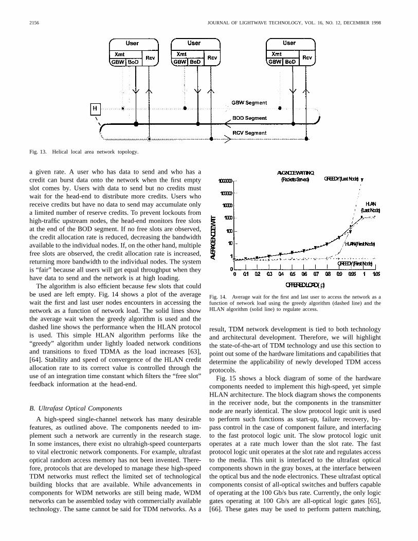
2156 JOURNAL OF LIGHTWAVE TECHNOLOGY, VOL. 16, NO. 12, DECEMBER 1998
Fig. 13. Helical local area network topology.
a given rate. A user who has data to send and who has acredit can burst data onto the network when the first emptyslot comes by. Users with data to send but no credits mustwait for the head-end to distribute more credits. Users whoreceive credits but have no data to send may accumulate onlya limited number of reserve credits. To prevent lockouts fromhigh-traffic upstream nodes, the head-end monitors free slotsat the end of the BOD segment. If no free slots are observed,the credit allocation rate is reduced, decreasing the bandwidthavailable to the individual nodes. If, on the other hand, multiplefree slots are observed, the credit allocation rate is increased,returning more bandwidth to the individual nodes. The systemis “fair” because all users will get equal throughput when theyhave data to send and the network is at high loading.
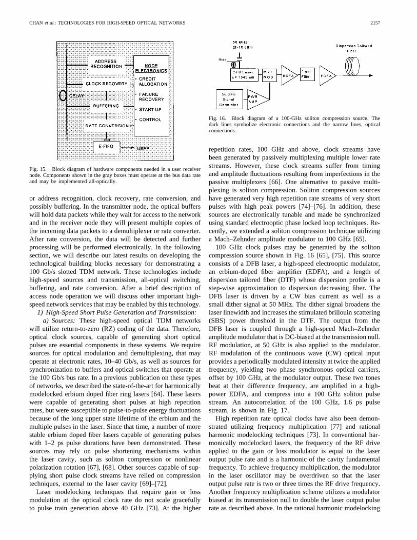
The algorithm is also efficient because few slots that couldbe used are left empty. Fig. 14 shows a plot of the averagewait the first and last user nodes encounters in accessing thenetwork as a function of network load. The solid lines showthe average wait when the greedy algorithm is used and thedashed line shows the performance when the HLAN protocolis used. This simple HLAN algorithm performs like the“greedy” algorithm under lightly loaded network conditionsand transitions to fixed TDMA as the load increases [63],[64]. Stability and speed of convergence of the HLAN creditallocation rate to its correct value is controlled through theuse of an integration time constant which filters the “free slot”feedback information at the head-end.
B. Ultrafast Optical Components
A high-speed single-channel network has many desirablefeatures, as outlined above. The components needed to im-plement such a network are currently in the research stage.In some instances, there exist no ultrahigh-speed counterpartsto vital electronic network components. For example, ultrafastoptical random access memory has not been invented. There-fore, protocols that are developed to manage these high-speedTDM networks must reflect the limited set of technologicalbuilding blocks that are available. While advancements incomponents for WDM networks are still being made, WDMnetworks can be assembled today with commercially availabletechnology. The same cannot be said for TDM networks. As a
Fig. 14. Average wait for the first and last user to access the network as afunction of network load using the greedy algorithm (dashed line) and theHLAN algorithm (solid line) to regulate access.
result, TDM network development is tied to both technologyand architectural development. Therefore, we will highlightthe state-of-the-art of TDM technology and use this section topoint out some of the hardware limitations and capabilities thatdetermine the applicability of newly developed TDM accessprotocols.
Fig. 15 shows a block diagram of some of the hardwarecomponents needed to implement this high-speed, yet simpleHLAN architecture. The block diagram shows the componentsin the receiver node, but the components in the transmitternode are nearly identical. The slow protocol logic unit is usedto perform such functions as start-up, failure recovery, by-pass control in the case of component failure, and interfacingto the fast protocol logic unit. The slow protocol logic unitoperates at a rate much lower than the slot rate. The fastprotocol logic unit operates at the slot rate and regulates accessto the media. This unit is interfaced to the ultrafast opticalcomponents shown in the gray boxes, at the interface betweenthe optical bus and the node electronics. These ultrafast opticalcomponents consist of all-optical switches and buffers capableof operating at the 100 Gb/s bus rate. Currently, the only logicgates operating at 100 Gb/s are all-optical logic gates [65],[66]. These gates may be used to perform pattern matching,
CHAN et al.: TECHNOLOGIES FOR HIGH-SPEED OPTICAL NETWORKS 2157
Fig. 15. Block diagram of hardware components needed in a user receivernode. Components shown in the gray boxes must operate at the bus data rateand may be implemented all-optically.
or address recognition, clock recovery, rate conversion, andpossibly buffering. In the transmitter node, the optical bufferswill hold data packets while they wait for access to the networkand in the receiver node they will present multiple copies ofthe incoming data packets to a demultiplexer or rate converter.After rate conversion, the data will be detected and furtherprocessing will be performed electronically. In the followingsection, we will describe our latest results on developing thetechnological building blocks necessary for demonstrating a100 Gb/s slotted TDM network. These technologies includehigh-speed sources and transmission, all-optical switching,buffering, and rate conversion. After a brief description ofaccess node operation we will discuss other important high-speed network services that may be enabled by this technology.
1) High-Speed Short Pulse Generation and Transmission:a) Sources:These high-speed optical TDM networks
will utilize return-to-zero (RZ) coding of the data. Therefore,optical clock sources, capable of generating short opticalpulses are essential components in these systems. We requiresources for optical modulation and demultiplexing, that mayoperate at electronic rates, 10–40 Gb/s, as well as sources forsynchronization to buffers and optical switches that operate atthe 100 Gb/s bus rate. In a previous publication on these typesof networks, we described the state-of-the-art for harmonicallymodelocked erbium doped fiber ring lasers [64]. These laserswere capable of generating short pulses at high repetitionrates, but were susceptible to pulse-to-pulse energy fluctuationsbecause of the long upper state lifetime of the erbium and themultiple pulses in the laser. Since that time, a number of morestable erbium doped fiber lasers capable of generating pulseswith 1–2 ps pulse durations have been demonstrated. Thesesources may rely on pulse shortening mechanisms withinthe laser cavity, such as soliton compression or nonlinearpolarization rotation [67], [68]. Other sources capable of sup-plying short pulse clock streams have relied on compressiontechniques, external to the laser cavity [69]–[72].
Laser modelocking techniques that require gain or lossmodulation at the optical clock rate do not scale gracefullyto pulse train generation above 40 GHz [73]. At the higher
Fig. 16. Block diagram of a 100-GHz soliton compression source. Thedark lines symbolize electronic connections and the narrow lines, opticalconnections.
repetition rates, 100 GHz and above, clock streams havebeen generated by passively multiplexing multiple lower ratestreams. However, these clock streams suffer from timingand amplitude fluctuations resulting from imperfections in thepassive multiplexers [66]. One alternative to passive multi-plexing is soliton compression. Soliton compression sourceshave generated very high repetition rate streams of very shortpulses with high peak powers [74]–[76]. In addition, thesesources are electronically tunable and made be synchronizedusing standard electrooptic phase locked loop techniques. Re-cently, we extended a soliton compression technique utilizinga Mach–Zehnder amplitude modulator to 100 GHz [65].
100 GHz clock pulses may be generated by the solitoncompression source shown in Fig. 16 [65], [75]. This sourceconsists of a DFB laser, a high-speed electrooptic modulator,an erbium-doped fiber amplifier (EDFA), and a length ofdispersion tailored fiber (DTF) whose dispersion profile is astep-wise approximation to dispersion decreasing fiber. TheDFB laser is driven by a CW bias current as well as asmall dither signal at 50 MHz. The dither signal broadens thelaser linewidth and increases the stimulated brillouin scattering(SBS) power threshold in the DTF. The output from theDFB laser is coupled through a high-speed Mach–Zehnderamplitude modulator that is DC-biased at the transmission null.RF modulation, at 50 GHz is also applied to the modulator.RF modulation of the continuous wave (CW) optical inputprovides a periodically modulated intensity at twice the appliedfrequency, yielding two phase synchronous optical carriers,offset by 100 GHz, at the modulator output. These two tonesbeat at their difference frequency, are amplified in a high-power EDFA, and compress into a 100 GHz soliton pulsestream. An autocorrelation of the 100 GHz, 1.6 ps pulsestream, is shown in Fig. 17.
High repetition rate optical clocks have also been demon-strated utilizing frequency multiplication [77] and rationalharmonic modelocking techniques [73]. In conventional har-monically modelocked lasers, the frequency of the RF driveapplied to the gain or loss modulator is equal to the laseroutput pulse rate and is a harmonic of the cavity fundamentalfrequency. To achieve frequency multiplication, the modulatorin the laser oscillator may be overdriven so that the laseroutput pulse rate is two or three times the RF drive frequency.Another frequency multiplication scheme utilizes a modulatorbiased at its transmission null to double the laser output pulserate as described above. In the rational harmonic modelocking

2158 JOURNAL OF LIGHTWAVE TECHNOLOGY, VOL. 16, NO. 12, DECEMBER 1998
Fig. 17. Autocorrelation of the 100 GHz stream of 1.6 ps pulses generatedby the soliton compression source shown in Fig. 16.
approach, the ratio of the RF drive frequency to the cavityfundamental is a noninteger rational number. In this case, thelaser output pulse rate is the least common multiple of the RFrate and the cavity fundamental [77]. In this rational harmonictechnique, pulses circulating in the optical oscillator are shiftedwith respect to the RF gain or loss modulation by a fractionof that RF drive period on each round trip. After a number ofround trips, equal to the ratio of the data rate to the modulationrate, a high-rate effective modulator response is realized.
b) Transmission:An important issue affecting the suc-cess of any future testbed demonstration is the propagationof 100 Gb/s data packets over 100 km long lengths of fiber.Recently, 640 Gb/s single-stream soliton transmission wasdemonstrated over a 60 km link [78]. In that experiment,the transmission distance was limited by polarization modedispersion (PMD). In another transmission scheme, multihun-dred Gb/s TDM streams have been propagated over near-zerodispersion fiber links with low optical powers [79], [80].Using low optical powers minimizes nonlinear effects in thefiber and low dispersion minimizes pulse spreading. However,in a multiaccess network there will be large gain and lossvariations along the fiber bus and it may be difficult torestrict the entire fiber span to zero-dispersion fiber. Still,transmission of 100 Gb/s data streams over long distances atlarge amplifier spacings may be possible if dispersion managedfiber links and all-optical regenerators are used. Dispersionmanaged soliton transmission is a hot research topic andmany exciting theoretical results have recently been reported[81]–[85]. However experimental studies of the limitations ofthis new transmission scheme for 100 Gb/s data streams havenot been reported. Another method that may be used to extendthe propagation distance for ultrafast data streams is opticalregeneration. A regenerator consists of a clock recovery unitand an optical switch. The clock recovery unit synchronizesa local clock with the incoming data stream. The incomingdata stream and the synchronized clock become the logicalinputs to an optical AND gate and the noisy input data signalis transferred to the local clock signal. The regenerator outputis an optical data stream that has been retimed and reshaped.If the regenerators are placed closely enough, transmission
distances may become limitless. All-optical regenerators havebeen demonstrated [86]–[88], and will be discussed further inthe section on optical switching applications.
2) User Node Data Processing:a) Address recognition:In electronic networks, address
recognition is a straightforward process and is usually doneby loading the received address into a register and comparingit with a stored bit pattern. For very-fast photonic networks,storing an address in a register and accessing it randomlyis problematic. Attractive solutions for address recognition invery-fast photonic networks include source signal coding andorthogonal signal coding. Source signal coding includes spe-cial flag codes in the address stream that are prohibited in thepacket data stream. Source signal coding can simplify systemdesign but usually involves special hardware to encode thedata and uses extra signaling bandwidth. In the optical domainsuch hardware may be impractical. Orthogonal signal codinghas the potential to take advantage of the special properties ofoptical transmission and conserve data bandwidth. Wavelengthand time are two dimensions that one can use for orthogonalsignal coding. Signaling in a separate wavelength is attractivebecause it is easy and inexpensive in the optical domain butdispersion may delay the signaling channel differently fordifferent receivers in a distributed network. Using the timedimension for signaling, such as using special marker codesor self-synchronizing codes, is attractive because the signalcoding travels on the same path as the data and remainsinvariant in a distributed network. In initial experiments, self-synchronizing codes have been implemented using uniquelyspaced pulse pairs [89] and different amplitude marker pulses[90] to signify the beginning of the address stream. Thedetermination of this absolute phase of the data packet is calledstream capture. After stream capture, ultrahigh-speed addressrecognition can be performed using all-optical logic gates.
All-optical logic gates and switches have been investigatedprimarily for wavelength conversion of high-speed data signalsin WDM systems and for demultiplexing in bit-interleavedTDM systems. For TDM applications, all-optical AND andNOT functions have been demonstrated using four-wave-mixing in waveguides [91], [92], cross-phase/gain modulationin nonlinear optical loop mirrors (NOLM’s) [93]–[95], semi-conductor NOLM’s [96], [97], Mach–Zehnder devices [98],[99], and ultrafast nonlinear interferometers [100]–[102].
Optical switches fundamentally rely on material nonlinear-ities. While many optical switching experiments have utilizedgain and absorption nonlinearities in optical waveguides, muchmore popular have been demonstrations utilizing interferomet-ric switches containing materials whose refractive index isintensity-dependent [103]. Interferometric switches are popularbecause they are the most versatile, capable of demonstratingAND, NOT, and XOR functionality using a single switch con-figuration. As an example, consider the simple Mach–Zehnderinterferometer shown in Fig. 18. To operate as an opticalswitch, at least one arm in the interferometer must containa material whose refractive index,, is intensity dependent,
. Here, is the linear refractive index,is the nonlinear refractive index coefficient and is theintensity of light. Then, assuming the beamsplitters in the
CHAN et al.: TECHNOLOGIES FOR HIGH-SPEED OPTICAL NETWORKS 2159
Fig. 18. Nonlinear Mach–Zehnder interferometer.
interferometer have a 50/50 splitting ratio, the interferometeroutput signal intensity is related to the input signal intensityby . Here, is the initial phase(length) difference between the two arms of the interferometerand is the phase difference inducedby the presence of a control beam with intensity. In thisexpression, is the interaction length of the signal and controlpulses and is the wavelength of the light. The control pulsesmay be distinguished from the signal pulses by wavelength,polarization, or the direction of propagation. From this simplepicture it is clear that to obtain all-optical switching, that ischanging the interferometer transmission from a maximum to aminimum, or vice versa, it is necessary to induce a phase shiftof in the nonlinear material. The peak intensity necessary toinduce this phase shift is given by . In opticalfiber, is approximately 2.8 10 16 cm2/W. A rule ofthumb is that an optical control pulse with a peak power of1 W, will induce a phase shift in a fiber interaction lengthof 1 km.
In the most common interferometric switch demonstratedto date, a 50/50 fiber coupler and a long length of opticalfiber are used to construct a Sagnac interferometer. Thistype of interferometric switch has been referred to as anonlinear optical loop mirror. Fiber has been a commonswitching material because the refractive index nonlinearity,owing to the Kerr effect, is essentially instantaneous and hasno corresponding transmission nonlinearity. Therefore, terabitper second switching may be possible in these fiber gates. Thedisadvantage of using fiber as the nonlinear material is thatis relatively small, and long interaction lengths are necessaryto achieve reasonable switching energies. Long fiber lengthsin optical switches are undesirable because of pulse distortioneffects and the large physical size of the device. Still, manyimportant network components have been demonstrated usingfiber based NOLM’s.
For example, all-optical address recognition has beendemonstrated using a NOLM configured as an XOR gate.While previous experiments utilized AND gates based on four-wave-mixing in semiconductor optical amplifiers (SOA’s) toperform address recognition, the number of potential addresseswas limited to a fixed set of “keywords” because some addresspatterns could be matched by patterns other than their logicalcompliment [104]. Using all-optical XOR gates to performaddress recognition removes the limitation on the availablenumber of keywords. Also, utilizing XOR gates in the address
Fig. 19. NOLM configured for XOR operation.
recognition circuit may facilitate the recognition of morethan one address per hardwired node. For example, a singlecircuit might be able to recognize a local address as well asa broadcast address.
We have demonstrated all-optical pattern generation andmatching at 10 Gb/s using a NOLM configured as an XORgate as shown in Fig. 19 [105]. Clock pulses are coupled tothe input port of the NOLM, are split at the fiber couplerinto two counterpropagating components that traverse the 2-km length of fiber, and are interfered back at the coupler. Inthe absence of a control pulse, the recombined clock pulsesexit the NOLM through the input port. In other words, forzero control input to the NOLM, there is zero signal (clock)output through the output port. A control pulse, coupledinto either of the two control ports shown, will copropagatewith one of the clock components and nonlinearly shift itsphase via cross-phase modulation. The control peak poweris chosen to induce a phase shift ofon the copropagatingclock component pulse, thereby switching the NOLM fromthe reflecting state to the transmitting state. At the outputport of the NOLM, an optical bandpass filter distinguishes theswitched out signal (clock) pulses from the control pulses. If acontrol pulse is simultaneously present at each control port,both counterpropagating clock components are nonlinearlyphase shifted by cross phase modulation and the interferometerremains in the reflecting state. Therefore, the NOLM actsas an all-optical XOR, with the two control streams as thelogical inputs to the gate. Fig. 20(a) and (b) shows the outputfrom the NOLM when a controlling data pattern is presentat control port 1 only, and control port 2 only. Fig. 20(c)shows the output from the NOLM when both control signalsare simultaneously present at the switch. Note the excellentcontrast ratio (25 : 1) at the output of the all-optical XOR gate.
b) Clock recovery:Besides self-synchronizing codes,the most likely form of clock recovery for a slottedOTDM access node will be phase synchronization usingall-optical or electrooptic phase locked loops. Picosecondaccuracy synchronization of 40 GHz clock streams has beendemonstrated using electrooptic phase locked loops [94].Typical lockup times have been on the order of microseconds,the equivalent of 10–100 slot times, but improvements inthe lock-up time are expected using specialized electroniccircuits. Much slower lock-up times have been demonstratedfor all-optical clock (typically laser injection locking) recovery
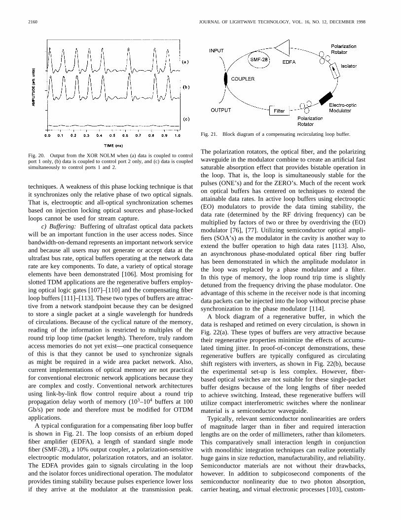
2160 JOURNAL OF LIGHTWAVE TECHNOLOGY, VOL. 16, NO. 12, DECEMBER 1998
Fig. 20. Output from the XOR NOLM when (a) data is coupled to controlport 1 only, (b) data is coupled to control port 2 only, and (c) data is coupledsimultaneously to control ports 1 and 2.
techniques. A weakness of this phase locking technique is thatit synchronizes only the relative phase of two optical signals.That is, electrooptic and all-optical synchronization schemesbased on injection locking optical sources and phase-lockedloops cannot be used for stream capture.
c) Buffering: Buffering of ultrafast optical data packetswill be an important function in the user access nodes. Sincebandwidth-on-demand represents an important network serviceand because all users may not generate or accept data at theultrafast bus rate, optical buffers operating at the network datarate are key components. To date, a variety of optical storageelements have been demonstrated [106]. Most promising forslotted TDM applications are the regenerative buffers employ-ing optical logic gates [107]–[110] and the compensating fiberloop buffers [111]–[113]. These two types of buffers are attrac-tive from a network standpoint because they can be designedto store a single packet at a single wavelength for hundredsof circulations. Because of the cyclical nature of the memory,reading of the information is restricted to multiples of theround trip loop time (packet length). Therefore, truly randomaccess memories do not yet exist—one practical consequenceof this is that they cannot be used to synchronize signalsas might be required in a wide area packet network. Also,current implementations of optical memory are not practicalfor conventional electronic network applications because theyare complex and costly. Conventional network architecturesusing link-by-link flow control require about a round trippropagation delay worth of memory (103–104 buffers at 100Gb/s) per node and therefore must be modified for OTDMapplications.
A typical configuration for a compensating fiber loop bufferis shown in Fig. 21. The loop consists of an erbium dopedfiber amplifier (EDFA), a length of standard single modefiber (SMF-28), a 10% output coupler, a polarization-sensitiveelectrooptic modulator, polarization rotators, and an isolator.The EDFA provides gain to signals circulating in the loopand the isolator forces unidirectional operation. The modulatorprovides timing stability because pulses experience lower lossif they arrive at the modulator at the transmission peak.
Fig. 21. Block diagram of a compensating recirculating loop buffer.
The polarization rotators, the optical fiber, and the polarizingwaveguide in the modulator combine to create an artificial fastsaturable absorption effect that provides bistable operation inthe loop. That is, the loop is simultaneously stable for thepulses (ONE’s) and for the ZERO’s. Much of the recent workon optical buffers has centered on techniques to extend theattainable data rates. In active loop buffers using electrooptic(EO) modulators to provide the data timing stability, thedata rate (determined by the RF driving frequency) can bemultiplied by factors of two or three by overdriving the (EO)modulator [76], [77]. Utilizing semiconductor optical ampli-fiers (SOA’s) as the modulator in the cavity is another way toextend the buffer operation to high data rates [113]. Also,an asynchronous phase-modulated optical fiber ring bufferhas been demonstrated in which the amplitude modulator inthe loop was replaced by a phase modulator and a filter.In this type of memory, the loop round trip time is slightlydetuned from the frequency driving the phase modulator. Oneadvantage of this scheme in the receiver node is that incomingdata packets can be injected into the loop without precise phasesynchronization to the phase modulator [114].
A block diagram of a regenerative buffer, in which thedata is reshaped and retimed on every circulation, is shown inFig. 22(a). These types of buffers are very attractive becausetheir regenerative properties minimize the effects of accumu-lated timing jitter. In proof-of-concept demonstrations, theseregenerative buffers are typically configured as circulatingshift registers with inverters, as shown in Fig. 22(b), becausethe experimental set-up is less complex. However, fiber-based optical switches are not suitable for these single-packetbuffer designs because of the long lengths of fiber neededto achieve switching. Instead, these regenerative buffers willutilize compact interferometric switches where the nonlinearmaterial is a semiconductor waveguide.
Typically, relevant semiconductor nonlinearities are ordersof magnitude larger than in fiber and required interactionlengths are on the order of millimeters, rather than kilometers.This comparatively small interaction length in conjunctionwith monolithic integration techniques can realize potentiallyhuge gains in size reduction, manufacturability, and reliability.Semiconductor materials are not without their drawbacks,however. In addition to subpicosecond components of thesemiconductor nonlinearity due to two photon absorption,carrier heating, and virtual electronic processes [103], custom-
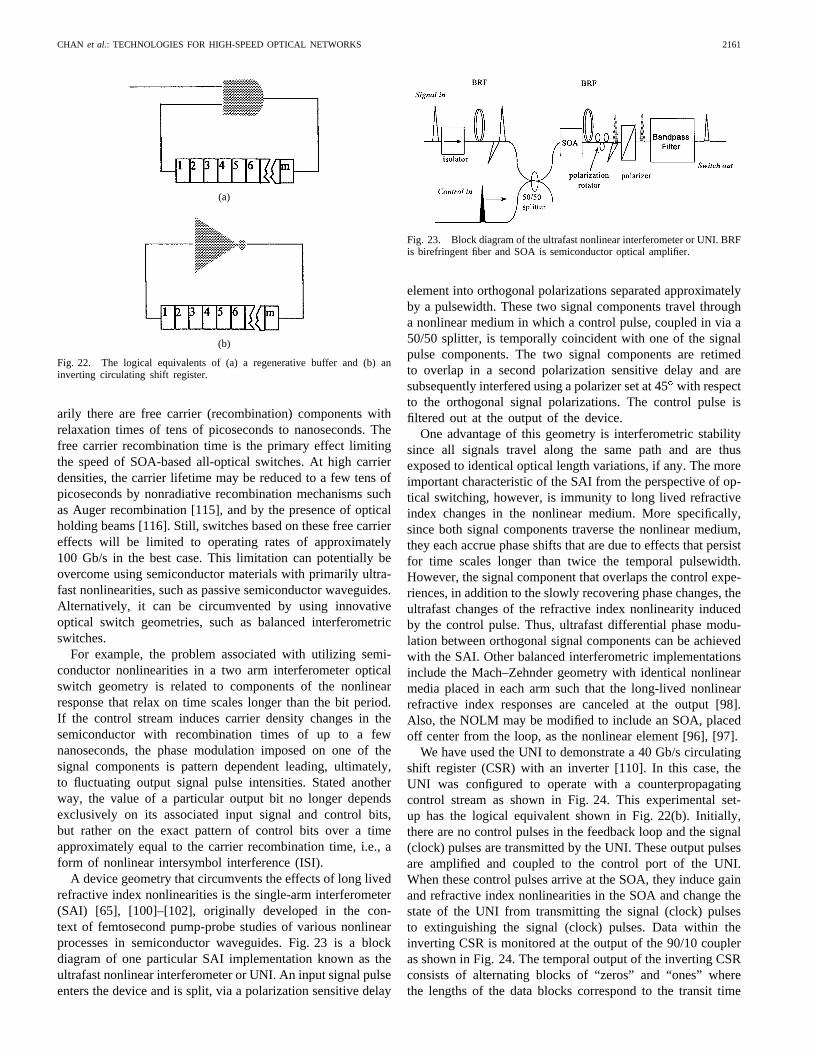
CHAN et al.: TECHNOLOGIES FOR HIGH-SPEED OPTICAL NETWORKS 2161
(a)
(b)
Fig. 22. The logical equivalents of (a) a regenerative buffer and (b) aninverting circulating shift register.
arily there are free carrier (recombination) components withrelaxation times of tens of picoseconds to nanoseconds. Thefree carrier recombination time is the primary effect limitingthe speed of SOA-based all-optical switches. At high carrierdensities, the carrier lifetime may be reduced to a few tens ofpicoseconds by nonradiative recombination mechanisms suchas Auger recombination [115], and by the presence of opticalholding beams [116]. Still, switches based on these free carriereffects will be limited to operating rates of approximately100 Gb/s in the best case. This limitation can potentially beovercome using semiconductor materials with primarily ultra-fast nonlinearities, such as passive semiconductor waveguides.Alternatively, it can be circumvented by using innovativeoptical switch geometries, such as balanced interferometricswitches.
For example, the problem associated with utilizing semi-conductor nonlinearities in a two arm interferometer opticalswitch geometry is related to components of the nonlinearresponse that relax on time scales longer than the bit period.If the control stream induces carrier density changes in thesemiconductor with recombination times of up to a fewnanoseconds, the phase modulation imposed on one of thesignal components is pattern dependent leading, ultimately,to fluctuating output signal pulse intensities. Stated anotherway, the value of a particular output bit no longer dependsexclusively on its associated input signal and control bits,but rather on the exact pattern of control bits over a timeapproximately equal to the carrier recombination time, i.e., aform of nonlinear intersymbol interference (ISI).
A device geometry that circumvents the effects of long livedrefractive index nonlinearities is the single-arm interferometer(SAI) [65], [100]–[102], originally developed in the con-text of femtosecond pump-probe studies of various nonlinearprocesses in semiconductor waveguides. Fig. 23 is a blockdiagram of one particular SAI implementation known as theultrafast nonlinear interferometer or UNI. An input signal pulseenters the device and is split, via a polarization sensitive delay
Fig. 23. Block diagram of the ultrafast nonlinear interferometer or UNI. BRFis birefringent fiber and SOA is semiconductor optical amplifier.
element into orthogonal polarizations separated approximatelyby a pulsewidth. These two signal components travel througha nonlinear medium in which a control pulse, coupled in via a50/50 splitter, is temporally coincident with one of the signalpulse components. The two signal components are retimedto overlap in a second polarization sensitive delay and aresubsequently interfered using a polarizer set at 45with respectto the orthogonal signal polarizations. The control pulse isfiltered out at the output of the device.
One advantage of this geometry is interferometric stabilitysince all signals travel along the same path and are thusexposed to identical optical length variations, if any. The moreimportant characteristic of the SAI from the perspective of op-tical switching, however, is immunity to long lived refractiveindex changes in the nonlinear medium. More specifically,since both signal components traverse the nonlinear medium,they each accrue phase shifts that are due to effects that persistfor time scales longer than twice the temporal pulsewidth.However, the signal component that overlaps the control expe-riences, in addition to the slowly recovering phase changes, theultrafast changes of the refractive index nonlinearity inducedby the control pulse. Thus, ultrafast differential phase modu-lation between orthogonal signal components can be achievedwith the SAI. Other balanced interferometric implementationsinclude the Mach–Zehnder geometry with identical nonlinearmedia placed in each arm such that the long-lived nonlinearrefractive index responses are canceled at the output [98].Also, the NOLM may be modified to include an SOA, placedoff center from the loop, as the nonlinear element [96], [97].
We have used the UNI to demonstrate a 40 Gb/s circulatingshift register (CSR) with an inverter [110]. In this case, theUNI was configured to operate with a counterpropagatingcontrol stream as shown in Fig. 24. This experimental set-up has the logical equivalent shown in Fig. 22(b). Initially,there are no control pulses in the feedback loop and the signal(clock) pulses are transmitted by the UNI. These output pulsesare amplified and coupled to the control port of the UNI.When these control pulses arrive at the SOA, they induce gainand refractive index nonlinearities in the SOA and change thestate of the UNI from transmitting the signal (clock) pulsesto extinguishing the signal (clock) pulses. Data within theinverting CSR is monitored at the output of the 90/10 coupleras shown in Fig. 24. The temporal output of the inverting CSRconsists of alternating blocks of “zeros” and “ones” wherethe lengths of the data blocks correspond to the transit time

2162 JOURNAL OF LIGHTWAVE TECHNOLOGY, VOL. 16, NO. 12, DECEMBER 1998
Fig. 24. Experimental set-up of the circulating shift register with an inverter. The UNI is configured as an inverter and the feedback loop constitutesthe feedback shift register.
Fig. 25. Temporal output from the inverting CSR. The data are detected anddisplayed on a 1-GHz 3-dB bandwidth oscilloscope.
through the feedback loop. In our case, the feedback looplength is approximately 28 m (in fiber) corresponding to atransit time of 142 ns.
Fig. 25 shows the output of the shift register on a mi-crosecond time scale. The data are detected by a high-speedphotodiode and displayed on a 1 GHz analog oscilloscope.Individual pulses in the data stream are not resolved. Thesedata clearly show the alternating blocks or packets of “zeros”and “ones.” The CSR was very stable and these alternatingpackets could be maintained for hours at a time, correspondingto tens of billions of circulations, with no temperature orlength stabilization applied to the feedback loop. Fig. 26(a)shows digital sampling oscilloscope traces of the 40 GHz inputclock stream on a 50 ps time scale. Note that the jitter ofthe displayed pulses is primarily due to timing jitter in theoscilloscope time base (6 ps) and not to timing jitter on thepulses themselves. The timing jitter of the soliton compressionsource is less than 0.5 ps [110]. Fig. 26(b) shows an eye-diagram of the data output from the inverting CSR. Again,the jitter in the data is due to limitations in the detectionelectronics.
d) Rate converters:Data stored in the recirculatingbuffers will be rate converted down to lower rate signalsthat the user node electronics can process. One method forperforming rate conversion is to demultiplex everyth bit ofan -bit long data packet such that and are relativelyprime. The time required to rate convert all of the data bits
(a)
(b)
Fig. 26. (a) Oscilloscope trace of the 40-GHz clock stream used to drivethe inverting CSR and (b) the eye diagram of the data stream output fromthe inverting CSR. The data are displayed on a 45-GHz 3-dB bandwidthoscilloscope.
within a packet using this scheme is where isthe bit period of the original data stream. Unfortunately,such schemes may scramble the data bits and, consequently,require further processing in electronics in order to faithfullyreconstruct the original packet. An alternative method for rateconversion is based on time dilation via optical sampling.This method has the advantage that the rate-converted streamrequires no reordering of bits. The essence of this techniqueis that the aliasing brought about by sampling a high speedoptical stream at a rate lower than the Nyquist rate gives riseto a time dilated version of the packet which can then bedetected and displayed on a low speed analog oscilloscope.The sampling can be achieved via optical cross-correlationin a nonlinear crystal or an optical switch, for example. The
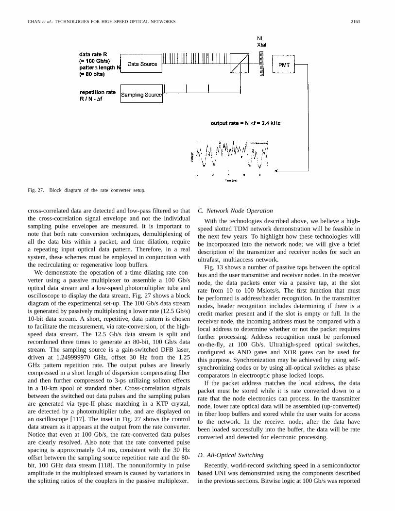
CHAN et al.: TECHNOLOGIES FOR HIGH-SPEED OPTICAL NETWORKS 2163
Fig. 27. Block diagram of the rate converter setup.
cross-correlated data are detected and low-pass filtered so thatthe cross-correlation signal envelope and not the individualsampling pulse envelopes are measured. It is important tonote that both rate conversion techniques, demultiplexing ofall the data bits within a packet, and time dilation, requirea repeating input optical data pattern. Therefore, in a realsystem, these schemes must be employed in conjunction withthe recirculating or regenerative loop buffers.
We demonstrate the operation of a time dilating rate con-verter using a passive multiplexer to assemble a 100 Gb/soptical data stream and a low-speed photomultiplier tube andoscilloscope to display the data stream. Fig. 27 shows a blockdiagram of the experimental set-up. The 100 Gb/s data streamis generated by passively multiplexing a lower rate (12.5 Gb/s)10-bit data stream. A short, repetitive, data pattern is chosento facilitate the measurement, via rate-conversion, of the high-speed data stream. The 12.5 Gb/s data stream is split andrecombined three times to generate an 80-bit, 100 Gb/s datastream. The sampling source is a gain-switched DFB laser,driven at 1.249999970 GHz, offset 30 Hz from the 1.25GHz pattern repetition rate. The output pulses are linearlycompressed in a short length of dispersion compensating fiberand then further compressed to 3-ps utilizing soliton effectsin a 10-km spool of standard fiber. Cross-correlation signalsbetween the switched out data pulses and the sampling pulsesare generated via type-II phase matching in a KTP crystal,are detected by a photomultiplier tube, and are displayed onan oscilloscope [117]. The inset in Fig. 27 shows the controldata stream as it appears at the output from the rate converter.Notice that even at 100 Gb/s, the rate-converted data pulsesare clearly resolved. Also note that the rate converted pulsespacing is approximately 0.4 ms, consistent with the 30 Hzoffset between the sampling source repetition rate and the 80-bit, 100 GHz data stream [118]. The nonuniformity in pulseamplitude in the multiplexed stream is caused by variations inthe splitting ratios of the couplers in the passive multiplexer.
C. Network Node Operation
With the technologies described above, we believe a high-speed slotted TDM network demonstration will be feasible inthe next few years. To highlight how these technologies willbe incorporated into the network node; we will give a briefdescription of the transmitter and receiver nodes for such anultrafast, multiaccess network.
Fig. 13 shows a number of passive taps between the opticalbus and the user transmitter and receiver nodes. In the receivernode, the data packets enter via a passive tap, at the slotrate from 10 to 100 Mslots/s. The first function that mustbe performed is address/header recognition. In the transmitternodes, header recognition includes determining if there is acredit marker present and if the slot is empty or full. In thereceiver node, the incoming address must be compared with alocal address to determine whether or not the packet requiresfurther processing. Address recognition must be performedon-the-fly, at 100 Gb/s. Ultrahigh-speed optical switches,configured as AND gates and XOR gates can be used forthis purpose. Synchronization may be achieved by using self-synchronizing codes or by using all-optical switches as phasecomparators in electrooptic phase locked loops.
If the packet address matches the local address, the datapacket must be stored while it is rate converted down to arate that the node electronics can process. In the transmitternode, lower rate optical data will be assembled (up-converted)in fiber loop buffers and stored while the user waits for accessto the network. In the receiver node, after the data havebeen loaded successfully into the buffer, the data will be rateconverted and detected for electronic processing.
D. All-Optical Switching
Recently, world-record switching speed in a semiconductorbased UNI was demonstrated using the components describedin the previous sections. Bitwise logic at 100 Gb/s was reported
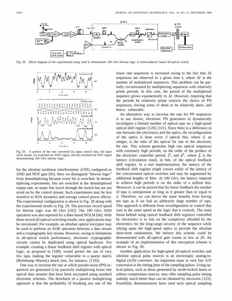
2164 JOURNAL OF LIGHTWAVE TECHNOLOGY, VOL. 16, NO. 12, DECEMBER 1998
Fig. 28. Block diagram of the experimental setup used to demonstrate 100 Gb/s bitwise logic in semiconductor based all-optical switch.
Fig. 29. A portion of the rate converted (a) input control data, (b) inputclock stream, (c) switched-out AND signal, and (d) switched-out NOT signaldemonstrating 100 Gb/s bitwise logic.
for the ultrafast nonlinear interferometer (UNI) configured asAND and NOT gate [65]. Here we distinguish “bitwise logic”from demultiplexing because every bit is switched. In demul-tiplexing experiments, bits are switched at the demultiplexedoutput rate, so many bits travel through the switch but are notacted on by the control stream. Such experiments may be lesssensitive to SOA dynamics and average control power effects.The experimental configuration is shown in Fig. 28 along withthe experimental results in Fig. 29. The previous record speedfor bitwise logic was 40 Gb/s [102]. The 100 Gb/s ANDoperation was also reported for a fiber-based NOLM [66]. Withthese record all-optical switching results, new applications maybe envisioned. For example, an ultrafast optical encrypter maybe used to perform an XOR operation between a data streamand a cryptographic key stream. However, owing to limitationsin all-optical switch performance, electronic cryptographiccircuits cannot be duplicated using optical hardware. Forexample, creating a linear feedback shift register with opticallogic, as proposed in [108], would permit the use of veryfew taps, making the register vulnerable to a sparse matrix(Berlekamp–Massey) attack (see, for instance, [119]).
One way to increase the rate at which pseudo-noise (PN) se-quences are generated is by passively multiplexing lower rateoptical data streams that have been encrypted using standardelectronic schemes. The drawback of a passive multiplexingapproach is that the probability of breaking any one of the
lower rate sequences is increased owing to the fact thatsequences are observed in a given time, where is thenumber of multiplexed sequences. This problem can be par-tially circumvented by multiplexing sequences with relativelyprime periods. In this case, the period of the multiplexedsequence grows exponentially in . However, requiring thatthe periods be relatively prime restricts the choice of PNsequences, forcing some of them to be relatively short, andhence, vulnerable.
An alternative way to increase the rate for PN sequencesis to use slower, electronic PN generators to dynamicallyreconfigure a limited number of optical taps on a high-speedoptical shift register [120], [121]. Since there is a difference inrate between the electronics and the optics, the reconfigurationof the optics is done every optical bits, where , aninteger, is the ratio of the optical bit rate to the electronicbit rate. This scheme generates high rate optical sequenceswith extremely high periods, on the order of the product ofthe electronic controller period, , and , where is thelatency (circulation time), in bits, of the optical feedbackshift register. In a real implementation, the latency of thefeedback shift register might consist solely of the latency ofthe concatenated optical switches and may be augmented byadditional lengths of fiber. At 100 Gb/s, the latency requiredto achieve high periods is on the order of a million bits.Moreover, it can be proved that for linear feedback the numberof taps is unimportant as long as it greater than or equal to
. Therefore, we can derive the same benefits from havingten taps as if we had an arbitrarily large number of taps.This approach is different from reconfiguration or control thatruns at the same speed as the logic that it controls. The mainthrust behind using optical feedback shift registers controlledby electronics is to rely on the complexity afforded by theelectronics for the long-range security of the sequence whilerelying upon the high-speed optics to provide the ultrafastshort-term randomness. We believe this scheme could bedemonstrated with all-optical gate counts as low as 20. Anexample of an implementation of this encryption scheme isshown in Fig. 30.
Another application for high-speed all-optical switches andultrafast optical pulse sources is an electrooptic analog-to-digital (A/D) converter. An important issue in very fast A/Dconversion is the timing jitter of the sampling pulses. Using op-tical pulses, such as those generated by mode-locked lasers orsoliton compression sources, may offer sampling pulse timingstability much better than can be obtained by electronic [123].Feasibility demonstrations have used such optical sampling
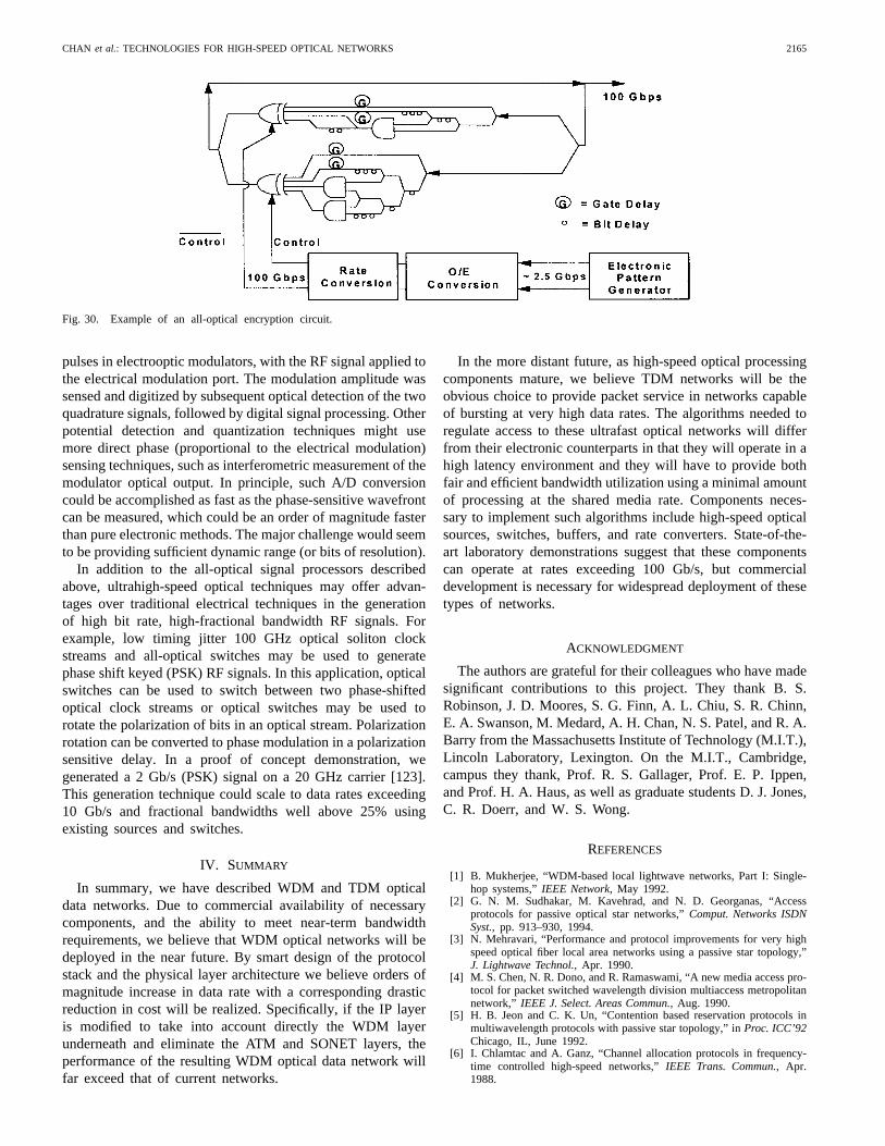
CHAN et al.: TECHNOLOGIES FOR HIGH-SPEED OPTICAL NETWORKS 2165
Fig. 30. Example of an all-optical encryption circuit.
pulses in electrooptic modulators, with the RF signal applied tothe electrical modulation port. The modulation amplitude wassensed and digitized by subsequent optical detection of the twoquadrature signals, followed by digital signal processing. Otherpotential detection and quantization techniques might usemore direct phase (proportional to the electrical modulation)sensing techniques, such as interferometric measurement of themodulator optical output. In principle, such A/D conversioncould be accomplished as fast as the phase-sensitive wavefrontcan be measured, which could be an order of magnitude fasterthan pure electronic methods. The major challenge would seemto be providing sufficient dynamic range (or bits of resolution).
In addition to the all-optical signal processors describedabove, ultrahigh-speed optical techniques may offer advan-tages over traditional electrical techniques in the generationof high bit rate, high-fractional bandwidth RF signals. Forexample, low timing jitter 100 GHz optical soliton clockstreams and all-optical switches may be used to generatephase shift keyed (PSK) RF signals. In this application, opticalswitches can be used to switch between two phase-shiftedoptical clock streams or optical switches may be used torotate the polarization of bits in an optical stream. Polarizationrotation can be converted to phase modulation in a polarizationsensitive delay. In a proof of concept demonstration, wegenerated a 2 Gb/s (PSK) signal on a 20 GHz carrier [123].This generation technique could scale to data rates exceeding10 Gb/s and fractional bandwidths well above 25% usingexisting sources and switches.
IV. SUMMARY
In summary, we have described WDM and TDM opticaldata networks. Due to commercial availability of necessarycomponents, and the ability to meet near-term bandwidthrequirements, we believe that WDM optical networks will bedeployed in the near future. By smart design of the protocolstack and the physical layer architecture we believe orders ofmagnitude increase in data rate with a corresponding drasticreduction in cost will be realized. Specifically, if the IP layeris modified to take into account directly the WDM layerunderneath and eliminate the ATM and SONET layers, theperformance of the resulting WDM optical data network willfar exceed that of current networks.
In the more distant future, as high-speed optical processingcomponents mature, we believe TDM networks will be theobvious choice to provide packet service in networks capableof bursting at very high data rates. The algorithms needed toregulate access to these ultrafast optical networks will differfrom their electronic counterparts in that they will operate in ahigh latency environment and they will have to provide bothfair and efficient bandwidth utilization using a minimal amountof processing at the shared media rate. Components neces-sary to implement such algorithms include high-speed opticalsources, switches, buffers, and rate converters. State-of-the-art laboratory demonstrations suggest that these componentscan operate at rates exceeding 100 Gb/s, but commercialdevelopment is necessary for widespread deployment of thesetypes of networks.
ACKNOWLEDGMENT
The authors are grateful for their colleagues who have madesignificant contributions to this project. They thank B. S.Robinson, J. D. Moores, S. G. Finn, A. L. Chiu, S. R. Chinn,E. A. Swanson, M. Medard, A. H. Chan, N. S. Patel, and R. A.Barry from the Massachusetts Institute of Technology (M.I.T.),Lincoln Laboratory, Lexington. On the M.I.T., Cambridge,campus they thank, Prof. R. S. Gallager, Prof. E. P. Ippen,and Prof. H. A. Haus, as well as graduate students D. J. Jones,C. R. Doerr, and W. S. Wong.
REFERENCES
[1] B. Mukherjee, “WDM-based local lightwave networks, Part I: Single-hop systems,”IEEE Network,May 1992.
[2] G. N. M. Sudhakar, M. Kavehrad, and N. D. Georganas, “Accessprotocols for passive optical star networks,”Comput. Networks ISDNSyst.,pp. 913–930, 1994.
[3] N. Mehravari, “Performance and protocol improvements for very highspeed optical fiber local area networks using a passive star topology,”J. Lightwave Technol.,Apr. 1990.
[4] M. S. Chen, N. R. Dono, and R. Ramaswami, “A new media access pro-tocol for packet switched wavelength division multiaccess metropolitannetwork,” IEEE J. Select. Areas Commun.,Aug. 1990.
[5] H. B. Jeon and C. K. Un, “Contention based reservation protocols inmultiwavelength protocols with passive star topology,” inProc. ICC’92Chicago, IL, June 1992.
[6] I. Chlamtac and A. Ganz, “Channel allocation protocols in frequency-time controlled high-speed networks,”IEEE Trans. Commun.,Apr.1988.

2166 JOURNAL OF LIGHTWAVE TECHNOLOGY, VOL. 16, NO. 12, DECEMBER 1998
[7] F. Jia and B. Mukherejee, “The receiver collision avoidance (RCA)protocol for single hop WDM lightwave networks,” inProc. ICC’92,Chicago, IL, June 1992.
[8] I. M. I. Habib, M. Kavehrad, and C.-E. W. Sundberg, “Protocols forvery high-speed optical fiber local area networks using a passive startopology,” J. Lightwave Technol.,Dec. 1987.
[9] G. N. M. Sudhakar, N. D. Georganas, and M. Kavehrad, “A multichanneloptical star LAN and its application as a broadband switch,” inProc.ICC’92, Chicago, IL, June 1992.
[10] P. Dowd, “Random access protocols for high speed interprocess com-munications based on a passive optical star topology,”J. LightwaveTechnol.,vol. 9, June 1991.
[11] I. P. Kaminowet al., “A wideband all-optical WDM network,”IEEE J.Select. Areas Commun.,June 1996.
[12] E. Modiano, “Unscheduled multicasts in WDM broadcast-and-selectnetworks,” inProc. INFOCOM ’98,San Francisco, CA, Mar. 1998.
[13] M. J. Karol, M. G. Hluchyj, and S. P. Morgan, “Input versus outputqueueing in a space-division packet switch,”IEEE Trans. Commun.,Dec. 1987.
[14] M. G. Hluchyj and M. J. Karol, “Queueing in high-performance packetswitching,” IEEE J. Select. Areas Commun.,Dec. 1988.
[15] K. M. Sivalingam and J. Wang, “Media access protocols for WDMnetworks with on-line scheduling,”J. Lightwave Technol.,June 1996.
[16] N. McKeown, V. Anantharam, and J. Walrand, “Achieving 100%throughput in an input queued switch,” inProc. INFOCOM’96, SanFrancisco, CA, Apr. 1996.
[17] J. E. Hopcroft and R. M. Karp, “An n5=2 algorithm for finding maximalmatching in bipartite graphs,”Soc. Industr. Appl. Math. J. Comput.,Feb.1973.
[18] E. Modiano, R. Barry, and E. Swanson, “A novel architecture andmedium access control protocol for WDM networks,”OSA Trends inOptics and Photon. (TOPS),vol. 20, 1998.
[19] J. Bannister, L. Fratta, and M. Gerla, “Topological design of WDMnetworks,” in Proc. INFOCOM’90.
[20] L. S. Brakmo and L. Peterson, “TCP vegas: End-to-end congestionavoidance on a global internet,”IEEE J. Select. Areas Commun.,Oct.1995.
[21] B. Schein and E. Modiano, “Increasing traffic capacity in WDM ringnetworks via topology reconfiguration,”OFC’99, to be published.
[22] G. Ellinas and T. E. Stern, “Automatic protection switching for linkfailures in optical networks with bidirectional links,” inProc. GLOBE-COM’96.
[23] S. G. Finn, M. Medard, and R. A. Barry, “A novel approach to automaticprotection switching using trees,” inProc. ICC’97.
[24] , “A new algorithm for bidirectional link self healing for arbitraryredundant networks,” inProc. OFC’98.
[25] D. W. Faulkneret al., “Optical networks for local loop applications,”J. Lightwave Technol.,Nov. 1989.
[26] N. J. Frigoet al., “A wavelength division multiplexed passive opticalnetwork with cost shared components,”IEEE Photon. Technol. Lett.,June 1994.
[27] N. J. Frigo, “Local access optical networks,”IEEE Network,Dec. 1996.[28] B. Glanceet al., “Novel optically restorable WDM ring network,” in
Proc. OFC’96.[29] O. Gerstel and R. Ramaswami, “Multiwavelength ring architectures
and protection schemes,” inPhotonic Networks, Advances in OpticalCommunications. New York: Springer-Verlag, 1997, pp. 42–51.
[30] P. P. Iannone, N. J. Frigo, and T. E. Darcie, “WDM passive opticalnetwork architecture with bidirectional optical spectral slicing,” inProc.OFC’95.
[31] V. Jacobson, R. Braden, and D. Dorman, “TCP extensions for highperformance,” Internet Engineering Task Force RFC-1323, May 1992.
[32] I. P. Kaminowet al., “A wideband all-optical WDM network,”IEEE J.Select. Areas Commun.,June 1996.
[33] T. V. Lakshman and U. Madhow, “The performance of TCP/IP fornetworks with high bandwidth-delay products and random loss,”IEEE/ACM Trans. Networking,1997.
[34] Y. M. Lin and D. R. Spears, “Passive optical subscriber loops withmultiaccess,”J. Lightwave Technol.,Nov. 1989.
[35] X. Lu et al., “Minifiber node hybrid fiber/coax networks for two waybroadband access,” inProc. OFC’96.
[36] A. Luvison, “The architecture of full service access network,” inProc.OFC’98, San Jose, CA, Mar. 1998.
[37] J. Manchester and P. Bonenfant, “Fiber optic network survivability:SONET/optical protection layer interworking,” inProc. Nat. Fiber OpticEng. Conf.,1996.
[38] E. Modiano, R. Barry, and E. Swanson, “A novel architecture andmedium access control (MAC) protocol for WDM networks,” inProc.OFC’98, San Jose, CA, Feb. 1998.
[39] , “A novel architecture and medium access control protocolfor WDM networks,” TOP’s, vol. 20, (Optical Networks and theirApplications), Optical Society of America, 1998.
[40] E. Modiano and A. Chiu, “Traffic grooming algorithms for minimizingelectronic costs in unidirectional SONET/WDM ring networks,” inProc.CISS’98,Princeton, NJ, Mar. 1998.
[41] A. L. Chiu and E. H. Modiano, “Reducing electronic multiplexingcosts in unidirectional SONET/WDM ring networks via efficient trafficgrooming,” in Proc. IEEE GLOBECOM’98,Sydney, Australia, Nov.1998.
[42] E. Modiano, “Unscheduled multicasts in WDM broadcast-and-selectnetworks,” inProc. IEEE INFOCOM’98,San Francisco, CA, Mar. 1998.
[43] B. Mukherjee, “WDM-based local lightwave networks, Part I,”IEEENetwork, May 1992.
[44] K. Nagamiet al., “Toshiba’s flow attribute notification protocol spec.,”in IETF RFC 2129,Apr. 1997.
[45] P. Narvaez and K.-Y. Siu, “An acknowledgment bucket scheme toregulate TCP flow over ATM,” inProc. IEEE GLOBECOM,Nov. 1997.
[46] P. Newman, T. Lyon, and G. Minshall, “Flow labeled IP: A connectionapproach to ATM,” inProc. IEEE INFOCOM,1996.
[47] W. Puh and G. Boyer, “Broadband access: Comparing alternatives,”IEEE Commun. Mag.,Aug. 1995.
[48] Y. Rekhteret al., “Cisco systems’ tag switching architecture overview,”in IETF RFC 2105,Feb. 1997.
[49] R. E. Wagner, R. C. Alferness, A. A. M. Saleh, and M. S. Goodman,“MONET: Multiwavelength optical networking,”J. Lightwave Technol.,June 1996.
[50] M. N. Ransom and D. R. Spears, “Applications of public giga-bitnetworks,” IEEE Network,Mar. 1992.
[51] R. Ramaswami and K. Sivarajan, “Design of logical topologies forwavelength routed optical networks,”IEEE J. Select. Areas Commun.,June 1996.
[52] , Optical Networks. San Francisco, CA: Morgan Kaufmann,1998.
[53] S. Subramanian and R. Barry, “Wavelength assignment in fixed routingWDM networks,” in Proc. ICC ’97, June 1997.
[54] J. M. Simmons, E. L. Goldstein, and A. A. M. Saleh, “On the valueof wavelength-add/drop in WDM rings with uniform traffic,” inProc.OFC’98, San Jose, CA, Feb. 1998.
[55] G. N. M. Sudhakar, M. Kavehrad, and N. D. Georganas, “Accessprotocols for passive optical star networks,”Comput. Networks ISDNSyst.,pp. 913–930, 1994.
[56] A. Viswanathanet al., “ARIS: Aggregate route-based IP switching,”IETF Internet Draft, Mar. 1997.
[57] S. S. Wagner and H. L. Lemberg, “Technology and system issues for aWDM-based fiber look architecture,”J. Lightwave Technol.,Nov. 1989.
[58] T.-H. Wu,Fiber Network Service Survivability.Norwood, MA: ArtechHouse, 1992.
[59] T.-H. Wu and W. I. Way, “A novel passive protected SONET bidi-rectional self-healing ring architecture,”J. Lightwave Technol.,vol. 10,Sept. 1992.
[60] S. G. Finn and R. A. Barry, “Optical services in future broadbandnetworks,” IEEE Network Mag.,p. 7, Nov./Dec. 1996.
[61] C. Yeh, M. Lin, M. Gerla, and P. Rodrigues, “RATO-net: A random-access protocol for unidirectional ultrahigh-speed optical fiber net-works,” J. Lightwave Technol.,vol. 8, Jan. 1990.
[62] G. C. Watson and S. Tohme, “S++—A new MAC protocol for Gb/s localarea networks,”IEEE J. Select. Areas Commun.,vol. 11, May 1993.
[63] S. G. Finn, “HLAN-an architecture for optical multiaccess networks,”in Tech. Dig. LEOS Summer Top. Mtg.,1995, vol. 45.
[64] R. A. Barry, V. W. S. Chan, K. L. Hall, E. S. Kintzer, J. D. Moores, K. A.Rauschenbach, E. A. Swanson, L. E. Adams, C. R. Doerr, S. G. Finn, H.A. Haus, E. P. Ippen, W. S. Wong, and M. Haner, “All-optical networkconsortium-ultrafast TDM networks,”J. Lightwave Technol./IEEE J.Select. Areas Commun.,vol. 14, no. 5, p. 999, 1996.
[65] K. L. Hall and K. A. Rauschenbach, “100 Gb/s bitwise logic,”Opt.Lett., vol. 23, no. 16, p. 1271–1273, 1998.
[66] H. Takara, I. Shake, K. Uchiyama, O. Kamatami, S. Kawanishi, and K.Sato, “Ultrahigh-speed optical TDM signal generator utilizing all-opticalmodulation and optical clock multiplication,“ inTech. Dig. Optic. FiberCommun. Conf.,1998, vol. 2, PD16-1-PD16-4.
[67] T. F. Carruthers and I. N. Duling, “10-GHz, 1.3-ps erbium fiber laseremploying soliton pulse shortening,”Opt. Lett.,vol. 21, no. 23, p. 1927,1996.
[68] M. Nakazawa, E. Yoshida, and K. Tamura, “10 GHz, 2 ps regenerativelyand harmonically FM mode-locked erbium fiber ring laser,”Electron.Lett., vol. 32, no. 14, p. 1285, 1996.
[69] S. V. Chernikov, M. J. Guy, J. R. Taylor, D. G. Moodie, and R.Kashyap, “Duration-tunable 0.2–2.0-ps 10-GHz source of transform

CHAN et al.: TECHNOLOGIES FOR HIGH-SPEED OPTICAL NETWORKS 2167
limited optical pulses based on an electroabsorption modulator,”Opt.Lett., vol. 20, no. 23, p. 2399, 1995.
[70] R. Ludwig, S. Diez, A. Ehrhardt, L. Kuller, W. Pieper, and H. G.Weber, “A tunable femtosecond modelocked semiconductor laser forapplications in OTDM systems,”IEICE Trans. Electron.,vol. E81-C,no. 2, p. 140, 1998.
[71] E. A. Swanson and S. R. Chinn, “23-GHz and 123-GHz soliton pulsegeneration using two CW lasers and standard single-mode fiber,”IEEEPhoton. Technol. Lett.,vol. 6, p. 796, July 1994.
[72] R. Kashyap, S. V. Chernikov, and J. R. Taylor, “Fiber laser and beatfrequency sources based on fiber gratings for microwave and ultrafastprocessing,”Int. J. Optoelectron.,vol. 11, no. 2, p. 87, 1997.
[73] J. D. Moores, W. S. Wong, and K. L. Hall, “50 Gb/s optical pulsestorage ring using novel rational-harmonic modulation,”Opt. Lett.,vol.20, no. 24, p. 2547, 1995.
[74] E. A. Swanson, S. R. Chinn, K. L. Hall, K. A. Rauschenbach, R. S.Bondurant, and J. W. Miller, “100-GHz soliton pulse train generationusing soliton compression of two phase side bands from a single DFBlaser,” IEEE Photon. Technol. Lett.,vol. 6, p. 1194, Oct. 1994.
[75] E. A. Swanson and S. R. Chinn, “40-GHz pulse train generationusing soliton compression of a Mach–Zehnder modulator output,”IEEEPhoton. Technol. Lett.,vol. 7, p. 114, Jan. 1995.
[76] F. Futami and K. Kikuchi, “Generation of 113-GHz, 1.8-ps optical pulsetrains by Fourier synthesis of four-wave-mixing signals obtained fromsemiconductor optical amplifiers,”Opt. Lett.,vol. 22, no. 24, p. 1873,1997.
[77] N. Onodera, A. J. Lowry, L. Zhai, Z. Ahmed, and R. S. Tucker, “Fre-quency multiplication in actively modelocked semiconductor lasers,”Appl. Phys. Lett.,vol. 62, no. 12, p. 1329, 1993.
[78] M. Nakazawa, E. Yoshida, T. Yamamoto, E. Yamada, and A. Sahara,“TDM single channel 640 Gb/s transmission experiment over 600 kmusing a 400 fs pulse train and a walk-off-free, dispersion flattenednonlinear optical loop mirror,” inTech. Dig. Optic. Fiber Commun.Conf., 1998, vol. 2, PD14-1–PD14-4.
[79] S. Kawanishi, H. Takara, T. Morioka, O. Kamatani, and M. Saruwatari,“200 Gb/s, 100 km time division multiplexed optical transmissionusing supercontinuum pulses with prescaled PLL timing extraction andall-optical demultiplexing,”Electron. Lett., vol. 31, no. 10, p. 816,1995.
[80] S. Kawanishi, H. Takara, K. Uchiyama, I. Shake, O. Kamatami, andH. Takahashi, “1.4 Tb/s (200 Gb/s� 7 ch) 50 km optical transmissionexperiment,”Electron. Lett.,vol. 33, no. 20, p. 1716, 1997.
[81] S. Kumar, M. Wald, F. Lederer, and A. Hasegawa, “Soliton interactionin strongly dispersion-managed optical fibers,”Opt. Lett.,vol. 23, no.13, p. 1019, 1998.
[82] Y. Chen and H. A. Haus, “Dispersion-managed solitons with net positivedispersion,”Opt. Lett.,vol. 23, no. 12, p. 1013, 1998.
[83] V. S. Grigoryan and C. R. Menyuk, “Dispersion-managed solitons atnormal average dispersion,”Opt. Lett.,vol. 23, no. 8, p. 609, 1998.
[84] J. F. L. Devaney, W. Forysiak, A. M. Niculae, and N. J. Doran, “Soli-ton collisions in dispersion-managed wavelength-division-multiplexedsystems,”Opt. Lett.,vol. 22, no. 22, p. 1695, 1997.
[85] J. N. Kutz and S. G. Evangelides, “Dispersion-managed breathers withaverage normal dispersion,”Opt. Lett.,vol. 23, no. 9, p. 685, 1998.
[86] M. Jinno and M. Abe, “All-optical regenerator based on nonlinear fiberSagnac interferometer,”Electron. Lett.,vol. 28, no. 14, p. 1350, 1992.
[87] J. K. Lucek and K. Smith, “All-optical signal regenerator,”Opt. Lett.,vol. 18, no. 15, p. 226, 1993.
[88] W. Pieper, K. Weich, R. Ludwig, E. Patzak, and H. G. Weber, “All-optical polarization and wavelength independent 3R signal regenerator,”Electron. Lett.,vol. 32, no. 14, p. 1316, 1996.
[89] M. Shabeer, J. K. Lucek, K. Smith, D. Cotter, and D. C. Rogers, “Self-synchronization scheme for high-speed photonic networks,”Electron.Lett., vol. 31, no. 17, p. 1476, 1995.
[90] Y. H. Kao, Y. Liang, T. J. Xia, K. H. Ahn, J. W. Lou, G. A.Nowak, O. Boyraz, and M. N. Islam, “Self-synchronization of 100 Gb/sTDM packets using a semiconductor laser amplifier and an intensitydiscriminator,” in Tech. Dig. Conf. Lasers Electro-Optics,1998, p. 503.
[91] D. Cotter, J. K. Lucek, M. Shabeer, K. Smith, D. C. Rogers, D. Nesset,and P. Gunning,Electron. Lett.,vol. 31, p. 1475, 1995.
[92] S. Kawanishi and O. Kamatani, “All-optical time division multiplexingusing four wave mixing,”Electron. Lett.,vol. 30, no. 20, p. 1697, 1994.
[93] N. J. Doran and D. Wood, “Nonlinear optical loop mirror,”Opt. Lett.,vol. 13, no. 1, p. 56, 1988.
[94] K. L. Hall, K. A. Rauschenbach, E. A. Swanson, S. R. Chinn, and G.Raybon, “Picosecond-accuracy all-optical bit phase comparison using anonlinear optical loop mirror,”IEEE Photon. Technol. Lett.,vol. 7, p.935, 1995.
[95] K. A. Rauschenbach, K. L. Hall, J. C. Livas, and G. Raybon, “All-opticalpulsewidth and wavelength conversion at 10 Gb/s using a nonlinearoptical loop mirror,” IEEE Photon. Technol. Lett.,vol. 6, p. 1130,1994.
[96] M. Eiselt, W. Pieper, and H. G. Weber, “All-optical high speed de-multiplexing with a semiconductor laser amplifier in a loop mirrorconfiguration,”Electron. Lett.,vol. 29, no. 13, p. 1167, 1993.
[97] J. P. Sokoloff, P. R. Prucnal, I. Glesk, and M. Kane, “A terahertz opticalasymmetric demultiplexer (TOAD),”IEEE Photon. Technol. Lett.,vol.5, p. 787, 1993.
[98] K. I. Kang, T. G. Chang, I. Glesk, and P. R. Prucnal, “Demonstration ofultrafast, all-optical low control energy, single wavelength polarizationindependent cascadable and integratable switch,”Appl. Phys. Lett.,vol.67, p. 605, 1995.
[99] S. Nakamura and K. Tajima, “Analysis of subpicosecond full-switchingwith a symmetric Mach–Zehnder all-optical switch,”Japan J. Appl.Phys. 2,vol. 35, no. 11, p. L1426, 1996.
[100] N. S. Patel, K. L. Hall, and K. A. Rauschenbach, “40 Gb/s cascadableall-optical logic with an ultrafast nonlinear interferometer,”Opt. Lett.,vol. 21, no. 18, p. 1466, 1996.
[101] N. S. Patel, K. A. Rauschenbach, and K. L. Hall, “40 Gb/s demultiplex-ing using an ultrafast nonlinear interferometer,”IEEE Photon. Technol.Lett., vol. 8, p. 1695, Dec. 1996.
[102] N. S. Patel, K. L. Hall, and K. A. Rauschenbach, “Interferometric all-optical switches for ultrafast signal processing,”Appl. Opt.,vol. 37, no.14, pp. 2831–2842, 1998.
[103] K. L. Hall, G. Lenz, A. M. Darwish, and E. P. Ippen, “Subpicosecondgain and index nonlinearities in InGaAsP diode lasers,”Opt. Commun.,vol. 111, pp. 589–612, 1994.
[104] D. Cotter and S. C. Cotter, “Algorithm for binary word recognitionsuited to ultrafast nonlinear optics,”Electron. Lett.,vol. 29, no. 11, p.945, 1993.
[105] K. L. Hall and K. A. Rauschenbach, “All-optical bit pattern generationand matching,”Electron. Lett.,vol. 32, no. 13, p. 1214, 1996.
[106] K. L. Hall, “All-optical buffers for high-speed slotted TDM networks,”in Proc. IEEE/LEOS Summer Topic. Mtg. Tech. Dig., Advanced Semi-conductor Lasers and Applications,1997, pp. 15–16.
[107] H. Avamopoulos and N. Whitaker, “Addressable fiber-loop buffer,”Opt.Lett., vol. 18, no. 1, p. 22, 1993.
[108] N. A. Whitaker, M. C. Gabriel, H. Avrampoulos, and A. Huang, “All-optical, all fiber circulating shift register with an inverter,”Opt. Lett.,vol. 16, no. 24, p. 1999, 1991.
[109] A. J. Poustie, R. J. Manning, and K. J. Blow, “All-optical circulatingshift register using a semiconductor optical amplifier in a fiber loopmirror,” Electron. Lett.,vol. 32, no. 13, p. 1215, 1996.
[110] K. L. Hall, J. P. Donnelly, S. H. Groves, C. I. Fennelly, R. J. Bailey,and A. Napoleone, “40 Gbit/s all-optical circulating shift register withan inverter,”Opt. Lett.,vol. 22, no. 19, pp. 1479–1481, 1997.
[111] C. R. Doerr, W. S. Wong, H. A. Haus, and E. P. Ippen, “Additive pulsemode-locking/limiting storage ring,”Opt. Lett.,vol. 19, no. 21, p. 1747,1994.
[112] J. D. Moores, K. L. Hall, S. M. LePage, K. A. Rauschenbach, W. S.Wong, H. A. Haus, and E. P. Ippen, “20-GHz optical storage loop/laserusing amplitude modulation, filtering and fast saturable absorption,”IEEE Photon. Technol. Lett.,vol. 7, p. 1096, Sept. 1995.
[113] K. L Hall, J. D. Moores, K. A. Rauschenbach, W. S. Wong, E. P. Ippen,and H. A. Haus, “All-optical storage of a 1.25 kbit packet at 10 Gb/s,”IEEE Photon. Technol. Lett.,vol. 7, p. 1093, Sept. 1995.
[114] D. J. Jones, K. L. Hall, H. A. Haus, and E. P. Ippen, “Asynchronousphase-modulated optical fiber-ring buffer,”Opt. Lett.,vol. 23, no. 3, pp.177–179, 1998.
[115] R. J. Manning, D. A. O. Davies, D. Cotter, and J. K. Lucek, “Enhancedrecovery rates in semiconductor laser amplifiers using optical pumping,”Electron. Lett.,vol. 30, no. 10, pp. 787–788, 1994.
[116] J. M. Wiesenfeld, “Gain dynamics and associated nonlinearities insemiconductor optical amplifiers,”Int. J. High Speed Electron.,vol. 7,no. 1, pp. 179–222, 1996.
[117] H. Takara, S. Kawanishi, T. Morioka, K. Mori, and M. Saruwatari,“100 Gb/s optical waveform measurement with 0.6 ps resolution opticalsampling using subpicosecond supercontinuum pulses,”Electron. Lett.,vol. 30, no. 14, pp. 1152–1153, 1994.
[118] N. S. Patel, K. L. Hall, and K. A. Rauschenbach, “Optical rateconversion for high-speed TDM networks,”IEEE Photon. Technol. Lett.,vol. 9, pp. 1277–1279, 1997.
[119] H. C. A. van Tilborg,An Introduction to Cryptography. New York:Kluwer Academic, 1988.
[120] A. H. Chan and M. Medard, “Reconfigurable feedback shift registers”in Proc. ISIT Tech. Dig. 1997,p. 178.
2168 JOURNAL OF LIGHTWAVE TECHNOLOGY, VOL. 16, NO. 12, DECEMBER 1998
[121] M. Medard, A. H. Chan, J. D. Moores, K. L. Hall, K. A. Rauschenbach,and S. Parikh, “Ultrafast cryptography using optical logic in recon-figurable feedback shift registers,” inMultimedia Networks: Security,Displays, Terminals, and Gateways, Proceedings of the SPIE,1998, vol.3228, p. 342.
[122] J. C. Twichell and R. Helky, “Solid state technical report,” M.I.T.Lincoln Laboratory, Lexington, MA, Tech. Rep. 3, 1996.
[123] K. L. Hall, S. R. Chinn, D. M. Boroson, and K. A. Rauschenbach,“Wideband Rf signal generation using all-optical switching,” inProc.Conf. Lasers Electro-Optics Tech. Dig. 1997,1997, p. 296.
Vincent W. S. Chan (S’69–M’88–SM’92–F’94)received the B.S., M.S., and Ph.D. degrees in electri-cal engineering from the Massachusetts Institute ofTechnology (M.I.T.), Cambridge, in 1971, 1972, and1974, respectively, in the area of communications.
From 1974 to 1977, he was an Assistant Pro-fessor with the School of Electrical Engineering atCornell University, Ithaca, NY. In 1977, he joinedthe M.I.T. Lincoln Laboratory, Lexington, MA, asa staff member of the Satellite CommunicationSystem Engineering Group. In January 1981, he
became the Assistant Leader of the Communication Technology Group startinga research and development program on optical space communications. InJuly 1983, he formed and became Leader of the Optical CommunicationTechnology Group and Manager of the LITE (Laser Intersatellite TransmissionExperiment) Program. He is currently the Head of the Communications andInformation Technology Division and serving as the principal investigator ofa new Next-Generation Internet consortium formed among AT&T, Cabletron,M.I.T., and JDS Fitel Company. On January 1, 1999, he will become theDirector of the Laboratory for Information and Decision Systems on the M.I.T.Campus and serve on the faculty as Professor of Aeronautics and Astronauticsand Electrical Engineering and Computer Science. His research interests arein optical communications, wireless communications, space communicationsand networks.
Katherine L. Hall (S’91–M’92–SM’96) was bornin Burlington, VT, on June 15, 1962. She receivedthe B.A. degree with honors in physics fromWellesley College, Wellesley, MA, in 1984 and theM.S. and Ph.D. degrees in electrical engineering forthe Massachusetts Institute of Technology (M.I.T.),Cambridge, in 1990 and 1993, respectively.
From 1984 to 1987, she worked in the LightwaveSystems Research Group, Crawford Hill Laboratory,AT&T Bell Laboratories, Holmdel, NJ. In 1993,she joined the Optical Communications Technology
Group at M.I.T. Lincoln Laboratory, Lexington, MA, and is now a seniorstaff member in the Advanced Networks Group. Her interests include high-speed optical communication systems and networks, subpicosecond opticaltechniques and nonlinear processes in semiconductor materials.
Dr. Hall is a member of Sigma Xi, the Laser and Electro-Optic Society(LEOS), and the Optical Society of America (OSA).
Eytan Modiano (S’90–M’93) received the B.S.degree in electrical engineering and computerscience from the University of Connecticut, Storrs,in 1986 and the M.S. and Ph.D. degrees in electricalengineering from the University of Maryland,College Park, in 1989 and 1992, respectively.
He was a Naval Research Laboratory Fellowbetween 1987 and 1992 and a National ResearchCouncil Postdoctoral Fellow during 1992–1993while he was conducting research on security andperformance issues in distributed network protocols.
He joined the Communications Division of the M.I.T. Lincoln Laboratory,Lexington, MA, in 1993, where he has been working on communicationprotocols for satellite, wireless, and optical networks. He has published over20 papers on various aspects of data networks including multiple access,queueing systems, and distributed protocols. Since 1994, he has also beenan Adjunct Professor at the College of Computer Science, NortheasternUniversity, Boston, MA, where he teaches graduate level courses on datanetworks.
Kristin A. Rauschenbach (M’98) received the B.S. degree in electricalengineering from the University of Minnesota, Minneapolis, in 1984 and theM.S., E.E., and Ph.D. degrees in electrical engineering from the MassachusettsInstitute of Technology (M.I.T.), Cambridge, in 1986, 1987, and 1989,respectively.
In 1989, she joined Arthur D. Little, Inc., in Cambridge, where sheworked on a variety of technical product development and business consultingprojects. In 1991, she rejoined the M.I.T. Lincoln Laboratory, Lexington, MA,as a staff member in the Optical Communications Group. She is currently anAssociate Division Head of the Communications and Information TechnologyDivision at the M.I.T. Lincoln Laboratory. Her technical interests are focusedin the areas of networking, optical switching, lasers, and integrated optics.
Related Documents