APPLICATION NOTE AN82901-1 Application of Microwave GaAs FETs INTRODUCTION The history of converting microwave communications, as well as other communications technologies, to solid state electronics is a long one. Early advances were first made in receivers, and then in transmitters. Progress in bipolar tran- sistor technology and the production of new semiconductor crystals during the 1960’s made possible the development of such new microwave diodes as the GUNN and the IMPATT (impact avalanche and transit time). For this reason, the decade might well be called the renaissance of microwave semiconductor devices. A series of microwave communica- tions amplifiers appeared in the first half of the 1970’s which used GUNN and IMPATT diodes. They played a leading role in the trend toward solid state technology. In the middle of the same decade, a commercially feasible gallium arsenide field effect transistor (GaAs FET) appeared, and the uses of this device are still increasing. In the latter half of the 1970’s, demands grew for systems more reliable than those using IMPATT and GUNN diodes. Users were demanding greater reliability, and those engaged in research and development began working toward this goal. The work is still going on today. The demands of the industry turned the emphasis away from creating new devices to developing competition among manu- facturers of semiconductors to produce devices of higher per- formance and greater reliability. Commercialization of GaAs field effect transistors led to lower energy consumption and smaller microwave components and systems. These are still major concerns today. With new developments in infor mation, communications and applied microwave systems, the GaAs FET has become an indispensable item. 1. THE FIELD EFFECT TRANSISTOR (FET) In 1952, Shockley conceived the structure of the field effect type transistor and pointed out that it could be used for am- plifier devices. Due to manufacturing difficulties, particu- larly in production technology, the field effect transistor was little known until the early 1960’s. The level of technology at the time made it very difficult for people to understand the importance of the FET. But with the development of planar technology, the micro wave semiconductor industry grew with explosive rapidity. There are three major types of FETS. The simplest of the three is the junction FET (JFET). Because of its simplicity and ease of manufacture, the JFET was the earliest to be produced commercially. It was put on the market about the same time as the first microwave bipolar transistor. With the development of semiconductor manufacturing tech- nology and the need for lower energy consumption, the metal oxide semiconductor FET (MOSFET) appeared. The MOSFET, like the JFET, was first developed for applica- tions in circuits that demanded high impedance, such as in- put circuits in analytical instruments. Field effect transis- tors, particularly the MOSFET, became widely known for their use as discrete devices in UHF band communications. However, having focused solely on performance for many years, nothing in the microwave band appeared on the mar- ket which was superior to the bipolar transistor. Around the time silicon reached its peak as a transistor ma- terial, Schottky barrier type FETs made of gallium arsenide appeared and quickly gained popularity by demonstrating their high theoretical performance. This new device, known as the Gallium Arsenide Metal Semiconductor FET (GaAs MESFET) showed performance far superior to the bipolar transistor. This new device provided lower noise and higher gain in established solid state applications. It also provided high frequency characteristics previously unavailable from bipo- lar transistors. It is made by using gallium arsenide (group III-V); one of the semiconductor com pounds which has been researched continually since the latter half of the 1960’s. The electron mobility of gallium arsenide is five to seven times that of silicon. Gallium arsenide crystal technology was used to produce the GUNN, varactor and Schottky diodes, and proved to be far better than silicon in high frequency performance. A GUNN diode made of silicon would be inconceivable, so the appearance of the contemporary GaAs FET contributed greatly to developing and commercializing the GUNN di- ode. The reason for this is that even though the GaAs MESFET is a three terminal device, it is simple in structure and its performance depends only on the crystal quality. Advances in crystal technology have made the commercial- ization of FETs possible. The GaAs FET is what is generally referred to as a “nor- mally ON” type device. Its basic difference from the MOSFET is the use of a Schottky barrier at the gate instead of an oxide layer. This is an extremely important point. In other words, almost no GaAs FET gates are insulated from the channels in terms of direct current. Thus, even though GaAs FETs are called “normally ON” type devices, the maxi- mum gate voltage must be zero. It does not use a dielectric like the MOSFET, so if a positive voltage is applied at the 9/82 California Eastern Laboratories

Welcome message from author
This document is posted to help you gain knowledge. Please leave a comment to let me know what you think about it! Share it to your friends and learn new things together.
Transcript

APPLICATION NOTEAN82901-1Application of Microwave GaAs FETs
INTRODUCTION
The history of converting microwave communications, as
well as other communications technologies, to solid state
electronics is a long one. Early advances were first made in
receivers, and then in transmitters. Progress in bipolar tran-
sistor technology and the production of new semiconductor
crystals during the 1960’s made possible the development of
such new microwave diodes as the GUNN and the IMPATT
(impact avalanche and transit time). For this reason, the
decade might well be called the renaissance of microwave
semiconductor devices. A series of microwave communica-
tions amplifiers appeared in the first half of the 1970’s which
used GUNN and IMPATT diodes. They played a leading
role in the trend toward solid state technology. In the middle
of the same decade, a commercially feasible gallium arsenide
field effect transistor (GaAs FET) appeared, and the uses of
this device are still increasing. In the latter half of the 1970’s,
demands grew for systems more reliable than those using
IMPATT and GUNN diodes. Users were demanding greater
reliability, and those engaged in research and development
began working toward this goal. The work is still going on
today.
The demands of the industry turned the emphasis away from
creating new devices to developing competition among manu-
facturers of semiconductors to produce devices of higher per-
formance and greater reliability. Commercialization of GaAs
field effect transistors led to lower energy consumption and
smaller microwave components and systems. These are still
major concerns today. With new developments in infor
mation, communications and applied microwave systems,
the GaAs FET has become an indispensable item.
1. THE FIELD EFFECT TRANSISTOR (FET)
In 1952, Shockley conceived the structure of the field effect
type transistor and pointed out that it could be used for am-
plifier devices. Due to manufacturing difficulties, particu-
larly in production technology, the field effect transistor was
little known until the early 1960’s. The level of technology
at the time made it very difficult for people to understand the
importance of the FET. But with the development of planar
technology, the micro wave semiconductor industry grew with
explosive rapidity.
There are three major types of FETS. The simplest of the
three is the junction FET (JFET). Because of its simplicity
and ease of manufacture, the JFET was the earliest to be
produced commercially. It was put on the market about the
same time as the first microwave bipolar transistor.
With the development of semiconductor manufacturing tech-
nology and the need for lower energy consumption, the metal
oxide semiconductor FET (MOSFET) appeared. The
MOSFET, like the JFET, was first developed for applica-
tions in circuits that demanded high impedance, such as in-
put circuits in analytical instruments. Field effect transis-
tors, particularly the MOSFET, became widely known for
their use as discrete devices in UHF band communications.
However, having focused solely on performance for many
years, nothing in the microwave band appeared on the mar-
ket which was superior to the bipolar transistor.
Around the time silicon reached its peak as a transistor ma-
terial, Schottky barrier type FETs made of gallium arsenide
appeared and quickly gained popularity by demonstrating
their high theoretical performance. This new device, known
as the Gallium Arsenide Metal Semiconductor FET (GaAs
MESFET) showed performance far superior to the bipolar
transistor.
This new device provided lower noise and higher gain in
established solid state applications. It also provided high
frequency characteristics previously unavailable from bipo-
lar transistors. It is made by using gallium arsenide (group
III-V); one of the semiconductor com pounds which has been
researched continually since the latter half of the 1960’s.
The electron mobility of gallium arsenide is five to seven
times that of silicon.
Gallium arsenide crystal technology was used to produce
the GUNN, varactor and Schottky diodes, and proved to be
far better than silicon in high frequency performance. A
GUNN diode made of silicon would be inconceivable, so the
appearance of the contemporary GaAs FET contributed
greatly to developing and commercializing the GUNN di-
ode. The reason for this is that even though the GaAs
MESFET is a three terminal device, it is simple in structure
and its performance depends only on the crystal quality.
Advances in crystal technology have made the commercial-
ization of FETs possible.
The GaAs FET is what is generally referred to as a “nor-
mally ON” type device. Its basic difference from the
MOSFET is the use of a Schottky barrier at the gate instead
of an oxide layer. This is an extremely important point. In
other words, almost no GaAs FET gates are insulated from
the channels in terms of direct current. Thus, even though
GaAs FETs are called “normally ON” type devices, the maxi-
mum gate voltage must be zero. It does not use a dielectric
like the MOSFET, so if a positive voltage is applied at the
9/82
California Eastern Laboratories
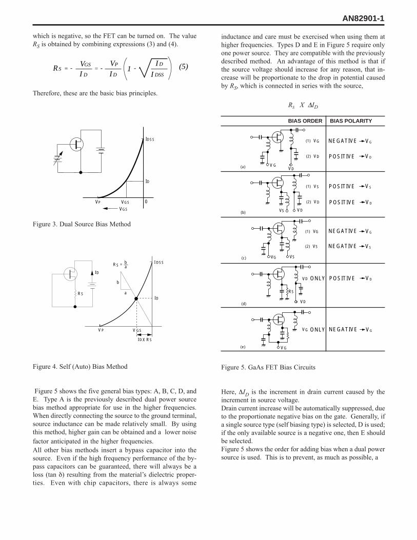
Mutual conductance is defined as the ratio of the change in
direct current to the minor change in voltage between gate
sources. This is generally described as the square-law char-
acteristic and is shown in the equation for ID in Figure 2.
When ID in expression (1) is differentiated with
respect to VGS, the result is
and the mutual conductance for each value of VGS can be
obtained.
II. GaAs FET BIAS AND OPERATING POINT
The most important characteristic to consider when design-
ing a bias circuit for small signal GaAs FETs is the previ-
ously mentioned transfer characteristic. Generally, two meth-
ods can be used to bias a GaAs FET.
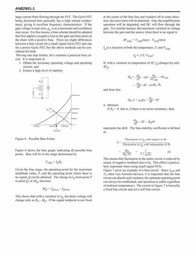
1. Dual Power Source Method
Figure 3 shows a bias circuit which uses the dual power
source method. Since the condition
VP < VGS < 0
must always apply to a GaAs FET, VGS can be derived from
expression (1)
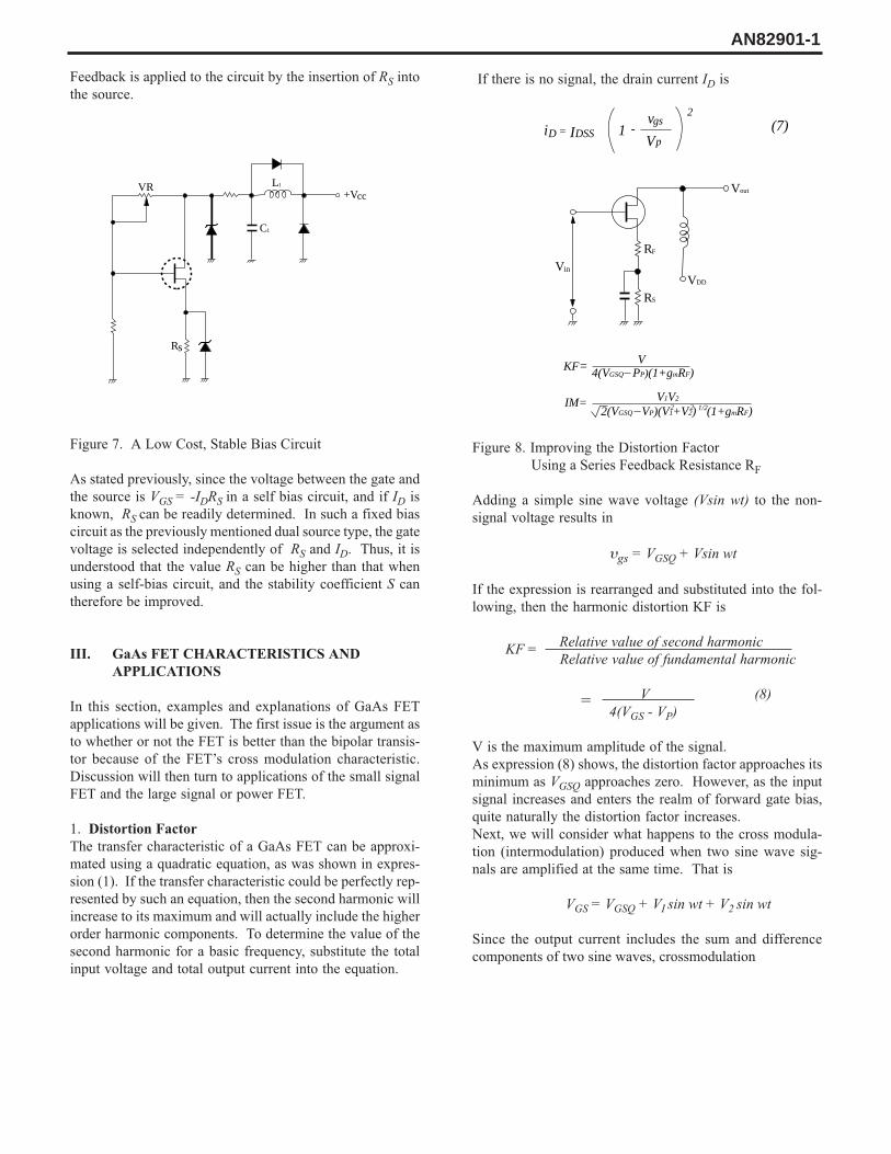
2. Self Bias Method (Auto-Bias)
Figure 4 shows the most universal method for reducing
electrical potential between a gate and the source when there
is only one power source. If the source resistance is RS, and
the operating current is ID, then the drop in electric poten-
tial caused by RS will be
ID x RS
The actual electrical potential between the gate
and the source will be
VGS = -ID . RS (4)
gate, direct current flows through it. Since the gate is a very
small piece of metal (0.5,µ—1.Oµ—2.0µ), the gate electrodes
will fuse completely in almost all cases.
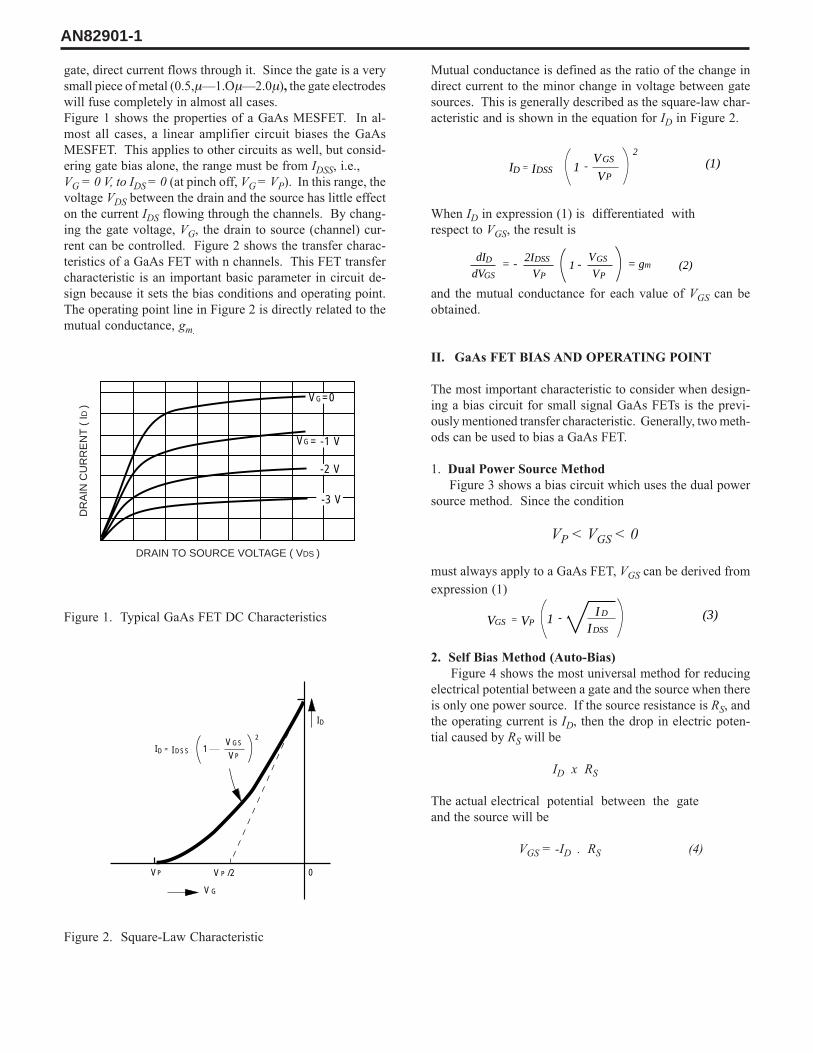
Figure 1 shows the properties of a GaAs MESFET. In al-
most all cases, a linear amplifier circuit biases the GaAs
MESFET. This applies to other circuits as well, but consid-
ering gate bias alone, the range must be from IDSS, i.e.,
VG = 0 V, to IDS = 0 (at pinch off, VG = VP). In this range, the
voltage VDS between the drain and the source has little effect
on the current IDS flowing through the channels. By chang-
ing the gate voltage, VG, the drain to source (channel) cur-
rent can be controlled. Figure 2 shows the transfer charac-
teristics of a GaAs FET with n channels. This FET transfer
characteristic is an important basic parameter in circuit de-
sign because it sets the bias conditions and operating point.
The operating point line in Figure 2 is directly related to the
mutual conductance, gm.
Figure 1. Typical GaAs FET DC Characteristics
Figure 2. Square-Law Characteristic
AN82901-1
DRAIN TO SOURCE VOLTAGE ( VDS )
DR
AIN
CU
RR
EN
T (
I D )
V =0
V = -1 V
-2 V
-3 V
G
G
ID IDSS= 1VV
I
V V
V
GS
P
2
D
P P /2
G
0
ID IDSS= 1V
V
GS
P
2(1)-
dID 2IDSS= 1V
VGS
P= gm
VP-
dVGS- (2)
VGS VP= 1I
ID
DSS
(3)-
inductance and care must be exercised when using them at
higher frequencies. Types D and E in Figure 5 require only
one power source. They are compatible with the previously
described method. An advantage of this method is that if
the source voltage should increase for any reason, that in-
crease will be proportionate to the drop in potential caused
by RS, which is connected in series with the source,
RS X ∆ID
Figure 5. GaAs FET Bias Circuits
Here, ∆ID is the increment in drain current caused by the
increment in source voltage.
Drain current increase will be automatically suppressed, due
to the proportionate negative bias on the gate. Generally, if
a single source type (self biasing type) is selected, D is used;
if the only available source is a negative one, then E should
be selected.
Figure 5 shows the order for adding bias when a dual power
source is used. This is to prevent, as much as possible, a
V
V
VD
G
G(1)
(2)
(a)
V
V
VD
D
VS
S(1)
(2)
(b)
V
VS
VS
VG
G(1)
(2)
(c)
VD(d)
VD
RS
VG
VG
(e)
NEGATIVE
POSITIVE
VG
VD
POSITIVE VS
POSITIVE VD
NEGATIVE VG
NEGATIVE VS
POSITIVE VDONLY
NEGATIVE VGONLY
VD
which is negative, so the FET can be turned on. The value
RS is obtained by combining expressions (3) and (4).
Therefore, these are the basic bias principles.
Figure 3. Dual Source Bias Method
Figure 4. Self (Auto) Bias Method
Figure 5 shows the five general bias types: A, B, C, D, and
E. Type A is the previously described dual power source
bias method appropriate for use in the higher frequencies.
When directly connecting the source to the ground terminal,
source inductance can be made relatively small. By using
this method, higher gain can be obtained and a lower noise
factor anticipated in the higher frequencies.
All other bias methods insert a bypass capacitor into the
source. Even if the high frequency performance of the by-
pass capacitors can be guaranteed, there will always be a
loss (tan δ) resulting from the material’s dielectric proper-
ties. Even with chip capacitors, there is always some
AN82901-1
BIAS ORDER BIAS POLARITY
VGS
DSS
D
SD
P
S
D
S
I
I
V
I R
R
R
I
X
b
a
ba=
I
I
V VVGS
GSP 0
D
DSS
VGS VP= 1
I
I
D
DSS
(5)--I DI D
= -RS
large current from flowing through the FET. The GaAs FET
being discussed here generally has a high mutual conduc-
tance, giving it excellent frequency characteristics. If the
gate voltage is near zero, gm is at a maximum and oscillation
may occur. For this reason, a bias scheme should be adopted
that first applies a negative bias to the gate and then turns on
the drain with a positive bias. There are slight differences
between a bias circuit for a small signal GaAs FET and one
for a power GaAs FET, but the above methods can be con-
sidered for both.
Moving one step further, let’s examine a practical bias cir-
cuit. It is important to:
1. Obtain the necessary operating voltage and operating
current, and
2. Ensure a high level of stability.
Figure 6. Possible Bias Points
Figure 6 shows the bias graph, indicating all possible bias
points. Bias will be in the range determined by
VGSQ = IQRS
Given the bias range, the operating point for the maximum
amplitude value, P, and the operating point where there is
no signal, Q can be obtained. The change in IQ from point P
to point Q, or ∆IQ, becomes
∆IQ = IQ(max) - IQ(min)
This shows that with a variation in IQ, the drain voltage will
change only as RD . ∆IQ. If the signal midpoint is not fixed
AN82901-1
δIQ
δIQ (0)
1
1 + gmRS
= = (6)
∂IQ
∂T
∂IQ
∂T
. ∂IQ
∂VGSQδT+ .
δT -.
δIQ =
.=
∂IQ
∂TδT = δIQ(0).
S =
δVGSQ
gmδIQ RS
δIQ (1 + gmRS) =∂IQ
∂TδT.
Fluctuation in IQ with independent of RS
Fluctuation in IQ with respect to RS
V
IQ(max)
IQ(min)
GS(min)
V VP(min) VP(max) GS(max)
DSS(min)IRS
DSS(max)I
R
S
D
R
at the center of the bias line and wanders off in some direc-
tion, the wave form will be distorted. Also, the amplification
operation will be degraded, and DC will flow through the
gate. In a similar manner, the maximum variation in voltage
between the gate and the source when there is no signal is
∆VGSQ = VGSQ(max) - VGSQ(min)
IQ is a function of both the temperature, T, and VGSQ
IQ = f (T, VGSQ )
If, with a variation in temperature of δT, IQ changes by only
δTQ .
and from this
is obtained.
If RS = 0, that is, if there is no series resistance, then
represents the drift. The bias stability coefficient is defined
as
This means that fluctuation in the entire circuit is reduced by
means of negative feedback due to RS. This effect is particu-
larly important when using small signal FETs.
Figure 7 gives an example of a bias circuit. Since IDSS and
VP often vary between devices, it is important that the bias
circuit can absorb such variation, the optimum operating point
can always be established, and operation is stable regardless
of ambient temperatures. The circuit in Figure 7 is basically
a fixed bias circuit and not a self bias circuit.
If there is no signal, the drain current ID is
Figure 8. Improving the Distortion Factor
Using a Series Feedback Resistance RF
Adding a simple sine wave voltage (Vsin wt) to the non-
signal voltage results in
υgs = VGSQ + Vsin wt
If the expression is rearranged and substituted into the fol-
lowing, then the harmonic distortion KF is
Relative value of second harmonic
Relative value of fundamental harmonic
V (8)
4(VGS - VP)
V is the maximum amplitude of the signal.
As expression (8) shows, the distortion factor approaches its
minimum as VGSQ approaches zero. However, as the input
signal increases and enters the realm of forward gate bias,
quite naturally the distortion factor increases.
Next, we will consider what happens to the cross modula-
tion (intermodulation) produced when two sine wave sig-
nals are amplified at the same time. That is
VGS = VGSQ + VI sin wt + V2 sin wt
Since the output current includes the sum and difference
components of two sine waves, crossmodulation
Feedback is applied to the circuit by the insertion of RS into
the source.
Figure 7. A Low Cost, Stable Bias Circuit
As stated previously, since the voltage between the gate and
the source is VGS = -IDRS in a self bias circuit, and if ID is
known, RS can be readily determined. In such a fixed bias
circuit as the previously mentioned dual source type, the gate
voltage is selected independently of RS and ID. Thus, it is
understood that the value RS can be higher than that when
using a self-bias circuit, and the stability coefficient S can
therefore be improved.
III. GaAs FET CHARACTERISTICS AND
APPLICATIONS
In this section, examples and explanations of GaAs FET
applications will be given. The first issue is the argument as
to whether or not the FET is better than the bipolar transis-
tor because of the FET’s cross modulation characteristic.
Discussion will then turn to applications of the small signal
FET and the large signal or power FET.
1. Distortion Factor
The transfer characteristic of a GaAs FET can be approxi-
mated using a quadratic equation, as was shown in expres-
sion (1). If the transfer characteristic could be perfectly rep-
resented by such an equation, then the second harmonic will
increase to its maximum and will actually include the higher
order harmonic components. To determine the value of the
second harmonic for a basic frequency, substitute the total
input voltage and total output current into the equation.
KF =
=
AN82901-1
VR L1
C1
+Vcc
Rs
iD IDSS= 1v
V
gs
p
2(7)-
Vin
RF
VDD
RS
Vout
KF= V4(VGSQ PP)(1+gmRF)
IM=2(VGSQ VP)(V1+V2)2 2 1/2(1+gmRF)
V1V2
in terms of noise, gain and output-power saturation char-
acteristics. Other than their primary use in ultra-high fre-
quency amplifiers, such as those for electronic countermea-
sures (ECM), most small signal FET applications are in low-
noise amplifiers. They are used in both line-of-sight and
over-the-horizon microwave communications, and in earth
stations communicating with satellites.
A low noise amplifier is designed by minimizing the noise
measure, M, shown in expression (12).
NF is the amplifier noise factor.
G is the amplifier gain.
In single-stage amplifiers, the general procedure for match-
ing input circuits is to mimimize the noise factor, NF; for
matching output circuits, the gain is maximized.
From observations of the input-output impedances of a GaAs
FET, it is noted that there is generally a difference in imped-
ance between maximum gain and minimum NF. This dif-
ference is particularly apparent at lower frequencies. As the
frequencies go higher, the difference seems to decrease. The
noise factor, which is a function of device gain, will be low
when the gain is maximized at high frequencies. However,
of the commercially available GaAs FETs having character-
istics which allow a gain of 8 to 10 dB or more, there is still
a difference between the impedance at maximum gain and
the impedance at miminum NF. This difference will be seen
until the frequency range approaches the X band.
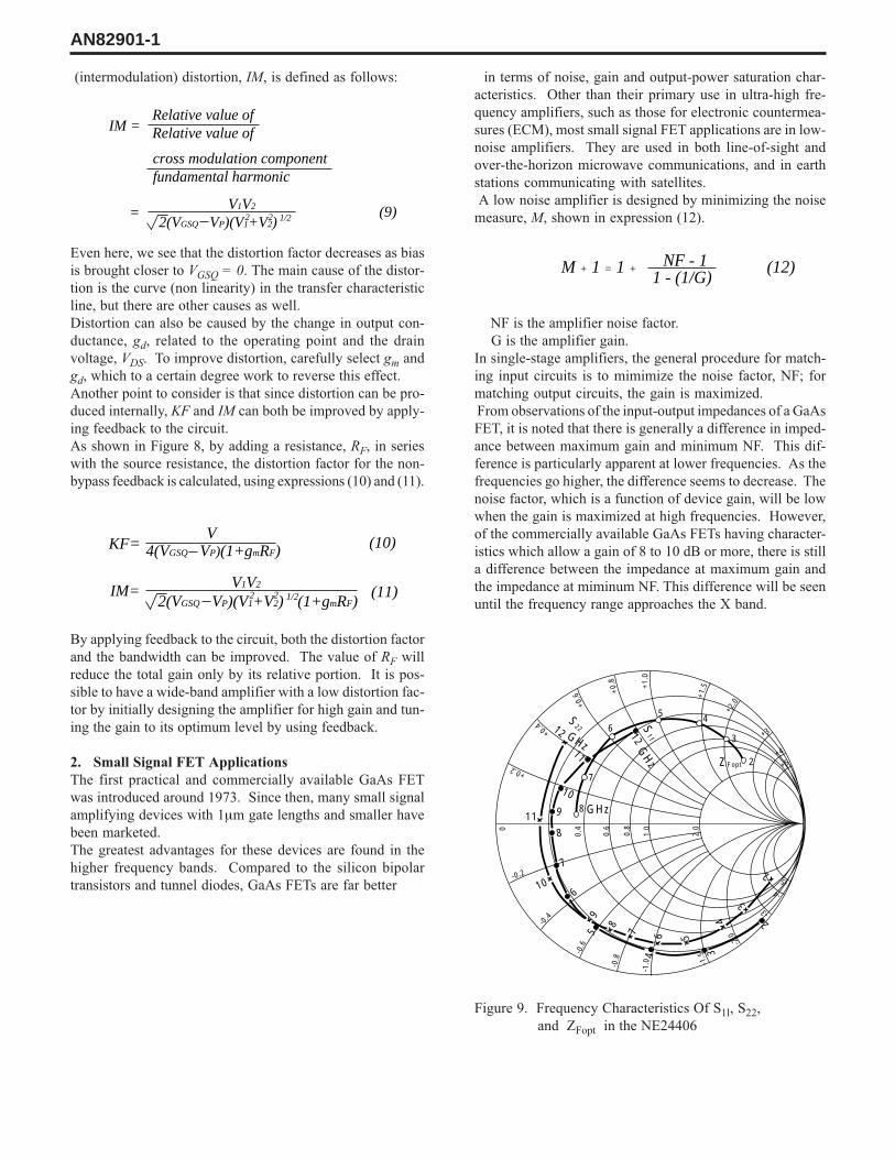
Figure 9. Frequency Characteristics Of S1l, S22,
and ZFopt in the NE24406
(intermodulation) distortion, IM, is defined as follows:
Even here, we see that the distortion factor decreases as bias
is brought closer to VGSQ = 0. The main cause of the distor-
tion is the curve (non linearity) in the transfer characteristic
line, but there are other causes as well.
Distortion can also be caused by the change in output con-
ductance, gd, related to the operating point and the drain
voltage, VDS. To improve distortion, carefully select gm and
gd, which to a certain degree work to reverse this effect.
Another point to consider is that since distortion can be pro-
duced internally, KF and IM can both be improved by apply-
ing feedback to the circuit.
As shown in Figure 8, by adding a resistance, RF, in series
with the source resistance, the distortion factor for the non-
bypass feedback is calculated, using expressions (10) and (11).
By applying feedback to the circuit, both the distortion factor
and the bandwidth can be improved. The value of RF will
reduce the total gain only by its relative portion. It is pos-
sible to have a wide-band amplifier with a low distortion fac-
tor by initially designing the amplifier for high gain and tun-
ing the gain to its optimum level by using feedback.
2. Small Signal FET Applications
The first practical and commercially available GaAs FET
was introduced around 1973. Since then, many small signal
amplifying devices with 1µm gate lengths and smaller have
been marketed.
The greatest advantages for these devices are found in the
higher frequency bands. Compared to the silicon bipolar
transistors and tunnel diodes, GaAs FETs are far better
AN82901-1
=2(VGSQ VP)(V1+V2)2 2 1/2
V1V2 (9)
IM =Relative value ofRelative value of
cross modulation componentfundamental harmonic
KF=V
4(VGSQ VP)(1+gmRF)
IM=2(VGSQ VP)(V1+V2)2 2 1/2(1+gmRF)
V1V2
(10)
(11)
M + 1 = 1 + NF - 11 - (1/G)
(12)
+5+4
2
+33
ZFopt
+2.0
+1.5+
1.0
45
+0.8
+0.6
+0.4 6
7
8
+0.20
-0.2
-0.4
-0.6
-0.8
-1.0 -1
.5
-2.0
-3
-4-5
2
3
4
56
2
34
8
7
95
6
7
8
10
11 9
10
GHz
GHz GH
z
11
12
12
2.0
1.0
0.8
0.6
0.4
S22 S
11
Figure 9 shows S11 and S22, indicating input output imped-
ance for the NE24406 and the signal source impedance when
the noise factor, NF, is minimized. Circuits can be matched
using these impedances. As mentioned previously, input
circuit matching is accomplished by matching to ZFopt; and
output circuit matching is accomplished by matching to S22.
In the design of a multi-stage amplifier, the first and second
stages are designed so that (M + 1) will be minimized, and
the third and subsequent stages are made in such a way that
their gain is maximized. Or, alternately, the amplifier can
be designed according to the characteristics determined by
the frequency and the device.
One impedance matching circuit, shown in Figure 10(a), is
the well known Tchebycheff filter type multi-stage imped-
ance matching circuit. The distinctive feature of this circuit
lies in its applicability to the input/output circuits of wide-
band amplifiers. In many cases, the circuit is used in ampli-
fiers covering the band range 8 GHz to 12 GHz and above.
Although this type of matching network was originally ap-
plied to comparatively narrow bands (such as a 500 MHz
bandwidth at 4 GHz), the matching circuits shown in Figure
10(b) and (c) are now believed to be best suited for bands
having approximately a 10 to 15 percent ratio to the
amplifier’s center frequency.
For these bandwidths, the NF can be reduced to its lowest
absolute value. If the widest possible bandwidth is the ob-
jective, then reduction of the NF to its absolute minimum is
not possible throughout the band. In the former amplifier,
the most important consideration is reducing, as much as
possible, the loss in the impedance matching circuit. The
Tchebycheff filter type impedance matching circuit in Fig-
ure 10(a) uses a large number of components and is not well
suited for obtaining a low loss matching network.
As Figure 9 shows, both S11 and S22 go from capacitive to
inductive with increasing frequencies. Consequently, S11
and S22 can use the circuit in Figure 10(b) for frequencies
which exhibit a capacitive response, or the circuit of Figure
10(c) for the frequencies which exhibit an inductive response.
In Figure 10(b), for frequencies slightly higher than the
amplifier’s center frequency, the GaAs FET input or output
has a resonance of either L1 or L2 (with a reactance of 0),
which is then matched to the desired impedance by the λ/4
impedance conversion circuit. This is only one of the count-
less possible impedance matching circuits. However, this is
a very effective design method for low noise amplifiers re-
quiring a band ratio of 10 to 15 percent when the amplifier’s
center frequency is 4 GHz or greater.
Figure 10. GaAs FET Matching Networks
AN82901-1
IMPEDANCEINVERTER
_l 34_ l 34
jX34
ADMITTANCEINVERTER
_l 23
λ / 4 λ / 4
_ l 23_ l 12
_ l 12
jX12
l
(a)
λ / 4
λ / 4l1
l2
(b)
λ / 4
λ / 4
(c)
C1
C2
IMPEDANCEINVERTER

3. Low Noise Amplifiers in the 4 GHz Band
Figure 11 is an example of a two-stage low-noise amplifier
for the 3.7 to 4.2 GHz band using either the NE21889 or the
NE72089. The matching circuit in Figure 11 is based on the
same idea as Figure 10(b). It uses a microstrip with an
0.8 mm thickness teflon glass fiber substrate and transistor
leads with lumped constant inductance. Figure 12 shows
the schematics. Figure 13 shows the gain and noise factor
normally obtained using this circuit.
Figure 11. PCB Layout of a 2-Stage Amplifier in the 3.7 GHz-4.2 GHz Band
Figure 12. Schematics for a 3.7 GHz-4.2 GHz Band 2- Stage Amplifier
AN82901-1
Parts List: NE72089 FET (2 ea.) California Eastern Laboratories10 pF Chip Capacitors (3 ea.) ATC #100A-100-J-P-X-50 or equivalent1000 pF Chip Capacitors (4 ea.) Johanson #50R11W102KP or equivalent1500 pF Feed-through Capacitors (4 ea.) Erie #2425-003-W5U0153AA or equivalentFerrite Beads (4 ea.) Fairrite #2643001301 or equivalent
CEL
10 pF
IN
10 pF
3.7-4.2 GHz LNA
THRU HOLES FORNE72089 SOURCE LEADS4 PLACES
10 pF
OUT
28.0 mm
69.6 mm
1000 pF4 PLACES
SHIM STOCK TO GROUNDALL 4 SOLDER PADS
C1
Z0
TRL1
SST1
λ / 4
λ / 4
λ / 4 λ / 4
λ / 4
λ / 4
C4 C5 C6
C2
C7 C8 C9 C10 C11 C12
C13 C14 C15
C3
SST2 SST3
SST4
Z0TRL2( )
TRL3Z0
Vd2
Vd1 Vg2Vg1
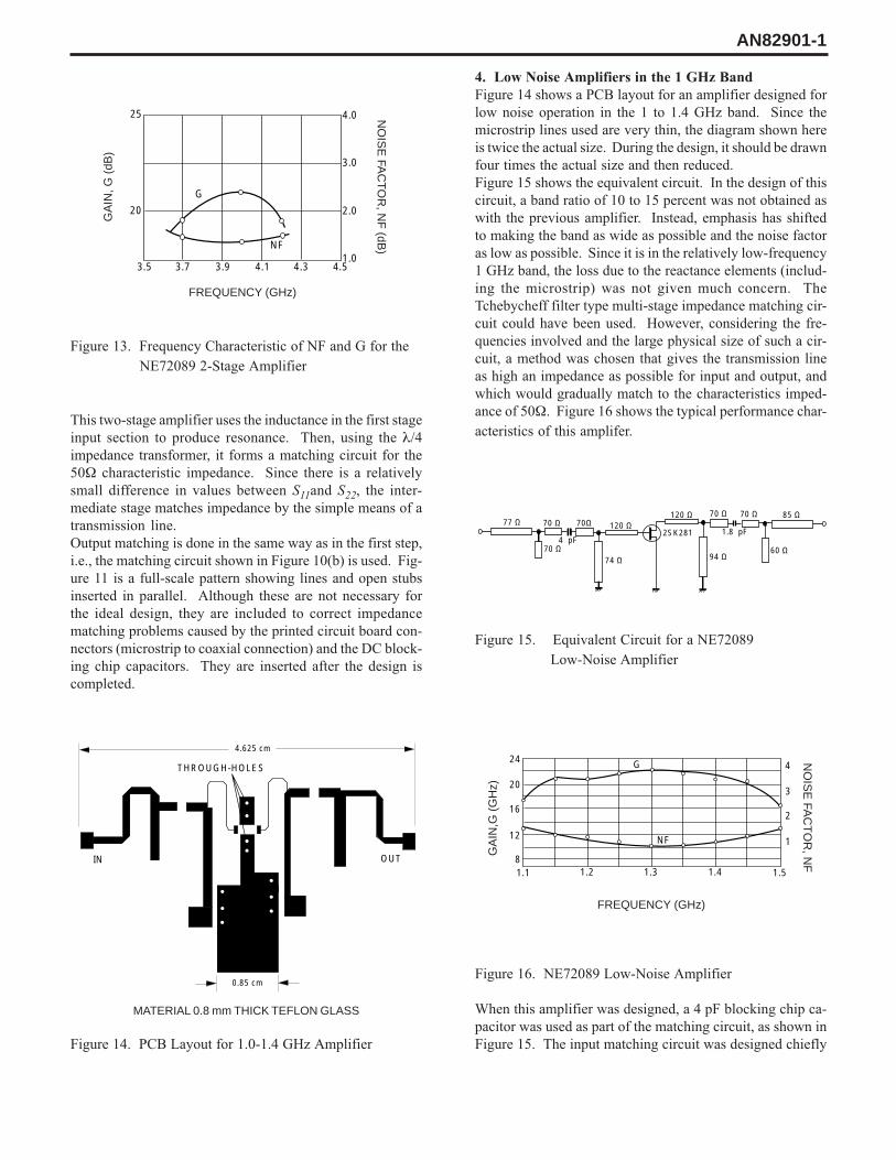
4. Low Noise Amplifiers in the 1 GHz Band
Figure 14 shows a PCB layout for an amplifier designed for
low noise operation in the 1 to 1.4 GHz band. Since the
microstrip lines used are very thin, the diagram shown here
is twice the actual size. During the design, it should be drawn
four times the actual size and then reduced.
Figure 15 shows the equivalent circuit. In the design of this
circuit, a band ratio of 10 to 15 percent was not obtained as
with the previous amplifier. Instead, emphasis has shifted
to making the band as wide as possible and the noise factor
as low as possible. Since it is in the relatively low-frequency
1 GHz band, the loss due to the reactance elements (includ-
ing the microstrip) was not given much concern. The
Tchebycheff filter type multi-stage impedance matching cir-
cuit could have been used. However, considering the fre-
quencies involved and the large physical size of such a cir-
cuit, a method was chosen that gives the transmission line
as high an impedance as possible for input and output, and
which would gradually match to the characteristics imped-
ance of 50Ω. Figure 16 shows the typical performance char-
acteristics of this amplifer.
Figure 15. Equivalent Circuit for a NE72089
Low-Noise Amplifier
Figure 16. NE72089 Low-Noise Amplifier
When this amplifier was designed, a 4 pF blocking chip ca-
pacitor was used as part of the matching circuit, as shown in
Figure 15. The input matching circuit was designed chieflyFigure 14. PCB Layout for 1.0-1.4 GHz Amplifier
This two-stage amplifier uses the inductance in the first stage
input section to produce resonance. Then, using the λ/4
impedance transformer, it forms a matching circuit for the
50Ω characteristic impedance. Since there is a relatively
small difference in values between S11and S22, the inter-
mediate stage matches impedance by the simple means of a
transmission line.
Output matching is done in the same way as in the first step,
i.e., the matching circuit shown in Figure 10(b) is used. Fig-
ure 11 is a full-scale pattern showing lines and open stubs
inserted in parallel. Although these are not necessary for
the ideal design, they are included to correct impedance
matching problems caused by the printed circuit board con-
nectors (microstrip to coaxial connection) and the DC block-
ing chip capacitors. They are inserted after the design is
completed.
Figure 13. Frequency Characteristic of NF and G for the
NE72089 2-Stage Amplifier
AN82901-1
GA
IN, G
(dB
)
NO
ISE
FAC
TO
R, N
F (dB
)
FREQUENCY (GHz)
MATERIAL 0.8 mm THICK TEFLON GLASS
FREQUENCY (GHz)
NO
ISE
FAC
TO
R, N
F
GA
IN,G
(G
Hz)
25
20
3.5 3.7 3.9 4.1 4.3 4.5
G
NF1.0
2.0
3.0
4.0
THROUGH-HOLES
IN OUT
4.625 cm
0.85 cm
77 Ω 70 Ω
70 Ω
70Ω 120 Ω120 Ω
74 Ω
4 pF
70 Ω 70 Ω
2SK281
94 Ω
85 Ω
60 Ω
1.8 pF
24
20
16
12
81.1 1.2 1.3 1.4 1.5
4
3
2
1NF
G
to obtain matching for the noise factor. The data used for
the NE72089 is shown below:
The bias circuit used to actuate this amplifier is shown in
Figure 17. The figure shows a bias circuit for a two-stage
amplifier. For a single stage amplifier, only one half of the
redundant portion of the circuit would be used. This circuit
is a constant voltage, constant current type bias circuit, one
of the most applicable examples of circuits for use in small-
signal amplifiers.
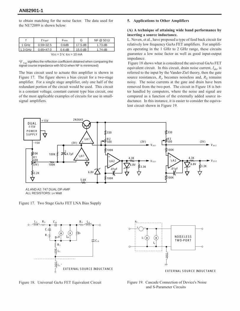
5. Applications to Other Amplifiers
(A) A technique of attaining wide band performance by
inserting a source inductance.
L. Neven, et al., have proposed a type of feed back circuit for
relatively low frequency GaAs FET amplifiers. For amplifi-
ers operating in the 1 GHz to 2 GHz range, these circuits
guarantee a low noise factor as well as good input-output
impedance.
Figure 18 shows what is considered the universal GaAs FET
equivalent circuit. In this circuit, drain noise current, Idn, is
referred to the input by the Vander-Ziel theory, then the gate
source resistances, Ri, becomes noiseless and, RS remains
noisy. The noise currents at the gate and drain have been
removed from the two-port. The circuit in Figure 18 is bet-
ter handled by computers, where the noise and signal are
compared as a function of the externally added source in-
ductance. In this instance, it is easier to consider the equiva-
lent circuit shown in Figure 19.
Figure 17. Two Stage GaAs FET LNA Bias Supply
Figure 18. Universal GaAs FET Equivalent Circuit Figure 19. Cascade Connection of Device's Noise
and S-Parameter Circuits
AN82901-1
f ΓFopt* Fmin G NF @ 50 Ω
1 GHz 0.59<32.5 0.6dB 17.5 dB 1.73 dB
1.3 GHz 0.65<47.0 0.6 dB 15.0 dB 1.74 dB
VDS = 3 V, IDS = 10 mA
*(I' Fopt
signifies the reflection coefficient obtained when comparing thesignal course impedance with 50 Ω when NF is minimized)
A1 AND A2: 747 DUAL OP-AMPALL RESISTORS: 1/4 Watt
VDS2
(3V)
100K
500R3
330
4.3K
6.8V3.3K
VGS2
100K
.01µF
4.3K
6.8V3.3K
.01µF
A21 2
(3V)VDS1
VGS1
100K
100K
6.8V
A11 2
A11 2
(3V) 500R2
330
4.7µF100K
100K(3V)
10KR1500
15V
2.2K
15VDUAL
POWERSUPPLY
15V 2N3643
5.6K
A21 2
LG GR Cgs d dR L
gd
m dnIg
C
R
R
L
L '
Cds
V
S
S
S
i
i
EXTERNAL SOURCE INDUCTANCE
en
+ -
I
I
C
u
NOISELESSTWO-PORT
EXTERNAL SOURCE INDUCTANCE
10 n H
1.5 n H
10 n Hλ 4 @ 1.5 GHz60 Ω
15
14
13
12
2
1
0
4
3
2
1
1.3 1.4 1.5 1.6 1.7
G
ISWR
OSWR
NF
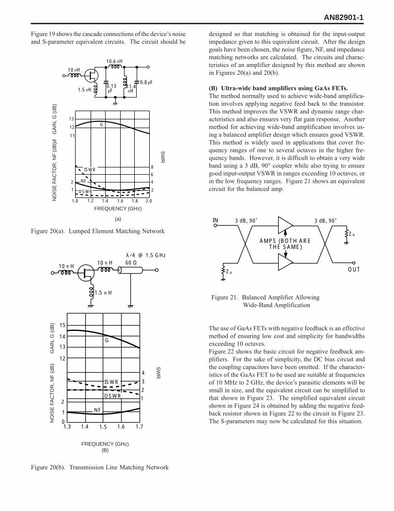
Figure 19 shows the cascade connections of the device’s noise
and S-parameter equivalent circuits. The circuit should be
designed so that matching is obtained for the input-output
impedance given to this equivalent circuit. After the design
goals have been chosen, the noise figure, NF, and impedance
matching networks are calculated. The circuits and charac-
teristics of an amplifier designed by this method are shown
in Figures 20(a) and 20(b).
(B) Ultra-wide band amplifiers using GaAs FETs.
The method normally used to achieve wide-band amplifica-
tion involves applying negative feed back to the transistor.
This method improves the VSWR and dynamic range char-
acteristics and also ensures very flat gain response. Another
method for achieving wide-band amplification involves us-
ing a balanced amplifier design which ensures good VSWR.
This method is widely used in applications that cover fre-
quency ranges of one to several octaves in the higher fre-
quency bands. However, it is difficult to obtain a very wide
band using a 3 dB, 90° coupler while also trying to ensure
good input-output VSWR in ranges exceeding 10 octaves, or
in the low frequency ranges. Figure 21 shows an equivalent
circuit for the balanced amp.
Figure 21. Balanced Amplifier Allowing
Wide-Band Amplification
The use of GaAs FETs with negative feedback is an effective
method of ensuring low cost and simplicity for bandwidths
exceeding 10 octaves.
Figure 22 shows the basic circuit for negative feedback am-
plifiers. For the sake of simplicity, the DC bias circuit and
the coupling capacitors have been omitted. If the character-
istics of the GaAs FET to be used are suitable at frequencies
of 10 MHz to 2 GHz, the device’s parasitic elements will be
small in size, and the equivalent circuit can be simplified to
that shown in Figure 23. The simplified equivalent circuit
shown in Figure 24 is obtained by adding the negative feed-
back resistor shown in Figure 22 to the circuit in Figure 23.
The S-parameters may now be calculated for this situation.
Figure 20(b). Transmission Line Matching Network
Figure 20(a). Lumped Element Matching Network
AN82901-1
FREQUENCY (GHz)
(a)
FREQUENCY (GHz)(B)
NO
ISE
FA
CT
OR
, NF
(dB
)
G
AIN
, G (
dB)
SW
RS
WR
NO
ISE
FA
CT
OR
, NF
(dB
)d
GA
IN, G
(dB
)
10 nH
10.6 nH
1.5 nH
pF0.8
nHpF0.13 11.4
G13
12
11
2
1
8
6
4
2
1.0 1.2 1.4 1.6 1.8 2.0
ISWR
NF
OSWR
IN 3 dB, 90˚ 3 dB, 90˚
OUTZo
Zo
AMPS (BOTH ARETHE SAME)
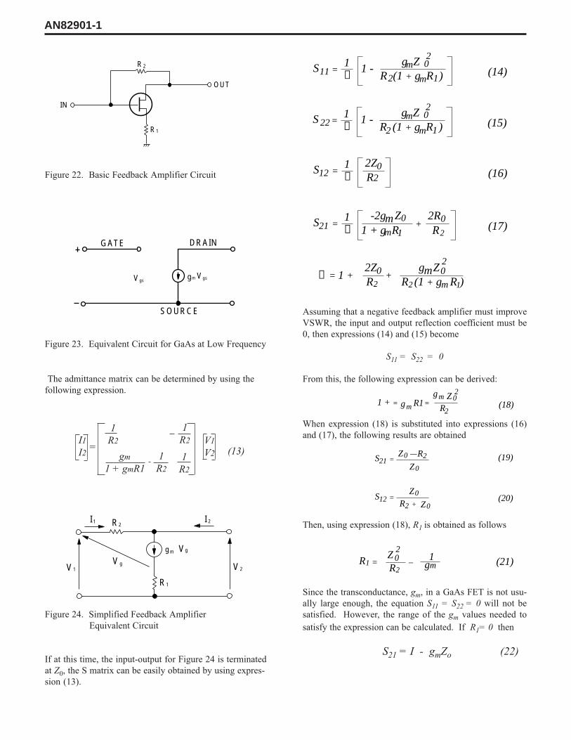
Assuming that a negative feedback amplifier must improve
VSWR, the input and output reflection coefficient must be
0, then expressions (14) and (15) become
S11 = S22 = 0
From this, the following expression can be derived:
When expression (18) is substituted into expressions (16)
and (17), the following results are obtained
Then, using expression (18), R1 is obtained as follows
Since the transconductance, gm, in a GaAs FET is not usu-
ally large enough, the equation S11 = S22 = 0 will not be
satisfied. However, the range of the gm values needed to
satisfy the expression can be calculated. If R1= 0 then
S21 = I - gmZo (22)
The admittance matrix can be determined by using the
following expression.
Figure 24. Simplified Feedback Amplifier
Equivalent Circuit
If at this time, the input-output for Figure 24 is terminated
at Z0, the S matrix can be easily obtained by using expres-
sion (13).
Figure 22. Basic Feedback Amplifier Circuit
Figure 23. Equivalent Circuit for GaAs at Low Frequency
AN82901-1
I1
I2=
1
R2
gm
1 + gmR1
V1
V2 (13)1
R2
1
R2
1
R2
R1
R2
IN
OUT
GATE DRAIN
VgsVgsgm
SOURCE
I R I
Vg
R
VV V
gm
22
1
g1 2
1
S11 =1∆ 1 -
R (1 + g R )g Z 2
0(14)
S 22 =1∆ 1 -
R (1 + g R )g Z 2
0(15)
S12 =1∆ R2
2Z0(16)
S21 =1∆ 1 + g R
-2g Z 2R0(17)+
0R
= 1∆R2Z0
R (1 + g R )++
g Z20
2 m 1
2 m 1
m
m
mm 1 2
1m
m2 2
= =1 +R
Z 20
2gm
gmR1 (18)
S12 =
S21 = Z R0
0
— 2
Z
Z R
0
02 Z+(20)
(19)
=R gm –Z
202
R11 (21)
is obtained, and thus
gm| min = 1 - S21 (23)
Zo
For example, consider the design of an amplifier with 10 dB
gain. Logically, if we take the input output VSWR as a low
value and the characteristic impedance, Z0, as 50Ω, when
S11 = S22 = 0, then substituting this in expression (23) yields,
It will therefore be acceptable if gm⊕83mS. Figure 25 shows
the characteristics of an ultra wide band amplifier designed
using this method.
Figure 25. GaAs FET Feedback Amplifier
6. Relation of Ambient Temperature, Frequency
and Noise Temperature in GaAs FETs
Up to this point, only the applications of GaAs FETs in am-
plifiers have been examined. Now, the discussion will turn
to the relationship between ambient temperature and noise
temperature.
Noise in a GaAs FET is chiefly thermal noise. Since there is
rarely shot noise, the noise temperature in an amplifier
changes greatly in response to the ambient temperature. Fig-
ure 26 shows the relationship of operating temperature and
the noise temperature for the NE67383/NE71083. The noisetemperature, Te and ambient operating temperature, Ta, can
be shown to correspond to the following:
Figure 26 shows the linearity in the relationship between the
ambient operating temperature and the noise temperature.
By taking advantage of this characteristic, a super low-noise
amplifier can be produced by cooling the amplifier with car-
bonic gas, liquid nitrogen or liquid helium.
Figure 26. Te vs. Ta for the NE67383/NE71083
7. Power GaAs FET Applications
For the small signal GaAs FETs discussed so far, we have
covered only those signal levels in the range in which oper-
ating characteristics are not dependent on signal voltage or
signal current. In other words, each terminal’s voltage and
current was in a range which satisfied a linear relationship.
As the signal level increases, this relation- ship is no longer
satisfied and we have a situation known as large signal op-
eration. Of course, even if the element is in non-linear op-
eration, the electrophysical quantity of the signal frequency
is still in a linear relationship if non-linearity is small. Thus,
the S-parameter relationship in a GaAs FET can be deter-
mined for small signal operation.
Because the voltage and current-to-terminal conditions which
define each parameter are not fixed for large signal opera-
tion, it is difficult to determine parameters indicating a lin-
ear relationship.
Figure 27 is a simplified diagram showing the small and
large signal operation of a Class A GaAs FET. Load lines A
and B indicate the optimum conditions for maximum input
and output when the input gate signal voltage is VGA and
VGB.
The optimum load for small signal operation is equal to the
drain conductance (∂IDS /∂VD). In large signal operation,
however, the input signal level will increase and gate volt-
age, VG, will enter the nonlinear zone. The output current,
which is the drain current, ID, will then reach its upper limit
and the load line gradient must increase to increase the out-
put power. Therefore, when designing a circuit, it is neces-
sary to use data which takes all factors into consideration.
AN82901-1
1 - (-3.16)
50
FREQUENCY (GHz)
GA
IN, G
(dB
)
ωCgs
gm
NO
ISE
TE
MP
ER
AT
UR
E, T
(K
)
= 0.082 S
Te = K TA (24)
GaAs FET OPERATING TEMPERATURE, Ta (K)
8
6
4
2
0.01 0.1 1 10
4GHz
12GHz
100 150 200 250 300 3500
50
100
150
200
250
300

Figure 27. Simplified Load Line for a Class A GaAs FET in Small and Large Signal Operation
8. Operating Methods for Power GaAs FETs
(A) Introduction
An important factor to consider when working with Power
GaAs FETs is power GaAs FETs are basically a group of
small signal GaAs FETs connected in parallel so that they
can handle a large power source. Therefore, they have an
extremely high transconductance. Another important and
necessary factor to consider is at which bias point operation
takes place. Consideration must be given as to whether there
is adequate bias resistance to suppress the gate current. As
mentioned previously, Schottky gates are used in a GaAs
FET, and there is the possibility that the operating point will
cause an excessive current to flow across the gate.
The gate structure in a GaAs FET is very delicate, with a
typical gate length of 0.5/µm to 1.0µm. In some cases, just
a slight current flow across the gate will have a current den-
sity of 106A/cm2. With such high current density, the gate
will eventually fail.
Figure 28 shows the change in input-output characteristics
due to the increasing gate current. Here, the operating drain
voltage is constant, but direct current begins to flow in the
opposite direction at the gate when the input signal level is
increased sufficiently. When the input signal power increases,
the Schottky gate is biased in the forward direction and gate
current begins to flow in that direction. Caution must be
Figure 28. Relationship of Input-Output Characteristics to
Increasing Gate Current
taken at this time since the amount of gate current has a
bearing on whether or not the FET will be destroyed.
AN82901-1
INPUT, Pin (dBm)
GA
TE
CU
RR
EN
T (m
A)
DR
AIN
CU
RR
EN
T (m
A)
OU
TP
UT,
Pou
t (dB
m)
DB
V
i D
DSI
i DB
t
it
A
B
DA
1
P
VD
VGBVGB
VDS
DB
V
DA
V
t
V =0G
t1
10
5
0
5
10
1.3
1.2
1.1
302010
20
30
NE8001 3.0 mANE8002 6.0 mA
NE8004 10.0 mANE8008 15.0 mANE3716 20.0 mA
NE9000 0.5 mANE9001 1.3 mANE9002 2.6 mA
NE9004 5.0 mANE9008 8.0 mANE8681 3.0 mA
NE8682 6.0 mANE8684 10.0 mANE8688 15.0 mA
NE8691 1.3 mANE8692 2.6 mANE8694 5.0 mA
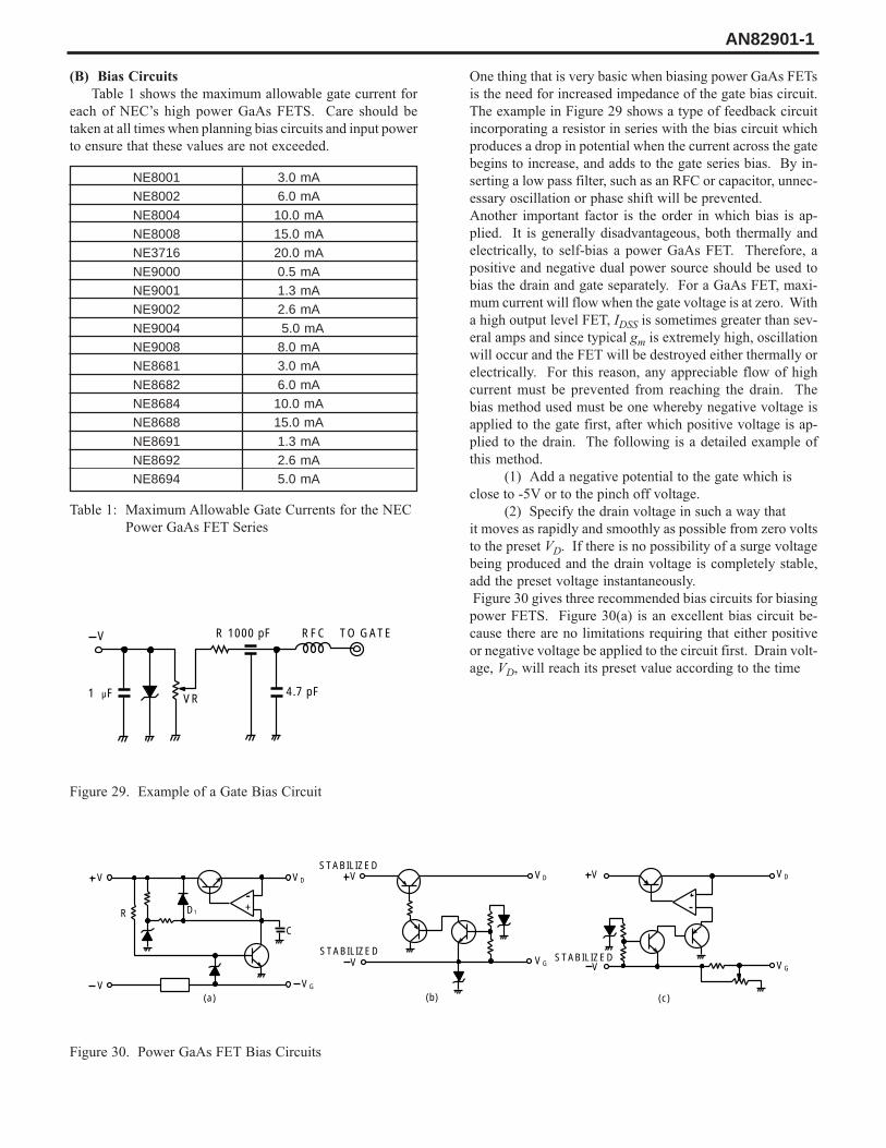
(B) Bias Circuits
Table 1 shows the maximum allowable gate current for
each of NEC’s high power GaAs FETS. Care should be
taken at all times when planning bias circuits and input power
to ensure that these values are not exceeded.
One thing that is very basic when biasing power GaAs FETs
is the need for increased impedance of the gate bias circuit.
The example in Figure 29 shows a type of feedback circuit
incorporating a resistor in series with the bias circuit which
produces a drop in potential when the current across the gate
begins to increase, and adds to the gate series bias. By in-
serting a low pass filter, such as an RFC or capacitor, unnec-
essary oscillation or phase shift will be prevented.
Another important factor is the order in which bias is ap-
plied. It is generally disadvantageous, both thermally and
electrically, to self-bias a power GaAs FET. Therefore, a
positive and negative dual power source should be used to
bias the drain and gate separately. For a GaAs FET, maxi-
mum current will flow when the gate voltage is at zero. With
a high output level FET, IDSS is sometimes greater than sev-
eral amps and since typical gm is extremely high, oscillation
will occur and the FET will be destroyed either thermally or
electrically. For this reason, any appreciable flow of high
current must be prevented from reaching the drain. The
bias method used must be one whereby negative voltage is
applied to the gate first, after which positive voltage is ap-
plied to the drain. The following is a detailed example of
this method.
(1) Add a negative potential to the gate which is
close to -5V or to the pinch off voltage.
(2) Specify the drain voltage in such a way that
it moves as rapidly and smoothly as possible from zero volts
to the preset VD. If there is no possibility of a surge voltage
being produced and the drain voltage is completely stable,
add the preset voltage instantaneously.
Figure 30 gives three recommended bias circuits for biasing
power FETS. Figure 30(a) is an excellent bias circuit be-
cause there are no limitations requiring that either positive
or negative voltage be applied to the circuit first. Drain volt-
age, VD, will reach its preset value according to the time
Figure 29. Example of a Gate Bias Circuit
Figure 30. Power GaAs FET Bias Circuits
Table 1: Maximum Allowable Gate Currents for the NEC
Power GaAs FET Series
AN82901-1
V
1 µF VR
R 1000 pF RFC TO GATE
4.7 pF
V
R D1
V(a)
C
STABILIZED
STABILIZEDV
VG
VD V
(b)
VG
VD V
V VG
VD
STABILIZED
(c)
+-

Figure 31. Power GaAs FET Regulated Bias Supply
constant determined by C and R. When the power source is
OFF, the electrical charge will pass through diode D1, and
return quickly to the power source side, thus the FET can
then be safely biased.
Figure 31 shows a bias circuit recommended for biasing a
multistage (5 stages) power GaAs FET amplifier.
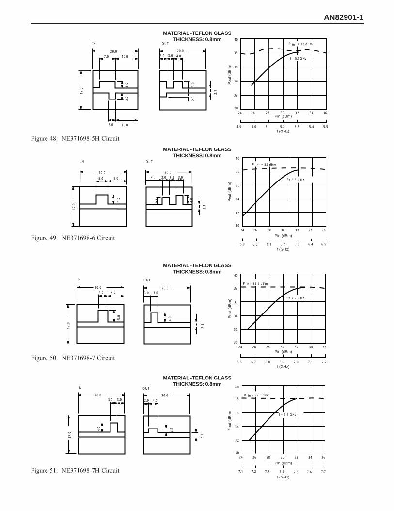
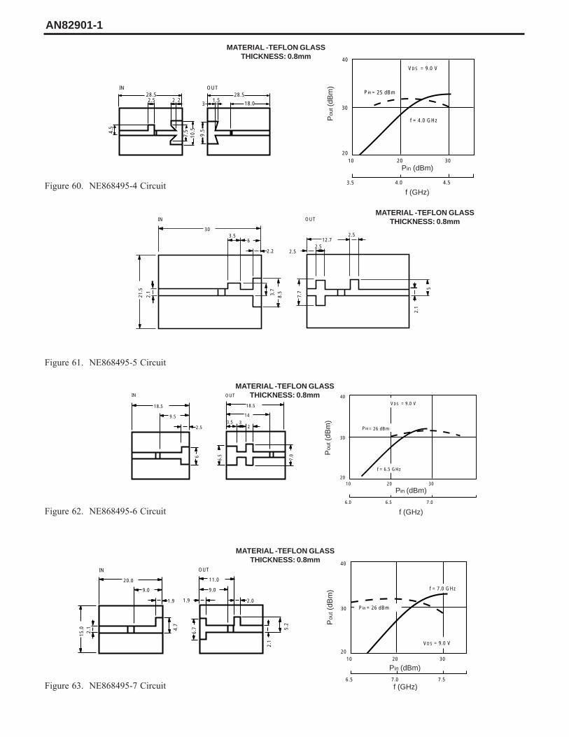
9. Examples of C-Band Application Circuits Using NEC’s
Power GaAs FET Series
With the exception of the devices with the 96 package, NEC’s
C-Band GaAs FET series using multiple chips contain in-
ternal matching network (IMN) circuits within the packages.
The IMNs are not intended to match the devices to 50Ω but
to facilitate and reduce the external matching networks. The
GaAs FET series which are in 98 packages have both input
and output matching circuits close to VSWR, 1:2.5. The
devices in 95 and 98 packages which have internal match-
ing circuits are identified by the numbers -4, -5, (-5H), -6,
-7, (-7H), and -8. Each of these numbers indicates the
center frequency at which the IMN circuit is optimized and
tested. For example, -4 is at 4 GHz (3.5-4.5 GHz) and -6 is
at 6 GHz (5.5-6.5 GHz).
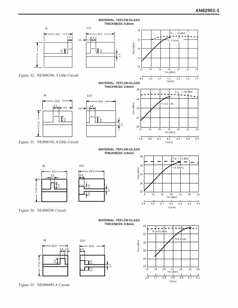
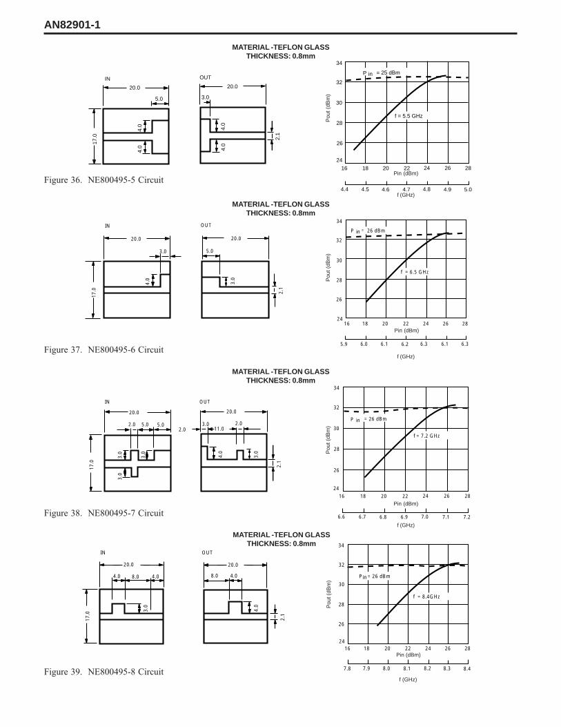
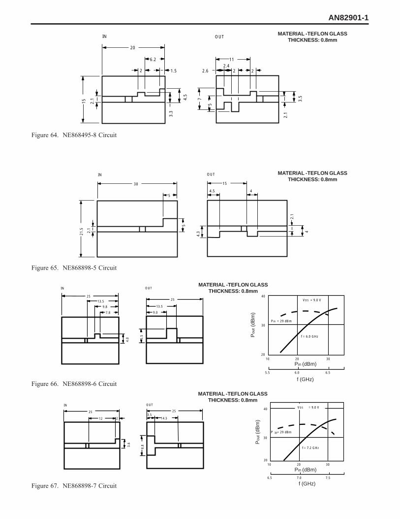
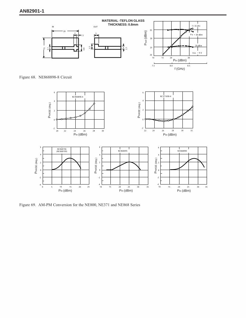
Figures 32 to 68 relate typical characteristics and illus-
trate application circuits using an 0.8mm thick teflon glass
circuit board. The units used in these charts are millimeters
(mm). Figure 69 gives AM-PM conversions for NE800,
NE371, and NE868 series. This data is particularly effec-
tive when designing a PCM transmitter. Figure 70 gives the
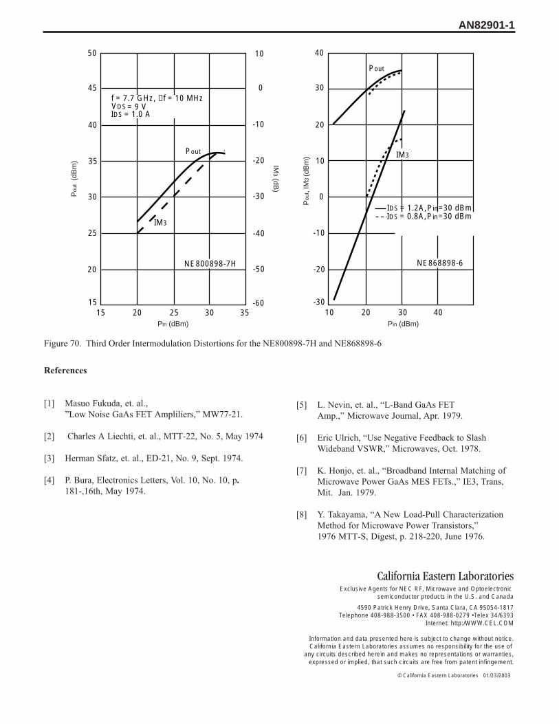
standard characteristics for the third order intermodulation
of NE800898-7H and NE868898-6.
This brief report explains current GaAs FET technology.
Improvement of device characteristics is a major goal for
both applied technology and research in electronics. GaAs
FET reliability has already been confirmed and there is little
doubt that FETs will eventually be used at frequencies of 40
GHz and higher.
AN82901-1
Q1 - SK3448Q2 - 2N706Q3 - 2N3771IC1- MC1469IC2-LM304
NOTE: 1) Ammeter is optional.2) Q3 is mounted on external heat sink.3) R1, R2 and R3 are mounted externally.4) All resistors are 1\4 watt unless otherwise noted.
DUAL±15V
POWERSUPPLY
S1A
+10µF
2A
5V2K
R120K
3
6
9 IC1
8
Q1
S1B 330 22 6
6.8K 2 10
1
4
5
7
.01µF
7
100
.001
.0003
Q3 .1 2W
1KQ247µF
10µF
10µF
2.4K
2.5K+
5
3
2
1 9
IC2
8
.0003 + 47µF
R2500
R333
+
VGS
+ VDS
A
IN
20.04.0 2.0
17.0 5.
0
20.04.0
3.0
3.0
2.1
OUT
34
32
30
P =25 dBmin
f=4.2GHz
28
26
2416 18 20 22 24
3.6 3.7 3.8 3.9 4.0 4.1 4.2
26 28
28
26
24
22
2012 14 16 18 20 22 24
5.9 6.0 6.1 6.2 6.3 6.4 6.5
f = 6.5 GHz
IN OUT
20.0
9.0 2.0
20.0
4.0
4.0
2.1
17.0
4.0
4.0
P = 18 dBmin
IN OUT
20.03.0
3.0
20.0
4.0
3.0
3.0
2.1
17.0
28
26
24
22
2012 14 16 18 20 22 24
4.9 5.0 5.1 5.2 5.3 5.4 5.5
P = 18 dBmin
f = 5.5GHz
AN82901-1
MATERIAL -TEFLON GLASSTHICKNESS: 0.8mm
Figure 32. NE800196, 5 GHz Circuit
MATERIAL -TEFLON GLASSTHICKNESS: 0.8mm
Pin (dBm)
f (GHz)
Pou
t (dB
m)
Pou
t (dB
m)
Pin (dBm)
f (GHz)Figure 33. NE800196, 6 GHz Circuit
MATERIAL -TEFLON GLASSTHICKNESS: 0.8mm
Pou
t (d
Bm
)
Pin (dBm)
f (GHz)Figure 34. NE800296 Circuit
MATERIAL -TEFLON GLASSTHICKNESS: 0.8mm
Pin (dBm)
f (GHz)
Pou
t (d
Bm
)
Figure 35. NE800495-4 Circuit
28
30
26
24
224 16 18 20 22 24 26
5.9 6.0 6.1 6.2 6.3 6.4 6.5
inP = 22 dBm
f = 6.5GHzOUT
20.0
4.0
2.0
2.0
2.1
20.0
3.0
17.0
5.0
IN
34
32
30
28
26
2416 18 20 22 24 26 28
7.8 7.9 8.0 8.1 8.2 8.3 8.4
P = 26 dBmin
f = 8.4GHz
20.0
8.0 4.0
4.0
2.1
3.0
17.0
20.0
8.0 4.04.0
IN OUT
34
32
30
28
26
24
16 18 20 22 24 26 28
6.6 6.7 6.8 6.9 7.0 7.1 7.2
P = 26 dBmin
f = 7.2 GHz
IN
20.0
5.0
20.0
3.0
3.0
4.0
3.0
17.0
OUT
2.1
2.02.0 11.0
5.02.0
3.0
3.0
P 26 dBmin
f = 6.5 GHz
2826242220181624
26
28
30
32
34OUT
20.0
IN
20.0
3.0
4.0
17.0
3.0
2.1
5.0
5.9 6.0 6.1 6.2 6.3 6.1 6.3
=
34
32
30
28
26
24
16 18 20 22 24 26 28
4.4 4.5 4.6 4.7 4.8 4.9 5.0
P = 25 dBmin
f = 5.5 GHz
IN
20.0
5.0
20.0
3.0
4.0
4.0
4.0
4.017
.0
OUT
2.1
AN82901-1
MATERIAL -TEFLON GLASSTHICKNESS: 0.8mm
f (GHz)
Pou
t (d
Bm
)
Pin (dBm)Figure 36. NE800495-5 Circuit
MATERIAL -TEFLON GLASSTHICKNESS: 0.8mm
Pou
t (d
Bm
)
f (GHz)
Pin (dBm)
Figure 37. NE800495-6 Circuit
MATERIAL -TEFLON GLASSTHICKNESS: 0.8mm
Pou
t (dB
m)
Pin (dBm)
f (GHz)
Figure 38. NE800495-7 Circuit
MATERIAL -TEFLON GLASSTHICKNESS: 0.8mm
Pou
t (dB
m)
f (GHz)
Pin (dBm)
Figure 39. NE800495-8 Circuit

P = 29.5 dBmin
f = 6.4 GHz
38
36
34
32
3022 24 26 28 30 32 34
5.9 6.0 6.1 6.2 6.3 6.4 6.5
IN OUT
20.0
2.0
20.0
2.0
2.0
2.1
1.0
17.0
20.0
10.05.0
2.0
17.0
2.1
3.0
4.0
2.0
1.0
2.1
20.02.0
17.0
1.0
IN OUT
P =29.5 dBmin
f = 5.5 GHz
38
36
34
32
3022 24 26 28 30 32 34
5.0 5.1 5.2 5.3 5.4 5.5 5.6
38
36
34
32
3022 24 26 28 30 32 34
4.4 4.5 4.6 4.7 4.8 4.9 5.0
P = 29 dBmin
f = 5 GHz20.0 20.0
3.0 3.0
3.0
3.0
IN OUT
6.0 4.0 6.011.3
1.0
17.0
2.1
P = 29 dBm
f = 4.2GHz
in
22 24 26 28 30 32 34
38
36
34
32
30
3.7 3.8 3.9 4.0 4.1 4.2 4.3
IN OUT20.0
3.010.0
20.03.0
14.0
5.0
4.0
4.0
2.1
17.0
AN82901-1
MATERIAL -TEFLON GLASSTHICKNESS: 0.8mm
Pou
t (d
Bm
)
Figure 42. NE800898-5H Circuit
MATERIAL -TEFLON GLASSTHICKNESS: 0.8mm
Figure 40. NE800898-4 Circuit
Figure 43. NE800898-6 Circuit
Pou
t (d
Bm
)
Pin (dBm)
f (GHz)
Pin (dBm)
f (GHz)
Pin (dBm)
f (GHz)
Pou
t (d
Bm
)P
out
(dB
m)
Pin (dBm)
f (GHz)
MATERIAL -TEFLON GLASSTHICKNESS: 0.8mm
Figure 41. NE800898-5 Circuit
MATERIAL -TEFLON GLASSTHICKNESS: 0.8mm

20.0
3.0 7.0
20.0
3.012.0
17.0
4.0
4.0
5.0
5.0
2.1
IN OUT 40
38
36
34
3224 26 28 30 32 34 36
3.7 3.8 3.9 4.0 4.1 4.2 4.3
P = 31.5 dBm
f = 4.2 GHz
in
20.03.0 4.0
2.0
20.03.0
10.0
3.0
2.1
17.0
OUTIN
34323028262422
7.8 7.9 8.0 8.1 8.2 8.3 8.4
38
36
34
32
30
28
P = 30.5dBmin
f = 8.4GHz
2.0
5.0 2.0
3.0
20.0
1.5
17.0
5.0 2.0
2.0
2.0
3.0
2.1
20.0
IN OUT 38
36
34
32
30
22 24 26 28 30 32 34
f = 7.4 GHz
P IN = 30 dBm
7.2 7.3 7.4 7.5 7.6 7.7 7.8
20.09.06.0
20.07.0
17.0
2.0
3.0
2.1
IN OUT
38
36
34
32
30
2822 24 26 28 30 32 34
6.6 6.7 6.8 6.9 7.0 7.1 7.2
f = 7.2 GHz
P = 29.5 dBmin
AN82901-1
MATERIAL -TEFLON GLASSTHICKNESS: 0.8mm
MATERIAL -TEFLON GLASSTHICKNESS: 0.8mm
Figure 44. NE800898-7 Circuit
Figure 45. NE800898-7H Circuit
MATERIAL -TEFLON GLASSTHICKNESS: 0.8mm
MATERIAL -TEFLON GLASSTHICKNESS: 0.8mm
Pou
t (d
Bm
)
Pin (dBm)
f (GHz)
Pin (dBm)
f (GHz)
Pou
t (dB
m)
Pin (dBm)
f (GHz)
Pou
t (d
Bm
)
Pin (dBm)
f (GHz)
Pou
t (d
Bm
)
Figure 46. NE800898-8 Circuit
Figure 47. NE371698-4 Circuit
20.010.07.0
3.0 10.03.
03.
0
17.0
20.03.0 3.0 4.0
3.0
2.0
2.1
IN OUT P = 32 dBm
f = 5.5GHz
40
38
36
34
32
3024 26 28 30 32 34 36
4.9 5.0 5.1 5.2 5.3 5.4 5.5
in
Figure 51. NE371698-7H Circuit
AN82901-1
MATERIAL -TEFLON GLASSTHICKNESS: 0.8mm
Pou
t (d
Bm
)
Pin (dBm)
f (GHz)
Figure 48. NE371698-5H Circuit
MATERIAL -TEFLON GLASSTHICKNESS: 0.8mm
MATERIAL -TEFLON GLASSTHICKNESS: 0.8mm
Pou
t (d
Bm
)
Pin (dBm)
f (GHz)
Figure 49. NE371698-6 Circuit
Pou
t (dB
m)
Figure 50. NE371698-7 Circuit
MATERIAL -TEFLON GLASSTHICKNESS: 0.8mm
Pin (dBm)
f (GHz)
Pou
t (d
Bm
)
Pin (dBm)
f (GHz)
f = 6.5 GHz
P = 32 dBmin
40
38
36
34
32
3024 26 28 30 32 34 36
5.9 6.0 6.1 6.2 6.3 6.4 6.5
20.0
5.0 8.0
4.0
4.0
3.0
17.0
2.1
20.07.0 3.0 3.0 3.0
OUTIN
40
38
36
34
32
3024 26 28 30 32 34 36
6.6 6.7 6.8 6.9 7.0 7.1 7.2
P = 32.5 dBmin
f = 7.2 GHz
20.04.0 7.0
5.0
4.0
20.03.0 3.0
17.0
2.1
IN OUT
40
38
36
34
32
3024 26 28 30 32 34 36
7.1 7.2 7.3 7.4 7.5 7.6 7.7
f = 7.7 GHz
P = 32.5 dBmin20.03.0 3.0
20.0
2.0 4.0
2.0
2.1
4.0
17.0
IN OUT

P =17 dBm
f = 5 GHz
30
20
100 10 20
4.5 5 5.5
20
7 6.53.5 3 8.5
1015 2
IN OUT
in
Figure 52. NE868196, 4 GHz Circuit
Figure 53. NE868196, 5 GHz Circuit
AN82901-1
MATERIAL -TEFLON GLASSTHICKNESS: 0.8mm
MATERIAL -TEFLON GLASSTHICKNESS: 0.8mm
MATERIAL -TEFLON GLASSTHICKNESS: 0.8mm
Pou
t (dB
m)
Pou
t (dB
m)
Pou
t (dB
m)
Pin (dBm)
f (GHz)
Pin (dBm)
f (GHz)
Pin (dBm)
f (GHz)
MATERIAL -TEFLON GLASSTHICKNESS: 0.8mm
f (GHz)
Pin (dBm)
Figure 54. NE868196, 6 GHz Circuit
Figure 55. NE868196 Test Circuit (6.5 GHz and 7.5 GHz)
Pou
t (dB
m)
30
20
100 10 20
3.5 4 4.5
Pin
f = 4 GHz
3014 6
21 10.5 29
3.5 3 4 3.8
5
OUTIN
= +17 dBm
IN OUT
20
8.3 5.22.6 4 8.4
6.8
6.52
15
30
20
100 10 20
5.5 6 6.5
P = +17 dBm
f = 6 GHz
in
30
20
100 10 20
6.5 7 7.5
P =+ 17 dBm
f = 7.2 GHzVDS = 9 VID = 125 mA
in20
10.53 3.5
11.5
5
6
15 2
IN OUT

Figure 57. NE868296, 5 GHz Circuit
AN82901-1
MATERIAL -TEFLON GLASSTHICKNESS: 0.8mm
MATERIAL -TEFLON GLASSTHICKNESS: 0.8mm
MATERIAL -TEFLON GLASSTHICKNESS: 0.8mm
MATERIAL -TEFLON GLASSTHICKNESS: 0.8mm
Figure 59. NE868296 Test Circuit (6.5 GHz and 7.5 GHz)
Figure 56. NE868296, 4 GHz Circuit
Figure 58. NE868296, 6 GHz Circuit
Pou
t (dB
m)
Pin (dBm)
Pin (dBm)
f (GHz)
Pin (dBm)
f (GHz)
f (GHz)
Pou
t (dB
m)
Pou
t (dB
m)
Pou
t (dB
m)
f (GHz)
Pin (dBm)
f = 4 GHz
Pin = 22 dBm
40
30
2010 20 30
3.5 4 4.5
308.5 6.5
2221
415 9.
5 6
2911.5
OUTIN
IN OUT30
20 4 5 63.5 3
8.5 5
99.5
10221 5.5
40
30
2010 20 30
4.5 5 5.5
f = 5 GHzPin = 22 dBm
40
30
2010 20 30
5.8 6 6.2 6.4 6.6
20
6.52.5
2
4
2 7.5 2
2 5615
4
IN OUT
Pin = 22 dBm
f = 6.5 GHz
2
IN OUT20
3 4.5 3 2.78.7
3
4
6.5
6.715
40
30
2010 20 30
6.5 7 7.5
Pin = 22 dBm
f = 7.2 GHz
40
30
2010 20 30
3.5 4.0 4.5
VDS = 9.0 V
Pin = 25 dBm
f = 4.0 GHz
9.5
10.5
7.5
28.5
18.01.53
28.52.5 2 2
4.5
IN OUT
Figure 60. NE868495-4 Circuit
Figure 61. NE868495-5 Circuit
Figure 63. NE868495-7 Circuit
AN82901-1
MATERIAL -TEFLON GLASSTHICKNESS: 0.8mm
MATERIAL -TEFLON GLASSTHICKNESS: 0.8mm
MATERIAL -TEFLON GLASSTHICKNESS: 0.8mm
Pin (dBm)
f (GHz)
Pou
t (dB
m)
Pou
t (dB
m)
Pin (dBm)
f (GHz)
Pou
t (dB
m)
Pin (dBm)
f (GHz)
Figure 62. NE868495-6 Circuit
MATERIAL -TEFLON GLASSTHICKNESS: 0.8mm
2.512.7
2.52.52.2
3.56
3.7
30
8.5
7.7
2.1
21.5
2.1
5
OUTIN
40
30
2010 20 30
6.0 6.5 7.0
VDS = 9.0 V
Pin= 26 dBm
f = 6.5 GHz
18.5
9.5
2.5
18.5
14
3.5 32
6
6.5
7.0
IN OUT
40
30
2010 20 30
6.5 7.0 7.5
f = 7.0 GHz
Pin = 26 dBm
VDS = 9.0 V
20.0
9.0
1.9 1.9
11.0
9.0
2.0
2.1
5.2
6.74.
7
2.1
15.0
IN OUT
IN OUT
25
12 23.5
25
14.5
3.6
8.8
40
30
2010 20 30
6.5 7.0 7.5
VDS = 9.0 V
f = 7.2 GHz
P in= 29 dBm
Figure 64. NE868495-8 Circuit
Figure 65. NE868898-5 Circuit
Figure 67. NE868898-7 Circuit
AN82901-1
MATERIAL -TEFLON GLASSTHICKNESS: 0.8mm
MATERIAL -TEFLON GLASSTHICKNESS: 0.8mm
MATERIAL -TEFLON GLASSTHICKNESS: 0.8mm
MATERIAL -TEFLON GLASSTHICKNESS: 0.8mm
Figure 66. NE868898-6 Circuit
Pin (dBm)
f (GHz)
Pou
t (dB
m)
Pin (dBm)
f (GHz)
Pou
t (dB
m)
IN OUT
20
6.2
2 1.5 2.6
112.4
2 2
15 2.1
3.3
4.5
5
7 3.5
2.1
15
44.55
5
4.3
2.1
42.1
21.5
30
IN OUT
IN OUT
25
13.5
9.8
7.8
25
13.5
9.0
4.0 5.
5
40
30
2010 20 30
5.5 6.0 6.5
VDS = 9.0 V
f = 6.0 GHz
Pin = 29 dBm
6
4
2
0
-220 22 24 26 28 30
NE800898-4 NE371698-4
6
4
2
0
-222 24 26 28 30 32
NE868196(NE868199)
6
4
2
0
-2
-40 5 10 15 20 25
6
4
2
0
-2
-410 15 20 25 30 35
NE868495 NE868898
10 15 20 25 30 35
6
4
2
0
-2
-4
Figure 68. NE868898-8 Circuit
Figure 69. AM-PM Conversion for the NE800, NE371 and NE868 Series
AN82901-1
MATERIAL -TEFLON GLASSTHICKNESS: 0.8mm
Pou
t (dB
m)
Pin (dBm)
f (GHz)
Pin (dBm)Pin (dBm)
Pin (dBm)Pin (dBm)Pin (dBm)
PH
AS
E (
deg.
)
PH
AS
E (
deg.
)
PH
AS
E (
deg.
)
PH
AS
E (
deg.
)
PH
AS
E (
deg.
)
202
1.53
4.815 2.1 3.
7
2.1
IN OUT
35
30
25
2010 15 20 30
7.5 8.0 8.5
f = 8 GHz
Pin = 30 dBm
20 dBm
VDS = 9 V
References
[1] Masuo Fukuda, et. al.,
”Low Noise GaAs FET Ampliliers,” MW77-21.
[2] Charles A Liechti, et. al., MTT-22, No. 5, May 1974
[3] Herman Sfatz, et. al., ED-21, No. 9, Sept. 1974.
[4] P. Bura, Electronics Letters, Vol. 10, No. 10, p.
181-,16th, May 1974.
Figure 70. Third Order Intermodulation Distortions for the NE800898-7H and NE868898-6
AN82901-1
Pou
t , IM
3 (d
Bm
)
Pou
t (d
Bm
)
Pin (dBm)Pin (dBm)
IM3 (dB
)
[5] L. Nevin, et. al., “L-Band GaAs FET
Amp.,” Microwave Journal, Apr. 1979.
[6] Eric Ulrich, “Use Negative Feedback to Slash
Wideband VSWR,” Microwaves, Oct. 1978.
[7] K. Honjo, et. al., “Broadband Internal Matching of
Microwave Power GaAs MES FETs.,” IE3, Trans,
Mit. Jan. 1979.
[8] Y. Takayama, “A New Load-Pull Characterization
Method for Microwave Power Transistors,”
1976 MTT-S, Digest, p. 218-220, June 1976.
50
45
40
35
30
25
20
1515 20 25 30 35
f = 7.7 GHz, ∆f = 10 MHzVDS= 9 VIDS = 1.0 A
Pout
IM3
10
0
-10
-20
-30
-40
-50
-60
40
30
20
10
0
-10
-20
-3010 20 30 40
NE800898-7H NE868898-6
Pout
IDS = 1.2A,Pin=30 dBmIDS = 0.8A,Pin=30 dBm
IM3
California Eastern LaboratoriesExclusive Agents for NEC RF, Microwave and Optoelectronic
semiconductor products in the U.S. and Canada
4590 Patrick Henry Drive, Santa Clara, CA 95054-1817Telephone 408-988-3500 • FAX 408-988-0279 •Telex 34/6393
Internet: http:/WWW.CEL.COM
Information and data presented here is subject to change without notice.California Eastern Laboratories assumes no responsibility for the use of
any circuits described herein and makes no representations or warranties,expressed or implied, that such circuits are free from patent infingement.
© California Eastern Laboratories 01/23/2003
Related Documents


