Atmel-0459D-PLD-Using-ATV750-750B-ATF750C-ApplicationNote_072013 1. Introduction This application note describes how to use the features of the ATV750, ATV750B, and ATF750C in the ABEL (and Atmel-ABEL) and CUPL (and Atmel-CUPL) high level description languages. The ATV750/ATV750B/ATF750C are easy upgrades from a 22V10. They offer twice the logic density and more flexibility in the same footprint. These three devices have 20 registers and individual clock and AR product terms for each register. Each I/O pin has a programmable polarity control and an individual output enable product term. Independent feedback paths from each register allow all of the registers to be buried without wasting the I/O pins. For the ATV750B and ATF750C, the registers can also be configured as D-type or T-type, and the clock can be selected as either a synchronous clock pin or a clock product term. The ATV750/ATV750B/ATF750C macrocell is shown in Figure 1-1. 1.1 Device Names and Pin/Node Assignments The device names for the ATV750/ATV750B/ATF750C for each language are shown in Table 1-1. Table 1-1. Device Names ABEL Device Name CUPL Device Name ATV750 DIP P750 V750 ATV750 PLCC P750C V750LCC ATV750B DIP P750B V750B ATV750B PLCC P750BC V750BLCC ATF750C DIP Pin-keeper Disabled Not Supported V750C ATF750C DIP Pin-keeper Enabled Not Supported V750CPPK ATF750C PLCC Pin-keeper Disabled Not Supported V750CLCC ATF750C PLCC Pin-keeper Enabled Not Supported V750CPPKLCC Application Note Using the ATV750, ATV750B, and ATF750C Erasable Programmable Logic Device

Welcome message from author
This document is posted to help you gain knowledge. Please leave a comment to let me know what you think about it! Share it to your friends and learn new things together.
Transcript
Application Note
Using the ATV750, ATV750B, and ATF750CErasable Programmable Logic Device
1. IntroductionThis application note describes how to use the features of the ATV750, ATV750B, and ATF750C in the ABEL (and Atmel-ABEL) and CUPL (and Atmel-CUPL) high level description languages. The ATV750/ATV750B/ATF750C are easy upgrades from a 22V10. They offer twice the logic density and more flexibility in the same footprint. These three devices have 20 registers and individual clock and AR product terms for each register. Each I/O pin has a programmable polarity control and an individual output enable product term. Independent feedback paths from each register allow all of the registers to be buried without wasting the I/O pins. For the ATV750B and ATF750C, the registers can also be configured as D-type or T-type, and the clock can be selected as either a synchronous clock pin or a clock product term. The ATV750/ATV750B/ATF750C macrocell is shown in Figure 1-1.
1.1 Device Names and Pin/Node AssignmentsThe device names for the ATV750/ATV750B/ATF750C for each language are shown in Table 1-1.
Table 1-1. Device Names
ABEL Device Name CUPL Device Name
ATV750 DIP P750 V750
ATV750 PLCC P750C V750LCC
ATV750B DIP P750B V750B
ATV750B PLCC P750BC V750BLCC
ATF750C DIP Pin-keeper Disabled Not Supported V750C
ATF750C DIP Pin-keeper Enabled Not Supported V750CPPK
ATF750C PLCC Pin-keeper Disabled Not Supported V750CLCC
ATF750C PLCC Pin-keeper Enabled Not Supported V750CPPKLCC
Atmel-0459D-PLD-Using-ATV750-750B-ATF750C-ApplicationNote_072013
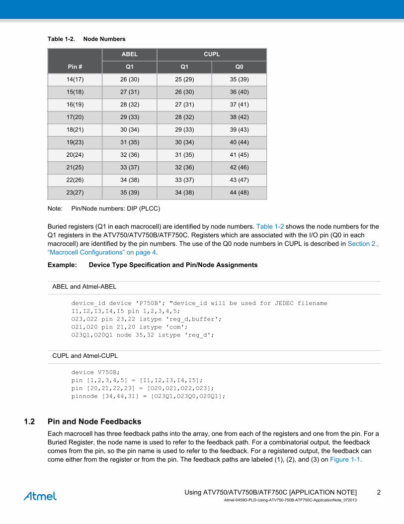
Table 1-2. Node Numbers
Note: Pin/Node numbers: DIP (PLCC)
Buried registers (Q1 in each macrocell) are identified by node numbers. Table 1-2 shows the node numbers for the Q1 registers in the ATV750/ATV750B/ATF750C. Registers which are associated with the I/O pin (Q0 in each macrocell) are identified by the pin numbers. The use of the Q0 node numbers in CUPL is described in Section 2., “Macrocell Configurations” on page 4.
Example: Device Type Specification and Pin/Node Assignments
ABEL and Atmel-ABEL
device_id device 'P750B'; "device_id will be used for JEDEC filename
I1,I2,I3,I4,I5 pin 1,2,3,4,5;
O23,O22 pin 23,22 istype 'reg_d,buffer';
O21,O20 pin 21,20 istype 'com';
O23Q1,O20Q1 node 35,32 istype 'reg_d';
CUPL and Atmel-CUPL
device V750B;
pin [1,2,3,4,5] = [I1,I2,I3,I4,I5];
pin [20,21,22,23] = [O20,O21,O22,O23];
pinnode [34,44,31] = [O23Q1,O23Q0,O20Q1];
1.2 Pin and Node Feedbacks Each macrocell has three feedback paths into the array, one from each of the registers and one from the pin. For a Buried Register, the node name is used to refer to the feedback path. For a combinatorial output, the feedback comes from the pin, so the pin name is used to refer to the feedback. For a registered output, the feedback can come either from the register or from the pin. The feedback paths are labeled (1), (2), and (3) on Figure 1-1.
Pin #
ABEL CUPL
Q1 Q1 Q0
14(17) 26 (30) 25 (29) 35 (39)
15(18) 27 (31) 26 (30) 36 (40)
16(19) 28 (32) 27 (31) 37 (41)
17(20) 29 (33) 28 (32) 38 (42)
18(21) 30 (34) 29 (33) 39 (43)
19(23) 31 (35) 30 (34) 40 (44)
20(24) 32 (36) 31 (35) 41 (45)
21(25) 33 (37) 32 (36) 42 (46)
22(26) 34 (38) 33 (37) 43 (47)
23(27) 35 (39) 34 (38) 44 (48)
2Using ATV750/ATV750B/ATF750C [APPLICATION NOTE]Atmel-0459D-PLD-Using-ATV750-750B-ATF750C-ApplicationNote_072013
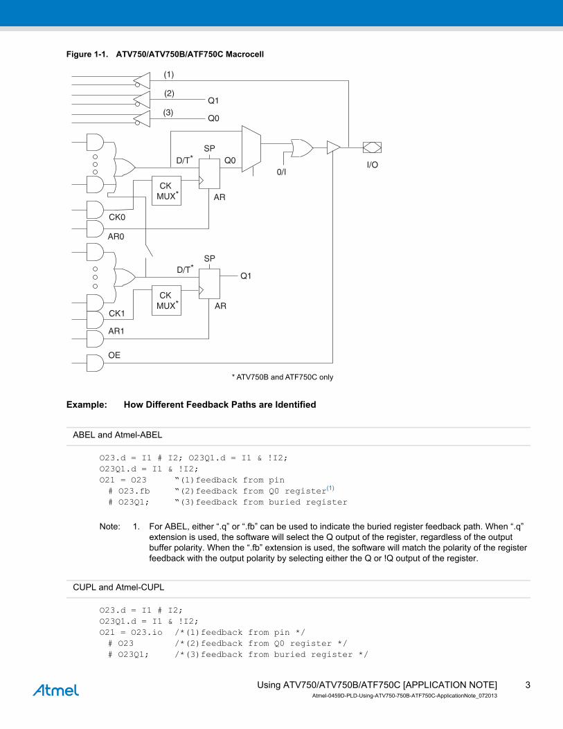
Figure 1-1. ATV750/ATV750B/ATF750C Macrocell
Example: How Different Feedback Paths are Identified
ABEL and Atmel-ABEL
O23.d = I1 # I2; O23Q1.d = I1 & !I2;
O23Q1.d = I1 & !I2;
O21 = O23 “(1)feedback from pin
# O23.fb “(2)feedback from Q0 register(1)
# O23Q1; “(3)feedback from buried register
Note: 1. For ABEL, either “.q” or “.fb” can be used to indicate the buried register feedback path. When “.q” extension is used, the software will select the Q output of the register, regardless of the output buffer polarity. When the “.fb” extension is used, the software will match the polarity of the register feedback with the output polarity by selecting either the Q or !Q output of the register.
CUPL and Atmel-CUPL
O23.d = I1 # I2;
O23Q1.d = I1 & !I2;
O21 = O23.io /*(1)feedback from pin */
# O23 /*(2)feedback from Q0 register */
# O23Q1; /*(3)feedback from buried register */
* ATV750B and ATF750C only
3Using ATV750/ATV750B/ATF750C [APPLICATION NOTE]Atmel-0459D-PLD-Using-ATV750-750B-ATF750C-ApplicationNote_072013
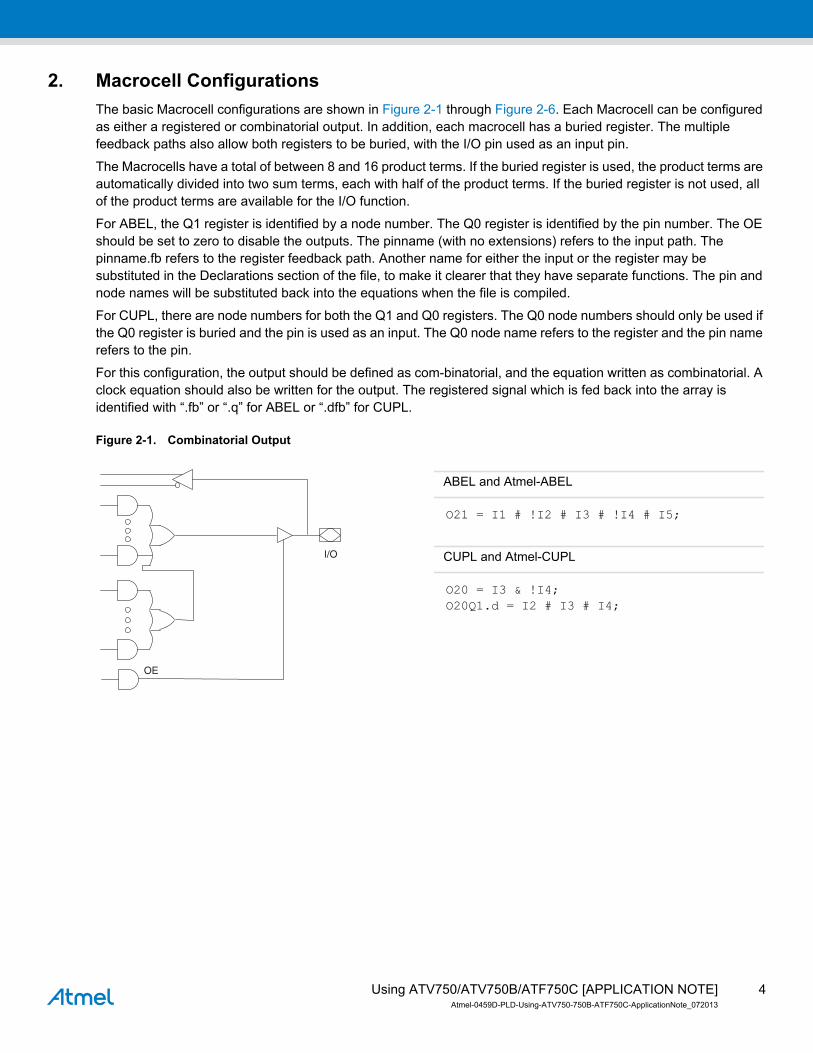
2. Macrocell Configurations The basic Macrocell configurations are shown in Figure 2-1 through Figure 2-6. Each Macrocell can be configured as either a registered or combinatorial output. In addition, each macrocell has a buried register. The multiple feedback paths also allow both registers to be buried, with the I/O pin used as an input pin.
The Macrocells have a total of between 8 and 16 product terms. If the buried register is used, the product terms are automatically divided into two sum terms, each with half of the product terms. If the buried register is not used, all of the product terms are available for the I/O function.
For ABEL, the Q1 register is identified by a node number. The Q0 register is identified by the pin number. The OE should be set to zero to disable the outputs. The pinname (with no extensions) refers to the input path. The pinname.fb refers to the register feedback path. Another name for either the input or the register may be substituted in the Declarations section of the file, to make it clearer that they have separate functions. The pin and node names will be substituted back into the equations when the file is compiled.
For CUPL, there are node numbers for both the Q1 and Q0 registers. The Q0 node numbers should only be used if the Q0 register is buried and the pin is used as an input. The Q0 node name refers to the register and the pin name refers to the pin.
For this configuration, the output should be defined as com-binatorial, and the equation written as combinatorial. A clock equation should also be written for the output. The registered signal which is fed back into the array is identified with “.fb” or “.q” for ABEL or “.dfb” for CUPL.
Figure 2-1. Combinatorial Output
ABEL and Atmel-ABEL
O21 = I1 # !I2 # I3 # !I4 # I5;
CUPL and Atmel-CUPL
O20 = I3 & !I4;
O20Q1.d = I2 # I3 # I4;
4Using ATV750/ATV750B/ATF750C [APPLICATION NOTE]Atmel-0459D-PLD-Using-ATV750-750B-ATF750C-ApplicationNote_072013
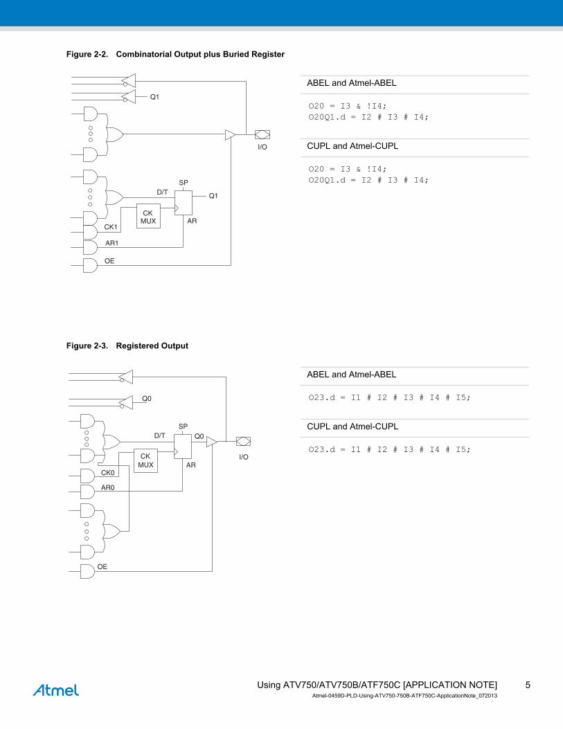
Figure 2-2. Combinatorial Output plus Buried Register
Figure 2-3. Registered Output
ABEL and Atmel-ABEL
O20 = I3 & !I4;
O20Q1.d = I2 # I3 # I4;
CUPL and Atmel-CUPL
O20 = I3 & !I4;
O20Q1.d = I2 # I3 # I4;
ABEL and Atmel-ABEL
O23.d = I1 # I2 # I3 # I4 # I5;
CUPL and Atmel-CUPL
O23.d = I1 # I2 # I3 # I4 # I5;
5Using ATV750/ATV750B/ATF750C [APPLICATION NOTE]Atmel-0459D-PLD-Using-ATV750-750B-ATF750C-ApplicationNote_072013
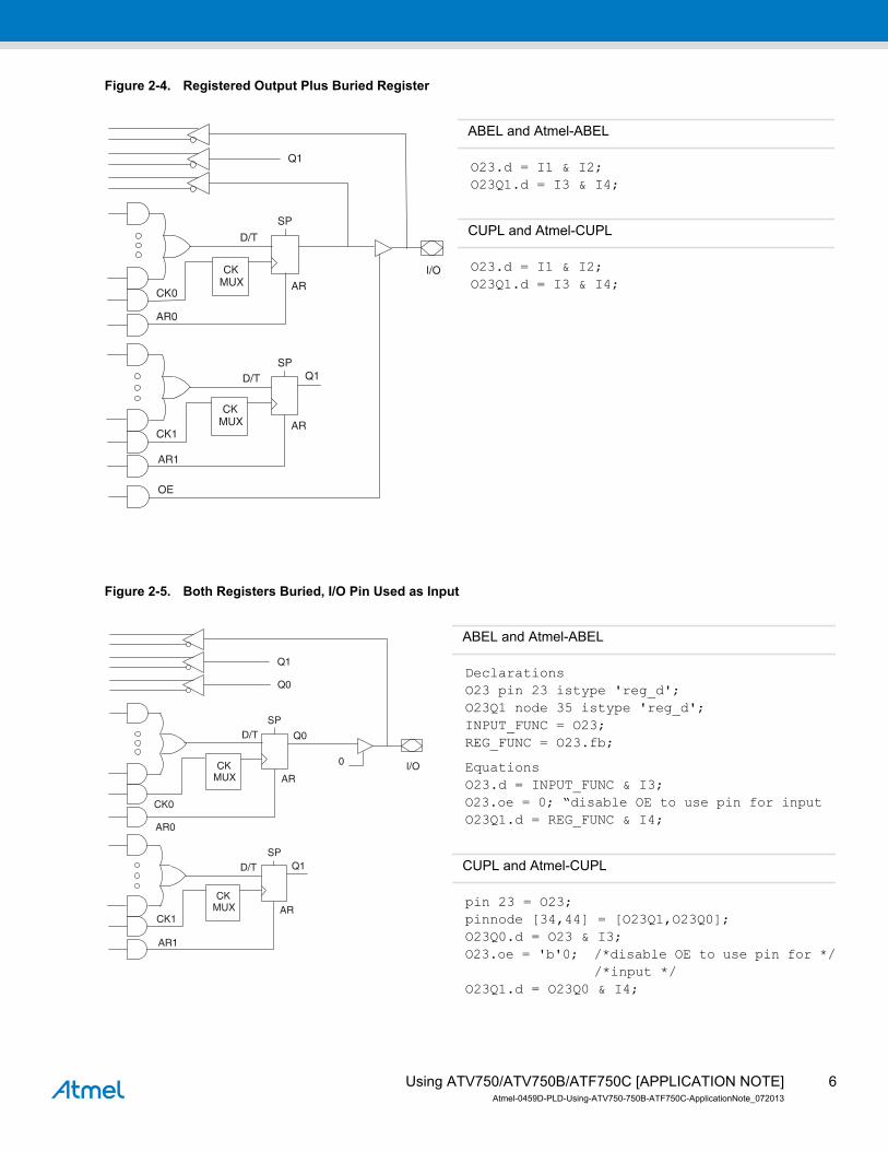
Figure 2-4. Registered Output Plus Buried Register
Figure 2-5. Both Registers Buried, I/O Pin Used as Input
ABEL and Atmel-ABEL
O23.d = I1 & I2;
O23Q1.d = I3 & I4;
CUPL and Atmel-CUPL
O23.d = I1 & I2;
O23Q1.d = I3 & I4;
ABEL and Atmel-ABEL
Declarations
O23 pin 23 istype 'reg_d';
O23Q1 node 35 istype 'reg_d';
INPUT_FUNC = O23;
REG_FUNC = O23.fb;
Equations
O23.d = INPUT_FUNC & I3;
O23.oe = 0; “disable OE to use pin for input
O23Q1.d = REG_FUNC & I4;
CUPL and Atmel-CUPL
pin 23 = O23;
pinnode [34,44] = [O23Q1,O23Q0];
O23Q0.d = O23 & I3;
O23.oe = 'b'0; /*disable OE to use pin for */
/*input */
O23Q1.d = O23Q0 & I4;
6Using ATV750/ATV750B/ATF750C [APPLICATION NOTE]Atmel-0459D-PLD-Using-ATV750-750B-ATF750C-ApplicationNote_072013
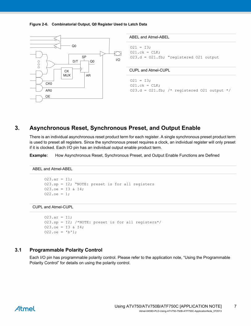
Figure 2-6. Combinatorial Output, Q0 Register Used to Latch Data
3. Asynchronous Reset, Synchronous Preset, and Output EnableThere is an individual asynchronous reset product term for each register. A single synchronous preset product term is used to preset all registers. Since the synchronous preset requires a clock, an individual register will only preset if it is clocked. Each I/O pin has an individual output enable product term.
Example: How Asynchronous Reset, Synchronous Preset, and Output Enable Functions are Defined
ABEL and Atmel-ABEL
O23.ar = I1;
O23.sp = I2; “NOTE: preset is for all registers
O23.oe = I3 & I4;
O22.oe = 1;
CUPL and Atmel-CUPL
O23.ar = I1;
O23.sp = I2; /*NOTE: preset is for all registers*/
O23.oe = I3 & I4;
O22.oe = 'b'1;
3.1 Programmable Polarity Control Each I/O pin has programmable polarity control. Please refer to the application note, “Using the Programmable Polarity Control” for details on using the polarity control.
ABEL and Atmel-ABEL
O21 = I3;
O21.ck = CLK;
O23.d = O21.fb; “registered O21 output
CUPL and Atmel-CUPL
O21 = I3;
O21.ck = CLK;
O23.d = O21.fb; /* registered O21 output */
7Using ATV750/ATV750B/ATF750C [APPLICATION NOTE]Atmel-0459D-PLD-Using-ATV750-750B-ATF750C-ApplicationNote_072013
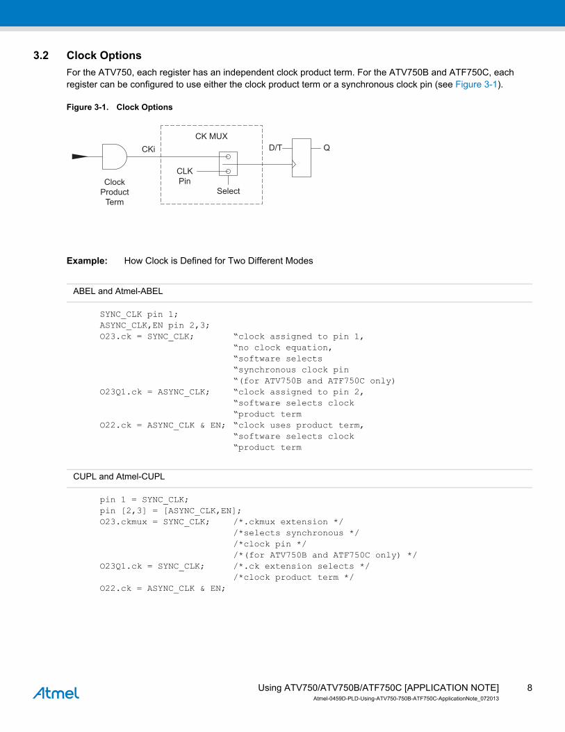
3.2 Clock Options For the ATV750, each register has an independent clock product term. For the ATV750B and ATF750C, each register can be configured to use either the clock product term or a synchronous clock pin (see Figure 3-1).
Figure 3-1. Clock Options
Example: How Clock is Defined for Two Different Modes
ABEL and Atmel-ABEL
SYNC_CLK pin 1;
ASYNC_CLK,EN pin 2,3;
O23.ck = SYNC_CLK; “clock assigned to pin 1,
“no clock equation,
“software selects
“synchronous clock pin
“(for ATV750B and ATF750C only)
O23Q1.ck = ASYNC_CLK; “clock assigned to pin 2,
“software selects clock
“product term
O22.ck = ASYNC_CLK & EN; “clock uses product term,
“software selects clock
“product term
CUPL and Atmel-CUPL
pin 1 = SYNC_CLK;
pin [2,3] = [ASYNC_CLK,EN];
O23.ckmux = SYNC_CLK; /*.ckmux extension */
/*selects synchronous */
/*clock pin */
/*(for ATV750B and ATF750C only) */
O23Q1.ck = SYNC_CLK; /*.ck extension selects */
/*clock product term */
O22.ck = ASYNC_CLK & EN;
ClockProduct
Term
CKiCK MUX
CLKPin
Select
D/T Q
8Using ATV750/ATV750B/ATF750C [APPLICATION NOTE]Atmel-0459D-PLD-Using-ATV750-750B-ATF750C-ApplicationNote_072013
3.3 D-type or T-type RegistersFor the ATV750, the registers can only be configured as D-type flip-flops. For the ATV750B and ATF750C, the registers can be configured as either D-type or T-type flip-flops.
Example: How to Configure Registers as Either D-type or T-type
ABEL and Atmel-ABEL
O13 pin 13 istype 'reg_t';
O23.d = I1 & I2;
O13.t = I1 # I2;
CUPL and Atmel-CUPL
pin 13 = O13;
O23.d = I1 & I2;
O13.t = I1 # I2;
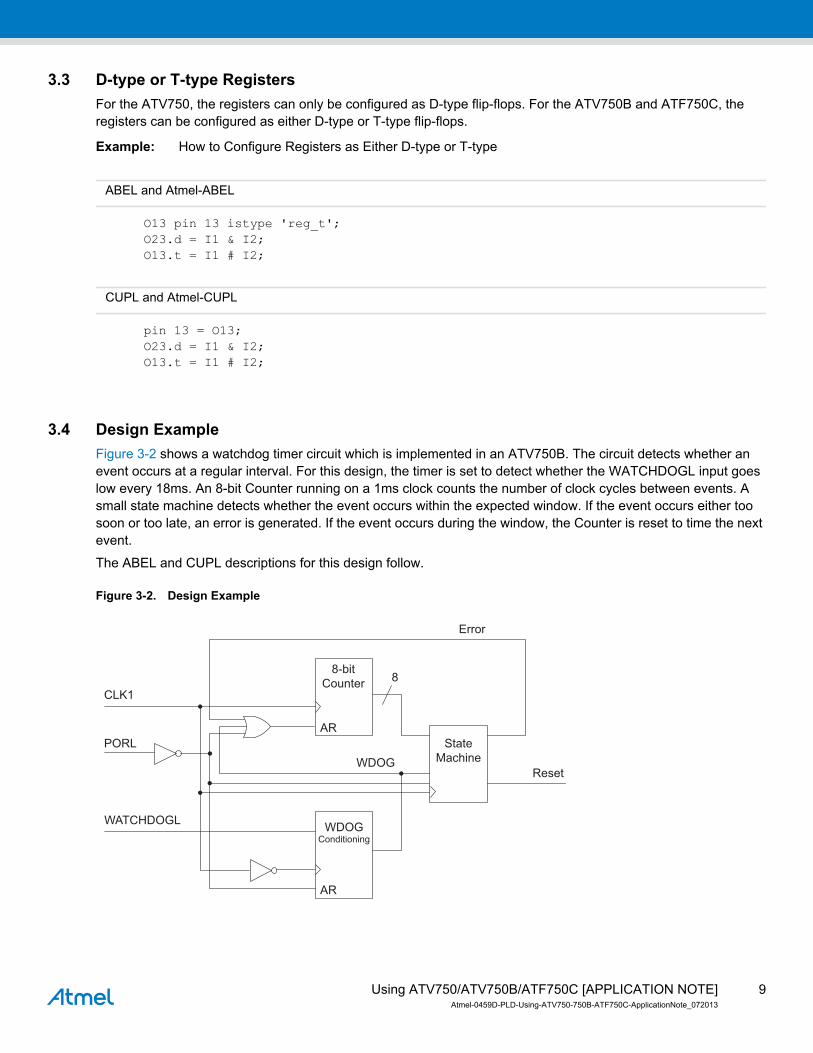
3.4 Design ExampleFigure 3-2 shows a watchdog timer circuit which is implemented in an ATV750B. The circuit detects whether an event occurs at a regular interval. For this design, the timer is set to detect whether the WATCHDOGL input goes low every 18ms. An 8-bit Counter running on a 1ms clock counts the number of clock cycles between events. A small state machine detects whether the event occurs within the expected window. If the event occurs either too soon or too late, an error is generated. If the event occurs during the window, the Counter is reset to time the next event.
The ABEL and CUPL descriptions for this design follow.
Figure 3-2. Design Example
CLK1
PORL
WATCHDOGL
Error
8-bitCounter 8
ARState
MachineReset
WDOG
WDOGConditioning
AR
9Using ATV750/ATV750B/ATF750C [APPLICATION NOTE]Atmel-0459D-PLD-Using-ATV750-750B-ATF750C-ApplicationNote_072013
4. Example ABEL Description Filemodule WATCH;
title ’Watchdog Timer V750B Design Example
ATMEL Corporation March 27, 1995’;
WATCH device ’P750B’;
CLK1,WATCHDOGL,PORL pin 1,2,3;
RESET,CLEARCOUNT pin 23,22 istype ’com,buffer’;
ERRPULSE,ERRPULSE2 pin 21,20 istype ’reg_d,buffer’;
WDOG,WDOG2 pin 17,16 istype ’reg_d,buffer’;
Q0,Q1,Q2,Q3,Q4,Q5,Q6,Q7 node 35,34,33,32,29,28,27,26 istype ’reg_t’;
REGA, REGB pin 18,19 istype ’reg_d,buffer’;
COUNT8 = [Q7..Q0]; "8-bit counter
H,L,Z,C,K,X,U,D = 1,0,.Z.,.C.,.K.,.X.,.U.,.D.;
"Define state values
POWERUP = ^B00;
IDLE = ^B10;
WAIT = ^B01;
ERROR = ^B11;
STATE_MACH = [REGB,REGA];
"Internal counter values used in state machine
" (these are 1 less than actual due to state machine delay)
LT18 = (COUNT8 < 16);
GT22 = (COUNT8 > 20);
MS256 = (COUNT8 == 255);
IRESET = (STATE_MACH == ERROR);
Equations
" For WATCHDOGL input, generate a 1 clock cycle wide pulse.
" Uses opposite edge of system clock from the state machine to
" insure that there are no setup or metastability problems between
" the inputs to the state machine and the state machine clock.
WDOG.d = (!WATCHDOGL & !WDOG2.fb);
WDOG2.d = (!WATCHDOGL);
WDOG.ck = !CLK1;
WDOG2.ck = !CLK1;
WDOG.ar = !PORL;
WDOG2.ar = !PORL;
" Generate 1 clock cycle wide error pulse upon entering ERROR
" state. Uses opposite clock edge from state machine to ensure
" error pulse generation is clean.
ERRPULSE.d = (IRESET & !ERRPULSE2.fb);
ERRPULSE2.d = IRESET;
ERRPULSE.ck = !CLK1;
ERRPULSE2.ck = !CLK1;
10Using ATV750/ATV750B/ATF750C [APPLICATION NOTE]Atmel-0459D-PLD-Using-ATV750-750B-ATF750C-ApplicationNote_072013
ERRPULSE.ar = !PORL;
ERRPULSE2.ar = !PORL;
"256mS Internal Timer
" (resets on power-up reset, watchdog input, or ERROR state)
CLEARCOUNT = (!PORL # WDOG # ERRPULSE.fb);
COUNT8.ck = CLK1;
COUNT8.ar = CLEARCOUNT;
COUNT8.t = (COUNT8 + 1) $ COUNT8;
RESET = (!PORL # IRESET); "external RESET output
"State machine clocks and resets
STATE_MACH.ck = CLK1;
STATE_MACH.ar = !PORL;
state_diagram STATE_MACH;
state POWERUP:
if (WDOG & !MS256) then IDLE;
else if (MS256) then ERROR;
else POWERUP;
state IDLE:
if (WDOG) then ERROR;
else if (!LT18) then WAIT;
else IDLE;
state WAIT:
if (WDOG) then IDLE;
else if (!WDOG & GT22) then ERROR;
else WAIT;
state ERROR:
if (MS256) then POWERUP;
else ERROR;
"Test normal powerup and normal watchdog input
TEST_VECTORS (
[CLK1, PORL, WATCHDOGL ] -> [STATE_MACH, COUNT8, RESET])
[ U, 0, X ] -> [POWERUP, 0, 1 ];
[ K, 1, 1 ] -> [POWERUP, 1, 0 ];
[ K, 1, 1 ] -> [POWERUP, 2, 0 ];
[ K, 1, 1 ] -> [POWERUP, 3, 0 ];
[ K, 1, 0 ] -> [IDLE, 0, 0 ];
@@CONST CNT = 0;
@@REPEAT 9 {
@@CONST CNT = CNT + 1;
[ K, 1, 0 ] -> [ IDLE, CNT, 0 ];}
@@REPEAT 7 {
@@CONST CNT = CNT + 1;
[ K, 1, 1 ] -> [IDLE, CNT, 0 ];}
[ K, 1, 1 ] -> [WAIT, 17, 0 ];
[ K, 1, 1 ] -> [WAIT, 18, 0 ];
[ K, 1, 1 ] -> [WAIT, 19, 0 ];
[ K, 1, 0 ] -> [IDLE, 0, 0 ];
[ K, 1, 0 ] -> [IDLE, 1, 0 ];
[ K, 1, 0 ] -> [IDLE, 2, 0 ];
11Using ATV750/ATV750B/ATF750C [APPLICATION NOTE]Atmel-0459D-PLD-Using-ATV750-750B-ATF750C-ApplicationNote_072013
"Now test various state transitions and timeouts
TEST_VECTORS (
[CLK1, PORL,WATCHDOGL] -> [STATE_MACH,COUNT8,RESET])
[ U, 0, X ] -> [POWERUP, 0, 1 ];
[ K, 1, 1 ] -> [POWERUP, 1, 0 ];
[ K, 1, 1 ] -> [POWERUP, 2, 0 ];
[ K, 1, 1 ] -> [POWERUP, 3, 0 ];
[ K, 1, 0 ] -> [IDLE, 0, 0 ];
@@CONST CNT = 0;
@@REPEAT 15 {
@@CONST CNT = CNT + 1;
[ K, 1, 1 ] -> [IDLE, CNT, 0 ];
[ K, 1, 1 ] -> [IDLE, 16, 0 ];
[ K, 1, 1 ] -> [WAIT, 17, 0 ];
[ K, 1, 1 ] -> [WAIT, 18, 0 ];
[ K, 1, 1 ] -> [WAIT, 19, 0 ];
[ K, 1, 1 ] -> [WAIT, 20, 0 ];
[ K, 1, 1 ] -> [WAIT, 21, 0 ];
[ K, 1, 1 ] -> [ERROR, 22, 1 ]; "Input doesn’t happen
[ K, 1, 1 ] -> [ERROR, 0, 1 ];
[ K, 1, 1 ] -> [ERROR, 1, 1 ];
[ K, 0, X ] -> [POWERUP, 0, 1 ]; "RESET
[ K, 1, 1 ] -> [POWERUP, 1, 0 ];
[ K, 1, 0 ] -> [IDLE, 0, 0 ];
[ K, 1, 1 ] -> [IDLE, 1, 0 ];
[ K, 1, 0 ] -> [ERROR, 0, 1 ]; "Input hits too soon
[ K, 1, 1 ] -> [ERROR, 0, 1 ];
[ K, 1, 1 ] -> [ERROR, 1, 1 ];
[ U, 0, 1 ] -> [POWERUP, 0, 1 ];
@@REPEAT 255 { "Test POWERUP timeout
[ K, 1, 1 ] -> [POWERUP, X, 0 ];
@@REPEAT 257 { "Test ERROR timeout
[ K, 1, 1 ] -> [ ERROR, X, 1 ];
[ K, 1, 1 ] -> [POWERUP, X, 0 ];
[ K, 1, 1 ] -> [POWERUP, X, 0 ];
[ K, 1, 1 ] -> [POWERUP, X, 0 ];
END WATCH;
12Using ATV750/ATV750B/ATF750C [APPLICATION NOTE]Atmel-0459D-PLD-Using-ATV750-750B-ATF750C-ApplicationNote_072013
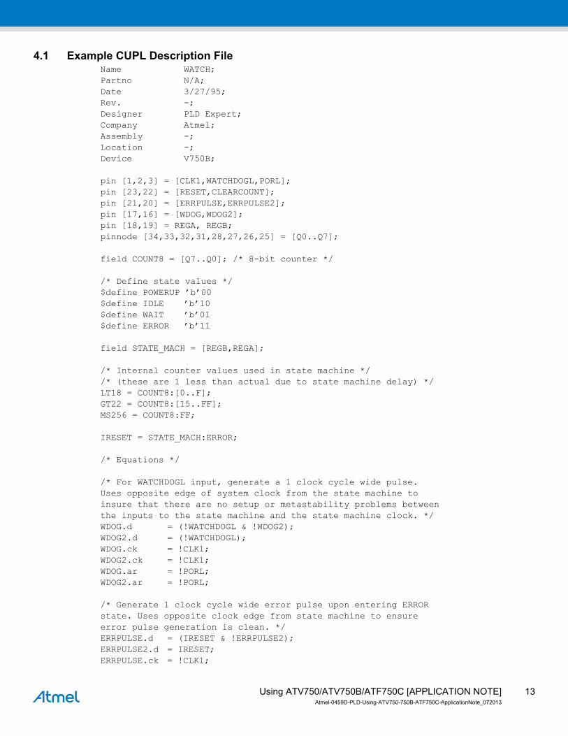
4.1 Example CUPL Description FileName WATCH;
Partno N/A;
Date 3/27/95;
Rev. -;
Designer PLD Expert;
Company Atmel;
Assembly -;
Location -;
Device V750B;
pin [1,2,3] = [CLK1,WATCHDOGL,PORL];
pin [23,22] = [RESET,CLEARCOUNT];
pin [21,20] = [ERRPULSE,ERRPULSE2];
pin [17,16] = [WDOG,WDOG2];
pin [18,19] = REGA, REGB;
pinnode [34,33,32,31,28,27,26,25] = [Q0..Q7];
field COUNT8 = [Q7..Q0]; /* 8-bit counter */
/* Define state values */
$define POWERUP ’b’00
$define IDLE ’b’10
$define WAIT ’b’01
$define ERROR ’b’11
field STATE_MACH = [REGB,REGA];
/* Internal counter values used in state machine */
/* (these are 1 less than actual due to state machine delay) */
LT18 = COUNT8:[0..F];
GT22 = COUNT8:[15..FF];
MS256 = COUNT8:FF;
IRESET = STATE_MACH:ERROR;
/* Equations */
/* For WATCHDOGL input, generate a 1 clock cycle wide pulse.
Uses opposite edge of system clock from the state machine to
insure that there are no setup or metastability problems between
the inputs to the state machine and the state machine clock. */
WDOG.d = (!WATCHDOGL & !WDOG2);
WDOG2.d = (!WATCHDOGL);
WDOG.ck = !CLK1;
WDOG2.ck = !CLK1;
WDOG.ar = !PORL;
WDOG2.ar = !PORL;
/* Generate 1 clock cycle wide error pulse upon entering ERROR
state. Uses opposite clock edge from state machine to ensure
error pulse generation is clean. */
ERRPULSE.d = (IRESET & !ERRPULSE2);
ERRPULSE2.d = IRESET;
ERRPULSE.ck = !CLK1;
13Using ATV750/ATV750B/ATF750C [APPLICATION NOTE]Atmel-0459D-PLD-Using-ATV750-750B-ATF750C-ApplicationNote_072013
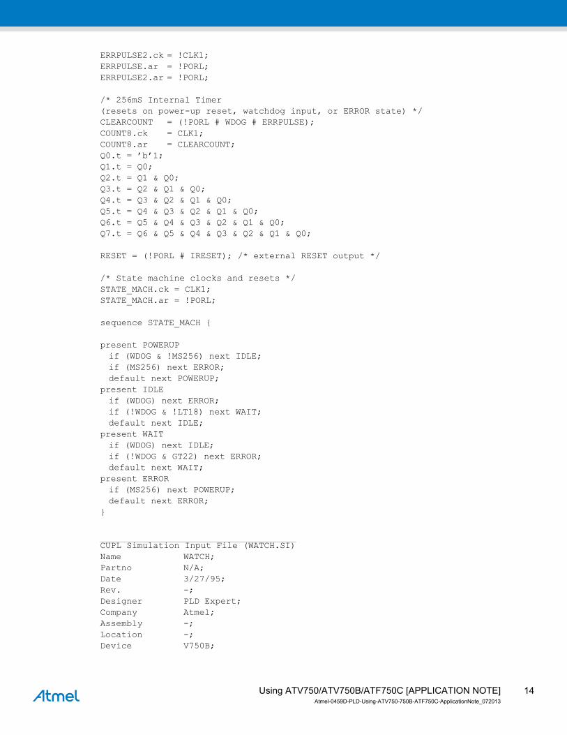
ERRPULSE2.ck = !CLK1;
ERRPULSE.ar = !PORL;
ERRPULSE2.ar = !PORL;
/* 256mS Internal Timer
(resets on power-up reset, watchdog input, or ERROR state) */
CLEARCOUNT = (!PORL # WDOG # ERRPULSE);
COUNT8.ck = CLK1;
COUNT8.ar = CLEARCOUNT;
Q0.t = ’b’1;
Q1.t = Q0;
Q2.t = Q1 & Q0;
Q3.t = Q2 & Q1 & Q0;
Q4.t = Q3 & Q2 & Q1 & Q0;
Q5.t = Q4 & Q3 & Q2 & Q1 & Q0;
Q6.t = Q5 & Q4 & Q3 & Q2 & Q1 & Q0;
Q7.t = Q6 & Q5 & Q4 & Q3 & Q2 & Q1 & Q0;
RESET = (!PORL # IRESET); /* external RESET output */
/* State machine clocks and resets */
STATE_MACH.ck = CLK1;
STATE_MACH.ar = !PORL;
sequence STATE_MACH {
present POWERUP
if (WDOG & !MS256) next IDLE;
if (MS256) next ERROR;
default next POWERUP;
present IDLE
if (WDOG) next ERROR;
if (!WDOG & !LT18) next WAIT;
default next IDLE;
present WAIT
if (WDOG) next IDLE;
if (!WDOG & GT22) next ERROR;
default next WAIT;
present ERROR
if (MS256) next POWERUP;
default next ERROR;
}
CUPL Simulation Input File (WATCH.SI)
Name WATCH;
Partno N/A;
Date 3/27/95;
Rev. -;
Designer PLD Expert;
Company Atmel;
Assembly -;
Location -;
Device V750B;
14Using ATV750/ATV750B/ATF750C [APPLICATION NOTE]Atmel-0459D-PLD-Using-ATV750-750B-ATF750C-ApplicationNote_072013
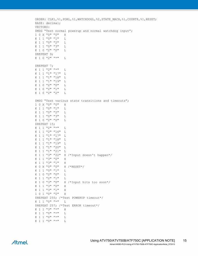
ORDER: CLK1,%1,PORL,%1,WATCHDOGL,%2,STATE_MACH,%1,COUNT8,%1,RESET;
BASE: decimal;
VECTORS:
$MSG “Test normal powerup and normal watchdog input”;
1 0 X “0" ”0" H
K 1 1 “0" ”1" L
K 1 1 “0" ”2" L
K 1 1 “0" ”3" L
K 1 0 “2" ”0" L
$REPEAT 9;
K 1 0 “2" ”*" L
$REPEAT 7;
K 1 1 “2" ”*" L
K 1 1 “1" ”17" L
K 1 1 “1" ”18" L
K 1 1 “1" ”19" L
K 1 0 “2" ”0" L
K 1 0 “2" ”1" L
K 1 0 “2" ”2" L
$MSG “Test various state transitions and timeouts”;
1 0 X “0" ”0" H
K 1 1 “0" ”1" L
K 1 1 “0" ”2" L
K 1 1 “0" ”3" L
K 1 0 “2" ”0" L
$REPEAT 15;
K 1 1 “2" ”*" L
K 1 1 “2" ”16" L
K 1 1 “1" ”17" L
K 1 1 “1" ”18" L
K 1 1 “1" ”19" L
K 1 1 “1" ”20" L
K 1 1 “1" ”21" L
K 1 1 “3" ”22" H /*Input doesn't happen*/
K 1 1 “3" ”0" H
K 1 1 “3" ”1" H
K 0 X “0" ”0" H /*RESET*/
K 1 1 “0" ”1" L
K 1 0 “2" ”0" L
K 1 1 “2" ”1" L
K 1 0 “3" ”0" H /*Input hits too soon*/
K 1 1 “3" ”0" H
K 1 1 “3" ”1" H
1 0 1 “0" ”0" H
$REPEAT 255; /*Test POWERUP timeout*/
K 1 1 “0" ”*" L
$REPEAT 257; /*Test ERROR timeout*/
K 1 1 “3" ”*" H
K 1 1 “0" ”*" L
K 1 1 “0" ”*" L
K 1 1 “0" ”*" L
15Using ATV750/ATV750B/ATF750C [APPLICATION NOTE]Atmel-0459D-PLD-Using-ATV750-750B-ATF750C-ApplicationNote_072013
5. Revision History
FunctionZZ_Summary Notes
Doc. Rev. Date Comments
0459D 07/2013Add ATF750C device.
Update template.
0459C 09/1999
16Using ATV750/ATV750B/ATF750C [APPLICATION NOTE]Atmel-0459D-PLD-Using-ATV750-750B-ATF750C-ApplicationNote_072013

XX X XAtmel Corporation 1600 Technology Drive, San Jose, CA 95110 USA T: (+1)(408) 441.0311 F: (+1)(408) 436.4200 | www.atmel.com
© 2013 Atmel Corporation. / Rev.: Atmel-0459D-PLD-Using-ATV750-750B-ATF750C-ApplicationNote_072013.
Atmel®, Atmel logo and combinations thereof, Enabling Unlimited Possibilities®, and others are registered trademarks or trademarks of Atmel Corporation or its subsidiaries. Other terms and product names may be trademarks of others.
DISCLAIMER: The information in this document is provided in connection with Atmel products. No license, express or implied, by estoppel or otherwise, to any intellectual property rightis granted by this document or in connection with the sale of Atmel products. EXCEPT AS SET FORTH IN THE ATMEL TERMS AND CONDITIONS OF SALES LOCATED ON THEATMEL WEBSITE, ATMEL ASSUMES NO LIABILITY WHATSOEVER AND DISCLAIMS ANY EXPRESS, IMPLIED OR STATUTORY WARRANTY RELATING TO ITS PRODUCTSINCLUDING, BUT NOT LIMITED TO, THE IMPLIED WARRANTY OF MERCHANTABILITY, FITNESS FOR A PARTICULAR PURPOSE, OR NON-INFRINGEMENT. IN NO EVENTSHALL ATMEL BE LIABLE FOR ANY DIRECT, INDIRECT, CONSEQUENTIAL, PUNITIVE, SPECIAL OR INCIDENTAL DAMAGES (INCLUDING, WITHOUT LIMITATION, DAMAGESFOR LOSS AND PROFITS, BUSINESS INTERRUPTION, OR LOSS OF INFORMATION) ARISING OUT OF THE USE OR INABILITY TO USE THIS DOCUMENT, EVEN IF ATMEL HASBEEN ADVISED OF THE POSSIBILITY OF SUCH DAMAGES. Atmel makes no representations or warranties with respect to the accuracy or completeness of the contents of thisdocument and reserves the right to make changes to specifications and products descriptions at any time without notice. Atmel does not make any commitment to update the informationcontained herein. Unless specifically provided otherwise, Atmel products are not suitable for, and shall not be used in, automotive applications. Atmel products are not intended,authorized, or warranted for use as components in applications intended to support or sustain life.
SAFETY-CRITICAL, MILITARY, AND AUTOMOTIVE APPLICATIONS DISCLAIMER: Atmel products are not designed for and will not be used in connection with any applications wherethe failure of such products would reasonably be expected to result in significant personal injury or death (“Safety-Critical Applications”) without an Atmel officer's specific writtenconsent. Safety-Critical Applications include, without limitation, life support devices and systems, equipment or systems for the operation of nuclear facilities and weapons systems.Atmel products are not designed nor intended for use in military or aerospace applications or environments unless specifically designated by Atmel as military-grade. Atmel products arenot designed nor intended for use in automotive applications unless specifically designated by Atmel as automotive-grade.
Related Documents


![SAMA5D3 Layout Recommendations - Microchip Technologyww1.microchip.com/downloads/en/AppNotes/Atmel... · SAMA5D3 Layout Recommendations [APPLICATION NOTE] 3 Atmel-11284B-ATARM-SAMA5D3](https://static.cupdf.com/doc/110x72/5ec95b888c0173649011ce25/sama5d3-layout-recommendations-microchip-sama5d3-layout-recommendations-application.jpg)

