Rev A00 ©2015 Finisar Corporation AN-2132 Page 1 of 33 2-June-2015 Application Note AN-2132 Designing with the AOC 10Gbps TOSA and ROSA Introduction With the advent of the IEEE 10Gbps Ethernet [1] and the ANSI X3.T11 10GFC (Fibre Channel) [2] standards, optical interconnections at serial data rates of 10Gbps are becoming more prominent in data communications networks. In addition, suppliers of these new network centric links have formed several industry groups to standardize on the mechanical and electrical interface, e.g. XENPAK, XPAK, X2, XFP [3], among others. This application note is intended to aid the design engineer in using AOC’s 10GB VCSEL (HFE6x90) and detector (HFD6x80 – 850nm, HFD6x40 – 1250-1600nm) solutions for these emerging applications. For the latest in datasheet specifications, visit http://www.finisar.com/aoc.php. Operation of lasers and detectors at 10Gbps requires a new approach to many aspects of the design of the laser packaging and ultimately transceiver packaging. AOC has designed a new TO can package while maintaining excellent mechanical, optical, and thermal characteristics at a competitive cost. The decision to maintain a TO can based infrastructure allows for a lower total cost by leveraging the significant manufacturing infrastructure. Mechanical Interface for TOSA and ROSA The AOC TOSA and ROSA assemblies consist of a TO-46 component aligned to an integral lens barrel. Connection to the next assembly is made through a flexible circuit, which gives great adaptability to a customer’s housing and PCB configuration. The features of the flexible circuit which allow this adaptability also make it vulnerable to damage during the assembly process. With care in handling the flexible circuit during assembly and careful control of the soldering temperature, successful assembly can be achieved with each device. The information contained in this application note describes the structure of the flexible circuit and lists the precautions and the process followed by the AOC for this type of assembly.

Welcome message from author
This document is posted to help you gain knowledge. Please leave a comment to let me know what you think about it! Share it to your friends and learn new things together.
Transcript

Rev A00 ©2015 Finisar Corporation AN-2132 Page 1 of 33 2-June-2015
Application Note AN-2132
Designing with the AOC 10Gbps TOSA and ROSA
Introduction
With the advent of the IEEE 10Gbps Ethernet [1] and the ANSI X3.T11 10GFC (Fibre Channel) [2]
standards, optical interconnections at serial data rates of 10Gbps are becoming more prominent in
data communications networks. In addition, suppliers of these new network centric links have
formed several industry groups to standardize on the mechanical and electrical interface, e.g.
XENPAK, XPAK, X2, XFP [3], among others. This application note is intended to aid the design
engineer in using AOC’s 10GB VCSEL (HFE6x90) and detector (HFD6x80 – 850nm, HFD6x40 –
1250-1600nm) solutions for these emerging applications. For the latest in datasheet specifications,
visit http://www.finisar.com/aoc.php.
Operation of lasers and detectors at 10Gbps requires a new approach to many aspects of the
design of the laser packaging and ultimately transceiver packaging. AOC has designed a new TO
can package while maintaining excellent mechanical, optical, and thermal characteristics at a
competitive cost. The decision to maintain a TO can based infrastructure allows for a lower total
cost by leveraging the significant manufacturing infrastructure.
Mechanical Interface for TOSA and ROSA
The AOC TOSA and ROSA assemblies consist of a TO-46 component aligned to an integral lens
barrel. Connection to the next assembly is made through a flexible circuit, which gives great
adaptability to a customer’s housing and PCB configuration. The features of the flexible circuit
which allow this adaptability also make it vulnerable to damage during the assembly process. With
care in handling the flexible circuit during assembly and careful control of the soldering temperature,
successful assembly can be achieved with each device. The information contained in this
application note describes the structure of the flexible circuit and lists the precautions and the
process followed by the AOC for this type of assembly.

Rev A00 ©2015 Finisar Corporation AN-2132 Page 2 of 33 2-June-2015
The flexible circuit used in the AOC OSAs (Optical Sub Assemblies) is designed to be thin and thus
very flexible. The core is a .002” thick polyimide layer manufactured by DuPont [4]. This is clad on
either side with ¼ oz copper. One copper layer is used for the signal traces and the other is used as
a ground plane. Over each copper layer is a .001” thick cover layer, also made by DuPont. Total
thickness of the flexible circuit is < .005”.
At the component end of the flexible circuit are copper pads which are attached to the TO-46
component leads. At the interconnect end of the flexible circuit are copper pads which are attached
to pads on the customer’s PCB.
Since the solder pads of the flexible circuit are thicker, stiffer, and sometimes wider than the traces,
the connection between the two is a weak area in the physical structure of the circuitry. For this
reason the traces have been widened (and thus strengthened) by “tear-dropping” (or expanding)
them as they approach the solder pads.
This also reduces the discontinuity seen by the high speed signals as they approach these solder
pads. The openings, which are cut in the cover layer, serve as windows to allow the solder
operation to take place.

Rev A00 ©2015 Finisar Corporation AN-2132 Page 3 of 33 2-June-2015
By removing the cover layer material that would normally strengthen this copper connection, the
traces are more susceptible to breakage in this weak area if the device is not handled correctly. In
the area of the flexible circuit where the copper trace is protected by the cover layer, the flexible
circuit can be bent once or twice to a radius as small as .015 without damage. Larger radii are
preferred, both from a physical integrity and a signal integrity standpoint. However, when the
flexible circuit is bent in the area of the trace exposed in a cover layer window, the results can often
be a broken signal trace or a broken connection to the ground plane. Careful handling is the best
means of protecting the integrity of these traces.
The amount and duration of heat used when soldering the flexible circuit to the PCB is another area
of concern. AOC VCSEL Product Group operators have been very successful in soldering the
flexible circuit using a soldering iron with a very small tip and controlling the temperature of this
soldering tip to 800 °F. All flexible circuit assembly uses lead-free
Sn-Ag-Cu alloy solder with a melting point of 217 °C (423 °F ). Since the surface of the copper has
been tin plated, there is no need to pre-tin the flexible circuit pads before assembly. Pre-tinning the
PCB pads and even heating the PCB during the solder operation may reduce the amount of time
required for the soldering operation, but this step has not been found to be necessary. Soldering the
flexible circuit to the header leads typically takes 1 - 2 seconds each. Soldering to the pads on test
boards typically takes 2 - 3 seconds each. Please note that the flexible circuit has a damage
threshold of 700 °F, so care should be taken with the tip of the soldering iron. Finally, the flex circuit
passes the solder float test for 10 seconds minimum at 288 °C.
In summary, therefore, the guidelines followed by AOC when assembling the flexible circuit are as
follows:
1. Keep bends away from the ends of the flexible circuit where the traces are exposed in the
cover layer windows.
2. Don’t pull on the flexible circuit as if trying to peel it off the back of the component.
3. Don’t push on the PCB end of the flexible circuit when forming a bend or when installing the
OSA into an assembly.
4. Carefully control and limit the soldering time and temperature to the minimum needed.
Rev A00 ©2015 Finisar Corporation AN-2132 Page 4 of 33 2-June-2015
5. This is an ESD sensitive device, so proper ESD precautions should always be taken during
every step of the assembly process.
Once soldering of the flexible circuit to the PCB is complete, there are two other areas of concern.
One is the method of securing the flexible circuit to the PCB and the other is unsoldering it from the
PCB.
The flexible circuit has two notches located at the interconnect end which can be used to align it to
the PCB. There are several ways in which epoxy can be added to provide strain relief to this
assembly.
1. Carefully insert epoxy between the flexible circuit and the PCB.
2. Apply an epoxy fillet between the edge of the PCB and the bottom of the flexible circuit.
3. Apply epoxy on top of the flexible circuit along its edges. Be careful not to place epoxy on top of
the two high speed traces as this could affect their signal integrity.
Occasionally, a TOSA or ROSA must be unsoldered from a PCB in order to be used in a different
product. The typical unsoldering process using solder braid or other solder removing tool applied
one pad at a time has consistently damaged flexible circuits rendering them unusable. The
preferred method at AOC is to add solder to all six pads and then heat them all
at the same time. Pulling the flexible circuit parallel to the surface of the PCB will safely remove the
flexible circuit from the PCB. The copper pads of the flexible circuit can then have excess solder
removed in preparation for being assembled into another product.
The product provided by AOC is not intended to contain all the plug features necessary for it to be
the front end of a module. Instead, features are present to allow it to be snugly held in an injection
molded or die cast housing. This housing would most likely be of a clamshell type (two pieces) that
would securely hold the AOC product in place as well as have the fiber cable interface features.
This housing would also have mechanical features to rigidly fix it in the customer's module housing.
TOSA and ROSA Optical Interface
AOC offers 10GB components with both an SC and LC optical interface in footprints that are
compatible with all of the associated MSA agreements. The fiber ferrule sleeve receptacle is
designed in compliance with TIA FOCIS 3 (EIA/TIA 604-3A), and TIA FOCIS 10 (EIA/TIA 604-10)
for the SC and LC respectively. A mechanical stop for the fiber end face is provided in the package,
and is referenced in the detail mechanical drawings on the datasheets. (Note: The fiber stop is also
referred to as the optical reference plane) It is recommended that users refer to the TIA FOCIS
standards for mechanical definition of the SC and LC latching mechanisms.
The 10GB TOSA is specifically designed to interface to multi-mode optical fiber. Based on the work
of the TIA FO2.2 committee, and the adoption of the Restricted Modal Launch (RML) by the IEEE

Rev A00 ©2015 Finisar Corporation AN-2132 Page 5 of 33 2-June-2015
802.3ae, AOC has designed the VCSEL and lens system to be compliant with the specifications.
While ensuring the bandwidth of the enhanced multimode fiber by restricting the modal launch into
the optical fiber, it has also been shown that similar launches can significantly improve
the bandwidth rating of traditional multimode fiber [7]. The fiber modal profile (encircled flux) of two
worst case TOSAs are shown in figure 1. The blue lines are measured encircled flux profiles as a
function of radius, and the red boxes indicate the forbidden areas. The eye diagram was taken after
510m of 2000MHz/km fiber. For details on how to measure the encircled flux in the optical fiber
from the VCSEL launch, the reader is referred to the TIA/EIA 455-203. While the launch
conditioning is critical for performance on the enhanced bandwidth multimode optical fiber, it will
also generally greatly increase the reach of lower grade optical fiber, and link lengths far exceeding
the 10GB Ethernet standards may be observed in application.
Figure 1
TOSA and ROSA Electrical Interface
Traditional laser packages such as the Transistor Outline (TO) style packages have been used for
lasers in data links operating up to 2.5Gbps, and continue to be the package of choice for those
applications. However, it has long been recognized by the telecommunications industry that these
packages suffer from significant electrical parasitics that make operation at higher data rates very
difficult. The butterfly style package and silicon optical bench (SiOB) designs work well for edge
emitting lasers, but are not easily adaptable to low cost VCSEL packaging, and more importantly, to
packages with optical connectors instead of fiber pigtails. In addition, Butterfly style packages also
do not lend themselves to the highly automated assembly required of low cost components, and are
not easily edge mounted in a customer application. Recently, there has been a great deal of interest
in making TO style cans with reduced electrical parasitics such that they are amenable to operation
at 10Gbps. Our studies indicate that operation at 10Gbps is possible in some TO style packages in
a well controlled manufacturing environment. Early 10Gbps designs at AOC focused on a hybrid
microwave ceramic approach which yielded much better results than early TO samples. Since then,
AOC has designed a TO based TOSA that has equal electro-optical performance, and fits the

Rev A00 ©2015 Finisar Corporation AN-2132 Page 6 of 33 2-June-2015
embedded TO manufacturing infrastructure. The TO approach will help meet the cost requirements
of the market, and allow for very quick volume ramp up capability. The TO package also uses a
flexible circuit interface.
The ROSA solution is a similar TO can based design which has excellent electrical characteristics.
The ROSA contains a fast photodiode, a transimpedance amplifier, and several passive
components. The flexible circuit interface to the package was designed to allow the user to comply
with any of the Multi-Source Agreements (MSAs) that dictate the transceiver electrical, mechanical,
and optical interfaces.
To build an electrical interface model for the VCSEL, each of the parts are analyzed independently
into lumped circuit elements as indicated in the figure 2 drawing below.
Figure 2
The first piece to be analyzed is the VCSEL chip itself. Measurement of the S11 parameter is
perhaps the best way to characterize the electrical impedance of the VCSEL. S11 can also be used
to extract a lumped circuit model for the VCSEL. While the validity of lumped circuits at these
operational frequencies is questionable, they are nonetheless an excellent visual tool for the
designing engineer. Figure 3 is a representation of the VCSEL equivalent circuit. The model
includes the bond wire inductance to the VCSEL, but no other packaging related parasitics. The
VCSEL equivalent circuit model depicted below is for a cathode driven device. Other configurations
will have variances in the placement of wire bonds.
Figure 3
Rev A00 ©2015 Finisar Corporation AN-2132 Page 7 of 33 2-June-2015
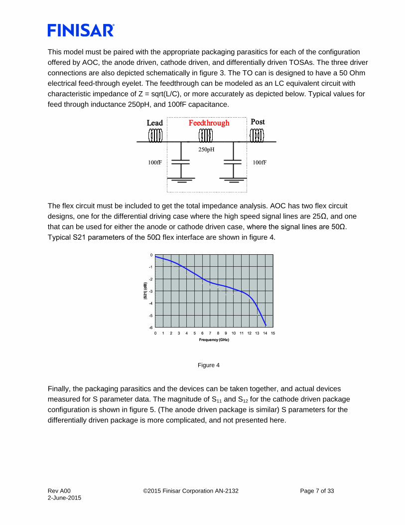
This model must be paired with the appropriate packaging parasitics for each of the configuration
offered by AOC, the anode driven, cathode driven, and differentially driven TOSAs. The three driver
connections are also depicted schematically in figure 3. The TO can is designed to have a 50 Ohm
electrical feed-through eyelet. The feedthrough can be modeled as an LC equivalent circuit with
characteristic impedance of Z = sqrt(L/C), or more accurately as depicted below. Typical values for
feed through inductance 250pH, and 100fF capacitance.
The flex circuit must be included to get the total impedance analysis. AOC has two flex circuit
designs, one for the differential driving case where the high speed signal lines are 25Ω, and one
that can be used for either the anode or cathode driven case, where the signal lines are 50Ω.
Typical S21 parameters of the 50Ω flex interface are shown in figure 4.
Figure 4
Finally, the packaging parasitics and the devices can be taken together, and actual devices
measured for S parameter data. The magnitude of S11 and S12 for the cathode driven package
configuration is shown in figure 5. (The anode driven package is similar) S parameters for the
differentially driven package is more complicated, and not presented here.

Rev A00 ©2015 Finisar Corporation AN-2132 Page 8 of 33 2-June-2015
Figure 5
While AOC offers three different packaging configurations for the VCSEL, it is left to the designer to
decide which of the configurations best suits the application. Choice of configurations depends on
the laser driver chosen, the board level parasitics, etc. The user is referred to various vendors for
more information on flexible circuit board material, such as http://www.dupont.com/fcm.
The flex circuit used for the ROSA has the same characteristic impedance as the cathode/anode
driven flex described above. The output of the TIA is source terminated with 50Ω and must be
capacitively coupled at the flex interface.
The receiver package requires the photodiode to be externally biased, which can be used to
measure the average current into the photodiode. The current into pin 1 is a direct measure of the
average optical power at the receiver, and can be monotored and scaled to provide a measure of
the average incident power. This implementation was chosen instead of other implementations
because it is a direct measure of the optical power, providing the lowest error in received signal
strength indication. A schematic for doing this is shown in figure 6. The voltage drop across the
100Ω resistor is neglible.

Rev A00 ©2015 Finisar Corporation AN-2132 Page 9 of 33 2-June-2015
Figure 6
Introduction to Triple Trade Off Curves
Before discussing the triple trade off curves, it may be beneficial to describe the relationships
between extinction ratio (ER), optical modulation amplitude (OMA) and average optical power
(PAVE). Figure 7 provides a schematic of the optical signal with the relevant values identified. The
equations given are valid for linear units, and not for values expressed in decibels. In addition, a
graphical representation of the relationship between OMA and ER for various average powers is
also provided.
Figure 7

Rev A00 ©2015 Finisar Corporation AN-2132 Page 10 of 33 2-June-2015
Figure 8
Triple trade off curves represent a modern approach to specifying optical components for fiber optic
links. The trade offs represented by these curves are optical power, wavelength, and RMS spectral
width of the optical source. The trade offs are a result of modal dispersion in multimode optical fiber
and chromatic dispersion of single mode optical fiber and noise sources in both the transmitter and
receiver. To provide the lowest total cost transmitters, the standards community recognizes the
trade offs that are present in the link budget calculations. The penalties associated with the laser
spectral width are taken into account at the receiver in the form of power sensitivity, specifically in
the specified minimum OMA of the laser source. The triple trade off curves provided in 10GBASE-
SX are reproduced here for reference.
Figure 9

Rev A00 ©2015 Finisar Corporation AN-2132 Page 11 of 33 2-June-2015
For a two level system (“1” and “0”) with Gaussian noise characteristics, a signal to noise ratio of 14
is required to achieve a Bit Error Rate (BER) os 10-12. Logically, the wider the optical spectrum
used, the more dispersion and other noise sources will cause problems, making the penalties
higher for larger spectral widths. Also, the magnitude of the dispersion is a function of the center
wavelength. Taking these two together, a penalty can be calculated for a particular center
wavelength and RMS spectral width of the source. The penalty is then translated to the amplitude
differences between an optical “1” and an optical “0”, which is the Optical Modulation Amplitude
(OMA) specification. The center wavelength of the VCSEL is controlled by the epitaxial design, and
can be held within a few nanometers, and tunes with temperature at a rate of 0.06nm/C, and at a
rate of 0.15nm/mA with current. The optical power increases linearly with current. The RMS spectral
width is a function of the optical power and device design. AOC has developed a VCSEL with
excellent operational characteristics that consistently meets the RMS spectral width requirements,
having spectral width <0.4nm. This is a non-trivial design issue because conventional wisdom
would drive designers to reduce the active area diameter, however this also has the adverse effect
of increasing the RMS spectral width. RMS spectral width is also difficult to measure accurately in a
multi-transverse mode laser like a VCSEL where the mode spacing can be very small. The current
methodology specified is adequate for multi-longitudinal mode lasers. AOC is currently working with
the Telecommunications Industry Association (TIA) to define test methodologies appropriate for
multitransverse mode laser sources. The current methodology (FOTP-127) utilizes a gaussian fit to
the peaks of the optical spectrum, and works reasonably well as long as all of the peaks are
resolved. Typical mode spacing in a multi longitudinal mode laser is about 0.3nm, readily resolved
by most optical spectrum analyzers, while mode spacing can be extremely small, less than 0.05nm.
Peaks more than 20dB lower in power from the maximum are discarded. The method being
proposed by AOC will utilize the entire optical spectrum in the gaussian fitting approach, and will
lead to much better correlation within the industry. The figure below shows an optical spectrum from
a typical VCSEL (red line), and the gaussian fit using the FOTP method (green line) and the
proposed fitting method (blue line). There is reasonable agreement in the methodologies here
because all of the peaks are resolved, but the correlation is adversely effected by lack of peak
resolution.
Because of the high launch power allowed in the standard, there is a need to be aware of the trade
offs necessary to maintain eye safe operation over the entire operating lifetime and ambient
temperature. In addition to the power launched into the optical fiber, the user must be cognizant of
the power emitted from the open bore of the fiber receptacle (i.e. when there is not a fiber plugged
into the transmitter receptacle.) The open bore power must also be considered for operation over
temperature, and for operation with an average power control circuit. The design criteria that must
be considered include the tracking error of the photodiode to the light output, the temperature range
of operation, the coupling loss, extinction ratio, and the coupled optical power. AOC has developed
a launch budget analysis to assist the user in this analysis. Table 1 summarizes the approach taken,
assuming class 1 eye safety is desired.
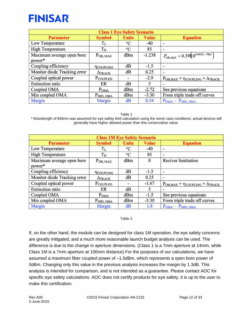
Rev A00 ©2015 Finisar Corporation AN-2132 Page 12 of 33 2-June-2015
Table 1 * Wavelength of 846nm was assumed for eye safety limit calculation using the worst case conditions; actual devices will
generally have higher allowed power than this conservative value.
Table 2
If, on the other hand, the module can be designed for class 1M operation, the eye safety concerns
are greatly mitigated, and a much more reasonable launch budget analysis can be used. The
difference is due to the change in aperture dimensions. (Class 1 is a 7mm aperture at 14mm, while
Class 1M is a 7mm aperture at 100mm distance) For the purposes of our calculations, we have
assumed a maximum fiber coupled power of –1.5dBm, which represents a open bore power of
0dBm. Changing only this value in the previous analysis increases the margin by 1.3dB. This
analysis is intended for comparison, and is not intended as a guarantee. Please contact AOC for
specific eye safety calculations. AOC does not certify products for eye safety, it is up to the user to
make this certification.
Rev A00 ©2015 Finisar Corporation AN-2132 Page 13 of 33 2-June-2015
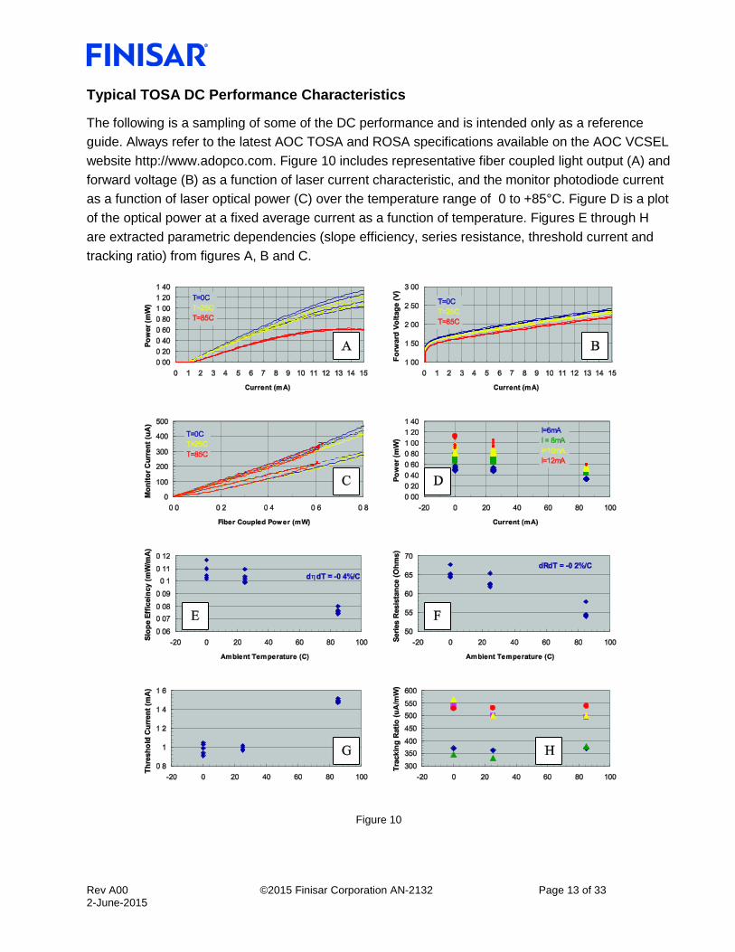
Typical TOSA DC Performance Characteristics
The following is a sampling of some of the DC performance and is intended only as a reference
guide. Always refer to the latest AOC TOSA and ROSA specifications available on the AOC VCSEL
website http://www.adopco.com. Figure 10 includes representative fiber coupled light output (A) and
forward voltage (B) as a function of laser current characteristic, and the monitor photodiode current
as a function of laser optical power (C) over the temperature range of 0 to +85°C. Figure D is a plot
of the optical power at a fixed average current as a function of temperature. Figures E through H
are extracted parametric dependencies (slope efficiency, series resistance, threshold current and
tracking ratio) from figures A, B and C.
Figure 10

Rev A00 ©2015 Finisar Corporation AN-2132 Page 14 of 33 2-June-2015
From the data measured above, predictions on how the VCSEL can best be compensated over
temperature are possible. In general, AOC recommends the use of an average power control circuit
that that can adjust the bias current to the laser to hold a fixed power output (monitor current). This
effectively handles the parabolic threshold characteristics. However, the linear change in slope
efficiency over temperature must also be compensated in order to maintain suitable optical
modulation amplitude over the expected temperature range. Using the data above, and assuming
that an OMA of –2dBm was set at room temperature, the predicted OMA values for various
amounts of slope efficiency compensation is shown in figure 11. In order to effectively operate over
the entire temperature range, it is best to closely match the actual slope change with temperature.
However, if it is only the upper ends of the temperature range that are of interest (as is more
typically the case in indoor installations), then over correction of the slope efficiency change with
temperature might be beneficial to device operation. In this example, the measured data indicates a
–0.3%/C change in the slope efficiency with temperature, and does in fact yield the most stable
results over the entire temperature range (green line), while the over corrected slope yields the
smallest change over the 0 to 70°C range (purple line).
Figure 11
Typical TOSA AC Characteristics
Eye diagram measurements at AOC are typically done in a benchtop setup using a pattern
generator to directly drive the VCSEL cathode. A dc current source is used to set the average
power from the VCSEL through the inductive channel of a bias tee. The modulation signal is a
voltage level coming from the pattern generator, which is source terminated with 50???that is AC
coupled to the VCSEL through a bias tee. The voltage is adjusted to set the OMA value. A
schematic and picture of the test configuration is shown in figure 12.

Rev A00 ©2015 Finisar Corporation AN-2132 Page 15 of 33 2-June-2015
Figure 12
Typical eye diagrams are depicted in figure 13 on the following page, over temperature measured
with this test configuration. The monitor photo-diode current was held constant during the tests. The
modulation voltage was adjusted to maintain the OMA. Each mask of the eye includes 10% margin.
Figure 13

Rev A00 ©2015 Finisar Corporation AN-2132 Page 16 of 33 2-June-2015
Figure 14 is a plot of the measured RMS spectral width of a typical VCSEL operating a constant
power of –1dBm over the temperature range of –40 to +80°C. Inset into the figure are the measured
spectra at –40, 25 and 80°C. The values reported here are measured using the FOTP 127 style
measurements. The unique design of the AOC VCSEL enables the user to meet the triple trade off
curves of IEEE 802.3ae as described earlier.
Figure 14
Foregoing the use of APC
Average power control circuits have worked very well at lower data rates, but may not be
appropriate for use in the 10Gbps applications. As described earlier in this application note, the
launch power budget for class 1 eye safety is quite restrictive. In addition, obtaining high quality
optical eye diagrams and very high reliability standards are often conflicting. Another approach is to
use a prescribed bias current across temperature which can be programmed through a EEPROM.
This approach has the advantage of being able to increase and decrease the average current in the
VCSEL to optimize both eye diagrams and reliability. Consider the example below, where eye
diagrams were collected using an average power control scheme and a programmable bias
scheme. In all cases, the OMA value was maintained at 600mW.
As can be seen in the eye diagrams, figure 15, the APC circuit does not provide the optimal eye
diagram for each of the tested temperatures. The general problem statement is that the device is
under-driven at low temperatures to achieve the best eye quality, and over driven at high
temperature to achieve the best reliability. Figure 16 summarizes the measured jitter and overshoot
as a function of the current normalized to threshold at temperatures of 0, 25, 50, and 85C.

Rev A00 ©2015 Finisar Corporation AN-2132 Page 17 of 33 2-June-2015
Figure 15
Figure 16
The key point from these graphs is that appropriate levels of overshoot and jitter (and therefore eye
quality) can be achieved at much lower currents relative to threshold as the temperature is
increased. This indicates that the bias current can actually be reduced as the temperature
increases and still maintain good eye quality. Reduction in the bias current at elevated temperature
will result in improved reliability. The data also indicate that it may be necessary to increase the bias
relative to threshold as the temperature decreases in order to maintain good eye quality. A
sampling of the eye diagrams used to generate this data is shown in the figure 17.

Rev A00 ©2015 Finisar Corporation AN-2132 Page 18 of 33 2-June-2015
Figure 17
Furthermore, this data can be used to calculate a relative speed factor as a function of the bias
current for the cases of average power control, and programmable bias control. This is plotted in
figure 18.

Rev A00 ©2015 Finisar Corporation AN-2132 Page 19 of 33 2-June-2015
Figure 18
Finally, the impact of bias control can be measured in reliability terms. By reducing the current by
1mA at the high temperature, nearly a factor of 2 in reliability can be achieved. This is depicted in
the figure 19, where the time to 1% failure is plotted for the APC scheme (blue diamonds) and the
bias control scheme (red squares).
Figure 19

Rev A00 ©2015 Finisar Corporation AN-2132 Page 20 of 33 2-June-2015
Recommended Transmitter Setup Conditions
In a typical application of Ethernet, AOC recommends that the user set the optical transceiver for
class 1M eye safety operation. This can be accomplished by first setting the average fiber coupled
power at room temperature at –1.5dBm using the bias adjustment on the laser driver. The
modulation current amplitude should be adjusted to obtain an OMA value of approximately –
1.5dBM, or an extinction ratio of approximately 5dB. If desired, temperature adjustment to the
average power should be done using the backmonitor photodiode and the laser bias current to
maintain a constant optical power over temperature. However, it is recommended that a current
clamp of 10.5mA be used in order to preserve reliability at high temperatures, and to prevent
operation close to power rollover in the VCSEL. If operation over the extended temperature range
of –40 to +85°C is required, then careful matching of the slope efficiency tempco is necessary.
Otherwise, for applications from 0 to 70°C, over correction of the slope efficiency change will yield
the most stable OMA performance. However, this may yield an excessive ER at high temperature
and lead to an increase in the deterministic jitter. Figure 20 demonstrates the performance of the
TOSA for several set up conditions of ER and PAVE at room temperature. As described earlier,
programmable laser bias as a function of temperature can be very advantageous in achieving
excellent eye quality and reliability over temperature.
Figure 20

Rev A00 ©2015 Finisar Corporation AN-2132 Page 21 of 33 2-June-2015
As can be seen in the figure 20, the eye quality general increases with increasing PAVE and
decreasing ER. For a more detailed discussion of the effects of extinction ratio and PAVE on the
optical output, the reader is referred to the AOC application note “Modulating AOC Oxide VCSELs,”
available at www.honeywell.com/vcsel. Table 2 summarizes the expected setup conditions for a
typical AOC 10Gbps TOSA.
Table 2
Use of Electrical Peaking Circuits
One problem with optical compliance testing is creating a reference transmitter that has extremely
fast rise and fall times. One method to achieve faster response times in a VCSEL is to introduce a
peaking circuit on the electrical driving waveform. The peaking circuit helps to push and pull charge
out of the capacitor storage in the VCSEL. Consider the circuit configuration shown figure 21, where
a simple RC network has been added to the VCSEL drive path. Simulation of this circuit for
frequencies of 10GBps and 5Gbps are shown as well.

Rev A00 ©2015 Finisar Corporation AN-2132 Page 22 of 33 2-June-2015
Figure 21
The effect of the peaking circuit has also been verified experimentally, and this is shown on the next
page. Also, a peaking circuit can be generated with cabling, attenuators, and power couplers. This
is shown schematically in figure 22, and results are collected in figure 23.
Figure 22

Rev A00 ©2015 Finisar Corporation AN-2132 Page 23 of 33 2-June-2015
Figure 23
Typical ROSA Characteristics
The mechanical and electrical interface of the AOC ROSA is very similar to that described earlier,
and will not be repeated here. AOC is continuously evaluating commercial transimpedance
amplifiers for use in the 10GB product. AOC is also providing solutions using a customer preferred
transimpedance amplifier. The sections that follow provide the user with general information to
calculate receiver performance based on the datasheet parameters provided by AOC. The interface
circuit may also be specific to various TIA used. Refer to the AOC receiver data sheets available at
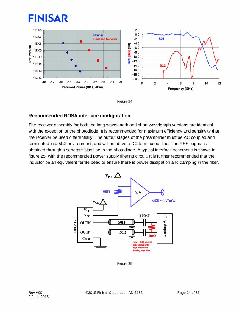
www.adopco.com for detail specifications and performance characteristics. Figure 24 demonstrates
the current BER performance of the 850nm ROSA with (red curve) and with-out (blue curve) a logic
amplifier in the measurement system. Typical sensitivity values for the 1310nm/1550nm ROSA are
1 to 2dB better due to the difference in photodiode responsivity.
Rev A00 ©2015 Finisar Corporation AN-2132 Page 24 of 33 2-June-2015
Figure 24
Recommended ROSA interface configuration
The receiver assembly for both the long wavelength and short wavelength versions are identical
with the exception of the photodiode. It is recommended for maximum efficiency and sensitivity that
the receiver be used differentially. The output stages of the preamplifier must be AC coupled and
terminated in a 50Ω environment, and will not drive a DC terminated |line. The RSSI signal is
obtained through a separate bias line to the photodiode. A typical interface schematic is shown in
figure 25, with the recommended power supply filtering circuit. It is further recommended that the
inductor be an equivalent ferrite bead to ensure there is power dissipation and damping in the filter.
Figure 25

Rev A00 ©2015 Finisar Corporation AN-2132 Page 25 of 33 2-June-2015
Figure 26
Estimating Receiver Sensitivity
In order to Accurately estimate the receiver sensitivity for an optical system, it is important to
consider all of the relevant components, such as the optical lensing system, the photodiode, the
transimpedance amplifier, and the input sensitivity level of the logical components that follow. The
analysis below is intended to take all of these variables into account; however, the accuracy for any
particular application is not guaranteed. One thing to note here is that the analysis only takes into
account vertical eye closure, and not horizontal eye closure from the various timing jitter sources.
The analysis will also only consider gaussian statistics for error probability, where for a given signal
to noise ratio, Q, the probability that an error will occur is given by,
Therefore, to achieve a probability P(Q) of bit errors < 10-12, then Q>7. However, this only
considers the noise from one of the logical states. When both logical states are considered, then
Q>14 is necessary to achieve an error rate < 10-12. The blocks that must be considered in this
analysis are the optical signal, the photodiode, the transimpedance amplifier, and the logical
circuitry to follow. For simplicity, this analysis will assume an input amplitude sensitivity to the
logical circuitry, and that a Q > 14 as sufficient to achieve error rates < 10-12. The function blocks
are depicted in figure 27.
Figure 27
The receiver sensitivity can then be estimated from the following necessary conditions,

Rev A00 ©2015 Finisar Corporation AN-2132 Page 26 of 33 2-June-2015
Where, ILIGHT (A) is the current generated by the light input into the photodiode, INOISE (A) is the RMS
noise current equivalent at the input node of the transimpedance amplifier, VOUT (V) is the output
voltage level of the TIA, and VSENSITIVITY (V) is the input sensitivity of the logic circuitry. Each of the
above variables is further defined as,
Where POPTICAL is the optical modulation amplitude (OMA as defined earlier) in units of W, ƞOPTICAL is
the efficiency of the optical lensing system, RPD is the responsivity of the photodiode (A/W), and
GTIA is the transimpedance gain (V/A) of the TIA. Taken together, the sensitivity can be expressed
then as,
Table 3 illustrates the calculation of receiver sensitivity. Please note that this document only
considered ideal optical inputs, and that degradation in receiver sensitivity can be observed with
degradation of the signal to noise ratio of the optical input. In addition, horizontal eye closure (jitter)
effects on the receiver sensitivity. It has also assumed that the signal from the photodiode is “AC”
coupled to the TIA. Refer to the AOC product data sheet for current parameters.
Note: AOC uses a COTS TIA, and is willing to customize the product offering with a TIA
provided/required by a customer.
Table 3
Designing for EMI Performance
EMI performance of the optical transceiver is a detail of the mechanical, electrical, and optical
system that is unfortunately often overlooked in initial design. The standard TOSA and ROSA
offered by AOC is made from an unfilled plastic material. Unfortunately, this material offers little
electromagnetic radiation shielding. Thus, it is imperative that the transceiver designer incorporate
EMI design principles from the very first mechanical designs.

Rev A00 ©2015 Finisar Corporation AN-2132 Page 27 of 33 2-June-2015
There are several apertures and radiation sources that should be considered. First is radiation from
the TOSA and ROSA that eminate from the various bond wires in the package. Typically the bond
wires inside the TO can are less than 1mm in length, and therefore are generally very low in
radiation. The total power radiated, PRADIATED in Watts, from a simple wire can be expressed as:
where c is the speed of light (3x10⁸ m/sec), ? is the impedance of free space (377 ?), I is the
current in the wire (A), L is the length of the wire (m), and f is the frequency (Hz). For a closed loop
antenna, the total power radiated can be expressed as:
The total power radiated for a short wire and a loop antenna are plotted in figure 28 for a current of
10mA at each frequency. In practical cases, the current will be limited due to the finite electrical
bandwidth of the TOSA and ROSA packages.
Figure 28
Radiaition from a single wire or a loop wire that can escape the packaging is generally emitted from
inside the TO can. EMI from this source can only be effected by the user through reduction of
modulation current.
The second type of radiation emission sources that must be considered is emissions from the
electronic circuitry that can escape through the front of the transceiver. This type of radiation is
conrolled by introducing significant EMI shielding, typically in the form of a conductive (grounded)
surface. A general rule of thumb for electromagnetic emissions is that any openings in the shielding
should be limited to less than one tenth the wavelength. For a 10Gbps (5GHz fundamental
Rev A00 ©2015 Finisar Corporation AN-2132 Page 28 of 33 2-June-2015
frequency) system, harmonics to more than 50GHz are possible in the electrical signal. Thus, the
worst-case opening should be limited to,
AOC recommends the use of metallic bezels in between the LC connector ports in the connector
design, as well as potentially using a bezel in between the components near the circuit board
connections. In the worst case for the LC connectors, in the absence of any shielding, the worst
case effective on axis opening is about 0.5mm. For SC connectors, the worst case on axis opening
is 5mm. (Note that these are projections based on the use of metallic components to hold the TOSA
and ROSA) It is critical to include extensive EMI shielding between the TOSA and ROSA for the SC
design.
To prevent electrical crosstalk between the TOSA and ROSA, it is recommended that customers
contact the ground plane of the TOSA and ROSA package to both analog and digital ground of the
transceiver. Users should be careful to minimize noise on the transceiver ground plane by utilizing
significant capacitive decoupling and controlled impedance wherever practical. It is also often
beneficial to provide power dissipation in the decoupling, such as ferrite beads in place of inductors.
Because of the close proximity in mounting of the TOSA and ROSA for duplex operation, it is
further recommended that the ROSA electrical interface be surrounded by a grounded EMI cage. If
possible, the power supplies for the TOSA and ROSA should be separated and capacitively
decoupled to ground to minimize any potential for electrical crosstalk between the components.
There is no possibility of optical crosstalk between the components.
Reliability
The reliability of AOC VCSELs is determined by two interde-pendent parameters, the temperature
of the active region, and the total current density. AOC has developed a VCSEL reliability model
that has been validated in both oxide and proton VCSELs, and for multiple aperture dimensions and
several internal configurations [8]. To a first approximation, the reliability goes as the inverse
square of the current density, which would dictate that the VCSEL should be operated at the lowest
possible current. However, the intrinsic speed of the VCSEL increases with the square root of the
current density, indicating that higher current density is better for performance. The figure below
displays the design tradeoffs.
NOTE: this set of curves does not represent typical AOC devices, but is intended only as an
educational tool for reliability and speed trade-off discussions. Contact AOC for specific
reliability calculations.
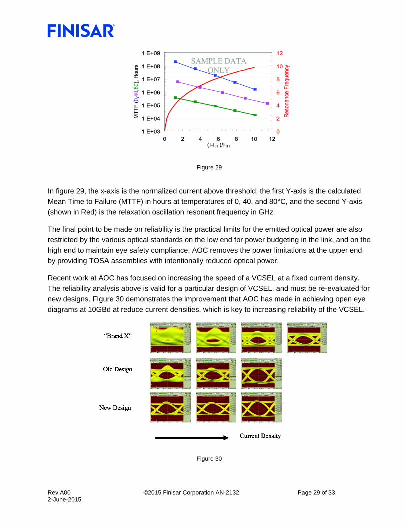
Rev A00 ©2015 Finisar Corporation AN-2132 Page 29 of 33 2-June-2015
Figure 29
In figure 29, the x-axis is the normalized current above threshold; the first Y-axis is the calculated
Mean Time to Failure (MTTF) in hours at temperatures of 0, 40, and 80°C, and the second Y-axis
(shown in Red) is the relaxation oscillation resonant frequency in GHz.
The final point to be made on reliability is the practical limits for the emitted optical power are also
restricted by the various optical standards on the low end for power budgeting in the link, and on the
high end to maintain eye safety compliance. AOC removes the power limitations at the upper end
by providing TOSA assemblies with intentionally reduced optical power.
Recent work at AOC has focused on increasing the speed of a VCSEL at a fixed current density.
The reliability analysis above is valid for a particular design of VCSEL, and must be re-evaluated for
new designs. FIgure 30 demonstrates the improvement that AOC has made in achieving open eye
diagrams at 10GBd at reduce current densities, which is key to increasing reliability of the VCSEL.
Figure 30

Rev A00 ©2015 Finisar Corporation AN-2132 Page 30 of 33 2-June-2015
The reliability of AOC VCSELs operating at 10Gbps is constantly under investigation and
improvement. Visit http://www.finisar.com/aoc.php for the current reliability metrics. Finally, the
reliability can be further improved with the use of programmable bias control, and limiting the
average current at high temperature.
Using the AOC TOSA and ROSA Evaluation Boards
The 10GB VCSEL samples are provided attached to an evaluation board for rapid evaluation and
ease of use by the customer. There are three board configurations, anode driven, cathode driven,
and differential driven. All of the boards have a common attachment means for both the TOSA and
the ROSA. Referring to Figure below, the TOSA/ROSA may be removed/replaced by
1. Remove the knurled screws holding the black contact bar in place.
2. Gently remove the flex from the board by pulling upwards. Note that there are alignment pins
for the flex on the board. Electrical contact is made by pressure from the contact bar.
3. Replace TOSA/ROSA with a new part to be evaluated
4. Replace contact bar, and tighten nuts holding bar in place
To remove the LC lens barrel assembly from the LC connector plug, remove the black plastic
insertion bar located on the bottom of the package, and gently pull the component out of the
connector mating assembly.
Electrical Connections
The evaluation board was originally designed to handle both single ended TOSAs and differential
ROSAs at the same time. Subsequent testing has indicated that the single ended trace is
significantly lower in bandwidth than the differential signal connections. It is therefore recommended
that both TOSAs and ROSAs be connected to the differential traces, and the single ended trace not
be used. Therefore, the user will need separate evaluation boards for the TOSA and ROSA. The
electrical connections are detailed in figure 31.
Anode Driven Part
To test the TOSA component, connect a current meter between the monitor diode cathode and
ground. A bias voltage is not required for the monitor diode. Using a high frequency bias tee such
as the Picometrix 5541A, connect the pattern generator output to the AC leg of the tee, and
connect a constant current source to the DC leg. The cathode contact should be terminated with a
50 ohm load.
Cathode Driven Part
To test the TOSA component, connect a current meter between the monitor diode cathode and
ground. A bias voltage is not required for the monitor diode. Connect a high frequency bias tee such
Rev A00 ©2015 Finisar Corporation AN-2132 Page 31 of 33 2-June-2015
as the Picometrix 5541A to the cathode of the VCSEL Connect the pattern generator output to the
AC leg of the tee, and connect a constant current source to the DC leg. The anode contact should
be terminated with a 50 ohm load, The cathode driven VCSEL includes a capacitor inside the TOSA.
Differential Driven Part
To test the TOSA component, connect a current meter between the monitor diode cathode and
ground. A bias voltage is not required for the monitor diode. Connect a high frequency bias tee such
as the Picometrix 5541A to both the anode and the cathode of the VCSEL. Connect the outputs of
the pattern generator to the AC legs of the bias tees, and connect a constant current source
between the DC legs of the bias tee. Differential driven parts are available with either 25 or 50 Ohm
transmission lines.
ROSA Connection
The HFD6x80 ROSA can also be evaluated on this board. Power supply filtering for both the Vcc
and Vpd connections has been provided on the board. To test the ROSA, connect a 3.3V source to
the Vcc connection. Next, connect a 3.3V source to the Vpd, this is the power supply for the PIN
photodiode. (Please note that labeling on the board is incorrect) Current into this pin is the average
current in the PD. Connect a high frequency bias tee (or DC block) such as the Picometrix 5541A to
both the differential outputs. Do not connect the DC leg of the bias tee to a power supply. The bias
tee is simply used as an AC coupling from the TIA. Connect the outputs of the TIA to a 50Ohm
terminated load, typically an oscilloscope, error detector, CDR, etc. Ensure that both sides of the
TIA are terminated or the ROSA may become unstable.
Optical characterization
Connect an LC fiber into the receptacle, and connect the other end to the optical input of an
oscilloscope, or other suitable detector. Adjust the DC current level to achieve the desired average
optical power, typically –3dBm. Adjust the amplitude of the pattern generator output to achieve the
proper optical modulation amplitude or extinction ratio. For more information on typical set points,
please refer to the earlier sections of this application note.
References
[1] IEEE 802.3ae 10GB Ethernet specifications
[2] ANSI X3.T11 10GFC specifications
[3] See for example http://www.xenpak.org/, http://www.xpak.org/, http://www.xfpmsa.org/,
http://www.x2msa.org
[4] For more information visit http://www.dupont.com, or http://www.dupont.com/fcm/products/H-
73234.pdf
[5] TIA FOCIS 604-3a specifications

Rev A00 ©2015 Finisar Corporation AN-2132 Page 32 of 33 2-June-2015
[6] TIA FOCIS 604-10 specifications
[7] P. Pepelugjuski, J. Abbott, and J. A. Tatum, “Effect of Launch Conditions on Power Penalties in
Gigabit Links Using 62.5um Core Fibers Operating at 850nm,” NIST symposium on fiber modal
bandwidth, 1998. Available at www.adopco.com
[8] B.M. Hawkins, R.A. Hawthorne III, J.K. Guenter, J.A. Tatum, J.R. Biard, "Reliability of Various
Size Oxide Aperture VCSELs," Proceedings of the 52nd Electronic Components and
Technology Conference, pp. 540-550, IEEE, Piscataway, NJ, 2002. Available at
www.adopco.com
ADVANCED OPTICAL COMPONENTS
Finisar’s ADVANCED OPTICAL COMPONENTS division was formed through strategic acquisition
of key optical component suppliers. The company has led the industry in high volume Vertical
Cavity Surface Emitting Laser (VCSEL) and associated detector technology since 1996. VCSELs
have become the primary laser source for optical data communication, and are rapidly expanding
into a wide variety of sensor applications. VCSELs’ superior reliability, low drive current, high
coupled power, narrow and circularly symmetric beam and versatile packaging options (including
arrays) are enabling solutions not possible with other optical technologies. ADVANCED OPTICAL
COMPONENTS is also a key supplier of Fabrey-Perot (FP) and Distributed Feedback (DFB) Lasers,
and Optical Isolators (OI) for use in single mode fiber data and telecommunications networks
LOCATION
Allen, TX - Business unit headquarters, VCSEL wafer growth, wafer fabrication and TO package
assembly.
Fremont, CA – Wafer growth and fabrication of 1310 to 1550nm FP and DFB lasers.
Shanghai, PRC – Optical passives assembly, including optical isolators and splitters.
SALES AND SERVICE
Finisar’s ADVANCED OPTICAL COMPONENTS division serves its customers through a worldwide
network of sales offices and distributors. For application assistance, current specifications, pricing
or name of the nearest Authorized Distributor, contact a nearby sales office or call the number listed
below.
AOC CAPABILITIES
ADVANCED OPTICAL COMPONENTS’ advanced capabilities include:
1, 2, 4, 8, and 10Gbps serial VCSEL solutions
1, 2, 4, 8, and 10Gbps serial SW DETECTOR solutions
VCSEL and detector arrays
1, 2, 4, 8, and 10Gbps FP and DFB solutions at 1310 and 1550nm

Rev A00 ©2015 Finisar Corporation AN-2132 Page 33 of 33 2-June-2015
1, 2, 4, 8, and 10Gbps serial LW DETECTOR solutions
Optical Isolators from 1260 to 1600nm range
Laser packaging in TO46, TO56, and Optical subassemblies with SC, LC, and MU interfaces for
communication networks
VCSELs operating at 670nm, 780nm, 980nm, and 1310nm in development
Sensor packages include surface mount, various plastics, chip on board, chipscale packages,
etc.
Custom packaging options
Contact Information
Finisar Corporation 1389 Moffett Park Drive Sunnyvale, CA USA 94089 Phone: +1 (408) 548-1000 Email: [email protected] Website: www.finisar.com
Related Documents


![Gerenciamiento 2132[1]](https://static.cupdf.com/doc/110x72/55908f8e1a28ab736d8b4795/gerenciamiento-21321.jpg)