INSTITUTE OF PHYSICS PUBLISHING JOURNAL OF PHYSICS: CONDENSED MATTER J. Phys.: Condens. Matter 18 (2006) 5793–5805 doi:10.1088/0953-8984/18/26/001 Apparent diameter of carbon nanotubes in scanning tunnelling microscopy measurements L Tapaszt´ o 1 ,GIM´ ark 1 , A A Ko ´ os 1 , P Lambin 2 and L P Bir ´ o 1 1 Research Institute for Technical Physics and Materials Science, H-1525 Budapest, PO Box 49, Hungary 2 Departement de Physique, FUNDP, 61 Rue de Bruxelles, B-5000 Namur, Belgium E-mail: [email protected] Received 13 March 2006 Published 16 June 2006 Online at stacks.iop.org/JPhysCM/18/5793 Abstract Geometric effects influencing scanning tunnelling microscopy (STM) image formation of single wall carbon nanotubes (SWCNTs) were studied within the framework of a simple model potential. We focused on the geometrical effects which may influence the tunnelling probabilities and lead to discrepancies between the apparent height of the nanotubes measured by STM and their real geometrical diameter. We found that there are two main factors responsible for the underestimation of nanotubes diameter by measuring their height in STM images: (1) the curvature of the nanotube affects the cross sectional shape of the tunnelling channel; (2) the decay rate of tunnelling probabilities inside the tunnel gap increases with increasing curvature of the electrodes. For a nanotube with 1 nm diameter an apparent flattening of about 10%, due to these geometry- related effects, is predicted. Furthermore these effects are found to be dependent on the diameter of the tubes and tip–sample distances: an increasing flattening of the tubes is predicted for decreasing tube diameter and increasing tip–sample distance. (Some figures in this article are in colour only in the electronic version) 1. Introduction Due to their extraordinary electronic and mechanical properties [1] carbon nanotubes (CNTs) have been in the focus of attention for more than a decade. Several potential applications of CNTs, utilizing their unique properties have already been demonstrated, including CNT transistors [2] and logical circuits [3]. The electronic structure of a freestanding single wall carbon nanotube (SWNT) is uniquely determined by its atomic structure and geometry [4]. These all-carbon molecules can be metallic or semiconducting according to the (n, m) wrapping indices of the graphene sheet. Simple tight-binding theory reproduces this relation remarkably 0953-8984/06/265793+13$30.00 © 2006 IOP Publishing Ltd Printed in the UK 5793

Welcome message from author
This document is posted to help you gain knowledge. Please leave a comment to let me know what you think about it! Share it to your friends and learn new things together.
Transcript
INSTITUTE OF PHYSICS PUBLISHING JOURNAL OF PHYSICS: CONDENSED MATTER
J. Phys.: Condens. Matter 18 (2006) 5793–5805 doi:10.1088/0953-8984/18/26/001
Apparent diameter of carbon nanotubes in scanningtunnelling microscopy measurements
L Tapaszto1, G I Mark1, A A Koos1, P Lambin2 and L P Biro1
1 Research Institute for Technical Physics and Materials Science, H-1525 Budapest, PO Box 49,Hungary2 Departement de Physique, FUNDP, 61 Rue de Bruxelles, B-5000 Namur, Belgium
E-mail: [email protected]
Received 13 March 2006Published 16 June 2006Online at stacks.iop.org/JPhysCM/18/5793
AbstractGeometric effects influencing scanning tunnelling microscopy (STM) imageformation of single wall carbon nanotubes (SWCNTs) were studied within theframework of a simple model potential. We focused on the geometrical effectswhich may influence the tunnelling probabilities and lead to discrepanciesbetween the apparent height of the nanotubes measured by STM and their realgeometrical diameter. We found that there are two main factors responsible forthe underestimation of nanotubes diameter by measuring their height in STMimages: (1) the curvature of the nanotube affects the cross sectional shape ofthe tunnelling channel; (2) the decay rate of tunnelling probabilities inside thetunnel gap increases with increasing curvature of the electrodes. For a nanotubewith 1 nm diameter an apparent flattening of about 10%, due to these geometry-related effects, is predicted. Furthermore these effects are found to be dependenton the diameter of the tubes and tip–sample distances: an increasing flatteningof the tubes is predicted for decreasing tube diameter and increasing tip–sampledistance.
(Some figures in this article are in colour only in the electronic version)
1. Introduction
Due to their extraordinary electronic and mechanical properties [1] carbon nanotubes (CNTs)have been in the focus of attention for more than a decade. Several potential applicationsof CNTs, utilizing their unique properties have already been demonstrated, including CNTtransistors [2] and logical circuits [3]. The electronic structure of a freestanding single wallcarbon nanotube (SWNT) is uniquely determined by its atomic structure and geometry [4].These all-carbon molecules can be metallic or semiconducting according to the (n,m) wrappingindices of the graphene sheet. Simple tight-binding theory reproduces this relation remarkably
0953-8984/06/265793+13$30.00 © 2006 IOP Publishing Ltd Printed in the UK 5793
5794 L Tapaszto et al
correctly [5], as verified by ab initio calculations [6, 7]. Although these theoretical predictionswere made soon after the discovery of the nanotubes, the experimental verification becamepossible only six years later, when atomically resolved scanning tunnelling microscopy (STM)images and reliable scanning tunnelling spectroscopy (STS) measurements could be achievedon individual SWCNTs [8, 9]. Even today, scanning tunnelling microscopy is the only methodthat enables us to investigate at the same time both the topology and electronic structure ofnanometre-sized objects [10].
Together with theoretical techniques for modelling the electronic structure of surfaces,STM measurements have been successfully applied in real space investigation of varioussurfaces [11]. However, the STM investigation of carbon nanotubes significantly differs fromthat of bulk surfaces: (1) the tube has a curvature on a nanometric scale which introducessome important geometrical effects (e.g. the well-known tip convolution effects) in the imagingprocess [12]; (2) for an STM investigation CNTs have to be deposited on the surface ofa conducting support, that gives rise to a second tunnelling gap between the tube and thesubstrate, besides the STM tip–sample tunnel junction present in all STM measurements.
Theoretical modelling of STM images of CNTs focuses on atomic resolution images, andsophisticated calculations are invoked in order to quantitatively reproduce the contrast observedin experimental images [7, 13]. It was possible to relate the experimentally observed imageswith the nanotubes’ helicity (chiral angle) [7, 13]. However, the real diameter of the tubes,which is also of crucial importance in the identification of the nanotube structure—cannot beinferred in a straightforward way. From experimental findings it is obvious that neither thewidth nor the height of the CNTs observed in STM measurements is a reliable quantity fordetermining the precise diameter of the imaged nanotube [12, 14]. For a typical nanotube of1 nm diameter, the apparent broadening of the tube can reach 300% of the geometric diameter,due to tip convolution effects [12]. Theoretically we can obtain the geometrical diameter bydeconvolution [9]; however, this would require the precise knowledge of the specific STM tipgeometry, which is not available in the majority of cases.
A more accurate method seems to be measuring the height of the tube which is notaffected by convolution effects. However, comparison with STS data [14] and observationof nanotubes with anomalously small apparent heights [15, 16] have led to the conclusionthat the apparent height of nanotubes measured by STM may significantly differ from theirreal diameter. These discrepancies were usually attributed to the following factors: (1) thedifference in the electronic structure of the tube and support [8, 12], (2) the presence of thesecond tunnel junction [12], and (3) the mechanical deformation of the nanotubes due tointeraction with the support and STM tip [14]. Ab initio calculations show that the deviation indiameter due to the difference in the electronic structure of the (gold) support and the nanotubeis smaller than 1% [7, 14].
A more substantial deviation may arise from the mechanical deformation of nanotubes.However, deformation due to van der Waals interaction with the substrate for a nanotubeof 1.4 nm diameter gives rise to a deformation of about 2%, which further decreases withdecreasing tube diameter [17]. Compression of the nanotube by the STM tip during themeasurements may occur; however, significantly decreased apparent heights (as compared tospectroscopic data) were observed for tip–tube distances estimated at 0.4 nm, which is unlikelyto result in a compressed tube [14].
In the present paper we propose that the discrepancies between the geometrical diameterand those observed in STM measurements, by measuring the height of the nanotubes relativeto the substrate, are due to geometrical and quantum mechanical effects arising from thecomplex shape of the 3D potential barrier of the STM tip–CNT tunnel junction. We invokethe Bardeen formalism in our description of the tunnelling, and a simple jellium potential
Apparent diameter of carbon nanotubes in STM measurements 5795
model which allow us to perform analytical calculations. Although the use of a jelliumpotential might seem oversimplified, in so far as we are dealing with geometrical effects itcan be adequately justified. Following the conclusion of Hofer et al [18] and Briggs et al [11],when modelling atomic resolution STM images, the electronic states of the tip and the surfacemust be precisely simulated, because these states determine the obtainable contrast, whichshould be in quantitative accordance with measurements. For this reason in these simulationsone has generally to rely on sophisticated methods invoking first principles density functionaltheory [18–20]. However, in the present work we focus on the height of the nanotube on anHOPG (highly oriented pyrolytic graphite) support (corresponding to a feature size of about1 nm), rather than imaging the atomic structure of nanotubes with high resolution. In this caseone has to bear in mind that STM maps the electronic states of the surface several angstromsoutside the surface, where the wavefunctions decay very quickly (approximately a factor of10 decrease in probability density for every angstrom of distance). It therefore requires quitestrong electronic effects to overcome relatively small geometrical ones [11]. Because the decayof wavefunctions outside the sample is well reproduced by our model, and modulations of highspatial frequency decay more rapidly with the distance within the tunnel gap [21], we concludethat we can apply our model in order to investigate geometric effects, and the results will berelevant for experiments because of the strong influence of geometry on the phenomena.
Jellium models combined with analytic approximations as well as self-consistentelectronic-structure models are widely used in studying the transport properties of variousmetallic nanowires, where the geometry of the system is playing the major role [22–24].Experimentally observed confinement effects in finite-size carbon nanotubes can also bereproduced by a simple particle in a box model which can be regarded as a simplified jelliummodel [7, 25, 26]. In a series of papers we successfully used the combination of wavepacketdynamic methods with a jellium potential to get insight in the tunnelling processes throughsupported carbon nanotubes, and we were able to cross-correlate experimental and theoreticalresults as concerning tip convolution effects [27], point contact operating mode [28] or axialcharge spreading in nanotubes during the tunnelling [29].
The paper is organized as follows. In section 2, some preliminary results are presented:first the eigenstates of the freestanding jellium CNT are calculated analytically, then theinfluence of the substrate and STM tip on the energies and wavefunctions of the freestandingnanotube are calculated in order to justify the applicability of the perturbational (Bardeen [30]or transfer Hamiltonian) treatment of tunnelling. In section 3 the tunnelling probabilitiesthrough the ‘STM tip–CNT’, ‘CNT–substrate’ and ‘STM tip–substrate’ tunnel junctions arecalculated, using the Bardeen formalism. The results are applied in interpreting the decreasedapparent height observed in STM measurements of the nanotubes.
Hartree atomic units are used in all formulae except where explicit units are given.International system units are used, however, in all figures and numerical data.
2. Analytically calculated stationary energies and wavefunctions for the jellium model ofthe carbon nanotubes and proximity effects
In most electronic structure calculations, a basis set of wavefunctions is chosen and the problemis transformed to the one of diagonalizing the Hamiltonian matrix. These methods are welladapted to problems of total energy and band-structure calculations, but are less appropriatefor correct calculation of STM images. In tunnelling current calculations, the principal roleis played by the tail of the wavefunction at relatively large distances from the sample. Theaccurate details of these ‘tails’ contribute little to the total energy, thus most methods treat themrather inaccurately. The only method which permits an accurate calculation of wavefunctions
5796 L Tapaszto et al
outside the sample at realistic distances is the explicit integration of the Schrodinger equation,as pointed out by Tersoff [31].
In the transfer Hamiltonian formalism [30] one computes the tunnel current in terms of thewavefunctions determined separately for each electrode in the absence of the others. Thismethod is appropriate when the separation between the electrodes is large, and hence theoverlap of the wavefunctions of the two electrodes is small. As a first step we consider thedifferent electrodes separately; further on we will investigate the effects of their interactionusing the perturbation theory.
In order to calculate the analytical wavefunctions of a CNT, we solved the stationarySchrodinger equation for the one-electron potential modelling a carbon nanotube withgeometrical and material parameters chosen to be consistent with our former wavepacketdynamical (WPD) simulations [27–29]. The CNT is modelled by a cylinder of radius rtube =0.5 nm with effective surfaces lying j = 0.071 nm outside the geometrical surface in order toaccount for the decrease of the tunnel barrier due to the image potential [27, 32]. A jelliumpotential of V (r) = V0 = −9.81 eV between the inner and outer effective surfaces models thebinding of the electrons in the tube and V (r) = 0 in the vacuum gap between the electrodes. Inthe case of the freestanding nanotube, from symmetry considerations, it was feasible to writethe Schrodinger equation in cylindrical coordinates, because the jellium potential of an infiniteCNT depends only on the radial coordinate r :
V (r, ϕ, z) = V (r) = 1
2
m2 − 1/4
r 2+
{−9.81 eV r ∈ [
rtube − j, rtube + j]
0 otherwise(1)
where m is the azimuthal quantum number (see below).Because of translational symmetry along the axis of the jellium CNT, the axial component
of the wavefunction is a plane wave for infinite tube length:
ψ(r, ϕ, z) = ψ2D(r, ϕ)eikz z. (2)
Thus the energy of the axial motion can be separated from the total energy:
E(m, kz) = E2D(m)+ Eaxial(kz) (3)
where E2D is the cross sectional component of the energy, i.e. that corresponding to theψ2D(r, ϕ) wavefunction component. For the case of the freestanding infinite CNT and also forthe investigation of CNT–support interaction it is enough to consider only the cross sectionalcomponent of the wavefunction and the energy, i.e. ψ2D(r, ϕ) and E2D, because the presenceof substrate conserves the translational symmetry of the system along the axis of the tube.
Solving the Schrodinger equation for the real cylindrical geometry eliminates the widelyused zone folding approximation [4]. Deviations from zone folding results are of particularimportance in the case of small diameter tubes [33, 34]. In our model the radial solution can bewritten as
Rn,m(r, Em) = am Im(r, Em)+ bm Jm(r, Em)+ cmYm(r, Em)+ dm Km(r, Em), (4)
a combination of first and second kind Bessel and modified Bessel functions [35], where n isthe radial and m the azimuthal quantum number. The Rn,m(r) function determines the decayof the wavefunctions. For our range of parameters there is only one radial solution for each m,hence we omit the radial quantum number in notations. The azimuthal solution is quantizeddue to the periodic boundary condition in 2π and is doubly degenerate for m > 0:
ψ2D(r, ϕ) = Rm(r) [Cm cos mϕ + Sm sin mϕ] . (5)
Figure 1 shows the ground state and the first two excited states of the freestanding jelliumtube. The ground-state is non degenerate, while all excited states are doubly degenerate. By
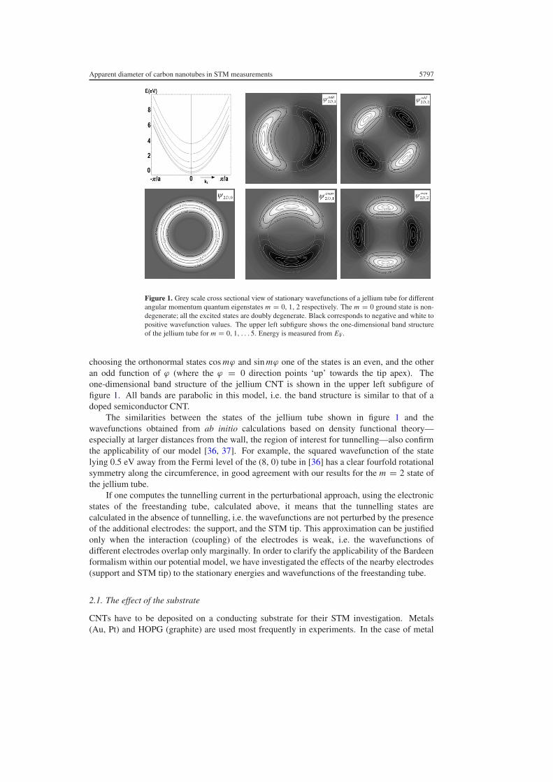
Apparent diameter of carbon nanotubes in STM measurements 5797
Figure 1. Grey scale cross sectional view of stationary wavefunctions of a jellium tube for differentangular momentum quantum eigenstates m = 0, 1, 2 respectively. The m = 0 ground state is non-degenerate; all the excited states are doubly degenerate. Black corresponds to negative and white topositive wavefunction values. The upper left subfigure shows the one-dimensional band structureof the jellium tube for m = 0, 1, . . . 5. Energy is measured from EF.
choosing the orthonormal states cos mϕ and sin mϕ one of the states is an even, and the otheran odd function of ϕ (where the ϕ = 0 direction points ‘up’ towards the tip apex). Theone-dimensional band structure of the jellium CNT is shown in the upper left subfigure offigure 1. All bands are parabolic in this model, i.e. the band structure is similar to that of adoped semiconductor CNT.
The similarities between the states of the jellium tube shown in figure 1 and thewavefunctions obtained from ab initio calculations based on density functional theory—especially at larger distances from the wall, the region of interest for tunnelling—also confirmthe applicability of our model [36, 37]. For example, the squared wavefunction of the statelying 0.5 eV away from the Fermi level of the (8, 0) tube in [36] has a clear fourfold rotationalsymmetry along the circumference, in good agreement with our results for the m = 2 state ofthe jellium tube.
If one computes the tunnelling current in the perturbational approach, using the electronicstates of the freestanding tube, calculated above, it means that the tunnelling states arecalculated in the absence of tunnelling, i.e. the wavefunctions are not perturbed by the presenceof the additional electrodes: the support, and the STM tip. This approximation can be justifiedonly when the interaction (coupling) of the electrodes is weak, i.e. the wavefunctions ofdifferent electrodes overlap only marginally. In order to clarify the applicability of the Bardeenformalism within our potential model, we have investigated the effects of the nearby electrodes(support and STM tip) to the stationary energies and wavefunctions of the freestanding tube.
2.1. The effect of the substrate
CNTs have to be deposited on a conducting substrate for their STM investigation. Metals(Au, Pt) and HOPG (graphite) are used most frequently in experiments. In the case of metal
5798 L Tapaszto et al
surfaces the most important effect of the substrate on the STM image is the doping of theCNT [8, 38]. However, this effect is not present when the work functions of the nanotubeand substrate are similar, i.e. nanotubes on an HOPG substrate [39]. Another effect is that theproximity of the support perturbs the electronic states of the CNT even when no doping occurs.In order to investigate this effect we choose the same work function and Fermi energy valuesfor our jellium potential model of the CNT and support, in accordance also with the WPDcalculations [29], EF = 5 eV, W = 4.81 eV. The support surface is modelled by a semi-infinite3D jellium potential. The nanotube is taken to float 0.335 nm above the support, due to the vander Waals interaction [17].
In order to calculate the first-order perturbation correction, due to the presence of thesupport, for the non-degenerate m = 0 angular momentum quantum state of the nanotube,we have to calculate the integral of the probability density of the unperturbed wavefunctioncalculated in section 2 over the region where the potential of the support is different from zero:
�E2D,0 = V0
∫ +∞
−∞dx
∫ ysup
−∞dy ρ2D,0(x, y) (6)
where ysup is the y coordinate of the effective jellium surface of the support (the y axis isperpendicular to the support). The integral gives the probability of finding the quasiparticlein the support region, i.e. �E2D,0 = V0 psup. For the case of an SWNT with 1 nm diameterfloating over the substrate at 0.335 nm distance, the energy corresponding to the m = 0 angularmomentum eigenstate is shifted down by an amount �E2D,0 = −1.48 meV, which is quitesmall.
As discussed in section 2, the angular momentum states with nonzero quantum numberm are doubly degenerate; hence, in order to calculate the corrections induced by the substratewe have to apply the perturbation theory of degenerate states. The effect of the support forthe m �= 0 states is to split the degeneracy. For the case of the m = 1 state the energycorrections are �Eeven
2D,1 = −2.89 meV and �Eodd2D,1 = −0.15 meV. Both of the degenerate
states are downshifted, but the energy shift for the odd state is much less than that of the evenstate because the odd state has a much lower probability density in the support region (figure 1).The splitting of the energies of the nonzero angular momentum quantum states corresponds tothe splitting of van Hove singularities in the STS spectra.
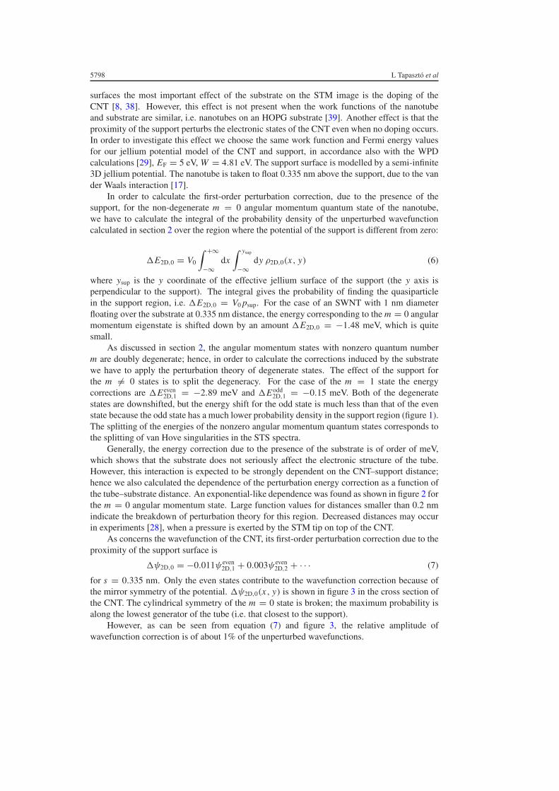
Generally, the energy correction due to the presence of the substrate is of order of meV,which shows that the substrate does not seriously affect the electronic structure of the tube.However, this interaction is expected to be strongly dependent on the CNT–support distance;hence we also calculated the dependence of the perturbation energy correction as a function ofthe tube–substrate distance. An exponential-like dependence was found as shown in figure 2 forthe m = 0 angular momentum state. Large function values for distances smaller than 0.2 nmindicate the breakdown of perturbation theory for this region. Decreased distances may occurin experiments [28], when a pressure is exerted by the STM tip on top of the CNT.
As concerns the wavefunction of the CNT, its first-order perturbation correction due to theproximity of the support surface is
�ψ2D,0 = −0.011ψeven2D,1 + 0.003ψeven
2D,2 + · · · (7)
for s = 0.335 nm. Only the even states contribute to the wavefunction correction because ofthe mirror symmetry of the potential. �ψ2D,0(x, y) is shown in figure 3 in the cross section ofthe CNT. The cylindrical symmetry of the m = 0 state is broken; the maximum probability isalong the lowest generator of the tube (i.e. that closest to the support).
However, as can be seen from equation (7) and figure 3, the relative amplitude ofwavefunction correction is of about 1% of the unperturbed wavefunctions.
Apparent diameter of carbon nanotubes in STM measurements 5799
Figure 2. The first-order energy correction (expressed as a percentage of the ground state energy)shows an exponential dependence as a function of CNT–support distance. The shaded regionindicates the range where the applicability of the perturbation treatment breaks down. The dashedline indicates the 0.335 nm van der Waals distance.
Figure 3. First-order perturbation correction to the ground state wavefunction of the tube due to theproximity of the support surface for 0.335 nm CNT–support distance.
2.2. The effect of the STM tip
The influence of the STM tip, through mechanical tip–sample interactions or multipletip effects [40], on the STM images has been studied both experimentally andtheoretically [41, 42]. When the tip is not in mechanical contact with the sample, it is stillpossible to affect the sample through the perturbation caused by the tip on the electronicstructure of the sample. Tekman and Ciraci identified [43] three ranges for the tip–sampledistance in their theoretical examination of the graphene sheet sample–single carbon atom tipmodel. They pointed out that the tip interacting with the sample induces localized states on thesample surface. For distances smaller than 0.35 nm these so-called tip-induced localized states(TILSs) become pronounced and lead to a modification of the tunnel current.
To study the effect of the tip on the jellium wavefunctions of the CNT we calculatedthe first-order perturbation correction for the ψ2D,0 ground state. Because the tip potentialis not translation symmetric along the axis of the CNT (z direction), the perturbation correctioncontains a weighted sum of all eikz z plane waves:
�ψ2D,0(r, ϕ, z) =∑
m
∫dzcm (z) ψ2D,m (r, ϕ) eikz z (8)
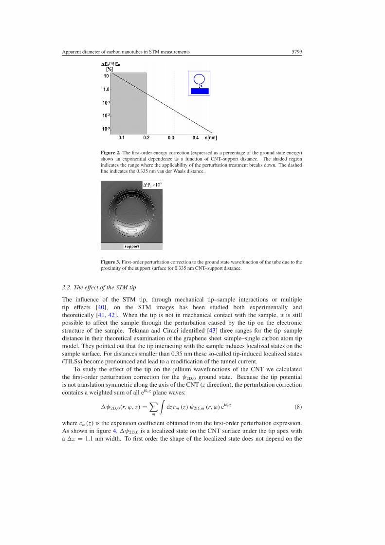
where cm(z) is the expansion coefficient obtained from the first-order perturbation expression.As shown in figure 4, �ψ2D,0 is a localized state on the CNT surface under the tip apex witha �z = 1.1 nm width. To first order the shape of the localized state does not depend on the
5800 L Tapaszto et al
Figure 4. Tip-induced localized state (TILS) on the nanotube visualized by an isodensity surface.White lines show the effective jellium surfaces of the 1 nm diameter nanotube. The axial distancebetween the broken circles is 1.92 nm. The effective jellium surface of the hyperbolic tip is shownabove the tube. The tip–tube distance is 0.409 nm.
tip–sample distance: only its magnitude is increasing exponentially with decreasing distance.For the 0.409 nm tip–CNT distance (consistent with WPD simulations) the relative magnitudeof the wavefunction correction (as compared with the unperturbed ground state of the CNT) isonly 7 × 10⁻⁵, but for a 0.2 nm separation it already increases to 10−2. This shows that for a0.409 nm tunnel gap the electronic structure of the CNT is not perturbed significantly by thetip but for a gap smaller than 0.2 nm the TILS [43] has to be taken into account in the tunnelcurrent calculation.
Therefore we conclude that the proximity of the substrate and tip electrodes, which isunavoidable in STM measurements of carbon nanotubes, in typical measurement conditions,does not affect the electronic states of the nanotubes in a decisive way; hence the applicabilityof perturbational treatment to study tunnelling phenomena within our model can be justified.The above results are confirmed by the small transmission coefficients of about 10−3 obtainedin WPD simulations—indicating a weak coupling between the electrodes—performed on thesame potential model, and are also in accordance with ab initio calculations performed on morerealistic potential models, but with similar geometries [7].
3. STM currents and tunnelling matrix elements of the tip–tube–support system
In calculating tunnelling currents flowing trough our model system it is desirable to takeadvantage of the fact that the results of section 2 indicate a weak coupling between theelectrodes. In this limit the tunnel current can be written as
I = 2π∑
t,s
|Mts|2δ (Et − EF) δ (Es − EF) (9)
where the indices t and s mean the tip and sample, respectively. Nevertheless it is sometimesnecessary to treat the problem non-perturbatively, in particular at exceedingly small electrodedistances as indicated by figure 2 and demonstrated by Lang [44].
The main difficulty is evaluating the Mts tunnelling matrix elements (TMEs). Bardeenshowed [30] that the tunnelling matrix elements can be expressed as an integral over a surface Slying between the tip and sample in the region where the Vt and Vs potentials of both electrodesare negligibly small:
Mts =∫
d�S �µts (η, ξ) (10)
Apparent diameter of carbon nanotubes in STM measurements 5801
where η, ξ are the inner coordinates of the surface. The expression for �µts(η, ξ), the position-dependent overlap of the wavefunctions of the electrodes, is formally similar to the expressionof quantum mechanical current density:
�µts =(ψ∗
t�∇ψs − ψ∗
s�∇ψt
). (11)
3.1. The tube–substrate tunnel junction
One of the significant differences between the STM measurements of the surfaces of bulkmaterials and those on supported carbon nanotubes is the existence of a second tunnellinggap [28, 29] in the latter case. This second tunnelling gap is that between the CNT and itssupport, because the nanotube floats at a distance 0.335 nm over the support surface due to vander Waals interactions. Since in order to measure a tunnelling current the electron has to passthrough both tunnel gaps, the STM image is determined by the characteristics of both tunneljunctions. In order to separate the effects of the different junctions it is interesting to comparetheir transmittivity. Hence we calculated, using the Bardeen formalism, the tunnelling matrixelement (TME) between the m = 0 state of the tube (see section 2) and the correspondingstate of the substrate where, the substrate wavefunction is an eigenstate of a semi-infinite 3Djellium potential with a plane surface using the same potential parameters as in the case ofthe CNT. The Mtube−substrate matrix element is a function of tube length; hence in order tobe consistent with the WPD simulations we considered the axial length of the axial chargespreading of electrons during the tunnelling, corresponding to a length section of about 5 nmcalculated using the same potential parameters and geometry [29]. Then, for the sake ofcomparison, we also calculated the tunnelling matrix element, Mtip−tube, between the m = 0eigenstate of the tube, and an s-wave type eigenstate of a spherical tip with 0.5 nm radiusof curvature, at a distance 0.409 nm above the tube. In the region of interest for tunnelling,the tip wavefunction has an asymptotic spherical form, similar to the one used by Tersoff andHamann [45] in their description of STM measurements of bulk surfaces. When consideringthe ratio of these two TMEs for the particular configuration used in our WPD simulations,we found Mtip−tube/Mtube−substrate = 2.34 × 10⁻³. Since the tunnelling probability (current) isproportional to the square of the corresponding matrix elements, the tunnel resistance of thetip–CNT junction turns out to be much larger than the tube–substrate tunnel resistance, for tip–tube distances away from the point contact regime. The larger tunnelling resistance determinesthe tunnelling current and hence the characteristics of the STM images of carbon nanotubes.
Therefore we conclude that the second tunnelling gap—that between the nanotube andthe substrate—does not significantly affect the measured tunnelling current; hence it cannotbe responsible for discrepancies in the apparent height of the nanotubes observed in STMmeasurements for conductive substrates. However, the presence of a thin oxide layer or othercontaminations may seriously affect these results.
The above justified findings were successfully applied as an assumption in the tight bindingtheory for calculation of atomic resolution STM images of carbon nanotubes [46].
3.2. The tip–tube and tip–substrate tunnel junction
Although theories considering the STM tip as a mathematical point source of current havebeen successfully applied in many cases [45], the effects arising from the finite extent andgeometry of the STM tip are well known (e.g. the tip–sample convolution effects). Theseeffects have been studied experimentally and successfully described theoretically using theWPD method [28].
5802 L Tapaszto et al
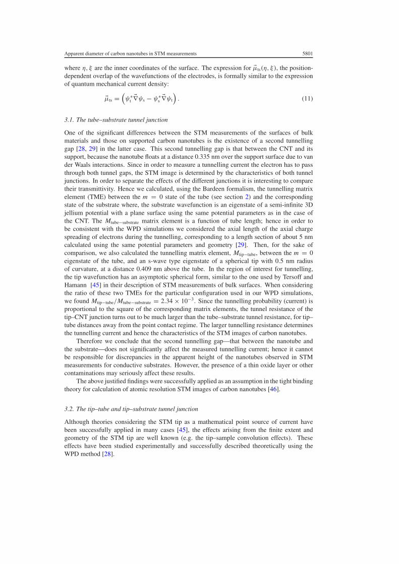
Figure 5. Transmission probabilities for the STM tip–CNT (full line) and STM tip–substrate(dashed line) systems as a function of tunnel gap s, showing an exponential-like decay of thetunnelling probability. Note that not only are the lines shifted relative to each other, but their slopesare also slightly different. The inset shows the mechanism for the flattening of the tube (see the textfor details).
Although not affected by tip convolution effects, discrepancies in the apparent height ofthe nanotubes measured by STM also occur [14–16]. Measuring the height of the nanotubespractically means comparing tunnelling currents for the STM tip positioned over the top of thetube with that above the substrate, which means comparing tunnel currents flowing through thetip–CNT and tip–support tunnel junctions, respectively.
In order to study this problem, we have calculated the TMEs of the tip–CNT (and tip–substrate) junctions as a function of tip–CNT (tip–substrate) distances. The results are shownin figure 5.
Our results show an exponential-like decay of tunnelling probability with distance, andalso reproduce the one order of magnitude decay on every angstrom distance, a rule of thumbderived from experimental observations.
In the most common, constant current operating mode, the STM tip follows a constantelectronic density of states (DOS) surface weighted by the tunnelling probability. Since thedifference in the DOS of the CNT and the support seems to affect little the apparent height ofthe nanotubes [7], it is more relevant to compare the tunnelling probabilities above the CNTand substrate. According to figure 5, in order to maintain a constant tunnelling probabilityMtip−tube(s1) = Mtip−plane(s2) above the CNT and substrate the STM feedback loop has toretract the tip from the value s1 = 0.409 nm above the CNT to the value s2 = 0.485 nm abovethe substrate; hence an apparent flattening of about 10% of the tube occurs.
We found that there are two main reasons responsible for the apparent flattening of the nan-otubes in STM measurements (according to the above discussed: no mechanical deformationof the tube or difference in the electronic structure relative to the substrate is present).
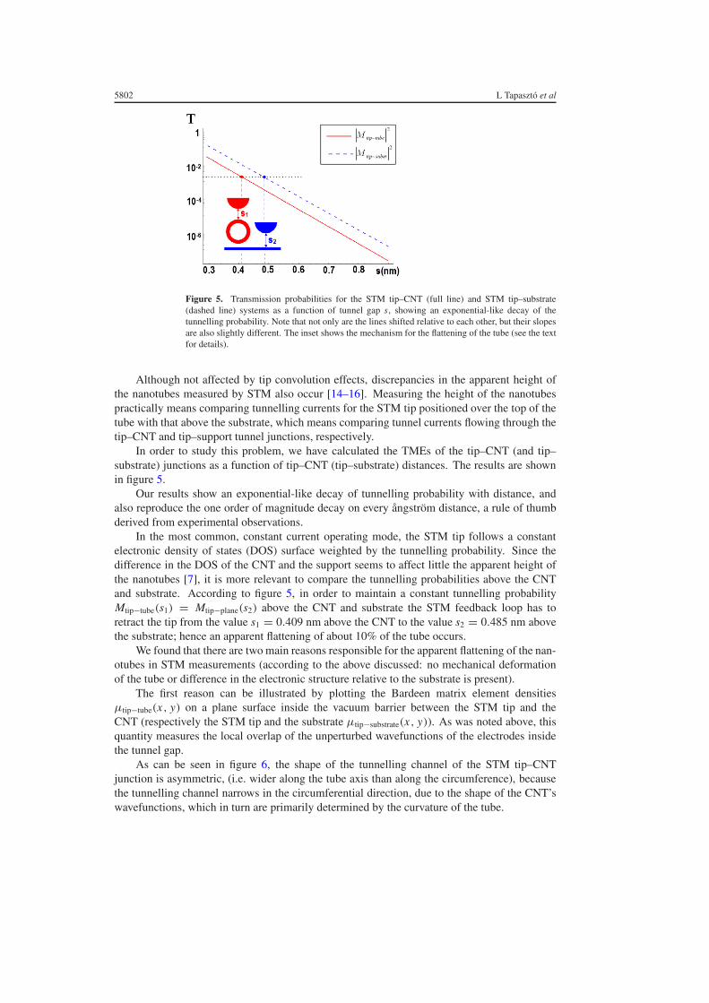
The first reason can be illustrated by plotting the Bardeen matrix element densitiesµtip−tube(x, y) on a plane surface inside the vacuum barrier between the STM tip and theCNT (respectively the STM tip and the substrate µtip−substrate(x, y)). As was noted above, thisquantity measures the local overlap of the unperturbed wavefunctions of the electrodes insidethe tunnel gap.
As can be seen in figure 6, the shape of the tunnelling channel of the STM tip–CNTjunction is asymmetric, (i.e. wider along the tube axis than along the circumference), becausethe tunnelling channel narrows in the circumferential direction, due to the shape of the CNT’swavefunctions, which in turn are primarily determined by the curvature of the tube.
Apparent diameter of carbon nanotubes in STM measurements 5803
Figure 6. Cross sectional plot of the tip–tube (left) and tip–substrate (right) tunnelling channelrepresented by the tip–tube (tip–substrate) tunnelling matrix element density on a plane inside thevacuum gap between the STM tip and nanotube (substrate) for a 0.409 nm tunnel gap in both cases.The grey scales are identical in both figures.
The transmission probability can be obtained by integrating the µ(x, y) functions on the(x, y) plane. It is easy to anticipate from figure 6 that in the case of the tip–tube tunnel junctionthis value will be smaller than in case of the tip–substrate tunnel junction, due to the shrinking ofthe tunnelling channel along the circumference of the tube. This effect is even more accentuatedfor smaller tube diameters.
The second reason for the flattening observed in our model is related to the connectionbetween the decay rate of tunnelling probabilities and the complex 3D geometry of thetunnelling gap.
The distance dependence of the tunnelling probability is usually written as
T ∝ e−2χs , where χ = √2(V0 − E) (12)
gives the decay rate of the tunnelling probability with distance. This behaviour is quite generalas it is derived from various models of tunnelling through one-dimensional barriers [47].
From figure 5 it is obvious that both the tip–tube and tip–substrate tunnelling junctionsshow an exponential-like decay. However, when we calculate the decay rate of the fittedexponentials we find χtip−tube = 11.62 nm−1 for the tip–tube tunnel junction, and χtip−substrate =11.34 nm−1 for the tip–support tunnel junction, which are slightly different from χ calculatedusing the 1D tunnelling theory, where χ = √
2(V0 − E) = 11.24 nm−1 corresponding totwo planar electrodes in 3D. In order to clarify the effect of the curved 3D geometry, wecalculated the effective decay rate χ for a blunt tip and a large-diameter tube in order toapproach the plane–plane tunnel junction situation. The χ decay rate in this case was found tobe χ = 11.24 nm−1, practically equal to the one predicted by 1D tunnelling theory (two planarelectrodes). Hence we attribute the differences found in the effective decay rate to the curvatureof the electrodes (in the case of χtip−tube due to the curvature of both tip and nanotube, whilein the case of χtip−substrate due only to the curvature of the tip). Therefore this effect is closelyrelated to the 3D tunnel barrier geometry.
The main conclusion of this result is that the decay rate of the tunnelling probabilityincreases with increasing curvature of the electrodes. Therefore the difference in the decay ratesof the ‘tip–tube’ and ‘tip–substrate’ tunnel junctions also contributes to the apparent flatteningof the nanotubes in STM measurements. This effect is responsible for the difference in theslopes of the lines in figure 5, which gives rise to a tip–sample distance-dependent flattening ofthe tubes.
Our findings related to the increased effective decay rates attributed to the geometry of thetunnel junction are in good agreement with the results of Garcia et al [48], who used a scattering
5804 L Tapaszto et al
approach for the description of tunnelling between a periodic array of tips and a jellium surface.They found that the tip curvature increases the decay rate of the tunnelling probability, andincluded this increase in the exponential factor 2 of equation (12), which became 2.14 for anatomically sharp tip.
Both of the effects mentioned above leading to the apparent flattening of the tube inSTM measurements increase with decreasing tube diameter, which is in agreement withthe experimental findings of Olk and Heremans [49], who found an increasing deviationwith decreasing tube diameter for the diameter measured by STM and that calculated fromspectroscopic data.
4. Conclusions
We studied within the framework of a simple model system the geometrical effects influencingthe tunnelling probabilities in STM configurations, which are proposed to be the main factorsresponsible for discrepancies between the apparent height of the nanotubes measured bySTM and their real diameter. We propose two main factors influencing the image formationmechanism: (1) the shrinkage of the tunnelling channel in the circumferential direction, due tothe curvature of the tube, and (2) the increased decay rate of tunnelling probabilities for curvedelectrodes (as compared to planar ones). A faster decay with smaller curvature radii was found.For a tube with 1 nm diameter a flattening of about 10% is predicted by the calculated geometry-related effects. These effects are also dependent on the CNT’s diameter and the tip–sampledistance. An increasing flattening of the tubes is found with decreasing tube diameter andincreasing tip–sample distance. Anomalously small diameters can be observed at exceedinglylarge tip–CNT distances.
Acknowledgments
This work has been partly funded by OTKA Grant No T 043685 in Hungary and partly by theIUAP program P5/01 ‘Quantum size effects in nanostructured materials’ of the Belgian SciencePolicy Programming.
References
[1] Reich S, Thomsen Ch and Maultzsch J 2002 Carbon Nanotubes: Basic Concepts and Physical Properties (Berlin:Wiley)
[2] Seidel R, Graham A P, Unger E, Duesberg G S, Liebau M, Steinhoegl W, Kreupl F, Hoenlein W andPompe W 2004 Nano Lett. 4 831
[3] Bachtold A, Hadley P, Nakanishi T and Dekker C 2001 Science 294 1317[4] Dresselhaus M S, Dresselhaus G and Eklund P C 1996 Science of Fullerenes and Carbon Nanostructures
(San Diego, CA: Academic)[5] Hamada N, Sawada S and Oshiyama A 1992 Phys. Rev. Lett. 68 1579[6] Mintmire J W, Dunlap B I and White C T 1992 Phys. Rev. Lett. 68 631[7] Rubio A, Sanchez-Portal D, Artacho E, Ordejon P and Soler J M 1999 Phys. Rev. Lett. 82 3520[8] Wildoer J W G, Venema L C, Rinzler A G, Smalley R E and Dekker C 1998 Nature 391 59[9] Odom T W, Huang J L, Kim Ph and Lieber C M 1998 Nature 391 62
[10] Biro L P and Lambin Ph 2003 Scanning tunneling microscopy of carbon nanotubes Encyclopedia of Nanoscienceand Nanotechnology ed H S Nalwa (Fairfield, NJ: American Scientific Publishers)
[11] Briggs G A D and Fisher A J 1999 Surf. Sci. Rep. 33 1[12] Biro L P, Gyulai J, Lambin Ph, Nagy J B, Lazarescu S, Mark G I, Fonseca A, Surjan P R, Szekeres Zs,
Thiry P A and Lucas A A 1998 Carbon 36 689[13] Meunier V and Lambin P 1998 Phys. Rev. Lett. 81 5588
Apparent diameter of carbon nanotubes in STM measurements 5805
[14] Venema L C, Meunier V, Lambin Ph and Dekker C 2000 Phys. Rev. B 61 2991[15] Kim Ph, Odom T W, Huang J L and Lieber C M 2000 Carbon 38 1741[16] Klusek Z, Datta S, Byszewski P, Kowalczyk P and Kozlowsk W 2002 Surf. Sci. 507 577[17] Hertel T, Walkup R and Avouris Ph 1998 Phys. Rev. B 58 13 870[18] Hofer W A, Foster A S and Shluger A L 2003 Rev. Mod. Phys. 75 1287[19] Kresse G and Hafner J 1993 Phys. Rev. B 47 558[20] Kresse G and Furthmuller J 1996 Phys. Rev. B 54 11169[21] Tersoff J 1986 Phys. Rev. Lett. 57 440[22] Ogando E, Torsti T, Zabala N and Puska M J 2003 Phys. Rev. B 67 075417[23] Ogando E, Zabala N and Puska M 2002 Nanotechnology 13 363[24] Yannouleas C, Bogachek E and Landman U 1998 Phys. Rev. B 57 4872[25] Venema L C, Widoer J W G, Janssen J W, Tans S J, Temminck H L J, Louwenhoven L P and Dekker C 1999
Science 283 52[26] Wu J, Duan W, Gu B L, Yu J Z and Kawazoe Y 2000 Appl. Phys. Lett. 77 2554[27] Mark G I, Biro L P and Gyulai J 1998 Phys. Rev. B 58 12645[28] Mark G I, Biro L P, Gyulai J, Thiry P A, Lucas A A and Lambin P 2000 Phys. Rev. B 62 2797[29] Mark G I, Biro L P and Lambin P 2004 Phys. Rev. B 70 115423[30] Bardeen J 1961 Phys. Rev. Lett. 6 57[31] Tersoff J 1989 Scanning Tunneling Microscopy and Related Methods (NATO ASI Series vol E184) ed R J Behm,
N Garcia and H Rohrer, (Dordrecht: Kluwer Academic Publishers) pp 77–95[32] Orosz L and Balazs E 1986 Surf. Sci. 177 444[33] Kurti J, Zolyomi V, Kertesz M, Sun G, Baughman R H and Kuzmany H 2004 Carbon 42 971[34] Tapaszto L, Mark G I, Gyulai J, Lambin P and Biro L P, 2003 Electronic Properties of Novel Materials-
Nanostructures (AIP Conf. Proc. vol 685) ed H Kuzmany, J Fink, M Mehring and S Roth (Melville, NY:American Institute of Physics) p 439
[35] Bowman F 1958 Introduction to Bessel Functions (New York: Dover)[36] Jhi S H, Louie S G and Cohen M L 2000 Phys. Rev. Lett. 85 1710[37] Pan H, Feng Y P and Lin J Y 2004 Phys. Rev. B 70 245425[38] Shan B and Cho K 2004 Phys. Rev. B 70 233405[39] Biro L P, Lazarescu S, Lambin Ph, Thiry P A, Fonseca A, Nagy J B and Lucas A A 1997 Phys. Rev. B 56 12490[40] Biro L P, Mark G I and Balazs E 1994 Nanophase Materials (NATO ASI Ser. vol E260) (Dordrecht: Kluwer
Academic Publishers) p 205[41] Mizes H A, Park S and Harrison W A 1987 Phys. Rev. B 36 4491[42] Ciraci S and Batra I P 1987 Phys. Rev. B 36 R6194[43] Tekman E and Ciraci S 1989 Phys. Rev. B 40 10286[44] Lang N D 1988 Phys. Rev. B 37 R10395[45] Tersoff J and Hamann D R 1985 Phys. Rev. B 31 805[46] Meunier V, Senet P and Lambin Ph 1999 Phys. Rev. B 60 7792[47] Wiesendanger R 1994 Scanning Probe Microscopy and Spectroscopy (Cambridge: Cambridge University Press)[48] Garcia N, Ocal C and Flores F 1983 Phys. Rev. Lett. 50 2002[49] Olk Ch H and Heremans J P 1994 J. Mater. Res. 9 259
Related Documents