Freescale Semiconductor Application Note Document Number: AN3582 Rev. 0, 02/2008 Contents © Freescale Semiconductor, Inc., 2008. All rights reserved. 1 Introduction A data logger is an attractive alternative to a recorder or data acquisition system in many applications. Data loggers have the ability to accept a greater number of input channels with better accurate resolution, and record large amounts of data. The data logger also has intelligence that provides the user with diverse capabilities. For example, raw data can be analyzed to give voltage, differential temperatures, and an alarm if the analysis result is beyond the normal range. USB has been used in many applications. It is not limited to the field of consumer electronics. It is widely used in industrial control, test and measurement, and embedded systems. The MC9S08JM60 is an 8-bit MCU with a USB interface. It has many peripherals, such as ADC, SPI, SCI, IIC, ACMP, TPM that make it easy to be integrated into different applications. This document demonstrates the development of a USB data logger with an MC9S08JM60. This data logger makes use of peripherals from the MC9S08JM60 that are 1 Introduction . . . . . . . . . . . . . . . . . . . . . . . . . . . . . . . . . . . 1 2 Data Logger Main Features . . . . . . . . . . . . . . . . . . . . . . . 2 3 Work Scheme of the USB Data Logger . . . . . . . . . . . . . . 4 3.1 Data Transfer between Host and Device. . . . . . . . . 4 3.2 Customized Protocol . . . . . . . . . . . . . . . . . . . . . . . . 5 3.3 USB Data Logger Communication Pipes . . . . . . . . 6 4 Hardware of the USB Data Logger . . . . . . . . . . . . . . . . . 6 5 Firmware Design . . . . . . . . . . . . . . . . . . . . . . . . . . . . . . . 7 5.1 System Framework . . . . . . . . . . . . . . . . . . . . . . . . . 7 5.2 Porting of the USB Stack . . . . . . . . . . . . . . . . . . . . 10 5.3 Firmware for Different Functional Modules . . . . . . 13 6 PC Software of the Data Logger . . . . . . . . . . . . . . . . . . 15 7 Summary . . . . . . . . . . . . . . . . . . . . . . . . . . . . . . . . . . . . 16 8 Acronyms. . . . . . . . . . . . . . . . . . . . . . . . . . . . . . . . . . . . 16 Appendix AApplication Protocol of the Data Logger . . . . . . . 17 A.1 ADC (Peripheral 0x02) . . . . . . . . . . . . . . . . . . . . . 17 A.2 General Use IO (Peripheral 0x06) . . . . . . . . . . . . . 20 A.3 TPM (Peripheral 0x07) . . . . . . . . . . . . . . . . . . . . . 21 Appendix Bthe USB Data Logger Software . . . . . . . . . . . . . . 22 The USB Data Logger Based on the MC9S08JM60 by: Derek Liu, Daniel Uribe Systems and Applications Engineering

Welcome message from author
This document is posted to help you gain knowledge. Please leave a comment to let me know what you think about it! Share it to your friends and learn new things together.
Transcript

Freescale SemiconductorApplication Note
Document Number: AN3582Rev. 0, 02/2008
Contents Introduction. . . . . . . . . . . . . . . . . . . . . . . . . . . . . . . . . . . 1Data Logger Main Features. . . . . . . . . . . . . . . . . . . . . . . 2Work Scheme of the USB Data Logger. . . . . . . . . . . . . . 4
3.1 Data Transfer between Host and Device. . . . . . . . . 43.2 Customized Protocol . . . . . . . . . . . . . . . . . . . . . . . . 53.3 USB Data Logger Communication Pipes . . . . . . . . 6Hardware of the USB Data Logger . . . . . . . . . . . . . . . . . 6Firmware Design . . . . . . . . . . . . . . . . . . . . . . . . . . . . . . . 7
5.1 System Framework . . . . . . . . . . . . . . . . . . . . . . . . . 75.2 Porting of the USB Stack. . . . . . . . . . . . . . . . . . . . 105.3 Firmware for Different Functional Modules . . . . . . 13PC Software of the Data Logger . . . . . . . . . . . . . . . . . . 15Summary . . . . . . . . . . . . . . . . . . . . . . . . . . . . . . . . . . . . 16Acronyms. . . . . . . . . . . . . . . . . . . . . . . . . . . . . . . . . . . . 16
ppendix AApplication Protocol of the Data Logger . . . . . . . 17A.1 ADC (Peripheral 0x02) . . . . . . . . . . . . . . . . . . . . . 17A.2 General Use IO (Peripheral 0x06) . . . . . . . . . . . . . 20A.3 TPM (Peripheral 0x07) . . . . . . . . . . . . . . . . . . . . . 21
ppendix Bthe USB Data Logger Software. . . . . . . . . . . . . . 22
The USB Data Logger Based on the MC9S08JM60by: Derek Liu, Daniel Uribe
Systems and Applications Engineering
1 IntroductionA data logger is an attractive alternative to a recorder or data acquisition system in many applications. Data loggers have the ability to accept a greater number of input channels with better accurate resolution, and record large amounts of data. The data logger also has intelligence that provides the user with diverse capabilities. For example, raw data can be analyzed to give voltage, differential temperatures, and an alarm if the analysis result is beyond the normal range.
USB has been used in many applications. It is not limited to the field of consumer electronics. It is widely used in industrial control, test and measurement, and embedded systems. The MC9S08JM60 is an 8-bit MCU with a USB interface. It has many peripherals, such as ADC, SPI, SCI, IIC, ACMP, TPM that make it easy to be integrated into different applications.
This document demonstrates the development of a USB data logger with an MC9S08JM60. This data logger makes use of peripherals from the MC9S08JM60 that are
123
45
678A
A
© Freescale Semiconductor, Inc., 2008. All rights reserved.

Data Logger Main Features
easy to implement without more external components. Based on the Freescale USB stack the hardware and firmware are also easy to design. This data logger is simple, economic, and useful.
2 Data Logger Main Features
Figure 1. Data Logger System
Figure 1 is the USB data logger system based on the MC9S08JM60 demonstration board. The data logger is composed of a PC and a demonstration board. It consists of three parts from the software point of view:
• PC GUI • PC driver• Firmware
The data logger is designed to support the following features based on the demo board resource:• Data acquisition (14 channels)
The MC9S08JM60 provides 12 external ADC channels. ADPC0, ADPC1, ADPC2... ADPC10, and ADPC11 are all in the data logger. It also provides an on-chip temperature sensor and reference voltage band gap. The ADC channels are:— ADPC0–11— Temperature— BandgapAll ADC channels can be enabled or disabled. Any of them can be used.The data logger supports 3 resolutions: — 8-bit, — 10-bit— 12-bit (MC9S08JM60 feature)
The USB Data Logger Based on the MC9S08JM60, Rev. 0
Freescale Semiconductor2

Data Logger Main Features
The data logger is designed to support three kinds of trigger modes:— Software (SW) trigger mode: The ADC can be started by command from the USB host.— Delay trigger mode: The ADC can be triggered after a time delay of 0–256 seconds. The host
sends the start command to a device with a time delay parameter and the ADC starts to work after the delay time has elapsed.
— Voltage level trigger mode: The voltage level and trigger logic can be set. The ADC is triggered if the voltage of a channel is greater or less than the set voltage. The command has four parameters: trigger channel, voltage level, and trigger logic.
In this application the channels ADPC0, ADPC1, and ADPC3 are connected to the X, Y, and Z output of the 3-axis accelerometer sensor on the demonstration board. The ADPC2 is connected to the output of the potentiometer. The other channels can be connected to the external analog input signal.
• GPIO status control and readingThe data logger can control seven LEDs on demonstration boards and read the status of four buttons.
• Pulse width modulation (PWM) signal outputThe data logger controls the TPM and generates the PWM signal that drives the buzzer on the demonstration board. The buzzer can be used to show when the status or data exceeds its normal range in the data logger system.
• Data recordingThe software running on the PC can read the data and status from the device, display them on the GUI, and record them into a data file. With this method the data can be visualized in real time. The USB data logger uses the data storage space of the computer system and achieves mass data recording.
NOTE The data logger in this application has up to 14 ADC channels input. For a phase difference between two different channels. All ADC inputs must be converted one by one, not in parallel. The phase difference between channel 0 and channel 1 is illustrated in Figure 2.
Figure 2. ADC Work Scheme
… … … …… …… Ch0 Ch1 Chn Ch0 Ch1 Chn Ch0 Ch1 Chn
…Ch0 Ch1 Chn
1st Sample 2nd Sample 3rd Sample Nth Sample
1 Period 1 Period
Conversion time of 1 Channel
…… Phase
difference between Ch0 and
Ch1
The USB Data Logger Based on the MC9S08JM60, Rev. 0
Freescale Semiconductor 3

Work Scheme of the USB Data Logger
3 Work Scheme of the USB Data Logger
3.1 Data Transfer between Host and DeviceAll communication starts from the USB host because the data logger is based on the USB system. The host sends the command and request to the device. The USB device then executes the command, responds to the request, and feeds back the necessary data to the host. Figure 3 illustrates the communication scheme of a typical USB system and adopted in the data logger system.
Figure 3. USB Communication Scheme
As shown in Figure 3, the host sends the command and data to the device through the USB driver. The device then executes the command, saves the data, and replies to the host with status or data. The USB driver is transparent between the GUI software and the firmware of the device.
After the USB is enumerated and configured successfully, a communication pipe is created between the USB host and the device. All commands and data are transferred into the pipes. According to the USB features of the MC9S08JM60 five pipes are built in the data logger system.
• Default pipe (control pipe):The default pipe is used to enumerate and configure the USB device and is essential for all USB devices. The default pipe is built on endpoint 0.
• Command pipeThe command pipe is used by the host to send the commands to USB device. It is built on endpoint 1 of the USB device.
• Status pipeThe USB device sends the response to the host via the status pipe after it receives and executes the command.
• Data out pipeThis pipe is used by the host to transfer data to the device.
• Data in pipe The device sends the data to the host via the data in pipe.
GUI Driver Firmware
Command, Data…Command, Data,…
ResponseResponse
The USB Data Logger Based on the MC9S08JM60, Rev. 0
Freescale Semiconductor4

Work Scheme of the USB Data Logger
3.2 Customized ProtocolThe control pipe and status pipe are designed to transfer a packet of up to16 bytes.
The data out and data in pipe can accommodate 32 bytes in one packet. They are designed to transfer mass data because the sessions for control and status information are not too much. They are designed to use smaller packet sizes.
The commands, data, and response in Figure 3 are transferred in the application layer of the USB system and located above the USB standard protocol. Refer to AN3560-- The USB Device Development with the MC9S08JM60 for the description of the USB protocol layer. They are defined in a customized protocol according to different applications. The data logger applies a simple protocol made by the developer.
Table 1 and Table 2 are the command format and response format transferred between the USB host and the device adopted by the data logger. The first byte indicates the module that accepts the command. For example, the 0x02 means the command belongs to the ADC module. The second byte is the command for the module specified in the first byte. For example, for the ADC module 0x01 is a configuration command and 0x02 is the command for reading the configuration. The following bytes are parameters for the command. The parameter is flexible and optional. It can be neglected for some commands. For example:
The start ADC conversion command is:
The response for starting the ADC conversion from the device is:
Parameter 0xFF means that the ADC conversion has started successfully. If the ADC fails to start it reads 0x00.
The detailed protocol is attached in Appendix A, “Application Protocol of the Data Logger”.
Table 1. Command Format from Host
Byte 1 2 3 4 ……
Description Module Command Para1 Para2 Para……
Table 2. Response from Device
Byte 1 2 3 ……
Description Module Command Para1 Para……
0x02 0x03
0x02 0x03 0xFF
The USB Data Logger Based on the MC9S08JM60, Rev. 0
Freescale Semiconductor 5

Hardware of the USB Data Logger
3.3 USB Data Logger Communication Pipes
Figure 4. Communication Pipes for USB Data Logger
Figure 4 is the connection between host and device. The pipes are built after the device is enumerated and configured successfully. The data transfer direction is illustrated in Figure 4. The bulk transfer type is applied to the command pipe, status pipe, and data out pipe. To make sure the application can get the guaranteed bandwidth the interrupt transfer type is adopted for the data in pipe. The data sample results are transferred in this pipe and helps to get a stable sample rate.
The customized protocol before mentioned is applied to the data transferred in these pipes.
4 Hardware of the USB Data Logger The USB data logger is based on the MC9S08JM60 demonstration board. A different power supply is built on the 3-axis accelerometer, potentiometer, buzzer, LEDs, buttons, and P&E multi-link circuit.
The outputs of the accelerometer and potentiometer are attached to the ADC input channels. The buzzer can be connected to the output of the TPM2 module. The LEDs and buttons are connected to the input and output module of the MCU. The on-board P&E multi-link can be used to download and debug the firmware. The power supply circuit enables the system in several different power modes:
• Bus powered• Self-powered• Powered by multi-link• External power supply• External 5 V power
Command Pipe
Control Pipe
Status Pipe
Data out Pipe
EP0
EP1
EP2
EP3
Data in Pipe EP5
PC Software
USB Module
The USB Data Logger Based on the MC9S08JM60, Rev. 0
Freescale Semiconductor6

Firmware Design
The data logger can be debugged and works only with the demo board and CodeWarrior installed on a computer.
The detailed schematic of the demonstration board is not discussed here. For details go to www.freescale.com.
5 Firmware Design
5.1 System Framework
5.1.1 Firmware Architecture
Figure 5. USB Data Logger Firmware Architecture
Figure 5 illustrates the USB data logger firmware architecture.
The USB stack is used for the USB device enumeration and configuration. While the USB device is attached to the host it starts the enumeration process. The enumeration process is done on endpoint 0. It is the same for all USB devices. The USB device is configured in the enumeration process. During this process the address of the USB device is assigned and all USB device descriptors are transferred to the host.
In the USB data logger application one USB stack designed for JM60 MCU is ported. It is easy and flex-ible. For detailed information refer to AN3560 —The USB Device Development with the MC9S08JM60, and AN3564 — Customize the USB Application Using the MC9S08JM.The API is the interface for the application to access the USB port. It is based on the USB stack and provides the communication functions for endpoint 1–6 of the USB module. The high layer application calls the API function to send or receive data.
The driver for other peripherals provide the API functions to access the ADC, TPM, and GPIO modules. The application in high layer calls these API functions to implement for certain purposes.
Application – Data Logger
USB Stack
USB User API ADC, TPM, GPIO Driver
The USB Data Logger Based on the MC9S08JM60, Rev. 0
Freescale Semiconductor 7

Firmware Design
5.1.2 Main Function
Figure 6. Flow Chart of the Main Function
The main function flow chart is illustrated in Figure 6. At first the firmware initializes the system. The MCG, ADC, TPM, GPIO, and other modules are set to system default. The USB is enabled in this process. Then the main function enters into an infinite loop. The Check_USB_Status function controls the transfer of the USB states between attached and suspend. The Usr_Task is called in the main loop after the device succeeds to enumerate.
The enumeration process is not expressed in the main function because it is based on the USB interrupt. For more details on enumeration, please refer to AN3560—The USB Device Development with the MC9S08JM60.
System Initialization
System Start
Check_USB_Status
Usr_Task
The USB Data Logger Based on the MC9S08JM60, Rev. 0
Freescale Semiconductor8
Firmware Design
5.1.3 User Task
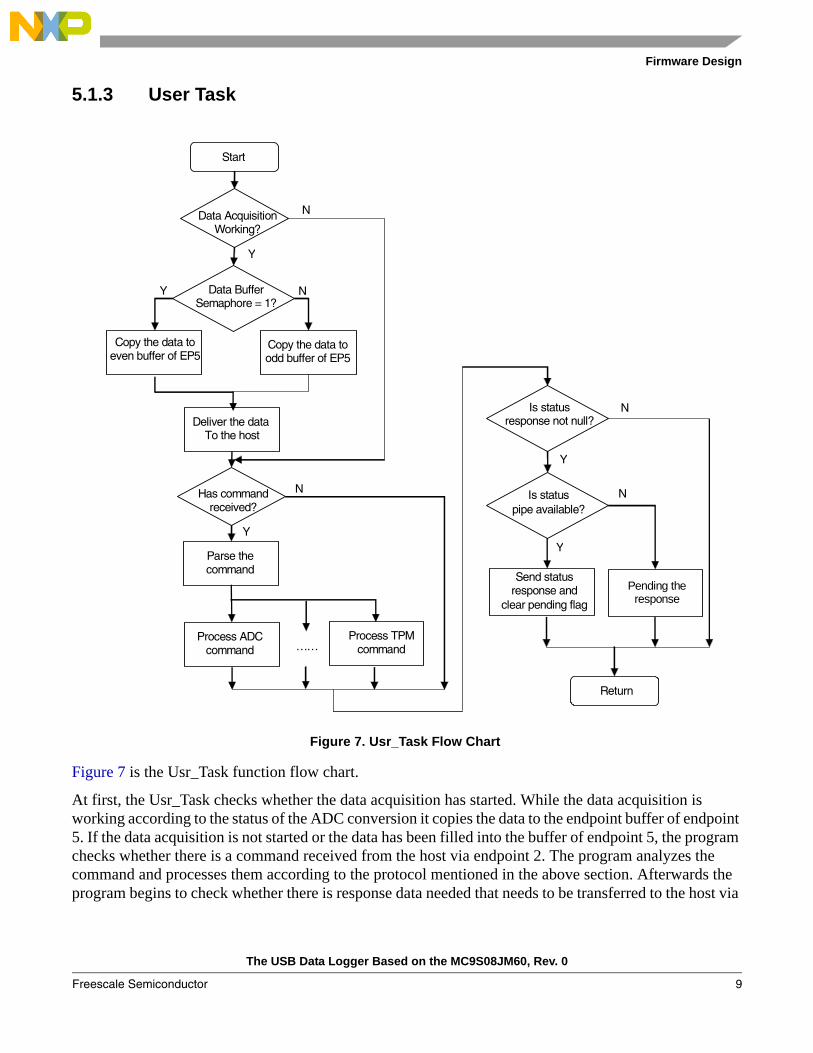
Figure 7. Usr_Task Flow Chart
Figure 7 is the Usr_Task function flow chart.
At first, the Usr_Task checks whether the data acquisition has started. While the data acquisition is working according to the status of the ADC conversion it copies the data to the endpoint buffer of endpoint 5. If the data acquisition is not started or the data has been filled into the buffer of endpoint 5, the program checks whether there is a command received from the host via endpoint 2. The program analyzes the command and processes them according to the protocol mentioned in the above section. Afterwards the program begins to check whether there is response data needed that needs to be transferred to the host via
Start
Data Acquisition Working?
Data Buffer Semaphore = 1?
Copy the data to even buffer of EP5
Copy the data to odd buffer of EP5
Deliver the data To the host
Has command received?
Parse the command
Process ADC command
Process TPMcommand
Send status response and
clear pending flag
Is status pipe available?
Pending the response
Return
Is status response not null?
N Y
Y
N
……
N
Y
Y
N
Y
N
The USB Data Logger Based on the MC9S08JM60, Rev. 0
Freescale Semiconductor 9

Firmware Design
status pipe. If there is a response data it is delivered. If there is no response the program suspends and then exits from the function.
The following section discusses the firmware of the USB data logger in detail.
5.2 Porting of the USB StackFreescale provides the optimized USB stack with good performance, small code size and RAM usage. The following steps are the porting process.
1. The clock generationThe USB module of the MC9S08JM60 needs a 24 MHz bus clock. The MCG initialization function needs to be modified in terms of the external clock source. The USB data logger application uses a 12 MHz external crystal clock source.
2. Power modeThe USB device has bus-powered and self-powered modes. The USB data logger adopts the bus-powered mode. The MCU is in attached mode after the MCU begins to work. The MCU needs to detect the status of the USB connection if the self-powered mode is selected and one GPIO port can be used to sense the connection. The function of Check_USBBus_Status() in Usb_drv.c file can be modified to match the detection requirement.
3. USB configurationThe regulator pullup resistor of the USB module must be configured according to the application. The result in the USB initialization needs to be adjusted.
4. USB descriptors modificationAll descriptors must be modified according to the application that includes the device descriptor, configuration descriptor, interface descriptor, and string descriptor.The related file is Usb_descriptor.c and Usb_descriptor.h
5. USB standard class supportThe process for a class standard request can be placed in the call-back function if the device matches the USB standard class. Place the entrance of this call-back function into the Class_Req_Handler array in the Usb_Descriptor.c.The USB data logger is not a standard class device. No call-back function is needed for the array of Class_Req_Handler.
6. Support for suspend modeThe firmware has a different configuration between self-powered and a bus-powered USB device. For more details refer to AN3560 -- USB Device Development with MC9S08JM60.The device supports remote wakeup from suspend mode. This feature is declared in the USB configuration descriptor. The interrupt source for wake up must be set correctly. The un-expected interrupt can be disabled in the Clear_Int() function before entering suspend mode, and recovered in Recover_Int() function after wakeup.
The USB Data Logger Based on the MC9S08JM60, Rev. 0
Freescale Semiconductor10

Firmware Design
7. Other modificationsThe transaction for stall interrupt can be processed in the USB_Stall_Handler function (Usb_Drv.c) if the stall is used for endpoint 1-6.
5.2.1 USB Resource AssignmentThe USB data logger uses four endpoints besides endpoint 0. The packet size and endpoint buffer assigned to them are listed in the following table.
The declaration of the variant for these endpoints are placed in the file Usr_Ep_Handler.h. The initialization and events process for the endpoints are placed in the file Usr_Ep.Handler.c.
The MC9S08JM60 start address of the USB endpoint buffer must be 16-byte aligned. Therefore the allocated endpoint buffer in Table 3 starts from 0x20, 0x30, 0x40 and are the multiples of 16.
5.2.2 Data Transfer for the USB Application Layer
5.2.2.1 Call-Back Function for Endpoint 1-6The USB interrupt is generated when a transaction finishes at an endpoint. The USB interrupt service (ISR) calls the USB_Transaction_Handler function and makes the program jump to the call-back functions of endpoints 1–6 according to the information in STAT register.
Table 3. USB Resource Assignment
Pipe Name Endpoint Direction Transfer
TypeBuffer Length
Related Address
Absolute Address
Control pipe 0 In Control 8 0x20 0x1880
Out 8 0x30 0x1890
Command pipe 1 Out Bulk 16 0x40 0x18A0
Status pipe 2 In Bulk 16 0x50 0x18B0
Data out pipe 3 Out Bulk 32 0x60 0x18C0
4
Data in pipe 5 In Interrupt 32 0x80 0x18E0
6
The USB Data Logger Based on the MC9S08JM60, Rev. 0
Freescale Semiconductor 11

Firmware Design
Figure 8. Jump to Call-Back Function
The array of the Usr_Ep_Handler[6] keeps the call-back functions for endpoints 1–6. The entrance of the call-back function is copied to the Usr_Ep_Handler array if the interrupt for endpoint (1–6) is enabled otherwise NULL is set to the associated element in the array.
The processing function for the USB data logger is saved in the Usr_Ep_Handler array.pFunc Usr_Ep_Handler[6] = { &Ep1_Handler, &Ep2_Handler, &Ep3_Handler, NULL, &Ep5_Handler, NULL };
The code above is the declaration and initialization of Usr_Rp_Handler array. The unused endpoint 4 and 6 have no call-back function, therefore the elements of Usr_Ep_handler (3 and 5) are set to NULL.
5.2.2.2 Endpoint StateThe variable Usr_Ep_Buf_State is used to save the state of endpoints1–6. Bit [3..0] of this variable is used to save the state of the endpoints 1–4, and bit [7..5] keeps the state of endpoints 5 and 6. Endpoints 5 and 6 are a ping-pong buffer and each take two bits.
Logic 1 means that the endpoint receives data from the host and controlled by the CPU if the endpoint is set to out direction. Logic 0 means the SIE controls the endpoint.
Logic 1 means that the data has filled into endpoint buffer and SIE controls the endpoint buffer if the endpoint is set to in direction. The bit is logic 0 if the CPU has the control of the endpoint buffer.
Table 4. State of the Endpoint Buffer
EP6Odd
EP6Even
EP5Odd
EP5Even
EP4 EP3 EP2 EP1
T ra n sa c tio n o n th e E P x
is fin ish ed
E P 0 o r E P 1 –6 ?
Th e tra n sac tio n fo r co n tro l tra n s fe r
Ju m p to ca ll-b ack ro u tine o f th e E P 1 – 6
R e tu rn (R E T I)
E P 0 E P 1 – 6
The USB Data Logger Based on the MC9S08JM60, Rev. 0
Freescale Semiconductor12

Firmware Design
5.2.2.3 Call-Back FunctionThe call-back function for the endpoint in out direction sets the associated bit to logic 1. This is because the SIE gives up control of the buffer descriptor (BD) and endpoint buffer to the CPU while an interrupt occurs. The data in the endpoint buffer is then copied to the user buffer that is assigned to keep the data temporary while the endpoint is busy. Finally the call-back function gives up control of the BD and endpoint buffer to the SIE for the next taction. This is the process for Ep1_Handler function.
The call-back function for the endpoint in in direction clears the associated bit to logic 0. The CPU then controls the BD and endpoint buffer after the data has been fetched by the host. The main loop of the firmware polls the state of in direction endpoint, fills the data into the endpoint buffer, and delivers to the host.
5.2.2.4 Function for Sending DataTwo functions are used for delivering the data to the host: Send_Data_Ep() and Send_Data_PpEp().
Send_Data_Ep is used to send the data to endpoint 1–4 and Send_Data_PpEp is used to send data to the ping-pong buffer. The caller must pass one parameter to point out the even or odd buffer for the Send_Data_PpEp function.
At first both functions receive the source address and endpoint buffer address. Copy the data to the USB RAM (endpoint buffer) and hand over the control of the BD and endpoint buffer to the SIE.
5.3 Firmware for Different Functional Modules
5.3.1 Driver for the ADC ModuleThe ADC module driver is located in ADC.c. A few API functions are provided for the Usr_Task to call.
The ADC must be configured before starting conversion. Several variables are provided to keep the ADC configuration. Three functions are provided to configure the ADC module and receive the current ADC configurations. They are ADC_Config(), Set_Trigger_Type (), and Get_ADC_Configuration().
After the ADC is configured the selected channels and their conversion commands are saved in the array Work_Channel. The total number of enabled channels are kept in the variable of Total_Channels. The firmware fetches the conversion command from Work_Channel array and enables the conversion while the ADC is working.
Functions Get_ADC_Result () and Get_ADC_Ch_Result() are used to receive the result of one or all ADC channels.
5.3.1.1 Data Buffer for the ADC Conversion ResultsThe firmware adopts two buffers to keep the ADC conversion results for all channels. The working scheme is the same as the MC9S08JM60 USB ping-pong buffer.
The USB Data Logger Based on the MC9S08JM60, Rev. 0
Freescale Semiconductor 13

Firmware Design
Figure 9. Working Scheme of ADC Buffers
The Working_Buf variable is used to keep the activity buffer for the ADC module. The ADC conversion result is written to buffer 0 when the Working_Buf is 0. The result is written to buffer 1 when the Working_Buf is 1.
In case the data in the buffer is modified before delivering to the host a buffer is controlled by the ADC module and data from the other buffer can be copied to one of the ping-pong buffers of endpoint 5.
The data in buffer 0 is copied to the even buffer of endpoint 5, and the data in buffer 1 is copied to the odd buffer. The data in buffer 0 and 1 are then copied to the ping-pong buffer of endpoint 5.
The even buffer is used to transfer the DATA0 packet. The odd buffer for the DATA1 packet and the DATA0/1 synchronization (DTS) does not need to be set in the BD of the ping-pong buffer.
5.3.1.2 Control of Sample RateFigure 2 illustrates the ADC sample sequence. All ADC channels are sampled and converted one by one in a sample period. The sample period is controlled by a timer. The ADC conversion starts when the timer expires and the conversion channels saved in the array of Work_Channel are converted one by one.
The ADC module adopts 6 MHz (24 MHz / 4) as the input clock. The conversion time for one channel with a 12 bit resolution is about 4 μs (23 × ADCK + 5 × Bus_Clk). The total time for 14 channels is about 56 ms. The firmware can set the total conversion time to 100 ms because the time for switching channels must be taken into consideration. The USB data logger sets the maximum sample rate to 1 kHz. The ADC can perform the requirement without any problems.
The RTC module is adopted to the timer for the ADC sample. The RTC module of the MC9S08JM60 can use an on-chip 1 kHz clock source. The RTC module is enabled after the ADC is started and the ADC sample re-starts in the RTC interrupt service function.
ADC
Buffer 0
Buffer 1
USB (Evenbuffer)
Transferring Sampling to Buffer 0 Host
ADC
Buffer 0
Buffer 1
USB (Oddbuffer)
Transferring Sampling to Buffer 1 Host
Buffer Switching
The USB Data Logger Based on the MC9S08JM60, Rev. 0
Freescale Semiconductor14

PC Software of the Data Logger
The RTC supports a long sample period (low sample period), but can not meet the requirements for high sample frequency (more than 100 Hz). In this condition, the TPM1 is adopted to receive a high sample frequency for the data logger.
5.3.2 Input/Output Module The GPIO.c file provides the initialization function for the input/output module, the API for LED control, and the function for returning the button status.
5.3.3 TPM ModuleChannel 1 of the TPM2 is used to drive the buzzer on the demonstration board.
The tpm.c provides the API functions for the TPM2 module. It includes TPM initialization, configuration, and start and stop. The configuration function is used to set the TPM2 for outputting the PWM signal. The frequency and duty of the PWM signal can also be configured.
The TPM_Start and TPM_Stop are used to start or stop the output of the PWM signal.
6 PC Software of the Data LoggerThe PC software of the USB data logger comprises the USB DLL driver and a friendly GUI.
The USB DLL driver provides the API functions for the GUI. These functions can be loaded automatically according to the vendor ID and product ID reported in the USB device enumeration process.
Figure 10 is the USB data logger GUI.
Figure 10. Data Logger GUI
The USB Data Logger Based on the MC9S08JM60, Rev. 0
Freescale Semiconductor 15

Summary
The data logger GUI can perform the following actions:1. Refresh the status button2. Set the buzzer to different frequencies3. Set the PWM signal to a determined duty4. Configure ADC channels, resolution, and trigger modes5. Start/stop ADC conversion6. Save the real-time data
7 SummaryIn this document the USB data logger development is discussed. The following topics are involved:
• Features of the USB data logger• Working scheme for USB data logger• Firmware design of the USB data logger
— Firmware architecture— Porting the USB stack— API functions for the user application layer— The ADC, TPM, and GPIO driver
The USB data logger firmware provides a clear USB application framework. The work scheme of the USB data logger and the development process is clear and porting the USB stack to a new application is easy.
8 AcronymsUSB Universal Serial Bus
TPM Time/Pulse-Width Modulator
RTC Real-Time Counter
BD Buffer Descriptor
SIE Serial Interface Engine
GUI Graphic User Interface
The USB Data Logger Based on the MC9S08JM60, Rev. 0
Freescale Semiconductor16

Acronyms
Appendix A Application Protocol of the Data Logger
A.1 ADC (Peripheral 0x02)
A.1.1 Host to Device
Command Description Data
0x00 Request ADC data
Byte 1 – Channel number:0 – 11: ADCH 0 – 11 12: Temperature channel13: Band gap channel
The USB Data Logger Based on the MC9S08JM60, Rev. 0
Freescale Semiconductor 17

Acronyms
0x01 Config_ADC() Byte 1 – Channel Highbit7..6: Reservedbit5: Temperature bit4: Band Gap bit3..0: Ch11..Ch8Byte 2 – Channel LowCh7..Ch0Byte 3 – Precision0: 8 bit1: 10 bit2: 12 bitByte 4 – Sample frequency0: 0.01 Hz1: 0.02 Hz2: 0.05 Hz3: 0.1 Hz4: 0.2 Hz5: 0.5 Hz6: 1 Hz7: 2 Hz8: 5 Hz9: 10 Hz10: 20 Hz11: 50 Hz12: 100 Hz13: 200 Hz14: 500 Hz15: 1 kHz16: 2 kHz17: 5 kHz18: 10 kHzByte 5 – Sample mode0: SW trigger1: Delay trigger2: Level triggerByte 6 – Para1Delay trigger: Delay time(0–256s)Level trigger: trigger channelSW trigger: NAByte 7 – Para 2Level trigger: trigger logic, 0 greater than1 less thanByte 8 – Para 3Trigger level: 0-100%
0x02 Return_ADC_Configuration() – Send the ADC configuration to the host
Command Description Data
The USB Data Logger Based on the MC9S08JM60, Rev. 0
Freescale Semiconductor18

Acronyms
A.1.2 Device to Host
0x03 Start_ADC()
0x04 Stop_ADC()
0x05 Return_ADC_State()
Command Description Data
0x00 Return ADC data Byte 1 – ADC ChannelByte 2 – Channel data highByte 3 – Channel data low
0x01 Config_ADC() ACK 0xFF – Configuration accepted0x00 – Configuration not accepted
0x02 Return_ADC_Configuration()
Byte 1 – Channel Highbit7..6: Reservedbit5: Temperaturebit4: Band Gapbit3..0: Ch11..Ch8Byte 2 – Channel lowCh7..Ch0Byte 3 – Precision0: 8 bit1: 10 bit2: 12 bitByte 4 – Sample frequency0: 1 Hz1: 10 Hz2: 100 Hz…..5: 100 kHzByte 5 – Sample mode0: SW trigger1: Delay trigger2: Level triggerByte 6 – Para1Delay trigger: Delay time(0-256s)Level trigger: Trigger channelSW trigger: NAByte 7 – Para 2Level trigger: trigger logic, 0 greater than1 less thanByte 8 – Para 3Trigger level: 0-100%
0x03 Start_ADC() ACK 0xFF – Configuration accepted0x00 – Configuration not accepted
0x04 Stop_ADC() ACK 0xFF – Configuration accepted0x00 – Configuration not accepted
Command Description Data
The USB Data Logger Based on the MC9S08JM60, Rev. 0
Freescale Semiconductor 19
Acronyms
A.2 General Use IO (Peripheral 0x06)
A.2.1 Host to Device
A.2.2 Device to Host
A.3 TPM (Peripheral 0x07)
A.3.1 Host to Device
A.3.2 Device to host
0x05 Return_ADC_State() Byte 1 – bit 7: Configuredbit 6..2: Reservedbit 1: Data available
Command Description Data
0x00 Set LED status 1 byte – Data to be transferred to 8 bit output port (PTE2, PTE3, PTF0, PTF1, PTC2, PTC4, PTF5, PTD2). Binary encoded.
0x01 Read the buttons’ status
Command Description Data
0x00 Set LED status 0xFF – configuration accepted0x00 – configuration not accepted
0x01 Read the buttons’ status Bit3..Bit0 Led4..Led1
Command Description Data
0x00 Start PWM Byte 1 – Frequency highByte 2 – Frequency low(Range: 0 - 1000)Byte 3 – Duty cycle (0 – 100)
0x01 Stop PWM
Command Description Data
0x00 Start PWM 0xFF – Configuration accepted0x00 – Configuration not accepted
0x01 Stop PWM 0xFF – Configuration accepted0x00 – Configuration not accepted
Command Description Data
The USB Data Logger Based on the MC9S08JM60, Rev. 0
Freescale Semiconductor20

Acronyms
Appendix B the USB Data Logger SoftwareThe USB data logger software is provided for reference. The software includes the firmware, PC driver (Win-Driver), and GUI. For more details go to www.freescale.com.
The USB data logger firmware project is developed under CodeWarrior for the HC(S)08 V6.0 with the MC9S08JM60 service pack installed. It can be downloaded to the demonstration board MC9S08JM60.
If the data logger demonstration board is connected to a PC with Windows XP the system then prompts a dialog box to show that a new device is detected and the Win-Driver can be installed.
The GUI is included in the installation package and can be installed in the system.
The USB Data Logger Based on the MC9S08JM60, Rev. 0
Freescale Semiconductor 21

Document Number: AN3582Rev. 002/2008
How to Reach Us:
Home Page:www.freescale.com
Web Support:http://www.freescale.com/support
USA/Europe or Locations Not Listed:Freescale Semiconductor, Inc.Technical Information Center, EL5162100 East Elliot RoadTempe, Arizona 85284+1-800-521-6274 or +1-480-768-2130www.freescale.com/support
Europe, Middle East, and Africa:Freescale Halbleiter Deutschland GmbHTechnical Information CenterSchatzbogen 781829 Muenchen, Germany+44 1296 380 456 (English)+46 8 52200080 (English)+49 89 92103 559 (German)+33 1 69 35 48 48 (French)www.freescale.com/support
Japan:Freescale Semiconductor Japan Ltd.HeadquartersARCO Tower 15F1-8-1, Shimo-Meguro, Meguro-ku,Tokyo 153-0064Japan0120 191014 or +81 3 5437 [email protected]
Asia/Pacific:Freescale Semiconductor Hong Kong Ltd.Technical Information Center2 Dai King StreetTai Po Industrial EstateTai Po, N.T., Hong Kong+800 2666 [email protected]
For Literature Requests Only:Freescale Semiconductor Literature Distribution CenterP.O. Box 5405Denver, Colorado 802171-800-441-2447 or 303-675-2140Fax: [email protected]
Information in this document is provided solely to enable system and software implementers to use Freescale Semiconductor products. There are no express or implied copyright licenses granted hereunder to design or fabricate any integrated circuits or integrated circuits based on the information in this document.
Freescale Semiconductor reserves the right to make changes without further notice to any products herein. Freescale Semiconductor makes no warranty, representation or guarantee regarding the suitability of its products for any particular purpose, nor does Freescale Semiconductor assume any liability arising out of the application or use of any product or circuit, and specifically disclaims any and all liability, including without limitation consequential or incidental damages. “Typical” parameters that may be provided in Freescale Semiconductor data sheets and/or specifications can and do vary in different applications and actual performance may vary over time. All operating parameters, including “Typicals”, must be validated for each customer application by customer’s technical experts. Freescale Semiconductor does not convey any license under its patent rights nor the rights of others. Freescale Semiconductor products are not designed, intended, or authorized for use as components in systems intended for surgical implant into the body, or other applications intended to support or sustain life, or for any other application in which the failure of the Freescale Semiconductor product could create a situation where personal injury or death may occur. Should Buyer purchase or use Freescale Semiconductor products for any such unintended or unauthorized application, Buyer shall indemnify and hold Freescale Semiconductor and its officers, employees, subsidiaries, affiliates, and distributors harmless against all claims, costs, damages, and expenses, and reasonable attorney fees arising out of, directly or indirectly, any claim of personal injury or death associated with such unintended or unauthorized use, even if such claim alleges that Freescale Semiconductor was negligent regarding the design or manufacture of the part.
RoHS-compliant and/or Pb-free versions of Freescale products have the functionality and electrical characteristics as their non-RoHS-compliant and/or non-Pb-free counterparts. For further information, see http://www.freescale.com or contact your Freescale sales representative.
For information on Freescale’s Environmental Products program, go to http://www.freescale.com/epp.
Freescale™ and the Freescale logo are trademarks of Freescale Semiconductor, Inc. All other product or service names are the property of their respective owners.© Freescale Semiconductor, Inc. 2008. All rights reserved.
Related Documents