APJ ABDUL KALAM TECHNOLOGICAL UNIVERSITY (THRISSUR CLUSTER - 07) SCHEME AND SYLLABI of M. TECH. in VLSI DESIGN (as on 31.10.2015) OFFERING DEPARTMENT ELECTRONICS & COMMUNICATION ENGINEERING

Welcome message from author
This document is posted to help you gain knowledge. Please leave a comment to let me know what you think about it! Share it to your friends and learn new things together.
Transcript
APJ ABDUL KALAM
TECHNOLOGICAL UNIVERSITY
(THRISSUR CLUSTER - 07)
SCHEME AND SYLLABI
of
M. TECH.
in
VLSI DESIGN (as on 31.10.2015)
OFFERING DEPARTMENT
ELECTRONICS & COMMUNICATION
ENGINEERING

ii
CLUSTER LEVEL GRADUATE PROGRAM COMMITTEE
1. Dr Devdas Menon, Professor, IIT Madras, Chennai Chairman
2 Principal, Government Engineering College Trichur, Thrissur Convener
3 Principal, AXIS College of Engineering & Technology, East
Kodaly, Murikkingal, Thrissur Member
4 Principal, IES College of Engineering, Chittilappilly,
Thrissur Member
5 Principal, MET'S School of Engineering, Mala, Thrissur Member
6 Principal, Royal College of Engineering & Technology,
Akkikkavu, Thrissur Member
7 Principal, Vidya Academy of Science & Technology,
Thalakkottukara, Thrissur Member
8 Principal, Thejus Engineering College, Vellarakkad,
Erumappetty, Thrissur Member
9 Principal, Universal Engineering College, Vallivattom,
Konathakunnu, Thrissur Member
10 Principal, Sahrdaya College of Engineering & Technology,
Kodakara, Thrissur Member
iii
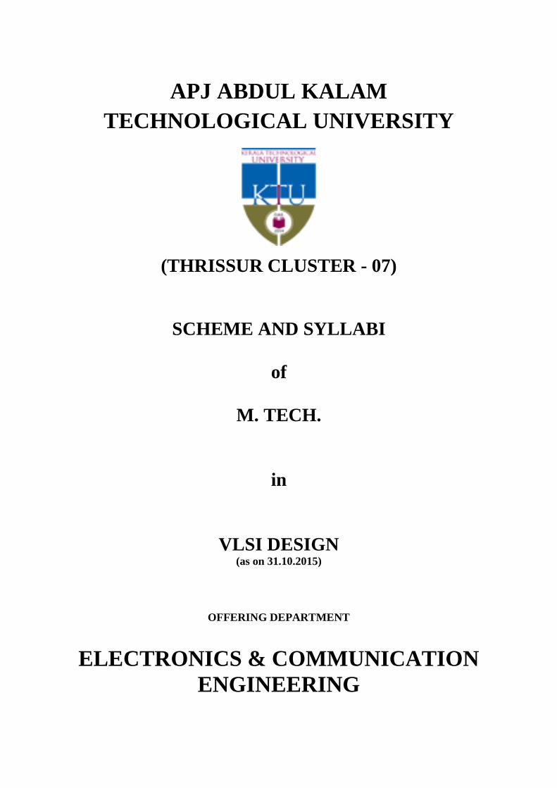
CERTIFICATE
This is to certify that
1. The scheme and syllabi are prepared in accordance with the regulation and guidelines
issued by the KTU from time to time and also as per the decisions made in the CGPC
meetings.
2. The suggestions/modifications suggested while presenting the scheme and syllabi
before CGPC on 25.6.2015 have been incorporated.
3. There is no discrepancy among the soft copy in MS word format, PDF and hard copy
of the syllabi submitted to the CGPC.
4. The document has been verified by all the constituent colleges
Coordinator in charge of syllabus revision of the programme
Ms. Manju V.M.,
PG Co-ordinator,
IES College of Engineering,
Chittilappilly.
Principal of the lead college
Dr.V. S. Pradeepan
Principal,
IES College of Engineering,
Chittilappilly.
Principals of the colleges in which the programme is offered
No Name of the college Principal’s Name Signature
1 IES College of Engineering Dr. V. S. Pradeepan
2 MET’S School of Engineering Dr. C. Rajendran
Date: 31.10.2015 Chairman
Place: Thrissur

1
Scheme for M. Tech. Programme in
VLSI DESIGN
Semester I (Credits: 21)
Exam
slot
Course
No. Subject Name
Hours /
Week Internal
Marks
End semester exam
Credits
L T P Marks Duration
A 07MA6017
Advanced
Engineering
Mathematics
4 0 0 40 60 3 4
B 07EC6503 Digital CMOS
VLSI 4 0 0 40 60 3 4
C 07EC6505 Analog VLSI 4 0 0 40 60 3 4
D 07EC6507 CAD for VLSI
Circuits 3 0 0 40 60 3 3
E 07EC65XX Elective I 3 0 0 40 60 3 3
07GN6001 Research
Methodology 0 2 0 100 - 2
07EC6511
Computer Aided
Design of VLSI
Circuits
Laboratory
0 0 2 100 - 1
07EC6513
Introduction to
seminar 0 0 1 - - - -
-
Departmental
Assistance - - 7 - - - -
Total 18 2 10 21
ELECTIVE I
07EC6409 Electronic System Design
07EC6229 Digital Image Processing
07EC6529 Hardware Software CoDesign
L-Lecture T-Tutorial P-Practical C-Credit
2
Semester II (Credits: 21)
Exam
slot
Course
No. Subject Name
Hours /
Week Internal
Marks
End sem exam
Credits L T P Mark Duration
A 07EC6502
Testing &
Verification of
VLSI Circuits
4 0 0 40 60 3 4
B 07EC6504 Advanced Digital
System Design 3 0 0 40 60 3 3
C 07EC6506
FPGA
Architecture and
implementation
3 0 0 40 60 3 3
D 07EC65XX Elective II 3 0 0 40 60 3 3
E 07EC65XX Elective III 3 0 0 40 60 3 3
07EC6514 Seminar 0 0 2 100 - - 2
07EC6516 Mini Project 0 0 4 100 - - 2
07EC6518
Testing &
Verification of
VLSI Circuits
Laboratory
0 0 2 100 - - 1
-
Departmental
Assistance - - 6 - - - -
Total 16 0 14 21
ELECTIVE II
07EC6528 Embedded System Design
07EC6538 VLSI Process Technology
07EC6548 DSP Architecture and Design
ELECTIVE III
07EC6512 Low Power VLSI Design
07EC6522 Advanced Computer Architecture
07EC6532 SOC Design and Verification
3
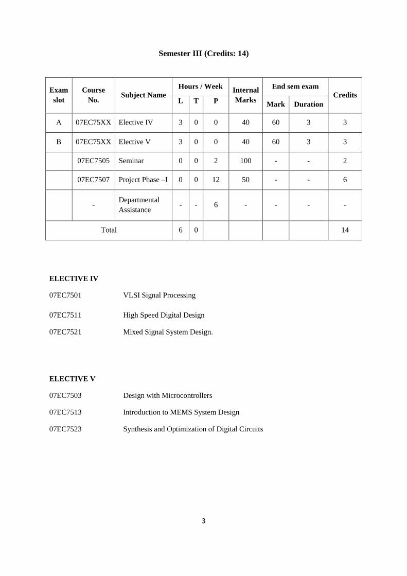
Semester III (Credits: 14)
Exam
slot
Course
No. Subject Name
Hours / Week Internal
Marks
End sem exam
Credits L T P
Mark Duration
A 07EC75XX Elective IV 3 0 0 40 60 3 3
B 07EC75XX Elective V 3 0 0 40 60 3 3
07EC7505 Seminar 0 0 2 100 - - 2
07EC7507 Project Phase –I 0 0 12 50 - - 6
- Departmental
Assistance - - 6 - - - -
Total 6 0 14
ELECTIVE IV
07EC7501 VLSI Signal Processing
07EC7511 High Speed Digital Design
07EC7521 Mixed Signal System Design.
ELECTIVE V
07EC7503 Design with Microcontrollers
07EC7513 Introduction to MEMS System Design
07EC7523 Synthesis and Optimization of Digital Circuits
4
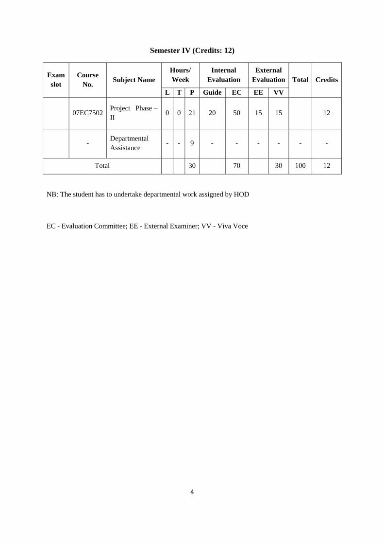
Semester IV (Credits: 12)
Exam
slot
Course
No. Subject Name
Hours/
Week
Internal
Evaluation
External
Evaluation Total Credits
L T P Guide EC EE VV
07EC7502 Project Phase –
II 0 0 21 20 50 15 15 12
- Departmental
Assistance - - 9 - - - - - -
Total 30 70 30 100 12
NB: The student has to undertake departmental work assigned by HOD
EC - Evaluation Committee; EE - External Examiner; VV - Viva Voce
5
SEMESTER I
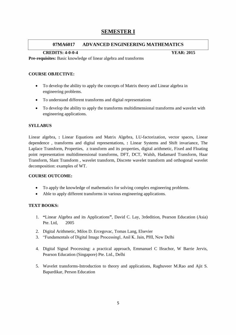
07MA6017 ADVANCED ENGINEERING MATHEMATICS
CREDITS: 4-0-0-4 YEAR: 2015
Pre-requisites: Basic knowledge of linear algebra and transforms
COURSE OBJECTIVE:
To develop the ability to apply the concepts of Matrix theory and Linear algebra in
engineering problems.
To understand different transforms and digital representations
To develop the ability to apply the transforms multidimensional transforms and wavelet with
engineering applications.
SYLLABUS
Linear algebra, : Linear Equations and Matrix Algebra, LU-factorization, vector spaces, Linear
dependence , transforms and digital representations, : Linear Systems and Shift invariance, The
Laplace Transform, Properties, z transform and its properties, digital arithmetic, Fixed and Floating
point representation multidimensional transforms, DFT, DCT, Walsh, Hadamard Transform, Haar
Transform, Slant Transform , wavelet transform, Discrete wavelet transform and orthogonal wavelet
decomposition: examples of WT.
COURSE OUTCOME:
To apply the knowledge of mathematics for solving complex engineering problems.
Able to apply different transforms in various engineering applications.
TEXT BOOKS:
1. “Linear Algebra and its Applications”, David C. Lay, 3rdedition, Pearson Education (Asia)
Pte. Ltd, 2005
2. Digital Arithmetic, Milos D. Ercegovac, Tomas Lang, Elsevier
3. “Fundamentals of Digital Image Processing‖, Anil K. Jain, PHI, New Delhi
4. Digital Signal Processing: a practical approach, Emmanuel C Ifeachor, W Barrie Jervis,
Pearson Education (Singapore) Pte. Ltd., Delhi
5. Wavelet transforms-Introduction to theory and applications, Raghuveer M.Rao and Ajit S.
Bapardikar, Person Education
6
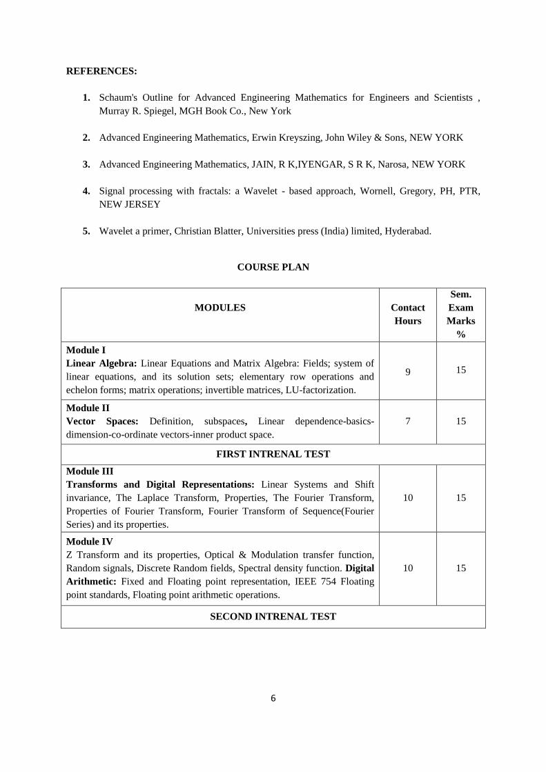
REFERENCES:
1. Schaum's Outline for Advanced Engineering Mathematics for Engineers and Scientists ,
Murray R. Spiegel, MGH Book Co., New York
2. Advanced Engineering Mathematics, Erwin Kreyszing, John Wiley & Sons, NEW YORK
3. Advanced Engineering Mathematics, JAIN, R K,IYENGAR, S R K, Narosa, NEW YORK
4. Signal processing with fractals: a Wavelet - based approach, Wornell, Gregory, PH, PTR,
NEW JERSEY
5. Wavelet a primer, Christian Blatter, Universities press (India) limited, Hyderabad.
COURSE PLAN
MODULES
Contact
Hours
Sem.
Exam
Marks
%
Module I
Linear Algebra: Linear Equations and Matrix Algebra: Fields; system of
linear equations, and its solution sets; elementary row operations and
echelon forms; matrix operations; invertible matrices, LU-factorization.
9 15
Module II
Vector Spaces: Definition, subspaces, Linear dependence-basics-
dimension-co-ordinate vectors-inner product space.
7 15
FIRST INTRENAL TEST
Module III
Transforms and Digital Representations: Linear Systems and Shift
invariance, The Laplace Transform, Properties, The Fourier Transform,
Properties of Fourier Transform, Fourier Transform of Sequence(Fourier
Series) and its properties.
10 15
Module IV
Z Transform and its properties, Optical & Modulation transfer function,
Random signals, Discrete Random fields, Spectral density function. Digital
Arithmetic: Fixed and Floating point representation, IEEE 754 Floating
point standards, Floating point arithmetic operations.
10 15
SECOND INTRENAL TEST
7
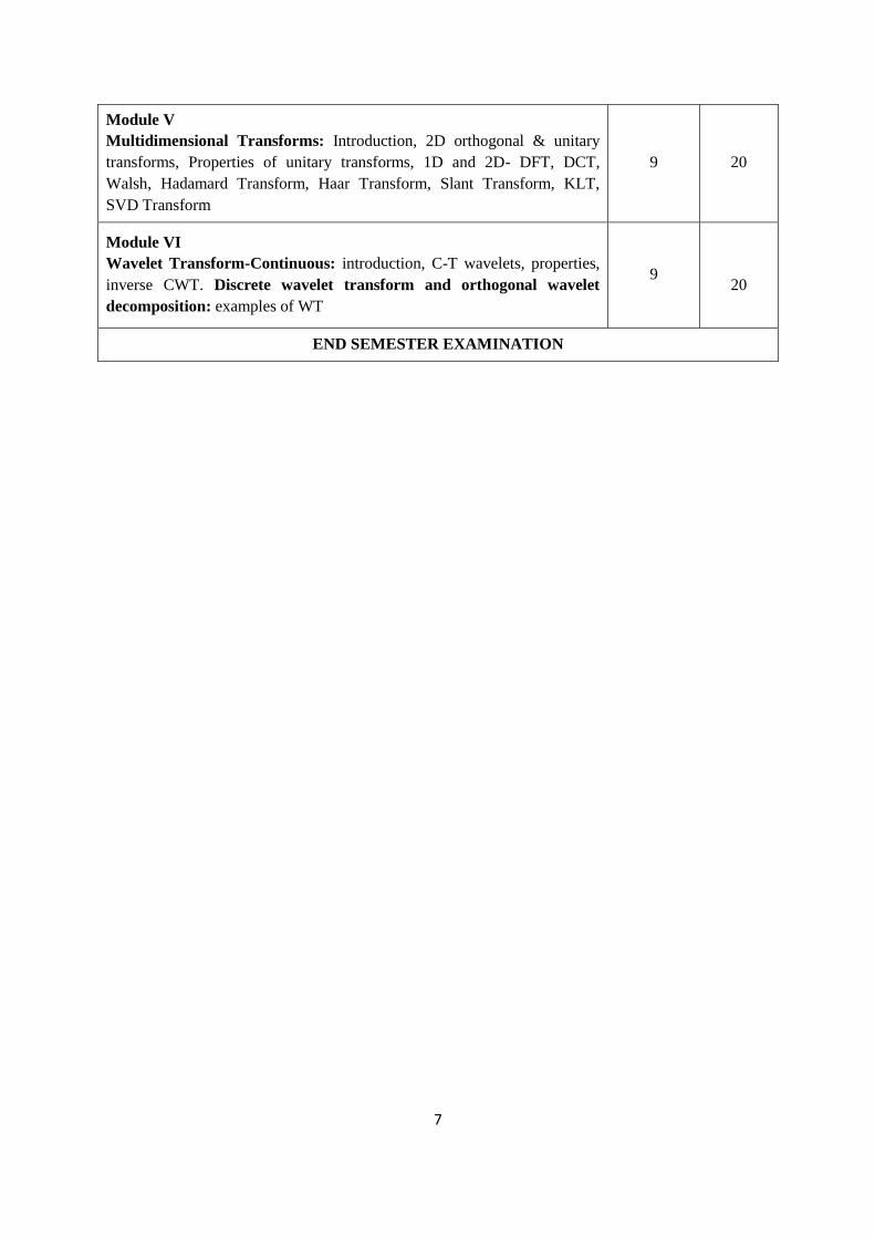
Module V
Multidimensional Transforms: Introduction, 2D orthogonal & unitary
transforms, Properties of unitary transforms, 1D and 2D- DFT, DCT,
Walsh, Hadamard Transform, Haar Transform, Slant Transform, KLT,
SVD Transform
9 20
Module VI
Wavelet Transform-Continuous: introduction, C-T wavelets, properties,
inverse CWT. Discrete wavelet transform and orthogonal wavelet
decomposition: examples of WT
9
20
END SEMESTER EXAMINATION
8
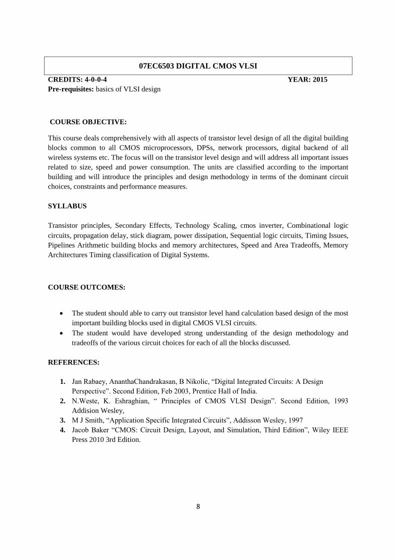
07EC6503 DIGITAL CMOS VLSI
CREDITS: 4-0-0-4 YEAR: 2015
Pre-requisites: basics of VLSI design
COURSE OBJECTIVE:
This course deals comprehensively with all aspects of transistor level design of all the digital building
blocks common to all CMOS microprocessors, DPSs, network processors, digital backend of all
wireless systems etc. The focus will on the transistor level design and will address all important issues
related to size, speed and power consumption. The units are classified according to the important
building and will introduce the principles and design methodology in terms of the dominant circuit
choices, constraints and performance measures.
SYLLABUS
Transistor principles, Secondary Effects, Technology Scaling, cmos inverter, Combinational logic
circuits, propagation delay, stick diagram, power dissipation, Sequential logic circuits, Timing Issues,
Pipelines Arithmetic building blocks and memory architectures, Speed and Area Tradeoffs, Memory
Architectures Timing classification of Digital Systems.
COURSE OUTCOMES:
The student should able to carry out transistor level hand calculation based design of the most
important building blocks used in digital CMOS VLSI circuits.
The student would have developed strong understanding of the design methodology and
tradeoffs of the various circuit choices for each of all the blocks discussed.
REFERENCES:
1. Jan Rabaey, AnanthaChandrakasan, B Nikolic, “Digital Integrated Circuits: A Design
Perspective”. Second Edition, Feb 2003, Prentice Hall of India.
2. N.Weste, K. Eshraghian, “ Principles of CMOS VLSI Design”. Second Edition, 1993
Addision Wesley,
3. M J Smith, “Application Specific Integrated Circuits”, Addisson Wesley, 1997
4. Jacob Baker “CMOS: Circuit Design, Layout, and Simulation, Third Edition”, Wiley IEEE
Press 2010 3rd Edition.
9
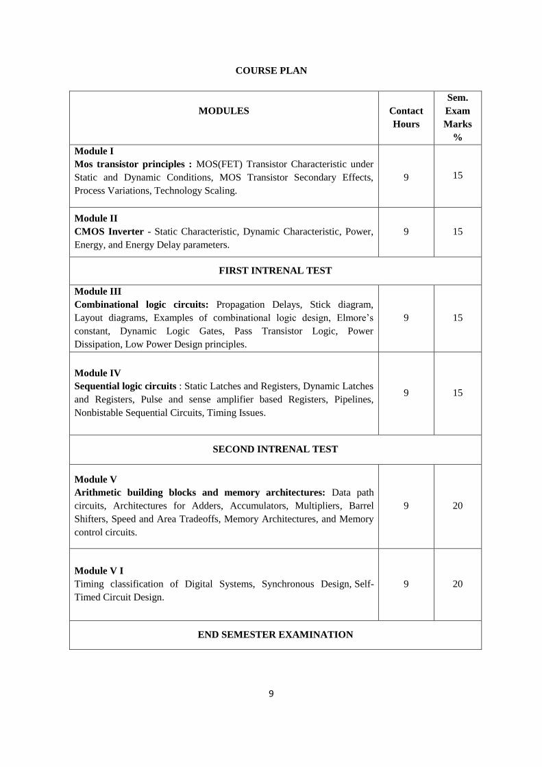
COURSE PLAN
MODULES
Contact
Hours
Sem.
Exam
Marks
%
Module I
Mos transistor principles : MOS(FET) Transistor Characteristic under
Static and Dynamic Conditions, MOS Transistor Secondary Effects,
Process Variations, Technology Scaling.
9 15
Module II
CMOS Inverter - Static Characteristic, Dynamic Characteristic, Power,
Energy, and Energy Delay parameters.
9 15
FIRST INTRENAL TEST
Module III
Combinational logic circuits: Propagation Delays, Stick diagram,
Layout diagrams, Examples of combinational logic design, Elmore’s
constant, Dynamic Logic Gates, Pass Transistor Logic, Power
Dissipation, Low Power Design principles.
9 15
Module IV
Sequential logic circuits : Static Latches and Registers, Dynamic Latches
and Registers, Pulse and sense amplifier based Registers, Pipelines,
Nonbistable Sequential Circuits, Timing Issues.
9 15
SECOND INTRENAL TEST
Module V
Arithmetic building blocks and memory architectures: Data path
circuits, Architectures for Adders, Accumulators, Multipliers, Barrel
Shifters, Speed and Area Tradeoffs, Memory Architectures, and Memory
control circuits.
9 20
Module V I
Timing classification of Digital Systems, Synchronous Design, Self-
Timed Circuit Design.
9 20
END SEMESTER EXAMINATION

10
07EC6505 ANALOG VLSI
CREDITS: 4-0-0-4 YEAR: 2015
Pre-requisites: Analog and mixed mos circuits
COURSE OBJECTIVE:
To learn about Device Modeling- Various types of analog systems- CMOS amplifiers , Comparators
and Switched Capacitor Circuits.
SYLLABUS
Analog mos transistor models, characterization of resistive, capacitive elements and MOS devices,
frequency response, differential amplifiers, Cascode and Folded cascade structures, high performance
Opamps, current mirrors, filter implementations, supply independent and temperature independent
references, cmos comparators, CMOS oscillators, simple and charge pump CMOS PLLs, non ideal
effects in PLLs, Delay locked loops and applications. cmos data converters, Over sampling
converters.
COURSE OUTCOME:
Students will be able to understand the concepts of analog design and to design various analog
systems including data converters- CMOS amplifiers- Comparators and Switched Capacitor Circuits.
REFERENCES:
1. “Analog Integrated Circuit Design”, David. A. Johns and Ken Martin, John Wiley and Sons,
2001.
2. “Design of Analog CMOS Integrated Circuit”, BehzadRazavi, Tata McGraw HILL, 2002.
3. “CMOS Analog Circuit Design”, Philip Allen & Douglas Holberg, Oxford University Press,
2002.
4. “Analog VLSI – Signal Information and Processing”, Mohammed Ismail &Feiz , John Wiley
and Sons.
COURSE PLAN
MODULES
Contact
Hours
Sem.
Exam
Marks
%
Module I
Analog MOS transistor models: Temperature effects and Noise in MOS
transistor. MOS resistors, characterization of resistive, capacitive
10 15
11
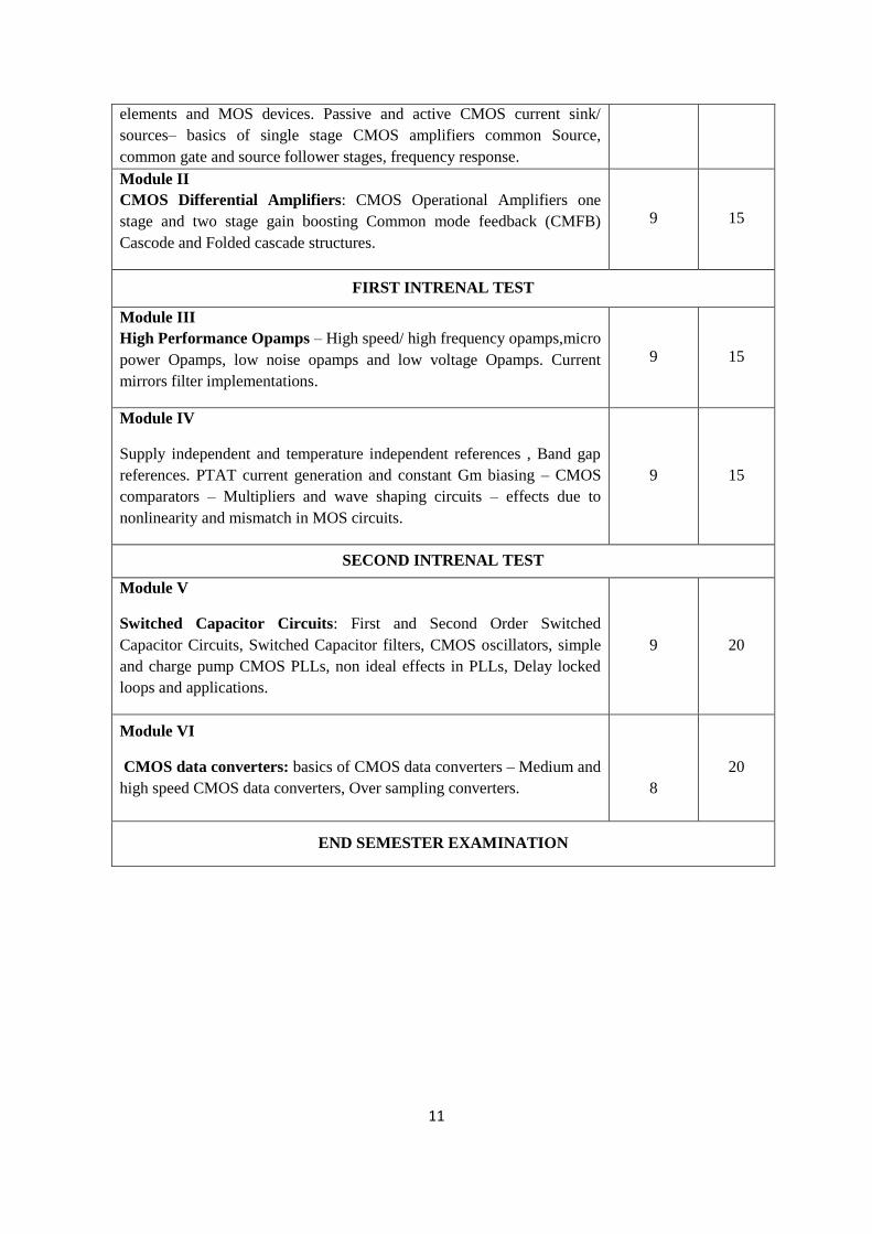
elements and MOS devices. Passive and active CMOS current sink/
sources– basics of single stage CMOS amplifiers common Source,
common gate and source follower stages, frequency response.
Module II
CMOS Differential Amplifiers: CMOS Operational Amplifiers one
stage and two stage gain boosting Common mode feedback (CMFB)
Cascode and Folded cascade structures.
9 15
FIRST INTRENAL TEST
Module III
High Performance Opamps – High speed/ high frequency opamps,micro
power Opamps, low noise opamps and low voltage Opamps. Current
mirrors filter implementations.
9 15
Module IV
Supply independent and temperature independent references , Band gap
references. PTAT current generation and constant Gm biasing – CMOS
comparators – Multipliers and wave shaping circuits – effects due to
nonlinearity and mismatch in MOS circuits.
9 15
SECOND INTRENAL TEST
Module V
Switched Capacitor Circuits: First and Second Order Switched
Capacitor Circuits, Switched Capacitor filters, CMOS oscillators, simple
and charge pump CMOS PLLs, non ideal effects in PLLs, Delay locked
loops and applications.
9 20
Module VI
CMOS data converters: basics of CMOS data converters – Medium and
high speed CMOS data converters, Over sampling converters.
8
20
END SEMESTER EXAMINATION
12
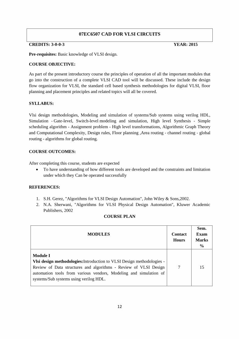
07EC6507 CAD FOR VLSI CIRCUITS
CREDITS: 3-0-0-3 YEAR: 2015
Pre-requisites: Basic knowledge of VLSI design.
COURSE OBJECTIVE:
As part of the present introductory course the principles of operation of all the important modules that
go into the construction of a complete VLSI CAD tool will be discussed. These include the design
flow organization for VLSI, the standard cell based synthesis methodologies for digital VLSI, floor
planning and placement principles and related topics will all be covered.
SYLLABUS:
Vlsi design methodologies, Modeling and simulation of systems/Sub systems using verilog HDL,
Simulation - Gate-level, Switch-level modeling and simulation, High level Synthesis - Simple
scheduling algorithm - Assignment problem - High level transformations, Algorithmic Graph Theory
and Computational Complexity, Design rules, Floor planning ,Area routing - channel routing - global
routing - algorithms for global routing.
COURSE OUTCOMES:
After completing this course, students are expected
To have understanding of how different tools are developed and the constraints and limitation
under which they Can be operated successfully
REFERENCES:
1. S.H. Gerez, "Algorithms for VLSI Design Automation", John Wiley & Sons,2002.
2. N.A. Sherwani, "Algorithms for VLSI Physical Design Automation", Kluwer Academic
Publishers, 2002
COURSE PLAN
MODULES
Contact
Hours
Sem.
Exam
Marks
%
Module I
Vlsi design methodologies:Introduction to VLSI Design methodologies -
Review of Data structures and algorithms - Review of VLSI Design
automation tools from various vendors, Modeling and simulation of
systems/Sub systems using verilog HDL.
7 15
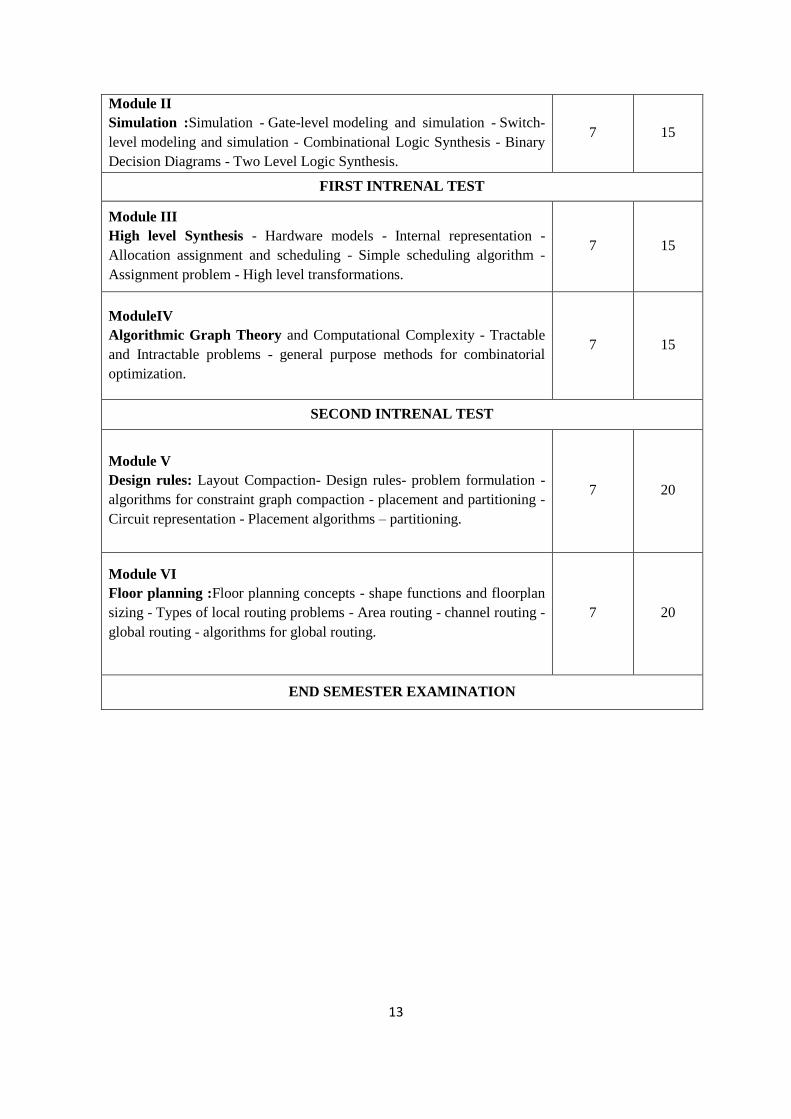
13
Module II
Simulation :Simulation - Gate-level modeling and simulation - Switch-
level modeling and simulation - Combinational Logic Synthesis - Binary
Decision Diagrams - Two Level Logic Synthesis.
7 15
FIRST INTRENAL TEST
Module III
High level Synthesis - Hardware models - Internal representation -
Allocation assignment and scheduling - Simple scheduling algorithm -
Assignment problem - High level transformations.
7 15
ModuleIV
Algorithmic Graph Theory and Computational Complexity - Tractable
and Intractable problems - general purpose methods for combinatorial
optimization.
7 15
SECOND INTRENAL TEST
Module V
Design rules: Layout Compaction- Design rules- problem formulation -
algorithms for constraint graph compaction - placement and partitioning -
Circuit representation - Placement algorithms – partitioning.
7 20
Module VI
Floor planning :Floor planning concepts - shape functions and floorplan
sizing - Types of local routing problems - Area routing - channel routing -
global routing - algorithms for global routing.
7 20
END SEMESTER EXAMINATION
14
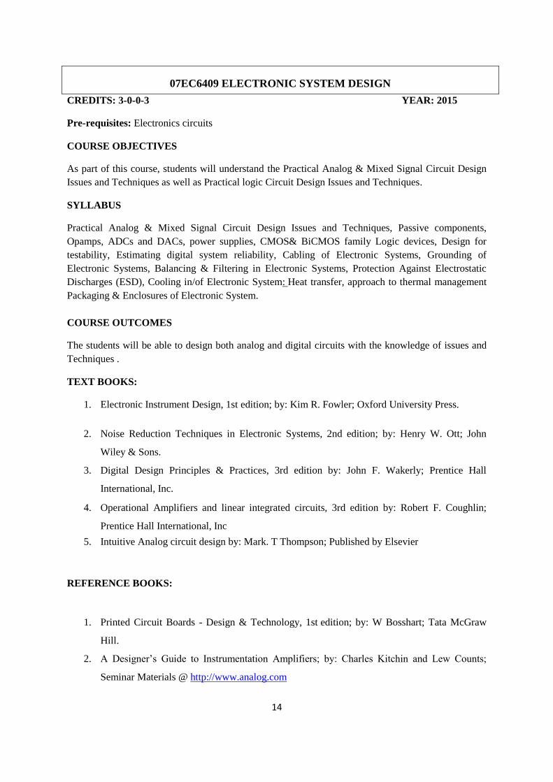
07EC6409 ELECTRONIC SYSTEM DESIGN
CREDITS: 3-0-0-3 YEAR: 2015
Pre-requisites: Electronics circuits
COURSE OBJECTIVES
As part of this course, students will understand the Practical Analog & Mixed Signal Circuit Design
Issues and Techniques as well as Practical logic Circuit Design Issues and Techniques.
SYLLABUS
Practical Analog & Mixed Signal Circuit Design Issues and Techniques, Passive components,
Opamps, ADCs and DACs, power supplies, CMOS& BiCMOS family Logic devices, Design for
testability, Estimating digital system reliability, Cabling of Electronic Systems, Grounding of
Electronic Systems, Balancing & Filtering in Electronic Systems, Protection Against Electrostatic
Discharges (ESD), Cooling in/of Electronic System: Heat transfer, approach to thermal management
Packaging & Enclosures of Electronic System.
COURSE OUTCOMES
The students will be able to design both analog and digital circuits with the knowledge of issues and
Techniques .
TEXT BOOKS:
1. Electronic Instrument Design, 1st edition; by: Kim R. Fowler; Oxford University Press.
2. Noise Reduction Techniques in Electronic Systems, 2nd edition; by: Henry W. Ott; John
Wiley & Sons.
3. Digital Design Principles & Practices, 3rd edition by: John F. Wakerly; Prentice Hall
International, Inc.
4. Operational Amplifiers and linear integrated circuits, 3rd edition by: Robert F. Coughlin;
Prentice Hall International, Inc
5. Intuitive Analog circuit design by: Mark. T Thompson; Published by Elsevier
REFERENCE BOOKS:
1. Printed Circuit Boards - Design & Technology, 1st edition; by: W Bosshart; Tata McGraw
Hill.
2. A Designer’s Guide to Instrumentation Amplifiers; by: Charles Kitchin and Lew Counts;
Seminar Materials @ http://www.analog.com

15
3. Errors and Error Budget Analysis in Instrumentation Amplifier Applications; by: Eamon
Nash; Application note AN-539@ http://www.analog.com
4. Practical Analog Design Techniques; by: Adolofo Garcia and Wes Freeman; Seminar
Materials@ http://www.analog.com
5. Selecting An A/D Converter; by:Larry Gaddy; Application bulletin @http://www.Ti.com
6. Benefits and issues on migration of 5-volt and 3.3 volt logic to lower voltage supplies;
Application note SDAA011A@ http://www.Ti.com
7. JTAG/IEEE 1149.1 deigns considerations; Application note SCTA029@http://www.Ti.com
8. Live Insertion; Application note SDYA012@ http://www.Ti.com
9. PCB Design Guidelines For Reduced EMI; Application note SZZA009@http://www.Ti.com
COURSE PLAN
MODULES
Contact
Hours
Sem.
Exam
Marks
%
Module I
Practical Analog & Mixed Signal Circuit Design Issues and Techniques:
Passive components: Understanding and interpreting data sheets and
specifications of various passive and active components, non-ideal behavior
of passive components,.
Op amps: DC performance of op amps: Bias, offset and drift. AC
Performance of operational amplifiers: band width, slew rate and noise.
Properties of a high quality instrumentation amplifier. Design issues
affecting dc accuracy & error budget analysis in instrumentation amplifier
applications.
7 15
Module II
ADCs and DACs: Characteristics, interfacing to microcontrollers. Selecting
an ADC,Power supplies: Characteristics, design of full wave bridge
regulated power supply, Circuit layout and grounding in mixed signal
system.
Practical Logic Circuit Design Issues and Techniques: Understanding and
interpreting data sheets & specifications of various CMOS& BiCMOS
7 15

16
family Logic devices. Electrical behavior (steady state & dynamic) of
CMOS& BiCMOS family logic devices. Benefits and issues on migration
of 5-volt and 3.3 volt logic to lower voltage supplies.
FIRST INTRENAL TEST
Module III
Design for testability, Estimating digital system reliability. Digital circuit
layout and grounding. PCB design guidelines for reduced EMI.
Electromagnetic Compatibility (EMC): Designing for (EMC), EMC
regulations, typical noise path, methods of noise coupling, methods of
reducing interference in electronic systems
7 15
Module IV
Cabling of Electronic Systems: Capacitive coupling, effect of shield on
capacitive coupling, inductive coupling, effect of shield on inductive
coupling, effect of shield on magnetic coupling, magnetic coupling between
shield and inner conductor, shielding to prevent magnetic radiation, shielding
a receptor against magnetic fields, coaxial cable versus shielded twisted pair,
ribbon cables.
Grounding of Electronic Systems: Safety grounds, signal grounds, single-
point ground systems, multipoint-point ground systems, hybrid grounds,
functional ground layout, practical low frequency grounding, hardware
grounds, grounding of cable shields, ground loops, shield grounding at high
frequencies.
7 15
SECOND INTRENAL TEST
Module V
Balancing & Filtering in Electronic Systems: Balancing, power line filtering,
power supply decoupling, decoupling filters, high frequency filtering, system
bandwidth.
Protection Against Electrostatic Discharges (ESD): Static generation, human
body model, static discharge, ESD protection in equipment design, software
and ESD protection, ESD versus EMC.
7 20

17
Module VI
Packaging & Enclosures of Electronic System: Effect of environmental
factors on electronic system (environmental specifications), nature of
environment and safety measures. Packaging’s influence and its factors.
Cooling in/of Electronic System: Heat transfer, approach to thermal
management, mechanisms for cooling, operating range, basic thermal
calculations, cooling choices, heat sink selection
7 20
END SEMESTER EXAMINATION

18
07EC6229 DIGITAL IMAGE PROCESSING
CREDITS: 3-0-0-3 YEAR: 2015
Pre-requisites: A basic course in Digital Signal Processing
COURSE OBJECTIVES
Get a thorough understanding of digital image representation and processing
techniques
Understand the various steps in digital image processing.
SYLLABUS
Image representation, Two dimensional orthogonal transforms - DFT, FFT, WHT, Haar transform,
KLT, DCT, Image enhancement, histogram-based processing, homomorphic filtering, Edge
detection, LOG filters, localization problem, Image Restoration restoration using inverse filtering,
Wiener filtering and maximum entropy-based methods, Mathematical morphology, gray scale
morphology, applications, Image and Video Compression Standards, Sub-band Decomposition,
Entropy Encoding, JPEG, JPEG2000, MPEG, Image texture analysis, statistical models for textures,
Hough Transform, Computer tomography, Radon transform, Back-projection operator, Fourier-slice
theorem, CBP and FBP methods, ART, Fan beam projection.
COURSE OUTCOMES
Understand various techniques for image representation
Ability to process the image in spatial and transform domain for better enhancement.
REFERENCES
1. Gonzalez and Woods, Digital image processing, Prentice Hall, 2002..
2. A. K. Jain, Fundamentals of digital image processing, Prentice Hall of India, 1989.
3. M. Haralick, and L.G. Shapiro, Computer and Robot Vision, Vol-1, Addison Wesley,
Reading, MA, 1992
COURSE PLAN
MODULES
Contact
Hours
Sem.
Exam
Marks
%
Module I
Image representation - Gray scale and colour Images, image sampling and
quantization, Two dimensional orthogonal transforms - DFT, FFT, WHT,
Haar transform, KLT, DCT.
7 15

19
Module II
Image enhancement - filters in spatial and frequency domains,
histogram-based processing, homomorphic filtering
7 15
FIRST INTRENAL TEST
Module III
Edge detection - non parametric and model based approaches, LOG
filters, localization problem, Image Restoration - PSF, circulant and
block - circulant matrices, deconvolution, restoration using inverse
filtering, Wiener filtering and maximum entropy-based methods
7 15
Module IV
Mathematical morphology - binary morphology, dilation, erosion,
opening and closing, duality relations, gray scale morphology,
applications such as hit-and-miss transform, thinning and shape
decomposition,Image and Video Compression Standards- Lossy and
lossless compression schemes: Sub-band Decomposition, Entropy
Encoding, JPEG, JPEG2000, MPEG.
7 15
SECOND INTRENAL TEST
Module V
Image texture analysis: co-occurrence matrix, measures of textures,
statistical models for textures. Hough Transform, boundary detection,
chain coding, segmentation and thresholding methods
7 20
Module VI
Computer tomography: parallel beam projection, Radon transform, and its
inverse, Back-projection operator, Fourier-slice theorem, CBP and FBP
methods, ART, Fan beam projection
7 20
END SEMESTER EXAMINATION
20
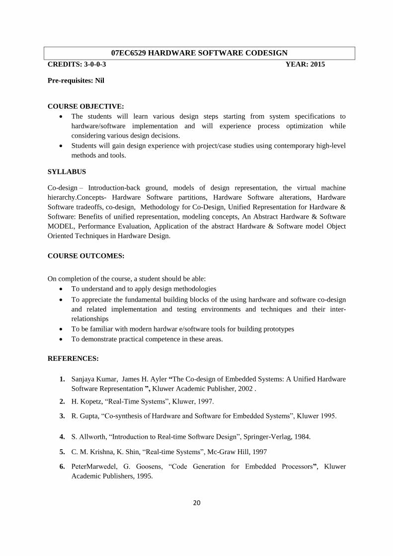
07EC6529 HARDWARE SOFTWARE CODESIGN
CREDITS: 3-0-0-3 YEAR: 2015
Pre-requisites: Nil
COURSE OBJECTIVE:
The students will learn various design steps starting from system specifications to
hardware/software implementation and will experience process optimization while
considering various design decisions.
Students will gain design experience with project/case studies using contemporary high-level
methods and tools.
SYLLABUS
Co-design – Introduction-back ground, models of design representation, the virtual machine
hierarchy.Concepts- Hardware Software partitions, Hardware Software alterations, Hardware
Software tradeoffs, co-design, Methodology for Co-Design, Unified Representation for Hardware &
Software: Benefits of unified representation, modeling concepts, An Abstract Hardware & Software
MODEL, Performance Evaluation, Application of the abstract Hardware & Software model Object
Oriented Techniques in Hardware Design.
COURSE OUTCOMES:
0 0 3
On completion of the course, a student should be able:
To understand and to apply design methodologies
To appreciate the fundamental building blocks of the using hardware and software co-design
and related implementation and testing environments and techniques and their inter-
relationships
To be familiar with modern hardwar e/software tools for building prototypes
To demonstrate practical competence in these areas.
REFERENCES:
1. Sanjaya Kumar, James H. Ayler “The Co-design of Embedded Systems: A Unified Hardware
Software Representation ”, Kluwer Academic Publisher, 2002 .
2. H. Kopetz, “Real-Time Systems”, Kluwer, 1997.
3. R. Gupta, “Co-synthesis of Hardware and Software for Embedded Systems”, Kluwer 1995.
4. S. Allworth, “Introduction to Real-time Software Design”, Springer-Verlag, 1984.
5. C. M. Krishna, K. Shin, “Real-time Systems”, Mc-Graw Hill, 1997
6. PeterMarwedel, G. Goosens, “Code Generation for Embedded Processors”, Kluwer
Academic Publishers, 1995.

21
COURSE PLAN
MODULES
Contact
Hours
Sem.
Exam
Marks
%
Module I
Introduction: Motivation hardware & software co-design, system design
consideration, research scope & overviews, Hardware Software back
ground: Embedded systems, models of design representation, the virtual
machine hierarchy.
7 15
Module II
Co-design Concepts: Functions, functional decomposition, virtual
machines, Hardware Software partitioning, Hardware Software partitions,
Hardware Software alterations, Hardware Software tradeoffs, co-design.
7 15
FIRST INTRENAL TEST
Module III
Methodology for Co-Design: Amount of unification, general
consideration & basic philosophies, a framework for co-design, Unified
Representation for Hardware & Software: Benefits of unified
representation, modeling concepts.
7 15
Module IV An
Abstract Hardware & Software Model: Requirement & applications of
the models, models of Hardware Software system, an abstract Hardware
Software models, generality of the model.
7 15
SECOND INTRENAL TEST
Module V
Performance Evaluation: the performance3 modeling, Hardware
Software development.
Application of the abstract Hardware & Software model, examples of
performance evaluation.
7 20
Module VI
Object Oriented Techniques in Hardware Design: Motivation for
object oriented technique, data types, modeling hardware components as
classes, designing specialized components, data decomposition, Processor
example.
7 20
END SEMESTER EXAMINATION
22
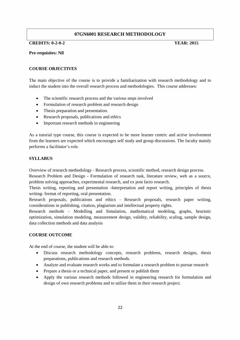
07GN6001 RESEARCH METHODOLOGY
CREDITS: 0-2-0-2 YEAR: 2015
Pre-requisites: Nil
COURSE OBJECTIVES
The main objective of the course is to provide a familiarization with research methodology and to
induct the student into the overall research process and methodologies. This course addresses:
The scientific research process and the various steps involved
Formulation of research problem and research design
Thesis preparation and presentation.
Research proposals, publications and ethics
Important research methods in engineering
As a tutorial type course, this course is expected to be more learner centric and active involvement
from the learners are expected which encourages self study and group discussions. The faculty mainly
performs a facilitator’s role.
SYLLABUS
Overview of research methodology - Research process, scientific method, research design process.
Research Problem and Design - Formulation of research task, literature review, web as a source,
problem solving approaches, experimental research, and ex post facto research.
Thesis writing, reporting and presentation -Interpretation and report writing, principles of thesis
writing- format of reporting, oral presentation.
Research proposals, publications and ethics - Research proposals, research paper writing,
considerations in publishing, citation, plagiarism and intellectual property rights.
Research methods – Modelling and Simulation, mathematical modeling, graphs, heuristic
optimization, simulation modeling, measurement design, validity, reliability, scaling, sample design,
data collection methods and data analysis
COURSE OUTCOME
At the end of course, the student will be able to:
Discuss research methodology concepts, research problems, research designs, thesis
preparations, publications and research methods.
Analyze and evaluate research works and to formulate a research problem to pursue research
Prepare a thesis or a technical paper, and present or publish them
Apply the various research methods followed in engineering research for formulation and
design of own research problems and to utilize them in their research project.

23
REFERENCE BOOKS
1. C. R. Kothari, Research Methodology, Methods and Techniques, New Age International
Publishers
2. K. N. Krishnaswamy, Appa Iyer Sivakumar, M. Mathirajan, Management Research
Methodology, Integration of principles, Methods and Techniques, Pearson Education
3. R. Panneerselvam, Research Methodology, PHI Learning
4. Deepak Chawla, Meena Sondhi, Research Methodology–concepts & cases, Vikas Publg
House
5. J.W Bames, Statistical Analysis for Engineers and Scientists, McGraw Hill, N.York
6. Schank Fr., Theories of Engineering Experiments, Tata Mc Graw Hill Publication.
7. Willktnsion K. L, Bhandarkar P. L, Formulation of Hypothesis, Himalaya Publication.
8. Fred M Kerlinger , Research Methodology
9. Ranjit Kumar, Research Methodology – A step by step guide for beginners, Pearson
Education
10. John W Best, James V Kahan – Research in Education , PHI Learning
11. Donald R. Cooper, Pamela S. Schindler, Business Research Methods, 8/e, Tata McGraw-Hill
Co Ltd
12. Sinha, S.C. and Dhiman, A.K., 2002. Research Methodology, Ess Ess Publications. 2
volumes
13. Trochim, W.M.K., 2005. Research Methods: the concise knowledge base, Atomic Dog
Publishing. 270p.
14. Coley, S.M. and Scheinberg, C. A., 1990, "Proposal Writing", Sage Publications.
15. Day, R.A., 1992.How to Write and Publish a Scientific Paper, Cambridge University Press.
16. Fink, A., 2009. Conducting Research Literature Reviews: From the Internet to Paper. Sage
Publications
17. Donald H.McBurney, Research Methods, 5th Edition, Thomson Learning, ISBN:81-315-
0047- 0,2006
18. Garg, B.L., Karadia, R., Agarwal, F. and Agarwal, U.K., 2002. An introduction to Research
Methodology, RBSA Publishers..
19. Wadehra, B.L. 2000. Law relating to patents, trademarks, copyright designs and geographical
indications. Universal Law Publishing
20. Carlos, C.M., 2000. Intellectual property rights, the WTO and developing countries: the
TRIPS agreement and policy options. Zed Books, New York.
21. Additional suitable web resources
22. Guidelines related to conference and journal publications
COURSE PLAN
Modules Contact
hours
Int. Exam
Marks %
Module I
Overview of Research Methodology: Research concepts – meaning –
objectives – motivation - types of research –research process – criteria for
good research – problems encountered by Indian researchers - scientific
method - research design process – decisional research.
5 10%
24
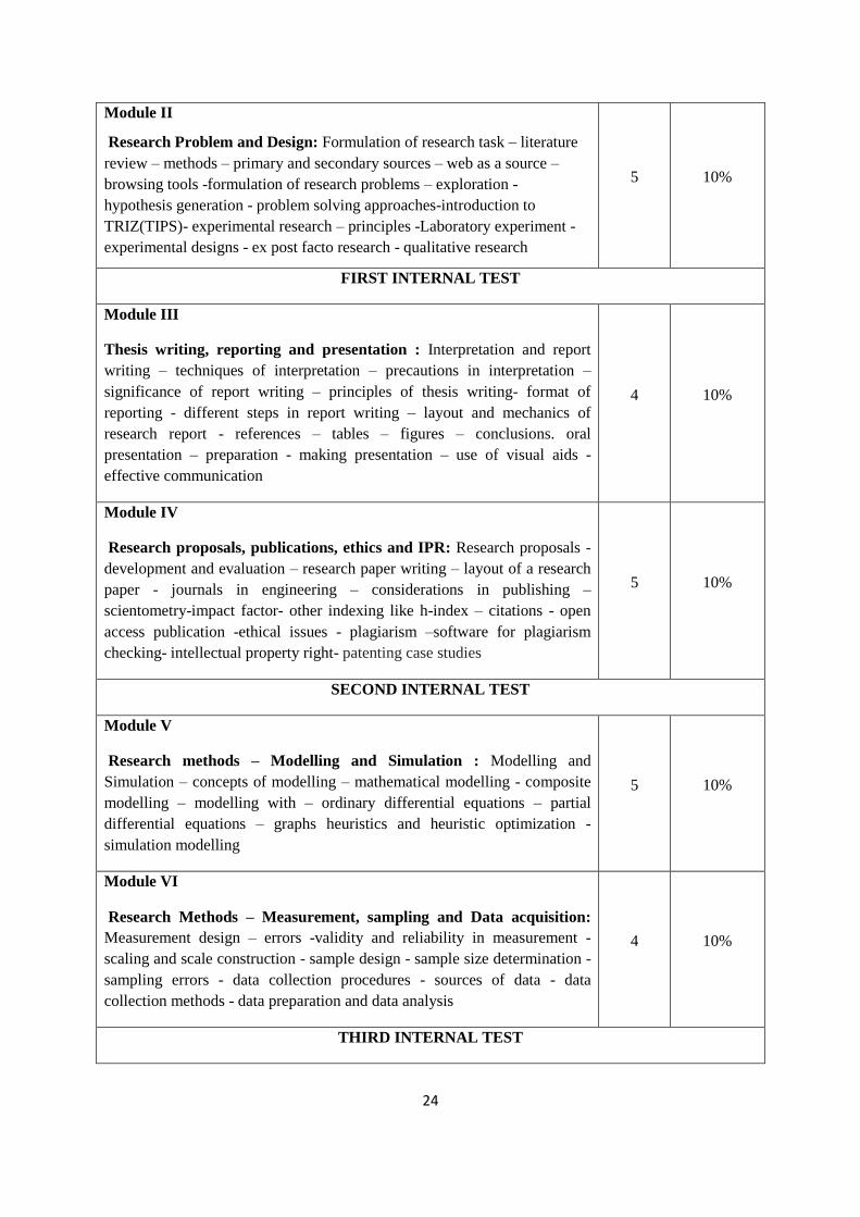
Module II
Research Problem and Design: Formulation of research task – literature
review – methods – primary and secondary sources – web as a source –
browsing tools -formulation of research problems – exploration -
hypothesis generation - problem solving approaches-introduction to
TRIZ(TIPS)- experimental research – principles -Laboratory experiment -
experimental designs - ex post facto research - qualitative research
5 10%
FIRST INTERNAL TEST
Module III
Thesis writing, reporting and presentation : Interpretation and report
writing – techniques of interpretation – precautions in interpretation –
significance of report writing – principles of thesis writing- format of
reporting - different steps in report writing – layout and mechanics of
research report - references – tables – figures – conclusions. oral
presentation – preparation - making presentation – use of visual aids -
effective communication
4 10%
Module IV
Research proposals, publications, ethics and IPR: Research proposals -
development and evaluation – research paper writing – layout of a research
paper - journals in engineering – considerations in publishing –
scientometry-impact factor- other indexing like h-index – citations - open
access publication -ethical issues - plagiarism –software for plagiarism
checking- intellectual property right- patenting case studies
5 10%
SECOND INTERNAL TEST
Module V
Research methods – Modelling and Simulation : Modelling and
Simulation – concepts of modelling – mathematical modelling - composite
modelling – modelling with – ordinary differential equations – partial
differential equations – graphs heuristics and heuristic optimization -
simulation modelling
5 10%
Module VI
Research Methods – Measurement, sampling and Data acquisition:
Measurement design – errors -validity and reliability in measurement -
scaling and scale construction - sample design - sample size determination -
sampling errors - data collection procedures - sources of data - data
collection methods - data preparation and data analysis
4 10%
THIRD INTERNAL TEST

25
Internal continuous assessment: 100 marks
Internal continuous assessment is in the form of periodical tests and assignments. There are three tests
for the course (3 x 20 = 60 marks) and assignments (40 marks). The assignments can be in the form of
seminar, group tasks, case studies, research work or in a suitable format as decided by the teacher.
The assessment details are to be announced to students at the beginning of the semester by the
teacher.

26
07EC6511 COMPUTER AIDED DESIGN OF VLSI CIRCUITS LABORATORY
CREDITS: 0-0-2-1 YEAR: 2015
Pre-requisites: Basic knowledge in Digital system Design
COURSE OBJECTIVES:
To provide an introduction to the fundamentals of Computer-Aided Design tools for the
modelling, design and analysis of VLSI circuits.
To familiarize the students with verilog, hardware description Language.
To familiarize the students with FPGA based design methodology.
SYLLABUS
Modeling and simulation of Combinational and sequential circuits, ALU, FSM, Memory , FIFO and
UART in Verilog, Simulation of NMOS and CMOS circuits using SPICE, Implementation of circuits
in FPGA, MOSFET modeling using C.
COURSE OUTCOMES:
Upon completion of the course students will be able to
Demonstrate knowledge and understanding of fundamental concepts in CAD.
To model , design and analyze VLSI systems as their own.
To map a given digital system to FPGA.
REFERENCE BOOKS:
1. Modern Digital Electronics by R P Jain
2. Verilog HDL by Samir Palnitkar.
3. VERILOG HDL SYNTHESIS: A PRACTICAL PRIMER by J Bhaskar
LIST OF EXPERIMENTS
Cycle I
1. Modeling and simulation of Combinational and sequential circuits using Verilog
2. Modeling and Simulation of ALU using Verilog
3. Modeling and Simulation of FSMs using Verilog
4. Modeling and simulation of Memory and FIFO in Verilog

27
Cycle II
1. Modeling and simulation of UART in Verilog
2. Simulation of NMOS and CMOS circuits using SPICE
5. Design and implementation of Combinational and sequential circuits using FPGA.
3. Modeling of MOSFET using C.
Internal Continuous Assessment:
Practical record/
Results
Regular Class Viva
Voce Final Test Total
Marks 25 25 50 100

28
07EC6513 INTRODUCTION TO SEMINAR
CREDITS: 0-0-1-0 YEAR: 2015
Pre-requisites: Nil
OBJECTIVE:
The Introduction to Seminar is included to improve the of communication skills of the students and to
train them to present technical topics in a well organised manner to an audience. It is also intended to
make them confident in expressing their views with clarity. This will help create self esteem and
confidence that are essential for engineers. Individual students are required to choose a topic of their
interest from VLSI Design preferably from outside the M.Tech syllabus and give a seminar on that
topic about 30 minutes. Each student shall submit two copies of a write up of his/her seminar topic.
One copy shall be returned to the student after duly certifying it by the chairman of the assessing
committee and the other will be kept in the department. A committee consisting of at least three
faculty members shall assess the presentation of the seminar based on the relevance of the topic,
organisation of the seminar, presentation skill, quality of the report and participation.

29
SEMESTER II
07EC6502 TESTING & VERIFICATION OF VLSI CIRCUITS
CREDITS: 4-0-0-4 YEAR: 2015
Pre-requisites: Basics of VLSI Design
COURSE OBJECTIVE:
To know the various types of faults and also to study about fault detection and dominance.
To know the concepts of test generation for combinational and sequential circuits
To understand the concepts of test generation method – DFT, BIST.
To understand the fault diagnosis method.
SYLLABUS
Introduction to Testing-fault modeling, Yield-ATE Block Diagram- Fault Modeling - glossary of
Fault models - single stuck-at-faults , fault simulation-test benches, Combinational and Sequential
ATPG, Testability Measures D-Algorithm-PODEM- Sequential ATPG Implementation and
complexity- Time Frame Expansion, Delay, Transition faults - delay test methodologies – practical
consideration, Memory and IDDQ Testing, DFT, BIST and Boundary Scan, Pattern Generation-
Output Response Analysis-BILBO- Boundary Scan standard- Introduction to Fault Diagnosis.
COURSE OUTCOME:
An ability to explain the VLSI testing procedure.
An ability to analyze VLSI circuit for testability.
An ability to understand basic ATPG Algorithms used in VLSI Testing.
An ability to explain the delay testing, IDDQ testing and Memory Testing
An ability to design logic circuit easier for testing by inserting elementary testing hardware.
TEXT BOOKS
1. Viswani D Agarwal and Michael L Bushnell, “Essentials of Electronic Testing of Digital
Memory and Mixed Signal VLSI Circuits”, Springer, 2000.
2. M. Abramovici, M A Breuer and A D Friedman, “Digital systems Testing and Testable
Design”, IEEE Press, 1994.
REFERENCES
1. P.K. Lala, “Fault Tolerant and Fault Testable Hardware Design”, Academic Press, 2012.
2. P.K. Lala, “Digital Circuit Testing and Testability”, Academic Press, 2002
3. Alfred L Cronch, “Design for Test for Digital IC’s and Embedded Core system”, Prentice Hall,
1999.
4. Niraj Jha and Sanjeep K Gupta, “Testing of Digital Systems”, Cambridge University Press,
2003.
30
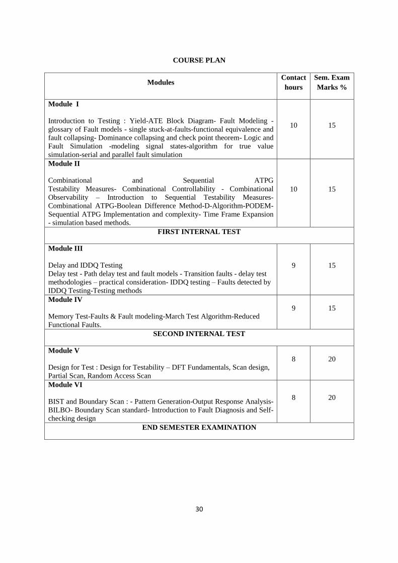
COURSE PLAN
Modules Contact
hours
Sem. Exam
Marks %
Module I
Introduction to Testing : Yield-ATE Block Diagram- Fault Modeling -
glossary of Fault models - single stuck-at-faults-functional equivalence and
fault collapsing- Dominance collapsing and check point theorem- Logic and
Fault Simulation -modeling signal states-algorithm for true value
simulation-serial and parallel fault simulation
10 15
Module II
Combinational and Sequential ATPG
Testability Measures- Combinational Controllability - Combinational
Observability – Introduction to Sequential Testability Measures-
Combinational ATPG-Boolean Difference Method-D-Algorithm-PODEM-
Sequential ATPG Implementation and complexity- Time Frame Expansion
- simulation based methods.
10 15
FIRST INTERNAL TEST
Module III
Delay and IDDQ Testing
Delay test - Path delay test and fault models - Transition faults - delay test
methodologies – practical consideration- IDDQ testing – Faults detected by
IDDQ Testing-Testing methods
9 15
Module IV
Memory Test-Faults & Fault modeling-March Test Algorithm-Reduced
Functional Faults.
9 15
SECOND INTERNAL TEST
Module V
Design for Test : Design for Testability – DFT Fundamentals, Scan design,
Partial Scan, Random Access Scan
8 20
Module VI
BIST and Boundary Scan : - Pattern Generation-Output Response Analysis-
BILBO- Boundary Scan standard- Introduction to Fault Diagnosis and Self-
checking design
8 20
END SEMESTER EXAMINATION
31
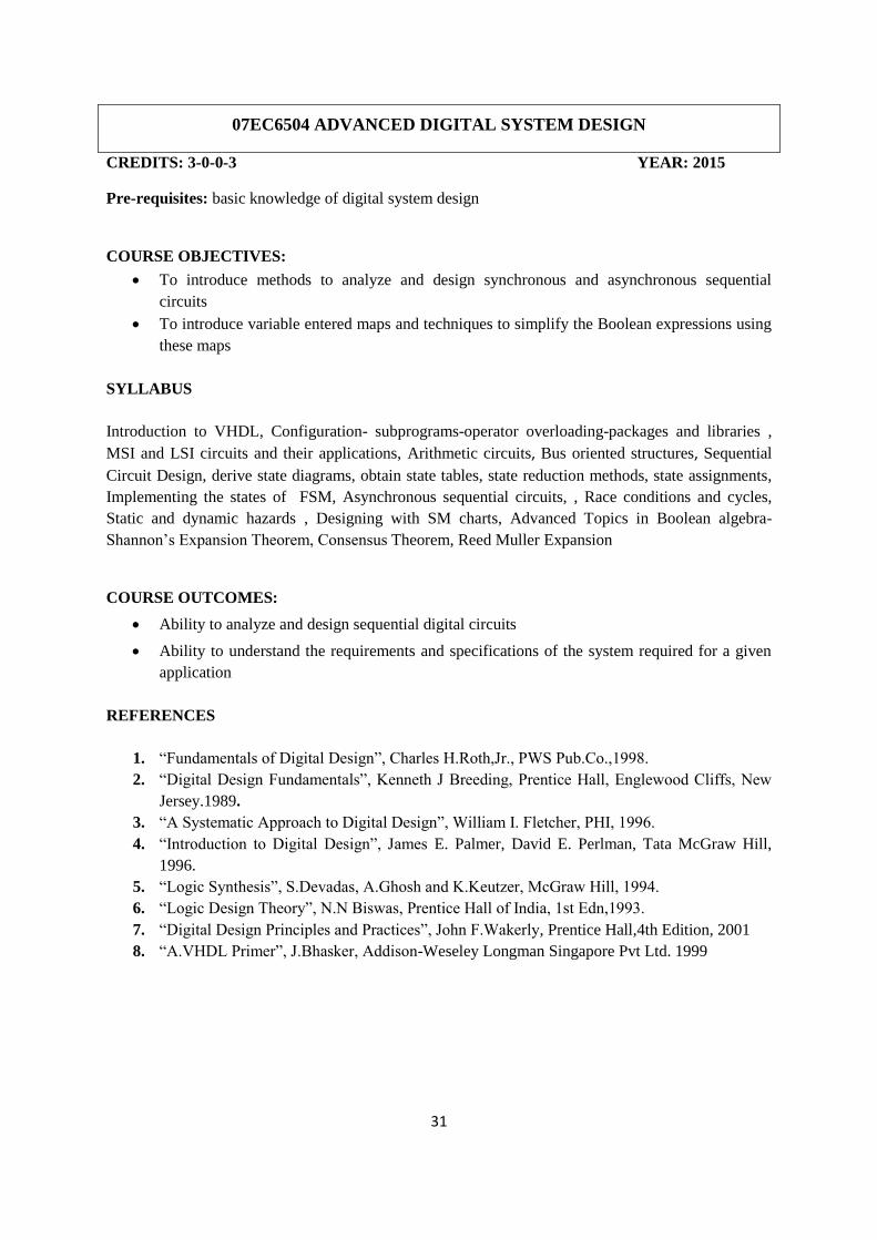
07EC6504 ADVANCED DIGITAL SYSTEM DESIGN
CREDITS: 3-0-0-3 YEAR: 2015
Pre-requisites: basic knowledge of digital system design
COURSE OBJECTIVES:
To introduce methods to analyze and design synchronous and asynchronous sequential
circuits
To introduce variable entered maps and techniques to simplify the Boolean expressions using
these maps
SYLLABUS
Introduction to VHDL, Configuration- subprograms-operator overloading-packages and libraries ,
MSI and LSI circuits and their applications, Arithmetic circuits, Bus oriented structures, Sequential
Circuit Design, derive state diagrams, obtain state tables, state reduction methods, state assignments,
Implementing the states of FSM, Asynchronous sequential circuits, , Race conditions and cycles,
Static and dynamic hazards , Designing with SM charts, Advanced Topics in Boolean algebra-
Shannon’s Expansion Theorem, Consensus Theorem, Reed Muller Expansion
COURSE OUTCOMES:
Ability to analyze and design sequential digital circuits
Ability to understand the requirements and specifications of the system required for a given
application
REFERENCES
1. “Fundamentals of Digital Design”, Charles H.Roth,Jr., PWS Pub.Co.,1998.
2. “Digital Design Fundamentals”, Kenneth J Breeding, Prentice Hall, Englewood Cliffs, New
Jersey.1989.
3. “A Systematic Approach to Digital Design”, William I. Fletcher, PHI, 1996.
4. “Introduction to Digital Design”, James E. Palmer, David E. Perlman, Tata McGraw Hill,
1996.
5. “Logic Synthesis”, S.Devadas, A.Ghosh and K.Keutzer, McGraw Hill, 1994.
6. “Logic Design Theory”, N.N Biswas, Prentice Hall of India, 1st Edn,1993.
7. “Digital Design Principles and Practices”, John F.Wakerly, Prentice Hall,4th Edition, 2001
8. “A.VHDL Primer”, J.Bhasker, Addison-Weseley Longman Singapore Pvt Ltd. 1999
32
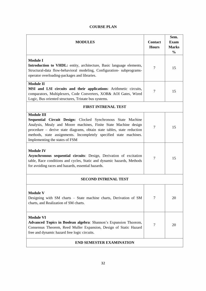
COURSE PLAN
MODULES
Contact
Hours
Sem.
Exam
Marks
%
Module I
Introduction to VHDL: entity, architecture, Basic language elements,
Structural-data flow-behavioral modeling, Configuration- subprograms-
operator overloading-packages and libraries.
7 15
Module II
MSI and LSI circuits and their applications: Arithmetic circuits,
comparators, Multiplexers, Code Converters, XOR& AOI Gates, Wired
Logic, Bus oriented structures, Tristate bus systems.
7 15
FIRST INTRENAL TEST
Module III
Sequential Circuit Design: Clocked Synchronous State Machine
Analysis, Mealy and Moore machines, Finite State Machine design
procedure – derive state diagrams, obtain state tables, state reduction
methods, state assignments. Incompletely specified state machines.
Implementing the states of FSM
7 15
Module IV
Asynchronous sequential circuits: Design, Derivation of excitation
table, Race conditions and cycles, Static and dynamic hazards, Methods
for avoiding races and hazards, essential hazards.
7 15
SECOND INTRENAL TEST
Module V
Designing with SM charts – State machine charts, Derivation of SM
charts, and Realization of SM charts.
7 20
Module VI
Advanced Topics in Boolean algebra: Shannon’s Expansion Theorem,
Consensus Theorem, Reed Muller Expansion, Design of Static Hazard
free and dynamic hazard free logic circuits.
7 20
END SEMESTER EXAMINATION
33
07EC6506 FPGA ARCHITECTURE AND IMPLEMENTATION
CREDITS: 3-0-0-3 YEAR: 2015
Pre-requisites: Nil
COURSE OBJECTIVES:
Familiarization of various complex programmable Logic devices of different families.
To study Field programmable gate arrays and realization techniques.
To study different case studies using one hot design methods.
SYLLABUS:
Programmable logic Devices, Applications and Implementation of MSI circuits using Programmable
logic Devices. FPGAs, Finite State Machines, Top down Design, State Transition Table, State
assignments for FPGAs, Realization of state machine charts using PAL FSM Architectures,
Subsystem Level Design, System level design using mentor graphics/Xilinx EDA tool (FPGA
Advantage/Xilinx ISE), Design flow using FPGAs, Case studies.
COURSE OUTCOMES:
Able to gain the knowledge about PLDs, FPGA Design & architectures.
Students should be able to understand different types of arrays.
FSM and different FSM techniques like petrinets, and different case studies
REFERENCES:
1. Field Programmable Gate Array Technology - S. Trimberger, Edr, 1994, Kluwer Academic
Publications.
2. Engineering Digital Design - RICHARD F.TINDER, 2nd Edition, Academic press.
3. Fundamentals of logic design-Charles H. Roth, 4th Edition Jaico Publishing House.
4. Digital Design Using Field Programmable Gate Array, P.K. Chan & S. Mourad, 1994,
Prentice Hall.
5. Field programmable gate array, S. Brown, R.J. Francis, J. Rose, Z.G. Vranesic, 2007, BS
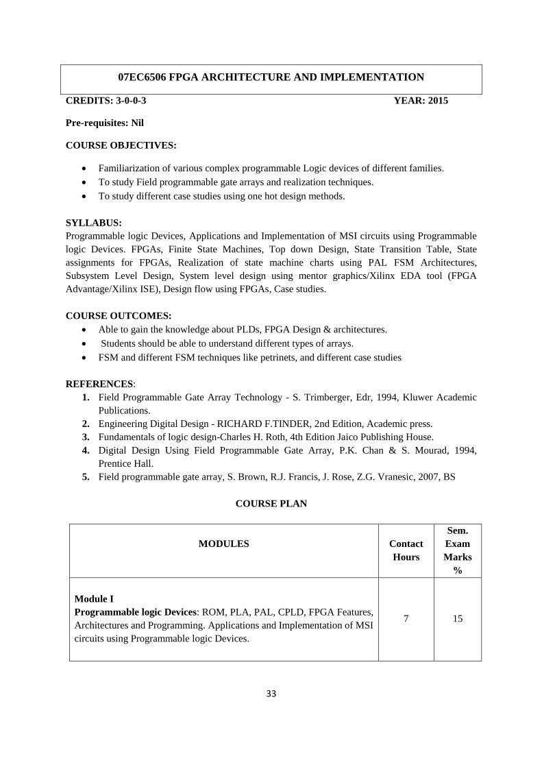
COURSE PLAN
MODULES
Contact
Hours
Sem.
Exam
Marks
%
Module I
Programmable logic Devices: ROM, PLA, PAL, CPLD, FPGA Features,
Architectures and Programming. Applications and Implementation of MSI
circuits using Programmable logic Devices.
7 15

34
Module II
FPGAs: Field Programmable Gate Arrays- Logic blocks, routing
architecture, design flow, technology mapping for FPGAs, Case studies
Xilinx XC4000 & ALTERA’s FLEX 8000/10000 FPGAs. Introduction to
advanced FPGAs: Xilinx Virtex and ALTERA Stratix.
7 15
FIRST INTRENAL TEST
Module III
Finvite State Machines (FSM): Top Down Design, State Transition
Table, State assignments for FPGAs,Realization of state machine charts
using PAL, Alternative realization for state machine charts using
microprogramming, linked state machine, encoded state machine.
7 15
Module IV
FSM Architectures: Architectures Centered around non registered PLDs,
Design of state machines centered around shift registers, One_Hot state
machine, Petrinets for state machines-Basic concepts and properties,
Finite State Machine-Case study.
7 15
SECOND INTRENAL TEST
Module V
Sbystem Level Design: Controller, data path designing, Functional
partition, Digital front end digital design tools for FPGAs. System level
design using mentor graphics/Xilinx EDA tool (FPGA Advantage/Xilinx
ISE), Design flow using FPGAs.
7 20
Module VI
Case studies: Design considerations using FPGAs of parallel adder cell,
parallel adder sequential circuits, counters, multiplexers, parallel
controllers.
7 20
END SEMESTER EXAMINATION
35
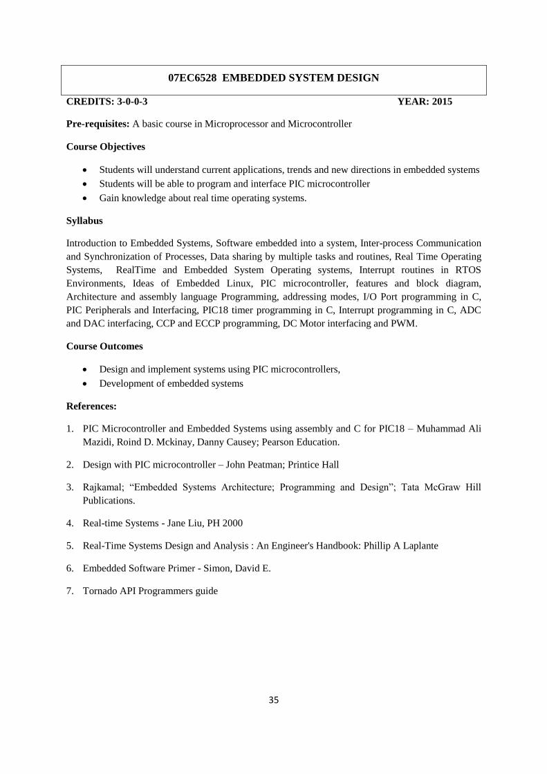
07EC6528 EMBEDDED SYSTEM DESIGN
CREDITS: 3-0-0-3 YEAR: 2015
Pre-requisites: A basic course in Microprocessor and Microcontroller
Course Objectives
Students will understand current applications, trends and new directions in embedded systems
Students will be able to program and interface PIC microcontroller
Gain knowledge about real time operating systems.
Syllabus
Introduction to Embedded Systems, Software embedded into a system, Inter-process Communication
and Synchronization of Processes, Data sharing by multiple tasks and routines, Real Time Operating
Systems, RealTime and Embedded System Operating systems, Interrupt routines in RTOS
Environments, Ideas of Embedded Linux, PIC microcontroller, features and block diagram,
Architecture and assembly language Programming, addressing modes, I/O Port programming in C,
PIC Peripherals and Interfacing, PIC18 timer programming in C, Interrupt programming in C, ADC
and DAC interfacing, CCP and ECCP programming, DC Motor interfacing and PWM.
Course Outcomes
Design and implement systems using PIC microcontrollers,
Development of embedded systems
References:
1. PIC Microcontroller and Embedded Systems using assembly and C for PIC18 – Muhammad Ali
Mazidi, Roind D. Mckinay, Danny Causey; Pearson Education.
2. Design with PIC microcontroller – John Peatman; Printice Hall
3. Rajkamal; “Embedded Systems Architecture; Programming and Design”; Tata McGraw Hill
Publications.
4. Real-time Systems - Jane Liu, PH 2000
5. Real-Time Systems Design and Analysis : An Engineer's Handbook: Phillip A Laplante
6. Embedded Software Primer - Simon, David E.
7. Tornado API Programmers guide
36
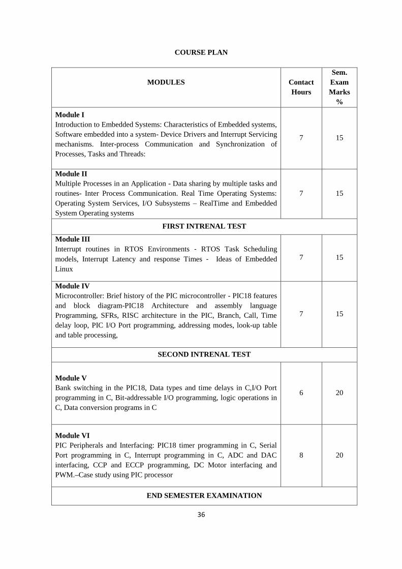
COURSE PLAN
MODULES
Contact
Hours
Sem.
Exam
Marks
%
Module I
Introduction to Embedded Systems: Characteristics of Embedded systems,
Software embedded into a system- Device Drivers and Interrupt Servicing
mechanisms. Inter-process Communication and Synchronization of
Processes, Tasks and Threads:
7 15
Module II
Multiple Processes in an Application - Data sharing by multiple tasks and
routines- Inter Process Communication. Real Time Operating Systems:
Operating System Services, I/O Subsystems – RealTime and Embedded
System Operating systems
7 15
FIRST INTRENAL TEST
Module III
Interrupt routines in RTOS Environments ‐ RTOS Task Scheduling
models, Interrupt Latency and response Times ‐ Ideas of Embedded
Linux
7 15
Module IV
Microcontroller: Brief history of the PIC microcontroller - PIC18 features
and block diagram-PIC18 Architecture and assembly language
Programming, SFRs, RISC architecture in the PIC, Branch, Call, Time
delay loop, PIC I/O Port programming, addressing modes, look-up table
and table processing,
7 15
SECOND INTRENAL TEST
Module V
Bank switching in the PIC18, Data types and time delays in C,I/O Port
programming in C, Bit-addressable I/O programming, logic operations in
C, Data conversion programs in C
6 20
Module VI
PIC Peripherals and Interfacing: PIC18 timer programming in C, Serial
Port programming in C, Interrupt programming in C, ADC and DAC
interfacing, CCP and ECCP programming, DC Motor interfacing and
PWM.–Case study using PIC processor
8 20
END SEMESTER EXAMINATION
37
07EC6538 VLSI PROCESS TECHNOLOGY
CREDITS: 3-0-0-3 YEAR:2015
Pre-requisites: A basic course in micro electronics
COURSE OBJECTIVE:
To learn in detail about the fabrication of MOSFET transistors. All the unit process steps involved in
planar process starting from silicon crystal growth to packaging of circuits has to be dealt in depth.
SYLLABUS
Overview And Materials, Moore’s Law, ITRS, Electric field effects, Segregation, microscopic model,
vacancy and interstitial dependence, Diffusion, different dopant profile study, Electric field effects,
Segregation, microscopic model, Thermal Oxidation, Deposition and Growth, Evaporation and
Sputtering: DC, RF, plasma, Chemical Vapor Deposition, Epitaxial Growth , Ion Implantation,
Pattern Transfer, optics, advanced lithography techniques, Exposure Development, Enhancement
techniques Enhancement techniques, Etching, Process Integration.
COURSE OUTCOME:
On completion of this course Students are expected to design VLSI circuits by keeping technological
process constraints in mind
REFERENCES:
1. The Science and Engineering of Microelectronic Fabrication, S.A. Campbell, 2/e, OUP, India,
2012.
2. J.D. Plummer, M.D. Deal, P.G. Griffin, Silicon VLSI Technology, Pearson Education, 2001
3. S.K. Ghandhi, VLSI Fabrication Principles – Silicon and Gallium Arsenide, John Wiley and
Sons.
COURSE PLAN
MODULES
Contact
Hours
Sem.
Exam
Marks
%
Module I
Overview And Materials: An Introduction to Microelectronic Fabrication,
Moore’s Law, ITRS. Semiconductor Substrates. Hot
Processing: Diffusion: Dopant diffusivities, channeling, Fick's 1st and
2nd law of diffusion, different dopant profile study, Electric field effects,
7 15

38
Segregation, microscopic model, vacancy and interstitial dependence.
Module II
Thermal Oxidation: Types of oxides, furnace design, Deal Grove Model –
wet and dry oxidation, thin oxide growth (deviation from Deal Grove),
Rapid Thermal Oxidation.
7 15
FIRST INTRENAL TEST
Module III
Deposition and Growth: Physical Deposition: Evaporation and Sputtering:
DC, RF, plasma, Chemical Vapor Deposition, Epitaxial Growth: MBE,
Growth Kinetics: ALD, MOCVD, LPCVD, APCVD, PECVD etc
7 15
Module IV
Ion Implantation: Implantation Modeling, Electronic and nuclear
stopping, Channeling, Damage Annealing, Transient enhanced diffusion
(TED).
7 15
SECOND INTRENAL TEST
Module V
Pattern Transfer: Optical Lithography,Non optical Lithographic
Techniques, Photoresists, Exposure: Systems: optics, advanced
lithography techniques, Exposure Development, Enhancement techniques:
proximity correction, phase shift masks.
7 20
Module VI
Etching: Isotropic / anisotropic, selectivity, Wet and dry etch. Reactive
ion etching (RIE), Chemical-mechanical polishing (CMP).
Process Integration: Device Isolation, Contacts, and Metallization.
7 20
END SEMESTER EXAM

39
07EC6548 DSP ARCHITECTURE AND DESIGN
CREDITS: 3-0-0-3 YEAR: 2015
Pre-requisites: A basic knowledge in Digital Signal Processing.
COURSE OBJECTIVE:
To provide sound foundation of digital signal processing (DSP) architectures and designing
efficient VLSI architectures for DSP systems
SYLLABUS
Hardware modeling, hardware abstraction, behavioralmodeling,dataflow modeling, structural
modeling, DSP Algorithm and Architecture Design, filtering algorithms (Winograd's, FFT, short-
length FIR), DSP Module Synthesis, distributed arithmetic (DA), modeling for synthesis in HDL,
synthesis place-and-route, Parallel algorithms and their dependence, delay operator and z-transform
techniques for mapping DSP algorithms, algebraic technique for mapping algorithms, applications
using common DSP algorithms.
COURSE OUTCOMES
Understand DSP architectures
Analyze DSP architectures
Understand DSP Algorithm and their implementation in architecture Design
Understand pipelining, parallel processing and retiming
Understand the concept of DSP module synthesis.
REFERENCES:
1. SenM.Kuo ,Woon-Seng S. Gan, Digal Signal Processors: Architectures, Implementations, and
Applications Prentice Hall 2004.
2. Uwe Meyer-Baese, Digital Signal Processing with Field Programmable Gate Array, Springer-
Verlag 2001.
3. Keshab K. Parhi, VLSI Signal Processing Systems, Design and Implementation, John Wiley
& Sons,1999.
4. John G. Proakis ,DimitrisManolakis K, DSP Principles, Algorithms and Applications,
Prentice Hall 1995.
5. J Bhasker, VHDL Primer, Pearson Education Asia, 3rd edition.
40
COURSE PLAN
MODULES
Contact
Hours
Sem.
Exam
Marks
%
Module I
Hardware modeling: Introduction to hardware description language,
hardware abstraction, entity declaration, architecture body,
behavioralmodeling, process statement, signal assignment statement,
dataflow modeling, concurrent signal assignment statement, structural
modeling, component declaration, component instantiation statement,
mixed modeling, Case study: mixed style of modeling of a full adder,
modeling of a state register.
8 15
Module II
DSP Algorithm and Architecture Design: DSP representations (data-flow,
control-flow, and signal-flow graphs, block diagrams), filter structures
(recursive, non recursive and lattice), behavioralmodeling in HDL, system
modeling and performance measures.
6 15
FIRST INTRENAL TEST
Module III fast
filtering algorithms (Winograd's, FFT, short- length FIR), retiming and
pipelining, block processing, folding, distributed arithmetic architectures,
VLSI performance measures (area, power, and speed), structural
modeling in VHDL.
6 15
Module IV
DSP Module Synthesis: distributed arithmetic (DA), advantageous of
using DA, size reduction of look-up tables, canonic signed digit
arithmetic, implementation of elementary functions Table-oriented
methods, linear feedback shift register, high performance arithmetic unit
architectures (adders, multipliers, dividers), bit-parallel, bit-serial, digit-
serial, carry-save architectures, redundant number system, modeling for
synthesis in HDL, synthesis place-and-route.
8 15
SECOND INTRENAL TEST

41
Module V
Parallel algorithms and their dependence: Applications to some common
DSP algorithms, system timing using the scheduling vector, projection of
the dependence graph using a projection direction, the delay operator and
z-transform techniques for mapping DSP algorithms onto processor
arrays,
7 20
Module VI
algebraic technique for mapping algorithms, computation domain,
dependence matrix of a variable, scheduling and projection functions, data
broadcast and pipelining, applications using common DSP algorithms.
7 20
END SEMESTER EXAMINATION

42
07EC6512 LOW POWER VLSI DESIGN
CREDITS: 3-0-0-3 YEAR: 2015
Pre-requisites: Basics of VLSI Design
COURSE OBJECTIVE:
Identify sources of power in an IC.
Identify the power reduction techniques based on technology independent and technology
dependent
Power dissipation mechanism in various MOS logic style.
Identify suitable techniques to reduce the power dissipation.
Design memory circuits with low power dissipation.
SYLLABUS
Need for low power VLSI chips, Physics of power dissipation in CMOS devices. Device &
Technology Impact on Low Power, Dynamic dissipation in CMOS, Technology & Device innovation,
Power estimation. Simulation Power analysis, gate level capacitance estimation, architecture level
analysis, data correlation analysis in DSP systems. Monte Carlo simulation, Probabilistic power
analysis, Low Power Design- Circuit level, Low power Architecture & Systems.
COURSE OUTCOMES:
The student will get to know the basics and advanced techniques in low power design which is a hot
topic in today’s market where the power plays major role.
REFERENCES
1. Gary Yeap , “Practical Low Power Digital VLSI Design ", 2002.
2. Kaushik Roy, Sharat Prasad, “Low Power CMOS VLSI Circuit Design ", 2000.
3. A.P.Chandrakasan and R.W. Broadersen, Low power digital CMOS design, Kluwer,1995.
4. CMOS Analog Circuit Design”, Philip Allen & Douglas Holberg, Oxford University Press, 2002.
5. Rabaey, Pedram, “Low power design methodologies” Kluwer Academic, 1997
COURSE PLAN
MODULES
Contact
Hours
Sem.
Exam
Marks
%
Module I
Need for low power VLSI chips, Sources of power dissipation on Digital
Integrated circuits. Emerging Low power approaches. Physics of power
dissipation in CMOS devices. Device & Technology Impact on Low Power.
7 15
43
Module II
Dynamic dissipation in CMOS, Transistor sizing & gate oxide thickness,
Impact of technology Scaling, Technology & Device innovation, Power
estimation.
7 15
FIRST INTRENAL TEST
Module III
Simulation Power analysis: SPICE circuit simulators, gate level logic
simulation, capacitive power estimation, static state power, gate level
capacitance estimation, architecture level analysis, data correlation analysis
in DSP systems. Monte Carlo simulation.
7 15
Module IV
Probabilistic power analysis: Random logic signals, probability &
frequency, probabilistic power analysis techniques, signal entropy.
7 15
SECOND INTRENAL TEST
Module V
Low Power Design- Circuit level: Power consumption in circuits. Flip
Flops & Latches design, high capacitance nodes, low power digital cells
library. Logic level: Gate reorganization, signal gating, logic encoding, state
machine encoding, pre-computation logic.
7 20
Module VI
Low power Architecture & Systems: Power & performance management,
switching activity reduction, parallel architecture with voltage reduction,
flow graph transformation, low power arithmetic components, low power
memory design.
7 20
END SEMESTER EXAMINATION
44
07EC6522 ADVANCED COMPUTER ARCHITECTURE
CREDITS: 3-0-0-3 YEAR: 2015
Pre-requisites: A basic course in Computer Architecture.
COURSE OBJECTIVES:
To understand the evolution of computer architecture.
To understand the state-of-the-art in computer architecture.
To understand the design challenges in building a system.
SYLLABUS
Pipelining and ILP, Instruction Level Parallelism and Its Exploitation - Concepts and Challenges,
Overcoming Data Hazards with Dynamic Scheduling, Case Studies, Thread-level parallelism, Cache
Coherence Issues - Performance Issues – Synchronization Issues . Models of Memory Consistency,
SIMD and GPU Architectures, Memory hierarchy design– Name Mapping Implementations, Virtual
Memory and Virtual Machines - Design of Memory Hierarchies - Case Studies.
COURSE OUTCOMES:
At the end of the course, the student will be able to:
Compare and evaluate the performance of various architectures.
Design sub-systems to meet specific performance requirements.
Analyze the requirements of large systems to select and build the right infrastructure.
REFERENCES:
1. John L. Hennessey and David A. Patterson, “Computer Architecture – A quantitative
approach”, Morgan Kaufmann / Elsevier, Fifth edition, 2012.
2. Richard Y. Kain, “Advanced Computer Architecture a Systems Design Approach”, PHI,
2011.
COURSE PLAN
MODULES
Contact
Hours
Sem.
Exam
Marks
%
Module I
PIPELINING AND ILP:Fundamentals of Computer Design - Measuring
and Reporting Performance - Instruction Level Parallelism and Its
Exploitation - Concepts and Challenges .
7 15
45
Module II
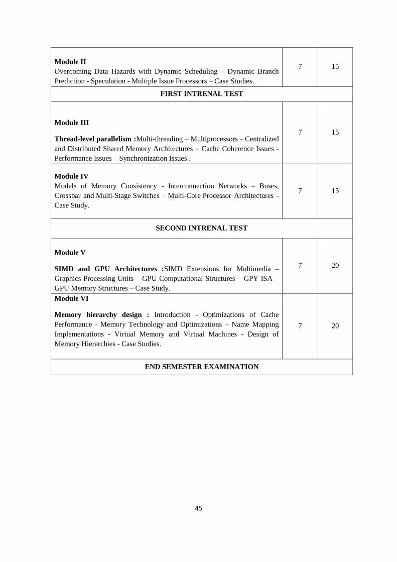
Overcoming Data Hazards with Dynamic Scheduling – Dynamic Branch
Prediction - Speculation - Multiple Issue Processors – Case Studies.
7 15
FIRST INTRENAL TEST
Module III
Thread-level parallelism :Multi-threading – Multiprocessors - Centralized
and Distributed Shared Memory Architectures – Cache Coherence Issues -
Performance Issues – Synchronization Issues .
7 15
Module IV
Models of Memory Consistency - Interconnection Networks – Buses,
Crossbar and Multi-Stage Switches – Multi-Core Processor Architectures -
Case Study.
7 15
SECOND INTRENAL TEST
Module V
SIMD and GPU Architectures :SIMD Extensions for Multimedia –
Graphics Processing Units – GPU Computational Structures – GPY ISA –
GPU Memory Structures – Case Study.
7 20
Module VI
Memory hierarchy design : Introduction - Optimizations of Cache
Performance - Memory Technology and Optimizations – Name Mapping
Implementations - Virtual Memory and Virtual Machines - Design of
Memory Hierarchies - Case Studies.
7 20
END SEMESTER EXAMINATION

46
07EC6532 SOC DESIGN AND VERIFICATION
CREDITS: 3-0-0-3 YEAR: 2015
Pre-requisites: Nil
COURSE OBJECTIVES:
To understand the System on Chip with its need, evolution, challenges, goals, superiority over
system on board & stacked ICs in package.
To Analyze how the SoCs are designed in industrial environment using different design
To understand different Macro Design Process.
To discuss different SOC verification techniques.
To understand how the Communication Architectures are designed for SoCs.
SYLLABUS
Introduction to System On Chip Design Process, top down vs Bottom up, System level design issues,
Macro Design Process, SoC Verification, System level verification, Block level verification,
Hardware/software co-verification and Static net list verification, Design of Communication
Architectures For SoCs, Design space exploration, Adaptive communication architectures.
Communication architecture tuners, Introduction to bus functional models and bus functional model
based verification.
COURSE OUTCOMES:
After completion of the course students will be able:
To design an SoC according to industrial requirements.
To handle different Macro design process.
To perform different levels of SoC verification.
To design communication Architectures for SoCs.
REFERENCES:
1. “SoC Verification Methodology and Techniques”, PrakashRashinkar Peter Paterson and
Leena Singh. Kluwer Academic Publishers, 2001.
2. “Reuse Methodology manual for System On A Chip Designs”, Michael Keating, Pierre
Bricaud, Kluwer Academic Publishers, second edition,2001.
3. “Design Verification: Simulation and Formal Method based Approaches”, William K. Lam,
Prentice Hall.
4. “System- on -a- Chip Design and Test”, RochitRajsuman, ISBN.
47
5. “Multiprocessor Systemsonchips”, A.A. Jerraya, W.Wolf, M K Publishers.
6. “The EDA HandBook”, Dirk Jansen, Kluwer Academic Publishers.
COURSE PLAN
MODULES
Contact
Hours
Sem.
Exam
Marks
%
Module I
Introduction to System On Chip Design Process: A canonical SoC
Design, SoC Design flow- waterfall vs spiral, topdown vs Bottom up.
Specification requirement, Types of Specification .
7 15
Module II
System Design process: System level design issues, Soft IP Vs Hard IP,
Design for timing closure,Logic design issues Verification strategy, Onchip
buses and interfaces, Low Power, Manufacturing test strategies.
7 15
FIRST INTRENAL TEST
Module III
Macro Design Process: Top level Macro Design, Macro Integration, Soft
Macro productization, Developing hard macros, Design issues for hard
macros, Design,System Integration with reusable macros.
7 15
Module IV
SoC Verification: Verification technology options, Verification
methodology, Verification languages, Verification approaches, and
Verification plans. System level verification, Block level verification,
Hardware/software co-verification and Static net list verification.
Verification architecture, Verification components, Introduction to VMM,
OVM and UVM.
7 15
SECOND INTRENAL TEST
Module V
Design of Communication Architectures For SoCs: On chip
communication architectures, System level analysis for designing
communication, Design space exploration, Adaptive communication
architectures.
7 20

48
Module VI
Communication architecture tuners, Communication architectures for
energy/battery efficient systems. Introduction to bus functional models and
bus functional model based verification.
7 20
END SEMESTER EXAM

49
07EC6514 SEMINAR
CREDITS: 0-0-2-2 YEAR: 2015
Pre-requisites: Nil
OBJECTIVE:
To train students to talk to a group of people and to present technical topics in a well-organized
manner to the audience. It is also intended for improvement of communication skills of students, to
make them confident in expressing their views with clarity and to make them prepared for taking part
in debates. This will help create self esteem and confidence that are essential for engineers.
Individual students are required to choose a topic of their interest from VLSI design related topics
preferably from outside the M.Tech syllabus and give a seminar on that topic about 30 minutes. A
committee consisting of at least three faculty members (preferably specialized in VLSI Design) shall
assess the presentation of the seminar and award marks to the students. Each student shall submit two
copies of a write up of his/her seminar topic. One copy shall be returned to the student after duly
certifying it by the chairman of the assessing committee and the other will be kept in the departmental
library. Internal continuous assessment marks are awarded based on the relevance of the topic,
presentation skill, quality of the report and participation.
Internal Continuous Assessment:
Report
Presentation Question/Answer
session Total
Marks 30 40 30 100
50
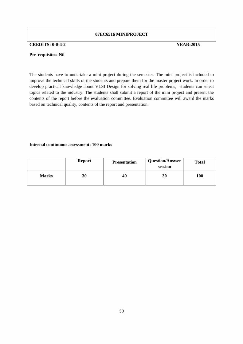
07EC6516 MINIPROJECT
CREDITS: 0-0-4-2 YEAR:2015
Pre-requisites: Nil
The students have to undertake a mini project during the semester. The mini project is included to
improve the technical skills of the students and prepare them for the master project work. In order to
develop practical knowledge about VLSI Design for solving real life problems, students can select
topics related to the industry. The students shall submit a report of the mini project and present the
contents of the report before the evaluation committee. Evaluation committee will award the marks
based on technical quality, contents of the report and presentation.
Internal continuous assessment: 100 marks
Report
Presentation Question/Answer
session Total
Marks 30 40 30 100
51
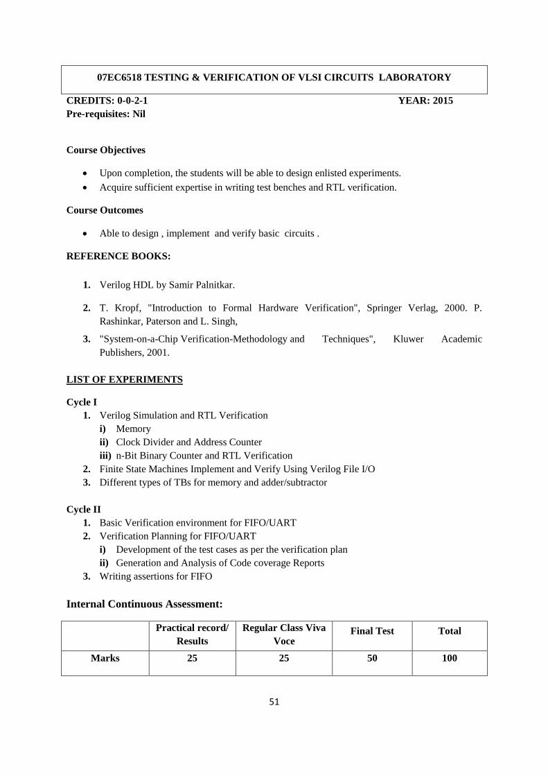
07EC6518 TESTING & VERIFICATION OF VLSI CIRCUITS LABORATORY
CREDITS: 0-0-2-1 YEAR: 2015
Pre-requisites: Nil
Course Objectives
Upon completion, the students will be able to design enlisted experiments.
Acquire sufficient expertise in writing test benches and RTL verification.
Course Outcomes
Able to design , implement and verify basic circuits .
REFERENCE BOOKS:
1. Verilog HDL by Samir Palnitkar.
2. T. Kropf, "Introduction to Formal Hardware Verification", Springer Verlag, 2000. P.
Rashinkar, Paterson and L. Singh,
3. "System-on-a-Chip Verification-Methodology and Techniques", Kluwer Academic
Publishers, 2001.
LIST OF EXPERIMENTS
Cycle I
1. Verilog Simulation and RTL Verification
i) Memory
ii) Clock Divider and Address Counter
iii) n-Bit Binary Counter and RTL Verification
2. Finite State Machines Implement and Verify Using Verilog File I/O
3. Different types of TBs for memory and adder/subtractor
Cycle II
1. Basic Verification environment for FIFO/UART
2. Verification Planning for FIFO/UART
i) Development of the test cases as per the verification plan
ii) Generation and Analysis of Code coverage Reports
3. Writing assertions for FIFO
Internal Continuous Assessment:
Practical record/
Results
Regular Class Viva
Voce Final Test Total
Marks 25 25 50 100
52
SEMESTER III
07EC7501 VLSI SIGNAL PROCESSING
CREDITS: 3-0-0-3 YEAR:2015
Pre-requisites: Basic knowledge in signal processing
COURSE OBJECTIVE
To introduce techniques for altering the existing DSP structures to suit VLSI implementations.
To introduce efficient design of DSP architectures suitable for VLSI
SYLLABUS
Introduction to DSP systems- Dependence graphs-Loop bound, iteration nbound , Pipelining and
Parallel processing for low power, Retiming, unfolding, sample period reduction, Algorithmic
strength reduction, Fast convolution algorithms, Pipelined and parallel recursive filters, Bit-
level arithmetic architectures, CSD representation, CSD multiplication using Horner’s rule for
precision improvement, Distributed Arithmetic fundamentals and FIR filters,Numerical strength
reduction, synchronous pipelining and clocking styles, wave pipelining, Asynchronous pipelining
bundled data versus dual rail protocol.
COURSE OUTCOME:
Ability to modify the existing or new DSP architectures suitable for VLSI.
REFERENCES:
1. Keshab K. Parhi, “ VLSI Digital Signal Processing Systems, Design and implementation “,
Wiley, Interscience, 2007.
2. U. Meyer – Baese, “ Digital Signal Processing with Field Programmable Gate Arrays”,
Springer, Second Edition, 2004
3. Allen, J., Computer Architectures for Digital Signal Processing, Proceedings of the IEEE,
Vol.73, No.5, May 1985
4. Bateman A., and Yates, W., Digital Signal Processing Design, Computer Science Press, New
York
5. S.Y. Kung, H.J. White House, T. Kailath, VLSI and Modern Signal Processing, Prentice Hall,
1985

53
COURSE PLAN
MODULES
Contact
Hours
Sem.
Exam
Marks
%
Module I
Introduction to DSP systems – Typical DSP algorithms, Data flow and
Dependence graphs - critical path, Loop bound, iteration bound, Longest
path matrix algorithm,Pipelining and Parallel processing of FIR filters,
Pipelining and Parallel processing for low power.
7 15
Module II
Retiming – definitions and properties, Unfolding – an algorithm for
unfolding, properties of unfolding, sample period reduction and parallel
processing application.
6 15
FIRST INTRENAL TEST
Module III
Algorithmic strength reduction in filters and transforms – 2-
parallel FIR filter, 2-parallel fast FIR filter, DCT architecture, rank-
order filters,Odd-Even merge-sort architecture, parallel rank-order filters.
7 15
Module IV
Fast convolution, Pipelining and parallel Processing of IIR Filters –
Cook-Toom algorithm, modified Cook-Toom algorithm, Pipelined and
parallel recursive filters – Look-Ahead pipelining in first-order IIR
filters, Look-Ahead pipelining with power-of-2decomposition,
Clustered look-ahead pipelining, Parallel processing of IIR filters,
combined pipelining and parallel processing of IIR filters.
8 15
SECOND INTRENAL TEST
Module V
Bit-level arithmetic architectures – parallel multipliers with sign
extension, parallel carry-ripple andcarry-save multipliers, Design of
Lyon’s bit-serial multipliers using Horner’s rule, bit-serial FIR filter, CSD
representation, CSD multiplication using Horner’s rule for precision
improvement, Distributed Arithmetic fundamentals and FIR filters.
7 20

54
Module VI
Numerical strength reduction – subexpression elimination, multiple
constantmatching, synchronous pipelining and clocking styles, clock skew
in edge-triggered single phase clocking, two-phase clocking, wave
pipelining. Asynchronous pipelining bundled data versus dual rail protocol.
7 20
END SEMESTER EXAM

55
07EC7511 HIGH SPEED DIGITAL DESIGN
CREDITS: 3-0-0-3 YEAR:2015
Pre-requisites: Basic course in Digital Electronics, Electromagnetic theory
COURSE OBJECTIVES
To acquaint the students with the problems associated with high-speed digital devices
To provide an overview of power distribution and noise
To study about timing and synchronization
SYLLABUS
Introduction to high speed digital design: Capacitance and inductance effects, High seed properties of
logic gates , Speed and power, Modelling of wires, transmission,Power distribution and noise:
Power supply network, local power regulation,IR , on chip bypass capacitors, power supply
isolation, Noise sources in digital system, Signalling convention and circuits, Signalling modes for
transmission lines, Driving lossy LC lines, simultaneous bi-directional signaling, Timing convention
and synchronization, timing properties of clocked storage elements, pipeline timing,
synchronization failure and meta-stability, PLL and DLL based clock aligners
COURSE OUTCOMES
Understand the design issues in high speed digital devices
Consider the different noise sources while designing a power distribution network
Appreciate the significance of timing and synchronization
REFERENCES
1. Howard Johnson and Martin Graham, "High Speed Digital Design: A Handbook of
BlackMagic”, 3rd Edition, Prentice Hall Modern Semiconductor Design Series' Sub Series:
PH Signal Integrity Library, 2006
2. Stephen H. Hall, Garrett W. Hall, and James A. McCall, “High-Speed Digital System
Design: A Handbook of Interconnect Theory and Design Practices by ", Wiley, 2007 3.
3. Kerry Bernstein, K.M. Carrig, Christopher M. Durham, and Patrick R. Hansen, “High Speed
CMOS Design Styles”,Springer Wiley 2006
4. Ramesh Harjani, “Design of High-Speed Communication Circuits (Selected Topics in
Electronics and Systems)” World Scientific Publishing Company, 2006
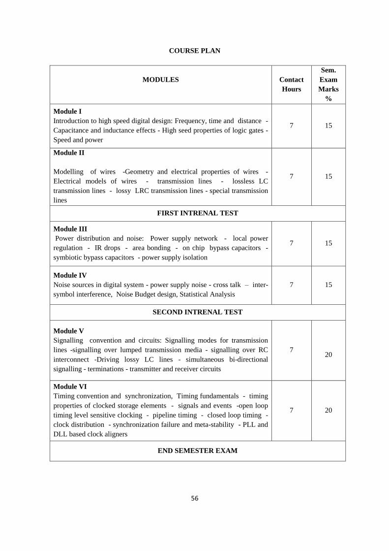
56
COURSE PLAN
MODULES
Contact
Hours
Sem.
Exam
Marks
%
Module I
Introduction to high speed digital design: Frequency, time and distance -
Capacitance and inductance effects - High seed properties of logic gates -
Speed and power
7 15
Module II
Modelling of wires -Geometry and electrical properties of wires -
Electrical models of wires - transmission lines - lossless LC
transmission lines - lossy LRC transmission lines - special transmission
lines
7 15
FIRST INTRENAL TEST
Module III
Power distribution and noise: Power supply network - local power
regulation - IR drops - area bonding - on chip bypass capacitors -
symbiotic bypass capacitors - power supply isolation
7 15
Module IV
Noise sources in digital system - power supply noise - cross talk – inter-
symbol interference, Noise Budget design, Statistical Analysis
7 15
SECOND INTRENAL TEST
Module V
Signalling convention and circuits: Signalling modes for transmission
lines -signalling over lumped transmission media - signalling over RC
interconnect -Driving lossy LC lines - simultaneous bi-directional
signalling - terminations - transmitter and receiver circuits
7
20
Module VI
Timing convention and synchronization, Timing fundamentals - timing
properties of clocked storage elements - signals and events -open loop
timing level sensitive clocking - pipeline timing - closed loop timing -
clock distribution - synchronization failure and meta-stability - PLL and
DLL based clock aligners
7 20
END SEMESTER EXAM

57
07EC7521 MIXED SIGNAL SYSTEM DESIGN
CREDITS: 3-0-0-3 YEAR: 2015
Pre-requisites: Nil
COURSE OBJECTIVES:
Understand design and operation of basic analog and digital circuits, understand layout and matching
of analog components, design and analysis of switched capacitor circuits, analysis of data conversion
algorithms, design of data converter circuits, understand performance limitation of converter
topologies, Group projects involving a complete mixed-signal system design.
SYLLABUS
PN Junctions, MOS Transistor, CMOS Inverter AC and DC Characteristic, Digital Sub Circuits, TG
based implementation of multiplexers, de-multiplexers, encoders, decoders, Comparator, Parity
generator.Memory elements, Analog Sub circuits, configuration Differential Ideal amplifier basics,
VCO, PLL, Comparator characteristics, two stage open loop comparator, Switched capacitor
amplifier, Digital to Analog Data Converters , Analog to Digital Data Converters, Over sampling
Data Converters .
COURSE OUTCOMES:
At the completion of this course, each student will have demonstrated proficiency in:
Understanding MOSFET models (nMOS and pMOS transistors);
Designing CMOS analog circuits to achieve performance specifications;
Analyzing CMOS based switched capacitor circuits;
Understanding mixed-signal design flow
Understanding basics of data converters g. Working as a team to design, implement, and
document a mixed-signal integrated circuit.
REFERENCES
1. .Gray Paul R, Meyer, Robert G, Analysis and Design of Analog Integrated Circuits,
3rd edition, John Wiley & Sons.
2. Jacob Baker, "CMOS Mixed-Signal circuit design", A John Willy & Sons, inc., publications,
2003.
3. Professor Bernhard Boser -”Analysis and Design of VLSI Analog-Digital Interface Integrated
Circuits” “Addison Wisely publications” (1991).
4. D A John, Ken Martin, Analog Integrated Circuit Design, 1st Edition, John Wiley
5. CMOS Analog Circuit Design, 2nd edition; by: Allen, Phillip E, Holberg , Douglas R, Oxford
University Press, (Indian Edition
6. Ken Martin, Digital Integrated Circuit Design, John Wiley
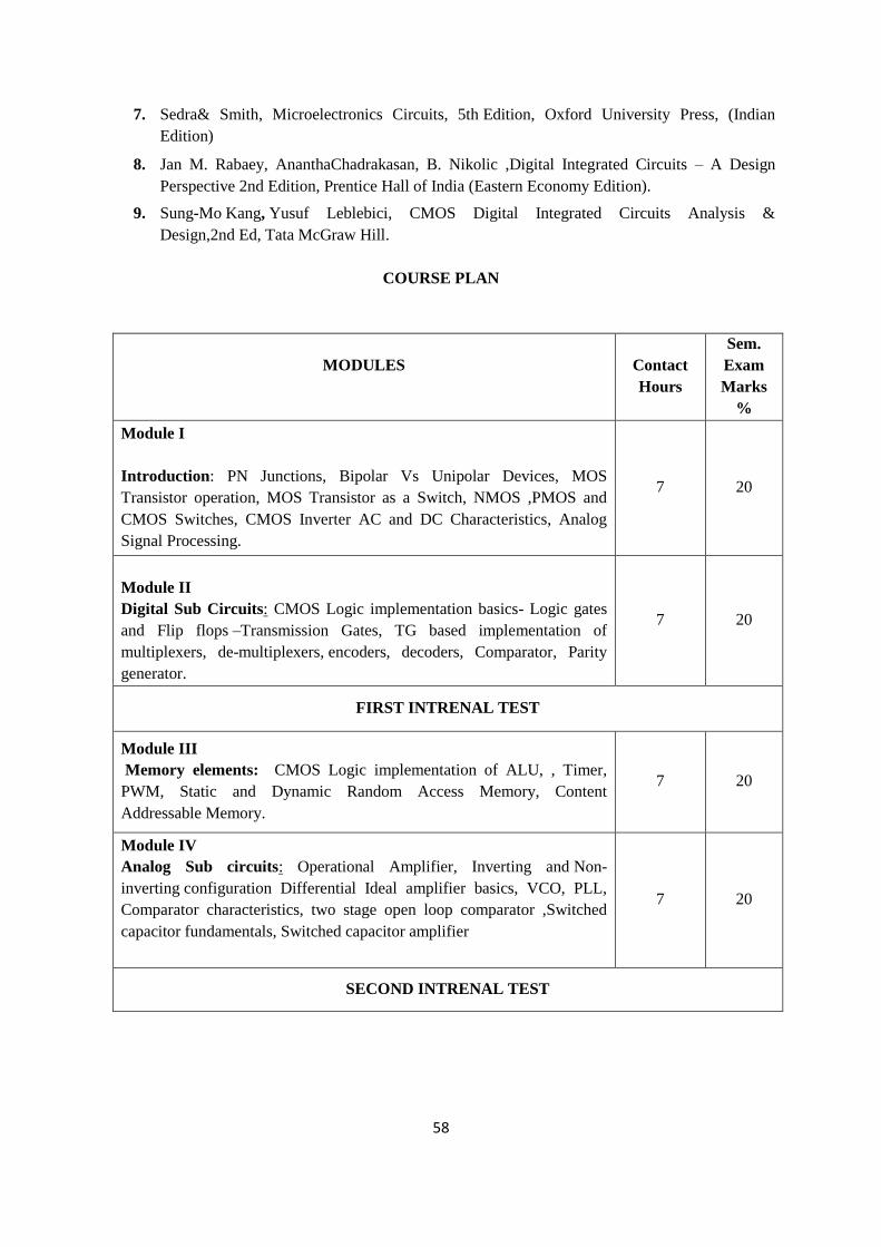
58
7. Sedra& Smith, Microelectronics Circuits, 5th Edition, Oxford University Press, (Indian
Edition)
8. Jan M. Rabaey, AnanthaChadrakasan, B. Nikolic ,Digital Integrated Circuits – A Design
Perspective 2nd Edition, Prentice Hall of India (Eastern Economy Edition).
9. Sung-Mo Kang, Yusuf Leblebici, CMOS Digital Integrated Circuits Analysis &
Design,2nd Ed, Tata McGraw Hill.
COURSE PLAN
MODULES
Contact
Hours
Sem.
Exam
Marks
%
Module I
Introduction: PN Junctions, Bipolar Vs Unipolar Devices, MOS
Transistor operation, MOS Transistor as a Switch, NMOS ,PMOS and
CMOS Switches, CMOS Inverter AC and DC Characteristics, Analog
Signal Processing.
7 20
Module II
Digital Sub Circuits: CMOS Logic implementation basics- Logic gates
and Flip flops –Transmission Gates, TG based implementation of
multiplexers, de-multiplexers, encoders, decoders, Comparator, Parity
generator.
7 20
FIRST INTRENAL TEST
Module III
Memory elements: CMOS Logic implementation of ALU, , Timer,
PWM, Static and Dynamic Random Access Memory, Content
Addressable Memory.
7 20
Module IV
Analog Sub circuits: Operational Amplifier, Inverting and Non-
inverting configuration Differential Ideal amplifier basics, VCO, PLL,
Comparator characteristics, two stage open loop comparator ,Switched
capacitor fundamentals, Switched capacitor amplifier
7 20
SECOND INTRENAL TEST

59
Module V
Digital to Analog Data Converters : Static &Dynamic Charatersitics,1
Bit DAC, String DAC, Fully Decoded DAC,PWM DAC, Current scaling,
voltage scaling DACs
6 20
Module VI
Analog to Digital Data Converters: Static &Dynamic Characteristics,
Nyquist Criteria , Sample & Hold Circuit, Quantization error, Concept of
over sampling, Counting ADC, Tracking ADC, Successive approximation
ADC, Flash ADC, Dual Slope ADC.
Over sampling Data Converters : Over sampling fundamentals, Delta –
Sigma Converter basics, ∑ Modulator
8 20
END SEMESTER EXAMINATION
60
07EC7503 DESIGN WITH MICROCONTROLLERS
CREDITS: 3-0-0-3 YEAR: 2015
Pre-requisites: Basic knowledge of Microprocessors and micro controllers.
COURSE OBJECTIVES:
To provide the students with basic understanding of microcontroller based system design. This
includes system requirements specifications, architectural and detailed design, and implementation,
focusing on real-time applications. And to help the students to familiarize with development &
debugging Tools for Microcontroller based Embedded Systems.
SYLLABUS:
8-Bit Microcontrollers, Architecture, peripherals, programming, Microcontroller based System
Design-case study, 32- Bit ARM920T Processor, Programmers Model, Cache, Architecture – Basic
Architecture of a Cache, Basic operation of a cache controller, Cache and main memory relationship,
Set Associativity Cache Policy, Memory Management Units, instruction set,thump instruction,
interrupt handling, ARM9 Microcontroller Architecture, Memory Controller , External Bus Interface
, Memory Interface, PERIPHERALS-Interrupt Controller, USART, Development & Debugging Tools
for Microcontroller based Embedded Systems, Software and Hardware tools like Cross Assembler,
Compiler, Debugger, Simulator.
COURSE OUTCOMES:
On completion of the course, a student should be able:
To identify basic architecture of different Microcontroller 8051.
To design an application using 8-bit 8051 Microcontrollers.
To understand the internal architecture and interfacing of different peripheral devices with
Microcontrollers.
To use tools for the development & debugging of Microcontroller based Embedded Systems.
TEXT BOOKS:
1. Muhammad Ali Mazidi, Janice GillispieMazidi, Rolin D. McKinlay, “The 8051
Microcontroller and Embedded Systems using Assembly and C”, 2nd Edition, Prentice Hall.
2. ARM Company Ltd. “ARM Architecture Reference Manual– ARM DDI 0100E”
3. Andrew N Sloss, Dominic Symes, Chris Wright, “ARM System Developer's Guide -
Designing and Optimizing System Software”, 2006, Elsevier
REFERENCES:
1. Ayala, Kenneth J “8051 Microcontroller - Architecture, Programming & Applications”,
1st Edition, Penram International Publishing
2. Steve Furber, “ARM System-on-Chip Architecture”, 2nd Edition, Pearson Education

61
3. Predko, Myke, “Programming and Customizing the 8051 Microcontroller”, 1st Edition,
McGraw Hill International
4. Schultz, Thomas W, “C and the 8051 Programming for Multitasking”, 1stEdition, Prentice
Hall
5. Schultz, Thomas W, “C and the 8051: Hardware, Modular Programming and Multitasking”,
Vol I, 2nd Edition, Prentice Hall
6. Stewart, James W, Miao, Kai X, “8051 Microcontroller: Hardware, Software and
Interfacing”, 2nd Edition, Prentice Hall
7. Arnold. S. Berger, “Embedded Systems Design - An introduction to Processes, Tools and
Techniques”, Easwer Press
8. Raj Kamal, “Microcontroller - Architecture Programming Interfacing and System Design”
1st Edition, Pearson Education
9. P.S Manoharan, P.S. Kannan, “Microcontroller based System Design”, 1stEdition, Scitech
Publications
10. David Calcutt, Fred Cowan, Hassan Parchizadeh, “8051 Microcontrollers – An Application
based Introduction”, Elsevier
11. Ajay Deshmukh, “Microcontroller - Theory & Applications”, Tata McGraw
COURSE PLAN
MODULES
Contact
Hours
Sem.
Exam
Marks
%
Module I
8-Bit Microcontrollers: Intel 8051-Architecture: CPU Block diagram,
Memory Organization, Program memory, Data Memory, Interrupts,
Peripherals: Timers, Serial Port, I/O Port, Programming: Addressing
Modes, Instruction Set, Programming
Microcontroller based System Design: Timing Analysis, Case study with
reference to 8-bit 8051 Microcontroller-application design -requirement
analysis -concept design-hardware and software design using 8-bit 8051
Microcontrollers
7 15
Module II
32- Bit ARM920T Processor-Introduction: RISC/ARM Design
Philosophy, About the ARM920T Core, Processor Functional Block
Diagram.
Programmers Model: Data Types, Processor modes, Registers, General
Purpose Registers, Program Status Register, CP15 Coprocessor, Memory
and memory mapped I/O, Pipeline, Exceptions, Interrupts and Vector table,
Architecture revisions.
Cache: Memory hierarchy and cache , Cache Architecture – Basic
Architecture of a Cache, Basic operation of a cache controller, Cache and
main memory relationship, Set Associativity Cache Policy – Write policy,
Cache line replacement policies, allocation policy on a cache miss,
Instruction Cache, Data Cache, Write Buffer and Physical Address TAG
RAM
8 15

62
Memory Management Units: virtual memory, Details of the ARM MMU,
Page Tables, Translation Look-aside Buffer, Domains and Memory access
permissions.
FIRST INTRENAL TEST
Module III
ARM (ARM920T) Instruction Set: Data Processing instructions, Branch
instructions, Load - Store instructions, Software Interrupt Instruction,
Program Status Register Instruction, Loading Constants.
Thumb Instruction Set: Thumb register usage, ARM-Thumb interworking,
Branch instruction, Data processing instructions, Load - store instructions,
stack instructions, instruction, Data processing instructions, Load - store
instructions, stack instructions, software interrupt instructions.
Interrupt Handling: Interrupts, Assigning interrupts, Interrupt latency,
IRQ& FIQ, exceptions, Basic interrupt stack design and
implementation, Non-nested Interrupt handler
8 15
Module IV
ARM9 Microcontroller Architecture: A popular ARM9 Microcontroller
from Atmel (AT91RM9200) is covered under this section
AT91RM9200 Architecture: Block Diagram, Features, Memory Mapping
Memory Controller (MC), Memory Controller Block Diagram, Address
Decoder, External Memory Areas, Internal Memory Mapping
External Bus Interface (EBI), Organization of the External Bus Interface,
EBI Connections to Memory Devices
7 15
SECOND INTRENAL TEST
Module V
External Memory Interface, Write Access, Read Access, Wait State
Management.
AT91RM9200 PERIPHERALS-Interrupt Controller: Normal Interrupt,
Fast Interrupt, AIC.
System Timer (ST): Period Interval Timer (PIT), Watchdog Timer (WDT),
Real- time Timer (RTT)
6 20
Module VI
Universal Synchronous Asynchronous Receiver Transceiver
(USART): Block Diagram, Functional Description, Synchronous and
Asynchronous Modes. Development & Debugging Tools for
Microcontroller based Embedded Systems: Software and Hardware tools
like Cross Assembler, Compiler, Debugger, Simulator, In-Circuit Emulator
.(ICE), Logic Analyzer ETC
6 20
END SEMESTER EXAMINATION

63
07EC7513 INTRODUCTION TO MEMS SYSTEM DESIGN
CREDITS: 3-0-0-3 YEAR: 2015
Pre-requisites: Nil
COURSE OBJECTIVES:
To give the students hands on experience for the fabrication processes using micro-
fabrication tools in the cleanroom.
Briefly review on various application fields of the microsensors, MEMS, and smart devices.
The materials and the processes required to make different kinds of the microdevices.
The standard microelectronics technology to produce ultra large-scale integrated circuits and
package them will also be reviewed. The new techniques that have been developed to make
microsensors and microactuators, such as bulk and surface silicon micromachining will be
followed.
The fabrication process will include metal thin film e-beam evaporation, dielectric thin film
growing using oxidation tube furnace, electrochemical deposition, and various kinds of
chemical processes.
SYLLABUS
Introduction to mems, Miniaturization, Typical products, Micro sensors, Micro actuation, Mechanics
for mems design, force and response time, Fracture and thin film mechanics, Electro static design,
basic theory, Surface tension, gap and finger pull up, Electro static actuators, Comb generators, gap
closers, rotary motors, inch worms, Circuit and system issues, Case studies – Capacitive
accelerometer, Peizo electric pressure sensor.Optical MEMS, MEMS scanners and retinal scanning
display, Digital Micro mirror devices, RF MEMS.
COURSE OUTCOMES:
On completion of the module students should:
Be able to extend the principles of microfabrication to the development of micromechanical
devices and the design of microsystems
Understand the principles of energy transduction, sensing and actuation on a microscopic
scale.
Appreciate the effects of scaling, and the similarities and differences between
micromechanical assemblies and macroscopic machines.
REFERENCES:
1. Stephen Santuria,” Microsystems Design”, Kluwer publishers, 2000.
2. NadimMaluf,” An introduction to Micro electro mechanical system design”, Artech House,
2000
3. Mohamed Gad-el-Hak, editor,” The MEMS Handbook”, CRC press Baco Raton,2000.
4. Tai Ran Hsu,” MEMS & Micro systems Design and Manufacture” Tata McGraw Hill, New
Delhi, 2002.
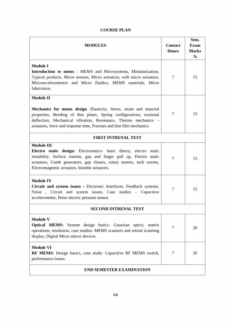
64
COURSE PLAN
MODULES
Contact
Hours
Sem.
Exam
Marks
%
Module I
Introduction to mems : MEMS and Microsystems, Miniaturization,
Typical products, Micro sensors, Micro actuation, with micro actuators,
Microaccelorometers and Micro fluidics, MEMS materials, Micro
fabrication.
7 15
Module II
Mechanics for mems design :Elasticity, Stress, strain and material
properties, Bending of thin plates, Spring configurations, torsional
deflection, Mechanical vibration, Resonance, Thermo mechanics –
actuators, force and response time, Fracture and thin film mechanics.
7 15
FIRST INTRENAL TEST
Module III
Electro static design: Electrostatics- basic theory, electro static
instability. Surface tension, gap and finger pull up, Electro static
actuators, Comb generators, gap closers, rotary motors, inch worms,
Electromagnetic actuators. bistable actuators.
7 15
Module IV
Circuit and system issues : Electronic Interfaces, Feedback systems,
Noise , Circuit and system issues, Case studies – Capacitive
accelerometer, Peizo electric pressure sensor.
7 15
SECOND INTRENAL TEST
Module V
Optical MEMS: System design basics- Gaussian optics, matrix
operations, resolution, case studies- MEMS scanners and retinal scanning
display, Digital Micro mirror devices.
7 20
Module VI
RF MEMS: Design basics, case study- Capacitive RF MEMS switch,
performance issues.
7 20
END SEMESTER EXAMINATION
65
07EC7523 SYNTHESIS AND OPTIMIZATION OF DIGITAL CIRCUITS
CREDITS: 3-0-0-3 YEAR: 2015
Pre-requisites: Nil
COURSE OBJECTIVES:
To introduce students to basic optimization techniques used in circuits design
To introduce students to advanced tools and techniques in digital systems design. These
include Hardware Modeling and Compilation Techniques.
To introduce Architecture-level synthesis and optimization.
To introduce in details Logic-Level synthesis and optimization techniques for combinational
and sequential circuits.
To introduce students to Library binding algorithms to achieve implementations with specific
cell libraries.
SYLLABUS
Introduction to Synthesis and optimization, High-level synthesis: Motivation and
organization,Scheduling,Resource sharing,Data path and control synthesis. Two Level Combinational
Logic Optimization- algorithms for logic minimization, symbolic minimization and encoding
problems, Timing issues- library mapping, Algorithms and rule-based systems, Optimization of
digital circuits: Area, Timing and power optimization, Introduction to Hw/SwCodesign,Problem
taxonomy,Embedded system design,Software optimizationPerspectives.
COURSE OUTCOMES:
On completion of the course students will be:
Familiarized with basic optimization techniques used in circuits design
Able to describe the flow of VLSI digital design, and the algorithms used in various types of
design.
Able to design both combinational and sequential circuits using different levels of synthesis
and optimization techniques.
REFERENCES:
1. Giovanni De Micheli, “Synthesis and Optimization of Digital Circuits”,McGraw-Hill, 1994,
5th print.
2. “Logic Synthesis”, S. Devadas, A. Ghosh and K. Keutzer, McGraw Hill, 1994.
3. R. Gupta, “Co-synthesis of Hardware and Software for Embedded Systems”, Kluwer 1995.
4. Edwars M.D., Automatic Logic synthesis Techniques for Digital Systems, Macmillan New
Electronic Series, 1992
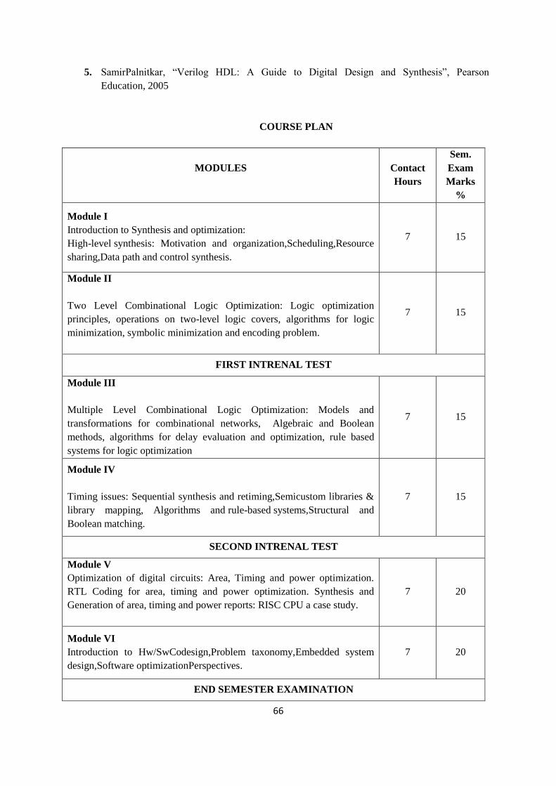
66
5. SamirPalnitkar, “Verilog HDL: A Guide to Digital Design and Synthesis”, Pearson
Education, 2005
COURSE PLAN
MODULES
Contact
Hours
Sem.
Exam
Marks
%
Module I
Introduction to Synthesis and optimization:
High-level synthesis: Motivation and organization,Scheduling,Resource
sharing,Data path and control synthesis.
7 15
Module II
Two Level Combinational Logic Optimization: Logic optimization
principles, operations on two-level logic covers, algorithms for logic
minimization, symbolic minimization and encoding problem.
7 15
FIRST INTRENAL TEST
Module III
Multiple Level Combinational Logic Optimization: Models and
transformations for combinational networks, Algebraic and Boolean
methods, algorithms for delay evaluation and optimization, rule based
systems for logic optimization
7 15
Module IV
Timing issues: Sequential synthesis and retiming,Semicustom libraries &
library mapping, Algorithms and rule-based systems,Structural and
Boolean matching.
7 15
SECOND INTRENAL TEST
Module V
Optimization of digital circuits: Area, Timing and power optimization.
RTL Coding for area, timing and power optimization. Synthesis and
Generation of area, timing and power reports: RISC CPU a case study.
7 20
Module VI
Introduction to Hw/SwCodesign,Problem taxonomy,Embedded system
design,Software optimizationPerspectives.
7 20
END SEMESTER EXAMINATION
67
CREDITS: 0-0-2-2 YEAR:2015
Pre-requisites: Nil
COURSE OBJECTIVE:
To train students to talk to a group of people and to present technical topics in a well
organised manner to the audience. It is also intended for improvement of communication
skills of students, to make them confident in expressing their views with clarity and to make
them prepared for taking part in debates. This will help create self esteem and confidence that
are essential for engineers.
Individual students are required to choose a topic of their interest from VLSI Design related
topics preferably from outside the M.Tech syllabus and give a seminar on that topic about 30
minutes. A committee consisting of at least three faculty members (preferably specialized in
VLSI Design) shall assess the presentation of the seminar and award marks to the students.
Each student shall submit two copies of a write up of his/her seminar topic. One copy shall be
returned to the student after duly certifying it by the chairman of the assessing committee and
the other will be kept in the departmental library. Internal continuous assessment marks are
awarded based on the relevance of the topic, presentation skill, quality of the report and
participation.
Internal Continuous Assessment:
Report
Presentation Question/Answer
session Total
Marks 30 40 30 100
07EC7505 C SEMINAR
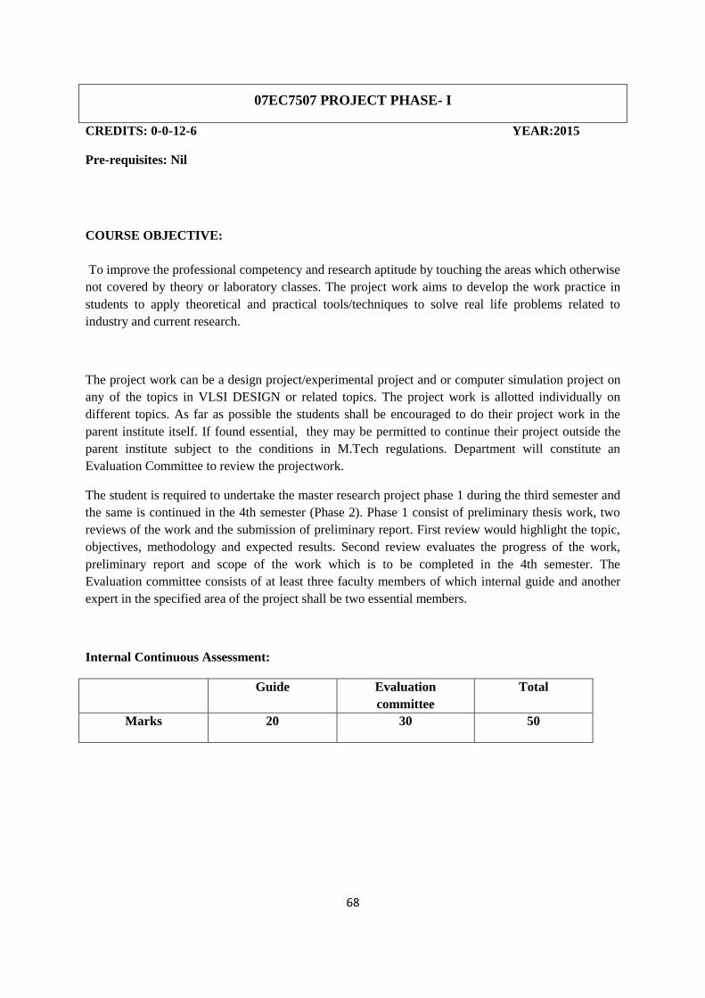
68
07EC7507 PROJECT PHASE- I
CREDITS: 0-0-12-6 YEAR:2015
Pre-requisites: Nil
COURSE OBJECTIVE:
To improve the professional competency and research aptitude by touching the areas which otherwise
not covered by theory or laboratory classes. The project work aims to develop the work practice in
students to apply theoretical and practical tools/techniques to solve real life problems related to
industry and current research.
The project work can be a design project/experimental project and or computer simulation project on
any of the topics in VLSI DESIGN or related topics. The project work is allotted individually on
different topics. As far as possible the students shall be encouraged to do their project work in the
parent institute itself. If found essential, they may be permitted to continue their project outside the
parent institute subject to the conditions in M.Tech regulations. Department will constitute an
Evaluation Committee to review the projectwork.
The student is required to undertake the master research project phase 1 during the third semester and
the same is continued in the 4th semester (Phase 2). Phase 1 consist of preliminary thesis work, two
reviews of the work and the submission of preliminary report. First review would highlight the topic,
objectives, methodology and expected results. Second review evaluates the progress of the work,
preliminary report and scope of the work which is to be completed in the 4th semester. The
Evaluation committee consists of at least three faculty members of which internal guide and another
expert in the specified area of the project shall be two essential members.
Internal Continuous Assessment:
Guide
Evaluation
committee
Total
Marks 20 30 50
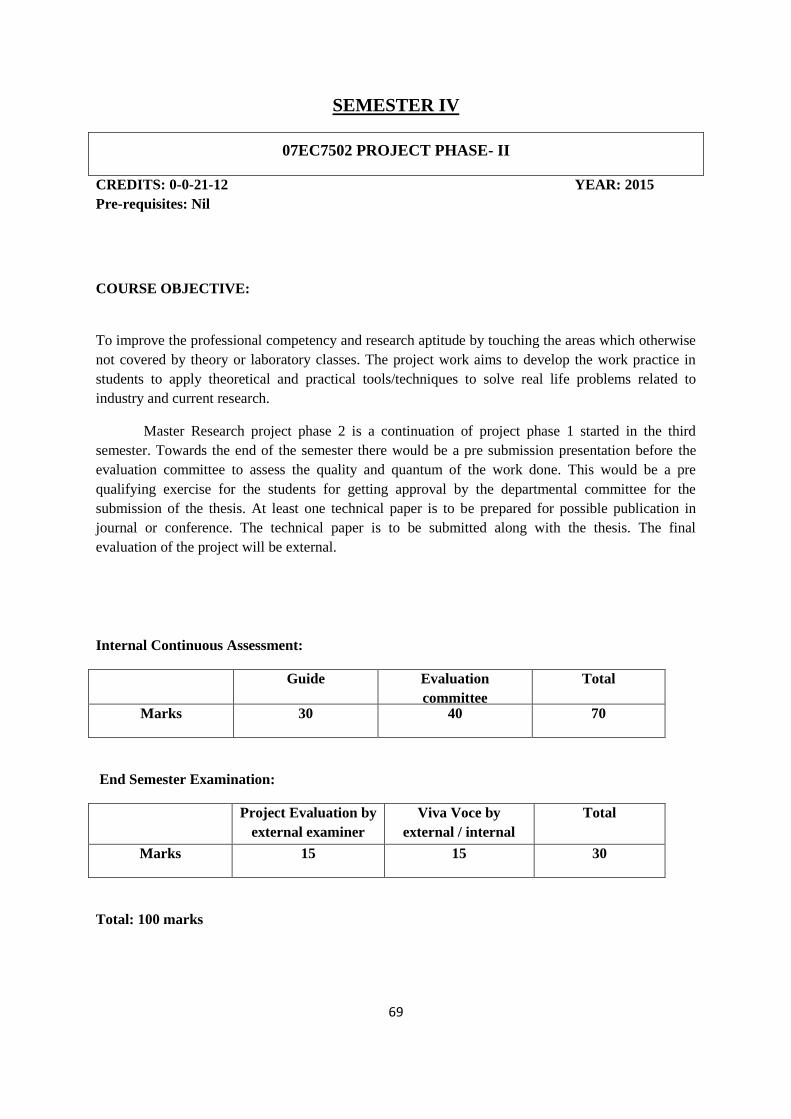
69
SEMESTER IV
07EC7502 PROJECT PHASE- II
CREDITS: 0-0-21-12 YEAR: 2015
Pre-requisites: Nil
COURSE OBJECTIVE:
To improve the professional competency and research aptitude by touching the areas which otherwise
not covered by theory or laboratory classes. The project work aims to develop the work practice in
students to apply theoretical and practical tools/techniques to solve real life problems related to
industry and current research.
Master Research project phase 2 is a continuation of project phase 1 started in the third
semester. Towards the end of the semester there would be a pre submission presentation before the
evaluation committee to assess the quality and quantum of the work done. This would be a pre
qualifying exercise for the students for getting approval by the departmental committee for the
submission of the thesis. At least one technical paper is to be prepared for possible publication in
journal or conference. The technical paper is to be submitted along with the thesis. The final
evaluation of the project will be external.
Internal Continuous Assessment:
Guide
Evaluation
committee
Total
Marks 30 40 70
End Semester Examination:
Project Evaluation by
external examiner
Viva Voce by
external / internal
examiner
Total
Marks 15 15 30
Total: 100 marks
Related Documents