ANTTI MÄNNISTÖ A STUDY OF HARDWARE ACCELERATION IN SYSTEM ON CHIP DESIGNS USING TRANSPORT TRIGGERED ARCHITECTURE Master of Science Thesis Examiner: Prof. Jarmo Takala Examiner and topic approved in the faculty of Computing and Electrical Engineering Council meeting 9 th of March 2016

Welcome message from author
This document is posted to help you gain knowledge. Please leave a comment to let me know what you think about it! Share it to your friends and learn new things together.
Transcript

ANTTI MÄNNISTÖ
A STUDY OF HARDWARE ACCELERATION IN SYSTEM ON CHIP
DESIGNS USING TRANSPORT TRIGGERED ARCHITECTURE
Master of Science Thesis
Examiner: Prof. Jarmo Takala Examiner and topic approved in the faculty of Computing and Electrical Engineering Council meeting 9th of March 2016

i
ABSTRACT
ANTTI MÄNNISTÖ: A Study of Hardware Acceleration in System on Chip De-signs using Transport Triggered Architecture Tampere University of Technology Master of Science Thesis, 47 pages, 1 Appendix page June 2016 Master’s Degree Programme in Electrical Engineering Major: Embedded Systems Examiner: Professor Jarmo Takala Keywords: Transport Triggered Architecture, LTE, Fast Fourier Transform, FFT
Transport Triggered Architecture is a processor design philosophy where the datapath is
visible for the programmer and the program controls the data transfers on the path di-
rectly. TTA processors offer a good alternative for application specific task as they can
be easily optimized for a given application. TTA processors, however, adjust poorly to
dynamic situations, but this can be compensated with external hosting.
Fast Fourier transform is an approximation of the Fourier transform for converting time
domain data into frequency domain. Fast Fourier transform is needed in many digital
signal processing applications. One example of the usage of the transform is the LTE
network access schemes where the symbols transmitted over the air interface are con-
structed with the fast Fourier transform and again de-modulated as they are received.
The study makes use of Nokia Co-Processor as the host for TTA processor and proposes
alternatives for different architectures for the usage of the TTA processor inside a practi-
cal design where data is being moved over interconnections and memories. One proposed
architecture is selected for implementation and the construction of this architecture is dis-
cussed regarding implementing the needed hardware and software to run the Fourier ap-
plication on TTA with data being fetched and written back in system memory. Lastly, the
performance of the implementation is discussed.

ii
TIIVISTELMÄ
ANTTI MÄNNISTÖ: Tutkimus laitteistokiihdytyksestä järjestelmäpiireillä käyttäen siirtoliipaistua arkkitehtuuria Tampereen teknillinen yliopisto Diplomityö, 47 sivua, 1 liitesivu Kesäkuu 2016 Sähkötekniikan koulutusohjelma Pääaine: sulautetut järjestelmät Tarkastaja: professori Jarmo Takala Avainsanat: siirtoliipaistu arkkitehtuuri, LTE, nopea Fourier-muunnos, FFT
Siirtoliipaistu prosessoriarkkitehtuuri on prosessorisuunnittelufilosofia, jossa datapolku
näkyy ohjelmoijalle ja ohjelma kontrolloi suoraan datapolun datasiirtoja. TTA prosessorit
tarjoavat hyvän vaihtoehdon sovellusspesifeille tehtäville, sillä ne voidaan helposti opti-
moida suoritettavalle sovellukselle. TTA prosessorit sopeutuvat kuitenkin huonosti dy-
naamisiin tilanteisiin, mitä voidaan kuitenkin kompensoida ulkoisella ohjauksella.
Nopea Fourier-muunnos on Fourier-muunnoksen approksimaatio datan muuntamiseksi
aikatasosta taajuustasoon. Nopeaa Fourier-muunnosta tarvitaan useissa digitaalisten sig-
naalien prosessointisovellutuksissa. Yksi esimerkki muunnoksen käytöstä on LTE-verk-
koon pääsy, jossa ilmarajapinnan yli lähetettävät symbolit konstruoidaan nopeaa Fourier-
muunnosta käyttäen ja edelleen demoduloidaan vastaanotettaessa.
Tämä tutkielma hyödyntää Nokian apuprosessoria ulkoisena ohjauksena TTA-prosesso-
rille ja ehdottaa vaihtoehtoja eri arkkitehtuureille TTA prosessorin käyttämiselle käytän-
nön piirissä, jossa data siirretään väylien ja muistien kautta. Yksi ehdotettu arkkitehtuuri
valitaan toteutettavaksi ja tämän arkkitehtuurin konstruointi käydään läpi koskien tarvit-
tavan raudan ja ohjelmiston toteuttamista Fourier sovelluksen ajamiseksi TTA:lla siten,
että data haetaan ja kirjoitetaan takaisin systeemimuistiin. Lopuksi käydään läpi toteutuk-
sen suorituskykyä.

iii
PREFACE
This thesis was done at Nokia Networks in Tampere, Finland, in spring 2016.
Many people at Nokia helped me with this thesis somewhere along the journey, and I
thank you all for the support and assistance. Special and warm thanks to Jari Heikkinen
for introducing me with the TTA processor and for providing me the first hand help,
advices and instructions. I also want to thank my examiner, Jarmo Takala, for the valuable
and irreplaceable comments and instructions regarding my work, and Lasse Lehtonen for
providing the TTA processor used in this study.
As one chapter ends, a new one begins.
Tampere 25.5.2016
Antti Männistö

iv
TABLE OF CONTENTS
1. INTRODUCTION .................................................................................................... 1
2. FREQUENCY DIVISION MULTIPLEXING IN WIRELESS
COMMUNICATIONS ...................................................................................................... 3
2.1 Fast Fourier Transform................................................................................... 3
2.2 Long Term Evolution Standard ...................................................................... 6
2.2.1 Overview .......................................................................................... 6
2.2.2 Frequency Division Multiplexing .................................................... 8
3. PROCESSOR TEMPLATES .................................................................................. 11
3.1 Transport Triggered Architecture................................................................. 11
3.2 Nokia Co-Processor...................................................................................... 13
4. ARCHITECTURAL ALTERNATIVES ................................................................ 15
4.1 Single COP System: DMA Control over the System Interconnect .............. 15
4.2 Single COP System: DMA Control over the Auxiliary Interface ................ 21
4.3 Dual COP System......................................................................................... 25
4.4 Performance Comparison ............................................................................. 26
5. IMPLEMENTATION ............................................................................................. 28
5.1 Top Level Design ......................................................................................... 28
5.2 COP Configuration ....................................................................................... 29
5.3 Auxiliary Units ............................................................................................. 29
5.3.1 Interfaces ........................................................................................ 29
5.3.2 Transaction Protocol ...................................................................... 31
5.3.3 Datapath ......................................................................................... 33
5.3.4 State Diagrams ............................................................................... 35
5.3.5 Buffers ............................................................................................ 37
5.3.6 TTA Control ................................................................................... 38
5.4 TTA Processor.............................................................................................. 39
5.5 Memories ...................................................................................................... 40
5.6 COP Software ............................................................................................... 41
6. RESULTS ............................................................................................................... 45
7. CONCLUSION ....................................................................................................... 46
REFERENCES ................................................................................................................ 47
APPENDIX A: IMPLEMENTED TTA PROCESSOR ARCHITECTURE

v
ABBREVIATIONS
3GPP 3rd Generation Partnership Project
ALU Arithmetic logic unit
AMBA Advanced Microcontroller Bus Architecture
ASIC Application-specific integrated circuit
ASIP Application-specific instruction-set processor
AUT Auxiliary Unit Transceive block
AUX Auxiliary (refers to Auxiliary port)
COP Nokia Co-Processor
CPU Central processing unit
DFT Discrete Fourier transform
DIT Decimation-in-time
DIF Decimation-in-frequency
DMA Direct memory access
DSP Digital signal processing
EDGE Enhanced Data Rates for GSM Evolution
eNB Evolved-Node B
EPS Evolved Packet System
FFT Fast Fourier transform
FIFO First-in-first-out
FU Functional unit
GCU Global control unit
GERAN GSM EDGE Radio Access network
GPRS General Packet Radio Service
GSM Global System for Mobile Communications
IC Interconnect
IFFT Inverse fast Fourier transform
IP Intellectual property
LSU Load-store-unit
LTE Long Term Evolution
OFDM Orthogonal Frequency Division Multiplexing
OFDMA Orthogonal Frequency Division Multiple Access
QAM Quadrature amplitude modulation
R4SDF Radix-4 single-path delay feedback
RAM Random access memory
RF Register file
RISC Reduced instruction set computer
SC-FDMA Single Carrier Frequency Division Multiple Access
SoC System on chip
SR Shift register
TCE TTA-based Co-Design Environment
TDMA Time Division Multiple Access
TTA Transport Triggered Architecture
UMTS Universal Mobile Telecommunications System
UTRAN UMTS Radio Access Network
VLIW Very long instruction word
VHDL VHSIC hardware description language
VHSIC Very high speed integrated circuit
WCDMA Wideband Code Division Multiple Access

1
1. INTRODUCTION
Moore’s law for the amount of transistors inside integrated circuits has stayed accurate
for the last 40 years and systems on chip (SoC) contain more logic than ever. Although
Moore’s law is starting to gradually slow down as the manufacturing technologies are
reaching their lower limits, the complexity of microchips is not saturating. The number
of cores inside chips is increased and parallelism is utilized on higher levels, increasing
the complexity even if the technology stays the same.
With the ever increasing complexity, it’s getting harder to design products with no faults.
Humans make mistakes and these can potentially be carried all the way inside a product
released on the market in spite of all the testing and verifying done along with the design
process. This proposes a serious problem in hardware design, especially with application-
specific integrated circuits (ASIC); once the faulty chip has been manufactured it is im-
possible to erase the error from the hardware. Therefore, any kind of additional program-
mability being able to include inside the designs comes with great value, if the faults in
hardware can be bypassed.
Many algorithms in digital signal processing (DSP) are too heavy to be ran by software
on a general purpose processor, especially in applications with real-time or near real-time
requirements, and have to be executed on a separate hardware accelerators. Application-
specific instruction-set processors (ASIP) provide a tradeoff between the programmabil-
ity of a general purpose processor and the efficiency of hardware acceleration. ASIPs are
tailored for a specific application only and are usually not suitable for other tasks.
The Transport Triggered Architecture (TTA) concept offers an interesting choice for
ASIP implementations. In TTA, the datapath of the processor is exposed for programmer
and the program performs data transfers between logical units inside the processor. TTA
processors can be optimized for a specific task for high performance, with the benefit of
the possibility of being re-programmed for a new use case. TTA processors have the
drawback of being inefficient with non-predefined situations, such as interrupts and
memory accesses, where the exact timing of the operation is unknown.
In this thesis, the usage of a TTA processor in practical design is studied with compen-
sating the inefficiencies of TTA with Nokia Co-Processor (COP). The use case for this
dual processor approach, the fast Fourier transform (FFT) in Long Term Evolution (LTE
standard, is first introduced in Chapter 2. The two processors used in this study are pre-
sented in Chapter 3, and three proposed architectures for the implementation are discussed

2
in Chapter 4 regarding their performance. One of the presented architectures was imple-
mented and the design is presented in Chapter 5. The performance of the implemented
architecture is discussed in Chapter 6.

3
2. FREQUENCY DIVISION MULTIPLEXING IN
WIRELESS COMMUNICATIONS
In radio networks and signal processing, there is typically a need for transferring data
from time to frequency domain and vice versa. Information is modulated into the carrier
signals which are transmitted over the air interface as a function of time. Modulating
information into several frequencies at the transmit side and de-modulating the data at the
receive side demands a method for the time-frequency transform.
In this chapter, the discrete Fourier transform (DFT) algorithm of the famous Fourier
transform theorem is presented. As an example of the usage of the DFT in modern radio
networks, the Long Term Evolution functionality is shortly from the DFT perspective.
2.1 Fast Fourier Transform
The mathematical way for representing a continuous time domain function 𝑓(𝑡) in fre-
quency domain is the famous Fourier integral or Fourier transform
𝐹(𝜔) = ∫ 𝑓(𝑡)𝑒−𝑗𝜔𝑡𝑑𝑡∞
−∞, (2.1)
where 𝜔 = 2𝜋𝑓 is the angular frequency and 𝑗 = √−1 is the imaginary unit [1]. For dig-
ital applications, a discrete version of the transform in an algorithmic representation is
needed. The discrete Fourier transform is an approximation of the Fourier transform. The
DFT 𝑋(𝑘) for input sequence 𝑥(𝑛) presented in [2] is defined as
𝑋(𝑘) = ∑ 𝑥(𝑛)𝑊𝑁𝑛𝑘
𝑁−1
𝑛=0 0 ≤ 𝑘 < 𝑁, (2.2)
where 𝑁 is the number of input samples and the coefficient 𝑊𝑁 = 𝑒−𝑗2𝜋
𝑁 is commonly
referred as the twiddle factor.
In practical use, the number of the input samples 𝑁 of the DFT often becomes an issue.
The DFT sizes can easily be in the scale of 1000 input samples or larger. According to
(2.2), the amount of multiplications done in one DFT operation is 𝑁2, so with 1000 inputs
there are 1000 000 multiplications in a single DFT. From hardware point of view this
becomes problematic since multiplication units are very costly in area and speed in digital
designs.
Resolving the performance issues of the traditional DFT, the fast Fourier transform was
first introduced by Cooley and Tukey in 1965 [3]. Size 𝑁 DFT inputs can be split into
two 𝑁/2 even and odd sequences:

4
𝑥0(𝑛) = 𝑥(2𝑛), 𝑛 = 0, … ,𝑁
2− 1 (2.3)
𝑥1(𝑛) = 𝑥(2𝑛 + 1), 𝑛 = 0, … ,𝑁
2− 1. (2.4)
The DFT in (2.2) can then be re-written as
𝑋(𝑘) = ∑ 𝑥(2𝑛)𝑊𝑁2𝑛𝑘 + ∑ 𝑥(2𝑛 + 1)𝑊𝑁
2(𝑛+1)𝑘𝑁
2−1
𝑛=0
𝑁
2−1
𝑛=0 . (2.5)
Also
𝑊𝑁2 = (𝑒−
𝑗2𝜋
𝑁 )2
= 𝑒−
𝑗2𝜋𝑁2
= 𝑊𝑁/2 , (2.6)
so (2.5) assumes the form
𝑋(𝑘) = ∑ 𝑥0(𝑛)𝑊𝑁/2𝑛𝑘 + 𝑊𝑁
𝑘 ∑ 𝑥1(𝑛)𝑊𝑁/2𝑛𝑘
𝑁
2−1
𝑛=0
𝑁
2−1
𝑛=0 = 𝑋0(𝑘) + 𝑊𝑁𝑘𝑋1(𝑘), 0 ≤ 𝑘 <
𝑁
2.
(2.7)
The terms 𝑋0(𝑘) and 𝑋1(𝑘) represent two 𝑁/2-point DFTs for input sequences 𝑥0(𝑛)
and 𝑥1(𝑛). The form in (2.7) is, however, for size 𝑁/2 only. Since 𝑋0(𝑘) and 𝑋1(𝑘) are
periodic and 𝑊𝑘+𝑁/2 = −𝑊𝑘, (2.7) can be expressed as
𝑋(𝑘 + 𝑁/2) = 𝑋0(𝑘) − 𝑊𝑁𝑘𝑋1(𝑘), 0 ≤ 𝑘 <
𝑁
2. (2.8)
The previous DFT decomposition is called decimation-in-time (DIT) and (2.7) and (2.8)
are referred as butterfly operations. The principle of 8-point DIF FFT is illustrated in
Figure 2.1. The 8-point DFT is split into two different 4-point DFTs for the even and odd
inputs. The grey boxes indexed 0…3 represent the twiddle factor multiplications and the
sum operations with.
With 𝑁 being the size of power of 2, the DFT can be constructed with log2 𝑁 stages
where each stage contains 𝑁/2 butterfly operations. This kind of DFT is referred as radix-
2 FFT since every DFT operation is done with 2-point operation. An example of 8-point
Radix-2 FFT is shown in Figure 2.2. The grey boxes indicate the butterfly operations for
each stage, with the number corresponding to exponent 𝑘 in 𝑊𝑁𝑘.
The inputs are even-odd paired recursively first for all the 8 inputs, then again for the 4
inputs for the 2-point DFTs. The input sequence {𝑥(0), 𝑥(1), 𝑥(2), 𝑥(3), 𝑥(4), 𝑥(5),
𝑥(6), 𝑥(7)} is first decimated into {𝑥(0), 𝑥(2), 𝑥(4), 𝑥(6)} and {𝑥(1), 𝑥(3), 𝑥(5), 𝑥(7)}
(as was with the DFT in Figure 2.1) and then again into pairs {𝑥(0), 𝑥(4)}, {𝑥(2), 𝑥(6)},
{𝑥(1), 𝑥(5)} and {𝑥(3), 𝑥(7)}.

5
Figure 2.1. 8-point FFT [2, Fig. 19.4].
The idea behind the radix-2 algorithm can be extended to other radices as well. For ex-
ample radix-4 FFT is constructed with 4-point DFTs. With this approach the FFT size 𝑁
has to be a power-of-two.
Figure 2.2. 8-point Radix-2 FFT [2, Fig. 19.5].
Another approach for FFT would be Decimation-in-Frequency (DIF). The principle of
DIF is shown in Figure 2.3 for 8-point FFT. Rather than dividing the input into two 4-
point DFTs, the input is divided into four 2-point DFTs.

6
Figure 2.3. Decimation-in-Frequency for 8-point FFT [2, Fig. 19.9].
2.2 Long Term Evolution Standard
The 3rd Generation Partnership Project (3GPP) is a global initiative that provides technical
specifications and reports defining telecommunications standards [4]. These standards
cover cellular telecommunication network technologies e.g. radio access and the core
transport network.
The first basis for the LTE network technologies was described in the 3GPP Release 8
frozen in 2008 [5]. The Releases are updated constantly and most resent technical docu-
mentation can be found in Release 13 [6].
2.2.1 Overview
Ever since the first smartphones started taking over the mobile device markets, the
amount of mobile data traffic has expanded rapidly and keeps on rising. For example
Cisco forecasts the mobile data traffic to reach 30.6 EB per month until the end of this
decade [7]. The user demands for higher data rates have been growing along with the data
traffic and new technologies has to be taken into use for covering them.
The differences between the old and new radio network solutions are illustrated in Figure
2.4. The early standard Global System for Mobile Communications (GSM) was based on
circuit switching and carried real time services. With circuit switching, only low data rates
are possible and packet switching was needed to carry data more efficiently. General
Packet Radio Service (GPRS) was developed beside GSM to provide the IP-address based
packet switched solution and later the GSM/GPRS was improved with Enhanced Data
Rates for GSM Evolution (EDGE). The network access for these standards are based on
Time Division Multiple Access (TDMA) method. The access network is referred as GSM
EDGE Radio Access network (GERAN).

7
The third generation Universal Mobile Telecommunications System (UMTS) is based on
the GSM standard. The access network is referred as UMTS Radio Access Network (UT-
RAN). It emulates circuit switching technology for real time services and packet switch-
ing for IP based data traffic. The access technology is Wideband Code Division Multiple
Access (WCDMA) and it allows higher data rates compared to TDMA.
The Long Term Evolution network uses Orthogonal Frequency Division Multiple Access
(OFDMA). With LTE, a high order modulation, up to 64 Quadrature Amplitude Modu-
lation (QAM), and wide 20 MHz bandwidth are used for high data rates, achieving a
theoretical 300 Mbps rate in downlink and 75 Mbps in uplink direction. In LTE, there is
no separate circuit and packed switching functionality as with the older standards and,
therefore, no longer need to maintain two separate core networks because the Evolved
Packet System (EPS) of LTE is purely IP based.
The LTE access network is a base station network, shown in Figure 2.5. There is no
central controller, but the control has been divided between the base stations (evolved-
Node B, eNB) for speeding up the setup for the connections. The base stations are con-
nected together with so called X2-interface and to the core network with the S1-inter-
face.
Figure 2.4. From GSM to LTE [5].

8
Figure 2.5. LTE access network structure [5].
2.2.2 Frequency Division Multiplexing
As described in the previous section, different network standards use different kind of
access techniques for network accessing. In LTE, two multiple access modulation
schemes are used: the OFDMA in the downlink direction and the Single Carrier Fre-
quency Division Multiple Access (SC-FDMA) in the uplink direction, as described in [8].
Both are based on the functionality of Orthogonal Frequency Division Multiplexing
(OFDM) where the spacing of the subcarriers of the frequency band is arranged orthog-
onally, as illustrated in Figure 2.6. The frequency 1/𝑇𝑢 represents the modulation rate per
subcarrier. With the orthogonality the overlapping of the subcarriers can be removed.
In OFDM, the transmission bandwidth is divided into relatively large number of N or-
thogonal subcarriers. The principle is illustrated in Figure 2.7. The frequency axis repre-
sent the used 𝑁 subcarriers that are modulated with data symbols 𝑎𝑘(𝑚)
, with 𝑘 indicating
the subcarrier and 𝑚 the index of the OFDM symbol the data is related to.
In OFDMA, each subcarrier carries information related to different data symbol and the
data is being sent for relatively long time. In SC-FDMA, however, each subcarrier carries
data related one data symbol only, i.e. one data symbol modulates all the subcarriers, and
the data is being sent for relatively short time. Referring again to Figure 2.7, with
OFDMA symbols being transmitted the subcarriers are modulated with different data
symbols 𝑎𝑘(𝑚)
and with SC-FDMA symbols all the subcarriers are modulated with the
same data symbol.

9
Figure 2.6. Orthogonal subcarrier spacing [8, Fig.3.2].
The FFT processing, described in section 2.1, is used with the OFDM symbols demodu-
lation. The principle is shown in Figure 2.8. The received time domain signal 𝑟(𝑡) is
sampled into 𝑁 inputs for the FFT operation with sampling rate 1/𝑇𝑠. The serial samples
are converted into parallel form for the FFT processing. The FFT engines are usually
implemented for the size 2𝑛 to achieve the benefits of the effective radix-n solution for
the operation, but this is not always the size exact size of the data being transmitted over
the air interface. The data is zero-padded into the 2𝑛-size form and the zeros are removed
after the FFT operation.
Figure 2.7. OFDM time-frequency grid [8, Fig.3.4].
The FFT is used on the receiver size in LTE but there is also inverse fast Fourier trans-
form (IFFT) used in the transmitter side for generating the OFDMA and SC-FDMA sym-
bols. The IFFT performs the opposite functionality relating the FFT, i.e. transforms data
from frequency domain to time domain. The principle of the OFDM symbol generation,
i.e. the data modulation is shown in Figure 2.9. The modulating data symbols 𝑎𝑘 are
transferred into parallel form and the IFFT operation is performed. The time domain for-
mat data is serialized and transferred for radio transmitter after converted into analog
form.

10
Figure 2.8. OFDM demodulation [8, Fig.3.7].
Figure 2.9. OFDM modulation [8, Fig.3.6].

11
3. PROCESSOR TEMPLATES
Transport Triggered Architecture offers an interesting alternative for completely fixed
hardware solutions inside SoCs due to its benefits, such as flexibility and programmabil-
ity. The resources available inside the TTA processor can be very easily be allocated for
new tasks when in need just by loading new program image to the instruction memory of
the processor.
Transport Triggered Architecture can be, however, inefficient as a standalone, general
purpose processors, because for example interrupt handling is very difficult due to the
structure of TTA. In general, the platform is not good with dynamic solutions, but these
drawbacks are possible to compensate with external control
In this chapter, the Transport Triggered Architecture is shortly introduced for demonstrat-
ing its possibilities and weaknesses inside SoC. Also, the Nokia Co-Processor is presented
as a proposal for the host processor for TTA.
3.1 Transport Triggered Architecture
The Transport Triggered Architecture was first presented by Corporaal [9] in 1995 as an
alternative for the Very Long Instruction Word (VLIW) architecture. VLIW processors
represent a good platform for ASIPs, but their complexity considering the datapath in-
creases rapidly as the application becomes complex, especially with the register file by-
passing logic. Transport Triggered Architecture provides solution for this complexity.
The design philosophy behind TTA is to extend the responsibility of parallel execution
of processor further towards the program code. In traditional processor machine code, the
program determines which operation is executed, but with TTA, the program only deter-
mines the transports on the bus that triggers the executions.
The basic principle of the architecture is presented in Figure 3.1. It consists of functional
units (FU) connected to each other through a network of buses forming an interconnect
(IC). The FUs can in principle be any kind of logical units, but the interface towards the
IC is the same: each FU is associated with one triggering port, indicated with the cross
boxes in Figure 3.1, one operand port and one result port. Typical TTA processor con-
tains at least arithmetic logical unit (ALU), register file (RF) and load-store-unit (LSU)
for the normal central processing unit (CPU) operation. The instruction fetch and decode
is done by global control unit (GCU). The timings of the individual FUs can vary and are
not dependent on each other. When data is written to FU’s trigger port, it launches the
execution inside the FU. When the trigger arrives, the FU assumes the operand port data
to be present too. After the fixed time the specific operation takes, the FU provides result
on the corresponding port.

12
Figure 3.1. Example architecture of TTA processor. Functional units are connected
together with 3 buses.
With TTA, the program code is responsible for the correct timing between the data FU
operations. Depending on the IC, multiple transports are possible to execute in a single
clock cycle. In the traditional assembly code of a processor the machine command deter-
mines the operation, as shown with the add command below.
add r3, r1, r2 //Add r1 and r2, and store the result in r3
With the command the source and target registers r1 and r2 are provided and the proces-
sor stores the result in the destination register r3. With TTA, the program determines only
the data transfers. The TTA format for the same add command is shown below.
r1 -> ALU.operand //r1 contents to ALU operand port r2 -> ALU.trigger //r2 contents to ALU trigger port ALU.result -> r3 //Result to r3
The amount of multiple data transfers possible depends on the number of buses in the IC.
With the example architecture in Figure 3.1 a total of three transfers are possible to exe-
cute in a single clock cycle. The possible transfers between two FUs are determined by
the bus connections. This is why the TTA is good choice for ASIPs: the processor can be
configured and optimized for a specific functionality by determining the optimum amount
of buses and connections. The best performance is achieved by connecting all the FUs
together, but this makes the IC relatively complex.
The instruction width of the processor is determined by the IC. One command has to
contain information of all the transfers. For the three bus configuration, three move slots
are included inside the command. These slots specify the destination and source IDs of
the sockets on the bus network. There is also a guard bit involved with every slot that is
used for conditional statements. The instruction contains also space for immediate deliv-
ering. Therefore, with very complex IC the width of the instruction expands as well.

13
As the IC becomes complex, the interrupt handling gets difficult. In worst case scenario,
the whole processor state has to be saved somewhere for resuming the operation after the
interrupt has been handled. This applies to all dynamic situations in TTA. Therefore, TTA
is not very convenient for acting a general purpose processors.
The poor dynamic situation handling can be, however, compensated with external host-
ing. TTA processors are often implemented with a global lock that can be used for stalling
the whole processor. The host locks the TTA processor whenever it detects a possible
hazard condition and released it when the operation can be continued. From the TTA
processor’s perspective, the operation is static and no preparations for the dynamic situa-
tions are needed on TTA side.
3.2 Nokia Co-Processor
The Nokia Co-Processor is a configurable Harvard architecture [10] reduced instruction
set computer (RISC) processor. The generalized high level architecture is shown in Figure
3.2. COP has separate instruction and data memories. COP has two Advanced Microcon-
troller Bus Architecture (AMBA) interfaces [11], one for configuration and one for ac-
cessing the system interconnect. For interrupt based communication COP has the Excep-
tion, Done and Attn ports. The Exception port is asserted when any kind of fault occurs
inside COP. The Done port assumes values according to the internal thread state of COP
and the Attn port can be used for waking up threads in an external interrupt.
Figure 3.2. Co-Processor, high level architecture.
COP has one interesting extra feature, the Auxiliary port (AUX) with the relevant signals
shown in Figure 3.3. This port can be considered as an extension of ALU. There are
maximum of three data slots the size of the machine word of COP related to the Auxiliary
operations. These can be considered the source, target and destination registers of normal
ALU operation. Every operation is initiated with a tag and operation code and a result
with the same tag is expected to be delivered at some point.

14
Figure 3.3. Auxiliary port relevant signals.
The timing of one Auxiliary operation is shown in Figure 3.4. COP initiates the operation
with initiating signal and delivers the data with the same clock edge. The AUX unit has
a ready for command signal which it can use for stalling the operation. If the unit de-
asserts this signal, COP keeps on trying to initiate with the same data until the unit again
informs it is ready for command. The AUX unit provides the result data with the result
ready signal which is held high until COP acknowledges it. There is also information of
the operation to be executed and the index of the AUX unit the operation is targeted in-
volved with the initiation. The time between the initiate and the result assertions is not
the constant 3 cycles shown in Figure 3.4, but can vary with different operations.
Figure 3.4. Auxiliary operation timing.
Having the AMBA configuration port, COP is well suited as a co-operation control unit
since it can be easily hosted and configured for different operations. COP is especially
capable with memory transactions having the AMBA bus interface. The AMBA protocols
support bus widths up to 1024 and data can be moved as bursts instead of individual read
and write operations [12].

15
4. ARCHITECTURAL ALTERNATIVES
In VLSI circuits, there are typically several memory storages containing input and output
data consumed and produced by the intellectual property (IP) blocks inside the design.
Data is moved between the memories and the IP blocks through buses and interconnects.
This requires usually some direct memory access (DMA) units between the functional
blocks and the system memory or some other control logic with system memory interface.
With the COP-TTA architecture, all the control is abstracted outside the TTA processor
and the DMA responsibility is left for COP with no need for extra DMA accelerator in-
tegrated to the TTA processor. There are several ways this kind of architecture can be
constructed regarding the DMA transfers and other control, and in this chapter, three dif-
ferent architectures are proposed for implementation and performance for each is esti-
mated.
4.1 Single COP System: DMA Control over the System Inter-
connect
With the simplest architecture, one COP unit acts only as a DMA controller as shown in
Figure 4.1. The main system memory, COP and the TTA processor are all connected via
the system interconnect, through which all data traffic takes place.
With performing the DMA transfers, a separate slave module is needed between the TTA
processor and the interconnect for performing the AMBA protocol conversion suitable
for accessing the TTA. The slave module can be considered as an abstraction of the pos-
sible ways to connect the TTA processor to the interconnect and one solution is presented
in Figure 4.2. The slave module contains all the needed control, interfaces, buffering and
storage for the input and output data of TTA. Within this context, the storage is considered
as Random Access Memory (RAM), to which the TTA processor has interfaces from its
load-store unit LSU. The RAM is the storage from which the TTA processor fetches its
input data and to where it stores the results of its operation results.
For performance estimation, let 𝑇𝑂𝑝𝑒𝑟𝑎𝑡𝑖𝑜𝑛 indicate the execution time of a specific oper-
ation in units of time, ut. One unit of time, 1 ut, corresponds to the time period of one
clock cycle, assuming that the whole design works under one clock domain.
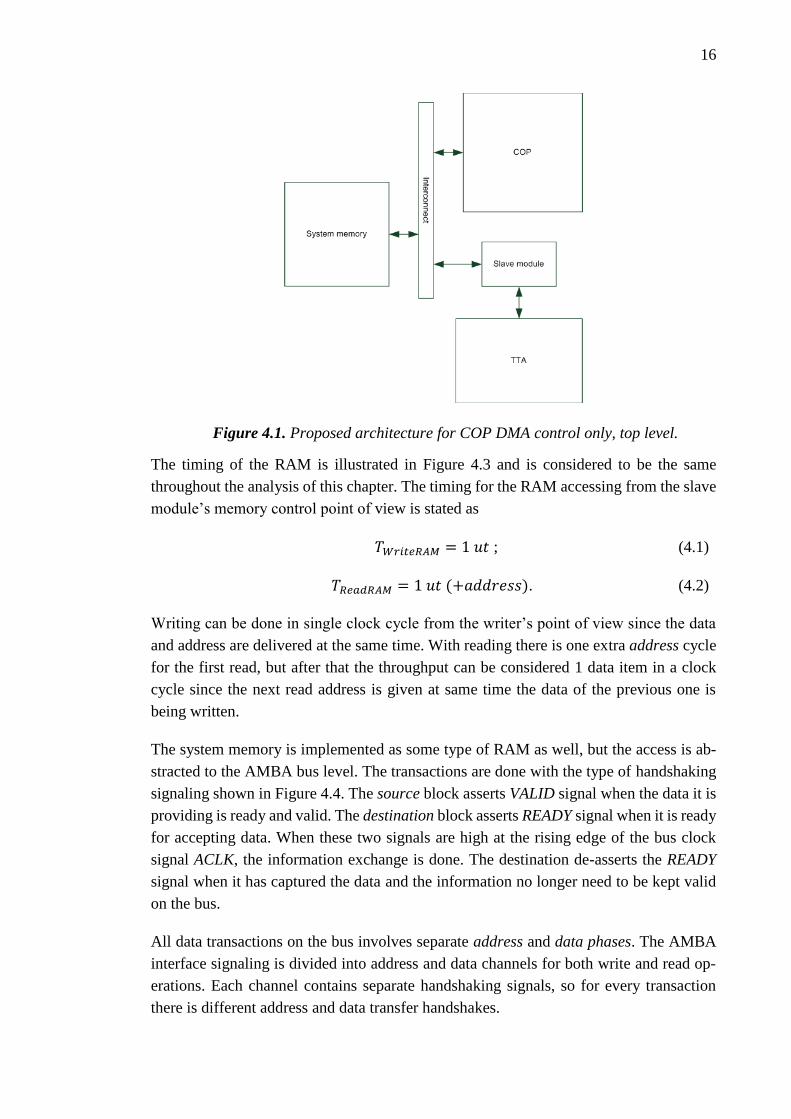
16
Figure 4.1. Proposed architecture for COP DMA control only, top level.
The timing of the RAM is illustrated in Figure 4.3 and is considered to be the same
throughout the analysis of this chapter. The timing for the RAM accessing from the slave
module’s memory control point of view is stated as
𝑇𝑊𝑟𝑖𝑡𝑒𝑅𝐴𝑀 = 1 𝑢𝑡 ; (4.1)
𝑇𝑅𝑒𝑎𝑑𝑅𝐴𝑀 = 1 𝑢𝑡 (+𝑎𝑑𝑑𝑟𝑒𝑠𝑠). (4.2)
Writing can be done in single clock cycle from the writer’s point of view since the data
and address are delivered at the same time. With reading there is one extra address cycle
for the first read, but after that the throughput can be considered 1 data item in a clock
cycle since the next read address is given at same time the data of the previous one is
being written.
The system memory is implemented as some type of RAM as well, but the access is ab-
stracted to the AMBA bus level. The transactions are done with the type of handshaking
signaling shown in Figure 4.4. The source block asserts VALID signal when the data it is
providing is ready and valid. The destination block asserts READY signal when it is ready
for accepting data. When these two signals are high at the rising edge of the bus clock
signal ACLK, the information exchange is done. The destination de-asserts the READY
signal when it has captured the data and the information no longer need to be kept valid
on the bus.
All data transactions on the bus involves separate address and data phases. The AMBA
interface signaling is divided into address and data channels for both write and read op-
erations. Each channel contains separate handshaking signals, so for every transaction
there is different address and data transfer handshakes.

17
Figure 4.2. Slave module.
Since the AMBA protocols support bursts as mentioned in Chapter 3, one address phase
can be followed by multiple data exchanges. Therefore, for single burst operation only
one address handshaking has to be issued for large amount of data. With the data phase
there is handshaking still done with every data element transferred. An example of the
handshaking signaling timing over the interconnect is shown in Figure 4.5. There can be
several blocks accessing the same system memory over the interconnect, so for example
with the address phase the exact moment when the system memory grants access by is-
suing the READY signal is unknown. This uncertainty related to the address phase is re-
ferred here as 𝑇𝑆𝑦𝑠𝑀𝑒𝑚𝐴𝑑𝑑𝑟𝑒𝑠𝑠, representing the average time the AMBA address phase
takes in system memory accessing in addition to the 1 cycle minimum handshaking. There
is also a delay with every data phase information exchange called 𝑇𝑆𝑦𝑠𝑀𝑒𝑚𝐷𝑎𝑡𝑎, which
represent the average time a data exchange takes.
Figure 4.3. RAM timing.

18
Figure 4.4. AMBA handshaking [12].
For performance estimations, let the system interconnect word size be 128 bits, which is
one of AMBA bus widths. This is also one of the generic word sizes COP can be config-
ured for. Let also the input and output samples the TTA processor operates with be 32-
bit wide, as well as the width of the RAM. With 128-bit word, a total of four 32-bit sam-
ples can be transferred on the bus at once. If considering bursts the length of 16, a total
of 64 samples can be transferred as a single transaction with one address phase. By in-
cluding one address phase with in every burst and the delay 𝑇𝑆𝑦𝑠𝑀𝑒𝑚𝐷𝑎𝑡𝑎 with every data
information exchange, the time for the system memory accessing in both writing and
reading directions can be stated as
𝑇𝑆𝑦𝑠𝑀𝑒𝑚𝐵𝑢𝑟𝑠𝑡16 = 𝑇𝑆𝑦𝑠𝑀𝑒𝑚𝐴𝑑𝑑𝑟𝑒𝑠𝑠 + 16𝑇𝑆𝑦𝑠𝑀𝑒𝑚𝐷𝑎𝑡𝑎. (4.3)
Figure 4.5. AMBA burst data phase timing example.
The slave module access timing is could be considered the same as in (4.3), but if the
slave module is however fully optimized for COP data writing and reading, the delays
related to the address and data phases can be considered to be constant. The buffering
shown in the block diagram of Figure 4.2 ensures that the module can accept data with
higher rate than it is able to write to the RAM. Therefore, one 64 sample write burst
towards the slave module can be executed with 1 clock cycle address phase and 1 clock
cycle data exchanges and the time is

19
𝑇𝐶𝑂𝑃𝑊𝑟𝑖𝑡𝑒𝑆𝑙𝑎𝑣𝑒64 = 𝑇𝑆𝑙𝑎𝑣𝑒𝐴𝑑𝑑𝑟𝑒𝑠𝑠𝑃ℎ𝑎𝑠𝑒 + 16𝑇𝑆𝑙𝑎𝑣𝑒𝐷𝑎𝑡𝑎𝑃ℎ𝑎𝑠𝑒 = 1𝑢𝑡 + 16𝑢𝑡 = 17𝑢𝑡,
(4.4)
where the terms 𝑇𝑆𝑙𝑎𝑣𝑒𝐴𝑑𝑑𝑟𝑒𝑠𝑠𝑃ℎ𝑎𝑠𝑒 and 𝑇𝑆𝑙𝑎𝑣𝑒𝐷𝑎𝑡𝑎𝑃ℎ𝑎𝑠𝑒 correspond to the address and data
phase delays. The data phase timing of the writing of the slave module is illustrated in
Figure 4.6. With the buffering implemented inside the module it can accept 4 samples on
every clock cycle although the RAM is accessed slower. The RAM writing starts imme-
diately after the module has received the first samples. 𝑇𝐶𝑂𝑃𝑊𝑟𝑖𝑡𝑒𝑆𝑙𝑎𝑣𝑒64 is the time that
COP experiences when writing towards the slave module. As seen from Figure 4.6, the
RAM is written much slower. The time COP experiences for the samples to be written in
the RAM is
𝑇𝐶𝑂𝑃𝑊𝑟𝑖𝑡𝑒𝑆𝑙𝑎𝑣𝑒𝑅𝐴𝑀64 = 𝑇𝑆𝑙𝑎𝑣𝑒𝐴𝑑𝑑𝑟𝑒𝑠𝑠𝑃ℎ𝑎𝑠𝑒 + 1𝑢𝑡 + 64𝑇𝑊𝑟𝑖𝑡𝑒𝑅𝐴𝑀 = 66𝑢𝑡, (4.5)
where the one extra clock cycle represents the capturing of the first RAM write address.
Figure 4.6. Slave write operation data phase timing.
In the opposite direction, the address phase of the slave module reading can be considered
constant, as was with the writing. But the RAM reading forms a bottleneck in the read
flow because only one sample can be read in a clock cycle from the RAM after the first
RAM address has been written. The timing of the slave module reading data phase is
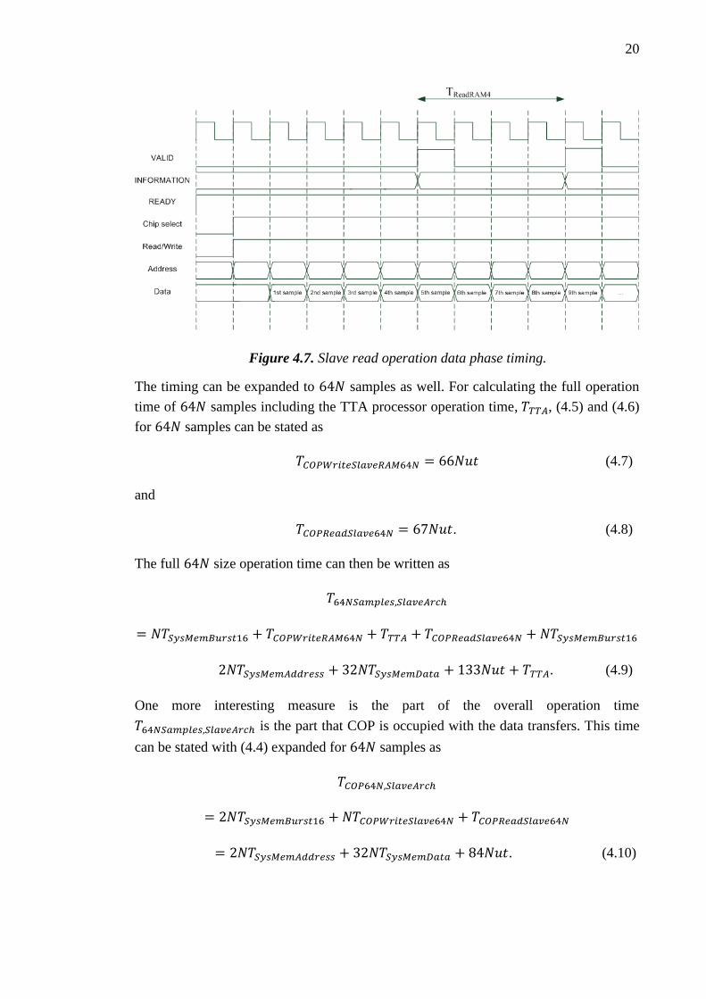
shown in Figure 4.7. Reading 4 samples from the RAM takes 4 clock cycles as indicated
by 𝑇𝑅𝑒𝑎𝑑𝑅𝐴𝑀4 in the figure. There are still two extra cycles in the beginning of the burst
for capturing the read address and writing it for the RAM. The timing for the 64 result
samples read can therefore be stated as
𝑇𝐶𝑂𝑃𝑅𝑒𝑎𝑑𝑆𝑙𝑎𝑣𝑒64 = 𝑇𝑆𝑙𝑎𝑣𝑒𝐴𝑑𝑑𝑟𝑒𝑠𝑠𝑃ℎ𝑎𝑠𝑒 + 2𝑢𝑡 + 64𝑇𝑅𝑒𝑎𝑑𝑅𝐴𝑀 = 67𝑢𝑡, (4.6)
where the term 𝑇𝑅𝑒𝑎𝑑𝑅𝐴𝑀 is the RAM reading time stated in (4.2).
20
Figure 4.7. Slave read operation data phase timing.
The timing can be expanded to 64𝑁 samples as well. For calculating the full operation
time of 64𝑁 samples including the TTA processor operation time, 𝑇𝑇𝑇𝐴, (4.5) and (4.6)
for 64𝑁 samples can be stated as
𝑇𝐶𝑂𝑃𝑊𝑟𝑖𝑡𝑒𝑆𝑙𝑎𝑣𝑒𝑅𝐴𝑀64𝑁 = 66𝑁𝑢𝑡 (4.7)
and
𝑇𝐶𝑂𝑃𝑅𝑒𝑎𝑑𝑆𝑙𝑎𝑣𝑒64𝑁 = 67𝑁𝑢𝑡. (4.8)
The full 64𝑁 size operation time can then be written as
𝑇64𝑁𝑆𝑎𝑚𝑝𝑙𝑒𝑠,𝑆𝑙𝑎𝑣𝑒𝐴𝑟𝑐ℎ
= 𝑁𝑇𝑆𝑦𝑠𝑀𝑒𝑚𝐵𝑢𝑟𝑠𝑡16 + 𝑇𝐶𝑂𝑃𝑊𝑟𝑖𝑡𝑒𝑅𝐴𝑀64𝑁 + 𝑇𝑇𝑇𝐴 + 𝑇𝐶𝑂𝑃𝑅𝑒𝑎𝑑𝑆𝑙𝑎𝑣𝑒64𝑁 + 𝑁𝑇𝑆𝑦𝑠𝑀𝑒𝑚𝐵𝑢𝑟𝑠𝑡16
2𝑁𝑇𝑆𝑦𝑠𝑀𝑒𝑚𝐴𝑑𝑑𝑟𝑒𝑠𝑠 + 32𝑁𝑇𝑆𝑦𝑠𝑀𝑒𝑚𝐷𝑎𝑡𝑎 + 133𝑁𝑢𝑡 + 𝑇𝑇𝑇𝐴. (4.9)
One more interesting measure is the part of the overall operation time
𝑇64𝑁𝑆𝑎𝑚𝑝𝑙𝑒𝑠,𝑆𝑙𝑎𝑣𝑒𝐴𝑟𝑐ℎ is the part that COP is occupied with the data transfers. This time
can be stated with (4.4) expanded for 64𝑁 samples as
𝑇𝐶𝑂𝑃64𝑁,𝑆𝑙𝑎𝑣𝑒𝐴𝑟𝑐ℎ
= 2𝑁𝑇𝑆𝑦𝑠𝑀𝑒𝑚𝐵𝑢𝑟𝑠𝑡16 + 𝑁𝑇𝐶𝑂𝑃𝑊𝑟𝑖𝑡𝑒𝑆𝑙𝑎𝑣𝑒64𝑁 + 𝑇𝐶𝑂𝑃𝑅𝑒𝑎𝑑𝑆𝑙𝑎𝑣𝑒64𝑁
= 2𝑁𝑇𝑆𝑦𝑠𝑀𝑒𝑚𝐴𝑑𝑑𝑟𝑒𝑠𝑠 + 32𝑁𝑇𝑆𝑦𝑠𝑀𝑒𝑚𝐷𝑎𝑡𝑎 + 84𝑁𝑢𝑡. (4.10)

21
4.2 Single COP System: DMA Control over the Auxiliary Inter-
face
With the second proposed architecture, the data traffic between COP and the TTA pro-
cessor is arranged through the Auxiliary interface of COP, described in Chapter 3. The
top level block diagram of the architecture is shown in Figure 4.8. This architecture re-
quires separate Auxiliary unit that converts the data on the AUX port suitable for the TTA
processor.
Figure 4.8. One COP and AUX interface, top level.
The block diagram of the needed AUX unit is shown in Figure 4.9 with the COP and TTA
interfaces. The block contains all the needed control towards the AUX interface, buffering
and data storing, as was with the slave module in the previous section. The storage is
modeled as RAM also with this architecture.
The data rate at which COP can operate the system memory over the AMBA bus is the
same as was with the previous architecture. The timings with the 128-bit COP architecture
and bus data width for 64 sample read and write are the ones described in (4.3).

22
Figure 4.9. Auxiliary unit.
As described in Chapter 3, the Auxiliary port of COP can deliver maximum of 3 data
items the size of the processor’s machine word in 1 clock cycle. Each command, with
which the 3 data items are delivered, expect a result as was indicated already in Chapter
3. To get the best throughput possible the commands should be pipelined as shown in
Figure 4.10. The result of the previous operation initiated is sent at the same time the
current operation is being read.
Figure 4.10. AUX port write timing.
In the opposite direction, 1 data item can be read in a clock cycle as a result for one
initiated operation. If considering only a single command, it would take 2 cycles to read
1 item. The reading can be pipelined the same way as the writing as shown in Figure 4.11
to get the 1 result item per clock cycle rate.

23
Figure 4.11. AUX port read timing.
With 128-bit architecture, a total of 12 samples can be delivered in a single clock cycle.
On the opposite direction, 4 samples can be delivered for COP also in a single cycle, if
the operations are pipelined. Considering the same 64 sample operation as in the previous
section, a total of 5 writes the size of 12 samples and 1 write the size of 4 samples are
needed for delivering 64 samples. From COP’s perspective the time for this operation is
𝑇𝐶𝑂𝑃𝑊𝑟𝑖𝑡𝑒𝐴𝑈𝑋64 = 5 ∗ 1𝑢𝑡 + 1𝑢𝑡 = 6𝑢𝑡. (4.11)
As was with the pervious architecture’s slave module writing time 𝑇𝐶𝑂𝑃𝑊𝑟𝑖𝑡𝑒𝑆𝑙𝑎𝑣𝑒64, this
is also the time that COP experiences with writing the Auxiliary unit without the RAM
access time being concerned. If the Auxiliary unit is constructed in the same manner as
was the slave module, as shown in Figure 4.9, COP does not have to wait before initiating
a new AUX write as the buffer of the AUX unit ensures the fluent data flow and the
pipelining can be done.
The AUX unit can start writing the RAM when the first 3 data items are received and 1
clock cycle capturing delay. Therefore, the time for COP to write the 64 samples all the
way to the RAM is
𝑇𝐶𝑂𝑃𝑊𝑟𝑖𝑡𝑒𝐴𝑈𝑋𝑅𝐴𝑀64 = 1𝑢𝑡 + 64𝑇𝑊𝑟𝑖𝑡𝑒𝑅𝐴𝑀 = 65𝑢𝑡. (4.12)
The timing of the 64 results reading can be analyzed in the same manner as the reading
with the previous architecture. The RAM reading forms a bottleneck also with this archi-
tecture, and if the RAM reading is started with the first initiated command, the pipelining
cannot be done with the same rate as in Figure 4.11 but with similar manner as was in
presented in the previous section. The AUX port read timing with the RAM included is
presented in Figure 4.12. There are the same 2 cycle delay before the first sample is read
as was in Figure 4.7. For every 4 samples there is a 4-cycle delay. There are also 2 extra
cycles due to the data capturing and RAM write addressing. Therefore, the time is
𝑇𝐶𝑂𝑃𝑅𝑒𝑎𝑑𝐴𝑈𝑋64 = 2𝑢𝑡 + 64𝑇𝑅𝑒𝑎𝑑𝑅𝐴𝑀 = 66𝑢𝑡. (4.13)

24
The AUX accessing times in (4.12) and (4.13) can be expanded for the same 64𝑁 size
operation as with the previous architecture. Since there are no separate access phases, no
extra cycles for the data capturing are needed after the first one in writing direction, so
the 64𝑁 input samples timing over the AUX writing all to way to the RAM is
𝑇𝐶𝑂𝑃𝑊𝑟𝑖𝑡𝑒𝐴𝑈𝑋𝑅𝐴𝑀64𝑁 = 1𝑢𝑡 + 64𝑁𝑇𝑊𝑟𝑖𝑡𝑒𝑅𝐴𝑀 = 1𝑢𝑡 + 64𝑁𝑢𝑡. (4.14)
In the reading direction, the two extra cycles are present only with the first read and after
that the RAM accessing speed limits the data rate, so the time can be stated as
𝑇𝐶𝑂𝑃𝑅𝑒𝑎𝑑𝐴𝑈𝑋64𝑁 = 2𝑢𝑡 + 64𝑁𝑇𝑅𝑒𝑎𝑑𝑅𝐴𝑀 = 2𝑢𝑡 + 64𝑁𝑢𝑡. (4.15)
Figure 4.12. AUX port read with RAM timing.
The full 64𝑁 size operation can be stated as
𝑇64𝑁𝑆𝑎𝑚𝑝𝑙𝑒𝑠,𝐴𝑈𝑋𝐴𝑟𝑐ℎ =
𝑁𝑇𝑆𝑦𝑠𝑀𝑒𝑚𝐵𝑢𝑟𝑠𝑡16 + 𝑇𝐶𝑂𝑃𝑊𝑟𝑖𝑡𝑒𝐴𝑈𝑋𝑅𝐴𝑀64𝑁 + 𝑇𝑇𝑇𝐴 + 𝑇𝐶𝑂𝑃𝑅𝑒𝑎𝑑𝐴𝑈𝑋64𝑁 + 𝑁𝑇𝑆𝑦𝑠𝑀𝑒𝑚𝐵𝑢𝑟𝑠𝑡16
= 2𝑁𝑇𝑆𝑦𝑠𝑀𝑒𝑚𝐴𝑑𝑑𝑟𝑒𝑠𝑠 + 32𝑁𝑇𝑆𝑦𝑠𝑀𝑒𝑚𝐷𝑎𝑡𝑎 + 1𝑢𝑡 + 64𝑁𝑢𝑡 + 2𝑢𝑡 + 64𝑁𝑢𝑡 + 𝑇𝑇𝑇𝐴
= 2𝑁𝑇𝑆𝑦𝑠𝑀𝑒𝑚𝐴𝑑𝑑𝑟𝑒𝑠𝑠 + 32𝑁𝑇𝑆𝑦𝑠𝑀𝑒𝑚𝐷𝑎𝑡𝑎 + 3𝑢𝑡 + 128𝑁𝑢𝑡 + 𝑇𝑇𝑇𝐴. (4.16)
If the time COP is occupied with the AUX writing as in (4.11) is expanded for the 64𝑁
samples as well, the time COP occupied time of the full operation can be stated as
𝑇𝐶𝑂𝑃64𝑁,𝐴𝑈𝑋𝐴𝑟𝑐ℎ
= 2𝑁𝑇𝑆𝑦𝑠𝑀𝑒𝑚𝐵𝑢𝑟𝑠𝑡16 + 𝑁𝑇𝐶𝑂𝑃𝑊𝑟𝑖𝑡𝑒𝐴𝑈𝑋64𝑁 + 𝑇𝐶𝑂𝑃𝑅𝑒𝑎𝑑𝐴𝑈𝑋64𝑁
= 2𝑁𝑇𝑆𝑦𝑠𝑀𝑒𝑚𝐴𝑑𝑑𝑟𝑒𝑠𝑠 + 32𝑁𝑇𝑆𝑦𝑠𝑀𝑒𝑚𝐷𝑎𝑡𝑎 + 6𝑁𝑢𝑡 + 2𝑢𝑡 + 64𝑁𝑢𝑡
= 2𝑁𝑇𝑆𝑦𝑠𝑀𝑒𝑚𝐴𝑑𝑑𝑟𝑒𝑠𝑠 + 32𝑁𝑇𝑆𝑦𝑠𝑀𝑒𝑚𝐷𝑎𝑡𝑎 + 2𝑢𝑡 + 70𝑁𝑢𝑡. (4.17)

25
4.3 Dual COP System
One option for the design is to use two COP units instead of one. With this approach, the
first COP is configured as the inputs provider for the TTA processor and the second for
the output reading to the system memory. With this architecture, the TTA processor in-
terface can be implemented with either of the previously presented ways, as a slave device
accessible over the interconnect or as a CPU extension of the AUX interface. The timing
values calculated in the previous sections are valid for the two COP architecture also. The
top level block diagram of two COP architecture with the Auxiliary port as the interface
towards the TTA processor is presented in Figure 4.13. For this approach the AUX unit
operation has to be split in two.
The two COP approach provides better performance for the design. The total throughput
stays the same as with the single COP architecture, but the time each COP is occupied
reduced dramatically. The COPs processing times over one 64𝑁 samples operation are
𝑇𝐶𝑂𝑃𝐶𝑜𝑚𝑚𝑎𝑛𝑑 = 𝑁𝑇𝑆𝑦𝑠𝑀𝑒𝑚𝐴𝑑𝑑𝑟𝑒𝑠𝑠 + 16𝑁𝑇𝑆𝑦𝑠𝑀𝑒𝑚𝐷𝑎𝑡𝑎 + 6𝑁𝑢𝑡 (4.18)
and
𝑇𝐶𝑂𝑃𝑅𝑒𝑠𝑢𝑙𝑡 = 2𝑢𝑡 + 64𝑁𝑢𝑡 + 𝑁𝑇𝑆𝑦𝑠𝑀𝑒𝑚𝐴𝑑𝑑𝑟𝑒𝑠𝑠 + 16𝑁𝑇𝑆𝑦𝑠𝑀𝑒𝑚𝐷𝑎𝑡𝑎 . (4.19)

26
Figure 4.13. Two COP and AUX units, top level.
4.4 Performance Comparison
With the AMBA bus timings being the same for both of the proposed single COP unit
architectures, the 64N sample operation timings in (4.9) and (4.16) differ by
𝑇𝐷𝑖𝑓𝑓𝑒𝑟𝑒𝑛𝑐𝑒𝐹𝑢𝑙𝑙𝑂𝑝𝑒𝑟𝑎𝑡𝑖𝑜𝑛 = 133𝑁𝑢𝑡 − 3𝑢𝑡 − 128𝑁𝑢𝑡 = 5𝑁𝑢𝑡 − 3𝑢𝑡. (4.20)
and it can be stated that the Auxiliary unit architecture is faster due to its ability for larger
data delivering at a time.
One more interesting comparison between the two architectures is the COP operation
time presented in (4.10) and (4.17). The difference between the times is
𝑇𝐶𝑂𝑃𝐷𝑖𝑓𝑓𝑒𝑟𝑒𝑛𝑐𝑒 = 84𝑁𝑢𝑡 − 2𝑢𝑡 − 70𝑁𝑢𝑡 = 14𝑁𝑢𝑡 − 2𝑢𝑡. (4.21)
The AUX unit architecture is clearly better from this perspective as well. The reason why
the COP occupied part of the whole operation time is interesting is that as a general RISC
processor COP can perform other functionality as well while not transferring data, rather
than acting only as a DMA controller. This functionality can be related to the task being
processed on the TTA processor or something else. This time is referred as slack time and
it can be stated as
𝑇𝐶𝑂𝑃𝑆𝑙𝑎𝑐𝑘,𝑆𝑙𝑎𝑣𝑒𝐴𝑟𝑐ℎ = 𝑇64𝑁𝑆𝑎𝑚𝑝𝑙𝑒𝑠,𝑆𝑙𝑎𝑣𝑒𝐴𝑟𝑐ℎ − 𝑇𝐶𝑂𝑃64𝑁,𝑆𝑙𝑎𝑣𝑒𝐴𝑟𝑐ℎ = 49𝑁𝑢𝑡 + 𝑇𝑇𝑇𝐴
(4.22)
and

27
𝑇𝐶𝑂𝑃𝑆𝑙𝑎𝑐𝑘,𝐴𝑈𝑋𝐴𝑟𝑐ℎ = 𝑇64𝑁𝑆𝑎𝑚𝑝𝑙𝑒𝑠,𝐴𝑈𝑋𝐴𝑟𝑐ℎ − 𝑇𝐶𝑂𝑃64𝑁,𝐴𝑈𝑋𝐴𝑟𝑐ℎ = 1𝑢𝑡 + 58𝑁𝑢𝑡 + 𝑇𝑇𝑇𝐴.
(4.23)
The operation time of the TTA processor is application specific and can be left out when
comparing the slacks. Different slack times are listed in Table 4.1 with different values
of 𝑁 with the TTA processing time left out. It can be seen that with 4096-size operation
the difference with the slack is in the scale of hundreds of clock cycles.
Table 4.1. 64N-size operation COP slack times without TTA processing delay.
N Operation size (num-ber of samples)
Slack, Slave module archi-tecture (ut)
Slack, AUX unit architec-ture (ut)
1 64 49 59
2 128 98 117
4 256 196 233
8 512 392 465
16 1024 784 929
32 2048 1568 1857
64 4096 3136 3713

28
5. IMPLEMENTATION
Of the three proposed architectures, the one described in section 4.2 was selected for im-
plementation. In addition to DMA control it was in high interest to demonstrate the usage
of the Auxiliary port of COP in practice. The single COP architecture was chosen over
the two COP design for simplicity reasons and to demonstrate the power and usefulness
of COP as an independent control unit.
The implementation had three steps: designing and building the missing hardware be-
tween the Auxiliary unit and the TTA processor, integration of all of the building blocks
together as one design and developing software for COP to run the use case application.
All the functional hardware in the design was implemented with Very High Speed Inte-
grated Circuit (VHSIC) hardware description language (VHDL).
5.1 Top Level Design
Detailed top level architecture of the design is shown in Figure 5.1. All the used blocks
and memories are shown on a block level abstraction.
Figure 5.1. Single COP design, top level.
The Auxiliary Unit was split into two independent functional blocks, the Command and
the Result block. The internal structure of these blocks is described in detail in section

29
5.3. Arbitration between these blocks is done by ready-made Auxiliary Unit Transceive
block (AUT).
5.2 COP Configuration
For the architecture selected for implementation, COP was configured for 128-bit ma-
chine word size. With this word size, a total of 12 32-bit samples can be delivered through
the Auxiliary unit towards the TTA processor and 4 32-bit samples read back with one
Auxiliary command.
COP was configured for 4 separate threads. The register space of COP was split between
the threads so that each holds 32 general purpose registers. The Auxiliary port was con-
figured to support 2 units. The arbitration between the AUX units was done with the AUT
which can be used for chaining the Auxiliary units as illustrated in Figure 5.2. The AUT
unit reads the Unit signal when COP initiates new command and based on the value of
the signal the AUT unit forwards the Initiate signal to the right AUX unit.
Figure 5.2. AUX units chaining with AUT units.
5.3 Auxiliary Units
The basis for the AUX units was to design a generic interface between COP and TTA
processor. With this in mind it was reasonable choice to split the one unit into two. For
example in the two COP design both COPs would be wrapped up with just one of the
AUX units. The two blocks are referred as Command and Result block. This section de-
scribes the main structure and operation of the blocks.
5.3.1 Interfaces
There are differences with the memory and the TTA control interfaces between the two
AUX units, but towards COP both interfaces are similar, as illustrated in Figures 5.3 and
5.4. Both blocks work under single clock and reset domain.

30
Figure 5.3. Command block interfaces.
Both the blocks have interface towards TTA. The Command block uses the interface to
initiate TTA processor operation with the TTA_initiate and TTA_op_out signals. The
TTA_done and TTA_op_in signals in the interface are there for the internal bookkeeping
of the initiated and ready operations on the TTA processor. The TTA_done signal is also
forwarded to the Attn port of COP. More of the usage of the Attn port with this imple-
mentation is described in section 5.6.
The opcode was designed to carry the base address of the input data towards TTA and the
base address of the results towards the Result bock. For simplicity reason it was used with
this design only to carry the opcode for the operation initiated i.e. the index of the memory
segment where the data is located.
The only signal used in the TTA control interface of the Result block is TTA_op_in that
delivers opcode for the base address. Rest of the interface is used mainly for bookkeeping
information of the initiated and ready operations on the TTA processor, as was with the
Command block. The Result block does not issue any result reads without the correspond-
ing commands coming first from COP.
The TTA memory interfaces are similar in both blocks, except for the direction of the
memory access. The RAM signals are the basic address A, chip select CS, data D, write
enable WE and bit select BS. The Command block is used only for writing input data and
the Result block for reading the results, so only the write data signal D needed to imple-
ment in the Command block and the read data signal Q in the Result block.
There is also a memory interface for the TTA instruction memory writing in the Com-
mand block. This was implemented because no external configuration port was placed on
the TTA processor for accessing the memory.

31
Figure 5.4. Result block interfaces.
5.3.2 Transaction Protocol
To transfer the data between COP and TTA processor as efficiently as possible, a simple
protocol was constructed for the Auxiliary unit data transfers. For example in the writing
direction, the Command block needs addresses for the input samples it receives and the
information when it has received all the samples and the TTA processor can be released
for operation. Data is usually transferred in large chunks at a time, so it is more practical
to handle the data transfers as a transactions initiated with base address and number of
read/write operation rather than include this information in every Auxiliary command.
The commands implemented with the AUX blocks are listed in Tables 5.1 and 5.2 with
the related description, parameters and result. The command itself is delivered with the
AUX port’s Operation signal. The parameters are transferred with the data signals DataA,
DataB and DataC. The parameters can be data or information of some kind. COP hard-
ware expect a result for every initiated command, so the command block has to provide
one. There is, however, not any relevant data given, except with the Init command there
is message for errors. The rest of the results do not have to contain any data and no valid
information is sent as a result with the Command block. This is why the results in the
Tables 5.1 and 5.2 are set as Discarded except for the Init command.
Table 5.1. Command block commands.
Command Description Parameters Result
Init Initiate new write transaction Base address, Number
of samples to be written
Error message if no
room for samples
APartial Delivery of 1-3 sample Data Discarded
AFull Delivery of 4 samples Data Discarded
ABCFull Delivery of 12 samples Data Discarded
IMemWrite Write word to TTA IMEM Data, address Discarded
32
The write transaction with Command block works as follows: transactions are initiated
with the Init command. Two parameters are delivered for Command block with the com-
mand with the data signals DataA and DataB: the base address for TTA input memory
writing and the number of samples to be written. The Command block captures these
values into variables NumOfWrites and Addr. If there is space in the TTA input memory
for this amount of samples and the address is in the allowed range, the Command block
sends all zeros as result for COP. This acts as response for the initiate command. If either
of the parameters violates the allowed conditions, all ones is send as error message.
After the transaction initiation, the Command block can start accepting input data. It is
on the Command block’s responsibility to do all the buffering and memory address up-
dating after the Init command so that the software on COP can perform the AUX writing
fluently. If the Command block needs to stall the transaction for some reason, it de-asserts
the ready for command signal and gives no results for COP before the transaction can be
continued. This way COP pauses its instruction execution and waits before it continues
the writing. From software point of view the data is provided with registers and received
in a register and there is always the ID number of the Auxiliary unit delivered with the
commands (the Unit parameter). Pseudo code example for the Command block writing
looks as follows:
ldi r1, NumOfSamples //The number of samples ldi r2, Address ldi r3, 0 aux Unit, Init, r1, r2, r3 //Initate with the parameters breq r3, ERROR //Check for errors aux Unit, ABCFull, r4, r5, r6 //Registers r4-r6 contains write data aux Unit, ABCFull, r7, r8, r9 aux Unit, AFull, r10, r11, r12 //Only r10 contains data
The command block has one extra command, IMemWrite, listed last in Table 5.1. This
command is used to write to TTA instruction memory. For simplicity reasons and the fact
that the instruction word length of the TTA processor is most probably not divisible with
the power of two (42 bits in this implementation), the TTA instruction memory writing is
not implemented as transaction. Instead, the instruction memory address and the data to
be written are provided with the data signals DataA and DataB.
The Result block read transaction is initiated with the Init command, as was with the
Command block. Similar error response is related to the read initiation as was with the
Command block, which is issued if initiation is done when no result data is available on
the TTA output memory. With the results Init operation only the number of reads is de-
livered for the Result block. It is on the Result block’s responsibility to do the bookkeep-
ing for the locations of the ready data in the TTA output memory. The bookkeeping is
done according to the TTA interface signaling.

33
The number of the reads is stored in variable NumOfReads. After the Init command COP
starts issuing AUX port commands and the read samples are provided as result for each
command. Pseudo code example for the read transactions is listed below.
ldi r1, NumOfReads //Number of reads ldi r2, 0 ldi r3, 0 aux Unit, Init, r1, r2, r3 //Initiate with the parameter breq r3, ERROR aux Unit, Read4, r1, r2, r3 //Read 4 command st r3, SysMemAddr //Store the result data (the read data) aux Unit, Read4, r1, r2, r3 //Read command st r3, SysMemAddr //Store the result data (the read data)
The code execution stalls with the Auxiliary command if the Result block de-asserts the
ready for command signal. The system memory store operations are therefore not exe-
cuted before the previous AUX read result is given.
The Result block has one extra command, ReadyCount, as listed in Table 5.2. This com-
mand was implemented for the COP to be able to inquire new results. This feature was
not in fact taken in use in the final implementation because the assertion for new data was
done through the COP Attn port.
Table 5.2. Result block commands.
Command Description Parameters Result
Init Initiate new read transaction Number of samples to
be read
Error message if no
results available
Read1 Read 1 sample None Result sample
Read4 Read 4 samples None Result samples
ReadyCount Get the number of ready re-
sult groups
None Count of ready result
groups
For either of the blocks, no distinct stop command for the transaction was needed, because
both blocks observe the NumOfWrites and NumOfReads variables and operate on the
memories according to these. The transactions can, however, be stopped simply by initi-
ating new transaction with the Init command.
5.3.3 Datapath
Data can be delivered for Command block and read back from Result block in various
chunks of samples. The TTA input and output memories are accessed with only one sam-
ple per clock cycle, so input data slicing and result data wrapping into 128-bit form is
needed.
As shown in Figure 5.5, the datapath of the Command block can be separated into four
stages. The incoming data from the Command stage is captured on the Capture stage.

34
According to the Auxiliary command parameters, the control logic decides how many
samples are sliced and inserted to buffer on the Buffer stage. At the RAM stage the data
from the buffer is written to RAM if there are samples in the buffer. The control logic
takes care of the buffer accessing pointers updating and the RAM writing. More about
the buffer implementation is described in section 5.3.5.
Figure 5.5. Command block datapath.
The datapath of the Result block, shown in Figure 5.6, is very much like reversed datapath
of the Command block. However, there is no separate capture stage and the data read
from RAM is inserted into the buffer immediately on the next stage after the RAM stage.
The buffer itself is implemented with the same principle as the buffer inside the Command
block, but the data form inside the buffer is different. The Command block’s buffer holds
the data in the 32-bit sample size form, but inside the Result block the samples are ar-
ranged in 128-bit AUX port result form. The control logic is responsible for inserting the
data into the right 128-bit slot and into the right position within this slot. The data is
delivered for COP at the result stage.

35
Figure 5.6. Result block datapath.
5.3.4 State Diagrams
The control over the Command block datapath was constructed with a separate processes
for the command port, buffer and RAM control functionalities. These are be illustrated as
state diagrams, shown in Figure 5.7.
The control over the data capturing on the AUX port is illustrated in Figure 5.7a. The
process observes the Initiate signal and if a new command is initiated when the Command
block’s status is ready for command, the data along with the tag of the operation is cap-
tured. The results for the commands are given according to the state diagram in 5.7b. This
process observes the same conditions as the previous one. The result state is kept if there
is a new initiation and the block is ready for the command. If there is initiation with the
block not being ready, or no initiation, the process performs waiting and no results are
given for the initiated commands. If COP tries to initiate when the Command block is not
ready, it keeps on trying the initiation with the same data and tag until the block is signaled
ready and the data can be captured.
The signaling of the Command block’s status of being ready for a new command is con-
trolled by the state diagram in 5.7c. The ready for command signal is kept high if there is
space in the buffer. If the buffer becomes full the signal is de-asserted until there is again
space in the buffer.
The RAM writing is controlled by the state diagram in 5.7d. When the Init command is
issued at the AUX port and accepted, the control enters the waiting state. This state is
held until there is something to be written in the buffer. If the buffer empties during trans-
action the control enters the waiting state. When all the samples indicated by the NumOf-
Samples variable is written, the control returns to waiting for a new transaction initiation.

36
Figure 5.7. Command block state diagrams with a) capture b) ready for command
c) result d) RAM control.
The Result block control state diagrams are shown in Figures 5.8 and 5.9. The RAM
reading is started immediately after the initiation of a new transaction. The memory con-
trol can be viewed with three states. The first one in 5.8a observes the initiations and if
there is an Auxiliary command with new transaction initiation, the control moves to the
RAM addressing state. The addressing is done NumOfReads times starting from the base
address the Result block has saved after the TTA processor has issued operation done.
The data capturing control in 5.8b moves to the read RAM state with one clock cycle
behind the addressing. The two processes are operating with pipelined manner. Both state
diagrams will enter the waiting state if the memory accessing is externally stalled. The
stalling is controlled by the state diagram in 5.8c by observing the state of the buffer. If
the buffer becomes full, the RAM reading is stalled.
The results are provided for the initiated commands similar way as with the Result block.
In the state diagram in 5.9a result is only provided when there is a new initiation on the
AUX port and the block is ready for it. The state diagram in 5.9b shows the ready for new
command control. If the buffer is empty and there is no data to provide as a result for
AUX command, the block holds the ready signal down.
37
Figure 5.8. Result block RAM reading related state diagrams with a) addressing b)
read data capturing c) buffer control.
Figure 5.9. Result block state diagrams related to a) result b) ready for command
control.
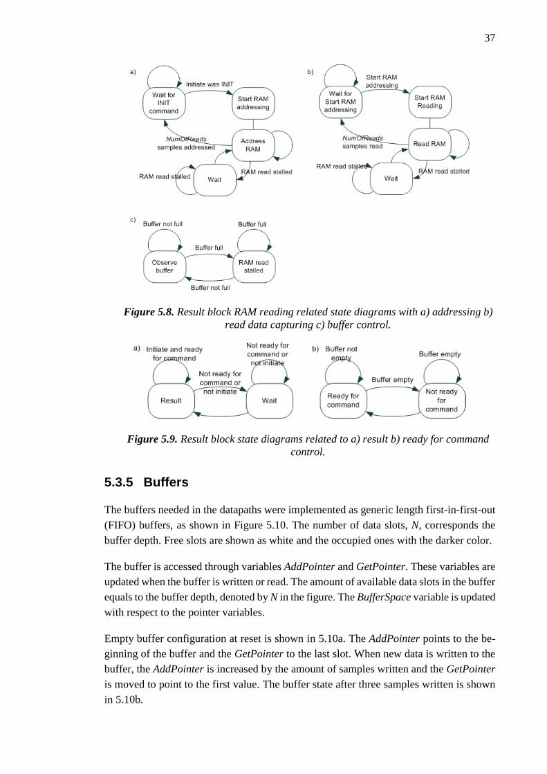
5.3.5 Buffers
The buffers needed in the datapaths were implemented as generic length first-in-first-out
(FIFO) buffers, as shown in Figure 5.10. The number of data slots, N, corresponds the
buffer depth. Free slots are shown as white and the occupied ones with the darker color.
The buffer is accessed through variables AddPointer and GetPointer. These variables are
updated when the buffer is written or read. The amount of available data slots in the buffer
equals to the buffer depth, denoted by N in the figure. The BufferSpace variable is updated
with respect to the pointer variables.
Empty buffer configuration at reset is shown in 5.10a. The AddPointer points to the be-
ginning of the buffer and the GetPointer to the last slot. When new data is written to the
buffer, the AddPointer is increased by the amount of samples written and the GetPointer
is moved to point to the first value. The buffer state after three samples written is shown
in 5.10b.

38
Figure 5.10. Buffer operation with a) buffer empty b) buffer filled with 3 samples c)
buffer filled with 2 samples.
When data is read from the buffer, the GetPointer is increased by the amount of the sam-
ples read. 5.10c shows the buffer state after the 5.10b state when one sample has been
read.
The buffers accessing is constructed in a way that more than one data sample can be
written to the buffer per clock cycle, a maximum of 12 samples at a time with the Com-
mand block. The read access rate of the Command block buffer is still only 1 sample per
clock cycle because of the TTA input memory is cannot be written faster. The memory
accessing restricts the Result block buffer access also to 1 sample per clock cycle.
5.3.6 TTA Control
The control over the TTA processor is implemented with the TTA control interface,
shown in Figure 5.3. The Command block initiates a new operation with TTA_initiate and
TTA_op_out signals. The generic width TTA_op_out signal is used as opcode for the TTA
processor to deliver the information where the new data is located on TTA input memory.
The opcode was designed to deliver the exact base address of the data, but for this imple-
mentation only the data segment index is passed to TTA.
The TTA control interface signal glock controls the global locking of the TTA processor.
The lock is released when a new operation on TTA is initiated and reserved when TTA

39
ihas finished execution. With this implementation the TTA program code halts after fin-
ishing execution so the need for the global locking was not necessary when the TTA is
done operation.
5.4 TTA Processor
The TTA processor used in this implementation was provided by Tampere University of
Technology, Department of Pervasive Computing. It was designed and generated with
the Department’s TTA-based Co-Design Environment (TCE) toolset [13].
The used architecture is presented in Appendix A. The interconnection network between
the functional units was constructed with 5 data buses. In addition to the decoder and
global control units, the architecture contains ALU, 32-bit register file of 8 general pur-
pose registers, Boolean register of 2 slots, load-store unit and separate load and store units
for the TTA input and output memory accessing.
The blocks considered as special function units are the Request, Resp and R4FFT units.
The Request and Resp are considered as input-output units and they perform all the func-
tionality towards outside. The Request unit is responsible for observing the TTA_initiate
and TTA_op_out signals and launching a new operation on the TTA. The Resp unit asserts
the TTA_done signal and provides the operation code for the Result block with
TTA_op_out when TTA is done with the FFT.
The FFT functionality was implemented inside the R4FFT unit as a radix-4 Single-Path
Delay Feedback (R4SDF) decimation in frequency FFT, described in [14], and for 4096-
point size. The basic principle is illustrated in Figure 5.11 for 64-point FFT. The inputs
are read in serial form and the shift registers (SR) are used for delaying. With the radix-
4 DIF approach, the input is divided into 𝑁/4 size groups, so for 64-point FFT into groups
of 16 samples. The butterfly operation of the stage 2 can be started when the first 48
samples have been read into the 16-word SRs. On stage 1, the same is principle is applied
for groups of 4 samples and for 1 samples at stage 0. With the 4096-point implementation
there are six stages with 1024-depth SRs on the stage 5.
The size of the program code for this TTA implementation was 28 lines, with 42-bit in-
structions. Since the main functionality was inside one SFU, most of the program func-
tionality concerned only the data transfers between the R4FFT unit and the LU and SU.

40
Figure 5.11. Principle for 64-point Radix-4 SDF [2, Fig. 19.7].
5.5 Memories
The memories used in the design are listed in Table 5.3. The TTA input and output mem-
ories and the TTA instruction memory were implemented as dual port and others as single
port memory. All memories are single clock memories. The FFT engine implementation
on TTA has also internal data storages acting as memories but these are not considered
as external RAM.
Table 5.3. List of used memories.
Command Width (bit) Depth
COP DMEM 128 256
COP IMEM 32 1024
TTA Input MEM 32 12288
TTA Output MEM 32 12288
TTA DMEM 32 256
TTA IMEM 42 128
All the widths of the memories are fixed for the 32-bit complex valued FFT use case,
except the COP data memory and TTA instruction memory widths. The COP data
memory width is set according to the machine word of the processor, so the 128-bit width
is due to this particular implementation. The TTA instruction memory width is deter-
mined by the processor architecture and the 42-bit instruction width was generated with
this FFT implementation.
The depths of the memories are all selected for this exact implementation. The data and
instruction memories could have been set to other depths as well, but these were consid-
ered suitable for the processors to operate. The TTA input and output memory depths
were selected so that they can each contain three 4096 sample data segments. The seg-
ments are indexed to match with the TTA operation code. This was for ensuring uninter-
rupted data flow between COP and TTA so that COP could still operate on the memories
if TTA is for some reason interrupted, and vice versa.

41
5.6 COP Software
The COP software was written in assembly. Functionality was split into four separate
threads to simplify the code and to demonstrate the potential of COP multithreading. The
threads’ program images were allocated to the instruction memory of COP with equal
spacing so that from the 1024 size memory space 256 sized spaces were reserved for each
thread. One thread was configured as the main thread with system privileges like the
permission to spawn other threads as well. The flowchart of the main thread is shown in
Figure 5.12. The main thread sleeps most of its lifetime. The thread is awaken if there is
an attention request in the Attn port of COP. The threading mechanism is built for sup-
porting the system privileged threads to be synchronized with the Attn port.
With this implementation two kind of attention requests exist. The TTA_done signal at-
tached to the Attn port and every time a new TTA operation is ready, the port is asserted.
Another request is the external new data request indicating a new input data availability
in the system memory.
Pre-defined load and store base addresses are configured in COP’s data memory in system
startup. With this implementation 6 memory locations for both the input and result data
was reserved from the system memory and the base addresses of these are stored in fixed
COP data memory locations. The data memory allocation for the addressing is shown in
Figure 5.13. The loading and storing threads are configured for reading the base addresses
for system memory reading and writing from the fixed memory locations, indicated with
the names Loading base address and Storing base address in Figure 5.13. The main
thread updates these locations before spawning the threads and performs bookkeeping of
the addresses to be configured next.
If new data is asserted to be available, the main thread performs its configurations and
spawns first the acknowledgement thread. This thread contains no functionality, but its
visibility outside COP is used as a confirmation signal that COP has received the info of
the new operation. The acknowledging is completed with the COP Done port that reflects
the threads awake as shown in Figure 5.14. All threads have personal ID number related
to them and the indexes of the Attn port bits corresponds to the IDs of the threads.
After the acknowledgement, the main thread spawns the loading thread and resumes sleep
status. If the attention request was indication TTA operation done, the main thread again
performs its configuration, spawns the storing thread and resumes sleep.

42
Figure 5.12. Main thread operation.
The operation of the loading thread is illustrated in Figure 5.15. When the thread is
spawned it loads the Loading base address from data memory fixed location for the sys-
tem memory reading. Because this implementation was fixed for 4096-point FFT, the
number of input samples to be read is hard coded inside the thread source but this could
have been provided the same way as the base address. After the thread has the base ad-
dress and the number of reads stored in its registers, the thread initiates a new AUX trans-
action the size of 4096. The thread then starts reading the system memory 64 input sam-
ples at a time as a single AMBA burst. When the 64 samples are read, a total of five AUX
writes are done with 12 samples delivery and one write with 4 samples delivery for the
total 64 samples. This is repeated until all the 4096 samples are delivered and the thread
resumes sleep state.
The TTA_done signal is assigned to the Attn port of COP. When the TTA processor in-
forms operation to be completed, the main thread wakes up and checks which attention
request was concerned. With the TTA done request the main thread performs the base
address configuration, i.e. loads the next Storing base address to the fixed data memory
location and spawns the thrad.
The storing thread operation is shown in Figure 5.16. After being spawned the thread
loads the base address for system memory writing and initiates a new 4096 sized read
transaction on the Result block. After 16 reads are done for getting 64 samples from the
TTA output memory, COP writes the samples to the system memory starting according
to the base address. This is repeated until the whole 4096 results are written and the thread
resumes sleep state.

43
Figure 5.13. Base address allocation in COP data memory. The addresses for load-
ing and storing are allocated in the COP data memory in pairs, indicated with the
dashed lines. When the main thread configures loading or storing threads, it writes
address information of one pair in the Loading base address and Storing base ad-
dress memory slots for the threads to use.
Figure 5.14. Done port operation. In a) all the threads are suspended b) thread with
ID no. 0 is in running state c) threads with ID nos. 0, 2 and 3 are in running state.

44
Figure 5.15. Loading thread operation.
Figure 5.16. Storing thread operation.

45
6. RESULTS
The design was simulated under a test bench written is SystemVerilog. 32-it complex
valued input data was generated with Matlab into a file and written in the system memory
model used in the simulation. The test bench generated interrupts to the Attn port of COP
to initiate new operation. After finished, the result data was read from the system memory
and written into a file. Matlab Fourier operation was used for verifying the results.
The separate operational latencies are listed as cycle counts in Table 6.1 for one 4096-
point FFT operation. The full operation took 17892 cycles. The average delay the system
memory model created for the AMBA bus accessing was, for 64 samples, around 60 cy-
cles. By including the 8243 delay of the TTA processor, the theoretical latency for one
operation in (4.16) can be calculated to be 20 278 cycles. This is greater than the simu-
lated full operation latency, because the theoretical value did not consider the Result block
reading the TTA output RAM while COP was writing the previous results to the system
memory. With the effective buffering inside the Result block, almost every time COP
initiated a new read command, the data was already available and was given immediately
as the result for the initiating command. Therefore, the timing was limited basically only
by the AMBA bus delay.
COP is free from the whole 4096 size operation for 8 299 cycles. This is approximately
46% of the total operation time. This time can used for providing new inputs to the TTA
input memory or reading the results from a previous FFT.
Considering the 71.4µs LTE symbol duration for 2048-point FFT, the performance of the
4096-point FFT used in this implementation gives some estimation of the usefulness of
this design. For example, with 600 MHz clock frequency the latency for one 4096-point
FFT operation is ~13.7µs and for the whole operation ~29.8µs. Although the 2048-point
FFT is the largest size for most of the processing LTE, the 4096-point FFT is still needed
for example with the 7.5 kHz subcarrier spacing.
Table 6.1. 4096-samples operation performance.
Operation Time (cc)
Full operation 17 892
COP input delivery for Command block buffer 4 578
Input delivery for TTA input RAM 4 634
COP output read time 5 015
TTA operation 8 243
COP free of operation 8 299

46
7. CONCLUSION
In this thesis, the usage of a TTA processor as a hardware accelerator inside a practical
design was demonstrated. The drawbacks of the TTA platform, concerning especially the
system memory accessing, were compensated by using the Nokia Co-Processor’s good
DMA properties and external attention requests handling. Also, to demonstrate the usage
of the Auxiliary port of COP, the data transferring between COP and the TTA processor
was implemented with the AUX command and result mechanism by constructing suitable
hardware between the AUX port and the TTA processor.
The usefulness of COP and its AUX port were proved. COP is capable with the DMA
operations and can very well be used as a standalone control unit. The Auxiliary port
offers a suitable choice for data transferring, as it is capable of delivering data approxi-
mately three times faster towards external blocks than the AMBA bus.
The implementation offers a programmable solution for hardware acceleration. Although
the TTA FFT functionality was implemented as one fixed size FFT inside a single func-
tional unit, the flexibility of the design could be increased by diversifying the functional-
ity inside the single FFT FU into several individual FUs and letting the program control
these for the FFT algorithm operation. This way a different sizes of FFT (the sizes of
power of 4 with the radix-4 implementation) could be achieved by using the same build-
ing the 4096-point FFT was built on.
The synthesis part of the implementation was not managed to carry in this study with the
time margin of the thesis, and, therefore, no area estimations were presented. As there
were two processors and lot of memory space involved, the area could form a problem if
the design size is a valuable resource. If the design is, however, considered taken into a
multimillion transistor implementation, the area might not be problem, and the design
proposes a good, robust, programmable solution for hardware acceleration in SoC de-
signs.

47
REFERENCES
[1] A. Papoulis, The Fourier Integral and its applications, McGraw-Hill book com-
pany Inc. New York, 1962, p.1
[2] F. Gebali, “The Fast Fourier Transform,” in Algorithms and Parallel Computing,
John Wiley & Sons, 2011
[3] Cooley, James W; Tukey, John W. "An algorithm for the machine calculation of
complex Fourier series". Math. Comput. vol.19, pages 297–301, 1965
[4] About 3GPP. [Online]. Available: http://www.3gpp.org/about-3gpp, accessed
2016-05-10
[5] 3GPP LTE. [Online]. Available: http://www.3gpp.org/technologies/keywords-
acronyms/98-lte, accessed 2016-05-10
[6] Evolved Universal Terrestrial Radio Access (E-UTRA); Physical channels and
modulation. [Online]. Available: http://www.3gpp.org/DynaReport/36211.htm,
accessed 2016-05-10
[7] Global Mobile Data Traffic, 2015 to 2020. [Online] Available:
http://www.cisco.com/c/en/us/solutions/collateral/service-provider/visual-net-
working-index-vni/mobile-white-paper-c11-520862.html, accessed 2016-05-23
[8] “OFDM Transmission,” in 4G: LTE/LTE-Advanced for Mobile Broadband, Sec-
ond Edition, Academic Press, 2014
[9] H. Corporaal, “From VLIW to TTA,” in Transport Triggered Architectures: De-
sign and Evaluation, Ph.D. dissertation, Delft Univ. Tech., Sept. 1995.
[10] “Introduction,” in The Essentials of Computer Organization and Architecture,
Fourth Edition, Jones and Bartlett Learning, 2015
[11] AMBA Specifications. [Online]. Available: http://www.arm.com/products/sys-
tem-ip/amba-specifications.php, accessed 2016-05-12
[12] AMBA® AXI™ and ACE™ Protocol Specification, Nokia Sharenet D503756349.
Limited availability.
[13] TTA-Based Co-Design Environment. [Online]. Available: http://tce.cs.tut.fi/, ac-
cessed 2016-05-22
[14] A. M. Despain, "Fourier Transform Computers Using CORDIC Iterations," in
IEEE Transactions on Computers, vol. C-23, no. 10, pp. 993-1001, Oct. 1974.

48
APPENDIX A: IMPLEMENTED TTA PROCESSOR ARCHITEC-
TURE
Related Documents