10/02/2010 1 ALMA MATER STUDIORUM – UNIVERSITA’ DI BOLOGNA Antennas and circuits for RF energy scavenging Prof. Alessandra Costanzo ([email protected] ) Co-authors: Francesco Donzelli, Diego Masotti, Matteo Fabiani and Aldo Romani Doctorate course on: Devices, circuits and systems for energy efficiency Bologna, 5 febbraio 2010 Ultra-low energy requirements Pervasive ICT systems needs “stand-alone” operations, absence of battery maintainance such as: •Ambiental sensors •Wearable devices •Implantable medical systems •Solutions required for “energy autonomous systems” •“RF energy harvesting/scavenging” •“RFwireless power transmission”

Welcome message from author
This document is posted to help you gain knowledge. Please leave a comment to let me know what you think about it! Share it to your friends and learn new things together.
Transcript

10/02/2010
1
ALMA MATER STUDIORUM – UNIVERSITA’ DI BOLOGNA
Antennas and circuits for RF energy scavenging
Prof. Alessandra Costanzo ([email protected])
Co-authors: Francesco Donzelli, Diego Masotti, Matteo Fabiani and Aldo Romani
Doctorate course on:Devices, circuits and systems for energy efficiency
Bologn a, 5 febbraio 2010
Ultra-low energy requirements
Pervasive ICT systems needs “stand-alone”operations, absence of battery maintainancesuch as:
•Ambiental sensors•Wearable devices•Implantable medical systems•Solutions required for “energy autonomoussystems”•“RF energy harvesting/scavenging”•“RFwireless power transmission”

10/02/2010
2
Energy-Harvesting
Environment as a source of highly-available
low-density energy
Mechanical
Thermal
Electromagnetic
Solar
etc.
em radiation
thermal gradientssolar radiation
mechanical vibrations
Why Harvesting Energy?
Growing integration of electronics into human lives
and environments Paradigm of pervasivity
Micro-/Nano-electronics
allow for ultra-low power
designs
Sustainability and
energy autonomy
Longer-lifes
Avoid bulky batteries
Unprecedented applications

10/02/2010
3
Electronic systems with minumum active cycle
Extended Ultra-Low-Power standby modeMinimum active duty cycleInterrupt driven performance on-demand
RF energy harvesting: subjects described
• General block description of a “RECTENNA”
(RECTifiying antENNA)
• Problems to be solved depending on applications:
• Wireless power transmission
• RF power harvesting
• Electromagnetic techniques to effectively quantify
available RF power
• Rectifier circuit selection
• EM nonlinear co-design of the RECTENNA
• Design example
• State of the art overview

10/02/2010
4
RF non-linear receiving circuits
CasoCaso 22:: HARVESTING RF
ENERGY
UNKNOWNUNKNOWN• Frequency source
• Source Intensity
• Polarization
• Direction of arrival
• Antennas requirements:
• Wideband/multiband
• Low directivity
• Circularly polarized
Case Case 11: WIRELESS
POWER TRANSMISSION
KNOWNKNOWN• Frequency source
• Source Intensity
• Polarization
• Direction of arrival
Antennas requirements:
• Single frequency
• High directivity
• Linearly polarized
Antenna selection based on different requirements:
Block
diagram
•• DesignDesign specificationspecification: deliver the maximum DC power to
the load given the antenna RF received power.
• Rectenna efficiency:
•• RectennaRectenna designdesign problemsproblems toto bebe solvedsolved::1. quantify RF power incident on the rectenna
2. need for “electromagnetic” characterization of the
antenna to provide meaningful received power
evaluation
3. Rectifier topology and devices selection
4. Nonlinear analysis and design of the entire system to
quantify RF/DC conversion operation
)η(PP
Pη RF
RF
DCDCFR ==−
RECTENNA” (RECTifiying antENNA)

10/02/2010
5
1 -Quantify RF power incident on the rectenna
•• NEARNEAR--FIELDFIELD FREQUENCYFREQUENCYDEPENDENTDEPENDENT BEHAVIOURBEHAVIOUR
• provide effective input
impedance to the
rectifier YA(ω)
• far from ideal 50 Ω
impedance-30
-25
-20
-15
-10
-5
0
0.6 0.9 1.2 1.5 1.8 2.1 2.4 2.7 3
Frequency (GHz)
Return Loss (dB)
numerical modelling measurements
ElectromagneticElectromagnetic SimulationSimulation of the antenna layout
•• FARFAR--FIELDFIELD FREQUENCYFREQUENCYDEPENDENTDEPENDENT BEHAVIOURBEHAVIOUR
• provide the effective received
EM field EA (ω, θ,φ) to receive
the RF energy
Rogorous evaluation of PRF
• The incident power density
(W/cm2) may NOT be
received at all by the rectenna
depending on:
θ
φ
ψψ
ψ
ψ
(θ , φ )
E
E
E
E
E
E : incident electric field
E : electric field radiated
EE
EIncident RF source 1
Incident RF source k
Incident RF source n
RECTENNA
inc
inc
inc
inc1
k
k
k k
n
k
k
n
n
n
k
k
1
inc
inc
D D
A
D
D
AA
A
x
y
z
θ,φ EA
of RF source k
by the antenna
: polarization angle of
: incidence direction of
φ
φ
φ
θ
θ
θ
1.Carrier frequency
2.antenna effective area
3.Direction of arrival
4.Polarization
5.Link budget
• To accurate predict rectenna PRF (POWER AVAILABLE
FOR RECTIFICATION)

10/02/2010
6
11 -EuMC02 Sept 29, 2009
“Electromagnetic conversion efficiency”
From the power density in the harvester location
Non-realistic prediction of the available power to the rectifier ),(A),,r(p),,r(P effinc ϕθϕθ=ϕθ
η
ϕθ=ϕθ
2
2),,r(
),,r(p incE
AV
DCEM
DCRF
P
P=η −
By combining the antenna performance, computed by EM simulation, with the reciprocity theorem, the actual available RF power at the rectifier input port Pav may be derived
Does not account for near-field frequency behavior of the antennapolarization mismatch between the antenna and the incoming field.
The circuit-antenna assembly is then optimized as a whole simultaneously accounting for its radiation and nonlinear behavior
New figure of merit:electromagnetic-conversion efficiency
( )RFAAinc ;, ωφθE
Plane wave incidentfrom the ambient
I. Antenna in receiving mode
φA
θA
Receiver equivalent excitation( )
A
AincRF
RY
U
rj,,J
+
⋅
η
λ=ωφϑ
1
2 EE
II. Antenna in transmitting
modeFrom the Reciprocity
Theorem:φA’
θA’
( )RFAAA ;',' ωφθE
1 –Equivalent circuit representation of the incident RF power
10/02/2010
7
Rigorous circuit model of the receiving antenna
θ
φ
ψψ
ψ
ψ
(θ , φ )
E
E
E
E
E
E : incident electric field
E : electric field radiated
EE
EIncident RF source 1
Incident RF source k
Incident RF source n
RECTENNA
inc
inc
inc
inc1
k
k
k k
n
k
k
n
n
n
k
k
1
inc
inc
D D
A
D
D
AA
A
x
y
z
θ,φ EA
of RF source k
by the antenna
: polarization angle of
: incidence direction of
φ
φ
φ
θ
θ
θ
JA(ω, θ,φ) YA(ω)
3 - Rectifier topology and devices selection
1)(eII DαV
SD −=
SPICE MODEL
Main parameters
influencing efficiency
Low-threashold SCHOTTKY diodes: low
available RF power requre special care on
device selection and rectifier topology
• high saturation current IS• Low junction capacitance CJ0
• Low ideality factor n
• low threashold voltage Vth
ID
nkT
qSoluzione:
VD
kyworks Single Diode SMS7630-001

10/02/2010
8
2.2. twotwo stage full stage full wavewave rectifierrectifier forfor ultra-low RF available power (in the
µW range):
CascadeCascade ofof N N stagesstages ((voltagevoltage mutipliermutiplier):):• Usually adopted in passive RFID when the
transmitted power is significant and known
• Outcomes:
• losse increases with the number of
stages
• Solution not suitable for ultra-low power
available
vin(t)
t
Si opta per nuove
soluzioni progettuali
Rectifes the positive half wave
Rectifier topology: choices
Rectifes the negative half wave
Rectifier efficiency depends on available power

10/02/2010
9
PACKAGED diode and parasitic effect
Stima della capacità parassita del package
PM
J
R
J0V C
V
V1
CC +
+
=
0.15nH0.18pF
At microwave frequencies the package effects need be accounted for
• Impiego del modello del varactor (per VR =
15V)[Rigorous Modeling of Packaged Schottky Diodesby the Nonlinear Lumped Network (NL2N)–FDTD Approach, Emili et. AI
EEE-MTT2000]
Induttanza parassita
fornita dal costruttore
Induttanza parassita
Capacità parassita
Equivalent circuit of the diode and its package
Circuito
equivalente
del package
Designing the rectenna as a whole
Rectifier to maximize RF-DC conversion efficiency
full-wave peak-to-peak Schottky-diode RF-DC power converter
low threshold voltage in order to guarantee turn-on at µW power level
Need for high diode areas and saturation currents:
lowest zero-bias junction capacitance (Cj0), + highest saturation current (IS)
A diode package model has also been included in the rectenna design.
Cp
Cp
The load
Designed to harvest the maximum DC power
The RF source
Extremely variable range
Internal impedance variable with frequency

10/02/2010
10
Rectenna non-linear design
• Design based on harmonic balance of the entire circuit
• Design specification on optimum efficiency
L
O
A
D
antenna EM-
based equivalent
circuit
antenna-rectifier
matching network
capacitance design:
discharge period much
longer than the RF
optimum
load
)η(PP
Pη RF
RF
DCDCFR ==− electromagnetic conversion efficiency
CONFRONTO CON LO STATO DELL’ARTE
Rettificatori ad alta efficienza (oltre 80%) sono
stati realizzati negli ultimi anni, in contesti di
• Antenne o schiere fortemente direttive(G > 11dB)• Alte potenze disponibili (Pr ~ 100 mW)
Strassner, Chang:
“Highly efficient C-
Band Polarized
Antenna”
Per potenze disponibili più basse ed antenne poco performanti, le efficienze sono generalmente più contenute (40÷50%)
Akkermans, Van
Beurden: “Analytical
Models for low-
power rectenna
design”
Hagerty, Popovic: “Experimental and
Theoretical characterization of a broadband
arbitrarly polarized rectenna”

10/02/2010
11
Case 1: harvesting from known sources
FirstFirst exampleexample: harvesting from
GSM1800 sources with known location
• Peack power of a GSM terminal= 2W
• Unica componente di attenuazione
(condizione free loss)
• Harvester distance = circa 1m
• Conversion efficiency in the 1.92:1.98
GHz band
• Substrate Rogers DuroidRT5870• εr = 2.33, Tanδ = 0.0012, h = 17.5 µm•Gain ~ 12dB
Harvesting from known sources: design results
0
10
20
30
40
50
60
70
80
90
100
1.92 1.94 1.96 1.98
Eff
icie
ncy
(%
)
Frequency (GHz)
0
20
40
60
80
100
1.92 1.94 1.96 1.98
Eff
icie
ncy
(%
)
Frequency (GHz)
STARING POINT with an input
reference impedance of 50 Ω
PRF= 1.38 mW
Broadband efficiency 7 uncorrelated nonlinear
regimes
% harmonics
Design variables:
Matching network
Rectifier capacitances
Load
Design specs: PDC > 0.6 mW,
RL < -10 dB
FINAL POINT (accounting for the
dispersive behaviour of the antenna
impedance)
0102030405060708090
100
0 2 4 6 8 10 12 14
Eff
icie
ncy
(%
)
Pin_(RF) (mW)
f0 = 1.95GHz
Starting point
Final point

10/02/2010
12
Matching network
rectifier
Proptotype realization
Lab test: un GSM terminal in “calling” state
DC rectifier
output
voltage

10/02/2010
13
Typical measurement round
Incident field monitored by a
commercial envelope field probe
• Estimated RF input voltage
source
0
0.05
0.1
0.15
0.2
0.25
0.3
1 m 90 cm 80 cm 70 cm 60 cm 50 cm
RF
Voltage
[V]
Cordless phone GSM Motorola
0
1
2
3
4
5
6
7
8
1m 90 cm 80 cm 70 cm 60 cm 50 cm
|E| [V/m]
Cordless Phone GSM Motorola
Equivalent RF voltage source
Measurement results
PHONE CALL - GSM
0
0.05
0.1
0.15
0.2
0.25
0.3
0.35
0.4
0.45
0.5
0 5 10 15 20 25
Time (ms)
DC
Volt
ag
e o
n m
atc
hed
Lo
ad
(V)
1 90 cm
80 cm
70 cm
60 cm
50 cm

10/02/2010
14
Modelling and measurements
PHONE CALL
0.0
0.2
0.4
0.6
0.8
1.0
1.2
2.0 4.0 6.0 8.0 10.0 12.0Time
Volt
ag
e o
n m
atc
hed
Lo
ad
(V
) MHB Simulations
Measurements
28 -EuMC02 Sept 29, 2009
x
zy
Efficient harvesting from 3 common transmitting standards (GSM 900, GSM 1800 and Wi-Fi)
Wearable implementation
inner patch+
two rings +
near-field coupling(frequency dependent)
Two sets of three slots arranged orthogonally Excited by two feed lines, departing from a 90-degree broad band power divider
3 resonant structures
Circular polarization

10/02/2010
15
29 -EuMC02 Sept 29, 2009
0.9 GHz
1.75 GHz
2.4 GHz
Isolated antenna
Radiating antenna
R. Vullers,“Energy harvesting for Autonomous Sensor
systems”, Holst center 2009
Idea: to simultaneously extract power from all most common bands
Compact layout wearable!
0
200
400
600
-35 -30 -25 -20 -15 -10 -5 0
Pav [dBm]
Vd
c [m
V] 0.9GHz
0
200
400
600
-35 -30 -25 -20 -15 -10 -5 0
Pav [dBm]
Vd
c [m
V]
2.45GHz
Gap-coupled multiband resonator
VDC vs
RF Input
power
Multiresonator Aperture Coupled Antenna
single-frequency
30 -EuMC02 Sept 29, 2009
0.9 GHz
1.75 GHz
2.4 GHz
Isolated antenna
Radiating antenna
Gap-coupled multiband resonator
Polyurethane
foam
Taconic RF-60
Ground and
aperture slot
(t=35µm)
Microstrip feedline
(t=35µm)
Radiator Patch (t=35µm)
H1 = 4 mm
0.635 mm
Neltec
Plexiglass
Working principle
Cross section: layers dimensions and materials

10/02/2010
16
31 -EuMC02 Sept 29, 2009
Antenna + matching networknear-field and far-field behaviour
-30
-25
-20
-15
-10
-5
0
0.6 0.9 1.2 1.5 1.8 2.1 2.4 2.7 3
Frequency (GHz)
Retu
rn Loss (dB)
numerical modelling measurements
φ
θ
0.9 GHz
1.75 GHz2.4 GHz
Radiation pattern in
the broadside direction (θ = 0°)
32 -EuMC02 Sept 29, 2009
Simulation results in terms of circular polarization
phi = 0° @ 2.4 GHz
-50
-40
-30
-20
-10
0
10
20
30
-180 -120 -60 0 60 120 180
theta (°)
dB
V/m
vertical
horizontal
phi = 0° @ 0.9 GHz
-50
-40
-30
-20
-10
0
10
20
30
-180 -120 -60 0 60 120 180
theta (°)
dB
V/m
vertical
horizontal
phi = 0° @ 1.76 GHz
-50
-40
-30
-20
-10
0
10
20
30
-180 -120 -60 0 60 120 180
theta (°)
dB
V/m
vertical
horizontal

10/02/2010
17
33 -EuMC02 Sept 29, 2009
Rectenna simlulation results
0
10
20
30
40
50
60
70
0 2000 4000 6000 8000
Input power [µW]
Co
nv
ersi
on
eff
icie
ncy
(orig
inal)
[%
] [email protected] [email protected]
0
200
400
600
800
1000
0 500 1000 1500RF-Received Power [µµµµW]
DC
Po
wer
[ µµ µµW
]
2.4GHz 2.45GHz 2.48GHz
0 25
Incident power density [µµµµW/cm^2]5 201510
0
200
400
600
800
1000
0 500 1000 1500RF-Received Power [µµµµW]
DC
Po
wer
[ µµ µµW
]
0.89GHz 0.9GHz 0.915GHz
0 1 2 5Incident power density [µµµµW/cm^2]
3 4
0
200
400
600
800
1000
0 500 1000 1500RF-Received Power [µµµµW]
DC
Po
wer
[µµ µµ
W]
1.73GHz 1.76GHz 1.785GHz
0 10 30Incident power density [µµµµW/cm^2]
20
34 -EuMC02 Sept 29, 2009
Simultaneous harvesting from the three sources
Three-tone analysis of the rectenna performance
0
50
100
150
DC
Po
wer
[µµ µµ
W]
P 0.9GHz: 93 WRF µP 1.8GHz WRF µ: 40.2
P 2.4GHz: WRF µ68.7
P 0.9GHz: 93 WRF µ
P 1.8GHz WRF µ: 101
P 2.4GHz: WRF µ68.7
P 0.9GHz: 37.4 WRF µ
P 1.8GHz WRF µ: 40.2
P 2.4GHz: 27.3 WRF µ

10/02/2010
18
35 -EuMC02 Sept 29, 2009
Rectenna layout on conventional substrates
Rectifier layerAntenna layer
14 cm
36 -EuMC02 Sept 29, 2009
Predicted and measured DC output voltage
2450-MHz incident wave @ 0.5-meter
for varying direction of
incidence
0
100
200
300
0 0.4 0.8 1.2 1.6 2
Incident power density (uW/cm^2)
DC output (mV)
measurement @Ψ = 90°
measurement @Ψ = 45°
measurement @ Ψ = 0°
Model @ Ψ = 90°
0
200
400
600
0 0.4 0.8 1.2 1.6 2
Incident power density (uW/cm^2)
DC outp
ut (m
V)
Measured
Predicted
900-MHz incident
wave
@ 1-meter

10/02/2010
19
Towards wearable implementations
Performance during bending
must be preserved. In our design
at 0.9 and 2.45 Ghz it remains unchanged
Electro-textiles: generally
created by incorporating
conductive threads into fabrics
by means of weaving and
knitting
A challenging technology conversion, which
implies:
oAn overview of suitable electrotextile materials
oA detailed investigation about antenna
performance when bent on curved surfaces
The multi-resonator powers a wristwatchharvesting from a cell phone at 40 cm apart

10/02/2010
20
39 -EuMC02 Sept 29, 2009
Wearable implementation
Pile
Kapton
Pile fabrics
Ground and aperture
slot
(t=35µm)
Microstrip feedline (t=35µm)
Patch – Zeven(t=254µm)
Metallic Shield (Zeven) (t=35µm)
H2 = 10 mm
H1 = 4 mm
Height substrate = 0.635 mm
Wearable rectenna
cross section
40 -EuMC02 Sept 29, 2009
Modelling the effects of antenna bending
Bending in the presence of human body (εr= 57)
• The antenna is bent around cylinder with diameter of 15 cmthat is typical for rib cage
Frequency [GHz]
||Einc|| [V/m] (original
technology)
||Einc|| [V/m] (wearable-flat)
0.90.9 4.744.74 4.14.1
1.761.76 5.105.10 4.84.8
2.452.45 6.906.90 4.324.32
Bending in the absence of human body
Frequency [GHz]
||Einc|| [V/m] (original
technology)
||Einc|| [V/m] (wearable)
0.90.9 4.744.74 4.64.6
1.761.76 5.105.10 6.376.37
2.452.45 6.906.90 4.784.78
10/02/2010
21
41 -EuMC02 Sept 29, 2009
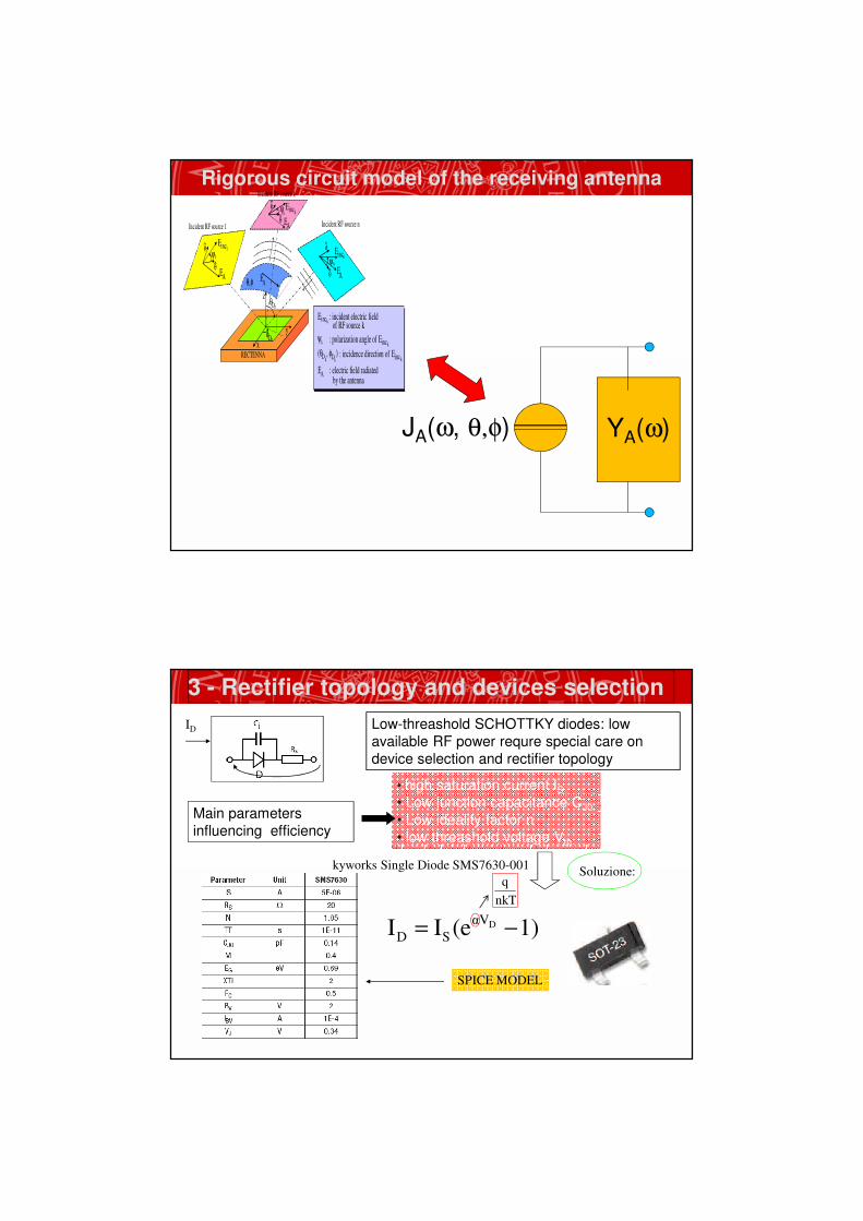
Power management
• The best rectennaperformance depends on optimum loading conditions
• Need for an “optimum resistor emulator”
• Design of a custom power management system and storage
PRF
PRECT_OUT PRECT_OUT
MAX PHARVEST
42 -EuMC02 Sept 29, 2009
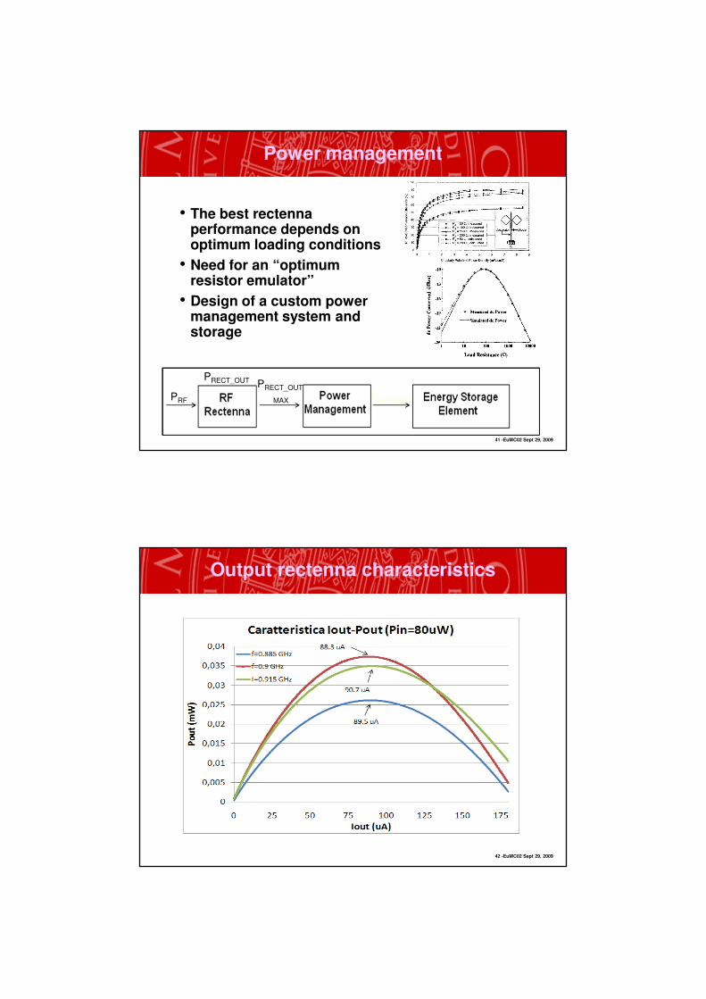
Output rectenna characteristics

10/02/2010
22
43 -EuMC02 Sept 29, 2009
Optimum rectenna load
• a good trade-off for the rectenna load generally occurs in the vicinity of the halved open-circuit DC output voltage
PRF=1
00uW
PRF=1
00uW
44 -EuMC02 Sept 29, 2009
The switch-based converter for dynamically keeping the rectified voltage VRECT around half of its open-circuit value
matchingnetwork
CRECT1
CRECT2
L C
CHOLD C
HOLD +
-
ENABLE
φ
φ
φ
φ
SAMPLEHALF
controlunit
>
ENABLE
HALF
SAMPLE
D1
D2
D3
SW1
SW2
SW3
SW4
rectifier boost converter storageantenna
control
VRECT
VHARVEST
VW
The converter operates in two phases. The converter operates in two phases. 1. When VRECT > VW, Φ is high and an increasing current flows from the
rectenna output through L, SW3 and SW4 while VRECT starts decreasing.
The output capacitor is disconnected.
2. When VRECT < VW, Φ is low and SW1-SW2 are closed. A decreasing
current flows through L, SW1, SW2, D3 onto C, so that VHARVEST rises.
The energy initially stored in L is thus transferred to C. Meanwhile, the
rectenna is disconnected from the converter and VRECT rises because of
the received RF power.
The voltage VW should be periodically updated after many commutations,
(e.g. at the beginning of each time slot of GSM900 standard.)
The boost converter consists of:
• two pairs of synchronous switches
(SW1-SW2, SW3-SW4)
•
•an inductor L, a diode D3
•a storage capacitor C.
•a simple control circuit is used for
driving the switches.
10/02/2010
23
45 -EuMC02 Sept 29, 2009
Rectenna + converter time-domain analysis
0
200
400
600
800
1000
1200
0.0
0.2
0.4
0.6
0.8
1.0
1.2
0 10 20 30 40 50 60 70
Cu
rren
t (u
A)
Vo
lta
ge (V
)
time(us)
VRECT VHARVEST IL
0.0
0.2
0.4
0.6
0.8
1.0
0 100 200 300 400 500
Vo
lta
ge (V
)
time (us)
V_harvest
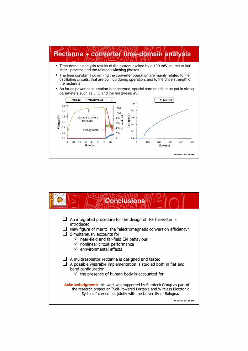
• Time-domain analysis results of the system excited by a 100 mW source at 900 MHz process and the related switching phases.
• The time constants governing the converter operation are mainly related to the oscillating circuits, that are built up during operation, and to the drive strength of the rectenna.
• As far as power consumption is concerned, special care needs to be put in sizing parameters such as L, C and the hysteresis ∆V.
storage process
transient
steady-state
46 -EuMC02 Sept 29, 2009
Conclusions
An integrated procedure for the design of RF harvester is introduced
New figure of merit: the “electromagnetic conversion efficiency” Simultaneusly accounts for
near-field and far-field EM behaviour nonlinear circuit performance ennvironmental effects
A multiresonator rectenna is designed and tested A possible wearable implementation is studied both in flat and
bend configuration the presence of human body is accounted for
Acknowledgment: this work was supported by Eurotech Group as part of the research project on “Self-Powered Portable and Wireless Electronic
Systems” carried out jointly with the University of Bologna.

10/02/2010
24
Challenges RF harvesting researches world-wide
Potenze elevate, ma ottenute in Potenze elevate, ma ottenute in
condizioni non realistichecondizioni non realistiche.Antenna collocata nelle vicinanze di un sistema di
ripetitori radio (campo EM fuori normativa)
Budget di potenza e hardware ambigui Budget di potenza e hardware ambigui Densità di potenza RF incidente a qualche m
dall’hot-spot non compatibile con la potenza
richiesta per la carica del 30% di un Blackberry in
90’. Uso di batterie speciali.
Intel activity
• The researchers powered a wall-mounted
household weather station with an LCD screen
using a TV antenna pointed at a local TV
station.
• The Intel researchers aimed a TV antenna at a
TV station 4 km away, and harvested enough
energy to power a mini weather meter.
• The technology used for this technique is an
extension of that used in off-the-shelf RFID
tags in which the tag reader supplies power to
the otherwise unpowered ID tag.
• With gadgets becoming more and more
energy efficient, the idea of using RF energy
harvesting to power them is closer to
reality...though it will be quite awhile before we
have gadgets on the market powered through
this method.
Details about the experiment:
• The Intel Researchers set up a TV antenna on a balcony with line of sight to the KING-TV tower 4.1 km
away.
• The TV station broadcasts on channel 48 between 674 and 680 MHz with an effective radiation power
(ERP) of 960 Kw.
• The TV antenna used was a UHF log periodic with 5 dBi gain connected to a 4 stage charge pump power
harvesting circuit of the same design as that found in an RFID tag.
• Across an 8 KOhm load the team measured 0.7V, corresponding to 60 microwatts of power harvested.
• That was enough to drive a thermometer/hygrometer and its LCD display, which is normally powered, by
a 1.5 volt AAA battery
Related Documents