ECE 711 Final Report – Winter 2010 Design of Patch Antennas Report by: Tom Zajdel Due date: 3/9/2011

Welcome message from author
This document is posted to help you gain knowledge. Please leave a comment to let me know what you think about it! Share it to your friends and learn new things together.
Transcript

ECE 711
Final Report – Winter 2010
Design of Patch Antennas Report by: Tom Zajdel
Due date: 3/9/2011

2
Introduction
The objective of this project was to design two microstrip patch antennas. The first design was
for a single square patch, and the other design explored microstrip patch arrays. One array was
used to demonstrate the properties of mutual coupling between two patch antennas to determine
the best patch alignment to use in array. The second three-element array was used to improve
directivity of the patch antenna system, and used the results from the exploration with two
patches to minimize mutual coupling.
These antennas were designed for use in a GPS system, so their center frequency was designed
to be 1575 MHz. Microstrip patches were used because they are inexpensive to manufacture and
have a conformal profile suitable for portable devices.
All antenna designs were generated as mesh grids in MATLAB, which were then imported to
NEC-WIN where finite analysis was carried out.
This report will progress by first presenting the design objective of Design 1, the design process
and analysis of the results. Then, the report will detail the design objective of Design 2, and
continue with the design process and analysis of the results of the patch arrays.

3
Design 1: Circularly polarized patch antenna
Design Specification
This design was for a circularly polarized square patch antenna, excited by two orthogonal feeds.
The specifications for this antenna could be summarized as:
1. Operating frequency of 1575 MHz
2. Matched to two 100 Ω coaxial feeds
3. Circularly polarized radiation in the z-axis direction
Figure 1 shows the patch antenna, with all the parameters marked. Parameter h, the height of the
square patch above an infinite PEC ground plane, was set at a constant 12 mm.
Figure 1: Square patch antenna structure (image taken from project statement)
The width of the antenna w and the length of both feeds from the center of the patch d were the
two tunable parameters. Note that the center of the patch antenna was connected to the ground
plane by a grounding pin.
Design Procedure
The basic design procedure was to first estimate the width of the square patch w. Then, the feeds’
magnitudes and phases were specified to best result in circularly polarized radiation. After this,
the location of the feeds was approximated to provide the best matching with the 100 Ω feeds.
These estimated parameters were all fine-tuned using the results of NEC-WIN analysis.

4
Width, w
In order to estimate the length of the patch required, a cavity model was used with antenna
resonance of 1575 MHz. This length can be approximated using equation 1.
Equation 1:
Where fres is the resonant frequency of the antenna (1575 MHz), c0 is the speed of light in a
vacuum, and w is the width of the patch. Since there is no substrate, free space speed of light was
used. In other words, the width of the patch had to be about one half of a wavelength of light.
For this antenna, the nominal width was calculated as:
This nominal width had to be modified, since the antenna was simulated as a mesh grid of wires
in NEC-WIN. This mesh tends to have a lower resonant frequency than a solid patch would. For
this reason, the correction length factor would not be significant, and was not calculated. Thus,
the width was decreased until the antenna was approximately matched to 1575 MHz. This was
accomplished by feeding the antenna at one edge along the y-axis, and simulating for different
patch widths. The results of these plots are shown in Figure 2.
Figure 2: VSWR vs frequency for various widths w
1450 1500 1550 1600 1650 17001
2
3
4
5
6
7
8
9
10
11VSWR vs frequency - 1 feed for various patch widths
Frequency (MHz)
VS
WR
w=95mm
w=85mm
w=75mm

5
A rough cut value of 75 mm was used for the width of the patch, since this selection resulted in
approximate matching at 1575 MHz.
Magnitude and phase of feeds for circular polarization
The condition for circular polarization is that the radiation polarization locus has an equal
magnitude in the x and y-directions, and that these are 90 degrees out of phase from one another.
In the case of these two feeds, Feed 1 is set to produce a wave polarized linearly in the x-
direction, while Feed 2 is set to produce a wave polarized linearly in the y-direction. These two
feeds form orthogonal waves already, so their magnitude and phase must be adjusted.
Recalling the requirements for CP, the two source magnitudes of the feeds had to be the same,
and their phases had to have a difference of 90 degrees. Table 1 shows the conditions used in the
final antenna design.
Table 1: Conditions for voltage sources attached to coax feeds
Feed Magnitude (V) Phase (deg)
1 1.0 0
2 1.0 90
Feed offset, d
Feed offset had to be selected so that the antenna was matched as well as it could be to both
feeds, with characteristic impedance Z0 = 100 Ω. This offset was constrained to be equal for both
feeds to ensure optimal circular polarization of the radiation.
Analytically, this distance could be calculated by using slot conductance and slot resistance
formulas found in Table 14.2 of Balanis. The formula to obtain slot conductance is given as
Equation 2.
Equation 2:
( )
Where G1 is the slot conductance, W is the antenna width (75 mm), is the wavelength
(19.0476 mm), is the wavenumber (0.3299 rad/mm), and h is the height of the patch (12 mm).
This resulted in a slot conductance of:
( )[
( ) ]
Now, input slot resistance can be approximated (assuming no coupling) using Equation 3, also
found in Balanis Table 14.2.

6
Equation 3:
Where Rin is the input slot resistance at the edge of the antenna. Using the value for slot
conductance computed above:
( )
Next, Equation 4, also found in Balanis, Table 14.2, could be used to modify the input resistance
at a feed point other than the patch’s slot.
Equation 4: ( ) (
)
Where ( ) is the resulting input resistance (here we are looking for 100 Ω), Rin is the
input resistance at the edge of the slot, and y0 is the desired feed offset. This formula was used to
calculate the following result:
( ) (
)
( )
= 14.25 mm
Since this is the offset from the slot, the distance from the center d could be calculated with
Equation 5.
Equation 5:
Using this formula, the following d was computed:
This approximation does not account for a second slot’s coupling, but it is a good rough cut.
NEC-Win setup
In order to approximate the patch, a mesh grid was used in MATLAB. This mesh used 10
vertical and 10 horizontal wires to approximate the solid patch. In order to ensure that all the
space was filed between the wires, wire diameter was picked to be 2.0 mm. This thickness would
7
improve the simulation result, but also leave some space between wires (they would not overlap).
The MATLAB code used may be found in the appendix.
Since the grid was discretized, the feeds could not be placed perfectly at 23.35 mm. However, it
was possible to place each feed at a point d = 22.5 mm from the center, since this point formed
an intersection between wires in the grid. This setup was used, and simulated. These two
parameters were tweaked to attempt to improve matching and polarization axial ratio, but these
initial cut parameters proved to be satisfactory.
The final fine-tuned parameters were w = 75 mm, d = 22.5 mm.
Results & Analysis
The antenna was simulated using a frequency sweep from 1450 MHz to 1700 MHz. Various
operation parameters were measured for comparison. The resulting VSWR is plotted below in
Figure 3.
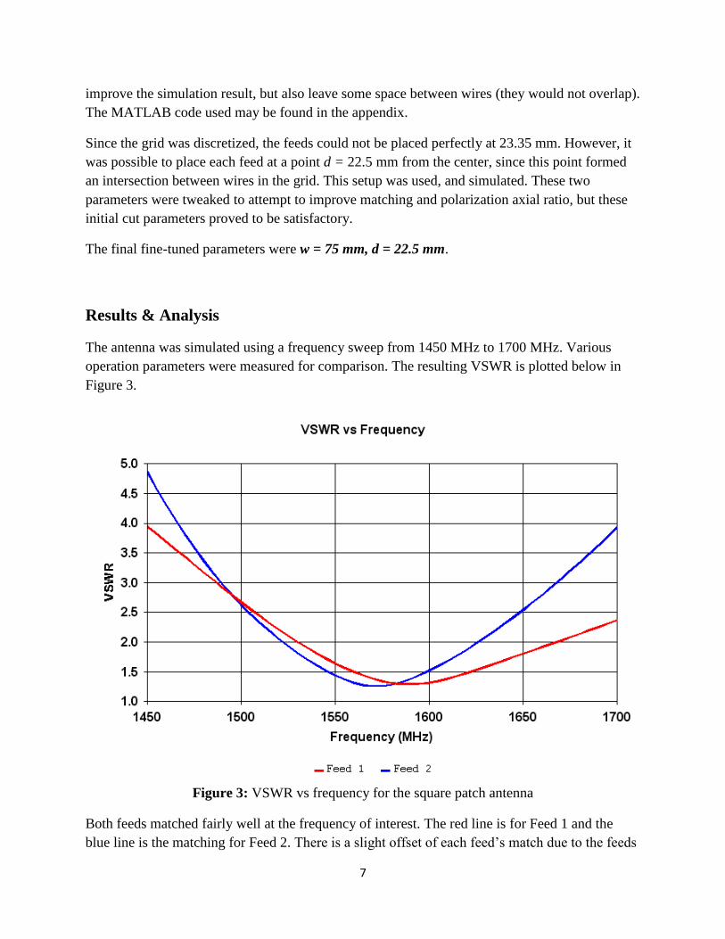
Figure 3: VSWR vs frequency for the square patch antenna
Both feeds matched fairly well at the frequency of interest. The red line is for Feed 1 and the
blue line is the matching for Feed 2. There is a slight offset of each feed’s match due to the feeds

8
being excited 90 degrees out of phase. At 1575 MHz, the VSWR is 1.34 for Feed 1 and 1.26 for
Feed 2. This is rather close to the ideal VSWR of 1.00 for perfect matching.
From this plot, the antenna bandwidth may be determined. By defining bandwidth as the band in
frequencies in which the VSWR ≤ 2 (3 dB power points), the upper frequency bound fU = 1625
MHz, and lower bound fL = 1530 MHz. Using Equation 5, the fractional bandwidth can be
computed.
Equation 6:
This results in a fractional bandwidth of:
This relatively low fractional bandwidth is expected, since the square patch antenna is a highly
resonant (frequency-specific) antenna.
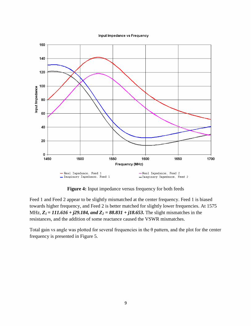
The input impedance for both feeds is plotted against frequency, and is given in Figure 4.
9
Figure 4: Input impedance versus frequency for both feeds
Feed 1 and Feed 2 appear to be slightly mismatched at the center frequency. Feed 1 is biased
towards higher frequency, and Feed 2 is better matched for slightly lower frequencies. At 1575
MHz, Z1 = 111.616 + j29.184, and Z2 = 88.831 + j18.653. The slight mismatches in the
resistances, and the addition of some reactance caused the VSWR mismatches.
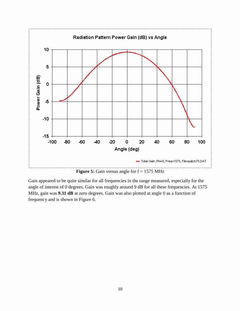
Total gain vs angle was plotted for several frequencies in the θ pattern, and the plot for the center
frequency is presented in Figure 5.
10
Figure 5: Gain versus angle for f = 1575 MHz
Gain appeared to be quite similar for all frequencies in the range measured, especially for the
angle of interest of 0 degrees. Gain was roughly around 9 dB for all these frequencies. At 1575
MHz, gain was 9.31 dB at zero degrees. Gain was also plotted at angle 0 as a function of
frequency and is shown in Figure 6.

11
Figure 6: Gain vs frequency for z-axis
Optimal gain was obtained closest to the center frequency, perhaps with peak results at 1600
MHz, due to non-ideal effects in the design.
Axial ratio was also plotted as another figure of merit for the system. The axial ratio is the ratio
of the magnitude of x-polarization versus y-polarization. In perfectly circular polarized waves,
the AR = 1.0. Any deviation from that implies some elliptical polarization. Axial ratio is plotted
for the antenna operating at its center frequency in Figure 7.
The axial ratio was about 0.79 at the angle of interest of 0 degrees, which corresponds with
observing the wave from the z-axis. This could be seen as a quality measurement, where the
polarization is only about 79% matching with CP. As angle drifts from the z-axis, AR worsens
and worsens, because the observation is no longer in the same plane as the two linear feeds
creating the CP. For this reason, it did not make sense to plot polarization of the phi pattern,
since this pattern is not of main interest. The feeds were designed to create CP in the z-axis
direction, so this is the AR we are interested in. Optimal angle was very close to 0 degrees, with
fluctuations likely caused by discretization of the patch.
1450 1500 1550 1600 1650 17008.5
8.6
8.7
8.8
8.9
9
9.1
9.2
9.3
9.4Gain vs frequency
Frequency (MHz)
Gain
(dB
)

12
Figure 7: Axial ratio vs angle, f = 1575 MHz
In Figure 8, the axial ratio for the z-axis is plotted against frequency. It appears that the optimal
axis ratio of 0.85 was obtained for 1500 MHz. In general, AR performed more poorly as the
frequency deviated from the center frequency. Forcing the feeds to be at a particular point due to
the discretization of the grid prevented the feed wires from being matched the same way at the
center frequency. This is likely leading to the discrepancy between polarizations at the center
frequency. More equivalent matching occurred at 1500 MHz, so there is a more circular
polarization.
In general, these relatively high values for AR (above 0.75) suggest that the feeding system did
work in getting CP. There are some issues with the overall AR quality, but at least the result is
far from linear polarization.

13
Figure 8: AR versus frequency for several frequencies, theta = 0
Finally, the radiation patterns for the antenna were plotted and are given in Figure 9. Figure 9a is
the patch’s E-plane plot and Figure 9b is the patch’s H-plane plot.
The H-plane is biased towards the 135 degree direction due to the positioning of the feeds
towards that quadrant. The E-plane is roughly what would be expected of a patch antenna. There
is no radiated power in the lower half of the E-plane, because of the infinite PEC ground plane
beneath the patch.
From these plots, the half power beam width (HPBW) of each cut can be measured. From
analysis of the plots, HPBWs were determined. For the E-plane, HPBW = 80 , and for the H-
plane, HPBW = 195 . The E-plane was much more directive than the H-plane, which is to be
expected, since a patch antenna typically radiates in the axis normal to the patch’s surface.
1450 1500 1550 1600 1650 1700
0.65
0.7
0.75
0.8
0.85AR vs frequency
Frequency (MHz)
Axia
l R
atio

14
Figure 9: Polar plots of radiation for E-plane (a) and H-plane (b) in dB
15
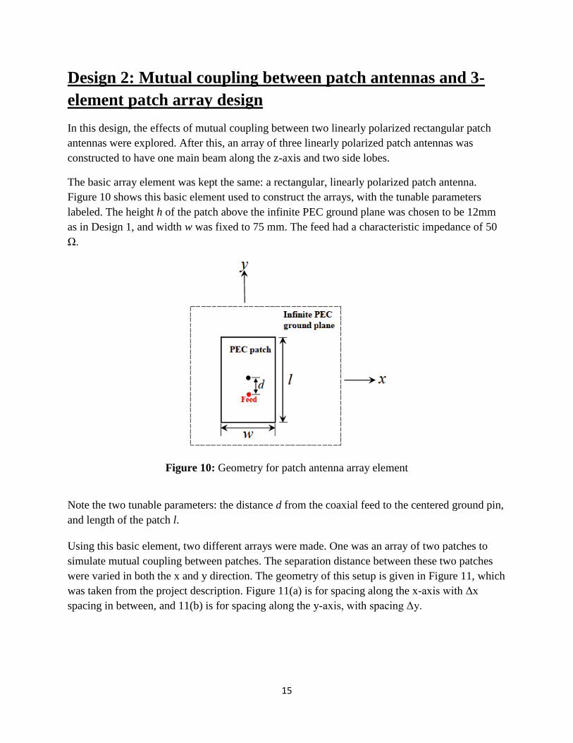
Design 2: Mutual coupling between patch antennas and 3-
element patch array design
In this design, the effects of mutual coupling between two linearly polarized rectangular patch
antennas were explored. After this, an array of three linearly polarized patch antennas was
constructed to have one main beam along the z-axis and two side lobes.
The basic array element was kept the same: a rectangular, linearly polarized patch antenna.
Figure 10 shows this basic element used to construct the arrays, with the tunable parameters
labeled. The height h of the patch above the infinite PEC ground plane was chosen to be 12mm
as in Design 1, and width w was fixed to 75 mm. The feed had a characteristic impedance of 50
Ω.
Figure 10: Geometry for patch antenna array element
Note the two tunable parameters: the distance d from the coaxial feed to the centered ground pin,
and length of the patch l.
Using this basic element, two different arrays were made. One was an array of two patches to
simulate mutual coupling between patches. The separation distance between these two patches
were varied in both the x and y direction. The geometry of this setup is given in Figure 11, which
was taken from the project description. Figure 11(a) is for spacing along the x-axis with Δx
spacing in between, and 11(b) is for spacing along the y-axis, with spacing Δy.

16
Figure 11: 2-element array to test mutual impedance due to spacing (a) in the x-direction and (b)
in the y-direction
After the effect of spacing on mutual impedance was investigated, the second array was made.
This array had the following specifications:
1) Center frequency of 1575 MHz
2) Each element matched to a 50 Ω coax feed
3) Equal linear spacing along the x-axis
4) One main beam along the z-axis, and one side lobe on each side
Figure 12 shows the geometry of this designed array, given in the project specifications.
Figure 12: Three linearly polarized patch antennas, forming an array

17
Design Procedure
The basic design procedure was to first estimate the length of the rectangular patch required to
resonate at the center frequency of 1575 MHz. Then, the offset of the feed from the antenna’s
center was calculated to perform a nominal design. The matching of the patch to a 50 Ω feed was
optimized, and then the experiment with mutual coupling was performed. After this, the array
factor of a linear array was calculated, and the array was simulated in NEC-Win.
Length, l
First, the length of the patch element had to be calculated. This was done using Equation 1 to
obtain the nominal length of the patch. As was calculated for the width for Design 1, this was
found to be .
Since there were fringing fields at the edge of each side of the patch, and the width of the
antenna is fixed, a correction factor added to the length l that was nominally calculated by
Equation 1. The fringing fields effectively lengthen the patch, so this correction length must be
subtracted from the nominal length. As a first step to the correction calculations, the effective
dielectric constant was calculated using Equation 7.
Equation 7: ( )
√
Where is the effective relative dielectric constant, and is the relative dielectric constant of
the substrate, 1 in this case since the substrate is free space. Since , the calculated = 1.
With the effective relative dielectric, the correction length can be computed using Equation 8.
Equation 8: ( )(
)
( )(
)
Where is the correction length. Using this formula, the correction length was calculated as:
( )( ) (
)
( ) ( )
Since the correction length affects the nominal length on both sides, twice must be subtracted
from the computed l. This results in a computed length of l = 79.26 mm.

18
Feed offset, d
The feed offset had to be selected that resulted in an input impedance of 50 Ω to match the coax
feed. This offset was calculated using the same procedure as in Design 1. This required the use
of Equations 2, 3, 4, and 5.
Using Equation 2, slot conductance was computed:
( )[
( ) ]
Using Equation 3, the input resistance was calculated as before:
( )
Using Equation 4, the offset was calculated as:
( ) (
)
( )
= 24.29 mm
Using Equation 5, the following d was computed:
So the nominal feed offset for the antenna element for 50 Ω matching is d = 15.34 mm.
NEC-Win setup
In order to approximate the patch, a mesh grid was used in MATLAB. This mesh used 10
vertical and 10 horizontal wires to approximate the solid patch, with wire diameter 2.0 mm as in
Design 1.
The feed point was placed at a grid intersection point closest to the nominal d of 15.34 mm to
improve the simulation results. This restriction made the actual d used 15.852 mm. This value
was tuned until the real part of the impedance of the patch was 50 Ω. After some tuning of d, the
VSWR was reduced to an acceptable value. Here, VSWR = 1.35, Zin = 48.177 + j14.187 Ω,
which is close to the desired Zin of 50 Ω.
The final fine-tuned parameters for this patch element were l = 79.26 mm, d = 23.778 mm.

19
The VSWR for this patch was plotted versus frequency, to reinforce these results. The plot is
presented in Figure 13.
Figure 13: VSWR versus frequency for the basic array patch element
The VSWR has its minimum close to 1575 MHz. The fractional bandwidth of this element is
6.98%.
Alignment of patches to minimize mutual coupling
Mutual coupling comes about when the electric field from one patch induces current in the
second patch. The closer two patches are together, the more coupling that results. In order to
make the best array, the patches should be aligned to minimize mutual coupling, since mutual
coupling affects the input impedance of the array.
There are two options for the alignment of the patches: along the x-axis, and along the y-axis
(see Figure 11). The field that results by aligning the feeds along the y-axis, as stated by the
design objective section, the radiated electric fields in the resonant l direction are polarized
linearly.

20
This means that the electric field radiated is mostly polarized in the y-direction. This means that
more coupling occurs in the y-direction. As a consequence of this, the patches ought to be
aligned along the x-axis to minimize mutual coupling between the antenna elements. This
would result in an array that looks like the one shown in Figure 12.
Mutual coupling versus separation simulation
In NEC-Win, the two-patch arrays were implemented to confirm through simulation the
conclusion reached in the previous section, that aligning the patches on the x-axis would reduce
the mutual coupling between the patches and result in an improved final array design.
Data was collected for separation varying from 0 to 2 wavelengths between the patches, in both
the x and y-directions. At each separation, the total input impedance at one patch was recorded,
with uniform unit current source excitation. Then, the total impedance was recorded with one
current source fed with a negative unit current. These two results can be used in conjunction with
Equation 9, which shows the equation for mutual impedance.
Equation 9:
Where Z11 is self-impedance of patch 1, Z12 is the mutual impedance, I1 is the current fed to
patch 1, and I2 is the current fed to patch 2. If the total impedance recorded from the results of
one simulation, with current sources (I1, I2) = (1,1), is called Za, and the total impedance recorded
from the (I1, I2) = (1,-1) case is called Zb, the following derivation results in an expression that
may be used to find mutual impedance:
( )
( )
This expression was used for every two points, and the results were recorded and plotted
Figure 14 shows the calculated results of mutual impedance versus separation width in the x-
direction, and Figure 15 shows mutual impedance versus separation in the y-direction.
Notice that in general, the mutual impedance was highest when the two patches were closest
together. As the patches were separated more, mutual impedance generally decreased to a
relatively constant rate (the results fluctuated above and below this point).

21
Figure 14: Mutual impedance versus separation in x-direction
For the x-direction, mutual impedance was rather small and did not contribute much to the total
impedance, after a short separation distance. This mutual impedance proved to be predictably
low. The impedance was largely capacitive until the coupling level tended towards zero as
distance increased.
In the y-direction, the mutual impedance was higher than the patches separated along the x-
direction after a certain point (roughly 0.5 separation). This shows that as predicted, the coupling
between patches in the y direction (after some distance) would be higher. This is because both
patches were fed in the y-direction. Higher coupling leads to more interaction between the fields
of the two patches, and therefore the mutual impedance increases substantially.
As the separation distance was increased, the mutual impedance eventually decreased,
fluctuating around and very close to zero. The separation distance required for minimal coupling
was much lower for the x-direction spacing, so the elements in the 3-patch linear array ought to
be spaced along the x-axis. This would make impedance matching with the coaxial feeds much
more possible.
0 0.5 1 1.5 2
-50
-40
-30
-20
-10
0
10
x/
Mutu
al im
pedance (
)
Zmutual
vs x
Rmutual
Xmutual

22
Figure 15: Mutual impedance versus separation in y-direction
Array Factor design
In the final design, a 3-element patch antenna was to be used to generate a pattern with one main
beam along the z-axis and two side lobes on each side. The array was chosen to be a uniformly
excited, linearly spaced array.
Since the pattern of a uniform array is a scaling between the power pattern of one element with
the array factor, it would be useful to observe the radiation pattern of a single patch element in
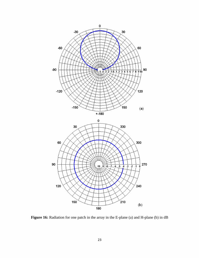
this array. The radiation of one patch is given in Figure 16, for both the E and H-plane cuts.
Notice the gain for the antenna in the direction of interest (along the z-axis) is just over 9 dB.
This patch also is omnidirectional in the H-plane. This radiation pattern is well suited for
combination with an array factor to increase its directivity.
0 0.5 1 1.5 2
-20
-15
-10
-5
0
5
10
15
y/
Mutu
al im
pedance (
)
Zmutual
vs y
Rmutual
Xmutual
23
Figure 16: Radiation for one patch in the array in the E-plane (a) and H-plane (b) in dB
24
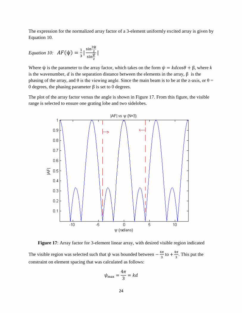
The expression for the normalized array factor of a 3-element uniformly excited array is given by
Equation 10.
Equation 10: ( )
Where is the parameter to the array factor, which takes on the form , where k
is the wavenumber, is the separation distance between the elements in the array, is the
phasing of the array, and θ is the viewing angle. Since the main beam is to be at the z-axis, or θ =
0 degrees, the phasing parameter is set to 0 degrees.
The plot of the array factor versus the angle is shown in Figure 17. From this figure, the visible
range is selected to ensure one grating lobe and two sidelobes.
Figure 17: Array factor for 3-element linear array, with desired visible region indicated
The visible region was selected such that was bounded between
to
. This put the
constraint on element spacing that was calculated as follows:

25
Thus, the spacing required between patches in this array (center frequency 1575 MHz) would be
d = 126.984 mm. Therefore, the spacing between patches in this array was chosen as
The radiation patterns resulting from this plot are shown in Figure 18. This pattern is the power
pattern, so it is the array factor squared times the single element pattern. The array increased the
gain of the patch antenna to 14 dB. The two sidelobes in the pattern are also visible.
The HPBW of the main beam in the H-plane was 30 degrees, and the HPBW of the main beam
in the E-plane was about 30 degrees as well. This array was quite more directive than a single
patch alone was.
The antenna was matched fairly well. Table 2 shows the matching for the three feeds, by
tabulating the real input impedance (Rin), imaginary input impedance (Xin), and voltage standing
wave ratio (VSWR).
Table 2: Matching of 3-patch array antenna to 50 Ω coax feeds
Feed Rin Xin VSWR
1 54.266 18.943 1.45
2 50.743 17.099 1.40
3 50.743 17.099 1.40
The axial ratio of the antenna at the center frequency was a constant 0.0, which implied perfect
linear polarization, as was expected.
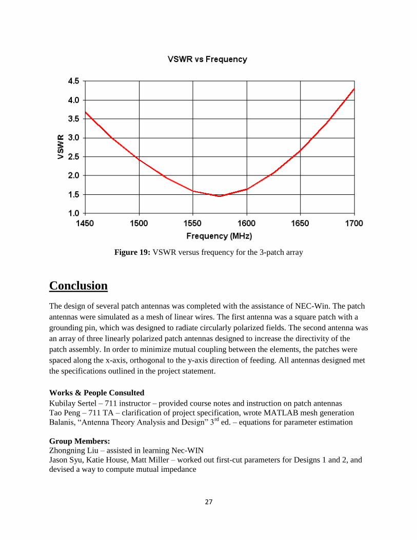
VSWR was also plotted against frequency for the three feeds to gain an estimation of the
fractional bandwidth of the antenna. The plot is provided in Figure 19. From this graph, the
fractional bandwidth could be determined as 6.3%. This bandwidth is still relatively small,
because patch antennas are highly resonant.

26
Figure 18: Radiation for 3-patch array in the E-plane (a) and H-plane (b) in dB
27
Figure 19: VSWR versus frequency for the 3-patch array
Conclusion
The design of several patch antennas was completed with the assistance of NEC-Win. The patch
antennas were simulated as a mesh of linear wires. The first antenna was a square patch with a
grounding pin, which was designed to radiate circularly polarized fields. The second antenna was
an array of three linearly polarized patch antennas designed to increase the directivity of the
patch assembly. In order to minimize mutual coupling between the elements, the patches were
spaced along the x-axis, orthogonal to the y-axis direction of feeding. All antennas designed met
the specifications outlined in the project statement.
Works & People Consulted
Kubilay Sertel – 711 instructor – provided course notes and instruction on patch antennas
Tao Peng – 711 TA – clarification of project specification, wrote MATLAB mesh generation
Balanis, “Antenna Theory Analysis and Design” 3rd
ed. – equations for parameter estimation
Group Members:
Zhongning Liu – assisted in learning Nec-WIN
Jason Syu, Katie House, Matt Miller – worked out first-cut parameters for Designs 1 and 2, and
devised a way to compute mutual impedance

28
APPENDIX A: MATLAB CODE
% This script was written by 711 TA Tao Peng to generate one mesh % modifications, copies, source specifications, and translations to this % mesh were all added in the NEC-Win wizard.
%L: patch length in the y axis; %W: patch width in the x axis; %H: patch height in the z axis; %NL: the number of wires in the y axis in the wire grid model; %NW: the number of wires in the x axis in the wire grid model; %seg: the number of segments for each wire; %rr: the radius of each wire; L=75; W=75; H=12; NL=10; NW=10; seg=2; rr=1.0; x=-(W/2):(W/NW):(W/2); y=-(L/2):(L/NL):(L/2); z=H;
fp=fopen('patch_geometry.nec','w'); fprintf(fp,'CM\n'); fprintf(fp,'CM\n'); fprintf(fp,'CM\n'); fprintf(fp,'CE\n');
t = 1; for m = 1:NL for n = 1:NW fprintf(fp, 'GW %8.0f %8.0f %8.3f %8.3f %8.3f %8.3f %8.3f %8.3f %8.3f\n',
... t, seg, x(n), y(m), z, x(n+1), y(m), z, rr); t=t+1; fprintf(fp, 'GW %8.0f %8.0f %8.3f %8.3f %8.3f %8.3f %8.3f %8.3f %8.3f\n',
... t, seg, x(n), y(m), z, x(n), y(m+1), z, rr); t=t+1; end fprintf(fp, 'GW %8.0f %8.0f %8.3f %8.3f %8.3f %8.3f %8.3f %8.3f %8.3f\n',
... t, seg, x(NW+1), y(m), z, x(NW+1), y(m+1), z, rr); t=t+1; end for n = 1:NW fprintf(fp, 'GW %8.0f %8.0f %8.3f %8.3f %8.3f %8.3f %8.3f %8.3f %8.3f\n',
... t, seg, x(n), y(NL+1), z, x(n+1), y(NL+1), z, rr); t=t+1; end fprintf(fp, 'EN\n'); fclose(fp);
Related Documents