Opt Quant Electron DOI 10.1007/s11082-011-9452-0 Anode material based on SWCNT for infrared quantum dot light-emitting devices Ahmed E. Farghal · S. Wageh · Atef Abou El-Azm Received: 29 August 2010 / Accepted: 15 March 2011 © Springer Science+Business Media, LLC. 2011 Abstract We present an optical model based on Green’s function to investigate the effect of using single-wall carbon nanotube (SWCNT) as anode for infrared quantum dot light-emitting devices (IR QD-LEDs). To the best of our knowledge, there is no report in using SWCNT as anode in IR QD-LEDs. We have studied the emitted power distribution among the dif- ferent optical modes (external propagating mode (photon outcoupling efficiency), substrate, anode/organics, and surface plasmon modes (SP)), angular intensity distribution, viewing angle effect on the optical characteristics, and the emission spectral characteristics. We have found that the light outcoupling efficiency of IR QD-LEDs based on SWCNT as anode was increased nearly by a factor of 4 relative to that one based on indium-tin oxide (ITO). We also investigated the effect of using different cathode materials on the optical characteristics of IR QD-LEDs. Keywords Light-emitting devices · PbSe quantum dot · SWCNT 1 Introduction Indium-tin oxide (ITO) has been dominantly used as transparent electrode for decades in flat panel displays, solar cells, organic light-emitting diodes (OLED), and quantum dot organic light-emitting diodes (QD-LED), due to its excellent transparency and relatively high conduc- tivity. ITO is a highly degenerate n-type semiconductor with a wide band gap semiconductor ( E g : 3.5–4.7 eV) (Kim et al. 1999; Li et al. 2006) and has a low electrical resistivity A. E. Farghal · S. Wageh (B ) · A. Abou El-Azm Faculty of Electronic Engineering, Menufiya University, Menouf 32952, Egypt e-mail: [email protected] A. E. Farghal e-mail: [email protected] A. Abou El-Azm e-mail: atef_abuelazm@menofia.edu.eg 123

Welcome message from author
This document is posted to help you gain knowledge. Please leave a comment to let me know what you think about it! Share it to your friends and learn new things together.
Transcript
Opt Quant ElectronDOI 10.1007/s11082-011-9452-0
Anode material based on SWCNT for infrared quantumdot light-emitting devices
Ahmed E. Farghal · S. Wageh · Atef Abou El-Azm
Received: 29 August 2010 / Accepted: 15 March 2011© Springer Science+Business Media, LLC. 2011
Abstract We present an optical model based on Green’s function to investigate the effect ofusing single-wall carbon nanotube (SWCNT) as anode for infrared quantum dot light-emittingdevices (IR QD-LEDs). To the best of our knowledge, there is no report in using SWCNTas anode in IR QD-LEDs. We have studied the emitted power distribution among the dif-ferent optical modes (external propagating mode (photon outcoupling efficiency), substrate,anode/organics, and surface plasmon modes (SP)), angular intensity distribution, viewingangle effect on the optical characteristics, and the emission spectral characteristics. We havefound that the light outcoupling efficiency of IR QD-LEDs based on SWCNT as anode wasincreased nearly by a factor of 4 relative to that one based on indium-tin oxide (ITO). Wealso investigated the effect of using different cathode materials on the optical characteristicsof IR QD-LEDs.
Keywords Light-emitting devices · PbSe quantum dot · SWCNT
1 Introduction
Indium-tin oxide (ITO) has been dominantly used as transparent electrode for decades in flatpanel displays, solar cells, organic light-emitting diodes (OLED), and quantum dot organiclight-emitting diodes (QD-LED), due to its excellent transparency and relatively high conduc-tivity. ITO is a highly degenerate n-type semiconductor with a wide band gap semiconductor(Eg : 3.5–4.7 eV) (Kim et al. 1999; Li et al. 2006) and has a low electrical resistivity
A. E. Farghal · S. Wageh (B) · A. Abou El-AzmFaculty of Electronic Engineering, Menufiya University, Menouf 32952, Egypte-mail: [email protected]
A. E. Farghale-mail: [email protected]
A. Abou El-Azme-mail: [email protected]
123

A. E. Farghal et al.
of 2–4 × 10⁻⁴� cm. ITO shows good transmission in the visible and near-infrared (NIR)regions of the electromagnetic spectrum. Furthermore, ITO has also shown good efficiencyfor hole injection into organic materials.
However, ITO has several limitations for current and future generation LEDs. It has limitedchemical stability leading to diffusion of oxygen into proximate organic layers, relatively lowwork functions (∼4.7 eV), also, its increasingly expensive due to the limited worldwide pro-duction of indium which may soon find difficulty meeting the ever increasing demand forlarge-scale transparent conductive electrodes (Li et al. 2006; Zhang et al. 2006). ITO is rel-atively brittle, which degrades its performance on flexible substrates (Green and Hersam2008). Strong free-carrier absorption of infrared (IR) photons, which limits the device photogenerated current in thin film photovoltaic (PV) devices (Contreras et al. 2006). Also, ITOshows high reflectivity in the IR region (Kim et al. 1999) and only transmits 70% at 1,500 nm(Steckel 2003).
New transparent electrodes are needed in QD-LED to provide higher transmittance inthe IR portions of the spectrum. In response to these limitations, SWCNTs have receivedincreasing attention as ITO alternatives (Li et al. 2006; Green and Hersam 2008).
The SWCNT networks have a work function in the 4.7–5.2 eV range. Such high workfunction meets the requirement for anodes in several types of optoelectronic devices, suchas OLED and organic solar cells. In addition, the nanotube films have large surface areadue to the nanoporous structure which offer a potential for hole injection. Also, exceptionalmechanical flexibility of SWCNT, the nanotube was repeatedly deformable over 100% strainwithout causing a substantial change in conductance. Ordinary conductors cannot undergonearly such large strains without losing electrical contact with the actuating material (Li et al.2006; Zhang et al. 2005).
On the other hand, SWCNT film fabrication on a flexible substrate is relatively simple,while ITO deposition on flexible substrates requires vacuum and elaborate process equipment(Li et al. 2006; Zhang et al. 2006).
The SWCNT-based electrodes are highly conductive in thin layers, and optical mea-surements indicate superior optical transmission (>80%) in the IR (wavelengths > 1,200 nm)compared to traditional ITO, in addition to the absence of free-carrier absorption in that region(Contreras et al. 2006). These characteristics of SWCNT layer are a significant qualitativedifference as compared to ITO. The SWCNT-based transparent electrodes have already beenused in photovoltaic and OLEDs (Li et al. 2006; Zhang et al. 2006; Contreras et al. 2006;Weeks et al. 2006). However, to the best of our knowledge, they have not been employed inIR QD-LEDs. Here, we will study theoretically the effect of using SWCNT film as anode incomparison with ITO film on the optical characteristics of IR QD-LEDs.
The simulations presented in this work are based on the Poynting vector analytical expres-sion developed by Celebi et al. (2007) and followed our computations for the IR QD-LEDs(Farghal et al. 2010). Several other approaches for the simulation of OLEDs have beendescribed in the literatures; for example, the radiative transfer approach which allows oneto compute only the color (Crawford 1988; Bulovic et al. 1998) model which enables oneto compute accurately the intensity, but only for simple device structures, Fermi’s goldenrule (Kahen 2001) which compute both the radiative and internal intensities, however, thevalidity of that approach is limited to lossless devices, and does not account for nonradia-tive losses to the metal electrodes or absorption, wave optics and transfer matrix formalism(Chen et al. 2006), but they cannot be directly applied to OLEDs, because OLED uses athick glass substrate, which results in computational difficulty, and the scheme described byKahen (2001), is rigorous but not efficient, since the calculation involves the evaluation of thesommerfeld-like integral which requires careful selection of the integration path, in addition,
123

Anode material based on SWCNT
accurate computation of the far-field at a large viewing angle is inefficient due to the rapidoscillating nature of Bessel function with the large argument. While the model presentedhere is straightforward model without numerical difficulties, it takes into account the surfaceplasmon modes and absorption in different layers.
This article is organized as follows; the theoretical model is given in Sect. 2. The simula-tion results and the related discussion are presented in Sect. 3. Finally, conclusions are drawnin Sect. 4.
2 Theory
The radiation field is described by constructing a Green’s function for the multilayer mediumcontaining the exciton, and the total radiative energy is calculated by integrating the Poyn-ting vector over the magnitude of the normalized in-plane wavevector which varies fromzero to infinite. Assuming that the QDs emitting layer contains the exciton radiators withrandom orientations, it can be decomposed into the vertical and horizontal exciton compo-nents. Therefore, we can compute the total radiation intensity by adding the vertical andhorizontal exciton components. The vertical exciton power in each layer is given by Celebiet al. (2007):
PVz, j = �
(∫SV ∗
z, j dA
)= 3q
4�
⎡⎣
∞∫0
duu3
(√ε j
)∗∣∣1−u2
∣∣ √ε j
√(ε j/ε5−u2
) (R′
j eih j z−R j e
−ih j z)
∗(
R′j e
ih j z + R j e−ih j z
)](1)
and for an exciton oriented horizontal, the power is:
P Hz, j = �
(∫SH∗
z, j dA
)
= 3q
8�
⎡⎣
∞∫0
duu
(√ε j
)∗√
ε j
√(ε j/ε5−u2
) (R′
j eih j z−R j e
−ih j z) (
R′j e
ih j z+R j e−ih j z
)∗
+∫
duu
(√(ε j/ε5 − u2
))∗
∣∣1 − u2∣∣
(T ′
j eih j z + Tj e
−ih j z) (
T ′j e
ih j z − Tj e−ih j z
)∗⎤⎥⎦ (2)
where PVz, j and P H
z, j are the vertical and horizontal exciton power at each layer, respectively.
SVz and SH
z are the Poynting vectors in the Z direction for vertical and horizontal exciton,
respectively. h j =√
k2j − K 2, k2
j = ε j (ω/c)2 , h j and K are the amplitudes of the horizon-
tal and vertical components of the propagation vector, k. ε j represents the complex dielectricconstant, and j is the layer index. ε5 is the average dielectric constant for QD layer (emis-sion layer). u = K/k5 is the normalized in-plane wavevector at QD layer location. q isthe intrinsic quantum yield of the QD emitting material. The coefficients Tj , R j and T ′
j , R′j
correspond to the upward and downward traveling eigenfunctions, respectively, which arefounded by applying boundary conditions that the tangential electric fields are continuousacross the interface between layers and the radiation conditions.
123

A. E. Farghal et al.
The effective dielectric constant of the QD layer is computed as followed Drndic et al.(2002):
ε5 = εo + 4√
2π
3
(εq(λ) − εo
) [R
2R + d
]3
(3)
where εo is the dielectric constant of the organic material, εq is the dielectric constant ofthe PbSe QD which is wavelength dependant (Palik 1985), R is the QD radius, and d is thesurface-to-surface separation between QDs.
The exciton power transfer efficiency to an individual layer as a unitless percentage of thetotal power emitted is found by taking the difference in the magnitude of this flux found atboth boundaries of the layer and then normalizing it to bV or bH . Where bV is the normalizeddecay rate for oscillating exciton oriented vertical in infinite medium, which is given by Procket al. (1978):
bV = 1 − q + 3
2q
⎧⎨⎩1 + 3
2�
⎡⎣
∞∫0
dKK 3
h5 K 35
(R5 + R′
5
)⎤⎦
⎫⎬⎭ (4)
and bH is the normalized decay rate for oscillating exciton oriented horizontal in infinitemedium, and given by:
bH = 1 − q + q
⎧⎨⎩1 + 3
4�
⎡⎣
∞∫0
dKK
h5 K5
(T5 + T ′
5 + h25
K 22
R5 + R′5
)⎤⎦
⎫⎬⎭ (5)
The fraction of the generated power can be divided into four different optical modes:direct transmission into the air mode, the glass total internal reflection mode, anode/organicwaveguided mode, and plasmon mode in terms of the wavenumber ko. Of this generatedpower, that fraction within the range 0 ≤ K ≤ 2πnair/λ corresponds to the external modesof the QD-LED structures capable of producing useful far filed radiation.
In the case of plane waves propagating through multilayers, an emitting angle θair in theair region associated with K and wavevector ko = 2πnair/λ, according to the formula ofko sin θair = K . The power in the K space can be transformed to a power in the real spatialspace. The intensity angular distribution is related to the power P by
I (θair) = P(K )
2π tan(θair)(6)
where P(K ) is 13 PV
z, j + 23 P H
z, j for isotropic exciton power emitted in air as a function of K .The device used in our calculation is depicted in Fig. 1 and consists of a glass substrate,
(160 nm) ITO anode, (40 nm) 4,4-bis[N -(1-naphthyl)-N -phenyl-amino]biphenyl (α-NPD)as hole-transporting organic layer, (20 nm) PbSe QD monolayer as emitting layer radi-ates typically at 1.55µm, (40 nm), tris-(8-hydroxyquinoline) aluminum (Alq3) as electron-transporting layer (ETL), and metal cathode (50 nm thick Mg:Ag, by weight, 50 nm Ag cap).The device shown in Fig. 1b is the same structure but with replacement ITO by (160 nm)CNT layer as anode. Optical constants of Alq3 and α-NPD are taken from Himcinschi et al.(2005), optical constants of ITO and Mg:Ag are taken from Palik (1985) and refractive indexof SWCNT n is taken the value of graphite (Palik 1985; Wang 2004).
123

Anode material based on SWCNT
Fig. 1 The schematic of the IR QD-LED device structure used in calculations for a ITO/α-NPD/PbSeQD/Alq3/Mg:Ag/Ag and b CNT/α-NPD/PbSe QD/Alq3/Mg:Ag/Ag. The scheme attached to b to illustratethe exciton position in the emitting layer
3 Results and discussions
We have investigated the effect of changing the position of the emitting exciton within theemission QD layer on the coupling strength to different optical modes and on outcouplingefficiency of the device. We have computed the distribution of emitted IR radiation at 1.55µmfrom QD-LED as a function of the exciton position within the emitting layer. Here, we con-sidered the emitting QDs packed regularly with 5 nm diameter and center-to-center distanceequal 5 nm. In addition, we assumed that the exciton lies in the middle of every QD as shownin Fig. 1.
The exciton power transfer efficiency to an individual layer and photon outcoupling effi-ciency as a unit-less percentage of the total power emitted is found by taking the differencein the magnitude of the flux found at boundaries of the layer and then dividing it by bV
or bH .Figure 2a, b shows the distribution of light emission at 1.55μm for glass/ITO/α-NPD/PbSe
QD/Alq3/Mg:Ag/Ag QD-LED and glass/SWNT/α-NPD/PbSe QD/Alq3/Mg:Ag/Ag QD-LED as a function of the exciton position within the QDs layer. The fraction of powerthat coupled in the anode layer for the two devices is largely dependent on the emittingcenter position within the emitting QD layer and increases with increasing the distance fromthe metal cathode. If the emitting exciton is close to the cathode, most of the power is cou-pled into SP modes. On the other hand, for the device based on SWCNT anode, there is asignificant increase in the external emission (photon outcoupling efficiency) and decreasein the anode/organics modes as compared to the device based on ITO anode. The increasein these modes leads to increasing outcoupling efficiency. The outcoupling efficiency of thedevice based on SWCNT anode improved more than 3.99 times relative to the device basedon ITO anode. We attributed the improvement in the outcoupling efficiency to the superiorIR transmission of CNT compared to ITO (Contreras et al. 2006), also the high refractiveindex of SWCNT (n ∼ 1.99 at 1,550 nm) which lower the mismatch with high refractiveindex PbSe QD (n ∼ 4.6) (Wehrenberg et al. 2002).
Figure 3 shows a comparison between the effects of varying the wavelength on the opti-cal characteristics of IR QD-LED based on ITO anode (Fig. 3a, b) and IR QD-LED basedon CNT as anode (Fig. 3c, d). It is clear that the device based on CNT has a noticeable
123

A. E. Farghal et al.
Fig. 2 Calculated distribution of emission into the four optical modes versus the exciton distance from thecathode with using different anodes. a ITO anode b SWCNT anode
improvement on the outcoupling efficiency at longer wavelengths, while that one based onITO has a good performance at lower wavelengths.
Figure 4 shows the angular radiation profile of isotropic exciton emission for glass/ITO/α-NPD/PbSe QD/Alq3/Mg:Ag/Ag QD-LED and glass/SWCNT/α-NPD/PbSe QD/Alq3/Mg:Ag/Ag QD-LED. For the device based on ITO anode, the angular radiation profile isnot Lambertian and the light is stronger beaming in the forward direction. While for thedevice based on SWCNT anode, the angular radiation profile is approximately Lambertian,which is consistent with the previously reported results for IR QD-LEDs (Tessler et al. 2002;Bourdakos et al. 2008). We ascribed the non-Lambertian profile of the device based on ITOanode due to the large refractive index mismatch in the IR region between PbSe QD (n ∼ 4.6)and ITO (n ∼ 0.5).
In Fig. 5, we show the effect of varying the anode layer thickness on the fraction of exci-ton emitted power coupled into the four optical modes. Clearly, the external mode is lessaffected by anode thickness variation for the device based on SWCNT (Fig. 5a), but for thedevice based on ITO anode, the fractional of external mode (photon outcoupling efficiency)is decreased with increasing the anode thickness (Fig. 5b). We ascribed this result to con-stancy of the SWCNT transmission with thickness in IR region (Zhang et al. 2006). Theanode/organics and SP modes are less affected by the variation in the SWCNT thickness.But for the device based on ITO anode, the effect of anode thickness variation on the
123

Anode material based on SWCNT
Fig. 3 Average calculated fractions of power emitted in each optical mode for IR QD-LED based on ITOanode at a 1,550 nm and at b 1,300 nm and for IR QD-LED based on CNT anode at c 1,550 nm and at d1,300 nm
Fig. 4 Radiation profiles of the isotropic exciton sources of NIR QD-LED structure at λ = 1.55µm withdifferent anodes. a ITO anode and b SWCNT anode
anode/organics and SP modes is only remembered at very low anode thickness. We shouldbear in mind; the thickness of anode layer of the device not only affects the optical charac-teristics but also affects the electrical characteristics.
123

A. E. Farghal et al.
Fig. 5 Simulation results of the power fraction coupled into the four optical modes versus anode layer thick-ness variation for the QD-LED with different anodes. a ITO anode and b SWCNT anode
Figure 6a, b shows the variation in the fraction of the power coupled to the four opti-cal modes as a function of QD diameter for the two devices based on ITO and SWCNTas anodes, respectively. As shown in Fig. 7, the emission wavelength changes with the QDdiameter (quantum size effect), consequently dielectric constant change as its wavelengthdependent. Furthermore, there is a small change in the average dielectric constant of themedium containing the QDs with changing the QD size.
Obviously, at smaller QD sizes, the external emission (photon outcoupling efficiency) ishigher for the device based on ITO relative to that one based on SWCNT anode. Conversely,at larger QD sizes, the external emission for the device based on SWCNT becomes supe-rior relative to the device based on ITO anode. We attributed this result to the increase in
123

Anode material based on SWCNT
Fig. 6 Simulation results of the power fraction coupled into the four optical modes as a function of QDdiameter (nm) for QD-LED with different anodes. a ITO anode b SWCNT anode
transmission coefficient for the SWCNT and decrease in transmission coefficient for ITOat higher wavelengths. We also note that the anode/organic modes are greatly suppressedwhen using SWCNT as anode. Our computations also showed that a considerable amountof radiation is trapped inside the glass substrate and in the SP modes in the case of SWCNT,but the improvement in the external modes is significant.
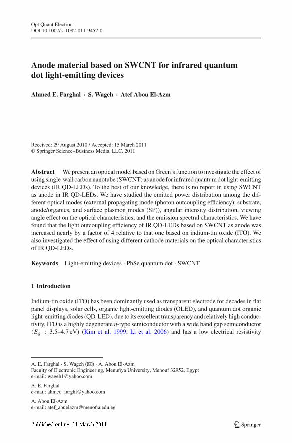
Figure 7 shows the experimental measurements of the position of the first absorptionpeak versus the diameter of semiconductor QD (Steckel 2003). The figure demonstrates thewavelength tunability afforded by controlling the QD size (quantum confinement effect).
123
A. E. Farghal et al.
Fig. 7 Diameter of semiconductor QDs versus the position of the first absorption peak. Data were taken fromSteckel (2003)
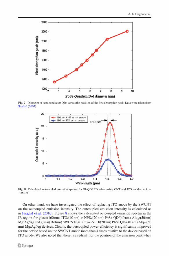
Fig. 8 Calculated outcoupled emission spectra for IR-QDLED when using CNT and ITO anodes at λ =1.55µm
On other hand, we have investigated the effect of replacing ITO anode by the SWCNTon the outcoupled emission intensity. The outcoupled emission intensity is calculated asin Farghal et al. (2010). Figure 8 shows the calculated outcoupled emission spectra in theIR region for glass/(160 nm) ITO/(40 nm) α-NPD/(20 nm) PbSe QD/(40 nm) Alq3/(50 nm)Mg:Ag/Ag and glass/(160 nm) SWCNT/(40 nm) α-NPD/(20 nm) PbSe QD/(40 nm) Alq3/(50nm) Mg:Ag/Ag devices. Clearly, the outcoupled power efficiency is significantly improvedfor the device based on the SWCNT anode more than 4 times relative to the device based onITO anode. We also noted that there is a redshift for the position of the emission peak when
123
Anode material based on SWCNT
Fig. 9 Simulation results of outcoupled power emission spectra at λ = 1.5µm with various cathode metalsfor the device based on a SWCNT anode b ITO anode
using SWCNT as anode instead of ITO anode. This redshift is due to the large refractiveindex of CNT compared to that of ITO in the IR region.
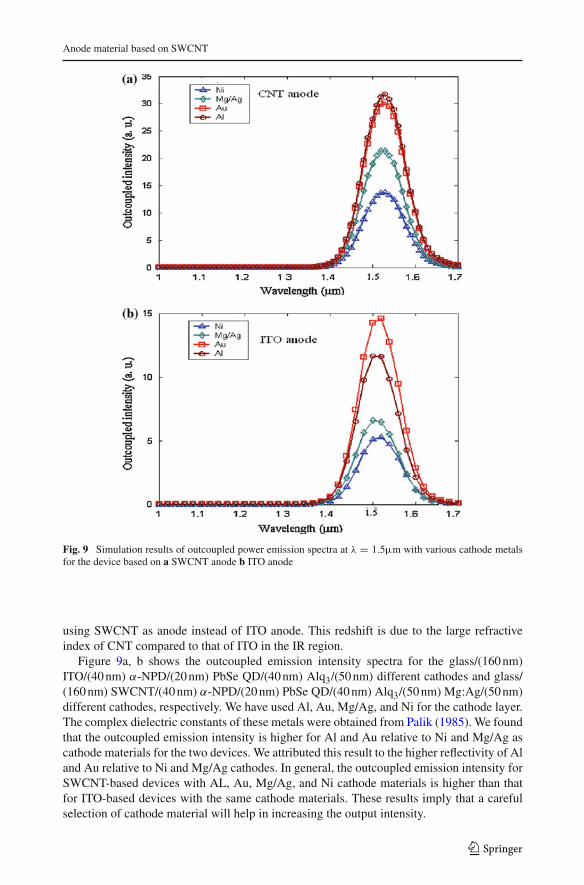
Figure 9a, b shows the outcoupled emission intensity spectra for the glass/(160 nm)ITO/(40 nm) α-NPD/(20 nm) PbSe QD/(40 nm) Alq3/(50 nm) different cathodes and glass/(160 nm) SWCNT/(40 nm) α-NPD/(20 nm) PbSe QD/(40 nm) Alq3/(50 nm) Mg:Ag/(50 nm)different cathodes, respectively. We have used Al, Au, Mg/Ag, and Ni for the cathode layer.The complex dielectric constants of these metals were obtained from Palik (1985). We foundthat the outcoupled emission intensity is higher for Al and Au relative to Ni and Mg/Ag ascathode materials for the two devices. We attributed this result to the higher reflectivity of Aland Au relative to Ni and Mg/Ag cathodes. In general, the outcoupled emission intensity forSWCNT-based devices with AL, Au, Mg/Ag, and Ni cathode materials is higher than thatfor ITO-based devices with the same cathode materials. These results imply that a carefulselection of cathode material will help in increasing the output intensity.
123

A. E. Farghal et al.
Fig. 10 a Calculated EL spectra at different viewing angles from normal for QD-LED based on ITO anode.b Normalized EL spectra for 0◦ and 60◦
Fig. 11 a Calculated EL spectra at different viewing angles from normal for IR QD-LED based on CNTanode. b Normalized EL spectra for 0◦ and 60◦
We also investigate the viewing angle dependence on the emission spectrum of the twodevices based on ITO and SWCNT as anode. A simulated EL spectrum for various viewingangles is shown in Fig. 10 for IR QD-LED based on ITO anode. Clearly, the peak intensitydecreases gradually as the viewing angle increases with respect to the normal. In addition,there is a small shift on the emission maximum which is cleared on Fig. 10b. This shift maybe due to the formation of weak microcavity between the Mg:Ag cathode on one side of thedevice and ITO on the other side. Figure 11 shows the simulated EL spectrum for variousviewing angles for IR QD-LED based on CNT anode. The emission intensity decreases grad-ually as the angle increases with respect to the normal. But in general, the emission intensityfor IR QD-LED based on CNT is larger than the emission intensity for IR QD-LED basedon ITO. Also, it is worth to mention that there is no shift on the emission maximum as theviewing angle increases with respect to the normal for IR QD-LED based on CNT anodewhich may be due to the low reflectivity of the CNT.
4 Conclusions
In conclusion, we have utilized a green’s function-based model to calculate the outcouplingefficiency of IR QD-LED using CNT anode. The calculations suggest that it is relatively
123
Anode material based on SWCNT
simple to use CNT anode to increase the light outcoupling efficiency by a factor ∼4. So,CNT is an ideal choice for IR QD-LEDs. Also, we have investigated the effect of metalcathode material types on the optical characteristics of IR QD-LEDs. We have found that theapplication of Al and Au as cathode materials is better relative to Mg/Ag and Ni as cathodematerials from optical characteristics point view point, especially in the case of SWCNTanode. Finally, we have studied the effect of viewing angle on the emission spectrum andfound that the emission intensity decreases gradually as the angle increases with respect tothe normal. In addition to the device based on ITO as anode, there is a small shift on theemission maximum, while that one based on CNT as anode there is no noticeable shift onthe emission spectrum.
References
Bourdakos, K.N., Dissanayake, D.M.N.M., Lutz, T., Silva, S.R.P., Curry, R.J.: Highly efficient near-infraredhybrid organic-inorganic nanocrystal electroluminescence device. Appl. Phys. Lett. 92(15), 153311-1–153311-3 (2008)
Bulovic, V., Khalfin, V.B., Gu, G., Burrows, P.E., Garbuzov, D.Z., Forrest, S.R.: Weak microcavity effects inorganic light-emitting devices. Phys. Rev. B 58(7), 3730 (1998)
Celebi, K., Heidel, T.D., Baldo, M.A.: Simplified calculation of dipole energy transport in a multilayer stackusing dyadic Green’s functions. Opt. Express 15(4), 1762–1772 (2007)
Chance, R.R., Prock, A., Silbey, R.: Molecular fluorescence and energy transfer near metal interfaces. In:Prigogine, I., Rice, S.A. (eds.) Advances in Chemical Physics, pp. 1–65. Wiley, London (1978)
Chen, H.-C., Lee, J.-H., Shiau, C.-C., Yang, C.-C., Kiang, Y.-W.: Electromagnetic modeling of organic light-emitting devices. J. Lightwave Technol. 24(6), 2450 (2006)
Contreras, M., Barnes, T., van de Lagemaat, J., Rumbles, G., Coutts, T.J., Weeks, C., Glatkowski, P., Levitsky,I., Peltola, J.: Application of single-wall carbon nanotubes as transparent electrodes in Cu(In,Ga)Se2-based solar cells. In: Photovoltaic Energy Conversion Conference. IEEE, Waikoloa, HI (2006)
Crawford, O.H.: Radiation from oscillating dipoles embedded in a layered system. J. Chem. Phys.89(10), 6017 (1988)
Drndic, M., Jarosz, M.V., Morgan, N.Y., Kastner, M.A., Bawendi, M.G.: Transport properties of annealedCdSe colloidal nanocrystal solids. J. Appl. Phys. 92(12), 7498 (2002)
Farghal, A.E., Wageh, S., Abou El-Azm, A.: Electromagnetic modeling of outcoupling efficiency and lightemission in near-infrared quantum dot light emitting devices. Prog. Electromagn. Res. B 24, 263–284 (2010)
Green, A.A., Hersam, M.C.: Colored semitransparent conductive coatings consisting of monodisperse metallicsingle-walled carbon nanotubes. Nano Lett. 8(5), 1417–1422 (2008)
Himcinschi, C., Meyer, N., Hartmann, S., Gersdorff, M., Friedrich, M., Johannes, H.-H., Kowalsky, W., Sch-wambera, M., Strauch, G., Heuken, M., Zahn, D.R.T.: Spectroscopic ellipsometric characterization oforganic films obtained via organic vapor phase deposition. Appl. Phys. A 80(3), 551–555 (2005)
Kahen, K.B.: Rigorous optical modeling of multilayer organic light-emitting diode devices. Appl. Phys.Lett. 78(12), 1649 (2001)
Kim, H., Gilmore, C.M., Piqué, A., Horwitz, J.S., Mattoussi, H., Murata, H., Kafafi, Z.H., Chrisey, D.B.: Elec-trical, optical, and structural properties of indium-tin-oxide thin films for organic light-emitting devices.J. Appl. Phys. 86(11), 6451–6461 (1999)
Li, J., Hu, L., Wang, L., Zhou, Y., Gruüner, G., Marks, T.J.: Organic light-emitting diodes having carbonnanotube anodes. Nano Lett. 6(11), 2472–2477 (2006)
Palik, E.D.: Handbook of Optical Constants of Solids. Academic, New York (1985)Steckel, J.S. et al.: 1.3μm to 1.55μm tunable electroluminescence from PbSe quantum dots embedded within
an organic device. Adv. Mater. 15(21), 1862–1866 (2003)Tessler, N., Medvedev, V., Kazes, M., Kan, S., Banin, U.: Efficient near-infrared polymer nanocrystal light-
emitting diodes. Science 295(5559), 1506–1508 (2002)Wang, T.: Light Scattering Study on Single Wall Carbon Nanotube (SWNT) Dispersions. Thesis, Georgia
Institute of Technology (2004)Weeks, C. et al.: Single-wall carbon nanotubes as transparent electrodes for photovoltaics. In: Photovoltaic
Energy Conversion Conference. IEEE, Waikoloa, HI (2006)
123

A. E. Farghal et al.
Wehrenberg, B.L., Wang, C., Philippe, G.-S.: Interband and intraband optical studies of PbSe colloidal quantumdots. J. Phys. Chem. B 106(41), 10634–10640 (2002)
Zhang, M., Fang, S., Zakhidov, A.A., Lee, S.B., Aliev, A.E., Williams, C.D., Atkinson, K.R.,Baughman, R.H.: Strong, transparent, multifunctional, carbon nanotube sheets. Science 309(5738),1215–1219 (2005)
Zhang, D., Ryu, K., Liu, X., Polikarpov, E., Ly, J., Tompson, M.E., Zhou, C.: Transparent, conductive, andflexible carbon nanotube films and their application in organic light-emitting diodes. Nano Lett. 6(9),1880–1886 (2006)
123
Related Documents