Welcome message from author
This document is posted to help you gain knowledge. Please leave a comment to let me know what you think about it! Share it to your friends and learn new things together.
Transcript
Wissenschaftlich-Technische Berichte FZD – 493 2008
Annual Report 2007
Institute of Ion Beam Physics and Materials Research
Editors:
J. von Borany, V. Heera, M. Helm, W. Möller
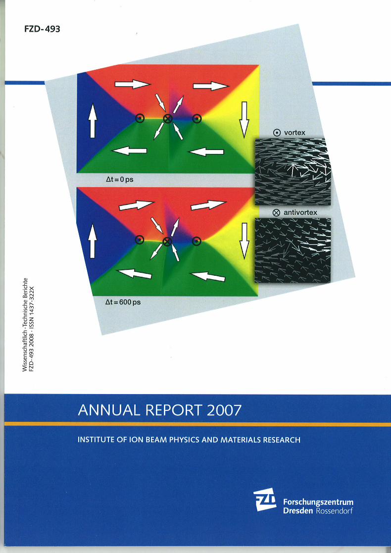
Cover Picture: The top coloured image shows a magnetic domain configuration of a rectangular ferromagnetic platelet (5 µm × 3 µm × 20 nm) exhibiting a single cross-tie wall. This cross-tie wall consists of two clockwise magnetization curls indicated by the arrows. The centre of each magnetization curl exhibits a vortex core with the magnetization pointing either upwards or downwards (see sketches at the right). In the example shown here both vortex cores point upwards. In the centre of the structure an antivortex is located. Also here a singularity in magnetization (pointing upwards/downwards) is obtained. Although only a few nanometer in size these singularities govern the overall magnetization dynamics of the whole element.
The bottom coloured image shows the magnetization configuration after excitation by a pulsed magnetic field (20 Oe, 500 ps) after 600 ps. As a result in the upper and lower domains the magnetization is tilted upwards and the vertical domain wall in the centre is bended to the right. After several nanoseconds the domain, domain wall and vortex excitations are decayed and the equilibrium state (upper image) is re-established.
The micromagnetic simulations shown here are used to interpret the magnetization dynamics in thin magnetic films fields which has been studied by time-resolved photoelectron microscopy using Synchro-tron radiation at the Swiss Light Source.
For detail see the contribution of K. Küpper at al.; pp. 20 – 23.
Forschungszentrum Dresden - Rossendorf e.V. Institut für Ionenstrahlphysik und Materialforschung Postfach 51 01 19 D-01314 Dresden Bundesrepublik Deutschland Direktoren Prof. Dr. Manfred Helm Prof. Dr. Wolfhard Möller Telefon + 49 (351) 260 2260 + 49 (351) 260 2245 Telefax + 49 (351) 260 3285 + 49 (351) 260 3285 E-mail [email protected] [email protected]
Homepage http://www.fzd.de/FWI
Annual Report IIM 2007, FZD-493
3
Preface by the Directors The "Structure of Matter" program activities of Forschungszentrum Dresden-Rossendorf (FZD)
are to a large fraction delivered by the Institute of Ion Beam Physics and Materials Research (IIM) in the fields of semiconductor physics and materials research using ion beams. The institute operates a national and international Ion Beam Center (IBC), which, in addition to its own scientific activities, makes available fast ion technologies to universities, other research institutes, and industry. Parts of its activities are also dedicated to exploit the infrared/THz free-electron laser at the 40 MeV super-conducting electron accelerator ELBE for condensed matter research. For both facilities the institute holds EU grants for funding access of external users. Cooperation with colleagues from the High Magnetic Field Laboratory Dresden (HLD), another institute of the FZD, is increasing as well.
In 2007, the process of staff rejuvenation upon retirements continued at the institute. A new research group dealing with magnetic semiconductors was established under the leadership of Dr. Heidemarie Schmidt as a young scientist. A substantial increase in particular of the number of young scientists and students resulted in a total IIM staff of more than 150 at the end of 2007.
Ion - Solid Interaction
Thin Films
Doping and Defects in Semiconductors
NanostructuresOptoelectronic
Materials
Ion Beams SemiconductorsProf. Wolfhard Möller Prof. Manfred Helm
HighlyCharged Ion
Group
Nanoscale Magnetism
The diagram displays the presently six R&D topics of the institute, together with the associated
Highly Charged Ion (HCI) Group of the TU Dresden. Our research activities span a wide range of topics relevant for future information processing and energy technology, be it in the realm of nanoelectronics, optoelectronics, magnetoelectronics, spintronics and solar technology. Highlights of last year’s research are presented in this Annual Report through reprints of short papers that were published in leading international journals. IIM staff published more than 150 papers in peer-reviewed journals in 2007, thereof about 40 contributions to high-impact journals (impact factor larger > 3). The scientific achievements of IIM have also been honored internally at FZD, by awarding the 2007 Research and PhD Student Prizes to Dr. Karsten Küpper and Dr. Dominik Stehr, respectively.
We are also pleased that we can report on a stable level of third-party funding, in spite of the ever-tougher competition. In particular, funding the by German Science Foundation (DFG) has taken another steep increase. Here we would especially like to mention the participation of several IIM scientists in a National Research Group "Self-Organized Nanostructures by Low-Energy Ion-Beam Erosion" funded by DFG. A good part of funding comes through contracts with industrial companies,
Preface
4
including also local microelectronics and other high-tech industry. Thus also our funding spectrum reflects our scope from more basic to more applied research.
Recalling the events of the year, IIM contributed essentially to the FZD Open Laboratory Day on May 12, which focused on materials research, and to the Dresden Long Night of Science on June 29. Quite an effort went into the preparation of the evaluation of FZD by the German Wissenschaftsrat (Science Council) which took place at the end of November. There are no official statements available so far, but we are quite optimistic about the outcome. IIM organized the 4th Int. Workshop on High-Resolution Depth Profiling Using Ion Beams at Radebeul near Dresden, acted as co-organizer of the 9th Int. Workshop on Plasma Based Ion Implantation and Deposition at Leipzig/Germany and the 15th Int. Summer School on Vacuum, Electron and Ion Technologies at Sozopol/Bulgaria.
We sincerely thank all partners, friends, and organizations who supported our progress in 2007. Special thanks are due to the Executive Board of the Forschungszentrum Dresden-Rossendorf, the Minister of Science and Arts of the Free State of Saxony, and the Minister of Education and Research of the Federal Government of Germany. Numerous partners from universities, industry and research institutes all around the world contributed essentially, and play a crucial role for the further develop-ment of the institute. Last but not least, the directors would like to thank all IIM staff for their efforts and excellent contributions in 2007.
Prof. Wolfhard Möller Prof. Manfred Helm

Annual Report IIM 2007, FZD-493
5
Contents
Selected Publications
Copyright Remarks..................................................................................................................................... 9
D. Kost, S. Facsko, W. Möller, R. Hellhammer, and N. Stolterfoht ..................................................... 10 Channels of potential energy dissipation during multiply charged argon-ion bombardment of copper
D. Güttler, R. Grötzschel, and W. Möller …………………………....................................................... 14 Lateral variation of target poisoning during reactive magnetron sputtering
B. Abendroth, H. U. Jäger, W. Möller, and M. Bilek ……………………………………..................... 17 Binary-collision modeling of ion-induced stress relaxation in cubic BN and amorphous C thin films
K. Küpper, M. Buess, J. Raabe, C. Quitmann, and J. Fassbender ….................................................... 20 Dynamic vortex–antivortex interaction in a single cross-tie wall
M. O. Liedke, B. Liedke, A. Keller, B. Hillebrands, A. Mücklich, S. Facsko, and J. Fassbender ..... 24 Induced anisotropies in exchange-coupled systems on rippled substrates
K. Potzger, S. Zhou, H. Reuther, K. Küpper, G. Talut, M. Helm, J. Fassbender, and J. D. Denlinger ……………………………………………………………………...….……............. 28 Suppression of secondary phase formation in Fe implanted ZnO single crystals
L. Röntzsch, K.-H. Heinig, J. A. Schuller, and M. L. Brongersma ....................................................... 31 Thin film patterning by surface-plasmon-induced thermocapillarity
S. Prucnal, J. M. Sun, W. Skorupa, and M. Helm .................................................................................. 34 Switchable two-color electroluminescence based on a Si metal-oxide-semiconductor structure doped with Eu
H. Schmidt, M. Wiebe, B. Dittes, and M. Grundmann ......................................................................... 37 Meyer-Nedel rule in ZnO
F. Peter, S. Winnerl, S. Nitzsche, A. Dreyhaupt, H. Schneider, and M. Helm .................................. 40 Coherent terahertz detection with a large-area photoconductive antenna
H. Schneider, T. Maier, M. Walther, and H. C. Liu ……………………............................................... 43 Two-photon photocurrent spectroscopy of electron intersubband relaxation and dephasing in quantum wells
C. Villas-Boas Grimm, M. Priegnitz, S. Winnerl, H. Schneider, M. Helm, K. Biermann, and H. Künzel .................................................................................................................... 46 Intersubband relaxation dynamics in single and double quantum wells based on strained InGaAs/AlAs/AlAsSb
Statistics Monographs and Book Chapters ............................................................................................................. 51 Journal Publications .................................................................................................................................. 51 Invited Conference Talks .......................................................................................................................... 61 Conference Contributions ........................................................................................................................ 63

Contents
6
Lectures ....................................................................................................................................................... 71 PhD and Master / Diploma Theses ........................................................................................................ 73 Patents ……………………………………………………………………………………………………. 73 Organization of Workshops .................................................................................................................... 74 Laboratory Visits ....................................................................................................................................... 74 Guests ......................................................................................................................................................... 75 AIM Visitors ............................................................................................................................................... 77 AI-SFS Visitors ........................................................................................................................................... 78 ROBL-MRH Visitors ................................................................................................................................. 78 Colloquium of the Institute ..................................................................................................................... 80 Seminars ……............................................................................................................................................. 80 Projects ........................................................................................................................................................ 82 Experimental Equipment ......................................................................................................................... 85 Services ....................................................................................................................................................... 88 Organigram ............................................................................................................................................... 90 List of Personnel ....................................................................................................................................... 91

SSeelleecctteedd PPuubblliiccaattiioonnss


Annual Report IIM 2007, FZD-493 9
Copyright Remarks The following journal articles are reprinted with kind permission from D. Kost, S. Facsko, W. Möller, R. Hellhammer, and N. Stolterfoht Physical Review Letters, Vol. 98, Issue 22, Art.No. 225 503, 2007 Copyright 2007, The American Physical Society D. Güttler, R. Grötzschel, and W. Möller Applied Physics Letters, Vol. 90, Issue 26, Art.No. 263 502, 2007 Copyright 2007, American Institute of Physics B. Abendroth, H.-U. Jäger, W. Möller, and M. Bilek Applied Physics Letters, Vol. 90, Issue 18, Art.No. 181 910, 2007 Copyright 2007, American Institute of Physics K. Küpper, M. Buess, J. Raabe, C. Quitmann, and J. Fassbender Physical Review Letters, Vol. 99, Issue 16, Art.No. 167 202, 2007 Copyright 2007, The American Physical Society M. O. Liedke, B. Liedke, A. Keller, B. Hillebrands, A. Mücklich, S. Facsko, and J. Fassbender Physical Review B, Vol. 75, Issue 22, Art.No. 220 407(R), 2007 Copyright 2007, The American Physical Society K. Potzger, S. Zhou, H. Reuther, K. Küpper, G. Talut, M. Helm, J. Fassbender, and J. D. Denlinger Applied Physics Letters, Vol. 91, Issue 6, Art.No. 062 107, 2007 Copyright 2007, American Institute of Physics L. Röntzsch, K.-H. Heinig, J. A. Schuller, and M. L. Brongersma Applied Physics Letters, Vol. 90, Issue 4, Art.No. 044 105, 2007 Copyright 2007, American Institute of Physics S. Prucnal, J. M. Sun, W. Skorupa, and M. Helm Applied Physics Letters, Vol. 90, Issue 18, Art.No. 181 121, 2007 Copyright 2007, American Institute of Physics H. Schmidt, M. Wiebe, B. Dittes, and M. Grundmann Applied Physics Letters, Vol. 91, Issue 23, Art.No. 232 110, 2007 Copyright 2007, American Institute of Physics F. Peter, S. Winnerl, S. Nitsche, A. Dreyhaupt, H. Schneider, and M. Helm Applied Physics Letters, Vol. 91, Issue 8, Art.No. 081 109, 2007 Copyright 2007, American Institute of Physics H. Schneider, T. Maier, M. Walther, and H. C. Liu Applied Physics Letters, Vol. 91, Issue 19, Art.No. 191 116, 2007 Copyright 2007, American Institute of Physics C. Villas-Boas Grimm, M. Priegnitz, S. Winnerl, H. Schneider, M. Helm, K. Biermann, and H. Künzel Applied Physics Letters, Vol. 91, Issue 19, Art.No. 191 121, 2007 Copyright 2007, American Institute of Physics
Channels of Potential Energy Dissipation during Multiply Charged Argon-Ion Bombardmentof Copper
D. Kost, S. Facsko, and W. Moller*Institute of Ion Beam Physics and Materials Research, Forschungszentrum Dresden-Rossendorf, 01314 Dresden, Germany
R. Hellhammer and N. StolterfohtDivision of Structure Research, Hahn-Meitner Institute, 14109 Berlin, Germany
(Received 8 January 2007; published 1 June 2007)
The dissipation of potential energy of multiply charged Ar ions incident on Cu has been studied bycomplementary electron spectroscopy and calorimetry at charge states between 2 and 10 and kineticenergies between 100 eV and 1 keV. The emitted and deposited fractions of potential energy increase atincreasing charge state, showing a significant jump for charge states q > 8 due to the presence of L-shellvacancies in the ion. Both fractions balance the total potential energy, thus rendering former hypotheses ofa significant deficit of potential energy obsolete. The experimental data are reproduced by computersimulations based on the extended dynamic classical-over-the-barrier model.
DOI: 10.1103/PhysRevLett.98.225503 PACS numbers: 61.80.Jh, 41.75.Ak, 52.50.Gj, 79.20.Rf
In 1983, Datz stated [1] that ‘‘our community is almostcertainly on the verge of discovering new phenomena thatoccur in multiply charged ion (MCI) interaction with sol-ids.’’ Since then, research is continuously verifying thisstatement by demonstrating not only new aspects of atomicphysics which occur during the approach of an MCI to asolid surface, but also characteristic new effects of ion-solid interaction (for reviews, see Refs. [2–4]). The latterinclude enhanced secondary-electron emission, enhancedsputtering, and desorption of adatoms, pointing to promis-ing prospects of MCI applications in materials science.These include surface analysis, the synthesis of materialswith new properties [5,6], and the formation of nanotopo-graphical structures on surfaces [4,7]. The effects arerelated to the potential energy of the MCI (the sum of thebinding energies of the removed electrons), which mayexceed the kinetic energy of the ion significantly at suffi-ciently low velocity. During MCI interaction with a solidsurface, the potential energy is released in connection withthe neutralization of the ion. According to the classical-over-the-barrier model [8], the interaction process maystart already a few tenths of a nanometer in front of thesurface, being associated with the transfer of a large num-ber of electrons. Emission of Auger electrons from theresulting hollow atom or during its subsequent collisionalinteraction with the top surface [8–10] may reemit a sig-nificant fraction of the initial potential energy into thevacuum. However, this fraction plus the energy carriedaway by x rays and secondary atoms and ions was foundto amount to less than about 10% of the initial potentialenergy ([11] and references therein). Thus, a substantialfraction will remain in the bulk of the substrate, which issimultaneously a prerequisite for significant effects ofpotential energy surface modifications.
To the best of our knowledge, only two earlier publica-tions described measurements of this retained fraction of
the potential energy. Schenkel et al. [11] employed asilicon detector to determine the charge transported byAuger electrons into the depletion layer as well as thecharge created there by UV photons and x rays. Theirresult of 35%–40% of retained potential energy for highlycharged Xe and Au ions represents a lower estimate as asignificant fraction might be deposited in the 50 nm in-sensitive surface layer of their detector. Alternatively,Kentsch et al. [12] used a calorimetric setup to measurethe retained potential energy for Ar ions incident on cop-per. Again, a retained fraction of 30%–40% was found,which, in comparison to Ref. [11], was considered to befortuitous but to corroborate the conclusion that a signifi-cant fraction of the potential energy dissipates into un-known channels. Therefore, it was the aim of the presentstudy to remeasure electron emission and calorimetric dataunder improved experimental conditions using the identi-cal system of Arq� incident on copper. As we will showbelow, electron emission and thermalization in the solidrepresent the dominant channels of dissipation of potentialenergy. The findings are consistent with a full detection ofthe potential energy, thus resolving the former puzzle ofunknown dissipation channels.
The electron emission experiments were performed in aUHV vacuum chamber attached to the 14.5 GHz electroncyclotron resonance (ECR) source at Hahn-MeitnerInstitute. The base vacuum was well in the 10�10 mbarrange. Prior to the measurements, the polycrystalline cop-per samples were sputter cleaned by 3 keV Ar� bombard-ment. During the subsequent measurements of electronemission, no traces of any C or O contaminants werevisible in the energy spectra. Using a deceleration lenssystem, the measurements were performed at fixed kineticion energy of 720 eV for all charge states. The availablecharge states were limited to q < 10, as the 40Ar10� beamwas contaminated by ions of equal mass to charge ratio
PRL 98, 225503 (2007) P H Y S I C A L R E V I E W L E T T E R S week ending1 JUNE 2007
0031-9007=07=98(22)=225503(4) 225503-1 © 2007 The American Physical Society
10 Journal Reprint
(e.g., 16O4�). To evaluate the amount of the emittedsecondary-electron energy, double differential electronspectroscopy was employed yielding the number of elec-trons d2N=dEd� per interval of electron energy E andemission angle � with respect to the surface normal. Thedata were fitted using the function [10,13]
d2NdEd�
�E;�� � A�E� � B�E� cos���; (1)
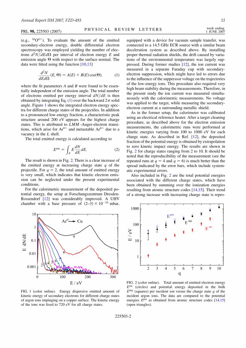
where the fit parameters A and B were found to be essen-tially independent of the emission angle. The total numberof electrons emitted per energy interval dN=dE is thenobtained by integrating Eq. (1) over the backward 2� solidangle. Figure 1 shows the integrated electron energy spec-tra for different charge states of the projectiles. In additionto a pronounced low-energy fraction, a characteristic peakstructure around 200 eV appears for the highest chargestates. This is attributed to LMM–Auger-electron transi-tions, which arise for Ar9� and metastable Ar8� due to avacancy in the L shell.
The total emitted energy is calculated according to
Eem �ZEEdNdE
dE: (2)
The result is shown in Fig. 2. There is a clear increase ofthe emitted energy at increasing charge state q of theprojectile. For q � 2, the total amount of emitted energyis very small, which indicates that kinetic electron emis-sion can be neglected under the present experimentalconditions.
For the calorimetric measurement of the deposited po-tential energy, the setup at Forschungszentrum Dresden-Rossendorf [12] was considerably improved. A UHVchamber with a base pressure of �2–3� � 10�10 mbar,
equipped with a device for vacuum sample transfer, wasconnected to a 14.5 GHz ECR source with a similar beamdeceleration system as described above. By installingproper thermal radiation shields, the drift caused by varia-tions of the environmental temperature was largely sup-pressed. During former studies [12], the ion current wasmeasured in a separate Faraday cup with secondary-electron suppression, which might have led to errors dueto the influence of the suppressor voltage on the trajectoriesof the low-energy ions. This procedure also required veryhigh beam stability during the measurements. Therefore, inthe present study the ion current was measured simulta-neously with the calorimetric measurements. No voltagewas applied to the target, while measuring the secondary-electron current at a surrounding metallic shield.
As in the former setup, the calorimeter was calibratedusing an electrical reference heater. After a target cleaningprocedure, as described above for the electron emissionmeasurements, the calorimetric runs were performed atkinetic energies varying from 100 to 1000 eV for eachcharge state. As described in Ref. [12], the depositedfraction of the potential energy is obtained by extrapolationto zero kinetic impact energy. The results are shown inFig. 2 for charge states ranging from 2 to 10. It should benoted that the reproducibility of the measurement (see therepeated runs at q � 4 and q � 6) is much better than thespread indicated by the error bars, which include system-atic experimental errors.
Also included in Fig. 2 are the total potential energiesassociated with the different charge states, which havebeen obtained by summing over the ionization energiesresulting from atomic structure codes [14,15]. Their trendof a strong increase with increasing charge state is repro-
FIG. 1 (color online). Energy dispersive emitted amount ofkinetic energy of secondary electrons for different charge statesof argon ions impinging on a copper surface. The kinetic energyof the ions was fixed to 720 eV for all charge states.
FIG. 2 (color online). Total amount of emitted electron energyEem (circles) and potential energy deposited in the bulkEdep (squares) per incident ion versus the charge state q of theincident argon ions. The data are compared to the potentialenergies Epot as obtained from atomic structure codes [14,15](open triangles).
PRL 98, 225503 (2007) P H Y S I C A L R E V I E W L E T T E R S week ending1 JUNE 2007
225503-2
Annual Report IIM 2007, FZD-493 11
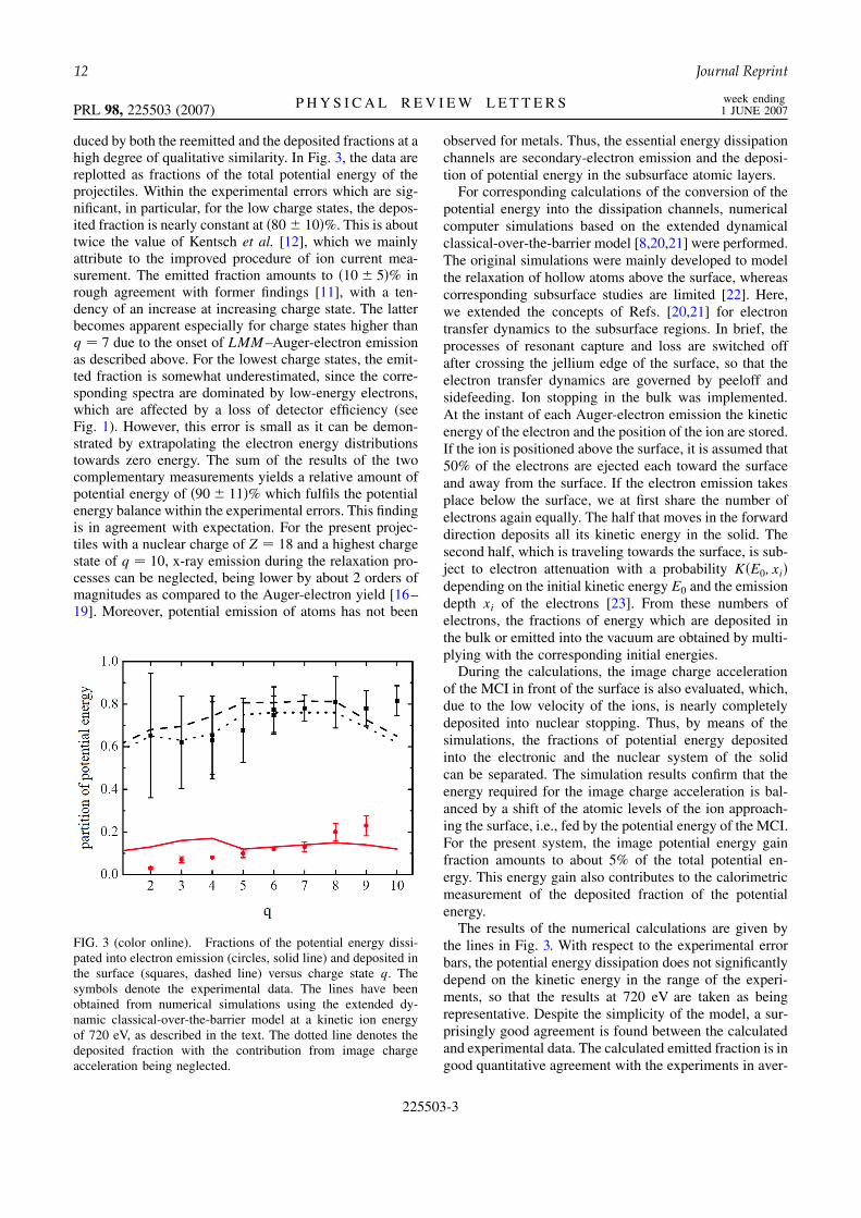
duced by both the reemitted and the deposited fractions at ahigh degree of qualitative similarity. In Fig. 3, the data arereplotted as fractions of the total potential energy of theprojectiles. Within the experimental errors which are sig-nificant, in particular, for the low charge states, the depos-ited fraction is nearly constant at �80� 10�%. This is abouttwice the value of Kentsch et al. [12], which we mainlyattribute to the improved procedure of ion current mea-surement. The emitted fraction amounts to �10� 5�% inrough agreement with former findings [11], with a ten-dency of an increase at increasing charge state. The latterbecomes apparent especially for charge states higher thanq � 7 due to the onset of LMM–Auger-electron emissionas described above. For the lowest charge states, the emit-ted fraction is somewhat underestimated, since the corre-sponding spectra are dominated by low-energy electrons,which are affected by a loss of detector efficiency (seeFig. 1). However, this error is small as it can be demon-strated by extrapolating the electron energy distributionstowards zero energy. The sum of the results of the twocomplementary measurements yields a relative amount ofpotential energy of �90� 11�% which fulfils the potentialenergy balance within the experimental errors. This findingis in agreement with expectation. For the present projec-tiles with a nuclear charge of Z � 18 and a highest chargestate of q � 10, x-ray emission during the relaxation pro-cesses can be neglected, being lower by about 2 orders ofmagnitudes as compared to the Auger-electron yield [16–19]. Moreover, potential emission of atoms has not been
observed for metals. Thus, the essential energy dissipationchannels are secondary-electron emission and the deposi-tion of potential energy in the subsurface atomic layers.
For corresponding calculations of the conversion of thepotential energy into the dissipation channels, numericalcomputer simulations based on the extended dynamicalclassical-over-the-barrier model [8,20,21] were performed.The original simulations were mainly developed to modelthe relaxation of hollow atoms above the surface, whereascorresponding subsurface studies are limited [22]. Here,we extended the concepts of Refs. [20,21] for electrontransfer dynamics to the subsurface regions. In brief, theprocesses of resonant capture and loss are switched offafter crossing the jellium edge of the surface, so that theelectron transfer dynamics are governed by peeloff andsidefeeding. Ion stopping in the bulk was implemented.At the instant of each Auger-electron emission the kineticenergy of the electron and the position of the ion are stored.If the ion is positioned above the surface, it is assumed that50% of the electrons are ejected each toward the surfaceand away from the surface. If the electron emission takesplace below the surface, we at first share the number ofelectrons again equally. The half that moves in the forwarddirection deposits all its kinetic energy in the solid. Thesecond half, which is traveling towards the surface, is sub-ject to electron attenuation with a probability K�E0; xi�depending on the initial kinetic energy E0 and the emissiondepth xi of the electrons [23]. From these numbers ofelectrons, the fractions of energy which are deposited inthe bulk or emitted into the vacuum are obtained by multi-plying with the corresponding initial energies.
During the calculations, the image charge accelerationof the MCI in front of the surface is also evaluated, which,due to the low velocity of the ions, is nearly completelydeposited into nuclear stopping. Thus, by means of thesimulations, the fractions of potential energy depositedinto the electronic and the nuclear system of the solidcan be separated. The simulation results confirm that theenergy required for the image charge acceleration is bal-anced by a shift of the atomic levels of the ion approach-ing the surface, i.e., fed by the potential energy of the MCI.For the present system, the image potential energy gainfraction amounts to about 5% of the total potential en-ergy. This energy gain also contributes to the calorimetricmeasurement of the deposited fraction of the potentialenergy.
The results of the numerical calculations are given bythe lines in Fig. 3. With respect to the experimental errorbars, the potential energy dissipation does not significantlydepend on the kinetic energy in the range of the experi-ments, so that the results at 720 eV are taken as beingrepresentative. Despite the simplicity of the model, a sur-prisingly good agreement is found between the calculatedand experimental data. The calculated emitted fraction is ingood quantitative agreement with the experiments in aver-
FIG. 3 (color online). Fractions of the potential energy dissi-pated into electron emission (circles, solid line) and deposited inthe surface (squares, dashed line) versus charge state q. Thesymbols denote the experimental data. The lines have beenobtained from numerical simulations using the extended dy-namic classical-over-the-barrier model at a kinetic ion energyof 720 eV, as described in the text. The dotted line denotes thedeposited fraction with the contribution from image chargeacceleration being neglected.
PRL 98, 225503 (2007) P H Y S I C A L R E V I E W L E T T E R S week ending1 JUNE 2007
225503-3
12 Journal Reprint

age, but is almost independent of the charge state in con-trast to the experimental trend. For the deposited fraction,there is a significant deviation only at the highest chargestates. The model calculations treat the influence of theimage charge potential on the atomic levels of the ions as aperturbation. For L-shell vacancies, the ion neutralizationin front of the surface is reduced due to frequent auto-ionization processes, so that the ion survives longer whenapproaching the surface. This leads to an increase of theperturbation and a correspondingly reduced energy of thereleased electrons. As the screening by outer electrons isneglected, this high perturbation might be partly artificialand result in a reduced calculated fraction of the releasedpotential energy.
Both in experiment and from calculation, the depositedand emitted fractions do not fully add to the nominalpotential energy of the ions. The latter is given relative tothe vacuum level, whereas during ion-solid interactionelectrons are transferred to the ion from the Fermi levelof the solid, which corresponds to the consumption of thework function per transferred electron. With the workfunction of Cu of 4.4 eV, this energy consumption rangesfrom about 10 to 40 eV for the present charge states. At thecharge states of 6 and 7, where the experimental errors arerelatively small and the agreement between model calcu-lations and experiments is best (see Fig. 3), the resultingrelative energy deficit is about 8% in good agreement withthe data of Fig. 3. This, however, might be fortuitous inview of the experimental errors and the simplicity of themodel.
Summarizing, we conclude that the potential energy ofthe MCI is released by emission of a specific number ofAuger electrons along the ion trajectory, which either areemitted into the vacuum or deposit their kinetic energy inthe solid, depending on the MCI position at emission timeand the energy of the Auger-electron transition. For thefirst time, it is demonstrated that the fraction of the poten-tial energy of multiply charged ions which is released byAuger electrons, and the fraction which is deposited intothe target, balance with the total potential energy at differ-ent charge states. For argon ions incident on copper withcharge states up to 10, the deposited fraction is almostindependent of the charge state. The results of computersimulations based on the extended dynamic classical-over-the-barrier model are in good agreement with the experi-
mental data, thus corroborating the picture that the poten-tial energy is essentially transferred via Auger electrons,which are either emitted into the vacuum or deposited intothe bulk.
*Corresponding author.Email address: [email protected]: +49-351-260 3285
[1] S. Datz, Phys. Scr. T3, 79 (1983).[2] A. Arnau et al., Surf. Sci. 27, 113 (1997).[3] J. D. Gillaspy, J. Phys. B 34, R93 (2001).[4] F. Aumayr and H. P. Winter, Nucl. Instrum. Methods Phys.
Res., Sect. B 233, 111 (2005).[5] G. Borsoni et al., Solid-State Electron. 46, 1855 (2002).[6] T. Meguro et al., Nucl. Instrum. Methods Phys. Res.,
Sect. B 235, 431 (2005).[7] M. Terada et al., Nucl. Instrum. Methods Phys. Res.,
Sect. B 235, 452 (2005).[8] J. Burgdorfer, P. Lerner, and F. Meyer, Phys. Rev. A 44,
5674 (1991).[9] F. Aumayr et al., Phys. Rev. Lett. 71, 1943 (1993).
[10] R. Kohrbruck et al., Phys. Rev. A 45, 4653 (1992).[11] T. Schenkel et al., Phys. Rev. Lett. 83, 4273 (1999).[12] U. Kentsch, H. Tyrroff, G. Zschornack, and W. Moller,
Phys. Rev. Lett. 87, 105504 (2001).[13] R. Kohrbruck et al., Phys. Rev. A 50, 1429 (1994).[14] R. D. Cowan, The Theory of Atomic Structure and Spectra
(University of California Press, Berkeley, 1981).[15] M. F. Gu, Astrophys. J. 582, 1241 (2003).[16] G. Wenzel, Z. Phys. 43, 524 (1927).[17] K. D. Sevier, Low Energy Electron Spectrometry (John
Wiley & Sons, New York, 1972).[18] R. W. Fink, R. C. Jopson, H. Mark, and C. D. Swift, Rev.
Mod. Phys. 38, 513 (1966).[19] G. D. Archard, in Proceedings of the Second International
Symposium on X-Ray Microscopy and Microanalysis,Stockholm, 1959 (Elsevier, Amsterdam, 1960).
[20] J. Ducree, H. J. Andra, and U. Thumm, Phys. Scr. T80,220 (1999).
[21] J. Ducree, F. Casali, and U. Thumm, Phys. Rev. A 57, 338(1998).
[22] N. Stolterfoht, A. Arnau, M. Grether, R. Kohrbruck,A. Spieler, R. Page, A. Saal, J. Thomaschewski, and J.Bleck-Neuhaus, Phys. Rev. A 52, 445 (1995).
[23] P. J. Cumpson and M. P. Seah, Surf. Interface Anal. 25,430 (1997).
PRL 98, 225503 (2007) P H Y S I C A L R E V I E W L E T T E R S week ending1 JUNE 2007
225503-4
Annual Report IIM 2007, FZD-493 13
Lateral variation of target poisoning during reactive magnetron sputteringD. Güttler, R. Grötzschel, and W. Möllera�
Institute of Ion Beam Physics and Materials Research, Forschungszentrum Dresden-Rossendorf,P.O. Box 510119, 01314 Dresden, Germany
�Received 11 May 2007; accepted 1 June 2007; published online 26 June 2007�
The reactive gas incorporation into a Ti sputter target has been investigated using laterally resolvingion beam analysis during dc magnetron deposition of TiN in an Ar/N2 atmosphere. At sufficientlylow reactive gas flow, the nitrogen incorporation exhibits a pronounced lateral variation, with alower areal density in the target racetrack compared to the target center and edge. The findings arereproduced by model calculations. In the racetrack, the balance of reactive gas injection and sputtererosion is shifted toward erosion. The injection of nitrogen is dominated by combined molecularadsorption and recoil implantation versus direct ion implantation. © 2007 American Institute ofPhysics. �DOI: 10.1063/1.2752019�
Magnetron sputtering1,2 is a common technique in thefabrication of high quality functional thin films. In the reac-tive deposition mode,3,4 a metal target is exposed to a raregas discharge to which a fraction of reactive gas �such asnitrogen and oxygen� is added. At the substrate, the reactivegas reacts with the sputtered target material to the desiredcompound. Its stoichiometry depends, e.g., on the reactivegas partial pressure and the deposition power. The efficiencyof the process, however, is often limited by the so-calledtarget poisoning, which means that the compound layerforms not only on the substrate as desired but also on thesputter target. This results in a significantly reduced sputteryield, and thereby a reduced deposition rate. As a furtherconsequence, the reactive gas consumption decreases due tothe lower yield of sputtered material, and its partial pressureincreases rapidly. For this situation, global particle-balancemodels of the interaction between gas flow, target erosion,and thin film deposition5–7 show a partly negative slope ofthe relation between reactive gas flow and partial pressure,which results in a hysteresis behavior. A corresponding insta-bility often requires additional means of stabilization forpractical applications.8 At the target, the particle balance isdetermined by the fluxes of neutral and ionic species fromthe gas and the plasma. The incorporation of reactive gas hasbeen suggested to result from a stationary balance of injec-tion by ion implantation and chemisorption in connectionwith recoil implantation, and erosion by ion-inducedsputtering.9–11 This was confirmed in previous experimentsusing in situ real-time ion beam analysis of the nitrogen in-corporation at the target.10
Magnetron discharges are laterally strongly nonuniformdue to the electron confinement in the magnetic field con-figuration. In front of a cylindrical magnetron target a toroi-dal region of high plasma density is formed, which createsthe so-called racetrack as a zone of high target erosion. Con-sequently, also a nonuniform incorporation of reactive gasatoms can be expected. With this background, an experimenthas been designed, which allows laterally resolved in situ ionbeam analysis of the reactive gas incorporation at the targetsurface. A standard magnetron sputter configuration was in-stalled in an ultrahigh vacuum chamber of 50 l volume. The
planar, cylindrical dc magnetron of 5 cm diameter wasequipped with a 99.995% purity titanium target and installedin the center of an ultrahigh vacuum chamber of 50 l vol-ume. It was operated in constant current mode at 0.3 A. Us-ing mass flow controllers, the argon and nitrogen flows werefixed at 10 SCCM �SCCM denotes cubic centimeter perminute at STP� and varied between 0 and 2.5 SCCM, respec-tively, which resulted in operating pressures between 0.3 and0.35 Pa. The partial pressures were measured by means of amass spectrometer, which was calibrated in pure Ar and N2.The target voltage adjusted from �330 to �360 V at in-creasing reactive gas flow. For in situ ion beam analysis ofthe nitrogen incorporation at the target by means of the14N�d ,��12C nuclear reaction, the setup is attached to thebeam line system of a 5 MV tandem ion accelerator �fordetails, see Ref. 10�. The ion beam is collimated to a spot of1�1 mm2, which defines the lateral resolution of the analy-sis. The low cross section of the reaction requires analysistimes of up to 30 min to obtain statistically satisfactory re-sults. In order to reduce the consumption of the sputter targetand the corresponding contamination of the target chamber,the measurements have been performed after magnetron op-eration. By comparison to real-time analysis during magne-tron operation, it was assured that no postoperation nitrogenloss occurs.10
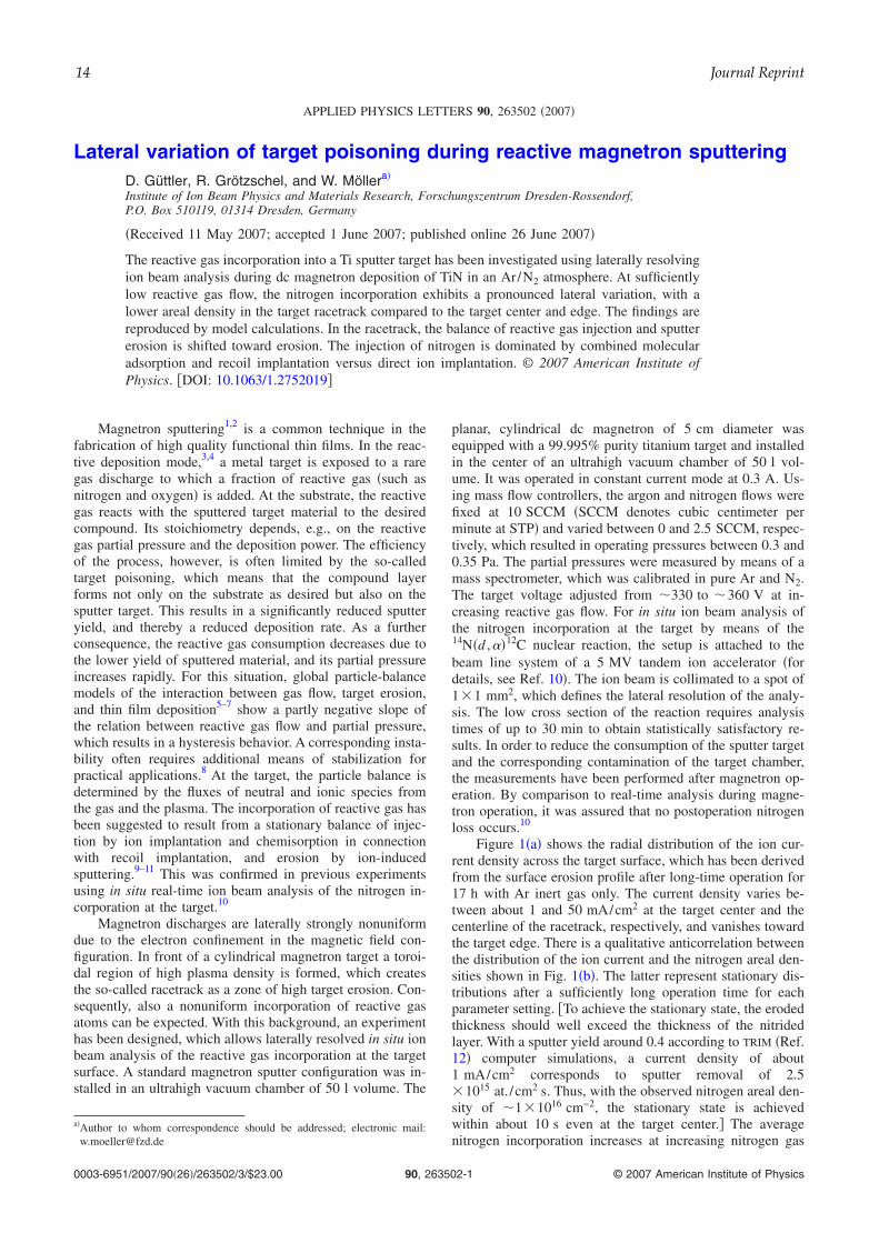
Figure 1�a� shows the radial distribution of the ion cur-rent density across the target surface, which has been derivedfrom the surface erosion profile after long-time operation for17 h with Ar inert gas only. The current density varies be-tween about 1 and 50 mA/cm2 at the target center and thecenterline of the racetrack, respectively, and vanishes towardthe target edge. There is a qualitative anticorrelation betweenthe distribution of the ion current and the nitrogen areal den-sities shown in Fig. 1�b�. The latter represent stationary dis-tributions after a sufficiently long operation time for eachparameter setting. �To achieve the stationary state, the erodedthickness should well exceed the thickness of the nitridedlayer. With a sputter yield around 0.4 according to TRIM �Ref.12� computer simulations, a current density of about1 mA/cm2 corresponds to sputter removal of 2.5�1015 at. / cm2 s. Thus, with the observed nitrogen areal den-sity of �1�1016 cm−2, the stationary state is achievedwithin about 10 s even at the target center.� The averagenitrogen incorporation increases at increasing nitrogen gas
a�Author to whom correspondence should be addressed; electronic mail:[email protected]
APPLIED PHYSICS LETTERS 90, 263502 �2007�
0003-6951/2007/90�26�/263502/3/$23.00 © 2007 American Institute of Physics90, 263502-1Downloaded 20 Feb 2008 to 149.220.35.103. Redistribution subject to AIP license or copyright; see http://apl.aip.org/apl/copyright.jsp
14 Journal Reprint
flow. At the target center, the nitrogen areal density appearsto saturate except for the lowest nitrogen flow. When ne-glecting sputtering, an upper estimate of the saturation arealdensity can be obtained assuming the formation of stoichio-metric TiN within the range of the incident reactive gas ions.The dominant reactive ion species from the discharge is N2
+,which, after acceleration by the target voltage and upon im-pinging the surface, splits into two atoms of half-energy. Therange distribution of the resulting �175 eV N atoms extendsto about 2.7 nm in Ti,12 which corresponds to a nitrogenareal density of 1.5�1016 cm−2 in rough agreement with theexperimental result. Toward the centerline of the racetrack,the nitrogen incorporation decreases by �45% and �10%for the lowest and highest nitrogen flows, respectively. Theradial position of minimum nitrogen incorporation is in goodagreement with that of the maximum current density. Fur-ther, toward the edge of the target, the nitrogen areal densityincreases again in accordance with the decreasing ion flux.However, for the largest nitrogen flows, it increases to a levelwhich is significantly above the saturation level at the targetcenter, although the current density is similar. We ascribe thisto some redeposition of Ti and corresponding compound for-mation in this outer area, although the transport mechanismsof redeposition are not obvious.
As briefly mentioned above, the stationary reactive gasincorporation results from a balance of reactive gas deposi-tion and sputter erosion. The three major mechanisms of re-active gas accumulation are chemisorption of reactive gas
molecules at the surface, direct implantation of ionized reac-tive species, and recoil implantation of the chemisorbed spe-cies by ion bombardment. Recoil implantation and sputtererosion are mainly due to inert gas ions, as the nitrogenaddition is relatively small and the electron-impact ionizationcross sections of Ar are larger than the ones of N2.14,15 Allion fluxes, and thereby the sputter erosion, follow the radialcurrent distribution of Fig. 1�a�, whereas the molecular gasflux arrives uniformly across the target. Thus, if adsorption inconnection with recoil implantation plays a significant rolefor deposition, the deposition-erosion balance is shifted to-ward erosion in the center of the racetrack compared to thetarget center and edge, which results in a reduced nitrogenincorporation.
In order to corroborate this picture, quantitative modelcalculations have been performed. For this purpose, the dy-namic global surface model given by Kubart et al.,13 whichincorporates the above mechanisms, has been applied to thestationary state. Compound formation at the surface is mod-eled by chemisorption of incident reactive gas molecules as-suming a unity sticking coefficient on the metallic fraction ofthe surface. The corresponding gas-kinetic fluxes are derivedfrom the nitrogen partial pressure, which has been measuredusing mass spectrometry for each setting of the reactive gasflow. Of ions, only Ar+ and N2
+ are taken into account, whichare dominant in the discharge according to the electron-impact ionization cross sections.14,15 The radially varying to-tal �Ar+ plus N2
+� ion flux is taken from the radial distributionof Fig. 1�a�. �Secondary electron production at the target isneglected, as it is known to be small.16� The Ar+ to N2
+ fluxratio is chosen according to the respective partial pressuresand the ratio of the ionization cross sections. The latter isobtained by averaging the cross sections over an energyrange extending from the ionization threshold to the targetvoltage. The yields of surface sputtering and recoil implan-tation are derived from TRIM �Ref. 12� with Ar+ ions incidenton 1 ML of TiN on Ti. �The surface binding energies havebeen chosen according to Ref. 17.� Recoil implantation ofsurface nitrogen atoms into the bulk and direct implantationof N2
+ ions are modeled by a saturable transfer into a fixedmonolayer at a depth of 2.7 nm �see above�. Thus, the modelneglects any details of the depth distributions of direct andrecoil implantation and any in-depth multiple relocation ofthe reactive atoms.
Figure 1�c� shows the model prediction of the nitrogenincorporation versus the target radius. At the target center,the experimental results �cf. Fig. 1�b�� are reproduced quan-titatively. As discussed above, the discrepancy at the targetedge is attributed to redeposition. The sequence of the radialdependencies at different reactive gas flows shows goodqualitative agreement between experiment and model results,although the shape of the radial dependencies appears some-what different with a narrower depression in the racetrackobtained from the model. In particular, for the highest nitro-gen flow, the predicted reduction of nitrogen incorporation inthe center of the racetrack is in excellent agreement with theexperiment. Thus, in view of the simplicity of the model, theagreement between model predictions and experiment can beregarded as being surprisingly good. The inspection of thenitrogen depth profiles obtained from the model shows thatthe saturated areal density is associated with the formation ofa stoichiometric layer, whereas in the nonsaturated regionaround the racetrack centerline a constant, substoichiometric
FIG. 1. Radial distributions of the ion current �a� and of the nitrogen arealdensity at the target surface at different nitrogen flows ��b� and �c��, asdetermined from ion beam analysis �b� and from model calculations �c�. For�b� and �c�, the nitrogen gas flows are 0.65 SCCM �dots�, 1 SCCM�squares�, 2 sccm �full triangles�, and 2.5 SCCM �open triangles�. The linesare added to guide the eyes.
263502-2 Güttler, Grötzschel, and Möller Appl. Phys. Lett. 90, 263502 �2007�
Downloaded 20 Feb 2008 to 149.220.35.103. Redistribution subject to AIP license or copyright; see http://apl.aip.org/apl/copyright.jsp
Annual Report IIM 2007, FZD-493 15
nitrogen concentration extends from the surface into thedepth. In view of the good agreement with the model results,we apply this picture with some confidence also to the inter-pretation of the experimentally observed areal densities.
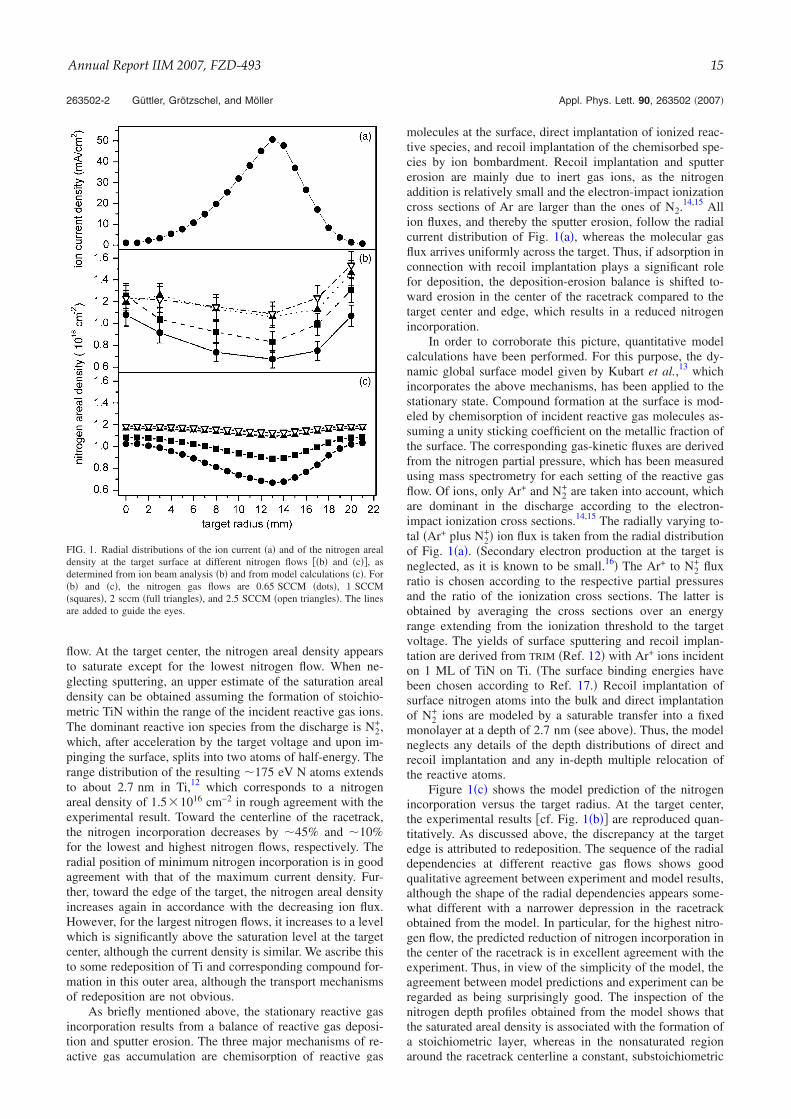
In the framework of the above modeling, Fig. 2 illus-trates the relative contributions of the mechanisms of nitro-gen incorporation at different reactive gas flows and targetlocations, as calculated for the stationary state. In the presentrange of reactive gas partial pressure, combined chemisorp-tion and recoil implantation dominates over direct ion im-plantation. This is consistent with the high gas-kinetic flux ofnitrogen molecules relative to the flux of N2
+ ions, and anefficient transfer of the chemisorbed nitrogen by recoil im-plantation into the bulk. At increasing nitrogen partial pres-sure, the relative contribution of direct ion implantation in-creases, as the surface becomes increasingly saturated. Thelatter limits the rate of chemisorption of gas molecules at thesurface, and thereby the inward flux by recoil implantation.Comparing the two lines of Fig. 2, the relative contributionof direct ion implantation is somewhat higher in the race-track. However, the difference is surprisingly small in viewof the ion current distribution, which varies by more than oneorder of magnitude. This is again attributed to the limitationof combined chemisorption and recoil implantation, whichoccurs preferentially at the target center and edge. The high
ion bombardment in the racetrack not only increases the rela-tive contribution of direct implantation of reactive ions butalso transfers chemisorbed nitrogen efficiently to the bulk byrecoil implantation, so that a high rate of chemisorption issustained.
In conclusion, we have demonstrated a significant varia-tion of target poisoning across the target surface during re-active magnetron sputtering of TiN, which depends on thereactive gas admixture. For typical conditions of practicalapplications with a reactive gas addition of a few percent, thenitrogen incorporation in the racetrack may be reduced byalmost 50% compared to the target center and edge. Theexperimental results are consistent with the simple modelingof the local particle balance. Ion implantation, reactive gasadsorption in combination with recoil implantation, and sput-ter erosion are confirmed as the main mechanisms of estab-lishing the local target composition in the stationary state.
1J. A. Thornton and J. E. Greene, Sputter Deposition Processes, Handbookof Deposition Technologies for Films and Coatings, 2nd ed., edited by R.Bunshah �Noyes, Park Ridge, NJ, 1994�, p. 249.
2P. Hovsepian, D. Lewis, and W. D. Münz, Surf. Coat. Technol. 133, 166�2000�.
3S. Schiller, U. Heisig, C. Korndörfer, G. Beister, J. Reschke, K.Steinfelder, and J. Strümpfel, Surf. Coat. Technol. 33, 405 �1987�.
4W. D. Sproul, Science 273, 889 �1996�.5S. Berg, H.-O. Blom, T. Larsson, and C. Nender, J. Vac. Sci. Technol. A 5,202 �1987�.
6S. Berg, T. Larsson, H.-O. Blom, and C. Nender, J. Appl. Phys. 63, 887�1988�.
7S. Berg and T. Nyberg, Thin Solid Films 476, 215 �2005�.8T. Wallendorf, S. Marke, C. May, and J. Strümpfel, Surf. Coat. Technol.
174–175, 222 �2003�.9D. Depla and R. De Gryse, Surf. Coat. Technol. 183, 184 �2004�; 183,190 �2004�; 183, 196 �2004�.
10D. Güttler, B. Abendroth, R. Grötzschel, W. Möller, and D. Depla, Appl.Phys. Lett. 85, 6134 �2004�.
11D. Rosen, I. Katardjiev, S. Berg, and W. Möller, Nucl. Instrum. MethodsPhys. Res. B 228, 193 �2005�.
12J. F. Ziegler, J. P. Biersack, and U. Littmark, The Stopping and Range ofIons in Solids �Pergamon, New York 1985�, Chap. 8. �http://www.srim.org�
13T. Kubart, O. Kappertz, T. Nyberg, and S. Berg, Thin Solid Films 515,421 �2006�.
14H. C. Straub, P. Renaud, B. G. Lindsay, K. A. Smith, and R. F. Stebbings,Phys. Rev. A 52, 1115 �1995�.
15H. C. Straub, P. Renaud, B. G. Lindsay, K. A. Smith, and R. F. Stebbings,Phys. Rev. A 54, 2146 �1996�.
16M. A. Lieberman and A. J. Lichtenberg, Principles of Plasma Dischargesand Materials Processing �Wiley, New York, 1994�, p. 467.
17W. Möller and M. Posselt, TRIDYN_FZR User Manual, Scientific Tech-nical Report No. FZR-317 �Forschungszentrum Rossendorf, Dresden, Ger-many, 2001�.
FIG. 2. Ratio of nitrogen injection by direct ion implantation and recoilimplantation from the surface layer vs the nitrogen partial pressure for dif-ferent target locations. jN
+ and jrecoil denote the respective atomic nitrogenfluxes. The partial pressure of 0.07 Pa corresponds to a reactive gas flow of2.5 SCCM.
263502-3 Güttler, Grötzschel, and Möller Appl. Phys. Lett. 90, 263502 �2007�
Downloaded 20 Feb 2008 to 149.220.35.103. Redistribution subject to AIP license or copyright; see http://apl.aip.org/apl/copyright.jsp
16 Journal Reprint
Binary-collision modeling of ion-induced stress relaxation in cubic BN andamorphous C thin films
B. Abendroth,a� H. U. Jäger, and W. MöllerInstitute of Ion Beam Physics and Materials Research, Forschungszentrum Dresden-Rossendorf, D-01314Germany
M. BilekApplied and Plasma Physics Department, School of Physics, University of Sydney, Sydney, New SouthWales 2006, Australia
�Received 15 February 2007; accepted 2 April 2007; published online 1 May 2007�
It is demonstrated that ion-bombardment-induced stress release during physical vapor deposition ofcubic boron nitride �cBN� and amorphous carbon �aC� films is related to collisional relocation ofatoms. A model based on TRIM and molecular dynamics computer simulations is presented.Experimental results obtained using pulsed substrate bias are in good agreement with the modelpredictions at adequately chosen threshold energies of atomic relocation. The collisional relaxationmodel describes the experimental data significantly better than the widely applied thermal spikemodel. © 2007 American Institute of Physics. �DOI: 10.1063/1.2734472�
Low-energy ion bombardment �Eion�1 keV� is widelyused in physical and chemical vapor deposition of thin filmsto improve film adhesion, structure, and morphology.1 Bysubplantation of primary ions or recoil atoms into the sub-surface region,2,3 ion bombardment facilitates the synthesisof metastable phases such as tetrahedral amorphous carbon�taC�, as well as diamondlike carbon.4 In the case of boronnitride deposition, low-energy ion bombardment is requiredto enable the nucleation and growth of the cubic �cBN�phase.5,6 On the other hand, low-energy ion bombardmentmay lead to high compressive stress in the film, which in thecase of cBN �Ref. 7� and taC �Ref. 8� can reach 10 GPa, andhence limit the adhesion and the achievable film thickness.Davis9 developed a model that relates the stress in thin filmsto the energy of incident particles. This model treats stressgeneration as a consequence of subplantation of primary ionsor recoil atoms into subsurface regions. The density n ofimplanted atoms is approximately related to the ion flux jiand energy E by n� jiE
1/2.10 A strain � evolves, which isproportional to n. Elastic theory predicts a biaxial stress � inthe thin film on a substrate, which is proportional to �.11
Further, a thermal spike12 that evolves around an ion impactallowing strained atoms to move to the surface, thereby de-creasing n is invoked to describe stress relaxation. The bal-ance between stress formation and relaxation in thermalspikes leads to a maximum of compressive stress at lowerion energies. At higher ion energies the relaxation outweighsthe stress formation, resulting in lower net film stress. High-energy ion bombardment has been used specifically to reducethe stress in thin films. Good film qualities were achieved bycombining the low-energy film forming particle flux j0 witha high-energy ion flux ji, with ji� j0 and E�ji�E�j0�, forstress relaxation.13–17 For cBN �Refs. 18 and 19� and amor-phous carbon �aC� �Refs. 8 and 20� films, the stress relax-ation due to high-energy ion impact has been studied system-atically at varied ion flux and energy. Both materials showthe same behavior of increasing stress relaxation as the prod-uct of ion energy and ion flux increases, followed by a satu-
ration at a certain level of residual stress for high values ofE�ji�ji. The same trends were also reported for the stressrelaxation in AlN and TiN.16,17 The dependence of the stressrelaxation on Eji is in contradiction to the model of atomicrearrangements in a thermal spike as it is applied in themodel described above9 which predicts a scaling of the num-ber of atomic relocations, and hence of the stress relaxationwith E5/3.3,9,12 In the present letter we will demonstrate thatthe stress relaxation in cBN and aC can be described well bycollisional relocation, rather than by using the thermal spikeconcept �E5/3 scaling�.
To model the stress relaxation, two particle flux compo-nents are considered as described above. The film formingflux j0 is assumed to leave some atoms in interstitial or oth-erwise unfavorable positions, leading to a certain density nof atoms in strained bonding configurations. Stress relief oc-curs by relocations of these atoms from unfavorable posi-tions due to energy transfer from the energetic ion flux ji.Each incident ion activates some atoms within a certain vol-ume around the impact site with a depth distribution functionfa�x ,E�. Integration over x yields the total number of activa-tion events, a�E�, per incident ion. In the dynamic situationof film growth, the average number of activation events, Na,per atom of the growing film is obtained by integration witha moving boundary, i.e., the film surface, resulting in Na
= �ji / j0�a�E�, where j0 can be written as the product of filmatomic density n0 and growth velocity vg, assuming a unityincorporation of the film forming flux into the film. The re-laxation rate of the strained atom density due to atomic re-locations can be written as
dn�x�dt
= − jifa�x,E�n�x�n0
. �1�
Substituting dt=dx /vg and integrating over time and depthyields the final density of unrelaxed atoms in the film,a�Electronic mail: [email protected]
APPLIED PHYSICS LETTERS 90, 181910 �2007�
0003-6951/2007/90�18�/181910/3/$23.00 © 2007 American Institute of Physics90, 181910-1Downloaded 20 Feb 2008 to 149.220.35.103. Redistribution subject to AIP license or copyright; see http://apl.aip.org/apl/copyright.jsp
Annual Report IIM 2007, FZD-493 17
n = nu exp�−ji
j0a�E�� = nu exp�− Na� , �2�
with nu being the density of unrelaxed atoms at zero flux ofenergetic ions. From elastic theory, the stress is proportionalto the strain. Hence, the film stress is proportional to thedensity of unrelaxed atoms and can be written as
� = ��u − �r�exp�−ji
j0a�E�� + �r, �3�
where �u is the intrinsic film stress without relaxation and �ris a residual stress which cannot be relaxed further, as isobserved in the experiments. Note that compressive stress isset as positive.
In analogy to the concept of collisional damage,21 thetransferred energy must exceed a threshold energy Ea
col toproduce a permanent relocation. For simplicity, we assume asharp threshold rather than a spectrum of threshold energies.Based on the binary-collision approximation �BCA�, themodified Kinchin-Pease �KP� model21 predicts a
KP�E�=�E /2Ea
col for the number of relocations per incident ion,where � is a constant with value around 0.8. The modifiedKP approximation becomes questionable in the threshold re-gime and it treats electronic stopping only in an approximateway. Therefore, higher accuracy BCA computer simulations�TRIM� �Ref. 22� have been employed here to obtain the col-lisional relocation function a
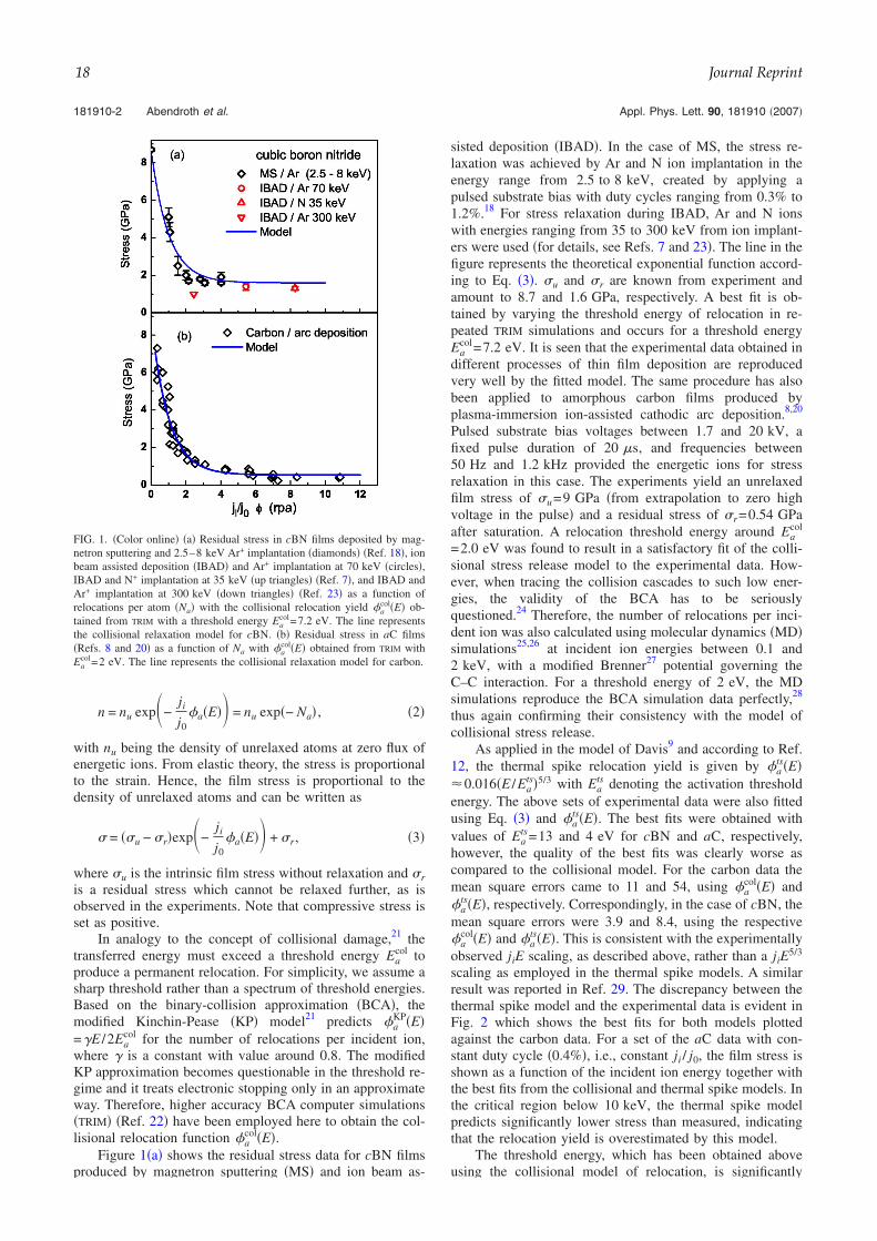
col�E�.Figure 1�a� shows the residual stress data for cBN films
produced by magnetron sputtering �MS� and ion beam as-
sisted deposition �IBAD�. In the case of MS, the stress re-laxation was achieved by Ar and N ion implantation in theenergy range from 2.5 to 8 keV, created by applying apulsed substrate bias with duty cycles ranging from 0.3% to1.2%.18 For stress relaxation during IBAD, Ar and N ionswith energies ranging from 35 to 300 keV from ion implant-ers were used �for details, see Refs. 7 and 23�. The line in thefigure represents the theoretical exponential function accord-ing to Eq. �3�. �u and �r are known from experiment andamount to 8.7 and 1.6 GPa, respectively. A best fit is ob-tained by varying the threshold energy of relocation in re-peated TRIM simulations and occurs for a threshold energyEa
col=7.2 eV. It is seen that the experimental data obtained indifferent processes of thin film deposition are reproducedvery well by the fitted model. The same procedure has alsobeen applied to amorphous carbon films produced byplasma-immersion ion-assisted cathodic arc deposition.8,20
Pulsed substrate bias voltages between 1.7 and 20 kV, afixed pulse duration of 20 �s, and frequencies between50 Hz and 1.2 kHz provided the energetic ions for stressrelaxation in this case. The experiments yield an unrelaxedfilm stress of �u=9 GPa �from extrapolation to zero highvoltage in the pulse� and a residual stress of �r=0.54 GPaafter saturation. A relocation threshold energy around Ea
col
=2.0 eV was found to result in a satisfactory fit of the colli-sional stress release model to the experimental data. How-ever, when tracing the collision cascades to such low ener-gies, the validity of the BCA has to be seriouslyquestioned.24 Therefore, the number of relocations per inci-dent ion was also calculated using molecular dynamics �MD�simulations25,26 at incident ion energies between 0.1 and2 keV, with a modified Brenner27 potential governing theC–C interaction. For a threshold energy of 2 eV, the MDsimulations reproduce the BCA simulation data perfectly,28
thus again confirming their consistency with the model ofcollisional stress release.
As applied in the model of Davis9 and according to Ref.12, the thermal spike relocation yield is given by a
ts�E�0.016�E /Ea
ts�5/3 with Eats denoting the activation threshold
energy. The above sets of experimental data were also fittedusing Eq. �3� and a
ts�E�. The best fits were obtained withvalues of Ea
ts=13 and 4 eV for cBN and aC, respectively,however, the quality of the best fits was clearly worse ascompared to the collisional model. For the carbon data themean square errors came to 11 and 54, using a
col�E� anda
ts�E�, respectively. Correspondingly, in the case of cBN, themean square errors were 3.9 and 8.4, using the respectivea
col�E� and ats�E�. This is consistent with the experimentally
observed jiE scaling, as described above, rather than a jiE5/3
scaling as employed in the thermal spike models. A similarresult was reported in Ref. 29. The discrepancy between thethermal spike model and the experimental data is evident inFig. 2 which shows the best fits for both models plottedagainst the carbon data. For a set of the aC data with con-stant duty cycle �0.4%�, i.e., constant ji / j0, the film stress isshown as a function of the incident ion energy together withthe best fits from the collisional and thermal spike models. Inthe critical region below 10 keV, the thermal spike modelpredicts significantly lower stress than measured, indicatingthat the relocation yield is overestimated by this model.
The threshold energy, which has been obtained aboveusing the collisional model of relocation, is significantly
FIG. 1. �Color online� �a� Residual stress in cBN films deposited by mag-netron sputtering and 2.5–8 keV Ar+ implantation �diamonds� �Ref. 18�, ionbeam assisted deposition �IBAD� and Ar+ implantation at 70 keV �circles�,IBAD and N+ implantation at 35 keV �up triangles� �Ref. 7�, and IBAD andAr+ implantation at 300 keV �down triangles� �Ref. 23� as a function ofrelocations per atom �Na� with the collisional relocation yield a
col�E� ob-tained from TRIM with a threshold energy Ea
col=7.2 eV. The line representsthe collisional relaxation model for cBN. �b� Residual stress in aC films�Refs. 8 and 20� as a function of Na with a
col�E� obtained from TRIM withEa
col=2 eV. The line represents the collisional relaxation model for carbon.
181910-2 Abendroth et al. Appl. Phys. Lett. 90, 181910 �2007�
Downloaded 20 Feb 2008 to 149.220.35.103. Redistribution subject to AIP license or copyright; see http://apl.aip.org/apl/copyright.jsp
18 Journal Reprint

larger for cBN than for aC. For cBN, it has been shown thatstress relaxation occurs within the grains of the nanocrystal-line material,18,19 which may be ascribed to the removal ofinterstitial atoms from the grains and their transport to thegrain boundaries. On the other hand, aC is amorphous in thestressed state, so that only slight rearrangements of theatomic configuration without significant atomic transportmight result in stress release, which would require a lowerenergy transfer than for cBN. These pictures are qualitativelyconsistent with the observed residual stress �r upon satura-tion of stress relief, which, for cBN, is significantly largerand can be attributed to interface stress.19 They are also con-sistent with the pronounced stability of cBN against ionirradiation,7,19,30 whereas in aC, sp3 bonds are easily trans-formed under ion irradiation into sp2 hybridization,31 leadingto a swelling of the surface. The threshold energies for bothmaterials are significantly lower than the conventional dam-age thresholds21 which are characteristic for the creation of astable Frenkel pair. The latter consumes the Frenkel pair for-mation energy plus a critical kinetic energy transfer for asufficient separation of the interstitial-vacancy pair. In con-trast, the displacement of a preexisting interstitial and a localrearrangement in an amorphous structure, which are respon-sible for stress relief in our cases, require clearly lower en-ergy transfers.
The above jiE scaling would be consistent with a univer-sal role of the average energy parameter �ji / j0�E in describ-ing film growth and morphology, which has been discussedcontroversially in literature �e.g., Refs. 15 and 32, and refer-ences therein�. However, the above scaling is only valid ifthe incident energies are large compared to the relocationthreshold energies. This is not necessarily fulfilled in general,as, e.g., low substrate bias. Moreover, other collisionalmechanisms, such as diffusion, may determine film growthand properties.
In conclusion, the results show that the stress relaxationby energetic ion bombardment is described well by a modelbased on collisional relocation of atoms in strained bondingconfigurations. The data and the model are consistent in a
wide range of ion energies and for different deposition tech-niques. The Kinchin-Pease approximation, which predictsthe collisional relocation yield per incident ion to be propor-tional to the ion energy, is consistent with the experimentalfinding that the stress relaxation depends on the product ofion flux and ion energy. In contrast, the thermal spike modelis not supported by the data. These results suggest a criticalrevision of subplantation models of thin film growth whichinvolve thermal spikes.
1L. Hultman, W.-D. Münz, J. Musil, S. Kadlec, I. Petrov, and J. E. Greene,J. Vac. Sci. Technol. A 9, 434 �1991�.
2Y. Lifshitz, S. R. Kasi, and J. W. Rabalais, Phys. Rev. Lett. 62, 1290�1989�.
3J. Robertson, Diamond Relat. Mater. 2, 984 �1993�.4M. Weiler, S. Sattel, T. Giessen, K. Jung, H. Ehrhardt, V. S. Veerasamy,and J. Robertson, Phys. Rev. B 53, 1594 �1996�.
5P. Mirkarimi, K. McCarty, and D. Medlin, Mater. Sci. Eng., R. 21, 47�1997�.
6W. Kulisch and S. Ulrich, Thin Solid Films 423, 183 �2003�.7C. Fitz, A. Kolitsch, W. Möller, and W. Fukarek, Appl. Phys. Lett. 80, 55�2002�.
8M. M. M. Bilek, M. Verdon, L. Ryves, T. W. H. Oates, C. T. Ha, and D. R.McKenzie, Thin Solid Films 482, 69 �2005�.
9C. A. Davis, Thin Solid Films 226, 30 �1993�.10P. Sigmund, in Sputtering by Particle Bombardment, edited by R. Behrisch
�Springer, Berlin, 1981�, Vol. 1, p. 9.11H. Windischmann, J. Appl. Phys. 62, 1800 �1987�.12F. Seitz and J. Koehler, Solid State Phys. 3, 305 �1956�.13H. Ljuncrantz, L. Hultman, J. E. Sundgren, and L. Karlsson, J. Appl. Phys.
78, 832 �1995�.14D. H. Lee, S. Fayeulle, K. C. Walter, and M. Nastasi, Nucl. Instrum.
Methods Phys. Res. B 148, 216 �1999�.15S. Mukherjee, F. Prokert, E. Richter, and W. Möller, Thin Solid Films
445, 48 �2003�.16B. K. Gan, M. M. M. Bilek, D. R. McKenzie, Yang Shi, D. A. Tompset,
M. B. Taylor, and D. G. McCulloch, J. Phys. D 16, 1751 �2004�.17S. H. N. Lim, D. G. McCulloch, M. M. M. Bilek, and D. R. McKenzie,
Surf. Coat. Technol. 174, 76 �2003�.18B. Abendroth, R. Gago, A. Kolitsch, and W. Möller, Thin Solid Films
447, 131 �2004�.19B. Abendroth, R. Gago, F. Eichhorn, and W. Möller, Appl. Phys. Lett. 85,
5905 �2004�.20M. M. M. Bilek, D. R. McKenzie, and W. Möller, Surf. Coat. Technol.
186, 21 �2004�.21M. Nastasi, J. Mayer, and J. Hirvonen, Ion-solid Interactions: Fundamen-
tals and Applications �Cambridge University Press, Cambridge, 1996�.22J. Ziegler, J. Biersack, and U. Littmark, The Stopping and Range of Ions in
Solids �Pergamon, New York, 1985�.23H.-G. Boyen, P. Widmayer, D. Schwertberger, N. Deyneka, and P. Zi-
emann, Appl. Phys. Lett. 76, 709 �2000�.24W. Eckstein, Computer Simulation of Ion-Solid Interactions �Springer,
Berlin, 1991�.25H. U. Jäger and A. Y. Belov, Phys. Rev. B 68, 024201 �2003�.26A. Y. Belov and H. U. Jäger, Thin Solid Films 482, 74 �2005�.27D. W. Brenner, Phys. Rev. B 42, 9458 �1990�; 46, 1948 �1992�.28W. Möller, B. Abendroth, H.-U. Jäger, and M. Bilek �unpublished�.29M. M. M. Bilek and D. R. McKenzie, Surf. Coat. Technol. 200, 4645
�2006�.30S. Eyhusen, I. Gerhards, H. Hofsäss, C. Ronning, M. Blomenhofer, J.
Zweck, and M. Seibt, Diamond Relat. Mater. 12, 1877 �2003�.31T. W. H. Oates, L. Ryves, F. A. Burgmann, B. Abendroth, M. M. M. Bilek,
D. R. McKenzie, and D. G. McCulloch, Diamond Relat. Mater. 12, 1395�2005�.
32I. Petrov, F. Adibi, J. E. Greene, L. Hultman, and J. E. Sundgren, Appl.Phys. Lett. 63, 36 �1993�.
FIG. 2. �Color online� Experimental data �diamonds� for aC �Refs. 8 and20� and the stress relaxation model with a relocation yield a
ts�E� accordingto the thermal spike model with a threshold energy Ea
ts=4 eV �solid line� anda collisional relocation yield a
col�E� with Eacol=2 eV �dash-dotted line� as a
function of the ion energy at constant ion to neutral flux ratio.
181910-3 Abendroth et al. Appl. Phys. Lett. 90, 181910 �2007�
Downloaded 20 Feb 2008 to 149.220.35.103. Redistribution subject to AIP license or copyright; see http://apl.aip.org/apl/copyright.jsp
Annual Report IIM 2007, FZD-493 19
Dynamic Vortex-Antivortex Interaction in a Single Cross-Tie Wall
K. Kuepper,1,* M. Buess,2 J. Raabe,2 C. Quitmann,2 and J. Fassbender1
1Forschungszentrum Dresden-Rossendorf, Post Office Box 51 01 19, D-01314 Dresden, Germany2Swiss Light Source, Paul Scherrer Institut, CH-5232 Villigen, Switzerland
(Received 1 March 2007; revised manuscript received 17 May 2007; published 18 October 2007)
A fascinating property of micromagnetism comes from the possibility to control the domain and vortexconfiguration through the sample shape and size. For instance, in a rectangular platelet a configurationcontaining a stable combination of vortices and an antivortex can be created. Such a single cross-tie wallcan be understood as being a coupled micromagnetic system with three static solitons. Here we report onits magnetization dynamics including the vortex-antivortex interactions. The spectrum of eigenmodes isinvestigated as well as the effect of different vortex core orientations. We show that the vortex dynamicscan be used to identify the core configuration, which is not directly accessible to x-ray microscopybecause of its limited spatial resolution.
DOI: 10.1103/PhysRevLett.99.167202 PACS numbers: 75.40.Gb, 75.60.Ch, 75.75.+a
Two-dimensional topological solitons are fascinating forresearchers in many fields. These solitons determine theproperties of very different systems such as atoms in super-fluids and Bose-Einstein condensates [1,2] and Cooperpairs in superconductors. In thin ferromagnetic films theycan be present as vortices and antivortices [3–7]. Becausevortex and antivortex are the corresponding antiparticlesthey can annihilate under emission of energy [8]. However,in special geometries a stable combination of vortices andantivortices can be obtained. A cross-tie wall is an exampleof an infinite chain of vortices and antivortices.
Here we study a ferromagnetic rectangle, containing twovortices and a single antivortex, thus forming the unit cellof a cross-tie wall. The solitons are coupled through thedomain walls and domains. This special geometry providesinsight into the vortex configuration and into couplingeffects which turn out to be very relevant for the dynamicsof these solitons.
Up to now, significant effort has been invested in under-standing the dynamics of ‘‘simple’’ magnetic vortex struc-tures, such as thin permalloy squares and disks. Time-resolved imaging [9,10] allows us to investigate their ex-citations and switching in the time-domain [11–14].Vortex-antivortex interaction has also attracted attentionin semicontinuous films because of potential applicationsfor spin wave radiation devices [8,15], and magnetic pin-ning arrays for superconducting films [16].
Neudert et al. [17] have investigated the generation ofcross-tie walls in large permalloy platelets following theexcitation by field pulses using Kerr microscopy. In thisLetter we investigate the excitations of a single cross-tiewall by combining micromagnetic simulations based onthe LLG equation [18] and magnetic imaging by means oftime-resolved photo emission electron microscopy(PEEM). We study the response to weak magnetic in-planefield pulses, concentrating on the dynamics of the vorticesand the antivortex and their mutual interaction.
Permalloy (Ni81Fe19) samples of 50 �m length, 6 �mwidth, and 20 nm thickness were prepared on a 10 �mwide coplanar waveguide. A rectangular element of 10�6 �m2 was patterned by focused ion beam (FIB) sputter-ing. The time and spatially resolved magnetization wasmeasured using PEEM. Employing x-ray magnetic circulardichroism at the Fe L3 edge the image intensity is I /My�~r� ~P. We use a gray scale representation with whiterepresenting the parallel and black the antiparallel orienta-tion of the magnetization and the polarization. The rect-angle is excited every 16 ns using magnetic field pulsessynchronized to the x-ray pulses emitted by the synchro-tron. The time dependence is measured by varying the timedelay �t [12]. The field pulse ~Hp is along the y directionand has a magnitude of 20 Oe and a temporal width of500 ps with a rise time of about 150 ps.
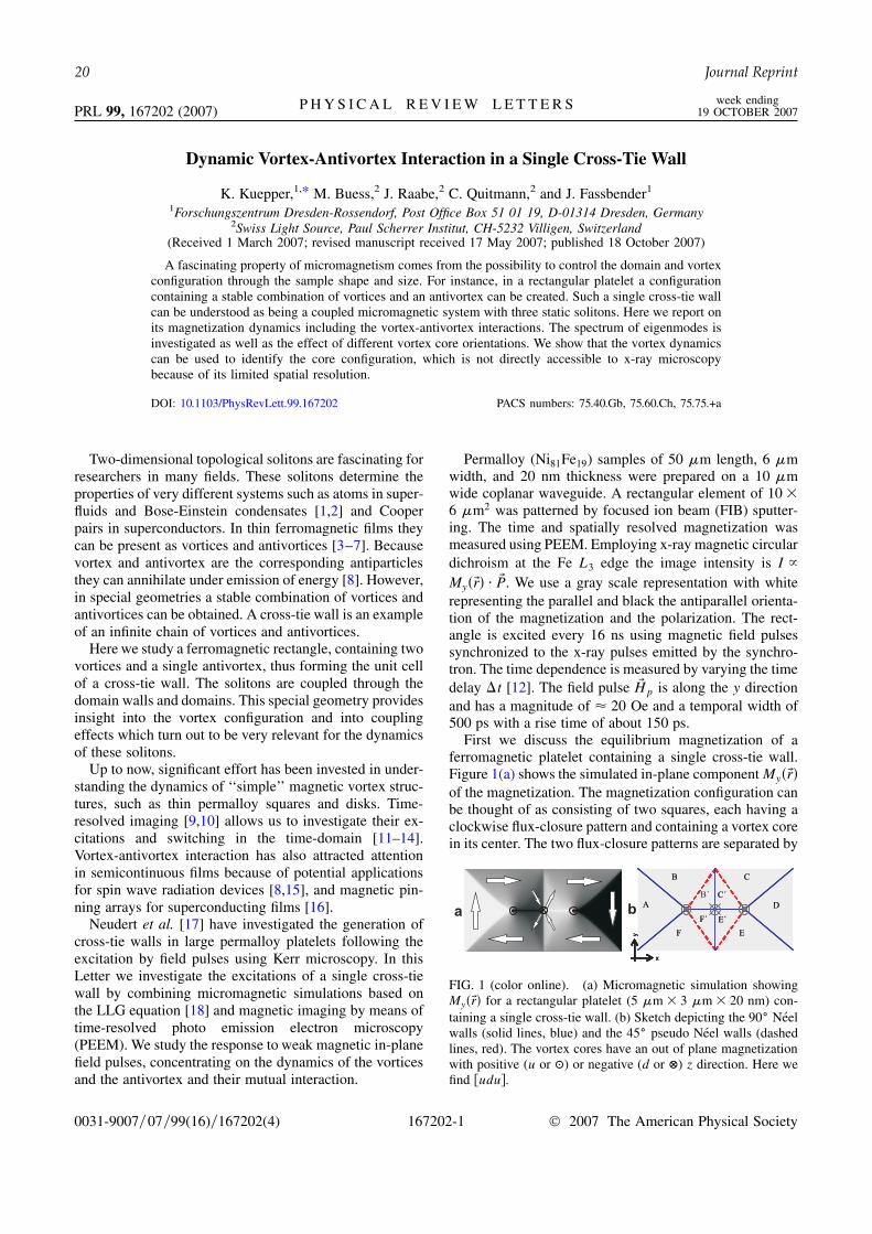
First we discuss the equilibrium magnetization of aferromagnetic platelet containing a single cross-tie wall.Figure 1(a) shows the simulated in-plane component My� ~r�of the magnetization. The magnetization configuration canbe thought of as consisting of two squares, each having aclockwise flux-closure pattern and containing a vortex corein its center. The two flux-closure patterns are separated by
y
x
yy
xx
FIG. 1 (color online). (a) Micromagnetic simulation showingMy�~r� for a rectangular platelet (5 �m� 3 �m� 20 nm) con-taining a single cross-tie wall. (b) Sketch depicting the 90� Neelwalls (solid lines, blue) and the 45� pseudo Neel walls (dashedlines, red). The vortex cores have an out of plane magnetizationwith positive (u or �) or negative (d or ) z direction. Here wefind �udu�.
PRL 99, 167202 (2007) P H Y S I C A L R E V I E W L E T T E R S week ending19 OCTOBER 2007
0031-9007=07=99(16)=167202(4) 167202-1 © 2007 The American Physical Society
20 Journal Reprint

a Neel wall of �90� running along the y axis and contain-ing the antivortex at the center. A second Neel wall con-necting the two vortex cores runs along the x axis [seeFig. 1(b)]. The cross-tie structure consists of these 90�Neel walls and four 45� pseudo Neel walls (dashed lines).The latter are pseudo domain walls, because along themthe magnetization rotates continuously (e.g., between do-mains B and B0). In addition there are four 90� Neel walls(solid lines) running from the platelet edges to the vortexcores. To reduce the exchange energy that would be asso-ciated with spins on neighboring atoms pointing antipar-allel, the magnetization of the vortex and antivortex rotatesout of plane in a narrow region called the core. This corecan point either in positive (u or �) or in negative (d or ) zdirection resulting in a total of 23 possible configurations.
PEEM images of the magnetization My� ~r;�t� of thepermalloy rectangle (10�m�6�m�20 nm) are shownin Fig. 2 (for a movie of the full series see Ref. [19]). Thetop row displays the experimental data, the second row thecorresponding micromagnetic simulations. The two subse-quent rows show difference images My�~r;�t� �My�~r; 0�for experiment and simulation, respectively. These differ-ence images visualize the changes relative to the equilib-rium state. In our geometry, the short edge of the rectangleis along the y direction and parallel to both the x-raypolarization ~P and the magnetic field pulse ~Hp.
The first image shows the equilibrium state of the mag-netization (�t � 0). The domains A-F are similar to do-mains in conventional flux-closure patterns. Domain A,which is parallel to y, is white and domain D, which isantiparallel, is black. Domains B, C, E, and F are graysince their magnetization is perpendicular to y. The do-mains B0, F0, C0, and E0 in the cross-tie are at �45� to yresulting in darker and lighter gray values, respectively.
Next we discuss the temporal evolution of the magneti-zation. At a delay of �t � 300 ps all domains having afinite x component of the magnetization in the equilibriumstate have become brighter. The reason is the torque ( ~M�~Hp) exerted by the field pulse causing an excursion in the z
direction followed by a precession. This rotates their mag-netization into the y direction leading to a higher intensity.Only domains A and D do not show such an increasedintensity because they are parallel and antiparallel to thefield pulse, respectively.
In addition the 90� Neel walls originating from the flux-closure pattern and the cross-tie wall pointing along ybulge to the right. In the difference images these effectsshow up as bright areas and lines, respectively. At �t �450 ps the coherent precession in the domains has contin-ued. The magnetization is almost perpendicular to y, re-sulting in a gray difference intensity. The bulged domainwalls are now even more intense than at �t � 300 ps andare visible in experiment and simulation. At �t � 600 psthe ongoing precession leads to a brighter appearance ofdomains B, C, E, and F again. For this delay time weobserve a maximum in the curvature of both, the cross-tie
wall along y and the 90� Neel walls along the black (D)and white (A) domains.
Turning to longer delays, the vortex dynamics becomesprominent. The difference images show that the Landaulike domains A-F have almost completely relaxed back tothe equilibrium state. The domain walls, the two vortices,and the antivortex, on the other hand, are still displaced,resulting in a finite intensity for the difference images. For1500 ps, the main visible features are the two vortices andthe antivortex, indicating their slow relaxation into theequilibrium state. For all delays we find reasonable agree-ment between simulation and experiment [20].
To gain further insight into the dynamics we perform aFourier transformation [21,22] of the experimental data,using a Hamming cutoff window. Large Fourier amplitudesindicate eigenfrequencies of the system. Figure 3 showsthe spatial distribution of the Fourier amplitude and phasefor the observed eigenfrequencies. For the higher frequen-cies (2.2 and 2.4 GHz) the intensity dominates in thedomains B, C, E, and F, all of which have their equilibriummagnetization perpendicular to ~Hp. The frequencies andthe observed phase shift of � (corresponding to a changefrom red to blue in Fig. 3) are in good agreement with thefindings in Landau flux-closure structures [12].
FIG. 2. Magnetization My�~r;�t) at characteristic delay times.Experimental results (top row) and difference images (third row)are compared to the corresponding simulation (second and fourthrow).
PRL 99, 167202 (2007) P H Y S I C A L R E V I E W L E T T E R S week ending19 OCTOBER 2007
167202-2
Annual Report IIM 2007, FZD-493 21
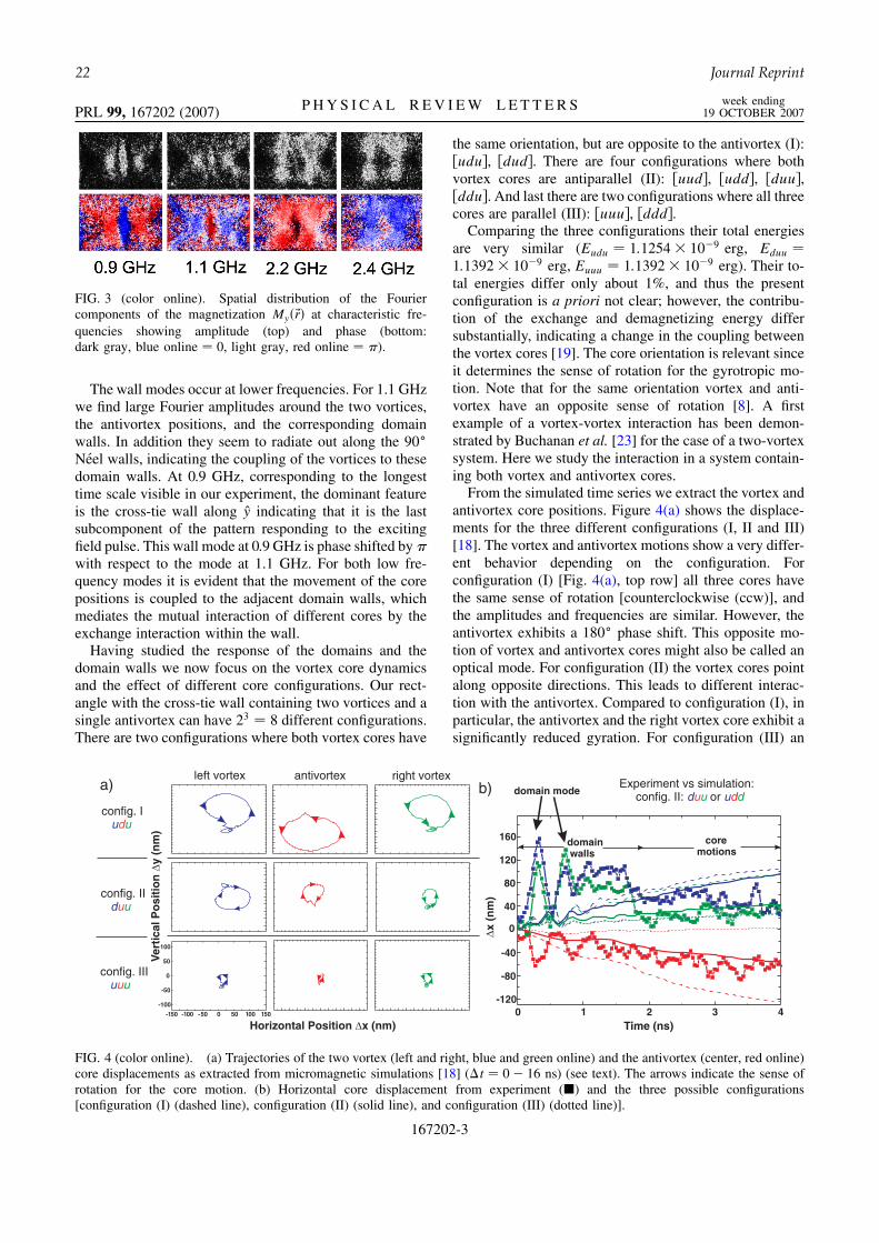
The wall modes occur at lower frequencies. For 1.1 GHzwe find large Fourier amplitudes around the two vortices,the antivortex positions, and the corresponding domainwalls. In addition they seem to radiate out along the 90�Neel walls, indicating the coupling of the vortices to thesedomain walls. At 0.9 GHz, corresponding to the longesttime scale visible in our experiment, the dominant featureis the cross-tie wall along y indicating that it is the lastsubcomponent of the pattern responding to the excitingfield pulse. This wall mode at 0.9 GHz is phase shifted by �with respect to the mode at 1.1 GHz. For both low fre-quency modes it is evident that the movement of the corepositions is coupled to the adjacent domain walls, whichmediates the mutual interaction of different cores by theexchange interaction within the wall.
Having studied the response of the domains and thedomain walls we now focus on the vortex core dynamicsand the effect of different core configurations. Our rect-angle with the cross-tie wall containing two vortices and asingle antivortex can have 23 � 8 different configurations.There are two configurations where both vortex cores have
the same orientation, but are opposite to the antivortex (I):�udu�, �dud�. There are four configurations where bothvortex cores are antiparallel (II): �uud�, �udd�, �duu�,�ddu�. And last there are two configurations where all threecores are parallel (III): �uuu�, �ddd�.
Comparing the three configurations their total energiesare very similar (Eudu � 1:1254� 10�9 erg, Eduu �1:1392� 10�9 erg, Euuu � 1:1392� 10�9 erg). Their to-tal energies differ only about 1%, and thus the presentconfiguration is a priori not clear; however, the contribu-tion of the exchange and demagnetizing energy differsubstantially, indicating a change in the coupling betweenthe vortex cores [19]. The core orientation is relevant sinceit determines the sense of rotation for the gyrotropic mo-tion. Note that for the same orientation vortex and anti-vortex have an opposite sense of rotation [8]. A firstexample of a vortex-vortex interaction has been demon-strated by Buchanan et al. [23] for the case of a two-vortexsystem. Here we study the interaction in a system contain-ing both vortex and antivortex cores.
From the simulated time series we extract the vortex andantivortex core positions. Figure 4(a) shows the displace-ments for the three different configurations (I, II and III)[18]. The vortex and antivortex motions show a very differ-ent behavior depending on the configuration. Forconfiguration (I) [Fig. 4(a), top row] all three cores havethe same sense of rotation [counterclockwise (ccw)], andthe amplitudes and frequencies are similar. However, theantivortex exhibits a 180� phase shift. This opposite mo-tion of vortex and antivortex cores might also be called anoptical mode. For configuration (II) the vortex cores pointalong opposite directions. This leads to different interac-tion with the antivortex. Compared to configuration (I), inparticular, the antivortex and the right vortex core exhibit asignificantly reduced gyration. For configuration (III) an
FIG. 3 (color online). Spatial distribution of the Fouriercomponents of the magnetization My�~r� at characteristic fre-quencies showing amplitude (top) and phase (bottom:dark gray, blue online � 0, light gray, red online � �).
Horizontal Position x (nm)
)m
n(y
noitis
oPlacitre
V
domain mode
domainwalls
coremotions
a) b)config. I
udu
config. IIduu
config. IIIuuu
Experiment vs simulation:config. II: ord uuu dd
0 1 2 3 4-120
-80
-40
0
40
80
120
160
Time (ns)
)m
n(x
left vortex antivortex right vortex
-150 -100 -50 0 50 100 150
-100
-50
0
50
100
FIG. 4 (color online). (a) Trajectories of the two vortex (left and right, blue and green online) and the antivortex (center, red online)core displacements as extracted from micromagnetic simulations [18] (�t � 0� 16 ns) (see text). The arrows indicate the sense ofrotation for the core motion. (b) Horizontal core displacement from experiment (�) and the three possible configurations[configuration (I) (dashed line), configuration (II) (solid line), and configuration (III) (dotted line)].
PRL 99, 167202 (2007) P H Y S I C A L R E V I E W L E T T E R S week ending19 OCTOBER 2007
167202-3
22 Journal Reprint

even more complex behavior is observed. The amplitudesof all three cores are even more reduced. The two vortexcores gyrate as expected (ccw) and again have comparableamplitudes. The antivortex core gyration is, however, op-posite from what was expected and its amplitude is reducedsignificantly. The reason is the interaction with the adjacentvortex cores, quenching the free gyration of the antivortex.The remaining five configurations can be deduced bymeans of symmetry considerations, provided the symmetrybreaking caused by the direction of the pulse field Hp isneglected.
From the above results it is evident that the vortex-antivortex interaction, mediated by the exchange interac-tion of the corresponding domain walls, is very importantfor the magnetization dynamics of a single cross-tie wall.All other systems comprising multiple vortex and/or anti-vortex structures are likely to exhibit an even more com-plex dynamic behavior which can only be explained with adetailed understanding of the individual constituents.
To finally determine which of the 23 possible coreconfigurations is present in our experiment we make useof the strong configuration dependence of the dynamicspresented in Fig. 4(a). The horizontal vortex displacementsdetermined from experiment and simulations are comparedin Fig. 4(b).
For configuration (II) we observe an agreement in thehorizontal displacement direction for all three movingcores and in addition comparable amplitudes for �t *2 ns. For �t & 2 ns the movements of the domain andthe domain walls are strongly overlapping the vortex andantivortex movements (see Fig. 2) leading to a large un-certainty in the experimental determination of the coreposition. The horizontal displacement of the antivortexand the right vortex is very well reproduced, whereas theleft vortex shows a somewhat larger displacement in thesimulation; however, this deviation is comparable to theprecision of the core determination of about 30 nm.
An analysis of the vertical displacement is more difficultbecause of the reduced amplitudes and is not shown. Wecan therefore not distinguish between a �duu� and a �udd�configuration consistent with the horizontal displacementobserved for configuration (II). However, we can concludethat one vortex is antiparallel to the antivortex and the othervortex core in the present experiment.
In summary, we report results of vortex-antivortex dy-namics. These include the dynamics of antivortices and theindirect coupling between vortex cores and the antivortex,which is mediated by the exchange interaction of theadjacent domain walls. This coupling is significant andintroduces unexpected effects, such as the quenching ofgyrotropic motion for the antivortex in certain core con-figurations. Another consequence is the absence of simpleeigenmodes describing the vortex gyration. By using simu-lations the strong influence of the vortex coupling on thecore dynamics can in turn be used to determine the core
configuration, a parameter otherwise inaccessible to directobservation.
Part of this work has been performed at the Swiss LightSource, Paul Scherrer Institut, Villigen, Switzerland. Weare grateful to L. Bischoff for performing FIB. We thankS. Wintz, B. Liedke, M. R. Scheinfein, and C. H. Backfor support and helpful discussions. We are indebted toD. Weiss (University of Regensburg) for making the clean-room available.
*[email protected][1] D. R. Tilley and J. Tilley, Superfluidity and Super-
conductivity (IOP Publishing Ltd., Bristol, 1990), 3rd ed..[2] M. R. Matthews et al., Phys. Rev. Lett. 83, 2498 (1999).[3] G. Blatter et al., Rev. Mod. Phys. 66, 1125 (1994).[4] C. Kittel, Rev. Mod. Phys. 21, 541 (1949).[5] A. Hubert and R. Schafer, Magnetic Domains (Springer,
Berlin, 1998).[6] J. Raabe et al., J. Appl. Phys. 88, 4437 (2000).[7] A. Wachowiak et al., Science 298, 577 (2002).[8] R. Hertel and C. M. Schneider, Phys. Rev. Lett. 97, 177202
(2006).[9] Y. Acremann et al., Science 290, 492 (2000).
[10] T. Gerrits et al., Nature (London) 418, 509 (2002).[11] S.-B. Choe et al., Science 304, 420 (2004).[12] J. Raabe et al., Phys. Rev. Lett. 94, 217204 (2005).[13] K. Kuepper et al., Appl. Phys. Lett. 90, 062506 (2007).[14] B. van Waeyenberge et al., Nature (London) 444, 461
(2006).[15] S.-K. Kim et al., Appl. Phys. Lett. 86, 052504 (2005).[16] M. V. Milosevic and F. M. Peeters, Phys. Rev. Lett. 93,
267006 (2004).[17] A. Neudert et al., J. Appl. Phys. 99, 08F302 (2006).[18] http://llgmicro.home.mindspring.com We use standard
permalloy material parameters: exchange constant A �8� 10�12 J=m, saturation magnetization Ms �860:000 A=m, magnetic damping constant � � 0:01, uni-axial anisotropy Ku � 0. To take into account a possibleresonant excitation we simulate a sequence of five fullexcitation cycles (every 16 ns) for each configuration. Weobserve no significant change in the frequencies or thetrajectories of the vortex cores, only the amplitudes of thetrajectories increase. For the analysis we use the averagedresults of the third—fifth excitation cycles.
[19] See EPAPS Document No. E-PRLTAO-99-053742 for atable displaying the energies of the three configuations anda movie of the data shown in Fig. 2. For more informationon EPAPS, see http://www.aip.org/pubservs/epaps.html.
[20] Simulations were done for a rectangle of (5 �m�3 �m� 20 nm) and a cell size of 5� 5� 20 nm3 tolimit the neccessary memory and and computing times.The experiments are done on larger rectangles of(10 �m� 6 �m� 20 nm). We find good agreement be-tween simulation and experiment justifying reduced sizefor the simulation.
[21] J. P. Park et al., Phys. Rev. B 67, 020403 (2003).[22] M. Buess et al., Phys. Rev. Lett. 93, 077207 (2004).[23] K. S. Buchanan et al., Nature Phys. 1, 172 (2005).
PRL 99, 167202 (2007) P H Y S I C A L R E V I E W L E T T E R S week ending19 OCTOBER 2007
167202-4
Annual Report IIM 2007, FZD-493 23
Induced anisotropies in exchange-coupled systems on rippled substrates
M. O. Liedke,1,2 B. Liedke,1 A. Keller,1 B. Hillebrands,2 A. Mücklich,1 S. Facsko,1 and J. Fassbender1,*1Institute of Ion Beam Physics and Materials Research, Forschungszentrum Dresden-Rossendorf, P.O. Box 51 01 19, D-01314
Dresden, Germany2Fachbereich Physik, TU Kaiserslautern, Erwin-Schroedinger-Strasse 56, D-67663 Kaiserslautern, Germany
�Received 1 June 2007; published 25 June 2007�
The role of monoatomic steps at the mutual interface between a ferromagnetic and an antiferromagneticlayer in a Ni81Fe19/Fe50Mn50 exchange bias system is enlightened. For this purpose a special ripple substratewith a well defined morphology is used. Due to the film morphology a strong uniaxial anisotropy is induced inthe polycrystalline Ni81Fe19 layer, which is fixed in its orientation. By means of different field annealing cyclesthe direction of the induced unidirectional anisotropy can be chosen. For all mutual orientations both aniso-tropy contributions are superimposed independently and the angular dependence of the magnetization reversalbehavior can be described perfectly by a coherent rotation model with one parameter set. In addition it isdemonstrated that the magnitude of the unidirectional anisotropy contribution scales with the step density ofthe substrate, which is in full agreement with theoretical predictions.
DOI: 10.1103/PhysRevB.75.220407 PACS number�s�: 75.30.Gw, 68.35.Ct, 75.70.Cn, 75.75. a
A thin ferromagnetic layer experiences a unidirectionalanisotropy when an internal magnetic field is created due tothe exchange coupling to an antiferromagnetic layer of suf-ficient thickness.1,2 A shift of the hysteresis loop, the so-called exchange bias field Heb, is observed if the inducedinternal field exhibits a well defined direction. This is con-ventionally achieved by a field annealing cycle, i.e., the mag-netization of the ferromagnetic layer is aligned along anydesired direction, when the antiferromagnetic layer is cooleddown below the blocking temperature. By doing so the spinconfiguration of the antiferromagnetic layer is frozen andgenerates an internal magnetic field which acts on the ferro-magnetic layer. Since in a polycrystalline film the grains areusually randomly oriented in the film plane, no higher-orderanisotropies are present and the angular dependence of Hebfollows a simple cosine behavior, Heb��M�=Heb�cos��M
−�K1�, as expected from a coherent rotation model. �M ��K1
�is the angle between the magnetization direction �field-cooling direction� and a reference direction. However, ifhigher-order anisotropy contributions are present, as, for ex-ample, magnetocrystalline contributions in epitaxialsystems,3–6 buffer induced anisotropy contributions,7,8 orshape anisotropy contributions in patterned films,9,10 a com-plicated angular dependence of the magnetization reversalbehavior is observed. If in addition interfacial roughnesscomes into play, even more parameters enter the magnetiza-tion reversal process,11–13 which further complicate the inter-pretation. In general, in experimental papers addressing theeffect of interfacial roughness published so far, the amount ofroughness could neither be varied easily nor quantified abso-lutely. Thus no consensus about the effect of interfacialroughness on the unidirectional anisotropy could beachieved.
In this Rapid Communication a special template system isused which allows us �i� to easily determine the step densityand thus the interfacial roughness, and �ii� to induce a stronguniaxial anisotropy which is directly related to the highlyanisotropic step distribution. Thereby we can �i� unambigu-ously determine the roughness induced increase in unidirec-tional anisotropy, and �ii� since by means of different
magnetic-field annealing cycles the mutual angle betweenuniaxial and unidirectional anisotropy can be chosen inde-pendently, we can study their potential intercorrelation.
In order to create such a template system, self-organizedripple formation during low-energy ion erosion is employed.This process is well known for semiconductor surfaces,14,15
where rather high topographic modulations �typically2–20 nm� can be achieved. However, due to the ion erosionprocess the sample surface is amorphized. Ripple formationhas also been studied for metallic surfaces and magnetic thinfilms.16–18 In these cases the topographic modulations aremuch smaller ��0.2 nm� and so far these investigations arerestricted to single crystalline surfaces. Therefore step-ormorphology-induced anisotropy contributions are always su-perimposed by magnetocrystalline contributions. In order tosimplify the interpretation of our results, magnetocrystallineanisotropy contributions have to be circumvented. This hasbeen achieved by the deposition of initially low anisotropicpolycrystalline Ni81Fe19 films on top of rippled Si surfaces.
The Si templates are created by 500-eV Ar+ sputtering ofa Si�001� wafer with an incident angle of 67° with respect tothe surface normal in high vacuum. A sputter fluence of 1�1018 ions/cm2 leads to a modulated Si surface which afterdeposition of a metallic buffer produces subsequently a highanisotropic step density �see Fig. 1�. After ion erosion thetemplates have been removed from the vacuum chamberwhich leads to a natural oxide of 2–4 nm on the surface.Subsequent to initial atomic force microscopy �AFM� char-acterization the template was inserted into a molecular-beamepitaxy system. Prior to film deposition the sample washeated to 250 °C in order to clean the sample surface. Sub-sequently the whole layer stack, 2-nm Mn/9-nmNi81Fe19/10-nm Fe50Mn50/2-nm Cr, was deposited at roomtemperature by e-beam evaporation �Cr, Ni81Fe19, Fe� andfrom a Knudsen cell �Mn�, respectively. In order to comparethe exchange bias system with the single ferromagnetic layer,the antiferromagnetic FeMn layer was deposited on half ofthe sample only. Subsequently the surface topography wasreinvestigated by means of ex situ AFM. In order to furtherclarify the film morphology, cross-sectional transmission
PHYSICAL REVIEW B 75, 220407�R� �2007�
RAPID COMMUNICATIONS
1098-0121/2007/75�22�/220407�4� ©2007 The American Physical Society220407-1
24 Journal Reprint
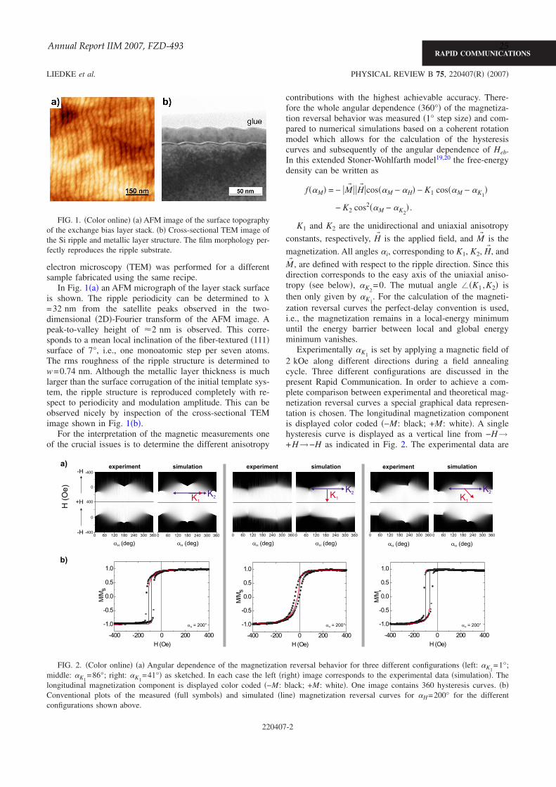
electron microscopy �TEM� was performed for a differentsample fabricated using the same recipe.
In Fig. 1�a� an AFM micrograph of the layer stack surfaceis shown. The ripple periodicity can be determined to �=32 nm from the satellite peaks observed in the two-dimensional �2D�-Fourier transform of the AFM image. Apeak-to-valley height of 2 nm is observed. This corre-sponds to a mean local inclination of the fiber-textured �111�surface of 7°, i.e., one monoatomic step per seven atoms.The rms roughness of the ripple structure is determined tow=0.74 nm. Although the metallic layer thickness is muchlarger than the surface corrugation of the initial template sys-tem, the ripple structure is reproduced completely with re-spect to periodicity and modulation amplitude. This can beobserved nicely by inspection of the cross-sectional TEMimage shown in Fig. 1�b�.
For the interpretation of the magnetic measurements oneof the crucial issues is to determine the different anisotropy
contributions with the highest achievable accuracy. There-fore the whole angular dependence �360°� of the magnetiza-tion reversal behavior was measured �1° step size� and com-pared to numerical simulations based on a coherent rotationmodel which allows for the calculation of the hysteresiscurves and subsequently of the angular dependence of Heb.In this extended Stoner-Wohlfarth model19,20 the free-energydensity can be written as
f��M� = − M� H� cos��M − �H� − K1 cos��M − �K1�
− K2 cos2��M − �K2� .
K1 and K2 are the unidirectional and uniaxial anisotropy
constants, respectively, H� is the applied field, and M� is the
magnetization. All angles �i, corresponding to K1, K2, H� , and
M� , are defined with respect to the ripple direction. Since thisdirection corresponds to the easy axis of the uniaxial aniso-tropy �see below�, �K2
=0. The mutual angle ��K1 ,K2� isthen only given by �K1
. For the calculation of the magneti-zation reversal curves the perfect-delay convention is used,i.e., the magnetization remains in a local-energy minimumuntil the energy barrier between local and global energyminimum vanishes.
Experimentally �K1is set by applying a magnetic field of
2 kOe along different directions during a field annealingcycle. Three different configurations are discussed in thepresent Rapid Communication. In order to achieve a com-plete comparison between experimental and theoretical mag-netization reversal curves a special graphical data represen-tation is chosen. The longitudinal magnetization componentis displayed color coded �−M: black; +M: white�. A singlehysteresis curve is displayed as a vertical line from −H→+H→−H as indicated in Fig. 2. The experimental data are
FIG. 2. �Color online� �a� Angular dependence of the magnetization reversal behavior for three different configurations �left: �K1=1°;
middle: �K1=86°; right: �K1
=41°� as sketched. In each case the left �right� image corresponds to the experimental data �simulation�. Thelongitudinal magnetization component is displayed color coded �−M: black; +M: white�. One image contains 360 hysteresis curves. �b�Conventional plots of the measured �full symbols� and simulated �line� magnetization reversal curves for �H=200° for the differentconfigurations shown above.
FIG. 1. �Color online� �a� AFM image of the surface topographyof the exchange bias layer stack. �b� Cross-sectional TEM image ofthe Si ripple and metallic layer structure. The film morphology per-fectly reproduces the ripple substrate.
LIEDKE et al. PHYSICAL REVIEW B 75, 220407�R� �2007�
RAPID COMMUNICATIONS
220407-2
Annual Report IIM 2007, FZD-493 25
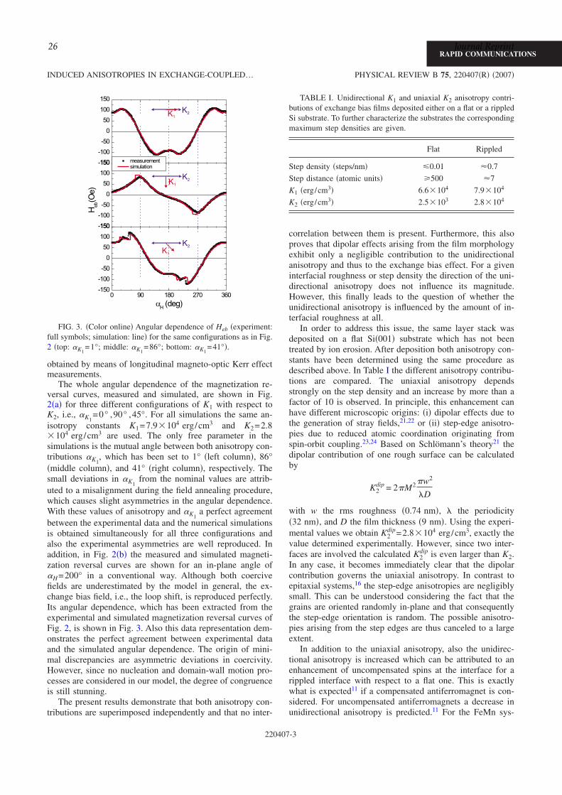
obtained by means of longitudinal magneto-optic Kerr effectmeasurements.
The whole angular dependence of the magnetization re-versal curves, measured and simulated, are shown in Fig.2�a� for three different configurations of K1 with respect toK2, i.e., �K1
=0° ,90° ,45°. For all simulations the same an-isotropy constants K1=7.9�104 erg/cm3 and K2=2.8�104 erg/cm3 are used. The only free parameter in thesimulations is the mutual angle between both anisotropy con-tributions �K1
, which has been set to 1° �left column�, 86°�middle column�, and 41° �right column�, respectively. Thesmall deviations in �K1
from the nominal values are attrib-uted to a misalignment during the field annealing procedure,which causes slight asymmetries in the angular dependence.With these values of anisotropy and �K1
a perfect agreementbetween the experimental data and the numerical simulationsis obtained simultaneously for all three configurations andalso the experimental asymmetries are well reproduced. Inaddition, in Fig. 2�b� the measured and simulated magneti-zation reversal curves are shown for an in-plane angle of�H=200° in a conventional way. Although both coercivefields are underestimated by the model in general, the ex-change bias field, i.e., the loop shift, is reproduced perfectly.Its angular dependence, which has been extracted from theexperimental and simulated magnetization reversal curves ofFig. 2, is shown in Fig. 3. Also this data representation dem-onstrates the perfect agreement between experimental dataand the simulated angular dependence. The origin of mini-mal discrepancies are asymmetric deviations in coercivity.However, since no nucleation and domain-wall motion pro-cesses are considered in our model, the degree of congruenceis still stunning.
The present results demonstrate that both anisotropy con-tributions are superimposed independently and that no inter-
correlation between them is present. Furthermore, this alsoproves that dipolar effects arising from the film morphologyexhibit only a negligible contribution to the unidirectionalanisotropy and thus to the exchange bias effect. For a giveninterfacial roughness or step density the direction of the uni-directional anisotropy does not influence its magnitude.However, this finally leads to the question of whether theunidirectional anisotropy is influenced by the amount of in-terfacial roughness at all.
In order to address this issue, the same layer stack wasdeposited on a flat Si�001� substrate which has not beentreated by ion erosion. After deposition both anisotropy con-stants have been determined using the same procedure asdescribed above. In Table I the different anisotropy contribu-tions are compared. The uniaxial anisotropy dependsstrongly on the step density and an increase by more than afactor of 10 is observed. In principle, this enhancement canhave different microscopic origins: �i� dipolar effects due tothe generation of stray fields,21,22 or �ii� step-edge anisotro-pies due to reduced atomic coordination originating fromspin-orbit coupling.23,24 Based on Schlömann’s theory21 thedipolar contribution of one rough surface can be calculatedby
K2dip = 2�M2�w2
�D
with w the rms roughness �0.74 nm�, � the periodicity�32 nm�, and D the film thickness �9 nm�. Using the experi-mental values we obtain K2
dip=2.8�104 erg/cm3, exactly thevalue determined experimentally. However, since two inter-faces are involved the calculated K2
dip is even larger than K2.In any case, it becomes immediately clear that the dipolarcontribution governs the uniaxial anisotropy. In contrast toepitaxial systems,16 the step-edge anisotropies are negligiblysmall. This can be understood considering the fact that thegrains are oriented randomly in-plane and that consequentlythe step-edge orientation is random. The possible anisotro-pies arising from the step edges are thus canceled to a largeextent.
In addition to the uniaxial anisotropy, also the unidirec-tional anisotropy is increased which can be attributed to anenhancement of uncompensated spins at the interface for arippled interface with respect to a flat one. This is exactlywhat is expected11 if a compensated antiferromagnet is con-sidered. For uncompensated antiferromagnets a decrease inunidirectional anisotropy is predicted.11 For the FeMn sys-
FIG. 3. �Color online� Angular dependence of Heb �experiment:full symbols; simulation: line� for the same configurations as in Fig.2 �top: �K1
=1°; middle: �K1=86°; bottom: �K1
=41°�.
TABLE I. Unidirectional K1 and uniaxial K2 anisotropy contri-butions of exchange bias films deposited either on a flat or a rippledSi substrate. To further characterize the substrates the correspondingmaximum step densities are given.
Flat Rippled
Step density �steps/nm� �0.01 0.7
Step distance �atomic units� �500 7
K1 �erg/cm3� 6.6�104 7.9�104
K2 �erg/cm3� 2.5�103 2.8�104
INDUCED ANISOTROPIES IN EXCHANGE-COUPLED… PHYSICAL REVIEW B 75, 220407�R� �2007�
RAPID COMMUNICATIONS
220407-3
26 Journal Reprint
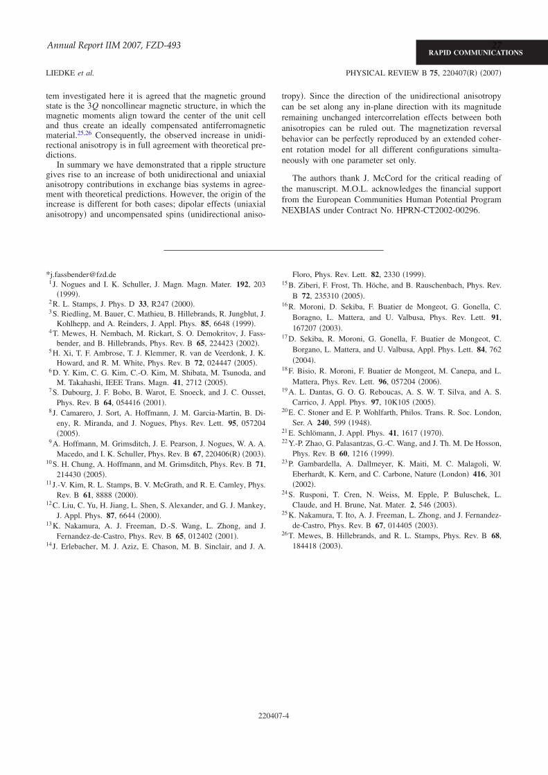
tem investigated here it is agreed that the magnetic groundstate is the 3Q noncollinear magnetic structure, in which themagnetic moments align toward the center of the unit celland thus create an ideally compensated antiferromagneticmaterial.25,26 Consequently, the observed increase in unidi-rectional anisotropy is in full agreement with theoretical pre-dictions.
In summary we have demonstrated that a ripple structuregives rise to an increase of both unidirectional and uniaxialanisotropy contributions in exchange bias systems in agree-ment with theoretical predictions. However, the origin of theincrease is different for both cases; dipolar effects �uniaxialanisotropy� and uncompensated spins �unidirectional aniso-
tropy�. Since the direction of the unidirectional anisotropycan be set along any in-plane direction with its magnituderemaining unchanged intercorrelation effects between bothanisotropies can be ruled out. The magnetization reversalbehavior can be perfectly reproduced by an extended coher-ent rotation model for all different configurations simulta-neously with one parameter set only.
The authors thank J. McCord for the critical reading ofthe manuscript. M.O.L. acknowledges the financial supportfrom the European Communities Human Potential ProgramNEXBIAS under Contract No. HPRN-CT2002-00296.
*[email protected] J. Nogues and I. K. Schuller, J. Magn. Magn. Mater. 192, 203
�1999�.2 R. L. Stamps, J. Phys. D 33, R247 �2000�.3 S. Riedling, M. Bauer, C. Mathieu, B. Hillebrands, R. Jungblut, J.
Kohlhepp, and A. Reinders, J. Appl. Phys. 85, 6648 �1999�.4 T. Mewes, H. Nembach, M. Rickart, S. O. Demokritov, J. Fass-
bender, and B. Hillebrands, Phys. Rev. B 65, 224423 �2002�.5 H. Xi, T. F. Ambrose, T. J. Klemmer, R. van de Veerdonk, J. K.
Howard, and R. M. White, Phys. Rev. B 72, 024447 �2005�.6 D. Y. Kim, C. G. Kim, C.-O. Kim, M. Shibata, M. Tsunoda, and
M. Takahashi, IEEE Trans. Magn. 41, 2712 �2005�.7 S. Dubourg, J. F. Bobo, B. Warot, E. Snoeck, and J. C. Ousset,
Phys. Rev. B 64, 054416 �2001�.8 J. Camarero, J. Sort, A. Hoffmann, J. M. Garcia-Martin, B. Di-
eny, R. Miranda, and J. Nogues, Phys. Rev. Lett. 95, 057204�2005�.
9 A. Hoffmann, M. Grimsditch, J. E. Pearson, J. Nogues, W. A. A.Macedo, and I. K. Schuller, Phys. Rev. B 67, 220406�R� �2003�.
10 S. H. Chung, A. Hoffmann, and M. Grimsditch, Phys. Rev. B 71,214430 �2005�.
11 J.-V. Kim, R. L. Stamps, B. V. McGrath, and R. E. Camley, Phys.Rev. B 61, 8888 �2000�.
12 C. Liu, C. Yu, H. Jiang, L. Shen, S. Alexander, and G. J. Mankey,J. Appl. Phys. 87, 6644 �2000�.
13 K. Nakamura, A. J. Freeman, D.-S. Wang, L. Zhong, and J.Fernandez-de-Castro, Phys. Rev. B 65, 012402 �2001�.
14 J. Erlebacher, M. J. Aziz, E. Chason, M. B. Sinclair, and J. A.
Floro, Phys. Rev. Lett. 82, 2330 �1999�.15 B. Ziberi, F. Frost, Th. Höche, and B. Rauschenbach, Phys. Rev.
B 72, 235310 �2005�.16 R. Moroni, D. Sekiba, F. Buatier de Mongeot, G. Gonella, C.
Boragno, L. Mattera, and U. Valbusa, Phys. Rev. Lett. 91,167207 �2003�.
17 D. Sekiba, R. Moroni, G. Gonella, F. Buatier de Mongeot, C.Borgano, L. Mattera, and U. Valbusa, Appl. Phys. Lett. 84, 762�2004�.
18 F. Bisio, R. Moroni, F. Buatier de Mongeot, M. Canepa, and L.Mattera, Phys. Rev. Lett. 96, 057204 �2006�.
19 A. L. Dantas, G. O. G. Reboucas, A. S. W. T. Silva, and A. S.Carrico, J. Appl. Phys. 97, 10K105 �2005�.
20 E. C. Stoner and E. P. Wohlfarth, Philos. Trans. R. Soc. London,Ser. A 240, 599 �1948�.
21 E. Schlömann, J. Appl. Phys. 41, 1617 �1970�.22 Y.-P. Zhao, G. Palasantzas, G.-C. Wang, and J. Th. M. De Hosson,
Phys. Rev. B 60, 1216 �1999�.23 P. Gambardella, A. Dallmeyer, K. Maiti, M. C. Malagoli, W.
Eberhardt, K. Kern, and C. Carbone, Nature �London� 416, 301�2002�.
24 S. Rusponi, T. Cren, N. Weiss, M. Epple, P. Buluschek, L.Claude, and H. Brune, Nat. Mater. 2, 546 �2003�.
25 K. Nakamura, T. Ito, A. J. Freeman, L. Zhong, and J. Fernandez-de-Castro, Phys. Rev. B 67, 014405 �2003�.
26 T. Mewes, B. Hillebrands, and R. L. Stamps, Phys. Rev. B 68,184418 �2003�.
LIEDKE et al. PHYSICAL REVIEW B 75, 220407�R� �2007�
RAPID COMMUNICATIONS
220407-4
Annual Report IIM 2007, FZD-493 27

Suppression of secondary phase formation in Fe implanted ZnO singlecrystals
K. Potzger,a� Shengqiang Zhou, H. Reuther, K. Kuepper, G. Talut,M. Helm, and J. FassbenderInstitute of Ion Beam Physics and Materials Research, Forschungszentrum Dresden-Rossendorf,P.O. Box 510119, 01314 Dresden, Germany
J. D. DenlingerAdvanced Light Source, Lawrence Berkeley National Laboratory, Berkeley, California 94720
�Received 11 April 2007; accepted 12 July 2007; published online 7 August 2007�
Unwanted secondary phases are one of the major problems in diluted magnetic semiconductorcreation. Here, the authors show possibilities to avoid such phases in Fe implanted and postannealedZnO�0001� single crystals. While �-Fe nanoparticles are formed after such doping in as-polishedcrystals, high temperature �1273 K� annealing in O2 or high vacuum before implantation suppressesthese phases. Thus, the residual saturation magnetization in the preannealed ZnO single crystals isabout 20 times lower than for the as-polished ones and assigned to indirect coupling betweenisolated Fe ions rather than to clusters. © 2007 American Institute of Physics.�DOI: 10.1063/1.2768196�
Diluted magnetic semiconductors �DMSs� such as tran-sition metal �TM� doped ZnO have recently attracted hugeattention due to their application potential in spintronics.1,2
Especially for rather easy available n-type ZnO, TM dopantssuch as Fe or Co but not Mn are theoretically predicted toyield ferromagnetic coupling.2 One of the major drawbacksin preparation is the unwanted formation of magnetic sec-ondary phases for high TM concentrations ��5% �necessary3–5 mimicking a room-temperature DMS. In thisletter, we show that unwanted secondary phases in ZnOsingle crystals implant doped with Fe can be avoided byannealing the crystals prior to implantation. Moreover, weakferromagnetic properties are introduced that are not related toordinary superparamagnetic nanoparticles. Thus, the follow-ing sample set has been prepared from hydrothermal, com-mercial epipolished ZnO�0001� substrates purchased fromCrystec: �1� nonpreannealed, i.e., as polished, �2� O2 prean-nealed in flowing O2 at 1273 K for 15 min, and �3� vacuumpreannealed in high vacuum �base pressure �1�10−6 mbar�at 1273 K for 15 min. O2 annealing at high temperatures isknown to reduce lattice damage in the near surface region ofZnO.6,7 Vacuum annealing �3�, was chosen due to the forma-tion of point defects that might mediate indirect ferromag-netic coupling of the implanted ions.8–10 Note that mildvacuum annealing around 873 K usually introduces both Ovacancies and Zn interstitials.11 After high temperature an-nealing, however, Zn interstitials are not stable, i.e., the de-fects are dominated by oxygen vacancies.12 Following thatpaper, oxygen vacancies are not expected to mediate ferro-magnetic coupling, while Zn interstitials are. Thus, our ap-proach, in addition to the suppression of secondary phases,would give a confirmation of these different effects of vari-ous kinds of defects for the case of Fe doping. For furtherprocessing, our samples were subjected to 57Fe ion implan-tation. The implantation energy was 80 keV at an incidentangle of 7° yielding a projected range of 38 nm and a strag-gling of 17 nm �TRIM�. The implanted Fe fluence of 2
�1016 cm−2 yielded a maximum atomic concentration of5%. In order to avoid magnetic secondary phases already inthe as-implanted samples, a low implantation temperature of253 K was used.3 Postimplantation annealing for lattice re-covery was performed in high vacuum at a temperature of823 K for 15 min. The base pressure was below 1�10−6 mbar. The particular parameters for the postannealinghave been chosen to avoid long-range diffusion and oxida-tion of the implanted Fe as have been observed earlier forhigher annealing temperatures.4 For a detailed analysis weapplied x-ray diffraction �XRD� using a Siemens D 5005diffractometer equipped with a Göbel mirror for enhancedbrilliance, Rutherford backscattering/channeling �RBS/C�,atomic force microscopy �AFM�, conversion electron Möss-bauer spectroscopy �CEMS� at room temperature, x-ray ab-sorption spectroscopy �XAS� performed at beam line 8.0.1 ofthe Advanced Light Source in Berkeley, and superconductingquantum interference device �SQUID� magnetometry withthe magnetic field applied parallel to the sample surface.RBS/C revealed no significant change of the crystallinity af-ter preannealing. In contrast, AFM �not shown� reveals pro-nounced changes of the crystal surface morphology. After O2preannealing, the root mean square surface roughness �Rq� ofthe ZnO sample slightly increases from 0.23 to 0.27 nm andregularly oriented steps appear. The latter is an indication forsurface recrystallization.7 Vacuum preannealing, in contrast,yielded a surface roughness of 23 nm. While after implanta-tion a slight increase of Rq is detectable, postannealing doesnot change Rq significantly for any of the samples. RBS/Cfor both the preannealed and nonpreannealed crystals �Fig.1�a�� shows a decrease of the minimum channeling yield��min� with postannealing. The drop is largest for the nonpre-annealed crystal and smallest for the vacuum preannealedsample. The lowest �min is achieved for the O2 preannealedcrystal. �min directly reflects the crystalline homogeneity, i.e.,while an amorphous sample shows a �min of 100%, a perfectsingle crystalline sample exhibits 1%–2%. Diffusion of theimplanted Fe due to postannealing could be ruled out bymeans of RBS/C random spectra �Fig. 1�b��. Bumps origi-a�Electronic mail: [email protected]
APPLIED PHYSICS LETTERS 91, 062107 �2007�
0003-6951/2007/91�6�/062107/3/$23.00 © 2007 American Institute of Physics91, 062107-1Downloaded 20 Feb 2008 to 149.220.35.103. Redistribution subject to AIP license or copyright; see http://apl.aip.org/apl/copyright.jsp
28 Journal Reprint
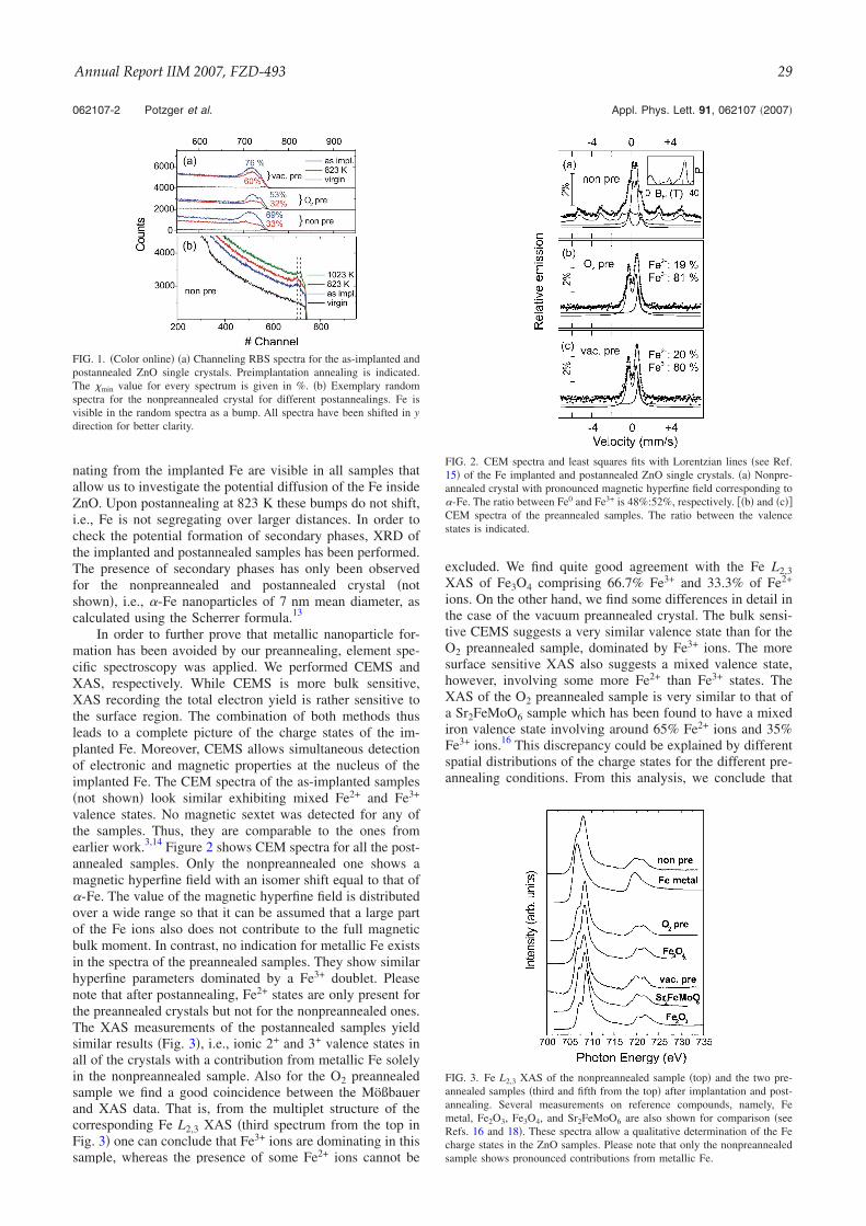
nating from the implanted Fe are visible in all samples thatallow us to investigate the potential diffusion of the Fe insideZnO. Upon postannealing at 823 K these bumps do not shift,i.e., Fe is not segregating over larger distances. In order tocheck the potential formation of secondary phases, XRD ofthe implanted and postannealed samples has been performed.The presence of secondary phases has only been observedfor the nonpreannealed and postannealed crystal �notshown�, i.e., �-Fe nanoparticles of 7 nm mean diameter, ascalculated using the Scherrer formula.13
In order to further prove that metallic nanoparticle for-mation has been avoided by our preannealing, element spe-cific spectroscopy was applied. We performed CEMS andXAS, respectively. While CEMS is more bulk sensitive,XAS recording the total electron yield is rather sensitive tothe surface region. The combination of both methods thusleads to a complete picture of the charge states of the im-planted Fe. Moreover, CEMS allows simultaneous detectionof electronic and magnetic properties at the nucleus of theimplanted Fe. The CEM spectra of the as-implanted samples�not shown� look similar exhibiting mixed Fe2+ and Fe3+
valence states. No magnetic sextet was detected for any ofthe samples. Thus, they are comparable to the ones fromearlier work.3,14 Figure 2 shows CEM spectra for all the post-annealed samples. Only the nonpreannealed one shows amagnetic hyperfine field with an isomer shift equal to that of�-Fe. The value of the magnetic hyperfine field is distributedover a wide range so that it can be assumed that a large partof the Fe ions also does not contribute to the full magneticbulk moment. In contrast, no indication for metallic Fe existsin the spectra of the preannealed samples. They show similarhyperfine parameters dominated by a Fe3+ doublet. Pleasenote that after postannealing, Fe2+ states are only present forthe preannealed crystals but not for the nonpreannealed ones.The XAS measurements of the postannealed samples yieldsimilar results �Fig. 3�, i.e., ionic 2+ and 3+ valence states inall of the crystals with a contribution from metallic Fe solelyin the nonpreannealed sample. Also for the O2 preannealedsample we find a good coincidence between the Mößbauerand XAS data. That is, from the multiplet structure of thecorresponding Fe L2,3 XAS �third spectrum from the top inFig. 3� one can conclude that Fe3+ ions are dominating in thissample, whereas the presence of some Fe2+ ions cannot be
excluded. We find quite good agreement with the Fe L2,3XAS of Fe3O4 comprising 66.7% Fe3+ and 33.3% of Fe2+
ions. On the other hand, we find some differences in detail inthe case of the vacuum preannealed crystal. The bulk sensi-tive CEMS suggests a very similar valence state than for theO2 preannealed sample, dominated by Fe3+ ions. The moresurface sensitive XAS also suggests a mixed valence state,however, involving some more Fe2+ than Fe3+ states. TheXAS of the O2 preannealed sample is very similar to that ofa Sr2FeMoO6 sample which has been found to have a mixediron valence state involving around 65% Fe2+ ions and 35%Fe3+ ions.16 This discrepancy could be explained by differentspatial distributions of the charge states for the different pre-annealing conditions. From this analysis, we conclude that
FIG. 1. �Color online� �a� Channeling RBS spectra for the as-implanted andpostannealed ZnO single crystals. Preimplantation annealing is indicated.The �min value for every spectrum is given in %. �b� Exemplary randomspectra for the nonpreannealed crystal for different postannealings. Fe isvisible in the random spectra as a bump. All spectra have been shifted in ydirection for better clarity.
FIG. 2. CEM spectra and least squares fits with Lorentzian lines �see Ref.15� of the Fe implanted and postannealed ZnO single crystals. �a� Nonpre-annealed crystal with pronounced magnetic hyperfine field corresponding to�-Fe. The ratio between Fe0 and Fe3+ is 48%:52%, respectively. ��b� and �c��CEM spectra of the preannealed samples. The ratio between the valencestates is indicated.
FIG. 3. Fe L2,3 XAS of the nonpreannealed sample �top� and the two pre-annealed samples �third and fifth from the top� after implantation and post-annealing. Several measurements on reference compounds, namely, Femetal, Fe2O3, Fe3O4, and Sr2FeMoO6 are also shown for comparison �seeRefs. 16 and 18�. These spectra allow a qualitative determination of the Fecharge states in the ZnO samples. Please note that only the nonpreannealedsample shows pronounced contributions from metallic Fe.
062107-2 Potzger et al. Appl. Phys. Lett. 91, 062107 �2007�
Downloaded 20 Feb 2008 to 149.220.35.103. Redistribution subject to AIP license or copyright; see http://apl.aip.org/apl/copyright.jsp
Annual Report IIM 2007, FZD-493 29
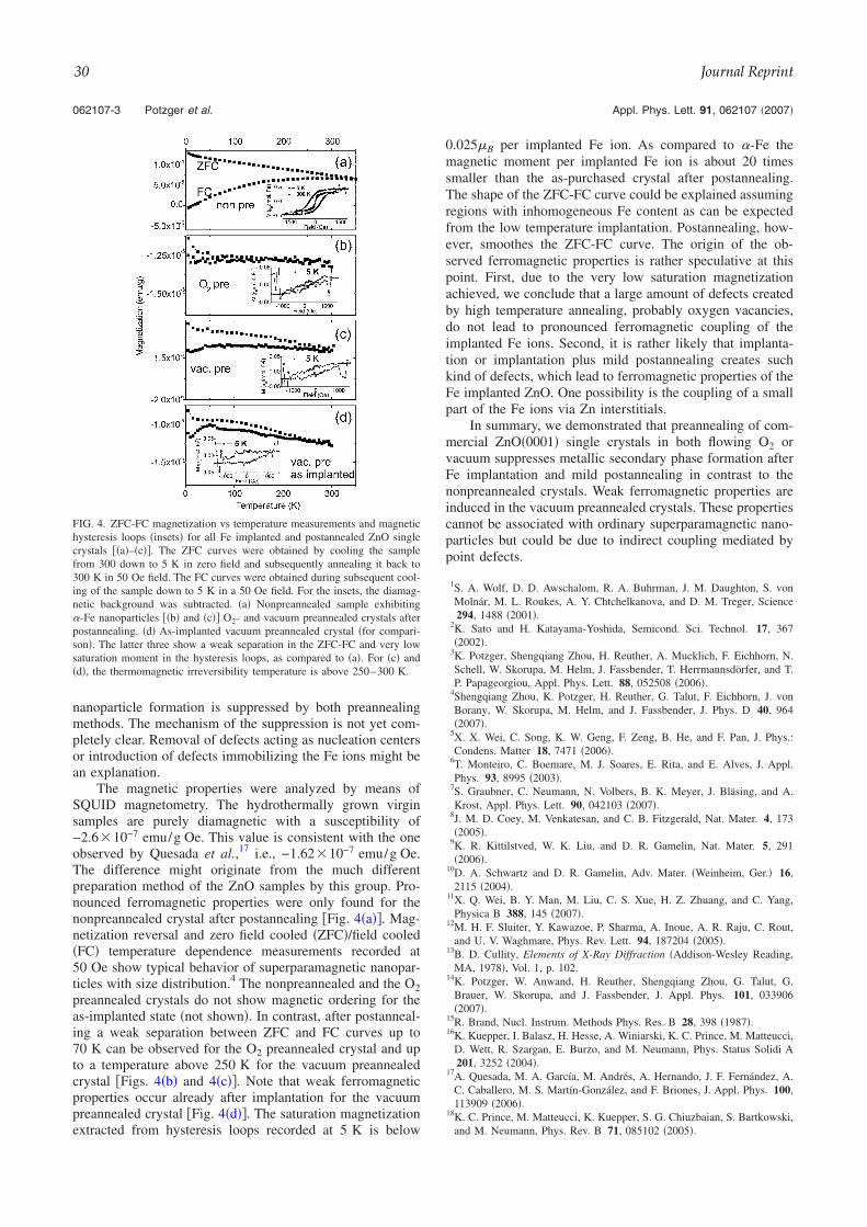
nanoparticle formation is suppressed by both preannealingmethods. The mechanism of the suppression is not yet com-pletely clear. Removal of defects acting as nucleation centersor introduction of defects immobilizing the Fe ions might bean explanation.
The magnetic properties were analyzed by means ofSQUID magnetometry. The hydrothermally grown virginsamples are purely diamagnetic with a susceptibility of−2.6�10−7 emu/g Oe. This value is consistent with the oneobserved by Quesada et al.,17 i.e., −1.62�10−7 emu/g Oe.The difference might originate from the much differentpreparation method of the ZnO samples by this group. Pro-nounced ferromagnetic properties were only found for thenonpreannealed crystal after postannealing �Fig. 4�a��. Mag-netization reversal and zero field cooled �ZFC�/field cooled�FC� temperature dependence measurements recorded at50 Oe show typical behavior of superparamagnetic nanopar-ticles with size distribution.4 The nonpreannealed and the O2preannealed crystals do not show magnetic ordering for theas-implanted state �not shown�. In contrast, after postanneal-ing a weak separation between ZFC and FC curves up to70 K can be observed for the O2 preannealed crystal and upto a temperature above 250 K for the vacuum preannealedcrystal �Figs. 4�b� and 4�c��. Note that weak ferromagneticproperties occur already after implantation for the vacuumpreannealed crystal �Fig. 4�d��. The saturation magnetizationextracted from hysteresis loops recorded at 5 K is below
0.025�B per implanted Fe ion. As compared to �-Fe themagnetic moment per implanted Fe ion is about 20 timessmaller than the as-purchased crystal after postannealing.The shape of the ZFC-FC curve could be explained assumingregions with inhomogeneous Fe content as can be expectedfrom the low temperature implantation. Postannealing, how-ever, smoothes the ZFC-FC curve. The origin of the ob-served ferromagnetic properties is rather speculative at thispoint. First, due to the very low saturation magnetizationachieved, we conclude that a large amount of defects createdby high temperature annealing, probably oxygen vacancies,do not lead to pronounced ferromagnetic coupling of theimplanted Fe ions. Second, it is rather likely that implanta-tion or implantation plus mild postannealing creates suchkind of defects, which lead to ferromagnetic properties of theFe implanted ZnO. One possibility is the coupling of a smallpart of the Fe ions via Zn interstitials.
In summary, we demonstrated that preannealing of com-mercial ZnO�0001� single crystals in both flowing O2 orvacuum suppresses metallic secondary phase formation afterFe implantation and mild postannealing in contrast to thenonpreannealed crystals. Weak ferromagnetic properties areinduced in the vacuum preannealed crystals. These propertiescannot be associated with ordinary superparamagnetic nano-particles but could be due to indirect coupling mediated bypoint defects.
1S. A. Wolf, D. D. Awschalom, R. A. Buhrman, J. M. Daughton, S. vonMolnár, M. L. Roukes, A. Y. Chtchelkanova, and D. M. Treger, Science294, 1488 �2001�.
2K. Sato and H. Katayama-Yoshida, Semicond. Sci. Technol. 17, 367�2002�.
3K. Potzger, Shengqiang Zhou, H. Reuther, A. Mucklich, F. Eichhorn, N.Schell, W. Skorupa, M. Helm, J. Fassbender, T. Herrmannsdörfer, and T.P. Papageorgiou, Appl. Phys. Lett. 88, 052508 �2006�.
4Shengqiang Zhou, K. Potzger, H. Reuther, G. Talut, F. Eichhorn, J. vonBorany, W. Skorupa, M. Helm, and J. Fassbender, J. Phys. D 40, 964�2007�.
5X. X. Wei, C. Song, K. W. Geng, F. Zeng, B. He, and F. Pan, J. Phys.:Condens. Matter 18, 7471 �2006�.
6T. Monteiro, C. Boemare, M. J. Soares, E. Rita, and E. Alves, J. Appl.Phys. 93, 8995 �2003�.
7S. Graubner, C. Neumann, N. Volbers, B. K. Meyer, J. Bläsing, and A.Krost, Appl. Phys. Lett. 90, 042103 �2007�.
8J. M. D. Coey, M. Venkatesan, and C. B. Fitzgerald, Nat. Mater. 4, 173�2005�.
9K. R. Kittilstved, W. K. Liu, and D. R. Gamelin, Nat. Mater. 5, 291�2006�.
10D. A. Schwartz and D. R. Gamelin, Adv. Mater. �Weinheim, Ger.� 16,2115 �2004�.
11X. Q. Wei, B. Y. Man, M. Liu, C. S. Xue, H. Z. Zhuang, and C. Yang,Physica B 388, 145 �2007�.
12M. H. F. Sluiter, Y. Kawazoe, P. Sharma, A. Inoue, A. R. Raju, C. Rout,and U. V. Waghmare, Phys. Rev. Lett. 94, 187204 �2005�.
13B. D. Cullity, Elements of X-Ray Diffraction �Addison-Wesley Reading,MA, 1978�, Vol. 1, p. 102.
14K. Potzger, W. Anwand, H. Reuther, Shengqiang Zhou, G. Talut, G.Brauer, W. Skorupa, and J. Fassbender, J. Appl. Phys. 101, 033906�2007�.
15R. Brand, Nucl. Instrum. Methods Phys. Res. B 28, 398 �1987�.16K. Kuepper, I. Balasz, H. Hesse, A. Winiarski, K. C. Prince, M. Matteucci,
D. Wett, R. Szargan, E. Burzo, and M. Neumann, Phys. Status Solidi A201, 3252 �2004�.
17A. Quesada, M. A. García, M. Andrés, A. Hernando, J. F. Fernández, A.C. Caballero, M. S. Martín-González, and F. Briones, J. Appl. Phys. 100,113909 �2006�.
18K. C. Prince, M. Matteucci, K. Kuepper, S. G. Chiuzbaian, S. Bartkowski,and M. Neumann, Phys. Rev. B 71, 085102 �2005�.
FIG. 4. ZFC-FC magnetization vs temperature measurements and magnetichysteresis loops �insets� for all Fe implanted and postannealed ZnO singlecrystals ��a�–�c��. The ZFC curves were obtained by cooling the samplefrom 300 down to 5 K in zero field and subsequently annealing it back to300 K in 50 Oe field. The FC curves were obtained during subsequent cool-ing of the sample down to 5 K in a 50 Oe field. For the insets, the diamag-netic background was subtracted. �a� Nonpreannealed sample exhibiting�-Fe nanoparticles ��b� and �c�� O2− and vacuum preannealed crystals afterpostannealing. �d� As-implanted vacuum preannealed crystal �for compari-son�. The latter three show a weak separation in the ZFC-FC and very lowsaturation moment in the hysteresis loops, as compared to �a�. For �c� and�d�, the thermomagnetic irreversibility temperature is above 250–300 K.
062107-3 Potzger et al. Appl. Phys. Lett. 91, 062107 �2007�
Downloaded 20 Feb 2008 to 149.220.35.103. Redistribution subject to AIP license or copyright; see http://apl.aip.org/apl/copyright.jsp
30 Journal Reprint

Thin film patterning by surface-plasmon-induced thermocapillarityLars Röntzscha� and Karl-Heinz HeinigInstitute of Ion Beam Physics and Materials Research, Research Center Dresden-Rossendorf,P.O. Box 51 01 19, 01314 Dresden, Germany
Jon A. Schuller and Mark L. BrongersmaGeballe Laboratory of Advanced Materials, Stanford University, 476 Lomita Mall, Stanford,California 94305
�Received 18 September 2006; accepted 14 December 2006; published online 22 January 2007�
It is reported that standing surface-plasmon-polariton �SPP� waves can cause regular thicknessundulations of thin polymethyl methacrylate �PMMA� films above a metallic substrate. Ripples,rings, and hillock arrays with long-range order were found. Numerical calculations reveal thatperiodic in-plane temperature profiles are generated in the PMMA due to the nonradiative dampingof SPP interference patterns. Computer simulations on the temperature-gradient-driven masstransport confirm that thermocapillarity is the dominating mechanism of the observed surfacepatterning. © 2007 American Institute of Physics. �DOI: 10.1063/1.2432282�
In the course of miniaturization of functional structurescapillary effects have become increasingly important due tothe large surface-to-volume ratio at the micro- and nanos-cale. This principle applies equally to systems in the liquid1
and in the solid state.2,3 The difference lies in the micro-scopic kinetics of these systems: hydrodynamic flow on theone hand and atomic diffusion on the other. If a system is leftto itself, capillarity-driven processes lead to surface free en-ergy minimization; thus, the morphology of functional struc-tures may strongly change in a self-organizing manner.1–3 Onthe contrary, if a system is exposed to external forces it canbe driven to a nonequilibrium state. Thermal gradients forinstance give rise to thermocapillary forces which trigger abiased material flux.4 If these gradients are periodic in space,long-range-ordered structures can be achieved.
In this letter, we report on a method to fabricate long-range-ordered thickness undulations in thin polymethylmethacrylate �PMMA� films on metals. This method, whichuses periodic in-plane temperature fields induced by thedamping of surface plasmon polaritons �SPPs�, was previ-ously used to characterize SPP propagation and scattering.5
Here, experiments and numerical calculations are performedto further elucidate the underlying mechanisms for creatingthe observed thickness undulations. Reflection pole method�RPM� calculations6 are used to determine the spatially de-pendent power losses generated by SPPs excited at aPMMA/Au interface. These losses give rise to local heating.Taking these losses as a spatially varying heat source, heatconduction calculations show that periodic temperaturefields, which result in thermocapillary effects in the PMMA,are produced. Kinetic Monte Carlo �KMC� simulations re-veal that such in-plane thermal gradients trigger a biasedmaterial transport. It is expected that this nonequilibriumfabrication method of SPP lithography can be applied toother thin film systems �particularly thin polymer films� inorder to achieve regular thickness undulations with long-range order.
In Fig. 1, sample structure and experimental procedureare drawn schematically. A 50 nm thick patterned metal film
�45 nm Au, 5 nm Ti sticking layer� was deposited on aSi�001� wafer �500 �m thick�. Afterwards, a 1 �m thick495 000 molecular weight PMMA film was spin coated overthe whole wafer. The samples were then exposed for 1 s toCO2 laser light ��=10.64 �m� at room temperature �RT�.The 5 W quasi-continuous-wave7 linearly polarized laserbeam �E=Eex� was focused to a spot of approximately200 �m diameter, illuminating the patterned Au structures atnormal incidence. After laser irradiation, surface profileswere imaged with differential image contrast �DIC� andatomic force microscopy.
In Fig. 2�a�, a DIC micrograph that clearly indicates aripple structure on the PMMA is shown. The periodic ripplesonly occur above the rectangular Au pads �region “B” inFig. 1�. In those areas with no Au beneath the PMMA �region“A” in Fig. 1�, no periodic PMMA surface roughening isobserved after laser irradiation. The ripple pattern is onlyperiodic along the direction of laser polarization ex as ex-pected for a standing wave arising from a transverse mag-netic �TM� guided mode. The location �above Au� and ob-served polarization dependence �TM� strongly suggest thatthe ripple patterns are caused by SPPs. Furthermore, ourelectromagnetic simulations based on RPM calculations6
show that the structure supports a SPP mode with a wave-length of 10.2 �m but no other waveguide modes. That SPPsinduce the ripple structure becomes even more evident in thecase of more exotic SPP interference patterns which are ob-served when Au pads of different geometries are illuminated�Figs. 2�b� and 2�c��. The excitation of SPPs at curved orangled interfaces results in circular and triangular interfer-ence patterns that induce annular and hillock patterns on thePMMA surface, respectively.
a�Electronic mail: [email protected]. 1. Schematic drawing of �a� sample setup, experimental procedure, and�b� the periodic surface pattern obtained.
APPLIED PHYSICS LETTERS 90, 044105 �2007�
0003-6951/2007/90�4�/044105/3/$23.00 © 2007 American Institute of Physics90, 044105-1Downloaded 20 Feb 2008 to 149.220.35.103. Redistribution subject to AIP license or copyright; see http://apl.aip.org/apl/copyright.jsp
Annual Report IIM 2007, FZD-493 31
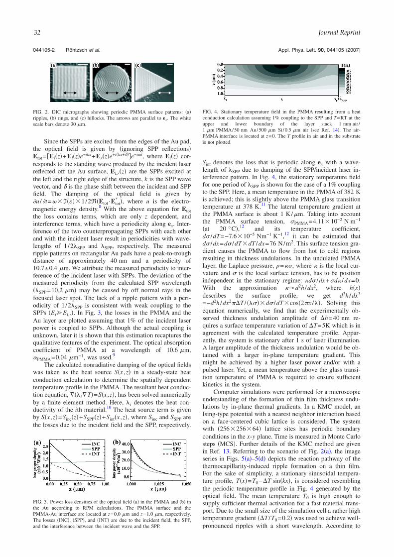
Since the SPPs are excited from the edges of the Au pad,the optical field is given by �ignoring SPP reflections�Etot= �Ei�z�+El�z�e−ikx+Er�z�e+i�kx+���e−i�t, where Ei�z� cor-responds to the standing wave produced by the incident laserreflected off the Au surface, El,r�z� are the SPPs excited atthe left and the right edge of the structure, k is the SPP wavevector, and � is the phase shift between the incident and SPPfield. The damping of the optical field is given by�u /�t=��I����1/2R�Etot ·Etot
* �, where u is the electro-magnetic energy density.8 With the above equation for Etotthe loss contains terms, which are only z dependent, andinterference terms, which have a periodicity along ex. Inter-ference of the two counterpropagating SPPs with each otherand with the incident laser result in periodicities with wave-lengths of 1 /2�SPP and �SPP, respectively. The measuredripple patterns on rectangular Au pads have a peak-to-troughdistance of approximately 40 nm and a periodicity of10.7±0.4 �m. We attribute the measured periodicity to inter-ference of the incident laser with SPPs. The deviation of themeasured periodicity from the calculated SPP wavelength��SPP=10.2 �m� may be caused by off normal rays in thefocused laser spot. The lack of a ripple pattern with a peri-odicity of 1 /2�SPP is consistent with weak coupling to theSPPs �EiEl,r�. In Fig. 3, the losses in the PMMA and theAu layer are plotted assuming that 1% of the incident laserpower is coupled to SPPs. Although the actual coupling isunknown, later it is shown that this estimation recaptures thequalitative features of the experiment. The optical absorptioncoefficient of PMMA at a wavelength of 10.6 �m,�PMMA=0.04 �m−1, was used.9
The calculated nonradiative damping of the optical fieldswas taken as the heat source S�x ,z� in a steady-state heatconduction calculation to determine the spatially dependenttemperature profile in the PMMA. The resultant heat conduc-tion equation, ���i�T�=S�x ,z�, has been solved numericallyby a finite element method. Here, �i denotes the heat con-ductivity of the ith material.10 The heat source term is givenby S�x ,z�=Sinc�z�+SSPP�z�+Sint�x ,z�, where Sinc and SSPP arethe losses due to the incident field and the SPP, respectively.
Sint denotes the loss that is periodic along ex with a wave-length of �SPP due to damping of the SPP/incident laser in-terference pattern. In Fig. 4, the stationary temperature fieldfor one period of �SPP is shown for the case of a 1% couplingto the SPP. Here, a mean temperature in the PMMA of 382 Kis achieved; this is slightly above the PMMA glass transitiontemperature at 378 K.11 The lateral temperature gradient atthe PMMA surface is about 1 K/�m. Taking into accountthe PMMA surface tension, �PMMA=4.11�10−2 N m−1
�at 20 °C�,12 and its temperature coefficient,d� /dT=−7.6�10−5 Nm−1 K−1,12 it can be estimated thatd� /dx=d� /dT�dT /dx=76 N/m2. This surface tension gra-dient causes the PMMA to flow from hot to cold regionsresulting in thickness undulations. In the undulated PMMAlayer, the Laplace pressure, p=��, where � is the local cur-vature and � is the local surface tension, has to be positionindependent in the stationary regime: �d� /dx+�d� /dx=0.With the approximation �d2h /dx2, where h�x�describes the surface profile, we get d3h /dx3
=−d2h /dx2��T / �����d� /dT�cos�2�x /��. Solving thisequation numerically, we find that the experimentally ob-served thickness undulation amplitude of �h=40 nm re-quires a surface temperature variation of �T=5K which is inagreement with the calculated temperature profile. Appar-ently, the system is stationary after 1 s of laser illumination.A larger amplitude of the thickness undulation would be ob-tained with a larger in-plane temperature gradient. Thismight be achieved by a higher laser power and/or with apulsed laser. Yet, a mean temperature above the glass transi-tion temperature of PMMA is required to ensure sufficientkinetics in the system.
Computer simulations were performed for a microscopicunderstanding of the formation of thin film thickness undu-lations by in-plane thermal gradients. In a KMC model, anIsing-type potential with a nearest neighbor interaction basedon a face-centered cubic lattice is considered. The systemwith �256�256�64� lattice sites has periodic boundaryconditions in the x-y plane. Time is measured in Monte Carlosteps �MCS�. Further details of the KMC method are givenin Ref. 13. Referring to the scenario of Fig. 2�a�, the imageseries in Figs. 5�a�–5�d� depicts the reaction pathway of thethermocapillarity-induced ripple formation on a thin film.For the sake of simplicity, a stationary sinusoidal tempera-ture profile, T�x�=T0−�T sin�kx�, is considered resemblingthe periodic temperature profile in Fig. 4 generated by theoptical field. The mean temperature T0 is high enough tosupply sufficient thermal activation for a fast material trans-port. Due to the small size of the simulation cell a rather hightemperature gradient ��T /T0=0.2� was used to achieve well-pronounced ripples with a short wavelength. According to
FIG. 2. DIC micrographs showing periodic PMMA surface patterns: �a�ripples, �b� rings, and �c� hillocks. The arrows are parallel to ex. The whitescale bars denote 30 �m.
FIG. 3. Power loss densities of the optical field �a� in the PMMA and �b� inthe Au according to RPM calculations. The PMMA surface and thePMMA-Au interface are located at z=0.0 �m and z=1.0 �m, respectively.The losses �INC�, �SPP�, and �INT� are due to the incident field, the SPP,and the interference between the incident wave and the SPP.
FIG. 4. Stationary temperature field in the PMMA resulting from a heatconduction calculation assuming 1% coupling to the SPP and T=RT at theupper and lower boundary of the layer stack 1 mm air/1 �m PMMA/50 nm Au/500 �m Si/0.5 �m air �see Ref. 14�. The air-PMMA interface is located at z=0. The T profile in air and in the substrateis not plotted.
044105-2 Röntzsch et al. Appl. Phys. Lett. 90, 044105 �2007�
Downloaded 20 Feb 2008 to 149.220.35.103. Redistribution subject to AIP license or copyright; see http://apl.aip.org/apl/copyright.jsp
32 Journal Reprint
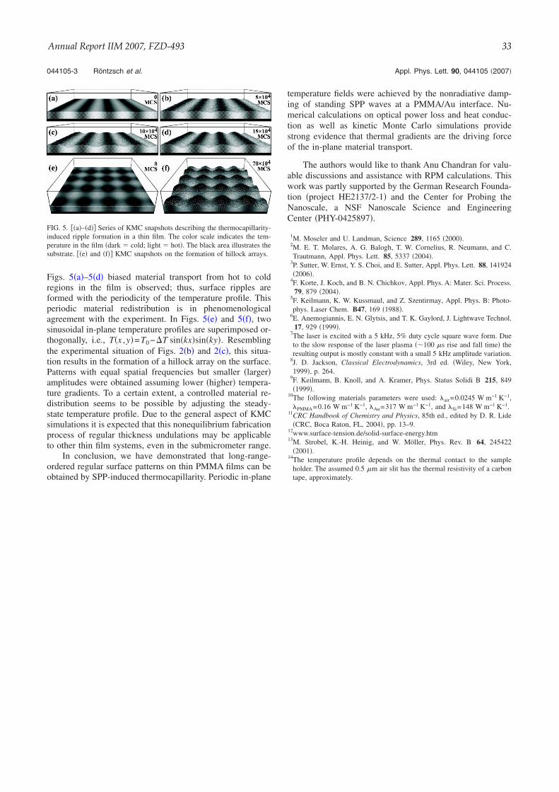
Figs. 5�a�–5�d� biased material transport from hot to coldregions in the film is observed; thus, surface ripples areformed with the periodicity of the temperature profile. Thisperiodic material redistribution is in phenomenologicalagreement with the experiment. In Figs. 5�e� and 5�f�, twosinusoidal in-plane temperature profiles are superimposed or-thogonally, i.e., T�x ,y�=T0−�T sin�kx�sin�ky�. Resemblingthe experimental situation of Figs. 2�b� and 2�c�, this situa-tion results in the formation of a hillock array on the surface.Patterns with equal spatial frequencies but smaller �larger�amplitudes were obtained assuming lower �higher� tempera-ture gradients. To a certain extent, a controlled material re-distribution seems to be possible by adjusting the steady-state temperature profile. Due to the general aspect of KMCsimulations it is expected that this nonequilibrium fabricationprocess of regular thickness undulations may be applicableto other thin film systems, even in the submicrometer range.
In conclusion, we have demonstrated that long-range-ordered regular surface patterns on thin PMMA films can beobtained by SPP-induced thermocapillarity. Periodic in-plane
temperature fields were achieved by the nonradiative damp-ing of standing SPP waves at a PMMA/Au interface. Nu-merical calculations on optical power loss and heat conduc-tion as well as kinetic Monte Carlo simulations providestrong evidence that thermal gradients are the driving forceof the in-plane material transport.
The authors would like to thank Anu Chandran for valu-able discussions and assistance with RPM calculations. Thiswork was partly supported by the German Research Founda-tion �project HE2137/2-1� and the Center for Probing theNanoscale, a NSF Nanoscale Science and EngineeringCenter �PHY-0425897�.
1M. Moseler and U. Landman, Science 289, 1165 �2000�.2M. E. T. Molares, A. G. Balogh, T. W. Cornelius, R. Neumann, and C.Trautmann, Appl. Phys. Lett. 85, 5337 �2004�.
3P. Sutter, W. Ernst, Y. S. Choi, and E. Sutter, Appl. Phys. Lett. 88, 141924�2006�.
4F. Korte, J. Koch, and B. N. Chichkov, Appl. Phys. A: Mater. Sci. Process.79, 879 �2004�.
5F. Keilmann, K. W. Kussmaul, and Z. Szentirmay, Appl. Phys. B: Photo-phys. Laser Chem. B47, 169 �1988�.
6E. Anemogiannis, E. N. Glytsis, and T. K. Gaylord, J. Lightwave Technol.17, 929 �1999�.
7The laser is excited with a 5 kHz, 5% duty cycle square wave form. Dueto the slow response of the laser plasma ��100 �s rise and fall time� theresulting output is mostly constant with a small 5 kHz amplitude variation.
8J. D. Jackson, Classical Electrodynamics, 3rd ed. �Wiley, New York,1999�, p. 264.
9F. Keilmann, B. Knoll, and A. Kramer, Phys. Status Solidi B 215, 849�1999�.
10The following materials parameters were used: �air=0.0245 W m−1 K−1,�PMMA=0.16 W m−1 K−1, �Au=317 W m−1 K−1, and �Si=148 W m−1 K−1.
11CRC Handbook of Chemistry and Physics, 85th ed., edited by D. R. Lide�CRC, Boca Raton, FL, 2004�, pp. 13–9.
12www.surface-tension.de/solid-surface-energy.htm13M. Strobel, K.-H. Heinig, and W. Möller, Phys. Rev. B 64, 245422
�2001�.14The temperature profile depends on the thermal contact to the sample
holder. The assumed 0.5 �m air slit has the thermal resistivity of a carbontape, approximately.
FIG. 5. ��a�–�d�� Series of KMC snapshots describing the thermocapillarity-induced ripple formation in a thin film. The color scale indicates the tem-perature in the film �dark � cold; light � hot�. The black area illustrates thesubstrate. ��e� and �f�� KMC snapshots on the formation of hillock arrays.
044105-3 Röntzsch et al. Appl. Phys. Lett. 90, 044105 �2007�
Downloaded 20 Feb 2008 to 149.220.35.103. Redistribution subject to AIP license or copyright; see http://apl.aip.org/apl/copyright.jsp
Annual Report IIM 2007, FZD-493 33
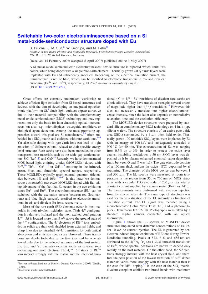
Switchable two-color electroluminescence based on a Simetal-oxide-semiconductor structure doped with Eu
S. Prucnal, J. M. Sun,a� W. Skorupa, and M. Helmb�
Institute of Ion Beam Physics and Materials Research, Forschungszentrum Dresden-Rossendorf,P.O. Box 510119, 01314 Dresden, Germany
�Received 14 February 2007; accepted 5 April 2007; published online 3 May 2007�
A Si metal-oxide-semiconductor electroluminescent device structure is reported which emits twocolors, while being doped with a single rare-earth element. Thermally grown SiO2 oxide layers wereimplanted with Eu and subseqently annealed. Depending on the electrical excitation current, theluminescence is red or blue, which can be ascribed to electronic transitions in tri- and divalenteuropium �Eu3+ and Eu2+�, respectively. © 2007 American Institute of Physics.�DOI: 10.1063/1.2735285�
Great efforts are currently undertaken worldwide toachieve efficient light emission from Si based structures anddevices with the aim of developing an integrated optoelec-tronic platform on Si.1 Such light emitters appear attractivedue to their material compatibility with the complementarymetal-oxide-semiconductor �MOS� technology and may rep-resent not only the basis for inter-/intrachip optical intercon-nects but also, e.g., microdisplays, waveguide amplifiers, orbiological agent detection. Among the most promising ap-proaches toward this goal are Si nanoclusters,2,3 often em-bedded in a SiO2 matrix and codoped with rare-earth ions.4–6
Yet also sole doping with rare-earth ions can lead to lightemission of different colors,7 related to their specific energylevel structure. Rare earths have also been embedded in othertransparent host materials such as the wide-gap semiconduc-tors SiC �Ref. 8� and GaN.9 Recently, we have demonstratedMOS based light emitting diodes �MOSLEDs� doped withEr3+,10 Tb3+,11 Ce3+,12 or Gd3+,13 emitting in the infrared,green, blue, and ultraviolet spectral ranges, respectively.These MOSLEDs typically reach external quantum efficien-cies between 1% and 10%.7,10–13 In this letter we demon-strate a switchable two-color MOSLED doped with Eu, tak-ing advantage of the fact that Eu occurs in the two oxidationstates Eu3+ and Eu2+. The electroluminescence �EL� can beswitched with the excitation current between red �low cur-rent� and blue �high current�, ascribed to electronic transi-tions in tri- and divalent Eu ions, respectively.
Most of the rare-earth �RE� elements occur in host ma-terials in their trivalent oxidation state. Their 4fn configura-tion is relatively isolated and the next excited configuration4fn−1 5d is located more than 5 eV above the ground state ofthe 4fn configuration. The 4f electrons of RE3+ ions embed-ded in solids are thus well shielded from external fields, andsharp lines due to intrashell 4f-4f transitions for both opticalabsorption and emission spectra are observed. These transi-tions are dipole forbidden in the free ions and become al-lowed only due to the reduced symmetry of the host matrix.Eu, Sm, and Yb can also exist in solids as divalent ionscontaining one more electron. The 4fn−1 5d states of RE2+
ions interact strongly with the matrix and the interconfigura-
tional 4fn to 4fn−1 5d transitions of divalent rare earths aredipole allowed. They have transition strengths several ordersof magnitude higher than 4f-4f transitions.14 However, thisdoes not necessarily translate into higher electrolumines-cence intensity, since the latter also depends on nonradiativerelaxation time and the excitation efficiency.
The MOSLED device structures were prepared by stan-dard silicon complementary MOS technology on 4 in. n-typesilicon wafers. The structure consists of an active gate oxidearea �SiO2� surrounded by a 1 �m thick field oxide. Ther-mally grown 100 nm thick SiO2 layers were implanted by Euwith an energy of 100 keV and subsequently annealed at900 °C for 40 min. The concentration of Eu was rangingfrom 0.5% up to 3%. In order to protect the oxide layeragainst instability breakdown, a 50 nm SiON layer was de-posited on it by plasma-enhanced chemical vapor deposition�ratio between O and N was 1:1�. The gate electrode consistsof a 100 nm thick indium tin oxide �ITO� deposited by rfsputtering. The diameter of the MOS device was between 1and 500 �m. The EL spectra were measured at room tem-perature in the region from 350 to 750 nm on MOS struc-tures with a circular ITO electrode of 200 �m diameter atconstant current supplied by a source meter �Keithley 2410�.The measurements were performed with electron injectionfrom the silicon substrate. The same type of structures wasused for the investigation of the EL intensity as function ofexcitation current. The EL signal was recorded using amonochromator �Jobin Yvon Triax 320� and a photomulti-plier �Hamamatsu H7732-10�. Photographs were taken by astandard digital camera connected with an opticalmicroscope.
Figure 1 shows the EL spectra of MOSLED devicestructures implanted with different concentrations of Eu un-der 10 �A dc current injection. The EL is generated by hot-electron induced impact excitation of RE ions during Fowler-Nordheim tunneling. Peaks at 573, 616, and 655 nm areattributed to the 4f 5D0-7FJ �J=1,2 ,3� intrashell transitionsof Eu3+, whose spectral positions are known to depend onlyweakly on the host material. On the other hand, the 5d elec-trons strongly interact with the host crystal field, and there-fore the peak position of the lowest transition of Eu2+ dopedmaterials varies more strongly with the host material than isthe case for RE3+ doping.15 In the case of the SiO2 matrix,divalent europium exhibits two broad bands with maximum
a�Present address: Institute of Physics, Nankai University, 300071 Tianjin,China.
b�Electronic mails: [email protected]
APPLIED PHYSICS LETTERS 90, 181121 �2007�
0003-6951/2007/90�18�/181121/3/$23.00 © 2007 American Institute of Physics90, 181121-1Downloaded 20 Feb 2008 to 149.220.35.103. Redistribution subject to AIP license or copyright; see http://apl.aip.org/apl/copyright.jsp
34 Journal Reprint

intensities at 400 and 470 nm, corresponding to the 4f6
5d-4f7 �8S7/2� transitions. �Note that the peak at 470 nm mayalso have some contribution from oxygen deficiency centersin SiO2.16�. For Eu2+ the strongest luminescence was ob-served for a concentration of 3%, while the trivalent eu-ropium shows the highest electroluminescence for the lowesteuropium concentration �0.5%�. At higher concentrations,this intra-4f electroluminescence may undergo concentrationquenching,11 caused by a nonradiative energy transfer be-tween two neighboring Eu atoms.
Figure 2 shows the dependence of the blue and red ELintensities and applied voltage on the current for samplescontaining 0.5% of Eu. The radiative transition between the5D0 and 7F2 levels in Eu3+ is observed already for a currentof 2�10−8 A and a voltage of 99 V. With increasing injec-tion current the red light monotonically increases up to thebreakdown point. To obtain a population of the first excitedlevel 4f6 5d in divalent europium, higher voltages��105 V� and current ��4�10−7 A� are needed. An in-crease of the 400 nm emission with current was observed upto 1 mA before it is finally quenched. For a current of up to90 �A, the red light dominates over the blue one. In therange of 90 mA–1.8 the reverse situation is observed. The
inset of Fig. 2 shows the blue/red ratio of the EL intensityversus current. It is clearly visible that by a proper choice ofthe operation current regime it is possible to switch betweenthe two main colors: red and blue. In addition, for a currentof around 100 �A as well as higher than 1.8 mA both colorshave similar intensity resulting in violet emission�see Fig. 3�c��. Operating at one of these crossover points,switching can be achieved by superimposing a small acmodulation voltage. Such a switchable two-color behaviorhas not been reported before for Si based light emitters. Weare only aware of GaN based devices, where two colors weregenerated using two different rare-earth ions �Er and Eu�.17,18
The simplest explanation of the color change with appliedvoltage can be given considering the hot-electron distributionin the oxide.19 At lower electric fields the average electronkinetic energy is only sufficient to excite the red transition�transition energy of �2 eV�, whereas at higher fields theelectrons are more energetic and can also excite the bluetransition �2.5–3 eV�. Another possibility is electron captureat high current. A more detailed understanding of the micro-scopic mechanism will require further experiments.
Figure 3 shows photographs taken from devices of200 �m diameter by a standard digital camera under an op-tical microscope. The red-light emission obtained with low-current excitation is presented in Fig. 3�a�. Similar resultswere observed by Heikenfeld et al. from a GaN:Eu LED.20
The blue electroluminescence �see Fig. 3�b�� from any ma-trix containing Eu2+ was not observed up to now. Kim andHolloway have identified both divalent and trivalent eu-ropium ions in GaN by x-ray photoelectron spectroscopy, butthey observed EL only from Eu3+.21 Cathodoluminescencefrom Eu2+ doped BaMg�1+x�SixAl10Oy has been reported byStudenikin and Cocivera.22
In summary, we have presented a switchable two-colorMOSLED device structure based on a Eu implanted SiO2layer. This shows that photonics based on silicon has still alot of potential, and even offers interesting optoelectronicfunctionalities. Future goals will be aimed toward a micro-scopic understanding of the two-color behavior and a reduc-tion of the operating voltage by using thinner oxides. Com-bination with a green light emitter such as SiO2:Tb couldresult in a Si based full-color microdisplay.
The authors would like to thank J. Winkler and F.Ludewig for the ion implantation, H. Felsmann, C. Neisser,and G. Schnabel for the processing of the MOS structures.
1S. Ossicini, L. Pavesi, and F. Priolo, Light Emitting Silicon for Micropho-tonics, Springer Tracts in Modern Physics Vol. 194 �Springer, New York,2003�.
2L. Pavesi, L. Dal Negro, C. Mazzoleni, G. Franzó, and F. Priolo,Nature �London� 408, 440 �2000�.
3R. J. Walters, G. I. Bourianoff, and H. A. Atwater, Nat. Mater. 4, 143�2005�.
4A. Polman, Nat. Mater. 1, 10 �2002�.
FIG. 1. Electroluminescence spectra of SiO2:Eu MOSLED devices withdifferent Eu concentrations as indicated. The excitation current is 10 �Aand the device diameter is 200 �m.
FIG. 2. �Color online� Electroluminescence intensity of a MOSLED devicewith 0.5% Eu, measured at 400 nm �blue solid curve� and 616 nm �reddashed curve� as a function of the injection current �left scale�. The blacksolid curve shows the applied voltage vs current �right scale�. The insetdisplays the ratio of the blue to the red EL vs injection current. The devicewas 200 �m in diameter.
FIG. 3. �Color online� Photographs of SiO2:Eu MOSLED devices with200 �m diameter. The excitation currents were 20 �A �a�, 1 mA �b�, and2.5 mA �c�, respectively.
181121-2 Prucnal et al. Appl. Phys. Lett. 90, 181121 �2007�
Downloaded 20 Feb 2008 to 149.220.35.103. Redistribution subject to AIP license or copyright; see http://apl.aip.org/apl/copyright.jsp
Annual Report IIM 2007, FZD-493 35

5M. Fujii, M. Yoshida, Y. Kanzawa, S. Hayashi, and K. Yamamoto,Appl. Phys. Lett. 71, 1198 �1997�.
6S. Minissale, T. Gregorkiewicz, M. Forcales, and R. G. Elliman,Appl. Phys. Lett. 89, 171908 �2006�, and references therein.
7M. E. Castagna, S. Coffa, M. Monaco, A. Muscara, L. Caristia, S. Lorenti,and A. Messina, Mater. Sci. Eng., B 105, 83 �2003�.
8W. J. Choyke, R. P. Devaty, L. L. Clemen, M. Yoganathan, G. Pensl, andCh. Hässler, Appl. Phys. Lett. 65, 1668 �1994�.
9A. J. Steckl, J. C. Heikenfeld, D.-S. Lee, M. J. Garter, C. C. Baker, Y.Wang, and R. Jones, IEEE J. Sel. Top. Quantum Electron. 8, 749 �2002�.
10J. M. Sun, W. Skorupa, T. Dekorsy, M. Helm, and A. M. Nazarov,Opt. Mater. �Amsterdam, Neth.� 27, 1050 �2005�.
11J. M. Sun, W. Skorupa, T. Dekorsy, M. Helm, L. Rebohle, and T. Gebel,J. Appl. Phys. 97, 123513 �2005�.
12J. M. Sun, S. Prucnal, W. Skorupa, M. Helm, L. Rebohle, and T. Gebel,Appl. Phys. Lett. 89, 091908 �2006�.
13J. M. Sun, W. Skorupa, T. Dekorsy, M. Helm, L. Rebohle, and T. Gebel,
Appl. Phys. Lett. 85, 3387 �2004�.14G. Liu and B. Jacquier, Spectroscopic Properties of Rare Earths in Optical
Materials �Springer, Berlin, 2005�, p. 122.15J. Rubio, J. Phys. Chem. Solids 52, 101 �1991�.16W. Skorupa, L. Rebohle, and T. Gebel, Appl. Phys. A: Mater. Sci. Process.
76, 1049 �2003�.17D. S. Lee, J. Heikenfeld, R. Birkhahn, M. Garter, B. K. Lee, and A. J.
Steckl, Appl. Phys. Lett. 76, 1525 �2000�.18J. Heikenfeld and A. J. Steckl, IEEE Trans. Electron Devices 49, 1545
�2002�.19M. V. Fischetti, D. J. DiMaria, S. D. Brorson, T. N. Theis, and J. R.
Kirtley, Phys. Rev. B 31, 8124 �1985�.20J. Heikenfeld, M. Garter, D. S. Lee, R. Birkhahn, and A. J. Steckl,
Appl. Phys. Lett. 75, 1189 �1999�.21J. H. Kim and P. H. Holloway, J. Appl. Phys. 95, 4787 �2004�.22S. A. Studenikin and M. Cocivera, Thin Solid Films 394, 264 �2001�.
181121-3 Prucnal et al. Appl. Phys. Lett. 90, 181121 �2007�
Downloaded 20 Feb 2008 to 149.220.35.103. Redistribution subject to AIP license or copyright; see http://apl.aip.org/apl/copyright.jsp
36 Journal Reprint

Meyer-Neldel rule in ZnOHeidemarie Schmidta�
Institut für Experimentelle Physik II, Fakultät für Physik und Geowissenschaften, Universität Leipzig,Linnéstraße 3-5, 04103 Leipzig, Germany, and Forschungszentrum Dresden-Rossendorf e. V.,Institut für Ionenstrahlphysik und Materialforschung, Bautzner Landstrasse 128, 01328 Dresden, Germany
Maria Wiebe, Beatrice Dittes, and Marius GrundmannInstitut für Experimentelle Physik II, Fakultät für Physik und Geowissenschaften, Universität Leipzig,Linnéstraße 3-5, 04103 Leipzig, Germany
�Received 11 April 2007; accepted 9 November 2007; published online 6 December 2007�
Seventy years ago Meyer and Neldel investigated four polycrystalline n-type conducting ZnO rods�W. Meyer and H. Neldel, Z. Tech. Phys. �Leipzig� 12, 588 �1937��. The specific conductivityincreased exponentially with temperature. A linear relationship between the thermal activationenergy for the specific conductivity and the logarithm of the prefactor was observed. Since thenthermally activated processes revealing this behavior are said to follow the Meyer-Neldel �MN� rule.We show that the emission of charge carriers from deep electron traps in ZnO follows the MN rulewith the isokinetic temperature amounting to 226±4 K. © 2007 American Institute of Physics.�DOI: 10.1063/1.2819603�
In this work, we report on the properties of deep electrondefects in ZnO thin films probed by deep level transientspectroscopy �DLTS�.1 The apparent thermal activation en-ergy Ea and the capture cross section �i are the fingerprintsof deep defects. However, due to the simple analysis ofDLTS data,
ei�T� = 1/� = Nc�th�i exp�− Ea/kBT�
= e0T2 exp�− Ea/kBT� , �1�
where a temperature independent capture cross section �i isassumed, the reported capture cross sections vary over manyorders of magnitude. The parameter e0 is related with theapparent capture cross section �i by
e0 = Nc�th�i/T2 = 4��m�k2
h3 ��6��i. �2�
Therefore, even in nominally undoped, intrinsicallyn-conducting ZnO, the “fingerprints” of deep defects are notunambiguous.
Seventy years ago Meyer and Neldel investigated thetemperature dependence of the specific conductivity � inZnO and other oxidic compounds and found that the conduc-tivity depends exponentially on temperature,
� = �0 exp�− Ea/kBT� ,
��� = �−1 cm−1. �3�
Furthermore, they observed that the prefactor �0 depends onthe activation energy Ea.2 In more detail, the logarithm of theprefactor reads
ln��0� = ln��00� + Ea/kBTiso, �4�
with �00 being a true constant and Tiso being the so-calledisokinetic temperature.3 The empiric Meyer-Neldel �MN�behavior has been found in different thermally activated
processes including charge emission4 and current flow,5 andis well known to chemists from surface desorptionprocesses.6 Equation �4� is a good approximation if the con-ductivity is determined by deep traps. However, if shallowimpurities determine the conductivity, the parameter �00strongly depends on the Fermi level position and mobility,and appears to be temperature dependent. If determined fromconductivity measurements, the �00 parameter thus may dif-fer in one and the same material with different deep traps andshallow impurities.
We probed the parameters of deep electron defects inn-type conducting ZnO thin films using DLTS. Differentgroups report on thermal activation energies ranging from0.1 up to 0.6 eV below the ZnO conduction band minimumand an abnormally large variation of the capture cross sec-tion. Here, we report a correct analysis of DLTS data with atemperature dependent capture cross section4 and reveal thatdeep electron defects in ZnO exhibit a MN behavior. Ourwork will enable the categorization of deep electron defectsin ZnO with respect to the change of phonon configurationentropy in the thermally activated carrier detrapping fromdeep defects. We have investigated more than 130 samples of�1 �m thick ZnO films by DLTS. The epilayer structuresconsist of an �0.2 �m thick 1% Al-doped ZnO layer grownby pulsed laser deposition on 10�10 mm2 a-plane sapphiresubstrates using a KrF excimer laser,7 serving as the Ohmicback electrode,8 before the deposition of undoped ZnO filmsor of ZnO films doped with different 3d transition metal ions.All deposited films were n conducting. Finally, circularSchottky contacts were fabricated by thermal evaporation ofPd on the film surface.
DLTS is a powerful technique to characterize deep de-fects in the depletion region of reverse biased diodes by pro-viding the thermal activation energy Ea, electron capturecross section �i, and defect concentration NT.9 For DLTS, thefree charge carrier concentration has to be at least one orderof magnitude larger than NT in order to ensure that the Fermilevel position is not influenced by the deep defects them-selves. Typically, this condition is fulfilled in our samples fortemperatures above 50 K with free charge carrier concentra-a�Electronic mail: [email protected].
APPLIED PHYSICS LETTERS 91, 232110 �2007�
0003-6951/2007/91�23�/232110/3/$23.00 © 2007 American Institute of Physics91, 232110-1Downloaded 20 Feb 2008 to 149.220.35.103. Redistribution subject to AIP license or copyright; see http://apl.aip.org/apl/copyright.jsp
Annual Report IIM 2007, FZD-493 37
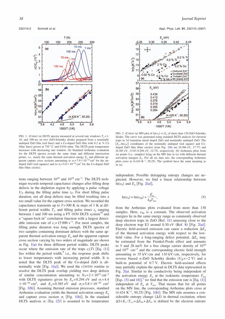
tions ranging between 1016 and 1018 cm−3. The DLTS tech-nique records temporal capacitance changes after filling deepdefects in the depletion region by applying a pulse voltageUP during the filling pulse time tP. For short filling pulseduration, not all deep defects may be filled resulting into atoo small value for the capture cross section. We recorded thecapacitance transients up to T=300 K in steps of 1 K at dif-ferent period widths Tw and filling pulse times tp rangingbetween 1 and 100 ms using a FT 1030 DLTS system10 anda “square-lock-in” correlation function with a largest detect-able emission rate of ei=15 000 s−1. For most samples, thefilling pulse duration was long enough. DLTS spectra oftwo samples containing dominant defects with the same ap-parent thermal activation energy Ea and the apparent capturecross section varying by two orders of magnitude are shownin Fig. 1�a� for three different period widths. DLTS peaksoccur where the emission rate of the traps ei�T� �Eq. �1��lies within the period width,9 i.e., the response peak shiftsto lower temperatures with increasing period width. It isnoted that the DLTS peak of the Co-doped ZnO is ab-normally wide �Fig. 1�a��. We used the CONTIN routine toresolve the DLTS peak overlap yielding two deep defectsof similar concentration amounting to NT=2�1014 cm−3
with DLTS signatures given by Ea=0.294 eV and �i=4.4�10−16 cm2, and Ea=0.385 eV and �i=5.8�10−16 cm2
�Fig. 1�b��. Assuming thermal emission processes, standardArrhenius evaluation yields the thermal activation energy Ea
and capture cross section �i �Fig. 1�b��. In the standardDLTS analysis �i �Eq. �2�� is assumed to be temperature
independent. Possible detrapping entropy changes are ne-glected. However, we find a linear relationship betweenln�e0� and Ea �Fig. 2�a��,
ln�e0� = ln�e00� +Ea
kBTiso, �5�
from the Arrhenius plots evaluated from more than 130samples. Here, e00 is a constant. The observed activationenergies lie in the same energy range as commonly observeddeep electron traps in ZnO �Ref. 11� amassing close to thedeep electron trap E3 around 0.30 eV �Ref. 8� �Fig. 2�a��.Electric field-assisted emission can cause a reduction �Eaof the thermal activation energy with respect to the low-field value. For a long-ranging defect potential, �Ea maybe estimated from the Frenkel-Poole effect and amountsto 5 and 28 meV for a free charge carrier density of 1016
and 1018 cm−3 and the corresponding electric field strengthamounting to 35 kV /cm and 110 kV /cm, respectively, forreverse biased n-ZnO Schottky diodes �UR=−2 V� and abuilt-in potential of 0.7 V. Electric field-assisted effectsmay partially explain the spread in DLTS data represented inFig. 2�a�. Similar to the conductivity being independent ofthe activation energy Ea at the isokinetic temperature Tiso�Eqs. �3� and �4��,2 we find that the emission rate is �Eq. �1��independent of Ea at Tiso. That means that for all pointson the MN line, the corresponding Arrhenius plots cross at�4.424 K−1, 50.25� �Fig. 1�b��. The MN rule assumes a con-siderable entropy change ��S� in thermal excitation, where�S=Ea /Tiso=�Sph+�Sel is defined by the electron entropy
FIG. 1. �Color� �a� DLTS spectra measured at several rate windows Tw=1,10, and 100 ms on two ZnO-Schottky diodes prepared from a nominallyundoped ZnO film �red lines� and a Co-doped ZnO film with 0.2 at. % Co�blue lines� grown at 730 °C and 0.016 mbar. The DLTS peak temperatureincreases with decreasing rate window. �b� Standard Arrhenius evaluationfor the DLTS spectra reveals the same slope and different intersectionpoints, i.e., nearly the same thermal activation energy Ea and different ap-parent capture cross sections amounting to �i=7.9�10−14 cm2 for the un-doped ZnO �red squares� and to �i=5.8�10−16 cm2 for the Co-doped ZnOfilm �blue circles�.
FIG. 2. �Color� �a� MN plot of ln�e0� vs Ea of more than 130 ZnO Schottkydiodes. The curve was generated using standard DLTS analysis for electrontraps in 3d transition metal doped ZnO and nominally undoped ZnO. The�Ea , ln�e0�� coordinates of the nominally undoped �red square� and Co-doped ZnO film �blue circles� from Fig. 1�b� are �0.386 eV, 17.77� and�0.385 eV, 13.03 /0.294 eV, 12.75�, respectively. �b� Arrhenius plots fromsix points �i.e., samples� lying on the MN line in �a� with different thermalactivation energies Ea. For all six data sets, the corresponding Arrheniusplots cross at �4.424 K−1, 50.25�. The symbols have the same meaning asin �a�.
232110-2 Schmidt et al. Appl. Phys. Lett. 91, 232110 �2007�
Downloaded 20 Feb 2008 to 149.220.35.103. Redistribution subject to AIP license or copyright; see http://apl.aip.org/apl/copyright.jsp
38 Journal Reprint

term �Sel and the phonon configuration entropy �Sph. Sub-stituting Eq. �5� into Eq. �1� yields
ei�T� = e00 exp�Ea/kBTiso�T2 exp�− Ea/kBT� . �6�
The slope of the MN line in Fig. 2�a� is �kBTiso�−1 withTiso=226 K. At T=Tiso, ei is independent of Ea �Fig. 2�b��for all samples on the MN line. Tiso
−1 is not far outside theDLTS data range. From the intersection of the MN linewith the ln�e0� axis in Fig. 2�a�, ln�e00�=ln�e0�Ea→0��=ln�e0�T→���=−2.14 has been determined. Because the es-timated values of e0 and Ea are not independent, slightlydifferent MN lines may result with the isokinetic temperatureamounting to 226±4 K. Mainly, deep electron traps in 3dtransition metal doped ZnO thin films lie below the MN line.Their smaller apparent capture cross sections hint toward atoo short filling pulse time tp or the presence of other deepdefects in 3d transition metal doped ZnO thin films simulta-neously filled when the pulse voltage is applied during thefilling pulse time tp. Probably, due to an uncomplete fillingand a reduced apparent capture cross section, the deep defectin Co-doped ZnO with the same thermal activation energyas the defect in undoped ZnO �Fig. 1�b�� lies below theMN line �Fig. 2�a��. The defect in Co-doped ZnO with thesmaller thermal activation energy �Fig. 1�b�� lies on theMN line �Fig. 1�a�� and seems to be completely filled. Alldeep electron traps on the MN line emit at the determinedTiso=226 K with the same rate ei�Tiso�=e00Tiso
2 =5996 s−1.For T→�, a single capture cross section amounting to1.5�10−22 cm2 has been determined for deep electron trapson the MN line using m�=0.24m0 �Ref. 12� in Eqs. �1� and�5�. Despite the smaller capture cross section, the isokinetictemperature is the same for a set of Co-doped and Ti-dopedZnO films �scattered lines with the same slope in Fig. 2�a��.Because the thermal activation energy Ea is large comparedto typical elementary excitations of the system, many exci-tations of the system have to be assembled before the ther-mally activated emission of trapped electrons may takeplace.13 Namely, n=Ea /Eph phonons have to be annihilated,where Eph is the phonon energy amounting to 72 meV forlongitudinal optical �LO� phonons in ZnO. Assuming Nphonons lie in the interaction volume, the dimensionless en-tropy change associated with the thermally activated processis the natural logarithm of the number of ways of assemblingn out of N interacting phonons,13
�S/kB =Ea
kBTiso= ln� N!
n!�N − n�! . �7�
For n�N, Eq. �7� simplifes to S /kB=n ln�N /n� and the tem-perature dependent number of phonons N which have to lie
in the interaction volume may be easily determined. For ex-ample, for the deep electron trap E3 n4 and N200.
In summary, we have shown that the charge-carrieremission rate from deep levels in n-type conducting ZnOobeys the MN rule with an isokinetic temperature of 226 K.Mainly observed in 3d transition metal doped ZnO, an in-complete filling of deep defects reduces the apparent capturecross section. The single capture cross section of deepelectron traps in ZnO lying on the MN line has been deter-mined by including entropy changes in a detailed balanceanalysis and amounts to �i=1.5�10−22 cm2. The MN linemay not be extended to shallow defects in hydrothermallygrown ZnO single crystals probed by admittance spectros-copy measurements.14 Compared to deep defects in ZnO, thishints toward different entropy changes in thermal excitationof shallow defects in ZnO. Finally, we would like to statethat the MN behavior can only be explored by investigatingthermally activated processes with well-known temperaturedependent prefactors in a large set of samples.
Parts of this work �H.S.� were supported by the GermanFederal Ministry of Science and Research �FKZ 03N8708�.We acknowledge epilayer and diode preparation and fruitfuldiscussions with G. Biehne, G. Ramm, H. Hochmuth, M.Lorenz, H. von Wenckstern �University Leipzig�, and L. Co-hausz and S. Weiss �PhysTech GmbH�.
1M. Diaconu, H. Schmidt, H. Hochmuth, M. Lorenz, H. von Wenckstern,G. Biehne, D. Spemann, and M. Grundmann, Solid State Commun. 137,417 �2006�.
2W. Meyer and H. Neldel, Z. Tech. Phys. �Leipzig� 12, 588 �1937�.3A. Abd-El Mongy, Egypt. J. Solids 24, 207 �2001�.4J. A. M. AbuShama, S. W. Johston, R. S. Crandall, and R. Noufi, Appl.Phys. Lett. 87, 123502 �2006�.
5R. Widenhorn, M. Fitzgibbons, and E. Bodegom, J. Appl. Phys. 96, 7379�2004�.
6F. Grosse, W. Barvosa-Carter, J. J. Zinck, and M. F. Gyure, Phys. Rev. B66, 075321 �2002�.
7M. Lorenz, in Basics and Applications in Thin Film Solar Cells �SpringerSeries in Material Science�, edited by K. Ellmer, A. Klein, and B. Rech�Springer, Berlin, 2007�, Vol. 7, p. 303.
8H. von Wenckstern, S. Weinhold, G. Biehne, R. Pickenhain, H. Schmidt,H. Hochmuth, and M. Grundmann, Adv. Solid State Phys. 45, 263 �2005�.
9D. V. Lang, J. Appl. Phys. 45, 3023 �1974�.10S. Weiss and R. Kassing, Solid-State Electron. 31, 1733 �1988�.11F. D. Auret, S. A. Goodman, M. J. Legodi, W. E. Meyer, and D. C. Look,
Appl. Phys. Lett. 80, 1340 �2002�.12W. S. Baer, Phys. Rev. 154, 785 �1967�.13A. Yelon, B. Movaghar, and H. M. Branz, Phys. Rev. B 46, 12244 �1992�.14H. von Wenckstern, H. Schmidt, M. Grundmann, M. W. Allen, P. Miller,
R. J. Reeves, and S. M. Durbin, Appl. Phys. Lett. 91, 022913 �2007�.
232110-3 Schmidt et al. Appl. Phys. Lett. 91, 232110 �2007�
Downloaded 20 Feb 2008 to 149.220.35.103. Redistribution subject to AIP license or copyright; see http://apl.aip.org/apl/copyright.jsp
Annual Report IIM 2007, FZD-493 39
Coherent terahertz detection with a large-area photoconductive antennaF. Peter,a� S. Winnerl, S. Nitsche, A. Dreyhaupt, H. Schneider, and M. HelmInstitute of Ion Beam Physics and Materials Research, Forschungszentrum Dresden Rossendorf, P.O. Box510119, 01314 Dresden, Germany
�Received 3 July 2007; accepted 27 July 2007; published online 21 August 2007�
We present a nonresonant photoconductive terahertz detection antenna suitable for detection of bothfocused and unfocused terahertz radiations. Our system consists of a scalable terahertz emitter basedon an interdigitated electrode structure and a detection antenna with similar electrode geometry.While the emitter is fabricated on semi-insulating GaAs we compare different ion-implantedGaAs-based detection antennas. We studied the dependence of the measured terahertz signal on thepower and spot size of the gating laser pulse. In addition we compare the performance of ourantenna with that of electro-optical sampling. © 2007 American Institute of Physics.�DOI: 10.1063/1.2772783�
Terahertz spectroscopy is of great scientific and techno-logical interest in different fields.1,2 While many time domainterahertz spectroscopy systems use electro-optic detection,there have been various advances in the field of photocon-ductive �PC� terahertz detection in recent years. In particular,new antenna geometries have been developed for polariza-tion sensitive detection.3 Furthermore, GaAs implanted withH+ or N+,4,5 and ErAs:GaAs nanoisland superlattices6 havebeen tested successfully as alternative substrate materialswith a short carrier lifetime instead of the commonly usedlow-temperature grown GaAs for detection antennas. An im-portant advantage of PC detection over electro-optic sam-pling is the possibility to build compact fiber-coupledsystems.7 Avoiding bulky reflective optical elements by ap-plying silicon lenses makes such systems very attractive forimaging and for spectroscopy in magnetic fields.8,9 So far allPC detection antennas are dipole antennas with typical gapwidth of a few micrometers.10 Therefore the alignment is notsimple, the beam pointing stability is crucial, and the possi-bility to move the antenna is limited.
In this letter we discuss a detection antenna based on ascalable interdigitated metallization where every secondspacing between the electrodes is blocked by another goldlayer. Using N+-implanted GaAs substrates, high-performance terahertz detection is achieved with the addi-tional benefit of allowing flexibility with respect to the spotdiameter of both the terahertz signal and the gating laser. Thesensitivity of the antenna is also compared with that ofelectro-optical sampling.
The design of the terahertz detector is similar to thestructure of a terahertz emitter reported previously,11 how-ever, with a smaller area of 1�1 mm2. The interdigitatedmetallization comprises 5 �m wide metal stripes with 5 �mspacing. An additional gold layer, separated from the firstmetallization by an isolating dielectric, blocks the opticalexcitation in every second spacing between the electrodes. Inorder to achieve a short carrier lifetime, semi-insulating �SI�GaAs implanted with N+ �dual-energy implant, 0.4 MeV,dose 1�1013 cm−2 and 0.9 MeV, dose 3�1013 cm−2� isused as a substrate for the antennas. The implantation resultsin a nearly homogeneous vacancy density to a depth of about
1 �m.12 A terahertz field induces a photocurrent in this non-resonant antenna, as electrons are accelerated towards oneset of connected electrode fingers and holes to the oppositeones.
For our experiments we use a standard setup, as de-scribed in Ref. 13. A mode-locked Ti:sapphire laser whichgenerates 50 fs pulses at a wavelength of 800 nm is used forexciting the terahertz emitter and for coherent detection. Theterahertz radiation is collimated and focused by a pair ofoff-axis parabolic mirrors. The terahertz signal and the probebeam are combined by a tin doped indium oxide coated mir-ror. The PC antenna is placed in the focus of the secondparabolic mirror in the setup, such that both the terahertzradiation and the optical gating beam enter the antenna onthe metallized side. The detected current is preamplified us-ing a transimpedance amplifier �Femto DLPCA-200�. Theemitter used for the measurements had a similar electrodegeometry as the detector, but with a 3�3 mm2 active areaand fabricated on SI GaAs. The emitter was driven with abias of 15 V and excited with 450 mW of laser power fo-cussed to a spot of 300 �m full width at half maximum�FWHM�. To compare the PC antenna with electro-opticsensing, the detection antenna is replaced by a 160 �m thick�110� ZnTe crystal and two balanced photodiodes, as de-scribed in Ref. 13. The laser power for electro-optical detec-tion and also for PC detection was 3 mW �spot size of130 �m FWHM�.
Figure 1�a� shows the comparison between PC detectionand electro-optical sensing under similar conditions. For thePC detection a maximum current of 7 nA was measured. InFig. 1�a� the temporal derivative of the current is plotted. Thesignal-to-noise ratio is 7�103 for electro-optical detectionand 8�102 for photoconductive detection measured with a100 ms time constant.
In general the detected current I�t� is proportional to aconvolution I�t���−�
� E�t1�g�t− t1�dt1 of the time dependentconductivity g�t� and the time dependent terahertz field E�t�.Assuming a single exponential decay of the type g�t��e−t/���t� with the Heaviside function ��t� and time con-stant � allows us to deconvolve the measured current. Theterahertz field is then given by the relation E�t�� �dI�t� /dt�+ �1/��I�t�. If the carrier lifetime is much shorter than thetypical timescale of the terahertz waveform, the measureda�Electronic mail: [email protected]
APPLIED PHYSICS LETTERS 91, 081109 �2007�
0003-6951/2007/91�8�/081109/3/$23.00 © 2007 American Institute of Physics91, 081109-1Downloaded 20 Feb 2008 to 149.220.35.103. Redistribution subject to AIP license or copyright; see http://apl.aip.org/apl/copyright.jsp
40 Journal Reprint
current is directly proportional to E�t�. In the opposite caseof long carrier lifetimes, E�t� is proportional to the first de-rivative of the measured current.
To characterize the PC material, we compare the fieldobtained from deconvoluting the measured current assumingdifferent time constants with the result from electro-opticalsampling �Fig. 1�b��. For clarity, all curves are normalizedand vertically shifted. For �=0.0 ps the plotted curve corre-sponds to the measured current. Good agreement at positivetime delay between the experimental curve and the calcula-tion is found for �=0.7 ps. The deviation for negative timedelay can be attributed to slight differences in the terahertzwave forms seen by electro-optic detection and PC antennadue to different reflectivities of the surfaces. However, thecomparison of the calculated and measured signals providesconvincing evidence that the N+ implanted material has acharacteristic response time of at least 0.7 ps.
To investigate the proper gating conditions of the detec-tor and to resolve the spatial emission characteristics of theemitter we removed the off-axis parabolic mirrors. The emit-ter and detector are now placed directly opposite to eachother at a distance of 27 mm and the unfocused terahertzbeam is detected. In this configuration the terahertz waveenters the detector through the substrate, while the opticalgating pulse still hits the metallized side of the antenna. Theexcitation power on the emitter is 350 mW and the spot sizeis again 300 �m. The spot size of the optical gating pulse is50 �m. Figure 2 shows the detected terahertz signal for dif-ferent excitation densities at the detector. The highest excita-
tion density corresponds to a power of 100 mW. At low ex-citation densities the terahertz field induced current increaseslinearly, as shown in the inset of Fig. 2. At higher excitationdensity the increase becomes sublinear. This is presumablycaused by carrier scattering and screening effects at an exci-tation density of the order of several 1017 cm−3.14 Due to thelarge spot size of the gating beam the antenna can be drivenat significantly higher laser power, as compared to conven-tional dipole antennas. This allows one to achieve photocur-rents up to 2 nA in this configuration for detection of anunfocused terahertz beam.
To find optimum operation conditions we varied the spotsize of the gating beam while keeping its power constant at70 mW. The results are shown in Fig. 3. The terahertz signalincreases strongly with spot size below 200 �m, then it isconstant and decreases slowly for spot size larger than500 �m. This decrease can be related to the fact that for suchlarge spot size a part of the laser radiation is lost because itenters outside the 1�1 mm2 active area of the antenna. Thestrong reduction for spot sizes below 200 �m is attributed tothe nonlinear dependence of the terahertz signal at high ex-citation density. The solid line in Fig. 3 is the result of acalculation, where we take into account the sublinear in-crease displayed in Fig. 2.
FIG. 1. �Color online� �a� Time domain terahertz wave form detected withelectro-optical sensing �dotted line�. The solid line shows the first derivativein time of the measured photocurrent. The spot diameter on the PC detectorwas 130 �m. The inset of �a� shows the calculated amplitude spectra. �b�shows a comparison between electro-optical signal �exp� and modeled usingdifferent carrier lifetimes of the detector material �.
FIG. 2. Measured terahertz signal for different excitation densities at thephotoconductive detector. The inset shows the linear behavior for low exci-tation densities. The solid line is the linear extrapolation from the low exci-tation densities.
FIG. 3. Terahertz signal vs spot diameter of the gating beam at a fixedpower of 70 mW on the detector. The black squares are the measured data,while the solid curve is a semiempirical calculation accounting for the non-linear dependence between excitation density and terahertz signal �Fig 2�.The inset shows the experimental configuration.
081109-2 Peter et al. Appl. Phys. Lett. 91, 081109 �2007�
Downloaded 20 Feb 2008 to 149.220.35.103. Redistribution subject to AIP license or copyright; see http://apl.aip.org/apl/copyright.jsp
Annual Report IIM 2007, FZD-493 41
Finally we take advantage of the good detector proper-ties to characterize the spatial profile of the terahertz beamfrom the emitter. This is done by moving the detector and theprobe beam perpendicular to the terahertz beam �Fig. 4�a��.By transforming the measured terahertz wave forms from thetime into the frequency domain for each position, we obtainthe beam profiles of the emitter �Fig. 4�b�� for different fre-quencies. Comparing these profiles, we observe a strong in-crease of the beam divergence for lower frequencies. The
FWHMs of the Gaussian profiles are 7.5, 7.8, and 15.2 mmat 1.5, 0.7, and 0.2 THz, respectively. This corresponds toopening angles from 15° at 1.5 THz to 32° at 0.2 THz. Thisdivergence is smaller than expected from Gaussian beampropagation and can be described by a treatment of diffrac-tion beyond the paraxial approximation.15
In conclusion, we have used an interdigitated electrodedesign for photoconductive terahertz detectors and comparedit with electro-optic sampling. Besides the choice of the sub-strate material of the detector, also the beam properties of thegating laser are found to be important for optimum detection.In contrast to other PC antennas, our approach allows the useof larger spot size for gating which makes the detector morestable against misalignment and beam pointing instabilities.With these detectors we were able to measure directly, with-out any focusing component, the emission profile of a tera-hertz emitter.
The authors are grateful to A. Kolitsch for ion implanta-tions and H. Felsmann for sample preparation.
1M. Tonouchi, Nat. Photonics 1, 97 �2007�.2H. Liu, Y. Chen, G. J. Bastiaans, and X.-C. Zhang, Opt. Express 14, 415�2006�.
3E. Castro-Camus, J. Lloyd-Hughes, M. B. Johnston, M. D. Fraser, H. H.Tan, and C. Jagadish, Appl. Phys. Lett. 86, 254102 �2005�.
4B. Salem, D. Morris, V. Aimez, J. Beauvais, and D. Houde, Semicond.Sci. Technol. 21, 283 �2006�.
5M. Mikulics, M. Marso, S. Mantl, H. Lueth, and P. Kordos, Appl. Phys.Lett. 89, 091103 �2006�.
6J. F. O’Hara, J. M. O. Zide, A. C. Gossard, A. J. Taylor, and R. D. Averitt,Appl. Phys. Lett. 88, 251119 �2006�.
7S. A. Crooker, Rev. Sci. Instrum. 73, 3258 �2002�.8X. P. Gao, J. Y. Sohn, and S. A. Crooker, Appl. Phys. Lett. 89, 122108�2006�.
9R. Inoue, Y. Ohno, and M. Tonouchi, Jpn. J. Appl. Phys., Part 1 45, 7928�2006�.
10S. G. Park, M. R. Melloch, and A. M. Weiner, Appl. Phys. Lett. 73, 3184�1998�.
11A. Dreyhaupt, S. Winnerl, T. Dekorsy, and M. Helm, Appl. Phys. Lett. 86,121114 �2005�.
12J. F. Ziegler, J. P. Biersack, and U. Littmark, The Stopping and Range ofIons in Solids �Pergamon, New York, 1985�, Vol. 1, http://www.srim.org/.
13A. Dreyhaupt, S. Winnerl, M. Helm, and T. Dekorsy, Opt. Lett. 31, 1546�2006�.
14D. S. Kim and D. S. Citrin, Appl. Phys. Lett. 88, 161117 �2006�.15S. Winnerl �unpublished�.
FIG. 4. �a� Measured terahertz profile. �b� Beam divergences resolved forseveral frequency components. Solid lines are Gaussian fits to the measureddata.
081109-3 Peter et al. Appl. Phys. Lett. 91, 081109 �2007�
Downloaded 20 Feb 2008 to 149.220.35.103. Redistribution subject to AIP license or copyright; see http://apl.aip.org/apl/copyright.jsp
42 Journal Reprint

Two-photon photocurrent spectroscopy of electron intersubband relaxationand dephasing in quantum wells
Harald Schneidera�
Forschungszentrum Dresden Rossendorf, Institute of Ion Beam Physics and Materials Research,P.O. Box 510119, 01314 Dresden, Germany and Fraunhofer Institute for Applied Solid State Physics,Tullastrasse 72, D-79108 Freiburg, Germany
Thomas Maier and Martin WaltherFraunhofer Institute for Applied Solid State Physics, Tullastrasse 72, D-79108 Freiburg, Germany
H. C. LiuInstitute for Microstructural Sciences, National Research Council, Ottawa K1A 0R6, Canada
�Received 9 October 2007; accepted 18 October 2007; published online 8 November 2007�
Resonantly enhanced nonlinear absorption between conduction subbands in InGaAs/AlGaAsquantum wells induces a two-photon photocurrent under femtosecond excitation, which is exploitedto determine electron intersubband relaxation and dephasing times. The approach allows us to studysystematically the dependence of these time constants on structural parameters, including carrierdensity and modulation/well doping, and to discriminate between different scattering processes.© 2007 American Institute of Physics. �DOI: 10.1063/1.2806963�
Knowing the dynamics of intersubband transitions inquantum wells �QW� is crucial for optimizing quantum wellinfrared photodetectors1 �QWIP� and quantum cascadelasers.2 In addition, intersubband transitions in QWs consti-tute a model system to study basic concepts in semiconduc-tor physics, including scattering,3 many-particle effects,4
quantum interference,5 and coherent transport.6 While mostinvestigations have concentrated on linear spectroscopy ofintersubband transitions, an increasing body of researchefforts has focused on nonlinear optical studies, includingharmonic generation,7 pump-probe,8–11 and four-wavemixing.10,11
We have previously demonstrated two-photon photode-tection involving three equidistant energy levels 1�, 2�, and3�, namely, two bound states at energies E1 and E2, and onecontinuum resonance at energy E3.12,13 In contrast to QWIPs,where transitions from a bound state to a continuum reso-nance leads to a linear photocurrent, the three-level configu-ration requires two photons to generate a photocurrent �insetof Fig. 2�. Therefore, the photocurrent scales quadraticallywith the incident power, which has been verified down toexcitation densities as low as 0.1 W/cm2.12 This quadraticbehavior allows for interferometric autocorrelation measure-ments under femtosecond excitation, and to determine theintersubband relaxation time T1 and dephasing time T2.Based on the third-order nonlinear susceptibility ��3�, thisapproach provides an interesting alternative to four-wavemixing experiments for studying the dynamics of intersub-band excitations.
In the present letter, we investigate systematically theinfluence of dopant concentration and distribution on the in-tersubband dynamics in InGaAs/AlGaAs QWs by interfero-metric two-photon photocurrent autocorrelation measure-ments.
The samples are based on modulation-doped and well-doped In0.10Ga0.90As/Al0.31Ga0.69As multiple QW structuresgrown by molecular beam epitaxy �MBE� on �100�-orientedsemi-insulating GaAs substrates. The active region, designed
for a transition energy E2−E1 of about 150 meV, consists of20 periods of 7.3 nm wide QWs separated by 46 nm widebarriers, and is embedded between n-type contact layers. Forsamples 1–3, nominally the central 5 nm of each QW are Sidoped, whereas for sample 4, the QWs are modulation dopedby incorporating 2 nm of Si-doped AlGaAs subsequent to12 nm of undoped AlGaAs in each barrier, with doping con-centrations as summarized in Table I. The wafers were pro-cessed into mesa detectors of 120�120 and 240�240 �m2 in area with Ohmic contact metallization cover-ing the top of the mesas. For photocurrent measurements, theradiation is coupled into the structures via 45° facets in orderto provide an electric field component parallel to the quan-tized direction.1 The actual doping concentrations, also givenin Table I, have been measured by secondary-ion mass spec-troscopy �SIMS�.
Figure 1�a� shows intersubband absorption spectra of theas-grown layer structures involving the 1�→ 2� transition,measured at a temperature of 77 K in Brewster angle geom-etry using a Fourier-transform infrared �FTIR� spectrometer.Also shown are fit functions yielding the Lorentzian fullwidth at half maximum broadenings �L given in Table I. Thespectra in Fig. 1�a� indicate a characteristic increase of tran-sition energy with increasing carrier density, which is attrib-uted to many-particle effects.1,4
a�Electronic mail: [email protected]
FIG. 1. �Color online� Normalized absorption spectra �a� of the 1�→ 2�transition in Brewster-angle geometry at 77 K and normalized photocurrentspectra �b� at an elevated temperature of 160 K. Solid lines in �a� indicateLorentzian fits to the experimental spectra.
APPLIED PHYSICS LETTERS 91, 191116 �2007�
0003-6951/2007/91�19�/191116/3/$23.00 © 2007 American Institute of Physics91, 191116-1Downloaded 20 Feb 2008 to 149.220.35.103. Redistribution subject to AIP license or copyright; see http://apl.aip.org/apl/copyright.jsp
Annual Report IIM 2007, FZD-493 43

Further information on the subband spacings is obtainedfrom photocurrent spectroscopy at higher temperature�160 K�, where photons at energy h�=E3−E2 produce a lin-ear photocurrent since sufficient carriers are excited intolevel 2�. After amplification by a transimpedance amplifier,photocurrent spectra are readily obtained using a standardFTIR spectrometer. Figure 1�b� shows photocurrent spectraof the well-doped structures. Interestingly, relatively narrowphotocurrent peaks, only about 50% wider than those of theabsorption measurement, are observed at the essentially de-generate energies of the 1�→ 2� and 2�→ 3� transitions.Besides the 2�→ 3� bound-to-continuum excitation of elec-trons in the thermally populated second subband, an addi-tional contribution presumably involves the 1�→ 2� transi-tion of electrons with high enough kinetic energy, such thatthe total energy of the final state in the second subband isclose to or above the barrier edge.
Even though the 1�→ 3� transition is parity forbiddenin a symmetric QW, it still leads to a finite photocurrent,since residual asymmetry is induced by the externally ap-plied electric field and by asymmetric dopant distributions.The steplike increase at around 280 meV indicates the pho-toconductive energy threshold; the broad absorption line ischaracteristic for bound-to-continuum transitions and relaxesthe conditions for resonant two-photon transitions to be ob-served. Due to the induced asymmetry, the 1�→ 3� photo-current is larger than the peak at around 160 meV since onlyabout 0.1% of the carriers are thermally excited into the sec-ond subband at this temperature. From Fig. 1�b�, the con-tinuum resonance appears wide enough to ensure that reso-nantly enhanced two-photon absorption is always present aslong as the photon energy matches the 1�→ 2� transition.
To study the intersubband dynamics, pulses of 165 fsduration, tunable from 6 to 18 �m, are generated at a repeti-tion rate of 76 MHz by difference frequency mixing of thesignal and idler beams of an optical parametric oscillator.14
Using a beam splitter and a Michelson interferometer, thesamples are illuminated by collinear pulses with variable de-lay time. Mesurements were conducted at a temperature of77 K, low enough to suppress the thermally activated, linearphotocurrent contribution discussed above, and at moderateoperation voltages in the range of 1–2 V to avoid tunnelingout of the intermediate state. The latter effect comes into playat high bias voltages where it allows for electrical switchingbetween linear and quadratic detection.15
Quadratic photocurrent autocorrelation traces, normal-ized to the signal at large time delay, are shown in Fig. 2. Inthese experiments, the excitation energy was chosen tomatch the 1�→ 2� transition. The peak-to-background ratioclose to the ideal 8:1 value confirms that the signal scalesquadratically with the incident power for all samples.12 The
“ideal” autocorrelation trace as obtained by assumingtransform-limited Gaussian pulses �which is a good approxi-mation for the midinfrared pulses used in our experiments14�has been included in Fig. 2 for comparison.
Comparing the experimental traces with the ideal auto-correlation, two striking differences are observed.12 First, thefringe amplitude decays exponentially with increasing delaytime �, which directly reflects the phase relaxation of thecoherent intersubband polarization. Therefore, the associ-ated decay constant agrees with the phase relaxation time T2.In contrast, the ideal case �lowest panel of Fig. 2� shows aGaussian decay of the fringes. Second, even after the fringeshave disappeared, the two-photon autocorrelation signal ex-hibits further exponential decay towards its asymptoticvalue. The latter decay constant arises from the intersubbandpopulation associated with the population relaxation time T1.
These considerations provide the basis for a phenomeno-logical model introduced by Nessler et al.,16 which yields ananalytical solution for numerical fitting of the experimentaldata. In fact, the fits thus obtained exhibit satisfactory agree-ment with experimental autocorrelation traces.13 This agree-ment is also evident from the envelope functions shown inFig. 2, which nicely reproduce the minima and maxima ofthe fringes.
The observed dynamics in Fig. 2, in particular, for thedecay of the oscillatory part, depends considerably on thecarrier density. Yet significantly longer time constants comeinto play for the modulation doped device structure 4. Forfurther analysis, Fig. 3 compares the measured dynamicalparameters, namely the diagonal and off-diagonal relaxationrates T1
−1 and T2−1, respectively, with the decay rate �L /2
associated with the 1�→ 2� absorption linewidth. Onlysmall deviations exist between values of �L /2 and observeddephasing rates, indicating predominantly homogenousbroadening �i.e., lifetime broadening� of the 1�→ 2� transi-tion. Residual deviations of 10%–25% between these twoquantities are attributed to some additional inhomogeneousbroadening contribution.
The increase of the rates T1−1 and T2
−1 in Fig. 3 withcarrier concentration constitutes clear signature for electron-impurity scattering. T1
−1 depends only weakly on the dopingconcentration, indicating that LO phonon scattering domi-nates over impurity scattering. Assuming a linear depen-dence of the impurity scattering rate �imp
−1 on the doping con-centration in our well-doped structures, linear extrapolationgives rise to T1
−1=2.13 THz at ND=0, with a slope of �imp−1
=0.45ND cm2/s. In particular, this means that about 22% ofthe intersubband relaxation rate is caused by impurity scat-tering for the highest doped sample. For the modulation-doped sample, however, T1
−1 is as low as 1.56 THz, signifi-cantly below the extrapolated value. Taking account of theotherwise identical MBE growth parameters, the latter obser-vation is unexpected and not understood at present.
The dephasing rate T2−1 is found to depend more strongly
on the doping concentration than T1−1. Here linear extrapola-
tion for the well-doped case yields T2−1=5.6 THz at ND=0.
The slope �6±1ND cm2/s� is mainly associated with �intra-subband� ionized impurity scattering,3 with some additionalcontribution from electron-electron scattering �because den-sity dependent T2
−1 is known to exist also in modulation-doped QWs �Ref. 10��. Again, the dephasing rate for themodulation-doped structure is somewhat lower than ex-pected from linear extrapolation.
TABLE I. Doping concentrations �nominal and as determined by SIMS�,measured transition energy E2−E1 and peak wavelength �peak, Lorentzianlinewidth �L, and relaxation times T1 and T2 of the investigated samples.
SampleNominal/SIMS doping
�1011 cm−2�E2−E1
�meV��L
�meV�T1
�fs�T2
�fs�
1 4/4.4 �well doped� 156.6 9.8 420 1302 8/6.6 �well doped� 163.2 11.0 410 1003 16/13.4 �well doped� 162.9 14.0 360 754 2/1.9 �mod doped� 150.0 4.4 640 260
191116-2 Schneider et al. Appl. Phys. Lett. 91, 191116 �2007�
Downloaded 20 Feb 2008 to 149.220.35.103. Redistribution subject to AIP license or copyright; see http://apl.aip.org/apl/copyright.jsp
44 Journal Reprint

Similar behavior is found for the linewidth parameter��L /2 =6 THz at ND=0, slope 3.5±1ND cm2/s�. Appar-ently, well doping leads to extra broadening which remainsfinite also at low density. We attribute this extra impurity-induced broadening to the dependence of the impurity bind-ing energy on the dopant position along the growthdirection,17 which in turn influences the subband energies.18
Since the correlation length associated with the impurity po-tentials, which is of the order of the mean impurity spacing,is still below the electronic scattering length for the carrierdensities under consideration, the associated broadening isexpected to be homogeneous �see also the discussion in Ref.3 for the case of interface roughness scattering�.
Since the dephasing directly relates to �L for a homoge-neously broadened transition, the observed doping depen-dence of T2
−1 is consistent with the line broadenings and canthus be qualitatively understood from the underlying scatter-ing processes. We note that the observed large T1 value formodulation doping cannot be traced back to impurity-
induced broadening, since this process should only affect thecoherence time and be of negligible influence for intersub-band scattering.
To check the temperature dependence, we have also per-formed intensity autocorrelation measurements on sample 1at higher temperatures up to 150 K �not shown� and foundonly a slight decrease of T1 from 420 to 390 fs. This is con-sistent with the expected behavior of emission rates associ-ated with the Fröhlich interaction.19
In conclusion, femtosecond dynamics of intersubbandtransitions in In0.10Ga0.90As/Al0.31Ga0.69As QWs has beenstudied by interferometric two-photon photocurrent autocor-relation measurements. The approach has been used to inves-tigate population and phase relaxation times, in particular,their dependence on impurity concentration and impurity lo-cation, and to discriminate between different scattering pro-cesses. Knowing these dependencies will be crucial for fur-ther optimization of intersubband detectors, emitters, andmodulators.
The authors are grateful to M. Maier �Freiburg� forSIMS measurements and to P. Koidl �Freiburg� and M. Helm�Dresden� for helpful discussions. HCL thanks the Alexandervon Humboldt foundation for the Bessel Award and the re-newed research stay in Dresden.
1H. Schneider and H. C. Liu, Quantum Well Infrared Photodetectors: Phys-ics and Applications, Springer Series in Optical Sciences Vol. 126�Springer, Heidelberg, 2006�.
2C. Sirtori and R. Teissier, in Intersubband Transitions in Quantum Struc-tures, edited by R. Paiella �McGraw-Hill, New York, 2006�, Chap. 1, pp.1–44.
3T. Unuma, M. Yoshita, T. Noda, H. Sakaki, and H. Akiyama, J. Appl.Phys. 93, 1586 �2003�.
4M. Helm, in Intersubband Transition in Quantum Wells: Physics and De-vice Applications I, Semiconductors and Semimetals Vol. 62, edited by H.C. Liu and F. Capasso �Academic, New York, 2000�, Chap. 1, p. 199.
5J. Faist, F. Capasso, C. Sirtori, D. L. Sivco, and A. Y. Cho, in IntersubbandTransition in Quantum Wells: Physics and Device Applications I, Semi-conductors and Semimetals Vol. 62, edited by H. C. Liu and F. Capasso�Academic, New York, 2000�, Chap. 2, pp. 101–128.
6C. Schönbein, H. Schneider, and M. Walther, Phys. Rev. B 60, R13993�1999�.
7C. Sirtori, F. Capasso, D. L. Sivco, and A. Y. Cho, in Intersubband Tran-sition in Quantum Wells: Physics and Device Applications I, Semiconduc-tors and Semimetals Vol. 66, edited by H. C. Liu and F. Capasso �Aca-demic, New York, 2000�, Chap. 2, pp. 85–125.
8J. Hamazaki, H. Kunugita, K. Ema, A. Kikuchi, and K. Kishino, Phys.Rev. B 71, 165334 �2005�.
9C. V.-B. Tribuzy, S. Ohser, S. Winnerl, J. Grenzer, H. Schneider, M.Helm, J. Neuhaus, T. Dekorsy, K. Biermann, and H. Künzel, Appl. Phys.Lett. 89, 171104 �2006�.
10R. A. Kaindl, K. Reimann, M. Woerner, T. Elsaesser, R. Hey, and K. H.Ploog, Phys. Rev. B 63, 161308�R� �2001�.
11T. Elsaesser, in Intersubband Transitions in Quantum Structures, edited byR. Paiella �McGraw-Hill, New York, 2006�, Chap. 4, pp. 135–180.
12H. Schneider, T. Maier, H. C. Liu, M. Walther, and P. Koidl, Opt. Lett. 30,287 �2005�.
13T. Maier, H. Schneider, H. C. Liu, M. Walther, and P. Koidl, InfraredPhys. Technol. 47, 182 �2005�.
14S. Ehret and H. Schneider, Appl. Phys. B: Lasers Opt. 66, 27 �1998�.15T. Maier, H. Schneider, H. C. Liu, M. Walther, and P. Koidl, Appl. Phys.
Lett. 88, 051117 �2006�.16W. Nessler, S. Ogawa, H. Nagano, H. Petek, J. Shimoyama, Y. Nakayama,
and K. Kishio, J. Electron Spectrosc. Relat. Phenom. 88, 495 �1998�.17G. Bastard, Phys. Rev. B 24, 4714 �1981�.18D. Stehr, C. Metzner, M. Helm, T. Roch, and G. Strasser, Phys. Rev. Lett.
95, 257401 �2005�.19R. Ferreira and G. Bastard, Phys. Rev. B 40, 1074 �1989�.
FIG. 2. �Color online� Photocurrent autocorrelation traces of samples 1–4 at77 K and calculated ideal autocorrelation vs delay time. Relaxation times asobtained from the numerical fit �envelopes shown as thin lines� are listed inTable I. The inset shows the schematics of the two-photon QWIP.
FIG. 3. �Color online� Population decay rate 1/T1, dephasing rate 1 /T2, andline broadening �L /2 vs carrier density.
191116-3 Schneider et al. Appl. Phys. Lett. 91, 191116 �2007�
Downloaded 20 Feb 2008 to 149.220.35.103. Redistribution subject to AIP license or copyright; see http://apl.aip.org/apl/copyright.jsp
Annual Report IIM 2007, FZD-493 45
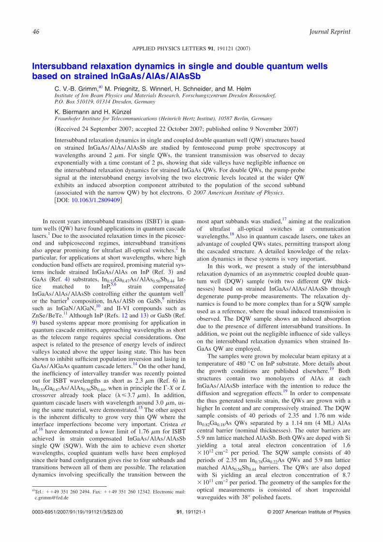
Intersubband relaxation dynamics in single and double quantum wellsbased on strained InGaAs/AlAs/AlAsSb
C. V.-B. Grimm,a� M. Priegnitz, S. Winnerl, H. Schneider, and M. HelmInstitute of Ion Beam Physics and Materials Research, Forschungszentrum Dresden Rossendorf,P.O. Box 510119, 01314 Dresden, Germany
K. Biermann and H. KünzelFraunhofer Institute for Telecommunications (Heinrich Hertz Institut), 10587 Berlin, Germany
�Received 24 September 2007; accepted 22 October 2007; published online 9 November 2007�
Intersubband relaxation dynamics in single and coupled double quantum well �QW� structures basedon strained InGaAs/AlAs/AlAsSb are studied by femtosecond pump probe spectroscopy atwavelengths around 2 �m. For single QWs, the transient transmission was observed to decayexponentially with a time constant of 2 ps, showing that side valleys have negligible influence onthe intersubband relaxation dynamics for strained InGaAs QWs. For double QWs, the pump-probesignal at the intersubband energy involving the two electronic levels located at the wider QWexhibits an induced absorption component attributed to the population of the second subband�associated with the narrow QW� by hot electrons. © 2007 American Institute of Physics.�DOI: 10.1063/1.2809409�
In recent years intersubband transitions �ISBT� in quan-tum wells �QW� have found applications in quantum cascadelasers.1 Due to the associated relaxation times in the picosec-ond and subpicosecond regimes, intersubband transitionsalso appear promising for ultrafast all-optical switches.2 Inparticular, for applications at short wavelengths, where highconduction band offsets are required, promising material sys-tems include strained InGaAs/AlAs on InP �Ref. 3� andGaAs �Ref. 4� substrates, In0.53Ga0.47As/AlAs0.56Sb0.44 lat-tice matched to InP,5,6 strain compensatedInGaAs/AlAs/AlAsSb controlling either the quantum well7
or the barrier8 composition, InAs/AlSb on GaSb,9 nitridessuch as InGaN/AlGaN,10 and II-VI compounds such asZnSe/BeTe.11 Although InP �Refs. 12 and 13� or GaSb �Ref.9� based systems appear more promising for application inquantum cascade emitters, approaching wavelengths as shortas the telecom range requires special considerations. Oneaspect is related to the presence of energy levels of indirectvalleys located above the upper lasing state. This has beenshown to inhibit sufficient population inversion and lasing inGaAs/AlGaAs quantum cascade letters.14 On the other hand,the inefficiency of intervalley transfer was recently pointedout for ISBT wavelengths as short as 2.3 �m �Ref. 6� inIn0.53Ga0.47As/AlAs0.56Sb0.44, when in principle the �-X or Lcrossover already took place ���3.7 �m�. In addition,quantum cascade lasers with wavelength around 3.0 �m, us-ing the same material, were demonstrated.15 The other aspectis the inherent difficulty to grow very thin QW where theinterface imperfections become very important. Cristea etal.16 have demonstrated a lower limit of 1.76 �m for ISBTachieved in strain compensated InGaAs/AlAs/AlAsSbsingle QW �SQW�. With the aim to achieve even shorterwavelengths, coupled quantum wells have been employedsince their band configuration gives rise to four subbands andtransitions between all of them are possible. The relaxationdynamics involving specifically the transition between the
most apart subbands was studied,17 aiming at the realizationof ultrafast all-optical switches at communicationwavelengths.18 Also in quantum cascade lasers, one takes anadvantage of coupled QWs states, permitting transport alongthe cascaded structure. A detailed knowledge of the relax-ation dynamics in these systems is very important.
In this work, we present a study of the intersubbandrelaxation dynamics of an asymmetric coupled double quan-tum well �DQW� sample �with two different QW thick-nesses� based on strained InGaAs/AlAs/AlAsSb throughdegenerate pump-probe measurements. The relaxation dy-namics is found to be more complex than for a SQW sampleused as a reference, where the usual induced transmission isobserved. The DQW sample shows an induced absorptiondue to the presence of different intersubband transitions. Inaddition, we point out the negligible influence of side valleyson the intersubband relaxation dynamics when strained In-GaAs QW are employed.
The samples were grown by molecular beam epitaxy at atemperature of 480 °C on InP substrate. More details aboutthe growth conditions are published elsewhere.19 Bothstructures contain two monolayers of AlAs at eachInGaAs/AlAsSb interface with the intention to reduce thediffusion and segregation effects.19 In order to compensatethe thus generated tensile strain, the QWs are grown with ahigher In content and are compressively strained. The DQWsample consists of 40 periods of 2.35 and 1.76 nm wideIn0.82Ga0.18As QWs separated by a 1.14 nm �4 ML� AlAscentral barrier �nominal thicknesses�. The outer barriers are5.9 nm lattice matched AlAsSb. Both QWs are doped with Siyielding a total areal electron concentration of 1.6�1012 cm−2 per period. The SQW sample consists of 40periods of 2.35 nm In0.78Ga0.22As QWs and 5.9 nm latticematched AlAs0.56Sb0.44 barriers. The QWs are also dopedwith Si yielding an areal electron concentration of 8.7�1011 cm−2 per period. The geometry of the samples for theoptical measurements is consisted of short trapezoidalwaveguides with 38° polished facets.
a�Tel.: 49 351 260 2494. Fax: 49 351 260 12342. Electronic mail:[email protected]
APPLIED PHYSICS LETTERS 91, 191121 �2007�
0003-6951/2007/91�19�/191121/3/$23.00 © 2007 American Institute of Physics91, 191121-1Downloaded 20 Feb 2008 to 149.220.35.103. Redistribution subject to AIP license or copyright; see http://apl.aip.org/apl/copyright.jsp
46 Journal Reprint
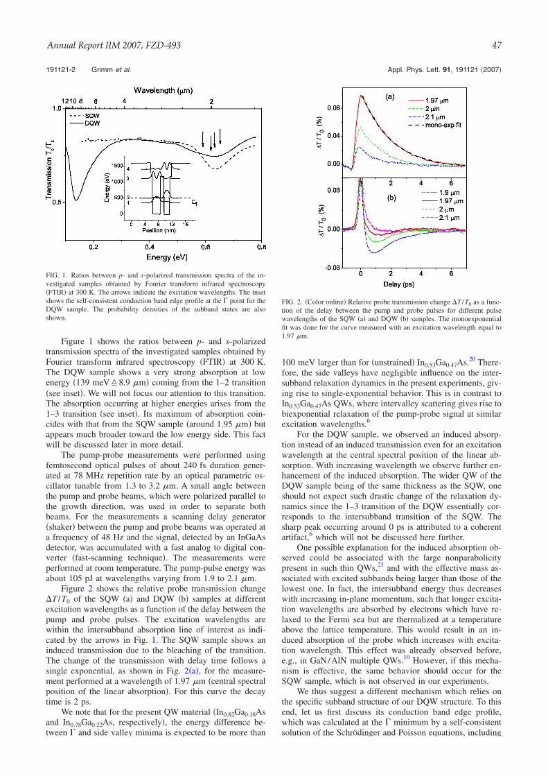
Figure 1 shows the ratios between p- and s-polarizedtransmission spectra of the investigated samples obtained byFourier transform infrared spectroscopy �FTIR� at 300 K.The DQW sample shows a very strong absorption at lowenergy �139 meV�8.9 �m� coming from the 1–2 transition�see inset�. We will not focus our attention to this transition.The absorption occurring at higher energies arises from the1–3 transition �see inset�. Its maximum of absorption coin-cides with that from the SQW sample �around 1.95 �m� butappears much broader toward the low energy side. This factwill be discussed later in more detail.
The pump-probe measurements were performed usingfemtosecond optical pulses of about 240 fs duration gener-ated at 78 MHz repetition rate by an optical parametric os-cillator tunable from 1.3 to 3.2 �m. A small angle betweenthe pump and probe beams, which were polarized parallel tothe growth direction, was used in order to separate bothbeams. For the measurements a scanning delay generator�shaker� between the pump and probe beams was operated ata frequency of 48 Hz and the signal, detected by an InGaAsdetector, was accumulated with a fast analog to digital con-verter �fast-scanning technique�. The measurements wereperformed at room temperature. The pump-pulse energy wasabout 105 pJ at wavelengths varying from 1.9 to 2.1 �m.
Figure 2 shows the relative probe transmission change�T /T0 of the SQW �a� and DQW �b� samples at differentexcitation wavelengths as a function of the delay between thepump and probe pulses. The excitation wavelengths arewithin the intersubband absorption line of interest as indi-cated by the arrows in Fig. 1. The SQW sample shows aninduced transmission due to the bleaching of the transition.The change of the transmission with delay time follows asingle exponential, as shown in Fig. 2�a�, for the measure-ment performed at a wavelength of 1.97 �m �central spectralposition of the linear absorption�. For this curve the decaytime is 2 ps.
We note that for the present QW material �In0.82Ga0.18Asand In0.78Ga0.22As, respectively�, the energy difference be-tween � and side valley minima is expected to be more than
100 meV larger than for �unstrained� In0.53Ga0.47As.20 There-fore, the side valleys have negligible influence on the inter-subband relaxation dynamics in the present experiments, giv-ing rise to single-exponential behavior. This is in contrast toIn0.53Ga0.47As QWs, where intervalley scattering gives rise tobiexponential relaxation of the pump-probe signal at similarexcitation wavelengths.6
For the DQW sample, we observed an induced absorp-tion instead of an induced transmission even for an excitationwavelength at the central spectral position of the linear ab-sorption. With increasing wavelength we observe further en-hancement of the induced absorption. The wider QW of theDQW sample being of the same thickness as the SQW, oneshould not expect such drastic change of the relaxation dy-namics since the 1–3 transition of the DQW essentially cor-responds to the intersubband transition of the SQW. Thesharp peak occurring around 0 ps is attributed to a coherentartifact,6 which will not be discussed here further.
One possible explanation for the induced absorption ob-served could be associated with the large nonparabolicitypresent in such thin QWs,21 and with the effective mass as-sociated with excited subbands being larger than those of thelowest one. In fact, the intersubband energy thus decreaseswith increasing in-plane momentum, such that longer excita-tion wavelengths are absorbed by electrons which have re-laxed to the Fermi sea but are thermalized at a temperatureabove the lattice temperature. This would result in an in-duced absorption of the probe which increases with excita-tion wavelength. This effect was already observed before,e.g., in GaN/AlN multiple QWs.10 However, if this mecha-nism is effective, the same behavior should occur for theSQW sample, which is not observed in our experiments.
We thus suggest a different mechanism which relies onthe specific subband structure of our DQW structure. To thisend, let us first discuss its conduction band edge profile,which was calculated at the � minimum by a self-consistentsolution of the Schrödinger and Poisson equations, including
FIG. 1. Ratios between p- and s-polarized transmission spectra of the in-vestigated samples obtained by Fourier transform infrared spectroscopy�FTIR� at 300 K. The arrows indicate the excitation wavelengths. The insetshows the self-consistent conduction band edge profile at the � point for theDQW sample. The probability densities of the subband states are alsoshown.
FIG. 2. �Color online� Relative probe transmission change �T /T0 as a func-tion of the delay between the pump and probe pulses for different pulsewavelengths of the SQW �a� and DQW �b� samples. The monoexponentialfit was done for the curve measured with an excitation wavelength equal to1.97 �m.
191121-2 Grimm et al. Appl. Phys. Lett. 91, 191121 �2007�
Downloaded 20 Feb 2008 to 149.220.35.103. Redistribution subject to AIP license or copyright; see http://apl.aip.org/apl/copyright.jsp
Annual Report IIM 2007, FZD-493 47
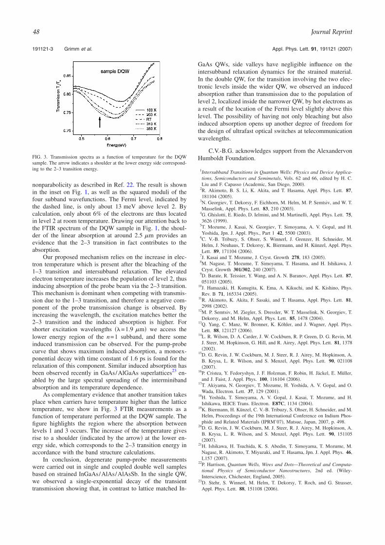
nonparabolicity as described in Ref. 22. The result is shownin the inset on Fig. 1, as well as the squared moduli of thefour subband wavefunctions. The Fermi level, indicated bythe dashed line, is only about 13 meV above level 2. Bycalculation, only about 6% of the electrons are thus locatedin level 2 at room temperature. Drawing our attention back tothe FTIR spectrum of the DQW sample in Fig. 1, the shoul-der of the linear absorption at around 2.5 �m provides anevidence that the 2–3 transition in fact contributes to theabsorption.
Our proposed mechanism relies on the increase in elec-tron temperature which is present after the bleaching of the1–3 transition and intersubband relaxation. The elevatedelectron temperature increases the population of level 2, thusinducing absorption of the probe beam via the 2–3 transition.This mechanism is dominant when competing with transmis-sion due to the 1–3 transition, and therefore a negative com-ponent of the probe transmission change is observed. Byincreasing the wavelength, the excitation matches better the2–3 transition and the induced absorption is higher. Forshorter excitation wavelengths ��=1.9 �m� we access thelower energy region of the n=1 subband, and there someinduced transmission can be observed. For the pump-probecurve that shows maximum induced absorption, a monoex-ponential decay with time constant of 1.6 ps is found for therelaxation of this component. Similar induced absorption hasbeen observed recently in GaAs/AlGaAs superlattices23 en-abled by the large spectral spreading of the interminibandabsorption and its temperature dependence.
As complementary evidence that another transition takesplace when carriers have temperature higher than the latticetemperature, we show in Fig. 3 FTIR measurements as afunction of temperature performed at the DQW sample. Thefigure highlights the region where the absorption betweenlevels 1 and 3 occurs. The increase of the temperature givesrise to a shoulder �indicated by the arrow� at the lower en-ergy side, which corresponds to the 2–3 transition energy inaccordance with the band structure calculations.
In conclusion, degenerate pump-probe measurementswere carried out in single and coupled double well samplesbased on strained InGaAs/AlAs/AlAsSb. In the single QW,we observed a single-exponential decay of the transienttransmission showing that, in contrast to lattice matched In-
GaAs QWs, side valleys have negligible influence on theintersubband relaxation dynamics for the strained material.In the double QW, for the transition involving the two elec-tronic levels inside the wider QW, we observed an inducedabsorption rather than transmission due to the population oflevel 2, localized inside the narrower QW, by hot electrons asa result of the location of the Fermi level slightly above thislevel. The possibility of having not only bleaching but alsoinduced absorption opens up another degree of freedom forthe design of ultrafast optical switches at telecommunicationwavelengths.
C.V.-B.G. acknowledges support from the AlexandervonHumboldt Foundation.
1Intersubband Transitions in Quantum Wells: Physics and Device Applica-tions, Semiconductors and Semimetals, Vols. 62 and 66, edited by H. C.Liu and F. Capasso �Academic, San Diego, 2000�.
2R. Akimoto, B. S. Li, K. Akita, and T. Hasama, Appl. Phys. Lett. 87,181104 �2005�.
3N. Georgiev, T. Dekorsy, F. Eichhorn, M. Helm, M. P. Semtsiv, and W. T.Masselink, Appl. Phys. Lett. 83, 210 �2003�.
4G. Ghislotti, E. Riedo, D. Ielmini, and M. Martinelli, Appl. Phys. Lett. 75,3626 �1999�.
5T. Mozume, J. Kasai, N. Georgiev, T. Simoyama, A. V. Gopal, and H.Yoshida, Jpn. J. Appl. Phys., Part 1 42, 5500 �2003�.
6C. V.-B. Tribuzy, S. Ohser, S. Winnerl, J. Grenzer, H. Schneider, M.Helm, J. Neuhaus, T. Dekorsy, K. Biermann, and H. Künzel, Appl. Phys.Lett. 89, 171104 �2006�.
7J. Kasai and T. Mozume, J. Cryst. Growth 278, 183 �2005�.8M. Nagase, T. Mozume, T. Simoyama, T. Hasama, and H. Ishikawa, J.Cryst. Growth 301/302, 240 �2007�.
9D. Barate, R. Teissier, Y. Wang, and A. N. Baranov, Appl. Phys. Lett. 87,051103 �2005�.
10J. Hamazaki, H. Kunugita, K. Ema, A. Kikuchi, and K. Kishino, Phys.Rev. B 71, 165334 �2005�.
11R. Akimoto, K. Akita, F. Sasaki, and T. Hasama, Appl. Phys. Lett. 81,2998 �2002�.
12M. P. Semtsiv, M. Ziegler, S. Dressler, W. T. Masselink, N. Georgiev, T.Dekorsy, and M. Helm, Appl. Phys. Lett. 85, 1478 �2004�.
13Q. Yang, C. Manz, W. Bronner, K. Köhler, and J. Wagner, Appl. Phys.Lett. 88, 121127 �2006�.
14L. R. Wilson, D. A. Carder, J. W. Cockburn, R. P. Green, D. G. Revin, M.J. Steer, M. Hopkinson, G. Hill, and R. Airey, Appl. Phys. Lett. 81, 1378�2002�.
15D. G. Revin, J. W. Cockburn, M. J. Steer, R. J. Airey, M. Hopkinson, A.B. Krysa, L. R. Wilson, and S. Menzel, Appl. Phys. Lett. 90, 021108�2007�.
16P. Cristea, Y. Fedoryshyn, J. F. Holzman, F. Robin, H. Jäckel, E. Müller,and J. Faist, J. Appl. Phys. 100, 116104 �2006�.
17T. Akiyama, N. Georgiev, T. Mozume, H. Yoshida, A. V. Gopal, and O.Wada, Electron. Lett. 37, 129 �2001�.
18H. Yoshida, T. Simoyama, A. V. Gopal, J. Kasai, T. Mozume, and H.Ishikawa, IEICE Trans. Electron. E87C, 1134 �2004�.
19K. Biermann, H. Künzel, C. V.-B. Tribuzy, S. Ohser, H. Schneider, and M.Helm, Proceedings of the 19th International Conference on Indium Phos-phide and Related Materials �IPRM’07�, Matsue, Japan, 2007, p. 498.
20D. G. Revin, J. W. Cockburn, M. J. Steer, R. J. Airey, M. Hopkinson, A.B. Krysa, L. R. Wilson, and S. Menzel, Appl. Phys. Lett. 90, 151105�2007�.
21H. Ishikawa, H. Tsuchida, K. S. Abedin, T. Simoyama, T. Mozume, M.Nagase, R. Akimoto, T. Miyazaki, and T. Hasama, Jpn. J. Appl. Phys. 46,L157 �2007�.
22P. Harrison, Quantum Wells, Wires and Dots—Theoretical and Computa-tional Physics of Semiconductor Nanostructures, 2nd ed. �Wiley-Interscience, Chichester, England, 2005�.
23D. Stehr, S. Winnerl, M. Helm, T. Dekorsy, T. Roch, and G. Strasser,Appl. Phys. Lett. 88, 151108 �2006�.
FIG. 3. Transmission spectra as a function of temperature for the DQWsample. The arrow indicates a shoulder at the lower energy side correspond-ing to the 2–3 transition energy.
191121-3 Grimm et al. Appl. Phys. Lett. 91, 191121 �2007�
Downloaded 20 Feb 2008 to 149.220.35.103. Redistribution subject to AIP license or copyright; see http://apl.aip.org/apl/copyright.jsp
48 Journal Reprint

SSStttaaatttiiissstttiiicccsss

Annual Report IIM 2007, FZD-493
51
1. Gemming, S.; Schreiber, M.; Suck, J.-B. (Editors) Materials for Tomorrow Berlin - Heidelberg - New York: Springer, 2007, 978-3-540-47970-3, 212 pages
2. Enyashin, A. N.; Gemming, S.; Seifert, G. Simulation of inorganic nanotubes in S. Gemming, M. Schreiber, J.-B. Suck, Materials for Tomorrow, Berlin - Heidelberg - New York: Springer, 2007, 978-3-540-47970-3, pp. 33-57
3. Gemming, S.; Schreiber, M. Theoretical investigation of interfaces in S. Gemming, M. Schreiber, J.-B. Suck, Materials for Tomorrow, Berlin - Heidelberg - New York: Springer, 2007, 978-3-540-47970-3, pp. 91 - 122
Ion-Solid-Interaction 1. Facsko, S.; Kost, D.; Keller, A.; Möller, W.; Pesic, Z.; Stolterfoht, N.
Interaction of highly charged ions with the surface of insulators Radiation Physics and Chemistry 76, 387 (2007).
2. Grambole, D.; Herrmann, F.; Heera, V.; Meijer, J. Study of crystal damage by ion implantation using micro RBS/Channeling Nuclear Instruments and Methods in Physics Research B 260, 276 (2007).
3. Grynszpan, R. I.; Brauer, G.; Anwand, W.; Malaquin, L.; Saudé, S.; Vickridge, I.; Briand, E. Radiation damage in zirconia investigated by positively charged particles Nuclear Instruments and Methods in Physics Research B 261, 888 (2007).
4. Güttler, D.; Grötzschel, R.; Möller, W. Lateral variation of target poisoning during reactive magnetron sputtering Applied Physics Letters 90, 263502 (2007).
5. Kost, D.; Facsko, S.; Möller, W.; Hellhammer, R.; Stolterfoht, N. Channels of potential energy dissipation during multiply charged argon ion bombardment of copper Physical Review Letters 98, 225503 (2007).
6. Kost, D.; Röder, F.; Möller, W. Deposition and re-emission of potential energy - extended dynamical COB simulation Journal of Physics: Conference Series 58, 343 (2007).
7. Möller, W.; Güttler, D. Modeling of plasma-target interaction during reactive magnetron sputtering of TiN Journal of Applied Physics 102, 094501 (2007).
8. Shiryaev, A. A.; Grambole, D.; Rivera, A.; Herrmann, F. On the interaction of molecular hydrogen with diamonds: An experimental study using nuclear probes and thermal desorption Diamond and Related Materials 16, 1479 (2007).
9. Zschornack, G.; Grossmann, F.; Heller, R.; Kentsch, U.; Kreller, M.; Landgraf, S.; Ovsyannikov, V. P.; Schmidt, M.; Ullmann, F. Production of highly charged ions for ion-surface interaction studies Nuclear Instruments and Methods in Physics Research B 258, 205 (2007).
Thin Films 10. Abd El-Rahman, A. M.; Maitz, M. F.; Kassem, M. A.; El-Hossary, F.; Prokert, F.; Reuther, H.; Pham, M. T.;
Richter, E. Surface improvement and biocompatibility of TiAl24Nb10 intermetallic alloy using rf plasma nitriding Applied Surface Science 253, 9067 (2007).
Publications
Monographs & Book Chapters

Publications 52
11. Abendroth, B.; Jäger, H. U.; Möller, W.; Bilek, M. Binary-collision modeling of ion-induced stress relaxation in cubic BN and amorphous C thin films Applied Physics Letters 90, 181910 (2007).
12. Abrasonis, G.; Krause, M.; Mücklich, A.; Sedlackova, K.; Radnoczi, G.; Kreissig, U.; Kolitsch, A.; Möller, W. Growth regimes and metal enhanced 6-fold ring clustering of carbon in carbon-nickel composite thin films Carbon 45, 2995 (2007).
13. Beckers, M.; Schell, N.; Martins, R. M. S.; Mücklich, A.; Möller, W.; Hultman, L. Nucleation and growth of Ti2AlN thin films deposited by reactive magnetron sputtering onto MgO(111) Journal of Applied Physics 102, 074916 (2007).
14. Blomqvist, M.; Bongiorno, G.; Podesta, A.; Serin, V.; Abrasonis, G.; Kreissig, U.; Möller, W.; Coronel, E.; Wachtmeister, S.; Csillag, S.; Cassina, V.; Piseri, P.; Milani, P. Structural and tribological properties of cluster-assembled CNx films Applied Physics A 87, 767 (2007).
15. Borras, A.; Lopez, C.; Rico, V.; Gracia, F.; Gonzalez-Elipe, A.; Richter, E.; Battiston, G.; Gerbasi, R.; McSporran, N.; Sauthier, G.; Gyorgy, E.; Figueras, A. Effect of visible and UV illumination on the water contact angle of TiO2 thin films with incorporated nitrogen Journal of Physical Chemistry C 111, 1801 (2007).
16. Cizek, J.; Prochazka, I.; Danis, S.; Melikhova, O.; Vlach, M.; Zaludova, N.; Brauer, G.; Anwand, W.; Mücklich, A.; Gemma, R.; Nikitin, E.; Kirchheim, R.; Pundt, A. Positron annihilation study of hydrogen trapping at open-volume defects: Comparison of nanocrystalline and epitaxial Nb thin films Journal of Alloys and Compounds 446, 484 (2007).
17. Cizek, J.; Prochazka, I.; Danis, S.; Vlach, M.; Zaludova, N.; Brauer, G.; Anwand, W.; Mücklich, A.; Gemma, R.; Nikitin, E.; Kirchheim, R.; Pundt, A. Defect studies of hydrogen loaded Nb: Bulk metals and thin films Physica Status Solidi (C) 4, 3485 (2007).
18. Donchev, A.; Richter, E.; Schütze, M.; Yankov, R. Improvement of the oxidation resistance of TiAl-alloys with fluorine Intermetallics 14, 1168 (2007).
19. Gago, R.; Abendroth, B.; Cerda, J. I.; Jimenez, I.; Möller, W. Detection of intrinsic stress in cubic boron nitride films by x-ray absorption near-edge structure: Stress relaxation mechanisms by simultaneous ion implantation during growth Physical Review B 76, 174111 (2007).
20. Grynszpan, R. I.; Anwand, W.; Brauer, G.; Coleman, G. Positron depth profiling in solid surface layers Annales de Chimie - Science des Matériaux 32, 365 (2007).
21. Höglund, C.; Beckers, M.; Schell, N.; Borany, J. von; Birch, J.; Hultman, L. Topotaxial growth of Ti2AlN by solid state reaction in AlN/Ti(0001)multilayer thin films Applied Physics Letters 90, 174106 (2007).
22. Jagielski, J.; Piatkowska, A.; Merstallinger, A.; Librant, Z.; Aubert, P.; Grötzschel, R.; Suszko, T. Friction properties of implanted alumina for vacuum applications Vacuum 81, 1357 (2007).
23. Krause, M.; Abrasonis, G.; Kolitsch, A.; Mücklich, A.; Kreissig, U.; Möller, W. Nickel catalysed sixfold ring clustering and graphitisation in C:Ni nanocomposites: A Raman analysis Physica Status Solidi (B) 244, 4236 (2007).
24. Krause, M.; Ziegs, F.; Popov, A. A.; Dunsch, L. Entrapped bonded hydrogen in a fullerene - The five atomic cluster Sc3CH in C80 ChemPhysChem 8, 537 (2007).
25. Lifshitz, Y.; Edrei, R.; Hoffman, A.; Grossman, E.; Lempert, G. D.; Berthold, J.; Schultrich, B.; Jäger, H. U. Surface roughness evolution and growth mechanism of carbon films from hyperthermal species Diamond and Related Materials 16, 1771 (2007).
26. Mandumpal, J.; Gemming, S.; Seifert, G. Curvature effects of nitrogen on graphitic sheets: Structures and energetics Chemical Physics Letters 447, 115 (2007).
Annual Report IIM 2007, FZD-493
53
27. Manova, D.; Eichentopf, I.; Heinrich, S.; Mandl, S.; Richter, E.; Neumann, H.; Rauschenbach, B. Interplay of cold working and nitrogen diffusion in austenitic stainless steel Nuclear Instruments and Methods in Physics Research B 257, 442 (2007).
28. Manova, D.; Hirsch, D.; Richter, E.; Mandl, S.; Neumann, H.; Rauschenbach, B. Microstructure of nitrogen implanted stainless steel after wear experiment Surface and Coatings Technology 201, 8329 (2007).
29. Martins, R. M. S.; Schell, N.; Silva, R. J. C.; Pereira, L.; Mahesh, K. K.; Fernandes, F. M. B. In-situ study of Ni-Ti thin film growth on a TiN intermediate layer by X-ray diffraction Sensors and Actuators B 126, 332 (2007).
30. Michel, K. H.; Verberck, B.; Hulman, M.; Kuzmany, H.; Krause, M. Superposition of quantum and classical rotational motions in Sc2C2@C84 fullerite Journal of Chemical Physics 126, 64304 (2007).
31. Niskanen, A.; Kreissig, U.; Leskelä, M.; Ritala, M. Radical enhanced atomic layer deposition of tantalum oxide Chemistry of Materials 19, 2316 (2007).
32. Peter, S.; Graupner, K.; Grambole, D.; Richter, F. A comparative experimental analysis of the a-C:H deposition processes using CH4 and C2H2 as precursors Journal of Applied Physics 102, 53304 (2007).
33. Piekoszewski, J.; Kempinski, W.; Andrzejewski, B.; Trybula, Z.; Kaszynski, J.; Stankowski, J.; Stanislawski, J.; Barlak, M.; Jagielski, J.; Werner, Z.; Grötzschel, R.; Richter, E. Formation of superconducting regions of MgB2 by implantation of magnesium ions into boron substrate followed by intense pulsed plasma treatment Surface and Coatings Technology 201, 8175 (2007).
34. Piekoszewski, J.; Kempinski, W.; Barlak, M.; Kaszynski, J.; Stanislawski, J.; Anduejewski, B.; Werner, Z.; Plekara-Sady, L.; Richter, E.; Stankowskic, J.; Grötzschel, R.; Lo, S. Superconducting and electrical properties of Mg-B structures formed by implantation of magnesium ions into the bulk boron followed by pulse plasma treatment Vacuum 81, 1398 (2007).
35. Ram Mohan Rao, K.; Mukherjee, S.; Roy, S. K.; Richter, E.; Möller, W.; Manna, I. Plasma immersion ion implantation of nitrogen on austenitic stainless steel at variable energy for enhanced corrosion resistance Surface and Coatings Technology 201, 4919 (2007).
36. Riviere, J. P.; Templier, C.; Declémy, A.; Redjdal, O.; Chumlyakov, Y.; Abrasonis, G. Microstructure of expanded austenite in ion-nitrided AISI 316L single crystals Surface and Coatings Technology 201, 8210 (2007).
37. Rogozin, A.; Vinnichenko, M.; Shevchenko, N.; Vazquez, L.; Mücklich, A.; Kreissig, U.; Yankov, R. A.; Kolitsch, A.; Möller, W. Effect of elevated substrate temperature on growth, properties, and structure of indium tin oxide films prepared by reactive magnetron sputtering Journal of Materials Research 22, 2319 (2007).
38. Seppänen, T.; Hultman, L.; Birch, J.; Beckers, M.; Kreissig, U. Deviations from Vegard's rule in Al1-xInxN (0001) alloy thin films grown by magnetron sputter epitaxy Journal of Applied Physics 101, 043519 (2007).
39. Silva, M. M.; Ueda, M.; Pichon, L.; Reuther, H.; Lepienski, C. M. Surface modification of Ti6Al4V alloy by PIII at high temperatures: Effects of plasma potential Nuclear Instruments and Methods in Physics Research B 257, 722 (2007).
40. Tan, I. H.; Ueda, M.; Oliveira, R. M.; Dallaqua, R. S.; Reuther, H. Plasma immersion ion implantation in arc and glow discharge plasmas submitted to low magnetic fields Surface and Coatings Technology 201, 4826 (2007).
41. Tan, I. H.; Ueda, M.; Rossi, J. O.; Diaz, B.; Abramof, E.; Reuther, H. Nitrogen plasma ion implantation in silicon using short pulse high voltage glow discharges Journal of Physics D 40, 5196 (2007).
42. Tsyganov, I. A.; Maitz, M. F.; Richter, E.; Reuther, H.; Mashina, A. I.; Rustichelli, F. Hemocompatibility of titanium-based coatings prepared by metal plasma immersion ion implantation and deposition Nuclear Instruments and Methods in Physics Research B 257, 122 (2007).
Publications 54
43. Ueda, M.; Silva, M. M.; Lepienski, C. M.; Soares, P. C. Jr.; Gonçalves, J. A. N.; Reuther, H. High-temperature plasma immersion ion implantation Surface and Coatings Technology 201, 4953 (2007).
44. Vinnichenko, M.; Shevchenko, N.; Rogozin, A.; Grötzschel, R.; Mücklich, A.; Kolitsch, A.; Möller, W. Structure and dielectric function of two- and single-domain ZnO epitaxial films Journal of Applied Physics 102, 113505 (2007).
45. Yankov, R. A.; Shevchenko, N.; Rogozin, A.; Maitz, M. F.; Richter, E.; Möller, W.; Donchev, A.; Schütze, M. Reactive plasma immersion ion implantation for surface passivation Surface and Coatings Technology 201, 6752 (2007).
Nanoscale Magnetism 46. Gemming, S.; Janisch, R.; Schreiber, M.; Spaldin, N. A.
Density functional investigation of the (113)[-110] twin grain boundary in TiO2 anatase and its influence on magnetism in diluted magnetic semiconductors Physical Review B 76, 045204 (2007).
47. Küpper, K.; Bischoff, L.; Akhmadaliev, C.; Fassbender, J.; Stoll, H.; Chou, K. W.; Puzic, A.; Fauth, K.; Dolgos, D.; Schütz, G.; van Waeyenberge, B.; Tyliszczak, T.; Neudecker, I.; Woltersdorf, G.; Back, C. H. Vortex dynamics in permalloy disks with artificially point defects: Suppression of the gyrotropic mode Applied Physics Letters 90, 062506 (2007).
48. Küpper, K.; Buess, M.; Raabe, J.; Quitmann, C.; Fassbender, J. Dynamic vortex − antivortex interaction in a single cross-tie wall Physical Review Letters 99, 167202 (2007).
49. Liedke, M. O.; Liedke, B.; Keller, A.; Hillebrands, B.; Mücklich, A.; Facsko, S.; Fassbender, J. Induced anisotropies in exchange coupled systems on rippled substrates Physical Review B 75, 220407 (2007).
50. Mattern, N.; Zhang, W. X.; Roth, S.; Reuther, H.; Bähtz, C.; Richter, M. Structural and magnetic properties of non-stoichiometric Fe2Zr Journal of Physics: Condensed Matter 19, 376202 (2007).
51. Patra, A. K.; Neu, V.; Fähler, S.; Grötzschel, R.; Bedanta, S.; Kleemann, W.; Schultz, L. Crystal structure and its correlation to intrinsic and extrinsic magnetic properties of epitaxial hard magnetic Pr-Co films Physical Review B 75, 184417 (2007).
52. Potzger, K.; Anwand, W.; Reuther, H.; Zhou, S.; Talut, G.; Fassbender, J.; Brauer, G.; Skorupa, W. The effect of flash lamp annealing on Fe implanted ZnO single crystals Journal of Applied Physics 101, 033906 (2007).
53. Potzger, K.; Zhou, S.; Reuther, H.; Küpper, K.; Talut, G.; Helm, M.; Fassbender, J.; Denlinger, J. D. Suppression of secondary phase formation in Fe implanted ZnO single crystals Applied Physics Letters 91, 062107 (2007).
54. Som, T.; Ghosh, S.; Mäder, M.; Grötzschel, R.; Roy, S.; Paramanik, D.; Gupta, A. Temperature-dependent changes in structural and magnetic properties of heavy ion irradiated nanoscale Co/Pt multilayers New Journal of Physics 9, 164 (2007).
55. Talut, G.; Reuther, H.; Stromberg, F.; Zhou, S.; Potzger, K.; Eichhorn, F. Ferromagnetism in GaN induced by Fe ion implantation Journal of Applied Physics 102, 083909 (2007).
56. Xu, Q.; Hartmann, L.; Schmidt, H.; Hochmuth, H.; Lorenz, M.; Spemann, D.; Grundmann, M. s-d exchange interaction induced magnetoresistance in magnetic ZnO Physical Review B 76, 134417 (2007).
57. Zhou, S.; Potzger, K.; Mücklich, A.; Eichhorn, F.; Schell, N.; Grötzschel, R.; Schmidt, B.; Skorupa, W.; Helm, M.; Fassbender, J.; Geiger, D. Structural and magnetic properties of Mn-implanted Si Physical Review B 75, 085203 (2007).
58. Zhou, S.; Potzger, K.; Reuther, H.; Skorupa, W.; Helm, M.; Fassbender, J. Absence of ferromagnetism in V-implanted ZnO single crystals Journal of Applied Physics 101, 09H109 (2007).

Annual Report IIM 2007, FZD-493
55
59. Zhou, S.; Potzger, K.; Reuther, H.; Talut, G.; Eichhorn, F.; Borany, J. von; Skorupa, W.; Helm, M.; Fassbender, J. Crystallographically oriented magnetic ZnFe2O4 nanoparticles synthesized by Fe implantation into ZnO Journal of Physics D 40, 964 (2007).
Nanostructures 60. Beyer, V.; Borany, J. von; Klimenkov, M.
A transient electrical model of charging for Ge nanocrystal containing gate oxides Journal of Applied Physics 101, 094507 (2007).
61. Bischoff, L.; Akhmadaliev, Ch.; Schmidt, B. Defect induced nanowire growth by FIB implantation Microelectronic Engineering 84, 1459 (2007).
62. Brauer, G.; Anwand, W.; Grambole, D.; Skorupa, W.; Hou, Y.; Andreev, A.; Teichert, C.; Tam, K. H.; Djurisic, A. B. Non-destructive characterization of vertical ZnO nanowire arrays by slow positron implantation spectroscopy, atomic force microscopy, and nuclear reaction analysis Nanotechnology 18, 195301 (2007).
63. Enyashin, A. N.; Gemming, S. TiSi2-nanostructures - Enhanced conductivity at nanoscale? Physica Status Solidi (B) 244, 3593 (2007).
64. Enyashin, A. N.; Gemming, S.; Seifert, G. DNA-wrapped carbon nanotubes Nanotechnology 18, 245702 (2007).
65. Enyashin, A. N.; Gemming, S.; Seifert, G. Nanosized allotropes of molybdenum disulfide European Physical Journal - Special Topics 149, 103 (2007).
66. Enyashin, Andrey N.; Gemming, S.; Bar-Sadan, M.; Popovits-Biro, R.; Hong, Sung Y.; Prior, Y.; Tenne, R.; Seifert, G. Structure and stability of molybdenum sulfide fullerenes Angewandte Chemie 119, 631 (2007).
67. Gemming, S.; Seifert, G. Nanocrystals: Catalysts on the edge Nature Nanotechnology 2, 21 (2007).
68. Ghicov, A.; Schmidt, B.; Kunze, J.; Schmuki, P. Photoresponse in the visible range from Cr doped TiO2 nanotubes Chemical Physics Letters 433, 323 (2007).
69. Grenzer, J.; Mücklich, A.; Grigorian, S.; Pietsch, U.; Datta, D.; Chini, T. K.; Hazra, S.; Sanyal, M. K. High-temperature induced nanocrystal formation in ion-beam-induced amorphous silicon ripples Physica Status Solidi (A) 204, 2555 (2007).
70. Kim, D. S.; Ji, R.; Fan, H. J.; Bertram, F.; Scholz, R.; Dadgar, A.; Nielsch, K.; Krost, A.; Christen, J.; Gösele, U.; Zacharias, M. Laser interference lithography tailored for highly symmetric arranged ZnO nanowire arrays Small 3, 76 (2007).
71. Oates, T. W. H.; Christalle, E. Real-time spectroscopic ellipsometry of silver nanoparticle formation in poly(vinyl alcohol) thin films Journal of Physical Chemistry C 111, 182 (2007).
72. Oates, T. W. H., Keller, A., Facsko, S., Mücklich, A. Aligned silver nanoparticles on rippled silicon templates exhibiting anisotropic plasmon absorption Plasmonics 2, 47 (2007).
73. Peeva, A.; Kalitzova, M.; Beshkov, G.; Zollo, G.; Vitali, G.; Skorupa, W. Nanocluster evolution in Ge+ ion implanted Ta2O5 layers Materials Letters 61, 3620 (2007).
74. Popov, I.; Gemming, S.; Seifert, G. Structural and electronic properties of a Mo6S8 cluster deposited on a Au(111) surface Physical Review B 75, 245436 (2007).
Publications 56
75. Popov, I.; Kunze, T.; Gemming, S.; Seifert, G. Self-assembly of Mo6S8 clusters on the Au(111) surface European Physical Journal D 45, 439 (2007).
76. Popov, Alexey A.; Krause, M.; Yang, S.; Wong, J.; Dunsch, L. C78 cage isomerism defined by trimetallic nitride cluster size: A computational and vibrational spectroscopic study Journal of Physical Chemistry B 111, 3363 (2007).
77. Radke de Cuba, M. H.; Emmerich, H.; Gemming, S. Finding polymorphic structures during vicinal surface growth European Physical Journal - Special Topics 1, 43 (2007).
78. Rangelow, I. W.; Ivanov, T.; Ivanova, K.; Volland, B. E.; Grabiec, P.; Sarov, Y.; Persaud, A.; Gotszalk, T.; Zawierucha, P.; Zielony, M.; Dontzov, D.; Schmidt, B.; Zier, M.; Nikolov, N.; Kostic, I.; Engl, W.; Sulzbach, T.; Mielczarski, J.; Kolb, S.; Latimier, Du P.; Pedreau, R.; Djakov, V.; Huq, S. E.; Edinger, K.; Fortagne, O.; Almansa, A.; Blom, H. O. Piezoresistive and self-actuated 128-cantilever arrays for nanotechnology applications Microelectronic Engineering 84, 1260 (2007).
79. Röntzsch, L.; Heinig, K.-H.; Schuller, Jon A.; Brongersma, M. L. Thin film patterning by surface-plasmon-induced thermocapillarity Applied Physics Letters 90, 044105 (2007).
80. Salh, R.; Fitting, L.; Kolesnikova, E. V.; Sitnikova, A. A.; Zamoryanskaya, M. V.; Schmidt, B.; Fitting, H.-J. Si and Ge nanocluster formation in silica matrix Semiconductors 41, 397 (2007).
81. Schmidt, B. Nanocluster memories by ion beam synthesis of Si in SiO2 Materials Science 25, 1213 (2007).
82. Schmidt, B. Nanostructures by ion beams Radiation Effects and Defects in Solids 162, 171 (2007).
83. Schmidt, B.; Mücklich, A.; Röntzsch, L.; Heinig, K.-H. How do high energy heavy ions shape Ge nanoparticles embedded in SiO2? Nuclear Instruments and Methods in Physics Research B 257, 30 (2007).
84. Schöndorfer, C.; Lugstein, A.; Bischoff, L.; Hyun, Y. J.; Pongratz, P.; Bertagnolli, E. FIB induced growth of antimony nanowires Microelectronic Engineering 84, 1440 (2007).
85. Schöndorfer, Ch.; Lugstein, A.; Hyun, Y.-J.; Bertagnolli, E.; Bischoff, L.; Nellen, P. M.; Callegari, V.; Pongratz, P. Focused ion beam induced synthesis of a porous antimony nanowire network Journal of Applied Physics 102, 044308 (2007).
86. Stepina, N. P.; Dvurechenskii, A. V.; Armbrister, V. A.; Kesler, V. G.; Novikov, P. L.; Gutakovskii, A. K.; Kirienko, V. V.; Smagina, Zh. V.; Grötzschel, R. Pulsed ion-beam induced nucleation and growth of Ge nanocrystals on SiO2 Applied Physics Letters 90, 33120 (2007).
87. Takahashi, S.; Dawson, P.; Zayats, A. V.; Bischoff, L.; Angelov, O.; Dimova-Malinovska, D.; Tsvetkova, T.; Townsend, P. D. Optical contrast in ion-implanted amorphous silicon carbide nanostructures Journal of Physics D 40, 7492 (2007).
Doping and Defects of Semiconductors 88. Beyer, R.; Schmidt, B.
Scanning capacitance microscopy and the role of localized charges in dielectric films: Infering or challenging? Microelectronic Engineering 84, 376 (2007).
89. Beyer, V.; Borany, J. von; Heinig, K.-H. Dissociation of Si+ ion implanted and as-grown thin SiO2 layers during annealing in ultra-pure neutral ambient by emanation of SiO Journal of Applied Physics 101, 053516 (2007).
Annual Report IIM 2007, FZD-493
57
90. Brauer, G.; Anwand, W.; Skorupa, W.; Kuriplach, J.; Melikhova, O.; Cizek, J.; Prochazka, I.; Moisson, C.; Wenckstern, H. von; Schmidt, H.; Lorenz, M.; Grundmann, M. Comparative characterization of differently grown ZnO single crystals by positron annihilation and Hall effect Superlattices and Microstructures 42, 259 (2007).
91. Brauer, G.; Anwand, W.; Skorupa, W.; Kuriplach, J.; Melikhova, O.; Cizek, J.; Prochazka, I.; Wenckstern, H. von; Brandt, M.; Lorenz, M.; Grundmann, M. Defects in N+ ion-implanted ZnO single crystals studied by positron annihilation and Hall effect Physica Status Solidi (C) 4, 3642 (2007).
92. Brauer, G.; Kuriplach, J.; Anwand, W.; Becvar, F.; Skorupa, W. Characterization of various crystalline structures at the SiO2/Si interface by positrons Radiation Physics and Chemistry 76, 195 (2007).
93. Brauer, G.; Kuriplach, J.; Cizek, J.; Anwand, W.; Melikhova, O.; Prochazka, I.; Skorupa, W. Positron lifetimes in ZnO single crystals Vacuum 81, 1314 (2007).
94. Danesh, P.; Pantchev, B.; Schmidt, B.; Grambole, D. Molecular hydrogen in amorphous silicon with high internal stress Japanese Journal of Applied Physics 46, 5050 (2007).
95. Diaz, B.; Abramof, E.; Castro, R. M.; Ueda, M.; Reuther, H. Strain profile of (001) silicon implanted with nitrogen by plasma immersion Journal of Applied Physics 101, 103523 (2007).
96. Fitting, H.-J.; Salh, R.; Schmidt, B. Multimodal electronic-vibronic spectra of luminescence in ion-implanted silica layers Journal of Luminescence 122, 743 (2007).
97. Fitting, H.-J.; Salh, R.; Schmidt, B. Multimodal luminescence spectra of ion-implanted silica Semiconductors 41, 453 (2007).
98. Gao, F.; Du, J.; Bylaska, E. J.; Posselt, M.; Weber, W. J. Ab-initio atomic simulations of antisite pair recovery in cubic silicon carbide Applied Physics Letters 90, 221915 (2007).
99. Gao, F.; Zhang, Y.; Devanathan, R.; Posselt, M.; Weber, W. J. Atomistic simulations of epitaxial recrystallization in 4H-SiC along the [0001] direction Nuclear Instruments and Methods in Physics Research B 255, 136 (2007).
100. Höhne, R.; Esquinazi, P.; Heera, V.; Weishart, H. Magnetic properties of ion implanted diamond Diamond and Related Materials 16, 1589 (2007).
101. Hui, C. W.; Zhang, Z. D.; Taojun, Z.; Ling, C. C.; Beling, C. D.; Fung, S.; Brauer, G.; Anwand, W.; Skorupa, W. Positron annihilation spectroscopic study of hydrothermal grown n-type zinc oxide single crystal Physica Status Solidi (C) 4, 3672 (2007).
102. Kögler, R.; Mücklich, A.; Eichhorn, F.; Schell, N.; Skorupa, W.; Christensen, J. S. Praseodymium compound formation in silicon by ion beam synthesis Vacuum 81, 1318 (2007).
103. Kögler, R.; Peeva, A.; Mücklich, A.; Kutznetsov, A.; Christensen, J. S.; Svensson, B. G.; Skorupa, W. Excess vacancies in high energy ion implanted SiGe Journal of Applied Physics 101, 033508 (2007).
104. Kögler, R.; Mücklich, A.; Vines, L.; Krecar, D.; Kuznetsov, A. Y.; Skorupa, W. Defect engineering in the initial stage of SIMOX processing Nuclear Instruments and Methods in Physics Research B 257, 161 (2007).
105. Markwitz, A.; Barry, B.; Eichhorn, F. X-ray diffraction study of low-energy carbon-ion implanted Si(001) Surface and Interface Analysis 39, 415 (2007).
106. McMahon, R. A.; Smith, M. P.; Seffen, K. A.; Voelskow, M.; Anwand, W.; Skorupa, W. Flash-lamp annealing of semiconductor materials - Applications and process models Vacuum 81, 1301 (2007).
Publications 58
107. Nasdala, L.; Kronz, A.; Grambole, D.; Trullenque, G. Effects of irradiation damage on the back-scattering of electrons: Silicon-implanted silicon American Mineralogist 92, 1768 (2007).
108. Nasdala, L.; Grambole, D. Raman study of irradiation damage in silicon Mitteilungen der Österreichischen Mineralogischen Gesellschaft 153, 85 (2007).
109. Nazarov, A.; Osiyuk, I.; Sun, J.; Yankov, R.; Skorupa, W.; Tyagulskii, I.; Lysenko, V.; Prucnal, S.; Gebel, T.; Rebohle, L. Quenching of electroluminescence and charge trapping in high-efficiency Ge-implanted MOS light-emitting silicon diodes Applied Physics B 87, 129 (2007).
110. Peeva, A.; Dikovska, A. Og.; Atanasov, P. A.; Jimenez de Castro, M.; Skorupa, W. Rare-earth implanted Y2O3 thin films Applied Surface Science 253, 8165 (2007).
111. Pezoldt, J.; Kups, Th.; Voelskow, M.; Skorupa, W. Ion beam synthesis of 4H-(Si1–xC1–y)Gex+y solid solutions Physica Status Solidi (A) 204, 998 (2007).
112. Popov, V. P.; Tyschenko, I. E.; Cherkov, A. G.; Pokhil, G. P.; Fridman, V. M.; Voelskow, M. Advanced heterostructure Si-InSb on insulator formed by bonding of hydrogen transferred Si layer and implanted SiO2 film ECS Transactions 6, 345 (2007).
113. Popov, V. P.; Tyschenko, I. E.; Cherkov, A. G.; Pokhil, G. P.; Fridman, V. M.; Voelskow, M. Nanoscaled silicon-based heterostructures formed by interface mediated endotaxy ECS Transactions 6, 87 (2007).
114. Prucnal, S.; Sun, J.; Nazarov, A.; Tjagulskii, I.; Osiyuk, I.; Fedaruk, R.; Skorupa, W. Correlation between defect-related electroluminescence and charge trapping in Gd-implanted SiO2 layers Applied Physics B 88, 241 (2007).
115. Prucnal, S.; Sun, J.; Reuther, H.; Skorupa, W.; Buchal, C. Electronegativity and point defect formation in ion implanted SiO2 layers Vacuum 81, 1296 (2007).
116. Salh, R.; Fitting Kourkoutis, L.; Schmidt, B.; Fitting, H.-J. Luminescence of isoelectronically ion-implanted SiO2 layers Physica Status Solidi (A) 204, 3132 (2007).
117. Salh, R.; Fitting-Kourkoutis, L.; Schmidt, B.; Fitting, H.-J. Cathodoluminescence of ion-implanted silica layers Microscopy and Microanalysis 13, 328 (2007).
118. Satta, A.; D’Amore, A.; Simoen, E.; Anwand, W.; Skorupa, W.; Clarysse, T.; van Daele, B.; Janssens, T. Formation of germanium shallow junction by flash annealing Nuclear Instruments and Methods in Physics Research B 257, 157 (2007).
119. Schmidt, H.; Wiebe, M.; Dittes, B.; Grundmann, M. Meyer-Neldel rule in ZnO Applied Physics Letters 91, 232110 (2007).
120. Tyschenko, I. E.; Cherkov, A. G.; Voelskow, M.; Popov, V. P. Crystallization of InSb phase near the bonding interface of silicon-on-insulator structure Solid State Phenomena 131-133, 137 (2007).
121. Tyschenko, I. E.; Talochkin, A. B.; Bagaev, E. M.; Cherkov, A. G.; Popov, V. P.; Misiuk, A.; Yankov, R. A. Formation of a resonant microcavity in hydrogen ion-implanted silicon-on-insulator structures Journal of Applied Physics 102, 074312 (2007).
122. Tyschenko, I. E.; Voelskow, M.; Cherkov, A. G.; Popov, V. P. Behavior of germanium ion-implanted into SiO2 near the bonding interface of a silicon-on-insulator structure Semiconductors 41, 291 (2007).
123. Vines, L.; Kögler, R.; Kuznetsov, A. Y. Scanning spreading resistance microscopy of defect engineered low dose SIMOX samples Microelectronic Engineering 84, 547 (2007).
Annual Report IIM 2007, FZD-493
59
124. Wenckstern, H. von; Pickenhain, R.; Schmidt, H.; Brandt, M.; Biehne, G.; Lorenz, M.; Grundmann, M.; Brauer, G. Investigation of acceptor states in ZnO by junction DLTS Superlattices and Microstructures 42, 14 (2007).
125. Zolnai, Z.; Ster, A.; Khanh, N. Q.; Battistig, G.; Lohner, T.; Gyulai, J.; Kotai, E.; Posselt, M. Damage accumulation in nitrogen implanted 6H SiC: Dependence on the direction of ion incidence and on the ion fluence Journal of Applied Physics 101, 023502 (2007).
Optoelectronics 126. Ben Simon, A.; Paltiel, Y.; Jung, G.; Berger, V.; Schneider, H.
Measurements of non-Gaussian noise in quantum wells Physical Review B 76, 235308 (2007).
127. Grange, T.; Zibik, E. A.; Ferreira, R.; Bastard, G.; Phillips, P. J.; Stehr, D.; Winnerl, S.; Helm, M.; Steer, M. J.; Hopkinson, M.; Cockburn, J. W.; Skolnick, M. S.; Wilson, L. R. Singlet and triplet polaron relaxation in doubly charged self-assembled quantum dots New Journal of Physics 9, 259 (2007).
128. Peter, F.; Winnerl, S.; Nitsche, S.; Dreyhaupt, A.; Schneider, H.; Helm, M. Coherent terahertz detection with a large-area photoconductive antenna Applied Physics Letters 91, 081109 (2007).
129. Prucnal, S.; Sun, J. M.; Mücklich, A.; Skorupa, W. Flash lamp annealing vs rapid thermal and furnace annealing for optimized metal-oxide-silicon-based light-emitting diodes Electrochemical and Solid State Letters 10, H50 (2007).
130. Prucnal, S.; Sun, J. M.; Rebohle, L.; Skorupa, W. Fourfold increase of the ultraviolet (314 nm) electroluminescence from SiO2:Gd layers by fluorine co-implantation and flash lamp annealing Applied Physics Letters 91, 181107 (2007).
131. Prucnal, S.; Sun, J. M.; Reuther, H.; Skorupa, W.; Buchal, Ch. Strong improvement of the electroluminescence stability of SiO2:Gd layers by potassium co-implantation. Electrochemical and Solid State Letters 10, 330 (2007).
132. Prucnal, S.; Sun, J. M.; Skorupa, W.; Helm, M. Switchable two-color electroluminescence based on a Si metal-oxide-semiconductor structure doped with Eu Applied Physics Letters 90, 181121 (2007).
133. Schneider, H.; Drachenko, O.; Winnerl, S.; Helm, M.; Maier, T.; Walther, M. Autocorrelation measurements of free-electron laser radiation using a two-photon QWIP Infrared Physics and Technology 50, 95 (2007).
134. Schneider, H.; Maier, T.; Walther, M.; Liu, H. C. Two-photon photocurrent spectroscopy of electron intersubband relaxation and dephasing in quantum wells Applied Physics Letters 91, 191116 (2007).
135. Schneider, S.; Seidel, J.; Grafström, S.; Eng, L. M.; Winnerl, S.; Stehr, D.; Helm, M. Impact of optical in-plane anisotropy on near-field phonon polariton spectroscopy Applied Physics Letters 90, 143101 (2007).
136. Stehr, D.; Helm, M.; Metzner, C.; Wanke, M. C. Theory of impurity states in coupled quantum wells and superlattices and their infrared absorption spectra AIP Conference Proceedings 893, 243 (2007).
137. Stehr, D.; Winnerl, S.; Helm, M.; Andrews, A. M.; Roch, T.; Strasser, G. Relaxation dynamics of interminiband transitions and electron cooling in doped GaAs/AlGaAs superlattices AIP Conference Proceedings 893, 485 (2007).
138. Villas-Boas Grimm, C.; Priegnitz, M.; Winnerl, S.; Schneider, H.; Helm, M. Intersubband relaxation dynamics in single and double quantum wells based on strained
Publications 60
InGaAs/AlAs/AlAsSb Applied Physics Letters 91, 191121 (2007).
Others 139. Bischoff, L.; Pilz, W.; Ganetsos, Th.; Forbes, R.; Akhmadaliev, C.
GaBi liquid metal alloy ion source for the production of ions of interest in microelectronics research Ultramicroscopy 107, 865 (2007).
140. Bürger, W.; Lange, H.; Petr, V. A new method of improving the acceleration voltage stability of Van de Graaff accelerators Nuclear Instruments and Methods in Physics Research A 586, 160 (2007).
141. Chen, X. D.; Ling, C. C.; Djurisic, A. B.; Brauer, G.; Anwand, W.; Skorupa, W.; Reuther, H. Influence of hydrogen peroxide treatment on Au/n-ZnO contact Physica Status Solidi (C) 4, 3633 (2007).
142. Cieslak, J.; Dubiel, S. M.; Eichhorn, F.; Menzel, M.; Reuther, H. Investigation of single-crystals of chromium implanted with 119Sn-ions of various energies Journal of Alloys and Compounds 442, 235 (2007).
143. Cizek, J.; Prochazka, I.; Danis, S.; Cieslar, M.; Brauer, G.; Anwand, W.; Kirchheim, R.; Pundt, A. Hydrogen-induced defects in niobium Journal of Alloys and Compounds 446, 479 (2007).
144. Ganetsos, Th.; Mair, A. W. R.; Bischoff, L.; Akhmadaliev, C.; Aidinis, C. J. Can direct field-evaporation of doubly-charged ions and post-ionisation from singly-charged state co-exist? Surface and Interface Analysis 39, 128 (2007).
145. Gemming, S.; Luschtinetz, R.; Chaplygin, I.; Seifert, G.; Loppacher, C.; Eng, Lukas M.; Kunze, T.; Olbrich, C. Polymorphism in ferroic functional elements - Bridging length and time scales European Physical Journal - Special Topics 149, 145 (2007).
146. Gemming, S.; Popov, I.; Lehmann, M. Polymorphism in liquid crystals from star-shaped mesogens Philosophical Magazine Letters 87, 883 (2007).
147. Grynszpan, R. I.; Saude, S.; Mazerolles, L.; Anwand, W.; Brauer, G. Positron depth profiling in ion-implanted zirconia stabilized with trivalent cations Radiation Physics and Chemistry 76, 333 (2007).
148. Gu, Q. L.; Ling, C. C.; Chen, X. D.; Cheng, C. K.; Ng, A. M. C.; Beling, C. D.; Fung, S.; Djurišić, A. B.; Brauer, G.; Ong, H. C. Hydrogen peroxide treatment induced rectifying behavior of Au/n-ZnO contact Applied Physics Letters 90, 122101 (2007).
149. Kubarev, O. L.; Komlev, V. S.; Maitz, M. F.; Barinov, S. M. Bioactive composite ceramics in the hydroxyapatite-tricalcium phosphate system Doklady Chemistry 413, 72 (2007).
150. Kuriplach, J.; Melikhova, O.; Brauer, G. Basic positron properties of oxides: A computational study Radiation Physics and Chemistry 76, 101 (2007).
151. Melikhova, O.; Kuriplach, J.; Cizek, J.; Prochazka, I.; Anwand, W.; Brauer, G.; Konstantinova, T. E.; Danilenko, I. A. Positron annihilation in three zirconia polymorphs Physica Status Solidi (C) 4, 3831 (2007).
152. Röhnert, D.; Phillipp, F.; Reuther, H.; Weber, T.; Wessel, E.; Schütze, M. Initial stages in the metal-dusting process on alloy 800 Oxidation of Metals 68, 271 (2007).
153. Salavcova, L.; Spirkova, J.; Ondracek, F.; Mackova, A.; Vacik, J.; Kreissig, U.; Eichhorn, F.; Grötzschel, R. Study of anomalous behaviour of LiTaO3 during the annealed proton exchange process of optical waveguide’s formation - Comparison with LiNbO3 Optical Materials 29, 913 (2007).
154. Walther, K.; Frischbutter, A.; Scheffzük, C.; Kenkmann, T.; Eichhorn, F. Diffraction measurements with synchrotron radiation on superimposed deformed composite of quartzite

Annual Report IIM 2007, FZD-493
61
and dunite Zeitschrift für Geologische Wissenschaften 35, 17 (2007).
155. Wang, T. S.; Grambole, D.; Herrmann, F.; Peng, H. B.; Wang, S. W. Hydrogen 3D-distribution and the kinetics in a Ti/H system studied by micro-ERDA, NRA and XRD Surface and Interface Analysis 39, 52 (2007).
156. Zeimer, U.; Grenzer, J.; Korn, D.; Döring, S.; Zorn, M.; Pittroff, W.; Pietsch, U.; Saas, F.; Weyers, M. X-ray diffraction spot mapping – A tool to study structural properties of semiconductor disk laser devices Physica Status Solidi (A) 204, 2753 (2007).
157. Zen, A.; Pingel, P.; Neher, D.; Grenzer, J.; Zhuang, W.; Rabe, J. P.; Bilge, A.; Galbrecht, F.; Nehls, B.; Farrell, T.; Scherf, U.; Abellons, R. D.; Grozema, F. C.; Siebbeles, L. D. A. Organic field-effect transistors utilising oligothiophene based swivel cruciform Chemistry of Materials 19, 1267 (2007).
1. Abrasonis, G. Fullerene-like alloyed carbon films 15th International Summer School on Vacuum, Electron and Ion Technologies (VEIT-2007), 17.-21.09.2007, Sozopol, Bulgaria
2. Bischoff, L. Ion beam synthesis of nanoclusters and nanowires Symposium on Vacuum based Science and Technology, 05.-07.09.2007, Greifswald, Germany
3. Bischoff, L. Application of mass-separated focused ion beams in nano-technology 18th International Conference on Ion Beam Analysis, 23.-28.09.2007, Hyderabad, India
4. Bischoff, L. FIB Anwendungen mit Legierungs-Flüssigmetall-Ionenquellen Crossbeam Workshop, 24.-25.10.2007, Halle/Saale, Germany
5. Bischoff, L. Nanostrukturen VDE YoungNet Convention 2007, 15.10.2007, Dresden, Germany
6. Brauer, G. Characterization of ZnO by positron annihilation 37th Polish Seminar on Positron Annihilation, 03.-07.09.2007, Ladek Zdroj, Poland
7. Cizek, J.; Prochazka, I.; Brauer, G.; Anwand, W.; Gemma, R.; Nikitin, E.; Kirchheim, R.; Pundt, A. Hydrogen interaction with vacancies in electron irradiated niobium 37th Polish Seminar on Positron Annihilation, 03.-07.09.2007, Ladek Zdroj, Poland
8. Fassbender, J. Ion beam induced magnetic property modifications Workshop on "Ion beam Processing and Magnetic Properties of Semiconductors", 13.02.2007, Leuven, Belgium
9. Fassbender, J. Ionenmodifizierte Oberflächen für die Magnetsensorik Workshop "Funktionalisierte Oberflächen", 22.11.2007, Augsburg, Germany
10. Gago, R.; Jiménez, I.; Vinnichenko, M.; Jäger, H. U.; Belov, A. Yu. Bonding network in filtered-arc-deposited carbon films: Simulation and characterization International Conference on Metallurgical Coatings and Thin Films (ICMCTF 2007), 23.-27.04.2007, San Diego, California, USA
11. Gemming, S. Modelling ferroic functional elements SFB 484 - Kooperative Phänomene im Festkörper, 16.10.2007, Augsburg, Germany
12. Gemming, S.; Seifert, G.; Enyashin, A.; Popov, I.; Tamuliene, J. From clusters to wires - DFT investigations of molybdenum sulfide nanostructures iNANO-Seminar, 08.08.2007, Aarhus, Denmark
Invited Conference Talks

Invited Conference Talks 62
13. Heinig, K.-H. Driving forces of surface patterning and nanocluster tailoring with ion and laser beams 2007 MRS Fall Meeting, Symposium on Nanoscale Pattern Formation, 26.-29.11.2007, Boston, United States
14. Helm, M. THz sources: From the large to the small 4th meeting of GDR-E THz: Semiconductor Sources and Detectors for THz Radiation, 01.-02.06.2007, Bombannes, France
15. Krause-Rehberg, R.; Brauer, G.; Jungmann, M.; Krille, A.; Rogov, A.; Noack, K. Progress of the intense positron beam project EPOS 11th International Workshop on Slow Positron Beam Techniques for Solids and Surfaces (SLOPOS-11), 09.-13.07.2007, Orleans, France
16. Krause-Rehberg, R.; Brauer, G.; Jungmann, M.; Krille, A.; Rogov, A.; Noack, K. Progress of the intense positron beam project EPOS 37th Polish Seminar on Positron Annihilation, 03.-07.09.2007, Ladek Zdroj, Poland
17. Ling, C. C.; Cheung, C. K.; Gu, Q. L.; Dai, X. M.; Xu, S. J.; Zhu, C. Y.; Luo, J. M.; Tam, K. H.; Djurisic, A. B.; Beling, C. D.; Fung, S.; Lu, L. W.; Brauer, G.; Anwand, W.; Skorupa, W.; Ong, H. C. Defect study in ZnO related structures - a multi-spectroscopic approach 11th International Workshop on Slow Positron Beam Techniques for Solids and Surfaces (SLOPOS-11), 09.-13.07.2007, Orleans, France
18. Möller, W. Target poisoning during reactive magnetron sputtering 15th International Summer School on Vacuum, Electron, and Ion Technologies (VEIT 2007), 19.09.2007, Sozopol, Bulgaria
19. Möller, W. Plasma-target interaction in reactive magnetron sputtering Master Class: Physics and Technology of Plasma-Enhanced CVD Methods, 06.-13.10.2007, Bad Honnef, Germany
20. Potzger, K.; Zhou, S.; Reuther, H.; Helm, M.; Brauer, W.; Fassbender, J.; Arenholz, E.; Denlinger, J. D.; Zeitz, W.-D.; Imielski, P. Transition metal doping of semiconductors by ion beams - Diluted vs. granular magnetism Eastmag 2007, 23.-26.08.2007, Kazan, Russia
21. Quitmann, C.; Raabe, J.; Buess, M.; Back, C.; Perzelmaier, K.; Küpper, K.; Fassbender, J. The dance of the domains: Excitations in magnetic microstructures 6th International Symposium on Atomic Level Characterizations for New Materials and Devices 2007 (ALC'07), 28.10.-02.11.2007, Kanazawa, Japan
22. Rebohle, L.; Prucnal, S.; Sun, J. M.; Helm, M.; Skorupa, W. Switchable multi-color light emitter based on Eu implanted SiO2 layers confined in a MOS structure Silicon to Light & Light to Silicon - Materials, Characterisation and Applications, 09.-10.07.2007, Halle, Germany
23. Satta, A.; Simoen, E.; van Daele, B.; Clarysse, T.; Nicholas, G.; Vandervorst, W.; Anwand, W.; Skorupa, W.; Peaker, T.; Markevich, V. Junction formation in Ge by ion implantation International Workshop on INSIGHT in Semiconductor Device Fabrication, Metrology and Modeling (INSIGHT-2007), 06.-09.05.2007, Napa, USA
24. Schmidt, B. Fabrication of nanostructures by FIB: Cobalt disilicide nanowires in silicon Ion Beam Nanofabrication, NANO 2007 AAMU/Huntsville Nanotechnology Meeting, 21.-22.05.2007, Huntsville, Alabama, USA
25. Schneider, H. High performance thermal imaging using quantum well infrared photodetector arrays March Meeting of the American Physical Society, 05.-09.03.2007, Denver, CO, USA
26. Schneider, H.; Drachenko, O.; Winnerl, S.; Helm, M.; Walther, M. Autocorrelation measurements of the FELBE free-electron laser and photocurrent saturation study in two-photon QWIPs SPIE Photonics West, 11th Conference on Ultrafast Phenomena in Semiconductors and Nanostructure Materials, 20.-25.01.2007, San Jose, CA, USA
Annual Report IIM 2007, FZD-493
63
27. Skorupa, W. Silicon-based MOS light emitters using rare earth implantation Silicon to Light & Light to Silicon - Materials, Characterisation and Applications, 09.-10.07.2007, Halle, Germany
28. Skorupa, W.; Anwand, W.; Posselt, M.; Prucnal, S.; Rebohle, L.; Voelskow, M.; Zhou, S.; McMahon, R. A.; Smith, M.; Gebel, T.; Hentsch, W.; Fendler, R.; Lüthge, T.; Satta, A.; Moe Børseth, T.; Kuznetsov, A. Yu.; Svensson, B. G. Millisecond processing beyond chip technology: From electronics to photonics 15th IEEE International Conference on Advanced Thermal Processing of Semiconductors (IEEE RTP 2007), 02.-07.10.2007, Catania, Italy
29. Sort, J.; Menendez, E.; Liedke, M. O.; Strache, T.; Fassbender, J.; Gemming, T.; Weber, A.; Heyderman, Laura J.; Surinach, S.; Concustell, A.; Rao, K. V.; Deevi, S. C.; Baro, Maria D.; Nogues, J. Micro- and nanoscale magnetic patterning of paramagnetic FeAl alloys by means of nanoindentation or selective ion irradiation 1st Workshop on Nanolithography and Their Applications, 23.-26.10.2007, Zaragoza, Spain
1. Abrasonis, G.; Mücklich, A.; Küpper, K.; Krause, M.; Kreissig, U.; Kolitsch, A.; Möller, W.; Sedlackova, K.; Radnoczi, G.; Torres, R.; Jimenez, I.; Gago, R. Morphology and bonding structure of fullerene-like nanocomposite C:Ni (~30 at%.) thin films grown by ion beam sputtering XXIst International Winterschool on Electronic Properties of Novel Materials 2007, 10.-17.03.2007, Kirchberg, Austria
2. Akhmadaliev, S.; Bischoff, L. High intensity capillary gas ion source for accelerator applications 9th European Conference on Accelerators in Applied Research and Technology (ECAART-9), 03.-07.09.2007, Florence, Italy
3. Anwand, W.; Skorupa, W.; Schumann, Th.; Posselt, M.; Schmidt, B.; Grötzschel, R.; Brauer, G. Defect profiles in B or P implanted Ge after flash lamp annealing probed by slow positron implantation spectroscopy 3rd CADRES Ge Workshop, 23.01.2007, Gent, Belgium
4. Anwand, W.; Skorupa, W.; Schumann, Th.; Posselt, M.; Schmidt, B.; Grötzschel, R.; Brauer, G. Defect profiles in B or P implanted Ge after flash lamp annealing probed by slow positron implantation spectroscopy 11th International Workshop on Slow Positron Beam Techniques for Solids and Surfaces (SLOPOS-11), 09.-13.07.2007, Orleans, France
5. Anwand, W.; Skorupa, W.; Schumann, Th.; Posselt, M.; Schmidt, B.; Grötzschel, R.; Brauer, G. Implantation-caused open volume defects in Ge after flash lamp annealing (FLA) probed by slow positron implantation spectroscopy (SPIS) 11th Workshop on Positron Beam Techniques for Solids and Surfaces, 09.-13.07.2007, Orleans, France
6. Anwand, W.; Xiong, S. Z.; Wu, C. Y.; Gebel, Th.; Schumann, Th.; Brauer, G.; Skorupa, W. Structural changes in flash lamp annealed amorphous Si layers probed by slow positron implantation spectroscopy 37th Polish Seminar on Positron Annihilation, 03.-07.09.2007, Ladek Zdroj, Poland
7. Baumgart, C.; Abendroth, B.; Abrasonis, G.; Kolitsch, A.; Möller, W. Growth and optical characterization of dielectric/metal nanocomposites 15th International Summer School on Vacuum, Electron and Ion Technologies (VEIT-2007), 17.-21.09.2007, Sozopol, Bulgaria
8. Benayoun, S.; Grynszpan, R. I.; Hantzpergue, J. J.; Anwand, W.; Eichhorn, F.; Brauer, G. Phase transition and internal stresses in tungsten coatings 11th International Workshop on Slow Positron Beam Techniques for Solids and Surfaces (SLOPOS-11), 09.-13.07.2007, Orleans, France
9. Beyer, V.; Heinig, K.-H.; Schmidt, B.; Stegemann, K.-H.; Dimitrakis, P. Memory and luminescence properties of Si nanocrystals fabricated by ion beam mixing 3rd International Workshop on Semiconductor Nanostructures (SEMINANO'07), 13.-16.06.2007, Bad Honnef, Germany
Conference Contributions
Conference Contributions 64
10. Biermann, K.; Kuenzel, H.; Tribuzy, C. V.-B.; Ohser, S.; Schneider, H.; Helm, M. Impact of interface formation on intersubband transtitions in MBE GaInAs:Si/AlAsSb multiple coupled DQWs 19th International Conference on Indium Phosphide and Related Materials (IPRM'07), 14.-18.05.2007, Matsue, Japan
11. Biermanns, A.; Grenzer, J.; Facsko, S.; Grigorian, S.; Pietsch, U. Ion-induced surface ripples in silicon DPG Jahrestagung und DPG Frühjahrstagung des Arbeitskreises Festkörperphysik, 26.-30.03.2007, Regensburg, Germany
12. Biermanns, A.; Grigorian, S.; Pietsch, U.; Hanisch, A.; Facsko, S.; Grenzer, J. X-ray study of ion-beam induced amorphous-crystalline ripples in silicon Workshop on Nanopatterning via Ions, Photon Beam and Epitaxy, 23.-27.09.2007, Sestri Levante, Italy
13. Bischoff, L.; Heera, V. Graphite nanostructures in diamond produced by focused ion beam E-MRS Spring Meeting, Symposium L, 28.05.-01.06.2007, Strasbourg, France
14. Bischoff, L.; Schmidt, B.; Akhmadaliev, Ch. Ion beam synthesis and patterning by FIB RUBion Workshop “Ionenstrahlen und Nanotechnologie”, 10.-11.05.2007, Bochum, Germany
15. Borany, J. von; Cantelli, V.; Christalle, E.; Mücklich, A.; Talut, G.; Grenzer, J. Fabrication of self-assembled L10 ordered FePt nanoislands by conventional DC magnetron sputtering E-MRS Spring Meeting (E-MRS 2007), Session K: Nanoscale Self-Assembly and Patterning, 28.05.-01.06.2007, Strasbourg, France
16. Borany, J. von; Gerbeth, G.; Rogozin, A.; Shevchenko, N.; Schmidt, B. Photovoltaics related research activities at the Forschungszentrum Dresden-Rossendorf WE-Heraeus-Seminar on Photon Management in Solar Cells, 28.10.-01.11.2007, Bad Honnef, Germany
17. Brauer, G.; Schmidt, M.; Wenckstern, H. von; Anwand, W.; Skorupa, W.; Helm, M.; Grundmann, M. Geplante PLEPS-Messungen an ZnO-Dünnfilmen 2nd User Meeting at NEPOMUC, 30.10.2007, Garching, Germany
18. Cantelli, V.; Borany, J. von; Grenzer, J. Self-assembly FePt nanoislands: Surface studies and magnetic properties 7th Autumn School on X-ray Scattering from Surfaces and Thin Layers, 04.-06.10.2007, Smolenice, Slovakia
19. Cantelli, V.; Borany, J. von; Grenzer, J. Fabrication of self-assembled L10 ordered FePt nanoislands by conventional DC magnetron sputtering International Conference on Nanoscale Magnetism - ICNM-2007, 25.-29.06.2007, Istanbul, Turkey
20. Cizek, J.; Prochazka, I.; Vlach, M.; Zaludova, N.; Danis, S.; Dobron, P.; Chmelik, F.; Brauer, G.; Anwand, W.; Mücklich, A.; Nikitin, E.; Gemma, R.; Kirchheim, R.; Pundt, A. Hydrogen-induced buckling of Pd films studied by positron annihilation 11th International Workshop on Slow Positron Beam Techniques for Solids and Surfaces (SLOPOS-11), 09.-13.07.2007, Orleans, France
21. Cizek, J.; Prochazka, I.; Vlach, M.; Zaludova, N.; Danis, S.; Brauer, G.; Anwand, W.; Mücklich, A.; Gemma, R.; Kirchheim, R.; Pundt, A. Defect studies of hydrogen-loaded nanocrystalline Gd films 11th International Workshop on Slow Positron Beam Techniques for Solids and Surfaces (SLOPOS-11), 09.-13.07.2007, Orleans, France
22. Dai, X. M.; Gu, Q. L.; Ling, C. C.; Xu, S. J.; Brauer, G.; Anwand, W.; Skorupa, W. New red luminescence defects in nitrogen-implanted ZnO crystals 4th International Conference on Materials for Advanced Technologies (ICMAT 2007), 01.-06.07.2007, Singapore, Singapore
23. Donchev, A.; Kolitsch, A.; Schütze, M.; Yankov, R. Fluorine surface treatment of TiAl alloys for aerospace applications European Congress on Advanced Materials and Processes (EUROMAT-2007), 10.-13.09.2007, Nürnberg, Germany
24. Enyashin, A. N.; Gemming, S.; Seifert, G. Theory of DNA-wrapped Carbon Nanotubes E-MRS 2007 Spring Meeting, 27.05.-01.06.2007, Strasbourg, France
25. Fassbender, J. Ionenstrahlmodifikationen magnetischer Schichten Workshop "Ionenstrahlphysik und Nanotechnologie", 10.-11.05.2007, Bochum, Germany
Annual Report IIM 2007, FZD-493
65
26. Frank, A.; Zöllner, J.-P.; Sarov, Y.; Ivanov, Tz.; Rangelow, I. W.; Swiatkowski, M.; Gotszalk, T.; Nikolov, N.; Zier, M.; Schmidt, B. SPICE simulations of self-actuated piezoresistive cantilever arrays 33rd International Conference on Micro- and Nano-Engineering (MNE07), 23.-26.09.2007, Copenhagen, Denmark
27. Ganetsos, Th.; Bischoff, L.; Pilz, W.; Akhmadaliev, Ch.; Kotsos, B.; Laskaris, N. Energy distribution measurements with a BiGa liquid metal alloy ion source XXIII IUPAP International Conference on Statistical Physics, 09.-13.07.2007, Genova, Italy
28. Geissler, A.; Merroun, M.; Geipel, G.; Reuther, H.; Selenska-Pobell, S. Bacterial responses to uranyl and sodium nitrate treatments and fate of the added U(VI) in uranium mining waste piles 9th Symposium on Bacterial Genetics and Ecology (BAGECO-9), 23.-27.06.2007, Wernigerode, Germany
29. Gemming, S.; Emmerich, H.; Radke de Cuba, M. H.; Kundin, J. A hybrid method for the structural evolution of stepped surfaces EUROMAT 2007, 10.-14.09.2007, Nürnberg, Germany
30. Geßner, H.; Posselt, M. Equilibrium concentration and diffusivity of vacancies and self-diffusion in Ge: An atomistic study CADRES Ge Workshop, 23.01.2007, Ghent, Belgium
31. Grenzer, J.; Mücklich, A.; Grigorian, S.; Biermanns, A.; Chini, T. K.; Sanyal, M. K.; Pietsch, U. Ripple structures at top surfaces and underlying crystalline layers induced by ion beam erosion in silicon 12th International Conference on Defects-Recognition, Imaging and Physics in Semiconductors (DRIP), 09.-13.09.2007, Berlin, Germany
32. Grimm, C. V.-B.; Ohser, S.; Winnerl, S.; Grenzer, J.; Schneider, H.; Helm, M.; Neuhaus, J.; Dekorsy, T.; Biermann, K.; Künzel, H. Intersubband relaxation dynamics in short-wavelength InGaAs/AlAsSb quantum well structures PHOTONICS WEST 2007, Symposium on Physics and Simulation of Optoelectronic Devices XV, 20.-25.01.2007, San José, CA, USA
33. Gu, Q. L.; Ling, C. C.; Brauer, G.; Anwand, W.; Skorupa, W. Electrical characterization of deep levels in N+-implanted ZnO single crystal 4th International Conference on Materials for Advanced Technologies (ICMAT 2007), 01.-06.07.2007, Singapore, Singapore
34. Heinig, K.-H. Exotisches Verhalten von Grenzflächen unter Ionenbestrahlung Workshop „Ionenstrahlphysik und Nanotechnologie“, 10.-11.05.2007, Bochum, Germany
35. Heinig, K.-H.; Röntzsch, L. Driving forces of ion-beam-induced nanopatterning Workshop on Nanopatterning via Ions, Photon Beam and Epitaxy, 23.-27.09.2007, Sestri Levante, Italy
36. Heinig, K.-H.; Röntzsch, L.; Schuller, J. A.; Brongersma, M. L. Thin film patterning by surface-plasmon-induced thermocapillarity Workshop on Nanopatterning via Ions, Photon Beam and Epitaxy, 23.-27.09.2007, Sestri Levante, Italy
37. Hanisch, A.; Grenzer, J.; Facsko, S.; Biermanns, A.; Pietsch, U.; Metzger, T. H.; Carbone, G. Ion-induced ripple structures on silicon, X-ray measurements and TEM 7th Autumn School on X-ray scattering from Surfaces and Thin Layers, 04.-06.10.2007, Smolenice, Slovakia
38. Hofmann, M.; Kambor, S.; Schmidt, C.; Grambole, D.; Rentsch, J.; Glunz, S.; Preu, R. Firing stable surface passivation using all-PECVD stacks of SiOx:H and SiNx:H 22nd European Photovoltaic Solar Energy Conference and Exhibition, 03.-07.09.2007, Milano, Italy
39. Hofmann, M.; Schmidt, C.; Kohn, N.; Grambole, D.; Rentsch, J.; Glunz, S.; Preu, R. Detailed analysis of amorphous silicon passivation layers deposited in industrial in-line and laboratory-type PECVD reactors 22nd European Photovoltaic Solar Energy Conference and Exhibition, 03.-07.09.2007, Milano, Italy
40. Hou, Y.; Andreev, A.; Teichert, C.; Brauer, G.; Djurisic, A. Characterization of ZnO nanorods by AFM Materials Today Asia, 03.-05.09.2007, Beijing, China
41. Hou, Y.; Andreev, A.; Teichert, C.; Brauer, G.; Djurisic, A. Characterization of ZnO nanorods by AFM E-MRS 2007 Spring Meeting, SYMPOSIUM M, 28.05.-01.06.2007, Strasbourg, France

Conference Contributions 66
42. Jungmann, M.; Krause-Rehberg, R.; Brauer, G. Construction and timing system of the EPOS beam system 11th International Workshop on Slow Positron Beam Techniques for Solids and Surfaces (SLOPOS-11), 09.-13.07.2007, Orleans, France
43. Keller, A.; Facsko, S.; Möller, W. Evolution of ion induced ripple patterns on silicon surfaces Workshop on Nanopatterning via Ions, Photon Beam and Epitaxy, 23.-27.09.2007, Sestri Levante, Italy
44. Keller, A.; Rossbach, S.; Facsko, S.; Möller, W. Simultaneous formation of two ripple modes on ion sputtered silicon International Workshop on SEMIconductor NANOstructures 2007, 13.-16.06.2007, Bad Honnef, Germany
45. Kögler, R.; Mücklich, A.; Anwand, W.; Eichhorn, F.; Skorupa, W. Defect engineering for SIMOX processing Gettering and Defect Engineering in Semiconductor Technology (GADEST'07 ), 14.-19.10.2007, Erice, Italy
46. Küpper, K.; Buess, M.; Raabe, J.; Quitmann, C.; Fassbender, J. Dynamic vortex-antivortex interaction in a single cross-tie wall 6th International Symposium on Metallic Multilayers, 15.-19.10.2007, Perth, Australia
47. Küpper, K.; Marko, D.; Buess, M.; Raabe, J.; Quitmann, C.; Fassbender, J. Magnetization dynamics of a single cross-tie wall DPG Jahrestagung und DPG Frühjahrstagung des AKF, 26.-30.03.2007, Regensburg, Germany
48. Kups, Th.; Tonisch, K.; Voelskow, M.; Skorupa, W.; Konkin, A. L.; Pezoldt, J. Structure and lattice location of Ge implanted 4H-SiC International Conference on Silicon Carbide and Related Materials 2007 (ICSCRM2007), 14.-19.10.2007, Otsu, Japan
49. Krause, M.; Abrasonis, G.; Kolitsch, A.; Mücklich, A.; Möller, W. Nickel nanoparticle catalysed formation of fullerene like carbon nanostructures - A Raman analysis XXIst International Winterschool Molecular Nanostructures, 10.-17.03.2007, Kirchberg, Austria
50. Loppacher, Ch.; Zerweck, U.; Eng, L. M.; Gemming, S.; Seifert, G.; Olbrich, C.; Morawetz, K.; Schreiber, M. Simulation and AFM-measurement of PTCDA on Ag-supported KBr films E-MRS 2007 Spring Meeting, 27.05.-01.06.2007, Strasbourg, France
51. Martinavičius, A.; Abrasonis, G.; Möller, W.; Templier, C.; Declemy, A. Orientation dependant nitrogen diffusion in single crystalline austenitic stainless steel during ion beam nitriding 15th International Summer School on Vacuum, Electron and Ion Technologies (VEIT-2007), 17.-21.09.2007, Sozopol, Bulgaria
52. Martins, R. M. S.; Schell, N.; Borany, J. von; Braz Fernandes, F. M. In-situ study of the ion bombardment of Ni-Ti thin films ESRF Users' Meeting 2007, 07.02.2007, Grenoble, France
53. Martins, R. M. S.; Schell, N.; Reuther, H.; Pereira, L.; Silva, R. J. C.; Mahesh, K. K.; Braz Fernandes, F. M. Characterization of Ni-Ti (Shape Memory Alloy) thin film by in-situ XRD and complementary ex-situ techniques 4th International Materials Symposium (Materials 2007 ), 01.-04.04.2007, Porto, Portugal
54. Martins, R. M. S.; Beckers, M.; Mücklich, A.; Schell, N.; Silva, R. J. C.; Mahesh, K. K.; Braz Fernandes, F. M. The interfacial diffusion zone in magnetron sputtered Ni-Ti thin films deposited on different Si substrates studied by HR-TEM 4th International Materials Symposium (Materiais 2007), 01.-04.04.2007, Porto, Portugal
55. Martins, R. M. S.; Schell, N.; Zhou, S.; Beckers, M.; Silva, R. J. C.; Mahesh, K. K.; Braz Fernandes, F. M. Sputter deposition of high-temperature NiTiHf shape memory thin films 4th International Materials Symposium (Materiais 2007), 01.-04.04.2007, Porto, Portugal
56. Martins, R. M. S.; Mücklich, A.; Schell, N.; Silva, R. J. C.; Mahesh, K. K.; Braz Fernandes, F. M. Characterization of sputtered Shape Memory Alloy Ni-Ti films by cross-sectional TEM and SEM International Conference on Microscopy and Microanalysis (INCOMAM-07) - XLII Congress of the Portuguese Microscopy Society, 06.-07.12.2007, Coimbra, Portugal
57. McCord, J.; Fassbender, J. Hybrid soft-magnetic films with novel functionality created by magnetic property patterning 6th International Symposium on Metallic Multilayers, 15.-19.10.2007, Perth, Australia

Annual Report IIM 2007, FZD-493
67
58. Möller, W. Materials research using ion beams at the Dresden Ion Beam Centre Workshop on Small-Scale Accelerator Facilities, 08.09.2007, Aghios Nikolaos, Greece
59. Möller, W.; Güttler, D.; Abendroth, B.; Grötzschel, R. Mechanismen und Modellierung der Targetvergiftung beim reaktiven Magnetron- Sputtern 13. Fachtagung Plasmatechnologie, 06.03.2007, Bochum, Germany
60. Möller, W.; Güttler, D.; Cornelius, S. Puzzling energy and angle distributions of atoms ejected during reactive magnetron sputtering: Effects of target texture? Symposium on Reactive Sputter Deposition, 06.-07.12.2007, Leoben, Austria
61. Müller, C.; Leonhardt, A.; Elefant, D.; Reuther, H.; Büchner, B. New aspects about the growth of metal-filled CNT on structured substrates and the tuning of their magnetic properties 8th International Conference on the Science and Application of Nanotubes, 24.-29.06.2007, Ouro Preto, Brasil
62. Munnik, F.; Grambole, D.; Bischoff, L.; Grötzschel, R. Micro channeling study of crystal damage in ZnO by ion implantation 18th International Conference on Ion Beam Analysis, 23.-28.09.2007, Hyderabad, India
63. Nasdala, L.; Grambole, D. Raman study of irradiation damage in silicon Tagung der Österreichischen Mineralogischen Gesellschaft gemeinsam mit dem Geologischen Dienst der Autonomen Provinz Bozen (MinPet 2007), 16.-21.09.2007, Meran, Italy
64. Nasdala, L.; Kronz, A.; Tichomirowa, M.; Grambole, D.; Trullenque, G. Effects of radiation damage in minerals on their electron back-scatter coefficient Frontiers in Mineral Sciences, 26.-28.06.2007, Cambridge, UK
65. Novak, P.; Chaplygin, I.; Seifert, G.; Gemming, S.; Laskowski, R. Ab-initio calculation of exchange interactions in YMnO3 ICMAT07, 01.-06.07.2007, Singapore, Singapore
66. Pankoke, V.; Gemming, S. Magnetic properties of Pd-films on piezoelectric substrates EUROMAT 2007, 11.-13.09.2007, Nürnberg, Germany
67. Peter, F.; Nitsche, S.; Winnerl, S.; Dreyhaupt, A.; Schneider, H.; Helm, M. Terahertz radiation from a large-area photoconductive device DPG-Frühjahrstagung, 26.-30.03.2007, Regensburg, Germany
68. Popov, A. A.; Dunsch, L.; Krause, M.; Yang, S.; Kalbac, M. Vibrational spectroscopic and DFT studies of the metal-nitride clusterfullerenes: Cluster-cage interactions and molecular structures 211th ECS Meeting, 06.-10.05.2007, Chicago, USA
69. Posselt, M.; Schmidt, B.; Anwand, W.; Grötzschel, R.; Skorupa, W.; Heera, V.; Gennaro, S.; Bersani, M.; Giubertoni, D. N-doping by P implantation into pre-amorphized Ge and subsequent annealing: P diffusion, solid-phase-epitaxial regrowth and P activation CADRES Ge Workshop, 23.01.2007, Ghent, Belgium
70. Posselt, M.; Schmidt, B.; Anwand, W.; Grötzschel, R.; Heera, V.; Wündisch, C.; Skorupa, W.; Hortenbach, H.; Gennaro, S.; Bersani, M.; Giubertoni, D.; Möller, A.; Bracht, H. P implantation into pre-amorphized germanium and subsequent annealing: Solid phase epitaxial regrowth, P diffusion and activation International Workshop on INSIGHT in Semiconductor Device Fabrication, Metrology and Modeling (INSIGHT-2007), 06.-09.05.2007, Napa, USA
71. Posselt, M. Dependence of the correlation factor for self-diffusion by vacancies and self-interstitials on the migration mechanism: An atomistic study 12th International Autumn Meeting Gettering and Defect Engineering in Semiconductor Technology (GADEST 2007), 14.-19.10.2007, Erice, Sicily, Italy
72. Posselt, M.; Bischoff, L.; Grambole, D.; Herrmann, F. Competition between damage buildup and dynamic annealing in ion implantation into Ge 12th International Autumn Meeting Gettering and Defect Engineering in Semiconductor Technology (GADEST 2007), 14.-19.10.2007, Erice, Sicily, Italy

Conference Contributions 68
73. Posselt, M.; Schmidt, B.; Anwand, W.; Grötzschel, R.; Heera, V.; Wündisch, C.; Skorupa, W.; Hortenbach, H.; Gennaro, S.; Bersani, M.; Giubertoni, D.; Möller, A.; Bracht, H. P-Implantation in voramorphisiertes Ge und anschließende Temperung: Festphasen-Epitaxie, P-Diffusion und -Aktivierung 38. Treffen der Nutzergruppe Ionenimplantation, 09.11.2007, Dresden, Germany
74. Potzger, K.; Anwand, W.; Reuther, H.; Zhou, S.; Talut, G.; Fassbender, J.; Brauer, G.; Skorupa, W. The effect of flash lamp annealing on Fe implanted ZnO single crystals 71. Jahrestagung der Deutschen Physikalischen Gesellschaft und DPG Frühjahrstagung des Arbeitskreises Festkörperphysik, 26.-30.03.2007, Regensburg, Germany
75. Prinz, M.; Takacs, A. F.; Küpper, K.; Postnikov, A. V.; Scheurer, A.; Saalfrank, R. W.; Sperner, S.; Prince, K. C.; Neumann, M. Electronic structure study of the "ferric star" single molecule magnet 15th International Conference on Vacuum Ultraviolet Radiation Physics (VUV- XV), 29.07.-03.08.2007, Berlin, Germany
76. Prinz, M.; Voget, S.; Damnik, N.; Raekers, M.; Küpper, K.; Chaudhuri, P.; George, S.; Coldea, M.; Neumann, M. Magnetism of the single molecule magnet system [(MnIIL2)3MnII](BF4)2 DPG Jahrestagung und DPG Frühjahrstagung des AKF, 26.-30.03.2007, Regensburg, Germany
77. Prochazka, I.; Cizek, J.; Brauer, G.; Anwand, W. Slow-positron implantation spectroscopy in nanoscience Nanostructured Materials for Functional, Structural and Bio-Applications (NANO'07 ), 08.-10.10.2007, Brno, Czech Republic
78. Quitmann, C.; Back, C.; Buess, M.; Fassbender, J.; Küpper, K.; Raabe, J. Magnetization dynamics investigated by X-ray microscopy 15th International Conference on Vacuum Ultraviolet Radiation Physics (VUV XV), 29.07.-03.08.2007, Berlin, Germany
79. Raekers, M.; Bartkowski, S.; Küpper, K.; Zhou, S.; Potzger, K.; Postnikov, A.; Uecker, R.; Neumann, M. Investigation of high-k materials RScO3 (R=Sm, Gd, Dy) by XPS and band structure calculations DPG Jahrestagung und DPG Frühjahrstagung des AKF, 26.-30.03.2007, Regensburg, Germany
80. Raff, J.; Pollmann, K.; Scholz, A. Novel photocatalytic nanomaterials for environmental purposes based on bacterial cells and S-layer proteins 1st International Workshop Aquatic Nanosciences and Nanotechnology, 09.-11.12.2007, Wien, Austria
81. Rebohle, L.; Prucnal, S.; Sun, J. M.; Helm, M.; Skorupa, W. Switchable multi-color light emitter based on Eu-implanted SiO2 layers confined in a MOS structure 3rd International Workshop on Semiconductor Nanostructures (SEMINANO'07), 13.-16.06.2007, Bad Honnef, Germany
82. Schmidt, B. Formung von Ge Nanopartikeln mit MeV Ionen Workshop „Ionenstrahlphysik und Nanotechnologie“, 10.-11.05.2007, Bochum, Germany
83. Schneider, H.; Drachenko, O.; Winnerl, S.; Helm, M.; Walther, M. Quadratic autocorrelation and photocurrent saturation study in two-photon QWIPs 9th International Conference on Intersubband Transitions in Quantum Wells, 09.-14.09.2007, Ambleside, Cumbria, UK
84. Shengqiang, Z.; Potzger, K.; Talut, G.; Borany, J. von; Skorupa, W.; Helm, M.; Fassbender, J. Using X-ray diffraction to identify precipitates in transition metal doped semiconductors 52nd Conference on Magnetism and Magnetic Materials and Intermag Conference, 05.-09.11.2007, Tampa, USA
85. Shevchenko, N.; Weber, J.; Kolitsch, A. Formation and morphology control of nanostructures produced by PIII Workshop “Beschichtung für Biotechnologie und Medizintechnik”, 16.-17.10.2007, Dresden, Germany
86. Shevchenko, N.; Weber, J.; Kolitsch, A. Nanostructured metal surfaces by plasma immersion ion implantation EuroNanoForum 2007, 19.-21.06.2007, Düsseldorf, Germany
87. Shevchenko, N.; Weber, J.; Kolitsch, A. Nanoporous metal surfaces produced by plasma immersion ion implantation
Annual Report IIM 2007, FZD-493
69
15th International Summer School on Vacuum, Electron and Ion Technologies (VEIT-2007), 17.-21.09.2007, Sozopol, Bulgaria
88. Shevchenko, N.; Weber, J.; Reuther, H.; Kolitsch, A. Formation and morphology control of nanostructures produced by PIII 9th International Workshop on Plasma Based Ion Implantation and Deposition (PBII&D ’07), 02.-06.09.2007, Leipzig, Germany
89. Skorupa, W.; Rossner, M.; Neelmeijer, C.; Eichhorn, F.; Borany, J. von; Werner, H.; Eule, A.-C.; Schucknecht, T.; Klemm, V.; Rafaja, D. A new casting technique for the restoration of lead pipes in old organs E-MRS 2007 Spring Meeting, Workshop: Science & Technology of Cultural Heritage Materials: Art Conservation and Restoration, 28.05.-01.06.2007, Strasbourg, France
90. Stehr, D.; Wagner, M.; Winnerl, S.; Helm, M.; Andrews, A. M.; Roch, T.; Strasser, G. Picosecond electron dynamics in doped superlattices studied by two-color infrared pump-probe spectroscopy 15th International Conference on Nonequilibrium Carrier Dynamics in Semiconductors, 22.-27.07.2007, Tokyo, Japan
91. Strivay, D.; Ramboz, C.; Gallien, J.-P.; Grambole, D.; Sauvage, T. Micro-crystalline inclusions analysis by PIXE/RBS 9th European Conference on Accelerators in Applied Research and Technology, 03.-07.09.2007, Florence, Italy
92. Talut, G.; Reuther, H.; Stromberg, F.; Zhou, S.; Potzger, K.; Eichhorn, F. Ferromagnetism in GaN induced by Fe ion implantation 2nd International Conference on Nanospintronic Design and Realization 2007, 21.-25.05.2007, Dresden, Germany
93. Talut, G.; Reuther, H.; Stromberg, F.; Zhou, S.; Potzger, K.; Eichhorn, F. Ferromagnetism in GaN induced by Fe ion implantation International Conference on the Applications of the Mössbauer Effect, 14.-19.10.2007, Kanpur, India
94. Talut, G.; Reuther, H.; Zhou, S.; Potzger, K. Phase change in Fe implanted rutile TiO2 after thermal treatment International Conference on the Applications of the Mössbauer Effect, 14.-19.10.2007, Kanpur, India
95. Talut, G.; Potzger, K.; Mücklich, A.; Zhou, S. Formation of metallic clusters in oxide insulators by means of ion beam mixing 52nd Conference on Magnetism and Magnetic Materials, 05.-09.11.2007, Tampa, USA
96. Talut, G.; Reuther, H.; Zhou, S.; Potzger, K. Correlation between magnetic properties and lattice site location of Fe implanted TiO2 at different temperatures 52nd Magnetism and Magnetic Materials Conference, 05.-09.11.2007, Tampa, Florida, USA
97. Teichert, St.; Muehle, U.; Fachmann, J.; Steinhoff, J.; Kudelka, S.; Wilde, L.; Borany, J. von; Eichhorn, F. Structural properties of thin HfSiO films 11th International Conference on the Formation of Semiconductor Interfaces (ICFSI), 19.-24.08.2007, Manaus-Amazonas, Brazil
98. Thieme, M.; Gemming, S. Density functional theory - Investigations of vanadium silicides DPG-Frühjahrstagung Regensburg, 27.03.2007, Regensburg, Germany
99. Tribuzy, C. V.-B.; Ohser, S.; Sellesk, M.; Winnerl, S.; Schneider, H.; Helm, M.; Neuhaus, J.; Dekorsy, T.; Biermann, K.; Künzel, H. Inefficiency of intervalley transfer in narrow InGaAs/AlAsSb quantum wells 15th International Conference on Nonequilibrium Carrier Dynamics in Semiconductors (HCIS-15), 23.-27.07.2007, Tokyo, Japan
100. Tribuzy, C. V.-B.; Ohser, S.; Sellesk, M.; Winnerl, S.; Schneider, H.; Helm, M.; Neuhaus, J.; Dekorsy, T.; Biermann, K.; Künzel, K. Intervally transfer in narrow InGaAS/AlAsSb quantum wells studied by pump-probe spectroscopy 13th International Conference on Narrow Gap Semiconductors, 08.-12.07.2007, Guildford, UK
101. Tribuzy, C. V.-B.; Schneider, H.; Ohser, S.; Sellesk, M.; Winnerl, S.; Grenzer, J.; Helm, M.; Neuhaus, J.; Dekorsy, T.; Biermann, K.; Künzel, H. Intersubband relaxation dynamics in InGaAs/AlAsSb multiple quantum wells 9th International Conference on Intersubband Transitions in Quantum Wells (ITQW-2007), 14.09.2007, Ambleside, Cumbria, United Kingdom
Conference Contributions 70
102. Tyschenko, I. E.; Cherkov, A. G.; Voelskow, M.; Popov, V. P. Crystallization of InSb phase near the bonding interface of silicon-on-insulator structure 12th GADEST Conference 2007, 14.-19.10.2007, Erice, Italy
103. Tyschenko, I. E.; Cherkov, A. G.; Voelskow, M.; Popov, V. P. SiGe heterostructures-on-insulator produced by Ge+-ion implantation and subsequent hydrogen transfer 12th GADEST Conference 2007, 14.-19.10.2007, Erice, Italy
104. Tyschenko, I. E.; Voelskow, M.; Cherkov, A. G.; Popov, V. P. The properties of the nanometer thick Si/Ge films-on-insulator produced by Ge+ ion implantation and subsequent hydrogen transfer 3rd International Conference on Micro- Nanoelectronics, Nanotechnology and MEMs (Micro&Nano2007), 18.-21.11.2007, Athen, Greece
105. Tyschenko, I. E.; Voelskow, M.; Cherkov, A. G.; Popov, V. P. Endotaxial growth of InSb nanocrystals on the bonding interface of silicon-oninsulator structure 3rd International Conference on Micro- Nanoelectronics, Nanotechnology and MEMs (Micro&Nano2007), 18.-21.11.2007, Athen, Greece
106. Vaupel, M.; Vinnichenko, M. Influence of local plasma flow on optical properties and thickness of ITO-films observed with spectroscopic imaging ellipsometry 4th International Conference on Spectroscopic Ellipsometry, 11.-15.06.2007, Stockholm, Sweden
107. Vinnichenko, M.; Rogozin, A.; Shevchenko, N.; Kolitsch, A.; Möller, W. Effect of As incorporation on ZnO film structure and dielectric function 13th International Conference on II-VI Compounds, 10.-14.09.2007, Jeju, Korea
108. Vinnichenko, M.; Rogozin, A.; Kolitsch, A.; Möller, W. Effect of elevated temperature on optical properties of Al-doped polycrystalline ZnO films Woollam-Ellipsometrie-Seminar, 24.10.2007, Darmstadt, Germany
109. Vinnichenko, M.; Rogozin, A.; Shevchenko, N.; Kolitsch, A.; Möller, W. Real-time evolution of tin-doped indium oxide film properties during growth and crystallization studied by spectroscopic ellipsometry 4th International Conference on Spectroscopic Ellipsometry, 11.-15.06.2007, Stockholm, Sweden
110. Wagner, M.; Stehr, D.; Schneider, H.; Winnerl, S.; Helm, M.; Andrews, M.; Roch, T.; Strasser, G. Intersubband-dephasing in an undoped multi-quantum well 71. Jahrestagung der Deutschen Physikalischen Gesellschaft und DPG Frühjahrstagung des Arbeitskreises Festkörperphysik, 26.-30.03.2007, Regensburg, Germany
111. Wagner, M.; Stehr, D.; Winnerl, S.; Helm, M.; Andrews, M.; Roch, T.; Strasser, G. Two-color pump-probe spectroscopy of electron dynamics in doped superlattices 9th International Conference on Intersubband Transitions in Quantum Wells (ITQW’2007), 09.-14.09.2007, Ambleside, UK
112. Winnerl, S.; Nitsche, S.; Peter, F.; Drachenko, O.; Schneider, H.; Helm, M.; Köhler, K. Easy-to-use scalable antennas for coherent detection of THz radiation 13th International Conference on Narrow Gap Semiconductors, 08.-12.07.2007, Guildford, UK
113. Winnerl, S.; Peter, F.; Nitsche, S.; Dreyhaupt, A.; Drachenko, O.; Schneider, H.; Helm, M.; Köhler, K. Coherent detection of terahertz radiation with scalable antennas Joint 32nd International Conference on Infrared and Millimeter Waves and 15th International Conference on Terahertz Electronics, 02.-09.09.2007, Cardiff, UK
114. Yankov, R. A.; Kolitsch, A.; Steinert, M.; Donchev, A.; Schütze, M. Oxidation-resistant TiAl alloys produced by plasma immersion ion implantation of fluorine 9th International Workshop on Plasma-Based Ion Implantation & Deposition, 02.-06.09.2007, Leipzig, Germany
115. Yankov, R. A.; Kolitsch, A.; Rogozin, A.; Steinert, M.; Donchev, A.; Schütze, M. Oxidation-resistant γ-TiAl alloys produced by ion implantation of fluorine E-MRS Spring Meeting, 28.05.-01.06.2007, Strasbourg, France
116. Zelenetskaya, K.; Jähne, E.; Adler, H.-J.; Loppacher, C.; Eng, L.; Grenzer, J.; Scholz, A. Investigation on thin films of new substituted quarterthiophene films of new substituted quarterthiophene DPG Jahrestagung und DPG Frühjahrstagung des AK Festkörperphysik, 26.-30.03.2007, Regensburg, Germany
117. Zhou, S.; Potzger, K.; Borany, J. von; Skorupa, W.; Helm, M.; Fassbender, J. Structural investigations of magnetic nanocrystals embedded in semiconductors using synchrotron

Annual Report IIM 2007, FZD-493
71
radiation x-ray diffraction 17th ESRF Users Meeting, 05.-08.02.2007, Grenoble, France
118. Zhou, S.; Potzger, K.; Reuther, H.; Skorupa, W.; Helm, M.; Fassbender, J. Absence of ferromagnetism in V-implanted ZnO single crystals 71. Jahrestagung der Deutschen Physikalischen Gesellschaft und DPG Frühjahrstagung des AK Festkörperphysik, 26.-30.03.2007, Regensburg, Germany
119. Zhou, S.; Potzger, K.; Skorupa, W.; Helm, M.; Fassbender, J. Thermal phase transformation and perpendicular exchange coupling of Co nanocrystals embedded in ZnO 71. Jahrestagung der Deutschen Physikalischen Gesellschaft und DPG Frühjahrstagung des AK Festkörperphysik, 26.-30.03.2007, Regensburg, Germany
120. Zhou, S.; Potzger, K.; Borany, J. von; Skorupa, W.; Helm, M.; Fassbender, J. Structural investigations of magnetic nanocrystals embedded in semiconductors using synchrotron radiation X-ray diffraction 2nd International Conference on Nanospintronic Design and Realization 2007, 21.-25.05.2007, Dresden, Germany
121. Zhou, S.; Potzger, K.; Borany, J. von; Skorupa, W.; Helm, M.; Fassbender, J. Probing the phase separation in transition metal implanted semiconductors using synchrotron radiation x-ray diffraction Workshop on Ion Beam Processing and Magnetic Properties of Semiconductors, 13.02.2007, Leuven, Belgium
1. Bischoff, L. Ion beam synthesis of nanoclusters and nanowires by FIB Indian Association for the Cultivation of Science, 01.10.2007, Kalkutta, India
2. Brauer, G. Slow positron implantation spectroscopy – A tool to characterize vacancy-type damage in solids Seminar at Nuclear Physics Institute, 15.06.2007, Rez, Czech Republic
3. Seminar at Institute of Experimental and Applied Physics, 19.06.2007, Praha, Czech Republic
4. Brauer, G.; Anwand, W. Positron annihilation spectroscopy – Its basics and application to ZnO single crystals Seminar at Institute of Physics, Opole University, 25.10.2007, Opole, Poland
5. Seminar at Institute of Experimental Physics, Wroclaw University, 26.10.2007, Wroclaw, Poland
6. Borany, J. von Nanostrukturen - Neue Konzepte und Verfahren für die Photovoltaik Gründerimpuls-Veranstaltung "Nanotechnologie", 10.10.2007, Dresden, Germany
7. Cantelli, V.; Grenzer, J.; von Borany, J. Dual-magnetron sputtering deposition of ferromagnetic FePt layers: In-situ X-ray investigations Seminar „Neue Entwicklungen in Röntgendiffraktometrie und –topographie“, 24.04.2007, Frankfurt (Oder), Germany
8. Donchev, A.; Kolitsch, A.; Möller, W.; Schütze, M.; Yankov, R. Implantation of halogens to improve TiAl-components for high temperature applications, 2nd Meeting of the International Advisory Committee of the Ion Beam Centre at FZD, 01.10.2007, Dresden, Germany
9. Fassbender, J. Tailoring and imaging the magnetization dynamics in microstructures Seminar, 2. Physikalisches Institut der RWTH Aachen, 12.02.2007, Aachen, Germany
10. Seminar, Institut für Festkörperforschung des FZ Jülich, 14.02.2007, Jülich, Germany
11. Fassbender, J. Ions hit magnetism - New challenges for the design of artificial nanostructures Seminar, University of Sydney, 09.10.2007, Sydney, Australia
12. Seminar, Australian National University, 11.10.2007, Canberra, Australia 13. Physikalisches Kolloquium, Universität Chemnitz, 14.11.2007, Chemnitz, Germany 14. Seminar, Universität Augsburg, 21.11.2007, Augsburg, Germany
15. Helm, M. Festkörperspektroskopie bei Terahertz-Frequenzen mit dem Freie-Elektronenlaser Physikalisches Kolloquium, Universität Konstanz (invited), 26.06.2007, Konstanz, Germany
16. Physikalisches Kolloquium, Universität Linz (invited), 28.06.2007, Linz, Austria
Lectures
Lectures 72
17. Physikalisches Kolloquium, Universität Leipzig (invited), 10.07.2007, Leipzig, Germany
18. Helm, M. THz physics at the Research Center Dresden-Rossendorf: From scalable photoconductive THz antennas to near-field microscopy of ferroelectrics using a free-electron laser Seminar at Physics Department der Kyoto University, Japan, 30.07.2007, Kyoto, Japan
19. Helm, M. Neuartige Lichtemitter und Nanosonden für zukünftige Optoelektronik und Nanotechnologie Seminarvortrag, TU Wien, 05.12.2007, Wien, Austria
20. Küpper, K. Nanomagnetism at the Forschungszentrum Dresden-Rossendorf MSD Seminar, Argonne National Lab., Argonne, USA, 17.01.2007, Argonne, USA
21. Küpper, K.; Buess, M.; Raabe, J.; Quitmann, C.; Fassbender, J. Dynamic vortex-antivortex interaction in a single cross-tie wall Seminar at Université Paris Sud, 30.11.2007, Orsay, France
22. Möller, W. Nanostructures by ion-driven self-organisation Seminar, 02.02.2007, GANIL-CIRIL Caen, France
23. Seminar, 20.03.2007, University of Aarhus, Denmark 24. Materials Modelling Seminar, 24.10.2007, Loughborough University, UK
25. Möller, W. Nanostrukturen durch Ionen-getriebene Selbstorganisation Physikalisches Kolloquium der Ruhr-Universität, 22.10.2007, Bochum, Germany
26. Peter, F.; Nitsche, S.; Winnerl, S.; Dreyhaupt, A.; Schneider, H.; Helm, M. THz Strahlung von einem skalierbaren photoleitenden Emitter THz – Frischlinge - Meeting, 01.-04.04.2007, Freiburg, Germany
27. Potzger, K.; Zhou, S.; Zhang, G.; Reuther, H.; Talut, G.; Mücklich, A.; Eichhorn, F.; Schell, N.; Grötzschel, R.; Skorupa, W.; Helm, M.; Anwand, W.; Brauer, G.; Fassbender, J. Diluted magnetic semiconductors created by non-equilibrium processing -new challenges for ion beams Fachbereichsseminar der AG B.K. Meyer, Universität Giessen, 2.2.2007, Giessen, Deutschland
28. Schneider, H. Semiconductor spectroscopy with free-electron and tabletop pulsed lasers at FZD Seminar, 30.01.2007, Santa Barbara, CA, USA
29. Schneider, H. Time-resolved semiconductor spectroscopy at FZD Seminar, 07.09.2007, Nottingham, UK
30. Schneider, H. Time-resolved semiconductor spectroscopy in the mid-infrared and Terahertz regimes Seminar, 30.11.2007, Palaiseau, France
31. Skorupa, W. Short time thermal processing of materials - beyond electronics and photonics to pipe organ materials Seminar, Planck Institut für Mikrostrukturphysik, 05.12.2007, Halle/Saale, Germany
32. Talut, G. Ionen in der Materialforschung und verdünnte magnetische Halbleiter Vortrag im Rahmen der Vorlesung zur Oberflächentechnik, 04.05.2007, Wildau, Germany
33. Talut, G.; Reuther, H.; Stromberg, F.; Zhou, S.; Potzger, K.; Grenzer, J.; Mücklich, A.; Eichhorn, F. Search of the origin of ferromagnetism in DMS Condensed Matter Seminar, University of Central Florida, 12.11.2007, Orlando, Florida, USA
34. Vinnichenko, M. Fundamentals and applications of ellipsometry Informal Seminar at Centro de Micro-Analisis de Materiales (CMAM), 29.06.2007, Madrid, Spain
35. Weishart, H.; Heera, V. Entwicklung hochtemperaturstabiler Kontakte auf SiC 3. NanoHoch-Projekttreffen, 25.05.2007, Dresden, Germany
Annual Report IIM 2007, FZD-493
73
36. Winnerl, S. Das Auflösungsvermögen optischer Mikroskope - Wo liegt die Grenze? Lehrerfortbildung "Bildgebende Verfahren", 16.02.2007, Dresden, Germany
37. Winnerl, S.; Peter, F.; Dreyhaupt, A.; Nitsche, S.; Drachenko, O.; Schneider, H.; Helm, M.; Köhler, K. Coherent detection of terahertz radiation with non-resonant antennas French Russian Seminar: Sources and Detectors of Terahertz Radiation based on Semiconductur Nanostructures, 05.06.2007, Toulouse, France
1. Kost, D. Energieeintrag langsamer hochgeladener Ionen in Festkörperoberflächen TU Dresden, 26.04.2007
2. Röntzsch, L. Shape evolution of nanostructures by thermal and ion beam processing TU Dresden, 14.08.2007
3. Stehr, D. Infrared studies of impurity states and ultrafast carrier dynamics in semiconductor quantum structures TU Dresden, 11.07.2007
1. Kunze, T. Numerical solution of the equations of motion of a rigid body in an n-dimensional periodic potential TU Chemnitz, 31.12.2007
2. Nauert, D. Untersuchungen modifizierter Glasoberflächen TU Bergakademie Freiberg, 31.03.2007
3. Sellesk, M. Zeitaufgelöste Intersubbandspektroskopie an InGaAs/AlAsSb-Quantenstrukturen TU Bergakademie Freiberg, 30.06.2007
4. Silze, A. Elektronenstoß-Ionisationsquerschnitte hochgeladener Ionen aus zeitaufgelösten Röntgen- und Ionenextraktionsspektren TU Dresden, 30.11.2007
5. Strache, T. Magnetische Eigenschaften von ionenstrahlmodifizierten Filmen und Mikrostrukturen TU Dresden, 12.11.2007
1. Schütze, M.; Donchev, A.; Yankov, R.; Richter, E. Erhöhung der Oxidationsbeständigkeit von TiAl-Legierungen durch die kombinierte Implantation von Fluor und Silizium DE 10 2006 043 436 B3
2. Voelskow, M.; Anwand, W.; Skorupa, W. Verfahren zur Behandlung von Halbleitersubstraten, die mittels intensiven Lichtimpulsen ausgeheilt werden DE 10 2005 036 669 A1
3. Voelskow, M.; Skorupa, W.; Anwand, W. Verfahren zur Behandlung von Halbleiter-Substratoberflächen, die mittels intensiven Lichtimpulsen kurzzeitig aufgeschmolzen werden DE 10 2005 036 669 A1 EP 06 013 986
PhD Theses
Master & Diploma Theses
Patents

74 Workshops / Visits
1. Borany, J. von, Brauer, G., Skorupa, W. 22. Treffen der Nutzergruppe RTP 08.-09.11.2007, Dresden, Germany
2. Grötzschel, R. International Workshop on High-Resolution Depth Profiling 17.-21.06.2007, Radebeul, Germany
3. Heinig, K.-H. International Workshop on SEMIconductor NANOstructures (SEMI-NANO 2007) 13.-16.06.2007, Bad Honnef, Germany
4. Möller, W.; Guerassimov, N. 15th International School on Vacuum, Electron, and Ion Technologies (VEIT 2007) 17.-21.09.2007, Sozopol, Bulgaria
1. Abrasonis, G. ESRF Grenoble, France; 14.-18.05.2007 Lawrence Berkeley Naional Lab, USA; 21.10.-11.11.2007 University of Sydney, Australia; 21.06.-23.07.2007
2. Bähtz, C. ESRF Grenoble, France; 12.02.-01.03., 25.-30.11.2007
3. Borany, J. von ESRF Grenoble, France; 12.-23.02., 18.-23.03., 05.-08.11., 03.-09.12., 13.-17.12.2007
4. Drachenko, O. Toulouse High Magnetic Field Lab, France; 01.01.-11.02.2007 University of Kiew, Ukraine; 14.06.-02.07.2007 Institute for Physics of Microstructures Nizhny Novgorod, Russia; 05.-12.10.2007
5. Facsko, S. ESRF Grenoble, France; 05.-08.12.2007
6. Grenzer, J. ESRF Grenoble, France; 20.-28.02., 12.-19.03., 30.04.-05.05., 25.09.-04.10., 05.-08.11., 04.-11.12.2007
7. Hanisch, A. ESRF Grenoble, France; 30.04.-08.05., 15.-19.05., 04.-11.12.2007
8. Heller, R. Jagellonian University Krakow, Poland; 03.-14.12.2007
9. Jeutter, N. ESRF Grenoble, France, 25.-30.11.2007
10. Keller, A. ESRF Grenoble, France; 20.-28.02., 01.-07.05., 03.-11.12.2007
11. Küpper, K. Lawrence Berkeley National Laboratory, USA; 05.-20.02., 04.-15.09.2007 Swiss Light Source, PSI Villigen, Switzerland; 06.-10.03., 22.-26.06., 09.-15.08., 07.-12.12.2007
12. Markó, D. Swiss Light Source, PSI Villigen, Switzerland, 06.-10.03.2007 Lawrence Berkeley National Laboratory, USA; 11.10.-04.11.2007
13. Martinavicius, A. University of Poitiers, France; 03.-14.07.2007
14. Martins, R. M. S. ESRF Grenoble, France; 21.-24.02.2007
Organization of Workshops
Laboratory Visits

Annual Report IIM 2007, FZD-493
75
15. Potzger, K. Lawrence Berkeley National Laboratory, USA; 13.–20.02., 04.-15.09.2007
16. Rogozin, A. ESRF Grenoble, France; 09.-17.07.2007
17. Shalimov, A. ESRF Grenoble, France; 23.-30.08.2007
18. Shevchenko, N. ESRF Grenoble, France; 09.-17.07.2007 Sibian Physical and Technical Institute, Tomsk, Russia; 23.-26.07.2007
19. Talut, G. ESRF Grenoble, France; 25.09.-04.10.2007
20. Winnerl, S. Toulouse High Magnetic Field Lab, France; 04.-08.06.2007
21. Wintz, S. Swiss Light Source, PSI Villigen, Switzerland; 22.-26.06.,09.-15.08., 06.-11.12.2007 Lawrence Berkeley National Laboratory, USA; 09.-15.09.2007
22. Zhou, S. ESRF Grenoble, France; 05.-09.02., 05.-08.05., 23.-30.08.2007
1. Abd El-Rahman, A.-M. Sohag University, Egypt; 30.07.-25.08.2007
2. Aronzon, B. Kurchatov Institute Moscow, Russia; 12.-15.08.2007
3. Bilek, M. University of Sydney, Australia; 08.-12.01., 08.-15.09.2007
4. Bukas, V.-J. University of Athens, Greece; 25.06.-17.08.2007
5. Cheng, R. University of Lanzhou, China; 03.12.2007-30.11.2008
6. Dev, B. University of Bhubaneswar, India; 01.–04.11.2007
7. Eslam, M.-I. Sohag University, Egypt; 30.07.–11.08.2007
8. Gordillo, N. Universtidad Autonoma de Madrid, Spain; 05.-31.03.2007
9. Grynszpan, R. ESRF Grenoble, France; 25.09.–01.10.2007
10. Hultman, L. Linköping University, Sweden; 12.-18.08.2007
11. Kuriplach, J. Charles Universtity Prague, Czech Republic; 03.–18.10., 06.-19.12.2007
12. Lasse, V. University of Oslo, Norway; 07.05-01.06.2007
13. Lyon, S. Princeton University, USA; 02.-14.07.2007
14. Medhisuwakul, M. Chiang Mai University, Thailand; 01.10.-31.12.2007
15. Miletic, A. Universtity of Novi Sad, Serbia; 28.02.-30.04.2007
Guests

76 Guests 16. Minniti, M.
Università della Calabria, Italy; 10.02.-31.12.2007
17. Muzalkova, M. University of Lipetsk, Russia; 04.02.-04.03.2007
18. Nazarov, A. Academy of Science, Ukraina; 09.07.-22.08.2007
19. Odor , G. KEKI Budapest, Hungary; 06.-14.09.2007
20. Peng, H. University of Lanzhou, China; 03.12.2007–30.11.2008
21. Polmann, A. FOM Amsterdam, Netherlands; 30.09.-01.10.2007
22. Polyakov, A. University of Lipetsk, Russia; 09.11.-08.12.2007
23. Priolo, F. University of Catania, Italy; 30.09.-01.10.2007
24. Prochazka, I. Charles Universtity Prague, Czech Republic; 15.–23.10., 29.10.-18.11.2007
25. Prucnal, S. University Marie-Sklodovska-Curie, Poland; 04.03.-04.04., 01.– 31.10.2007
26. Ricardi, P. Università della Calabria, Italy; 05.-07.11.2007
27. Stolterfoht, N. University of Florida, USA; 08.-10.10.2007
28. Sun ,J. Nankai University, China; 01.11.-31.12.2007
29. Stritzker, B. Universität Augsburg, Germany; 30.09.-01.10.2007
30. Tsyganov, I. University of Lipetsk, Russia; 01.03.-01.09.2007
31. Tyagulskyy, I. Academy of Science, Ukraina; 09.07.-22.08.2007
32. Vasilyeva, E. University of Lipetsk, Russia; 15.03.-15.04.2007
33. Vredenberg, A. University of Utrecht, Netherlands; 16.–19.01., 27.-30.08.2007
34. Wang, T. Lanzhou University, China; 20.-29.06.2007
35. Weber, E. Fraunhofer ISE Freiburg, Germany; 30.09.-01.10.2007
36. Ziemann, P. Universität Ulm, Germany; 30.09.-01.10.2007

Annual Report IIM 2007, FZD-493
77
1. Arab, Z. University of Poitiers, France; 05.–12.02., 25.06.–06.07.2007
2. Boycheva, T. University of Sofia, Bulgaria; 07.–20.10.2007
3. Bugoi, R. Institute of Atomic Physics Bukarest, Romania; 01.–08.07.2007
4. Constantinescu, B. Institute of Atomic Physics Bukarest, Romania; 01.–08.07.2007
5. Cordillo, N. Universidad de Madrid, Spain; 18.02.–04.04.2007
6. Danesh, P. Institute of Solid State Physics Sofia, 04.11.–03.12.2007
7. Dekov, V. University of Sofia, Bulgaria; 07.–20.10.2007
8. Depla, D. University of Ghent, Belgium; 20.–26.05.2007
9. Duquenne, C. Université de Nantes, France; 26.02.–23.03., 18.–29.06.2007
10. Gomez, P. Universidad de Sevilla, Spain; 10–29.09.2007
11. Jagielski, J. ITME Warschau Poland; 18.–24.03.2007
12. Mahieu, S. University of Ghent, Belgium; 20.–26.05.2007
13. Menendez, E. Universidad de Barcelona, Spain; 10.–18.09.2007
14. Niklaus, M. ETH Lausanne, Switzerland; 16.–21.04.2007
15. Pagowska, K. ITME Warschau, Poland; 25.02.–03.03., 13.–18.05., 11.–16.06., 09.–15.12.2007
16. Palmero, A. Universidad de Sevilla, Spain; 10.–28.09.2007
17. Pantchev, B. Institute of Solid State Physics Sofia, Bulgaria; 04.11.–03.12.2007
18. Prucnal, S. University of Lublin, Poland; 14.05.–30.06.2007
19. Ratajczak, R. ITME Warschau, Poland; 18.–24.03., 15.–21.04., 15.–18.05., 11.–16.06., 09.–15.12.2007
20. Ritter, R. Universität Wien, Austria; 19.–31.08.2007
21. Schoendorfer, C. Universität Wien, Austria; 21.–25.05.2007
22. Sherif El-Said, A. Universität Wien, Austria; 19.–24.08.2007
23. Stonert, A. ITME Warschau, Poland; 18.–24.03., 15.–21.04.2007
24. Sulser, F. ETH Zürich, Switzerland; 21.–26.10.2007
AIM Visitors

78 AIM / IA-SFS / ROBL-MRH Visitors 25. Tsvetkova, T.
BAS Sofia, Bulgaria; 16.–30.06.2007
26. Turos, A. ITME Warschau, Poland; 25.02.–03.03., 11.–16.06., 09.–15.12.2007
27. Vaczi, T. Universität Wien, Austria; 04.-10.11.2007
28. Wirth, E. University of Lei, Lithuania; 01.–09.12.2007
1. Carpenter, B. University of Sheffield, UK; 05.-10.02.2007
2. Ceponkus, J. University of Vilnius, Poland; 18.-25.02., 21.-28.04.2007
3. Fromherz, T. Universität Linz, Austria; 18.-25.11.2007
4. Jobson, K. University of Sheffield, UK; 18.-24.02.2007
5. Khalil, G. E. University of Sheffield, UK; 18.-24.02.2007
6. Porter, N. University of Sheffield, UK; 26.-30.11.2007
7. Sablinskas, V. University of Vilnius, Poland; 18.-25.02., 21.-28.04.2007
8. Wilson, L. University of Sheffield, UK; 24.-29.09., 26.-28.11.2007
9. Zibik, E. University of Sheffield, UK; 05.-11.02.2007
1. Beckers, M. Thin Film Physics Division, Linköping University, Schweden; 05.–10.04., 07.–13.11.2007
2. Biermans, A. Fachbereich Festkörperphysik, Universität Siegen, Germany; 14.–20.11.2007
3. Braz Fernandes, F. M. CENIMAT, Universidade Nova de Lisboa, Monte da Caparica, Portugal; 14.–21.02.2007
4. Brüser, B. Fachbereich Festkörperphysik, Universität Siegen, Germany; 14.–19.03.2007
5. Caha, O. Institute of Condensed Matter Physics, University of Brno, Czech Republic; 30.08.–05.09.2007
6. Eriksson, F. Thin Film Physics Division, Linköping University, Schweden; 07.–13.11.2007
7. Feydt, J. Department of Electron Microscopy, CÄSAR Research Center, Bonn, Germany; 04.– 08.12.2007
8. Gaca, J. Institute of Electronic Materials Technology, Warszawa, Poland; 18.–21.07.2007
9. Grigorian, S. Fachbereich Festkörperphysik, Universität Siegen, Germany; 14.–19.03.2007
IA-SFS Visitors
ROBL-MRH Visitors

Annual Report IIM 2007, FZD-493
79
10. Keplinger, M. Institut für Halbleiterphysik, Universität Linz, Austria; 30.08.–05.09.2007
11. Kräußlich, Je Institut für Optik- und Quantenelektronik, Universität Jena, Germany; 21.–24.07., 08.-11.12.2007
12. Krüger, S. Institut für Röntgenphysik, Universität Göttingen, Germany, 20.–26.06.2007
13. Krügener, J. Qimonda Dresden, Dresden, Germany; 14.–17.12.2007
14. Kurtulus, Ö. Fachbereich Festkörperphysik, Universität Siegen, Germany; 14.–20.11.2007
15. Lauridsen, J. Thin Film Physics Division, Linköping University, Schweden; 07.–13.11.2007
16. Mazur, K. Institute of Electronic Materials Technology, Warszawa, Poland; 18.–21.07.2007
17. Meduna, M. Institute of Condensed Matter Physics, University Brno, Czech Republic; 30.08.–05.09.2007
18. Pietsch, U. Fachbereich Festkörperphysik, Universität Siegen, Germany; 14.–19.03.2007
19. Rinderknecht, J. AMD Saxony, Dresden, Germany; 25.04.–01.05., 19.–25.09.2007
20. Prinz, H. AMD Saxony, Dresden, Germany; 25.04.–01.05, 19.–25.09.2007
21. Salditt, T. Institut für Röntgenphysik, Universität Göttingen, Germany; 20.–26.06.2007
22. Schell, N. GKSS, Geesthacht, Germany; 14.–21.02.2007
23. Silva, R. J. C. Materials Science Department & CENIMAT, Universidade Nova de Lisboa, Monte da Caparica, Portugal, 14.–21.02. 2007
24. Slobodsky, T. Institut für Synchrotronstrahlung, Forschungszentrum Karlsruhe, Germany; 14.–21.02.2007
25. Teichert, S. Fraunhofer Center Nanolectronic Technology (CNT), Dresden, Germany; 19.–21.03., 14.–17.12.2007
26. Wilde, L. Fraunhofer Center Nanolectronic Technology (CNT), Dresden, Germany; 19.-21.03., 14.-17.12.2007
27. Wojcik, M. Institute of Electronic Materials Technology, Warszawa, Poland; 18.–21.07.2007
28. Uschmann, I. Institut für Optik- und Quantenelektronik, Universität Jena, Germany; 21.–24.07.2007
29. Zastrau, U. Institut für Optik- und Quantenelektronik, Universität Jena, Germany; 21.–24.07., 08.–11.12.2007
30. Zienert, I. AMD Saxony, Dresden, Germany; 25.04.–01.05., 19.–25.09.2007
31. Zotov, N. Department of Electron Microscopy, CÄSAR Research Center, Bonn, Germany; 04.–08.12.2007

80 Colloquium / Seminars
1. Albrecht, M. – Universität Konstanz, Germany Magnetische Filme auf selbstorganisierten Partikelmonolagen 08.02.2007
2. Bilek, M. - University of Sydney, Australia Linking disciplines: Covalent attachment of bioactive proteins to plasma treated polymeric surfaces 13.09.2007
3. Boutard, J.-L. – EFDA Close Support Unit Garching, Germany Highly irradiated structural materials for fusion reactor: Experimental results and multiscale modelling 31.08.2007
4. Doebeli, M. – Paul-Scherrer-Institut Zürich, Switzerland Beschleunigermassenspektrometrie und ihre Anwendungen in der Materialforschung 05.07.2007
5. Frey, L. – TU/ Bergakademie Freiberg, Germany Lösen neue Materialien die Probleme der Mikro- und Nanoelektronik? 19.07.2007
6. Gross, R. – Bayerische Akademie der Wissenschaften – TU München, Germany Multifunctional oxide thin films and heterostructures 15.03.2007
7. Hultman, L. – Linköping University, Sweden Material science studies of nanostructured functional thin films 16.08.2007
8. Kutschera, W. – Universität Wien, VERA Laboratory, Austria The puzzle of dating the volcanic eruption of Santorini, a crucial time marker for the second Millennium BC 25.10.2007
9. Lyon, S. - Department of Electrical Engineering, Princeton University, USA Electron spin coherence in silicon for quantum computing 12.07.2007
10. Mücklich, F. –Universität des Saarlandes, Saarbrücken, Germany Neue Gefügearchitekturen durch Laser-Interferenz-Metallurgie 18.01.2007
11. Quitmann, C. – Paul-Scherrer-Institut Villigen, Switzerland The dance of the domains: Excitations and switching in magnetic microparticles 01.02.2007
12. Scheffler, M. – FHI Berlin, Germany Get Real! The importance of complexity for understanding the function of materials 25.01.2007
13. Schneider, R. – MPI für Plasmaphysik Greifswald, Germany Plasma-edge physics: A bridge between disciplines 24.04.2007
1. Aeschlimann, M. – Universität Kaiserslautern, Germany Time resolved photoemission 05.07.2007
2. Aharonovich, A.– University of of Melbourne, Australia Controlled formation of single photon Controlled entres in diamond for quantum applications 17.01.2007
3. Awazu, K. - University of Tokyo & Centre of Applied Near-Field Optics Research, National Institute of Advanced Industrial Science and Technology, Japan
Colloquium
Seminars

Annual Report IIM 2007, FZD-493
81
Three dimensional nano-order fabrications of TiO2 and SiO2 by swift heavy ions 26.10.2007
4. Baberschke, K. – FU Berlin, Germany Why are spin wave excitations all important in nanoscale magnetism? 17.04.2007
5. Conradie, L. – LABS South Africa The status and new developments at iThemba LABS/ South Africa 10.07.2007
6. Gerasimenko, N. - Moscow Institute for Electronic Technology, Russia Radiation methods for nanoelectronic technology 20.12.2007
7. Habicht, S. - Arizona State University, Tempe, USA Moderne Fehleranalyse-Methoden: Untersuchungen zur Wirkung des 1064 / 1320 nm Lasers an ausgewählten Strukturen 21.12.2007
8. Klug, J. – Rubion Bochum, Germany Bochumer Hochstrom-Heliumionenquelle (Torvis von NEC) 02.02.2007
9. Lenz, K.- FU Berlin, Germany, Ferromagnetic Resonance – a small tool to study static and dynamic magnetic properties 28.01.2007
10. Maziewski, A. - Institut of Physics, University of Bialystok, Poland Experimental and theoretical studies of Co nanostructures 12.12.2007
11. Moser, J. – Universität Konstanz, Germany Magnetoresistive effects in Co/Pd multilayers on self-assembled nanospheres 21.01.2007
12. Muñoz-García, J. - Departamento de Matematicas. Facultad de Ciencias u´ımicas. Universidad de Castilla-La Mancha Ciudad Real, Spain Invariance scale and pattern formation on ion-sputtered surfaces: A new theoretical two-field coupled model 16.10.2007
13. Nogues, J. - Institut Català de Nanotechnologia Barcelona/ Spain Using exchange bias to control magnatic vortices 24.10.2007
14. Numazawa, S. - TU Dresden, Germany Ein funktionentheoretischer Zugang zu einem “terrainfolgenden“ Boussines System für lange Oberflächenwasserwellen 16.11.2007
15. Savchenko, E. – National Academy of Science, Ukraine Electronically induced defect generation and relaxation processes in atomic solids 25.10.2007
16. Whitlow, H. - University Jyväskylä, Finnland Ion beam applications in biomedical technology 29.10.2007

82 Projects
1. 03/2004 – 02/2009 European Union EU
IA-SFS - Integrating activity on synchrotron and free electron laser science Prof. M. Helm Tel.: 0351 260-2260 [email protected]
2. 09/2004 – 08/2007 WTZ with Russia WTZ Titan im Blutkontakt Dr. A. Kolitsch Tel.: 0351 260 3348 [email protected]
3. 11/2004 – 12/2008 Silicon Sensor Berlin GmbH Industry Hochenergie-Ionenimplantation für optische Sensoren Dr. J. von Borany Tel.: 0351 260 3378 [email protected]
4. 01/2005 – 12/2008 European Union EU EuroMagNET – A coordinated approach to access, experimental development and scientific exploitation of European large infrastructures for high magnetic fields Prof. M. Helm Tel.: 0351 260 2260 [email protected]
5. 04/2005 – 12/2007 DEGUSSA AG Industry Untersuchungen zur Blitzlampentemperung beschichteter Substrate Dr. W. Skorupa Tel.: 0351 260 3612 [email protected]
6. 04/2005 – 06/2007 Arbeitsgemeinschaft industrieller Forschungsvereinigungen AiF Oxidationsschutz für neuartige Hochtemperatur-Leichtbauwerkstoffe durch Ionenimplantation ( III) Dr. A. Kolitsch Tel.: 0351 260 3348 [email protected]
7. 04/2005 – 03/2010 European Union EU PRONANO – Technology for the production of massively parallel intelligent cantilever-probe platforms for nanoscale analysis and synthesis Dr. B. Schmidt Tel.: 0351 260 2726 [email protected]
8. 06/2005 – 06/2008 Deutsche Forschungsgemeinschaft DFG Mössbauerspektroskopie an ionenimplantierten magnetischen Halbleitern Dr. H. Reuther Tel.: 0351 260 2898 [email protected]
9. 07/2005 – 06/2007 Robert Bosch GmbH Industry NanoHoch - Nanostrukturierte Hochtemperatur-Halbleiter für integrierte Abgassensoren in Dieselmotor- und Magermotorapplikationen Dr. V. Heera Tel.: 0351 260 3343 [email protected]
10. 09/2005 – 02/2010 European Union EU FOREMOST – Fullerene-based opportunities for robust engineering: Making optimised surfaces for tribology Dr. A. Kolitsch Tel.: 0351 260 3348 [email protected]
11. 11/2005 – 10/2007 Eifeler GmbH Industry Technologietransfer c- BN Dr. A. Kolitsch Tel.: 0351 260 3348 [email protected]
12. 01/2006 – 03/2007 Boston Scientific Scimed Industry Nitinol II Dr. A. Kolitsch Tel.: 0351 260 3348 [email protected]
13. 01/2006 - 12/2009 European Union EU ITS-LEIF - Ion technology and spectroscopy at low energy ion beam facilities Dr. S. Facsko Tel.: 0351 260 2987 [email protected]
14. 02/2006 - 01/2010 European Union EU AIM - Center for application of ion beams to materials research Dr. A. Kolitsch Tel.: 0351 260 3348 [email protected]
15. 07/2006 - 09/2007 Deutsche Forschungsgemeinschaft DFG Hybrid-Modell Dr. S. Gemming Tel.: 0351 260 2470 [email protected]
Projects

Annual Report IIM 2007, FZD-493
83
16. 07/2006 - 10/2009 Deutsche Forschungsgemeinschaft DFG Magnetschicht (FOR520) Dr. S. Gemming Tel.: 0351 260 2470 [email protected]
17. 08/2006 - 11/2007 Sächsisches Staatsministerium für Wirtschaft und Arbeit SMWA Solarmetall - Entwicklung und Optimierung der optisch transparenten und elektrisch leitfähigen Deckschicht Dr. A. Kolitsch Tel.: 0351 260 3348 [email protected]
18. 12/2006 - 11/2008 Qimonda Dresden Industry Ionenstreu-Analysen an Halbleiter-Materialien Dr. R. Grötzschel Tel.: 0351 260 3294 [email protected]
19. 11/2006 - 12/2007 Qimonda Dresden Industry Röntgenbeugungs-Analysen an Halbleiter-Materialien Dr. J. von Borany Tel.: 0351 260 3378 [email protected]
20. 12/2006 - 11/2007 Sächsisches Staatsministerium für Wirtschaft und Arbeit SMWA Materialcharakterisierung MUSIGUSS Dr. W. Skorupa Tel.: 0351 260 3612 [email protected]
21. 12/2006 - 11/2008 Arbeitsgemeinschaft industrieller Forschungsvereinigungen AiF Nanomorph - Amorphe Nanostrukturen Dr. A. Kolitsch Tel.: 0351 260 3348 [email protected]
22. 01/2006 – 12/2007 DAAD-Portugal DAAD Erzeugung und Charakterisierung von Ni-Ti Shape Memory Dünnschicht-Legierungen Dr. N. Schell Tel.: +33 (0)4.76.88.23.67 [email protected]
23. 07/2006 – 09/2006 ICT GmbH Industry Fertigung von PrSi-LAMS Emittern Dr. B. Schmidt Tel.: 0351 260 2726 [email protected]
24. 11/2006 – 06/2008 SARAD GmbH Industry Entwicklung und Herstellung von ionenimplantierten Si-Strahlungsdetektoren Dr. B. Schmidt Tel.: 0351 260 2726 [email protected]
25. 11/2006 – 01/2007 ETH Zürich Industry Herstellung und Untersuchung von co-implantierten Schichtstrukturen Dr. B. Schmidt Tel.: 0351 260 2726 [email protected]
26. 12/2006 – 12/2009 VKTA e.V. Dresden Bilateral Durchführung von REM- bzw. EDX- sowie Mössbauer-spektroskopischen Untersuchungen an Metallproben Dr. H. Reuther Tel.: 0351 260 2898 [email protected]
27. 01/2007 - 09/2007 Deutsche Forschungsgemeinschaft DFG Grenz- und Oberflächen von ferroischen Schichten Dr. S. Gemming Tel.: 0351 260 2470 [email protected]
28. 02/2007 - 12/2007 ICT GmbH Industry PrSi-Ionenquellen Dr. B. Schmidt Tel.: 0351 260 2726 [email protected]
29. 02/2007 - 03/2008 Alexander-von-Humboldt-Stiftung AvH Gastaufenthalt Dr. C. Grimm Prof. M. Helm Tel.: 0351 260 2260 [email protected]
30. 04/2007 - 12/2007 Boston Scientific Scimed Inc. Industry Nanoporous Dr. A. Kolitsch Tel.: 0351 260 3348 [email protected]
31. 04/2007 - 12/2007 AMD Saxony Industry ROBL-Röntgenuntersuchungen Dr. J. von Borany Tel.: 0351 260 3378 [email protected]
32. 04/2007 - 03/2009 Arbeitsgemeinschaft industrieller Forschungsvereinigungen AiF Unterdrückung der Sauerstoffversprödung von Titanlegierungen Dr. A. Kolitsch Tel.: 0351 260 3348 [email protected]

84 Projects 33. 04/2007 - 03/2009 Deutsche Forschungsgemeinschaft DFG
Ion-beam induced rippling at the amorphous-crystalline interface in silicon Dr. J. Grenzer Tel.: 0351 260 3389 [email protected]
34. 05/2007 - 06/2009 Deutsche Forschungsgemeinschaft DFG Strukturübergänge eingebetteter magnetischer Nanopartikel Dr. K. Potzger Tel.: 0351 260 3148 [email protected]
35. 07/2007 - 12/2008 Deutsche Forschungsgemeinschaft DFG Hybride Magnetische Materialien Dr. J. Fassbender Tel.: 0351 260 3096 [email protected]
36. 08/2007 - 07/2009 Arbeitsgemeinschaft industrieller Forschungsvereinigungen AiF Grenzen des Halogeneffektes für TiAl-Hochtemperaturleichtbaulegierungen unter industriellen Bedingungen Dr. A. Kolitsch Tel.: 0351 260 3348 [email protected]
37. 08/2007 - 11/2010 Deutsche Forschungsgemeinschaft DFG Nanostrukturierung von Oberflächen mit direkter Extraktion der Ionen aus Plasmaquellen Dr. S. Facsko Tel.: 0351 260 2987 [email protected]
38. 08/2007 - 10/2010 Deutsche Forschungsgemeinschaft DFG Selbstorganisierte Nanostrukturen durch niederenergetische Ionenstrahlerosion Dr. K.-H. Heinig Tel.: 0351 260 3288 [email protected]
39. 08/2007 - 08/2008 Bundesministerium für Bildung und Forschung BMBF Magnetoelektronik ferromagnetischer Traps Dr. H. Schmidt Tel.: 0351 260 2724 [email protected]
40. 08/2007 - 12/2008 Deutsche Forschungsgemeinschaft DFG Ferromagnetism in transition metal doped ZnO Dr. H. Schmidt Tel.: 0351 260 2724 [email protected]
41. 09/2007 - 08/2009 European Union EU TEMPUS courses of materials science Prof. W. Möller Tel.: 0351 260 2245 [email protected]
42. 09/2007 - 02/2008 AMD Saxony Industry Experimente an ROBL-Beamline Dr. J. von Borany Tel.: 0351 260 3378 [email protected]
43. 09/2007 - 10/2010 Deutsche Forschungsgemeinschaft DFG Infrared scattering near-field optical microscopy near dielectric (polaritonic) resonances using a free-electron laser Prof. M. Helm Tel.: 0351 260 2260 [email protected]
44. 10/2007 - 09/2008 Alexander-von-Humboldt-Stiftung AvH Gastaufenthalt Dr. A. Kanjilal Prof. M. Helm Tel.: 0351 260 2260 [email protected]
45. 10/2007 - 09/2009 Dechema Dechema Haifischhaut Dr. A. Kolitsch Tel.: 0351 260 3348 [email protected]
46. 11/2007 - 10/2009 Eifeler GmbH Industry Technologietransfer c-BN II Dr. A. Kolitsch Tel.: 0351 260 3348 [email protected]
47. 12/2007 - 11/2009 Deutsche Forschungsgemeinschaft DFG Mössbauerspektroskopie an magnetischen Halbleitern II Dr. H. Reuther Tel.: 0351 260 2898 [email protected]
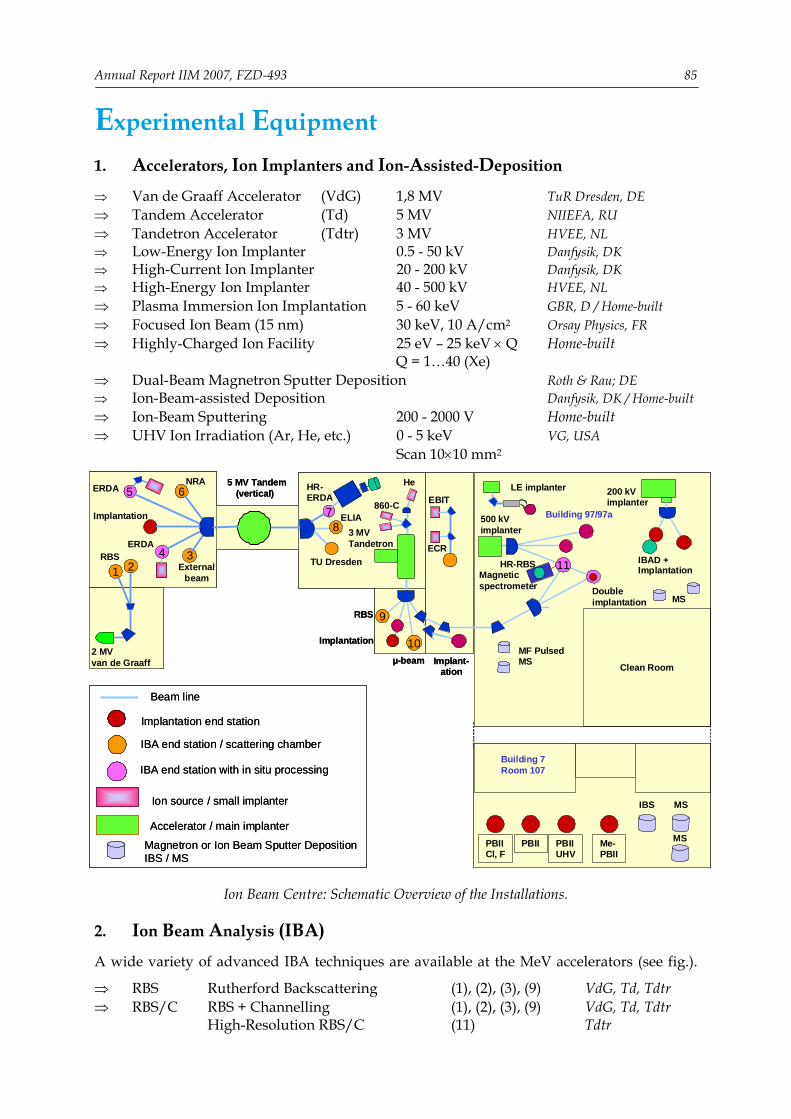
Annual Report IIM 2007, FZD-493
85
Experimental Equipment
1. Accelerators, Ion Implanters and Ion-Assisted-Deposition
⇒ Van de Graaff Accelerator (VdG) 1,8 MV TuR Dresden, DE ⇒ Tandem Accelerator (Td) 5 MV NIIEFA, RU ⇒ Tandetron Accelerator (Tdtr) 3 MV HVEE, NL ⇒ Low-Energy Ion Implanter 0.5 - 50 kV Danfysik, DK ⇒ High-Current Ion Implanter 20 - 200 kV Danfysik, DK ⇒ High-Energy Ion Implanter 40 - 500 kV HVEE, NL ⇒ Plasma Immersion Ion Implantation 5 - 60 keV GBR, D / Home-built ⇒ Focused Ion Beam (15 nm) 30 keV, 10 A/cm2 Orsay Physics, FR ⇒ Highly-Charged Ion Facility 25 eV – 25 keV × Q Home-built
Q = 1…40 (Xe) ⇒ Dual-Beam Magnetron Sputter Deposition Roth & Rau; DE ⇒ Ion-Beam-assisted Deposition Danfysik, DK / Home-built ⇒ Ion-Beam Sputtering 200 - 2000 V Home-built ⇒ UHV Ion Irradiation (Ar, He, etc.) 0 - 5 keV VG, USA Scan 10×10 mm2
6
411
200 kVimplanter
500 kVimplanter
5 MV Tandem(vertical)
2 MV van de Graaff
3 MV Tandetron
Magneticspectrometer
Beam line
Implantation end station
Accelerator / main implanter
Ion source / small implanter
IBA end station / scattering chamber
IBA end station with in situ processing
Double implantation
ERDANRA
ERDA
External beam
RBS TU Dresden HR-RBS IBAD +
HR-ERDA
µ-beam
RBS
LE implanter
ECR
EBIT
ELIA860-C
Clean Room
Implantation
He
Implantation
MF PulsedMS
MS
Magnetron or Ion Beam Sputter DepositionIBS / MS
IBS MS
MSPBIICl, F
PBII PBIIUHV
Me-PBII
Building 7Room 107
Building 97/97a
Implantation
Implant-ation
3
5
87
21
10
9
Ion Beam Centre: Schematic Overview of the Installations.
2. Ion Beam Analysis (IBA)
A wide variety of advanced IBA techniques are available at the MeV accelerators (see fig.).
⇒ RBS Rutherford Backscattering (1), (2), (3), (9) VdG, Td, Tdtr ⇒ RBS/C RBS + Channelling (1), (2), (3), (9) VdG, Td, Tdtr High-Resolution RBS/C (11) Tdtr

Experimental Equipment 86
⇒ ERDA Elastic Recoil Detection Analysis (2), (4), (5) VdG, Td High-resolution ERDA (7), (8) Td ⇒ PIXE Proton-Induced x-ray Emission (3) Td ⇒ PIGE Proton-Induced γ Emission (3) Td ⇒ NRA Nuclear Reaction Analysis (4) Td ⇒ NRRA Nuclear Resonance Reaction Anal. (6) Td ⇒ Nuclear Microprobe (10) Tdtr
Some stations are equipped with additional process facilities which enable in-situ IBA investigations during ion irradiation, sputtering, deposition, annealing etc. 3. Other Particle Based Analytical Techniques ⇒ SEM Scanning Electron Microscope 1 - 30 keV Hitachi, JP + EDX ⇒ TEM Transmission Electron Microscope 80 - 300 keV FEI, NL (Titan 80-300 with Image Corrector) + EDX, +GIF ⇒ AES Auger Electron Spectroscopy + XPS Fisions, GB ⇒ CEMS Mössbauer Spectroscopy 57Fe source Home-built ⇒ PAS Positron Annihilation Spectroscopy 22Na source Home-built 30 V - 36 kV 4. Photon Based Analytical Techniques ⇒ XRD/XRR X-Ray Diffraction and Reflection Cu-Kα Bruker axs, DE
HR-XRD High-Resolution XRD Cu-Kα GE Inspection, DE XRD/XRR with Synchrotron Radiation 5 – 35 keV ROBL at ESRF, FR ⇒ SE Spectroscopic Ellipsometry 250 - 1700 nm Woolam, USA ⇒ FTIR Fourier-Transform Infrared Spectr. 600 - 7000 cm-1 Nicolet, USA ⇒ FTIR Fourier-Transform Infrared Spectr. 50 - 15000 cm-1 Bruker, DE ⇒ Ti:Sapphire Femtosecond Laser Spectra Physics, USA ⇒ Femtosecond Optical Parametric Oscillator APE, DE ⇒ Ti:Sapphire Femtosecond Amplifier Femtolasers, AT ⇒ Femtosecond Optical Parametric Amplifier Light Conversion, LT ⇒ Raman Raman Spectroscopy 45 cm-1 shift Jobin-Yvon-Horiba, FR ⇒ PL Photoluminescence 300 - 1500 nm Jobin-Yvon-Horiba, FR ⇒ TRPL Time-Resolved PL τ = 3 ps - 2 ns Hamamatsu Phot., JP τ > 5 ns Stanford Research, USA ⇒ EL Electroluminescence (10-300 K) 300 - 1500 nm Jobin-Yvon-Horiba, FR
Optical Split-Coil Supercond. Magnet 7 T Oxford Instrum., GB ⇒ PR Photomodulated Reflectivity 300 - 1500 nm Jobin-Yvon-Horiba, FR ⇒ PLE Photoluminescence Excitation 300 - 1500 nm Jobin-Yvon-Horiba, FR 5. Magnetic Thin Film Deposition and Properties Analysis ⇒ MBE Molecular Beam Epitaxy with in-situ FIB CreaTec,DE ⇒ MBE Molecular Beam Epitaxy Home-built ⇒ MFM Magnetic Force Microscope ~ 50 nm resol. VEECO / DI, USA ⇒ SQUID Supercond. Quantum Interf. Device ± 7 T Quantum Design, USA ⇒ MOKE Magneto-Optic Kerr Effect (in-plane) ± 0.35 T Home-built ⇒ MOKE Magneto-Optic Kerr Effect (perp.) ± 2 T Home-built ⇒ SKM Scanning Kerr Microscope Home-built ⇒ TR-MOKE Time-Resolved MOKE (Pump-Probe) Home-built
Annual Report IIM 2007, FZD-493
87
⇒ VNA-FMR Vector Network Analyzer Ferromagnetic Resonance Agilent / Home-built 6. Other Analytical and Measuring Techniques ⇒ Scanning Tunneling Microscope (with AFM-option) DME, DK ⇒ Atomic Force Microscope (tapping mode) SIS, DE ⇒ Atomic Force Microscope (with c-AFM, SCM-module) Veeco Instruments, GB ⇒ In-situ Scanning Tunneling Microscope (variable-Temp.) Omicron, DE ⇒ Dektak Surface Profilometer Veeco, USA ⇒ Micro Indenter / Scratch Tester Shimatsu, JP ⇒ Wear Tester (pin-on disc) Home-built ⇒ Spreading Resistance Profiling Sentech, DE ⇒ Hall Effect Equipment (2 - 400 K, ≤ 9 T) LakeShore, USA ⇒ DLTS (+ I-U / C-V) (10 - 300 K, 1 MHz) PhysTech, DE ⇒ I-V and C-V Analyzer Keithley, USA ⇒ I-V and C-V Semi-Automatic Prober (-60 - 300°C) Keithley, USA Süss, DE 7. Processing and Preparation Techniques ⇒ Etching / Cleaning incl. Anisotropic Selective KOH Etching ⇒ Photolithography Mask-aligner, 2 µm-level Süss, DE ⇒ Thermal Treatment Room Temperature - 2000°C • Furnace InnoTherm, DE • Rapid Thermal Annealing ADDAX, FR • Flash-Lamp Unit (0.5 – 20 ms) Home-built; FHR, DE • RF Heating (Vacuum) JIP.ELEC, FR ⇒ Physical Deposition Sputtering DC / RF, Evaporation Nordiko, GB Electron Beam Evaporation System Leybold Optics, DE ⇒ Thermal Evaporation Bal-Tec, FL ⇒ Dry Etching Plasma and RIE Mode Sentech, DE ⇒ Bonding Techniques Ultrasonic Wire Bonding Kulicke&Soffa, USA ⇒ Cutting, Grinding, Polishing Bühler, DE ⇒ TEM Sample Preparation Plan View and Cross Section incl. Ion Milling Equipment Gatan, USA

Services 88
Services The institute serves as a user center and technology transfer point in connection with its many years
of experience in the application of ion beams for modification and analysis of solid surfaces and thin films of arbitrary materials.
Ion beam treatment of metallic materials (e.g. light metals like Al, Ti; stainless steel) can be advantageously applied for the improvement of the tribological properties (hardness, wear, corrosion resistance etc.). Using ion beam assisted deposition, hard coatings with special properties are obtained, such as a high adhesive strength and low internal stress. New technologies of high energy ion implantation or focused ion beam techniques result in new applications of electronic devices or microintegrated circuits.
Ion beams are an excellent instrument for the analysis of solid state surfaces. The interaction of the incident ion beam with the surface layer of a material leads to a specific radiation response, which yields information on the elemental composition as function of depth in a quantitative and essentially non-destructive way.
Additional means of preparation and diagnostics are available to fulfill the needs of users from different industrial branches. Do not hesitate to contact our experienced team.
Main Areas of Competence: • Development and fabrication of sensors and detectors for charged particle spectroscopy • Deposition of functional coatings using ion-assisted physical vapor deposition • Fabrication of wear protection layers on metallic materials or alloys • Deposition of blood compatible layers (i.e. TiOx) on different materials • Ion implantation in a broad range of ion energy (~ 200 eV to ~ 50 MeV) and substrate temperature • Advanced ion beam technologies (high energy ion implantation, focused ion beam) for microelec-
tronic applications • Application of high energy ion implantation for power devices and laser structures • Doping of semiconductors, in particular wide bandgap semiconductors • Surface analysis of solid materials with high energy ion beams • Computer simulation of ion beam interaction with materials • Optical characterization of materials (luminescence, FTIR, Raman) Offers: • Consultation and problem evaluation for ion beam applications • Process development for ion beam treatment of different materials (metals, ceramics, semiconductors) • Process development in ion-assisted deposition of thin films • Preparation and treatment of material samples, tools or complex parts of devices • Ion implantation and ion beam analysis services • Ion implantation into semiconductor materials for applications in microsystems and micro- and power
electronics, • Preparation / fabrication of semiconductors or silicon radiation sensors under clean room conditions • Structural diagnostics of materials surfaces including e-beam- (SEM, TEM, AES) and X-ray techniques
(XRD, XRR with both Cu-K and Synchrotron (5-35 keV) radiation). Examples: • Improvement of wear resistance of austenitic stainless steels using plasma immersion
ion implantation • High energy ion implantation for power semiconductor devices, • Micro- and nano-engineering with focused ion beams • Non-destructive quantitative hydrogen analysis in materials • Non-destructive ion beam analysis of art objects
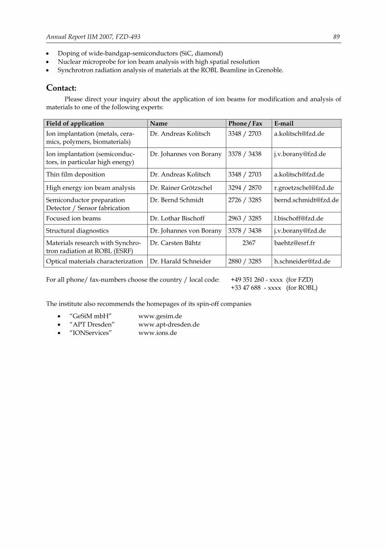
Annual Report IIM 2007, FZD-493
89
• Doping of wide-bandgap-semiconductors (SiC, diamond) • Nuclear microprobe for ion beam analysis with high spatial resolution • Synchrotron radiation analysis of materials at the ROBL Beamline in Grenoble. Contact:
Please direct your inquiry about the application of ion beams for modification and analysis of materials to one of the following experts: Field of application Name Phone / Fax E-mail Ion implantation (metals, cera-mics, polymers, biomaterials)
Dr. Andreas Kolitsch 3348 / 2703 [email protected]
Ion implantation (semiconduc-tors, in particular high energy)
Dr. Johannes von Borany 3378 / 3438 [email protected]
Thin film deposition Dr. Andreas Kolitsch 3348 / 2703 [email protected]
High energy ion beam analysis Dr. Rainer Grötzschel 3294 / 2870 [email protected]
Semiconductor preparation Detector / Sensor fabrication
Dr. Bernd Schmidt 2726 / 3285 [email protected]
Focused ion beams Dr. Lothar Bischoff 2963 / 3285 [email protected]
Structural diagnostics Dr. Johannes von Borany 3378 / 3438 [email protected]
Materials research with Synchro-tron radiation at ROBL (ESRF)
Dr. Carsten Bähtz 2367 [email protected]
Optical materials characterization Dr. Harald Schneider 2880 / 3285 [email protected] For all phone/ fax-numbers choose the country / local code: +49 351 260 - xxxx (for FZD) +33 47 688 - xxxx (for ROBL) The institute also recommends the homepages of its spin-off companies
• “GeSiM mbH” www.gesim.de • “APT Dresden” www.apt-dresden.de • “IONServices” www.ions.de
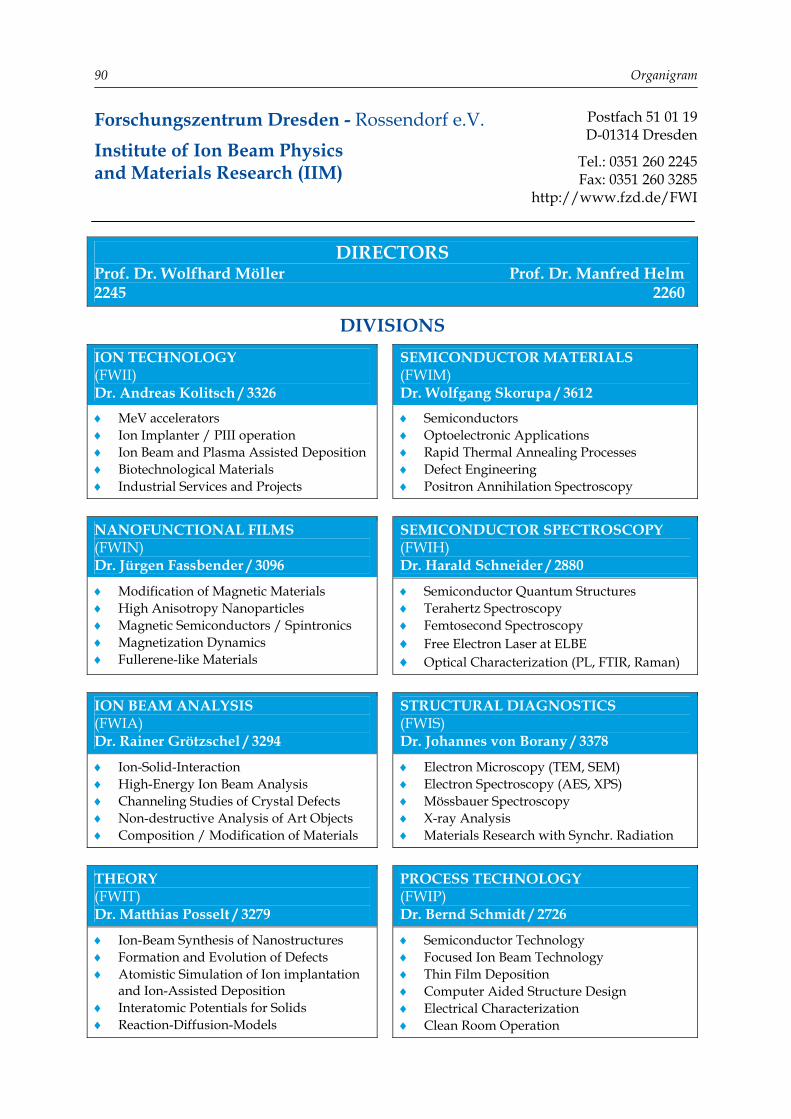
Organigram
90
Forschungszentrum Dresden - Rossendorf e.V. Institute of Ion Beam Physics and Materials Research (IIM)
Postfach 51 01 19 D-01314 Dresden
Tel.: 0351 260 2245 Fax: 0351 260 3285
http://www.fzd.de/FWI
DIRECTORS Prof. Dr. Wolfhard Möller Prof. Dr. Manfred Helm 2245 2260
DIVISIONS ION TECHNOLOGY (FWII) Dr. Andreas Kolitsch / 3326
SEMICONDUCTOR MATERIALS (FWIM) Dr. Wolfgang Skorupa / 3612
♦ MeV accelerators ♦ Ion Implanter / PIII operation ♦ Ion Beam and Plasma Assisted Deposition ♦ Biotechnological Materials ♦ Industrial Services and Projects
♦ Semiconductors ♦ Optoelectronic Applications ♦ Rapid Thermal Annealing Processes ♦ Defect Engineering ♦ Positron Annihilation Spectroscopy
NANOFUNCTIONAL FILMS (FWIN) Dr. Jürgen Fassbender / 3096
SEMICONDUCTOR SPECTROSCOPY (FWIH) Dr. Harald Schneider / 2880
♦ Modification of Magnetic Materials ♦ High Anisotropy Nanoparticles ♦ Magnetic Semiconductors / Spintronics ♦ Magnetization Dynamics ♦ Fullerene-like Materials
♦ Semiconductor Quantum Structures ♦ Terahertz Spectroscopy ♦ Femtosecond Spectroscopy ♦ Free Electron Laser at ELBE ♦ Optical Characterization (PL, FTIR, Raman)
ION BEAM ANALYSIS (FWIA) Dr. Rainer Grötzschel / 3294
STRUCTURAL DIAGNOSTICS (FWIS) Dr. Johannes von Borany / 3378
♦ Ion-Solid-Interaction ♦ High-Energy Ion Beam Analysis ♦ Channeling Studies of Crystal Defects ♦ Non-destructive Analysis of Art Objects ♦ Composition / Modification of Materials
♦ Electron Microscopy (TEM, SEM) ♦ Electron Spectroscopy (AES, XPS) ♦ Mössbauer Spectroscopy ♦ X-ray Analysis ♦ Materials Research with Synchr. Radiation
THEORY (FWIT) Dr. Matthias Posselt / 3279
PROCESS TECHNOLOGY (FWIP) Dr. Bernd Schmidt / 2726
♦ Ion-Beam Synthesis of Nanostructures ♦ Formation and Evolution of Defects ♦ Atomistic Simulation of Ion implantation
and Ion-Assisted Deposition ♦ Interatomic Potentials for Solids ♦ Reaction-Diffusion-Models
♦ Semiconductor Technology ♦ Focused Ion Beam Technology ♦ Thin Film Deposition ♦ Computer Aided Structure Design ♦ Electrical Characterization ♦ Clean Room Operation

List of Personnel
91
List of Personnel 2007
Directors: Prof. M. Helm Prof. W. Möller
Office: I. Heidel, S. Kirch, L. Post
Scientific Staff: Permanent: Dr. G. Abrasonis Dr. C. Akhmadaliev Dr. C. Bähtz Dr. L. Bischoff Dr. J. von Borany Dr. W. Bürger Dr. S. Facsko Dr. J. Faßbender Dr. M. Friedrich Dr. S. Gemming Dr. D. Grambole Dr. J. Grenzer Dr. R. Grötzschel Dr. V. Heera F. Herrmann Dr. K.-H. Heinig Dr. R. Kögler Dr. A. Kolitsch Dr. U. Kreißig Dr. A. Mücklich Dr. F. Munnik Dr. C. Neelmeijer Dr. M. Posselt Dr. K. Potzger Dr. L. Rebohle Dr. H. Reuther Dr. A. Rogozin Dr. B. Schmidt Dr. H. Schneider Dr. W. Skorupa Dr. D. Stehr Dr. M. Voelskow Dr. S. Winnerl
Post Docs: Dr. N. Jeutter Dr. K. Küpper Dr. M. O. Liedke Dr. Z. Pesic Dr. M. Vinnichenko
Projects: Dr. B. Abendroth W. Anwand Dr. G. Brauer Dr. O. Drachenko Dr. C. V.-B. Grimm Dr. A. Kanjilal Dr. M. Krause R.S.M. Martins V. Pankoke Dr. W. Pilz Dr. H. Schmidt Dr. A. Shalimov Dr. N. Shevchenko Dr. H. Weishart Dr. Q. Xu Dr. R. Yankov Dr. M. Zier M. Zschintsch
PhD Students: M. Berndt V. Beyer V. Cantelli R. Cheng C. Cherkouk A. Dreyhaupt H. Geßner D. Güttler A. Hanisch R. Heller R. Jacob A. Keller M. Kosmata B. Liedke R. Mukesh D. Markó A. Martinavicius S. Ohser X. Ou H. Peng F. Peter
J. Potfajova H. G. von Ribbeck L. Röntzsch C. Scarlat M. Schmidt T. Schucknecht T. Strache G. Talut M. Thieme M. Wagner C. Wündisch J. Zhou S. Zhou
Diploma Students: C. Baumgart D. Bürger S. Cornelius M. Fritsche A.-A. Gabriel O. Kallauch M. Körner T. Kunze D. Nauert C. Pfau S. Schreiber M. Sellesk A. Silze S. Wintz B. Zimmermann
Technical Staff:
Permanent: Rb. Aniol Ry. Aniol G. Anwand E. Christalle H. Felsmann K. Fukarek
B. Gebauer H.-J. Grahl D. Hanf P. Hartmann J. Haufe A. Henschke G. Hofmann S. Klare J. Kreher A. Kunz H. Lange U. Lucchesi F. Ludewig R. Mester M. Mißbach C. Neisser S. Probst E. Quaritsch A. Reichel M. Roch B. Scheumann G. Schnabel A. Schneider J. Schneider A. Scholz T. Schumann U. Strauch K. Thiemig A. Vetter R. Weidauer A. Weise J. Winkelmann G. Winkler I. Winkler L. Zimmermann J. Zscharschuch
Projects: S. Eisenwinder M. Steinert I. Skorupa
Related Documents