Welcome message from author
This document is posted to help you gain knowledge. Please leave a comment to let me know what you think about it! Share it to your friends and learn new things together.
Transcript
Wissenschaftlich-Technische Berichte FZR – 448 2006
Annual Report 2005
Institute of Ion Beam Physics and Materials Research
Editors:
J. von Borany, V. Heera, M. Helm, W. Möller
Cover Picture:
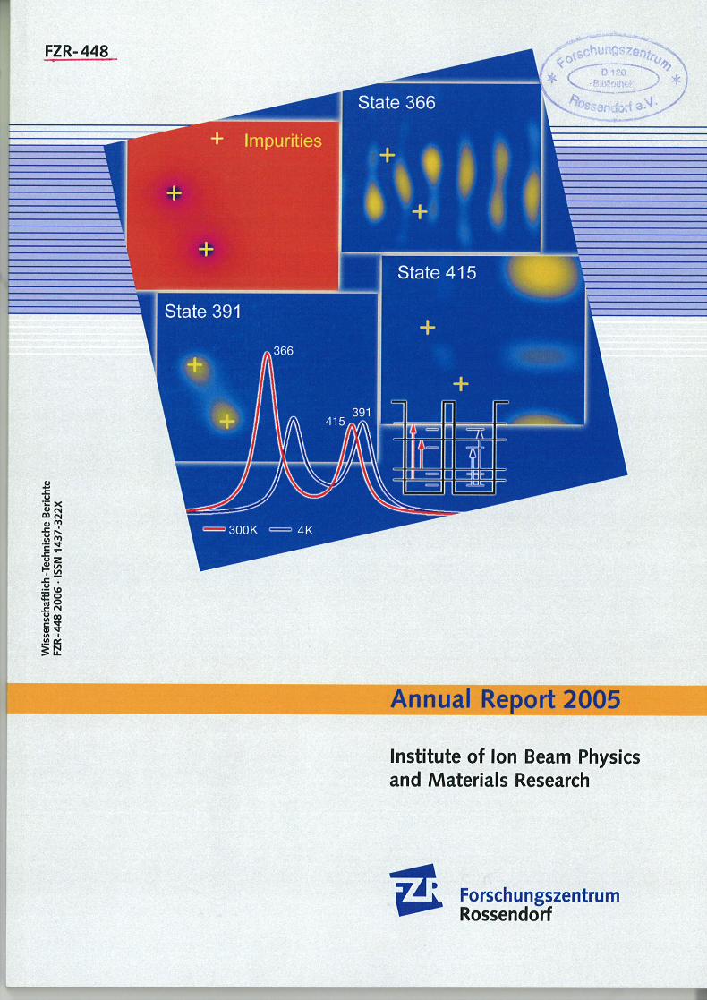
The graph in the lower part shows two mid-infrared absorption spectra of a GaAs/AlGaAs double quantum well structure, which exhibits intersubband transitions at higher temperature (red curve) and impurity transitions at lower temperature (blue curve). The quantum well po-tential (z-direction) with the transitions indicated by arrows is sketched besides. The upper square panel shows the position and the electrostatic potential of two random impurities, and the three blue panels show the calculated wavefunctions of the relevant final states in the xy plane (area 100 × 100 nm2) and integrated over z. Clearly, state 391 is localized around the impurities, whereas 366 and 415 are extended states. The numbers of these final states are added to the corresponding peaks in the absorption spectra. For details see contribution on p. 36. Forschungszentrum Rossendorf e.V. Institut für Ionenstrahlphysik und Materialforschung Postfach 51 01 19 D-01314 Dresden Bundesrepublik Deutschland Direktoren Prof. Dr. Wolfhard Möller Prof. Dr. Manfred Helm Telefon + 49 (3 51) 2 60 22 45 + 49 (3 51) 2 60 22 60 Telefax + 49 (3 51) 2 60 32 85 + 49 (3 51) 2 60 32 85 E-mail [email protected] [email protected]
Internet http://www.fz-rossendorf.de/FWI
Annual Report IIM 2005, FZR-448
3
Preface by the Directors
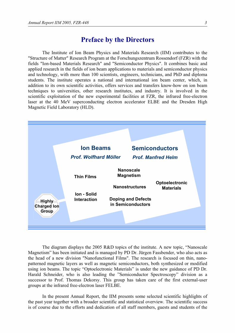
The Institute of Ion Beam Physics and Materials Research (IIM) contributes to the "Structure of Matter" Research Program at the Forschungszentrum Rossendorf (FZR) with the fields "Ion-based Materials Research" and "Semiconductor Physics". It combines basic and applied research in the fields of ion beam applications to materials and semiconductor physics and technology, with more than 100 scientists, engineers, technicians, and PhD and diploma students. The institute operates a national and international ion beam center, which, in addition to its own scientific activities, offers services and transfers know-how on ion beam techniques to universities, other research institutes, and industry. It is involved in the scientific exploitation of the new experimental facilities at FZR, the infrared free-electron laser at the 40 MeV superconducting electron accelerator ELBE and the Dresden High Magnetic Field Laboratory (HLD).
Ion - Solid Interaction
Thin Films
Doping and Defects in Semiconductors
NanostructuresOptoelectronic
Materials
Ion Beams SemiconductorsProf. Wolfhard Möller Prof. Manfred Helm
HighlyCharged Ion
Group
Nanoscale Magnetism
The diagram displays the 2005 R&D topics of the institute. A new topic, “Nanoscale
Magnetism” has been initiated and is managed by PD Dr. Jürgen Fassbender, who also acts as the head of a new division "Nanofunctional Films". The research is focused on thin, nano-patterned magnetic layers as well as magnetic semiconductors, both synthesized or modified using ion beams. The topic “Optoelectronic Materials” is under the new guidance of PD Dr. Harald Schneider, who is also leading the ”Semiconductor Spectroscopy” division as a successor to Prof. Thomas Dekorsy. This group has taken care of the first external-user groups at the infrared free-electron laser FELBE.
In the present Annual Report, the IIM presents some selected scientific highlights of the past year together with a broader scientific and statistical overview. The scientific success is of course due to the efforts and dedication of all staff members, guests and students of the

Preface
4
institute – sincere thanks to all of them! The institute would also like to thank all partners and friends from universities, industry, and research institutes around the world for good cooperations. Special thanks are due to the Executive Board of the Forschungszentrum Rossendorf, the Ministry of Science and Arts of the Free State of Saxony, the German Federal Ministry of Education and Research, and all other funding organizations for their support.
Prof. Wolfhard Möller Prof. Manfred Helm
Annual Report IIM 2005, FZR-448
5
Contents
Selected Reports Page M. Beckers, N. Schell, R.M.S. Martins, A. Mücklich, W. Möller and L. Hultman 9 Microstructure and Nonbasal-Plane Growth of Epitaxial MAX PhaseTi2AlN Thin Films R. Gago, G. Abrasonis, A. Mücklich, W. Möller, Zs. Czigány and G. Radnóczi 13 Fullerene-Like Arrangements in Carbon Nitride Thin Films Grown by Direct Ion Beam Sputtering K. Potzger, S. Zhou, H. Reuther, A. Mücklich, F. Eichhorn, N. Schell, W. Skorupa, 17 M. Helm, J. Fassbender, T. Herrmannsdörfer and T.P. Papageorgiou Fe Implanted Ferromagnetic ZnO V. Beyer, J. von Borany and A. Mücklich 21 A Transient Electrical Model of Charging for Ge Nanocrystal Containing Gate Oxides with DRAM-Like Behavior A. Nazarov, J.M. Sun, I.N. Osiyuk, I.P. Tjagulskii, V.S. Lysenko, W. Skorupa, 25 R.A. Yankov and T. Gebel Light Emission and Charge Trapping in Er doped Silicon Dioxide Films Containing Silicon Nanocrystals M. Posselt, M. Mäder, A. Lebedev and R. Grötzschel 29 Multiple Implantations into Si: Influence of the Implantation Sequence on Ion Range Profiles M. Voelskow, W. Skorupa, M. Smith and R. McMahon 33 Homogenization of the Melting Depth in SiC on Si Structures during Flash Lamp Irradiation D. Stehr, C. Metzner, M. Helm, T. Roch and G. Strasser 36 Resonant Impurity Bands in Semiconductor Superlattices A. Dreyhaupt, S. Winnerl, T. Dekorsy and M. Helm 41 High-Intensity Terahertz Radiation from a Microstructured Large-Area Photoconductor
Short Contributions Ion-Solid-Interaction 47 Thin Films 50 Nanoscale Magnetism 55 Nanostructures 61 Doping and Defects in Semiconductors 66 Optoelectronic Materials 71 Others 75
Contents
6
Equipment 77 Glossary 81
Statistics Book Chapters 85 Publications in Refereed Journals 85 Conference Proceedings 98 Invited Talks 99 Conference Contributions 102 Lectures 117 Reports 120 Patents 121 PhD and Master/Diploma Theses 121 Awards 122 Organization of Workshops 122 Laboratory Visits 122 Guests 123 ROBL-MRH Visitors 126 Colloquium of the Institute 128 Other Seminars 129 Projects 131 Experimental Equipment 134 Services 136 Organigram 138 List of Personnel 139

Selected Reports

Annual Report IIM 2005, FZR-448
9
Microstructure and Nonbasal-Plane Growth of Epitaxial MAX Phase Ti2AlN Thin Films
M. Beckers, N. Schell, R.M.S. Martins, A. Mücklich, W. Möller and L. Hultman1
1Thin Film Physics Division, Department of Physics, Chemistry and Biology (IFM), Linköping University, Linköping SE-581 83, Sweden
The Mn+1AXn phases [1] are a family of nanolaminated compounds, where M is a transition metal, A an A-group element and X is nitrogen and/or carbon. Their hexagonal structure consists of [MX6] octahedrons, interleaved by A-group element layers. In M2AX1 every third layer is constituted by A-group atoms, every fourth for M3AX2, every fifth for M4AX3. For the Ti-Al-N system Ti2AlN [2] and Ti4AlN3 [3] have been reported. Here, the [MX]6 slabs are identical with the structure of wear protective TiN. Since the M-X bonds are of strong covalent-ionic nature, the Mn+1AXn phases exhibit typical ceramic properties like high melting points and thermal stabilities [4]. On the other hand the M-A bonds are rather weak. Therefore, Mn+1AXn phases also exhibit metallic properties like good electrical-thermal conduct-ivity [5]. Under force effect they deform by kink bands which yields high ductility and machinability. Due to this unique combination of properties, applications for Mn+1AXn phase are manifold, one of them being wear protective functional coatings for high temperature applica-tions. The first Mn+1AXn phase thin films, in the Ti-S-C system, were deposited using magnetron sputtering [6]. Mn+1ANn phases are harder to obtain by sputter deposition, since the nitrogen has to be introduced via the gas phase. Hence, only very recently Joelsson et al. demonstrated the deposition of Ti2AlN thin films [7]. They used reactive sputtering from a compound 2Ti:Al target, and deposited onto MgO(111) single-crystals at substrate temperatures of 830°C.
The present work reports on successful Ti2AlN deposition by reactive cosputtering using elemental Ti and Al targets, at considerably lower substrate temperatures of 690°C studied by in-situ x-ray diffraction. The temperature was measured using a thermocouple clamped onto the substrate holder. MgO(111) wafers were used as substrates. The base pressure at the deposition temperature was ~ 8 × 10⁻⁵ Pa. Prior to the Ti2AlN, a thin fcc (Ti1-xAlx)N seed layer was deposited at Ar and N2 fluxes of 2.76 and 1.38 sccm at a working pressure of 0.35 Pa. The Ti and Al magnetrons were set to 60 and 20 W, yielding a composition of
(Ti0.63Al0.37)N. For Ti2AlN growth the deposition pressure was increased to 0.8 Pa at Ar and N2 fluxes of 7.94 and 0.48 sccm, respectively. The Ti and Al magnetron powers were changed to 80 and 26 W.
The whole deposition chamber is mounted into the goniometer of the ROBL beamline at the European Synchrotron Radiation Facility (ESRF), and equipped with x-ray windows [8]. Monochro-matized x-rays of 12.915 keV were employed to study the Ti2AlN film growth in-situ in two differ-ent scattering geometries: (1) low angle specular reflectivity (XRR) either time-resolved at a fixed incidence angle, or scanned in coplanar scattering geometry for the determination of the film thickness; (2) large angle x-ray diffraction (XRD) in Bragg-Brentano geometry in order to determine the off-plane lattice parameter. The time resolved XRR signal can be used to observe changes in the surface morphology on an atomic scale, from which the growth mode of the developing film can be derived. The microstructure and texture of the final film was investigated using a combination of lab source pole figure measurements and cross-sectional transmission electron microscopy (XTEM). The final film composition was exa-mined by Rutherford backscattering spectroscopy (RBS), using a 1.7 MeV He+ beam.
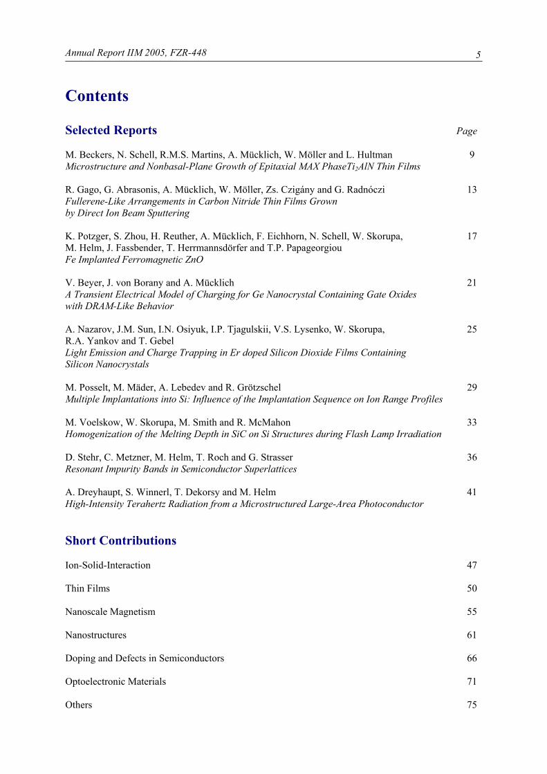
Figure 1 shows time dependent XRR data for both the seed layer (a) and the Ti2AlN Mn+1AXn phase layer (b) deposited onto MgO(111). Clear intensity oscillations are depicted for the seed layer. The oscillation amplitude does not diminish during deposition, hence a smooth layer-by-layer (step flow) growth onto MgO can be deduced, as expected from reported epitaxial growth of pure TiN onto MgO(111) [9]. XRR characterization during a deposition interruption yielded a layer thickness of 121 Å, corresponding to a low growth rate of 0.3 Å/s, further promoting the layer-by-layer growth. Each oscillation in the time dependent XRR can be attributed to one lattice constant of (Ti0.63Al0.37)N, hence a perfect cube-on-cube heteroepitaxial relation (Ti0.63Al0.37)N100<100> // MgO 100<100> with only 0.74 % lattice mismatch between
M. Beckers et al.; Microstructure and Nonbasal-Plane Growth ...
10
Fig. 1: Time dependent in-situ XRR of the fcc (Ti0.63Al0.37)N seed layer (a) and Ti2AlN (b) on MgO(111). The oscillatory behaviour for the deposited seed layer as well as the Ti2AlN are a fingerprint of layer-by-layer growth. The decreasing amplitudes of those oscillations reveal increasing roughness or island growth for Ti2AlN. (b) The in-situ XRD data recorded after the deposition of the seed layer and two Ti2AlN film deposition steps of approximately 400 Å each show only a Ti2AlN(101) peak. The vertical dashed line represents literature data [10].
(Ti0.63Al0.37)N and (4.18 Å) MgO (4.211 Å) can be assumed. Figure 1(b) shows that even after interrupting the deposition process for about 1 h, the Ti2AlN Mn+1AXn phase nucleation onto the seed layer again starts with a layer-by-layer mode. The oscillations are clearly visible for more than fifteen monolayers, however their exponential decay points to a pronounced kinetic roughening, i.e. a Stranski-Krastanov-like growth mode. The deposition rate of the Ti2AlN MAX phase was determined to be 1.3 Å/s, explaining the smaller oscillation period compared to the seed layer.
The θ -2θ XRD scans are shown in Fig. 1(c). After deposition of the seed layer the intensity distribution remains undistinguishable due to the perfect epitaxial nature of the seed layer growth. In contrast, already after the first deposition of ~ 400 Å Ti2AlN the Ti2AlN(1013) peak can clear-ly be identified as the only one resulting. It is so close to Ti2AlN(0006) that in early diffraction data the peaks were not separated [10], but due to the lack of other order Ti2AlN(000l) peaks a mix-up can be excluded. For later discussions it should be noted that the lattice spacing of the Ti2AlN(1013) peak is increased compared to the literature values as indicated by the dashed line.
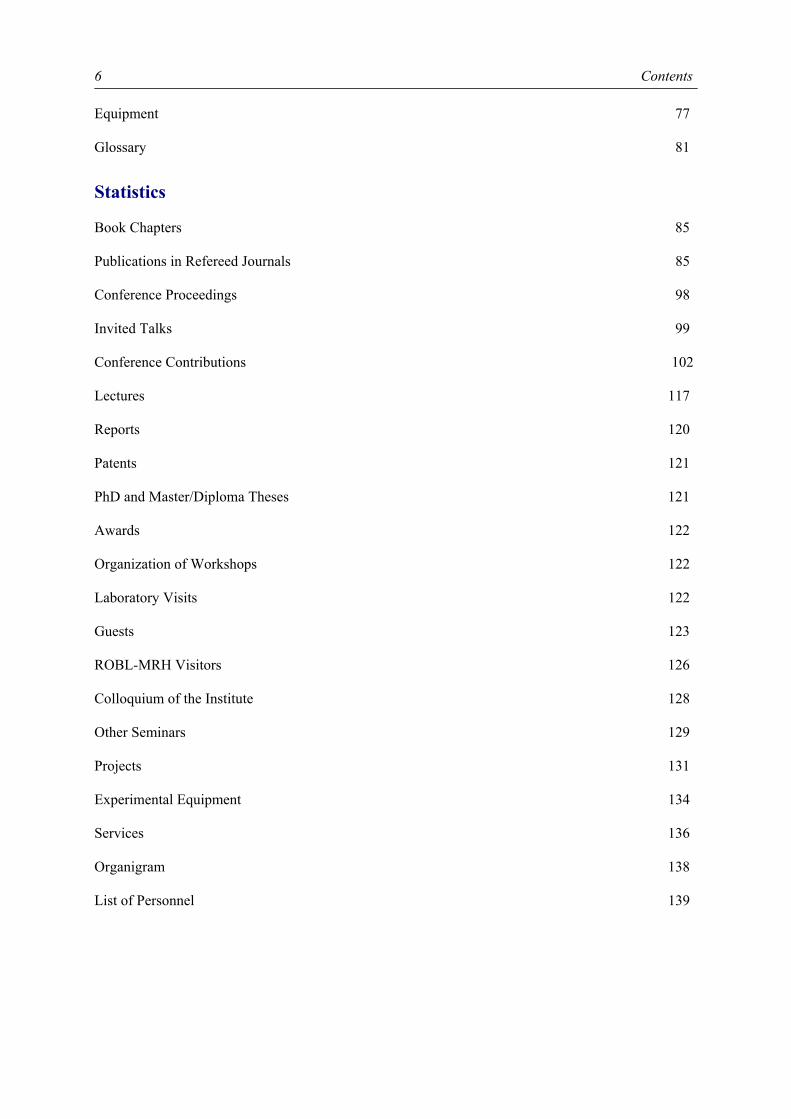
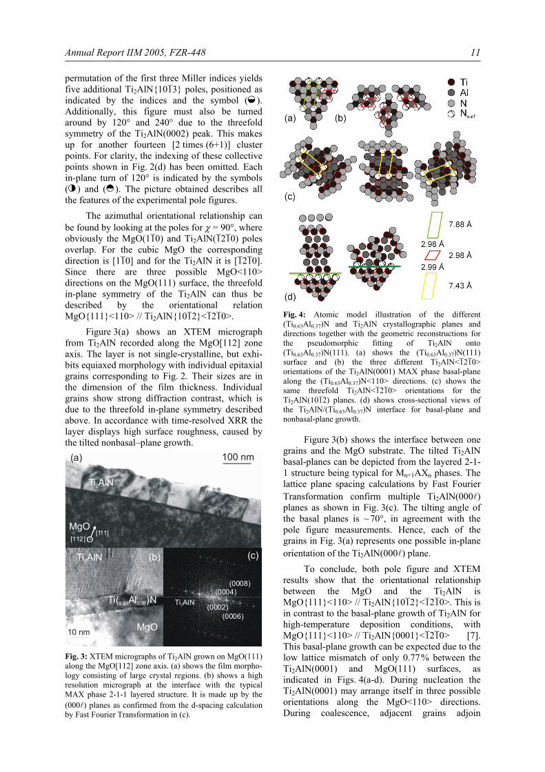
Figure 2 shows the experimental pole figure for Ti2AlN on MgO(111), recorded in the
(111)
(010)
(001)
(100) (111)
(0113)(1103)
(0001)
(1012)
(1013)
(1013)
(1103)
Ti2AlN: no turn, MgOsubstrate:
(0113)
(a) (b)
(c) (d)
φ
χ
φ
χ
(011)
(112)
(110)
(101)
(1210)
Ti2AlN: no turn, 120° turn, 240°turnMgOsubstrate:
Fig. 2: Pole figures of MAX phase Ti2AlN grown onto MgO(111), measured on the Bragg peaks Ti2AlN(1013) (a) and Ti2AlN(0002) (b). The stereographic projection (c) shows the theoretical poles of Ti2AlN1013, 1012, 0001, 2110 and MgO111, 110, 112. The expe-rimental pole figure can be obtained by turning the poles for 120° around the MgO[111] direction, as indicated by the symbols (d).
Ti2AlN(1013) Bragg peak. Due to the immediate vicinity of the Ti2AlN(0006) and MgO(111) as well as MgO(100) peaks, the pole figure comprises orientation distributions of all these four lattice planes. The θ -2θ scans of all cluster points within the experimental pole figure in Fig. 2(a) showed only substrate and Ti2AlN(1013) Bragg peaks, except for the ones at χ ~ 60°. Here, a peak at 2θ = 13° was observed, which is close to Ti2AlN(0002). The pole figure on that peak in Fig. 2(b) clearly shows three distinct cluster points at χ ~ 60° and φ = 0°, 120° and 240°. Thus, the Ti2AlN(000l) basal planes are tilted ~60° away from the surface normal with threefold in-plane symmetry.
Figure 2(c) shows the stereographic project-ion of the Ti2AlN [11] and MgO [10] lattice. Assuming single-crystal Ti2AlN and MgO, the (111) substrate orientation leads to a central MgO(111) pole and three MgO100 poles at a tilting angle χ = 54.7° and azimuth angles φ = 0°, 120° and 240°. As seen in Fig. 2(b), close to the MgO(001) pole lies the Ti2AlN(000l) pole. As a consequence, the Ti2AlN(1013) pole does not lie in the center of the pole figure, but at χ = 9° and φ = 0°. Accordingly, within the central position lies the Ti2AlN(1012) pole. Thus, one can denote MgO(111) // Ti2AlN(1012). Within Fig. 2(a),
Annual Report IIM 2005, FZR-448
11
permutation of the first three Miller indices yields five additional Ti2AlN1013 poles, positioned as indicated by the indices and the symbol ( ). Additionally, this figure must also be turned around by 120° and 240° due to the threefold symmetry of the Ti2AlN(0002) peak. This makes up for another fourteen [2 times (6+1)] cluster points. For clarity, the indexing of these collective points shown in Fig. 2(d) has been omitted. Each in-plane turn of 120° is indicated by the symbols ( ) and ( ). The picture obtained describes all the features of the experimental pole figures.
The azimuthal orientational relationship can be found by looking at the poles for χ = 90°, where obviously the MgO(110) and Ti2AlN(1210) poles overlap. For the cubic MgO the corresponding direction is [110] and for the Ti2AlN it is [1210]. Since there are three possible MgO<110> directions on the MgO(111) surface, the threefold in-plane symmetry of the Ti2AlN can thus be described by the orientational relation MgO111<110> // Ti2AlN1012<1210>.
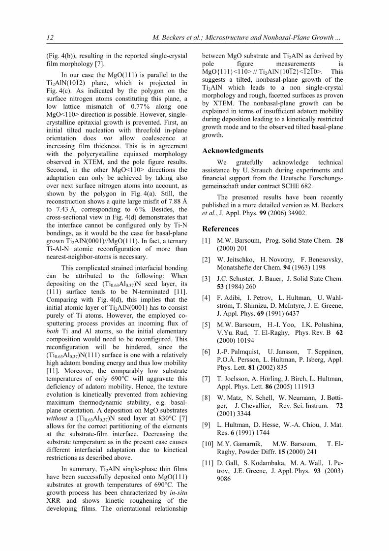
Figure 3(a) shows an XTEM micrograph from Ti2AlN recorded along the MgO[112] zone axis. The layer is not single-crystalline, but exhi-bits equiaxed morphology with individual epitaxial grains corresponding to Fig. 2. Their sizes are in the dimension of the film thickness. Individual grains show strong diffraction contrast, which is due to the threefold in-plane symmetry described above. In accordance with time-resolved XRR the layer displays high surface roughness, caused by the tilted nonbasal–plane growth.
100 nm
Ti( Al )N0.63 0.37
Ti AlN2
Ti AlN2
(0004)
(0006)
(0008)
(0002)
Ti AlN2
10 nm
(a)
(b) (c)
MgO
MgO[112]
[111]
Fig. 3: XTEM micrographs of Ti2AlN grown on MgO(111) along the MgO[112] zone axis. (a) shows the film morpho-logy consisting of large crystal regions. (b) shows a high resolution micrograph at the interface with the typical MAX phase 2-1-1 layered structure. It is made up by the (000l) planes as confirmed from the d-spacing calculation by Fast Fourier Transformation in (c).
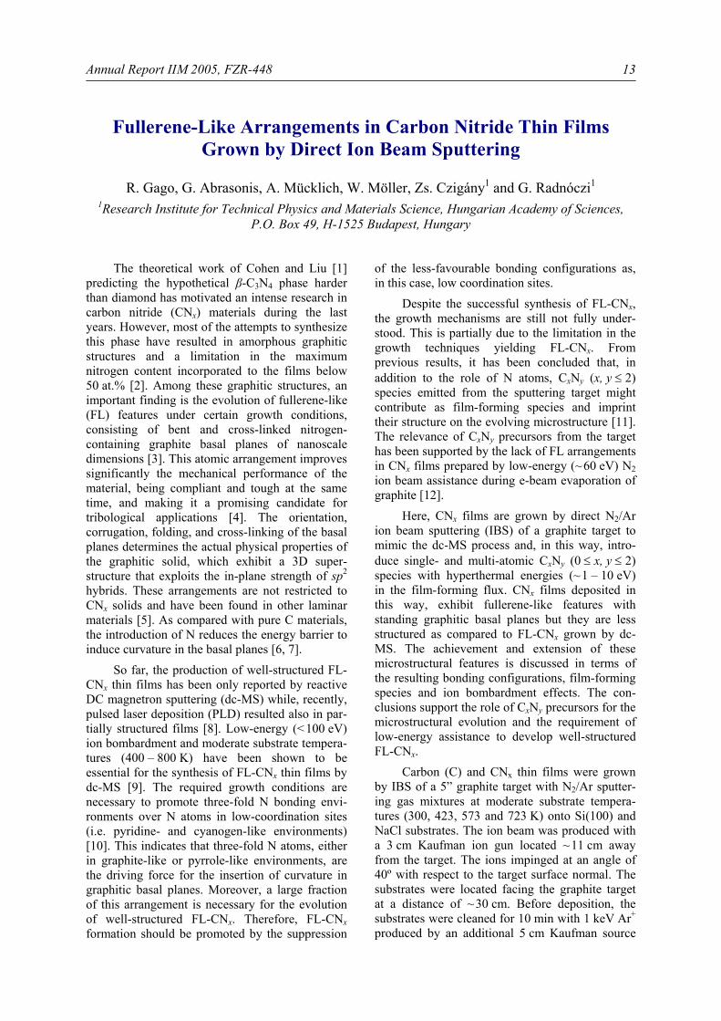
Fig. 4: Atomic model illustration of the different (Ti0.63Al0.37)N and Ti2AlN crystallographic planes and directions together with the geometric reconstructions for the pseudomorphic fitting of Ti2AlN onto (Ti0.63Al0.37)N(111). (a) shows the (Ti0.63Al0.37)N(111) surface and (b) the three different Ti2AlN<1210> orientations of the Ti2AlN(0001) MAX phase basal-plane along the (Ti0.63Al0.37)N<110> directions. (c) shows the same threefold Ti2AlN<1210> orientations for the Ti2AlN(1012) planes. (d) shows cross-sectional views of the Ti2AlN/(Ti0.63Al0.37)N interface for basal-plane and nonbasal-plane growth.
Figure 3(b) shows the interface between one grains and the MgO substrate. The tilted Ti2AlN basal-planes can be depicted from the layered 2-1-1 structure being typical for Mn+1AXn phases. The lattice plane spacing calculations by Fast Fourier Transformation confirm multiple Ti2AlN(000l) planes as shown in Fig. 3(c). The tilting angle of the basal planes is ~ 70°, in agreement with the pole figure measurements. Hence, each of the grains in Fig. 3(a) represents one possible in-plane orientation of the Ti2AlN(000l) plane.
To conclude, both pole figure and XTEM results show that the orientational relationship between the MgO and the Ti2AlN is MgO111<110> // Ti2AlN1012<1210>. This is in contrast to the basal-plane growth of Ti2AlN for high-temperature deposition conditions, with MgO111<110> // Ti2AlN0001<1210> [7]. This basal-plane growth can be expected due to the low lattice mismatch of only 0.77 % between the Ti2AlN(0001) and MgO(111) surfaces, as indicated in Figs. 4(a-d). During nucleation the Ti2AlN(0001) may arrange itself in three possible orientations along the MgO<110> directions. During coalescence, adjacent grains adjoin
M. Beckers et al.; Microstructure and Nonbasal-Plane Growth ...
12
(Fig. 4(b)), resulting in the reported single-crystal film morphology [7].
In our case the MgO(111) is parallel to the Ti2AlN(1012) plane, which is projected in Fig. 4(c). As indicated by the polygon on the surface nitrogen atoms constituting this plane, a low lattice mismatch of 0.77 % along one MgO<110> direction is possible. However, single-crystalline epitaxial growth is prevented. First, an initial tilted nucleation with threefold in-plane orientation does not allow coalescence at increasing film thickness. This is in agreement with the polycrystalline equiaxed morphology observed in XTEM, and the pole figure results. Second, in the other MgO<110> directions the adaptation can only be achieved by taking also over next surface nitrogen atoms into account, as shown by the polygon in Fig. 4(a). Still, the reconstruction shows a quite large misfit of 7.88 Å to 7.43 Å, corresponding to 6 %. Besides, the cross-sectional view in Fig. 4(d) demonstrates that the interface cannot be configured only by Ti-N bondings, as it would be the case for basal-plane grown Ti2AlN(0001)//MgO(111). In fact, a ternary Ti-Al-N atomic reconfiguration of more than nearest-neighbor-atoms is necessary.
This complicated strained interfacial bonding can be attributed to the following: When depositing on the (Ti0.63Al0.37)N seed layer, its (111) surface tends to be N-terminated [11]. Comparing with Fig. 4(d), this implies that the initial atomic layer of Ti2AlN(0001) has to consist purely of Ti atoms. However, the employed co-sputtering process provides an incoming flux of both Ti and Al atoms, so the initial elementary composition would need to be reconfigured. This reconfiguration will be hindered, since the (Ti0.63Al0.37)N(111) surface is one with a relatively high adatom bonding energy and thus low mobility [11]. Moreover, the comparably low substrate temperatures of only 690°C will aggravate this deficiency of adatom mobility. Hence, the texture evolution is kinetically prevented from achieving maximum thermodynamic stability, e.g. basal-plane orientation. A deposition on MgO substrates without a (Ti0.63Al0.37)N seed layer at 830°C [7] allows for the correct partitioning of the elements at the substrate-film interface. Decreasing the substrate temperature as in the present case causes different interfacial adaptation due to kinetical restrictions as described above.
In summary, Ti2AlN single-phase thin films have been successfully deposited onto MgO(111) substrates at growth temperatures of 690°C. The growth process has been characterized by in-situ XRR and shows kinetic roughening of the developing films. The orientational relationship
between MgO substrate and Ti2AlN as derived by pole figure measurements is MgO111<110> // Ti2AlN1012<1210>. This suggests a tilted, nonbasal-plane growth of the Ti2AlN which leads to a non single-crystal morphology and rough, facetted surfaces as proven by XTEM. The nonbasal-plane growth can be explained in terms of insufficient adatom mobility during deposition leading to a kinetically restricted growth mode and to the observed tilted basal-plane growth.
Acknowledgments We gratefully acknowledge technical
assistance by U. Strauch during experiments and financial support from the Deutsche Forschungs-gemeinschaft under contract SCHE 682.
The presented results have been recently published in a more detailed version as M. Beckers et al., J. Appl. Phys. 99 (2006) 34902.
References [1] M.W. Barsoum, Prog. Solid State Chem. 28
(2000) 201 [2] W. Jeitschko, H. Novotny, F. Benesovsky,
Monatshefte der Chem. 94 (1963) 1198 [3] J.C. Schuster, J. Bauer, J. Solid State Chem.
53 (1984) 260 [4] F. Adibi, I. Petrov, L. Hultman, U. Wahl-
ström, T. Shimizu, D. McIntyre, J. E. Greene, J. Appl. Phys. 69 (1991) 6437
[5] M.W. Barsoum, H.-I. Yoo, I.K. Polushina, V.Yu. Rud, T. El-Raghy, Phys. Rev. B 62 (2000) 10194
[6] J.-P. Palmquist, U. Jansson, T. Seppänen, P.O.Å. Persson, L. Hultman, P. Isberg, Appl. Phys. Lett. 81 (2002) 835
[7] T. Joelsson, A. Hörling, J. Birch, L. Hultman, Appl. Phys. Lett. 86 (2005) 111913
[8] W. Matz, N. Schell, W. Neumann, J. Bøtti-ger, J. Chevallier, Rev. Sci. Instrum. 72 (2001) 3344
[9] L. Hultman, D. Hesse, W.-A. Chiou, J. Mat. Res. 6 (1991) 1744
[10] M.Y. Gamarnik, M.W. Barsoum, T. El-Raghy, Powder Diffr. 15 (2000) 241
[11] D. Gall, S. Kodambaka, M. A. Wall, I. Pe-trov, J.E. Greene, J. Appl. Phys. 93 (2003) 9086
Annual Report IIM 2005, FZR-448
13
Fullerene-Like Arrangements in Carbon Nitride Thin Films Grown by Direct Ion Beam Sputtering
R. Gago, G. Abrasonis, A. Mücklich, W. Möller, Zs. Czigány1 and G. Radnóczi1 1Research Institute for Technical Physics and Materials Science, Hungarian Academy of Sciences,
P.O. Box 49, H-1525 Budapest, Hungary
The theoretical work of Cohen and Liu [1] predicting the hypothetical β-C3N4 phase harder than diamond has motivated an intense research in carbon nitride (CNx) materials during the last years. However, most of the attempts to synthesize this phase have resulted in amorphous graphitic structures and a limitation in the maximum nitrogen content incorporated to the films below 50 at.% [2]. Among these graphitic structures, an important finding is the evolution of fullerene-like (FL) features under certain growth conditions, consisting of bent and cross-linked nitrogen-containing graphite basal planes of nanoscale dimensions [3]. This atomic arrangement improves significantly the mechanical performance of the material, being compliant and tough at the same time, and making it a promising candidate for tribological applications [4]. The orientation, corrugation, folding, and cross-linking of the basal planes determines the actual physical properties of the graphitic solid, which exhibit a 3D super-structure that exploits the in-plane strength of sp2 hybrids. These arrangements are not restricted to CNx solids and have been found in other laminar materials [5]. As compared with pure C materials, the introduction of N reduces the energy barrier to induce curvature in the basal planes [6, 7].
So far, the production of well-structured FL-CNx thin films has been only reported by reactive DC magnetron sputtering (dc-MS) while, recently, pulsed laser deposition (PLD) resulted also in par-tially structured films [8]. Low-energy (< 100 eV) ion bombardment and moderate substrate tempera-tures (400 – 800 K) have been shown to be essential for the synthesis of FL-CNx thin films by dc-MS [9]. The required growth conditions are necessary to promote three-fold N bonding envi-ronments over N atoms in low-coordination sites (i.e. pyridine- and cyanogen-like environments) [10]. This indicates that three-fold N atoms, either in graphite-like or pyrrole-like environments, are the driving force for the insertion of curvature in graphitic basal planes. Moreover, a large fraction of this arrangement is necessary for the evolution of well-structured FL-CNx. Therefore, FL-CNx formation should be promoted by the suppression
of the less-favourable bonding configurations as, in this case, low coordination sites.
Despite the successful synthesis of FL-CNx, the growth mechanisms are still not fully under-stood. This is partially due to the limitation in the growth techniques yielding FL-CNx. From previous results, it has been concluded that, in addition to the role of N atoms, CxNy (x, y ≤ 2) species emitted from the sputtering target might contribute as film-forming species and imprint their structure on the evolving microstructure [11]. The relevance of CxNy precursors from the target has been supported by the lack of FL arrangements in CNx films prepared by low-energy (~ 60 eV) N2 ion beam assistance during e-beam evaporation of graphite [12].
Here, CNx films are grown by direct N2/Ar ion beam sputtering (IBS) of a graphite target to mimic the dc-MS process and, in this way, intro-duce single- and multi-atomic CxNy (0 ≤ x, y ≤ 2) species with hyperthermal energies (~ 1 – 10 eV) in the film-forming flux. CNx films deposited in this way, exhibit fullerene-like features with standing graphitic basal planes but they are less structured as compared to FL-CNx grown by dc-MS. The achievement and extension of these microstructural features is discussed in terms of the resulting bonding configurations, film-forming species and ion bombardment effects. The con-clusions support the role of CxNy precursors for the microstructural evolution and the requirement of low-energy assistance to develop well-structured FL-CNx.
Carbon (C) and CNx thin films were grown by IBS of a 5” graphite target with N2/Ar sputter-ing gas mixtures at moderate substrate tempera-tures (300, 423, 573 and 723 K) onto Si(100) and NaCl substrates. The ion beam was produced with a 3 cm Kaufman ion gun located ~ 11 cm away from the target. The ions impinged at an angle of 40º with respect to the target surface normal. The substrates were located facing the graphite target at a distance of ~ 30 cm. Before deposition, the substrates were cleaned for 10 min with 1 keV Ar+ produced by an additional 5 cm Kaufman source
R. Gago et al.; Fullerene-Like Arrangements …
14
facing the substrate. Further details about the growth method, composition and bonding structure of the films can be found in Ref. 13.
The microstructure was studied by high-resolution transmission electron microscopy (HRTEM). Plan-view specimens were obtained from samples grown on NaCl substrates by floating-off technique while cross-sectional specimens were made by gluing slices from samples grown on Si(100) followed by mechanical thinning, polishing and thinned to electron transparency by ion beam milling with 10 keV Ar+ impinging at 4° with respect to the surface. In the final period of the milling process, the ion energy was decreased gradually to 250 eV to minimize surface amorphization [14, 15]. The investigations were made in a JEOL 3010 microscope operated at 300 kV and a resolution of 0.17 nm.
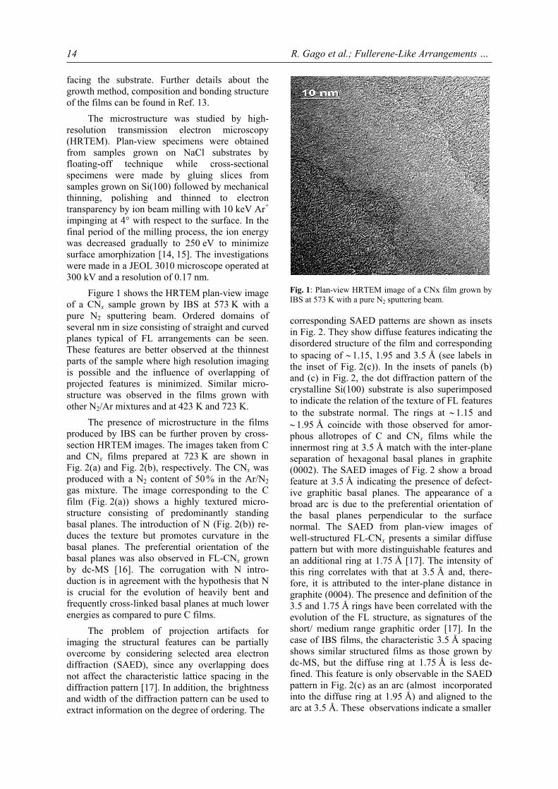
Figure 1 shows the HRTEM plan-view image of a CNx sample grown by IBS at 573 K with a pure N2 sputtering beam. Ordered domains of several nm in size consisting of straight and curved planes typical of FL arrangements can be seen. These features are better observed at the thinnest parts of the sample where high resolution imaging is possible and the influence of overlapping of projected features is minimized. Similar micro-structure was observed in the films grown with other N2/Ar mixtures and at 423 K and 723 K.
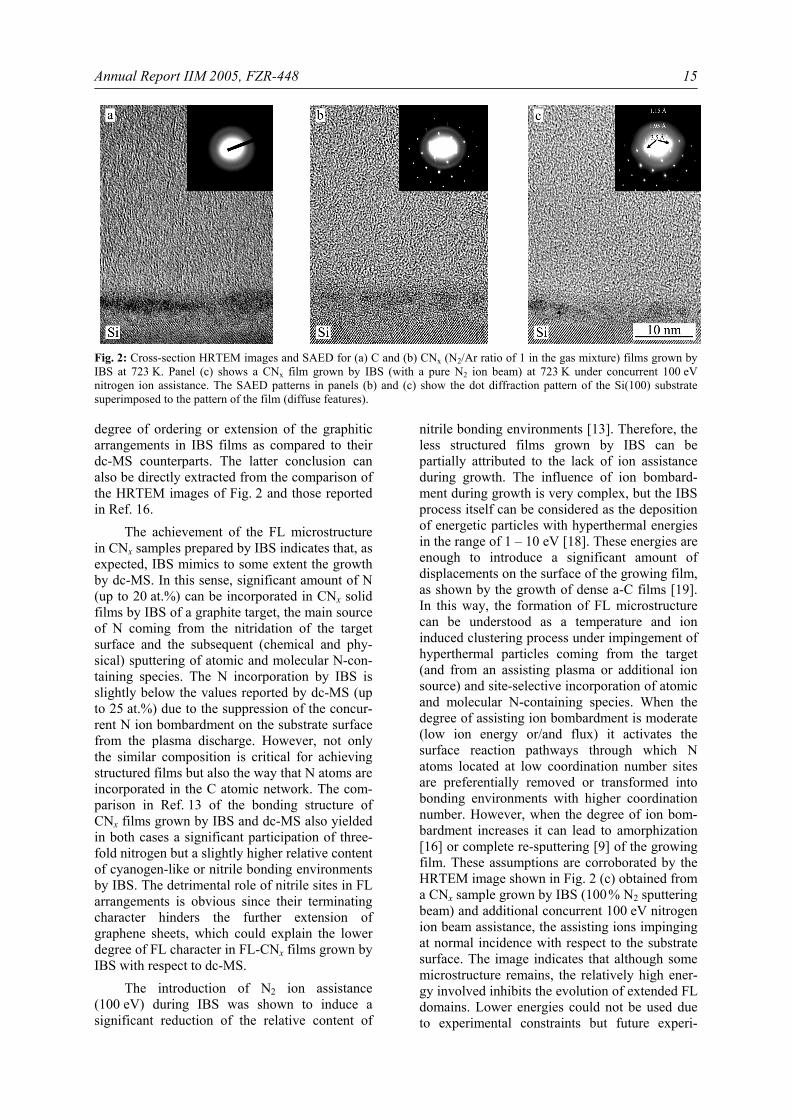
The presence of microstructure in the films produced by IBS can be further proven by cross-section HRTEM images. The images taken from C and CNx films prepared at 723 K are shown in Fig. 2(a) and Fig. 2(b), respectively. The CNx was produced with a N2 content of 50 % in the Ar/N2 gas mixture. The image corresponding to the C film (Fig. 2(a)) shows a highly textured micro-structure consisting of predominantly standing basal planes. The introduction of N (Fig. 2(b)) re-duces the texture but promotes curvature in the basal planes. The preferential orientation of the basal planes was also observed in FL-CNx grown by dc-MS [16]. The corrugation with N intro-duction is in agreement with the hypothesis that N is crucial for the evolution of heavily bent and frequently cross-linked basal planes at much lower energies as compared to pure C films.
The problem of projection artifacts for imaging the structural features can be partially overcome by considering selected area electron diffraction (SAED), since any overlapping does not affect the characteristic lattice spacing in the diffraction pattern [17]. In addition, the brightness and width of the diffraction pattern can be used to extract information on the degree of ordering. The
Fig. 1: Plan-view HRTEM image of a CNx film grown by IBS at 573 K with a pure N2 sputtering beam.
corresponding SAED patterns are shown as insets in Fig. 2. They show diffuse features indicating the disordered structure of the film and corresponding to spacing of ∼ 1.15, 1.95 and 3.5 Å (see labels in the inset of Fig. 2(c)). In the insets of panels (b) and (c) in Fig. 2, the dot diffraction pattern of the crystalline Si(100) substrate is also superimposed to indicate the relation of the texture of FL features to the substrate normal. The rings at ∼ 1.15 and ∼ 1.95 Å coincide with those observed for amor-phous allotropes of C and CNx films while the innermost ring at 3.5 Å match with the inter-plane separation of hexagonal basal planes in graphite (0002). The SAED images of Fig. 2 show a broad feature at 3.5 Å indicating the presence of defect-ive graphitic basal planes. The appearance of a broad arc is due to the preferential orientation of the basal planes perpendicular to the surface normal. The SAED from plan-view images of well-structured FL-CNx presents a similar diffuse pattern but with more distinguishable features and an additional ring at 1.75 Å [17]. The intensity of this ring correlates with that at 3.5 Å and, there-fore, it is attributed to the inter-plane distance in graphite (0004). The presence and definition of the 3.5 and 1.75 Å rings have been correlated with the evolution of the FL structure, as signatures of the short/ medium range graphitic order [17]. In the case of IBS films, the characteristic 3.5 Å spacing shows similar structured films as those grown by dc-MS, but the diffuse ring at 1.75 Å is less de-fined. This feature is only observable in the SAED pattern in Fig. 2(c) as an arc (almost incorporated into the diffuse ring at 1.95 Å) and aligned to the arc at 3.5 Å. These observations indicate a smaller
Annual Report IIM 2005, FZR-448
15
Fig. 2: Cross-section HRTEM images and SAED for (a) C and (b) CNx (N2/Ar ratio of 1 in the gas mixture) films grown by IBS at 723 K. Panel (c) shows a CNx film grown by IBS (with a pure N2 ion beam) at 723 K under concurrent 100 eV nitrogen ion assistance. The SAED patterns in panels (b) and (c) show the dot diffraction pattern of the Si(100) substrate superimposed to the pattern of the film (diffuse features).
degree of ordering or extension of the graphitic arrangements in IBS films as compared to their dc-MS counterparts. The latter conclusion can also be directly extracted from the comparison of the HRTEM images of Fig. 2 and those reported in Ref. 16.
The achievement of the FL microstructure in CNx samples prepared by IBS indicates that, as expected, IBS mimics to some extent the growth by dc-MS. In this sense, significant amount of N (up to 20 at.%) can be incorporated in CNx solid films by IBS of a graphite target, the main source of N coming from the nitridation of the target surface and the subsequent (chemical and phy-sical) sputtering of atomic and molecular N-con-taining species. The N incorporation by IBS is slightly below the values reported by dc-MS (up to 25 at.%) due to the suppression of the concur-rent N ion bombardment on the substrate surface from the plasma discharge. However, not only the similar composition is critical for achieving structured films but also the way that N atoms are incorporated in the C atomic network. The com-parison in Ref. 13 of the bonding structure of CNx films grown by IBS and dc-MS also yielded in both cases a significant participation of three-fold nitrogen but a slightly higher relative content of cyanogen-like or nitrile bonding environments by IBS. The detrimental role of nitrile sites in FL arrangements is obvious since their terminating character hinders the further extension of graphene sheets, which could explain the lower degree of FL character in FL-CNx films grown by IBS with respect to dc-MS.
The introduction of N2 ion assistance (100 eV) during IBS was shown to induce a significant reduction of the relative content of
nitrile bonding environments [13]. Therefore, the less structured films grown by IBS can be partially attributed to the lack of ion assistance during growth. The influence of ion bombard-ment during growth is very complex, but the IBS process itself can be considered as the deposition of energetic particles with hyperthermal energies in the range of 1 – 10 eV [18]. These energies are enough to introduce a significant amount of displacements on the surface of the growing film, as shown by the growth of dense a-C films [19]. In this way, the formation of FL microstructure can be understood as a temperature and ion induced clustering process under impingement of hyperthermal particles coming from the target (and from an assisting plasma or additional ion source) and site-selective incorporation of atomic and molecular N-containing species. When the degree of assisting ion bombardment is moderate (low ion energy or/and flux) it activates the surface reaction pathways through which N atoms located at low coordination number sites are preferentially removed or transformed into bonding environments with higher coordination number. However, when the degree of ion bom-bardment increases it can lead to amorphization [16] or complete re-sputtering [9] of the growing film. These assumptions are corroborated by the HRTEM image shown in Fig. 2 (c) obtained from a CNx sample grown by IBS (100 % N2 sputtering beam) and additional concurrent 100 eV nitrogen ion beam assistance, the assisting ions impinging at normal incidence with respect to the substrate surface. The image indicates that although some microstructure remains, the relatively high ener-gy involved inhibits the evolution of extended FL domains. Lower energies could not be used due to experimental constraints but future experi-
R. Gago et al.; Fullerene-Like Arrangements …
16
ments are in progress to reduce the energy of the assistance ions and, in this way, check the pro-motion of FL arrangements by ion assistance.
In conclusion, HRTEM images reveal the formation of FL-CNx by IBS at moderate tempe-ratures. This result supports the presence of CxNy species in the film-forming flux and low-energy ion bombardment as the main paths to induce the evolution of curved graphitic structures in CNx solids. In addition, the formation of such struc-tures is clearly related to the promotion of three-fold N in hexagonal or pentagonal arrangements and a reduced participation of nitrile bonding environments.
Acknowledgements This work has been carried out inside the
IHP-Network “Synthesis, structure and properties of new fullerene-like materials” being supported by the EU contract no. HPRN-CT-2002-00209.
The presented results have been recently published as R. Gago et al., Appl. Phys. Lett. 87 (2005) 071901.
References [1] A.Y. Liu, M.L. Cohen, Science 245 (1989)
841 [2] C. Ronning, H. Feldermann, R. Merk, H.
Hofsäss, P. Reinke, J.U. Thiele, Phys. Rev. B 58 (1998) 2207
[3] H. Sjöström, S. Stafström, M. Boman, J.E. Sundgren, Phys. Rev. Lett. 75 (1995) 1336
[4] L. Hultman, J. Neidhardt, N. Hellgren, H. Sjöström, J.-E. Sundgren, MRS Bulletin 28 (2003) 19
[5] I. Alexandrou, H.J. Scheibe, C.J. Kiely, A.J. Papworth, G.A.J. Amaratuga, B. Schultrich, Phys. Rev. B 60 (1999) 10903
[6] N. Lin, N. Hellgren, M.P. Johansson, L. Hultman, R. Erlandsson, J.-E. Sundgren, Phys. Rev. B 61 (2000) 4898
[7] S. Stafström, Appl. Phys. Lett. 77 (2000) 3941
[8] A.A. Voevodin, J.G. Jones, J.S. Zabinski, Zs. Czigány, L. Hultman, J. Appl. Phys. 92 (2002) 4980
[9] N. Hellgren, K. Macák, E. Broitman, M.P. Johansson, L. Hultman, J.-E. Sundgren, J. Appl. Phys. 88 (2000) 524
[10] R. Gago, I. Jiménez, J. Neidhardt, B. Abendroth, I. Caretti, L. Hultman, W. Möller, Phys. Rev. B 71 (2005) 125414
[11] J. Neidhardt, B. Abendroth, R. Gago, W. Möller, L. Hultman, J. Appl. Phys. 94 (2003) 7059
[12] R. Gago, J. Neidhardt, M. Vinnichenko, U. Kreissig, Zs. Czigány, A. Kolitsch, L. Hult-man, W. Möller, Thin Solid Films 483 (2005) 89
[13] G. Abrasonis, R. Gago, I. Jiménez, U. Kreissig, A. Kolitsch, W. Möller, J. Appl. Phys. 98 (2005) 074907
[14] Á. Barna, B. Pécz, M. Menyhárd, Ultra-microscopy 70 (1998) 161
[15] Zs. Czigány, J. Neidhardt, I.F. Brunell, L. Hultman, Ultramicroscopy 94 (2002) 163
[16] J. Neidhardt, Zs. Czigány, I.F. Brunell, L. Hultman, J. Appl. Phys. 93 (2003) 3002
[17] J. Neidhardt, L. Hultman, Zs. Czigány, Carbon 42 (2004) 2734
[18] S.M. Rossnagel, J. Vac. Sci. Technol. A 7 (1989) 1025
[19] J.J. Cuomo, J.P. Doyle, J. Bruley, J.C. Liu, Appl. Phys. Lett. 58 (1991) 46
Annual Report IIM 2005, FZR-448
17
Fe Implanted Ferromagnetic ZnO
K. Potzger, S. Zhou, H. Reuther, A. Mücklich, F. Eichhorn, N. Schell, W. Skorupa, M. Helm, J. Fassbender, T. Herrmannsdörfer1 and T.P. Papageorgiou1
1Hochfeld-Magnetlabor Dresden, Forschungszentrum Rossendorf, P.O. Box 510119, 01314 Dresden
In the field of spintronics [1], diluted mag-netic semiconductors (DMS) are worldwide under intense investigation. DMS are “conventional” semiconductors doped with transition metal (TM) or rare-earth ions which are diluted within the host matrix and ferromagnetically aligned via an in-direct magnetic coupling [2-7]. The existence of DMS based on Mn doped p-type ZnO [2] and V, Ti, Fe, Co or Ni doped n-type ZnO [7] has been predicted by theory. However, currently only n-type conducting ZnO films or single crystals are available. Recent reviews of experimental work in the field, are given by S.J. Pearton et al. [8] and Ü. Özgür et al. [9]. Among other systems, n-type ZnO doped with Fe has been confirmed experi-mentally [10-12] to exhibit ferromagnetism at room temperature. In some cases, especially at high processing temperatures, unwanted secondary phases are formed inside the ZnO matrix, which are responsible for the ferromagnetic properties [11]. One way to overcome this problem is the use of ion beam doping at low temperatures and thus far from thermal equilibrium [12-14]. In any case, structural analysis methods with high sensitivity are necessary in order to exclude secondary phases.
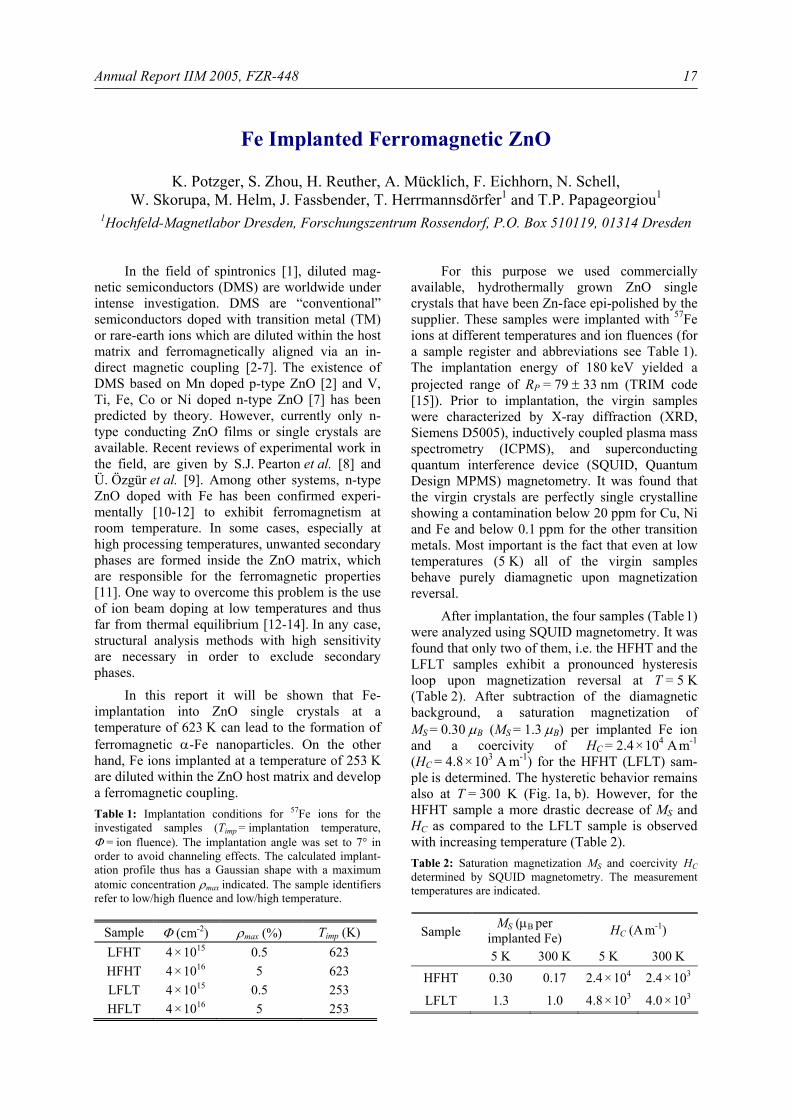
In this report it will be shown that Fe-implantation into ZnO single crystals at a temperature of 623 K can lead to the formation of ferromagnetic α-Fe nanoparticles. On the other hand, Fe ions implanted at a temperature of 253 K are diluted within the ZnO host matrix and develop a ferromagnetic coupling. Table 1: Implantation conditions for 57Fe ions for the investigated samples (Timp = implantation temperature, Φ = ion fluence). The implantation angle was set to 7° in order to avoid channeling effects. The calculated implant-ation profile thus has a Gaussian shape with a maximum atomic concentration ρmax indicated. The sample identifiers refer to low/high fluence and low/high temperature.
Sample Φ (cm-2) ρmax (%) Timp (K) LFHT 4 × 10¹⁵ 0.5 623 HFHT 4 × 10¹⁶ 5 623 LFLT 4 × 10¹⁵ 0.5 253 HFLT 4 × 10¹⁶ 5 253
For this purpose we used commercially available, hydrothermally grown ZnO single crystals that have been Zn-face epi-polished by the supplier. These samples were implanted with 57Fe ions at different temperatures and ion fluences (for a sample register and abbreviations see Table 1). The implantation energy of 180 keV yielded a projected range of RP = 79 ± 33 nm (TRIM code [15]). Prior to implantation, the virgin samples were characterized by X-ray diffraction (XRD, Siemens D5005), inductively coupled plasma mass spectrometry (ICPMS), and superconducting quantum interference device (SQUID, Quantum Design MPMS) magnetometry. It was found that the virgin crystals are perfectly single crystalline showing a contamination below 20 ppm for Cu, Ni and Fe and below 0.1 ppm for the other transition metals. Most important is the fact that even at low temperatures (5 K) all of the virgin samples behave purely diamagnetic upon magnetization reversal.
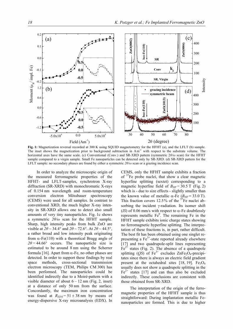
After implantation, the four samples (Table 1) were analyzed using SQUID magnetometry. It was found that only two of them, i.e. the HFHT and the LFLT samples exhibit a pronounced hysteresis loop upon magnetization reversal at T = 5 K (Table 2). After subtraction of the diamagnetic background, a saturation magnetization of MS = 0.30 µB (MS = 1.3 µB) per implanted Fe ion and a coercivity of HC = 2.4 × 10⁴ A m-1 (HC = 4.8 × 10³ A m-1) for the HFHT (LFLT) sam-ple is determined. The hysteretic behavior remains also at T = 300 K (Fig. 1a, b). However, for the HFHT sample a more drastic decrease of MS and HC as compared to the LFLT sample is observed with increasing temperature (Table 2). Table 2: Saturation magnetization MS and coercivity HC determined by SQUID magnetometry. The measurement temperatures are indicated.
MS (µB per implanted Fe) HC (A m-1) Sample
5 K 300 K 5 K 300 K
HFHT 0.30 0.17 2.4 × 10⁴ 2.4 × 10³
LFLT 1.3 1.0 4.8 × 10³ 4.0 × 10³
K. Potzger et al.; Fe Implanted Ferromagnetic ZnO
18
Fig. 1: Magnetization reversal recorded at 300 K using SQUID magnetometry for the HFHT (a), and the LFLT (b) sample. The inset shows the magnetization prior to background subtraction in A m-1 with respect to the substrate volume. The horizontal axes have the same scale. (c) Conventional (Conv.) and SR-XRD pattern (symmetric 2θ/ω scan) for the HFHT sample compared to a virgin sample. Small Fe nanoparticles can be detected only by SR-XRD. (d) SR-XRD pattern for the LFLT sample: no secondary phases are found by either a symmetric 2θ/ω scan or a grazing incidence scan.
In order to analyze the microscopic origin of the measured ferromagnetic properties of the HFHT- and LFLT-samples, synchrotron X-ray diffraction (SR-XRD) with monochromatic X-rays of 0.154 nm wavelength and room-temperature conversion electron Mössbauer spectroscopy (CEMS) were used for all samples. In contrast to conventional XRD, the much higher X-ray inten-sity in SR-XRD allows one to detect also small amounts of very tiny nanoparticles. Fig. 1c shows a symmetric 2θ/ω scan for the HFHT sample. Sharp, high intensity peaks from bulk ZnO are visible at 2θ ~ 34.4° and 2θ ~ 72.6°. At 2θ ~ 44.5°, a rather broad and low intensity peak originating from α-Fe(110) with a theoretical Bragg angle of 2θ = 44.66° occurs. The nanoparticle size is estimated to be around 8 nm using the Scherrer formula [16]. Apart from α-Fe, no other phases are detected. In order to support these findings by real space methods, cross-sectional transmission electron microscopy (TEM, Philips CM 300) has been performed. The nanoparticles could be identified indirectly due to a Moiré-pattern with a visible diameter of about 6 – 12 nm (Fig. 2, inset) at a distance of only 50 nm from the surface. Concordantly, the maximum iron concentration was found at REDX = 51 ± 38 nm by means of energy-dispersive X-ray microanalysis (EDX). In
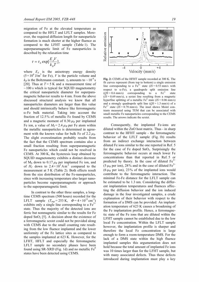
CEMS, only the HFHT sample exhibits a fraction of 57Fe probe nuclei, that show a clear magnetic hyperfine splitting (sextet) corresponding to a magnetic hyperfine field of BHF = 30.5 T (Fig. 2) which is - due to size effects - slightly smaller than the known value of metallic α-Fe (BHF = 33.0 T). This fraction covers 12.5 % of the 57Fe nuclei ab-sorbing the incident γ-radiation. Its isomer shift (IS) of 0.06 mm/s with respect to α-Fe doubtlessly represents metallic Fe0. The remaining Fe in the HFHT sample exhibits ionic charge states showing no ferromagnetic hyperfine splitting. The interpre-tation of these fractions is, in part, rather difficult. The best fit has been obtained using one singlet re-presenting a Fe3+-state reported already elsewhere [17] and two quadrupole-split lines representing Fe2+ states (Fig. 2). The absence of a quadrupole splitting (QS) of Fe3+ excludes ZnFe2O4-precipi-tates since there is always an electric field gradient present at the octahedral sites [18, 19]. Fe3O4 usually does not show a quadrupole splitting in the Fe2+ states [17] and can thus also be excluded indirectly. These conclusions are consistent with those obtained from SR-XRD.
The interpretation of the origin of the ferro-magnetic properties of the HFHT sample is thus straightforward: During implantation metallic Fe-nanoparticles are formed. This is due to higher
-0.2
-0.1
0.0
0.1
0.2
(b)
(a)
-0.5
0.0
0.5
M
omen
t (µ B
/ im
pl. F
e)
Field (Am-1)
-5.0x10⁴ 0.0 5.0x10⁴
-1.2
-0.6
0.0
0.6
1.2
-0.5
0.0
0.5
100
200
300
400(c)
Inte
nsity
ZnO
(000
2)
kβ
ZnO
(000
4)
bcc-
Fe(1
10)
SR. Virgin
Conv
SR
30 40 50 60 70 80
100
200
300
400(d)
ZnO
(101
3)
grazing incidence symmetric beam
bcc-
Fe(1
10)
2θ (degree)
Annual Report IIM 2005, FZR-448
19
migration of Fe at the elevated temperature as compared to the HFLT and LFLT samples. More-over, the required diffusion length for nanoparticle formation is much shorter at the higher fluence as compared to the LFHT sample (Table 1). The superparamagnetic limit of Fe nanoparticles is described by the relaxation time
]exp[0 TkVE
B
Aττ = ,
where EA is the anisotropy energy density (5 × 10⁴ J/m3 for Fe), V is the particle volume and kB is the Boltzmann constant. τ0 amounts to ~ 10-9 s [20]. Thus at T = 5 K and a measurement time of ~ 100 s which is typical for SQUID magnetometry the critical nanoparticle diameter for superpara-magnetic behavior results to 4 nm. From the above discussed structural analysis we know that all nanoparticles diameters are larger than this value and should intrinsically behave like ferromagnetic α-Fe bulk material. Taking into account the fraction of 12.5 % of metallic Fe found by CEMS and a magnetic moment of 0.30 µB per implanted Fe ion, a value of MS = 2.4 µΒ per Fe atom within the metallic nanoparticles is determined in agree-ment with the known value for bulk Fe of 2.2 µB. The slight overestimation probably results from the fact that the CEMS spectrum contains also a small fraction resulting from superparamagnetic Fe nanoparticles which could not be resolved in CEMS. At 300 K, the hysteresis loop obtained by SQUID magnetometry exhibits a distinct decrease of MS down to 0.17 µB per implanted Fe ion, and of HC down to 2.4 × 10³ A m-1 compared to the measurement at 5 K (Table 2). Both effects result from the size distribution of the Fe-nanoparticles, since with increasing temperature also larger nano-particles become superparamagnetic or approach to the superparamagnetic limit.
In contrast to the other three samples, a long-time CEMS spectrum (500 hours) recorded for the LFLT sample (Timp = 253 K, Φ = 4 × 1015 cm-2) exhibits only a single line corresponding to a Fe3+ state. Thus the majority of the detected ions are ferric but nonmagnetic similar to the results for Fe doped SnO2 [5]. A decision about the existence of a ferromagnetic sextet could not be provided along with CEMS due to the small counting rate result-ing from the low fluence implanted and the lower uniformity of the Fe lattice sites as compared to the samples implanted at 623 K. However, for the LFHT, HFLT and especially the ferromagnetic LFLT sample no secondary phases have been found using SR-XRD (Fig. 1d) and no metallic Fe0 states have been detected using CEMS.
Fig. 2: CEMS of the HFHT sample recorded at 300 K. The fit curves represent (from top to bottom) a single emission line corresponding to a Fe3+ state (IS = 0.53 mm/s with respect to α-Fe), a quadrupole split emission line (QS = 0.6 mm/s) corresponding to a Fe2+ state (IS = 0.69 mm/s), a sextet line resulting from a magnetic hyperfine splitting of a metallic Fe0 state (IS = 0.06 mm/s) and a strongly quadrupole split line (QS = 1.3 mm/s) of a Fe2+ state (IS = 0.78 mm/s). The inset shows Moiré con-trasts measured using TEM that can be associated with small metallic Fe nanoparticles corresponding to the CEMS results. The arrows indicate the sextet.
Consequently, the implanted Fe-ions are diluted within the ZnO host matrix. Thus - in sharp contrast to the HFHT sample - the ferromagnetic behavior of the LFLT sample (Fig. 1b) results from an indirect exchange interaction between diluted Fe ions similar to the one reported in Ref. 5 for the case of Fe doped SnO2. Surprisingly the ferromagnetic behavior occurs at much lower Fe concentrations than that reported in Ref. 5 or predicted by theory. In the case of diluted Fe3+ (5 µB per ion), 28 % and in the case of diluted Fe2+ (6 µB per ion), 23 % of the implanted ions would contribute to the ferromagnetic interaction. The minimal Fe-Fe distance for the LFLT sample can be estimated to be 1.3 nm. Considering the differ-ent implantation temperatures and fluences affec-ting the diffusion behavior and the ion induced damage in the four investigated samples, a crude explanation of their behavior with respect to the formation of a DMS can be provided: An implant-ation temperature of 623 K causes a broadening of the Fe implantation profile. Hence, a ferromagne-tic state of the Fe ions that are diluted within the LFHT sample cannot be established due to the low local Fe concentration. Within the LFLT sample however, the implantation profile is sharper and therefore the local Fe concentration is large enough to form a room-temperature DMS. For the lack of a DMS state within the high fluence implanted samples this argumentation does not hold because the total amount of implanted Fe ions was 10 times larger than for the LFHT sample, but with many associated defects. Thus these defects introduced during implantation must play a key
K. Potzger et al.; Fe Implanted Ferromagnetic ZnO
20
role for the DMS formation. Rutherford backscat-tering (RBS) analysis shows that the damage level for both high fluence implanted samples are simi-lar, i.e. χmin ~ 65 % [21], while the damage level for the LFLT sample is much lower (χmin = 30 %, χmin of the virgin samples: 3 %). Such defects affect the transport properties of ZnO [22] and thus the path of ferromagnetic coupling.
In summary, 180 keV Fe implanted ZnO single crystals can develop ferromagnetic proper-ties that are either caused by α-Fe nanoparticles or an indirect coupling of the Fe ions in a DMS system, depending on the details of ion fluence and implantation temperature. Detailed structural analysis is required to rule out secondary phases.
The presented results have been recently published as K. Potzger et al., Appl. Phys. Lett. 88 (2006) 052508.
References [1] S.A. Wolf, D.D. Awschalom, R.A. Buhrman,
J.M. Daughton, S. von Molnár, M.L. Roukes, A.Y. Chtchelkanova, D.M. Treger, Science 294 (2001)1488
[2] T. Dietl, H. Ohno, F. Matsukura, J. Cibert, D. Ferrand, Science 287 (2000) 1019
[3] V. Barzykin, Phys. Rev. B 71 (2005) 155203 [4] D.J. Priour, E.H. Hwang, S. Das Sarma,
Phys. Rev. Lett. 92 (2004) 117201 [5] J.M.D. Coey, A.P. Douvalis, C.B. Fitzgerald,
M. Venkatesan, Appl. Phys. Lett. 84 (2004) 1332
[6] J.M.D. Coey, M. Venkatesan, C.B. Fitz-gerald, Nat. Mater. 4 (2005) 173
[7] K. Sato, H. Katayama-Yoshida, Semicond. Sci. Tech. 17 (2002) 367
[8] S.J. Pearton, D.P. Norton, K. Ip, Y.W. Heo, T. Steiner, J. Vac. Sci. Technol. B 22 (2004) 932
[9] Ü. Özgür, Ya.I. Alivov, C. Liu, A. Teke, M.A. Reshchikov, S. Doğan, V. Avrutin, S.-J. Cho, H. Morkoç, J. Appl. Phys. 98 (2005) 041301
[10] M. Venkatesan, C.B. Fitzgerald, J.G. Lun-ney, J.M.D. Coey, Phys. Rev. Lett. 93 (2004) 177206
[11] J.H. Shim, T. Hwang, S. Lee, J.H. Park, S.-J. Han, Y.H. Jeong, Appl. Phys. Lett. 86 (2005) 082503
[12] A.Y. Polyakov, A.V. Govorkov, N.B. Smirnov, N.V. Pashkova, S.J. Pearton, K. Ip, R.M. Frazier, C.R. Abernathy, D.P. Norton, J.M. Zavada, R.G. Wilson, Mat. Sci. Semicon. Proc. 7 (2004) 77
[13] E. Rita, U. Wahl, J.G. Correia, E. Alves, J.C. Soares, Appl. Phys. Lett. 85 (2004) 4899
[14] D.P. Norton, M.E. Overberg, S.J. Pearton, K. Pruessner, J.D. Budai, L.A. Boatner, M.F. Chisholm, S.J. Lee, Z.G. Khim, Y.D. Park, R.G. Wilson, Appl. Phys. Lett. 83 (2003) 5488
[15] J. Ziegler, J. Biersack, U. Littmark, The Stopping and Range of Ions in Matter, Pergamon Press, New York, 1985, SRIM 2000 code, www.srim.org
[16] B.D. Cullity, Elements of X-ray Diffraction, Reading, MA: Addison-Wesley, 1978, p. 102
[17] E. Murad, Phys. Chem. Miner. 23 (1996) 248 [18] H.B. Mathur, A.P.B. Sinha, C.M. Yagnik,
Indian J. Pure Ap. Phy. 5 (1967) 155 [19] B.J. Evans, S.S. Hafner, H.P. Weber, J.
Chem. Phys. 55 (1971) 5282 [20] R. Waser, Nanoelectronics and Information
Technology, Wiley-CH, Weinheim, 2003, p. 624
[21] χmin is the channeling minimum yield in RBS/C, which is the ratio of the back-scattering yield when the impinging beam is aligned parallel to a crystallographic axis to that for a random beam incidence. Therefore, an amorphous sample shows a χmin of 100 %, while a perfect single crystal corresponds to a χmin of 1-2 %.
[22] S.O. Kucheyev, C. Jagadish, J.S. Williams, P.N.K. Deenapanray, M. Yano, K. Koike, S. Sasa, M. Inoue, K. Ogata, J. Appl. Phys. 93 (2003) 2972
Annual Report IIM 2005, FZR-448
21
A Transient Electrical Model of Charging for Ge Nanocrystal Containing Gate Oxides with DRAM-Like Behavior
V. Beyer, J. von Borany and A. Mücklich
Since the mid 90s the multidot memory has been of major interest in the research activities of emerging non-volatile memory devices [1, 2]. This memory concept is based on a layer of well sepa-rated Si or Ge nanocrystals (NCs) embedded in the transistor gate oxide substituting the floating gate of classical Flash-memory devices. Among various techniques for NCs fabrication [3] ion-beam syn-thesis (IBS) has been established as a versatile method to produce a high density (> 1012 cm-2) of small (< 3 nm) Ge or Si NCs in thin gate oxides [4, 5]. Multidot memories likewise promise short programming / write times (tprog < 1 µs), low operating voltages (|Vprog| n 10 V) as well as high endurance (109 cycles) with preferably long data retention [1, 6, 7].
In this paper, the write performance of Ge NCs containing gate oxides is investigated by means of MOS (metal-oxide-semiconductor) capa-citors. It has been shown that under specific prepa-ration conditions a self-organized, δ-like layer of Ge NCs close to the Si/SiO2 interface (IF) is formed during IBS in thin SiO2 films [8, 9]. For this case, where the charge transfer occurs in the direct tunneling (DT) regime, charging by holes (instead of electrons) offers the advantage of en-hanced data retention due to the higher tunneling barrier φb [10]. Thus, we studied the time depen-dence of hole charging under substrate accumula-tion conditions. The evaluation is based on capaci-tance-voltage (C-V) measurements of MOS capa-citors which restrict the programming time to tprog ≥ 3 ms. To predict the write performance with respect to memory applications for much shorter times (tprog ~ µs), this experimental study will be accompanied by simulations using a physical / electrical model of the device structure.
The MOS capacitors were prepared as follows: 74Ge+-ions (12 keV, 5 × 1015 cm-2) were implanted at room temperature in a 20 nm thick thermally grown gate oxide on <100> p-type Si (ρ ~ 10 Ω cm). After a standard cleaning step in H2O2 / H2SO4, rapid thermal annealing (RTA) was carried out at 950°C for 30 s in Ar to recover the damaged oxide and to form the Ge NCs. After-wards, metal dots (A = 0.1 mm2) were fabricated by Al-sputtering, photolithographic patterning and a 400°C, 15 min furnace anneal in N2.
The Ge profile and the corresponding NC-distribution in the gate oxide were characterized by Rutherford backscattering spectrometry (RBS) and transmission electron microscopy (TEM), re-spectively. The RBS measurements were obtained by 1.7 MeV He+ ions at a scattering angle of 170° and an incident angle of 70° to improve the depth resolution. The TEM analysis was carried out on a Philips CM300 microscope operating at 300 kV. The C-V characteristics of the MOS capacitors were measured by a Keithley 590 CV analyzer at 100 kHz using a programmable external voltage source (Keithley 237). The measurement sequence is shown in Fig. 1.
Fig. 1: Sequence of the applied voltage pulses to investi-gate the programming characteristic of MOS capacitors.
The MOS devices were charged by negative square voltage pulses (-3 V ≥ Vprog ≥ -8 V) with durations of 3 ms ≤ tprog ≤ 30 s. After 1 ms at the reference potential of 0 V, a read pulse was applied with |Vread| < |Vprog| for tread = tprog while the C-V data C(Vread) are recorded. Vread is adjusted in such a way that at the beginning of the read-cycle C(Vread) is about CFB(VFB,0) which avoids any influence of the reading process itself on the NCs charge state after programming. CFB denotes the flatband capacitance and VFB,0 the flatband voltage of the initial (uncharged) MOS capacitor. Thus, the flatband voltage shift - as a measure of the stored charge - is easily obtained as ∆VFB = Vread - VFB,0. Profiting by a short data retention (~ s) and the high endurance this procedure was repeated for each data point (Vprog, tprog).
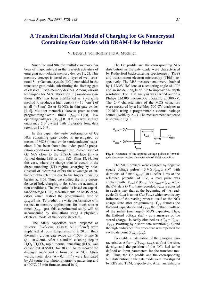
To enable a calculation of the charging cha-racteristics ∆VFB = f (Vprog, tprog), at first the size, density, and the position of the NCs had to be defined as input parameters for the transient mo-del. Thus, the Ge profile and the corresponding NC distribution in the gate oxide were investigated by RBS and TEM, respectively. After annealing a
V. Beyer et al.; A Transient Electrical Model …
22
Fig. 2: Ge distribution after ion-implantation ( ) and an-nealing ( ) as measured by RBS. After annealing the ma-jor part (~ 1.3 × 1015 cm-2) of the remaining Ge is located in a close vicinity to the Si/SiO2-IF.
Fig. 3: Cross-sectional bright-field TEM-micrograph of the Ge implanted oxide after annealing. Primarily due to their very small size the Ge NCs are detected only by Z-contrast imaging.
significant redistribution of the initial (as-implant-ed) Ge profile towards the Si/SiO2-IF is obtained from RBS in Fig. 2. A layer of separated Ge NCs forms in the oxide close to the IF as confirmed from TEM imaging (cf. Fig. 3). For the near-interface NCs a mean size of dnc ≈ 2 nm and a density of Nnc ~ 1 × 1012 cm-2 as a lower limit can be deduced. For a total oxide thickness of ~ 23 nm the tunneling oxide thickness varies between ~ 1 and 2.5 nm. An upper limit of the NC density of Nnc ~ 7 × 1012 cm-2 can be deduced from RBS if the amount of near-interface Ge (1.3 × 1015 cm-2) con-tributes completely to equal sized NCs of 2 nm diameter.
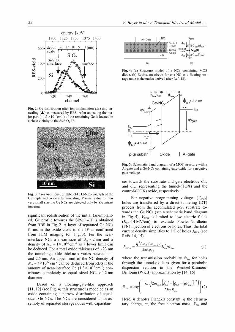
Based on a floating-gate-like approach [11, 12] (see Fig. 4) this structure is modeled as an oxide containing a narrow distribution of equal-sized Ge NCs. The NCs are considered as an as-sembly of separated storage nodes with capacitan-
Fig. 4: (a) Structure model of a NCs containing MOS diode. (b) Equivalent circuit for one NC as a floating sto-rage node (schematics derived after Ref. 13).
Fig. 5: Schematic band diagram of a MOS structure with a Al-gate and a Ge-NCs containing gate-oxide for a negative gate-voltage.
ces towards the substrate and gate electrode Ctox and Ccox representing the tunnel-(TOX) and the control-(COX) oxide, respectively.
For negative programming voltages (Vprog) holes are transferred by a direct tunneling (DT) process from the accumulated p-Si substrate to-wards the Ge NCs (see a schematic band diagram in Fig. 5). Vprog is limited to low electric fields (Eox < 4 MV/cm) to exclude Fowler-Nordheim (FN) injection of electrons or holes. Thus, the total current density simplifies to DT of holes JDT,h (see Refs. 14, 15)
(1)tox2tox
h,b
h,ox03
h,DT Eh8
)m/m(qJ Θ=
φπ where the transmission probability Θtox for holes through the tunnel-oxide is given for a parabolic dispersion relation in the Wentzel-Kramers-Brillouin (WKB) approximation by [14, 16]
( )( )(2)
328
exp2/3
,2/3
,,
⎟⎟
⎠
⎞
⎜⎜
⎝
⎛ −−−=Θ
tox
toxhbhbhoxtox Ehq
Vqm φφπ
Here, h denotes Planck's constant, q the elemen-tary charge, m0 the free electron mass, Vtox and
Annual Report IIM 2005, FZR-448
23
Etox = Vtox / dtox are the voltage drop and the electric field across TOX, respectively. The tunneling barrier of holes φb,h and the effective mass for holes in the oxide mox,h were set to φb,h = 4.5 eV and mox,h = 0.32 m0 as assumed for hole valence band tunneling in a semi-empirical approach by Lee and Hu [16]. As the effective charge density Qnc according to the whole capacitor surface is implicitly given by the integral over JDT [12], the time dependent (transient) charging process of the NCs is calculated iteratively as
(3).t))t(Q,V(JR)t(Q)t(Q inctoxDTncinc1inc ∆+=+
where Rnc = (π/4) dnc2 Nnc presents the relative part
of the capacitor area covered by Ge NCs. Equation (3) holds for small time increments ∆t, hence the potentials within the gate oxide do not change significantly between the time steps ti and ti+1. The voltage drop across the tunneling oxide Vtox de-pends on the coupling factor k, the NCs charge Qnc and the reduced applied gate voltage V'gate accor-ding to [12, 17]
(4)/
)()(')( ⎟⎟
⎠
⎞⎜⎜⎝
⎛+=
coxox
incigateitox d
tQtVktV
ε
( ) (5)withcoxncncoxtox
tox
ddddk
++=
εε
To the benefit of simplified equations the charge is centered at the interface between the NCs and the control-oxide as usually presumed for floating-gate devices [12]. Correspondingly ∆VFB(t) can be calculated using Qnc(t) from Eq. (3) by
(6)./)()( oxcoxinciFB dtQtV ε−=∆
From the physical point of view, the NCs are characterized by their size dnc, the dielectric per-mittivity εnc • εGe, the density Nnc and their posi-tion with respect to the Si/SiO2-IF, i.e. dtox. The latter one has the strongest influence on the char-ging properties. Due to the statistic processes of ion beam mixing at the Si/SiO2-IF, phase separa-tion and Ge redistribution during IBS, the spatial distribution of NCs is characterized by a variable distance of the NCs to the Si-substrate, i.e. each dtox corresponds to a number of NCs with different values of Qnc(t) and JDT. In the calculation this effect has been taken into account using a norma-lized Gaussian distribution of dox with a spread of σ.
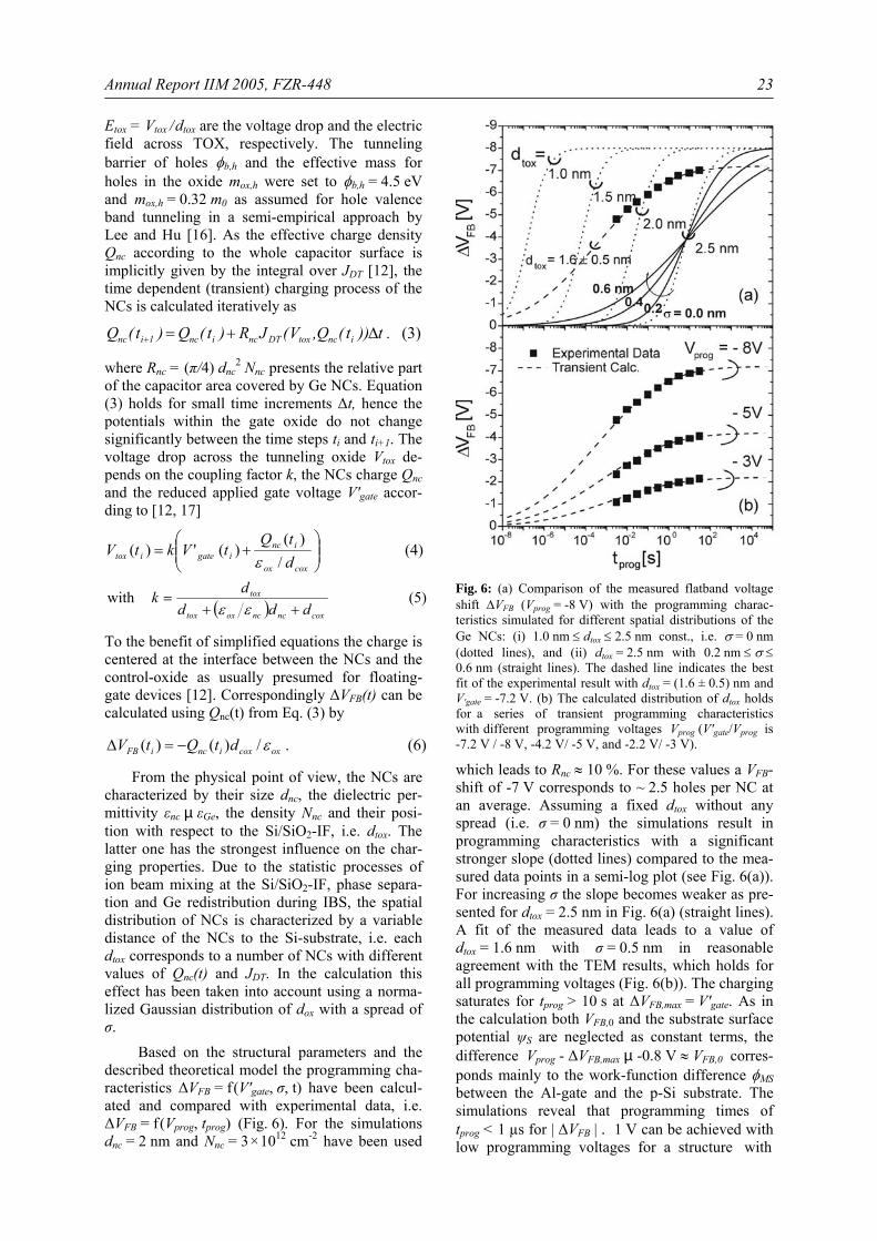
Based on the structural parameters and the described theoretical model the programming cha-racteristics ∆VFB = f (V'gate, σ, t) have been calcul-ated and compared with experimental data, i.e. ∆VFB = f (Vprog, tprog) (Fig. 6). For the simulations dnc = 2 nm and Nnc = 3 × 1012 cm-2 have been used
Fig. 6: (a) Comparison of the measured flatband voltage shift ∆VFB (Vprog = -8 V) with the programming charac-teristics simulated for different spatial distributions of the Ge NCs: (i) 1.0 nm ≤ dtox ≤ 2.5 nm const., i.e. σ = 0 nm (dotted lines), and (ii) dtox = 2.5 nm with 0.2 nm ≤ σ ≤ 0.6 nm (straight lines). The dashed line indicates the best fit of the experimental result with dtox = (1.6 ± 0.5) nm and V'gate = -7.2 V. (b) The calculated distribution of dtox holds for a series of transient programming characteristics with different programming voltages Vprog (V'gate/Vprog is -7.2 V / -8 V, -4.2 V/ -5 V, and -2.2 V/ -3 V).
which leads to Rnc ≈ 10 %. For these values a VFB-shift of -7 V corresponds to ~ 2.5 holes per NC at an average. Assuming a fixed dtox without any spread (i.e. σ = 0 nm) the simulations result in programming characteristics with a significant stronger slope (dotted lines) compared to the mea-sured data points in a semi-log plot (see Fig. 6(a)). For increasing σ the slope becomes weaker as pre-sented for dtox = 2.5 nm in Fig. 6(a) (straight lines). A fit of the measured data leads to a value of dtox = 1.6 nm with σ = 0.5 nm in reasonable agreement with the TEM results, which holds for all programming voltages (Fig. 6(b)). The charging saturates for tprog > 10 s at ∆VFB,max = V'gate. As in the calculation both VFB,0 and the substrate surface potential ψS are neglected as constant terms, the difference Vprog - ∆VFB,max • -0.8 V ≈ VFB,0 corres-ponds mainly to the work-function difference φMS between the Al-gate and the p-Si substrate. The simulations reveal that programming times of tprog < 1 µs for | ∆VFB | . 1 V can be achieved with low programming voltages for a structure with
V. Beyer et al.; A Transient Electrical Model …
24
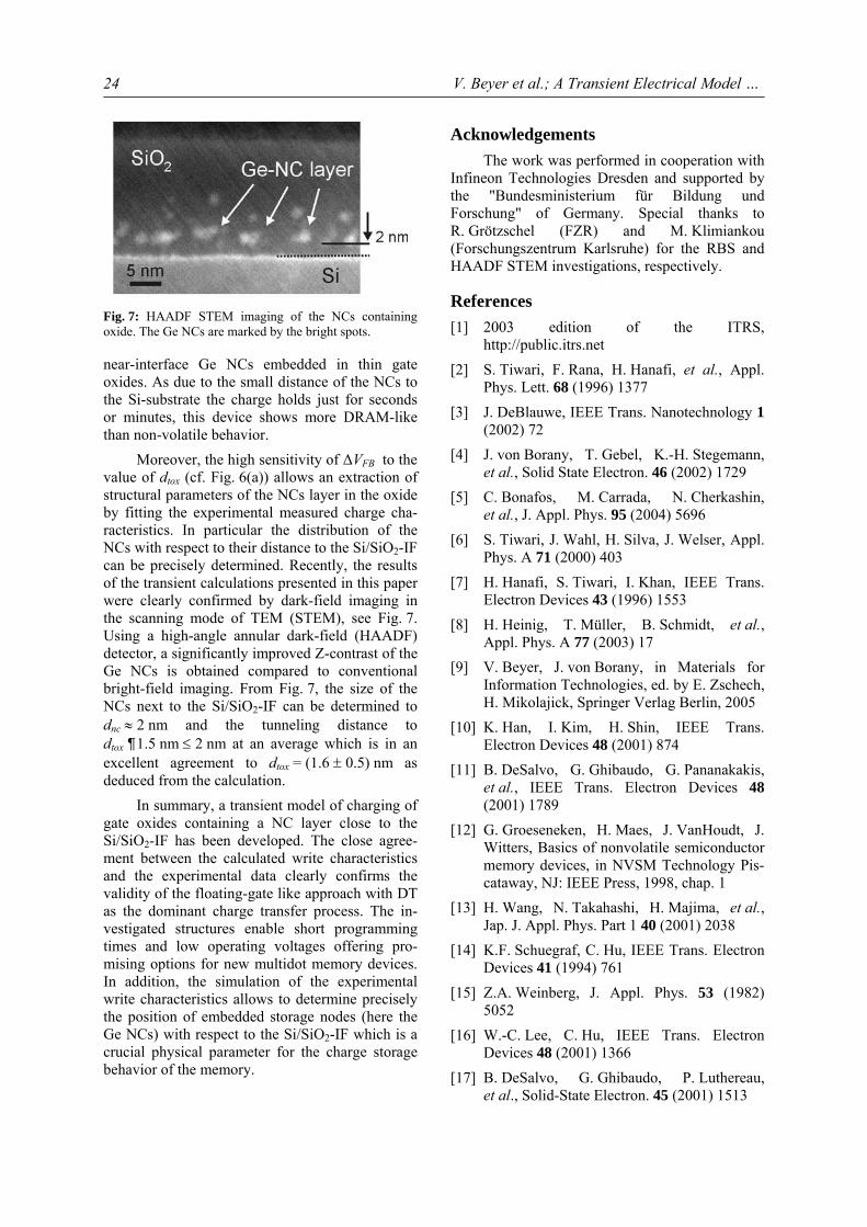
Fig. 7: HAADF STEM imaging of the NCs containing oxide. The Ge NCs are marked by the bright spots.
near-interface Ge NCs embedded in thin gate oxides. As due to the small distance of the NCs to the Si-substrate the charge holds just for seconds or minutes, this device shows more DRAM-like than non-volatile behavior.
Moreover, the high sensitivity of ∆VFB to the value of dtox (cf. Fig. 6(a)) allows an extraction of structural parameters of the NCs layer in the oxide by fitting the experimental measured charge cha-racteristics. In particular the distribution of the NCs with respect to their distance to the Si/SiO2-IF can be precisely determined. Recently, the results of the transient calculations presented in this paper were clearly confirmed by dark-field imaging in the scanning mode of TEM (STEM), see Fig. 7. Using a high-angle annular dark-field (HAADF) detector, a significantly improved Z-contrast of the Ge NCs is obtained compared to conventional bright-field imaging. From Fig. 7, the size of the NCs next to the Si/SiO2-IF can be determined to dnc ≈ 2 nm and the tunneling distance to dtox –1.5 nm ≤ 2 nm at an average which is in an excellent agreement to dtox = (1.6 ± 0.5) nm as deduced from the calculation.
In summary, a transient model of charging of gate oxides containing a NC layer close to the Si/SiO2-IF has been developed. The close agree-ment between the calculated write characteristics and the experimental data clearly confirms the validity of the floating-gate like approach with DT as the dominant charge transfer process. The in-vestigated structures enable short programming times and low operating voltages offering pro-mising options for new multidot memory devices. In addition, the simulation of the experimental write characteristics allows to determine precisely the position of embedded storage nodes (here the Ge NCs) with respect to the Si/SiO2-IF which is a crucial physical parameter for the charge storage behavior of the memory.
Acknowledgements The work was performed in cooperation with
Infineon Technologies Dresden and supported by the "Bundesministerium für Bildung und Forschung" of Germany. Special thanks to R. Grötzschel (FZR) and M. Klimiankou (Forschungszentrum Karlsruhe) for the RBS and HAADF STEM investigations, respectively.
References [1] 2003 edition of the ITRS,
http://public.itrs.net [2] S. Tiwari, F. Rana, H. Hanafi, et al., Appl.
Phys. Lett. 68 (1996) 1377 [3] J. DeBlauwe, IEEE Trans. Nanotechnology 1
(2002) 72 [4] J. von Borany, T. Gebel, K.-H. Stegemann,
et al., Solid State Electron. 46 (2002) 1729 [5] C. Bonafos, M. Carrada, N. Cherkashin,
et al., J. Appl. Phys. 95 (2004) 5696 [6] S. Tiwari, J. Wahl, H. Silva, J. Welser, Appl.
Phys. A 71 (2000) 403 [7] H. Hanafi, S. Tiwari, I. Khan, IEEE Trans.
Electron Devices 43 (1996) 1553 [8] H. Heinig, T. Müller, B. Schmidt, et al.,
Appl. Phys. A 77 (2003) 17 [9] V. Beyer, J. von Borany, in Materials for
Information Technologies, ed. by E. Zschech, H. Mikolajick, Springer Verlag Berlin, 2005
[10] K. Han, I. Kim, H. Shin, IEEE Trans. Electron Devices 48 (2001) 874
[11] B. DeSalvo, G. Ghibaudo, G. Pananakakis, et al., IEEE Trans. Electron Devices 48 (2001) 1789
[12] G. Groeseneken, H. Maes, J. VanHoudt, J. Witters, Basics of nonvolatile semiconductor memory devices, in NVSM Technology Pis-cataway, NJ: IEEE Press, 1998, chap. 1
[13] H. Wang, N. Takahashi, H. Majima, et al., Jap. J. Appl. Phys. Part 1 40 (2001) 2038
[14] K.F. Schuegraf, C. Hu, IEEE Trans. Electron Devices 41 (1994) 761
[15] Z.A. Weinberg, J. Appl. Phys. 53 (1982) 5052
[16] W.-C. Lee, C. Hu, IEEE Trans. Electron Devices 48 (2001) 1366
[17] B. DeSalvo, G. Ghibaudo, P. Luthereau, et al., Solid-State Electron. 45 (2001) 1513
Annual Report IIM 2005, FZR-448
25
Light Emission and Charge Trapping in Er Doped Silicon Dioxide Films Containing Silicon Nanocrystals
A. Nazarov1, J.M. Sun, I.N. Osiyuk1, I.P. Tjagulskii1, V.S. Lysenko1, W. Skorupa, R.A. Yankov and T. Gebel2
1Institute of Semiconductor Physics, National Academy of Sciences of Ukraine Prospekt Nauki 45, 03028 Kyiv, Ukraine
2nanoparc GmbH, Bautzner Landstrasse 45, D-01454 Dresden – Rossendorf, Germany
Er implanted SiO2 films have recently attracted considerable interest due to the possibility of making EL devices that operate at a wavelength of 1.54 µm, i.e. within the range of optical transparency of quartz optical fibers [1, 2]. The fabrication of such light emitting devices is fully compatible with Si based integrated circuit (IC) technology, thus permitting their integration into advanced Si ICs. Critical issues of the device performance are the relatively low emission efficiencies and the low currents that can be passed through the dielectric. It has been shown in a number of studies that the introduction of Si nanocrystals into Er-doped SiO2 enables the intensity of the PL at 1.54 µm to be largely increased [3-5] while causing concurrently a somewhat reduced EL intensity [6]. However, the mechanism of attenuation of the Er associated EL at 1.54 µm after introducing Si nanoclusters into the SiO2 matrix has not been elucidated. The present work provides new insights into the relationship between light emission efficiency and charge trapping in Er doped SiO2 containing Si nanoclusters. The influence of the Si nanocluster density on both the capture of charge carriers at traps associated with the presence of Er and the resulting PL and EL at 1.54 µm is examined for the first time.
Si wafers with a 200 nm thick thermally grown SiO2 film were used in the study. The depth profiles of the implanted Si+ and Er+ ions were calculated using TRIM 98 as a first approximation. Si+ ions were implanted at two implantation ener-gies of 35 and 80 keV, which generated a fairly flat-topped profile of 1.1 to 15 at.% excess silicon atoms over a depth region of 65 to 150 nm. After annealing at 1100°C in an N2 ambient for 1 h necessary to form Si nanocrystals, Er+ ions were implanted at 280 keV with a dose of 1 × 1015 cm-2 in such a way as to position the peak of their distribution about the central part of the Si clusters profile. Finally, the samples were annealed at 850°C in an ambient of N2 for 30 min to reduce the amount of the implantation induced damage
and activate the implanted Er3+ centers. The top electrodes were 100 nm indium-tin-oxide (ITO) layers patterned into circular dots with a diameter of 0.05 to 1.00 mm.
The formation of Si nanoclusters and Er3+ centers were monitored by PL measurements over the wavelength range of 600 to 900 nm and at 1535 nm using the 532 nm line of a Nd:YAG laser and the 633 nm line of a He-Ne laser with a power of 5 mW as the excitation sources, respectively. Measurements of the EL and charge trapping were carried out in a high field, constant current inject-ion regime. Charge traps were studied over a wide range of cross sections using three levels of injected constant current density, namely 1 × 10⁻⁷, 2 × 10⁻⁵ and 5 × 10⁻⁴ A cm-2, with the last value of the current density being typical of the regime of EL excitation. During the current injection, nega-tive (or positive) charges were trapped within the oxide layer, which caused a decrease (or increase) in the electric field distribution at the Si/SiO2 interface. In order to maintain a constant current injection, one needs to shift the applied voltage as the trapped charges change. Charge trapping pro-cesses were studied under conditions of electron injection from the Si substrate into the oxide by measuring the shift of the applied voltage with the injected charge Qinj. The absolute value of the net trapped charge was calibrated using the shift of the flat band voltage, ∆VFB, extracted from the high frequency (1 MHz) capacitance-voltage (C-V) characteristics after injecting an electron charge of 1 × 10¹³ e/cm2.
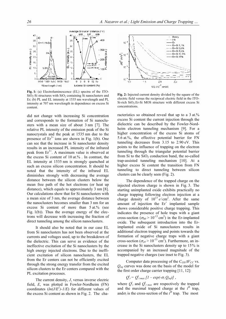
Figure 1(a) shows EL spectra measured over the wavelength range of 1450 to 1650 nm in Er implanted structures containing Si nanocrystals of different density. The peak at 1535 nm, which is characteristic of the intra-transition of the electron in the Er+3 ion from the excited 4I15/2 state to the ground state, is clearly seen. A broad PL peak centered at 700 nm was observed as a result of the introduction into the oxide of an excess of Si atoms above 3 at.%. The position of the PL peak
A. Nazarov et al.; Light Emission and Charge Trapping …
26
Fig. 1: (a) Electroluminescence (EL) spectra of the ITO-SiO2-Si structures with SiO2 containing Si nanoclusters and Er; (b) PL and EL intensity at 1535 nm wavelength and PL intensity at 707 nm wavelength in dependence on excess Si content.
did not change with increasing Si concentration and corresponds to the formation of Si nanoclu-sters with a mean size of about 3 nm [7]. The relative PL intensity of the emission peak of the Si nanocrystals and the peak at 1535 nm due to the presence of Er3+ ions are shown in Fig. 1(b). One can see that the increase in Si nanocluster density results in an increased PL intensity of the infrared peak from Er3+. A maximum value is observed at the excess Si content of 10 at.% . In contrast, the EL intensity at 1535 nm is strongly quenched at such an excess silicon concentration. It should be noted that the intensity of the infrared EL diminishes strongly with decreasing the average distance between the silicon clusters below the mean free path of the hot electrons (or heat up distance), which equals to approximately 3 nm [8]. Our calculations show that for Si nanoclusters with a mean size of 3 nm, the average distance between the nanoclusters becomes smaller than 3 nm for an excess Si content of more than 5 at.% (see Fig. 1(b)). Thus the average energy of the elec-trons will decrease with increasing the fraction of direct tunneling among the silicon nanoclusters.
It should also be noted that in our case EL from Si nanoclusters has not been observed at the currents and voltages used, up to the breakdown of the dielectric. This can serve as evidence of the ineffective excitation of the Si nanoclusters by the high energy injected electrons. Due to the ineffi-cient excitation of silicon nanoclusters, the EL from the Er centers can not be efficiently excited through the strong energy transfer from the excited silicon clusters to the Er centers compared with the PL excitation processes.
The current density, J, versus inverse electric field, E, was plotted in Fowler-Nordheim (FN) coordinates (ln(J/E2)-1/E) for different values of the excess Si content as shown in Fig. 2. The cha-
Fig. 2: Injected current density divided by the square of the electric field versus the reciprocal electric field in the ITO-Si-rich SiO2:Er-Si MOS structure with different excess Si concentrations.
racteristics so obtained reveal that up to a 3 at.% excess Si content the current injection through the dielectric can be described by the Fowler-Nord-heim electron tunneling mechanism [9]. For a higher concentration of the excess Si atoms of 5.6 at.%, the effective potential barrier for FN tunneling decreases from 3.15 to 2.90 eV. This points to the influence of trapping on the electron tunneling through the triangular potential barrier from Si to the SiO2 conduction band, the so-called trap-assisted tunneling mechanism [10]. At a higher excess Si content the transition from FN tunneling to direct tunneling between silicon clusters can be clearly seen (Fig. 2).
The dependence of the trapped charge on the injected electron charge is shown in Fig. 3. The starting unimplanted oxide exhibits practically no charge trapping following electron injection at a charge density of 1013 e / cm2. After the same amount of injection the Er+ implanted sample shows considerable positive charge trapping. This indicates the presence of hole traps with a giant cross-section (σh0 > 10-13 cm2) in the Er-implanted oxide. The subsequent introduction into the Er-implanted oxide of Si nanoclusters results in additional electron trapping and points towards the formation of negative charge traps with a giant cross-section (σe0 > 10-13 cm2). Furthermore, an in-crease in the Si nanoclusters density up to 15 % is accompanied by an increased magnitude of the trapped negative charges (see inset to Fig. 3).
Computer data processing of the COX∆VCC vs. Qinj curves was done on the basis of the model for the first order charge carrier trapping [11, 12]:
Qit = Qi
t max [1 – exp(-σi Qinj)] , where Qi
t and Qit max are respectively the trapped
and the maximal trapped charge at the ith trap, andσi is the cross-section of the ith trap. The most
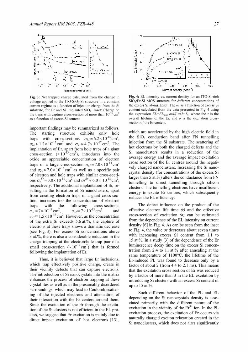
Annual Report IIM 2005, FZR-448
27
Fig. 3: Net trapped charge calculated from the change in voltage applied to the ITO-SiO2-Si structure in a constant current regime as a function of injection charge from the Si substrate, for Er and Si implanted SiO2. Inset: Charge on the traps with capture cross-section of more than 10-13 cm2 as a function of excess Si content.
important findings may be summarized as follows. The starting structure exhibits only hole traps with cross-sections σh1 ≈
6.2 × 10⁻¹⁵ cm2, σh2 ≈
1.2 × 10⁻¹⁵ cm2 and σh3 ≈ 4.7 × 10⁻¹⁷ cm2. The
implantation of Er, apart from hole traps of a giant cross-section (> 10-13 cm2), introduces into the oxide an appreciable concentration of electron traps of a large cross-section σe1 ≈
7.0 × 10⁻¹⁴ cm2 and σe2 ≈
7.0 × 10⁻¹⁵ cm2 as well as a specific pair of electron and hole traps with similar cross-secti-ons σe
Er ≈ 3.0 × 10⁻¹⁸ cm2 and σhEr ≈ 6.0 × 10⁻¹⁸ cm2,
respectively. The additional implantation of Si, re-sulting in the formation of Si nanoclusters, apart from creating electron traps of a giant cross-sec-tion, increases too the concentration of electron traps with the following cross-sections: σe1 ≈ 7 × 10-14 сm2, σe2 ≈ 7 × 10-15 сm2 and σe3 ≈ 1.5 × 10⁻¹⁵ сm2. However, as the concentration of the extra Si exceeds 5.6 at.%, the capture of electrons at these traps shows a dramatic decrease (see Fig. 3). For excess Si concentrations above 3 at.%, there is also a considerable reduction in the charge trapping at the electron/hole trap pair of a small cross-section (∼ 10-18 cm2) that is formed following the implantation of Er.
Thus, it is believed that large Er inclusions, which trap effectively positive charge, create in their vicinity defects that can capture electrons. The introduction of Si nanocrystals into the matrix enhances the process of electron trapping at these crystallites as well as in the presumably disordered surroundings, which may lead to Coulomb scatter-ing of the injected electrons and attenuation of their interaction with the Er centers around them. Since the excitation of the Er through the excita-tion of the Si clusters is not efficient in the EL pro-cess, we suggest that Er excitation is mainly due to direct impact excitation of hot electrons [13],
Fig. 4: EL intensity vs. current density for an ITO-Si-rich SiO2:Er-Si MOS structure for different concentrations of the excess Si atoms. Inset: The στ as a function of excess Si content calculated from the data presented in Fig. 4 using the expression EL=ELmax στJ/( στJ+1), where the τ is the overall lifetime of the Er, and σ is the excitation cross-section of the Er centers.
which are accelerated by the high electric field in the SiO2 conduction band after FN tunnelling injection from the Si substrate. The scattering of hot electrons by both the charged defects and the Si nanoclusters results in a reduction of the average energy and the average impact excitation cross section of the Er centres around the negati-vely charged nanoclusters. Increasing the Si nano-crystal density (for concentrations of the excess Si larger than 5 at.%) alters the conductance from FN tunnelling to direct tunnelling through silicon clusters. The tunnelling electrons have insufficient energy to excite Er centres, which subsequently reduces the EL efficiency.
The defect influence on the product of the effective electron life time (τ) and the effective cross-section of excitation (σ) can be estimated from the dependence of the EL intensity on current density [6] in Fig. 4. As can be seen from the inset to Fig. 4, the value στ decreases about seven times with increasing excess Si content from 1.1 to 15 at.%. In a study [3] of the dependence of the Er luminescence decay time on the excess Si concen-tration from 2.4 to 11 at.% after annealing at the same temperature of 1100°C, the lifetime of the Er-induced PL was found to decrease only by a factor of about 2 (from 4.4 to 2.1 ms). This means that the excitation cross section of Er was reduced by a factor of more than 3 in the EL excitation by introducing Si clusters with an excess Si content of up to 15 at.%.
Such different behavior of the PL and EL depending on the Si nanocrystals density is asso-ciated primarily with the different nature of the excitation in the vicinity of the Er3+ ion. In the PL excitation process, the excitation of Er occurs via naturally charged exciton relaxation created in the Si nanoclusters, which does not alter significantly
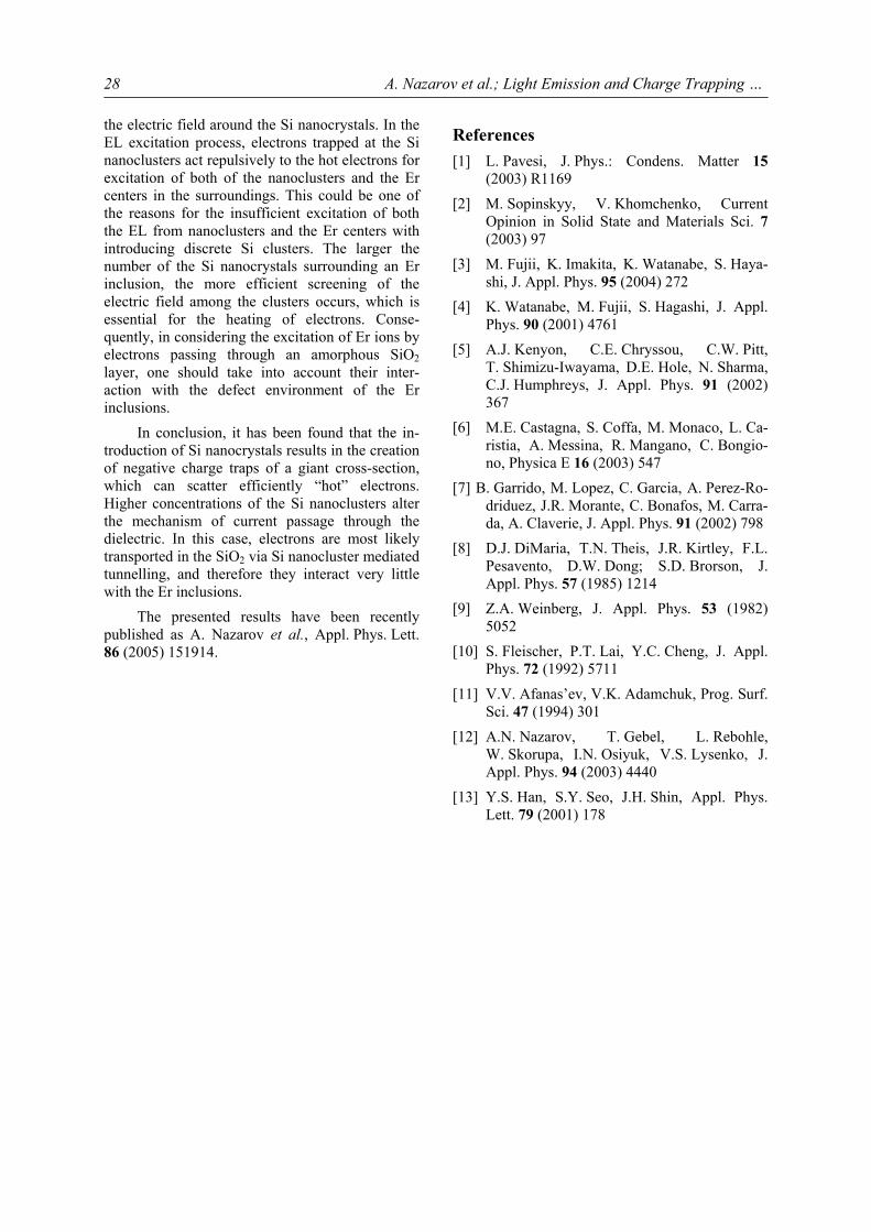
A. Nazarov et al.; Light Emission and Charge Trapping …
28
the electric field around the Si nanocrystals. In the EL excitation process, electrons trapped at the Si nanoclusters act repulsively to the hot electrons for excitation of both of the nanoclusters and the Er centers in the surroundings. This could be one of the reasons for the insufficient excitation of both the EL from nanoclusters and the Er centers with introducing discrete Si clusters. The larger the number of the Si nanocrystals surrounding an Er inclusion, the more efficient screening of the electric field among the clusters occurs, which is essential for the heating of electrons. Conse-quently, in considering the excitation of Er ions by electrons passing through an amorphous SiO2 layer, one should take into account their inter-action with the defect environment of the Er inclusions.
In conclusion, it has been found that the in-troduction of Si nanocrystals results in the creation of negative charge traps of a giant cross-section, which can scatter efficiently “hot” electrons. Higher concentrations of the Si nanoclusters alter the mechanism of current passage through the dielectric. In this case, electrons are most likely transported in the SiO2 via Si nanocluster mediated tunnelling, and therefore they interact very little with the Er inclusions.
The presented results have been recently published as A. Nazarov et al., Appl. Phys. Lett. 86 (2005) 151914.
References [1] L. Pavesi, J. Phys.: Condens. Matter 15
(2003) R1169 [2] M. Sopinskyy, V. Khomchenko, Current
Opinion in Solid State and Materials Sci. 7 (2003) 97
[3] M. Fujii, K. Imakita, K. Watanabe, S. Haya-shi, J. Appl. Phys. 95 (2004) 272
[4] K. Watanabe, M. Fujii, S. Hagashi, J. Appl. Phys. 90 (2001) 4761
[5] A.J. Kenyon, C.E. Chryssou, C.W. Pitt, T. Shimizu-Iwayama, D.E. Hole, N. Sharma, C.J. Humphreys, J. Appl. Phys. 91 (2002) 367
[6] M.E. Castagna, S. Coffa, M. Monaco, L. Ca-ristia, A. Messina, R. Mangano, C. Bongio-no, Physica E 16 (2003) 547
[7] B. Garrido, M. Lopez, C. Garcia, A. Perez-Ro-driduez, J.R. Morante, C. Bonafos, M. Carra-da, A. Claverie, J. Appl. Phys. 91 (2002) 798
[8] D.J. DiMaria, T.N. Theis, J.R. Kirtley, F.L. Pesavento, D.W. Dong; S.D. Brorson, J. Appl. Phys. 57 (1985) 1214
[9] Z.A. Weinberg, J. Appl. Phys. 53 (1982) 5052
[10] S. Fleischer, P.T. Lai, Y.C. Cheng, J. Appl. Phys. 72 (1992) 5711
[11] V.V. Afanas’ev, V.K. Adamchuk, Prog. Surf. Sci. 47 (1994) 301
[12] A.N. Nazarov, T. Gebel, L. Rebohle, W. Skorupa, I.N. Osiyuk, V.S. Lysenko, J. Appl. Phys. 94 (2003) 4440
[13] Y.S. Han, S.Y. Seo, J.H. Shin, Appl. Phys. Lett. 79 (2001) 178
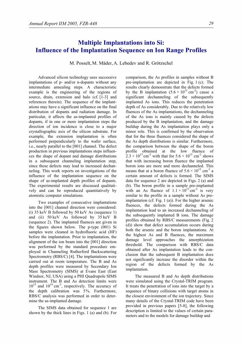
Annual Report IIM 2005, FZR-448
29
Multiple Implantations into Si: Influence of the Implantation Sequence on Ion Range Profiles
M. Posselt, M. Mäder, A. Lebedev and R. Grötzschel
Advanced silicon technology uses successive implantations of p- and/or n-dopants without any intermediate annealing steps. A characteristic example is the engineering of the regions of source, drain, extension and halo (cf. [1-3] and references therein). The sequence of the implant-ations may have a significant influence on the final distribution of dopants and radiation damage. In particular, it affects the as-implanted profiles of dopants, if in one or more implantation steps the direction of ion incidence is close to a major crystallographic axis of the silicon substrate. For example, the extension implantation is often performed perpendicularly to the wafer surface, i.e., nearly parallel to the [001] channel. The defect production in previous implantations steps influen-ces the shape of dopant and damage distributions in a subsequent channeling implantation step, since these defects may lead to increased dechan-neling. This work reports on investigations of the influence of the implantation sequence on the shape of as-implanted depth profiles of dopants. The experimental results are discussed qualitati-vely and can be reproduced quantitatively by atomistic computer simulations.
Two examples of consecutive implantations into the [001] channel direction were considered: (i) 35 keV B followed by 50 keV As (sequence 1) and (ii) 50 keV As followed by 35 keV B (sequence 2). The implanted fluences are given in the figures shown below. The p-type (001) Si samples were cleaned in hydrofluoric acid (HF) before the implantation. Prior to implantation, the alignment of the ion beam into the [001] direction was performed by the standard procedure em-ployed in Channeling Rutherford Backscattering Spectrometry (RBS/C) [4]. The implantations were carried out at room temperature. The B and As depth profiles were measured by Secondary Ion Mass Spectrometry (SIMS) at Evans East (East Windsor, NJ, USA) using a PHI Quadrupole SIMS instrument. The B and As detection limits were 1015 and 1014 cm-3, respectively. The accuracy of the depth calibration was 5 %. Furthermore, RBS/C analysis was performed in order to deter-mine the as-implanted damage.
The SIMS data obtained for sequence 1 are shown by the thick lines in Figs. 1 (a) and (b). For
comparison, the As profiles in samples without B pre-implantation are depicted in Fig. 1 (c). The results clearly demonstrate that the defects formed by the B implantation (5.6 × 1015 cm-2) cause a significant dechanneling of the subsequently implanted As ions. This reduces the penetration depth of As considerably. Due to the relatively low fluences of the As implantations, the dechanneling of the As ions is mainly caused by the defects produced by the B implantation, and the damage buildup during the As implantation plays only a minor role. This is confirmed by the observation that for the three fluences considered the shape of the As depth distributions is similar. Furthermore, the comparison between the shape of the boron profile obtained at the low fluence of 2.3 × 1013 cm-2 with that for 5.6 × 1015 cm-2 shows that with increasing boron fluence the implanted boron ions are more and more dechanneled. This means that at a boron fluence of 5.6 × 1015 cm-2 a certain amount of defects is formed. The SIMS data for sequence 2 are depicted in Figs. 2 (a) and (b). The boron profile in a sample pre-implanted with an As fluence of 1.1 × 1013 cm-2 is very similar to the profile in a sample without As pre-implantation (cf. Fig. 1 (a)). For the higher arsenic fluences, the defects formed during the As implantation lead to an increased dechanneling of the subsequently implanted B ions. The damage profiles obtained by RBS/C measurements (Fig. 2 (d)) show that defect accumulation occurs during both the arsenic and the boron implantations. At the highest As and B fluences, the maximum damage level approaches the amorphization threshold. The comparison with RBS/C data obtained after As implantation leads to the con-clusion that the subsequent B implantation does not significantly increase the disorder within the region of the defects formed by the As implantation.
The measured B and As depth distributions were simulated using the Crystal-TRIM program. It treats the penetration of ions into the target by a sequence of binary collisions with target atoms in the closest environment of the ion trajectory. Since many details of the Crystal-TRIM code have been provided in previous papers [5-8], the following description is limited to the values of certain para-meters and to the models for damage buildup and
M. Posselt et al.; Multiple Implantations into Si …
30
depth (nm)
conc
entr
atio
n(c
m-3
)
1016
1017
1018
1019
1020
1021
(a) 5.6x1015 cm-2
2.3x1013 cm-2
1014
1015
1016
1017
1018
1019
(b)
1.3x1011 cm-2
1.0x1012 cm-2
1.0x1013 cm-2
0 100 200 300 400 5001014
1015
1016
1017
1018
1019
(c)
8.1x1010 cm-2
1.2x1013 cm-2
1.2x1012 cm-2
Fig. 1: Implantation sequence 1: 35 keV B (5.6 × 1015 cm-2) followed by 50 keV As (1.3 × 10¹¹, 1.0 × 10¹², 1.0 × 10¹³
cm-2). In (a) and (b) the thick lines show the B and As depth distributions measured by SIMS, respectively. The B profile in (a) was determined after the first implantation step. For comparison, the measured As depth profiles in samples without B pre-implantation are also given (c). In (a) the thin line shows SIMS data obtained after B implantation at 2.3 × 1013 cm-2. The histograms depict the results of computer simulations.
dynamic annealing. The thickness of the native oxide layer on the (001) Si sample was set to 0.5 nm, i.e., smaller than the default value of 1.5 nm. This assumption is justified due to the HF cleaning procedure before the implantation. The parameters Cλ and Cel used in the model for the electronic energy loss of an incident ion in a collision with a target atom [5] have the following values: Cλ = 1.01, Cel = 1.1 for B and Cλ = 0.9, Cel = 1.57 for As. The first parameter is employed to calculate the electronic energy loss averaged over all impact parameters, using the ZBL electronic stopping cross-section [9]. The second parameter describes the impact-parameter depen-dence of the electronic energy loss in a modified Oen-Robinson model [10].
The Crystal-TRIM code simulates only the ballistic processes during ion bombardment, but
not the subsequent relaxation processes which are responsible for the formation of the as-implanted defect structure. Therefore, a phenomenological description is used to treat the influence of defect production on the trajectories of the implanted ions [7, 8]. It is based on results of molecular dynamics simulations and on experimental investigations. The fundamental quantities of the model are the nuclear energy deposition per target atom En
A and the probability pd that the implanted ion collides with an atom of a damaged region. The first quan-tity can be determined exactly by the consideration of the ballistic processes. It increases monotonic-ally throughout the implantation since each implanted ion contributes to the nuclear energy deposition. The second quantity describes the damage level in the target and depends on En
A, the ion species, the target temperature and the incident ion flux. En
A and pd are local quantities, i.e., their values may vary in dependence on the considered volume element of the target. The collision of the ion with atoms in a damaged region is treated in the same manner as projectile-target collisions in an amorphous target. This is a simplifying assumption about the nature of the defects formed during ion implantation. Molecular dynamics simulations showed that the as-implanted defect structure depends on the ion mass [11, 12]. The implantation of heavy ions leads to dense collision cascades. Therefore, after the fast relaxation of the ballistic disorder a considerable number of complex defects may be formed. Some of them are small amorphous regions or amorphous pockets, as assumed in the simplified damage model. On the other hand, light ion implantation with a compara-ble local nuclear energy deposition per atom yields a smaller percentage of complex defects since the collision cascades are more dilute. Temperature and ion flux influence the dynamic annealing during the ion bombardment [13, 7, 8]. The phenomenological description used in Crystal-TRIM considers two simple but extreme cases: (i) the damage buildup and (ii) the dynamic annealing (cf. [7], equations (1) and (2)). In both cases, for low values of En
A the damage probability pd grows linearly with En
A. In the damage buildup model the local region is amorphized (pd = 1), if pd exceeds the threshold pt (pt ≤ 1). If dynamic annealing prevails, the local damage saturates at a constant level pS (pS ≤ 1) when pd exceeds pS. The model parameters, i.e., the parameter Ca which charac-terizes the linear increase, and the threshold pt or pS, depend on the ion species, the target temperature and the ion flux. In the present work the damage accumulation model is applied to simulate the As implantation (Ca = 10.67 meV-1, pt = 0.12), whereas the dynamic annealing model is used for the B implantation (Ca = 1.6 meV-1,
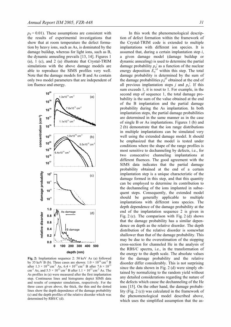
Annual Report IIM 2005, FZR-448
31
pS = 0.01). These assumptions are consistent with the results of experimental investigations that show that at room temperature the defect forma-tion by heavy ions, such as As, is dominated by the damage buildup, whereas for light ions, such as B, the dynamic annealing prevails [13, 14]. Figures 1 (a), 1 (c), and 2 (a) illustrate that Crystal-TRIM simulations with the above damage models are able to reproduce the SIMS profiles very well. Note that the damage models for B and As contain only two model parameters that are independent of ion fluence and energy.
conc
entr
atio
n(c
m-3
)
1016
1017
1018
1019
1020
1.1x1013 cm-2
7.6x1013 cm-2
1.3x1014 cm-2 (a)
1017
1018
1019
1020
1021 (b)
5.5x1015 cm-2
6.4x1015 cm-2
1.0x1016 cm-2
depth (nm)
0 100 200 300 400 5000.0
0.2
0.4
0.6
0.8
1.0(d)As damage
B damage
rela
tive
diso
rder
10-3
10-2
10-1
100(c)
dam
age
prob
abilt
y
Fig. 2: Implantation sequence 2: 50 keV As (a) followed by 35 keV B (b). Three cases are shown: 1.0 × 1016 cm-2 B after 1.3 × 1014 cm-2 As, 6.4 × 1015 cm-2 B after 7.6 × 10¹³
cm-2 As, and 5.5 × 1015 cm-2 B after 1.1 × 1013 cm-2 As. The As profiles in (a) were measured after the first implantation step. Continuous lines and histograms depict SIMS data and results of computer simulations, respectively. For the three cases given above, the thick, the thin and the dotted lines show the depth dependence of the damage probability (c) and the depth profiles of the relative disorder which was determined by RBS/C (d).
In this work the phenomenological descrip-tion of defect formation within the framework of the Crystal-TRIM code is extended to multiple implantations with different ion species. It is assumed that, during a certain implantation step i, a given damage model (damage buildup or dynamic annealing) is used to determine the partial damage probability pd
i as a function of the nuclear energy deposition En
iA within this step. The total damage probability is determined by the sum of the damage probabilities pd
jE obtained at the end of all previous implantation steps j and pd
i. If this sum exceeds 1, it is reset to 1. For example, in the second step of sequence 1, the total damage pro-bability is the sum of the value obtained at the end of the B implantation and the partial damage probability during the As implantation. In both implantation steps, the partial damage probabilities are determined in the same manner as in the case of single B or As implantations. Figures 1 (b) and 2 (b) demonstrate that the ion range distributions in multiple implantations can be simulated very well using the extended damage model. It should be emphasized that the model is tested under conditions where the shape of the range profiles is most sensitive to dechanneling by defects, i.e., for two consecutive channeling implantations at different fluences. The good agreement with the SIMS data indicates that the partial damage probability obtained at the end of a certain implantation step is a unique characteristic of the damage formed in this step, and that this quantity can be employed to determine its contribution to the dechanneling of the ions implanted in subse-quent steps. Consequently, the extended model should be generally applicable to multiple implantations with different ions species. The depth dependence of the damage probability at the end of the implantation sequence 2 is given in Fig. 2 (c). The comparison with Fig. 2 (d) shows that the damage probability has a similar depen-dence on depth as the relative disorder. The depth distribution of the relative disorder is somewhat shallower than that of the damage probability. This may be due to the overestimation of the stopping cross-section for channeled He in the analysis of the RBS/C spectra, i.e., in the transformation of the energy to the depth scale. The absolute values for the damage probability and the relative disorder differ considerably. This is not surprising since the data shown in Fig. 2 (d) were simply ob-tained by normalizing to the random yield without any detailed considerations regarding the nature of the defects which cause the dechanneling of the He ions [15]. On the other hand, the damage probabi-lity (Fig. 2 (c)) was calculated in the framework of the phenomenological model described above, which uses the simplified assumption that the as-
M. Posselt et al.; Multiple Implantations into Si …
32
implanted defect structure consists of amorphous pockets. These defects have a strong influence on the ion trajectories so that a small damage pro-bability suffices to cause significant dechanneling.
Acknowledgements The authors thank Dr. M.S. Denker (Evans
East) for the SIMS analysis and for valuable com-ments.
The present results have been recently published as M. Posselt et al., Appl. Phys. Lett. 87 (2005) 043109.
References [1] P.M. Zeitzoff, in: Semiconductor Fabtech,
10th Edition, Henley Publishing, London, 1999, p. 275
[2] T. Ghani, K. Mistry, P. Packan, M. Arm-strong, S. Thompson, S. Tyagi, M. Bohr, Symp. VLSI Tech. Dig., 2001, p. 17
[3] D. Onimatsu, K. Shibahara, in: Extended Ab-stracts, Int. Conf. on Solid State Devices and Materials, Tokyo, 2001, p. 184
[4] W.-K. Chu, J.W. Mayer, M.-A. Nicolet, Backscattering Spectrometry, Academic Press, New York, 1978
[5] M. Posselt, Radiat. Eff. Defects Solids 130/131 (1994) 87
[6] M. Posselt, B. Schmidt, C.S. Murthy, T. Feu-del, K. Suzuki, J. Electrochem. Soc. 144 (1997) 1495
[7] M. Posselt, L. Bischoff, J. Teichert, Appl. Phys. Lett. 79 (2001) 1444
[8] M. Posselt, L. Bischoff, J. Teichert, A. Ster, J. Appl. Phys. 93 (2003) 1004
[9] J.F. Ziegler, J.P. Biersack, U. Littmark, The Stopping and Range of Ions in Solids, Per-gamon Press, New York, 1985
[10] O.S. Oen, M.T. Robinson, Nucl. Instr. Meth. 132 (1976) 647
[11] M.-J. Caturla, T. Diaz de la Rubia, L.A. Mar-ques, G.H. Gilmer, Phys. Rev. B 54 (1996) 16683
[12] M. Posselt, Mater. Res. Soc. Symp. Proc. 647 (2001), O2.1.1
[13] R.D. Goldberg, J.S. Williams, R.G. Elliman, Nucl. Instr. Meth. B 106 (1995) 242
[14] F.F. Morehead, Jr., B.L. Crowder, Radiat. Eff. 6 (1970) 27
[15] J.R. Tesmer, M. Nastasi, J.C. Barbour, C.J. Maggiore, J.W. Mayer (Editors), Handbook of Modern Ion Beam Material Analysis, Materials Research Society, Pittsburgh, 1995
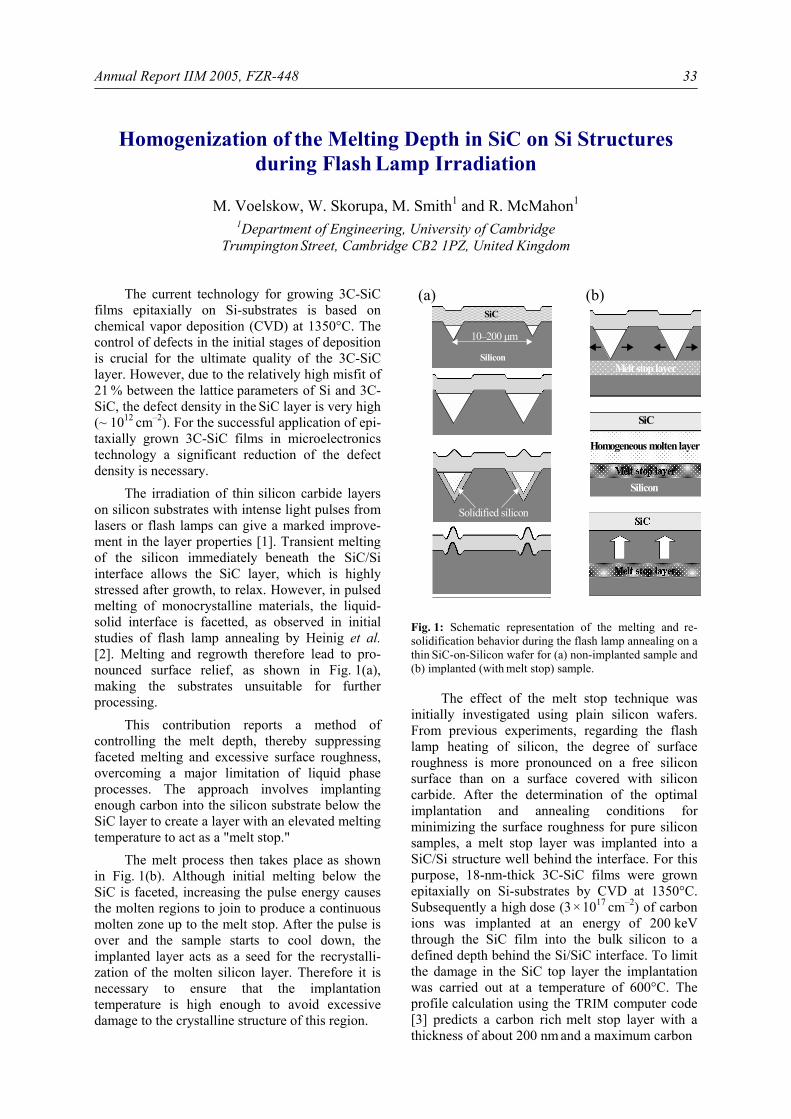
Annual Report IIM 2005, FZR-448
33
Homogenization of the Melting Depth in SiC on Si Structures during Flash Lamp Irradiation
M. Voelskow, W. Skorupa, M. Smith1 and R. McMahon1
1Department of Engineering, University of Cambridge Trumpington Street, Cambridge CB2 1PZ, United Kingdom
The current technology for growing 3C-SiC films epitaxially on Si-substrates is based on chemical vapor deposition (CVD) at 1350°C. The control of defects in the initial stages of deposition is crucial for the ultimate quality of the 3C-SiC layer. However, due to the relatively high misfit of 21 % between the lattice parameters of Si and 3C-SiC, the defect density in the SiC layer is very high (~ 1012 cm–2). For the successful application of epi-taxially grown 3C-SiC films in microelectronics technology a significant reduction of the defect density is necessary.
The irradiation of thin silicon carbide layers on silicon substrates with intense light pulses from lasers or flash lamps can give a marked improve-ment in the layer properties [1]. Transient melting of the silicon immediately beneath the SiC/Si interface allows the SiC layer, which is highly stressed after growth, to relax. However, in pulsed melting of monocrystalline materials, the liquid-solid interface is facetted, as observed in initial studies of flash lamp annealing by Heinig et al. [2]. Melting and regrowth therefore lead to pro-nounced surface relief, as shown in Fig. 1(a), making the substrates unsuitable for further processing.
This contribution reports a method of controlling the melt depth, thereby suppressing faceted melting and excessive surface roughness, overcoming a major limitation of liquid phase processes. The approach involves implanting enough carbon into the silicon substrate below the SiC layer to create a layer with an elevated melting temperature to act as a "melt stop."
The melt process then takes place as shown in Fig. 1(b). Although initial melting below the SiC is faceted, increasing the pulse energy causes the molten regions to join to produce a continuous molten zone up to the melt stop. After the pulse is over and the sample starts to cool down, the implanted layer acts as a seed for the recrystalli-zation of the molten silicon layer. Therefore it is necessary to ensure that the implantation
temperature is high enough to avoid excessive damage to the crystalline structure of this region.
(a) (b)
Fig. 1: Schematic representation of the melting and re-solidification behavior during the flash lamp annealing on a thin SiC-on-Silicon wafer for (a) non-implanted sample and (b) implanted (with melt stop) sample.
The effect of the melt stop technique was initially investigated using plain silicon wafers. From previous experiments, regarding the flash lamp heating of silicon, the degree of surface roughness is more pronounced on a free silicon surface than on a surface covered with silicon carbide. After the determination of the optimal implantation and annealing conditions for minimizing the surface roughness for pure silicon samples, a melt stop layer was implanted into a SiC/Si structure well behind the interface. For this purpose, 18-nm-thick 3C-SiC films were grown
epitaxially on Si-substrates by CVD at 1350°C. Subsequently a high dose (3 × 1017 cm–2) of carbon ions was implanted at an energy of 200 keV through the SiC film into the bulk silicon to a defined depth behind the Si/SiC interface. To limit the damage in the SiC top layer the implantation was carried out at a temperature of 600°C. The profile calculation using the TRIM computer code [3] predicts a carbon rich melt stop layer with a thickness of about 200 nm and a maximum carbon
10–200 µm
Silicon
SiC
Solidified siliconSolidified silicon
Melt stop layerMelt stop layer
SiC
Homogeneous molten layer
Silicon
SiC
Homogeneous molten layer
SiC
Homogeneous molten layer
Silicon
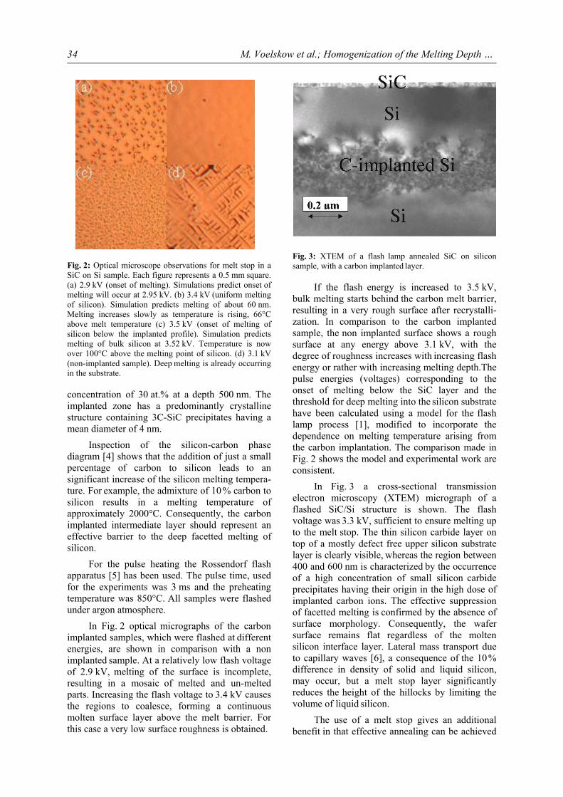
M. Voelskow et al.; Homogenization of the Melting Depth …
34
Fig. 2: Optical microscope observations for melt stop in a
SiC on Si sample. Each figure represents a 0.5 mm square. (a) 2.9 kV (onset of melting). Simulations predict onset of melting will occur at 2.95 kV. (b) 3.4 kV (uniform melting of silicon). Simulation predicts melting of about 60 nm. Melting increases slowly as temperature is rising, 66°C above melt temperature (c) 3.5 kV (onset of melting of silicon below the implanted profile). Simulation predicts melting of bulk silicon at 3.52 kV. Temperature is now over 100°C above the melting point of silicon. (d) 3.1 kV (non-implanted sample). Deep melting is already occurring in the substrate.
concentration of 30 at.% at a depth 500 nm. The implanted zone has a predominantly crystalline structure containing 3C-SiC precipitates having a mean diameter of 4 nm.
Inspection of the silicon-carbon phase diagram [4] shows that the addition of just a small percentage of carbon to silicon leads to an significant increase of the silicon melting tempera-ture. For example, the admixture of 10 % carbon to silicon results in a melting temperature of approximately 2000°C. Consequently, the carbon implanted intermediate layer should represent an effective barrier to the deep facetted melting of silicon.
For the pulse heating the Rossendorf flash apparatus [5] has been used. The pulse time, used for the experiments was 3 ms and the preheating temperature was 850°C. All samples were flashed under argon atmosphere.
In Fig. 2 optical micrographs of the carbon implanted samples, which were flashed at different energies, are shown in comparison with a non implanted sample. At a relatively low flash voltage of 2.9 kV, melting of the surface is incomplete, resulting in a mosaic of melted and un-melted parts. Increasing the flash voltage to 3.4 kV causes the regions to coalesce, forming a continuous
molten surface layer above the melt barrier. For this case a very low surface roughness is obtained.
Fig. 3: XTEM of a flash lamp annealed SiC on silicon sample, with a carbon implanted layer.
If the flash energy is increased to 3.5 kV, bulk melting starts behind the carbon melt barrier, resulting in a very rough surface after recrystalli-zation. In comparison to the carbon implanted sample, the non implanted surface shows a rough surface at any energy above 3.1 kV, with the degree of roughness increases with increasing flash energy or rather with increasing melting depth.The pulse energies (voltages) corresponding to the onset of melting below the SiC layer and the threshold for deep melting into the silicon substrate have been calculated using a model for the flash lamp process [1], modified to incorporate the dependence on melting temperature arising from the carbon implantation. The comparison made in
Fig. 2 shows the model and experimental work are consistent.
In Fig. 3 a cross-sectional transmission electron microscopy (XTEM) micrograph of a flashed SiC/Si structure is shown. The flash voltage was 3.3 kV, sufficient to ensure melting up to the melt stop. The thin silicon carbide layer on
top of a mostly defect free upper silicon substrate layer is clearly visible, whereas the region between 400 and 600 nm is characterized by the occurrence of a high concentration of small silicon carbide precipitates having their origin in the high dose of
implanted carbon ions. The effective suppression of facetted melting is confirmed by the absence of surface morphology. Consequently, the wafer surface remains flat regardless of the molten silicon interface layer. Lateral mass transport due to capillary waves [6], a consequence of the 10 % difference in density of solid and liquid silicon, may occur, but a melt stop layer significantly reduces the height of the hillocks by limiting the volume of liquid silicon.
The use of a melt stop gives an additional benefit in that effective annealing can be achieved
Annual Report IIM 2005, FZR-448
35
over a range of process conditions (approximately 3.0 - 3.5 kV), increasing the tolerance to lateral inhomogeneities in energy density, variations in energy from flash to flash and differences in wafer structure.
Apart from its application for the improve-ment of heteroepitaxial silicon carbide on silicon structures there should be a potential of the melt stop technique for semiconductor doping too. Using a melt stop layer beneath an initial ion implanted dopant profile it should be possible to get after the flash lamp melting, depending on the
segregation coefficient of the implanted species, either a rectangular profile (high segregation coefficient) or a very sharp dopant peak near the surface (low segregation coefficient). Moreover, the melt stop technique is equally applicable to laser induced melting, opening the way for the wider application of liquid phase processes.
Acknowledgements This work was supported by the EU, project
No GRD 1-2001- 40466. Moreover, we do grate-fully acknowledge the support of the European FLASiC consortium and, especially, the kind sup-port of W. Anwand, D. Panknin, A. Mücklich and T. Schumann, all at FZ Rossendorf.
The presented results have been recently published as M. Voelskow et al., Appl. Phys. Lett. 87 (2005) 241901.
References [1] M. Smith, R. McMahon, M. Voelskow, W.
Skorupa, Appl. Phys. Lett. 96 (2004) 4883 [2] K.-H. Heinig, M. Voelskow, J. Matthaei,
Proceedings of the International Conference on Energy Pulse and Particle Beam Modifi-cation of Materials, Dresden, 1984
[3] J.F. Ziegler, J.P. Biersack, U. Littmark, The Stopping and Ranges of Ions in Solids, New York, Pergamon, 1985, Vol. 1
[4] E.A. Brandes, G.B. Brook, Smithells Metals Reference Book, 7th ed., Butterworth-Hei-nemann, Oxford, 1998, p. 11
[5] W. Anwand, W. Skorupa, L. Rebohle, T. Trautmann, S. Tamme, T. Grass, Internatio-nal Topical Workshop on Heteroepitaxy of 3C-SiC on Silicon and its Application to Sensor Devices, Krippen, Germany, 2005
[6] D.K. Fork, G.B. Anderson, J.B. Boyce, R.I. Johnson, P. Mei, Appl. Phys. Lett. 68 (1996) 2138
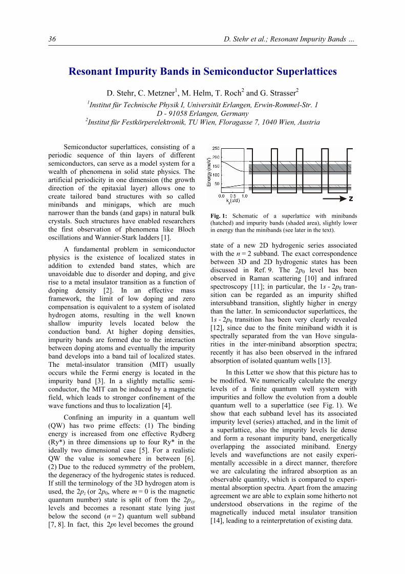
D. Stehr et al.; Resonant Impurity Bands …
36
Resonant Impurity Bands in Semiconductor Superlattices
D. Stehr, C. Metzner1, M. Helm, T. Roch2 and G. Strasser2 1Institut für Technische Physik I, Universität Erlangen, Erwin-Rommel-Str. 1
D - 91058 Erlangen, Germany 2Institut für Festkörperelektronik, TU Wien, Floragasse 7, 1040 Wien, Austria
Semiconductor superlattices, consisting of a periodic sequence of thin layers of different semiconductors, can serve as a model system for a wealth of phenomena in solid state physics. The artificial periodicity in one dimension (the growth direction of the epitaxial layer) allows one to create tailored band structures with so called minibands and minigaps, which are much narrower than the bands (and gaps) in natural bulk crystals. Such structures have enabled researchers the first observation of phenomena like Bloch oscillations and Wannier-Stark ladders [1].
A fundamental problem in semiconductor physics is the existence of localized states in addition to extended band states, which are unavoidable due to disorder and doping, and give rise to a metal insulator transition as a function of doping density [2]. In an effective mass framework, the limit of low doping and zero compensation is equivalent to a system of isolated hydrogen atoms, resulting in the well known shallow impurity levels located below the conduction band. At higher doping densities, impurity bands are formed due to the interaction between doping atoms and eventually the impurity band develops into a band tail of localized states. The metal-insulator transition (MIT) usually occurs while the Fermi energy is located in the impurity band [3]. In a slightly metallic semi-conductor, the MIT can be induced by a magnetic field, which leads to stronger confinement of the wave functions and thus to localization [4].
Confining an impurity in a quantum well (QW) has two prime effects: (1) The binding energy is increased from one effective Rydberg (Ry*) in three dimensions up to four Ry* in the ideally two dimensional case [5]. For a realistic QW the value is somewhere in between [6]. (2) Due to the reduced symmetry of the problem, the degeneracy of the hydrogenic states is reduced. If still the terminology of the 3D hydrogen atom is used, the 2pz (or 2p0, where m = 0 is the magnetic quantum number) state is split of from the 2pxy levels and becomes a resonant state lying just below the second (n = 2) quantum well subband [7, 8]. In fact, this 2p0 level becomes the ground
Fig. 1: Schematic of a superlattice with minibands (hatched) and impurity bands (shaded area), slightly lower in energy than the minibands (see later in the text).
state of a new 2D hydrogenic series associated with the n = 2 subband. The exact correspondence between 3D and 2D hydrogenic states has been discussed in Ref. 9. The 2p0 level has been observed in Raman scattering [10] and infrared spectroscopy [11]; in particular, the 1s - 2p0 tran-sition can be regarded as an impurity shifted intersubband transition, slightly higher in energy than the latter. In semiconductor superlattices, the 1s - 2p0 transition has been very clearly revealed [12], since due to the finite miniband width it is spectrally separated from the van Hove singula-rities in the inter-miniband absorption spectra; recently it has also been observed in the infrared absorption of isolated quantum wells [13].
In this Letter we show that this picture has to be modified. We numerically calculate the energy levels of a finite quantum well system with impurities and follow the evolution from a double quantum well to a superlattice (see Fig. 1). We show that each subband level has its associated impurity level (series) attached, and in the limit of a superlattice, also the impurity levels lie dense and form a resonant impurity band, energetically overlapping the associated miniband. Energy levels and wavefunctions are not easily experi-mentally accessible in a direct manner, therefore we are calculating the infrared absorption as an observable quantity, which is compared to experi-mental absorption spectra. Apart from the amazing agreement we are able to explain some hitherto not understood observations in the regime of the magnetically induced metal insulator transition [14], leading to a reinterpretation of existing data.
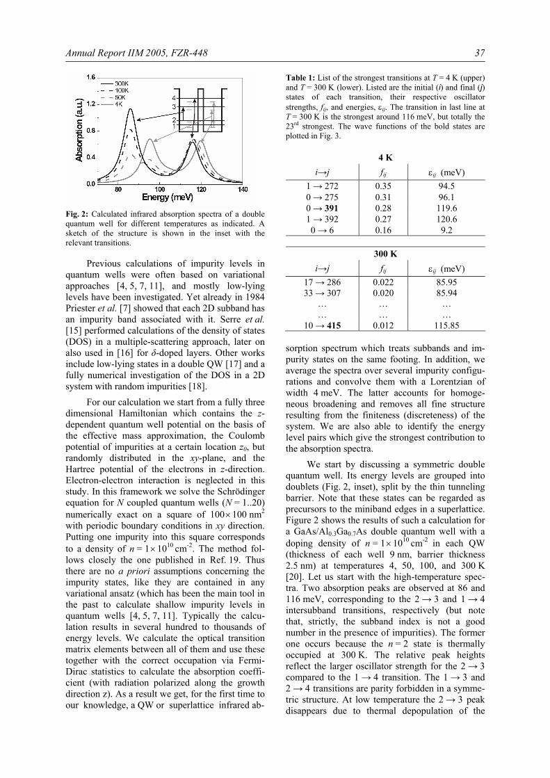
Annual Report IIM 2005, FZR-448
37
Fig. 2: Calculated infrared absorption spectra of a double quantum well for different temperatures as indicated. A sketch of the structure is shown in the inset with the relevant transitions.
Previous calculations of impurity levels in quantum wells were often based on variational approaches [4, 5, 7, 11], and mostly low-lying levels have been investigated. Yet already in 1984 Priester et al. [7] showed that each 2D subband has an impurity band associated with it. Serre et al. [15] performed calculations of the density of states (DOS) in a multiple-scattering approach, later on also used in [16] for δ-doped layers. Other works include low-lying states in a double QW [17] and a fully numerical investigation of the DOS in a 2D system with random impurities [18].
For our calculation we start from a fully three dimensional Hamiltonian which contains the z-dependent quantum well potential on the basis of the effective mass approximation, the Coulomb potential of impurities at a certain location z0, but randomly distributed in the xy-plane, and the Hartree potential of the electrons in z-direction. Electron-electron interaction is neglected in this study. In this framework we solve the Schrödinger equation for N coupled quantum wells (N = 1..20) numerically exact on a square of 100 × 100 nm2
with periodic boundary conditions in xy direction. Putting one impurity into this square corresponds to a density of n = 1 × 1010 cm-2. The method fol-lows closely the one published in Ref. 19. Thus there are no a priori assumptions concerning the impurity states, like they are contained in any variational ansatz (which has been the main tool in the past to calculate shallow impurity levels in quantum wells [4, 5, 7, 11]. Typically the calcu-lation results in several hundred to thousands of energy levels. We calculate the optical transition matrix elements between all of them and use these together with the correct occupation via Fermi-Dirac statistics to calculate the absorption coeffi-cient (with radiation polarized along the growth direction z). As a result we get, for the first time to our knowledge, a QW or superlattice infrared ab-
Table 1: List of the strongest transitions at T = 4 K (upper) and T = 300 K (lower). Listed are the initial (i) and final (j) states of each transition, their respective oscillator strengths, fij, and energies, εij. The transition in last line at T = 300 K is the strongest around 116 meV, but totally the 23rd strongest. The wave functions of the bold states are plotted in Fig. 3.
4 K i→j fij εij (meV)
1 → 272 0.35 94.5 0 → 275 0.31 96.1 0 → 391 0.28 119.6 1 → 392 0.27 120.6 0 → 6 0.16 9.2
300 K
i→j fij εij (meV) 17 → 286 0.022 85.95 33 → 307 0.020 85.94
… … … … … …
10 → 415 0.012 115.85
sorption spectrum which treats subbands and im-purity states on the same footing. In addition, we average the spectra over several impurity configu-rations and convolve them with a Lorentzian of width 4 meV. The latter accounts for homoge-neous broadening and removes all fine structure resulting from the finiteness (discreteness) of the system. We are also able to identify the energy level pairs which give the strongest contribution to the absorption spectra.
We start by discussing a symmetric double quantum well. Its energy levels are grouped into doublets (Fig. 2, inset), split by the thin tunneling barrier. Note that these states can be regarded as precursors to the miniband edges in a superlattice. Figure 2 shows the results of such a calculation for a GaAs/Al0.3Ga0.7As double quantum well with a doping density of n = 1 × 1010 cm-2 in each QW (thickness of each well 9 nm, barrier thickness 2.5 nm) at temperatures 4, 50, 100, and 300 K [20]. Let us start with the high-temperature spec-tra. Two absorption peaks are observed at 86 and 116 meV, corresponding to the 2 → 3 and 1 → 4 intersubband transitions, respectively (but note that, strictly, the subband index is not a good number in the presence of impurities). The former one occurs because the n = 2 state is thermally occupied at 300 K. The relative peak heights reflect the larger oscillator strength for the 2 → 3 compared to the 1 → 4 transition. The 1 → 3 and 2 → 4 transitions are parity forbidden in a symme-tric structure. At low temperature the 2 → 3 peak disappears due to thermal depopulation of the
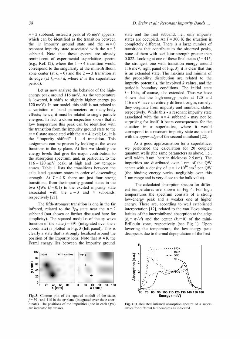
D. Stehr et al.; Resonant Impurity Bands …
38
n = 2 subband; instead a peak at 95 meV appears, which can be identified as the transition between the 1s impurity ground state and the m = 0 resonant impurity state associated with the n = 3 subband. Note that these spectra are already reminiscent of experimental superlattice spectra (e.g., Ref. 12), where the 1 → 4 transition would correspond to the singularity at the mini-Brillouin zone center (at kz = 0) and the 2 → 3 transition at its edge (at kz =π / d, where d is the superlattice period).
Let us now analyze the behavior of the high-energy peak around 116 meV. As the temperature is lowered, it shifts to slightly higher energy (to 120 meV). In our model, this shift is not related to a variation of band parameters or many-body effects; hence, it must be related to single particle energies. In fact, a closer inspection shows that at low temperature this peak can be identified with the transition from the impurity ground state to the m = 0 state associated with the n = 4 level; i.e., it is the ‘‘impurity shifted’’ 1 → 4 transition. This assignment can be proven by looking at the wave functions in the xy plane. At first we identify the energy levels that give the major contribution to the absorption spectrum, and, in particular, to the 116 – 120 meV peak, at high and low temper-atures. Table 1 lists the transitions between the calculated quantum states in order of descending strength. At T = 4 K there are just four strong transitions, from the impurity ground states in the two QWs (i = 0,1) to the excited impurity state associated with the n = 3 and 4 subbands, respectively [21].
The fifth-strongest transition is one in the far infrared, related to the 2p0 state near the n = 2 subband (not shown or further discussed here for simplicity). The squared modulus of the xy wave function of the state j = 391 (integrated over the z coordinate) is plotted in Fig. 3 (left panel). This is clearly a state that is strongly localized around the position of the impurity ions. Note that at 4 K the Fermi energy lies between the impurity ground
Fig. 3: Contour plot of the squared moduli of the states j = 391 and 415 in the xy plane (integrated over the z coor-dinate). The positions of the impurities (one in each QW) are indicated by crosses.
state and the first subband; i.e., only impurity states are occupied. At T = 300 K the situation is completely different. There is a large number of transitions that contribute to the observed peaks, none of them with oscillator strength greater than 0.022. Looking at one of these final states (j = 415, the strongest one with transition energy around 116 meV, right panel of Fig. 3), it is clear that this is an extended state. The maxima and minima of the probability distribution are related to the impurity potentials, the involved k values, and the periodic boundary conditions. The initial state i = 10 is, of course, also extended. Thus we have shown that the high-energy peaks at 120 and 116 meV have an entirely different origin; namely, they originate from impurity and miniband states, respectively. While this - a resonant impurity state associated with the n = 4 subband - may not be surprising for itself, it bears consequences for the situation in a superlattice, where it would correspond to a resonant impurity state associated with the upper edge of the second miniband [22].
As a good approximation for a superlattice, we performed the calculation for 20 coupled quantum wells (the same parameters as above, i.e., well width 9 nm, barrier thickness 2.5 nm). The impurities are distributed over 1 nm of the QW center with a density of n = 1 × 1010 cm-2 per QW (the binding energy varies negligibly over this 1 nm range and is very close to the bulk value).
The calculated absorption spectra for differ-ent temperatures are shown in Fig. 4. For high temperatures the spectrum consists of a strong low-energy peak and a weaker one at higher energy. These are, according to well established interpretation [12], related to the van Hove singu-larities of the interminiband absorption at the edge (kz = π / d) and the center (kz = 0) of the mini-Brillouin zone, respectively (see Fig. 1). Upon lowering the temperature, the low-energy peak disappears due to thermal depopulation of the first
Fig. 4: Calculated infrared absorption spectra of a super-lattice for different temperatures as indicated.
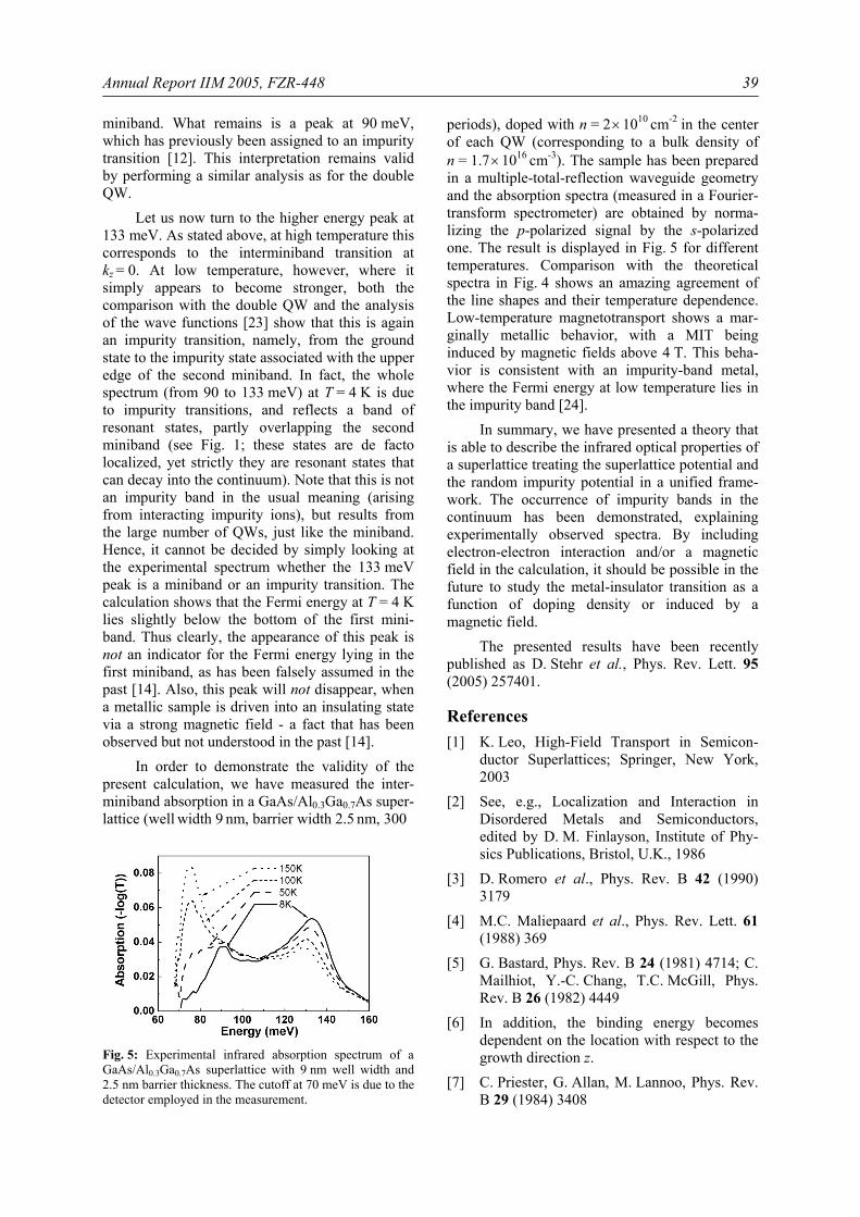
Annual Report IIM 2005, FZR-448
39
miniband. What remains is a peak at 90 meV, which has previously been assigned to an impurity transition [12]. This interpretation remains valid by performing a similar analysis as for the double QW.
Let us now turn to the higher energy peak at 133 meV. As stated above, at high temperature this corresponds to the interminiband transition at kz = 0. At low temperature, however, where it simply appears to become stronger, both the comparison with the double QW and the analysis of the wave functions [23] show that this is again an impurity transition, namely, from the ground state to the impurity state associated with the upper edge of the second miniband. In fact, the whole spectrum (from 90 to 133 meV) at T = 4 K is due to impurity transitions, and reflects a band of resonant states, partly overlapping the second miniband (see Fig. 1; these states are de facto localized, yet strictly they are resonant states that can decay into the continuum). Note that this is not an impurity band in the usual meaning (arising from interacting impurity ions), but results from the large number of QWs, just like the miniband. Hence, it cannot be decided by simply looking at the experimental spectrum whether the 133 meV peak is a miniband or an impurity transition. The calculation shows that the Fermi energy at T = 4 K lies slightly below the bottom of the first mini-band. Thus clearly, the appearance of this peak is not an indicator for the Fermi energy lying in the first miniband, as has been falsely assumed in the past [14]. Also, this peak will not disappear, when a metallic sample is driven into an insulating state via a strong magnetic field - a fact that has been observed but not understood in the past [14].
In order to demonstrate the validity of the present calculation, we have measured the inter-miniband absorption in a GaAs/Al0.3Ga0.7As super-lattice (well width 9 nm, barrier width 2.5 nm, 300
Fig. 5: Experimental infrared absorption spectrum of a GaAs/Al0.3Ga0.7As superlattice with 9 nm well width and 2.5 nm barrier thickness. The cutoff at 70 meV is due to the detector employed in the measurement.
periods), doped with n = 2 × 1010 cm-2 in the center of each QW (corresponding to a bulk density of n = 1.7 × 1016 cm-3). The sample has been prepared in a multiple-total-reflection waveguide geometry and the absorption spectra (measured in a Fourier-transform spectrometer) are obtained by norma-lizing the p-polarized signal by the s-polarized one. The result is displayed in Fig. 5 for different temperatures. Comparison with the theoretical spectra in Fig. 4 shows an amazing agreement of the line shapes and their temperature dependence. Low-temperature magnetotransport shows a mar-ginally metallic behavior, with a MIT being induced by magnetic fields above 4 T. This beha-vior is consistent with an impurity-band metal, where the Fermi energy at low temperature lies in the impurity band [24].
In summary, we have presented a theory that is able to describe the infrared optical properties of a superlattice treating the superlattice potential and the random impurity potential in a unified frame-work. The occurrence of impurity bands in the continuum has been demonstrated, explaining experimentally observed spectra. By including electron-electron interaction and/or a magnetic field in the calculation, it should be possible in the future to study the metal-insulator transition as a function of doping density or induced by a magnetic field.
The presented results have been recently published as D. Stehr et al., Phys. Rev. Lett. 95 (2005) 257401.
References [1] K. Leo, High-Field Transport in Semicon-
ductor Superlattices; Springer, New York, 2003
[2] See, e.g., Localization and Interaction in Disordered Metals and Semiconductors, edited by D. M. Finlayson, Institute of Phy-sics Publications, Bristol, U.K., 1986
[3] D. Romero et al., Phys. Rev. B 42 (1990) 3179
[4] M.C. Maliepaard et al., Phys. Rev. Lett. 61 (1988) 369
[5] G. Bastard, Phys. Rev. B 24 (1981) 4714; C. Mailhiot, Y.-C. Chang, T.C. McGill, Phys. Rev. B 26 (1982) 4449
[6] In addition, the binding energy becomes dependent on the location with respect to the growth direction z.
[7] C. Priester, G. Allan, M. Lannoo, Phys. Rev. B 29 (1984) 3408
D. Stehr et al.; Resonant Impurity Bands …
40
[8] R.L. Greene, K.K. Bajaj, Phys. Rev. B 31 (1985) 4006
[9] J.P. Cheng, B.D. McCombe, Phys. Rev. B 42 (1990) 7626
[10] T.A. Perry et al., Phys. Rev. Lett. 54 (1985) 2623
[11] M. Helm et al., Phys. Rev. B 43 (1991) 13 983
[12] M. Helm et al., Phys. Rev. B 48 (1993) 1601, M. Helm, Semicond. Sci. Technol. 10 (1995) 557
[13] M. Carras et al., Phys. Rev. B 70 (2004) 233310
[14] W. Hilber et al., Phys. Rev. B 53 (1996) 6919, M. Helm et al. (unpublished)
[15] J. Serre, A. Ghazali, A. Gold, Phys. Rev. B 39 (1989) 8499
[16] J. Kortus, J. Monecke, Phys. Rev. B 49 (1994) 17 216
[17] S.T. Yen, Phys. Rev. B 68 (2003) 165331 [18] M. Hofmann, M. Bockstedte, O. Pankratov,
Phys. Rev. B 64 (2001) 245321
[19] C. Metzner, M. Hofmann, G.H. Döhler, Phys. Rev. B 58 (1998) 7188
[20] Note that our calculation also yields the low-energy spectra (<10 meV) due to impurity and intersubband transitions near the first doublet. They are not shown here since we concentrate on the comparison to midinfrared absorption experiments.
[21] Note the different level numbering: n counts the few subbands due to the z confinement, whereas i counts the levels of the full 3D calculation.
[22] In a completely different context localized states near the upper miniband edge have been predicted; see H. A. Fertig, S. Das Sarma, Phys. Rev. B 42 (1990) 1448
[23] We suppress any detailed discussion as for the double QW, due to the large number of energy levels involved here.
[24] S. Liu et al., Phys. Rev. B 45 (1992) 1155
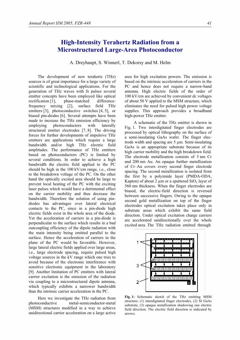
Annual Report IIM 2005, FZR-448
41
High-Intensity Terahertz Radiation from a Microstructured Large-Area Photoconductor
A. Dreyhaupt, S. Winnerl, T. Dekorsy and M. Helm
The development of new terahertz (THz) sources is of great importance for a large variety of scientific and technological applications. For the generation of THz waves with fs pulses several emitter concepts have been employed like optical rectification [1], phase-matched difference-frequency mixing [2], surface field THz emitters [3], photoconductive switches [4, 5], or biased pin-diodes [6]. Several attempts have been made to increase the THz emission efficiency by employing photoconductors with laterally structured emitter electrodes [7, 8]. The driving forces for further developments of impulsive THz emitters are applications which require a large bandwidth and/or high THz electric field amplitudes. The performance of THz emitters based on photoconductors (PC) is limited by several conditions. In order to achieve a high bandwidth the electric field applied to the PC should be high in the 100 kV/cm range, i.e., close to the breakdown voltage of the PC. On the other hand the optically excited area should be large to prevent local heating of the PC with the exciting laser pulses which would have a detrimental effect on the carrier mobility and thus decrease the bandwidth. Therefore the solution of using pin-diodes has advantages over lateral electrical contacts to the PC, since in a pin-diode high electric fields exist in the whole area of the diode. Yet the acceleration of carriers in a pin-diode is perpendicular to the surface which results in a bad outcoupling efficiency of the dipole radiation with the main intensity being emitted parallel to the surface. Hence the acceleration of carriers in the plane of the PC would be favorable. However, large lateral electric fields applied over large areas, i.e., large electrode spacing, require pulsed high voltage sources in the kV range which one tries to avoid because of the electronic interference with sensitive electronic equipment in the laboratory [9]. Another limitation of PC emitters with lateral carrier excitation is the emission of the radiation via coupling to a microstructured dipole antenna, which typically exhibits a narrower bandwidth than the intrinsic carrier acceleration in the PC.
Here we investigate the THz radiation from photoconductive metal-semiconductor-metal (MSM) structures modified in a way to achieve unidirectional carrier acceleration on a large active
area for high excitation powers. The emission is based on the intrinsic acceleration of carriers in the PC and hence does not require a narrow-band antenna. High electric fields of the order of 100 kV/cm are achieved by convenient dc voltages of about 50 V applied to the MSM structure, which eliminates the need for pulsed high power voltage supplies. This approach provides a broadband high-power THz emitter.
A schematic of the THz emitter is shown in Fig. 1. Two interdigitated finger electrodes are processed by optical lithography on the surface of a semi-insulating GaAs wafer. The finger elec-trode width and spacing are 5 µm. Semi-insulating GaAs is an appropriate substrate because of its high carrier mobility and the high breakdown field. The electrode metallization consists of 5 nm Cr and 200 nm Au. An opaque further metallization of Cr–Au covers every second finger electrode spacing. The second metallization is isolated from the first by a polyimide layer (PMDA-ODA, Kapton) of about 2 µm or a sputtered SiOx layer of 560 nm thickness. When the finger electrodes are biased, the electric-field direction is reversed between successive fingers. Owing to the opaque second gold metallization on top of the finger electrodes optical excitation takes place only in substrate areas which exhibit the same field direction. Under optical excitation charge carriers are accelerated unidirectionally over the whole excited area. The THz radiation emitted through
Fig. 1: Schematic sketch of the THz emitting MSM structure; (1) interdigitated finger electrodes, (2) SI GaAs substrate, (3) opaque metallization shadowing one electric field direction. The electric field direction is indicated by arrows.
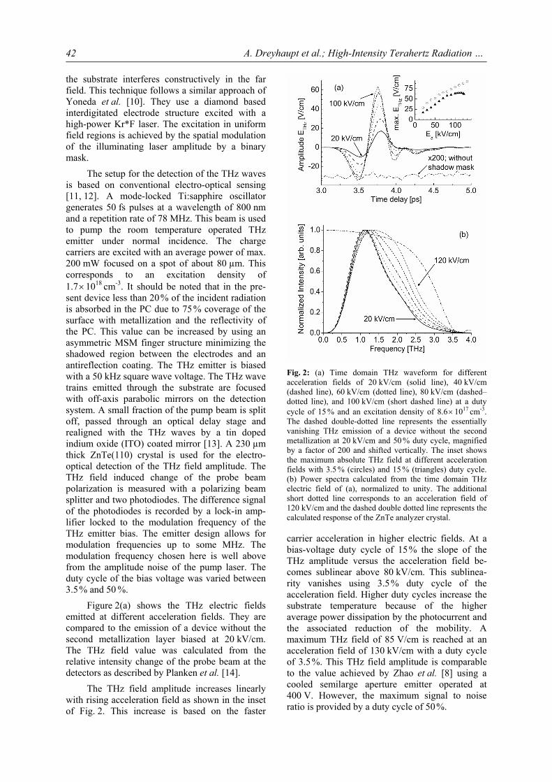
A. Dreyhaupt et al.; High-Intensity Terahertz Radiation …
42
the substrate interferes constructively in the far field. This technique follows a similar approach of Yoneda et al. [10]. They use a diamond based interdigitated electrode structure excited with a high-power Kr*F laser. The excitation in uniform field regions is achieved by the spatial modulation of the illuminating laser amplitude by a binary mask.
The setup for the detection of the THz waves is based on conventional electro-optical sensing [11, 12]. A mode-locked Ti:sapphire oscillator generates 50 fs pulses at a wavelength of 800 nm and a repetition rate of 78 MHz. This beam is used to pump the room temperature operated THz emitter under normal incidence. The charge carriers are excited with an average power of max. 200 mW focused on a spot of about 80 µm. This corresponds to an excitation density of 1.7 × 1018 cm-3. It should be noted that in the pre-sent device less than 20 % of the incident radiation is absorbed in the PC due to 75 % coverage of the surface with metallization and the reflectivity of the PC. This value can be increased by using an asymmetric MSM finger structure minimizing the shadowed region between the electrodes and an antireflection coating. The THz emitter is biased with a 50 kHz square wave voltage. The THz wave trains emitted through the substrate are focused with off-axis parabolic mirrors on the detection system. A small fraction of the pump beam is split off, passed through an optical delay stage and realigned with the THz waves by a tin doped indium oxide (ITO) coated mirror [13]. A 230 µm thick ZnTe(110) crystal is used for the electro-optical detection of the THz field amplitude. The THz field induced change of the probe beam polarization is measured with a polarizing beam splitter and two photodiodes. The difference signal of the photodiodes is recorded by a lock-in amp-lifier locked to the modulation frequency of the THz emitter bias. The emitter design allows for modulation frequencies up to some MHz. The modulation frequency chosen here is well above from the amplitude noise of the pump laser. The duty cycle of the bias voltage was varied between 3.5 % and 50 %.
Figure 2(a) shows the THz electric fields emitted at different acceleration fields. They are compared to the emission of a device without the second metallization layer biased at 20 kV/cm. The THz field value was calculated from the relative intensity change of the probe beam at the detectors as described by Planken et al. [14].
The THz field amplitude increases linearly with rising acceleration field as shown in the inset of Fig. 2. This increase is based on the faster
Fig. 2: (a) Time domain THz waveform for different acceleration fields of 20 kV/cm (solid line), 40 kV/cm (dashed line), 60 kV/cm (dotted line), 80 kV/cm (dashed–dotted line), and 100 kV/cm (short dashed line) at a duty cycle of 15 % and an excitation density of 8.6 × 1017 cm-3. The dashed double-dotted line represents the essentially vanishing THz emission of a device without the second metallization at 20 kV/cm and 50 % duty cycle, magnified by a factor of 200 and shifted vertically. The inset shows the maximum absolute THz field at different acceleration fields with 3.5 % (circles) and 15 % (triangles) duty cycle. (b) Power spectra calculated from the time domain THz electric field of (a), normalized to unity. The additional short dotted line corresponds to an acceleration field of 120 kV/cm and the dashed double dotted line represents the calculated response of the ZnTe analyzer crystal.
carrier acceleration in higher electric fields. At a bias-voltage duty cycle of 15 % the slope of the THz amplitude versus the acceleration field be-comes sublinear above 80 kV/cm. This sublinea-rity vanishes using 3.5 % duty cycle of the acceleration field. Higher duty cycles increase the substrate temperature because of the higher average power dissipation by the photocurrent and the associated reduction of the mobility. A maximum THz field of 85 V/cm is reached at an acceleration field of 130 kV/cm with a duty cycle of 3.5 %. This THz field amplitude is comparable to the value achieved by Zhao et al. [8] using a cooled semilarge aperture emitter operated at 400 V. However, the maximum signal to noise ratio is provided by a duty cycle of 50 %.
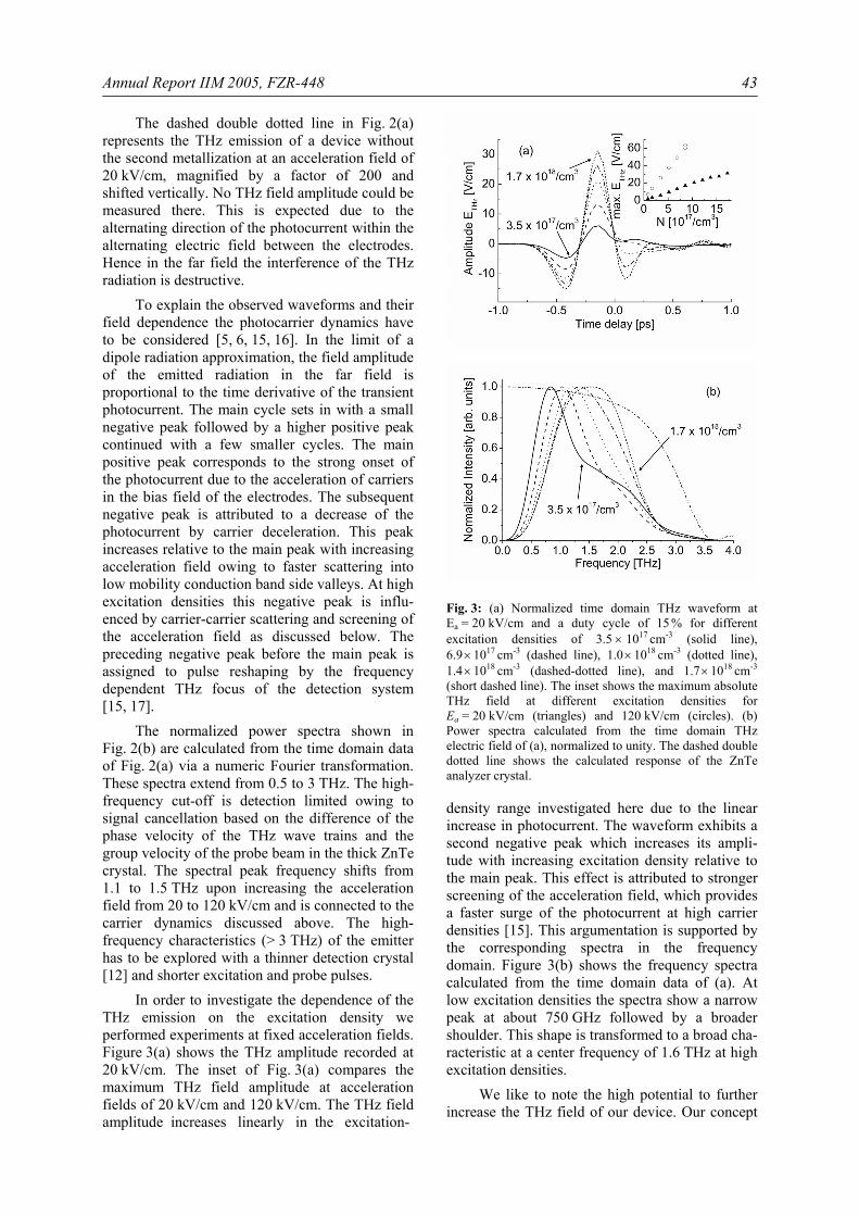
Annual Report IIM 2005, FZR-448
43
The dashed double dotted line in Fig. 2(a) represents the THz emission of a device without the second metallization at an acceleration field of 20 kV/cm, magnified by a factor of 200 and shifted vertically. No THz field amplitude could be measured there. This is expected due to the alternating direction of the photocurrent within the alternating electric field between the electrodes. Hence in the far field the interference of the THz radiation is destructive.
To explain the observed waveforms and their field dependence the photocarrier dynamics have to be considered [5, 6, 15, 16]. In the limit of a dipole radiation approximation, the field amplitude of the emitted radiation in the far field is proportional to the time derivative of the transient photocurrent. The main cycle sets in with a small negative peak followed by a higher positive peak continued with a few smaller cycles. The main positive peak corresponds to the strong onset of the photocurrent due to the acceleration of carriers in the bias field of the electrodes. The subsequent negative peak is attributed to a decrease of the photocurrent by carrier deceleration. This peak increases relative to the main peak with increasing acceleration field owing to faster scattering into low mobility conduction band side valleys. At high excitation densities this negative peak is influ-enced by carrier-carrier scattering and screening of the acceleration field as discussed below. The preceding negative peak before the main peak is assigned to pulse reshaping by the frequency dependent THz focus of the detection system [15, 17].
The normalized power spectra shown in Fig. 2(b) are calculated from the time domain data of Fig. 2(a) via a numeric Fourier transformation. These spectra extend from 0.5 to 3 THz. The high-frequency cut-off is detection limited owing to signal cancellation based on the difference of the phase velocity of the THz wave trains and the group velocity of the probe beam in the thick ZnTe crystal. The spectral peak frequency shifts from 1.1 to 1.5 THz upon increasing the acceleration field from 20 to 120 kV/cm and is connected to the carrier dynamics discussed above. The high-frequency characteristics (> 3 THz) of the emitter has to be explored with a thinner detection crystal [12] and shorter excitation and probe pulses.
In order to investigate the dependence of the THz emission on the excitation density we performed experiments at fixed acceleration fields. Figure 3(a) shows the THz amplitude recorded at 20 kV/cm. The inset of Fig. 3(a) compares the maximum THz field amplitude at acceleration fields of 20 kV/cm and 120 kV/cm. The THz field amplitude increases linearly in the excitation-
Fig. 3: (a) Normalized time domain THz waveform at Ea = 20 kV/cm and a duty cycle of 15 % for different excitation densities of 3.5 × 1017 cm-3 (solid line), 6.9 × 1017 cm-3 (dashed line), 1.0 × 1018 cm-3 (dotted line), 1.4 × 1018 cm-3 (dashed-dotted line), and 1.7 × 1018 cm-3 (short dashed line). The inset shows the maximum absolute THz field at different excitation densities for Ea = 20 kV/cm (triangles) and 120 kV/cm (circles). (b) Power spectra calculated from the time domain THz electric field of (a), normalized to unity. The dashed double dotted line shows the calculated response of the ZnTe analyzer crystal.
density range investigated here due to the linear increase in photocurrent. The waveform exhibits a second negative peak which increases its ampli-tude with increasing excitation density relative to the main peak. This effect is attributed to stronger screening of the acceleration field, which provides a faster surge of the photocurrent at high carrier densities [15]. This argumentation is supported by the corresponding spectra in the frequency domain. Figure 3(b) shows the frequency spectra calculated from the time domain data of (a). At low excitation densities the spectra show a narrow peak at about 750 GHz followed by a broader shoulder. This shape is transformed to a broad cha-racteristic at a center frequency of 1.6 THz at high excitation densities.
We like to note the high potential to further increase the THz field of our device. Our concept
A. Dreyhaupt et al.; High-Intensity Terahertz Radiation …
44
is scalable towards larger emitting areas from presently approximately 5000 µm2 to some mm2 and even cm2 which can be excited with amplified laser pulses. This in principle would enhance the emitted THz amplitude by orders of magnitude. Such a system could have comparable performan-ce to optical rectification or difference frequency mixing [2] and would open the pathway to non-linear THz spectroscopy in many interesting sys-tems. In addition such an emitter would be suitable for generation of continuous wave THz radiation by mixing two laser lines in a PC [18]. This approach has often been limited by the power dissipation in a small excited area.
In conclusion, we have demonstrated the generation of high-intensity THz radiation based on a transient photocurrent in a large-area emitter with a novel electrode design in conjunction with selective shadowing of the optical excitation. This device overcomes disadvantages inherent to emitters using photoconductive antennas and large aperture emitters using two electrodes. In contrast to the latter the proposed device structure enables the exploitation of a large emitting area while keeping the bias field at large values. The high acceleration field which can be obtained in our concept makes the use of low-temperature grown GaAs favorable.
Acknowledgements We acknowledge the preparation of the
polyimide isolation layer by M. Guenther, and the support in sample preparation and helpful discus-sions by H. Felsmann and B. Schmidt.
The presented results have been recently published as A. Dreyhaupt et al., Appl. Phys. Lett. 86 (2005) 121114.
References [1] X.-C. Zhang, Y. Jin, X.F. Ma, Appl. Phys.
Lett. 61 (1992) 2764 [2] K. Reimann, R.P. Smith, A.M. Weiner, T.
Elsaesser, M. Woerner, Opt. Lett. 28 (2003) 471
[3] X.-C. Zhang, D.H. Auston, J. Appl. Phys. 71 (1992) 326
[4] D. Grischkowsky, S. Keiding, M.V. Exter, C. Fattinger, J. Opt. Soc. Am. B 7 (1990) 2006
[5] For a review, see J. Shan, T.F. Heinz, in Ultrafast Dynamical Processes in Semicon-ductors, edited by K.-T. Tsen, Springer-Verlag, Berlin, 2004, pp. 1–56
[6] L. Xu, X.-C. Zhang, D.H. Auston, B. Jalali, Appl. Phys. Lett. 59 (1991) 3357
[7] S.R. Andrews, A. Armitage, P.G. Huggard, A. Hussain, Phys. Med. Biol. 47 (2002) 37053710
[8] G. Zhao, R.N. Schouten, N. van der Valk, W.T. Wenckebach, P.C.M. Planken, Rev. Sci. Instrum. 73 (2002) 1715
[9] P.K. Benicewicz, J.P. Roberts, A.J. Taylor, J. Opt. Soc. Am. B 11 (1994) 2533
[10] H. Yoneda, K. Tokuyama, K. Ueda, H. Ya-mamoto, K. Baba, Appl. Opt. 46 (2001) 6733
[11] Q. Wu, X.-C. Zhang, Appl. Phys. Lett. 68 (1996) 1604
[12] A. Leitenstorfer, S. Hunsche, J. Shah, M.C. Nuss, W.H. Knox, Appl. Phys. Lett. 74 (1999) 1516
[13] T. Bauer, J.S. Kolb, T. Löffler, E. Mohler, H.G. Roskos, U.C. Pernisz, J. Appl. Phys. 92 (2002) 2210
[14] P.C.M. Planken, H.-K. Nienhuys, H.J. Bak-ker, T. Wenckebach, J. Opt. Soc. Am. B 18 (2001) 313
[15] P.U. Jepsen, R.H. Jacobsen, S.R. Keiding, J. Opt. Soc. Am. B 13 (1996) 2424
[16] T.-A. Liu, M. Tani, C.-L. Pan, J. Appl. Phys. 93 (2003) 2996
[17] C. Fattinger, D. Grischkowsky, Appl. Phys. Lett. 54 (1989) 490
[18] E.R. Brown, K.A. McIntosh, K.B. Nichols, C.L. Dennis, Appl. Phys. Lett. 66 (1995) 285

Short Contributions

Annual Report IIM 2005, FZR-448
47
Ion-Solid Interaction D. Kost S. Facsko R. Hellhammer1
Electron spectroscopy on HCIs-interaction with Cu, Si, and SiO2 Double differential secondary electron spectra were evaluated in dependence of the kinetic energy and the charge state of incoming highly-charged ions (HCIs). For Cu and Si surfaces a quadratic increase of the reemitted energy with increasing charge state up to Ar7+ is observed. For Ar8+ and Ar9+ the increase is steeper due to the contribution of the projectile LMM Auger electrons. The reemitted energy amounts to between 15 % and 20 % of the total potential energy of the incoming ion, almost independent of the ion charge state. For SiO2 layers on Si, quasi-static surface charging of some 10 V is observed, which increases at increasing oxide thickness, so that the contribution of low-energy electrons to the reemission of potential energy is suppressed. Therefore, energy reemission is negligible for charge states up to Ar7+. For Ar9+, the reemitted energy increases to 12 % of the total potential energy due to the LMM Auger electron contribution. At decreasing kinetic energy for Ar9+, the electron yield and the reemitted energy increase slightly with decreasing projectile energy. Collaboration:1Hahn-Meitner-Institute, Berlin, Germany
A. Keller S. Facsko J. Grenzer O. Plantevin1,2 D. Carbone1 T.H. Metzger1 R. Gago3
In-situ x-ray diffraction of GaSb nanopatterned by normal incidence sputter erosion Low-energy ion erosion of surfaces can lead to the formation of self-orga-nized structures in the range from 10 to 100 nm. Periodic ripple patterns and hexagonally ordered dot arrays can be achieved for oblique and normal incidence, respectively. The evolution of dot patterns on GaSb(001) under normal incidence sputtering at ion energies from 100 to 1000 eV was investi-gated in-situ using grazing incidence small angle x-ray scattering (GISAXS) and grazing incidence diffraction (GID) at the beamline ID01 at the ESRF. With GISAXS the morphology and the correlation of the dots is analysed, while in GID information about the crystalline structure (i.e. strain) is achieved. Three time regimes are identified as smoothing at the beginning of sputtering, followed by pattern formation, and increase of lateral order at high ion fluences. Collaboration: 1ID01-Anomalous Scattering Beamline, ESRF, France, 2Centre de Spectrométrie Nucléaire et de Spectrométrie de Masse, France, 3Centro de Micro-Análisis de Materiales, Universidad Autónoma de Madrid, Spain
S. Roßbach A. Keller S. Facsko
Ion induced ripple formation on Si surfaces at grazing angles The surface morphology induced by ion beam erosion of Si has been studied for incidence angles of 50–70° to the surface normal at different ion energies and ion fluences. In a window from 60 to 70° regular ripple patterns oriented perpendicular to the ion beam are formed. At smaller incidence angles the surface remains flat, whereas at 75° irregular structures appear which are assigned to processes governed by shadowing effects. The wavelength of the ripple patterns depends on the ion energy and varies from 20 nm at 240 eV to 60 nm at 1 keV. With ion fluence the periodicity also increases in contrast to the Bradley-Harper model which predicts a constant wavelength. From theo-ry a critical angle is expected around 60° where the orientation of the ripple structures should change from perpendicular at smaller angles to parallel at higher angles. In contrast, two ripple modes are present at all incidence angles where ripples appear. A detailed analysis of the power spectra density reveals two periodic features in the patterns. The ripples with the small perio-dicity are periodically modulated with a wavelength of 100 nm, oriented parallel to the ion beam. Simulations with an extended continuum equation model show qualitative agreement with these findings.
Ion-Solid-Interaction 48
S. Grigorian1 J. Grenzer S. Hazra2 T.K. Chini2 U. Pietsch1
Investigation of the ripple structure in Si by x-ray scattering techniques The morphology of Ar+ ion beam induced ripples on Si was studied. The for-mation of ripple structures on the sample surface is evident from AFM, while its formation in the buried crystalline region below an amorphous top layer is evident from grazing incidence diffraction (GID) studies. The GID technique reveals that these periodically modulated wave-like buried crystalline features become highly regular and strongly correlated at Ar ion beam energies between 60 keV and 100 keV. The vertical density profile obtained from the analysis of vineyard profiles shows that the density in the upper top part of ripples is strongly decreased. Particularly, we measured the degree of amorphization of the top layer as a function of irradiation dose using grazing incidence amorphous scattering (GIAS). Two broad peaks indicating short-range ordering of amorphous material changing with the penetration depth of the probing x-ray wave suggest a model of dose-dependent amorphization. The strong damage of crystalline structure starting at low doses (5 × 1016 cm-2) before it becomes complete amorphous and mostly uniform at high doses of irradiation (> 5 × 1017 cm-2). Collaboration: 1Institute of Physics, University of Siegen, Germany, 2Surface Phy-sics Division, Saha Institute of Nuclear Physics, Kolkata, India
L. Harangus1 A. Iordan1 E.A. Preoteasa1 D. Grambole R. Grötzschel F. Herrmann C. Neelmeijer S. Gomez2 A. Mihul3 C. lonescu-Tirgoviste4 D. Gutu4
Proton microprobe analysis of normal and osteoporosisaffected compact bone In osteoporosis, the altered metabolism of Ca and trace elements leading to low bone density is not fully understood. Therefore PIXE, PIGE and proton backscattering (PBS) were applied complementary to analyse the outer layer of femur and tibia from normal and experimental diabetes-affected rats, tibia from humans with osteoporosis-complicated diabetes, clinically sound hu-man femoral neck and normal bovine metacarp. Measurements were carried out at the Rossendorf nuclear microprobe with a 3.1 MeV proton microbeam focused to a spot of about 3 µm. Hydroxylapatite (HA), CaF2, NaCl and pyrite were used as reference mate-rials. Concentrations were determined from PIXE spectra by GUPIX calcula-tions. In all bones, a P/Ca ratio of 0.32 – 0.39 was found, below the 0.46 value of HA. PBS suggests a fraction of Ca as carbonate in addition to HA. Most elements of the second main group were detected: Mg by PIGE and PBS, and Ca as well as Sr and Ba by PIXE. Other divalent ion-forming trace metals detected by PIXE are Cr, Mn, Fe, Ni, Cu and Zn from the transition element groups, and Pb. Only normal bones contained Cr, Mn and Cu. The concentration of Ca, Fe, Ni and Zn varies strongly even in the same bone, while the Sr concentration shows only small variations. Ca maps exhibit spatially well-defined patterns of bands. Diabetic rat bones show Ca depleted regions near the surface, giving a hint for next studies of osteoporosis affected bones. Collaboration: 1National Institute for Physics and Nuclear Engineering, Bucharest, Romania, 2Faculty of Medicine, University of Cadiz, Spain, 3Faculty of Physics, University of Bucharest, Romania; 4Nicolae Paulescu Institute of Diabetes Research, Bucharest, Romania
M. Mäder1 M. Schreiner1 E. Bidaud1 W. Zich1 K. Uhlir1 D. Grambole F. Herrmann M. Alram2
The Becin hoard – silver coins of the Ottoman Empire In summer 2000 a spectacular hoard of silver coins was excavated at the medieval site Becin, next to Ephesos. This trove, which includes about 60.000 coins with a total weight of about 30 kg, represents the largest finding of coins ever made in Turkey. The main part of the coins covers almost all mint places recorded for the Ottoman Empire and all rulers of the second half of the 16th century up to the beginning of the 17th century. Thus, the numis-matic evaluation and the material analysis of the coins will provide a general
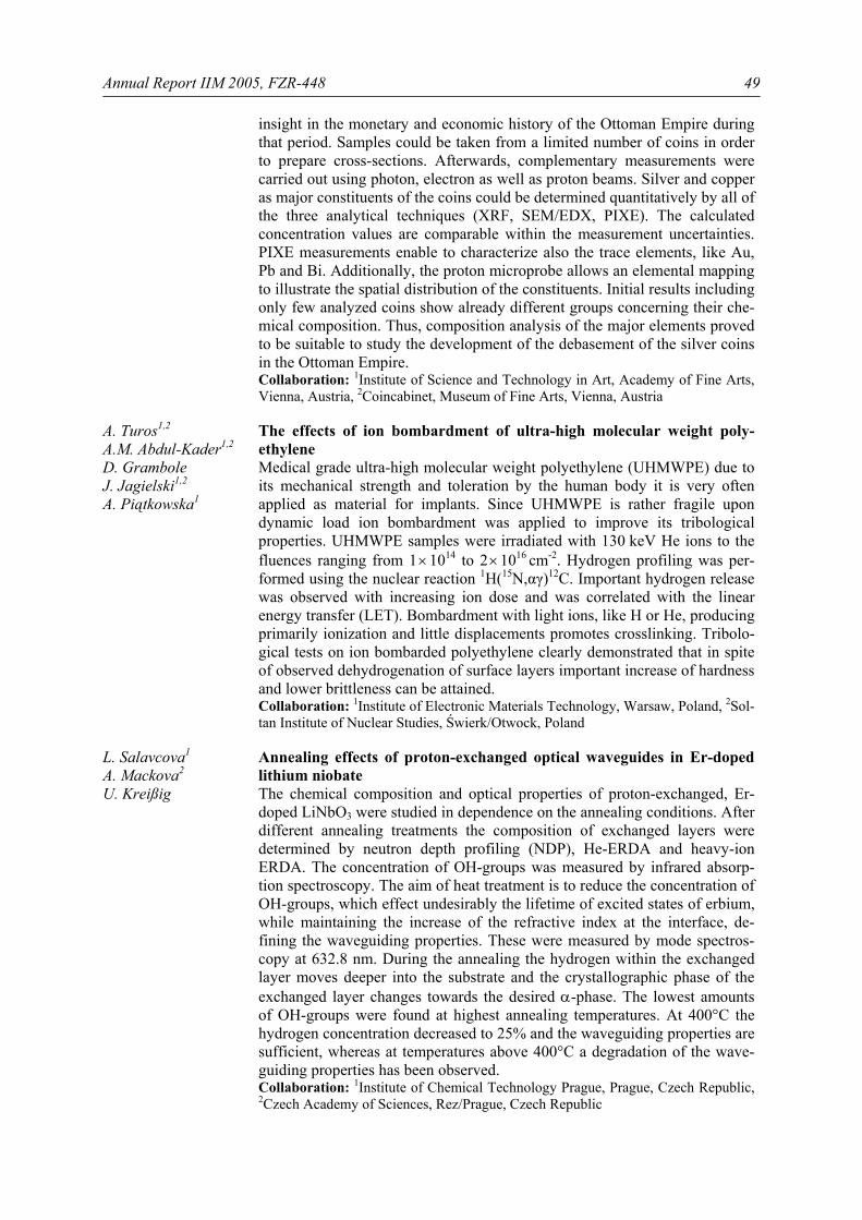
Annual Report IIM 2005, FZR-448
49
insight in the monetary and economic history of the Ottoman Empire during that period. Samples could be taken from a limited number of coins in order to prepare cross-sections. Afterwards, complementary measurements were carried out using photon, electron as well as proton beams. Silver and copper as major constituents of the coins could be determined quantitatively by all of the three analytical techniques (XRF, SEM/EDX, PIXE). The calculated concentration values are comparable within the measurement uncertainties. PIXE measurements enable to characterize also the trace elements, like Au, Pb and Bi. Additionally, the proton microprobe allows an elemental mapping to illustrate the spatial distribution of the constituents. Initial results including only few analyzed coins show already different groups concerning their che-mical composition. Thus, composition analysis of the major elements proved to be suitable to study the development of the debasement of the silver coins in the Ottoman Empire. Collaboration: 1Institute of Science and Technology in Art, Academy of Fine Arts, Vienna, Austria, 2Coincabinet, Museum of Fine Arts, Vienna, Austria
A. Turos1,2 A.M. Abdul-Kader1,2 D. Grambole J. Jagielski1,2 A. Piątkowska1
The effects of ion bombardment of ultra-high molecular weight poly-ethylene Medical grade ultra-high molecular weight polyethylene (UHMWPE) due to its mechanical strength and toleration by the human body it is very often applied as material for implants. Since UHMWPE is rather fragile upon dynamic load ion bombardment was applied to improve its tribological properties. UHMWPE samples were irradiated with 130 keV He ions to the fluences ranging from 1 × 10¹⁴ to 2 × 1016 cm-2. Hydrogen profiling was per-formed using the nuclear reaction 1H(15N,αγ)12C. Important hydrogen release was observed with increasing ion dose and was correlated with the linear energy transfer (LET). Bombardment with light ions, like H or He, producing primarily ionization and little displacements promotes crosslinking. Tribolo-gical tests on ion bombarded polyethylene clearly demonstrated that in spite of observed dehydrogenation of surface layers important increase of hardness and lower brittleness can be attained. Collaboration: 1Institute of Electronic Materials Technology, Warsaw, Poland, 2Sol-tan Institute of Nuclear Studies, Świerk/Otwock, Poland
L. Salavcova1 A. Mackova2 U. Kreißig
Annealing effects of proton-exchanged optical waveguides in Er-doped lithium niobate The chemical composition and optical properties of proton-exchanged, Er-doped LiNbO3 were studied in dependence on the annealing conditions. After different annealing treatments the composition of exchanged layers were determined by neutron depth profiling (NDP), He-ERDA and heavy-ion ERDA. The concentration of OH-groups was measured by infrared absorp-tion spectroscopy. The aim of heat treatment is to reduce the concentration of OH-groups, which effect undesirably the lifetime of excited states of erbium, while maintaining the increase of the refractive index at the interface, de-fining the waveguiding properties. These were measured by mode spectros-copy at 632.8 nm. During the annealing the hydrogen within the exchanged layer moves deeper into the substrate and the crystallographic phase of the exchanged layer changes towards the desired α-phase. The lowest amounts of OH-groups were found at highest annealing temperatures. At 400°C the hydrogen concentration decreased to 25% and the waveguiding properties are sufficient, whereas at temperatures above 400°C a degradation of the wave-guiding properties has been observed. Collaboration: 1Institute of Chemical Technology Prague, Prague, Czech Republic, 2Czech Academy of Sciences, Rez/Prague, Czech Republic
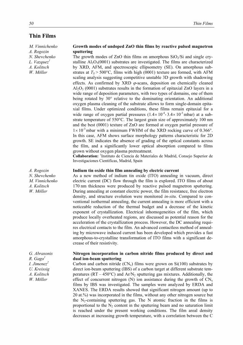
Thin Films 50
Thin Films M. Vinnichenko A. Rogozin N. Shevchenko L. Vazquez1 A. Kolitsch W. Möller
Growth modes of undoped ZnO thin films by reactive pulsed magnetron sputtering The growth modes of ZnO thin films on amorphous SiO2/Si and single cry-stalline Al2O3(0001) substrates are investigated. The films are characterized by XRD, AFM, and spectroscopic ellipsometry (SE). On amorphous sub-strates at TS > 500°C, films with high (0001) texture are formed, with AFM scaling analysis suggesting competitive unstable 3D growth with shadowing effects. As confirmed by XRD ϕ-scans, deposition on chemically cleaned Al2O3 (0001) substrates results in the formation of epitaxial ZnO layers in a wide range of deposition parameters, with two types of domains, one of them being rotated by 30° relative to the dominating orientation. An additional oxygen plasma cleaning of the substrate allows to form single-domain epita-xial films. Under optimized conditions, these films remain epitaxial for a wide range of oxygen partial pressures (1.4 × 10⁻⁴- 3.4 × 10⁻³ mbar) at a sub-strate temperature of 550°C. The largest grain size of approximately 100 nm and the best (0001) texture of ZnO are formed at oxygen partial pressure of 1 × 10⁻³ mbar with a minimum FWHM of the XRD rocking curve of 0.366°. In this case, AFM shows surface morphology patterns characteristic for 2D growth. SE indicates the absence of grading of the optical constants across the film, and a significantly lower optical absorption compared to films grown without oxygen plasma pretreatment. Collaboration: 1Instituto de Ciencia de Materiales de Madrid, Consejo Superior de Investigaciones Cientificas, Madrid, Spain
A. Rogozin N. Shevchenko M. Vinnichenko A. Kolitsch W. Möller
Indium tin oxide thin film annealing by electric current As a new method of indium tin oxide (ITO) annealing in vacuum, direct electric current (DC) flow through the film is explored. ITO films of about 170 nm thickness were produced by reactive pulsed magnetron sputtering. During annealing at constant electric power, the film resistance, free electron density, and structure evolution were monitored in-situ. Compared to con-ventional isothermal annealing, the current annealing is more efficient with a noticeable reduction of the thermal budget and a decrease of the kinetic exponent of crystallization. Electrical inhomogeneities of the film, which produce locally overheated regions, are discussed as potential reason for the acceleration of the crystallization process. However, the DC annealing requi-res electrical contacts to the film. An advanced contactless method of anneal-ing by microwave induced current has been developed which provides a fast amorphous-to-crystalline transformation of ITO films with a significant de-crease of their resistivity.
G. Abrasonis R. Gago1 I. Jimenez2 U. Kreissig A. Kolitsch W. Möller
Nitrogen incorporation in carbon nitride films produced by direct and dual ion-beam sputtering Carbon and carbon nitride (CNx) films were grown on Si(100) substrates by direct ion-beam sputtering (IBS) of a carbon target at different substrate tem-peratures (RT – 450°C) and Ar/N2 sputtering gas mixtures. Additionally, the effect of concurrent nitrogen (N) ion assistance during the growth of CNx films by IBS was investigated. The samples were analyzed by ERDA and XANES. The ERDA results showed that significant nitrogen amount (up to 20 at.%) was incorporated in the films, without any other nitrogen source but the N2-containing sputtering gas. The N atomic fraction in the films is proportional to the N2 content in the sputtering beam and no saturation limit is reached under the present working conditions. The film areal density decreases at increasing growth temperature, with a correlation between the C
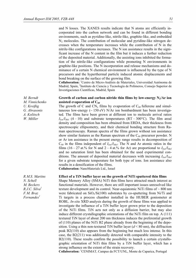
Annual Report IIM 2005, FZR-448
51
and N losses. The XANES results indicate that N atoms are efficiently in-corporated into the carbon network and can be found in different bonding environments, such as pyridine-like, nitrile-like, graphite-like, and embedded N2 molecules. The contribution of molecular and pyridine-like nitrogen de-creases when the temperature increases while the contribution of N in the nitrile-like configurations increases. The N ion assistance results in the signi-ficant increase of the N content in the film but it induces a further reduction of the deposited material. Additionally, the assisting ions inhibited the forma-tion of the nitrile-like configurations while promoting N environments in graphite-like positions. The N incorporation and release mechanisms and do-minance of a certain N chemical environment is influenced by the type of N precursors and the hyperthermal particle induced atomic displacements and bond breaking on the surface of the growing film. Collaboration: 1Centro de Micro-Análisis de Materiales, Universidad Autónoma de Madrid, Spain, 2Instituto de Ciencia y Tecnología de Polímeros, Consejo Superior de Investigaciones Científicas, Madrid, Spain
M. Berndt M. Vinnichenko U. Kreißig G. Abrasonis A. Kolitsch W. Möller
Growth of carbon and carbon nitride thin films by low-energy N2/Ar ion assisted evaporation of C60 The growth of C and CNx films by evaporation of C60 fullerene and simul-taneous low-energy (~ 150 eV) N/Ar ion bombardment has been investiga-ted. The films have been grown at different ion to molecule arrival ratios IIon/IMol (4 – 10) and substrate temperatures (RT – 300°C). The film areal density and composition has been obtained from ERDA, their thickness from spectroscopic ellipsometry, and their chemical bonding structure from Ra-man spectroscopy. Raman spectra of the films grown without ion assistance show similar features as the Raman spectrum of the C60 precursor powder. N or Ar ion assistance in the present energy range results in decomposition of C60 in the films independent of IIon/IMol. The N and Ar atomic ratios in the films (16 – 27 at.% for N and 2 – 4 at.% for Ar) are proportional to IIon/IMol and no saturation limit has been obtained for the used experimental con-ditions. The amount of deposited material decreases with increasing IIon/IMol for a given substrate temperature for both type of ions. Ion assistance also results in a densification of the films. Collaboration: NanoMaterials Ltd., Israel
R.M.S. Martins N. Schell M. Beckers R.J.C. Silva1 F.M. Braz Fernandes1
Effect of a TiN buffer layer on the growth of NiTi sputtered thin films Shape Memory Alloy (SMA) NiTi thin films have attracted much interest as functional materials. However, there are still important issues unresolved like texture development and its control. Near-equiatomic NiTi films of ~ 800 nm were fabricated on SiO2/Si(100) substrates by co-sputtering from Ni/Ti and Ti targets in a process chamber installed in the HUBER goniometer at ROBL. In-situ XRD analysis during the growth of these films was applied to investigate the influence of a TiN buffer layer grown prior to the deposition of the NiTi films. TiN acts not only as a diffusion barrier, but may also induce different crystallographic orientations of the NiTi film on top. A (111) textured TiN layer of about 200 nm thickness induces the preferential growth of (110) planes of the NiTi B2 phase already from the beginning of the depo-sition. Using a thin non-textured TiN buffer layer (d < 80 nm), the diffraction peak B2(110) also appears from the beginning but much less intense. In this case, the B2(211) was additionally detected with comparable intensity to the B2(110). These results confirm the possibility to launch a certain crystallo-graphic orientation of NiTi thin films by a TiN buffer layer, which has a strong influence on the extent of the strain recovery. Collaboration: 1CENIMAT, Campus da FCT/UNL, Monte de Caparica, Portugal
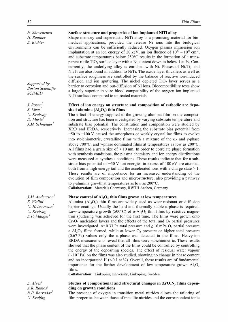
Thin Films 52
N. Shevchenko H. Reuther E. Richter
Supported by Boston Scientific SCIMED
Surface structure and properties of ion implanted NiTi alloy Shape memory and superelastic NiTi alloy is a promising material for bio-medical applications, provided the release Ni ions into the biological environments can be sufficiently reduced. Oxygen plasma immersion ion implantation at an ion energy of 20 keV, an ion fluence of 1017 – 1018 cm-2, and substrate temperatures below 250°C results in the formation of a trans-parent rutile TiO2 surface layer with a Ni content down to below 1 at.%. Con-currently, the underlying alloy is enriched with Ni. Phases of Ni4Ti3 and Ni3Ti are also found in addition to NiTi. The oxide layer thickness as well as the surface roughness are controlled by the balance of reactive ion-induced diffusion and ion sputtering. The nickel depleted TiO2 layer serves as a barrier to corrosion and out-diffusion of Ni ions. Biocompatibility tests show a largely superior in vitro blood compatibility of the oxygen ion implanted NiTi surfaces compared to untreated materials.
J. Rosen1 S. Mraz1 U. Kreissig D. Music1 J.M. Schneider1
Effect of ion energy on structure and composition of cathodic arc depo-sited alumina (Al2O3) thin films The effect of energy supplied to the growing alumina film on the composi-tion and structure has been investigated by varying substrate temperature and substrate bias potential. The constitution and composition were studied by XRD and ERDA, respectively. Increasing the substrate bias potential from −50 to −100 V caused the amorphous or weakly crystalline films to evolve into stoichiometric, crystalline films with a mixture of the α- and γ-phase above 700°C, and γ-phase dominated films at temperatures as low as 200°C. All films had a grain size of < 10 nm. In order to correlate phase formation with synthesis conditions, the plasma chemistry and ion energy distributions were measured at synthesis conditions. These results indicate that for a sub-strate bias potential of −50 V ion energies in excess of 100 eV are attained, both from a high energy tail and the accelerated ions with a charge state > 1. These results are of importance for an increased understanding of the evolution of film composition and microstructure, also providing a pathway to γ-alumina growth at temperatures as low as 200°C. Collaboration: 1Materials Chemistry, RWTH Aachen, Germany
J.M. Andersson1 E. Wallin1 U. Helmersson1 U. Kreissig E.P. Münger1
Phase control of Al2O3 thin films grown at low temperatures Alumina (Al2O3) thin films are widely used as wear-resistant or diffusion barrier coatings. Usually the hard and thermally stable α-phase is required. Low-temperature growth (500°C) of α-Al2O3 thin films by reactive magne-tron sputtering was achieved for the first time. The films were grown onto Cr2O3 nucleation layers and the effects of the total and O2 partial pressures were investigated. At 0.33 Pa total pressure and ≥ 16 mPa O2 partial pressure α-Al2O3 films formed, while at lower O2 pressure or higher total pressure (0.67 Pa) values only the α-phase was detected in the films. Heavy-ion ERDA measurements reveal that all films were stoichiometric. These results showed that the phase content of the films could be controlled by controlling the energy of the depositing species. The effect of residual water vapour (~ 10-4 Pa) on the films was also studied, showing no change in phase content and no incorporated H (< 0.1 at.%). Overall, these results are of fundamental importance for the further development of low-temperature grown Al2O3 films. Collaboration: 1Linköping University, Linköping, Sweden
E. Alves1 A.R. Ramos1 N.P. Barradas1 U. Kreißig
Studies of compositional and structural changes in ZrOxNy films depen-ding on growth conditions The presence of oxygen in transition metal nitrides allows the tailoring of film properties between those of metallic nitrides and the correspondent ionic
Annual Report IIM 2005, FZR-448
53
L. Rebouta2 F. Vaz2
oxides. Changing the oxide/nitride ratio gives the possibility to tune the bandgap, bandwidth, crystallographic order and hence the properties of the films. The work focuses on the analysis of ZrOxNy thin films, the composi-tion evolution with changing growth conditions and its relation to the struc-tural and morphological properties of the films. The films were prepared by rf reactive magnetron sputtering, using different reactive gas flows. Compo-sition and structure were measured combining IBA and XRD techniques. The depth profiles of nitrogen and oxygen have been obtained by ERDA. Results showed that the oxygen fraction in the films increases with gas flow, rea-ching a value of x ~ 0.33 for a reactive gas flow mixture of 6.25 sccm. During growth mixed zirconium nitride and oxide phases form. Furthermore, the deposition rate correlates with the oxygen content variations, showing a continuous decrease with reactive gas flow. Collaboration: 1Nuclear and Technological Institute, Sacavem, Portugal; 2University of Minho, Guimaraes, Portugal
R. Yankov A. Donchev1 M. Schütze1 E. Richter
Supported by AiF
Efficient oxidation protection of γ-TiAl alloys by ion implantation of halogens For the development of a commercially viable process for enhancing the high-temperature (> 700°C) oxidation resistance of γ-TiAl alloys, exploratory beamline co-implantation studies have been performed using F+ + B+, F+ + C+, F+ + N+, F+ +Y+, (SiF)+, and Cl +Y+ ions with overlapping implantat-ion profiles at a mean depth of 100 nm. Oxidation tests at 900°C in synthetic air demonstrated a lowest mass gain after 100 h for (SiF)+ implant followed by F+ + B+, F+ + C+ and F+ + N+ implants. Initial efforts using PIII of Cl from an 80 % Ar / 20 % Cl plasma have focused on the optimization of the process. Highest oxidation resistance has been achieved with 106 pulses at a bias vol-tage of 30 kV, a frequency of 250 Hz, and an RF power of 350 W. Increasing the power to 1000 W leads to appreciable deterioration of the oxidation behavior. The optimized PIII of Cl produces largely improved oxidation resistance similar to that achieved by beamline implantation of Cl. In order to ease practical handling, dichlormethane (CH2Cl2) has been used as an alter-native precursor gas, with an even slightly increased oxidation resistance compared to the Ar/Cl processing. This may be explained by the combined effect of Cl and C as a microalloying element. The oxidation time for the CH2Cl2- treated samples has been extended to 1000 h, and excellent oxidation resistance has been retained throughout the test. Collaboration: 1Karl-Winnacker-Institute of the DECHEMA e.V., Frankfurt/Main, Germany
N. Özkucur1 E. Richter C. Wetzel2 F. Hollstein2 R.H.W. Funk1 T.K. Monsees1
Enhanced biocompatibility of human endothelial cells on ion-beam-treated polyurethane surfaces To improve the biocompatibility of polyurethane (PUR) in blood-contacted devices, PUR surfaces were modified by ion irradiation using C, O, N, or Ar ions with energies of 0.3 – 50 keV and doses of 1013 – 1015 ions/cm2. Adhe-sion, proliferation and cytotoxicity of human umbilical vein endothelial cells (HUVEC) were compared to unmodified control surfaces (uPUR). Ion irra-diation strongly influences surface topography and free energy as demon-strated by AFM and contact angle measurement, respectively. The surface roughness is lowest at medium ion energies and increases at elevated ion dose. The largest contact angles result from medium ion energies. A triple immunostaining for actin cytoskeleton, vinculin (as a marker of focal contacts) and nuclei (DAPI), was employed for adhesion studies. The apoptosis rates were calculated by counting fragmented nuclei. WST-1 assay was used for analysis of cell proliferation. A strong improvement in endothelial cell adhesion and proliferation on ion implanted surfaces was
Thin Films 54
observed. Intensive cell spreading and most focal contacts were found on O- and N-implanted surfaces, followed by Ar-implanted, or N- and O-plasma treated implants. In contrast, C-implanted surfaces display low adhesion and a higher apoptosis rate. Ion energy has a stronger effect on cell numbers (24 h) and cell proliferation (5 d) than ion dose. Collaboration: 1Institute of Anatomy, TU Dresden, Germany, 2Techno-Coat Ober-flächentechnik GmbH, Zittau, Germany
A. Bentzen1,3 A. Ulyashin2 A. Suphellen3 E. Sauar1 D. Grambole D.N. Wright3 E.S. Marstein3 B.G. Svensson2 A. Holt3
Surface passivation of silicon solar cells by a-Si/Si3N4 dual layers Surface passivation of silicon by a dual structure consisting of a hydro-genated amorphous silicon (a-Si) thin film capped by a Si3N4 anti-reflection layer, both layers deposited by plasma enhanced chemical vapour deposition, was investigated. The results show that a synergetic effect on the surface passivation properties is obtained from such a dual structure. Moreover, the surface passivation can be significantly enhanced after a short anneal for temperatures up to about 500°C, whereas anneals at higher temperatures result in degradation of the passivation properties. From NRA of the as-depo-sited and annealed structures, the enhanced surface passivation experienced after annealing is indicated to be due to hydrogen release from the structure towards the Si substrate, possibly followed by a redistribution of hydrogen and subsequent passivation of Si dangling bonds in the sub-interface region. Collaboration: 1Renewable Energy Corp. AS, Høvik, Norway, 2Center for Material Science and Nanotechnology, University of Oslo, Norway, 3Section for Renewable Energy, Institute for Energy Technology, Kjeller, Norway
M. Kutzer1 F. Allenstein1 G. Beddies1 R. Grötzschel H.-J. Hinneberg1 S. Mantl2
Ohmic contacts on Si(001) by selenium modification of metal/semicon-ductor-interface The deposition of about one monolayer (ML) of Se onto Si(001) leads to the restoration of surface geometry and consequently to an electronic and che-mical surface passivation. In particular, it is possible to realise metal-contacts with negative Schottky barriers on Se-passivated n-type Si(001). We studied the deposition of Se on n-type Si(001) after various surface preparation steps to find conditions for self-limited growth of only 1 ML. The depositions were performed in a MBE system in ultrahigh vacuum (UHV). Selenium was eva-porated by using two different source materials: SnSe2 and WSe2. The sur-face retention of Se atoms, that means the remaining Se areal density and as well as that of contaminations were measured ex-situ by RBS with He ions. It could be shown that Se only sticks to “clean”, silicon terminated Si(001) surfaces, achieved by growing a Si buffer layer of 80 nm or by etching-off the native SiO2 in UHV a chemical reaction of impinging Si at 700°C which reduces SiO2 to volatile SiO. Due to the low binding energy of Se at Si the Se desorption during the exposition to atmosphere and later during the RBS measurement cannot be avoided and therefore samples had to be enhanced with a metallic cap layer that disables the Se loss. Using the compound SnSe2 as source material a contamination of the Se coverage with Sn at the level of about 1 at.% was unavoidable. In the case of WSe2 the W contamination in the passivation layer is below the RBS detection limit of < 1011 atoms/cm2. Collaboration: 1TU Chemnitz, Germany 2Forschungszentrum Jülich, Germany
Annual Report IIM 2005, FZR-448
55
Nanoscale Magnetism J. Fassbender J. McCord1
Control of saturation magnetization, anisotropy and damping due to Ni implantation in thin Ni81Fe19 layers The static and dynamic magnetic properties of 20 nm thick Ni81Fe19 films implanted with Ni-ions have been investigated as a function of the ion flu-ence up to 1 × 10¹⁶
cm-2 (~ 5 at.%). The implantation has been performed at 30 keV. The maximum of the projected ion range is located in the center of the ferromagnetic layer for a rather homogeneous ion distribution throughout the film. With increasing ion fluence the saturation magnetization and the effective magnetic anisotropies (static and dynamic) are reduced. However, the effective magnetic damping is drastically enhanced for higher ion fluen-ces. This increase can be explained mainly by the drop in saturation magneti-zation in connection with structural changes. In addition ion implantation in an applied magnetic field allows the setting of the uniaxial anisotropy direc-tion irrespective of the initial orientation. Collaboration: 1Leibniz Institute of Solid State and Materials Research Dresden, Germany
J. Fassbender J. von Borany A. Mücklich K. Potzger W. Möller J. McCord1 L. Schultz1 R. Mattheis2
Structural and magnetic modifications in Cr implanted permalloy The static and dynamic magnetic properties, especially the magnetic damping behavior, have been investigated as a function of saturation magnetization in thin Ni81F19 (permalloy) films. Ion implantation doping with Cr in the per-centage regime has been used to effectively reduce the Curie temperature and thus the saturation magnetization at room temperature. In order to understand the magnetic modifications the changes in stoichiometry but also the ion induced structural changes have been addressed. As a function of fluence first an improvement of the (111) fiber texture, then a lattice expansion and finally a partial amorphization of the interface near region of the permalloy layer is found. The region of amorphization can be understood quantitatively by simulation of the concentration profiles as a function of depth in combi-nation with irradiation induced damage formation. The magnetic properties change correspondingly. For increasing Cr doping a drop in saturation mag-netization and a decrease of the uniaxial magnetic anisotropy is observed. For a fluence of 0.8 × 10¹⁶
Cr/cm2 (~ 4 at.%) the magnetic damping parameter α increases by a factor of 7. This strong increase is mainly caused by the reduc-tion of the saturation magnetization and a change of the sample crystallinity. Collaboration: 1Leibniz Institute of Solid State and Materials Research Dresden, Germany, 2Institute for Physical High Technology Jena, Germany
V. Cantelli J. v. Borany J. Grenzer J. Fassbender R. Kaltofen1 J. Schumann1
Influence of He ion irradiation on thin NiMn / Ni81F19 exchange bias films Magnetron sputtered film stacks of 5 nm Ta / 50(15) nm NiMn / 20 nm Ni81Fe19 / 5 nm Ta deposited at SiO2/Si substrates were subsequently irra-diated with He+ ions (30 keV, 1 × 10¹⁵ – 3 × 1016 cm-2, RT or 250°C). The tran-sition from the paramagnetic NiMn phase (fcc) to the chemically ordered, antiferromagnetic tetragonal L10 phase during annealing (100 – 500°C, Va-cuum) was studied by in-situ XRD using synchrotron radiation. A small L10 fraction (< 15%) is already available after deposition. The transformation to a dominating L10 ordered NiMn film (long-range order parameter S > 0.5) takes place between 300 – 400°C irrespective of the irradiation. This is consistent with magnetization reversal measurements of the corresponding permalloy layers. Annealing at elevated temperatures (TA > 400°C) leads to a loss of L10 ordering due to a complete intermixing of the NiMn and the permalloy films. The benefit of low-fluence ion irradiation (1 × 1015 cm-2) is a reduction of the mosaicity for both the NiMn and the permalloy film, and a smoothening of
Nanoscale Magnetism 56
internal interfaces.
M.C. Weber1 H. Nembach1 B. Hillebrands1 J. Fassbender
supported by DFG
All-optical probe of precessional magnetization dynamics in exchange biased Ni81Fe19/FeMn bilayers An internal anisotropy pulse field is launched by an 8.3 ps short laser excita-tion, which triggers precessional magnetization dynamics of a polycrystalline Ni81Fe19 / FeMn exchange bias system on a picosecond timescale. Due to the excitation the exchange coupling across the interface between the ferromag-netic and the antiferromagnetic layer is reduced, leading to a fast reduction of the exchange bias field and to a dramatic increase of the zero-field suscepti-bility. The fast optical unpinning is followed by a slower recovery of the interfacial exchange coupling dominated by spin-lattice and heat flow relaxa-tion with a time constant of the order of 160 ps. The measured picosecond time evolution of the exchange decoupling and restoration is interpreted as an anisotropy pulse field giving rise to fast precessional magnetization dynamics of the ferromagnetic layer. The strength of the internal pulse field and even the initial magnetization deflection direction from the equilibrium orientation can be controlled by the absorbed photons. The dependence of the effective Gilbert damping on both small and large angle precessional motion was stu-died, yielding that both cases can be modeled with reasonable accuracy within the Landau-Lifshitz and Gilbert framework. Collaboration: 1Department of Physics, TU Kaiserslautern, Germany
K. Küpper L. Bischoff J. Fassbender K.W. Chou1 B. van Waeyenberge1 H. Stoll1 G. Schütz1 T. Tyliszczak2 I. Neudecker3 C.H. Back3
Suppression of vortex core motion by means of focused ion beams Recently, vortex-core driven magnetization dynamics has become a hot to-pic. The gyrotropic motion of the vortex core is found to be in the sub-GHz regime and thus easily accessible with high-resolution synchrotron-based time-resolved transmission x-ray microscopy (TR-TXM) techniques. In order to investigate the influence of artificial magnetic defects positioned within the vortex structure on the magnetization dynamics and the potential switching between individual defects focused ion beam milling has been employed. The understanding and control of these mechanisms is of utmost scientific and technological relevance. A series of circular and square shaped permalloy (Ni81Fe19) microstructures have been investigated, which exhibit a nanoscopic hole at different positions. The gyrotropic motion of the vortex core is excited by means of a microwave sine-excitation with different ex-citation amplitudes. The magnetization dynamics is sensed by TR-TXM. It is found that a defect located far away from the vortex core has almost no influence on the magnetization dynamics. However, a point defect located in the centre of the structure suppresses the gyrotropic motion of the vortex core completely. Collaboration: 1Max-Planck Institute for Metal Research, Stuttgart, Germany, 2Ad-vanced Light Source, Lawrence Berkeley National Laboratory, Berkeley, USA, 3In-stitute for Experimental and Applied Physics, University of Regensburg, Germany
M.C. Weber1 H. Nembach1 B. Hillebrands1 M.J. Carey2 J. Fassbender
Real-time evidence of two-magnon scattering in exchange coupled bilayers Coherent spin waves in exchange biased bilayers have been excited by ultra-fast photomodulation of the exchange bias anisotropy. Photoinduced preces-sion in CoFe / IrMn samples with different IrMn thickness, thus, different ex-change bias fields, has been studied in real-time by time-resolved Kerr-effect. The extracted effective damping parameter is proportional to the square of the exchange bias field. Two-magnon scattering of the coherent precession of the ferromagnetic layer at local interfacial fluctuations of the exchange bias field can account for the observed increase. Hence, there is time-domain evi-dence of two-magnon damping involved in the relaxation of photoexcited
Annual Report IIM 2005, FZR-448
57
supported by DFG
spins. Collaboration: 1Department of Physics, TU Kaiserslautern, Germany, 2Hitachi Glo-bal Storage Technologies, San Jose, USA
K. Küpper L. Bischoff R. Mattheis1 P. Fischer2 J. Fassbender
Magnetic domains and magnetization reversal of ion-induced magneti-cally patterned RKKY-coupled Ni81Fe19/Ru/Co90Fe10 films Pure magnetic patterning by means of ion beam irradiation of magnetic thin films and multilayers result often from a post deposition local modification of the interface structure with only minor effects on the film topography. In this study a 60 keV fine focused Co ion beam was used to change the coup-ling in a Ni81Fe19 / Ru / Co90Fe10 structure from antiferromagnetic to ferro-magnetic on a micron scale. Thereby an artificial structure with locally vary-ing interlayer exchange coupling and therefore magnetization alignment is produced. High-resolution full-field x-ray microscopy is used to determine the magnetic domain configuration during the magnetization reversal process locally and layer resolved due to the element specific contrast in circular x-ray dichroism. In the magnetically patterned structure there is in addition to the locally varying interlayer exchange coupling across the Ru layer also the direct exchange coupling within each ferromagnetic layer present. Therefore the magnetization reversal behaviour of the irradiated stripes is largely influ-enced by the surrounding magnetic film. Collaboration: 1Institute for Physical High Technology Jena, Germany, 2Center for X-Ray Optics, Lawrence Berkeley National Laboratory, Berkeley, USA
M.O. Liedke K. Potzger A.H. Bothmer B. Hillebrands1 M. Rickart2 P.P. Freitas2 J. Fassbender Supported by EU
Domain structure during magnetization reversal of PtMn/CoFe exchan-ge bias micro patterned lines The magnetic domain configuration and the magnetization reversal behaviour of micropatterned exchange bias elements were investigated by means of magnetic force microscopy. In addition to the unidirectional anisotropy the shape anisotropy determines the overall magnetization reversal behaviour. In order to modify the ratio between both anisotropy contributions the exchange bias field strength was reduced by means of 5 keV He+ ion irradiation. For the as-prepared samples a mono-domain magnetization state with the magne-tization direction aligned along the exchange bias field direction was found regardless of the element shape. After irradiation the unidirectional anisotro-py contribution is reduced and hence the previously homogeneous magneti-zation state brakes up into small domains with 360° domain walls in bet-ween. The appearance of these domain walls, which was mainly observed for the descending branch of the magnetization reversal, is found to depend strongly on the structure width and orientation. Collaboration: 1Department of Physics, TU Kaiserslautern, Germany, 2INESC MN, Lisbon, Portugal
P. Candeloro1 S. Blomeier1 P.A. Beck1 H. Schultheiß1 H.T. Nembach1 B. Hillebrands1 M.O. Liedke J. Fassbender B. Reuscher2
supported by EU
Evidence of lateral coupling in exchange bias double layers with lateral modulation of the exchange bias field Magnetic properties of a Ni81Fe19/FeMn exchange bias bilayer were modified on the micron and submicron scale by ion irradiation, without significant changes in the sample topography. The resulting magnetic patterns were in-vestigated by MOKE and MFM. The hysteresis loops measured by MOKE reveal that the magnetization reversal is not proceeding independently in irradiated and non-irradiated areas. This magnetic coupling is confirmed by MFM measurements, which clearly show that magnetic domains in irradiated and non-irradiated elements are mutually influencing each other during the reversal process. Collaboration: 1Department of Physics, TU Kaiserslautern, Germany, 2Institut für Oberflächen- und Schichtanalytik (IFOS), Kaiserslautern, Germany
Nanoscale Magnetism 58
K. Potzger S. Zhou F. Eichhorn F. Herrmann M. Helm W. Skorupa J. Fassbender T. Herrmannsdörfer1 A. Bianchi1
Ferromagnetic Gd-implanted ZnO single crystals In order to introduce ferromagnetic properties, ZnO single crystals have been implanted with Gd ions at 180 keV ion energy and two different fluences. Magnetization reversal hysteresis loops have been recorded for as-implanted as well as annealed samples using a SQUID magnetometer. For a fluence of 5 × 10¹⁵ ions/cm2, post implantation annealing leads to an increase of the satu-ration moment up to 1.8 µB/Gd at exactly 300 K, thus excluding Gd, ZnGd or Gd2O3 secondary phases to be the origin of the observed ferromagnetism. Collaboration: 1Dresden High Magnetic Field Laboratory, Forschungszentrum Ros-sendorf, Germany
G. Brauer W. Anwand W. Skorupa H. Schmidt1 M. Diaconu1 M. Lorenz1 M. Grundmann1
Structure and ferromagnetism of Mn+ ion-implanted ZnO thin films on sapphire Slow positron implantation spectroscopy (SPIS), based on the generation, implantation and subsequent annihilation of mono-energetic positrons in a sample, has been used to study depth dependent vacancy-type damage in three ZnO films grown by PLD on c-plane sapphire. Doping was achieved by implantation of 250 keV Mn+ ions at 300°C with three different fluences - 1016, 3 × 10¹⁶, and 6 × 1016 cm-2, and subsequent thermal annealing in air. The evolution of the open volume damage, its depth distribution, and the mag-netic behaviour was investigated by SPIS and MFM. No indication of mag-netic domain formation was found in any of the three films after implantation and the first annealing at 500°C, whereas after the second annealing at 750°C the two samples having the higher fluence showed stripe-like magnetic do-mains. Collaboration: 1Institut für Experimentelle Physik II, Universität Leipzig, Germany
S. Zhou K. Potzger A. Mücklich R. Grötzschel B. Schmidt F. Eichhorn W. Skorupa J. Fassbender
Mn-silicide nanoparticles formed in Si using ion implantation 300 keV Mn+ ions were implanted into Si with a fluence of 1 × 1015 cm-2, 1 × 1016 cm-2, 5 × 1016 cm-2, respectively. The samples were annealed at 800°C in N2 ambient for 5 min by rapid thermal annealing method. RBS/C, TEM and XRD were applied for structural characterization. It was found that this annealing is not sufficient to remove the implantation damage. Moreover no evidence is found for Mn substituting Si sites. MnxSiy nanoparticles were formed after annealing. The control of these effects is essential for the design of Si-based diluted magnetic semiconductors.
G. Talut H. Reuther F. Eichhorn K. Potzger S. Zhou Supported by DFG
Magnetic and structural properties of 57Fe implanted GaN In order to investigate the possibility to create and stabilize a DMS (diluted magnetic semiconductor) behaviour in the (Ga,Fe)N-system, p-doped GaN was implanted with 57Fe+ ions (200 keV, 1 – 16 × 1016 cm-2) at 350°C and sub-sequently annealed between 700 and 900°C in N2-flux for 5 min. CEMS measurements of the as-implanted samples (1 – 16 × 1016 cm-2) show a mag-netic hyperfine field of Bhf = 10 T which cannot only be attributed to α-Fe (Bhf = 33 T). However, annealing of the high-fluence implanted samples (≥ 6 × 1016 cm-2) result in the formation of fiber-textured α-Fe-clusters with 5 and 15 nm size after 700 and 900°C annealing, respectively. For the highest Fe-doped sample (16 × 1016 cm-2) annealed at 900°C, AES reveals a disper-sion of the Fe-implantation profile due to radiation-enhanced diffusion and the existence of Fe-rich regions which reflects the formation of Fe clusters. Zero-field-cooled / field-cooled SQUID measurements of the sample implan-ted with 1 × 1016 cm-2 and annealed at 850°C show a Curie-temperature of 250 – 270°C, which is associated with the DMS. However it also indicates the presence of superparamagnetic Fe-clusters with a blocking temperature of 40 K. No other crystalline phases like iron-nitrides were found by XRD.
Annual Report IIM 2005, FZR-448
59
V. Heera R. Höhne1 P. Esquinazi1
Magnetic properties of ion implanted diamond and graphite Recent experimental and theoretical studies suggest the existence of intrinsic ferromagnetism in carbon structures with predominant sp2-bonds like highly oriented pyrolytic graphite (HOPG) and fullerene polymers. In contrast, ferromagnetism in diamond with sp3 bonds has never been observed. It is speculated that the magnetism in the carbon phases is caused by special lattice defects and not, as sometimes suggested, by magnetic impurities. In order to elucidate the role of lattice defects, nonmagnetic and magnetic impu-rities in different carbon phases, a series of implantation experiments was carried out. Diamond and HOPG samples were implanted with F+ and Fe+. Defect-rich surface layers with impurity concentrations from 50 to 500 ppm extending to a depth of about 2 µm were produced by multiple energy im-plantation in the MeV range. The magnetic properties were measured with a SQUID magnetometer. Preliminary results show that the weak ferromagne-tism of the unimplanted HOPG is not markedly influenced after implantation of iron or fluorine. The paramagnetic part of the magnetization of HOPG and diamond clearly increases by ion implantation mainly due to the enhance-ment of disorder. No ferromagnetism was detected in the diamond samples. Collaboration: 1University of Leipzig, Germany
K. Potzger H. Reuther S. Zhou A. Mücklich R. Grötzschel F. Eichhorn M.O. Liedke J. Fassbender H. Lichte1 A. Lenk1
Ion beam synthesis of Fe nanoparticles in MgO and yttria stabilized zir-conia (YSZ) In order to synthesize embedded Fe nanoparticles MgO(001) and YSZ(001), single crystals have been implanted with Fe+ ions at different temperatures and ion energies of 100 keV and 110 keV respectively. Using a fixed ion fluence of 6 × 1016 cm-2, γ-Fe nanoparticles are formed inside the MgO sub-strate up to a temperature of 1073 K. In contrast, ferromagnetic α-Fe nano-particles are formed inside YSZ at elevated temperatures with an efficiency of 100 % at an implantation temperature of 1273 K. Their ferromagnetic be-haviour is reflected by a magnetic hyperfine field of 330 kOe and a hysteretic magnetization reversal. Electron holography measurements have been carried out in order to visualize the stray field of the particles. Collaboration: 1Triebenberg Laboratory for High-Resolution Electron Microscopy, TU Dresden, Germany
V. Cantelli J. von Borany J. Fassbender N. Schell S. Zhou
Influence of energetic atoms on the L10 ordering of FePt films fabricated by magnetron sputtering The L10-ordering of stoichiometric FePt films (30 – 120 nm) deposited on SiO2/Si substrates by dc magnetron sputtering from elemental targets has been studied. A low deposition rate (0.6 Å/s) and Ar pressure (0.3 Pa) was used. The kinetics of A1→L10 transition and ordering in FePt films have been investigated by in-situ XRD at the Synchrotron beamline ROBL at ESRF. The transition has been obtained at relatively low temperatures of (300 ± 20)°C leading to almost complete L10 ordered films with an ordering parameter S > 0.8. No remarkable differences are obtained by combining de-position at room temperature and post-deposition annealing or deposition at the annealing temperature except of slightly variations in the grain size. An additional ion irradiation with He+ (50 keV, 1 × 10¹⁵ – 3 × 1016 cm-2) does not influence the transition temperature and the degree of ordering. Calculations reveal that for our experimental conditions there is no thermalization of the sputtered target atoms and the reflected Ar neutrals, thus a considerable frac-tion of atoms meet the substrate with energies exceeding the displacement threshold. This corresponds to the formations of point defects already during deposition which support the L10 ordering if they get mobile at temperatures > 250°C.
Nanoscale Magnetism 60
K.-H. Heinig
Even-odd effect of anisotropy transfer from a stack of metal films to the L10 superstructure Atomic collisions in solids are often associated with the concept of disorder. However, recently we demonstrated that irradiation may induce chemical order in intermetallic alloys, where significant structural L10 order of alterna-ting (001)Fe and (001)Pt atomic layers in almost fcc-type FePt was obtained and controlled in FePt by postgrowth He ion irradiation well below the order-ing temperature. Now, the irradiation-assisted L10 phase formation from a stack of several atomic layers thick Fe and Pt films was studied by kinetic Monte-Carlo simulations. An unexpected even-odd effect in the anisotropy of the final L10 phase was discovered: Whereas stacks of films consisting of an even number of atomic (001) layers show no preferred c-axis selection of the final structure, stacks of films consisting of an odd number of atomic (001) layers may show an almost perfect c-axis alignment perpendicular to the substrate. This very selective L10 phase formation has been understood by the peculiarity of the reaction pathway in a stack of films: The L10 FePt phase forms from Fe and Pt via the two L12 phases (Fe3Pt, FePt3), where the L12 unit cells fit commensurably or incommensurably in a single film of one metal. Thus, during the formation of the L10 superstructure from the two L12 phases, the anisotropy of the Fe/Pt interface will be either transferred to a single L10 variant or will be lost completely. This evolution of anisotropy of layered systems is very important for the synthesis of new magnetic recor-ding films.
M.O. Liedke S. Rossbach S. Facsko J. Fassbender
Exchange bias on rippled substrates Monoatomic steps at the interfaces between a ferromagnetic and an antiferro-magnetic layer give rise to uncompensated spins which are the origin of the exchange bias phenomenon. Such steps have been generated by substrate sur-face patterning by means of Ar+ ion erosion. Depending on the primary ener-gy and the angle of incidence, a rippled surface with a well defined periodi-city (~ 20 – 100 nm) and peak-to-valley height (~ 2 – 5 nm) has been created. On top of this surface, an exchange bias system consisting of 5 nm Ni81Fe19 coupled to 10 nm Fe50Mn50 has been prepared by MBE. The interface corru-gation remains throughout the layer stack. By means of a field annealing cycle the exchange bias direction has been initialized either along or perpen-dicular to the ripple direction, which causes to align the uniaxial and uni-directional anisotropy contributions either parallel or perpendicular to each other. The magnetization reversal behaviour has been investigated by means of MOKE. For both cases the magnetic easy- and hard-axes remained identical as the uniaxial anisotropy contribution is much larger than the uni-directional one. However, exchange bias initialization along or perpendicular to the ripple direction shifts the magnetization reversal loop of the easy-axis or hard-axis, respectively. A complete angular dependence of the magnetiza-tion reversal behaviour has been investigated for both cases and compared to simulations based on a Stoner-Wohlfarth coherent rotation model. A good agreement between experimental data and simulations is found.
Annual Report IIM 2005, FZR-448
61
Nanostructures L. Röntzsch K.-H. Heinig B. Schmidt A. Mücklich W. Möller J. Thomas1 T. Gemming1
Direct evidence of self-aligned Si nanocrystals formed by ion irradiation of Si/SiO2 interfaces by energy-filtered TEM Recently it has been proven that thin SiO2 layers placed between the Si sub-strate and a poly-Si top layer become an efficient charge storage medium for non-volatile memory applications by Si+ ion irradiation and subsequent an-nealing. It has been predicted by atomistic computer simulations that δ-layers of tiny Si nanocrystals (NCs) are formed by this technique. So far these NCs could neither be imaged by TEM nor unambiguously identified by any other analytical method. For the first time, we deliver direct evidence of Si NC δ-layers in SiO2 by energy-filtered TEM. We found ≤ 3 nm sized Si NCs at the ion-irradiated (ESi = 50 keV, ΦSi = 7 × 1015 cm-2) and annealed (T = 1050°C, t = 120 s) Si/SiO2 interfaces of a MOS-like “50 nm Si / 15nm SiO2 / Si sub-strate” structure. The position and shape of the NC δ-layers are in good agreement with the predictions of former atomistic computer simulations. Collaboration: 1Leibniz Institute for Solid State and Materials Research Dresden, Germany
L. Röntzsch K.-H. Heinig Supported by DFG
Atomistic simulations on the focused-ion-beam-based synthesis of func-tional 1D nanostructures Nanowires (NWs) play an important role as basic components of electronic and photonic devices. Atomistic computer simulations on focused ion beam (FIB) implantation and subsequent phase separation during thermal annealing were performed. The systematic investigations are aimed at optimum react-ion pathways for CMOS-compatible fabrication of metal silicide and semi-conductor nanowires. On realistic time and length scales, the simulation of the whole process was divided into two steps: (i) the spatio-temporal evo-lution of FIB implantation profiles was calculated by a new computer code including dynamical target changes, local ion erosion etc, (ii) post-implant-ation annealing causes NW formation, which is modelled by kinetic Monte Carlo simulations. It is demonstrated that the evolution of the FIB implant-ation profile proceeds in three stages: (i) phase separation by nucleation and growth, (ii) NW formation by coalescence of nanoclusters, (iii) NW surface smoothening. Likewise, functional structures for nanoelectronic and photonic devices including several NWs, like T- or X-junctions, are obtained by cros-sing different FIB traces.
L. Röntzsch K.-H. Heinig Supported by DFG
Search for reaction pathways of a CMOS-compatible channel fabricati-on for nanofluidic devices Nanofluidic devices are going to play an important role in miniaturization, automation and parallelization of chemical, biological, or medical systems. For “lab-on-a-chip” devices, CMOS compatibility is desired. We discovered a potential reaction pathway for a nonconventional, however, CMOS-com-patible fabrication method of nanofluidic channels and channel networks. Starting from the “silicon-on-nothing” technique developed by a Japanese group (T. Sato et al., Jap. J. Appl. Phys. 43 (2003) 12), we predict, by kinetic Monte-Carlo simulations, nanochannel formation in (001)Si from appropriate trench ensembles. During a thermal treatment, thin trenches decouple quickly from the wafer surface forming buried voids. In a self-organizing manner, neighbouring voids coalesce and, thus, form a buried channel. Thick trenches are more stable. They remain open at the wafer surface and, therefore, may act as vertical supply and drain pipes for buried channels. The simulations predict also the formation of elementary nanochannel networks such as T- or X-like junctions, H-filters, as well as buried toroidal voids.
Nanostructures 62
L. Röntzsch K.-H. Heinig
Supported by DFG
Size and position control of chains or arrays of nanoparticles by thermo-capillarity Surface free energy minimization, driven by capillary forces, may lead to morphological changes of wires, i.e. their decay into a droplet chain (Ray-leigh instability). At nanoscale dimensions, capillary-driven self-organization processes are subject to increasing fluctuation with decreasing size, thus preventing the formation of long-range ordered regular structures. Here, a novel method to fabricate size- and position controlled chains of nanopartic-les is examined by means of kinetic Monte Carlo simulations. The method rests on the temperature dependence of surface tension – the origin of ther-mocapillarity. Uncompensated forces occur due to surface temperature gra-dients. It is found that surface tension gradients trigger the biased migration of atoms from hot to cold regions. We predict that the regularity of nano-particle chains formed during the self-organized disintegration of nanowires can be considerably improved by an external periodic temperature profile along the nanowires. Strong external temperature fields control the nanowire decay, however, weak ones have to be commensurable with the Rayleigh wavelength to produce long rang order.
T.W.H. Oates A. Mücklich
Supported by EU (MC-IIF)
Controlling the growth of Ag nanoparticles in polymer matrices using spectroscopic ellipsometry Controlled growth of metal nanoparticles in a polymer matrix is of technical interest for catalytic, biosensor and optoelectronic applications. Monitoring of PVD nanoparticle growth using in-situ spectroscopic ellipsometry (SE) has been performed. Ag nanoparticle growth is performed in an RF magne-tron sputter facility equipped with in-situ SE and sample stage heating capa-bilities. High resolution TEM imaging of the nanoparticles shows almost spherical single-crystal particles. Major advances have been made in model-ling of the SE data utilising collective electron oscillations in the form of plasmon-polariton resonances. Information concerning the particle size and nucleation processes can be extracted by considering the mean free path of the electrons in the nanoparticles. For incorporation of the nanoparticles in polymer matrices, dual magnetron sputtering is utilised for the production of metal nanoparticle/polymer composite films by both alternate and co-sput-tering and the process monitored with in-situ FTIR and SE. A second approach investigates the growth of nanoparticles by reduction of metallic ions in a polymer. Thermal degradation of an organometallic precursor dis-persed in polystyrene is shown to produce silver particles of the order of 6 nm radius, a process which is recorded in real-time by SE. Plasmon- pola-riton resonances in the particles allow the real time growth of the particles to be followed in the range of 2 to 10 nm in radius.
C. Akhmadaliev B. Schmidt L. Bischoff
Investigation of FIB assisted CoSi2 nanowire and nanochain growth in crystalline silicon The ion beam synthesis of CoSi2 nanowires (NW) by writing stoichiometric FIB implantation and subsequent annealing has been studied. Si(111) and Si(100) samples were implanted at a sample temperature of 450°C or at room temperature (RT). The implantation dose for heated and non-heated samples was in the range of (0.5 – 2) × 1017 cm-2 and (0.1 – 1.0) × 1016 cm-2, respective-ly. The line scan direction of the FIB was aligned under 0°, 15°, 30° and 45° relative to the <110> crystal direction. The heated samples were subsequent-ly annealed in a two step process: 600°C for 60 min and 1000°C for 30 min in dry N2. Stable CoSi2 nanowires with diameter down to 10 – 50 nm and up to 5 µm length were achieved when the FIB trace was precisely aligned along <110>-direction. In the case of a misaligned FIB trace the nanowires are not
Annual Report IIM 2005, FZR-448
63
Supported by DFG
stable and decay into chains of CoSi2 nanoparticles. This behaviour is con-sistent with 3D kinetic Monte-Carlo-simulations of phase separation, coa-lescence and decay of NWs. FIB implantation at RT leads to local defect formation and produces nucleation (strain) centers. After implantation the sample back side was additionally coated with 10 nm Co. During subsequent annealing (heating, quenching) a Co super-saturation through the sample was achieved. Self-aligned wire growth starting at the nucleation centers and along <110> directions was observed in Si(100) and Si(111) substrate mate-rials. Further efforts are focused on increasing of reproducibility of nanowire growth and the fabrication of nanodevices.
L. Bischoff C. Akhmadaliev S. Facsko A. Keller
Surface structures induced by sputtering of Si and Ge with a FIB Self-organized periodic structures with submicron periodicity are known to be formed by a broad ion beam. They can be arranged as ripple patterns at off-normal ion incidence and as hexagonal patterns at normal incidence. We have studied the pattern formation induced by a scanned focused ion beam (FIB) on Si and Ge surfaces as a function of ion species, ion current, ion dose, and incidence angle. While high currents of about 1 nA lead to strongly structured surfaces, low currents of some ten pA seem to result in a flattening of the surface at nearly the same total current densities of the order of A cm-2. At off-normal angles of incidence the appearance of ripple patterns with periodicities around 1 µm similar to the ripples produced by broad beams are observed. However, at normal incidence of the FIB new complex structures starting from the edges of the scanned area are formed which are not ob-served during broad beam ion irradiation. A great advantage of the FIB is its ability for in-situ imaging of secondary electrons during pattern formation. The in-situ analysis of the dynamical behavior of the surface morphology gives a new access to distinguish between the different models for the pattern formation.
C. Akhmadaliev L. Bischoff B. Schmidt V. Luchnikov1 M. Stamm1
Supported by DFG
Focused ion beam milling of polymer bi-layers for fabrication of self-rol-led micro- and nanotubes The formation of micro- and nanotubes from scrollable polymer bi-films deposited on an Al sacrifice layer on a silicon substrate was studied. The dimensions and the position of the rolled-up tubes were controlled by FIB-milling of H- and U-like structures of different shape in the polymer films. The FIB has several advantages compared to the application of other techni-ques, like mechanical cutting or lithography, due to a better spatial resolution and the direct structuring of materials independent of the composition. First the silicon substrate was covered with an Al layer. Then the polymer bi-layer was deposited by means of spin-coating starting with a film of poly-4-vinyl pyridine from a chloroform solution followed by a polystyrene film from a toluene solution. The FIB pattered samples were etched in alkaline water or in acid solution in order to remove the Al layer which enables the polymer bi-layer to roll-up into tubes. The diameter is a function of the polymer thick-ness whereas for a 50 nm thick bi-layer tubes with a diameter of about 0.8 – 1 µm were obtained. Collaboration: 1Leibniz-Institute for Polymer Research Dresden, Germany
J. Grenzer L. Bischoff M. Posselt U. Pietsch1
X-ray grazing incidence investigations of focused ion beam implantation pattern at Si and GaAs surfaces 2D arrays of circular dots have been fabricated on GaAs(001) and Si(001) substrates using a Ga+ FIB implantation with a spot size of about 50 nm (nor-mal incidence, 25 keV, 1014 cm-2 per dot). The 2D-lattice structures had a period of 250 × 250 nm2 covering a total area of 0.2 mm2. The influence of the implanted ions on the host lattice has been investigated by means of
Nanostructures 64
grazing incidence diffraction (GID) performed at the ESRF-beamlines ID10 and ID1. The low-dose implantation creates point defects (interstitials and vacancies) below the surface in both substrates. In Si substrates a 2D perio-dical strain field is generated which is clearly obtained in the GID pattern. For the GaAs substrate we found a more complex scattering pattern depen-ding on the in-plane orientation of the 2D dot array with respect to the crystallographic orientation of the GaAs crystal. A significantly enhanced scattering contrast is obtained if the implantation is performed with a twist of 14° towards the [110] direction. The reason for the experimentally obtained difference in the scattering pattern between FIB implanted Si and GaAs is still under discussion, but clearly associated with the crystalline structure of the substrate. Collaboration: 1Institute of Physics, University of Siegen, Germany
B. Schmidt S. Oswald1 L. Bischoff
Etch rate retardation of Ga+ ion beam irradiated silicon Surface chemistry during wet chemical etching in alkaline KOH solution and dry etching in SF6 / O2 plasma of high-dose Ga+ implanted Si has been investigated by means of SIMS and XPS. During wet chemical etching in a KOH/H2O solution a thin layer of GaOx of < 1 nm thickness is formed, which has been investigated in more detail by angle-resolved XPS. In the case of dry reactive ion etching (RIE) the surface chemistry is quite different. In this case a more enhanced oxidation of Ga takes place due to the high reactivity of atomic oxygen from the SF6 / O2 plasma. SIMS results show that during RIE a Ga-rich surface layer forms, and therefore an enhanced Ga oxidation takes place, leading to a thicker GaOx layer compared to wet chemical treat-ment. XPS depth profiling reveals a stoichiometry of almost completely oxidized Ga (Ga2O3) layer free from Si with a thickness of about 5 – 10 nm. The etch rate lowering in Ga+ as-implanted silicon is ascribed to the forma-tion of gallium oxide at the Si surface during the etch processes. Collaboration: 1Institute of Solid State and Materials Research Dresden, Germany
S. Oswald1 B. Schmidt K.-H. Heinig
Influence of sputtering conditions and electron energy on XPS depth profiling of Ge in SiO2 Ge nanocluster formation in SiO2 is of growing interest for new electronic applications. Ion beam synthesis using Ge implantation connected with ther-mal annealing is one possible preparation method of such clusters. In addi-tion to investigations of electrical and structural changes during the cluster formation process we also studied chemical changes in the samples using XPS. This was done with low-energy noble gas ion sputtering for depth profiling. Binding state information can be obtained from the XPS data by means of factor analysis in combination with other structural investigations. However, mixed bonding states probably created by ion beam damage during sputter erosion dominate the results. It is shown that, by changing the experi-mental conditions (ion beam impact depth during sputtering, electron infor-mation depth during XPS measurement) these mixed states are influenced in an appropriate manner. It is concluded that useful chemical information on the behaviour of the implanted Ge can be derived despite of the ion beam damage. Collaboration: 1Institute of Solid State and Materials Research Dresden, Germany
M. Zier B. Schmidt
Shallow pn-junctions for piezoresistive cantilevers Piezoresistive ultra thin p-type silicon layers can serve as compact, highly sensitive bending sensors in AFM cantilevers. Such piezoresistors for use in cantilever arrays have been fabricated using ion implantation of 1 keV B+ ions. To reduce channeling and therefore the pn-junction depth, the substrate was pre-amorphised by irradiation with 30 or 60 keV Ge+ ions. To remove
Annual Report IIM 2005, FZR-448
65
Supported by EU
the radiation damage and for electrically activation of boron, RTA for 10 to 60 s at 1000°C was employed. In parallel computer simulations of the ion implantation and annealing were carried out using the Crystal-TRIM and TESIM codes. TEM cross-section images showed an excellent agreement of the thickness of the amorphised layer with Crystal-TRIM simulations. SIMS measurements for the B+ implanted and annealed samples agreed very well with TESIM simulations. For electrical characterization, test structures were fabricated to measure the sheet and contact resistances, the pn-junction breakdown and the leakage current, so that they can be optimised very quickly. The resistor layer meets the desired sheet resistance of around 300 Ω/ and the junctions provide an excellent reverse bias insulation with a high breakdown voltage (> 150 V) and a low leakage current (< 10-7 A). Further research using point defect engineering to create ultra-shallow junc-tions is currently pursued.
Doping and Defects in Semiconductors 66
Doping and Defects of Semiconductors W. Vandervorst1
T. Janssens2
B. Brijs2
R. Delhougne2
R. Loo2
M. Caymax2
B.J. Pawlak3
M. Posselt
Athermal germanium migration in strained silicon layers during junc-tion formation with solid-phase epitaxial regrowth The Ge depth profile within a system consisting of a thin strained Si layer on top of a strain-relaxed SiGe buffer was monitored after the preamorphization step (without any anneal) and after the solid-phase epitaxial regrowth (SPER) process. The SIMS data show a drastic Ge redistribution if during the pre-amorphization a considerable amount of nuclear energy deposition occurs near the Si–SiGe interface. Therefore, the change of the Ge depth distribution is athermal and directly related to the atomic displacements in the collision cascades of the impinging ions. Atomistic simulations using the TRIDYN code confirm that ballistic mixing can be indeed considered as the dominant mechanism for the Ge redistribution. The calculated Ge depth profiles agree very well with measured data. Thermal anneals at the SPER temperatures, prior to or after the preamorphization implant, do not affect significantly the Ge distribution since the thermal diffusivity of Ge is relatively low. Collaboration: 1IMEC and KU Leuven, Belgium, 2IMEC Leuven, Belgium, 3Philips Research Leuven, Belgium
M. Posselt F. Gao1 D. Zwicker
Migration of di- and tri-interstitials in silicon A comprehensive study on the migration of di- and tri-interstitials in Si was performed using classical molecular dynamics simulations with the Stillin-ger-Weber potential. For temperatures between 800 and 1600 K the defect diffusivity, the self-diffusion coefficient per defect and the corresponding ef-fective migration barriers were calculated. Compared to the mono-interstitial, the di-interstitial migrates faster, whereas the tri-interstitial diffuses slower. The mobility of the di- and the mono-interstitial is higher than the mobility of the lattice atoms during the diffusion of these defects. On the other hand, the tri-interstitial mobility is lower than the corresponding atomic mobility. The migration mechanism of the di-interstitial shows a pronounced dependence on the temperature. At low temperature a high mobility on zig-zag-like lines along a <110> axis within a 110 plane is found, whereas the change bet-ween equivalent <110> directions or equivalent 110 planes occurs seldom and requires a long time. At high temperature a frequent change between equivalent 110 planes is observed. During the diffusion within 110 planes the di-interstitial moves like a wave packet so that the atomic mobility is lower than that of the defect. On the other hand, the change between equivalent 110 migration planes is characterized by frequent atomic rearrangements. The visual analysis of the tri-interstitial diffusion reveals complex migration mechanisms and a high atomic mobility. The present re-sults have implications for the explanation of experimental data on defect evolution and migration. Collaboration: 1Pacific Northwest National Laboratory, Richland, USA
H. Geßner M. Posselt
Atomistic study of intrinsic defects in germanium A number of parametrizations of the Stillinger-Weber (SW) interatomic po-tential and one of the Tersoff potential were evaluated with respect to their accuracy in describing the structure and energetics as well as the migration of point defects in Ge. For the SW parameter sets of W. Yu et al. and K. Nord-lund et al. the structure and energetics of the vacancy and of the most stable self-interstitial configuration agree reasonably well with the ab-initio results from the literature. Furthermore, for these parametrizations, the contribution of vacancies to self-diffusion is found to be significantly higher than that of self-interstitials, in agreement with experimental data. However, the calcula-
Annual Report IIM 2005, FZR-448
67
ted activation energy for self-diffusion in Ge (2.2 eV) is smaller than the measured value (3.1 eV). Therefore, the accuracy of those interatomic poten-tials found to be most suitable in the present study is still not sufficient for a quantitative description of point defect properties in Ge.
S. Prucna1l J.M. Sun A. Nazarov2 I.P. Tjagulskii2 I.N. Osiyuk2 W. Skorupa
Correlation between defect-related electroluminescence (EL) and charge trapping in Gd-implanted SiO2 layers When amorphous silica is bombarded with energetic ions, various types of defects are created as consequence of ion-solid interaction (oxygen deficient centres: ODC, non-bridging oxygen hole centres: NBOHC, E’-centres, etc.). MOS structures with Gd implanted SiO2 exhibit strong ultraviolet EL at 316 nm from Gd3+ ions. The intensity of the luminescent peaks from ODC at 460 nm (2.7 eV), NBOHC at 650 nm (1.9 eV) and defect centres with emission at 600 nm (2.07 eV) changes with Gd concentration. Charge trap-ping in Gd implanted SiO2 layers was induced using constant current electron injection to study the EL intensity in dependence on the applied voltage change. The process of electron trap generation during high field carrier in-jection results in an increase of the EL from NBOHC, whereas the initial in-crease of the luminescence from ODCs (460 nm) appears in the same inject-ed charge range where positive charge is trapped. Direct correlation between electron trapping and the quenching of the EL at 600 and 460 nm was ob-served with variation of the implanted Gd concentration. Collaboration: 1Maria Curie-Sklodowska University, Lublin, Poland, 2Institute of Semiconductor Physics, Kiev, Ukraine
J.M. Sun S. Prucnal1
H. Reuther W. Skorupa
Point defects and electrical stability of SiO2:Gd layers due to potassium and fluorine atoms MOS light emitting diodes (MOSLEDs) containing Gd exhibit strong ultra-violet electroluminescence (EL) at 316 nm from Gd3+ and luminescence en-hancement from defects at 465 nm, 520 nm and 650 nm corresponding to ODCs, E’-centres and NBOHCs (see contribution above), respectively. The elimination of such defects is very important from the viewpoint of electrical stability of MOSLEDs. The creation and transformation of point defects in bulk SiO2:Gd containing fluorine and potassium atoms and their influence on optical and electrical stability of MOSLEDs during constant current injection was investigated. Additional implantation of fluorine into the SiO2:Gd layer leads to a decrease of the number of defects together with an increasing effi-ciency of 316 nm Gd3+ EL. Mobile positive potassium ions can recombine with the negative charges trapped by the RE centres or in their vicinity. In contrast to that potassium doped SiO2:Gd layers cause a distinct decrease of the EL quenching of the UV light, but a fourfold increased operation time in comparison with the samples containing only Gd or Gd + F ions. Collaboration: 1Maria Curie-Sklodowska University, Lublin, Poland
S. Prucnal1 J.M. Sun W. Anwand W. Skorupa
Flash-lamp processing in the ms-range for MOS-based light emitting diodes Conventional annealing processes as furnace annealing (FA) and rapid ther-mal annealing (RTA) were compared to the more advanced technique of flash-lamp annealing (FLA) regarding the EL efficiency, electrical stability, defect formation and rare-earth nanocluster (RE-NC) creation in MOS-based light emitting diodes (MOSLEDs) with Gd and Tb implanted SiO2 layers. The samples were annealed at different temperature / time regimes (800 to 1000°C, 40 min for FA, 1000°C to 1200°C, 6 s for RTA and 1100°C to 1200°C, 20 ms for FLA). The formation and distribution of RE-NCs in silica were investigated using a combination of RBS and XTEM. We observed strong correlation between the EL efficiency, the NCs sizes and the em-
Doping and Defects in Semiconductors 68
ployed annealing techniques for both Gd and Tb implanted oxides. The increase of the annealing temperature and time leads to an inrease of the RE-NC size and a decrease of the EL efficiency. The mean size of the RE-NC diameter changed from 2 nm for 900°C up to 15 nm for 1100°C in the case of FA, while the high-temperature FLA (1200°C for 20 ms) causes the form-ation of NCs with an average diameter below 2 nm. Therefore, FLA has a clear advantage among other annealing techniques (FA and RTA) with respect to stable and efficient light emitters such as MOSLEDs devices. Collaboration: 1Maria Curie-Sklodowska University, Lublin, Poland
D. Panknin M. Voelskow W. Skorupa B. Pecz1 L. Dobos1 C. Lioutas2 N. Vouroutzis2
Crystallization of amorphous Si films by flash-lamp annealing The crystallization of amorphous silicon films deposited on glass using the flash-lamp annealing (FLA) process was realized and studied. The duration of the flash is 20 ms, about two orders of magnitude shorter than the standard rapid thermal annealing process. The a-Si films deposited on Corning glass were irradiated with different energy densities and crystallized exhibiting grains with a mean size up to 6 µm. These grains are almost free of in-grain defects. In this process amorphous silicon can be crystallized both by solid phase crystallization (SPC) and in the super lateral growth (SLG) regime. As in the case of laser processing, both regimes of SPC for low energy densities, as well as SLG for high energy densities appear during the FLA process. In order to reduce the strain due to the thermal gradient, the samples were preheated from the backside. The ability of the FLA process to eliminate the in-grain defects in already crystallized poly-Si films at 600°C is also demon-strated. Collaboration: 1Research Institute of Technical Physics and Material Science, Bu-dapest, Hungary, 2University of Thessaloniki, Greece
M. Smith1 R. McMahon1 M. Voelskow D. Panknin W. Skorupa
Modelling of flash-lamp-induced crystallization of a-Si thin films on glass Thin polycrystalline Si films are attractive for the fabrication of active-matrix liquid crystal displays. The use of flash-lamp annealing to crystallize amor-phous silicon (a-Si) layers on glass substrates as a low-cost manufacturing route shows a lot of promise. In this process, amorphous silicon can be cry-stallized both by solid phase crystallization (SPC) and in the super lateral growth (SLG) regime. A thermal model was developed, which incorporates the phase transitions during annealing The model comprises three parts. The first part is the thermal model, which computes the temperature profiles in the wafer from the energy absorbed from flash lamp pulse, taking into account any internal phase transitions. The second part is the optical model, which calculates how the flash lamp irradiation is absorbed into the wafer and transformed into heat energy. The final part of the model is the incorpo-ration of the kinetics of the phase transitions, which include solid-liquid transitions as well as solid-phase crystallization. We have shown that pre-dictions from the model are in good agreement with experimental observa-tions. In addition, the model is a valuable aid to optimise the process condi-tions. Collaboration: 1University of Cambridge, UK
G. Brauer W. Anwand W. Skorupa S. Brandstetter1 C. Teichert1
Characterization of 6H-SiC surfaces after ion implantation and anneal-ing using positron annihilation spectroscopy and AFM Systematic slow positron implantation spectroscopy (SPIS) and AFM studies of various 6H-SiC samples were performed to clarify the role of conductivity type, crystal quality, ion implantation (B+, Al+, N+), and annealing (1650°C) in the formation of continuous long furrows running in one direction across the wafer surface. It is found that the observed changes in surface morpho-
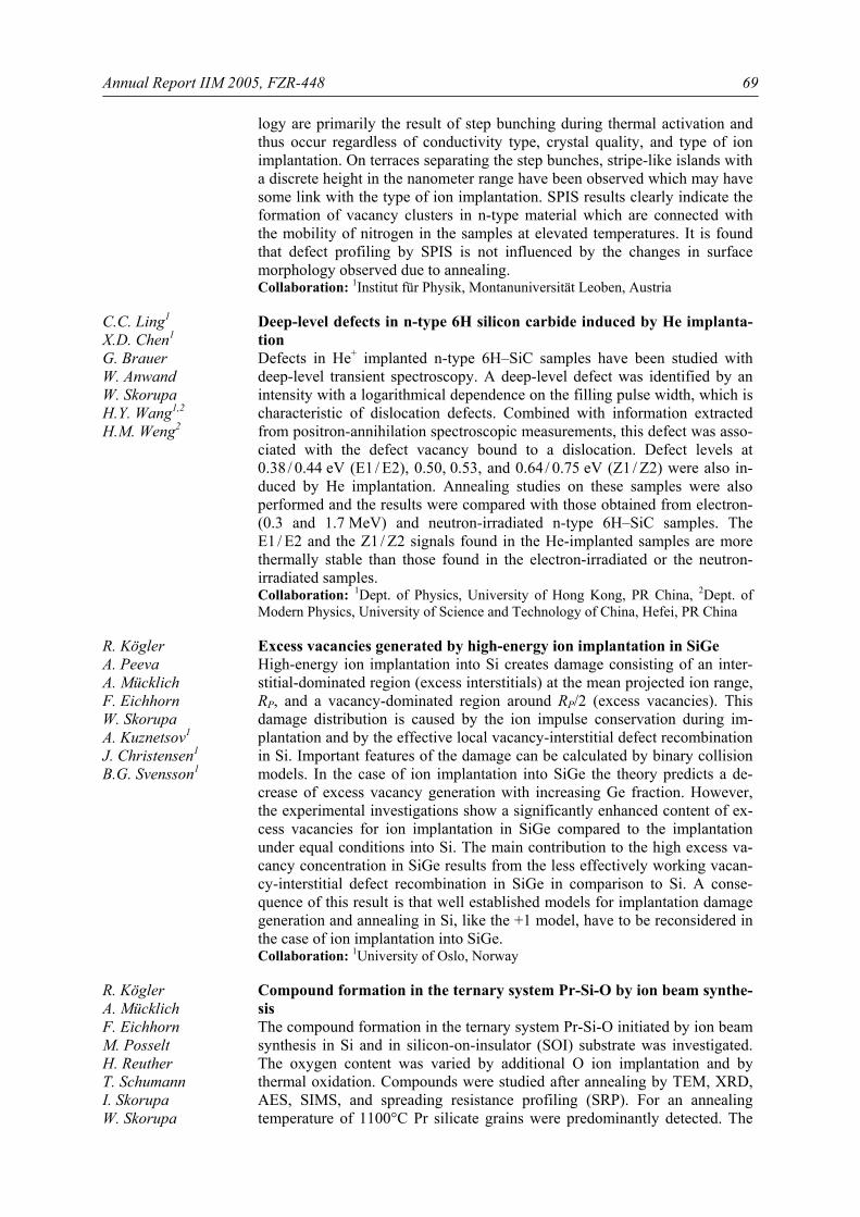
Annual Report IIM 2005, FZR-448
69
logy are primarily the result of step bunching during thermal activation and thus occur regardless of conductivity type, crystal quality, and type of ion implantation. On terraces separating the step bunches, stripe-like islands with a discrete height in the nanometer range have been observed which may have some link with the type of ion implantation. SPIS results clearly indicate the formation of vacancy clusters in n-type material which are connected with the mobility of nitrogen in the samples at elevated temperatures. It is found that defect profiling by SPIS is not influenced by the changes in surface morphology observed due to annealing. Collaboration: 1Institut für Physik, Montanuniversität Leoben, Austria
C.C. Ling1 X.D. Chen1 G. Brauer W. Anwand W. Skorupa H.Y. Wang1,2 H.M. Weng2
Deep-level defects in n-type 6H silicon carbide induced by He implanta-tion Defects in He+ implanted n-type 6H–SiC samples have been studied with deep-level transient spectroscopy. A deep-level defect was identified by an intensity with a logarithmical dependence on the filling pulse width, which is characteristic of dislocation defects. Combined with information extracted from positron-annihilation spectroscopic measurements, this defect was asso-ciated with the defect vacancy bound to a dislocation. Defect levels at 0.38 / 0.44 eV (E1 / E2), 0.50, 0.53, and 0.64 / 0.75 eV (Z1 / Z2) were also in-duced by He implantation. Annealing studies on these samples were also performed and the results were compared with those obtained from electron- (0.3 and 1.7 MeV) and neutron-irradiated n-type 6H–SiC samples. The E1 / E2 and the Z1 / Z2 signals found in the He-implanted samples are more thermally stable than those found in the electron-irradiated or the neutron-irradiated samples. Collaboration: 1Dept. of Physics, University of Hong Kong, PR China, 2Dept. of Modern Physics, University of Science and Technology of China, Hefei, PR China
R. Kögler A. Peeva A. Mücklich F. Eichhorn W. Skorupa A. Kuznetsov1 J. Christensen1 B.G. Svensson1
Excess vacancies generated by high-energy ion implantation in SiGe High-energy ion implantation into Si creates damage consisting of an inter-stitial-dominated region (excess interstitials) at the mean projected ion range, RP, and a vacancy-dominated region around RP/2 (excess vacancies). This damage distribution is caused by the ion impulse conservation during im-plantation and by the effective local vacancy-interstitial defect recombination in Si. Important features of the damage can be calculated by binary collision models. In the case of ion implantation into SiGe the theory predicts a de-crease of excess vacancy generation with increasing Ge fraction. However, the experimental investigations show a significantly enhanced content of ex-cess vacancies for ion implantation in SiGe compared to the implantation under equal conditions into Si. The main contribution to the high excess va-cancy concentration in SiGe results from the less effectively working vacan-cy-interstitial defect recombination in SiGe in comparison to Si. A conse-quence of this result is that well established models for implantation damage generation and annealing in Si, like the +1 model, have to be reconsidered in the case of ion implantation into SiGe. Collaboration: 1University of Oslo, Norway
R. Kögler A. Mücklich F. Eichhorn M. Posselt H. Reuther T. Schumann I. Skorupa W. Skorupa
Compound formation in the ternary system Pr-Si-O by ion beam synthe-sis The compound formation in the ternary system Pr-Si-O initiated by ion beam synthesis in Si and in silicon-on-insulator (SOI) substrate was investigated. The oxygen content was varied by additional O ion implantation and by thermal oxidation. Compounds were studied after annealing by TEM, XRD, AES, SIMS, and spreading resistance profiling (SRP). For an annealing temperature of 1100°C Pr silicate grains were predominantly detected. The
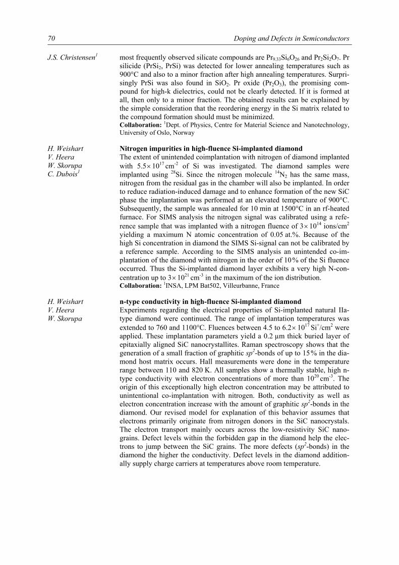
Doping and Defects in Semiconductors 70
J.S. Christensen1 most frequently observed silicate compounds are Pr9.33Si6O26 and Pr2Si2O7. Pr silicide (PrSi2, PrSi) was detected for lower annealing temperatures such as 900°C and also to a minor fraction after high annealing temperatures. Surpri-singly PrSi was also found in SiO2. Pr oxide (Pr2O3), the promising com-pound for high-k dielectrics, could not be clearly detected. If it is formed at all, then only to a minor fraction. The obtained results can be explained by the simple consideration that the reordering energy in the Si matrix related to the compound formation should must be minimized. Collaboration: 1Dept. of Physics, Centre for Material Science and Nanotechnology, University of Oslo, Norway
H. Weishart V. Heera W. Skorupa C. Dubois1
Nitrogen impurities in high-fluence Si-implanted diamond The extent of unintended coimplantation with nitrogen of diamond implanted with 5.5 × 1017 cm-2 of Si was investigated. The diamond samples were implanted using 28Si. Since the nitrogen molecule 14N2 has the same mass, nitrogen from the residual gas in the chamber will also be implanted. In order to reduce radiation-induced damage and to enhance formation of the new SiC phase the implantation was performed at an elevated temperature of 900°C. Subsequently, the sample was annealed for 10 min at 1500°C in an rf-heated furnace. For SIMS analysis the nitrogen signal was calibrated using a refe-rence sample that was implanted with a nitrogen fluence of 3 × 10¹⁴ ions/cm2 yielding a maximum N atomic concentration of 0.05 at.%. Because of the high Si concentration in diamond the SIMS Si-signal can not be calibrated by a reference sample. According to the SIMS analysis an unintended co-im-plantation of the diamond with nitrogen in the order of 10 % of the Si fluence occurred. Thus the Si-implanted diamond layer exhibits a very high N-con-centration up to 3 × 1021 cm-3 in the maximum of the ion distribution. Collaboration: 1INSA, LPM Bat502, Villeurbanne, France
H. Weishart V. Heera W. Skorupa
n-type conductivity in high-fluence Si-implanted diamond Experiments regarding the electrical properties of Si-implanted natural IIa-type diamond were continued. The range of implantation temperatures was extended to 760 and 1100°C. Fluences between 4.5 to 6.2 × 10¹⁷ Si+/cm2 were applied. These implantation parameters yield a 0.2 µm thick buried layer of epitaxially aligned SiC nanocrystallites. Raman spectroscopy shows that the generation of a small fraction of graphitic sp2-bonds of up to 15 % in the dia-mond host matrix occurs. Hall measurements were done in the temperature range between 110 and 820 K. All samples show a thermally stable, high n-type conductivity with electron concentrations of more than 1020 cm-3. The origin of this exceptionally high electron concentration may be attributed to unintentional co-implantation with nitrogen. Both, conductivity as well as electron concentration increase with the amount of graphitic sp2-bonds in the diamond. Our revised model for explanation of this behavior assumes that electrons primarily originate from nitrogen donors in the SiC nanocrystals. The electron transport mainly occurs across the low-resistivity SiC nano-grains. Defect levels within the forbidden gap in the diamond help the elec-trons to jump between the SiC grains. The more defects (sp2-bonds) in the diamond the higher the conductivity. Defect levels in the diamond addition-ally supply charge carriers at temperatures above room temperature.
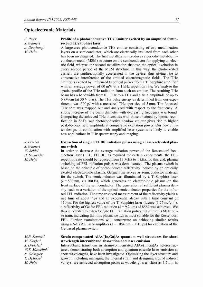
Annual Report IIM 2005, FZR-448
71
Optoelectronic Materials F. Peter S. Winnerl A. Dreyhaupt M. Helm
Profile of a photoconductive THz Emitter excited by an amplified femto-second Ti:Sapphire laser A large-area photoconductive THz emitter consisting of two metallization layers on a semiconductor, which are electrically insulated from each other has been investigated. The first metallization produces a periodic metal-semi-conductor-metal (MSM) structure on the semiconductor for applying an elec-tric field, whereas the second metallization shadows the optical excitation in every second period of the MSM structure. In this way, the photoexcited carriers are unidirectionally accelerated in the device, thus giving rise to constructive interference of the emitted electromagnetic fields. The THz emitter is excited by unfocused fs optical pulses from a Ti:Sapphire amplifier with an average power of 60 mW at a 1 kHz repetition rate. We analyse the spatial profile of the THz radiation from such an emitter. The resulting THz beam has a bandwidth from 0.1 THz to 4 THz and a field amplitude of up to 6 kV/cm (at 30 V bias). The THz pulse energy as determined from our expe-riments was 500 pJ with a measured THz spot size of 5 mm. The focussed THz spot was mapped out and analyzed with respect to the frequency. A strong increase of the beam diameter with decreasing frequency was found. Comparing the achieved THz intensities with those obtained by optical recti-fication in ZnTe, our photoconductive shadow emitter gives rise to higher peak-to-peak field amplitude at comparable excitation power. Our new emit-ter design, in combination with amplified laser systems is likely to enable new applications in THz spectroscopy and imaging.
S. Friebel S. Winnerl W. Seidel H. Schneider M. Helm
Extraction of single FELBE radiation pulses using a laser-activated plas-ma switch In order to decrease the average radiation power of the Rossendorf free-electron laser (FEL) FELBE, as required for certain experiments, the FEL repetition rate should be reduced from 13 MHz to 1 kHz. To this end, plasma switching of FEL radiation pulses was demonstrated. The plasma switch is based on the principle of photo-induced reflectivity induced by an optically excited electron-hole plasma. Germanium serves as semiconductor material for the switch. The semiconductor was illuminated by a Ti:Sapphire laser (λ = 800 nm, τ < 100 fs), which generates an electron-hole plasma on the front surface of the semiconductor. The generation of sufficient plasma den-sity leads to a variation of the optical semiconductor properties for the infra-red FEL radiation. The time-resolved measurement of the reflectivity yields a rise time of about 7 ps and an exponential decay with a time constant of 110 ps. For the highest value of the Ti:Sapphire laser fluence (1.75 mJ/cm2), a reflectivity of Ge for FEL radiation (λ = 9.2 µm) of 85 % was achieved. We thus succeeded to extract single FEL radiation pulses out of the 13 MHz pul-se train, indicating that this plasma switch is most suitable for the Rossendorf FEL. Further examinations will concentrate on achieving similar results using a Nd:YAG laser amplifier (λ = 1064 nm, τ < 16 ps) for excitation of the Ge-based plasma switch.
M.P. Semtsiv1 M. Ziegler1 S. Dressler1 W.T. Masselink1 N. Georgiev T. Dekorsy2 M. Helm
Strain-compensated AlAs/(In,Ga)As quantum well structures for short wavelength intersubband absorption and laser emission Intersubband transitions in strain-compensated AlAs/(In,Ga)As heterostruc-tures, demonstrating both absorption and quantum-cascade laser emission at short wavelengths, have been investigated. Optimizing the layer structure and growth, including managing the internal strain and designing around indirect valleys, we achieved absorption peaks at wavelengths as short as 1.7 µm in
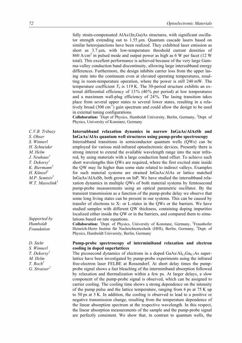
Optoelectronic Materials 72
fully strain-compensated AlAs/(In,Ga)As structures, with significant oscilla-tor strength extending out to 1.55 µm. Quantum cascade lasers based on similar heterojunctions have been realized. They exhibited laser emission as short as 3.7 µm, with low-temperature threshold current densities of 860 A/cm2 in pulsed mode and output power as high as 6 W per facet (12 W total). This excellent performance is achieved because of the very large Gam-ma-valley conduction band discontinuity, allowing large intersubband energy differences. Furthermore, the design inhibits carrier loss from the upper las-ing state into the continuum even at elevated operating temperatures, resul-ting in room-temperature operation, where the power is still 240 mW. The temperature coefficient T0 is 119 K. The 30-period structure exhibits an ex-ternal differential efficiency of 13 % (40 % per period) at low temperatures and a maximum wall-plug efficiency of 24 %. The lasing transition takes place from several upper states to several lower states, resulting in a rela-tively broad (300 cm-1) gain spectrum and could allow the design to be used in external tuning configurations. Collaboration: 1Dept of Physics, Humboldt University, Berlin, Germany, 2Dept. of Physics, University of Konstanz, Germany
C.V.B. Tribuzy S. Ohser S. Winnerl H. Schneider M. Helm J. Neuhaus1 T. Dekorsy1 K. Biermann2 H. Künzel2 M.P. Semtsiv3 W.T. Masselink3
Supported by Humboldt Foundation
Intersubband relaxation dynamics in narrow InGaAs/AlAsSb and InGaAs/AlAs quantum well structures using pump-probe spectroscopy Intersubband transitions in semiconductor quantum wells (QWs) can be employed for various mid-infrared optoelectronic devices. Presently there is strong interest to extend the available wavelength range into the near infra-red, by using materials with a large conduction band offset. To achieve such short wavelengths thin QWs are required, where the first excited state inside the QW may lie higher than some state related to indirect valleys. Examples for such material systems are strained InGaAs/AlAs or lattice matched InGaAs/AlAsSb, both grown on InP. We have studied the intersubband rela-xation dynamics in multiple QWs of both material systems by femtosecond pump-probe measurements using an optical parametric oscillator. By the transient transmission as a function of the pump-probe delay we observe that some long living states can be present in our systems. This can be caused by transfer of electrons to X- or L-states in the QWs or the barriers. We have studied samples with different QW thickness, containing doping impurities localized either inside the QW or in the barriers, and compared them to simu-lations based on rate equations. Collaboration: 1Dept. of Physics, University of Konstanz, Germany, 2Fraunhofer Heinrich-Hertz Institut für Nachrichtentechnik (HHI), Berlin, Germany, 3Dept. of Physics, Humboldt University, Berlin, Germany
D. Stehr S. Winnerl T. Dekorsy1 M. Helm T. Roch2 G. Strasser2
Pump-probe spectroscopy of interminiband relaxation and electron cooling in doped superlattices The picosecond dynamics of electrons in a doped GaAs/Al0.3Ga0.7As super-lattice have been investigated by pump-probe experiments using the infrared free-electron laser FELBE at Rossendorf. At short delay times the pump-probe signal shows a fast bleaching of the interminiband absorption followed by relaxation and thermalization within a few ps. At larger delays, a slow component of the pump-probe signal is observed, which can be assigned to carrier cooling. The cooling time shows a strong dependence on the intensity of the pump pulse and the lattice temperature, ranging from 6 ps at 75 K up to 50 ps at 5 K. In addition, the cooling is observed to lead to a positive or negative transmission change, resulting from the temperature dependence of the linear absorption spectrum at the respective wavelength. In this respect, the linear absorption measurements of the sample and the pump-probe signal are perfectly consistent. We show that, in contrast to quantum wells, the
Annual Report IIM 2005, FZR-448
73
superlattice provides a unique picosecond thermometer for the electron temp-erature based on the dependence of the absorption on the electron distribution function. Collaboration: 1Dept. of Physics, University of Konstanz, Germany, 2Institut für Festkörperelektronik, TU Wien, Austria
M. Wagner D. Stehr S. Winnerl M. Helm
Broad-band THz radiation from optical rectification in GaSe for pump-probe-experiments with the FEL We have built up a broad-band THz-radiation source for time-dependent op-tical-pump and THz-probe experiments. Our THz source is based on phase-matched optical rectification in thin GaSe crystals driven by 10 fs laser pul-ses. With different emitters we are able to generate radiation in a broad spectral range between 12 THz (detector cut-off) and 50 THz with a FWHM of 16 THz by adjusting the phase-matching angle. THz pulses as short as 45 fs can thus be generated and we can achieve a time-averaged THz power of 250 nW out of a near-infrared 120 mW beam. Our experimental arrange-ment allows us to switch between linear THz-autocorrelation measurements with two pulses from the same emitter and THz cross-correlation with two pulses from different emitters. These setups have been used to characterize the THz-pulses and to perform interband-pump / intersubband-probe mea-surements, respectively. The functionality was demonstrated by comparing absorption spectra of a multiple-quantum-well (MQW) sample and a super-lattice, as obtained by an infrared spectrometer, with the Fourier-transform of the THz autocorrelation measurement. The setup is ready to be used with the FEL or another synchronized laser for spectrally resolved pump-probe expe-riments. In some first experiments of this kind, we have studied the lifetime of photo-excited carriers in a MQW using a Ti:Sapphire laser that has been successfully synchronized to the THz-radiation source.
H.-J. Fitting1 R. Salh1 T. Barfels1 B. Schmidt
Multimodal luminescence spectra of ion-implanted silica Thermally oxidized SiO2 layers have been implanted by oxygen and sulfur ions up to an atomic dopant fraction of about 4 at.%. The cathodolumines-cence spectra of these ion implanted layers show, besides the characteristic bands, an identical sharp and intense multimodal structure in the green up to near IR region. The energy step differences of the luminescence sublevels in average amount to 120 meV and indicate vibronic transitions in terms of a configuration coordinate potential model. The most probable candidate for these spectra are O2 interstitial molecules, as we could demonstrate by re-spective configuration coordinate data. These assumptions are in contrast to photonic crystal models for the multimodal spectra as well as to models of quantum size effects, both discussed recently in literature. Collaboration: 1Department of Physics, University of Rostock, Germany
J. Potfajova J.M. Sun B. Schmidt T. Dekorsy W. Skorupa M. Helm
Fabrication of efficient Si based light emitting diodes with resonant ca-vities Resonant-cavity light-emitting diodes (RCLED) on a silicon-on-insulator (SOI) substrates present a promising path towards more efficient Si based optical devices. The pn-diodes were fabricated using standard silicon techno-logy and boron implantation into n-Si. Forward biased highly boron doped pn-junctions are known to show efficient room-temperature luminescence at a wavelength of 1150 nm, This electroluminescence (EL) is also observed in the present 5 µm thick SOI layers, however modulated by characteristic thickness fringes. The thickness of the top Si layer was reduced down to 1300 nm by anisotropic etching, which is an optimum in order to obtain a 4λ microcavity with a sharp EL peak at the wavelength of 1150 nm. The desired thickness was measured by FTIR spectroscopy. The back-side etching pro-
Optoelectronic Materials 74
cess of the SOI wafer down to the buried SiO2 layer as an etch-stop was also optimized. For fabrication of an effective RCLED, a resonator will be fa-bricated by deposition of Si/SiO2 distributed Bragg reflectors both on the top and the rear side of the pn-diode.
J.M. Sun W. Skorupa T. Dekorsy M. Helm L. Rebohle1 T. Gebel1
Modulation of the 1535 nm photoluminescence from Er-doped Si-rich silicon dioxide by field-induced quenching Field-induced quenching of the intense photoluminescence at 1535 nm was observed from Si-rich SiO2:Er thin films prepared by Er+ and Si+ co-implant-ation. The quenching effect was strongly enhanced by increasing the density of Si nanoclusters (NCs) at an electric field above 5 MV/cm. A modulation ratio of 0.37 was obtained at an electric field of 9 MV/cm for a 200 nm Er-doped Si-rich layer containing 0.24 % of Er atoms and 10 % excess Si NCs. The mechanism of the field-induced quenching of the photoluminescence was studied by simultaneously measuring the light intensity from NCs and Er3+ ions, the injection current and the electric field. The quenching mecha-nism could be attributed to the field induced separation of the excitons created in the Si NCs and tunneling of carriers between the Er ions and Si NCs. This strong field-induced quenching effect will be useful for controlling the optical gain in Si-rich SiO2:Er waveguide amplifiers, but also for the small size optical modulator in silicon photonics. Collaboration: 1nanoparc GmbH, Dresden, Germany
J. M. Sun S. Prucnal1 W. Skorupa M. Helm L. Rebohle2 T. Gebel2
Efficient blue electroluminescence from metal-oxide-semiconductor light emitting devices with Ce and Gd co-implanted SiO2 layers Ultraviolet and blue electroluminescence (EL) was observed from Gd and Ce co-implanted indium-tin oxide / SiO2:(Gd, Ce) / Si metal-oxide-semiconductor light emitting devices (MOSLEDs). The UV emission peak at 316 nm and the broad blue emission at around 440 nm are ascribed to electronic tran-sitions from 6P7/2 to 8S7/2 of Gd3+ centers and 5d-4f transitions of Ce3+, respec-tively, both excited by hot electrons. A decrease of the EL decay time and the impact cross-section of Gd3+ was observed with co-implanted Ce. As a con-sequence, the strong energy transfer from Gd3+ to Ce3+ centers leads to a five-fold increase of the blue EL from Ce3+ centers in silicon MOSLEDs. Collaboration: 1Maria Curie-Sklodowska University, Lublin, Poland, 2nanoparc GmbH, Dresden, Germany
S. Prucnal1 X.Q. Cheng J.M. Sun R. Kögler W. Skorupa
Supported by Humboldt Foundation
Optical and microstructural properties of SiO2 layers containing Er, Ge and Si atoms Photoluminescence (PL) properties of 500 nm thick SiO2 layers containing combined Ge+Si and Er+Si implants have been studied. The double-beam implantations of Ge+Si and Er+Si were performed both sequentially and simultaneously. After implantation, the samples were annealed at tempera-tures ranging from 700 to 1100°C, in order to obtain Si and Ge nanoclusters (NCs) and remove the point defects induced by ion implantation. A weak near-UV luminescence peak at 315 nm, a strong blue band at 400 nm and a near-infrared 780 nm band were observed from samples implanted by Ge and Si atoms. The SiO2 layers containing Er and Si-NCs exhibit a strong infrared PL peak at 1.54 µm. The enhancement of the this PL peak with increasing Si nanocluster concentration suggests an energy transfer from Si-NCs to Er3+
ions in the SiO2 matrix. It should be noted that the simultaneous implantation creates more defects in the matrix than the sequential one. Moreover, diffu-sion of Ge towards the Si/SiO2 interface during the annealing process is suppressed by silicon ions additionally introduced into SiO2. Collaboration: 1Maria Curie-Sklodowska University, Lublin, Poland
Annual Report IIM 2005, FZR-448
75
Others J. Grenzer A. Zen1 D. Neher1 S. Grigorian2 U. Pietsch2 U. Asawapirom3 S. Janietz3 U. Scherf4
Effect of molecular weight on the structure and crystallinity of poly (3-hexylthiophene) The carrier mobility of field-effect transistors made from regioregular poly (3-hexylthiophene) (P3HT) increases strongly with the molecular weight. Using complementary techniques (differential scanning calorimetry, XRD), the structural properties of P3HT has been studied as a function of the mole-cular weight. For powder samples, all weight fractions possess a rather broad molecular weight distribution. The measurements reveal a strong decrease of the crystallization temperature and, most important, a significant decrease of the degree of crystallinity with decreasing molecular weight. In order to stu-dy the structure of P3HT thin films (thickness several 10 nm) in lateral and vertical directions, X-ray grazing incidence diffraction and reflectivity measurements were utilized. These methods show that thin layers of the low molecular weight fraction consist of well-defined crystalline domains embed-ded in a disordered matrix. Thus we propose that the transport properties of layers prepared from fractions of P3HT with different molecular weight is largely determined by the crystallinity of the samples and not by the perfec-tion of the packing of the chains in the individual crystallites. Collaboration: 1Institute of Physics, University of Potsdam, Germany, 2Institute of Physics, University of Siegen, Germany, 3Macromolecular Chemistry, University of Wuppertal, Germany, 4Fraunhofer Institute for Applied Polymer Research, Gol, Germany
R.I. Grynszpan1,2 N. Baclet3 A. Darque3 J.L. Flament4 F. Zielinski4 W. Anwand G. Brauer
Positron and deuteron depth profiling in 3He implanted Electrum-like alloy In spite of previous extensive studies, the He behavior in metals still remains an issue in microelectronics as well as in nuclear technology. A gold-silver solid solution (Au60Ag40: synthetic gold-rich electrum) was chosen as a rele-vant model to study helium irradiation of heavy metals. After 3He+ ion implantation at an energy ranging from 4.2 to 5.6 MeV, NRA based on the 3He(d,p)4He reaction, was performed in order to study the thermal diffusion of He atoms. At room temperature, NRA data reveal that a single Gaussian can fit the He-distribution, which remains unchanged after annealing at temp-eratures below 0.45 of the melting point. Slow positron implantation spec-troscopy, used to monitor the fluence dependence of induced defects unveils a positron trapping saturation, which occurs for He contents of the order of 50 – 100 appm, whereas concentrations larger than 500 appm seem to favor an increase in the S-parameter of Doppler broadening. Moreover, at high temperature, NRA results clearly show that He long range diffusion occurs, though, without following a simple Fick law. Collaboration: 1Lab. de Chimie Métallurgique des Terres Rares, ISCSA, Thiais, France, 2Positive Leptons Spectroscopy Cell, DGA/CEP/CGN/LOT, Dept. of De-fense, Arcueil, France, 3CEA/VA/DRMN/SEMP, Is-sur-Tille, France, 4CEA/DIF/ DPTA/SP2A, Bruyères-le-Châtel, France
R.I. Grynszpan1,2,3 S. Saudé1,2,3 L. Mazerolles3 G. Brauer W. Anwand
Positron depth profiling in ion-implanted zirconia stabilized with tri-valent cations Slow positron implantation spectroscopy has been performed on a series of (ZrO2)1-x (M2O3)x solid solutions, either stabilized in the cubic phase (with M: Y, Dy or Er and x = 0.095, 0.16 or 0.16, respectively) or in the tetragonal metastable phase (M: Y and x = 0.03). Stabilization induces native oxygen-vacancy complexes, which lead to saturation trapping of positrons in the cubic crystals, regardless of the cation type. The positron diffusion length in the tetragonal phase (L+ ≈ 60 nm, vs. ≈ 2.5 nm in the cubic phase) suggests

Others 76
that Y atoms segregate around antiphase boundaries formed in the lattice. Implantations of helium and oxygen ions induce new defects, more trapping effective than the native defects. However, their production rate and tem-perature stability seem primarily dependent on the crystal structure, hence on the concentration of trivalent cations, irrespective of their chemical nature. Collaboration: 1SERAM & SINUMEF, Ecole Nationale Supérieure d’Arts et Mé-tiers, Paris, France, 2DGA/CEP/CGN/LOT, Dept. of Defense, Arcueil, France, 3ISCSA, IFR-CNRS-1780, Thiais, France
Annual Report IIM 2005, FZR-448
77
Equipment M. Friedrich W. Bürger A. Reichel S. Turuc
Operation and development of the electrostatic accelerators The 2 MV VdG accelerator has been used exclusively for RBS analysis. The rf ion source has been equipped with a ceramic discharge bottle. This modifi-cation results in higher beam currents with improved stability. A modernized energy stabilizing system has been installed. The 5 MV Tandem has been applied for ion beam analysis, high-energy implantation and detector development. After rupture of the charging belt (CIGO / Italy) after 1700 operation hours a new belt (Wennerlund / Sweden) was installed. After reducing the self-charging effect at the inner belt side by an additional discharge needle line inside the terminal the belt has given satisfying stability of the terminal voltage. The energy and beam position sta-bility has been improved by a new control strategy on the base of predictive compensation of terminal voltage disturbances (see separate report). The 3 MV Tandetron has been applied mainly for high-energy implantation and ion beam analysis. At the second He ion source a commercial Rb charge exchange canal (NEC / USA) has been installed. In 2005 the total operating hours of the high-energy accelerators were 1681 h (2 MV VdG), 1673 h (5 MV Tandem) and 1670 h (3 MV Tandetron). The available beam times of the 5 MV Tandem and of the 3 MV Tandetron were reduced due to a three-week inspection of the pressure vessels by the tech-nical supervising authorities.
W. Bürger H. Lange
Predictive compensation of terminal voltage disturbances at Van de Graaff belt generators The precision of controlling the acceleration voltage (AV) of Van de Graaff (VdG) accelerators directly by the charging current is strongly limited by the dead time of the charge transfer in the belt generator from ground potential to the accelerator terminal. A major source of instabilities are imperfections of the charging belt, which accordingly lead to a periodic ripple. In a novel approach, this periodicity allows to estimate the development and to counter-act ahead of time. For this purpose, the control chain from the input of the charging current generator up to the reaction of the AV has been precisely identified, and a real-time predictive algorithm has been developed. Accor-dingly, a control strategy was implemented in a microcontroller RENESAS SH2/7047. Based on a measurement of the transfer function of the charging system, estimates of few spectral lines of the AV disturbance are continuous-ly calculated by a sliding short time signal transformation into the Fourier frequency domain. For the spectral lines, compensation signals are estimated, retransformed to the time domain and added to the charging current controller input. In this way, the belt-rotation related ripple of the two VdG accelerators was decreased by a factor of 5 – 10, and the total effective ripple by a factor of 3 – 4. The relative AV fluctuation reaches a level well below ∆U/U < 10-4, which is not attainable by conventional methods.
R. Heller D. Kost G. Zschornack1 S. Facsko
Characteristics of the highly charged ion beam from the Dresden EBIT source The Rossendorf Two Beam Facility offers both an ECR ion source for low to medium ionic charge states and the Dresden room-temperature electron beam ion trap (EBIT) for highest charge states. In order to optimise the highly charged ion output, the ion extraction from the EBIT was studied. At the 1st faraday cup directly after the extraction optics total ion currents up to 2 µA were determined. The charge state distribution analysis of the ion beam re-vealed the formation and extraction of charge states up to Ar18+ as well as
Equipment 78
charge states up to Xe44+. For the first time the so called “leaky mode” of the EBIT source was studied to more detail, which delivers a continuous beam in contrast to the usual pulsed operation. It could be demonstrated that conti-nuous beams even of high charge states (e.g. Ar17+ and Xe21+) can be produc-ed. The transmission of the ion beam through the beamline has been deter-mined to be nearly 100 %. For guiding the EBIT beam into the target cham-ber, the remaining magnetization of the ECR source magnet was suppressed by additional constant-current windings. Collaboration: 1Institute for Applied Physics, TU Dresden, Germany
D. Kost F. Röder
Plasma potential of the ECR ion source of the dual-beam highly-charged ion facility At the dual-beam facility, highly charged ions are decelerated down to ki-netic energies of some 10 eV times charge state. In this low energy range the plasma potential of the ion source renders an important contribution to the total kinetic energy. For its measurement, a single Langmuir probe was con-structed and adapted to the ECR ion source. The results were found in good agreement with measurements of the total kinetic ion energy using a retarding field arrangement. Main source parameters influencing the plasma potential are the microwave (MW) power and the gas pressure. The plasma potential increases monotonically from 10 V to 25 V with MW power from 40 to 240 W and with gas pressure in the range of 10-6 to 6 × 10⁻⁵ mbar. However, a hysteretic behaviour is observed in the pressure range of 3 × 10⁻⁶ to 10-5 mbar. Avoiding this regime, the plasma potential is nearly constant with (10 ± 2) V in the low-pressure range of 10-6 to 3 × 10⁻⁶ mbar, and with (27 ± 3) V above 10-5 mbar.
S. Winnerl D. Stehr W. Seidel H. Schneider M. Helm K. Unterrainer1 F.F. Schrey1 B.A. Carpenter2 E.A. Zibik2 J. Cockburn2 L.R. Wilson2 S. Schneider3 J. Seidel3 S. Grafström3 L.M. Eng3
supported by EU
Cooperation with and support of external user groups at FELBE Partially supported by an "integrated infrastructure initiative" funded by the European Union, the free-electron laser facility FELBE was made available to external user groups for the first time. Interesting initial experiments have been conducted in cooperation with scientists from Rossendorf. These users included groups from Vienna and from Sheffield, who performed infrared pump / probe measurements on InGaAs/GaAs quantum dots, and a group from TU Dresden, who developed an infrared scattering scanning optical near-field microscope. In addition to interesting scientific interactions, these experiments also provided an important opportunity to gain experience with this service-oriented operation mode of FELBE, which represents an impor-tant step towards our goal of creating a major scientific impact within Europe through this facility. Collaboration: 1Institut für Festkörperelektronik, TU Wien, Austria, 2University of Sheffield, Dept. of Physics and Astronomy, UK,3Institute of Applied Physics, TU Dresden, Germany
N. Schell F. Eichhorn A. Bjeoumikhov1 H. Prinz2 C. Ollinger3
Parabolic capillary optics with less than 50 µm focus and large focal distance for synchrotron radiation scattering In cooperation with the Institute for Scientific Instruments, Berlin, a unique parabolic focussing optics for the general purpose materials research station at the ROssendorf BeamLine, ROBL-CRG at ESRF, was developed and commissioned. The measured gain between 8 – 12 keV was > 1000, the focal spot < 40 µm at a focal length of 235 mm (8 keV) and 244 mm (11.5 keV), respectively, which allows the use of special sample environments around the focus spot. The low divergence of < 0.15° especially permits the in-situ cha-
Annual Report IIM 2005, FZR-448
79
Supported by AMD
racterization of stress states in copper dual inlaid interconnect micro-struct-ures as well as the measurement of far-field diffraction patterns of planar wave-guides. For the positioning of selected regions of the sample with respect to the X-ray spot a CCD camera system is used. Corresponding first test results showed the advantages of this parabolic focusing optics in compa-rison to the standard beam geometry using apertures for decreasing the X-ray spot size. Collaboration: 1Institute for Scientific Instruments, Berlin, Germany, 2AMD Saxo-ny, Dresden, Germany, 3Institute for X-ray Physics, University of Göttingen, Germa-ny
N. Schell J. von Borany J. Hauser M. Beckers
Installation and test of a new magnetron sputter deposition chamber equipped with an additional ion gun for in-situ synchrotron radiation scattering experiments A new process chamber for the in-situ study of film growth and modification during magnetron sputter deposition by synchrotron XRD and XRR was developed and commissioned. The chamber is sealed with four Be-windows allowing scattering access of –2° up to +50° off-plane and –2.9° up to +65° in-plane, respectively. The chamber fits into the standard six-circle HUBER diffractometer of the ROssendorf BeamLine (ROBL) at ESRF. Two comer-cial miniature magnetrons with additional gas inlets allow for the deposition of compound films and multilayers. Substrate heating up to 1000°C and substrate biasing is possible. An additional ion gun up to 6 keV and 10 µA allows post-deposition ion irradiation or energetic ion bombardment during sputter deposition. The performance of the chamber was tested during the high-temperature deposition of MAX phase Ti2AlN films.
J. Grenzer F. Eichhorn
New universal high-resolution diffractometer Since December 2005 a new high-resolution four circle diffractometer (XRD-3003 PTR from GE Inspection Technologies) in an unique configu-ration is operating at IIM. The device is optimized for small sample sizes using a beam of 2 × 2mm2. This is realized by a standard sealed tube in com-bination with a 2D collimating mirror resulting in an almost parallel beam in two dimensions. The system can be equally used for standard coplanar high resolution and reflectivity measurements as well as for non-coplanar mea-surements using grazing incidence and exit geometries. Without any mono-chromator a photon flux of 5 × 10⁷ /s within a beam diameter of 500 µm and a beam divergence of about 1 mrad in both directions is obtained. Depending on the investigated sample the (angular and spectral) resolution of the setup can be changed accordingly by using a four-bounced monochromator Ge(220) and a triple-axis analyzer for the highest resolution possible or a multilayer analyzer for intermediated experimental resolutions.
O. Drachenko S. Winnerl H. Schneider M. Helm
Rapid-scan THz spectroscopy for application in pulsed magnetic fields The pulsed high-magnetic-field laboratory (HLD) at FZR will enable many exciting experiments in solid state physics. Among others, THz spectroscopy is an important technique to investigate material properties in high magnetic fields. However, state-of-the-art time-domain THz spectroscopy is not fast enough to be performed within a millisecond magnetic-field pulse, mainly because mechanical delay lines are used for temporally scanning the THz wave. Therefore we build up a system based on asynchronous optical sampling (ASOPS). This approach uses two exciting femtosecond laser sour-ces with slightly different repetition rates (F and F+D) to gate the emitter and detector of the THz spectrometer (which will be installed in the magnet). The lasers produce two pulses with a time delay linearly ramped in time between zero and 1/F. Since the scan rate of the time delay is fixed by the beat
Equipment 80
frequency D, ASOPS does not require any mechanical delay stage, so that the THz transient field can be recorded much faster (> kHz). To this end a novel twin-laser system has been installed in the high magnetic field laboratory and successfully characterized, followed now by the set up of the THz spectro-meter.
L. Bischoff W. Pilz C. Akhmadaliev C.J. Aidinis1 T. Ganetsos2
Development of new alloy LMIS for FIB applications Two new types of alloy liquid metal ion sources (LMIS) for the application in the IMSA-Orsay Physics FIB system were developed, tested and analysed concerning their I-V characteristics, mass spectra, energy spread of certain ion species and their temperature behavior. An electrochemical sharpened 250 µm tungsten wire tip was wetted with a Mn45Ge54Si1 alloy (Tmelt = 720°C) and welded on a heating filament. Ion beams of single isotopic Mn1+ (dominating in the beam) and Mn2+ could be clearly separated. Mn is a promising element for doping or modification of electrical, mecha-nical, optical or magnetic properties of II-VI semiconductors. Secondly a Ga38Bi62 (Tmelt = 222°C) alloy LMIS was prepared on a mechanically treated Ta emitter. This Ga38Bi62 LMIS allows one to dope, i.e. Si with acceptors (Ga) as well as with shallow donors (Bi) using the same ion source. The re-latively high vapor pressure of Mn and Bi at higher temperatures requires the operation of the source close to Tmelt to obtain a long source life time. Collaboration: 1Department of Physics, University of Athens, Greece, 2TEI of La-mia, Greece
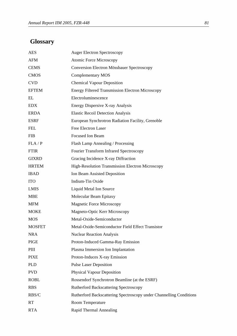
Annual Report IIM 2005, FZR-448
81
Glossary
AES Auger Electron Spectroscopy
AFM Atomic Force Microscopy
CEMS Conversion Electron Mössbauer Spectroscopy
CMOS Complementary MOS
CVD Chemical Vapour Deposition
EFTEM Energy Filtered Transmission Electron Microscopy
EL Electroluminescence
EDX Energy Dispersive X-ray Analysis
ERDA Elastic Recoil Detection Analysis
ESRF European Synchrotron Radiation Facility, Grenoble
FEL Free Electron Laser
FIB Focused Ion Beam
FLA / P Flash Lamp Annealing / Processing
FTIR Fourier Transform Infrared Spectroscopy
GIXRD Gracing Incidence X-ray Diffraction
HRTEM High-Resolution Transmission Electron Microscopy
IBAD Ion Beam Assisted Deposition
ITO Indium-Tin Oxide
LMIS Liquid Metal Ion Source
MBE Molecular Beam Epitaxy
MFM Magnetic Force Microscopy
MOKE Magneto-Optic Kerr Microscopy
MOS Metal-Oxide-Semiconductor
MOSFET Metal-Oxide-Semiconductor Field Effect Transistor
NRA Nuclear Reaction Analysis
PIGE Proton-Induced Gamma-Ray Emission
PIII Plasma Immersion Ion Implantation
PIXE Proton-Induces X-ray Emission
PLD Pulse Laser Deposition
PVD Physical Vapour Deposition
ROBL Rossendorf Synchrotron Beamline (at the ESRF)
RBS Rutherford Backscattering Spectroscopy
RBS/C Rutherford Backscattering Spectroscopy under Channelling Conditions
RT Room Temperature
RTA Rapid Thermal Annealing
Glossary
82
SAD Selected Area Diffraction
SEM Scanning Electron Microscopy
SIMS Secondary Ion Mass Spectrometry
SPIS Slow Positron Implantation Spectroscopy
STM Scanning Tunnel Microscope
TEM Transmission Electron Microscopy
XANES X-ray Absorption Near Edge Spectroscopy
XPS X-ray Photoelectron Spectroscopy
XRD X-ray Diffraction
XRF X-Ray Fluorescence Analysis
XRR X-ray Reflectivity
XTEM Cross-Sectional Transmission Electron Microscopy
Supporting Institutions AiF Arbeitsgemeinschaft Industrieller Forschungsvereinigungen e.V.
AvH Alexander-von-Humboldt Stiftung
BMBF Bundesministerium für Bildung und Forschung
BMWA Bundesministerium für Wirtschaft und Arbeit
DAAD Deutscher Akademischer Austauschdienst
DFG Deutsche Forschungsgemeinschaft
EU European Union
MPG Max-Planck-Gesellschaft
SMWK Sächsisches Staatsministerium für Wissenschaft und Kunst
SMWA Sächsisches Staatsministerium für Wirtschaft und Arbeit
WTZ BMBF-Programm der „Wissenschaftlich-Technischen Zusammenarbeit“

Statistics

Annual Report IIM 2005, FZR-448
85
Book Chapters Beyer, V., Borany, J. von Ion-beam synthesis of nanocrystals for multidot memory structures in: Materials for Information Technology – Devices, Interconnects and Packaging; Series: Engineering Materials and Processes (Eds. E.Zschech, C. Whelan, T. Mikolajick), Springer-Verlag, Berlin, 2005, ISBN: 1-85233-941-1, pp. 139 – 147 Neelmeijer, C., Mäder, M. Endangered glass objects identified by ion beam analysis in: Cultural Heritage Conservation and Environmental Impact Assessment by Non-Destructive Testing and Micro-Analysis (Eds. R. Van Grieken, K. Janssens), A.A. Balkema Publishers, Taylor & Francis Group, London, 2005, pp. 211 – 222
Publications in Refereed Journals Ion-Solid-Interaction Abdul-Kader, A.M., Turos, A., Grambole, D., Jagielski, J., Piatkowska, A., Madi, N.K., Al-Maadeed, M. Compositional transformations in ion-implanted polymers Nucl. Instr. Meth. B 240 (2005) 152 Bracht, H., Staskunaite, R., Haller, E.E., Fielitz, P., Borchardt, G., Grambole, D. Silicon diffusion in sol-gel derived isotopically enriched silica glasses J. Appl. Phys. 97 (2005) 046107 Constantinescu, B., Bugoi, R., Cojocaru, V., Voiculescu, D., Grambole, D., Herrmann, F., Ceccato, D. Romanian ancient gold objects provenance studies using micro-beam methods: the case of Pietroasa hoard Nucl. Instr. Meth. B 231 (2005) 541 Mackova, A., Grötzschel, R., Nekvindova, P., Spirkova, J., Svorcik, V., Zemek, J. Analysis of PF surfaces and interfaces using nuclear analytical methods Acta Phys. Slovaca 55 (2005) 323 Mackova, A., Spirkova, J., Nekvindova, P., Salavcova, L., Grötzschel, R., Eichhorn, F. Comparison of crystal lattice changes caused by APE treatment of Er: LiNbO3 and by localised Er doping into LiNbO3 obtained by RBS-channeling and XRD analysis Nucl. Instr. Meth. B 240 (2005) 391 Mäder, M., Jembrih-Simbürger, D., Neelmeijer, C., Schreiner, M. IBA of iridescent Art Nouveau glass - comparative studies Nucl. Instr. Meth. B 239 (2005)107 Posselt, M., Mäder, M., Lebedev, A., Grötzschel, R. Multiple implantations into Si: influence of the implantation sequence on ion range profiles Appl. Phys. Lett. 87 (2005) 043109 Rosén, D., Katardjiev, I., Berg, S., Möller, W. TRIDYN simulation of target poisoning in reactive sputtering Nucl. Instr. Meth. B 228 (2005) 193
Journal Publications
86
Salavcova, L., Spirkova, J., Capek, P., Novotna, M., Vacik, J., Mackova, A., Kreißig, U. Effect of the annealing process on active properties of proton-exchanged optical waveguides in erbium-doped lithium niobate Ceramics - Silikaty 49 (2005) 86 Thin Films Abd El-Rahman, A.M., Negm, N.Z., Prokert, F., El-Hossary, F.M., Richter, E., Möller, W. Depth-related microstructure of rf plasma nitrocarburized austenitic stainless steel Surf. Coat. Technol. 191 (2005) 140 Abd El-Rahman, A.M., El-Hossary, F.M., Prokert, F., Negm, N.Z., Schell, N., Richter, E., Möller, W. In-situ stability study of nitrocarburized 304 stainless steel during heating Surf. Coat. Technol. 200 (2005) 602 Abrasonis, G., Riviere, J.P., Templier, C., Pranevicius, L., Barradas, N.P. Flux effect on the ion-beam nitriding of austenitic stainless-steel AISI 304L J. Appl. Phys. 97 (2005) 124906 Abrasonis, G., Gago, R., Jimenez, I., Kreißig, U., Kolitsch, A., Möller, W. Nitrogen incorporation in carbon nitride films produced by direct and dual ion-beam sputtering J. Appl. Phys. 98 (2005) 074907 Allenstein, F., Budzinski, L., Hirsch, D., Mogilatenko, A., Beddies, G., Grötzschel, R., Hinneberg, H. Influence of Al on the growth of NiSi2 on Si(001) Microelectron. Eng. 82 (2005) 474 Almtoft, K.P., Bøttiger, J., Chevallier, J., Schell, N., Martins, R.M.S. Influence of the substrate bias on the size and thermal stability of grains in magnetron-sputtered nanocrystalline Ag films J. Mat. Res. 20 (2005) 1071 Andreasen, K.P., Bøttiger, J., Chevallier, J., Schell, N. Real time in-situ diagnostics of PVD growth using synchrotron radiation Surf. Coat. Technol. 200 (2005) 1 Beckers, M., Schell, N., Martins, R.M.S., Mücklich, A., Möller, W. In-situ x-ray diffraction studies concerning the influence of Al concentration on the texture development during sputter deposition of Ti-Al-N thin films J. Vac. Sci. Technol. A 23 (2005) 1384 Beckers, M., Schell, N., Martins, R.M.S., Mücklich, A., Möller, W. The influence of the growth rate on the preferred orientation of magnetron sputtered Ti-Al-N thin films studied by in-situ x-ray diffraction J. Appl. Phys. 98 (2005) 44901 ESRF Newsletter 42 (2005) 20 Belov, A.Y., Jäger, H.-U. Relaxation kinetics in amorphous carbon films: an insight from atomic scale simulation Thin Solid Films 482 (2005) 74 Belov, A.Y., Jäger, H.-U. Formation and evolution of sp2 clusters in amorphous carbon networks as predicted by molecular dynamics annealing simulations Diam. Rel. Mat. 14 (2005) 1014
Annual Report IIM 2005, FZR-448
87
Bohne, Y., Shevchenko, N., Prokert, F., Borany, J. von, Rauschenbach, B., Möller, W. In-situ characterization of phase formation during high-energy oxygen ion implantation in molybdenum Nucl. Instr. Meth. B 240 (2005) 157 Casiraghi, C., Piazza, F., Ferrari, A. C., Grambole, D., Robertson, J. Bonding in hydrogenated diamond-like carbon by Raman spectroscopy Diam. Rel. Mat. 14 (2005) 1098 Dittmar, K., Engelmann, H.-J., Peikert, M., Wieser, E., Borany, J. von Investigation of ultrathin tantalum based diffusion barrier films using AES and TEM Appl. Surf. Sci. 252 (2005) 185 Foerster, C.E., Fitz, T., Dekorsy, T., Prokert, F., Kreißig, U., Mücklich, A., Richter, E., Möller, W. Carbon ion implantation in pure aluminium at low fluences Surf. Coat. Technol. 192 (2005) 317 Gago, R., Abrasonis, G., Mücklich, A., Möller, W., Czigany, Z., Radnoczi, G. Fullerene-like arrangements in carbon nitride thin films grown by direct ion beam sputtering Appl. Phys. Lett. 87 (2005) 071901 Gago, R., Neidhardt, J., Vinnichenko, M., Kreißig, U., Czigány, Z., Kolitsch, A., Hultman, L., Möller, W. Synthesis of carbon nitride thin films by low-energy ion beam assisted evaporation: on the mechanisms for fullerene-like microstructure formation Thin Solid Films 483 (2005) 89 Gago, R., Jiménez, I., Neidhardt, J., Abendroth, B., Caretti, I., Hultman, L., Möller, W. Correlation between bonding structure and microstructure in fullerene-like carbon nitride thin films Phys. Rev. B 72 (2005) 115414 Gago, R., Vinnichenko, M., Jäger, H.-U., Belov, A.Yu., Jiménez, I., Huang, N., Sun, H., Maitz, M.F. Evolution of sp2 networks with substrate temperature in amorphous carbon films: experiment and theory Phys. Rev. B 72 (2005) 014120 Gomes, G.F., Ueda, M., Reuther, H., Richter, E., Beloto, A.F. Nitrogen recoil chromium implantation into SAE 1020 steel by means of ion beam or plasma immersion ion implantation Surf. Coat. Technol. 196 (2005) 275 Gomes, G.F., Ueda, M., Beloto, A., Reuther, H., Richter, E. Chromium enrichment of AISI 304 stainless steel surface after nitrogen ion recoil bombardment of chromium film Nucl. Instr. Meth. B 240 (2005) 194 Gorbunov, A., Levin, A.A., Meyer, D.C., Bischoff, L., Eckert, D., Köhler, B., Mertig, M., Weissbach, T., Wieser, E., Pompe, W. Correlation of structural and physical properties of metastable Fe-Cr phases Crystal Res. Technol. 40 (2005) 106 Ignatova, V.A., Möller, W., Conard, T., Vandervorst, W., Gijbels, R. Interpretation of TOF-SIMS depth profiles from ultrashallow high-K dielectric stacks assisted by hybrid collisional computer simulation Appl. Phys. A 81 (2005) 71
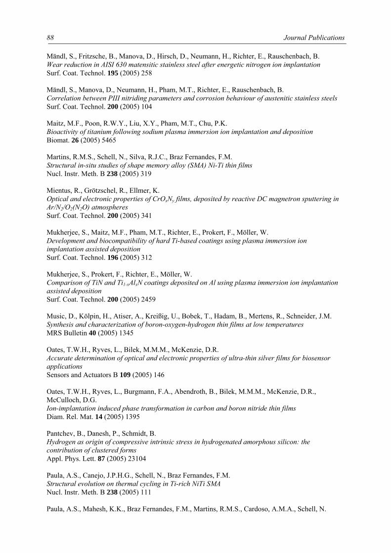
Journal Publications
88
Mändl, S., Fritzsche, B., Manova, D., Hirsch, D., Neumann, H., Richter, E., Rauschenbach, B. Wear reduction in AISI 630 matensitic stainless steel after energetic nitrogen ion implantation Surf. Coat. Technol. 195 (2005) 258 Mändl, S., Manova, D., Neumann, H., Pham, M.T., Richter, E., Rauschenbach, B. Correlation between PIII nitriding parameters and corrosion behaviour of austenitic stainless steels Surf. Coat. Technol. 200 (2005) 104 Maitz, M.F., Poon, R.W.Y., Liu, X.Y., Pham, M.T., Chu, P.K. Bioactivity of titanium following sodium plasma immersion ion implantation and deposition Biomat. 26 (2005) 5465 Martins, R.M.S., Schell, N., Silva, R.J.C., Braz Fernandes, F.M. Structural in-situ studies of shape memory alloy (SMA) Ni-Ti thin films Nucl. Instr. Meth. B 238 (2005) 319 Mientus, R., Grötzschel, R., Ellmer, K. Optical and electronic properties of CrOxNy films, deposited by reactive DC magnetron sputtering in Ar/N2/O2(N2O) atmospheres Surf. Coat. Technol. 200 (2005) 341 Mukherjee, S., Maitz, M.F., Pham, M.T., Richter, E., Prokert, F., Möller, W. Development and biocompatibility of hard Ti-based coatings using plasma immersion ion implantation assisted deposition Surf. Coat. Technol. 196 (2005) 312 Mukherjee, S., Prokert, F., Richter, E., Möller, W. Comparison of TiN and Ti1-xAlxN coatings deposited on Al using plasma immersion ion implantation assisted deposition Surf. Coat. Technol. 200 (2005) 2459 Music, D., Kölpin, H., Atiser, A., Kreißig, U., Bobek, T., Hadam, B., Mertens, R., Schneider, J.M. Synthesis and characterization of boron-oxygen-hydrogen thin films at low temperatures MRS Bulletin 40 (2005) 1345 Oates, T.W.H., Ryves, L., Bilek, M.M.M., McKenzie, D.R. Accurate determination of optical and electronic properties of ultra-thin silver films for biosensor applications Sensors and Actuators B 109 (2005) 146 Oates, T.W.H., Ryves, L., Burgmann, F.A., Abendroth, B., Bilek, M.M.M., McKenzie, D.R., McCulloch, D.G. Ion-implantation induced phase transformation in carbon and boron nitride thin films Diam. Rel. Mat. 14 (2005) 1395 Pantchev, B., Danesh, P., Schmidt, B. Hydrogen as origin of compressive intrinsic stress in hydrogenated amorphous silicon: the contribution of clustered forms Appl. Phys. Lett. 87 (2005) 23104 Paula, A.S., Canejo, J.P.H.G., Schell, N., Braz Fernandes, F.M. Structural evolution on thermal cycling in Ti-rich NiTi SMA Nucl. Instr. Meth. B 238 (2005) 111 Paula, A.S., Mahesh, K.K., Braz Fernandes, F.M., Martins, R.M.S., Cardoso, A.M.A., Schell, N.
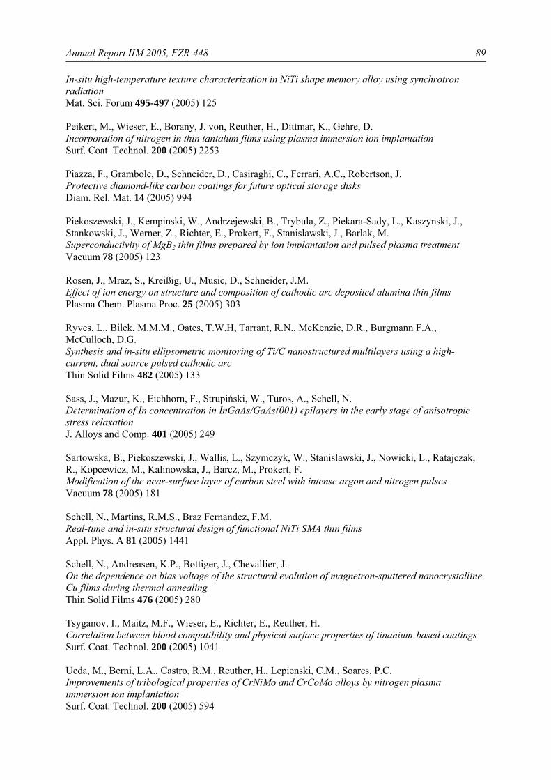
Annual Report IIM 2005, FZR-448
89
In-situ high-temperature texture characterization in NiTi shape memory alloy using synchrotron radiation Mat. Sci. Forum 495-497 (2005) 125 Peikert, M., Wieser, E., Borany, J. von, Reuther, H., Dittmar, K., Gehre, D. Incorporation of nitrogen in thin tantalum films using plasma immersion ion implantation Surf. Coat. Technol. 200 (2005) 2253 Piazza, F., Grambole, D., Schneider, D., Casiraghi, C., Ferrari, A.C., Robertson, J. Protective diamond-like carbon coatings for future optical storage disks Diam. Rel. Mat. 14 (2005) 994 Piekoszewski, J., Kempinski, W., Andrzejewski, B., Trybula, Z., Piekara-Sady, L., Kaszynski, J., Stankowski, J., Werner, Z., Richter, E., Prokert, F., Stanislawski, J., Barlak, M. Superconductivity of MgB2 thin films prepared by ion implantation and pulsed plasma treatment Vacuum 78 (2005) 123 Rosen, J., Mraz, S., Kreißig, U., Music, D., Schneider, J.M. Effect of ion energy on structure and composition of cathodic arc deposited alumina thin films Plasma Chem. Plasma Proc. 25 (2005) 303 Ryves, L., Bilek, M.M.M., Oates, T.W.H, Tarrant, R.N., McKenzie, D.R., Burgmann F.A., McCulloch, D.G. Synthesis and in-situ ellipsometric monitoring of Ti/C nanostructured multilayers using a high-current, dual source pulsed cathodic arc Thin Solid Films 482 (2005) 133 Sass, J., Mazur, K., Eichhorn, F., Strupiński, W., Turos, A., Schell, N. Determination of In concentration in InGaAs/GaAs(001) epilayers in the early stage of anisotropic stress relaxation J. Alloys and Comp. 401 (2005) 249 Sartowska, B., Piekoszewski, J., Wallis, L., Szymczyk, W., Stanislawski, J., Nowicki, L., Ratajczak, R., Kopcewicz, M., Kalinowska, J., Barcz, M., Prokert, F. Modification of the near-surface layer of carbon steel with intense argon and nitrogen pulses Vacuum 78 (2005) 181 Schell, N., Martins, R.M.S., Braz Fernandez, F.M. Real-time and in-situ structural design of functional NiTi SMA thin films Appl. Phys. A 81 (2005) 1441 Schell, N., Andreasen, K.P., Bøttiger, J., Chevallier, J. On the dependence on bias voltage of the structural evolution of magnetron-sputtered nanocrystalline Cu films during thermal annealing Thin Solid Films 476 (2005) 280 Tsyganov, I., Maitz, M.F., Wieser, E., Richter, E., Reuther, H. Correlation between blood compatibility and physical surface properties of tinanium-based coatings Surf. Coat. Technol. 200 (2005) 1041 Ueda, M., Berni, L.A., Castro, R.M., Reuther, H., Lepienski, C.M., Soares, P.C. Improvements of tribological properties of CrNiMo and CrCoMo alloys by nitrogen plasma immersion ion implantation Surf. Coat. Technol. 200 (2005) 594
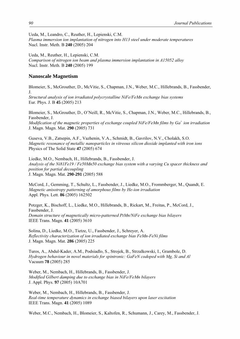
Journal Publications
90
Ueda, M., Leandro, C., Reuther, H., Lepienski, C.M. Plasma immersion ion implantation of nitrogen into H13 steel under moderate temperatures Nucl. Instr. Meth. B 240 (2005) 204 Ueda, M., Reuther, H., Lepienski, C.M. Comparison of nitrogen ion beam and plasma immersion implantation in A15052 alloy Nucl. Instr. Meth. B 240 (2005) 199 Nanoscale Magnetism Blomeier, S., McGrouther, D., McVitie, S., Chapman, J.N., Weber, M.C., Hillebrands, B., Fassbender, J. Structural analysis of ion irradiated polycrystalline NiFe/FeMn exchange bias systems Eur. Phys. J. B 45 (2005) 213 Blomeier, S., McGrouther, D., O’Neill, R., McVitie, S., Chapman, J.N., Weber, M.C., Hillebrands, B., Fassbender, J. Modification of the magnetic properties of exchange coupled NiFe/FeMn films by Ga+ ion irradiation J. Magn. Magn. Mat. 290 (2005) 731 Guseva, V.B., Zatsepin, A.F., Vazhenin, V.A., Schmidt, B., Gavrilov, N.V., Cholakh, S.O. Magnetic resonance of metallic nanoparticles in vitreous silicon dioxide implanted with iron ions Physics of The Solid State 47 (2005) 674 Liedke, M.O., Nembach, H., Hillebrands, B., Fassbender, J. Analysis of the Ni81Fe19 / Fe50Mn50 exchange bias system with a varying Cu spacer thickness and position for partial decoupling J. Magn. Magn. Mat. 290-291 (2005) 588 McCord, J., Gemming, T., Schultz, L., Fassbender, J., Liedke, M.O., Frommberger, M., Quandt, E. Magnetic anisotropy patterning of amorphous films by He-ion irradiation Appl. Phys. Lett. 86 (2005) 162502 Potzger, K., Bischoff, L., Liedke, M.O., Hillebrands, B., Rickart, M., Freitas, P., McCord, J., Fassbender, J. Domain structure of magnetically micro-patterned PtMn/NiFe exchange bias bilayers IEEE Trans. Magn. 41 (2005) 3610 Solina, D., Liedke, M.O., Tietze, U., Fassbender, J., Schreyer, A. Reflectivity characterization of ion irradiated exchange bias FeMn-FeNi films J. Magn. Magn. Mat. 286 (2005) 225 Turos, A., Abdul-Kader, A.M., Podsiadlo, S., Strojek, B., Strzalkowski, I., Grambole, D. Hydrogen behaviour in novel materials for spintronic: GaFeN codoped with Mg, Si and Al Vacuum 78 (2005) 285 Weber, M., Nembach, H., Hillebrands, B., Fassbender, J. Modified Gilbert damping due to exchange bias in NiFe/FeMn bilayers J. Appl. Phys. 97 (2005) 10A701 Weber, M., Nembach, H., Hillebrands, B., Fassbender, J. Real-time temperature dynamics in exchange biased bilayers upon laser excitation IEEE Trans. Magn. 41 (2005) 1089 Weber, M.C., Nembach, H., Blomeier, S., Kaltofen, R., Schumann, J., Carey, M., Fassbender, J.
Annual Report IIM 2005, FZR-448
91
All-optical probe of magnetization dynamics in exchange biased bilayers on the picosecond time-scale Eur. Phys. J. B 45 (2005) 243 Nanostructures Bischoff, L., Schmidt, B., Akhmadaliev, C., Heinig, K.-H. Nanodrähte durch Ionenbeschuss Dresdner Transferbrief 2 (2005) 13 Cantelli, V., Borany, J. von, Mücklich, A., Schell, N. Investigation of the formation and phase transition of small Ge and Co nanoparticles in a SiO2 matrix Nucl. Instr. Meth. B 238 (2005) 268 Dimitrakis, P., Normand, P., Vontintseva, E., Stegemann, K.-H., Heinig, K.-H., Schmidt, B. Memory devices obtained by Si+ irradiation through poly-Si/SiO2 gate stack J. Phys.: Conf. Ser. 10 (2005) 7 Dvurechenskii, A.V., Smagina, J.V., Grötzschel, R., Zinovyev, V.A., Armbrister, V.A., Novikov, P.L., Teys, S.A., Gutakovskii, A.K. Ge/Si quantum dot nanostructures grown with low-energy ion beam assisted epitaxy Surf. Coat. Technol. 196 (2005) 25 Eichhorn, F., Gaca, J., Heera, V., Schell, N., Turos, A., Weishart, H., Wojcik, M. Structural studies on ion implanted semiconductors using x-ray synchrotron radiation: strain evolution and growth of nanocrystals Vacuum 78 (2005) 303 Grenzer, J., Bischoff, L., Pietsch, U. Grazing-incidence diffraction strain analysis of a laterally patterned Si wafer treated by focused Ge and Au ion beam implantation Phys. Status Solidi A 202 (2005) 1009 Johnson, S., Markwitz, A., Rudolphi, M., Baumann, H., Kuo, P.-Y., Blaikie, R., Mücklich, A. Effect of crystal orientation on self-assembled silicon nanostructures formed by electron beam annealing J. Appl. Phys. 97 (2005) 94301 Kurmaev, E.Z., Zatsepin, D.A., Cholakh, S.O., Schmidt, B., Harada, Y., Tokushima, T., Osawa, H., Shin, S., Takeuchi, T. Iron nanoparticles in amorphous SiO2: x-ray emission and absorption spectra Phys. of The Solid State 47 (2005) 754 Markwitz, A., Johnson, S., Rudolphi, M., Baumann, H., Mücklich, A. Formation of SiC surface nanocrystals by ion implantation and electron beam rapid thermal annealing Appl. Phys. Lett. 86 (2005) 013108 Meduňa, M., Novák, J., Falub, C.V., Bauer, G., Tsujino, S., Grützmacher, D., Müller, E., Campidelli, Y., Kermarrec, O., Bensahel, D., Schell, N. High temperature investigations of Si/SiGe based cascade structures using x-ray scattering methods J. Phys. D: Appl. Phys. 38 (2005) A121 Oates, T.W.H., Mücklich, A. Evolution of plasmon resonances during plasma deposition of silver nanoparticles Nanotechnol. 16 (2005) 2606
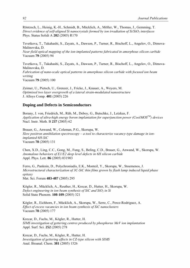
Journal Publications
92
Röntzsch, L., Heinig, K.-H., Schmidt, B., Mücklich, A., Möller, W., Thomas, J., Gemming, T. Direct evidence of self-aligned Si nanocrystals formed by ion irradiation of Si/SiO2 interfaces Phys. Status Solidi A 202 (2005) R170 Tsvetkova, T., Takahashi, S., Zayats, A., Dawson, P., Turner, R., Bischoff, L., Angelov, O., Dimova-Malinovska, D. Near-field optical mapping of the ion-implanted patterns fabricated in amorphous silicon carbide Vacuum 79 (2005) 94 Tsvetkova, T., Takahashi, S., Zayats, A., Dawson, P., Turner, R., Bischoff, L., Angelov, O., Dimova-Malinovska, D. Fabrication of nano-scale optical patterns in amorphous silicon carbide with focused ion beam writing Vacuum 79 (2005) 100 Zeimer, U., Pietsch, U., Grenzer, J., Fricke, J., Knauer, A., Weyers, M. Optimised two layer overgrowth of a lateral strain-modulated nanostructure J. Alloys Comp. 401 (2005) 226 Doping and Defects in Semiconductors Borany, J. von, Friedrich, M., Rüb, M., Deboy, G., Butschke, J., Letzkus, F. Application of ultra-high energy boron implantation for superjunction power (CoolMOSTM) devices Nucl. Instr. Meth. B 237 (2005) 62 Brauer, G., Anwand, W., Coleman, P.G., Skorupa, W. Slow positron annihilation spectroscopy – a tool to characterize vacancy-type damage in ion-implanted 6H-SiC Vacuum 78 (2005) 131 Chen, X.D., Ling, C.C., Gong, M., Fung, S., Beling, C.D., Brauer, G., Anwand, W., Skorupa, W. Anomalous behaviors of E1/E2 deep level defects in 6H silicon carbide Appl. Phys. Lett. 86 (2005) 031903 Ferro, G., Panknin, D., Polychroniadis, E.K., Monteil, Y., Skorupa, W., Stoemenos, J. Microstructural characterization of 3C-SiC thin films grown by flash lamp induced liquid phase epitaxy Mat. Sci. Forum 483-487 (2005) 295 Kögler, R., Mücklich, A., Reuther, H., Krecar, D., Hutter, H., Skorupa, W. Defect engineering in ion beam synthesis of SiC and SiO2 in Si Solid State Phenom. 108-109 (2005) 321 Kögler, R., Eichhorn, F., Mücklich, A., Skorupa, W., Serre, C., Perez-Rodriguez, A. Effect of excess vacancies in ion beam synthesis of SiC nanoclusters Vacuum 78 (2005) 177 Krecar, D., Fuchs, M., Kögler, R., Hutter, H. SIMS investigation of gettering centres produced by phosphorus MeV ion implantation Appl. Surf. Sci. 252 (2005) 278 Krecar, D., Fuchs, M., Kögler, R., Hutter, H. Investigation of gettering effects in CZ-type silicon with SIMS Anal. Bioanal. Chem. 381 (2005) 1526
Annual Report IIM 2005, FZR-448
93
Ling, C.C., Chen, X.D., Brauer, G., Anwand, W., Skorupa, W., Wang, H.Y., Weng, H.M. Deep-level defects in n-type 6H silicon carbide induced by He-implantation J. Appl. Phys. 98 (2005) 043508 Nazarov, A.N., Skorupa, W., Osiyuk, I.N., Tjagulski, I.P., Lysenko, V.S., Yankov, R.A., Gebel, T. Comparative study of charge trapping in high-dose Si and Ge-implanted Al/SiO2/Si structures J. Electrochem. Soc. 152 (2005) F20 Pecz, B., Dobos, L., Panknin, D., Skorupa, W., Lioutas, C., Vouroutzis, N. Crystallization of amorphous-Si films by flash lamp annealing Appl. Surf. Sci. 242 (2005) 185 Pezoldt, J., Polychroniadis, E., Stauden, T., Ecke, G., Chassagne, T., Vennegues, P., Leycuras, A., Panknin, D., Stoemenos, J., Skorupa, W. Nucleation control in FLASIC assisted short time liquid phase epitaxy by melt modification Mat. Sci. Forum 483-487 (2005) 213 Posselt, M., Gao, F., Zwicker, D. Atomistic study of the migration of di- and tri-interstitials in silicon Phys. Rev. B 71 (2005) 245202 Posselt, M., Gao, F., Zwicker, D. Migration of di- and tri-interstitials in silicon Nucl. Instr. Meth. B 228 (2005) 212 Skorupa, W., Panknin, D., Voelskow, M., Anwand, W., Gebel, T., Yankov, R.A. Advanced thermal processing of materials in the msec range Vacuum 78 (2005) 673 Skorupa, W., Gebel, T., Yankov, R.A., Paul, S., Lerch, W., Downey, D.F., Arevalo, E.A. Advanced thermal processing of ultrashallow implanted junctions using flash lamp annealing J. Electrochem. Soc. 152 (2005) G436 Smith, M., McMahon, R., Voelskow, M., Skorupa, W., Stoemenos, J. Regrowth mechanisms in flash lamp processing of heteroepitaxial SiC on silicon substrates J. Cryst. Growth 277 (2005) 162 Smith, M., McMahon, R., Voelskow, M., Panknin, D., Skorupa, W. Modelling of flash-lamp-induced crystallization of amorphous silicon thin films on glass J. Cryst. Growth 285 (2005) 249 Smith, M., McMahon, R.A., Skorupa, W., Voelskow, M., Stoemenos, J. A thermal model for flash lamp annealing of 3C-SiC/Si multi-layer systems (i-FLASiC) Mat. Sci. Forum 483-487 (2005) 217 Vandervorst, W., Janssens, T., Brijs, B., Delhougne, R., Loo, R., Caymax, M., Pawlak, B. J., Posselt, M. Athermal germanium migration in strained silicon layers during junction formation with solid-phase epitaxial regrowth Appl. Phys. Lett. 86 (2005) 081915 Voelskow, M., Skorupa, W., Smith, M.P., McMahon, R.A. Homogenization of the melting depth in SiC on Si structures during flash lamp irradiation Appl. Phys. Lett. 87 (2005) 241901
Journal Publications
94
Voelskow, M., Panknin, D., Polychroniadis, E.K., Ferro, G., Godignon, P., Mestres, N., Skorupa, W., Monteil, Y., Stoemenos, J. Epitaxial SiC formation at the SiO2/Si interface by C+ implantation into SiO2 and subsequent annealing Mat. Sci. Forum 483-487 (2005) 233 Weih, P., Stauden, T., Ecke, G., Shokhovets, S., Zgheib, C., Voelskow, M., Skorupa, W., Ambacher, O., Pezoldt, J. Ion beam synthesis of 3C-(Si1-xC1-y)Gex+y solid solutions Phys. Status Solidi A 202 (2005) 545 Weishart, H., Heera, V., Skorupa, W. n-type conductivity in high-fluence Si-implanted diamond J. Appl. Phys. 97 (2005) 103514 Weishart, H., Eichhorn, F., Heera, V., Pécz, B., Barna, Á., Skorupa, W. High-fluence Si-implanted diamond: optimum implantation temperature for SiC formation J. Appl. Phys. 98 (2005) 043503 Wiatrowski, A., Boratynski, B., Prucnal, S., Synowiec, Z., Zuk, J. Proton implant isolation in GaN Vacuum 78 (2005) 463 Wierzchowski, W., Wieteska, K., Graeff, W., Gawlik, G., Turos, A., Maurin, J., Mücklich, A. Strain profiles in the insulated buried layers obtained by He implantation in AlGaAs Acta Cryst. A 61 (2005) C449 Zolnai, Z., Ster, A., Khánh, N.Q., Kótai, E., Posselt, M., Battistig, G., Lohner, T., Gyulai, J. Ion-beam analysis and computer simulation of damage accumulation in nitrogen implanted 6H-SiC: effects of channeling Mat. Sci. Forum 483-485 (2005) 637 Optoelectronic Materials Cheng, X.Q., Sun, J.M., Kögler, R., Skorupa, W., Möller, W., Prucnal, S. Photoluminescence of Er-doped SiO2 layers containing Si nanoclusters using dual ion implantation and annealing Vacuum 78 (2005) 177 Drachenko, O., Galibert, J., Léotin, J., Tomm, J.W., Semtsiv, M.P., Ziegler, M., Dressler, S., Müller, U., Masselink, W.T. Electron-optical-phonon interaction in the In0.73Ga0.27As-AlAs intersubband laser Appl. Phys. Lett. 87 (2005) 121114 Dreyhaupt, A.,Winnerl, S., Dekorsy, T., Helm, M. High-intensity terahertz radiation from a microstructured large-area photoconductor Appl. Phys. Lett. 86 (2005) 121114 Fitting, H.-J., Ziems, T., Salh, R., Charnowski, A. von, Schmidt, B. Luminescent defect dynamics in amorphous SiO2:H Phys. Status Solidi C 2 (2005) 693 Fitting, H.-J., Ziems, T., Salh, R., Zamoryanskaya, M.V., Kolesnikova, K.V., Schmidt, B., Czarnowski, A. von Cathodoluminescence of wet, dry, and hydrogen-implanted silica films
Annual Report IIM 2005, FZR-448
95
J. Non-Cryst. Sol. 351 (2005) 2251 Fitting, H.-J., Salh, R., Barfels, T., Schmidt, B. Multimodal luminescence spectra of ion-implanted silica Phys. Status Solidi A 202 (2005) R142 Gushterova, P., Sharlandjiev, P., Schmidt, B., Pham, M.T. On the determination of the optical constants of very thin (λ/50) films J. Optoel. Adv. Mat. 7 (2005) 305 Helm, M., Sun, J. M., Potfajova, J., Dekorsy, T., Schmidt, B., Skorupa, W. Efficient silicon based light emitters Microel. J. 36 (2005) 957 Helm, M., Sun, J., Potfajova, J., Winnerl, S., Dekorsy, T., Skorupa, W., Schmidt, B., Mücklich, A. Efficient light emitting diodes based on nanoscale silicon Phys. Status Solidi C 2 (2005) 2941 Lebedev, M.V., Misochko, O.V., Dekorsy, T., Georgiev, N. On the nature of the coherent artifact J. Exp. Theor. Phys. 100 (2005) 272 Misochko, O.V., Lebedev, M.V., Dekorsy, T. Observation of longitudinal optical-transverse optical splitting for E-symmetry phonons in Te by coherent phonon spectroscopy J. Phys. Cond. Matter 17 (2005) 3015 Nazarov, A.N., Vovk, J.N., Osiyuk, I.N., Tkachenko, A.S., Tyagulskii, I.P., Lysenko, V.S., Gebel, T., Rebohle, L., Skorupa, W., Yankov, R.A. The effect of radio-frequency plasma treatment on the electroluminescent properties of violet light-emitting germanium implanted metal-oxide-semiconductor structures Mat. Sci. Eng. B 124 (2005) 458 Nazarov, A.N., Sun, J.M., Skorupa, W., Yankov, R.A., Osiyuk, I.N., Tjagulski, I.P., Lysenko, V.S., Gebel, T. Light emission and charge trapping in Er-doped silicon dioxide films containing silicon nanocrystals Appl. Phys. Lett. 86 (2005) 151914 Prucnal, S., Cheng, X.Q., Sun, J.M., Kögler, R., Zuk, J., Skorupa, W. Optical and microstructural properties of doubly Ge-Si implanted SiO2 layers Vacuum 78 (2005) 693 Rebohle, L., Gebel, T., Yankov, R.A., Trautmann, T., Skorupa, W., Sun, J.M., Gauglitz, G., Frank, R. Microarrays of silicon-based light emitters for novel biosensor and lab-on-a-chip applications Optical Mat. 27 (2005) 1055 Salh, R., Schmidt, B., Fitting, H.-J. Multiplet luminescence of sulfur implanted silica – SiO2:S Phys. Status Solidi A 202 (2005) R53 Semtsiv, M.P., Ziegler, M., Dressler, S., Masselink, W.T., Georgiev, N., Dekorsy, T., Helm, M. Strain-compensated AlAs/(In,Ga)As heterostructures for short wavelength intersubband absorption and laser emission J. Crystal Growth 278 (2005) 526
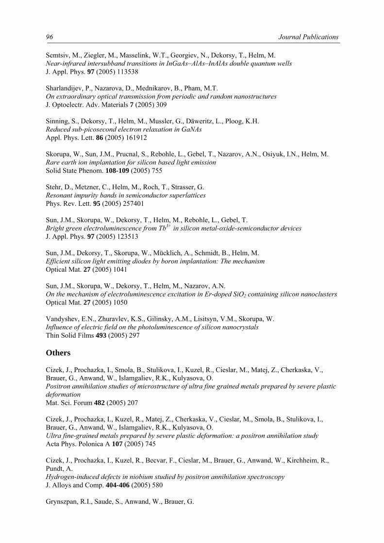
Journal Publications
96
Semtsiv, M., Ziegler, M., Masselink, W.T., Georgiev, N., Dekorsy, T., Helm, M. Near-infrared intersubband transitions in InGaAs–AlAs–InAlAs double quantum wells J. Appl. Phys. 97 (2005) 113538 Sharlandijev, P., Nazarova, D., Mednikarov, B., Pham, M.T. On extraordinary optical transmission from periodic and random nanostructures J. Optoelectr. Adv. Materials 7 (2005) 309 Sinning, S., Dekorsy, T., Helm, M., Mussler, G., Däweritz, L., Ploog, K.H. Reduced sub-picosecond electron relaxation in GaNAs Appl. Phys. Lett. 86 (2005) 161912 Skorupa, W., Sun, J.M., Prucnal, S., Rebohle, L., Gebel, T., Nazarov, A.N., Osiyuk, I.N., Helm, M. Rare earth ion implantation for silicon based light emission Solid State Phenom. 108-109 (2005) 755 Stehr, D., Metzner, C., Helm, M., Roch, T., Strasser, G. Resonant impurity bands in semiconductor superlattices Phys. Rev. Lett. 95 (2005) 257401 Sun, J.M., Skorupa, W., Dekorsy, T., Helm, M., Rebohle, L., Gebel, T. Bright green electroluminescence from Tb3+ in silicon metal-oxide-semiconductor devices J. Appl. Phys. 97 (2005) 123513 Sun, J.M., Dekorsy, T., Skorupa, W., Mücklich, A., Schmidt, B., Helm, M. Efficient silicon light emitting diodes by boron implantation: The mechanism Optical Mat. 27 (2005) 1041 Sun, J.M., Skorupa, W., Dekorsy, T., Helm, M., Nazarov, A.N. On the mechanism of electroluminescence excitation in Er-doped SiO2 containing silicon nanoclusters Optical Mat. 27 (2005) 1050 Vandyshev, E.N., Zhuravlev, K.S., Gilinsky, A.M., Lisitsyn, V.M., Skorupa, W. Influence of electric field on the photoluminescence of silicon nanocrystals Thin Solid Films 493 (2005) 297 Others Cizek, J., Prochazka, I., Smola, B., Stulikova, I., Kuzel, R., Cieslar, M., Matej, Z., Cherkaska, V., Brauer, G., Anwand, W., Islamgaliev, R.K., Kulyasova, O. Positron annihilation studies of microstructure of ultra fine grained metals prepared by severe plastic deformation Mat. Sci. Forum 482 (2005) 207 Cizek, J., Prochazka, I., Kuzel, R., Matej, Z., Cherkaska, V., Cieslar, M., Smola, B., Stulikova, I., Brauer, G., Anwand, W., Islamgaliev, R.K., Kulyasova, O. Ultra fine-grained metals prepared by severe plastic deformation: a positron annihilation study Acta Phys. Polonica A 107 (2005) 745 Cizek, J., Prochazka, I., Kuzel, R., Becvar, F., Cieslar, M., Brauer, G., Anwand, W., Kirchheim, R., Pundt, A. Hydrogen-induced defects in niobium studied by positron annihilation spectroscopy J. Alloys and Comp. 404-406 (2005) 580 Grynszpan, R.I., Saude, S., Anwand, W., Brauer, G.
Annual Report IIM 2005, FZR-448
97
Positron annihilation investigation and nuclear reaction analysis of helium and oxygen-implanted zirconia Nucl. Instr. Meth. B 241 (2005) 526 Hennig, C., Reich, T., Kraus, W., Reck, G., Prokert, F., Schell, N. Combining EXAFS and x-ray powder diffraction to solve structures containing heavy atoms Physica Scripta T 115 (2005) 352 Kondyurin, A., Romanova, V., Begishev, V., Kondyurina, I., Günzel, R., Maitz, F.M. Cross linking polyurethane coating on vascular stents for enhanced x-ray contrasts J. Bioactive and Compatible Polymers 20 (2005) 77 Krause-Rehberg, R., Bondarenko, V., Thiele, E., Klemm, R., Schell, N. Determination of absolute defect concentrations for saturated position trapping – deformed polycrystalline Ni as a case study Nucl. Instr. Meth. B 240 (2005) 719 Oswald, S., Mazilu, I., Fahler, S., Gruner, W., Hermann, R., Loser, W., Filip, O., Wendrock, H., Schultz, L., Schmidt, B., Rodewald, W. SIMS measurements of oxygen content in the Nd2Fe14B phase J. Magn. Magn. Mat. 290 (2005) 1240 Oswald, S., Schmidt, B., Heinig, K.-H. Influence of sputtering conditions and electron energy on XPS depth profiling of Ge in SiO2 Cryst. Res. Technol. 40 (2005) 1134 Schmidt, B., Oswald, S., Bischoff, L. Etch rate retardation of Ga+-ion beam-irradiated silicon J. Electrochem. Soc. 152 (2005) G875 Thiele, E., Klemm, R., Hollang, L., Holste, C., Schell, N., Natter, H., Hempelmann, R. An approach to cyclic plasticity and deformation-induced structure changes of electrodeposited nickel Mat. Sci. Eng. A 390 (2005) 42 Tunc, S., Maitz, M.F., Steiner, G., Vázques, L., Pham, M.T., Salzer, R. In-situ conformational analysis of fibrinogen absorbed on Si surfaces Colloids and Surfaces: Biointerfaces 42 (2005) 219 Equipment Bischoff, L. Alloy liquid metal ion sources and their application in mass separated focused ion beams Ultramicroscopy 103 (2005) 59 Bischoff, L., Mair, G.L.R., Akhmadaliev, C., Mair, A.W.R., Ganetsos, T. The post-ionisation of Pb ions from a molten Sn host field-ion emitter Appl. Phys. A 80 (2005) 205 Bischoff, L., Pilz, W., Ganetsos, T., Akhmadaliev, C., Aidinis, C.J., Londos, C.A. On the temperature dependence of the mass spectra of AuGe and AuGeSi liquid metal alloy ion sources J. Phys.: Conf. Ser. 10 (2005) 214 Kaschny, J.R., Kögler, R., Tyroff, H., Bürger, W., Eichhorn, F., Mücklich, A., Serre, C., Skorupa, W. Facility for simultaneous dual-beam ion implantation
Conference Proceedings
98
Nucl. Instr. Meth. A 551 (2005) 2000 Mair, G.L.R., Bischoff, L., Londos, C.A., Ganetsos, T., Akhmadaliev, C., Aidinis, C.J. An in-depth investigation into the temperature dependence of the mass spectra of an Au82Si18 liquid metal field emitter Appl. Phys. A 81 (2005) 385 Zschornack, G., Landgraf, S., Großmann, F., Kentsch, U., Ovsyannikov, V.P., Schmidt, M., Ullmann, F. A low energy ion beam line for highly charged ions Vacuum 78 (2005) 319
Conference Proceedings Bonafos, C., Cherkashin, N., Carrada, M., Coffin, H., Ben Assayag, G., Schamm , S., Dimitrakis, P., Normand, P., Perego, M., Fanciulli, M., Müller, T., Heinig, K.-H., Argawal, A., Claverie, A. Manipulation of 2D arrays of Si nanocrystals by ultra-low-energy ion beam synthesis for nonvolatile memories applications MRS Soc. Symp. Proc. 830 (2005) D5.2 Dekorsy, T., Sun, J. M., Skorupa, W., Mücklich, A., Schmidt, B., Helm, M. Origin of efficient light emission from si pn diodes prepared by ion implantation AIP Conf. Proc. 772 (2005) 1539 Dekorsy, T., Sinning, S., Helm, M., Mussler, G., Däweritz, L., Ploog, K.H. Ultrafast carrier dynamics in nitrogen containing GaAs AIP Conf. Proc. 772 (2005) 235 Drachenko, O., Rylkov, V.V., Leotin, J. Compact Terahertz cyclotron resonance spectrometer in high magnetic fields IEEE Conference digest IRMMW2005/THz2005 (2005) 20 Gebel, T., Rebohle, L., Trautmann, T., Yankov, R.A., Skorupa, W., Gauglitz, G., Frank, R. Miniaturised arrays of light-sources based on silicon technology: a promising approach for novel sensors and lab-on-a-chip systems Sensor 2005, Conf. Proc. Vol. 1, B1.4 (2005) 125 Ling, C.C., Chen, X.D., Fung, S., Beling, C.D., Brauer, G., Anwand, W., Skorupa, W., Gong, M. Deep level defects E1/E2 in n-type 6H silicon carbide induced by electron radiation and He implantation AIP Conf. Proc. 772 (2005) 99 Masselink, W.T., Semtsiv, M.P., Dressler, S., Ziegler, M., Georgiev, N., Dekorsy, T., Helm, M. High-power short-wavelength quantum cascade lasers Proc. SPIE 5738 (2005) 13 Reuther, H., Menzel, M., Vinnichenko, M., Kolitsch, A. Investigation of the Sn4+ charge density variation in In2O3 using Mössbauer spectroscopy AIP Conf. Proc. 765 (2005) 132 Skorupa, W., Yankov, R.A., Voelskow, M., Anwand, W., Panknin, D., McMahon, R.A., Smith, M., Gebel, T., Rebohle, L., Fendler, R., Hentsch, W. Advanced thermal processing of semiconductor materials in the msec range (invited)
Annual Report IIM 2005, FZR-448
99
Proc. XIII. Int. Conf. Advanced Thermal Processing of Semiconductors (RTP 2005), Oct. 4-7, 2005, Santa Barbara, USA, IEEE Cat.No.05EX1090, ISBN 0-7803-9223-X, 53-71 (2005) Skorupa, W., Sun, J.M., Prucnal, S., Rebohle, L., Gebel, T., Nazarov, A.N., Osiyuk, I.N., Dekorsy, T., Helm, M. Rare earth ion implantation for silicon based light emission: From infrared to ultraviolet MRS Soc. Symp. Proc. 866 (2005) V4.1.1 / FF4.1.1
Invited Talks Brauer, G., Anwand, W., Eichhorn, F., Skorupa, W., Hofer, C., Brandstetter, S., Teichert, C., Kuriplach, J., Cizek, J., Prochazka, I., Coleman, P.G., Nozawa, T., Kohyama, A. Surface studies of SiC 10th Int. Workshop on Slow Positron Beam Techniques for Solids and Surfaces (SLOPOS-10), Doha, Qatar, March 19 – 25, 2005 Fassbender, J., Potzger, K., Bischoff, L., Zhou, S., Talut, G., Liedke, M.O., Reuther, H., Mücklich, A., Grötzschel, R. Ion-driven magnetic nanostructures 14th Int. Summer School on Vacuum, Electron and Ion Technologies, Sunny Beach, Bulgaria, Sept 12 – 16, 2005 Facsko, S., Kost, D., Keller, A., Möller, W., Pesic, Z., Stolterfoht, N. Interaction of highly-charged ions with the surface of insulators 3rd Conf. on Elementary Processes in Atomic Systems (CEPAS), Miskolc, Hungary, Aug 31 – Sept 2, 2005 Gao, F., Zhang, Y., Posselt, M., Devanathan, R., Weber, W.J. Epitaxial recrystallization of nano-sized amorphous layers, phase nucleation and growth in 4H-SiC MRS Fall Meeting, Boston, MA, USA, Nov 27 – Dec 1, 2005 Grenzer, J. Grazing-incidence diffraction and small angle X-ray scattering 6th Autumn School on X-ray Scattering from Surfaces and Thin Layers, Smolenice, Slovakia, Sept 18 – 21, 2005 Grynszpan, R.I., Brauer, G., Anwand, W. Positron annihilation investigation in ion-implanted Yttria-stabilized zirconia MRS Fall Meeting , Boston, MA, USA, Nov 28 – Dec 2, 2005 Heinig, K.-H. Modelling of ion-driven nanostructures 14th Int. Summer School on Vacuum, Electron and Ion Technologies, Sunny Beach, Bulgaria, Sept 12 – 16, 2005 Heinig, K.-H., Müller, T., Röntzsch, L., Möller, W. Growth and taming of nanostructures with ion beams Int. Symp. on Trends in Nanoscience: Structure and Functions, Irsee, Germany, Oct 8 – 12, 2005 Helm, M. Approaches for silicon based light emitters 8th German-Vietnamese Seminar on Physics and Engineering, Erlangen, Germany, April 3 – 9, 2005 Helm, M.
Invited Talks
100
Efficient silicon based light emitters 4th Workshop on Semiconductor Nanodevices and Nanostructured Materials (NANOSEMIMAT-4), Sao Pedro, SP, Brazil, March 9 – 13, 2005 Helm, M. New concepts for short-wavelength quantum cascade lasers and few-cycle THz emitters Japan-Germany Colloquium 2005: Semiconductor Physics and Technology, Dresden, Germany Feb 14 – 16, 2005 Krause-Rehberg, R., Sachert, S., Brauer, G., Rogov, A., Nowak, K. EPOS – an intense positron beam project at the Research Center Rossendorf 10th Int. Workshop on Slow Positron Beam Techniques for Solids and Surfaces (SLOPOS-10), Doha, Qatar, March 19 – 25, 2005 Masselink, W.T., Semtsiv, M.P., Dressler, S., Ziegler, M., Georgiev, N., Dekorsy, T., Helm, M. High-power short-wavelength quantum cascade lasers Photonics West, SPIE, San Jose, CA, USA, Jan 22 – 27, 2005 Möller, W. Plasma surface interaction and ion bombardment Intern. School "Nanostructuring by Ion Beams", New Delhi, India, Feb 18 – 19, 2005 Möller, W., Heinig, K.-H., Müller, T., Röntzsch, L., Schmidt, B. Ion beam synthesis of nanostructures with keV/amu ions Indo-German Workshop "Synthesis and Modification of Nanostructured Materials by Energetic Ion Beams", New Delhi, India, Feb 21 – 24, 2005 Möller, W., Abendroth, B., Gago, R., Kolitsch, A. Ion bombardment for stress release in cubic boron nitride thin films Intern. Conf. on Metallurgical Coatings and Thin Films, San Diego, USA, May 2 – 6, 2005 Möller, W. Plasma immersion ion implantation: Process, promises and prospects 15th Intern. Colloq. on Plasma Processes, Autrans, France, June 5 – 9, 2005 Möller, W. Ion-induced stress release in hard coatings 14th Intern. Summer School on Vacuum, Electron, and Ion Technologies, Sunny Beach, Bulgaria, Sept 12 – 16, 2005 Möller, W., Shevchenko, N., Yankov, R.A., Rogozin, A., Maitz, M.F., Richter, E., Donchev, A., Schütze, M. Reactive ion plasma immersion implantation for surface passivation 8th Intern. Workshop on Plasma-Based Ion Implantation and Deposition, Chengdu, China, Sept 18 – 22, 2005 Müller, T., Heinig, K.-H., Schmidt, B., Röntzsch, L., Stegemann, K.-H. Fabrication of Si nanocrystals for nonvolatile memories using ion beams 1st Int. Workshop on Semiconductor Nanocrystals (SEMINANO), Budapest, Hungary Sept 10 – 12, 2005 Potzger, K., Reuther, H., Zhou, S., Anwand, W., Brauer, G. Ion implantation of 3d-metals into ZnO single crystals Int. Topical Workshop on Heteroepitaxy of 3C-SiC on Silicon and its Application to Sensor Devices (HeT-SiC-05), Hotel Erbgericht Krippen, Germany, April 26 – May 1, 2005
Annual Report IIM 2005, FZR-448
101
Schneider, H., Maier, T., Schönbein, C., Koidl, P., Walther, M., Liu, H.C. Optical and transport nonlinearities in quantum well infrared photodetectors 8th Int. Conf. on Intersubband Transitions in Quantum Wells, Cape Cod, MA, USA, Sept 11 – 16, 2005 Schneider, H., Maier, T., Fleissner, J., Walther, M., Koidl, P., Weimann, G., Cabanski, W., Finck, M., Menger, P., Rode, W., Ziegler, J. Quantum well infrared photodetectors: quantum structures for high-performance thermal imaging Int. Symp. on Advanced Electronics for Future Generations - “Secure-Life Electronics” for Quality Life and Society, Tokyo, Japan, Oct 11 – 12, 2005 Skorupa, W., Panknin, D., Anwand, W., Voelskow, M., Yankov, R.A., Gebel, T., Paul, S., Lerch, W., Downey, D.E., Arevalo, E., Mannino, G. Advanced thermal processing of silicon in the msec-range using flash lamps EU-Workshop on “Non-conventional thermal processes for advanced CMOS”, Rome, Italy, Jan 21, 2005 Skorupa, W., Sun, J.M., Prucnal, S., Rebohle, L., Gebel, T., Nazarov, A.N., Osiyuk, I.N., Dekorsy, T., Helm, M. Rare earth ion implantation for silicon based light emission: From infrared to ultraviolet MRS Spring Meeting, San Francisco, CA, USA, March 29 – April 1, 2005 Skorupa, W. Seltenerden-Implantation für die Si-basierte Lichtemission Workshop "Ionenstrahlphysik und -technologie", Leipzig, Germany, April 11 – 12, 2005 Deutsches Nutzertreffen Ionenimplantation, Erlangen, Germany, May 13, 2005 Skorupa, W. Basics and advances of ion beam synthesis Nordic Summer School on Defects and Diffusion in Semiconductors and Heterostructures, Sundvolden, Norway, Aug 18 – 21, 2005 Skorupa,W., Anwand, W. Thermobehandlung von Halbleitermaterialien im msec-Bereich Summerschool S2B Nanotronics 2005, Science to Business Center Nanotronics-DEGUSSA AG, Marl, Germany, Aug. 29 – 30, 2005 Skorupa, W., Yankov, R.A., Voelskow, M., Anwand, W., Panknin, D., McMahon, R.A., Smith, M., Gebel, T., Rebohle, L., Fendler, R., Hentsch, W. Advanced thermal processing of semiconductor materials in the msec range 13th Annual IEEE Int. Conf. on Advanced Thermal Processing of Semiconductors (RTP2005), Santa Barbara, CA, USA, Oct 3 – 7, 2005 Skorupa, W. USJ-related and non-related applications of flash lamp annealing Deutsches Nutzertreffen Kurzzeit-Temperung, Reutte, Austria, Nov 10, 2005 Sun, J.M, Skorupa, W., Dekorsy, T., Schmidt, B., Helm, M. Efficient light emission from Si pn diodes and metal-oxide-semiconductor structures 14th Int. Conf. on Luminescence (ICL05), Beijing, China, July 25 – 29, 2005 Vredenberg, A., Polman, A., Kooi, B.J., Van Dillen, T., Heinig, K.-H., Toulemonde, M. Ion beam shaping of nanometals MRS Fall Meeting, Boston, MA, USA, Nov 27 – Dec 1, 2005
Conference Contributions
102
Conference Contributions Abrasonis, G., Gago, R., Vinnichenko, M., Kreißig, U., Mücklich, A., Kolitsch, A., Möller, W. Deposition by ion beam sputtering of CNx thin films: the influence of the composition of the sputtering ion beam and temperature Workshop "Oberflächentechnologie mit Plasma- und Ionenstrahlprozessen", Mühlleithen, Germany, March 16 – 18, 2005 Abrasonis, G., Gago, R., Czigany, Z., Mücklich, A., Jimenez, I., Radnoczi, G., Kolitsch, A., Möller, W. Aromatic clustering processes in C and CNx thin films during ion beam sputtering and ion beam assisted deposition 7th Biennial Workshop "Fullerenes and Atomic Clusters", St. Petersburg, Russia, June 27 – July 1, 2005 Akhmadaliev, C., Bischoff, L., Schmidt, B. Focused ion beam synthesis of CoSi2 nanowires 342. WE-Heraeus Seminar "Science and Technology of Inorganic Nanowires", Bad Honnef, Germany, Feb 13 – 16, 2005
Akhmadaliev, C., Schmidt, B., Bischoff, L. Ion beam synthesis of CoSi2 nanowires using FIB Meeting des DFG-Schwerpunktes „Nanodrähte und Nanoröhren“, Fulda, Germany, May 2 – 4, 2005 Akhmadaliev, C., Bischoff, L., Schmidt, B. CoSi2 nanostructures by writing FIB ion beam synthesis Meeting des DFG-Schwerpunktes „Nanodrähte und Nanoröhren“, Bad Honnef, Feb 14 – 17, 2005 E-MRS Spring Meeting, Strasbourg, France, May 31 – June 3, 2005 Akhmadaliev, C., Schmidt, B., Bischoff, L. Synthesis of Cobaltdisilicide nanowires using fine focused ion beam Meeting des DFG-Schwerpunktes 1165 „Nanodrähte und Nanoröhren“, Hirschegg, Germany, Sept 4 – 8, 2005 Anwand, W., Skorupa, W., Rebohle, L., Trautmann, T., Tamme, S., Grass, T. A new flash lamp apparatus for applications to millisecond heat treatments Int. Topical Workshop on Heteroepitaxy of 3C-SiC on Silicon and its Application to Sensor Devices (HeT-SiC-05), Hotel Erbgericht Krippen, Germany, April 26 – May 1, 2005 Anwand, W., Brauer, G. Slow positron implantation spectroscopy - a tool to characterize vacancy-type damage 1st Humboldt-Institute-Partnership Workshop, Universität Göttingen, Institut für Materialphysik, Göttingen, Germany, Oct 24 – 26, 2005 Arazi, A., Faestermann, T., Fernandez-Niello, J., Kurz, K., Korschinek, G., Poutivtsev, M., Richter, E., Wallner, A. Stellar rates for the 25Mg(p,γ)26Al reaction studied via AMS 10th Int. Conf. Accelerator Mass Spectrometry, Sept 5 – 10, 2005 Ayache, R., Bouabellou, A., Richter, E., Kermiche, F. Elaboration de siliciures de fer par bombardement ionique 2nd Algerian Crystallography Congress, Constantine, Algeria, April 17 – 21, 2005 Ayache, R., Boubelleou, A., Eichhorn, F., Richter, E.
Annual Report IIM 2005, FZR-448
103
Structural and optical properties of iron silicide formed ion beam mixing E-MRS Fall Meeting, Warsaw, Poland, Sept 5 – 9, 2005 Beckers, M., Schell, N., Martins, R.M.S., Möller, W. Texture development during growth of Ti1-xAlxN thin films studied by in-situ x-ray diffraction Int. Conf. on Metallurgical Coatings and Thin Films (ICMCTF 2005), San Diego, USA, May 2 – 6, 2005 Beckers, M., Schell, N., Martins, R.M.S., Mücklich, A., Möller, W. The growth and microstructure of magnetron sputtered Ti2AlN MAX phase thin films characterized by in-situ x-ray diffraction 14th Int. Summer School on Vacuum, Electron and Ion Technologies, Sunny Beach, Bulgaria, Sept 12 – 16, 2005 Bentzen, A., Ulyashin, A., Suphellen, A., Sauar, E., Grambole, D., Wright, D.N., Marstein, E.S., Svensson, B.G., Holt, A. Surface passivation of silicon solar cells by amorphous silicon/silicon nitride dual layers 15th Int. Photovoltaic Science and Engineering Conference (PVSEC-15), Shanghai, China, Oct 10 – 15, 2005 Bischoff, L. Schmidt, B., Akhmadaliev, C. CoSi2 nanowires synthesized by FIB DPG-Frühjahrstagung, Berlin, Germany, March 4 – 9, 2005 Bischoff, L., Schmidt, B., Akhmadaliev, C. Investigation of FIB assisted CoSi2 nanowire growth 31th Int. Conf. on Micro- and Nano-Engineering (MNE2005), Vienna, Austria, Sept 19 – 22, 2005 Brauer, G., Anwand, W., Eichhorn, F., Skorupa, W., Hofer, C., Teichert, C., Kuriplach, J., Cizek, J., Prochazka, I., Coleman, P.G., Nozawa, T., Kohyama, A. Surface characterization of a SiC/SiC composite 10th Int. Workshop on Slow Positron Beam Techniques for Solids and Surfaces (SLOPOS-10), Doha, Qatar, March 19 – 25, 2005 Brauer, G., Becvar, F., Anwand, W., Skorupa, W. Evidence of a low quartz structure at the SiO2/Si interface from coincidence Doppler broadening spectroscopy 10th Int. Workshop on Slow Positron Beam Techniques for Solids and Surfaces (SLOPOS-10), Doha, Qatar, March 19 – 25, 2005 Brauer, G., Anwand, W., Skorupa, W., Schmidt, H., Diaconu, M., Lorenz, M., Grundmann, M. Structure and ferromagnetism of Mn+ ion implanted ZnO thin films on sapphire E-MRS Spring Meeting, Strasbourg, France May 31 – June 3, 2005 Brauer, G. Indications for a low quartz structure at the SiO2/Si interface revealed by positron annihilation spectroscopies 1st Humboldt-Institute-Partnership Workshop, Universität Göttingen, Institut für Materialphysik, Göttingen, Germany, Oct 24 – 26, 2005 Brauer, G., Anwand, W., Coleman, P.G., Skorupa, W. Slow positron implantation spectroscopy – a tool to characterize vacancy-type damage in ion-implanted 6H-SiC Mini-Workshop on Positron Physics and Positron Experiments / 1st User Meeting at NEPOMUC, TU München (ZWE FRM-II), Garching, Germany, Sept 1, 2005
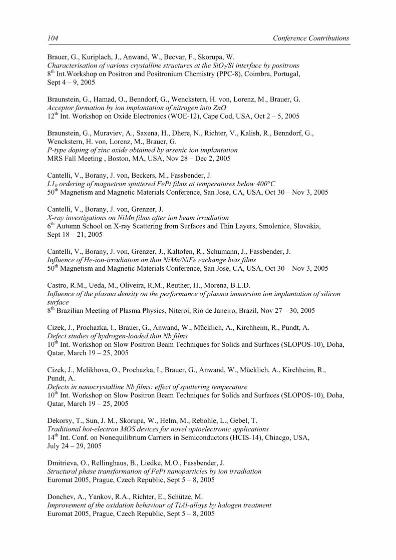
Conference Contributions
104
Brauer, G., Kuriplach, J., Anwand, W., Becvar, F., Skorupa, W. Characterisation of various crystalline structures at the SiO2/Si interface by positrons 8th Int.Workshop on Positron and Positronium Chemistry (PPC-8), Coimbra, Portugal, Sept 4 – 9, 2005 Braunstein, G., Hamad, O., Benndorf, G., Wenckstern, H. von, Lorenz, M., Brauer, G. Acceptor formation by ion implantation of nitrogen into ZnO 12th Int. Workshop on Oxide Electronics (WOE-12), Cape Cod, USA, Oct 2 – 5, 2005 Braunstein, G., Muraviev, A., Saxena, H., Dhere, N., Richter, V., Kalish, R., Benndorf, G., Wenckstern, H. von, Lorenz, M., Brauer, G. P-type doping of zinc oxide obtained by arsenic ion implantation MRS Fall Meeting , Boston, MA, USA, Nov 28 – Dec 2, 2005 Cantelli, V., Borany, J. von, Beckers, M., Fassbender, J. L10 ordering of magnetron sputtered FePt films at temperatures below 400°C 50th Magnetism and Magnetic Materials Conference, San Jose, CA, USA, Oct 30 – Nov 3, 2005 Cantelli, V., Borany, J. von, Grenzer, J. X-ray investigations on NiMn films after ion beam irradiation 6th Autumn School on X-ray Scattering from Surfaces and Thin Layers, Smolenice, Slovakia, Sept 18 – 21, 2005 Cantelli, V., Borany, J. von, Grenzer, J., Kaltofen, R., Schumann, J., Fassbender, J. Influence of He-ion-irradiation on thin NiMn/NiFe exchange bias films 50th Magnetism and Magnetic Materials Conference, San Jose, CA, USA, Oct 30 – Nov 3, 2005 Castro, R.M., Ueda, M., Oliveira, R.M., Reuther, H., Morena, B.L.D. Influence of the plasma density on the performance of plasma immersion íon implantation of silicon surface 8th Brazilian Meeting of Plasma Physics, Niteroi, Rio de Janeiro, Brazil, Nov 27 – 30, 2005 Cizek, J., Prochazka, I., Brauer, G., Anwand, W., Mücklich, A., Kirchheim, R., Pundt, A. Defect studies of hydrogen-loaded thin Nb films 10th Int. Workshop on Slow Positron Beam Techniques for Solids and Surfaces (SLOPOS-10), Doha, Qatar, March 19 – 25, 2005 Cizek, J., Melikhova, O., Prochazka, I., Brauer, G., Anwand, W., Mücklich, A., Kirchheim, R., Pundt, A. Defects in nanocrystalline Nb films: effect of sputtering temperature 10th Int. Workshop on Slow Positron Beam Techniques for Solids and Surfaces (SLOPOS-10), Doha, Qatar, March 19 – 25, 2005 Dekorsy, T., Sun, J. M., Skorupa, W., Helm, M., Rebohle, L., Gebel, T. Traditional hot-electron MOS devices for novel optoelectronic applications 14th Int. Conf. on Nonequilibrium Carriers in Semiconductors (HCIS-14), Chiacgo, USA, July 24 – 29, 2005 Dmitrieva, O., Rellinghaus, B., Liedke, M.O., Fassbender, J. Structural phase transformation of FePt nanoparticles by ion irradiation Euromat 2005, Prague, Czech Republic, Sept 5 – 8, 2005 Donchev, A., Yankov, R.A., Richter, E., Schütze, M. Improvement of the oxidation behaviour of TiAl-alloys by halogen treatment Euromat 2005, Prague, Czech Republic, Sept 5 – 8, 2005
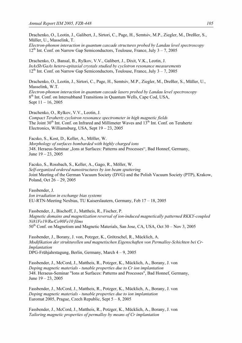
Annual Report IIM 2005, FZR-448
105
Drachenko, O., Leotin, J., Galibert, J., Sirtori, C., Page, H., Semtsiv, M.P., Ziegler, M., Dreßler, S., Müller, U., Masselink, T. Electron-phonon interaction in quantum cascade structures probed by Landau level spectroscopy 12th Int. Conf. on Narrow Gap Semiconductors, Toulouse, France, July 3 – 7, 2005 Drachenko, O., Bansal, B., Rylkov, V.V., Galibert, J., Dixit, V.K., Leotin, J. InAsSb/GaAs hetero-epitaxial crystals studied by cyclotron resonance measurements 12th Int. Conf. on Narrow Gap Semiconductors, Toulouse, France, July 3 – 7, 2005 Drachenko, O., Leotin, J., Sirtori, C., Page, H., Semtsiv, M.P., Ziegler, M., Dreßler, S., Müller, U., Masselink, W.T. Electron-phonon interaction in quantum cascade lasers probed by Landau level spectroscopy 8th Int. Conf. on Intersubband Transitions in Quantum Wells, Cape Cod, USA, Sept 11 – 16, 2005 Drachenko, O., Rylkov, V.V., Leotin, J. Compact Terahertz cyclotron resonance spectrometer in high magnetic fields The Joint 30th Int. Conf. on Infrared and Millimeter Waves and 13th Int. Conf. on Terahertz Electronics, Williamsburg, USA, Sept 19 – 23, 2005 Facsko, S., Kost, D., Keller, A., Möller, W. Morphology of surfaces bombarded with highly charged ions 348. Heraeus-Seminar „Ions at Surfaces: Patterns and Processes“, Bad Honnef, Germany, June 19 – 23, 2005 Facsko, S., Rossbach, S., Keller, A., Gago, R., Möller, W. Self-organized ordered nanostructures by ion beam sputtering Joint Meeting of the German Vacuum Society (DVG) and the Polish Vacuum Society (PTP), Krakow, Poland, Oct 26 – 29, 2005 Fassbender, J. Ion irradiation in exchange bias systems EU-RTN-Meeting Nexbias, TU Kaiserslautern, Germany, Feb 17 – 18, 2005 Fassbender, J., Bischoff, J., Mattheis, R., Fischer, P. Magnetic domains and magnetization reversal of ion-induced magnetically patterned RKKY-coupled Ni81Fe19/Ru/Co90Fe10 films 50th Conf. on Magnetism and Magnetic Materials, San Jose, CA, USA, Oct 30 – Nov 3, 2005 Fassbender, J., Borany, J. von, Potzger, K., Grötzschel, R., Mücklich, A. Modifikation der strukturellen und magnetischen Eigenschaften von Permalloy-Schichten bei Cr-Implantation DPG-Frühjahrstagung, Berlin, Germany, March 4 – 9, 2005 Fassbender, J., McCord, J., Mattheis, R., Potzger, K., Mücklich, A., Borany, J. von Doping magnetic materials - tunable properties due to Cr ion implantation 348. Heraeus-Seminar "Ions at Surfaces: Patterns and Processes", Bad Honnef, Germany, June 19 – 23, 2005 Fassbender, J., McCord, J., Mattheis, R., Potzger, K., Mücklich, A., Borany, J. von Doping magnetic materials - tunable properties due to ion implantation Euromat 2005, Prague, Czech Republic, Sept 5 – 8, 2005 Fassbender, J., McCord, J., Mattheis, R., Potzger, K., Mücklich, A., Borany, J. von Tailoring magnetic properties of permalloy by means of Cr implantation
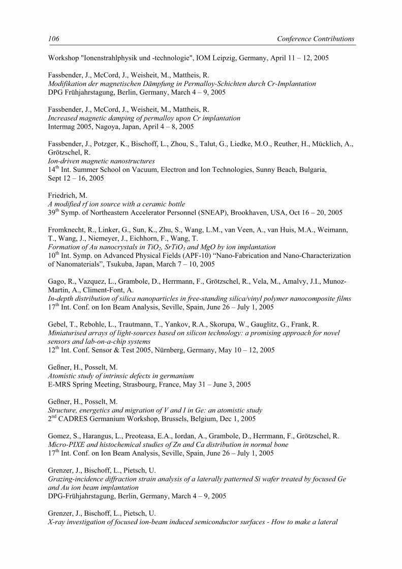
Conference Contributions
106
Workshop "Ionenstrahlphysik und -technologie", IOM Leipzig, Germany, April 11 – 12, 2005 Fassbender, J., McCord, J., Weisheit, M., Mattheis, R. Modifikation der magnetischen Dämpfung in Permalloy-Schichten durch Cr-Implantation DPG Frühjahrstagung, Berlin, Germany, March 4 – 9, 2005 Fassbender, J., McCord, J., Weisheit, M., Mattheis, R. Increased magnetic damping of permalloy upon Cr implantation Intermag 2005, Nagoya, Japan, April 4 – 8, 2005 Fassbender, J., Potzger, K., Bischoff, L., Zhou, S., Talut, G., Liedke, M.O., Reuther, H., Mücklich, A., Grötzschel, R. Ion-driven magnetic nanostructures 14th Int. Summer School on Vacuum, Electron and Ion Technologies, Sunny Beach, Bulgaria, Sept 12 – 16, 2005 Friedrich, M. A modified rf ion source with a ceramic bottle 39th Symp. of Northeastern Accelerator Personnel (SNEAP), Brookhaven, USA, Oct 16 – 20, 2005 Fromknecht, R., Linker, G., Sun, K., Zhu, S., Wang, L.M., van Veen, A., van Huis, M.A., Weimann, T., Wang, J., Niemeyer, J., Eichhorn, F., Wang, T. Formation of Au nanocrystals in TiO2, SrTiO3 and MgO by ion implantation 10th Int. Symp. on Advanced Physical Fields (APF-10) “Nano-Fabrication and Nano-Characterization of Nanomaterials”, Tsukuba, Japan, March 7 – 10, 2005 Gago, R., Vazquez, L., Grambole, D., Herrmann, F., Grötzschel, R., Vela, M., Amalvy, J.I., Munoz-Martin, A., Climent-Font, A. In-depth distribution of silica nanoparticles in free-standing silica/vinyl polymer nanocomposite films 17th Int. Conf. on Ion Beam Analysis, Seville, Spain, June 26 – July 1, 2005 Gebel, T., Rebohle, L., Trautmann, T., Yankov, R.A., Skorupa, W., Gauglitz, G., Frank, R. Miniaturised arrays of light-sources based on silicon technology: a promising approach for novel sensors and lab-on-a-chip systems 12th Int. Conf. Sensor & Test 2005, Nürnberg, Germany, May 10 – 12, 2005 Geßner, H., Posselt, M. Atomistic study of intrinsic defects in germanium E-MRS Spring Meeting, Strasbourg, France, May 31 – June 3, 2005 Geßner, H., Posselt, M. Structure, energetics and migration of V and I in Ge: an atomistic study 2nd CADRES Germanium Workshop, Brussels, Belgium, Dec 1, 2005 Gomez, S., Harangus, L., Preoteasa, E.A., Iordan, A., Grambole, D., Herrmann, F., Grötzschel, R. Micro-PIXE and histochemical studies of Zn and Ca distribution in normal bone 17th Int. Conf. on Ion Beam Analysis, Seville, Spain, June 26 – July 1, 2005 Grenzer, J., Bischoff, L., Pietsch, U. Grazing-incidence diffraction strain analysis of a laterally patterned Si wafer treated by focused Ge and Au ion beam implantation DPG-Frühjahrstagung, Berlin, Germany, March 4 – 9, 2005 Grenzer, J., Bischoff, L., Pietsch, U. X-ray investigation of focused ion-beam induced semiconductor surfaces - How to make a lateral
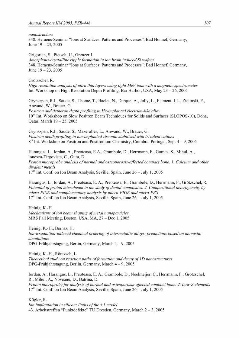
Annual Report IIM 2005, FZR-448
107
nanostructure 348. Heraeus-Seminar “Ions at Surfaces: Patterns and Processes”, Bad Honnef, Germany, June 19 – 23, 2005 Grigorian, S., Pietsch, U., Grenzer J. Amorphous-crystalline ripple formation in ion beam induced Si wafers 348. Heraeus-Seminar “Ions at Surfaces: Patterns and Processes”, Bad Honnef, Germany, June 19 – 23, 2005 Grötzschel, R. High resolution analysis of ultra thin layers using light MeV ions with a magnetic spectrometer Int. Workshop on High Resolution Depth Profiling, Bar Harbor, USA, May 23 – 26, 2005 Grynszpan, R.I., Saude, S., Thome, T., Baclet, N., Darque, A., Jolly, L., Flament, J.L., Zielinski, F., Anwand, W., Brauer, G. Positron and deuteron depth profiling in He-implanted electrum-like alloy 10th Int. Workshop on Slow Positron Beam Techniques for Solids and Surfaces (SLOPOS-10), Doha, Qatar, March 19 – 25, 2005 Grynszpan, R.I., Saude, S., Mazerolles, L., Anwand, W., Brauer, G. Positron depth profiling in ion-implanted zirconia stabilized with trivalent cations 8th Int. Workshop on Positron and Positronium Chemistry, Coimbra, Portugal, Sept 4 – 9, 2005 Harangus, L., Iordan, A., Preoteasa, E.A., Grambole, D., Herrmann, F., Gomez, S., Mihul, A., lonescu-Tirgoviste, C., Gutu, D. Proton microprobe analysis of normal and osteoporosis-affected compact bone. 1. Calcium and other divalent metals 17th Int. Conf. on Ion Beam Analysis, Seville, Spain, June 26 – July 1, 2005 Harangus, L., Iordan, A., Preoteasa, E. A., Preoteasa, E., Grambole, D., Herrmann, F., Grötzschel, R. Potential of proton microbeam in the study of dental composites. 2. Compositional heterogeneity by micro-PIXE and complementary analysis by micro-PIGE and micro-PBS 17th Int. Conf. on Ion Beam Analysis, Seville, Spain, June 26 – July 1, 2005 Heinig, K.-H. Mechanisms of ion beam shaping of metal nanoparticles MRS Fall Meeting, Boston, USA, MA, 27 – Dec 1, 2005 Heinig, K.-H., Bernas, H. Ion-irradiation-induced chemical ordering of intermetallic alloys: predictions based on atomistic simulations DPG-Frühjahrstagung, Berlin, Germany, March 4 – 9, 2005 Heinig, K.-H., Röntzsch, L. Theoretical study on reaction paths of formation and decay of 1D nanostructures DPG-Frühjahrstagung, Berlin, Germany, March 4 – 9, 2005 Iordan, A., Harangus, L., Preoteasa, E. A., Grambole, D., Neelmeijer, C., Herrmann, F., Grötzschel, R., Mihul, A., Noveanu, D., Batrina, D. Proton microprobe for analysis of normal and osteoporosis-affected compact bone. 2. Low-Z elements 17th Int. Conf. on Ion Beam Analysis, Seville, Spain, June 26 – July 1, 2005 Kögler, R. Ion implantation in silicon: limits of the +1 model 43. Arbeitstreffen “Punktdefekte” TU Dresden, Germany, March 2 – 3, 2005
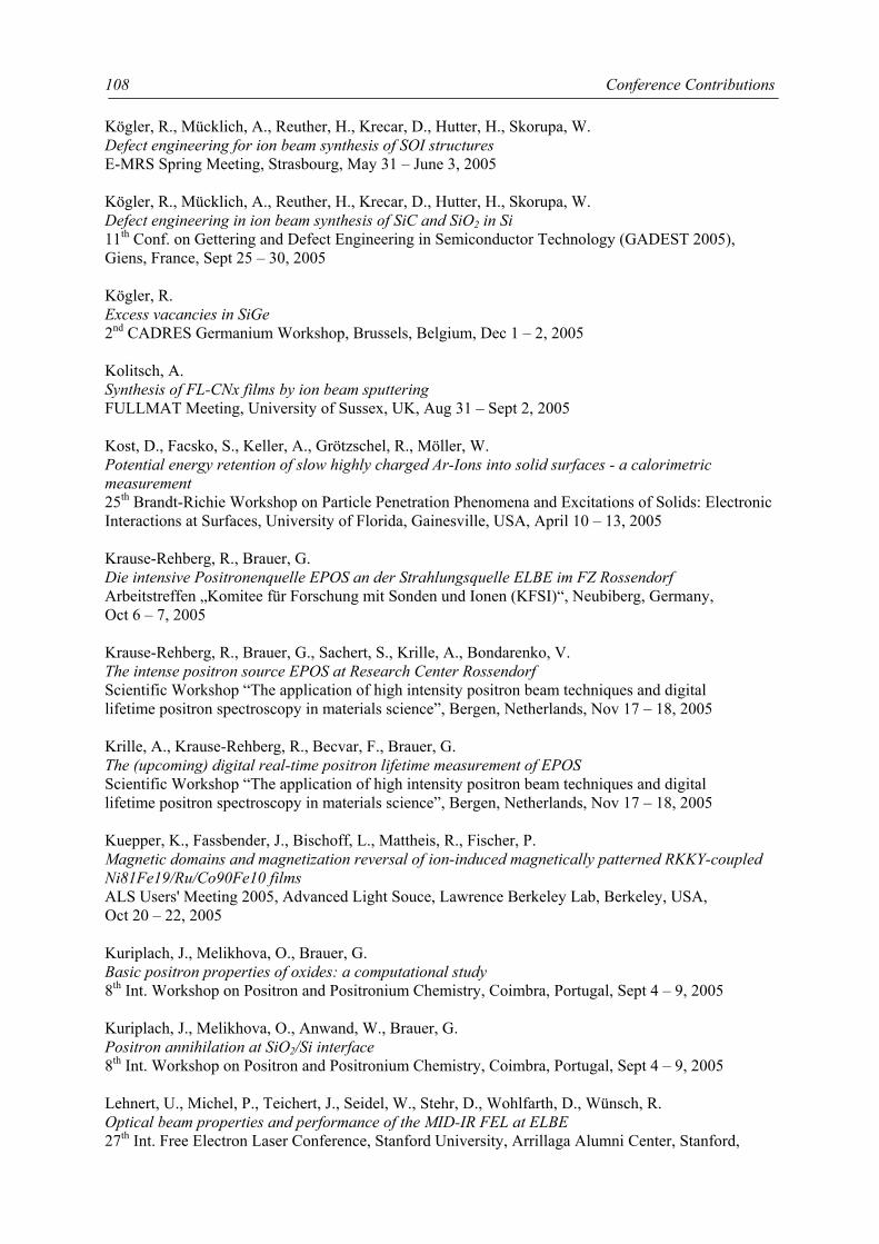
Conference Contributions
108
Kögler, R., Mücklich, A., Reuther, H., Krecar, D., Hutter, H., Skorupa, W. Defect engineering for ion beam synthesis of SOI structures E-MRS Spring Meeting, Strasbourg, May 31 – June 3, 2005 Kögler, R., Mücklich, A., Reuther, H., Krecar, D., Hutter, H., Skorupa, W. Defect engineering in ion beam synthesis of SiC and SiO2 in Si 11th Conf. on Gettering and Defect Engineering in Semiconductor Technology (GADEST 2005), Giens, France, Sept 25 – 30, 2005 Kögler, R. Excess vacancies in SiGe 2nd CADRES Germanium Workshop, Brussels, Belgium, Dec 1 – 2, 2005 Kolitsch, A. Synthesis of FL-CNx films by ion beam sputtering FULLMAT Meeting, University of Sussex, UK, Aug 31 – Sept 2, 2005 Kost, D., Facsko, S., Keller, A., Grötzschel, R., Möller, W. Potential energy retention of slow highly charged Ar-Ions into solid surfaces - a calorimetric measurement 25th Brandt-Richie Workshop on Particle Penetration Phenomena and Excitations of Solids: Electronic Interactions at Surfaces, University of Florida, Gainesville, USA, April 10 – 13, 2005 Krause-Rehberg, R., Brauer, G. Die intensive Positronenquelle EPOS an der Strahlungsquelle ELBE im FZ Rossendorf Arbeitstreffen „Komitee für Forschung mit Sonden und Ionen (KFSI)“, Neubiberg, Germany, Oct 6 – 7, 2005 Krause-Rehberg, R., Brauer, G., Sachert, S., Krille, A., Bondarenko, V. The intense positron source EPOS at Research Center Rossendorf Scientific Workshop “The application of high intensity positron beam techniques and digital lifetime positron spectroscopy in materials science”, Bergen, Netherlands, Nov 17 – 18, 2005 Krille, A., Krause-Rehberg, R., Becvar, F., Brauer, G. The (upcoming) digital real-time positron lifetime measurement of EPOS Scientific Workshop “The application of high intensity positron beam techniques and digital lifetime positron spectroscopy in materials science”, Bergen, Netherlands, Nov 17 – 18, 2005 Kuepper, K., Fassbender, J., Bischoff, L., Mattheis, R., Fischer, P. Magnetic domains and magnetization reversal of ion-induced magnetically patterned RKKY-coupled Ni81Fe19/Ru/Co90Fe10 films ALS Users' Meeting 2005, Advanced Light Souce, Lawrence Berkeley Lab, Berkeley, USA, Oct 20 – 22, 2005 Kuriplach, J., Melikhova, O., Brauer, G. Basic positron properties of oxides: a computational study 8th Int. Workshop on Positron and Positronium Chemistry, Coimbra, Portugal, Sept 4 – 9, 2005 Kuriplach, J., Melikhova, O., Anwand, W., Brauer, G. Positron annihilation at SiO2/Si interface 8th Int. Workshop on Positron and Positronium Chemistry, Coimbra, Portugal, Sept 4 – 9, 2005 Lehnert, U., Michel, P., Teichert, J., Seidel, W., Stehr, D., Wohlfarth, D., Wünsch, R. Optical beam properties and performance of the MID-IR FEL at ELBE 27th Int. Free Electron Laser Conference, Stanford University, Arrillaga Alumni Center, Stanford,
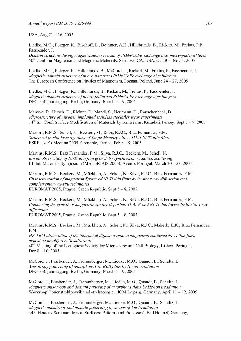
Annual Report IIM 2005, FZR-448
109
USA, Aug 21 – 26, 2005 Liedke, M.O., Potzger, K., Bischoff, L., Bothmer, A.H., Hillebrands, B., Rickart, M., Freitas, P.P., Fassbender, J. Domain structure during magnetization reversal of PtMn/CoFe exchange bias micro-pattered lines 50th Conf. on Magnetism and Magnetic Materials, San Jose, CA, USA, Oct 30 – Nov 3, 2005 Liedke, M.O., Potzger, K., Hillebrands, B., McCord, J., Rickart, M., Freitas, P., Fassbender, J. Magnetic domain structure of micro-patterned PtMn/CoFe exchange bias bilayers The European Conference on Physics of Magnetism, Poznan, Poland, June 24 – 27, 2005 Liedke, M.O., Potzger, K., Hillebrands, B., Rickart, M., Freitas, P., Fassbender, J. Magnetic domain structure of micro-patterned PtMn/CoFe exchange bias bilayers DPG-Frühjahrstagung, Berlin, Germany, March 4 – 9, 2005 Manova, D., Hirsch, D., Richter, E., Mändl, S., Neumann, H., Rauschenbach, B. Microstructure of nitrogen implanted stainless steelafter wear experiments 14th Int. Conf. Surface Modification of Materials by Ion Beams, Kusadasi,Turkey, Sept 5 – 9, 2005 Martins, R.M.S., Schell, N., Beckers, M., Silva, R.J.C., Braz Fernandes, F.M. Structural in-situ investigations of Shape Memory Alloy (SMA) Ni-Ti thin films ESRF User’s Meeting 2005, Grenoble, France, Feb 8 – 9, 2005 Martins, R.M.S., Braz Fernandes, F.M., Silva, R.J.C., Beckers, M., Schell, N. In-situ observation of Ni-Ti thin film growth by synchrotron radiation scattering III. Int. Materials Symposium (MATERIAIS 2005), Aveiro, Portugal, March 20 – 23, 2005 Martins, R.M.S., Beckers, M., Mücklich, A., Schell, N., Silva, R.J.C., Braz Fernandes, F.M. Characterization of magnetron Sputtered Ni-Ti thin films by in-situ x-ray diffraction and complementary ex-situ techniques EUROMAT 2005, Prague, Czech Republic, Sept 5 – 8, 2005 Martins, R.M.S., Beckers, M., Mücklich, A., Schell, N., Silva, R.J.C., Braz Fernandes, F.M. Comparing the growth of magnetron sputter deposited Ti-Al-N and Ni-Ti thin layers by in-situ x-ray diffraction EUROMAT 2005, Prague, Czech Republic, Sept 5 – 8, 2005 Martins, R.M.S., Beckers, M., Mücklich, A., Schell, N., Silva, R.J.C., Mahesh, K.K., Braz Fernandes, F.M. HR-TEM observation of the interfacial diffusion zone in magnetron sputtered Ni-Ti thin films deposited on different Si substrates 40th Meeting of the Portuguese Society for Microscopy and Cell Biology, Lisbon, Portugal, Dec 8 – 10, 2005 McCord, J., Fassbender, J., Frommberger, M., Liedke, M.O., Quandt, E., Schultz, L. Anisotropy patterning of amorphous CoFeSiB films by Heion irradiation DPG-Frühjahrstagung, Berlin, Germany, March 4 – 9, 2005 McCord, J., Fassbender, J., Frommberger, M., Liedke, M.O., Quandt, E., Schultz, L. Magnetic anisotropy and domain pattering of amorphous films by He-ion irradiation Workshop "Ionenstrahlphysik und -technologie", IOM Leipzig, Germany, April 11 – 12, 2005 McCord, J., Fassbender, J., Frommberger, M., Liedke, M.O., Quandt, E., Schultz, L. Magnetic anisotropy and domain patterning by means of ion irradiation 348. Heraeus-Seminar "Ions at Surfaces: Patterns and Processes", Bad Honnef, Germany,
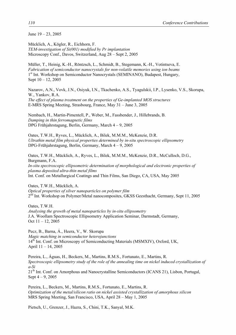
Conference Contributions
110
June 19 – 23, 2005 Mücklich, A., Kögler, R., Eichhorn, F. TEM-investigation of Si(001) modified by Pr implantation Microscopy Conf., Davos, Switzerland, Aug 28 – Sept 2, 2005 Müller, T., Heinig, K.-H., Röntzsch, L., Schmidt, B., Stegemann, K.-H., Votintseva, E. Fabrication of semiconductor nanocrystals for non-volatile memories using ion beams 1st Int. Workshop on Semiconductor Nanocrystals (SEMINANO), Budapest, Hungary, Sept 10 – 12, 2005 Nazarov, A.N., Vovk, J.N., Osiyuk, I.N., Tkachenko, A.S., Tyagulskii, I.P., Lysenko, V.S., Skorupa, W., Yankov, R.A. The effect of plasma treatment on the properties of Ge-implanted MOS structures E-MRS Spring Meeting, Strasbourg, France, May 31 – June 3, 2005 Nembach, H., Martin-Pimentell, P., Weber, M., Fassbender, J., Hillebrands, B. Damping in thin ferromagnetic films DPG Frühjahrstagung, Berlin, Germany, March 4 – 9, 2005 Oates, T.W.H., Ryves, L., Mücklich, A., Bilek, M.M.M., McKenzie, D.R. Ultrathin metal film physical properties determined by in-situ spectroscopic ellipsometry DPG-Frühjahrstagung, Berlin, Germany, March 4 – 9, 2005 Oates, T.W.H., Mücklich, A., Ryves, L., Bilek, M.M.M., McKenzie, D.R., McCulloch, D.G., Burgmann, F.A. In-situ spectroscopic ellipsometric determination of morphological and electronic properties of plasma deposited ultra-thin metal films Int. Conf. on Metallurgical Coatings and Thin Films, San Diego, CA, USA, May 2005 Oates, T.W.H., Mücklich, A. Optical properties of silver nanoparticles on polymer film 2nd Int. Workshop on Polymer/Metal nanocomposites, GKSS Geesthacht, Germany, Sept 11, 2005 Oates, T.W.H. Analysing the growth of metal nanoparticles by in-situ ellipsometry J.A. Woollam Spectroscopic Ellipsometry Application Seminar, Darmstadt, Germany, Oct 11 – 12, 2005 Pecz, B., Barna, Á., Heera, V., W. Skorupa Magic matching in semiconductor heterojunctions 14th Int. Conf. on Microscopy of Semiconducting Materials (MSMXIV), Oxford, UK, April 11 – 14, 2005 Pereira, L., Águas, H., Beckers, M., Martins, R.M.S., Fortunato, E., Martins, R. Spectroscopic ellipsometry study of the role of the annealing time on nickel induced crystallization of a-Si 21th Int. Conf. on Amorphous and Nanocrystalline Semiconductors (ICANS 21), Lisbon, Portugal, Sept 4 – 9, 2005 Pereira, L., Beckers, M., Martins, R.M.S., Fortunato, E., Martins, R. Optimization of the metal/silicon ratio on nickel assisted crystallization of amorphous silicon MRS Spring Meeting, San Francisco, USA, April 28 – May 1, 2005 Pietsch, U., Grenzer, J., Hazra, S., Chini, T.K., Sanyal, M.K.
Annual Report IIM 2005, FZR-448
111
Ripple structure of ion beam induced Si wafers 20th Congress of the International Union of Crystallography (IUCr 2005), Florence, Italy, Aug 23 – 31, 2005 Posselt, M. Atomistic simulation of defects in Si: migration of di- and tri-interstitials 43. Arbeitskreis Punktdefekte, Dresden, Germany, March 2 – 3, 2005 Posselt, M. Formation of highly mobile di-interstitials during ion implantation E-MRS Spring Meeting, Strasbourg, France, May 31 – June 3, 2005 Posselt, M., Gao, F. A modified concerted exchange mechanism for antisite pair recombination in cubic and hexagonal silicon carbide 11th Int. Autumn Meeting on Gettering and Defect Engineering in Semiconductor Technology (GADEST), Giens, France, Sept 25 – 30, 2005 Posselt, M., Gao, F. Atomistic study of the mobility of small interstitial clusters in silicon 11th Int. Autumn Meeting on Gettering and Defect Engineering in Semiconductor Technology (GADEST), Giens, France, Sept 25 – 30, 2005 Potfajova, J., Sun, J.M., Dekorsy, T., Skorupa, W., Schmidt, B., Wiemer, M., Helm, M. Silicon microcavity light emitting diodes with buried cobalt silicide metallic mirrors E-MRS Spring Meeting, Strasbourg, France, May 31 – June 3, 2005 Potzger, K., Bischoff, L., Liedke, M.O., Hillebrands, B., Rickart, M., Freitas, P. P., McCord, J., Fassbender, J. Magnetic domain structure of micro-patterned PtMn/NiFe exchange bias bilayers DPG-Frühjahrstagung, Berlin, Germany, March 4 – 9, 2005 Potzger, K., Bischoff, L., Liedke, M.O., Hillebrands, B., Rickart, M., Freitas, P. P., McCord, J., Fassbender, J. Domain structure of magnetically micro-patterned PtMn/NiFe exchange bias bilayers 50th Conf. on Magnetism and Magnetic Materials, San Jose, CA, USA, Oct 30 – Nov 3, 2005 Potzger, K., Bischoff, L., Liedke, M.O., Hillebrands, B., Rickart, M., Freitas, P., McCord, J., Fassbender, J. Magnetic domain structure of micro-patterned PtMn/NiFe exchange bias bilayers Intermag 2005, Nagoya, Japan, April 4 – 8, 2005 Potzger, K., Reuther, H., Zhou, S., Mücklich, A., Grötzschel, R., Eichhorn, F., Liedke, M.O., Fassbender, J. Ion beam synthesis of Fe nanoparticles in MgO and Y:ZrO2 50th Magnetism and Magnetic Materials Conference, San Jose, CA, USA, Oct 30 – Nov 3, 2005 Potzger, K., Zhou, S., Reuther, H., Brauer, G., Anwand, W., Eichhorn, F., Bischoff, L., Herrmann, F., Grambole, D., Grötzschel, R., Fassbender, J. Effects of implantation of magnetic ions into ZnO Int. Topical Workshop on Heteroepitaxy of 3C-SiC on Silicon and its Application to Sensor Devices (HeT-SiC-05), Hotel Erbgericht Krippen, Germany, April 26 – May 1, 2005 Potzger, K., Zhou, S., Reuther, H., Mücklich, F., Talut, G., Fassbender, J., Herrmannsdörfer, T., Bianchi, A.
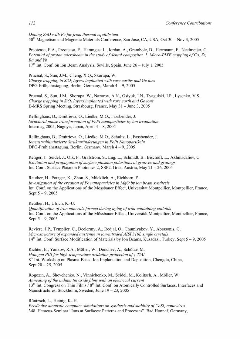
Conference Contributions
112
Doping ZnO with Fe far from thermal equilibrium 50th Magnetism and Magnetic Materials Conference, San Jose, CA, USA, Oct 30 – Nov 3, 2005 Preoteasa, E.A., Preoteasa, E., Harangus, L., Iordan, A., Grambole, D., Herrmann, F., Neelmeijer, C. Potential of proton microbeam in the study of dental composites. 1. Micro-PIXE mapping of Ca, Zr, Ba and Yb 17th Int. Conf. on Ion Beam Analysis, Seville, Spain, June 26 – July 1, 2005 Prucnal, S., Sun, J.M., Cheng, X.Q., Skorupa, W. Charge trapping in SiO2 layers implanted with rare earths and Ge ions DPG-Frühjahrstagung, Berlin, Germany, March 4 – 9, 2005 Prucnal, S., Sun, J.M., Skorupa, W., Nazarov, A.N., Osiyuk, I.N., Tyagulski, I.P., Lysenko, V.S. Charge trapping in SiO2 layers implanted with rare earth and Ge ions E-MRS Spring Meeting, Strasbourg, France, May 31 – June 3, 2005 Rellinghaus, B., Dmitrieva, O., Liedke, M.O., Fassbender, J. Structural phase transformation of FePt nanoparticles by ion irradiation Intermag 2005, Nagoya, Japan, April 4 – 8, 2005 Rellinghaus, B., Dmitrieva, O., Liedke, M.O., Schultz, L., Fassbender, J. Ionenstrahlinduzierte Strukturänderungen in FePt Nanopartikeln DPG-Frühjahrstagung, Berlin, Germany, March 4 – 9, 2005 Renger, J., Seidel, J., Olk, P., Grafström, S., Eng, L., Schmidt, B., Bischoff, L., Akhmadaliev, C. Excitation and propagation of surface plasmon polaritons at grooves and gratings Int. Conf. Surface Plasmon Photonics 2, SSP2, Graz, Austria, May 21 – 26, 2005 Reuther, H., Potzger, K., Zhou, S., Mücklich, A., Eichhorn, F. Investigation of the creation of Fe nanoparticles in MgO by ion beam synthesis Int. Conf. on the Applications of the Mössbauer Effect, Universität Montpellier, Montpellier, France, Sept 5 – 9, 2005 Reuther, H., Ulrich, K.-U. Quantification of iron minerals formed during aging of iron-containing colloids Int. Conf. on the Applications of the Mössbauer Effect, Universität Montpellier, Montpellier, France, Sept 5 – 9, 2005 Reviere, J.P., Templier, C., Declermy, A., Redjal, O., Chumlyakov, Y., Abrasonis, G. Microstructure of expanded austenite in ion-nitrided AISI 316L single crystals 14th Int. Conf. Surface Modification of Materials by Ion Beams, Kusadasi, Turkey, Sept 5 – 9, 2005 Richter, E., Yankov, R.A., Möller, W., Donchev, A., Schütze, M. Halogen PIII for high-temperature oxidation protection of γ-TiAl 8th Int. Workshop on Plasma-Based Ion Implantation and Deposition, Chengdu, China, Sept 20 – 25, 2005 Rogozin, A., Shevchenko, N., Vinnichenko, M., Seidel, M., Kolitsch, A., Möller, W. Annealing of the indium tin oxide films with an electrical current 13th Int. Congress on Thin Films / 8th Int. Conf. on Atomically Controlled Surfaces, Interfaces and Nanostructures, Stockholm, Sweden, June 19 – 23, 2005 Röntzsch, L., Heinig, K.-H. Predictive atomistic computer simulations on synthesis and stability of CoSi2 nanowires 348. Heraeus-Seminar “Ions at Surfaces: Patterns and Processes”, Bad Honnef, Germany,
Annual Report IIM 2005, FZR-448
113
June 19 – 23, 2005 Röntzsch, L., Heinig, K.-H., Schmidt, B. Ion irradiation through SiO2-Si interfaces: TEM study of self-organized Si nanocrystals applicable in nonvolatile memories DPG-Frühjahrstagung, Berlin, Germany, March 4 – 9, 2005 Röntzsch, L., Heinig, K.-H. Atomistic computer simulations on ion beam synthesis and decay of single-crystalline nanowires DPG-Frühjahrstagung, Berlin, Germany, March 4 – 9, 2005 Röntzsch, L., Heinig, K.-H. Atomistic computer simulations on synthesis and stability of single-crystalline nanowires Treffen DFG-Schwerpunkt Nanodrähte und Nanoröhren, Fulda, Germany, May 2 – 4, 2005 Röntzsch, L., Heinig, K.-H. Ion beam synthesis of CoSi2 nanowires in Si and their stability - predictions of atomistic computer simulations E-MRS Spring Meeting, Strasbourg, France, May 31 – June 3, 2005 Röntzsch, L., Heinig, K.-H. Ion beam synthesis of single-crystalline nanowires and their stability – predictions of atomistic computer simulations 25th GIF Conference, Dresden, Germany, June 20 – 23, 2005 Röntzsch, L., Heinig, K.-H. Predictions on ion-assisted synthesis of functional 1D-nanostructures using atomistic computer simulations 14th Int. Summer School on Vacuum, Electron and Ion Technologies, Sunny Beach, Bulgaria, Sept 12 – 16, 2005 Röntzsch, L., Heinig, K.-H. Reaction pathways of ion beam synthesis and stability of monocrystalline nanowires 1st Int. Workshop on Semiconductor Nanocrystals (SEMINANO), Budapest, Hungary, Sept 10 – 12, 2005 Rossi, J.O., Ueda, M., Reuther, H. Plasma immersion íon implantation with high-energy íons for use in surface treatments 8th Brazilian Meeting of Plasma Physics, Niteroi, Rio de Janeiro, Brazil, Nov 27 – 30, 2005 Rossi, J.O., Ueda, M., Silva, G., Reuther, H. A solid-state compact pulser of 5 kV / 2 A / 5 kHz for surface treatment by plasma immersion ion implantation 8th Brazilian Meeting of Plasma Physics, Niteroi, Rio de Janeiro, Brazil, Nov 27 – 30, 2005 Schell, N., Beckers, M., Martins, R.M.S., Mücklich, A, Möller, W. Observation of the growth and microstructural development of MAX Phase Ti2AlN thin films during magnetron sputtering using synchrotron radiation AVS 52nd Int. Symposium & Exhibition, Boston, USA, Oct 30 – Nov 4, 2005 Schmidt, B., Heinig, K-.H., Röntzsch, L., Mücklich, A., Stegemann, K.-H., Votintseva, E., Klimenkov, M. Fabrication of Si nanocrystals for memory application by ion irradiation through SiO2/Si-interfaces DPG-Frühjahrstagung, Berlin, Germany, March 4 – 9, 2005
Conference Contributions
114
Schreiner, M., Mäder, M., Bidaud, E., Zich, W., Uhlir, K., Grambole, D., Herrmann, F., Alram, M. The Becin hoard – Analysis of the ancient silver coins 17th Int. Conf. on Ion Beam Analysis, Seville, Spain, June 26 – July 1, 2005 Schütze, M., Donchev, A., Yankov, A., Richter, E. Improvement of high temperature oxidation resistance of TiAl 14th Int. Conf. Surface Modification of Materials by Ion Beams, Kusadasi, Turkey, Sept 5 – 9, 2005 Semtsiv, M.P., Masselink, W.T., Georgiev, N., Dekorsy, T., Helm, M. Intersubband absorption in GaP-AlP multiple quantum wells 8th Int. Conf. on Intersubband Transitions in Quantum Wells (ITQW 2005), Cape Cod, USA, Sept 11 – 16, 2005 Semtsiv, M. P., Masselink, W.T., Georgiev, N., Dekorsy, T., Helm, M. Intersubband transitions in GaP-AlP heterostructures for infrared applications 12th Int. Conf. on Narrow Gap Semiconductors (NGS-12), Toulouse, France, July 3 – 7, 2005 Shevchenko, N., Mücklich, A., Richter, E., Maitz, M.F. Porous surface of NiTi alloy produced by plasma ion implantation E-MRS Spring Meeting, Strasbourg, France, May 31 – June 3, 2005 Shevchenko, N., Rogozin, A., Vinnichenko, M., Cantelli, V., Kolitsch, A., Möller, W. Real-time investigations of ITO film structure evolution during annealing 13th Int. Congress on Thin Films / 8th International Conference on Atomically Controlled Surfaces, Interfaces and Nanostructures, Stockholm, Sweden, June 19 – 23, 2005 Shevchenko, N., Richter, E., Pham, M.T., Maitz, M.F. Structure and properties of oxygen implanted NiTi surfaces 13th Int. Congress on Thin Films / 8th International Conference on Atomically Controlled Surfaces, Interfaces and Nanostructures, Stockholm, Sweden, June 19 – 23, 2005 Shevchenko, N., Richter, E., Maitz, M.F., Möller, W. Oxygen implanted NiTi surfaces for biomedical application 8th Int. Workshop on Plasma Based Ion Implantation and Deposition, Chengdu, China, Sept 18 – 22, 2005 Skorupa, W., Sun, J.M., Dekorsy, T., Helm, M., Rebohle, L., Gebel, T., Nazarov, A.N., Tjagulski, I.P., Osiyuk, I.N., Prucnal, S., Zuk, J. Silicon-based light emission from rare earth ion-implanted silicon dioxide E-MRS Spring Meeting, Strasbourg, France, May 31 – June 3, 2005 Skorupa, W., Panknin, D., Voelskow, M., Smith, M., McMahon, R.A. Rapid thermal processing using flash lamps for the crystallisation of amorphous silicon layers 21st Int. Conf. on Amorphous and Nanocrystalline Semiconductors (ICANS21), Lisbon, Portugal, Sept 3 – 9, 2005 Skorupa, W., Sun, J.M., Prucnal, S., Rebohle, L., Gebel, T., Nazarov, A.N., Osiyuk, I.N., Helm, M. Rare earth ion implantation for silicon based light emission 11th Conf. on Gettering and Defect Engineering in Semiconductor Technology (GADEST 2005), Giens, France, Sept 25 – 30, 2005 Silva, M.M., Ueda, M., Lepienski, C.M., Soares Jr., P.C., Gonçalves, J.A.N., Reuther, H. Nitrogen plasma immersion ion implantation in Ti6Al4V with treatment temperatures ranging from 400 to 800°C 5th Asian-European Int. Conf. on Plasma Surface Engineering, Qingdao City, China,
Annual Report IIM 2005, FZR-448
115
Sept 12 – 16, 2005 Silva, M.M., Ueda, M., Otani, C., Reuther, H., Lepienski, C.M., Soares Jr., P.C. Surface modification of Ti6Al4V alloy by duplex plasma processing 18th Int. Congress of Mechanical Engineering, Cobem 2005, Ouro Preto, Minas Gerais, Brazil, Nov 6 – 11, 2005 Smith, M., McMahon, R.A., Voelskow, M., Skorupa, W. Modelling of flash lamp processing of SiC-on-silicon heterostructures Int. Topical Workshop on Heteroepitaxy of 3C-SiC on Silicon and its Application to Sensor Devices (HeT-SiC-05,), Hotel Erbgericht Krippen, Germany, April 26 – May 1, 2005 Solina, D., Lott, D., Kaltofen, R., Schumann, J., Fassbender, J., Tietze, U., Schreyer, A. X-ray and Neutron Scattering studies of NiMn-CoFe exchange bias systems DPG Frühjahrstagung, Berlin, Germany, March 4 – 9, 2005 Stehr, D., Metzner, C., Helm, M., Roch, T., Strasser, G. Impurity states in quantum wells and superlattices and their influence in the intersubband absorption spectra 8th Int. Conf. on Intersubband Transitions in Quantum Wells (ITQW 2005), Cape Cod, MA, USA, Sept 11 – 16, 2005 Sun, J.M., Skorupa, W., Dekorsy, T., Helm, M., Rebohle, L., Gebel, T. Modulation of the 1535 nm photoluminescence from Er-doped Si-rich silicon dioxide by field-induced quenching E-MRS Spring Meeting, Strasbourg, France, May 31 – June 3, 2005 Sun, J.M., Skorupa, W., Dekorsy, T., Helm, M., Rebohle, L., Gebel, T. Efficent electroluminescence from Tb-implanted silicon metal-oxide-semiconductor devices E-MRS Spring Meeting, Strasbourg, France, May 31 – June 3, 2005 Sun, J.M., Skorupa, W., Dekorsy, T., Helm, M. Efficient electroluminescence from rare-earth implanted SiO2 metal-oxide-semiconductor structures 2nd Int. Conf. on Group IV Photonics, Antwerp, Belgium, Sep 21, 2005 Tan, I.H., Ueda, M., Dallaqua, R.S., Abramof, E., Reuther, H. Effects of low magnetic fields on nitrogen implantation in silicon by plasma immersion 8th Brazilian Meeting of Plasma Physics, Niteroi, Rio de Janeiro, Brazil, Nov 27 – 30, 2005 Tsvetkova, T., Takahashi, S., Zayats, A., Dawson, P., Turner, R., Bischoff, L., Angelov, O., Dimova-Malinovska, D. Nano-scale optical pattering in amorphous silicon carbide Opto Ireland, SPIE Europe, Dublin, Ireland, April 4 – 6, 2005 Tsyganov, I., Richter, E. Phase formation, corrosion behaviour and mechanical properties of boron implanted near-alpha titanium alloy 14th Int. Conf. Surface Modification of Materials by Ion Beams, Kusadasi, Turkey, Sept 5 – 9, 2005 Turos, A., Abdul-Kader, A. M., Grambole, D., Jagielski, J., Piątkowska, A. The effects of ion bombardments of polymers: hydrogen release and oxidation 17th Int. Conf. on Ion Beam Analysis, Seville, Spain, June 26 – July 1, 2005 Ueda, M., Silva, M.M., Lepienski, C.M., Soares Jr., P.C., Gonçalves, J.A., Reuther, H. High temperature plasma immersion ion implantation of Ti6Al4V
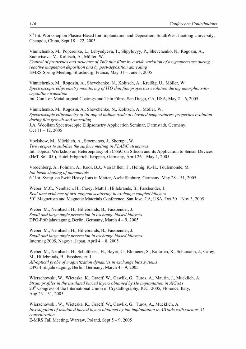
Conference Contributions
116
8th Int. Workshop on Plasma-Based Ion Implantation and Deposition, SouthWest Jiaotong University, Chengdu, China, Sept 18 – 22, 2005 Vinnichenko, M., Poperenko, L., Lebyedyeva, T., Shpylovyy, P., Shevchenko, N., Rogozin, A., Sudovtsova, V., Kolitsch, A., Möller, W. Control of properties and structure of ZnO thin films by a wide variation of oxygenpressure during reactive magnetron deposition and by post-deposition annealing EMRS Spring Meeting, Strasbourg, France, May 31 – June 3, 2005 Vinnichenko, M., Rogozin, A., Shevchenko, N., Kolitsch, A., Kreißig, U., Möller, W. Spectroscopic ellipsometry monitoring of ITO thin film properties evolution during amorphous-to-crystalline transition Int. Conf. on Metallurgical Coatings and Thin Films, San Diego, CA, USA, May 2 – 6, 2005 Vinnichenko, M., Rogozin, A., Shevchenko, N., Kolitsch, A., Möller, W. Spectroscopic ellipsometry of tin-doped indium oxide at elevated temperatures: properties evolution during film growth and annealing J.A. Woollam Spectroscopic Ellipsometry Application Seminar, Darmstadt, Germany, Oct 11 – 12, 2005 Voelskow, M., Mücklich, A., Stoemenos, J., Skorupa, W. Two recipes to stabilize the surface melting in FLASiC structures Int. Topical Workshop on Heteroepitaxy of 3C-SiC on Silicon and its Application to Sensor Devices (HeT-SiC-05,), Hotel Erbgericht Krippen, Germany, April 26 – May 1, 2005 Vredenberg, A., Polman, A., Kooi, B.J., Van Dillen, T., Heinig, K.-H., Toulemonde, M. Ion beam shaping of nanometals 6th Int. Symp. on Swift Heavy Ions in Matter, Aschaffenburg, Germany, May 28 – 31, 2005 Weber, M.C., Nembach, H., Carey, Matt J., Hillebrands, B., Fassbender, J. Real time evidence of two-magnon scattering in exchange coupled bilayers 50th Magnetism and Magnetic Materials Conference, San Jose, CA, USA, Oct 30 – Nov 3, 2005 Weber, M., Nembach, H., Hillebrands, B., Fassbender, J. Small and large angle precession in exchange biased bilayers DPG-Frühjahrstagung, Berlin, Germany, March 4 – 9, 2005 Weber, M., Nembach, H., Hillebrands, B., Fassbender, J. Small and large angle precession in exchange biased bilayers Intermag 2005, Nagoya, Japan, April 4 – 8, 2005 Weber, M., Nembach, H., Schultheiss, H., Bayer, C., Blomeier, S., Kaltofen, R., Schumann, J., Carey, M., Hillebrands, B., Fassbender, J. All-optical probe of magnetization dynamics in exchange bias systems DPG-Frühjahrstagung, Berlin, Germany, March 4 – 9, 2005 Wierzchowski, W., Wieteska, K., Graeff, W., Gawlik, G., Turos, A., Maurin, J., Mücklich, A. Strain profiles in the insulated buried layers obtained by He implantation in AlGaAs 20th Congress of the International Union of Crystallography, IUCr 2005, Florence, Italy, Aug 23 – 31, 2005 Wierzchowski, W., Wieteska, K., Graeff, W., Gawlik, G., Turos, A., Mücklich, A. Investigation of insulated buried layers obtained by ion implantation in AlGaAs with various Al concentration E-MRS Fall Meeting, Warsaw, Poland, Sept 5 – 9, 2005
Annual Report IIM 2005, FZR-448
117
Winnerl, S., Dreyhaupt, A., Krenz, M., Stehr, D., Dekorsy, T., Helm, M. High-intensity THz radiation pulses from a scalable photoconductive device DPG Frühjahrstagung, Berlin, Germany, March 4 – 9, 2005 Winnerl, S., Krenz, M., Dreyhaupt, A., Stehr, D., Dekorsy, T., Helm, M. High-intensity THz radiation pulses from a scalable large-aperture emitter Conf. on Lasers and Opto-Electronics/Quantum Electronics and Laser Science Conference (CLEO/QELS), Baltimore, USA, May 22 – 27, 2005 Winnerl, S., Dreyhaupt, A., Peter, F., Stehr, D., Helm, M., Dekorsy, T. High-intensity THz radiation from a large-aperture photoconductive emitter 14th Int. Conf. on Nonequilibrium Carrier Dynamics in Semiconductors (HCIS-14), Chicago, USA, July 24 – 29, 2005 Yankov, R.A., Richter, E., Donchev, A. Schütze, M. Efficient oxidation protection of γ-TiA.l alloys by ion implantation of halogens Int. Conf. on Novel Applications for Surface Modification, Chester, UK, Sept 18 – 21, 2005 Zen, A., Saphiannikova, M., Neher, D., Grenzer, J., Pietsch, U, Asawapirom, U., Scherf, U. Molecular structure and electronic properties of poly(3-hexylthiophene) DPG Frühjahrstagung, Berlin, Germany, March 4 – 9, 2005
Lectures Abrasonis, G. Synthesis of CNx films by ion beam sputtering: the influence of the sputtering beam composition and substrate temperature RWTH Aachen, Germany, May 31, 2005 Bischoff, L. The application of FIB from mass separated alloy LMIS NanoFIB Meeting, University of Oxford, UK, April 15, 2005 Bischoff, L. Nanofabrication with a mass-separated FIB FAHL Academica, University Leipzig, Wörlitz , Sept 26 – 27, 2005 Brauer, G., Anwand, W., Coleman, P.G., Skorupa, W. The positron as an antiparticle – from a poetic to a physical view University of Qatar, Physics Dept., Doha, Qatar, March 29, 2005 Fassbender, J. Magnetization dynamics Evaluierung von Beschichtungs- und Oxidationsverfahren für Tunnel-Schichtsysteme, Singulus Technologies AG, Kahl, Germany, April 19, 2005 Fassbender, J. The potential of ion irradiation for the creation of artificial magnetic structures Argonne National Laboratories, Argonne, USA, June 1, 2005 Fassbender, J. Tuning magnetic properties locally by ion irradiation and implantation Center for X-ray Optics, Lawrence Berkeley National Laboratory, Berkeley, USA, May 26, 2005
Lectures
118
Fassbender, J. Ion induced modifications of magnetic thin films and multilayers Universität Konstanz, Germany, Dec 2, 2005 Grenzer, J. Depth resolved strain analysis of lateral nanostructures by x-ray grazing incidence diffraction Warsaw University, Faculty of Physics, Warszawa, Poland, May 11, 2005 Grötzschel, R. Ionenstrahlanalytik ultradünner Schichten TU Dresden, Germany, Sept 27, 2005 Grötzschel, R., Grambole, D., Güttler, D., Herrmann, F., Kreißig, U., Neelmeijer, C. Ionenstrahlanalytik an den Rossendorfer Beschleunigern Zukunftsperspektiven und Anwendungen von Ionenstrahlen, Bundesanstalt für Materialforschung und -prüfung (BAM), Berlin, Germany, Oct 17, 2005 Heinig, K.-H. Ion beam synthesis and processing of nanostructures GSI Darmstadt, Germany, Nov 15, 2005 Helm, M. From short-wavelength quantum cascade lasers to impulsive THz emitters THALES Research & Technology, Orsay, France, Feb 24, 2005 Helm, M. Silizium-basierte Lichtemitter: auf dem Weg zur Silizium-Photonik? Universität Kaiserslautern, Germany, Jan 17, 2005 Krause-Rehberg, R., Brauer, G. Die intensive Positronenquelle EPOS am Forschungszentrum Rossendorf FSU Jena, Institut für Festkörperphysik, Jena, Germany, Dec 2, 2005 Möller, W. Ion-based materials research at FZR Laborat. of Ion Beam Physics and Materials Research, University of Lanzhou, China, Sept 23, 2005 Möller, W. Fast ions for nano technology Fraunhofer Center of Nanoelectronic Technologies, Dresden, Germany, Oct 13, 2005 Möller, W., Beckers, M., Schell, N., Mücklich, A. Deposition and characterization of nitride MAX phase thin films CSIC-ICMM, Madrid, Spain, Dec 13, 2005 Neelmeijer, C. Ionen als Agenten und Detektive Berufliches Schulzentrum Dresden, Wissenschaftstag 12. Klassen, Dresden, Germany, Sept 29, 2005 Oates, T.W.H. In situ spectroscopic ellipsometric determination of morpholoigal and electronic properties of plasma deposited ultra-thin metal films RWTH Aachen, Germany, May 31, 2005 Oates, T.W.H.
Annual Report IIM 2005, FZR-448
119
Analysing the growth of metal nanoparticles by in-situ ellipsometry Institut für Experimentalphysik, Universität Leipzig, Germany, Sept 2005 Oates, T.W.H. Analysing the growth of metal nanoparticles by in-situ ellipsometry Institut für Festkörperphysik, Technische Universität Berlin, Germany, Nov 2005 Posselt, M. Atomistic simulation of ion irradiation, ion-beam-induced defect formation and defect migration Physikalisches Institut der Universität Bern, Switzerland, April 20, 2005 Posselt, M. Atomistische Computersimulation ionenstrahlinduzierter Prozesse: Implantation, Defektbildung, Defektmigration Leibniz-Institut für Oberflächenmodifizierung, Leipzig, Germany, May 19, 2005 Posselt, M. Atomistic computer simulation of ion implantation, ion-beam-induced defect formation and defect migration CEA-LETI, Grenoble, France, Oct 11, 2005 Posselt, M. Atomistische Simulation von Defekten in Festkörpern Institut für Sicherheitsforschung des FZR, Dresden, Germany, Nov 17, 2005 Prucnal, S. Investigation of electroluminescence mechanisms in SiO2 layers implanted with rare earth ions Maria Curie-Sklodowska University, Lublin, Poland, Jan 12, 2005 Reuther, H. Oberflächenmodifizierung durch Ionenstrahlbehandlung – Charakterisierung mittels Elektronen Institut für Festkörperanalytik und Strukturforschung, IFW Dresden, Germany, April 20, 2005 Richter, E. Hitzebeständige TiAl-Legierungen Werkstoff-Forum, Hannover Messe, Germany, April 11-15, 2005 Rogozin, A., Vinnichenko, M., Shevchenko, N., Kolitsch, A., Möller, W. Properties and structure tailoring of ITO films grown by pulsed reactive magnetron sputtering RWTH Aachen, Germany, May 31, 2005 Schmidt, B. Nano-Technologie Lehrerfortbildungsseminar, FZ Rossendorf, Germany, Feb 12, 2005 Schmidt, B. Präparation und Charakterisierung von Strukturen für die Nanotechnologie Institut für Physik, Universität Rostock, Germany, June 27, 2005 Schmidt, B. Nano-Technologie – Materialien für die Zukunft Lange Nacht der Wissenschaften, Dresden, Germany, July 1, 2005 Schmidt, B. Was können Ionenstrahlen in der Nanotechnologie bewirken?
Reports
120
Universität der Bundeswehr, München-Neubiberg, Germany, Oct 6, 2005 Schmidt, B. Ion beam synthesis of CoSi2 for nanoscale interconnects FhG Center of Nanotechnology, Dresden, Germany, Oct 13, 2005 Infineon Technologies, Dresden, Germany, Dec 16, 2005 Schmidt, B. Ionenstrahltechnik und Nano-Technologie URANIA Vortragszentrum e.V. Dresden, Germany, Oct 14, 2005 Skorupa, W. Advanced thermal processing of silicon in the msec-range using flash lamps Heraeus GmbH, Hanau, Germany, April 6, 2005 Skorupa, W. Ion beam processing for Si-based light emission: From IR to UV Inst. of Electronic Materials Technology, Warsaw, Poland, June 20, 2005 Skorupa, W. Ion beam processing for Si-based light emission: From IR to UV Inst. Fiz. Jądr. im. H. Niewodniczańskiego Polsk. Ak. Nauk, Krakow, Poland, June 24, 2005 Skorupa, W. Advanced ion beam processing of semiconductor materials Depto. de Física, Universidade de Coimbra, Portugal, Sept 9, 2005 Winnerl, S. Die Lichtrevolution durch Leuchtdioden Licht-Licht-Licht, Interdisziplinärer Studientag an der TU Dresden, Germany, Dec 15, 2005 Winnerl, S. Die Lichtrevolution durch Leuchtdioden Lange Nacht der Wissenschaften, Dresden, Germany, July 1, 2005
Reports Brauer, G., Skorupa, W. (Editors) HeT-SiC-05, International Topical Workshop on Heteroepitaxy of 3C-SiC on Silicon and its Application to Sensor Devices, Hotel Erbgericht Krippen / Germany, April 26 – May 1, 2005 – Selected Contributions – Wissenschaftlich-Technische Berichte FZR-433, Aug 2005, ISSN 1437-322x Scheinost, A.C., Schell, N. (Editors) Rossendorf Beamline at ESRF: Biannual Report 2003/2004 Wissenschaftlich-Technische Berichte, FZR-418, Jan 2005 Rogozin, A., Shevchenko, N., Vinnichenko, M., Prokert, F., Cantelli, V., Kolitsch, A., Möller, W. Real-time evolution of the ITO film properties and structure during annealing in vacuum ESRF Highlights 2004, Feb 2005
Annual Report IIM 2005, FZR-448
121
Patents Dekorsy, T., Neuhaus, J., Helm, M. Sättigbarer Absorber Patentanmeldung 10 2005 022 436.9 Pilz, W., Bischoff, L. Needleless emitter for liquid metal (alloy) ion source European patent application 05016351.8 Applicant: ICT GmbH 27.07.2005 Voelskow, M., Skorupa, W., Anwand, W. Verfahren zur Behandlung von Halbleiter-Substratoberflächen, die mittels intensiven Lichtimpulsen kurzzeitig aufgeschmolzen werden Deutsche Patentanmeldung DE 10 2005 036 669.4 (2005)
PhD Thesis Müller, T. Low energy ion beam synthesis of Si nanocrystals for nonvolatile memories – modeling and process simulation TU Dresden, Oct 19, 2005 Wissenschaftlich-Technische Berichte, FZR-439, 2005
Master/Diploma Theses Heller, R. Optimierung der Ionenextraktion aus der EBIT der Rossendorfer Zweiquellenionenstrahlanlage TU Dresden 2005 Keller, A. Komparative Studie des Energieeintrags langsamer hochgeladener Ionen in Halbleiter und Isolatoroberflächen FH Coburg, May 2005 Kreller, M. Studium der Ionisationseigenschaften hochdichter Elektronenstrahlen mit röntgenspektroskopischen und elektrischen Analysemethoden TU Dresden 2005 Roßbach, S. Nanostrukturierung von Silizium-Oberflächen durch atomare Erosion FH Zwickau, Dec 2005
Awards Anwand, W., Panknin, D., Skorupa, W., Schumann, T., Voelskow, M. Blitzlampentemperung im ms-Bereich für modernste Halbleiterprozessierung Technologiepreis 2005 des FZR
Workshops / Laboratory Visits
122
Workshops (organized by IIM) Brauer, G., Skorupa, W. Heteroepitaxy of 3C-SiC on silicon and its application to sensor devices-HeT-SiC-05 Int. Topical Workshop, Hotel Erbgericht Krippen, Germany, April 26 – May 1, 2005 Facsko, S. (Co-Organizer) Workshop “Ions at Surfaces: Patterns and Processes” Bad Honnef, Germany, June 19 – 23, 2005 Helm, M., Mathis, Y.-L., Schade, U. (jointly with ANKA and BESSY) International Workshop on Infrared Microscopy and Spectroscopy with Accelerator Based Sources Rathen, Germany, June 26 – 30, 2005
Laboratory Visits Beckers, M. ESRF Grenoble, ROBL-Beamline, France, Jan 25 – 31, June 27 – July 4, Aug 31 – Sept 3, 2005 Borany, J. von ESRF Grenoble, ROBL-Beamline, France, Feb 24 – March 1, Dec 8 – 13, 2005 Brauer, G. Universität Halle-Wittenberg, Fachbereich Physik, Halle/Saale, Germany, Feb 9 – 11, 2005 University of Qatar, Physics Department, Doha, Qatar, March 28 – 30, 2005 Universität Göttingen, Institut für Materialphysik, Göttingen, Germany, Oct 24 – 26,2005 Cantelli, V. ESRF Grenoble, ROBL-Beamline, France, Dec 6 – 13, 2005 Drachenko, O. LNCMP Toulouse, France, May 9 – 17, June 27 – July 11, 2005 Eichhorn, F. ESRF Grenoble, ROBL-Beamline, France, April 19 – 24, Aug 24 – 31, Nov 20 – 25, 2005 Institute of Electronic Materials Technology, Warsaw, Poland, Sept 19 – 24, 2005 Facsko S. ESRF, Grenoble, France, Feb 23 – 26, Nov 23 – 28, 2005 Ciril, Caen, France, Oct 9 – 11, 2005 Fassbender, J. Advanced Light Source, Berkeley, USA, May 23 – June 2, Sept 26 – Oct 3, 2005 Friedrich, M. Universidad Autónoma de Madrid, Centro de Microanálisys de Materiales (CMAM), Madrid/Spain, Sept 12 – 15, 2005 Grambole, D. Universität Bochum, Germany, Sept 28 – Oct 2, 2005 Grenzer, J.
Annual Report IIM 2005, FZR-448
123
Institute of Electronic Materials Technology, Warsaw, Poland, May 9 – 13, 2005 ESRF Grenoble, ROBL-Beamline, France, Feb 10 – 15, July 13 – 18, Nov 2 – 8, Nov 16 – 21, 2005 Heinig, K.-H. CNRS Orsay/University Paris South, France, April 27 – 29, 2005 Helm, M. Université Paris VII, Paris, France und Thales Research & Technology, Orsay, France, Feb 20 – 25, July 8 – 22, 2005 Kögler, R. University of Oslo, Oslo, Norway, June 20 – 30, 2005 Kolitsch, A. Centro de Micro-Análisis de Materiales, Universidad Autónoma de Madrid, Spain, Dec 12 – 14, 2005 Kost, D. Hahn-Meitner Institut, Berlin, Gemany, June 13 – 24, July 25 – 29, Dec 5 – 9, 2005 Küpper, K. Swiss Light Source, Paul Scherrer Institute, Switzerland, Aug 13 – 16, Nov 26 – 29, 2005 Advanced Light Source, Berkeley, USA, Sept 26 – Oct 31, 2005 Rogozin, A. ESRF Grenoble, ROBL-Beamline, France, May 14 – 15, Sept 20 – 26, 2005 Schneider, H. Institute for Microstruct. Sciences, National Research Council, Ottawa, Canada, Sept 19 – 30, 2005 Shevchenko, N. ESRF Grenoble, ROBL-Beamline, France, May 14 – 15, Sept 20 – 26, 2005 Siberian Physical and Technical Institute, Tomsk, Russia, July 18 – 22, 2005 Skorupa, W. University of Oslo, Norway, Aug 14 – 21, 2005
Guests Abdul-Kader, A.M. Institute of Electronic Materials Technology, Warsaw, Poland, Jan 30 – Febr 2, 2005 Aidinis, C.J. University of Athens, Greece, July 19 – 30, 2005 Andersson, J. Linköping University, Linköping, Sweden, Sept 6 – 9, 2005 Arazi, A. University of Buenos Aires, Argentinia, July 18 – 23, 2005 Ayache, R. University of Batna, Algeria, June 1 – Aug 31, 2005 Bernas, H.
Guests
124
CSNSM Orsay, Paris, France, Oct 18 – 21, 2005 Bhattacharjee, K. Institute of Physics Bhubaneswar, India, Dec 11 – 31, 2005 Bilek, M.M. University of Sydney, Australia, June 27 – July 8, 2005 Blomqvist, M. University of Milano, Milano, Italy, July 26 – Aug 10, 2005 Brongersma, H. TU Eindhoven, The Netherlands, Dec 6 – 9, 2005 Carpenter, B.A. University of Sheffield, UK, Nov 7 – 11, 2005 Cenger, Y. University of Ankara, Turkey, July 4 – Sept 8, 2005 Chini, T. Surface Physics Division, Saha Instit. of Nuclear Phys., Bidhannagar, Kolkata, India, Dec 1 – 31, 2005 Cizek, J. Charles University, Prague, Czech Republic, Oct 7 – Nov 5, 2005 Dagkaldiran, Ü. Universität Bochum, Germany, April 21 – 22, Aug 1 – 9, Nov 1 – 3, 2005 Dev, B. Institute of Physics Bhubaneswar, India, April 1 – Dec 31, 2005 Emmerlich, J. Linköping University, Linköping, Sweden, Aug 16 – 19, 2005 Gago, R. Universidad Autonoma de Madrid, Spain, Feb 27 – March 3, 2005 Ganetsos, T. T.E.I. of Lamia- Athens, Greece, Oct 4 – 12, 2005 Gracia, J.A. Universidad Autonoma de Madrid, Spain, Oct 17 – Nov 4, 2005 Guarino, A. ETH Zürich, Switzerland, June 27 – 29, Sept 21 – 23, Dec 6 – 9, 2005 Kondyurin, A. University of Perm, Russia, Jan 1 – March 31, Aug 1 – 31, 2005 Korschinek, G. TU München, Germany, July 17 – 20, 2005 Krasilnikova, O. University of Lipezk, Russia, Nov 25 – Dec 24, 2005
Annual Report IIM 2005, FZR-448
125
Kuriplach, J. Charles University, Prague, Czech Republic, May 11 – 25, June 22 – July 6, Nov 16 – 30, Dec 6 – 20, 2005 Levin, J. Applied Materials Israel Ltd., Israel, Dec 5 – 8, 2005 Mackova, A. NPI Rez, Czech Republic, March 23 – 25, Dec 7 – 9, 2005 Mäder, M. Akademie der Bildenden Künste Wien, Austria, Feb 2 – 4, March 22 – 24, June 24 – 27, July 8 – 12, 2005 Markov, A. Institute for High Current Electronics, Tomsk, Russia, May 9 – July 3, 2005 McMahon, R. University of Cambridge, Engineering Dept., UK, July 18 – 19, Sept 13 – 15, Dec 12 – 14, 2005 Murdin, B.N. University of Surrey, UK, July 25 – 29, 2005 Nazarov, A.N. Ukraine Academy of Sciences, Kyiv, Ukraine, July 19 – Aug 17, 2005 Osiyuk, I.N. Ukraine Academy of Sciences, Kyiv, Ukraine, June 17 – Aug 17, 2005 Ozerov, M. Kyiv National Taras Shevchenko University, Ukraine, Oct 17 – Dec 16, 2005 Pecheva, E. University of Sofia, Bulgaria, Feb 14 – April 8, 2005 Peeva, A. Academy of Sciences of Bulgaria, Sofia, Bulgaria, July 1 – Aug 28, Nov 1 – Dec 23, 2005 Poberaj, G. ETH Zürich, Switzerland, June 27 – 29, Aug 15 – 17, 2005 Poutivtev, M., Kurchatov Institute Moskau, Russia, July 18 – 20, 2005 Prochazka, I. Charles University, Prague, Czech Republic, Sep 15 – Oct 14, 2005 Prucnal, S. Marie Curie-Sklodowska University Lublin, Poland, Feb 1 – March 31, May 1 – June 30, Aug 15 – Dec 15, 2005 Rugel, G. TU München, Germany, July 20 – 23, 2005 Sass, J.
ROBL-MRH Visitors
126
Institute of Electronic Materials Technology, Warsaw, Poland, Oct 5 – 9, 2005 Schrey, F.F. TU Wien, Austria, June 19 – 24, 2005 Siketic, Z. Ruder Boskovic Institute, Zagreb, Croatia, Sept 5 – Oct 5, 2005 Singkarat, S. Chiang Mai University, Thailand, Aug 8 – 12, 2005 Som, T. Institute of Physics Bhubaneswar, India, June 1 – July 31, 2005 Ster, A. Research Institute for Technical and Materials Science, Budapest, Hungary, Sept 4 – 17, 2005 Stonert, A. Institute of Electronic Materials Technology, Warsaw, Poland, Dec 6 – 12, 2005 Tsyganov, I. University of Lipezk, Russia, Jan 16 – March 24, Nov 25 – Dec 19, 2005 Turos, A. Institute of Electronic Materials Technology, Warsaw, Poland, Jan 30 – Feb 3, Feb 13 – 15, April 24 – 30, Sept 10 – 15, Dec 6 – 12, 2005 Zibik, E.A. University of Sheffield, UK, Nov 4 – 11, 2005
ROBL-MRH Visitors Almtoft, K.P. Dept. of Physics and Astronomy, University of Aarhus, Aarhus, Denmark, June 22 – 28, 2005 Bjeoumikhov, A. Institut for Scientific Instruments, Berlin, Germany, 26, 2005 Bøttiger, J. Dept. of Physics and Astronomy, University of Aarhus, Aarhus, Denmark, June 22 – 28, 2005 Braz-Fernandes, F.M. CENIMAT F.C.T., Universidade Nova de Lisboa, Lisbon, Portugal, Feb 16 – 22, April 12 – 19, 2005 Cieslak, J. Institute for Optics and Quantumelectronics, FSU Jena, Germany, May 11 – 15, 2005 Cordeiro Silva, R.J. CENIMAT F.C.T., Universidade Nova de Lisboa, Lisbon, Portugal, Feb 16 – 22, April 12 – 19, 2005 Dev, B.N. Institute of Physics Bhubaneswar, India, Nov 16 – 21, 2005 Ejsing, M.
Annual Report IIM 2005, FZR-448
127
Dept. of Physics and Astronomy, University of Aarhus, Aarhus, Denmark, June 22 – 28, 2005 Fuhse, C. Institute for X-Ray Physics, University Göttingen, Germany, March 23 – 27, Sept 3 – 6, 2005 Gaca, J. ITME Warsaw, Poland, April 20 – 27, Aug 27 – 31, 2005 Hahn, T. Institute for Optics and Quantum Electronics, FSU Jena, Germany, May 11 – 15, 2005 Juricic, C. Institut für Werkstoffkunde, TU Wien, Vienna, Austria, July 20 – 27, 2005 Kräußlich, J. Institute for Optics and Quantum Electronics, FSU Jena, Germany, May 11 – 15, 2005 Mahesh, K. CENIMAT F.C.T., Universidade Nova de Lisboa, Lisbon, Portugal, Feb 16 – 22, April 12 – 19, 2005 Mazur, K. ITME Warsaw, Poland, April 20 – 27, Aug 27 – 31, 2005 Ollinger, C. Institute for X-Ray Physics, University Göttingen, Germany, March 23 – 27, Sept 3 – 6, 2005 Prinz, H. AMD Saxony, Dresden, Germany, March 16 – 21, Nov 9 – 15, 2005 Pyzalla, A. Institut für Werkstoffkunde, TU Wien, Vienna, Austria, July 20 – 27, 2005 Rinderknecht, J. AMD Saxony, Dresden, Germany, March 16 – 21, Nov 9 – 15, 2005 Salditt, T. Institute for X-Ray Physics, University Göttingen, Germany, March 22 – 27, 2005 Sass, J. ITME Warsaw, Poland, April 20 – 27, 2005 Silva da, P. Institut für Werkstoffkunde, TU Wien, Vienna, Austria, July 20 – 27, 2005 Walther, K. GeoForschungszentrum Potsdam, Germany, Dec 14 – 17, 2005 Weiss, A. Institut for Scientific Instruments, Berlin, Germany, Aug 24 – 26, 2005 Wojcik, M. ITME Warsaw, Poland, April 20 – 27, Aug 27 – 31, 2005 Zienert, I. AMD Saxony, Dresden, Germany, March 16 – 21, Nov 9 – 15, 2005
Institute Colloquium
128
Colloquium of the Institute D.K. Avashti – Nuclear Science Center New Delhi, India Nanostructuring with ion beams at Nuclear Science Center June 2, 2005 H. Biederman – Dept. of Macromolecular Physics, Charles University Prague, Czech Republic Plasma polymer coatings prepared by rf sputtering Feb 3, 2005 H. Brongersma – Calipso B.V., Eindhoven, Netherlands LEIS: A new tool for the analysis of the outer surface, ultra-thin layers and contacts Dec 8, 2005 F. Cristiano – LAAS/CNRS Toulouse, France Extended defects, boron diffusion and activation anomalies in ultra-shallow junctions Jan 27, 2005 G. Deboy – Infineon Technologies, Villach, Austria Power semiconductor devices - trends and trade offs Dec 1, 2005 T. Dietl – Laboratory for Cryogenic and Spintronic Research, Institute of Physics, Polish Academy of Sciences, Warszawa and Institute of Theoretical Physics, Warsaw University, Poland Wide-band-gap ferromagnetic semiconductors May 12, 2005 O. Hahn – BAM Berlin, AG "Emission aus Materialien", Germany Röntgenfluoreszenz- und Röntgenabsorptionsuntersuchungen an historischen Eisengallustinten Oct 20, 2005 J. Keinonen – Accelerator Laboratory, University of Helsinki, Finland Materials research in the Accelerator Laboratory of the University of Helsinki Jan 13, 2005 P. Kücher – Center Nanoelectronic Technologies, Infineon Technologies Dresden GmbH, Germany Center Nanoelectronic Technologies - Scaling for future production May 20, 2005 Y. Lifshitz – Technion, Israel Institute of Technology, Haifa, Israel Nanostructuring materials - from witchcraft to science June 23, 2005 S. Müller – Institut für Angewandte Physik, Universität Erlangen, Nürnberg, Germany Modellierung mesoskopischer Systeme auf quantenmechanischer Basis Oct 10, 2005 K. Nielsch – MPI für Mikrostrukturphysik, Halle, Germany Magnetic nanowires and nanotubes based on aluminium oxide membranes April 28, 2005 U. Pietsch – Universität Potsdam, Institut für Physik, Germany Ripple structure in ion beam implanted silicon wafers May 27, 2005
Annual Report IIM 2005, FZR-448
129
E. Schultheiß – FhI für Elektronenstrahl- und Plasmatechnik, Dresden, Germany Dünne Schichten - große Flächen (Aktivitäten am Fraunhofer FEP Dresden) Jan 20, 2005 Ch. Treutler – Robert Bosch GmbH, Stuttgart, Germany Industrieller Einsatz der Plasmabeschichtungstechnik zum Schutz von Bauteilen der Kraftfahrzeugtechnik gegen Reibung und Verschleiß Oct 27, 2005 W. Vandervorst – IMEC Leuven, Belgium Basics, properties and limitations of SIMS in nanometer scale semiconductor technologies Nov 3, 2005 A. Vantomme – Nuclear and Radiation Physics Section, Katholieke Universiteit Leuven, Belgium Rare earth implanted GaN: defect accumulation and lattice site March 31, 2005 J. Vlcek – Faculty of Applied Sciences University of West Bohemia, Plzen, Czech Republic Reactive magnetron sputtering of new quaternary Si-B-C-N films and their properties Nov 17, 2005 W. Windl – Ohio State University, USA Ab-initio assisted atomic-resolution characterization and process modeling for nanoelectronic devices July 7, 2005
Other Seminars I. Bakony – Research Institute for Solid State Physics and Optics, Budapest, Hungary Recent progress on electrodeposited multilayer films with giant magnetoresistance (GMR) behaviour Nov 24, 2005 U. Birkenheuer – MPI für Physik Komplexer Systeme, Dresden, Germany Ab initio investigations in surface and material science Sept 2, 2005 A. Deac – CEA Grenoble, France Current induced magnetisation switching in spin-valve pillars for CPP-GMR heads Feb 2, 2005 M.A. Djouadi – Institut des Matériaux, Nantes, France BN, CNx and carbon thin films synthesis by plasma methods March 14, 2005 S. Gemming – Institut für Physikalische Chemie und Elektrochemie, TU Dresden, Germany DF investigations of Ti-Si interfaces Aug 23, 2005 C. Ichihara – Kobe Steel, Ltd., Japan Presentation of high-resolution RBS system July 8, 2005 M. Johnston – Clarendon Laboratory, Oxford University, UK Polarisation resolved terahertz time domain spectroscopy Sept 5, 2005
Seminars
130
R. Kalish – Solid State Institute, Technion Haifa, Israel Electron Emmission from Diamond - what is so special about it? Aug 8, 2005 F. Kolb – MPI für Mikrostrukturphysik, Halle SiO-VLS growth of silicon nanowires May 25, 2005 D. Kovalev – Physik Dept., TU München, Germany Nanosilicon: new properties - new functionality June 3, 2005 J. K. Le – Fudan University of Shanghai, China The influence of stoichometry on the growth of cBN thin films Oct 17, 2005 J. Levin – Applied Materials, Rehovot, Israel FIB applications - Pecularities of applied materials new FIB Tool Dec 7, 2005 O. Liepack – Jet Propulsion Laboratory, Pasadena, USA First results and details of the Huygens landing at Titan June 1, 2005 H. Ohno – Tohoku University, Sendai, Japan Electrical magnetization manipulation in semiconductors May 12, 2005 F.M. Peeters – Physics Dept., University Antwerpen, Belgium Excitons in single and vertically coupled type II quantum dots in the presence of high magnetic fields Oct 20, 2005 D. Tsoukalas – Institute of Microelectronics, RC Demokritos, Athens, Greece Nanocrystals and their application in nonvolatile memories Oct 19, 2005 T. Winkelmann – HMI Berlin, Germany Die Injektoren des ISL Berlin: Aufbau, Leistungsparameter und spezielle Anwendungen Dec 9, 2005
Annual Report IIM 2005, FZR-448
131
Projects based on External Funds 04/2002 – 06/2005 European Union EU FLASiC - Flash lamp supported deposition of 3C-SiC films Dr. W. Skorupa Tel.: 0351 260 3612 [email protected] 09/2002 – 08/2005 WTZ with Russia WTZ Dynamische Bestrahlungseffekte in metastabilen Legierungen unter Ionenbeschuss Dr. E. Richter Tel.: 0351 260 3326 [email protected] 10/2002 – 09/2005 WTZ with Poland WTZ Strukturelle Charakterisierung von Heterostrukturen für Opto- und Mikroelektronik Dr. F. Eichhorn Tel.: 0351 260 3534 [email protected] 10/2002 – 09/2006 European Union EU New Fullerene - Synthesis, structure and properties of new fullerene like materials Dr. A. Kolitsch Tel.: 0351 260 3348 [email protected] 11/2002 – 01/2006 Deutsche Forschungsgemeinschaft DFG Phasen- und Strukturdesign von Ti-Al-N-Schichten durch Echtzeit-in-situ-Röntgendiffraktion Dr. N. Schell Tel.: +33 (0)4.76.88.23.67 [email protected] 01/2003 – 12/2005 WTZ with Russia WTZ Substituted hydroxyapatite for improved adsorption of osteoinductive factors Dr. E. Richter Tel.: 0351 260 3326 [email protected] 04/2003 – 03/2005 Arbeitsgemeinschaft industrieller Forschungsvereinigungen AiF Oxidationsschutz für neuartige Hochtemperatur-Leichtbauwerkstoffe durch Ionenimplantation (II) Dr. E. Richter Tel.: 0351 260 3326 [email protected] 08/2003 – 12/2005 Applied Materials, ICT GmbH Auftrag Fabrication and investigation of the parameters of LMIS emitters Dr. L. Bischoff Tel.: 0351 260 2963 [email protected] 01/2004 – 12/2005 DAAD-Norwegen DAAD Ion implantation induced defects in Si-SiGe-based heterostructures Dr. R. Kögler Tel.: 0351 260 3613 [email protected] 01/2004 – 12/2005 DAAD-Acciones Integradas Hispano-Alemanas DAAD Preparation and characterization of Boron-Carbon-Nitrogen compounds: functional materials for biocompatibility Prof. W. Möller Tel.: 0351 260 2245 [email protected] 03/2004 – 02/2009 European Union EU IA-SFS - Integrating activity on synchrotron and free electron laser science Prof. M. Helm Tel.: 0351 260-2260 [email protected] 07/2004 – 06/2006 Deutsche Forschungsgemeinschaft DFG Theoretische Untersuchungen zu Wachstum, Stabilität und Funktionalität von Nanodrähten Dr. K.-H. Heinig Tel.: 0351 260-3288 [email protected]
Projects
132
07/2004 – 06/2006 Deutsche Forschungsgemeinschaft DFG Synthese von Nanodrähten und Nanoketten mit feinfokussierten Ionenstrahlen Dr. B. Schmidt Tel.: 0351 260 2726 [email protected] 08/2004 – 07/2006 European Union, Marie-Curie-Program EU POLYION - Polymer surface modification by ion implantation Dr. E. Richter Tel.: 0351 260-3326 [email protected] 09/2004 – 06/2006 Bundesministerium für Bildung und Forschung BMBF Funktionalisierung der Oberflächen von Polyurethan als Basiswerkstoff für flexible und im Blutkontakt stehende medizinische Implantate und Devices Dr. E. Richter Tel.: 0351 260 3326 [email protected] 09/2004 – 08/2006 WTZ with Russia WTZ Titan im Blutkontakt Dr. E. Richter Tel.: 0351 260 3326 [email protected] 10/2004 – 12/2005 AMD Saxony Auftrag Strukturuntersuchungen an BEOL-Komponenten Dr. N. Schell Tel.: +33 (0)4.76.88.23.67 [email protected] 01/2005 – 12/2006 DAAD-Poland DAAD Ionenstrahlmodifizierung mit Polymeren Dr. D. Grambole Tel.: 0351 260 3050 [email protected] 01/2005 – 12/2008 European Union EU EuroMagNET – A coordinated approach to access, experimental development and scientific exploitation of European large infrastructures for high magnetic fields Prof. M. Helm Tel.: 0351 260 2260 [email protected] 02/2005 – 03/2006 European Union EU NANOMULTI – Nanostructured nonmagnetic and magnetic multilayers Dr. R. Grötzschel Tel.: 0351 260 3294 [email protected] 04/2005 – 12/2006 DEGUSSA AG Auftrag Untersuchungen zur Blitzlampentemperung beschichteter Substrate Dr. W. Skorupa Tel.: 0351 260 3612 [email protected] 04/2005 – 03/2007 Arbeitsgemeinschaft industrieller Forschungsvereinigungen AiF Oxidationsschutz für neuartige Hochtemperatur-Leichtbauwerkstoffe durch Ionenimplantation ( III) Dr. E. Richter Tel.: 0351 260 3326 [email protected] 04/2005 – 03/2010 European Union EU PRONANO – Technology for the production of massively parallel intelligent cantilever-probe platforms for nanoscale analysis and synthesis Dr. B. Schmidt Tel.: 0351 260 2726 [email protected] 06/2005 – 12/2006 AMD Saxony Auftrag Röntgen-Mikrofokus an ROBL Dr. N. Schell Tel.: +33 (0)4.76.88.23.67 [email protected] 06/2005 – 05/2007 Deutsche Forschungsgemeinschaft DFG Mössbauerspektroskopie an ionenimplantierten magnetischen Halbleitern Dr. H. Reuther Tel.: 0351 260 2898 [email protected]
Annual Report IIM 2005, FZR-448
133
07/2005 – 06/2007 Robert Bosch GmbH Auftrag NanoHoch - Nanostrukturierte Hochtemperatur-Halbleiter für integrierte Abgassensoren in Dieselmotor- und Magermotorapplikationen Dr. V. Heera Tel.: 0351 260 3343 [email protected] 09/2005 – 02/2010 European Union EU FOREMOST – Fullerene-based opportunities for robust engineering: Making optimised surfaces for tribology Dr. A. Kolitsch Tel.: 0351 260 3348 [email protected] 11/2005 – 10/2007 Eifeler GmbH Auftrag Technologietransfer cBN Dr. A. Kolitsch Tel.: 0351 260 3348 [email protected] 01/2005 – 12/2005 Boston Scientific Scimed Auftrag Nitinol Dr. E. Richter Tel.: 0351 260 3326 [email protected] 04/2005 – 12/2005 Boston Scientific Scimed Auftrag Polymer Ballons Dr. E. Richter Tel.: 0351 260 3326 [email protected] 07/2003 – 06/2005 ISE Integrated Systems Engineering AG Auftrag Weiterentwicklung eines Implantationsmoduls Dr. M. Posselt Tel.: 0351 260 3279 [email protected]
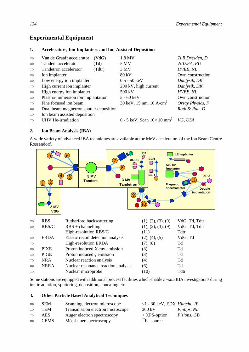
Experimental Equipment 134
Experimental Equipment 1. Accelerators, Ion Implanters and Ion-Assisted-Deposition
⇒ Van de Graaff accelerator (VdG) 1,8 MV TuR Dresden, D ⇒ Tandem accelerator (Td) 5 MV NIIEFA, RU ⇒ Tandetron accelerator (Tdtr) 3 MV HVEE, NL ⇒ Ion implanter 80 kV Own construction ⇒ Low energy ion implanter 0.5 - 50 keV Danfysik, DK ⇒ High current ion implanter 200 kV, high current Danfysik, DK ⇒ High energy ion implanter 500 kV HVEE, NL ⇒ Plasma-immersion ion implantation 5 - 60 keV Own construction ⇒ Fine focused ion beam 30 keV, 15 nm, 10 A/cm2 Orsay Physics, F ⇒ Dual beam magnetron sputter deposition Roth & Rau, D ⇒ Ion beam assisted deposition ⇒ UHV He-irradiation 0 - 5 keV, Scan 10 × 10 mm2 VG, USA 2. Ion Beam Analysis (IBA)
A wide variety of advanced IBA techniques are available at the MeV accelerators of the Ion Beam Centre Rossendorf.
2 MV VdG
1
500 kVimplanter
5 MV Tandem 3 MV
Tandetron Magneticspectrometer Double
implantation
LE implanterECR
EBIT
860-C
XRD
He
34
5 6
2
10
11
87
9
2 MV VdG
1
500 kVimplanter
5 MV Tandem 3 MV
Tandetron Magneticspectrometer Double
implantation
LE implanterECR
EBIT
860-C
XRD
He
34
5 6
2
10
11
87
9
⇒ RBS Rutherford backscattering (1), (2), (3), (9) VdG, Td, Tdtr ⇒ RBS/C RBS + channelling (1), (2), (3), (9) VdG, Td, Tdtr High-resolution RBS/C (11) Tdtr ⇒ ERDA Elastic recoil detection analysis (2), (4), (5) VdG, Td ⇒ High-resolution ERDA (7), (8) Td ⇒ PIXE Proton induced X-ray emission (3) Td ⇒ PIGE Proton induced γ emission (3) Td ⇒ NRA Nuclear reaction analysis (4) Td ⇒ NRRA Nuclear resonance reaction analysis (6) Td ⇒ Nuclear microprobe (10) Tdtr
Some stations are equipped with additional process facilities which enable in-situ IBA investigations during ion irradiation, sputtering, deposition, annealing etc. 3. Other Particle Based Analytical Techniques
⇒ SEM Scanning electron microscope <1 - 30 keV, EDX Hitachi, JP ⇒ TEM Transmission electron microscope 300 kV Philips, NL ⇒ AES Auger electron spectroscopy + XPS-option Fisions, GB ⇒ CEMS Mössbauer spectroscopy 57Fe source
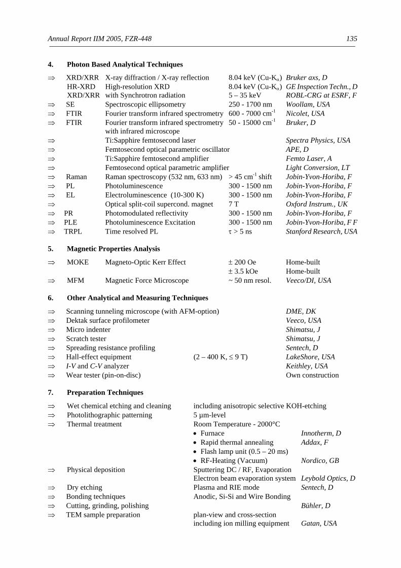
Annual Report IIM 2005, FZR-448
135
4. Photon Based Analytical Techniques
⇒ XRD/XRR X-ray diffraction / X-ray reflection 8.04 keV (Cu-Kα) Bruker axs, D HR-XRD High-resolution XRD 8.04 keV (Cu-Kα) GE Inspection Techn., D
XRD/XRR with Synchrotron radiation 5 – 35 keV ROBL-CRG at ESRF, F ⇒ SE Spectroscopic ellipsometry 250 - 1700 nm Woollam, USA ⇒ FTIR Fourier transform infrared spectrometry 600 - 7000 cm-1 Nicolet, USA ⇒ FTIR Fourier transform infrared spectrometry 50 - 15000 cm-1 Bruker, D with infrared microscope ⇒ Ti:Sapphire femtosecond laser Spectra Physics, USA ⇒ Femtosecond optical parametric oscillator APE, D ⇒ Ti:Sapphire femtosecond amplifier Femto Laser, A ⇒ Femtosecond optical parametric amplifier Light Conversion, LT ⇒ Raman Raman spectroscopy (532 nm, 633 nm) > 45 cm-1 shift Jobin-Yvon-Horiba, F ⇒ PL Photoluminescence 300 - 1500 nm Jobin-Yvon-Horiba, F ⇒ EL Electroluminescence (10-300 K) 300 - 1500 nm Jobin-Yvon-Horiba, F ⇒ Optical split-coil supercond. magnet 7 T Oxford Instrum., UK ⇒ PR Photomodulated reflectivity 300 - 1500 nm Jobin-Yvon-Horiba, F ⇒ PLE Photoluminescence Excitation 300 - 1500 nm Jobin-Yvon-Horiba, F F ⇒ TRPL Time resolved PL τ > 5 ns Stanford Research, USA 5. Magnetic Properties Analysis
⇒ MOKE Magneto-Optic Kerr Effect ± 200 Oe Home-built ± 3.5 kOe Home-built ⇒ MFM Magnetic Force Microscope ~ 50 nm resol. Veeco/DI, USA 6. Other Analytical and Measuring Techniques
⇒ Scanning tunneling microscope (with AFM-option) DME, DK ⇒ Dektak surface profilometer Veeco, USA ⇒ Micro indenter Shimatsu, J ⇒ Scratch tester Shimatsu, J ⇒ Spreading resistance profiling Sentech, D ⇒ Hall-effect equipment (2 – 400 K, ≤ 9 T) LakeShore, USA ⇒ I-V and C-V analyzer Keithley, USA ⇒ Wear tester (pin-on-disc) Own construction 7. Preparation Techniques
⇒ Wet chemical etching and cleaning including anisotropic selective KOH-etching ⇒ Photolithographic patterning 5 µm-level ⇒ Thermal treatment Room Temperature - 2000°C • Furnace Innotherm, D • Rapid thermal annealing Addax, F • Flash lamp unit (0.5 – 20 ms) • RF-Heating (Vacuum) Nordico, GB ⇒ Physical deposition Sputtering DC / RF, Evaporation Electron beam evaporation system Leybold Optics, D ⇒ Dry etching Plasma and RIE mode Sentech, D ⇒ Bonding techniques Anodic, Si-Si and Wire Bonding ⇒ Cutting, grinding, polishing Bühler, D ⇒ TEM sample preparation plan-view and cross-section including ion milling equipment Gatan, USA
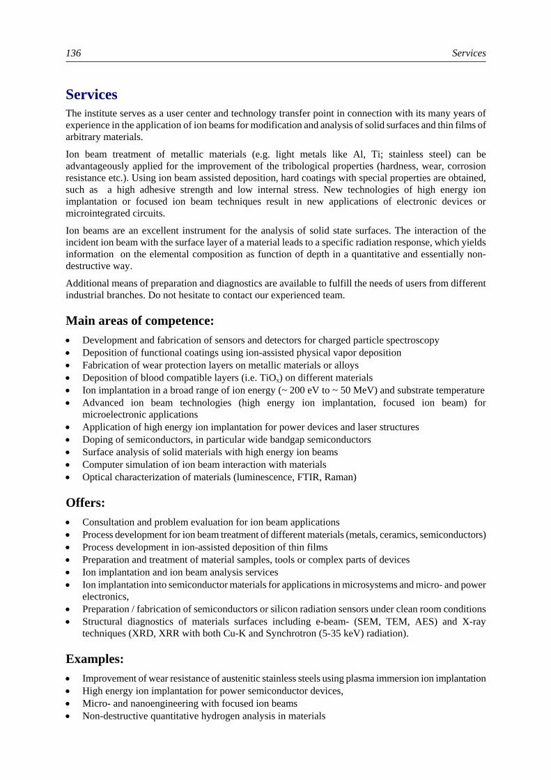
Services 136
Services The institute serves as a user center and technology transfer point in connection with its many years of experience in the application of ion beams for modification and analysis of solid surfaces and thin films of arbitrary materials.
Ion beam treatment of metallic materials (e.g. light metals like Al, Ti; stainless steel) can be advantageously applied for the improvement of the tribological properties (hardness, wear, corrosion resistance etc.). Using ion beam assisted deposition, hard coatings with special properties are obtained, such as a high adhesive strength and low internal stress. New technologies of high energy ion implantation or focused ion beam techniques result in new applications of electronic devices or microintegrated circuits.
Ion beams are an excellent instrument for the analysis of solid state surfaces. The interaction of the incident ion beam with the surface layer of a material leads to a specific radiation response, which yields information on the elemental composition as function of depth in a quantitative and essentially non-destructive way.
Additional means of preparation and diagnostics are available to fulfill the needs of users from different industrial branches. Do not hesitate to contact our experienced team. Main areas of competence: • Development and fabrication of sensors and detectors for charged particle spectroscopy • Deposition of functional coatings using ion-assisted physical vapor deposition • Fabrication of wear protection layers on metallic materials or alloys • Deposition of blood compatible layers (i.e. TiOx) on different materials • Ion implantation in a broad range of ion energy (~ 200 eV to ~ 50 MeV) and substrate temperature • Advanced ion beam technologies (high energy ion implantation, focused ion beam) for
microelectronic applications • Application of high energy ion implantation for power devices and laser structures • Doping of semiconductors, in particular wide bandgap semiconductors • Surface analysis of solid materials with high energy ion beams • Computer simulation of ion beam interaction with materials • Optical characterization of materials (luminescence, FTIR, Raman) Offers: • Consultation and problem evaluation for ion beam applications • Process development for ion beam treatment of different materials (metals, ceramics, semiconductors) • Process development in ion-assisted deposition of thin films • Preparation and treatment of material samples, tools or complex parts of devices • Ion implantation and ion beam analysis services • Ion implantation into semiconductor materials for applications in microsystems and micro- and power
electronics, • Preparation / fabrication of semiconductors or silicon radiation sensors under clean room conditions • Structural diagnostics of materials surfaces including e-beam- (SEM, TEM, AES) and X-ray
techniques (XRD, XRR with both Cu-K and Synchrotron (5-35 keV) radiation). Examples: • Improvement of wear resistance of austenitic stainless steels using plasma immersion ion implantation • High energy ion implantation for power semiconductor devices, • Micro- and nanoengineering with focused ion beams • Non-destructive quantitative hydrogen analysis in materials
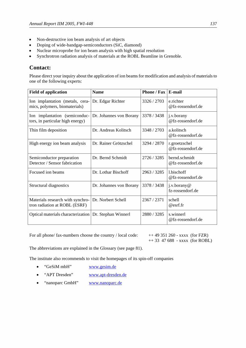
Annual Report IIM 2005, FWI-448 137
• Non-destructive ion beam analysis of art objects • Doping of wide-bandgap-semiconductors (SiC, diamond) • Nuclear microprobe for ion beam analysis with high spatial resolution • Synchrotron radiation analysis of materials at the ROBL Beamline in Grenoble. Contact: Please direct your inquiry about the application of ion beams for modification and analysis of materials to one of the following experts: Field of application Name Phone / Fax E-mail
Ion implantation (metals, cera-mics, polymers, biomaterials)
Dr. Edgar Richter 3326 / 2703 e.richter @fz-rossendorf.de
Ion implantation (semiconduc-tors, in particular high energy)
Dr. Johannes von Borany 3378 / 3438 j.v.borany @fz-rossendorf.de
Thin film deposition Dr. Andreas Kolitsch 3348 / 2703 a.kolitsch @fz-rossendorf.de
High energy ion beam analysis Dr. Rainer Grötzschel 3294 / 2870 r.groetzschel @fz-rossendorf.de
Semiconductor preparation Detector / Sensor fabrication
Dr. Bernd Schmidt 2726 / 3285 bernd.schmidt @fz-rossendorf.de
Focused ion beams Dr. Lothar Bischoff 2963 / 3285 l.bischoff @fz-rossendorf.de
Structural diagnostics Dr. Johannes von Borany 3378 / 3438 j.v.borany@ fz-rossendorf.de
Materials research with synchro-tron radiation at ROBL (ESRF)
Dr. Norbert Schell 2367 / 2371 schell @esrf.fr
Optical materials characterization Dr. Stephan Winnerl 2880 / 3285 s.winnerl @fz-rossendorf.de
For all phone/ fax-numbers choose the country / local code: ++ 49 351 260 - xxxx (for FZR) ++ 33 47 688 - xxxx (for ROBL)
The abbreviations are explained in the Glossary (see page 81).
The institute also recommends to visit the homepages of its spin-off companies
• “GeSiM mbH” www.gesim.de
• “APT Dresden” www.apt-dresden.de
• “nanoparc GmbH” www.nanoparc.de
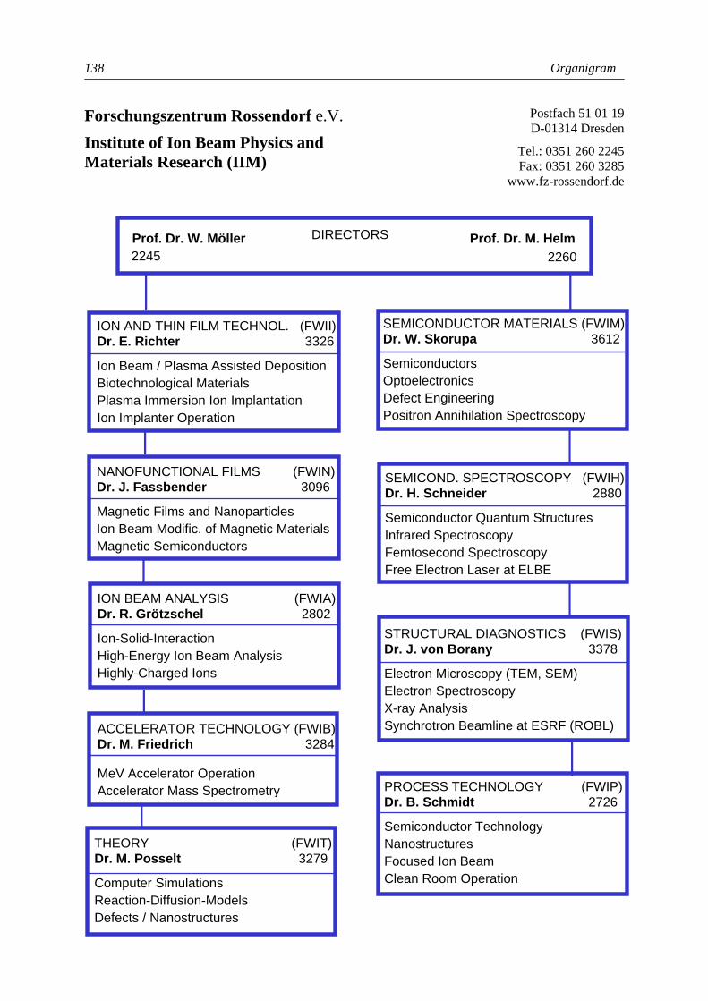
Organigram
138
F orschungszentrum Rossendorf e.V. Institute of Ion Beam Physics and Materials Research (IIM)
Postfach 51 01 19 D-01314 Dresden
Tel.: 0351 260 2245 Fax: 0351 260 3285
www.fz-rossendorf.de
Prof. Dr. W. Möller DIRECTORS Prof. Dr. M. Helm 2245 2260
SEMICONDUCTOR MATERIALS (FWIM) Dr. W. Skorupa 3612
Semiconductors Optoelectronics Defect Engineering Positron Annihilation Spectroscopy
ION BEAM ANALYSIS (FWIA) Dr. R. Grötzschel 2802
Ion-Solid-Interaction High-Energy Ion Beam Analysis Highly-Charged Ions
ACCELERATOR TECHNOLOGY (FWIB) Dr. M. Friedrich 3284
MeV Accelerator Operation Accelerator Mass Spectrometry
ION AND THIN FILM TECHNOL. (FWII)Dr. E. Richter 3326
Ion Beam / Plasma Assisted Deposition Biotechnological Materials Plasma Immersion Ion Implantation Ion Implanter Operation
THEORY (FWIT)Dr. M. Posselt 3279
Computer Simulations Reaction-Diffusion-Models Defects / Nanostructures
SEMICOND. SPECTROSCOPY (FWIH) Dr. H. Schneider 2880
Semiconductor Quantum Structures Infrared Spectroscopy Femtosecond Spectroscopy Free Electron Laser at ELBE
STRUCTURAL DIAGNOSTICS (FWIS)Dr. J. von Borany 3378
Electron Microscopy (TEM, SEM) Electron Spectroscopy X-ray Analysis Synchrotron Beamline at ESRF (ROBL)
PROCESS TECHNOLOGY (FWIP)Dr. B. Schmidt 2726
Semiconductor Technology Nanostructures Focused Ion Beam Clean Room Operation
NANOFUNCTIONAL FILMS (FWIN)Dr. J. Fassbender 3096
Magnetic Films and Nanoparticles Ion Beam Modific. of Magnetic Materials Magnetic Semiconductors

Annual Report IIM 2005, FZR-448
139
List of Personnel Directors: Prof. M. Helm Prof. W. Möller Office: I. Heidel, S. Kirch Scientific Staff: Permanent: Dr. G. Abrasonis Dr. L. Bischoff Dr. J. von Borany Dr. W. Bürger Dr. F. Eichhorn Dr. S. Facsko Dr. J. Faßbender Dr. M. Friedrich Dr. D. Grambole Dr. J. Grenzer Dr. R. Grötzschel Dr. V. Heera F. Herrmann Dr. K.-H. Heinig Dr. H.-U. Jäger Dr. R. Kögler Dr. A. Kolitsch Dr. U. Kreißig Dr. A. Mücklich Dr. C. Neelmeijer Dr. M. Posselt Dr. H. Reuther Dr. E. Richter Dr. N. Schell Dr. B. Schmidt Dr. H. Schneider Dr. W. Skorupa Dr. M. Voelskow Dr. S. Winnerl Post Docs: Dr. K. Küpper Dr. K. Potzger Dr. J. Sun Dr. M. Vinnichenko Projects: Dr. B. Abendroth Dr. C. Akhmadaliev W. Anwand Dr. G. Brauer
N. Bulatovic Dr. O. Drachenko Dr. A. Lebedev R. Martins Dr. T. Oates Dr. W. Pilz Dr. A. Rogozin Dr. M. Seidel Dr. N. Shevchenko Dr. C. V.-B. Tribuzy Dr. H. Weishart Dr. R. Yankov Dr. M. Zier PhD Students: M. Beckers M. Berndt V. Cantelli A. Dreyhaupt H. Geßner D. Güttler A. Keller D. Kost M. O. Liedke J. Potfajova L. Röntzsch S. Sinning D. Stehr S. Zhou Diploma Students: S. Friebel R. Heller M. Kreller H. Lange S. Ohser F. Peter S. Roßbach G. Talut M. Wagner S. Walther
Technical Staff: Permanent: R. Aniol G. Anwand W. Boede K.-D. Butter E. Christalle H. Felsmann K. Fukarek B. Gebauer H.-J. Grahl G. Grunert P. Hartmann J. Haufe G. Hofmann S. Klare J. Kreher A. Kunz U. Lucchesi M. Mißbach C. Neisser E. Quaritsch A. Reichel B. Richter M. Roch B. Scheumann G. Schnabel A. Schneider J. Schneider A. Scholz T. Schumann H. Seifert K. Thiemig S. Turuc A. Vetter R. Weidauer A. Weise J. Winkelmann G. Winkler I. Winkler
Projects: F. Ludewig M. Steinert I. Skorupa J. Zscharschuch
Related Documents