Journal of Alloys and Compounds 482 (2009) 131–136 Contents lists available at ScienceDirect Journal of Alloys and Compounds journal homepage: www.elsevier.com/locate/jallcom Annealing Ni nanocrystalline on WC–Co C.M. Fernandes a , G. Guisbiers a , S. Pereira a , N.P. Barradas b , E. Alves b , A.M.R. Senos a,∗ , M.T. Vieira c a CICECO, University of Aveiro, 3810-193 Aveiro, Portugal b Nuclear and Technological Institute, E.N. 10, 2686-953 Sacavém, Portugal c Mechanical Engineering Department, ICEMS, Polo II, 3030-201 Coimbra, Portugal article info Article history: Received 11 February 2009 Received in revised form 15 April 2009 Accepted 15 April 2009 Available online 3 May 2009 Keywords: Coating materials Thin films Vapour deposition Diffusion Rutherford backscattering RBS abstract The effects of annealing temperature on nanocrystalline sputter-deposited Ni thin films (500 nm) deposited on WC–Co (4 wt.%) were investigated. Special attention was focused on quantitative evaluation of residual stress and Ni diffusion into the WC–Co, after heat treatment, from 873 to 1273 K. The estimated level of residual stress, as measured by X-ray diffraction, is around −1.3 ± 0.1 GPa for the as-deposited film, whereas after annealing at 1273K it decreases significantly. Atomic force microscopy shows that high annealing temperature results into an exponential increase of the roughness. An intermixing between the nanocrystalline Ni and the Co from WC substrate occurs, as it is revealed by quantitative depth-resolved Rutherford backscattering spectrometry analysis and also supported by X-ray photoelectron spectroscopy. We ascribe a significant stress relief with the increasing annealing temperature to the diffusion process. The understanding of this process is particularly impor- tant in WC–Co parts with the surface treated with Ni in order to improve the maximum surface service temperature. © 2009 Elsevier B.V. All rights reserved. 1. Introduction The tungsten carbide with cobalt as binder persists to be the election material for cutting tools, particularly in extreme condi- tions such as higher cutting feed rates and sea water environments. In spite of the proximity between Ni and Co in the periodic table, Ni stabilizes the FCC structure of Co (Co-FCC, at 623 K Co-HC) and increases its stacking fault energy, which allows an improvement of the high temperature strength of Co–(Ni). Other property to be reinforced by the presence of Ni in Co is the behaviour in salt water: addition of Ni contributes to an increase of the corrosion resistance in Co, as verified in other alloys [1]. Additionally, the increase of the maximum service temperature for Ni–Co alloys, relatively to Ni, has been also reported [2]. The WC–Co with a thin underlayer of Ni could be of great interest for the improvement of the surface characteristics of coated or uncoated WC–Co tools. However, a heat treatment is necessary for the promotion of interdiffusion between Co and Ni. The focus of the present work concerns the diffusion of a nanocrystalline thin film of Ni deposited in the WC–Co. The effect of heat treatment holding temperature in residual stress will be also emphasized, due to its effect in the adhesion during the heat treat- ment. Previously reported results concern the effects of annealing temperature on the stress and surface morphology of Ni-based ∗ Corresponding author. Tel.: +351 234 370 354; fax: +351 234 370 204. E-mail address: [email protected] (A.M.R. Senos). thin films, like NiAl [3], Ti–Ni [4] and WC–Ni [5]. Therefore, the goal of this paper is to report on the effects of annealing temper- ature in Ni thin films on WC–Co substrates. Without the stress evaluation it is not possible to persecute/determine the effect of Ni in solution in the Co in the tools performance during applica- tion. Thin films deposited on a substrate usually exhibit intrinsic and thermal residual stress, that could be highly detrimental for the adhesion of the film to the substrate [6,7]. The intrinsic com- ponent is due to the growth process itself, whereas the thermal one appears due to the difference between the thermal expan- sion coefficients between the deposited material and substrate. Sputtering is the deposition technique selected here for Ni coat- ing deposition. Sputter-deposited Ni coatings are largely used for electrical and optical applications [8,9], or as protective layers to improve corrosion resistance, wear resistance and hardness of different materials [10,11]. In high melting point materials, such as Ni deposited by sputtering, the accumulated intrinsic stresses tend to dominate over thermal stresses, according to the Thornton and Hoffman’s criterion [12]. This criterion traditionally separates the materials into two categories: the low melting point mate- rials (T substrate /T m,∞ > 0.25) and the high melting point materials (T substrate /T m,∞ < 0.25). The low/high melting point materials are characterized by a low/high intrinsic residual stress compared to the thermal one. Note that the separation point at ∼0.25 is only valid at the macroscale, since this value is a function of the nanos- tructures size due to the size effects on the melting temperature, as discussed previously [13]. 0925-8388/$ – see front matter © 2009 Elsevier B.V. All rights reserved. doi:10.1016/j.jallcom.2009.04.106

Welcome message from author
This document is posted to help you gain knowledge. Please leave a comment to let me know what you think about it! Share it to your friends and learn new things together.
Transcript

A
Ca
b
c
a
ARRAA
KCTVDR
1
etINioraitNoctC
nhemt
0d
Journal of Alloys and Compounds 482 (2009) 131–136
Contents lists available at ScienceDirect
Journal of Alloys and Compounds
journa l homepage: www.e lsev ier .com/ locate / ja l l com
nnealing Ni nanocrystalline on WC–Co
.M. Fernandesa, G. Guisbiersa, S. Pereiraa, N.P. Barradasb, E. Alvesb, A.M.R. Senosa,∗, M.T. Vieirac
CICECO, University of Aveiro, 3810-193 Aveiro, PortugalNuclear and Technological Institute, E.N. 10, 2686-953 Sacavém, PortugalMechanical Engineering Department, ICEMS, Polo II, 3030-201 Coimbra, Portugal
r t i c l e i n f o
rticle history:eceived 11 February 2009eceived in revised form 15 April 2009ccepted 15 April 2009vailable online 3 May 2009
a b s t r a c t
The effects of annealing temperature on nanocrystalline sputter-deposited Ni thin films (500 nm)deposited on WC–Co (4 wt.%) were investigated. Special attention was focused on quantitative evaluationof residual stress and Ni diffusion into the WC–Co, after heat treatment, from 873 to 1273 K. The estimatedlevel of residual stress, as measured by X-ray diffraction, is around −1.3 ± 0.1 GPa for the as-deposited film,whereas after annealing at 1273 K it decreases significantly.
eywords:oating materialshin filmsapour depositioniffusion
Atomic force microscopy shows that high annealing temperature results into an exponential increaseof the roughness. An intermixing between the nanocrystalline Ni and the Co from WC substrate occurs,as it is revealed by quantitative depth-resolved Rutherford backscattering spectrometry analysis and alsosupported by X-ray photoelectron spectroscopy. We ascribe a significant stress relief with the increasingannealing temperature to the diffusion process. The understanding of this process is particularly impor-
the
utherford backscattering RBS tant in WC–Co parts withtemperature.. Introduction
The tungsten carbide with cobalt as binder persists to be thelection material for cutting tools, particularly in extreme condi-ions such as higher cutting feed rates and sea water environments.n spite of the proximity between Ni and Co in the periodic table,i stabilizes the FCC structure of Co (Co-FCC, at 623 K Co-HC) and
ncreases its stacking fault energy, which allows an improvementf the high temperature strength of Co–(Ni). Other property to beeinforced by the presence of Ni in Co is the behaviour in salt water:ddition of Ni contributes to an increase of the corrosion resistancen Co, as verified in other alloys [1]. Additionally, the increase ofhe maximum service temperature for Ni–Co alloys, relatively toi, has been also reported [2]. The WC–Co with a thin underlayerf Ni could be of great interest for the improvement of the surfaceharacteristics of coated or uncoated WC–Co tools. However, a heatreatment is necessary for the promotion of interdiffusion betweeno and Ni.
The focus of the present work concerns the diffusion of aanocrystalline thin film of Ni deposited in the WC–Co. The effect of
eat treatment holding temperature in residual stress will be alsomphasized, due to its effect in the adhesion during the heat treat-ent. Previously reported results concern the effects of annealingemperature on the stress and surface morphology of Ni-based
∗ Corresponding author. Tel.: +351 234 370 354; fax: +351 234 370 204.E-mail address: [email protected] (A.M.R. Senos).
925-8388/$ – see front matter © 2009 Elsevier B.V. All rights reserved.oi:10.1016/j.jallcom.2009.04.106
surface treated with Ni in order to improve the maximum surface service
© 2009 Elsevier B.V. All rights reserved.
thin films, like NiAl [3], Ti–Ni [4] and WC–Ni [5]. Therefore, thegoal of this paper is to report on the effects of annealing temper-ature in Ni thin films on WC–Co substrates. Without the stressevaluation it is not possible to persecute/determine the effect ofNi in solution in the Co in the tools performance during applica-tion.
Thin films deposited on a substrate usually exhibit intrinsicand thermal residual stress, that could be highly detrimental forthe adhesion of the film to the substrate [6,7]. The intrinsic com-ponent is due to the growth process itself, whereas the thermalone appears due to the difference between the thermal expan-sion coefficients between the deposited material and substrate.Sputtering is the deposition technique selected here for Ni coat-ing deposition. Sputter-deposited Ni coatings are largely used forelectrical and optical applications [8,9], or as protective layersto improve corrosion resistance, wear resistance and hardness ofdifferent materials [10,11]. In high melting point materials, suchas Ni deposited by sputtering, the accumulated intrinsic stressestend to dominate over thermal stresses, according to the Thorntonand Hoffman’s criterion [12]. This criterion traditionally separatesthe materials into two categories: the low melting point mate-rials (Tsubstrate/Tm,∞ > 0.25) and the high melting point materials(Tsubstrate/Tm,∞ < 0.25). The low/high melting point materials are
characterized by a low/high intrinsic residual stress compared tothe thermal one. Note that the separation point at ∼0.25 is onlyvalid at the macroscale, since this value is a function of the nanos-tructures size due to the size effects on the melting temperature, asdiscussed previously [13].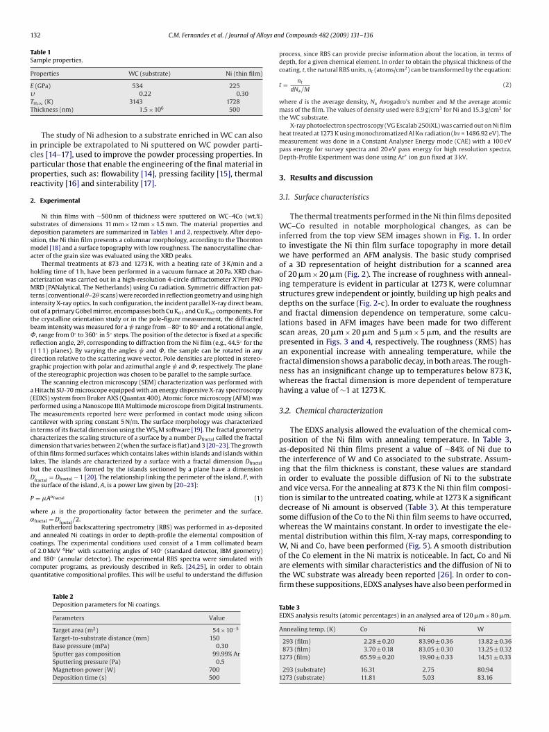
132 C.M. Fernandes et al. / Journal of Alloys an
Table 1Sample properties.
Properties WC (substrate) Ni (thin film)
E (GPa) 534 225�TT
icppr
2
sdsma
haMtiotb˚r{dgo
a(pTcicdolbDt
P
w˛
acoacq
0.22 0.30m,∞ (K) 3143 1728hickness (nm) 1.5 × 10⁶ 500
The study of Ni adhesion to a substrate enriched in WC can alson principle be extrapolated to Ni sputtered on WC powder parti-les [14–17], used to improve the powder processing properties. Inarticular those that enable the engineering of the final material inroperties, such as: flowability [14], pressing facility [15], thermaleactivity [16] and sinterability [17].
. Experimental
Ni thin films with ∼500 nm of thickness were sputtered on WC–4Co (wt.%)ubstrates of dimensions 11 mm × 12 mm × 1.5 mm. The material properties andeposition parameters are summarized in Tables 1 and 2, respectively. After depo-ition, the Ni thin film presents a columnar morphology, according to the Thorntonodel [18] and a surface topography with low roughness. The nanocrystalline char-
cter of the grain size was evaluated using the XRD peaks.Thermal treatments at 873 and 1273 K, with a heating rate of 3 K/min and a
olding time of 1 h, have been performed in a vacuum furnace at 20 Pa. XRD char-cterization was carried out in a high-resolution 4-circle diffractometer X’Pert PRORD (PANalytical, The Netherlands) using Cu radiation. Symmetric diffraction pat-
erns (conventional �–2� scans) were recorded in reflection geometry and using highntensity X-ray optics. In such configuration, the incident parallel X-ray direct beam,ut of a primary Göbel mirror, encompasses both Cu K�1 and Cu K�2 components. Forhe crystalline orientation study or in the pole-figure measurement, the diffractedeam intensity was measured for a range from −80◦ to 80◦ and a rotational angle,, range from 0◦ to 360◦ in 5◦ steps. The position of the detector is fixed at a specific
eflection angle, 2�, corresponding to diffraction from the Ni film (e.g., 44.5◦ for the1 1 1} planes). By varying the angles and ˚, the sample can be rotated in anyirection relative to the scattering wave vector. Pole densities are plotted in stereo-raphic projection with polar and azimuthal angle and˚, respectively. The planef the stereographic projection was chosen to be parallel to the sample surface.
The scanning electron microscopy (SEM) characterization was performed withHitachi SU-70 microscope equipped with an energy dispersive X-ray spectroscopy
EDXS) system from Bruker AXS (Quantax 400). Atomic force microscopy (AFM) waserformed using a Nanoscope IIIA Multimode microscope from Digital Instruments.he measurements reported here were performed in contact mode using siliconantilever with spring constant 5 N/m. The surface morphology was characterizedn terms of its fractal dimension using the WSxM software [19]. The fractal geometryharacterizes the scaling structure of a surface by a number Dfractal called the fractalimension that varies between 2 (when the surface is flat) and 3 [20–23]. The growthf thin films formed surfaces which contains lakes within islands and islands withinakes. The islands are characterized by a surface with a fractal dimension Dfractal
ut the coastlines formed by the islands sectioned by a plane have a dimension′fractal
= Dfractal − 1 [20]. The relationship linking the perimeter of the island, P, withhe surface of the island, A, is a power law given by [20–23]:
= �A˛fractal (1)
here � is the proportionality factor between the perimeter and the surface,fractal = D′
fractal/2.
Rutherford backscattering spectrometry (RBS) was performed in as-depositednd annealed Ni coatings in order to depth-profile the elemental composition of
oatings. The experimental conditions used consist of a 1 mm collimated beamf 2.0 MeV 4He+ with scattering angles of 140◦ (standard detector, IBM geometry)nd 180◦ (annular detector). The experimental RBS spectra were simulated withomputer programs, as previously described in Refs. [24,25], in order to obtainuantitative compositional profiles. This will be useful to understand the diffusionTable 2Deposition parameters for Ni coatings.
Parameters Value
Target area (m2) 54 × 10−5
Target-to-substrate distance (mm) 150Base pressure (mPa) 0.30Sputter gas composition 99.99% ArSputtering pressure (Pa) 0.5Magnetron power (W) 700Deposition time (s) 500
d Compounds 482 (2009) 131–136
process, since RBS can provide precise information about the location, in terms ofdepth, for a given chemical element. In order to obtain the physical thickness of thecoating, t, the natural RBS units, nt (atoms/cm2) can be transformed by the equation:
t = ntdNa/M
(2)
where d is the average density, Na Avogadro’s number and M the average atomicmass of the film. The values of density used were 8.9 g/cm3 for Ni and 15.3 g/cm3 forthe WC substrate.
X-ray photoelectron spectroscopy (VG Escalab 250iXL) was carried out on Ni filmheat treated at 1273 K using monochromatized Al K� radiation (h� = 1486.92 eV). Themeasurement was done in a Constant Analyser Energy mode (CAE) with a 100 eVpass energy for survey spectra and 20 eV pass energy for high resolution spectra.Depth-Profile Experiment was done using Ar+ ion gun fixed at 3 kV.
3. Results and discussion
3.1. Surface characteristics
The thermal treatments performed in the Ni thin films depositedWC–Co resulted in notable morphological changes, as can beinferred from the top view SEM images shown in Fig. 1. In orderto investigate the Ni thin film surface topography in more detailwe have performed an AFM analysis. The basic study comprisedof a 3D representation of height distribution for a scanned areaof 20 �m × 20 �m (Fig. 2). The increase of roughness with anneal-ing temperature is evident in particular at 1273 K, were columnarstructures grew independent or jointly, building up high peaks anddepths on the surface (Fig. 2-c). In order to evaluate the roughnessand fractal dimension dependence on temperature, some calcu-lations based in AFM images have been made for two differentscan areas, 20 �m × 20 �m and 5 �m × 5 �m, and the results arepresented in Figs. 3 and 4, respectively. The roughness (RMS) hasan exponential increase with annealing temperature, while thefractal dimension shows a parabolic decay, in both areas. The rough-ness has an insignificant change up to temperatures below 873 K,whereas the fractal dimension is more dependent of temperaturehaving a value of ∼1 at 1273 K.
3.2. Chemical characterization
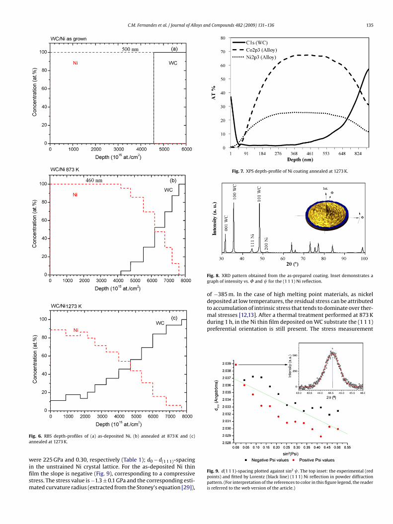
The EDXS analysis allowed the evaluation of the chemical com-position of the Ni film with annealing temperature. In Table 3,as-deposited Ni thin films present a value of ∼84% of Ni due tothe interference of W and Co associated to the substrate. Assum-ing that the film thickness is constant, these values are standardin order to evaluate the possible diffusion of Ni to the substrateand vice versa. For the annealing at 873 K the Ni thin film composi-tion is similar to the untreated coating, while at 1273 K a significantdecrease of Ni amount is observed (Table 3). At this temperaturesome diffusion of the Co to the Ni thin film seems to have occurred,whereas the W maintains constant. In order to investigate the ele-mental distribution within this film, X-ray maps, corresponding to
W, Ni and Co, have been performed (Fig. 5). A smooth distributionof the Co element in the Ni matrix is noticeable. In fact, Co and Niare elements with similar characteristics and the diffusion of Ni tothe WC substrate was already been reported [26]. In order to con-firm these suppositions, EDXS analyses have also been performed inTable 3EDXS analysis results (atomic percentages) in an analysed area of 120 �m × 80 �m.
Annealing temp. (K) Co Ni W
293 (film) 2.28 ± 0.20 83.90 ± 0.36 13.82 ± 0.36873 (film) 3.70 ± 0.18 83.05 ± 0.30 13.25 ± 0.32
1273 (film) 65.59 ± 0.20 19.90 ± 0.33 14.51 ± 0.33
293 (substrate) 16.31 2.75 80.941273 (substrate) 11.81 5.03 83.16

C.M. Fernandes et al. / Journal of Alloys and Compounds 482 (2009) 131–136 133
Fa
tbrahTtfis5mot
Fig. 2. AFM Ni coating surface images for: (a) as-deposited, (b) annealed at 873 Kand (c) annealed at 1273 K (scan size 20 �m × 20 �m). The arrows in (c) indicatedepressed and elevated regions, called lakes and islands, respectively.
ig. 1. SEM micrographs of Ni coating surface: (a) as-deposited, (b) annealed at 873 Knd (c) annealed at 1273 K.
he WC substrates. For such purpose the as-deposited Ni thin film,efore and after heat treatment at 1273 K, has been mechanicallyemoved. The results, presented in Table 3, show that the substratennealed at 1273 K presents, at the surface, lower contents of Co andigher contents of Ni than the substrate untreated (WC–Co 4 wt.%).he RBS depth-profiles performed in as-deposited and annealed Nihin film are presented in Fig. 6. The fit of the as-deposited Ni thinlm was made assuming a sharp interface between Ni and the sub-
trate; the calculated Ni thickness, using Eq. (2), is approximately00 nm (Fig. 6-a), which is in good agreement with the measure-ent by SEM. The Ni thin film annealed at 873 K (Fig. 6-b) consistsf pure Ni, up to a depth of about ∼460 nm; close to the interfacehere is intermixing between Ni and WC, noticeable up to depths Fig. 3. RMS roughness vs. annealing temperature.

134 C.M. Fernandes et al. / Journal of Alloys an
ofeth
1
s6aZd
etst
(E
)1
(d(d (� ))
)
Fig. 4. Fractal dimension vs. annealing temperature.
f about 700 nm. For the layer annealed at 1273 K severe interdif-usion occurred, so that, even at the surface, the metallic substratelements (W and Co) are detected (Fig. 6-c and Table 3). Therefore,he diffusion process between Ni and WC–Co starts at temperaturesigher than 873 K and is more intense at 1273 K.
The XPS depth-profile performed on the Ni coating annealed at273 K also reveals the strong concentration of Co in the Ni (Fig. 7).
Högberg et al. [27] have also reported the diffusion of Ni sub-trate into WC films chemical vapour deposited at 1173 K, during0 min. The WC films containing metallic Ni grains on the surfaces well as in the bulk, resulted from several phase transformations.hou et al. [28] also described the diffusion of Ni into WC particlesuring laser induction hybrid rapid cladding (∼1073 K).
The diffusion process that occurs in planar substrates can be
xtrapolated to WC powders sputter-deposited with Ni and sin-ered at high temperatures, normally higher than 1273 K, as alreadyuggested [26]. The interdiffusion process increases the Ni adhesiono the WC–Co, and the formation of a Co–Ni surface binder alloyFig. 5. SEM micrograph of Ni thin film at 1273 K
d Compounds 482 (2009) 131–136
could be an important improvement in high temperature strengthand corrosion resistance of the binder. However, it is necessary thatthe residual stress also decreases with the heat treatment.
3.3. Stress measurements
The conventional �–2� XRD pattern from the as-prepared coat-ing was performed (Fig. 8), in order to obtain the peak intensityof the Ni coating and the substrate (WC–4 wt.% Co). The peak at2� = 44.49◦, corresponding to the {1 1 1} planes, is the most intenseamong the Ni peaks measured in the �–2� scan, as shown in Fig. 8.In order to evaluate the texture of the Ni films we have used the(1 1 1) reflection to measure the intensity of the diffracted beamversus the polar coordinates ( , ˚). The peak (1 1 1) has its max-imum polar density centred at = 0 (see inset in Fig. 8), meaningthat there is a high density of (1 1 1) planes parallel to the sub-strate surface. Hence, one can conclude that the Ni coatings are(1 1 1)-textured, pointing to the presence of a considerable amountof residual stress. Therefore, this peak is used for the stress analy-sis. Such preferential orientation along the (1 1 1) planes of Ni thinfilms sputter-deposited was already been reported by other authors[8,10,11] and possibly responsible for a higher wear resistance thanthe bulk Ni [11]. A strong shift towards lower diffraction angle wasobserved for 2� scans performed for increasing . In order to obtainan accurate d(1 1 1)-spacing at different , the centre of a Lorentzfit (Fig. 9, top inset) was taken as the diffraction angle in Bragg’slaw. In a good agreement with the biaxial approximation, a lineardependence of the d(1 1 1) versus sin2 was observed (Fig. 9).
The residual stress, �, is independent of the azimuthal angle ϕ,and can be estimated from (3):
� =1 + � 1 1 1 d0
1 1 1
d(sin2� )(3)
where E and � are, respectively, the Young’s modulus and Pois-son’s ratio of the deposited thin film. For Ni thin film these values
and respective X-ray maps of elements.
C.M. Fernandes et al. / Journal of Alloys and Compounds 482 (2009) 131–136 135
Fa
wifism
Fig. 7. XPS depth-profile of Ni coating annealed at 1273 K.
deposited at low temperatures, the residual stress can be attributedto accumulation of intrinsic stress that tends to dominate over ther-mal stresses [12,13]. After a thermal treatment performed at 873 Kduring 1 h, in the Ni thin film deposited on WC substrate the (1 1 1)preferential orientation is still present. The stress measurement
ig. 6. RBS depth-profiles of (a) as-deposited Ni, (b) annealed at 873 K and (c)nnealed at 1273 K.
ere 225 GPa and 0.30, respectively (Table 1); d0 − d(1 1 1)-spacing
n the unstrained Ni crystal lattice. For the as-deposited Ni thinlm the slope is negative (Fig. 9), corresponding to a compressivetress. The stress value is −1.3 ± 0.1 GPa and the corresponding esti-ated curvature radius (extracted from the Stoney’s equation [29]),Fig. 8. XRD pattern obtained from the as-prepared coating. Inset demonstrates agraph of intensity vs.˚ and for the (1 1 1) Ni reflection.
of −385 m. In the case of high melting point materials, as nickel
Fig. 9. d(1 1 1)-spacing plotted against sin2 . The top inset: the experimental (redpoints) and fitted by Lorentz (black line) (1 1 1) Ni reflection in powder diffractionpattern. (For interpretation of the references to color in this figure legend, the readeris referred to the web version of the article.)

136 C.M. Fernandes et al. / Journal of Alloys an
Table 4Estimated curvature radius for the differenttemperatures.
Annealing temp. (K) R (m)
293 −385873 −2122
1273 3950
F
asarawt
pt(tp
4
nrdsetw
fptdt
[
[[[
[
[[
B 217 (2004) 479.
ig. 10. Calculated stress dependence with annealing temperature (GL = guide line).
lso results in a negative slope, corresponding to a compressivetress, with a value of −242 MPa, from Eq. (3). An increase of thennealing temperature in Ni thin film, up to 1273 K, results in aandom crystallographic orientation. The stress values show nowslightly positive slope, corresponding to a tensile stress in the Niith a value of 130 ± 84 MPa; the estimated curvature radii for both
emperatures studied are shown in Table 4.Assuming a linear dependence of stress with the annealing tem-
erature (Fig. 10) it is possible to roughly estimate the annealingemperature where the amount of residual stress approaches zero∼1123 K). It is also possible to estimate the stress value after heatreatment at temperatures normally used to sinter hardmetals (WCowders coated with Ni), for example at 1673 K, �≈ 800 MPa.
. Conclusions
The increase of the annealing temperature up to 1273 K ofanocrystalline sputter-deposited Ni thin films on WC–Co (4 wt.%)esults in the intermixing between Ni and Co from the substrate. Auctile layer of Co(Ni) is formed during this diffusion process thateems complete at 1273 K, leading to an adhesion increase of thexternal layer to the bulk WC–Co. Another important outcome ofhis heat treatment is the exponential increase of surface roughnessith a significant reduction of residual stress.
The modification of surface characteristics with a nearly stress-
ree and intermixed alloy layer reinforced the resulting filmroperties. The corrosion resistance and the maximum serviceemperature could be improved by a heat treatment of sputter-eposited Ni thin films on WC–Co substrates. This heat treatmenthat leads to a stress relief process can be applied in hardmetal parts[
[[[
d Compounds 482 (2009) 131–136
used in special applications. It may be also important for coatedpowders, where the formation of an interdiffused layer of Co(Ni)may lead to the improvement of the bulk properties during andafter sintering.
Acknowledgments
The authors wish to thank Doctor Aying Wu for the help inthe AFM analysis, Dr. Carmen Serra for the XPS measurements andalso Doctor Dimitry Khalyavin for the assistance in stress measure-ments. The authors C.M.F. and G. Guisbiers gratefully acknowledgethe financial support of the POCTI programme of the PortugueseFoundation for Science and Technology (FCT) and European SocialFund (FSE).
References
[1] A.M. Russel, K.L. Lee, Structure–Property–Relations in Non-Ferrous Metals, JohnWiley and sons, 2005.
[2] CES, EduPack Software, Granta Design Limited, Cambridge, UK, 2008.[3] M. Toparli, F. Sen, O. Culha, E. Celik, J. Mater. Process. Technol. 190 (2007) 26–32.[4] L. Zhang, C. Xie, J. Wu, J. Alloys Compd. 427 (2007) 238–243.[5] X. Guozhi, Z. Jingxian, L. Yijun, W. Keyu, M. Xiangyin, L. Pinghua, Mater. Sci. Eng.
A 460–461 (2007) 351–356.[6] M.J. Madou, Fundamentals of Microfabrication: The Science of Miniaturization,
second ed., CRC Press, Boca Raton, 2002.[7] M. Ohring, Materials Science of Thin Films Deposition and Structure, second
ed., Academic Press, New York, 2002.[8] Y. Mikami, K. Yamada, A. Ohnari, T. Degawa, T. Migita, T. Tanaka, K. Kawabata,
H. Kajioka, Surf. Coat. Technol. 133–134 (2000) 295–300.[9] M. Farooq, I.A. Raja, Renew. Energy 33 (2008) 1275–1285.
[10] B. Subramanian, S. Mohan, S. Jayakrishnan, M. Jayachandran, Curr. Appl. Phys.7 (2007) 305–313.
[11] K. Bouslykhane, J.P. Villain, P. Moine, Tribol. Int. 29 (2) (1996) 169–173.12] J.A. Thornton, D.W. Hoffman, Thin Solid Films 171 (1989) 5–31.
[13] G. Guisbiers, M. Kazan, O. Van Overschelde, M. Wautelet, S. Pereira, J. Phys.Chem. C 112 (2008) 4097.
[14] J.M. Castanho, M.T. Vieira, C.M. Fernandes, A.M.R. Senos, Vacuum 82 (12) (2008)1404–1406.
[15] C.M. Fernandes, V.M. Ferreira, A.M.R. Senos, M.T. Vieira, Surf. Coat. Technol. 176(2003) 103–108.
[16] C.M. Fernandes, A.M.R. Senos, J.M. Castanho, M.T. Vieira, Mater. Sci. Forum514–516 (2006) 633–637.
[17] C.M. Fernandes, A.M.R. Senos, M.T. Vieira, Int. J. Refract. Met. Hard Mater. 25 (4)(2007) 310–317.
[18] J.A. Thornton, Ann. Rev. Mater. Sci. 7 (1977) 239.[19] http://www.nanotec.es.20] B.B. Mandelbrot, D.E. Passoja, A.J. Paullay, Nature 308 (1984) 721–722.21] R.F. Voss, R.B. Laibowitz, E.I. Allessandrini, Phys. Rev. Lett. 49 (1982) 1441–1444.22] T. Nakayama, K. Yakubo, Fractal Concepts in Condensed Matter Physics,
Springer, Berlin, 2003.23] G. Guisbiers, O. Van Overschelde, M. Wautelet, P. Leclere, R. Lazzaroni, J. Phys.
D: Appl. Phys. 40 (2007) 1077–1079.24] N.P. Barradas, C. Jeynes, R.P. Webb, Appl. Phys. Lett. 71 (1997) 291.25] N.P. Barradas, E. Alves, S. Pereira, V.V. Shvartsman, A.L. Kholkin, E. Pereira, K.P.
O’Donnell, C. Liu, C.J. Deatcher, I.M. Watson, M. Mayer, Nucl. Instrum. Methods
26] C.M. Fernandes, A.M.R. Senos, M.T. Vieira, J.M. Antunes, Int. J. Refract. Met. HardMater. 26 (5) (2008) 491–498.
27] H. Högberg, Tägtström, J. Lu, U. Jansson, Thin Solid Films 272 (1996) 116–123.28] S. Zhou, Y. Huang, X. Zeng, Appl. Surf. Sci. 254 (10) (2008) 3110–3119.29] G.G. Stoney, Proc. Roy. Soc., London A82 (1909) 172.
Related Documents