DTI - ,LE CoPy RADC-TR-90-168 Final Technical Report May 1990 AD-A223 437 MAGNETOSTATIC WAVE TRANSDUCERS, RESONATORS AND DISPERSION CONTROL University of Texas at Arlington John M. Owens, Ronald L. Carter, W. Alan Davis, Younes Atallyan . DIC ANN& ECTE L TJU N 2 8 19 9 0 1 APPROVED FOR PUBLIC RELEASE; DISTRIBUTION UNLIMITED. ROME AIR DEVELOPMENT CENTER Air Force Systems Command Griffiss Air Force Base, NY 13441-5700 .0 06 2 015

Welcome message from author
This document is posted to help you gain knowledge. Please leave a comment to let me know what you think about it! Share it to your friends and learn new things together.
Transcript

DTI -,LE CoPy
RADC-TR-90-168Final Technical ReportMay 1990
AD-A223 437
MAGNETOSTATIC WAVETRANSDUCERS, RESONATORS ANDDISPERSION CONTROL
University of Texas at Arlington
John M. Owens, Ronald L. Carter, W. Alan Davis, Younes Atallyan
. DICANN& ECTE
L TJU N 2 8 19 90 1
APPROVED FOR PUBLIC RELEASE; DISTRIBUTION UNLIMITED.
ROME AIR DEVELOPMENT CENTERAir Force Systems Command
Griffiss Air Force Base, NY 13441-5700
.0 06 2 015

r
This report has been reviewed by the RADC Public Affairs Division (PA)
and is releasable to the National Technical Information Service (NTIS). At
NTIS it will be releasable to the general public, including foreign nations.
RADC-TR-90-168 has been reviewed and is approved for publication.
APPROVED: 6JAMES C. SETHARESProject Engineer
APPROVED:
JOHN K. SCHINDLER
Acting DirectorDirectorate of Electromagnetics
FOR THE COMMANDER:
JOHN A. RITZDirectorate of Plans & Programs
If your address has changed or if you wish to be removed from the RADC
mailing list, or if the addressee is no longer employed by your organization,
please notify RADC (EEAC ) Hanscom AFB MA 01731-5000. This will assist us in
maintaining a current mailing list.
Do not return copies of this report unless contractual obligations or notices
on a specific document require that it be returned.

RONTROLO U E TA INP G PN 070-0188
Johno bM. ' OAes oal L.A Catr ho Ala Davis AWw %a 400432ad. Youe AtaiiyanNo
1. GENY SE NLYam, 8W 2 RPO~ DAE . RPORPEANDDPESRMN COVRGITO
4. PEOMDN SUBTIE lO &AESAOORS(I FUNDING NUMBERS
UAnerOsAity of V Texas UERS atOATR Arlington C -F162-4--0
POTO PE B- 19016F
CArlington TX 76019
7. PERFORING UORINAGN NAME(S) AND ADRESSS) 1. PRFORINGOGNIZAINAEC
REPORT NUMBERRome Air Development Center (EEAC)Hanscom AFB MA 01731-5000 RADC-TR-90-168
ii. SUPPEMENTARY NOTES
RADC Project Engineer: Peter 3. Rainville/EEAC/(617) 377-4663
12&. DWISTIOW4AVAILAIITfY STATEMENT 12b. DISTRIBUTION CODE
Approved for public release; distribution unlimited.
12& ABSTRACT (AOaMaM 200 vWThis report describes the design of magnetostatic surface waves (MSW) and transversalfilters. Firs', ' ivariable time delay device is described that uses a cascadedsurface wave device and a backward volume wave device. Transducers composed of, - r7
periodic arrays of shorted microstrip lines Are described. Theoretical andexperimental work has resulted in the first '.true"-' synthesized magnetostatic wavetransversal filter. Furthermore, sample delay lines showed less than 16 dB insertionloss and 16 Hz bandwidth at 26 - 40 GHz.
14. SUS.ECT TERMS 1S. NMMR OF PAGESMagnetostatic Surface Waves 160Transversal Filter 16. PRICE COO!E
17 SECUFMTCLASSIFICATlON IIs. SECURITY CAASSIFICATION 19I SECURITY CLASSIFICT-ION 20. UMITATION OF ABSTRACTOF REPORT IOF THS PAGEI O FASSTPACT UUNCLSSIiEDUNCLASSIFIED UNCLASSIFIED
NSH M 'wmt-om 29a SS92

TABLE OF CONTENTS
1. INTRODUCTION and SUMMARY ................................................ 1
2. MAGNETOSTATIC WAVE DISPERSION CONTROL
2.1 Linearly Dispersive Time-Delay Control of Magnetostatic
Surface Wave by Variable Ground Plane Spacing
2.1.1 Introduction .................................................................... 4
2.1 ? Theoretical S ut . . .......................................... 4
2.1.3 Experimental Evaluation ...................................................... 5
2.2 Electronically Variable Time Delays Using Cascaded
Magnetostatic Delay Lines
2.2.1 Introduction .................................................................... 17
2.2.2 Theory .......................................................................... 18
2.2.3 Experimental Results ......................................................... 22
2.2.4 Experimental Results .......................................................... 27
2.3 Passive Magnetostatic Wave Pulse Compression Loop
2.3.1 Introduction .................................................................... 28
2.3.2 Passive Generation of the Down Chirp Coded Signal .................... 30
2.3.3 MSSW Linear Matching Filter ............................................... 30
2.3.4 Experimental Results .......................................................... 30
2.3.5 Conclusion ..................................................................... 34
2.4 Magnetostatic Surface Wave Matching Network .................................... 37
2.5 References .............................................................................. 44
3. MSW TRANSVERSAL FILTERS
3.1 MSSW Transversal Filter Based on Open Circuit
Transducer A rrays ...................................................................... 45
i

4. DELAY LINES
4.1 S Band Linear Delay Line ..................................................... 89
4.2 Ka Band Delay Lines ......................................................... 95
5. SUMMARY... ............................................................... 103
6. PUBLICATIONS FROM AFOSR SUPPORT ................................ 111
7. APPENDIX 1 ............................................................... 113
8. APPENDIX 2 ............................................................... 116
9. APPENDIX 3 ............................................................... 138
10. APPENDIX 4 ............................................................. 142
11. APPENDIX 5 ........................................................... 146
Ace rin For
Ul-2 17<

I INTRODUCT ION AND SUMMARY
A military need exists- for microwave solid state device
technology with complementary analog signal processing capabilities
which has been developed over the past ten years in surface acoustic
waves (SAW) technology. In this technology, non-recursive
transversal filters have been realized through either interdigital
transducers and/or periodic reflective arrays defined on the
piezoelectric substrates in which the surface acoustic waves are
propagated. Utilizing this technology simple delay lines, :omplex
matched filters, high Q resonators and chirp filters, have been
realized in the VHF, UHF, frequency range. Unfortunately, extension
of this technology to the microwave region (f > IGHz) has been
difficult. At these frequencies, the surface acoustic wavelength Is
less than lum making fabrication difficult and the propagation loss
becomes excessive (>100 db/usec at 10 GHz).
Final report contract AFOSR 80-8264 summarizes the results of a
viable technological realization of this goal through magnetostatic
waves (MSW) propagating at microwave frequencies in magnetically
biased, liquid phase epitaxial films of Yttrium Iron Garnet
(YIG) grown on Gadolinium Gallium Garnet (GGG). This technology
has a number of advantages; low loss (<30 db/usec at 10 GHz),
tunable by bias field to any center frequency (1-40 GHz), and
finally a well understood and characterized wave phenomena
(MSW). The necessary non-recursive transducer filtering is
achieved through a multi-element transducer and/or the Interaction
of the MSW with periodic structures in or on the YIG film.
This report summarizes the work accomplished toward achieving
1

MSW transversal filtering. First. studies of a variable time delay
device based on a cascaded MSSW forward wave delay line and an MSBVw
backward wave delay line. are presented. Next. studies of MSSW
(Maanetostatic Surface Wave) transducers composed of periodic arrays
of narrow shorted microstrips are summarized. A 3 port model for
this type of transducer and experimental measurements of test
devices were carried out to verify the model. A synthesis procedure
has been developed to allow synthesis of the desired response
function. Experimental studies of synthesized filters has resulted
in the first "true" synthesized MSW transversal filter. Finally.
studies of MSSW and MSFVW delay lines at Ku Band (26-40GHz) were
carried out resulting in sample delay lines with less than 16db
insertion loss and I GHz bandwidths.
Pulse compression systems utilizing surface acoustic wave
(SAW) dispersive delay lines have been under intensive investigation
for the past 14 years. These studies have concentrated primarily on
using the SAW linear dispersive delay line for downchlrp phase
codina with quadratic phase error less that one degree in the
expander section of the SAW pulse compression system. The low time-
sidelobes is achieved by appropriate amplitude weighting in the
compressor section. Time-bandwith products of over 1000 with greater
than 40 dB sidelobe suppression have been obtained for the SAW pulse
compression system. The typical operating center frequency for a SAW
device is less than I GHz (due to the physical limit of technology).
For radar systems of higher operating frequencies (in the GHz
region), mixing is required to convert the radar carrier frequencies
to the operating frequencies of the SAW pulse compression subsystem.
2

A new technology based on "slow" magnetostatic wave (MSW)
propagation in a magnetically biased epitaxial Yttrium Iron Garnet
(YIG) is emerging as a complementary signal processing technology to
SAW at microwave frequencies (1-20 GHz). Three major propagating
modes with the propagation direction in the film plane have been
used In device applications. These three modes are magnetostatic
surface wave (MSSW) mode in which the bias field is perpendicular to
the direction of the wave propagation and in the plane of the film,
magnetostatic forward volume wave (MSFVW) mode in which the bias
field is perpendicular to the film and the propagation direction,
and magnetostatic backward volume wave (MSBVW) mode in which the
direction of the bias field is the same as the propagation
direction. These modes are dispersive and characterized by a limited
propagation passband width (.5 to 2.2 GHz) with the center frequency
electronically tunable between 1 to 20 GHz by adjusting the bias
field. The 1-20 GHz center frequency range of this MSW modes makes
signal processing possible directly at radar carrier freque!ncy and
the typical group delays of the modes are between 50 nsec/cm to
IOOnsec/cm, depending on the YIG film thickness and the bias
magnetic field used. This dispersive slow wave structure of
magnetostatic wave makes the investigation of MSW devices in pulse
compression logical.
3

2 - MAGINe.ETOSTAT IC WAVED I SP=ERS I ON CO:N-TROL
2.1 Linearly Dispersive Time-Delay Control ofMagnetostatic Surface Wave by Variable Ground PlaneSpacing
2.1.1 Introduction
The propagation characteristics of magnetostatic waves in
eoitaxial Yttrium Iron Garnet (YIG) films have been extensively
investigated both experimentally and theoretically for a number of
years (1-4). These studies have shown that the delay versus
frequency characteristics of MSSW delay lines of a YIG film spaced
from a ground plane are functions of the saturation magnetization,
bias field. YIG film thickness, and ground plane spacing. A study
of how different parameters affect the delay characteristics of
surface waves indicated that dispersion control by ground plane
spacing is most effective (4). This chapter described the
th'ecret c:' and exp'rimentel results on the theoretical simulation
and experimental evaluation of a magnetostatic surface wave variable
ground plane spacing delay line with linear group delay.
2.1.2 Theoretical Simulation
Figure 2.1.1 shows the variation of the group delay with
frequency for MSSW delay lines with ground plane spacing (Ti) and
propagation length (Li) as adjusting parameters. The YIG film
thickness used in these calculations is 30 um. Examination of this
figure indicates that it is possible to achieve a linear variation
of delay by adjusting the length of the short section (Li) of the
step qround plane as shown in Figure 2.1.2. A nine step ground plane
4

structure is selected, with an eight step ground plane in the middle
of this MSSW stepped ground plane delay line. The separation of
this eight step ground to the YIG film can be adjusted by a pair of
set screws. The ninth step in this MSSW delay is fixed by the
substrate thickness which is 250 um. The propagation length can be
adjusted by photographically changing the single bar transducer
separation between it and this edge of the substrate. The length of
each section is then optimized to provide a minimum deviation from
quadratic phase over the linearized delay bandwidth. The linear
time delay characteristic which is obtained by summing the
individual time delay corresponding to each section of the MSSW 9
stepped ground plane structure, is shown in Figure 2.1.3. A linear
regression fit is also shown In this figure which indicates a linear
delay region between 2.89 to 3.33 GHz (Figure 2.1.4.). The
R.M.S. deviation from quadratic phase over this 440MHz bandwidth is
8 degrees. The corresponding time bandwidth product (TBP) is near
120 for this nine stepped ground plane MSSW theoretical simulated
linear delay line.
2.1.3 Experimental Evaluation
Due to the difficulty and long waiting period for
fabrication of the eight stepped center ground plane, a continuously
variable ground plane is used to provide the variation of ground
plane spacing to the YIG film along the propagation direction of the
MSSW delay line. The separation of this continuously variable
ground plane to the YIG film can be adjusted by changing structure
of the ground plane and varying the distance of this ground to the
film by a pair of set screws.
5

25.0
150
0
0
LAJ
2.80 2.92 3.04 3.16 3.28 3.4C
FREQUENCY (HZ)
Figure 2.1.1 variation of group delay with Erequencvfor mssw del ay lines with ;round ;lanespacing (Ti) and ooagation dista.vice(Li) as adjusting parameters.

Ti( uM) Li(cm)
300 .18250 .20225 .15200 .15175 .23150 .22135 .20115 . 10100 .07
'fable 2.1.1 Ground plane spacings and lengths for a nine-section delay line
7
'8 STEP GROUND PLATE
Figure 2.1.2 mSSw Delay line with stepped ground planie
8

3563
THE LINEAR
2.C REGRESSION PIT125.0 ,
S93.8_
U, SLOPE -- 26.6 nsec/iOO MHz
62.5
-j
ul:
LIJ
31.3 N "
TIME DELAY
C-ARACTERISTICS OF THE
STEP GROUND PLANE DEVICE
0.00
2.80 2.92 3.04 3.16 3.28 3.4C
FREQUENCY ( G Hz)
Figure 2.1.3 The summation of the individual time delay sectionin the 9-step ground plane structure, withdimension shown in table 2.1, results a lineartime delay characteristic between 2.89 to 3.33GHz. Thickness of YIG is 30 uM.
9

16.0
9.6
3.20
z 0
Ft -9.6 _
- 16.0 I I I ,
2.90 3.00 3.10 3.20 3.30 3.40
FREQUENCY (GHz)
Figure 2.1.4 The quadratic phase error of the linear delayregion of the 9-step ground plane structureThe R.M.S. deviation from quadratic phase in thisbandwidth is 8 degrees.
10

Figure 2.1.5 shows a sketch of the MSSW variable ground plane
delay line. The device Is In a "flipped" configuration with the YIG
film flipped over the single bar microstrip transducer. A pair of
shorted-circuited 50 um-wide, 3 mm-long, and 3 um-thick microstrip
couplers are used for the launching and receiving of the microwave
energy for MSSW propagation along the YIG film. A 25 um-thick 3mm-
wide YIG film and 15 um-thick Gadolinium Gallium Garnet (GGG)
substrate was used for the delay measurement. The HP 84098
automatic network analyzer was used to measure the reflection and
transmission parameters of the device under test.
The group delay was then obtained from the S 1 2 phase data by
calculation of phase slope. Since this Is a differentiation
process, the resolution is determined both by the frequency aperture
(Af) and the phase detector resolution of the network analyzer. By
increasing the frequency aperture and the corresponding phase
difference, an averaging effect is performed to reduce the time
delay ripples. A 30 MHz frequency aperture Is chosen in order to
optimize the calculated time delay obtained from the automatic
network analyzer phase measurement. A modification of the control
program of the automatic network analyzer Is performed to compute
the absolute phase change as a function of frequency over the
frequency bandwidth of interest. For a linear delay bandwidth. the
corresponding absolute phase function is a quadratic function of
frequency. (For a constant delay bandwidth, the corresponding
absolute phase function is a linear function of frequency). A root
mean square fit is then performed for this experimentally determined
phase data. The deviation from quadratiq phase defined as the
experimental phase data Is then used as the parameters to determine
11

MICROSTRIP TRANSDUCER GGG
YI(
AI2 0 3 Ti Al2 03
//77
Li
A 15 STEP 3ROUNO PLANE MODEL IS USED TO
OBTAIN THE THEORETICAL CASCADED DELAY
CHARACTERISTIC
Ti (pm) Li (cm)
I 800 .0562 750 .02533 700 ,03034 650 .0303
5 600 .03576 550 .0506
7 500 .0648a 450 .0901
9 400 .09720 350 .1245H 300 .2000'2 250 .1708
3 200 .2260
14 150 .119015 140 .1300
Figure 2.1.5 Sketch of ontinuOUSlY variatle roun--lane 'ss;delay line
12

the deviation from linear delay (quadratic phase) over the bandwidth
of interest of the device under test.
By carefully adjusting the separation of the continuously
variable ground plane to the YIG film, linear delay of bandwidth up
to 500 MHz can be experimentally obtained with phase error less than
200. The slope of the linear region can also be adjusted by
changing the structure of the continuously variable ground plane.
Figure 2.1.6 shows the experimental delay measurement of one of the
devices under test. A linear delay of 500 MHz bandwidth (between
2.62 to 3.12 GHz) with a slope of 15.3 nsec/100 MHz was observed.
Figure 2.1.7 shows the quadratic phase error of this device in the
linear delay region. The corresponding R.M.S. phase error is 130.
The insertion loss over the linear region is between 15 to 20 dB
(unmatched). The separation of this continuously variable ground
plane to the YIG is roughly determined by removing the "flipped"
over YIG film and measuring the profile of the MSSW delay line along
the direction of propagation. A 50um air gap was added to the
measured data to represent the air gap that is unavoidable in the
flipped configuration. A 15-step ground plane structure, with
dimensions given in Figure 2.1.5, was then used to approximate the
continuously variable ground plane structure measured. The computed
delay characteristic of this 15-step model is also in Figure 2.1.6.
The difference between this computed delay characteristic and the
experimental linear delay characteristic is quite large. This large
discrepancy is due to the error associated with the measurement of
the bias field strength, YIG thickness, and separation of the ground
plane to the YIG film.
13

500.0
0 THEORY400.0- 0 EXPERIMENTAL
(,az0UW 300.0 -
zz
-1 200.0
100.0-
0.0 L2.61 2.79 2.96 3.13 3.30 3.481
FREQUENCY (GHz)
Figure 2.1.6 Experimental dispersion curve for a variableground plane MSSW delay line. The theoreticalcurve was calculated for a 15 step model.
14

20.3
"r
- .33 .8 , , I , ,
2.62 2.?2 2.82 2.92 3.02 3. 12
FREQUENCY(GHz)
Figure 2.1.7 The quadratic phase error oe the continuouslyvariable ground plane mSSW delay line
The R.M.S. phase error is 13 degrees over the
linear delay bandwidth.
15

Applications of these MSSW linear delay devices Include pulse
compression systems (5,6), compressive receivers and variable time
delay devices utilizing a cascade configuration with a lInearized
backward volume wave device (7,8).
16

2.2 Electronically Variable Time Delay Using Cascaded MagnetostaticWave Delay Lines
2.2.1 Introduction
Two features which make magnetostatic wave (MSW) devices
attractive are (a) an operating frequency range above 1 GHz and (b)
electronic tunability. Both of these features are required for
electronically variable time delay components used in phase array
radar and communication systems. The basic architecture for a
variable time delay device based on MSW technology was described
originally by Sethares, Owens and Smith (7). A Schematic of their
approach is illustrated In Figure 2.2.1. Briefly, two MSW delay
lines, one biased to operate In the backward volume wave (MSBVW)
mode, and the other biased to operate In the surface wave (MSSW)
mode, are cascaded together. The dispersion (i.e., the delay vs.
frequency) of the MSSW device has a positive slope, while the slope
of the MSBVW dispersion Is negative. If the absolute magnitudes of
these two slopes are identical, and If the dispersions are linear,
then the net dispersion of the cascaded device will be zero over a
common frequency band. If the frequency domain of one delay line is
shifted by changing the strength of Its applied biasing field, then
the absolute delay of the cascaded device will also be shifted.
Thus, different values of constant delay can be obtained by simply
changing the strength of the bias by a small amount. One impediment
to the realization of a device of this type with large bandwidth is
that in general the dispersion of typical MSW devices is nonlinear.
In the original experiments no attempt was made to linearize the
individual dispersions. Even so the results were generally
17

encouraging. In this chapter an Improved version of the original
device in which care has been taken to linearize the dispersion for
both the surface and backward modes is reported.
2.2.2 Theory
From the study of the dispersive characteristics for MSSW and
MSBVW delay line, It Is found that the shape of the dispersion curve
is strongly dependent on the thickness of the film and the spacing
above the ground plane. It has been demonstrated (9) that the
linearity of the dispersion can be substantially Improved by
carefully adjusting the spacing between the ground plane and the YIG
film. Thus, the ground spacing technique was incorporated into the
design of the delay line components of the cascaded device.
A linear MSBVW dispersion curve can be obtained in a straight
forward manner by using a 35 um thick layer of YIG spaced 250 um
above the ground plane. This spacing Is very close to the standard
for MSW delay lines, and no special fabrication techniques are
required, other than some polishing of the dielectric spacer. It
requires a much closer ground plane spacing to achieve the same
results with the MSSW mode and past experience has shown that ground
current losses increase as the spacing decreases.
To circumvent this problem a variable ground plane structure
of the type reported by Chang, Owens, and Carter (10) was selected
for the MSSW device. The essence of this approach Is that the YIG
delay line is held above a ground plane whose distance from the YIG
film Is a function of the path length. A schematic of the technique
is shown in Figure 2.2.1, with experimental results shown In Figure
2.2.2 and Table 2.2.1. The advantage of this approach Is that In
principle optimum dispersion control can be achieved and the minimum
18

.,
RF OUT
MS8w CURRENTSOURCE
H/
> / " '. " COILS
-
_______ _ BIAS MAGNETS
/RFIN
Figure 2.2.1 Schematic of the MSW variable time delay device
19

25QO 0
to
20QO 20
30
15Q0O 40
__ lO~p C,,
100050oHe~~ W-60 ASV 70YIG THOICKOEASS = 35 pr/
50. YIG SPACING FROM GROUND PLANE 250 pm s O
SLOPE z - 13.3 nsec/lO0 MHz 90TRANSDUCER SEPARATION z 1.5 em
0 1 100
2zOO 3300
50.0000 MHz/DIV
Upper curve: Transmtcion loss For the MS2VW
delay I ire.
Lower curve: Delay versus freauency with mrrows
defini ng a band of I imear del&y.
Figure 2.2.2 The characteristlc of the MSBVW delay line
20

-12.5 7.60 -12. 6 7.3625 -13,6 7.S
-14.L L .0
Tr~n~u s- e n;- :cn : 1.5 cYIG Thickness: -SuMGround spacing: 5.auM3ndwidrhh: 2.S to 3.1! C(4z
Table 2.2.1 The effect on changing the slopes of the MSBVW linear
delay line by adjusting the bias field
21

spacing required is greater than in the uniform spacing case.
For both modes of propagation the figure of merit is defined
in terms of the phase deviation from the appropriate theoretical
phase vs. frequency curve. If the delay time is a linear function
of the frequency then the phase dependence on frequency is
quadratic. On the other hand, if the delay time is constant over
the frequency band, then the phase is a linear function of
frequency. In principle, it is possible to achieve close to zero
deviation from quadratic phase over a bandwidth of 500 MHz centered
at 3 GHz using the ground plane spacing techniques described in
Chapter 2.1
2.2.3 Experimental Results
A cascaded device was prepared using a MSSW delay line with a
variable ground plane and a MS8VW delay line with a YIG film
thickness of 35 um and ground plane spacing of 254 um. The
ch racteristIc of the MSBVW delay line Is shown in Figure 2.2.2.
The variable ground plane was prepared by polishing a ground plane
into a smooth curve. The ground plane curve was optimized by
alternating vs. frequency measurements with block sanding until the
desired dispersion curve was obtained.
The delay line material was prepared by growing YIG films on
the 1 Inch diameter Gadolinium Gallium Garnet (GGG) wafers using the
Liquic Phase EpItaxy (LPE) method. The YIG thickness for the MSSW
delay line was 25 um, while the thickness of the MSBVW delay line
YIG was 35 um. The wafers were cut into bars for delay line use,
and the ends of these bars were beveled to reduce reflections.
The individual delay lines were experimentally evaluated with
22

an automatic network analyzer. Large laboratory electromagnets were
used to supply the necessary d.c. bias. In the final configuration
both the MSSW delay line and the MSBVW delay line exhibited R.M.S.
phase deviation from quadratic of about 130 over approximately
500 MHz bandwidth centered at 3GHz. Experimental plots from the
network analyzer of delay time vs. frequency for both MSSW and MSBVW
devices are given in Figure 2.2.3. The slopes of these curves are
9.6 nsec/100 MHz and -9.7 nsec/l00 MHz, respectively.
It Is found that by adjusting the d.c, bias field of the
variable ground plane MSSW delay line, the dispersion characteristic
of the linear delay bandwidth becomes nonlinear. In fact, the
deviation from quadratic phase over the frequency band of interest
Increases substantially by changing *the bias field. For the
backward volume wave delay line, the linear bandwidth can be changed
by adjusting the bias field. The dispersion characteristic over the
bandwidth of interest remains linear with a slight adjustment in the
slope. Table 2.2.1 gives the effect of changing the d.c. bias of
the MSBVW delay line on the slopes of the linearized frequency band.
Because of these experimental results, the bias field for the MSSW
linear delay line Is fixed at the same value, whereas the bias field
of the MSBVW linear delay line can be changed to provide adjustment
for the time delay In the cascaded device. These two MSW delay
lines are then cascaded together to provide the variable time delay
experiments.
Delay vs. frequency curves experimentally obtained from the
cascaded MSSW and MSBVW device are shown In Figure 2.2.4. To obtain
these curves the bias on the MSSW delay line was held constant at
410 Gauss while the bias applied to the MSBVW delay line was varied
23

0201
0.15
0.1wV
CA0.05-
2800 3300
50M Hz' D IVISION
Figure 2.2.3 MSSW and MSBVW dispersion curve and their sum
24

0.25
0.20: 7
&u0.15:
S0.01-
2950 320025 MHz PER DIVISION
Figure 2.2.4 Dispersion curves for cascaded delay line as a
function of bias field
sin (x)Current weighting in the form of ____in a 16 element filter
x
25

from 540 to 650 Gauss. The data obtained are summerlzed in Table
2.2.2. The maximum delay differential obtained was 42nsec with an
applied bias field of 110 Gauss. The bandwidth of this variable
delay line is between 2.9 and 3.15 GHz, while the R.M.S. phase
deviation from linearity ranged from 6.40 to 12.90. These values
are quite acceptable for a number of phased array radar/communica-
tions applications and represent a significant advancement in the
state-of-the-art for MSW devices.
There is one problem with the cascaded device as it stands
now. The insertion loss is high, approximately 35 dB across the
band. This high value is a result of the device not being tuned. The
loss could be reduced considerably with proper matching of the
transducers.
2.2.4 Summary
An electronically variable time delay device comprised of two
cascaded MSW delay lines has been fabricated and evaluated, and the
operating characteristics are substantially better than previously
reported embodiments of this device. The Improvements are due mainly
to the linearization of the two component dispersions. With a
reduction In insertion loss and compact packaging, a device of this
type will be ready for service in phased array systems.
26

Experimental results -or the MS4 Vari ble
Time delay I irnes
HBVN(Gauss) T(nsec) R.M.S. (deerses"
540.0 149.6 9.75
550.0 154.7 12.90562.5 159.7 11.10575.0 164.7 10.So587.5 1SS.3 9.50GOO.0 173.8 9.10
612.5 178.0 6.40625.0 162.4 6.80637.5 186.7 6.40650.0 191.4 12.20
Sandwidt' 2.c TO 3. 15 GHz
Table 2.2.2 Experimental results for the MSW Variable Timedelay lines
27

2.3 Passive Magnetostatic Wave Pulse Compression Loop
2.3.1 Introduction
A MSW pulse compression loop using active expended chirp
signal generation and magnetostalc surface wave (MSSW) delay line
with a nonlinear delay characteristic as the compression filter, was
first demonstrated by K.W. Reed, et.al of this laboratory [11]. The
"down chirp" signal was generated by a voltage controlled Oscillator
driven by a programmable sweep voltage with a matched nonlinear
phase characteristic appropriate to the intrinsic non linearity of
MSSW delay line. Phase predistortion techniques were used to achieve
a 24 dB sidelobe ratio with a time-bandwidth product of 30.
In this study a matched pair of quadratic phase MSW delay
lines with a center frequency of 3.2 GHz and 3 dB bandwidth of 320
MHz have been used as expander and compressor devices for pulse
compression loop. A schematic diagram of the MSW pulse compression
loop is shown in Figure 2.3.1. Appropriate amplitude weighting by
using loop transducers in the MSSW device have provided 30 dB
sldelobe suppression.
28

.KOCK OIAGAM OF NSW PULSE CWIPRESS ION LOOP
Figure 2.3.1 Block diagram of mSW pulse compression loop
29

2.3.2 Passive Generation Of The Down Chirp Coded Signal
A simple linear backward volume wave delay line, driven bv a
fast rite pulse generation, was used for the passive generation of
the FM down chirp signal. The l inear MSBVW dispersion cridracteristic
was obtained in a straight Forward mariner by using a 50 um thick
layer of YIG film spaced 250 um above the ground plane. The I inear
dispersive curve of this deiav line is shown in Figure 2.2.3. The
slope of th is linear delay line is -9. i risec/100 MHz. with deviation
from quadratic phase less than 10 degrees over 500 MHz bandwidth at
3 GHz center frequency. The irnsertion loss of this delay line
15 dB over the 500 MHz bandwidth.
2.3.3 MSSW Linear Matching Filter
The "matched" Filter required in this pulse compressior QQo
is a delay line with a time-inverted replica of the exDanded signal
- i impulse response. Since a I fnear MSBVW de lav witn a "down-
chirp" quadratic phase ,Tharcterist *H: is used t,. generate tne down
:hirr signal, a I inear delay with oppust:e cor:s.,nt, eiav -. ,pe over
Whe same Frequency band must be emploved as The mitched F! 'tr. T:,e
,v iabie ground piarie spacing techniQue described. ir 'n.c't_ .
hx been used to achieve the required q4u-ldr.-tic . " : ihr ,z"
character i zt ics in a MSSW cielav 7in. I WA. Fh 3 o ->_
disof ers ion characteri tic, 5huwn ir Figur-e 2.2.3, in' .5 n.eVI'
',Hz with a R.M.S. wh.se ei ror iess triar, 12 er± c.'_r . .. i
b ndwidth at 3 GH= ceonter freuuencv.
2.3.4 Experimental Results
Initial experimental results, u-:.nq siriqie z .,: tran'Z, uc2,2I in
the MSSW delay I ne, ihoweLd oniv 20 JB u ;.J dtt i --L urre .)r;.
T:is is a result of i ri ur r!L:t aip I tude weigh Lirig _in,J =m s5e
30
distortion at the band edge. The 3 dB pulse width is approximately
5.5 nsec with a time bandwidth product of 24. An improved MSSW
device was designed with a loop transducer to achieve a better
weighting function characteristic for the MSSW pulse response
envelope. The deviation from the Hamming weighting function was + or
- 2.5 dB over the 320 MHz bandwidth at 3.2 GHz center frequency for
a loop transducer of 250 um loop spacing. The quadratic phase
behavior was matched by adjusting the ground plane according to
chapter 2. A 30 dB peak sidelobe ratio was obtained by using this
loop transducer MSSW linear delay as the compressor in the MSW pulse
compression loop with no phase predistortion. The characteristic of
the MSBVW linear delay line down chirp filter, used as the impluse
expander in the MSW compression loop, is summarized in Table 2.3.1.
The characteristic of the MSSW linear delay line, used as the
compressor in the MSW compression loop, Is summarized in Table
2.3.2. The recompressed signal obtained by this pair of MSW matching
31

THE CHARACTERISTIC OF MSBVW LINEARDELAY LINE DOWN CHIRP FILTER
YIG THICKNESS: 50 umSPACING TO GROUND: 250 umBANDWIDTH:500 MHZCENTER FREQUENCY: 3.2 GHzBIAS FIELD: 590 GaussTRANSDUCER SEPARATION: I cmINSERTION LOSS: 12 TO 15 dBDEVIATION FROM QUADRATIC PHASE: 100
SLOPE OF LINEAR DELAY: -9.1 nsec/100 MHz
Table 2.3.1 The characteristic of the MSBVW linear down chirpexpansion filter
32

THE CHARACTERISTIC OF THE MSSW LINEARDELAY LINE COMPRESSION FILTER
VARIABLE GROUND PLANE SPACINGYIG THICKNESS: 25 um
BANDWIDTH: 320 MHzCENTER FREQUENCY: 3.2 GHzBIAS FIELD: 410 GaussDEVIATION FROM QUADRATIC PHASE:
120
SLOPE OF THE LINEAR DELAY: 9.7 nsec/100 MHzWEIGHTING: loop transducer
250 uM loop spacing
Table 2.3.2 The characteristic of the MSSW linear compression filter
33

filters is shown in Figure 2.3.2 with 8 nsec 3 dB pulse width and a
time bandwidth product of 12.
2.3.5 Conclusion
A pulse compression loop using a pair of matched MSW delay
lines with passive (impulse) generation has been demonstrated with
-30 dB time sidelobes and a time bandwidth. Finally, a comparison
of the SAW and MSW pulse compression loop is summarized in Table
2.3.3. As shown in this table the compression gain of MSW
compression loop is modest by SAW standards. However, significant
potential for increase in gain exists, as well as good potential for
better sidelobe suppression.
34

Figure 2.3.2 Experimentally recompressed pulse from looptransducer device
35

SAW MSW
IF freq (< GHz) RF freq (1-20 GHz)
-3 dB pulse width -3 dB pulse width8 to 1000 nsec 2 to 10 nsec
weighting weightingusing Interdigital approximate by looptransducer transducer
TBP 50 to 1500 TBP 12 to 30(experimental)
sidelobe levels sidelobe levels30 to 45 dB 24 to 30 d8
Table 2.3.3 A comparison of SAW and MSW pulse compression loop
36

2 - 4 a n t s a I c SL ur-1ec W v
M-tch- i ng Network ~
Impedance matching provides a method of maximum power
transfer between the signal source and the load. Usually, a
quarter wavelength microstrip line-section Is required for
impedance matching when the value of the source resistance is quite
different from that of the load impedance. However, the quarter
wavelength is bandwidth limited. From early work of microstrip
transducer theory and experiments, it was known that the input
impedance of a single bar transducer, used as a microwave energy
coupler in the "flipped" configuration with the YIG film flipped
over the single bar microstrip transducer, depends on the length and
width of the single bar microstrip and the thickness of the YIG
film [12). Experimentally, the coupling between electromagnetic
waves and MSW is strong, and the resultant input impedance of a
single bar MSW microstrip transducer of length in the order of
-millimeters is In the range of 50 Ohms. Theoretically, by adjusting
the length of the single bar transducer, the real (resistance) part
of the input impedance can be selected, so that it is close to the
source resistance of 50 Ohms. Therefore, by adjusting the length of
the single bar transducer, input impedance matching can be
performed. The length of the mfcrostrip Is then adjusted
accordingly to obtain, to first order, the input matching circuit.
Usually, the imaginary (reactance) part of this microstrip
transducer is inductive; one way to compensate this inductive
reactance Is to Introduce a series input capacitor. Another way is
to use one short section of microstrip transmission line to rotate
the input impedance to the real axis of the Smith chart and a
37

quarter wavelength line-section of appropriate characteristic
impedance to match this inductive reactance to the source impedance
that is usually 50 Ohms.
The objective of this study is to reduce the insertion loss
associated with the mismatch in the continuously variable ground
plane magnetostatic surface wave linear delay device. This device
was 50 um-wide by 3 mm-long, had a 3 um thick microstrip
transducer and had a 25 um YIG flipped over on it. It was
measured with the external bias field of 410 Gauss with the output
short circuited in the MSSW mode. The HP 84098 automatic network
analyzer was used to measure the reflection parameters of the
device. The reference plane chosen In this measurement was in the
end of the 50 Ohms cable with a SMA male connector. The rotation
of the input impedance data due to the electronic length of the SMA
connector and the 50 Ohm microstrip line is accomodated by using a
NEG statement in the COMPACT analysis program. The corrected input
impedance Is shown In Figure 2.4.1. The bandwidth of interest In
this case is from 2.9 to 3.15 GHz or only 250 MHz. The resistance
of this set of data from 2.9 to 3.15 GHz Is close to 50 Ohms. One
can match the reactance of this set of data to 50 Ohms by a series
capacitor of 1.9 pF or by using a 50 Ohm 30 degree microstrip line
to rotate the parameters to the resistance axis on the Smith Chart
and a 65 Ohm quarter wavelength transformer to match the
parameters to 50 Ohms. Figure 2.4.2 shows the theoretical
predicted reflection coefficients by COMPACT by using the 50 Ohm
30 degree microstrip line and the 65 Ohm 90 degree microstrlp as
the matching network. An experimental matching network using the
38

S 1.
.2
f 1: 2.80000
f2: 3.30000
.2 .5 £2 wr
Figu.re 2.4.1 The reflection coefficients of the MSSW device witzha shorted-circuited 50 urn-wide, 3 -mr-long, and3thick microstrin transducer in the "fli~pped"configurationThickness of YIG is 25 ;m
39

fi1: 2.190000
f2: 3.30000
.2.5 1.2
Figure 2.4.2 Theoretical predicted results by COMPACT on thereflection coefficients bv usina a 50 Ohm 30 degreesmicrostrip line and a 65 Ohm 90'degree microstrip;line as th e matching network
40

50 Ohm 30 degree microstrip line and the 65 Ohm 90 degree
microstrip transformer was built and tested. Figure 2.4.3 shows the
measured data of this device. This is very close to the theoretical
predicted data shown in Fig 2.4.2.
Experimentally, one finds that the reflection coefficients
are the same for devices with or without the continuously variable
plane structure, but the insertion loss for the device with a
continuously variable ground plane Is higher due to ground current
loss. Therefore, the matching network should work for a device with
or without a ground plane. By matching the input impedance, the
loss due to reflections is minimized. Figure 2.4.4 shows the
insertion loss of the MSSW delay line without the variable ground
plane structure and without the matching network from 2.8 to 3.3
GHz; the maximum insertion loss from 2.9 to 3.15 GHz is about 15 dB
whereas the minimum insertion loss in this frequency band is 11 dB.
Figure 2.4.5 shows the improvement due to the matching network for
the MSSW delay line without the center variable plane structure; the
maximum Insertion loss Is 12 dB and the minimum value is 8 dB. The
overall improvement Is about 3 dB across the bandwidth of interest.
41

Figure 2.4.3 The experimental measured data on the reflectioncoefficients of the matching network by using a
50 ohms 30 degrees microstrip line and a 65 ohms
quarter wavelength microstrip transformer
42

rA
Figure 2.4.4 The insertion loss of the non-matched MSSW delayline 2.8 to 3.3 GHz
Figure 2.4.5 The insertion loss of the matched MSSW delay linefrom 2.9 to 3.15 GHz
43

2.5 REFERENCES
1. R.W. Damon, and J.R. Eshbach, "Magnetostatic Modes of aferromagnet slab", J. Phys. Chem. Solids, 1961, 19, po. 308-320.
2. W.L. Bongfanni, "Magnetostatic propagation in a dielectriclayered structure", J. Appl. Phys., 1972, 43, pp. 2541-2548.
3. J.M. Owens, and R.L. Carter, "Magnetostatic advance: the shapeof wave to come", MSN, 1983, 13, pp. 103-111.
4. J.D. Adam, M.R. Daniel, P.R. Emtage, and R.W. Weinert, "MSWvariable time-delay techniques", Rome Air Development Centre,Electronic Systems Division, Final Report, Contract F19628-80-C-0150, 1982.
5. K.W. Reed, J.M. Owens, C.V. Smith, Jr., and R.L. Carter,"Simple magnetostatic delay lines in microwave pulse compres-sion loops", 1980 Int. Microwave Symp. Digest, 80 CH 1545-3MTT, pp. 40-42.
6. Kok Wai Chang, Duccio Gerli, R.L. Carter, and J.M. Owens,"Passive Manetostatic Wave Pulse Compression Loop", Acceptedfor publication in 1984 Int. Microwave Symp. Digest.
7. J.C. Sethares, J.M. Owens, C.V. Smith, Jr., "MSW nondispersive,electronically-tunable time delay elements", Electron. Lett.,1980, 16, pp. 825-826.
8. L.R. Adkins, R.L. Carter, Kok Wai Chang, H.L. Glass, J.M.Owens, and F.S. Sterns, "Electronically variable time delaysusing cascaded magnetostatic delay lines", To be published atJ. AppI. Phys.
9. J.D. Adam, M.R. Daniel, and D.K. Schroder, "Magnetostatic-wavedevices move microwave design into gigahertz realm",Electronics, May 8, 1980, pp.123.
10. K.W. Chang, J.M. Owens, and R.L. Carter, "Linearly designs inTime-Delay Control of Magnetostatic Surface wave by variableGround-Plane Spacing", Electron. Lett. 19, 1983, pp.546.
11. K.W. Reed, C.V. Smith, Jr., J.M. Owens, and R.L. Carter,"Microwave Pulse Compression Loops Using Magnetostatic WaveDelay Lines", Proceedings of the 1981 RADC Microwave MagneticsTechnology Workshop, RADC-TR-83-15, Rome Air Force Base, NY13441, pp. 277-289 (1983).
12. H.J. Wu, "Magnetostatic Wave Transducers", Ph.D. Thesis,University of Texas at Arlington, December, 1978.
13. K.W. Reed, "Magnetostatic Ion Implanted Reflected ArrayFilters, PhD Dissertation, UT Arlington, 1985
44

3. MSW TRANSVERSAL F I LTER
3.1 MSSW Transversal Filter Based on Open Circuit TransducerArrays
Although some limited types of bandpass shaping are possible
using multibar transducers or reflective arrays, the performance of
these devices exhibit high insertion loss. The complexity of the
theoretical multibar transducer response using the reflective array
techniques (etched metal film patterns, ion implanted zone, etc.) is
the main reason for this group to seek alternative techniques.
The first approach was to investigate the practicality of the
design of transversal filters by current weighting of multibar
transducers. To do so, two sets of single bar, 3mm I/0 transducers
were built. One set was made using the standard photolithography
and gold up-plating technique which resulted in a circuit pattern
with gold thickness of about 3 um. The ohmic resistance of the
transducer was approximately 0.5 Ohms. For the other set, the
transducers were covered with photoresist before gold plating the
circuit to prevent It from plating, so only the 50 Ohm transmission
line was gold plated to a thickness of 3 um. The transducers had a
thickness of about 800 Angstroms and the ohmic resistance was about
200 Ohms. The theoretical and experimental insertion loss vs.
frequency response of the two devices are shown in Figure 3.1. The
same procedure was repeated for a two parallel I/O bar and a four
parallel I/O bar delay lines with transducer spacing of 300 um for
all of them. The results are shown in Figures 3.2 and 3.3.
45

t.SINJLLASPP. g.PrL~lyc~*.e~io.iNte
46

2 4 62 3a 32 3 4
Figure 3.2 The theoretical frequency response of a 2 parallel ]bars 1/O delay line(TOP) and the experimental results for 3 micro thick transducers(MIDDLE) and 800 angstrom thick transducers (BOTTOM).
47

Hii.u,4f hL AlL'O ' 'C
Figure 3.3 The theoretical frequency response of a 4 parallel bars I/O delay line(TOP) and experimental results for 3 micron thick transducer (MIDDLE)and 800 angstrom thick transducer (BOTTOM).
48

The next step was to see if some kind of current weighting
could be done by having thin gold In a portion of the transducer
while the rest of the transducer length had thick gold. As an
example, consider two delay lines, each having a single bar in the
input and the output with one device having thick transducers and
the other with thin transducers. If the average current in the
thick transducer is I and the average current In the th!n transducer
is 10 (where obviously I > 10), then the minimum current weighting
factor is equal to I 0 /I=a where 0<a<l. If the thickness in the
thin transducer is very small, then 04a<I. Therefore any current
weighting could be obtained by dividing the transducer into two
specified regions of thick and thin films. Three sets of 5 bar
I/O transducers were fabricated. One set had thick gold on the
entire length of each transducer, and was used as the control
sample. The responses of the other devices were compared with
this control. In the other two sets, a portion of each transducer
was made to have a thickness of about 800 Angstroms (shown as the
white area in Figure 3.4), and the remaining length had a thickness
of about 3 um (black region).
It should be pointed out that at this point no attempt was made
to precisely control the ratio of the thick and thin gold regions.
The main Interest was to experimentally Investigate the effect of
current weighting (although unknown), on the frequency response of
the multIbar transducers. The Insertion loss responses of the three
devices are shown In Figure 3.4. As can be seen a dramatic change
can occur If the current is not distributed evenly in each finger of
a multibar transducer delay line. These results indicate that the
frequency response can be changed with proper current weighting
49

- 2. I 1 " F:
/ 14
,_ _ _ IMIM
Figure 3.4 Thbe theoretical frequency-I.L response for a 5parallel bars 1/O delay line (TOP). The experimental responsefor three dufferent current weighting configurations areshown here.
50

technique.
The theoretical approach for designing a filter is given In
Appendix 1. The set of computer programs used for synthesizing a
filter Is printed In Appendix 2. All the programs were written In
FORTRAN and were run on a DEC-20 system. The first program gives
the linear insertion loss vs. frequency response (total of 152
points) for a single bar delay line with zero path length in the
MSSW mode. The second program, (13] calculates the complex K values
for the frequency range determined from running the first program.
Finally, the synthesis program was run which used linear
frequency vs. insertion loss data and complex K data from the two
previous programs to generate normalized current weighing factors
for an N bar transducer. The shape of the filter was in this case
predetermined to have a square passband. In this program, one can
change the shape of the passband, the bandwidth, the center
frequency, the sidelobe suppression and the number of transducers.
As an example, the program was run for synthesizing a bandpass
filter centered at 2.8 GHz. This showed the effect of the passband
and also the number of transducers on the frequency response of the
filter. The passbands being considered are 100 MHz, 150 MHz and 200
MHz. For each case the number of transducers varied as 5, 7, 9, 11,
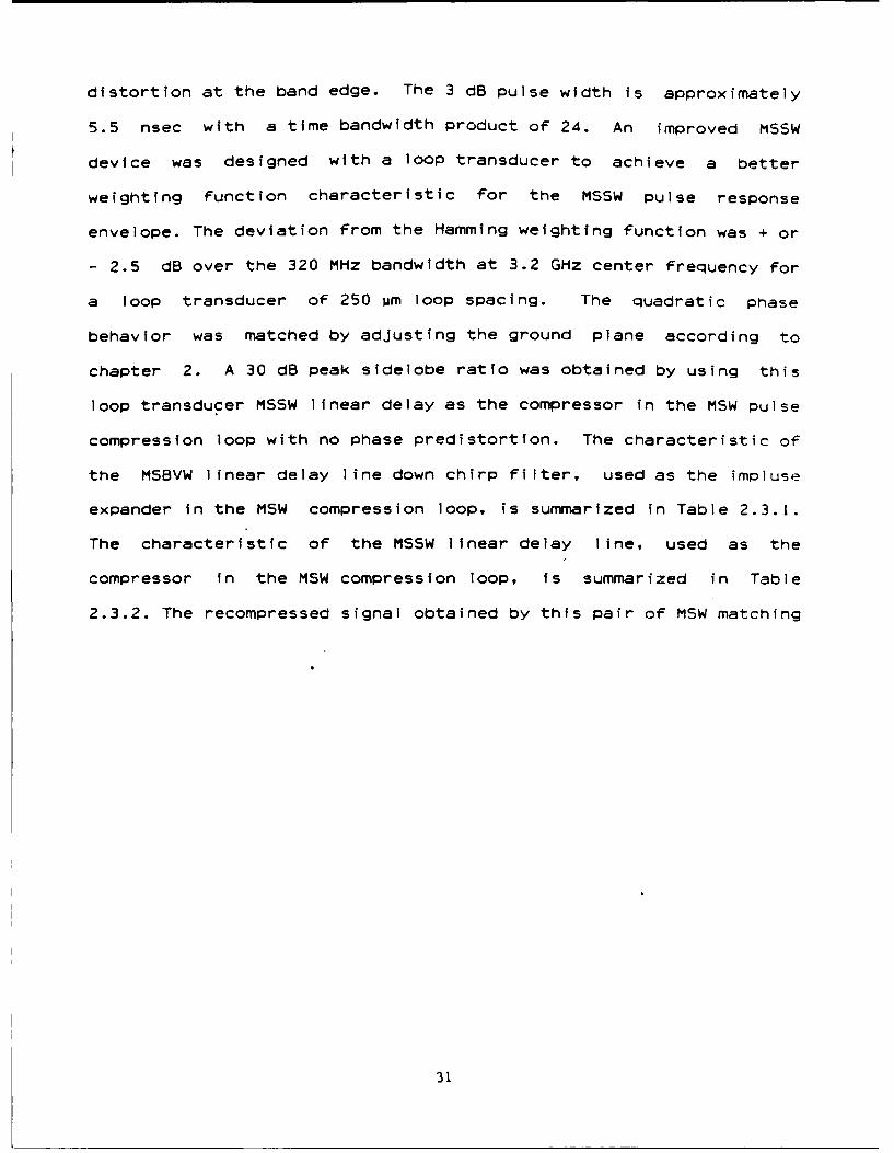
13, 15 and 25. From the results shown In Figure 3.5, it Is clear
that for a given bandwidth there is an optimum number of
transducers. Increasing the number of bars beyond this point will
not Improve the response of the filter any further. Figure 3.6 Is
the theoretical response of a 21 bar transducer programmed to be a
100 MHz bandpass filter centered at 2.8 GHz with sidelobe
suppression of 100 dB. As can be seen the maximum theoretical
51
a) 0
0
m 1- 0
Cu
0>.aJo
4.J .i~
, a,
C4r
100 ISO 200
52
m m m~ m m m m m mm mm Cu -4m 'm m m ImIm a~ a ml m m ia

ta..
53.

0
2 0Hz 3.5
-70 L.. . .
2.5 OHz 3.0
Figure 3.6 The theoretical frequency response and its expanded form ofa 21 bar filter designed to have a bandwidth of 100 MHz,centered at 2.8 GHz and to have a sidelobe suppression of 100dB.
54

sidelobe suppression is about 30 dB.
This synthesis program outputs the normalized current weighting
factors (-1<a<+) and does not determine or depend on the technique
being used to achieve the weighting. To experimentally check the
synthesis program, four sets of devices were constructed (named
CHECK5-A, CHECK5-B, CHECK7-A, and CHECK7-8) which are shown in
Figure 3.7. In all four patterns, the transducers were 3 mm long
and 30 um wide and the 50 Ohm transmission lines feeding each
element were equal in length for each device. This was done to
equalize the phase for each bar. The devices had either 5 or 7
bars at the Input and one at the output. MSW delay line is bilateral
so that the input and output can be interchanged when the direction
of the magnetic field Is changed. For tha two cases of CHECKS-B
and CHECK7-B the patterns were designed so two of the elements could
have current flowing In the opposite direction of the current in the
other bars.
In addition, different attenuators having different values were
connected to each port to control the current passing through each
finger. Using equal length 50 Ohm coaxial cables, the attenuators
were connected to an 8-way power divider where Its unused ports were
terminated by 50 ohm loads. A computer program ( Appendix 3) was
written to compute the insertion loss response of an N bar
transducer with external attenuators for current weighting. The
theoretical and experimental responses for these devices with
different cases are shown in Figure 3.8. These figures demonstrate
very good correlation between the theory and experiment.
The next step was to construct the filter and use a current
55

CHECK5-B CHECK5-A
CHECK7-B CHECK7-A
Figure 3.7 See text for explanations.
56

80'2 "a z 35
Figure 3. 8 The values of the external atternuators, the theoretical predtictionof the frequency response, and the experimental results forseveral devices with different configurations. (Notice the valuesof the attenuators given in dB for each case).
57

101
2 ONZ 35
Figure 3.8 continued.
58

-AOL
ON
Figure 3.8 continued.
59

Ir
Figure 3.8 continued.
60

In
0,
Values of the external attenuators (right), theoretical prediction (top-left),and the experimental results (bottom-left).
Figure 3.8 continued.
61

InL o
Values of the external attenuators (right),theortetical predition (top-left), and theexternal results (bottom-left).
Figure 3.8 continued.
62

a . 6 0 d8
Values of the external attenuators (top), theoretical prediction (middle),and the experimental results (bottom).
Figure 3.8 continued.
63

L
Figure 3.8 continued.
64

I..
Values of the external attenuators (top), theoretical prediction (middle)and the experimental results (bottom).
Figure 3.8 continued.
65

weighting technique that can produce any current weighting factor in
the range of -1 to +1.
The earlier method of weighting the transducer by thick and
thin gold plating has several shortcomings. First of all, It Is
practically limited by the precision of controlling the thickness.
Second, one can only achieve positive weighting factors, and even
then, It is impossible to have a practical current weighting of
zero.
To overcome these problems, another approach to the
distribution of current was taken by using an open gap transducer.
technique. In an open ended transducer bar the current at the
position of the gap is zero and increases in the sinusoidal form as
distance away from the gap Increases. If the length of the
transducer is very small in comparison with the wavelength, the
current distribution can be considered to be linear. If a transducer
is fed from both ends and a gap is placed In the center of the
transducer, the .net current of the transducer will be zero. By
varying the position of the gap along the length of the transducer,
It Is possible to have a normalized current of any value from -1 to
+1 (see Figure 3.9). Figure 3.10 shows the circuit pattern and the
frequency response of a 21 bar bandpass filter (named FILTER-A)
designed to have 100 MHz bandwidth centered at 2.8 GHz. Two other
designs (FILTER-B and FILTER-C) and their frequency responses are
shown in Figures 3.11 and 3.12.
All these filters seemed to work only at a single frequency and
when the tuning was attempted, the response became disturbed as
shown In Figure 3.13-d. The following explanation Is believed to
cause the distortion. As shown in Figure 3.13-a, in addition to the
66

SIN(X)/X current distribution of the transducer, there is also an
additional current distribution due to the transmission line feeding
the fingers. The combined effects are shown in Figure 3.13-b, and
the frequency response for this kind of current distribution is
plotted in Figure 3.13-c. This is very similar to Figure 3.13-d.
Effects of the addition of different types of current distributions
on the main SIN(X)/X curve are shown in a series of plots in Figure
3.14.
A power divider to distribute current evenly to each bar was
needed to overcome this problem. A simplified current divider was
used to design a 16 finger bandpass filter which is shown in Figure
3.15. The tuning capability of this device Is demonstrated in
Figure 3.16.
Next, to suppress the other harmonics of the filter, a loop
transducer was used instead of the single bar transducer. As shown
In Figure 3.17, when the response of a single bar-loop delay line
(curve # 2) is superimposed on the frequency response of a weighted
multibar-single bar filter (curve # 1), the result is suppression of
the harmonics (curve # 3). The procedure to theoretically calculate
the loop-multibar response follows. First, program I of Appendix 2
Is run for single bar-single bar mode. Then the same program is run
for loop-loop mode. The two outputs are then used by program 4 of
Appendix 2 to obtain the linear frequency vs. insertion loss
response of single bar-loop delay line with zero path. The last
data can now be used for synthesizing a filter in the manner
described earlier. Figu!'e 3.18 shows the circuit pattern and a
photograph of the constructed 16 bar filter with loop transducer.
67

GCuarrent W 0 3fht I n-i;
7I
Average CurrentCurrent Distribution in -an open transducer
Current weighting of an open circuited gap transducer assuming O<«A.
0. DO
I CI 1 0
Catrrnt Weis),ting ir kte form Of i1 ) in 1 1.6 erementfi ;ter.
Figure 3.9 Current Weighting Filter
68

C F: 2.4 GHzA F : 1.5 0Hz
Figure 3.10 The circuit pattern and thp frequencyresponse of FILTER-A.
69

.OX.X
{ I I.II
/ II[, ,
2 GHz 4
Figure 3.11 The circuit pattern (TOP), theoretical (MIDDLE) and theexperimental response (BOTTOM) of the device FILTER-B. Theresponse is amplified to show the suppression of the sidelobes.
70

e*F
Figure 3.12 The circuit pattern (TOP), theoretical prediction (middle) andthe experimental response (bottom) of FILTER-C. The output is amplifiedto show sidelobe suppression.
71

+t
+% * 044,4*0+o
'-- +
Fiur 3.1 Il curn i*rbt fth igr n h edr(13 1) cobndt0omacretdsrbto hw nfgr3b
Fxigena .3Tecurretdscrio of thedeietndaa fngey defeeer
from the one designed for.
72

;+ %2 \
4. .4 .
*+
4 ----
AIV
2 Hz 3.6Figure 3.14 The theoretical predicltion of t~he frequency response of
a 100 MHz bendpass filter when the feeders contribute tothe main SIN(X)/X current distribution. (3 differentcombinations are being considered.)
73
.

% /% ,,•
Figue 3.14 contnued.
74

0 +
* ' O
+
: : : : - I ' . . 4 ..,
#.""A
4p +0
Figure 314 continued.
75

Figure 3.15 The circuit pattern of a 16 bar bandpass
filter with a simplified power divider.
76

:235 - 420C
340 .65
,'49C
2.5 4
390
25 4
Figure 3.16 The frequency response of tiie filter shown in Figure 3.15,tuned at different frequencies by varying H from 235 to500 Oe.
77

Figure~ ~ ~ ~ ~~~~~A 3.7CmiigtefeunyrspneoI utbrsn a
fitrwt- ige a-opdlylne(O)cnrsl
Figre3.1 min n hpe feqenyrepos of ah hulrbar-inilsba
78 _

Circuit pattern of the 100 MHz tunable bandpass filter.
Photograph of the constructed 16 element bandpass filter.
Figure 3.18
79

The frequency response and its tunability are shown in Figures 3.19
and 3.20.
To improve the insertion loss, an attempt was made tc narrow
band match the power divider. The pattern and the frequency
response is shown in Figure 3.21. As can be seen an improvement of
about 10 dB can be achieved by having a matched power divider.
Another filter was constructed with transducer length of 5 mm and was
operated at higher frequency (4.5 - 5.5 GHz). The theoretical and
experimental responses are shown in Figure 3.22. With this device,
the minimum insertion loss was as low as 6 dB.
A matched power divider, was needed to gain information about
the transducer coupling at different frequencies and with different
lengths of transducer being under the YIG. A single bar I/0 delay
line was used. The S response of the device at 2 GHz, 3 GHz, 4
GHz and 5 GHz are shown In Figure 3.23 as points A through D. In
this case the YIG was on the entire 3 mm length of the transducer.
Next, the effect of transducer length on S 1 1 was investigated by
using 25 um thick YIG covering 3 mm (point 0), 2 mm (point E), I mm
(point F) and 0 mm (point G) of the transducer operating at 5.0 GHz.
As shown In these two figures, constructing a matched power
divider is a difficult task because of the complexity of the load on
each transducer.
Finally, instead of a single bar in output, the same filter
pattern was used both in the input and the output ports. The
theoretical response of this kind of filter Is compared with the one
which has single bar as an output (Figure 3.24). As can be seen,
theoretically it is possible to suppress the sidelobe as much as 45
80

-I
1.5 0.1 GHz/div 3.0
Theoretical prediction of the I.L. vs frequency.
0
1.5 0.15 GHz/div 3.0
The experimental I.L. vs frequency response of the device.
Figure 3.19
81

2.0 0.1 GHz/div 3.5
The theoretical simulation of the tunability of the filter.
The experimental results of the filter tuned at different bias fields.
Figure 3.20
82

C=0O3PF
Narrowband matching circuit.
2O GM 3.5
Improvement of the minimum insertion loss.
Figure 3.21
83

OUT
MICROSTREP CIRCUIT
Figure 3.22 The circuit pattern of the 16 finger filter with 5 mm. transducerlength (TOP) and its theoretical simulation of frequency responsein tunning (BOTITOM-LEFT) and the experimental result(BOTrOM-RIGHT).
84

..........
.........
>5Q5x
................
.. .........
Y ... ... .. .
Figure 3.23 TOP- the measured S11 of a single bar delay line with the YIG coveringentire length of the transducer and tuned at 2 0Hz (point A), 3 0Hz(point B), 4 0Hz (point C) and 5 0Hz (point D).BO'TTOM the measured S, , response of the same device tuned at 5 0Hzwith the YIG covering entire 3 mm transducer (point D), covering2 mm (point E), covering I mm (point F) and removed (point 0).
85

0 r~
B1
I I
-100 3.5
2" 0
dB
2 3a5
Fiqure 3.24 The theoretical frequenc:-I.L response of a multibar-single barfilter (top) and multibar-multibar filter (
86

dB. But when a device was made (Figure 25) with a semimatched power
divider, the results were not satisfactory. A paper describing the
theory and the experimental results of the first MSW transversal
filter based on the work described so far, was presented at the
IEEE-MTT (1986) meeting and was published In the proceedings of that
meeting. A copy of this paper Is given in Appendix 4.
87

S..... ...........
-I
- ,.. .........
K,, I A v- o.... .. ....... . V.. .. ... ...
--I , .-.
ss5ae 3800 400 42013 4 60 5~o ao 900
-RE-;UENC iH
-40
G I
N ..
.=o iI p
4 000 4600 4 7- 40 49 00
FPCUENCr M z)
Figure 3.25 P:,otograph of the device with synthesised filter patternboth in the input and the output, and the frequencyresponse.
88
... .... ......

4 DELAY L I NES
4.1 S Band Linear Delay Line The research for the
construction of linearly dispersive MSSW delay line was continued.
Several attempts were made for miniaturization of the device and
Improvement of Its Insertion loss and group delay. One of the
devices is shown in Figure 4.1 along with the measured Si, and S2 1
responses.
The magnet package shown in Figure 4.2a, provided by Rockwell
International was designed to house the MSSW delay line. It had a
constant field of 400 Oe at the center. The device ( Figure 4.2b)
was designed to have the transducers located in the center of the
device. Figure 4.2c is the photograph of this device with the
graded ground plane and the YIG placed on it. Figure 4.3 shows the
Insertion loss vs. frequency response in the frequency range of 2.4-
3.9 GHz (top-left), the reflection coefficient (S1I) for 2.8-3.2 GHz
range (top-right), and the phase - magnitude response in the 2.9-
3.15 GHz range (bottom).
Several graded ground planes were tested and the R.M.S.
deviation from quadratic phase for different frequency ranges were
calculated. The results are shown in Figure 4.4.
Our earlier experience had shown that a few dB improvement in
the insertion loss can be achieved If the graded ground plane and
the ground block are both gold plated, and If Indium solder Is used
for grounding the A] 20 3 substrate Instead of silver paste. In the
final stage, when the repeated measurements of the Insertion loss
response and the group delay was satisfactory, the graded ground
plane was permanently soldered to the block and the YIG strip was
89

'igure 4.1 Phocograpih ) -racihd MSSW Ja lineplane (TOP), S, :n the requc ra3n e of 3- 3.3(BOTTOM-LEFT) , and S- for 5.~- *jdZ (O:M~2
90

91

S2 17 S1 ,
S21 S 11
Figure 4.3 S-),, in the frequen~cy range of 2.4-3.9 GkRz -nd SlH fo~r
3.2 GHz (TOP) and phase-miagnicude response for 2.9-3.15 G*Hz
range (BOTTO"M).
92

* .2i o.5| * | .-2 b. i... i
".. Ze TION room QUAISSTIz 0"19 ts:
t* -.4 ? .IS 4A. 54.134 I12)55 C.I
S IQiI€*.Z4-.5K * )I(..O 0 '+T .i *.N .S. S IV K A Yt 0 X ,I OA SA V ~IC *..*1( S : ;0 1
3. aces 26VAIOSTle PROP QUADRAT)IC P"Ac Is
.a160 To 30214 CI
I NI. .lg 4,o
.a OTNI ~n., a|IA~ON UADRTC PWS1 s: 1.2994
93KS 30# 1-24.70
.ew. Z.5se YO 3.:10 CHI
/ 't . 63I.'Ii, 3.-414.t364
VMS I.R.I. DSVIATTOM PRO" OAUaANTIC Owass iS: 13.110
3.We 2.*10 l- 1 M CHIS
A.o r mU.I I. -30S.4 is: 31.61)4
I.M. 2 .1.0 TO 3.163i CHI
V Ma I.R.S. DEVIATIOM rooR OUADRATIC 0.A2C K: 19.4192
S.W. is.e V j.5 CHIt
.Mi 5.A.l. SIVtAV|O ASO St0 S AIC 'MASS IS: is.*fe43O0.IS .UO....e
1 Sw. zieeil tlse CHI
VMS M.M.S. SEVIATION ABOf OUAIISVKC AMAS KS: 14.044• eee ;
Fiur A* Ti.me'4 da eo at liarVMS I.R.S. BSVIAVKO. AfA QUADIAVIC *.A55 KS: I5.e152
*. 1460 .? .SSO ....A. 44.3514 5.-|3l.5g5
t
Ph.(OUAAI)I. 5A. V-t3.*( -oF-W3)
VMS I.R.S. SSVIATKOM 'ION OUNI1AVIC R A1 KS: 5.1520
0N0 3|,He 3.5450 VO 3.2l3e CM:
_____________e_______________A 9?.1491 II-1t3.53IPtMA*.I3UAIKC).. sOaIIp-O-I*-Ii.)
2036.106 'ge.Il Mfq:.-lV 3210668 * VMS I.R.S. SIVIAVKOM IO OUASIATTC +AAS KS: ;1.5431
Figure 4.4 Time delay response and analy$iS of the linearity of the
group delay ffor several types of graded ground planes,
93

s~aeee 4
B.W= 2.8000 TO 3.0550 0HzA= 181.4271 B-470.4292PhaseQUADRATIC)=.5A(P 2 .F02)B*(FFo)THE R.M.S. DEVIATION FROM QUADRAT1C PHASE IS: 20.8681
B.W= 2.8500 TO 3.1850 GHzA= 154.2979 B-390.4362PhaseQUADR.ATIC)-.5A(F 2-F02 ).B(F-FO)THE R.M.S. DEVIATION FROM QUADRATIC PHASE IS: 7.5878
B.W= 2.9000 TO 3.1550 0HzA- 133.6094 B-328.6460PhaseQUADR.ATC)-.5A(Fa.FO2 )-B(F-Fo)THE R.M.S. DEVIATION FROM QUADRATIC PHASE IS: 13.8825
B.W= 2.9450 TO 3.2000 0HzA- 112.3049 B--264.0575PhmssQUADRATC-.A(F 2 F0
2 )-B(F-Fo)THE R.M.S. DEVIATION FROM QUADRATIC PHASE IS: 16.0892
Figure 4A contimud.
94

secured with glue applied at both ends. This linearly dispersive
(positive slope) MSSW delay line was intended to be cascaded with
another linearly dispersive (negative slope) MSBVW delay line to
produce an electronically tunable constant delay line. The MSBVW
device was constructed at Rockwell International. A paper
describing the theory of operation and the experimental results was
presented at the Phased Arrays, 1985 Symposium and was also
published In the 1986 March issue of the MICROWAVE JOURNAL. A
reproduction of this paper is given In Appendix 5.
4.2 Ka Band Delay Lines To explore the usefulness of MSW
devices at higher frequencies, the response of simple delay line at
Ka band (26.5-40 GHz) was investigated. The first sample was an
open ended single bar I/O delay line with transducer length of 3 mm
and 10 um width constructed on quartz substrate.
Figure 4.5 shows photographs of the 521 for the zero line (no
device) and also the direct break-through (device with no H field).
Figure 4.6 Is the frequency response of the device operated in the
forward volume wave mode for different YIG widths and different
positions. The same procedures are repeated for the backward volume
wave mode and the results are shown in Figure 4.7. All the pictures
in Figures 4.5, 4.6 and 4.7 were taken for center frequency of 27
GHz and frequency sweep of I GHz with 50 um thick YIG.
The tunabflity of the device in the frequency range of 27 GHz-
33 GHz Is shown Is the series of photographs displaying S11 and S12
in Figure 4.8. For these pictures the 1.5 mm wide and 50 um thick
YIG covered the second half (close to the transmission line) of the
3 mm long trarsdjcer. For a!! the p'vu-s the frequency sweep was i
95

CF 27 GHz
Figure 4.5 S), r,sptonse for zero ',ie (no duvicc2 aind direct-tlr,,ou:i(d.±\Kce w4ithout tht! f ield).
96

NO - ) LC(S1 - SW*S.NO ILE!,[) -
.2. TNED -
D LEVICE. TUNED-
C F 2 7 GHAF 1
Figure 4.6 I.L vs frequency response for different YIG widths and po'sitionsfor MSFVW mode.
97

S21 - NO DEVICE_
S1I - DEViCE, NO FIELD -
S21 - DEVICE, TUNED
Figure 4.7 Same as Figure 4.6, but for MSBVW mode.
98

CF 27GHzH
CF 29H Qck
Figure 4.8 S I Plw t r 1i1 j t: s2 S. I
va r-,u ii
1 i I t : * L *c ~ V .A F1 I0Hz
99

CF
H
CF
H ~i~
CF 33
H I I
Figure 4.8 Con t i ntwd.
1.00

GHz. The second device was a 150 um loop I/0 delay line (with I
mm center/center spacing) constructed on quartz substrate. A
photograph showing the pattern and also the frequency response of
the device is shown in Figure 4.9. In the picture showing the
response, the top line Is the zero line, the bottom line is the
direct break-through and the middle line is S21 of the device, all
in the frequency range of 27.5-28.5 GHz operated in the MSFVW mode
with 50 um thick YIG.
After subtracting the zero line from the S2 1 of the MSFVW mode
In the frequency range of 27-29 GHz, a sample plot of insertion loss
vs. frequency for another device is shown in Figure 4.10. This
figure shows there is a promise of designing MSW delay lines at high
frequencies.
Another device (Figure 4.11) was designed with open ended
transducers of width 30 um and length 4 mm. In order to reduce the
mismatch, special semi-rigid cables with type K connectors were used
to Interface the device with the test Instrument.
Several experiments were performed with YIG strips oF different
thicknesses and widths, and positioned at various places on the
transducers. The results showed that narrower strips (less than
I mm) with YIG thicKnesses > 50um positioned 2/3 of the way away
from the open end of the transducer resulted In the lowest insertion
loss and the smoothest response. Figure 4.12 shows the insertion
loss vs. frequency and phase response operated In the MSFVW mode.
The pictures are for the center frequency of 30 GHz and a bandwidth
of 1.5 GHz. For the same center frequency, but with the sweep
bandwidth of 500 MHz, the magnitude and the phase responses in the
same mode are shown In Figure 4.13. The magnitude and the phase
101

responses of the device operated in the forward and reverse modes
of MSSW are shown In Figures 4.14 and 4.15, respectively.
102

5- SUMMAFRY
In summary the primary accomplishments of this final program
period have been:
1. A variable time delay device with an R.M.S. phase error of
a5 low as 6.400 R.M.S. has been built and tested. Time variation of
42 nsec was achieved, the design proceLures for dispersion control
utilizing a variable and backward wave delay line with linearized
dispersiun, and thus matched dispersive line have bcen developed
with significant potential in signal processing applications.
2. The current weighting technique using open gap transducers
to realize MSSW filters, has demonstrated good correlation between
the theoretical prediction and measured response. Using this
technique, filters were realized. Tunable bandpass filters with
sidelobe suppression greater than 20 db and passband ripple of less
than 3 db, and insertion loss of 6 db have been realized.
3. Ka Band delay MSFVW lines with insertion losses of less
than 16 db and bandwidth of greater than I GHz have been realized.
103

1
ZERO LINE -
S2--
DIRECT TH-RU
CENTER F=28 GHz
SWEEP -1 GHz
Figure 4.9 Photograph of loop-loop delay line and its frequency responsein the MSFVW mode.
104

• / " , '4 r
LM
- II
2 29
27.00 Z7.41 27.80 28.-0 28.90 2.1. 00
FREQUENJCY (GHz)
Figure 4.10 Plot of I.L vs F for device operating in the MSFVW modecorrected for the zero line.
105

Figure 4.11 Photograph of open-ended single bar I/0 delay line.
106

0 F 3C,
AF 1.5
H 12 .1
Figure 4.12 [1 . v - F i~nd thet piic.--, response of rhe c: cinthe >ISFVW% rwdc.
107

CF 3
Figurp 4.13 The expanded view of Figure 4.1.2.
108

CF 27
A F 0).4
H 8.6
Figure 4. 14 :i~nit2;,id t!hL p;):.;e of rile devi ck'L .
109

CF
Figure 4.15 >.2 t~C:11 Il~

6.0 PUBLICATIONSFROM AFOSR SUPPORT
1. R. L. Carter, C. V. Smith, Jr., and J. M. Owens, "MagnetostaticForward Volume Wave-Spin Wave Conversion by Eteched Grating inLPE-YIG," IEEE Trans-Mag, Vol. Mag-16, 5, 1159-1161, September 1980.
2. J. M. Owens, "Magnetostatics Join SAW's" Microwave Systems News,May 1980 v. 10, No. 5, pp. 112-113.
3. C. V. Smith, Jr., J. M. Owens, R. L. Carter and J. H. Collins,"Magnetostatic Waves, Microwave SAW," Ultrasonics SymposiumProceedings, IEEE Cat. No. 80CH1602+2, pp. 506-513, November 1980.
4. J. C. Sethares, J. M. Owens, C. V. Smith, Jr., "MSWNon-dispersive, Electronically Tunable Time Delay Elements,"Electronics Letters, Oct. 1980, V. 16, No. 22 pp. 825-826.
5. J. C. Sethares, C. V. Smith, Jr. and J. M. Owens, "MSW TimeDelays," Symposium Proceedings, IEEE Cat. No. 80CH1602-2, pp.518-521, November 1980.
6. J. M. Owens, R. L. Carter, C. V. Smith, Jr., and G. Hasnian, "A3-Port Model for Magnetostatic Wave Transducers," SymposiumProceedings, IEEE Cat. No. 80CH1602-2, pp. 538-542, November 1980.
7. W. R. Brinlee, J. M. Owens, C. V. Smith, Jr., and R. L. Carter,"Two-port Magnetostatic Wave Resonators Utilizing Periodic MetalReflective Arrays" J. Appl. Physics, 52, 3, 2276-2278, March 1981.
8. J. M. Owens, C. V. Smith, Jr. and R. L. Carter, "The Status ofMagnetostatic Wave Devices," 35th Ann. Freq. Control SymposiumUSAERADCOM, Ft. Monmouth, N. J. 077030, 358-363 (1981).
9. R. L. Carter, J. M. Owens, W. R. Brinlee, Y. W. Sam and C. V.Smith, Jr. "Tunable Magnetostatic Surface Wave Oscillator at 4GHz," 1981 IEEE .TT-S Symposium Proceedings, Cat No. 81 Ch 1592-5,pp. 383-385, June 1981.
10. C. V. Smith, Jr., J. M. Owens, N. D. Parikh and R. L. Carter,"Anisotropic Propagation of Magnetostatic Waves in Epitaxial YIGFilms," IEEE Trans. Magn., Mag-17, 2967-2969 (1981).
11. R. L. Carter, J. X. Owens, C. V. Smith, Jr., and K. W. Reed, "IonImplanted Magnetostatic Wave Reflective Array Filter," J. Appl.Phys. 53, 2655-2657 (1982).
12. R. L. Carter, J. 1. Owens, C. V. Smith, Jr., and K. W. Reed, "IonImplanted Oblique Incidence Magnetostatic Wave Reflective ArrayFilters," 1982 IEEE MTTs Microwave Symposium Digest #82 CH 1705-3,pp. 83-85, June, 1982.
111

13. G. F. Manes, and J. M. Owens, "Microwave Signal Processing UsingMagnetostatic Wave Devices," Alta Frequenza No. 2 VLI, pp. 103-106,(1982).
14. J. M. Owens, C. V. Smith, Jr., and R. L. Carter, "MSW ReflectingArray Filters," Proceedings of the the 1981 RADC MicrowaveMagnetics Technology Workshop, RADC-TR-83-15, Rome Air DevelopmentCenter, Griffis Air Force Base, NY 13441, pp. 106-116 (1983).
15. C. V. Smith, Jr., J. M. Owens, R. L. Carter, and K. W. Reed,"Microwave Pulse Compression Loops Using Magnetostatic Wave DelayLines," Proceedings of the 1981 RADC Microwave Magnetics TechnologyWorkshop, RADC-TR-83-15, Rome Air Development Center, Griffis AirForce Base. NY 13441, pp. 277-289 (1983).
16. J. M. Owens and R. L. Carter, ".agnetostatics Advance: The Shapeof Things To Come," Microwave System News, V. 13 No. 3, pp. 103-111(1983).
17. K. W. Reed, J. M. Owens, R. L. Carter, and C. V. Smith, Jr., "AnOblique Incidence ion Implanced IISFVW RAF with Linear Group Delay,"1983 IEEE MTT-S international M!icrowave, IEEE Cat. No. 82CH1871-3pp. 259-261.
18. J. M. Owens, R. L. Carter, and Y. Y. Sam, "A Hybrid GaAs MICOscillator Using a Magnetostat:c Wave Resonator," 1983 IEEE MTT-SInternational Microwave Proceedings. IEEE Cat. No. 82CH1871-3 pp.323-326.
19. J. M. Owens and R. L. Carter "The Status of Magnetostatic WaveResonator Oscillators, 1983 Frequency Control SymposiumProcceedings, pp. 477-480 IEEE Cat. No. CH1957-0/83/0000.
20. Kok Wai Chang, J. M. Owens, R. L. Carter, "Linearly DispersiveTime-Delay control of Magnetistatic Surface Wave by Variable GroundPlane Spacing" Electronics Letters V. 19 No. 14 (July 7th 1983) pp.346-347.
21. Kok Wai Chang, L. R. Adkins, R. L. Cacter, H. L. Glass, J. M. Owensand F. S. Sterns, "Electronically Variable Time Delays UsingCascaded Magnetosratic Delay Lines," accepted for publication in J.Appl. Phys.
112

APPENDIX I
"FILTER SYNTHESIS THEORY"
113

0'
'3 20
AAw)
40
iCA 60
2 5 2.7. 2.9 3.1 3.3 3.5
Frequency f (GHz)
The frequency response for a zero path single bar 1/0transducer, A(w), and the desired response of a multibarbandpass filter, H(w).
) N N -K (wn9G (w) = - - Zn=I anAQ )eWn (1)
G(w) -array response
N -number of transducer elements.
n(w) -nth element response.
an -weighting factor for the nth element.
A(W) -transmission response of a single-bar/single-barzero-path delay line.
K(w) x+j B (CL and Bare loss factor and wave number,respectively).
n -path length for the nth element.
R(W) -desired frequency response.
"14

(02- ~l (1 n=Ian- (c ).
1 fWo)Zn~an H(o)eZl..aAW- (W
W2 W1 W1 AN - - K ) nx ( H (o) - Z n =1 anA (o)e )d (2)
+C 0)2 (0 *"
; 6) I e- K (co))t.r
N -K (0) In
x (i~o) Z n =I anX(Oe c 3
(0)&K(0Re A " (cooe" (c) -/o Imr
a 0)270 1 *
n a f c
_ .. =-2 {Re Ac)~)e K {)Id
am R 2-' 1 ;
N co 2
Q i =Real I)eK co) I2
11
xe -[K W)I+K()m -K 0tl (4
Q i=Real f }H (e dw
115

APPENDIX 2
"LIST OF THE PROGRAMIS FOR SYNTHESIZING BANDPASS FILTER*
116

PROGRAM #1
C MSSV DISPERSION RELATION CALCULATES 152 W-K POINTS AND 305 W-K -C POINTS FOR HILBERT TRANSFORM INTEGRATIONC MSSW DISPERSION RELATION, GROUP VELOCITY AND TIME DELAY,PHASE VEL.C DESIGNED FOR STRUCTURE A/ B, REVERSE (+/-) DIRECTION
C EDITTED AND MODEFIED ON 7/24/84. Y.J. ATAIIYANDIMENSION FRQ(152).RK1(152),RK2(152),TM1(152),T 2(152),QF(305),QK1
1(305) ,QK2(305)DIMENSION RI1(152),RI2(152),RIC(152),XI1(152),XI2(152),
1XIL(152) ,TO1(20)DIMENSION Rl(152),R2(152),RMX1CL52),RnX2(152),XMX1(152),
1XMX2(152) ,QRM(305) ,QRN(305) ,FQN(152) ,'AVL(152) ,ILIIA(152) ,ILMB(152)DIMENSION FQ(152),TD1(152),TD2(152),XILMA(152)REAL ILMA,ILMBREAL'8 VP1 ,VP2,RKF,RKR,T11,TM2REAL'S FRQ,R1,R!,QF,QK1,QK2,FRQ3,FRQ4,FRQ1,FRQ2,DF,RFRQ,QRM,F,ZF,R1Kl,RK2,QRN,R!VU,.,RMX2,ARGUE,H1,H2,H3,SUH1,SUM2,SUM,SIMP2,RMRM1,RM21 ,RND,OH,RN,RML2,XIIL2,GM,XMX1 ,XIIX2REAL'S FQ,R22,TD2,XM1,XM2,XM,EK,1ZCBETAIIAC,AR,AR1,AR2,AX,AX1,AX2,CZC,CBT.CAC,CAR,2CXM,ALPH,AL,BL,RIN,XIN,RIl,RI2,RIC,XI1,XI2,XIL,PT1,PT2,CL1,CL23,XL1 ,XL2,X,CSTREAL'S T,OW,RNlIAX,PN,U1,U2,AU1,AU2,1RK,RKS,RD,RT,BT,FT,DELT,EXT,A,B,C,D,PC,Pl,P3,P21,P22,P2,P,,DET1,DET2,E,G,RTT,RTU,TTRllREAL'S SSECHREAL'S DELTF,A1 ,A2,RTL,RT1 ,TL,,Tl,DL,DL ,FL,F1,TX,DX,FX,VOV1,V7,V3,VG1 ,VG2,TDD,TDTCOMMON F,RKF,RKR,RM1,RM2COMMON DO,TO,BO,RLGH,TU,SO,UOCOMMON HI,GA,JCONF,NMAX,FPMDSECH(X)-DSQRT(1.-DTANH(X)'DTANH(X))
C *** DEFINITION OF THE TERMS " " " " ~ " "
C DO=YIG THICKNESS (METERS)C TO= AL203 THICKNESS("C BO= TRANSDUCER WIDTH (C RLGH= TRANSDUCER LENGTH("C TU= YIG/TRANSDUCER AIR GAP()C SO- SEPARATION BETWEEN TRANSDUCERS()C UO- 7!!!C HI= SIAS FIELD (OE)C GA. GYROMAGNETIC RATIO (HZ/OE)C ZO.. CHARACTRISTIC IMP. OF THE TRANSDUCER.C SO=WAVELENGTH AT CENTER FREQ. IT DOES NOT HAVE ANY EFFECTC ON SINGLE BAR, FOR LOOP TRANSD. SPACINGS ARE SO/2, FORC PARALLELL IT IS EQUAL TO SO.C CONDITION JUMP ON TRANSDUCER CONFIGURATIONS (1 FOR SINGLE BAR, 2C FOR PARALLEL ODD BARS, 3 FOR PARALLEL EVEN BARS, 4 FOR MEANDERC STRIPS, 5 FOR PI 0.5 CENTER SPACING, 6 FOR PI 1.5 CENTER SPACING)C NMAX IS THE STRIP NUMIBER FOR MSW TRANSDUCERSC INPUT THE FILE NAME FOR STORING THE DATA
117

OPEN(UNIT=23 ,DEVICE='DSK' ,DIALOG)TYPE 1200
1200 FORMAT(11,'ENTER YIG AND ALUMINA THICK IN MICRON')ACCEPT 1201,DO,TO
1201 FORMAT (2F)DO-DO*1 .OE-6TO-TO' 1. OE-6
FPM=1750.TYPE 1202
1202 FORMAT(1X,'ENTER EXT H FIELD')ACCEPT 1203,HI
1203 FORMAT(1F)GA-2.8E6GM-GA*FPMTYPE 1204
1204 FORMAT(1X,'TYPE WIDTH AND LENGTH OF TRANSD. IN MICRON')ACCEPT 1201,BO,RLGHTYPE 1210
1210 FORMAT(1X,'ENTER I/0 TRANSD. SPACINGS IN CM')ACCEPT 1203,PATHPATH-PATH*1 .OE-2TYPE 1205
1205 FORMAT(lX,'ENTER AIR GAP(MICRON), AND LAMBDA AT CENTER'*,'FREQ. (MICRON)')
ACCEPT 1201,TU,SOBQ=9O*1 .OE-6RLGH-RLGH'1 .OE-6TU-TU'1 .OE-6SO=SO*1 .OE-6
UO=1 .25663 7E-6TYPE 1206
1206 FORMAT(11,' ENTER CHARAC. IMP. OF TRANSD (ZC))ACCEPT 1203,ZCTYPE 1207
1207 FORMAT(1X,'ENTER COND CODE AND * OF TRANSDS (I I))TYPE 1208
1208 FORMAT(1X,' CC FOR SINGLEai, PARAL ODD=2, PARAL EVEN=3*,MEAND-4, .5 SPACING PI-5, 1-.5 SPACING PI=6')
ACCEPT 1209,JCONF,NMAX1209 FORMAT(2)
TYPE 12331213 FORMAT(1X,'IL IN DB (TYPE 1) OR LINEAR IL (TYPE 0)
ACCEPT 1214,NYJA1214 FORMAT(I
OH-HI /FPMFRQ3=DSQRT(OH'(OH+1. ))*GMFRQ4u(OH+ . 5)*GMFRQIuFRQ3*1 .01FRQ2uFRQ40.99
C FREQUENCY SAMPLING 305 POINTS FOR HILBERT TRANSFORMQF(1 )-FRQ3QF(3)=FRQ1QF( 2)=O. 5*(FRQ3+FRQ1)QF(103)=O.5*(FRQ2+FRQ1)QF( 305)=FRQ4
118

QF( 303 ).FRQ2QF( 304)umO.5*(FRQ2+FRQ4)DF=(QF(103)-QF(3) )/100.ODO 100 1=1,99RI-IJ=I+3
100 QF(J)zQF(3)+RI*DFDO 101 1=1,199RI-IJ=1+103
101 QF(J)aQF(103)+RI*DF'O.5C FREQUENCY SAMPLING 152 POINTS FOR DISPERSION RELATION
FRQ( 1)=FRQ3+O. 75*(FRQ1-FRQ3)FRQ( 2)=FRQ1+O.5*DFDO 102 I=1,49RI=IJ=I+2
102 FRQ(J)=FRQ(2)+RI*DF*2.OFRQ(52)=QF( 103)+DF*O.25DO 103 1=1,99RI=IJ=52+1
103 FRQ(J)=FRQ(52)+RI*DFFRQ( 152)=FRQ2+O.25' (FRQ4-FRQ2)
C DISPERSION RELATIONDO 130 11-1,152F=FRQ(M)OW-F/GM
U1-1 .0-OH/(OV*OV-OH*OH)U2=OV/ (OV'OW-OH*OH)
C S=+i.Al=U1+U2+1.A2=U1-U2-1.
C REGI FALSI ITERATION TO FIND INITIAL GUESS FOR NEWTON ITERATIONRTL=O. 1*TORT1=l .0E5*TODO 20 1=1,500IF((I-500).EQ.O) VRITE(23,13)TL-DTANH( RTL)T1-DTANH(RT1)DL-DEXP(-2. 'DO'RTL/TO)Dl=DEXP(-2. 'DO*RT1 ITO)
FL-(U1-U2+TL) 'A1-(U1+U2-TL) 'A2'DLFlm(U1-U2+T1 )'A1-(U1+U2-T1 )*A2*D1
X-(Rfl'F1-RT1'FL)/(F1-FL)TX-DTANH(X)DX=DEXP(-2. 'DO*X/TO)
FXm(U1-U2+TX) 'A1-(U1+U2-TX)'A2*DXIF(DABS(FX)-1.OE-7) 51,51.31
31 CLX=FX*FLCUX=FX'F 1IF(CUX.GT.0.) RTl*XIF(CLX.GT.O.) RfLmX
20 CONTINUEC NEWTON ITERATION
119

51 D0 90 L-1,500IF((L-500).EQ.O) URITE(23,19)T2C-DTANH(X)DX-DEXP(-2.'DO*X/TO)
-FX-(U1-U2+TX)*Al-(U1+U2-TX) 'A2*DXDF=DX'A2*(+2. 'DO*(Ul+U2-TI) /TO+DSECH(X)**2)+A1*DSECH(X)**2IF(DABS(FX)-l.OE-lO) 92,92,91
91 X-X-FX/DF90 CONTINUE92 Rl1-X/TO
C PHASE VELOCITY, GROUP VELOCITY AND DELAY TIME CALCULATIONRKl(H)-R11FN1=FXTX=DTANH(X)DX-DEXP(.2. 'DO'X/TO)VO=3. 078760801D10'TOV1=DX'Al*(+2. 'DO'(Ul-U2+TX) /TO+DSECH(X)**2)+A2*DSECH(X)**2V2-( (U1+U2-TX)-Al*DX)/( (OV-OH)"*2)V3-(A2-(Ul-U2+TX)*DX)/( (OW+OH)**2)VGI=VO*V1/(V2-V3)
TDD=PATH/VG 1Tml(K)=TDDVPl=6. 283 185307*FIR1 1
C S=-A1=Ul+U2-1.A2=Ul-U2+1.
C REGI FALSI ITERATION TO FIND INITIAL GUESS FOR NEWTON ITERATIONRTL=O. 1*TORT1=1 .0E5'TOD0 209 1=1,500IF((I-500).EQ.O) WRITE(23,139)TL=DTANH(RTL)Tl=DTANH(RT1)DL=DEXP(-2.*DO*RTL/TO)D1=DEXP(-2. 'DO*RT1I/TO)FL=DL' (U1-U2-TL) *A1-(Ul+U2+Th)*A2F 1=01'(Ul-U2-T1 ) Al-( U1+U2+T1 ) A2X-(Rfl'F1-RTl'FL) /(Fl-FL)TX-DTANH (X)DX-DEXP (-2. 'DO*X ITO)FICOX' (Ul-U2-TX) 'Al-(Ul+U2+TX)*A2IF(DABS(FX)-l.OE-7) 519,519,319
319 CLX=FX'FLCUxaFx'FlIF(CUX.GT.O.) RTl=XIF(CLX.GT.O.) RTL=X
209 CONTINUEC NEWTON ITERATION
519 DO 909 L=1,500IF((L-500).EQ.0) VRITE(23,199)TX-DTANH(X)DX-DEXP(-2. 'DO*X/TO)FX-DX' (Ul-U2-TX)'Al-(Ul+U2+TX)'A2DF-DX*Al*(-2.*DO'(Ul-U2-TX)/TO-DSECH(X)**2)-A2*DSECH(X)**2IF(DADS(FX)-l.OE-lO) 929,929,919
120

919 X=X-FX/DF909 CONTINUE929 R22=X/TO
C PHASE VELOCITY, GROUP VELOCITY AND DELAY TIME CALCULATIONRK2(M)-R22FN2=FXTX=DTANH(X)DX=DEXP(-2. 'DO*X/TO)VO=3 .078 760801D10*TOVl=DX'A1' (-2. *DO*(U1.4J2,..)/TO-DSECH(X)**2)..A2*DSECH(X) **2V2-( (U1+U24TX)-Al*DX)/( (OV-OH)**2)V3=(A2-(U1--U2-TX)*DX)/( (OV+OH)**2)VG2=VO*V / (V2-V3)TDT=1 .OE-2/VG2T112(I1)=TDTVP2=6. 283 185307*F1R22
130 CONTINUEC HILBERT TRANSFORM V-K POINTS
DO 5130 M-2,304F-QF(M)OW-F /GZI
Ulmi .O-OH/(OV*OW-OH*OH)U2=OV/ (OH'OV-OH' OH)
C S=+1A1=UI+U2+1.A2=Ul-U2-1.
c REGI FALSI ITERATION TO FIND INITIAL GUESS FOR NEWTON ITERATIONRTL=O. 1*TORT1=1 .0E5*TODO 520 Ia1,500IF((I-500).EQ.O) VRITE(23,13)TL=DTANH( RTL)Tl=DTANH(RTI)DL=DEXP(-2. 'DO*RTL/TO)Dl=DEXP(-Z. *DO*RT1 ITO)
FL=(Ul-U2+TL) *Al..(U1+U2.TL) 'A2*DLFl-(U1-U2+T1 )*Al-(U1+U2-T1 )*AZ*D1
X=(RTL*F1-RT1*FL) /(F1-FL)TX=DTANH (X)DX=DEXP(-2. *DO*X/TO)
FX.(U1-U2+TX)'A1-(U1+U2-TX) *A2*DXIF(DABS(FXE-1.OE-7) 551,551,531
531 CLX=FX*FLCUX=FX*FlIF(CUX.GT.0.) RT1=XIF(CLX.GT.0.) Rfl=X
520 CONTINUEC NEWTON ITERATION
551 DO 590 L-1,500IF((L-500).EQ.O) VRITE(23,19)TX-DTANH( X)DX-DEXP (-2. *DO*X/TO)
FXa(U1-U2+TX) 'Al-(U1+U2-TX)*A2*DXDF-DX*A2*(+2.*DO*(U1+U2-TX)/TO+DSECH(X)**2)+A1*DSECH(X)**2IF(DABS(FX)-1.OE-10) 592,592,591
121

591 X-X-FX/DF590 CONTINUE592 RlX/TO
QK1 (M)-R11FN1=FX
C Sn-iAL=U1+U2-1.A2=U1-U2+1.
C REGI FALSI ITERATION TO FIND INITIAL GUESS FOR NEWTON ITERATIONRTL=O. 1*TORTl-1 .0E5'ToDO 5209 I=1,500IF((I-500).EQ.O) WRITE(23,139)TL=DTANH (RTL)Tl=DTANH(RT1)DL=DEXP(-2. 'O'RTL/TO)Dl=DEXP(-2 .*DO*RT1/TO)FL=DL*(U1-U2-TL)*Al-(Ul+U2+TL)*A2Fl=D1'(U1-U2-Tl)*Al-(U1+U2+T1 )*A2X=(RTL*Fl-RT1*FL)/(F 1-FL)TX=DTANH( X)DX=DEXP (-2. 'DO*X/TO)FX=DX*(Ul-U2-TX) 'A1-(Ul+U2+TX) 'AZIF(DABS(FX)-1.OE-7) 5519,5519,5319
5319 .CLX=FX*FLCUX=FX*F IIF(CUX.GT.O.) RT1=XIF(CLX.GT.O.) RTL=X
5209 CONTINUEC NEWTON ITERATION5519 DO 5909 L=1,500
IF((L-500).EQ.O) IRITE(23,199)TX=DTANH(X)DX=DEXP(-2. *DO*X/TO)FX=DX* (U1-U2-TX) 'Al-(Ul+U2+TX) 'A2DF=DX*A1'(-2.*DO*(U*.U2*TX) /TO-DSECH(X)**2)-A2*DSECH(X)*"2rF(DASS(FX)-1.OE-10) 5929,5929,5919
5919 X=X-FX/DF5909 CONTINUE5929 R22=X/TO
QK2(M)=R22FN2=FX
5130 CONTINUEC MSSW RADIATION IMPEDANCE RM AND XN/ RN AS A SUBPROGRAM, XMC CALCULATED FROM HILBERT TRANSFORM OF XM BY USING 2ND ORDER CLOSEDC FORM SIMPSON RULE FOR INTEGRATION
GM-GA' FPMOH-HI IFPMFRQ3=DSQRT(OH*(OH+1. ))'GMFRQ4u(OH+0.5)*GMFRQ1=FRQ3*1 .01FRQ2=FRQ4'O .99DF=(FRQ2-FRQ1 )/200. 0RFRQ-FRQ4/FRQ3QF(1)=1.O
122

QF( 305 )=RFRQQRM(1)=O.QRM(305)=O.QRN(1)=O.QRN(305)=O.DO 200 I=2,304FaQF(I)RKF=QKI(I)RKR=QK2( I)CALL PGRMQRM( I)=RM1QRN( I)=RM2QF(I)-QF(I)/FRQ3
200 CONTINUEDO 400 I=1,152F=FRQ(I)ZF=F/FRQ3RKF=RK1(I)RKR=RK2(I)CALL PGRMRMX1(I)=RM1RMX2(I)=RM2ARGUE=(ZF+1. )*(RFRQ-ZF)/((ZF-1.)*(RFRQ+ZF))RM=Rt1RN=RM2
C 2ND ORDER CLOSED FORM OF SIMPSON RULE FOR INTEGRATIONH1=(QRM( 1)-RM)/(QF( 1)*QF(1 )-ZF*ZF)I{2=(QRM( 2)-RM)I (QF(2)*QF(2)-ZF*ZF)H3=(QRM( 3)-RM)/(QF(3)*QF(3)-ZF*ZF)SUM1=(FRQ1-FRQ3)*(H1+4.*H2+H3)/(6.*FRQ3)Hl=(QRM( 3O3)-RM)/(QF(3O3)*QF(303)-ZF*ZF)H2=(QRM(304)-RM)I(QF(3G4)*QF(304)-ZF*ZF)H3=(QRM(305)-RM)/(QF(305)*QF(305)-ZF*ZF)SUM2=( FRQ4-FRQ2)' (H1+4 . H2+H3 ) /(6. *FRQ3)SUM=SUML +SUM2DO 401 K=1,50JK=2*(K+1)J1=JK-1J2-JK.1
H2=(QRM(JK)-RM) /(QF(JK)*QF(JK)-ZF*ZF)H3u(QRM(J2)-RM)/(QF(J2)*QF(J2)-ZF*ZF)SIMP2:DF'(H1+4.*H2+H3)/( 3.*FRQ3)
401 SUII=SUM4SIMP2DO 402 K=51,150JK=2*(K+1)J1=JK-1J2-JK+1
H2-(QRM(JK)-RM)/(QF(JK)*QF(JK)-ZF*ZF)H3=(QRM(J2)-RM)/(QF(J2)*QF(J2)-ZF*ZF)SIMP2=DF'(H1+4.*H2+H3)*O.5/(3.*FRQ3)
402 SUM=SUM+SIMP2XMX1(1)=0.318098862*(RM*DLOG(ARGUE)+2.*ZF*SUN)
C 2ND ORDER CLOSED FORM OF SIMPSON RULE FOR INTEGRATION
123

H2=(QRN(2)-RN)/(QF(2)*QF(2)-ZF*ZF)H3a(QRN(3)-RN)/(QF(3)*QF(3)-ZF*ZF)SUM1=(FRQ1-FRQ3)* (H+4 . *H2+H3 ) (6. *FRQ3)H1=(QRN(303)-R.N)/(QF(3O3)*QF(3O3)-ZF*ZF)H2a(QRN(304)-RN)/(QF(3O4)*QF(3O4)-ZF*ZF)H3=(QRN(3O5)-RN)/(QF(3O5)*QF(3O5)-ZF*ZF)SUM2=(FRQ4-FRQ2)*(H1+4.*H2+H3)/(6.*FRQ3)SUM=SUM1+SUM2DO 550 K=1,50JK=2*(K+l)JlaJK-1J2-JK+lHl=(QRN(Jl)-RN)/(QF(Jl )*QF(J1 )-ZF*ZF)H2=(QRN(JK)-RN) /(QF(JK)*QF(JK)-ZF*ZF)H3=(QRN(J2)-RN)/(QF(J2)*QF(J2)-ZF*ZF)SIMP2=DF*(H1+4 . *H2+H3) 1(3. *FRQ3)
550 SUM=SUM+SIMP2DO 555 K=51,150JK-2'(K+1)Jl=JK-1J 2=JK~1H1=(QRN(J1 )-RN) /(QF(J1 )*QF(J1 )-ZF*ZF)H2=(QRN(JK)-RN)/(QF(JK)*QF(JK)-ZF*ZF)H3=(QRN(J2)-RN) /(QF(J2)*QF(J2)-ZF*ZF)SIMP2=DF*(Hl+4.*H2+H3)*O.5/(3. 'FRQ3)
555 SUM-SUM+SIMP2XNX2(I)=O.318098862*(RN*DLOG(ARGUE)+2.*ZF*SUMI)
400 CONTINUEC mssw FREQUENCY RESPONSE PROGRAM TO CALCULATE TRANSMISSIONC LINE PARAMETERS, CIRCUIT ELEMENTS, INPUT IMPEDANCE, AND INSERTIONC LOSS
RN=NMAXND=NMAX/ 2RND=NDCST=l.DO 105 J=1,152F=FRQ(J)TM9uTh1 (J)Tl'8=ThM2(J)RMiaRMXl (J)RM2=RMX2(J)Xml=XmI1(J)XM2=XMX2(J)RM=RM1 +RM2XM=X1I1 +M2BETA-3 .636102608D-8*FAC=6. 32D-7*DSQRT(F)/(BO*ZC)RML2=RM*RLGH*O. 5XHL2-XM'RLGH'O. 5ARs . 5*RH/ZCARizO. 5*RM1/ZCAR2=0.5*RM2/ZCAX=O. 5'XH/ZCAX1=O.5*XN1/ZC
124

AX2= . 5*XM2/ZCGO TO (81,82,82,93,94,94),JCONF
81 CZC=1.CBT=l.CAC=1.CAR=1.CXM=1.GO TO 99
82 CZC=1./RNCBT=1.CAC=l.CAR-i. /RNCXM=1 ./RNGO TO 99
93 CZC=l.CBT=RNCAC=RNCAR=1 ./RNCXM= . /RNGO TO 99
94 CZC=1./RNDCBT=2.CAC=2.CAR=i /RNCXM= . /RN
C TRANSMISSION LINE PARAMETER MODIFICATIONS FOR TRANSDUCER ARRAYS99 ZC=CZC*ZC
BETA=CBT' BETAAC=CAC*ACAR=CAR*ARAR1=CAR*AR1AR2=CAR*AR2AX=CXM*AXAX1=CXM*AX1AX2=CXM*AX2ALPH-AR+ACBET=BETA+AXAL=2. *ALPH*RLGHBL=2. O*BET*RLGH
C INPUT IMPEDANCE AND CIRCUIT ELEMENTSRIN=ZC*DTANH(AL)/(l.+DCOS(BL)*DSECH(AL))XIN=ZC*DSIN(BL)*DSECH(AL)/(l.+DCOS(BL)*DSECHCAL))RI1(J)-R114'AR1/ALPHR12(J )=RIN*AR2/ALPHRIC(J)=RIN*AC/ALPHXli (J)=XIN*AX1/BETX12(J)=XIN*AX2/BETXIL ( J )XIN*DETA/BET
C POWER RATIO, CONVERSION LOSS AND INSERTION LOSSPT1=200.O'RI1 (J)/( (RIN+50.O)**2.+XIN**2)PT2=200.O*RI2(J)/( (RIN+5O.O)**2.+XIN**2)CL1=1O. *DLOG10( PTI)CL2=10.*DLOG10(PT2)XL1=2 .*CL1-76. 4E+6*Th9*CST' 1.5XL2=2.*CL2-76.4E+6*Th8*CST*1.5
125

IF(NYJA.EQ.1) GO TO 1215YOUNES=1O.**(XLI/20.)
GO TO 12161215 YOUNES-XLl1216 ILMA(J)=YOUNES
ILMB(J)=-2.*CL1FQN(J)=F/1 .E9WAVL(J)=2.*3. 14159/RK1(J)TOTRM=RMXI (J)+RMX2(J)TOTRK=RKL (J)+RK2(J)TOTRX=XMX1 (J)+XMX2(J)
105 CONTINUE13 FORMAT (11,' NO CONVERGENCE OF 1ST ITERATION + WAVE')19 FORMAT (lX,' NO CONVERGENCE OF 2ND ITERATION + WAVE')
139 FORMAT (iX,' NO CONVERGENCE OF 1ST ITERATION - WAVE')199 FORMAT (IX,' NO CONVERGENCE OF 2ND ITERATION - WAVE-)
DO 4567 11=1,1524567 WRITE(23,3456)FRQ(II),ILMA(II)3456 FORMAT(1X,E12.5,2X,E12.5)
STOPENDSUBROUTINE PGRM
C RM SUBPROGRAM TO CALCULATE RADIATION RESISTANCEREAL*S OH,T,F,RKFRKR,OW,RNMAX,RN,PN,U1,U2,AU1,AU2,1RK,RKS: ,RT,BT,FT,DELT,EXT,A,B,C,D,PC,P1,P3,P21,P22,P2,P,RM1,RM2,,RM,X,DET1,DET2,E,G,RTTRTU,TT,GM,SSECHCOMMON F,RKF,RKR,RM1,RM2COMMON DO,TO,BO,RLGH,TU,SO,UOCOMMON HI,GA,JCONF,NMAX,FPMSSECH(X)=1 .-DTANH(X)*DTANH(X)DSECH(X)=DSQRT(1.-DTANH(X)*DTANH(X))TT=TO.TUGM=GA*FPMRN=NMAXND=NMAX/ 2RND=NDOH=HI1/FPMOW-F/GMU1=1 .-OH/(OW'OW-OI'OH)U.2=OW/ ( OW'O-OH*OH)
C S=+1AU1=U1+UZ+1.AU2=U1-U2-1.RK=RKFRKS-RK*SORD-RK*DORT=TO*RKRTT=TT*RKRTU=TU' RKBT=DSIX(O.5*RK*BO)/(O. 5*RK*BO)DET1=AUI'TT*DSECH(RTT)*DSECH(RTT)+AU2*DEXP(-2.*RD)*(2.*DO*(U1+U2-D1TANH(RTT) )+TT*DSECH(RTT)*DSECH(RTT))DET2=AU1'(Ul-U2+DTANH(RTT) )-AU2*DEXP(-2.*RD)*(Ul+U2-DTANH(RTT))DELTU(TO*DSECH(RT)*DSECH(RT)*DTANH(RTU)+TU*DSECI(RTU)*DSECH(RTU)*DITANH(RT))*DET24(1.+DTANH(RT)*DTANH(RTU))*DET1
126

EXT.(-1. )*BT/(DELT*RK)A=EXT*(AU2*(Ul+U2-DTANH(RTU))*DEXP(-2.*RD)+AU1*(U2-Ul-DTANH(RTU)))B=EXT'DTANH(RT) 'AUI*DSECH(RTU)C=EXT*DTANH(RT)*AU2*DEXP(-2.*RD)*DSECH(RTU)D-EXT'DTANH(RT)*2 . 'U1DSECH(RTU)E=EXT*(AU2*(U1+U2)*DEXP(-2.*RD).AU1*(U2-U1 ) )DTANH(RT)*(-l.)G=EXT*(AU1+DEXP(-2. *RD) *AU2) 'DTANH(RT)PC33. 141592654*F*UO*RK
P1=.S *D*D*DEXP(-.2 . *RD)RKP3=O.5*A*A*(DTANH(RT)/RK-T0*DSECH(RT)*DSECH(RT))
P21=U1*(B*B*(l.-DEXP(-2.*RD))/RK.C*C*(DEXP(4.2.*RD)-l.)/RK-4.*B*C*DO)P2-2(**l-EP-.R)/R-**DX(2*D-./K
P2=O.5*(P21-P22)P4=O.5*T1J(E*E-G*G)*SSECH(RTU)+O.5*(E*E+G*G)*DTANH(RTU)/RK+E*G*DTALNH(RTU) 'DTANH(RTU) IRKP=PC*(Pl+P2+P3+P4)GO TO (71,72,93,94,95,96),JCONF
71 FT=1.GO TO 99
72 FT=1.DO 920 N=1,NDP14=t
920 FT=FT+2. 'DCOS (PN*RKS)GO TO 99
93 FT=O.DO 930 t4=1,NDPN=m
930 FT=FT+2.*DCOS((PN-O.5)*RKS)GO TO 99
94 FT=O.DO 940 N=1,NDPN=m
940 FT=FT+Z.*((-1.)**N)*DSIN((PN-0.5)*O.5*RKS)GO TO 99
95 FT=O.DO 950 N=1,NDPN=N
950 FT=FT+2.*DSII( PN-O.75)*RKS)GO TO 99
96 FT=O.DO 960 N=1,NDPNuII
960 FT=FT+2. 'DSIN( (PH-O. 25)*RKS)99 P=P'FT*FT
RK1=2.*PC SM-1.
AU1=Ul-U2+1.AU2=Ul+U2-1.RK=-RKRRKS-RK*SORD. RK*DORT=TO*RKRTT=TT*RKRTIJ.TU* RK
1.27

BT=DSIN( 0. 5*RK*BO) 1(0. 5*RK*BO)DET1=AU1*TT*DSECH(RTT)*DSECH(RTT)+AU2*DEXP(+2.*RD)*(2.*DO*(u1-u2+D
1TANH(RTT) )+TT*DSECH(RTT)*DSECH(RTT))DET2=DEXP(2.*RD)*AU2*(U1-U2+DTA4H(RTT) )-AU1*(Ul+U2-DTANH(RTT))DELT=(TO*DSECH(RT)*DSECH(RT)*DTANH(RTU)+TU*DSECHCRTU) *DSECH(RTU) 'D
ITANH(RT) )*DET2+(l1.+DTANH(RT)*DTANH(RTU) )*DET1EXT=BT/ (DELT*RK)A=EXT*(AU2*(U2-Ul-DTANH(RTU))*DEXP(+2.*RD)+AUI*(U2+U1-DTANH(RTU)))B=EXT*DTANH(RT)*AU2*DEXP(+2 . RD) 'DSECH(RTU)C=EXT*DTANH( RT) 'AUl 'DSECH( RTU)D=EXT*DTANH(RT)*2. 'U1'DSECH(RTU)E=EXT*(AU2*(U2-Ul)*DEXP(+2.*RD)+AU1*CU2+Ul) )*DTAOI(RT)*(....)G=EXT*(DEXP(2.0*RD)*AU2+AU1)*DTANH(RT)PC=3. 141592654*F*U0*RR*(-1.)
P13-0. 5*D*D*DEXP(+2.*RD) IRKP3=0.5*A*A*(DTANH(RT)/RK-TO*DSECH(RT)*DSECH(RT))
PZ1=Ul*(B*B*(1.-DEXP(-2.*RD))/RK+C*C*(DEXP(+2.*RD)-1.)/RK-4.*B*C*DO)P22=U2*(B*B*(l1.-DEXP(-2.*RD) )/RK-C*C*(DEXP(+2.*RD)-l. )/RK)P2=0.5*(P21-P22)P4=0.5*TU*(E*E-G*G)*SSECH(RTU)+0.5*(E*E+G*G)*DTANH(RTU)/RK+E*G*DTA1NH(RTU)*DTANH(RTU) IRKP=PC' (P1+P2+P3+P4)GO TO (81,82,83,84,85,86),JCONF
81 FT=1.GO TO 89
82 FT=1.DO 820 N=1,NDPN3N
820 FT=FT+2.'DC OS (PN*RKS)GO TO 89
83 FT=O.DO 830 Nz1,NDPN=t4
830 FT=FT+2.*DCOS( (PN-O.5)*RKS)GO TO 89
84 FT=O.DO 840 N=1,?4DP N=N
840 FT=FT+2.*((-l.)*"N)*DSIN((PN-O.5)*0.5*RKS)GO TO 89
85 FT=O.DO 850 N-i dIDPNMN
850 FT=FT+2. 'DSIN( (PH-0. 75)*RKS)GO TO 89
86 FT=O.DO 860 N-i .NDPHN
860 FT=FT+2. 'DSIN( (PN-O. 25)*RKS)89 P=P'FT'FT
RM2=2. 'PRETURNEND
1.28

PROGRAM #2
C PROGRAM DESCRIPTION:CC THIS PROGRAM CALCULATES THE COMPLEX DISPERSION RELATION FORCC 1) ION IMPLANTED MSSW,CC 2) UNIMPLANTED MSSV.CC THE ASSUMED FORM IS,CC EXP(J(WT-KY)),CC CORRESPONDING TO A DISPERSION FACTOR OF THE FORM,CC K = BETA - J*ALPHA.CC- ____
CC SET UP CONSTANTS AND DECLARE COMPLEX AND REAL
COMPLEX JCHOGAMFOK3,K4,GK,IGAMMA,E2KU,E2KD,FOFKFO,COSHKV,SINHKVREAL MOOPEN(UNIT=23,DEVICE='DSK',DIALOG)PI=3.1415927J=CMPLX(O.0,1.0)GYRO=17.6E+06M0=1750.0ZERO=I.OE-04FRACT=1.OE-04TYIGIM-0.0
CC-C USER SUPPLIED INPUTSC
TYPE 12001200 FORMAT(1X,'ENTER YIG AND SUBST. THICKNESS (MICRON)')
ACCEPT 1201,TTIG,TAL2031201 FORMAT(2F)C YIG THICKNESS (MICRONS)CC ALUMINA SUBSTRATE THICKNESS (MICRONS)
TYPE 12021202 FORMAT(1X,'ENTER H FIELD')
ACCEPT 1203,HO1203 FORMAT(F)C INTERNAL BIAS FIELD (OERSTEDS)-CC GILBERT LOSS PARAMETERS (FO IN HERTZ AND DELTA-H MIN IN OERSTEDS)-
FO=3.OE+09
129

DHMI N=O. 5CC DESIRED FREQUENCY INCREMENT IN OUTPUT DATA (MHZ)
TYPE 12041204 FORMAT(1X,'ENTER FREQ. INCR. (11HZ)')
ACCEPT 1203,DELFDELFH=DELF*1 .0E6
CC DESIRED START AND STOP FREQUENCY IN OUTPUT (GHZ)-------C *** IMPORTANT *** : THE FSTART SHOULD BE DIGGER THAN F(l) FROMC WU'S PROGRAM, AND FSTOP SHOULD BE SMALLER THAN F(152) FROM UU'SC PROGRAM.
TYPE 12051205 FORMAT(lX,'ENTER FSTART FSTOP (GHZ). '
*'NOTE THAT FSTART SHOULD BE BIGGER THAN FSTART IN MSSW'''PROGRAM AND FSTOP SHOULD BE SMALLER THAN ITS FSTOP')ACCEPT 1201 ,FSTART,FSTOP
FSTSTH=FSTART*1 .0E9NUMBER=INT( (FSTOP-FSTART)* 1000. /DELF)WRITE(23, 111) FSTSTH,DELFH,NUMBER
111 FORMAT(1X,E12.5,2X,El2.5,4X,I5)CC-C
TYIGIM=TYIGIM*1 .OE-06TYIGPU=(TYIG*1 .OE-06)-TYIGIMTAL2O3-TAL2O3*1 .OE-06USTART=FSTART*2 .OE+09*PIWSTOP=FSTOP* 2. OE+09*PIDELW=OELF*2 .OE+06*PIW=WSTART-DELJ
CC MAKE AN INITIAL GUESS ON GAMMA
GAMFO=CMPLX(O.O,O.O)11111 V=W+DELV
F=H/(2.0*PI)CC CALCULATE GILBERT LOSS TERM-
DELH=DHMIN*( FO/F+FIFO) /2.0CHO=CMPLX(HO ,DELH/2.0)
CC CALCULATE PERMITIVITY RELATED CONSTANTS FOR FORWARD PROPAGATION-
K3-1.0 + MO/(CHO - V/GYRO)K4-1.0 + MO/(CHO + V/GYRO)
CC INCREMENT NEWTON RAPHSON ON FORWARD UNIMPLANTED GAMMA -
002 IK2-1,200,1SINHKV=-J*CSIN(J*GAMFO*TAL2O3)COSHKV-CCOS(J*GAMFO*TAL2O3)E2KU-CEXP( 2.O'GAMFO*TYIGIM)E2KD=CEXP( 2.O*GAMFO*TYIGPU)FOFKFO=(K4+1 .O)*(K3*COSHKV+SINHKV)*E2KU*E2KDI -(K3-1.0)*(K4*COSHKV-SINHKV)IF(CABSkFOFKFO).LE.ZERO) GO TO 1000GAFO=CLOG( (K3-1 .O)(K4*COSHKV-SINHKV)
130

1 ,((K4+1.O)*(K3*COSHKV+SINHKV)))/(2.O*CTYIGPU+TYIGIH))CHRE=ABS (REAL (GAIIHA-GAMFO))CHIM=ABS (AIMAG (GAZIMA-GAJIFO))OLDRE=ABS(REAL(GAMMA))OLDIM-ABS(AIMAG(GAMKA))IF(CHRE.GT.FRACT*OLDRE) GO TO 77IF(CHIM.LT.FRACTIOLDIM) GO TO 1000
77 GAl MA=GAMFO2 CONTINUEWRITE(23,31) F,GAZIFO,CHRE,CHII
31 FORMAT(1X,'FREQ = ',lElO.3.5X,'GAMFO = ',2(ElO.3,lX),4X,1/,lX,'CHRE =',lE1O.3,SX,'CHIM =',lE1O.3)
STOP1000 FREQ=F/1 .OE+09
GK=J*GAIIFOWRITE(23,1O1) GK
101 FORIAT(5X,E12.5,2X,E12.5)IF(W.LT.WSTOP) GO TO 11111STOPEND
131

PROGRAM #3
C THIS PROGRAM IS GENERAL SYNT. OF TRANSDUCERS.CC IMPORTANTCC BE SURE TO CHANGE THE DIMENSIONS OF L,YY,XX TO THEC NUMBER OF TRANSDUCERS.C TO SOLVE THE MATRIX, THIS PROGRAM NEEDS A SUBROUTINE. INC THIS PROGRAM IT USES THE SUBROUTINE CALLED "SIMQ" WHICH ISC STORED IN THE MAIN COMPUETR. IF THIS PROGRAM IS USED ANYVHEREC BUT "UTA-DEC20 SYSTEM", YOU NEED TO ADD MATRIX SOLVINGC PROGRAM.
DIMENSION FREQ(152),AAW(152),FRQ(1500),AW(1500),1K(1500),L(16),YY(16),XX(16,16),Hl(1500),H2(1500)
DIMENSION H(1500)COMPLEX K,H,Y1,Y2,Y3,Y4,Y5,XI,X2,X3,X4,X5,Zl,Z2,Z3,K2REAL ISP,L0,LOSSDB,L,PII,KHAR,LOCPII=3.1415927TYPE 1000
C FOUR FILE NAME IS NEEDED:C ONE FOR READING F VS IL (LINEAR) DATA,C ONE FOR READING COMPLEX K VALUES,C ONE TO STORE THE F-IL DATA,C AND ONE TO STORE XDUCER AND FILTER DATA.
OPEN(UNIT=23,DEVICE='DSK',DIALOG)OPEN(UNIT=24,DEVICE='DSK',DIALOG)OPEN(UNIT=25,DEVICE='DSK',DIALOG)OPEN(UNIT=26,DEVICE='DSK',DIALOG)
C READ 152 DATA OF F VS I.L(LINEAR)READ(23,3)(FREQ(I),AAW(I),I=1,152)
C READ START FREQ. ,F INCREAMENT, AND TOTAL # OF DATA.READ(24,333) FO,DF,NUMBERTYPE 1
C ACCEPT * OF TRANSDUCERS.ACCEPT 2,NUMFO=FO-DF
C READ COMPLEX K VALUES.READ(24,3)(K(I),I=1,NUMBER)
C EXPAND THE 152 F VS I.L. DATA TO THE NUMBER OF DATA FROMC COMPLEX K FILE. THIS IS TO MATCH F AND I.L. TO THE K VAL
DO 82 J=1,NUMBERFO=FO+DFDO 80 I=1,152IF(FREQ(I).LE.FO) GO TO 81ODFl=FREQ(I)-FREQ(I-i)DDAW=AAW(I)-AAV(I-i)DDF2=FREQ(I)-FORATIOl*DDAW/DDF1RESULT=AAW(I)-RATIOI'DDF2FRQ(J)=FOAW(J)=RESULT
132

GO TO 8281 IF(I.EQ.152) GO TO 88
GO TO 8088 FRQ(J)FO
AV(J)=O.OGO TO 82
80 CONTINUE82 CONTINUE
TYPE 13C ACCEPT CEN. F IN HRZ.
ACCEPT 34,FCENTC FIND DATA * CORRESPONDING TO C.F
DO 90 I=1,NUMBERIF(FRQ(I).LE.FCENT) GO TO 90IFO=IGO TO 91
90 CONTINUE91 CONTINUE
TYPE 22C ACCEPT THE INTEGER * (N) TO FIND TRANS. SPACING OF N*LAMBDA
ACCEPT 34,FSPC CALCULATE THE W.L. OF C.F.
XKXK=AIMAG(K(IFO))XXX=2.0*PII*I.0E6/XKXKXLAM=INT(XXX)S01=XLAM*FSP
C CALCULATES TRANSD. SPACING (METERS)SO=SO1*1.OE-6TYPE 1200
1200 FORMAT(IX,' ENTER I/O SPACING (CM)')C ACCEPT CENT/CENT SPACING OF I/O TRANSDUCERS (CM)
ACCEPT 34,LOLO=LO*1.OE-2
C FIND IiO SPASING FOR EACH TRANSDUCERS.DO 6 I=I,NUM
6 L(I)=LO+(I-I)*SOTYPE 5
C ACCEPT B.W OF DESIRED FILTER (MHZ)357 ACCEPT 34,BWC FIND FREQ. CORRESP. TO THE B.W AND CALCULATING THEC DATA * CORRESP. TO THESE FREQS.
BWV1=(BV*1.0E6)/(2.0*DF)BV1=INT(BWVI)IFI-IFO-BWIIF2aIFO+BWIIF(IFl.LT.1) GO TO 648IF(IF2.GT.NUMBER) GO TO 648GO TO 234
648 TYPE 432432 FORMAT(IX,'B.W. IS TOO BIG, TRY SMALLER B.W.')
GO TO 357234 CONTINUE
KHAR=XKXK*2.0c FIND W.L. OF THE FIRST HARMONIC OF THE BAND-PATH FILTER
XLAMH=2.0*PII'1.0E6/KHAR
133

DO 123 I=1,NUIIBERXKXK=AIHAG(K(I))IF(XKXK.LE.KHAR) GO TO 123IHAR-IGO TO 321
123 CONTINUE321 1F12=IHAR
IF(IHAR.LE.IF2) IF12=1F2+1OC EQUATION FOR CALCULATING THE DESIRED PHASE(PH=C*F)
DO 7 I=1.NUHBERK2aK(I)HHH2=-AIMAG(K2)LOC=( (HUH-I)/2. )*SO+LOI21=HHH2*LOCH22=INT(H21/(2.*PII))H2(I)=H21+H22*2. *PII
7 CONTINUEC CALCULATE UPPER AND LOWER VALUES OF THE BAND-PATH FILTERC IN THE LINEAR SCALE. (E.G. IF HI IS 1.0 AND -.001, IT MIEANSC WE WANT THE FILTER TO HAVE 0-DB IN THE PASS-BAND, ANDC -60DB OUTSIDE THE PASSBAND.
DO 20 I=1,NUIIBERIF(I.GE.IFl) GO TO 21H1(I)=0.0001GO TO 20
21 IF(I.LE.1F2) Hl(I)=1.OIF(I.GT.IF2) Hl(I)=O.OO0l
20 CONTINUEDO 25 Iml,NUIIBERHH1=Hl(I)HH2=H2(I)H(I)aHHI*CMPLX(COS(HH2) ,SIN(HH2))
25 CONTINUETYPE 567
567 FORMAT(lX,'DO YOU WANT SYNT. ONLY FOR THE FIRST FUND.AHARHONIC (YES=CR, NO=1)')
ACCEPT 2,ICHOISYN-NUMBERIF(ICHO.EQ.O) ISYN-IF12DO 30 Ilal,NUMY5-(0.0,0.0)DO 31 Jl-l,ISYNYl=K(Jl)Y2=CONJG(YI)Y3uY2*L( Il)Y4aCEXP(-Y3)
31 Y5=H(Jl)*Y4*AW(Jl)*DF+Y5YY(I1 )-REAL(Y5)
30 CONTINUEDO 50 IlmlNUHDO 50 12=1,NUMXS=(O.0,0.0)DO 40 Jln1.ISYNXluK(Jl)XZ=CONJG (Xl)
134

X3=X2*L(I1 )+K(J1 )*L(12)X4=CEXP(-X3)
40 X5-(AW(J1)**2. )*X4*DF+X5XX(I1 * 2)-REAL(X5)
50 CONTINUEKS=OCALL SIHQ(XX,YY,NUH,KS)YO=O.ODO 100 I=1,NUMIF(ABS(YY(I)).GT.YO) GO TO 111GO TO 100
ill YO=ABS(YY(I))100 CONTINUE
DO 101 I=1,NUNYY(I)=YY(I)/YO
101 CONTINUEVRITE(26,92)FRQ(1),FRQ(NUHBER),FCENT,XLA,NUl,SO1,
ABW,FRQ(IFl) ,FRQ(1F2) ,XLAIIH,FRQ(IHAR) ,FRQ(1) ,FRQ(ISYN),B(YY(I) ,I=1 ,NUII)
92 FORMAT(1X,'NATURAL CUT-OFF FRQ.S ARE: ',E12.5,' & ',E12.5AX/ CENTER FRQ. IS:',El2.5,' WITH THE W.L(MIC) OFB,F6.1/,' * OF XDUCERS = ',13, ' WITH SEPARATION (MIC) OFC,F6.1/,' FILTER B.W (MHZ)=#,FS.1,/' (START F='D,E12.5,' AND STOP F=',E1Z.5,' Y'/E' W.L (MIC) OF THE FIRST HARH=',F6.1,' AND FRQ-'F,E12.5,/' SYNTH. START AT :',E12.5,' AND ENDS AT:G,E12.5/' THE WEIGHTING FACTORS ARE:'/,5(1X,E12.5))
DO 200 I1=1,NUHBERzYY=OZ3-(0.0,0.0)DO 201 12=1,NUMZ1=-K(I1 )*L(I2)Z2=CEXP (Zi)ZYY=ZYY+(YY(12)**Z.)
201 Z3=Z2*AW(I1)*YY(I2)+Z3Z4=CABS(Z3/ZYY)LOSSDB=20 .*ALOG1O(Z4)AL=AINAG(Z3)A2=REAL (Z3)A3-Al/A2A4=ATAN(A3)TETAzA4*180. /PIIWRITE(25,33)FRQ(I1) .LOSSDB
200 CONTINUEI FORMAT(11,'ENTER * OF TRANSDUERS '
2 FORHAT(I3 FORMAT(2E)13 FORI'AT(X,'ENTER CENTER FREQUENCY (HZ)'5 FOR!IAT(lX,'ENTER B.W (MHZ) ')22 FORMAT(1X,'ENTER XDUCER SPACING IN TERMS OF LAMBDA')26 FORNAT(1X.5(LE11.4))33 FORMAT(lX,2E)34 FORMAT(E)333 FORMAT(2E,I)1000 FORMAT(1X,'THIS PROGRAM ASKS FOR FOUR FILE NAMES. THE
135

I FIRST ONE IS FREQ. VS I.L. (152 DATA) , THE SECOND FILE2 IS THE COMPLEX VALUES OF K., THIRD FILE STORES THE F3 VS I.L.(DB), AND THE LAST FILE STORES PARAMETERS.')
STOPEND
136

PROGRAM #4
C THIS PROGRAM COMBINES THE I.L. DATA FROM SINGLE BAR(ZEROC PATH) AND LOOP (ZERO PATH). 1/15/85
OPEN(UNIT=23.*DEVICE-' DSK' IDIALOG)OPEN(UNIT=24 ,DE VICE-' DSK',*DIALOG)OPEK(UNIT=25 ,DEVICE='DSK' IDIALOG)DO 1 1-1,152READ( 231 2)F,XREAD(24,2)F,YRESI=SQRT(X)RES2-SQRT(Y)RES=RESI*RES2
1 WRITE(25,3)F,RES2 FORMAT(E)3 FORMAT(1I,2(2X,E12.5))
STOPEND
137

APPENDIX 3
"PROGRAM FOR CALCULATING F-I.L RESPONSE WITH EXTERNAL ATTENUATORS"
138

C THIS PROGRAM IS FOR MULTIBAR TRANSDUCER WITH EXTERNAL ATTENUATORES.C OR THIS PROGRAM CAN BE USED TO CHECK THE RESULTS OF SYNTH.VALUESC BE SURE TO CHANGE THE DIMENSION OF L,YY AND Ti TO THE #OF XDUCER
DIMENSION FREQ(152),AAW(152),FRQ(1500),AW(1500),1K(1500) .L(16) ,YT(16) ,Yl(16)
COMPLEX K,ZL.Z2,Z3REAL LO,LOSSDD,L,PIIP11=3.1415927TYPE 1000
C PROGRAM ASKS FOR 4 FILE NAME:C FIRST IS TO READ F VS LINEAR IL DATC SECOND TO READ COMPLEX K VALUESC THIRD TO STORE THE F VS IL(DB) OF FILTER RESPONSEC AND THE LAST TO STORE XDUCER AND FILTER DATA.
OPEN(UNIT=23 ,DEVICE-'DSK' IDIALOG)OPEN(UNIT=24 ,DEVICE='DSK' .DIALOG)OPEN(UNIT=25, DEVIC.E='DSK' .DIALOG)OPEN(UNIT=26,DEVICE='DSK' IDIALOG)READ(23,3)(FREQ(I) ,AAU(I) ,I=1,152)READ(24,333) FO,DFINUHBERTYPE 1ACCEPT 2,NUMFOmFO-DFREAD(24,3)(K(I),I=1 INUMBER)DO 82 J=1,NUMBERFO=FO+DFDO 80 I=1,152IF(FREQ(I).LE.FO) GO TO 81DDFI=FREQ( I)-FREQ(I-1)DDAW-AAWC I)-AAW( I-i)DDF2=FREQ( I)-FORATIO1=DDAW/DDFIRESULT=AAW(rI)-RATIOI'DDF2FRQ(J)=FOAW(J )=RESULTGO TO 82
81 IF(I.EQ.152) GO TO 88GO TO 80
88 FRQ(J)=FOAV(J)=O.OGO TO 82
80 CONTINUE82 CONTINUE
TYPE 22ACCEPT 34,SO1SO=SOL* 1.OE-6TYPE 2000
2000 FORMAT(1X,'ENTER I/O CENTER/CENTER SPACING (CM)')ACCEPT 2001,LO
2001 FORMAT(E)13

LO-LO*1.OE-2DO 6 Ia1,NUM
6 L(I)-LO+(I-1)*SOTYPE 1200
1200 FORMAT(1X,'LINEAR (TYPE 0) OR DB (TYPE 1) COEF. 7')ACCEPT 12O1,NYJA
1201 FORMAT(ITYPE 1.3
13 FORMAT(1X,'ENTER THE VALUES OF THE ATTENUATORES1' STARTING WITH THE 'I,' TRANSDUCER CLOSE TO INPUT'2,' (F FORMAT). ONE DATA PER LINE')
DO 90 I=1,NUMACCEPT 34, Y1(I)IF(NYJA.EQ.0) GO TO 1203Y11=ABS(Y1 (I))Y2=Y11/20.Y3=10.O"*Y2IF(Y1(I).LT.O) GO TO 234YT (I) = 1/Y3GO TO 90
234 YY(I)=-l./Y3GO TO 90
1203 YT(I)=Y1(I)IF(Y1(I).LT.0) GO TO 1205Yl(I)z20.*ALOG1O(Y1(I))GO TO 90
1205 Yl(I)=ABS(Y1(I))Y1(I)=-20.*ALOG1O(Y1(I))
90 CONTINUE34 FORMATMF
WRITE(2.6,92) FRQ(1),FRQ(NUMBER) .NUMS01,(Y1(I) ,I=1,NUH)WRITE(26,29) (YY(I),I=1,NUM)
92 FORMAT(1X,'NATURAL CUT-OFF FRQ.S ARE: ',E12.5,' & ',E12.5/l,' NUMBER OF XDUCERS = ',13,' WITH SEPARATION (IIIC) OF '.F8.2/2,' VALUES OF THE ATTENUATORES (IN DD) ARE:'/,5(1X,E12.5))
29 FORIIAT(lX,' OR THEIR NORMALIZED (0 TO 1) VALUES ARE: '1 ,5(1X,E12.5))
DO 2OO I1-1,NUMBERZYYmO .0Z3a(o.0,O.o)DO 201 12=1,NUMZls-K(11)*L(12)Z2-CEXP(Z1)ZY =ZYY+(YY(12)**2.0)
201 z3-Z2*AW(I1)*YY(12)+Z3Z4-CABS (Z3 /ZYY)LOSSDB-20. 'ALOG1O(Z4)Al-AIMAG(Z3)A2-REAL (Z3)A3=A1 /A2A4-ATAN(A3)TETA-A4* 180. /PIIWRITE(25,33)FRQ(11) ,LOSSDB
200 CONTINUE1FORMAT(1X,'ENTER 8 OF TRANSDUERS '
140

2 FORMAT(I)3 FORMAT(2E)22 FORMAT(1X,'ENTER XDUCER SPACING IN MICRON ')26 FORMAT(IX,5(1X,EII.4))33 FORMAT(1X,2E)333 FORMAT(2EI)1000 FORMAT(1X,'THIS PROGRAM ASKS FOR FOUR FILE NAMES. THE
I FIRST ONE IS FREQ. VS I.L.',/," (152 DATA) THE SECOND FILE2 IS THE COMPLEX VALUES OF K,',/" THIRD FILE IS FOR STORING3 PROGRAM INFORMATION AND DATA, AND THE ',/,' LAST FILE IS TO STORE4 THE RESULTED F VS I.L. DATA')
STOPEND
141

Appendix 4
U-5NSSII TRIANSVERSAL, FLTERS IIASED ON CURRENT WEXGHTING IN NARROW (10 ps) TRANSDUCERS
Y.J. Ataliyan. J.M. Owens. K.W. Reed, L.L. Carter, V.A Davis
The Center for Advanced Electron Devices and Systems (CAMS)
The University of Texas at Arlington, Arlington, Tx. 76019
ABSTRACT were used.
A Magntostat ic Surf ace Wave, HERtuablIe bancpass filter using currentweighted transducer arrays based on Nagnetostatic Waves (MSW) aretransver-sal filtering techniques has been basically magnetically coupled dispersivebuilt. A 100 M14z handoass filter was waves that propagate In a magneticallyrealilzed with a minimum insertion biased ferrite material such as Yttriumloss of 15 d8 and sidelobe suppression Iron Garnet (YIG). The theoretical and
of 20 dB. The usable tunadl I ty experimental characteristics of the MSWrange of the device was from 2 to 3.5 G~z. technology are well documented elsewhere
Cl1.2.3.41.Regardless of the type of the wave
in the propagating medium (SAW or MSW) and
I NTROOUCT ION Independent of the We ight ing technique.the procedure for synthesizing a filter is
Magnetostatic Wav 0 (MIW) devices funrdamentally the sm (5.6]. For ahave opene a new door to high frequency non-interacting N el ement transducer arraySignal processing above I Gfti. whsere with a weighting factor of a for eachSurface Acoustic Wave C(SAW) devices have element and Path-length 1, . N~he arrayhigh Insertion loss anid are difficult to response can be written in tne formsfabricate.* One arms that has eludedresearchers hs been the development oftunable "Sid transversal filters. This RwL Npaper presents results on the realization G;ww) N n~~ ~Wof the first synthesized NIW transversal GMi n-iaA(~
filters. Progress In this area has been -nl
Slow* primarily as a result of the()dispersive nature of "SW's. strongcoupling of radiating current element s.interaCt ion between neighboring elements.and reflections from the elements In the Where.array. To overcome the first problem. a-computer Program Was developed to G(a) a array responsesynthesiZe the desired bandpess filter.- JB(an£ar losacrThis was based on theoretically calculated K(s) a*+J wa ande a arelse actlyInsertion loss and frequency data for a adwv ubr epciey
ZeroPath length delay I Ine with single - - lmn epnebar transducers on both the input and V n W a-t lmn epnethe output. The program generatedthe normalized current distribution fo The quantity A(s) denotes the complex
each transducer elemen. A bwwPass value of the transmiss ion response for afilter utl I zing nndi spars ive waves single-bair/sIngle-bar transducer Pair with(e.g. SAM). would require a current Xer pah This transducer characteristicdistribution Of the form SIN(X)/X. I s obta Ined by mcideI Ing the transducerConversely, for MSWs the current filaments s a simple ageliess microstripdistribution must be distorted to In a manner discribed by Wu E73. Acompensate for the dispersion of the wave. pointing vector calculation Is used toIn order. to reduc~e element interaction an define a radiation resistancereflections fro the array. transucer representative of the Coupling to the
elements were made as narrow as Possible ferrite.(1 0 WIN for operation with a 300 umn center- The linearized array response givenband waveleng9th). and In order to I mit In equation (1) can~ be "lad to fit thecoup'ling Short open circuited transducers des ired frequency response ofl the array.
0I49466SX6M0000.07SSI.00 a I%* MEB 142 1"6 M Tf-S D*jM

H(u). The R.M.S error. C, can be Setting the ,,artial derivatives of thecalculated from equation (2). error function with respect to each of the
N Parameters to zero yields a matrix of NI I near. I I nea ly Independent equations.For simplicIty, It paraeters mI and Q aredefi ned ass,
1 W. - N - -K(w)L n
(H(W) -E anA(W~e W .. ( , . iW W1 nra I a WelIi ) Iew 2-KMi+KwIgI d
N. . ! (W)Ln w ~ ,.( lZH(W n- 1 aA (| } dw (2) =Reel ,A (=R(o)e dwni
which Should be minimized with respect to The set of equations In (4) can bethe weighting factors a: expressed as.
1W A~' (w) e tg, 1 2 N1 3 . . .aIjam "2 -"W!{ A1 l
12 1 .2
-. . ( ) Lm X ..X{H ( w.) - En1 l anA (w} e "d M"Na I C NniN ! . .Mi Q
WJ.. 0 -K l()Lmf 41A Me This Set of equat I ons can be
algebratically Inverted to obtain theN -K unnormeII zed element weighting.
(H (W)n- anA(w)e }dwl (3) coefficients. once the num- C In-1 Integration has been carried ou on the
nltr I x e I ements. The weightingcoeff IcIents were then Constra i ned to bereal and normalized to unity (-I to +1).The i ntegrals |ifl eQuii |on ( 3) are
conjugate of each otner, so the sum can beexpressed as twice the real part. Somemanipulation yields,
ac -,2 -. (a. Lmt - Rol, Aiwliliwle dw
N 2t
-Reag '4(l EXPERI MENTAL PROCEDURE
The 16 elemen filter In thise perIment was dell gned to have a passmnwd
- IK (wW . K()J of 100 MMZ at the center freQuency,don o (4) f =2.7 GI. an as mu-h sidelobe
)8ppression as the retically Mosibleusing a 25 um thick YIG film. Thecurrent I s d11 str I buted among the e I ementsvia a SimplifIed 16 wey power-divider.which Provide phase equalization for eachOpe circuted finger. Individual
143

transdu Cers within the array are all 10 i EXPE"RIMENTAL RESULTSwide and 4mm long. with only 3nm under
the YIG (see figure I ). Transducers are Figure 2 shows the thereticalfed from both ends with the current rion of the insertion loss versus
weighting in each transducer determined by predc for a t cal filter wth the
the placement of an open circuited gap. desired characteristics discrer earlier.
positioned relative to the longitudinal de minimum Insertion loss of the
array axis. As an example. a gaP fabricated device was oserv to be
at the center of a transducer would which i ma de to te
result In a zero net current ow--d. which Is ainly a e to the
contribution for that element. It was VSWR in the Stand of the Filter.
assumed that In the case of an FlSr 3 i the transtssion response for
open-circulted microstrip of length the device in the frequency ree of 1.5
n ec 1/t, with fringe effecs Glz to 3.0 GHz. In this picture the
nelectio the turrent exhibits iner output of the device is amplified to show
variation along the lnh. Therefore the sidelobe suppression, otherwise not
the ga In each element was clearly distinguishable from directpositioned so that the average current on rakthrou.opposing elements had the requi reusign and value dictated by the synthesisprogram. In order to reduce the harmonicresponses of the array, a shorted 1/2spaced loop transducer Is used on the
output.The transducers are fabricated from
ip-plated gold on 10 mil thick.I"xl" alumina substrates. The 3me wide.25 wn thick YIG film Is angle-lapped atthe ends to minimize reflections there.
m
1.5 0.15 Gizdiv 3.0
Figure 2: Theoretical prediction of S12.
41L
Figure 1: Circuit pattern of the 100 Mz tunablebandpess filter. The position of the 1.5 0.15 0112/div 3.0
gap is arked with "." at the left sidefor each traasducer. GasActual dimension: 1"%l".
Figure 3: The experimental S12 of the device.
144

The t eoreticaI simulation of thetunability of the filter Is shown in CONCLUSIONfigure 4. This was done by superimposingthe calculated transmission responses of The current weighting technilquethe filter at four different bias using open gap transducers to realize MSSWfields. Figure 5 shows the experimental filters, demonstrates a good correlationresults ota I ned by varying the between the theoretical predictions andmagnetic bias field. Figures 4 nd -5 obtained performence. With thisclearly demonstrate a decrease In the technique. it Is possible to construct apassoand for higher center frequencies. tunable bandpass ffiter with sidelobeThis is due to the band limiting suppression as high as 20 dO. with lesscharacteristics of MSSW delay line then 3 d amplitude ripple . Thedictated by the applied bias field. vriation of the minimum insertion loss In
the tunable range of the device can be aslow as 2 dB. An Improvement of about 10dl on the minimum insertion loss wasachieved by a narrow band matching of theexisting power-divider. Therefore. we
believe further improvement in deliveringthe maximum power to each finger viaconstruction of a better matched broadband power-divider can bring the minimuminsertion loss close to -10 dO.
AOKNOWLEDGMIENT
The authors wish to acknowledge theo supprt of the Army Researcr- Wflce (ArO)
under grant No. 0AAG2982K0073 and Rome AirOevelopment Center (RAOC) under grant No.F 1962U-84-K-0029.
2.0 0.15 G~s/div 3.5
Gas
Figure 4: Theoretical praeic i for tuzability
of $12. REFERENCES
(I] J.M. Owens and C.V. Smith Jr., "leyound SAWFilters: MaGtnetotat1cs Show Promise", MSN,P.44, June 1979.
(21 M.R. Stiglitz and J.C. Sathares,
"Magnetostatic Eaves Take Over Where SAWsLeave Off", microwave Journal, P.18, February1982.
(33 J.M. Owens and R.L. Carter, "MagnetestaticsAdvance: The Shape of Waves to Come", HSU,P .103, March 1983.
([] H.L. Glass and M.T. Elliot, paper 08.3-, 10th
International Conference Crystallography,Amterdam, August 1975.
(53 D.S. Humpherys, "The AnalySiS, Design, andSynthesis of Electrical Filters".Prentioe-Hall, Inc., N.J., Chapter 6, 197O.2.0 0.13 GIls/div 3.5
(~s[6] K.W. Ned. wgnetostatic Ion Mplanted2.0 0.15lo:tive Array lters,Dissertatlon, Univ
Figure 5: TunabIlity of S12 (200 - 450 Oe). Tex" Arlington, De. 1985.
(71 N.J. Wu, nMsgne*tostati Wave Transducers",Dissertation, Univ Texas Arlington. Dee. 1978.
145

Appendix 5
Technical Feature
Electronically Variable TimeDelays Using Magnetostatic
Wave TecbnologyLR. Adkins, H.L Glass, K.K Jin, F.S. Steams
Rockwell International:Y.T. Atailyn, R.L Carter, J.M. OwensThe University of Texas at Arlington.
D.D. StancilNorth Carolina State University
Variable time delays are necessary in phased array systems to prevent phase squinting and pulse stretching.Methods for providing these time delays include an assortment of fixed cables. ferrite loaded cables. surface acousticwave iSA W) devices and magnetostatic wave iMSW) devices. Fixed cables are bulky limiting the number that canbe employed per system. Ferrite loaded cables and SAW devices are applicable primarily at frequencies belowI GHz and provide relatively small delay differentials. MSW wave technology is capable of operating at frequenciesup to 20 GHz and providing differential time delays on the order if tens of nanosecond. An MSW device has recentlybeen demonstrated with a bandwidth greater than 200 MHz centered at 3 GHz. This device has a phase erroracross the band as low as 8' and is capable of providing nearly 50 nS differential delay. Thus. MSW technologyappears to be the most promising technique for the next generation of phased array systems.
Introduction strictly coherent only at .one fre- plished using ideal phase shifters.The need for enhanced perform- quency. Figure 2 shows clearly that the com-
ance and miniaturization in ohased Consider an array of radiators mon passband of these two fre-array system components has with spacing d as shown in Figure quencies has been narrowed by thefueled the exploration of new tech- 1 If the steering angles is i and 0 isniques for providing time delays. the path difference between adla-Ideally. a time delay component cent radiators. then the relationsnouldbesmal ano rapidlytunable oetween i ara D s given byover a delay range of a few tens of 31sinlit)=1. Thus. :re -eauired WA PR ,1om"nanoseconds. should have excel- phase at eacn raciator 'or Nave-- --.---------------lent :nase linearity charactensitics. length L will be 2- -" 0 L C'early.and SrMOLid be inexpensive. In this a frequency inoepencent cnase d
paper we describe recent advan- shifter can satisfy this reouirementces in the state of the an for one new at only one frequency. Other fre-tunable time delay technique. the quency components will sum co-magnetostatic wave iMSW) delay herently in slightly different direc-line. tons. and the net system result will
True time delays perform two be high sidelobes outside a relative-Principal functions in phased array ly narrow passband. This is illustrat- z - •eam steerec,!rro..;n .irqe 1systems: they eliminate "phase ed in Figure 2 by a simuiatec beamsquinting" in broadband beams and pattern from an array of radiators.they allow the undistorted trans- For this calculation, a uniform lin- beamsteering. In effect. a broad-mission and reception of narrow ear array with 10 isotropic elements band imaging system has beenpulses. Consider the first problem, was assumed (i.e. no attempt was squinted" into a narrower-banaIn a phased array antenna the beam made to modify the sin(xl/x re- one.is steered by adjusting the phase of sponse of the passband). The de- The second problem. the pulsethe electromagnetic signals from sired beam angle for the array was distortion of a narrow pulse. is ince-eacn of a large number of radiating 453. the element spacing was 5 pendent of bandwidth and will anseelements so that the radiated waves wavelength and the phase error whenever the steering angle isadd coherently only in a specified was simulated using a random large. This is illustrated in Figure 3.direction If frequency independent number generator. Calculations Let TA represent the time requiredphase snifters such as diode were made for two center frequen- for an electromagnetic signal tophasers are used to provide me cies separated by 250 MHz (2.875 travel across an antenna array. If theneeded phase shift then for a given and 3.125 GHz). with the assump- beam is steered an angle i awaysteering angle the signal will be tion that beamsteeing was accom- from me array normal. then the lead-
MICROWAVE JOURNAL 0 MARCH ISM 146

My . array
in•eg of a-' - transmitted" pus rm Frtrwple work,41the " array wave is chageb I appyngalagFig. 2 eem snip for an wIl Phase shifter at two dvduences Fg. 3 Pulse distortion due to uncompensated tmel delay acrosssepiratea by 250 MHz. the array.
ing edge of a transmitted pulse from For narrow pulse work. the array wave is changed by applying a largethe near side of the array will arrive is commonly divided into subrrays voltage across the delay path. Bothat a target TA*sin(O) earlier than the and each of these units is provided the ferrite loaded line and the SAWleading edge of the pulse trans- with a 3-bit phase shifter comprised delay line operate at low frequen-mitred from the far side of the array. of long cables. For a system such as cies (below 2 GHz) and provide rel-In effect, the pulse width will be the COBRA DANE radar, delays as atively small differential delays (<20stretched by an amount TA*sin(O). long as 64 wavelengths can be ob- nS). In contrast, magnetostatic waveSince TA is usually on the order of tamed for each subarray. Although (MSW) devices have the potential ofa few tens of nanoseconds, the et- this technique is believed to be ade- operating at frequencies up to 20fect is important only for narrow quate for most current applications. GHz with differential delays greaterpulses. However. narrow pulses are there is necessarily some distortion than 50 nS. Thus. this paper is con-mandatory when high resolution of the pulse due to the finite delay cerned with the current status ofimaging of a target is required, and across each subarray. However. it is MSW technology.thus the problem is highly signifi- clearly impractical to provide eachcant element of the array with long delay Magnetostatic Delay Line
lines, since something like 100 miles Considerable progress nas beenFixed Delay Elements of cable would be required for a made recently toward me realiza-
In most present day systems. time radar like COBRA DANE. Even us- tion of an MSW variable time delaydelays are provided by an assort- ing the subarray approach, about device that can operate in the mi-merit of fixed transmission lines. ei- one mile of cable is necessary. It crowave frequency range and pro-ther stripline or cable. An excellent would clearly be desirable to re- vide electronically tunable delays ofelementary review of this approach place these great lengths of cable a few tens of nanoseconds. Thishas been given by Brookner.1 For with compact modules: therefore, device has been developed underlarge angle sweeping, a 3-bit phase considerable effort has been ex- the sponsorship of Rome Air Devel-shifter, consisting of three unequal pended in recent years in exploring opment Center through a joint effortlength striplines, is provided at each methods of varying delays electron- of Rockwell International. The Uni-radiating element These lines have ically. versity of Texas at Arlington andpaths equivalent to 1/2. 1/4. and The principal approaches inves- North Carolina State University.1/8 wavelength and can be com- tigatedtodateincludefernteloaded The propagating medium forbined to give phase differences of 0' helical transmission lines,2 surface magnetostatic wave iMSW) devicesto 360' in step of 45'. The three acoustic wave (SAW) delay lines3 "5 consists of an epitaxial ferrite filmstriolines together are less than one and magnetostatic wave (MSW) de- (usually yttrium iron garnet or YIG)wavelength long, so that the total vices. The delay is changed in the on a garnet substrate. This structurephase shift is never more than 360. ferrite loaded line by applying an is usually prepared in the form of aThus. although broadband opera- external magnetic field. This bar with input and output trans-tion is realized, high resolution, nar- changes the permeability of the for- ducers at each end. The device isrow pulses a few tens of wave- nte. the impedance of the trans- placed between the poles of alengths wide cannot be recon- mission line and. hence, the velocity magnet and an RF signal is fed intostructed unambiguously using of the electromagnetic wave. The one transducer. An illustration of athese elements alone, velocity of the surface acoustic (Continued on page 1121
147UCROWAVE JOURNAL MARCH 1MS

u ltra Fom Page 1 101 AKN
hi-mlevel(+27 dBm 10)
.05 to 500 MHz 0 a000abonl~y$ 7495-
IN STOCK .. IMMEDIATE DEU VERY -
low distortion, +38d8mintercept point, (two-tone,3rd order)
*upto -24 dm RF input ~low conversion loss. 6 dB
e ni isolation. 40 d6*miniature 0.4 x 0,8 x 0.4 in Fig. 4 Excitanon of NiSSw. MSSVM and MSF%/W onl a YiG deta, tine using a smoned
etctroce !ransoucer. (fromn Sugistz and Setriaresol.*nermeticaiiy -sealed" MIL-M-28837 1 A standard MSW delay tone is shown ielocity. Thie specific dlispersive
performance *in Figure 4.6 At a specific comoina- cnaracteristics of 3n MISW delay'" one year guarantee tbon ot signal frequency and mag- %re are clecencent on a number ot
.. Z.netic field strength, magnetic spin iariabies. but ore useful feature isVA- PCIIAIN waves will be launched from the 'hat the siope of the aiscersion can
VAY. 5PClFCA~ONSinput transducer down the bar. be either positive or negative. de-OPEQLIENCY QANGE Mmz) These waves are reconverteo into vending on the orientation of the.F 302500 eletrmgne energy at the out- magnetic bias field. This aspect nasiF 0 02S put transducer. Since the velocity of been applied in the oesign of a var-
One ocave #for" 0ana eag 60 7 5 magnetostatic waves in the YIG is able aelay !ire that operates at the1'oa'anqe 75 85a some three orders of magnitude certer freouency rear 3 GHz and'SOLATiON a[% TYP MiN smaller than electromagnetic exh~ibits a delay differential of moreow'afl'e O*AF 47 40 waves in free space. a substantial -ran 40 nS.
LO-i 47 delay is realized with a delay path A schematic diagram of the ap-'0a'ange LO-AF '6 35 of about 1 cm. Magnetostatic waves oroacn is Shown ;n Figure 5. Two
..OdF 46 35 are somewhat analogous to surface %MSW delay tines naving dispersive,ozef -ange .O-RF 35 25 acoustic waves, but they have two characteristics with slopes of opoo-
LO-IF 35 2 advantages for phased array sys- site signs are cascaded together. IfSIGNAL 1 08 Coniovession loe -24 48Mi 1'ya tems applicatons: they operate from tne aispersions are linear and the
1 to 20 GHz. and their frequency of slopes are equal in absolute mag-* -. ,operation can be electronically nitude. then the net dispersion will
tuned by changing the value of the be zero across the passband. If onemagnetic bias field, delay line is provided with a con-= M in v;C rcu ts MSW delay lines are inherently stant bias while the bias on the other
imitim to0. dispersive. i.e. the group velocity is varied, the net delay will changePO. Box 166.5 Bklyn. N.Y 11235 (718) 934-4500 does not in general equal the phase (Conanuell on Page 11 41
CIRCLE " C ' *4 6 JW 148 MICOWAVE JOURNAL 0 MARCH IMG

(From page 1121 ADKINS
(Solltron/Microwave)
SEACOAXIAL
CONNECTORS
Fig, 5 _ecrror~cai1 iti'acle r-e *etay usirg a rmagnetostatic wave cascaaea delay'ireICOL)
but remain flat as a functior of fre- soac~rg between the film and thequercy over thle c^assbano ',Ne Ni11 grouric plane. For !the MSSW ielayrefer to a device of 's -,ce as a line a variable gircura cdare ivas'ASW cascaded delay r-e C63L, A prcv'ijeo 7ese tecmrnoues are ae-When you think of SMA con- laboratory version of tr'e aoorcacri scribed in ricre zetal oy Charg etnectors. think Solitron/ Micro- was first reported by Setrares ira al"' and in re.e~erce 3wave, We offer hundreds of Owens.- and an improvea -acora- 7re _ac~agirg-- eserves someSMA standard and Custom tory version was reported vv :re ::rmert. it S moortant thiat thedeindversions,.ohml authors of this article in 1984 , hs fields seen b y thle delay lines bedesgne boh mle device has now been packagec and rltfcirm !o crevent additional un-and female types. which can is shown :n Figure 6. ,varled frecuency dispersion Suchmeet any application require- The negatively sloped dispersion jrnformaty -s reaoily achieved withment. Standard types are avail. is provided by a backward volume arge 'aboratory magnets, but smallable from the factory for imme- wave !MSBVW) delay mie while a zackagea components sually pro-
diate delivery. All of our SMA surface wave IMSSW) delay one -luce ron-uniform magretic fieids.gives the Positive slope character- Our aporoach was to olace the bi-coaxial connectors feature low istic. The MSBVW mode is obtaired asing magnets at opposite ends ofVSWR and meet or exceed when the bias field is parallel to the tlhe oackages anid focus their fieldsMIL-C-39012 requirements, direction of propagation. rhe aiorg the central axis by means ofMISSW mode is produced when the a series of Smaller magnets withfield is applied in the plane of the film opposing fields suitably spacedContact us ty for and is perpendicular to the direction along the remaining sides, top andcomplet infomtion and literature of propagation. One problem inher- bottom. As the fields required were_______________________ ent in MSW dispersion is that it is in relatively small 1600 oe), ferrite mag.
Soitn/Aicowa!Jgeneral non-linear. Thus, some nets were used throughout In themR~1lI~e~ip~~I~gi'.n~amethod for linearizing these char- photograph the magnets are theaCteristics must be used. For the dark colored rectangles while theMSBVW delay line, the dispersion light rectangles are aluminum spac-was linearized by adjusting the (COrillnued on Page 11
149 MICROWAVE JOURNAL * MARCH IMS

(From page 1141 ADKINS
(Solltron/Mlcrowave
""SUPER CUBE"RIGHT ANGLECONNECTORS
wabe Plug
Plug/Jack AdaoWFSF2994-6602
U Pig. 6 Packaged COL
?SPlug Receptacle
Sofitron/Microwiaves new 18GHzSMA CObe Right Anqe Connectorsare designed with a unique cubedaabody, teflon insulators and a onepiece pre-oen center contact. The _____________
result? Low VSWR and insertion Le PNMVA4ICY 11112al 3.2 Ls F11111OUIN111CY tOQal 3.2
lass at hlighler frequencies! Also. (bi
these high rreauerocy Super Cube"Connectors are available at a muchlower cast tman standard Radius Pig. 7 Linear dispers;ons with NM58VW arc 'NISSW ceiay uoes:Right Angle types. (a) MS8VW: bil MSSW
Typical specifications include: emg The uniformity of the biasing From a visual inspection of these" FREQUENCY RANGE: fields was excellent using this tech- ilustrations. the linearity of the indi-
DC to 18GHz nique. The variable field was pro- vidual delay lines and the flatness Of" 'JSWR: 1.05 + .008 x fGHz vided by means of coils in the the cascaded device appear to be" INSERTION LOSS- MSBVW package, and the outer excellent. For a more quantitative
.03 d8 x'/i shell of both components was stain - measure of these chiaracteristics.Ourcubd Rght~ Cf16UIoes steel. the root mean square IAMS) of the
Ouailbe Rih mAngl Coret The frequency dispersive chair- phase aeviation from linearityam mlailein a" onf~ macteristics of the packaged MSSW across the band was computed.including receptacle. cabled ani and MSBVW delay lines are shown This Calculation was based on theadape type. in Figure 7. and the net frequency fact that the phase IS linear across
dispersion from the complete COL is a non -dispiersive passband. PhaseCoIIZ2 us Mo~ for given in Figurie 8. The figure shows data as a function of frequency were
1:011111:11 UIinUZIO amd iftwraurls. a delay differential of 34 nS (approx- obtained from the automatic net-imately 100 wavelengths at center work analyzer and were fitted to a
(Slir* Icawv frequency) when the current linear curve. The deviation of the-through the coil is changed from 0 measured phase from the calculat-
to .6 amps. The maximum delay ed Curve was taken to be, the phasechange that has been demonstrated error, and the RMS value was com-with this configuration is 47 nS. puted from these data using Stan-
[Contifued on pages 1181
CIRCE 150 WMWAVE J01,111111" MARCH $U

(From page 1161 ADKINS
ConclusionAs a variable time delay compo-
nent the MSW COL has two clearadvantages over competing tecn-nologiesl such as ferrite loaded ca-bles arnd surface acoustic wave de-
________lay lines: the frequency of operationis well into the microwave region (3
"115 11 GHz for the present device). anddelay differentials on the order oftens of nanoseconds (47 nS for thepresent device) are obtainable. Withrespect to the first feature note thatalthough the present device has acenter frequency of 3 GHz, MSWtechnology is capable of performing
~ -. *USII~i~Wi llSat frequencies up to 20 GHz. This isM.7 Z4..... in contrast to surface acoustic wavedevices that are essentially con -
Fig. 8 Disportiori curves for tMe packiaged COL at tnree current settings. fined to a frequency regime of 1 GHz_______________________________________________ or less and the ferrite loaded helix
S*,* ~., ~that operates at or below the VHF~'a1e..*region (300 MHz). The differentialC~rWLOW, r'CPAACTNUMdelay obtainable with the MSW de-
,~, ,. EYEA nmc cHM S~cSvice also is impressive. A delayC~Sm~s.Memimi~hiechangeof 47 nS has been obtained
-'P~ ~-with teMSW CDL while a maxi-~I~~"5:' ~lh~sW"': 2.U4.81 ~mum variation of 4 nS has been
-T .'4^.% reported for the helix and about 10,.. .- 'T.1.4.UnS for the SAW delay line. in the
G~pa~.3 4-4706 SAW case avoltage on the order of________kilovolts was required to realize the
- ~ -17.V (WOU reported change.The main drawbacks to the MSW
kigudm Ila 30 dS (cunloi) device are sensitivity to temperatureSubjileg Om < IN OS change. moderate insertion loss
pew.iimd~g ~ . ~and low power handling capability1111" hod" I owTh~e power handling capability is in-
tr:nsic to the magnetostatic interac-!or, process. but the insertion losscn'aracteristic and temoerature sta-13iiity can be imp~roved with further
dard statistical techniques. The crit- phase shifters will be necessary. research. Thus. the results reporteaical characteristics of the device are This should not be a serious draw- 'tere inaicate that MSW devices willgiven in the Table 1. back, however, since these phase be capable of meeting many of the
The characteristics listed above shifters are reasonably small and :ime delay requirements of futurecome very close to meeting system can be integrated on a semi- generation pnased array systems.needs. Referring back to the discus- conductor chip.sion on fixed delay lines, COLs with Simulated beam shapes using Ackflowledgflwfitthese characteristics could replace COLs plus phase shifters are shown This work was supported by thethe assortment of long cables at the in Figures 9 and 10. Except for the US Air Force Systems Commandsubarray. reducing a mile of cable addition of MSW delay lines to the (Electronic Systems Division) underto aset of compact (< 2cm)pcom- beamasteering mechanism. the as- contract No. F19628-82-C0098. Uponents. However, it still will be nec- sumptions here are identical toessary to provide the radiators with those used in calculating Figure 2.3-bit Cr to 380& phase shifters. Since As before, the beam shape is calcu- Referenlcesthe MSW delay lines are frequency lated for two center frequencies: I 100nr Eli. 'Ptmao Array Radars.dispersive. thio group velocity line- 2.875 and 3.125 GHz. For the two is".ntt fn~l.22 P 412anized by the COL is not equal to the figures here, the delay lines have 2 Clark. Donald E,. -HF Low-Loss Nanose-Phase velocity. Thus. the COL can- RMS phas errors of 8' and 12. cono vanacie Delay Ljn. 'IEEE South.not simultaneously provide a given repsectivelly. It is clear that beam esltonf 1961 coniefelce Proceeaing.absolute phase and the required squinting has been dramatically re- Ci4165. op. 135-139, 1981. Tmgroup delay. To provide phase co- duced using components with 31201.SG.-EetoiclyvnoeTmherence across in* array, V to 360 these chalractenatics. Iotudo ae10
151 MICROWAVEI jOURNAL a NMRC IMi

(From page 118,I ADKINS
8ag 1 MS 2.373
RM 3.12111 Mbz
3.12
-2
0 36 72 IN I Na 6 7 SO I o-wA too"E
Fig. 9 Beam snapie tar an array using an MSW delay ine plus a Fig. 10. Beam snape for an array using an MSW detay iie otus apnase shifter. The AMS phase error is assumed to be r. phase snifter. The RMS pnase error is aSsumea to oe 12*
Delay in a LiNbO1 SAW Delay Line.' Pro- ale- 197. AlP Cant. Proc. No. 34. joint S. Adkins. L.A m L Glass. F S StearnsCeangs oftheIEEE 70. pp. 95-96. 1982. MMM.INTERMAG Conference. .june K.W Chang. P L Caner. ,JM Owens
4. Budreau. Alan J.. Gary J. Scalzi. Paul H. 15-18. 1976.00p.259.261 Electronically variable Timre De'avs us-Carr. Henry L Bertoni. Electrostatcally 6. Sbglitz. Martin R.. James C. Setthares. ng Cascaoeo Magnetostatic Oea'variable SAW Delay Lines - Theory and MVagnetostatic Waves Take Over Where Lines. Journat of Aoouitea Physics 55Experiment * IEEE Trans. Sonics arid UI- SAWS Leave Off." iWcrowave journal. pp. 2518-2520. 1984frasonics. SU-31. pp. 646-461. 1984. 25. Pa. 18-38. February 1982. 9. Chang. K.W. J.M. Owens R L Canter
5. Gariguly. AXK. KIL Davis. D.C. Webb. C. 7 Setrares. J.C.. J.M. Owens. C.V Smith. 'Linearly Dispersive Timre-.Delay ContraVffora. -,Magnetic Contro of Surface -An Electronically variable Magneto- of Magnetostatic Surface N~ave by VarElastic Waves in a Novel Layered Struc- static Wave Time Delay Device.' Efec- iable Grauno-Plane Spacing.' 19. ppture." Magnetism and Magnetic AMaten. tronict; Leoars 16. p. 825. 1980. 546.547 1983.
Built to Stand the Test of Time...by the people who grew up with the product!
WRITE FOR OURV4 ,CATALOGJUST OFF 'THE PRESS!
dj
~~~-AD PTERS(201) 922.1009
Is laos -50S v.AwvF11Filters "UTE the system engineers choice"rm 32" T1APICCCL=UINOIN h3V INC3"CAMD 152

MISSION
ofRome Air Development Center
RADC plans and executes research, development, test andselected acquisition programs in support of Command, Control,Communications and Intelligence (C3I) activities. Technical andengineering support within areas of competence is provided toESD Program Offices (POs) and other ESD elements toperform effective acquisition of C3I systems. The areas oftechnical competence include communications, command andcontrol, battle management information processing, surveillancesensors, intelligence data collection and handling, solid statesciences, electromagnetics, and propagation, and electronicreliability/maintainability and compatibility.
Related Documents