Android Electro Cardio Monitor (AECM) Group 22 Department of Electrical Engineering & Computer Science University of Central Florida Dr. Samuel Richie Senior Design 2 – Spring 2015 May 1, 2015 Jeffrey Frye Jonathan Gibson Michael Sun Cheng-Chieh Wang i

Welcome message from author
This document is posted to help you gain knowledge. Please leave a comment to let me know what you think about it! Share it to your friends and learn new things together.
Transcript

Android Electro Cardio Monitor (AECM) Group 22
Department of Electrical Engineering & Computer Science
University of Central Florida Dr. Samuel Richie
Senior Design 2 – Spring 2015 May 1, 2015
Jeffrey Frye Jonathan Gibson
Michael Sun Cheng-Chieh Wang
i

Table of Contents Table of Contents ..................................................................................................ii 1. Executive Summary .......................................................................................... 1 2. Project Description ........................................................................................... 2
2.1 Project Motivation and Goals ...................................................................... 2 2.2 Objectives ................................................................................................... 3 2.3 Project Requirements and Specifications.................................................... 4
3. Research Related to Project Definition ............................................................. 5
3.1 Relevant Technologies................................................................................ 5 3.2 Existing Similar Projects and Products........................................................ 9
3.2.1 A Wearable ECG System ..................................................................... 9 3.2.2 Wireless Pulse Rate Monitoring Using NFC ....................................... 10 3.2.3 An Authentic ECG Simulator .............................................................. 10 3.2.4 Wireless Oscilloscope for Android Phones ......................................... 11
3.3 Design Research ...................................................................................... 11
3.3.1 Initial Design Architectures and Block Diagrams ................................ 11 3.3.2 Heart Rate Simulator .......................................................................... 17
3.3.2.1 Pulse Width Modulation ............................................................... 18 3.3.2.2 Attenuator .................................................................................... 18
3.3.3 ECG Reader ....................................................................................... 19
3.3.3.1 Electrodes Research .................................................................... 19 3.3.3.2 Instrumentation Amplifier ............................................................. 20 3.3.3.3 Input Protection ............................................................................ 23 3.3.3.4 Right-Leg Common Feedback ..................................................... 24 3.3.3.5 Power Interference ....................................................................... 24 3.3.3.6 Frequency Spectrum and Requirements ..................................... 27 3.3.3.7 Gain Requirement ........................................................................ 27 3.3.3.8 Analog-to-Digital Converter .......................................................... 29 3.3.3.9 Analog Front End Design Reference ........................................... 31
3.4 Components Research ............................................................................. 39
3.4.1 Heart Rate Simulator .......................................................................... 39
3.4.1.1 Microcontroller Comparison ......................................................... 39
3.4.1.1.1 MSP430G2553 ................................................................................................ 40
3.4.1.1.2 MSP430FR4133 ............................................................................................... 40
3.4.1.1.3 MSP430F169 ................................................................................................... 41
3.4.1.2 LCD Comparison ......................................................................... 42
3.4.1.2.1 LCD on MSP430FR4133 LaunchPad ................................................................ 43
ii

3.4.1.2.2 Crystalfontz LCD Display (CFAH1602B-YYH-JTE) ............................................. 44
3.4.1.3 External Memory Comparison...................................................... 46
3.4.1.3.1 Flash Memory ................................................................................................. 46
3.4.1.3.2 SD Card ............................................................................................................ 48
3.4.1.4 Digital to Analog Converter .............................................................. 48
3.4.1.4 Digital to Analog Converter Comparison ...................................... 48
3.4.1.4.1 DAC 7760......................................................................................................... 48
3.4.1.4.2 DAC12 Built Into MSP430F169 ........................................................................ 49
3.4.2 ECG Reader ....................................................................................... 49
3.4.2.1 Microcontroller Comparison ......................................................... 50
3.4.2.1.1 Atmel ATmega328........................................................................................... 50
3.4.2.1.2 Atmel ATtiny85 ............................................................................................... 52
3.4.2.2 Instrumentation Amplifier Comparison ......................................... 54 3.4.2.3 Operational Amplifiers Comparison ............................................. 55 3.4.2.4 Bluetooth Comparison ................................................................. 55
4. Project Hardware and Software Design Details .............................................. 56
4.1 ECG Simulator .......................................................................................... 56
4.1.1 ECG Data Source ............................................................................... 58 4.2.2 Formatting the ECG Data Files .......................................................... 61
4.2 ECG Reader ............................................................................................. 62
4.2.1 Three-Lead Electrodes ....................................................................... 62
4.2.1.1 Electrode Requirement Specifications ......................................... 63 4.2.1.2 Proposed Solutions .................................................................. 63 4.2.1.3 Parts/Cost Analysis ...................................................................... 63
4.2.2 Instrumentation Amplifier .................................................................... 64 4.2.3 Bandpass Filter .................................................................................. 65 4.2.4 Notch Filter ......................................................................................... 66 4.2.5 The Gain Amplifier .............................................................................. 67 4.2.6 ECG Reader Microcontroller .............................................................. 67 4.2.7 Median Filter ....................................................................................... 68
4.3 Mobile Application (Android) ..................................................................... 69
4.3.1 Software ............................................................................................. 70 4.3.2 Software Specifications ...................................................................... 70 4.3.3 Design and Implementation ................................................................ 71 4.3.4 Features ............................................................................................. 73 4.3.5 Graphical User Interface ..................................................................... 73 4.3.6 Bluetooth ............................................................................................ 75
4.3.6.1 Bluetooth Transceiver Module ..................................................... 75
iii

4.3.6.2 Receiving and Sending Data through Bluetooth .......................... 76 4.3.6.3 Potential Issues............................................................................ 76 4.3.6.4 Initializing our Application with Bluetooth ..................................... 76
4.3.7 Application Framework ....................................................................... 79 4.3.8 Ethernet .............................................................................................. 79 4.3.9 Software Environment ........................................................................ 79
4.4 Power Management Design Consideration ............................................... 80
4.4.1 Power Supply Design ......................................................................... 81
4.4.1.1 Transformer ................................................................................. 81 4.4.1.2 Wave Rectifier.............................................................................. 82 4.4.1.3 DC Wave Filter............................................................................. 83 4.4.1.4 Voltage Regulators ...................................................................... 84 4.4.1.5 Battery Power .............................................................................. 84
5. Project Prototype Construction and Coding .................................................... 89
5.1 Application Prototype Design .................................................................... 90
5.1.1 ECG Simulator Prototype Testing ...................................................... 90 5.1.2 ECG Reader Prototype Plan .............................................................. 92 5.1.3 Mobile Application Prototype Plan ...................................................... 95
5.2 Bill of Materials .......................................................................................... 97 5.3 Hardware Prototype Design and Assembly............................................... 98 5.4 PCB Vendor and Assembly ..................................................................... 101
6. Project Prototype Testing ............................................................................. 107
6.1 Hardware Test Environment ................................................................... 107 6.2 Hardware Specific Testing ...................................................................... 108 6.3 Software Test Environment ..................................................................... 109 6.4 Software Specific Testing ........................................................................ 110
7. Administrative Content ................................................................................. 113
7.1 Milestone Discussion .............................................................................. 113 7.2 Group Responsibilities ............................................................................ 117 7.3 Budget and Finance Discussion .............................................................. 118 7.4 Engineering Standards ........................................................................... 120
Appendices ....................................................................................................... 121
Appendix A: Datasheets ............................................................................... 121 Appendix B: References ............................................................................... 122 Appendix C: Copyright Permissions .............................................................. 123
iv
Table of Figures
Figure 3.1.1: ECG Signal……………………………………………………………….6 Figure 3.1.2: Related Technology System..…………………... …………………….8 Figure 3.1.3: Related Technology Power System ……….……………….………….9 Figure 3.3.1.1: Overall System Block Diagram…………………………………..…12 Figure 3.3.1.2: Heart Rate Simulator Block Diagram………………………………13 Figure 3.3.1.3: ECG Reader Block Diagram………………………………………..14 Figure 3.3.1.4: Power System with Battery Charger……………………………….14 Figure 3.3.1.5: Power System Block Diagram……………………………………...15 Figure 3.3.1.6: Power System with Linear Voltage Regulator…………………….16 Figure 3.3.1.7: Android Application subsystem........................................…........17 Figure 3.3.2.1: PWM Signal to Analog Signal………………………………………18 Figure 3.3.3.1: Lead Electrode Configuration………………………………...........20 Figure 3.3.3.2.1: Basic Instrumentation Amplifier……………........……………….21 Figure 3.3.3.2.2: Simulation Circuit in Multisim……………………………….........23 Figure 3.3.3.3.1: Limiting Voltage Circuit……………………………………………23 Figure 3.3.3.4.1: Driven Right Leg Circuit………………………………….............24 Figure 3.3.3.5.1: Notch Filter Frequency Response……………………………….26 Figure 3.3.3.5.2: EMG Interference Caused by the Lead Wire…………………...26 Figure 3.3.3.6.1: Wide Bandpass Filter Frequency Response…………….…..….27 Figure 3.3.3.7.1: Inverting Amplifier with T-Network and Voltage Inverter………28 Figure 3.3.3.9.1: Second Stage Circuit Configuration……………………………..32 Figure 3.3.3.9.2: 1st Order High-pass Filter……………………………………......33 Figure 3.3.3.9.3: 2nd Order High-pass Filter…………………...………………......33 Figure 3.3.3.9.4: 1st Order Low-pass Filter…………………………………………34 Figure 3.3.3.9.5: 2nd Order Low-pass Filter……………………………….............35 Figure 3.3.3.9.6: Instrumentation Amplifier Input Stage……………….................36 Figure 3.3.3.9.7: Low-pass Filter Circuit Added……………………………...........37 Figure 3.3.3.9.8: DC Integrator Circuit Added………………………………………38 Figure 3.3.3.9.9: Baseline Wandering Simulator Added………………………..…38 Figure 3.4.1.2.1.1: LCD Signal on MSP430FR4133 LaunchPad…………………43 Figure 3.4.1.2.2.1 Crystalfontz LCD Display………………………………………..44 Figure 3.4.1.2.2.2: Typical VO Connections…………………………………………45 Figure 3.4.1.2.2.3: LED Backlight Connections for “Always On”………...........…46 Figure 3.4.2.1.1.1: Pin Configuration of ATmega328……………………………...51 Figure 3.4.2.1.2.1: Pin Configuration of ATtiny85………………………………….53 Figure 4.1.1: Push Button Configuration…………………………………………….57 Figure 4.1.2: LCD Display Interface……………………………………………........57 Figure 4.1.3: Filters and Attenuator………………………………………………….58 Figure 4.1.1.1: An Example of Electrocardiogram………………………………....59 Figure 4.1.1.2: Excerpt Form of ECG Signal Data…………………………………60 Figure 4.2.1.1: 3-lead electrocardiogram configuration……………………………63 Figure 4.2.1.3.1: 3-lead Electrode Block Diagram……………………………........64 Figure 4.2.2.1: INA128/INA129 Pin Configuration and Gain Equation…………..64
v

Figure 4.2.3.1: Second Order High-Pass Filter Circuit Design……………………65 Figure 4.2.3.2: Second Order Low-Pass Filter Circuit Design………………........66 Figure 4.2.4.1: Notch Filter Circuit Design……………………………………….....66 Figure 4.2.6.1: PCB Schematic for ATiny and Bluetooth………………………….67 Figure 4.2.7.1: Signal Before Median Filter………………………………………….68 Figure 4.2.7.2: Signal After Median Filter…………………………………………….68 Figure 4.3.2: The Waterfall Model……………………………………………………70 Figure 4.3.3.1: Application Use Case Activities…………………………………….71 Figure 4.3.5.2: Main Screen Landscape Mode GUI………………………….........73 Figure 4.3.5.1: Main Screen Portrait Mode GUI……………………………………74 Figure 4.3.5.3: Bluetooth Activity GUI……………………………………………….74 Figure 4.3.6.1: Bluetooth Module…………………………………………………….75 Figure 4.3.6.4.1: Block Diagram of Bluetooth Connectivity……………………….78 Figure 4.4.1: Power Management Block Diagram……………………………........81 Figure 4.4.1.3.2: Pi Filter Circuit Topology………………………………………….83 Figure 4.4.1.4.1: Independent Power Buses………………………………………..84 Figure 4.4.1.5.1: NI-CD Voltage, Temperature, and Time Graph……………......85 Figure 4.4.1.5.2: NI-MH Voltage, Temperature, and Time Graph………………..86 Figure 4.4.1.5.3: Battery Charger State Diagram…………………………………..87 Figure 4.4.1.5.4: MAX712 Pinout…………………………………………………….88 Figure 4.4.1.5.5: Charge Circuit with MAX712 Implemented……………………..89 Figure 5.1.1.1: Heart Simulator Functional Block Diagram………………….........90 Figure 5.1.2.2 Flowchart for Testing Analog Inputs………………………………..93 Figure 5.1.2.3: ECG Signal to ATmega……………………………………………..94 Figure 5.1.2.4: ATtiny85 Programming Setup………………………………………95 Figure 5.1.3.1: Bluetooth Testing Algorithm………………………………………...96 Figure 5.1.3.2: Bluetooth Module Testing……………………………………..........96 Figure 5.3.1: Battery Prototype…………………………………………………........99 Figure 5.3.2: Ground Planes……………………………………………………......100 Figure 5.3.3: System Prototype Layout………………………………………........101 Figure 5.4.1: Circuit Board Systems……………………………………................102 Figure 5.4.2a: Side View Board Layout with Ground Plane Configuration…….103 Figure 5.4.2b: Top View Board Layout with Ground Plane Configuration……..103 Figure 5.4.3a: Side View Grounding System and Power Supplies……...……...104 Figure 5.4.3b: Top View Grounding System and Power Supplies……………...104 Figure 5.4.4: Analog and Digital Circuits…………………………………………..105 Figure 5.4.5: ATtiny Microcontroller and Bluetooth Module……………………..105 Figure 5.4.2: Analog Front End Circuit Layout……………………………………106 Figure 5.4.3: ECG Simulator Layouts…………………………………………......107 Figure 7.2.1: Funding Differences………………………………………………….119 Figure 7.2.2: Total Budget for Project……………………………………………..120
vi

Table of Tables
Table 2.3.1: Specifications and Requirements.......................................................4 Table 3.4.1.1.1.1: The Main Features of MSP430G2553......................................40 Table 3.4.1.1.2.1: The Main Features of MSP430FR4133....................................41 Table 3.4.1.1.3.1: The Main Features of MSP430F169........................................42 Table 3.4.1.2.2.1: Interface Pin Functions............................................................44 Table 3.4.1.3.1.1: Pin Configurations for Flash Memory.......................................47 Table 3.4.2.1: ATmega vs. ATtiny…………………………………………………….50 Table 3.4.2.1.1.1: Descriptions of Pin Configuration of ATmega………................51 Table 3.4.2.1.1.2: Items to Build ATmega328 without Development Board..........52 Table 3.4.2.1.2.1: The Alternative Functions of Port B for ATtiny..........................53 Table 3.4.2.2.1: Necessary Item for Homemade INA............................................54 Table 3.4.2.2.2: Comparison of INA Price on Market............................................54 Table 3.4.2.2.3: Parameters Comparison.............................................................54 Table 3.4.2.3.1: Op-amp Characteristics..............................................................55 Table 3.4.2.4.1: BTM-5 Specification....................................................................55 Table 4.3.3.1: Start Application use case ............................................................72 Table 4.3.3.2: Connect to Bluetooth Module use case..........................................72 Table 4.3.3.3: Transmit Heart Rate use case........................................................72 Table 4.3.3.4: Disconnect use case......................................................................72 Table 4.3.6.1.2: Bluetooth Specification…………………………………………..…76 Table 5.2.1: ECG Expenses Chart........................................................................97 Table 5.2.2: Total Cost of Actual Product…..........................................................98 Table 6.2.1: ECG Simulator Specific Testing......................................................108 Table 6.2.2: ECG Circuit Output Testing.............................................................108 Table 6.2.3: Microcontroller Output Testing........................................................109 Table 6.2.4: Power System Specific Testing......................................................109 Table 6.4.1: Test Case - Installation...................................................................110 Table 6.4.2: Test Case - Launch Time................................................................111 Table 6.4.3: Test Case - Bluetooth Permission...................................................111 Table 6.4.4: Test case - Bluetooth device scanning............................................112 Table 6.4.5: Test case - Bluetooth Connection with Module and Device…..........112 Table 7.1.1: Initial Project and Group Identification Document Deadlines..........115 Table 7.1.2: Senior Design I Document Deadlines.............................................116 Table 7.1.3a: Senior Design II Project Deadlines................................................116 Table 7.1.3b: Senior Design II Project Deadlines................................................117 Table 7.2.1 Group Responsibilities.....................................................................118
vii
1. Executive Summary After brainstorming and processing several different ideas within the first couple weeks of the fall semester, the group decided to create a project that would monitor a patients’ heart rate and display it on a mobile device. The primary motivation came from group member, Jonathan Gibson, when he expressed his interest in the medical field, specifically electrocardiograms (or ECGs). Medical professionals are increasingly getting busier and need tech solutions to make their jobs more manageable. Monitoring and recording vital signs of patients is critical in the medical field. The old-fashioned way of using pen and paper to log data is no longer an acceptable means in this digital age. Doctors need to be able to record and store multiple patients’ data accurately and immediately. The general functionality of this project is a portable device that can monitor patients’ heart rate and display a graph (aka ECG). Since testing on humans is not a safe and feasible idea due to health and legal regulations regarding human testing, a heart rate simulator must be built first. This simulator will use previous patients’ data that will be imported from an online database. The microprocessor will handle the heart rate signals and allow the user to select from the different signals that are saved on the device using push buttons and an LCD display. Connected to the microprocessor, multiple electrodes will read in the signal. These electrodes will be connected to an ECG Analog Front. On this portion of the circuit, another microcontroller will be attached. On this microcontroller, a Bluetooth module will be present. This module will transmit the signal to an Android phone or tablet to display the corresponding heart rate signal and data using an Android application. To make the data more useful to the medical professional, there will be integrated capability to draw on the display, circle and draw arrows to different areas, and take notes as well. The final product will allow users to monitor the patients’ heart rate and important data processed on a real time touch screen display. Users will be able to take notes and draw on the graph using the touch screen display. The application will have a user friendly interface, with tabs at the top for displaying the heart rate, drawing and taking notes, and other features that will be implemented. To finance this project, we were sponsored by the CECS Alumni Chapter for $150. With this financial backing, we will be able to purchase all of the microprocessors, LCD displays, electrical components, and the creation of the final printed circuit board design. With such a low cost in building the project, we plan to make this very budget friendly so it can be easily recreated without much financial loss.
1
2. Project Description In this next section, the group’s motivation and goals for the project will be discussed. We will also see what the project’s requirements and specifications are and the objectives we will need to meet these. Furthermore, we will discuss the functionality and practicality of the project. 2.1 Project Motivation and Goals With the number of people visiting physician offices and hospital outpatient and emergency departments over one billion in just the United States, medical professionals need a new strategy for recording the vital signals of their patients. In the digital age that we live in, the doctors and nurses in the medical field need to be able to quickly monitor patients’ data, write down notes, and store this information in a timely fashion. Gone are the days where just a pencil and a piece of paper will suffice. The results of an ECG are essential data that should be portable so the patient and patient’s family and visitors can all be able to view the signals. Also, the technical terms used by those in the medical field are already difficult enough to understand. The information the doctor gives to the patients should be able to be easily viewed and available in the future. Instead of having to describe what is going on with the signal and point at different peaks and waveforms, the medical professionals should be able to have the signal right there in front of them. This way, they can circle important areas and draw arrows and jot down their own notes in real time. The goal for the Electrocardiography Reader is to act as a solution to this problem, designed to tackle these dilemmas and eliminate any concerns that the doctors may have. This ECG Reader will simplify the experience of getting an ECG for both the doctor and the patient. As tablets and other smart devices are getting more and more popular, they are being incorporated into our daily lives. Schools are giving each student an Apple iPad to read their digital books. Some schools are handing out Google Chromebooks as a cheaper alternative to a laptop for a student to do their school work on. A major goal for our project is to use an Android device to show that our project is up-to-date with the current trends. This Android device would act as the display for which the doctors and patients will view the corresponding signals and data. Our ECG Reader will have a user friendly interface so that the doctor can easily explain and demonstrate important aspect of the heart rate signal to those in the room. Another goal for our Electrocardiography Reader is to actually design the analog front that will read in the signal. Instead of just doing digital design with microprocessors and coding an application, we want more experience designing
2
electrical circuits. So, to read in the signal from multiple electrodes, an electrical circuit could be implemented. We also want to be able to use Bluetooth communication to transmit the signal from this circuit to the Android device. This means that a Bluetooth module would have to be incorporated onto the microcontroller after the circuit to be able to communicate with the smart device. Since our project will not actually be tested on human patients, a goal for our project is to design our own heart rate simulator. This simulator should act as a realistic human’s heart rate signal would, with similar peaks and beats per minute. With all of these goals combined, our project will incorporate several aspects of digital and analog design. By doing this, we expect our project to be able to function in a hospital-like environment. 2.2 Objectives For this exciting project idea of the Electrocardiography Reader, for us to determine if the implementation of our project is successful or not, there are several objectives that our group would like to accomplish.
Design and implement a heart rate simulator using previous patients’ records from an online database.
The user should be able to select between several heart rate signals that
will be used to test the electrocardiography reader by using push buttons and a small display.
The analog front end should filter out any interference and isolate the
desired signal from the simulator to be amplified.
A Bluetooth module should transmit the heart rate signal to the Android device.
The Android application must be user friendly and be intuitive.
The Android application must allow the user to view the signal in real time.
The Android application must give the user space to take notes about the
signal and draw anything related to the data.
The Android device must be portable to allow doctors and patients to view the signal and corresponding data.
The maximum voltage that any of the four subsystems in this project will be
allowed is 12 volts.
3
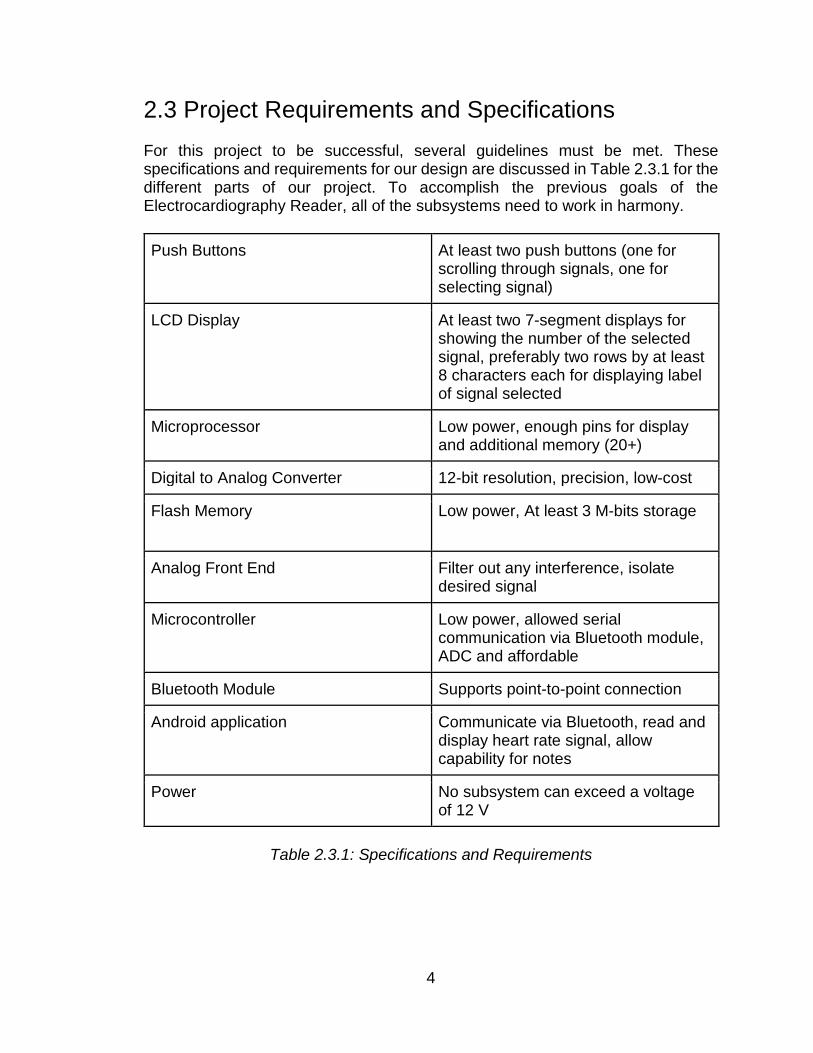
2.3 Project Requirements and Specifications For this project to be successful, several guidelines must be met. These specifications and requirements for our design are discussed in Table 2.3.1 for the different parts of our project. To accomplish the previous goals of the Electrocardiography Reader, all of the subsystems need to work in harmony. Push Buttons At least two push buttons (one for
scrolling through signals, one for selecting signal)
LCD Display At least two 7-segment displays for showing the number of the selected signal, preferably two rows by at least 8 characters each for displaying label of signal selected
Microprocessor Low power, enough pins for display and additional memory (20+)
Digital to Analog Converter 12-bit resolution, precision, low-cost
Flash Memory Low power, At least 3 M-bits storage
Analog Front End Filter out any interference, isolate desired signal
Microcontroller Low power, allowed serial communication via Bluetooth module, ADC and affordable
Bluetooth Module Supports point-to-point connection
Android application Communicate via Bluetooth, read and display heart rate signal, allow capability for notes
Power No subsystem can exceed a voltage of 12 V
Table 2.3.1: Specifications and Requirements
4
3. Research Related to Project Definition Before the team started designing the project, the research was done in order to look at ways the product can be designed so that it meets the goals and specifications. Different methods and technologies are compared until a decision that will be used in the design is made. The topics that are discussed in this section include:
1. The relevant technologies that are currently used in the field of medical electrocardiography signal measurement and the method of quantizing waveforms and displaying them on a monitor
2. A look at some similar projects or products that could possibly provide
guidance and assist in the design of our project 3.1 Relevant Technologies The electrocardiogram was first invented in 1902 by Willem Einthoven to record electrical activity of the heart. The system used 3 electrodes placed in a triangular configuration in reference to the heart. This configuration became known as the Einthoven triangle, which allowed users to capture 3 different electrical signals from the heart. Today, there have been many modifications to this first working device but in many cases, the 3 electrode cardiogram is still applicable. Modern electrocardiograms come in many forms. The 3 channel ECG has been improved by using modern integrated circuits for filtering and digitizing captured analog signals for advanced processing algorithms. The 5 channel ECG improves the quality of specific segments in the electrical signal that the 3 channel system fails to capture. This system utilizes 4 extremity electrodes (legs/arms) and 1 electrode placed near the heart. The most advanced ECG setup is the 12 lead ECG. The system uses 10 electrodes which gives the clearest and most accurate electrical signals. All of the previous mentioned electrocardiogram systems are also available with different modular functions. One configuration allows for modules to be added or removed to the processing unit. This can allow for more or less electrodes to be added and could be used to add different sensors to the unit such as respiratory. In many cases electrocardiogram monitoring needs to be combined with other vital monitoring systems and this modular form works best. The second form is an integrated system which has predefined functions built into the system. Integrated systems would probably work best in mobile device applications. Typically, mobile devices do not have many input connections or the processing power to handle multiple sensors. Finally, there are systems that combined both modular and integrated sensors. This configuration can take advantage of plug-and-play sensor
5

technologies in the future with its modular functionality, while offering a current top-of-the-line integrated system. Electrocardiograms are displayed using computer or TV monitors. The display usually has multiple graphs that are showing simultaneously. These graphs reflect the different views of the heart that can be measured depending on which electrode is designated as the reference node. There are two common filter modes that will determine the image quality of the signal displayed. The first mode is known as monitoring mode and has a band-pass filter ranging from 0.5 - 50 Hz. The high pass filter with cutoff frequency of 0.5 Hz limits baseline wandering from body movement. The low pass filter with cutoff frequency of 50 Hz reduces interference from AC outlets, muscles, and high frequency electromagnetic equipment. The second mode is known as diagnostic mode and has a bandpass frequency of 0.05 - 150 Hz. This mode allows for a higher signal resolution. In this mode the ST, QRS, P and T segments can be seen clearly, unlike in monitoring mode. In monitoring mode these segments may be visible but lack image definition. For an original ECG signal, it is characterized by six peaks and valleys. On the Figure 3.1.1, it labeled each peak and valley with successive letters of the alphabet P, Q, R, S, T, and U. These peaks and valleys are the most important data we must save.
Figure 3.1.1: ECG Signal The program that displays the electrocardiogram signals may contain many built in functions that allow users to adjust the interface to specific applications. Standard electrocardiogram displays contain lead selection that allows users to select the amount of leads that are connected to the system. The visual program also allows users to calibrate the ECG for proper signal display. Zoom functions
6
are common in many displays, which allow the user to focus in on specific parts of heart rate signals. A notable feature on almost all electrocardiograms is the beeping audio tone that comes from the system. The beeping audio tone serves as a warning system to caregivers who are monitoring patients. A common audio scheme is beeping that tracts the heart rate. This can be accomplished in various ways such as beeping at the peak of the QRS complex. By tracking heart rate in this manner the monitor can create graph summaries of heart rate events over a specific period of time. Another purpose the audio tone serves is sounding an alarm if electrodes become disconnected. This can be detected by an ECG signal flat line in the display. The flat line detection can also signal that the patient’s heart stopped. There are many other alarm sounds that electrocardiogram monitors use to notify caregivers. Sometimes patients need to be monitored while they are mobile and wired sensor-to-display connections are not possible. In this case wireless technologies must be used to bridge the system. As in most wireless technologies, radio frequency (RF) signals are used to transmit data. The heart rate signal can be modulated and transmitted as an analog signal, which decreases circuit topology complexity. However, this increases the chances of signal interference and signal distortion. The modern way to transmit signals is digitally. The analog heart signal is converted first into a digital signal before it is modulated then transmitted. The common portable ECG device is powered by a 9 volt battery or “AA” batteries. Portable ECG devices are typically held in a pouch attached to the patient. Functions such as call features may be applied to the device to allow patients to communicate with their caregivers. Other module functions can be added to the device to monitor vital signs but this will decrease the battery life of the device. The data from these devices can be transmitted directly back to a monitor or be recorded from the device and examined later. Current technologies are using information centers that can be used to establish a cellular architecture to collect transmitted data. This architect would also allow for the information center to send information directly to the device. Cellular architecture is important because it is becoming more common to see electrocardiograms being used in outpatient settings. Patients wear these monitors 24 hours a day and data is constantly streaming to these information centers. This allows the corresponding caregivers that are monitoring patients with critical heart disorders to be alerted at any time and from anywhere of problems, while still allowing the patient to live a normal life style. A modern electrocardiogram that is available to purchase is Bionet BM3 patient monitor. The system is small size to accommodate patients that are moving around in hospitals. Unlike portable systems, this system is designed to be placed on a light stand with wheels that can be wheeled around hospitals. The stand can be removed and the monitor along with the built in functionalities can be carried by its
7

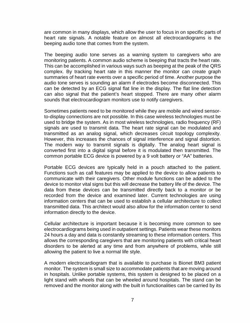
handle. The BM3 patient monitor can measure parameters such as ECG, SpO2, NIBP, temperature and pulse. As mentioned earlier, many electrocardiogram systems are accompanied with other vital signal measurements. The display is a 5.7-inch color LCD screen that allows users to view multiple waveforms and vital signs simultaneously. It also can function as a central monitoring system and allow for multiple patients to be monitored on the same display. Features of the main body include a power key, function keys, trim knob control key, and silence alarm key. The input and output terminals consist of a protective ground terminal to protect the system components from shorts. The BM3 contains: a DC Power Input Port, RJ45 LAN Ports, RS-232C Serial port, ECG Probe Connector, NIBP Probe Connector, TEMP Probe Connector, and SpO2 Probe Connector. These input and output ports allow for separate accessories to plug into the device as needed. The Figure 3.1.2 and Figure 3.1.3 describe the system hardware functions.
Figure 3.1.2: Related Technology System
8
Figure 3.1.3: Related Technology Power System
3.2 Existing Similar Projects and Products Here are some projects and products that our group found that are similar to the goals and specifications of this ECG Project. These can be used as guidelines and will offer plenty of assistance when our group begins to construct our main design. 3.2.1 A Wearable ECG System In Internal Journal of Smart Home, a paper documented the works of the design and implementation of a wearable ECG System. In this paper, the wearable ECG System used smartphones for real-time monitoring for chronic heart disease patients before sudden outbreaks. Patients wore a smart shirt with an ECG system so healthcare professionals could access patients’ data wirelessly in real time with their smartphone. This project used well-known technologies such as the instrumentation amplifier, right leg drive feedback circuit filter, isolation amplifier, band-pass filter, and Butterworth filter.
9
The Bluetooth 2.0 module is used to wirelessly transmit the measured data in hexadecimal code. The ECG App framework was based on the Android OS platform. The final product of the circuitry was compacted by a System on a Chip design. In addition, the sport-shirt was embedded with 3 electrodes. These electrodes were used to measure the ECG from three parts of the body according to the Einthoven’s triangle that was previously discussed. In addition to that, the mobile application provides graphical information with personal history management tools and an automatic emergency call system. Due to today’s technology, smartphones are becoming powerful. Besides for meeting all of our goals and requirements, we could create more functionalities for our mobile application. This paper gives us a clear direction of how to get started on the hardware development of our project and offers valuable software ideas as well. 3.2.2 Wireless Pulse Rate Monitoring Using NFC A project from Cornell University’s Master of Electrical Engineering program created an electrocardiogram monitor using NFC specifications to facilitate the monitoring of pulse rates for small laboratory animals by researchers. The transmitter, which would be attached to the laboratory animal, consists of an Atmel ATtiny25 microcontroller. The ATtiny25 microcontroller reads the ECG signal from the monitored subject into its analog-to-digital converter and encodes the data with a 106 kHz clock using a Manchester encoding scheme. Then the signal becomes an amplitude modulated signal with a 13.5 MHz carrier wave and is outputted to an antenna resonating as the NFC specification. Finally, the ATmega32 microcontroller is used to receive the signal and transmit that data via serial communication (RS232) to a PC. 3.2.3 An Authentic ECG Simulator A computer engineering graduate from the University of Central Florida in 2006 completed his thesis on a similar project to our first subsystem. He designed a portable, authentic electrocardiogram simulator. His project stored different types of ECG data files on a flash memory chip. His data files were originally obtained from the online MIT-BIH Database and required formatting and storing onto a memory chip. Using a digital to analog converter, the files were processed and output to produce an authentic ECG signal onto a four-lead network. His system was built around the MSP430F169 microcontroller which has a built-in 12-bit digital to analog converter. He purchased a Samsung NAND 8M x 8 bit flash memory chip and a 16x2 character LCD display that came as a part of the development board.
10
This project will be very useful in having something to model our ECG simulator off of. The online database where the files were obtained will also be used in our project, and we will have to scale our data files as well so they can be used by a DAC or an equivalent. 3.2.4 Wireless Oscilloscope for Android Phones A software developer from the Philippines in 2010 came up with his own Android application that will provide assistance to the software portion of our project. The application is an Android Bluetooth Oscilloscope. The oscilloscope has the ability to display images of the varying electrical voltages that are being read in with respect to time. The interesting portion of this project is the fact that the software for the oscilloscope has been combined with an Android device via Bluetooth communication. The oscilloscope is shown on the device’s display, allowing the user to capture up to two different channels of data. The data is received at 2 MHz per second using a PIC microcontroller. The available analog-to-digital converter available on the microcontroller does the actual conversions of the signal. Then, these signals are sent to the Android device using the LMX9838 Bluetooth serial port module to be displayed. The developer of this application has provided his source code to help other developers interested in a similar project like how our group is. Our group members will be able to examine his methods of capturing the signals and displaying them on the Android device to facilitate our progress of designing our own related Android application. 3.3 Design Research The project architectures in the block diagrams are constructed to simplify and describe the connection between each subsystem and how each system works with one another. Section 3.3.1 connects all the components together and the follow up sections will be discussing the principle of how each subsystems works with one another. 3.3.1 Initial Design Architectures and Block Diagrams The overall system block diagram is shown in Figure 3.3.1.1. This shows how the heart rate signal is sent out from the Heart Rate Simulator subsystem, received from the ECG Analog Front, and then is sent via Bluetooth to the Android application. If a live human's heart signal was used, this would be read from electrodes and be received from the same three inputs of the ECG Analog Front.
11
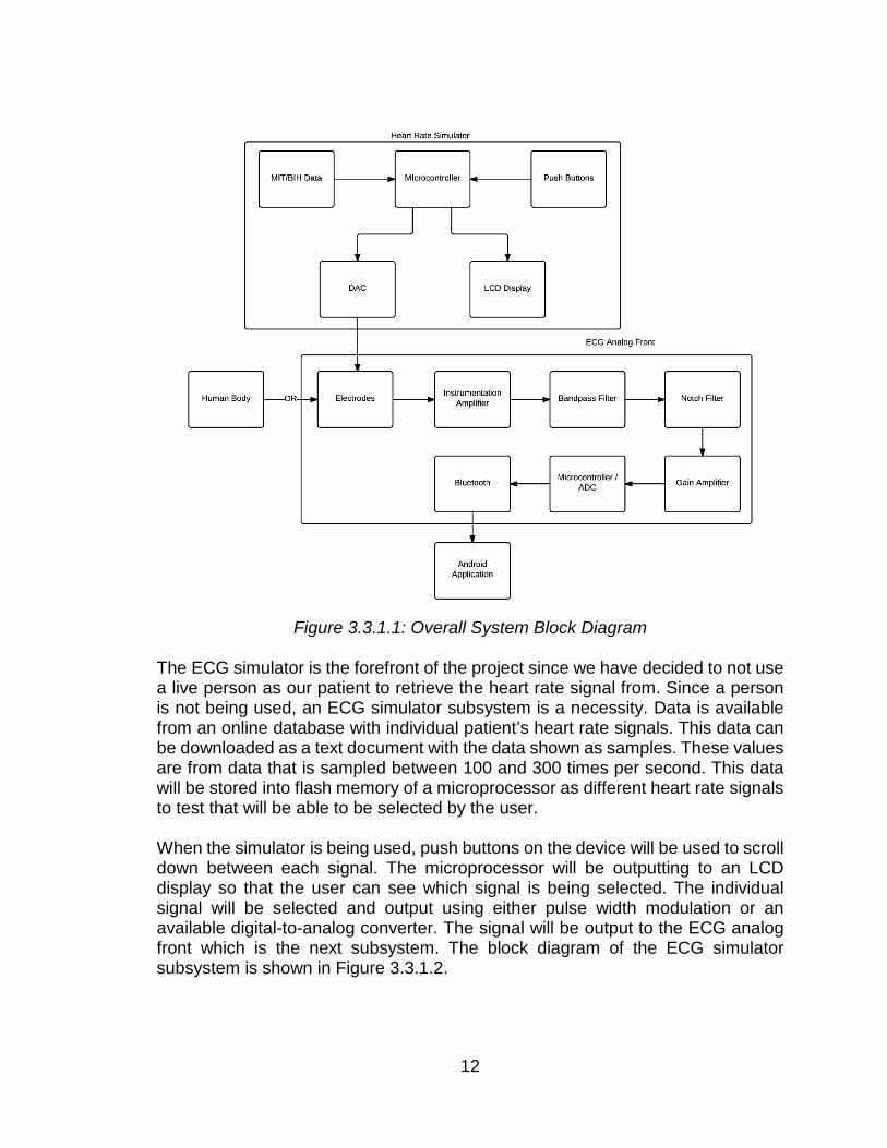
Figure 3.3.1.1: Overall System Block Diagram
The ECG simulator is the forefront of the project since we have decided to not use a live person as our patient to retrieve the heart rate signal from. Since a person is not being used, an ECG simulator subsystem is a necessity. Data is available from an online database with individual patient’s heart rate signals. This data can be downloaded as a text document with the data shown as samples. These values are from data that is sampled between 100 and 300 times per second. This data will be stored into flash memory of a microprocessor as different heart rate signals to test that will be able to be selected by the user. When the simulator is being used, push buttons on the device will be used to scroll down between each signal. The microprocessor will be outputting to an LCD display so that the user can see which signal is being selected. The individual signal will be selected and output using either pulse width modulation or an available digital-to-analog converter. The signal will be output to the ECG analog front which is the next subsystem. The block diagram of the ECG simulator subsystem is shown in Figure 3.3.1.2.
12
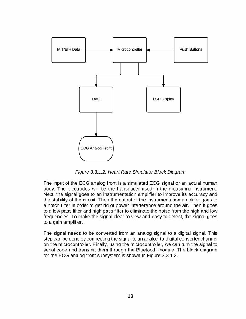
Figure 3.3.1.2: Heart Rate Simulator Block Diagram
The input of the ECG analog front is a simulated ECG signal or an actual human body. The electrodes will be the transducer used in the measuring instrument. Next, the signal goes to an instrumentation amplifier to improve its accuracy and the stability of the circuit. Then the output of the instrumentation amplifier goes to a notch filter in order to get rid of power interference around the air. Then it goes to a low pass filter and high pass filter to eliminate the noise from the high and low frequencies. To make the signal clear to view and easy to detect, the signal goes to a gain amplifier. The signal needs to be converted from an analog signal to a digital signal. This step can be done by connecting the signal to an analog-to-digital converter channel on the microcontroller. Finally, using the microcontroller, we can turn the signal to serial code and transmit them through the Bluetooth module. The block diagram for the ECG analog front subsystem is shown in Figure 3.3.1.3.
13

Figure 3.3.1.3: ECG Reader Block Diagram
The power system can be done in three different ways. One of these methods is getting the power source from the wall outlet. The second method is using battery as the power source. Third method is using very simple linear voltage regulator as the power source. The block diagram in Figure 3.3.1.5 illustrates the process of getting the power source from rechargeable batteries for each subsystem.
Figure 3.3.1.5: Power System with Battery Charger
14

The block diagram in Figure 3.3.1.6 illustrates the first method of getting the power source from the wall outlet.
Figure 3.3.1.6: Power System Block Diagram
The block diagram in Figure 3.3.1.7 illustrates the power system using simple linear voltage regulator.
15

Figure 3.3.1.7: Power System with Linear Voltage Regulator
The block diagram illustrates the Android application subsystem and is shown in Figure 3.3.1.4.
16

Figure 3.3.1.4: Android Application subsystem
3.3.2 Heart Rate Simulator The first subsystem is the Heart Rate Simulator. In this section, the concepts behind pulse width modulation, how to recover an analog signal, and attenuation will be discussed.
17
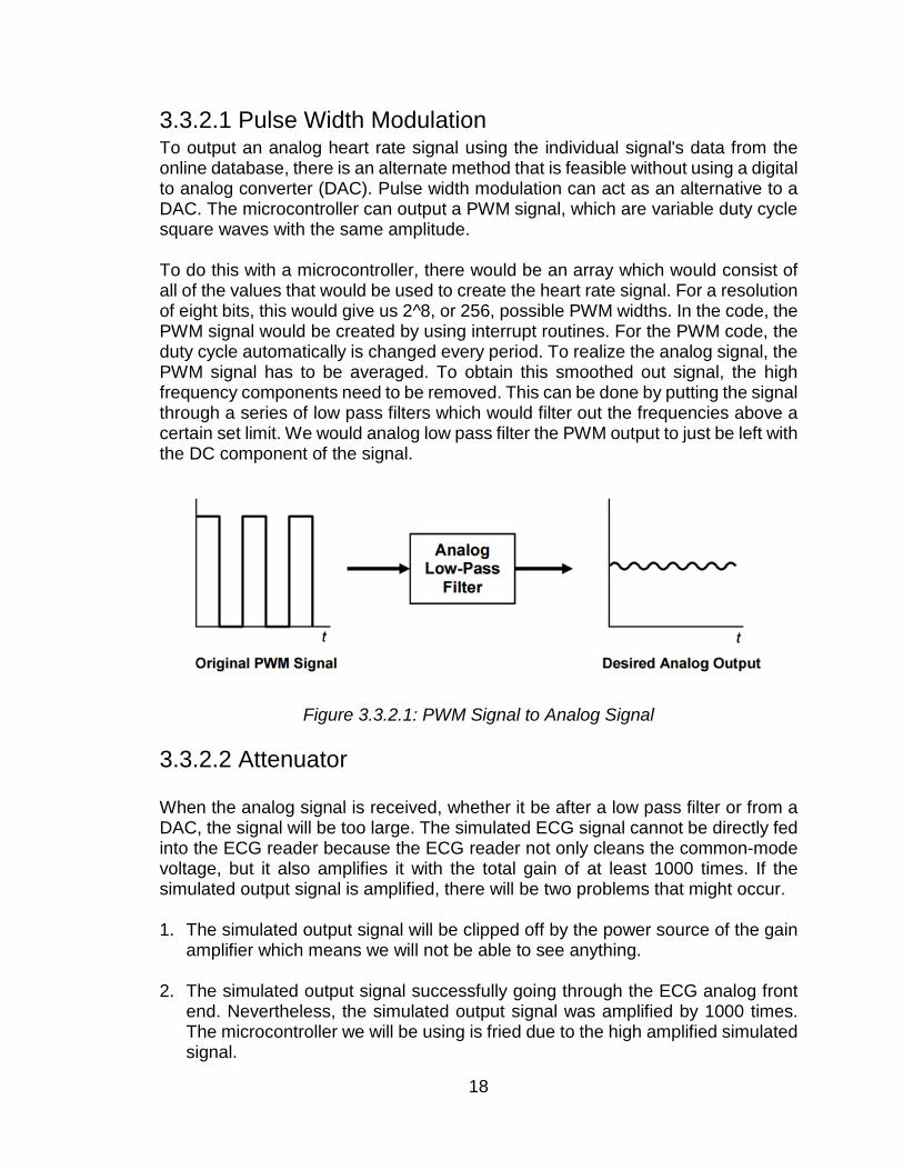
3.3.2.1 Pulse Width Modulation To output an analog heart rate signal using the individual signal's data from the online database, there is an alternate method that is feasible without using a digital to analog converter (DAC). Pulse width modulation can act as an alternative to a DAC. The microcontroller can output a PWM signal, which are variable duty cycle square waves with the same amplitude. To do this with a microcontroller, there would be an array which would consist of all of the values that would be used to create the heart rate signal. For a resolution of eight bits, this would give us 2^8, or 256, possible PWM widths. In the code, the PWM signal would be created by using interrupt routines. For the PWM code, the duty cycle automatically is changed every period. To realize the analog signal, the PWM signal has to be averaged. To obtain this smoothed out signal, the high frequency components need to be removed. This can be done by putting the signal through a series of low pass filters which would filter out the frequencies above a certain set limit. We would analog low pass filter the PWM output to just be left with the DC component of the signal.
Figure 3.3.2.1: PWM Signal to Analog Signal 3.3.2.2 Attenuator When the analog signal is received, whether it be after a low pass filter or from a DAC, the signal will be too large. The simulated ECG signal cannot be directly fed into the ECG reader because the ECG reader not only cleans the common-mode voltage, but it also amplifies it with the total gain of at least 1000 times. If the simulated output signal is amplified, there will be two problems that might occur. 1. The simulated output signal will be clipped off by the power source of the gain
amplifier which means we will not be able to see anything. 2. The simulated output signal successfully going through the ECG analog front
end. Nevertheless, the simulated output signal was amplified by 1000 times. The microcontroller we will be using is fried due to the high amplified simulated signal.
18
Therefore, we need to downgrade our simulated output signal. The method to downgrade the simulated signal is using an attenuator. The simplest attenuator can be created by voltage divider networks. First of all, the simulated ECG signal is in the range of 0 V to 5 V. The actual ECG signal measured with oscilloscope would have some negative components. First, we need to get rid of the DC offset of the simulated ECG signal. It is convenient to discuss the attenuation in terms of decibels relative to power. Assuming the amplitude of the simulated ECG signal is 5 V, we need the ECG signal to be around 5 mV. This means the attenuation that would be needed would be around 60 dB. 3.3.3 ECG Reader For the ECG Reader, much research had to be done since this subsystem was the main backbone of the project. Here, concepts of how to best filter out any interference, eliminate unnecessary noise in the signal, implement the instrumentation amplifiers, and deal with powering the system will be discussed. 3.3.3.1 Electrodes Research The first stage of the ECG amplifier is a transducer (electrode), which converts the ECG into electrical voltage. The voltage received from the transducer is in the range of 10 μV ~ 5 mV. The electrical activity of the heart can be modeled as an electric dipole located in a conducting medium where a dipole consists of points of equal positive and negative charge separated from one another and is denoted by the dipole moment, so-called cardiac vector. The cardiac vector indicates the direction of the depolarization in time. For that reason, we want to capture the cardiac vector by connecting leads on the surface of the body to detect biopotentials. There are many different electrode lead configurations in electrocardiogram systems. The most common type is the “12 Lead system” which is used in professional medical applications. The term lead is often confused with the number of electrodes that are placed on the body. However, in the case of an ECG it refers to the number of ways the electrical activity of the heart can be viewed. For a 12-lead system there are only 10 electrodes. Five electrodes are placed horizontally just beneath the left side of the chest. One electrode is placed just beneath the right side of the chest near the sternum. The remaining four electrodes get divided between both arms and legs. The electrodes on the arm can be placed anywhere between the shoulder and elbow. The electrodes on the legs are placed anywhere above the ankle and below the torso. The way in which these electrodes are placed will allow 12 separate voltage vectors to be viewed of the heart. These vectors from the center of the heart are 30 degrees a part from each other. Figure 3.3.3.1
19
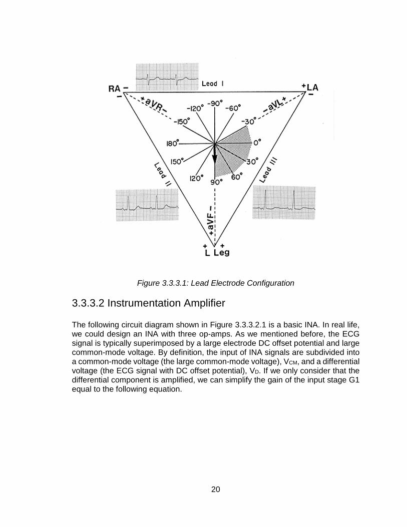
Figure 3.3.3.1: Lead Electrode Configuration
3.3.3.2 Instrumentation Amplifier The following circuit diagram shown in Figure 3.3.3.2.1 is a basic INA. In real life, we could design an INA with three op-amps. As we mentioned before, the ECG signal is typically superimposed by a large electrode DC offset potential and large common-mode voltage. By definition, the input of INA signals are subdivided into a common-mode voltage (the large common-mode voltage), VCM, and a differential voltage (the ECG signal with DC offset potential), VD. If we only consider that the differential component is amplified, we can simplify the gain of the input stage G1 equal to the following equation.
20

Figure 3.3.3.2.1: Basic Instrumentation Amplifier
The difference amplifier, A3, subtracts output of A1 from A2 and amplifies the difference with the gain G2 is the following equation.
Solving for the total gain of this INA is the following equation. If we take a look at the output of the input stage, for the case of the resistors Rf is different, it would only make the difference gain G1 to be
As the result, this would only modified the gain by a little. Therefore, we do not need to worry about the resistor Rf to be different. The resistors that could make an impact on our result of the INA is R1 and R2 on the difference amplifier. To make the output of the amplifier to be zero in common mode, the resistance value must be identical. Otherwise, the output of op-amp A1 and A2 would be amplified differently which might leave a significant difference voltage as we are performing a common mode operation. However, in reality, it is very hard to find an exact same resistance for resistors that supposed to have the same resistance. One way to overcome this problem is to use a variable resistor. We could adjust the resistor until the output becomes very close to zero. Assuming that our INA operates from a typical ±5 V supply and according to Texas Instrument, the typical ECG signal (VD) detected from electrodes would be around
21

1 mV AC signal with 400 mV DC offset and the common-mode potential is at a maximum of VCM = 1.5 V. The common-mode potential made up of two parts: power line interference and DC electrode offset potential. From inspection, we can derive the equation
, where V1 is the output of op-amp A1.
Then we figure out the maximum of input gain G1 is
, in which we assume the power supply is ±5 V. To determine the maximum of gain G2, we neglected the VD_DC offset and calculated the total gain for maximum ECG signal to be
Now, assuming the input gain G1 is 10, the gain G2 will be 500. In the next step, we should eliminate the differential potential DC offset. In signal processing, DC offset can be reduced in real-time by a high-pass filter. These DC offsets in real-time is just a very low frequencies signal or so-called “slowly changing DC” or “baseline wander”. With a low-pass filter in the feedback loop of A3, the transfer function of the difference amplifier treats it with high-pass characteristics. Since a typical ECG signal frequency range is within 0.05 Hz and 150 Hz, the cutoff frequency should be set to 0.05 Hz.
To do this, we use a TL084 Quad op-amp. In order to make sure the ECG signal does not clip off due to the power supply, we set the gain G2 = 1 and input gain G1 = 3. This will give us the total gain of 3. We do not want our gain to be too high because the noise would affect the output of the circuit according to the equation. The root means square (RMS) voltage due to the thermal noise, generated in a resistance R over bandwidth Δf, is given by the following equation.
In this equation, kb is Boltzmann’s constant and T is the resistor’s absolute temperature. As a result, the noise signal depends on the frequency that will pass through the INA. Using the simulation, as we expected, the difference voltage was amplified at the factor of 3 and the difference DC offset was eliminated. The simulation shown in Figure 3.3.3.2.2 is the simulation result in Multisim.
22

Figure 3.3.3.2.2: Simulation Circuit in Multisim
3.3.3.3 Input Protection According to Electronics Laboratory Safety Information and OSHA, the typical cannot let-go current (the current that made a person lose muscular control) is about 6 - 30 mA. Even 1 mA could still be dangerous under certain conditions. For example, under dry conditions, human skin is very resistant. Wet skin dramatically drops the body’s resistance. We must design an input protection to limit the input current or over voltage. To protect the ECG circuit against high voltages which occur for example in the operating room when the ECG signal is combined with the use of an electrosurgical unit that will induce high transient voltages into the patient. The circuit shown in Figure 3.3.3.3.1 is a standard voltage limiting circuit which using voltage limiting devices such as diodes. Diodes are connected between the lead and RL ground. In addition to that, we can tackle the overvoltage protection from the input is to place a large resistance before the input of the amplifier. This way preserves high input impedance thus avoiding the current backflow to the patient.
Figure 3.3.3.3.1: Limiting Voltage Circuit
23
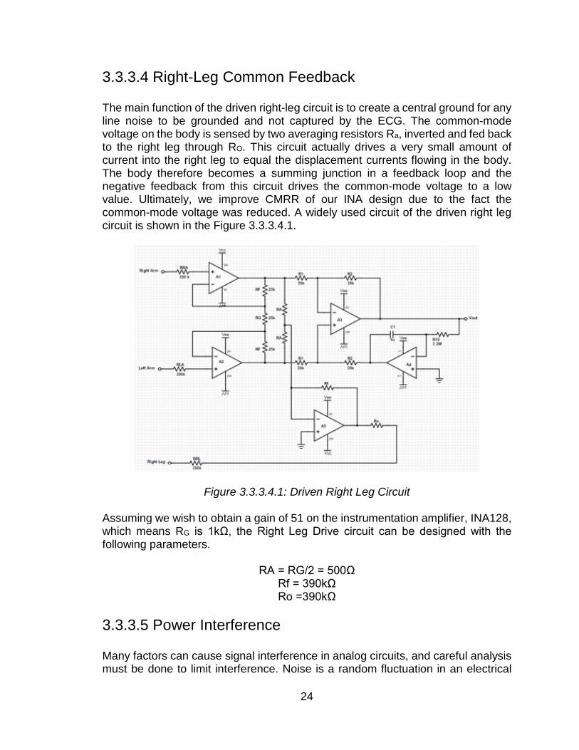
3.3.3.4 Right-Leg Common Feedback The main function of the driven right-leg circuit is to create a central ground for any line noise to be grounded and not captured by the ECG. The common-mode voltage on the body is sensed by two averaging resistors Ra, inverted and fed back to the right leg through RO. This circuit actually drives a very small amount of current into the right leg to equal the displacement currents flowing in the body. The body therefore becomes a summing junction in a feedback loop and the negative feedback from this circuit drives the common-mode voltage to a low value. Ultimately, we improve CMRR of our INA design due to the fact the common-mode voltage was reduced. A widely used circuit of the driven right leg circuit is shown in the Figure 3.3.3.4.1.
Figure 3.3.3.4.1: Driven Right Leg Circuit
Assuming we wish to obtain a gain of 51 on the instrumentation amplifier, INA128, which means RG is 1kΩ, the Right Leg Drive circuit can be designed with the following parameters.
RA = RG/2 = 500Ω Rf = 390kΩ Ro =390kΩ
3.3.3.5 Power Interference Many factors can cause signal interference in analog circuits, and careful analysis must be done to limit interference. Noise is a random fluctuation in an electrical
24
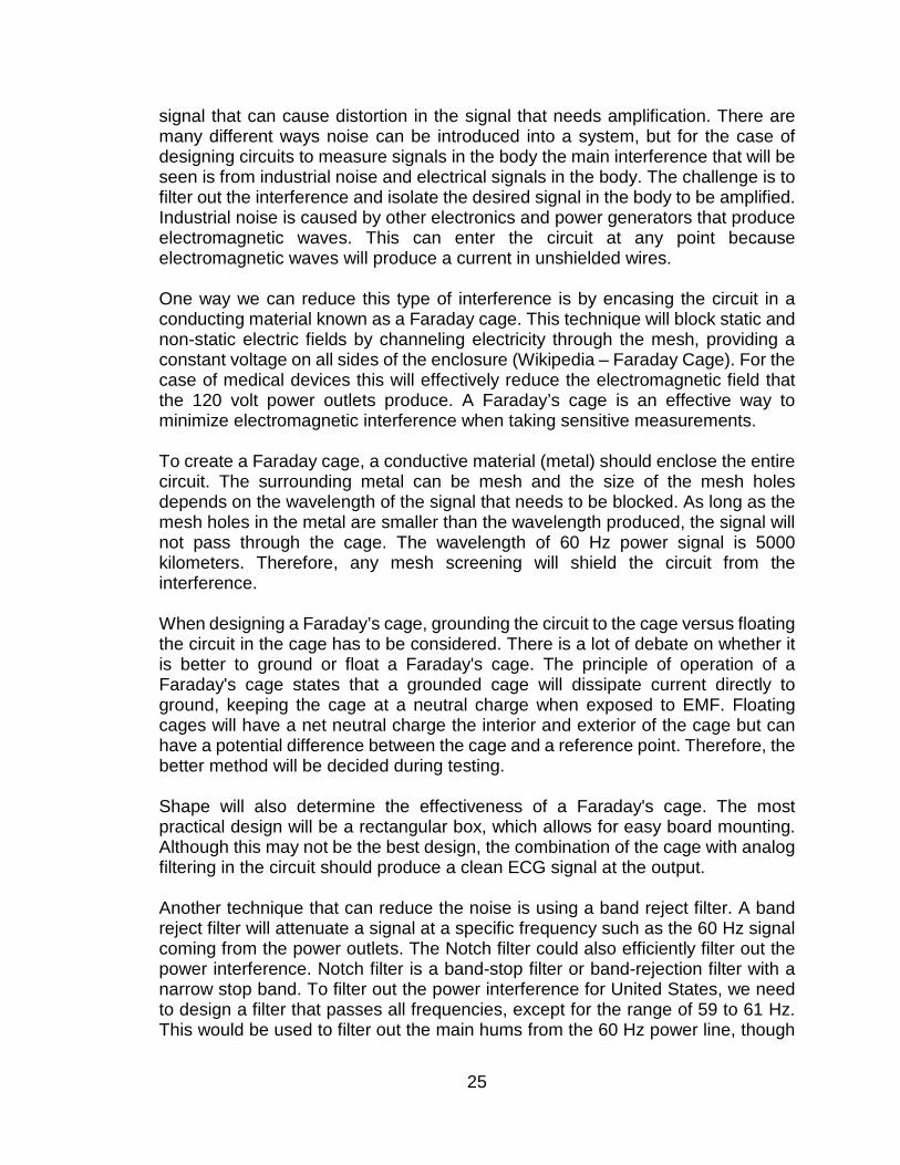
signal that can cause distortion in the signal that needs amplification. There are many different ways noise can be introduced into a system, but for the case of designing circuits to measure signals in the body the main interference that will be seen is from industrial noise and electrical signals in the body. The challenge is to filter out the interference and isolate the desired signal in the body to be amplified. Industrial noise is caused by other electronics and power generators that produce electromagnetic waves. This can enter the circuit at any point because electromagnetic waves will produce a current in unshielded wires. One way we can reduce this type of interference is by encasing the circuit in a conducting material known as a Faraday cage. This technique will block static and non-static electric fields by channeling electricity through the mesh, providing a constant voltage on all sides of the enclosure (Wikipedia – Faraday Cage). For the case of medical devices this will effectively reduce the electromagnetic field that the 120 volt power outlets produce. A Faraday’s cage is an effective way to minimize electromagnetic interference when taking sensitive measurements. To create a Faraday cage, a conductive material (metal) should enclose the entire circuit. The surrounding metal can be mesh and the size of the mesh holes depends on the wavelength of the signal that needs to be blocked. As long as the mesh holes in the metal are smaller than the wavelength produced, the signal will not pass through the cage. The wavelength of 60 Hz power signal is 5000 kilometers. Therefore, any mesh screening will shield the circuit from the interference. When designing a Faraday’s cage, grounding the circuit to the cage versus floating the circuit in the cage has to be considered. There is a lot of debate on whether it is better to ground or float a Faraday's cage. The principle of operation of a Faraday's cage states that a grounded cage will dissipate current directly to ground, keeping the cage at a neutral charge when exposed to EMF. Floating cages will have a net neutral charge the interior and exterior of the cage but can have a potential difference between the cage and a reference point. Therefore, the better method will be decided during testing. Shape will also determine the effectiveness of a Faraday's cage. The most practical design will be a rectangular box, which allows for easy board mounting. Although this may not be the best design, the combination of the cage with analog filtering in the circuit should produce a clean ECG signal at the output. Another technique that can reduce the noise is using a band reject filter. A band reject filter will attenuate a signal at a specific frequency such as the 60 Hz signal coming from the power outlets. The Notch filter could also efficiently filter out the power interference. Notch filter is a band-stop filter or band-rejection filter with a narrow stop band. To filter out the power interference for United States, we need to design a filter that passes all frequencies, except for the range of 59 to 61 Hz. This would be used to filter out the main hums from the 60 Hz power line, though
25
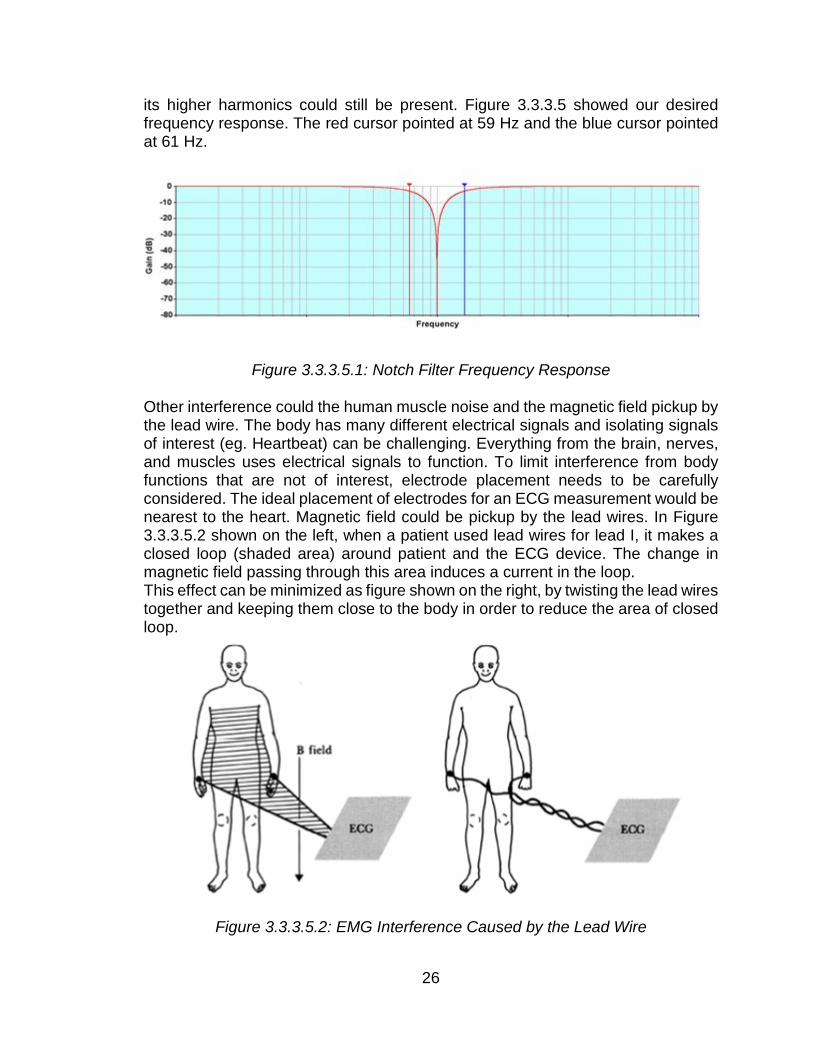
its higher harmonics could still be present. Figure 3.3.3.5 showed our desired frequency response. The red cursor pointed at 59 Hz and the blue cursor pointed at 61 Hz.
Figure 3.3.3.5.1: Notch Filter Frequency Response Other interference could the human muscle noise and the magnetic field pickup by the lead wire. The body has many different electrical signals and isolating signals of interest (eg. Heartbeat) can be challenging. Everything from the brain, nerves, and muscles uses electrical signals to function. To limit interference from body functions that are not of interest, electrode placement needs to be carefully considered. The ideal placement of electrodes for an ECG measurement would be nearest to the heart. Magnetic field could be pickup by the lead wires. In Figure 3.3.3.5.2 shown on the left, when a patient used lead wires for lead I, it makes a closed loop (shaded area) around patient and the ECG device. The change in magnetic field passing through this area induces a current in the loop. This effect can be minimized as figure shown on the right, by twisting the lead wires together and keeping them close to the body in order to reduce the area of closed loop.
Figure 3.3.3.5.2: EMG Interference Caused by the Lead Wire
26

3.3.3.6 Frequency Spectrum and Requirements The ECG signal varies from frequency 0.05 Hz to 150 Hz. A bandpass filter that constructs a low-pass filter cascaded with a high-pass filter would make a perfect bandpass filter. The high-pass filter comes first, so energy from it that stretches to infinite frequency will be low passed. In addition to that, we decided to use a single power supply filter. The low-pass filter should have the cutoff frequency of 150 Hz. The high-pass filter should have the cutoff frequency of 0.05 Hz. Figure 3.3.3.6.1 is the desired frequency response, where the red cursor is at 0.05 Hz and the blue cursor is at 150 Hz.
Figure 3.3.3.6.1: Wide Bandpass Filter Frequency Response 3.3.3.7 Gain Requirement In order to obtain better interpretation of the ECG signal for analog to digital converter, the total gain of 1000 must achieved. Considered the microcontroller that will be using for analog to digital calculation, the normal analog input that can be take in is from 0V to 5V. The range of the ECG signal is from microvolts to millivolts. In addition to that, the heartbeat speed is slow compare to any high frequency signal. The internal capacitance and resistance of the op-amp will create a high-pass characteristic filter. Therefore, we should not need to worry about signal being cut off by the amplifier. Also the amplifier will be cascaded after all the filters that eliminate the unwanted signals. One way to build a high gain output amplifier without using a large value resistor, we can used the circuit as shown in Figure 3.3.3.7.1 below.
27

Figure 3.3.3.7.1: Inverting Amplifier with T-Network and Voltage Inverter
This circuit is an inverting amplifier with T-network. Then the output is going to the inverting amplifier with gain of -1. This will invert the output of the gain stage. We can use this circuit to avoid using large value resistors, which are difficult to obtain with a highly stable performance, and which can be expensive, the T-network can be used. This network increases gain without increasing resistor values. One disadvantage of T-network is that it amplifies the offset voltage of op-amp. The following equation is derived from the circuit.
Writing a brute force program in MATLAB, we went to from 1 kΩ to 100 kΩ for each resistor value. Finally, we found some suitable resistors to get the gain of 1000. Since we could not find an exact value for the resistors, this gave us some flexibility for our design. In addition to that, the gain of bandpass filters and instrumentation amplifiers can make a difference as well. For that reason, this MATLAB program can save us a lot of time picking resistors value to achieve the desired gain. Another way to amplify the ECG signal is to simply build a noninverting amplifier. The gain of this noninverting amplifier is very easy. Rf is the feedback resistor and Rg is the resistor at the V- channel.
With this simple amplifier, we can easily find the right combination of resistor value to obtain the desired gain. We plugged in the equation which represents the total gain of the entire analog circuit, which GP is the gain of all previous stages and Gain is the gain of this noninverting amplifier
28
Assume the analog-to-digital converter can take in the maximum of 5 V input and the amplitude of ECG signal is 1 mV. The total gain of our analog circuit should not be greater than 5000. We designed the maximum amplitude of the amplified ECG signal is 4.5 V which mean the total gain is 4500. We assumed all the previous stage would give us the gain of 15. Now, we found the ratio of between Rf and Rg is
However, there are the downfalls with choosing very large resistors and very small resistors. Looking at this noninverting amplifier as an example, the ratio is about 300. We can choose Rf = 30 kΩ and Rg = 100 Ω or Rf = 300 MΩ and Rg = 1MΩ. These two configurations will give us the same gain as long as our op-amp is ideal. Nevertheless, that is not the case in real life. Choosing small resistors require a higher current to provide with appropriate voltage drops for the op-amp to work. Although most op-amps are able to provide up to 10 mA, if the op-amp provides too many current, there would be a lot of heat generated in the resistors. On the other hand, large resistors could enlarged the problems of input bias current and input offset current. They are usually very small as the datasheet provided. If large resistors is applied, it would throw off the gain the circuit supposed to provide. The best way to solve this problem is to pick the resistance value in the middle range and test the component with an actual resistors. 3.3.3.8 Analog-to-Digital Converter Connecting digital circuitry to sensor devices is simple if the sensor devices are inherently digital themselves. Switches, relays, and encoders are easily interfaced with gate circuits due to the on/off nature of their signals. However, when analog devices are involved, interfacing becomes much complex. What is needed is a way to translate analog signals to digital numbers (binary). An analog-to-digital converter (ADC) can input an analog electrical signal such as voltage or current and outputs a binary number. The simplest ADC is formed of a series of comparators, each one comparing the input signal to a unique reference voltage. The comparator outputs are connected to the inputs of a priority encoder circuit, which produces a binary sequence of output. Another way to work with analog-to-digital converter is using a microcontroller. One of the microcontroller chips could be ATmega328. The chip has 8-channel 10-bit
29

ADC in quad flat (TQFP) and quad flat no-leads (QFN)/ micro-lead frame (MLF) package and 6-channel 10-bit ADC in Dual in-line package. It has master/slave SPI serial interface, and built-in clock distribution system. An ATmega328 will definitely do everything we need. In addition to that, an ATmega328 chip cost around $5.50. Comparing with the price of ADC, a priority encoder, and SPI module, it would be about the same price. Nevertheless, each parts will be sent from different vendors. This would delay our schedule in prototyping stage. With all these advantages of choosing a microcontroller, we are capable of building the prototype without worrying about the insufficient clock frequency, mismatched Baud rates, or delay shipping time for the parts. One important consideration of designing an ADC is its resolution. The resolution of an ADC is the number of binary bits output by the converter. An analog signal is continuously variable. An ADC circuit took in an analog signal and resolved it into many discrete steps. It is important to know how many of discrete steps there are in total. The discrete step determines the accuracy of the output quantities. In an ECG signal, the resolution of the measurement became the most important factor. Since an ECG signal is a very small signal even after the signal is being amplified, some quantities might be lost due to bad resolution of ADC. Assuming the amplitude of an amplified ECG signal to be 4.5 Vpeak, we might require approximately 8-bit ADC. It became impractical to build the ADC ourselves as shown in the previous figure since we will need two quad op-amp to build one. This is a waste of space. Therefore, a built integrated circuit would be a better choice. Another important factor when using an ADC is its sampling frequency, or conversion rate. This is the speed of the converter outputs a new binary number. An insufficient sampling frequency would cause loss of data. To make sure we do not miss any important data, we must have a good sampling frequency to interpret the ECG signal. The duration of QRS interval is about 80 to 120 ms which is around 125 Hz to 84 Hz. This means our sampling frequency must be higher than 125 Hz in order to acquire all data for conversion to digital outputs. For the resolution of the ECG signal, AREF pin on the AVR microcontroller chip means Analog Reference. It allowed us to feed the chip a reference voltage from an external power supply. For example, if we want to measure voltages with a maximum range of 3.3 V, we would feed 3.3 V into the AREF pin. Then each step of the ADC would represent 3.22 mV. From the previous discussion on ECG amplification, we decided to let the amplitude of ECG signal to be approximately 5 V. This is due to the fact that most of the microcontroller would only take up to 5 V analog signal. The ATmega328 has a built-in reference equal to 1.1 V. Then each step of the ADC would represent ~1.1 mV. This would give us roughly 4545 samples measuring from 0 V to 5 V. It is an excellent number of samples. However, it might be too much samples and
30

causing the calculation slow. Therefore, we could use a voltage regulator of 3.3 V feed into the AREF pin. This gave us around 1552 samples measuring from 0 V to 5 V. If we want to increase the resolution, we can simply apply a voltage divider then connect to AREF pin. The sampling rate of an ADC impacts greatly the accuracy of measurement of various ECG parameters. However, according to an online article Digital Sampling Rate and ECG Analysis, the statistical study showed that no significant difference between results obtained at sampling rates of 500 and 250 samples per seconds. The recording made at 125 samples per seconds could be used in particular conditions when only the measurement of certain intervals is required. Therefore, more samples from the analog signal will not hurt. In our application, we will to send via a Bluetooth module. A Bluetooth module operates on the serial communication. Therefore, we must send the digital samples in a serial I/O port in order for a Bluetooth module to be recognized. This means the speed of the ADC sending data is critical. Although there are a lot of IC ADC in the market, many ADC in the market required an external clock to operate which mean they could operate at a different clock frequency. Our final product will be mainly operating on a mobile application. There would be a lot of debugging and trial and error testing. In addition to that, our budget is limited. Therefore, it would not be a smart move to build an ADC and Bluetooth module on a fixed circuit. It is a better idea to do it on software development. 3.3.3.9 Analog Front End Design Reference Design 1 1. An instrumentation amplifier will be used as the input stage of the circuit. The
amplifier consists of two inputs and the difference between the voltages will be amplified at the output. The advantages of using the instrumentation amplifier are low noise, high input impedance, and high common mode rejection ratio. This will help to reduce many of the problems such as line noise and common input signals. Between the electrodes and input of the instrumentation amplifier will be 1M ohm resistors. This will protect patients from dangerous currents and keep input resistance on the instrumentation amplifier similar.
2. The second stage will be a notch filter center at 60 Hz. This will prevent any
power line voltage from being amplified throughout the circuit. Using this filter in the design may eliminate the need for a shielded encasing around the circuit. The notch filter will be designed using Texas instruments UAF42 active filter. This chip can be configured solely using resistors to be a band pass filter. This allows for the use of variable resistors to be used to tune the filter during testing.
Burr-Brown Application Bulletin has tested a 60 Hz notch filter design using the UAF42 and it will be used as a reference design. This design uses six resistors to
31

set the 60 Hz notch filter. The configuration in Figure 3.3.3.9.1 below shows the pin configuration for the UAF42 and external resistors used.
Figure 3.3.3.9.1: Second Stage Circuit Configuration
3. The third stage of the circuit will be a high-pass filter with a cutoff frequency of 1 Hz. This will filter dc swing voltages that occur at the electrodes. In this stage an active first order low pass filter and a second order Butterworth filter will be considered. An advantage that the active first order low pass filter has is it can easily be tuned during testing. The disadvantage is it has a low roll off and can possibly attenuate signals outside of the 1 Hz cutoff frequency. The Butterworth filter has the advantage of a high roll off, producing a more accurate desired cutoff at 1 Hz. The disadvantage is it will be more difficult to tune during testing.
For the active first order high pass filter shown in Figure 3.3.3.9.2, the resistor and capacitor values will be 160k and 1uF respectively. For the Butterworth second order high-pass filter shown in Figure 3.3.3.9.3, the resistors and capacitor values are R1= 16k, R2= 16k, C1= 10uF, C2= 10uF.
32
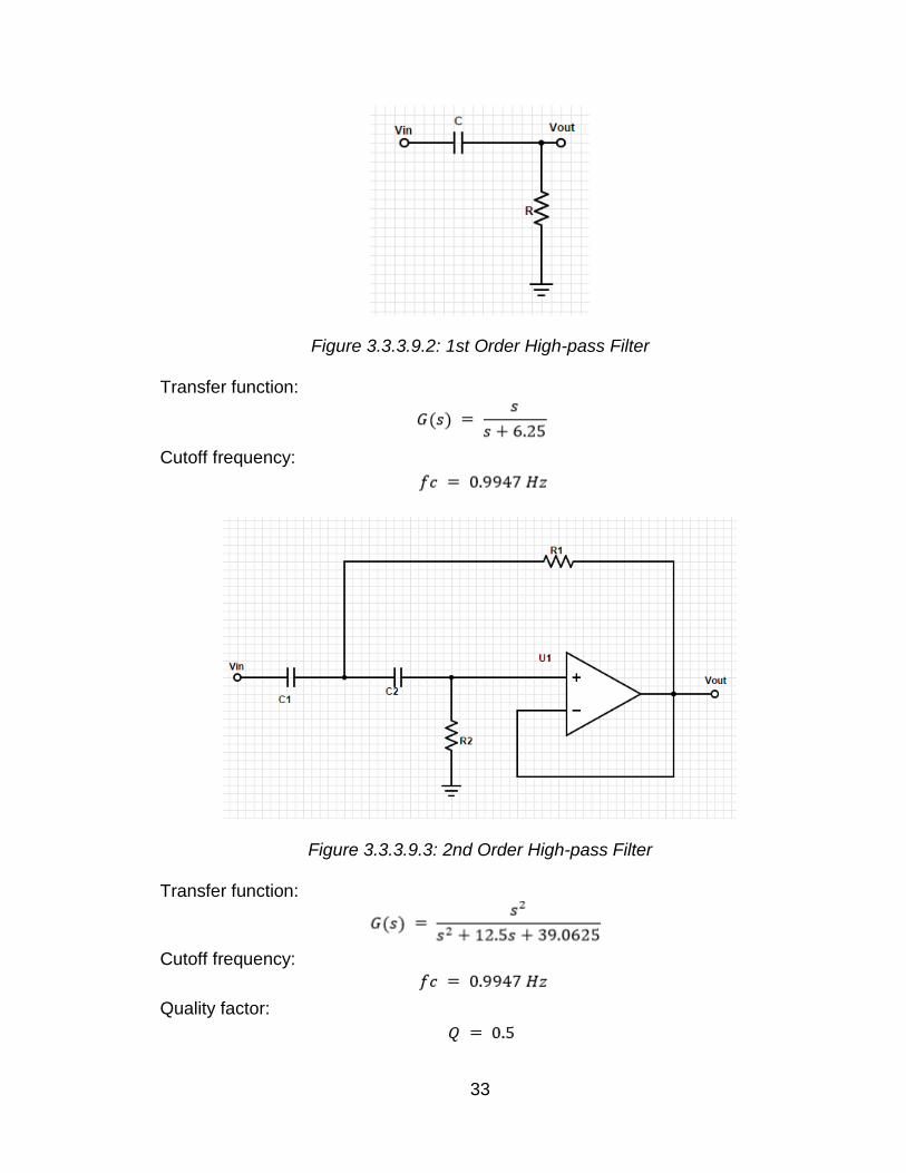
Figure 3.3.3.9.2: 1st Order High-pass Filter
Transfer function:
Cutoff frequency:
Figure 3.3.3.9.3: 2nd Order High-pass Filter Transfer function:
Cutoff frequency:
Quality factor:
33
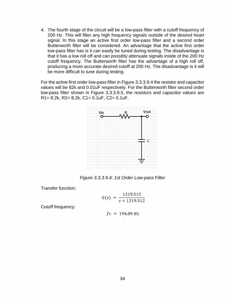
4. The fourth stage of the circuit will be a low-pass filter with a cutoff frequency of 200 Hz. This will filter any high frequency signals outside of the desired heart signal. In this stage an active first order low-pass filter and a second order Butterworth filter will be considered. An advantage that the active first order low-pass filter has is it can easily be tuned during testing. The disadvantage is that it has a low roll off and can possibly attenuate signals inside of the 200 Hz cutoff frequency. The Butterworth filter has the advantage of a high roll off, producing a more accurate desired cutoff at 200 Hz. The disadvantage is it will be more difficult to tune during testing.
For the active first order low-pass filter in Figure 3.3.3.9.4 the resistor and capacitor values will be 82k and 0.01uF respectively. For the Butterworth filter second order low-pass filter shown in Figure 3.3.3.9.5, the resistors and capacitor values are R1= 8.2k, R2= 8.2k, C1= 0.1uF, C2= 0.1uF.
Figure 3.3.3.9.4: 1st Order Low-pass Filter Transfer function:
Cutoff frequency:
34
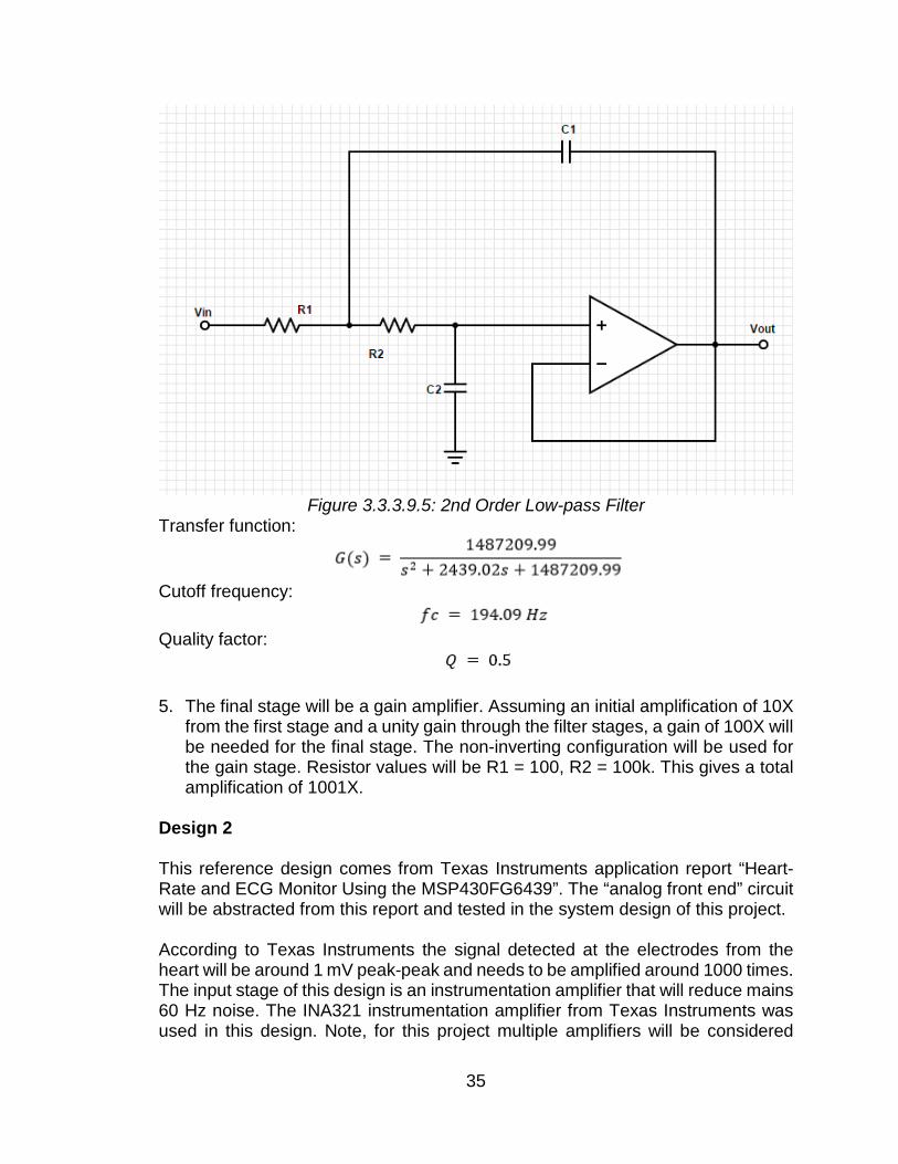
Figure 3.3.3.9.5: 2nd Order Low-pass Filter
Transfer function:
Cutoff frequency:
Quality factor:
5. The final stage will be a gain amplifier. Assuming an initial amplification of 10X from the first stage and a unity gain through the filter stages, a gain of 100X will be needed for the final stage. The non-inverting configuration will be used for the gain stage. Resistor values will be R1 = 100, R2 = 100k. This gives a total amplification of 1001X.
Design 2 This reference design comes from Texas Instruments application report “Heart-Rate and ECG Monitor Using the MSP430FG6439”. The “analog front end” circuit will be abstracted from this report and tested in the system design of this project. According to Texas Instruments the signal detected at the electrodes from the heart will be around 1 mV peak-peak and needs to be amplified around 1000 times. The input stage of this design is an instrumentation amplifier that will reduce mains 60 Hz noise. The INA321 instrumentation amplifier from Texas Instruments was used in this design. Note, for this project multiple amplifiers will be considered
35
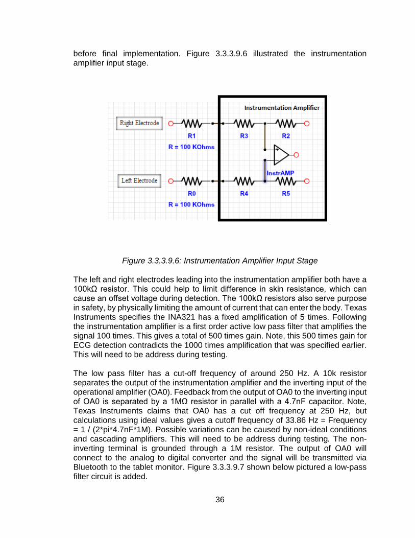
before final implementation. Figure 3.3.3.9.6 illustrated the instrumentation amplifier input stage.
Figure 3.3.3.9.6: Instrumentation Amplifier Input Stage
The left and right electrodes leading into the instrumentation amplifier both have a 100kΩ resistor. This could help to limit difference in skin resistance, which can cause an offset voltage during detection. The 100kΩ resistors also serve purpose in safety, by physically limiting the amount of current that can enter the body. Texas Instruments specifies the INA321 has a fixed amplification of 5 times. Following the instrumentation amplifier is a first order active low pass filter that amplifies the signal 100 times. This gives a total of 500 times gain. Note, this 500 times gain for ECG detection contradicts the 1000 times amplification that was specified earlier. This will need to be address during testing. The low pass filter has a cut-off frequency of around 250 Hz. A 10k resistor separates the output of the instrumentation amplifier and the inverting input of the operational amplifier (OA0). Feedback from the output of OA0 to the inverting input of OA0 is separated by a 1MΩ resistor in parallel with a 4.7nF capacitor. Note, Texas Instruments claims that OA0 has a cut off frequency at 250 Hz, but calculations using ideal values gives a cutoff frequency of 33.86 Hz = Frequency = 1 / (2*pi*4.7nF*1M). Possible variations can be caused by non-ideal conditions and cascading amplifiers. This will need to be address during testing. The non-inverting terminal is grounded through a 1M resistor. The output of OA0 will connect to the analog to digital converter and the signal will be transmitted via Bluetooth to the tablet monitor. Figure 3.3.3.9.7 shown below pictured a low-pass filter circuit is added.
36

Figure 3.3.3.9.7: Low-pass Filter Circuit Added
In this design Texas Instruments addresses a possible problem called baseline wandering. This is caused by differences in electrode and skin contact resistance and causes slow variations in the dc content of the amplified signal. This can lead to problems such as the amplifiers saturating and wavy traces in the ECG signal. The solution to this problem is using a feedback circuit between the output of the instrumentation amplifier and OA0 that integrates the dc component of the signal back into the input of the non-inverting terminal of the instrumentation amplifier. 0A1 consists of a high pass filter connected to the output of the instrumentation amplifier at one terminal and at the other terminal it connects to the noninverting terminal of OA0 through a 820 ohm resistor. Note, that connections to inverting and noninverting terminals of OA1 are not specified in diagram. The most likely connection is the high pass filter connecting to the inverting terminal because its feedback configuration. This will need to be address during testing. The high pass filter consists of a 1M resistor in series with a 0.1uF capacitor giving a calculated cutoff frequency of 1.59 Hz. Figure 3.3.3.9.8 illustrated the DC integrator circuit is added.
37

Figure 3.3.3.9.8: DC Integrator Circuit Added
Texas Instruments added a digital to analog converter (DAC1) to both the non-inverting and inverting terminals of the instrumentation amplifier to simulate baseline wandering as mentioned previously. The digital to analog converter is also fed to the terminal of OA1 that does not contain the high pass filter. Not included in this design is the third electrode that feeds back to the body. However, Texas Instruments mentions the configuration in the text of the report. Between DAC1 and the third electrode a unity gain buffer should be added. This configuration allows for clear monitoring and display applications. Figure 3.3.3.9.9 shown below is the picture with baseline wandering simulator added to the circuit.
Figure 3.3.3.9.9: Baseline Wandering Simulator Added
38
3.4 Components Research In this section, all physical hardware and components that were researched will be discussed. This includes our group's different options for microcontrollers, operational amplifiers, LCD displays, and digital to analog converters. 3.4.1 Heart Rate Simulator The Heart Rate Simulator has several different components that needed to be researched for this subsystem. The main components that have to be decided on are the microcontroller to use, the LCD display for the user to see the signals, what external memory type, and different DACs to output an analog signal. 3.4.1.1 Microcontroller Comparison When choosing a device to operate the simulator, several factors relating to the project came into play. First of all, since the simulator portion of the project should be reasonably small and hand-held, even though we are not dealing with power conservation, a low-power microcontroller cannot hurt and could suffice. They usually come in very small packages and if needed can sometimes be operated by using low-power batteries. The microprocessor has to read in the data from the ECG data source. It has to be able to store the thousands of lines of data for each of the ten sample signals. Also, the chosen microprocessor needs to have enough pins to connect and interface with outside systems. For example, the microprocessor will be taking input from at least two push buttons. These push buttons will be used to scroll up and down to switch between the different records. The other button would be used to select the signal that would be shown further down the line. The microprocessor will also be connected to an external display for showing the signal label when the user is selecting the exact signal to simulate. This display would be showing a label of the different sample signals the user is selecting between. Also, if any additional memory or converters are needed, pins will be used for this too. With all of these combined, our project needs at least twenty additional pins on the microprocessor. Since all of our group members have experience programming Texas Instrument MSP430 microcontroller, this family was initially our favorite. The MSP430 family is built around a modern 16-bit RISC CPU with 16-bit registers and constant generators. These factors combined result in a microprocessor that is very efficient and has relatively high execution performance. The MSP430 comes in several different variations with different advantages for each configuration. The main deciding factors between each MSP430 comes in the availability and differences of their analog-to-digital converters, digital-to-analog converters, comparators, timers, USARTs, LCD drivers, watchdog, internal oscillators, and so on. But they all are known for being the industry’s lowest power 16-bit microcontroller. With this
39
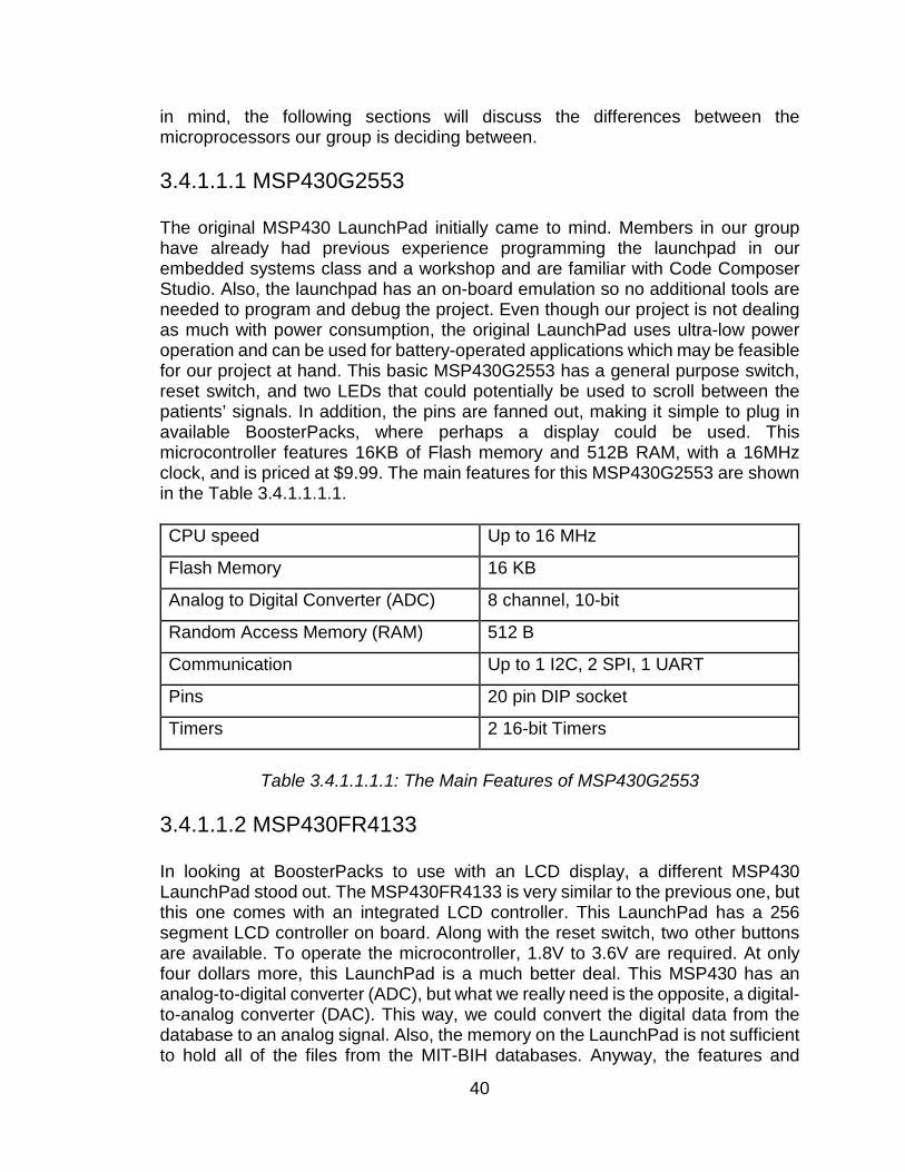
in mind, the following sections will discuss the differences between the microprocessors our group is deciding between. 3.4.1.1.1 MSP430G2553 The original MSP430 LaunchPad initially came to mind. Members in our group have already had previous experience programming the launchpad in our embedded systems class and a workshop and are familiar with Code Composer Studio. Also, the launchpad has an on-board emulation so no additional tools are needed to program and debug the project. Even though our project is not dealing as much with power consumption, the original LaunchPad uses ultra-low power operation and can be used for battery-operated applications which may be feasible for our project at hand. This basic MSP430G2553 has a general purpose switch, reset switch, and two LEDs that could potentially be used to scroll between the patients’ signals. In addition, the pins are fanned out, making it simple to plug in available BoosterPacks, where perhaps a display could be used. This microcontroller features 16KB of Flash memory and 512B RAM, with a 16MHz clock, and is priced at $9.99. The main features for this MSP430G2553 are shown in the Table 3.4.1.1.1.1. CPU speed Up to 16 MHz
Flash Memory 16 KB
Analog to Digital Converter (ADC) 8 channel, 10-bit
Random Access Memory (RAM) 512 B
Communication Up to 1 I2C, 2 SPI, 1 UART
Pins 20 pin DIP socket
Timers 2 16-bit Timers
Table 3.4.1.1.1.1: The Main Features of MSP430G2553
3.4.1.1.2 MSP430FR4133 In looking at BoosterPacks to use with an LCD display, a different MSP430 LaunchPad stood out. The MSP430FR4133 is very similar to the previous one, but this one comes with an integrated LCD controller. This LaunchPad has a 256 segment LCD controller on board. Along with the reset switch, two other buttons are available. To operate the microcontroller, 1.8V to 3.6V are required. At only four dollars more, this LaunchPad is a much better deal. This MSP430 has an analog-to-digital converter (ADC), but what we really need is the opposite, a digital-to-analog converter (DAC). This way, we could convert the digital data from the database to an analog signal. Also, the memory on the LaunchPad is not sufficient to hold all of the files from the MIT-BIH databases. Anyway, the features and
40
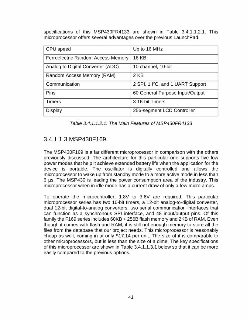
specifications of this MSP430FR4133 are shown in Table 3.4.1.1.2.1. This microprocessor offers several advantages over the previous LaunchPad. CPU speed Up to 16 MHz
Ferroelectric Random Access Memory 16 KB
Analog to Digital Converter (ADC) 10 channel, 10-bit
Random Access Memory (RAM) 2 KB
Communication 2 SPI, 1 I2C, and 1 UART Support
Pins 60 General Purpose Input/Output
Timers 3 16-bit Timers
Display 256-segment LCD Controller
Table 3.4.1.1.2.1: The Main Features of MSP430FR4133
3.4.1.1.3 MSP430F169 The MSP430F169 is a far different microprocessor in comparison with the others previously discussed. The architecture for this particular one supports five low power modes that help it achieve extended battery life when the application for the device is portable. The oscillator is digitally controlled and allows the microprocessor to wake up from standby mode to a more active mode in less than 6 µs. The MSP430 is leading the power consumption area of the industry. This microprocessor when in idle mode has a current draw of only a few micro amps. To operate the microcontroller, 1.8V to 3.6V are required. This particular microprocessor series has two 16-bit timers, a 12-bit analog-to-digital converter, dual 12-bit digital-to-analog converters, two serial communication interfaces that can function as a synchronous SPI interface, and 48 input/output pins. Of this family the F169 series includes 60KB + 256B flash memory and 2KB of RAM. Even though it comes with flash and RAM, it is still not enough memory to store all the files from the database that our project needs. This microprocessor is reasonably cheap as well, coming in at only $17.14 per unit. The size of it is comparable to other microprocessors, but is less than the size of a dime. The key specifications of this microprocessor are shown in Table 3.4.1.1.3.1 below so that it can be more easily compared to the previous options.
41
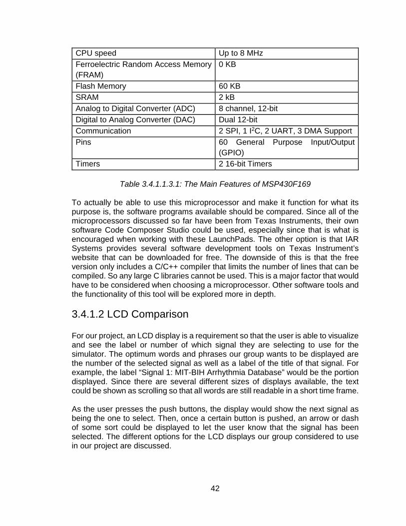
CPU speed Up to 8 MHz Ferroelectric Random Access Memory (FRAM)
0 KB
Flash Memory 60 KB SRAM 2 kB Analog to Digital Converter (ADC) 8 channel, 12-bit Digital to Analog Converter (DAC) Dual 12-bit Communication 2 SPI, 1 I2C, 2 UART, 3 DMA Support Pins 60 General Purpose Input/Output
(GPIO) Timers 2 16-bit Timers
Table 3.4.1.1.3.1: The Main Features of MSP430F169
To actually be able to use this microprocessor and make it function for what its purpose is, the software programs available should be compared. Since all of the microprocessors discussed so far have been from Texas Instruments, their own software Code Composer Studio could be used, especially since that is what is encouraged when working with these LaunchPads. The other option is that IAR Systems provides several software development tools on Texas Instrument’s website that can be downloaded for free. The downside of this is that the free version only includes a C/C++ compiler that limits the number of lines that can be compiled. So any large C libraries cannot be used. This is a major factor that would have to be considered when choosing a microprocessor. Other software tools and the functionality of this tool will be explored more in depth. 3.4.1.2 LCD Comparison For our project, an LCD display is a requirement so that the user is able to visualize and see the label or number of which signal they are selecting to use for the simulator. The optimum words and phrases our group wants to be displayed are the number of the selected signal as well as a label of the title of that signal. For example, the label “Signal 1: MIT-BIH Arrhythmia Database” would be the portion displayed. Since there are several different sizes of displays available, the text could be shown as scrolling so that all words are still readable in a short time frame. As the user presses the push buttons, the display would show the next signal as being the one to select. Then, once a certain button is pushed, an arrow or dash of some sort could be displayed to let the user know that the signal has been selected. The different options for the LCD displays our group considered to use in our project are discussed.
42
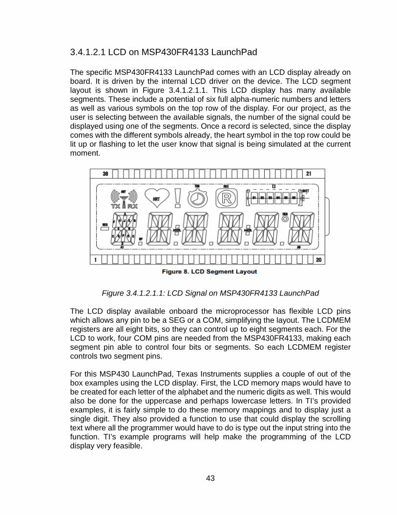
3.4.1.2.1 LCD on MSP430FR4133 LaunchPad The specific MSP430FR4133 LaunchPad comes with an LCD display already on board. It is driven by the internal LCD driver on the device. The LCD segment layout is shown in Figure 3.4.1.2.1.1. This LCD display has many available segments. These include a potential of six full alpha-numeric numbers and letters as well as various symbols on the top row of the display. For our project, as the user is selecting between the available signals, the number of the signal could be displayed using one of the segments. Once a record is selected, since the display comes with the different symbols already, the heart symbol in the top row could be lit up or flashing to let the user know that signal is being simulated at the current moment.
Figure 3.4.1.2.1.1: LCD Signal on MSP430FR4133 LaunchPad The LCD display available onboard the microprocessor has flexible LCD pins which allows any pin to be a SEG or a COM, simplifying the layout. The LCDMEM registers are all eight bits, so they can control up to eight segments each. For the LCD to work, four COM pins are needed from the MSP430FR4133, making each segment pin able to control four bits or segments. So each LCDMEM register controls two segment pins. For this MSP430 LaunchPad, Texas Instruments supplies a couple of out of the box examples using the LCD display. First, the LCD memory maps would have to be created for each letter of the alphabet and the numeric digits as well. This would also be done for the uppercase and perhaps lowercase letters. In TI’s provided examples, it is fairly simple to do these memory mappings and to display just a single digit. They also provided a function to use that could display the scrolling text where all the programmer would have to do is type out the input string into the function. TI’s example programs will help make the programming of the LCD display very feasible.
43

3.4.1.2.2 Crystalfontz LCD Display (CFAH1602B-YYH-JTE) If the LaunchPad MSP430 is not used, then our group will have to use an LCD display that would just be bought on its own. Crystalfontz manufactures and supplies character and graphic LCD modules and graphic OLED displays that can be used for embedded and different consumer applications. On their website is a very user-friendly product filter where we can select different preferences such as a foreground color, the number of lines, the number of characters, and any specific interface. For a simple LCD, just two lines of text and sixteen characters could suffice.
Figure 3.4.1.2.2.1 Crystalfontz LCD Display A fairly cheap and simple LCD module that was decided on is Crystalfontz’ CFAH1602B-YYH-JTE Character LCD Module. This module features a 16 character by 2 line LCD which has a somewhat large display area for the compact dimensions. It features a yellow/green LED backlight, edge style backlight, and is readable at a large viewing angle.
PIN SIGNAL LEVEL DIR DESCRIPTION 1 VSS 0V Ground 2 VDD +5.0V Supply voltage for logic 3 VO variable Supply voltage for driving LCD 4 RS H/L I Register selection input
H: Data register (for read and write) L: Instruction code (for write)
5 R/W H/L I H: Read (Module←Host) L: Write (Host→Module)
6 E H, H→L I Read/write enable signal H: Read data is enabled by a high level H→L: Write data latched on falling edge
7-14 DB0-DB7 H/L I/O Data bits 0-7 15 A (LED +) Supply voltage for LED
“A” (anode) or “+” of LED backlight 16 K (LED -) Supply voltage for LED
“K” (cathode) or “-” of LED backlight
Table 3.4.1.2.2.1: Interface Pin Functions
44
To interface with the microcontroller, there are 16 pins on the LCD display. The pins and their corresponding descriptions are shown in Table 4.2.4.2.2. There are two different types of data operations, either 4-bit or 8-bit operations. Using 4-bit operations to interface 4-bit data, the DB4 to DB7 4-bus line is used. This means that the DB0 to DB3 bus lines are not being used. To interface 8-bit data in the same way requires transferring twice. The higher 4-bit data (DB7 to DB4) is transferred first using the 4-busline, then the lower 4-bit data is transferred (DB3 to DB0). On the other hand, for 8-bit operations, the 8-bit data is transferred by 8-buslines (DB0 to DB7). The R/W pin is used to select whether it will be reading or writing actions. This bit is set when the LCD is processing. This LCD can be used in either a 4-bit or 8-bit parallel interface. It displays dark characters on a yellow-green background and is readable even when under direct sunlight. The necessary supply voltage for driving the LCD is variable. With an output voltage of +1.2V and a typical supply voltage for the logic of +5V, this gives the voltage for the LCD, VLCD, equal to the difference of the two, or 3.8V. This is all with a resistance between the supply voltage of 10kΩ, and supply current into the display of 1.2mA. These typical VO connections are shown in Figure 3.4.1.2.2.2.
Figure 3.4.1.2.2.2: Typical VO Connections This LCD display uses an LED backlight, which is fairly simple to use, but is also very easy to damage by abuse. The LEDs are current devices. So it is very important that to drive it, the current flowing through it is the main aspect to pay attention to instead of the voltage across it. A simple current limiting resistor in line from a voltage source will work well and is simpler than a current source. These typical LED backlight connections for the display to be “Always On” are shown in Figure 3.4.1.2.2.3. To do this, the forward voltage of the LEDs must be known so that the current limiting resistance (RLIMIT) can be calculated. The equation to calculate RLIMIT is just the difference between the supply voltage, VDD, and the typical LED forward voltage, VLED, divided by the typical LED forward current, ILED. So the specific calculation for the CFAH1602B-YYH-JTE LCD display with VDD equal to 5V, VLED equal to 4.2V, and ILED equal to 0.02A results in RLIMIT equal to 40Ω for a minimum.
45

Figure 3.4.1.2.2.3: LED Backlight Connections for “Always On” 3.4.1.3 External Memory Comparison For the simulator to store the large amount of data coming from the MIT-BIH databases, the memory on the microcontroller would not be sufficient enough to store all of these files. So other memory options were explored for us to use. 3.4.1.3.1 Flash Memory A flash memory chip can provide this necessary large storage space. Coming with the flash memory are several advantages also. The flash memory is very small in size, usually low in power consumption, and non-volatile so that the data would not be lost when the flash memory is no longer connected to power. With this in mind, the chosen flash memory is the Winbond W25Q16BV. It is a 16M-bit serial flash memory that operates on a single 2.7V to 3.6V power supply, with current consumption being as low as 4 mA active and 1 µA when the power-down. It supports the standard Serial Peripheral Interface (SPI), and a high performance Dual/Quad I/O SPI. This W25Q16BV flash memory can be interfaced with through an SPI compatible bus. This bus consists of four different signals, including the Serial Clock (CLK), Chip Select (/CS), Serial Data Input (DI), and Serial Data Output (DO). To serially write data to the device, the unidirectional DI input pin is used. It is written on the rising edge of the serial clock input pin, while the unidirectional DO output pin would be used to read the data or its status on the falling edge of the serial clock. This flash memory device also supports Dual and Quad SPI operation. The bidirectional IO pins are used to serially write data on the rising edge of CLK and read data from the device on the falling edge. For the Quad SPI instructions, the non-volatile Quad Enable bit (QE) in the status register-2 must be set. For Quad SPI operation, the non-volatile Quad Enable bit must set to 1. The write protect
46
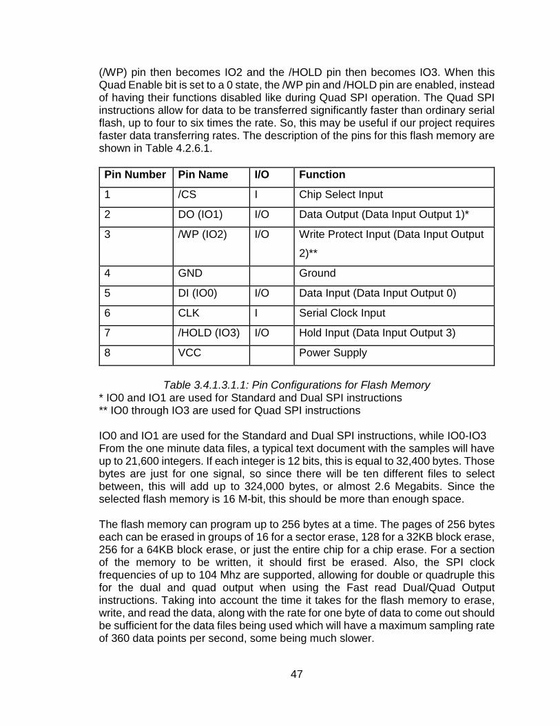
(/WP) pin then becomes IO2 and the /HOLD pin then becomes IO3. When this Quad Enable bit is set to a 0 state, the /WP pin and /HOLD pin are enabled, instead of having their functions disabled like during Quad SPI operation. The Quad SPI instructions allow for data to be transferred significantly faster than ordinary serial flash, up to four to six times the rate. So, this may be useful if our project requires faster data transferring rates. The description of the pins for this flash memory are shown in Table 4.2.6.1. Pin Number Pin Name I/O Function
1 /CS I Chip Select Input
2 DO (IO1) I/O Data Output (Data Input Output 1)*
3 /WP (IO2) I/O Write Protect Input (Data Input Output
2)**
4 GND Ground
5 DI (IO0) I/O Data Input (Data Input Output 0)
6 CLK I Serial Clock Input
7 /HOLD (IO3) I/O Hold Input (Data Input Output 3)
8 VCC Power Supply
Table 3.4.1.3.1.1: Pin Configurations for Flash Memory
* IO0 and IO1 are used for Standard and Dual SPI instructions ** IO0 through IO3 are used for Quad SPI instructions IO0 and IO1 are used for the Standard and Dual SPI instructions, while IO0-IO3 From the one minute data files, a typical text document with the samples will have up to 21,600 integers. If each integer is 12 bits, this is equal to 32,400 bytes. Those bytes are just for one signal, so since there will be ten different files to select between, this will add up to 324,000 bytes, or almost 2.6 Megabits. Since the selected flash memory is 16 M-bit, this should be more than enough space. The flash memory can program up to 256 bytes at a time. The pages of 256 bytes each can be erased in groups of 16 for a sector erase, 128 for a 32KB block erase, 256 for a 64KB block erase, or just the entire chip for a chip erase. For a section of the memory to be written, it should first be erased. Also, the SPI clock frequencies of up to 104 Mhz are supported, allowing for double or quadruple this for the dual and quad output when using the Fast read Dual/Quad Output instructions. Taking into account the time it takes for the flash memory to erase, write, and read the data, along with the rate for one byte of data to come out should be sufficient for the data files being used which will have a maximum sampling rate of 360 data points per second, some being much slower.
47
3.4.1.3.2 SD Card An alternate method is to use an SD card for the external memory. The use of an SD card is inexpensive and supports very microcontroller friendly SPI protocol. There are a few different online sources that discuss interfacing and connecting an SD card to the MSP430 that would be one of our microcontroller options. There exists a free, open-source FAT file system library, which can be used on flash disks and USB sticks. But since the MSP430 is already low on memory, dumping large libraries is not a good idea. So a related smaller library, named Petite-FS, can work. We would pre-create the file on the SD card on our computer of all the data of the heart signals before using it on the MSP430. An SD card socket could be purchased, where the SD card would just be pushed in and out of that, and the pins would be soldered onto our PCB. As for the code, Energia has example tutorials that can be unzipped and work with the MSP430. With these tutorials and online resources, the use of an SD card seems like a much cheaper and practical solution to the memory issue. 3.4.1.4 Digital to Analog Converter Comparison The digital to analog converter will convert the digital data into analog signals, or voltages in our project. The main use of this device will be to convert the digital samples from the MIT-BIH files into analog signals so that the ECG simulator can nearly replicate an actual patient’s ECG signal. There are some things that need to be considered. If one of the MSP430 LaunchPads are used, then our group must purchase our own DAC. On the other hand, if the MSP430F169 is used, a digital-to-analog converter is already built into it. In this section, the two DACs will be discussed. 3.4.1.4.1 DAC 7760 Texas Instruments sells a useful digital-to-analog converter, DAC 7760. It is a low-cost, precision, full-integrated, 12-bit digital-to-analog converter. In addition to being able to be programmed as a current output, our use will be for it to function as a voltage output. This device can be programmed as a voltage output with several different ranges of voltages to output. This device also includes a power-on-reset function so that when it is powering up, it can be in a known state. In this case, both IOUT and VOUT are disabled and the device is in a Hi-Z state. To set the voltage to output to zero-scale or midscale, the CLR and CLR-SEL pins must be set. Another plus for this device is that the output slew rate can be programmed by the register. This digital-to-analog converter would be the best option if either of the LaunchPads are used.
48
3.4.1.4.2 DAC12 Built Into MSP430F169 The MSP430F169 already comes with two built-in digital-to-analog converters, so now one will not have to be purchased. This particular DAC is a 12-bit monotonic output type DAC. This means that the output changes in the same direction for each increase in the input code, or it would remain the same. Likewise, for decreasing input code, the output changes in that direction. The type of DAC12 that comes on this microprocessor is referred to as an R-ladder type DAC. This DAC is binary weighted, and it creates each value with a repeating structure of 2 resistor values. These resistor values will be R and 2R. In this way, it is much easier to produce many equally matched values of resistors, but the conversion speed is lower because of parasitic capacitance. This DAC12 can be used in two different modes, either an 8-bit or 12-bit mode. The 8-bit mode will not be used since it just reduces the resolution, so our group has decided to implement the DAC in the 12-bit mode. When the resolution of the 12-bit DAC is discussed, this is referring to the number of output levels that are possible to reproduce using the DAC. The number of bits being used is the base two logarithm of the number of levels. Using this knowledge, the more levels we have, the higher the resolution. So our 12-bit DAC is designed to reproduce or 4096 levels. There are several different options available for the DAC. The settling time speed with respect to power consumption can vary, meaning that faster settling time requires more power to be used. Also, the options of using an internal voltage reference or an external voltage reference, using binary or two’s compliment data, and the ability to use two DAC12s synchronized all must be considered. These different configurations are chosen using the Control Register (DAC12_xCTL) on the DAC. The 16 bits of this register will be configured using the software on the microcontroller. The other important register we need to consider is the data register. It is also a 16-bit register, but this DAC uses only 12 bits so bits zero through eleven will be used. This data register has been designed so that it will receive data as unsigned integers which range from zero to 4095, or 212. To send out data in the form of unsigned integers, the data files from the MIT-BIH online database will be reformatted. 3.4.2 ECG Reader For the ECG reader, different microcontrollers and instrumentation amplifiers had to be decided on. Also, for the Bluetooth communication, we had to finalize which Bluetooth module to use and how that interaction between the app and the ECG reader will work.
49

3.4.2.1 Microcontroller Comparison Whether we decide to transfer online data to simulate an ECG signal or use real ECG signal, an embedded system is indispensable. Microcontrollers or microprocessors are flexible electronics that provide a good prototyping platform for electrical engineers. There are many choices of microcontrollers and microprocessor on the market. Spending the time to select the optimum embedded systems could save us a lot of time and money. These microcontrollers are listed below with different specifications such as power consumption, processor speed, memory size, and number of I/O pins. Since we already want to use Atmel microcontroller for our project, Table 3.4.2.1 concludes the difference and similarity between two Atmel microcontrollers. ATmega ATtiny Operating Voltage 1.8 V to 5.5 V 2.7 V to 5.5 V In system memory 4/8/16/32K Bytes 2/4/8K Bytes External Clock
Up to 20 MHz Up to 20 MHz
Internal Clock 1 MHz or 8 MHz 1 MHz or 8 MHz I/O pins 23 6 Analog inputs 6 channels (10 bits ADC) 4 (10 bits ADC, sharing
with I/O pins)
Table 3.4.2.1: ATmega vs. ATtiny 3.4.2.1.1 Atmel ATmega328 ATmega328 is the Atmel microcontroller. It also used on Arduino UNO. This product allow us to build our project on a smaller scale without using a full size Arduino board. There are three types of integrated circuit package Atmel offers: TQFP, PDIP, and MLF. Since one of our group members already has an Arduino UNO board, DIP package will be a better choice. The DIP package is more flexible and we could program the microcontroller on an Arduino UNO board and then attach it on our PCB design. The Figure 3.4.2.1.1.1 is the pin configuration of ATmega328 in DIP package.
50
Figure 3.4.2.1.1.1: Pin Configuration of ATmega328
The Table 3.4.2.1.1.1 concludes all the usage of PIN on ATmega328 in the DIP package. PIN Descriptions VCC Digital Supply Voltage (5V) GND Ground Port B(PB7:0) 8-bit bidirectional I/O port with internal pull-up resistor.
Depending on the clock selection fuse settings, PB6 can be used as input to the inverting Oscillator amplifier and input to the internal clock operating circuit. PB7 can be used as output from the inverting Oscillator amplifier.
Port C (PC5:0) 7-bit bidirectional I/O port with internal pull-up resistor. This port has the analog to digital converter input channel.
PC6/RESET If the RSTDISBL Fuse is programmed, PC6 is used as an I/O pin. If not, PC6 is used as a Reset input.
Port D (PD7:0) 8-bit bidirectional I/O port with internal pull-up resistors. PD1 is USART Output Pin. PD0 is USART Input Pin.
AVcc The supply voltage pin for the ADC, PC3:0, and ADC7:6. If the ADC is used, it should be connected to Vcc through a low-pass filter. If the ADC is not used, it should still be externally connected to Vcc.
AREF The analog reference pin for the ADC
Table 3.4.2.1.1.1: Descriptions of Pin Configuration of ATmega
51

There are many tutorials online that show people how to build your own Arduino on a breadboard. We can walk through all the steps including making a printed
circuit board (PCB), building an Arduino and loading the programs/sketches onto the board. We read some of these tutorials and the datasheet of ATmega328. We figured out all the necessary items to make another microcontroller board.
Table 3.4.2.1.1.2 lists all the items that we need and the price of each item. We can used this table as reference to purchase all necessary components.
Items Amount Price
DIP Sockets Solder Tail - 28 pin 0.3” 1 $0.95
ATmega328 with Arduino Optiboot 1 $5.50
LED - Basic Green 3mm (optional) 1 $0.35
Resistor 330 Ω 1 $0.25
Resistor 10 kΩ 1 $0.25
Mini Push Button Switch 1 $0.35
Electrolytic Decoupling Capacitors - 10uF/25V 4 $1.80
Voltage Regulator - 5V (L7805) 1 $0.95
Crystal 16 MHz 1 $0.95
Capacitor Ceramic 22pF 2 $0.25
Total $11.60
Table 3.4.2.1.1.2: Items to Build ATmega328 without Development Board
3.4.2.1.2 Atmel ATtiny85 ATtiny85 has a very similar characteristic of ATmega328 except this microcontroller is much smaller. Since we only need to convert one analog signal to a digital signal, we will not need that many I/O pins as ATmega328 provides. The small size also becomes the advantage of choosing a microcontroller to do the analog-to-digital converter job. However, the disadvantage of using ATtiny85 is that the memory is small; the limited pinouts make it impossible to have an external flash memory. On the other hand, the advantage of using ATtiny85 is that we can save space and money. One ATtiny85 chip only costs around $2.84. ATtiny85 only has 8 pinouts. Similar to ATmega328, the Figure 3.4.2.1.2.1 is the pinouts name and functions. The Table 3.4.2.1.2.1 lists the alternative functions for Port B.
52
Figure 3.4.2.1.2.1: Pin Configuration of ATtiny85
Port Pin Alternate Function PB5 RESET’: Reset Pin
dW: debugWIRE I/O ADC0: ADC Input Channel 0 PCINT5: Pin Change Interrupt, Source 5
PB4 XTAL2: Crystal Oscillator Output CLKO: System Clock Output ADC2: ADC input Channel 2 OC1B: Timer/Counter1 Compare Match B Output PCINT4: Pin Change Interrupt 0, Source 4
PB3 XTAL1: Crystal Oscillator Output CLK1: External Clock Output ADC3: ADC input Channel 3 OC1B’: Complementary Timer/Counter1 Compare Match B Output PCINT3: Pin Change Interrupt 0, Source 3
PB2 SCK: Serial Clock Input ADC1: ADC input Channel 1 T0: Timer/Counter0 Clock Source USCK: USI Clock (Three Wire Mode) SCL: USI Clock (Two Wire Mode) INT0: External Interrupt 0 Input PCINT2: Pin Change Interrupt 0, Source 2
PB1 MISO: SPI Master Data Input/ Slave Data Output AIN1: Analog Comparator, Negative Input OC0B: TImer/Counter0 Compare Match B Output OC1A: TImer/Counter1 Compare Match A Output DO: USI Data Output (Three Wire Mode) PCINT1: Pin Change Interrupt 0, Source 1
PB0 MISI: SPI Master Data Output/ Slave Data Input AIN0: Analog Comparator, Positive Input OC0A: TImer/Counter0 Compare Match A Output OC1A’: Complementary TImer/Counter1 Compare Match A Output DI: USI Data Input (Three Wire Mode) SDA: USI Data Input (Two Wire Mode) AREF: External Analog Reference PCINT0: Pin Change Interrupt 0, Source 0
Table 3.4.2.1.2.1: The Alternative Functions of Port B for ATtiny
53
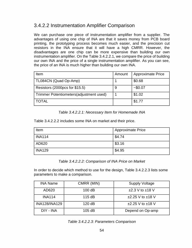
3.4.2.2 Instrumentation Amplifier Comparison We can purchase one piece of instrumentation amplifier from a supplier. The advantages of using one chip of INA are that it saves money from PCB board printing, the prototyping process becomes much easier, and the precision cut resistors in the INA ensure that it will have a high CMRR. However, the disadvantages are one chip can be more expensive than building our own instrumentation amplifier. On the Table 3.4.2.2.1, we compare the price of building our own INA and the price of a single instrumentation amplifier. As you can see, the price of an INA is much higher than building our own INA. Item Amount Approximate Price
TL084CN (Quad Op-Amp) 1 $0.68
Resistors (2000pcs for $15.5) 9 ~$0.07
Trimmer Potentiometers(adjustment used) 1 $1.02
TOTAL $1.77
Table 3.4.2.2.1: Necessary Item for Homemade INA
Table 3.4.2.2.2 includes some INA on market and their price. Item Approximate Price
INA114 $4.74
AD620 $3.16
INA129 $4.95
Table 3.4.2.2.2: Comparison of INA Price on Market
In order to decide which method to use for the design, Table 3.4.2.2.3 lists some parameters to make a comparison.
INA Name CMRR (MIN) Supply Voltage
AD620 100 dB ±2.3 V to ±18 V
INA114 115 dB ±2.25 V to ±18 V
INA128/INA129 120 dB ±2.25 V to ±18 V
DIY - INA 105 dB Depend on Op-amp
Table 3.4.2.2.3: Parameters Comparison
54

3.4.2.3 Operational Amplifiers Comparison Operational Amplifiers (Op-amps) is one of the main component we will be using throughout the entire project. Therefore, choosing a right op-amp is very important. Table 3.4.2.3.1 summaries the op-amp characteristics and price. Since we are going to use a lot of op-amps, we decided to search for the amplifier IC with 4 channel on it. Operational Amplifier LM348N TL084CN Price $0.62 0.68 Supply Voltage ±4 V to ±18 V ±3.5 V to ±18 V CMRR (MIN) 70 dB 70 dB Manufacturer TI TI
Table 3.4.2.3.1: Op-amp Characteristics
3.4.2.4 Bluetooth Comparison BTM-5 module is a class 2 Bluetooth module using BlueCore4-External chipset from a Bluetooth chipset supplier Cambridge Silicon Radio. This module support both Master and Slave mode operations. It can be changed by AT command configuration. Each Master/Slave BTM-5 pair auto link with the default device address after power up. After the link is established, user can transmit and receive data via the UART interface with each other. BTM-5 module is also widely used on communication between Arduino microcontroller and Mobile device. The Table 3.4.2.4.1 is the specification of a BTM-5. Parameters Specifications Operating Frequency Band 2.4 GHz-2.48 GHz unlicensed ISM
Band Bluetooth Specification V2.0+EDR Output Power Class -4 ~ 6 dBm adjustable , Class 2 Sensitivity -80 dBm at 0.1% BER Data Rate Asynchronous: 2 Mbps (Max) Operating Voltage 3.3 V Host Interface USB/UART Audio Interface PCM and Analog interface Flash Memory Size 8 Mbit Operation Temperature -20 ~ +55 Dimension 26.9mm(L) x 13mm(W) x 2.2mm(H)
Table 3.4.2.4.1: BTM-5 Specification
55

They provided two variations of BTM-5 breakout board, one is RS232 interface, and the other one is TTL interface. These two difference breakout board use different supply voltage and difference interface. RS232 breakout board used 5 V power supply and TTL breakout board used 3.3 V power supply. The Bluetooth module without breakout board is cheaper but more difficult to solder. Since we will start building our prototype first, we used the Bluetooth module with the TTL breakout board. Another Bluetooth module we can use is HC-06. HC-06 has similar specification as BTM-5. One advantage of choosing this Bluetooth module is that we already owned this Bluetooth module.
4. Project Hardware and Software Design Details Now that all of the different options have been discussed, we made important decisions on which actual hardware we would end up using. In this section, the main decisions and components being used for each subsystem, along with details on the software in our project is discussed. 4.1 ECG Simulator In the end, we decided to use the MSP430G2553. This is the microcontroller that originally comes on board the Launchpad. This microcontroller was very cheap, and with just twenty pins, this is just enough for our project. Since we are going to be testing several different signals, with more than 300 data points per second, none of the microcontrollers we looked at had enough memory so we did not really put the memory space as a major factor when picking a microcontroller. All members in our group have already had experience programming the launchpad in our embedded systems class and are familiar with Code Composer Studio. Also, for this microprocessor and using the Launchpad, it is much easier to code and test this subsystem of our project. Once the microprocessor is on the PCB, it can act as a standalone chip and it is very simple to load new software onto the chip and test it. Since with the final product, we did not use the entire Launchpad, we had to connect external push buttons that were used for the simulator. So we are using a simple pull-up configuration for the switches. We combated the bouncing of the switch by adding a capacitor. Using the equation for an RC circuit, our time constant is about 3.3ms. The capacitor is considered charged after about 17ms. When the button is pressed and the switch is closed, the voltage across the capacitor is discharged through the switch to ground. Since there is little resistance, this happens quickly. When the switch is released and open, the capacitor is charged via the 33k resistor and should take about 17ms to charge back up to the supply voltage. Any spikes from bouncing contacts are absorbed by the RC circuit. This configuration is shown in Figure 4.1.1.
56
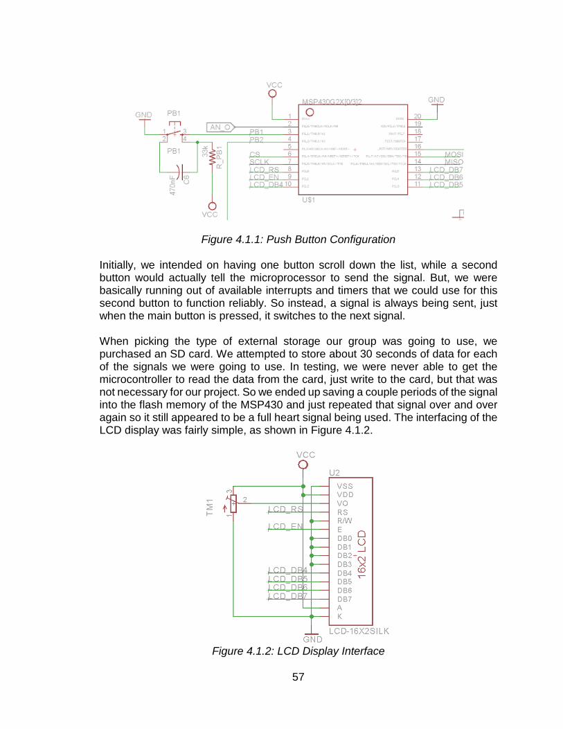
Figure 4.1.1: Push Button Configuration Initially, we intended on having one button scroll down the list, while a second button would actually tell the microprocessor to send the signal. But, we were basically running out of available interrupts and timers that we could use for this second button to function reliably. So instead, a signal is always being sent, just when the main button is pressed, it switches to the next signal. When picking the type of external storage our group was going to use, we purchased an SD card. We attempted to store about 30 seconds of data for each of the signals we were going to use. In testing, we were never able to get the microcontroller to read the data from the card, just write to the card, but that was not necessary for our project. So we ended up saving a couple periods of the signal into the flash memory of the MSP430 and just repeated that signal over and over again so it still appeared to be a full heart signal being used. The interfacing of the LCD display was fairly simple, as shown in Figure 4.1.2.
Figure 4.1.2: LCD Display Interface
57
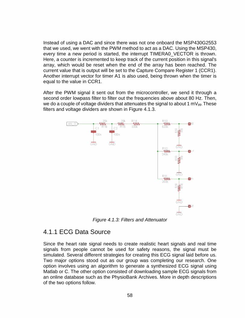
Instead of using a DAC and since there was not one onboard the MSP430G2553 that we used, we went with the PWM method to act as a DAC. Using the MSP430, every time a new period is started, the interrupt TIMERA0_VECTOR is thrown. Here, a counter is incremented to keep track of the current position in this signal's array, which would be reset when the end of the array has been reached. The current value that is output will be set to the Capture Compare Register 1 (CCR1). Another interrupt vector for timer A1 is also used, being thrown when the timer is equal to the value in CCR1. After the PWM signal it sent out from the microcontroller, we send it through a second order lowpass filter to filter out the frequencies above about 80 Hz. Then, we do a couple of voltage dividers that attenuates the signal to about 1 mVpp. These filters and voltage dividers are shown in Figure 4.1.3.
Figure 4.1.3: Filters and Attenuator
4.1.1 ECG Data Source Since the heart rate signal needs to create realistic heart signals and real time signals from people cannot be used for safety reasons, the signal must be simulated. Several different strategies for creating this ECG signal laid before us. Two major options stood out as our group was completing our research. One option involves using an algorithm to generate a synthesized ECG signal using Matlab or C. The other option consisted of downloading sample ECG signals from an online database such as the PhysioBank Archives. More in depth descriptions of the two options follow.
58
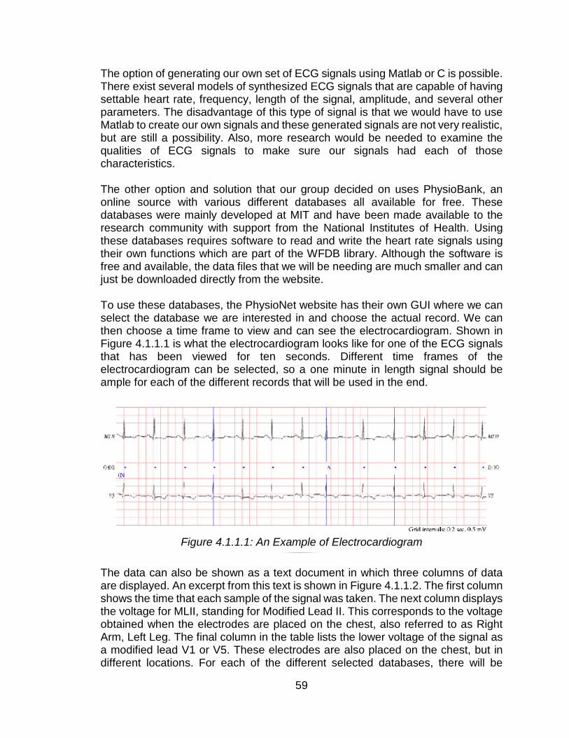
The option of generating our own set of ECG signals using Matlab or C is possible. There exist several models of synthesized ECG signals that are capable of having settable heart rate, frequency, length of the signal, amplitude, and several other parameters. The disadvantage of this type of signal is that we would have to use Matlab to create our own signals and these generated signals are not very realistic, but are still a possibility. Also, more research would be needed to examine the qualities of ECG signals to make sure our signals had each of those characteristics. The other option and solution that our group decided on uses PhysioBank, an online source with various different databases all available for free. These databases were mainly developed at MIT and have been made available to the research community with support from the National Institutes of Health. Using these databases requires software to read and write the heart rate signals using their own functions which are part of the WFDB library. Although the software is free and available, the data files that we will be needing are much smaller and can just be downloaded directly from the website. To use these databases, the PhysioNet website has their own GUI where we can select the database we are interested in and choose the actual record. We can then choose a time frame to view and can see the electrocardiogram. Shown in Figure 4.1.1.1 is what the electrocardiogram looks like for one of the ECG signals that has been viewed for ten seconds. Different time frames of the electrocardiogram can be selected, so a one minute in length signal should be ample for each of the different records that will be used in the end.
Figure 4.1.1.1: An Example of Electrocardiogram
The data can also be shown as a text document in which three columns of data are displayed. An excerpt from this text is shown in Figure 4.1.1.2. The first column shows the time that each sample of the signal was taken. The next column displays the voltage for MLII, standing for Modified Lead II. This corresponds to the voltage obtained when the electrodes are placed on the chest, also referred to as Right Arm, Left Leg. The final column in the table lists the lower voltage of the signal as a modified lead V1 or V5. These electrodes are also placed on the chest, but in different locations. For each of the different selected databases, there will be
59
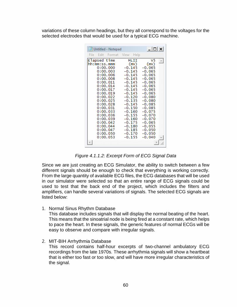
variations of these column headings, but they all correspond to the voltages for the selected electrodes that would be used for a typical ECG machine.
Figure 4.1.1.2: Excerpt Form of ECG Signal Data
Since we are just creating an ECG Simulator, the ability to switch between a few different signals should be enough to check that everything is working correctly. From the large quantity of available ECG files, the ECG databases that will be used in our simulator were selected so that an entire range of ECG signals could be used to test that the back end of the project, which includes the filters and amplifiers, can handle several variations of signals. The selected ECG signals are listed below: 1. Normal Sinus Rhythm Database
This database includes signals that will display the normal beating of the heart. This means that the sinoatrial node is being fired at a constant rate, which helps to pace the heart. In these signals, the generic features of normal ECGs will be easy to observe and compare with irregular signals.
2. MIT-BIH Arrhythmia Database
This record contains half-hour excerpts of two-channel ambulatory ECG recordings from the late 1970s. These arrhythmia signals will show a heartbeat that is either too fast or too slow, and will have more irregular characteristics of the signal.
60
3. QT Database In this database, there are several two-lead ECG recordings that also show labels of the signals at the peaks and point out different factors to notice. The QT interval is the time between the start of the Q wave and the end of the T wave. With irregular signals, the QT interval will be lengthened in comparison to a typical ECG.
Each of these databases were sampled at different frequencies. For example, the data in Figure 4.1.1.2 was sampled at 360 samples per second. For us to use a one minute waveform except from this signal, there ends up being 21,600 rows of data for each of the columns in the table. The databases mostly have a sample rate of around 100 to 300 samples per second. Using the text data for each signal being used, the digital data will be able to be converted to an analog signal using the microprocessor and the pulse width modulation, followed by the series of low pass filters. 4.2.2 Formatting the ECG Data Files The data that is used to graph each heart signal being used has to be scaled so that it is distributed between the ranges of 0 to 256 since we are using eight bits for the pulse width modulation method of getting the analog signal. To scale the decimal values, first a scaling factor is needed. To initially calculate the scaling factor, several parameters are needed. These include the resolution that we used of 8 bits, the maximum data value from that individual data file, and the minimum data value. To calculate the scaling factor, S, using these parameters, the following formula will be used.
Once this scaling factor is obtained, the minimum value should be subtracted from each original data value. Then, the newly obtained value would be multiplied by the scaling factor and finally converted to an unsigned integer. This is shown in the formula below.
To format these data files and scale the values, all values were pasted into Microsoft Excel and scaled using the equations previously discussed. Once all of the values were scaled that we would be using for each signal, we checked to make sure the signal appeared to be what we expected. The original ECG signal using the data from the MIT-BIH database was plotted with the scale in millivolts. Then this plot was compared with a plot of the formatted data values using integer values ranging from zero to 256. The plot of the formatted data was compared
61
side-by-side with the original data. These comparison plots were checked to make sure they look exactly the same. The only difference was expected and was the fact that the amplitude is different as a result of the scaling.
4.2 ECG Reader A good ECG signal measurement is to amplify the small biopotential signal and also filter the external and internal noise out. The main core of the electrocardiogram Reader is divided into several subsystem: electrode, instrumentation amplifier, bandpass filter, notch filter, gain amplifier, analog to digital converter, and microcontroller. Basic Requirements:
To take a weak electric signal of biological origin and increase its amplitude with an amplifier
High input impedance so that ECG amplifier provides minimal loading to avoid distortion of the signal. A typical input impedance is 1 MΩ
Input circuit must provide protection. Minimize current flow appearing at the input terminals.
Output circuit that is used to drive the amplifier load should have a low output impedance in order to minimize load regulation effect.
ECG amplifier must be designed to be optimal in a particular
frequency range as needed by the signal to obtain optimal signal to noise ratios
4.2.1 Three-Lead Electrodes For this project, a 3-lead electrocardiogram system will be used. The 3-lead system is the simplest ECG design and can be easily realized using basic circuit designs. There are actually 3 electrodes in the 3-lead system unlike the 12-lead system that uses 10 electrodes. Many placement options can be used in the 3-lead design. One way is placing an electrode on the interior side of each wrist. The final electrode can be placed on either the left of right ankle. This placement creates what is called an Einthoven’s triangle. Three separate ECG graphs can be derived from this placement depending on which electrode is designated to be the ground potential. The difference in voltage potential between the left and right arm electrodes with the leg electrode designated as ground is referred to as “Lead I”. “Lead II” is the difference in voltage between the right arm and leg electrode with the left arm designated as ground.
62
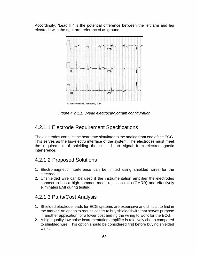
Accordingly, “Lead III” is the potential difference between the left arm and leg electrode with the right arm referenced as ground.
Figure 4.2.1.1: 3-lead electrocardiogram configuration
4.2.1.1 Electrode Requirement Specifications The electrodes connect the heart rate simulator to the analog front end of the ECG. This serves as the bio-electro interface of the system. The electrodes must meet the requirement of shielding the small heart signal from electromagnetic interference. 4.2.1.2 Proposed Solutions 1. Electromagnetic interference can be limited using shielded wires for the
electrodes. 2. Unshielded wire can be used if the instrumentation amplifier the electrodes
connect to has a high common mode rejection ratio (CMRR) and effectively eliminates EMI during testing.
4.2.1.3 Parts/Cost Analysis 1. Shielded electrode leads for ECG systems are expensive and difficult to find in
the market. An option to reduce cost is to buy shielded wire that serves purpose in another application for a lower cost and rig the wiring to work for the ECG.
2. A high quality low noise instrumentation amplifier is relatively cheap compared to shielded wire. This option should be considered first before buying shielded wires.
63

Figure 4.2.1.3.1: 3-lead Electrode Block Diagram
4.2.2 Instrumentation Amplifier There are several INAs in the market. Instead of using three op-amps to build one INA, we can use one instrumentation amplifier. The method of designing an INA is similar as using three op-amps. We can also use the method discussed below to get rid of common-voltage.
The INA128 and INA129 are low power, general purpose instrumentation amplifiers offering excellent accuracy. Some of the features are listed below:
LOW OFFSET VOLTAGE: 50mV max. LOW DRIFT: 0.5mV/°C max. LOW INPUT BIAS CURRENT: 5nA max. HIGH CMR: 120 dB min. INPUTS PROTECTED TO ±40V. WIDE SUPPLY RANGE: ±2.25 to ±18V. LOW QUIESCENT CURRENT: 700mA. 8-PIN PLASTIC DIP, SO-8.
To calculate the gain is really simply, Figure 4.2.2.1 shown includes the equation to configure the desired gain.
Figure 4.2.2.1: INA128/INA129 Pin Configuration and Gain Equation
64

For our design, we choose RG = 1kΩ. The gain we get is 51. We implemented it with the gain of 100, the minimum CMRR would be 120. However, similar idea as three op-amps INA, the noise would still affect the output of the circuit. In addition to that, there are built in over-voltage protection in the Integrated circuit chip. Therefore, we do not have to worry about them.
4.2.3 Bandpass Filter To design a filter, four things must be known in advance: 1. The power supplies: we need to know whether we are using single power
supply or dual power supply. 2. The frequencies that need to be passed, and those that need to be rejected. 3. The transition frequency: we need to know the point at which the filter starts to
work and where the filter is centered so that it will be symmetrical. 4. An initial capacitor value: we need to pick a capacitor that will not make
resulting resistor values too large or too small. We designed a second order high-pass filter as shown in Figure 4.3.3.1. The cutoff frequency would be 0.05 Hz. In our design, we had two of the second order high-pass filter cascading each other which made the fourth order high-pass filter.
Figure 4.2.3.1: Second Order High-Pass Filter Circuit Design
65
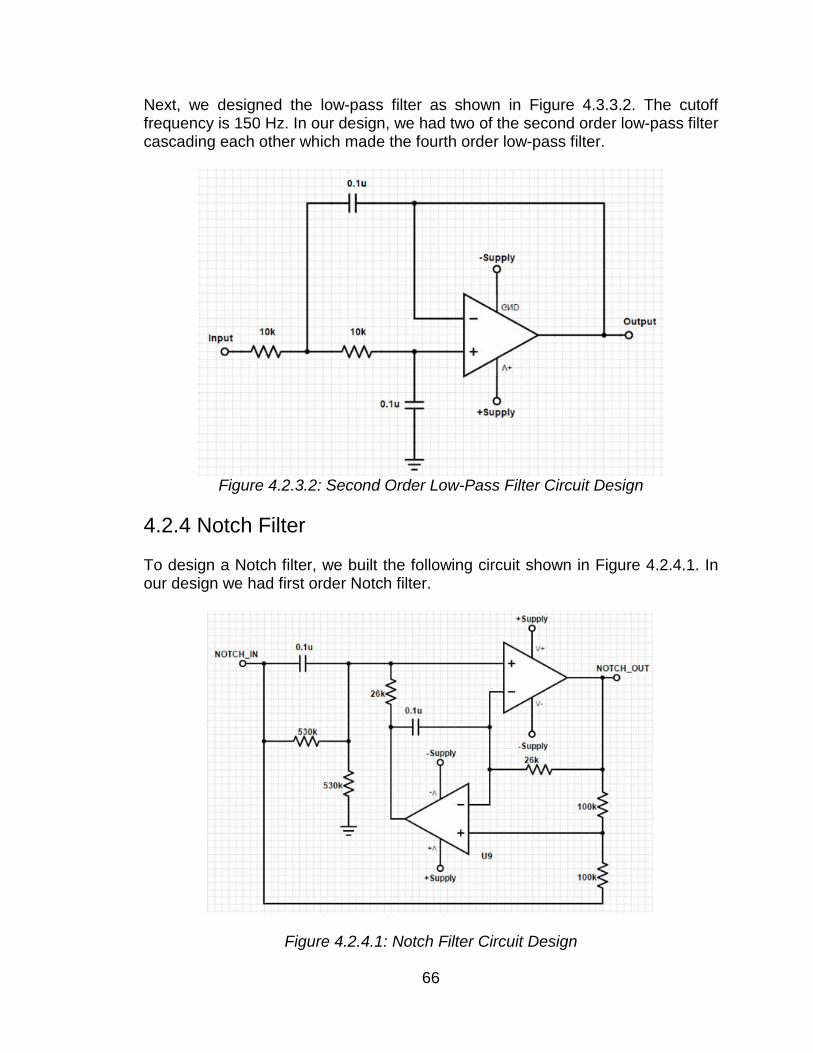
Next, we designed the low-pass filter as shown in Figure 4.3.3.2. The cutoff frequency is 150 Hz. In our design, we had two of the second order low-pass filter cascading each other which made the fourth order low-pass filter.
Figure 4.2.3.2: Second Order Low-Pass Filter Circuit Design
4.2.4 Notch Filter To design a Notch filter, we built the following circuit shown in Figure 4.2.4.1. In our design we had first order Notch filter.
Figure 4.2.4.1: Notch Filter Circuit Design
66

4.2.5 The Gain Amplifier The output impedance of the amplifier should be very low in order to drive any external load with minimal distortion. Any distortion caused by the output impedance might create clipping and not enough gain at the gain stage. Since the desired signal is in a small range, the signal needed to be amplified in order to be better interpreted. Typically, a gain of over 1000 is implemented in biopotential amplifier circuits. The amplifier must have a high common mode rejection ratio to eliminate large offset signals. The amplifiers must have the following characteristics:
1. Zero output impedance
2. Infinite input impedance
3. Zero noise
4. Zero input offset voltage
5. High common-mode rejection ratio (CMRR) 4.2.6 ECG Reader Microcontroller Atmel ATtiny85 was the microcontroller we used to transmit the ECG signal to mobile app. Figure 4.3.6.1 shown below is the schematic of the microcontroller unit. For reading ECG signal, we only need one analog input and we used PB0, PB1, PB2, and PB5 as it displayed on the schematic.
Figure 4.2.6.1: PCB Schematic for ATiny and Bluetooth
67

4.2.7 Median Filter The digital filter was added with Arduino code because the Notch filter did not filter out all the power interference as we expected it would be. Figure 4.2.7.1 shown below is the screenshot that showed the distortion noise appeared along with the simulated ECG signal.
Figure 4.2.7.1: Signal Before Median Filter
The filter we used is median filter. We used a window size of three with one entry immediately preceding and following each entry because there is no entry preceding the first value, the first value is repeated, same as with the last value. For instance, If the exact value is [2 80 6 3],
y[1] = Median[2 2 80] = 2, y[2] = Median[2 80 6] = 6, y[3] = Median[80 6 3] = 6, y[4] = Median[6 3 3] = 3.
so the final output is [2 6 6 3]. Figure 4.3.8.3 shown below is the filtered signal after using median filter.
Figure 4.2.7.2: Signal After Median Filter
68

4.3 Mobile Application (Android) In this day and age ever since the introduction of the iPhone, we have seen a revolution in the industry of smart phones and the tremendous growth of consumers that own a smartphone and the growth of mobile application development. There are over 50 million applications downloaded on Android devices and 48 million applications downloaded on Apple devices in 2013. Wireless sensor technology had also advanced which made remote monitoring easier, and so the number of developers who utilize this technology also increases. It is more frequent to see more mobile applications that utilize electrocardiogram (ECG) that as health monitoring devices. The Android platform is the most popular and used operating system for smart phones and handheld tablet devices so it is important to consider for hardware manufacturers and mobile application developers. The aim of our project is to begin developing on the Android platform and create a prototype ECG application on our Android device. The application will be used for the transmission of ECG data signals that are being transmitted from our microcontroller through Bluetooth communication. The mobile application is the main interface and application that the User utilizes, and will initially be created for most Android phone and tablet displays. This application will connect to the analog circuit via Bluetooth in order to receive the analog signals and heart rate frequencies. The heart rate monitor is specifically designed to be used in professional medical or hospital settings and used by medical professionals. The mobile application will be have user friendly, simple GUI (Graphical User Interface) that will allow users to monitor the heart rate frequency sent from the electrodes connected to a patient’s body (a simulator in our case). Users will also be able to draw on the touchscreen and take notes. The design for the mobile application will comprise of a few tabs for navigation. The main tab will have an area where the heart rate frequency will be displayed in the top part of the screen, and the bottom part is where the user can type notes. In landscape mode, the heart rate frequency will take most of the screen with a more detailed view and other detailed information. The next tab will consist of primarily the drawing application.
69
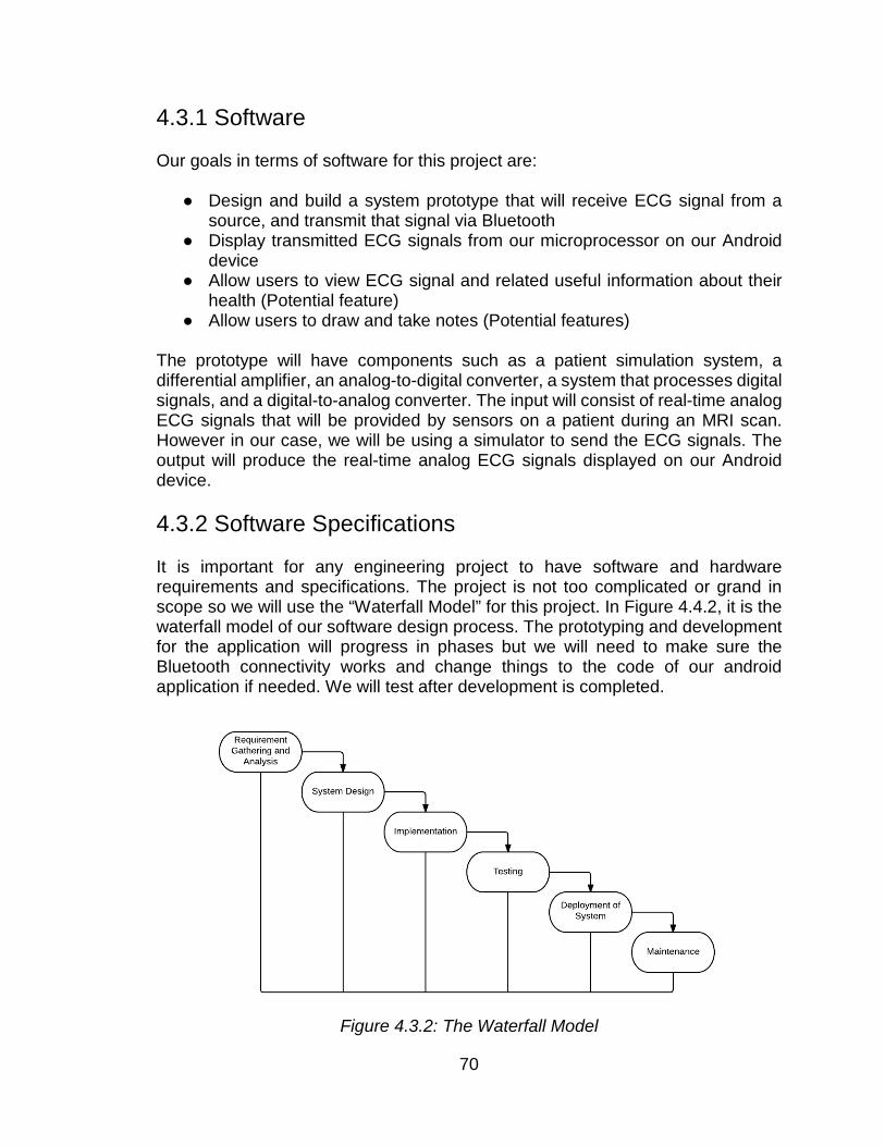
4.3.1 Software Our goals in terms of software for this project are:
Design and build a system prototype that will receive ECG signal from a source, and transmit that signal via Bluetooth
Display transmitted ECG signals from our microprocessor on our Android device
Allow users to view ECG signal and related useful information about their health (Potential feature)
Allow users to draw and take notes (Potential features) The prototype will have components such as a patient simulation system, a differential amplifier, an analog-to-digital converter, a system that processes digital signals, and a digital-to-analog converter. The input will consist of real-time analog ECG signals that will be provided by sensors on a patient during an MRI scan. However in our case, we will be using a simulator to send the ECG signals. The output will produce the real-time analog ECG signals displayed on our Android device. 4.3.2 Software Specifications It is important for any engineering project to have software and hardware requirements and specifications. The project is not too complicated or grand in scope so we will use the “Waterfall Model” for this project. In Figure 4.4.2, it is the waterfall model of our software design process. The prototyping and development for the application will progress in phases but we will need to make sure the Bluetooth connectivity works and change things to the code of our android application if needed. We will test after development is completed.
Figure 4.3.2: The Waterfall Model
70
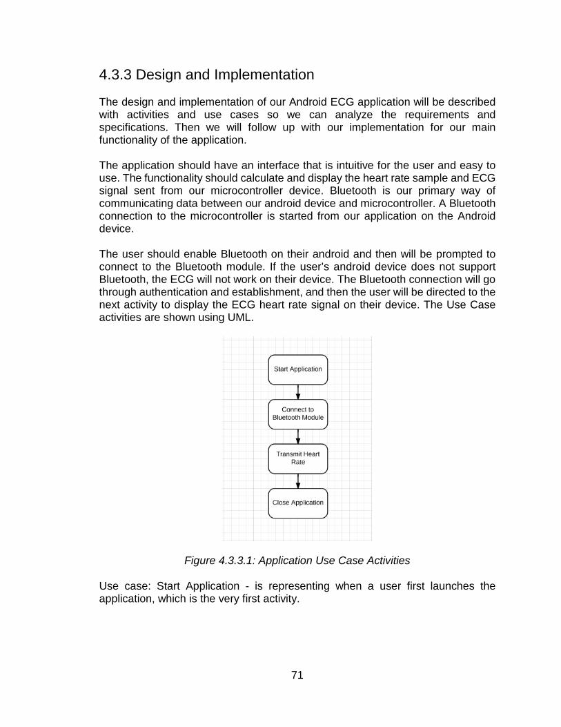
4.3.3 Design and Implementation The design and implementation of our Android ECG application will be described with activities and use cases so we can analyze the requirements and specifications. Then we will follow up with our implementation for our main functionality of the application. The application should have an interface that is intuitive for the user and easy to use. The functionality should calculate and display the heart rate sample and ECG signal sent from our microcontroller device. Bluetooth is our primary way of communicating data between our android device and microcontroller. A Bluetooth connection to the microcontroller is started from our application on the Android device. The user should enable Bluetooth on their android and then will be prompted to connect to the Bluetooth module. If the user’s android device does not support Bluetooth, the ECG will not work on their device. The Bluetooth connection will go through authentication and establishment, and then the user will be directed to the next activity to display the ECG heart rate signal on their device. The Use Case activities are shown using UML.
Figure 4.3.3.1: Application Use Case Activities Use case: Start Application - is representing when a user first launches the application, which is the very first activity.
71

Name Start Application
Actors User
Pre-Condition Android device with Bluetooth support
Description Start up (First Activity) and welcome activity
Table 4.3.3.1: Start Application use case
Name Connect to Bluetooth Module
Actors User
Pre-Condition User starts Application
Description Prompt the user for device discovery and connecting the devices
Table 4.3.3.2: Connect to Bluetooth Module use case
Name Transmit Heart Rate
Actors User
Pre-Condition Bluetooth connection is established
Description Begin reading data sent from Bluetooth module and display on Android device
Table 4.3.3.3: Transmit Heart Rate use case
Name Disconnect
Actors User
Pre-Condition Bluetooth connection is established
Description User can disconnect from the Bluetooth module and exit the application
Table 4.3.3.4: Disconnect use case
72

4.3.4 Features There are additional features that we could implement to make the application better if we have plenty of time after the main functionality works completely. The primarily function is having the heartbeat monitor display correctly in a user friendly user interface, and giving the user the ability to draw and take notes. Features that we could possibly implement in the future will be described in an extras section. 4.3.5 Graphical User Interface The GUI (Graphical User Interface) is the primary interface that the user will see and be able to interact with the application with. It is really important that the GUI is really user friendly, simple, and nice to look at. Legend Electro-Cardio - Title bar Main ECG heart rate frequency - Graph display Main Screen Landscape Mode GUI
Figure 4.3.5.2: Main Screen Landscape Mode GUI
73
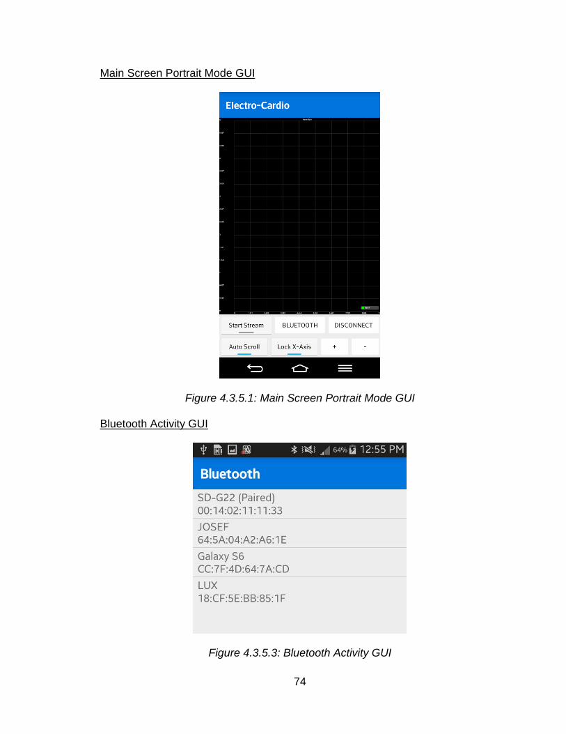
Main Screen Portrait Mode GUI
Figure 4.3.5.1: Main Screen Portrait Mode GUI
Bluetooth Activity GUI
Figure 4.3.5.3: Bluetooth Activity GUI
74
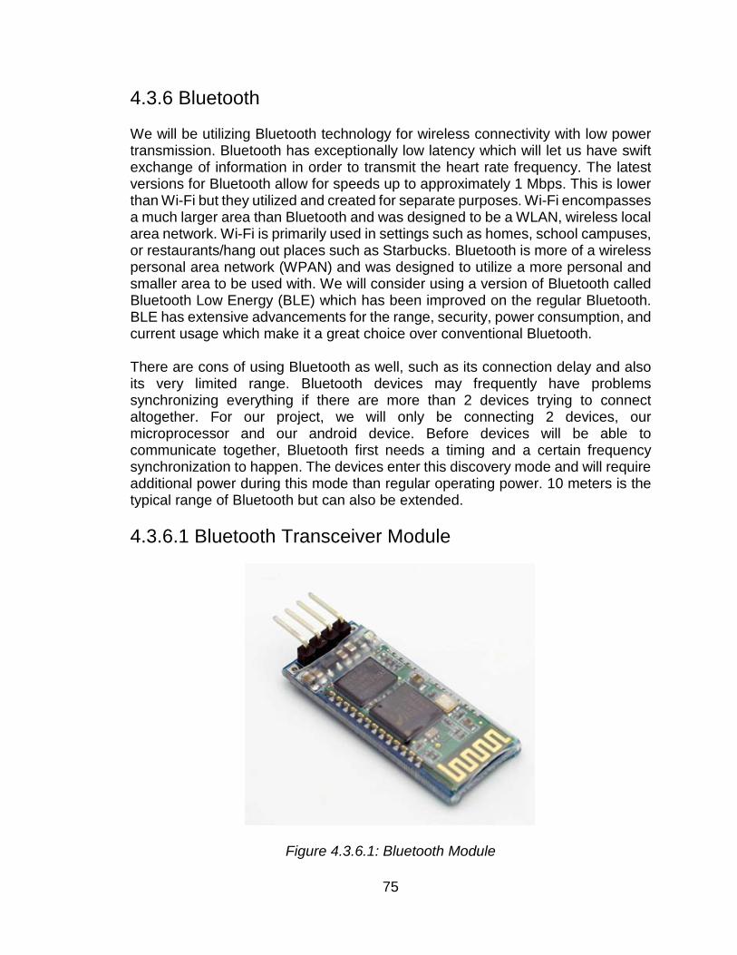
4.3.6 Bluetooth We will be utilizing Bluetooth technology for wireless connectivity with low power transmission. Bluetooth has exceptionally low latency which will let us have swift exchange of information in order to transmit the heart rate frequency. The latest versions for Bluetooth allow for speeds up to approximately 1 Mbps. This is lower than Wi-Fi but they utilized and created for separate purposes. Wi-Fi encompasses a much larger area than Bluetooth and was designed to be a WLAN, wireless local area network. Wi-Fi is primarily used in settings such as homes, school campuses, or restaurants/hang out places such as Starbucks. Bluetooth is more of a wireless personal area network (WPAN) and was designed to utilize a more personal and smaller area to be used with. We will consider using a version of Bluetooth called Bluetooth Low Energy (BLE) which has been improved on the regular Bluetooth. BLE has extensive advancements for the range, security, power consumption, and current usage which make it a great choice over conventional Bluetooth. There are cons of using Bluetooth as well, such as its connection delay and also its very limited range. Bluetooth devices may frequently have problems synchronizing everything if there are more than 2 devices trying to connect altogether. For our project, we will only be connecting 2 devices, our microprocessor and our android device. Before devices will be able to communicate together, Bluetooth first needs a timing and a certain frequency synchronization to happen. The devices enter this discovery mode and will require additional power during this mode than regular operating power. 10 meters is the typical range of Bluetooth but can also be extended. 4.3.6.1 Bluetooth Transceiver Module
Figure 4.3.6.1: Bluetooth Module
75

Table 4.3.6.1.2: Bluetooth Specification. 4.3.6.2 Receiving and Sending Data through Bluetooth Most smartphones in this day and age will have the ability to connect wirelessly with Bluetooth so it is gaining popularity as a way to communicate between devices. We need our application to utilize Bluetooth so we can communicate with a microcontroller. Important goals that we want to achieve consists of confirming Bluetooth status and support, connecting and pairing with the Bluetooth module on the microcontroller, sending and receiving the right data that we want. 4.3.6.3 Potential Issues We first must overcome some hurdles before we can get Android device to actually transmit and receive data through Bluetooth. First, we have to find out if the Android device supports Bluetooth, and if it does, we should prompt the user to turn on Bluetooth on their device. Then, it has to pair up and connect with the Bluetooth module on the microcontroller. Lastly, the must send and receive data between our Android device and microcontroller. 4.3.6.4 Initializing our Application with Bluetooth Before we can do anything, the Android device and the microcontroller’s Bluetooth module must be paired up. To accomplish this, we have to find the Android’s Bluetooth settings and pick the microcontrollers Bluetooth module so we can pair them up. If the Bluetooth module is not appearing on the Android device, we need
76

to verify that the Android is connected to the module properly and that the microcontroller is getting power. Additionally we should unpair all other Bluetooth devices in the vicinity so we can make sure that our two devices will be able to correctly connect. Our first step in programming is to make a new Android Application Project in Eclipse. The first thing we need the program to do is determine if Bluetooth is supported by the Android device. To accomplish this we need to create a BluetoothAdapter object with a predefined function, getDefaultAdapter(). If the function returns null, then Bluetooth is not supported on the Android device. The Android device supports Bluetooth if getDefaultAdapter does not return null. After this check we have to do another check, to see if Bluetooth is enabled on the Android device. If Bluetooth is not enabled, we will enable it on the device. Our code prompts the user to enable Bluetooth on the device if it is not enabled. After, the program has to detect which actual Bluetooth device that it wants to be communicating with, which is our microcontrollers Bluetooth module. We used the getBondedDevices() function in order to accomplish this. What this function will do is get every device that the Android is currently paired with and put all of those devices into a storage structure known as a “set”. We should have made sure that only the microcontrollers Bluetooth module is connected to the Android in our earlier instructions, so it should be the only one in the Set. We will make a BluetoothDevice variable and assign our microcontroller Bluetooth module to that. Now the BluetoothDevice object will be storing the Microcontrollers Bluetooth module. Next we want to connect the Android and the Bluetooth module. This part should be done in a thread that’s separate from the main user interface thread. This is because we want the user to have the best experience with no interruptions. Trying to make the connection can potentially stop the thread for a significant period of time. The user interface thread should at no time ever be stopped. So we will make a separate thread class so we can create the connection. In this thread, we will need BluetoothDevice as an argument and we that we will use it to make a BluetoothSocket. Bluetooth uses sockets in order to transmit and receive data between our Android and Bluetooth module. We need to let the socket know that the data will be transmitted serially (1 byte at a time) so that is what the UUID is doing. In order to utilize this thread, we need to add a bit of code to onCreate() at the end. Now with this code, the Android will hook up with the Bluetooth module and be connected. Finally, our last objective is to transmit and receive data with the connection we just made. Just like making the connection, transmitting and receiving data takes quite some time and can stop the thread, therefore we will
77

also make this process into another thread. We are going to make another inner thread that will need a BluetoothSocket as an argument and we will make an InputStream and an OutputStream. The InputStream will allow us to obtain incoming data from our Microcontroller, while the OutputStream will allow us to transmit data to our Microcontroller. Our Android device will only be receiving data for this project, the data will be the heart rate frequency of ECG signal from the microcontroller. Figure 4.4.8 shows a block diagram of the Bluetooth connection process between our Android device and microcontroller. First the user will start up the application, without much delay. The application will detect if the device supports Bluetooth. If it does, continue on and detect and list Bluetooth devices in the vicinity. If it does not support Bluetooth, it will close the application.
Figure 4.3.6.4.1: Block Diagram of Bluetooth Connectivity
78

After detection of nearby Bluetooth devices and displaying them to the user, the user will be able to choose which Bluetooth device to connect to. Usually only our microcontroller Bluetooth module will be the only Bluetooth device to connect to in the area. Then it will go through the whole Bluetooth connection process and the two devices will be connected, being able to transmit and receive our ECG data that we will need to process and display on our application. 4.3.7 Application Framework The Android application framework consists of a set of managers that users will be interacting with quite a bit throughout their daily use. These managers maintain services for different views, activities, content, and notifications that support the Android operating system. A number of the application framework layer components are:
Content Providers - manages access to data from a central repository
Resource Manager - allows access to resources such as graphics, layouts, etc.
Notification Manager - used to display notifications sent to the user
Activity Manager- interacts with all of the overall activities that run in the
system 4.3.8 Ethernet Ethernet is the standardized solution for wired connections ever since the 1980s. The 802.3 protocols at first could have speeds of up to 10 Mbps, but now it has the capability of speeds of up to 100 Gbps. Of course, the problem with ethernet is that is relies on a wire, and our project is aimed to be designed as a wireless solution for our Bluetooth to android connection. There are also costs for the setup and maintenance of these cables that could potentially cost more in the than using a simple and cheap Bluetooth wireless system for communication. However, the stable, usability, and speed of ethernet will be not achieved by any wireless types. 4.3.9 Software Environment The heart rate frequencies will be transmitted from the Microprocessor and sent to our Android device. Initially, we do not know what microprocessor that we will be using so we will research which one will be suitable for our project, and we will compare different Integrated Development Environments (IDE) for programming in Java, C, and possibly assembly languages.
79

NetBeans is an IDE that is open source used for C, C++, Java, PHP and HTML. It is popular but points more toward web applications, so we will not be utilizing NetBeans for our project. Eclipse is open source IDE created by the Eclipse Foundation which has a huge community supporting it who believes in collaboration on this open development platform. Eclipse is primarily used for development in languages like Java, C, and C++. Developers can also install plugins for Eclipse that will allow them to code in even more languages, use even more specific tools, and even work with other programming platforms. Eclipse is mainly recommended and used at UCF for its core computer science classes. We will be using the Android Development Tools (ADT) bundle, which also includes Eclipse already configured in the package. Android Studio SDK (Software Development Kit) and ADT (Android Developer Tools) are what will allow us to create the software for our Android device. The Android SDK contains all of the API (Application programming interface) and the developer tools that are needed to build, test, and debug mobile applications on Android devices. By downloading the ADT Bundle, we can swiftly begin creating our application. The bundle is comprised of the important Android SDK ingredients and a special version of Eclipse IDE that has ADT (Android Developer Tools) built-in to integrate our Android application development. 4.4 Power Management Design Consideration The ECG project required a steady power supply to power the devices. There are four subsystems of the project that required specific power demands. The “heart rate stimulator” uses a microcontroller to imitate a real heart signal. Depending on which microcontroller is chosen for the final product will determine the power requirements. The “analog-front end” uses operational amplifiers that will require power for operation. Again, the power requirements will be determined by the final selection of the Op-Amp. Power will be needed for “Bluetooth transmission” and power requirements will vary based on the final chip selection. The final power specification will be for the “Android Tablet”. The tablet uses a universal micro USB connector which has a typical voltage rating of 5 volts DC. The diagram below is our proposed method for powering the subsystems while there batteries are charging. The power designs in section 4.4.X did not get implemented towards the end of the project due to time restraints. All subsystems in the final project were powered by 9 volt batteries with fixed voltage regulators.
80
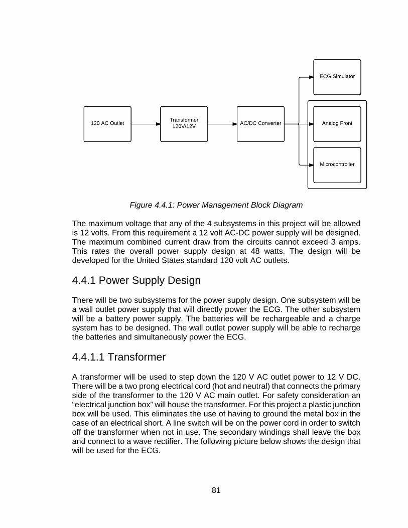
Figure 4.4.1: Power Management Block Diagram
The maximum voltage that any of the 4 subsystems in this project will be allowed is 12 volts. From this requirement a 12 volt AC-DC power supply will be designed. The maximum combined current draw from the circuits cannot exceed 3 amps. This rates the overall power supply design at 48 watts. The design will be developed for the United States standard 120 volt AC outlets. 4.4.1 Power Supply Design There will be two subsystems for the power supply design. One subsystem will be a wall outlet power supply that will directly power the ECG. The other subsystem will be a battery power supply. The batteries will be rechargeable and a charge system has to be designed. The wall outlet power supply will be able to recharge the batteries and simultaneously power the ECG. 4.4.1.1 Transformer A transformer will be used to step down the 120 V AC outlet power to 12 V DC. There will be a two prong electrical cord (hot and neutral) that connects the primary side of the transformer to the 120 V AC main outlet. For safety consideration an “electrical junction box” will house the transformer. For this project a plastic junction box will be used. This eliminates the use of having to ground the metal box in the case of an electrical short. A line switch will be on the power cord in order to switch off the transformer when not in use. The secondary windings shall leave the box and connect to a wave rectifier. The following picture below shows the design that will be used for the ECG.
81

Radio Shack offers a variety of transformers that are specifically designed for various circuit board and electrical projects. One of those transformers is a 120 volt to 12.6 volt AC transformer that will meet this projects system requirements. It is a standard 1.2 amp center tap transformer which offers 15 watts of power. This transformer can be easily mounted on to a circuit board or in a standalone junction box. There are also wires that are already connected to the transformer so no soldering is required. Note, since the transformer casing is metal, proper system grounding needs to be in place to prevent electrical shocks. Below is a picture of the transformer that will be used. The Radio Shack transformer is center tapped as mentioned in the previous paragraph. Center tap is a contact made to a point halfway along a winding of a transformer. The significance of this is there are two AC output voltages that can be used on the transformer. In the case of the Radio Shack transformer using one of the outer windings and the center winding the output voltage will be 6.3 volts AC. Using both the outer windings will give a voltage of 12.6 volts AC. Another advantage with center tap configurations is that it can simplify wave rectification. Instead of having to use a full wave rectifier to conduct both half wave cycle, only two diodes are needed. The two diodes connects to outer windings of the transformer. The load is connected to one of the diodes and the center winding of the transformer. This was a great design to save money before modern day semiconductors. The rectifying design that will most likely be used on this project will be full wave rectification with four diodes. This will allow for the transformer to act as dual power supply if needed. A standard power cord with hot, neutral, and ground leads will be used to connect the transformer to the wall outlet. There is no particular manufactured cord what will work best for this application, therefore any cord can be purchased. The cord will need to be cut and spliced to the transformer. If there is not a wire for the ground wire to be attached to on the transformer than it can be left off. 4.4.1.2 Wave Rectifier A rectifier allows only one polarity to conduct through a circuit. For example a half wave rectifier will allow all positive polarities to conduct through the circuit, while blocking all negative polarities. The advantage of this circuit is its simplicity in design. The disadvantage is waste power by not conducting the negative cycle. The solution to this problem is the full wave rectifier. The full wave rectifier allows both positive and negative polarities to conduct, but it converts the negative polarities into positive polarities. This allows for maximum power efficiency for rectification.
82
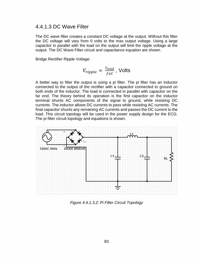
4.4.1.3 DC Wave Filter The DC wave filter creates a constant DC voltage at the output. Without this filter the DC voltage will vary from 0 volts to the max output voltage. Using a large capacitor in parallel with the load on the output will limit the ripple voltage at the output. The DC Wave Filter circuit and capacitance equation are shown. Bridge Rectifier Ripple Voltage:
𝑉𝑉𝑟𝑟𝑟𝑟𝑟𝑟𝑟𝑟𝑟𝑟𝑟𝑟 = 𝐼𝐼𝑙𝑙𝑙𝑙𝑙𝑙𝑙𝑙𝑓𝑓𝑓𝑓𝑓𝑓
, Volts A better way to filter the output is using a pi filter. The pi filter has an inductor connected to the output of the rectifier with a capacitor connected to ground on both ends of the inductor. The load is connected in parallel with capacitor on the far end. The theory behind its operation is the first capacitor on the inductor terminal shunts AC components of the signal to ground, while resisting DC currents. The inductor allows DC currents to pass while resisting AC currents. The final capacitor shunts any remaining AC currents and passes the DC current to the load. This circuit topology will be used in the power supply design for the ECG. The pi filter circuit topology and equations is shown.
Figure 4.4.1.3.2: Pi Filter Circuit Topology
83
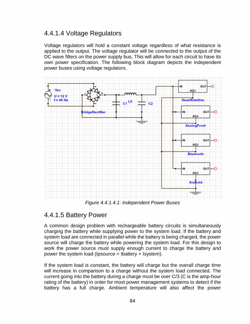
4.4.1.4 Voltage Regulators Voltage regulators will hold a constant voltage regardless of what resistance is applied to the output. The voltage regulator will be connected to the output of the DC wave filters on the power supply bus. This will allow for each circuit to have its own power specification. The following block diagram depicts the independent power buses using voltage regulators.
Figure 4.4.1.4.1: Independent Power Buses
4.4.1.5 Battery Power A common design problem with rechargeable battery circuits is simultaneously charging the battery while supplying power to the system load. If the battery and system load are connected in parallel while the battery is being charged, the power source will charge the battery while powering the system load. For this design to work the power source must supply enough current to charge the battery and power the system load (Ipsource = Ibattery + Isystem). If the system load is constant, the battery will charge but the overall charge time will increase in comparison to a charge without the system load connected. The current going into the battery during a charge must be over C/3 (C is the amp-hour rating of the battery) in order for most power management systems to detect if the battery has a full charge. Ambient temperature will also affect the power
84
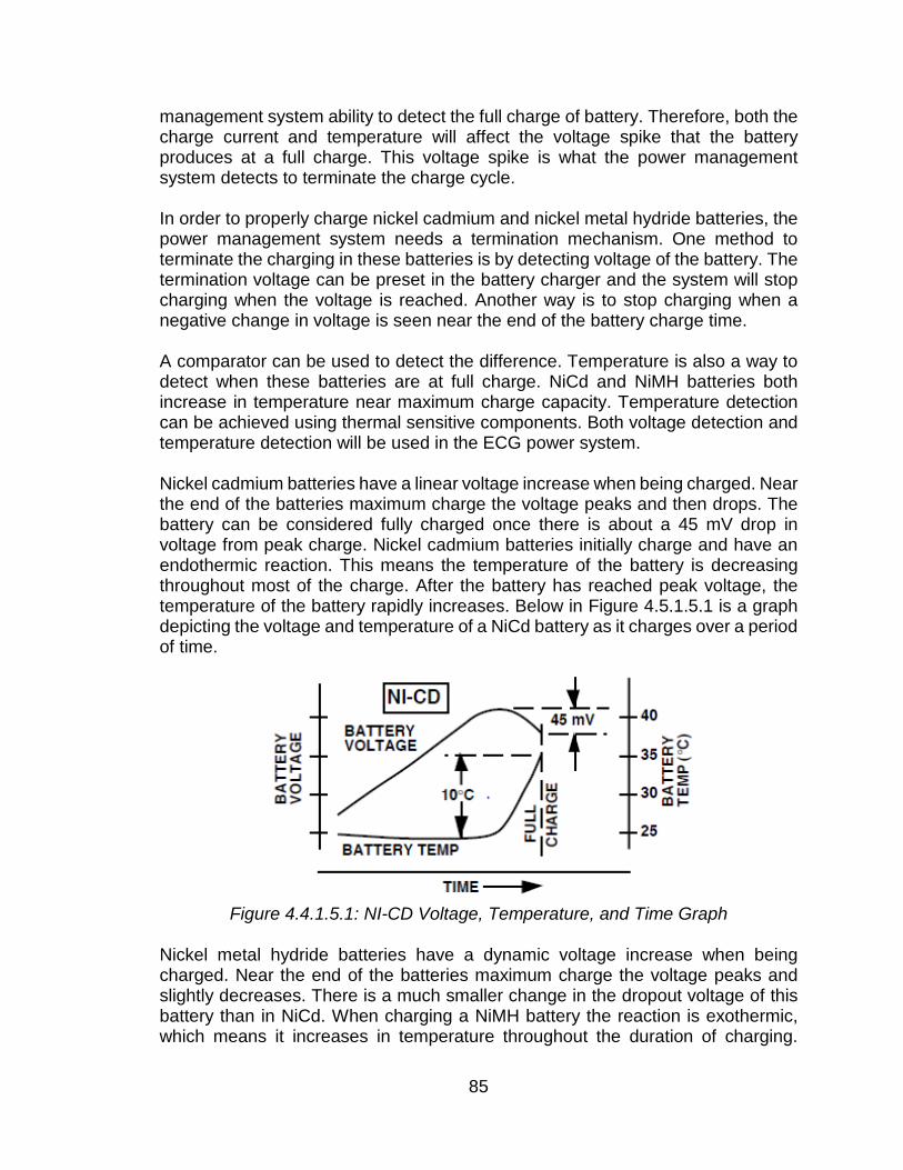
management system ability to detect the full charge of battery. Therefore, both the charge current and temperature will affect the voltage spike that the battery produces at a full charge. This voltage spike is what the power management system detects to terminate the charge cycle. In order to properly charge nickel cadmium and nickel metal hydride batteries, the power management system needs a termination mechanism. One method to terminate the charging in these batteries is by detecting voltage of the battery. The termination voltage can be preset in the battery charger and the system will stop charging when the voltage is reached. Another way is to stop charging when a negative change in voltage is seen near the end of the battery charge time. A comparator can be used to detect the difference. Temperature is also a way to detect when these batteries are at full charge. NiCd and NiMH batteries both increase in temperature near maximum charge capacity. Temperature detection can be achieved using thermal sensitive components. Both voltage detection and temperature detection will be used in the ECG power system. Nickel cadmium batteries have a linear voltage increase when being charged. Near the end of the batteries maximum charge the voltage peaks and then drops. The battery can be considered fully charged once there is about a 45 mV drop in voltage from peak charge. Nickel cadmium batteries initially charge and have an endothermic reaction. This means the temperature of the battery is decreasing throughout most of the charge. After the battery has reached peak voltage, the temperature of the battery rapidly increases. Below in Figure 4.5.1.5.1 is a graph depicting the voltage and temperature of a NiCd battery as it charges over a period of time.
Figure 4.4.1.5.1: NI-CD Voltage, Temperature, and Time Graph
Nickel metal hydride batteries have a dynamic voltage increase when being charged. Near the end of the batteries maximum charge the voltage peaks and slightly decreases. There is a much smaller change in the dropout voltage of this battery than in NiCd. When charging a NiMH battery the reaction is exothermic, which means it increases in temperature throughout the duration of charging.
85

When the battery charge approaches maximum capacity the temperature increases rapidly. Below in Figure 4.4.1.5.2 is a graph depicting the voltage and temperature of a NiMH battery as it charges over a period of time.
Figure 4.4.1.5.2: NI-MH Voltage, Temperature, and Time Graph
The battery management system for the EKG needs to be able to handle both NiCd and NiMH batteries. To meet this requirement the battery charger needs to be easily adaptable for both applications. The charge system must automatically be able to adjust to the parameters or be able to convert with limited change in the circuit configuration. A dynamic system load will cause a change in current going into the battery. This will change the voltage across the battery terminal and the power management system may interpret this as a termination voltage. The result of this can cause the battery to only be partially charged. A state diagram of a basic power management system is shown in Figure 4.4.1.5.3. This will be implemented in our design. For this project a NiCD/NiMH battery fast-charge controller will be used to monitor and control battery charging. Maxim Integrated, Max712/Max713 fast-charge controller will meet the demands of this project. The controller can handle charging 1 to 16 series cells and fast charge from C/4 to 4C rate. The controller has integrated features that allow for voltage slope, temperature, and timing to be monitored. Using these features, the chip can be programmed to stop and start charging.
86

Figure 4.4.1.5.3: Battery Charger State Diagram
87
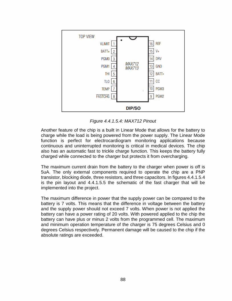
Figure 4.4.1.5.4: MAX712 Pinout
Another feature of the chip is a built in Linear Mode that allows for the battery to charge while the load is being powered from the power supply. The Linear Mode function is perfect for electrocardiogram monitoring applications because continuous and uninterrupted monitoring is critical in medical devices. The chip also has an automatic fast to trickle charge function. This keeps the battery fully charged while connected to the charger but protects it from overcharging. The maximum current drain from the battery to the charger when power is off is 5uA. The only external components required to operate the chip are a PNP transistor, blocking diode, three resistors, and three capacitors. In figures 4.4.1.5.4 is the pin layout and 4.4.1.5.5 the schematic of the fast charger that will be implemented into the project. The maximum difference in power that the supply power can be compared to the battery is 7 volts. This means that the difference in voltage between the battery and the supply power should not exceed 7 volts. When power is not applied the battery can have a power rating of 20 volts. With powered applied to the chip the battery can have plus or minus 2 volts from the programmed cell. The maximum and minimum operation temperature of the charger is 75 degrees Celsius and 0 degrees Celsius respectively. Permanent damage will be caused to the chip if the absolute ratings are exceeded.
88

Figure 4.4.1.5.5: Charge Circuit with MAX712 Implemented
5. Project Prototype Construction and Coding Now that the research and design are out of the way, we needed a plan for the prototype construction before we start purchasing parts. This section will outline:
1. The mainstream and substream design of our product
2. The cost of all the parts and Vendors
3. Hardware and software design plans
89
5.1 Application Prototype Design The project is divided into three main systems: ECG simulator, ECG reader, and the mobile application. Each system also has its mainstream and substream designs. However, our project’s subsystems should not have any conflicts or delays between one and another. 5.1.1 ECG Simulator Prototype Testing To describe the prototype plan for the ECG simulator, the functionality of the prototype should first be discussed. The purpose of this subsystem compared to the overall design is to provide the following systems with a seemingly realistic ECG voltage signal. This voltage signal will be output to a series of "electrodes" that will be used by the ECG Reader portion of the project. The functional block diagram for the Heart Rate Simulator subsystem is shown in Figure 5.1.1.1.
Figure 5.1.1.1: Heart Simulator Functional Block Diagram
90
In this section, the prototype plan for the overall processes of the simulator and how they will function will be discussed, along with the software areas and how those can be accomplished. The major objective of the ECG Simulator subsystem is to get the data from the online database and convert it to an analog signal to be read by the ECG Reader subsystem. In order to get the sample heart rate data into an analog waveform, some formatting has to be done. After this formatting is complete, the data will need to be written onto the flash memory of the MSP430. Then when the project is active, the microprocessor will read the data from the flash memory, load it into the RAM of the microcontroller, and output it through pulse width modulation. A block diagram displaying the different software applications and how they interface with each other to produce the subsystem are shown in Figure 5.1.1.1. The prototyping of the ECG simulator begins with obtaining the MIT-BIH ECG data files from the PhysioNet website. As discussed earlier, the data will be formatted into unsigned integers from its original floating point numbers by the formatting algorithm. Next, the program working with the microcontroller will save the formatted data onto the flash memory of the MSP430. This will have to be repeated for each of the different signals being used. This loop of storing data into the memory on the MSP430 and verifying that it was correctly stored has to be done several times since this loop only portrays the writing of one data array onto the flash memory, while our project will be using a few different MIT-BIH data files. Now that all data has been stored and we are confident that it has been stored correctly on the flash, the rest of the program that will send the data as modulated pulse widths to produce the simulated heart rate signal can be run. To program the MSP430, the software tools must be chosen. It is already known that Texas Instruments has their own Code Composer Studio software. Our group members have experience with this in our Embedded Systems class. Also, we used some of Energia to do prototyping with the LCD display since Energia had a few different examples with LCD-compatible functions. For the ECG Simulator to function correctly, the LCD and input buttons are two of the main aspects of the software that will have to run on the MSP430 that we are using. These two portions provide the interface that will be displayed to the user. These will also be used to prompt the user for input choices as the different heart signals to select are shown on the display. To make things simpler and not require too much rethinking of what goes into the programming of the LCD and push buttons, define statements can be used. These will specify the variables to be used. Similarly, the input buttons will be defined in terms of their port number and pin number and the port direction, which would be set to input. These define statements will set the buttons to their default state which would be that they are
91
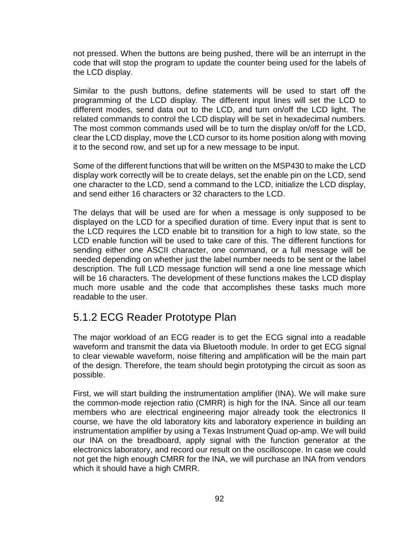
not pressed. When the buttons are being pushed, there will be an interrupt in the code that will stop the program to update the counter being used for the labels of the LCD display. Similar to the push buttons, define statements will be used to start off the programming of the LCD display. The different input lines will set the LCD to different modes, send data out to the LCD, and turn on/off the LCD light. The related commands to control the LCD display will be set in hexadecimal numbers. The most common commands used will be to turn the display on/off for the LCD, clear the LCD display, move the LCD cursor to its home position along with moving it to the second row, and set up for a new message to be input. Some of the different functions that will be written on the MSP430 to make the LCD display work correctly will be to create delays, set the enable pin on the LCD, send one character to the LCD, send a command to the LCD, initialize the LCD display, and send either 16 characters or 32 characters to the LCD. The delays that will be used are for when a message is only supposed to be displayed on the LCD for a specified duration of time. Every input that is sent to the LCD requires the LCD enable bit to transition for a high to low state, so the LCD enable function will be used to take care of this. The different functions for sending either one ASCII character, one command, or a full message will be needed depending on whether just the label number needs to be sent or the label description. The full LCD message function will send a one line message which will be 16 characters. The development of these functions makes the LCD display much more usable and the code that accomplishes these tasks much more readable to the user. 5.1.2 ECG Reader Prototype Plan The major workload of an ECG reader is to get the ECG signal into a readable waveform and transmit the data via Bluetooth module. In order to get ECG signal to clear viewable waveform, noise filtering and amplification will be the main part of the design. Therefore, the team should begin prototyping the circuit as soon as possible. First, we will start building the instrumentation amplifier (INA). We will make sure the common-mode rejection ratio (CMRR) is high for the INA. Since all our team members who are electrical engineering major already took the electronics II course, we have the old laboratory kits and laboratory experience in building an instrumentation amplifier by using a Texas Instrument Quad op-amp. We will build our INA on the breadboard, apply signal with the function generator at the electronics laboratory, and record our result on the oscilloscope. In case we could not get the high enough CMRR for the INA, we will purchase an INA from vendors which it should have a high CMRR.
92
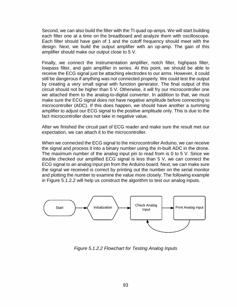
Second, we can also build the filter with the TI quad op-amps. We will start building each filter one at a time on the breadboard and analyze them with oscilloscope. Each filter should have gain of 1 and the cutoff frequency should meet with the design. Next, we build the output amplifier with an op-amp. The gain of this amplifier should make our output close to 5 V. Finally, we connect the instrumentation amplifier, notch filter, highpass filter, lowpass filter, and gain amplifier in series. At this point, we should be able to receive the ECG signal just be attaching electrodes to our arms. However, it could still be dangerous if anything was not connected properly. We could test the output by creating a very small signal with function generator. The final output of this circuit should not be higher than 5 V. Otherwise, it will fry our microcontroller one we attached them to the analog-to-digital converter. In addition to that, we must make sure the ECG signal does not have negative amplitude before connecting to microcontroller (ADC). If this does happen, we should have another a summing amplifier to adjust our ECG signal to the positive amplitude only. This is due to the fact microcontroller does not take in negative value. After we finished the circuit part of ECG reader and make sure the result met our expectation, we can attach it to the microcontroller. When we connected the ECG signal to the microcontroller Arduino, we can receive the signal and process it into a binary number using the in-built ADC in the drone. The maximum number of the analog input pin to read from is 0 to 5 V. Since we double checked our amplified ECG signal is less than 5 V, we can connect the ECG signal to an analog input pin from the Arduino board. Next, we can make sure the signal we received is correct by printing out the number on the serial monitor and plotting the number to examine the value more closely. The following example in Figure 5.1.2.2 will help us construct the algorithm to test our analog inputs.
Figure 5.1.2.2 Flowchart for Testing Analog Inputs
93
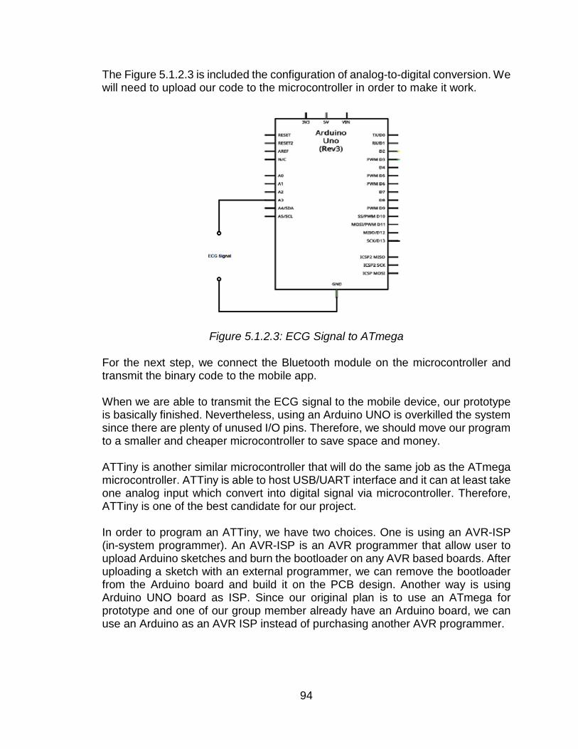
The Figure 5.1.2.3 is included the configuration of analog-to-digital conversion. We will need to upload our code to the microcontroller in order to make it work.
Figure 5.1.2.3: ECG Signal to ATmega
For the next step, we connect the Bluetooth module on the microcontroller and transmit the binary code to the mobile app. When we are able to transmit the ECG signal to the mobile device, our prototype is basically finished. Nevertheless, using an Arduino UNO is overkilled the system since there are plenty of unused I/O pins. Therefore, we should move our program to a smaller and cheaper microcontroller to save space and money. ATTiny is another similar microcontroller that will do the same job as the ATmega microcontroller. ATTiny is able to host USB/UART interface and it can at least take one analog input which convert into digital signal via microcontroller. Therefore, ATTiny is one of the best candidate for our project. In order to program an ATTiny, we have two choices. One is using an AVR-ISP (in-system programmer). An AVR-ISP is an AVR programmer that allow user to upload Arduino sketches and burn the bootloader on any AVR based boards. After uploading a sketch with an external programmer, we can remove the bootloader from the Arduino board and build it on the PCB design. Another way is using Arduino UNO board as ISP. Since our original plan is to use an ATmega for prototype and one of our group member already have an Arduino board, we can use an Arduino as an AVR ISP instead of purchasing another AVR programmer.
94

Figure 5.1.2.4: ATtiny85 Programming Setup
The following schematic in Figure 5.1.2.4 sums up how to setup the AVR ISP testing. This circuit schematic is from the Code and Life will be used to help assist our group in the setup of the microcontroller. We powered the chip from Arduino UNO board 5 V and GND power connections. Then we transferred the code that we previously made to ATtiny. One additional thing to do is to have a 0.1 µF capacitor between Vcc and GND. This would ensure the AVR chip being programmed gets a steady supply of power. 5.1.3 Mobile Application Prototype Plan The most important function of our mobile application is whether our mobile application can received the Bluetooth signal effectively. Therefore, we can read a simple mobile app that would turn on and off the LED light on the microcontroller. The Figure 5.1.3.1 shows the algorithm of testing communication between the mobile device and the microcontroller.
95
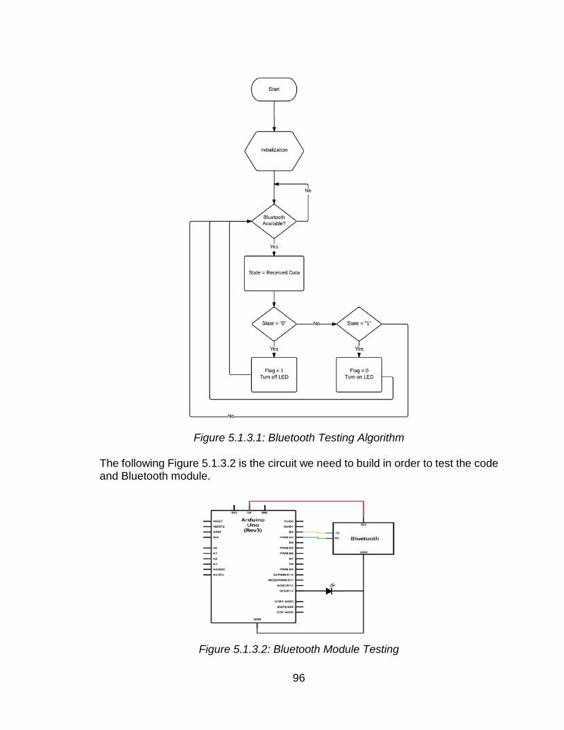
Figure 5.1.3.1: Bluetooth Testing Algorithm
The following Figure 5.1.3.2 is the circuit we need to build in order to test the code and Bluetooth module.
Figure 5.1.3.2: Bluetooth Module Testing
96

After we are able to make the communication between mobile device and microcontroller, we can start transmit the ECG signal in binary code and then construct a real-time graphic on the mobile device. 5.2 Bill of Materials The parts chosen by the group based on the initial research and what we ended up figuring out in the second semester while working on the project are shown in Table 5.2.1, and Table 5.2.2 below. The item chosen is shown with quantity, price, and the vendor of purchase. Table 5.2.1 is the total expenses that we've spent throughout the two semesters for Android Electro Cardio Monitor. Most of the components we purchased with a very low price, including the miscellaneous electrical components. However, for a few of the parts, especially the PCBs, the delivery time was much longer than expected since we did not pay extra for an express delivery. The PCBs were definitely the most costly part since for each of the three PCBs, we received three copies of the same one. Item Quantity Price ($) Vendor
INA128 2 13.00 Ebay
Green 16 pin LCD 1 4.95 Ebay
TL084CN 10 3.99 Ebay
ATTiny85 2 3.99 Ebay
Electrodes 50 7.89 Ebay
SD Card Breakout Many 9.95 Sparkfun
Sensor Cable 1 4.95 Sparkfun
Miscellaneous Many 20.00
Bluetooth Module 2 10.76
MSP430 Launchpad 1 FREE
PCBs 9 136.00 OSH Park
Total 215.48
Table 5.2.1: ECG Expenses Chart
97
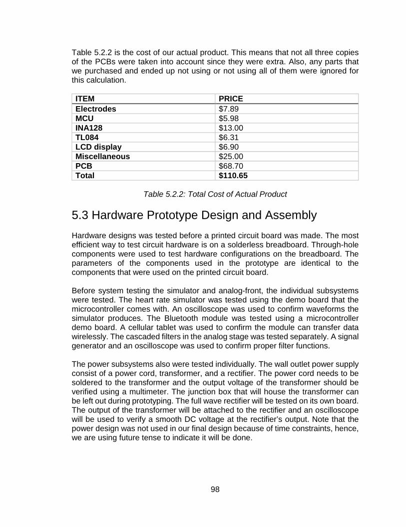
Table 5.2.2 is the cost of our actual product. This means that not all three copies of the PCBs were taken into account since they were extra. Also, any parts that we purchased and ended up not using or not using all of them were ignored for this calculation. ITEM PRICE Electrodes $7.89 MCU $5.98 INA128 $13.00 TL084 $6.31 LCD display $6.90 Miscellaneous $25.00 PCB $68.70 Total $110.65
Table 5.2.2: Total Cost of Actual Product
5.3 Hardware Prototype Design and Assembly Hardware designs was tested before a printed circuit board was made. The most efficient way to test circuit hardware is on a solderless breadboard. Through-hole components were used to test hardware configurations on the breadboard. The parameters of the components used in the prototype are identical to the components that were used on the printed circuit board. Before system testing the simulator and analog-front, the individual subsystems were tested. The heart rate simulator was tested using the demo board that the microcontroller comes with. An oscilloscope was used to confirm waveforms the simulator produces. The Bluetooth module was tested using a microcontroller demo board. A cellular tablet was used to confirm the module can transfer data wirelessly. The cascaded filters in the analog stage was tested separately. A signal generator and an oscilloscope was used to confirm proper filter functions. The power subsystems also were tested individually. The wall outlet power supply consist of a power cord, transformer, and a rectifier. The power cord needs to be soldered to the transformer and the output voltage of the transformer should be verified using a multimeter. The junction box that will house the transformer can be left out during prototyping. The full wave rectifier will be tested on its own board. The output of the transformer will be attached to the rectifier and an oscilloscope will be used to verify a smooth DC voltage at the rectifier’s output. Note that the power design was not used in our final design because of time constraints, hence, we are using future tense to indicate it will be done.
98
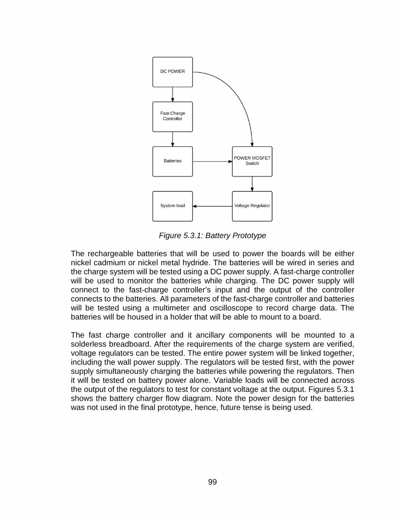
Figure 5.3.1: Battery Prototype
The rechargeable batteries that will be used to power the boards will be either nickel cadmium or nickel metal hydride. The batteries will be wired in series and the charge system will be tested using a DC power supply. A fast-charge controller will be used to monitor the batteries while charging. The DC power supply will connect to the fast-charge controller’s input and the output of the controller connects to the batteries. All parameters of the fast-charge controller and batteries will be tested using a multimeter and oscilloscope to record charge data. The batteries will be housed in a holder that will be able to mount to a board. The fast charge controller and it ancillary components will be mounted to a solderless breadboard. After the requirements of the charge system are verified, voltage regulators can be tested. The entire power system will be linked together, including the wall power supply. The regulators will be tested first, with the power supply simultaneously charging the batteries while powering the regulators. Then it will be tested on battery power alone. Variable loads will be connected across the output of the regulators to test for constant voltage at the output. Figures 5.3.1 shows the battery charger flow diagram. Note the power design for the batteries was not used in the final prototype, hence, future tense is being used.
99
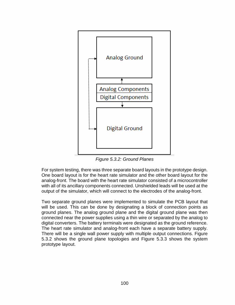
Figure 5.3.2: Ground Planes
For system testing, there was three separate board layouts in the prototype design. One board layout is for the heart rate simulator and the other board layout for the analog-front. The board with the heart rate simulator consisted of a microcontroller with all of its ancillary components connected. Unshielded leads will be used at the output of the simulator, which will connect to the electrodes of the analog-front. Two separate ground planes were implemented to simulate the PCB layout that will be used. This can be done by designating a block of connection points as ground planes. The analog ground plane and the digital ground plane was then connected near the power supplies using a thin wire or separated by the analog to digital converters. The battery terminals were designated as the ground reference. The heart rate simulator and analog-front each have a separate battery supply. There will be a single wall power supply with multiple output connections. Figure 5.3.2 shows the ground plane topologies and Figure 5.3.3 shows the system prototype layout.
100

Figure 5.3.3: System Prototype Layout 5.4 PCB Vendor and Assembly A couple of companies that manufacture printed circuit boards are ExpressPCB and OSH Park. ExpressPCB offers a miniboard service that has a fixed price of $75 for a 2 layer board and $98 for a 4 layer board. The board size must be 3.8 x 2.5 inches. Anything other than this will not be considered for those prices. The next size up is a 21 square inch rectangular board that cost $195 and is 4 layers. OSH Park offers a 4 layer board at $10 per square inch. The pricing for OSH is more expensive but they allow the customer to specify a specific board size unlike ExpressPCB. The best manufacturer will be decided after designs and board layout are completed. There are many printed circuit board software that will assist in design layout. The software that will be used in this project is CadSoft EAGLE. CadSoft EAGLE has a free version that can be used develop the entire schematic, board layout, and has a built in Autorouter for wire traces. The schematic editor provides functions that allows the user to check circuit parameters such as connections, voltages, and currents. The editor also automatically transfers the schematic into the board layout editor making it easy to place components onto the board. Components and their pricings can be imported into the software to be used in the board design. In EAGLE the board layout editor allows for quick designs, manual and auto wire routing, and a rule check to ensure all connections are made. The software also support multiple layers for copper planes, which will be needed in this system. Once the board layout is complete the Gerber files can be exported from EAGLE and sent to any board house for assembly.
101

For this project a printed circuit board will be required. All of the components will need to be laid out on the board. There are many PCB design software that can assist with creating a board. However, designing a PCB is still a challenging task even with software because there are a lot of parameters that have to be considered. The Analog-Front-End of an electrocardiogram has small signals that will pass through it and they need to be undistorted throughout the circuit. This is difficult to do achieve even if the analog circuit is placed on the board by itself. But, there will be Bluetooth on the PCB board and a microcontroller. The Bluetooth chip is a radio frequency device and RF devices are known to cause problems with other components attached to the circuit board. The microcontroller also poses a problem since it acts as a clock for the Bluetooth. For this project, a separate board was used to build the heart rate simulator. The design challenges for the simulator were easier to handle since there was no analog or RF device attached to the board. A diagram of the simulator circuit board outputting a signal to the analog/Bluetooth circuit board is shown in Figure 5.4.1.
Figure 5.4.1: Circuit Board Systems
As mentioned previously RF systems on PCB’s creates greater challenges and parasitic effects need to be considered. Proper grounding can help to minimize distortion caused by RF devices on and off the board. Ground planes are common when designing printed circuit board. A ground plane is a large area or layer of copper foil connected to the circuit’s ground point. The ground plane is usually defined as one of the terminals of the power supply. The ground plane is typically a separate layer covering the entire board. These ground planes ensures that all the components on the circuit board are at the same voltage reference point. In the case of this project the ground plane also serves to limit signal interference and electrical noise. To have the optimum reduction in electrical noise, the type of conductor used as the ground plane needs to have extremely low resistance. Wire traces also need to have low resistance. Copper is commonly mistaken as a superconductor, but it is not. There is resistance in copper wires and it becomes apparent when building printed circuit boards. Pure copper has a resistance of 1.7 µΩ/cm at 25 and a standard copper trace on a PCB has a resistance of 0.48 mΩ/square. This seems small, but if there
102

is an inch of copper tracing this would be around 48 mΩ/inch. This is more than enough to cause errors in the output of the PCB. The solution to this problem is usually using wider traces and limiting the length of wire between each component in on the board. For this project there were not many components going on the PCB so these options were easily implemented to improve overall system efficiency. We expected there to be still unintended voltage drops due to resistive copper traces throughout the system and this could have severely caused gain errors. We did find this to be somewhat true, but we still were able to work around this and our systems ended up working fine in the end. Since the electrocardiogram has multiple gain stages at the input and output of the analog front, adjustments could have been necessary after the PCB components had been attached. Variable resistors and capacitors should be an option in the design to allow for system calibration. Shown in Figure 5.4.2 is a diagram representing the board layout with a ground plane configuration that was used for the electrocardiogram.
Figure 5.4.2a: Side View Board Layout with Ground Plane Configuration
Figure 5.4.2b: Top View Board Layout with Ground Plane Configuration High frequency and low frequency circuits on the PCB should be isolated from each other. The analog front end of the electrocardiogram is considered a low frequency circuit in this project. The maximum frequency that will pass through the filters is around 200 Hz. The inputs of the analog front end also were isolated from
103
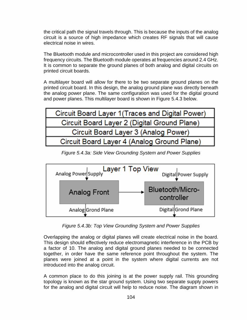
the critical path the signal travels through. This is because the inputs of the analog circuit is a source of high impedance which creates RF signals that will cause electrical noise in wires. The Bluetooth module and microcontroller used in this project are considered high frequency circuits. The Bluetooth module operates at frequencies around 2.4 GHz. It is common to separate the ground planes of both analog and digital circuits on printed circuit boards. A multilayer board will allow for there to be two separate ground planes on the printed circuit board. In this design, the analog ground plane was directly beneath the analog power plane. The same configuration was used for the digital ground and power planes. This multilayer board is shown in Figure 5.4.3 below.
Figure 5.4.3a: Side View Grounding System and Power Supplies
Figure 5.4.3b: Top View Grounding System and Power Supplies
Overlapping the analog or digital planes will create electrical noise in the board. This design should effectively reduce electromagnetic interference in the PCB by a factor of 10. The analog and digital ground planes needed to be connected together, in order have the same reference point throughout the system. The planes were joined at a point in the system where digital currents are not introduced into the analog circuit. A common place to do this joining is at the power supply rail. This grounding topology is known as the star ground system. Using two separate supply powers for the analog and digital circuit will help to reduce noise. The diagram shown in
104
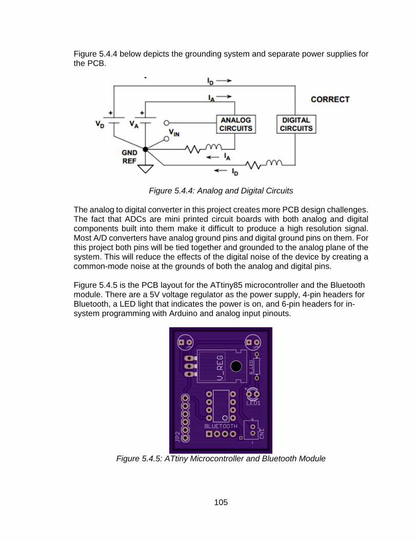
Figure 5.4.4 below depicts the grounding system and separate power supplies for the PCB.
Figure 5.4.4: Analog and Digital Circuits
The analog to digital converter in this project creates more PCB design challenges. The fact that ADCs are mini printed circuit boards with both analog and digital components built into them make it difficult to produce a high resolution signal. Most A/D converters have analog ground pins and digital ground pins on them. For this project both pins will be tied together and grounded to the analog plane of the system. This will reduce the effects of the digital noise of the device by creating a common-mode noise at the grounds of both the analog and digital pins. Figure 5.4.5 is the PCB layout for the ATtiny85 microcontroller and the Bluetooth module. There are a 5V voltage regulator as the power supply, 4-pin headers for Bluetooth, a LED light that indicates the power is on, and 6-pin headers for in-system programming with Arduino and analog input pinouts.
Figure 5.4.5: ATtiny Microcontroller and Bluetooth Module
105
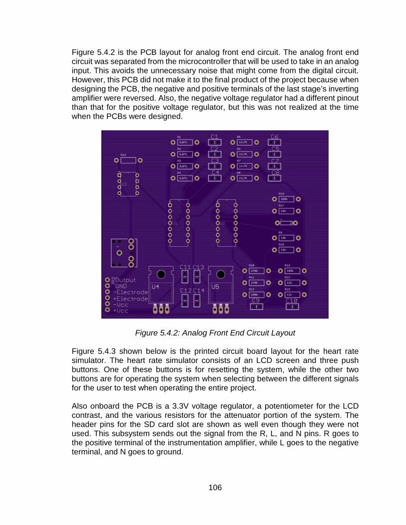
Figure 5.4.2 is the PCB layout for analog front end circuit. The analog front end circuit was separated from the microcontroller that will be used to take in an analog input. This avoids the unnecessary noise that might come from the digital circuit. However, this PCB did not make it to the final product of the project because when designing the PCB, the negative and positive terminals of the last stage’s inverting amplifier were reversed. Also, the negative voltage regulator had a different pinout than that for the positive voltage regulator, but this was not realized at the time when the PCBs were designed.
Figure 5.4.2: Analog Front End Circuit Layout Figure 5.4.3 shown below is the printed circuit board layout for the heart rate simulator. The heart rate simulator consists of an LCD screen and three push buttons. One of these buttons is for resetting the system, while the other two buttons are for operating the system when selecting between the different signals for the user to test when operating the entire project. Also onboard the PCB is a 3.3V voltage regulator, a potentiometer for the LCD contrast, and the various resistors for the attenuator portion of the system. The header pins for the SD card slot are shown as well even though they were not used. This subsystem sends out the signal from the R, L, and N pins. R goes to the positive terminal of the instrumentation amplifier, while L goes to the negative terminal, and N goes to ground.
106
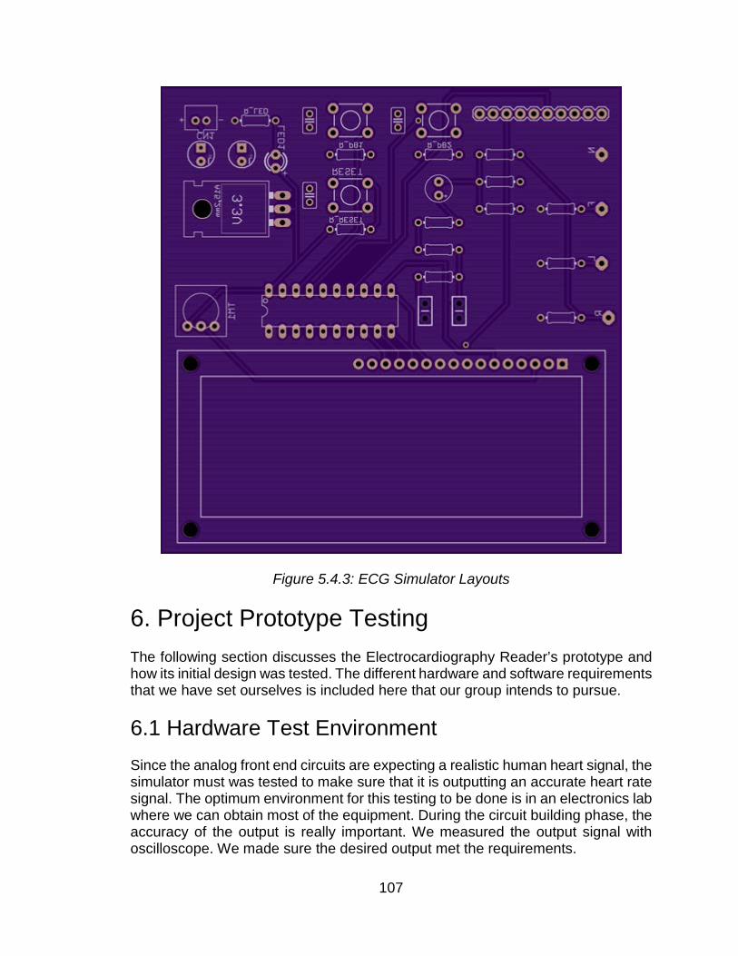
Figure 5.4.3: ECG Simulator Layouts
6. Project Prototype Testing The following section discusses the Electrocardiography Reader’s prototype and how its initial design was tested. The different hardware and software requirements that we have set ourselves is included here that our group intends to pursue. 6.1 Hardware Test Environment Since the analog front end circuits are expecting a realistic human heart signal, the simulator must was tested to make sure that it is outputting an accurate heart rate signal. The optimum environment for this testing to be done is in an electronics lab where we can obtain most of the equipment. During the circuit building phase, the accuracy of the output is really important. We measured the output signal with oscilloscope. We made sure the desired output met the requirements.
107

6.2 Hardware Specific Testing For hardware testing, we need to test the ECG simulator, the output of the ECG reader with ECG simulator as the input, the ADC process, the Bluetooth transmission, and the power system. There are some of the specific testing for our purpose. Table 6.2.1 is the hardware specific testing for the ECG simulator. ECG Simulator Output
Amplitude Less than 5 mV
Frequency Around 0.5 Hz to 150 Hz
User Interface
Pushbutton & LCD display Selecting the correct patient ECG signal and
LCD display should react according to it
Output Selections Making sure ECG simulator is able to output
different ECG signal
Table 6.2.1: ECG Simulator Specific Testing
Table 6.2.2 is the hardware specific testing for the ECG circuit and the output from this system. ECG Circuit Output
Instrumentation Amplifier High CMRR at least 100 dB
Bandpass Filter Cutoff frequency at 0.05 Hz and 150 Hz
Notch Filter or Other Method Make sure power interference are gone
Amplifier & DC offset The ECG signal must be in the range of 0 V to
5 V
Table 6.2.2: ECG Circuit Output Testing
108
Table 6.2.3 is the specific testing for the microcontroller output, specifically related to the testing of the analog to digital conversion and Bluetooth transmission. Microcontroller
Analog-to-Digital Conversion Although we can use oscilloscope to make
sure our output is correct, we must make the
conversion between analog-to-digital correctly
in order to transmit via Bluetooth
Bluetooth Transmission The mobile device should be able to receive
hexadecimal data in order to construct a plot.
Table 6.2.3: Microcontroller Output Testing Table 6.2.4 is the hardware specific for power system. Whether we decided to use a wall outlet as the power source or battery. Power system is the most important part of the design. This involved safety of the group. System Requirements
MSP430 Power Supply: 3.3 V
AT Microcontroller Power Supply: 5 V
Analog Front End Power Supply: ±5 V
AC to DC converter 12 V DC
Table 6.2.4: Power System Specific Testing 6.3 Software Test Environment For our testing, we want to test our application on a number of different Android devices and systems. Initially, we will be testing the software based on the heart rate data provided by the online databases. As we develop our application of ECG filtering we will use a development style known as Test Driven Development. In this style of development we want to test every piece of code that we create, so before we begin developing, we will create tests in mind so we can test the code immediately after we write it. This allows for a smooth flow of development and testing in order to create a good product.
109

Test Driven Development is known as an Agile Methodology, which means it allows for small and quick changes that will ensure us that each small change is made well and tested. The more tests we have, the better our application will be and the more productive we will be. After testing our mobile application on just our device, we need work on integration testing, so the whole project as a whole works when they are integrated together. Knowing that specific parts of our code works with just our emulator and android device works, does not mean it will work when everything is put together. We want to fix any errors that we run into right away because if they’re just left sitting there, they might just be forgotten. If errors are found early on during development and they are not addressed and fixed, they more they will hurt later on in the process. Next we will want to make sure that our applications functionality works as designed and that we make all the requirements that we set out in the design process. We will use System Testing and make sure that the program does not produce any other side effects that we did not plan for or intend to happen. We have to make sure that there are no extra threads executing after exiting the application and that we do not have any memory leaks. 6.4 Software Specific Testing For Android Mobile application testing, we can test it with the development tools provided in the Android SDK. We will first use the emulators and after that we will test with actual hardware devices. Since we are making a Bluetooth application, we need to carry out development and testing aimed towards Android devices that have Bluetooth capabilities. For this project, we are utilizing black box testing because it is used to carry out testing for mobile application development. Black Box testing is a type of testing that focuses on the applications functionality. The user of the application should be able to intuitively use the application and not know the internal structures of the test. Test ID 1.1
Test Title Installation
Test Description The .apk file has to be installed on the device
Test Steps 1. Launch a browser on the
Android device 2. Navigate to the installation URL 3. Download application
Result 1. Application is installed on the
device
Result Table 6.4.1: Test Case – Installation
110

We will carry out tests of the application on the most recent stable version of Android, which is KitKat, Android 4.4-4.4.4. The actual hardware devices we will use to test will be on the Samsung Galaxy S3 and Google Nexus 5 phones. We will test the Bluetooth functionalities like discovery and connectivity and the ECG heart rate monitor. The tables in this section will describe the list of tests we will carry out on our application. We will use these to make sure we follow an orderly process in the testing of our Android application. Pretty straight forward, the user must download and install the application by going to the installation URL on a browser. Test ID 1.2
Test Title Life Cycle (Launching the application)
Test Description User taps on the icon for the application, test the launch time of the application, there should be no lag/delays
Result
Table 6.4.2: Test Case - Launch Time
Test if the application launches without delay when the user taps on the icon Test ID 1.3
Test Title Bluetooth Discovery and Permission
Test Description 1. Application should Exit if
Bluetooth is not supported by device
2. Application should prompt the user to enable Bluetooth if it is off and is supported on the device
Result
Table 6.4.3: Test Case - Bluetooth Permission Test if Bluetooth is enabled on the device, if it is not enabled, prompt user to turn it on. If Bluetooth is not supported by the device, exit.
111

Test ID 1.4
Test Title Device Query and scanning
Test Description 1. Application should have the
ability to scan for Bluetooth devices in the area
2. When scanning for Bluetooth devices in the proximity, show the user a list of devices in the surrounding area
Steps 1. Open application 2. Enable Bluetooth if Bluetooth is
supported on the device
3. Select the microcontroller Bluetooth module in the list
Result
Table 6.4.4: Test case - Bluetooth device scanning
Test ID 1.5
Test Name Bluetooth connection with module and device
Test Description Bluetooth Connection between the Samsung Galaxy/Nexus 5 and the microcontroller should be established
Steps 1. Select the microcontroller on
the list of Bluetooth devices nearby
2. Connect to the microcontroller 3. Enter PIN code “0000” to
establish the Bluetooth connection
Result
Table 6.4.5: Test case - Bluetooth Connection with Module and Device Finally we need to test that the ECG data is being transmitted and displayed successfully, however when we develop and integrate all of the systems, the expected outcome will be much different than the actual outcome. Also we must also consider the multi-tasking issues that might appear while using an Android smartphone. There could be incoming calls or text messages, or if the user wants to run multimedia or any other type of application simultaneously, we need to make sure the application works in these situations.
112

In the process of developing mobile applications, it is important to consider the performance of our application and to make sure the device does not heat up and consume too much power. It is also important that the basic applications of the phone will not have any disruptions while using our application.
7. Administrative Content In this next section, our group discussed the important milestones that our project required of us. Exact dates, deadlines, and meeting dates were considered. In addition, a separation of the primary responsibilities of the group was written down so everybody could be held responsible for their section and so there would not be any confusion as to who is working on which part. Also, the specific budget for our project was provided and a discussion of the finances required of our group is shown. 7.1 Milestone Discussion Our group had several important milestones to meet throughout this project. Included in these are our proposal for our initial project, five meetings within our group to make sure that the senior design research and document are going as planned, a rough draft meeting, and a final revision date. After this final revision, the completed document will be turned in. After our finished document was submitted at the end of the Fall 2014 semester, we began developing our subsystems for the electrocardiography reader. We met two times over the winter break to discuss each other’s progress on their portion of the project to make sure we would be ready once the Spring 2015 semester started. Once the spring semester started, we began combining the individual subsystems and planned on having a rough prototype of our final project before the end of January 2015. Then, we began putting in the final touches in the next month and checked to make sure that all of our requirements have been met. Once our project met every requirement, our completed project was turned in. To get more into specifics for the design phase of our document, our group had five major meetings to discuss where every member was in their progress. The first meeting was on October 16th, 2014, at 8:00am to make sure that each member started and completed all of the necessary research for each subsystem of the project. The second meeting was on October 30th, 2014, at the same time to make sure each member completed at least 8 pages to stay on track for 120 pages by the deadline at the end of the semester.
113

The third meeting was on November 13th, 2014 in the morning to make sure each group member completed at least 16 pages. Also during this meeting, the individual documents were combined into one larger document and the style and quality of each document was formatted to be consistent. At this point, each member was critiqued on sections in the documents and members suggested edits that seemed necessary. On November 20th, 2014, our group had a rough draft meeting and made sure each member had at least 22 pages completed. Next, we had a meeting with our professor. After that, our group met to discuss what each member had left to complete in their 30 pages. On November 27th, 2014, our group met once again to make sure each member had completed their 30 pages. At this point, each member had successfully done their part for the paper. We also made sure that the appendixes, references, and datasheets were all up-to-date, the formatting was correct, and all images were legally allowed to be used in our document. To do this, we either requested permission from the company or creator of the image or create our own similar image that still gets the same idea to the reader. After completing our design document, our group began implementing the design. To do this, we purchased all of our materials at the end of the fall semester so we could start our prototyping phase during the winter break. This prototyping phase was completed within the first couple of weeks of the spring semester. We wanted to ensure that we could have each subsystem working independently before combining each together. We attempted to measure the simulated signal on an oscilloscope to ensure the subsystems were functioning. To prototype the analog front end circuits, a function generator was used as the signal instead of the simulated heart rate signal. We also attempted to measure the noise that was in these circuits and how much is being removed from the filters. After measuring this, we decided on the appropriate filters to use for our project. We wanted to have several filters that could be working with our design and then narrow it down to find the simplest, but effective filter. The next step in our timeframe was testing. For each subsystem, as a new circuit or feature was added, it should was put through a thorough test. Everything that is being programmed in the Android application that was worth being coded was worth being tested so we could make sure we were not missing anything. Along with testing, documentation went along with every step in the process. We recorded each test that was done and checked to make sure that our project met the standards and requirements that have been set. Since this was a system that could possibly be used in the medical field, our circuits, filters, and application should be able to handle any situation that arises.
114

The list of tasks that were completed are shown in a chart. This chart shows everything that each member accomplished. The work for our group was equally divided to pertain to each individual’s skills and interests. The tasks for the Initial Project and Group Identification Document are shown previously in Table 7.1.1. Task Name Duration Start Date Finish Date
Initial Project and Group Identification Document
30 days Tue 8/26/14 Thu 9/25/14
Project
Descriptive Title,
Group Members,
and identify any
sponsors
3 days Tue 9/16/14 Thu 9/18/14
Project Narrative
Description
3 days Tue 9/16/14 Thu 9/18/14
Specifications and
Requirements
3 days Tue 9/16/14 Thu 9/18/14
Block Diagrams 3 days Mon 9/22/14 Wed 9/24/14
Project Budget 3 days Mon 9/22/14 Wed 9/24/14
Milestones 3 days Mon 9/22/14 Wed 9/24/14
Decision Matrix 1 day Mon 9/22/14 Wed 9/24/14
Table 7.1.1: Initial Project and Group Identification Document Deadlines
115

Next, we have a task list with the milestones of how we plan on completing the entire document for Senior Design I. This is shown in Table 7.1.2. Task Name Duration Start Date Finish Date
Final Document 70 days Thu 9/25/14 Thu 12/04/14
Rough Draft 21 days Thu 9/25/14 Thu 11/13/14
Executive Summary
1 day Thu 9/25/14 Fri 9/26/14
Project Description
1 day Thu 9/25/14 Fri 9/26/14
Research Related to Project Definition
5 days Thu 9/25/14 Thu 9/30/14
Project Hardware and Software Design Details
14 days Thu 9/30/14 Thu 11/13/14
Design Summary of Software and Hardware
7 days Thu 11/13/14 Thu 11/20/14
Project Prototype Construction and Coding
2 days Thu 11/20/14 Sat 11/22/14
Project Prototype Testing
3 days Sun 11/23/14 Tue 11/25/14
Table 7.1.2: Senior Design I Document Deadlines A timeline for completing the entire project with the design and testing is also necessary. This is shown in Table 7.1.3 below. Task Name Duration Start Date Finish Date
Final Project 92 days Mon 1/12/15 Sat 4/13/15
Research 21 days Mon 1/12/15 Fri 3/20/15
Table 7.1.3a: Senior Design II Project Deadlines
116

Task Name Duration Start Date Finish Date
Initial Research 9 days Fri 1/02/15 Mon 1/11/15
Rough Research 7 days Mon 2/16/15 Mon 2/23/15
Final Research 5 days Mon 3/23/15 Sat 3/28/15
Prototype 79 days Mon 1/12/15 Sat 4/13/15
Initial Prototype 28 days Mon 1/12/15 Mon 2/09/15
Initial Testing 7 days Mon 2/09/15 Mon 2/16/15
Rough Prototype 21 days Mon 2/23/15 Mon 3/16/15
Final Testing 7 days Mon 3/16/15 Mon 3/23/15
Final Prototype 16 days Sat 3/28/15 Mon 4/13/15
Table 7.1.3b: Senior Design II Project Deadlines Cont.
7.2 Group Responsibilities Each group member had different interests, along with different strengths and weaknesses in their engineering field. Everybody also wanted to get something different out of this Senior Design project. To make sure that each member was assigned an adequate amount of tasks and learned as much as they could throughout the two semesters that this project spans, we each selected which subsystem of the project we would prefer to work on. Table 7.2.1 was made showing the different subsystems of the project. Next to each subsystem, a solid square shows which person had the key responsibility for the design, prototyping, and testing of that portion, while a hollow square shows which person was an extra set of eyes and was able to offer some contribution. We tried to make that sure the most important subsystems had more than one pair of eyes on it to ensure that one group member was not overlooking anything or forgetting about an important part of the design. As was evident, since some of the subsystems were more in depth than others, each person reasonably had the same amount of work provided for them.
117

Jeffrey worked mainly on the Heart Rate Simulator and was assisted by Cheng-Chieh Wang (Jay) in that area for the PCB. For the ECG Sensor, Jay was the main person responsible for that task, while Jonathan also helped. Jonathan was the sole person working on the power systems, while Michael mainly worked on the Android application and the Bluetooth communication between the Analog Front End and the app. Jeffrey assisted Michael with the app, while Jay assisted Michael with the Bluetooth communication.
Jeffrey Frye Jonathan
Gibson
Michael Sun Jay Wang
Heart Rate
Simulator
ECG Sensor
Power System
Bluetooth
Communication
Android
Application
Table 7.2.1 Group Responsibilities
- Main Responsibility - Partial Responsibility 7.3 Budget and Finance Discussion Thanks to the CECS Alumni Chapter, our group was able to receive funding in order to make this project a reality. They had provided us with only $150, but since our project did not require very expensive items and equipment, this small amount of money was able to cover the main components of our budget. Without the support of the CECS Alumni Chapter, it would have been unlikely that our project would have been able to include all of the features that we originally desired. With this money though, our group was be able to add a few extra capabilities and features to make our Android Electro Cardio Monitor even more exciting. With the provided funding, we started purchasing the various parts for our project as soon as the start of the Spring 2015 semester. For all parts that we purchased, the products were shipped to a specific address at UCF so that all reimbursement processes could be handled smoothly. All receipts were saved from here on out to keep up to date with how much we had spent and in case there was any discrepancy with regards to our funding. The differences in funding from the CECS
118
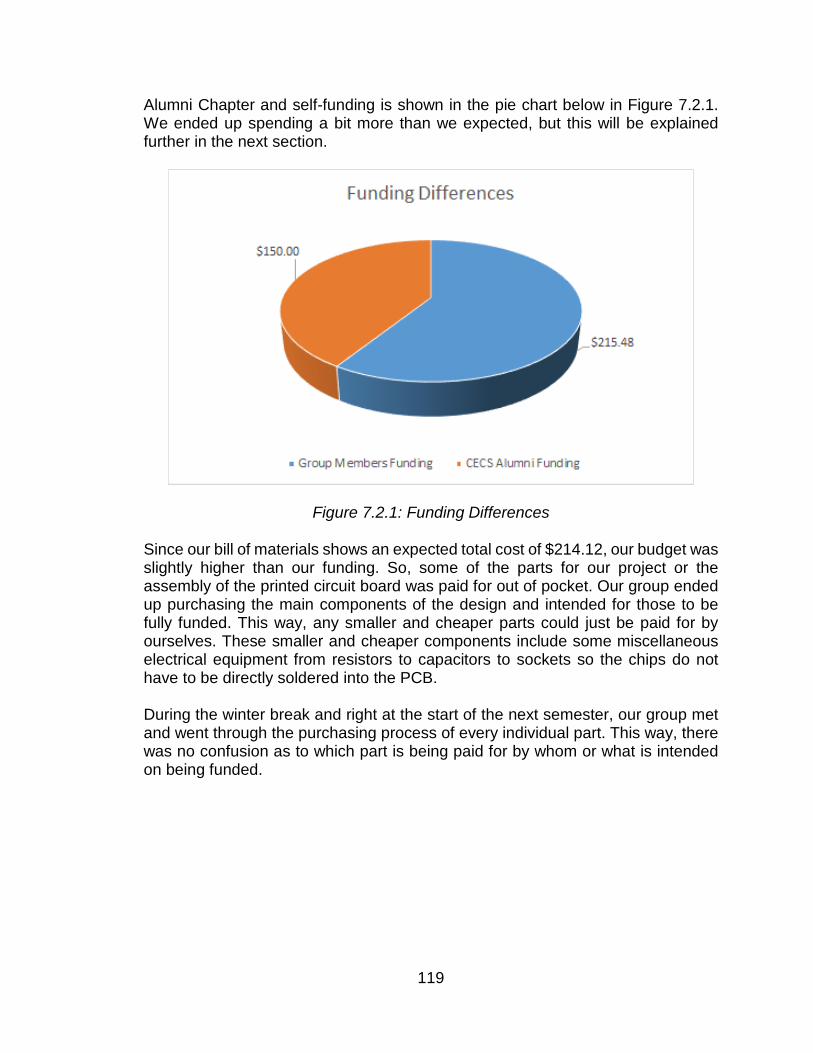
Alumni Chapter and self-funding is shown in the pie chart below in Figure 7.2.1. We ended up spending a bit more than we expected, but this will be explained further in the next section.
Figure 7.2.1: Funding Differences Since our bill of materials shows an expected total cost of $214.12, our budget was slightly higher than our funding. So, some of the parts for our project or the assembly of the printed circuit board was paid for out of pocket. Our group ended up purchasing the main components of the design and intended for those to be fully funded. This way, any smaller and cheaper parts could just be paid for by ourselves. These smaller and cheaper components include some miscellaneous electrical equipment from resistors to capacitors to sockets so the chips do not have to be directly soldered into the PCB. During the winter break and right at the start of the next semester, our group met and went through the purchasing process of every individual part. This way, there was no confusion as to which part is being paid for by whom or what is intended on being funded.
119

Figure 7.2.2: Total Budget for Project As the pie chart shows our budget for our project, it is obvious that shipping was a large portion of the overall price. But several of the part were purchased on ebay.com, with free shipping because multiple products were purchased at the time. Texas Instruments also offered some of their products as a free sample, so our group attempted to go through that process to save money since we would just be ordering one unit from them. Since the funding was directly provided to us, the difficult part in the purchasing process was waiting for the shipments to arrive and having to pick them up from UCF instead of having them directly sent to our residences. Overall, we stuck to the budget for each subsystem and our group never had any problems. 7.4 Engineering Standards Standards define the characteristics of a product, process or service, such as dimensions, safety aspects, and performance requirements. Listed below are a few standards that pertain to our project. [1] Health informatics - Medical waveform format - Part 92001: Encoding rules, ISO/TS 11073-92001:2007, 2007. [2] Common mode rejection in ECG monitoring, AAMI TIR60:2014 (AAMI TIR 60:2014), Date N/A [3] Medical electrical equipment - Part 2-27: Particular requirements for the basic safety and essential performance of electrocardiographic monitoring equipment, IEC 60601-2-27 Ed. 3.0 b:2011, Date N/A
120
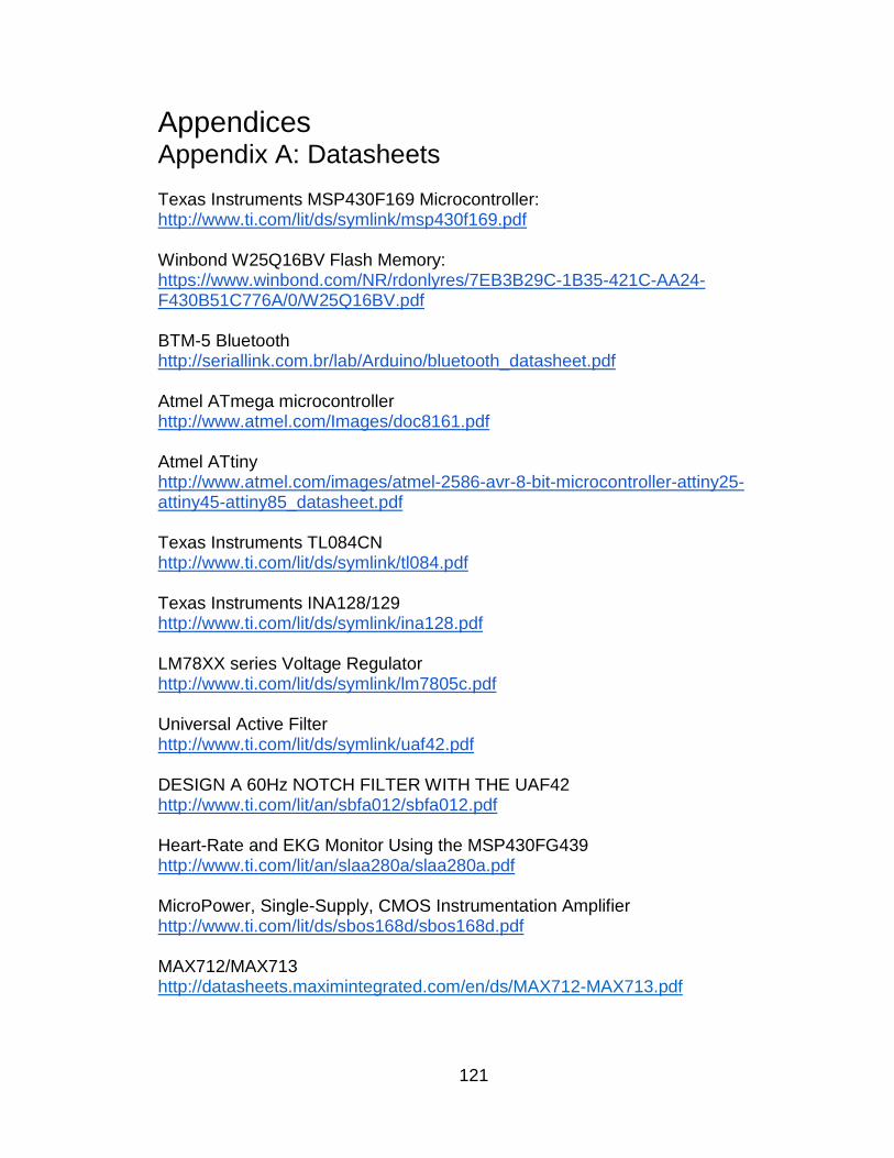
Appendices Appendix A: Datasheets Texas Instruments MSP430F169 Microcontroller: http://www.ti.com/lit/ds/symlink/msp430f169.pdf Winbond W25Q16BV Flash Memory: https://www.winbond.com/NR/rdonlyres/7EB3B29C-1B35-421C-AA24-F430B51C776A/0/W25Q16BV.pdf BTM-5 Bluetooth http://seriallink.com.br/lab/Arduino/bluetooth_datasheet.pdf Atmel ATmega microcontroller http://www.atmel.com/Images/doc8161.pdf Atmel ATtiny http://www.atmel.com/images/atmel-2586-avr-8-bit-microcontroller-attiny25-attiny45-attiny85_datasheet.pdf Texas Instruments TL084CN http://www.ti.com/lit/ds/symlink/tl084.pdf Texas Instruments INA128/129 http://www.ti.com/lit/ds/symlink/ina128.pdf LM78XX series Voltage Regulator http://www.ti.com/lit/ds/symlink/lm7805c.pdf Universal Active Filter http://www.ti.com/lit/ds/symlink/uaf42.pdf DESIGN A 60Hz NOTCH FILTER WITH THE UAF42 http://www.ti.com/lit/an/sbfa012/sbfa012.pdf Heart-Rate and EKG Monitor Using the MSP430FG439 http://www.ti.com/lit/an/slaa280a/slaa280a.pdf MicroPower, Single-Supply, CMOS Instrumentation Amplifier http://www.ti.com/lit/ds/sbos168d/sbos168d.pdf MAX712/MAX713 http://datasheets.maximintegrated.com/en/ds/MAX712-MAX713.pdf
121

Appendix B: References Behutiye, Woubshet. "Android ECG Application Development." (n.d.): n. pag.
Spring 2012. Web. 15 Nov. 2014.
"Biopotential Amplifiers." SJSU EE Faculty Website. N.p., n.d. Web. 02 Dec. 2014. <http://www.engr.sjsu.edu/mkeralapura/>.
Cache. "Interface MSP430 Launchpad with LCD Module (LCM) in 4 Bit Mode."
Web log post. Co-Random Thoughts. N.p., n.d. Web. 1 Dec. 2014. <http://cacheattack.blogspot.com/2011/06/quick-overview-on-interfacing-m sp430.html>.
Chawda, Hemanshu K., and Zi Ling Kang. WIRELESS PULSE RATE
MONITORING USING NEAR FIELD COMMUNICATION (n.d.): n. pag. May 2008. Web. Dec. 2014.
Diaby, Tidaine, and Chris Harkins. "Wireless ECG Monitoring Device." (n.d.): n.
pag. Apr. 2013. Web. 24 Nov. 2014. "ECG Image Index." ECG Learning Center. N.p., n.d. Web. 02 Dec. 2014. <http://ecg.utah.edu/img_index>. Ganier, CJ. "Digital-to-Analog Converter on TI MSP430." Web log
post.OpenStax-CNX. N.p., n.d. Web. 1 Dec. 2014. <http://cnx.org/contents/8d5e6c7a-8bcb-4ba9-8f8a-8b24191613ef@2/Digital-to-Analog_Converter_on>.\
"Getting the Most out of Your Instrumentation Amplifier Design." (n.d.): n. pag.
Amplifiers: Op Amps. Web. 1 Dec. 2014. <http://www.ti.com/lit/an/slyt226/slyt226.pdf>.
MICHALEK, Paul J. "AN AUTHENTIC ECG SIMULATOR." Thesis. University of
Central Florida, 2006. Web. 1 Dec. 2014. <http://etd.fcla.edu/CF/CFE0001214/Michalek_Paul_J_200608_MS.pdf>.
"Microcontrollers (MCU)." Microcontrollers. Texas Instruments, n.d. Web. 02 Dec. 2014.<http://www.ti.com/lsds/ti/microcontrollers_16-bit_32-bit/products.page>.
"PhysioBank ATM." PhysioBank ATM. N.p., n.d. Web. 01 Dec. 2014.
<http://www.physionet.org/cgi-bin/atm/ATM>.
Pihlajamaa, Joonas. "Using Arduino Uno as ISP." Web log post. Code and Life. N.p., n.d. Web. 1 Dec. 2014. <http://codeandlife.com/2012/03/21/using-arduino-uno-as-isp/>.
122

Appendix C: Copyright Permissions Texas Instruments includes a section in their Copyright information granting us permission to download, print copies, store files on our computer, and reference the information they provide in our documents for our personal and non-commercial use. So the few images or circuits that were used from Texas Instruments will be assumed to be allowed as long as we cite the sources. University of Utah’s ECG Learning Center has a Copyright information section that states that we are free to share any images, meaning we can copy and redistribute the material in any medium or format as long as we cite the source.
123

124
Related Documents