STMicroelectronics Philippe Roche 1 [email protected] and Reno Harboe-Sorensen 2 [email protected] in collaboration with HIREX and iRoC test subcontractors 1 STMicroelectronics, Crolles, France 2 ESA-ESTEC, Noordwijk, The Netherlands Final Presentation of ESTEC Contract No. 13528/95/NL/MV, COO-18. Progress Presentation of ESTEC Contract No. 18799/04/NL/AG, COO-3. Radiation Evaluation of ST Test Structures in commercial 130nm CMOS BULK and SOI In commercial 90nm CMOS BULK in commercial 65nm CMOS BULK and SOI

Welcome message from author
This document is posted to help you gain knowledge. Please leave a comment to let me know what you think about it! Share it to your friends and learn new things together.
Transcript
STMicroelectronics
Philippe Roche1
Reno Harboe-Sorensen2
in collaboration with HIREX and iRoC test subcontractors
1 STMicroelectronics, Crolles, France2 ESA-ESTEC, Noordwijk, The Netherlands
Final Presentation of ESTEC Contract No. 13528/95/NL/MV, COO-18.Progress Presentation of ESTEC Contract No. 18799/04/NL/AG, COO-3.
Radiation Evaluation of ST Test Structuresin commercial 130nm CMOS BULK and SOIIn commercial 90nm CMOS BULKin commercial 65nm CMOS BULK and SOI

© STMicroelectronics 2Jan-2007 / P.Roche
Headline� Brief overview on ST (Crolles) developments in radiation test, modeling & hardening
– why does ST-Central R&D care about TERRESTRIAL radiations for years?– radiation test procedures for consumer applications– proprietary neutron & alpha simulators– original hardened solutions
� Test parameters for the radiation assessment of commercial ST 130 and 90nm CMOS– selection of several process options, circuits, devices, power supplies, etc– commercial technologies : not hardened against radiations
� Main Single Event Effects (SEE) test results with heavy ions & protons– 130nm BULK and SOI– 90nm BULK
� Main Total Ionizing Dose (TID) test results with a Co60 gamma source– 130nm BULK– 90nm BULK
� Preliminary results in ST 65nm CMOS BULK and SOI
� Conclusion
© STMicroelectronics 3Jan-2007 / P.Roche
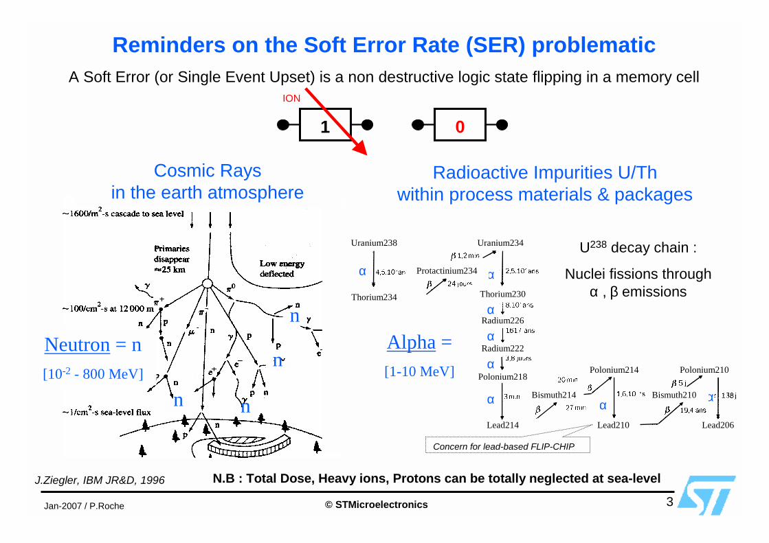
Reminders on the Soft Error Rate (SER) problematic
1 0
ION
A Soft Error (or Single Event Upset) is a non destructive logic state flipping in a memory cell
Radioactive Impurities U/Thwithin process materials & packages
U238 decay chain :
Nuclei fissions through α , β emissions
Alpha =[1-10 MeV]
α
α
α
α α α
αα
n
Cosmic Rays in the earth atmosphere
Neutron = n[10-2 - 800 MeV]
Uranium238
Thorium234
Protactinium234
Uranium234
Thorium230
Radium226
Radium222
Polonium218
Lead214
Bismuth214
Polonium214
Lead210
Bismuth210
Polonium210
Lead206
J.Ziegler, IBM JR&D, 1996
n
nn
N.B : Total Dose, Heavy ions, Protons can be totally neglected at sea-level
Concern for lead-based FLIP-CHIP
© STMicroelectronics 4Jan-2007 / P.Roche
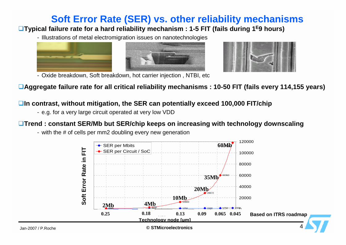
Soft Error Rate (SER) vs. other reliability mechanisms�Typical failure rate for a hard reliability mechanism : 1-5 FIT (fails during 1E9 hours)
- Illustrations of metal electromigration issues on nanotechnologies
- Oxide breakdown, Soft breakdown, hot carrier injection , NTBI, etc
�Aggregate failure rate for all critical reliability mechanisms : 10-50 FIT (fails every 114,155 years)
�In contrast, without mitigation, the SER can potentially exceed 100,000 FIT/chip- e.g. for a very large circuit operated at very low VDD
�Trend : constant SER/Mb but SER/chip keeps on increasing with technology downscaling- with the # of cells per mm2 doubling every new generation
500 750 1250 1500 1750 20001000 3200
12800
28672
60362
117965
0
20000
40000
60000
80000
100000
120000
0.040.070.10.130.160.190.220.25Technology node [µm]
SER
FIT
rate
SER per MbitsSER per Circuit / SoC
2Mb
60Mb
20Mb10Mb
4Mb
35Mb
0.25 0.25 0.13 0.09 0.065 0.0450.18
Soft
Erro
r Rat
e in
FIT
Based on ITRS roadmap
© STMicroelectronics 5Jan-2007 / P.Roche
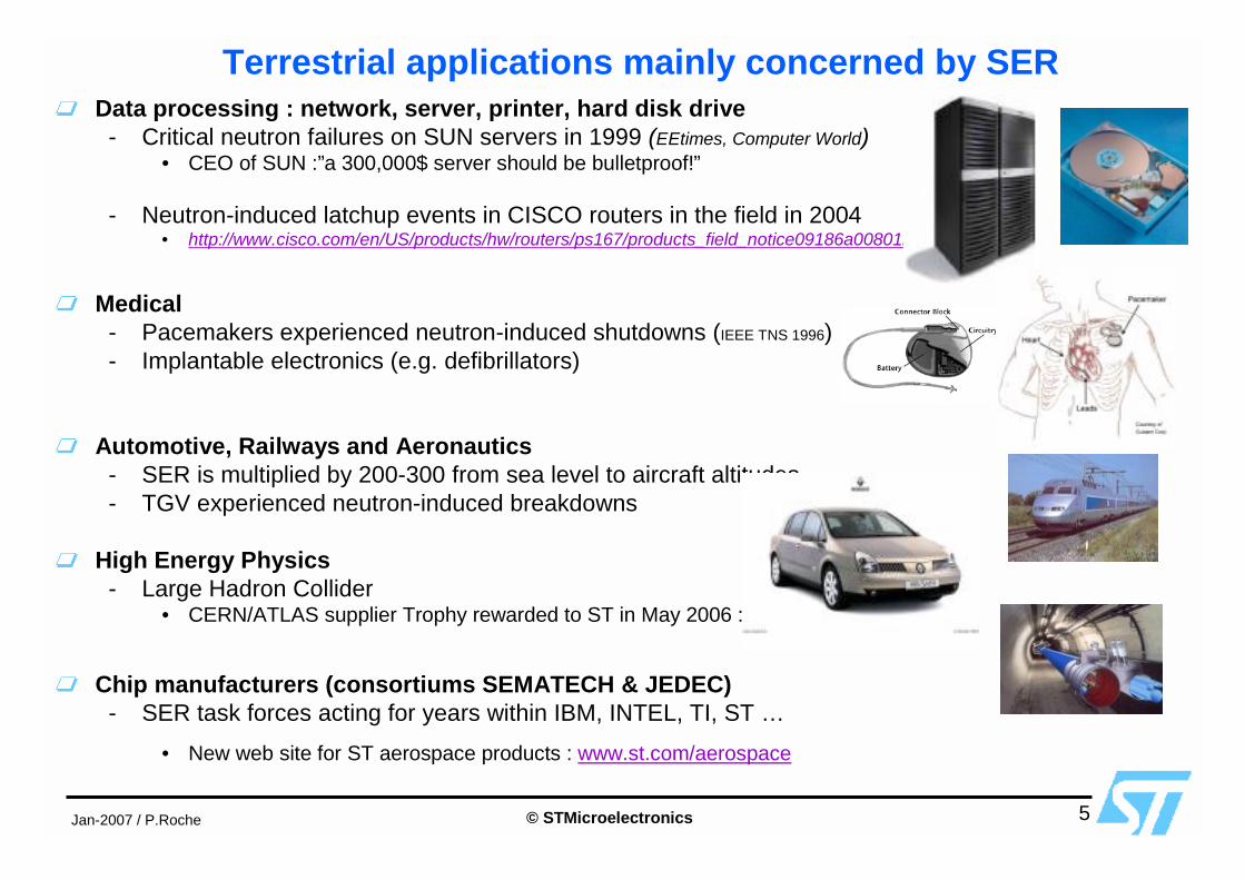
Terrestrial applications mainly concerned by SERData processing : network, server, printer, hard disk drive
- Critical neutron failures on SUN servers in 1999 (EEtimes, Computer World)• CEO of SUN :”a 300,000$ server should be bulletproof!”
- Neutron-induced latchup events in CISCO routers in the field in 2004• http://www.cisco.com/en/US/products/hw/routers/ps167/products_field_notice09186a00801b3df8.shtml
Medical - Pacemakers experienced neutron-induced shutdowns (IEEE TNS 1996)- Implantable electronics (e.g. defibrillators)
Automotive, Railways and Aeronautics- SER is multiplied by 200-300 from sea level to aircraft altitudes- TGV experienced neutron-induced breakdowns
High Energy Physics- Large Hadron Collider
• CERN/ATLAS supplier Trophy rewarded to ST in May 2006 :
Chip manufacturers (consortiums SEMATECH & JEDEC)- SER task forces acting for years within IBM, INTEL, TI, ST …
• New web site for ST aerospace products : www.st.com/aerospace

6
SER simulatorsAt device levelAt chip level
SER simulatorsAt device levelAt chip level
Semi-empirical Scaling model
(fast but 1st order)
Semi-empirical Scaling model
(fast but 1st order)
New Technology(Process/design)
New Technology(Process/design)
PreviousTechnologyPrevious
Technology
Development Phase
PrototypePhase
QualificationPhase
Measurements of radioactive
contaminants inwafers & liquids
Measurements of radioactive
contaminants inwafers & liquids
NeutronAccelerated SER
NeutronAccelerated SER
AlphaAccelerated SER
AlphaAccelerated SER
Occasionally :Thermal neutronsAccelerated ASER
Occasionally :Thermal neutronsAccelerated ASER
Real time or SystemSER (SSER)
In altitude
Real time or SystemSER (SSER)
In altitude
Verification of Models
Verification of Models
ST SER characterization flow
Experimental
modeling
Color legend
5 samples 1000 samples
Fast-expanding :Heavy ions
ProtonsX-Gamma rays
Fast-expanding :Heavy ions
ProtonsX-Gamma rays
Test flow already applied to ST CMOS 130, 90 and 65nmST CMOS 45nm : about to be started

© STMicroelectronics 7Jan-2007 / P.Roche
ST accelerated SER measurements : in North America & Crolles
counterbeam output
DUT1
DUT2 neutro
n path
Neutron : @ Los Alamos & Vancouver Alpha : @ Crolles with a radioactive alpha source Am241 100µCi
DUT
Radioactive alpha source
Specific ASER tester : static/dynamic testing + latchup monitoring + heating 125����C-Usable with any kind of radiation source (heavy ions, protons, neutrons, gamma)
Test methodology : compliant with international test standards-JEDEC JESD89A : defined with the ST participation
-Joint Electron Device Engineering Council : 270 companies
-ESA SCC basic specifications N�25100 & 22900
More than 20 neutron test campaigns at Los Alamos and Vancouver since 2000
1 hour in the beam ~ 15753 years at sea-level
ASER tester
Industrial tester
© STMicroelectronics 8Jan-2007 / P.Roche
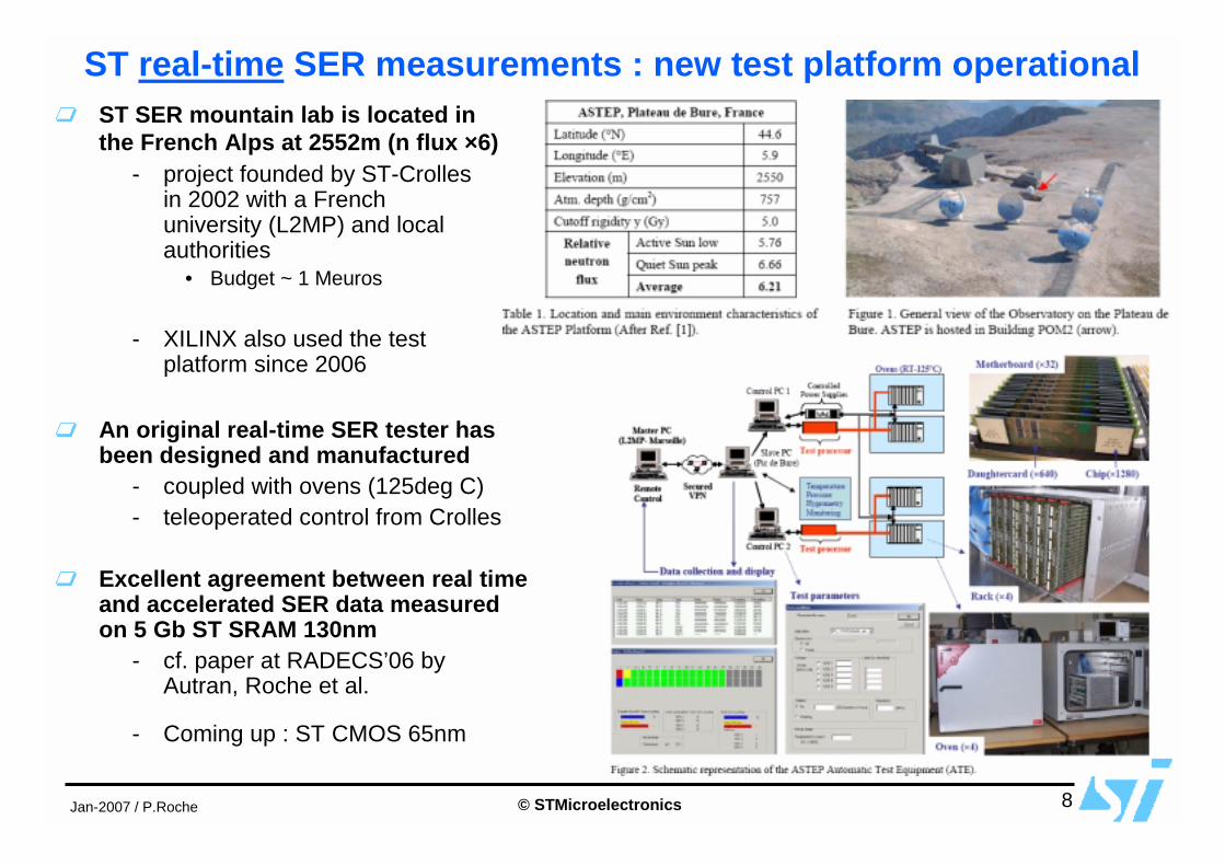
ST real-time SER measurements : new test platform operationalST SER mountain lab is located in the French Alps at 2552m (n flux ×6)
- project founded by ST-Crolles in 2002 with a French university (L2MP) and local authorities
• Budget ~ 1 Meuros
- XILINX also used the test platform since 2006
An original real-time SER tester has been designed and manufactured
- coupled with ovens (125deg C) - teleoperated control from Crolles
Excellent agreement between real time and accelerated SER data measured on 5 Gb ST SRAM 130nm
- cf. paper at RADECS’06 by Autran, Roche et al.
- Coming up : ST CMOS 65nm
© STMicroelectronics 9Jan-2007 / P.Roche
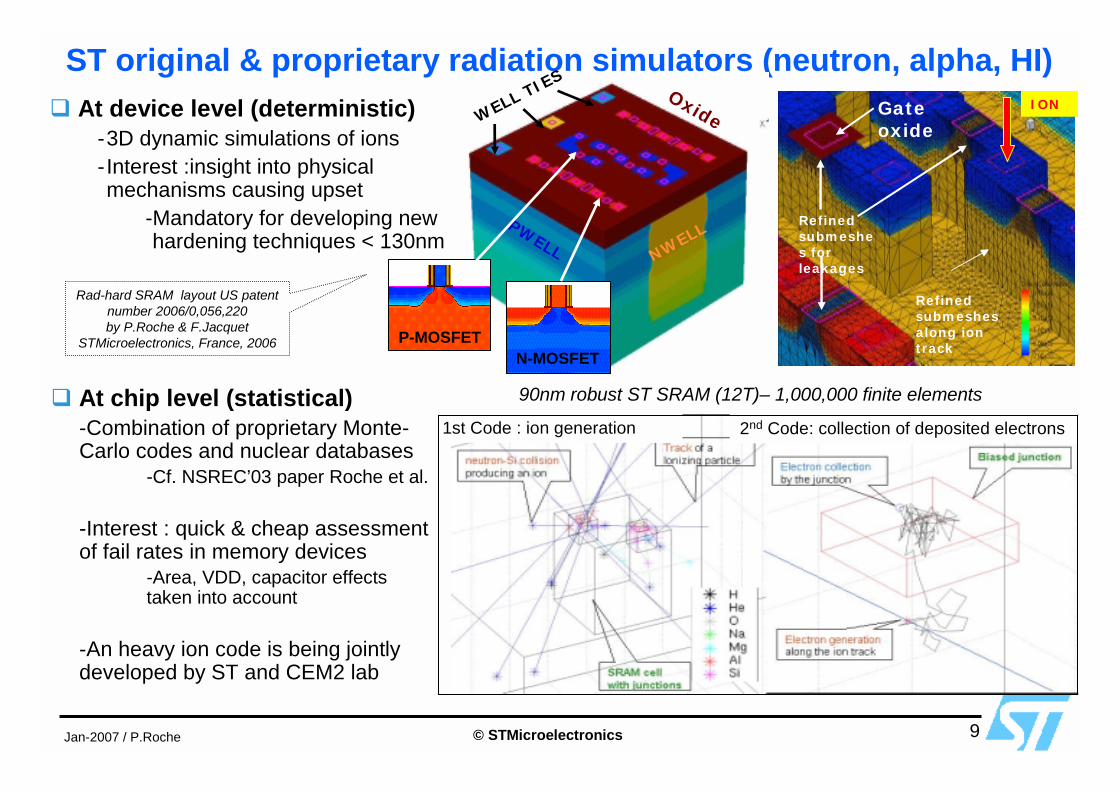
ST original & proprietary radiation simulators (neutron, alpha, HI)
� At chip level (statistical)-Combination of proprietary Monte-Carlo codes and nuclear databases
-Cf. NSREC’03 paper Roche et al.
-Interest : quick & cheap assessment of fail rates in memory devices
-Area, VDD, capacitor effects taken into account
-An heavy ion code is being jointly developed by ST and CEM2 lab
1st Code : ion generation 2nd Code: collection of deposited electrons
90nm robust ST SRAM (12T)– 1,000,000 finite elements
Gate oxide
Refined submeshes for leakages
Refined submeshes along ion track
IONOxide
PWELL NWELL
WELL TIES
P-MOSFETN-MOSFET
Rad-hard SRAM layout US patent number 2006/0,056,220 by P.Roche & F.Jacquet
STMicroelectronics, France, 2006
� At device level (deterministic)-3D dynamic simulations of ions-Interest :insight into physical mechanisms causing upset
-Mandatory for developing new hardening techniques < 130nm

© STMicroelectronics 10Jan-2007 / P.Roche
Examples of SER mitigation techniques at system level� RAM protected by Error Correction Codes (ECC) : addition of parity or check bits
�physical interleaving (physical separation of check bits) in conjunction with temporal scrubbing (periodical check for single error before a double error occurs in a same word)
� LOGIC protected by triple redundancy : multiple identical logic paths feeding into a majority voting
ECC/EDAC available by default on ST eDRAM and as an option in ST eSRAM
ECC wrappers (and BIST) available in ST CMOS65
RAM

© STMicroelectronics 11Jan-2007 / P.Roche
Examples of SER mitigations at device level with hardened cellsExample of SEU hardened static storage cell : preserves the logic state even if one internal node is altered by ionizing particle strikes
- Cons : area penalty • x2.5 for ST UHD 12T-SRAM in 90nm
- Pros : used to protect SRAM, registers, BRAM, FFs• Rad-hard LAYOUT mandatory below 130nm
• ST will be offering a robust library in CMOS65 in Q2’07
Examples of SET hardened cells : maintain the previous output signal when one input of the dual to single path converter is impacted by ions
- Cons : area penalty - Pros : radiation distortions cannot propagate
through other logic elements because of the tri-state functions
US patent number 5,570,313, by P.Masson & R.Ferrant (ST) Thomson-CSF, France, 1996
12T-SRAM cell schematic
CLK
1 2 3 4 5 6 7 8 9 10 11 12 13 14 15 16
17
18 19
2021
2223
24 25 26 27 28 29 30 31
32 33 34 35 36 37 38 39 40 41 42 43 44 45 46 47
50 51
5352
54 55
56 57
CLK
1 2 3 4 5 6 7 8 9 10 11 12 13 14 15 16
17
18 19
2021
2223
24 25 26 27 28 29 30 31
32 33 34 35 36 37 38 39 40 41 42 43 44 45 46 47
50 51
5352
54 55
56 57
>15 patents filed by ST-Crolles in hardening by design the past 6 years
12T-SRAM cell schematicPatent pending, by G.Gasiot & P.Roche
STMicroelectronics, France, 2006
Robust clock tree Patent pending, by P.Roche & F.Jacquet
STMicroelectronics, France, 2006
© STMicroelectronics 12Jan-2007 / P.Roche
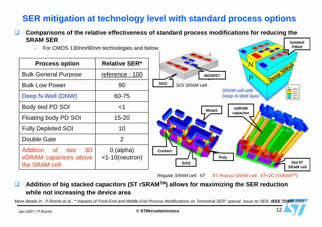
SER mitigation at technology level with standard process options� Comparisons of the relative effectiveness of standard process modifications for reducing the
SRAM SER- For CMOS 130nm/90nm technologies and below
� Addition of big stacked capacitors (ST rSRAMTM) allows for maximizing the SER reduction while not increasing the device area
More details in : P.Roche et al., “ Impacts of Front-End and Middle-End Process Modifications on Terrestrial SER” special issue on SER, IEEE TDMR 2005
0 (alpha)<1-10(neutron)
Addition of two 3D eDRAM capacitors above the SRAM cell
2Double Gate
10Fully Depleted SOI
15-20Floating body PD SOI
<1Body tied PD SOI
60-75Deep N-Well (DNW)
90Bulk Low Power
reference : 100Bulk General Purpose
Relative SER*Process option
Metal1
ST Robust SRAM cell : 6T+2C (rSRAMTM)
ContactPoly.
eDRAM capacitor
Deep NWellN
P
SRAM cell with Deep N-Well layer
Regular SRAM cell : 6T
Isolated PWell
SOI SRAM cellSiO2
MOSFET
SiO2 Std 6T SRAM cell
© STMicroelectronics 13Jan-2007 / P.Roche
Intermediate conclusion : ST radiation characterization flow
� is based on experimental tests (accelerated & real time)- ten’s of complex circuits already characterized In CMOS 250/180/130/90/65nm
• Library Validation testchips• Specific SER testchips (robust SRAMs & Flip-flops)
� uses original & proprietary simulators (deterministic & statistical)- theoretical models have been co-developed with research labs since many years- 6 Ph.D programs sponsored by ST-Crolles for continuously improving the simulators
� was already applied to ST CMOS 65nm with neutrons & alphas, and soon in 45nm- 130nm/90nm CMOS : qualification completed in 2003-2005- 65nm CMOS : six 65nm complex testchips tested in North America and Crolles in 2005-2006- 45nm CMOS : new silicon available mid-March 2007
� is compliant with international radiation test standards - JEDEC for neutron & alpha : radiation tests & measurements of radioactive contaminants- ESA-SCC : to be made more explicit in the next part
© STMicroelectronics 14Jan-2007 / P.Roche
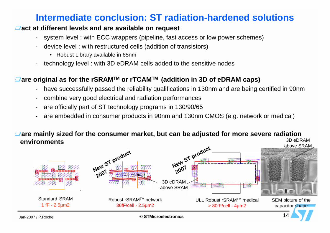
Intermediate conclusion: ST radiation-hardened solutionsact at different levels and are available on request
- system level : with ECC wrappers (pipeline, fast access or low power schemes)- device level : with restructured cells (addition of transistors)
• Robust Library available in 65nm- technology level : with 3D eDRAM cells added to the sensitive nodes
are original as for the rSRAMTM or rTCAMTM (addition in 3D of eDRAM caps)- have successfully passed the reliability qualifications in 130nm and are being certified in 90nm- combine very good electrical and radiation performances - are officially part of ST technology programs in 130/90/65 - are embedded in consumer products in 90nm and 130nm CMOS (e.g. network or medical)
are mainly sized for the consumer market, but can be adjusted for more severe radiation environments
ULL Robust rSRAMTM medical > 80fF/cell - 4µm2
Robust rSRAMTM network 36fF/cell - 2.5µm2
Standard SRAM 1 fF - 2.5µm2
3D eDRAMabove SRAM
New ST product
2007New ST product
2007
SEM picture of thecapacitor shape
3D eDRAMabove SRAM
© STMicroelectronics 15Jan-2007 / P.Roche
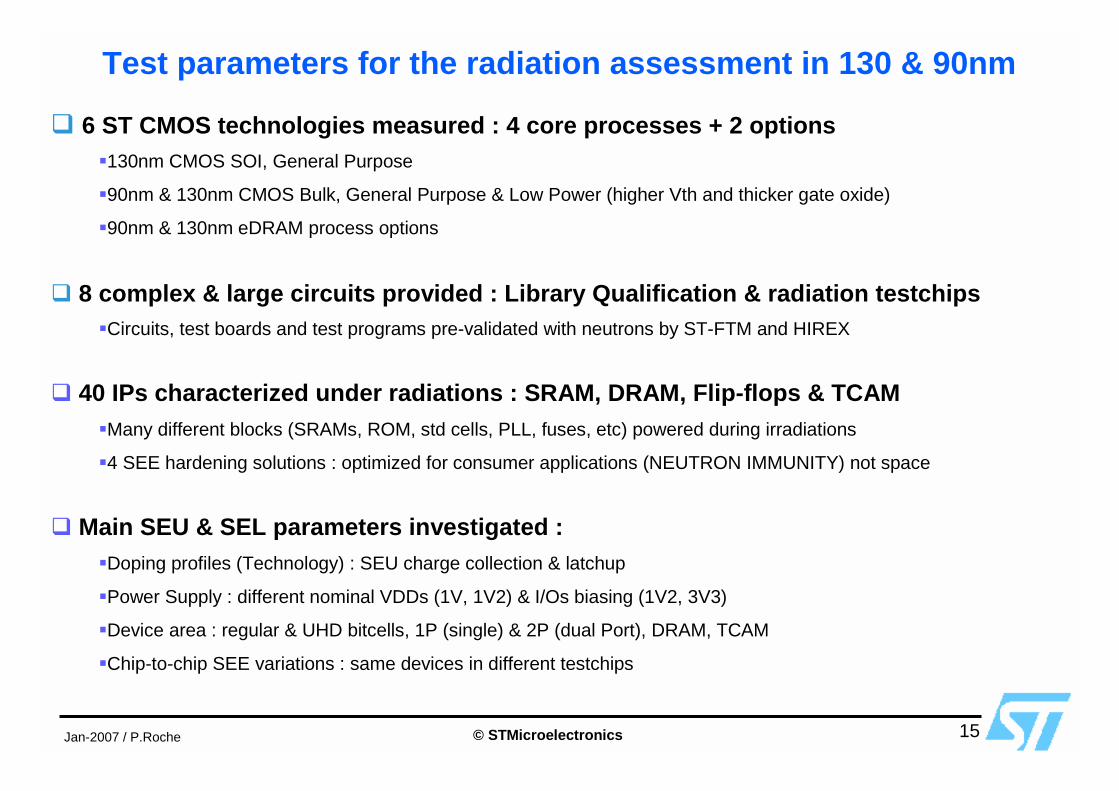
Test parameters for the radiation assessment in 130 & 90nm
� 6 ST CMOS technologies measured : 4 core processes + 2 options�130nm CMOS SOI, General Purpose
�90nm & 130nm CMOS Bulk, General Purpose & Low Power (higher Vth and thicker gate oxide)
�90nm & 130nm eDRAM process options
� 8 complex & large circuits provided : Library Qualification & radiation testchips�Circuits, test boards and test programs pre-validated with neutrons by ST-FTM and HIREX
� 40 IPs characterized under radiations : SRAM, DRAM, Flip-flops & TCAM�Many different blocks (SRAMs, ROM, std cells, PLL, fuses, etc) powered during irradiations
�4 SEE hardening solutions : optimized for consumer applications (NEUTRON IMMUNITY) not space
� Main SEU & SEL parameters investigated :�Doping profiles (Technology) : SEU charge collection & latchup
�Power Supply : different nominal VDDs (1V, 1V2) & I/Os biasing (1V2, 3V3)
�Device area : regular & UHD bitcells, 1P (single) & 2P (dual Port), DRAM, TCAM
�Chip-to-chip SEE variations : same devices in different testchips
© STMicroelectronics 16Jan-2007 / P.Roche
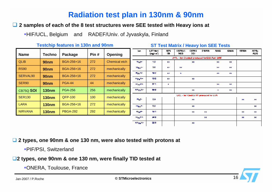
Radiation test plan in 130nm & 90nm� 2 samples of each of the 8 test structures were SEE tested with Heavy ions at
�HIF/UCL, Belgium and RADEF/Univ. of Jyvaskyla, Finland
� 2 types, one 90nm & one 130 nm, were also tested with protons at
�PIF/PSI, Switzerland
�2 types, one 90nm & one 130 nm, were finally TID tested at
�ONERA, Toulouse, France
ST Test Matrix / Heavy Ion SEE Tests
mechanically272BGA-256+16130nm LARA
mechanically292PBGA-292130nm NIRVANA
mechanically100QFP-100130nm SER130
mechanically256PGA-256130nmCB75Q SOI
mechanically44PGA-4490nm SER90
mechanically272BGA-256+1690nm SERVAL90
mechanically272BGA-256+1690nm RS90
Chemical etch272BGA-256+1690nmQLIB
OpeningPin #PackageTechnoName
Testchip features in 130n and 90nm
© STMicroelectronics 17Jan-2007 / P.Roche
Main SEE test results in 130nm and 90nm
For 8 testchips tested with heavy ions up to LET of 120 MeV/(mg.cm2)
&
For 2 testchips tested with protons up to an energy of 60 MeV
© STMicroelectronics 18Jan-2007 / P.Roche
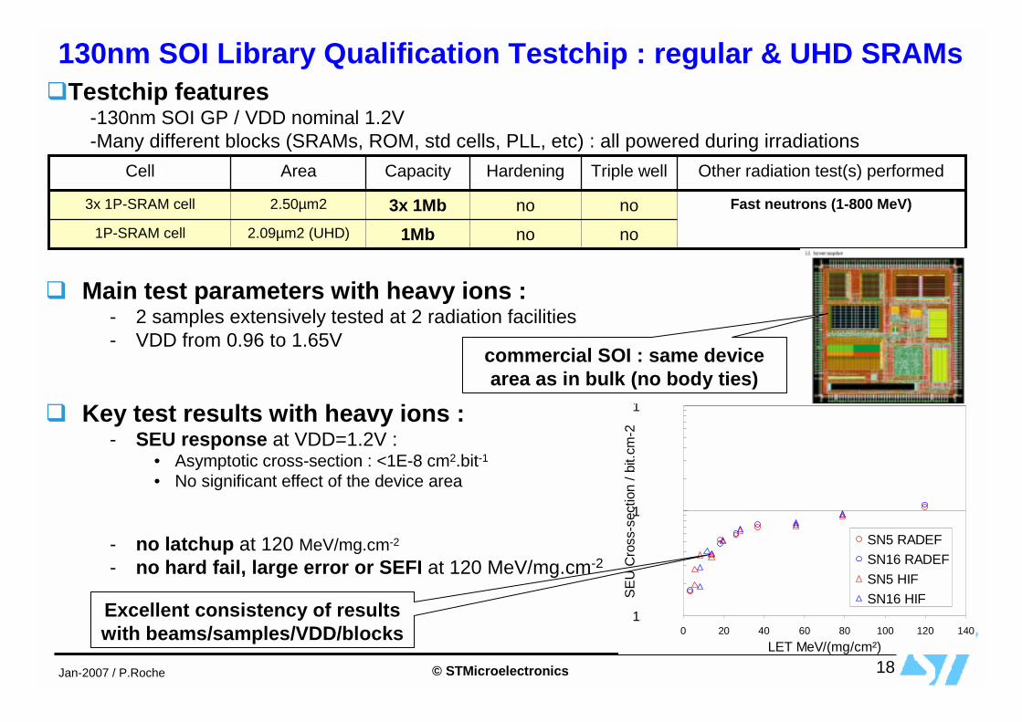
130nm SOI Library Qualification Testchip : regular & UHD SRAMs
no
no
Hardening
no1Mb2.09µm2 (UHD)1P-SRAM cell
2.50µm2
Area
3x 1Mb
Capacity
no
Triple well
Fast neutrons (1-800 MeV)3x 1P-SRAM cell
Other radiation test(s) performedCell
� Main test parameters with heavy ions :- 2 samples extensively tested at 2 radiation facilities - VDD from 0.96 to 1.65V
� Key test results with heavy ions :- SEU response at VDD=1.2V :
• Asymptotic cross-section : <1E-8 cm2.bit-1• No significant effect of the device area
- no latchup at 120 MeV/mg.cm-2
- no hard fail, large error or SEFI at 120 MeV/mg.cm-2
�Testchip features-130nm SOI GP / VDD nominal 1.2V-Many different blocks (SRAMs, ROM, std cells, PLL, etc) : all powered during irradiations
commercial SOI : same device area as in bulk (no body ties)
1,E-09
1,E-08
1,E-07
0 20 40 60 80 100 120 140
LET MeV/(mg/cm²)S
EU
Cro
ss-s
ectio
n / b
it.cm
-2
.
SN5 RADEFSN16 RADEFSN5 HIFSN16 HIFExcellent consistency of results
with beams/samples/VDD/blocks

© STMicroelectronics 19Jan-2007 / P.Roche
130nm SOI Library Qualification Testchip : regular & UHD SRAMs
no
no
Hardening
no1Mb2.09µm2 (UHD)1P-SRAM cell
2.50µm2
Area
3x 1Mb
Capacity
no
Triple well
Fast neutrons (1-800 MeV)3x 1P-SRAM cell
Other radiation test(s) performedCell
� Main test parameters with PROTONS :- 2 samples extensively tested- VDD from 1.1V, 1.2V, 1.3V
� Key test results with PROTONS :- SEU response at 1.2V :
• Asymptotic cross-section : ~1E-14 cm2.bit-1• No significant effect of the device area
- no latchup at 60 MeV (maximum energy used)- no hard fail, large error or SEFI at 60 MeV
�Testchip features-130nm SOI GP / VDD nominal 1.2V-Many different blocks (SRAMs, ROM, std cells, PLL, etc) : all powered during irradiations
1,E-15
1,E-14
1,E-13
0 20 40 60 80
Energy MeV
SE
U C
ross
-sec
tion
/ bit.
cm-2
.
SN5 1V2SN16 1V2SN5 1V1SN5 1V3
Excellent consistency of results with samples/VDD/blocks

© STMicroelectronics 20Jan-2007 / P.Roche
130nm BULK eDRAM validation testchip
�Main test parameters :- 3 samples measured - 2 different RAS conditions - VDD set at 1V/3V (SEU Worst Case), few runs at 1.2V/3.3V (nominal)
�Key test results with heavy ions :
- in Worst Case SEU conditions (VDD=1V, RAS=250ns) with ECC deactivated :
• Asymptotic cross-section : ~1.5E- 9 cm2.bit-1
- no hard fail at 68 MeV/mg.cm-2 (max LET available)
�Testchip features-130nm bulk GP / VDD nominal 1.2V and 3.3V (specific DRAM)
Yes (ECC)
Hardening0.53µm2
Area
3MbCapacity
Yes
Triple wellFast neutrons (1-800 MeV)Protons/neutrons at UCL
Alpha particles
DRAM cell
Other radiation test(s) performedCell
2 Mb 2 Mb
2 Mb2 Mb

© STMicroelectronics 21Jan-2007 / P.Roche
130nm BULK (1st) radiation testchip : regular & robust SRAMs
�Main test parameters :-2 samples tested-VDD set at 1.2V
�Key test results with heavy ions :-regular SRAM / SEU response at 1.2V :
•Asymptotic cross-section : ~1E-7 cm2.bit-1
-robust SRAM (optimized for consumer products)•Asymptotic cross-section : improved by 3x•LET threshold : increased by 10x
-no large error, hard fail or SEFI at 58 MeV/mg.cm-²
-no latchup at 58 MeV/mg.cm-² (max LET available)
�Testchip features-130nm bulk GP / VDD nominal 1.2V-Many different blocks (large SRAMs, std cells, PLL, etc) : all powered during irradiations
yes
no
Hardening
2.50µm2
2.50µm2
Area
2 x 1 Mb2 x 1MbCapacity
No / Yes
No / Yes
Triple well
2x Robust 1P-SRAM cell
Fast neutrons (1-800 MeV) + Alpha TID (1MradSi)
2 x 1P-SRAM cell
Other radiation test(s) performedCell
1,E-12
1,E-11
1,E-10
1,E-09
1,E-08
1,E-07
1,E-06
0 20 40 60 80LET MeV/(mg/cm²)
SEU
Cro
ss-s
ectio
n / b
it.cm
-2
.
regular SRAM
robust SRAM
Estimated gain for the SEU rate in GEO ~10x with this 130nm rSRAMTM
Optimization for reachinga quasi neutron immunity
© STMicroelectronics 22Jan-2007 / P.Roche
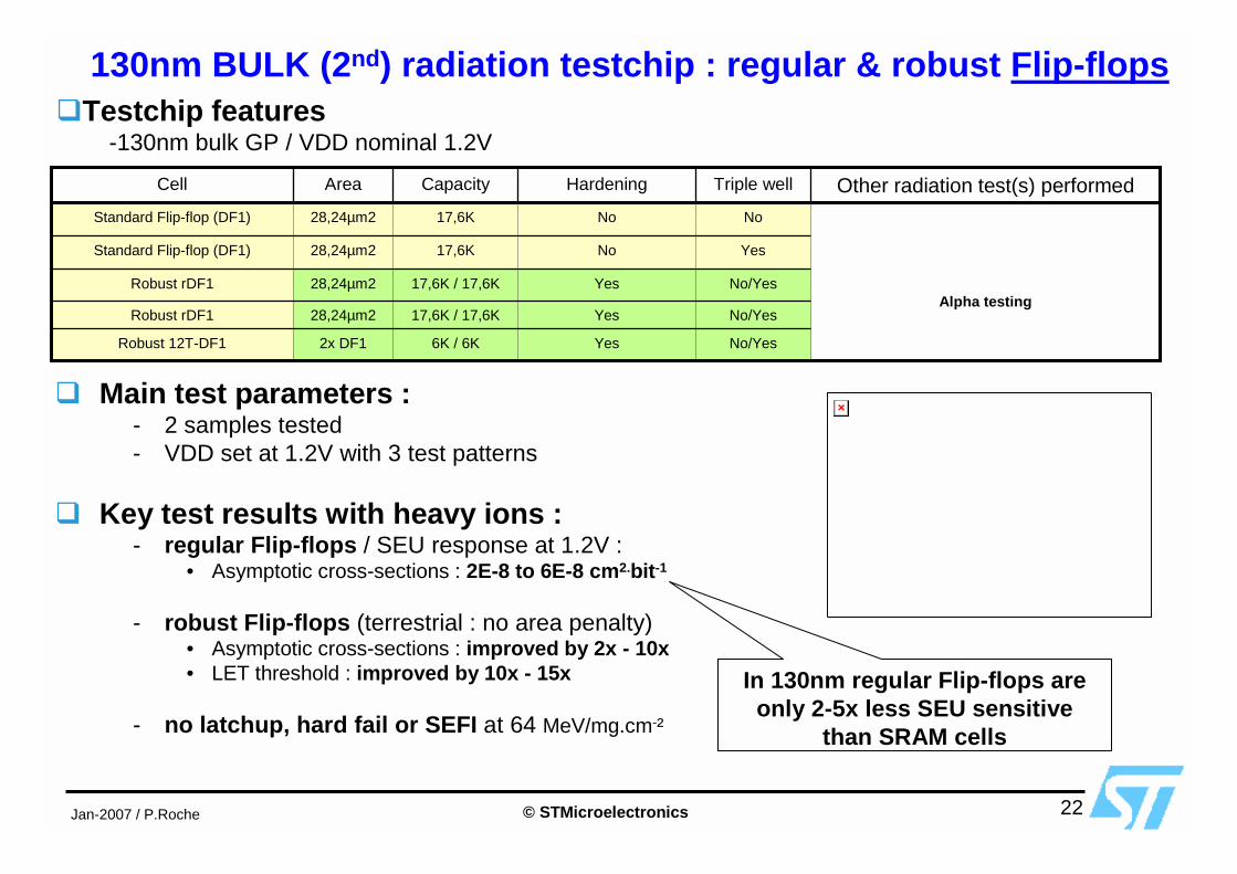
130nm BULK (2nd) radiation testchip : regular & robust Flip-flops
� Main test parameters :- 2 samples tested- VDD set at 1.2V with 3 test patterns
� Key test results with heavy ions :- regular Flip-flops / SEU response at 1.2V :
• Asymptotic cross-sections : 2E-8 to 6E-8 cm2.bit-1
- robust Flip-flops (terrestrial : no area penalty)• Asymptotic cross-sections : improved by 2x - 10x• LET threshold : improved by 10x - 15x
- no latchup, hard fail or SEFI at 64 MeV/mg.cm-²
�Testchip features-130nm bulk GP / VDD nominal 1.2V
No/YesYes17,6K / 17,6K28,24µm2Robust rDF1
YesNo17,6K28,24µm2Standard Flip-flop (DF1)
Alpha testing
NoNo17,6K28,24µm2Standard Flip-flop (DF1)
Yes
Yes
Hardening
2x DF1
28,24µm2
Area
6K / 6K
17,6K / 17,6K
Capacity
No/Yes
No/Yes
Triple well
Robust 12T-DF1
Robust rDF1
Other radiation test(s) performedCell
In 130nm regular Flip-flops are only 2-5x less SEU sensitive
than SRAM cells
© STMicroelectronics 23Jan-2007 / P.Roche
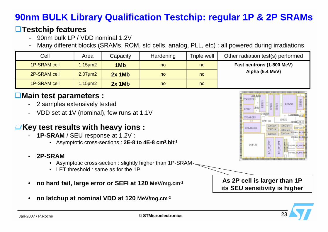
90nm BULK Library Qualification Testchip: regular 1P & 2P SRAMs
�Main test parameters :- 2 samples extensively tested- VDD set at 1V (nominal), few runs at 1.1V
Key test results with heavy ions :- 1P-SRAM / SEU response at 1.2V :
• Asymptotic cross-sections : 2E-8 to 4E-8 cm2.bit-1
- 2P-SRAM • Asymptotic cross-section : slightly higher than 1P-SRAM• LET threshold : same as for the 1P
• no hard fail, large error or SEFI at 120 MeV/mg.cm-2
• no latchup at nominal VDD at 120 MeV/mg.cm-2
�Testchip features- 90nm bulk LP / VDD nominal 1.2V- Many different blocks (SRAMs, ROM, std cells, analog, PLL, etc) : all powered during irradiations
nono2x 1Mb1.15µm21P-SRAM cell
no
no
Hardening
2.07µm2
1.15µm2
Area
2x 1Mb1Mb
Capacity
no
no
Triple well
2P-SRAM cell
Fast neutrons (1-800 MeV)Alpha (5.4 MeV)
1P-SRAM cell
Other radiation test(s) performedCell
As 2P cell is larger than 1P its SEU sensitivity is higher

© STMicroelectronics 24Jan-2007 / P.Roche
90nm BULK (1st) radiation testchip : regular Flip-flops
� Main test parameters :- 2 samples extensively tested- VDD set at 1.2V with 3 test patterns and 2 clock states
Key test results with heavy ions :- Regular Flip-flops / SEU response at 1.2V :
• Asymptotic cross-sections : 6E-8 to 1E-7 cm2.bit-1
- no latchup, hard fail or SEFI at 68 MeV/mg.cm-²
�Testchip features-90nm bulk LP / VDD nominal 1.2V
NoNo100KStd VThStandard Flip-flop (DF2SQX05 )
NoNo100Khigh driveStandard Flip-flop (DF1QX2 1)
NoNo100KHigh VThStandard Flip-flop (DF1QX05V )
Fast neutrons (1-800 MeV)Alpha testing
NoNo100KRef.Standard Flip-flop (DF1QX05 )
No
Hardening
HD
interest
100K
Capacity
No
Triple well
Standard Flip-flop (DF1SQY1)
Other radiation test(s) performedCell
FF1
FF3
FF2
FF4
FF5
4.2 mm
4.7
mm
In 90nm regular Flip-flops are more HI sensitive than 90nm SRAMs & as
sensitive as 130nm SRAMs

© STMicroelectronics 25Jan-2007 / P.Roche
90nm BULK (2nd) radiation testchip : regular & robust rSRAMTM
�Main test parameters :- 2 samples extensively tested- VDD set at 1V (nominal), few runs at 1.1V and 1.2V
�Key test results with heavy ions :- regular UHD SRAM / SEU response at 1V :
• Asymptotic cross-section : 5E-8 cm2.bit-1
- robust UHD rSRAM (Ultra High Density)• Asymptotic cross-section : improved by 3x• LET threshold : improved 5x
- no large error, hard fail or SEFI at 68 MeV/mg.cm-2 (max LET available)
- no latchup at nominal VDD at 68 MeV/mg.cm-2 (max LET available)
�Testchip features- 90nm Bulk GP / VDD nominal 1V- Many different blocks (SRAMs, TCAM, Flip-flops, etc) : all powered during irradiations
yesyes288Kb + 512Kb4.98µm2Robust TerCAM cell
nono64 KbitStandard Flip-flop (DF1 )Yes
no
yes
no
Hardening
no72KbitsN/ARobust Flip-flop
4.98µm2
0.99µm2
0.99µm2
Area
288Kb + 512Kb
1 Mb
1 Mb
Capacity
no
no
no
Triple well
TerCAM cell
Robust UHD 1P-SRAM cell
Fast neutrons (1-800 MeV)Alpha (5.4 MeV)
1P-SRAM cell
Other radiation test(s) performedCell
HI SEU rates in orbits significantly reduced with 90nm rSRAMTM

© STMicroelectronics 26Jan-2007 / P.Roche
90nm BULK (2nd) radiation testchip : regular & robust rSRAMTM
�Main test parameters with PROTONS :- 2 samples extensively tested- VDD set at 1V (nominal), at 0.9V and 1.1V
�Key test results with PROTONS :- regular UHD SRAM / SEU response at 1V :
• Asymptotic cross-section : 3E-14 cm2.bit-1- robust UHD SRAM
• Asymptotic cross-section : improved by 10x
- regular Flip-flop / SEU response at 1V : • Asymptotic cross-sections : x3 higher than SRAM
- no SEL, LE or SEFI at 60 MeV
�Testchip features- 90nm Bulk GP / VDD nominal 1V- Many different blocs (SRAMs, TCAM, Flip-flops, etc) : all powered during irradiations
1,E-16
1,E-15
1,E-14
1,E-13
0 20 40 60 80Energy MeV
SEU
Cro
ss-s
ectio
n / b
it.cm
-2
.
robust SRAM SN21 1Vregular SRAM SN21 1V
same as with HI
yesyes288Kb + 512Kb4.98µm2Robust TerCAM cell
nono64 KbitStandard Flip-flop (DF1 )Yes
no
yes
no
Hardening
no72KbitsN/ARobust Flip-flop
4.98µm2
0.99µm2
0.99µm2
Area
288Kb + 512Kb
1 Mb
1 Mb
Capacity
no
no
no
Triple well
TerCAM cell
Robust UHD 1P-SRAM cell
Fast neutrons (1-800 MeV)Alpha (5.4 MeV)
1P-SRAM cell
Other radiation test(s) performedCell
© STMicroelectronics 27Jan-2007 / P.Roche
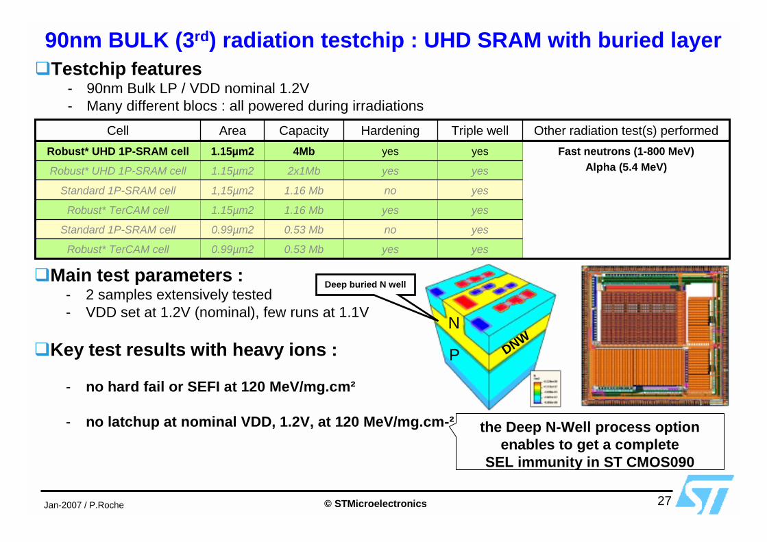
90nm BULK (3rd) radiation testchip : UHD SRAM with buried layer
�Main test parameters :- 2 samples extensively tested- VDD set at 1.2V (nominal), few runs at 1.1V
�Key test results with heavy ions :
- no hard fail or SEFI at 120 MeV/mg.cm²
- no latchup at nominal VDD, 1.2V, at 120 MeV/mg.cm-²
�Testchip features- 90nm Bulk LP / VDD nominal 1.2V- Many different blocs : all powered during irradiations
Fast neutrons (1-800 MeV)Alpha (5.4 MeV)yesyes2x1Mb1.15µm2Robust* UHD 1P-SRAM cell
yesno0.53 Mb0.99µm2Standard 1P-SRAM cell
yesyes1.16 Mb1.15µm2Robust* TerCAM cell
yesyes0.53 Mb0.99µm2Robust* TerCAM cell
no
yes
Hardening
1,15µm2
1.15µm2
Area
1.16 Mb
4Mb
Capacity
yes
yes
Triple well
Standard 1P-SRAM cell
Robust* UHD 1P-SRAM cell
Other radiation test(s) performedCell
the Deep N-Well process option enables to get a complete
SEL immunity in ST CMOS090
DNWN
P
Deep buried N well
© STMicroelectronics 28Jan-2007 / P.Roche
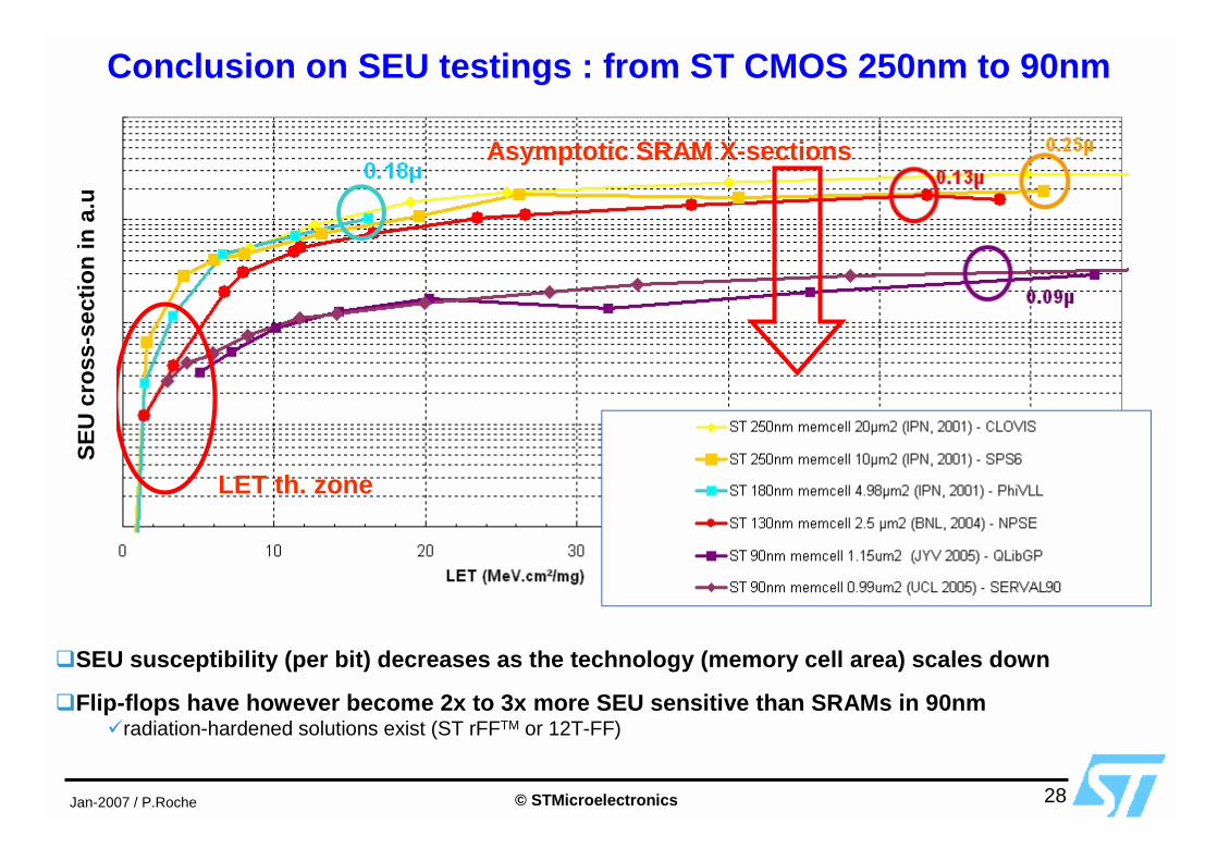
Conclusion on SEU testings : from ST CMOS 250nm to 90nm
�SEU susceptibility (per bit) decreases as the technology (memory cell area) scales down
�Flip-flops have however become 2x to 3x more SEU sensitive than SRAMs in 90nm �radiation-hardened solutions exist (ST rFFTM or 12T-FF)
LET th. zone
Asymptotic SRAM X-sections
SEU
cro
ss-s
ectio
n in
a.u
© STMicroelectronics 29Jan-2007 / P.Roche
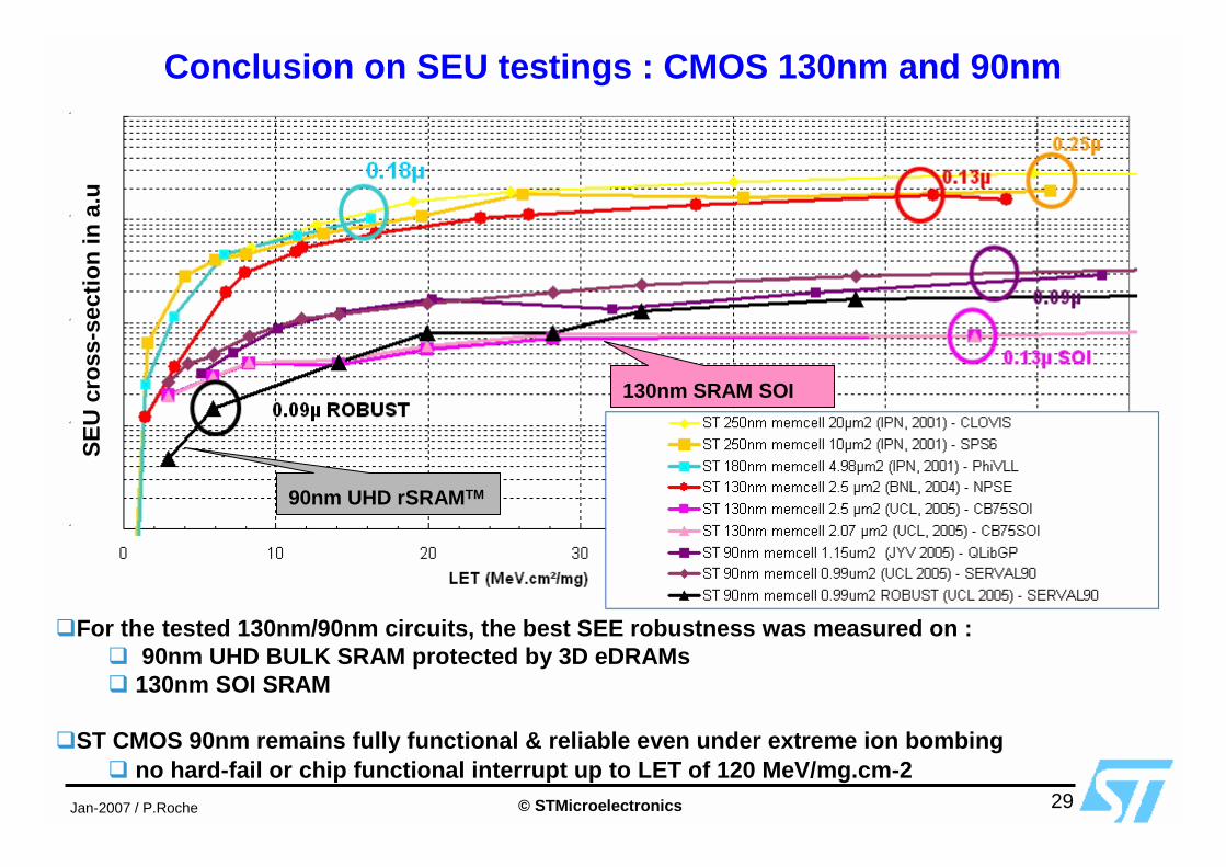
�For the tested 130nm/90nm circuits, the best SEE robustness was measured on : � 90nm UHD BULK SRAM protected by 3D eDRAMs� 130nm SOI SRAM
�ST CMOS 90nm remains fully functional & reliable even under extreme ion bombing � no hard-fail or chip functional interrupt up to LET of 120 MeV/mg.cm-2
Conclusion on SEU testings : CMOS 130nm and 90nm
130nm SRAM SOI
90nm UHD rSRAMTM
SEU
cro
ss-s
ectio
n in
a.u

© STMicroelectronics 30Jan-2007 / P.Roche
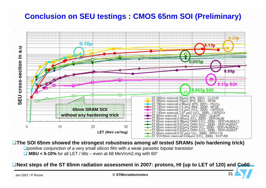
�Cross-sections in 65nm are in-between 130nm and 90nm because of a stronger MBU contribution� 80% of MBUs at LET of 14.1� 95% of MBUs at LET of 19.9 � 98% of MBUs at LET of 34
�ST CMOS 65nm remains fully functional at LET of 68 MeV/mg.cm-2 (max. LET available at UCL)
Conclusion on SEU testings : CMOS 65nm BULK (Preliminary)�5 testchips CMOS65, embedding non-hardened RAMs & FFs, measured at UCL end of 2006
65nm SRAMs BULKin 4 different testchips
SEU
cro
ss-s
ectio
n in
a.u
© STMicroelectronics 31Jan-2007 / P.Roche
�The SOI 65nm showed the strongest robustness among all tested SRAMs (w/o hardening trick)�positive conjunction of a very small silicon film with a weak parasitic bipolar transistor� MBU < 5-10% for all LET / tilts – even at 68 MeV/cm2.mg with 60°
�Next steps of the ST 65nm radiation assessment in 2007: protons, HI (up to LET of 120) and Co60
Conclusion on SEU testings : CMOS 65nm SOI (Preliminary)
65nm SRAM SOIwithout any hardening trick
SEU
cro
ss-s
ectio
n in
a.u
© STMicroelectronics 32Jan-2007 / P.Roche
TID test results in 130nm & 90nm
for 2 testchips tested with gamma rays up to 100kradSi
+ earlier test results in the MradSi regime
© STMicroelectronics 33Jan-2007 / P.Roche
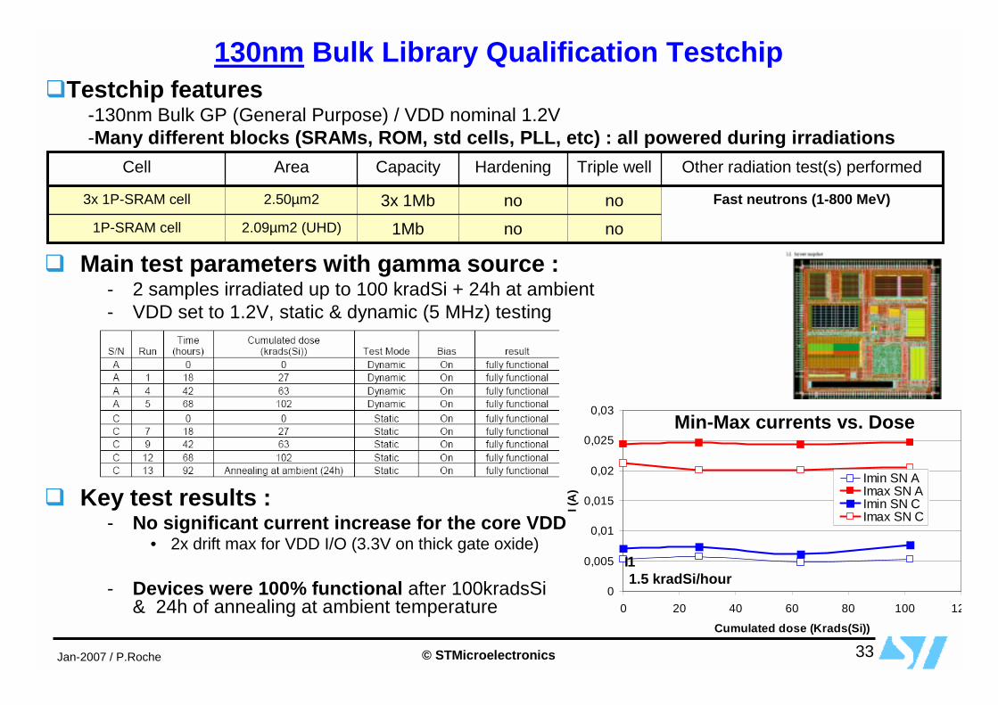
130nm Bulk Library Qualification Testchip
no
no
Hardening
no1Mb2.09µm2 (UHD)1P-SRAM cell
2.50µm2
Area
3x 1Mb
Capacity
no
Triple well
Fast neutrons (1-800 MeV)3x 1P-SRAM cell
Other radiation test(s) performedCell
� Main test parameters with gamma source :- 2 samples irradiated up to 100 kradSi + 24h at ambient- VDD set to 1.2V, static & dynamic (5 MHz) testing
� Key test results :- No significant current increase for the core VDD
• 2x drift max for VDD I/O (3.3V on thick gate oxide)
- Devices were 100% functional after 100kradsSi & 24h of annealing at ambient temperature
�Testchip features-130nm Bulk GP (General Purpose) / VDD nominal 1.2V-Many different blocks (SRAMs, ROM, std cells, PLL, etc) : all powered during irradiations
I1
0
0,005
0,01
0,015
0,02
0,025
0,03
0 20 40 60 80 100 12
Cumulated dose (Krads(Si))
I (A
)
Imin SN AImax SN AImin SN CImax SN C
1.5 kradSi/hour
Min-Max currents vs. Dose
© STMicroelectronics 34Jan-2007 / P.Roche
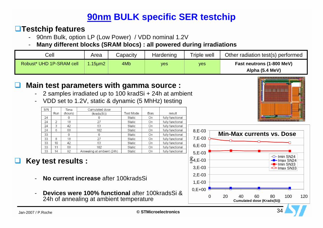
90nm BULK specific SER testchip �Testchip features
- 90nm Bulk, option LP (Low Power) / VDD nominal 1.2V- Many different blocks (SRAM blocs) : all powered during irradiations
Fast neutrons (1-800 MeV)Alpha (5.4 MeV)
yes
Hardening1.15µm2
Area4Mb
Capacityyes
Triple wellRobust* UHD 1P-SRAM cell
Other radiation test(s) performedCell
� Main test parameters with gamma source :- 2 samples irradiated up to 100 kradSi + 24h at ambient- VDD set to 1.2V, static & dynamic (5 MhHz) testing
� Key test results :
- No current increase after 100kradsSi
- Devices were 100% functional after 100kradsSi & 24h of annealing at ambient temperature
0,E+001,E-03
2,E-033,E-034,E-03
5,E-036,E-03
7,E-038,E-03
0 20 40 60 80 100 120Cumulated dose (Krads(Si))
I (A
) Imin SN24Imax SN24Imin SN33Imax SN33
Min-Max currents vs. Dose

© STMicroelectronics 35Jan-2007 / P.Roche
Similar extreme TID robustness in the Mrad regime for ST 130nm
Linear transistors ST 130nm with thin gate oxide irradiated up to 30 MradSi� Threshold voltage shift < 10 mV : negligible� Subthreshold swing variations : negligible � Transconductance degradation of less than 10%
Linear transistors ST 130nm with thick gate oxide irradiated up to 30 MradSi� Threshold voltage shift < 35 mV : negligible� Transconductance degradation of less than 10%
Two SRAMs 1Mb ST 130nm, standard and rSRAMTM, irradiated up to 1 MradSi� No bit error detected for each memory cut
• at initial and after each exposure step (0, 100, 500 and 1000Krads(Si))� Full functionality of the 2 cuts after being exposed to a cumulative dose of 1Mrad(Si).
Whatever the γγγγ or X-ray source, dose rate, cumulative dose, or type of devicethe tested ST 130nm & 90nm circuits are extremely TID resistant
(without any guard rings or edgeless transistors)

© STMicroelectronics 36Jan-2007 / P.Roche
General conclusion for ST CMOS 130 and 90nmThe radiation testings were jointly performed by ESA-ESTEC, ST-FTM and HIREX for 1 year on
- 8 testchips during 2 HI campaigns in Belgium and Finland- 2 testchips during 1 proton campaign in Switzerland- 2 testchips with gamma rays in France
More than 350 test runs and 1800 log files were analyzed
The test results have shown for the commercial (non hardened) 130 and 90nm ST devices- no dose issue
• devices 100% functional after 100kradsSi & 24h of ambient annealing
- no hard fail occurrence or SEFI• up to 120 MeV/mg.cm-²
- no latchup with protons • up to 60 MeV
- no latchup with heavy ions in 130nm BULK & SOI • up to respectively 64 & 120 MeV/mg.cm-²
- no latchup with heavy ions in 90nm BULK • up to 120 MeV/mg.cm-² at nominal VDD
- the best SEU robustness for the 90nm UHD rSRAMTM & 130nm SOI SRAM• SEU rates very likely decreased by several decades
First HI tests on 5 ST 65nm testchips have already demonstrated a good reliability and hardness
Related Documents


