1 Analytical Approaches and Expert Systems in the Characterization of Microelectronic Devices D. E. Passoja 1 , Lawrence A. Casper 2 , and A . J . Scharman 3 1 Linde Division, Union Carbide Corporation, Tarrytown, NY 10591 2 Solid State Electronics Division, Honeywell Inc., Plymouth, M N 55441 3 Central Scientific Laboratory, Union Carbide Corporation, Tarrytown, NY 10591 With further device miniaturization anticipated for microelectronics in the future, more stringent requirements will be placed on contaminants and impurities in the chemicals, materials and gases that are supplied to the industry. It is suggested that absolute determination of the role of a particular contaminant during device processing will be difficult. It is proposed that the present analytical "characterization" of a device is an image composed of texels - discrete picture elements - defined in a space of magnification and sensitivity. By viewing the microanalytical problem from a broader perspective based upon the geometric organization of the microscopic world, it is also proposed that by the use of "expert systems", more structured analytical algorithms and some simple scaling laws it should be possible to provide more efficient problem solving methods for the analyst. In the past 10 years the driving force of miniaturization in the microelectronics industry has resulted in a consistent decrease in the feature sizes of integrated circuits. Commensurate with this miniaturization there has been an increase in the complexity of the technology base (Figures 1-3)• Whereas the early solid state technology was based primarily on knowledge of systems and circuits, materials science and chemistry, had a significant but limited role in it. With the advent of the integrated circuit, however, the technology base expanded and to include a broad range of disciplines that is now a continuum of overlapping technologies merging to produce the final outcome: the integrated circuit. In progressing from discrete to integrated devices at the levels of small and medium scale integration, i t became necessary to incorporate device physics into the technology base. As device structures were made progressively smaller, they behaved neither as "bulk" three dimensional devices nor as strict two dimensional 0097-6156/ 86/ 0295-0001 $06.00/ 0 © 1986 American Chemical Society Downloaded by 172.254.119.16 on December 9, 2013 | http://pubs.acs.org Publication Date: January 28, 1986 | doi: 10.1021/bk-1986-0295.ch001 In Microelectronics Processing: Inorganic Materials Characterization; Casper, L.; ACS Symposium Series; American Chemical Society: Washington, DC, 1986.

Welcome message from author
This document is posted to help you gain knowledge. Please leave a comment to let me know what you think about it! Share it to your friends and learn new things together.
Transcript
1 Analytical Approaches and Expert Systems in the Characterization of Microelectronic Devices
D. E. Passoja1, Lawrence A. Casper2, and A. J. Scharman3
1Linde Division, Union Carbide Corporation, Tarrytown, NY 10591 2Solid State Electronics Division, Honeywell Inc., Plymouth, MN 55441 3Central Scientific Laboratory, Union Carbide Corporation, Tarrytown, NY 10591
With further device miniaturization anticipated for microelectronics in the future, more stringent requirements will be placed on contaminants and impurities in the chemicals, materials and gases that are supplied to the industry. It is suggested that absolute determination of the role of a particular contaminant during device processing will be difficult. It is proposed that the present analytical "characterization" of a device is an image composed of texels - discrete picture elements - defined in a space of magnification and sensitivity. By viewing the microanalytical problem from a broader perspective based upon the geometric organization of the microscopic world, i t is also proposed that by the use of "expert systems", more structured analytical algorithms and some simple scaling laws i t should be possible to provide more efficient problem solving methods for the analyst.
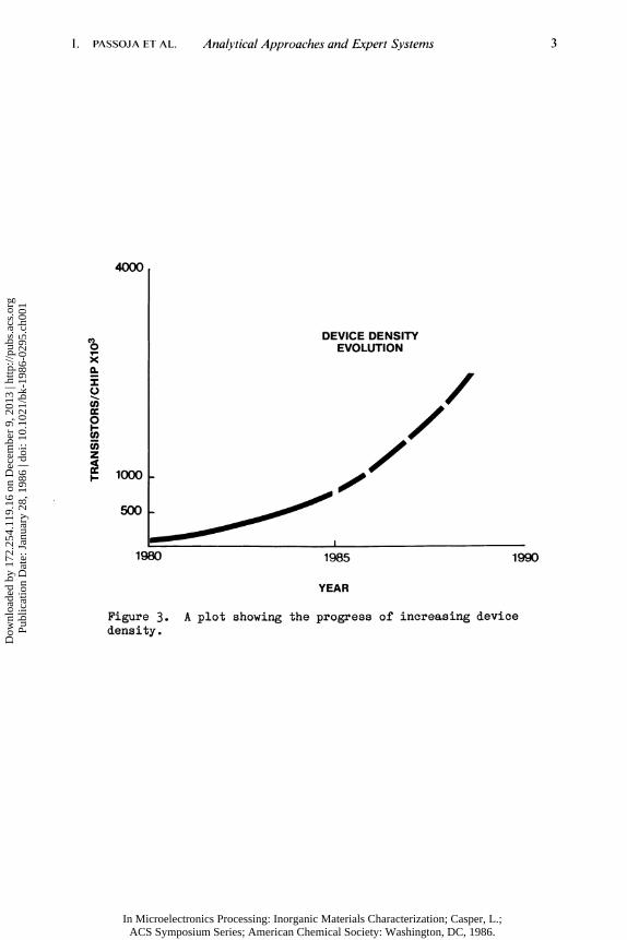
In the past 10 years the d r i v i n g f o r c e o f m i n i a t u r i z a t i o n i n the m i c r o e l e c t r o n i c s i n d u s t r y has r e s u l t e d i n a c o n s i s t e n t decrease i n the feature s i z e s o f i n t e g r a t e d c i r c u i t s . Commensurate with t h i s m i n i a t u r i z a t i o n there has been an incre a s e i n the complexity o f the technology base (Figures 1-3)• Whereas the e a r l y s o l i d s t a t e technology was based p r i m a r i l y on knowledge of systems and c i r c u i t s , m a t e r i a l s science and chemistry, had a s i g n i f i c a n t but l i m i t e d r o l e i n i t . With the advent o f the i n t e g r a t e d c i r c u i t , however, the technology base expanded and to i n c l u d e a broad range o f d i s c i p l i n e s t h a t i s now a continuum o f overlapping technologies merging to produce the f i n a l outcome: the i n t e g r a t e d c i r c u i t .
In p r o g r e s s i n g from d i s c r e t e to i n t e g r a t e d devices a t the l e v e l s o f sma l l and medium s c a l e i n t e g r a t i o n , i t became necessary to i n c o r p o r a t e device p h y s i c s i n t o the technology base. As device s t r u c t u r e s were made p r o g r e s s i v e l y s m a l l e r , they behaved n e i t h e r as "bulk" three dimensional devices nor as s t r i c t two dimensional
0097-6156/ 86/ 0295-0001 $06.00/ 0 © 1986 American Chemical Society
Dow
nloa
ded
by 1
72.2
54.1
19.1
6 on
Dec
embe
r 9,
201
3 | h
ttp://
pubs
.acs
.org
P
ublic
atio
n D
ate:
Jan
uary
28,
198
6 | d
oi: 1
0.10
21/b
k-19
86-0
295.
ch00
1
In Microelectronics Processing: Inorganic Materials Characterization; Casper, L.; ACS Symposium Series; American Chemical Society: Washington, DC, 1986.
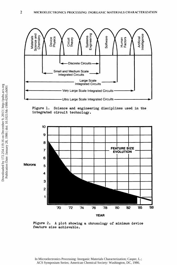
2 MICROELECTRONICS PROCESSING: INORGANIC MATERIALS CHARACTERIZATION
Large Scale ^ Integrated Circuits
Very Large Scale Integrated Circuits •
Ultra Large Scale Integrated Circuits •
Figure 1. Science and engineering d i s c i p l i n e s used i n the in t e g r a t e d c i r c u i t technology.
Microns
70 72 74 76 78 80 82 85 88
YEAR
Figure 2. A p l o t showing a chronology o f minimum device f e a t u r e s i z e a c h i e v a b l e .
Dow
nloa
ded
by 1
72.2
54.1
19.1
6 on
Dec
embe
r 9,
201
3 | h
ttp://
pubs
.acs
.org
P
ublic
atio
n D
ate:
Jan
uary
28,
198
6 | d
oi: 1
0.10
21/b
k-19
86-0
295.
ch00
1
In Microelectronics Processing: Inorganic Materials Characterization; Casper, L.; ACS Symposium Series; American Chemical Society: Washington, DC, 1986.
1. PASSOJA ET A L . Analytical Approaches and Expert Systems 3
4000
DEVICE DENSITY EVOLUTION
1000 U
500 U
1980 1990
Figure 3. A p l o t showing the progress of i n c r e a s i n g device d e n s i t y .
Dow
nloa
ded
by 1
72.2
54.1
19.1
6 on
Dec
embe
r 9,
201
3 | h
ttp://
pubs
.acs
.org
P
ublic
atio
n D
ate:
Jan
uary
28,
198
6 | d
oi: 1
0.10
21/b
k-19
86-0
295.
ch00
1
In Microelectronics Processing: Inorganic Materials Characterization; Casper, L.; ACS Symposium Series; American Chemical Society: Washington, DC, 1986.
4 MICROELECTRONICS PROCESSING: INORGANIC MATERIALS CHARACTERIZATION
devices. At these l e v e l s o f m i n i a t u r i z a t i o n , d e f e c t s and contaminants are not minor c o n s t i t u e n t s s i n c e f a i l u r e of only a small f r a c t i o n o f c i r c u i t s on the device l e v e l r e s u l t s i n a s u b s t a n t i a l decrease i n process y i e l d s . As m i n i a t u r i z a t i o n progresses f u r t h e r , d e f e c t s and contaminants w i l l become even more i n f l u e n t i a l on device y i e l d , performance and r e l i a b i l i t y .
As the semiconductor i n d u s t r y progresses i n t o the l a t t e r p a r t o f t h i s decade, submicron technology w i l l become a r e a l i t y . Prom s c a l i n g laws we know t h a t t h i n f i l m s are not t h i n enough. For example i n metal-oxide-semiconductor (MOS) technology, gate oxides w i l l be 200 i n t h i c k n e s s or l e s s . Such l a y e r s should probably not be thought o f as t h i n f i l m s s i n c e they are more a c c u r a t e l y d e s c r i b e d as "surface r e g i o n " or using the terminology o f surface chemistry, " i n t e r p h a s e " r e g i o n .
The high s e n s i t i v i t y o f VLSI technology to d e f e c t s and contamination has n e c e s s i t a t e d a s u b s t a n t i a l investment i n new processing technology. Contamination and defect c o n t r o l i s now a b a s i c requirement i n a l l aspects of p r o c e s s i n g . Accompanying t h i s new u l t r a - c l e a n technology i s the need to c h a r a c t e r i z e the m a t e r i a l s and chemicals, the u n i t processes and the ambients to which the wafers are exposed.
At a more fundamental l e v e l , VLSI devices must be s t u d i e d to determine the complex r e l a t i o n s h i p s t h a t e x i s t between a device's s t r u c t u r e , composition and e l e c t r i c a l c h a r a c t e r i s t i c s . I t i s p r e s e n t l y uneconomic to achieve process c o n t r o l by determining the d e t a i l e d changes which occur i n a device's s t r u c t u r e and chemistry once processing begins. Process c o n t r o l i s u s u a l l y achieved i n s t e a d by monitoring c r i t i c a l parameters such as f i l m t h i ckness and e l e c t r i c a l c h a r a c t e r i s t i c s thereby e l i m i n a t i n g (or reworking) wafers t h a t are not i n the c o n t r o l range.
The l a t i t u d e o f a process and the s e n s i t i v i t y of c e r t a i n designs to y i e l d l o s s e s a r e , i n p a r t , a d i r e c t r e f l e c t i o n of the e v o l u t i o n o f microscopic s t r u c t u r a l i m p e r f e c t i o n s t h a t develop d u r i n g p r o c e s s i n g . Such d e t a i l s as a d e f e c t ' s s c a l i n g behavior need to be s t u d i e d i n order t o determine the r e l a t i o n s h i p between t h e i r s p a t i a l e v o l u t i o n , formation mechanisms and frequency o f occurrence. This behavior i s q u i t e complex and w i l l c e r t a i n l y i n c l u d e more surface r e l a t e d i s s u e s as device dimensional s c a l i n g continues. I t would be expected t h a t a t some l e v e l of m i n i a t u r i z a t i o n the synergism between the accumulated process t r a n s i e n t s and randomness inherent a t the atomic l e v e l might represent a fundamental p h y s i c a l l i m i t a t i o n o f current technology and make f u r t h e r m i n i a t u r i z a t i o n d i f f i c u l t i f not i m p o s s i b l e .
As surface s c i e n t i s t s , m a t e r i a l s c i e n t i s t s and chemists i t would be u s e f u l a t t h i s time t o step back and r e f l e c t on what impact f u r t h e r m i n i a t u r i z a t i o n w i l l have on us. Of p a r t i c u l a r i n t e r e s t to us i s the a n a l y s i s o f process performance and device y i e l d s u s i n g surface a n a l y s i s techniques. With f u r t h e r m i n i a t u r i z a t i o n w i l l i t be p o s s i b l e to make meaningful analyses on device f a i l u r e s i n an attempt to answer such questions as: why d i d t h i s device f a i l ? or w i l l i t soon be necessary to speak i n more general terms and develop answers i n terms of p r o b a b i l i t i e s . For example, i f one d i e i s c h a r a c t e r i z e d i n great d e t a i l should i t be considered as a unique observation or should i t be considered
Dow
nloa
ded
by 1
72.2
54.1
19.1
6 on
Dec
embe
r 9,
201
3 | h
ttp://
pubs
.acs
.org
P
ublic
atio
n D
ate:
Jan
uary
28,
198
6 | d
oi: 1
0.10
21/b
k-19
86-0
295.
ch00
1
In Microelectronics Processing: Inorganic Materials Characterization; Casper, L.; ACS Symposium Series; American Chemical Society: Washington, DC, 1986.
1. PASSOJAETAL. Analytical Approaches and Expert Systems 5
as p a r t o f an ensemble o f d i c e i n the process? I f the l a t t e r c o n s i d e r a t i o n i s the more appropriate one then the task o f c h a r a c t e r i z a t i o n i s to r e c o n s t r u c t a p r o b a b i l i t y d i s t r i b u t i o n ( f o r a s e t o f d i c e i n the process) from incompletely sampled data. This i s a f a m i l i a r problem which can be analyzed by usi n g the " maximum entropy method",(1-4) a technique used e x t e n s i v e l y elsewhere i n the f i e l d o f image a n a l y s i s .
More s p e c i f i c a l l y , an important q u e s t i o n to be answered i s : i n f a i l u r e a n a l y s i s o f m i c r o e l e c t r o n i c devices what are the consequences o f m i n i a t u r i z a t i o n and what impact w i l l f u r t h e r m i n i a t u r i z a t i o n have on the way an a n a l y s i s i s performed? Simple questions such as - what technique should be used? and what i s a de f e c t , would I know one i f I saw one? appear to have answers a t one l e v e l o f m i n i a t u r i z a t i o n but a t another l e v e l the answers become more e l u s i v e and expensive to o b t a i n d i r e c t l y by d i r e c t m i c r o a n a l y t i c a l methods.
As we look to the f u t u r e expansion o f t h i s technology base the a n a l y t i c a l problems indeed look c h a l l e n g i n g and more d i f f i c u l t . I t i s a n t i c i p a t e d t h a t w i t h f u r t h e r m i n i a t u r i z a t i o n the use o f machine i n t e l l i g e n c e could a s s i s t the a n a l y s t i n problem s o l v i n g . We have assembled some necessary i n f o r m a t i o n t h a t we hope w i l l f o s t e r f u t u r e developments i n t h i s important a r e a .
Problem S o l v i n g - A Look a t Expert Systems
In the l a s t 15 years or so, s e v e r a l research groups working i n a r t i f i c i a l i n t e l l i g e n c e (AI) have been a b l e to make some formal statements concerning problem s o l v i n g . These methods have been used to develop some e f f e c t i v e , s p e c i a l i z e d computer based methods to analyze problems such as the i d e n t i f i c a t i o n of molecular s t r u c t u r e from mass s p e c t r a l data (DENDRAL) and d i a g n o s i s o f cardio-pulmonary diseases (PUFF)(5). These machine implemented "expert systems" are j u s t beginning to be a p p l i e d to s e l e c t e d problems wi t h notable success ( f o r example, PROSPECTOR'S i d e n t i f i c a t i o n o f a mineral deposit p o t e n t i a l l y worth $100 m i l l i o n ) ( 5 ) .
The meaning of knowledge i s d i f f i c u l t to d e f i n e yet we are aware o f i t s usefulness i n our everyday experiences. "Knowledge engineering" has been developed even though a p r e c i s e d e f i n i t i o n o f knowledge i s n ' t a v a i l a b l e . This has occurred because a pragmatic, working d e f i n i t i o n f o r knowledge has been adopted by the AI community. Knowledge can be s t a t e d i n general terms as:(5)
Knowledge = Facts + B e l i e f s + H e u r i s t i c s This statement doesn't f a c i l i t a t e an understanding of knowledge i n d e t a i l but i n s t e a d d e f i n e s i t s boundaries i n r a t h e r broad terms.
Knowledge a l s o contains c e r t a i n f e a t u r e s and although they are o f t e n expressed i n broad terms, they can be programmed to def i n e a knowledge base. D e s c r i p t i o n s u s i n g the knowledge base seem l i k e sentences i n a language whose elementary components c o n s i s t o f p r i m i t i v e f e a t u r e s or concepts. C e r t a i n d e s c r i p t i o n s w i t h i n t h i s system d e f i n e unique r e l a t i o n s h i p s t h a t can be used to develop and analyze other r e l a t i o n s h i p s . Two major themes o f knowledge r e p r e s e n t a t i o n are thus:
Dow
nloa
ded
by 1
72.2
54.1
19.1
6 on
Dec
embe
r 9,
201
3 | h
ttp://
pubs
.acs
.org
P
ublic
atio
n D
ate:
Jan
uary
28,
198
6 | d
oi: 1
0.10
21/b
k-19
86-0
295.
ch00
1
In Microelectronics Processing: Inorganic Materials Characterization; Casper, L.; ACS Symposium Series; American Chemical Society: Washington, DC, 1986.
6 MICROELECTRONICS PROCESSING: INORGANIC MATERIALS CHARACTERIZATION
A r e p r e s e n t a t i o n system must s p e c i f y how to represent any chunk of knowledge i n a domain. A r e p r e s e n t a t i o n system must supply algorithms f o r manipulating i t s data s t r u c t u r e s and determining that some expressions " f o l l o w from" others.(5^) An e x p l a n a t i o n o f a s o l u t i o n to a problem can be developed by
d e f i n i n g a path from a problem s t a t e to a s o l u t i o n s t a t e . An "expert system" i s thus a machine of a c c e s s i b l e knowledge r e p r e s e n t a t i o n that can be used to f i n d a s o l u t i o n to a problem by s e l e c t i n g an a p p r o p r i a t e path from a problem s t a t e to a s o l u t i o n s t a t e from a l a r g e number of p o s s i b l e a l t e r n a t i v e s ( 5 ) . In t h i s endeavor an a n a l y s t must be s u c c e s s f u l which i s d e f i n e d as: Success = f i n d i n g a good enough answer w i t h the a v a i l a b l e resources.
In the course of assembling expert o p i n i o n and t e c h n i c a l resources f o r t h i s paper, i t became apparent that c e r t a i n g u i d e l i n e s were being used by the m i c r o a n a l y s i s community to s o l v e m i c r o e l e c t r o n i c process and f a i l u r e problems. Not everyone was aware of these g u i d e l i n e s , not everyone was aware that any such r u l e s e x i s t e d nor was t h e i r a p p l i c a t i o n uniform, s i n c e not every problem was s o l v e d by the a n a l y s t s . T y p i c a l comments were made such as:(12)
" people who know how to do these problems w e l l seem to be hard wired or born w i t h the knowledge..." " people who don't know the r u l e s don't do microa n a l y s i s because they're j u s t not e f f i c i e n t a t i t . . . "
I t was g e n e r a l l y agreed that g u i d e l i n e s were indeed being used and they were considered to be " i n t u i t i v e l y obvious" to those who used them.
The authors f e l t t hat s i n c e these g u i d e l i n e s seem almost t r i v i a l to some a n a l y s t s , but to others (perhaps the l e s s s u c c e s s f u l ones) they are unknown, we b e l i e v e d that i t would be h e l p f u l to s t a t e a few of them e x p l i c i t l y . Our purpose here i s to begin assembling shared knowledge so that we can develop more f o r m a l i z e d procedures and p r o t o c o l s w i t h hope to construct an expert system f o r s o l v i n g process r e l a t e d problems i n m i c r o c i r c u i t manufacturing.
We s t a t e below some of the r u l e s that experts used f o r s o l v i n g m i c r o a n a l y s i s problems. The l i s t i s not meant to be exhaustive, nor i s i t complete. I t i s s t a t e d merely as an attempt a t assembling some c o l l e c t i v e knowledge from the m a t e r i a l s a n a l y s i s community on problem s o l v i n g .
Some Expert's Opinions
I t i s recognized t h a t any problem s o l u t i o n i s probably goal o r i e n t e d and t h a t answers must be obtained e f f i c i e n t l y . As experts we should t r y to r e p l a c e knowledge f o r search whenever p o s s i b l e s i n c e i t i s more e f f i c i e n t : l e a r n i n g must occur q u i c k l y from observations t h a t are made during any search. E r r o r s i n understanding and/or i n l e a r n i n g should be avoided s i n c e mistakes can propagate and grow i n the course of our search. I f t h i s occurs our problem s o l v i n g w i l l become i n e f f i c i e n t as i t progresses•
Dow
nloa
ded
by 1
72.2
54.1
19.1
6 on
Dec
embe
r 9,
201
3 | h
ttp://
pubs
.acs
.org
P
ublic
atio
n D
ate:
Jan
uary
28,
198
6 | d
oi: 1
0.10
21/b
k-19
86-0
295.
ch00
1
In Microelectronics Processing: Inorganic Materials Characterization; Casper, L.; ACS Symposium Series; American Chemical Society: Washington, DC, 1986.
1. PASSOJAETAL. Analytical Approaches and Expert Systems 1
Some Gui d e l i n e s f o r Problem So l v i n g ( 6 )
• Use low m a g n i f i c a t i o n f i r s t and work to higher and higher m a g n i f i c a t i o n s . Part of the b a s i s f o r t h i s approach appears to be inherent i n the d e f i n i n t i o n o f any microscopy problem. Low m a g n i f i c a t i o n d e f i n e s a s p a t i a l average o f some c h a r a c t e r i s t i c o f i n t e r e s t . Higher m a g n i f i c a t i o n observations u s u a l l y r e v e a l f l u c t u a t i o n s (higher moments of the d i s t r i b u t i o n ) and " s t r u c t u r e s w i t h i n s t r u c t u r e s " .
• Try to develop an understanding (a working hypothesis) a t each m a g n i f i c a t i o n t h a t i s used by aski n g questions such as: I s t h i s o bservation s i g n i f i c a n t ? How can t h i s i n f l u e n c e the observed f a i l u r e ? Are there more of these d e f e c t s ? How could these d e f e c t s i n t e r a c t w i t h t h e i r environment? Are there p h y s i c a l models tha t are a v a i l a b l e t h a t would help to e x p l a i n the r o l e o f t h i s d e f e c t ?
• Read the l i t e r a t u r e to make the search f o r an answer more e f f i c i e n t .
• Use i n f o r m a t i o n from more than one source (when p o s s i b l e ) to i n t e r p r e t the i n f o r m a t i o n obtained from the m i c r o a n a l y s i s .
• Recognize t h a t there are c e r t a i n types of problems and that each has a p a r t i c u l a r s t r u c t u r e . There are not an u n l i m i t e d number of problem types. The unique s t r u c t u r e s u s u a l l y depend upon s t a t i s t i c s that u n d e r l i e the phenomena that caused the defect i n the f i r s t p l a c e . I f p o s s i b l e , a complete d e s c r i p t i o n of a defe c t ' s d i s t r i b u t i o n f u n c t i o n ( s ) would probably be h e l p f u l , but t h i s i s u s u a l l y too expensive to measure or the problem i s too p o o r l y understood to spend much time on i t s measurement.
• Information c o l l e c t e d from a h i e r a r c h i a l l e v e l i s more e f f i c i e n t than that c o l l e c t e d from a more fundamental l e v e l . This i s J . Ramsay's "molecular l e v e l i n f o r m a t i o n " observation ( i n t h i s symposium's proceedings). This can a l s o be s t a t e d i n a d i f f e r e n t way as: "By searching an ab s t r a c t e d r e p r e s e n t a t i o n of a space, the corabinatorimetries can be reduced. The search of the a b s t r a c t space i s quicker because i t i s s m a l l e r ; s i n g l e steps i n the a b s t r a c t space correspond to b i g steps i n the ground search space."(5)
• Try to r e l a t e observations made at one m a g n i f i c a t i o n to those made a t another m a g n i f i c a t i o n . What s c a l e s are independent of one another?
• Use s o l i d s c i e n t i f i c i n f o r m a t i o n i n any f a c t s t h a t are developed i n the search, don't t r y to invent new scie n c e . The chances are small that i t i s p o s s i b l e to do t h i s without making mistakes.
Dow
nloa
ded
by 1
72.2
54.1
19.1
6 on
Dec
embe
r 9,
201
3 | h
ttp://
pubs
.acs
.org
P
ublic
atio
n D
ate:
Jan
uary
28,
198
6 | d
oi: 1
0.10
21/b
k-19
86-0
295.
ch00
1
In Microelectronics Processing: Inorganic Materials Characterization; Casper, L.; ACS Symposium Series; American Chemical Society: Washington, DC, 1986.
8 MICROELECTRONICS PROCESSING: INORGANIC MATERIALS CHARACTERIZATION
• Don't ask questions i n d e s c r i m i n a t e l y . I f t h i s i s done the problem w i l l grow u n c o n t r o l l a b l y s i n c e each question spawns new ones. Be conservative and tho u g h t f u l i n developing c r i t i c a l i n q u i r y .
• Measurements are r e a l , s p e c u l a t i o n s about r e a l i t y are not. When i n doubt get some measurements!
• A f t e r an a n a l y s i s has been done there i s a tendency to b e l i e v e i t , t h i s should be r e s i s t e d i f the r e s u l t s cannot be supported by some p h y s i c a l reason or c o r r e l a t e d w i t h other measurements.
• Q u a n t i t a t i o n or transformation o f the problem i n t o a more a b s t r a c t one can be h e l p f u l s i n c e new modes o f t h i n k i n g can appear. This should be done w i t h some ca u t i o n s i n c e mistakes can be made.
• Each a n a l y t i c a l technique has i t s l i m i t a t i o n s t h a t must be f u l l y understood i n the context o f each a p p l i c a t i o n . Don't push a n a l y t i c a l methods and techniques beyond t h e i r l i m i t s f o r any a p p l i c a t i o n s .
• Avoid using a " s i n g l e technique" approach, i t i s u s u a l l y i n e f f i c i e n t . Background i n f o r m a t i o n i s u s e f u l s i n c e i t places the problem i n p e r s p e c t i v e ; t h i s p e r s p e c t i v e i s valu a b l e s i n c e i t forms a " s o l u t i o n space" th a t d e f i n e s the context o f the problem.
Some Features o f the A n a l y t i c a l Image Space
A general task t h a t microanalysts o f t e n encounter i s to c o l l e c t i n f o r m a t i o n concerning the s t r u c t u r e and composition o f f a i l e d devices or to c h a r a c t e r i z e some aspect o f a m i c r o e l e c t r o n i c manufacturing process. U s u a l l y a number o f a n a l y t i c a l techniques must be used i n order "to perform a c h a r a c t e r i z a t i o n " . We suggest that the meaning o f "to c h a r a c t e r i z e " , as understood by the a n a l y s t , can be developed f u r t h e r by borrowing some concepts used i n AI and image a n a l y s i s .
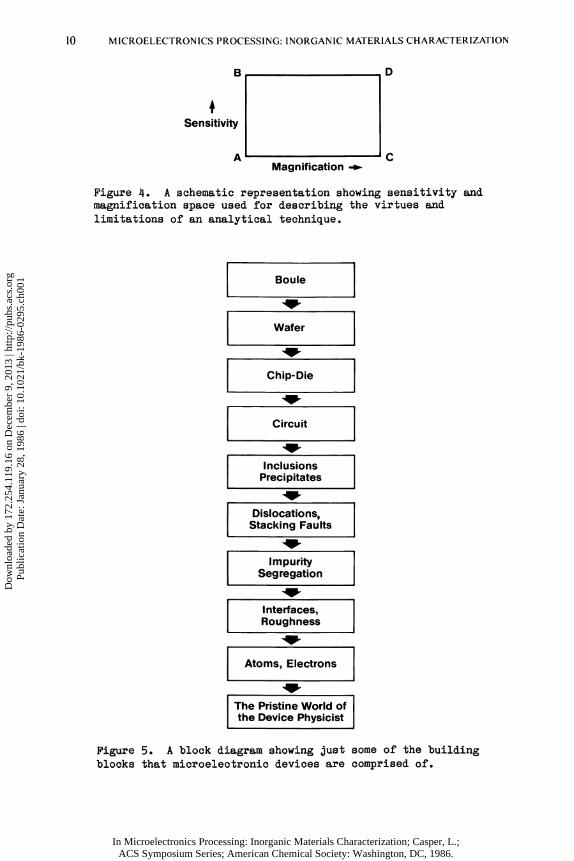
Figure 4 d e s c r i b e s an elemental u n i t constructed from a set of orthogonal coordinates o f s e n s i t i v i t y and m a g n i f i c a t i o n . ( I n an i n t e r e s t i n g h i s t o r i c a l note, Weiner(7) considered m a g n i f i c a t i o n to be a trans f o r m a t i o n o f s p a t i a l c o ordinates, a p o t e n t i a l l y f a r more s i g n i f i c a n t concept than i s u s u a l l y a s c r i b e d to m a g n i f i c a t i o n nowadays. These coordinates are q u i t e f a m i l i a r to every a n a l y s t as they d i r e c t l y impact the cost o f an a n a l y s i s . Four p o i n t s are described i n t h i s space i n f a m i l i a r terminology as shown i n Figure 4.
In order "to c h a r a c t e r i z e " something, the a n a l y s t u s u a l l y d e f i n e s some p o i n t i n t h i s space by the instrument t h a t he chooses and develops geometric and chemical i n f o r m a t i o n about the object of i n t e r e s t .
The space i n the v i c i n i t y o f the chosen p o i n t can be extended somewhat by us i n g a s e r i e s o f overlapping techniques and thus d e f i n i n g movement i n the space. The extension i s r e a l i z e d once s p a t i a l v a r i a t i o n s i n composition are measured i n space-time determining an o b j e c t ' s " t e x t u r e " and thus the object i s " c h a r a c t e r i z e d " . The a n a l y s t e s s e n t i a l l y decides how to b u i l d an
Dow
nloa
ded
by 1
72.2
54.1
19.1
6 on
Dec
embe
r 9,
201
3 | h
ttp://
pubs
.acs
.org
P
ublic
atio
n D
ate:
Jan
uary
28,
198
6 | d
oi: 1
0.10
21/b
k-19
86-0
295.
ch00
1
In Microelectronics Processing: Inorganic Materials Characterization; Casper, L.; ACS Symposium Series; American Chemical Society: Washington, DC, 1986.
I. PASSOJA ET AL. Analytical Approaches and Expert Systems 9
image o f the object i n t h i s space by usi n g t e x t u r e p r i m i t i v e s or " t e x e l s " s i m i l a r to p i c t u r e p r i m i t i v e s or p i x e l s .
Expressing t h i s i n a l e s s a b s t r a c t manner; the a n a l y s t must des c r i b e the o b j e c t w i t h as few m a g n i f i c a t i o n steps as are necessary i n order to span a given range. These depend upon the s t r u c t u r e under study and must be adjusted a c c o r d i n g l y . At each m a g n i f i c a t i o n , the o b j e c t under i n v e s t i g a t i o n i s s c r u t i n i z e d and i t s s t r u c t u r e and composition are determined as a f u n c t i o n of the s p a t i a l c oordinates. The a n a l y s t s dilemma can be best described by the f o l l o w i n g :
M a g n i f i c a t i o n and S e n s i t i v i t y Considerations
I n c r e a s i n g A. Low m a g n f i c i a t i o n -Complexity Low s e n s i t i v i t y , "a l i t t l e b i t everywhere"
and £• Low m a g n i f i c a t i o n -Costs High s e n s i t i v i t y , "a s e n s i t i v i t y window"
C. High m a g n i f i c a t i o n -Low s e n s i t i v i t y , "a t y p i c a l microscopy problem"
D. High m a g n i f i c a t i o n -High s e n s i t i v i t y , " f o o l s rush i n . . . "
the paradox o f no p o s i t i v e r e s u l t s a f t e r commencing.
In the f o l l o w i n g s e c t i o n we touch on i s s u e s o f m a g n i f i c a t i o n and s e n s i t i v i t y by co n s i d e r i n g some s p e c i f i c examples. The observation of space and the m i c r o s t r u e t u r a l h e t e r o g e n e i t i e s embedded i n i t has a p h y s i c a l b a s i s that i s d e r i v e d from p r o b a b i l i t y d i s t r i b u t i o n s . As Prigogine(8-9) has suggested, macroscopic i r r e v e r s i b l e phenomena are a s s o c i a t e d w i t h p r o b a b i l i t y d i s t r i b u t i o n s and t h e i r e v o l u t i o n i n time. P a r t i t i o n i n g a system introduces an " i n t e r n a l " time to a system. The i n t r o d u c t i o n o f p a r t i t i o n s i n t o a system merely de f i n e s a subset th a t may be observed by i n c r e a s i n g the m a g n i f i c a t i o n . We f o l l o w P r i g o g i n e 1 s b a s i c l i n e of reasoning i n the examples t h a t f o l l o w by co n s i d e r i n g p r o b a b i l i t y d i s t r i b u t i o n s as a f u n c t i o n o f m a g n i f i c a t i o n ( i n s t e a d o f t i m e ) . Our d i s c u s s i o n i s not exhaustive but i l l u s t r a t e s what meaning p a r t i c u l a r s p a t i a l defect d i s t r i b u t i o n s can have f o r the a n a l y s t when a c h a r a c t e r i z a t i o n i s performed.
Geometric Elements and P h y s i c a l C o n s t r a i n t s
Figure 5 describes the geometric b u i l d i n g blocks or independent geometric f e a t u r e s o f which m i c r o e l e c t r o n i c devices are composed. The l i s t i s ordered to r e v e a l smaller and smaller geometric f e a t u r e s from the top to the bottom l i s t . By a p p l y i n g Rule 1 above i t i s p o s s i b l e to f i r s t recognize the boule's s t r u c t u r e , then the wafer's e t c . At higher and higher m a g n i f i c a t i o n f i n e r and f i n e r s t r u c t u r a l d e t a i l s can be observed u n t i l f i n a l l y atoms can be seen. At each l e v e l o f m a g n i f i c a t i o n there i s a l i m i t e d f i e l d o f view and a l i m i t e d r e s o l u t i o n t h a t d e f i n e s a t e x e l s i z e ; we observe f i n i t e s e t s o f defects (generic) having given s t r u c t u r e s . The i n f o r m a t i o n t h a t i s c o l l e c t e d a t each m a g n i f i c a t i o n i s a r e s u l t o f knowing more and more about l e s s and
Dow
nloa
ded
by 1
72.2
54.1
19.1
6 on
Dec
embe
r 9,
201
3 | h
ttp://
pubs
.acs
.org
P
ublic
atio
n D
ate:
Jan
uary
28,
198
6 | d
oi: 1
0.10
21/b
k-19
86-0
295.
ch00
1
In Microelectronics Processing: Inorganic Materials Characterization; Casper, L.; ACS Symposium Series; American Chemical Society: Washington, DC, 1986.
MICROELECTRONICS PROCESSING: INORGANIC MATERIALS CHARACTERIZATION
Sensitivity
Magnification
Figure 4. A schematic r e p r e s e n t a t i o n showing s e n s i t i v i t y and m a g n i f i c a t i o n space used f o r d e s c r i b i n g the v i r t u e s and l i m i t a t i o n s of an a n a l y t i c a l technique.
Boule
Wafer
Chip-Die
Circuit
Inclusions Precipitates
Dislocations, Stacking Faults
Impurity Segregation
Interfaces, Roughness
Atoms, Electrons
The Pristine World of the Device Physicist
Figure 5. A block diagram showing j u s t some of the b u i l d i n g blocks that m i c r o e l e c t r o n i c devices are comprised o f .
Dow
nloa
ded
by 1
72.2
54.1
19.1
6 on
Dec
embe
r 9,
201
3 | h
ttp://
pubs
.acs
.org
P
ublic
atio
n D
ate:
Jan
uary
28,
198
6 | d
oi: 1
0.10
21/b
k-19
86-0
295.
ch00
1
In Microelectronics Processing: Inorganic Materials Characterization; Casper, L.; ACS Symposium Series; American Chemical Society: Washington, DC, 1986.
1. PASSOJA ET AL. Analytical Approaches and Expert Systems 11
l e s s of the s t r u c t u r e . Observations made a t higher and higher m a g n i f i c a t i o n r e s u l t i n more s p e c i a l i z e d knowledge about the mi c r o s t r u c t u r e . In order to describe the s t r u c t u r e o f the device, more area must be scanned and a cost i s a s s o c i a t e d w i t h t h i s a c t i v i t y . (A s i m i l a r problem has been discussed by A. Wheeler(11) and i s known as the t r a v e l i n g salesman problem. Here the problem i s to optimize the time that the salesman i s to v i s i t remote p o i n t s i n a search space.)
P r o b a b i l i t y D i s t r i b u t i o n s
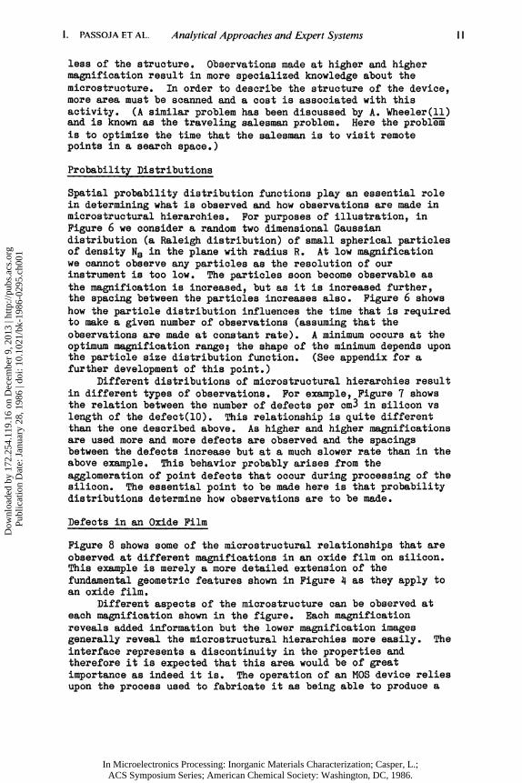
S p a t i a l p r o b a b i l i t y d i s t r i b u t i o n f u n c t i o n s p l a y an e s s e n t i a l r o l e i n determining what i s observed and how observations are made i n m i c r o s t r u c t u r a l h i e r a r c h i e s . For purposes of i l l u s t r a t i o n , i n Figure 6 we consider a random two dimensional Gaussian d i s t r i b u t i o n (a Raleigh d i s t r i b u t i o n ) o f sm a l l s p h e r i c a l p a r t i c l e s of d e n s i t y N s i n the plane w i t h r a d i u s R. At low m a g n i f i c a t i o n we cannot observe any p a r t i c l e s as the r e s o l u t i o n o f our instrument i s too low. The p a r t i c l e s soon become observable as the m a g n i f i c a t i o n i s increa s e d , but as i t i s increased f u r t h e r , the spacing between the p a r t i c l e s increases a l s o . Figure 6 shows how the p a r t i c l e d i s t r i b u t i o n i n f l u e n c e s the time that i s r e q u i r e d to make a given number of observations (assuming that the observations are made a t constant r a t e ) . A minimum occurs a t the optimum m a g n i f i c a t i o n range; the shape of the minimum depends upon the p a r t i c l e s i z e d i s t r i b u t i o n f u n c t i o n . (See appendix f o r a f u r t h e r development of t h i s p o i n t . )
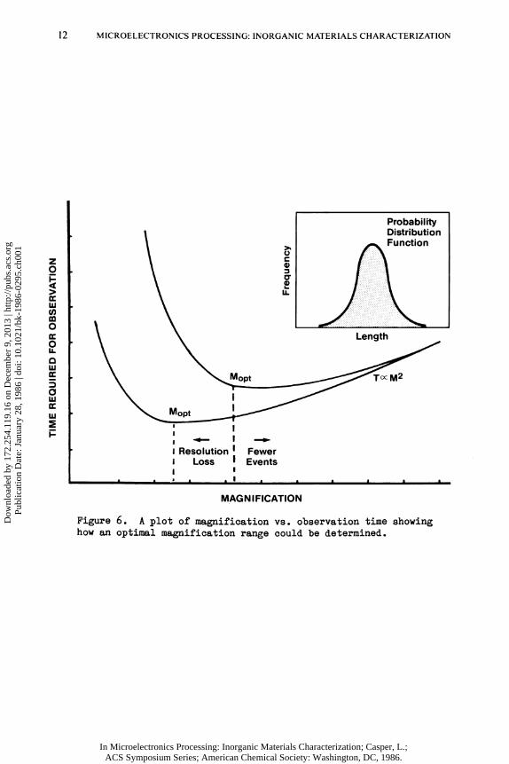
D i f f e r e n t d i s t r i b u t i o n s of m i c r o s t r u c t u r a l h i e r a r c h i e s r e s u l t i n d i f f e r e n t types o f observations. For example, Figure 7 shows the r e l a t i o n between the number of def e c t s per cm3 i n s i l i c o n vs length of the d e f e c t ( 1 0 ) . This r e l a t i o n s h i p i s q u i t e d i f f e r e n t than the one des c r i b e d above. As higher and higher m a g n i f i c a t i o n s are used more and more def e c t s are observed and the spacings between the de f e c t s i n c r e a s e but a t a much slower r a t e than i n the above example. This behavior probably a r i s e s from the agglomeration of p o i n t d e f e c t s that occur d u r i n g p r o c e s s i n g of the s i l i c o n . The e s s e n t i a l p o i n t to be made here i s that p r o b a b i l i t y d i s t r i b u t i o n s determine how observations are to be made.
Defects i n an Oxide F i l m
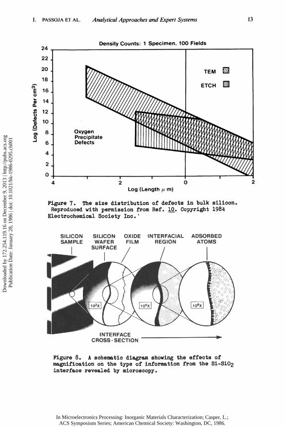
Figure 8 shows some of the m i c r o s t r u c t u r a l r e l a t i o n s h i p s t h a t are observed a t d i f f e r e n t m a g n i f i c a t i o n s i n an oxide f i l m on s i l i c o n . This example i s merely a more d e t a i l e d extension of the fundamental geometric f e a t u r e s shown i n Figure 4 as they apply to an oxide f i l m .
D i f f e r e n t aspects o f the mi c r o s t r u c t u r e can be observed a t each m a g n i f i c a t i o n shown i n the f i g u r e . Each m a g n i f i c a t i o n r e v e a l s added i n f o r m a t i o n but the lower m a g n i f i c a t i o n images g e n e r a l l y r e v e a l the m i c r o s t r u c t u r a l h i e r a r c h i e s more e a s i l y . The i n t e r f a c e represents a d i s c o n t i n u i t y i n the p r o p e r t i e s and th e r e f o r e i t i s expected th a t t h i s area would be of great importance as indeed i t i s . The operation of an MOS device r e l i e s upon the process used to f a b r i c a t e i t as being a b l e to produce a
Dow
nloa
ded
by 1
72.2
54.1
19.1
6 on
Dec
embe
r 9,
201
3 | h
ttp://
pubs
.acs
.org
P
ublic
atio
n D
ate:
Jan
uary
28,
198
6 | d
oi: 1
0.10
21/b
k-19
86-0
295.
ch00
1
In Microelectronics Processing: Inorganic Materials Characterization; Casper, L.; ACS Symposium Series; American Chemical Society: Washington, DC, 1986.
12 MICROELECTRONICS PROCESSING: INORGANIC MATERIALS CHARACTERIZATION
Figure 6. A p l o t of m a g n i f i c a t i o n vs. observation time showing how an optimal m a g n i f i c a t i o n range could be determined.
Dow
nloa
ded
by 1
72.2
54.1
19.1
6 on
Dec
embe
r 9,
201
3 | h
ttp://
pubs
.acs
.org
P
ublic
atio
n D
ate:
Jan
uary
28,
198
6 | d
oi: 1
0.10
21/b
k-19
86-0
295.
ch00
1
In Microelectronics Processing: Inorganic Materials Characterization; Casper, L.; ACS Symposium Series; American Chemical Society: Washington, DC, 1986.
1. PASSOJA ET AL. Analytical Approaches and Expert Systems 13
Density Counts: 1 Specimen, 100 Fields 24 , . ,
22 .
Log (Length fi m)
Figure 7. The s i z e d i s t r i b u t i o n o f defects i n bulk s i l i c o n . Reproduced w i t h permission from Ref. 10. Copyright 1984
Elec t r o c h e m i c a l S o c i e t y I n c . '
Figure 8. A schematic diagram showing the e f f e c t s o f ma g n i f i c a t i o n on the type o f in f o r m a t i o n from the S i - S i 0 2 i n t e r f a c e revealed by microscopy.
Dow
nloa
ded
by 1
72.2
54.1
19.1
6 on
Dec
embe
r 9,
201
3 | h
ttp://
pubs
.acs
.org
P
ublic
atio
n D
ate:
Jan
uary
28,
198
6 | d
oi: 1
0.10
21/b
k-19
86-0
295.
ch00
1
In Microelectronics Processing: Inorganic Materials Characterization; Casper, L.; ACS Symposium Series; American Chemical Society: Washington, DC, 1986.
14 MICROELECTRONICS PROCESSING: INORGANIC MATERIALS CHARACTERIZATION
w e l l d efined i n t e r f a c e w i t h a c o n s i s t e n t charge d i s t r i b u t i o n . Measurement of a C-V r e l a t i o n s h i p would y i e l d microscopic i n f o r m a t i o n , whereas a cross s e c t i o n a l TEM study would y i e l d 1 dimensional i n f o r m a t i o n about the i n t e r f a c i a l s t r u c t u r e - more microscopic i n f o r m a t i o n . SIMS, on the other hand, would y i e l d more two dimensional i n f o r m a t i o n about the i n t e r f a c e a t a s e n s i t i v i t y range that i s lower than t h a t of the e l e c t r i c a l measurements i . e . sodium l e v e l s that would i n f l u e n c e the device would not be measured by t h i s method. To "solve the problem" the a n a l y s t must c h a r a c t e r i z e the s t r u c t u r e , r e l a t e i t to the microchemistry and then show how t h i s i n f l u e n c e s the operation of the d e v i c e .
At each m a g n i f i c a t i o n s t a r t i n g from low to high we observe more and more d e t a i l e d i n f o r m a t i o n u n t i l atoms are observed. I t i s p o s s i b l e to d e s c r i b e a h i e r a r c h y of d e f e c t s s i n c e they are embedded i n the m a t e r i a l - they are merely members of a set o f d i s c r e t e o b j e c t s which represent d e v i a t i o n s from the i d e a l s t r u c t u r e . The a n a l y s t i s faced w i t h the task o f d e s c r i b i n g the s e t s of d e f e c t s and c o n d i t i o n s under which they are d e t r i m e n t a l to the operation o f the device.
A n a l y t i c a l Requirements
The a n a l y t i c a l requirements i n IC p r o c e s s i n g equal or surpass those of any other i n d u s t r y and present a formidable problem to the a n a l y s t . The f a b r i c a t i o n o f a semiconductor device i n v o l v e s i n t e r a c t i o n of m a t e r i a l s , processes and environment to produce a complex, geometrical c o n f i g u r a t i o n o f many m a t e r i a l s . When processed through to the package l e v e l a t y p i c a l IC i s a composite o f semiconductors, metals, ceramics and polymers c o n t a i n i n g over a dozen d i s t i n c t m a t e r i a l s .
In the process o f f a b r i c a t i o n these m a t e r i a l s have been exposed to a wide range of m a t e r i a l s or chemicals, ranging from plasmas to aggressive chemical etchants. Environmental e f f e c t s may a l s o be produced as a r e s u l t of exposure to ambients such as vacuum and high temperature, as w e l l as a i r laden w i t h moisture and a v a r i e t y of contaminants.
In the face of t h i s complexity there are few a n a l y t i c a l techniques which do not apply1 An advanced IC process w i l l u t i l i z e t r a d i t i o n a l bulk chemical a n a l y s i s , i . e . chromatography, spectroscopy, t i t r i m e t r y , e t c . , as w e l l as the a r r a y of i o n and e l e c t r o n beam techniques f o r t h i n f i l m and s m a l l spot a n a l y s i s . In a d d i t i o n , process a n a l y s i s i s becoming more common where plasmas, gases, d i s t i l l e d water and other process "streams" are continuously monitored f o r a v a r i e t y o f c o n s t i t u e n t s . The goal o f such extensive a n a l y t i c a l support i s t o e s t a b l i s h and maintain the process "window".
Ph i l o s o p h i e s d i f f e r on the need f o r a n a l y t i c a l i nstrumentation i n IC c h a r a c t e r i z a t i o n . These range from e x c e p t i o n a l l y complete (and expensive) support f a c i l i t i e s to bare-bone operations which r e l y on the more s o p h i s t i c a t e d techniques only when c a t a s t r o p h i c f a i l u r e occurs. The l a t t e r approach i s Edisonian i n nature, i . e . h i g h l y e m p i r i c a l . The problem a r i s e s t h a t through a l a c k of a n a l y t i c a l i n f o r m a t i o n the process window i s not w e l l d e f i n e d .
Dow
nloa
ded
by 1
72.2
54.1
19.1
6 on
Dec
embe
r 9,
201
3 | h
ttp://
pubs
.acs
.org
P
ublic
atio
n D
ate:
Jan
uary
28,
198
6 | d
oi: 1
0.10
21/b
k-19
86-0
295.
ch00
1
In Microelectronics Processing: Inorganic Materials Characterization; Casper, L.; ACS Symposium Series; American Chemical Society: Washington, DC, 1986.
1. PASSOJA ET A L . Analytical Approaches and Expert Systems
Excursions outside these process l i m i t s may produce a y i e l d crash o r , worse, a longer-term r e l i a b i l i t y problem. The w e l l - c h a r a c t e r i z e d process i s l e s s prone to such problems and when they do occur the c a p a b i l i t y i s a t hand to support f a i l u r e a n a l y s i s .
The type and s o p h i s t i c a t i o n of m a t e r i a l s c h a r a c t e r i z a t i o n instrumentation made a v a i l a b l e f o r a given IC f a c i l i t y w i l l depend on s e v e r a l f a c t o r s : c o s t / b e n e f i t , q u a l i t y p e r c e p t i o n s , process complexity, m a t u r i t y of the process. Commercial support l a b s are becoming more r e a d i l y a v a i l a b l e to meet the VLSI challenge. The mix o f in-house versus e x t e r n a l l a b o r a t o r y support then becomes a matter of choice based on co n s i d e r a t i o n s o f sample turn-around time, maintaining s e c u r i t y of p r o p r i e t a r y devices or processes, and outside versus i n s i d e expenditures.
Regardless o f the a n a l y t i c a l i n s t r u m e n t a t i o n mix, the a r t o f problem-solving remains. A person or team must make the d e c i s i o n s about a n a l y s i s : what, when, and how. There must be an a n a l y t i c a l "expert" be i t man or computer, who can make choices o f appropriate technique.
The choice o f technique and the i n t e r p r e t a t i o n o f r e s u l t i n g data c o n s t i t u t e s the a r t and science of a n a l y s i s . The science i s the c o n s i d e r a t i o n o f the many f a c t o r s i n choosing an a n a l y t i c a l technique, among them:
• S p a t i a l r e s o l u t i o n • A n a l y t i c a l s e n s i t i v i t y • D e t e c t i o n l i m i t • I n t e r f e r e n c e s • Sample p r e p a r a t i o n • A n a l y t i c a l volume • Sample consumption or d e s t r u c t i o n • Elemental or molecular i n f o r m a t i o n
Such complex i n f o r m a t i o n i s known by experts i n each a n a l y t i c a l a r e a . The problem f o r most p r a c t i t i o n e r s i s to o b t a i n the needed i n f o r m a t i o n or knowledge and proceed w i t h an a n a l y t i c a l scheme. The extent to which t h i s knowledge becomes a v a i l a b l e i n computerized "expert systems" the e a s i e r and more e f f i c i e n t t h i s task w i l l become. This creates more freedom f o r the a r t , or the i n t u i t i v e / c r e a t i v e s i d e o f a n a l y s i s . The c r i t i c a l r o l e of the a n a l y s t i s then the b u i l d i n g o f s c i e n t i f i c a l l y c o n s i s t e n t mental p i c t u r e , a concept or a model, to f i t the accumulated data.
Conclusions
The problem s o l v i n g g u i d e l i n e s used by vario u s experts appear to have a f a i r l y w e l l d e f i n e d s t r u c t u r e . The r u l e s themselves seem to be s e l f evident and q u i t e general but t h e i r general a p p l i c a t i o n i s not uniform s i n c e problem s o l v i n g i s p r e s e n t l y an a r t u s u a l l y based on the a n a l y s t ' s i n t u i t i o n and i n d i v i d u a l problem s o l v i n g a b i l i t y . We suspect that w i t h f u r t h e r m i n i a t u r i z a t i o n t h i s approach w i l l not s u f f i c e but w i l l need to be repl a c e d by more c o n s i s t e n t , systematic methods that are machine based. This should standardize the methods and make them more e f f i c i e n t .
New manufacturing technology w i l l probably i n c r e a s e the need f o r machine o r i e n t e d problem s o l v i n g methods. Any movement of the
Dow
nloa
ded
by 1
72.2
54.1
19.1
6 on
Dec
embe
r 9,
201
3 | h
ttp://
pubs
.acs
.org
P
ublic
atio
n D
ate:
Jan
uary
28,
198
6 | d
oi: 1
0.10
21/b
k-19
86-0
295.
ch00
1
In Microelectronics Processing: Inorganic Materials Characterization; Casper, L.; ACS Symposium Series; American Chemical Society: Washington, DC, 1986.
16 MICROELECTRONICS PROCESSING: INORGANIC MATERIALS CHARACTERIZATION
technology toward v a r i a b l e p o i n t - t o - p o i n t m i c r o f a b r i c a t i o n such as l a s e r p r o c e s s i n g w i l l o n l y a c c e l e r a t e the need f o r p r o t o c o l s and more s t anda rd ized problem s o l v i n g methods. With ref inement o f our manufactur ing p roces se s , m a t e r i a l changes w i l l be produced a t h igher r e s o l u t i o n thereby i n c r e a s i n g the i n f o r m a t i o n content /volume o f our manufactured i t e m s . The need f o r more e f f i c i e n t m i c r o s c o p i c i n f o r m a t i o n c o l l e c t i o n and a n a l y s i s i s t he re fo re expected to accompany these t r e n d s .
The advances i n technology tha t have d r i v e n the m i n i a t u r i z a t i o n t rends have c rea ted a complex s i t u a t i o n f o r m i c r o a n a l y s i s t ha t can o n l y become more complex i n the f u t u r e . Even though t e c h n o l o g i c a l advances might improve the r e s o l u t i o n o f some o f our i n s t r u m e n t a t i o n , m i n i a t u r i z a t i o n i t s e l f w i l l on ly compl ica te our a b i l i t y to c h a r a c t e r i z e dev ices i n the f u t u r e . A r t i f i c i a l i n t e l l i g e n c e and exper t systems appear to have an e x c e l l e n t p o t e n t i a l f o r enhancing our problem s o l v i n g a b i l i t y . I t i s expected tha t w i t h proper development, t h i s t o o l c o u l d become an e s s e n t i a l i t em i n the m i c r o a n a l y s e s r e p e r t o i r e o f techniques i n tomorrow's t echno logy .
Literature Cited 1. Skilling, J. Nature, Vol. 309, June 28, 1984, p. 748. 2. Tikochinsky, Y.; Tishby, N.Z., Levine, R. D. Phys. Rev
Letters, Vol. 52, No. 6, April 16, 1984, p. 1357-1360. 3. Jaynes, E. T. Phys Rev, Vol. 106, No. 4, May 1957, p. 620-630. 4. Frieden, R. B. Jrnl Optical Society of America, Vol. 62, No.
4, April 1972, p. 511-518. 5. Fredrick, H.; Waterman, D. A.; Lenat, D. B. eds., Building
Expert Systems, Addison-Wesley, Reading, Mass. 1983, p. 8-29. 6. Ramsay, J . ; Linfors, P; Balazs, M.; Passoja, D. E., Casper;
L.S. Private communication April, 1984 7. Weiner, N. Cybernetics, MIT press. Cambridge, Mass., 1965, p.
50. 8. Prigogine, I.; Stengers, I, Order out of Chaos, Bantam Books,
NY, NY, 1984, p. 272. 9. Prigogine, I. From Being to Becoming, Freeman and Sons, San
Francisco, CA. 1982. 10. Craven, R.A.; Shimura, F.; Hockett, R. S.; Shive, L. W.;
Faundrot, T. B.; Keefe-Frandort, G. "Characterization Techniques for VLSI Silicon", Proceedings of 2nd International Symposium on VLSI Science and Technology, Electrochemical Society Inc., Princeton, NJ 1984, p. 20-35.
11. Wheeler, J. A. Americal Journal of Physics, Vol. 51, No. 5, May 1983, p. 398-404; Armour, R. S.; Wheeler, J . A. op cit, p. 405-406.
12. Linfors, P. Physical Electronics - Private Communication, April, 1984.
Appendix
I t i s suggested tha t the c o s t / m a g n i f i c a t i o n curve shown i n F i g u r e 6 i s fundamental . The p a r t i c u l a r one shown i s d e r i v e d from man as an observer o f e i t h e r the mic roscop ic o r the macroscopic
Dow
nloa
ded
by 1
72.2
54.1
19.1
6 on
Dec
embe
r 9,
201
3 | h
ttp://
pubs
.acs
.org
P
ublic
atio
n D
ate:
Jan
uary
28,
198
6 | d
oi: 1
0.10
21/b
k-19
86-0
295.
ch00
1
In Microelectronics Processing: Inorganic Materials Characterization; Casper, L.; ACS Symposium Series; American Chemical Society: Washington, DC, 1986.
1. PASSOJA ET AL. Analytical Approaches and Expert Systems
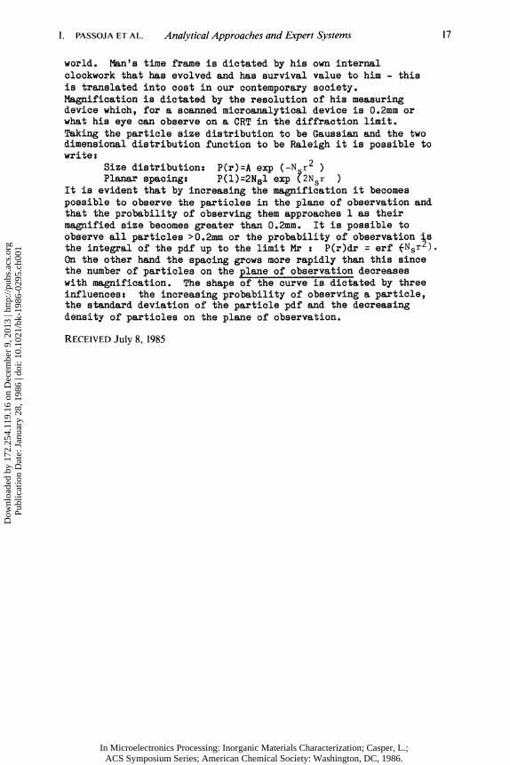
world. Man's time frame i s d i c t a t e d by h i s own i n t e r n a l clockwork that has evolved and has s u r v i v a l value to him - t h i s i s t r a n s l a t e d i n t o cost i n our contemporary s o c i e t y . M a g n i f i c a t i o n i s d i c t a t e d by the r e s o l u t i o n o f h i s measuring device which, f o r a scanned m i c r o a n a l y t i c a l device i s 0.2mm or what h i s eye can observe on a CRT i n the d i f f r a c t i o n l i m i t . Taking the p a r t i c l e s i z e d i s t r i b u t i o n to be Gaussian and the two dimensional d i s t r i b u t i o n f u n c t i o n to be Raleigh i t i s p o s s i b l e to w r i t e :
S i z e d i s t r i b u t i o n : P(r)=A exp (-Nor 2 ) Planar spacing: P(1)=2N S1 exp ( 2 N gr )
I t i s evident t h a t by i n c r e a s i n g the m a g n i f i c a t i o n i t becomes p o s s i b l e to observe the p a r t i c l e s i n the plane o f observation and that the p r o b a b i l i t y of observing them approaches 1 as t h e i r magnified s i z e becomes greater than 0.2mm. I t i s p o s s i b l e to observe a l l p a r t i c l e s >0.2mm or the p r o b a b i l i t y of observation i s the i n t e g r a l o f the pdf up to the l i m i t Mr : P ( r ) d r = e r f (-N sr 2). On the other hand the spacing grows more r a p i d l y than t h i s s i n c e the number of p a r t i c l e s on the plane of observation decreases w i t h m a g n i f i c a t i o n . The shape of the curve i s d i c t a t e d by three i n f l u e n c e s : the i n c r e a s i n g p r o b a b i l i t y o f observing a p a r t i c l e , the standard d e v i a t i o n o f the p a r t i c l e pdf and the decreasing d e n s i t y o f p a r t i c l e s on the plane o f observation.
RECEIVED July 8, 1985
Dow
nloa
ded
by 1
72.2
54.1
19.1
6 on
Dec
embe
r 9,
201
3 | h
ttp://
pubs
.acs
.org
P
ublic
atio
n D
ate:
Jan
uary
28,
198
6 | d
oi: 1
0.10
21/b
k-19
86-0
295.
ch00
1
In Microelectronics Processing: Inorganic Materials Characterization; Casper, L.; ACS Symposium Series; American Chemical Society: Washington, DC, 1986.
Related Documents