ISSN (Print) : 2320 – 3765 ISSN (Online): 2278 – 8875 International Journal of Advanced Research in Electrical, Electronics and Instrumentation Engineering (An ISO 3297: 2007 Certified Organization) Vol. 4, Issue 2, February 2015 Copyright to IJAREEIE 10.15662/ijareeie.2015.0402036 756 Analysis of Single Phase AC-DC SEPIC Converter using Closed Loop Techniques A.Ramkumar 1 , S.Vijula Shini Florence 2 PG Student [AE], Dept. of ECE, Renganayagi Varatharaj College of Engineering, Sivakasi, Tamilnadu, India 1 Assistant Professor, Dept. of EEE, Renganayagi Varatharaj College of Engineering, Sivakasi, Tamilnadu, India 2 ABSTRACT: This paper proposes single phase AC-DC SEPIC converter using closed loop techniques for domestic and industrial applications. The Single Ended Primary Inductor Converter (SEPIC) is a type of DC-DC converter allowing the electrical potential (voltage) at its output to be greater then, less then, or equal to that of its input. A SEPIC converter is similar to the BUCK-BOOST and BOOST-BUCK converter, but has advantages of having non-inverted output (The polarity of the output voltage is same as that of the input). There are two types of techniques, open loop and closed loop technique. In open loop, a non-isolated SEPIC converter is used. This has lower power factor and high THD. Hence the closed loop technique is used to improve power factor and THD. The control techniques are voltage follower approach and average current control technique. By using the above techniques the power quality parameters will be improved when compared to open loop. The simulation of SEPIC converter is done by using the software tool PSIM (Power Simulation). KEYWORDS: SEPIC converter, Power Factor Correction, Harmonic reduction, PWM, PSIM. I.INTRODUCTION Power conversion is converting electric energy from one form to another, converting between AC and DC or just varying the voltage and frequency or some combination of these. The power conversion systems can be classified according to the type of input and output power AC to DC (Rectifier) DC to AC (inverter) DC to DC (DC to DC converter) AC to AC (AC to AC converter) DC to DC converters are important in portable electronic devices such as cellular phones and laptop computers, which are supplied by power from batteries mainly. The majority DC to DC converters also control the output voltage. AC to DC converters (rectifier) is an electrical device that converts alternating current (AC), which periodically reverses direction, to direct current (DC), which flows in only one direction. The process is well-known as rectification. Rectifiers have several uses, however are often found serving as components of DC power supplies and high-voltage direct current power transmission systems. Rectification may well serve in roles other than to generate direct current for use as a source of power. Because of the alternating nature of the input AC sine waves, the method of rectification only produces a DC current that, while unidirectional, consists of pulses of current. Several applications of rectifiers, such as power supplies for television, radio and computer equipment, necessitate a steady constant DC current (as would be produced by a battery).Normally AC-DC conversion is carried out by simply rectifying the AC input and the rectified output voltage is filtered by means of a large valued capacitance to get a nearly constant DC output voltage. In this conversion, the input AC supply current is drawn in narrow pulses since the capacitor voltage value is nearly constant. This narrow pulse current of high peak, results in power quality problems to nearby consumers, which include higher value of THD on supply current, higher THD of input supply voltage, lower value of power factor and displacement factor and poor distortion factor. These large harmonic currents are undesirable because they not only produce distortion of AC line voltage but also result in conducted and radiated electromagnetic interference (EMI). The problem becomes more serious particularly when several drive units are connected to single phase supply where the input power pulsates at twice the frequency. Recent international regulations governing the power quality and harmonic currents pollution limits at the utility have placed an increased emphasis on the application of improved power quality AC-DC converters to feed the load. For ideal sine wave line voltage, harmonic currents do not contribute to active power, this

Welcome message from author
This document is posted to help you gain knowledge. Please leave a comment to let me know what you think about it! Share it to your friends and learn new things together.
Transcript

ISSN (Print) : 2320 – 3765
ISSN (Online): 2278 – 8875
International Journal of Advanced Research in Electrical,
Electronics and Instrumentation Engineering
(An ISO 3297: 2007 Certified Organization)
Vol. 4, Issue 2, February 2015
Copyright to IJAREEIE 10.15662/ijareeie.2015.0402036 756
Analysis of Single Phase AC-DC SEPIC
Converter using Closed Loop Techniques
A.Ramkumar1, S.Vijula Shini Florence
2
PG Student [AE], Dept. of ECE, Renganayagi Varatharaj College of Engineering, Sivakasi, Tamilnadu, India 1
Assistant Professor, Dept. of EEE, Renganayagi Varatharaj College of Engineering, Sivakasi, Tamilnadu, India 2
ABSTRACT: This paper proposes single phase AC-DC SEPIC converter using closed loop techniques for domestic
and industrial applications. The Single Ended Primary Inductor Converter (SEPIC) is a type of DC-DC converter
allowing the electrical potential (voltage) at its output to be greater then, less then, or equal to that of its input. A SEPIC
converter is similar to the BUCK-BOOST and BOOST-BUCK converter, but has advantages of having non-inverted
output (The polarity of the output voltage is same as that of the input). There are two types of techniques, open loop
and closed loop technique. In open loop, a non-isolated SEPIC converter is used. This has lower power factor and high
THD. Hence the closed loop technique is used to improve power factor and THD. The control techniques are voltage
follower approach and average current control technique. By using the above techniques the power quality parameters
will be improved when compared to open loop. The simulation of SEPIC converter is done by using the software tool
PSIM (Power Simulation).
KEYWORDS: SEPIC converter, Power Factor Correction, Harmonic reduction, PWM, PSIM.
I.INTRODUCTION
Power conversion is converting electric energy from one form to another, converting between AC and DC or just
varying the voltage and frequency or some combination of these. The power conversion systems can be classified
according to the type of input and output power
AC to DC (Rectifier)
DC to AC (inverter)
DC to DC (DC to DC converter)
AC to AC (AC to AC converter)
DC to DC converters are important in portable electronic devices such as cellular phones and laptop computers, which
are supplied by power from batteries mainly. The majority DC to DC converters also control the output voltage. AC to
DC converters (rectifier) is an electrical device that converts alternating current (AC), which periodically reverses
direction, to direct current (DC), which flows in only one direction. The process is well-known as rectification.
Rectifiers have several uses, however are often found serving as components of DC power supplies and high-voltage
direct current power transmission systems. Rectification may well serve in roles other than to generate direct current for
use as a source of power. Because of the alternating nature of the input AC sine waves, the method of rectification only
produces a DC current that, while unidirectional, consists of pulses of current. Several applications of rectifiers, such as
power supplies for television, radio and computer equipment, necessitate a steady constant DC current (as would be
produced by a battery).Normally AC-DC conversion is carried out by simply rectifying the AC input and the rectified
output voltage is filtered by means of a large valued capacitance to get a nearly constant DC output voltage. In this
conversion, the input AC supply current is drawn in narrow pulses since the capacitor voltage value is nearly constant.
This narrow pulse current of high peak, results in power quality problems to nearby consumers, which include higher
value of THD on supply current, higher THD of input supply voltage, lower value of power factor and displacement
factor and poor distortion factor. These large harmonic currents are undesirable because they not only produce
distortion of AC line voltage but also result in conducted and radiated electromagnetic interference (EMI). The problem
becomes more serious particularly when several drive units are connected to single phase supply where the input power
pulsates at twice the frequency. Recent international regulations governing the power quality and harmonic currents
pollution limits at the utility have placed an increased emphasis on the application of improved power quality AC-DC
converters to feed the load. For ideal sine wave line voltage, harmonic currents do not contribute to active power, this
ISSN (Print) : 2320 – 3765
ISSN (Online): 2278 – 8875
International Journal of Advanced Research in Electrical,
Electronics and Instrumentation Engineering
(An ISO 3297: 2007 Certified Organization)
Vol. 4, Issue 2, February 2015
Copyright to IJAREEIE 10.15662/ijareeie.2015.0402036 757
result in increased value of RMS current and therefore produces higher losses in the utility line. It is a prime concern to
consider these power quality issues to design an AC-DC power converter, which provides unity power factor at input
mains and also results in close regulations of output DC voltage. The single-ended primary-inductance converter
(SEPIC) is a DC/DC-converter topology that provides a positive regulated output voltage from an input voltage that
varies from above to below the output voltage. This kind of conversion is helpful when the designer uses voltages (e.g.,
12 V) from an unregulated input power supply such as a low-cost wall wart. The SEPIC converter topology is one that
fulfils all above requirements without inverting output voltage polarity. The circuit was first developed at AT&T Bell
laboratories in the mid 1970s and has not been very widely used until recently. Now it is becoming more and more
popular, especially in power conversion systems where the input voltage varies in wide range. In typical DC-DC power
conversion system the output voltage must be kept constant regardless of changes in the input voltage or in effective
load resistance. Therefore, such system invariably requires feedback control loop. Its design is based on the dynamic
model of DC-DC power conversion system. Several topologies of single phase AC-DC converters are implemented in
buck, boost, and buck-boost converters with improving the power quality in terms of reducing the harmonics of input
current [2]. In a buck type DC-DC converter reported in [1] & [3], the DC output voltage is controlled using the digital
multi loop PID controller and high frequency-link(HFL) power conversion systems(PCSs). We have proposed a circuit
to realize isolated buck boost DC to DC conversion; and the full-bridge (FB) boost converter, [4] in this circuit the
input voltage is close to output voltage. The modified SEPIC converter is integrated with solar powered system [5]. The
typical model used closed loop control with maximum power point tracking (MPPT) algorithm to get high efficiency.
Studies and analysis of cuk converter circuit is controlled the duty ratio of the switching element with output constant
was reported in [6]. In this paper introduce a buck converter and SEPIC converter working in a step-down mode of
operation and using for the optimized equation [7].
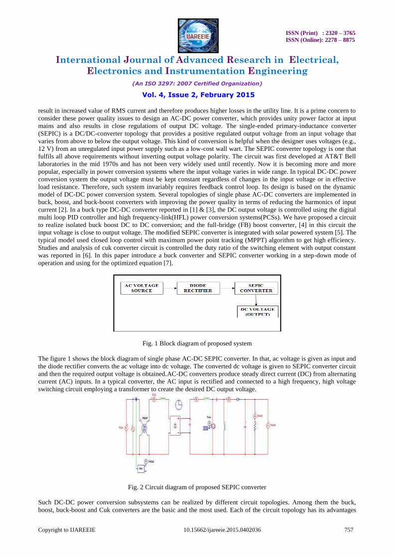
Fig. 1 Block diagram of proposed system
The figure 1 shows the block diagram of single phase AC-DC SEPIC converter. In that, ac voltage is given as input and
the diode rectifier converts the ac voltage into dc voltage. The converted dc voltage is given to SEPIC converter circuit
and then the required output voltage is obtained.AC-DC converters produce steady direct current (DC) from alternating
current (AC) inputs. In a typical converter, the AC input is rectified and connected to a high frequency, high voltage
switching circuit employing a transformer to create the desired DC output voltage.
Fig. 2 Circuit diagram of proposed SEPIC converter
Such DC-DC power conversion subsystems can be realized by different circuit topologies. Among them the buck,
boost, buck-boost and Cuk converters are the basic and the most used. Each of the circuit topology has its advantages

ISSN (Print) : 2320 – 3765
ISSN (Online): 2278 – 8875
International Journal of Advanced Research in Electrical,
Electronics and Instrumentation Engineering
(An ISO 3297: 2007 Certified Organization)
Vol. 4, Issue 2, February 2015
Copyright to IJAREEIE 10.15662/ijareeie.2015.0402036 758
and disadvantages and the choice depends on requirements for power conversion system. In general, circuits with the
switch referenced to the ground node are preferred to simplify the switch driving circuits. Additionally, the non-
pulsating input current is desirable to minimize EMI and reduce the need for additional filter elements. Significant
advantage of the power conversion system is also the ability to generate output voltage either above or below the input
voltage. In Figure 2 the circuit topology of the non isolated SEPIC converter is presented. It consists of two
inductances, two capacitors, one MOSFET transistor, one diode, the input voltage source and the load resistance at the
output of the converter. The amount of energy exchanged is controlled through switch S1, which is classically a
transistor such as a MOSFET.
II.ANALYSIS OF THE SEPIC CONVERTER
A SEPIC is a type of DC-DC converter allowing the electrical potential (voltage) at its output to be less than, greater
than, or equal to that at its input; the output of the SEPIC is controlled by the duty cycle of the control transistor. SEPIC
is effectively a boost converter followed by a buck-boost converter, consequently it is like to a conventional buck-boost
converter, other than has advantages of having non-inverted output (the output has the same voltage polarity as the
input), passing through a series capacitor to couple energy from the input to the output (and thus can respond more
gracefully to a short-circuit output), and being able of factual shutdown: after the switch S1 is turned off, its output
drops to 0 V, following a rather hefty transient abandon of charge. SEPICs are helpful in applications in which a
battery voltage can be above and below that of the regulator's intended output
.
Fig. 3 Circuit diagram of SEPIC converter
The schematic diagram for a basic SEPIC is shown in Figure 3 As with other switched mode power supplies
(specifically DC-to-DC converters), the SEPIC interactions energy between the capacitors and inductors in order to
convert from one voltage to another. The amount of energy exchanged is proscribed in switch S1, which is classically a
transistor such as a MOSFET. MOSFET offers much higher input impedance and lower voltage drop than bipolar
junction transistors (BJTs), and do not require biasing resistors as MOSFET switching is controlled by differences in
voltage rather than a current, like with BJTs.
A. CONTINUOUS MODE
A SEPIC is said to be in continuous-conduction mode if the current through the inductor L1 never falls to zero. During
a SEPIC's steady-state process, the average voltage crosswise capacitor C1 (VC1) is equal to the input voltage (VIN).
Because capacitor C1 blocks direct current (DC), the average current across it (IC1) is zero, making inductor L2 the
simply source of load current. Hence, the average current through inductor L2 (IL2) is the same as the average load
current and hence independent of the input voltage .Looking at average voltages, the following can be written:
𝑉𝐼𝑁 = 𝑉𝐿1 + 𝑉𝐶1 + 𝑉𝐿2 (1)
Because the average voltage of VC1 is equal to VIN, VL1 = −VL2. For this reason, the two inductors can be wound on the
similar core. Since the voltages are the equivalent in magnitude, their belongings of the mutual inductance will be zero,
assuming the polarity of the windings is correct. Also, since the voltages are the same into magnitude, the ripple
currents from the two inductors will be equal in magnitude. The average currents are summed as follows:
𝐼𝐷 = 𝐼𝐿1 − 𝐼𝐿2 (2)
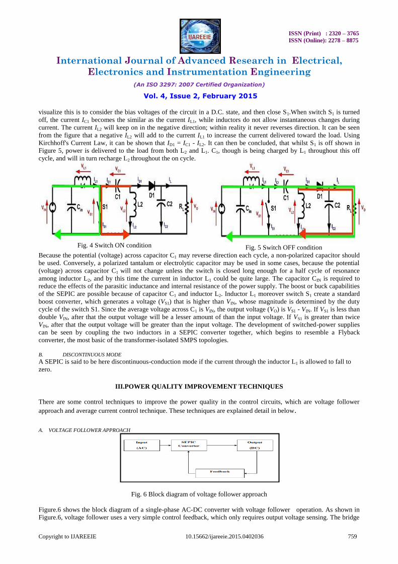
When switch S1 is turned on is shown in Figure 4, current IL1 increases and the current IL2 increases in the negative
direction. The energy to enhance the current IL1 comes from the input supply. Since S1 is a little while closed, and the
instant voltage VC1 is just about VIN, the voltage VL2 is approximately −VIN. Therefore, the capacitor C1 supplies the
energy to increase the magnitude of the current in IL2 and thus increase the energy stored into L2. The easiest method to
ISSN (Print) : 2320 – 3765
ISSN (Online): 2278 – 8875
International Journal of Advanced Research in Electrical,
Electronics and Instrumentation Engineering
(An ISO 3297: 2007 Certified Organization)
Vol. 4, Issue 2, February 2015
Copyright to IJAREEIE 10.15662/ijareeie.2015.0402036 759
visualize this is to consider the bias voltages of the circuit in a D.C. state, and then close S1.When switch S1 is turned
off, the current IC1 becomes the similar as the current IL1, while inductors do not allow instantaneous changes during
current. The current IL2 will keep on in the negative direction; within reality it never reverses direction. It can be seen
from the figure that a negative IL2 will add to the current IL1 to increase the current delivered toward the load. Using
Kirchhoff's Current Law, it can be shown that ID1 = IC1 - IL2. It can then be concluded, that whilst S1 is off shown in
Figure 5, power is delivered to the load from both L2 and L1. C1, though is being charged by L1 throughout this off
cycle, and will in turn recharge L2 throughout the on cycle.
Fig. 4 Switch ON condition
Fig. 5 Switch OFF condition
Because the potential (voltage) across capacitor C1 may reverse direction each cycle, a non-polarized capacitor should
be used. Conversely, a polarized tantalum or electrolytic capacitor may be used in some cases, because the potential
(voltage) across capacitor C1 will not change unless the switch is closed long enough for a half cycle of resonance
among inductor L2, and by this time the current in inductor L1 could be quite large. The capacitor CIN is required to
reduce the effects of the parasitic inductance and internal resistance of the power supply. The boost or buck capabilities
of the SEPIC are possible because of capacitor C1 and inductor L2. Inductor L1 moreover switch S1 create a standard
boost converter, which generates a voltage (VS1) that is higher than VIN, whose magnitude is determined by the duty
cycle of the switch S1. Since the average voltage across C1 is VIN, the output voltage (VO) is VS1 - VIN. If VS1 is less than
double VIN, after that the output voltage will be a lesser amount of than the input voltage. If VS1 is greater than twice
VIN, after that the output voltage will be greater than the input voltage. The development of switched-power supplies
can be seen by coupling the two inductors in a SEPIC converter together, which begins to resemble a Flyback
converter, the most basic of the transformer-isolated SMPS topologies.
B. DISCONTINUOUS MODE
A SEPIC is said to be here discontinuous-conduction mode if the current through the inductor L1 is allowed to fall to
zero.
III.POWER QUALITY IMPROVEMENT TECHNIQUES
There are some control techniques to improve the power quality in the control circuits, which are voltage follower
approach and average current control technique. These techniques are explained detail in below.
A. VOLTAGE FOLLOWER APPROACH
Fig. 6 Block diagram of voltage follower approach
Figure.6 shows the block diagram of a single-phase AC-DC converter with voltage follower operation. As shown in
Figure.6, voltage follower uses a very simple control feedback, which only requires output voltage sensing. The bridge
ISSN (Print) : 2320 – 3765
ISSN (Online): 2278 – 8875
International Journal of Advanced Research in Electrical,
Electronics and Instrumentation Engineering
(An ISO 3297: 2007 Certified Organization)
Vol. 4, Issue 2, February 2015
Copyright to IJAREEIE 10.15662/ijareeie.2015.0402036 760
rectifier is used at the input AC side with a power factor corrector using an inductor and capacitor combination. Now, a
small value of output voltage, compared to the reference value and resulting value, passes through the output voltage
controller, which generates the PWM output and is used for switching the converter. It has inherent power factor
correction characteristics with constant duty ratio and switching frequency, offering an attractive solution for lower
power applications. The output voltage regulation is provided by the feedback loop as shown in Figure.6 where the
output sensed voltage is compared with a reference value and the error is amplified in a proportional integral (PI)
controller which is compared with a saw-tooth ramp, thus providing the pulse to power switch. Therefore, this circuit is
controlled by the difference in the on- time interval and the constant switching frequency fs.
Advantages
Constant switching frequency
No need of current sensing
Simple PWM control
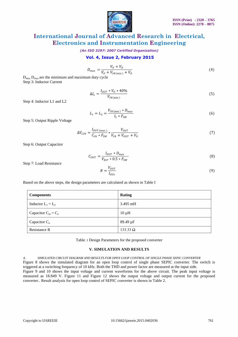
B. AVERAGE CURRENT CONTROL TECHNIQUE Another control method, which allows a better input current waveform is the regular current control represented in
Figure.7. Here the inductor current is sensed and filtered by a current error amplifier whose output drives a PWM
modulator. In this way the inside current loop tends to minimize the error between the average input current and its
reference. This later is obtained in the similar way as in the peak current control. The converter works in CICM, thus
the same considerations done with regard to the peak current control can be applied.
Fig. 7 Block diagram of average current control technique
Advantages
Constant switching frequency.
No need of compensation ramp.
Control is fewer sensitive to commutation noises, due to current filtering.
Improved input current waveforms than for the peak current control since, near the zero crossing of the line
voltage, the duty cycle is close to one, so reducing the dead angle in the input current.
IV.DESINGN OF PROPOSED SEPIC CONVERTER
The design steps for the proposed are as follows,
Step 1: Switching Frequency
𝐹𝑆𝑊 = 10𝑘𝐻𝑍
Step 2: Duty Cycle
𝐷𝑚𝑖𝑛 =𝑉𝑂 + 𝑉𝐷
𝑉𝑂 + 𝑉𝐼𝑁 𝑚𝑎𝑥 + 𝑉𝐷
(3)
ISSN (Print) : 2320 – 3765
ISSN (Online): 2278 – 8875
International Journal of Advanced Research in Electrical,
Electronics and Instrumentation Engineering
(An ISO 3297: 2007 Certified Organization)
Vol. 4, Issue 2, February 2015
Copyright to IJAREEIE 10.15662/ijareeie.2015.0402036 761
𝐷𝑚𝑎𝑥 =𝑉𝑂 + 𝑉𝐷
𝑉𝑂 + 𝑉𝐼𝑁 𝑚𝑖𝑛 + 𝑉𝐷
(4)
Dmin, Dmax are the minimum and maximum duty cycle
Step 3: Inductor Current
∆𝐼𝐿 =𝐼𝑂𝑈𝑇 ∗ 𝑉𝑂 ∗ 40%
𝑉𝐼𝑁 min (5)
Step 4: Inductor L1 and L2
𝐿1 = 𝐿2 =𝑉𝐼𝑁 min ∗ 𝐷𝑚𝑎𝑥
𝐼𝐿 ∗ 𝐹𝑆𝑊
(6)
Step 5: Output Ripple Voltage
∆𝑉𝐶𝐼𝑁 =𝐼𝑂𝑈𝑇 (𝑚𝑎𝑥 )
𝐶𝐼𝑁 ∗ 𝐹𝑆𝑊
∗𝑉𝑂𝑈𝑇
𝑉𝐼𝑁 + 𝑉𝑂𝑈𝑇 + 𝑉𝐷
(7)
Step 6: Output Capacitor
𝐶𝑂𝑈𝑇 =𝐼𝑂𝑈𝑇 ∗ 𝐷𝑚𝑎𝑥
𝑉𝑅𝐼𝑃 ∗ 0.5 ∗ 𝐹𝑆𝑊 (8)
Step 7: Load Resistance
𝑅 =𝑉𝑂𝑈𝑇
𝐼𝑂𝑈𝑡
(9)
Based on the above steps, the design parameters are calculated as shown in Table I
Components Rating
Inductor L1 = L2 3.495 mH
Capacitor Cin = Cs 10 µH
Capacitor Co 89.49 µF
Resistance R 133.33 Ω
Table. 1 Design Parameters for the proposed converter
V. SIMULATION AND RESULTS
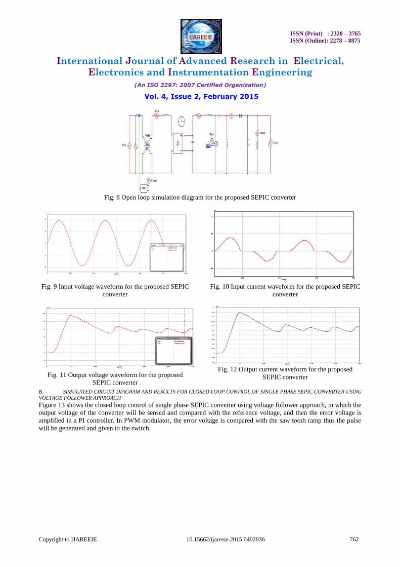
A. SIMULATED CIRCUIT DIAGRAM AND RESULTS FOR OPEN LOOP CONTROL OF SINGLE PHASE SEPIC CONVERTER Figure 8 shows the simulated diagram for an open loop control of single phase SEPIC converter. The switch is
triggered at a switching frequency of 10 kHz. Both the THD and power factor are measured at the input side.
Figure 9 and 10 shows the input voltage and current waveforms for the above circuit. The peak input voltage is
measured as 18.849 V. Figure 11 and Figure 12 shows the output voltage and output current for the proposed
converter.. Result analysis for open loop control of SEPIC converter is shown in Table 2.
ISSN (Print) : 2320 – 3765
ISSN (Online): 2278 – 8875
International Journal of Advanced Research in Electrical,
Electronics and Instrumentation Engineering
(An ISO 3297: 2007 Certified Organization)
Vol. 4, Issue 2, February 2015
Copyright to IJAREEIE 10.15662/ijareeie.2015.0402036 762
Fig. 8 Open loop simulation diagram for the proposed SEPIC converter
Fig. 9 Input voltage waveform for the proposed SEPIC
converter
Fig. 10 Input current waveform for the proposed SEPIC
converter
Fig. 11 Output voltage waveform for the proposed
SEPIC converter
Fig. 12 Output current waveform for the proposed
SEPIC converter
B. SIMULATED CIRCUIT DIAGRAM AND RESULTS FOR CLOSED LOOP CONTROL OF SINGLE PHASE SEPIC CONVERTER USING
VOLTAGE FOLLOWER APPROACH
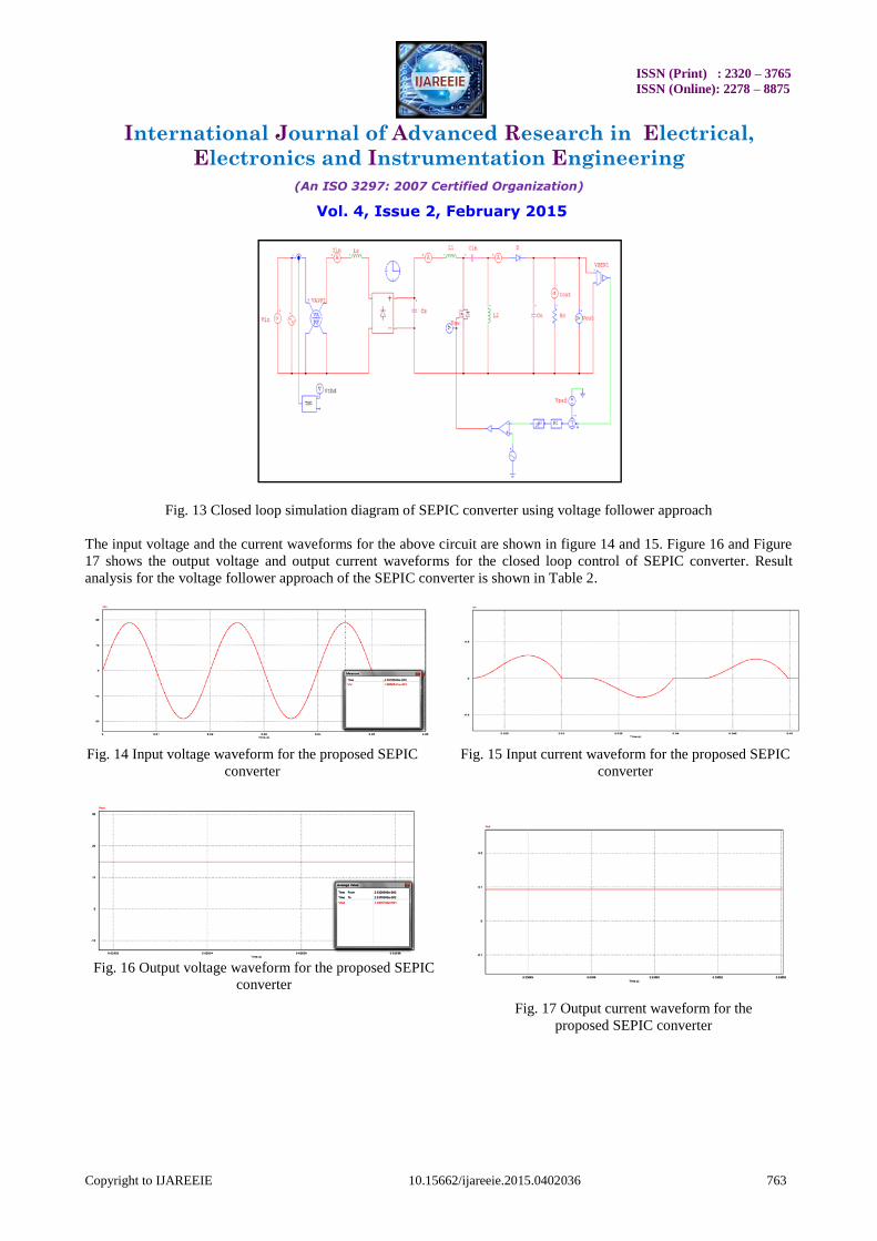
Figure 13 shows the closed loop control of single phase SEPIC converter using voltage follower approach, in which the
output voltage of the converter will be sensed and compared with the reference voltage, and then the error voltage is
amplified in a PI controller. In PWM modulator, the error voltage is compared with the saw tooth ramp thus the pulse
will be generated and given to the switch.
ISSN (Print) : 2320 – 3765
ISSN (Online): 2278 – 8875
International Journal of Advanced Research in Electrical,
Electronics and Instrumentation Engineering
(An ISO 3297: 2007 Certified Organization)
Vol. 4, Issue 2, February 2015
Copyright to IJAREEIE 10.15662/ijareeie.2015.0402036 763
Fig. 13 Closed loop simulation diagram of SEPIC converter using voltage follower approach
The input voltage and the current waveforms for the above circuit are shown in figure 14 and 15. Figure 16 and Figure
17 shows the output voltage and output current waveforms for the closed loop control of SEPIC converter. Result
analysis for the voltage follower approach of the SEPIC converter is shown in Table 2.
Fig. 14 Input voltage waveform for the proposed SEPIC
converter
Fig. 15 Input current waveform for the proposed SEPIC
converter
Fig. 16 Output voltage waveform for the proposed SEPIC
converter
Fig. 17 Output current waveform for the
proposed SEPIC converter
ISSN (Print) : 2320 – 3765
ISSN (Online): 2278 – 8875
International Journal of Advanced Research in Electrical,
Electronics and Instrumentation Engineering
(An ISO 3297: 2007 Certified Organization)
Vol. 4, Issue 2, February 2015
Copyright to IJAREEIE 10.15662/ijareeie.2015.0402036 764
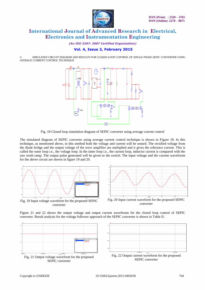
C. SIMULATED CIRCUIT DIAGRAM AND RESULTS FOR CLOSED LOOP CONTROL OF SINGLE PHASE SEPIC CONVERTER USING
AVERAGE CURRENT CONTROL TECHNIQUE
Fig. 18 Closed loop simulation diagram of SEPIC converter using average current control
The simulated diagram of SEPIC converter using average current control technique is shown in Figure 18. In this
technique, as mentioned above, in this method both the voltage and current will be sensed. The rectified voltage from
the diode bridge and the output voltage of the error amplifier are multiplied and it gives the reference current. This is
called the outer loop i.e., the voltage loop. In the inner loop i.e., the current loop, inductor current is compared with the
saw tooth ramp. The output pulse generated will be given to the switch. The input voltage and the current waveforms
for the above circuit are shown in figure 19 and 20.
Fig. 19 Input voltage waveform for the proposed SEPIC
converter
Fig. 20 Input current waveform for the proposed SEPIC
converter
Figure 21 and 22 shows the output voltage and output current waveforms for the closed loop control of SEPIC
converter. Result analysis for the voltage follower approach of the SEPIC converter is shown in Table II.
Fig. 21 Output voltage waveform for the proposed
SEPIC converter
Fig. 22 Output current waveform for the proposed
SEPIC converter

ISSN (Print) : 2320 – 3765
ISSN (Online): 2278 – 8875
International Journal of Advanced Research in Electrical,
Electronics and Instrumentation Engineering
(An ISO 3297: 2007 Certified Organization)
Vol. 4, Issue 2, February 2015
Copyright to IJAREEIE 10.15662/ijareeie.2015.0402036 765
Comparison Output Voltage(volts) Power Factor THD %
Open loop 12.69 0.6529 84.15
Voltage Follower Approach 14.93 0.7510 45.58
Average Current Control 15.24 0.9761 1.12
Table. 2 Comparison between open loop and closed loop control technique
Figure 23 and 24 shows the THD and Power Factor chart for various control techniques.
Fig. 23. THD chart for various control techniques
Fig. 24. Power Factor chart for various control techniques
VI.CONCLUSION
The design, simulation and development of single-switch Buck-Boost SEPIC converter with high frequency non-
isolation has been carried out for 15v output. With this designed converter, simulation has been done in standard PSIM
(Power Simulation) software. High power quality is obtained with design parameters with power factor in the order of
0.97 and THD in the order of 1.12% using the Power Quality Improvement Techniques. Simulated and test results on
the developed converter show the improved performance of the proposed high frequency Non-isolated AC-DC SEPIC
converter in terms of low THD of supply current and improved power factor of AC mains.
REFERENCES
1. Biao Zhao, Qiang Song, Wenhua Liu, and Yandong Sun, “Overview of Dual-Active-Bridge Isolated Bidirectional DC–DC Converter for
High-Frequency-Link Power-Conversion System”, IEEE Transactions on Power Electronics, Vol.29, No.8, pp. 4091-4106, August 2014.
2. R.Ramesh, U.subatra, M.Ananthi, “Single phase AC-DC power factor corrected converter with high frequency isolation using buck converter”, ISSN, Vol.4, No.3, pp. 79-82, March 2014.
3. Robert Priewasser, MatteoAgostinelli, ChristophUnterrieder, Stefano Marsiliand Mario Huemer “Modeling, Control, and Implementation of
DC–DC Converters for Variable Frequency Operation”, IEEE Transactions on Power Electronics, Vol.29, No.1, pp. 287-301, January 2014. 4. Satish. Bandaru, R.Suresh“The Isolated Buck Boost dc to dc Converter With High Efficiency For Higher Input Voltages”, ISSN, Vol.8, No.5,
pp. 1-16, December 2013.
5. AnamZaman, Gavin Paes, MalaikaD’sa, NipunikaDhawan, Saikrishna V. “Design of a Closed Loop System Using Modified SEPIC” ISSN, Vol.1, No.3, pp. 94-98, April 2013.
6. Kavya Shree G V, Eranna, K Cnandra Mohan Reddy, “An Isolated CUK Converter With Multiple Outputs Using PWM Controller”
ISSN(Print), Vol.1, No.2, pp. 33-36, 2013. 7. ChakibAlaoui, “Spectral Analysis of BUCK and SEPIC Converters”ISSN, Vol.3, No.2, pp. 1705-1711, February 2011.

ISSN (Print) : 2320 – 3765
ISSN (Online): 2278 – 8875
International Journal of Advanced Research in Electrical,
Electronics and Instrumentation Engineering
(An ISO 3297: 2007 Certified Organization)
Vol. 4, Issue 2, February 2015
Copyright to IJAREEIE 10.15662/ijareeie.2015.0402036 766
BIOGRAPHY
Mr.A.Ramkumar received the B.Tech degree in Electrical and Electronics Engineering from Kalasalingam
University, Krishnankoil in 2012.Currently he is doing his M.E degree in Applied Electronics at Renganayagi
Varatharaj College of Engineering, Sivakasi. His main area of interest includes power electronics and power quality.
Ms.S.Vijula Shini Florence is working as an assistant professor in Electrical and Electronics Engineering at
Renganayagi Varatharaj College of Engineering, Sivakasi. She has received BE (Electrical and Electronics
Engineering) degree from P.S.R Engineering College, Sivakasi in 2010, ME (Power Electronics) from Mepco Schlenk
Engineering College, Sivakasi in 2012. Her research interest includes power electronics and drives and control system.
Related Documents