Analysis of personal computer ride through capability during voltage sags Hussain Shareef ∗ , Azah Mohamed, Nazri Marzuki Department of Electrical, Electronic and Systems Engineering, Universiti Kebangsaan Malaysia, Bangi, 43600, Selangor, Malaysia abstract Voltage sags have emerged as one of the most serious power quality problems, particularly for sensitive equipments such as personal computers (PCs). It is a complex electronic computing device designed to be powered by a switch mode power supply (SMPS). This paper presents an investigation of vulnerability of PCs to voltage sags and development of methods to enhance the voltage sag ride through capability of PCs. Based on recent testing standards, extensive tests were conducted for a wide range of PCs. For standard reboot/restart malfunction criterion, sag depth and duration were varied to construct individual voltage immunity curves for PCs. Based on the analysis, two methods were implemented to improve the voltage sag ride through capability of the PCs. These methods include the use of additional dc capacitors and alteration of the under voltage detection (UVD) signal in the housekeeping block of the SMPS. The experimental results on different PCs show that installation of additional capacitors can only expand PCs’ immunity duration to voltage sag while shift in the UVD signal helps to enhance the tolerance level in terms of sag magnitude. Finally, the advantages and disadvantages involved in the implemented methods to enhance voltage tolerance level of PCs are highlighted. 1. Introduction The importance of providing power with steady voltage and frequency has been recognized since the inception of the electric supply industry (ESI). As ESI proliferates along with the introduction of power system deregulation, electronic and information tech- nology equipment in a wide range of systems, and unpredictable climate changes, it is almost impossible to avoid power system disturbances. Over the past few years, voltage sags have emerged as one of the most serious power quality problems. It is a sudden decrease in voltage amplitude followed by a return to its initial level after a short time [1]. Sags are caused by network faults, switching actions such as starting of large motors, transformer energizing, etc. These incidents that initiate voltage sags can disrupt or damage sensitive equipment such as personal computers (PCs). Personal computers first appeared in the late 1970s. It is a com- plex electronic computing device designed to be powered by a switch mode power supply (SMPS) which converts incoming sin- gle phase ac line voltage into a dc voltage that feeds the electronics components [2]. The malfunction of PCs incorporated in on-line or even off-line systems can incur substantial cost, due to the losses ∗ Corresponding author at: Faculty of Engineering, and Built Environment, Department of Electrical, Electronic and Systems Engineering, Universiti Kebangsaan Malaysia, Bangi, 43600, Selangor, Malaysia. Tel.: +60 3 89216590; fax: +60 3 89216146. E-mail address: [email protected] (H. Shareef). associated with the computer controlled systems and processes [3]. Studies assessing sensitivity of voltage sags on customer loads are gradually increasing with efforts primarily divided into practi- cal and theoretical approaches. The practical approaches investigate the effects of voltage sag by monitoring, conducting experiments on customers’ sensitive loads, and performing pertinent surveys [4,5]. Current standards related to testing sensitivity of equipment to voltage sags and short interruptions suggest that the tests should be performed preferably at 0 ◦ point on wave of the voltage waveform [6–8]. The International Electrotechnical Commission recommends testing of the equipment for additional angles only if they are considered critical by product committees or individual product specifications. If so, a range from 0 ◦ to 360 ◦ in steps of 45 ◦ is optional for such additional testing [6]. Equipment sensitivity to voltage sag can also be considered and presented in the form of power acceptability curves. These curves are plots of bus voltage deviation versus time duration which sepa- rate the bus voltage deviation–time duration plane into two regions namely, “acceptable” and “unacceptable” regions. The lower limb of the power acceptability curve relates to voltage sags and momen- tary outages. The latest power acceptability standard is known as the SEMI F47 issued by the Semiconductor Equipment and Materials International (SEMI) in the year 2000 [7]. The specification simply states that semiconductor processing, metrology, and automated test equipment must be designed and built to confirm to the volt- age sag ride-through capability as per the defined curve. Equipment must continue to operate without interruption during condi-

Welcome message from author
This document is posted to help you gain knowledge. Please leave a comment to let me know what you think about it! Share it to your friends and learn new things together.
Transcript

A
HD
1
fsoncdadaaes
psgce
DMf
nalysis of personal computer ride through capability during voltage sags
ussain Shareef ∗, Azah Mohamed, Nazri Marzukiepartment of Electrical, Electronic and Systems Engineering, Universiti Kebangsaan Malaysia, Bangi, 43600, Selangor, Malaysia
a b s t r a c t
Voltage sags have emerged as one of the most serious power quality problems, particularly for sensitiveequipments such as personal computers (PCs). It is a complex electronic computing device designed tobe powered by a switch mode power supply (SMPS). This paper presents an investigation of vulnerabilityof PCs to voltage sags and development of methods to enhance the voltage sag ride through capabilityof PCs. Based on recent testing standards, extensive tests were conducted for a wide range of PCs. Forstandard reboot/restart malfunction criterion, sag depth and duration were varied to construct individual
voltage immunity curves for PCs. Based on the analysis, two methods were implemented to improve thevoltage sag ride through capability of the PCs. These methods include the use of additional dc capacitorsand alteration of the under voltage detection (UVD) signal in the housekeeping block of the SMPS. Theexperimental results on different PCs show that installation of additional capacitors can only expand PCs’immunity duration to voltage sag while shift in the UVD signal helps to enhance the tolerance level interms of sag magnitude. Finally, the advantages and disadvantages involved in the implemented methodsnce le
to enhance voltage tolera. Introduction
The importance of providing power with steady voltage andrequency has been recognized since the inception of the electricupply industry (ESI). As ESI proliferates along with the introductionf power system deregulation, electronic and information tech-ology equipment in a wide range of systems, and unpredictablelimate changes, it is almost impossible to avoid power systemisturbances. Over the past few years, voltage sags have emergeds one of the most serious power quality problems. It is a suddenecrease in voltage amplitude followed by a return to its initial levelfter a short time [1]. Sags are caused by network faults, switchingctions such as starting of large motors, transformer energizing,tc. These incidents that initiate voltage sags can disrupt or damageensitive equipment such as personal computers (PCs).
Personal computers first appeared in the late 1970s. It is a com-lex electronic computing device designed to be powered by a
witch mode power supply (SMPS) which converts incoming sin-le phase ac line voltage into a dc voltage that feeds the electronicsomponents [2]. The malfunction of PCs incorporated in on-line orven off-line systems can incur substantial cost, due to the losses∗ Corresponding author at: Faculty of Engineering, and Built Environment,epartment of Electrical, Electronic and Systems Engineering, Universiti Kebangsaanalaysia, Bangi, 43600, Selangor, Malaysia. Tel.: +60 3 89216590;
ax: +60 3 89216146.E-mail address: [email protected] (H. Shareef).
vel of PCs are highlighted.
associated with the computer controlled systems and processes[3].
Studies assessing sensitivity of voltage sags on customer loadsare gradually increasing with efforts primarily divided into practi-cal and theoretical approaches. The practical approaches investigatethe effects of voltage sag by monitoring, conducting experiments oncustomers’ sensitive loads, and performing pertinent surveys [4,5].Current standards related to testing sensitivity of equipment tovoltage sags and short interruptions suggest that the tests should beperformed preferably at 0◦ point on wave of the voltage waveform[6–8]. The International Electrotechnical Commission recommendstesting of the equipment for additional angles only if they areconsidered critical by product committees or individual productspecifications. If so, a range from 0◦ to 360◦ in steps of 45◦ is optionalfor such additional testing [6].
Equipment sensitivity to voltage sag can also be considered andpresented in the form of power acceptability curves. These curvesare plots of bus voltage deviation versus time duration which sepa-rate the bus voltage deviation–time duration plane into two regionsnamely, “acceptable” and “unacceptable” regions. The lower limb ofthe power acceptability curve relates to voltage sags and momen-tary outages. The latest power acceptability standard is known asthe SEMI F47 issued by the Semiconductor Equipment and Materials
International (SEMI) in the year 2000 [7]. The specification simplystates that semiconductor processing, metrology, and automatedtest equipment must be designed and built to confirm to the volt-age sag ride-through capability as per the defined curve. Equipmentmust continue to operate without interruption during condi-
mpon
t[
ma[rfwtad
cttTttecnta
vLstiRpvt
lmmmpp
crwcbpaitu
Fig. 1. Basic co
ions identified in the area above the defined acceptable region9].
As an effort to understand the voltage immunity level of PCs,any works have been reported in the past. Seven PCs of different
ge are investigated for voltage sags by Pohjanheimo and Lehtonen10]. The malfunction criterion for the PCs selected is automaticeboot. The voltage tolerance curves obtained from the tests areound to be rectangular, having a flat vertical and horizontal part
ith a sharp knee between them. The authors reported that the PCsolerate the under voltage level up to 50–60% of remaining volt-ge for 100 ms. However, there is no clear correlation between theevice age and sensitivity observed.
Test results on standard restart/reboot malfunction criterion foromputers due to voltage sags can be found in [11]. It is reportedhat if the depth of voltage sag is larger than 30% and lasts morehan 8 cycles, the voltage sag may cause a computer to restart.hese tests were only carried out for the 120 V/60 Hz systems. Fur-hermore, it is concluded that the performance of the SMPS andhe power consumption of a computer plays a vital role on the sagffect but did not provide further details. Similar experiments areonducted by Bok et al. [12] to identify the effect of rectangular andon-rectangular voltage sags on the same restart/reboot malfunc-ion criteria. It is noted that rectangular sags with loading conditionre found to influence most on the susceptibility of PCs.
Another comprehensive study on the behavior of PCs duringoltage sags and short interruptions is presented by Djokic et al. [3].aboratory experiments are performed with rectangular voltageags as well as with non-rectangular sags to simulate the starting ofhe large motors. Supply from the non-ideal voltage source is real-zed by incorporating harmonic and supply frequency variations.esults show that all the voltage tolerance curves for different com-uters have the same rectangular shape with two clearly distinctiveertical and horizontal parts, with a very sharp “knee” betweenhem.
Medora et al. [13] presents a PSpice simulation study to ana-yze the operation of 120 V/60 Hz SMPS during line voltage sags by
erely observing the discharge of the dc link capacitor. One of theain conclusions drawn is that the inrush current control circuitsust be designed to operate effectively for line voltage sags of all
redictable depths and time durations to avoid damage to the PCower supply.
This paper focuses on investigating the vulnerability of personalomputers to voltage sags in the 230 V/50 Hz mains supply. Aftereviewing the previously published work, this paper tries to answerhy almost all the PCs have rectangular shaped voltage immunity
urves with the flat vertical and horizontal part with a sharp kneeetween them. Extensive laboratory tests are conducted for this
urpose by analyzing the operation of SMPS of the PCs during volt-ge sags. From the analysis of the test findings, two methods aremplemented to improve the voltage sag ride through capability ofhe PCs. These methods can also be applied to other devices thattilize SMPS.ents of a SMPS.
2. Switch mode power supply model
A power supply converts the output from an ac power line to asteady dc output or multiple outputs. The ac voltage is first rectifiedto provide a pulsating dc voltage. Then it is filtered and regulated toproduce a constant output voltage despite variations in the ac linevoltage or circuit loading. Traditionally, the regulation is done by alinear regulator to drive the pass element and cancel any variationsappearing at the output of the dc voltage. However, power supplieswhich switching regulators employ solid-state devices, which oper-ate as switches to perform power conversion and it enjoys muchmore advantages than that uses linear voltage regulators. A SMPScan be a fairly complicated circuit, as can be seen from the blockdiagram shown in Fig. 1.
2.1. Diode bridge rectifier
A diode bridge is the first stage in any SMPS to rectify the incom-ing voltage. A large capacitor then filters the pulsating dc voltage tocreate a nearly constant dc voltage. Under normal operating condi-tions, over a half-cycle, the capacitor voltage decays to a value givenby [13]:
�V = I0T50
2Cdc(1)
where �V is the capacitor voltage decay, I0 is the load current, T50is the 50-cycle period, Cdc is the capacitance of the filter capacitor.
Therefore the capacitor is essentially charged close to the peakof the ac mains peak voltage plus �V/2 which is ideal for the dc–dcconverter circuit to operate efficiently. However, during the eventof voltage sag of N cycles, the dc link capacitor discharges to 2N�V.Depending upon the minimum voltage value set by the design ofthe input circuit, the dc–dc converter will deliver rated dc outputvoltage until the capacitor voltage reaches its minimum value. Thetime to reach this voltage at rated load is defined as the holduptime, Th, which is represented mathematically as [14]:
Th = Cdc(V2norm − V2
min)
2P(2)
where Cdc is the capacitance of the filter capacitor, Vnorm is the peaknominal voltage, Vmin is the peak minimum voltage set by the SMPSdesign, P is the rated power of the SMPS.
2.2. dc–dc converter
The unregulated dc is fed directly to the central block of thesupply unit, which is the high frequency power switching section
shown in Fig. 1. Fast switching power semiconductor devices suchas MOSFETs and bipolar transistors are driven on and off, and switchthe input voltage across the primary of the power transformer. Thedrive pulses normally have fixed frequency and variable duty cycle.Hence, a voltage pulse train of suitable magnitude and duty ratio
Table 1Specifications of tested PCs.
PC no. Specifications
PCI
CPU: Pentium III, 450 MHz Processor, 128 MBSDRAMOS: Windows MePower supply:Model: PS-5141-2D1100–127 V/200–240 V, 5/2.5 A, 60/50 Hz, 145 W
PC2
CPU: Pentium 4, 2.40 GHz Processor, 261 MBRAMOS: Windows 2000 ProfessionalPower supply:Model: NPS-180BBA100–120 V/200–240 V, 5/3 A, 60/50 Hz, 180 W
PC3
CPU: Core 2 Duo, 2.00 GHz Processor, 1 GB RAMOS: Windows XP ProfessionalPower supply:Model: PS-5251-08 T100–127 V/200–240 V, 8/4 A, 60/50 Hz, 250 W
PC4
CPU: Pentium III, 933 MHz Processor, 256 MBRAMOS: Windows 2000 ProfessionalPower supply:Model: SA-320-35005100–127 V/200–240 V, 9/4.5 A, 60/50 Hz, 300 W
P
CPU: Pentium 4, CPU 1.90 GHz, 504 MB RAM
aa
2
cewapc
icTpaclsa
striStar
3
Pm
3.2. Testing procedure
A series of test results on PCs is obtained by following the pre-defined procedure given below. The procedure is repeated for at
C5OS: Windows XP Home EditionPower supply:Model: ATX-480 W100–127 V/200–240 V, 6/3 A, 60/50 Hz, 250 W
ppears on the transformer secondaries. This voltage pulse train isppropriately rectified, and then smoothed by an output filter.
.3. Control and protection circuitry
Regulation of the output to provide a stabilized dc supply isarried out by the control and feedback block shown in Fig. 1. Gen-rally, SMPS systems operate on pulse width modulation technique,here the duration of the on-time of the power switch is varied oncycle by cycle basis. This duty cycle depends on the error voltageroduced by the feedback comparator and hence compensates forhanges in the input supply and output load.
Protection against accidental short circuits and fault conditionss mandatory in PC power supplies. These circuits monitor criti-al circuit conditions and report any violations of prescribed limits.here are single chip integrated circuits (IC) which provide com-lete protection required for PCs’ SMPS. Some of the salient featuresnd benefits of this device is that it provides over voltage and overurrent protection for 3.3, ±5 and ±12 V, generates power goodogic output signal, programmable timing for power good signal,table internal voltage reference and voltage reference for main anduxiliary regulation.
In addition, there is a special under voltage detection input forensing the input voltage to the power supply. This input causeshe power good signal to toggle if there is insufficient voltage toun the power supply unit outputs. A high power good logic outputndicates that the power from the mains is good for PC operation.ince power supplies must maintain high voltage isolation betweenhe primary and secondary sides of the system, the under volt-ge detection signal is usually tied to a divided down and filteredepresentation of the secondary side voltage waveform.
. PC testing
This section aims to illustrate the design of the experiment forC testing and procedure followed to obtain the results on perfor-ance of personal computers to voltage sags.
3.1. Experimental setup
The methodology that is used in the testing is generally basedon the guideline given in [5,6]. Five PCs with different specificationsare tested to study the effect of voltage sags on the performance ofthe computers. The specifications of the tested PCs are shown inTable 1.
The experimental setup consists of four components namely,sag generator, equipment under test (EUT), data acquisition system,and a computer to analyze the signals. In this case, an industrialpower corruptor (IPC) from the Power Standards Lab is used, whichis a voltage sag generator combined with built-in data acquisitionsystem that is capable of producing and interrupting voltages up to480 V and current at 200 A in single or three phase systems.
Fig. 2. Testing procedure.

lt
i
ii
iv
v
4
tcviiEbfofioafc
east three times to avoid probable errors that may occur duringhe experiments.
i. Using the terminal blocks available at the back of IPC, the con-ductors from mains panel and conductors to the PC under testare connected and the IPC is powered on.
i. The PC with all input/output (I/O) and pointing devices connectedis switched on. Allowed it to boot and load the operating system.
i. Allow disk defragmenter program to scan and defragment systemdiscs.
. Starting from nominal voltage, voltage sags are initiated in stepsof 2.5% down to zero volts. The sag initiation angle and the dura-tion are kept constant. The initial sag duration and phase angleare set to 1 cycle and 0◦, respectively. The critical sag depth forthe pre-defined malfunction criteria is determined by repeatedtesting for at least 3 times for a particular sag magnitude andduration. If reboot malfunction condition is observed, a quickinspection for proper operation of EUT is conducted before initi-ating the next sag. For each triggered sag event, different voltageand current waveforms supplying and controlling the EUT arerecorded. Observation such as visible or audible influence on thePC is also noted.
. The duration of sag is adjusted in steps of 1 cycle and measure-ments outlined in Step 4 are repeated.
A flowchart of the aforementioned procedure is shown in Fig. 2.
. Voltage sag ride through techniques
PCs may shutdown or reboot either due to an active interven-ion by the under voltage protection or by a breakdown of the dc–dconverter. In both cases the malfunction will occur when the dc busoltage reaches a certain value, Vmin, set by the design as describedn Section 2. As long as the ac voltage maintains above this min-mum voltage value the PC will continue to work properly. Fromq. (2) it can be seen that the holdup time, Th, can be increasedy increasing the capacitance of the dc link capacitor, Cdc. There-ore, one way to improve the voltage sag ride through capabilityf PCs is to add more capacitance to the dc bus which is at recti-
er dc output. Unfortunately, Eq. (2) only indicates that the effectf increasing the dc link capacitance can only improve the volt-ge sag tolerance duration but not its magnitude. To immunize PCsor longer sags, large amount of capacitance is needed which isonsidered infeasible [15].Fig. 4. Effect of sag depth on the rectifi
Fig. 3. Voltage tolerance curves of various PCs.
The second parameter that that can be adjusted to improve thevoltage tolerance level of PCs is to adjust the minimum voltage,Vmin, given in Eq. (2). Vmin is directly linked to the under voltageprotection circuitry of the PCs’ SMPS. The under voltage detectionsignal is usually fed from a filtered voltage divider circuitry tiedto the secondary side voltage waveform. Therefore, it is possible totune the Vmin so as to enhance the ride through capability of the PCsin terms of sag magnitude. However, care must be taken in shiftingthis minimum voltage in order to maintain appropriate stress levelfor all components of the power supply unit and other circuitry inthe PC.
In addition to the aforementioned methods, there are few moremethods that can be investigated to immunize the PCs from voltagesags. These include changing existing power supply unit to a higherrated one and using power factor correction circuitry. However,these methods are usually not feasible and are expensive.
5. Result and analysis
The test findings from the experiments on sensitivity of PCsto voltage sags are initially presented as typical voltage tolerancecurves. The upper region of these curves represents proper opera-
tion region while the lower region indicates unacceptable voltageconditions for PCs’ operation.er dc output at 10 cycles for PC4.

rectifi
5
wvodbk1itWPbia
raFoebcu
Fig. 5. Effect of sag depth on the
.1. Analysis of voltage tolerance level of PCs
Effect of voltage sag on all the tested PCs is shown in Fig. 3 alongith the standard SEMI F47 power acceptability curve. Like in pre-
ious research findings on sensitivity of PCs to voltage sags, thebtained curves have the same rectangular shape with two clearlyistinctive vertical and horizontal parts, with a very sharp “knee”etween them. From Fig. 3, it can be seen that for PC1 to PC5, thenee points are 47.5%: 14 cycles, 25%: 8 cycles, 40%: 12cycles, 50%:1 cycles and 45%: 14 cycles, respectively. If one compares thesendividual voltage tolerance curves, it can be observed that PC4 ishe most sensitive PC to voltage magnitude while PC2 is the least.
hen the sensitivity of the PCs in terms of duration is considered,C2 starts to malfunction at 8 cycles. One final observation that cane obtained from Fig. 3 is that all tested PCs can ride through indef-
nitely if the magnitude of the sag is less than 50% nominal voltagend satisfy the design goals of SEMI F47 standard.
To further understand the reason why almost all the PCs haveectangular shaped voltage sensitivity curves, signals obtainedt different points of the SMPS of PC3 and PC4 are analyzed.igs. 4 and 5 illustrate the waveforms obtained at the rectifier dcutput and power good logic output of the PC4 SMPS during differ-
nt magnitude of voltage sags. From Fig. 4, it can be observed thaty varying sag depth from 52.5% to 5% remaining voltage for 10ycles, the voltage decay at the rectifier dc output remains almostnchanged even for very deep sags. At 10 cycles, the energy storedFig. 6. Effect of sag duration on the rectifier dc o
er dc output at 11 cycles for PC4.
in the dc link capacitor does not allow the rectifier dc output todecrease up to its minimum voltage as defined in Eq. (2). For thisreason, the under voltage detection section of the housekeeping cir-cuit does not toggle the power good signal as shown in Fig. 4. Thisindicates that PC4 will continue to operate normally for 10 cycleseven if there is no mains supply for 200 ms.
Fig. 5 shows the variation of the rectifier dc output voltage andpower good signal where PC4 starts to malfunction at 11 cycle. Sincethe sag duration is 20 ms longer at 11 cycles, the rectifier dc outputvoltage decays further. From Fig. 5, it is clear that deeper sags causethe power good signal to toggle and PC4 to reboot. This is due tothe fact that the deeper sags starting from 50% remaining voltagecause the rectifier dc output to fall below the set minimum voltageof 154 V for PC4. Almost similar waveforms are obtained for thecase of tests conducted on PC3. The only difference as indicated inthe waveforms is that the SMPS of PC3 is designed for a differentminimum voltage of 118 V.
In order to observe the effect of voltage sag duration, waveformsat the rectifier dc link are observed for constant sag magnitude.Fig. 6 illustrates the performance of the SMPS in PC4 when theduration of sag having 52.5% remaining voltage is varied from 11to 30 cycles. A careful observation in Fig. 6 reveals that the min-
imum voltage that appears at the rectifier dc output is 160 V andit does not drop beyond its critical value of 154 V even if the saglasts for a very long time. Thus, the under voltage protection circuitin SMPS of PC4 does not alert the power good signal to toggle. Byutput at 52.5% remaining voltage for PC4.

er dc
irpisdS
acvso
tiditn
5i
s
Fig. 7. Effect of sag duration on the rectifi
ncreasing the sag duration further, it is noted that PC4 starts toeboot at 50% remaining voltage as shown in Fig. 7. An importantoint that can be observed from Fig. 7 is that when the sag depth
s increased from 52.5% to 50% remaining voltage, the power goodignal starts to toggle at 218 ms. Note that at this time, the rectifierc link voltage reaches 154 V which is the minimum voltage of PC4MPS.
A similar observation is found for the effect of varying the volt-ge sag duration in the case of PC3. Fig. 8 shows the test resultsonducted on PC3 at a constant sag magnitude of 40% remainingoltage. Here again, the power good signal toggles as soon as theet minimum rectifier dc output voltage is reached. For PC3, it isbserved to occur around 240 ms at 118 V.
From the extensive tests and analysis, it can be concluded thathe PC reboot/restart malfunction depends upon the energy storedn the dc link capacitor and the minimum voltage for which the PC isesigned to trigger the under voltage protection circuit embedded
n the SMPS of the PC. In addition, studies conducted to analyzehe effect of sag depth and duration help to understand rectangularature of voltage tolerance curves of PCs.
.2. Results of implementing PC ride through capabilitymprovement methods
As described in Section 2 and from the above-mentioned analy-is, it is evident that there are two parameters that can be adjusted
Fig. 8. Effect of sag duration on the rectifier dc
output at 50% remaining voltage for PC4.
to improve the ride through capability of PCs during voltage sags. Itincludes increasing the holdup time and decreasing the minimumvoltage that triggers the under voltage detection circuit in the SMPSof the PC.
5.2.1. Effect of increasing holdup timeIn order to delay the rate of voltage decay at the rectifier out-
put, two 220 �F/200 V capacitors connected in series are used. Thiscombination is then connected in parallel with the existing dc linkcapacitor in the original design of SMPS of PCs. Once the additionalcapacitors are connected the experimental procedure presented inSection 3 is repeated. Fig. 9 shows the effect of increasing the capac-itance value at the rectifier dc output for PC4. By comparing thetime when PC4 starts to reboot from the case without and with theadded capacitors, it can be noted that the time to reach the min-imum voltage that triggers the under voltage protection circuit ofSMPS can be delayed. With the addition of these capacitors, PC4can now ride through for any sag or interruption whose durationis less than 14 cycles. This shifts the vertical part of the originalvoltage immunity curve of PC4 by 3 cycles. Fig. 9 also illustratesthat by increasing the dc link capacitance, the power good signal of
PC4 toggles whenever the set minimum voltage is reached, whichis 154 V.A similar observation is found in the case of PC3. Fig. 10 showsthe effect of adding similar 220 �F/200 V capacitor combination atthe PC3 rectifier dc output. From Fig. 10, it can be observed that by
output at 40% remaining voltage for PC3.
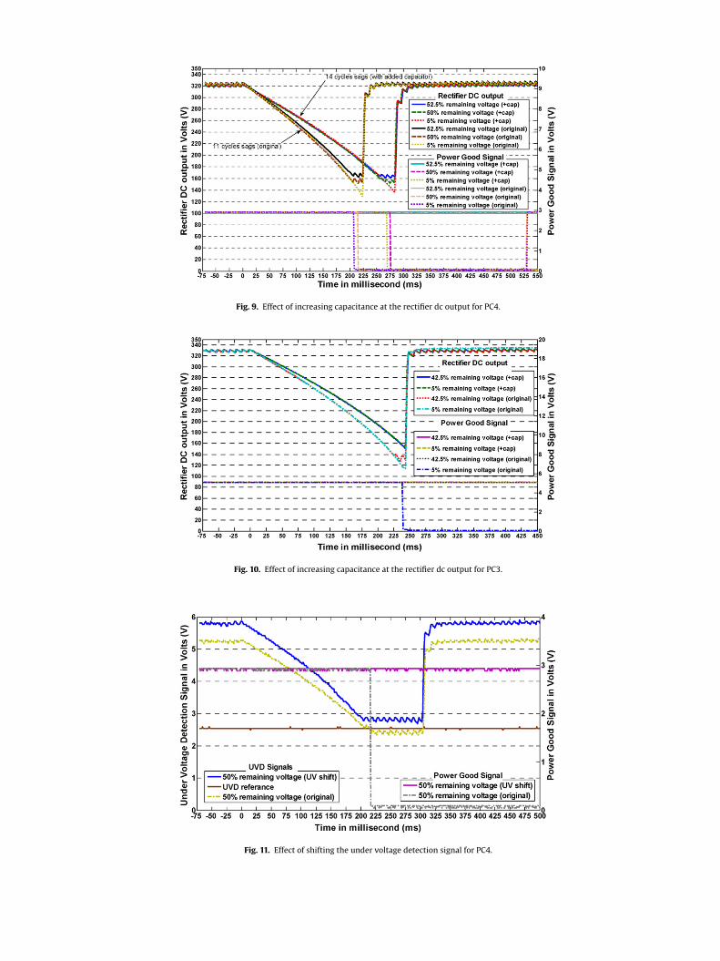
Fig. 9. Effect of increasing capacitance at the rectifier dc output for PC4.
Fig. 10. Effect of increasing capacitance at the rectifier dc output for PC3.
Fig. 11. Effect of shifting the under voltage detection signal for PC4.

der v
ainmopctSd
5
itbvodstFti
Fig. 12. Effect of shifting the un
dding the capacitors, PC3 is now immune to any sag duration ornterruption for 12 cycles. This proves that the added capacitors doot allow the dc link voltage to fall below 118 V which is the setinimum voltage that triggers the under voltage protection circuit
f PC3 SMPS. Unlike PC4, only one cycle improvement in the verticalart of voltage tolerance curve of PC3 is achieved with the sameapacitor size. Therefore, from this analysis it is possible to concludehat by adding extra capacitance at the rectifier dc output of PCs’MPS, the voltage sag ride through capability of PC in terms of saguration can be improved.
.2.2. Effect of shifting under voltage detection signalThe voltage divider circuitry tied to the secondary side of auxil-
ary transformer in PCs’ SMPS can be tuned to increase or decreasehe set minimum voltage so as to improve the ride through capa-ility of the PCs in terms of sag magnitude. Fig. 11 shows the underoltage tracking waveforms at the under voltage detection circuitf the PC4 SMPS, before and after shifting the signal for a 50% sagepth that lasts for 15 cycle. From Fig. 11 it can be noted that for
ag having 50% remaining voltage, the tracking voltage falls belowhe 2.5 V reference value of the under voltage detection circuit.rom the observation, it can be seen that at the instant where theracking voltage decreases to 2.5 V, the power good signal togglesmmediately and causes the PC to reboot. However, when the track-Fig. 13. Effect of modifying the dc link capacitance and s
oltage detection signal for PC3.
ing voltage is shifted up by adjusting the voltage divider, it neverfalls below the reference voltage for the same magnitude of sag. Inthis case, the power good signal does not toggle and therefore thePC operates normally. Although PC4 starts to malfunction at 50%remaining voltage, it is possible to increase the ride through capa-bility up to 47.5% remaining voltage by shifting the under voltagetracking signal by 0.6 V. The new minimum voltage at the recti-fier dc link that triggers the power good signal is found to be 140 Vrather than 154 V as in the original voltage divider circuit design.
Fig. 12 shows the tracking voltage waveforms of the under volt-age detection circuit in the PC3 SMPS, before and after shifting thesignal for a sag depth of 40% remaining voltage that lasts for 13cycles. From Fig. 12 it is clearly seen that the under voltage mon-itoring signal falls below the 1.6 V reference value. Note that thepower good signal toggles whenever the tracking voltage decreasesto 1.6 V. A small variation in the under voltage tracking waveformscan be observed between PC3 and PC4. In the SMPS of PC3, theunder voltage tracking signal remains low after the reference volt-age is reached and does not revert back at the end of sag event. This
is due to the fact that PC3 uses a Zener diode voltage divider withunder voltage blanking period unlike a resistive divider circuit forPC4. Fig. 12 also shows that the under voltage monitoring signal canbe shifted up to decrease the set minimum voltage that toggles thepower good signal due to under voltage condition.hifting the under voltage detection signal for PC4.

to var
5
dewdFiiirr
5
blgiadi
Fig. 14. Variation of mains current due
.2.3. Effect of varying the capacitance and set minimum voltageTo observe the effect of increasing the capacitance at the rectifier
c link and reducing the set minimum voltage simultaneously, sev-ral experiments have been conducted. Fig. 13 shows the knee pointhere PC4 starts to malfunction after adjusting the under voltage
etection signal and adding the capacitors at the rectifier dc output.rom Fig. 13, it can be seen that the ride through capability of PC4s improved further in terms of duration. Note that the knee pointn this case appears to occur at data point 290 ms and 140 V. A sim-lar observation is obtained in the case of PC3 with improvement inide through duration up to 14 cycles and for sag depth up to 37.5%emaining voltage.
.2.4. Drawbacks of adjustmentsFrom the above analysis it is clear that the ride through capa-
ility of PCs can be increased substantially by using additional dcink capacitors and adjusting the minimum voltage value that trig-
ers the under voltage detection circuit of PCs’ SMPS. However, thismprovement in immunity level of the PCs does not come withoutny drawbacks. Fig. 14 shows a comparison of current waveformsrawn from mains supply due to various changes made to the orig-nal design of PC4 SMPS. These waveforms are obtained for voltage
Fig. 15. Variation of the under voltage detection
ious modifications in the SMPS of PC4.
sags that last for 15 cycles with 40% remaining voltage. From thewaveforms, it is noted that addition of dc link capacitors and adjust-ment of the minimum voltage cause high inrush current at the endof sag event. A careful observation reveals that increase in capaci-tance is the main cause of high inrush current. In the case of shiftingthe under voltage tracking signal, the observed high inrush currentarises primarily due to the fact that it allows the dc link capac-itor at the rectifier output to discharge further. Note that at thebeginning of the sag event, no current is drawn from the mainssupply. At this point the voltage at the rectifier dc output of SMPSis higher than that of the voltage sag magnitude and this initiallyblocks the current flow. The inrush current drawn by the PC3 SMPSalso shows a similar pattern for the variations made during theexperiments.
Another disadvantage in shifting the under voltage detectionsignal is the increase in voltage discharge rate at the dc link. Fig. 15illustrates a comparison of under voltage detection signal of PC4
due to various modifications performed during the experiment fora sag whose magnitude and duration is 50% nominal voltage and30 cycles, respectively. It can be seen clearly that the decay rateof the rectifier dc output is much faster when the under voltagetracking signal is raised. In order to observe the decay time due tosignal due to various adjustments for PC4.

utput
dpimSo
6
mrsFarsttg
rcpPdltrS
ttfrateprficc
[
[
[
[
[
Fig. 16. Variation of the rectifier dc o
ifferent adjustments on the rectifier dc output waveform, a com-arison of these waveforms obtained from SMPS of PC3 is shown
n Fig. 16. From the figure, it is shown that the decreased mini-um voltage triggers the under voltage protection circuit of the
MPS and causes a fast decay in dc link voltage at the rectifierutput.
. Conclusion
An extensive experimental study has been performed to deter-ine the effect of voltage sag on personal computers. From the
esults of the test data, voltage tolerance curves of PCs are con-tructed to describe the sensitivity of various PCs to voltage sags.rom the experimental results, it can be concluded that the volt-ge tolerance level of the PCs used in the tests vary over a wideange. All the voltage immunity curves obtained appear to haveimilar shape with distinctive vertical and horizontal parts. Whenhe voltage immunity levels of the tested PCs are compared withhe SEMI F47 standard, all the tested PCs satisfies its designoal.
By observing different waveforms at the SMPS of PCs, theeason behind the rectangular nature of PCs voltage toleranceurves is revealed. Moreover, investigation on the rectifier dc out-ut and power good signal of SMPS shows that malfunction ofC occurs at a specific time for a predefined minimum voltageefined by the design of the PC SMPS. Therefore, deeper and
onger duration sags do not have any correlation with the ini-iation of PC restart malfunction condition. It only appears toely on the holdup time and the set minimum voltage of theMPS.
With thorough understanding about SMPS used in the PCs andhe data obtained from the experiments, it is possible to improvehe ride through capability of PCs. The experimental results on dif-erent PCs show that installation of additional capacitors at theectifier dc link can only expand PCs’ immunity duration to volt-ge sag while shift in the under voltage detection signal helpso improve the tolerance level in terms of sag magnitude. How-ver, these techniques produce inrush current during the recovery
eriod of voltage sag. To prevent large inrush current, it is notecommended to install a large capacitor at the end of the recti-er dc link for the purpose of enhancing voltage sag ride throughapability without incorporating proper inrush current control cir-uitry.[
due to various adjustments for PC3.
Acknowledgement
This work was carried out with the financial support from theUniversiti Kebangsaan Malaysia under the research grant UKM-GUP-BTT-07-25-151.
References
[1] J. Barros, R.I. Diego, Effects of nonsinusoidal supply on voltage tolerance ofequipment, IEEE Power Engineering Review 22 (2002) 46–47.
[2] H. Fujita, H. Akagi, Control and performance of a pulse-density-modulatedseries-resonant inverter for corona discharge processes, IEEE Transaction onIndustrial Application 35 (1999) 621–627.
[3] S.Z. Djokic, J. Desmet, G. Vanalme, J.V. Milanovic, K. Stockman, Sensitivity ofpersonal computers to voltage sags and short interruptions, IEEE Transactionon Power Delivery 20 (2005) 375–383.
[4] M.H.J. Bollen, Understanding Power Quality Problems: Voltage Sags and Inter-ruptions, first ed., IEEE Press, New York, 2000.
[5] International Electrotechnical Commission, Electromagnetic Compatibility(EMC), Part 4: Testing and Measurement Techniques, Section 30: Power QualityMeasurement Techniques, Std. IEC 61 000-4-30, 2003.
[6] International Electrotechnical Commission, Electromagnetic Compatibility(EMC), Part 4: Testing and Measurement Techniques, Section 11: Voltage Dips,Short Interruptions and Voltage Variations Immunity Tests, Std. IEC 61000-4-11,1994.
[7] Semiconductor Equipment and Materials International, SEMI F42-0600, TestMethod for Semiconductor Processing Equipment Voltage Sag Immunity, 2000.
[8] Semiconductor Equipment and Materials International, SEMI F47-0200, Spec-ification for Semiconductor Processing Equipment Voltage Sag Immunity,1999/2000.
[9] Institute of Electrical and Electronics Engineers Inc., Recommended Practicefor Powering and Grounding Electronic Equipment, second ed., IEEE Press, NewYork, 2005.
10] P. Pohjanheimo, M. Lehtonen, Equipment sensitivity to voltage sags—test resultsfor contactors, pcs and gas discharge lamps, in: Proceeding of the 10th Inter-national Conference on Harmonics and Quality of Power, Rio de Janeiro, Brazil,October 6–9, 2002, pp. 559–564.
11] S. Saksena, B. Shi, G. Karady, Effects of voltage sags on household loads, in: Pro-ceeding Power and Energy Society General Meeting—Conversion and Deliveryof Electrical Energy in the 21st Century, USA, June 12–16, 2005, pp. 2456–2461.
12] J. Bok, J. Drápela, P. Toman, Personal computers immunity to short voltage dipsand interruptions, in: Proceeding of 13th International Conference on Harmon-ics and Quality of Power, Wollongong, Australia, September 28–October 1, 2008,pp. 1–6.
13] N.K. Medora, A. Kusko, M. Thompson, Impact of line voltage sag on switch modepower supply operation, in: Proceeding of the 3rd IEEE Conference on IndustrialElectronics and Applications, June 3–5, 2008, pp. 2178–2183.
14] J. Fernandez, M. Sebastian, M. Hernando, P. Villegas, J. Garcia, Helpful hints to
select a power-factor-correction solution for low- and medium-power single-phase power supplies, IEEE Transaction on Industrial Electronics 52 (2005)46–55.15] M.H.J. Bollen, L.D. Zhang, Analysis of voltage tolerance of ac adjustable-speeddrives for three-phase balanced and unbalanced sags, IEEE Transaction onIndustrial Application 36 (2000) 904–910.
Related Documents