ISSN(Online) :2319-8753 ISSN (Print) : 2347-6710 International Journal of Innovative Research in Science, Engineering and Technology (An ISO 3297: 2007 Certified Organization) Vol. 4, Issue 9, September 2015 Copyright to IJIRSET DOI:10.15680/IJIRSET.2015.04090044 8321 Analysis of Multilayer Stacked Microstrip Patch Antenna for Bandwidth Enhancement Nagendra Pachauri, Aparna Gupta and Soni Changlani Dept. of Electronics and Communication Engineering, Laxmi Narayan College of Technology & Science Bhopal, Madhya Pradesh, India ABSTRACT: In this paper we design and simulate four types antenna with different dielectric material and compared result on the basis of variation of different dielectric coefficient and different layers and calculate some parameter of antenna for bandwidth analysis. We have enhance bandwidth of increasing layer that is 12.639%, 15.27%, 21.9% and 33.22% respectively up to forth layer. KEYWORDS: Microstrip patch antenna; stacked Antenna, bandwidth. I. INTRODUCTION Microstrip antennas are in greater demands in wireless communication and space applications because of small size, low weight. The microstrip antennas possess the shortcomings such as narrow bandwidth, low gain and poor efficiency [1]. These shortcomings can be overcome by using multilayered rectangular microstrip antennas. This can be achieved by proper combination of the substrate and superstrate thickness over and under the patch. Multilayer Microstrip patch is also useful to provide protection to patch from heat, rain, physical damage, and naturally formed ice layers during flight [3]. There are many methods available in the literature to calculate the resonant frequency of multilayered rectangular patch based on numerical technique [2]. None of the efficient analytical model is available in literature related to multilayered structure to obtain the antenna dimension. There are mainly four techniques for enhancement of Bandwidth of given Microstrip Patch Antenna. Which are, multilayered configurations of Broadband Microstrip patch antenna, Stacked Multiresonator Microstrip patch antenna, Modified Shape Patch Broadband Microstrip patch antenna, Planar Multiresonator configuration of Broadband Microstrip patch antenna, in multilayered configuration patches are placed over different dielectric substrates and they are stacked on each other. Based on the coupling mechanism, these configurations are of two types electromagnetically-coupled or aperture-coupled. There are mainly two method of coupling to multilayered antenna, Electromagnetically-coupled Technique and Aperture-coupled Technique. In Stacked Multiresonator Microstrip patch antenna configuration multiresonator and stacked configurations are combined to provide broadband microstrip patch antenna. This antenna is applicable for wireless communication such as WLAN. A single line feed stacked microstrip antenna for 4G system is presented and performance of proposed antenna improvement of bandwidth 15% [4]. II. RELATED WORK I. J. Bahl et. al [3] design of a microstrip antenna covered with a dielectric layer is presented. Due ton loading, the resonant frequency of the antenna changes. The absolute value of the change increases with the operating frequency, the relative permittivity (except plasma), and the thickness of the dielectric layer. This change may cause degradation in performance due to the inherent narrow bandwidth of microstrip antennas if the effect of loading is not considered in the design. The curves presented here may be used to design microstrip antennas that may be subjected to icing or a plasma environment or coated with protective layers. Numerical and experimental results for the fractional change in the resonant frequency are round to be in good agreement.

Welcome message from author
This document is posted to help you gain knowledge. Please leave a comment to let me know what you think about it! Share it to your friends and learn new things together.
Transcript

ISSN(Online) :2319-8753
ISSN (Print) : 2347-6710
International Journal of Innovative Research in Science,
Engineering and Technology
(An ISO 3297: 2007 Certified Organization)
Vol. 4, Issue 9, September 2015
Copyright to IJIRSET DOI:10.15680/IJIRSET.2015.04090044 8321
Analysis of Multilayer Stacked Microstrip
Patch Antenna for Bandwidth Enhancement
Nagendra Pachauri, Aparna Gupta and Soni Changlani
Dept. of Electronics and Communication Engineering, Laxmi Narayan College of Technology & Science Bhopal,
Madhya Pradesh, India
ABSTRACT: In this paper we design and simulate four types antenna with different dielectric material and compared
result on the basis of variation of different dielectric coefficient and different layers and calculate some parameter of
antenna for bandwidth analysis. We have enhance bandwidth of increasing layer that is 12.639%, 15.27%, 21.9% and
33.22% respectively up to forth layer.
KEYWORDS: Microstrip patch antenna; stacked Antenna, bandwidth.
I. INTRODUCTION
Microstrip antennas are in greater demands in wireless communication and space applications because of small size,
low weight. The microstrip antennas possess the shortcomings such as narrow bandwidth, low gain and poor efficiency
[1]. These shortcomings can be overcome by using multilayered rectangular microstrip antennas. This can be achieved
by proper combination of the substrate and superstrate thickness over and under the patch. Multilayer Microstrip patch
is also useful to provide protection to patch from heat, rain, physical damage, and naturally formed ice layers during
flight [3]. There are many methods available in the literature to calculate the resonant frequency of multilayered
rectangular patch based on numerical technique [2]. None of the efficient analytical model is available in literature
related to multilayered structure to obtain the antenna dimension. There are mainly four techniques for enhancement of
Bandwidth of given Microstrip Patch Antenna. Which are, multilayered configurations of Broadband Microstrip patch
antenna, Stacked Multiresonator Microstrip patch antenna, Modified Shape Patch Broadband Microstrip patch antenna,
Planar Multiresonator configuration of Broadband Microstrip patch antenna, in multilayered configuration patches are
placed over different dielectric substrates and they are stacked on each other. Based on the coupling mechanism, these
configurations are of two types electromagnetically-coupled or aperture-coupled. There are mainly two method of
coupling to multilayered antenna, Electromagnetically-coupled Technique and Aperture-coupled Technique. In Stacked
Multiresonator Microstrip patch antenna configuration multiresonator and stacked configurations are combined to
provide broadband microstrip patch antenna. This antenna is applicable for wireless communication such as WLAN. A
single line feed stacked microstrip antenna for 4G system is presented and performance of proposed antenna
improvement of bandwidth 15% [4].
II. RELATED WORK
I. J. Bahl et. al [3] design of a microstrip antenna covered with a dielectric layer is presented. Due ton loading, the
resonant frequency of the antenna changes. The absolute value of the change increases with the operating frequency,
the relative permittivity (except plasma), and the thickness of the dielectric layer. This change may cause degradation in
performance due to the inherent narrow bandwidth of microstrip antennas if the effect of loading is not considered in
the design. The curves presented here may be used to design microstrip antennas that may be subjected to icing or a
plasma environment or coated with protective layers. Numerical and experimental results for the fractional change in
the resonant frequency are round to be in good agreement.

ISSN(Online) :2319-8753
ISSN (Print) : 2347-6710
International Journal of Innovative Research in Science,
Engineering and Technology
(An ISO 3297: 2007 Certified Organization)
Vol. 4, Issue 9, September 2015
Copyright to IJIRSET DOI:10.15680/IJIRSET.2015.04090044 8322
[4] A single line feed stacked microstrip antenna for 4G system is presented by Awadhesh K. G. Kandu and D.C.
Dhubkarya. The proposed antenna with two properly square patches are stacked. The top patch can perform as a driven
element is design on 2.44 GHz and lower patch is also design on 2.44 GHz. The performance of proposed antenna for
4G band frequency (2400-2500 MHz). Also gating the improvement of bandwidth (15%) is very high compared to
conventional antenna.
R. Afzalzadeh and R. N. Karekar [5] design a dielectric protecting superstate with spacing on the order of one
wavelength from the rectangular microstrip patch antenna and of thickness up to about half a wavelength shows very
small variation in resonance frequency (fr) and reflection coefficient (Γ). Effects of the same on radiation pattern (RP)
includes drastic changes in beamwidths. By use of the spaced superstate the patch can be protected without the need to
redesign parameters like fr and Γ.© 1994 John Wiley & Sons, Inc.
Shavit, R [6] A theoretical model to analyze a covered rectangular antenna with an arbitrary dielectric constant
superstrate is developed. The antenna is simulated by the radiation of two magnetic dipoles located at the radiating
edges of the patch. The Green's function of an elementary magnetic dipole in a superstrate-substrate structure, utilizing
spectral-domain analysis, is formulated, and the surface-wave and radiation field are computed. An improved
transmission line model, which considers the stored energy near the radiating edges and the external mutual coupling, is
used to compute the input impedances and radiation efficiency. Design considerations on the superstrate thickness and
its dielectric constant are discussed. Experimental data for a single element and a 4×4 microstrip array is presented to
validate the theory.
N. Aouabdia et. al[7]worked on consists in characterizing a rectangular microstrip antenna while emphasizing the
possibilities of various types of current expansion functions. A detailed calculation of the spectral Green's dyad, and
conduction current calculated by the integral equation method via the moment's method was treated. The numerical
method consists in simulating the various types of basic functions by testing convergence and by considering the effect
of the parameters of the dielectric substrate such as thickness and permittivity on resonance frequency. An application
of the air gap structure was also taken into account.
Ansari, J. A., Singh, P., & Yadav, N. P [8] analyses of stacked patch antenna with two parasitic elements is presented.
The antenna shows improved radiation and directivity by 6.57 dB when compared with single layer patch antenna. The
bandwidth of the antenna is found to be dependent on various parameters such as h1, h2, and s. The proposed results are
compared with the IE3D simulation and reported experimental results.
Sharma, A., & Singh, G. [9] they are simulated a single-pin-shorted microstrip line fed three-dielectric-layer (with
different permittivity and thickness) rectangular patch microstrip antenna for all those communication systems whose
limited antenna size is premium. Low permittivity hard foam has been used as one substrate to achieve wide
bandwidth. The simulation of this proposed antenna has been performed by using CST Microwave Studio, which is a
commercially available electromagnetic simulator based on the finite difference time domain technique.
Liu, Z. F., et al [10] explained narrow bandwidth of a microstrip antenna is one of the important features that restrict its
wide usage. A simple and practical method for the design of broad-band microstrip antennas is presented in this paper.
Utilizing this design technique, several two-layer microstrip antennas have been proposed. To confirm the applicability
of the method for the designs of antennas at L-band, experiments have been carried out. The measured results show that
the proposed antennas have a bandwidth of up to 25.7%. Also, the method proposed in this paper is applicable to the
design of other types of multilayered planar antennas.
J. A. Ansari et. al [11] analyzed of multilayer patch antenna has been carriedout. The antenna shows the broad
bandwidth when a patch is stacked over fed patch in gap coupled structure. Typically a 42.65% bandwidth is achieved
in three layer antenna. Further the bandwidth of the antenna depends inversely on the gap(s). The gain of the antenna is
found to be 6.08 dB with 3 dB beam width of 92°. The theoretical results are compared with IE3D simulation and
reported experimental data.

ISSN(Online) :2319-8753
ISSN (Print) : 2347-6710
International Journal of Innovative Research in Science,
Engineering and Technology
(An ISO 3297: 2007 Certified Organization)
Vol. 4, Issue 9, September 2015
Copyright to IJIRSET DOI:10.15680/IJIRSET.2015.04090044 8323
Oluyemi P. [12] a novel design of a stacked-patch triple-band antenna in both circular and linear polarizations that can
be used on a handheld terminal for surveying and geo-informatics applications is presented. The inculcation of corner
truncation and I-slot in both the lower and middle patches has achieved better impedance bandwidth and axial ratio at
GPS L1, L2, and GSM 1800 resonant frequency bands. A prototype of the proposed design is fabricated, and its
performance is verified in measurement.
Samir Dev Gupta, M. C. Srivastava [13] described impedance bandwidth, one of the important characteristics of
microstrip patch antennas, can be significantly improved by using a multilayer dielectric configuration. In this paper the
focus is on bandwidth enhancement technique of a multilayer patch antenna for X-band applications. In order to
enhance the bandwidth, antenna losses are contained by controlling those quality factors which can have a significant
impact on the bandwidth for a given permittivity and thickness of the substrate. This has been achieved by conformal
transformation of the multidielectric microstrip antenna. For the ease of analysis Wheelers transformation is used to
map the complex permittivity of a multilayer substrate to a single layer. Method of Moments and Finite Difference
Time Domain approaches are used for the computation of results.
III. ANALYSIS OF MULTILAYER MICROSTRIP PATCH ANTENNA
There are two way to calculate the value of effective dielectric for multilayers Microstrip antenna conformal mapping
approach and transmission line approach but we used transmission line approach for analysis. The lowest-order mode,
TM10, resonates when the effective length across the patch is a half-wavelength. “Fig.1”, demonstrates the patch fed
below from a coaxial along the resonant length. Radiation occurs due to the fringing fields. These fields extend the
effective open circuit (magnetic wall) beyond the edge. The resonance frequency fmn depends on the patch size, cavity
dimension, and the filling dielectric constant, as follows:
r
mnmn
ckf
2
(1)
Where m, n = 0, 1, 2… kmn = wave number at m, n mode, c is the velocity of light, r is the dielectric constant of
substrate, and
22
L
n
W
mkmn
(2)
For TM01 mode, the length of non-radiating microstrip patch’s edge at a certain resonance frequency and dielectric
constant according to equation (1) becomes
rrf
cL
2
(3)
1
2
rrf
cW
(4)
Where fr = resonance frequency at which the rectangular microstrip antennas are to be designed. The radiating edge W,
patch width, is usually chosen such that it lies within the range L<W>2L, for efficient radiation. The ratio W/L = 1.5
gives good performance according to the side lobe appearances. In practice the fringing effect causes the effective
distance between the radiating edges of the patch to be slightly greater than L. By using above equation we can find the
value of actual length of the patch as,
ISSN(Online) :2319-8753
ISSN (Print) : 2347-6710
International Journal of Innovative Research in Science,
Engineering and Technology
(An ISO 3297: 2007 Certified Organization)
Vol. 4, Issue 9, September 2015
Copyright to IJIRSET DOI:10.15680/IJIRSET.2015.04090044 8324
Fig. 1 Multilayer Microstrip Antenna [13].
lf
cL
effr
22
(5)
Where eff= effective dielectric constant and l = line extension which is given multilayered substrate material
transmission line is shown in Figure 2.In this figure, a microstrip transmission line of length l, width w, and conductor
thickness t is shown. However, each layer has different relative dielectric permittivity and substrate thickness as shown
in the figure. In the case of multilayered substrate microstrip transmission line, the individual layer shave different
relative dielectric permittivity, and overall relative dielectric permittivity of the substrate is presented by ε rc and the
value of εrc for a two-layered substrate material has been obtained in[14]. Similarly, the expression for the frequency
dependent effective relative dielectric permittivity has been obtained in[15]. These two concepts are merged to obtain
the mathematical expression for the frequency-dependent effective relative dielectric permittivity of the multilayered
substrate material transmission line. The expression for the effective dielectric permittivity of the multilayered substrate
material is expressed as using the following.
Fig. 2 Multilayered transmission line at terahertz frequency
n
n
n
rcddd
ddd
2
2
1
1
21
(6)
1
'
11
kK
kKd
(7)
1
'
1
2
'
22
kK
kK
kK
kKd
(8)
1
'
1
2
'
2
3
'
33
kK
kK
kK
kK
kK
kKd
(9)

ISSN(Online) :2319-8753
ISSN (Print) : 2347-6710
International Journal of Innovative Research in Science,
Engineering and Technology
(An ISO 3297: 2007 Certified Organization)
Vol. 4, Issue 9, September 2015
Copyright to IJIRSET DOI:10.15680/IJIRSET.2015.04090044 8325
1
'
1
1
'
1
' kK
kK
kK
kK
kK
kKd
n
n
n
nn
(10)
and in general
1214cosh
1
hhhh
wk
nnn
n
for n=1,2,3….. (11)
In the above equations, hn,hn-1,…h1 represents the individual substrate layer thickness starting from the top layer.
Further, εn, εn-1,… ε1 are the complex relative dielectric permittivity of the respective substrate layer. Where
n
n
n
n
k
k
kK
kK
1
12ln
1'
for 0.7 ≤ kn ≤ 1 (12)
With the help of Eqs.(6)–(12), the frequency-independent relative dielectric permittivity of the multilayer substrate
material(εrc) is obtained. Once this parameter is obtained, the next goal is to find the frequency-dependent behavior.
The frequency-dependent behavior of a single-layered substrate material micro- strip transmission line is obtained with
the help of the mathematical expression discussed in detail in [17, 18]. However, in the present case, as the
multilayered Substrate relative dielectric permittivity has been reduced to εrc, it can be treated as the relative dielectric
permittivity of a single substrate layer of thickness
h = hn + hn-1 + ….. h1 and is obtained with the following formulas
m
a
ercrce
ff
f
1
0
(13)
hw
ff
rc
ba 73.1
332.075.075.0
(14)
0
10tan
0
746.47 1
erc
erc
erc
bh
f
(15)
cmmm 0 (16)
3
0 132.0
1
11
hw
h
wm
(17)
7.01
7.0235.015.01
4.11
45.0
hwfor
hwforehwm
aff
c
(18)
wh
thF
w
hrcrc
rcrce 1217.0,
121
2
1
2
10
2/1
(19)
10
11102.0,
2
hwfor
hwforhwhF rc
rc
(20)

ISSN(Online) :2319-8753
ISSN (Print) : 2347-6710
International Journal of Innovative Research in Science,
Engineering and Technology
(An ISO 3297: 2007 Certified Organization)
Vol. 4, Issue 9, September 2015
Copyright to IJIRSET DOI:10.15680/IJIRSET.2015.04090044 8326
In the above expressions, h = h3+ h2 + h1, w, and t are the total substrate thickness, width of the transmission line, and
the thickness of the conductor, respectively. In the analysis, the absolute value of d has been taken in to the
consideration because for three or more substrate layers, the value of dn as shown in(19)may be negative. However, its
value should remain positive to represent the distance between two parallel plates of the equivalent capacitance model
of the substrate.
IV. DESIGN AND SIMULATION OF PROPOSED ANTENNA
The proposed antennas designed frequency of 2.44 GHz, taking four types of dielectric constant of the substrate, RT
Duriod (εr) = 2.2, glass epoxy= 4.2, woven Teflon fiber glass = 2.55, Ceramic= 28.2. The height of dielectric substrate
(h) = 1.588 mm, 1.6 mm, 1.6 mm, 4.75 mm respectively. We have design four different antenna with different
dielectric constant and calculated effective dielectric then design different Microstrip antenna.
(a) Designing of Microstrip Antenna with First Layer
The basic design parameter as design frequency 2.44 GHz, thickness of the patch 1.6 mm and dielectric coefficient of
substrate is 2.55. Putting these parameters in above and can be calculated effective dielectric with help of two approach
but we put in transmission line approach and calculate length of the patch 29.8 mm and value of width 38.125 mm. The
dimension of the feed line calculated directly from the line Gauge of Zeland software for matching 50 Ω, are 21 mm ×
4.47 mm and bottom side of patch consider to Wg = W+6h and Lg = L+6h. The design parameters of the patch are
indicated in Table 1.
Table 1: Design parameters of single layer microstrip antenna.
Parameters Specification Unit
Patch width W 38.125 mm
Patch length L 29.8 mm
Feed line length F 21 mm
Strip width T 4.47 mm
Ground Plane width Wg 70 mm
Ground Plane length Lg 60 mm
Cut width WC 6 mm
Cut depth DC 6.5 m
m
(b) Simulation of Antenna with First Layer by IE3D
Making use of the IE3D software directly and select the Mgrid file, After the selection of Mgrid file then open basic
parameter box and select the grid size 0.025 mm, meshing frequency 5 GHz and cell per wavelength = 20, then feed the
some parameter before simulation in this dialog box like as top of the surface taking 1.6 mm, dielectric constant taking
2.55, and loss tangent taking 0.025. After the feed above parameters draw the finite ground plane with dimension 60 x
70 mm. Now draw the rectangular shape of length 29.8 mm and width 38.125 mm. After draw the patch select the edge
of the patch and cut width of cut is 6 mm and depth of cut is 6.5 mm, now draw a straight line with length of 21 mm
and width 4.47 mm. After the completion of designing select feed point location and feed at 29.1 mm in × direction and
0 mm in y direction.

ISSN(Online) :2319-8753
ISSN (Print) : 2347-6710
International Journal of Innovative Research in Science,
Engineering and Technology
(An ISO 3297: 2007 Certified Organization)
Vol. 4, Issue 9, September 2015
Copyright to IJIRSET DOI:10.15680/IJIRSET.2015.04090044 8327
Fig. 3 Proposed antenna with first layer at 2.44 GHz.
Simulation start with meshing frequency 5 GHz and the range of simulation frequency 0 - 5 GHz with step size 0.01
select the scheme as classical and enable adaptive symmetric matrix solver, simulation engine set as IE3D Full-Wave
EM Engine, enable current distribution and radiation pattern, then select ok. After simulation all data are save in
software directory.
(c) Designing of Microstrip Antenna with Second Layer
The basic design parameter as design frequency 2.44 GHz, thickness of the patch 1.6 mm, and 1.6 mm with dielectric
coefficients of substrate are 2.55 and 4.2. Putting these parameter in transmission line approach and calculate length of
the patch 29.6 mm and value of width 38.125 mm. The dimension of the feed line calculated directly from the line
Gauge of Zeland software for matching 50 Ω, are 21 mm × 4.47 mm and bottom side of patch consider to Wg = W+6h
and Lg = L+6h. The design parameters of the patch are indicated in Table 2.
Table 2: Design parameters of second layer antenna at 2.44 GHz.
Parameters Specifications Unit
Upper patch width W 38.125 mm
Upper patch length L 29.6 mm
Feed line length F 21 mm
Strip width T 4.47 mm
Ground plane length Lg 60 mm
Ground plane width Wg 70 mm
Cut width WC 6 mm
Cut depth DC 6.5 mm
.
(d) Simulation of antenna with second layer by IE3D
Making use of the IE3D software directly and select the Mgrid file, After the selection of Mgrid file then open basic
parameter box and select the grid size 0.025 mm, meshing frequency 5 GHz and cell per wavelength = 20, then feed the
some parameter before simulation in this dialog box like as top of the surface taking 1.588 mm, dielectric constant
taking 2.55, and loss tangent taking 0.025, Again taking dielectric constant for second layer 4.2 and loss tangent 0.2.
After the feed above parameters draw the finite ground plane with dimension 60 x 70 mm. After the feed above
parameters draw the rectangular shape of length 29.6 mm and width 38.125 mm. After draw the patch select the edge of
the patch and cut width of cut is 6 mm and depth of cut is 6.5 mm, now draw a straight line with length of 21 mm and
width 4.47 mm. After the completion of designing select feed point location and feed at 29.1 mm in × direction and 0
mm in y direction.

ISSN(Online) :2319-8753
ISSN (Print) : 2347-6710
International Journal of Innovative Research in Science,
Engineering and Technology
(An ISO 3297: 2007 Certified Organization)
Vol. 4, Issue 9, September 2015
Copyright to IJIRSET DOI:10.15680/IJIRSET.2015.04090044 8328
Fig. 4 Proposed antenna with second layer at 2.44 GHz.
Simulation start with meshing frequency 5 GHz and the range of simulation frequency 0 - 5 GHz with step size 0.01
select the scheme as classical and enable adaptive symmetric matrix solver, simulation engine set as IE3D Full-Wave
EM Engine, enable current distribution and radiation pattern, then select ok. After simulation all data are save in
software directory.
(e) Designing of Microstrip antenna with third layer
The basic design parameter as design frequency 2.44 GHz, thickness of the patch for first layer 1.6 mm, for second
layer 1.6 mm and for third layer 4.75 mm and dielectric coefficient of substrate are 2.55, 4.2 and 28.2 respectively.
Putting these parameters in above equation and calculate length of the patch 26.8 mm and value of width 38.125 mm.
The dimension of the feed line calculated directly from the line Gauge of Zeland software for matching 50 Ω, are 21
mm × 4.47 mm and bottom side of patch consider to Wg = W+6h and Lg = L+6h. The design parameters of the patch are
indicated in Table 3.
Table 3: Design parameters third layer antenna at 2.44 GHz.
Parameters Specification Unit
Patch width W 38.125 mm
Patch length L 26.8 mm
Feed line length F 21 mm
Strip width T 4.47 mm
Ground Plane width Wg 85.825 mm
Ground Plane length Lg 74.5 m
m
(f) Simulation of antenna with third layer by IE3D
Making use of the IE3D software directly and select the Mgrid file, After the selection of Mgrid file then open basic
parameter box and select the grid size 0.025 mm, meshing frequency 5 GHz and cell per wavelength = 20, then feed the
some parameter before simulation in this dialog box like as top of the surface taking 1.6 mm for first layer 1.6 mm for
second layer and for third layer 4.75 mm with dielectric constant taking 2.55, 4.2 and 28.2 and loss tangent taking
0.025, 0.2 and 0.5 respectively. After the feed above parameters draw the rectangular shape of length 26.8 mm and
width 38.125 mm. After draw the patch select the edge of the patch and cut width of cut is 6 mm and depth of cut is 6.5
mm, now draw a straight line with length of 21 mm and width 4.47 mm. After the completion of designing select feed
point location and feed at 29.1 mm in × direction and 0 mm in y direction. On the bottom side of the lower patch design
with 74.5 mm × 85.825 mm ground plane.

ISSN(Online) :2319-8753
ISSN (Print) : 2347-6710
International Journal of Innovative Research in Science,
Engineering and Technology
(An ISO 3297: 2007 Certified Organization)
Vol. 4, Issue 9, September 2015
Copyright to IJIRSET DOI:10.15680/IJIRSET.2015.04090044 8329
Fig. 5 Proposed antenna with third layer at 2.44 GHz.
Simulation start with meshing frequency 5 GHz and the range of simulation frequency 0 - 5 GHz with step size 0.01
select the scheme as classical and enable adaptive symmetric matrix solver, simulation engine set as IE3D Full-Wave
EM Engine, enable current distribution and radiation pattern, then select ok. After simulation all data are save in
software directory.
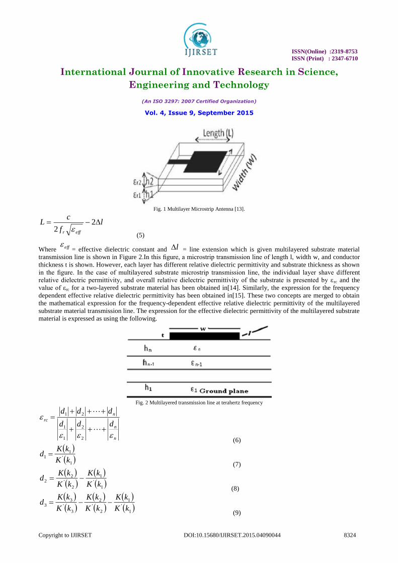
(g) Designing of Microstrip antenna with forth layer
The basic design parameter as design frequency 2.44 GHz, thickness of the patch for first layer 1.6 mm, for second
layer 1.6 mm for third layer 4.75 mm and 1.58 mm for forth layer with dielectric coefficient of substrate is 2.55, 4.2,
28.2 and 22 respectively.. Putting these parameters in above equation and calculate length of the patch 26.2 mm and
value of width 38.125 mm. The dimension of the feed line calculated directly from the line Gauge of Zeland software
for matching 50 Ω, are 21 mm × 4.47 mm and bottom side of patch consider to Wg =W+6h and Lg=L+6h. The design
parameters of the patch are indicated in Table 4.
Table 4: Design parameters of forth layer antenna at 2.44 GHz.
Parameters Specification Unit
Patch width W 38.125 mm
Patch length L 26.2 mm
Feed line length F 21 mm
Strip width T 4.47 mm
Ground Plane width Wg 95.305 mm
Ground Plane length Lg 83.38 mm
(h) Simulation of Antenna with Forth Layer by IE3D
Making use of the IE3D software directly and select the Mgrid file, After the selection of Mgrid file then open basic
parameter box and select the grid size 0.025 mm, meshing frequency 5 GHz and cell per wavelength = 20, then feed the
some parameter before simulation in this dialog box like as top of the surface taking 1.6 mm for first layer, 1.6 mm for
second layer, 4.75 for third layer and 1.58 mm for forth layer with dielectric constant 2.55, 4.2, 28.2 and 22
respectively. Now taking loss tangent are 0.025, 0.2, 0.5, and 0.0009 respectively. After the feed above parameters
draw the rectangular shape of length 26.2 mm and width 38.125 mm. After draw the patch select the edge of the patch
and cut width of cut is 6 mm and depth of cut is 6.5 mm, now draw a straight line with length of 21 mm and width 4.47
mm. After the completion of designing select feed point location and feed at 29.1 mm in × direction and 0 mm in y
direction. On the bottom side of the lower patch design with 83.38 mm × 95.305 mm metallic ground plane.
ISSN(Online) :2319-8753
ISSN (Print) : 2347-6710
International Journal of Innovative Research in Science,
Engineering and Technology
(An ISO 3297: 2007 Certified Organization)
Vol. 4, Issue 9, September 2015
Copyright to IJIRSET DOI:10.15680/IJIRSET.2015.04090044 8330
Fig. 6 Proposed antenna with forth layer at 2.44 GHz.
Simulation start with meshing frequency 5 GHz and the range of simulation frequency 0 - 5 GHz with step size 0.01
select the scheme as classical and enable adaptive symmetric matrix solver, simulation engine set as IE3D Full-Wave
EM Engine, enable current distribution and radiation pattern, then select ok. After simulation all data are save in
software directory.
V. RESULTS AND DISCUSSIONS
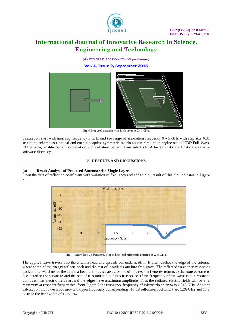
(a) Result Analysis of Proposed Antenna with Single Layer
Open the data of reflection coefficient with variation of frequency and add to plot, result of this plot indicates in Figure
7.
-25
-20
-15
-10
-5
0
0 0.5 1 1.5 2 2.5 3
Ret
urn
loss
(d
B)
frequency (GHz)
With First layer
Fig. 7 Return loss Vs frequency plot of line feed microstrip antenna at 2.44 GHz.
The applied wave travels into the antenna head and spreads out underneath it. It then reaches the edge of the antenna
where some of the energy reflects back and the rest of it radiates out into free-space. The reflected wave then resonates
back and forward inside the antenna head until it dies away. Some of this resonant energy returns to the source, some is
dissipated in the substrate and the rest of it is radiated out into free-space. If the frequency of the wave is at a resonant
point then the electric fields around the edges have maximum amplitude. Thus the radiated electric fields will be at a
maximum at resonant frequencies; from Figure 7 the resonance frequency of microstrip antenna is 1.345 GHz. Another
calculation the lower frequency and upper frequency corresponding -10 dB reflection coefficient are 1.26 GHz and 1.43
GHz so the bandwidth of 12.639%.

ISSN(Online) :2319-8753
ISSN (Print) : 2347-6710
International Journal of Innovative Research in Science,
Engineering and Technology
(An ISO 3297: 2007 Certified Organization)
Vol. 4, Issue 9, September 2015
Copyright to IJIRSET DOI:10.15680/IJIRSET.2015.04090044 8331
Table 5: Simulated result of proposed antenna with first layer.
Parameter Results
Resonance Frequency 1.32 GHz
Return loss -21.4607 dB
VSWR 1.447237
Bandwidth 12.639 %
Gain 3.34084 dBi
Directivity 4.46192 dBi
Antenna Efficiency 70.2489%
Radiation Efficiency 80.1458%
(b) Result Analysis of Proposed Antenna with Second Layer
Open the data of reflection coefficient with variation of frequency and add to plot, result of this indicates in Figure
8.The applied wave travels into the antenna head and spreads out underneath it. It then reaches the edge of the antenna
where some of the energy reflects back and the rest of it radiates out into free-space. The reflected wave then resonates
back and forward inside the antenna head until it dies away. Some of this resonant energy returns to the source, some is
dissipated in the substrate and the rest of it is radiated out into free-space. If the frequency of the wave is at a resonant
point then the electric fields around the edges have maximum amplitude. Thus the radiated electric fields will be at a
maximum at resonant frequencies. The resonance frequency of finite ground plane antenna is 1.38 GHz with -23.169
dB reflection coefficient. Another calculation the lower frequency and upper frequency corresponding -10 dB reflection
coefficient are 1.27 GHz and 1.48 GHz so the bandwidth of 15.27%
-35
-30
-25
-20
-15
-10
-5
0
0 0.5 1 1.5 2 2.5 3
Ret
urn
loss
(dB
)
frequency (GHz)
With First layer With Second layer
Fig. 8 Return loss Vs frequency plot of proposed microstrip antenna.
Table 6: Simulated result of proposed antenna with second layer.
Parameter Antenna with
first layer
Antenna with
second layer
Resonance Frequency (GHz) 1.32 GHz 1.38 GHz
Return loss (dB) -21.4607 dB -23.169 dB
VSWR 1.447237 1.498
Bandwidth 12.639 % 15.27%

ISSN(Online) :2319-8753
ISSN (Print) : 2347-6710
International Journal of Innovative Research in Science,
Engineering and Technology
(An ISO 3297: 2007 Certified Organization)
Vol. 4, Issue 9, September 2015
Copyright to IJIRSET DOI:10.15680/IJIRSET.2015.04090044 8332
Gain 3.34084 dBi 3.6832 dBi
Directivity 4.46192 dBi 4.41002 dBi
Antenna Efficiency 70.2489% 72.32%
Radiation Efficiency 80.1458% 78.172%
(c) Result Analysis of Proposed Antenna with Third Layer
Open the data of reflection coefficient with variation of frequency and add to plot, result of this indicates in Figure 9.
-35
-30-25
-20-15
-10
-5
0
0 0.5 1 1.5 2 2.5 3
Ret
urn
loss
(d
B)
frequency (GHz)
Series1 Series2 Series3
Fig. 9 Return loss Vs frequency plot of proposed microstrip antenna.
The applied wave travels into the antenna head and spreads out underneath it. It then reaches the edge of the antenna
where some of the energy reflects back and the rest of it radiates out into free-space. The reflected wave then resonates
back and forward inside the antenna head until it dies away. Some of this resonant energy returns to the source, some is
dissipated in the substrate and the rest of it is radiated out into free-space. If the frequency of the wave is at a resonant
point then the electric fields around the edges have maximum amplitude. Thus the radiated electric fields will be at a
maximum at resonant frequencies. From Figure 9 the resonance frequency of microstrip antenna is 1.48 GHz. Another
calculation the lower frequency and upper frequency corresponding -10 dB reflection coefficient are 1.26 GHz and 1.57
GHz so the bandwidth of 21.9%.
Table 7: Simulated result of proposed antenna with third layer.
Parameter Antenna with
first layer
Antenna with
second layer
Antenna with
third layer
Resonance Frequency (GHz) 1.32 GHz 1.38 GHz 1.48 GHz
Return loss (dB) -21.4607 dB -23.169 dB -24.778 dB
VSWR 1.45 1.5 1.38
Bandwidth 12.639 % 15.27% 21.9%
Gain 3.34084 dBi 3.6832 dBi 4.1842 dBi
Directivity 4.46192 dBi 4.41002 dBi 3.1102 dBi
Antenna Efficiency 70.2489% 72.32% 75.42%
Radiation Efficiency 80.1458% 78.172% 73.2%
(d) Result Analysis of Proposed Antenna with Forth Layer
Open the data of reflection coefficient with variation of frequency and add to plot, result of this indicates in Figure 10.
The applied wave travels into the antenna head and spreads out underneath it. It then reaches the edge of the antenna
where some of the energy reflects back and the rest of it radiates out into free-space. The reflected wave then resonates
back and forward inside the antenna head until it dies away. Some of this resonant energy returns to the source, some is

ISSN(Online) :2319-8753
ISSN (Print) : 2347-6710
International Journal of Innovative Research in Science,
Engineering and Technology
(An ISO 3297: 2007 Certified Organization)
Vol. 4, Issue 9, September 2015
Copyright to IJIRSET DOI:10.15680/IJIRSET.2015.04090044 8333
dissipated in the substrate and the rest of it is radiated out into free-space. If the frequency of the wave is at a resonant
point then the electric fields around the edges have maximum amplitude. Thus the radiated electric fields will be at a
maximum at resonant frequencies. From Figure 10 the resonance frequency of microstrip antenna is 1.46 GHz. Another
calculation the lower frequency and upper frequency corresponding -10 dB reflection coefficient are 1.23 GHz and 1.72
GHz so the bandwidth of 33.22%.
VI. CONCLUSION
Based on the computational, analysis of the proposed Microstrip antenna with different layers of dielectric coefficient
and calculate their effective dielectric and then design and calculate different parameters but in this paper we focus only
on bandwidth calculation. We have enhance bandwidth of increasing layer that is 12.639%, 15.27%, 21.9% and 33.22%
respectively up to forth layer.
-40-35-30-25-20-15-10
-50
0 0.5 1 1.5 2 2.5 3
Ret
urn
loss
(dB
)
frequency (GHz)
With first layer With Second layer
With Third layer With Forth layer
Fig.10 Return loss Vs frequency plot of proposed microstrip antenna.
Table 8: Simulated result of proposed antenna with forth layer.
Parameter Antenna with
first layer
Antenna with
second layer
Antenna with
third layer
Antenna with
forth layer
Resonance
Frequency (GHz) 1.32 GHz 1.38 GHz 1.48 GHz 1.46 GHz
Return loss (dB) -21.4607 dB -23.169 dB -24.778 dB -30.65 dB
VSWR 1.45 1.5 1.38 1.56
Bandwidth 12.639 % 15.27% 21.9% 33.22%
Gain 3.34084 dBi 3.6832 dBi 4.1842 dBi 4.88 dBi
Directivity 4.46192 dBi 4.41002 dBi 3.1102 dBi 2.89 dBi
Antenna Efficiency 70.2489% 72.32% 75.42% 80.22%
Radiation
Efficiency 80.1458% 78.172% 73.2% 64.13%
REFERENCES
[1] Balanis C. A., “Antenna Theory: Analysis and Design,” 3rd edition, John Wiley and Sons, pp. 811-876, 2005. [2] Garg R., P. Bhartia, I. Bahal, and A. Ittipiboon, “Microstrip Antenna Design Handbook,” Artech House, Boston London, 2001.

ISSN(Online) :2319-8753
ISSN (Print) : 2347-6710
International Journal of Innovative Research in Science,
Engineering and Technology
(An ISO 3297: 2007 Certified Organization)
Vol. 4, Issue 9, September 2015
Copyright to IJIRSET DOI:10.15680/IJIRSET.2015.04090044 8334
[3] I. J. Bahl et. al, “Design of microstrip antennas covered with a dielectric layer,” Antennas and Propagation, IEEE Transactions, Vol.
30 (2), Mar. 1982, pp.314-318.
[4] Awadhesh K. G. Kandu and D.C. Dhubkarya, “Stacked Square Microstrip Antenna for 4G System,” International Journal of Advanced Research in Computer Science and Electronics Engineering (IJARCSEE), ISSN: 2277-9043, Vol. 2 (8), August 2013, pp. 620-622.
[5] R. Afzalzadeh and R. N. Karekar, “Characteristics of a rectangular microstrip patch antenna with protecting spaced dielectric superstrate,”
Microwave and Optical Technology Letters, Vol. 7(2), 1994, pp.62-66. [6] Shavit, R., “Dielectric cover effect on rectangular microstrip antenna array,” Antennas and Propagation, IEEE Transactions, Vol. 42 (8),
1994, pp.1180-1184.
[7] N. Aouabdia, F. Benabdelaziz, F. Bouttout, C. Zebiri, F. Benmeddour, “Resonant Frequency of A Rectangular Microstrip Antenna Depends of the Dielectric Substrate Parameters Using The Various types of Current Expansion Function,” First International Symposium on Control,
Communications and Signal Processing, 2004. IEEE xplore 2004, pp. 347-350.
[8] Ansari, J. A., Singh, P., & Yadav, N. P., “Analysis of wideband multilayer patch antenna with two parasitic elements,” Microwave and Optical Technology Letters, 2009, Vol. 51, pp. 1397-1401.
[9] Sharma, A., & Singh, G., “Design of single pin shorted three-dielectric layered substrates rectangular patch microstrip antenna for
communication system,” Progress in Electromagnetic Research Letters, 2008, Vol.2, pp. 157-165. [10] Liu, Z. F., et al., “A method for designing broadband microstrip antenna in multilayered planar structures,” IEEE Transactions on Antennas
and Propagation, 1999, Vol. 47(9), pp. 1416-1420.
[11] J. A. Ansari, N. P. Yadav, Anurag Mishra, Prabhakar Singh, Babau R. Vishvakarma, “Analysis of Multilayer Rectangular Patch Antenna for Broadband Operation,” Wireless Personal Communications, January 2012, Vol. 62(2), pp.315-327.
[12] Oluyemi P. Falade, Yue Gao, Xiaodong Chen, and Clive Parini, “Stacked-Patch Dual-Polarized Antenna for Triple-Band Handheld
Terminals,” IEEE Antennas and Wireless Propagation Letters, 2013, Vol. 12, pp. 202-205. [13] Samir Dev Gupta, M. C. Srivastava, “Multilayer Microstrip Antenna Quality Factor Optimization for Bandwidth Enhancement,” Journal of
Engineering Science and Technology, 2012, Vol. 7(6), pp. 756 -773.
[14] Gupta, S.D.; and Srivastava, M.C., “Design of frequency agile multi dielectric microstrip antenna for airborne applications,” International Journal of Microwave and Optical Technology (IJMOT), 2010, Vol. 5(5), pp.257-266.
[15] Bahl, I.; Bhartia, P.; and Stuchly, S.S., “Design of microstrip antennas covered with a dielectric layer,” IEEE Transactions on Antennas and
Propagation, 1982, Vol. 30(2), pp. 314-318. [16] J. Anguera, G. Font, C. Puente, C. Borja, and J. Soler, “Multifrequency microstrip patch antenna using multiple stacked elements,” IEEE
Microwave Wireless Compon. Lett., March, 2003,Vol. 13(3), pp. 123-124.
Related Documents


![WIDEBAND MULTILAYER DIRECTIONAL COUPLER WITH …...One group of such circuits consists of microstrip directional couplers with distributed coupling [1], which have gained signif-icant](https://static.cupdf.com/doc/110x72/604134904496467b0c5379a9/wideband-multilayer-directional-coupler-with-one-group-of-such-circuits-consists.jpg)