Analysis of A PWM Boost Inverter . for Solar Home Application. By RAFIA AKHTER A thesis submitted to the Department of Electrical and Electronic Engineering Of Bangladesh University of Engineering and Technology In fulfillment ofthe requirements for the degree of MASTER OF SCIENCE IN ELECTRICAL AND ELECTRONiC ENGINEERING DEPARTMENT OF ELECTRICAL AND ELECTRONIC ENGINEERING BANGLADESH UNIVERSITY OF ENGINEERING AND TECHNOLOGY 2008 •

Welcome message from author
This document is posted to help you gain knowledge. Please leave a comment to let me know what you think about it! Share it to your friends and learn new things together.
Transcript

Analysis of A PWM Boost Inverter. for Solar Home Application.
ByRAFIA AKHTER
A thesis submitted to the Department of Electrical and Electronic EngineeringOf
Bangladesh University of Engineering and TechnologyIn fulfillment ofthe requirements for the degree of
MASTER OF SCIENCE IN ELECTRICAL AND ELECTRONiC ENGINEERING
DEPARTMENT OF ELECTRICAL AND ELECTRONIC ENGINEERINGBANGLADESH UNIVERSITY OF ENGINEERING AND TECHNOLOGY
2008
•

Declaration
It is hereby declared that this thesis or any part of it has nor been submitted elsewhere forthe award of any degree or diploma.
--------~------( Rafia Akhter )
Dedication
To my beloved parents, husbandand only one son.
.01\ .. '1... •.
. .'

The thesis entitled" Analysis of A PWM Boost Inverter for Solar Home Application."Submitted by Rafia Akhter, Roll No. 040306l06P, Session April 2003 has beenaccepted as satisfactory in partial fulfillment of the requirements for the degree ofMASTER OF SCIENCE IN ELECTRICAL AND ELECTRONICS ENGINEERING
BOARD OF EXAMINERS
Member
Chairman
,
.o,~(Dr. Aminul Hoque) (Supervisor)ProfessorDepartment of Electrical andElectronics Engineering, BUETDhaka~ 1000, Bangladesh .
..,._~ ~_~r.:_r::-,-~_~(Ex- Officio)
(Dr. S.P. Majumder)ProfessorDepartment of Electrical andElectronics Engineering, BUETDhaka- 1000, Bangladesh.
I,
I
('.-.J
Member ( External )C).j
Member
3.---- -----------------------;;:,ttf'u-o V(Dr. Mohammad Ali Choudhury)ProfessorDepartment of Electrical andElectronics Engineering, BUETDhaka- 1000, Ban ladesh.
0J!j{-4.-- - - - -- ~-.-~-.-w,(Dr. Kazi Khairul Islam)ProfessorDepartment of Electrical andElectronics Engineering, JUTGazipur

" '
-f--/
"
" .
Abstract
This thesis analyzes the procedural approach and benefits of applying
optimization techniques to the design of a boost dc-ac converter with solar cell as an
input. The analysis is performed based on the particular l2V DC to 230 V AC conversion
for home applications. A traditional design methodology is the use of buck inverter. One
of the characteristics of the most classical inverter is that it produces an AC output
instantaneous voltage always lower than the DC input voltage. Thus, if an output voltage
higher than the input one is needed, a boost dc-dc converter must be used between the
DC source and the inverter. It is less complex, lower cost and provides higher power
conversion efficiencies. This technique allows the P.W.M. voltage source inverter to
become a new feasible solution for solar home application.
V

Acknowledgements
I am very much grateful to the Almighty Allah for the successful completion ofthe work.
First of all, I would like to specially thank my supervisor Dr. Aminul Hoque,
Professor, Department of Electrical and Electronic Engineering, BUET, a brilliant
engineer and excellent human being, who lighted my way through the course of my
graduate work and life for the past two years. His enthusiasm, broad knowledge and
sharp thinking gained my most sincere admiration. His caring and understanding touched
me deeply.
I would also like to acknowledge and thank Dr. Mohammad Ali Choudhury,
Professor, Dept. of EEE, BUET, from whose teaching, discussions and contributions I
gained significant insight into the field of design optimization.
I also like to thank Dr. S.P. Majumder, Head and Professor, Dept. of EEE,
BUET, for his kind support for fulftlling my thesis.
I am also very much grate- full to Dr. Kazi Khairul Islam, for his great helpful
ness.
My sincere thanks to my friends Ms. Lutfa Akter, Assistant Professor, Dept. of
EEE, BUET, whose expertise in design optimization, hard work and patience made
possible the application of optimization techniques. It has been a pleasure to work with
them and I greatly enjoyed our friendship.
VI
(

ABSTRACT v
ACKNO WLED GEMENTS VI
TABLE 0 F CONTENTS ; VII
LIS T OFF IGURE S XIII
LIST OF TABLES XIV
CHAPTER 1 - INTRODUCTION...... 1
1.1 INTRODUCTION 1
1.2 LITERA TUR E RE VIEW 1
1.2.1 Stand alone solar electricity or Solar Home system 1
1.2.2 Solar System: How It Really Works Sun Light and Battery Bank! 2
1.2.3. Pulse Width Modulation (pWM) Basics 4
1.3. The Modern Switched-Mode Power Supply Topologies and Trends 5
1.3.1. The Switching Regulator Family 5
1.3.2. Analysis of converter waveforms 6
1.4 MOTIVATION AND OBJECTIVE 8
1.5 OUTLINE 9
VII
.-:j. .. ,

CHAPTER 2 - CONVERSION OF ELECTRIC ENERGY BY THE NEW PWM
BOOST INVERTER 10
2.1. Introduction 10
2.2. Solar Cells 10
2.2.1. Solar Electric systems 11
2.2.2. PV cell interconnection and module design 12
2.3. Stand Alone Solar Electric Systems 13
2.4. Voltage Source Inverter with Pulse Width Modulation 14
2.4.1. Voltage Source Inverter 14
2.4.2. Freewheeling diode 18
2.5. Switching mode regulator 19
2.5.1. Buck regulator 19
2.5.2. Boost regulator 21
2.5.3. Buck-boost regulator ; 23
2.5.4. Cuk Regulator 24
2.5.5. Converter Comparison 26
2.6. Converter interface of pv panels 26
2.6.1. Single DC String, Single DC-AC Inverter 27
2.6.2. Individual DC-AC Inverters per Panel (Module Integrated
Converters) 28
2.6.3. Multi-converter strings-panel integrated dc-dc, string dc-dc 28
VIII
~.
f::;',

2.7. Batteries Used in PV Systems 28
2.8. PWM Control. 29
2.8.1. Principle 29
2.8.2. Generation 29
2.8.2.1. Intersective .............................•......................................... 30
2.8.3 PWM Methods 31
2.8.4. Objective of PWM 32
2.8.5. Disadvantage of PWM 32
2.9. The conventional VSI. 33
2.9.1.Proposed Boost Inverter 34
2.9.1.1. The New Inverter and Principle ofOperation 34
2.10. Boost inverter circuit 36
2.10.1. Circuit operation 37
CHAPTER 3 - SIMULATION AND EXPERIMENTAL RESULTS 40
3.1. System description 40
3.2. The circuit description for the proposed boost inverter 41
3.2.1. Control design methodology 41
3.2.2. Selection of control parameters .41
IX
,,' ..

3.3 Simulation and experiment .42
3.3.1. The simulation and experimental results .42
3.3.1.1. Variation of output with load 150 and 500 ohm 48
3.3.2. Efficiency of Conversion 50
3.3.3. Simulation results with practical switches 51
3.3.3.1. The simulation and experimental results 51
3.4. Variation of Output 57
3.4.1. Variation in tabular form 56
3.4.2. Variation by graphical form 60
3.4.2.1. Variation by Modulation Index 60
3.4.2.2. Variation by modulating frequency ......•.•.............. 64
3.4.2.3. Variation by Boost stage 66
CHAPTER 4 - CONCLUSION 69
4.1. GENERAL••.•.•.••••••.••••••••••••••••••••••.•.••••..••••••••••.••••••••••••••••••..••••.••.••• 69
4.2. FUTUREWORKS .••..•••••••••••••••••••••••••••••••••.•••••••••.••.••.••••••••••••••••••••.•• 71
REFARENCES 72
GLOSSARY 76
x

LIST OF FIGURES
Figure. 2.1: Conversion of dc to ac 10
Figure. 2.2 Solar Cell.. 11
Figure. 2.3: Cells in series and in parallel. .12
Figure. 2.4. Single-phase voltage source converter. 15
Figure 2.5: Gate pulse input signal, and ac voltage and current outputs of a
pulse width modulation (PWM) converter. 16
Figure 2.6: Pulse width modulation (PWM) signals 17
Figure 2.7: Freewheeling diode operation 18
Fig. 2.8: Buck Converter. 19
Fig. 2.9: Voltage and current changes 20
Fig. 2.10: Boost Converter Circuit 21
Fig. 2.11: Voltage and current waveforms (Boost Converter) 22
Fig. 2.12: schematic for buck-boost converter. 23
. XI

Fig. 2.13: Waveforms for buck-boost converter 23
Fig. 2.14: CUK Converter 24
Fig. 2.15: CUK "ON-STATE" 25
Fig. 2.16: CUK "OFF-STATE" ; 25I
I
Fig. 2.17: Comparison of Voltage ratio ...............................•........... 26
Figure. 2.18: Comparison ofthree grid connected PV inverter
topologies 27
Figure.2.19: Pulse width modulation 29
Figure.2.20 :sguare wave, showing the definitions of Ymin, Ymax 29
Figure.2.21: A simple method to generate the PWM pulse train 31
Figure. 2.22: The conventional Voltage source inverter or buck inverter.
....................................................................... 33
Figure. 2.23: Circuit used to generate an AC voltage larger than DC input
voltage .33
Figure. 2.24: Principle of boost inverter 35
Figure. 2.25: The proposed Boost Inverter 36
XII

Figure. 2.26: Equivalent circuit for the boost inverter. .37
Figure. 2.27a: Mode I: Sl is closed and S2 is open 37
Figure. 2.27b: Mode 2: Sl is open and S2 is closed 38
Figure. 3.1: Conversion of solar cell to home application .40
Figure. 3.2: Boost Inverter using switches .42
Figure. 3.3 Control circuit .43
Figure. 3.4: Pulse width modulated signal. .44
Figure. 3.5: Output wave shapes of Sl and S2 .44
Figure. 3.6: Output voltage Across C2 45
Figure. 3.7: Output voltage Across C 1. .45
Figure. 3.8: Output voltage Across both cl and c2 .46
Figure. 3.9: Output voltage at load 250 Ohm, time t=84.1 ms,Vout= 22Vac .46
Figure. 3.10: Current for Rload= 250 Ohm, At time t= 83.67m, 0.9 A .... .47
XlII
- .'f'-

Figure. 3.11: Output voltage Across C2,Cl and for load 250 Ohm .47
Figure. 3.12: Vout=220.51 Vac at time, t=83.67 ms, Rload=150 ohm .. .48
Figure. 3.13: Current for Rload= 150 Ohm, Attime t= 83.67m, 1.47 A ... .48
Figure. 3.14: Vout = 228 V ac at time, t=84 ms, Rload=500 ohm .49
Figure. 3.15: Current for Rload= 500 Ohm, At time t= 83.67m, 0.45 A ... .49
Figure. 3.16: Output voltage at various load 50
Figure.3.17 : voltage gain at various load 50
Figure. 3.18: Boost Inverter using practical switches 52
Figure. 3.19: Control circuit 53
Figure. 3.20: Vout = 228 V ac at Rload=300 ohm 54
Figure. 3.21: lout = 0.76A ac at Rload=300 ohm 54
Figure. 3.22: Pout = 173.28 Watt 55
Figure. 3.23:Iin = lOA 55
Figure. 3.24: Pin = 178. 86Watt 56
XIV

Figure. 3.25: Variation of voltage gain with duty cycle 58
Figure. 3.26: Variation of output voltage with modulation index 59
Figure. 3.27: Pulse width modulated signal for m=I1.. 60
Figure. 3.28: Pulse width modulated signal for m=10 61
Figure. 3.29: Pulse width modulated signal for m=9 62
Figure. 3.30: Pulse width modulated signal for m=8 63
Figure. 3.31 : Variation of output modulating frequency, f= 50 Hz 64
Figure. 3.32: Variation of output modulating frequency, f= 60 Hz 64
Figure. 3.33: Variation of output modulating frequency, f= 70 Hz 65
Figure. 3.34: Variation of output modulating frequency, f= 80 Hz 65
Figure. 3.35: Variation of output by Boost stage, duty cycle =0.95 66
Figure. 3.36: Variation of output by Boost stage, duty cycle =0.85 66
xv

Figure. 3.37: Variation of output by Boost stage, duty cycle =0.75"." ...67
Figure. 3.38: Variation of output by Boost stage, duty cycle =0.65 67
Figure. 3.39: Variation of output by Boost stage, duty cycle =0.55"." ...68
Figure. 3.40: Variation of output by Boost stage, duty cycle =0.45 68
LIST OF TABLES
Table: 2.1 How a Standard Grid-Tied* Solar System Works 14
Table: 3.1 Output Power at various load 50
Table: 3.2 Variation of Boost stage 57
Table: 3.3 Variation of modulation index 58
Table: 3.4 Variation of input freq .,59
XVI
/

Chapter 1Introduction
1.1. Introduction
Photovoltaic cells produce DC power over a wide voltage range depending on the
amount of sunlight and ambient temperature. A minimum DC voltage is required to
directly convert this DC voltage to a standard 230 Volts AC and to do so without the
use of any transformer. An addition of a transformer decreases power conversion
efficiency and adds to the weight and overall inverter or system costs. In our thesis,
our requirement is 230 V for residential use i.e. for Solar Home Application(SHS).
For this, in this thesis we proposed a new voltage source inverter which is less
complexive, lower cost and has higher power conversion efficiencies.
1.2. Literature Review
In this section a literature review, on the basic operation of the solar cells, converters
and the control techniques most commonly used is provided.
1.2.1 Stand-alone solar electricity or Solar Home Systems
A means to supply remote areas with electrical energy are Solar Home Systems
(SHS). Apart from its ecological advantages in many cases this option is also the
most economic way to electrify rural areas, especially when consumption is low and

grid extension would be long. But even this most economic way has often a price that
is too high for allowing wide spread ofSHS [I].
Stand-alone solar electricity systems or solar home systems are used when no grid
electricity is available. A battery is needed to ensure the availability of electricity at
night or at periods with little bright sunlight. Solar Home Systems are often used to
cover the electricity needs of a household. Small systems (commercially available as
a SHS kit) cover the most basic needs (lighting and sometimes TV or radio), larger
systems can also power a water pump, wireless phone, refrigerator, electric tools
(drill, sewing machine, etc) and a VCR [2-5].
The system consists of:
.:. a solar panel,
.:. a control unit,
.:. battery storage,
.:. cables,
.:. the electric load and
.:. a support structure.
1.2.2. Solar System
Solar Cells
Solar cells receive the sun's energy and change it to electricity. Inside a solar panel,
each cell contains silicon, an element found in sand that absorbs sunlight. The energy
in this absorbed light produces a small electrical current. Metal grids around the solar
cells direct the currents into wires that lead to the power controls.
2

Solar Panels
The solar array is comprised of one or more solar PY modules (solar panels) which
convert sunlight into clean solar electricity. PY is short for Photo voltaics which
means electricity from light. The solar modules need to be mounted facing the sun
and avoiding shade for best results.
Charge Controller
The main function of a charge controller is to prevent over charging the batteries, as
well as keeping electrical storage in the batteries from discharging to the solar
modules at night.
Batteries
The batteries store the solar power generated and delivers the power as needed. The
battery bank consists of one or more solar deep-cycle type batteries. Depending on
the current and voltages for certain applications, the batteries are wired in series
and/or parallel.
Inverter
The Inverter changes the DC current stored in the batteries into usable AC current
which is the most common type used by most household appliances and lighting.
Wiring
Selecting the correct sIze and type of wire will enhance the performance and
reliability of these system. The size of the wire must be large enough to carry the
maximum current expected without undue voltage losses.
Loads
The appliances and devices (such as TV's, computers, lights, water pumps etc.) thatconsume electrical power are called loads.
3

1.2.3. Pulse Width Modulation (PWM) Basics
There are many forms of modulation used for communicating information. When a
high frequency signal has amplitude varied in response to a lower frequency signal
we have AM (amplitude modulation). When the signal frequency is varied in
response to the modulating signal we have FM (frequency modulation). These signals
are used for radio modulation because the high frequency carrier signal is needed for
efficient radiation of the signal. When communication by pulses was introduced, the
amplitude, frequency and pulse width become possible modulation options. In many
power electronic converters where the output voltage can be one of two values the
only option is modulation of average conduction time [6].
Linear Modulation: The simplest modulation to interpret is where the average ON
time of the pulses varies proportionally with the modulating signal. The advantage of
linear processing for this application lies in the ease of de-modulation. The
modulating signal can be recovered from the PWM by low pass filtering.
Triangular PWM: The simplest analog form of generating fixed frequency PWM is
by comparison with a linear slope waveform such as a triangular wave. Here the
output signal goes high when the sine wave is higher than the triangular wave. This is
implemented using a comparator whose output voltage goes to a logic HIGH when
the input is greater than the other [7-9].
Regular Sampled PWM: The Triangular carrier PWM generates a switching edge at
the instant of crossing of the sine wave and the triangle. This is an easy scheme to
implement using analog electronics but suffers the imprecision and drifts of all analog
computation, as well as, having difficulties of generating multiple edges when the
signal has even a small added noise. Many modulators are now implemented digitally
but there is difficulty in computing the precise intercept of the modulating wave and
the carrier. Regular sampled PWM makes the width of the pulse proportional to the
value of the modulating signal at the beginning of the carrier period.
4

There are many ways to generate a Pulse Width Modulated signal other than fixed
frequency sine saw tooth. For three phase systems the modulation of a Voltage
Source Inverter can generate a PWM signal for each phase leg by comparison of the
desired output voltage waveform for each phase with the same triangular wave. One
alternative which is easier to implement in a computer and gives a larger modulation
depth is using space vector modulation (see page 31).
1.3. The Modern Switched-Mode Power Supply Topologies and Trends
1.3.1. The Switching Regulator Family
A DC-to-DC converter is a device that accepts a DC input voltage and produces a DC
output voltage. Typically the output produced is at a different voltage level than the
input. In addition, DC-to-DC converters are used to provide noise isolation, power
bus regulation, etc [I 0-1 I].
DC-DC power converters are employed in a variety of applications, including power
supplies for personal computers, office equipment, spacecraft power systems, laptop
computers, and telecommunications equipment, as well as DC motor drives. The
input to a DC-DC converter is an unregulated dc voltage. The converter produces
regulated output voltage ,having a magnitude (and possibly polarity) that differs from
the input. For example, in a computer off-line power supply, the 120 V or 240 V ac
utility voltage is rectified, producing a DC voltage of approximately 170 V or 340 V,
respectively. A dc-dc converter then reduces the voltage to the regulated 5 V 3.3 V
required by the processor rcs. High efficiency is invariably required, since cooling of
inefficient power converters is difficult and expensive. The ideal DC-DC converter
exhibits 100% efficiency; in practice, efficiencies of 70% to 95% are typically
obtained. This is achieved using switched-mode,. or chopper, circuits whose elements
dissipate negligible power. Pulse-width modulation (PWM) allows control and
5

regulation of the output voltage. This approach is also employed in applications
involving alternating current, including high-efficiency DC-AC power converters
(inverters and power amplifiers), AC-AC power converters, and some AC-AC power
converters (low-harmonic rectifiers).
1.3.2. Analysis of Converter Waveforms
Under steady-state conditions, the voltage and current waveforms of a DC-DC
converter can be found by uses of two basic circuit analysis principles. The principle
of inductor volt-second balance states that the average value, or DC component, of
voltage applied across an ideal inductor winding must be zero. This principle also
applies to each winding of a transformer or other multiple winding magnetic devices.
Its dual, the principle of capacitor amp-second or charge balance, states that the
average current that flows through an ideal capacitor must be zero. Hence, to
determine the voltages and currents of DC-DC converters operating in periodic steady
state, one averages the inductor current and capacitor voltage waveforms over one
switching period, and equates the results to zero. The inductor currents and capacitor
voltages contain dc components, plus switching ripple at the switching frequency and
its harmonics. In most well designed converters, the switching ripple is small in
magnitude compared to the DC components. For inductor currents, a typical value of
switching ripple at maximum load is 10% to 20% of the DC component of current.
For an output capacitor voltage, the switching ripple is typically required to be much
less than I% of the DC output voltage. In both cases, the ripple magnitude is small
compared with the dc component, and can be ignored.
Some of the popular DC-to-DC converter topologies are:
I. Buck Converter/ Step down converter.
2. Boost Converter/ Step up converter.
3. Buck-Boost Converter/ Step up-down converter.
4. Cuk Converter
6

Buck Converter/ Step down converter- The buck converter, also known as the step-
down converter, is a switching converter that has the five basic components, namely
a power semiconductor switch, a diode, an inductor, a capacitor and a PWM
controller. This converter produces an output voltage LOWER than the source. Here,
V(") tem-=-Vin T
and defining "duty ratio" as
tD = ..2!!..T
the voltage relationship becomes Vo=D Vin • Since the circuit is lossless and the input
and output powers must match on the average Vo* 10 = Vin* lin' Thus the average
input and output current must satisfy lin =D 10 These relations are based on the
assumption that the inductor current does not reach zero (continuous conduction
mode).
Boost Converter/ Step up converter- The boost converter, also known as the step-
up converter, is another switching converter that has the same components as the
buck converter, but this converter produces an output voltage greater than the source.
The ideal boost converter has the five basic components, namely a power
semiconductor switch, a diode, an inductor, a capacitor and a PWM controller. The
placement of the inductor, the switch and the diode in the boost converter is different
from that of the buck converter. Here,
Va T I- =-- =Vin t~O' (1- D)
Since the duty ratio "D" is between 0 and 1 the output voltage must always be higher
than the input voltage in magnitude.
7

Buck-Boost Converter/ Step up-down converter- Here the output voltage may be.
higher or lower than the source depending to the value ofD. The circuit components
are same. Here,
Vo IJ-~----Vi;.; (1 - D)
Since the duty ratio "D" is between 0 and I the output voltage can vary between
lower or higher than the input voltage in magnitude. The negative sign indicates a
reversal of sense of the output voltage.
Cuk Converter- The buck, boost and buck-boost converters all transferred energy
between input and output using the inductor, analysis is based of voltage balance
across the inductor. The CUK converter uses capacitive energy transfer and analysis
is based on current balance of the capacitor. Here,
Va D-~----ViII (l - D)
Thus the voltage ratio is the same as the buck-boost converter.
1.4. Motivation and Objective
The design of a power electronics system involves a large number of design variables
and the application of knowledge from several different engineering fields (electrical,
magnetic, thermal, solar and mechanical). In order to simplifY the design problem,
traditional design procedures fix a subset of the design variables and introduce
assumptions (simplifications) based on the designer's understanding of the problem.
These simplifications allow an initial design to be obtained in a reasonable amount of
8

time, but further iterations through hardware prototype testing are usually required.
The ability and expertise of the designer usually leads to good and optimum design.
The aim of this work is to design and propose a new voltage source inverter (VSI)
referred to as a boost inverter or boost dc-ac converter. The main attribute of the new
inverter topology is the fact that it generates an ac output voltage larger than the dc
input one, depending on the instantaneous duty cycle. This property is not found in
the classical VSI, which produces an ac output instantaneous voltage always lower
than the dc input one. The new inverter is intended to be used whenever an ac voltage
larger than the dc link voltage is needed, with no need of a second power conversion
stage. Here as input, PV cell is used.
1.5. Outline
The proposed VSI consist. of a boost-regulator, four switches with eight diodes; dc
filter capacitor and a load. These converters will produce a DC - biased sine wave
output, so that each source only produces a unipolar voltage. The modulation of each
converter will be 180 degrees out of phase with the other, which maximizes the
voltage excursion across the load. The load will be connected differentially across the
converters. The values of series inductor and capacitor will be so chosen as to
resonate at supply frequency. A proper switching scheme will be developed and the
duty cycle of the switching pulse will be modulated over the period of main supply
voltage. The proposed inverter circuit will be modeled mathematically and simulation
will be carried out to reveal the influence of input resonating series inductor-
capacitor and switching frequency on input. The information thus obtained will be
used for design and finally comparison will be made with the voltage source inverter
generally used at present.
9

Chapter 2 I
IIConversion of Electric Energy by the new PWM
Boost Inverter
I2.1. Introduction
The electricity produced by solar cells is direct current (DC), so it cannot be used in the
home as it is. For this reason, an inverter is installed in the solar system to carry out the
conversion of the generated direct current to alternating current (AC) for use in the home.
'11.,
Generated inStack (DC)
Inverter
/\vSupplied toHome (AC)
Figure. 2.1 : Conversion of dc to ac
In the inverter, the direct current generated in the stack is converted as follows: square
wave ---> step-up ---> modulation/rectification ---> corrugation and is finally synchronized
with the alternating current used in the household, before being supplied to the home.
2.2. Solar Cells
Solar cells receive the sun's energy and change it to electricity. Inside a solar panel, each
cell contains silicon, an element found in sand that absorbs sunlight. The energy in this
10

absorbed light produces a small electrical current. Metal grids around the solar cells
direct the currents into wires that lead to the power controls.
Figure. 2.2 Solar Panel
2.2.1. Solar Electric Systems:
Solar energy systems consist of five major parts. These are,
I. The sun: Sunny days and cloudy days will produce power in a solar electric
system. Light rays from the sun - visible light and invisible rays, both help to
produce electricity in the panels.
2. The power producing mechanism: This consists of the solar electric panels.
These panels are assembled from solar cells. Each cell will produce electric
power when exposed to sunlight. These cells are manufactured in a high-tech
process similar to that which is used to make computer chips. Solar electricity
was developed in the 1950's and has been perfected since then. Present solar
panels have no moving parts, are very reliable, and have a long life.
3. The roof mounting structure: This consists of aluminum and stainless steel
units which are used to mount the system on the roof of home.
4. The inverter: Solar cells produce DC (direct current), which is similar to that
produced by a car battery or flashlight battery. The electrical inverter, through
electronic circuits, produces the AC (alternating current) power which is used
by appliances and lighting fixtures. The inverter makes the power useful by
producing AC power to the standards of our local power.
II

5. The wiring: This will be connected to the load center (circuit breaker box or
electrical panel) of home. The solar electric system, when installed this way,
can be thought of as a home appliance which produces power, rather that one
which uses power.
2.2.2. PV Cell interconnection and Module Design
Solar cells are rarely used individually. Rather, cells with similar characteristics are
connected and encapsulated to form modules (arrays) which, in turn, are the basic
building blocks of solar arrays.
As maximum voltage from a single silicon cell is only about 600 mY, cells are connected
in series to obtain the desired voltage. Usually about 36 cells are used for a nominal 12 V
charging system.
Under peak sunlight (I W/m2) the maximum current delivered by a cell is approximately
30 mA/cm2• Cells are therefore paralleled to obtain the desired current.
Figure. 2.3: Cells in series and in parallel.
12

A typical 36 cell module based on screen printed silicon cell technology has the cells
series connected to suit the charging of 12 volt battery [12].
The typical characteristics for each cell would be:
Yoc = 600 mY (250 C)
Isc = 3.0 AmpsYmp = 500 mY (250 C)
Area = 100 cm2
Therefore 36 cells in series give:
Yoc = 21.6 Yolts (250 C)Isc = 3.0 Amps
Ymp = 18 Volts (250 C)
Imp = 2.7 Amps
2.3. Stand Alone Solar Electric Systems
Stand-Alone solar electric systems operate on the same basic principles as grid-tied with
battery back-up systems, however, instead of tying into the local utility they function
independently from the grid. They are used for properties where utility power is not
available, or very costly. A stand-alone system utilizes a battery bank to store the energy
produced by the modules, allowing one to draw electricity even when the modules are not
receiving energy from the sun. After being stored in the batteries, the DC power flows to
the inverter where it is converted to AC electricity for use in home [4].
13

Table: 2.1 How a Standard Grid-Tied Solar System Works:
PHASE IABSORB
PHASE 2CONVERT
PHASE 3PROFIT
PHASE 4ENJOY
The solar photovoltaic modulesabsorb the energy from sunlight andgenerate direct current (DC) power.
The Inverter converts this power intohigh quality AC electricity forconnection to the utility.
Net-Metering allows meter to spinbackwards and "bank" excess energyfor later use.
Living Independently solar powered.by the sun!
2.4. Voltage Source Inverter with Pulse Width Modulation
2.4.1. Voltage Source Inverter
The amplitude of the harmonics can be reduced by using the pulse width modulation
(PWM) technique [13-14]. The basic concept of the PWM method is the division of the
on-time into several on and off periods with varying duration. The rms value of the ac
voltage is controlled by the on-time of the switches. The most frequently used PWM
technique is sinusoidal pulse width modulation. This approach requires a bridge
converter with IGBT or MOSFET switches shunted by an anti-parallel connected diode.
14

The diode allows current flow in the opposite direction when the switch is open. These
freewheeling diodes prevent inductive current interruption
This provides protection against transient over voltage, which may cause reverse
breakdown of the IGBT and MOSFET switches. The typical circuit diagram is shown in
Figure. 2.4.
+
Figure. 2.4. Single-phase voltage source converter
During the positive cycle, S I and S2 are switched by the high frequency pulse train
shown in Figure 2.5.During the negative cycle, the pulse train switches S3 and S4.
IS

LoadCurrent
SOms40ms30msV(VS:+,VS:-)
Time
LoadVoltage
20msv
10mso V(L1:1,VOUT-)
PWMOutputVoltage
Oso
I(VS)*10
400
o
-400
Figure 2.5: Gate pulse input signal, and ac voltage and current outputs of a pulse width
modulation (PWM) converter.
The load inductance integrates the generated pulse train and produces a sinusoidal
voltage (Vac) and current wave, as shown in Figure 2.5.The width of each pulse is varied
in proportion to the amplitude of a sine wave. A typical PWM waveform is also shown
in Figure 2.5.The switches in this converter are controlled by gate pulses.
The gate signal contains several pulses distributed along the half-cycle. The control
circuit produces the gate pulse train by generation of a triangular carrier wave and a
sinusoidal reference signal. The two signals are compared, and when the carrier wave is
larger than the reference signal, the gate signal is positive. When the carrier wave is
smaller than the reference signal, the gate signal is zero. This results in a gate pulse with
variable width.
On the next page, in Figure 2,6, it
(a) shows the carrier wave and reference sine wave;
(b) depicts the resulting gate signal with variable width pulses. It has to be noted that
several other methods are used for generation of PWM signals
16

1.0VCarrier wave
/
..... ';"1/' ..~.'-.:
Reference signal/
.:I .
.j..
OV".", '"
:--,'. "...:, . ~-.,.., --- _.,".- ~-:-: .-
.:?
Os 5msV(PWM_ TRI1.E1:IN+)
10ms 15ms• V(PWM_TRI1Vtri:+)
Time
20ms 25ms
(a) Triangular carrier wave and sinusoidal reference signal
Gate pulse with variable width
/ ----------
.OV
1.0V
-1.0V
as 5ms• V(PWM_TRI1:s)10ms 15ms 20ms 25ms
Time
(b)Variable-width gate pulse signal
Figure 2.6: Pulse width modulation (PWM) signals.
The frequency of the reference sine wave determines the frequency of the generated ac
voltage. The amplitude of the ac voltage can be regulated by the variation of the
reference signal amplitude. The amplitude of the fundamental component of the ac
voltage is:
vV = con/rot V =mVacV de decarner
The modulation index, m is the ratio of the peak-to-peak ac voltage (2 Vac) to the dc
voltage.
17

2.4.2. Freewheeling diode
The inverter interrupts the current several times each cycle. The interruption of an
inductive current would generate unacceptably high over voltage. This overvoltage
generation is eliminated by providing freewheeling diodes connected in parallel with the
switches. When the switches open, the current, if inductive, is diverted to the diodes, as
shown in Figure 2.7.
~ GmrtWffisWtms Sl arrl~ dmrlarrl~ arrl~ q:en•••....... Gmrt WffisWtmsSl arrl~ q:enarrl~ arrl~ q:en
••I.;m.J ••••••• ldo
~ t,,, ,, ,, ,, ,, ,
!! ,~
,,Va:
, , +, ,---. , ,,Vd;
~ .~~t
,,,, ,, ,,, ,, ---.•••••••••• ••••••••••
-Figure 2.7: Freewheeling diode operation.
The diagram shows the current path when switches 8 I and 82 are closed, and switches 83
and 84 are open. When switches 8 I and 82 open (now all switches are open), the current
18•

diverts through the diodes of switches 83 and 84. This current diversion prevents the
interruption of inductive current.
2.5. Switching Mode Regulator
Dc converter can be used as a switching-mode regulator to convert a dc voltage, normally
unregulated, to a regulated dc output voltage. The regulation is normally achieved by
PWM at a fixed frequency and the switching device is normally BJT, M08FET or IGBT.
There are four basic topologies of switching regulator [15-21]:
I. Buck regulator
11. Boost regulator
lll. Buck-boost regulator
IV. Cuk regulator
2.5.1. Buck regulator
The buck converter is also known as the step-down converter. Here the average output
voltage is less than the input voltage.
INPUT
Vin
L
Figure. 2.8: Buck Converter
OUTPUT
Voc
In this circuit the transistor turning ON will put voltage Yin on one end of the inductor.
This voltage will tend to cause the inductor current to rise. When the transistor is OFF,
the current will continue flowing through the inductor but now flowing through the diode.
19

It is initially assumed that the current through the inductor does not reach zero, thus the
voltage at Yx will now be only the voltage across the conducting diode during the full
OFF time. The average voltage at Yx will depend on the average ON time of the
transistor provided the inductor current is continuous.
T
T
TIME
Figure. 2.9: Voltage and current changes
To analyze the voltages of this circuit let consider the changes in the inductor current
over one cycle. From the relation
di= L-
dt
the change of current satisfies
eli ~ J(V1 -Vo)dt + J(Vx - v.,)dtON OFF
For steady state operation the current at the start and end of a period T will not change.
To get a simple relation between voltages ,it is assumed that no voltage drop across
transistor or diode while ON and a perfect switch change. Thus during the ON time
Yx=Yin and in the OFF Yx=O.
Thus
0= dl = .b""(Vin - Vo)dt + ri",,+i<1'j( -Vo)dt\m
20

which simplifies to
-- ••....._ r._.•••.
which gives,
and defining "duty ratio" as
the voltage relationship becomes Vo=O* Vin. Since the circuit is lossless and the input
and output powers must match on the average Vo* Io = Vin* lin. Thus the average input
and output current must satisfY lin =0 Io These relations are based on the assumption that
the inductor current does not reach zero.
2.5.2. Boost regulator
The buck converter is also known as the step-down converter. Here the average output
voltage is more than the input voltage.
INPUT V:o.: OUTPUT
Vut
• IVo
•
-J'I
Figure. 2. I0: Boost Converter Circuit
21

While the transistor is ON Vx =Vin, and the OFF state the inductor current flows through
the diode giving Vx =Vn. For this analysis it is assumed that the inductor current always
remains flowing (continuous conduction). The voltage across the inductor is shown in
Figure. 2.11 and the average must be zero for the average current to remain in steady
state
This can be rearranged as
Vo T 1-~-~/lin [off (1 - D)
and for a lossless circuit the power balance ensures
.10-. ~(I-D)l'ln
\' ,-'L
T
(Vin- Vo)
TIME
Figure. 2.11: Voltage and current waveforms (Boost Converter)
Since the duty ratio "D" is between 0 and I the output voltage must always be higher than
the input voltage in magnitude. The negative sign indicates a reversal of sense of the
output voltage.
22

2:5.3. Buck-Boost regulator
Here the average output voltage may be more or less than the input voltage depending on
the duty cycle.
LINPlrr OlrrPlrr
+ +
Vin v.Ie• •
Figure. 2.12: schematic for buck-boost converter
With continuous conduction for the Buck-Boost converter Vx =Vin when the transistor is
ON and Vx =Vo when the transistor is OFF. For zero net current change over a period the
average voltage across the inductor is zero
('./in)
T
(\fQ)
TIME
Figure. 2.13: Waveforms for buck-boost converter
which gives the voltage ratio
23
ff~..•

v:') DVi". (1- D)
and the corresponding current
10lin
(1- D\. ,
Since the duty ratio "0" is between 0 and I the output voltage can vary between lower or
higher than the input voltage in magnitude. The negative sign indicates a reversal of
sense of the output voltage.
2.5.4. Cuk Regulator
The buck, boost and buck-boost converters all transferred energy between input and
output using the inductor, analysis is based of voltage balance across the inductor. The
CUK converter uses capacitive energy transfer and analysis is based on current balance
of the capacitor. The circuit in Figure. 2.14 is derived from DUALITY principle on the
buck-boost converter.
INPUf
Vin
+
LZ
c
OUfPlrf
+
v.
Figure. 2.14: CUK Converter
It is assumed that the current through the inductors is essentially ripple free andean
examine the charge balance for the capacitor Cl. For the transistor ON the circuit
becomes
24

INPUT LI L2 OUTPUT,ILl vLI -
++ +
Vin v.C
Figure. 2.15: CUK "ON-STATE"
and the current in C I is Ill. When the transistor is OFF, the diode conducts and the
current in C I becomes IL2.
INPlTf LI L2 OUTPUT
+ III ''L2+ +
Vin v.C
Figure. 2.16: CUK "OFF-STATE"
Since the steady state assumes no net capacitor voltage rise ,the net current is zero
which implies
I L2 = (1- D)ILl D
The inductor currents match the input and output currents, thus using the power
conservation rule
Vo D-=-Vin (1- D)
25
"1

Thus the voltage ratio is the same as the buck-boost converter. The advantage of the CUK
converter is that the input and output inductors create a smooth current at both sides of
the converter while the buck, boost and buck-boost have at least one side with pulsedcurrent.
2.5.5. Converter Comparison
The voltage ratios achievable by the DC-DC converters is summarized in Figure. 2.17.
Notice that only the buck converter shows a linear relationship between the control (duty
ratio) and output voltage. The buck-boost can reduce or increase the voltage ratio with
unit gain for a duty ratio of 50%.
Variation of voltage gain wijh duty cycle
l 0 Ql ~ Q3 M Q5 M V M ~
__ ..__ dutycycle,D
Figure. 2.17: Comparison of voltage ratio with duty cycle
2.6. Converter Interface of PV Panels
In grid-connected inverters for PV applications, a number of different approaches have
been developed and used over the last 20 years. An excellent review of such systems
available in Europe is given in [22J. Only the two more common approaches used in
smaller residential scale installations (1-3 kW) are compared here (Figure. 2.18).
26

2.6.1. Single DC String, Single DC-AC Inverter
In a residential system of say 2 kW or less, all the PV panels on the rooftop can be
connected electrically in series, to create high voltage low current de source. This source
is connected a single dc-ac inverter within the roof or house. The ac then runs to the
residential switchboard [23].
__ c__
YVV
DCB~
••••••
Figure. 2.18: Comparison ofthree grid connected PV inverter topologies.
a) a single dc-ac inverter connected to a single de PV string,
b) integrated dc-ac inverter for every PV panel and
c) the proposed series connected panel integrated DC-DC converters
connected to a centralized dc-ac inverter.
27

2.6.2. Individual DC-AC Inverters per Panel (Module Integrated Converters)
In this more recent approach, each PV panel has its own dc-ac inverter, mounted at the
panel on the rooftop. A 220- V ac connection from the switchboard runs to the rooftop,
and loops from inverter to inverter, panel to panel. Each panel is now effectively placed
in parallel, via its own dedicated inverter. To be small, light and low cost, module-
integrated converters generally use high frequency switch mode techniques. To
efficiently convert the panel's low dc voltage to the 220-V ac grid voltage they invariably
require a transformer isolated converter. Most approaches rectify to a high voltage dc bus
which is followed by an ac inversion stage and line side filtering.
2.6.3. Multi-Converter Strings-Panel Integrated DC-DC, string DC-DC
The approach proposed in this thesis combines aspects of this two approaches. Every
panel has its own converter, but these converters are DC-DC converters, and the panels
with their associated converters are still placed in series to form a dc string. A single dc-
ac inverter is then required to connect to the grid. This intermediate solution is argued to
combine the best features of the two existing approaches presented.
2.7. Batteries Used in Some PV Systems
Batteries are often used in PV systems for the purpose of storing energy produced by the
PV array during the day, and to supply it to electrical loads as needed (during the night
and periods of cloudy weather). Other reasons batteries are used in PV systems are to
operate the PV array near its maximum power point, to power electrical loads at stable
voltages, and to supply surge currents to electrical loads and inverters. In most cases, a
battery charge controller is used in these systems to protect the battery from overchargeand over discharge.
28
,,'r 0

2.8. PWM Control
A pulse-width modulated signal is a square wave whose duty cycle is proportional to the
instantaneous value of some continuous source signal. The PWM signal effectively
applies discrete "on" and "off" signals for varying amounts of time. Below, there is a 1Hz
sine wave modulated with a 10Hz square wave.
Source Signal: Sine Wave of 1 Hz
0.8
0.6
0.4
0.2 0.4 0.6 0.8 1.2 1.4 1.6 1.8 2
- - ,-
,
Pulse-Width Modulated Sine Wave1.5
0.5
o
-0.5o 0.2 0.4 0.6 0.8 1 1.2Time (s)
1.4 1.6 18 2
Figure.2.l9: Pulse width modulation
is driven by a constant value of I and the 50% duty cycle square wave.
2.8.1 Principle
II :;'1 I .(I "I 'd YI.1l I
Figure.2.20 :Sguare wave, showing the definitions ofYmin,Ymax
29
~.'. IT.l<\'tf

Pulse-width modulation uses a square wave whose duty cycle is modulated resulting in
ihe variation of the average value of the waveform. If we consider a square waveform}\t)
with a low value Ymin, a high value Ymax and a duty cycle D ,the average value of the
waveform is given by:
1 T .;;= - ( f(f.)elt'" T 'n ..•0
As}\t) is a square wave, its value iSYmax for 0 .< t .< D . T
and Ymin for D .T t < T. The above expression then becomes:
Y 1 (f,DT rT )T 0 Y",oJ: elt + JDT Ymin dtD. T. Y"hu.+T(l-D) Yl1li 11
TD . YmoJ: + (1 - D) Ymin
.This latter expressIon can be fairly simplified. in many cases where Ymin = 0 as
y= D . Ymo.r. From this, it is obvious that the average value of the signal ([}) is
directly dependent on the duty cycle D.
2.8.2. Generation
2.8.2.1 Intersective
The simplest way to generate a PWM signal is theintersective method, which requires
only a sawtooth or a triangle waveform (easily generated using a simple oscillator) and a
comparator. When the value of the reference signal (the green sine wave in figure 2.21) is
more than the modulation waveform, the PWM signal is in the high state, otherwise it is
in the low state.
30

"
,/ I:1 Jj ,:
,- r' I
t /1": 'I:" / li !' Ii'I ,
I I " I I I I I I " I I ,I III :' , I Ii I i' I : i' I ' I III "" 'i, '[I II I j' Ii ,'I! i I, ! , , I , 'r j' I (' I , " I I i'
I " / ,.,' ,I I ~,' i I J: I I " ,I I , l. I I, j , I' , I I I I Ir , "I I ,I J I I 'I, II I ' I ' I ,I I' I II I ! I f J
" I I .' I ! ! " , ~ 'f , ' ,I ' .', 1 I I I. ,I I
"['i.
Figure.2.2I: A simple method to generate the PWM pulse train corresponding to a given
signal is the intersective PWM: the signal (here the sinewave) is compared with a
sawtooth waveform When the latter is less than the former, the PWM signal is in high
state (I). Otherwise it is in the low state (0).
2.8.3. PWM Methods
Various PWM techniques, include:
1. Sinusoidal PWM (most common)
The most common PWM approach is sinusoidal PWM. In this method a triangular wave
is compared to a sinusoidal wave of the desired frequency and the relative levels of the
two waves is used to control the switching of devices in each phase leg of the inverter.
2. Space-Vector PWM
Space vector PWM is an advanced, computationally intensive technique that offers
superior performance in variable-speed drives. This technique has the advantage of
31

taking account of interaction among the phases when the load neutral is isolated from the
center tap of the dc supply. Space vector PWM can be used to minimize harmonic
content of the three-phase isolated neutral load.
3. Sigma-Delta Modulation
Sigma-delta modulation is a useful technique for high frequency link converter systems -
uses integral half-cycle pulses to generate variable freq., variable voltage sinusoidal
waves.
2.8.4. Objective of PWM
.:. Control of inverter output voltage
.:. Reduction of harmonics
2.8.5. Disadvantages of PWM
.:. Increase of switching losses due to high PWM frequency
.:. Reduction of available voltage
.:. EMI problems due to high-order harmonics
In our circuit, sinusoidal pulse width modulation is used for switching. The description
is given to the next page [24-26].
32
QC

2.9. The Conventional VSI
The single phase VSI in Figure. 2.22 uses the topology which has the characteristic that
the average output voltage is always lower than the input dc voltage. Thus if an output
voltage higher than the input one is needed, a boost DC-DC converter must be used
between the dc source and the inverter, shown in Figure. 2.23. [27-35].
+Vin
R
+ Vo -
Figure. 2.22: The conventional voltage source inverter or buck inverter
Yin
cR
+ Vo -
BoostDC-DCConverter
Figure. 2.23: Circuit used to generate an AC voltage larger than DC input voltage
33
-,..

2.9.1. Proposed Boost Inverter
In this thesis, a new VSl is proposed, referred to as boost inverter, which naturally
generates an output ac voltage lower or larger than the input de voltage depending on the
duty cycle.
2.9.1.1. The New Inverter and Principle of Operation
Let us consider two DC-DC converters feeding a resistive load R as shown in Figure.
2.24a.The two converters produces a dc-biased sine wave output such that each source
only produces a unipolar voltage as shown in Figure. 2.24b. The modulation of each
converter is 180 degrees out of phase with the other so that the voltage excursion across
the load is maximized. Thus, the output voltage ofthe converters are described by
v = V + V sin wi (i)1 de In
V = V - V sin wi (ii)2 de m
Thus, the output voltage is sinusoidal as given by
V = V - V = 2V sin wi (iii)o 12m
34
( i
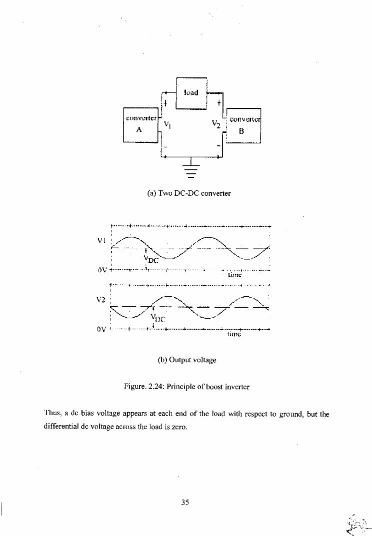
(a) Two DC-DC converter
t ~--.~,.t-~.~....•,..",..~..t' •.••..••.•4._..•_-_.•.~•...-_.•._._.----r"'- ---+-- ..•.,
VI ~~~_. _/~ ..... /; V
OC...--./ .....~.~ --'-~_..- :
,O\t + .. ----.-r------'!+------.'f--.---.'f .........• -...- ... -~. , ... f .•••..•••••••
LinH:
i .' ,.~ ".<-",. +- "'!- •• " .••.• ~ •••••• -•••.•.••• -- +- -'.•..__...•.
\'2~-.-~~-7~': '---_/ \'nc --------'
o \,r ~ .•. , '.. +--_. ----f.--(: .. -i-------.+---._ •.•• ---- --..•.---- --+--..__+•...•. time
(b) Output voltage
Figure. 2.24: Principle of boost inverter
Thus, a dc bias voltage appears at each end of the load with respect to ground, but the
differential dc voltage across the load is zero.
35.,
i!"'c,-

2.10. Boost Inverter Circuit:
Each converter is a current bidirectional boost converter as shown in Figure. 2.25a. The
boost inverter consists of two boost converters as shown in Figure. 2.25b. The output of
the inverter can be controlled by one of the two methods: (I) use a duty cycle D for
converter A and a duty cycle of (1- D) for converter B or (2) use a differential duty
cycle for each converter such that each converter produces a dc-biased sine wave output.
The second method is preferred and it uses controllers A and B to make the capacitor
voltage VI and v, follow a sinusoidal reference voltage.
Vin
+
C V1
(a) The current bi-directional boost converter
R
01 + Vo. D3
C2 V2ClVI 11 l2
02S2 04
64
(b) The proposed DC-AC boost converter
Figure. 2.25: The proposed Boost Inverter
36

2.10.1. Circuit Operatiou:
The operation of the Inverter can be explained by considering one converter A only as
shown in Figure. 2.26. There are two modes of operation: mode I and mode 2.
R
82 + Vo+
02
1 C V1 +V2
Yin81 01
Figure. 2.26: Equivalent circuit for the boost inverter
Mode 1: When the switch S] is closed and S2 is open as shown in Figure. 2.27a,current
ill rises quite linearly, diode D2 is reverse polarized, capacitor C] supplies energy to the
output stage, and voltage V] decreases.
Mode 2: When switch S] is open and S2 is closed ,as shown in Figure. 2.27b,current ill
flows through capacitor and the output stage. The current ill decreases while capacitor
C I is recharged.
Ra L1
V1
R1
+ Vo.
V2
Figure. 2.27a: Mode I: Sl is closed and S2 IS open
37

Ra L1
C1 V1
R1
+ Vo-
V2
Figure. 2.27b : Mode 2: Sl is open and S2 is closed
The average output of converter A, which operates under the boost mode, can be
found from
At mode I:
At mode 2:
From the above two equations,
=> V,." TON + Vl.l TO!'F = 0=> v,JON + (V" - 1'" )T;m' = 0=> ~'IIT()N + ~'IITOFF = V;)TOFF=> v,J = Vo(T -TON)
Vo. T=>-=---
1'" T - TONVo D=>-=--
1'" 1-D
So, V, 1 .- = -- (lV)VI" 1-D
The average output of converter B , assuming which operates 180 degree out of phase,
can be found from
V, 1- = _ (v)1'," D
38

Therefore, the average output voltage is given by
V V. V. v'n v,,, (.),,= 1- 2 = I-D -D VI
This gives the dc gain of the boost inverter as
where D is the duty cycle. It should be noted that va becomes zero at D=0.5. If the duty
cycle D is varied around the quiescent point of 50% duty cycle, there is an ac voltage
across the load. Because the output voltage in equation in (iii) is twice the sinusoidal
component of converter A, the peak output voltage equals to
V =2V =2V. -2V (viii)n(pk) m I de
Because a boost converter cannot produce an output voltage lower than the input voltage,
the dc component must satisfy the condition
Which implies there are many possible values of Vdc• However, the equal term produces
the least stress on the devices. From the equation (iv), (vii) and (viii), we get
V = 2V,n _2(V"{Pk)+V)o(pk) 1- D 2 In
Which gives the ac voltage gain is
G = v,,{Pk) = Dac V;n I-D
Thus, V,,{pk) becomes v'n at D=0.5.
39

Chapter 3
Simulation and Experimental results
3.1. SystemDescription
New residential scale photo voltaic CPV) arrays are commonly connected to the grid by a
single dc-ac inverter connected to a series string of pv panels, or many small dc-ac
inverters which connect one or two panels directly to the ac grid.
Buck, boost, buck-boost, and Clik converters are considered as possible dc-dc converters
that can be cascaded. ORCAD Capture 9.1 simulations are used here for conversion.
The, conversion structure from solar sell to home is shown in the Figure. 3.1. It consists of
the cascade connection of two stages. The first stage is a boost-regulator and the second
stage is the boost inverter. A solar cell can charge a battery up to 12 V de. Using boost
regulator is the first stage where output de voltage is almost 50 V de. This output is the
input of the second stage of the boost inverter. Here, the output is 230 V ac , pure
sinusoidal. Then this voltage is applied to home.
Boost BorneBoost Ae•Solar cell 12VRegulator Application
Inverter
Figure. 3.1: Conversion of solar cell to home application
40
/
.,

Here, a solar cell charges a battery up to 12 V dc. Then a boost regulator is used. It boost
up the 12 V to 48 V. This is the input of the boost inverter. Its output across resistive load
is 230 V ac. This is then applied to home.
3.2. The Circuit Description For The Proposed Boost Inverter
The boost dc-ac converter is shown in Figure.3.2. It includes dc supply voltage V;n, input
inductors LJ, Lz and L3• power switches 81 - 85, transfer capacitors CI - C3, free-
wheeling diodes DI-D5 and load resistance R .The principal purpose of the controllers A
and B is to make the capacitor voltages VI and V2 follow as faithfully as possible a
sinusoidal reference. The operation of the boost inverter is better understood through the
current bidirectional boost dc-dc converter shown in Figure. 2.8. In the description of the
converter operation, we assume that all the components are ideal and that the converter
operates in a continuous conduction mode. Figure. 2.9 shows two topological modes for
a period of operation.
3.2.1. Control Design Methodology
In the design of the converter, the following are assumed:
.:. ideal power switches;
.:. power supply free of sinusoidal ripple;
.:. converter operating at high-switching frequency.
3.2.2. Selection of Control Parameters
Once the boost inverter parameters are selected, inductances LJ, L2 and L3 are designed
from specified input and output current ripples, capacitors CI - C3 are designed so as to
limit the output voltage ripple in the case of fast and large load variations, and maximum
switching frequency is selected from the converter ratings and switch type.
41

3.3 Simulation and Experiment
3.3.1. The simulation and Experimental results
Frequency, f=50Hz.
R= 250 ohm
Vin = 12 Vdc
VO"' = 226 Vac
S, - S5 : switches;
D,-Ds : DINI 190(diodes);
C, -C2- C3 : 400uF
L,_ L2-L3 : 10 mH
R1
VOFF = 2VVON = 3V
53
C2
-=-0 s
VOFF '" 2VVON = 3V
54
L3
D7D5
L2
06 06
D12
~o
C1
VonD1N1190
V1 =-1V2 = 1TO '" 0TR =. 01mTF ::: .001mPER = .25m
PW=.1m
OFF = 2.0V1 ON = 3.0
D11
~o
C3
Figure. 3.2: Boost Inverter with ideal switches
42
•,

SI
« [« Rvee:l~ vee 1111
ISV U4AVI'IO USA
~'.10 Rl 8C= m '0.0 TR' 248ms1111V3 TF' OOlms= 1
lSV PW;.OOlms.O
~
PER' .15msVl0
VOFF'O 'VVM\?l' 7 .FREQ' 50
"'0 vee0Figure. 3.3: Control circuit
16U
-16UOs 2as ~RS,U(UlA:') • U(UlA:-)
6115 80S 111115 12115 16115 18115 261lS
HoeFigure. 3.4a: Pulse Width Modulation signal
43

.~.26U
.......... --
............ ..•. -- -----
•• "'r-- --- -"f" ••••• t •••••••
........, ; ..,...: . • •••••••• '1 ••••• •• ••• f •• •• -t •••••
..,... ..
..{_.. ..-2OU
us 20s, U(UIIA:OUT)
40s 60s 80s IOns 120s 140s 160s 181'5 21lns
Figure. 3.4b: Pulse width maculated signal
2. Oms
IiIII II
-H+I I II I
I I I
-*I,
l.ams
I I II I I
++ II I I
I I I-+: :I II
1.6ms
I I III
1. 4ms
I '
. LJ1-FTiU-1" -III I I I I
1.2m5
I~I I..LI II
I I II I I
-H .I-~I II II I
1.Orns
I II I
II I I
o .8m"
'II I
O.6ms
-H~-+-~ I II I -1-LLII I I I I
20VI II II II -I
lOY I II
'Ii .-LI III
ifov I I I
! I -1-LL -1-1 i- J-l I I-j-lJ--1++- I I LL -1 I I
-lOV + 1 tf-;. I
.:E. Ilr _:r-LLL -1-1-1_-+ I I
.20v I IT I I I I I IOs O.2ms O.4m3
• VIR2:1I • V(U1A:OUTITime
Figure. 3.5: Output wave shapes ofS I and S2
44

" ,-_ ~................•...•.... , ." '"... ;--_.~---; .._. -_.-'- -_: __ ._~-_. _._-~ .._~-_._~....
••• , •••• , ••••••••••••••••••••••••••••••••• ' ••• 4 ••••••••
•••• __ ••••••••••••• __ ••••••• C ••• " ••••••••
, ,
300U
200U
100U
OU
.........•. __ ..__ .
, ,
•....•....~.......•.......•.... '........•
" ," ,..•....•... ~ ....•, " ,
" ,
.. ..........•....---~_...•.. _.
_.~- .. ,._.-.- .:- - .-~....
.... , ...'. __ .'.__ .
• 1 ' ••• 1
.~~~.... . ..: ...:....; ...~ ~~.... ...'. ..•....' ...~~~.......~..: : .
...~~~ -: : ~.
..~....~....... -'~"",'--'...~..~....~....
, , ,...~..~....~....
...•...... __ .•.._-
...•.........•....• _.'. l. '. _
..~_ ..~- - -~.-_ •• __ .C J _
•••• •• ~ ••• J ••••
••• ~ ••• ~ ••• J ••••
• ••••••••• 1 ••••••, , ,---_ .._-_._-_ .•....
..__ .•.. __ .. _--
, ,'-:'_-l- __L---~ --:-._.~-_.• •• ' •••••••• C •••
• ••• ' ••• , ••• C •••
, '. '" '"... ~.... ~... ~......•. ;.... t .... ;•....... ~.•. ~.... ~.•..... : .... ~... ~-.... - .. :.... ~.. -.~ ..., ,. , , .,' " .. .. :-.-.t : : : ':"" t .. ';' "-:' .-. --. :" .-t 1 t .. ':." .: .
...~~~ ~ :.-..~ - ~~ ~......~ ~~ : ~~., ,. '" .,' '" '"••• ~••.. ~.•. ~.- -.: t ~ -~ .. J ••• , •••••• : •• -.~.-.~- ••••••• :•••• : •••• ~ •••
, " '"
41Jms
••• J •••• L ••• '••••
••• J •••• L •••• ' ••••
••• J •••• L •••• ' ••••
-100UOs• U(C2:2)
, , ,....~~ ~... ..~~~.....~~~.....~~ ~.
, , ,
•••••••• J •••• , ••••
....•.... '....•....
....~ ; : .
.... : : ; .
60Pl5 80ilS
Tillie
1001115 1281115 140ilS 160ms
Figure. 3.6: Output voltage across C2
161Jm51200510005S005
Ii",
600540ilS
U : : , , , , , , , , , ,,.... ._ ..•............. ....•.........• ._ .. ..-•....•........ .........•......... ...•....•..... .........•...: ' , , , , , , , , ,, , , , , , , , , , , , , ,...•....• .. '.... ....•..... _ ..•... _ ...•.........• .... .........•...•.... ....~...•......... ....•...•....•... ........~.. _ . _ ........•... .~..., , , , , , ,, , , , , , , , , , , , , , , , , , ,.. .... ._ ..~........•... ....•........ _. ........•........ .........•......... ..._~....•....•.... ........•.... .........•..., , , , , , : : A: ....~...j..~ ... ' , , , ,' , , ... + ... ;..rt ...... ... ....•............ ....•.........• .........•.... - ._ .. .........•.., ,
U' , , , , , , , , , , ,
: , ..1... : : : ,.~.... ....: ... ....~...~.-.,' .. ....l...~. .: ... ...~....~..~... ....;....~. .... l. .. J • ..~... ••• t •••• ~ .: ... .... ~ ••• t • .. ..., , ,
••• J •••• ....: ... ....~...~...~.. .... :....;. ..: ... ••• J •••• L ... .. •••• '•••• 1 ...•. .. •••• c ••• J • .., ... ...:....~..~.. ....:.._.~.., .., , , , ,, , , , , ,...~....~...~.
, , , , ,...~... ,L•• _.L .. ••• ',c ••• ~. ",'. ....l...~..: .. .. ..•. ~... t ... ~ .. ....~...~... l • •• t •••• ~ ..~. .. •••• C ••• I .._~.., ,, , , , ,...~... ~....:. .. .. ..~...~..~. ....:..... ...:. .. • •• J ••••••• J. .. ....:....~...:. .. •••• ~••• J ...~... ...:.... ...~. .. • ••• ;•••• 1 •• _L, ,, ,, , , , , ,
....~..-i-.-+. ' ,••• J. .. -..._. ....... ........ ....... ...•... ..
I;l+"' , , , , , : : , , , , ,, , , , , , , , ,....•... ....... LV......._ ..•.. .•....... ........ •........ ...v....:..I/:"':" ........•...., ,
....:..~....:... ' , :/:' , .::;.;... ,, , , :y' , ....~..:....:... ' , ,....•..•........ ...;... :'.'!'" ._._.- .~....•.., , ..y ....;... ' , , ....~..L...~... : : : ,, , , , , ,.•........ ......~........ .... ...•....... ... ..•....•.. .... ...•....... ............., , , , , , ,, ,: : : , , , , , , : : , ,, , , , , , , , , , , , , , ,...~....~....:. .. ..~...~....~... _ ...:.... :....:.... ...~....~...~.... ..-.:....~....:.... •••• c •• _J •••• L••• ...:....~...~.... ._.~._..:....~..., , ,, , , , , , , , , , ,...~....~....:.... •••• C ••• I •••• L. __ ....:....;....:.... ...~....~...~.... ....:....:....~..- ....~...~....~... ..-:-...~...~ ....:....:....~..., , ,, , , , , , , , , , , , , , , , ,...~....~....~... ....~...~....~_ .. ._ ..:...~....:.... _ ..~._..~...~.... ....:....:....;.... ....~...~....~... ...:._ ..~...~ ....;....:....~..., , , , , , , , , , ,...~.... ,' .. '. :.... ....~...~....~... _._.: ....:....:.... ...~.._.~- ..~.... ....:....:....~... ....~...~....~... ....:..._~-..~...- ....~...:....~..., , , , , , , , , , ,
OU
300
100U
-100UOs 20",• U(C1 :1)
Figure. 3.7: Output voltage across Cl
45

300U
__ ::: ::: , --ii ::: : : :--- ._- ...-._--
....•.... -_ ...•.. _-: :
160m,140ms1211llls1lHlll1s801'15601115401115
~: ' ,-- -- - ----.-- --- --- --;.;--- ----- ' --~- --ri--- -fl --- -t\:--- -ri--- --ri----rt--('i:---A n ~ : : :~'
••• J.. .' __• .c. _.J •• _ L •• , __ .'. _ ••••• J ••• ~ __ ~ .' •• __ __ _ _ _ __ ~_ •• L •• __ •• .J _. _ _.' ~ , _
_.J. .' .'._.J __~ ...•..•... '. __, .J __.~ __~ ••• __: I _.J. __ _•• __~__ ••••••• : ••• L •• ~ ••••• '•••• __.L ••
:::f!2- :::::\~:::;::;: ::::;:~-:: : -::::::~-::;::-:::~:::-:::;--:::;-::::;: -::;::'-::;:::-:::;:r:;-Jp:::[: -::[:-:/_ ' , ----,----'--- - viz::: 1/- ;---)-::j::::j.- --J- :--j- ---/-1--)- --j-r-Y- --Y- i-oj
ou , , , , , , , , ,_•• J._ •• L •• __ '. C J L •• _ ••••• ' ••••••• J .L __ .'. , • L • __ c J .L ••••••• L ••• I •••••••• ' •••• I •••• L •••
, , , , , , , " '" .,'• -- J. < .'. _ •• __ • _}_ •• ~ •• __ ~ • I '. __••• __• ~•••• ~••• ~_.__ ----:----l'-' ~_. ~ ~----;___ ___,. __.L J __ • ; : :•• _
• __ J •• _. , , ~ ~ ~_._ •••• ~ ••• _~ ; ~----."-. _~ • ._ •• ~ •• _~ :•• _. _. __ ~ __ • ~ __ ._~... • •• ~ •••• ~ ••• ~_ ••••••• ~_._~ •••• ~ •••
-- -~-- --~----:- --. - ~•.. ~ ~..• -.•. ~.. -~-- --l --- - . -.;.- .. ~•.. ~ :.•.. l ..•. ~ ..•.•.• ~.•. ~...• ~... . ..••. _.•. J -- --; ---;-- .-;---
200U
10lU
-100UOs 201115
• U(C2:2) • U(Cl:l)Tine
Figure_ 3.8: Output voltage across both c I and c2
16iJ11s140""
" ,..... _-- .._-~--_ ...............•...,, " '"---1-- --r---,- - , ' r---, " '", " ."
---~----~---_._--- .... '.... !.... ~...
120.5100.580.560.540""
200U-,
40011
"" , I ,
, " ,,' ,'" I" '" "--.T - • ..,..••• , •••••••• -c---.- ... ","'" .. T••••••••• _or --'--"T'" •• , •••••••• ---- -- -.T ••••••••
I 'I I" ,'I I '" I I I ",
I I, " "I I" ,'" ,,' 'I I '"
.;~\:-IIff-!TIITjltrII!- :rrrI':j.I , " :,: :': : : :: I ; : : : : ;
••••••••• , - __ •••••••••••• J , __ •••••••• • •• J ._.J ••••••• J. ,•.•.•_.__ •••••• • •••••••• .._ ••••••• J... ... J. •••.•.••••••••••.•••
'I I I I '" '" " I , I I I I I ,
'I '., I I I I" " I I " I I I, I I I
I ' " " " I 'I I ,I " I, I '" I I ,'---,-.--r- - ,-'" "--c---,. -- -'.'f'- •..,..--, -.- -••,••--, --. -- ---,-,-"'T ••••••• ---r---,- --, - .•..•••. -c --, --- ---..,..•.• T••••••• -, , , " I • " I I '" '" '"
, , , I I '" I' " " I '" '"
-20011 : : ::::,: :' :: :: : :I " '" '" " I" I I I I '"
I " I" " I '" .1" ", '" '"~ ••• J •••• ,. , ••••••••• J. , ••••••••••••• _J •••••••••••• ••••• _ ••••••••••••••••••••• • _ •••••••••••••••• _. •••••••••••••••••••
, " ", ", '., ,'" '" '" '"" '" " I '" ,'I' '" " I " I
~••• ~.••• ; •• -.~ -- .•••• ~ ••• ~•• -- ~- -- - - •• : ••• ~.••• : •• -- --.~ •••• ~ ••• ~•• - - - -.;.1. •• -: •••• ~ ••••••• ~••• ~- •• -:... • •• : •••• ~ ••• ~••• .~ ••• ; •••• ~•••, " '" 'I I 'I I ,I' I " I " I '"I " .,' '" I " ,I I I '" '" I I ,
t.--~---. ~- : -.~---~---.~ --.;--- ~---.~....•.. ~ ~--.~.•....• :.: ; ~.-- .. -.~._-~...• ; .•..•.• ~ ~__.~•.....• .;.•.• ;.•__~---• " " I • " I I I I' " '" '" " I, " '" '" I I I " " " I 'I I I I I-400U
Os 20""::,:U(C2:2,S2:3)
ii••Figure_ 3.9: Output voltage at load 250 Ohm, time t=84_I ms, Vout= 226 Vac
46

2.0A
L... . ..•. _.'.. • ••. •...
~.--~--- ... --- .,-- .. ---
. '._-- ._- ---- -..--- --..'---- -- .... ---- ...
~---
1601lls140••12011151001lls8f1ms6011'15401lls
, ",, '". " ",~ ~----~ -:---- ~._-~ ;--- - _- ---, '" "~---~... _~---+. - --- ~-._~----; ...
, " ", " " ",
, " '" '"r ••• :----; .••• :---- •••• :---t ..;-----..!----; ...I " '" "
1.0A
-1.00Os 21J11ls:ii: - J (R1)
Figure. 3.10: Current for Rload= 250 Ohm, At time t= 83.67m, 0.9 A
160msHOrns120mslOOmsBOrns60ms
v , ,i
i ;
f' .(;1;,
v ( ~ (
.. ':'. I I II I if I -:/- ' / I II '/. - ... --.. t-. .__ . -.--_. - L 1/ - ..- - ---. +.. ._--. _. -- ./--- .-J - ..
v JJ, V /, .A j :J j
\._- -._-- ,
-- , .. - . -.,.\ -.._-
\--, ... -_.,. ----
v \ \C ,
",, i i
v, , , , ,
'00
200
-400
Os 20ms 4Omsv V(C2:21 6 V(Cl:1) 0 V(Rl:2,R1;1)
-200
Time
Figure. 3.11: Combined output voltage across C2,CI and for load 250 Ohm
47

3.3.1.1. Variation of output with load 150 and 500 ohm:
161lm,
: - :-
........, ...•• :•.. f ..•• ; •.
140""
, , ,......_.~...•..... _ ...•....•.........
, " ,.,.-., ••••••••• , •••• """""""r'", , ,, , ,...; ; ; ;.- ..; : .
, " ",, " '"
120.,
.,.... ,....
":""f'"
; -: -....;..o
100.,
.~~...:....~...:: : :..,~ ." , ," , ,..~.:..+...:...:: : :-'; - :- :-..,.~..
" , ,..:t ..;....:" " ",.., , , _, .:: ;: :::..~.:....!....;....-.";'....i- .. ':'":: " '"
BO/lls
..., ,.
60/lls
.- ~-:--- -; _. --~- -- _ .. -.---~._ .. t___ ---. __ . _. , .... ..•.. _. t_. __• _
" I ,
- ---, ".- -,--- -, _.- --- j" --"r -. -j--,8 -:~~1'~-~2iJ'i-5ij1)-_.~._.~---or .... -- "j" "'r-- "1-- -- .. --,----'" "-r---
- - ;----:--..!..----+ ...:-.-+ ... --~-:-.. 1----:---- ----:----.; .. --f---- •• +---;---+--- ----:-.. +---;- ....•• ~•• _~---- ••• ~----~ ••• , •• _. -- r"'~----~'" --- ' •••• :._--; .••••• ~---.~ ••• ; •• r---,""""
"", ... ,. '.r".,""
.... ;... :.... f... ...~.. ...1••.
....•.........•.... ........•........, ,,', '", ,,'
""""~"", •••• """'.r"',""
•••• ; •... :•••• ;.- ..••• ~.. -.: •••• 1••••
..............•...""r"',"", •••
••• • :-•.. ~•••• f •..
.... ,.... ,.... ,....
~.......•....~...~~....~ : .
r :-.. -; ; .
-.._,._._, ..._,_.
'f\" :... i..), , ,
ou' -; -\; - :~--- ~---- ---~-_.I : :"._-,----, .. ----l.'--:--"H- :----, ,
400U
-.----.- -- ...---,--- ..-------r--.'-.--'".-
;.-.-:----~----:---- ... +--;----f---200U .--- --,-'-', roo •••• -r"' .~•• -"""
,----.--- .... _ .•..-
-200U
-~OOUos 20"":~:U(R1:2.R1:1)
TilrteFigure. 3,12: Vout = 220.51 V ac at time, t=83.67 ms, Rload=150 ohm
160'5140""120.5100""80.,60.,40.,20.,
, I : : : : : : : : : : , 0 , , 0 ,.....•....,....~... .- ..•...•....•... "ji,!"'7"':'" ...~....:...~"l3'.Ml.:h~,r~0....•....•....•- ... ...•....•.....- ... • •• ..L ••••••••• _ ••' , , , , , , , , , , ,," , , , , , , , ,•••••••••••••• ..L._. ....•.._ •....•... .. •.........•.... .........•......... ..•.... ..•....•... •• _.c •••.•••• _••••• ...•....•......... • ••• L ••••••••••••' , , , , , , , 0 o , 0 , •...~._ ..~... .~ ....~...;.... l(:L:~::::n~..;....~...•••• ..L ••••••• _•••• ..._,_ ........•... .. ....•...,.... ••• ..L ••• , •••• ~ ••• ..~ ••• ~ •••• ; •••• ,L ••• ....•..- ......- .. .. ••• ..L •••••••• /i...:...~...... '.........•... .. •.........•.... . .....•....,._.
'\~"'!""f ...' , o , , 0 , 0' , ,
0 , ,. -',~...~....:.... -.~...~_..~.... ' 0(...:-- ..:....:..... ... • •• ..L •••••••• .. ...•......... ...•....•... .....•....•..., 0 , 0 0 : ' , , , ,, ,
, , 0 o , , o , ,0-0 : 0 0 : " 0 : : 0 0 0I o , 0 0 0 " o , 0 0 , 0 o , ,....~....~....;.. ... ...{....~_.. ... • ...;._ ..}.... ...~...~...~.... ..'.'. ":"",1. ... .... ..~.... :.-.. ••• J • ..~...~.... . ... :.•. t •. -.~ ..."L..~.•..~....:.o , 0 o , " o , , 0 0 , ,.. .... ...~....~-.. ... • ...;....~.... ...~.• ',1. ••• ~ •••• ...•.'. ..~ •••••l .•• "'_,L. .~....:... ....~. ..~...~.... ....:...:-...~...: "A" , 0 , , ,
" , 0 , , , , 0 ,r'" " ..~.... :. . ....~..~....~.. •••• 1- ..:....:... ...~.. .~...~... •• J.' •. .:....~.. ••• _L. .~....~... ...~. ..~...~... - ..-:- ..:....~.."... J._ .~ .... :... 0 , 00 " , , , , o , , , ,....~. . ~.•.. t .. ....:. • .0•••• 1••• ...~.. .~...~... • _J.' •• .:-...~.. ... .~.~....:.. ...~.. .~...~... ....;.- .~....~..f : : ; ", ,
" , , , ,-'1 - ~ 7 -: -: : - :- 7 - -' - - c -: : -: - - ;- c 7 - : ' , -" 0 -, , , ,"
, ,L ••• ; •••• "";'" ._ .•••• J..•••• ....... .......•.. ........ .....•.. ..•..•... .....•. ......... •....... • •• ..L ••••••• , •' \: ' 0 " , 0 0 , 0 , , , 0 ,
" 0 , ,r ... ; .... ,.- .. , ... ....~..l..~ .......... ........ •....... ..•..... .....•- .._ ..•. ._ ...........•., , " , 0 : o , , , ," 0 , ,_ .._ ............ ....•._- ...• .. ........ ....•. .. ......... .. ..,.'.... ....•... .. .. • ••• L ••••••• LI : :
o , ,0
" 0 0 , , ,o , 0 0 0 0 " 0 , ,...t..;"f' ... -...._ ...... .. ....•..... .. ...•.... . _.J. .. • •• ..L ••• .. .. .. .''-;--''If-'-'; .., , : : " : : , :o , , ," , 0 , 0 ,
, '\{: ' '\.I ' , ,
...j....~V" " , ,
..).) V'" ' , 0
.. ..j. ... ;.V~..' , , o , ....:...Ld... t' , ,r .•• ~...• ~•••..•...-. ._ ..~...~._..~... _.J.' ••.. I_ ••••• ...~....~~.~..." ,o , , , 0 , o 0 o , " , , , ...~...+.~.... o 0• ••• J •••• ~ •••• '_ ••• ..-.~...~._ ..~... ....;...~... ,'." .._~....~..,"" ..~.:.... :..v, ... ....~...~..,'" ....:....:.. ,'-'I : : ' , , , , , , " , , , , 0 , 0 ,....~....~.-..:.... ....~...~....~... .... :....;._ ..:.... ...~....~...~.... • •• -' •••• 1 •••• 1. ••• .._.~...~_...:.... ...~....~...~.... ....~...:....~..." , ,L ..~....~...~....
' , , " , , , , , , , ,.._.~...~.._.~... .... :._ ..:....~.... ...~....~.._~.... • •••• '._ •• J ••••••• _ •••• ,L••• ~•••• : •••• ...~....~_..~.... ....:....:....~..." , ,, , , , 0 , , , 0 " , , o , 0 , , , , 0 ,,
00
2.00
-1.00
-2.00os::;:-I(Rl)
Ti.~Figure. 3.13: Current for Rload= 150 Ohm, at time t= 83.67m, 1.47 A
48

160ms140"120.s100"80ns600s40ms
400U, '::: ; ::': ::;: :
i"'~'-'-:-"': ... -...•._-•....•--- ....•----,....•---....•. _--•...•._---..;:._--:....~----...~._-~----:... --..•..._. ~.... __..•...• •..., , , ,'I ,,' I , ,
i"" , ... -r -- _.,•••. - -_.~ _•• j -..• ~._. --.. ;. ---:.-.. ;.... -._~•.. _~-_.~.. { 4-.ihM;228~.22 T--~... ~.---!...._.-j •••• ~-- -i- ... _.--~... !..--~_..;:::i:::L::,~::::::L:!:::L: -~::::L:L: :::LL:L: ::~-_::L:~:::::):::~~:::!::::::~::++::::~:::i:):::
2OOU-, ; : !_ f.\ : : --il--;--:----I) _, ,+ Il-l __; ;____:--f---T--- __~ __; ; _I : : : ••. _\ " " I' ;: : 'I " "}\i::r -:::::::;::::;::::::;:;::::;:::::;:_:;:::;:::::;::_-:;::::;::::::;:_-;::::;::::::;:_-:;:::;:::-::::_-:;::::;:::
ou~"-i y! -,~.;__: -i:-!- ": _: -::- '- ~ -i' _:- -:- ~; -:- -i-
~:::;::::(\::/:-:-:::-i::C;-:: :::-::<:::::-:: :::;:::::--:::: :: :::t::i\::r- ::::::::;--::;---:::;:::::--::;-:: ::::::::i~::;---: : \) :: :: :: :: \ : : \ : :: \ :-200U
, ,~ \!:: ,,,! \!: "! :: \!~- •• '--"' t ,__ •• t_ ••• __ •• t __ • ••••••••• ••• _ •• _.~ ••••••••••••• __ •• ~,. ,_ •• _. _ •• •••••• _ •••• _ •• __ •••••••• __ •••••• _ ••••••••• _ ••• ~ •••
"I' • , I ••I , I " , I I " 'I'~ ••• , •••• r •••• ,••••••• 'T ••• ' •• ' .r." •••. T••••••••• T••••••• , •• "r' •• , ••••••• r' •••• T'.'.r' •••••• r ••• , •••• T•• ' •••• , •••• r" ., ••••••••••••• , •••• T' ••
, I I '" II I, I I '"I I , , I " 'I " I
r :•••• ,~..•• :••...••• ;.•.• ~•••• ; ..•••• ,1 : '1 : : ;..•.... ~;'.. '1' .•. ~...•.•. f .••• ;•••• 1..•.•.• ~ ;.••. ~.....•.. :•.•. t .•.• ; .I" , I I 'I I
" , " I" 'I I-400UOs 21lins:;:: U(S3: 3 ,52: 3)
Tilile
Figure_ 3.14: Vout = 228 V ac at time, t=84 ms, Rload=500 ohm
161lins
, , ,....~..:....~..., ,
140"
,• .. t ••• ~.•• ~•••
120ns100.s
, " '".••• :••. t •••• ;....•••• ,".. ~•... ~.••, , ,
RO"
...~.. ',' ...~...
60.s41lms
, ,...•...,....•..., , ,, , ,, , ,....•........,..., , ,, , ,
20"
" ,...•....,....'........•... ,....,... ........•... ......,....•.................., " , I I I I
I I I I •
'I "........•.. ............•.• I, • I
, " ", " '"........•.. , .. .........• ..•.., " ,,'" " " '"' """",.,"',.,"...•...., ....•.... .. ....•... ..........•....... ,. .. ....•. . ....•... ...,......•.......,.................•..
I " '" , , , • , I , I , I , ,
' , """,.".,'' , I I, , , , , , , , , I ,
•••• ,"..• ,•••. } ••..•• t •. ~...• t ~...•.. ~ ,l •• , •••• :••••••• ~ ••• ,•••• ~•••• '.f.' ~ ; , ~., " ,,' , , '" '" , . '"
" " " " 'I, , , '"
...~....~....:..
...•....,....'.., ,.........,....,....
" . , ,' , " '" ,,' '" ". '" '"••. , •••• ' •••• '••.••••• l ••••.••• , ••.••••••.•••..••••••••••• J ••••••••••••••••••••••••••••••••••••• l ••••..•••••..•••••..••••• , ••••••.•••••••..•• l •••
I " 'I, ", "I ", 'I, '" '"
" ,."""""""""" "'. I. '" '" ,,' '" '"••• J •••• L•••• '•••••••• l ••• l •••• L••••••• 1••• .' •••• 1••••••• J •••• l ••• l ••••••••••••• I •••• l ••••••• l ••• J •••• L•••••••• l •••• l ••• l ••••••••••••• I •••• l •••' " 'I, '" 'I. '" '" ,., ."' " , , '" , , '" ." '" '"' " '" '" '" ", '" '" '"••• J •••• L•••• '•••••••• l ••• J •••••••••••• 1••••••••• 1••••••• J •••• l ••• J •••••••• '•••• 1••••••••••••• l ••• J•••• L••••••• t •••• l ••• l ••••••••••••• 1•••••••••' " '" '" '" '" '" '" '"' " '" .. , '" '" '" ", '"' " '" '" '" '" '" '" '"•.. ~•••• ~.••• :••..•••• } ••• ~••.• ~••..••• t ••.• :•••• t ..••••. ~.•• ',' ... ~.••••••• :••.. : ••• ~..••••.. } .•• ~••.. ~•••••.• t •••• } .•• ~•••.•••• :•..• : •••• } •••
, '" '" , , I" '" ", '"' " '" " " '" '" ",
O.SA
-O.OA
-O.SA
-l.OAOs, I(Rl)
Ii.,Figure. 3.15: Current for Rload= '500 Ohm, at time t= 83_67m, 0.45 A
49

Table: 3.1 Output Power at various load
RIoad (ohm) Vout (volt) Pout (watt)
100 216 471
150 220.51 324.15
200 226 258
250 228 210
500 230 102.6
o -----------.~--~----~--~ ---~--~--~-~500250200
load (ohm)
150100
19.4 I19.219
18.8.: 18.6>:; 18.4~ 18.2
1817.8 .17.617.4
500250200
load (ohm)
150100
600
500
100
£400o::- 300"o> 200
Figure. 3.16: Output voltage at various load, Figure.3.!7 : voltage gain at various load
3.3.2. Efficiency of conversion
It is the ratio of ae output power to the de input power.. p
Efficiency = -'!".!.. *!00%~"
,.'So

3.3.3. Simulation results with practical switches
3.3.3.l.The simulation and experimental results
Frequency, f=50Hz.
R : 300 ohm
Vi" : 12 Vdc
VOUI : 228 Vac
S] - S5 : APT45G J OOBN,practical switches ( igbt) ;
D]-D5 : DINIl90(diodes);
C] -C2 : 265 uF
C) : 280uF
L]_L2 : 10mH
L) : 1 mH
Pout : 173 Watt
Pin : 178 Watt
Efficiency: 97.19 %

200RIll
.Olu O1u
20:5u
10mH 10mH205u
VI=O rIII = 10 VJ
TO = 0 •TR = 0.001mpw= 0.085mTF = .001m
PER=0.1m
12V
gate 1((
R'---'0/1,I .001
.:l-1m
.01u
C2• f
co 280u
f.01
gnd2
01u
~o
Rll
1meg
Figure. 3.18: Boost Inverter using practical switches
52
••

"'" "10\&.J:- VI
o "00'
R"
"
"" <gndl
<gnd2
<g3l~2
Rg R8
5k 5k03
'00'R7
'"
o
o
TUl94
VI = 10
o
V1 = .10
i::~"mJTf •. 001msPW= 001msPER: .2~ms
o
Figure. 3.19: Control circuit
53

1801llS 20lhrls"""140ns128F1SBOns60llls
u.. .. .. ... .. .. .. ...:.. .. ... .. .. .. ... •• J. .:--- ... ------ ". .. .. ... .. .. ---:'.+'-f-- .. L • - ..: ..
.. .. .. ... .. .. ... .. .. .. .. ... ... .. ... .. .. .. '1~6:2~m.22t: 091"".. .. .. .. ... .. .. .. .. .~-- .. ... .. .. ... .. ... _-- ... .. .. ... .. ii'!!.I"k\" .. ;. : ' \: :._,- .. "-r-- _.-t---r'-,-" .. .. .. .. ._, ... .. ---,--- .. ... ... .. .. .. .. ..,-- .. ... ... '--,------:... •• 'C" ~:.!i ... ---:'--f-- .. "'1-- ... .. --1" ... .. j--- .. .. ... .. ... .. --1" .. -+-+- ... ... ...:..__ J ••• 'fj ._~ __ J __ ... •• .L _.t_ .., ... .. .. .. ... .. ---' .L •• '. ---{ ..r.- ,\ :..,A( ,,: : ..+.: .. : ...!) :---t- -r--, .. .. "Of_ .. .y.... .. .. .. .i...~.. ...--: •• -1- .• :..• ':lL ::t\1 ... :-- I- .. . ! .. .. :;r,... .. .. ... .. .. .. ... -_.'.- .. .. --+- .. .._.J ••• ' ••• ,._ ._.~.._~ ~--- --~._- .. .. _.. t. .. ... .. .. -_.,-- ... ... --.'... .. - --~_.- ..
: .\ !' ' , , .\: : : : : : : : : : : : : v: , ,v, : ,V, : ,V: : ,": :v'-- •....._-~-- --- ..-.~.... _- ---.--.-.-,--- --.---0--- •.. ..- .._~---.--- -- .•..-....... --.-_ ..---..... ....._---.-_. -- .......•...•.. --.---.--~.-.: : : : : : : :
--'---'---r'. ---,---r--,-" ."r--,---,-.' "Y--f---r-- ._-"", ...,--- ---,._-,---, ... '.,._.,---,--- --'r"',""." "'r .. , •.• t •• ••• , ••• t ••• ""
'--:-"1"':' .. ..-f-.+ ..;... "':"'.:"-l- .. .+..1.• + . ... f"':"'1". .. .i. "~ ... f ... •• { •. -f ... ;..• ..+..:._.{... ...:...~...~.. ..{ ... f ... :.••:
ou
4"
201lU
-400UOs 21Jr.ls 40msII U(R111:2.R111:1)
-200U
Timl.'
Figure. 3.20: Vout = 228 V ac at Rload=300 ohm
1B01JIs 20lbrJs160llls111lbrJs12 Oms10""8""6 OlliS40l'S
A: t<:,. ~:
.--:-.+ ..:.. - ... f ..• :••• !..- ...:... ...:... .f ... :.•• !... .;.. -f-. .:...At'1''';'' 1"of- .-:... .~...:._+- .~..- •. f ..
..~...•... '... ••• L ••• ' ••• '. .. 11'«'" ...~.. ~..~..-l'" :"':" J ••• ..~..~...~.. J._.L • .~._. .. ~..~-Li~~.~l!l~~~!..~ .....
..~........... ............... .. .. .. .. .. _.~...•-. .. .. ...: , ,
: : : ( \"'.""",-" .. t •••""", .. "". ,...•.. ... ,,-,...,.. .. •••t •• , •• ... •• , ••• t • .. ••• t. '.;" ... ..,...,. .. _••t ••,.. ... .., .•• t •: :.--:-.+ ..:.. ... "':'.-i. ...: •• j •.. :.. "', •••;•.. j . ... .+ ..:. ... ""('r' ", .+--:- ... "':"'f' ._; ","',' ._., .......,.'J\l"r ..'._.'. •• '._J . ...~..'... '. .. , ..~_.~. ... ..~...~.. .. . ..•..,. .. • ~ ••• L .. .., •• L •• ~ • ... •• J ••• L ..
.;-.-\/ ., .. i, : : : : : :••• t. " ..., .. ..,. ••• t ",... , .. ..,. .. "'r .,...~ _.,. .t •• , .. "'r ""'t .. , "", .. "'r ., ••• t, ,
''';-.-J- .. ;... ..+ .:...! .. .--;.. I"'; .. .. -f- .:...! .. .--:- +.~.. ._ .... ~... : .. .+ +.~.. ..+ .:... : .+ +..:.. ..-:.- .:...:..~... l ...:... • _.L •• '... ... ..J •. '... .. • •• L • ..... ... ..~.. '.. .. _••L. ..... .. ..... '.. .. • •• C. ~... .. ._ ...~.. .. ...~. J ••• ...
..•...•...•... ':'['1[ ::::::;\j.:: ... .. .. . ... .. .. .. . ...•.. ..... .. ... ...•. - ...-- .:..~..-:. "":'" ••• t- ••,-""" ••• t •••, • ,... ..,... .. ... '''c'' ,.. ..,._ . .. ... ...,..Vr-' ..,_ .. .. ... ...,.Vi": :~: .+.+~.+.-J- ..:... ... f"':"'I'" ... :.. -t- .. ;... ."i"': .:... ...~..~ f •• .+..f ~... _.. ;.••• :. 1"" .+..} +.- ••• :••• ~ • f ••
, , , , , ,
BOO"
OA
400mA
-!lnOlllA
-BOOIllAOs 201115II -I(R111)
Figure. 3.21: lout = 0.76A ac at Rload=300 ohm
S4

1BOllls 200ms16DIlIS120ms1001115ROms
W,. ',' ,. ','
,. ',' 'C ','" ',' "
" .. ..W
: :: : : : ,.. " ,
: : : +.. : :.. .. '. .. . .. : ..:
. if- + : : : : :.. : ....j. : : : :
w : : : : : :: : : : :
::\: .F- : : :: : : : :.. : ; : ., 'C: : : :.. 1: ::; : . ,: :
: : : : :..: : :
.. "(: : :'~;,',/'i :\1
, , .' ";1i ,. , ,"1, .' .'. ,: : : : : :ow
Os 2OlliS 40llls 6DillS• -U(R111:2,R111:1) * I(R111)
50W
200
150
100
Figure. 3.22: Pout = 173.28 Watt
100
100llls90r.JS
--:---:..
- ---.- ..,..... _. --,_._,--,--_ c_ ••• '••••• : _.J.. __ ' __ ;__
..: +--l-~-~-.,- .,.-....,--.--._'-- --:--.~ ~..:-..:---:--
, , I ,
--....•...•...•....,...•..--.-- .•.. -.-:._-:---:---:--, I , ,
8l1ms70ns60111550l1ls"DillS30flls20llls
: : I:
-'--.--r--r-- --r--r--r'-r'- --r--'--r--r-- --r--,...••...•... ~_.-..-.,--~-- ---,--.•.-.,..... ,,_'-..._.,.._...- ~__.,..__•..'_"" -'r-"---"-"'-'
:::::::::;:: ::(::(:(1: ::::::::::::~:::::;:::':.ltrrr::::::::::::F::::::;:::'~.: :::.:.::r'~::::::;:::::.'I:" ::1:"_•• _, --c- •••••• _ ,_" __," , , •.::••••','•• t,". . .,. '-r,' --~---,-' ..... -','-~-- r"
_.' .c__ __ c •••••• '._.' •• '. , __'-_~ •• '-. , __: :__ ;.. • •••• '._.'- _
.. .. .~.:.~. .;.... , .•..•...". '. .. ': ",",,' , ',' "'ir!""'" 'J';"'" ',"--~--~ '-.. '---'-._'--- --r-T"r";-- --~--:--~---:- ' '---'._- - '.-
__r_.r ••••••••• _. __._ •••__••••••••••••••• __ •••__ ••__ ••••••••.•• _
--.- ...-.....- _ ..--,- ......,.. - .•.. --..-,_.- .. - ...,...,._.,_ .... _- ' ..--:--:._-:-_. _.;- ..;...;---}-- _.;- ..;- ..:...:._- --:-._;---:-_.;-. ..:...;---:---:-- ---;...:.. ..:._- --.--
1 OlliS
..... --:
-r- r--r-- •• -- -or _roo •• '
r -r .- -- c--r •• c. --
•• , c_ C_.L c _
_.,..--,--:
-'r - --;- ~-
..,
•• C __ C __ C __ ,'-_ ••• \' •• C __ '- __ L_ •• c_
--.-- ..-.....----.- .... -.--r--
-++-:---;--- -+.:---.~--:-.-_.:-.
o
00
-50Os• I (R6)
TiIllE.'
Figure. 3.23:Iin = lOA
o-55

280W
100111590/1158illls7001560m5SOm54001530/115
,.'r",-
._~--~-~
, '" , , .+ , , , , ,., , , , , , , ,-- •. ..,...-,.. , .. ",--,--,--,.-." •.•.. ",-- '-r--,---,--,-- .. , • __._~..• , .. , .. , , __ "' . ....•..•.. ,.. __,__,__, __, ..
, " '"-"t"t.~,~~s~mj17:~l6,.. +. "r-- --:._-:---: ... :-- - .. :- ... -- .. --t--t-r- --;--';":---- ..( .. -- -- .... r"-i .. r --','--,---,-';'---~--'---:- _~ __ ~__ ~__ : ~._ .C •• '._.' •• J. __ .J. •••• ~--~_-: ••• _~ __ ~__ ~_ •••• _~. ~--~_-:-- •• '•• J •• J •• J._
" , , " , , " "', , I ,, . " , , , , , , " ",' , , ,<--<--<. ---..-- [-i-nT -----,-,. -.--.<- -- -- -- -- -- --,--,-.- -
, , , ,I '" '" .,'-,- -- __roo, "r" •• ,._- -- -,--,- , •••• "--T- r-- -- -or-or -,-- •• ", •• ," , __, ., , "" '", "" "" "," "', , ", I I , "" "", "" "', """ ",' '" .," ,," ,," "" '" "" , ,
__ Coo' -':'-~-- --;'-!'-!'-;-' ";-':--:'-':-' -':--;'--;";" --;--i--:--:-- --:--:'-:'-i-" -';'-;--;--:-- -':--:-';-':-' ":--;--;--;-- ._-'-- _~__J __
, "', "" ,',' "" ",' "" "" "" ,._~- .•.-~_.• -- - •••••••• --.-- --.-->_ .•. -.- ••• ~._~--~- •. - --.-.,_.,.- ••••.• --~--~-~-----~--.--.- ••••••••••. -.--.-- -->--~--~- ..•..•••• ,••, , " "" '" "" "" " , , , , ,. , " .,' , " "" ".,'" "', "" "", , , , " ,," "" "., "" "" "" "', ,._~.-;---:-.~_._.~..~._~--;-- --;--;._;--;- ..-;._~--~-~----~..;.-:..;.- ..;._;_.~--;--- --;-.~--~--~.. -.~..:--:--;-- --;--;--;-~-- ._.,- ..~..,.-, , " ,," "" ,,' , , " ,',' '" 1 "', ""
.-:---:---:-.~•. "':'-.;--;--f-- .. f •• } •• f •• :••• _.:-.-:---:---:-- --.:••; •• f •• f.- --r":---;---:-'- --:"':"1"1" "l.-f--f--f-- .. )-.•;..• :.•. :.. ..:.. ..;.. {--, " ,,', " , " "" ,," "" ,', "", ,t "" " , " ,," "" ",' '" ""
ow
-108WOs 10015 21lms• I(R6) * U(u999:')
Figure. 3.24 : Pin = 178. 86Watt
. pEfficiency = ----""'---* 100%
p."
- 173.28 * 100%178.86
=97%
56
~'.

3.4. Variation of output
(a) in Tabular form
(b) by graphical form
3.4.1. Variation in Tabular form:
The variables are
(i) Boost stage (i.e. duty cycle)
(ii) Modulation Index
(iii) Input frequency to the gate pulse
Table: 3.2 Variation of Boost stage
pw Duty Cvcle Vout(volt) Vin VoutlVin.098 .98 77 12 . 6.41.095 .95 134 12 11.16.087 .87 221 12 18.41.086 .86 226 12 18.83.085 .85 227 12 18.91.084 .84 224 12 18.67.075 .75 166.16 12 13.84.065 .65 133 12 11.08.055 .55 117.3 12 9.77.045 .45 102.5 12 8.54.035 .35 95.882 12 7.99.025 .25 87.112 12 7.26.015 .15 76.6 12 6.38.005 .05 60.275 12 5.02
57

Variation of ac gain with Duty Cycle, D
20 I18.~--16 j,~----
c~~t--i10 t~> 8t:1-
I
2 .I--~~~~~~~~~~~~~~~~~~~_
o l.~~~~~~~~~~~_~~0.050.150.250.350.450.550.650.750.840.850.860.87 0.95 098
Duty Cycle, D
Figure. 3.25: Variation of voltage gain with duty cycle
Table: 3.3 Variation of modulation index
Sin ampl M Vout(volt) VinII 1.1 233 1210 1.0 2279 0.9 2158 0.8 2147 0.7 2126 0.6 2105 0.5 2094 0.4 2053 0.3 2022 0.2 119
58
•

Variation of output voltage with modulation index, m
250 r-'-----200 t------;.,..-.-.~~:::::::::::::::~
~ 150 t--~---------------------~ 17-15 100 .~I----------------------------
> 501.---.--- ..------------ _ia -i--.--_--_- -_--_-_--_--_--,02 03 0.4 0.5 0.6 0.7 0.8 0.9 1 1.1
Modulation Index, m
Figure. 3.26: Variation of output voltage with modulation index
.:. From the graph, it is shown that, the amplitude of the ac voltage can be regulated
by the variation of the reference signal amplitude.
Table: 3.4 Variation of input freq
Fin(Hz) Fout(Hz)20 2030 3040 40.0350 50.0160 60.0670 70.480 8090 90100 100.0 I110 110
.:. It is shown that, the frequency of the reference sme wave determines the
frequency of the generated ac voltage.
59

3.4.2. Variation by graphical form
3.4.2.I.Variation by modulation index
118RS 180l'ts
. .,.. - .. - - ..:... "'r" ~"'i", .. ,, , ... ~ _- ~...•.., ".
116M17JtAS
.,-j--.( ••{•••••. :--••:•••••. .. ... .. . ...~...~..~... -- -~..-:.....172ns
._{-- ...
._~.. ..
170qs16Sns
. , .. .... ". ' .......f'.t "1""-["1""- "'["1"'f".. - --~..-: ---: ~..-: -~..-: ~..
.. , .--t'l"r- -_.~..t'i'" ---;"':"';'"_.._-- -~-..~..-:. - - - ..} ..-:...~- - - - - -:- ..:..-:-. - - -. -., .. .., .. ,.,
. '". ,. .., ""{"-I-":'" .. ,;- ..:... , ... _..:... t ••, ., '" .., .. ,.. ..
•• -:-- .: •. -:.•• •• -~.• -:••• ~••. _.~•. -J-'
CU
lCU
1SU
-1ClU
-lSU160Rs 162RS 16!lns
, U(U9:.) .• U(U5:t)Tille
11605 180ns118ns
.. i"'f ---:-..... :... ~_..•... .. .,'. .. ..,..]"".;--t- "r-t.; ....., ., .. ~--- ~ -_ .. " '". .. . .., .. '"-- _- -.- .. '. '". ,. .". .. '"-- ... -•..•... --- ....._- .... .. ' ... .. . ..
..;-_.; ..~ ~..~;_ .
. , .. ,_ .......•... _ ..•.., .. . '". . '". . . ... , '"
-'J'" '-f--' "'f".1 t ....~..- ..~ :-.~~..
_ .....•..~_ .--- ...•...--- .--- ._ ....~--- .
1111115
.+ ..;...;---_..}..~..-•... .. ..,. .. '"-.~...:..~--- -_.: ..~...~... .. '". " '". ... .. , .............. - ~ --, " .,.. .. '". .. ,.,...---.- .•.....-.-- •......, .. . ... .. . .., " .,....-_ -.-- •....... .. .,'. .. , ... . , ; --~ ~.. t- .. ~..
, , ... " .... ,. . ....•......•.....-.--~ .. .. .,'. .. ,.,, .. , ... .. ,.,.. ~---t.. :... ---:-":"':-.. .. ."..~...~..~..- ...~..~...:..172ns17llos1681:)5166QS
. .. '" .- _-_._ ., ,.. .. '" .. ...._ -- .•........, '" ., '.. ,, .. , ,
. " ."i---!"';'" ... t"';"'1'" "';"'1"';'" ...! ; !.....~...!..:._....~...;...~.-. .. .., .,. '" ., ... ~... l---:-.... _~---:-.. ~.... _~._.:.. -:-.. ---:"-:-"l'" --~_.. : .. ~.. - ---~.. ~... ~--, ., '" '" ,.. . .., " ... ." ,.. . .., .. ", '" .. . , '.. '" '"..~ -- .•....... --_ - ......•..... - _ --~_ ~..•....... .. .., ,., ", .. , , ... .. .., .,. ..' '" "., ,. '" '" '.. ... .,'--,-_ - -_ .....•. - ..-- ...•.... -- .•.- -- ......•....--.- ~.-.-_ .. . , '.. '" ... . .., .. ... '" '" ". '". .. '" '" ", ". , ....,--- ....•... -_ .....•. -- .._- .., -- ..•. -- .......•. -- ......•....--, ,..,-_ ., '. ", '" .,., .. .,. '" .. ,..~ :._~ ~...; ~ '-1-";"1'" --'f"';' ..:._-..~ ~..~ ~..~ ~_.
. . ". .. . '" .. .. ,. .., ,,' ,., '.. .,.-- •......... - -.......•........... -_ ......•...... - _ .•......,- .....•..•._ ., .. ". '" '" '" , .., ., ". ... .., '".. , .,. '" ... . ..
.-f-"i"-~-" "'1--.~---i'" ._-j--'1 ... 1... ---r- .. j"'i--- --f-.+._j_.. "'f"f--+'
..~..-l---:... '-':"-:-"l'-- "~"'l'--:--' ...:..-:--.:..... ~...~..~..... _:..~...:..
1SU
1 CU
-lOU
-1St/16005 162ns
• t/(U9A:OUT)TI••
Figure. 3.27: Pulse width modulated signal for m=ll
60

15U - ~..__ ._ ••••• J._ _.
.. ---;..._. --_ •...
-150160ns 162115 16~l':Is
• U(U9:') • U(US:-}178AS lUns
--j-"r"'1'" "+"i"'f"..~...~..~-.....~._~-..~..1761tS17~ns
, , .,'
--j ... "1'" --+"'j ... t ....~..- ..~ ~..~.._~..
172~
lioe"""16Bl'lS
. ,..". ".,.--..-..t- ---.-t- ..t.--'["'~"'~".. ..-:- ~ ~_ ~._~-..~..166ns
-- -.- ...:... --- ...;... --- --.:...... . ." . ...~ _~_ -:- ~ .
OU
lOU
-lOU
15U
lOU
CU
-lOU
.... i--- ; --i --- .. i {.._-.._; ; j •.••••• ;••••••• - ••••• ~••••••• :•• -••_.i j .•...•. ;...••.. j. __ .: :: ::; ::: ::: :::... ';-'" .. -:-_.---. 1 '"' r -1'-- ~ _.- r"" _.-1 ~.. ---- ~--- -- -'r' ~.---- :-----'r'" '--r -. " '" ." ", "......... _. _ __ - .........•... - -..~ - .._ _- -.....•...... _~- - -- - ., ,. ... '" '" '", " '" '" '" '".... :-- .;. _--: _-- ~ _-.:-- ~ - --.-..-:- -:- +..--- .:---._..~ .:._.-._ :.--._.+.._--.; -.
" , '". ,. '" ". '" '".-..i.' .---T' ; .-- - - -of - r'--- -T - T' ;.. - 1 --- r ----.T 1.--- !----..T .. -- .. ;.. --- .•• '., -. -. "', •• ' •• -., •••••••• -. -"r' ••••• ~••••••• ~.-- -. _ •••••••••••• _•• , •••••• ~••••••••••••• ~••••••• ~•••• _., ••••••••••••• , ••••••••..• _•••• , ••••••
..... - - _--. '., " '" .., ." ..'.- - _ - , ~ - , ,- ~ .. ., '" '" '" ,.. '" ".. ." '" "" ., . " "... . .. "".-.. ! --! J -- - ~ ;-- ; - - i'.-" ..! -';'" - ~ - ~ -- --.. . / .. " ." .., ' .
•.. -: -:-- "1.'.-" ...•.. -: .•.... ~.. --..•~.......••... -:-•..• --t ...•.. ~.-..•.•.. -- .. ~ ~...... • _......• _..... . ..•.. : .. _..•-15U160.3ns
• U(U9A:OUT)1M.ens 168.Cns 172.llos 176.Dns 18Q.Ons
Uoe
Figure. 3.28: Pulse width modulated signal for m=10
61

'" -- -- -- "" ... -- -- ---~---- -- --- -- ----
---:--- - -;_. --- ---:--- -_. --,.. --;--- --- -- -- - - -- - --.; ---:----;-----.. .--, '._ .. _- --~_ _- --'--- ---'--- --- ---'..- --~--- --~--- ---~-.~-_ .128l1lS 1301lls1261115
, " " , ,. " " , ,--l---r--t- --'~-'1-"._--- ---~--t- "':---.._~---~--~------~--~---... -- ...~._~------~--~--- _.
122fllS120111511811151161l1S
8U
10U
-10U
-15U11ltf:ls 1121115 11lJfllS
~ U(U9:+) v U(US:+)Tirol'
---~---j- -';' -- -- --1'" !-- -j- -- --- 1---~--r' ...['._~"'!-- - --+. --i--- i"' - ...!._.~---t- - -- j-- - r-- +- - "'f" .~.. -f--- _. -r" -+ '-1'" . --j-- --j- '-f ...--~-.-1---:.-----1-.-1.--~-."'i---r---f-- ---~--r-t- "r":'--;--- --r-r:-r" ---i-'T--r-- ---r'-r-"f-- ---f.-.f--r.' --.f--rT--
-- -"r" .- --1'.'
-- -..•.. -- -- ._,_.-
161'15 1811lS 201lls14",
, " ,--,---.- ..•....... _- --, " ,, " ., " ,
12IQS1 0/115.",os."
" " ., , , , , ." '" "" , " ,,' ,., '" .--.---.--- .. _.. _.__.. ---.-- -_.. _..•...•.. -- ---.-_ .• --.--- ..•• __._--.--- --~---.- ..•.. -_.<---.---.-- ---.---.-- .•..-- --->--. " " , , , . " '" ., . . "...". ".....,., " ". ,.. ". .,' .,. '" .,. ,
--,-. -. ---.- -- ---.- --.---.-. -- - •• --.- -- ••• ---.---. -- ,--. - --.- -.-.-, -- - -- ,---, ---.-- •• ' T" __ • • ,_._ ••• __ • _, __
" "..", ". " ", '" .. . , ,.. ",. .., ,. .,. ". ,., '" '" " "'". ,,' '" ,--,_.-.---.-- ---.---,---,-- --- ..--.--~-- ---.-_ ..--,--- -_ ..--,---.--- --,-_ .... -.-- ---,---.--- ..-- ....---.--~-- ---.-., ,. ". '" .,' '., '" ,,' '" ., " '" ,,' .,' '" ,,' ,., .,' ., " '" ", ". .., ." '" ... ,.- •. -- •. --,------ •...•.. -..-- ---.---, .•....... -'-_.C--'-'- ... , .. ,-.-,--- --,-- .•.•. , .. __,_._, , __ ...•.•. , •... ._, __
. . ., " '" "",.,.".--,- .., -- ---'---"-' ..- --- ---.- _-.--.-.- ...•..,._-.--- --,- ,.-.. , " """"'"" " "","',"" " ","',""" ", ., , , ,, '. '" "',."."""'--(-j---['-' .-j---;---]"" '.-r--t.- "'r' ..!.-.-;--- ---t .. t.!--- ---i---(';" .. -i---t---r-' ... t ... --
-.~---j---~----'j---t--.~-- - --t---:--- ,L ••• ~_.~ ---~--~ ••• t.-- --~---j"-~'- --+--t---:--. -.. t.-- --
15U
10"
-10U
-15UOs 211lS
II U(U9A:OUT)
Figure. 3.29: Pulse width modulated signal for m=9
62

15U ..... --.:........ ..~....
2llns
..{ .
..~.-. "'r".....~..
1'",
118ns 180ns
, ,. ., .. ..,.-'1•••••• { ••••.• :••• {••• f ••. .. .,.. .. '"-.~ ~..~ ~..~~..
16",
176ns
10",
.. ~... f .. "i"" ... '1-'-f"(' r .. -(( '1""('1' ..'.;..';"-;" '''! :'--:'' t t .. ; ".;.'-:"1" .. .. . ..
. .. '" .. .. ". . ............. - _ - .....•...•......., " .. , '" '", .. ... ." " ., .. .., ." .,'......... _~ ,_ ~.......•.... .. ,.. '" .... ., '" ... . .., .. ... .,. . ..
• ••••••••• p ••••••••••••••••••••••••••••••••••••••••••••••
, .. .., '.,. " ... ..,..i : ~ : ~..~.....•..-~..i ~...;...i .
..i I [ _.+ .
..•..... ..~.. .. . ~....
.. . ..,. . .... "'r"';'" "'i..t.t- ... ...~..~.-....~..~...~..
120s
i72ns
1lloS
l1llns
'os
16Bns
60S
. ,., .. ,. . , ,., ".•• ••• f ••• :••• J--. "':"'i"~'" ...~..~...t ••
o ., ••• • ••.. , .,. . .... '-'~"7"1'" .. ~._.~_.~ ~..~.-.~..
1661'5
.'"
. . , .. , .. ,, .. .., ..,...- _ ~ .. .. '" .,. ".. " ". '" ".. " .., ..,..•.......~ ~..~ ~ ., ., .., . .., .. ... . .., .. .,. ". ". "...........~ , ~.......•... ,. .., ,.. . .... , ,.. .., '" .. ,. . , ,.. .., ... ..,
•• , ••••••• , ••••• ' ••• r •••••••••• r ••• ' •••••• """'.'., ••••• , ••• , •• _, ••
..~ !..-f ! ~-..: ~ ~--.: ~..~ !--- .. ~ ~ t.-, .. ." ,.. '" ","r-r-r- "'i---f ..t."'1'-"f".t.. 'r.t.~ ... '.r"r-'r'
. ,. ....,.....,..........~............•.................... ~ .. .. .,',......,. " "...." .... . , """"'".+..1 [ 'r"+" j."r"1'.' ..+"1 j "+'+"r ....~~~ ~..-:- ~~..~ ~..~~ ~~.._~..
..~~...~..
.. ~ ~•.• l"
, , .,., . '"...(" _..~_.. "'r--'~-"1-" ";'" ..
.. ~..•.. -: ~.. 7 .. 1.. - --~....•
10U
OU
1SU ..t'~---r"..~---,-..•..
16U
.-.--- .
..•...•....-.
..•..........
..,--., ...•..
-16U
-15U160ns 162~ 16IJns
• U(U9:.) • U(U5:.)
.............-1OU
-1SUOs 2ns
Cl U(U9A:OUJ)
Tine
Figure. 3.30: Pulse width modulated signal for m=8
63

3.4.2.2.Variation by modnlating frequency
20lJlils
-- --- _ ..:._--- --- --..,---
19011tS1801115110llls1S01ll5
, . , , , ,, " ",' .,"-_ ---~-_._-- --_ _-_._- --_._-_.- --, , , , ,, , , " ", .._-:.....+..:-_._--;.._-;---! ... ;... _--!---:---;._-:-----
, , ,. ".,._,--- ---,--, .. ---,--,---.---.-- -'-,---r--,---,--' --. ,. ,," ,.,', , " ,,'
'+--I---}---;--'
" ,, " "" "" " . .'-r--rr-1--- , , , , ---;---:'-:---:--- --r-r'-r-r-- --(-rT-r- ---f--r-r--r-- --1'""r- -----r- "" --1"-~:r~i:~r~r::::r::~:::~::r:::T::~::~:::i:::::~:::!::~:::;:::::r:~:::!::r:::T::~::~:::r::::r" ::r: :::::r: ::.::r:
DU
400U
200U
-200U
-400012Dr:IS 13DIQS
o U(R111:2,R111:1)
Figure. 3.31: Variation of output modulating frequency, f= 50 Hz
Here, T=( 156,3-136.3)m=20m, f=l/20m=50Hz
20llos19 OllIS
, ,,", ""-_._-- -_ .•.._._-_.- -, ,,", ""
- - ~- . - - - -!" - ~- - -: - - -;'", ,,"-- --.--- --~.._,-_ ..- .....-, "".l.- \-'_'-..1
_. - -~-.. ...:..- _.. ..'. --..~---- -~-... --.:...
" ,-- .-.....- ..--- -...- ..---
180111517 Oms15011151401's
.. ., , , "
00
-ljOOU1201115 1301115
:~~:U(R111 :2. R111:1)Tilill.'
Figure. 3.32: Variation of output modulating frequency, f= 60 Hz
T=(I48.273-13I.623) m==16.65 m , f=lff = 60.06Hz
64

400U
10llm,Wilms180[115
... _. ---:--- ..... -- ---f", ,-- --- -- _. --- -..,.., ,, ,
HUms160",
-- ---; _.
15UIlIS140""
, , , ,. " ,, , ., 'I" ",' "'" " " '".. ~---~_._~--~-_. ---t--:---:---:-- ._-;---; ";---:--- --;---;---:-.-:--- ---:---;---;_.-:--- ---:---:---;---:-. --;-- --;- ---:---;" --:-_ .
. _~---;---~--~-.- ---~--~---; ... ;'.- ---;---r--, ... ;--- _.,--.;---:--,,--- ---:--'l-'-~-'-:"- ---~---;.--~.--r.. - --,--- ---:-.- -~---i... : _, , ,. ",' ,," "" ",' ,," , , " ,, , " ",' I,., "" ",' ",' ,. I"--~._-.-_ ..--.--- -_.~ -.---~-- - ---.-.- ..~..-.._-,---.--- --_ ---.---~-- - ,._-.---.-- ..•.......•.-- --- .......•--- -.__ .: " :,,: " , , , , ' :::: :::
OU
100U , ,--~--',---r--~--
-100U
-400U1201115 1301115
, U(R111:1,R111:1)Tine
Figure. 3.33: Variation of output modulating frequency, f= 70 Hz
T=(l56.2-142)m=14.2m, f=70.4 hz
, , , ,..•...........•..................., , , , , ...; ~; ~..; ~; .
..~~..~ , ~..~~..~., . " .,.,.....~....................•......., , ., ".,, , ., ., ..
100U
100U
OU
, "" "', '" ""'""';"'i ~ : +..:..+..~ 1 .. +..:..+ --;..+ ..:..+ ;..+.+..: f ••• ;••... + + ..f :.. + ., , " ".. "" "" ,." ,. ,..~...•...~..~ ~..•...' ~.........•.. ~ ~...•...~..,..........•..............•... ~ ., , ,. "" ",. ",' ",' " , "". " """"'" "',., , , , ,"".""'r' ••••• , .• , ••••••• r. ..' ••• r •• ' ••• , ••••••• , ••• ,••• , •••••• ,... ,"'r" '.','.'r" ••••.. ,... ,••.,.••,••, , " ,," "', ",' """""';".1"': "'; .... :... ~... 1-..: ... 1- .. i.... i ... 1.... ;" "";"'\" .... :.... ", "'i'" "';"':'" ";' ... : ... ~... ;... : ...
, , ," , ", , " "', ",' "...•...•.. ~ ~ ~ ~ _.
, , , , " "', "" ,,", , ., ,,' . " ",' "" .,' ...~:. ~..~ ~..~: ", ..~..~: ~: ":"';'" "'; .; ~..: ~;. : ~..••~••• : .. ~.• ~.•.•.• ~.. ~•••:•• ~...•. : ••~•.~ :...•• ~•.. :.. ~.• ~.••..• :.. ~•.• ~•• ~ ~ :. j •••~.., , " ",' "', ",' ". ""..~...•...~..~ ~..~ ~ ~ ~ ~ ~.....•..., , ., ",. , , , ,, , " "" ,," "" " ,,"
.. "f"':'"
.....•.......
.. '.', ...,...
.....~...:...
, . " ,," "" '" ,.,"',.,"""~:t:.::rt:. :t:~t:l:t~:::;:::::t~r:. ::tt:.,'::J::::: ~::t:t::~.::::t::., ::t:t::...L:t:::-:1:::::1:.:::t:t, " .," , , . " , " "., ,
.. ~.. 1" ':".'i' .... :... ; ' ":'" .. '1'" "'i"': ... ":'.';" 'i' ';'" . ':" ';'" :'.';' . "';.' :"';'" ;" ': ... ; ... ' ";". "';'" . ":"':' .
..~.. ' ...•..~.....•..~ ~...........•........~ ,. .•... .'...•...~ ~..........•........•......................., , , '" , " "', .," "" """.. , , " ", ,," "', ,." """, , '" ,, , ,. ,," ", "., "" "" "'"..~..: ~..~ "', .~.':"';'. "':'.'; .~.. : ~: :.. , ; ; ~: ~..;..; ~ ; ..~.';";'" ; ~.. : .. : ~..~ ~.~ .: ~ : ~.~.: ~: : : ~ } ~ ~..~~ ~..~.~~ ~ ~.~., , " , ., " . "., "., ,," , ", ,....... , ~ ~ ~ ~ ,.......•...~.....•...~......•....................... _ ., , " ,," ,." ", "',.,"""'".., ; ~.., ~.., ; ~ ; ~.., ; , ; : , : , ~~ ~: ; ~ , ~: , ~ ~; ., , " "" ,," "', ",' "" "" , "
-lDDU
-100u120[115 130/115
,O(R111:1,R111:1)1401115 1SUIlI5 160116 170", 1801115 190"" 2001115
Tillie
Figure. 3.34: Variation of output modulating frequency, f= 80 Hz
T= (I 87.09-174S5)m, f= 79.8h
65

3.4.2.3.Variation by Boost stage
1801QS 20lms
. .". ",".--- ~::~:f(~.~;~~13r-;~~~6
: - ;---;"-:----- ---;-- - :---t---; ...
1681115
... --- ..._---- -- ---.-- '. ---.--~--. .--- ---,--- _. --- -. "-,- -- --"---,--. .
--- ..";--- - - ---;-- "': - ---: --:.-.;--
1118ms
- --; ----
1281llS
. - ---: .. ---
11101115BUms
,. ..-. -- --~-- -- ._- .._~_. -- - ..•. - ----,. .,.. .- - .. - --,-- -- -- ---t- ',--- --- ---,-- ---"... .::~:::::;:: , :::;::.::::::::r. -- --"-f--:--- -- •• _-:-- -----
60llls
, . , , . ., " , , ".--.---.-_.~-- --.-- - ---.-_. - .--- --, " '" '"::j:::i:::t:::::;:::t::j:::~::t::j::t~:::j::t::t:: :::i::t:t:: ::t:j:::t:::-::t::t:::(::::~:::~::~~::~:t:t::t::
- ..i... j--.i--. --+ ..)... -j--. -.-:- .. -!.. +.- ---i---j--.!- .... +.-:---j--- ..+.+-+. -+-.~..+.... +-+-+-- -.+.+-+-
2110U--'---'-'.r_' ,_._,__, _
- -,---, -- -r- - . --!' -.~_.~--- . --r--;---1 --;--- --':"';"';--- - -:-- .. -_...
-~-- ... ~-- -:,""1---10DU
--.---.
-100U
-2011Uus 20l!lS 40w.;" U(R111:2.R111:1)
Figure. 3.35: Variation of output by Boost stage, duty cycle =0.95
1I00U
21101lls1801DS168ms1401ils1201115100msBOllls601lls''''s
. ,-..: .. ; .. -;--- --.1--.: :--- ---~---:.-.! --:---!-.-~.. "+--:---1 :.. +--f .. - -.~."f---;--- ---f.-.: ~-.- ---:---~-.+. _+_+._; _•• J_ ._.' •• _~ __ J .-.~ •• {---t--- __J ••• , ••• ~. ' ~ __ J •• ~ __ J L .- __ J '_._~_ •• "~"+-{~6 '-2~1!I~22r'-09j"-r--+-'._. __ •••• _b • __ .~ •• ~_ •• ._.~ •••••••• _. • •• _ •••• •• __ ._._ ._ ••••• _. __ •••••__ • __ ••••••• _.___ __. __ •• _ ••••••__
Ill; ; ; 1/\' • • /\. • •
--\'- .. .., \: _.- -..•._,---:l;:';~;1::::T::'::::]..:;::-::,:"i"'i:- :::;::i:";':- ::.::'::...~: .:~.::::::-::':::::::.: :-: :::::':1: _::1\:::::::-'" ;~:ll+,,;;;••:'"if:,:\::4;
'" ::v: ;;"; ;;v; ::'U: ;;v; ;;'11: ;;v:_.~..-.---.-- _- .._~.- --~-_ _ ..--- ---.--~ - ---~ -- -_ ..- ----- --- _.-.--- -._ -- ...•._-.-- -.-~--.; ~.• ---'--'r",--- ---~.. 1.--;--- -""',---r-- """-r--,'" "T--;-":'" --'--."",'-' ---'.","""- ---, , ,-- --""-,--, .---;---1 ;--- --+.+.-;--- -..~...:.--!.- .... ~... i---; .... +--:-.+ ... --:--+ .. f.----+.+ ..:.----+";"-;--- --';"'\'-+- ..';'--f"';'--
200U
-200U
-480UOs 20l11sa U(R111:2,R111:1)
Tilile
Figure. 3.36: Variation of output by Boost stage, duty cycle =0.85
66

180AS 200ms160111514IJms120ms10IJms80ms60ms
u : :-- -- . ---.--~--..... -- -- -- --- ---,-" -- -- -- --- -- -- --- -- .•..-. --- -- --,--. -- ---- -- -- -- _., .. In~t-:---T\j-- -- -- If.\!-- ---~:----- ::~L-- -- f'.
-- -- ---N- --- -- \1\( -- ---- -- -- -- ~i- :j:.2 ~~~6-rr1:-"6t-f f; :--- -- -- .... -- --- -,-_. --- -- -- -- -- --- --- -- ,--- -- ---- -- ...- -1-+,- --- -- -- --1-- -- -- -- --- -- --- -- --- -- -- -- -- -- -- ,_:(: -- -- -- --
u
I --- --. -- --- -- -- --- -- --- -- -- -- --- -- -- -- --- --: -- -- : -- --- ----. _. --. -- -- -- -- ---,_.... -- -: -- -- -- -- - .., --- : -- -- .. _, --)\:T --,- _.,---,- ---J
._-\ _.:. ---:- --i : ---:- --- : --- -- ...;. -- - --- - -~-+- -_or --, ...;. --- --; -- ---:.u
::i:::£( .. -- -- -- - __ Of ---- ---r- ,---, .. "'f" -- -- "'," -- - -- --,- -f" -- ---,- --, -- ..,.. --- --,- ---,
---j •• ---: -- --hi--: -- ._.:-- -- - -- --+- -- -- ---:-- --- _. --~.. f-- -- _.of-- ..; -- -_.:-- -- - -+- --.: --_.J. __' __."._ --.'-- -- -- "':-- ---t-- _.J •• --- -- -- -- --- ....- -~-- -- ...•.- --' -- --.'.. -- - -- __.J •• -_.' --...---.---.-- ---:---~-- .--- ---.-. .. --- --.-- .. _. ___ J _____ •••
_ .. ""'" -- ---::r:::~~-::::::-]0.: ...--- ....
".---.---.-- :iM:: " ....., - --- ' '" ---.--- .. --• - y-' T- --r-- +;\11--- ::r:;v;: :::i::i:~i::: -;::::;Ij;:: -- ~_.-~---;-- -+-+"+- .., --1'--:--- --+_.:.... :--- '--:--+--J--- --~--+--:--- ---1---:--+-- ---:---1-- -i-- -+--f---:--- ---f---:--+-- .--:.. + .. f-- -+ .. f---:--.
, '"
o
200
100
-208UOs 2oms 40msa U(R111:2,R111:1)
-100U
Time
Figure. 3.37: Variation of output by Boost stage, duty cycle =0_75
: : : : : : : : : : : : : : : : : : : : : : : :..•.. -.--.r-- -.....-.._,--- :i~:~\~f.:~ft:C::::r:: --- ........ ,.-- --~--.....,... --.---, ...~.- .--'---r- .•.. . --,---.-_.,--",---,-'-r" ---:---;--t~? '-""',"-,-- - -- .....,...,.- --~---~"':"- ---~---:-.+. . ---r--,---,-' .._;---, ...,---"':'--f--':--' ~;:::q:::-- '-'--:---\- ::~i\r:;::rA;:;:::!:: :vt:;::r iir:rr :11\;:(:::: -IA-:--+-+- ---i--.~..-:._-__~___' ••• L_ :--1-":' - :'''1-'-:-- tv---'- _ .....•..._~---.-.-... ,: ..
-- - -- ::p::t:' -4- -- --- . -- ---... ---~..~._.-- - --- -- --- -- -- --
j\:" --- ...,'-y -- - ..•.._,- --, ",---r- -_., ","-,-- --, ..,...•- -'r"-,-- -_ ......._-,- --, -'1' .. ~. --, ".- --,--j':- +--:- -- - --Hr --- "-:---l- ..~'-f---;- ---il--'---!- --- --j---if --, --10---:' --or --:--+ ---: -+--f --) .of- --;-...:L~ti ..i-J -- ._,- -.-_ ... --i\ .. -- -+!-J
"-,- 'r", .. •..., -- :t\i:J: ---, ,"', -- :::;::r' -- --, .. r'--, -- ._- .. ',--. -- -- .... ,._- _._, .. -----:--.j . r-- ---:--F--: -- ._.:... '..- --- --rL --.../ .. --- -- ..~.. r--- -- ••• f- - '--- --- ...:.- -' -- ....(-- --- ---'1"';---:'- --++--- ...~-- --- -- - --_ .... -- -- - --- -_.-. --- -- --_ .. -- --- _._' .. -- - -- -.•... -- --
::i:::LJ.t:: :--.--- ....... ::r:[\JC --.-.V ..-- ..~.... - ..- --.--.-v.-- ::U_vL_ ---'---v,'--- ---._,_.- ....~.- --.~..~..-.._- ""'-'---r-' ..-:---~--,-.. -- -~---:-- ....._.;._.: ...~-- '--'-""-,--- .._, ..,---,_.- .. i---i- --~-- "'i--i-"1'" '--:---r"~'" - -~-_.~'":''' ---r-- ..•.• '--- -- ..--. --,.- -- ..--.-'~"'f---:--- - .. t .. -:--.-;.-. - .• r---:-.-f--- .+.-f--.:- .. ---1---:--+" ---:---1"':---- -+.+ ..:._--- -: - ":" .~--- ---;", "-r-- "-1'" ---:',.
200U
108U
ou
-1011U
-288UIts 20ms 40msa U(R111:2,R111:1)
60PlS 80ms 10"", 120ms 1601's 1801's 208ms
Figure. 3.38: Variation of output by Boost stage, duty cycle =0.65
67
Q.,
II

UII.. .. .. .. ' .. .. _.~._. .. '. ... .. .. ... .. .. ... .. ... .. .. ". .. ... .. ..f
.. .. ... .... .. .. Iii2r7ft~~l)~---.. .. ... .. .. ... .. "r- ... .. ... .. .. .. ... .. ..
I.. ... ... ..
.. .. .. ... .-., .. ...:--- .. .. ... .. ... .. -+- . ... .. .. .. .. ... .. ... .. ..
J.. .. ... .. ..
.. .. .. .. ... .. __ oJ •• . . .~.-~.- -~- .- -._._. .. ..Iii
.. .. '"If_.J. __ ------ .. .. .. ... .. .. "r i' .. .. .. .. .. ..
: : : : : : I: : : : : : : : : : II: : : :_ ..--- .._-~.. .. , , , ....- ....~-- -- -- ..-_ ...--, ... -- --i'F' -- _ ...._~----',---,---r- --. "-r--,--' -- . -., .._,_ . .. ---r--'," --. -- ..,...•.. -- . ... ---,--,--- -- --iii:' -- - ...•-- .•... --'v""-~J -- . -","r- --. ._, ... ,.. -- --f---,- -- . "',"-,-- ---, -""--'- -- '-r'--,-- _.- ...,...•-- --. --,-.-,. .- ---r"',-'iY--:" --. ---:....:. --. ---:---i- --~I--:--': . •• f ..:..,;- --. -+--; ..._; --;---:- .~--~--.i ---; : I: --:1--:--:'--;",-1, , , ,
'i'.U:' j'ir' .-'-\. -- -- :-- . --i:--.~. .:~ \11: __,.I.. --....- -.--, .- +q':' , :-""',.. -- ---,-- r-' _. '--r" -- . -- . ..,.- J--- -- ...•.. ,--- -- ...... " .. -- --,.- r'" -- 'I:F:.: --'"' r--- --'+..1 ;--- ...!.. ---------;... --. --. ---:-.- --. -- ---1-' --- --. ...;... '--. --. -+-- -- . -- :::;::I.:i ::---;- .. -- --.__ .J ••• '._.~_. --':--':1''1:'-- -- --. -- -- ...•._- -- --. ...'... -- -- . _.J ••• -- --. ...~..- --: : : : :
__':'.:\1;. .:.:\1:.. ; __:.V.:. __.:.JI:.. 'i--:lL. --i~~;.. ' '.If.''-~---'--'~-' ..... --.---.-.- ' , ,I''-:--,--if ._.:-_.~--~._,---.---.-. ._-.--- .._,_ .. -"C'-,---.-.- ..,....-.-.-- ._- .._ .•..-., ..- --.,..--,---.- .. ..,._-,--- •.. -- ._-,- ..•..,._- ':--'i'{' ._,---.-., ..---y--,---,..-- ""---r-'~--- . -'r'- ~---;.-- -'~-'-"'-r-- ---T'--,--"-" '--,---,---,--- ""'-.---,--- ---,--- ..... ,..- ---,---,-'-r-' "',---,--','", , ,--~_.+--:--- '--i---r'--:--- -.. :.... :.--f-.- ---;-.. f"'r'- ---f---:--+" ..-:.-+-+. '-1.. -f.--;--- ---f--.:- •. i..- - --;---~---f-- "-1--+--;'"
Os 21llns 4005 60Pls 801115 mRS 120r.lS 140llls 160IQs
1
18805 200llls0 U(8111 :2,Rll1:1)
Tilill.'
OU
200
1f10U
-100U
-200U
Figure. 3.39: Variation of output by Boost stage, duty cycle =0.55
18'8" 281llns
',1
160ms140ms120ms
Tillll.'
101li>;80ms60ms
U : : : : : : : : : : : : : : : :: , , ,, , 'II , , ,--,---.-.- ... _.-.--- .._,- .. ....--,---,- .. ..,._-.---.-- ..,...,...•-.- -.'- •• r ••••••• ---,--.,..-., ... --T--,':r ._,-_ ..-., ..." , ,
--'-"T"-r-- '-',-"r",.-. ---r-',"-,'" --'---T---r-' "'T'- -,---,--- "-,"""-,-- --,---,"',"- ---r--' •..-"'"
::EFfr...,_ ..,...,..., , , , , , , , , , ,---;-.-1-.-; ... --.i .. -:--";'.. --':--+-'(61 5~wH~:5 41!-- -:._.; ... "':"'i"')-'" ..i...f ••• ;••• ... f ... ;••• ~•• - ..;...~...:..., , ,
__ ~_ •• : ••• ,c •• ___ :_ •• ,c •• ~._. .- -~..~...:... --' -:.._~.. ...:...:...~.. - ...:-..~...~_. _.~...:...~.. • _.~ ••• c •• J ••• • •• I ••• C_ •• ' •• _, , : : : : j' : : :U : : : : III: . , 'II I~I..•...•...•.. ' , , -- ' , ............. 'b--:--':-- ....•........, , , , , , : :11..,...,...•.. -- ,"'r",-'- -- -- ...,...•.. --. -- .....,... --t--i--'~--' -- ..-.-..,.. .. -- •• T", ••• -- -- ......,..-, , --;--:';11)\;:)1 -- . "'r'-," -- . ..,...,.. -- ' , -- . ' , :::p::t -- ...,...,. -- . ....._., .. --. --. "'r-",""'r"'r' " ... ,-. ..~...~-i--. '+'T --.: "';"-1- ...: --i--.f/. --. : ...:...;. "J -+ ..:. "-. ...:..+ .... --!--.:t "'; +':{, ,__:.J : :/ -Y' : --;.1. : II ' '4---. -- .•.., .. ...• ,... , -- ..... -- -- ,... -- -- -- "i :::;:y:::::t:;tC '-'T" -- --. "'r" -- . --. ..,.. ;... -- ...,.. r" --. -..... -- . -- .., •• r'" -- --.;.\,-- ... ...•.. --. 'ij••• j .•. -- --. ...:..- --. -- . .+ ...... •.. j .. --. ...:... --. --. ..;... -- --. . .. t •.. -- --. ...:... --. ';1 ...~..... --.
•• J ••• I ••• C •• ••• 1••• -- . •••~••J '... ••J. --. .-- • •• 1 ••• -- . ••• ' ••• 1 .-- ..J •••L '... ...~...' --. ... '._.J •... ...{...~t.,'...: : : : : : : : : : : : : : : : : : : : : : :iJ : : : : Ii ' '\I :: : : ' . , : II ' , ,, , , , , , , , , , , ,..~._........ ...........~... ...•..•....... ..~.......•.. ...... ......•... ............•.. -- ......._ .. ._ ..- .......•... --';--'1 ...•............, , , ' , , , , ,..,..... _ .... ...,........ ,... ' , ,......-., ...,... ..,...,.......• ,...,... ...........•.. ..,...•........ ••• r._ ••..•• , ••• ....... --: --'I .- ....•......., , . , , , , ,
.• ,. ", .. 'r" """-r",'"' , . , , ,
-"T'" ' , ,,-,... ,.-., ....- ,_ ..,_.,. .. ' , ,"'r","','" '-""T"'r" ,.._, ..."-r-","'"" -"," "'r" !I-" ~... ~••. :..., , , , , ,
- .. :... f ... :._. .. +.-:-- ..;_.. -";"--;"'i'" ... ;- •• f ••• :.. - ... 1••• :...~... .-.; ••• .;•. -f- ....+.+ ..:-.. ..+-.:-.. ;._. ...:... .+. 1--:+--;--I
OU
200
-200UOs 20ms 40mso U(8111:2,8111:1)
-100U
Figure. 3.40: Variation of output by Boost stage, duty cycle =0.45
68

Chapter 4
Conclusion
4.1. GENERAL
DC to AC power conversion is essential if the supply voltage is a battery or solar cell or aI
fuel cell. Use of inverter for the conversion is essential in power lines of all capacities.
Our proposed circuit is an attempt to propose a new voltage source inverter (VSI)
referred to as a boost inverter or boost dc-ac converter.
The main attribute of the new inverter topology is the fact that it generates an ac oJ~put
voltage larger than the dc input one, depending on the instantaneous duty cycle. This
property is not found in the classical VSI, which produces an ac output instantanJous
voltage always lower than the dc input one. The DC and small-signal performance bf a
boost DC to AC converter is determined simply by substituting the circuit's mo~els
(point by point) by the PWM switch, and analyzing the resulting linear circuits. ';1
Renewable energy can be cost effective right now in the right application. For cabins Ld
homes the first step is to make sure that we have the most energy efficient appliaJbes',I
available. This will lower our cost of the renewable energy system and give a quickerI
payback. Efficient appliances would include fluorescent lighting (about 4 times I, as
efficient as incandescent), efficient appliances such as a refrigerator/freezer and clotlles
washer, efficient water pump, and so on. The use of propane or natural gas apPIian~es
will also have to be considered for heating, cooking, air conditioning, and other hikh
power consuming duties. Although, these could also be done with high efficiency wo~d
burning appliances, solar heating, floor radiant heating, geothermal heat pump, or ot~er
renewable means.
o69

II
I
Photovoltaic can power just about any electrical load. However, air conditionitg and
electric heating elements (cook stove, water heater or furnace) use large amotnts of
electricity which drives the system cost beyond the average homeowner's means. 'I
'I
!IFor most residential and small offices, a I kilowatt to 3 kw system should add soJe real
"
value. For smaller homes and limited roof space, a 250, or 60,0, watt system clan be
installed. A rough calculation is that IDo' watts of AC peak power require 12 squaJe feet!Iof roof space - or I kw requires 120,square feet. I
i
"
1In our thesis, we found 228 Vac for modulation index=I.D, Sin_ampl =10, linputIfrequency=5DHz and duty cycle= 0,.85. The output power can be varied from IDo'~ to
I,"480, W, depending on the load. 'I!
So, it may be concluded that the thesis work is successful to achieve the goal for ruing
a small house by solar power. il
I
,I
'iIII::1I
I
I70,
J,

4.2. FUTURE WORKS
Reviewing the proposal and contributions made in this thesis, we can suggest some.'
future works to be done to achieve the same or related goals.
Research can be done
- on minimizing the time to achieve the desired sinusoidal vales.
- on minimizing the Capacitor current spikes in the inverter. circuit.
- the boost - regulator can be minimized and circuit may more simple.
- the output power can be increased.
- the initial input current is very high (almost 10A). So it can be minimized.
71

References
[1] Stefan Krauter, Fabian Ochs, "All-In-One Solar Home System", UFRJ-COPPE-
EE, PV-Labs, IEEE 2002, Pp 1668-1671
[2] The Solar Electric House: A Design Manual For Home-Scale Photovo!taic Power
Systems By Steven Strong And William Scheller. Sustainability Press. 1993.
[3] The New Solar Electric Home: The Photovo1taic Handbook - Joel Davidson.1990.
[4] Oksolar.Com Serving the Industry since 1988.
[5] Consumer's Guide to Buying a Solar Electric System. September 1999.
[6] Rivas, C., Rufer, A., "A P.W.M. Current Converter For Electric Energy
Production Systems From Fuel-Cells", European Power Electronics Conference
Proceedings, Pp. I-II, 200 I
[7] Http://www.Andrew.Cmu.Edu/User/Zke/Pwm_ModulelPwm_Def.Htm
[8] Http://Casemods .Pointofnoreturn. Org/PwmlPwmtheory .Html
[9] F. HEATH, "The Switching Regulator Power Supply", Electronics World, Pp 13-17. Oct 1971.
[10] W. Robert Erickson, "DC-DC Power Converters," Article In Wiley
Encyclopedia Of Electrical And Electronics Engineering, , Department Of
Electrical And Computer Engineering, University Of Colorado
72

[11] T. Noguchi, S. Togashi, And R. Nakamoto, "Short-Circuit Pulse-Based
Maximum-Power-Point Tracking Method For Multiple Photovoltaic- And-
Converter Module System," IEEE Trans. Ind Electron., Vol. 49, Pp. 217-223,Feb. 2002.
[12] Photovoltaic Panel Simulation User's Guide, Educational Bookmarks, Australian
Cooperative Research Centre For Renewable Energy (ACRE), August 14-1998
[13] Prof. Dr-Ing. Peter Mutschler, "AC Drive With VSI", Practical Training Sz
[14] G. T. Kim And T. A. Lipo, "VSI-PWM Rectifier/Inverter System With A
Reduced Switch Count," IEEE Transactions On Industry Applications, Vol. IA-
32, No.6, Pp. 1331-1337, Nov./Dec. 1996.
[15] A. Kislovski, R. Redl, And N. SokaI, "Dynamic Analysis Of Switching-Mode
DC/DC Converters", New York: Van Nostrand Reinhold, 1994.
[16] V. Vorperian, R. Tymerski, And F. C. Lee, " Equivalent Circuit Models For
Resonant And PWM Switches", IEEE Trans. Power Electron., Vol. 4, No.2, Pp.205-214, April 1989.
[17] N. Mohan, T. Undeland, And W. Robbins, Power Electronics: Converters,
Applications, Anddesign, 2nd Ed., New York: John Wiley & Sons, 1995.
[18] Forsyth, A.J., Mollov, S.V., "Modelling And Control Of DC-DC Converters,"
Power Engineering Journal, 12(5):229-236, October 1998.
[19] D. M. Mitchell, Dc-Dc Switching Regulator Analysis, New York: Mcgraw-Hill,1988
73

[20] S. Cuk, "Basics of Switched-Mode Power Conversion: Topologies, Magnetics,
And Control, In Advances In Switched-Mode Power Conversion", Vol. 2, Pp.
279-310, Irvine: Teslaco, 1981.
[21] R. D. Middlebrook And S. Cuk, "A General Unified Approach To Modeling
Switching-Converter Power Stages," Int. J Electronics, Vol. 42, No.6, Pp. 521-550, June 1977.
[22] M. Calais, J. M. A. Myrzik, And V. G. Agelidis, "Inverters For Single Phase Grid
Connected Photovo!taic Systems--overview And Prospects,"In Proc. 17th PV
Solar Energy Conj And Exhibition, Munich, Germany, Oct. 200 I.
[23] Geoffrey R. Walker, Member, IEEE, And Paul C. Sernia," Cascaded DC-DC
Converter Connection Of Photovoltaic Modules", IEEE Transactions On Power
Electronics, Vol. 19, NO.4, Pp. 1130-1139, July 2004.
[24] H.W. Van Der Broeck, H.-C. Skudelny, And G.V. Stanke, "Analysis And
Realization Of A Pulsewidth Modulator Based On Voltage Space Vectors,"
IEEE Transactions On Industry Applications, Vo1.24, Pp. 142-150, 1988.
[25] F. Barzegar And S. Cuk, "Solid-State Drives For Induction Motors: Early
Technology To Current Research," In Proc. IEEE Region 6 Con[, Anaheim, CA,Feb. 15-18, 1982.
[26] F. Barzegar And S. Cuk, "A New Switched-Mode Amplifier Produces Clean
Three-Phase Power," In Proc. Powercon 9, 9th Int. Solid-State Power Electronics
Conj, Washington, DC, July 13-15, 1982.
[27] F. Barzegar And S. Cuk, "A Boost Dc-Ac Converter: Design, Simulation And
Implementation," In Proc. Power Electronic Brazilian Con[ (COBEP '95), Dec.
1995, Pp. 509--'514.
74

[28] C' Aceres, R., Barbi, I., " A Boost DC-AC Converter: Analysis, Design, And
Experimentation", IEEE Transactions On Power Electronics, Vol. 14, Pp. 134-
141, January 1999.
[29] C' Aceres, R., Barbi, I., "A Boost Dc-Ac Converter: Operation, Analysis, Control
And Experimentation", In Proc. Int. Conj Industrial Electronics, Control And
Instrumentation (IECON'95), Pp. 546-551, Nov. 1995.
[30] R. C' Aceres, "DC-AC Converters family, Derived From The Basic Dc-Dc
Converters," Ph.D. Dissertation, Federal Univ. Santa Catarina, Brazil, 1997 (InPortuguese).
[3 I] Cecati, C., Dell' Aquila, A. And Liserre, M., " Analysis And Control Of A
Three-Phase Dc/Ac Step-Up Converter", In Proc. IEEE I8IE'02 Conj, Pp. 850-856,July 2002.
[32] Cecati, c., Dell' Aquila, A. And Liserre, M., "A Novel Three-Phase Single-
Stage Distributed Power Inverter", IEEE Transactions On Power Electronics,
Vol. 19, Pp. 1226-1233, September 2004.
[33J Espinoza, J.R. , Power Electronics Hand Book, Edited By M.H. Rashid. San
Diego, C.A: Academic Press 2001
[34] Jang, Y., Jovanovic, M., "New Two-Inductor Boost Converter With Auxiliary
Transformer", EEE Applied Power Electronics Conference, Pp.654-660, 2002.
[35] Rivas, C., Rufer, A.," A P.W.M. Current Converter For Electric Energy
Production Systems From Fuel-Cells", European Power Electronics Conference
Proceedings, Pp. I-II, 200 I
75

Glossary
Alternating current (ac) - Electric current that regularly alternates direction. This kind
of electricity is delivered from an inverter and used by buildings and homes.
Annual solar savings - The amount of energy saved by the power generated by a solar
electric system.
Cell - A (solar) cell or photovoltaic cell is a device that converts light energy into
electrical energy.
Cell efficiency - The percentage of electrical energy that a solar cell produces
compared to the total amount of energy from the sun falling on the cell under standard
testing conditions.
Current - The flow of electricity between two points. Measured in amps.
Direct current (de) - Electrical current that flows only in one direction. This kind of
electricity is generated by a solar system and is converted into AC power by the inverter.
It is the most common form of electricity used in boats and RVs.
Efficiency - The ratio of output energy to input energy.
Electric circuit - The path followed by electricity, beginning from the generating
source, continuing through the devices that use the electricity, and then traveling back to
the source.
Electricity - The controlled flow of electrons through a conductor.
Energy - Usable power. It is measured in kilowatt-hours.
76

Energy audit - A process that determines how much energy you use in your home.
Grid - A distribution network, including towers, poles, and wires that a utility uses to
deliver electricity.
Grid-connected PV system - A solar electric system that is tied in to the utility's
network. When a solar system generates more power than a building needs at that time,
solar power is lent to the utility grid and retrieved later when it is needed.
Inverter - A device that converts the electricity generated from a solar electric system
from direct current (DC) to alternating current (AC) for use in the home.
Irradiance - The amount of solar energy that strikes a surface during a specific time
period. Measured in kilowatts (kW).
Junction box - The point on a solar panel where it connects, or is strung, to other solar
modules.
Kilowatt (kW) - A unit of electrical power, one thousand watts.
Kilowatt-hour (kWh) - A unit of electric energy, or one thousand watts acting over a
period of one hour. The consumption of electrical energy by homes is typically measured
in kilowatt-hours.
Load - Anything that is connected to an electrical circuit and draws power from that
circuit.
Megawatt (mW) - One million watts, or one thousand kilowatts.
Module - Synonym
electricity.
for solar panel, or an assembly of solar cells used to generate

Monocrystalline solar cell - A solar cell made from a thin slice of a single large crystal
ofsilicon.
Multicrystalline- A solar cell composed of many small crystals (crystallites). Because
of the numerous grain boundaries, solar cells that employ this crystal structure will
operate with lower efficiency than monocrystalline solar cells.
Panel - Synonym for solar module, or an assembly of solar cells used to generate
electricity.
Passive solar home - A house that uses part of the building as a solar collector, in
contrast to active solar generation as with a solar power system.
Peak load - This is the largest amount of electricity being used at anyone point in time
during the day.
Photovoltaic (PV) - This is the conversion of visible light into electricity. Photo means
"light", voltaic means "electric."
Photovoltaic array - Synonym for a solar system. A solar array is an interconnected
assembly of solar panels that functions as a single electricity-producing unit.
Photovoltaic cell - Synonym for solar cell; A solar cell or photovoltaic cell is a device
that converts light energy into electrical energy.
Photovoltaic module - The layers of glass, plastic, and silicon cells framed in metal,
which collect the sun's energy.
Semiconductor - A solid material such as silicon or germanium that has an electrical
conductivity between that of a conductor and an insulator. Typical semiconductors for
78

PV cells include silicon, gallium arsenide, copper
telluride.
Silicon (Si) - A chemical element that is the most common semiconductor material used
in making PV cells.
Single-crystal silicon - Silicon material with a single crystal structure. A common
material for the construction of solar PV cells.
Solar cell - A solar cell or photovoltaic cell is a device that converts light energy into
electrical energy.
Solar energy - Energy from the sun.
Solar module - see photovoltaic module.
Solar panel- see photovoltaic module.
Solar power - Electricity generated from sunlight.
Voltage (or electric potential) - The electric force that causes electric current to flow
(analogous to pressure which can cause a water current to flow in a pipe) measured in
volts (V).
Watt (W) - The unit of electric power, which is the rate of energy production, or the
amount of energy consumed at a point in time. One ampere of current flowing at a
potential of one volt produces one watt of power.
Watt-hour (Wh) - A unit of energy equal to one watt of power being used for one
hour.
79
Related Documents