ANALYSIS AND DESIGN OF A QUASI-RESONANT FAST ON-LOAD TAP CHANGING REGULATOR a R. ECHAVARRÍA *, V. SÁNCHEZ **, M. PONCE *, M. COTOROGEA *, A. CLAUDIO * * Centro Nacional de Investigación y Desarrollo Tecnológico, CENIDET Apartado Postal 5-164, C.P. 62050, Cuernavaca, Morelos, México ** Universidad de Quintana Roo Boulevard Bahía S/N, Esq. I. Comonfort C.P. 77019, Chetumal, Quintana Roo, México Received 14 December 2002 Accepted The main function of the on-load tap changing (OLTC) regulators consists of maintaining a constant voltage in order to feed critical loads despite the load changes or voltage changes in the ac mains. The traditional regulators are still used nowadays, but present several disadvantages, like a slow response, which reaches from 100 ms to several seconds. These drawbacks can be overcome if the OLTC regulators would have shorter response time, commuting several times every cycle of the mains. There are two basic topologies for fast OLTC regulators, the first one consists of several taps and uses hard switching. The second one consists of two main switches commuting at high frequency, using soft- switching in order to reduce the power losses. The present topology is of the second type. This paper presents a mathematical model of the power stage of the proposed regulator. The model includes the parasitic resistances and the leakage inductances in order to obtain a better comprehension of the regulator operation. A parametric analysis has been done in order to observe the influence of the parasitic elements in the performance of the main parameters of the topology. The model is verified by experimental results obtained using a 500 W prototype. Keywords: resonant, on-load tap changing regulators, parasitic, model. Nomenclature C R Resonant capacitor I CA Load current L AUX Auxiliary inductance f R Resonant frequency L 1 Upper branch current-limiting inductance L 2 Lower branch current-limiting inductance L K1 Upper branch leakage inductance L K2 Resonant branch leakage inductance L K3 Lower branch leakage inductance L KAUX Auxiliary branch leakage inductance L R Resonant inductance n Transformation ratio R P1 Upper branch parasitic resistance R P2 Resonant branch parasitic resistance R P3 Lower branch parasitic resistance V TAP Voltage between main taps V AUX Auxiliary tap voltage V SW Switch drop voltage i 1 Upper branch current ___________________________________________________ a This paper was presented at the 31 st Power Electronics Specialists Conference, PESC’00, June 18-23, Galway , Ireland.

Welcome message from author
This document is posted to help you gain knowledge. Please leave a comment to let me know what you think about it! Share it to your friends and learn new things together.
Transcript
ANALYSIS AND DESIGN OF A QUASI-RESONANT FAST ON-LOAD TAP CHANGING REGULATOR a
R. ECHAVARRÍA *, V. SÁNCHEZ **, M. PONCE *,
M. COTOROGEA *, A. CLAUDIO *
* Centro Nacional de Investigación y Desarrollo Tecnológico, CENIDET Apartado Postal 5-164, C.P. 62050,
Cuernavaca, Morelos, México
** Universidad de Quintana Roo Boulevard Bahía S/N, Esq. I. Comonfort C.P. 77019,
Chetumal, Quintana Roo, México
Received 14 December 2002 Accepted
The main function of the on-load tap changing (OLTC) regulators consists of maintaining a constant voltage in order to feed critical loads despite the load changes or voltage changes in the ac mains. The traditional regulators are still used nowadays, but present several disadvantages, like a slow response, which reaches from 100 ms to several seconds. These drawbacks can be overcome if the OLTC regulators would have shorter response time, commuting several times every cycle of the mains. There are two basic topologies for fast OLTC regulators, the first one consists of several taps and uses hard switching. The second one consists of two main switches commuting at high frequency, using soft-switching in order to reduce the power losses. The present topology is of the second type. This paper presents a mathematical model of the power stage of the proposed regulator. The model includes the parasitic resistances and the leakage inductances in order to obtain a better comprehension of the regulator operation. A parametric analysis has been done in order to observe the influence of the parasitic elements in the performance of the main parameters of the topology. The model is verified by experimental results obtained using a 500 W prototype.
Keywords: resonant, on-load tap changing regulators, parasitic, model.
Nomenclature
CR Resonant capacitor ICA Load current LAUX Auxiliary inductance fR Resonant frequency L1 Upper branch current-limiting inductance L2 Lower branch current-limiting inductance LK1 Upper branch leakage inductance LK2 Resonant branch leakage inductance LK3 Lower branch leakage inductance LKAUX Auxiliary branch leakage inductance LR Resonant inductance n Transformation ratio RP1 Upper branch parasitic resistance RP2 Resonant branch parasitic resistance RP3 Lower branch parasitic resistance VTAP Voltage between main taps VAUX Auxiliary tap voltage VSW Switch drop voltage i1 Upper branch current ___________________________________________________ a This paper was presented at the 31st Power Electronics Specialists Conference, PESC’00, June 18-23, Galway , Ireland.
1. Introduction
The on-load tap changing regulators (OLTC) are widely used to improve the power quality in industrial installations (electromechanical regulators) and low power installations (solid state regulators, ferroresonant regulators). The main function of the OLTC regulators consists of maintaining a constant voltage in order to feed critical loads despite the load changes or voltage changes in the ac mains. Traditional regulators (ferrorresonant, mechanical or solid state regulators using triacs) are still used nowadays, but present several disadvantages, like a slow response, which reaches from 100 ms to several seconds.1 These drawbacks can be overcome if the OLTC regulators would have shorter response times, commuting several times every cycle of the mains. This allows the correction of additional problems in the ac mains, such as sags and flicker. The need for fast acting OLTC regulators has been envisaged at least since 1974 since they could replace directly the traditional ones.2 On the other hand, the insulated gate bipolar transistor (IGBT) is still the most promising device for high frequency and medium power applications and is suitable to be used in fast OLTC regulators.
There are two basic topologies for fast on-load tap changing regulators, the first one consists of several taps and uses hard switching. Depending on the input voltage, the control selects one of the taps in order to maintain the constant output voltage.3 The second one consists of two main switches commuting at high frequency, using soft-switching in order to reduce the power losses. The present topology is of the second type and it has been proposed in Zero-Current Switching (ZCS) has been widely researched in dc-dc converters, but only a few works have been presented in ac-ac power converters.4 This resulting topology is very sensitive to the parasitic elements, which affects the performance of the power topology of the regulator. This paper presents a mathematical model of the power stage of the proposed regulator. It includes the parasitic resistances and the leakage inductances in order to obtain a better comprehension of the regulator operation.5 The model is verified by the experimental results obtained using a 500 W prototype in open loop.
2. Operation of the proposed regulator
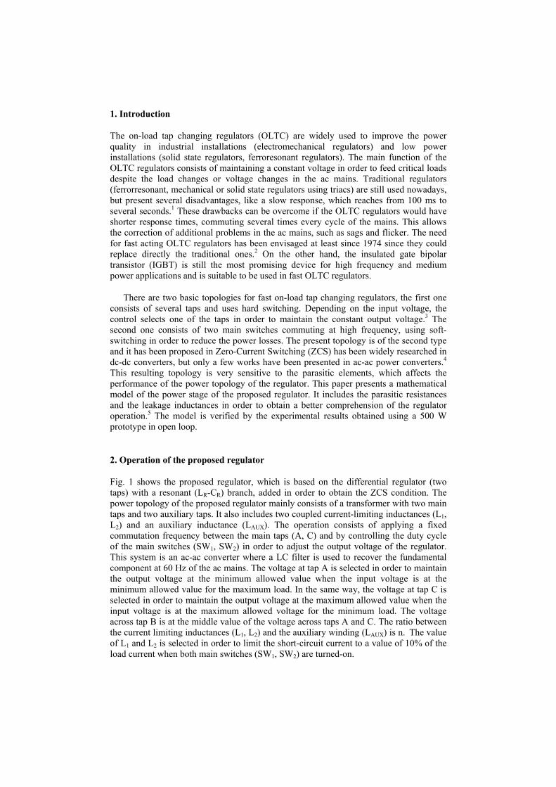
Fig. 1 shows the proposed regulator, which is based on the differential regulator (two taps) with a resonant (LR-CR) branch, added in order to obtain the ZCS condition. The power topology of the proposed regulator mainly consists of a transformer with two main taps and two auxiliary taps. It also includes two coupled current-limiting inductances (L1, L2) and an auxiliary inductance (LAUX). The operation consists of applying a fixed commutation frequency between the main taps (A, C) and by controlling the duty cycle of the main switches (SW1, SW2) in order to adjust the output voltage of the regulator. This system is an ac-ac converter where a LC filter is used to recover the fundamental component at 60 Hz of the ac mains. The voltage at tap A is selected in order to maintain the output voltage at the minimum allowed value when the input voltage is at the minimum allowed value for the maximum load. In the same way, the voltage at tap C is selected in order to maintain the output voltage at the maximum allowed value when the input voltage is at the maximum allowed voltage for the minimum load. The voltage across tap B is at the middle value of the voltage across taps A and C. The ratio between the current limiting inductances (L1, L2) and the auxiliary winding (LAUX) is n. The value of L1 and L2 is selected in order to limit the short-circuit current to a value of 10% of the load current when both main switches (SW1, SW2) are turned-on.
S W1
S W2
CR LR L
C
LAUX
S W3
S W4
InputVoltage
R
OutputVoltage
L1
L2
A
B
C
D
E
F
T
Fig. 1. Power topology of the proposed regulator.
LR
SW1
SW2
CR
SW3
SW4
OutputVoltage
A
L1
L2
LK2
LK1
LK3
RP1
RP2
RP3
LKAUX LAUX
ICA
VTAP
VAUX
VAUX
V
VTAP
B
C
D
E
F
T
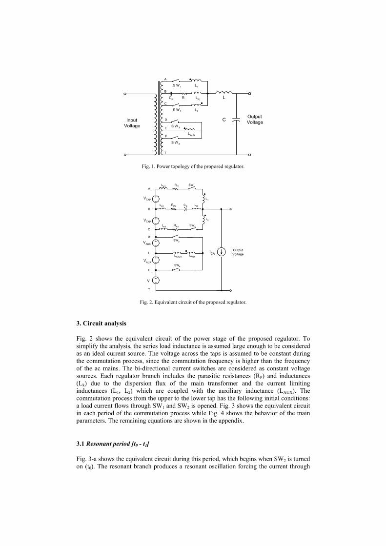
Fig. 2. Equivalent circuit of the proposed regulator.
3. Circuit analysis
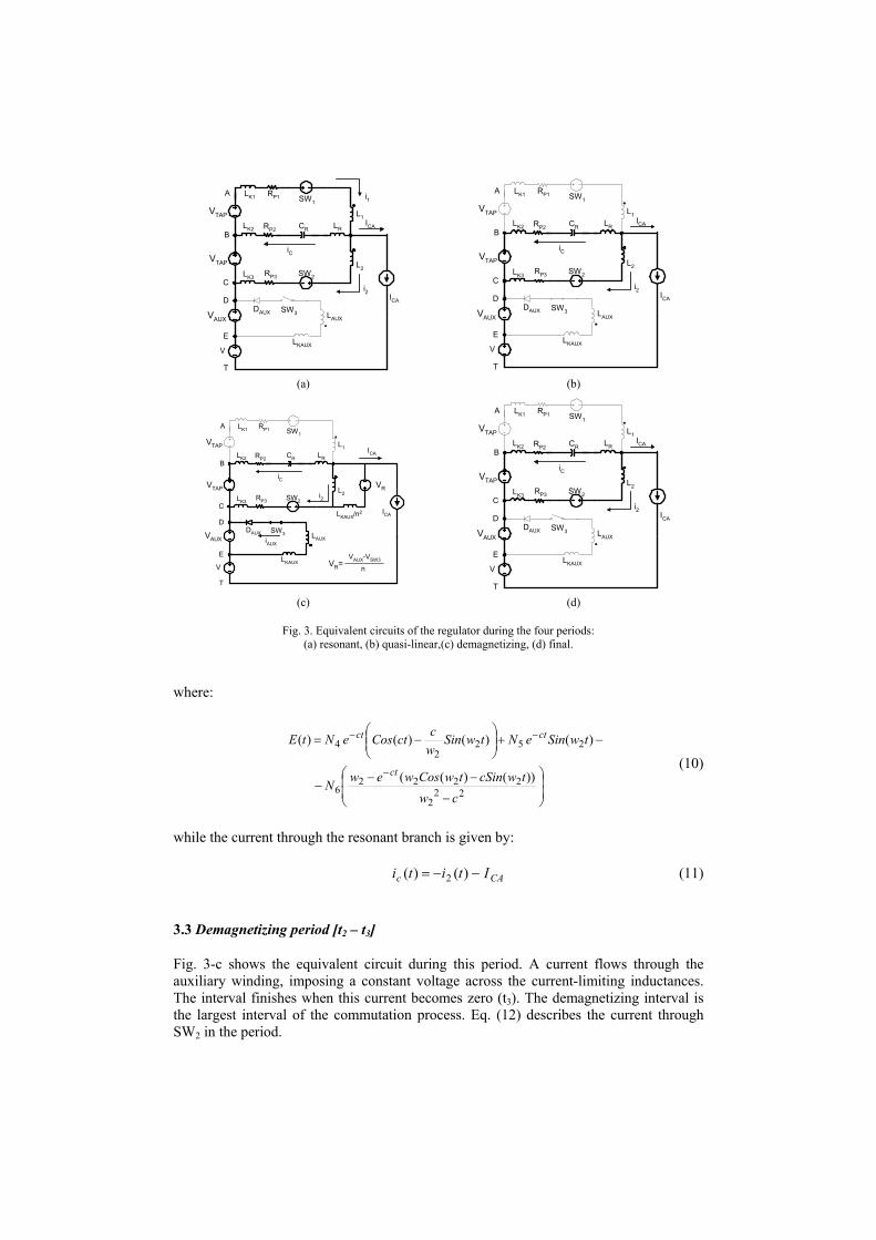
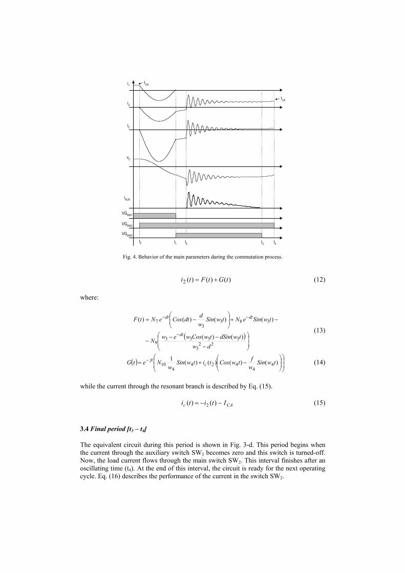
Fig. 2 shows the equivalent circuit of the power stage of the proposed regulator. To simplify the analysis, the series load inductance is assumed large enough to be considered as an ideal current source. The voltage across the taps is assumed to be constant during the commutation process, since the commutation frequency is higher than the frequency of the ac mains. The bi-directional current switches are considered as constant voltage sources. Each regulator branch includes the parasitic resistances (RP) and inductances (Lk) due to the dispersion flux of the main transformer and the current limiting inductances (L1, L2) which are coupled with the auxiliary inductance (LAUX). The commutation process from the upper to the lower tap has the following initial conditions: a load current flows through SW1 and SW2 is opened. Fig. 3 shows the equivalent circuit in each period of the commutation process while Fig. 4 shows the behavior of the main parameters. The remaining equations are shown in the appendix.
3.1 Resonant period [t0 - t1]
Fig. 3-a shows the equivalent circuit during this period, which begins when SW2 is turned on (t0). The resonant branch produces a resonant oscillation forcing the current through
SW1 to cross zero. The interval finishes when the switch SW1 is turned-off at the second zero crossing (t1). The initial conditions of the currents through the main switches are:
0)()( 0201 == tiIti CA (1)
The current in the main switch SW1 is given by:
)()()()()( 43211 tDMtCMtBMtAMti +++= (2)
where:
))(())())(((
))(())())2(((
)()(
2211
132
2211
12
13
122
1
2
bawwetwSinbabba
bawwetwCosabbww
baweatA
bt
btat
−+
−++−+
+−+
−++
−+=
−
−−
(3)
221
2211
1112
12
)(
))(())()()(()(
bawea
bawwetwCosawtwSinwabbtB
at
bt
−+
−+
+−+
++−=
−
−
(4)
))(())()()((
)()( 22
11
11122
1 bawwetwSinbatwCosw
bawetC
btat
−+
+−+−
−+=
−− (5)
))()((2
))((1
))()(())()()()2(()(
21
2221
221
21
2221
122
1111
wbbawba
bawae
wbbawetwSinbabwtwCosawbwtD
at
bt
+−+
−+
−+
−+
++−+
−+−−=
−
−
(6)
while the current through the main switch SW2 is given by:
)()()()( 3212 tDNtCNtBNti ++= (7)
and the current in the resonant branch is given by:
CAc Itititi −−= )()()( 21 (8)
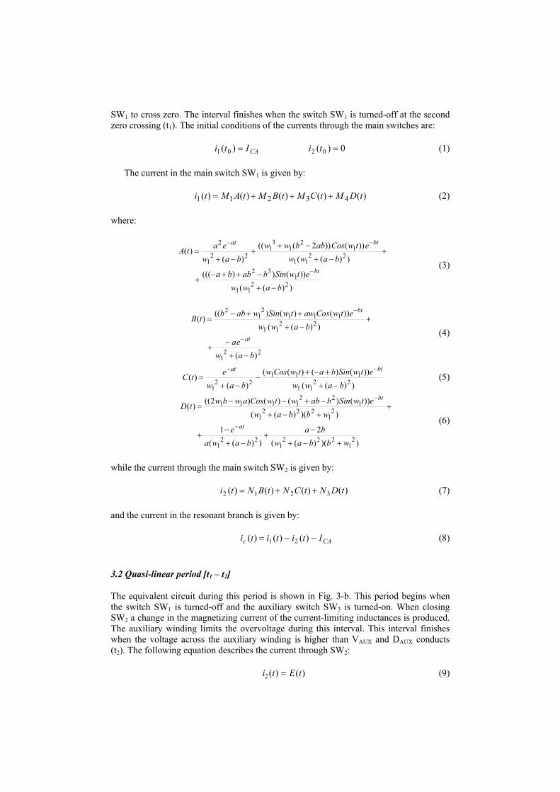
3.2 Quasi-linear period [t1 – t2]
The equivalent circuit during this period is shown in Fig. 3-b. This period begins when the switch SW1 is turned-off and the auxiliary switch SW3 is turned-on. When closing SW2 a change in the magnetizing current of the current-limiting inductances is produced. The auxiliary winding limits the overvoltage during this interval. This interval finishes when the voltage across the auxiliary winding is higher than VAUX and DAUX conducts (t2). The following equation describes the current through SW2:
)()(2 tEti = (9)
LR
SW1
SW2
CR
A
B
C
T
L1
L2
V
ICA
i1
i2
iC
VTAP
VTAP
RP2
RP1
RP3
LK2
LK3
LK1
ICA
SW3 LAUXDAUXVAUX
LKAUX
D
E
LR
SW1
SW2
CR
A
B
C
T
L1
L2
V
ICA
i2
iC
VTAP
VTAP
RP2
RP1
RP3
LK2
LK3
LK1
ICA
SW3 LAUX
DAUXVAUX
LKAUX
D
E
(a) (b)
VR
VR=VAUX-VSW3
n
LR
SW1
SW2
CR
A
B
C
T
L1
L2
V
ICA
i2
iC
VTAP
VTAP
RP2
RP1
RP3
LK2
LK3
LK1
ICA
SW3 LAUX
DAUXVAUX
LKAUX
D
E
LKAUX/n2
iAUX
LR
SW1
SW2
CR
A
B
C
T
L1
L2
V
ICA
i2
iC
VTAP
VTAP
RP2
RP1
RP3
LK2
LK3
LK1
ICA
SW3 LAUX
DAUXVAUX
LKAUX
D
E
(c) (d)
Fig. 3. Equivalent circuits of the regulator during the four periods: (a) resonant, (b) quasi-linear,(c) demagnetizing, (d) final.
where:
−
−−−
−+
−=
−
−−
222
22226
2522
4
))()((
)()()()(
cwtwcSintwCoswewN
twSineNtwSinwcctCoseNtE
ct
ctct
(10)
while the current through the resonant branch is given by:
CAc Ititi −−= )()( 2 (11)
3.3 Demagnetizing period [t2 – t3]
Fig. 3-c shows the equivalent circuit during this period. A current flows through the auxiliary winding, imposing a constant voltage across the current-limiting inductances. The interval finishes when this current becomes zero (t3). The demagnetizing interval is the largest interval of the commutation process. Eq. (12) describes the current through SW2 in the period.
i1
i2
iC
vC
iAUX
VGSW1
VGSW2
VGSW3
t0 t1 t2 t3 t4
ICA
ICA
Fig. 4. Behavior of the main parameters during the commutation process.
)()()(2 tGtFti += (12)
where:
( )
−
−−−
−+
−=
−
−−
223
33339
3833
7
)()(
)()()()(
dwtwdSintwCoswewN
twSineNtwSinwddtCoseNtF
dt
dtdt
(13)
( )
−+= − )()()()(1
44
4244
10 twSinwftwCostitwSin
wNetG c
ft (14)
while the current through the resonant branch is described by Eq. (15).
CAc Ititi −−= )()( 2 (15)
3.4 Final period [t3 – t4]
The equivalent circuit during this period is shown in Fig. 3-d. This period begins when the current through the auxiliary switch SW3 becomes zero and this switch is turned-off. Now, the load current flows through the main switch SW2. This interval finishes after an oscillating time (t4). At the end of this interval, the circuit is ready for the next operating cycle. Eq. (16) describes the performance of the current in the switch SW2.
)()(2 tHti = (16)
( )
−
−−−
−+
−=
−
−−
222
22226
21222
11
)()(
)()()()(
cwtwcSintwCoswewN
twSineNtwSinwcctCoseNtH
ct
ctct
(17)
while the current through the resonant branch is given by:
CAc Ititi −−= )()( 2 (18)
4. Power stage design
The values of the elements of the power stage are:
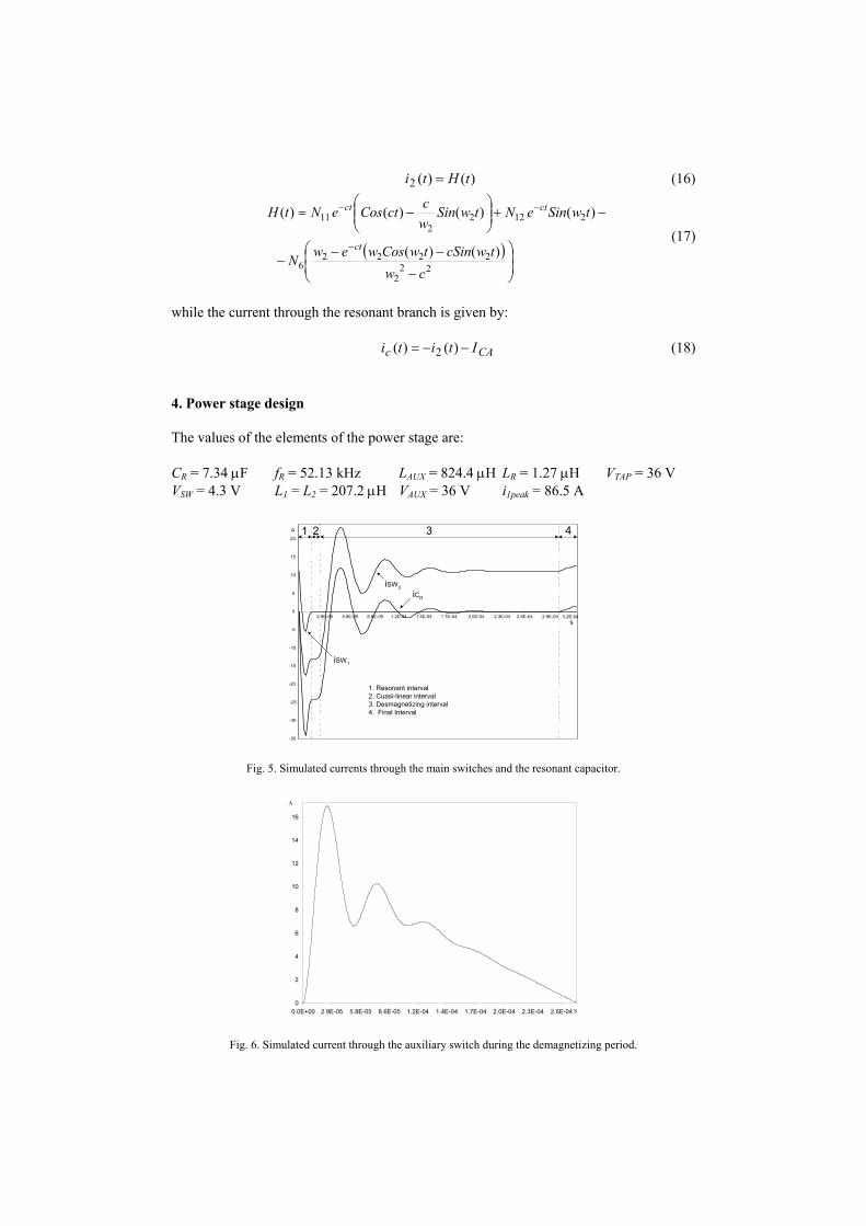
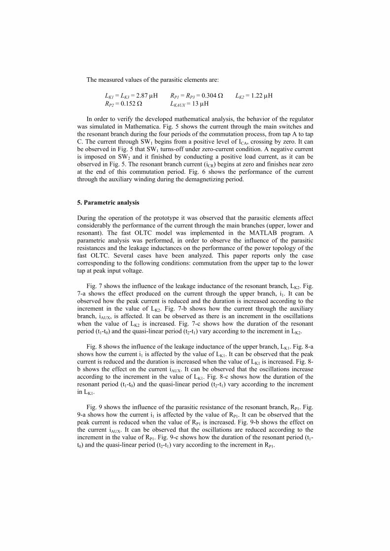
CR = 7.34 µF fR = 52.13 kHz LAUX = 824.4 µH LR = 1.27 µH VTAP = 36 V VSW = 4.3 V L1 = L2 = 207.2 µH VAUX = 36 V i1peak = 86.5 A
-35
-30
-25
-20
-15
-10
-5
0
5
10
15
20
2.9E-05 5.8E-05 8.6E-05 1.2E-04 1.4E-04 1.7E-04 2.0E-04 2.3E-04 2.6E-04 2.9E-04 3.2E-04
iSW1
iSW2
iCR
1 2 3 4
1. Resonant interval2. Cuasi-linear interval3. Desmagnetizing interval4. Final Interval
A
s
Fig. 5. Simulated currents through the main switches and the resonant capacitor.
0
2
4
6
8
10
12
14
16
0.0E+00 2.9E-05 5.8E-05 8.6E-05 1.2E-04 1.4E-04 1.7E-04 2.0E-04 2.3E-04 2.6E-04
A
s
Fig. 6. Simulated current through the auxiliary switch during the demagnetizing period.
The measured values of the parasitic elements are:
LK1 = LK3 = 2.87 µH RP1 = RP3 = 0.304 Ω LK2 = 1.22 µH RP2 = 0.152 Ω LKAUX = 13 µH
In order to verify the developed mathematical analysis, the behavior of the regulator was simulated in Mathematica. Fig. 5 shows the current through the main switches and the resonant branch during the four periods of the commutation process, from tap A to tap C. The current through SW1 begins from a positive level of ICA, crossing by zero. It can be observed in Fig. 5 that SW1 turns-off under zero-current condition. A negative current is imposed on SW2 and it finished by conducting a positive load current, as it can be observed in Fig. 5. The resonant branch current (iCR) begins at zero and finishes near zero at the end of this commutation period. Fig. 6 shows the performance of the current through the auxiliary winding during the demagnetizing period.
5. Parametric analysis
During the operation of the prototype it was observed that the parasitic elements affect considerably the performance of the current through the main branches (upper, lower and resonant). The fast OLTC model was implemented in the MATLAB program. A parametric analysis was performed, in order to observe the influence of the parasitic resistances and the leakage inductances on the performance of the power topology of the fast OLTC. Several cases have been analyzed. This paper reports only the case corresponding to the following conditions: commutation from the upper tap to the lower tap at peak input voltage.
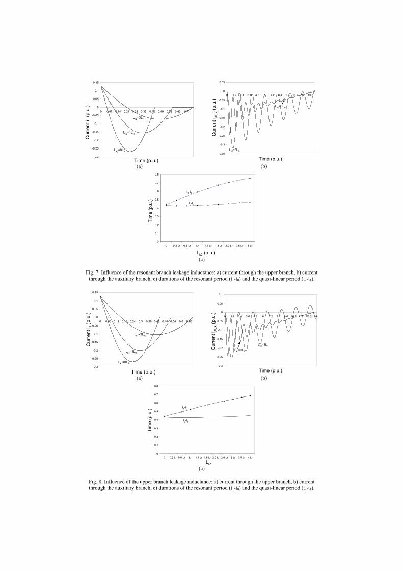
Fig. 7 shows the influence of the leakage inductance of the resonant branch, LK2. Fig. 7-a shows the effect produced on the current through the upper branch, i1. It can be observed how the peak current is reduced and the duration is increased according to the increment in the value of LK2. Fig. 7-b shows how the current through the auxiliary branch, iAUX, is affected. It can be observed as there is an increment in the oscillations when the value of LK2 is increased. Fig. 7-c shows how the duration of the resonant period (t1-t0) and the quasi-linear period (t2-t1) vary according to the increment in LK2.
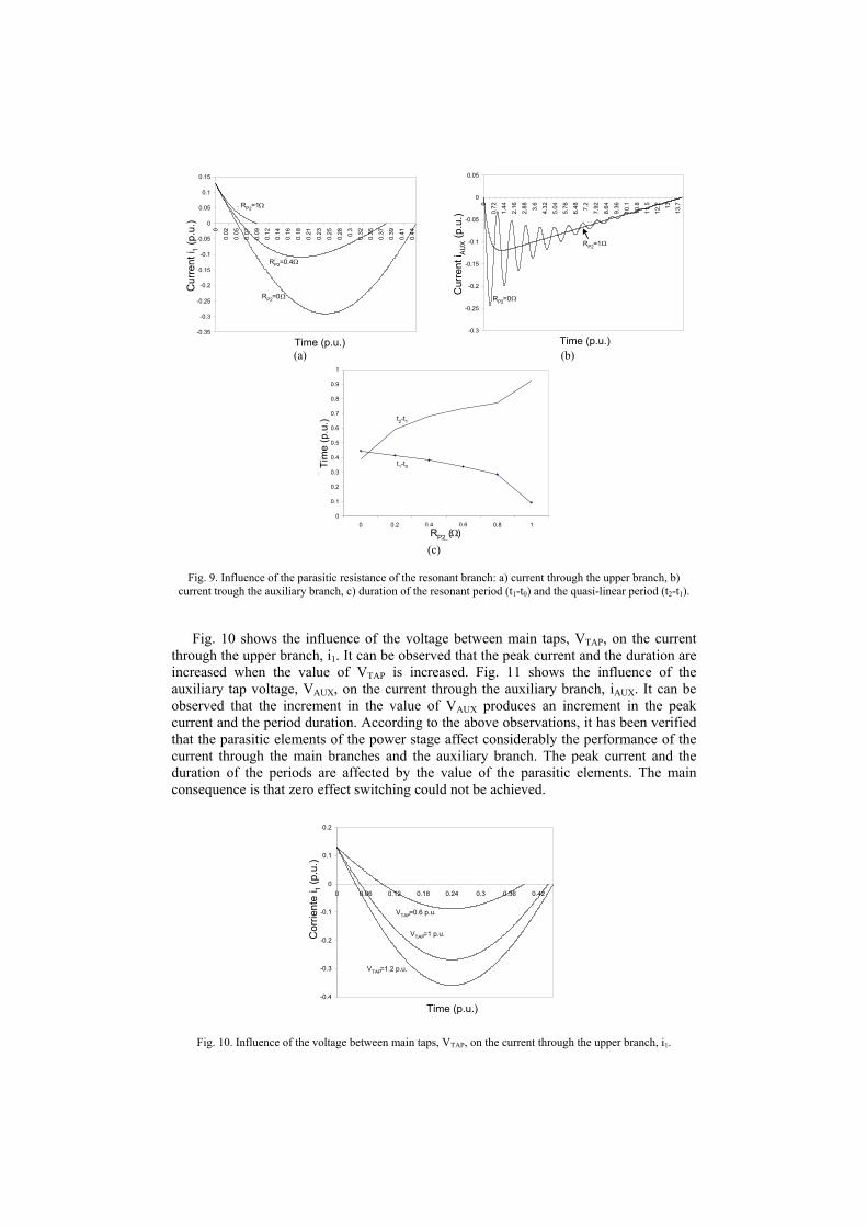
Fig. 8 shows the influence of the leakage inductance of the upper branch, LK1. Fig. 8-a shows how the current i1 is affected by the value of LK1. It can be observed that the peak current is reduced and the duration is increased when the value of LK1 is increased. Fig. 8-b shows the effect on the current iAUX. It can be observed that the oscillations increase according to the increment in the value of LK1. Fig. 8-c shows how the duration of the resonant period (t1-t0) and the quasi-linear period (t2-t1) vary according to the increment in LK1.
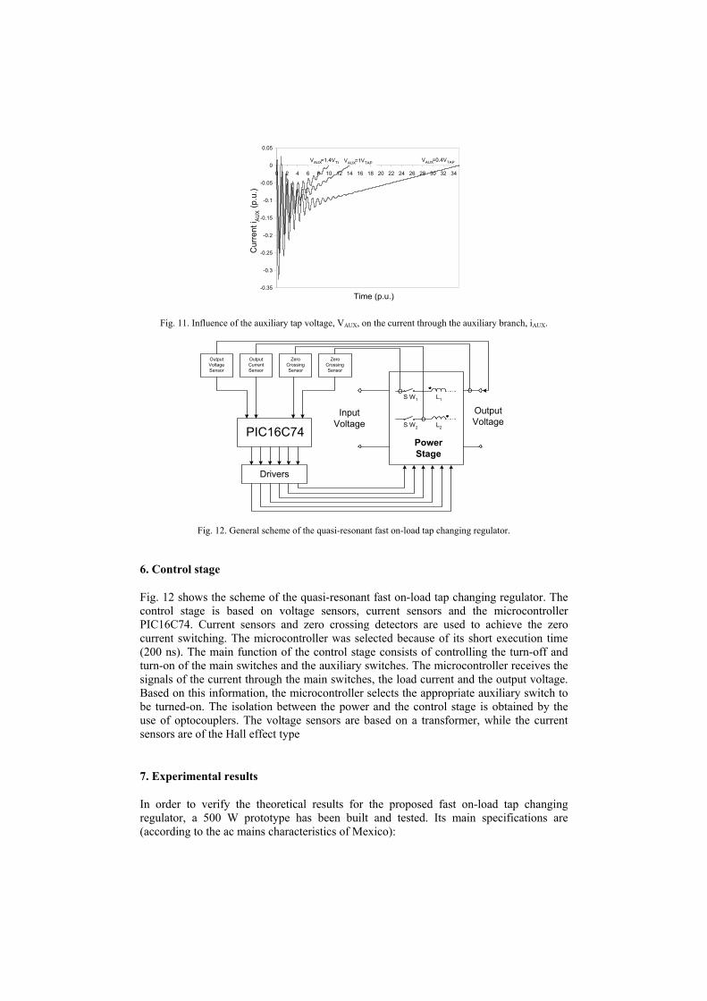
Fig. 9 shows the influence of the parasitic resistance of the resonant branch, RP1. Fig. 9-a shows how the current i1 is affected by the value of RP1. It can be observed that the peak current is reduced when the value of RP1 is increased. Fig. 9-b shows the effect on the current iAUX. It can be observed that the oscillations are reduced according to the increment in the value of RP1. Fig. 9-c shows how the duration of the resonant period (t1-t0) and the quasi-linear period (t2-t1) vary according to the increment in RP1.
-0.3
-0.25
-0.2
-0.15
-0.1
-0.05
0
0.05
0.1
0.15
0 0.07 0.14 0.21 0.28 0.35 0.42 0.49 0.56 0.63 0.7
tiempo (p.u.)
I (p.
u.)
3 Lr
0 Lr
1 Lr
Tiempo (p.u.)
Cor
rient
e (p
.u.)
Lk2=0LR
Lk2=1LR
Lk2=3LR
Cor
rient
e i 1 (
p.u.
)C
urre
nt i 1 (
p.u.
)
Time (p.u.)
Lk2=0LR
-0.35
-0.3
-0.25
-0.2
-0.15
-0.1
-0.05
0
0.05
0 1.2 2.4 3.6 4.8 6 7.2 8.4 9.6 10.8 12 13.2
t (p.u.)
I (p.
u.)
0 Lr
3 Lr
Tiempo (p.u.)
Cor
rient
e (p
.u.)
Lk2=3LR
Cor
rient
e i AU
X (p
.u.)
Time (p.u.)
Cur
rent
i AUX (p
.u.)
(a) (b)
L k2
Tiem
po(p
.u.)
0
0.1
0.2
0.3
0.4
0.5
0.6
0.7
0.8
0 0.3 Lr 0.6 Lr Lr 1.4 Lr 1.8 Lr 2.2 Lr 2.6 Lr 3 Lr
t1-t0
t2-t1
Tim
e (p
.u.)
Lk2 (p.u.) (c)
Fig. 7. Influence of the resonant branch leakage inductance: a) current through the upper branch, b) current through the auxiliary branch, c) durations of the resonant period (t1-t0) and the quasi-linear period (t2-t1).
-0.3
-0.25
-0.2
-0.15
-0.1
-0.05
0
0.05
0.1
0.15
0 0.06 0.12 0.18 0.24 0.3 0.36 0.42 0.48 0.54 0.6 0.66
t (p.u.)
I (p.
u.)
Lr
3 Lr
0 Lr
Tiempo (p.u.)
Lk1=0LR
Lk1=1LR
Lk1=3LR
Cor
rient
e (p
.u.)
Cor
rient
e i 1 (
p.u.
)
Time (p.u.)
Cur
rent
i 1 (p.
u.)
Lk1=0LR
-0.3
-0.25
-0.2
-0.15
-0.1
-0.05
0
0.05
0.1
0 1.2 2.4 3.6 4.8 6 7.2 8.4 9.6 10.8 12 13.2 14.4
t (p.u.)
I (p.
u.)
0 Lr
3 LrCor
rient
e (p
.u.)
Tiempo (p.u.)
Lk1=3LR
Cor
rient
e i AU
X (p
.u.)
Cur
rent
i AUX (p
.u.)
Time (p.u.) (a) (b)
0
0.1
0.2
0.3
0.4
0.5
0.6
0.7
0.8
0 0.3 Lr 0.6 Lr Lr 1.4 Lr 1.8 Lr 2.2 Lr 2.6 Lr 3 Lr 3.5 Lr 4 LrLP1, LP3
tiem
po (p
.u.)
t1
t2
Lk1
Tiem
po (p
.u.)
t2-t1
t1-t0
Tim
e (p
.u.)
Lk1 (c)
Fig. 8. Influence of the upper branch leakage inductance: a) current through the upper branch, b) current through the auxiliary branch, c) durations of the resonant period (t1-t0) and the quasi-linear period (t2-t1).
-0.35
-0.3
-0.25
-0.2
-0.15
-0.1
-0.05
0
0.05
0.1
0.15
0
0.02
0.05
0.07
0.09
0.12
0.14
0.16
0.18
0.21
0.23
0.25
0.28 0.3
0.32
0.35
0.37
0.39
0.41
0.44
t (p.u.)
I (p.
u.)
0 Ω
0.4 Ω
1 Ω
Tiempo (p.u.)
Cor
rient
e (p
.u.)
RP2=1Ω
RP2=0.4Ω
RP2=0ΩCor
rient
e i 1 (
p.u.
)
Time (p.u.)
Cur
rent
i 1 (p.
u.)
-0.3
-0.25
-0.2
-0.15
-0.1
-0.05
0
0.05
0
0.72
1.44
2.16
2.88 3.6
4.32
5.04
5.76
6.48 7.2
7.92
8.64
9.36
10.1
10.8
11.5
12.2 13
13.7
t (p.u.)
I (p.
u.)
0 Ω
1 Ω
Cor
rient
e (p
.u.)
Tiempo (p.u.)
RP2=0Ω
RP2=1Ω
Cor
rient
e i AU
X (p
.u.)
Cur
rent
i AUX (p
.u.)
Time (p.u.) (a) (b)
0
0.1
0.2
0.3
0.4
0.5
0.6
0.7
0.8
0.9
1
0 0.2 0.4 0.6 0.8 1RP2 (OHMS)
I (p.
u.)
t1
t2
RP2( )Ω
Cor
rient
e (p
.u.) t2-t1
t1-t0
Tiem
po (p
.u.)
Tim
e (p
.u.)
RP2 ( )Ω (c)
Fig. 9. Influence of the parasitic resistance of the resonant branch: a) current through the upper branch, b) current trough the auxiliary branch, c) duration of the resonant period (t1-t0) and the quasi-linear period (t2-t1).
Fig. 10 shows the influence of the voltage between main taps, VTAP, on the current through the upper branch, i1. It can be observed that the peak current and the duration are increased when the value of VTAP is increased. Fig. 11 shows the influence of the auxiliary tap voltage, VAUX, on the current through the auxiliary branch, iAUX. It can be observed that the increment in the value of VAUX produces an increment in the peak current and the period duration. According to the above observations, it has been verified that the parasitic elements of the power stage affect considerably the performance of the current through the main branches and the auxiliary branch. The peak current and the duration of the periods are affected by the value of the parasitic elements. The main consequence is that zero effect switching could not be achieved.
Cur
rent
i 1 (p.
u.)
-0.4
-0.3
-0.2
-0.1
0
0.1
0.2
0 0.06 0.12 0.18 0.24 0.3 0.36 0.42
t (p.u.)
I (p.
u.)
1.2 Vtap
Vtap
0.6 Vtap
Cor
rient
e i 1 (
p.u.
)
Tiempo (p.u.)
VTAP=0.6 p.u.
VTAP=1 p.u.
VTAP=1.2 p.u.
Time (p.u.)
Fig. 10. Influence of the voltage between main taps, VTAP, on the current through the upper branch, i1.
-0.35
-0.3
-0.25
-0.2
-0.15
-0.1
-0.05
0
0.05
0 2 4 6 8 10 12 14 16 18 20 22 24 26 28 30 32 34
t (p.u.)
I (p.
u.)
1.4 VTAP 0.4 VTAP1 VTAP
Tiempo (p.u.)
Cor
rient
e i AU
X (p
.u.)
VAUX=1.4VTAP VAUX=1VTAP VAUX=0.4VTAP
Time (p.u.)
Cur
rent
i AUX (p
.u.)
Fig. 11. Influence of the auxiliary tap voltage, VAUX, on the current through the auxiliary branch, iAUX.
OutputVoltageSensor
OutputCurrentSensor
ZeroCrossingSensor
ZeroCrossingSensor
S W1 L1
S W2 L2
PowerStage
InputVoltage
OutputVoltage
PIC16C74
Drivers
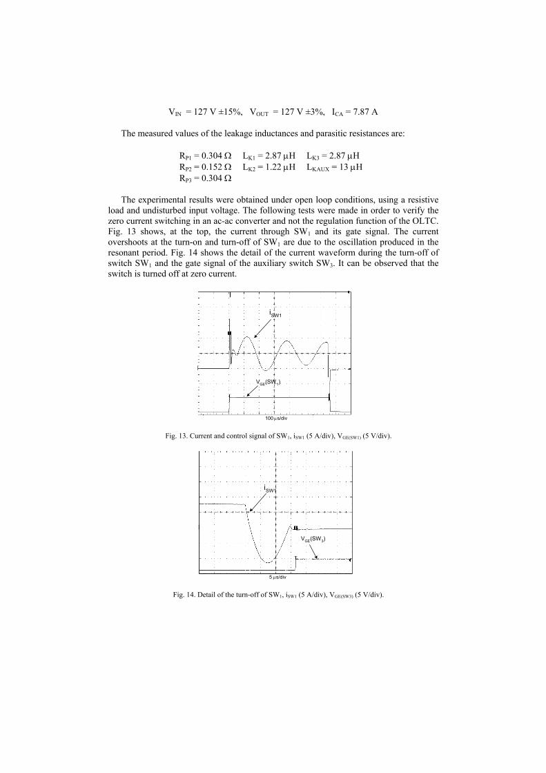
Fig. 12. General scheme of the quasi-resonant fast on-load tap changing regulator.
6. Control stage
Fig. 12 shows the scheme of the quasi-resonant fast on-load tap changing regulator. The control stage is based on voltage sensors, current sensors and the microcontroller PIC16C74. Current sensors and zero crossing detectors are used to achieve the zero current switching. The microcontroller was selected because of its short execution time (200 ns). The main function of the control stage consists of controlling the turn-off and turn-on of the main switches and the auxiliary switches. The microcontroller receives the signals of the current through the main switches, the load current and the output voltage. Based on this information, the microcontroller selects the appropriate auxiliary switch to be turned-on. The isolation between the power and the control stage is obtained by the use of optocouplers. The voltage sensors are based on a transformer, while the current sensors are of the Hall effect type
7. Experimental results
In order to verify the theoretical results for the proposed fast on-load tap changing regulator, a 500 W prototype has been built and tested. Its main specifications are (according to the ac mains characteristics of Mexico):
VIN = 127 V ±15%, VOUT = 127 V ±3%, ICA = 7.87 A
The measured values of the leakage inductances and parasitic resistances are:
RP1 = 0.304 Ω LK1 = 2.87 µH LK3 = 2.87 µH RP2 = 0.152 Ω LK2 = 1.22 µH LKAUX = 13 µH RP3 = 0.304 Ω
The experimental results were obtained under open loop conditions, using a resistive load and undisturbed input voltage. The following tests were made in order to verify the zero current switching in an ac-ac converter and not the regulation function of the OLTC. Fig. 13 shows, at the top, the current through SW1 and its gate signal. The current overshoots at the turn-on and turn-off of SW1 are due to the oscillation produced in the resonant period. Fig. 14 shows the detail of the current waveform during the turn-off of switch SW1 and the gate signal of the auxiliary switch SW3. It can be observed that the switch is turned off at zero current.
iSW1
VGE(SW1)
100 µs/div
Fig. 13. Current and control signal of SW1, iSW1 (5 A/div), VGE(SW1) (5 V/div).
iSW1
VGE(SW3)
5 µs/div
Fig. 14. Detail of the turn-off of SW1, iSW1 (5 A/div), VGE(SW3) (5 V/div).
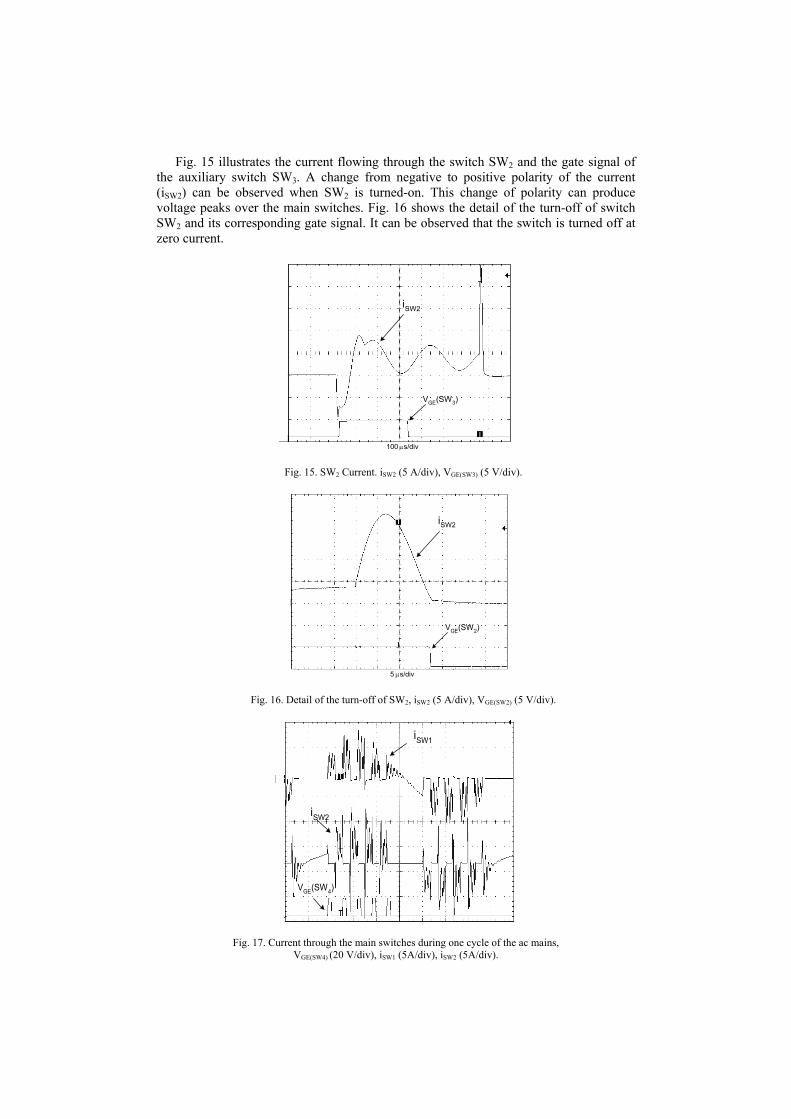
Fig. 15 illustrates the current flowing through the switch SW2 and the gate signal of the auxiliary switch SW3. A change from negative to positive polarity of the current (iSW2) can be observed when SW2 is turned-on. This change of polarity can produce voltage peaks over the main switches. Fig. 16 shows the detail of the turn-off of switch SW2 and its corresponding gate signal. It can be observed that the switch is turned off at zero current.
iSW2
VGE(SW3)
100 µs/div
Fig. 15. SW2 Current. iSW2 (5 A/div), VGE(SW3) (5 V/div).
iSW2
VGE(SW2)
5 µs/div
Fig. 16. Detail of the turn-off of SW2, iSW2 (5 A/div), VGE(SW2) (5 V/div).
iSW2
iSW1
VGE(SW4)
Fig. 17. Current through the main switches during one cycle of the ac mains, VGE(SW4) (20 V/div), iSW1 (5A/div), iSW2 (5A/div).
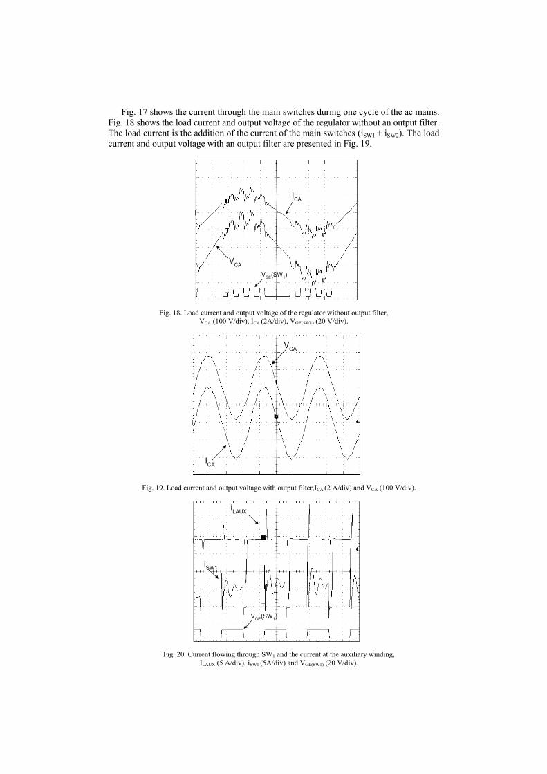
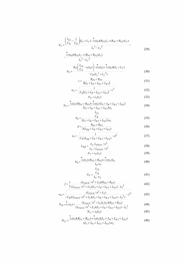
Fig. 17 shows the current through the main switches during one cycle of the ac mains. Fig. 18 shows the load current and output voltage of the regulator without an output filter. The load current is the addition of the current of the main switches (iSW1 + iSW2). The load current and output voltage with an output filter are presented in Fig. 19.
VCA
ICA
VGE(SW1)
Fig. 18. Load current and output voltage of the regulator without output filter,
VCA (100 V/div), ICA (2A/div), VGE(SW1) (20 V/div).
ICA
VCA
Fig. 19. Load current and output voltage with output filter,ICA (2 A/div) and VCA (100 V/div).
VGE(SW1)
iSW1
iLAUX
Fig. 20. Current flowing through SW1 and the current at the auxiliary winding,
ILAUX (5 A/div), iSW1 (5A/div) and VGE(SW1) (20 V/div).
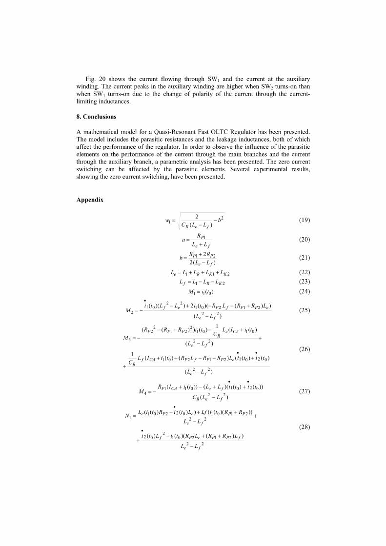
Fig. 20 shows the current flowing through SW1 and the current at the auxiliary winding. The current peaks in the auxiliary winding are higher when SW2 turns-on than when SW1 turns-on due to the change of polarity of the current through the current-limiting inductances.
8. Conclusions
A mathematical model for a Quasi-Resonant Fast OLTC Regulator has been presented. The model includes the parasitic resistances and the leakage inductances, both of which affect the performance of the regulator. In order to observe the influence of the parasitic elements on the performance of the current through the main branches and the current through the auxiliary branch, a parametric analysis has been presented. The zero current switching can be affected by the parasitic elements. Several experimental results, showing the zero current switching, have been presented.
Appendix
21 )(
2 bLLC
wfeR
−−
= (19)
fe
PLL
Ra
+= 1 (20)
)(22 21
fe
PPLLRRb
−+
= (21)
211 KKRe LLLLL +++= (22)
21 KRf LLLL −−= (23) )( 011 tiM = (24)
)(
))()((2))((22
2120122
012
fe
ePPfPef
LL
LRRLRtiLLtiM
−
+−−+−−=
•
(25)
)(
)()(()()((1
)(
)((1)())((
22
020121201
22
01012
212
2
3
fe
ePPfPCAfR
fe
CAeR
PPP
LL
titiLRRLRtiILC
LL
tiILC
tiRRRM
−
+−−+++
+−
+−+−−=
•• (26)
)(
))()()(())((22
02010114
feR
feCAP
LLC
titiLLtiIRM
−
++−+−=
••
(27)
2221201
202
22210102201
1
))()(()(
)))((())()((
fe
fPPePf
fe
PPePe
LL
LRRLRtiLti
LLRRtiLfLtiRtiLN
−
++−+
+−
++−=
•
•
(28)
2221202
22
21201
2
))()((
))()(()(1
fe
ePPfP
fe
fPPePfeRR
CA
LL
LRRLRti
LL
LRRLRtiLLCC
I
N
−
++−
−−
++−+
−
=
•
•
(29)
)(
)))(()(()(
22
0201011
3feR
feR
CAP
LLC
LLtititiCIR
N+
++−
−
=
••
(30)
( )322
322 KKR
PPLLLL
RRc+++
+= (31)
( )2
3222
1 cLLLLC
wKKRR
−+++
= (32)
)( 124 tiN = (33)
( ) ( )( ) 2322
3221232125
)()(wLLLL
LLLLtiRRtiNKKR
KKRPP+++
+++++=
••
(34)
( ) 23226 wLLLL
CI
NKKR
R
CA
+++= (35)
)(2 32
32
KKREQ
PPLLLL
RRd+++
+= (36)
2
323 )(
1 dLLLLC
wKKREQR
−+++
= (37)
22
22
/
/
nLL
nLLL
PAUX
PAUXEQ
+= (38)
)( 227 tiN = (39)
3
2232228
)()()(wL
LtiRRtiNh
kPP••
++= (40)
39 wL
CI
Nk
R
CA
= (41)
223222
2322
2
)()/())(/(
21
LLLLLLnLRRLnLf
KKRPAUX
PPPAUX
−++++
++= (42)
22
232222
22
4)))(/((
)/( fLLLLLLnLC
LnLwKKRPAUXR
PAUX −−++++
+= (43)
223222
23222
2
210))(/())(()/()(
LLLLLLnLRRtiLnLtiNKKRPAUX
PPcPAUXc
−++++
+++=
• (44)
)( 3211 tiN = (45)
2322
32232323212 )(
))(())((wLLLL
LLLLtiRRtiNKKR
KKRPP
++++++++
=
••
(46)
References
1. S. Martínez, “Estabilizadores de CA por pasos con corriente compartida”, Mundo Electrónico, No. 166 (1986), pp. 127-135, Spain.
2. G. Musgrave, D. O’Kelly “Improvement for power system transmission by solid-state techniques”, Proc. Power electronics, power semiconductors and their applications IEE Conference, 123, December 1974, pp. 228-233.
3. R. Echavarría, M. Cotorogea, A. Claudio, V. Sánchez, “Design and implementation of a fast on-load tap changing regulator”, Proc. Industry Applications Society Annual Meeting, IAS’00, Rome, Italy. October 8-12, 2000.
4. Vaquero J., “Estabilizadores de corriente alterna con tomas de conmutación rápida en carga para mejora de redes de distribución eléctrica.”. Ph.D. Thesis. DIEEC. ETSII, UNED, Madrid, Spain, 2000.
5. V. Sánchez, R. Echavarría, M. Cotorogea, A. Claudio, “Design and implementation of a fast on-load tap changing regulator using soft-switching commutation techniques”, Proc. Power Electronics Specialist Conference, PESC’00, 18-23 June, 2000, Galway, Ireland.
Related Documents

![A High-Frequency Resonant Inverter Topology with Low ... · PDF fileA High-Frequency Resonant Inverter Topology with ... the well-known class E inverter [12] uses resonant operation](https://static.cupdf.com/doc/110x72/5a9f06527f8b9a76178c370c/a-high-frequency-resonant-inverter-topology-with-low-high-frequency-resonant.jpg)


