Analysis and Synthesis of UHF RFID Antennas using the Embedded T-match Naaser Ahmed Mohammed Submitted to the graduate degree program in Electrical Engineering & Computer Science and the Graduate Faculty of the University of Kansas in partial fulfillment of the requirements for the degree of Master’s of Science Defended: July 22 nd , 2010 Thesis Committee: Dr. Daniel D. Deavours: Chairperson Dr. Kenneth R. Demarest Dr. James M. Stiles Dr. Shannon D. Blunt

Welcome message from author
This document is posted to help you gain knowledge. Please leave a comment to let me know what you think about it! Share it to your friends and learn new things together.
Transcript
Analysis and Synthesis of UHF RFIDAntennas using the Embedded T-match
Naaser Ahmed Mohammed
Submitted to the graduate degree program in ElectricalEngineering & Computer Science and the Graduate Faculty
of the University of Kansas in partial fulfillment ofthe requirements for the degree of Master’s of Science
Defended: July 22nd, 2010
Thesis Committee:
Dr. Daniel D. Deavours: Chairperson
Dr. Kenneth R. Demarest
Dr. James M. Stiles
Dr. Shannon D. Blunt
The Thesis Committee for Naaser A. Mohammed certifies
that this is the approved version of the following thesis:
Analysis and Synthesis of UHF RFID Tag Using Embedded T-Match
Antennas
Approved: July 22nd, 2010
Thesis Committee:
Dr. Daniel D. Deavours [Chairperson]
Dr. Kenneth R. Demarest
Dr. James M. Stiles
Dr. Shannon D. Blunt
i

Abstract
Radio frequency identification technology with its ability to being read at
long ranges and have reliable performance, is at the pinnacle of technological
advancement. With the number of applications for RFID increasing, designing
RFID tag antennas effectively to work efficiently for the particular application
is critical. Antenna characteristics if known, significantly help in antenna design.
T-match structure is commonly used to design RFID tags as the structure helps in
matching an RFID chips reactive impedance to a dipole. Models that describe T-
match are known, but they are neither sufficiently accurate to model antennas nor
to synthesize the antenna geometry. Here, we present a simple matching network
known as embedded T-match. The characteristics of this antenna are studied and
a model accurately analyzing the antenna is also presented. A synthesis process is
also presented to effectively synthesize the antenna geometry for the given design
constraint.
ii

Acknowledgment
I would like to thank Dr. Deavours for his guidance. From the beginning he
was very patient and helpful in all the research works and projects I have done.
As a professor he has advised me all throughout my masters in taking appropriate
courses and exceed in my field. Being a naive in the RFID he supervised me at
every step and pushed me till I understood and polished my skills. His ability to
perceive technological issues in a unique way is worth observing and learning.
I thank Dr. Demarest in pointing me at the right direction when ever I was
lost. His approach of understanding the issues at the basic level has been very
helpful in completing the thesis. I thank Dr. Stiles and Dr. Blunt for agreeing to
be a part of the committee and help me in the final stages.
I would also like to thank the department of Electrical Engineering and Com-
puter Science, and Information and Telecommunication Technology Center, at
The University of Kansas for all its support. The past and present members of
RFID Alliance lab who have helped me in accomplishing simple as well as complex
tasks. My friends in the University and in India for supporting and understanding
me.
Last, but not the least, I would like to thank my parents and family for their
undying love. They have been the strongest pillar of support in all decisions I
have taken. I would specially like to thank my eldest brother for believing in me
and pushing me to excel in life.
iii

Contents
Acceptance Page i
Abstract ii
Acknowledgment iii
1 Introduction 1
2 Background 4
2.1 RFID System . . . . . . . . . . . . . . . . . . . . . . . . . . . . . 4
2.2 Maximum Power Transfer . . . . . . . . . . . . . . . . . . . . . . 5
2.3 Classic Uda Model . . . . . . . . . . . . . . . . . . . . . . . . . . 7
2.4 Two-Port Network . . . . . . . . . . . . . . . . . . . . . . . . . . 12
2.5 Strip Dipole Uda Model . . . . . . . . . . . . . . . . . . . . . . . 15
2.5.1 Common Mode Impedance . . . . . . . . . . . . . . . . . . 16
2.5.2 Splitting Factor . . . . . . . . . . . . . . . . . . . . . . . . 18
2.5.3 Differential Mode Impedance . . . . . . . . . . . . . . . . . 20
3 Embedded T-Match Antenna 23
3.1 Permissible Region . . . . . . . . . . . . . . . . . . . . . . . . . . 25
3.2 Antenna Characteristics . . . . . . . . . . . . . . . . . . . . . . . 30
3.3 Accuracy of Strip Uda Model . . . . . . . . . . . . . . . . . . . . 35
3.4 Error Diagnosis . . . . . . . . . . . . . . . . . . . . . . . . . . . . 37
4 Augmented Uda Model 40
4.1 Analysis of Error in Transmission Line Mode . . . . . . . . . . . . 40
4.1.1 Gap Capacitance . . . . . . . . . . . . . . . . . . . . . . . 40
iv

4.1.2 Shunt Inductance . . . . . . . . . . . . . . . . . . . . . . . 43
4.2 Computation of Constants Ci, Co and Xs . . . . . . . . . . . . . . 45
4.3 Validation . . . . . . . . . . . . . . . . . . . . . . . . . . . . . . . 48
5 Synthesis 51
6 Conclusion 56
7 Future Work 58
A Antenna Characteristics 60
A.1 ZC vs. S and W1 . . . . . . . . . . . . . . . . . . . . . . . . . . . 60
A.2 α vs. S and L . . . . . . . . . . . . . . . . . . . . . . . . . . . . . 60
A.3 ZD vs. L . . . . . . . . . . . . . . . . . . . . . . . . . . . . . . . . 63
B Computation of Constants 64
C Derivation 67
References 69
v

List of Figures
2.1 Overview of RFID System . . . . . . . . . . . . . . . . . . . . . . 5
2.2 Circuit model of a passive UHF RFID tag . . . . . . . . . . . . . 6
2.3 Wire T-match antenna. . . . . . . . . . . . . . . . . . . . . . . . . 7
2.4 Common Mode. . . . . . . . . . . . . . . . . . . . . . . . . . . . . 8
2.5 Differential Mode. . . . . . . . . . . . . . . . . . . . . . . . . . . . 8
2.6 Common Mode Impedance. . . . . . . . . . . . . . . . . . . . . . 9
2.7 Differential Mode Impedance. . . . . . . . . . . . . . . . . . . . . 10
2.8 Transmission Line Mode. . . . . . . . . . . . . . . . . . . . . . . . 10
2.9 Equivalent Circuit Model. . . . . . . . . . . . . . . . . . . . . . . 12
2.10 Two Port Network. . . . . . . . . . . . . . . . . . . . . . . . . . . 13
2.11 Center-Fed Cylindrical Dipole. . . . . . . . . . . . . . . . . . . . . 16
2.12 Coplanar Strip folded dipole antenna. . . . . . . . . . . . . . . . . 19
3.1 Commercial RFID Tags . . . . . . . . . . . . . . . . . . . . . . . 23
3.2 Commercial RFID Tags with Embedded T-match structure . . . . 24
3.3 Embedded T-match Antenna. . . . . . . . . . . . . . . . . . . . . 25
3.4 Embedded T-match network transformation on smith chart . . . . 27
3.5 Permissible region for Embedded T-match antennas . . . . . . . . 28
3.6 Permissible region area for Embedded T-match antennas . . . . . 29
3.7 Two port analysis . . . . . . . . . . . . . . . . . . . . . . . . . . . 31
3.8 ZC vs S . . . . . . . . . . . . . . . . . . . . . . . . . . . . . . . . 32
3.9 ZC vs W1 . . . . . . . . . . . . . . . . . . . . . . . . . . . . . . . 33
3.10 α vs S . . . . . . . . . . . . . . . . . . . . . . . . . . . . . . . . . 34
3.11 α vs S . . . . . . . . . . . . . . . . . . . . . . . . . . . . . . . . . 35
3.12 ZD vs L . . . . . . . . . . . . . . . . . . . . . . . . . . . . . . . . 36
3.13 Simulated ZC using MoM solver . . . . . . . . . . . . . . . . . . . 37
vi

3.14 Simulated ZIN using MoM solver . . . . . . . . . . . . . . . . . . 37
3.15 Two Port analyis in MoM solver . . . . . . . . . . . . . . . . . . . 38
3.16 Wave port analysis to compute ZO using FEM solver . . . . . . . 39
4.1 Fringing fields formed . . . . . . . . . . . . . . . . . . . . . . . . . 41
4.2 Gap capacitance in transmission line mode . . . . . . . . . . . . . 42
4.3 Gap capacitance in transmission line mode with zero-potential plane 42
4.4 Imperfect termination in transmission line mode . . . . . . . . . . 43
4.5 Augmented Uda transmission line model . . . . . . . . . . . . . . 44
4.6 Curve fitting technique for W = 10 mm . . . . . . . . . . . . . . . 46
4.7 Curve fitting technique for W = 25 mm . . . . . . . . . . . . . . . 46
4.8 Error between analytic and simulated ZD for W = 15 mm . . . . 47
4.9 Error between analytic and simulated ZD for W = 20 mm . . . . 47
4.10 Comparison of analytic vs simulated input resistance . . . . . . . 49
4.11 Comparison of analytic vs simulated input reactance . . . . . . . 50
A.1 ZC vs S . . . . . . . . . . . . . . . . . . . . . . . . . . . . . . . . 61
A.2 ZC vs W1 . . . . . . . . . . . . . . . . . . . . . . . . . . . . . . . 61
A.3 α vs S . . . . . . . . . . . . . . . . . . . . . . . . . . . . . . . . . 62
A.4 α vs L . . . . . . . . . . . . . . . . . . . . . . . . . . . . . . . . . 62
A.5 ZD vs L . . . . . . . . . . . . . . . . . . . . . . . . . . . . . . . . 63
B.1 Curve fitting technique for W = 15 mm . . . . . . . . . . . . . . . 65
B.2 Curve fitting technique for W = 20 mm . . . . . . . . . . . . . . . 65
B.3 Error between analytic and simulated ZD for W = 10 mm . . . . 66
B.4 Error between analytic and simulated ZD for W = 25 mm . . . . 66
vii

Chapter 1
Introduction
Radio Frequency Identification (RFID) technology is used to identify and
track objects using radio waves. The radio waves are transmitted by a reader
via an antenna attached to the reader. The transmitted signal is modulated and
backscattered to the reader by an RFID tag. The RFID tag consists an integrated
circuit and antenna.
The first known use of passive backscatter technology to identify objects was
during World War II where the German pilots would roll their fighter planes
in order to change the backscatter signal and identify themselves [1]. With the
introduction of VLSI technology and reduction in price of electronic components,
RFID technology is being widely used to identifying various everyday used objects.
Over the years, RFID has been used in rail industry, toll roads payment, product
tracking, animal identification, libraries, passports, hospitals, asset management,
inventory systems etc.
RFID tags can be characterized into three types: Passive, Semipassive and
Active tags. Active and Semipassive tags have battery attached to the antenna,
thereby, increasing the cost of the tag. Passive tags are simple and can be man-
1
ufactured at low cost, but the read range of passive tags is less in comparison
to the semipassive and active tags. The read range of passive tags is limited by
the power needed to activate the integrated circuit (chip). Therefore, in order
to increase the read range the passive RFID tag, the tag antenna needs to be
designed, such that, maximum power in transfered to the chip (further explained
in section 2.2).
The most commonly used frequencies bands in RFID technology are low-
frequency (LF - 125/134 kHz), high-frequency (HF - 13.56 MHz), ultra-high-
frequency (UHF - 860 − 960 MHz) and microwave (2.4 − 2.45 GHz). Depending
on the type of tag and the frequency of operation, the read range of the tag, cost
of manufacturing and the features of the tag can be determined. For each ap-
plication of RFID technology a certain feature needs to be satisfied. The feature
can be the read range, the environment of operation, frequency of operation, form
factor of the tag, bandwidth etc.
The input impedance of UHF RFID tag antenna and the chip is generally
capacitive, in order to have maximum power transfer, the tag antenna’s impedance
needs to transformed to look inductive. This is done by using matching networks
[2,3]. The most commonly used matching networks are: T-match and Inductively
coupled loop.
The RFID tag antennas are generally designed in commercially available sim-
ulation tool. Ansys product suite - HFSS TMand Ansoft Designer R©, WIPL-D
Microwave, CST Microwave Studio R© and Agilent Technologies - Advanced De-
sign System (ADS) are few of the most commonly used simulation tools.
Depending on the requirements of the features, the chip being used, frequency
of operation, the simulation tool used, the time taken to design the antenna is
2

determined. This time can be significantly reduced if the antenna characteristics
are known. A prominent and simple antenna analysis method is the Uda analysis
[4,5]. The Uda analysis analyzes the antenna by considering the common and the
differential mode of the antenna. Using the Uda model the input impedance of
the antenna can be computed. The Uda model has been analyzed and verified at
length for a T-match antenna [2, 4–9].
The Uda analysis for the T-match, though rigorous, is found to lack analytical
expressions for the various parameters that describe the circuit with sufficient
accuracy. Although the Uda analysis provides excellent understanding of the T-
match antenna, we are not aware of any work which tests the accuracy of the Uda
analysis on the T-match antenna.
In this thesis, the analysis and synthesis of an UHF RFID tag antenna are
presented. The matching network used in the design process is Embedded T-
match, which is a special case of T-match. The Uda analysis is applied to this
structure and accuracy of the model is verified. An augmented Uda model is also
proposed, which improves the accuracy of the model while computing the input
impedance of the antenna. To find whether the Embedded T-match can match the
antenna impedance to the chip impedance, the permissible region of the Embedded
T-match antenna is found. The simplicity of the antenna structure and augmented
Uda model help in proposing steps to synthesis the Embedded T-match antenna
geometry. With the improved accuracy and the synthesis process, the complexity
of antenna designing process is reduced, thereby, significantly reducing the time
taken to design the antenna.
3

Chapter 2
Background
2.1 RFID System
An RFID system consists of an interrogator also known as the reader, the
transponder or tag, and a host computer which controls the reader, stores and
displays the resulting data. The block diagram of a RFID system is shown in Fig.
2.1. An antenna, connected to the reader, is used to communicate between the
reader and the tag. The reader is generally integrated with either a monostatic
or bistatic 6 dBi patch antenna.
The reader, when prompted by the host computer, generates and transmits
a carrier signal (electromagnetic wave) between the reader and the tag. This
transmission of data is generally known as the down-link and is used to request
the tag to send information back to the reader. Once the carrier signal reaches
the RFID tag, the RFID chip get activated (passive RFID tags) by harvesting the
power from the received signal and the chip then modulates the received signal
and backscatters it to the reader. The data backscattered generally consists of
information stored in the chip and the link between the tag and the reader is known
4
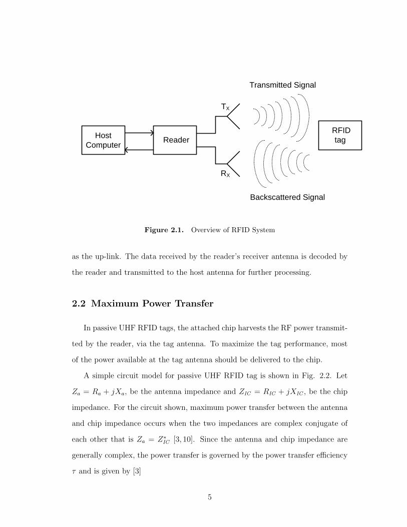
Transmitted Signal
Backscattered Signal
TX
RX
Host
ComputerReader
RFID
tag
Figure 2.1. Overview of RFID System
as the up-link. The data received by the reader’s receiver antenna is decoded by
the reader and transmitted to the host antenna for further processing.
2.2 Maximum Power Transfer
In passive UHF RFID tags, the attached chip harvests the RF power transmit-
ted by the reader, via the tag antenna. To maximize the tag performance, most
of the power available at the tag antenna should be delivered to the chip.
A simple circuit model for passive UHF RFID tag is shown in Fig. 2.2. Let
Za = Ra + jXa, be the antenna impedance and ZIC = RIC + jXIC , be the chip
impedance. For the circuit shown, maximum power transfer between the antenna
and chip impedance occurs when the two impedances are complex conjugate of
each other that is Za = Z∗IC [3, 10]. Since the antenna and chip impedance are
generally complex, the power transfer is governed by the power transfer efficiency
τ and is given by [3]
5
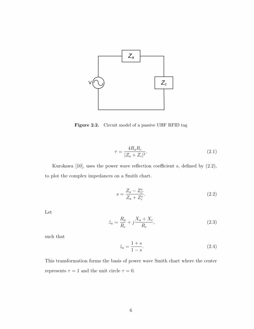
V
Za
Zc
Figure 2.2. Circuit model of a passive UHF RFID tag
τ =4RaRc
|Za + Zc|2. (2.1)
Kurokawa [10], uses the power wave reflection coefficient s, defined by (2.2),
to plot the complex impedances on a Smith chart.
s =Za − Z∗CZa + Z∗c
. (2.2)
Let
za =Ra
Rc
+ jXa +Xc
Rc
, (2.3)
such that
za =1 + s
1− s. (2.4)
This transformation forms the basis of power wave Smith chart where the center
represents τ = 1 and the unit circle τ = 0.
6
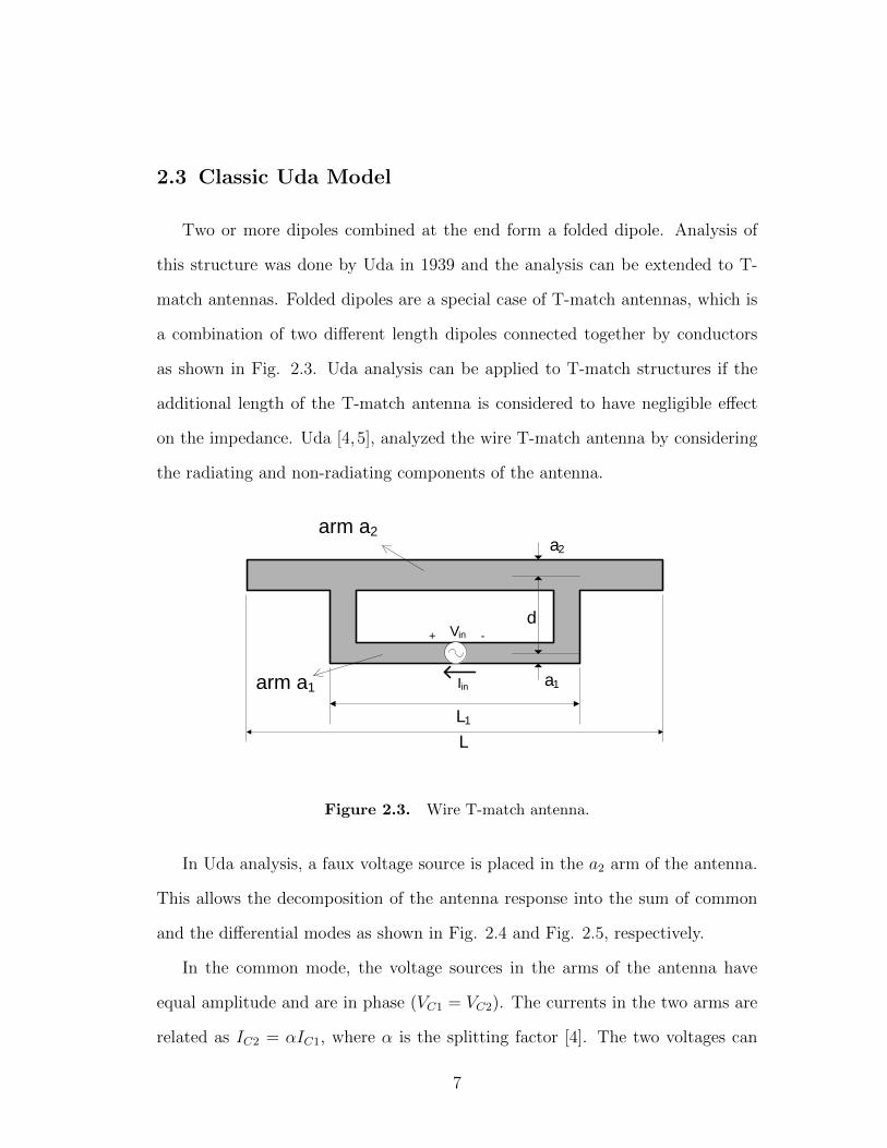
2.3 Classic Uda Model
Two or more dipoles combined at the end form a folded dipole. Analysis of
this structure was done by Uda in 1939 and the analysis can be extended to T-
match antennas. Folded dipoles are a special case of T-match antennas, which is
a combination of two different length dipoles connected together by conductors
as shown in Fig. 2.3. Uda analysis can be applied to T-match structures if the
additional length of the T-match antenna is considered to have negligible effect
on the impedance. Uda [4,5], analyzed the wire T-match antenna by considering
the radiating and non-radiating components of the antenna.
-+
L
L1
a1
a2
dVin
Iin
arm a2
arm a1
Figure 2.3. Wire T-match antenna.
In Uda analysis, a faux voltage source is placed in the a2 arm of the antenna.
This allows the decomposition of the antenna response into the sum of common
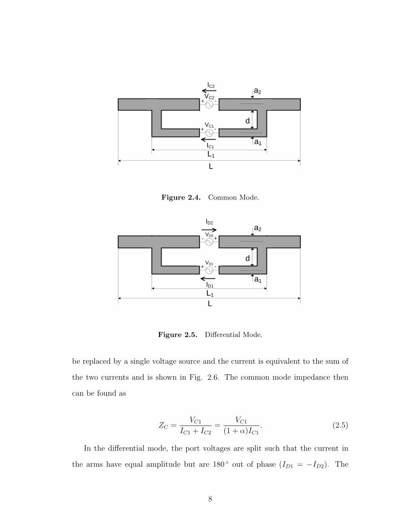
and the differential modes as shown in Fig. 2.4 and Fig. 2.5, respectively.
In the common mode, the voltage sources in the arms of the antenna have
equal amplitude and are in phase (VC1 = VC2). The currents in the two arms are
related as IC2 = αIC1, where α is the splitting factor [4]. The two voltages can
7
VC2
VC1
-+
-+
IC2
IC1
a2
d
a1
L1
L
Figure 2.4. Common Mode.
VD2
VD1
+-
-+
ID2
ID1
d
a1
L1
L
a2
Figure 2.5. Differential Mode.
be replaced by a single voltage source and the current is equivalent to the sum of
the two currents and is shown in Fig. 2.6. The common mode impedance then
can be found as
ZC =VC1
IC1 + IC2
=VC1
(1 + α)IC1
. (2.5)
In the differential mode, the port voltages are split such that the current in
the arms have equal amplitude but are 180 out of phase (ID1 = −ID2). The
8
VC1 -+
IC1 + IC2
d
a1
L1
L
a2
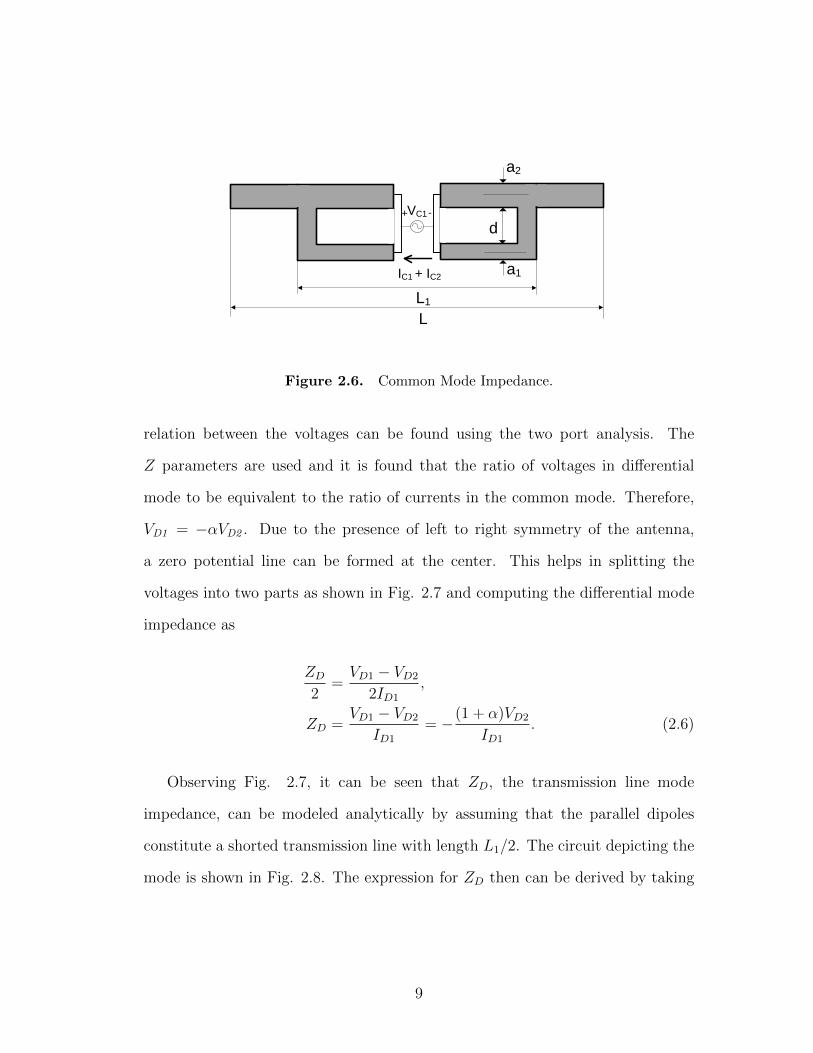
Figure 2.6. Common Mode Impedance.
relation between the voltages can be found using the two port analysis. The
Z parameters are used and it is found that the ratio of voltages in differential
mode to be equivalent to the ratio of currents in the common mode. Therefore,
VD1 = −αVD2 . Due to the presence of left to right symmetry of the antenna,
a zero potential line can be formed at the center. This helps in splitting the
voltages into two parts as shown in Fig. 2.7 and computing the differential mode
impedance as
ZD2
=VD1 − VD2
2ID1
,
ZD =VD1 − VD2
ID1
= −(1 + α)VD2
ID1
. (2.6)
Observing Fig. 2.7, it can be seen that ZD, the transmission line mode
impedance, can be modeled analytically by assuming that the parallel dipoles
constitute a shorted transmission line with length L1/2. The circuit depicting the
mode is shown in Fig. 2.8. The expression for ZD then can be derived by taking
9
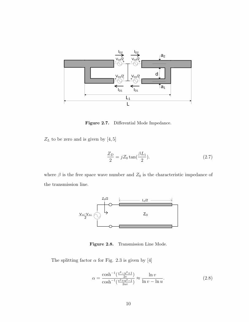
VD2/2
VD1/2
+-
-+
ID2
ID1
VD2/2
VD1/2
+-
-+
ID2
ID1
d
a1
L1
L
a2
Figure 2.7. Differential Mode Impedance.
ZL to be zero and is given by [4, 5]
ZD2
= jZ0 tan(βL1
2). (2.7)
where β is the free space wave number and Z0 is the characteristic impedance of
the transmission line.
ZD/2
ZO
L1/2
D1 D 2V V
2
Figure 2.8. Transmission Line Mode.
The splitting factor α for Fig. 2.3 is given by [4]
α =cosh−1(v
2−u2+12v
)
cosh−1(v2+u2−12uv
)≈ ln v
ln v − lnu. (2.8)
10

u = a2a1
, and v = da1
, where a1 and a2 are the radii of the first and second conductors
and d is the spacing between the conductors.
The input impedance of the antenna can be found by taking the superposition
of common mode and differential mode currents and voltages. In the first arm the
sum of the voltages is equal to Vin (the input voltage) and in the second arm the
sum of voltages is zero (faux voltage sources).
Vin = VC1 + VD1,
Iin = IC1 + ID1,
Va2 = VC2 + VD2 = 0, =⇒ VC2 = −VD2.
but, we know
VD1 = −αVD2, =⇒ VD1 = αVC2 = αVC1. (2.9)
The input impedance ZIN can then be computed as,
ZIN =Vin
Iin
=VC1 + αVC1
IC1 + ID1
, (2.10)
rewriting (2.5) and (2.6) as VC1 = ZC(1 + α)IC1 and ID1 = −(1 + α)VD2/ZD
respectively and substituting in (2.10) we get,
ZIN =(1 + α)VC1
IC1 + −(1+α)VD2
ZD
,
ZIN =(1 + α)VC1
IC1 + (1+α)VC1
ZD
,
ZIN =(1 + α)ZC(1 + α)IC1
IC1 + (1+α)ZC(1+α)IC1
ZD
, (2.11)
11
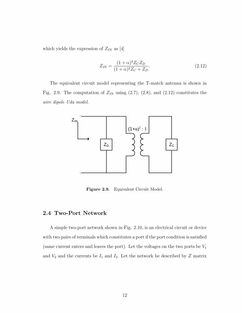
which yields the expression of ZIN as [4]
ZIN =(1 + α)2ZCZD
(1 + α)2ZC + ZD. (2.12)
The equivalent circuit model representing the T-match antenna is shown in
Fig. 2.9. The computation of ZIN using (2.7), (2.8), and (2.12) constitutes the
wire dipole Uda model.
ZD ZC
(1+α)2 : 1
ZIN
Figure 2.9. Equivalent Circuit Model.
2.4 Two-Port Network
A simple two-port network shown in Fig. 2.10, is an electrical circuit or device
with two pairs of terminals which constitutes a port if the port condition is satisfied
(same current enters and leaves the port). Let the voltages on the two ports be V1
and V2 and the currents be I1 and I2. Let the network be described by Z matrix
12
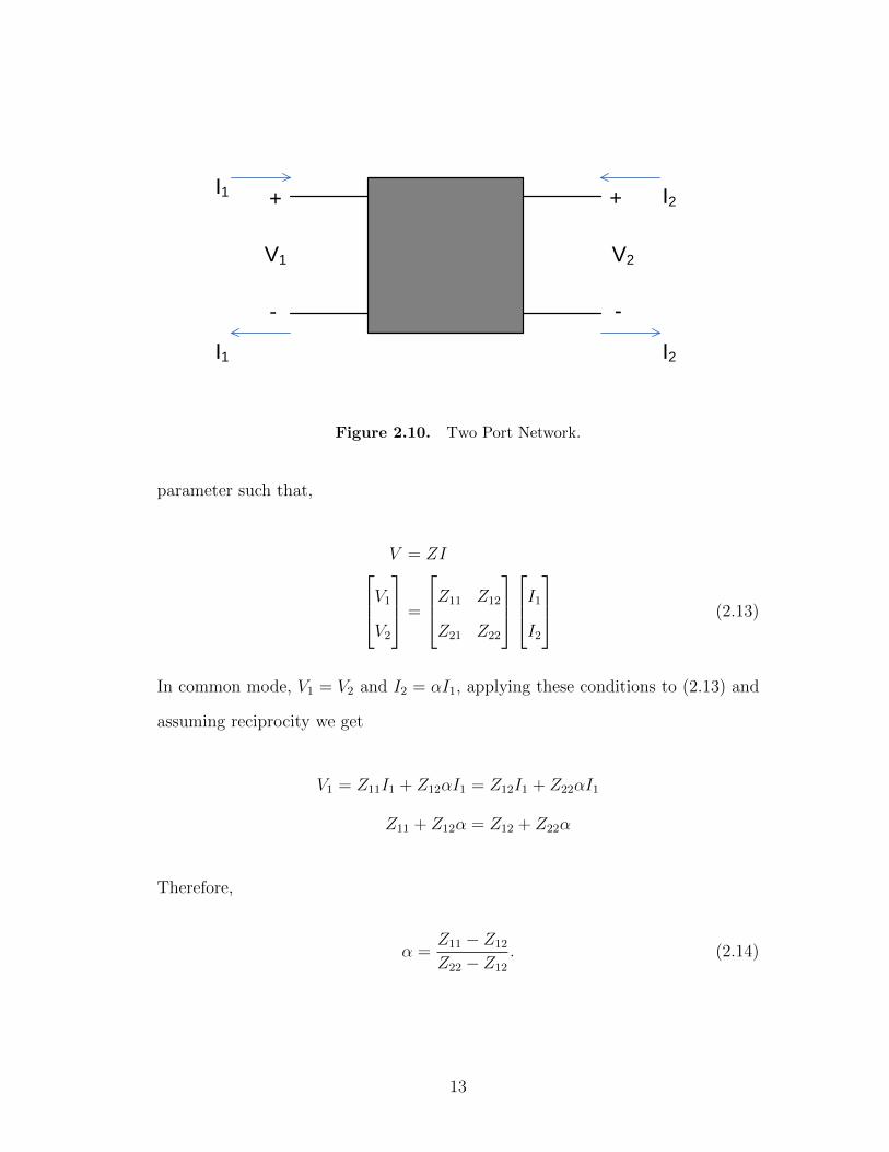
I1
I1
I2
I2
+
-
+
-
V1 V2
Figure 2.10. Two Port Network.
parameter such that,
V = ZIV1V2
=
Z11 Z12
Z21 Z22
I1I2
(2.13)
In common mode, V1 = V2 and I2 = αI1, applying these conditions to (2.13) and
assuming reciprocity we get
V1 = Z11I1 + Z12αI1 = Z12I1 + Z22αI1
Z11 + Z12α = Z12 + Z22α
Therefore,
α =Z11 − Z12
Z22 − Z12
. (2.14)
13
From (2.5) we know
ZC =V1
I1 + I2,
=Z11I1 + Z12αI1
I1 + αI1,
substituting (2.14), we get
ZC =Z11 + Z12
Z11−Z12
Z22−Z12
1 + Z11−Z12
Z22−Z12
,
=Z11Z22 − Z2
12
Z11 + Z22 − 2Z12
. (2.15)
In differential mode, we want I1 = −I2, to satisfy this condition let us compute
the relation between the two voltages. Assuming reciprocity we get
V1 = Z11I1 − Z12 I1,
V2 = Z12I1 − Z22I1,
V1V2
=Z11 − Z12
Z12 − Z22
,
V1 = −Z11 − Z12
Z22 − Z12
V2.
But α = Z11−Z12
Z22−Z12(2.14), therefore, V1 = −αV2.
Applying the differential mode conditions to (2.6) we get,
ZD =V1 − V2I1
=(1 + 1
α)V1
I1,
=(1 + 1
α)(Z11 − Z12)I1
I1. (2.16)
14

Substituting (2.14), we get
ZD = (1 +Z22 − Z12
Z11 − Z12
)(Z11 − Z12)
ZD = Z11 + Z22 − 2Z12 (2.17)
2.5 Strip Dipole Uda Model
In section 2.3, the analysis of a wire T-match antenna was presented, but
in general commercial RFID tag antennas are strip dipoles. Therefore, over the
years various evolutions of the Uda model have been proposed [7, 9, 11, 12] and
been applied to strip dipoles.
Thiele et al. [6] applies the wire Uda model to wire folded dipole with equal
arm diameters and shows that the transmission line mode in the Uda analysis
accurately predicts the input impedance of the folded wire dipole when the two
arms of the dipole are electrically close together. In [7], Visser applied the Uda
analysis to a strip folded dipole (using [11]) but needed to add correcting factors
to achieve good agreement between the analysis and full-wave simulation results.
Marrocco [2] and Choo et al. [9], apply the wire Uda model to a strip T-match
structure. The approximation for conversion of rectangular slab to an electrical
equivalent radius (W1 = 4a1) [5] is used to apply (2.7) and (2.8) on a strip T-
match structure. However, the authors do not validate the accuracy of the wire
dipole Uda model on the strip T-match antenna. In the following sections we will
discuss the methods to compute the model parameters for a strip dipole.
15
2.5.1 Common Mode Impedance
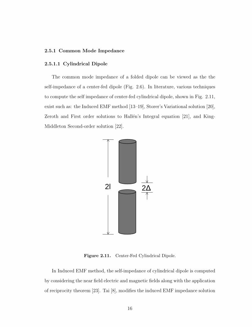
2.5.1.1 Cylindrical Dipole
The common mode impedance of a folded dipole can be viewed as the the
self-impedance of a center-fed dipole (Fig. 2.6). In literature, various techniques
to compute the self impedance of center-fed cylindrical dipole, shown in Fig. 2.11,
exist such as: the Induced EMF method [13–19], Storer’s Variational solution [20],
Zeroth and First order solutions to Hallen’s Integral equation [21], and King-
Middleton Second-order solution [22].
2l 2Δ
Figure 2.11. Center-Fed Cylindrical Dipole.
In Induced EMF method, the self-impedance of cylindrical dipole is computed
by considering the near field electric and magnetic fields along with the application
of reciprocity theorem [23]. Tai [8], modifies the induced EMF impedance solution
16
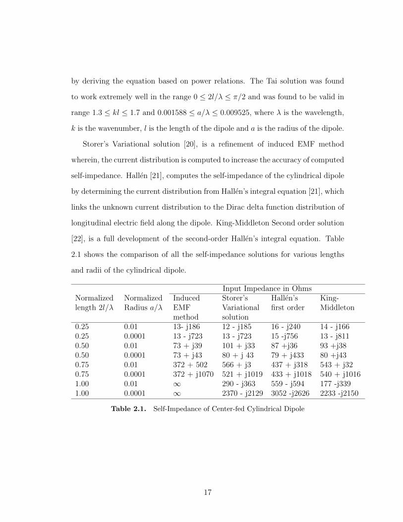
by deriving the equation based on power relations. The Tai solution was found
to work extremely well in the range 0 ≤ 2l/λ ≤ π/2 and was found to be valid in
range 1.3 ≤ kl ≤ 1.7 and 0.001588 ≤ a/λ ≤ 0.009525, where λ is the wavelength,
k is the wavenumber, l is the length of the dipole and a is the radius of the dipole.
Storer’s Variational solution [20], is a refinement of induced EMF method
wherein, the current distribution is computed to increase the accuracy of computed
self-impedance. Hallen [21], computes the self-impedance of the cylindrical dipole
by determining the current distribution from Hallen’s integral equation [21], which
links the unknown current distribution to the Dirac delta function distribution of
longitudinal electric field along the dipole. King-Middleton Second order solution
[22], is a full development of the second-order Hallen’s integral equation. Table
2.1 shows the comparison of all the self-impedance solutions for various lengths
and radii of the cylindrical dipole.
Input Impedance in OhmsNormalizedlength 2l/λ
NormalizedRadius a/λ
InducedEMFmethod
Storer’sVariationalsolution
Hallen’sfirst order
King-Middleton
0.25 0.01 13- j186 12 - j185 16 - j240 14 - j1660.25 0.0001 13 - j723 13 - j723 15 -j756 13 - j8110.50 0.01 73 + j39 101 + j33 87 +j36 93 +j380.50 0.0001 73 + j43 80 + j 43 79 + j433 80 +j430.75 0.01 372 + 502 566 + j3 437 + j318 543 + j320.75 0.0001 372 + j1070 521 + j1019 433 + j1018 540 + j10161.00 0.01 ∞ 290 - j363 559 - j594 177 -j3391.00 0.0001 ∞ 2370 - j2129 3052 -j2626 2233 -j2150
Table 2.1. Self-Impedance of Center-fed Cylindrical Dipole
17

2.5.1.2 Strip Dipole
A rectangular shape dipole of length l, width w and thickness t is known as
a Strip dipole. Such dipoles are easy to fabricated on dielectric substrates hence,
used as the antenna structure in most commercial RFID tags. If the strip is
slender (kw 1 and w l) then an equivalent cylindrical dipole of radius a and
length l can be found to compute the self-impedance of the strip dipole. Elliot [23],
gives the relationship between a and w as a = (w+ t)/4 and Balanis [5], assumes
(t λ) and approximates the relation as a = w/4.
The upper limit enforced on width of the antenna for the conversion is found
to be breached by most commercial RFID tag antennas, therefore, conventional
methods to compute self-impedance cannot be employed. Method of moment
(MoM) or Finite Element (FEM) tools, though can be used to effectively compute
self-impedance of the strip dipole. Moreover, many commercial RFID tag anten-
nas are built using meandered (to reduce the form factor of the antenna) dipoles
making the application of the self-impedance solutions improbable. Therefore, in
this thesis ZC , is computed using either MoM or FEM tool.
2.5.2 Splitting Factor
Lampe [11], applies the wire Uda model to Coplanar folded dipole antenna
shown in Fig. 2.12 and proposes an improvement in accuracy by accurately ap-
proximating the equivalent dipole radius and the splitting factor.
The splitting factor, α is the ratio of currents on the two conductors in the
common mode of the Uda analysis. When the potential at the two conductors is
the same and the end effect is ignored the ratio of currents in the two conductors
18

LW2
m
W1
Figure 2.12. Coplanar Strip folded dipole antenna.
is equivalent to the ratio of the charges, that is,
α =I2I1
=Q2
Q1
, (2.18)
where I1 and I2 are the currents in the conductors and Q1 and Q2 are the charges.
The charges on the two surfaces S1 and S2 can then be computed by solving
the two-dimensional, asymmetric coplanar strip problem
V (x) =
∫S1
q1(x′) ln |x− x′| dx′ +
∫S2
q2(x′) ln |x− x′| dx′, (2.19)
where q1(x) and q2(x) are the unknown charge distribution on the strip surfaces.
The total charge on each strip is given by
Q1 =
∫S1
q1(x) dx, Q2 =
∫S2
q2(x) dx. (2.20)
A single term, entire domain expansion function can be used to represent the
charge distribution to solve the problem. Point matching at the center of each strip
is used to test the potentials. The charge distribution have the same functional
19

form as the single strip charge distribution and are given as
q1(x) = a1[(W1/2)2 − (x+ c)2]−1/2, q2(x) = a2[(W2/2)2 − (x− c)2]−1/2, (2.21)
where a1 and a2 are unknown coefficients and c = (W1+W2+m+1)/4. Substitut-
ing (2.21) in (2.19), and finding the total charge using (2.20), α can be computed
as
α =Q2
Q1
=ln(4c+ 2[(2c)2 − (W1/2)2]1/2)− ln(W1)
ln(4c+ 2[(2c)2 − (W2/2)2]1/2)− ln(W2). (2.22)
2.5.3 Differential Mode Impedance
Differential mode impedance, (ZD) for a strip dipole can be computed by con-
sidering Fig. 2.8 and (2.7). Visser [7], applied the wire Uda model to a Coplanar
strip (CPS) folded dipole antenna, shown in Fig. 2.12, and proposes improved
design equations to improve the accuracy of the model. The width of CPS dipole
considered in the paper is 5 mm (lies within the conversion bound), thereby,
King-Middleton second-order solution [22] is used to compute ZC by considering
an equivalent cylindrical dipole of radius ρe. The splitting factor α is computed
using (2.22). The characteristic impedance Z0 in (2.7), is computed assuming that
the dipole is a CPS in a homogeneous medium of relative permitivity εr and is
given by the (2.23) [24,25]
Z0 =120π√εr
K(k)
K ′(k), (2.23)
where K(k) is the complete elliptic function of the first kind and K ′(k) = K(k′),
where k′2 = 1− k2. The approximated complete elliptic function of the first kind
20

can be found in [7, 26].
The author found that when the strip dipole is placed in free space the com-
puted ZIN using wire Uda model follows the simulated ZIN near resonance. But
when the dipole is placed on a dielectric slab the accuracy of the model degrades.
This degradation is attributed to the computation of Z0 as the effect of dielectric
slab needs to be accounted for while computing Z0. The author shows that the
accuracy of the model improves when Z0 is computed assuming a symmetric CPS
on a dielectric slab of height h and relative permittivity εr. For a asymmetric
CPS with finitely thick substrate the expression for Z0 [27] is given as
Z0 =60π√εeff
K ′(k1)
K(k1), (2.24)
where
εeff = 1 + q(εr − 1)
q =1
2
K(k2)
K ′(k2)
K ′(k1)
K(k1),
k1 =
√W1
W1 +m
W2
W2 +m,
k2 =
√sinh (πW1/2h)
sinh (π(W1 +m)/2h)
sinh (πW2/2h)
sinh (π(W2 +m)/2h),
where m is the slot width.
The computation of ZIN using (2.7), (2.24), (2.22), and (2.12) constitutes the
strip dipole Uda model. This model can be used to analyze strip dipoles effectively.
In this section, a brief background of RFID technology was discussed. The
wire and strip dipole Uda model were defined. The introduced strip dipole Uda
21

model can be applied to T-match antenna and can be used to analyze UHF RFID
tag antennas. To find the simulated ZC , α and ZD, two port network analysis was
also discussed. The condition for maximum power transfer between the antenna
and the attached chip is also defined.
22
Chapter 3
Embedded T-Match Antenna
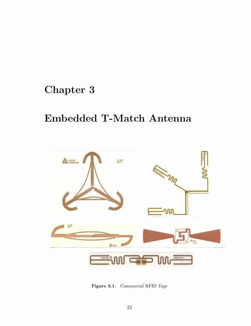
Figure 3.1. Commercial RFID Tags
23
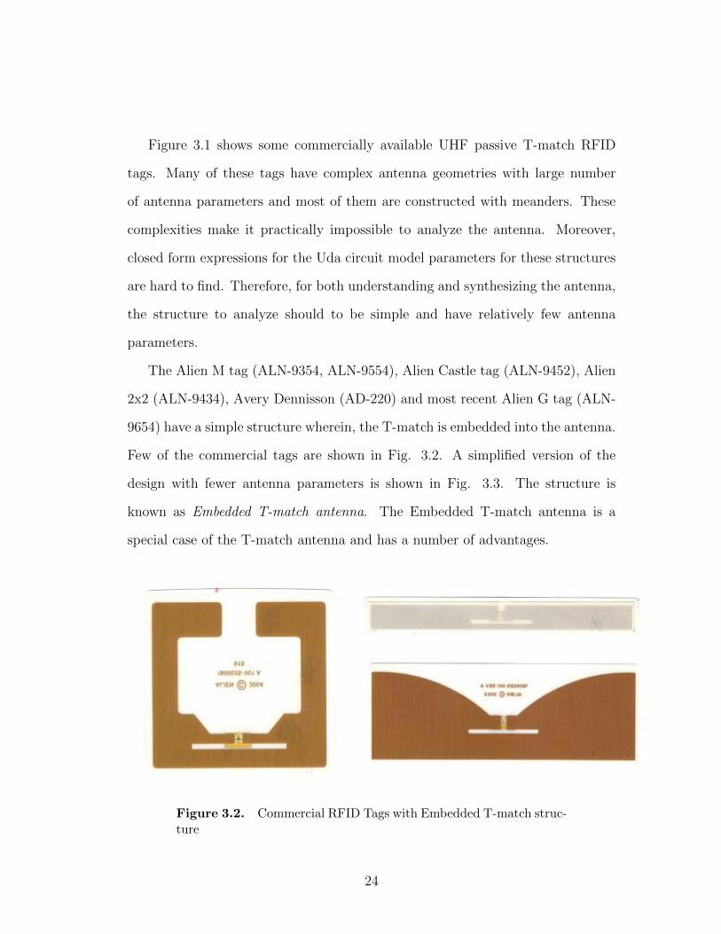
Figure 3.1 shows some commercially available UHF passive T-match RFID
tags. Many of these tags have complex antenna geometries with large number
of antenna parameters and most of them are constructed with meanders. These
complexities make it practically impossible to analyze the antenna. Moreover,
closed form expressions for the Uda circuit model parameters for these structures
are hard to find. Therefore, for both understanding and synthesizing the antenna,
the structure to analyze should to be simple and have relatively few antenna
parameters.
The Alien M tag (ALN-9354, ALN-9554), Alien Castle tag (ALN-9452), Alien
2x2 (ALN-9434), Avery Dennisson (AD-220) and most recent Alien G tag (ALN-
9654) have a simple structure wherein, the T-match is embedded into the antenna.
Few of the commercial tags are shown in Fig. 3.2. A simplified version of the
design with fewer antenna parameters is shown in Fig. 3.3. The structure is
known as Embedded T-match antenna. The Embedded T-match antenna is a
special case of the T-match antenna and has a number of advantages.
Figure 3.2. Commercial RFID Tags with Embedded T-match struc-ture
24
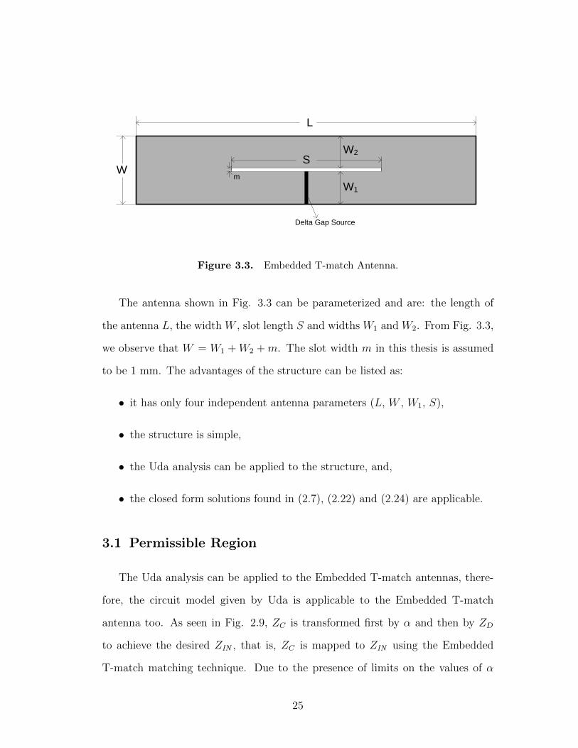
W
L
S
W1
W2
Delta Gap Source
m
Figure 3.3. Embedded T-match Antenna.
The antenna shown in Fig. 3.3 can be parameterized and are: the length of
the antenna L, the width W , slot length S and widths W1 and W2. From Fig. 3.3,
we observe that W = W1 + W2 + m. The slot width m in this thesis is assumed
to be 1 mm. The advantages of the structure can be listed as:
• it has only four independent antenna parameters (L, W , W1, S),
• the structure is simple,
• the Uda analysis can be applied to the structure, and,
• the closed form solutions found in (2.7), (2.22) and (2.24) are applicable.
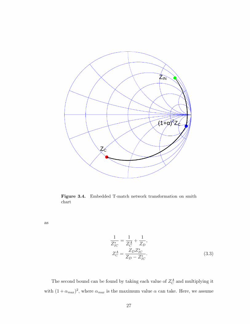
3.1 Permissible Region
The Uda analysis can be applied to the Embedded T-match antennas, there-
fore, the circuit model given by Uda is applicable to the Embedded T-match
antenna too. As seen in Fig. 2.9, ZC is transformed first by α and then by ZD
to achieve the desired ZIN , that is, ZC is mapped to ZIN using the Embedded
T-match matching technique. Due to the presence of limits on the values of α
25

and ZD, there are certain ZC values which can be transformed to ZIN . To find all
possible ZC values which can be transformed by the Embedded T-match antenna
we propose to study the permissible region of the antenna, which is defined as
the ”set of all possible values the common mode impedance, ZC , can take, which
when transformed using a matching network yields the desired impedance”.
The permissible region of Embedded T-match antenna can be found by study-
ing the transformation of ZC to ZIN . The first transformation of ZC is by a linear
multiplier (1+α)2 and can be represented on Smith chart by a linear curve. Shunt
impedance, ZD transforms (1 +α)2ZC by moving along the constant conductance
arc on the Smith chart. The transformation of ZC depicting the steps is shown in
Fig. 3.4.
To find the permissible region, we need to invert (2.12) to compute ZC in terms
of ZIN , ZD and α. To achieve maximum power transfer ZIN = Z∗IC , where ZIC is
the impedance of the attached chip. Bounds are also defined in order to get the
permissible region.
Z∗IC =(1 + α)2ZCZD
(1 + α)2ZC + ZD. (3.1)
This can be re-written as
1
Z∗IC
=1
(1 + α)2ZC+
1
ZD(3.2)
The first bound on the permissible region can be found by taking α to be 0 and
varying ZD from 0 to∞ Ω. This bound is represented as ZAC and can be computed
26
ZC
ZIN
(1+α)2ZC
Figure 3.4. Embedded T-match network transformation on smithchart
as
1
Z∗IC
=1
ZAC
+1
ZD,
ZAC =
ZDZ∗IC
ZD − Z∗IC
. (3.3)
The second bound can be found by taking each value of ZAC and multiplying it
with (1 +αmax )2, where αmax is the maximum value α can take. Here, we assume
27
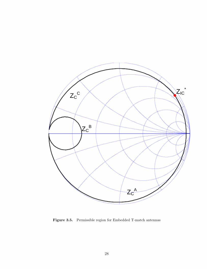
ZCA
ZCB
ZCC ZIC
*
Figure 3.5. Permissible region for Embedded T-match antennas
28
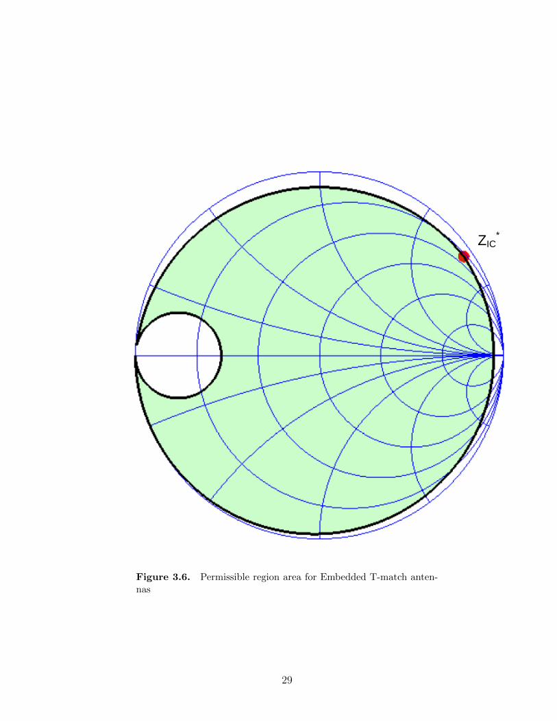
ZIC*
Figure 3.6. Permissible region area for Embedded T-match anten-nas
29

αmax to be 10. This bound is represented as ZBC and is given by
ZBC = (1 + αmax )−2ZA
C . (3.4)
Observing these bounds on the Smith chart we can then find the last bound by
taking ZD to be infinity and varying the value of α from 0 to αmax . Let the bound
be represented as ZCC and given by the expression
ZCC = (1 + αmax)
−2Z∗IC . (3.5)
The curves generated (ZIC = 14− j160 Ω) by ZAC , ZB
C and ZCC are shown in Fig.
3.5 and the area covered forms the permissible region for Embedded T-match
antennas and is shown in Fig. 3.6. The limits enforced on α and ZD are arbitrary.
3.2 Antenna Characteristics
To understand the Embedded T-match structure, experiments were conducted
wherein, the model parameters (L, W , W1 and S) were varied and the circuit
model parameters (ZC , α and ZD) were observed. Two port analysis was used
to compute the circuit model parameters, with the first port being placed on W1
arm and the second port on the W2 arm. The ports are constructed to replicate
delta gap sources and are shown in Fig. 3.7. The dipole antenna was placed in
free space and the frequency of operation was 915 MHz for all the experiments.
915 MHz was chosen as it is the center frequency of the Federal Communications
Commission (FCC) regulated frequency band for radio wave transmission in USA
and Canada.
Experiment 1
30

Port 1
L
WS
W1
Port 2
Figure 3.7. Two port analysis
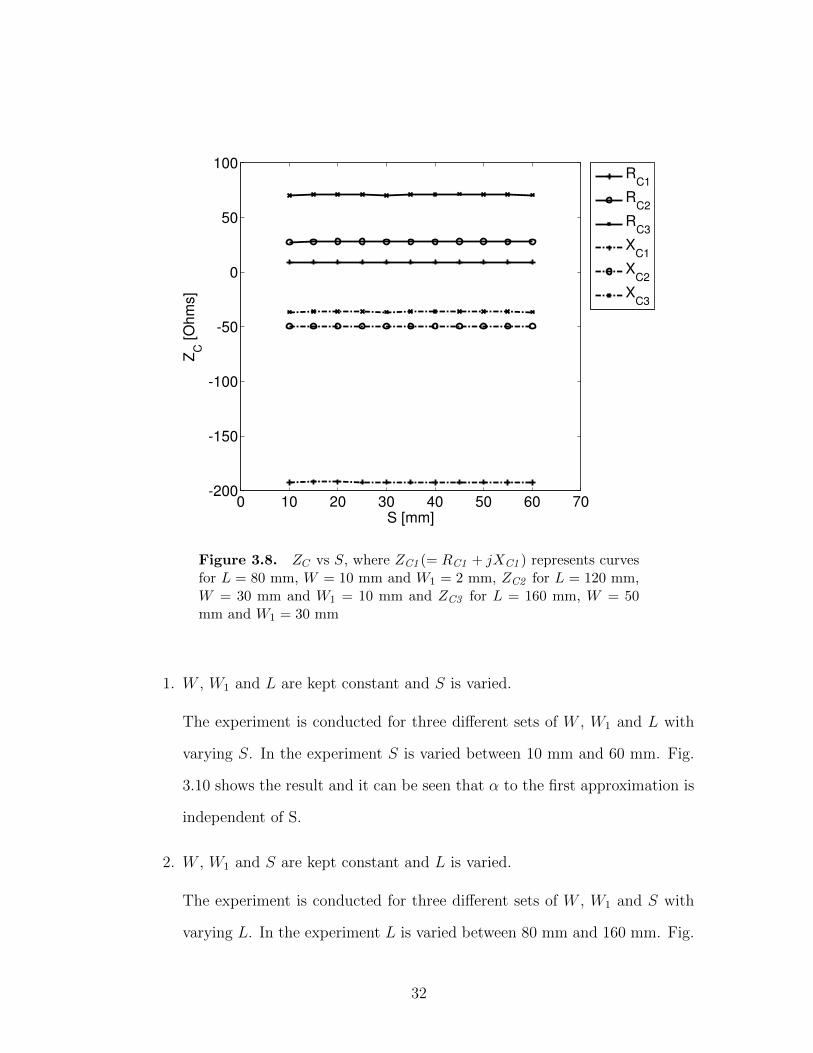
In the first experiment, the effect of model parameters on ZC is studied. ZC , is
the input impedance of a center-fed dipole, therefore, it depends only on L and W
of the embedded T-match antenna. The dependence on L and W can be verified
by studying the following cases
1. L, W and W1 are kept constant and S is varied.
Figure 3.8 shows the result of the experiment, wherein, three different sets
of L, W and W1 are used and S is varied between 10 mm to 60 mm for each
case. As can be seen ZC , is independent of S.
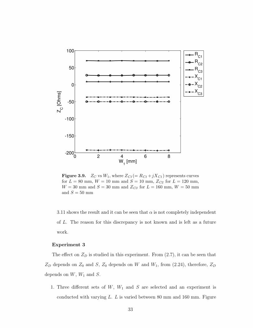
2. L, W and S are kept constant and W1 is varied.
In this experiment three different sets of L, W and S are used and W1 is
varied between 1 mm to 8 mm for each set. Figure 3.9 proves that ZC is
also independent of W1.
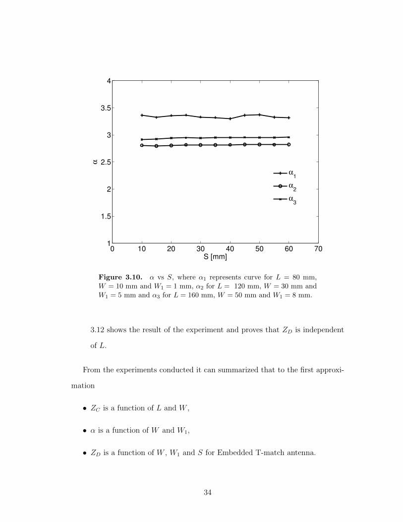
Experiment 2
The second experiment is conducted to observe the effect on model parameters
on α. From (2.22) it can be seen that α depends only on W and W1, this is further
verified by conducting the following experiments.
31
0 10 20 30 40 50 60 70-200
-150
-100
-50
0
50
100
S [mm]
ZC [
Oh
ms]
RC1
RC2
RC3
XC1
XC2
XC3
Figure 3.8. ZC vs S, where ZC1 (= RC1 + jXC1 ) represents curvesfor L = 80 mm, W = 10 mm and W1 = 2 mm, ZC2 for L = 120 mm,W = 30 mm and W1 = 10 mm and ZC3 for L = 160 mm, W = 50mm and W1 = 30 mm
1. W , W1 and L are kept constant and S is varied.
The experiment is conducted for three different sets of W , W1 and L with
varying S. In the experiment S is varied between 10 mm and 60 mm. Fig.
3.10 shows the result and it can be seen that α to the first approximation is
independent of S.
2. W , W1 and S are kept constant and L is varied.
The experiment is conducted for three different sets of W , W1 and S with
varying L. In the experiment L is varied between 80 mm and 160 mm. Fig.
32
0 2 4 6 8-200
-150
-100
-50
0
50
100
W1 [mm]
ZC [
Oh
ms]
RC1
RC2
RC3
XC1
XC2
XC3
Figure 3.9. ZC vs W1, where ZC1 (= RC1 +jXC1 ) represents curvesfor L = 80 mm, W = 10 mm and S = 10 mm, ZC2 for L = 120 mm,W = 30 mm and S = 30 mm and ZC3 for L = 160 mm, W = 50 mmand S = 50 mm
3.11 shows the result and it can be seen that α is not completely independent
of L. The reason for this discrepancy is not known and is left as a future
work.
Experiment 3
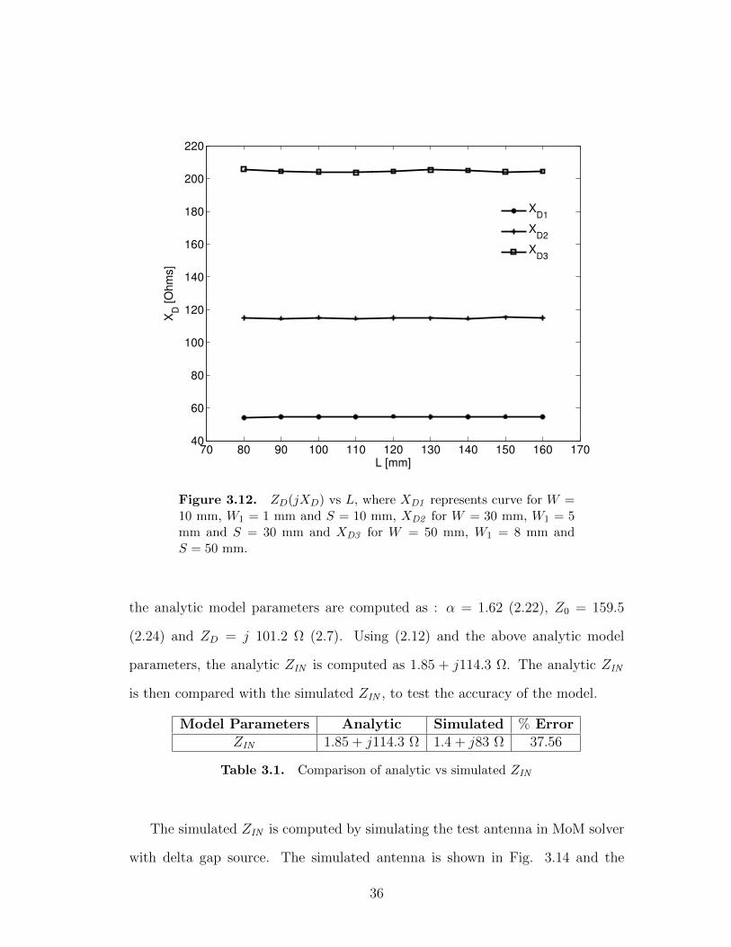
The effect on ZD is studied in this experiment. From (2.7), it can be seen that
ZD depends on Z0 and S, Z0 depends on W and W1, from (2.24), therefore, ZD
depends on W , W1 and S.
1. Three different sets of W , W1 and S are selected and an experiment is
conducted with varying L. L is varied between 80 mm and 160 mm. Figure
33
0 10 20 30 40 50 60 701
1.5
2
2.5
3
3.5
4
S [mm]
α
α1
α2
α3
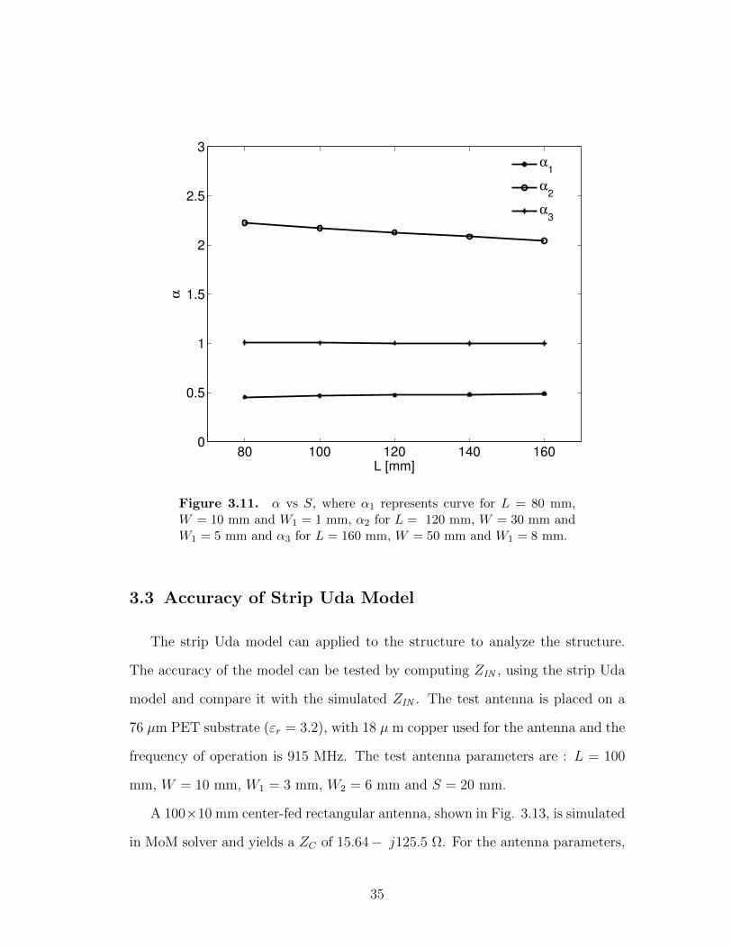
Figure 3.10. α vs S, where α1 represents curve for L = 80 mm,W = 10 mm and W1 = 1 mm, α2 for L = 120 mm, W = 30 mm andW1 = 5 mm and α3 for L = 160 mm, W = 50 mm and W1 = 8 mm.
3.12 shows the result of the experiment and proves that ZD is independent
of L.
From the experiments conducted it can summarized that to the first approxi-
mation
• ZC is a function of L and W ,
• α is a function of W and W1,
• ZD is a function of W , W1 and S for Embedded T-match antenna.
34
80 100 120 140 1600
0.5
1
1.5
2
2.5
3
L [mm]
α
α1
α2
α3
Figure 3.11. α vs S, where α1 represents curve for L = 80 mm,W = 10 mm and W1 = 1 mm, α2 for L = 120 mm, W = 30 mm andW1 = 5 mm and α3 for L = 160 mm, W = 50 mm and W1 = 8 mm.
3.3 Accuracy of Strip Uda Model
The strip Uda model can applied to the structure to analyze the structure.
The accuracy of the model can be tested by computing ZIN , using the strip Uda
model and compare it with the simulated ZIN . The test antenna is placed on a
76 µm PET substrate (εr = 3.2), with 18 µ m copper used for the antenna and the
frequency of operation is 915 MHz. The test antenna parameters are : L = 100
mm, W = 10 mm, W1 = 3 mm, W2 = 6 mm and S = 20 mm.
A 100×10 mm center-fed rectangular antenna, shown in Fig. 3.13, is simulated
in MoM solver and yields a ZC of 15.64− j125.5 Ω. For the antenna parameters,
35
70 80 90 100 110 120 130 140 150 160 17040
60
80
100
120
140
160
180
200
220
L [mm]
XD
[O
hm
s]
XD1
XD2
XD3
Figure 3.12. ZD(jXD) vs L, where XD1 represents curve for W =10 mm, W1 = 1 mm and S = 10 mm, XD2 for W = 30 mm, W1 = 5mm and S = 30 mm and XD3 for W = 50 mm, W1 = 8 mm andS = 50 mm.
the analytic model parameters are computed as : α = 1.62 (2.22), Z0 = 159.5
(2.24) and ZD = j 101.2 Ω (2.7). Using (2.12) and the above analytic model
parameters, the analytic ZIN is computed as 1.85 + j114.3 Ω. The analytic ZIN
is then compared with the simulated ZIN , to test the accuracy of the model.
Model Parameters Analytic Simulated % ErrorZIN 1.85 + j114.3 Ω 1.4 + j83 Ω 37.56
Table 3.1. Comparison of analytic vs simulated ZIN
The simulated ZIN is computed by simulating the test antenna in MoM solver
with delta gap source. The simulated antenna is shown in Fig. 3.14 and the
36

100 mm
10 mm
Port 1
Figure 3.13. Simulated ZC using MoM solver
simulated ZIN was found to be 1.4 + j83.1 Ω. This results in an error of 37.56
percent between the analytic and simulated ZIN and is tabulated in Table. 3.1.
Furthermore, the model was applied to similar antennas and the error was found
to be consistently larger than 20 percent.
Port 1
100 mm
10 mm20 mm
3 mm
Figure 3.14. Simulated ZIN using MoM solver
3.4 Error Diagnosis
The error in ZIN can be attributed to error in values of either analytic ZC ,
α, Z0, ZD or (2.12) itself. To find the origin of the error, the analytic circuit
model parameters can be compared to the simulated circuit model parameters.
The simulated circuit model parameters can be computed using two port analysis
and equations (2.15), (2.14) and (2.17). The second port is placed on the W2 arm
and delta gap sources are used. The MoM antenna design for two port analysis is
37
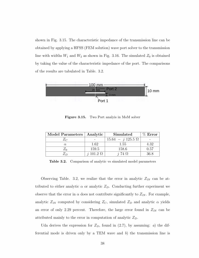
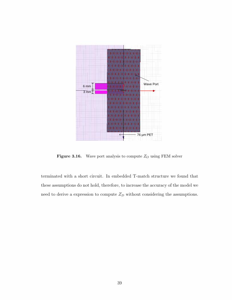
shown in Fig. 3.15. The characteristic impedance of the transmission line can be
obtained by applying a HFSS (FEM solution) wave port solver to the transmission
line with widths W1 and W2 as shown in Fig. 3.16. The simulated Z0 is obtained
by taking the value of the characteristic impedance of the port. The comparisons
of the results are tabulated in Table. 3.2.
Port 1
100 mm
10 mm20 mm
3 mm
Port 2
Figure 3.15. Two Port analyis in MoM solver
Model Parameters Analytic Simulated % ErrorZC - 15.64 − j 125.5 Ω -α 1.62 1.55 4.32Z0 159.5 158.6 0.57ZD j 101.2 Ω j 74 Ω 36.8
Table 3.2. Comparison of analytic vs simulated model parameters
Observing Table. 3.2, we realize that the error in analytic ZIN can be at-
tributed to either analytic α or analytic ZD. Conducting further experiment we
observe that the error in α does not contribute significantly to ZIN . For example,
analytic ZIN computed by considering ZC , simulated ZD and analytic α yields
an error of only 2.29 percent. Therefore, the large error found in ZIN can be
attributed mainly to the error in computation of analytic ZD.
Uda derives the expression for ZD, found in (2.7), by assuming: a) the dif-
ferential mode is driven only by a TEM wave and b) the transmission line is
38
6 mm
3 mm
Wave Port
76 µm PET
Figure 3.16. Wave port analysis to compute ZO using FEM solver
terminated with a short circuit. In embedded T-match structure we found that
these assumptions do not hold, therefore, to increase the accuracy of the model we
need to derive a expression to compute ZD without considering the assumptions.
39

Chapter 4
Augmented Uda Model
In this chapter we will further analyze the assumptions made in transmission
line mode of Uda analysis, derive the expression to compute ZD and, propose and
test Augmented Uda model.
4.1 Analysis of Error in Transmission Line Mode
In section 3.4, we found the error in analytic ZIN is due to assumptions made
while deriving the expression for ZD. To increase the accuracy of the model these
assumptions need to be incorporated into the expression of ZD.
4.1.1 Gap Capacitance
Recall that, Uda analyzes the wire T-match antenna by creating a faux voltage
source in one of the arms of the antenna and decomposing the antenna into com-
mon and transmission line modes. In the common and differential modes, there
are delta gap sources present in both arms of the antenna. This causes current to
flow on the edge and into the conductor. Fringing fields are also formed outside
40
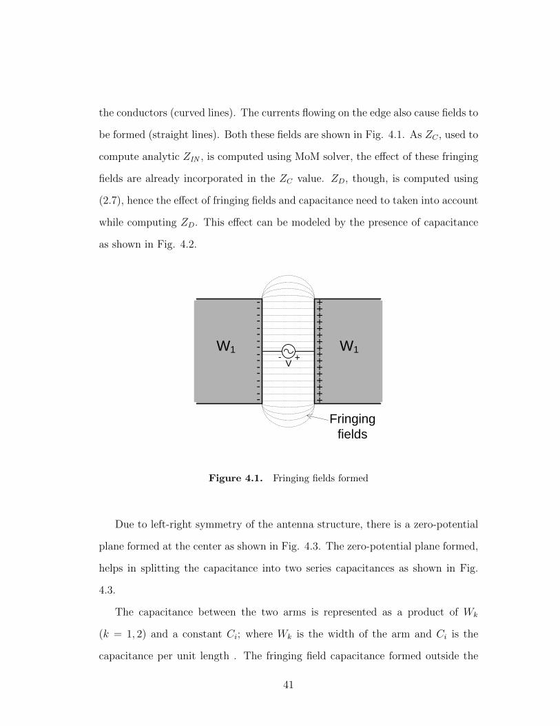
the conductors (curved lines). The currents flowing on the edge also cause fields to
be formed (straight lines). Both these fields are shown in Fig. 4.1. As ZC , used to
compute analytic ZIN , is computed using MoM solver, the effect of these fringing
fields are already incorporated in the ZC value. ZD, though, is computed using
(2.7), hence the effect of fringing fields and capacitance need to taken into account
while computing ZD. This effect can be modeled by the presence of capacitance
as shown in Fig. 4.2.
W1W1
-
+-
---------------
++++++++++++++++
V
Fringing
fields
Figure 4.1. Fringing fields formed
Due to left-right symmetry of the antenna structure, there is a zero-potential
plane formed at the center as shown in Fig. 4.3. The zero-potential plane formed,
helps in splitting the capacitance into two series capacitances as shown in Fig.
4.3.
The capacitance between the two arms is represented as a product of Wk
(k = 1, 2) and a constant Ci; where Wk is the width of the arm and Ci is the
capacitance per unit length . The fringing field capacitance formed outside the
41
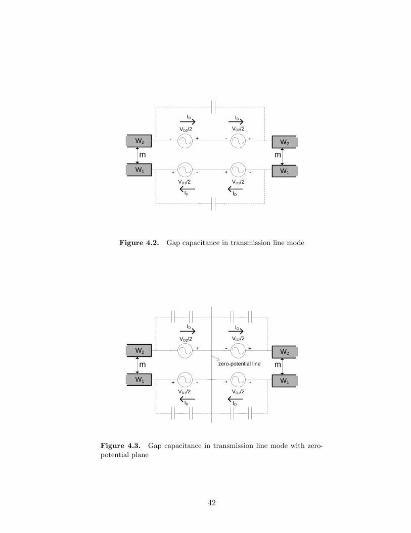
VD2/2 VD2/2
VD1/2 VD1/2
+
++
+-
-
-
-
ID
ID
ID
ID
W2 W2
W1W1
m m
Figure 4.2. Gap capacitance in transmission line mode
VD2/2 VD2/2
VD1/2 VD1/2
+
++
+-
-
-
-
ID
ID
ID
ID
zero-potential line
W2 W2
W1W1
m m
Figure 4.3. Gap capacitance in transmission line mode with zero-potential plane
42
arms is represented as another constant CO.
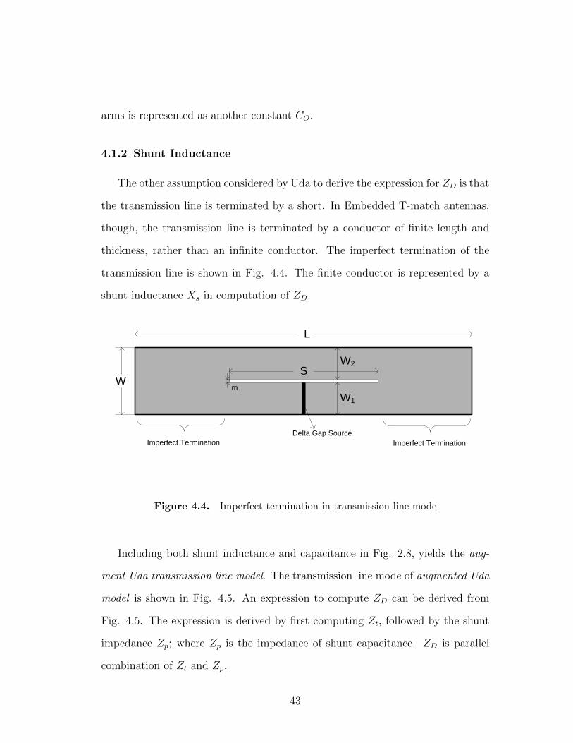
4.1.2 Shunt Inductance
The other assumption considered by Uda to derive the expression for ZD is that
the transmission line is terminated by a short. In Embedded T-match antennas,
though, the transmission line is terminated by a conductor of finite length and
thickness, rather than an infinite conductor. The imperfect termination of the
transmission line is shown in Fig. 4.4. The finite conductor is represented by a
shunt inductance Xs in computation of ZD.
W
L
S
W1
W2
Delta Gap Source
m
Imperfect Termination Imperfect Termination
Figure 4.4. Imperfect termination in transmission line mode
Including both shunt inductance and capacitance in Fig. 2.8, yields the aug-
ment Uda transmission line model. The transmission line mode of augmented Uda
model is shown in Fig. 4.5. An expression to compute ZD can be derived from
Fig. 4.5. The expression is derived by first computing Zt, followed by the shunt
impedance Zp; where Zp is the impedance of shunt capacitance. ZD is parallel
combination of Zt and Zp.
43
jXs
ZD/2
Zo
S/2
W1CiCo
Co W2Ci
Zt
D1 D 2V V2
Figure 4.5. Augmented Uda transmission line model
From Fig. 4.5, it can be observed that Zt is the input impedance of transmis-
sion line terminated by Xs.
Zt = Z0
(jXs + jZ0 tan(βS/2)
Z0 + jXs tan(βS/2)
),
for Xs Z0 and S λ/4,
Zt = Z0
(jXs + jZ0 tan(βS/2)
Z0
)Zt = jZ0 tan(βS/2) + jXs. (4.1)
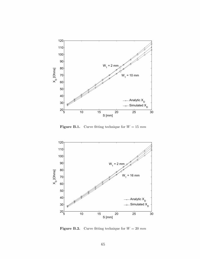
If we let Cp1 represent the parallel combination of CiW1 and Co and Cp2 =
CiW2 and Co, then the total shunt impedance is ZP = ZP1 + ZP2 , where ZP1 =
(jωCp1 )−1 and ZP2 = (jωCp2 )−1. The expression for ZD is then given by
ZD2
=ZpZtZp + Zt
. (4.2)
Computing ZIN using MoM solver, (2.22), (2.24) and (4.2) constitutes the aug-
mented Uda model.
44

4.2 Computation of Constants Ci, Co and Xs
From experience, it is observed that most RFID tag antennas are designed for
widths which lie between 10 mm and 25 mm. Therefore, the constants Ci, Co
and Xs in this thesis are optimized for these antennas. The dipoles in thesis are
designed for a 76 µm PET substrate (εr = 3.2), with 18 µm copper used for the
antenna. The frequency of operation is considered to be 915 MHz. The constants
can be computed using Curve fitting technique by observing ZD for varying W ,W1
and S.
ZD is observed by simulating the antenna design shown in Fig. 3.7 in MoM
solver and using (2.17) to compute the simulated ZD. A curve fitting technique
which yields an error less than 10 percent is applied for the following variations of
W , W1 and S : a) W varied between 10 mm and 25 mm, b) S varied between 6
mm and 30 mm and, c) W1 varied between 2 mm and (W −2) mm. For Xs = 4Ω,
Co = 0.135 pF and Ci = 0.155 pF/mm the error between the analytic ZD, using
(4.2), and simulated ZD was found to be less than 10 percent for all variations.
The curve fitting results for W = 10 mm and W = 25 mm is shown in Fig. 4.6 and
Fig. 4.7 respectively. The error found between the analytic ZD and simulated ZD
for W = 15 mm and W = 20 mm is shown in Fig. 4.8 and Fig. 4.9 respectively.
More results in the appendix.
For the example shown in section 3.3, Cp1 is calculated as 0.6 pF, Cp2 as 1.065
pF. This yields Zp1 of −289.9 Ω, Zp2 of −163.32 Ω and Zp of −453.22 Ω. With Xs
of 4 Ω, Zt is computed as j35 Ω and the new analytic ZD, using (4.2), is computed
as j75.89 Ω. Using (2.12) the analytic ZIN is computed as 0.95 + j81.98 Ω. This
yields an error of only 1.44 percent (recall simulated ZIN = 1.4+j83.1 Ω) between
the analytic and simulated ZIN . Also recall that the error found when using the
45
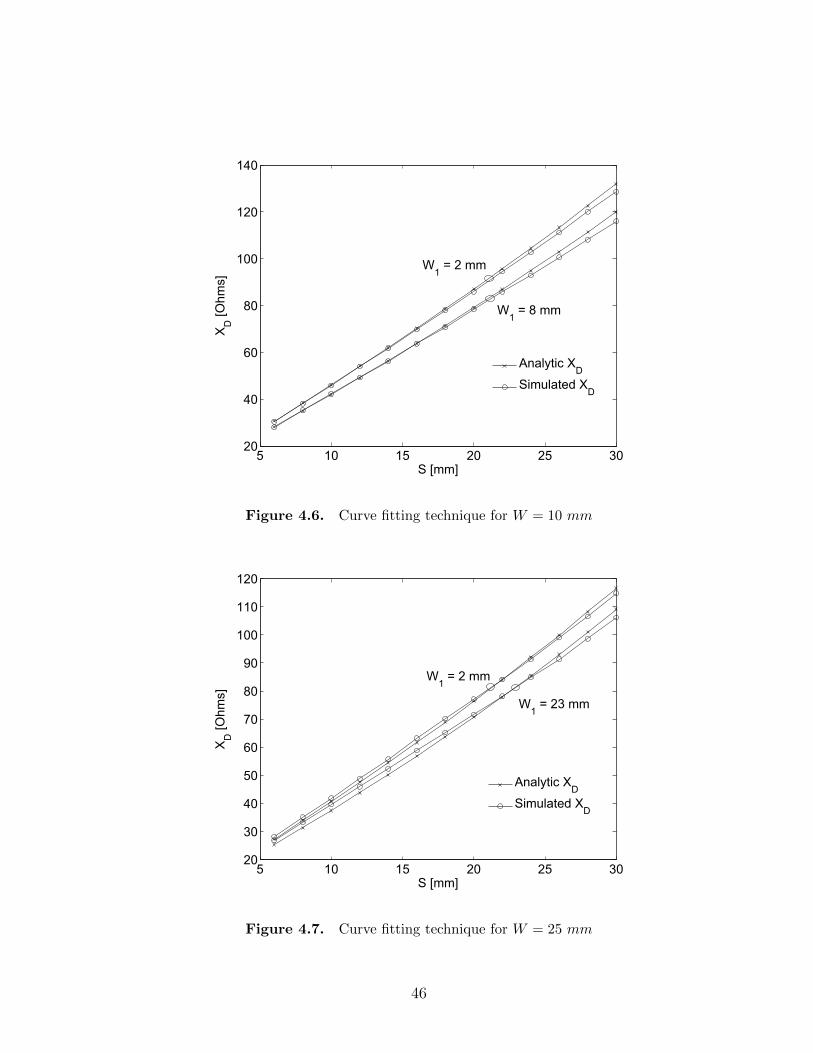
Figure 4.6. Curve fitting technique for W = 10 mm
!
!
Figure 4.7. Curve fitting technique for W = 25 mm
46
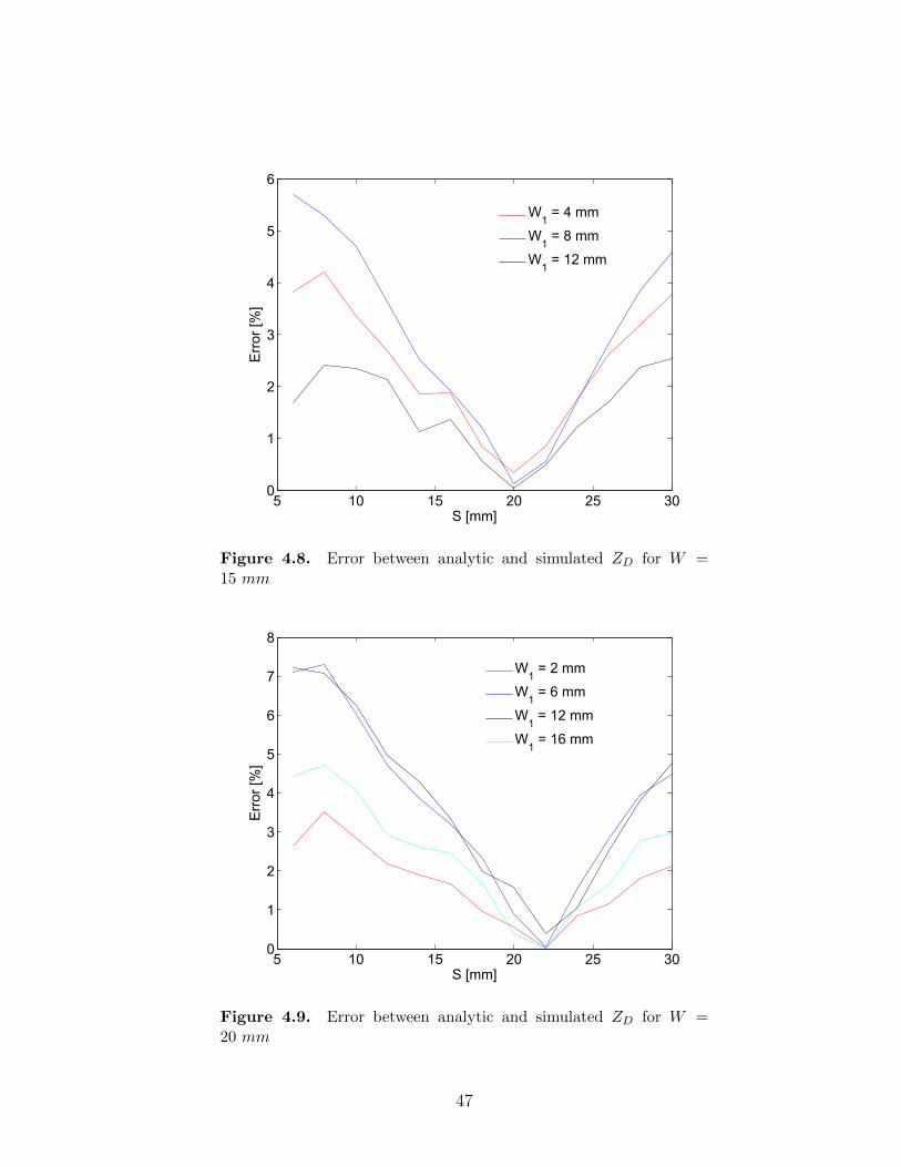
Figure 4.8. Error between analytic and simulated ZD for W =15 mm
Figure 4.9. Error between analytic and simulated ZD for W =20 mm
47

strip Uda model was 37.56 percent. Therefore with the use of the augmented
Uda model, the error is reduced considerably, which is a substantial improvement
over the previous model. This proves that the augmented Uda model works well
with the example, but to test the robustness of the model we need to validate the
model.
4.3 Validation
An effective way to validate the augmented Uda model is by comparing the
analytic ZIN values, computed using (2.12) with ZD computed using (4.2), with
the simulated ZIN , computed using numerical solvers (MoM and FEM codes). The
comparison is done by varying W1 and S for fixed L and W of the Embedded T-
match antenna. The frequency of operation is 915 MHz and the antenna is placed
on 76 µm PET substrate (εr = 3.2) with 18 µm copper used for the antenna. In
the numerical tools, the antenna is simulated with the delta gap source width of
0.2 mm.
The simulated ZC , using MoM solver, for L = 100 mm and W = 15 mm was
found to be 14.5 − j101.3 Ω. For each W1 and S combination, ZD is computed
using (4.2), Z0 using (2.24) and α using (2.22). The computed values along with
simulated ZC is then used to compute analytic ZIN . As S is varied from 6 to
30 mm, and W1 from 3 to 13 mm the comparison of the resistive and reactive
component of the ZIN is shown in Fig. 4.10 and Fig. 4.11 respectively. The
shown graphs are cropped, to restrict the upper limit on the impedance, and
results for only certain W1 values are plotted. This is done to increase the clarity
of the graph and to make the curves distinguishable from each other.
From the results shown in Fig. 4.10 and Fig. 4.11, we can conclude that the
48
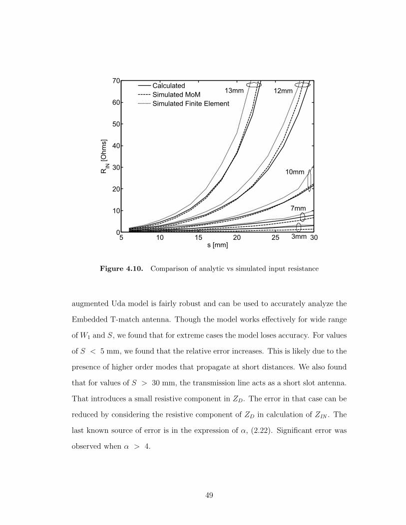
!
Figure 4.10. Comparison of analytic vs simulated input resistance
augmented Uda model is fairly robust and can be used to accurately analyze the
Embedded T-match antenna. Though the model works effectively for wide range
of W1 and S, we found that for extreme cases the model loses accuracy. For values
of S < 5 mm, we found that the relative error increases. This is likely due to the
presence of higher order modes that propagate at short distances. We also found
that for values of S > 30 mm, the transmission line acts as a short slot antenna.
That introduces a small resistive component in ZD. The error in that case can be
reduced by considering the resistive component of ZD in calculation of ZIN . The
last known source of error is in the expression of α, (2.22). Significant error was
observed when α > 4.
49
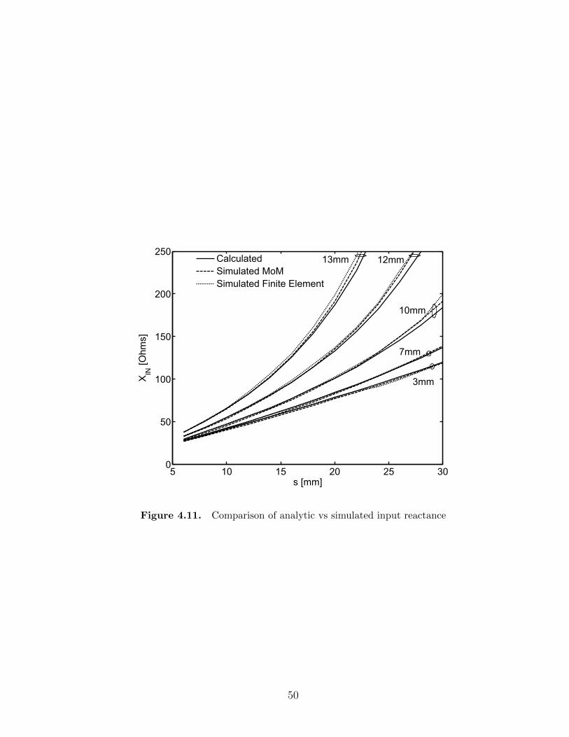
Figure 4.11. Comparison of analytic vs simulated input reactance
50

Chapter 5
Synthesis
RFID antennas are typically designed to transfer maximum power recieved by
the antenna to the attached chip. Maximum power transfer between the antenna
and chip occurs when the antenna impedance is complex conjugate of the chip
impedance.
Generally, when designing RFID antennas, the given design constraints are
the form factor (L and W ) of the antenna and the attached chip impedance ZIC .
Therefore, to synthesize the antenna geometry of the Embedded T-match antenna
only S and W1 need to be computed. Recall that ZC is independent of S and
W1 and and α is independent of S. Therefore, the antenna geometry can be
synthesized by executing the following steps:
Step 1 For given L and W , ZC is computed using MoM solver,
Step 2 using ZC , ZIC and (2.12), αreq and ZDreq is computed for maximum power
transfer,
Step 3 using (2.22) and αreq , W1 is computed,
51

Step 4 using (4.2) and ZDreq , S is computed.
Few notations taken into account are as follows:
ZIC = RIC − jXIC
ZC = RC − jXC
ZIN = RIN + jXIN
ZD = jXD (5.1)
The expression for αreq and ZDreq can be derived as follows:
for maximum power transfer ZIN = Z∗IC , therefore,
ZIN =(1 + αreq)2ZCZDreq
(1 + αreq)2ZC + ZDreq
= Z∗IC , (5.2)
using (5.1)
ZIN =(1 + αreq)2(RC − jXC)jXDreq
(1 + αreq)2(RC − jXC) + jXDreq
= RIC + jXIC . (5.3)
Let (1 + αreq)2 = Y . Re-writing the above expression we get
Y (RC − jXC)jXDreq = (RIC + jXIC )(Y (RC − jXC) + jXDreq), (5.4)
expanding the above expression we get,
jY RCXDreq + Y XCXDreq = Y RCRIC + Y XICXC −XICXDreq
+ j(Y RCXIC − Y RICXC +RICXDreq) (5.5)
52
Equating the real and imaginary parts, we get
Y XCXDreq = Y RCRIC + Y XCXIC −XICXDreq , (5.6)
Y RCXDreq = Y RCXIC − Y RICXC +RICXDreq . (5.7)
Solving for XDreq and Y we get
Y =RC(R2
IC +X2IC )
RIC (R2C +X2
C), (5.8)
XDreq =RC(R2
IC +X2IC )
RICXC +XICRC
. (5.9)
Subsequently, the expressions for ZDreq and αreq are:
αreq =
√RC(R2
IC +X2IC )
RIC (R2C +X2
C)− 1, (5.10)
ZDreq = jXD = −j RC(R2IC +X2
IC )
RCXIC +RICXC
. (5.11)
The derivation of the expressions can be found in Appendix.
From experience it is observed that α is monotonic with respect to width W ,
therefore, we can compute the values of W1 and W2 using bisection method. The
values can be computed using (2.22) for the particular αreq . The characteristic
impedance, Z0 of the asymmetric coplanar strip with widths W1 and W2 can
then be computed using (2.24). The slot length, S required for maximum power
transfer can then be computed using Z0, ZDreq and (4.2). The expression for S
can be derived as follows:
53

recall, (4.2)
ZDreq
2=
ZpZtZp + Zt
, (5.12)
=Zp(jZ0 tan(βS/2) + jXS)
Zp + jZ0 tan(βS/2) + jXS
. (5.13)
Solving for S
ZDreq(Zp + jZ0 tan(βS/2) + jXS) = 2Zp(jZ0 tan(βS/2) + jXS), (5.14)
ZDreqZp + jZDreqXS − j2XSZp = j2ZpZ0 tan(βS/2)− jZDreqZ0 tan(βS/2),
(5.15)
ZDreqZp + jXS(ZDreq − 2Zp) = jZ0 tan(βS/2)(2Zp − jZDreq), (5.16)
Therefore,
tan(βS/2) =1
jZ0
(ZDreqZp
(2Zp − jZDreq)− jXS
), (5.17)
S =2
βtan−1
((ZpZDreq
2Zp − ZDreq
− jXS
)1
jZ0
). (5.18)
To validate the synthesis process an Embedded T-match antenna was designed
for Higgs 2 chip. The initial design constraints given are the: L = 100 mm,
W = 15 mm, and ZIC = 11 − j133 Ω (Higgs 2 chip). The tag is designed to
be placed on 76 µm PET substrate (εr = 3.2) with 18 µ m copper used for the
antenna and the frequency of operation considered is 915 MHz. For the given
L and W , the simulated ZC was found to be 14.5 − j101.3 Ω, using the MoM
solver. Using (5.10) and (5.11) we found αreq = 0.498 and ZDreq = j84.9 Ω. Using
bisection method and αreq value we get W1 and W2 to be 10.07 mm and 3.93 mm
54

respectively, analytic Z0 using (2.24) is found to be 146.9 Ω, Zp for the antenna
is found to be −j 350.7 Ω and XS = 4 Ω. From (5.18) we compute S value to
be 23.6 mm.
An antenna with the geometry obtained is simulated in MoM solver to compute
ZIN . The antenna parameters can be summarized as: L = 100 mm, W = 15 mm,
W1 = 10.07 mm and S = 23.6 mm. The antenna was simulated with delta gap
source and the simulated ZIN was found to be 10.8 + j127.8 Ω, which yields an
error of 3.9 percent from Z∗IC with τ = 0.9295 (−0.6350 dB).
55

Chapter 6
Conclusion
RFID technology is used to track and identify products/objects. Radio waves
are transmitted by a reader, RFID tag receives this signal (if in vicinity), the chip
on the tag modulates the signal and backscatters it to the reader with a unique ID.
UHF RFID passive tags are easy to fabricate and can be manufactured at low cost,
thereby, are being used in everyday life. Features, such as, read range, frequency of
operation, environment, bandwidth etc. drive the UHF passive RFID tag antenna
design. The tag antenna design can be expedited if the antenna characteristics are
known. To increase the read range of the UHF passive RFID tag, among others,
maximum power transfer between the chip and the antenna needs to be attained.
Uda analysis of wire T-match antenna helps in characterizing the antenna.
THe Wire dipole Uda model, which is applicable to wire dipole antennas, has
been modified by researchers for strip dipoles. The model proposed in this thesis
is defined as strip dipole Uda model. Commercial RFID tags are constructed
using strip dipoles because they are easy to fabricate and manufacture. Most of
the commercial UHF passive RFID tags are complex and are difficult to analyze.
The Embedded T-match antenna, which is special case of T-match antenna
56

is a simple antenna design with numerous advantageous. Uda analysis can be
applied to this structure for analysis. The permissible region for the Embedded
T-match antenna is also found and is seen to be limited by the maximum value α
and ZD can take. The strip dipole Uda model is applied to this structure and it is
found that the analytic ZIN has an error of more than 20 percent when compared
to the simulated ZIN . The error in analytic ZIN was found to be due to the
assumptions made while deriving the expression for ZD (2.7). Gap capacitance and
shunt inductance are introduced in the expression of ZD to improve the accuracy.
An augment Uda model for strip dipoles is defined with the new derived ZD
expression.
The accuracy of the model was tested and the error was found to be less than 2
percent. The augmented Uda model was validated by comparing the analytic ZIN
with the simulated ZIN found using the MoM and FEM solvers. The simplicity
of the Embedded T-match structure helps in using the augmented Uda model
to synthesize the antenna geometry. For a given chip impedance, L and W ,
embedded T-match can be constructed for maximum power transfer condition.
The synthesis process was also tested and was found to be accurate.
In conclusion the Uda model which is applicable to folded dipoles can be
extended to T-match antennas but with errors. The Embedded T-match antenna
which is a special case of T-match can be analyzed using the Uda model. The
proposed model increases the accuracy computing the input impedance of the
Embedded T-match antenna. The proposed model also helps in understanding,
analyzing and synthesizing the Embedded T-match antenna.
57

Chapter 7
Future Work
Since expressions to compute ZC are hard to find for fat dipoles, ZC is com-
puted using MoM solver, in this thesis. An expression to compute analytic ZC for
fat dipoles needs to be derived and used in the model to reduce the dependency on
the numerical tools and further reduce the time taken to design the tag antenna.
We also noticed small error in computation of analytic ZIN , this may be due to
presence of small RD (resistance associated with ZD). The error found can be
further reduced by computing ZIN by considering RD.
The permissible region for the Embedded T-match antenna was found by forc-
ing arbitrary limits on the maximum value α and ZD can take. Practical limits for
α and ZD need to be found to compute the permissible region. While studying the
characteristics of the Embedded T-match antenna, α was found to be dependent
on L. Observing (2.22), it can be seen that α depends mostly on W and W1.
Therefore, this discrepancy needs to be further examined and corrected.
The augmented Uda model was applied and tested at only one frequency (915
MHz). The application of the model at other frequencies can also be validated
and tested. The expansion of this model to other frequencies can help in deter-
58

mining the bandwidth of the antenna. The values for gap capacitance and shunt
inductance were obtained using curve fitting technique. A more rigorous analysis
can be conducted to derive the equations to compute the constants. This would
further simplify the analysis of the antenna.
The Uda analysis in this thesis is applied to a dipole Embedded T-match
antenna. As a future work one can apply the analysis to a microstrip Embedded
T-match antenna and test the accuracy of the model. The model can also be used
to study the effect of dielectric substrates on performance of Embedded T-match
antenna.
59

Appendix A
Antenna Characteristics
This appendix contains more results for experiment conducted in section 3.2.
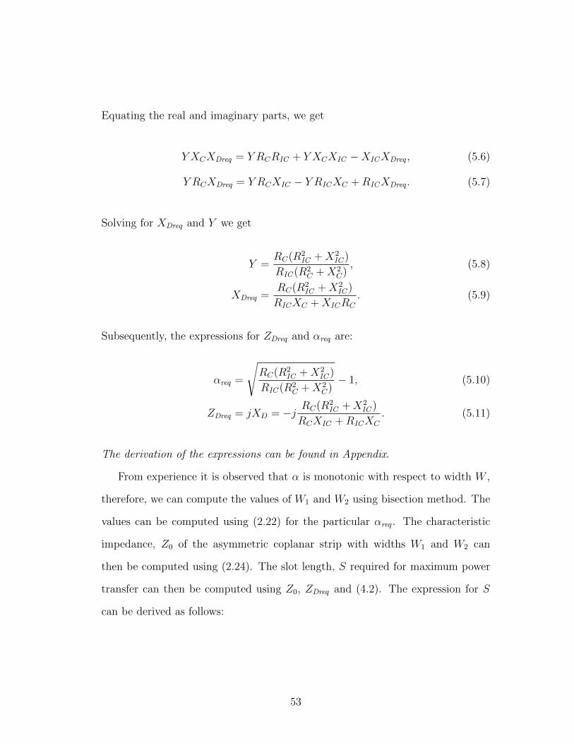
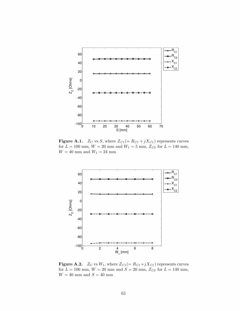
A.1 ZC vs. S and W1
Figure A.1 and A.2 shows the result of the experiment conducted for ZC for
varying S and W1 respectively. S is varied between 10 mm and 60 mm and W1 is
varied between 1 mm and 8 mm.
A.2 α vs. S and L
Figure A.3 and A.4 shows the result of the experiment conducted for α for
varying S and L respectively. S is varied between 10 mm and 60 mm and L is
varied between 80 mm and 160 mm.
60
0 10 20 30 40 50 60 70-100
-80
-60
-40
-20
0
20
40
60
S [mm]
ZC [
Oh
ms]
RC1
RC2
XC1
XC2
Figure A.1. ZC vs S, where ZC1 (= RC1 + jXC1 ) represents curvesfor L = 100 mm, W = 20 mm and W1 = 5 mm, ZC2 for L = 140 mm,W = 40 mm and W1 = 24 mm
0 2 4 6 8-100
-80
-60
-40
-20
0
20
40
60
W1 [mm]
ZC [
Oh
ms]
RC1
RC2
XC1
XC2
Figure A.2. ZC vs W1, where ZC1 (= RC1 +jXC1 ) represents curvesfor L = 100 mm, W = 20 mm and S = 20 mm, ZC2 for L = 140 mm,W = 40 mm and S = 40 mm
61
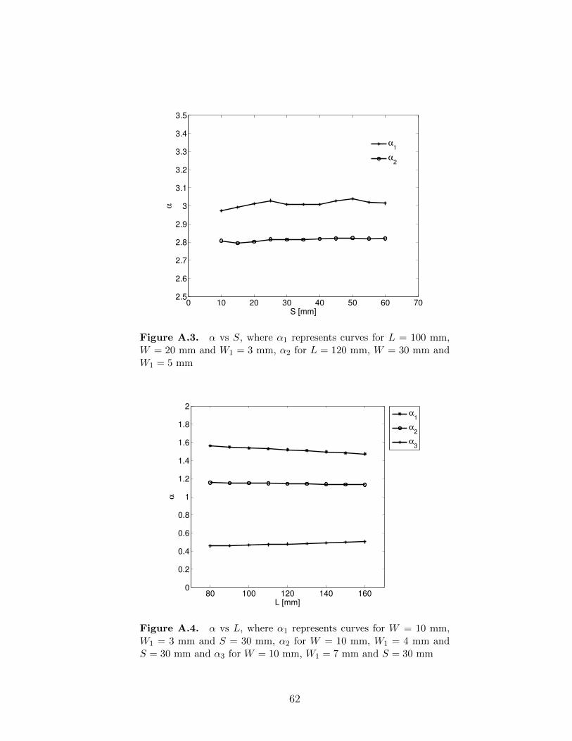
0 10 20 30 40 50 60 702.5
2.6
2.7
2.8
2.9
3
3.1
3.2
3.3
3.4
3.5
S [mm]
α
α1
α2
Figure A.3. α vs S, where α1 represents curves for L = 100 mm,W = 20 mm and W1 = 3 mm, α2 for L = 120 mm, W = 30 mm andW1 = 5 mm
80 100 120 140 1600
0.2
0.4
0.6
0.8
1
1.2
1.4
1.6
1.8
2
L [mm]
α
α1
α2
α3
Figure A.4. α vs L, where α1 represents curves for W = 10 mm,W1 = 3 mm and S = 30 mm, α2 for W = 10 mm, W1 = 4 mm andS = 30 mm and α3 for W = 10 mm, W1 = 7 mm and S = 30 mm
62
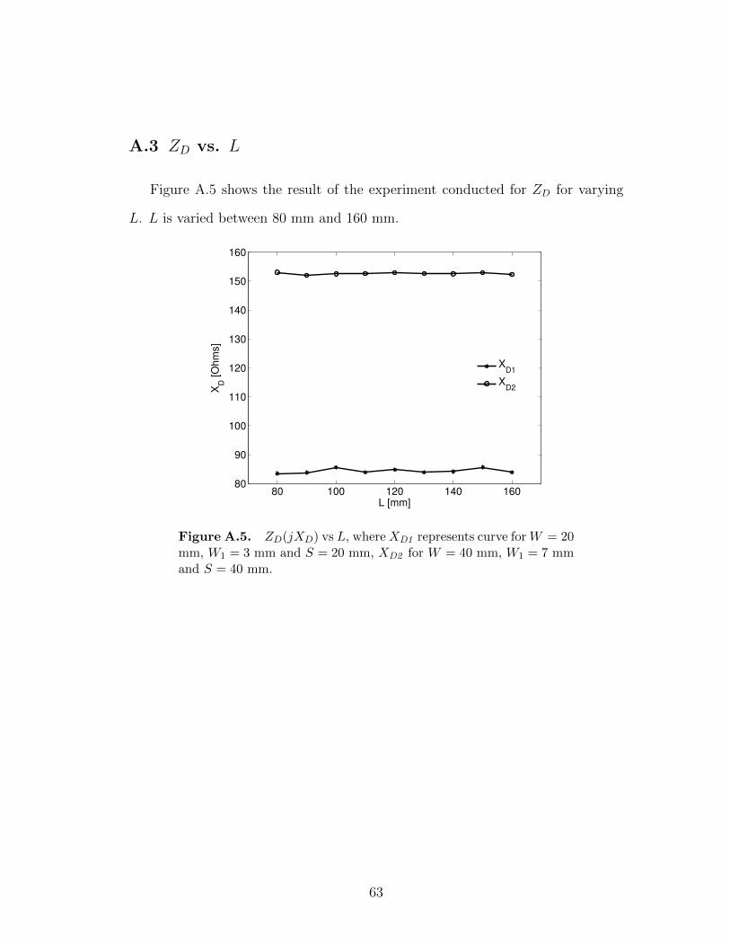
A.3 ZD vs. L
Figure A.5 shows the result of the experiment conducted for ZD for varying
L. L is varied between 80 mm and 160 mm.
80 100 120 140 16080
90
100
110
120
130
140
150
160
L [mm]
XD [
Oh
ms]
XD1
XD2
Figure A.5. ZD(jXD) vs L, whereXD1 represents curve forW = 20mm, W1 = 3 mm and S = 20 mm, XD2 for W = 40 mm, W1 = 7 mmand S = 40 mm.
63

Appendix B
Computation of Constants
Figure B.1 and B.2 shows the curve fitting technique graph generated while
computing the constants Ci, Co and Xs for W = 15 mm and W = 20 mm
respectively.
Figure B.3 and B.4 shows the error found between analytic and simulated ZD
for W = 10 mm and W = 25 mm respectively.
64
!
!
Figure B.1. Curve fitting technique for W = 15 mm
!
!
Figure B.2. Curve fitting technique for W = 20 mm
65
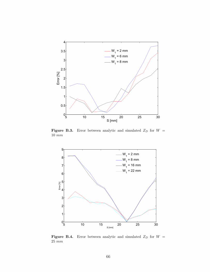
Figure B.3. Error between analytic and simulated ZD for W =10 mm
Figure B.4. Error between analytic and simulated ZD for W =25 mm
66

Appendix C
Derivation
In this appendix the derivation for ZDreq and αreq is shown.
Equation (5.6) can be re-written as
Y =−XICXDreq
XCXDreq +RCRIC +XCXIC
, (C.1)
substituting (C.1) in (5.7), we get
RICXDreq = Y (RCXDreq −RCXIC +RICXC), (C.2)
=
(−XICXDreq
XCXDreq +RCRIC +XCXIC
)(RCXDreq −RCXIC +RICXC). (C.3)
Solving for XDreq
−XICXDreqRC +RCX2IC −RICXCXIC = RICXCXDreq −RCR
2IC −RICXICXC ,
RC(R2IC +X2
IC ) = XDreq(RICXC +XICRC). (C.4)
67

The expression for XDreq is found to be
XDreq =RC(R2
IC +X2IC )
RICXC +XICRC
. (C.5)
Substituting (C.5) in (C.1)
Y =−XICRC(R2
IC +X2IC )
(RICXC +XICRC)(XC
RC(R2IC+X2
IC )
RICXC+XICRC−RCRIC −XICXC
) , (C.6)
=−XICRC(R2
IC +X2IC )
XCRCR2IC +XCRCX2
IC −RCR2ICXC −RICX2
CXIC −XICR2CRIC −X2
ICXCRC
.
(C.7)
=XICRC(R2
IC +X2IC )
RICX2CXIC +XICR2
CRIC
, (C.8)
=RC(R2
IC +X2IC )
RIC (R2C +X2
C). (C.9)
Therefore, αreq and ZDreq can be computed as
αreq =
√RC(R2
IC +X2IC )
RIC (R2C +X2
C)− 1, (C.10)
ZDreq = jXD = −j RC(R2IC +X2
IC )
RCXIC +RICXC
. (C.11)
68

References
[1] Daniel M. Dobkins. The RF in RFID: Passive UHF RFID in Practice.
Newnes, 2007.
[2] G. Marrocco. The Art of UHF RFID Antenna Design: Impedance-Matching
and Size-Reduction Techniques. In IEEE Antennas and Propagation Maga-
zine, volume 50, pages 66–79, 2008.
[3] P. V. Nikitin and K. V. Seshagiri Rao and S. F. Lam and V. Pillai and R.
Martinez and H. Heinrich. Power Reflection Coefficient Analysis for Com-
plex Impedances in RFID Tag Design. In IEEE Transactions on Microwave
Theory and Techniques, volume 53 NO. 9, pages 3870–3876, 2005.
[4] S. Uda and Y. Mushaike. Yagi-Uda Antenna. Sasaki Printing and Publishing
Co., 1954.
[5] C. A. Balanis. Antenna Theory Analysis and Design: 3rd Edition. John
Wiley & Sons Inc., 2005.
[6] G. A. Thiele and E. P. Ekelman and L. W. Henderson. On The Accuracy of
the Transmission Line Model of the Folded Dipole. In IEEE Transactions on
Antennas and Propagations, volume AP-28, No. 5, pages 700–703, 1980.
69

[7] H. J. Visser. Improved Design Equations for Asymmetric Coplanar Strip
Folded Dipoles on a Dielectric Slab. In Antennas and Propagation Interna-
tional Symposium, 2007.
[8] C. T. Tai. Theory of Terminated Monopole. In IEEE Transactions on An-
tennas and Propagation, pages 408–410, 1984.
[9] J. Choo and J. Ryoo and J. Hong and H. Jeon and C. Choi and M. M.
Tentzeris. T-Matching Networks for the Efficient Matching of Practical RFID
Tags. In European Microwace Conference, pages 5–8, 2009.
[10] K. Kurokawa. Power Waves and the Scatttering Matrix. In IEEE Transac-
tions on Microwave Theory and Technique, volume 13 No. 3, pages 194–202,
1965.
[11] R. W. Lampe. Design Formulas for an Asymmetric Coplanar Strip Folded
Dipole. In IEEE Transactions on Antennas and Propagation, pages 1028–
1031, 1985.
[12] R. W. Lampe. Corrections to: Design Formulas for an Asymmetric Coplanar
Strip Folded Dipole. In IEEE Transactions on Antennas and Propagation,
page 611, 1986.
[13] L. Brillouin. Origin of Radiation Resistance. In Radioelectricite, pages 147–
152, 1922.
[14] A. A. Pistolkors. Radiation Resistance of Beam Antennae. In Proceedings
IRE, pages 562–579, 1929.
[15] P. S. Carter. Circuit Relations in Radiating Systems and Applications to
Antenna Problems. In Proceeding IRE, pages 1004–1041, 1932.
70

[16] R. E. Burgess. Aerial Characteristics. In Wireless Engr., volume 21, pages
154–160, 1944.
[17] J. D. Kraus. Antennas. McGraw-Hill, New York, 1988.
[18] R. Bechmann. On the Calculation of Radiation Resistance of Antennas and
Antenna Combinations. In Proceedings IRE, volume 19, pages 461–466, 1931.
[19] H. E. King. Mutual Impedance of Inequal Length Antennas in Echelon. In
IRE Transactions Antennas and Propagation, volume AP-5, pages 306–313,
1957.
[20] J. E. Storer. Variational Solution to the PRoblem of the Symmetrical Cylin-
drical Antenna. Technical report, Cruft Laboratory Report No. 101, Harvard
University, 1950.
[21] E. Hallen. Theoritical Investigations onto Transmitting and Receiving Qual-
ities of Antennas. In Nova Acta Regiae Soc. Sci. Upsaliensis, pages 1–44,
1938.
[22] R. W. P. King. The Theory of Linear Antennas. Cambridge, Massachusetts:
Harvard University Press, 1956.
[23] R. S. Elliot. Antenna Theory and Design: Revised Edition. John Wiley &
Sons Inc., 2003.
[24] V. Fouad Hanna and D. Thebault. Analysis of Asymmetrical Coplanar
Waveguides. In Int. J. Electron., volume 50, pages 221–224, 1984.
71
[25] V. Fouad Hanna and D. Thebault. Theoretical and Experimental Investiga-
tion of Asymmetrical Coplanar Waveguides. In IEEE MTTS, pages 469–471,
1984.
[26] W. Hilberg. From Approximations to Exact Relations for Characteristic
Impedances. In IEEE Transactions on Microwave Theory and techniques,
volume MTT-17, No. 5, pages 259–265, 1969.
[27] Ramesh Garg and Prakash Bhartia and Inder Bahl and Apisak Ittipiboon.
Microstrip Antenna Design Handbook. Artech House, London.
72
Related Documents