ANALYSIS AND MEASUREMENT OF BFU520W LNA DESIGN FOR VHF APPLICATION By SARAVANAN MANOGARAN A dissertation submitted for partial fulfilment of the requirement for the degree of Master of Science June 2014

Welcome message from author
This document is posted to help you gain knowledge. Please leave a comment to let me know what you think about it! Share it to your friends and learn new things together.
Transcript

ANALYSIS AND MEASUREMENT OF BFU520W
LNA DESIGN FOR VHF APPLICATION
By
SARAVANAN MANOGARAN
A dissertation submitted for partial fulfilment of the requirement for
the degree of Master of Science
June 2014

ii
ACKNOWLEDGEMENT
The road leading to degree was told to be long journey of perseverance and
indeed it was. I was fortunate in obtaining divine grace in enduring the path full of trial
and tribulations in the labour of studies while working for the past 1 year. Many
individuals deserve warm gratitude for making this thesis a reality.
First and foremost, I would like to thank my supervisor, Dr. Nor Muzlifah
Mahyuddin for his monumental guidance throughout this postgraduate program. His
vocabulary of knowledge and vast experience have assisted me in identifying the problem
arises throughout the project and the maturity to overcome the obstacles. I look up to her
as an excellent research advisor and would like express my utmost gratitude. Thank you
again Dr. Nor Muzlifah Mahyuddin
I am indebted to all senior technical staff design engineers of Motorola
Technologies. To name a few, Trukesh Nadarajan, Aldrin Raj and also not forgetting
Ragavan Krishnamoorthy. Their professionalism and great technical advice as well as
enthusiastic technical inputs have inspired me to continuously challenge myself to reach
new levels.
Last but not least, my acknowledgements would not be complete without
expressing my gratitude to fellow working colleagues for their unconditional love,
support and care throughout my studies. Their love and overwhelming support in the face
of any obstacles or adversity I faced was not only instrumental but essential in the
completion of this thesis. I would not be where I am today without their contributions and
foundations that they have provided throughout the years.

iii
Dedications to my beloved parents
iv
TABLE OF CONTENTS
ACKNOWLEDGEMENT .................................................................................................. ii
TABLE OF CONTENTS ................................................................................................... iv
LIST OF TABLES ............................................................................................................. vi
LIST OF FIGURES .......................................................................................................... vii
LIST OF ABBREVIATIONS AND NOMENCLATURE ................................................ ix
ABSTRACT ....................................................................................................................... xi
ABSTRAK ........................................................................................................................ xii
CHAPTER 1 ........................................................................................................................1
INTRODUCTION ...............................................................................................................1
1.1 Overview ....................................................................................................................1 1.2 Objective and Purpose ...............................................................................................2
1.5 Thesis Outline ............................................................................................................4
CHAPTER 2 ........................................................................................................................6
LITERATURE REVIEW ....................................................................................................6
2.1 Introduction ................................................................................................................6
2.2 Low Noise Amplifier (LNA) .....................................................................................7
CHAPTER 3 ......................................................................................................................21
THEORY, DESIGN AND IMPLEMENTATION ............................................................21
3.1 Introduction ..............................................................................................................21
3.2 Measurement Setup ..................................................................................................23 3.2.1 LNA Measurement with Test Fixture ..............................................................24 3.2.2 Noise Figure Calculation .................................................................................24 3.2.3 1dB Compression Point ...................................................................................25
3.2.3.1 1dB Measurement Method .....................................................................26 3.2.4 Third Order Intercept Point, IIP3 ....................................................................26 3.2.5 IIP3 Measurement ...........................................................................................27
3.2.6 S-Parameters ....................................................................................................29 3.2.6.1 S-Parameters Measurement ...................................................................30
3.2.7 Transient Test for LNA ...................................................................................30 3.2.8 F2 Blocking .....................................................................................................32
v
3.3 Design Goals ............................................................................................................34
3.4 Design Methodology ................................................................................................35 3.4.1 Device Selection ..............................................................................................35 3.4.2 DC Analysis .....................................................................................................35
3.4.3 Characterizing the LNA via Simulation ..........................................................36 3.4.4 Receiver Front-End External LNA Circuit Overview and Enhancements ......36
3.5 Transient Performance for the LNA ........................................................................39 3.6 F2 Blocking ..............................................................................................................39 3.7 Simulations Results of the LNA using ADS ...........................................................40
3.8 Stability ....................................................................................................................41
CHAPTER 4 ......................................................................................................................43
RESULTS AND DISCUSSION ........................................................................................43
4.1 Introduction ..............................................................................................................43 4.2 LNA Subsection Measurement ................................................................................43
4.2.1 1dB Compression Point ...................................................................................46
4.3 Noise vs. Gain Circle Simulation ............................................................................50 4.4 Gain Measurement Using the Monte Carlo Simulation...........................................53
4.5 IIP3 Results ..............................................................................................................54 4.6 LNA Transient Measurement ..................................................................................59 4.7 Receiver System F2 Blocking Performance ............................................................61
4.8 Receiver System Critical Parameters Performance .................................................62 4.9 Critical Parameters Testing in Extreme Temperature ..............................................63
CHAPTER 5 ......................................................................................................................67
CONCLUSION ..................................................................................................................67
5.1 Overview ..................................................................................................................67 5.2 Results Summary .....................................................................................................67
5.3 Future Work and Direction ......................................................................................68
REFERENCES ..................................................................................................................69

vi
LIST OF TABLES
Table 2-1: Specification for the LNA ................................................................................. 9
Table 2-2: Maxim 2373 IC Simulation and Measurement Comparison ........................... 11
Table 2-3: Comparative Results of LNA Circuit W.SC and WO.SC ............................... 15
Table 2-4: Portable 8/900MHz LNA Specification Using LNA-LIFE IC ....................... 18
Table 3-1: VHF LNA Design Goal ................................................................................... 23
Table 4-1: Simulation and Measured Data Comparisons ................................................. 46
Table 4-2: Simulation and Measured Data Comparisons ................................................. 52
Table 4-3: IIP3 Measurement at the Ambient Temperature ............................................. 57
Table 4-4: IIP3 Measurement at the Cold (-30°C) Temperature ...................................... 58
Table 4-5: IIP3 Measurement at the Hot (60°C) Temperature ......................................... 58
Table 4-6: Comparison between Legacy LNA and BFU520W F2 Blocking
Performance .............................................................................................................. 61
Table 4-7: Legacy LNA Receiver System Performance................................................... 63
Table 4-8: BFU520W LNA Receiver System Performance ............................................. 63
Table 4-9: 12.5kHz Channel Spacing Measurement at Cold (-30°C) Temperature ......... 64
Table 4-10: 20kHz Channel Spacing Measurement at Cold (-30°C) Temperature .......... 64
Table 4-11: 25kHz Channel Spacing Measurement at Cold (-30°C) Temperature .......... 65
Table 4-12: 12.5kHz Channel Spacing Measurement at Hot (60°C) Temperature .......... 65
Table 4-13: 20kHz Channel Spacing Measurement at Hot (60°C) Temperature ............. 66
Table 4-14: 25kHz Channel Spacing Measurement at Hot (60°C) Temperature ............. 66

vii
LIST OF FIGURES
Figure 2-1: Two Stages Amplifier Topology...................................................................... 9
Figure 2-2: Cascode LNA Circuit ..................................................................................... 13
Figure 2-3: Block Diagram of RF Front End .................................................................... 14
Figure 2-4: Multiband Antenna with Single Wideband LNA .......................................... 17
Figure 2-5: Multiband Receiver with Couple of Narrowband LNA................................. 17
Figure 2-6: LNA-LIFE Block Diagram ............................................................................ 19
Figure 2-7: General Diagram of A RF Amplifier ............................................................. 20
Figure 3-1: Research Methodology Flow Chart ............................................................... 22
Figure 3-2: LNA Application Test Fixture ....................................................................... 24
Figure 3-3: Noise Figure with 8595E Spectrum Analyzer ............................................... 25
Figure 3-4: Intercept Points and 1dB Gain ....................................................................... 27
Figure 3-5: IIP3 Measurement Setup ................................................................................ 28
Figure 3-6: IIP3 Measurement Setup ................................................................................ 30
Figure 3-7: Transient Test Setup....................................................................................... 31
Figure 3-8: IIP3 Measurement Setup ................................................................................ 32
Figure 3-9: On-Channel Off-Slot Interference Blocking Rejection Measurement Setup. 34
Figure 3-10: LNA of BFU520W integrated with Receiver Front End ............................. 37
Figure 3-11: ADS 2 Tone Harmonic Balance Template .................................................. 38
Figure 3-12: Input Return Loss ......................................................................................... 40
Figure 3-13: Output Return Loss ...................................................................................... 40
Figure 3-14: Forward Gain, S21 ....................................................................................... 41
Figure 4-1: Tabulated Results of the Measured S Parameters of the LNA ...................... 45
Figure 4-2: New (a) and Old (b) 1dB Compression Point at 136MHz ............................. 47

viii
Figure 4-3: New (a) and Old (b) 1dB Compression Point at 155MHz ............................. 48
Figure 4-4: New (a) and Old (b) 1dB Compression Point at 174MHz ............................. 49
Figure 4-5: Optimum Gain and NF obtained at Low End (136MHz) .............................. 50
Figure 4-6: Optimum Gain and NF Simulation at Low End (136MHz)........................... 51
Figure 4-7: Optimum Gain and NF Simulation at High End (174MHz) .......................... 51
Figure 4-8: Optimum Gain and NF Simulation at High End (174MHz) .......................... 52
Figure 4-9: Mid Band Frequency (155MHz) Monte Carlo Simulation ............................ 53
Figure 4-10: High Band Frequency (174MHz) Monte Carlo Simulation ......................... 54
Figure 4-11: Third Order Intermodulation Products ......................................................... 56
Figure 4-12: Transient Response at 136MHz ................................................................... 59
Figure 4-13: Transient Response at 155MHz ................................................................... 60
Figure 4-14: Transient Response at 174MHz ................................................................... 60

ix
LIST OF ABBREVIATIONS AND NOMENCLATURE
LNA Low Noise Amplifier
IIP3 Third-order Intercept Point Input
OIP3 Third-order Intercept Point Output
SNR Signal to Noise Ratio
ADS Advanced Design System
VHF Very High Frequency
UHF Ultra High Frequency
PTT Push To Talk
ECAD Electronic Computer Aided Design
TRL Through, Reflect and Line
DC Direct Current
W-CDMA Wide Band Code Division Multiple Access
RF Radio Frequency
P Phase Constant
MN Matching Network
NF Noise Figure
RL Return Loss
FET Field Effect Transistor
PCB Printed Circuit Board
TV Television
GSM Global System for Mobile

x
IC Integrated Circuit
AGC Automatic Gain Control
AMP Amplifier
IMN Input Matching Network
DUT Device under Test
PSA Precision Spectrum Analyzer
VLIF Very Low Intermediate Frequency
IF Intermediate Frequency
ATE Automated Test Equipment
SINAD Signal to Noise and Distortion Ratio
IM Inter Modulation
CPK Process Capability

xi
ANALYSIS AND MEASUREMENT OF BFU520W LNA DESIGN FOR VHF
APPLICATION
ABSTRACT
The Low Noise Amplifier (LNA) is one of the critical blocks in a receiver chain lineup of
a two way portable radio. The main function of a LNA is to amplify weak signals without
adding excessive noise. LNA design optimization in the conventional way often involves
tedious and iterative process that takes various parameters trade-off into considerations
such as gain versus Third-order Intercept Point (IIP3), Noise Figure (NF), 1dB
compression point and F2 Blocking. Choosing the best possible LNA design has always
been a daunting task for designers across the globe. This research identifies the
BFU520W as one of the LNA which meets the important criteria in the portable two way
radio communication world. This validation proves that this LNA selection is a robust,
efficient and yet comparable or better compared to legacy LNA topology. This LNA
which is wideband capable needs to provide constant gain, low noise and unconditionally
stable to ensure the whole receiver lineup, from the Front End till Back End meets the
standard specification. In order to achieve this, BFU520W was validated to replace the
legacy LNA as due cost constraints which will eventually reduce to 70% of its operating
cost.The BFU520W was highlighted due to this reason and the performance are validated
to be or as comparable as the legacy LNA,The susbsection results will be discussed at the
end of this research and BFU520W is definitely the best ironic replacement for the
Legacy LNA.

xii
ANALISIS DAN PENGUKURAN BFU520W PENGUAT HINGAR RENDAH
DALAM MEREKA BENTUK APLIKAS VHF
ABSTRAK
Penguat Hingar Rendah (LNA) merupakan salah satu blok yang kritikal di dalam aturcara
penerima isyarat radio mudahalih dua hala. Fungsi utama LNA ini adalah bagi
memperkuatkan isyarat lemah tanpa menambah hingar yang berlebihan. Pengoptimuman
rekabentuk LNA tradisional seringkali melibatkan proses yang amat membosankan dan
lelaran yang mengambil kira kompromi antara pelbagai parameter seperti gandaan lawan
Poin Pintas Atur-ketiga (IIP3), Rajah Hingar, Poin kompresor 1dB dan Penghalang F2.
Memilih rekabentuk LNA yang terbaik dengan kos yang paling efektif selalu merupakan
satu tugas yang amat sukar bagi perekabentuk di seluruh glob. Kajian ini memilih
BFU520W sebagai satu LNA yang memenuhi kriteria penting di dalam dunia komunikasi
radio mudahalih dua hala. Pengoptimuman ini membuktikan bahawa pilihan LNA ini
mantap, efektif dan setanding atau lebih baik berbanding topologi LNA legasi. LNA ini
yang mana berkebolehan untuk berfungsi pada jalurlebar perlu menghasilkan peguat yang
konsisten, hingar rendah dan sentiasa stabil bagi memastikan keseluruhan aturcara
penerima, dari depan hingga ke belakang mematuhi piawaian yang ditetapkan.

1
CHAPTER 1
INTRODUCTION
1.1 Overview
Low Noise Amplifier (LNA) is an electronic amplifier usually used in the front
end of a receiver circuitry in a radio. In a portable two way radio device it is used as an
amplifier to attenuate the very weak signal that being picked up by the device through
antenna before channeling the amplified signal to the receiver circuitry. Despite its wide
usage in the communications world, it has always been a tough challenge even for the top
notch engineers to design a LNA which is both robust and efficient.
In today’s two way portable radio communication system, LNA offers a first level of
amplification of the signal being picked up or received by the system’s antenna.
Therefore the LNA plays an important role in the receiver chain. A good design are
measured by its ability to amplify extremely low signal level without adding additional
noise to the original signal thus preserving the required Signal to Noise Ratio (SNR) of
the system at extremely low power levels. The performance of a LNA can be gauged by
considering the various parameters such as noise level, gain, power level, impedance
matching, stability and linearity. (J.S. Goo et al., 2003)
A high performance LNA with inductive source degeneration is introduced to
generate the real part of input impedance without using a noisy resistor. The source
inductance is typically adjusted at such so that the real input impedance meets the ideal
50 ohm matching condition. Also an additional inductor is placed at the gate node to

2
resonate out the gate-source capacitance, which in turn reduces the output noise power
level. (B.H. Jung, A. Gopinath, et al., 2003)
A few big challenges was encountered during the optimization to design an
architecture of a good LNA with optimum gain, Third-order Intercept Point from the
Input (IIP3), noise figure, 1dB compression point and stability. The optimization was
carried out with the aid of Advance Design System (ADS) simulation tool.
1.2 Objective and Purpose
The main objective and purpose of this research is to be able to shed more light on
the LNA topology that is used in a two way portable radios and the proposal of a more
robust, efficient and cost effective design. This thesis discusses the optimization of
BFU520W LNA with the current topology designs. This LNA topology is required to
operate and cater the Very High Frequency (VHF) band, which ranges from 136MHz to
174MHz, and Ultra High Frequency (UHF) band, which ranges from 403MHz to
470MHz. Despite this wideband capability of the LNA, able to accommodate both VHF
and UHF and frequencies, this thesis content is focused only on the VHF band. The
purpose of this research is to design and validate a more robust, efficient and cost
effective LNA design to be used in the receiver chain of a VHF band two way portable
radio device or more commonly known as VHF band walkie-talkie.
In a nutshell, below are the objectives of this optimization .

3
To optimize the current topology with a new LNA, BFU520W
To design and validate a more robust, efficient and cost effective LNA design to
be used in the receiver chain of a VHF band two way portable radio
To validate Subsection Performance in Extreme Temperature
1.3 Problem Statement
The problem is designing a robust LNA which can cater for all frequency
range.BFU520W is wide band an its proposed that this LNA will be covered on other
wide band LNA’s.The problem or hurdle that may arise is that applying this BFU520W
LNA in the current topology.As it’s a not plug and play device and it needs matching
elements to be improvised.Beside’s all the subsection evaluation under the EIA and ETS
should meet the requirements
1.4 Research Problem
During the preliminary study, choosing the essential LNA for the project was like finding
a needle in a haystack. The criteria was the importance of the cost and as well the
performance should not degrade from the legacy product.After hours of selection, the
BFU520W was selected.Below are the comparison with other LNA’s

4
Table 1 : Comparison of BFU520W with other LNA’s in the market
LNA Types SKY65047 BFU520W SST12LN01 ZFL-500LN
Manufacturer Skyworks NXP SST Mini Circuits
Noise Figure Specification 1.5 dB 0.8 dB 1.55dB 2.9dB
Operating Current 7.2mA 3.5mA 10-12mA 8.2mA
3rd Order Input Intercept point -6dBm +11dBm >1dBM +14dBm
Input Return Loss 14dB 18dB 13dB 10dB
Output Return Loss 15dB 17dB 16dB 15dB
1.5 Thesis Outline
This thesis is organized in a total of 6 chapters. Each chapter is carefully written
to provide more details and clarification of the total research for all readers. Chapter 1 is
the introduction part of the research covering the objective and purpose of the research.
In order to provide more clarification a brief research methodology is also included in
this chapter.
Literature review is being presented in Chapter 2. The current available and used
topology in the industry world with its advantages and disadvantages are being discussed
in this chapter. This is to enlighten the understanding of the best topology and also the
learning on the standard method being used in both designing and validating the topology
in current times.
Chapter 3 describes the methodologies that are used in both designing and
implementation of the LNA topology that is proposed in detail. The methodologies also

5
covers all the setup of the measurement and methods of measurement used in order to
obtain the all the data and results pertaining to the design being discussed.
Chapter 4 presents a detailed results and all the discussion pertaining to the results
obtained from all testing and experiments that have been conducted on the proposed LNA
topology.
Last but not least, the final chapter, Chapter 5, provides the conclusions derived
from the research together with suggestion for future work that can be realized for this
research.

6
CHAPTER 2
LITERATURE REVIEW
2.1 Introduction
Regardless Portable or Mobile two way communication radio, widely known as
walkie talkie, are the two way communication devices. Its fundamental are ironically pre
historic as it its been used since World War II. Its development has to been given credit to
Donald L Hings and radio Engineer Alfred J.Gross the fore founders at the Engineering
Teams at Motorola or formerly known as Galvin Manufacturing Company of Chicago
(Leonard, 2005). The group includes Dan Noble who architects the design using FM
technology, Henry Magnuski who was the principal RF Engineer back then, Marion
Bond, Lloyd Morris and Bill Vogel (Wolinsky, 2003). Despite it was initially planned for
the military, eventually after the war it was spread across the globe for public safety
usage and become commercially hit .In the world of today, portable devices are also the
main communication devices used in most of the mission critical operations along with
military worldwide as a police force, medical agencies and fire service due to its main
advantages compared to other communication devices such as:
Real Time Communications – Two way radio provides real time communication
where the user has to only press the PTT on in another word ‘Push -To-Talk’
button and within a fraction of a second , the user is able talk and convey the

7
message in real time. On a day to day of fire fighting and tactical and operational
communication, this is one of the key factors in many organizations to rely on
Group Communication – Another Unique feature is the in a portable two way
radio area capable and equipped with one call to multi user. This means that
capability allows single user to convey their messages to multiple listeners at the
same time without any delay or lagging
Ease of Mobility- Due to the design of two way radio’s whereby it incorporates
both receiving and transmitting capability without any assistance from external
applications or devices, it is very mobile. Users with a set of two way radio’s are
able mobilize to almost any part of terrain nor location and still able convey and
receive messages.
2.2 Low Noise Amplifier (LNA)
Low Noise Amplifier (LNA) is one critical stage in the receiver chain lineup. The
main function of a LNA is to amplify weak signal without adding excessive noise. This is
critical as LNA is normally the first stage in the receiver chain lineup. LNA design in the
conventional way often involves tedious and iterative optimization process that takes
various parameters trade-off into consideration, such as gain versus IP3, Noise figure
versus input matching, stability versus gain, etc. As such, LNA designer tends to find it
time consuming without the aid of a proper simulation tool and significant correlation
results between simulation and actual design measurement. Agilent design system

8
(ECAD) and TRL calibration tool were used to reduce the design cycle time and provide
better correlation between simulation and actual measurement. This paper gives the LNA
designer a design guide through using ADS.
LNA design be it a modular LNA or a discrete transistor LNA, requires a good start
up to yield a lean design process which could fulfill the design requirements. This
research provides engineers a design guideline of LNA DC biasing, input and output
matching circuit; checking of maximum gain available, wide-span stability, IIP3 and
plotting of noise cycle and gain cycle for optimum impedance matching point selection
with ADS simulation. The paper also outlines the auto optimization done using ADS.
According to (Noh & Tun Zainal Azni, 2006), 2.14GHz Low Noise amplifier
(LNA) for the use in a Wide Band Code Division Multiple Access (W-CDMA).The
amplifier has a forward gain or in another word the Output return Loss (S21) of 11dB
which is meeting the standard. The Noise Figure of only 1.4dB which is lesser then
1.8dB.The input power which denotes to the 1 dB compression point of the LNA is -
11dBm and the IIP3 is 6.6dBm.However the current drain consumed by the LNA circuit
is 12.7mA.This is a drawback as low current drain approximate less the 5mA will enable
a better high IIP3(>8dBm).
In order to meet the demand of High Volume of MBC13916 LNA production, a
low cost automated RF set up has been established. A production DC machine was then
modified with the aid of network analyzer to measure the S parameters at 1.9 GHz
(Kaufman & Baker, 2003).
Across the globe, the LNA design has been adapted in many research and
applications. The design of two stages LNA in micro strip technology using the active
9
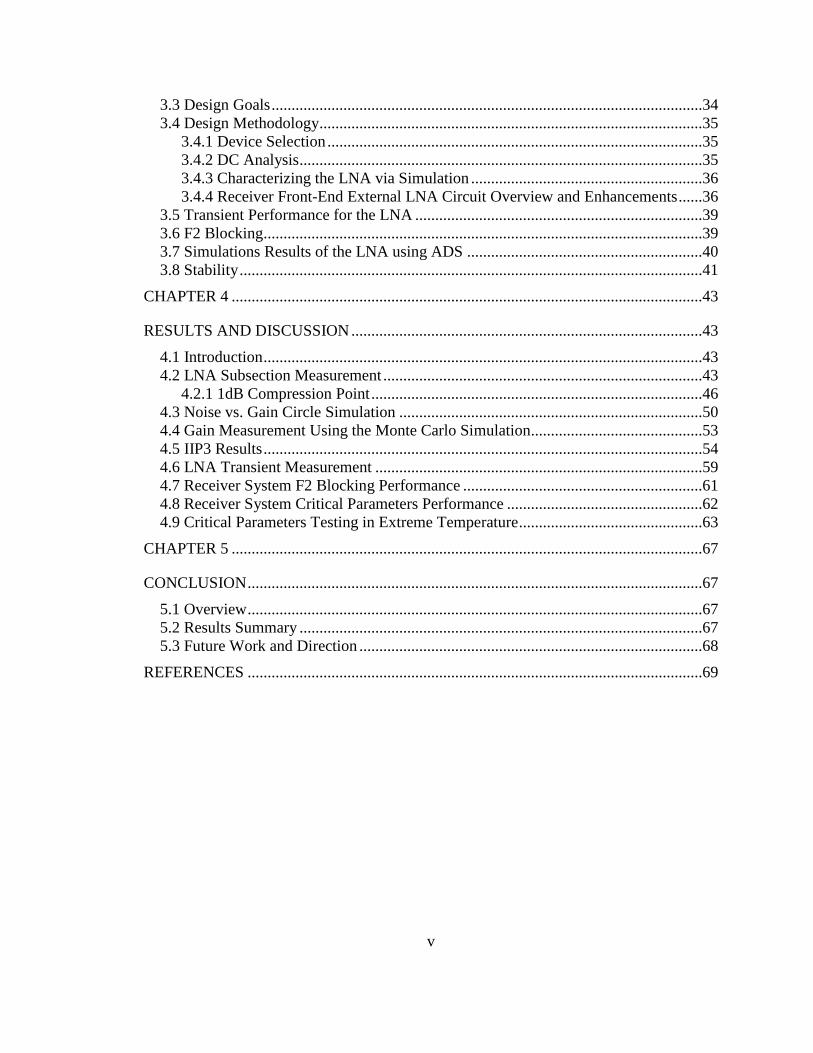
bias networks for K Band applications. The technology conveyed was and with Noise
Figure of 1.78dB, a power gain of 15.37dB and with 17.34 dB and 22.33 dB input and
output return loss. The LNA topology used was a 2 stage cascaded design as shown
below. The first amplifier function to excel the noise figure and the second amplifier is to
achieve the required gain at the desired Noise Figure as in the Table 2-1 and Figure 2-1
(M. Challal, 2011).
Table 2-1: Specification for the LNA
Parameters Specifications
Operating Frequency{Ghz} 24.125
Bias Point Vds=2V & Ids =10mA
Technology Microstrip
Gain{dB} > 15
Noise Figure {dB} < 2
Return Loss {dB) >10
Figure 2-1: Two Stages Amplifier Topology

10
The 2 stage’s LNA are based on input, inter –stage and output matching networks.
For any LNA, matching networks are the most important elements. The Matching have
been designed on a smith chart by using a single open tub matching technique .When the
stub’s length and position are matched, the input impedance Zin, which is at the junction
of the micro strip stub and the line matches exactly the characteristics impedance, Zo of
the system. The input impedance. Zin of an ideal terminated transmission line is:
ljZZ
ljZZZZ
L
L
in
tan
tan
0
0
0
(2.1)
Where the ZL is the terminating impedance, I is the physical distance along the line
from a particular load and P is the phase constant. However once choosing a DC bias
point for the desired gain and noise figure (NF) stability of transistor should be analyzed.
Since NE3514S02 LNA is unstable, shunt resistor with 200 ohms is added in the output
port. After checking the stability, matching networks (MN) have been considered.
Case Study of LNA design at 30GHz was discussed recently in an international
conference .It uses two single stage LNA topologies which includes a magnetic feedback
LNA and a cascade LNA. Post layout Simulations with the Gain of (S21) at only 5.9dB
and the Input (S11) and Output Return (S22) loss at -11.8dB and -11.4dB respectively.
The Noise Figure is estimated at 3.9dB which is extremely high and improper for the
industry. The case study emphasizes the need of proper LNA design with low NF
(Antonopoulos, Papathanasiou, & Bucher, 2012).

11
A journal paper describes that for a 800/900 band portable two way
communication, the LNA of Maxim 2373 IC was selected. Though this LNA does not
support wideband operations, it still provides desired gain, Noise Figure and IIP3 that
covers in frequency range. ADS momentum simulation used for the simulation purposes.
A comparison between simulated and measured data for the Maxim 2373 IC has been
tabulated in the Table 2-2 below.
Table 2-2: Maxim 2373 IC Simulation and Measurement Comparison
850MHz
Parameter Simulated Measured Goal
Gain 18.21dB 18.70dB > 16dB
Input RL -12.81dB -12.14dB < -10dB
Output RL -10.97dB -10.82dB < -10dB
941MHz
Parameter Simulated Measured Goal
Gain 17.06dB 17.76dB > 16dB
Input RL -15.34dB -15.14dB < -10dB
Output RL -10.37dB -11.27dB < -10dB
Although the goal of the gain is more the 16 dB and its achievable, the Output
return loss is marginally above on the desired goal. This is comparable for both the 800
and 900MHz (LNA Design guide with Agilent Design System, 2009, Maxim Integrated
Product, LNA Life2372/71 datasheet, 2002)
Voltaire LS is ideal for designing low-noise amplifiers (LNAs). In this application
note, a technique called negative-image modeling was used to design and optimize input

12
and output circuits for an 8-12 GHz LNA, and how the tune mode and genetic optimizer
simplifies the design process. The RF transistor (LNA) choosed is the NE32400 chip
FET. This is a low-noise device, rated at 0.6dB noise figure (NF) at 12GHz gain. Like all
low-noise FETs, the optimum NF is achieved at the current drain 10mA (Mass, 1999). .
In the development of wideband low noise amplifier (LNA), it is important to
choose the ideal topology. One of the researches done was on the balanced amplifier
topology, which was using the hybrid coupler and advanced E-PHEMPT transistor
technology in order to produce good wideband performance on the important parameters.
The LNA was fabricated in PCB Board and with the desired goal of Noise Figure of 1
dB, S parameters of Input and Output return losses greater then -10dB for a wideband
frequency range from 136-941MHz. However the it requires a dual supply of 5V each
and total current consumptions of 120mA.Across the globe, balanced amplifier is widely
adopted in the LNA design because of it excellent performance in input and output return
losses, low noise figure and better stability compared to the single ended amplifier,
However the drawback between other topology such as the negative feedback design and
a balanced amplifier is the balanced amplifier design topology requires bigger PCB
because they need longer transmission lines for the coupler (Osman & Noh, 2012).
There are many configurations to LNA design. In such , a low noise cascaded LNA
using a T- Matching network applicable for wireless applications has been studied. The
amplifier uses the FHX76LP Low Noise FET. The LNA designed using the T- Matching
network which consists of lump reactive element at the output and input terminal. The
cascode LNA produces gain of 18.5dB and NF of 1.3dB.The (S11) and (S22), input and
output return loss are respectively at -11.5dB and -12.3dB. This design on the front end

13
low noise amplifier is one of the challenges and constraints in the world of RF. The LNA
needs to provide good input impedance match, adequate power gain and certainly the
Low NF. Despite much high gain amplifier topologies have been proposed in the past, the
cascode technique induces results in a higher bandwidth and gain. Figure 2-2 shows
typical cascode LNA circuit (Othman, Ibrahim, Husain, Ahmad, & Senon, 2012).
Figure 2-2: Cascode LNA Circuit
Wide band RF is not only used in the normal two way portable communication
but also in the architecture of mobile TV applications which covers from the VHF Tri
Band (174-248MHz) to the UHF Band (470-746MHz). In the architecture, the RF front
end consists of a single to differential LNA with low amplitude /phase mismatch and also
an active notch filter as shown in Figure 2-3. The Notch filter behave as such it accepts

14
linear active inductors and rejects unwanted modulations in the 850/900 GSM noise by
approximate 37dB.The RF front end has gain around 15dB and NF of 5dB.
Figure 2-3: Block Diagram of RF Front End
This wide –band single to differential LNA has it’s own pro n cons. In order to
reduce common mode noise rejection and also the even order harmonics, the circuit is
being compensated with a balun to convert the single ended signal to a differential one. In
this process, since the balun is located at the front of the LNA, it degrades the NF of the
receiver and optimistic increase the cost of the receiver system (Sang Gyun, Seung
Hwan, & Yun Seong, 2013).
LNA circuit with possible combination of matching circuit has been researched.
The combination of ‘T” and “L” type matching circuits. Using the ADS simulation, the
circuit is simulated .The circuit is constructed with two possibilities, which is with and

15
without stabilizing circuit and feedback circuit .The RCL series circuit is constructed as a
feedback circuit to improve the stability of the LNA circuit. There is couple of try and
errors matching circuit simulation done. Example are L-L matching, L-T matching, T-T
matching and T- L matching. Of all this the T-L matching provides the best results for the
stability as shown in Table 2-3. NF for T-L matching is around 1.81dB which is about
0.35dB better the nearest matching of L-L. (Design and Comparison of Different
Matching Techniques for Low Noise Amplifier Circuit, D. Senthilkumar1, Dr.Uday
Pandit khot2, Prof. Santosh Jagtap3, Feb2013)
Table 2-3: Comparative Results of LNA Circuit W.SC and WO.SC
L-L L-T T-L T-T
WO.SC W.SC WO.SC W.SC WO.SC W.SC WO.SC W.SC
S21 16.280 10.390 13.539 5.237 16.296 14.140 13.588 6.468
S12 -14.170 -27.300 -16.910 -32.500 -14.150 -23.500 -16.864 -29.400
S22 -4.370 -16.100 -1.790 -1.240 -5.537 -6.290 -2.120 -11.800
S11 -2.922 -1.820 -11.250 -3.810 -2.937 -17.200 -11.923 -10.100
K 0.409 1.14 0.409 1.133 0.409 1.304 0.409 1.254
NF 0.906 2.150 0.906 2.478 0.906 1.816 0.906 3.974
As a conclusion from Table 2-3, with all the possible simulation, it is proven the
“L” output matching and “T” type input matching combination provides the better results
without much degradation in the Gain, NF and in the perspective of stability design
16
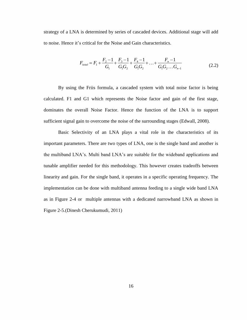
strategy of a LNA is determined by series of cascaded devices. Additional stage will add
to noise. Hence it’s critical for the Noise and Gain characteristics.
(2.2)
By using the Friis formula, a cascaded system with total noise factor is being
calculated. F1 and G1 which represents the Noise factor and gain of the first stage,
dominates the overall Noise Factor. Hence the function of the LNA is to support
sufficient signal gain to overcome the noise of the surrounding stages (Edwall, 2008).
Basic Selectivity of an LNA plays a vital role in the characteristics of its
important parameters. There are two types of LNA, one is the single band and another is
the multiband LNA’s. Multi band LNA’s are suitable for the wideband applications and
tunable amplifier needed for this methodology. This however creates tradeoffs between
linearity and gain. For the single band, it operates in a specific operating frequency. The
implementation can be done with multiband antenna feeding to a single wide band LNA
as in Figure 2-4 or multiple antennas with a dedicated narrowband LNA as shown in
Figure 2-5.(Dinesh Cherukumudi, 2011)
12121
4
21
3
1
21
1111
n
ntotal
GGG
F
GG
F
GG
F
G
FFF

17
Figure 2-4: Multiband Antenna with Single Wideband LNA
Figure 2-5: Multiband Receiver with Couple of Narrowband LNA
As reported by Anwar Faizd Osman and Prakash Chacko (Technical Paper,2011)
, wider band LNA provides a tougher challenge to the radio designer. It requires a LNA
at it receiver front end as it needs to provide constant gain, high linearity and Low Noise

18
for it to meet the specifications as tabulated in Table 2-4. LNA–LIFE which utilizes from
the MAXIM2371 IC consists of single channel, single ended, small signal low noise
amplifier with AGC incorporated.
Table 2-4: Portable 8/900MHz LNA Specification Using LNA-LIFE IC
Parameter Specs
Gain (dB) > 12
Noise Figure (dB) < 1.9
IIP3 (dBm) > 0
Stability Factor (K) > 1
Stability Factor (B1) > 0
Operating Freq (MHz) 850-941
The LNA-LIFE with construction as shown in Figure 2-6 provides constant gain
at the frequency at 850-941MHz. The Noise Figure however higher than the normal class
A, LNA which is around 1.5 or lesser. Higher NF means the Signal to Noise Ratio will be
deteriorated.

19
Figure 2-6: LNA-LIFE Block Diagram
Low Cost and small size constraint of the LNA was always been a huge criteria in
a LNA design. In such for the narrowband LNA for the UHF band using the micro strip
technology always synthesize a particular optimization. The well known topology of the
LNA is shown in the Figure 2-7. The LNA transistor which is specified by the S-
Scattering Matrix is consists gain element, biasing stage, input matching network (IMN)
and an output matching network. In this proposed methodology is redefined by using a
case study which the design of LNA amplifier. The transistor for this feasibility study is
the NE68033 which has gain between 19dB to 20dB which is greater than the desired
gain needed .The K factor is between 0.73 and 0.85 at the desired operating frequency
and the problem arises when the RF transistor is no longer conditionally stable at the
UHF band. (Rodríguez, Sebastián, 2011)

20
Figure 2-7: General Diagram of A RF Amplifier
As summary of the literature review, the approach selected was the balanced
amplifier topology for this LNA with the matching components .This is because the NF is
less then 1 dB which is one of the requirement of the project. Besides that, the current
drain of this LNA is less then 5 mA which is important as the lesser the current drain the
better the battery life performance. The test results and measurements will be discussed in
later chapters

21
CHAPTER 3
THEORY, DESIGN AND IMPLEMENTATION
3.1 Introduction
In a typical LNA design, there are few considerations to be taken consider off. Cost
of the RF transistor, size of the transistor itself. As discussed on Chapter 2, since there is
many architecture and topology which attributes to the LNA in radio. For the scope of
this thesis, the RF transistor of BFU520W is chosen due to its high speed and low noise
application in a plastic. The Minimum Noise Figure is = 0.6dB at 900Mhz and Maximum
stable gain of 18.5dB.This RF transistor is used in the LNA for VHF Band which
operates in the region of 136-174Mhz.In the next subtopics, design methodology for
LNA measurement using the BFU520W is discussed. The novelty here is by using the
same topology as the previous Legacy LNA and the subsection results should be
comparable with the current BFU520W.Then it is followed by the measurement set ups
to measure the LNA gain and Input and output return loss, Noise Figure, 1dB
Compression Point and F2 Blocking. Figure 3-1 illustrates the summary of the design
steps in the LNA implementation.

22
Yes
No
Yes
No
Yes
Yes
No
No
Figure 3-1: Research Methodology Flow Chart
Device Selection:
RF Transistor
Evaluation Board
Characterization
Meet the Goal of Cost
Effectiveness
Start
Simulation of the LNA(Optimization)
Proof of Concept:
Implementation, design and
validation
PCB Layout and Fabrication
System Characterization
End
Analysis
satisfied?
Analysis
satisfied?
Simulation
satisfied?
Full System Validation
Validation
satisfied?

23
3.1.2 The Design Goal of the BFU520W is as table below.Despite it wide band
capability, its only tested for the content of VHF only.The gain needed for this LNA
methodology is around 10 dB.Reason being, high gain induces the overall IIP3 system
performance.One of the main criteria is the current drain for the LNA.A low consumption
of current drain is needed .Input and Output return loss is targeted to be less the <-10dBm
Parameter Goal
Frequency 136-174(VHF) but supports wideband till 1 Ghz
Gain Approx 10 dB
Current Drain <5mA
IIP3 >-5 dBm
Input Return Loss <-10dBm
Output Input Return Loss <-10dBm
K Factor (Until 5 Ghz) > 1
B1 Factor (Until 8 Ghz) > 0
Table 3-1: VHF LNA Design Goal
3.2 Measurement Setup
In following sections below, test setup and configurations for each measurement
will be shown separately and in precise. In order to ensure the accuracy of the
measurement, equipment ensured been calibrated and measurement has been repeated
three times to verify the repeatability
24
3.2.1 LNA Measurement with Test Fixture
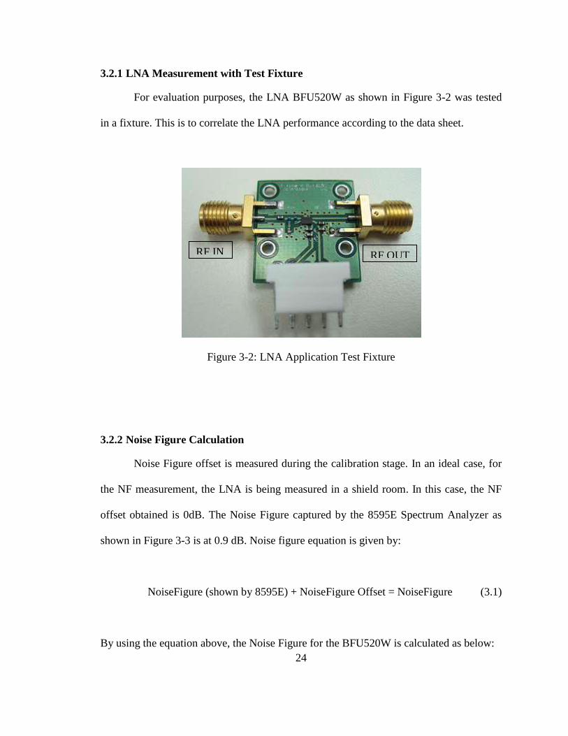
For evaluation purposes, the LNA BFU520W as shown in Figure 3-2 was tested
in a fixture. This is to correlate the LNA performance according to the data sheet.
Figure 3-2: LNA Application Test Fixture
3.2.2 Noise Figure Calculation
Noise Figure offset is measured during the calibration stage. In an ideal case, for
the NF measurement, the LNA is being measured in a shield room. In this case, the NF
offset obtained is 0dB. The Noise Figure captured by the 8595E Spectrum Analyzer as
shown in Figure 3-3 is at 0.9 dB. Noise figure equation is given by:
NoiseFigure (shown by 8595E) + NoiseFigure Offset = NoiseFigure (3.1)
By using the equation above, the Noise Figure for the BFU520W is calculated as below:
RF IN RF OUT
Related Documents