International Journal on Electrical Engineering and Informatics - Volume 8, Number 1, March 2016 Analysis and Development of an Improved Y-source Boost DC-DC Converter Mojtaba Forouzesh, Alfred Baghramian Department of Electrical Engineering, University of Guilan, Rasht, IRAN [email protected], [email protected] Abstract: Y-source impedance network is a new topology intended for implementing with high voltage gain converters. In contrary to the original Y-source impedance network, an improved Y-source presented in this paper has the advantage of a continuous input current characteristic. Since achieving high voltage gain and continuous input current, converters employing the proposed impedance network are suitable for implementing with renewable energy sources like fuel cell and photovoltaic systems. In this paper, analysis and operation principles of the developed network have been discussed. Moreover, mathematical equations and input current ripple analysis have been demonstrated in detail. Finally, both computer simulations and experimental results from a boost dc-dc converter are presented to validate the performance of the developed network. Keywords: DC-DC power converter, high voltage boost, Y-source, magnetically coupled impedance source (MCIS), continuous input current. 1. Introduction Recently, due to shortage of fossil fuels, alternative energy like renewable sources are in the center of attention. Among them fuel cell (FC) and photovoltaic (PV) systems because of no sound and emission characteristics are more desirable. Output voltage of these sources are environmentally dependent and can vary in a wide range. Thus, in order to cover dc-link voltage requirements, the need for a power electronics converter is undeniable. As mentioned above, in some conditions output voltage of both FC and PV can be such low that a converter with high voltage gain should be used [1]. Up to now, researchers have investigated various dc- dc converters with different structures. In order to meet dc link voltage requirements, there is demand for a high voltage gain converter when operating with low voltage sources. In a conventional dc-dc boost converter due to efficiency and reliability problems, a high voltage gain is not achievable. In transformer based converters usually a large turn ratio must be utilized to achieve a high voltage gain. Large turn ratios may lead to high leakage inductances and hence large voltage spike on semiconductor devices. Multilevel and interleaved converters usually use large amount of components that increase size and cost of converters. In addition, multilevel converters may not be desired for power conditioning systems due to their complex control algorithms and large components count [2, 3]. Recently coupled inductors are widely used in power converters. By utilizing coupled inductors, dc-dc converters usually can achieve high voltage gain with lower components [4-8]. Another application of coupled inductors is in magnetically coupled impedance networks. These networks called impedance sources that their generation initiated with the Z-source inverter in 2003 [9]. In recent years, many impedance sources have been developed for implementing on either dc/ac inverters or dc-dc converters. Originally, voltage gain of the Z- source and quasi-Z-source networks are low to be implemented with renewable energy power conditioning systems. Hence, improving Z-source based converter characteristics have been investigated [10-13]. Magnetically coupled impedance networks that appear recently, can achieve high voltage gain with lower components count. Some of dominant networks in this category can be named as trans-Z-source [14], Γ-source [15] and Y-source [16]. Received: May 25 th , 2015. Accepted: March 17 th , 2016 DOI: 10.15676/ijeei.2016.8.1.14 200

Welcome message from author
This document is posted to help you gain knowledge. Please leave a comment to let me know what you think about it! Share it to your friends and learn new things together.
Transcript
International Journal on Electrical Engineering and Informatics - Volume 8, Number 1, March 2016
Analysis and Development of an Improved Y-source Boost
DC-DC Converter
Mojtaba Forouzesh, Alfred Baghramian
Department of Electrical Engineering, University of Guilan, Rasht, IRAN
[email protected], [email protected]
Abstract: Y-source impedance network is a new topology intended for implementing with high
voltage gain converters. In contrary to the original Y-source impedance network, an improved
Y-source presented in this paper has the advantage of a continuous input current characteristic.
Since achieving high voltage gain and continuous input current, converters employing the
proposed impedance network are suitable for implementing with renewable energy sources like
fuel cell and photovoltaic systems. In this paper, analysis and operation principles of the
developed network have been discussed. Moreover, mathematical equations and input current
ripple analysis have been demonstrated in detail. Finally, both computer simulations and
experimental results from a boost dc-dc converter are presented to validate the performance of
the developed network.
Keywords: DC-DC power converter, high voltage boost, Y-source, magnetically coupled
impedance source (MCIS), continuous input current.
1. Introduction
Recently, due to shortage of fossil fuels, alternative energy like renewable sources are in
the center of attention. Among them fuel cell (FC) and photovoltaic (PV) systems because of
no sound and emission characteristics are more desirable. Output voltage of these sources are
environmentally dependent and can vary in a wide range. Thus, in order to cover dc-link
voltage requirements, the need for a power electronics converter is undeniable. As mentioned
above, in some conditions output voltage of both FC and PV can be such low that a converter
with high voltage gain should be used [1]. Up to now, researchers have investigated various dc-
dc converters with different structures. In order to meet dc link voltage requirements, there is
demand for a high voltage gain converter when operating with low voltage sources. In a
conventional dc-dc boost converter due to efficiency and reliability problems, a high voltage
gain is not achievable. In transformer based converters usually a large turn ratio must be
utilized to achieve a high voltage gain. Large turn ratios may lead to high leakage inductances
and hence large voltage spike on semiconductor devices. Multilevel and interleaved converters
usually use large amount of components that increase size and cost of converters. In addition,
multilevel converters may not be desired for power conditioning systems due to their complex
control algorithms and large components count [2, 3].
Recently coupled inductors are widely used in power converters. By utilizing coupled
inductors, dc-dc converters usually can achieve high voltage gain with lower components [4-8].
Another application of coupled inductors is in magnetically coupled impedance networks.
These networks called impedance sources that their generation initiated with the Z-source
inverter in 2003 [9]. In recent years, many impedance sources have been developed for
implementing on either dc/ac inverters or dc-dc converters. Originally, voltage gain of the Z-
source and quasi-Z-source networks are low to be implemented with renewable energy power
conditioning systems. Hence, improving Z-source based converter characteristics have been
investigated [10-13]. Magnetically coupled impedance networks that appear recently, can
achieve high voltage gain with lower components count. Some of dominant networks in this
category can be named as trans-Z-source [14], Γ-source [15] and Y-source [16].
Received: May 25
th, 2015. Accepted: March 17
th, 2016
DOI: 10.15676/ijeei.2016.8.1.14
200

Due to the presence of an input diode in mentioned impedance networks, these networks
inherently suffer from discontinuous input current. Whereas, a continuous input current trait is
an important feature for converters operating with renewable energy sources like FC and PV
systems. In a fuel cell system, drawing discontinuous input current lead to higher hydrogen
consumption, hence the efficiency of FC diminishes [17]. On the other hand, converters with
continuous input current can operate more accurately around the maximum power point in a
photovoltaic system [18]. Thus, it is noticeable that the efficiency of both FC and PV can be
improved by utilizing converters with a continuous input current. Besides drawing chopping
input current from FC and PV has negative influence on their lifetimes [17, 18]. Therefore,
converters with continues input current are always attractive due to their reducing negative
impact on the DC input source. Some investigations have been done in order to achieve a
continuous input current on magnetically coupled impedance sources. In these papers, usually
large filter inductor and capacitor were added to the original network [19, 20]. In fact, adding
large passive elements to the circuit results in more cost and weight (size) of power converters
that it is not desirable.
The Y-source impedance network can achieve high voltage gains in small duty cycles. In
contrary to other mentioned magnetically coupled networks, the Y-source utilizes three
coupled inductors that gives it more design freedoms. In this paper, an improved Y-source
network with a continuous input current is proposed for dc-dc converters. The proposed
impedance network not only has all the merits of original Y-source network but also has a
continuous input current. Moreover, the novel method introduced for achieving a continuous
input current on the Y-source can easily be extended to other magnetically coupled impedance
sources. In the proposed method, only one small value capacitor is added to the circuit of the
original network. Figure 1 shows some possible dc-dc converter architectures for the improved
Y-source impedance network. As it can be seen, the improved Y-source network can be
implemented on either a full bridge dc-dc structure or a single switch boost dc-dc converter.
Indeed, an improved Y-source based isolated dc-dc converter is under investigation by the
authors [21].
D1
Vin L2
C1
AL3L1
BA
B
S C3 RL
D2
Vout
S1
S2
R L
S3
S4
TrD2
D3
C3
C4
Vout
A
BN1 N3
N2
C2
single switch dc-dc converter structure
full-bridge dc-dc converter structure
improved Y-source impedance network
(a)
(b)
Figure 1. The proposed Y-source based dc-dc converter, (a) with full bridge isolated structure
and (b) with single switch boost structure.
Mojtaba Forouzesh, et al.
201

This paper is organized as follows. In section II, development of the improved Y-source
impedance network is demonstrated. In first, a review of the Y-source network and its
counterpart quasi-Y-source network have been presented. Subsequently, analysis and
principals of the improved impedance network have been discussed. In addition, their
corresponding equations have been derived in this section. In section III, the proposed high
voltage gain network with a continuous input current is implemented on a boost dc-dc
converter. Furthermore, input current ripple analysis and a comparison with other converters
are demonstrated in this section. In section IV, the performance of discussed networks verified
with the aid of PSIM simulations. The derived mathematical equations and expected
waveforms are also validated by simulation results. In section V, experimental results from a
laboratory prototype are illustrated to verify mentioned features of the proposed converter.
Finally, the conclusion is presented in the last section.
2. Operation Principles and Mathematical Derivations
A. Y-source impedance network
The conventional Y-source impedance network and its equivalent circuits are depicted in
Figure 2. It should be noted, since the effect of leakage inductance on the performance of
magnetically coupled Y-source network have been studied with introducing an additional
intermediate operating mode [22]. In this paper, in order to facilitate the analysis of in this
section, a perfect coupling is considered for the coupled inductors of all impedance networks.
Considering the latter mentioned, like other conventional impedance networks, the Y-source
impedance network has two basic operating modes, the shoot-through and non-shoot-through
modes. When switch S is turn ON the shoot-through sate starts in which diode D is in revers
bias and capacitors C2 is discharging to the magnetizing inductance of the coupled inductors.
The equivalent circuit of this mode is shown in Figureb. With the assumption that the voltage
across inductor L1 is 𝑉𝐿, then the voltage across L2 is 𝑉𝐿 𝑛12⁄ and voltage across L3 is 𝑉𝐿 𝑛13⁄ ,
which 𝑛12 = 𝑁1 𝑁2⁄ and 𝑛13 = 𝑁1 𝑁3⁄ are the turn ratios of the three winding coupled
inductors. By applying Kirchhoff’s Voltage Law (KVL) in both modes and writing voltage-
second balance principle for the inductor L1, the voltage across capacitor C2 and the voltage
gain of the Y-source impedance network can be achieved as follows.
𝑉𝐶2 =1−𝑑𝑆𝑇
1−(𝑁3+𝑁1𝑁3−𝑁2
)𝑑𝑆𝑇
𝑉𝑖𝑛 (1)
𝑉𝑜𝑢𝑡
𝑉𝑖𝑛=
1
1−(𝑁3+𝑁1𝑁3−𝑁2
)𝑑𝑆𝑇
(2)
In (4), 𝑑𝑆𝑇 is the shoot-through duty cycle. In order to simplify the equations, a winding
factor can be defined as 𝐾 =𝑁3+𝑁1
𝑁3−𝑁2. Therefore, (1) and (2) can be rewritten as
𝑉𝐶2 =1−𝑑𝑆𝑇
1−𝐾𝑑𝑆𝑇𝑉𝑖𝑛 (3)
𝑉𝑜𝑢𝑡
𝑉𝑖𝑛=
1
1−𝐾𝑑𝑆𝑇 (4)
In order to achieve positive boost characteristics for the Y-source impedance network,
denominator of (4) should be between zero and one. Thus, the available shoot-through duty
cycle can be obtained.
0 < 1 − 𝐾𝑑𝑆𝑇 < 1 → 0 < 𝑑𝑆𝑇 <1
𝐾 (6)
Analysis and Development of an Improved Y-source Boost
202

Vin
C2
S
D
VoutL2
C2
S
L3L1
+ +
(b) (c)
--
+
-Vin
+
-
D
VoutL2
C2
S
L3L1
VL
(a)
Vin
D
L2
+
- L3L1
+
-
N1 N3
N2
N1 N3
N2
Vout=0
iin iin
Figure 2. The Y-source impedance network and its equivalent circuit in (b) the shoot-through
state and (c) the non-shoot-through state
B. Quasi-Y-source impedance network
𝑉𝐶1 =(
𝑁1+𝑁2𝑁3−𝑁2
)𝑑𝑆𝑇
1−(𝑁3+𝑁1𝑁3−𝑁2
)𝑑𝑆𝑇
𝑉𝑖𝑛 (7)
By substituting the winding factor 𝐾 in (7), it can be rewritten as
𝑉𝐶1 =(𝐾−1)𝑑𝑆𝑇
1−𝐾𝑑𝑆𝑇𝑉𝑖𝑛 (8)
𝑉𝑜𝑢𝑡
𝑉𝑖𝑛=
1
1−𝐾𝑑𝑆𝑇 (9)
Vin
C1
S
D
VoutL2
C1
S
L3L1
+ +
(b) (c)
--
+
-Vin
+
-
D
VoutL2
C1
S
L3L1
VL
(a)
Vin
D
L2
+
- L3L1
+
-
N3
N2
N1 N3
N2
N1
Vout=0
iiniin
Figure 3. The quasi-Y-source impedance network and its equivalent circuit in (b) the
shoot-through state and (c) the non-shoot-through state
Mojtaba Forouzesh, et al.
203
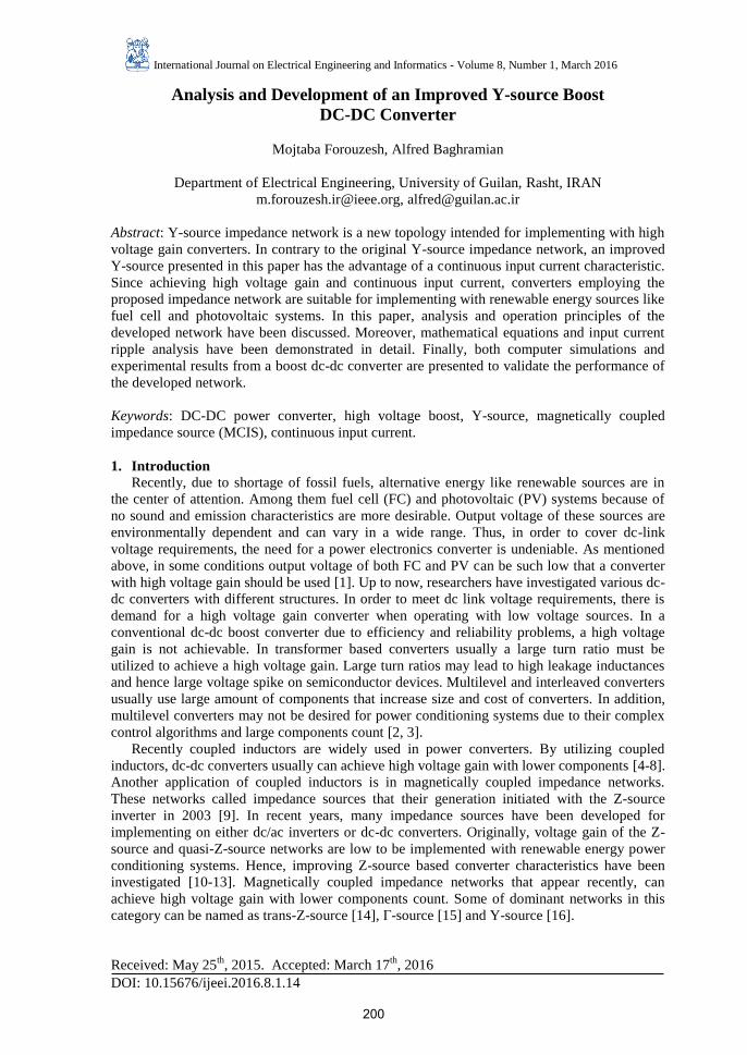
Energy storage capacitor of the original Y-source impedance network can be replaced as
shown in Figure 3. This new impedance network called as quasi-Y-source. The quasi-Y-source
network operates mostly like the Y-source network but they have some differences in capacitor
voltage stress and input current waveform. The equivalent circuit of the shoot-through mode is
shown in Figure 3b. In this mode, the magnetizing inductance of the coupled inductors is
charging form both input source and capacitor C1. Writing KVL in both modes then applying
voltage-second balance to the inductor L1, the voltage across capacitor C1 and the voltage gain
of the quasi-Y-source impedance network can be obtained.
It is obvious that the voltage gain of two latter networks are equal but their capacitors
voltage stress are different. Considering (3) and (8), the normalized voltage stress across
storage capacitors of two mentioned impedance network for a specific winding factor are
drawn in Figure 4. It is obvious that in every duty cycle and voltage gain, the voltage stress
across storage capacitor of the quasi-Y-source is lower than the Y-source impedance network.
Figure 4. Comparison between normalized capacitors voltage stress.
(a) (b)
t t
i ini in
TS dSTTS
shoot-throughshoot-through
shoot-through state
i in
tC2 / C1= xC2 / C1< x C2 / C1> x
inon-STiST
(c) Figure 5. Expected input current waveforms for (a) Y-source impedance network, (b) quasi-Y-
source impedance networks and (c) the improved Y-source impedance network with different
capacitors ratios
0 0.1 0.2 0.3 0.4 0.5 0.6 0.7 0.8 0.9 10
0.05
0.1
0.15
0.2
sho
ot-
thro
ug
h d
uty
cy
cle
(d
)
normalized voltage across capacitors
voltage across C1 in Y-source
voltage across C2 in quasi-Y-source
Analysis and Development of an Improved Y-source Boost
204

Expected input current waveform for the Y-source, quasi-Y-source and the improved Y-
source impedance networks are shown in Figure 5. The input current in both Y-source and
quasi-Y-source networks is discontinuous. In fact, the input current ripple in quasi-Y-source
network is more that in Y-source network. In the next section, a novel Y-source impedance
network with a continuous input current is presented. Figure 5c illustrates the input current
waveform of the proposed impedance network with different capacitor ratios (C1 and C2). To
achieve a continuous input current with no current jump in transition between two operation
modes, a proper capacitors ratio (𝑥) should be considered for the improved Y-source
impedance network.
C. improved Y-source impedance network
Figure 6 illustrates the improved Y-source impedance network and its equivalent circuits in
both modes. The improved Y-source network combines the two storage capacitors of the Y-
source and quasi-Y-source impedance networks. In the proposed Y-source network, a
continuous input current can be achieved with special consideration of the value of capacitors
C1 and C2. Proper selection of the capacitors will be shown in the following of this section.
Like aforementioned networks, in the shoot-through mode diode D is in reverse bias, in this
mode capacitors C1 and C2 are charging the magnetizing inductance of the coupled inductors.
Applying KVL in this mode, the following equations can be obtained.
𝑉𝐶2 = 𝑉𝑖𝑛 + 𝑉𝐶1 (11)
𝑉𝐿 =𝑛12𝑛13
𝑛12−𝑛13𝑉𝐶2 (12)
The non-shoot-through mode starts while diode D is conducting and capacitors C1 and C2
are charging from the input source. By applying KVL in this mode, the following equations
can be written.
𝑉𝐿 =𝑛12
1+𝑛12𝑉𝐶2 (13)
𝑉𝑜𝑢𝑡 = 𝑉𝑖𝑛 − 𝑉𝐿 −𝑉𝐿
𝑛13 (14)
Applying voltage-second balance principle to the inductor L1 and considering (11)-(14),
voltage across capacitors C1, C2 and the output voltage of improved Y-source network can be
achieved as follows.
𝑉𝐶1 =(1−𝑑𝑆𝑇)
1−(𝑁3+𝑁1𝑁3−𝑁2
)𝑑𝑆𝑇
𝑉𝑖𝑛 (15)
𝑉𝐶2 =(
𝑁1+𝑁2𝑁3−𝑁2
)𝑑𝑆𝑇
1−(𝑁3+𝑁1𝑁3−𝑁2
)𝑑𝑆𝑇
𝑉𝑖𝑛 (16)
𝑉𝑜𝑢𝑡 =𝑉𝑖𝑛
1−(𝑁3+𝑁1𝑁3−𝑁2
)𝑑𝑆𝑇
(17)
It is clear that the calculated equations for the voltage across C1 and C2 and output voltage
of the improved Y-source is same as which calculated for both previous networks.
Mojtaba Forouzesh, et al.
205

From derivative of (14), the relation between currents of capacitor C1 and C2 can be
achieved.
d𝑉𝐶2 = d𝑉𝐶1 → 𝑖𝐶2 =𝐶2
𝐶1𝑖𝐶1 (18)
Vin
C2
S
D1
Vout
C2
SC1
+
+
+
+
(b) (c)
-
--
-
+
-Vin
+
-
D1
Vout
C1
S
L3L1
VL
(a)
Vin
D1
L 2
+
-
Lm
i L2
i L3
i m
L 3L 1 L 3L 1
i L1
+
-
L 2 Lm
i L2 i m
i L3
L 2 Lm
+
-
i C1i C1 i C2i C2
C2
C1
1
2
3 3
Vout=0
Figure 6. The improved Y-source impedance network and its equivalent circuit in (b) the
shoot-through state and (c) the non-shoot-through state
Assuming that the network operates in its continuous conduction mode (CCM), the average
of magnetizing current in both shoot-through and non-shoot-through modes equals to the
average of magnetizing current in a switching period. According to Figure 5c, in order to
achieve a continuous input current with no current jump in transition between two modes, the
dc component of input current (𝐼𝑑𝑐) should be equal to the average of input current in either
shoot-through or non-shoot-through mode.
𝐼𝑑𝑐 = 𝐼𝑖𝑛𝑆𝑇= 𝐼𝑖𝑛𝑛𝑜𝑛−𝑆𝑇
(19)
In (22), 𝐼𝑖𝑛 denotes the average of input current and subscripts ‘ST’ and ‘non-ST’ represent
the shoot-through and non-shoot-through modes, respectively. Assuming that the improved Y-
source is loss less (𝑃𝑖𝑛 = 𝑃𝑜𝑢𝑡) and according to (17), the output current can be written as
follows.
𝐼𝑜𝑢𝑡 = (1 − (𝑁3+𝑁1
𝑁3−𝑁2) 𝑑𝑆𝑇) 𝐼𝑑𝑐 (20)
Ampere-turns balance in a three winding coupled inductors can be expressed as
𝑁1𝑖𝐿1 + 𝑁2𝑖𝐿2 + 𝑁3𝑖𝐿3 = 0 (21)
In the shoot-through mode, 𝑖𝐿1 current of L1 is zero. Applying Kirchhoff’s Current Law
(KCL) at nodes 1, 2 and 3 in Figure 6b and considering (18) and (20), the following equations
can be written.
Analysis and Development of an Improved Y-source Boost
206

𝑖𝑆𝑇 = (𝑁2
𝑁3−𝑁2) 𝑖𝑚 (22)
𝑖𝑚 = (𝑁3−𝑁2
𝑁2) (
𝐶2
𝐶1+ 1) 𝑖𝑖𝑛𝑆𝑇
(23)
𝑖𝐶2 = (𝑁2
𝑁3−𝑁2) 𝑖𝑚 − 𝑖𝑖𝑛𝑆𝑇
(24)
In (22), 𝑖𝑆𝑇 is the shoot-through current that flows into the semiconductor switch and 𝑖𝑚 is
the magnetizing current referred to the second winding (𝑁2). In the non-shoot-through mode,
considering (20) and by applying KCL at node 1 in Figure 6c, the following equation can be
written.
𝑖𝐶2 = (1 − (𝑁3+𝑁1
𝑁3−𝑁2) 𝑑𝑆𝑇) 𝐼𝑑𝑐 − 𝑖𝑖𝑛𝑛𝑜𝑛−𝑆𝑇
(25)
By considering small ripple for 𝑖𝑚, 𝑖𝑖𝑛𝑆𝑇 and 𝑖𝑖𝑛𝑛𝑜𝑛−𝑆𝑇
, they can be expressed by their
average values 𝐼𝑚, 𝐼𝑖𝑛𝑆𝑇 and 𝐼𝑖𝑛𝑛𝑜𝑛−𝑆𝑇
, respectively. Applying ampere-second balance principle
to the capacitor C2, dc component of the magnetizing current for improved Y-source network
can be obtained as
𝐼𝑚 = (𝑁1+𝑁3
𝑁2) 𝐼𝑑𝑐 (26)
By substituting (26) in (22), the average of shoot-through current in Y-source network can
be achieved as
𝐼𝑆𝑇 = (𝑁3+𝑁1
𝑁3−𝑁2) 𝐼𝑑𝑐 = 𝐾𝐼𝑑𝑐 (27)
Considering (19) and using (23) and (26), the proper capacitance ratio for the Y-source
network can be achieved.
𝐶2
𝐶1= 𝐾 − 1 (28)
3. Implementation of the Proposed DC-DC Converter
By having the advantage of high voltage boost and continuous input current abilities, the
improved Y-source impedance network is suitable for implementing with low input voltage dc-
dc converters. The dc-dc boost converter proposed in this paper is a simple example to show
the performance of the improved Y-source network. Input current analysis and comparison
with other dc-dc converters are discussed in this section.
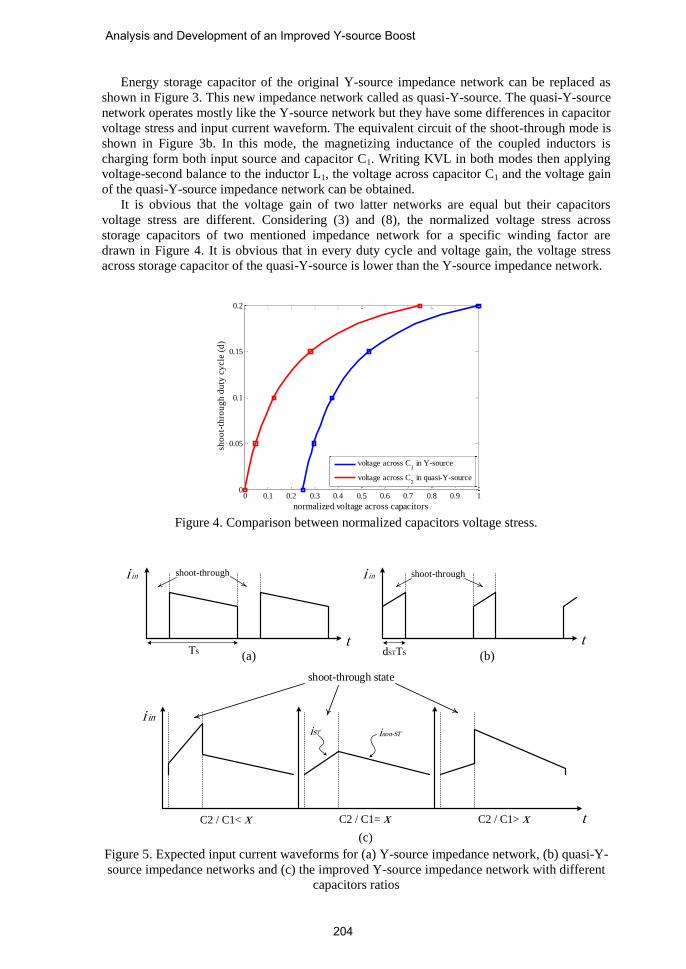
A. Principle of Operation
Figure 7 shows the configuration of the test system, where an improved Y-source
impedance network has been replaced with the input inductor of a boost dc-dc converter. The
shoot-through state can happens by turn ON of switch S, in which diode D1 and D2 are in
reveres bias. In this mode, input source and capacitors C1 and C2 are charging the magnetizing
inductance of the coupled inductors. Moreover, the resistive load is supplied by the capacitor
C3 in this mode. When the switch S is turned OFF, impedance network is in its non-shoot-
through mode. In which the capacitors are charging from the input source and capacitor C3 is
Mojtaba Forouzesh, et al.
207
supplied by the stored energy in coupled inductors and input source. This happens only if the
peak of output voltage (�̂�𝑜𝑢𝑡) is lower that the peak of (�̂�𝑑𝑠).
D1
VoutVin N2
C2
S
N3N1
C3
D2
RL
C1
Vds
Figure 7. The improved Y-source boost dc-dc converter
According to (17), in the proposed converter different winding turn ratios (𝑁1: 𝑁2: 𝑁3) can
be realized for a specific voltage gain. Considering (26), it is interesting that the required
magnetizing current for a specific voltage gain in the proposed Y-source based converter can
vary by various selection of winding turn ratios. This is another design freedom for the Y-
source impedance network in addition to other advantages mentioned in [16]. Table 1 shows
some different combinations of winding turns for specific winding factors and their
corresponding magnetizing current and voltage gain.
Table 1. Different magnetizing current and voltage gain of the Y-source impedance network
realized with different winding factor and turns ratio
Winding Factor
(𝐾 =𝑁3+𝑁1
𝑁3−𝑁2)
Turns Ratio
(𝑁1: 𝑁2: 𝑁3)
Magnetizing Current
(𝐼𝑚 =𝑁1+𝑁3
𝑁2× 𝐼𝑑𝑐)
Voltage Gain
(𝑉𝑜
𝑉𝑖𝑛=
1
1−𝐾𝑑𝑆𝑇)
3
1:3:5 2 × 𝐼𝑑𝑐 1
1 − 3𝑑𝑆𝑇
1:1:2 3 × 𝐼𝑑𝑐
3:1:3 6 × 𝐼𝑑𝑐
4
1:2:3 2 × 𝐼𝑑𝑐 1
1 − 4𝑑𝑆𝑇
2:1:2 4 × 𝐼𝑑𝑐
5:1:3 8 × 𝐼𝑑𝑐
5
1:3:4 2.5 × 𝐼𝑑𝑐 1
1 − 5𝑑𝑆𝑇
3:1:2 5 × 𝐼𝑑𝑐
7:1:3 10 × 𝐼𝑑𝑐
B. Analysis of Input Current and Magnetizing Current Ripples
The Input current of the proposed network is a ratio of the magnetizing current of coupled
inductors. Therefore, the input current ripple can be evaluated from the magnetizing current
ripple. For the following analysis, inductors and capacitors are assumed to be linear and
frequency independent. Accordingly, the voltage across magnetizing inductor on the second
winding (𝑁2) can be achieved using KVL in the non-shoot-through mode.
𝑉𝐿𝑚 = (𝑁2
𝑁1+𝑁2) 𝑉𝐶1 (29)
Then, the magnetizing current for the improved Y-source can be expressed as (30)
𝑖𝐿𝑚 =1
𝐿𝑚∫ 𝑉𝐿𝑚
𝑡
𝑑𝑆𝑇𝑇𝑑𝑡 + 𝑖𝐿𝑚(0) (30)
Analysis and Development of an Improved Y-source Boost
208

→ =𝑉𝐿𝑚
𝐿𝑚(𝑡 − 𝑑𝑆𝑇𝑇) + 𝑖𝐿𝑚(0)
In (30), 𝐿𝑚 is the magnetizing inductance seen from the second winding (𝑁2) of coupled
inductors. Considering (29) and (30), the magnetizing current ripple of improved Y-source
network can be written as
Δ𝑖𝐿𝑚 = (𝑁2
2
𝑁1𝑁2+𝑁22) ∙
𝑉𝐶1(1−𝑑𝑆𝑇)
𝐿𝑚𝑓𝑠 (31)
According to (29), the input current ripple for the improved Y-source can be obtained as
Δ𝑖𝑖𝑛 = (𝑁2
2
(𝑁1+𝑁2)(𝑁1+𝑁3)) ∙
𝑉𝐶1(1−𝑑𝑆𝑇)
𝐿𝑚𝑓𝑠 (32)
Considering Table 1 and equation (32), it is evident that with a specific voltage gain for the
improved Y-source, the input current ripple can differ by various windings turns. This feature
is only provided by the improved Y-source impedance network, which is not seen on other
magnetically coupled impedance networks yet.
C. Comparison With Other DC-DC Converters
Several high voltage dc-dc converters have been investigated for various applications.
Among them, few converters can achieve a continuous input current and high voltage boost
simultaneously. A comparison of different dc-dc converters in terms of their components and
voltage gains are presented in Table 2.
Table 2. Comparison of Various DC-DC Converters
Reference Voltage
Gain
Continuous
Input Current
Number of Components
Switch Diode Inductor Capacitor Total
[4] (1 + 𝑛)𝐷
1 − 𝐷 no 1 2 2 2 7
[5] 1
(1 − 𝐷)2 yes 2 3 2 3 10
[6] 1 + 𝑛𝑘
1 − 𝐷 no 1 3 2 3 9
[8] (2 + 𝑛𝐷)
1 − 𝐷 no 1 4 2 4 11
[13] 1
1 − 2𝐷 yes 1 1 3 2 7
[10] 2(1 − 𝐷)
1 − 3𝐷 yes 1 3 4 4 12
Proposed
Converter
1
1 − 𝐾𝐷 yes 1 2 3 2 8
From Table 2 it is obvious that the proposed converter can achieve high voltage gain with
relatively low number of circuit components. For better illustration, a comparison between
voltage gain of some mentioned dc-dc converters are drawn in Figure 8. It can be pointed out
that the comparison is made between converters with continuous input current characteristics.
It is obvious that the proposed Y-source based dc-dc converter can achieve higher voltage
gains with lower duty cycles. This feature of the proposed configuration makes it adequate for
applications that demand for short inductive charge.
Mojtaba Forouzesh, et al.
209

Figure 8. Comparison between voltage gain of the proposed converter and other converters
4. Simulation Results
For demonstrating the performance of mentioned impedance networks, some simulations
have been done in the PSIM software environment. Three coupled inductors ratio assumed to
be 2:1:2 (𝑁1: 𝑁2: 𝑁3). Thus, winding factor can be calculated as K=4. Considering a 40V input
voltage and a 200V output voltage, the voltage gain of the proposed converter should be about
5. From (2), the required shoot-through duty cycle can be calculated as 𝑑𝑆𝑇=0.2. Considering
(28), proper ratio for the capacitors should be 3 and hence C1 and C2 was selected 100µF and
300µF respectively. From (15) and (16), the voltage across capacitors C1 and C2 were
calculated as 𝑉𝐶1=120V and 𝑉𝐶2=160V respectively.
First, the simulations have done to verify the differences between the Y-source and quasi-
Y-source networks that mentioned earlier. Consequently, they were implemented on boost dc-
dc converters like the configuration shown in Figure 7. In this case, the same 300µF capacitor
is used for both networks. Simulation results for both converters are drawn in Figure 9. It can
be seen that the peak value of input current for quasi-Y-source is higher than its counterpart.
Because of this behavior that seen form two mentioned networks, in the improved Y-source
network, we have to consider a special ratio for two storage capacitors to achieve a continuous
input current with less ripple.
Simulation results for the improved Y-source boost dc-dc converter are depicted in Figure
10. It can be seen that the input current is continuous in the proposed converter and its ripple
can be tuned by both the switching frequency and the magnetizing inductance. The voltages
stress across capacitors C1 and C2 that are shown in Figure 10 are in good agreement with the
calculated values. From Table 1 and considering (32), it is found that for a specific voltage
gain, the input current ripple of the proposed converter can be lowered by different winding
turns ratios (𝑁1: 𝑁2: 𝑁3). In order to conduct a practical comparison for the currents analysis, it
is assumed that the magnetizing inductance seen form the winding with the lowest turns is 200
µH for all windings combinations.
0 0.1 0.2 0.3 0.4 0.5 0.6 0.7 0.80
2
4
6
8
10
12
14
16
18
20
Vo
lta
ge G
ain
Duty Cycle
dc-dc converter in [5]
quasi-Z-source dc-dc [13]
quasi-Z-source with voltage lift [10]
proposed improved Y-source dc-dc
Analysis and Development of an Improved Y-source Boost
210

(a)
(b)
Figure 9. Steady state respond for (a) Y-source boost dc-dc converter and (b) quasi-Y-source
boost dc-dc converter.
Figure 10. Simulation results for the improved Y-source boost dc-dc converter in steady state.
0
100
200
Vds (V) Vc1 (V)
0.2498 0.249867 0.249933 0.25
Time (s)
0
2.5
5
Input Current_Iin (A)
0
100
200
Vds (V) Vc1 (V)
0.2498 0.24985 0.2499 0.24995 0.25
Time (s)
0
7.5
15
Input Current_Iin (A)
0
50
100
150
200
Vc1 (V) Vc2 (V)
0
100
200
Voltage Across SW_Vds (V)
0.2498 0.24985 0.2499 0.24995 0.25
Time (s)
0
4
Input Current_Iin (A)
Mojtaba Forouzesh, et al.
211
Figure 11 illustrates the simulation results for the input current and magnetizing current
with different combinations of winding turns. In other to achieve K=4, three turns ratios are
mentioned in Table 1. Current ripples drawn in Figure 11a to Figure 11c are in accordance with
the calculated values from the equations (31) and (32). According to Figure 11, it is clear that
from winding turns 1:2:3 to 5:1:3 the magnetizing currents increased which is in consistent
with the calculations from (26). It can be pointed out that although much lower current ripples
can be achieved with the ratio of 5:1:3, but in experiment, maybe it is not available and cost
effective. It is clear that for the same magnetizing inductance, much wire and probably a larger
core should be realized for the 5:1:3 ratio. Hence, a balance should be established between
some mentioned parameters for the improved Y-source based dc-dc converter in the design
procedure.
(a)
(b)
(c)
Figure 11. Input and magnetizing currents for different combination of windings turns and
K=4.
0
1.25
2.5
3.75
5
Input Current_Iin (A), [ 1 : 2 : 3 ]
Ip-p=1.88 (A)
0.49985 0.4999 0.49995 0.5
Time (s)
0
2.5
5
7.5
10
Magnetizing Current_Im (A), [ 1 : 2 : 3 ] AVG(Im) (A)
Ip-p=3.76 (A)
0
1.25
2.5
3.75
5
Input Current_Iin (A), [ 2 : 1 : 2 ]
Ip-p=1.95 (A)
0.49985 0.4999 0.49995 0.5
Time (s)
0
5
10
15
20
Magnetizing Current_Im (A), [ 2 : 1 : 2 ] AVG(Im) (A)
Ip-p=7.8 (A)
0
1.25
2.5
3.75
5
Input Current_Iin (A), [ 5 : 1 : 3 ]
Ip-p=0.49 (A)
0.49985 0.4999 0.49995 0.5
Time (s)
15
18
21
24
Magnetizing Current_Im (A), [ 5 : 1 : 3 ] AVG(Im) (A)
Ip-p=3.92 (A)
Analysis and Development of an Improved Y-source Boost
212

5. Experimental Results
A scaled down laboratory prototype of the improved Y-source boost dc-dc converter has
been built to validate both theoretical expressions and simulation results. In order to reduce
size and weight of the converter, three coupled inductors have been integrated on the same
toroid core. The magnetic core used for the prototype is a molypermalloy powder (MPP) core
with permeability of 125µ from Dongbu Corporation. Component values and their part
numbers that were used for the experiment are listed in Table 3. It should pointed out that a
current probe was not available for digital scope at the time of experiment, thus in order to
better show input current with lower parasitic effects, switching frequency has been set to 20
kHz. Experimental results recorded from a 150 MHz Yokogawa (DL1540) digital scope. A
photo of the laboratory prototype is depicted in Figure 12.
Table 3. Experimental Values and Part numbers
Parameters/Description Value/Part Number
Power rating 100 W
Input voltage 40 V
Output voltage 200 V
Capacitor C1 100 µF
Capacitor C2 and C3 330 µF
Turns Ratio of Coupled Inductors
(𝑁1: 𝑁2: 𝑁3)
2:1:2 = 46:23:46
on M200152A core
Winding Factor (𝐾) 4
Duty Cycle (𝑑𝑆𝑇) 0.2
Switching Frequency (𝑓𝑠) 20 kHz
Switch SW IRFP460A
Diode D1 BYV08
Diode D2 MUR860
Figure 12. Experimental setup of the improved Y-source boost dc-dc converter.
Figure 13 illustrates experimental results obtained from the Y-source and quasi-Y-source
boost dc-dc converters. In which the drain source voltage of switches are shown in top and the
input currents are shown in bottom. It can be seen that the input current in both converters are
Mojtaba Forouzesh, et al.
213

pulsating and experimental results that observed in laboratory are in good accordance with the
simulation results.
(a)
(b)
Figure 13. Experimental results for (a) Y-source based dc-dc converter and (b) quasi-Y-source
based dc-dc converter.
Experimental results observed from the improved Y-source boost dc-dc converter using
components listed in Table 3 are depicted in Figure 14. As well as the simulation results, the
proposed converter draws a continuous input current. Measured magnetizing inductance from
the second winding was about 120µH. from (21) and other parameters mentioned in Table 2,
the input current ripple can be calculated as 3.33 A. Obviously, the input current ripple can be
lowered by employing more winding turns on a larger core. Furthermore, it is evident that the
voltage stress across capacitors C1 and C2 that observe in Figure 14 are in consistent with
previous calculations. Moreover, the ability to achieve a continuous input current in the
proposed improved Y-source based converter is verified by the experimental results.
The efficiency of the proposed converter with different load levels is depicted in Figure 15.
Notably, the relatively low efficiency of the laboratory prototype is mainly related to its loosely
connections (low graded wires and busbars) and internal parasitic elements of the circuit
components (Equivalent Series Resistance (ESR) of capacitors and losses related to the
semiconductors). However, the proposed converter can achieve more than 90% conversion
Analysis and Development of an Improved Y-source Boost
214

efficiency under load variations. Indeed the experimental evaluation focuses on validation of
theoretical expressions and simulation results not achieving high-end efficiency.
(a)
(b)
Figure 14. Experimental results for improved Y-source boost dc-dc converter, (a) the drain-
source voltage of switch SW and the input current (b) the voltage across Capacitors.
Figure 15. Measured efficiency of the proposed converter.
86
88
90
92
94
96
50 70 90 110
Eff
icie
ncy
(%
)
Output Power (W)
Mojtaba Forouzesh, et al.
215
6. Conclusions
A new Y-source boost dc-dc converter with high voltage gain and a continuous input
current introduced in this paper. The proposed converter is intended for applications with
varying and low input voltage sources as photovoltaic and fuel cells. Moreover, the proposed
converter uses a novel improved Y-source impedance network in its circuit. Steady state
analysis and operation principles of developed impedance networks documented in the paper.
Furthermore, it is found that the input current ripple of the improved Y-source can vary by
different combinations of winding turns. Computer simulations using PSIM software verified
the performance of the proposed converter and validated the mathematical derivations.
Experimental results from a 100W laboratory prototype also demonstrated the proof of all
mentioned characteristics for the proposed converter.
7. References
[1]. F. Blaabjerg, Z. Chen, and S. B. Kjaer, "Power electronics as efficient interface in
dispersed power generation systems," IEEE Trans. Power Electron., vol. 19, no. 5, pp.
1184-1194, Sept. 2004.
[2]. J. Dawidziuk, "Review and comparison of high efficiency high power boost DC/DC
converters for photovoltaic applications," Bulletin of the Polish Academy of Sciences:
Tech. Sci., vol. 59, no. 4, pp. 499-506, Feb. 2012.
[3]. W. Li, X. Lv, Y. Deng, J. Liu, and X. He, "A review of non-isolated high step-up DC/DC
converters in renewable energy applications," 24th Annu. Appl. Power Electron. Conf.
and Expo. (APEC), Washington, DC, 2009, pp. 364-369.
[4]. Q. Zhao and F. C. Lee, "High-efficiency, high step-up DC-DC converters," IEEE Trans.
Power Electron., vol. 18, no. 1, pp. 65-73, Jan. 2003.
[5]. B.-R. Lin and J.-J. Chen, "Analysis and implementation of a soft switching converter with
high-voltage conversion ratio," IET Power Electron., vol. 1, no. 3, pp. 386-394, Sept.
2008.
[6]. J.-W. Baek, M.-H. Ryoo, T.-J. Kim, D.-W. Yoo, and J.-S. Kim, "High boost converter
using voltage multiplier," 31st Annu. Conf. Ind. Electron. Soc. (IECON), 2005, p. 6 pp.
[7]. W. Yu, C. Hutchens, J.-S. Lai, J. Zhang, G. Lisi, A. Djabbari, et al., "High efficiency
converter with charge pump and coupled inductor for wide input photovoltaic AC module
applications," Energy Conv. Congr. and Expo. (ECCE), San Jose, CA, 2009, pp. 3895-
3900.
[8]. K. Yari, M. Forouzesh, and A. Baghramian, "A novel high voltage gain DC-DC converter
with reduced components voltage stress," 6th Power Electron., Drives Sys. & Tech. Conf.
(PEDSTC), Tehran, 2015, pp. 173-177.
[9]. F. Z. Peng, "Z-source inverter," IEEE Trans. Ind. Appl., vol. 39, no. 2, pp. 504-510,
Mar/Apr 2003.
[10]. T. Takiguchi and H. Koizumi, "Quasi-Z-source dc-dc converter with voltage-lift
technique," 39th Annu. Conf. Ind. Electron. Soc. (IECON), Vienna, 2013, pp. 1191-1196.
[11]. D. Vinnikov, I. Roasto, R. Strzelecki, and M. Adamowicz, "Step-up DC/DC converters
with cascaded quasi-Z-source network," IEEE Trans. Ind. Electron., vol. 59, no. 10, pp.
3727-3736, Oct. 2012.
[12]. D. Vinnikov, I. Roasto, R. Strzelecki, and M. Adamowicz, "Performance improvement
method for the voltage-fed qZSI with continuous input current," 15th Mediterranean
Electrotechnical Conf. (MELECON), Valletta, 2010, pp. 1459-1464.
[13]. D. Cao and F. Z. Peng, "A family of Z-source and quasi-Z-source DC-DC converters,"
24th Annu. Appl. Power Electron. Conf. and Expo. (APEC), Washington, DC, 2009, pp.
1097-1101.
[14]. W. Qian, F. Z. Peng, and H. Cha, "Trans-Z-source inverters," IEEE Trans. Power
Electron., vol. 26, no. 12, pp. 3453-3463, Dec. 2011.
[15]. P. C. Loh, D. Li, and F. Blaabjerg, "Γ-Z-source inverters," IEEE Trans. Power Electron.,
vol. 28, no. 11, pp. 4880-4884, Nov. 2013.
Analysis and Development of an Improved Y-source Boost
216

[16]. Y. P. Siwakoti, P. C. Loh, F. Blaabjerg and G. E. Town, "Y-Source Impedance Network,"
IEEE Trans. Power Electron., vol. 29, no. 7, pp. 3250-3254, July 2014.
[17]. S. K. Mazumder, R. K. Burra, and K. Acharya, "A ripple-mitigating and energy-efficient
fuel cell power-conditioning system," IEEE Trans. Power Electron., vol. 22, no. 4, pp.
1437-1452, July 2007.
[18]. A. E. Khateb, N. A. Rahim, J. Selvaraj, and B. W. Williams, "The effect of input current
ripple on the photovoltaic panel efficiency," Clean Energy and Tech. (CEAT),
Lankgkawi, 2013, pp. 478-481.
[19]. M. K. Nguyen, Y. C. Lim, and S.-J. Park, "Improved trans-Z-source inverter with
continuous input current and boost inversion capability," IEEE Trans. Power Electron,
vol. 28, no. 10, pp. 4500-4510, Oct. 2013.
[20]. W. Mo, P. C. Loh, and F. Blaabjerg, "Voltage Type Γ-source Inverters with Continuous
Input Current and Enhanced Voltage Boost Capability," 15th Int. Power Electron. and
Motion Cont. Conf. (EPE/PEMC), Novi Sad, 2012, pp. LS5d.2-1-LS5d.2-8.
[21]. M. Forouzesh and A. Baghramian, "High voltage gain Y-source based isolated DC-DC
converter with continuous input current," 6th Power Electron., Drives Sys. & Tech. Conf.
(PEDSTC), Tehran, 2015, pp. 453-457.
[22]. Y. P. Siwakoti, P. C. Loh, F. Blaabjerg and G. E. Town, "Effects of Leakage Inductances
on Magnetically Coupled Y-Source Network," IEEE Trans. Power Electron., vol. 29, no.
11, pp. 5662-5666, Nov. 2014.
Mojtaba Forouzesh received the B.S. degree in Physics from the University
of Guilan, Rasht, Iran, in 2011, and the M.S. degree in electrical engineering
with first class honors from the same institute in 2015.
He is currently a graduate researcher at the Department of Electrical
Engineering, the University of Guilan. His major research interests include
magnetically coupled impedance source based converters/inverters, high
step-up dc-dc converters, renewable energy technologies and applications,
small signal modeling of power converters and digital implementation of
modulation and control schemes.
Alfred Baghramian was born in Iran 1969, received the B.Sc. degree in
electrical engineering from Isfahan University of Technology, Isfahan, Iran,
in 1991; M.Sc. degree in electrical engineering from The University of
Tarbiat-Modarres, Tehran- Iran, in 1994 and the Ph.D. degree in power
electronics from the University of Birmingham, Birmingham, U.K., in 2006.
His research interests include high-frequency power converters, high power-
factor rectification and the modeling and control of autonomous power
systems. Dr. Alfred Baghramian has been a Lecturer at The University of
Guilan, Rasht-Iran Since 1994.
Mojtaba Forouzesh, et al.
217
Related Documents

![Vol. 2, Issue 9, September 2013 DESIGN OF DC-DC BOOST ... · DESIGN OF DC-DC BOOST CONVERTER WITH THERMOELECTRIC POWER SOURCE ... [2-4].In this research, DC-DC boost converter is](https://static.cupdf.com/doc/110x72/5aec36db7f8b9ae5318ea3af/vol-2-issue-9-september-2013-design-of-dc-dc-boost-of-dc-dc-boost-converter.jpg)