HAL Id: tel-02924619 https://tel.archives-ouvertes.fr/tel-02924619 Submitted on 28 Aug 2020 HAL is a multi-disciplinary open access archive for the deposit and dissemination of sci- entific research documents, whether they are pub- lished or not. The documents may come from teaching and research institutions in France or abroad, or from public or private research centers. L’archive ouverte pluridisciplinaire HAL, est destinée au dépôt et à la diffusion de documents scientifiques de niveau recherche, publiés ou non, émanant des établissements d’enseignement et de recherche français ou étrangers, des laboratoires publics ou privés. Analyse structurales de pseudo-substrats Gap/Si et d’hétérostructures CIGS/GaP/Si pour des applications photovoltaïques Ang Zhou To cite this version: Ang Zhou. Analyse structurales de pseudo-substrats Gap/Si et d’hétérostructures CIGS/GaP/Si pour des applications photovoltaïques. Matériaux. INSA de Rennes, 2019. Français. NNT : 2019ISAR0027. tel-02924619

Welcome message from author
This document is posted to help you gain knowledge. Please leave a comment to let me know what you think about it! Share it to your friends and learn new things together.
Transcript
HAL Id: tel-02924619https://tel.archives-ouvertes.fr/tel-02924619
Submitted on 28 Aug 2020
HAL is a multi-disciplinary open accessarchive for the deposit and dissemination of sci-entific research documents, whether they are pub-lished or not. The documents may come fromteaching and research institutions in France orabroad, or from public or private research centers.
L’archive ouverte pluridisciplinaire HAL, estdestinée au dépôt et à la diffusion de documentsscientifiques de niveau recherche, publiés ou non,émanant des établissements d’enseignement et derecherche français ou étrangers, des laboratoirespublics ou privés.
Analyse structurales de pseudo-substrats Gap/Si etd’hétérostructures CIGS/GaP/Si pour des applications
photovoltaïquesAng Zhou
To cite this version:Ang Zhou. Analyse structurales de pseudo-substrats Gap/Si et d’hétérostructures CIGS/GaP/Sipour des applications photovoltaïques. Matériaux. INSA de Rennes, 2019. Français. �NNT :2019ISAR0027�. �tel-02924619�
THESE DE DOCTORAT DE
L’INSTITUT NATIONAL DES SCIENCES
APPLIQUEES RENNES
COMUE UNIVERSITE BRETAGNE LOIRE
ECOLE DOCTORALE N° 596 Matière, Molécules, Matériaux Spécialité : « Sciences des Matériaux »
Par
Ang ZHOU
Analyses structurales de pseudo-substrats GaP/Si et d’hétérostructures CIGS/GaP/Si pour des applications photovoltaïques Thèse présentée et soutenue à Rennes, le « 13/12/2019 » Unité de recherche : Institut FOTON – UMR 6082 Thèse N° : D19-35 / 19ISAR 35
Rapporteurs avant soutenance :
Stéphanie Escoubas MCF HDR IM2NP Aix Marseille Université
Laurent Le Brizoual
Professeur IETR Université de Rennes 1
Composition du Jury :
Stéphanie Escoubas MCF-HDR IM2NP Aix Marseille Université / Rapportrice Laurent Le Brizoual Professeur IETR Université de Rennes 1 / Rapporteur Daniel Lincot Directeur de recherche IPVF CNRS / Président Nicolas Barreau MCF-HDR IMN Université de Nantes / Examinateur Olivier Durand Professeur Institut FOTON INSA-Rennes / Directeur de thèse Antoine Létoublon MCF Institut FOTON INSA-Rennes / Co-encadrant
Intitulé de la thèse :
Analyses structurales de pseudo-substrats GaP/Si et d’hétérostructures
CIGS/GaP/Si pour des applications photovoltaïques
Ang ZHOU
En partenariat avec :
Document protégé par les droits d’auteur

i
Acknowledgement
Firstly, I would like to express my deep acknowledgement to my supervisor Prof. DURAND
Olivier and my second supervisor Dr. LÉTOUBLON Antoine. I am appreciated to have the
opportunity to perform my Ph.D. project under their guidance, advices and pedagogy. In the
long trip, their solid knowledge has led me through the mist of ignorantness and their
encouragement has carried me out the sea of vastness.
I want to thank ESCOUBAS Stephanie, LE BRIZOUAL Laurent, LINCOT Daniel and BARREAU
Nicolas for being the members of my jury of defense, for their time, their patience and their
valuable opinions during the defense. I also want to specially thank ESCOUBAS Stephanie and
LE BRIZOUAL Laurent for reviewing my thesis documents.
I’m thankful to members of epitaxy group, CORNET Charles, ROHEL Tony, GAUTHERON-
BERNARD Rozenn and others, for their help in the sample growth. My thanks also go to LE
CORRE Alain, LÉGER Yoan, PEDESSEAU Laurent, TAVERNIER Karine, EVEN Jacky and all the
other colleagues in our laboratory, for teaching me research skills and giving me selfless help
in the work. I am appreciated to WANG Yanping, MICKAEL Da Silva, TREMBLAY Ronan, LUCCI
Ida, BRÉVALLE Gaëlle, CHEN Lipin, LORENZO RUIZ Alejandro and all the other Ph.D. students,
too. I have spent an unforgettable warm time with them.
Many collaborators contributed to this research. I have had the chance to cooperate with the
members on the ID01 beamline at the European Synchrotron Radiation Facility, especially
Tobias Tschulli, Gilbert Chahine, Vincent Favre- Nicolin and Joël Eymery. I also acknowledge
Valérie Demange from ICSR for providing us the access to their X-ray Diffractometer. In
particular I would like to thank BARREAU Nicolas from IMN for the EDX/(S)TEM images on the
analysis of CIGS grown on GaP, Gilles Patriarche, Mounib Bahri, Ludovic Largeau from LPN for
the beautiful TEM images on the analysis of GaP on Si.
Finally, I’m deeply indebted to my families for their selfless love and unconditional support
throughout my whole life and my study.

ii
iii
CONTENTS .......................................................................................................................................................................... I
ANALYSES STRUCTURALES DE PSEUDO-SUBSTRATS GAP/SI ET D’HETEROSTRUCTURES
CIGS/GAP/SI POUR DES APPLICATIONS PHOTOVOLTAÏQUES ......................................................... I
CONTENTS .......................................................................................................................................................... III
LIST OF FIGURES ................................................................................................................................................ V
LIST OF ABBREVIATIONS ................................................................................................................................. VIII
CHAPITRE 1. INTRODUCTION ............................................................................................................................... 1
1.1. Towards a better world ................................................................................................................... 2
1.2. Heteroepitaxy of GaP and Si ............................................................................................................ 3
1.3. Crystallographic defect .................................................................................................................... 6
1.3.1. Point defects ............................................................................................................................................... 6
1.3.2. Line defects ................................................................................................................................................. 8
1.3.3. Planar defects ............................................................................................................................................. 8
1.3.4. Volume defects ........................................................................................................................................... 9
1.4. Principle crystallographic defects in GaP/Si pseudo-substrate ....................................................... 9
1.4.1. Dislocation ................................................................................................................................................ 11
1.4.2. Microtwins ................................................................................................................................................ 13
1.4.3. Antiphase Domain .................................................................................................................................... 14
1.4.4. Mosaic ...................................................................................................................................................... 15
1.5. The organization of the thesis ....................................................................................................... 16
References ................................................................................................................................................... 17
CHAPITRE 2. GAP/SI EPITAXY AND CHARACTERIZATION TECHNIQUES ......................................................................... 26
2.1. Epitaxy of the GaP/Si pseudo-substrate ........................................................................................ 27
2.1.1. Growth cluster UHV/CVD – MBE .............................................................................................................. 27
2.1.2. The preparation of Si wafers..................................................................................................................... 28
2.2. X-ray diffraction characterization ................................................................................................. 28
2.2.1. X-ray diffraction setup .............................................................................................................................. 29
2.2.2. Longitudinal scan ...................................................................................................................................... 31
2.2.3. Reciprocal Space Mapping ........................................................................................................................ 35
2.2.4. Pole Figure ................................................................................................................................................ 40
2.2.5. Sub-Micrometer-Beam Scanning Synchrotron X-Ray Diffraction ............................................................. 43
2.3. Other Characterization Methods ................................................................................................... 47
2.3.1. Atomic Force Microscope ......................................................................................................................... 47
2.3.2. Transmission electron microscope and Scanning Transmission electron microscope ............................. 48
References ................................................................................................................................................... 49
CHAPITRE 3. SUB-MICROMETER-BEAM X-RAY DIFFRACTION ON GAP/SI PSEUDO-SUBSTRATE FOR LOCAL DISLOCATION
DISTRIBUTIONS 54
iv
3.1. Previous structural optimization on GaP/Si pseudo-substrate ...................................................... 55
3.1.1. Micro-twin quantification and corresponding growth condition optimization ........................................ 55
3.1.2. Anti-phase Domain quantification and corresponding growth condition optimization ........................... 56
3.2. Characterization of a 200 nm GaP/Si sample ................................................................................ 60
3.2.1. Sample growth and lab setup characterization ........................................................................................ 60
3.2.2. Performance of K-Map ............................................................................................................................. 61
3.2.3. Data processing ........................................................................................................................................ 64
3.2.4. The measurement resolution ................................................................................................................... 66
3.3. The local structural characterization with sub-micrometer-beam X-ray diffraction ..................... 68
3.4. Other observation and discussion on the line profile of the scattering spot along Qy .................. 73
3.5. Summary ....................................................................................................................................... 80
References ................................................................................................................................................... 81
CHAPITRE 4. X-RAY DIFFRACTION CHARACTERIZATION ON THE CIGS GROWN ON GAP/SI PSEUDO-SUBSTRATE .................. 85
4.1. CIGS on GaP/Si pseudo-substrate for photo-voltaic application ................................................... 87
4.2. Characterization of the CIGS grown on GaP/Si pseudo substrate. ................................................ 88
4.2.1. CIGS structural description ....................................................................................................................... 88
4.2.2. Sample preparation .................................................................................................................................. 89
4.2.3. ω/2θ scans and reciprocal space mapping ............................................................................................... 90
4.2.4. Epitaxy of CIGS on the GaP/Si platform. ................................................................................................... 98
4.2.5. Study of the Pole figures ......................................................................................................................... 100
4.3. First try of CIGSe solar cell on the GaP/Si (001) platform ............................................................ 106
4.4. Summary ..................................................................................................................................... 107
References ................................................................................................................................................. 109
CHAPITRE 5. GENERAL CONCLUSIONS AND PERSPECTIVE WORK ............................................................................... 113
5.1. Summary and conclusions ........................................................................................................... 113
5.2. Suggestions for future works ....................................................................................................... 114
References ................................................................................................................................................. 115
APPENDICES ....................................................................................................................................................... 116
A1. Performance of PF scans for Microtwin (MT) quantification .................................................... 116
RESUME DE THESE ............................................................................................................................................... 119

v
LIST OF FIGURES
FIGURE 1-1 BAND GAP ENERGY (WAVELENGTH) VERSUS LATTICE CONSTANTS FOR SILICON AND MOST COMMON III-V
SEMICONDUCTORS. ............................................................................................................................................. 4
FIGURE 1-2 A SCHEMATIC REPRESENTATION OF TYPICAL POINT DEFECTS IN THE LATTICE STRUCTURE. ............................................ 7
FIGURE 1-3 STACKING SEQUENCE OF HEXAGONAL CLOSE PACKED STRUCTURE (HCP) AND FACE CENTERED CUBIC STRUCTURE (FCC). .. 8
FIGURE 1-4 A TEM IMAGE WHICH SHOW THE GRAIN BOUNDARIES IN CIGS GROWN ON MO/GLASS. [80] .................................... 9
FIGURE 1-5 THE SKETCH OF THE LATTICE STRAIN OF GAP THIN LAYER ON A) NOMINAL AND B)VICINAL SI SUBSTRATE. [81] ............. 10
FIGURE 1-6 THE SKETCH OF THE A) EDGE DISLOCATION AND B) SCREW DISLOCATION. [91] ....................................................... 12
FIGURE 1-7 A SKETCH OF 60° DISLOCATIONS IN HETEROEPITAXY LAYER ON VICINAL SUBSTRATE. [92] ......................................... 12
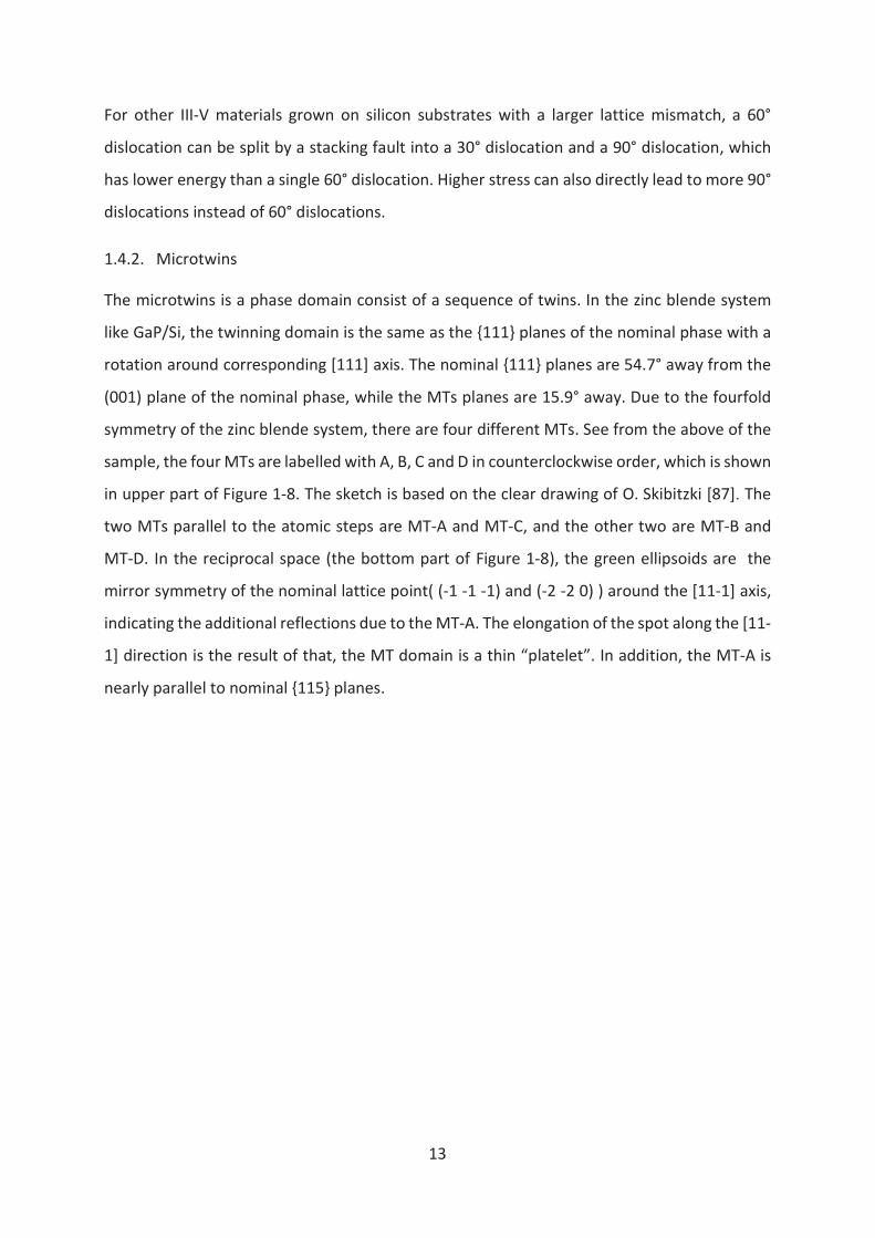
FIGURE 1-8 A SKETCH OF FOUR MICROTWINS IN GAP THIN LAYER ON VICINAL SI SUBSTRATE [87], AND GAP IN THE RECIPROCAL SPACE.
STRONG, MEDIUM AND WEAK REFLECTIONS ARE LABELLED WITH BLACK, BLUE AND RED POINTS. MT-A AND MT-C ARE
LABELLED WITH GREEN AND ORANGE ELLIPSOIDS. .................................................................................................... 14
FIGURE 1-9 THE APD IN GAP EPITAXY LAYERS ON SILICON SUBSTRATES WITH MONO-ATOMIC STEPS. ......................................... 15
FIGURE 1-10 A SKETCH OF MOSAICS WITH LIMITED LATERAL COHERENCE LENGTH, TILT OR TWIST IN GAP HETEROEPITAXY LAYER ON SI
SUBSTRATE. ..................................................................................................................................................... 16
FIGURE 2-1 UHV/CVD-MBE CLUSTER IN FOTON FOR GAP/SI PSEUDO-SUBSTRATE EPITAXY. ................................................ 27
FIGURE 2-2 SCHEMATIC DIAGRAM OF THE LAB SETUP X-RAY DIFFRACTOMETER IN THE LOW-RESOLUTION MODE. .......................... 30
FIGURE 2-3 SCHEMATIC DIAGRAM OF THE LAB SETUP X-RAY DIFFRACTOMETER IN THE HIGH-RESOLUTION MODE. .......................... 30
FIGURE 2-4 GONIOMETER GEOMETRY OF THE XRD LAB SETUP WITH FOUR ROTATIONAL DEGREES OF FREEDOM. ........................... 31
FIGURE 2-5 SCHEMATIC DIAGRAM OF Ω/2Θ LONGITUDINAL SCAN........................................................................................ 31
FIGURE 2-6 Ω/2Θ SCAN ON CIGS GROWN ON GAP/SI PSEUDO SUBSTRATE. ......................................................................... 34
FIGURE 2-7 2D RECIPROCAL SPACE AND EDWARD SPHERE DIAGRAM OF A SIMPLE CUBIC STRUCTURE CRYSTAL.............................. 36
FIGURE 2-8 SCHEMATIC DIAGRAM OF A) A NORMAL CRYSTAL PLANE FAMILY B) A CRYSTAL PLANE FAMILY A TILT OR C) WITH A DIFFERENT
LATTICE CONSTANT, I.E. A STRAIN STATE. ............................................................................................................... 38
FIGURE 2-9 SCHEMATIC DIAGRAM OF RELATIONSHIP BETWEEN RSM AND CRYSTAL PLANE PARAMETERS DHKL AND TILT !. ............ 39
FIGURE 2-10 SPHERICAL PROJECTION OF THE {100} POLES OF A CUBIC CRYSTAL. .................................................................... 40
FIGURE 2-11 EXAMPLE OF STEREOGRAPHIC PROJECTION OF A CUBIC CRYSTAL. ....................................................................... 41
FIGURE 2-12 EXAMPLE OF A POLE FIGURE. [19]............................................................................................................... 42
FIGURE 2-13 EXAMPLE OF POLE FIGURE USING THE PLANE {111} FOR GAP/SI (6° MISCUT) PSEUDO-SUBSTRATE. ......................... 43
FIGURE 2-14 SKETCH OF THE BEAMLINE ID01 DIFFRACTION EXPERIMENTAL SETUP. [48] ......................................................... 47
FIGURE 2-15 SCHEMATIC DIAGRAM OF THE PHOTODIODE DETECTOR SYSTEM. ........................................................................ 48
FIGURE 3-1 POLES FIGURE IMAGE AROUND THE NOMINAL GAP (111) REFLECTION FOR THE S1477 140NM GAP/SI (001) 6° -OFF
SAMPLE TOWARDS THE [110] DIRECTION. ............................................................................................................. 56
FIGURE 3-2 THE A) POLES FIGURE B) 5×5 ΜM2 AFM IMAGES OF A GAP/SI SAMPLE GROWN WITH THE OPTIMIZED CONDITION. ..... 56
FIGURE 3-3 EXAMPLE OF WILLIAMSON-HALL-LIKE PLOT. ................................................................................................... 58
FIGURE 3-4 LABORATORY XRD RSM AROUND (A) 002 AND (B) 004 NEARLY SPECULAR REFLECTIONS FOR S1330, AND THEIR
CORRESPONDING TRANSVERSE SCANS (C) AND (D). .................................................................................................. 59
vi
FIGURE 3-5 CROSS-SECTION STEM-BF IMAGES FOR THE OPTIMIZED GAP/SI GROWTH (FROM REF [7] ). .................................... 60
FIGURE 3-6 (A)RSM IMAGE OF (004) DIFFRACTION. (B) PF IMAGE (C) 5ΜM×5ΜM AFM IMAGE UNDER TAPPING MODE. (D) CROSS-
SECTIONAL (220) DARK-FIELD (DF) TEM IMAGE. THE MISFIT DISLOCATIONS ARE LABELLED WITH YELLOW ARROWS. ........... 62
FIGURE 3-7 A) THE EXPERIMENTAL SETUP OF THE K-MAP AND B) THE FOOTPRINT OF THE X-RAY BEAM FOR THE (004). ................. 63
FIGURE 3-8 SKETCH OF THE CORRECTED VERTICAL RESOLUTION IN A THIN LAYER, BROADENED BY THE PROJECTION OF THE CROSS-
SECTION AND THE SAMPLE THICKNESS. .................................................................................................................. 63
FIGURE 3-9 THE MOVEMENT OF THE X-RAY SPOT ON THE SAMPLE SURFACE CONTROLLED BY THE NANOMOTOR. ........................... 64
FIGURE 3-10 THE RESOLUTION OF QZ DETERMINED BY THE ROTATION OF THE DIFFRACTION VECTOR. ......................................... 67
FIGURE 3-11 TILT MAPPING TOWARDS (A) THE [-1-10] AND (B) THE [1-10] USING THE (004) BRAGG REFLECTION. (C) TILT MAPPING
TOWARDS THE [1-10] DIRECTION FOR THE (002) BRAGG REFLECTION WHICH EXHIBITS SIMILAR TILTS WITH (B) (THE SHIFT
ALONG THE X DIRECTION IS DUE TO IMPERFECT ALIGNMENT OR DRIFT BETWEEN MEASUREMENTS). ................................... 69
FIGURE 3-12 (A)LOCAL STRAIN (%) (B) FWHM OF THE QY PROFILE (°) MAPPING ON (004) BRAGG REFLECTION OF SAMPLE S1477,
WHICH IS 200NM GAP ON SI SUBSTRATE WITH 6° -OFF TOWARDS THE [-1-10] DIRECTION. ............................................ 70
FIGURE 3-13 THREE LBPS WITH NEIGHBORHOOD RANGES EQUAL TO 1, 2 AND 3. .................................................................. 71
FIGURE 3-14 (A) LOCAL BINARY IMAGE EXTRACTED FROM THE RESIDUAL STRAIN MAPPING (FIGURE 3-12 A). (B) SPATIAL FREQUENCY
OF THE LINES WITH HIGH STRAIN ALONG [-1-10] (BLUE) AND [1-10] (ORANGE). .......................................................... 71
FIGURE 3-15 SKETCH OF THE UNPARALLEL DISLOCATIONS FOR THE STEPS OF THE SUBSTRATE (REDREW BASED ON FIGURE 5(C) IN REF
[32]). ............................................................................................................................................................ 72
FIGURE 3-16 SPATIAL FREQUENCY OF AFM IMAGE FIGURE 1(B) ALONG [-1-10] (BLUE) AND [1-10] (ORANGE). ......................... 73
FIGURE 3-17 (A) THE SINGLE-PEAK POINT CCD IMAGE WITH Ω = 40.40° FOR (004) BRAGG REFLECTION AND (C) THE
CORRESPONDING TRANSVERSE SCAN WITH 0.01° WIDTH. (B) THE DOUBLE-PEAK POINT CCD IMAGE WITH Ω = 40.40° FOR
(004) BRAGG REFLECTION AND (D) THE CORRESPONDING TRANSVERSE SCAN WITH 0.01° WIDTH..................................... 74
FIGURE 3-18 SKETCH OF DIFFERENT MODES IN THE DIFFRACTION IMAGE. .............................................................................. 75
FIGURE 3-19 (A) THE MODE MAPPING FOR SAMPLE S1477. THE RED, WHITE AND GREEN AREAS RESPOND TO “SPLIT”, “SHIFT” AND
“NORMAL” MODES RESPECTIVELY. (B) TILT MAPPING TOWARDS [110] USING THE (004) BRAGG REFLECTION (I.E. FIGURE
3-11.B) AND THE OVERLAPPING CONTOUR LINES BASE ON (A), WHERE THE RED LINES LABELLED “SPLIT” AREAS AND THE WHITE
LINES LABELLED “SHIFT” AREAS. ........................................................................................................................... 76
FIGURE 3-20 (A) FWHM MAPPING OF THE MAIN PEAK ALONG QY AND (B) IN-PLANE RESIDUAL STRAIN MAPPING WITH OVERLAPPED
CONTOUR LINES (RED) OF THE “SPLIT” AREAS BASED ON FIGURE 3-19(A). ................................................................... 77
FIGURE 3-21 THE DIRECT CCD IMAGES OF SEVEN SAMPLING POINTS SHOWN IN FIGURE 3-20 (A). ............................................ 78
FIGURE 3-22 HYPOTHETICAL SKETCH OF THE MECHANISM RELATED TO THE “SPLIT” AREA. ........................................................ 80
FIGURE 4-1 TANDEM CONCEPT WITH CIGS TOP CELL WITH SELECTIVE CONTACTS AND SI BOTTOM CELL. ...................................... 86
FIGURE 4-2 STRUCTURAL MATCHING CRITERIA FOR THE EPITAXIAL GROWTH OF WIDE GAP CHALCOPYRITE ON GAP/SI. ADAPTED FROM
S. CHICHIBU ET. AL. [2] ..................................................................................................................................... 86
FIGURE 4-3 BAND OFFSET CRITERIA FOR THE OPTIMIZATION OF PHOTOVOLTAIC PROPERTIES OF THE CIGS/SI TANDEM DEVICES. VALUES
EXTRACTED BY IPVF FROM LITERATURE DATA[2]–[6], [7, P.], [8]. ............................................................................ 87
FIGURE 4-4 THE UNIT CELL OF CIGS. ............................................................................................................................. 88
vii
FIGURE 4-5 Ω/2Θ XRD SCANS A) FROM SAMPLE S554 (90NM GROWN AT 450°C) AND B) FROM SAMPLE 597 (600NM GAP GROWN
AT 580°C). THE RED TICK (RESP. THE BLUE ONE) GIVES THE THEORETICAL FULLY STRAINED GAP BRAGG PEAK POSITION (RESP.
THE THEORETICAL FULLY RELAXED ONE). ................................................................................................................ 89
FIGURE 4-6 Ω/2Θ SCANS WITH 2Θ RANGED FROM 20° TO 80° FOR SAMPLE 1743/GLASS. ...................................................... 91
FIGURE 4-7 Ω/2Θ SCANS WITH 2Θ RANGED FROM 20° TO 80° FOR SAMPLE 1743/S554, 1743/S597, 1744/S554 AND
1744/S597. .................................................................................................................................................. 92
FIGURE 4-8 A SELECTED AREA ELECTRON DIFFRACTION BY TEM ON 1743/S554. .................................................................. 93
FIGURE 4-9 EDX CARTOGRAPHY PERFORMED ON THE 1743/S554 SAMPLE, SHOWING THE ATOMIC FRACTION OF ALL THE CIGS
ELEMENTS, IN PARTICULAR THE IN AND GA ELEMENTS. ............................................................................................. 94
FIGURE 4-10 LEFT: EVOLUTION OF THE CIGS LATTICE PARAMETERS WITH RESPECT TO X, ACCORDING TO REF [16], [17] AND [29].
RIGHT: VARIATIONS OF THE CORRESPONDING XRD (008) AND (004) BRAGG PEAK POSITIONS WITH RESPECT TO X. THE
VERTICAL LINES CORRESPOND TO THE VARIATION OF X DEDUCED FROM THE ATOMIC FRACTIONS MEASURED BY EDX............. 95
FIGURE 4-11 Ω/2Θ SCANS WITH 2Θ RANGED A) FROM 25° TO 35° AND B) FROM 65° TO 70° FOR SAMPLE 1743/S554,
1743/S597, 1744/S554 AND 1744/S597. ....................................................................................................... 96
FIGURE 4-12 Ω/2Θ SCANS WITH 2Θ RANGED FROM 65° TO 70° FOR SAMPLE 1743/S554, 1744/S554 AND GAP/SI PSEUDO-
SUBSTRATE BEFORE GROWTH. ............................................................................................................................. 97
FIGURE 4-13 CROSS-SECTIONAL (220) BRIGHT-FIELD (BF) TEM IMAGE OF A CIGS SAMPLE GROWN ON GAP/SI SUBSTRATE. ....... 98
FIGURE 4-14 RSM IMAGE OF CIGS (1 1 10) AND GAP/SI (115) DIFFRACTION. .................................................................... 99
FIGURE 4-15 A) POLE FIGURE AT Χ = 45.5°, WHICH CORRESPONDS TO THE (204) CIGS BRAGG REFLECTION AND B) Ω/2Θ SCAN
AROUND THE (204) BRAGG REFLECTION (OBLIQUE PLANES) ON SAMPLE 1743/S597. ................................................. 100
FIGURE 4-16 STEM-HAADF IMAGE OF THE INTERFACE BETWEEN THE CIGS AND THE GAP LAYERS (WITH FFT OF EACH LAYER AS
INSETS), SHOWING THE EPITAXY BETWEEN BOTH LAYERS. ........................................................................................ 100
FIGURE 4-17 AN EXAMPLE OF THE INTEGRATED INTENSITY CALCULATION OF THE POLES. ........................................................ 101
FIGURE 4-18 THE POLE FIGURES AT CIGS (112) (LEFT) AND AT GAP(111), FOR SAMPLE A, B) 1743/S554, C, D) 1743/S597, E, F)
1744/S554 AND G, H) 1744/S597. ................................................................................................................ 104
FIGURE 4-19 Ω/2Θ SCANS FROM 26° TO 30° WITH Φ = 90° AND A) Χ = 16° OR B) Χ = 55°. .................................................. 104
FIGURE 4-20 SKETCHES OF THE NOMINAL CIGS PLANES AND PLANES OF THE MTS RELATED TO A) G-B AND B) G-C POLES
RESPECTIVELY. ................................................................................................................................................ 105
FIGURE 4-21 STIMULATION RESULT OF THE POLE FIGURE OF THE NOMINAL CIGS PLANES AND PLANES OF THE MTS. ................... 105
FIGURE 4-22 EXTERNAL QUANTUM EFFICIENCY OF CIGS SOLAR CELL ON NON-OPTIMIZED GAP/SI PSEUDO-SUBSTRATE COMPARED TO
CIGS SOLAR CELL ON GLASS (MO) SUBSTRATE. ..................................................................................................... 107
FIGURE 4-23 DARK I-V AND I-V CURVES UNDER ILLUMINATION (AM1.5) ON THE SOLAR CELL. ............................................... 107
FIGURE 5-1 A) TEM IMAGES OF CIGS/GAP/SI B) POLE FIGURE OF CIGS/GAP/SI, WHICH SHOWS A CLEAR CIGS (112) DIFFRACTION,
AS WELL AS THE MTS FORM IN THE CIGS LAYER. A TRANSVERSE SCAN AROUND THE CIGS (112) POSITION CONFIRMED THE
DIFFRACTION IS NOT AN ILLUSION FROM GAP (111). ............................................................................................. 114

viii
List of abbreviations
AFM Atomic Force Microscopy
APB Antiphase Boundary
APD Antiphase Domain
BF Bright Field
CMOS Complementary Metal Oxide Semi-conductor
CTR Crystal Truncation Rod
DF Dark Field
DFT Density Functional Theory
EQE External Quantum Efficiency
EIC Electronic Integrated Circuits
FCC Face Centered Cubic
HAADF High-Angle Annular Dark-Field
HCP Hexagonal Close Packed Structure
IB Integral Breadth
K-map quicK continuous Mapping
LED Light-Emitting Diode
MBE Molecular Beam Epitaxy
MEE Migration Enhanced Epitaxy
MOCVD Metal Organic Chemical Vapor Deposition
MOVPE Metal Organic Vapor Phase Epitaxy
ix
MT Microtwin
OEIC Optoelectronic Integrated Circuits
QF Quality Factor
r.m.s. Root Mean Square
RC Rocking Curve
RHEED Reflection High-Energy Electron Diffraction
RSM Reciprocal Space Map
SEM Scanning Electron Microscopy
SOI Silicon-on-Insulator
STEM Scanning Transmission Electron Microscopy
STM Scanning Tunneling Microscopy
TDS Thermal Diffuse Scattering
TEM Transmission Electron Microscopy
UHVCVD Ultra-High Vacuum Chemical Vapor Deposition
WHL Williamson-Hall like
XRD X-ray Diffraction
Remark: all the vectors are represented by a bold italic letter.

x

1
Chapitre 1. Introduction
This chapter is dedicated to introducing the purpose of the study. A brief review on the
heteroepitaxy of GaP on Si is given, which includes the applications of the study. The common
crystal defects are firstly introduced, and then some principle defects, for instance dislocations,
microtwins and antiphase boundaries, are discussed in the GaP/Si heteroepitaxial system. At
last, the organization of the dissertation is given.
2
1.1. Towards!a!better!world!
Energy, information and material are three pillars of development of modern society. The
semiconductor material is the key bonding between the three pillars. As to the bonding
between energy and material, the Photovoltaic (PV) system based on semiconductor materials
is one of the two technologies used in solar power plants (The other one is Concentrated Solar
Power (CSP) system), when the solar power grows more and more important in the energy
field, as the pollution of the traditional fossil power threatens the living environments of
human beings. [1] As to the bonding between information and material, nearly all the chips,
used in the electron computers, the smart phones, the domotics and other applications, are
fabricated by silicon. In further, optoelectronic integrated circuits, which is considered as an
alternative of the current electronic integrated circuits and a solution to overcome this
bottleneck, are also based on semiconductor materials.
Silicon is the most mature semiconductor material. It is widely in the microelectronic industry
and photovoltaic industry, owing to its natural abundance, low cost, high purity and
availability of large single crystals. Silicon photonics, which use silicon, SiC, silicon on insulator
(SOI) or SiGe, as the optical medium, has been applied in light emitters[2]–[4], waveguides[5]–
[7], modulators[8]–[10], photodetectors[11]–[13]. In addition, the market share of silicon
(including crystalline or amorphous) PV has never fell below 90% [14] in the last decade.
Nevertheless, silicon has its own limitation. The poor optical properties due to its indirect
bandgap precludes both the efficient light emission and the efficient light absorption.
Although many strategies have been applied to improve the optical properties of silicon, for
instance, porous silicon [15]–[17], erbium doping [18]–[20], nanowires[21], [22],
nanocrystals[23], [24], silicon is still less efficient compared to another important class of
semiconductor materials, III-V compound semiconductors. Thus, the monolithic integration of
III-V semiconductors on silicon is considered as a cornerstone for the integration of photonics
into the mature silicon technology (semiconductor LED or laser [25]–[27] and integrated
photonics devices [28]), as well as in the framework of the development of high-efficiency
solar cells on low-cost silicon substrates (multijunction solar cells or solar cell heterojunctions),
[29]–[31] and water splitting devices. [32]– [34]
3
Three main approaches have been developed and applied to realize the integration of III-V
compound semiconductor on top of a silicon wafer: flip-chip, bonding, and heteroepitaxy.
In the flip-chip integration, III-V optoelectronic devices and the silicon platform are processed
separately. Then one of the two components is flipped and interconnected to the other one
through soldering. [35], [36] The bonding technique is to contact mirror-polished, flat and
clean wafers to realize a strong bond between them based on the intermolecular interactions,
for instance, van der Waals forces, hydrogen bonds and strong covalent bonds. In the bonding
techniques, there are two different methods, i.e. direct bonding and adhesive bonding. In the
wafer bonding process, the adhesive bonding has additional intermediate layers as “glues”,
i.e. polymers or metals, while the direct bonding does not. The direct bonding of III-V
semiconductor materials and silicon demands a high-temperature (>600 °C) anneal, while
some devices fabricated on the silicon wafer, i.e. CMOS, become invalid at about 450 °C [37].
Thus, a key challenge to the direct bonding is that, how the anneal temperature can be
sufficiently low to inhibit active material degradation [38]. O2 plasma-assisted wafer bonding
is proposed to solve the problem, and the process temperature has be decreased to below
400 °C [38], [39]. For the adhesive bonding, several materials, i.e. thermoplastic [40],
elastomeric [41] and thermosetting materials [42], are used in the case of III-V semiconductor
materials and silicon. Divinylsiloxane-bis-benzocyclobutene (DVS-BCB), as a thermosetting
polymer, is selected from the materials by many groups due to its properties, such as, the low
optical loss at telecommunication wavelengths, the high planarization and the high glass
transition temperature[37], [43], [44].
Although some interesting results have been achieved with the two methods, heteroepitaxy
is still considered as a promising and attractive technique. Because heteroepitaxy provides
low-cost, highly integrated, and large-scale monolithic integration of III-V semiconductor
materials and silicon. A brief literature review on the heteroepitaxy of III-V materials on silicon,
especially GaP on Si, is given in the next section.
1.2. Heteroepitaxy!of!GaP!and!Si!
Epitaxy refers to the growth of a crystalline overlayer on the crystalline surface of the
substrate. The overlayer is also called epitaxy layer. The in-plane crystalline orientation of the
epitaxy layer is usually defined by the substrate crystal structure. According to the compound
4
of the epitaxy layer and the substrate, epitaxy is classified into two types, i.e. homoepitaxy
and heteroepitaxy. In the homoepitaxy, the epitaxy layer is the same material as the substrate,
while it is purer or has different doping levels, compared to the substrate. The epitaxy layer in
the heteroepitaxy has a different compound from the substrate, and III-V on silicon is a typical
heteroepitaxy.
The heteroepitaxy of several common III-V semiconductor materials on silicon has been
successfully performed, such as, GaAs[45]–[47], InGaAs[48], [49], InP[50], GaP[51], [52],
GaSb[53], GaN[54], [55] and et.al. But the lattice mismatch between most III-V compounds and
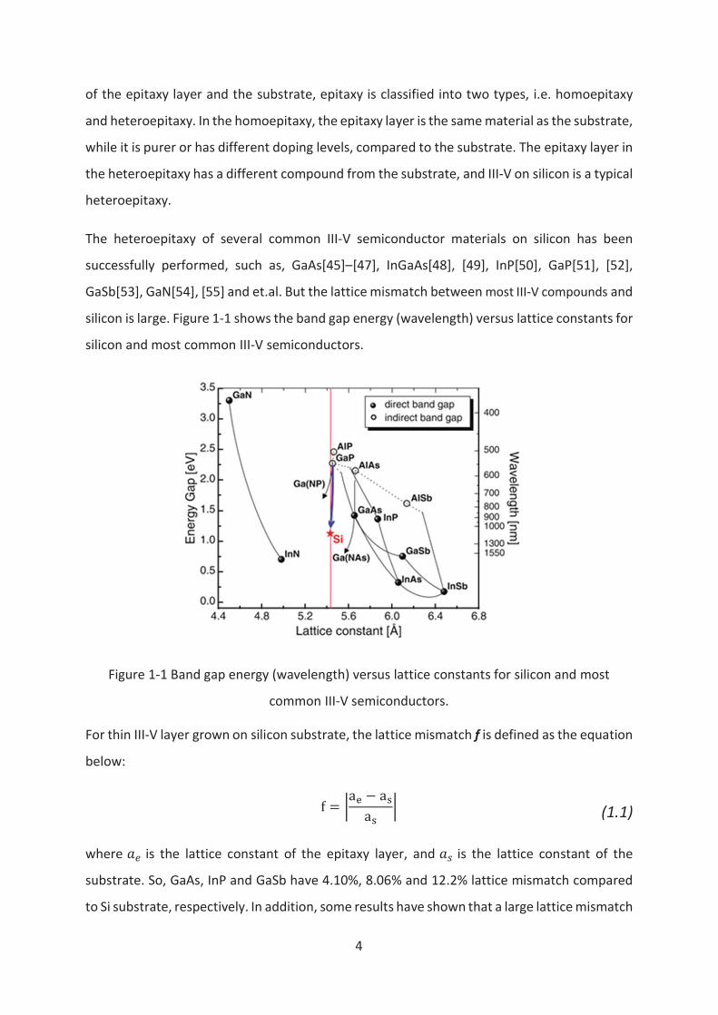
silicon is large. Figure 1-1 shows the band gap energy (wavelength) versus lattice constants for
silicon and most common III-V semiconductors.
Figure 1-1 Band gap energy (wavelength) versus lattice constants for silicon and most
common III-V semiconductors.
For thin III-V layer grown on silicon substrate, the lattice mismatch f is defined as the equation
below:
f = "a# $ a%a% " (1.1)
where &' is the lattice constant of the epitaxy layer, and &( is the lattice constant of the
substrate. So, GaAs, InP and GaSb have 4.10%, 8.06% and 12.2% lattice mismatch compared
to Si substrate, respectively. In addition, some results have shown that a large lattice mismatch
5
leads to a large dislocation density [56], [57], which can reduce the carrier lifetime [58]–[60]
and influence the photoelectric properties of the final devices based on the heteroepitaxy
structure.
While, Gallium phosphide (GaP), which is an indirect bandgap semiconductor material, has very
small lattice mismatch with silicon. Some basic parameter of GaP and Si at the room
temperature is shown as Table 1-1. The lattice mismatch of GaP and Si is only 0.37% at the
room temperature. Thus, the epitaxial growth of quasi-lattice matched GaP on silicon has
been developed to be used as an efficient platform for the subsequent integration of low-
defect or defect-free III-V based heterostructures. For instance, the development of GaP/Si
pseudo-substrates opens the route for the coherent growth of a direct band-gap material,
using for example diluted-nitrides GaPN-based materials. Having nearly a lattice-match to Si,
GaP/Si also provides a simple but important model system for the heteroepitaxial growth of
polar semiconductor material on a nonpolar substrate.
GaP Si
Lattice constant 0.5451 0.5431
C11 140.5 GPa 166.0 GPa
C12 62.0 GPa 64.0 GPa
Band gap energy 2.26 eV 1.12 eV
Thermal expansion coefficient 4.65×10⁻⁶/K 2.6×10⁻⁶/K
Table 1-1 Some basic parameter of GaP and Si at the room temperature (300K).
Broadie et.al. from IBM in USA [61], T. Katoda and M.Kishi from University of Tokyo in Japan [62]
had studied the heteroepitaxy of GaP on silicon substrated at 1980s. After that, T.J. Grassman et
al. from the Ohio State University in USA [63], [64], K.Volz et.al. from Philipps-University in
Marburg (Germany) [65], [66], Yonezu et.al. from Toyohashi University of Technology in Japan [67],
[68], have also sucssefully achieved the heteroepitaxy of GaP on Si by either MBE or MOCVD.
Recently, M. S. Sobolev and co-workers at St. Petersburg Academic University in Russia has
achieved single crystalline GaP nucleation and buffer layers on silicon substrates with MBE. [69]
They also invested the possibility of silicon or beryllium doping in GaP layers, which can used as
6
contact layers in the further development of devices. [70] C. Zhang et. al. from Arizona State
University in USA worked on the application of GaP/Si in the heterojunction solar cells and have
obtained n-GaP/n-Si heterojunction solar cells with an efficiency of 13.1% at AM1.5G. [71], [72]
They also cooperated with M. Vaisman et.al from Yale University and National Renewable Energy
Laboratory in USA to develop GaAsP solar cells on GaP/Si pseudo-substrate and achieved an
efficiency of 15.3% at AM1.5G. [73]
In our laboratory, GaP-based optical devices [74], [75] and solar cells [76] has been reported for
years. The heteroepitaxy of GaP on Si using UHVCVD-MBE is also studied in recent years [77]–[79].
The aim of the thesis work is to characterize the structure defects on the base of former study and
develop more analytical methods for the improvement of the GaP/Si platform.
1.3. Crystallographic!defect!
In an unlimited perfect crystal, the arrangement of the atoms or molecules usually has long-
range periodicity. The minimum group of atoms or molecules, which constitutes the repeating
pattern is called the unit cell. If each unit cell is treated as a point, then the crystal cells can
repeat themselves after a set of symmetry operations, which is called the crystallographic
point group. Thus, the interruptions of the periodic crystal structure are called the
crystallographic defects, or defects. According to the geometric dimension of the defects, they
can be classified into point defects, line defects, planar defects and bulk defects, which are
corresponding to 0D, 1D, 2D, and 3D, respectively. In the section, I will give a brief introduction
to the definition and the classification of these defects. For some principle defects in the
heteroepitaxy of GaP and Si, for instance dislocations, microtwins and antiphase boundaries,
the detailed discussion will be in the next section.
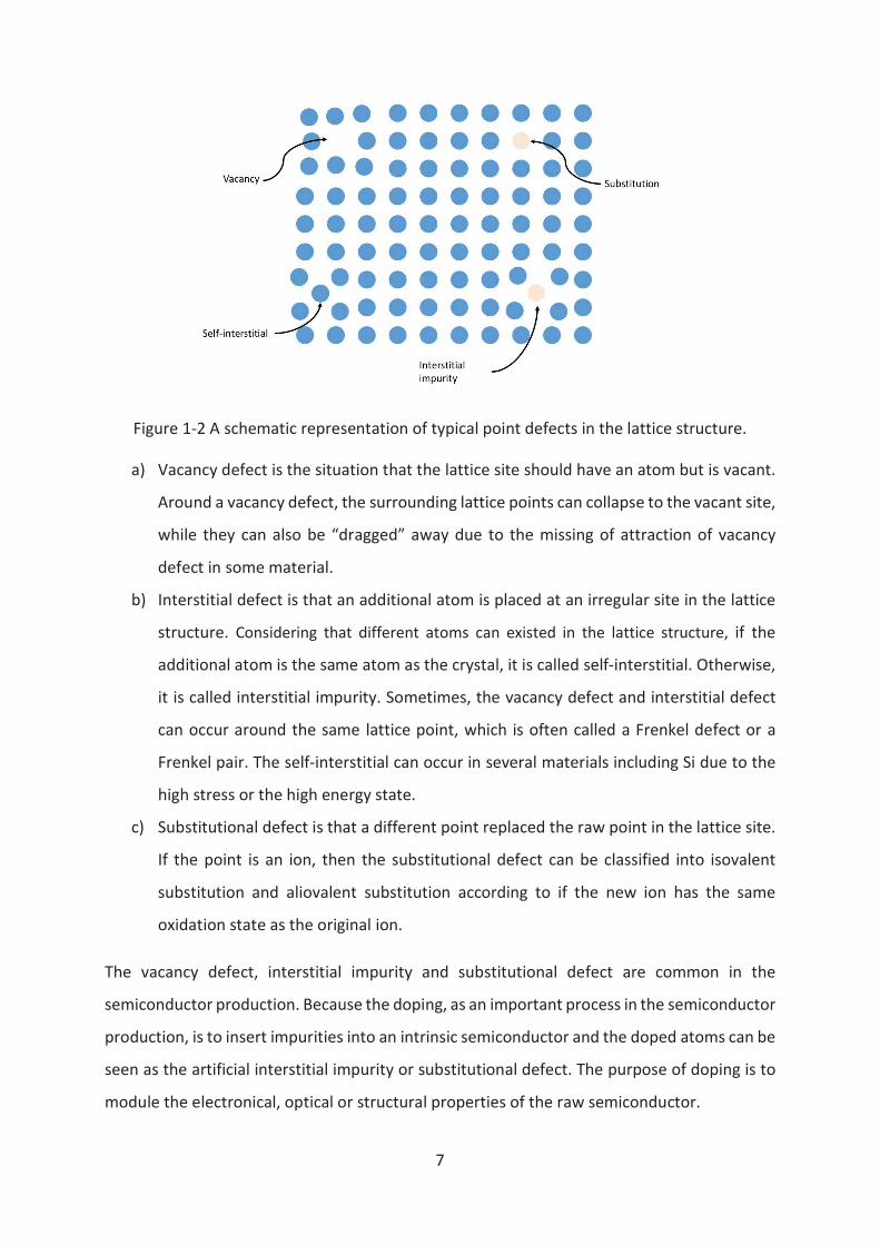
1.3.1. Point defects
Point defect occurs only at or around a single lattice point. A point can only be missing or
additionally placed in the lattice structure, so the point defects have three typical types, which is
shown in Figure 1-2.
7
Figure 1-2 A schematic representation of typical point defects in the lattice structure.
a) Vacancy defect is the situation that the lattice site should have an atom but is vacant.
Around a vacancy defect, the surrounding lattice points can collapse to the vacant site,
while they can also be “dragged” away due to the missing of attraction of vacancy
defect in some material.
b) Interstitial defect is that an additional atom is placed at an irregular site in the lattice
structure. Considering that different atoms can existed in the lattice structure, if the
additional atom is the same atom as the crystal, it is called self-interstitial. Otherwise,
it is called interstitial impurity. Sometimes, the vacancy defect and interstitial defect
can occur around the same lattice point, which is often called a Frenkel defect or a
Frenkel pair. The self-interstitial can occur in several materials including Si due to the
high stress or the high energy state.
c) Substitutional defect is that a different point replaced the raw point in the lattice site.
If the point is an ion, then the substitutional defect can be classified into isovalent
substitution and aliovalent substitution according to if the new ion has the same
oxidation state as the original ion.
The vacancy defect, interstitial impurity and substitutional defect are common in the
semiconductor production. Because the doping, as an important process in the semiconductor
production, is to insert impurities into an intrinsic semiconductor and the doped atoms can be
seen as the artificial interstitial impurity or substitutional defect. The purpose of doping is to
module the electronical, optical or structural properties of the raw semiconductor.
8
1.3.2. Line defects
A line defect refers to a whole row of anomalously arranged points in the lattice structure.
The mis-arrangement of the lattice points is usually called the line of dislocation. Thus, the
dislocations and the line defects are considered to be equivalent in many places.
1.3.3. Planar defects
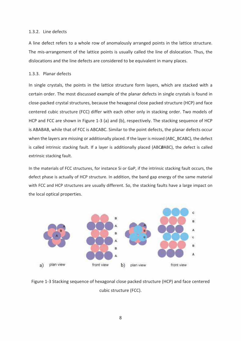
In single crystals, the points in the lattice structure form layers, which are stacked with a
certain order. The most discussed example of the planar defects in single crystals is found in
close-packed crystal structures, because the hexagonal close packed structure (HCP) and face
centered cubic structure (FCC) differ with each other only in stacking order. Two models of
HCP and FCC are shown in Figure 1-3 (a) and (b), respectively. The stacking sequence of HCP
is ABABAB, while that of FCC is ABCABC. Similar to the point defects, the planar defects occur
when the layers are missing or additionally placed. If the layer is missed (ABC_BCABC), the defect
is called intrinsic stacking fault. If a layer is additionally placed (ABCBABC), the defect is called
extrinsic stacking fault.
In the materials of FCC structures, for instance Si or GaP, if the intrinsic stacking fault occurs, the
defect phase is actually of HCP structure. In addition, the band gap energy of the same material
with FCC and HCP structures are usually different. So, the stacking faults have a large impact on
the local optical properties.
Figure 1-3 Stacking sequence of hexagonal close packed structure (HCP) and face centered
cubic structure (FCC).
9
A special case in the stacking fault is the twins, where the stacking sequences are mirror
symmetric besides the defects, i.e. ABCABC|CBCABC.
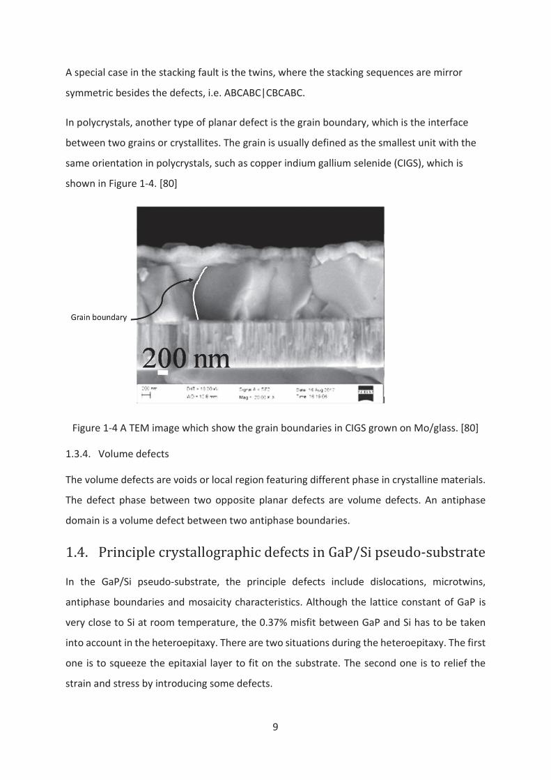
In polycrystals, another type of planar defect is the grain boundary, which is the interface
between two grains or crystallites. The grain is usually defined as the smallest unit with the
same orientation in polycrystals, such as copper indium gallium selenide (CIGS), which is
shown in Figure 1-4. [80]
Figure 1-4 A TEM image which show the grain boundaries in CIGS grown on Mo/glass. [80]
1.3.4. Volume defects
The volume defects are voids or local region featuring different phase in crystalline materials.
The defect phase between two opposite planar defects are volume defects. An antiphase
domain is a volume defect between two antiphase boundaries.
1.4. Principle!crystallographic!defects!in!GaP/Si!pseudo-substrate!
In the GaP/Si pseudo-substrate, the principle defects include dislocations, microtwins,
antiphase boundaries and mosaicity characteristics. Although the lattice constant of GaP is
very close to Si at room temperature, the 0.37% misfit between GaP and Si has to be taken
into account in the heteroepitaxy. There are two situations during the heteroepitaxy. The first
one is to squeeze the epitaxial layer to fit on the substrate. The second one is to relief the
strain and stress by introducing some defects.

10
The first situation often occurs in the growth of thin layers. The strain and stress energy will
be stored in the epitaxial layer. The growth mode of this situation is usually called “coherent
growth” or “pseudomophic growth”. For the growth of thicker epitaxy layer, the initial layer is also
similar to the thin layer.
The lattice strain of the GaP epitaxy layer on nominal Si substrate and vicinal Si substrate is shown
in Figure 1-5.
Figure 1-5 The sketch of the lattice strain of GaP thin layer on a) nominal and b)vicinal Si
substrate. [81]
The out-of-plane relaxation )* and in-plain relaxation )+ can be defined as below:
,* = a* $ a-a- (1.2)
,+ = a+ $ a-a- (1.3)
where .* is the out-of-plane lattice constant of the epitaxy layer, .+ is the out-of-plane lattice
constant of the epitaxy layer, and ./ is the lattice constant of bulk GaP.
According to the Hooke’s law, the out-of-plane relaxation 2* and in-plain relaxation 2+ have a
relationship as below:
,* = $3C45C44 ,+ (1.4)
For the nominal substrate, 6+ is equal to the lattice constant of Si 67. For the vicinal substrate,
the 6+ is: [81]
a+ = a% 8 9&:;<>?@9&:;<?@ a% (1.5)
11
where AB is the tilt angle between the [001] orientation of GaP and that of Si, E is the vicinal
angle of the substrate. For α = 6°, AB is only 0.041°. Thus, the difference between the 6+ and 67 is so little that it can be neglected.
The elastic energy E generated in this way is nearly proportional to the thickness of the
epitaxial layer h, which is:
F = ,+5M-h (1.6)
where GI is the biaxial modulus of the film. [82]
As the ability of the epitaxial layer to store the elastic energy is limited, the maximum thickness
to keep the energy is called the critical thickness. If the sample thickness is beyond the critical
thickness, the sample is considered to be relaxed. The critical thickness can be calculated with
the Matthews-Blakeslee critical thickness model [83]–[85], and modified by considering other
defects, such as vicinal substrate. The critical thickness for GaP/Si pair in heteroepitaxy has been
determined to be around 50 nm by Yamane et.al.[86], 45 nm by Skibitzki [87] and below 90
nm by Soga et.al.[88].
While, many of our sample has a thickness of the epitaxial layer which is beyond the critical
thickness. In the condition, the strain and stress energy will be released by relieved both by
formation and/or propagation the defects, which is mainly the dislocation. [89] In addition,
due to the physical and chemical presence of an interface between GaP and Si, some specific
defects, i.e. microtwins, antiphase boundaries and mosaicity characteristics, occur in the
heteroepitaxy.
1.4.1. Dislocation
Dislocation was proposed to be a defect in atomic scale by G. I. Taylor in 1934. [90] So, it is
also called Taylor’s dislocation. In geometry, dislocations can be described by a vector b, which
is called Burgers vector. The Burgers vector is determined by the closure failure of a closed
loop, which trace around the end of the dislocation plane. According to the direction of the
Burgers vector, dislocations can be classified into two primary type: edge dislocations and
screw dislocations, which is shown in Figure 1-6 a) and b), respectively [91]. The line vector t
describes the local direction of the dislocation line. If the Burgers vector b is orthogonal to the
line vector t, then the dislocation is edge dislocation. While, if the Burgers vector b is parallel
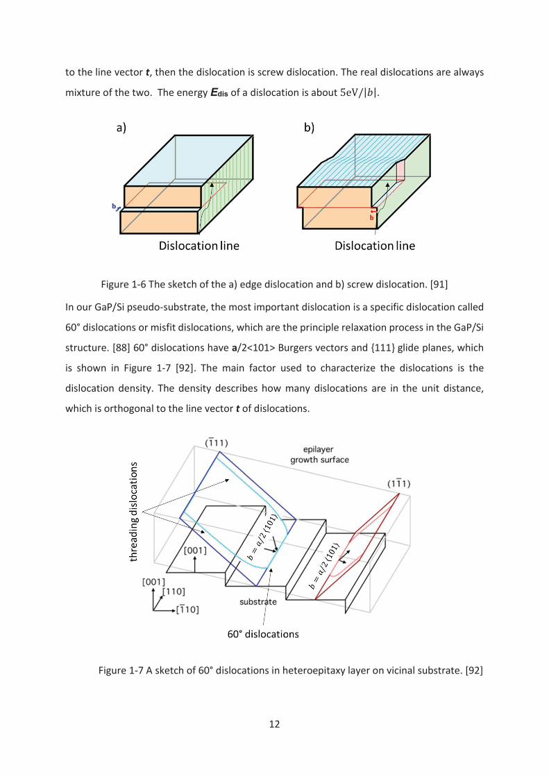
12
to the line vector t, then the dislocation is screw dislocation. The real dislocations are always
mixture of the two. The energy Edis of a dislocation is about JeVN|O|.
Figure 1-6 The sketch of the a) edge dislocation and b) screw dislocation. [91]
In our GaP/Si pseudo-substrate, the most important dislocation is a specific dislocation called
60° dislocations or misfit dislocations, which are the principle relaxation process in the GaP/Si
structure. [88] 60° dislocations have a/2<101> Burgers vectors and {111} glide planes, which
is shown in Figure 1-7 [92]. The main factor used to characterize the dislocations is the
dislocation density. The density describes how many dislocations are in the unit distance,
which is orthogonal to the line vector t of dislocations.
Figure 1-7 A sketch of 60° dislocations in heteroepitaxy layer on vicinal substrate. [92]
13
For other III-V materials grown on silicon substrates with a larger lattice mismatch, a 60°
dislocation can be split by a stacking fault into a 30° dislocation and a 90° dislocation, which
has lower energy than a single 60° dislocation. Higher stress can also directly lead to more 90°
dislocations instead of 60° dislocations.
1.4.2. Microtwins
The microtwins is a phase domain consist of a sequence of twins. In the zinc blende system
like GaP/Si, the twinning domain is the same as the {111} planes of the nominal phase with a
rotation around corresponding [111] axis. The nominal {111} planes are 54.7° away from the
(001) plane of the nominal phase, while the MTs planes are 15.9° away. Due to the fourfold
symmetry of the zinc blende system, there are four different MTs. See from the above of the
sample, the four MTs are labelled with A, B, C and D in counterclockwise order, which is shown
in upper part of Figure 1-8. The sketch is based on the clear drawing of O. Skibitzki [87]. The
two MTs parallel to the atomic steps are MT-A and MT-C, and the other two are MT-B and
MT-D. In the reciprocal space (the bottom part of Figure 1-8), the green ellipsoids are the
mirror symmetry of the nominal lattice point( (-1 -1 -1) and (-2 -2 0) ) around the [11-1] axis,
indicating the additional reflections due to the MT-A. The elongation of the spot along the [11-
1] direction is the result of that, the MT domain is a thin “platelet”. In addition, the MT-A is
nearly parallel to nominal {115} planes.
14
Figure 1-8 A sketch of four microtwins in GaP thin layer on vicinal Si substrate [87],
and GaP in the reciprocal space. Strong, medium and weak reflections are labelled with
black, blue and red points. MT-A and MT-C are labelled with green and orange ellipsoids.
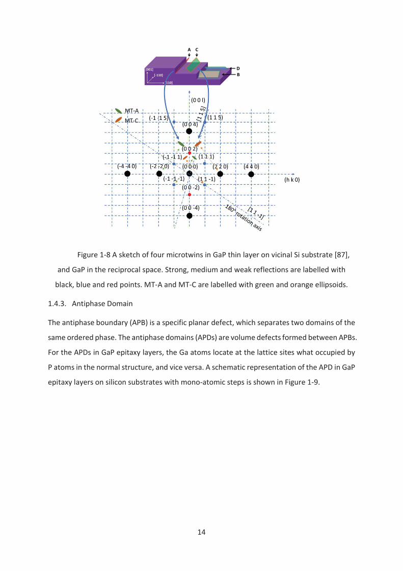
1.4.3. Antiphase Domain
The antiphase boundary (APB) is a specific planar defect, which separates two domains of the
same ordered phase. The antiphase domains (APDs) are volume defects formed between APBs.
For the APDs in GaP epitaxy layers, the Ga atoms locate at the lattice sites what occupied by
P atoms in the normal structure, and vice versa. A schematic representation of the APD in GaP
epitaxy layers on silicon substrates with mono-atomic steps is shown in Figure 1-9.
15
Figure 1-9 The APD in GaP epitaxy layers on silicon substrates with mono-atomic steps.
There have been several reports on the APDs in GaP epitaxy layers on silicon substrates. H.
Döscher et.al. from Helmholtz Center in Germany have applied Reflectance Anisotropy
Spectroscopy (RAS) as an in-situ probe to measure and quantify the Anti-Phase Domain (APD)
content in the GaP heteroepitaxial layer grown on the Si substrate. [93], [94] The originating
mechanism of the APDs, one of the main defects originating at the nucleation process of the
GaP on the Si (001) substrate, was discussed by K. Volz et.al. from Phillips University. [95], [96]
E. L. Warren et.al. from National Renewable Energy Laboratory in USA achieved APD free
growth of GaP on Si with in-situ AsH3-etching during the epitaxy by MOCVD, which is
demonstrated by both Low-energy electron diffraction (LEED) and Transmission electron
microscope (TEM). [52] Our laboratory has also used X-ray diffraction and transmission
electron microscopy (TEM) to quantitively measure the lateral size of the APDs in GaP on
vicinal Si substrates grown by MBE. [79], [97] It had been suggested that the APDs could be
better self-annihilated on vicinal Si substrates with bi-atomic steps. [98]–[100] A most recent
study in our laboratory by I. Lucci et.al. pointed that the phases of the initial GaP islands on
the Si substrates have large impact on the formation and self-annihilation of APDs. [101]
1.4.4. Mosaic
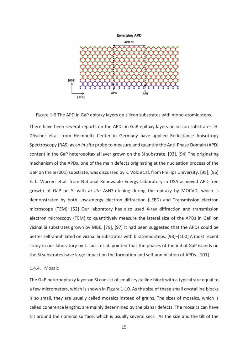
The GaP heteroepitaxy layer on Si consist of small crystalline block with a typical size equal to
a few micrometers, which is shown in Figure 1-10. As the size of these small crystalline blocks
is so small, they are usually called mosaics instead of grains. The sizes of mosaics, which is
called coherence lengths, are mainly determined by the planar defects. The mosaics can have
tilt around the nominal surface, which is usually several secs. As the size and the tilt of the
16
mosaics are both very small in GaP thin layers, the GaP thin layers are considered to be
monocrystalline in many situations. But if the spatial resolution of the characterization
methods (i.e. sub-microbeam X-ray scanning diffraction or TEM) are high enough, the
mosaicity characteristics should be taken into account.
Figure 1-10 A sketch of Mosaics with limited lateral coherence length, tilt or twist in GaP
heteroepitaxy layer on Si substrate.
1.5. The!organization!of!the!thesis!
Chapter 1 describes the purpose of the thesis work. The GaP/Si pseudo substrate provides an
important platform in the monolithic integration of III-V semiconductor materials and Si, which
have a large application field in both photonics and photovoltaics. A general introduction on
the crystal defects are presented, and some important defects in heteroepitaxial thin layers,
for instance dislocations, MTs and APDs, are detailed.
Chapter 2 introduces the techniques in the growth and characterization process, which are
applied in the thesis work. The Si substrate preparation and the heteroepitaxy of GaP/Si thin
layers by using MBE are firstly introduced. Then the most important characterization method,
X-ray diffractions, is detailed, including basic principles, experimental setup and data process
methods. Finally, other characterization methods, for instance atomic force microscope and
transmission electron microscope, are introduced.
Chapter 3 is dedicated to the characterization of the dislocations’ distribution, by using an
advanced X-ray technique, sub-micrometer scanning X-ray diffraction. Firstly, a brief review
on the former characterization results on similar samples are given. Then, the sample
17
preparation and the structural result performed with lab-setup measurements are present.
Finally, with the analysis of the sub-micrometer scanning X-ray diffraction results, the
distribution of dislocations is found to be inhomogeneous. The distribution of dislocations has
strong impact the sample surface roughness.
Chapter 4 presents the primary evaluation of CIGS/GaP/Si tandem solar cells, which can be
both low-cost and high-efficiency. The CIGS is observed to epitaxially grown on GaP/Si pseudo
substrates, by analyzing the results from ω/2θ scan, reciprocal space map and pole figures.
The influence of the growth condition on the structural quality is also discussed.
Finally, Chapter 5 summarizes all the results obtained during the thesis, including the
structural analyses of the GaP/Si layer and CIGS/GaP/Si solar cells.
References
[1] C. A. Horowitz, “Paris Agreement,” Int Leg Mater, vol. 55, no. 4, pp. 740–755, 2016.
[2] K. Eberl, O. G. Schmidt, R. Duschl, O. Kienzle, E. Ernst, and Y. Rau, “Self-assembling SiGe
and SiGeC nanostructures for light emitters and tunneling diodes,” Thin Solid Films, vol.
369, no. 1–2, pp. 33–38, 2000.
[3] D. P. Yu et al., “Amorphous silica nanowires: Intensive blue light emitters,” Appl. Phys.
Lett., vol. 73, no. 21, pp. 3076–3078, 1998.
[4] D. J. Lockwood, Z. H. Lu, and J.-M. Baribeau, “Quantum confined luminescence in Si/SiO 2
superlattices,” Phys. Rev. Lett., vol. 76, no. 3, p. 539, 1996.
[5] U. Fischer, T. Zinke, J.-R. Kropp, F. Arndt, and K. Petermann, “0.1 dB/cm waveguide losses
in single-mode SOI rib waveguides,” IEEE Photonics Technol. Lett., vol. 8, no. 5, pp. 647–
648, 1996.
[6] G. Li et al., “Ultralow-loss, high-density SOI optical waveguide routing for macrochip
interconnects,” Opt. Express, vol. 20, no. 11, pp. 12035–12039, 2012.
[7] X. Wang, W. Shi, H. Yun, S. Grist, N. A. Jaeger, and L. Chrostowski, “Narrow-band
waveguide Bragg gratings on SOI wafers with CMOS-compatible fabrication process,” Opt.
Express, vol. 20, no. 14, pp. 15547–15558, 2012.
[8] C. E. Png, S. P. Chan, S. T. Lim, and G. T. Reed, “Optical phase modulators for MHz and GHz
modulation in silicon-on-insulator (SOI),” J. Light. Technol., vol. 22, no. 6, p. 1573, 2004.
18
[9] J. Liu, D. Pan, S. Jongthammanurak, K. Wada, L. C. Kimerling, and J. Michel, “Design of
monolithically integrated GeSi electro-absorption modulators and photodetectors on an
SOI platform,” Opt. Express, vol. 15, no. 2, pp. 623–628, 2007.
[10] T.-Y. Liow et al., “Silicon modulators and germanium photodetectors on SOI:
monolithic integration, compatibility, and performance optimization,” IEEE J. Sel. Top.
Quantum Electron., vol. 16, no. 1, pp. 307–315, 2009.
[11] H. Yamamoto, K. Taniguchi, and C. Hamaguchi, “High-sensitivity SOI MOS
photodetector with self-amplification,” Jpn. J. Appl. Phys., vol. 35, no. 2S, p. 1382, 1996.
[12] G. Dehlinger, S. J. Koester, J. D. Schaub, J. O. Chu, Q. C. Ouyang, and A. Grill, “High-
speed germanium-on-SOI lateral PIN photodiodes,” IEEE Photonics Technol. Lett., vol. 16,
no. 11, pp. 2547–2549, 2004.
[13] X. Wang, Z. Cheng, K. Xu, H. K. Tsang, and J.-B. Xu, “High-responsivity graphene/silicon-
heterostructure waveguide photodetectors,” Nat. Photonics, vol. 7, no. 11, p. 888, 2013.
[14] S. Ali, Ed., Comprehensive Renewable Energy, vol. Photovoltaic Solar Energy, 1 vols.
Boston: Elevier Science, 2012.
[15] V. Lehmann and U. Gösele, “Porous silicon formation: A quantum wire effect,” Appl.
Phys. Lett., vol. 58, no. 8, pp. 856–858, 1991.
[16] V. S.-Y. Lin, K. Motesharei, K.-P. S. Dancil, M. J. Sailor, and M. R. Ghadiri, “A porous
silicon-based optical interferometric biosensor,” Science, vol. 278, no. 5339, pp. 840–843,
1997.
[17] G. Korotcenkov, “Porous Silicon Characterization and Application: General View,” in
Porous Silicon: From Formation to Application: Formation and Properties, Volume One,
CRC Press, 2016, pp. 20–43.
[18] H. Ennen, G. Pomrenke, A. Axmann, K. Eisele, W. Haydl, and J. Schneider, “1.54-μm
electroluminescence of erbium-doped silicon grown by molecular beam epitaxy,” Appl.
Phys. Lett., vol. 46, no. 4, pp. 381–383, 1985.
[19] J. Palm, F. Gan, B. Zheng, J. Michel, and L. C. Kimerling, “Electroluminescence of
erbium-doped silicon,” Phys. Rev. B, vol. 54, no. 24, p. 17603, 1996.
[20] G. Mula et al., “Doping porous silicon with erbium: pores filling as a method to limit
the Er-clustering effects and increasing its light emission,” Sci. Rep., vol. 7, no. 1, p. 5957,
2017.
19
[21] P. R. Wiecha, A. Arbouet, H. Kallel, P. Periwal, T. Baron, and V. Paillard, “Enhanced
nonlinear optical response from individual silicon nanowires,” Phys. Rev. B, vol. 91, no. 12,
p. 121416, 2015.
[22] M. Keplinger et al., “Strain distribution in single, suspended germanium nanowires
studied using nanofocused x-rays,” Nanotechnology, vol. 27, no. 5, p. 055705, Feb. 2016.
[23] M. Dasog, J. Kehrle, B. Rieger, and J. G. Veinot, “Silicon nanocrystals and silicon-
polymer hybrids: synthesis, surface engineering, and applications,” Angew. Chem. Int. Ed.,
vol. 55, no. 7, p. 2322–2339, 2016.
[24] N. J. Kramer, K. S. Schramke, and U. R. Kortshagen, “Plasmonic properties of silicon
nanocrystals doped with boron and phosphorus,” Nano Lett., vol. 15, no. 8, p. 5597–5603,
2015.
[25] S. Liebich et al., “Laser operation of Ga(NAsP) lattice-matched to (001) silicon
substrate,” Appl Phys Lett, vol. 99, no. 7, p. 071109, 2011.
[26] K. Yamane et al., “Growth of a lattice-matched GaAsPN p–i–n junction on a Si substrate
for monolithic III–V/Si tandem solar cells,” Appl Phys Express, vol. 10, no. 7, p. 075504,
2017.
[27] A. Y. Liu et al., “Electrically pumped continuous-wave 13 μm quantum-dot lasers
epitaxially grown on on-axis (001) GaP/Si,” Opt Lett, vol. 42, no. 2, p. 338, 2017.
[28] P. Guillemé et al., “Second harmonic generation in gallium phosphide microdisks on
silicon: from strict to random quasi-phase matching,” Semicond Sci Tech, vol. 32, no. 6, p.
065004, 2017.
[29] M. Feifel et al., “MOVPE Grown Gallium Phosphide-Silicon Heterojunction Solar Cells,”
Ieee J Photovolt, vol. 7, no. 2, pp. 502–507, 2017.
[30] C. Cornet, M. Silva, C. Levallois, and O. Durand, GaP/Si-Based Photovoltaic Devices
Grown by Molecular Beam Epitaxy, Second Edition., Elsevier, 2018, pp. 637–648.
[31] R. Varache, M. Darnon, M. Descazeaux, M. Martin, T. Baron, and D. Muñoz, “Evolution
of Bulk c-Si Properties during the Processing of GaP/c-Si Heterojunction Cell,” Enrgy
Proced, vol. 77, pp. 493–499, 2015.
[32] O. Supplie, M. M. May, H. Stange, C. Höhn, H.-J. Lewerenz, and T. Hannappel,
“Materials for light-induced water splitting: In situ controlled surface preparation of GaPN
epilayers grown lattice-matched on Si(100),” J Appl Phys, vol. 115, no. 11, p. 113509, 2014.
20
[33] J. L. Young, M. A. Steiner, H. Döscher, R. M. France, J. A. Turner, and T. G. Deutsch,
“Direct solar-to-hydrogen conversion via inverted metamorphic multi-junction
semiconductor architectures,” Nat Energy, vol. 2, no. 4, p. 17028, 2017.
[34] I. Lucci et al., “A Stress-Free and Textured GaP Template on Silicon for Solar Water
Splitting,” Adv Funct Mater, vol. 28, no. 30, p. 1801585, 2018.
[35] J. H. Lau, Flip chip technologies, vol. 1. New York: McGraw-Hill, 1996.
[36] M. D. Rostoker, Multi-chip semiconductor arrangements using flip chip dies. U.S.
Patents, 1995.
[37] G. Roelkens et al., “III-V/silicon photonics for on-chip and intra-chip optical
interconnects,” Laser Photonics Rev., vol. 4, no. 6, pp. 751–779, Nov. 2010.
[38] K. Tanabe, K. Watanabe, and Y. Arakawa, “III-V/Si hybrid photonic devices by direct
fusion bonding,” Sci. Rep., vol. 2, p. 349, 2012.
[39] D. Pasquariello and K. Hjort, “Plasma-assisted InP-to-Si low temperature wafer
bonding,” IEEE J. Sel. Top. Quantum Electron., vol. 8, no. 1, pp. 118–131, Feb. 2002.
[40] F. J. Blanco et al., “Novel three-dimensional embedded SU-8 microchannels fabricated
using a low temperature full wafer adhesive bonding,” J. Micromechanics
Microengineering, vol. 14, no. 7, p. 1047, 2004.
[41] Y. Sun, D.-Y. Khang, F. Hua, K. Hurley, R. G. Nuzzo, and J. A. Rogers, “Photolithographic
route to the fabrication of micro/nanowires of III–V semiconductors,” Adv. Funct. Mater.,
vol. 15, no. 1, pp. 30–40, 2005.
[42] S. Keyvaninia, M. Muneeb, S. Stanković, P. J. Van Veldhoven, D. Van Thourhout, and G.
Roelkens, “Ultra-thin DVS-BCB adhesive bonding of III-V wafers, dies and multiple dies to
a patterned silicon-on-insulator substrate,” Opt. Mater. Express, vol. 3, no. 1, pp. 35–46,
2013.
[43] S. Stankovic, R. Jones, M. N. Sysak, J. M. Heck, G. Roelkens, and D. Van Thourhout,
“Hybrid III–V/Si distributed-feedback laser based on adhesive bonding,” IEEE Photonics
Technol. Lett., vol. 24, no. 23, pp. 2155–2158, 2012.
[44] S. Keyvaninia et al., “Heterogeneously integrated III-V/silicon distributed feedback
lasers,” Opt. Lett., vol. 38, no. 24, pp. 5434–5437, 2013.
[45] D. K. Biegelsen, F. A. Ponce, A. J. Smith, and J. C. Tramontana, “Initial stages of epitaxial
growth of GaAs on (100) silicon,” J. Appl. Phys., vol. 61, no. 5, pp. 1856–1859, 1987.
21
[46] L. Wang et al., “Toward All MOCVD Grown InAs/GaAs Quantum Dot Laser on CMOS-
compatible (001) Silicon,” in CLEO: Science and Innovations, 2019, p. JTu2A. 82.
[47] J. Wang et al., “1.3 μm InAs/GaAs quantum dot lasers on silicon with GaInP upper
cladding layers,” Photonics Res., vol. 6, no. 4, pp. 321–325, 2018.
[48] S. Chowdhury, A. Das, and P. Banerji, “Growth of indium gallium arsenide thin film on
silicon substrate by MOCVD technique,” in AIP Conference Proceedings, 2018, vol. 1953,
p. 030233.
[49] W. K. Loke, K. H. Lee, Y. Wang, C. S. Tan, E. A. Fitzgerald, and S. F. Yoon, “MOCVD growth
of InGaP/GaAs heterojunction bipolar transistors on 200 mm Si wafers for heterogeneous
integration with Si CMOS,” Semicond. Sci. Technol., vol. 33, no. 11, p. 115011, 2018.
[50] S. Lourdudoss, “Heteroepitaxy of InP on Si for photonic and photovoltaic applications,”
in 2016 Compound Semiconductor Week (CSW)[Includes 28th International Conference on
Indium Phosphide & Related Materials (IPRM) & 43rd International Symposium on
Compound Semiconductors (ISCS)], 2016, pp. 1–1.
[51] C. Zhang, Y. Kim, N. N. Faleev, and C. B. Honsberg, “Improvement of GaP crystal quality
and silicon bulk lifetime in GaP/Si heteroepitaxy,” J. Cryst. Growth, vol. 475, pp. 83–87,
2017.
[52] E. L. Warren, A. E. Kibbler, R. M. France, A. G. Norman, J. M. Olson, and W. E. McMahon,
“Investigation of GaP/Si heteroepitaxy on MOCVD prepared Si (100) surfaces,” in 2015
IEEE 42nd Photovoltaic Specialist Conference (PVSC), 2015, pp. 1–4.
[53] B. Lai, “Heteroepitaxy and characterization of GaSb and InAs narrow bandgap
semiconductors on Si,” Master., Hong Kong University of Science and Technology, Hong
Kong, 2018.
[54] A. Tanaka, W. Choi, R. Chen, and S. A. Dayeh, “Si complies with GaN to overcome
thermal mismatches for the heteroepitaxy of thick GaN on Si,” Adv. Mater., vol. 29, no. 38,
p. 1702557, 2017.
[55] A. Bansal, N. C. Martin, K. Wang, and J. M. Redwing, “GaN Heteroepitaxy on Strain-
Engineered (111) Si/Si 1− x Ge x,” J. Electron. Mater., vol. 48, no. 5, pp. 3355–3362, 2019.
[56] R. People and J. C. Bean, “Calculation of critical layer thickness versus lattice mismatch
for Ge x Si1− x/Si strained-layer heterostructures,” Appl. Phys. Lett., vol. 47, no. 3, pp. 322–
324, 1985.
22
[57] G. B. Stringfellow, “The importance of lattice mismatch in the growth of Ga x In1− x P
epitaxial crystals,” J. Appl. Phys., vol. 43, no. 8, pp. 3455–3460, 1972.
[58] C. L. Andre et al., “Impact of dislocations on minority carrier electron and hole lifetimes
in GaAs grown on metamorphic SiGe substrates,” Appl. Phys. Lett., vol. 84, no. 18, pp.
3447–3449, May 2004.
[59] D. Jung et al., “Impact of threading dislocation density on the lifetime of InAs quantum
dot lasers on Si,” Appl. Phys. Lett., vol. 112, no. 15, p. 153507, Apr. 2018.
[60] C. Heidelberger and E. A. Fitzgerald, “GaAsP/InGaP HBTs grown epitaxially on Si
substrates: Effect of dislocation density on DC current gain,” J. Appl. Phys., vol. 123, no.
16, p. 161532, Apr. 2018.
[61] H. B. Pogge, B. M. Kemlage, and R. W. Broadie, “The heteroepitaxial growth of GaP
films on Si substrates,” J. Cryst. Growth, vol. 37, no. 1, pp. 13–22, Jan. 1977.
[62] T. Katoda and M. Kishi, “Heteroepitaxial growth of gallium phosphide on silicon,” J.
Electron. Mater., vol. 9, no. 4, pp. 783–796, Jul. 1980.
[63] T. J. Grassman et al., “Control and elimination of nucleation-related defects in GaP/Si
(001) heteroepitaxy,” Appl. Phys. Lett., vol. 94, no. 23, p. 232106, 2009.
[64] T. J. Grassman et al., “Nucleation-related defect-free GaP/Si (100) heteroepitaxy via
metal-organic chemical vapor deposition,” Appl. Phys. Lett., vol. 102, no. 14, p. 142102,
2013.
[65] I. Németh, B. Kunert, W. Stolz, and K. Volz, “Heteroepitaxy of GaP on Si: Correlation of
morphology, anti-phase-domain structure and MOVPE growth conditions,” J. Cryst.
Growth, vol. 310, no. 7–9, pp. 1595–1601, Apr. 2008.
[66] A. Beyer et al., “GaP heteroepitaxy on Si(001): Correlation of Si-surface structure, GaP
growth conditions, and Si-III/V interface structure,” J Appl Phys, vol. 111, no. 8, p. 083534,
2012.
[67] Y. Takagi, H. Yonezu, K. Samonji, T. Tsuji, and N. Ohshima, “Generation and suppression
process of crystalline defects in GaP layers grown on misoriented Si (1 0 0) substrates,” J
Cryst Growth, vol. 187, no. 1, pp. 42–50, 1998.
[68] J. A. Piedra-Lorenzana et al., “Estimation of Ga adatom diffusion length for GaP growth
by molecular beam epitaxy,” J. Cryst. Growth, vol. 512, pp. 37–40, 2019.
[69] M. S. Sobolev et al., “Heteroepitaxy of GaP Nucleation Layers on Si by Molecular Beam
Epitaxy,” Semiconductors, vol. 52, no. 16, pp. 2128–2131, 2018.
23
[70] A. A. Lazarenko, M. S. Sobolev, E. V. Pirogov, and E. V. Nikitina, “Doping of GaP layers
grown by molecular-beam epitaxy on silicon substrates,” in Journal of Physics: Conference
Series, 2018, vol. 1124, p. 022022.
[71] R. Saive, H. Emmer, C. T. Chen, C. Zhang, C. Honsberg, and H. Atwater, “Study of the
Interface in a GaP/Si Heterojunction Solar Cell,” IEEE J. Photovolt., vol. 8, no. 6, pp. 1568–
1576, Nov. 2018.
[72] C. Zhang, E. Vadiee, R. R. King, and C. B. Honsberg, “Carrier-selective contact GaP/Si
solar cells grown by molecular beam epitaxy,” J. Mater. Res., vol. 33, no. 4, pp. 414–423,
2018.
[73] M. Vaisman et al., “15.3%-Efficient GaAsP Solar Cells on GaP/Si Templates,” ACS Energy
Lett., vol. 2, no. 8, pp. 1911–1918, Aug. 2017.
[74] J.-P. Gauthier et al., “Electrical injection in GaP-based laser waveguides and active
areas,” in 26th International Conference on Indium Phosphide and Related Materials
(IPRM), 2014, pp. 1–2.
[75] C. Robert et al., “Electronic, optical, and structural properties of (In, Ga) As/GaP
quantum dots,” Phys. Rev. B, vol. 86, no. 20, p. 205316, 2012.
[76] M. Da Silva et al., “GaAsPN-based PIN solar cells MBE-grown on GaP substrates: toward
the III-V/Si tandem solar cell,” in Physics, Simulation, and Photonic Engineering of
Photovoltaic Devices IV, 2015, vol. 9358, p. 93580H.
[77] T. Quinci et al., “Defects limitation in epitaxial GaP on bistepped Si surface using
UHVCVD–MBE growth cluster,” J Cryst Growth, vol. 380, pp. 157–162, 2013.
[78] P. Y. Wang et al., “Abrupt GaP/Si hetero-interface using bistepped Si buffer,” Appl Phys
Lett, vol. 107, no. 19, p. 191603, 2015.
[79] P. Y. Wang et al., “Quantitative evaluation of microtwins and antiphase defects in
GaP/Si nanolayers for a III–V photonics platform on silicon using a laboratory X-ray
diffraction setup,” J. Appl. Crystallogr., vol. 48, no. 3, pp. 702–710, 2015.
[80] H. Li et al., “Engineering CIGS grains qualities to achieve high efficiency in ultrathin
Cu(In Ga1−)Se2 solar cells with a single-gradient band gap profile,” Results Phys., vol. 12,
pp. 704–711, Mar. 2019.
[81] Y. Takagi, Y. Furukawa, A. Wakahara, and H. Kan, “Lattice relaxation process and
crystallographic tilt in GaP layers grown on misoriented Si(001) substrates by metalorganic
vapor phase epitaxy,” J. Appl. Phys., vol. 107, no. 6, p. 063506, 2010.
24
[82] S. Adachi, Properties of semiconductor alloys: group-IV, III-V and II-VI semiconductors,
vol. 28. John Wiley & Sons, 2009.
[83] F. C. Frank and J. H. van der Merwe, “One-dimensional dislocations. I. Static theory,”
Proc. R. Soc. Lond. Ser. Math. Phys. Sci., vol. 198, no. 1053, pp. 205–216, 1949.
[84] J. H. Van der Merwe, “Crystal interfaces. Part I. Semi-infinite crystals,” J. Appl. Phys.,
vol. 34, no. 1, pp. 117–122, 1963.
[85] J. H. Van der Merwe, “Equilibrium structure of a thin epitaxial film,” J. Appl. Phys., vol.
41, no. 11, pp. 4725–4731, 1970.
[86] K. Yamane, T. Kawai, Y. Furukawa, H. Okada, and A. Wakahara, “Growth of low defect
density GaP layers on Si substrates within the critical thickness by optimized shutter
sequence and post-growth annealing,” vol. 312, no. 15, pp. 2179–2184, 2010.
[87] O. Skibitzki et al., “GaP collector development for SiGe heterojunction bipolar
transistor performance increase: A heterostructure growth study,” J Appl Phys, vol. 111,
no. 7, p. 073515, 2012.
[88] T. Soga, T. Jimbo, and M. Umeno, “Dislocation generation mechanisms for GaP on Si
grown by metalorganic chemical vapor deposition,” Appl. Phys. Lett., vol. 63, no. 18, pp.
2543–2545, Nov. 1993.
[89] A. Konkar, “Origin of the 60 degree and 90 degree dislocations and their role in strain
relief in lattice-mismatched heteroepitaxy of fcc materials,” ArXivcond-Mat0606744, Jun.
2006.
[90] G. I. Taylor, “The mechanism of plastic deformation of crystals. Part I.—Theoretical,”
Proc. R. Soc. Lond. Ser. Contain. Pap. Math. Phys. Character, vol. 145, no. 855, pp. 362–
387, 1934.
[91] H. Föll, “Defects in Crystals,” Essentials to Chapter 5.1: Dislocations - Basics. .
[92] R. M. France, W. E. McMahon, A. G. Norman, J. F. Geisz, and M. J. Romero, “Control of
misfit dislocation glide plane distribution during strain relaxation of CuPt-ordered GaInAs
and GaInP,” J. Appl. Phys., vol. 112, no. 2, p. 023520, Jul. 2012.
[93] H. Döscher, T. Hannappel, B. Kunert, A. Beyer, K. Volz, and W. Stolz, “In situ verification
of single-domain III-V on Si(100) growth via metal-organic vapor phase epitaxy,” Appl Phys
Lett, vol. 93, no. 17, p. 172110, 2008.
25
[94] H. Döscher and T. Hannappel, “In situ reflection anisotropy spectroscopy analysis of
heteroepitaxial GaP films grown on Si (100),” J. Appl. Phys., vol. 107, no. 12, p. 123523,
2010.
[95] A. Beyer et al., “Atomic structure of (110) anti-phase boundaries in GaP on Si(001),”
Appl Phys Lett, vol. 103, no. 3, p. 032107, 2013.
[96] P. Farin et al., “Three-dimensional structure of antiphase domains in GaP on Si(0 0 1),”
J Phys Condens Matter, vol. 31, no. 14, p. 144001, 2019.
[97] A. Létoublon et al., “X-ray study of antiphase domains and their stability in MBE grown
GaP on Si,” J. Cryst. Growth, vol. 323, no. 1, pp. 409–412, May 2011.
[98] O. Durand et al., “Monolithic integration of diluted-nitride III–VN compounds on silicon
substrates: toward the III–V/Si concentrated photovoltaics,” Energy Harvest. Syst., vol. 1,
no. 3–4, pp. 147–156, 2014.
[99] T. J. Grassman et al., “Toward metamorphic multijunction GaAsP/Si photovoltaics
grown on optimized GaP/Si virtual substrates using anion-graded GaAs y P 1-y buffers,” in
34th IEEE Photovoltaic Specialists Conference (PVSC), 2009, pp. 002016–002021.
[100] E. Tea et al., “Theoretical study of optical properties of anti-phase domains in GaP,” J.
Appl. Phys., vol. 115, no. 6, p. 063502, 2014.
[101] I. Lucci et al., “Universal description of III-V/Si epitaxial growth processes,” vol. 2, no.
6, p. 060401, 2018.

26
Chapitre 2. GaP/Si epitaxy and characterization
techniques
This chapter is dedicated to introducing the GaP/Si pseudo-substrate epitaxy and
characterization techniques, which are applied in this thesis. Firstly, the epitaxy of the GaP/Si
pseudo-substrate by MBE is introduced, which is performed by Tony Rohel et Charles Cornet
at Institute FOTON. Then, the setups, the parameters and the data processing methods of
several experiments for the characterization of our material are introduced.
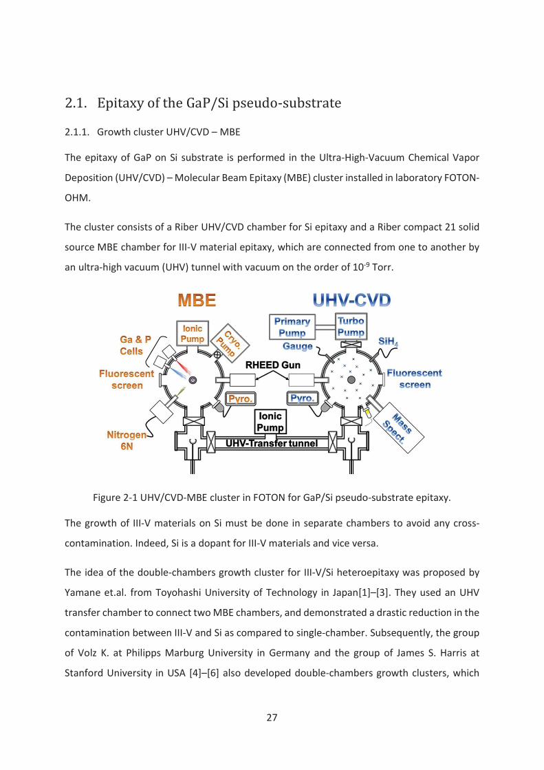
27
2.1. Epitaxy!of!the!GaP/Si!pseudo-substrate!
2.1.1. Growth cluster UHV/CVD – MBE
The epitaxy of GaP on Si substrate is performed in the Ultra-High-Vacuum Chemical Vapor
Deposition (UHV/CVD) – Molecular Beam Epitaxy (MBE) cluster installed in laboratory FOTON-
OHM.
The cluster consists of a Riber UHV/CVD chamber for Si epitaxy and a Riber compact 21 solid
source MBE chamber for III-V material epitaxy, which are connected from one to another by
an ultra-high vacuum (UHV) tunnel with vacuum on the order of 10-9 Torr.
Figure 2-1 UHV/CVD-MBE cluster in FOTON for GaP/Si pseudo-substrate epitaxy.
The growth of III-V materials on Si must be done in separate chambers to avoid any cross-
contamination. Indeed, Si is a dopant for III-V materials and vice versa.
The idea of the double-chambers growth cluster for III-V/Si heteroepitaxy was proposed by
Yamane et.al. from Toyohashi University of Technology in Japan[1]–[3]. They used an UHV
transfer chamber to connect two MBE chambers, and demonstrated a drastic reduction in the
contamination between III-V and Si as compared to single-chamber. Subsequently, the group
of Volz K. at Philipps Marburg University in Germany and the group of James S. Harris at
Stanford University in USA [4]–[6] also developed double-chambers growth clusters, which
28
consist of MOVPE/MBE and MBE/MBE respectively. The group of Volz K. et.al. at Philipps
Marburg University also use the Metal-organic Vapor Phase Expitaxy (MOVPE) after 2008 [7].
2.1.2. The preparation of Si wafers
In this work, all the GaP/Si pseudo-substrates are based on 2 inches n-type Si (001) wafers
with two flats to indicate the in-plane crystallographic orientation of the substrate. All the Si
wafers have vicinal surfaces, and the miscut of the surface are either 4° or 6° towards the [110]
direction. Both single-layer step and double-layers step can be formed on these vicinal
surfaces. The average length D of the terraces for single layer and double layer steps can be
respectively calculated as below:
D%PQRS# = aT9&:;<?@ (2.1)
DUWXYS# = a39&:;<?@ (2.2)
where a is the lattice constant of Si and Z is the miscut angle. For 4° miscut, the length of the
terraces for the single layer and double layer is 1.95 nm and 3.90 nm, respectively. For 6°
miscut, the length is 1.27 nm and 2.59 nm, respectively. The steps have been considered to
prevent or lower the formation of the APDs [8]–[11].
Before the epitaxy of GaP, the silicon wafer is cleaned with the “optimized HF process”, which
is introduced in ref [12]. The cleaning process is used to remove the carbon, oxide, metallic
and organic impurities at the Si surface prior to the GaP epitaxy. After the preparation, the Si
wafer will be immediately transferred into the MBE chamber and heated to 800 °C to
dehydrogenation. Then, the wafer will be cooled down for the epitaxy of GaP. The descriptions
of the growth of the different GaP/Si studied during my PhD work will be given in the following,
directly in the corresponding chapters.
2.2. X-ray!diffraction!characterization!
X-ray diffraction (XRD), which is also called X-ray crystallography (XRC) when it is applied in
the crystallography, may be the most widely used technique to measure the atomic and
molecular structural information of a crystal. In XRD, a beam of X-ray is sent into the crystal.
Then, the parameters of the diffraction beams are measured, for instance, the intensity, the
29
scattering width, the angle, the phase and so on. An analysis on these parameters can provide
the structural information, such as the crystal structure type, the defect distribution in the
sample and so on.
2.2.1. X-ray diffraction setup
The laboratory X-ray diffraction experiments are performed by using a 4-circle Bruker D8 X-
ray Diffractometer (horizontal scattering plane geometry), localized in the Institut des
Sciences Chimiques de Rennes (ISCR) at The Rennes 1 University. This diffractometer is
equipped with a 1D Gobel Multi-layer Mirror placed on the linear focus window of a standard
sealed tube as primary optics. The power of the X-ray source is usually set at 40kV and 40mA.
There are two setup modes applied in this thesis, i.e. the low-resolution mode (show in Figure
2-2) and the high-resolution mode(show in Figure 2-3). In general, the low-resolution mode is
applied in the quick θ/2θ scan and the Pole Figure (PL), and the high-resolution mode is
applied in the θ/2θ scan and the Reciprocal Space Mapping (RSM).
In the low-resolution mode, the linear beam focus is 12mm wide in height at source. The X-
ray beam passes through an 1mm wide source slit and a 5mm vertically wide anti-scattering
slit, which is often installed to limit the vertical width to be smaller than the sample
dimensions, before reaching the sample surface. On the other side, an anti-scattering slit of 8
mm horizontal height and 15 mm vertical width and a Soller slits of 2.5° are used to decrease
the intensity of the background signal. An optional Ni filter is inserted between the anti-
scattering slit and the Soller slits to lower the Cu-Kβ intensity and, therefore, to select the Cu-
Kα with a wavelength of 1.5418 nm. A 180 channels 1D position sensitive detector Lynxeye™
positioned at 300mm from the goniometer center works like a point detector in this mode.
The flux intensity from the selected pixels is summed as the final intensity.
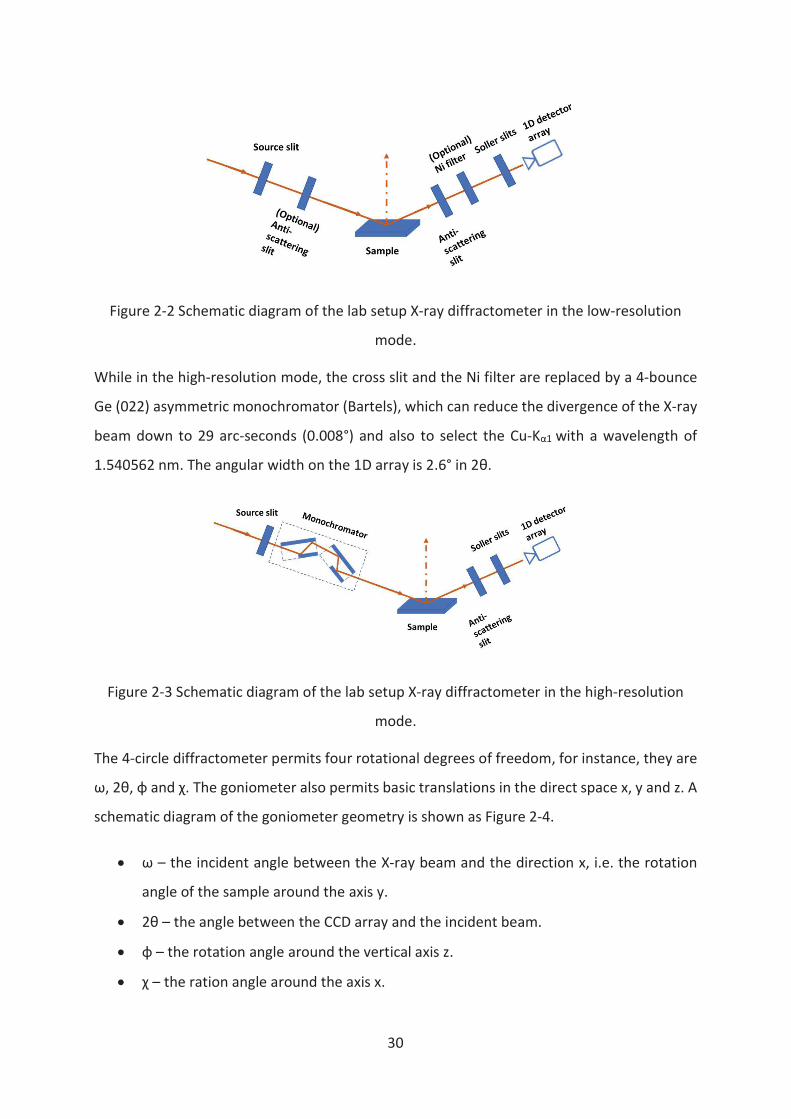
30
Figure 2-2 Schematic diagram of the lab setup X-ray diffractometer in the low-resolution
mode.
While in the high-resolution mode, the cross slit and the Ni filter are replaced by a 4-bounce
Ge (022) asymmetric monochromator (Bartels), which can reduce the divergence of the X-ray
beam down to 29 arc-seconds (0.008°) and also to select the Cu-Kα1 with a wavelength of
1.540562 nm. The angular width on the 1D array is 2.6° in 2θ.
Figure 2-3 Schematic diagram of the lab setup X-ray diffractometer in the high-resolution
mode.
The 4-circle diffractometer permits four rotational degrees of freedom, for instance, they are
ω, 2θ, φ and χ. The goniometer also permits basic translations in the direct space x, y and z. A
schematic diagram of the goniometer geometry is shown as Figure 2-4.
· ω – the incident angle between the X-ray beam and the direction x, i.e. the rotation
angle of the sample around the axis y.
· 2θ – the angle between the CCD array and the incident beam.
· φ – the rotation angle around the vertical axis z.
· χ – the ration angle around the axis x.
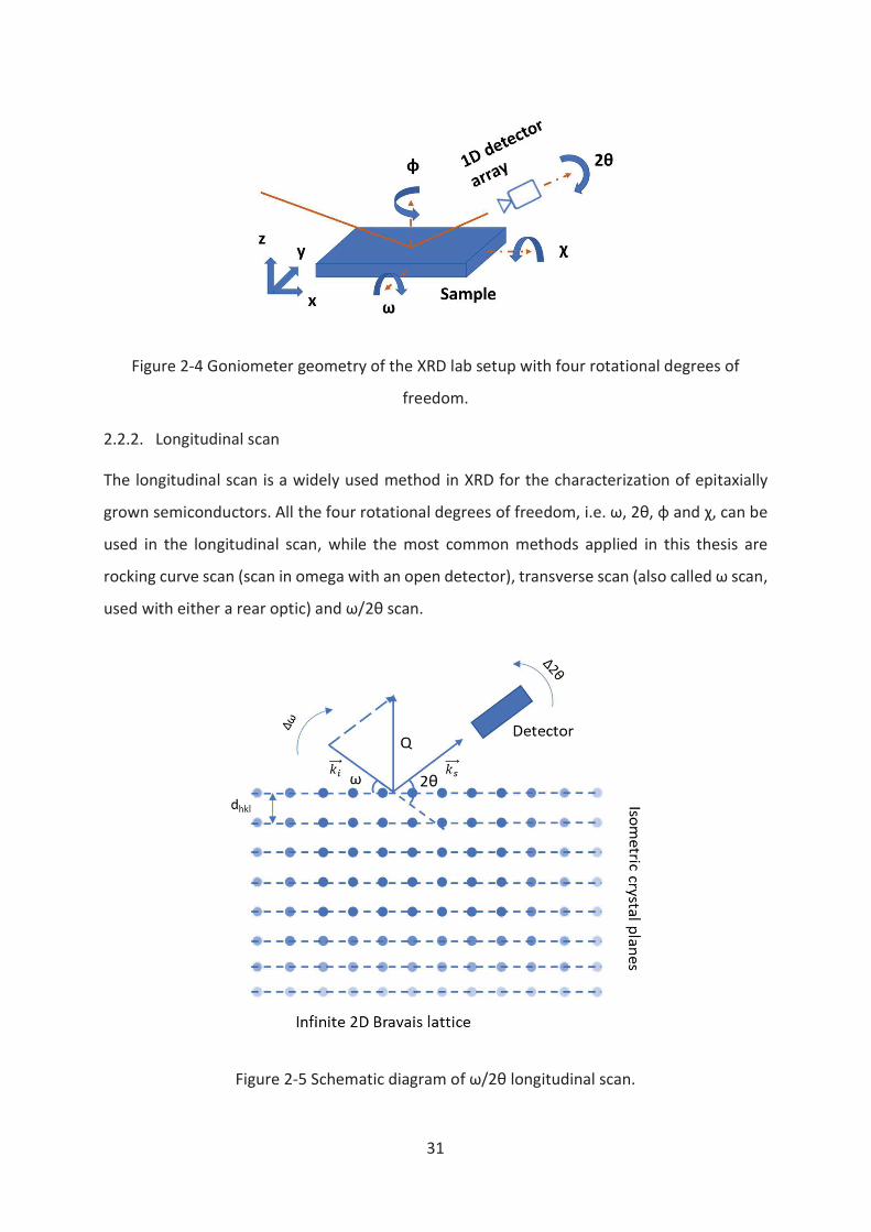
31
Figure 2-4 Goniometer geometry of the XRD lab setup with four rotational degrees of
freedom.
2.2.2. Longitudinal scan
The longitudinal scan is a widely used method in XRD for the characterization of epitaxially
grown semiconductors. All the four rotational degrees of freedom, i.e. ω, 2θ, φ and χ, can be
used in the longitudinal scan, while the most common methods applied in this thesis are
rocking curve scan (scan in omega with an open detector), transverse scan (also called ω scan,
used with either a rear optic) and ω/2θ scan.
Figure 2-5 Schematic diagram of ω/2θ longitudinal scan.
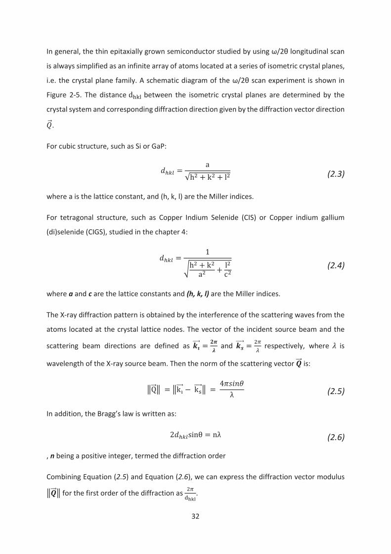
32
In general, the thin epitaxially grown semiconductor studied by using ω/2θ longitudinal scan
is always simplified as an infinite array of atoms located at a series of isometric crystal planes,
i.e. the crystal plane family. A schematic diagram of the ω/2θ scan experiment is shown in
Figure 2-5. The distance d[\S between the isometric crystal planes are determined by the
crystal system and corresponding diffraction direction given by the diffraction vector direction ]̂_. For cubic structure, such as Si or GaP:
`bcg = aih5 8 k5 8 l5 (2.3)
where a is the lattice constant, and (h, k, l) are the Miller indices.
For tetragonal structure, such as Copper Indium Selenide (CIS) or Copper indium gallium
(di)selenide (CIGS), studied in the chapter 4:
`bcg = 1jh5 8 k5a5 8 l5m5 (2.4)
where a and c are the lattice constants and (h, k, l) are the Miller indices.
The X-ray diffraction pattern is obtained by the interference of the scattering waves from the
atoms located at the crystal lattice nodes. The vector of the incident source beam and the
scattering beam directions are defined as no^̂ _̂ = pqr and n7^̂^̂_ = 5st respectively, where u is
wavelength of the X-ray source beam. Then the norm of the scattering vector v̂̂_ is:
wx̂̂_w ;= wky^̂ _̂ $ ;k%^̂ _̂w ;= ; Tz{}:~� (2.5)
In addition, the Bragg’s law is written as:
3`bcg���� = �� (2.6)
, n being a positive integer, termed the diffraction order
Combining Equation (2.5) and Equation (2.6), we can express the diffraction vector modulus wv̂̂_w for the first order of the diffraction as 5sU���.
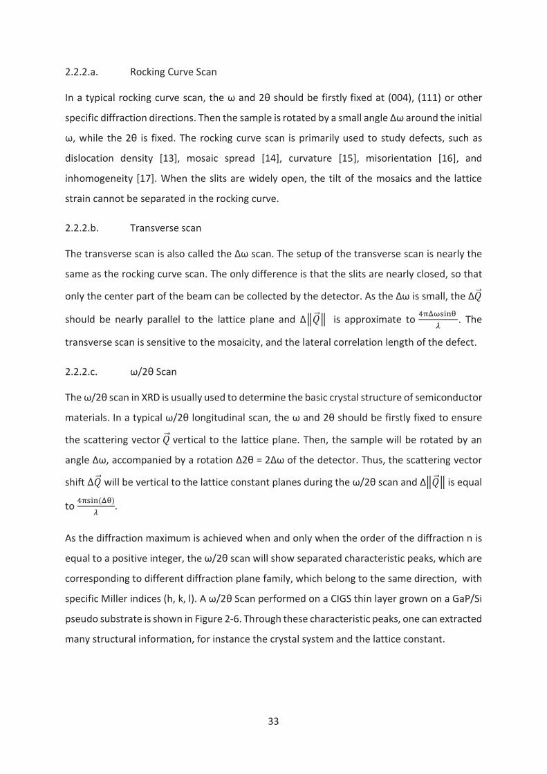
33
2.2.2.a. Rocking Curve Scan
In a typical rocking curve scan, the ω and 2θ should be firstly fixed at (004), (111) or other
specific diffraction directions. Then the sample is rotated by a small angle Δω around the initial
ω, while the 2θ is fixed. The rocking curve scan is primarily used to study defects, such as
dislocation density [13], mosaic spread [14], curvature [15], misorientation [16], and
inhomogeneity [17]. When the slits are widely open, the tilt of the mosaics and the lattice
strain cannot be separated in the rocking curve.
2.2.2.b. Transverse scan
The transverse scan is also called the Δω scan. The setup of the transverse scan is nearly the
same as the rocking curve scan. The only difference is that the slits are nearly closed, so that
only the center part of the beam can be collected by the detector. As the Δω is small, the Δ]̂_ should be nearly parallel to the lattice plane and Δw]̂_w is approximate to
����%PQ�;t . The
transverse scan is sensitive to the mosaicity, and the lateral correlation length of the defect.
2.2.2.c. ω/2θ Scan
The ω/2θ scan in XRD is usually used to determine the basic crystal structure of semiconductor
materials. In a typical ω/2θ longitudinal scan, the ω and 2θ should be firstly fixed to ensure
the scattering vector ]̂_ vertical to the lattice plane. Then, the sample will be rotated by an
angle Δω, accompanied by a rotation Δ2θ = 2Δω of the detector. Thus, the scattering vector
shift �]̂_ will be vertical to the lattice constant planes during the ω/2θ scan and Δw]̂_w is equal
to ��%PQ;<��@t .
As the diffraction maximum is achieved when and only when the order of the diffraction n is
equal to a positive integer, the ω/2θ scan will show separated characteristic peaks, which are
corresponding to different diffraction plane family, which belong to the same direction, with
specific Miller indices (h, k, l). A ω/2θ Scan performed on a CIGS thin layer grown on a GaP/Si
pseudo substrate is shown in Figure 2-6. Through these characteristic peaks, one can extracted
many structural information, for instance the crystal system and the lattice constant.
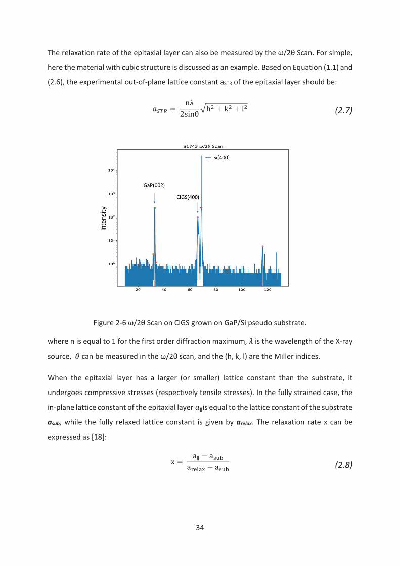
34
The relaxation rate of the epitaxial layer can also be measured by the ω/2θ Scan. For simple,
here the material with cubic structure is discussed as an example. Based on Equation (1.1) and
(2.6), the experimental out-of-plane lattice constant aSTR of the epitaxial layer should be:
&��� =; ��3�����h5 8 k5 8 l5 (2.7)
Figure 2-6 ω/2θ Scan on CIGS grown on GaP/Si pseudo substrate.
where n is equal to 1 for the first order diffraction maximum, u is the wavelength of the X-ray
source, ~ can be measured in the ω/2θ scan, and the (h, k, l) are the Miller indices.
When the epitaxial layer has a larger (or smaller) lattice constant than the substrate, it
undergoes compressive stresses (respectively tensile stresses). In the fully strained case, the
in-plane lattice constant of the epitaxial layer &+is equal to the lattice constant of the substrate
asub, while the fully relaxed lattice constant is given by arelax. The relaxation rate x can be
expressed as [18]:
� = ; a+ $ a%XYa�#S�� $ a%XY (2.8)

35
According to the generalized Hooke's law, the in-plane lattice constant &+ and out-of-plane
lattice constant &* for isotropic materials with the cubic crystal structure within the range of
elastic deformation has a relationship as below:
a+ $ a�#S�� = $ C443C45 <a* $ a�#S��@ (2.9)
where ��� and ��p are the elastic stiffness constants.
Thus, the relaxation rate x is:
� = 1 $ C443C45 ; a* $ a�#S��a�#S�� $ a%XY (2.10)
2.2.3. Reciprocal Space Mapping
2.2.3.a. Reciprocal Space and Ewald's Sphere
A crystal can be described as a periodic arrangement made with a pattern which consists of
one or more atoms and a lattice point called Bravais lattice which describes the periodic
arrangement of the pattern. A 3D expression of the Bravais lattice � is as below:
��^̂^̂ _̂ = �4a4^̂ _̂ 8 �5a5^̂^̂_ 8 ��a�^̂^̂_; (2.11)
where :� can be any integers and &�^̂ _̂ is the primitive vector in x, y, z directions.
The reciprocal space represents the Fourier transform of the real Bravais lattice. Then the
reciprocal vector �̂̂_ is:
�̂̂_ = h�4^̂^̂_ 8 k�5^̂^̂_ 8 l��^̂^̂_; (2.12)
where O�^̂̂ _ satisfy the formulas as below:
�4^̂^̂_ = 3 a5 × a�a4 ¡ <a5 × a�@; (2.13)
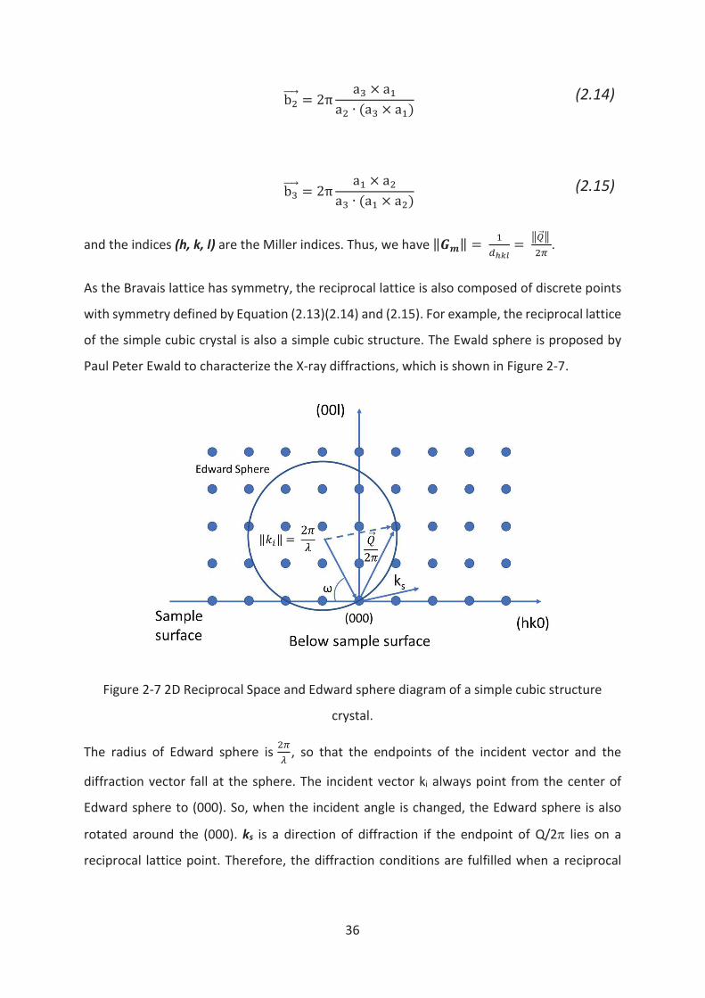
36
�5^̂^̂_ = 3 a� × a4a5 ¡ <a� × a4@; (2.14)
��^̂^̂_ = 3 a4 × a5a� ¡ <a4 × a5@; (2.15)
and the indices (h, k, l) are the Miller indices. Thus, we have ¢�£¢ = ; 4¤¥¦§ =; w¨̂_w;5s .
As the Bravais lattice has symmetry, the reciprocal lattice is also composed of discrete points
with symmetry defined by Equation (2.13)(2.14) and (2.15). For example, the reciprocal lattice
of the simple cubic crystal is also a simple cubic structure. The Ewald sphere is proposed by
Paul Peter Ewald to characterize the X-ray diffractions, which is shown in Figure 2-7.
Figure 2-7 2D Reciprocal Space and Edward sphere diagram of a simple cubic structure
crystal.
The radius of Edward sphere is 5st , so that the endpoints of the incident vector and the
diffraction vector fall at the sphere. The incident vector ki always point from the center of
Edward sphere to (000). So, when the incident angle is changed, the Edward sphere is also
rotated around the (000). ks is a direction of diffraction if the endpoint of Q/2p lies on a
reciprocal lattice point. Therefore, the diffraction conditions are fulfilled when a reciprocal
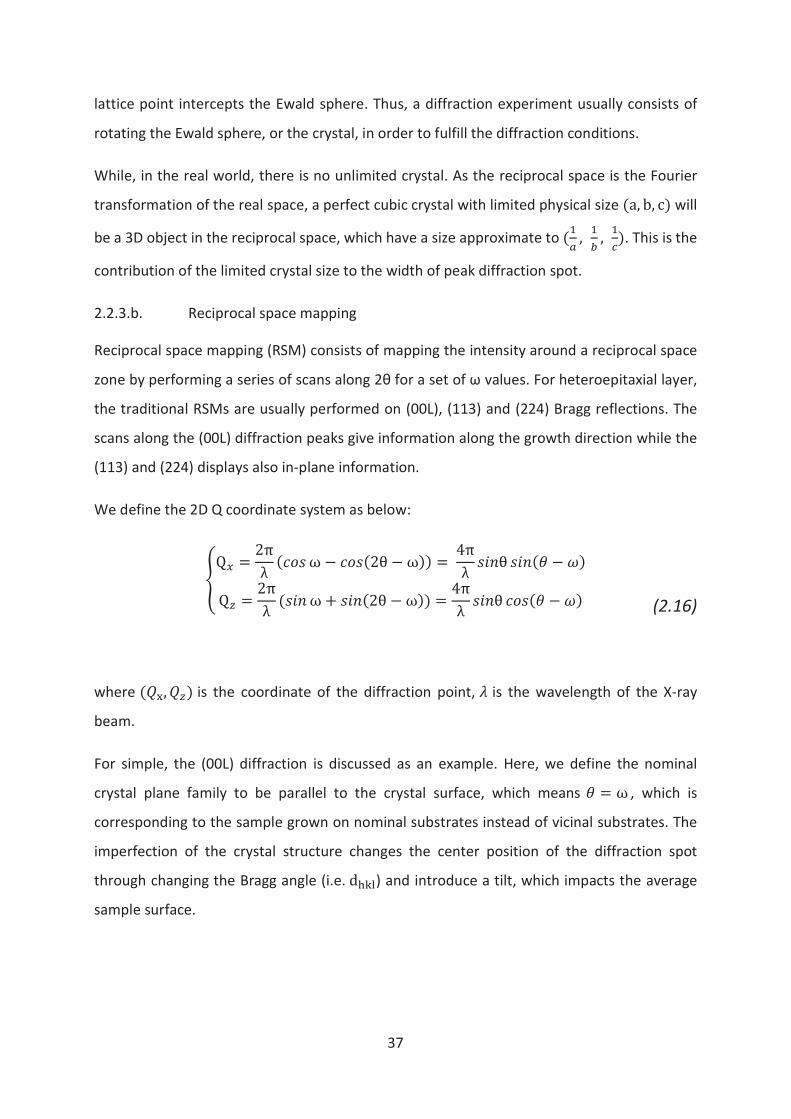
37
lattice point intercepts the Ewald sphere. Thus, a diffraction experiment usually consists of
rotating the Ewald sphere, or the crystal, in order to fulfill the diffraction conditions.
While, in the real world, there is no unlimited crystal. As the reciprocal space is the Fourier
transformation of the real space, a perfect cubic crystal with limited physical size <a© �© m@ will
be a 3D object in the reciprocal space, which have a size approximate to <4ª © 4« © 4¬@. This is the
contribution of the limited crystal size to the width of peak diffraction spot.
2.2.3.b. Reciprocal space mapping
Reciprocal space mapping (RSM) consists of mapping the intensity around a reciprocal space
zone by performing a series of scans along 2θ for a set of ω values. For heteroepitaxial layer,
the traditional RSMs are usually performed on (00L), (113) and (224) Bragg reflections. The
scans along the (00L) diffraction peaks give information along the growth direction while the
(113) and (224) displays also in-plane information.
We define the 2D Q coordinate system as below:
x® = 3 � <¯°{± $ ¯°{<3� $ ±@@ = ;T � {}:� {}:<~ $ ²@x³ = 3 � <{}:± 8 {}:<3� $ ±@@ = T � {}:� ¯°{<~ $ ²@
(2.16)
where <]�© ]³@ is the coordinate of the diffraction point,;u is the wavelength of the X-ray
beam.
For simple, the (00L) diffraction is discussed as an example. Here, we define the nominal
crystal plane family to be parallel to the crystal surface, which means ;~ = ± , which is
corresponding to the sample grown on nominal substrates instead of vicinal substrates. The
imperfection of the crystal structure changes the center position of the diffraction spot
through changing the Bragg angle (i.e. d[\S) and introduce a tilt, which impacts the average
sample surface.
38
Figure 2-8 Schematic diagram of a) a normal crystal plane family b) a crystal plane family a
tilt or c) with a different lattice constant, i.e. a strain state.
The schematic diagram of two simple models with a tilt and a strain state compared the
normal crystal plane family are shown in Figure 2-8 (b) and (c). While, there are usually much
more than one pf these specific cases in the scanning area of the XRD. So, the superposition
of the diffraction patterns leads to a broadening of the diffraction spot’s size, and/or a shift of
the center position of the diffraction spot.
For the two simple models shown in Figure 2-8 (b) and (c), the position of the scattering spot
in the reciprocal space can be calculated as follows.
As ±Q = ² 8 ! and �Q = ±Q, the center of the Q scattering spot can be calculated as below,
where ´ is the tilt angle:
x®µ = T � {}:�Q {}:<�Q $ ²µ@ = x���<$¶@x³µ = T � {}: �Q ¯°{<�Q $ ²µ@ = ;x;m·�<$¶@
(2.17)
with
] = ;Tzu ��� 3~3 ; where
55̧ is the Bragg angle and ! is the tilt angle.
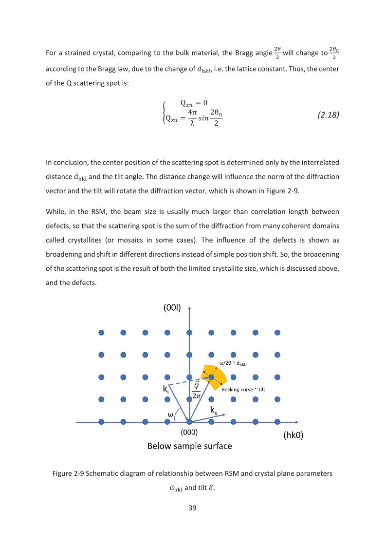
39
For a strained crystal, comparing to the bulk material, the Bragg angle 55̧ will change to
5¸¹5
according to the Bragg law, due to the change of `bcg, i.e. the lattice constant. Thus, the center
of the Q scattering spot is:
º x®µ = 0x³µ = T � {}: 3�Q3 (2.18)
In conclusion, the center position of the scattering spot is determined only by the interrelated
distance d[\S and the tilt angle. The distance change will influence the norm of the diffraction
vector and the tilt will rotate the diffraction vector, which is shown in Figure 2-9.
While, in the RSM, the beam size is usually much larger than correlation length between
defects, so that the scattering spot is the sum of the diffraction from many coherent domains
called crystallites (or mosaics in some cases). The influence of the defects is shown as
broadening and shift in different directions instead of simple position shift. So, the broadening
of the scattering spot is the result of both the limited crystallite size, which is discussed above,
and the defects.
Figure 2-9 Schematic diagram of relationship between RSM and crystal plane parameters d[\S and tilt !.
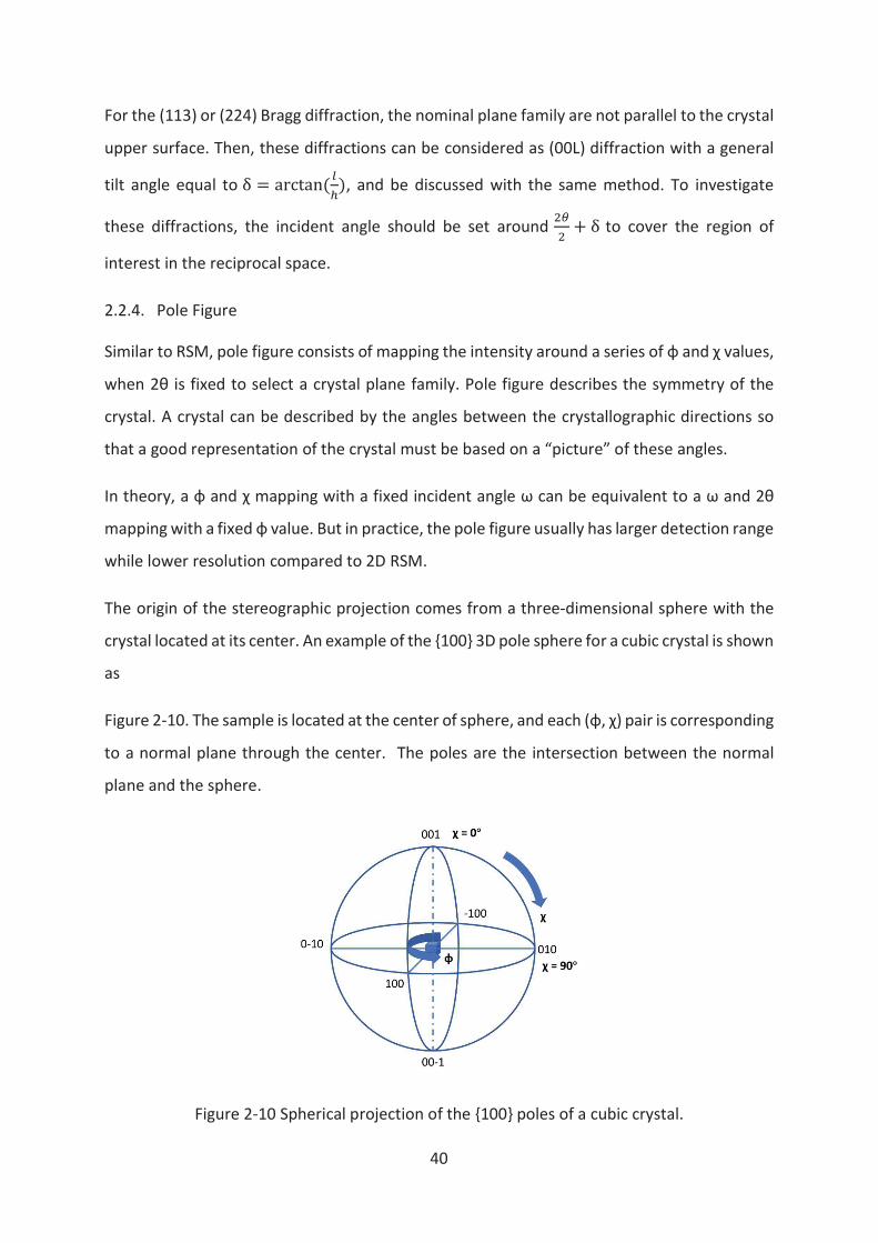
40
For the (113) or (224) Bragg diffraction, the nominal plane family are not parallel to the crystal
upper surface. Then, these diffractions can be considered as (00L) diffraction with a general
tilt angle equal to ¶ = a»m¼a�;< gb@, and be discussed with the same method. To investigate
these diffractions, the incident angle should be set around 55̧ 8 ¶ to cover the region of
interest in the reciprocal space.
2.2.4. Pole Figure
Similar to RSM, pole figure consists of mapping the intensity around a series of φ and χ values,
when 2θ is fixed to select a crystal plane family. Pole figure describes the symmetry of the
crystal. A crystal can be described by the angles between the crystallographic directions so
that a good representation of the crystal must be based on a “picture” of these angles.
In theory, a φ and χ mapping with a fixed incident angle ω can be equivalent to a ω and 2θ
mapping with a fixed φ value. But in practice, the pole figure usually has larger detection range
while lower resolution compared to 2D RSM.
The origin of the stereographic projection comes from a three-dimensional sphere with the
crystal located at its center. An example of the {100} 3D pole sphere for a cubic crystal is shown
as
Figure 2-10. The sample is located at the center of sphere, and each (φ, χ) pair is corresponding
to a normal plane through the center. The poles are the intersection between the normal
plane and the sphere.
Figure 2-10 Spherical projection of the {100} poles of a cubic crystal.
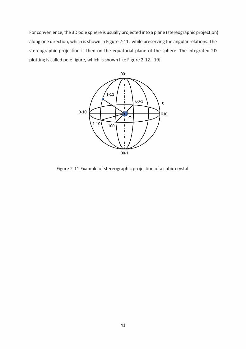
41
For convenience, the 3D pole sphere is usually projected into a plane (stereographic projection)
along one direction, which is shown in Figure 2-11, while preserving the angular relations. The
stereographic projection is then on the equatorial plane of the sphere. The integrated 2D
plotting is called pole figure, which is shown like Figure 2-12. [19]
Figure 2-11 Example of stereographic projection of a cubic crystal.
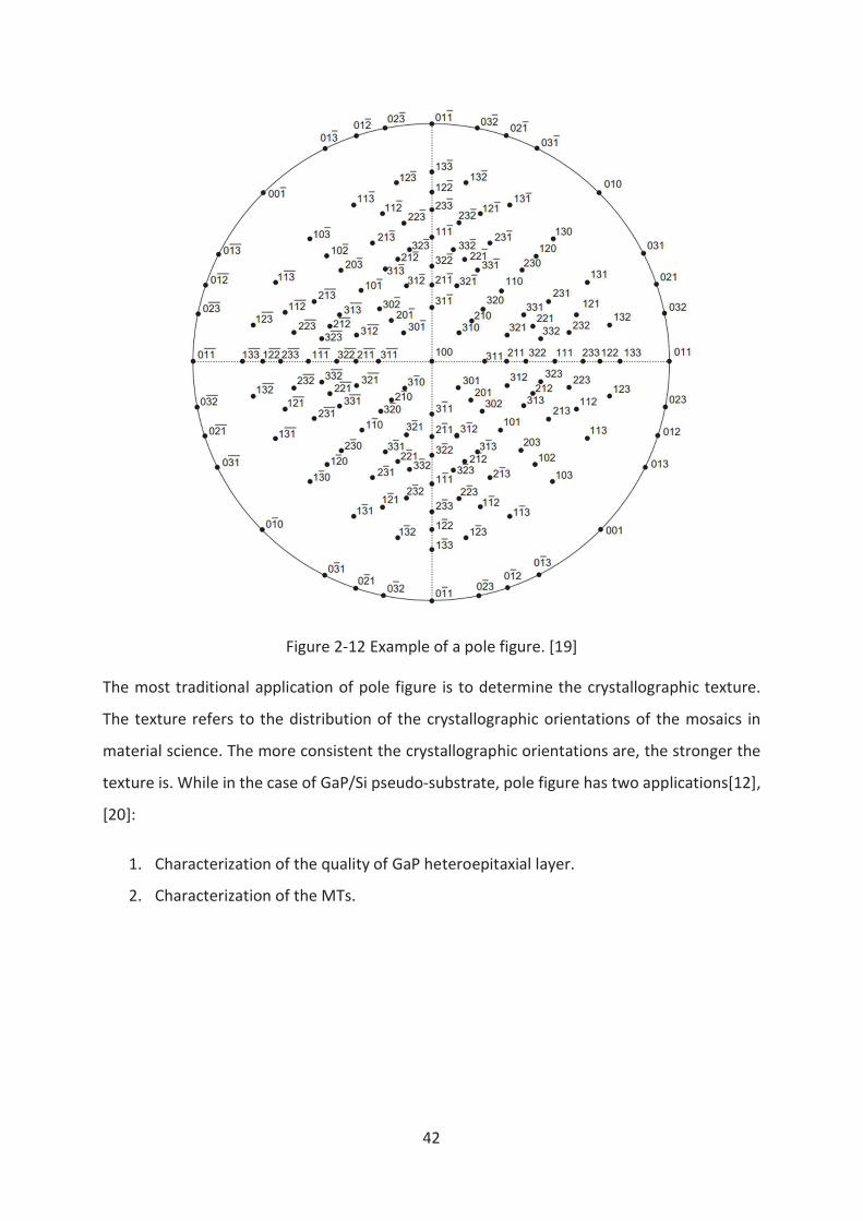
42
Figure 2-12 Example of a pole figure. [19]
The most traditional application of pole figure is to determine the crystallographic texture.
The texture refers to the distribution of the crystallographic orientations of the mosaics in
material science. The more consistent the crystallographic orientations are, the stronger the
texture is. While in the case of GaP/Si pseudo-substrate, pole figure has two applications[12],
[20]:
1. Characterization of the quality of GaP heteroepitaxial layer.
2. Characterization of the MTs.
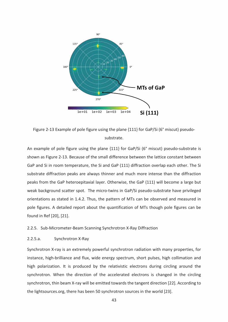
43
Figure 2-13 Example of pole figure using the plane {111} for GaP/Si (6° miscut) pseudo-
substrate.
An example of pole figure using the plane {111} for GaP/Si (6° miscut) pseudo-substrate is
shown as Figure 2-13. Because of the small difference between the lattice constant between
GaP and Si in room temperature, the Si and GaP (111) diffraction overlap each other. The Si
substrate diffraction peaks are always thinner and much more intense than the diffraction
peaks from the GaP heteroepitaxial layer. Otherwise, the GaP (111) will become a large but
weak background scatter spot. The micro-twins in GaP/Si pseudo-substrate have privileged
orientations as stated in 1.4.2. Thus, the pattern of MTs can be observed and measured in
pole figures. A detailed report about the quantification of MTs though pole figures can be
found in Ref [20], [21].
2.2.5. Sub-Micrometer-Beam Scanning Synchrotron X-Ray Diffraction
2.2.5.a. Synchrotron X-Ray
Synchrotron X-ray is an extremely powerful synchrotron radiation with many properties, for
instance, high-brilliance and flux, wide energy spectrum, short pulses, high collimation and
high polarization. It is produced by the relativistic electrons during circling around the
synchrotron. When the direction of the accelerated electrons is changed in the circling
synchrotron, thin beam X-ray will be emitted towards the tangent direction [22]. According to
the lightsources.org, there has been 50 synchrotron sources in the world [23].
44
Up to now, there has been four generations of synchrotron radiation sources (SRS). The first-
generation SRSs parasitically used the cycling electron synchrotrons developed for particle
physics, which were developed between the early 1950s to the early 1970s. After several years
running, the storage ring was added to the system as a great advance, which marks the
maturity of the first-generation SRSs. While, the X-ray emitted from the synchrotron is an
undesired energy loss in particle physics, so the demand of particle physics for the synchrotron
is partially opposite to the demand of synchrotron X-ray source. The dedicated SRSs were
designed to mainly produce synchrotron radiation. The first second-generation SRS was built
at the Daresbury Laboratory in the UK in around 1970. The main improvement for the second-
generation SRSs is the insertion devices, for instance, wigglers and undulators. Although the
flux density is only determined by the design of the synchrotrons and cannot be improved by
any optical technique, the insertion devices help concentrate the energy into one or a few
spectrally narrow peaks in the spectrum by introducing constructive interference effect. The
third-generation SRSs were born by effectively combination with the insertion device. The
third-generation SRSs often adopt NSLS two-ring model and can produce either soft or hard
X-ray radiation. The European Synchrotron Radiation Facility (ESRF) in Grenoble, France is the
first third-generation SRS. [24]–[28]
Today, there are tens of third-generation SRSs operating all over the world, such as ESRF in
Grenoble/France, APS in Argonne/Illinois/USA, SPring-8 in Sayo/Japan, ELETTRA in
Trieste/Italy, and et.al.
The next-generation SRSs have been developed for 10s of years and primarily installed in
several sites, such as SwissFEL, LCLS and European XFEL. Different from the third-generation
SRSs, the fourth-generation SRSs produce X-Ray Free-Electron Laser (XFEL). Through Self
Amplified Spontaneous Emission (SASE), the X-ray beam generated in the fourth-generation
SRSs can be 10000 times brighter than the X-ray beam in the third-generation SRSs and can
keep coherence.
2.2.5.b. The nano- /sub-micrometer-beam synchrotron X-ray
In the traditional X-ray diffraction, the scattering spots of several micrometers are always
much larger than the normal size of the structural defects in the samples. So, the analysis is

45
performed based on the statistical average of large density of defects, comparing to the
theoretical model.
In the last decade, the directly observation of the local structure comes true with an
application of hard X-ray nanobeams of the order of several hundreds of nanometers, or even
tens of nm recently [29]. The most important two challenges in the development of the X-ray
nanobeams are the X-ray optics and X-ray source.
To get nano- /sub-micrometer- hard X-ray beam, the first question is how to focus the X-ray
beam. There are three main types of X-ray focusing system, i.e. the reflective system, the
refractive system and the diffractive system [30].
For the reflective system and the refractive system, the principle challenge is that the
interactions between the X-ray and most of the material are weak. Thus, the reflective mirrors
in the X-ray focusing system need be coated with multilayers [31]. The reflective mirrors
themselves are usually made by dynamical bended Si substrates. Several designs have been
proposed to realize the nano-/sub-micrometer- hard X-ray beam with the reflective mirrors
[32], [33]. The horizontal and vertical beam are usually focused with two separated mirrors to
satisfy the demand of the optical aberration. The complex optical path design and the difficulty
in the mirror manufacture lead the reflective system impractical for the nano- /sub-
micrometer- hard X-ray beam.
In opposition to the visible light, the refractive indexes of many materials are only slightly
below 1 for hard X-ray beam. The low refractive indexes demand the X-ray to have only low
angles of incidence, otherwise the X-ray will pass through the lens without any change in the
direction. The idea of concave refractive lenses is proposed by Kirkpatrick and furtherly
developed Suehiro et.al., Yang et.al. and Snigirev et.al. [34]–[37]. The refractive lenses in use
now are mainly Compound Refractive Lenses (CRLs), which are made by beryllium or
aluminum. Compared to reflective mirrors, the refractive lenses are more stable and easier to
install and align. Due to the background noise, the CRLs made of beryllium or aluminum is less
practical for nano- /sub-micrometer- beam. The alternatives are mono-crystalline silicon [38]
and polymers [39], which reduce the background noise but also reduce the physical apertures
as a trade-off.
46
The diffractive system is the youngest system among these three and was proposed in the
1960s [40]. This system is extremely suitable for the nano-beam/sub-micrometer- beam,
because the high aspect ratios of the zone plates. Because the higher the aspect ratio is, the
shorter the focusing distance is. Thus, the losses of the intensity can be reduced. While, the
single zone plate with high aspect ratio is only used in the soft X-ray beam, because of the
tendency of zone collapse and the lifetime issues. For hard X-ray beam, the diffractive “lens”
consists of multi-layers sputtering deposited. This technique decreases the fabrication
difficulty, increases the lifetime, but demands a much longer fabrication time [41].
As the useful flux intensity is approximately inversely proportional to resolution, the nano-
beam/sub-micrometer-beam X-ray demands stable X-ray beam with high flux, high
collimation and low beam divergence. The SRSs are the most suitable source which satisfy all
these requirements. As a result, the nano-/sub-micrometer- beam diffraction have been
performed in nearly all the main third-generation SRSs, such as APS [42], [43], ESRF [44],
SPring-8 [45], MaxIV [46], NSLSII [47].
2.2.5.c. The quicK continuous Mapping
The quicK continuous Mapping (K-Map) is a non-destructive sub-micrometer-beam scanning
X-ray diffraction method, developed by Chahine et.al. at ID01-ESRF beamline [48]. This
technique provides large-scale local structure information by the X-ray diffraction mapping
with high resolution in a short time. Up to now, K-Map has been used to characterize organic
electronic devices[49] and to study the defects in the heteroepitaxy structure [50]–[52]. The
setup is improved by the staff of ID01 after 2014. Beam typical dimensions will be smaller in
the next version. The detail of the experiment setup of K-Map will be discussed in the Chapter
3 for our sample.
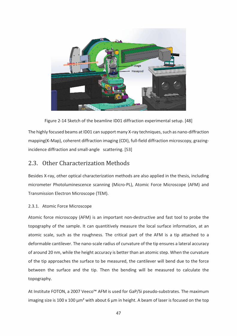
47
Figure 2-14 Sketch of the beamline ID01 diffraction experimental setup. [48]
The highly focused beams at ID01 can support many X-ray techniques, such as nano-diffraction
mapping(K-Map), coherent diffraction imaging (CDI), full-field diffraction microscopy, grazing-
incidence diffraction and small-angle scattering. [53]
2.3. Other!Characterization!Methods!
Besides X-ray, other optical characterization methods are also applied in the thesis, including
micrometer Photoluminescence scanning (Micro-PL), Atomic Force Microscope (AFM) and
Transmission Electron Microscope (TEM).
2.3.1. Atomic Force Microscope
Atomic force microscopy (AFM) is an important non-destructive and fast tool to probe the
topography of the sample. It can quantitively measure the local surface information, at an
atomic scale, such as the roughness. The critical part of the AFM is a tip attached to a
deformable cantilever. The nano-scale radius of curvature of the tip ensures a lateral accuracy
of around 20 nm, while the height accuracy is better than an atomic step. When the curvature
of the tip approaches the surface to be measured, the cantilever will bend due to the force
between the surface and the tip. Then the bending will be measured to calculate the
topography.
At Institute FOTON, a 2007 Veeco™ AFM is used for GaP/Si pseudo-substrates. The maximum
imaging size is 100 x 100 μm² with about 6 μm in height. A beam of laser is focused on the top
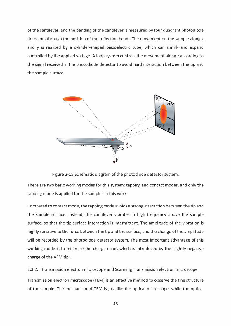
48
of the cantilever, and the bending of the cantilever is measured by four quadrant photodiode
detectors through the position of the reflection beam. The movement on the sample along x
and y is realized by a cylinder-shaped piezoelectric tube, which can shrink and expand
controlled by the applied voltage. A loop system controls the movement along z according to
the signal received in the photodiode detector to avoid hard interaction between the tip and
the sample surface.
Figure 2-15 Schematic diagram of the photodiode detector system.
There are two basic working modes for this system: tapping and contact modes, and only the
tapping mode is applied for the samples in this work.
Compared to contact mode, the tapping mode avoids a strong interaction between the tip and
the sample surface. Instead, the cantilever vibrates in high frequency above the sample
surface, so that the tip-surface interaction is intermittent. The amplitude of the vibration is
highly sensitive to the force between the tip and the surface, and the change of the amplitude
will be recorded by the photodiode detector system. The most important advantage of this
working mode is to minimize the charge error, which is introduced by the slightly negative
charge of the AFM tip .
2.3.2. Transmission electron microscope and Scanning Transmission electron microscope
Transmission electron microscope (TEM) is an effective method to observe the fine structure
of the sample. The mechanism of TEM is just like the optical microscope, while the optical
49
beam is replaced by a beam of electrons. The wavelength of the matter wave of electrons is
much shorter than the wavelength of photons, so the TEM can exceed the resolution
limitation of the optical microscope. The maximum resolution of the TEM can reach 0.05 nm,
but the heavy work in the preparation and the analysis steps limit the application of TEM.
The Scanning Transmission electron microscope (STEM) is an improved technique of the
traditional TEM, by scanning the sample pixel by pixel with a focused electron beam and a
very small probe. Compared to traditional TEM, STEM is performed with a focused electron
source which scanning the sample surface and can provide the structural information in a
higher contrast. While, the phase information is always lost in STEM due to the incoherent
and inelastic beam as a cost.
There are two major working mode in TEM: the imaging mode and the diffraction mode, while
only imaging mode is applied in STEM. In the imaging mode, the beam can be controlled by
an objective aperture located between the objective lens. If the center part of the beam is
selected, the transmitted direct beam contributes to the imaging, and thick areas, heavy
atoms and diffracting crystalline areas appear with dark contrast. This mode is called Bright
field. Otherwise, the transmitted direct beam can be blocked. Thus, the diffracted beam is
selected, and the planar defects or particle sizes can be observed. This is called Dark field.
All the TEM and STEM experiments in this thesis are performed by M. Bahri, G. Patriarche, L.
Largeau at the Laboratoire de Photonique et Nanostructures (LPN) in Marcoussis, France or
Eric Gautron at IMN, in Nante, France.
References
[1] K. Yamane, T. Kobayashi, Y. Furukawa, H. Okada, H. Yonezu, and A. Wakahara, “Growth of
pit-free GaP on Si by suppression of a surface reaction at an initial growth stage,” J. Cryst.
Growth, vol. 311, no. 3, pp. 794–797, 2009.
[2] K. Yamane, T. Kawai, Y. Furukawa, H. Okada, and A. Wakahara, “Growth of low defect
density GaP layers on Si substrates within the critical thickness by optimized shutter
sequence and post-growth annealing,” J. Cryst. Growth, vol. 312, no. 15, pp. 2179–2184,
2010.
50
[3] K. Yamane et al., “Growth of a lattice-matched GaAsPN p–i–n junction on a Si substrate
for monolithic III–V/Si tandem solar cells,” Appl. Phys. Express., vol. 10, no. 7, p. 075504,
2017.
[4] X. Yu, P. S. Kuo, K. Ma, O. Levi, M. M. Fejer, and J. S. Harris, “Single-phase growth studies
of GaP on Si by solid-source molecular beam epitaxy,” J. Vac. Sci. Technol., vol. 22, no. 3,
p. 1450, 2004.
[5] A. C. Lin, M. M. Fejer, and J. S. Harris, “Antiphase domain annihilation during growth of
GaP on Si by molecular beam epitaxy,” J. Cryst. Growth., vol. 363, pp. 258–263, 2013.
[6] A. C. Lin et al., “Epitaxial growth of GaP/AlGaP mirrors on Si for low thermal noise optical
coatings,” Opt. Mater. Express., vol. 5, no. 8, p. 1890, 2015.
[7] I. Németh, B. Kunert, W. Stolz, and K. Volz, “Heteroepitaxy of GaP on Si: Correlation of
morphology, anti-phase-domain structure and MOVPE growth conditions,” J. Cryst.
Growth., vol. 310, no. 7–9, pp. 1595–1601, Apr. 2008.
[8] H. Kroemer, “Polar-on-nonpolar epitaxy,” J. Cryst. Growth., vol. 81, no. 1–4, pp. 193–204,
1987.
[9] B. Kunert, I. Németh, S. Reinhard, K. Volz, and W. Stolz, “Si (001) surface preparation for
the antiphase domain free heteroepitaxial growth of GaP on Si substrate,” Thin Solid Films,
vol. 517, no. 1, pp. 140–143, 2008.
[10] I. Németh, B. Kunert, W. Stolz, and K. Volz, “Heteroepitaxy of GaP on Si: Correlation of
morphology, anti-phase-domain structure and MOVPE growth conditions,” J. Cryst.
Growth., vol. 310, no. 7–9, pp. 1595–1601, 2008.
[11] I. Lucci et al., “Universal description of III-V/Si epitaxial growth processes,” Phys. Rev.
B, vol. 2, no. 6, p. 060401, 2018.
[12] Y. Wang, “Structural analyses by advanced X-ray scattering on GaP layers epitaxially
grown on silicon for integrated photonic applications,” Ph.D., INSA Rennes, Rennes, 2016.
[13] B. Heying et al., Role of threading dislocation structure on the x ray diffraction
peak widths in epitaxial GaN films, Appl. Phys. Lett., vol. 68, no. 5, pp. 643 645, 1996.
[14] X. H. Zheng et al., “Determination of twist angle of in-plane mosaic spread of GaN films
by high-resolution X-ray diffraction,” J. Cryst. Growth, vol. 255, no. 1–2, pp. 63–67, 2003.
51
[15] A. Segmüller, J. Angilelo, and S. J. La Placa, Automatic X-ray diffraction measurement
of the lattice curvature of substrate wafers for the determination of linear strain patterns,
J. Appl. Phys., vol. 51, no. 12, pp. 6224 6230, 1980.
[16] H. Mughrabi and B. Obst, “Misorientations and geometrically necessary dislocations in
deformed copper crystals: a microstructural analysis of X-ray rocking curves,” Zeitschrift
für Metallkunde, vol. 96, no. 7, pp. 688–697, 2005.
[17] S. Weissmann, Method for the study of lattice inhomogeneities combining X ray
microscopy and diffraction analysis, J. Appl. Phys., vol. 27, no. 4, pp. 389 395, 1956.
[18] M. Fatemi and R. E. Stahlbush, X ray rocking curve measurement of composition
and strain in Si Ge buffer layers grown on Si substrates, Appl. Phys. Lett., vol. 58, no.
8, pp. 825 827, Feb. 1991.
[19] M. Tilli and A. Haapalinna, “Properties of Silicon,” in Handbook of Silicon Based MEMS
Materials and Technologies, Elsevier, 2015, pp. 3–17.
[20] P. Y. Wang et al., “Quantitative evaluation of microtwins and antiphase defects in
GaP/Si nanolayers for a III–V photonics platform on silicon using a laboratory X-ray
diffraction setup,” J. Appl. Crystallogr., vol. 48, no. 3, pp. 702–710, 2015.
[21] P. Y. Wang et al., “Abrupt GaP/Si hetero-interface using bistepped Si buffer,” Appl. Phys.
Lett., vol. 107, no. 19, p. 191603, 2015.
[22] E. Weckert, “The potential of future light sources to explore the structure and function
of matter,” IUCrJ, vol. 2, no. 2, pp. 230–245, Mar. 2015.
[23] “Synchrotron sources accelerate,” Nature Photonics, vol. 9, p. 281, 2015.
[24] A. A. Sokolov and I. M. Ternov, Synchrotron radiation. Moscow: Akademia Nauk SSSR,
Moskovskoie Obshchestvo Ispytatelei prirody, 1966.
[25] H. Winick and S. Doniach, “An Overview of Synchrotron Radiation Research,” in
Synchrotron Radiation Research, H. Winick and S. Doniach, Eds. Boston, MA: Springer US,
1980, pp. 1–10.
[26] K. Codling, “Atomic and Molecular Physics Using Synchrotron Radiation – the Early
Years,” J. Synchrotron. Rad., vol. 4, no. 6, pp. 316–333, Nov. 1997.
[27] H. Winick and S. Doniach, Synchrotron Radiation Research. Springer Science & Business
Media, 2012.
52
[28] P. Willmott, An Introduction to Synchrotron Radiation: Techniques and Applications.
John Wiley & Sons, 2019.
[29] T. U. Schϋlli and S. J. Leake, “X-ray nanobeam diffraction imaging of materials,” Curr.
Opin. Solid State Mater. Sci., no. Scient. Rep. 2017, pp. 188–201, 2018.
[30] A. V. Baez, “A Study in Diffraction Microscopy with Special Reference to X-Rays,” J. Opt.
Soc. Am., vol. 42, no. 10, p. 756, Oct. 1952.
[31] E. Spiller, Low Loss Reflection Coatings Using Absorbing Materials, Appl. Phys.
Lett., vol. 20, no. 9, pp. 365 367, May 1972.
[32] P. Kirkpatrick and A. V. Baez, “Formation of Optical Images by X-Rays,” J. Opt. Soc. Am.,
vol. 38, no. 9, p. 766, Sep. 1948.
[33] M. Montel, “Réflexion et focalisation des rayons X par les miroirs,” Ann. Phys., vol. 13,
no. 3, pp. 859–914, 1958.
[34] P. Kirkpatrick, “X-Ray Images by Refractive Focusing,” J. Opt. Soc. Am., vol. 39, no. 9, p.
796, Sep. 1949.
[35] S. Suehiro, H. Miyaji, and H. Hayashi, “Refractive lens for X-ray focus,” Nature, vol. 352,
no. 6334, pp. 385–386, Aug. 1991.
[36] B. X. Yang, “Fresnel and refractive lenses for X-rays,” Nucl. Instrum. Methods Phys. Res.,
vol. 328, no. 3, pp. 578–587, May 1993.
[37] A. Snigirev, V. Kohn, I. Snigireva, and B. Lengeler, “A compound refractive lens for
focusing high-energy X-rays,” Nature, vol. 384, no. 6604, pp. 49–51, Nov. 1996.
[38] V. V. Aristov et al., “X-ray focusing by planar parabolic refractive lenses made of silicon,”
Opt. Commun., vol. 177, no. 1–6, pp. 33–38, Apr. 2000.
[39] A. A. Snigirev et al., “Focusing properties of x-ray polymer refractive lenses from SU-8
resist layer,” presented at the Optical Science and Technology, SPIE’s 48th Annual Meeting,
San Diego, California, USA, 2003, p. 21.
[40] A. V. Baez, “Fresnel Zone Plate for Optical Image Formation Using Extreme Ultraviolet
and Soft X Radiation,” J. Opt. Soc. Am., vol. 51, no. 4, p. 405, Apr. 1961.
[41] K. Saitoh, K. Inagawa, K. Kohra, C. Hayashi, A. Iida, and N. Kato, “Fabrication and
Characterization of Multilayer Zone Plate for Hard X-Rays,” Jpn. J. Appl. Phys., vol. 27, no.
11A, p. L2131, Nov. 1988.
[42] W. Liu et al., “Achromatic nested Kirkpatrick–Baez mirror optics for hard X-ray
nanofocusing,” J. Synchrotron Rad., vol. 18, no. 4, pp. 575–579, Jul. 2011.
53
[43] R. P. Winarski et al., “A hard X-ray nanoprobe beamline for nanoscale microscopy,” J.
Synchrotron Rad., vol. 19, no. 6, pp. 1056–1060, Nov. 2012.
[44] C. Riekel, M. Burghammer, and R. Davies, “Progress in micro- and nano-diffraction at
the ESRF ID13 beamline,” IOP Conf. Ser.: Mater. Sci. Eng., vol. 14, p. 012013, Nov. 2010.
[45] M. Suzuki et al., “A hard X-ray nanospectroscopy station at SPring-8 BL39XU,” J. Phys.:
Conf. Ser., vol. 430, p. 012017, Apr. 2013.
[46] U. Johansson, U. Vogt, and A. Mikkelsen, “NanoMAX: a hard x-ray nanoprobe beamline
at MAX IV,” in X-Ray Nanoimaging: Instruments and Methods, 2013, vol. 8851, p. 88510L.
[47] E. Nazaretski et al., “Design and performance of an X-ray scanning microscope at the
Hard X-ray Nanoprobe beamline of NSLS-II,” J. Synchrotron Rad., vol. 24, no. 6, pp. 1113–
1119, Nov. 2017.
[48] G. A. Chahine et al., “Imaging of strain and lattice orientation by quick scanning X-ray
microscopy combined with three-dimensional reciprocal space mapping,” J. Appl.
Crystallogr., vol. 47, no. 2, pp. 762–769, 2014.
[49] C. Liewald et al., “Microdiffraction imaging—a suitable tool to characterize organic
electronic devices,” AIMS Materials Science, vol. 2, no. 4, pp. 369–378, 2015.
[50] V. Holý et al., “Observation of individual stacking faults in GaN microcrystals by x-ray
nanodiffraction,” Appl. Phys. Lett., vol. 110, no. 12, p. 121905, 2017.
[51] J. Wallentin, D. Jacobsson, M. Osterhoff, M. T. Borgström, and T. Salditt, “Bending and
Twisting Lattice Tilt in Strained Core-Shell Nanowires Revealed by Nanofocused X-ray
Diffraction,” Nano Lett., vol. 17, no. 7, pp. 4143–4150, 12 2017.
[52] M. Meduňa et al., “Lattice tilt and strain mapped by X-ray scanning nanodiffraction in
compositionally graded SiGe/Si microcrystals,” J. Appl. Crystallogr., vol. 51, no. 2, pp. 368–
385, Apr. 2018.
[53] S. J. Leake et al., “The Nanodiffraction beamline ID01/ESRF: a microscope for imaging
strain and structure,” J. Synchrotron Rad., vol. 26, no. 2, pp. 571–584, 2019.
54
Chapitre 3. Sub-micrometer-beam X-ray diffraction
on GaP/Si pseudo-substrate for local dislocation
distributions
This chapter introduces our work on the sub-micrometer-beam X-ray scattering for local
structure characterization of the GaP/Si pseudo-substrate. Firstly, a brief overview is given on
the previous structural optimization studies on MT and APD with laboratory set-up and
synchrotron X-ray source. Secondly, the sub-micrometer-beam X-ray diffraction experiment
setup and the data process methods are proposed to obtain the local relative tilt, strain, and
FWHM of line profile. These local scan mappings are then studied with the STEM and the AFM
results, to understand the relationship between 60° dislocation, local strain lines, and the
surface morphology. Thirdly, a further observation of the origin of the line profile broadening
is discussed. Finally, the experiment results are summarized and the potential application of
these results on the structural optimization is stated. Some work in the chapter is reproduced
by a paper titled “A study of the strain distribution by scanning X-ray diffraction on GaP/Si for
III-V monolithic integration on silicon”, J. Appl. Crystallogr., vol. 52, no. 4, pp. 809–815, Aug.
2019. [1]
55
3.1. Previous!structural!optimization!on!GaP/Si!pseudo-substrate!
The more recent previous works on GaP/Si pseudo-substrate structural optimization has been
carried on in FOTON-OHM by Tra Thanh Nguyen [1], Yanping Wang [2] during their thesis. The
last work was performed by Yanping Wang mainly on the quantitative measurements on two
main defects: microtwins (MT) and antiphase domains (APD) (separated by antiphase
boundaries-APB) and the optimization of the growth condition to eliminate them. Thus, sub-
micrometer-beam X-ray diffraction can be performed and analyzed on the samples to
thoroughly study the structural defects in our GaP/Si pseudo-substrates.
3.1.1. Micro-twin quantification and corresponding growth condition optimization
Figure 3-1 is a pole figure image around the nominal GaP (111) reflection for a 140nm GaP/Si
(001) 6° -off sample towards the [110] direction. This image is drawn with φ and χ polar
coordinates, where φ is the polar angle and χ is the radius. The inner four reflections are
contributed by the MTs in GaP epitaxy layer and the outer signals are mainly from Si as its far
higher effective scattering volume compared to GaP. The definition of the MT-A to MT-D is
the same as the statement in section 1.4.2. The intensity of the reflections from the MTs is
extracted from the image and corrected by removing the background noise. Then the intensity
is normalized taking into account the intensity of the incident beam ½¾ and other
measurement corrections, for instance Lorentz and polarization corrections. A more detailed
description of the method is shown in A1.
With this method, the epitaxy condition is optimized towards the elimination of the MT. The
experiment results showed that the samples grown at a temperature above 500 ¿ have much
fewer MTs compared to those grown at a temperature under 500 ¿. Then, the migration
enhanced epitaxy (MEE) technique which consists of alternated growth of Ga and P atomic
layer in order to favor 2D growth mode has been applied. Finally, a two-step growth procedure
which consists growing a first 10 nm-thin MEE followed by MBE growth of GaP has also been
proven to eliminate the MT volume fraction. [5]–[8]
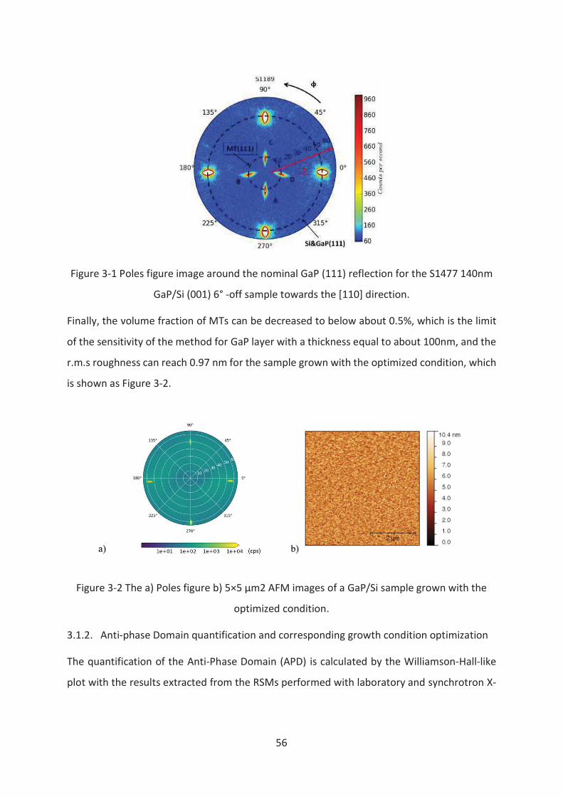
56
Figure 3-1 Poles figure image around the nominal GaP (111) reflection for the S1477 140nm
GaP/Si (001) 6° -off sample towards the [110] direction.
Finally, the volume fraction of MTs can be decreased to below about 0.5%, which is the limit
of the sensitivity of the method for GaP layer with a thickness equal to about 100nm, and the
r.m.s roughness can reach 0.97 nm for the sample grown with the optimized condition, which
is shown as Figure 3-2.
Figure 3-2 The a) Poles figure b) 5×5 μm2 AFM images of a GaP/Si sample grown with the
optimized condition.
3.1.2. Anti-phase Domain quantification and corresponding growth condition optimization
The quantification of the Anti-Phase Domain (APD) is calculated by the Williamson-Hall-like
plot with the results extracted from the RSMs performed with laboratory and synchrotron X-
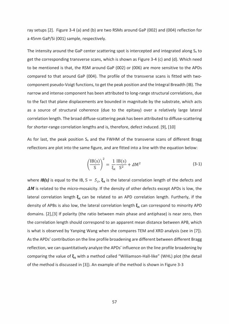
57
ray setups [2]. Figure 3-4 (a) and (b) are two RSMs around GaP (002) and (004) reflection for
a 45nm GaP/Si (001) sample, respectively.
The intensity around the GaP center scattering spot is intercepted and integrated along Sx to
get the corresponding transverse scans, which is shown as Figure 3-4 (c) and (d). Which need
to be mentioned is that, the RSM around GaP (002) or (006) are more sensitive to the APDs
compared to that around GaP (004). The profile of the transverse scans is fitted with two-
component pseudo-Voigt functions, to get the peak position and the Integral Breadth (IB). The
narrow and intense component has been attributed to long-range structural correlations, due
to the fact that plane displacements are bounded in magnitude by the substrate, which acts
as a source of structural coherence (due to the epitaxy) over a relatively large lateral
correlation length. The broad diffuse-scattering peak has been attributed to diffuse-scattering
for shorter-range correlation lengths and is, therefore, defect induced. [9], [10]
As for last, the peak position Sx and the FWHM of the transverse scans of different Bragg
reflections are plot into the same figure, and are fitted into a line with the equation below:
À½Á<�@ Ã5 =; 1Ä� ½Á<�@Â5 8 >M5; (3-1)
where IB(s) is equal to the IB,  = ;ų, ÆÇ is the lateral correlation length of the defects and AG is related to the micro-mosaicity. If the density of other defects except APDs is low, the
lateral correlation length ÆÇ can be related to an APD correlation length. Furtherly, if the
density of APBs is also low, the lateral correlation length ÆÇ can correspond to minority APD
domains. [2],[3] If polarity (the ratio between main phase and antiphase) is near zero, then
the correlation length should correspond to an apparent mean distance between APB, which
is what is observed by Yanping Wang when she compares TEM and XRD analysis (see in [7]).
As the APDs’ contribution on the line profile broadening are different between different Bragg
reflection, we can quantitatively analyze the APDs’ influence on the line profile broadening by
comparing the value of ÆÇ with a method called “Williamson-Hall-like” (WHL) plot (the detail
of the method is discussed in [3]). An example of the method is shown in Figure 3-3
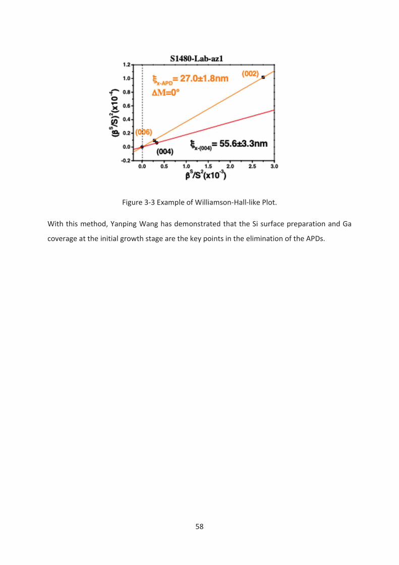
58
Figure 3-3 Example of Williamson-Hall-like Plot.
With this method, Yanping Wang has demonstrated that the Si surface preparation and Ga
coverage at the initial growth stage are the key points in the elimination of the APDs.
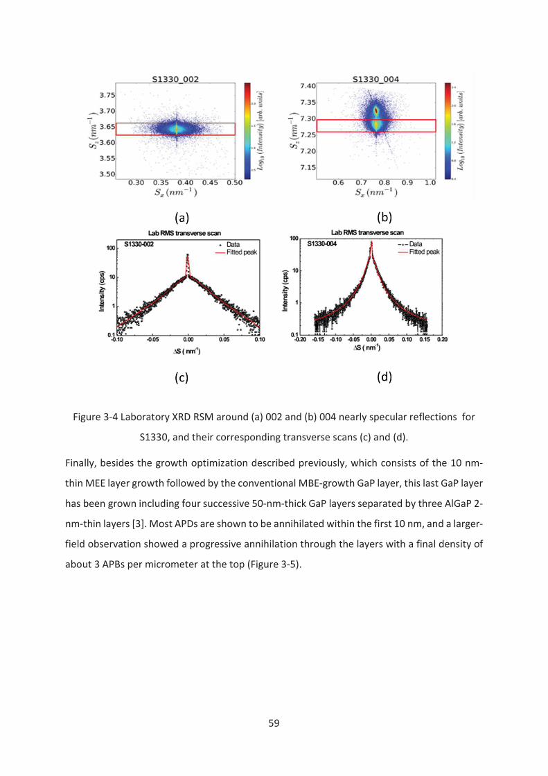
59
Figure 3-4 Laboratory XRD RSM around (a) 002 and (b) 004 nearly specular reflections for
S1330, and their corresponding transverse scans (c) and (d).
Finally, besides the growth optimization described previously, which consists of the 10 nm-
thin MEE layer growth followed by the conventional MBE-growth GaP layer, this last GaP layer
has been grown including four successive 50-nm-thick GaP layers separated by three AlGaP 2-
nm-thin layers [3]. Most APDs are shown to be annihilated within the first 10 nm, and a larger-
field observation showed a progressive annihilation through the layers with a final density of
about 3 APBs per micrometer at the top (Figure 3-5).
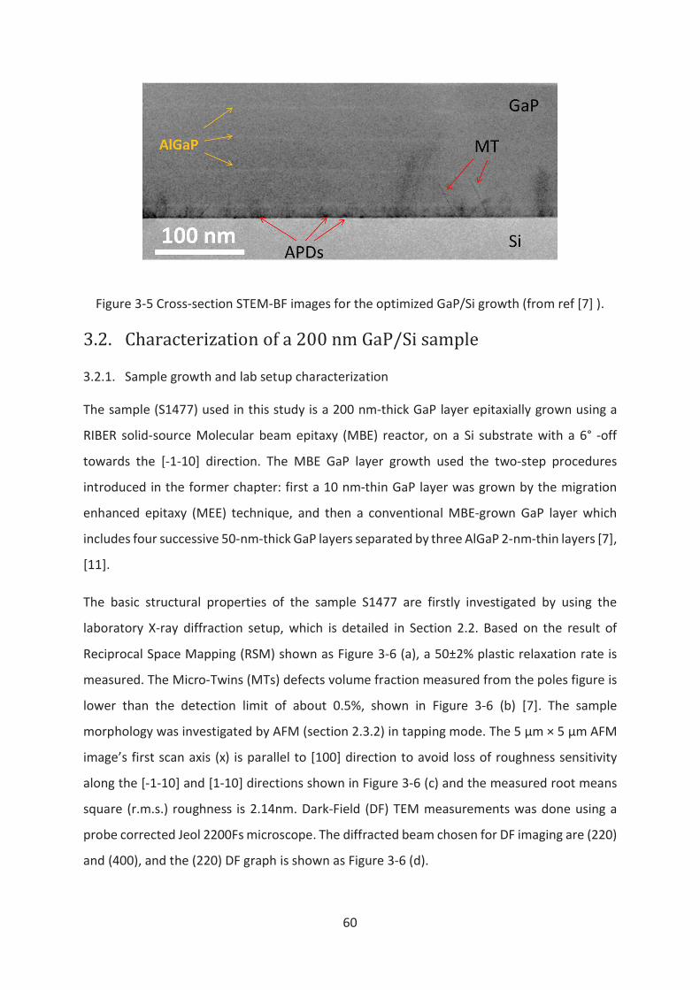
60
Figure 3-5 Cross-section STEM-BF images for the optimized GaP/Si growth (from ref [7] ).
3.2. Characterization!of!a!200!nm!GaP/Si!sample!
3.2.1. Sample growth and lab setup characterization
The sample (S1477) used in this study is a 200 nm-thick GaP layer epitaxially grown using a
RIBER solid-source Molecular beam epitaxy (MBE) reactor, on a Si substrate with a 6° -off
towards the [-1-10] direction. The MBE GaP layer growth used the two-step procedures
introduced in the former chapter: first a 10 nm-thin GaP layer was grown by the migration
enhanced epitaxy (MEE) technique, and then a conventional MBE-grown GaP layer which
includes four successive 50-nm-thick GaP layers separated by three AlGaP 2-nm-thin layers [7],
[11].
The basic structural properties of the sample S1477 are firstly investigated by using the
laboratory X-ray diffraction setup, which is detailed in Section 2.2. Based on the result of
Reciprocal Space Mapping (RSM) shown as Figure 3-6 (a), a 50±2% plastic relaxation rate is
measured. The Micro-Twins (MTs) defects volume fraction measured from the poles figure is
lower than the detection limit of about 0.5%, shown in Figure 3-6 (b) [7]. The sample
morphology was investigated by AFM (section 2.3.2) in tapping mode. The 5 μm × 5 μm AFM
image’s first scan axis (x) is parallel to [100] direction to avoid loss of roughness sensitivity
along the [-1-10] and [1-10] directions shown in Figure 3-6 (c) and the measured root means
square (r.m.s.) roughness is 2.14nm. Dark-Field (DF) TEM measurements was done using a
probe corrected Jeol 2200Fs microscope. The diffracted beam chosen for DF imaging are (220)
and (400), and the (220) DF graph is shown as Figure 3-6 (d).
61
3.2.2. Performance of K-Map
Before the appearance of the K-Map technique, many researchers have tried to develop X-ray
mapping techniques for the local structural information. For instance, P. M. Mooney et al.
have applied the X-ray microdiffraction to check the structural quality of SiGe thin layers
grown on Si substrates [12]. J. Matsui also performed a series of rocking curve scans on a
Silicon on Insulator (SOI) sample to measure the spatial distribution of the lattice strains [13].
Spatial resolution has been considerably enhanced by the recent development of the third-
generation synchrotron long beamlines and more performant X-ray optical focusing systems.
For faster acquisition, K-Map includes a hardware system that synchronizes the piezo scanner
holding the sample, and the detector. The resolution of the K-Map is limited by the size of the
beam, times the projection effect and the thickness effect of the projection of the beam in the
sample. But the K-Map avoids also sample preparation and is nondestructive. Mondiali et al.
have applied the K-Map to investigate SiGe on a patterned wafer [14], and Zoellner et al. used
the same method on a 1.6μm-thick SiGe sample on a normal Si substrate. They reported the
tilt and the strain distribution mapping result from the (004) and (113) Bragg reflections [15].
B. Vianne et al. have aslo investigated thermo-mechanical strain, induced by a Through Silicon
Via (TSV) process in silicon, using K-map measurements combined with finite element
modelling [16].
The K-Map is performed using the beamline ID01 at ESRF [17], [18]. The 8 keV X-ray beam was
focused by a Fresnel zone plate (FZP) with a beam stop (BS) and an order sorting aperture
(OSA) to the center of rotation of the goniometer. The beam cross section is around 300 nm
(horizontal) × 100 nm (vertical) at the goniometer center, which is shown in Figure 3-7 (a).
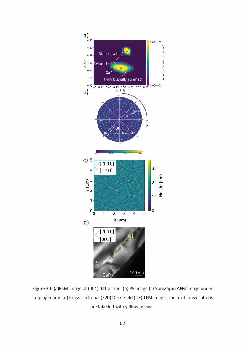
62
Figure 3-6 (a)RSM image of (004) diffraction. (b) PF image (c) 5μm×5μm AFM image under
tapping mode. (d) Cross-sectional (220) Dark-Field (DF) TEM image. The misfit dislocations
are labelled with yellow arrows.
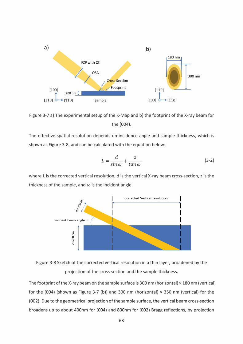
63
Figure 3-7 a) The experimental setup of the K-Map and b) the footprint of the X-ray beam for
the (004).
The effective spatial resolution depends on incidence angle and sample thickness, which is
shown as Figure 3-8, and can be calculated with the equation below:
È = `{}: ²; 8 É9&:²; (3-2)
where L is the corrected vertical resolution, d is the vertical X-ray beam cross-section, z is the
thickness of the sample, and ± is the incident angle.
Figure 3-8 Sketch of the corrected vertical resolution in a thin layer, broadened by the
projection of the cross-section and the sample thickness.
The footprint of the X-ray beam on the sample surface is 300 nm (horizontal) × 180 nm (vertical)
for the (004) (shown as Figure 3-7 (b)) and 300 nm (horizontal) × 350 nm (vertical) for the
(002). Due to the geometrical projection of the sample surface, the vertical beam cross-section
broadens up to about 400nm for (004) and 800nm for (002) Bragg reflections, by projection
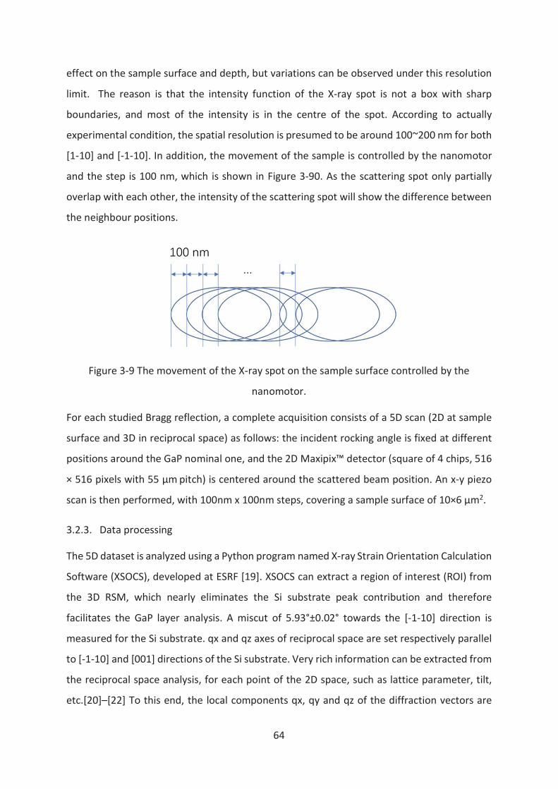
64
effect on the sample surface and depth, but variations can be observed under this resolution
limit. The reason is that the intensity function of the X-ray spot is not a box with sharp
boundaries, and most of the intensity is in the centre of the spot. According to actually
experimental condition, the spatial resolution is presumed to be around 100~200 nm for both
[1-10] and [-1-10]. In addition, the movement of the sample is controlled by the nanomotor
and the step is 100 nm, which is shown in Figure 3-90. As the scattering spot only partially
overlap with each other, the intensity of the scattering spot will show the difference between
the neighbour positions.
Figure 3-9 The movement of the X-ray spot on the sample surface controlled by the
nanomotor.
For each studied Bragg reflection, a complete acquisition consists of a 5D scan (2D at sample
surface and 3D in reciprocal space) as follows: the incident rocking angle is fixed at different
positions around the GaP nominal one, and the 2D Maxipix™ detector (square of 4 chips, 516
× 516 pixels with 55 µm pitch) is centered around the scattered beam position. An x-y piezo
scan is then performed, with 100nm x 100nm steps, covering a sample surface of 10×6 μm2.
3.2.3. Data processing
The 5D dataset is analyzed using a Python program named X-ray Strain Orientation Calculation
Software (XSOCS), developed at ESRF [19]. XSOCS can extract a region of interest (ROI) from
the 3D RSM, which nearly eliminates the Si substrate peak contribution and therefore
facilitates the GaP layer analysis. A miscut of 5.93°±0.02° towards the [-1-10] direction is
measured for the Si substrate. qx and qz axes of reciprocal space are set respectively parallel
to [-1-10] and [001] directions of the Si substrate. Very rich information can be extracted from
the reciprocal space analysis, for each point of the 2D space, such as lattice parameter, tilt,
etc.[20]–[22] To this end, the local components qx, qy and qz of the diffraction vectors are

65
calculated for each point of the 5D dataset. To analyze the full 3D RSM dataset for each direct-
space point, it is convenient to project these data in the (qx, qz) and (qy, qz) planes. To increase
the signal to noise ratio, the summed 2D datasets are furtherly summed up to 1D curves,
whose main dimensions are aligned with either the qx, or the qy axes. These 1D curves are
then fitted by a Gaussian function to determine the key parameters of the peak at each direct
space position, i.e. the reciprocal space peak maximum position, the Full Width at Half
Maximum (FWHM) and integrated intensity.
Since the qx and qy are parallel to the [-1-10] and [1-10] mean crystallographic directions
respectively, the local tilts towards [-1-10] and [1-10] can be directly calculated by the shift of
qx and qy peak positions respectively:
ZÊË4Ë4¾Ì = {}:Ë4 ÍÎ�Î Ï (3-3)
ZÊ4Ë4¾Ì = {}:Ë4<ÎÐÎ @ (3-4)
In addition, the total tilt angle, which is the angle between the local normal vectors and the Si
substrate [004] direction, is as follow:
Z = ; ¯°{Ë4<ÎÑÎ @ (3-5)
Being qz the scattering vector component aligned with the GaP (004) signal, that is corrected
from the miscut.
The local lattice constant & can be extracted with the following equation:
a = 3zÎ Ò �h5 8 k5 8 l5 (3-6)
where (h, k, l) is the corresponding Miller indices of the reflection.
As the reciprocal lattice point studied is the (004) Bragg reflection for our experiment in
general, the equation above can be written as:
a* = ÓzÎ (3-7)

66
In addition, because of the defects or the strain, the local normal scatter vector may rock
around the theoretical position. This variation let that qx and qy have small value instead of 0,
and the Equation (3-7) can be written as:
a* = ÓzjÎ�5 8 ÎÐ5 8 ÎÑ5 (3-8)
And the out-of-plane lattice constant &* provides the local in-plane strain compared to the
bulk GaP based on the following equation [23]:
)+ = a+ $ aÔ�ÕaÔ�Õ =;$ C443C45 × a* $ aÔ�ÕaÔ�Õ (3-9)
where 2+ is the in-plane strain compared to the bulk GaP, C11=140.5 GPa and C12=62 GPa are
the elastic stiffness constants of GaP [24], &ÖªØ = JÙTJ0JÚ is the bulk lattice constant of GaP
[25], and the 6+ is the mean local in-plane lattice constant of all the lattice vectors in (001)
plane.
3.2.4. The measurement resolution
According to the measurement, the angular resolution provided by the 2D pixel scanner is
0.0036 °/pixel. Thus, the resolution of the tilt along Qx or Qy is 0.0036°.
The resolution of the strain is complex. The strain is calculated from the distance of the Q in
the reciprocal space, while the parameters to determine the resolution of Qx, Qy and Qz are
different. As the Qz contributes most to the norm of Q, we can approximately assume that the
resolution of strain is determined with the same parameters with Qz.

67
Figure 3-10 The resolution of Qz determined by the rotation of the diffraction vector.
In this work, the resolution of Qz is mainly determined by the rotation of 5�5 , which is shown in
Figure 3-10. Then, according to Bragg’s law, we have these equations for (004) diffraction:
3`{}: Í3~3 Ï = :u (3-10)
d = aT (3-11)
where � is the wavelength of the X-ray (8keV), 5�5 is the Bragg angle of our sample (34.5°) and
� 5�5 is equal to the angular resolution provided by the 2D pixel scanner (1°/278), a is the out-
of-plane lattice constant of the measured material (GaP).
>& = ;$3:u ¯°{ Û3~3 ;Ü���5 Û3~3 Ü>3~3 (3-12)
The resolution of the lattice constant of GaP, �a is equal to 5×10⁻⁵ nm.
As the in-plane strain 2+ is as below:
)+ = a+ $ aÔ�ÕaÔ�Õ =;$ C443C45 ;a* $ aÔ�ÕaÔ�Õ (3-13)
We have:

68
>)+ = $ C443C45 ; >&aÔ�Õ (3-14)
where 2+ is the in-plane strain with respect to the bulk GaP, ��� = ;1T0ÙJ;ÝÞa and ��p =;ß3;ÝÞa are the elastic stiffness constants of GaP, &ÖªØ = 0ÙJTJ0J;nm is the bulk lattice
constant of GaP. So, the resolution of the in-plain strain is approximately equal to 0.01%.
While the resolutions calculated above can be worse in real for some reasons. For instance, in
the discussion above, we assume that the diffraction beam can be distinguished between the
neighborhood pixels on the 2D pixel scanner. But the real diffraction signal may have a width
cover more than one pixel of the scanner.
But according to our experience, the information in the tilt and strain mapping is still in within
the allowable range of the resolution.
3.3. The! local! structural! characterization! with! sub-micrometer-
beam!X-ray!diffraction!
Two mapping of the tilt towards [-1-10] and [1-10] directions are shown as Figure 3-11 (a) and
(b) respectively. They exhibit lines, of high tilt values, that are respectively nearly parallel to
the [-1-10] and [1-10] directions. To confirm the existence of these regions with high tilt values,
a K-Map is also performed on the (002) reflection of the sample. The result is shown Figure
3-11 (c) for tilt towards [1-10]. When comparing Figure 3-11 (b & c), very similar patterns are
identified with a slight shift that can be due to both imperfect alignment and drift of the x-y
piezo stage with the large incidence angle shift.
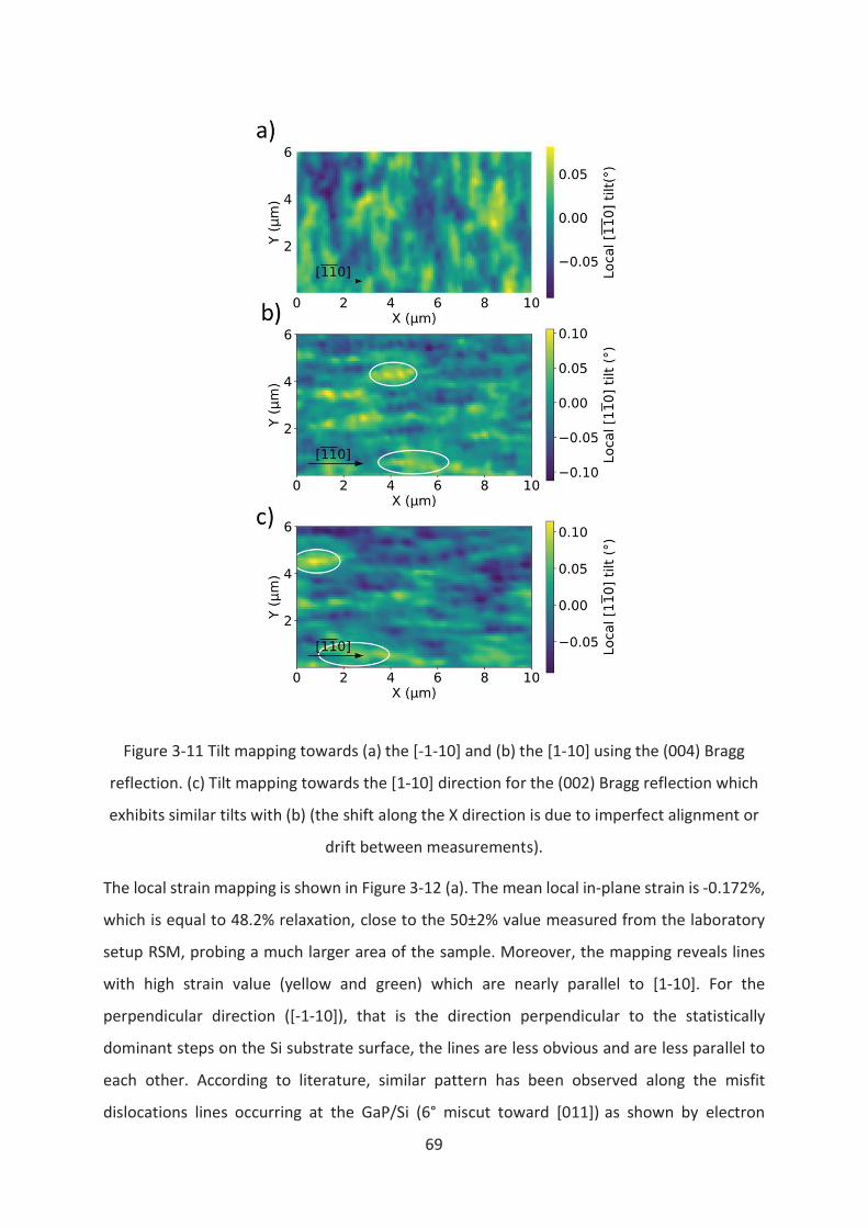
69
Figure 3-11 Tilt mapping towards (a) the [-1-10] and (b) the [1-10] using the (004) Bragg
reflection. (c) Tilt mapping towards the [1-10] direction for the (002) Bragg reflection which
exhibits similar tilts with (b) (the shift along the X direction is due to imperfect alignment or
drift between measurements).
The local strain mapping is shown in Figure 3-12 (a). The mean local in-plane strain is -0.172%,
which is equal to 48.2% relaxation, close to the 50±2% value measured from the laboratory
setup RSM, probing a much larger area of the sample. Moreover, the mapping reveals lines
with high strain value (yellow and green) which are nearly parallel to [1-10]. For the
perpendicular direction ([-1-10]), that is the direction perpendicular to the statistically
dominant steps on the Si substrate surface, the lines are less obvious and are less parallel to
each other. According to literature, similar pattern has been observed along the misfit
dislocations lines occurring at the GaP/Si (6° miscut toward [011]) as shown by electron
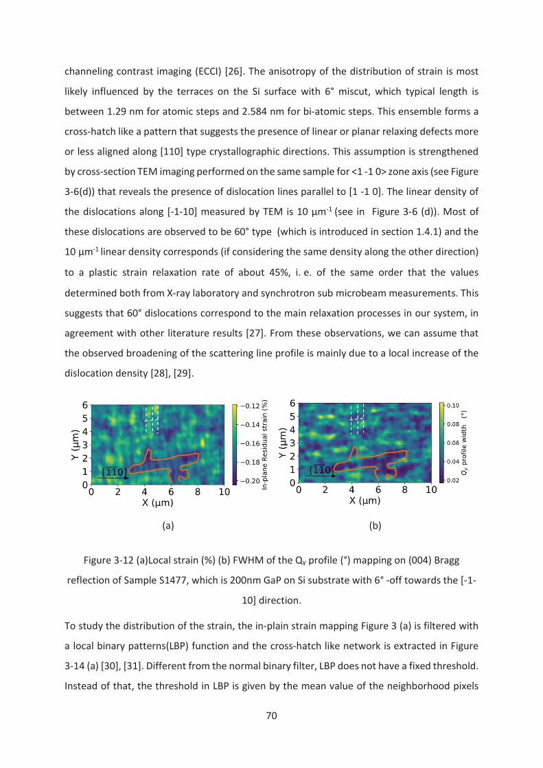
70
channeling contrast imaging (ECCI) [26]. The anisotropy of the distribution of strain is most
likely influenced by the terraces on the Si surface with 6° miscut, which typical length is
between 1.29 nm for atomic steps and 2.584 nm for bi-atomic steps. This ensemble forms a
cross-hatch like a pattern that suggests the presence of linear or planar relaxing defects more
or less aligned along [110] type crystallographic directions. This assumption is strengthened
by cross-section TEM imaging performed on the same sample for <1 -1 0> zone axis (see Figure
3-6(d)) that reveals the presence of dislocation lines parallel to [1 -1 0]. The linear density of
the dislocations along [-1-10] measured by TEM is 10 μm-1 (see in Figure 3-6 (d)). Most of
these dislocations are observed to be 60° type (which is introduced in section 1.4.1) and the
10 μm-1 linear density corresponds (if considering the same density along the other direction)
to a plastic strain relaxation rate of about 45%, i e. of the same order that the values
determined both from X-ray laboratory and synchrotron sub microbeam measurements. This
suggests that 60° dislocations correspond to the main relaxation processes in our system, in
agreement with other literature results [27]. From these observations, we can assume that
the observed broadening of the scattering line profile is mainly due to a local increase of the
dislocation density [28], [29].
(a) (b)
Figure 3-12 (a)Local strain (%) (b) FWHM of the Qy profile (°) mapping on (004) Bragg
reflection of Sample S1477, which is 200nm GaP on Si substrate with 6° -off towards the [-1-
10] direction.
To study the distribution of the strain, the in-plain strain mapping Figure 3 (a) is filtered with
a local binary patterns(LBP) function and the cross-hatch like network is extracted in Figure
3-14 (a) [30], [31]. Different from the normal binary filter, LBP does not have a fixed threshold.
Instead of that, the threshold in LBP is given by the mean value of the neighborhood pixels
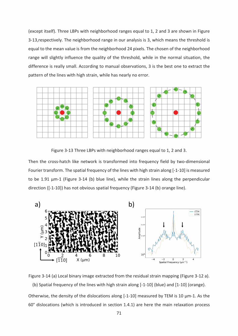
71
(except itself). Three LBPs with neighborhood ranges equal to 1, 2 and 3 are shown in Figure
3-13,respectively. The neighborhood range in our analysis is 3, which means the threshold is
equal to the mean value is from the neighborhood 24 pixels. The chosen of the neighborhood
range will slightly influence the quality of the threshold, while in the normal situation, the
difference is really small. According to manual observations, 3 is the best one to extract the
pattern of the lines with high strain, while has nearly no error.
Figure 3-13 Three LBPs with neighborhood ranges equal to 1, 2 and 3.
Then the cross-hatch like network is transformed into frequency field by two-dimensional
Fourier transform. The spatial frequency of the lines with high strain along [-1-10] is measured
to be 1.91 μm-1 (Figure 3-14 (b) blue line), while the strain lines along the perpendicular
direction ([-1-10]) has not obvious spatial frequency (Figure 3-14 (b) orange line).
Figure 3-14 (a) Local binary image extracted from the residual strain mapping (Figure 3-12 a).
(b) Spatial frequency of the lines with high strain along [-1-10] (blue) and [1-10] (orange).
Otherwise, the density of the dislocations along [-1-10] measured by TEM is 10 μm-1. As the
60° dislocations (which is introduced in section 1.4.1) are here the main relaxation process
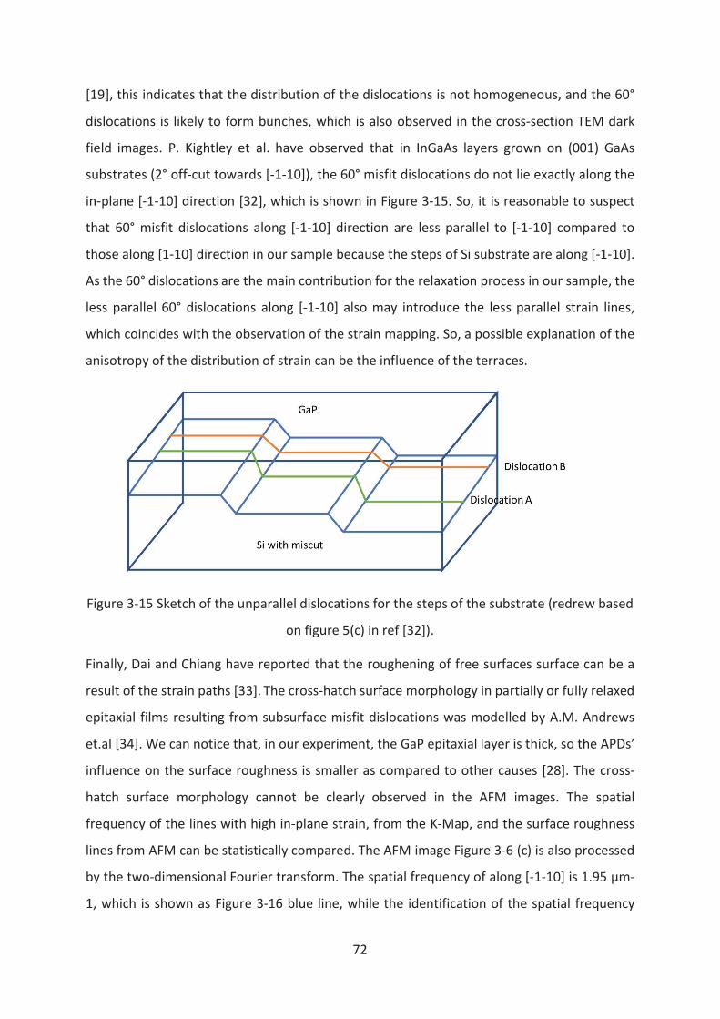
72
[19], this indicates that the distribution of the dislocations is not homogeneous, and the 60°
dislocations is likely to form bunches, which is also observed in the cross-section TEM dark
field images. P. Kightley et al. have observed that in InGaAs layers grown on (001) GaAs
substrates (2° off-cut towards [-1-10]), the 60° misfit dislocations do not lie exactly along the
in-plane [-1-10] direction [32], which is shown in Figure 3-15. So, it is reasonable to suspect
that 60° misfit dislocations along [-1-10] direction are less parallel to [-1-10] compared to
those along [1-10] direction in our sample because the steps of Si substrate are along [-1-10].
As the 60° dislocations are the main contribution for the relaxation process in our sample, the
less parallel 60° dislocations along [-1-10] also may introduce the less parallel strain lines,
which coincides with the observation of the strain mapping. So, a possible explanation of the
anisotropy of the distribution of strain can be the influence of the terraces.
Figure 3-15 Sketch of the unparallel dislocations for the steps of the substrate (redrew based
on figure 5(c) in ref [32]).
Finally, Dai and Chiang have reported that the roughening of free surfaces surface can be a
result of the strain paths [33]. The cross-hatch surface morphology in partially or fully relaxed
epitaxial films resulting from subsurface misfit dislocations was modelled by A.M. Andrews
et.al [34]. We can notice that, in our experiment, the GaP epitaxial layer is thick, so the APDs’
influence on the surface roughness is smaller as compared to other causes [28]. The cross-
hatch surface morphology cannot be clearly observed in the AFM images. The spatial
frequency of the lines with high in-plane strain, from the K-Map, and the surface roughness
lines from AFM can be statistically compared. The AFM image Figure 3-6 (c) is also processed
by the two-dimensional Fourier transform. The spatial frequency of along [-1-10] is 1.95 μm-
1, which is shown as Figure 3-16 blue line, while the identification of the spatial frequency
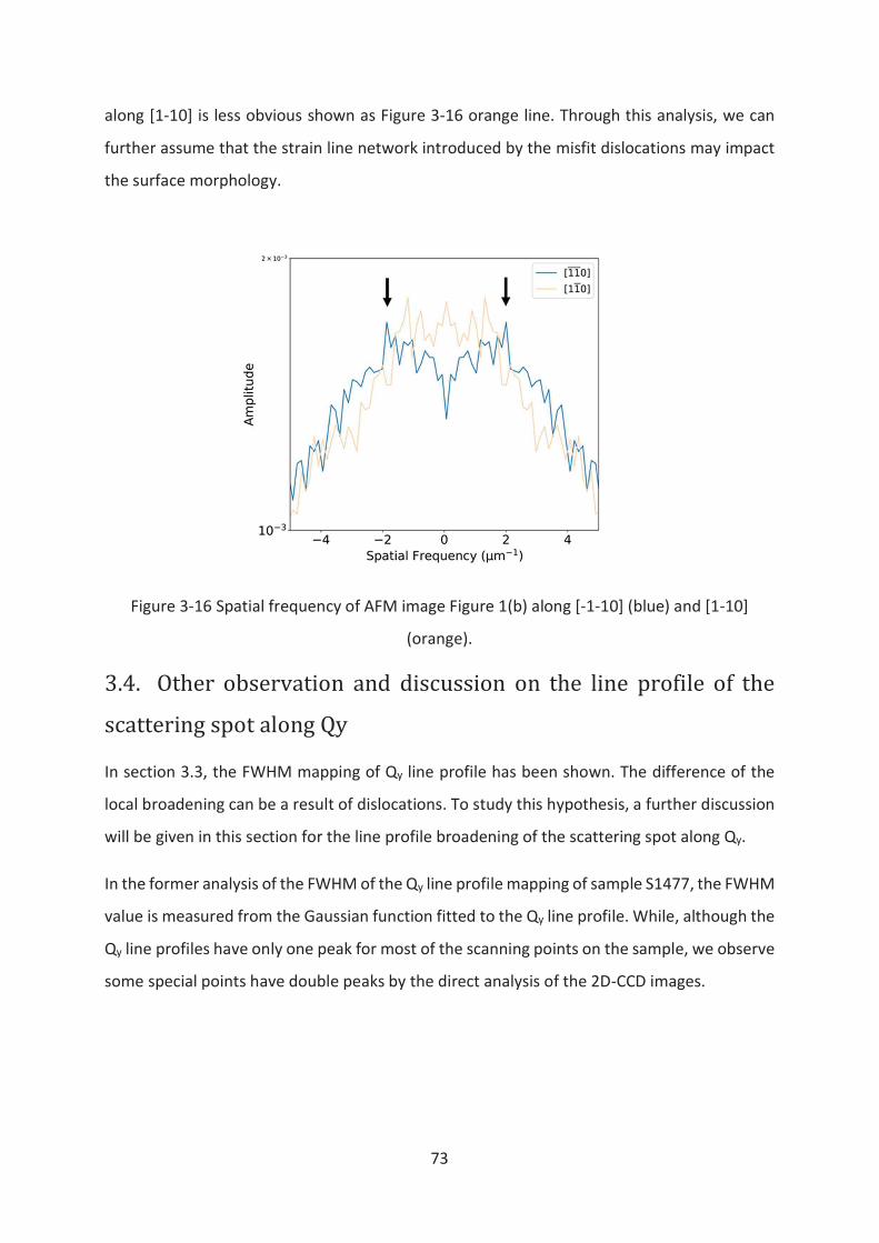
73
along [1-10] is less obvious shown as Figure 3-16 orange line. Through this analysis, we can
further assume that the strain line network introduced by the misfit dislocations may impact
the surface morphology.
Figure 3-16 Spatial frequency of AFM image Figure 1(b) along [-1-10] (blue) and [1-10]
(orange).
3.4. Other! observation! and! discussion! on! the! line! profile! of! the!
scattering!spot!along!Qy!
In section 3.3, the FWHM mapping of Qy line profile has been shown. The difference of the
local broadening can be a result of dislocations. To study this hypothesis, a further discussion
will be given in this section for the line profile broadening of the scattering spot along Qy.
In the former analysis of the FWHM of the Qy line profile mapping of sample S1477, the FWHM
value is measured from the Gaussian function fitted to the Qy line profile. While, although the
Qy line profiles have only one peak for most of the scanning points on the sample, we observe
some special points have double peaks by the direct analysis of the 2D-CCD images.
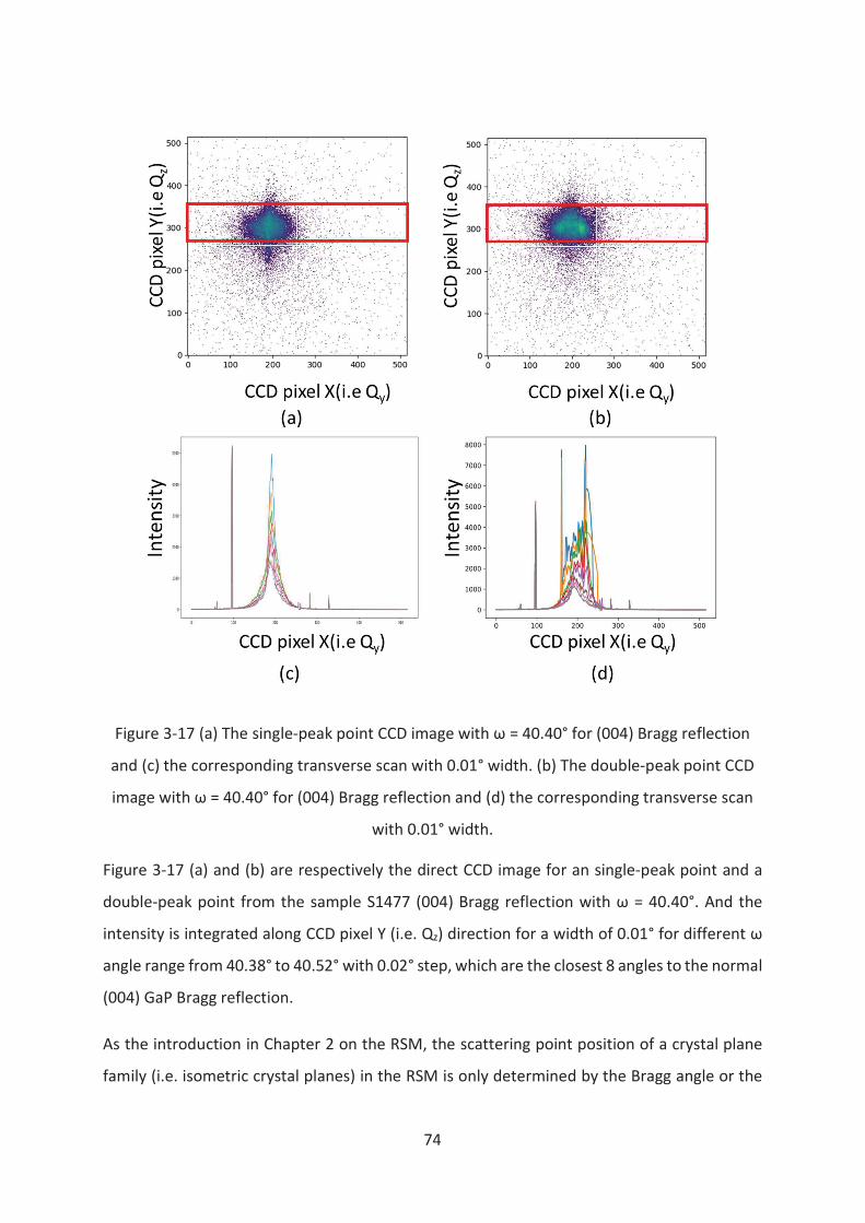
74
Figure 3-17 (a) The single-peak point CCD image with ω = 40.40° for (004) Bragg reflection
and (c) the corresponding transverse scan with 0.01° width. (b) The double-peak point CCD
image with ω = 40.40° for (004) Bragg reflection and (d) the corresponding transverse scan
with 0.01° width.
Figure 3-17 (a) and (b) are respectively the direct CCD image for an single-peak point and a
double-peak point from the sample S1477 (004) Bragg reflection with ω = 40.40°. And the
intensity is integrated along CCD pixel Y (i.e. Qz) direction for a width of 0.01° for different ω
angle range from 40.38° to 40.52° with 0.02° step, which are the closest 8 angles to the normal
(004) GaP Bragg reflection.
As the introduction in Chapter 2 on the RSM, the scattering point position of a crystal plane
family (i.e. isometric crystal planes) in the RSM is only determined by the Bragg angle or the
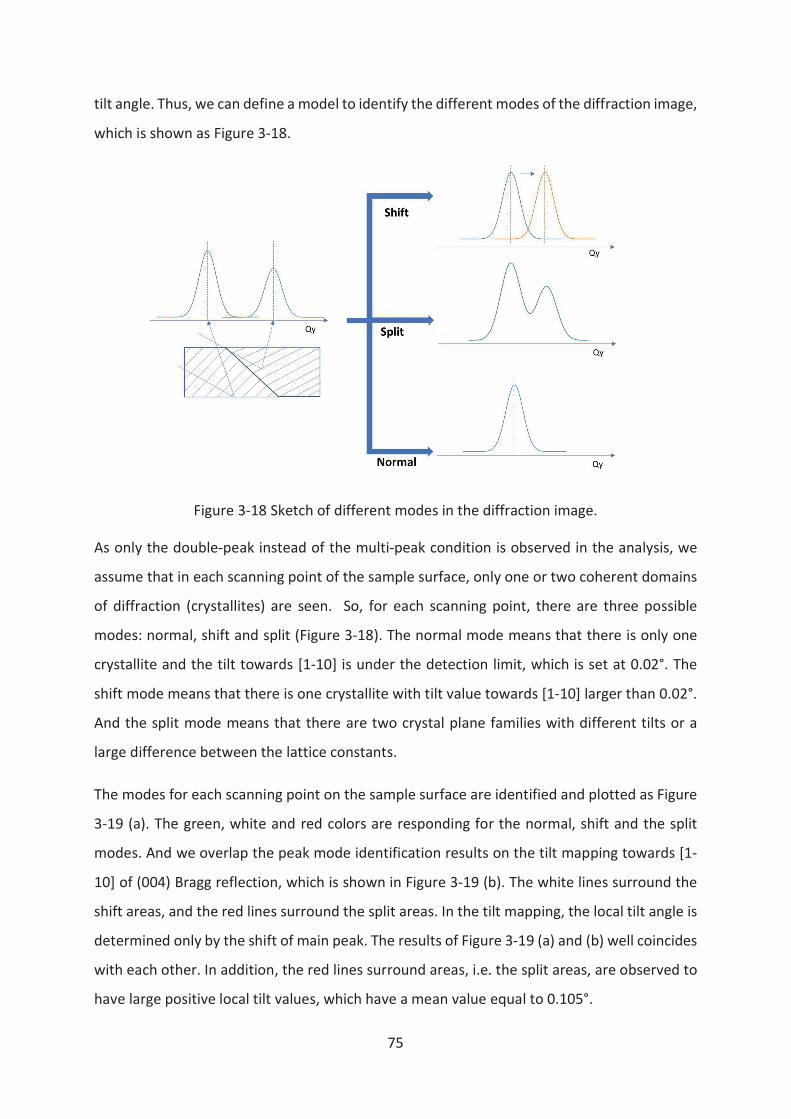
75
tilt angle. Thus, we can define a model to identify the different modes of the diffraction image,
which is shown as Figure 3-18.
Figure 3-18 Sketch of different modes in the diffraction image.
As only the double-peak instead of the multi-peak condition is observed in the analysis, we
assume that in each scanning point of the sample surface, only one or two coherent domains
of diffraction (crystallites) are seen. So, for each scanning point, there are three possible
modes: normal, shift and split (Figure 3-18). The normal mode means that there is only one
crystallite and the tilt towards [1-10] is under the detection limit, which is set at 0.02°. The
shift mode means that there is one crystallite with tilt value towards [1-10] larger than 0.02°.
And the split mode means that there are two crystal plane families with different tilts or a
large difference between the lattice constants.
The modes for each scanning point on the sample surface are identified and plotted as Figure
3-19 (a). The green, white and red colors are responding for the normal, shift and the split
modes. And we overlap the peak mode identification results on the tilt mapping towards [1-
10] of (004) Bragg reflection, which is shown in Figure 3-19 (b). The white lines surround the
shift areas, and the red lines surround the split areas. In the tilt mapping, the local tilt angle is
determined only by the shift of main peak. The results of Figure 3-19 (a) and (b) well coincides
with each other. In addition, the red lines surround areas, i.e. the split areas, are observed to
have large positive local tilt values, which have a mean value equal to 0.105°.
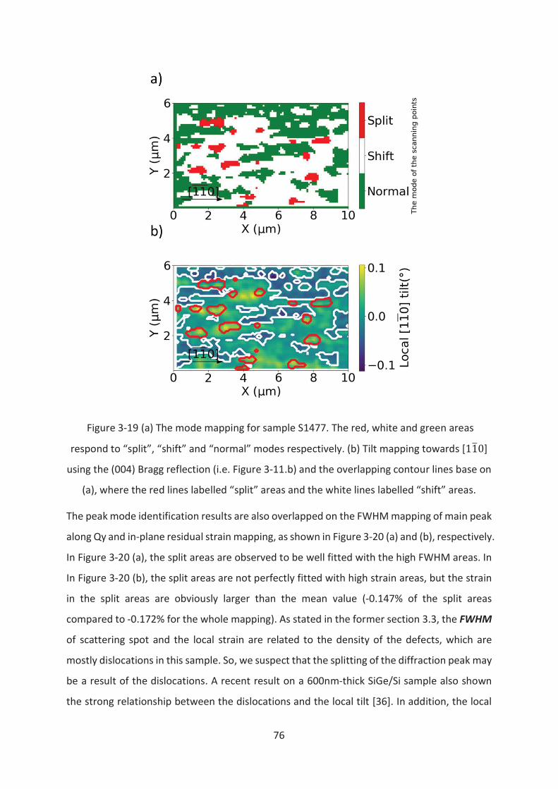
76
Figure 3-19 (a) The mode mapping for sample S1477. The red, white and green areas
respond to “split”, “shift” and “normal” modes respectively. (b) Tilt mapping towards [11à0]
using the (004) Bragg reflection (i.e. Figure 3-11.b) and the overlapping contour lines base on
(a), where the red lines labelled “split” areas and the white lines labelled “shift” areas.
The peak mode identification results are also overlapped on the FWHM mapping of main peak
along Qy and in-plane residual strain mapping, as shown in Figure 3-20 (a) and (b), respectively.
In Figure 3-20 (a), the split areas are observed to be well fitted with the high FWHM areas. In
In Figure 3-20 (b), the split areas are not perfectly fitted with high strain areas, but the strain
in the split areas are obviously larger than the mean value (-0.147% of the split areas
compared to -0.172% for the whole mapping). As stated in the former section 3.3, the FWHM
of scattering spot and the local strain are related to the density of the defects, which are
mostly dislocations in this sample. So, we suspect that the splitting of the diffraction peak may
be a result of the dislocations. A recent result on a 600nm-thick SiGe/Si sample also shown
the strong relationship between the dislocations and the local tilt [36]. In addition, the local
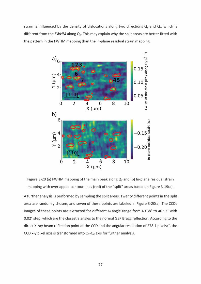
77
strain is influenced by the density of dislocations along two directions Qy and Qx, which is
different from the FWHM along Qy. This may explain why the split areas are better fitted with
the pattern in the FWHM mapping than the in-plane residual strain mapping.
Figure 3-20 (a) FWHM mapping of the main peak along Qy and (b) In-plane residual strain
mapping with overlapped contour lines (red) of the “split” areas based on Figure 3-19(a).
A further analysis is performed by sampling the split areas. Twenty different points in the split
area are randomly chosen, and seven of these points are labeled in Figure 3-20(a). The CCDs
images of these points are extracted for different ω angle range from 40.38° to 40.52° with
0.02° step, which are the closest 8 angles to the normal GaP Bragg reflection. According to the
direct X-ray beam reflection point at the CCD and the angular resolution of 278.1 pixels/°, the
CCD x-y pixel axis is transformed into Qy-Qz axis for further analysis.
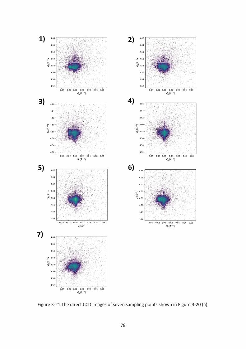
78
Figure 3-21 The direct CCD images of seven sampling points shown in Figure 3-20 (a).
79
The CCD images of the seven points at ω = 40.40° are shown in Figure 3-21 as a sample. We
observed that, compared to those points in the normal or shift areas, these points in split
areas always have a main diffraction spot and a side diffraction spot, and the two spots have
nearly the same value along Qz. The norm of the scattering vector Q and the distance á
between the two diffraction peaks are calculated from the CCD images, which is shown as
Table 3-1.
Index ¢â¢ (Å-1) δ (°)
1 4.575035 -0.22542
2 4.578039 -0.23779
3 4.572039 -0.2381
4 4.580028 -0.20016
5 4.576032 -0.21285
6 4.575016 -0.15028
7 4.570032 -0.21313
Table 3-1 The norm of the scattering vector Q and tilt angle ! of the side diffraction spot
calculated from the CCD images of seven sampling points.
The mean value of the ¢â¢ and δ for 20 points are 4.575 ± 0.005 Å-1 and -0.22 ± 0.02 °
respectively. The ¢â¢ and δ values have less than 0.1% and 10% difference compared to each
other respectively, although they have very different shapes in the CCD images. The result
suggests that the splitting in different positions is introduced by the same mechanism. In
addition, according to Section 2.2.3, these two scattering spots are from two crystallites with
nearly same ãänå but different tilt angles.
In conclusion, the splitting scattering spots (peaks if integrated along Qz) show two crystallites
with different tilt angles, which may be introduced by the dislocations. Because the strain is
relaxed by the dislocations, the local residual strain is lower for the areas with high density of
dislocations. Thus, the local out-of-plain lattice constant is lower than the neighborhood areas,
and the difference between the out-of-plane lattice constants may be the explanation of the
local tilt. A hypothetical sketch of the mechanism is plotted as Figure 3-22.
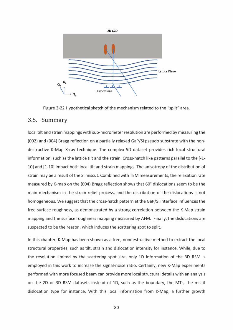
80
Figure 3-22 Hypothetical sketch of the mechanism related to the “split” area.
3.5. Summary!
local tilt and strain mappings with sub-micrometer resolution are performed by measuring the
(002) and (004) Bragg reflection on a partially relaxed GaP/Si pseudo substrate with the non-
destructive K-Map X-ray technique. The complex 5D dataset provides rich local structural
information, such as the lattice tilt and the strain. Cross-hatch like patterns parallel to the [-1-
10] and [1-10] impact both local tilt and strain mappings. The anisotropy of the distribution of
strain may be a result of the Si miscut. Combined with TEM measurements, the relaxation rate
measured by K-map on the (004) Bragg reflection shows that 60° dislocations seem to be the
main mechanism in the strain relief process, and the distribution of the dislocations is not
homogeneous. We suggest that the cross-hatch pattern at the GaP/Si interface influences the
free surface roughness, as demonstrated by a strong correlation between the K-Map strain
mapping and the surface roughness mapping measured by AFM. Finally, the dislocations are
suspected to be the reason, which induces the scattering spot to split.
In this chapter, K-Map has been shown as a free, nondestructive method to extract the local
structural properties, such as tilt, strain and dislocation intensity for instance. While, due to
the resolution limited by the scattering spot size, only 1D information of the 3D RSM is
employed in this work to increase the signal-noise ratio. Certainly, new K-Map experiments
performed with more focused beam can provide more local structural details with an analysis
on the 2D or 3D RSM datasets instead of 1D, such as the boundary, the MTs, the misfit
dislocation type for instance. With this local information from K-Map, a further growth
81
optimization can be carried out within some specially selected region, for instance, in the
application of III-V quantum dot structure analysis.
References
[1] A. Zhou et al., “A study of the strain distribution by scanning X-ray diffraction on GaP/Si
for III–V monolithic integration on silicon,” J. Appl. Crystallogr., vol. 52, no. 4, pp. 809–815,
Aug. 2019.
[2] T. T. Nguyen, “Sillicon photonics based on monolithic integration of III-V nanostructures
on silicon,” Ph.D., INSA Rennes, Rennes, 2013.
[3] Y. Wang, “Structural analyses by advanced X-ray scattering on GaP layers epitaxially grown
on silicon for integrated photonic applications,” Ph.D., INSA Rennes, Rennes, 2016.
[4] B. E. Warren, X-ray diffraction, Dover edition, Unabridged and Corrected republication of
the work originally published in 1969 by Addison-Wesley Publishing Company. New York:
Dover Publications, Inc, 1990.
[5] T. Nguyen Thanh et al., “Structural and optical analyses of GaP/Si and
(GaAsPN/GaPN)/GaP/Si nanolayers for integrated photonics on silicon,” J. Appl. Phys., vol.
112, no. 5, p. 053521, Sep. 2012.
[6] T. Nguyen Thanh et al., “Synchrotron X-ray diffraction analysis for quantitative defect
evaluation in GaP/Si nanolayers,” Thin Solid Films, vol. 541, pp. 36–40, Aug. 2013.
[7] P. Y. Wang et al., “Quantitative evaluation of microtwins and antiphase defects in GaP/Si
nanolayers for a III–V photonics platform on silicon using a laboratory X-ray diffraction
setup,” J. Appl. Crystallogr., vol. 48, no. 3, pp. 702–710, 2015.
[8] P. Y. Wang et al., “Abrupt GaP/Si hetero-interface using bistepped Si buffer,” Appl. Phys.
Lett., vol. 107, no. 19, p. 191603, 2015.
[9] O. Durand, A. Letoublon, D. J. Rogers, and F. Teherani, “Interpretation of the two-
components observed in high resolution X-ray diffraction ω scan peaks for mosaic ZnO
thin films grown on c-sapphire substrates using pulsed laser deposition,” Thin Solid Films,
vol. 519, no. 19, pp. 6369–6373, 2011.
[10] O. Durand, A. Létoublon, D. J. Rogers, F. H. Teherani, C. Cornet, and A. Le Corre,
“Studies of PLD-grown ZnO and MBE-grown GaP mosaic thin films by x-ray scattering
methods: beyond the restrictive Omega rocking curve linewidth as a figure-of-merit,” in
Oxide-based Materials and Devices II, 2011, vol. 7940, p. 79400L.
82
[11] P. Guillemé et al., “Antiphase domain tailoring for combination of modal and 4¯ -quasi-
phase matching in gallium phosphide microdisks.,” Opt. Express, vol. 24, no. 13, pp.
14608–17, 2016.
[12] P. M. Mooney, J. L. Jordan-Sweet, I. C. Noyan, and S. K. Kaldor, “Observation of local
tilted regions in strain-relaxed SiGe/Si buffer layers using x-ray microdiffraction,” Appl.
Phys. Lett., vol. 74, no. 5, pp. 726–728, 1999.
[13] J. Matsui et al., “Microscopic strain analysis of semiconductor crystals using a
synchrotron X-ray microbeam,” J. Cryst. Growth, vol. 237, pp. 317–323, 2002.
[14] V. Mondiali et al., “Dislocation engineering in SiGe on periodic and aperiodic Si(001)
templates studied by fast scanning X-ray nanodiffraction,” Appl. Phys. Lett., vol. 104, no.
2, p. 021918, 2014.
[15] M. H. Zoellner et al., “Imaging Structure and Composition Homogeneity of 300 mm
SiGe Virtual Substrates for Advanced CMOS Applications by Scanning X-ray Diffraction
Microscopy,” ACS Appl. Mater. Interfaces, vol. 7, no. 17, pp. 9031–9037, 2015.
[16] Vianne, B., Escoubas, S., Richard, M.-I., Labat, S., Chahine, G., Schülli, T., Farcy, A., Bar, P.,
Fiori, V. & Thomas, O. (2015). Microelectron Eng. 137, 117–123.
[17] T. U. Schϋlli and S. J. Leake, “X-ray nanobeam diffraction imaging of materials,” Curr.
Opin. Solid State Mater. Sci., no. Scient. Rep. 2017, pp. 188–201, 2018.
[18] S. J. Leake et al., “The Nanodiffraction beamline ID01/ESRF: a microscope for imaging
strain and structure,” J. Synchrotron Rad., vol. 26, no. 2, pp. 571–584, 2019.
[19] G. A. Chahine et al., “Imaging of strain and lattice orientation by quick scanning X-ray
microscopy combined with three-dimensional reciprocal space mapping,” J. Appl.
Crystallogr., vol. 47, no. 2, pp. 762–769, 2014.
[20] M. Keplinger et al., “Strain distribution in single, suspended germanium nanowires
studied using nanofocused x-rays,” Nanotechnology, vol. 27, no. 5, p. 055705, Feb. 2016.
[21] D. Kriegner et al., “Twin domain imaging in topological insulator Bi2Te3 and Bi2Se3
epitaxial thin films by scanning X-ray nanobeam microscopy and electron backscatter
diffraction,” J. Appl. Crystallogr., vol. 50, no. Pt 2, pp. 369–377, Apr. 2017.
[22] M. Hadjimichael, E. Zatterin, S. Fernandez-Peña, S. J. Leake, and P. Zubko, “Domain
Wall Orientations in Ferroelectric Superlattices Probed with Synchrotron X-Ray
Diffraction,” Phys. Rev. Lett., vol. 120, no. 3, p. 037602, Jan. 2018.
83
[23] Y. Takagi, Y. Furukawa, A. Wakahara, and H. Kan, “Lattice relaxation process and
crystallographic tilt in GaP layers grown on misoriented Si(001) substrates by metalorganic
vapor phase epitaxy,” J. Appl. Phys., vol. 107, no. 6, p. 063506, 2010.
[24] Y. K. Yoḡurtçu, A. J. Miller, and G. A. Saunders, “Pressure dependence of elastic
behaviour and force constants of GaP,” J. Phys. Chem. Solids, vol. 42, no. 1, pp. 49–56, Jan.
1981.
[25] G. Giesecke and H. Pfister, Präzisionsbestimmung der Gitterkonstanten von AIIIBv
Verbindungen, Acta. Crystallogr., vol. 11, no. 5, pp. 369 371, 1958.
[26] S. D. Carnevale et al., “Applications of Electron Channeling Contrast Imaging for the
Rapid Characterization of Extended Defects in III-V/Si Heterostructures,” IEEE J. Photovolt.,
vol. 5, no. 2, pp. 676–682, 2014.
[27] S. Kishinû, M. Ogirima, and K. Kurata, “A Cross-Hatch Pattern in GaAs1−xPx Epitaxially
Grown on GaAs Substrate,” J. Electrochem. Soc., vol. 119, no. 5, pp. 617–622, 1972.
[28] E. A. Fitzgerald et al., “Relaxed Ge x Si1- x structures for III-V integration with Si and
high mobility two-dimensional electron gases in Si,” J. Vac. Sci. Technol., vol. 10, no. 4, pp.
1807–1819, 1992.
[29] M. Albrecht et al., “Surface ripples, crosshatch pattern, and dislocation formation:
Cooperating mechanisms in lattice mismatch relaxation,” Appl. Phys. Lett., vol. 67, p. 1232,
1995.
[30] T. Ojala, M. Pietikainen, and D. Harwood, “Performance evaluation of texture
measures with classification based on Kullback discrimination of distributions,” in
Proceedings of 12th International Conference on Pattern Recognition, Jerusalem, Israel,
1994, vol. 1, pp. 582–585.
[31] T. Ojala, M. Pietikäinen, and D. Harwood, “A comparative study of texture measures
with classification based on featured distributions,” Pattern Recognit., vol. 29, no. 1, pp.
51–59, Jan. 1996.
[32] P. Kightley, P. J. Goodhew, R. R. Bradley, and P. D. Augustus, “A mechanism of misfit
dislocation reaction for GaInAs strained layers grown onto off-axis GaAs substrates,” J.
Cryst. Growth, vol. 112, no. 2–3, pp. 359–367, 1991.
[33] Y. Z. Dai and F. P. Chiang, “Strain path and surface roughness,” Mech. Mater., vol. 13,
no. 1, pp. 55–57, 1992.

84
[34] A. Andrews, J. Speck, A. Romanov, M. Bobeth, and W. Pompe, “Modeling cross-hatch
surface morphology in growing mismatched layers,” J. Appl. Phys., vol. 91, no. 4, pp. 1933–
1943, 2002.
[35] B. Kunert, I. Németh, S. Reinhard, K. Volz, and W. Stolz, “Si (001) surface preparation
for the antiphase domain free heteroepitaxial growth of GaP on Si substrate,” Thin Solid
Films, vol. 517, no. 1, pp. 140–143, 2008.
[36] F. Rovaris et al., “Misfit-Dislocation Distributions in Heteroepitaxy: From Mesoscale
Measurements to Individual Defects and Back,” Phys. Rev. Appl., vol. 10, no. 5, p. 054067,
Nov. 2018.
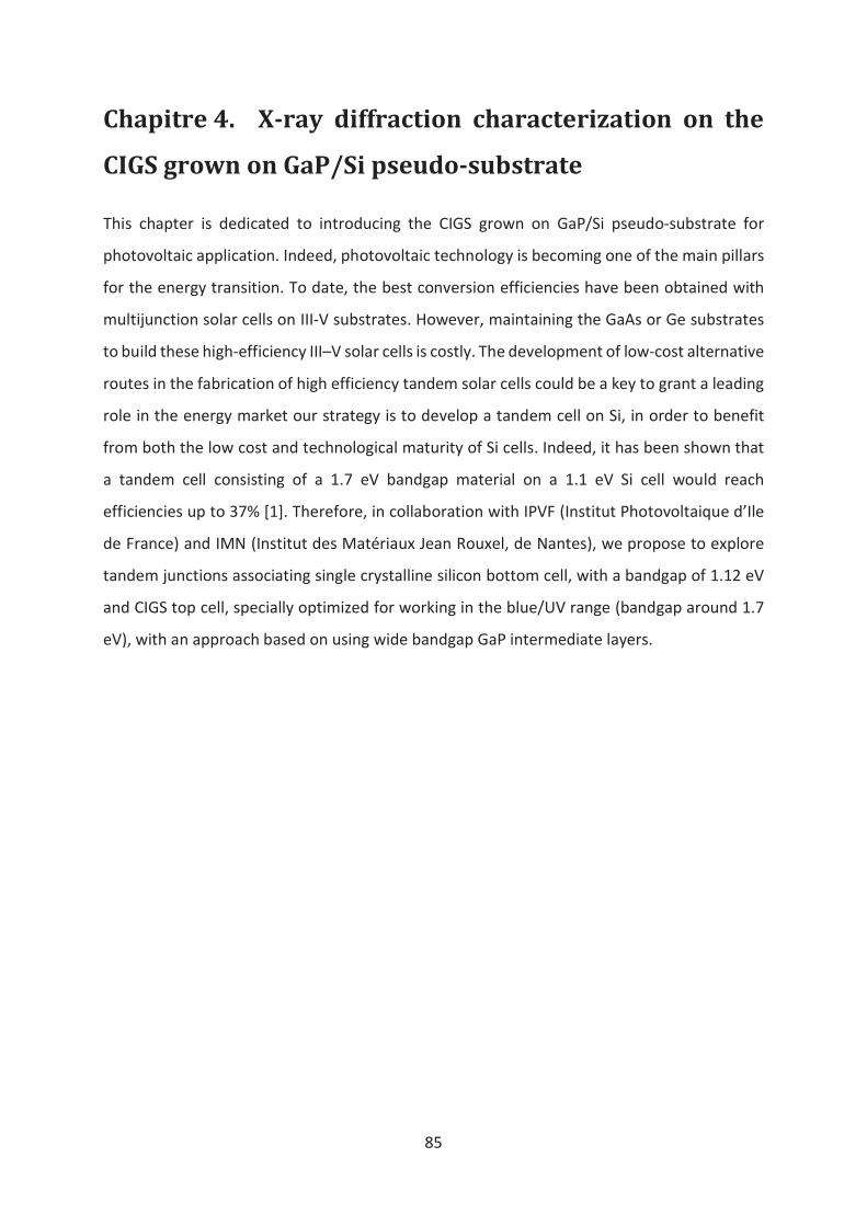
85
Chapitre 4. X-ray diffraction characterization on the
CIGS grown on GaP/Si pseudo-substrate
This chapter is dedicated to introducing the CIGS grown on GaP/Si pseudo-substrate for
photovoltaic application. Indeed, photovoltaic technology is becoming one of the main pillars
for the energy transition. To date, the best conversion efficiencies have been obtained with
multijunction solar cells on III-V substrates. However, maintaining the GaAs or Ge substrates
to build these high-efficiency III–V solar cells is costly. The development of low-cost alternative
routes in the fabrication of high efficiency tandem solar cells could be a key to grant a leading
role in the energy market our strategy is to develop a tandem cell on Si, in order to benefit
from both the low cost and technological maturity of Si cells. Indeed, it has been shown that
a tandem cell consisting of a 1.7 eV bandgap material on a 1.1 eV Si cell would reach
efficiencies up to 37% [1]. Therefore, in collaboration with IPVF (Institut Photovoltaique d’Ile
de France) and IMN (Institut des Matériaux Jean Rouxel, de Nantes), we propose to explore
tandem junctions associating single crystalline silicon bottom cell, with a bandgap of 1.12 eV
and CIGS top cell, specially optimized for working in the blue/UV range (bandgap around 1.7
eV), with an approach based on using wide bandgap GaP intermediate layers.
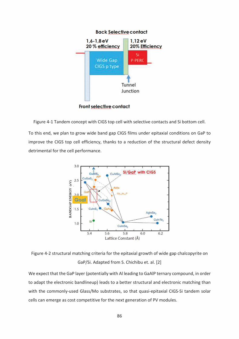
86
Figure 4-1 Tandem concept with CIGS top cell with selective contacts and Si bottom cell.
To this end, we plan to grow wide band gap CIGS films under epitaxial conditions on GaP to
improve the CIGS top cell efficiency, thanks to a reduction of the structural defect density
detrimental for the cell performance.
Figure 4-2 structural matching criteria for the epitaxial growth of wide gap chalcopyrite on
GaP/Si. Adapted from S. Chichibu et. al. [2]
We expect that the GaP layer (potentially with Al leading to GaAlP ternary compound, in order
to adapt the electronic bandlineup) leads to a better structural and electronic matching than
with the commonly-used Glass/Mo substrates, so that quasi-epitaxial CIGS-Si tandem solar
cells can emerge as cost competitive for the next generation of PV modules.
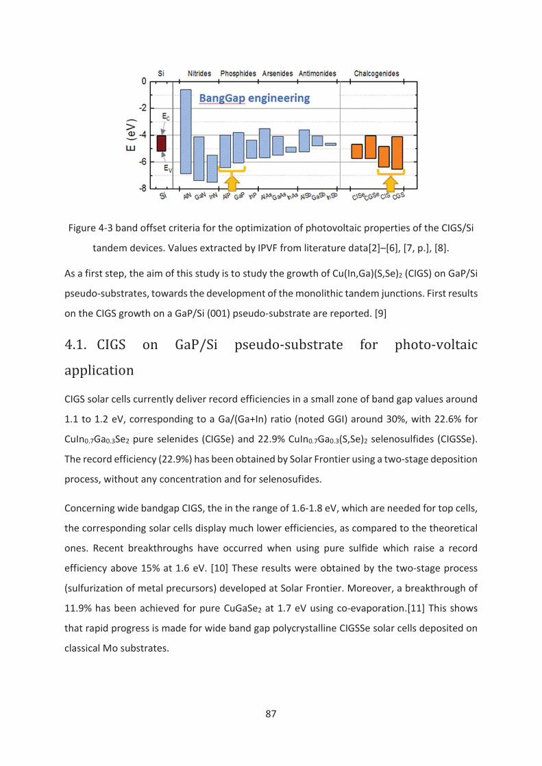
87
Figure 4-3 band offset criteria for the optimization of photovoltaic properties of the CIGS/Si
tandem devices. Values extracted by IPVF from literature data[2]–[6], [7, p.], [8].
As a first step, the aim of this study is to study the growth of Cu(In,Ga)(S,Se)2 (CIGS) on GaP/Si
pseudo-substrates, towards the development of the monolithic tandem junctions. First results
on the CIGS growth on a GaP/Si (001) pseudo-substrate are reported. [9]
4.1. CIGS! on! GaP/Si! pseudo-substrate! for! photo-voltaic!
application!
CIGS solar cells currently deliver record efficiencies in a small zone of band gap values around
1.1 to 1.2 eV, corresponding to a Ga/(Ga+In) ratio (noted GGI) around 30%, with 22.6% for
CuIn0.7Ga0.3Se2 pure selenides (CIGSe) and 22.9% CuIn0.7Ga0.3(S,Se)2 selenosulfides (CIGSSe).
The record efficiency (22.9%) has been obtained by Solar Frontier using a two-stage deposition
process, without any concentration and for selenosufides.
Concerning wide bandgap CIGS, the in the range of 1.6-1.8 eV, which are needed for top cells,
the corresponding solar cells display much lower efficiencies, as compared to the theoretical
ones. Recent breakthroughs have occurred when using pure sulfide which raise a record
efficiency above 15% at 1.6 eV. [10] These results were obtained by the two-stage process
(sulfurization of metal precursors) developed at Solar Frontier. Moreover, a breakthrough of
11.9% has been achieved for pure CuGaSe2 at 1.7 eV using co-evaporation.[11] This shows
that rapid progress is made for wide band gap polycrystalline CIGSSe solar cells deposited on
classical Mo substrates.
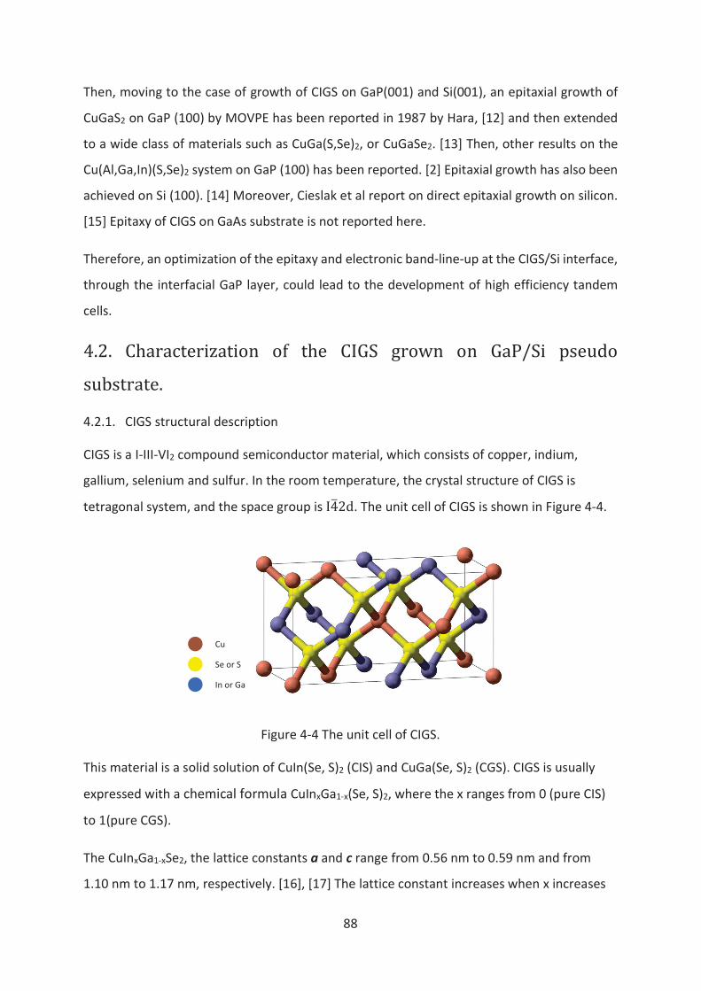
88
Then, moving to the case of growth of CIGS on GaP(001) and Si(001), an epitaxial growth of
CuGaS2 on GaP (100) by MOVPE has been reported in 1987 by Hara, [12] and then extended
to a wide class of materials such as CuGa(S,Se)2, or CuGaSe2. [13] Then, other results on the
Cu(Al,Ga,In)(S,Se)2 system on GaP (100) has been reported. [2] Epitaxial growth has also been
achieved on Si (100). [14] Moreover, Cieslak et al report on direct epitaxial growth on silicon.
[15] Epitaxy of CIGS on GaAs substrate is not reported here.
Therefore, an optimization of the epitaxy and electronic band-line-up at the CIGS/Si interface,
through the interfacial GaP layer, could lead to the development of high efficiency tandem
cells.
4.2. Characterization! of! the! CIGS! grown! on! GaP/Si! pseudo!
substrate.!
4.2.1. CIGS structural description
CIGS is a I-III-VI2 compound semiconductor material, which consists of copper, indium,
gallium, selenium and sulfur. In the room temperature, the crystal structure of CIGS is
tetragonal system, and the space group is ½Tà3d. The unit cell of CIGS is shown in Figure 4-4.
Figure 4-4 The unit cell of CIGS.
This material is a solid solution of CuIn(Se, S)2 (CIS) and CuGa(Se, S)2 (CGS). CIGS is usually
expressed with a chemical formula CuInxGa1-x(Se, S)2, where the x ranges from 0 (pure CIS)
to 1(pure CGS).
The CuInxGa1-xSe2, the lattice constants a and c range from 0.56 nm to 0.59 nm and from
1.10 nm to 1.17 nm, respectively. [16], [17] The lattice constant increases when x increases
Cu
Se or S
In or Ga
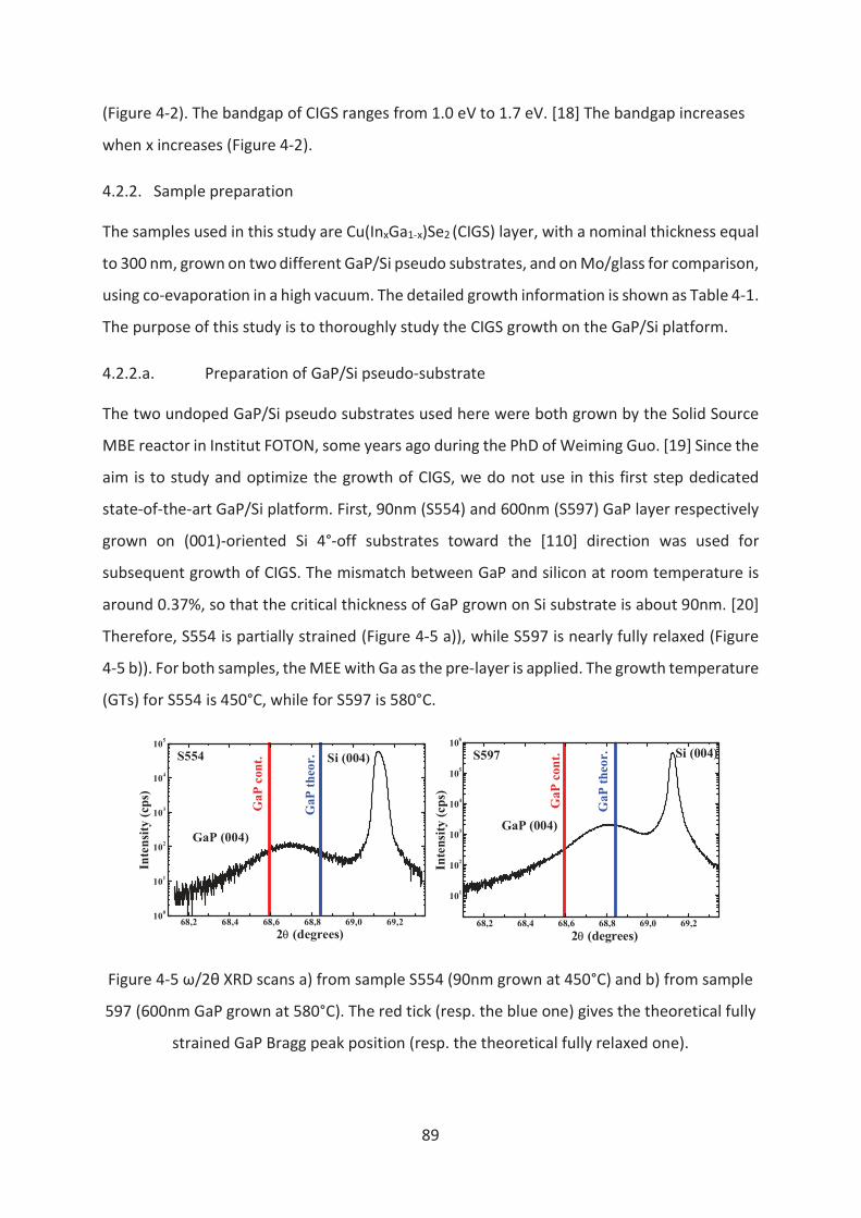
89
(Figure 4-2). The bandgap of CIGS ranges from 1.0 eV to 1.7 eV. [18] The bandgap increases
when x increases (Figure 4-2).
4.2.2. Sample preparation
The samples used in this study are Cu(InxGa1-x)Se2 (CIGS) layer, with a nominal thickness equal
to 300 nm, grown on two different GaP/Si pseudo substrates, and on Mo/glass for comparison,
using co-evaporation in a high vacuum. The detailed growth information is shown as Table 4-1.
The purpose of this study is to thoroughly study the CIGS growth on the GaP/Si platform.
4.2.2.a. Preparation of GaP/Si pseudo-substrate
The two undoped GaP/Si pseudo substrates used here were both grown by the Solid Source
MBE reactor in Institut FOTON, some years ago during the PhD of Weiming Guo. [19] Since the
aim is to study and optimize the growth of CIGS, we do not use in this first step dedicated
state-of-the-art GaP/Si platform. First, 90nm (S554) and 600nm (S597) GaP layer respectively
grown on (001)-oriented Si 4°-off substrates toward the [110] direction was used for
subsequent growth of CIGS. The mismatch between GaP and silicon at room temperature is
around 0.37%, so that the critical thickness of GaP grown on Si substrate is about 90nm. [20]
Therefore, S554 is partially strained (Figure 4-5 a)), while S597 is nearly fully relaxed (Figure
4-5 b)). For both samples, the MEE with Ga as the pre-layer is applied. The growth temperature
(GTs) for S554 is 450°C, while for S597 is 580°C.
68,2 68,4 68,6 68,8 69,0 69,210
0
101
102
103
104
105
Ga
P c
on
t.
GaP
th
eor.
GaP (004)
Si (004)S554
2q (degrees)
Inte
nsi
ty (
cps)
68,2 68,4 68,6 68,8 69,0 69,2
101
102
103
104
105
106
Ga
P c
on
t.
Ga
P t
heo
r.
GaP (004)
Si (004)S597
2q (degrees)
Inte
nsi
ty (
cp
s)
Figure 4-5 ω/2θ XRD scans a) from sample S554 (90nm grown at 450°C) and b) from sample
597 (600nm GaP grown at 580°C). The red tick (resp. the blue one) gives the theoretical fully
strained GaP Bragg peak position (resp. the theoretical fully relaxed one).
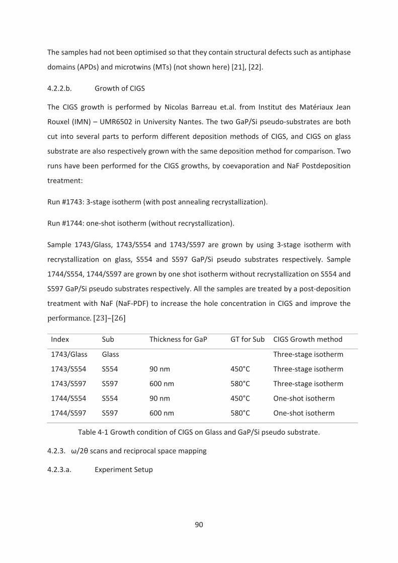
90
The samples had not been optimised so that they contain structural defects such as antiphase
domains (APDs) and microtwins (MTs) (not shown here) [21], [22].
4.2.2.b. Growth of CIGS
The CIGS growth is performed by Nicolas Barreau et.al. from Institut des Matériaux Jean
Rouxel (IMN) – UMR6502 in University Nantes. The two GaP/Si pseudo-substrates are both
cut into several parts to perform different deposition methods of CIGS, and CIGS on glass
substrate are also respectively grown with the same deposition method for comparison. Two
runs have been performed for the CIGS growths, by coevaporation and NaF Postdeposition
treatment:
Run #1743: 3-stage isotherm (with post annealing recrystallization).
Run #1744: one-shot isotherm (without recrystallization).
Sample 1743/Glass, 1743/S554 and 1743/S597 are grown by using 3-stage isotherm with
recrystallization on glass, S554 and S597 GaP/Si pseudo substrates respectively. Sample
1744/S554, 1744/S597 are grown by one shot isotherm without recrystallization on S554 and
S597 GaP/Si pseudo substrates respectively. All the samples are treated by a post-deposition
treatment with NaF (NaF-PDF) to increase the hole concentration in CIGS and improve the
performance.![23]�[26]
Index Sub Thickness for GaP GT for Sub CIGS Growth method
1743/Glass Glass
Three-stage isotherm
1743/S554 S554 90 nm 450°C Three-stage isotherm
1743/S597 S597 600 nm 580°C Three-stage isotherm
1744/S554 S554 90 nm 450°C One-shot isotherm
1744/S597 S597 600 nm 580°C One-shot isotherm
Table 4-1 Growth condition of CIGS on Glass and GaP/Si pseudo substrate.
4.2.3. ω/2θ scans and reciprocal space mapping
4.2.3.a. Experiment Setup
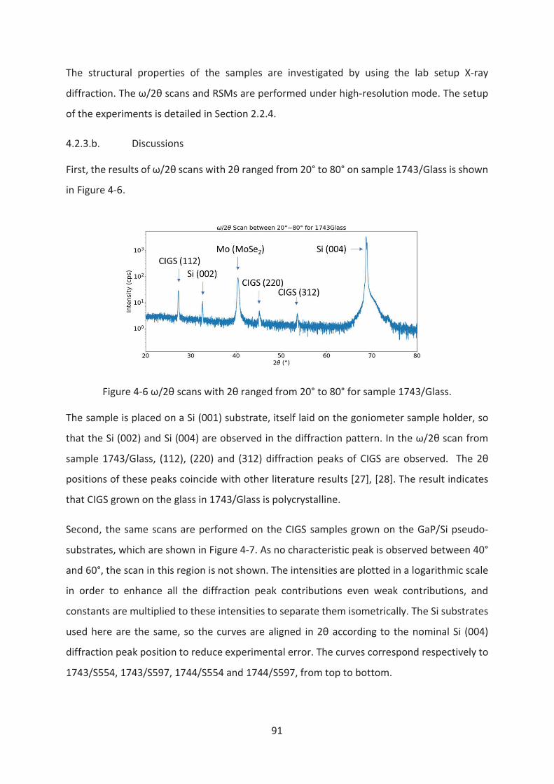
91
The structural properties of the samples are investigated by using the lab setup X-ray
diffraction. The ω/2θ scans and RSMs are performed under high-resolution mode. The setup
of the experiments is detailed in Section 2.2.4.
4.2.3.b. Discussions
First, the results of ω/2θ scans with 2θ ranged from 20° to 80° on sample 1743/Glass is shown
in Figure 4-6.
Figure 4-6 ω/2θ scans with 2θ ranged from 20° to 80° for sample 1743/Glass.
The sample is placed on a Si (001) substrate, itself laid on the goniometer sample holder, so
that the Si (002) and Si (004) are observed in the diffraction pattern. In the ω/2θ scan from
sample 1743/Glass, (112), (220) and (312) diffraction peaks of CIGS are observed. The 2θ
positions of these peaks coincide with other literature results [27], [28]. The result indicates
that CIGS grown on the glass in 1743/Glass is polycrystalline.
Second, the same scans are performed on the CIGS samples grown on the GaP/Si pseudo-
substrates, which are shown in Figure 4-7. As no characteristic peak is observed between 40°
and 60°, the scan in this region is not shown. The intensities are plotted in a logarithmic scale
in order to enhance all the diffraction peak contributions even weak contributions, and
constants are multiplied to these intensities to separate them isometrically. The Si substrates
used here are the same, so the curves are aligned in 2θ according to the nominal Si (004)
diffraction peak position to reduce experimental error. The curves correspond respectively to
1743/S554, 1743/S597, 1744/S554 and 1744/S597, from top to bottom.
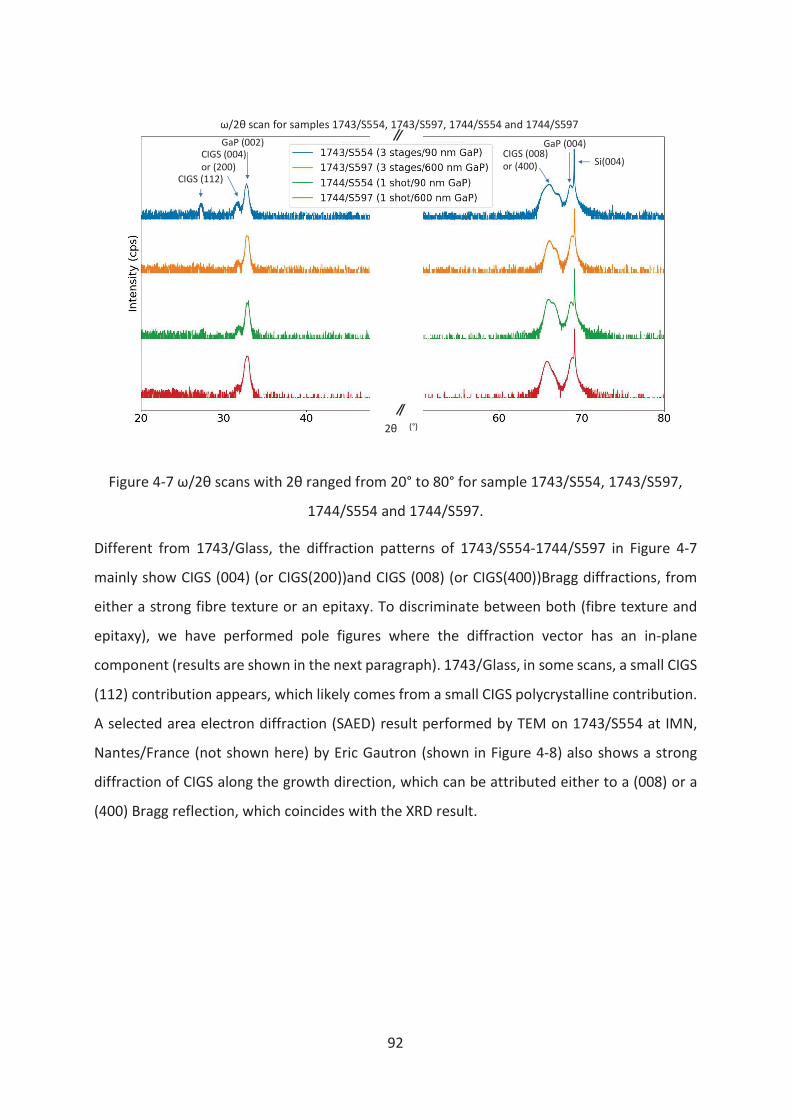
92
Figure 4-7 ω/2θ scans with 2θ ranged from 20° to 80° for sample 1743/S554, 1743/S597,
1744/S554 and 1744/S597.
Different from 1743/Glass, the diffraction patterns of 1743/S554-1744/S597 in Figure 4-7
mainly show CIGS (004) (or CIGS(200))and CIGS (008) (or CIGS(400))Bragg diffractions, from
either a strong fibre texture or an epitaxy. To discriminate between both (fibre texture and
epitaxy), we have performed pole figures where the diffraction vector has an in-plane
component (results are shown in the next paragraph). 1743/Glass, in some scans, a small CIGS
(112) contribution appears, which likely comes from a small CIGS polycrystalline contribution.
A selected area electron diffraction (SAED) result performed by TEM on 1743/S554 at IMN,
Nantes/France (not shown here) by Eric Gautron (shown in Figure 4-8) also shows a strong
diffraction of CIGS along the growth direction, which can be attributed either to a (008) or a
(400) Bragg reflection, which coincides with the XRD result.
2θ
CIGS (112)
CIGS (004) or (200)
GaP (002)CIGS (008) or (400)
GaP (004)
Si(004)
ω/2θ scan for samples 1743/S554, 1743/S597, 1744/S554 and 1744/S597
(°)
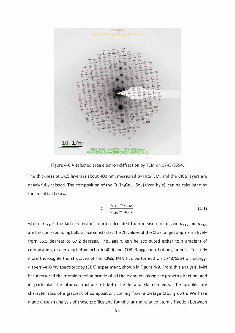
93
Figure 4-8 A selected area electron diffraction by TEM on 1743/S554.
The thickness of CIGS layers is about 400 nm, measured by HRSTEM, and the CIGS layers are
nearly fully relaxed. The composition of the Cu(InxGa1-x)Se2 (given by x) can be calculated by
the equation below:
æ = açèÕ $ aéÔêaéëê $ aéÔê ; (4-1)
where 6ìíî is the lattice constant a or c calculated from measurement, and 6�ïð and 6��ð
are the corresponding bulk lattice constants. The 2θ values of the CIGS ranges approximatively
from 65.5 degrees to 67.2 degrees. This, again, can be attributed either to a gradient of
composition, or a mixing between both (400) and (008) Bragg contributions, or both. To study
more thoroughly the structure of the CIGS, IMN has performed on 1743/S554 an Energy-
dispersive X-ray spectroscopy (EDX) experiment, shown in Figure 4-9. From this analysis, IMN
has measured the atomic fraction profile of all the elements along the growth direction, and
in particular the atomic fractions of both the In and Ga elements. The profiles are
characteristics of a gradient of composition, coming from a 3-stage CIGS growth. We have
made a rough analysis of these profiles and found that the relative atomic fraction between
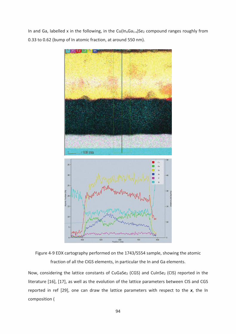
94
In and Ga, labelled x in the following, in the Cu(InxGa1-x)Se2 compound ranges roughly from
0.33 to 0.62 (bump of In atomic fraction, at around 550 nm).
Figure 4-9 EDX cartography performed on the 1743/S554 sample, showing the atomic
fraction of all the CIGS elements, in particular the In and Ga elements.
Now, considering the lattice constants of CuGaSe2 (CGS) and CuInSe2 (CIS) reported in the
literature [16], [17], as well as the evolution of the lattice parameters between CIS and CGS
reported in ref [29], one can draw the lattice parameters with respect to the x, the In
composition (
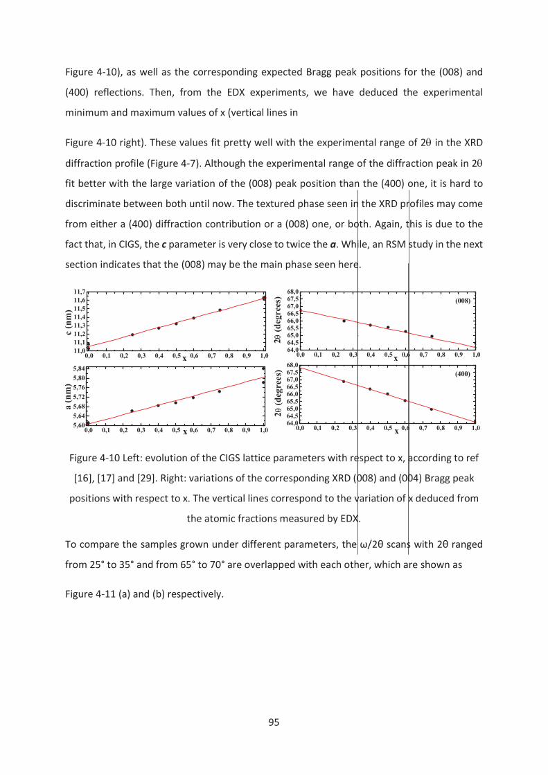
95
Figure 4-10), as well as the corresponding expected Bragg peak positions for the (008) and
(400) reflections. Then, from the EDX experiments, we have deduced the experimental
minimum and maximum values of x (vertical lines in
Figure 4-10 right). These values fit pretty well with the experimental range of 2q in the XRD
diffraction profile (Figure 4-7). Although the experimental range of the diffraction peak in 2q
fit better with the large variation of the (008) peak position than the (400) one, it is hard to
discriminate between both until now. The textured phase seen in the XRD profiles may come
from either a (400) diffraction contribution or a (008) one, or both. Again, this is due to the
fact that, in CIGS, the c parameter is very close to twice the a. While, an RSM study in the next
section indicates that the (008) may be the main phase seen here.
Figure 4-10 Left: evolution of the CIGS lattice parameters with respect to x, according to ref
[16], [17] and [29]. Right: variations of the corresponding XRD (008) and (004) Bragg peak
positions with respect to x. The vertical lines correspond to the variation of x deduced from
the atomic fractions measured by EDX.
To compare the samples grown under different parameters, the ω/2θ scans with 2θ ranged
from 25° to 35° and from 65° to 70° are overlapped with each other, which are shown as
Figure 4-11 (a) and (b) respectively.
0,0 0,1 0,2 0,3 0,4 0,5 0,6 0,7 0,8 0,9 1,011,0
11,1
11,2
11,3
11,4
11,5
11,6
11,7
x
c (
nm
)
0,0 0,1 0,2 0,3 0,4 0,5 0,6 0,7 0,8 0,9 1,05,60
5,64
5,68
5,72
5,76
5,80
5,84
x
a (
nm
)
0,0 0,1 0,2 0,3 0,4 0,5 0,6 0,7 0,8 0,9 1,064,064,565,065,566,066,567,067,568,0
(008)
x
2q (
degrees)
0,0 0,1 0,2 0,3 0,4 0,5 0,6 0,7 0,8 0,9 1,064,064,565,065,566,066,5
67,067,568,0
(400)
x
2q (
deg
ree
s)
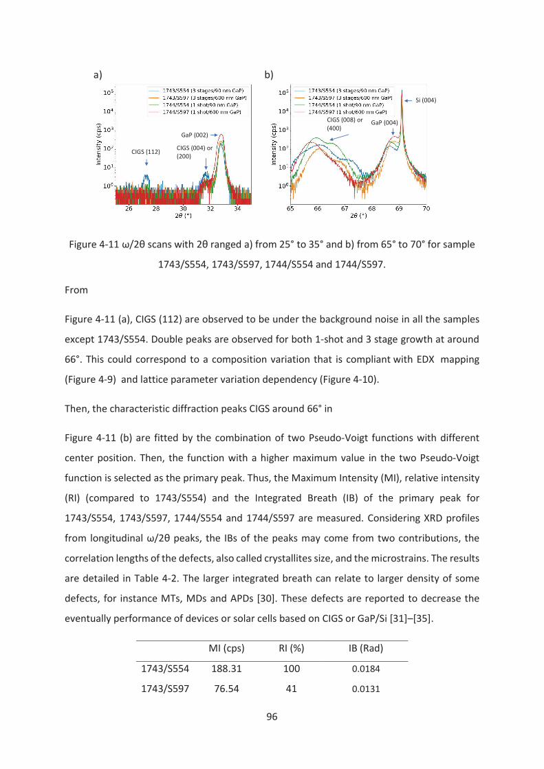
96
Figure 4-11 ω/2θ scans with 2θ ranged a) from 25° to 35° and b) from 65° to 70° for sample
1743/S554, 1743/S597, 1744/S554 and 1744/S597.
From
Figure 4-11 (a), CIGS (112) are observed to be under the background noise in all the samples
except 1743/S554. Double peaks are observed for both 1-shot and 3 stage growth at around
66°. This could correspond to a composition variation that is compliant with EDX mapping
(Figure 4-9) and lattice parameter variation dependency (Figure 4-10).
Then, the characteristic diffraction peaks CIGS around 66° in
Figure 4-11 (b) are fitted by the combination of two Pseudo-Voigt functions with different
center position. Then, the function with a higher maximum value in the two Pseudo-Voigt
function is selected as the primary peak. Thus, the Maximum Intensity (MI), relative intensity
(RI) (compared to 1743/S554) and the Integrated Breath (IB) of the primary peak for
1743/S554, 1743/S597, 1744/S554 and 1744/S597 are measured. Considering XRD profiles
from longitudinal ω/2θ peaks, the IBs of the peaks may come from two contributions, the
correlation lengths of the defects, also called crystallites size, and the microstrains. The results
are detailed in Table 4-2. The larger integrated breath can relate to larger density of some
defects, for instance MTs, MDs and APDs [30]. These defects are reported to decrease the
eventually performance of devices or solar cells based on CIGS or GaP/Si [31]–[35].
MI (cps) RI (%) IB (Rad)
1743/S554 188.31 100 0.0184
1743/S597 76.54 41 0.0131
a) b)
CIGS (112)CIGS (004) or (200)
GaP (002)
GaP (004)CIGS (008) or (400)
Si (004)
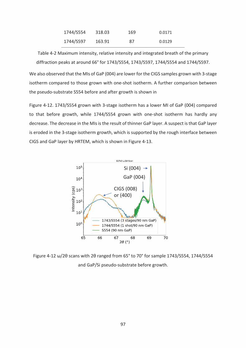
97
1744/S554 318.03 169 0.0171
1744/S597 163.91 87 0.0129
Table 4-2 Maximum intensity, relative intensity and integrated breath of the primary
diffraction peaks at around 66° for 1743/S554, 1743/S597, 1744/S554 and 1744/S597.
We also observed that the MIs of GaP (004) are lower for the CIGS samples grown with 3-stage
isotherm compared to those grown with one-shot isotherm. A further comparison between
the pseudo-substrate S554 before and after growth is shown in
Figure 4-12. 1743/S554 grown with 3-stage isotherm has a lower MI of GaP (004) compared
to that before growth, while 1744/S554 grown with one-shot isotherm has hardly any
decrease. The decrease in the MIs is the result of thinner GaP layer. A suspect is that GaP layer
is eroded in the 3-stage isotherm growth, which is supported by the rough interface between
CIGS and GaP layer by HRTEM, which is shown in Figure 4-13.
Figure 4-12 ω/2θ scans with 2θ ranged from 65° to 70° for sample 1743/S554, 1744/S554
and GaP/Si pseudo-substrate before growth.
GaP (004)
CIGS (008) or (400)
Si (004)
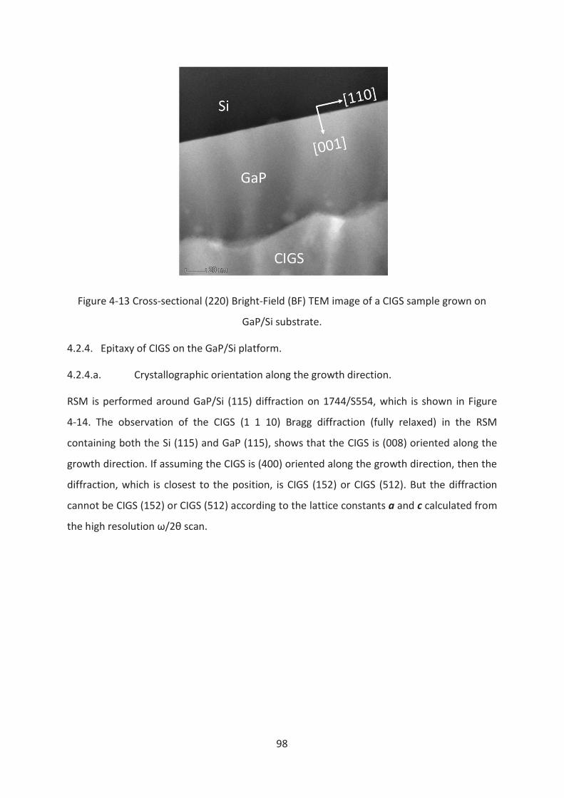
98
Figure 4-13 Cross-sectional (220) Bright-Field (BF) TEM image of a CIGS sample grown on
GaP/Si substrate.
4.2.4. Epitaxy of CIGS on the GaP/Si platform.
4.2.4.a. Crystallographic orientation along the growth direction.
RSM is performed around GaP/Si (115) diffraction on 1744/S554, which is shown in Figure
4-14. The observation of the CIGS (1 1 10) Bragg diffraction (fully relaxed) in the RSM
containing both the Si (115) and GaP (115), shows that the CIGS is (008) oriented along the
growth direction. If assuming the CIGS is (400) oriented along the growth direction, then the
diffraction, which is closest to the position, is CIGS (152) or CIGS (512). But the diffraction
cannot be CIGS (152) or CIGS (512) according to the lattice constants a and c calculated from
the high resolution ω/2θ scan.
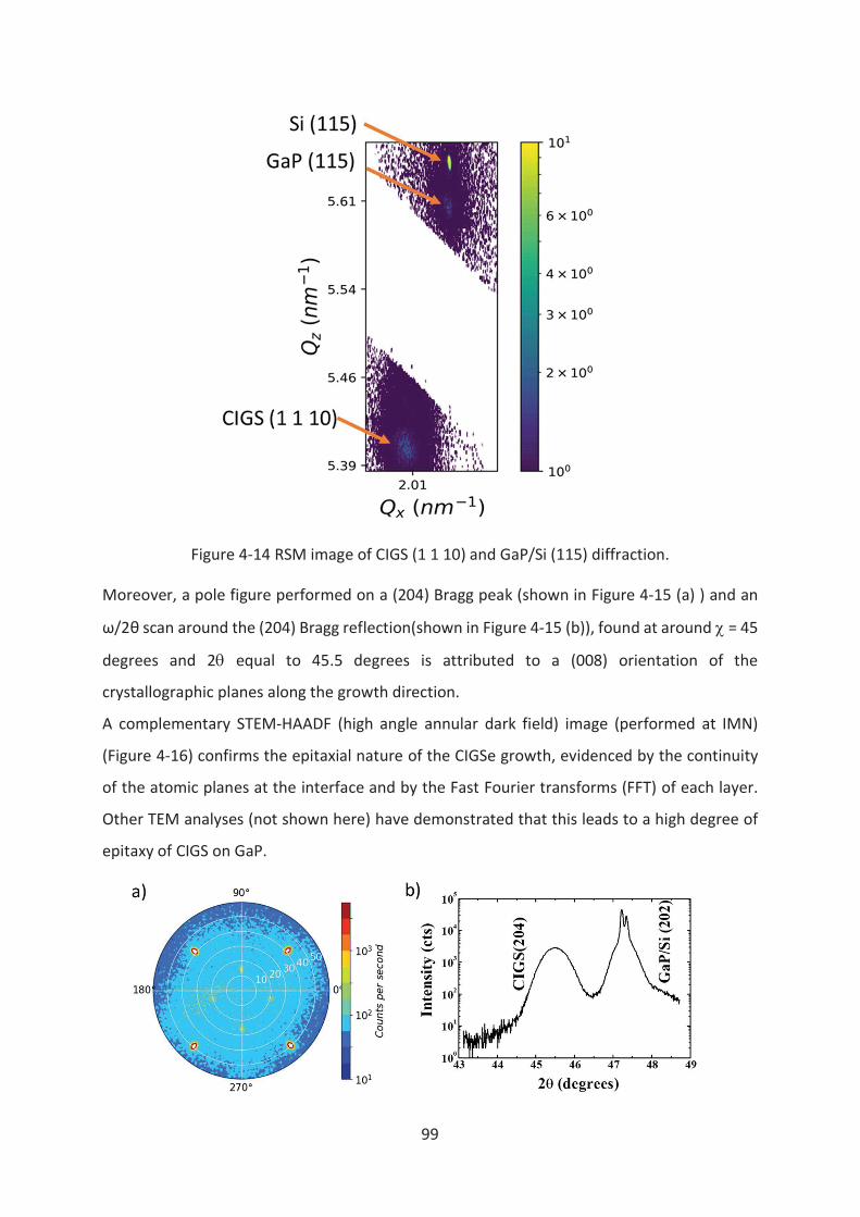
99
Figure 4-14 RSM image of CIGS (1 1 10) and GaP/Si (115) diffraction.
Moreover, a pole figure performed on a (204) Bragg peak (shown in Figure 4-15 (a) ) and an
ω/2θ scan around the (204) Bragg reflection(shown in Figure 4-15 (b)), found at around c = 45
degrees and 2q equal to 45.5 degrees is attributed to a (008) orientation of the
crystallographic planes along the growth direction.
A complementary STEM-HAADF (high angle annular dark field) image (performed at IMN)
(Figure 4-16) confirms the epitaxial nature of the CIGSe growth, evidenced by the continuity
of the atomic planes at the interface and by the Fast Fourier transforms (FFT) of each layer.
Other TEM analyses (not shown here) have demonstrated that this leads to a high degree of
epitaxy of CIGS on GaP.
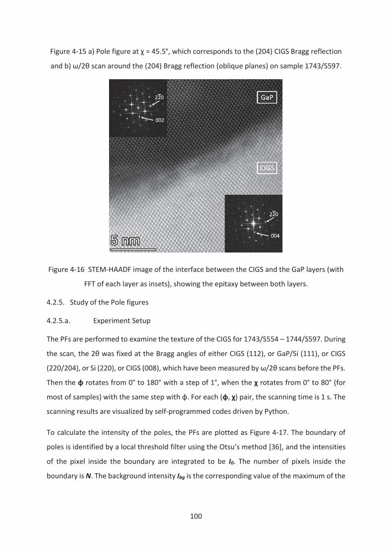
100
Figure 4-15 a) Pole figure at χ = 45.5°, which corresponds to the (204) CIGS Bragg reflection
and b) ω/2θ scan around the (204) Bragg reflection (oblique planes) on sample 1743/S597.
Figure 4-16 STEM-HAADF image of the interface between the CIGS and the GaP layers (with
FFT of each layer as insets), showing the epitaxy between both layers.
4.2.5. Study of the Pole figures
4.2.5.a. Experiment Setup
The PFs are performed to examine the texture of the CIGS for 1743/S554 – 1744/S597. During
the scan, the 2θ was fixed at the Bragg angles of either CIGS (112), or GaP/Si (111), or CIGS
(220/204), or Si (220), or CIGS (008), which have been measured by ω/2θ scans before the PFs.
Then the φ rotates from 0° to 180° with a step of 1°, when the χ rotates from 0° to 80° (for
most of samples) with the same step with φ. For each (φ, χ) pair, the scanning time is 1 s. The
scanning results are visualized by self-programmed codes driven by Python.
To calculate the intensity of the poles, the PFs are plotted as Figure 4-17. The boundary of
poles is identified by a local threshold filter using the Otsu’s method [36], and the intensities
of the pixel inside the boundary are integrated to be I0. The number of pixels inside the
boundary is N. The background intensity Ibg is the corresponding value of the maximum of the
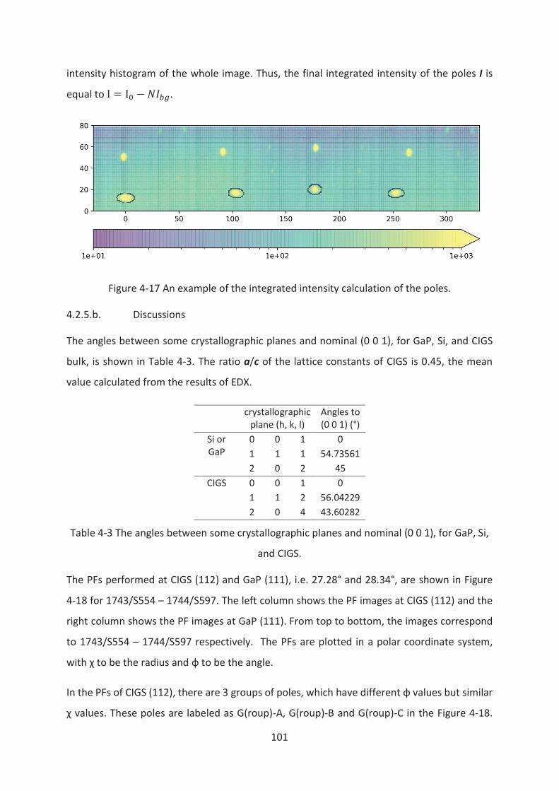
101
intensity histogram of the whole image. Thus, the final integrated intensity of the poles I is
equal to ½ = ½¾ $ ñò«ó.
Figure 4-17 An example of the integrated intensity calculation of the poles.
4.2.5.b. Discussions
The angles between some crystallographic planes and nominal (0 0 1), for GaP, Si, and CIGS
bulk, is shown in Table 4-3. The ratio a/c of the lattice constants of CIGS is 0.45, the mean
value calculated from the results of EDX.
crystallographic plane (h, k, l)
Angles to (0 0 1) (°)
Si or GaP
0 0 1 0
1 1 1 54.73561
2 0 2 45
CIGS 0 0 1 0
1 1 2 56.04229
2 0 4 43.60282
Table 4-3 The angles between some crystallographic planes and nominal (0 0 1), for GaP, Si,
and CIGS.
The PFs performed at CIGS (112) and GaP (111), i.e. 27.28° and 28.34°, are shown in Figure
4-18 for 1743/S554 – 1744/S597. The left column shows the PF images at CIGS (112) and the
right column shows the PF images at GaP (111). From top to bottom, the images correspond
to 1743/S554 – 1744/S597 respectively. The PFs are plotted in a polar coordinate system,
with χ to be the radius and φ to be the angle.
In the PFs of CIGS (112), there are 3 groups of poles, which have different φ values but similar
χ values. These poles are labeled as G(roup)-A, G(roup)-B and G(roup)-C in the Figure 4-18.
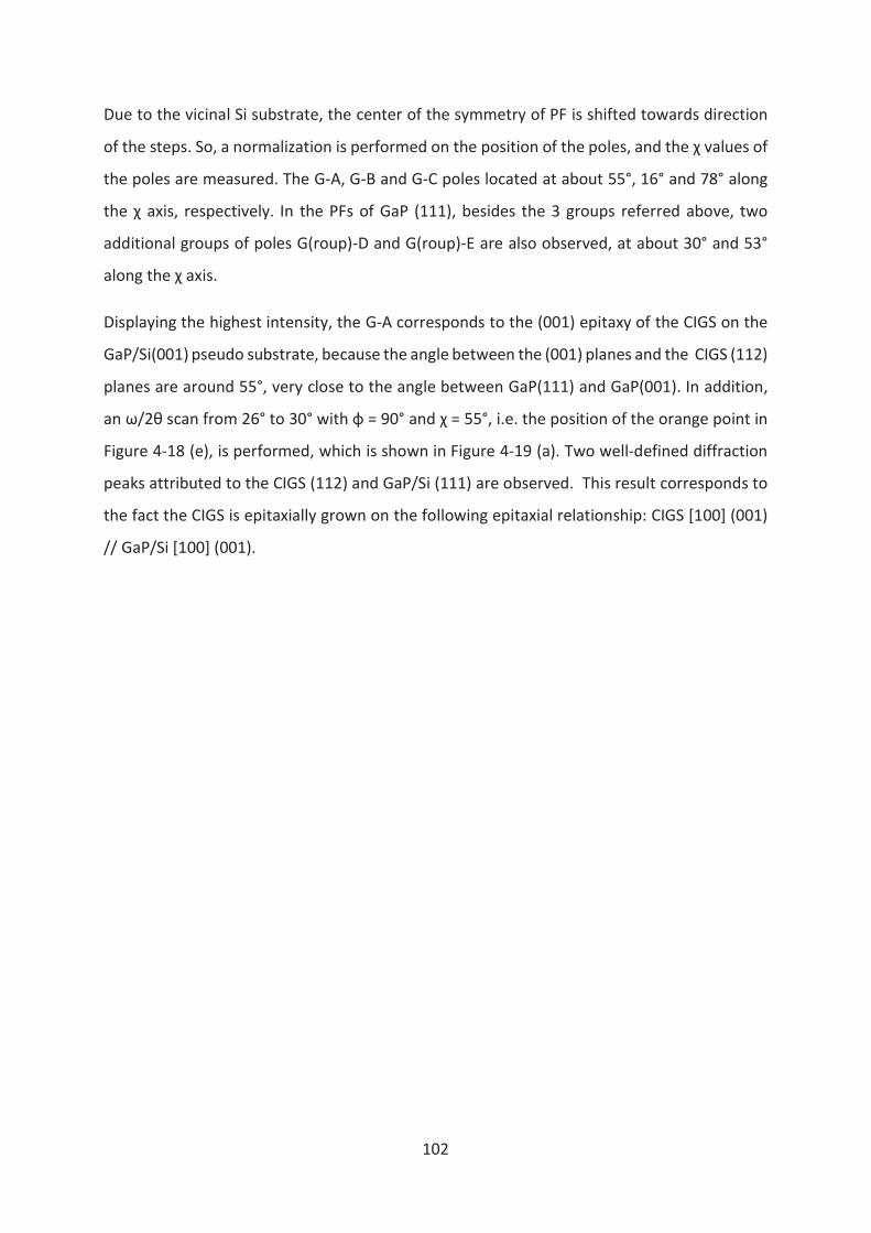
102
Due to the vicinal Si substrate, the center of the symmetry of PF is shifted towards direction
of the steps. So, a normalization is performed on the position of the poles, and the χ values of
the poles are measured. The G-A, G-B and G-C poles located at about 55°, 16° and 78° along
the χ axis, respectively. In the PFs of GaP (111), besides the 3 groups referred above, two
additional groups of poles G(roup)-D and G(roup)-E are also observed, at about 30° and 53°
along the χ axis.
Displaying the highest intensity, the G-A corresponds to the (001) epitaxy of the CIGS on the
GaP/Si(001) pseudo substrate, because the angle between the (001) planes and the CIGS (112)
planes are around 55°, very close to the angle between GaP(111) and GaP(001). In addition,
an ω/2θ scan from 26° to 30° with φ = 90° and χ = 55°, i.e. the position of the orange point in
Figure 4-18 (e), is performed, which is shown in Figure 4-19 (a). Two well-defined diffraction
peaks attributed to the CIGS (112) and GaP/Si (111) are observed. This result corresponds to
the fact the CIGS is epitaxially grown on the following epitaxial relationship: CIGS [100] (001)
// GaP/Si [100] (001).
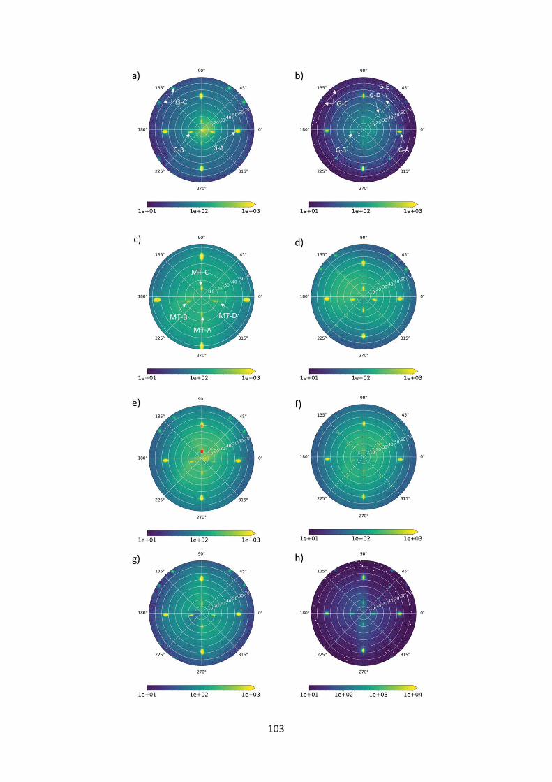
103
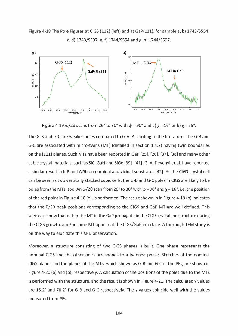
104
Figure 4-18 The Pole Figures at CIGS (112) (left) and at GaP(111), for sample a, b) 1743/S554,
c, d) 1743/S597, e, f) 1744/S554 and g, h) 1744/S597.
Figure 4-19 ω/2θ scans from 26° to 30° with φ = 90° and a) χ = 16° or b) χ = 55°.
The G-B and G-C are weaker poles compared to G-A. According to the literature, The G-B and
G-C are associated with micro-twins (MT) (detailed in section 1.4.2) having twin boundaries
on the {111} planes. Such MTs have been reported in GaP [25], [26], [37], [38] and many other
cubic crystal materials, such as SiC, GaN and SiGe [39]–[41]. G. A. Devenyi et.al. have reported
a similar result in InP and AlSb on nominal and vicinal substrates [42]. As the CIGS crystal cell
can be seen as two vertically stacked cubic cells, the G-B and G-C poles in CIGS are likely to be
poles from the MTs, too. An ω/2θ scan from 26° to 30° with φ = 90° and χ = 16°, i.e. the position
of the red point in Figure 4-18 (e), is performed. The result shown in in Figure 4-19 (b) indicates
that the q/2q peak positions corresponding to the CIGS and GaP MT are well-defined. This
seems to show that either the MT in the GaP propagate in the CIGS crystalline structure during
the CIGS growth, and/or some MT appear at the CIGS/GaP interface. A thorough TEM study is
on the way to elucidate this XRD observation.
Moreover, a structure consisting of two CIGS phases is built. One phase represents the
nominal CIGS and the other one corresponds to a twinned phase. Sketches of the nominal
CIGS planes and the planes of the MTs, which shown as G-B and G-C in the PFs, are shown in
Figure 4-20 (a) and (b), respectively. A calculation of the positions of the poles due to the MTs
is performed with the structure, and the result is shown in Figure 4-21. The calculated χ values
are 15.2° and 78.2° for G-B and G-C respectively. The χ values coincide well with the values
measured from PFs.
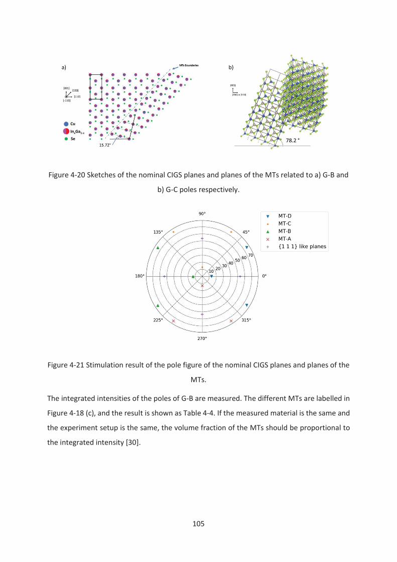
105
Figure 4-20 Sketches of the nominal CIGS planes and planes of the MTs related to a) G-B and
b) G-C poles respectively.
Figure 4-21 Stimulation result of the pole figure of the nominal CIGS planes and planes of the
MTs.
The integrated intensities of the poles of G-B are measured. The different MTs are labelled in
Figure 4-18 (c), and the result is shown as Table 4-4. If the measured material is the same and
the experiment setup is the same, the volume fraction of the MTs should be proportional to
the integrated intensity [30].
106
MT-A MT-B MT-C MT-D
1743/S554 62650 12396 77992 12248
1743/S597 19196 19650 40798 18442
1744/S554 68042 42318 112508 67684
1744/S597 25670 33294 48080 16512
Table 4-4 The Integrated intensities of the poles of G-B.
The G-D and G-E are weakest poles in the five groups of poles and have never been observed
in GaP/Si pseudo-substrate in our lab or reported in literature as I know. A possible
explanation is that an inter-layer is formed between GaP and CIGS, and [100] of the inter-layer
is parallel to [110] of the [110] of the nominal GaP.
4.3. First!try!of!CIGSe!solar!cell!on!the!GaP/Si!(001)!platform!
A 300 nm-thick CIGSe is grown on S553, a 90 nm-thick non-optimised undoped GaP/Si(001),
using one-shot isotherm, which is shown in Figure 4-22. Then, the CdS, ZnMgO and Al doped
ZnO (AZO) layers are grown in sequence on top of CIGSe to form a solar cell. A top-top
electrical contact is applied due to the undoped GaP/Si pseudo-substrate. The external
quantum efficiency (EQE) has been measured for the solar cell (black line) and then compared
with a PV cell for CIGS grown on glass substrates with the same growth conditions (red line),
which is also shown in Figure 4-22. The CIGS solar cell grown on GaP/Si shows only slightly
lower EQE than the one grown on glass, in the whole working spectrum. Therefore, the
External Quantum Efficiency (EQE) is encouraging, considering that the solar cell structure is
far from being optimized, so far. A JSC of 14.5 mA/cm² has been deduced from this EQE.
However, the L-I_V curve (I-V curve under AM1.5 illumination) displays a characteristic
showing large series and shunt resistances. Moreover, the I-V characteristic displays a
behavior which seems to be due to two diodes in series. Therefore, the solar cell needs to be
optimized and a top-bottom cell, that is grown on a doped GaP/Si substrate, will be developed
soon. However, the result opens promising perspectives for future layer grown on optimized
GaP/Si pseudo-substrates.
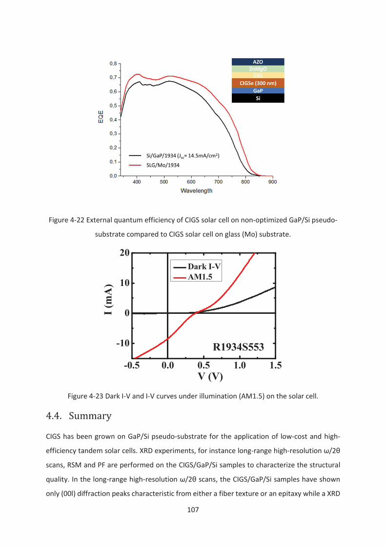
107
Figure 4-22 External quantum efficiency of CIGS solar cell on non-optimized GaP/Si pseudo-
substrate compared to CIGS solar cell on glass (Mo) substrate.
-0.5 0.0 0.5 1.0 1.5
-10
0
10
20
I (m
A)
V (V)
Dark I-V
AM1.5
R1934S553
Figure 4-23 Dark I-V and I-V curves under illumination (AM1.5) on the solar cell.
4.4. Summary!
CIGS has been grown on GaP/Si pseudo-substrate for the application of low-cost and high-
efficiency tandem solar cells. XRD experiments, for instance long-range high-resolution ω/2θ
scans, RSM and PF are performed on the CIGS/GaP/Si samples to characterize the structural
quality. In the long-range high-resolution ω/2θ scans, the CIGS/GaP/Si samples have shown
only (00l) diffraction peaks characteristic from either a fiber texture or an epitaxy while a XRD

108
pattern characteristic from a polycrystal has been measured on the CIGS/Glass samples. In the
RSM, the (1 1 10) diffraction of CIGS is observed. In the PFs, a (112) diffraction of CIGS besides
the GaP (111) is also observed and confirmed by the transverse scans. Combining the result
of TEM with XRD, we have shown that the CIGS growth on the GaP/Si platform leads to a quasi-
monocrystalline CIGSe monolayer, as expected. We also observed a few evidences which
shown that, depending on the CIGS growth condition, the interface between GaP and CIGS
can be damaged. But these results are still too few to conclude the influence of the grown
mode or the substrate on the final structural quality. In addition, the MTs in CIGS layer is
observed in PFs and a possible formation mechanics is also discussed. At last, the EQE of a
CIGSe solar cell on the GaP/Si (001) is measured and compared to a CIGS PV cell grown on
glass substrate, which shows the promising future of the CIGS/GaP/Si tandem solar cell.
109
References
[1] J. F. Geisz and D. J. Friedman, “III N V semiconductors for solar photovoltaic applications,”
Semicond. Sci. Technol., vol. 17, no. 8, pp. 769–777, Aug. 2002.
[2] S. Chichibu, Y. Harada, M. Sugiyama, and H. Nakanishi, “Metalorganic vapor phase epitaxy
of Cu(AlxGa1−x)(SySe1−y)2 chalcopyrite semiconductors and their band offsets,” J. Phys.
Chem. Solids, vol. 64, no. 9–10, pp. 1481–1489, Sep. 2003.
[3] S. Wei and A. Zunger, Band offsets and optical bowings of chalcopyrites and Zn-based
II-VI alloys, J. Appl. Phys., vol. 78, no. 6, pp. 3846 3856, Sep. 1995.
[4] R. Hunger, C. Pettenkofer, and R. Scheer, “Surface properties of (111), (001), and (110)-
oriented epitaxial CuInS2/Si films,” Surf. Sci., vol. 477, no. 1, pp. 76–93, Apr. 2001.
[5] M. Turcu, I. M. Kötschau, and U. Rau, “Composition dependence of defect energies and
band alignments in the Cu(In1−xGax)(Se1−ySy)2 alloy system,” J. Appl. Phys., vol. 91, no. 3,
pp. 1391–1399, Feb. 2002.
[6] M. Turcu and U. Rau, “Compositional trends of defect energies, band alignments, and
recombination mechanisms in the Cu(In,Ga)(Se,S)2 alloy system,” Thin Solid Films, vol.
431–432, pp. 158–162, May 2003.
[7] S. Siebentritt and U. Rau, Eds., Wide-gap chalcopyrites. Berlin: Springer, 2006.
[8] Ioffe Physico Chemical Institute, “Semiconductors on NSM.” .
[9] D. Lincot et al., “Exploring New Convergences between PV Technologies for High Efficiency
Tandem Solar Cells: Wide Band Gap Epitaxial CIGS Top Cells on Silicon Bottom Cells with
III-V Intermediate Layers,” in 35th European Photovoltaic Solar Energy Conference and
Exhibition, 2018, pp. 23–28.
[10] H. Hiroi, Y. Iwata, H. Sugimoto, and A. Yamada, “Progress Toward 1000-mV Open-
Circuit Voltage on Chalcopyrite Solar Cells,” IEEE J. Photovolt., vol. 6, no. 6, pp. 1630–1634,
Nov. 2016.
[11] F. Larsson et al., “Record 1.0 V open-circuit voltage in wide band gap chalcopyrite solar
cells,” Prog. Photovolt. Res. Appl., vol. 25, no. 9, pp. 755–763, Sep. 2017.
[12] K. Hara, T. Kojima, and H. Kukimoto, “Epitaxial Growth of CuGaS2 by Metalorganic
Chemical Vapor Deposition,” Jpn. J. Appl. Phys., vol. 26, no. Part 2, No. 7, pp. L1107–L1109,
Jul. 1987.
110
[13] K. Hara, T. Shinozawa, J. Yoshino, and H. Kukimoto, “MOVPE growth and
characterization of I-III-VI2 Chalcopyrite compounds,” J. Cryst. Growth, vol. 93, no. 1–4,
pp. 771–775, 1988.
[14] K. Oishi, H. Katagiri, S. Kobayashi, and N. Tsuboi, “Growth of Cu(In,Ga)S2 on Si(100)
substrates by multisource evaporation,” J. Phys. Chem. Solids, vol. 64, no. 9–10, pp. 1835–
1838, Sep. 2003.
[15] J. Cieslak et al., “Epitaxial CuIn1−xGaxS2on Si(111) ( 0 ô x ô 1 ) : Lattice match and
metastability,” Phys. Rev. B, vol. 75, no. 24, Jun. 2007.
[16] C. Rincón and F. Ramírez, “Lattice vibrations of CuInSe2 and CuGaSe2 by Raman
microspectrometry,” J Appl Phys, vol. 72, no. 9, pp. 4321–4324, 1992.
[17] M. L. Fearheiley, K. J. Bachmann, Y.-H. Shing, S. A. Vasquez, and C. R. Herrington, “The
lattice constants of CuInSe2,” J. Electron. Mater., vol. 14, no. 6, pp. 677–683, Nov. 1985.
[18] T. Tinoco, C. Rincón, M. Quintero, and G. S. Pérez, “Phase Diagram and Optical Energy
Gaps for CuInyGa1−ySe2 Alloys,” Phys. Status Solidi A, vol. 124, no. 2, pp. 427–434, Apr.
1991.
[19] G. Weiming, “Heterogeous MBE growth of GaP on silicon substrate and nanostructure
for photonics application Epitaxie,” Ph.D., INSA Rennes, Rennes, 2010.
[20] T. Soga, T. Jimbo, and M. Umeno, “Dislocation generation mechanisms for GaP on Si
grown by metalorganic chemical vapor deposition,” Appl. Phys. Lett., vol. 63, no. 18, pp.
2543–2545, Nov. 1993.
[21] P. Y. Wang et al., “Quantitative evaluation of microtwins and antiphase defects in
GaP/Si nanolayers for a III–V photonics platform on silicon using a laboratory X-ray
diffraction setup,” J. Appl. Crystallogr., vol. 48, no. 3, pp. 702–710, 2015.
[22] P. Y. Wang et al., “Abrupt GaP/Si hetero-interface using bistepped Si buffer,” Appl. Phys.
Lett., vol. 107, no. 19, p. 191603, 2015.
[23] P. Reinhard et al., “Features of KF and NaF Postdeposition Treatments of Cu(In,Ga)Se2
Absorbers for High Efficiency Thin Film Solar Cells,” Chem. Mater., vol. 27, no. 16, pp.
5755–5764, 2015.
[24] F. Pianezzi et al., “Unveiling the effects of post-deposition treatment with different
alkaline elements on the electronic properties of CIGS thin film solar cells,” Phys. Chem.
Chem. Phys., vol. 16, no. 19, pp. 8843–8851, 2014.
111
[25] B. Bissig et al., “Effects of NaF evaporation during low temperature Cu (In, Ga) Se2
growth,” Thin Solid Films, vol. 582, p. 56, 2015.
[26] E. Handick et al., “NaF/KF post-deposition treatments and their influence on the
structure of Cu (In, Ga) Se 2 absorber surfaces,” presented at the Proc. of IEE 44th
Photovoltaic Specialist Conference, 2016, pp. 0017–0021.
[27] M. G. Panthani et al., “Synthesis of CuInS2, CuInSe2, and Cu(InxGa1-x)Se2 (CIGS)
Nanocrystal ‘Inks’ for Printable Photovoltaics,” J. Am. Chem. Soc., vol. 130, no. 49, pp.
16770–16777, 2008.
[28] D. Fraga, E. Barrachina, I. Calvet, T. Stoyanova, and J. B. Carda, “Developing CIGS solar
cells on glass-ceramic substrates,” Mater. Lett., vol. 221, pp. 104–106, 2018.
[29] D. K. Suri, K. C. Nagpal, and G. K. Chadha, “X-ray study of CuGaxIn1−xSe2 solid solutions,”
J. Appl. Crystallogr., vol. 22, no. 6, pp. 578–583, Dec. 1989.
[30] B. E. Warren, X-ray diffraction, Dover edition, Unabridged and Corrected republication
of the work originally published in 1969 by Addison-Wesley Publishing Company. New
York: Dover Publications, Inc, 1990.
[31] C. J. Gibbings, D. L. Murrell, D. M. Cooper, and P. C. Spurdens, “Impact of GaInP growth
by MOVPE on laser performance,” in IEEE Colloquium on III-V Compound Semiconductor
Materials Growth, 1992, pp. 5/1-5/4.
[32] T. Nakada, K. Furumi, and A. Kunioka, “High-efficiency cadmium-free Cu(In,Ga)Se/sub
2/ thin-film solar cells with chemically deposited ZnS buffer layers,” IEEE Trans. Electron
Devices, vol. 46, no. 10, pp. 2093–2097, Oct. 1999.
[33] C. L. Andre et al., “Impact of dislocations on minority carrier electron and hole lifetimes
in GaAs grown on metamorphic SiGe substrates,” Appl. Phys. Lett., vol. 84, no. 18, pp.
3447–3449, May 2004.
[34] A. Beyer, I. Németh, S. Liebich, J. Ohlmann, W. Stolz, and K. Volz, “Influence of crystal
polarity on crystal defects in GaP grown on exact Si (001),” J. Appl. Phys., vol. 109, no. 8,
p. 083529, 2011.
[35] C. Heidelberger and E. A. Fitzgerald, “GaAsP/InGaP HBTs grown epitaxially on Si
substrates: Effect of dislocation density on DC current gain,” J. Appl. Phys., vol. 123, no.
16, p. 161532, Apr. 2018.
[36] N. Otsu, “A Threshold Selection Method from Gray-Level Histograms,” IEEE Trans. Syst.
Man Cybern., vol. 9, no. 1, pp. 62–66, Jan. 1979.
112
[37] T. Nguyen Thanh et al., “Synchrotron X-ray diffraction analysis for quantitative defect
evaluation in GaP/Si nanolayers,” Thin Solid Films, vol. 541, pp. 36–40, Aug. 2013.
[38] T. Grassman et al., “Control and elimination of nucleation-related defects in
GaP/Si(001) heteroepitaxy,” Appl. Phys. Lett., vol. 94, no. 23, p. 232106, 2009.
[39] X. H. Zheng et al., “Comprehensive analysis of microtwins in the 3C–SiC films on Si(001)
substrates,” J. Cryst. Growth, vol. 233, no. 1, pp. 40–44, Nov. 2001.
[40] K. Arimoto et al., “Crystalline morphologies of step-graded SiGe layers grown on exact
and vicinal (110) Si substrates,” J. Cryst. Growth, vol. 311, no. 3, pp. 809–813, Jan. 2009.
[41] B. Qu, X. H. Zheng, Y. T. Wang, S. M. Lin, H. Yang, and J. W. Liang, “Polarity dependence
of hexagonal inclusions and cubic twins in GaN/GaAs(001) epilayers measured by
conventional X-ray pole figure and grazing incident diffraction pole figure,” J. Cryst.
Growth, vol. 226, no. 1, pp. 57–61, Jun. 2001.
[42] G. Devenyi et al., “The role of vicinal silicon surfaces in the formation of epitaxial twins
during the growth of III-V thin films,” J. Appl. Phys., vol. 110, no. 12, p. 124316, 2011.
113
Chapitre 5. General conclusions and perspective work
5.1. !Summary!and!conclusions!
This thesis focuses on the structural analysis of the GaP/Si pseudo substrates and the application
of the pseudo substrate in the CIGS/GaP/Si tandem solar cell. The final purpose is the growth
of high-quality GaP/Si pseudo substrate, which have a low defect density and homogenous
distribution of defects. The main work in the thesis can be divided into two part:
In the first part, an advanced sub-micrometer-beam X-ray scattering, quicK continuous
Mapping, have been employed for a local structure characterization of the GaP epitaxy layer
on Si substrate. The diffraction pattern received by the 2D sensors is processed with a program
called XSOCS into a multi-dimension dataset which consist of 2D location information from
the real space, 3D structural information from the reciprocal space and the diffraction beam
intensity. The result, along with general structure measurements by XRD, surface roughness
measurements by AFM and local evidence of dislocations by TEM, have allowed understanding
the effect of the 60° dislocations (misfit dislocations) on the relaxation process and the final
surface roughness of the epitaxial layer.
60° dislocations seem to be the main mechanism in the strain relief process of GaP/Si pseudo
substrate, along with the experimental results and the literature. The distribution of the 60°
dislocations is also observed to be not homogenous, which tends to form bunches. The cross-
hatch pattern at the GaP/Si interface is also believed to influence the free surface roughness, as
demonstrated by a strong correlation between the K-Map strain mapping and the surface
roughness mapping measured by AFM. An assumption on the local tilt, which may be
introduced by the dislocation bunches, is also proposed after a further analysis on the K-map
result.
In the second part, CIGS grown on GaP/Si pseudo-substrate for photovoltaic application is
introduced. The epitaxy quality is analyzed based on long-range ω/2θ scan, reciprocal space
maps and pole figures using laboratory XRD setups. The CIGS is demonstrated to be epitaxially
grown on the GaP/Si pseudo-substrate, which is confirmed in local structure by TEM and in a
larger area by pole figures, which is shown in Figure 5-1. The MTs are also observed in the PFs,
and the formation mechanism has been discussed along with the experimental results and based
on the assumptions proposed in literature.
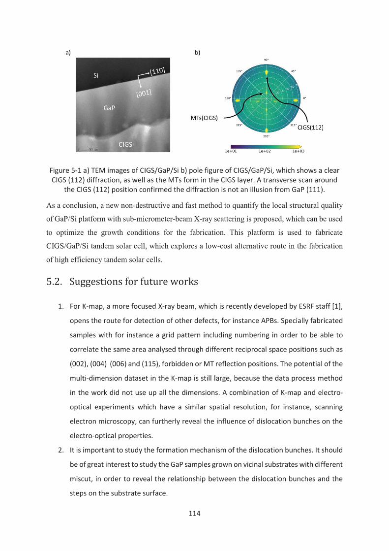
114
Figure 5-1 a) TEM images of CIGS/GaP/Si b) pole figure of CIGS/GaP/Si, which shows a clear CIGS (112) diffraction, as well as the MTs form in the CIGS layer. A transverse scan around
the CIGS (112) position confirmed the diffraction is not an illusion from GaP (111).
As a conclusion, a new non-destructive and fast method to quantify the local structural quality
of GaP/Si platform with sub-micrometer-beam X-ray scattering is proposed, which can be used
to optimize the growth conditions for the fabrication. This platform is used to fabricate
CIGS/GaP/Si tandem solar cell, which explores a low-cost alternative route in the fabrication
of high efficiency tandem solar cells.
5.2. Suggestions!for!future!works!
1. For K-map, a more focused X-ray beam, which is recently developed by ESRF staff [1],
opens the route for detection of other defects, for instance APBs. Specially fabricated
samples with for instance a grid pattern including numbering in order to be able to
correlate the same area analysed through different reciprocal space positions such as
(002), (004) (006) and (115), forbidden or MT reflection positions. The potential of the
multi-dimension dataset in the K-map is still large, because the data process method
in the work did not use up all the dimensions. A combination of K-map and electro-
optical experiments which have a similar spatial resolution, for instance, scanning
electron microscopy, can furtherly reveal the influence of dislocation bunches on the
electro-optical properties.
2. It is important to study the formation mechanism of the dislocation bunches. It should
be of great interest to study the GaP samples grown on vicinal substrates with different
miscut, in order to reveal the relationship between the dislocation bunches and the
steps on the substrate surface.
115
3. For CIGS grown on GaP/Si, the electro-optical properties of the tandem solar cells are
still waiting for the test. The abnormal diffraction in the pole figures, which may lead
by the interface between GaP and CIGS, requires further analysis and this will lead to
an improvement of the CIGS growth, as well as the obtaining of a 1.7 eV gap CIGS likely
with pure sulfur CIGS lattice-matched on the GaP/Si platform. Finally, forthcoming
developments of the CIGS top cell on a doped GaP/Si platform , for top-bottom cell
configuration, will allow the rapid development of a CIGS/Si tandem solar cell with an
tunnel junction (all Si) between both sub cells.
References
[1] S. J. Leake et al., “The Nanodiffraction beamline ID01/ESRF: a microscope for imaging
strain and structure,” J. Synchrotron Rad., vol. 26, no. 2, pp. 571–584, 2019.
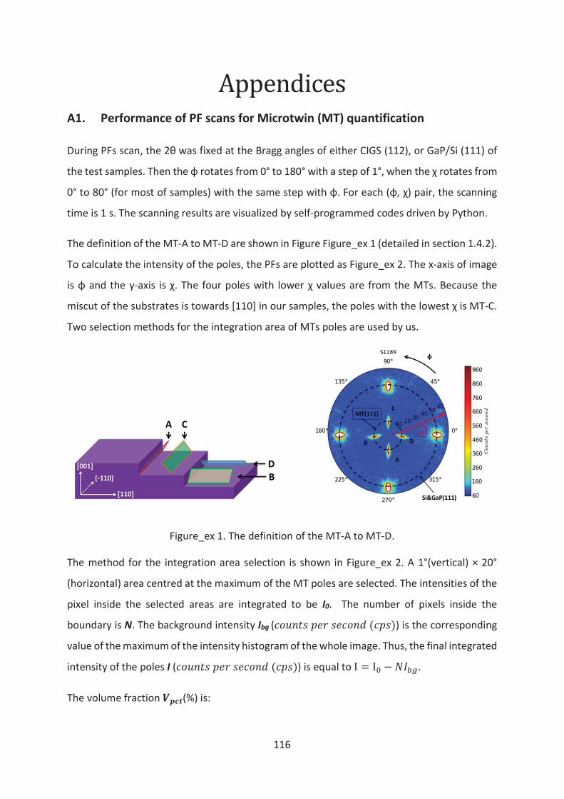
116
Appendices!A1. Performance of PF scans for Microtwin (MT) quantification
During PFs scan, the 2θ was fixed at the Bragg angles of either CIGS (112), or GaP/Si (111) of
the test samples. Then the φ rotates from 0° to 180° with a step of 1°, when the χ rotates from
0° to 80° (for most of samples) with the same step with φ. For each (φ, χ) pair, the scanning
time is 1 s. The scanning results are visualized by self-programmed codes driven by Python.
The definition of the MT-A to MT-D are shown in Figure Figure_ex 1 (detailed in section 1.4.2).
To calculate the intensity of the poles, the PFs are plotted as Figure_ex 2. The x-axis of image
is φ and the y-axis is χ. The four poles with lower χ values are from the MTs. Because the
miscut of the substrates is towards [110] in our samples, the poles with the lowest χ is MT-C.
Two selection methods for the integration area of MTs poles are used by us.
Figure_ex 1. The definition of the MT-A to MT-D.
The method for the integration area selection is shown in Figure_ex 2. A 1°(vertical) × 20°
(horizontal) area centred at the maximum of the MT poles are selected. The intensities of the
pixel inside the selected areas are integrated to be I0. The number of pixels inside the
boundary is N. The background intensity Ibg (¯°õ:9{;ö÷ø;{÷¯°:`;<¯ö{@) is the corresponding
value of the maximum of the intensity histogram of the whole image. Thus, the final integrated
intensity of the poles I (¯°õ:9{;ö÷ø;{÷¯°:`;<¯ö{@) is equal to ½ = ½¾ $ ñò«ó.
The volume fraction ùúûü(%) is:
117
Výþÿ<%@ = ò Ò !¬"## (1)
where $û&'' is the correction coefficient.
The correction coefficient is determined for each MT from a reference sample with the same
thickness and the same structure as the test samples. For the reference sample, both MT
quantification and Rocking Curve (RC) quantification is performed. Thus, the correction
coefficient $û&'' is:
!¬"## = 1½Õ( �)*+¬, (2)
where ïî- (¯°õ:9{;ö÷ø;{÷¯°:`;<¯ö{@) is the integrated intensity of the poles in the reference
sample and ./0123 (%) is volume fraction of MTs measured by RC quantification.
During the RC quantification, ./0123 is calculated as below:
1�)*+¬, = 1½#�ý4¾±5 »¾5 V��F657�5 8È (3)
where ;ï9:ú;<¯°õ:9{;ö÷ø;{÷¯°:`;<¯ö{@@ is the integrated intensity of the RC signals,
;<;<»ad@ is the intensity of the incident beam, =5 ;<»adN�@ is the angular velocity,;'<p is the
scattering cross-section of the electron, V is the effective volume of unit cell,;r (m) is the
incident X-ray beam wavelength, -> is unit cell structure factor taking into account of the
Debye-Walle factor, and PL is the Lorentz-polarization factor.
The method is developed during the thesis of Yanping Wang, Structural analyses by advanced
X-ray scattering on GaP layers epitaxially grown on silicon for integrated photonic applications,
2016. The details of the performance of the experiments could be found in her thesis
document. The integration area selection method is changed to the current one during this
thesis.
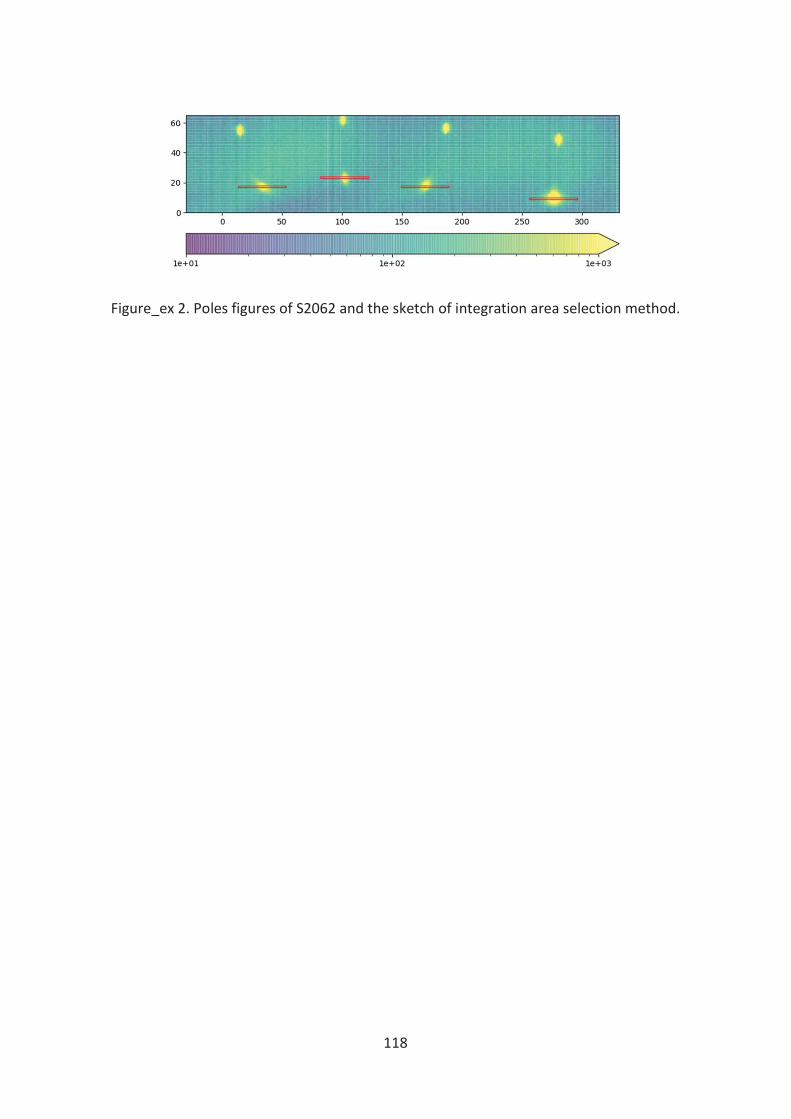
118
Figure_ex 2. Poles figures of S2062 and the sketch of integration area selection method.
119
Re"sume" !de!the#se!Les matériaux semi-conducteurs sont des briques de base à la fois pour la conversion de
l’énergie solaire et les technologies de l’information (micro et optoélectronique). Le silicium,
en tant que matériau semi-conducteur le plus mature, est largement utilisé dans les industries
de la microélectronique et du photovoltaïque, en raison de son abondance naturelle, de son
faible coût, de sa grande pureté et de la disponibilité sous forme de gros monocristaux.
Néanmoins, la bande interdite indirecte du Si empêche à la fois une émission de lumière
efficace et une absorption efficace, ce qui limite ses applications. De l'autre côté on trouve un
grand nombre de semi-conducteur direct parmi les composés III-V qui sont donc
particulièrement appréciés pour les applications en photonique, malgré des coûts de
fabrication élevés. Ainsi, l'intégration des semi-conducteurs III-V sur silicium est considérée
comme la pierre angulaire de l'intégration cohérente de la photonique dans la technologie du
silicium mature et des cellules solaires à haut rendement et à faible coût. Parmi les différentes
approches, l’hétéroépitaxie est considérée comme la technique la plus prometteuse et la plus
attrayante en raison de son faible coût et de sa capacité d’intégration à grande échelle.
Le phosphure de gallium (GaP), qui présente un désaccord de maille 0,37% à température
ambiante, par rapport au réseau cristallin du silicium, a été utilisé dans ces travaux, comme
couche intermédiaire efficace pour l'intégration ultérieure d'hétérostructures à base de III-V.
Les défauts de l'hétéroépitaxie de GaP et de Si, tels que les dislocations, les micro-macles (MT)
et les parois de domaines d’antiphase, peuvent limiter les propriétés électro-optiques des
dispositifs finaux (rendement, durabilité…). L'objectif de la thèse est donc de caractériser les
défauts structuraux et de développer des méthodes de caractérisation à l’échelle sub-
micrométrique en d’améliorer les propriétés de la plateforme GaP / Si et de mieux les
comprendre. Le but est aussi d'explorer l'application du GaP / Si aux cellules solaires tandem.
La thèse comprend 5 chapitres. Le chapitre 1 décrit l'objectif du travail de thèse et introduit
les défauts cristallins dans la plate-forme GaP / Si. Le chapitre 2 présente les techniques de
croissance et de caractérisation. Le chapitre 3 est consacré à la caractérisation d’une couche
GaP/Si partiellement relaxée plastiquement, à l’échelle globale (par diffraction des rayons X
en laboratoire) et l’échelle sub-micrométrique en utilisant une technique à l’état de l’art, de
diffractométrie de rayons X à balayage avec une résolution sub-micrométrique. Le chapitre 4
120
présente une analyse de plusieurs couches CIGS élaborée par CVD sur pseudo-substrats GaP/Si.
Ceci met en évidence une croissance de type épitaxial CIGS (001) sur GaP/Si (001). Une
première cellule tandem de type « top-top » a ensuite été réalisée. Le dernier chapitre fait la
synthèse des résultats et permet d’ouvrir des perspectives.
Dans ce travail, tous les pseudo-substrats GaP / Si sont basés sur des plaquettes de Si (001) de
2 pouces avec un miscut de 4 ° ou 6 ° dans la direction [110]. Avant l'épitaxie de GaP, le substrat
de silicium est nettoyée avec le « procédé HF optimisé » pour éliminer les impuretés de
carbone, d'oxydes, métalliques et organiques à la surface du Si. Après la préparation, la
plaquette de Si est immédiatement transférée dans la chambre MBE et chauffée à 800 ° C
pour la déshydrogénation. Ensuite, la plaquette est ramenée à plus basse température pour
l’épitaxie de GaP. Les méthodes de caractérisation incluent la diffraction des rayons X (DRX),
microscope à force atomique (AFM), microscopie électronique en transmission (et à balayage)
(SEM, TEM et STEM) entre autres.
Au chapitre 3, nous présentons l’analyse d’une couche de 200nm de GaP/Si avec un angle de
coupe de 6° par rapport à la direction [001]. Les propriétés cristallines sont tout d’abord
étudiées en DRX en laboratoire et révèlent une très faible densité de micro-macles, grâce à
l’optimisation du procédé de préparation chimique. Une relaxation plastique de l’ordre de 50%
est ensuite mesurée ce qui est cohérent avec le fait que l’épaisseur critique est de l’ordre de
50 à 90 nm. Une technique à l’état de l’art, développée sur la ligne synchrotron ID01 (ESRF) a
été employée pour étudier cet échantillon. Cette technique consiste à balayer, la surface de
l’échantillon avec un faisceau sub-micrométrique, au voisinage des conditions de Bragg. Ceci
permet d’extraire des informations de complexes de type déformation, tilt et longueur de
corrélation locale. Ceci a permis de mettre en évidence une distribution de dislocations dans
le pseudo-substrat GaP / Si. L'ensemble de données est analysé à l'aide d'un programme
Python appelé « X-ray Strain Orientation Calculation Software (XSOCS) », développé à l'ESRF.
[3] L'inclinaison locale B et la déformation locale dans le plan 2+ sont mesurées. La résolution
de l'inclinaison locale et de la déformation dans le plan est égale à 0,0036 ° et 0,01%,
respectivement.
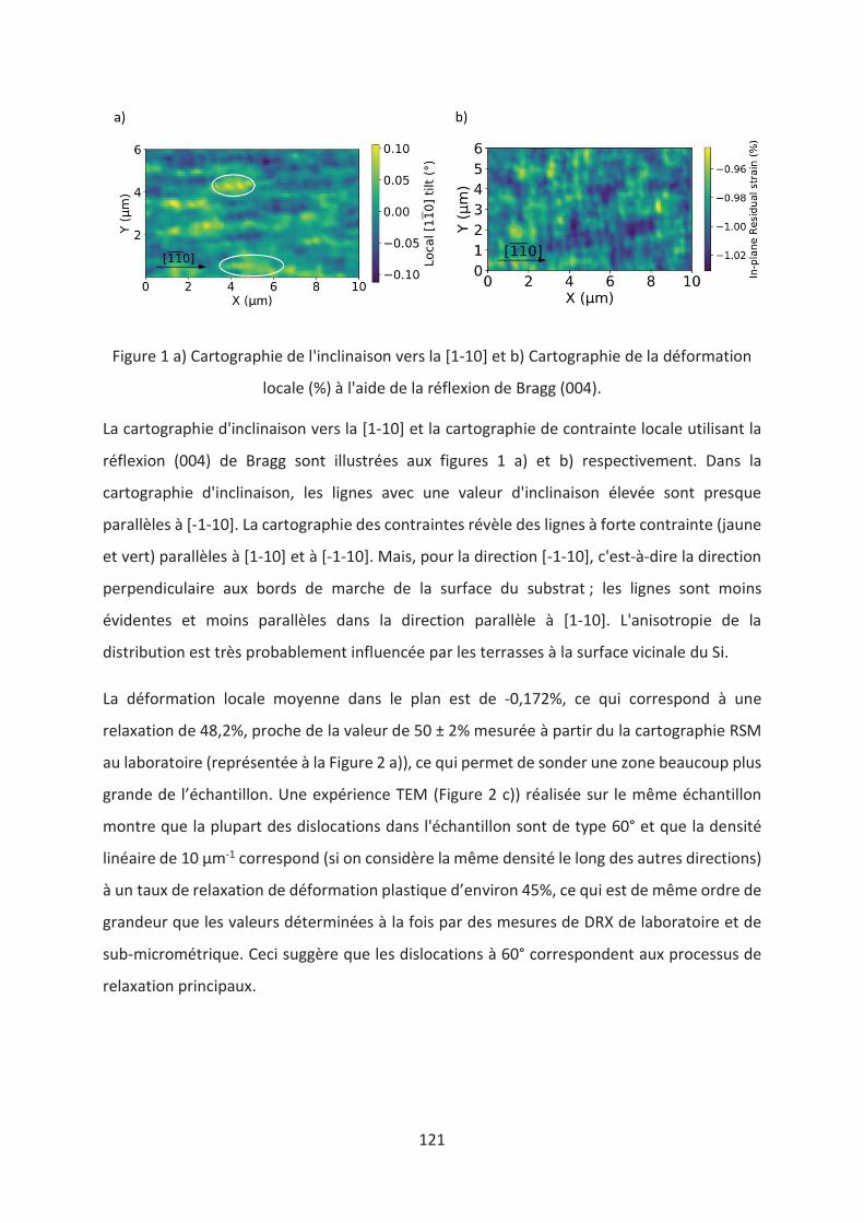
121
Figure 1 a) Cartographie de l'inclinaison vers la [1-10] et b) Cartographie de la déformation
locale (%) à l'aide de la réflexion de Bragg (004).
La cartographie d'inclinaison vers la [1-10] et la cartographie de contrainte locale utilisant la
réflexion (004) de Bragg sont illustrées aux figures 1 a) et b) respectivement. Dans la
cartographie d'inclinaison, les lignes avec une valeur d'inclinaison élevée sont presque
parallèles à [-1-10]. La cartographie des contraintes révèle des lignes à forte contrainte (jaune
et vert) parallèles à [1-10] et à [-1-10]. Mais, pour la direction [-1-10], c'est-à-dire la direction
perpendiculaire aux bords de marche de la surface du substrat ; les lignes sont moins
évidentes et moins parallèles dans la direction parallèle à [1-10]. L'anisotropie de la
distribution est très probablement influencée par les terrasses à la surface vicinale du Si.
La déformation locale moyenne dans le plan est de -0,172%, ce qui correspond à une
relaxation de 48,2%, proche de la valeur de 50 ± 2% mesurée à partir du la cartographie RSM
au laboratoire (représentée à la Figure 2 a)), ce qui permet de sonder une zone beaucoup plus
grande de l’échantillon. Une expérience TEM (Figure 2 c)) réalisée sur le même échantillon
montre que la plupart des dislocations dans l'échantillon sont de type 60° et que la densité
linéaire de 10 µm-1 correspond (si on considère la même densité le long des autres directions)
à un taux de relaxation de déformation plastique d’environ 45%, ce qui est de même ordre de
grandeur que les valeurs déterminées à la fois par des mesures de DRX de laboratoire et de
sub-micrométrique. Ceci suggère que les dislocations à 60° correspondent aux processus de
relaxation principaux.
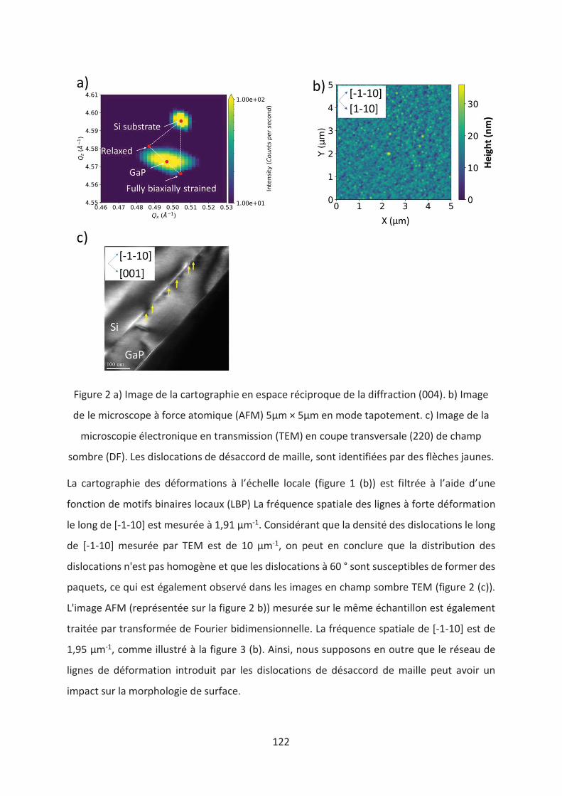
122
Figure 2 a) Image de la cartographie en espace réciproque de la diffraction (004). b) Image
de le microscope à force atomique (AFM) 5μm × 5μm en mode tapotement. c) Image de la
microscopie électronique en transmission (TEM) en coupe transversale (220) de champ
sombre (DF). Les dislocations de désaccord de maille, sont identifiées par des flèches jaunes.
La cartographie des déformations à l’échelle locale (figure 1 (b)) est filtrée à l’aide d’une
fonction de motifs binaires locaux (LBP) La fréquence spatiale des lignes à forte déformation
le long de [-1-10] est mesurée à 1,91 µm-1. Considérant que la densité des dislocations le long
de [-1-10] mesurée par TEM est de 10 μm-1, on peut en conclure que la distribution des
dislocations n'est pas homogène et que les dislocations à 60 ° sont susceptibles de former des
paquets, ce qui est également observé dans les images en champ sombre TEM (figure 2 (c)).
L'image AFM (représentée sur la figure 2 b)) mesurée sur le même échantillon est également
traitée par transformée de Fourier bidimensionnelle. La fréquence spatiale de [-1-10] est de
1,95 µm-1, comme illustré à la figure 3 (b). Ainsi, nous supposons en outre que le réseau de
lignes de déformation introduit par les dislocations de désaccord de maille peut avoir un
impact sur la morphologie de surface.
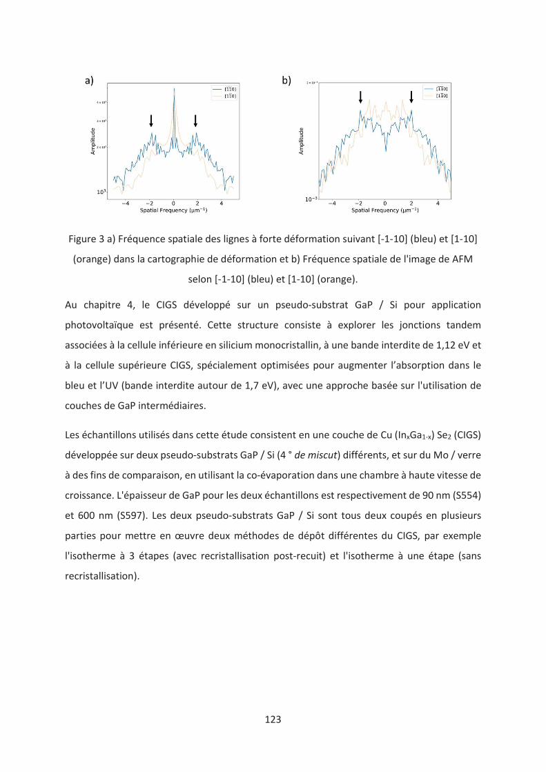
123
Figure 3 a) Fréquence spatiale des lignes à forte déformation suivant [-1-10] (bleu) et [1-10]
(orange) dans la cartographie de déformation et b) Fréquence spatiale de l'image de AFM
selon [-1-10] (bleu) et [1-10] (orange).
Au chapitre 4, le CIGS développé sur un pseudo-substrat GaP / Si pour application
photovoltaïque est présenté. Cette structure consiste à explorer les jonctions tandem
associées à la cellule inférieure en silicium monocristallin, à une bande interdite de 1,12 eV et
à la cellule supérieure CIGS, spécialement optimisées pour augmenter l’absorption dans le
bleu et l’UV (bande interdite autour de 1,7 eV), avec une approche basée sur l'utilisation de
couches de GaP intermédiaires.
Les échantillons utilisés dans cette étude consistent en une couche de Cu (InxGa1-x) Se2 (CIGS)
développée sur deux pseudo-substrats GaP / Si (4 ° de miscut) différents, et sur du Mo / verre
à des fins de comparaison, en utilisant la co-évaporation dans une chambre à haute vitesse de
croissance. L'épaisseur de GaP pour les deux échantillons est respectivement de 90 nm (S554)
et 600 nm (S597). Les deux pseudo-substrats GaP / Si sont tous deux coupés en plusieurs
parties pour mettre en œuvre deux méthodes de dépôt différentes du CIGS, par exemple
l'isotherme à 3 étapes (avec recristallisation post-recuit) et l'isotherme à une étape (sans
recristallisation).
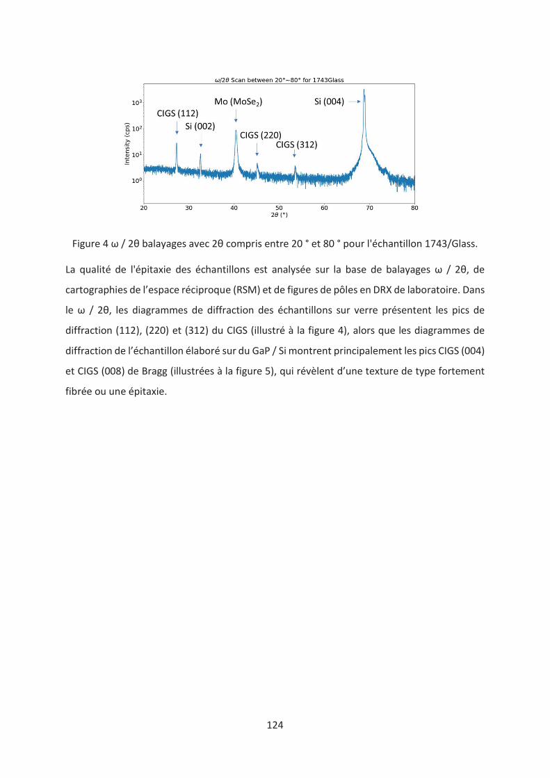
124
Figure 4 ω / 2θ balayages avec 2θ compris entre 20 ° et 80 ° pour l'échantillon 1743/Glass.
La qualité de l'épitaxie des échantillons est analysée sur la base de balayages ω / 2θ, de
cartographies de l’espace réciproque (RSM) et de figures de pôles en DRX de laboratoire. Dans
le ω / 2θ, les diagrammes de diffraction des échantillons sur verre présentent les pics de
diffraction (112), (220) et (312) du CIGS (illustré à la figure 4), alors que les diagrammes de
diffraction de l’échantillon élaboré sur du GaP / Si montrent principalement les pics CIGS (004)
et CIGS (008) de Bragg (illustrées à la figure 5), qui révèlent d’une texture de type fortement
fibrée ou une épitaxie.
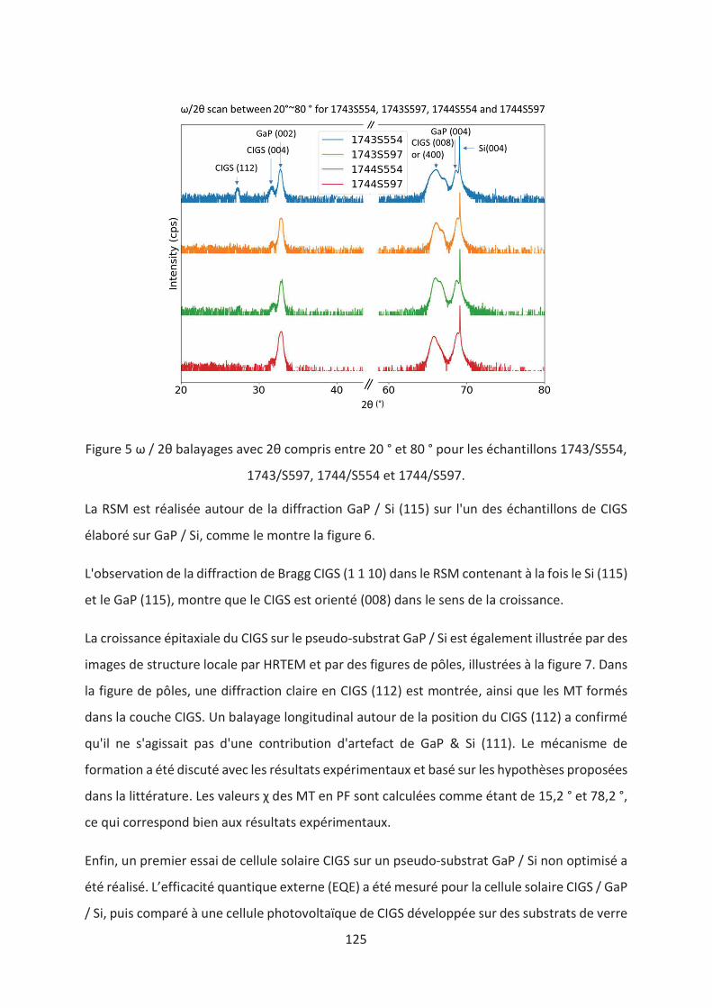
125
Figure 5 ω / 2θ balayages avec 2θ compris entre 20 ° et 80 ° pour les échantillons 1743/S554,
1743/S597, 1744/S554 et 1744/S597.
La RSM est réalisée autour de la diffraction GaP / Si (115) sur l'un des échantillons de CIGS
élaboré sur GaP / Si, comme le montre la figure 6.
L'observation de la diffraction de Bragg CIGS (1 1 10) dans le RSM contenant à la fois le Si (115)
et le GaP (115), montre que le CIGS est orienté (008) dans le sens de la croissance.
La croissance épitaxiale du CIGS sur le pseudo-substrat GaP / Si est également illustrée par des
images de structure locale par HRTEM et par des figures de pôles, illustrées à la figure 7. Dans
la figure de pôles, une diffraction claire en CIGS (112) est montrée, ainsi que les MT formés
dans la couche CIGS. Un balayage longitudinal autour de la position du CIGS (112) a confirmé
qu'il ne s'agissait pas d'une contribution d'artefact de GaP & Si (111). Le mécanisme de
formation a été discuté avec les résultats expérimentaux et basé sur les hypothèses proposées
dans la littérature. Les valeurs χ des MT en PF sont calculées comme étant de 15,2 ° et 78,2 °,
ce qui correspond bien aux résultats expérimentaux.
Enfin, un premier essai de cellule solaire CIGS sur un pseudo-substrat GaP / Si non optimisé a
été réalisé. L’efficacité quantique externe (EQE) a été mesuré pour la cellule solaire CIGS / GaP
/ Si, puis comparé à une cellule photovoltaïque de CIGS développée sur des substrats de verre
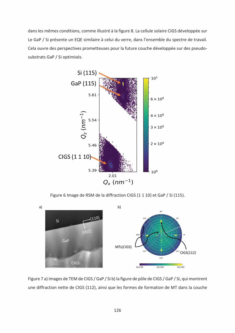
126
dans les mêmes conditions, comme illustré à la figure 8. La cellule solaire CIGS développée sur
Le GaP / Si présente un EQE similaire à celui du verre, dans l’ensemble du spectre de travail.
Cela ouvre des perspectives prometteuses pour la future couche développée sur des pseudo-
substrats GaP / Si optimisés.
Figure 6 Image de RSM de la diffraction CIGS (1 1 10) et GaP / Si (115).
Figure 7 a) Images de TEM de CIGS / GaP / Si b) la figure de pôle de CIGS / GaP / Si, qui montrent
une diffraction nette de CIGS (112), ainsi que les formes de formation de MT dans la couche
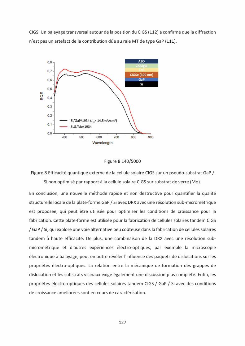
127
CIGS. Un balayage transversal autour de la position du CIGS (112) a confirmé que la diffraction
n’est pas un artefact de la contribution dûe au raie MT de type GaP (111).
Figure 8 140/5000
Figure 8 Efficacité quantique externe de la cellule solaire CIGS sur un pseudo-substrat GaP /
Si non optimisé par rapport à la cellule solaire CIGS sur substrat de verre (Mo).
En conclusion, une nouvelle méthode rapide et non destructive pour quantifier la qualité
structurelle locale de la plate-forme GaP / Si avec DRX avec une résolution sub-micrométrique
est proposée, qui peut être utilisée pour optimiser les conditions de croissance pour la
fabrication. Cette plate-forme est utilisée pour la fabrication de cellules solaires tandem CIGS
/ GaP / Si, qui explore une voie alternative peu coûteuse dans la fabrication de cellules solaires
tandem à haute efficacité. De plus, une combinaison de la DRX avec une résolution sub-
micrométrique et d'autres expériences électro-optiques, par exemple la microscopie
électronique à balayage, peut en outre révéler l'influence des paquets de dislocations sur les
propriétés électro-optiques. La relation entre la mécanique de formation des grappes de
dislocation et les substrats vicinaux exige également une discussion plus complète. Enfin, les
propriétés électro-optiques des cellules solaires tandem CIGS / GaP / Si avec des conditions
de croissance améliorées sont en cours de caractérisation.
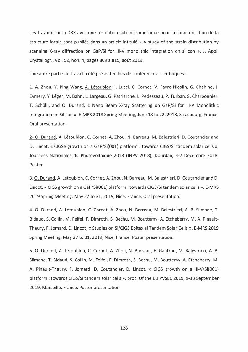
128
Les travaux sur la DRX avec une résolution sub-micrométrique pour la caractérisation de la
structure locale sont publiés dans un article intitulé « A study of the strain distribution by
scanning X-ray diffraction on GaP/Si for III-V monolithic integration on silicon », J. Appl.
Crystallogr., Vol. 52, non. 4, pages 809 à 815, août 2019.
Une autre partie du travail a été présentée lors de conférences scientifiques :
1. A. Zhou, Y. Ping Wang, A. Létoublon, I. Lucci, C. Cornet, V. Favre-Nicolin, G. Chahine, J.
Eymery, Y. Léger, M. Bahri, L. Largeau, G. Patriarche, L. Pedesseau, P. Turban, S. Charbonnier,
T. Schülli, and O. Durand, « Nano Beam X-ray Scattering on GaP/Si for III-V Monolithic
Integration on Silicon », E-MRS 2018 Spring Meeting, June 18 to 22, 2018, Strasbourg, France.
Oral presentation.
2- O. Durand, A. Létoublon, C. Cornet, A. Zhou, N. Barreau, M. Balestrieri, D. Coutancier and
D. Lincot. « CIGSe growth on a GaP/Si(001) platform : towards CIGS/Si tandem solar cells »,
Journées Nationales du Photovoltaique 2018 (JNPV 2018), Dourdan, 4-7 Décembre 2018.
Poster
3. O. Durand, A. Létoublon, C. Cornet, A. Zhou, N. Barreau, M. Balestrieri, D. Coutancier and D.
Lincot, « CIGS growth on a GaP/Si(001) platform : towards CIGS/Si tandem solar cells », E-MRS
2019 Spring Meeting, May 27 to 31, 2019, Nice, France. Oral presentation.
4. O. Durand, A. Létoublon, C. Cornet, A. Zhou, N. Barreau, M. Balestrieri, A. B. Slimane, T.
Bidaud, S. Collin, M. Feifel, F. Dimroth, S. Bechu, M. Bouttemy, A. Etcheberry, M. A. Pinault-
Thaury, F. Jomard, D. Lincot, « Studies on Si/CIGS Epitaxial Tandem Solar Cells », E-MRS 2019
Spring Meeting, May 27 to 31, 2019, Nice, France. Poster presentation.
5. O. Durand, A. Létoublon, C. Cornet, A. Zhou, N. Barreau, E. Gautron, M. Balestrieri, A. B.
Slimane, T. Bidaud, S. Collin, M. Feifel, F. Dimroth, S. Bechu, M. Bouttemy, A. Etcheberry, M.
A. Pinault-Thaury, F. Jomard, D. Coutancier, D. Lincot, « CIGS growth on a III-V/Si(001)
platform : towards CIGS/Si tandem solar cells », proc. Of the EU PVSEC 2019, 9-13 September
2019, Marseille, France. Poster presentation


129
Titre : Analyses structurales de pseudo-substrats GaP/Si et d’hétérostructures CIGS/GaP/Si pour des applications
photovoltaïques
Mots clés : GaP / Si, MBE, DRX avec une résolution sub-micrométrique, synchrotron, dislocations d'adaptation, cellule solaire tandem.
Résumé : Cette thèse porte sur l'analyse des défauts structuraux d'un pseudo-substrat GaP/Si. L'objectif principal concerne la qualité structurale de la couche épitaxiale de GaP sur un substrat de Si, en tant que pierre angulaire du développement d'une cellule solaire à haut rendement avec des dispositifs optoélectroniques à coût relativement bas et III-V. Tout d'abord, l'étude porte sur la caractérisation de la distribution des dislocations dans le pseudo-substrat vicinal GaP sur Si(001), à l’aide d’une méthode, appelée K-Map, utilisant la diffusion des rayons X en rayonnement synchrotron et avec une résolution sub-micrométrique. Les informations locales d’inclinaison et de déformation sont obtenues par une analyse de l’ensemble de données complexes 5D. Cette étude révèle une distribution anisotrope des dislocations dans différentes directions du cristal, liée aux marches à la surface du substrat de Si ainsi qu’une tendance au regroupement de ces dislocations.
La deuxième partie de l’étude porte sur la croissance et la caractérisation de CIGS sur GaP/Si, en vue de développer des cellules solaires tandems associant une cellule du dessous en silicium monocristallin et une cellule du dessus en CIGS. On observe (par XRD, EDX et HRTEM) que le CIGS est déposé par croissance épitaxiale sur le pseudo substrat GaP/Si et présente une qualité structurale proche d'un monocristal. Le premier essai, non optimisé, d'une cellule solaire simple jonction de CIGS sur pseudo-substrat GaP/Si, permet d'obtenir un EQE très encourageant, similaire à celui obtenu avec la même cellule déposée sur substrat de verre avec des paramètres de dépôts optimisés.
Title : Structural analysis of GaP/Si platform and CIGS/GaP/Si heterostructures for photovoltaic applications
Keywords : GaP/Si, MBE, Sub-micrometer XRD, synchrotron, Misfit Dislocations, tandem solar cell.
Abstract : This thesis focuses on the characterization of the structural defects on a MBE-made GaP/Si pseudo-substrate. The main purpose concerns the structural quality of GaP epitaxial layer on Si substrate, as a cornerstone for the development of high-efficiency solar cell with relatively low cost and optoelectronic devices.
Firstly, the study focuses on the characterization of the distribution of dislocations in GaP on Si (001) vicinal substrate, with an advanced sub-micrometer-beam X-ray scattering method, K-Map. The local tilt and strain information are obtained through an analysis of the complex 5D dataset. This study reveals an anisotropic distribution of the dislocations along different crystallographic directions, linked to the steps of the
surface of Si substrate, and an inhomogeneous distribution of the dislocations, linked to the tendency to form bunches. The second part of the study is on the growth and characterization of CIGS on GaP/Si, which is used to explore tandem junctions associating single crystalline silicon bottom cell. The CIGS is observed to be epitaxially grown on the GaP/Si pseudo substrate, combining the results collected from XRD, EDX and HRTEM. A first try of a CIGS/GaP/Si solar cell is realized on a non-optimized GaP/Si pseudo-substrate. The obtained EQE is similar to the one obtained with the CIGS solar cell grown on a traditional glass substrate with the optimised deposition parameters.
Related Documents