Indian Journal of Pure & Applied Physics Vol. 56, November 2018, pp. 869-874 Analog/RF performance and effect of interface trap charges in dielectric engineered gate all around junctionless MOSFET with ZrTiO 4 as gate dielectric Suman Sharma a *, Rajni Shukla a & M R Tripathy b a Department of Physics, Deenbandhu Chottu Ram University, Murthal, Sonepat 131 039, India b Department of Electronics and Communication Engineering, Amity University Noida, Noida 201 303, India Received 21 June 2017; accepted 27 March 2018 The present study provides the comprehensive appraisal of analog/RF performance of dielectric engineered gate all around junctionless MOSFET by the assimilation of gate material engineered along with ZrTiO 4 as high-k gate dielectric. The radical reductions in impact of positive and negative interface traps have been reported, which augment the device reliability. The cylindrical geometry of the MOSFET accounts for the self heating effect in the device, which accelerates the practice of hot carrier effect and diffusion of H, conscientious for negative bias temperature instability (NBTI) effect in P-MOSFET and PBTI effect in the N-MOSFET. The proposed design has been studied by taking SiO 2 , and orthorhombic ZrTiO 4 symmetric gate stack to improve the reliability of the device. The electrical characteristics like I d -V g , electric field, centre potential, transconductance and frequency have been measured using the ATLAS 3D simulator. Orthorhombic ZrTiO 4 with dielectric constant 45.9 shows the enhanced performance of the device. The interface trap charge concentration of 1×10 11 cm -2 (positive and negative both) for ZrTiO 4 have been compared with the device devoid of gate stack which provides the knowledge about the RF and analog performance of the MOSFET. Keywords: ATLAS-3D, High-k gate dielectric, Interface trap charges 1 Introduction With the decreasing size of MOSFET, various short channel effects such as hot carrier effects, DIBL (drain induced barrier lowering), leakage current, interface trap charges, etc. degrades the performance of the device. Many advanced architectures like multi gate MOSFETs 1,2 , pi gate 3,4 and cylindrical MOSFET 5-7 have been reported to overcome these shortcomings. The junctionless gate all around MOSFET (JL-GAA) 8-11 is the most promising design for improved performance at nanoscale. The homogeneous doping from source to channel without any junction fabrication makes the fabrication process of junctionless gate all around (JL-GAA) MOSFET simple than the conventional cylindrical MOSFET. The reason is that no abrupt junction formation is required which makes this fabrication very economic. A lot of research work is going on in junctionless GAA MOSFET 8-13 . With device dimensions downscaling, reliability of the device is also a challenge. Reducing dimensions up to nanoscale and increase in integration density of integrated circuits the interface trap/charges generation probability has increased. These trap charges drastically degrade the device performance 14-17 . Out of these reliability issues PBTI (positive bias temperature instability) in n-MOSFET 18 and PBTI (negative bias temperature instability) in p-MOSFET 19 is the main reliability issue in MOSFET’s which mainly occurs owing to the different stress damage conditions. The interface traps and trapping of holes in oxides are considered as the key mechanism of PBTI effect in the devices 19 . The reliability of high-mobility InGaAs channel n-MOSFETs under BTI stress has been discussed by Li Ming Fu et al. 20 in detail. The interface charges can occur due to various damage causing phenomena occurring in the device such as: process induced damage 21 , stress induced 22 (at the time of device fabrication), hot carrier induced damage and by radiation induced damage 23,24 . Radiation damage cause uniform allocation of interface traps at the silicon oxide interface whereas the hot carrier induced damage results into the interface traps towards the drain end. In order to model the effect of trap charges, accurately modelling of carrier mobility in the channel of a nanoscaled MOSFET, in the presence of discrete charges trapped at the channel/oxide interface 25 is required. A new physical method for the characterization of the interfacial and bulk defect ————— *Corresponding author (E-mail: [email protected])

Welcome message from author
This document is posted to help you gain knowledge. Please leave a comment to let me know what you think about it! Share it to your friends and learn new things together.
Transcript
Indian Journal of Pure & Applied Physics Vol. 56, November 2018, pp. 869-874
Analog/RF performance and effect of interface trap charges in dielectric engineered gate all around junctionless MOSFET with ZrTiO4 as gate dielectric
Suman Sharmaa*, Rajni Shuklaa & M R Tripathyb aDepartment of Physics, Deenbandhu Chottu Ram University, Murthal, Sonepat 131 039, India
bDepartment of Electronics and Communication Engineering, Amity University Noida, Noida 201 303, India
Received 21 June 2017; accepted 27 March 2018
The present study provides the comprehensive appraisal of analog/RF performance of dielectric engineered gate all around junctionless MOSFET by the assimilation of gate material engineered along with ZrTiO4 as high-k gate dielectric. The radical reductions in impact of positive and negative interface traps have been reported, which augment the device reliability. The cylindrical geometry of the MOSFET accounts for the self heating effect in the device, which accelerates the practice of hot carrier effect and diffusion of H, conscientious for negative bias temperature instability (NBTI) effect in P-MOSFET and PBTI effect in the N-MOSFET. The proposed design has been studied by taking SiO2, and orthorhombic ZrTiO4 symmetric gate stack to improve the reliability of the device. The electrical characteristics like Id-Vg, electric field, centre potential, transconductance and frequency have been measured using the ATLAS 3D simulator. Orthorhombic ZrTiO4 with dielectric constant 45.9 shows the enhanced performance of the device. The interface trap charge concentration of 1×1011 cm-2 (positive and negative both) for ZrTiO4 have been compared with the device devoid of gate stack which provides the knowledge about the RF and analog performance of the MOSFET.
Keywords: ATLAS-3D, High-k gate dielectric, Interface trap charges
1 Introduction With the decreasing size of MOSFET, various
short channel effects such as hot carrier effects, DIBL (drain induced barrier lowering), leakage current, interface trap charges, etc. degrades the performance of the device. Many advanced architectures like multi gate MOSFETs1,2, pi gate3,4 and cylindrical MOSFET5-7 have been reported to overcome these shortcomings. The junctionless gate all around MOSFET (JL-GAA)8-11 is the most promising design for improved performance at nanoscale. The homogeneous doping from source to channel without any junction fabrication makes the fabrication process of junctionless gate all around (JL-GAA) MOSFET simple than the conventional cylindrical MOSFET. The reason is that no abrupt junction formation is required which makes this fabrication very economic. A lot of research work is going on in junctionless GAA MOSFET8-13. With device dimensions downscaling, reliability of the device is also a challenge. Reducing dimensions up to nanoscale and increase in integration density of integrated circuits the interface trap/charges generation probability has increased. These trap charges drastically degrade the
device performance14-17. Out of these reliability issues PBTI (positive bias temperature instability) in n-MOSFET18 and PBTI (negative bias temperature instability) in p-MOSFET19 is the main reliability issue in MOSFET’s which mainly occurs owing to the different stress damage conditions. The interface traps and trapping of holes in oxides are considered as the key mechanism of PBTI effect in the devices19. The reliability of high-mobility InGaAs channel n-MOSFETs under BTI stress has been discussed by Li Ming Fu et al.20 in detail. The interface charges can occur due to various damage causing phenomena occurring in the device such as: process induced damage21, stress induced22 (at the time of device fabrication), hot carrier induced damage and by radiation induced damage23,24. Radiation damage cause uniform allocation of interface traps at the silicon oxide interface whereas the hot carrier induced damage results into the interface traps towards the drain end.
In order to model the effect of trap charges, accurately modelling of carrier mobility in the channel of a nanoscaled MOSFET, in the presence of discrete charges trapped at the channel/oxide interface25 is required. A new physical method for the characterization of the interfacial and bulk defect
————— *Corresponding author (E-mail: [email protected])

INDIAN J PURE & APPL PHYS, VOL. 56, NOVEMBER 2018
870
density in high-k/III–V MOSFETs has been demonstrated26. Dielectric engineering has come up with new dielectric materials to enhance scalability of the nanoscale devices by reducing short channel effects and effective oxide thickness (EOT). An ultralow EOT Ge MOS device with tetragonal HfO2 and high quality HfxGeyO interfacial layer has been suggested by Chang et al.27 The electrical comparison of high k dielectrics HfO2 and ZrO2 gate dielectrics on GaN has been done by Kyle et al.28 A new dielectric material ZrTiO4 has been suggested to reduce short channel effects leading to enhanced scalability29. But device reliability in terms of interface trapped charges for junctionless GAA MOSFET with ZrTiO4 as dielectric is not reported earlier.
This work presents a comparative study of junctionless GAA MOSFET with ZrTiO4 as dielectric materials over SiO2 in terms of effect of interface trapped charges and analog/RF performance. The study shows the decrease in the degradation caused due to interface trap charges (positive and negative) present at the interface of the junctionless GAA MOSFET by using dielectric engineering. 2 Device Structure and Simulation Methodology
ATLAS-3D device simulation tool30 has been used for the numerical simulation of junctionless GAA MOSFET. 3-D and 2D schematic of junctionless gate all around MOSFET is shown in Fig. 1. The various models included in simulations are CONMOB model for concentration dependent mobility, FLDMOB model for elevated electric field velocity saturation, CVT model for perpendicular electric field, and AUGER recombination model. The Boltzmann transport model (drift diffusion approach) as a drift diffusion model works quite well for the channel length greater than 40 nm without compromising the accuracy of the simulated results. The quantum effect has not been taken into account in present analysis. We have worked on channel length 40 nm and channel radius 10 nm31. Interface trap density (Nf =±1011 cm-2) has been chosen on the basis of experimental studies32-34.
3 Results and Discussion
3.1 Influence of localised charges on electrical characteristics The interface traps are generated at the Si-SiO2
interface due to various degradation mechanisms such as (1) process induced damage, (2) stress induced damage, (3) radiation induced damage and (4) hot carrier induced damage. Interface traps can be filled with electrons or holes on the basis of Fermi level position. An acceptor type interface trap can be treated as negative charge after occupation by an electron whereas empty acceptor trap is electrically neutral. Similarly, donor type trap can be treated as positive charge when it is empty and electrically neutral when occupied by a hole. When interface trap charges are present on the Si-SiO2 interface, these charges degrade the device performance a lot. These charges cause increase in band bending for negative interface charges and decrease in band bending for positive interface charges at the interface. This change in band bending is responsible for change in flat band voltage which ultimately changes the threshold voltage, drain current and all other parameters of the device.
Change in flat band voltage is given by equation35:
ffb
ox
qNV
C … (1)
Where 2
(1 2 )ox
oxsi ox si
Ct ln t t
… (2)
Thus the amount of change in the Flat band voltage
Vfb depends upon the thickness of the gate oxide tox, permittivity of the oxide ox and density of interface
localised charges Nf. 3.2 Centre potential variation
Since centre potential in JLGAA MOSFET depends on flat band voltage, it also gets affected as shown in Fig. 2. The graph shows the effect of
Fig. 1 — Schematic view (3-D and 2-D) of n-channel junctionless GAA MOSFET structure with high-k gate stack, L = 40 nm, R = 10 nm, doped n-type substrate ND =1 × 1018 cm-3, SiO2 thickness tSiO2 = 1 nm or thigh-k = 1 nm, work-function of the metal gate electrode Φm
= 5 eV.

SHARMA et al.: INTERFACE TRAP EFFECT IN JUNCTIONLESS GATE ALL AROUNT MOSFET
871
interface trap charges on centre potential with SiO2 dielectric for undamaged device, for damaged device having positive and negative trap charges, Int: Nf =+1011 cm-2, nint: Nf = -1011 cm-2. Figure 3 illustrates the centre potential in JLGAA MOSFET with ZrTiO4 gate stack in the presence of localised charges. It can be seen that change in potential with high-k gate stack due to interface charges is negligible as compared with SiO2 dielectric alone. 3.3 Electric field variation
As potential is directly related with electric field, Fig. 4 shows the electric field profile in the channel in presence of localised charges without gate stack. Here, it can be seen that due to change in band bending, there is a great variation in potential and electric field which results in threshold voltage variation. Since device
performance is severly degraded in presence of trap charges, some techniques should be applied in order to reduce the degradation. But in practical conditions, avoiding traps is not completely possible. Traps are always present there due to hot carrier damage, radiation damage, and process induced damage in a practical device. The method used in this work is dielectric engineering to reduce the impact of trap charges already present in the device. In the present study, we have used a high k dielectric (ZrTiO4) . It is clear from Fig. 5 that after using high-k gate stack there is no deviation in electric field profile because of damage caused by interface traps. In other words we can say that effect of interface traps is being nullified with the use of ZrTiO4 as dielectric material.
Fig. 2 — The effect of interface trap charges on centre potentialwith SiO2 dielectric for undamaged device, for damaged devicehaving positive and negative trap charges. Int: Nf =+1011 cm-2, nint: Nf = -1011 cm-2.
Fig. 3 — The effect of interface trap charges on centre potentialwith ZrTiO4 dielectric for undamaged device, for damaged devicehaving positive and negative trap charges. Int: Nf =+1011 cm-2, nint: Nf = -1011 cm-2.
Fig. 4 — The effect of interface trap charges on electric field profile with SiO2 dielectric for undamaged device, for damageddevice having positive and negative trap charges. Int: Nf =+1011
cm-2, nint: Nf = -1011 cm.-2
Fig. 5 — The effect of interface trap charges on electric field withZrTiO4 dielectric for undamaged device, for damaged devicehaving positive and negative trap charges. Int: Nf =+1011 cm-2, nint: Nf = -1011 cm-2.
INDIAN J PURE & APPL PHYS, VOL. 56, NOVEMBER 2018
872
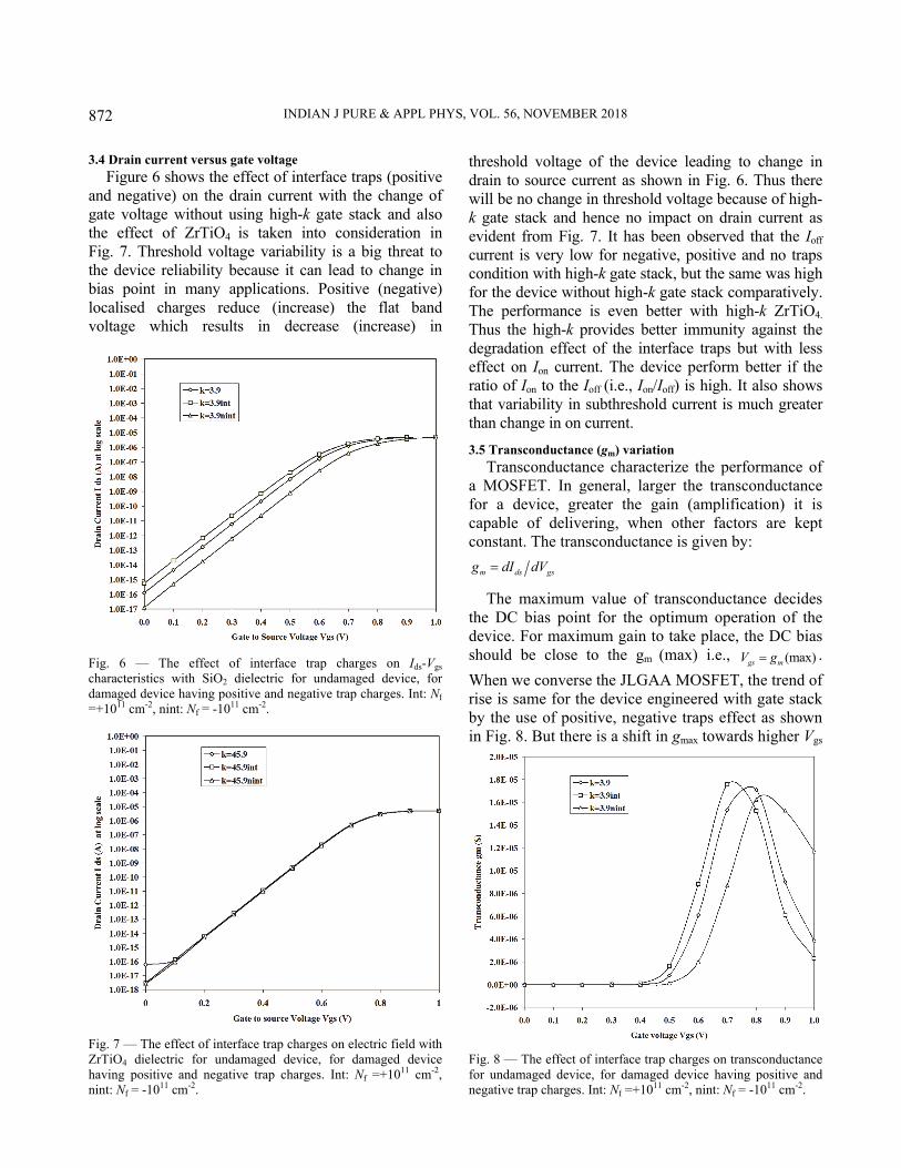
3.4 Drain current versus gate voltage Figure 6 shows the effect of interface traps (positive
and negative) on the drain current with the change of gate voltage without using high-k gate stack and also the effect of ZrTiO4 is taken into consideration in Fig. 7. Threshold voltage variability is a big threat to the device reliability because it can lead to change in bias point in many applications. Positive (negative) localised charges reduce (increase) the flat band voltage which results in decrease (increase) in
threshold voltage of the device leading to change in drain to source current as shown in Fig. 6. Thus there will be no change in threshold voltage because of high-k gate stack and hence no impact on drain current as evident from Fig. 7. It has been observed that the Ioff current is very low for negative, positive and no traps condition with high-k gate stack, but the same was high for the device without high-k gate stack comparatively. The performance is even better with high-k ZrTiO4.
Thus the high-k provides better immunity against the degradation effect of the interface traps but with less effect on Ion current. The device perform better if the ratio of Ion to the Ioff (i.e., Ion/Ioff) is high. It also shows that variability in subthreshold current is much greater than change in on current.
3.5 Transconductance (gm) variation Transconductance characterize the performance of
a MOSFET. In general, larger the transconductance for a device, greater the gain (amplification) it is capable of delivering, when other factors are kept constant. The transconductance is given by:
m ds gsg dI dV
The maximum value of transconductance decides the DC bias point for the optimum operation of the device. For maximum gain to take place, the DC bias should be close to the gm (max) i.e., (max)gs mV g .
When we converse the JLGAA MOSFET, the trend of rise is same for the device engineered with gate stack by the use of positive, negative traps effect as shown in Fig. 8. But there is a shift in gmax towards higher Vgs
Fig. 6 — The effect of interface trap charges on Ids-Vgs
characteristics with SiO2 dielectric for undamaged device, fordamaged device having positive and negative trap charges. Int: Nf
=+1011 cm-2, nint: Nf = -1011 cm-2.
Fig. 7 — The effect of interface trap charges on electric field withZrTiO4 dielectric for undamaged device, for damaged devicehaving positive and negative trap charges. Int: Nf =+1011 cm-2, nint: Nf = -1011 cm-2.
Fig. 8 — The effect of interface trap charges on transconductancefor undamaged device, for damaged device having positive andnegative trap charges. Int: Nf =+1011 cm-2, nint: Nf = -1011 cm-2.

SHARMA et al.: INTERFACE TRAP EFFECT IN JUNCTIONLESS GATE ALL AROUNT MOSFET
873
for both positive traps and negative interface traps charges without gate stack, as shown in Fig. 9.
3.6 Cut-off frequency variation Cut off frequency is given by:
2mg
Tgg
fC
… (3)
Where mg is transconductance and ggc is total gate
capacitance. Figures 10 and 11 portray the frequency profile for
JLGAA MOSFET without and with high-k gate stack,
respectively. It is being observed from here that for device with high-k a different behaviour was observed. Degradation in the peak of frequency was observed without high-k as compared to with gate stack, the peak shift towards the higher gate voltage for negative traps and no traps condition. But there no considerable shift was observed for device after application of high-k gate stack. It is evident from here that for device with high-k gate stack, interface trap charges (positive and negative) not providing the influence on the frequency of the device.
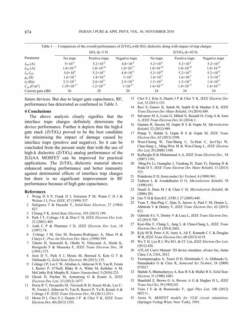
The high frequency output is observed without high-k gate stack as compared to with gate stack and along with interface traps because of high gate capacitance. Thus the present structural design with high-k gate stack is not appropriate for the high frequency application, it need some erstwhile effects to be taken into account like maximum frequency fmax instead of cut-off frequency as for microwave application maximum frequency is a imperative parameter for power gain. However, the comparison of the overall performance of ZrTiO4 with SiO2 dielectric along with impact of trap charges is shown in Table 1.
As evident from the Table 1 that the Ion/Ioff ratio improves by a factor of 10 in case of ZrTiO4 dielectric as compared to SiO2. Analog performance (Ion, Ion/Ioff) all have improved leading to higher scope for scalability. Not only the analog performance, device relability has also improved. The variation in threshold voltage, current and gm is negligible when ZrTiO4 is used. Thus it is a promising choice for
Fig. 9 — The effect of interface trap charges on transconductancewith ZrTiO4 dielectric for undamaged device, for damaged devicehaving positive and negative trap charges. Int: Nf =+1011 cm-2, nint: Nf = -1011 cm-2.
Fig. 10 — The effect of interface trap charges on cut-offfrequency for undamaged device, for damaged device havingpositive and negative trap charges. Int: Nf =+1011 cm-2, nint:Nf = -1011 cm-2.
Fig. 11 — The effect of interface trap charges on cut-off frequency with ZrTiO4 dielectric for undamaged device, fordamaged device having positive and negative trap charges.Int: Nf =+1011 cm-2, nint: Nf = -1011 cm-2.
INDIAN J PURE & APPL PHYS, VOL. 56, NOVEMBER 2018
874
future devices. But due to larger gate capacitance, RF, performance has deterioted as confirmed in Table 1.
4 Conclusions The above analysis clearly signifies that the
interface traps charges definitely deteriorate the device performance. Further it depicts that the high-k gate stack (ZrTiO4) proved to be the best candidate for minimising the impact of damage caused by interface traps (positive and negative). So it can be concluded from the present study that with the use of high-k dielectric (ZrTiO4) analog performance of the JLGAA MOSFET can be improved for practical applications. The ZrTiO4 dielectric material shows enhanced analog performance and better immunity against detrimental effects of interface trap charges but there is no significant improvement in RF performance because of high gate capacitance.
References 1 Wong H S P, Frank D J, Solomon P M, Wann C H J &
Welser J J, Proc IEEE, 87 (1999) 537. 2 Sekigawa T & Hayashi Y, Solid-State Electron, 27 (1984)
827. 3 Chiang T K, Solid-State Electron, 103 (2015) 199. 4 Park J T, Colinge J K & Diaz C H, IEEE Electron Dev Lett,
22 (2001) 405. 5 Auth C P & Plummer J D, IEEE Electron Dev Lett, 18
(1997) 74. 6 Colinge J M, Gao M, Romano-Rodriguez A, Maes H &
Claeys C, Proc Int Electron Dev Meet, (1990) 595. 7 Takato H, Sunouchi K, Okabe N, Nitayama A, Hieda K,
Horiguchi F & Masuoka F, IEEE Trans Electron Dev, 38 (1991) 573.
8 Jeon D Y, Park S J, Mouis M, Barraud S, Kim G T & Ghibaudo G, Solid State Electron, 80 (2013) 135.
9 Colinge J P, Lee C W, Afzalian A, Akhavan N D, Yan R, Ferain I, Razavi P, O’Neill, Blake B A, White M, Kelleher A M, McCarthy B & Murphy R, Nature Nanotechnol, 5 (2010) 225.
10 Ghosh D, Parihar M, Armstrong G & Kranti A, IEEE Electron Dev Lett, 33 (2012) 1477.
11 Doria R T, Pavanello M, Trevisoli R D, Souza M-de, Lee C-W, Ferain I, Akhavan N, Yan R, Razavi P, Yu R, Kranti A & Colinge J P, IEEE Trans Electron Dev, 58 (2011) 2511.
12 Moon D I, Choi S J, Duarte J P & Choi Y K, IEEE Trans Electron Dev, 60 (2013) 1355.
13 Choi S J, Kim S, Duarte J P & Choi Y K, IEEE Electron Dev Lett, 32 (2011) 125.
14 Ravi S, Gaurav K, Satish M, Sudeb D & Manhas S K, IEEE Trans Electron Dev Mater Reliabil, 14 (2014) 689.
15 Salvatore M A, Louis G, Mihail N, Razaidi H, Craig A & Asen A, IEEE Trans Electron Dev, 61 (2014) 1.
16 Gautam R, Saxena M, Gupta R S & Gupta M, Microelectron Reliabil, 52 (2012) 989.
17 Pratap Y, Haldar S, Gupta R S & Gupta M, IEEE Trans Electron Dev, 62 (2015) 2598.
18 Woei-Cherng W, Tien-Sheng C, Te-Hsin C, Jer-Chyi W, Chao-Sung L, Ming-Wen M & Wen-Cheng L, IEEE Electron Dev Lett, 29 (2008) 1340.
19 Kufluoglu H & Muhammad A A, IEEE Trans Electron Dev, 54 (2007) 1101.
20 Ming-Fu Li, Guangfan J, Yaodong H, Xuan Yi, Daming H & Peide D Y, IEEE Trans Electron Dev Mater Reliabil, 13 (2013) 515.
21 Poindexter E H, Semiconduct Sci Technol, 4 (1989) 961. 22 Trabzon L & Awadelkarim O O, Microelectron Reliabil, 38
(1998) 651. 23 Naseh S, Deen M J & Chen C H, Microelectron Reliabil, 46
(2006) 201. 24 Lho Y H & Kim KY, ETRI J, 27 (2005) 449. 25 Yuan T, Han-Ping C, Qian X, Jaesoo A, Paul C M, Dennis L,
Abhitosh V & Dmitry V, IEEE Trans Electron Dev, 62 (2015) 813.
26 Gabriele S L V, Dmitry V & Luca L, IEEE Trans Electron Dev, 62 (2015) 705.
27 Kuei-Shu F, Chang L, Jung L & Chun-Chang L, IEEE Trans Electron Dev, 61 (2014) 2662.
28 Kyle M B, Peter A H, Amir A, Ali F, Kenneth C C & Douglas W B, IEEE Trans Electron Dev, 60 (2013) 4119.
29 Wu Y H, Lyu R J, Wu M L & CC Lin, IEEE Electron Dev Lett, (2012) 426.
30 ATLAS User's Manual: 3D device simulator, silvaco Inc, Santa Clara, CA, USA, 2012
31 Tsormpatzoglou A, Tassis D H, Dimitriadis C A, Ghibaudo G, Pananakakis G & Clerc R, Semicond Sci Technol, 24 (2009) 075017.
32 Shabde S, Bhattacharyya A, Kao R S & Muller R S, Solid State Electron, 31 (1988) 1603.
33 Shanfield Z, Brown G A, Revesz A G & Hughes H L, IEEE Trans Nucl Sci, 39 (1992) 03.
34 Vries J E de & Rosenwaks Y, Appl Phys Lett, 100 (2012) 082111.
35 Arora N, MOSFET models for VLSI circuit simulation, (Springer-Verlag Wien: New York), 1993.
Table 1 — Comparison of the overall performance of ZrTiO4 with SiO2 dielectric along with impact of trap charges
SiO2 (k=3.9) ZrTiO4 (k=45.9)
Parameter No traps Positive traps Negative traps No traps Positive traps Negative traps
ION (A) 5×10⁻⁶ 5.2×10⁻⁶ 4.8×10⁻⁶ 5.2×10⁻⁶ 5.2×10⁻⁶ 5.2×10⁻⁶
IOff (A) 1.0×10⁻¹⁵ 1.0×10⁻¹⁶ 1.0×10⁻¹⁷ 1.0×10⁻¹⁶ 1.0×10⁻¹⁸ 1.0×10⁻¹⁸ Ion/Ioff 5.0×10⁹ 5.2×10¹¹ 4.8×10¹¹ 5.2×10¹⁰ 5.2×10¹² 5.2×10¹² gm (S) 1.6×10⁻⁵ 1.8×10⁻⁵ 1×10⁻⁵ 1.6×10⁻⁵ 1.6×10⁻⁵ 1.5×10⁻⁵ fT (Hz) 2.3×10¹¹ 2.6×10¹¹ 2.5×10¹¹ 1.5×10¹¹ 1.5×10¹¹ 1.4×10¹¹ Cgg (F/m2) 1.19×10⁻¹⁷ 1.2×10⁻¹⁷ 1×10-17 1.4×10⁻¹⁷ 1.4×10⁻¹⁷ 1.4×10⁻¹⁷
Current gain (dB) 26 28 20 24 24 24
Related Documents


![Design and Performance Analysis of Hybrid SELBOX Junctionless … papers/MIDEM_49(2019)1p25.pdf · 2019. 5. 7. · SOI junctionless transistor with the experimental data [12] at V](https://static.cupdf.com/doc/110x72/6111ac435675b8566f735258/design-and-performance-analysis-of-hybrid-selbox-junctionless-papersmidem4920191p25pdf.jpg)