Analog to Digital Converters (ADC) Ben Lester, Mike Steele, Quinn Morrison

Analog to Digital Converters (ADC) Ben Lester, Mike Steele, Quinn Morrison.
Dec 17, 2015
Welcome message from author
This document is posted to help you gain knowledge. Please leave a comment to let me know what you think about it! Share it to your friends and learn new things together.
Transcript

Analog to Digital Converters (ADC)
Ben Lester, Mike Steele, Quinn Morrison
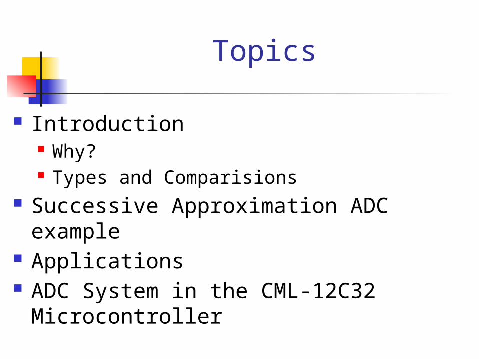
Topics
Introduction Why? Types and Comparisons
Successive Approximation ADC example Applications ADC System in the CML-12C32
Microcontroller
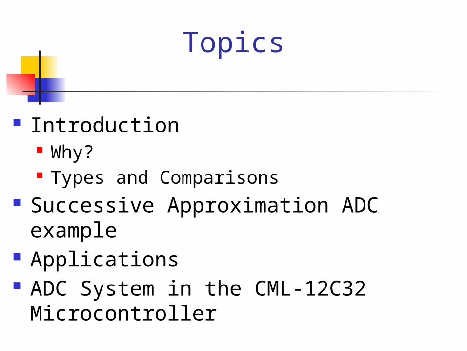
Analog systems are typically what engineers need to analyze. ADCs are used to turn analog information into digital data.
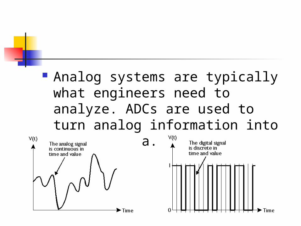
Process
Sampling, Quantification, EncodingOutput States
Discrete Voltage Ranges (V)
0 0.00-1.25
1 1.25-2.50
2 2.50-3.75
3 3.75-5.00
4 5.00-6.25
5 6.25-7.50
6 7.50-8.75
7 8.75-10.0
Out-put
Binary Equivalent
0 000
1 001
2 010
3 011
4 100
5 101
6 110
7 111
Resolution, Accuracy, and Conversion time
Resolution – Number of discrete values it can produce over the range of analog values; Q=R/N
Accuracy – Improved by increasing sampling rate and resolution.
Time – Based on number of steps required in the conversion process.
Comparing types of ADCs
Flash ADC Sigma-delta ADC Wilkinson ADC Integrating ADC Successive Approximation
Converter
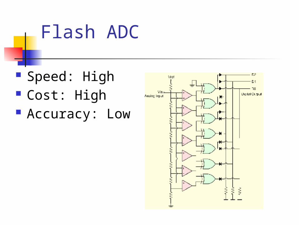
Flash ADC
Speed: High Cost: High Accuracy: Low
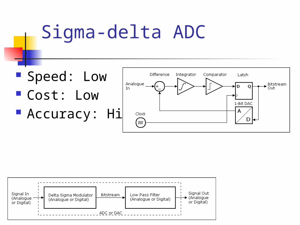
Sigma-delta ADC
Speed: Low Cost: Low Accuracy: High

Wilkinson ADC
Speed: High Cost: High Accuracy: High
Wilkinson Analog Digital Converter
(ADC) circuit schematic diagram
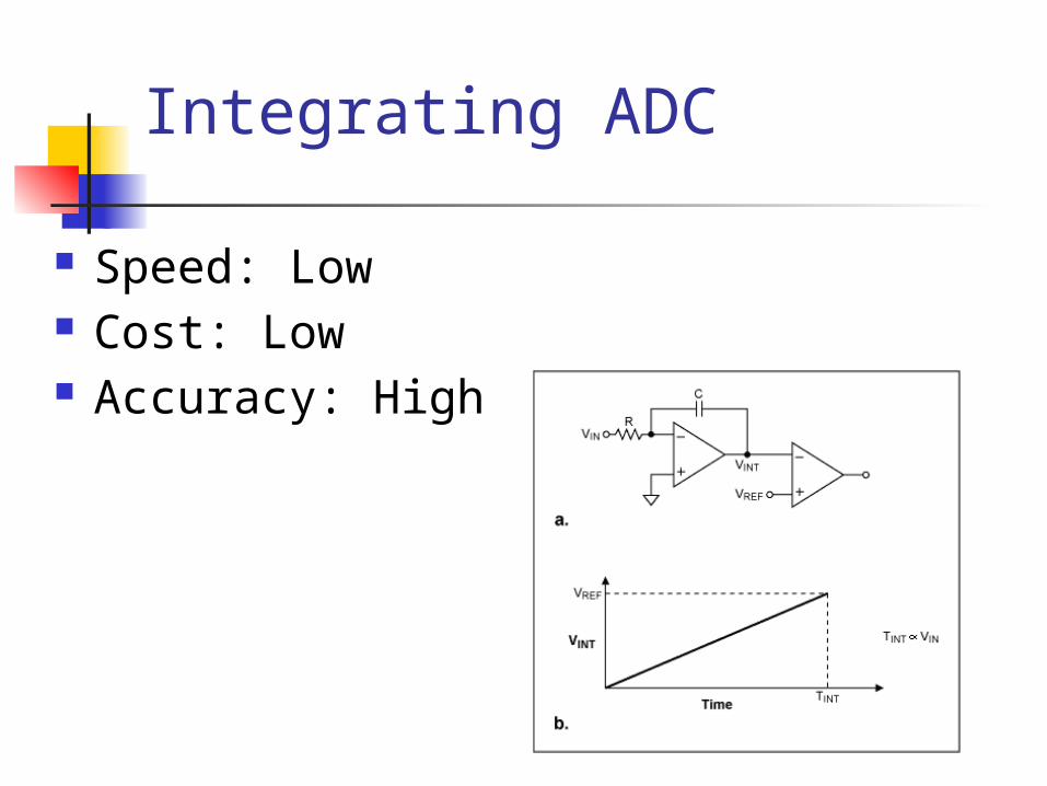
Integrating ADC
Speed: Low Cost: Low Accuracy: High

Successive Approximation Converter
Speed: High Cost: High Accuracy: High but limited
Topics
Introduction Why? Types and Comparisions
Successive Approximation ADC example Applications ADC System in the CML-12C32
Microcontroller
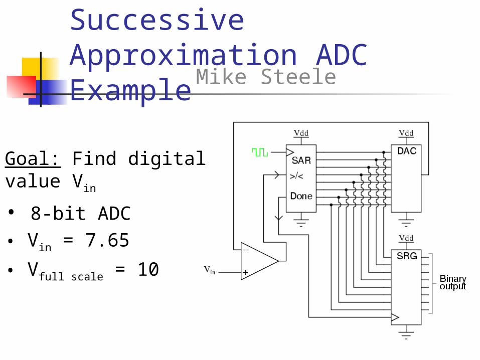
Successive Approximation ADC ExampleMike Steele
Goal: Find digital value Vin
• 8-bit ADC• Vin = 7.65
• Vfull scale = 10
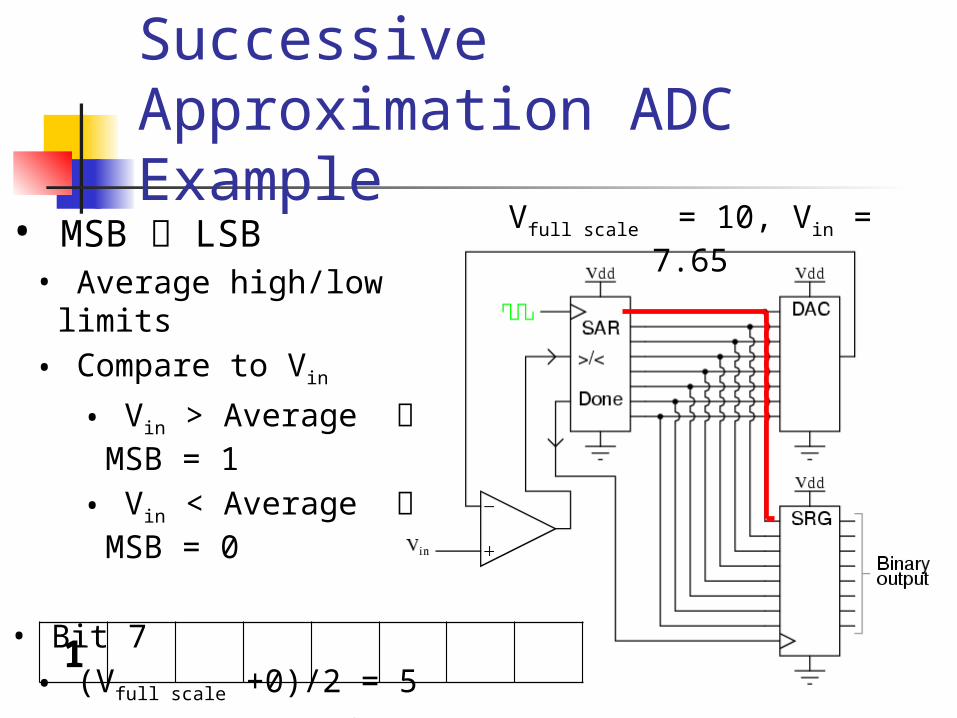
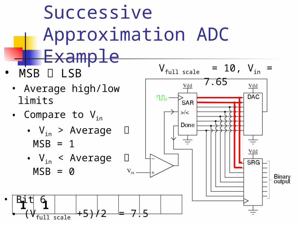
Successive Approximation ADC Example
• MSB LSB• Average high/low limits• Compare to Vin
• Vin > Average MSB = 1
• Vin < Average MSB = 0
• Bit 7• (Vfull scale +0)/2 = 5• 7.65 > 5 Bit 7 = 1
Vfull scale = 10, Vin = 7.65
1
Successive Approximation ADC Example
• MSB LSB• Average high/low limits• Compare to Vin
• Vin > Average MSB = 1
• Vin < Average MSB = 0
• Bit 6• (Vfull scale +5)/2 = 7.5• 7.65 > 7.5 Bit 6 = 1
Vfull scale = 10, Vin = 7.65
1 1

Successive Approximation ADC Example
• MSB LSB• Average high/low limits• Compare to Vin
• Vin > Average MSB = 1
• Vin < Average MSB = 0
• Bit 5• (Vfull scale +7.5)/2 = 8.75• 7.65 < 8.75 Bit 5 = 0
Vfull scale = 10, Vin = 7.65
1 1 0
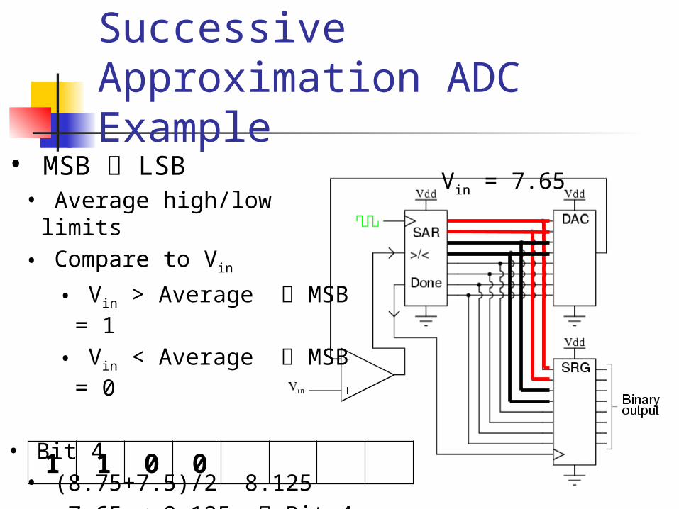
Successive Approximation ADC Example
• MSB LSB• Average high/low limits• Compare to Vin
• Vin > Average MSB = 1
• Vin < Average MSB = 0
• Bit 4• (8.75+7.5)/2 8.125• 7.65 < 8.125 Bit 4 = 0
Vin = 7.65
1 1 0 0

Successive Approximation ADC Example
• MSB LSB• Average high/low limits• Compare to Vin
• Vin > Average MSB = 1
• Vin < Average MSB = 0
• Bit 3• (8.125+7.5)/2 = 7.8125• 7.65 < 7.8125 Bit 3 = 0
Vin = 7.65
1 1 0 0 0
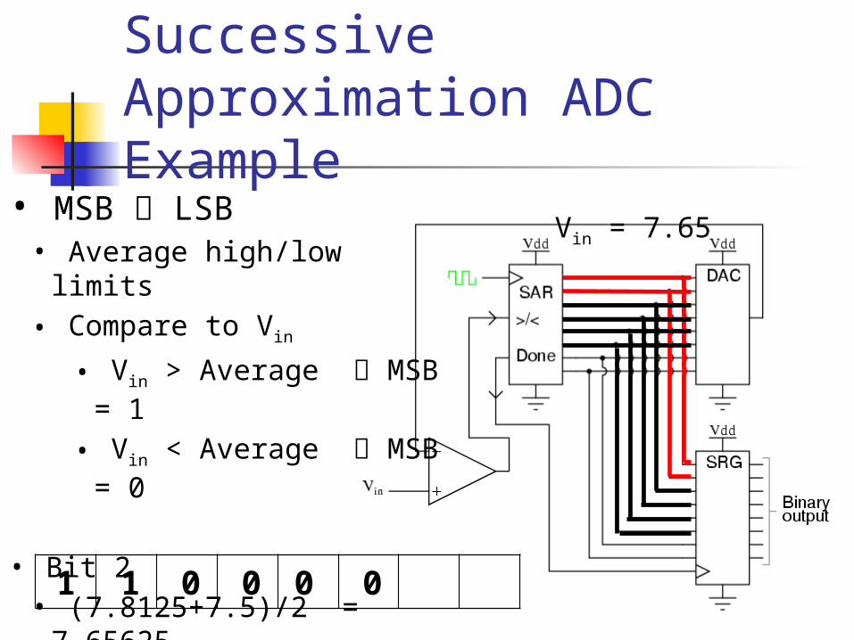
Successive Approximation ADC Example
• MSB LSB• Average high/low limits• Compare to Vin
• Vin > Average MSB = 1
• Vin < Average MSB = 0
• Bit 2• (7.8125+7.5)/2 = 7.65625• 7.65 < 7.65625 Bit 2 = 0
Vin = 7.65
1 1 0 0 0 0
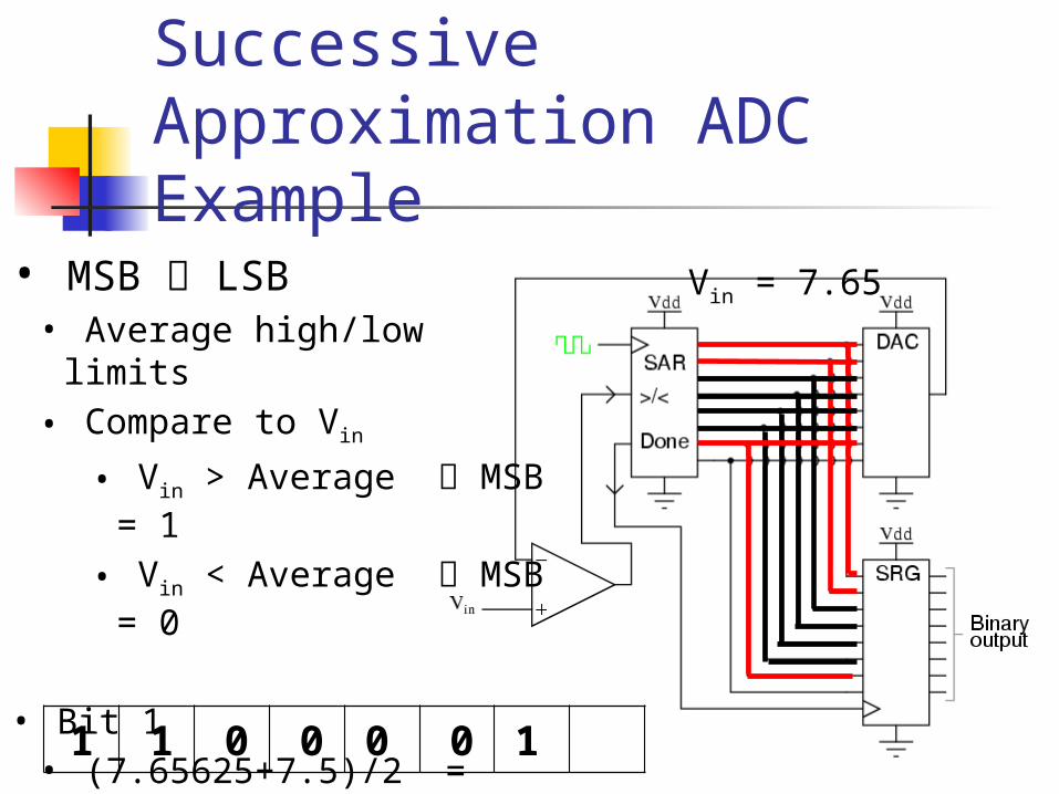
Successive Approximation ADC Example
• MSB LSB• Average high/low limits• Compare to Vin
• Vin > Average MSB = 1
• Vin < Average MSB = 0
• Bit 1• (7.65625+7.5)/2 = 7.578125• 7.65 > 7.578125 Bit 1 = 1
Vin = 7.65
1 1 0 0 0 0 1

Successive Approximation ADC Example
• MSB LSB• Average high/low limits• Compare to Vin
• Vin > Average MSB = 1
• Vin < Average MSB = 0
• Bit 0• (7.65625+7.578125)/2 =
7.6171875• 7.65 > 7.6171875 Bit 0 = 1
Vin = 7.65
1 1 0 0 0 0 1 1
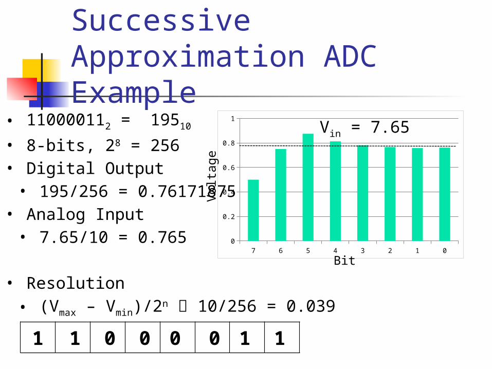
Successive Approximation ADC Example
• 110000112 = 19510
• 8-bits, 28 = 256• Digital Output
• 195/256 = 0.76171875• Analog Input
• 7.65/10 = 0.765
• Resolution• (Vmax – Vmin)/2n 10/256 = 0.039
1 1 0 0 0 0 1 1
7 6 5 4 3 2 1 00
0.2
0.4
0.6
0.8
1
Volta
ge
Bit
Vin = 7.65

ADC Applications
• Measurements / Data Acquisition• Control Systems• PLCs (Programmable Logic Controllers)• Sensor integration (Robotics)• Cell Phones• Video Devices • Audio Devices
t t
e e*Controller0
01
0010
1001
1101
1
∆t
e*(∆t)
100
1001
0101
0010
1
∆t
u*(∆t)
ATD10B8C on MC9S12C32
Presented by
Quinn Morrison

MC9S12C32 Block Diagram
ATD 10B8C
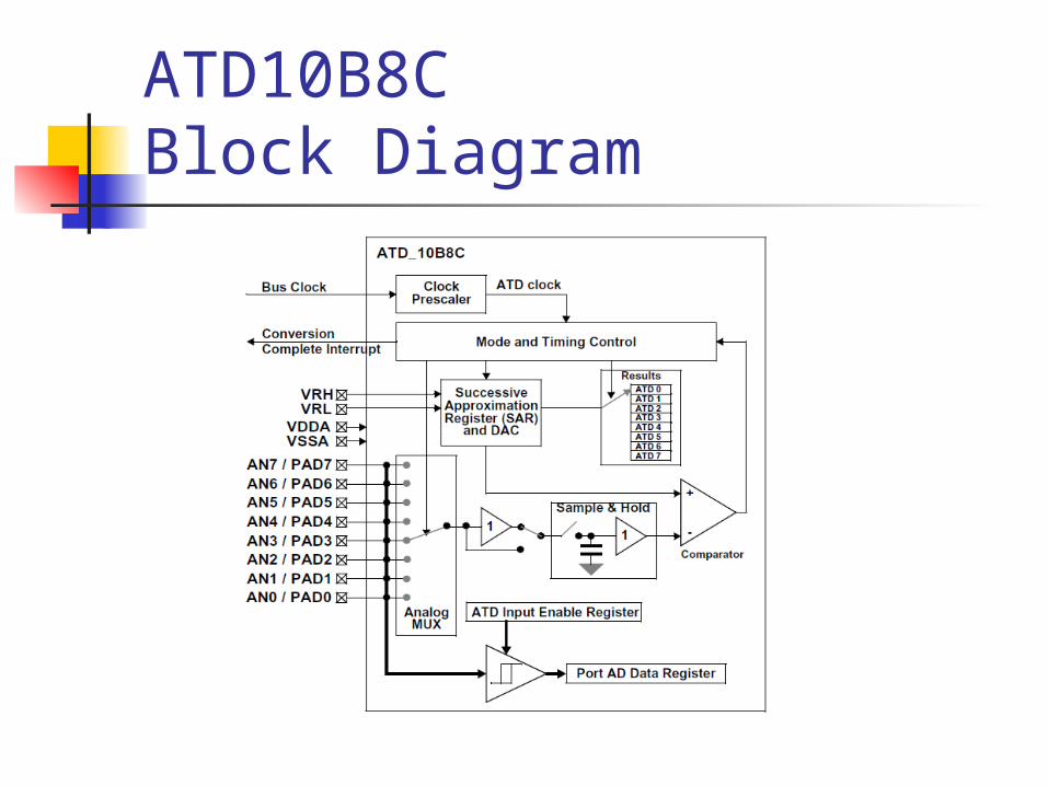
ATD10B8C Block Diagram

ATD10B8C Key Features Resolution
8/10 bit (manually chosen) Conversion Time
7 usec, 10 bit Successive Approximation ADC
architecture 8-channel multiplexed inputs External trigger control Conversion modes
Single or continuous sampling Single or multiple channels
ATD10B8C Modes and OperationsModes Stop Mode
All clocks halt; conversion aborts; minimum recovery delay Wait Mode
Reduced MCU power; can resume Freeze Mode
Breakpoint for debugging an application
Operations Setting up and Starting the A/D Conversion Aborting the A/D Conversion Resets Interrupts
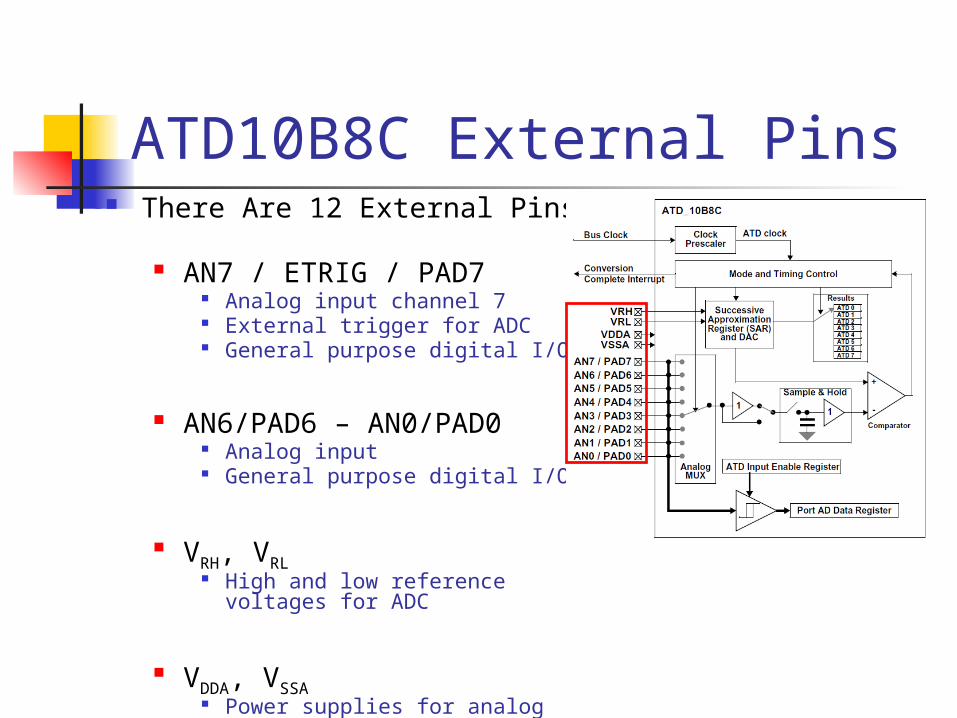
ATD10B8C External Pins There Are 12 External Pins
AN7 / ETRIG / PAD7 Analog input channel 7 External trigger for ADC General purpose digital I/O
AN6/PAD6 – AN0/PAD0 Analog input General purpose digital I/O
VRH, VRL High and low reference voltages for
ADC
VDDA, VSSA Power supplies for analog circuitry
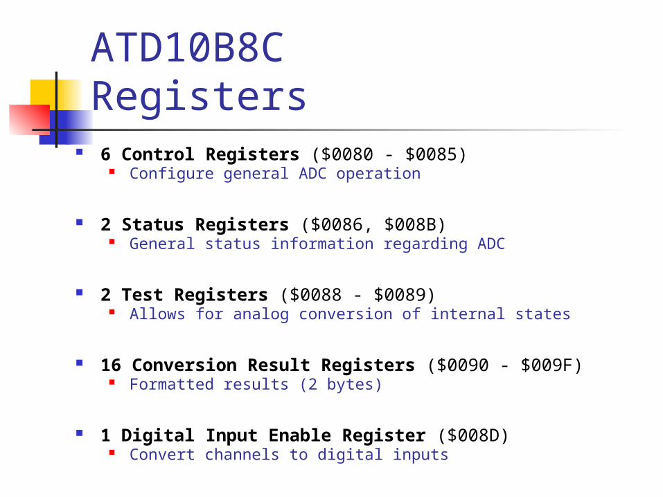
ATD10B8C Registers
6 Control Registers ($0080 - $0085) Configure general ADC operation
2 Status Registers ($0086, $008B) General status information regarding ADC
2 Test Registers ($0088 - $0089) Allows for analog conversion of internal states
16 Conversion Result Registers ($0090 - $009F) Formatted results (2 bytes)
1 Digital Input Enable Register ($008D) Convert channels to digital inputs
1 Digital Port Data Register ($008F) Contains logic levels of digital input pins

ATD10B8C Control Register 2
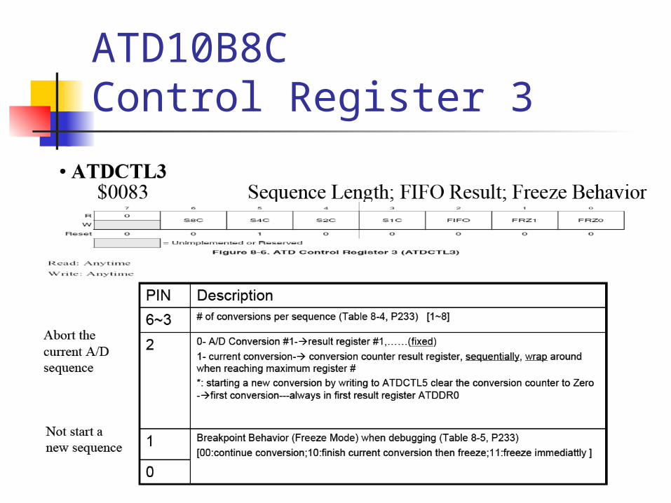
ATD10B8C Control Register 3
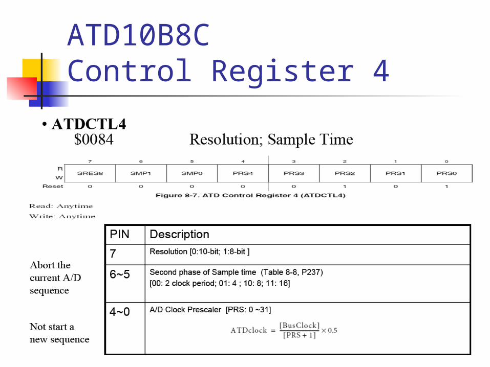
ATD10B8C Control Register 4
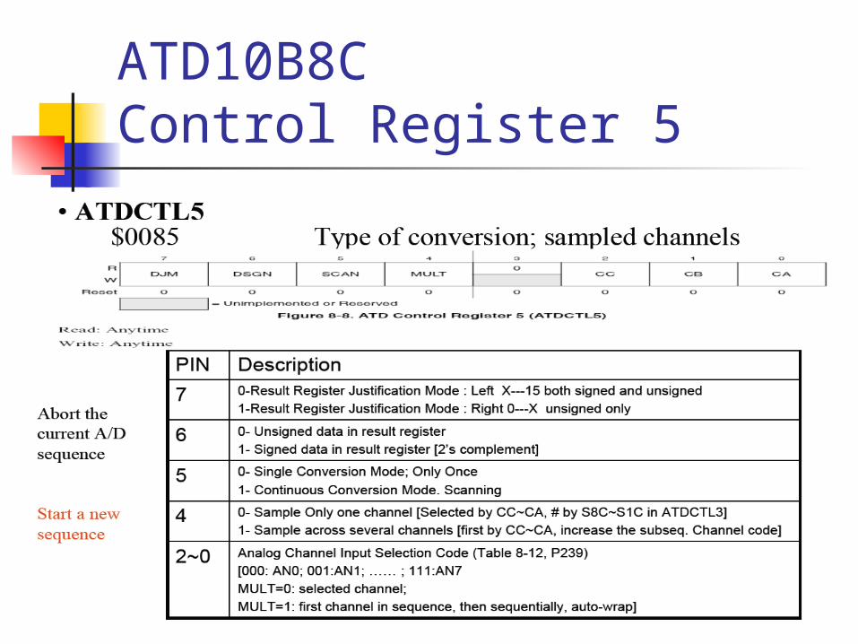
ATD10B8C Control Register 5
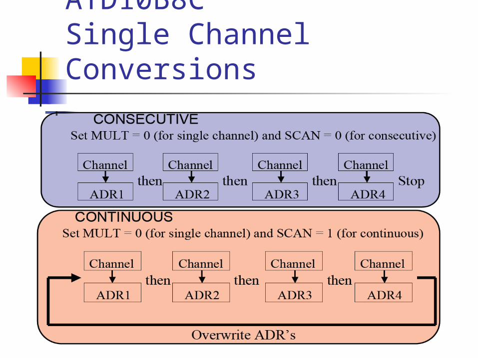
ATD10B8C Single Channel Conversions

ATD10B8C Multi-channel Conversions
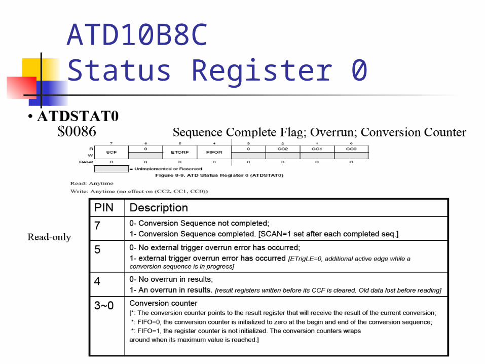
ATD10B8C Status Register 0

ATD10B8C Status Register 1
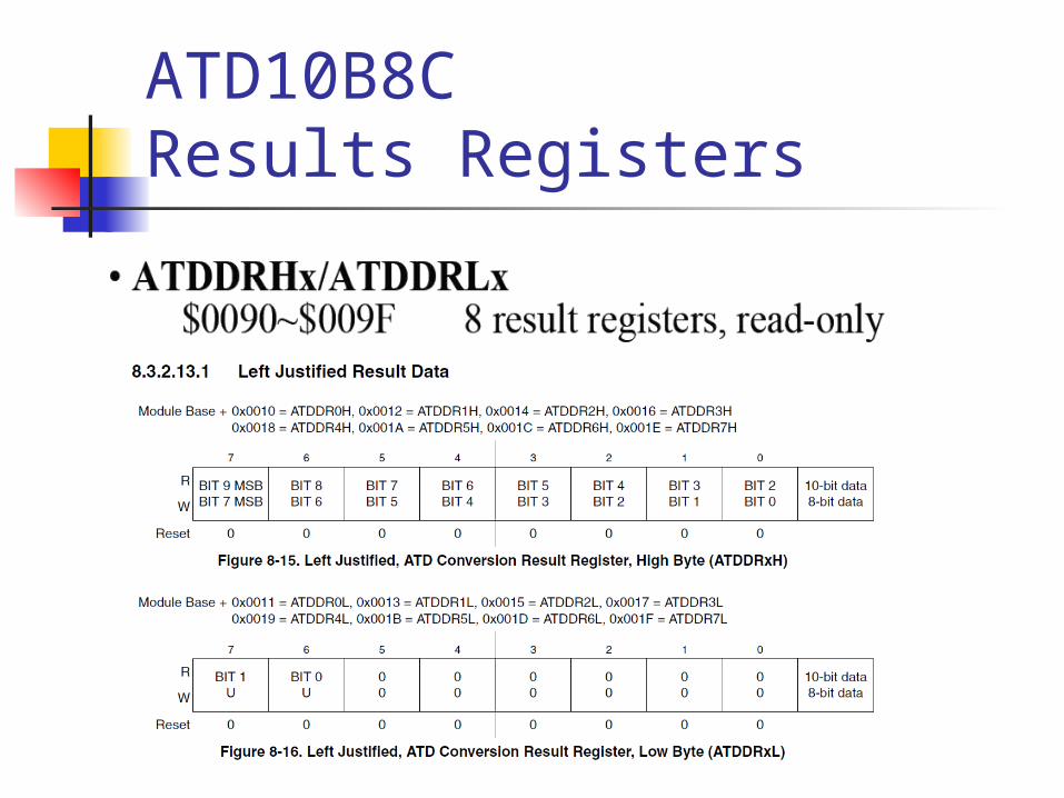
ATD10B8C Results Registers
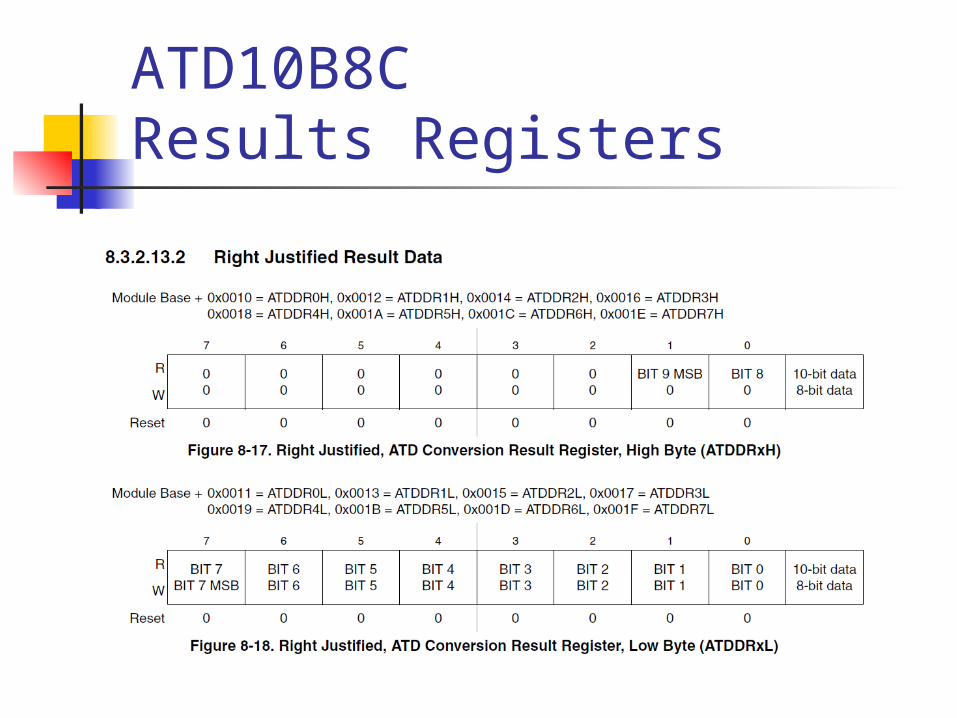
ATD10B8C Results Registers
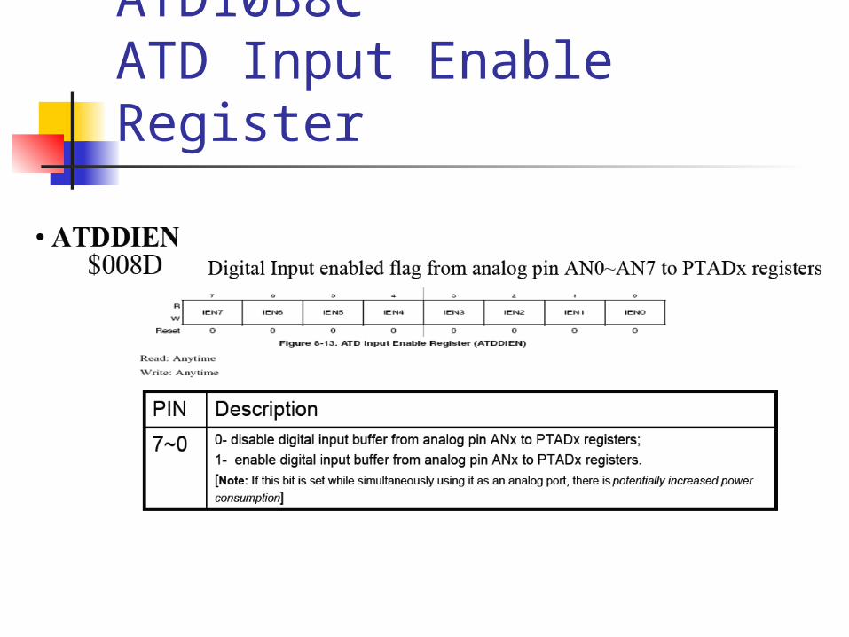
ATD10B8C ATD Input Enable Register
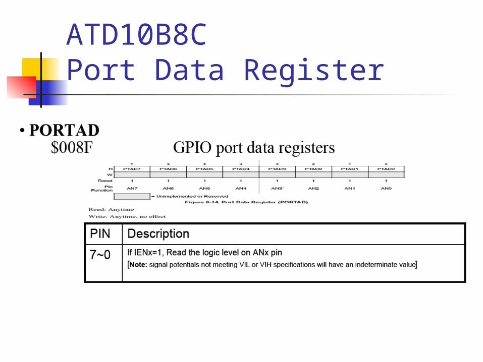
ATD10B8C Port Data Register
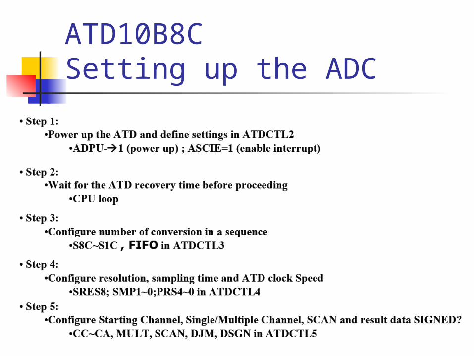
ATD10B8C Setting up the ADC

References
• Dr. Ume, http://www.me.gatech.edu/mechatronics_course/• Maxim Integrated Products, AN1870, AN 1870, APP1870, Appnote1870,
Appnote 1870
• "An Introduction to Sigma Delta Converters." Die Homepage Der Familie Beis. 10 June 2008. Web. 27 Sept. 2010. <http://www.beis.de/Elektronik/DeltaSigma/SigmaDelta.html>.
Related Documents