10-May-2016 Report ID 2016-W18 -SOAG May 2016 5 PRODUCT/PROCESS CHANGE NOTIFICATION PCN AMG/16/9830 Analog & MEMS Group (AMG) New material set in ST Bouskoura for General Purpose Analog Automotive grade products in SO8 and SO14 packages

Welcome message from author
This document is posted to help you gain knowledge. Please leave a comment to let me know what you think about it! Share it to your friends and learn new things together.
Transcript
10-May-2016 Report ID 2016-W18 -SOAG
May 2016 5
PRODUCT/PROCESS CHANGE NOTIFICATION
PCN AMG/16/9830
Analog & MEMS Group (AMG)
New material set in ST Bouskoura for General Purpose Analog
Automotive grade products in SO8 and SO14 packages

9-May-2016 Report ID 2016-W18 AG-SO
6
WHAT: Progressing on the activities related to quality continuous improvement, ST is glad to announce a new material set for Automotive Grade version of General Purpose Analog products in SO8 and SO14 packages produced in ST Bouskoura. Please find more information related to material change in the table here below (for all impacted products except TL431AIYDT and TL1431AIYDT).
Material Current process
Modified process
Comment
Diffusion location ST Ang Mo Kio (Singapore)/ UMC / ST Agrate
ST Ang Mo Kio (Singapore)/ UMC / ST Agrate
No change
Assembly location ST Bouskoura ST Bouskoura No change
Molding compound Sumitomo G700K Sumitomo G700KC Similar grade version more adapted to high density frame
Die attach Ablestick 8601-S25 Ablestick 8601-S25 No change
Leadframe Copper preplated NiPdAgAu
standard density Copper preplated ag spot
High density Move to Sn plating to solve some
sporadic discoloration issues
Wire Copper 1 mil Copper 1 mil No change
Plating NiPdAgAu
(see comment on Moisture Barrier Bag)
Sn
Sn plating already running for standard product for more than 3
year on SO package and will allow to solve sporadic discoloration is-sues sawn on NiPdAgAu plating
Please find more information related to material change for TL431AIYDT and TL1431AIYDT :
Material Current process
Modified process
Comment
Diffusion location ST Ang Mo Kio (Singapore) ST Ang Mo Kio (Singapore) No change
Assembly location ST Bouskoura ST Bouskoura No change
Molding compound HITACHI MP8000CH4-2A Sumitomo G700KC Move to a high reliability compound with lower moisture absorption and
less ionic content
Die attach HITACHI EN4900 ST10 Ablestick 8601-S25 Will allow to solve some sporadic
inhomogeneity issues sawn on cur-rent glue
Leadframe Copper preplated NiPdAu
standard density Copper preplated ag spot
High density Move to Sn plating to solve some
sporadic discoloration issues
Wire Gold 1 mil Copper 1 mil For production standardisation
Plating NiPdAgAu
(see comment on Moisture Barrier Bag)
Sn
Sn plating already running for standard product for more than 3
year on SO package and will allow to solve sporadic discoloration is-sues sawn on NiPdAgAu plating
MSL 1 3 As per internal rules for leadframe with fused pins
9-May-2016 Report ID 2016-W18 AG-SO
7
Moisture barrier bag on NiPdAgAu plating frame products : Please note that we will start on the current process (with NiPdAgAu plating) the implementation of a Moisture Barrier Bag from WK23’2016. This bag will protect the product during exposure to uncon-trolled environment before product usage (transportation/storage) and will avoid any lead coloration variation. The Moisture Barrier Bag will contain desiccant. The Label will be positioned on the MBB. Once the MBB is removed, there is no change as the reel has a label too. This moisture barrier bag will be removed once we switch to the new material set (with Tin plating) as it won’t be sensitive to lead discoloration anymore. For more details, please refer to the appendix at the end of this document. Samples of vehicle test are available now and other samples will be launched upon customer’s re-quests. Please submit requests for samples within 30 days of this notification. WHY: This material change will contribute to ST’s continuous quality product improvement and ensure a consistent assembly process through all the SO production lines. HOW: The qualification program consists mainly of comparative electrical characterization and reliability tests. You will find here after the qualification test plan which summarizes the various test methods and conditions that ST uses for this qualification program. WHEN: The new material set will be implemented in Q3/2016 in Bouskoura. Marking and traceability: Unless otherwise stated by customer’s specific requirement, the traceability of the parts assembled with the new material set will be ensured by new internal sales type, date code and lot number. The second level interconnect, printed on label will move from e4 to e3. The changes here reported will not affect the electrical, dimensional and thermal parameters keep-ing unchanged all the information reported on the relevant datasheets. There is -as well- no change in the packing process or in the standard delivery quantities. Lack of acknowledgement of the PCN within 30 days will constitute acceptance of the change. After acknowledgement, lack of additional response within the 90 day period will constitute acceptance of the change (Jedec Standard No. 46-C). Shipments may start earlier with the customer’s written agreement.
9-May-2016 Report ID 2016-W18 AG-SO
8
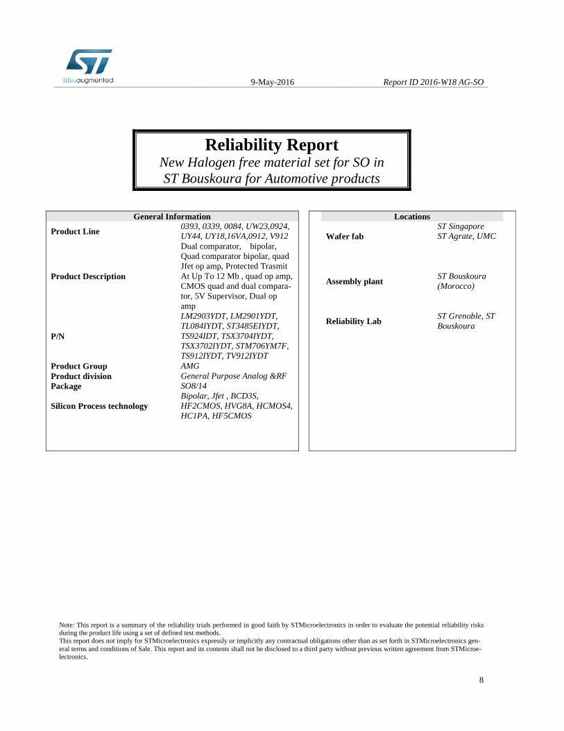
Reliability Report New Halogen free material set for SO in ST Bouskoura for Automotive products
General Information
Product Line 0393, 0339, 0084, UW23,0924, UY44, UY18,16VA,0912, V912
Product Description
Dual comparator, bipolar, Quad comparator bipolar, quad Jfet op amp, Protected Trasmit At Up To 12 Mb , quad op amp, CMOS quad and dual compara-tor, 5V Supervisor, Dual op amp
P/N
LM2903YDT, LM2901YDT, TL084IYDT, ST3485EIYDT, TS924IDT, TSX3704IYDT, TSX3702IYDT, STM706YM7F, TS912IYDT, TV912IYDT
Product Group AMG Product division General Purpose Analog &RF Package SO8/14
Silicon Process technology Bipolar, Jfet , BCD3S, HF2CMOS, HVG8A, HCMOS4, HC1PA, HF5CMOS
Locations
Wafer fab ST Singapore ST Agrate, UMC
Assembly plant ST Bouskoura (Morocco)
Reliability Lab ST Grenoble, ST Bouskoura
Note: This report is a summary of the reliability trials performed in good faith by STMicroelectronics in order to evaluate the potential reliability risks during the product life using a set of defined test methods. This report does not imply for STMicroelectronics expressly or implicitly any contractual obligations other than as set forth in STMicroelectronics gen-eral terms and conditions of Sale. This report and its contents shall not be disclosed to a third party without previous written agreement from STMicroe-lectronics.
9-May-2016 Report ID 2016-W18 AG-SO
9
TABLE OF CONTENTS 1 APPLICABLE AND REFERENCE DOCUMENTS .......................................................................................... 10 2 GLOSSARY ..................................................................................................................................................... 10 3 RELIABILITY EVALUATION OVERVIEW ...................................................................................................... 10
3.1 OBJECTIVES ............................................................................................................................................. 10 3.2 CONCLUSION ........................................................................................................................................... 10
4 DEVICE CHARACTERISTICS ........................................................................................................................ 11 4.1 DEVICE DESCRIPTION ............................................................................................................................... 11 4.2 CONSTRUCTION NOTE ............................................................................................................................... 19
5 TESTS RESULTS SUMMARY ........................................................................................................................ 20 5.1 TEST VEHICLE .......................................................................................................................................... 20 5.2 TEST PLAN AND RESULTS SUMMARY .......................................................................................................... 20
6 ANNEXES ........................................................................................................................................................ 39 6.1 DEVICE DETAILS ....................................................................................................................................... 39 6.2 TESTS DESCRIPTION ................................................................................................................................ 43

9-May-2016 Report ID 2016-W18 AG-SO
10
1 APPLICABLE AND REFERENCE DOCUMENTS
Document reference Short description AEC-Q100 Stress test qualification for automotive grade integrated circuits AEC-Q101 Stress test qualification for automotive grade discrete semiconductors JESD47 Stress-Test-Driven Qualification of Integrated Circuits
2 GLOSSARY DUT Device Under Test PCB Printed Circuit Board SS Sample Size
3 RELIABILITY EVALUATION OVERVIEW
3.1 Objectives To qualify a new material set for Automotive products in SO package produced in ST Bouskoura : - Sumitomo G700KC which is an evolution of Sumitomo G700K - move from NiPdAgAu preplating to Sn postplating
3.2 Conclusion Qualification Plan requirements have been fulfilled without issue. It is stressed that reliability tests have to show that the devices behave correctly against environmental tests (no failure). Moreover, the stability of electrical parameters during the accelerated tests have to demonstrate the ruggedness of the products and safe operation, which is consequently expected during their lifetime.

9-May-2016 Report ID 2016-W18 AG-SO
11
4 DEVICE CHARACTERISTICS
4.1 Device description LM2903YDT

9-May-2016 Report ID 2016-W18 AG-SO
12
LM2901YDT,
9-May-2016 Report ID 2016-W18 AG-SO
13
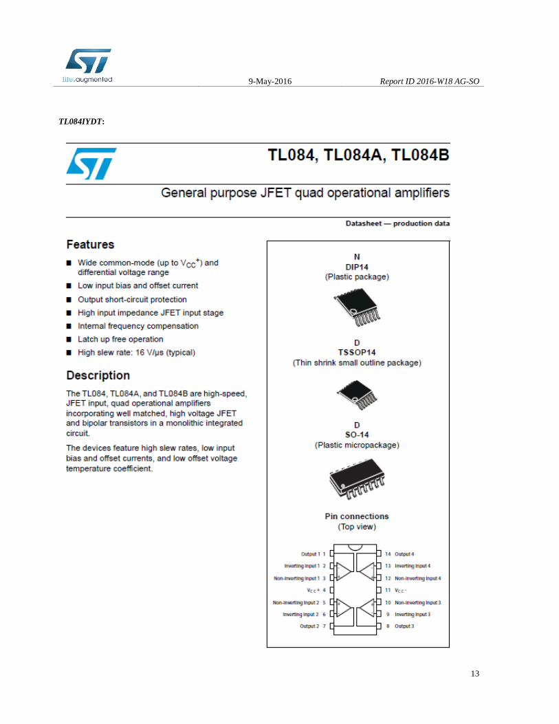
TL084IYDT:
9-May-2016 Report ID 2016-W18 AG-SO
14
9-May-2016 Report ID 2016-W18 AG-SO
15
9-May-2016 Report ID 2016-W18 AG-SO
16
9-May-2016 Report ID 2016-W18 AG-SO
17

9-May-2016 Report ID 2016-W18 AG-SO
18

9-May-2016 Report ID 2016-W18 AG-SO
19
4.2 Construction note P/N
LM2903YDT P/N
LM2901YDT P/N
TL084IYDT P/N
ST3485EIYDT P/N
TS924IDT Wafer/Die fab. information Wafer fab manufacturing loca-tion
ST Singapore ST Singapore ST Singapore ST Singapore ST Singapore
Technology Bipolar Bipolar JFet BCD3S HF2CMOS Die finishing back side RAW SILICON RAW SILICON RAW SILICON RAW SILICON RAW SILICON Die size (microns) 950 x 870 µm 1370x1270 2480 x 1460 1950x2720 1980x2450 Bond pad metallization layers AlSiCu AlSiCu AlSiCu AlSi AlSiCu Passivation type Nitride Nitride P-VAPOX/NITRIDE P-VAPOX/NITRIDE/POLYIMIDE P-VAPOX/NITRIDE
Wafer Testing (EWS) informa-tion
Electrical testing manufacturing location
ST Singapore ST Singapore ST Singapore ST Singapore
ST Singapore
Tester ASL1K ASL1K ASL1K ASL1K ASL1K
Assembly information Assembly site ST Bouskoura ST Bouskoura ST Bouskoura ST Bouskoura ST Bouskoura Package description SO8 SO14 SO14 SO8 SO14 Molding compound EME G700KC EME G700KC EME G700KC EME G700KC EME G700KC Frame material Cu Cu Cu Cu Cu Die attach process Epoxy Glue Epoxy Glue Epoxy Glue Epoxy Glue Epoxy Glue Die attach material 8601S-25 8601S-25 8601S-25 8601S-25 8601S-25 Wire bonding process Thermosonic ball bon-
ding Thermosonic ball bon-
ding Thermosonic ball bonding Thermosonic ball bonding Thermosonic ball bonding
Wires bonding mate-rials/diameters
Cu 1 mil Cu 1 mil Cu 1 mil Cu 1 mil Cu 1 mil
Lead finishing process electroplating electroplating electroplating electroplating electroplating Lead finishing/bump solder ma-terial
Matte tin Matte tin Matte tin Matte tin Matte tin
Final testing information Testing location ST Bouskoura ST Bouskoura ST Bouskoura ST Bouskoura ST Bouskoura Tester ASL1K ASL1K ASL1K ASL1K ASL1K
P/N
TSX3704IYDT P/N
TSX3702IYDT P/N
STM706YM7F P/N
MC33079YDT P/N
TS912IYDT P/N
TSV912IYDT Wafer/Die fab. infor-mation
Wafer fab manufactu-ring location
ST Agrate ST Agrate ST Singapore ST Singapore ST Singapore UMC
Technology HVG8A HVG8A HCMOS4 Bipolar HC1PA HF5CMOS Die finishing back side RAW SILICON RAW SILICON RAW SILICON RAW SILICON RAW SILICON RAW SILICON Die size (microns) 1830x1440 µm 1018x1238 µm 1350 x 1510µm 3230x1950µm 2600x1950µm 1100x1070µm Bond pad metallization layers
AlCu AlCu AlSiCu AlSiCu AlSi AlCu
Passivation type HDP/TEOS/SiN/Polyimide HDP/TEOS/SiN/Polyimide PSG+Silicon Ni-tride+Polyimide
Nitride PVAPOX+Nitride Nitride
Wafer Testing (EWS) information
Electrical testing manu-facturing location
ST Singapore ST Singapore ST Singapore ST Singapore ST Singapore ST Singapore
Tester ASL1K ASL1K ASL1K ASL1K ASL1K ASL1K
Assembly information Assembly site ST Bouskoura ST Bouskoura ST Bouskoura ST Bouskoura ST Bouskoura ST Bouskoura Package description SO14 SO14 SO8 SO14 SO8 SO8 Molding compound EME G700KC EME G700KC EME G700KC EME G700KC EME G700KC EME G700KC Frame material Cu Cu Cu Cu Cu Cu Die attach process Epoxy Glue Epoxy Glue Epoxy Glue Epoxy Glue Epoxy Glue Epoxy Glue Die attach material 8601S-25 8601S-25 8601S-25 8601S-25 8601S-25 8601S-25 Wire bonding process Thermosonic ball bonding Thermosonic ball bonding Thermosonic ball bonding Thermosonic ball bon-
ding Thermosonic ball
bonding Thermosonic ball bonding
Wires bonding mate-rials/diameters
Cu 1 mil Cu 1 mil Cu 1 mil Cu 1 mil Cu 1 mil Cu 1 mil
Lead finishing process electroplating electroplating electroplating electroplating electroplating electroplating Lead finishing/bump solder material
Matte tin Matte tin Matte tin Matte tin Matte tin Matte tin
Final testing informa-tion
Testing location ST Bouskoura ST Bouskoura ST Bouskoura ST Bouskoura ST Bouskoura ST Bouskoura
9-May-2016 Report ID 2016-W18 AG-SO
20
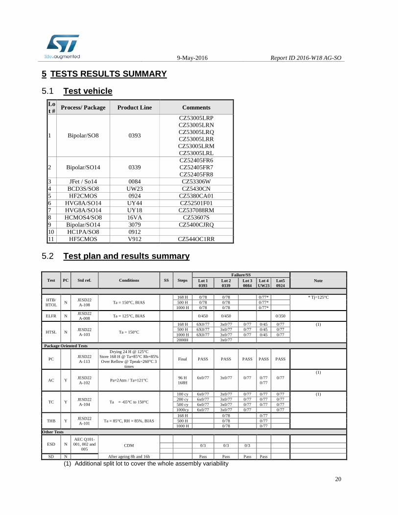
5 TESTS RESULTS SUMMARY
5.1 Test vehicle Lot #
Process/ Package Product Line Comments
1 Bipolar/SO8 0393
CZ53005LRP CZ53005LRN CZ53005LRQ CZ53005LRR CZ53005LRM CZ53005LRL
2 Bipolar/SO14 0339 CZ52405FR6 CZ52405FR7 CZ52405FR8
3 JFet / So14 0084 CZ53306W 4 BCD3S/SO8 UW23 CZ5430CN 5 HF2CMOS 0924 CZ5380CA01 6 HVG8A/SO14 UY44 CZ52501F01 7 HVG8A/SO14 UY18 CZ537088RM 8 HCMOS4/SO8 16VA CZ53607S 9 Bipolar/SO14 3079 CZ5400CJRQ 10 HC1PA/SO8 0912 11 HF5CMOS V912 CZ544OC1RR
5.2 Test plan and results summary
Test PC Std ref. Conditions SS Steps Failure/SS
Lot 1 0393
Lot 2 0339
Lot 3 0084
Lot 4 UW23
Lot5 0924
Note
HTB/ HTOL
N JESD22 A-108
Ta = 150°C, BIAS 168 H 0/78 0/78 0/77* * Tj=125°C 500 H 0/78 0/78 0/77* 1000 H 0/78 0/78 0/77*
ELFR N JESD22 A-008
Ta = 125°C, BIAS 0/450 0/450 0/350
HTSL N JESD22 A-103
Ta = 150°C
168 H 6X0/77 3x0/77 0/77 0/45 0/77 (1) 500 H 6X0/77 3x0/77 0/77 0/45 0/77 1000 H 6X0/77 3x0/77 0/77 0/45 0/77 2000H 3x0/77
Package Oriented Tests
PC JESD22 A-113
Drying 24 H @ 125°C Store 168 H @ Ta=85°C Rh=85% Over Reflow @ Tpeak=260°C 3
times
Final PASS PASS PASS PASS PASS
AC Y JESD22 A-102
Pa=2Atm / Ta=121°C 96 H 168H
6x0/77
3x0/77
0/77
0/77 0/77
0/77
(1)
TC Y JESD22 A-104
Ta = -65°C to 150°C
100 cy 6x0/77 3x0/77 0/77 0/77 0/77 (1) 200 cy 6x0/77 3x0/77 0/77 0/77 0/77 500 cy 6x0/77 3x0/77 0/77 0/77 0/77 1000cy 6x0/77 3x0/77 0/77 0/77
THB Y JESD22 A-101
Ta = 85°C, RH = 85%, BIAS 168 H 0/78 0/77 500 H 0/78 0/77 1000 H 0/78 0/77
Other Tests
ESD N AEC Q101-001, 002 and
005
CDM 0/3 0/3 0/3
SD N After ageing 8h and 16h Pass Pass Pass Pass
(1) Additional split lot to cover the whole assembly variability
9-May-2016 Report ID 2016-W18 AG-SO
21
Test PC Std ref. Conditions SS Steps Failure/SS
Lot 6 UY44
Lot 7 UY18
Lot8 16VA
Lot9 3079
Lot10 0912
Lot11 V912
Note
HTB/ HTOL
N JESD22 A-108
Tj = 125°C, BIAS 168 H 0/77 0/77 0/77 500 H 0/77 0/77 0/77 1000 H 0/77 0/77 0/77
ELFR N JESD22 A-008
Ta = 125°C, BIAS 450 0/450 450
HTSL N JESD22 A-103
Ta = 150°C
168 H 0/77 0/77 0/45 0/77 500 H 0/77 0/77 0/45 0/77 1000 H 0/77 0/45 0/77 2000H
Package Oriented Tests
PC JESD22 A-113
Drying 24 H @ 125°C Store 168 H @ Ta=85°C Rh=85% Over Reflow @ Tpeak=260°C 3
times
Final PASS PASS PASS
AC Y JESD22 A-102
Pa=2Atm / Ta=121°C 96 H 168H
0/77 0/77
0/77 0/77
0/77
TC Y JESD22 A-104
Ta = -65°C to 150°C
100 cy 0/77 0/77 0/77 0/77 200 cy 0/77 0/77 0/77 0/77 500 cy 0/77 0/77 0/77 0/77 1000cy 0/77 0/77
THB Y JESD22 A-101
Ta = 85°C, RH = 85%, BIAS 168 H 0/77 0/77 500 H 0/77 0/77 1000 H 0/77 0/77
Other Tests
ESD N AEC Q101-001, 002 and
005
CDM 1500V 0/3 0/3
SD N After ageing 8h and 16h PASS
9-May-2016 Report ID 2016-W18 AG-SO
22
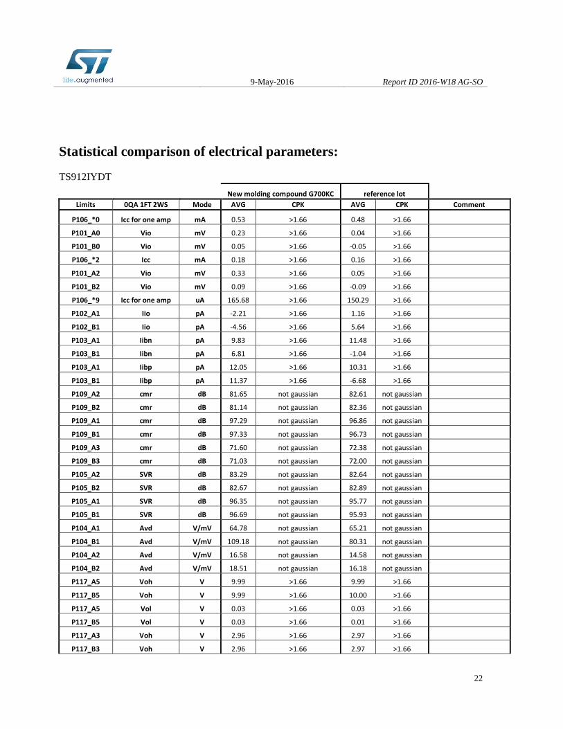
Statistical comparison of electrical parameters: TS912IYDT
New molding compound G700KC reference lot
Limits 0QA 1FT 2WS Mode AVG CPK AVG CPK Comment
P106_*0 Icc for one amp mA 0.53 >1.66 0.48 >1.66
P101_A0 Vio mV 0.23 >1.66 0.04 >1.66
P101_B0 Vio mV 0.05 >1.66 -0.05 >1.66
P106_*2 Icc mA 0.18 >1.66 0.16 >1.66
P101_A2 Vio mV 0.33 >1.66 0.05 >1.66
P101_B2 Vio mV 0.09 >1.66 -0.09 >1.66
P106_*9 Icc for one amp uA 165.68 >1.66 150.29 >1.66
P102_A1 Iio pA -2.21 >1.66 1.16 >1.66
P102_B1 Iio pA -4.56 >1.66 5.64 >1.66
P103_A1 Iibn pA 9.83 >1.66 11.48 >1.66
P103_B1 Iibn pA 6.81 >1.66 -1.04 >1.66
P103_A1 Iibp pA 12.05 >1.66 10.31 >1.66
P103_B1 Iibp pA 11.37 >1.66 -6.68 >1.66
P109_A2 cmr dB 81.65 not gaussian 82.61 not gaussian
P109_B2 cmr dB 81.14 not gaussian 82.36 not gaussian
P109_A1 cmr dB 97.29 not gaussian 96.86 not gaussian
P109_B1 cmr dB 97.33 not gaussian 96.73 not gaussian
P109_A3 cmr dB 71.60 not gaussian 72.38 not gaussian
P109_B3 cmr dB 71.03 not gaussian 72.00 not gaussian
P105_A2 SVR dB 83.29 not gaussian 82.64 not gaussian
P105_B2 SVR dB 82.67 not gaussian 82.89 not gaussian
P105_A1 SVR dB 96.35 not gaussian 95.77 not gaussian
P105_B1 SVR dB 96.69 not gaussian 95.93 not gaussian
P104_A1 Avd V/mV 64.78 not gaussian 65.21 not gaussian
P104_B1 Avd V/mV 109.18 not gaussian 80.31 not gaussian
P104_A2 Avd V/mV 16.58 not gaussian 14.58 not gaussian
P104_B2 Avd V/mV 18.51 not gaussian 16.18 not gaussian
P117_A5 Voh V 9.99 >1.66 9.99 >1.66
P117_B5 Voh V 9.99 >1.66 10.00 >1.66
P117_A5 Vol V 0.03 >1.66 0.03 >1.66
P117_B5 Vol V 0.03 >1.66 0.01 >1.66
P117_A3 Voh V 2.96 >1.66 2.97 >1.66
P117_B3 Voh V 2.96 >1.66 2.97 >1.66
9-May-2016 Report ID 2016-W18 AG-SO
23
P117_A3 Vol V 0.03 >1.66 0.03 >1.66
P117_B3 Vol V 0.03 >1.66 0.03 >1.66
P117_A4 Voh V 2.64 >1.66 2.67 >1.66
P117_B4 Voh V 2.64 >1.66 2.67 >1.66
P117_A4 Vol V 0.25 >1.66 0.24 >1.66
P117_B4 Vol V 0.25 >1.66 0.24 >1.66
P137_A2 Isk mA 39.98 >1.66 41.11 >1.66
P137_B2 Isk mA 41.05 >1.66 41.85 >1.66
P137_A2 Isr mA -40.47 >1.66 -40.49 >1.66
P137_B2 Isr mA -40.32 >1.66 -40.97 >1.66
P137_A1 Isk mA 68.90 >1.66 77.90 >1.66
P137_B1 Isk mA 68.31 >1.66 77.29 >1.66
P137_A1 Isr mA -62.56 >1.66 -70.97 >1.66
P137_B1 Isr mA -66.33 >1.66 -74.66 >1.66
P121_A2 GBP MHz 0.93 >1.66 0.87 >1.66
P121_B2 GBP MHz 0.83 >1.66 0.78 >1.66
P121_A1 GBP MHz 1.44 >1.66 1.30 >1.66
P121_B1 GBP MHz 1.36 >1.66 1.27 >1.66
P113_A2 SRn V/uS 0.47 >1.66 0.41 >1.66
P113_B2 SRn V/uS 0.47 >1.66 0.41 >1.66
P113_A2 SRp V/uS 0.71 >1.66 0.61 >1.66
P113_B2 SRp V/uS 0.55 >1.66 0.48 >1.66

9-May-2016 Report ID 2016-W18 AG-SO
24
LM2901YDT
New material set reference
Limits 0QA 1FT 2WS Units AVG CPK AVERAGE CPK Comment
P101_A0 Vio 5V mV -0.28 >1.6 -0.46 >1.6
P101_B0 Vio 5V mV 0.65 >1.6 0.40 >1.6
P101_C0 Vio 5V mV -0.45 >1.6 -0.41 >1.6
P101_D0 Vio 5V mV 0.71 >1.6 0.52 >1.6
P102_A1 Iio 30V nA -2.61 >1.6 -1.87 >1.6
P102_B1 Iio 30V nA -3.24 >1.6 -4.50 >1.6
P102_C1 Iio 30V nA 1.66 >1.6 -0.38 >1.6
P102_D1 Iio 30V nA -1.63 >1.6 2.13 >1.6
P103_A1 Iibn 30V nA -31.90 >1.6 -29.23 >1.6
P103_B1 Iibn 30V nA -27.01 >1.6 -30.42 >1.6
P103_C1 Iibn 30V nA -30.00 >1.6 -27.22 >1.6
P103_D1 Iibn 30V nA -31.15 >1.6 -25.55 >1.6
P103_A1 Iibp 30V nA -29.29 >1.6 -27.36 >1.6
P103_B1 Iibp 30V nA -23.76 >1.6 -25.92 >1.6
P103_C1 Iibp 30V nA -31.66 >1.6 -26.84 >1.6
P103_D1 Iibp 30V nA -29.52 >1.6 -27.68 >1.6
P101_A4 Vio 30V 28.5V mV -0.46 >1.6 -0.55 >1.6
P101_B4 Vio 30V 28.5V mV 1.33 >1.6 0.97 >1.6
P101_C4 Vio 30V 28.5V mV -0.81 >1.6 -0.86 >1.6
P101_D4 Vio 30V 28.5V mV 1.11 >1.6 0.86 >1.6
P106_*1 Icc 5V mA 0.24 >1.6 0.24 >1.6
P106_*2 Icc 30V mA 0.29 >1.6 0.29 >1.6
P117_A1 Vol 5V V 0.24 >1.6 0.22 >1.6
P117_B1 Vol 5V V 0.23 >1.6 0.20 >1.6
P117_C1 Vol 5V V 0.22 >1.6 0.20 >1.6
P117_D1 Vol 5V V 0.25 >1.6 0.22 >1.6
P137_A1 Isk 5V mA 18.37 >1.6 19.94 >1.6
P137_B1 Isk 5V mA 18.88 >1.6 20.38 >1.6
P137_C1 Isk 5V mA 18.55 >1.6 20.22 >1.6
P137_D1 Isk 5V mA 18.16 >1.6 19.52 >1.6
P138_A1 Ioh 30V uA 0.01 >1.6 0.02 >1.6
P138_B1 Ioh 30V uA 0.02 >1.6 0.01 >1.6
P138_C1 Ioh 30V uA 0.01 >1.6 0.01 >1.6
P138_D1 Ioh 30V uA 0.01 >1.6 0.01 >1.6
9-May-2016 Report ID 2016-W18 AG-SO
25
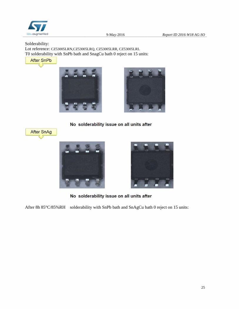
Solderability: Lot reference: CZ53005LRN,CZ53005LRQ, CZ53005LRR, CZ53005LRL T0 solderability with SnPb bath and SnagCu bath 0 reject on 15 units:
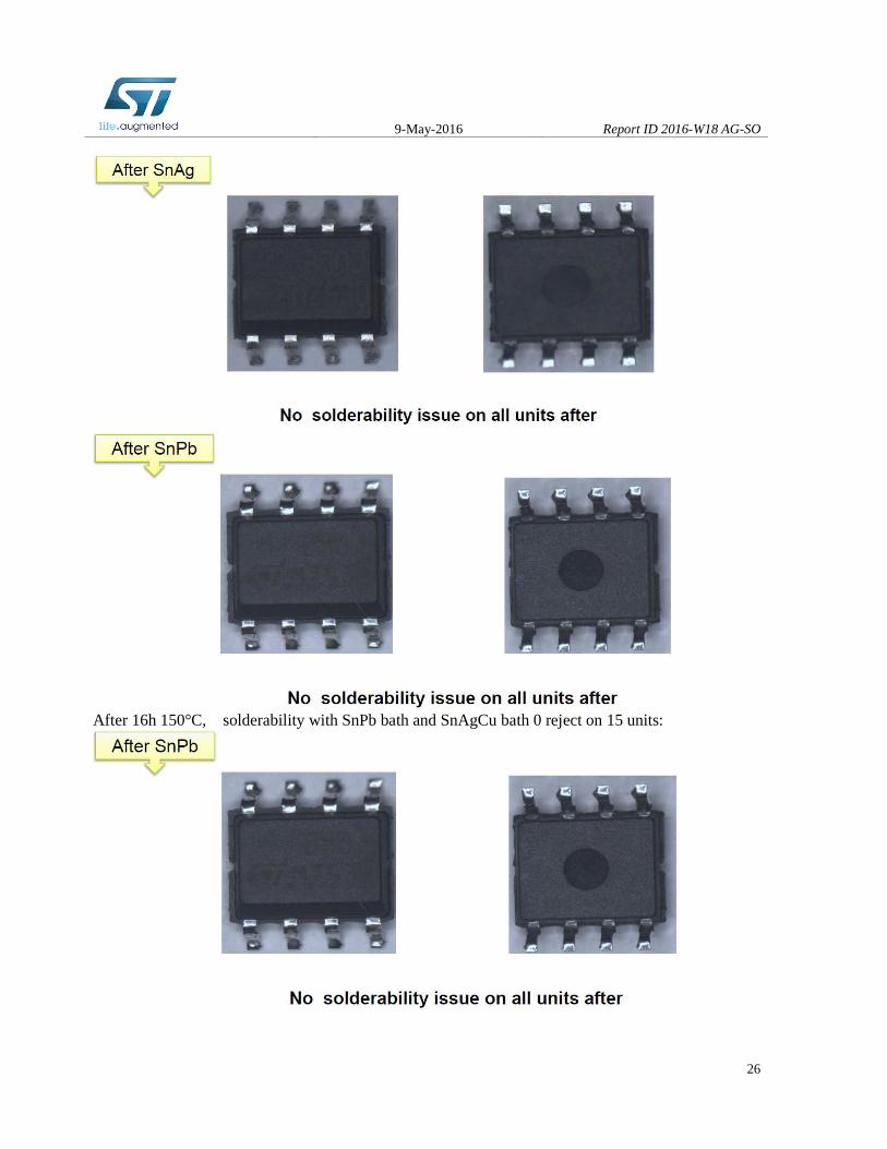
After 8h 85°C/85%RH solderability with SnPb bath and SnAgCu bath 0 reject on 15 units:
9-May-2016 Report ID 2016-W18 AG-SO
26
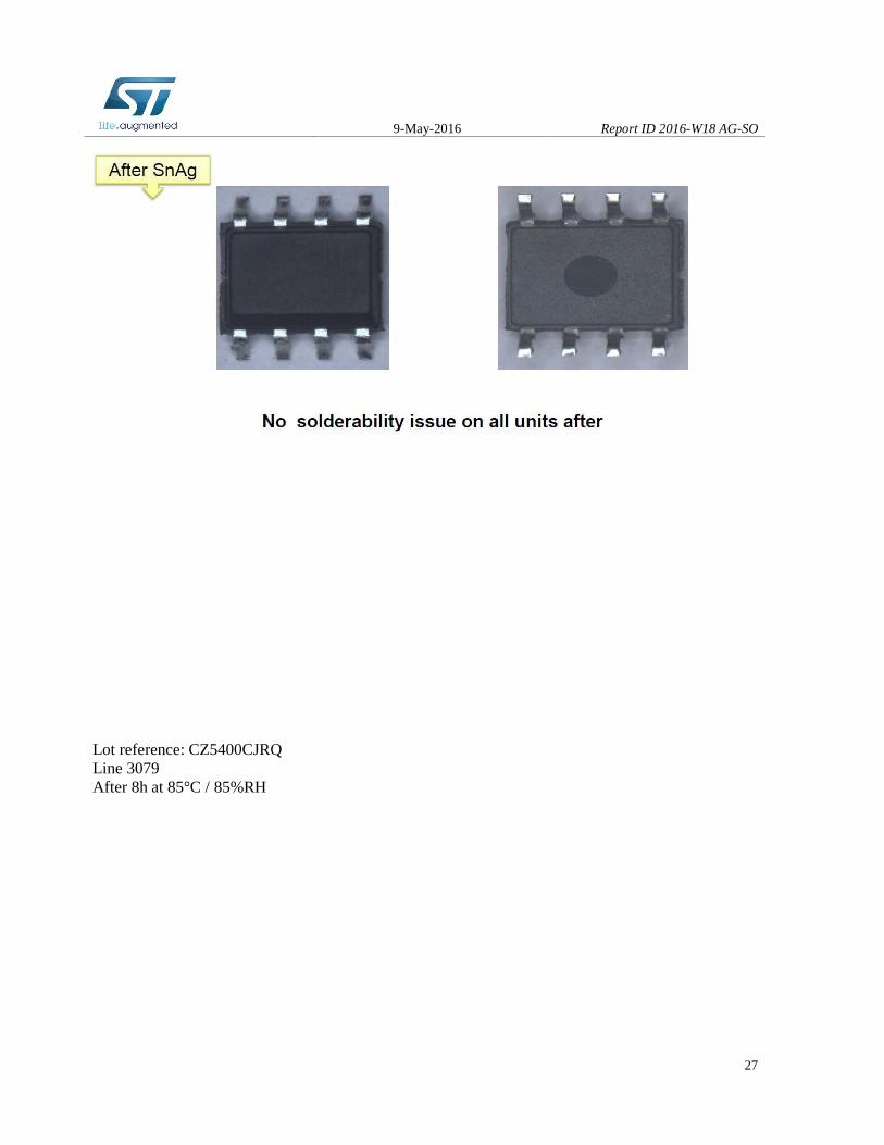
After 16h 150°C, solderability with SnPb bath and SnAgCu bath 0 reject on 15 units:
9-May-2016 Report ID 2016-W18 AG-SO
27
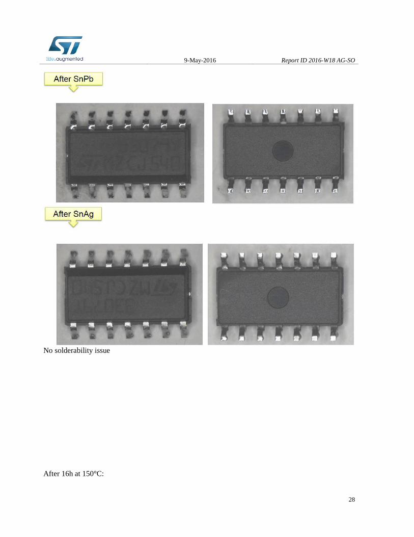
Lot reference: CZ5400CJRQ Line 3079 After 8h at 85°C / 85%RH
9-May-2016 Report ID 2016-W18 AG-SO
28
No solderability issue After 16h at 150°C:

9-May-2016 Report ID 2016-W18 AG-SO
29
No solderability issue

9-May-2016 Report ID 2016-W18 AG-SO
30
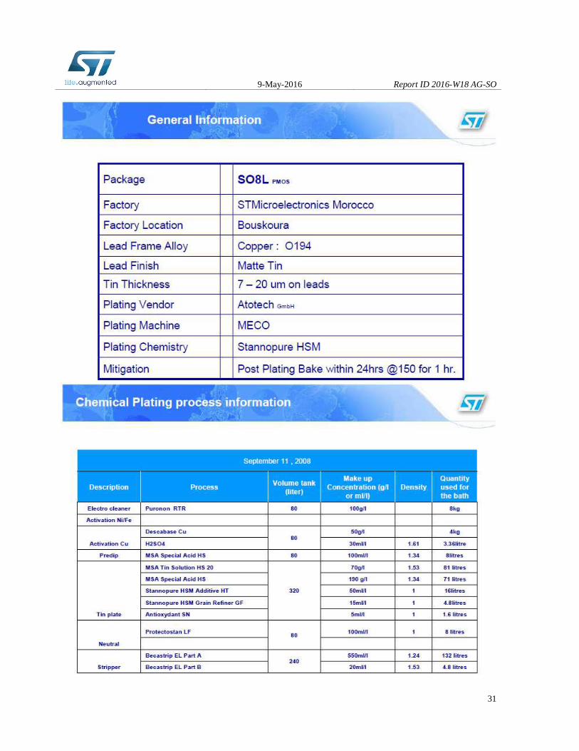
9-May-2016 Report ID 2016-W18 AG-SO
31

9-May-2016 Report ID 2016-W18 AG-SO
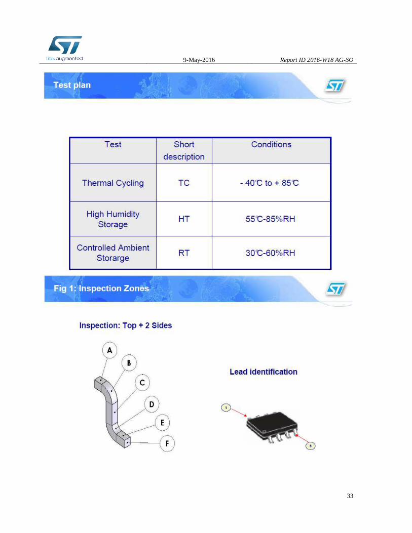
32
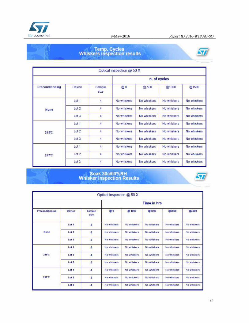
9-May-2016 Report ID 2016-W18 AG-SO
33
9-May-2016 Report ID 2016-W18 AG-SO
34

9-May-2016 Report ID 2016-W18 AG-SO
35
9-May-2016 Report ID 2016-W18 AG-SO
36
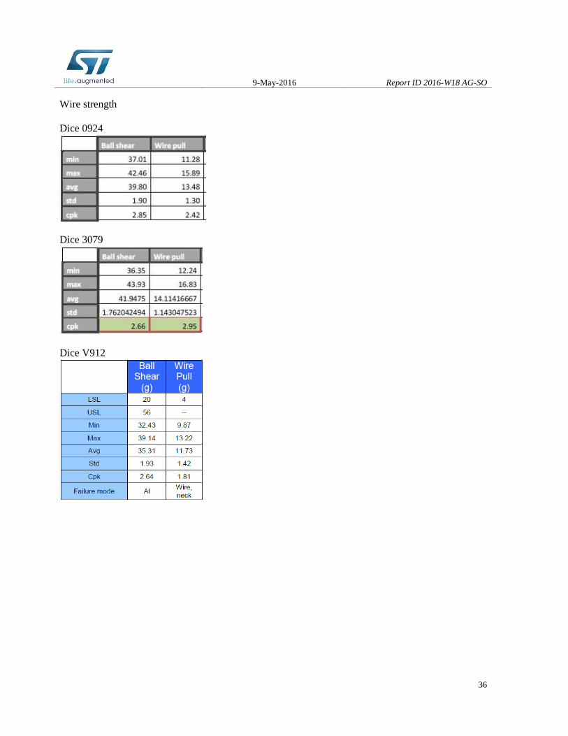
Wire strength Dice 0924
Dice 3079
Dice V912

9-May-2016 Report ID 2016-W18 AG-SO
37
Wire pull test results after TC Dice 16VA
Average 11g, min 7.5g, max 13.8g

9-May-2016 Report ID 2016-W18 AG-SO
38
Die shear Dice 3079
Dice 0393
Dice 0924
9-May-2016 Report ID 2016-W18 AG-SO
39
6 ANNEXES
6.1 Device details
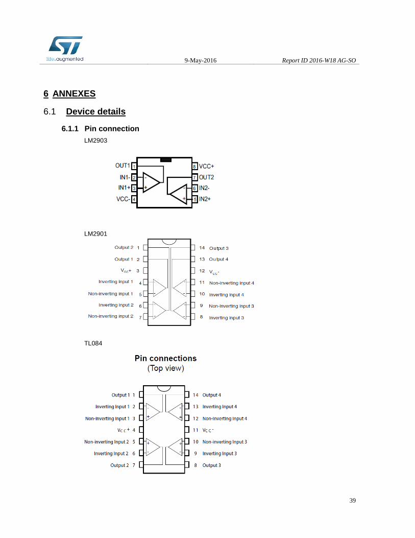
6.1.1 Pin connection
LM2903
LM2901
TL084

9-May-2016 Report ID 2016-W18 AG-SO
40
UW23
0924
UY44
UY18
9-May-2016 Report ID 2016-W18 AG-SO
41
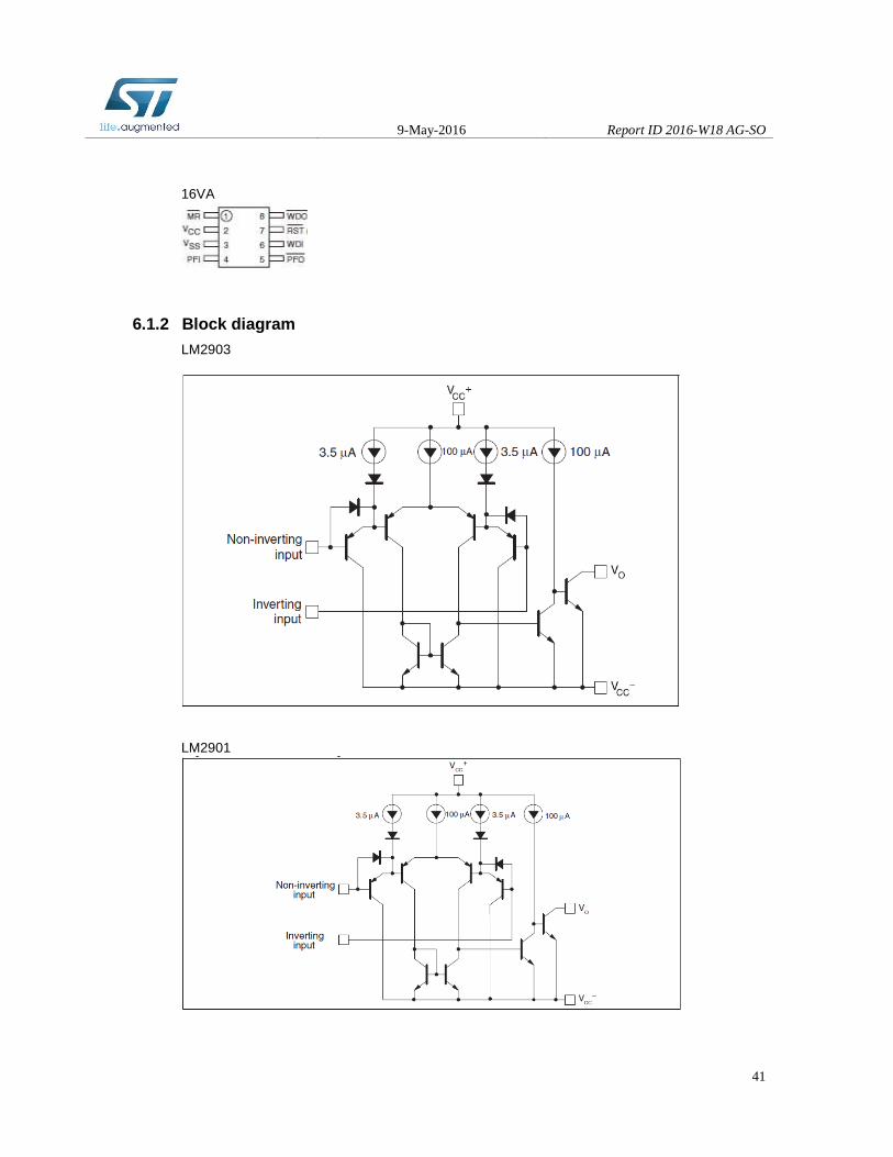
16VA
6.1.2 Block diagram
LM2903
LM2901
9-May-2016 Report ID 2016-W18 AG-SO
42
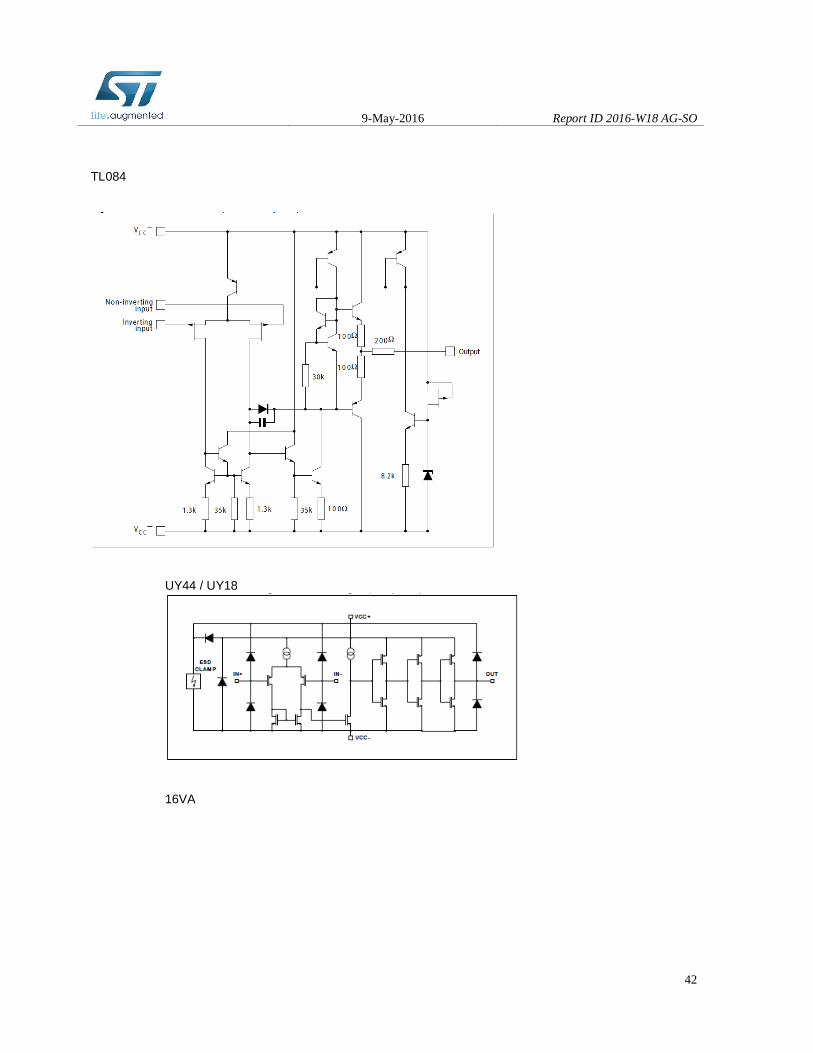
TL084
UY44 / UY18
16VA
9-May-2016 Report ID 2016-W18 AG-SO
43
6.2 Tests Description
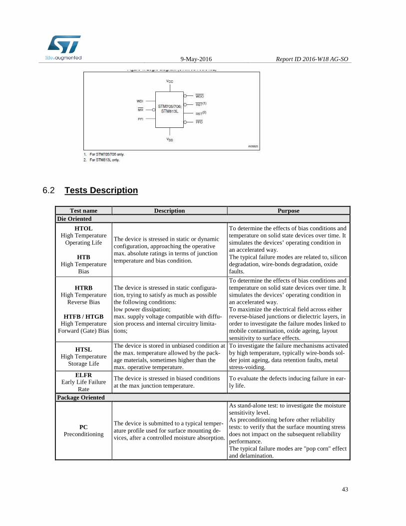
Test name Description Purpose Die Oriented
HTOL High Temperature
Operating Life
HTB High Temperature
Bias
The device is stressed in static or dynamic configuration, approaching the operative max. absolute ratings in terms of junction temperature and bias condition.
To determine the effects of bias conditions and temperature on solid state devices over time. It simulates the devices’ operating condition in an accelerated way. The typical failure modes are related to, silicon degradation, wire-bonds degradation, oxide faults.
HTRB High Temperature
Reverse Bias
HTFB / HTGB High Temperature
Forward (Gate) Bias
The device is stressed in static configura-tion, trying to satisfy as much as possible the following conditions: low power dissipation; max. supply voltage compatible with diffu-sion process and internal circuitry limita-tions;
To determine the effects of bias conditions and temperature on solid state devices over time. It simulates the devices’ operating condition in an accelerated way. To maximize the electrical field across either reverse-biased junctions or dielectric layers, in order to investigate the failure modes linked to mobile contamination, oxide ageing, layout sensitivity to surface effects.
HTSL High Temperature
Storage Life
The device is stored in unbiased condition at the max. temperature allowed by the pack-age materials, sometimes higher than the max. operative temperature.
To investigate the failure mechanisms activated by high temperature, typically wire-bonds sol-der joint ageing, data retention faults, metal stress-voiding.
ELFR Early Life Failure
Rate
The device is stressed in biased conditions at the max junction temperature.
To evaluate the defects inducing failure in ear-ly life.
Package Oriented
PC Preconditioning
The device is submitted to a typical temper-ature profile used for surface mounting de-vices, after a controlled moisture absorption.
As stand-alone test: to investigate the moisture sensitivity level. As preconditioning before other reliability tests: to verify that the surface mounting stress does not impact on the subsequent reliability performance. The typical failure modes are "pop corn" effect and delamination.

9-May-2016 Report ID 2016-W18 AG-SO
44
Test name Description Purpose AC
Auto Clave (Pres-sure Pot)
The device is stored in saturated steam, at fixed and controlled conditions of pressure and temperature.
To investigate corrosion phenomena affecting die or package materials, related to chemical contamination and package hermeticity.
TC Temperature Cy-
cling
The device is submitted to cycled tempera-ture excursions, between a hot and a cold chamber in air atmosphere.
To investigate failure modes related to the thermo-mechanical stress induced by the dif-ferent thermal expansion of the materials inter-acting in the die-package system. Typical fail-ure modes are linked to metal displacement, dielectric cracking, molding compound delam-ination, wire-bonds failure, die-attach layer degradation.
TF / IOL Thermal Fatigue / Intermittent Oper-
ating Life
The device is submitted to cycled tem-perature excursions generated by power cycles (ON/OFF) at T ambient.
To investigate failure modes related to the thermo-mechanical stress induced by the different thermal expansion of the materi-als interacting in the die-package system. Typical failure modes are linked to metal displacement, dielectric cracking, molding compound delamination, wire-bonds fail-ure, die-attach layer degradation.
THB Temperature Humi-
dity Bias
The device is biased in static configuration minimizing its internal power dissipation, and stored at controlled conditions of ambi-ent temperature and relative humidity.
To evaluate the package moisture resistance with electrical field applied, both electrolytic and galvanic corrosion are put in evidence.
Other
ESD Electro Static Dis-
charge
The device is submitted to a high voltage peak on all his pins simulating ESD stress according to different simulation models. CBM: Charged Device Model HBM: Human Body Model MM: Machine Model
To classify the device according to his suscep-tibility to damage or degradation by exposure to electrostatic discharge.
LU Latch-Up
The device is submitted to a direct current forced/sunk into the input/output pins. Re-moving the direct current no change in the supply current must be observed.
To verify the presence of bulk parasitic effect inducing latch-up.
9-May-2016 Report ID 2016-W18 AG-SO
45
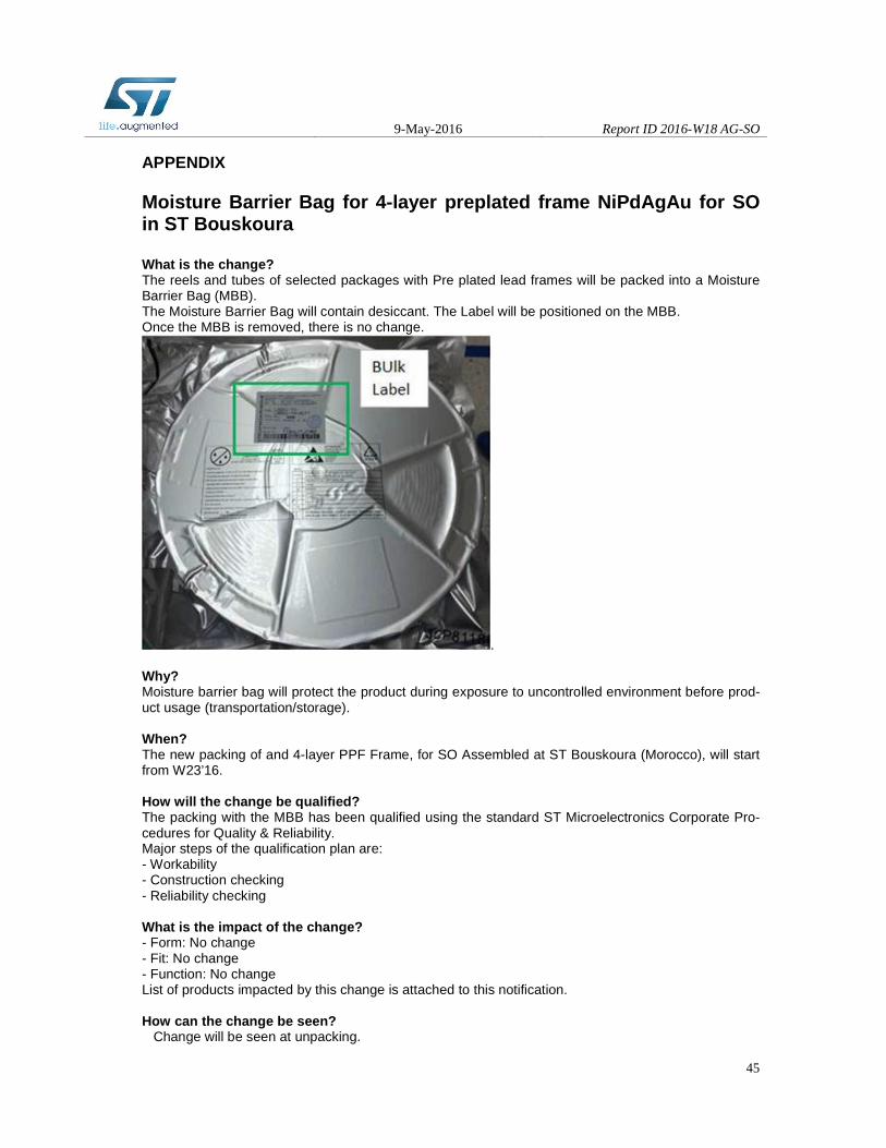
APPENDIX
Moisture Barrier Bag for 4-layer preplated frame NiPdAgAu for SO in ST Bouskoura What is the change? The reels and tubes of selected packages with Pre plated lead frames will be packed into a Moisture Barrier Bag (MBB). The Moisture Barrier Bag will contain desiccant. The Label will be positioned on the MBB. Once the MBB is removed, there is no change.
. Why? Moisture barrier bag will protect the product during exposure to uncontrolled environment before prod-uct usage (transportation/storage). When? The new packing of and 4-layer PPF Frame, for SO Assembled at ST Bouskoura (Morocco), will start from W23’16. How will the change be qualified? The packing with the MBB has been qualified using the standard ST Microelectronics Corporate Pro-cedures for Quality & Reliability. Major steps of the qualification plan are: - Workability - Construction checking - Reliability checking What is the impact of the change? - Form: No change - Fit: No change - Function: No change List of products impacted by this change is attached to this notification. How can the change be seen?
Change will be seen at unpacking.
Related Documents