Cat. No. W345-E1-11 Analog I/O Units SYSMAC CS/CJ Series CS1W-AD/DA CS1W-MAD CJ1W-AD/DA CJ1W-MAD OPERATION MANUAL

Welcome message from author
This document is posted to help you gain knowledge. Please leave a comment to let me know what you think about it! Share it to your friends and learn new things together.
Transcript

Cat. No. W345-E1-11
Analog I/O Units
SYSMAC CS/CJ SeriesCS1W-AD/DACS1W-MADCJ1W-AD/DACJ1W-MAD
OPERATION MANUAL


SYSMAC CS/CJ SeriesCS1W-AD041-V1/AD081-V1/AD161CS1W-DA041/DA08V/DA08C CS1W-MAD44 CJ1W-AD041-V1/AD081-V1/AD042 CJ1W-DA021/DA041/DA08V/DA08C/DA042VCJ1W-MAD42Analog I/O UnitsOperation ManualRevised August 2009

iv
Notice:OMRON products are manufactured for use according to proper procedures by a qualified operatorand only for the purposes described in this manual.
The following conventions are used to indicate and classify precautions in this manual. Always heedthe information provided with them. Failure to heed precautions can result in injury to people or dam-age to property.
!DANGER Indicates an imminently hazardous situation which, if not avoided, will result in death orserious injury. Additionally, there may be severe property damage.
!WARNING Indicates a potentially hazardous situation which, if not avoided, could result in death orserious injury. Additionally, there may be severe property damage.
!Caution Indicates a potentially hazardous situation which, if not avoided, may result in minor ormoderate injury, or property damage.
OMRON Product ReferencesAll OMRON products are capitalized in this manual. The word “Unit” is also capitalized when it refers toan OMRON product, regardless of whether or not it appears in the proper name of the product.
The abbreviation “Ch,” which appears in some displays and on some OMRON products, often means“word” and is abbreviated “Wd” in documentation in this sense.
The abbreviation “PLC” means Programmable Controller. “PC” is used, however, in some Program-ming Device displays to mean Programmable Controller.
Visual AidsThe following headings appear in the left column of the manual to help you locate different types ofinformation.
Note Indicates information of particular interest for efficient and convenient opera-tion of the product.
1,2,3... 1. Indicates lists of one sort or another, such as procedures, checklists, etc.
OMRON, 1999All rights reserved. No part of this publication may be reproduced, stored in a retrieval system, or transmitted, in any form, orby any means, mechanical, electronic, photocopying, recording, or otherwise, without the prior written permission ofOMRON.
No patent liability is assumed with respect to the use of the information contained herein. Moreover, because OMRON is con-stantly striving to improve its high-quality products, the information contained in this manual is subject to change withoutnotice. Every precaution has been taken in the preparation of this manual. Nevertheless, OMRON assumes no responsibilityfor errors or omissions. Neither is any liability assumed for damages resulting from the use of the information contained inthis publication.
v

vi

TABLE OF CONTENTS
PRECAUTIONS . . . . . . . . . . . . . . . . . . . . . . . . . . . . . . . . xvii1 Intended Audience . . . . . . . . . . . . . . . . . . . . . . . . . . . . . . . . . . . . . . . . . . . . . . . . . xviii
2 General Precautions . . . . . . . . . . . . . . . . . . . . . . . . . . . . . . . . . . . . . . . . . . . . . . . . xviii
3 Safety Precautions . . . . . . . . . . . . . . . . . . . . . . . . . . . . . . . . . . . . . . . . . . . . . . . . . xviii
4 Operating Environment Precautions . . . . . . . . . . . . . . . . . . . . . . . . . . . . . . . . . . . xix
5 Application Precautions. . . . . . . . . . . . . . . . . . . . . . . . . . . . . . . . . . . . . . . . . . . . . xx
6 Conformance to EC Directives . . . . . . . . . . . . . . . . . . . . . . . . . . . . . . . . . . . . . . . xxi
SECTION 1System Design . . . . . . . . . . . . . . . . . . . . . . . . . . . . . . . . . . 1
1-1 Features and Functions . . . . . . . . . . . . . . . . . . . . . . . . . . . . . . . . . . . . . . . . . . . . . 2
1-2 Basic Configuration . . . . . . . . . . . . . . . . . . . . . . . . . . . . . . . . . . . . . . . . . . . . . . . . 9
1-3 Function Applications . . . . . . . . . . . . . . . . . . . . . . . . . . . . . . . . . . . . . . . . . . . . . . 14
SECTION 2CS-series Analog Input Units (CS1W-AD041-V1/081-V1/161) . . . . . . . . . . . . . . . . . . . . 15
2-1 Specifications. . . . . . . . . . . . . . . . . . . . . . . . . . . . . . . . . . . . . . . . . . . . . . . . . . . . . 16
2-2 Operating Procedure . . . . . . . . . . . . . . . . . . . . . . . . . . . . . . . . . . . . . . . . . . . . . . . 22
2-3 Components and Switch Settings . . . . . . . . . . . . . . . . . . . . . . . . . . . . . . . . . . . . . 29
2-4 Wiring . . . . . . . . . . . . . . . . . . . . . . . . . . . . . . . . . . . . . . . . . . . . . . . . . . . . . . . . . . 34
2-5 Exchanging Data with the CPU Unit. . . . . . . . . . . . . . . . . . . . . . . . . . . . . . . . . . . 40
2-6 Analog Input Functions and Operating Procedures. . . . . . . . . . . . . . . . . . . . . . . . 54
2-7 Adjusting Offset and Gain . . . . . . . . . . . . . . . . . . . . . . . . . . . . . . . . . . . . . . . . . . . 62
2-8 Handling Errors and Alarms . . . . . . . . . . . . . . . . . . . . . . . . . . . . . . . . . . . . . . . . . 71
SECTION 3CJ-series Analog Input Units (CJ1W-AD041-V1/081-V1). . . . . . . . . . . . . . . . . . . . . . . . 79
3-1 Specifications. . . . . . . . . . . . . . . . . . . . . . . . . . . . . . . . . . . . . . . . . . . . . . . . . . . . . 80
3-2 Operating Procedure . . . . . . . . . . . . . . . . . . . . . . . . . . . . . . . . . . . . . . . . . . . . . . . 85
3-3 Components and Switch Settings . . . . . . . . . . . . . . . . . . . . . . . . . . . . . . . . . . . . . 91
3-4 Wiring . . . . . . . . . . . . . . . . . . . . . . . . . . . . . . . . . . . . . . . . . . . . . . . . . . . . . . . . . . 95
3-5 Exchanging Data with the CPU Unit. . . . . . . . . . . . . . . . . . . . . . . . . . . . . . . . . . . 99
3-6 Analog Input Functions and Operating Procedures. . . . . . . . . . . . . . . . . . . . . . . . 106
3-7 Adjusting Offset and Gain . . . . . . . . . . . . . . . . . . . . . . . . . . . . . . . . . . . . . . . . . . . 114
3-8 Handling Errors and Alarms . . . . . . . . . . . . . . . . . . . . . . . . . . . . . . . . . . . . . . . . . 122
vii

TABLE OF CONTENTS
SECTION 4CJ-series Analog Input Units (CJ1W-AD042) . . . . . . . . 129
4-1 Specifications. . . . . . . . . . . . . . . . . . . . . . . . . . . . . . . . . . . . . . . . . . . . . . . . . . . . . 130
4-2 Operating Procedure . . . . . . . . . . . . . . . . . . . . . . . . . . . . . . . . . . . . . . . . . . . . . . . 135
4-3 Components and Switch Settings . . . . . . . . . . . . . . . . . . . . . . . . . . . . . . . . . . . . . 140
4-4 Wiring . . . . . . . . . . . . . . . . . . . . . . . . . . . . . . . . . . . . . . . . . . . . . . . . . . . . . . . . . . 142
4-5 Exchanging Data with the CPU Unit. . . . . . . . . . . . . . . . . . . . . . . . . . . . . . . . . . . 147
4-6 Analog Input Functions and Operating Procedures. . . . . . . . . . . . . . . . . . . . . . . . 155
4-7 Handling Errors and Alarms . . . . . . . . . . . . . . . . . . . . . . . . . . . . . . . . . . . . . . . . . 164
SECTION 5CS-series Analog Output Units (CS1W-DA041/08V/08C) . . . . . . . . . . . . . . . . . . . . . . . . . 171
5-1 Specifications. . . . . . . . . . . . . . . . . . . . . . . . . . . . . . . . . . . . . . . . . . . . . . . . . . . . . 172
5-2 Operating Procedure . . . . . . . . . . . . . . . . . . . . . . . . . . . . . . . . . . . . . . . . . . . . . . . 176
5-3 Components and Switch Settings . . . . . . . . . . . . . . . . . . . . . . . . . . . . . . . . . . . . . 182
5-4 Wiring . . . . . . . . . . . . . . . . . . . . . . . . . . . . . . . . . . . . . . . . . . . . . . . . . . . . . . . . . . 185
5-5 Exchanging Data with the CPU Unit. . . . . . . . . . . . . . . . . . . . . . . . . . . . . . . . . . . 188
5-6 Analog Output Functions and Operating Procedures . . . . . . . . . . . . . . . . . . . . . . 195
5-7 Adjusting Offset and Gain . . . . . . . . . . . . . . . . . . . . . . . . . . . . . . . . . . . . . . . . . . . 199
5-8 Handling Errors and Alarms . . . . . . . . . . . . . . . . . . . . . . . . . . . . . . . . . . . . . . . . . 209
SECTION 6CJ-series Analog Output Unit (CJ1W-DA021/041/08V/08C) . . . . . . . . . . . . . . . . . . . . . . 215
6-1 Specifications. . . . . . . . . . . . . . . . . . . . . . . . . . . . . . . . . . . . . . . . . . . . . . . . . . . . . 216
6-2 Operating Procedure . . . . . . . . . . . . . . . . . . . . . . . . . . . . . . . . . . . . . . . . . . . . . . . 220
6-3 Components and Switch Settings . . . . . . . . . . . . . . . . . . . . . . . . . . . . . . . . . . . . . 228
6-4 Wiring . . . . . . . . . . . . . . . . . . . . . . . . . . . . . . . . . . . . . . . . . . . . . . . . . . . . . . . . . . 230
6-5 Exchanging Data with the CPU Unit. . . . . . . . . . . . . . . . . . . . . . . . . . . . . . . . . . . 234
6-6 Analog Output Functions and Operating Procedures . . . . . . . . . . . . . . . . . . . . . . 243
6-7 Adjusting Offset and Gain . . . . . . . . . . . . . . . . . . . . . . . . . . . . . . . . . . . . . . . . . . . 250
6-8 Handling Errors and Alarms . . . . . . . . . . . . . . . . . . . . . . . . . . . . . . . . . . . . . . . . . 261
SECTION 7CJ-series Analog Output Unit (CJ1W-DA042V) . . . . . . 267
7-1 Specifications. . . . . . . . . . . . . . . . . . . . . . . . . . . . . . . . . . . . . . . . . . . . . . . . . . . . . 268
7-2 Operating Procedure . . . . . . . . . . . . . . . . . . . . . . . . . . . . . . . . . . . . . . . . . . . . . . . 272
7-3 Components and Switch Settings . . . . . . . . . . . . . . . . . . . . . . . . . . . . . . . . . . . . . 276
7-4 Wiring . . . . . . . . . . . . . . . . . . . . . . . . . . . . . . . . . . . . . . . . . . . . . . . . . . . . . . . . . . 278
7-5 Exchanging Data with the CPU Unit. . . . . . . . . . . . . . . . . . . . . . . . . . . . . . . . . . . 281
7-6 Analog Output Functions and Operating Procedures . . . . . . . . . . . . . . . . . . . . . . 287
7-7 Handling Errors and Alarms . . . . . . . . . . . . . . . . . . . . . . . . . . . . . . . . . . . . . . . . . 294
viii
TABLE OF CONTENTS
SECTION 8CS-series Analog I/O Unit (CS1W-MAD44). . . . . . . . . . 299
8-1 Specifications. . . . . . . . . . . . . . . . . . . . . . . . . . . . . . . . . . . . . . . . . . . . . . . . . . . . . 300
8-2 Operating Procedure . . . . . . . . . . . . . . . . . . . . . . . . . . . . . . . . . . . . . . . . . . . . . . . 308
8-3 Components and Switch Settings . . . . . . . . . . . . . . . . . . . . . . . . . . . . . . . . . . . . . 315
8-4 Wiring . . . . . . . . . . . . . . . . . . . . . . . . . . . . . . . . . . . . . . . . . . . . . . . . . . . . . . . . . . 318
8-5 Exchanging Data with the CPU Unit. . . . . . . . . . . . . . . . . . . . . . . . . . . . . . . . . . . 322
8-6 Analog Input Functions and Operating Procedures. . . . . . . . . . . . . . . . . . . . . . . . 330
8-7 Analog Output Functions and Operating Procedures . . . . . . . . . . . . . . . . . . . . . . 337
8-8 Ratio Conversion Function . . . . . . . . . . . . . . . . . . . . . . . . . . . . . . . . . . . . . . . . . . 340
8-9 Adjusting Offset and Gain . . . . . . . . . . . . . . . . . . . . . . . . . . . . . . . . . . . . . . . . . . . 343
8-10 Handling Errors and Alarms . . . . . . . . . . . . . . . . . . . . . . . . . . . . . . . . . . . . . . . . . 359
SECTION 9CJ-series Analog I/O Unit (CJ1W-MAD42) . . . . . . . . . . 367
9-1 Specifications. . . . . . . . . . . . . . . . . . . . . . . . . . . . . . . . . . . . . . . . . . . . . . . . . . . . . 368
9-2 Operating Procedure . . . . . . . . . . . . . . . . . . . . . . . . . . . . . . . . . . . . . . . . . . . . . . . 375
9-3 Components and Switch Settings . . . . . . . . . . . . . . . . . . . . . . . . . . . . . . . . . . . . . 382
9-4 Wiring . . . . . . . . . . . . . . . . . . . . . . . . . . . . . . . . . . . . . . . . . . . . . . . . . . . . . . . . . . 385
9-5 Exchanging Data with the CPU Unit. . . . . . . . . . . . . . . . . . . . . . . . . . . . . . . . . . . 389
9-6 Analog Input Functions and Operating Procedures. . . . . . . . . . . . . . . . . . . . . . . . 398
9-7 Analog Output Functions and Operating Procedures . . . . . . . . . . . . . . . . . . . . . . 407
9-8 Ratio Conversion Function . . . . . . . . . . . . . . . . . . . . . . . . . . . . . . . . . . . . . . . . . . 413
9-9 Adjusting Offset and Gain . . . . . . . . . . . . . . . . . . . . . . . . . . . . . . . . . . . . . . . . . . . 416
9-10 Handling Errors and Alarms . . . . . . . . . . . . . . . . . . . . . . . . . . . . . . . . . . . . . . . . . 432
AppendicesA Dimensions . . . . . . . . . . . . . . . . . . . . . . . . . . . . . . . . . . . . . . . . . . . . . . . . . . . . . . 439
B Sample Programs . . . . . . . . . . . . . . . . . . . . . . . . . . . . . . . . . . . . . . . . . . . . . . . . . 443
C Data Memory Coding Sheets . . . . . . . . . . . . . . . . . . . . . . . . . . . . . . . . . . . . . . . . 453
D Execution Times for Special Instructions for the CJ1W-AD042/-DA042V . . . . . 479
Index . . . . . . . . . . . . . . . . . . . . . . . . . . . . . . . . . . . . . . . . . . 481
Revision History . . . . . . . . . . . . . . . . . . . . . . . . . . . . . . . . 487
ix

x

About this Manual:This manual describes the installation and operation of the CS1W-AD041-V1, CS1W-AD081-V1,CS1W-AD161, CJ1W-AD041-V1, CJ1W-AD081-V1, and CJ1W-AD042 Analog Input Units; the CS1W-DA041, CS1W-DA08V, CS1W-DA08C, CJ1W-DA021, CJ1W-DA041, CJ1W-DA08V, CJ1W-DA08C,and CJ1W-DA042V Analog Output Units; and the CS1W-MAD44 and CJ1W-MAD42 Analog I/O Units.This manual includes the sections described below.
The input function of CS/CJ-series Analog I/O Units converts analog sensor output to the digital formatand transmits it to CS/CJ-series PLCs. The output function converts digital data from the PLC to theanalog format for output.
Please read this manual and the other manuals related to the CS/CJ-series Analog I/O Units carefullyand be sure you understand the information provided before attempting to install and operate theUnits. The manuals used with the CS/CJ-series Analog I/O Units are listed in the following table. Thesuffixes have been omitted from the catalog numbers. Be sure you are using the most recent versionfor your area.
Name Cat. No. Contents
SYSMAC CS/CJ-series Analog I/O Units Operation ManualCS1W-AD041-V1/AD081-V1/AD161, CS1W-DA041/DA08V/DA08C, CS1W-MAD44, CJ1W-AD041-V1/AD081-V1, CJ1W-AD042, CJ1W-DA021/DA041/DA08V/DA08C, CJ1W-DA042V, CJ1W-MAD42
W345(this manual)
Describes the application methods of the CS/CJ-series Analog Input, Ana-log Output, and Analog I/O Units.
CJ-series CJ2 CPU Unit Hardware User’s Manual CJ2H-CPU6@-EIP, CJ2H-CPU6@
W472 Provides the following information on PLCs built with CJ2 CPU Units:• Overview• System design• System configuration• Maintenance
CJ-series CJ2 CPU Unit Software User’s Manual CJ2H-CPU6@-EIP, CJ2H-CPU6@
W473 Provides the following information on PLCs built with CJ2 CPU Units:• Overview of CPU Unit operation• Programming• System startup• Details on devices• Troubleshooting
SYSMAC CS-series Programmable Controllers Operation ManualCS1G/H-CPU@@-EV1, CS1G/H-CPU@@H
W339 Describes the installation and opera-tion of the CS-series PLCs.
SYSMAC CS Series CS1D Duplex System Operation ManualCS1D-CPU@@H CPU Units, CS1D-CPU@@S CPU Units, CS1D-DPL01 Duplex Unit, CS1D-PA/PD@@@ Power Sup-ply Unit
W405 Provides an outline of and describes the design, installation, maintenance, and other basic operations for a Duplex System based on CS1D CPU Units.
CJ-series PLCs Operation Manual CJ1H-CPU@@H-R, CJ1G/H-CPU@@H, CJ1G-CPU@@P, CJ1G-CPU@@, CJ1H-CPU@@
W393 Provides the following information on CJ-series PLCs:• Overview and features• System configuration design• Installation and wiring• I/O memory allocations• Troubleshooting
CS/CJ/NSJ-series PLCs Programming ManualCS1G/H-CPU@@H, CS1G/H-CPU@@-V1, CS1D-CPU@@H, CS1D-CPU@@S, CJ1H-CPU@@H-R, CJ1G/H-CPU@@H, CJ1G-CPU@@P, CJ1M-CPU@@, CJ1G-CPU@@, NSJ@-@@@@(B)-G5D, NSJ@-@@@@(B)-M3D
W394 Provides the following information on CS/CJ/NSJ-series PLCs:• Programming• Task functions• File memory• Various operations
xi

Section 1 describes the features and system configurations of the CS/CJ-series Analog I/O Unit.Section 2 explains how to use the CS1W-AD041-V1/081-V1/161 Analog Input Units.Section 3 explains how to use the CJ1W-AD041-V1/081-V1 Analog Input Units.Section 4 explains how to use the CJ1W-AD042 Analog Input Units.Section 5 explains how to use the CS1W-DA041/08V/08C Analog Output Units.Section 6 explains how to use the CJ1W-DA021/041/08V/08C Analog Output Units.Section 7 explains how to use the CJ1W-DA042V Analog Output Units.Section 8 explains how to use the CS1W-MAD44 Analog I/O Unit.Section 9 explains how to use the CJ1W-MAD42 Analog I/O Unit.Appendix A provides details on dimensions.Appendix B gives programming examples.Appendix C provides data memory coding sheets.
CS/CJ/NSJ-series PLCs Instructions Reference ManualCJ2H-CPU6@-EIP, CJ2H-CPU6@, CS1G/H-CPU@@H, CS1G/H-CPU@@-V1, CS1D-CPU@@H, CS1D-CPU@@S, CJ1H-CPU@@H-R, CJ1G/H-CPU@@H, CJ1G-CPU@@P, CJ1M-CPU@@, CJ1G-CPU@@, NSJ@-@@@@(B)-G5D, NSJ@-@@@@(B)-M3D
W474 Describes all the ladder programming instructions in detail.
CX-Programmer Operation Manual (Version 8.@)WS02-CXPC@-V8
W446 Describes how to use the CX-Pro-grammer.
SYSMAC CS/CJ-series Programming Consoles Operation Manual CQM1H-PRO01, CQM1-PRO01, C200H-PRO27 + CS1W-KS001
W341 Describes how to use the Program-ming Console.
Name Cat. No. Contents
!WARNING Failure to read and understand the information provided in this manual may result in per-sonal injury or death, damage to the product, or product failure. Please read each sectionin its entirety and be sure you understand the information provided in the section andrelated sections before attempting any of the procedures or operations given.
xii

Read and Understand this ManualPlease read and understand this manual before using the product. Please consult your OMRON representative if you have any questions or comments.
Warranty and Limitations of Liability
WARRANTY
OMRON's exclusive warranty is that the products are free from defects in materials and workmanship for a period of one year (or other period if specified) from date of sale by OMRON.
OMRON MAKES NO WARRANTY OR REPRESENTATION, EXPRESS OR IMPLIED, REGARDING NON-INFRINGEMENT, MERCHANTABILITY, OR FITNESS FOR PARTICULAR PURPOSE OF THE PRODUCTS. ANY BUYER OR USER ACKNOWLEDGES THAT THE BUYER OR USER ALONE HAS DETERMINED THAT THE PRODUCTS WILL SUITABLY MEET THE REQUIREMENTS OF THEIR INTENDED USE. OMRON DISCLAIMS ALL OTHER WARRANTIES, EXPRESS OR IMPLIED.
LIMITATIONS OF LIABILITY
OMRON SHALL NOT BE RESPONSIBLE FOR SPECIAL, INDIRECT, OR CONSEQUENTIAL DAMAGES, LOSS OF PROFITS OR COMMERCIAL LOSS IN ANY WAY CONNECTED WITH THE PRODUCTS, WHETHER SUCH CLAIM IS BASED ON CONTRACT, WARRANTY, NEGLIGENCE, OR STRICT LIABILITY.
In no event shall the responsibility of OMRON for any act exceed the individual price of the product on which liability is asserted.
IN NO EVENT SHALL OMRON BE RESPONSIBLE FOR WARRANTY, REPAIR, OR OTHER CLAIMS REGARDING THE PRODUCTS UNLESS OMRON'S ANALYSIS CONFIRMS THAT THE PRODUCTS WERE PROPERLY HANDLED, STORED, INSTALLED, AND MAINTAINED AND NOT SUBJECT TO CONTAMINATION, ABUSE, MISUSE, OR INAPPROPRIATE MODIFICATION OR REPAIR.
xiii

Application Considerations
SUITABILITY FOR USE
OMRON shall not be responsible for conformity with any standards, codes, or regulations that apply to the combination of products in the customer's application or use of the products.
At the customer's request, OMRON will provide applicable third party certification documents identifying ratings and limitations of use that apply to the products. This information by itself is not sufficient for a complete determination of the suitability of the products in combination with the end product, machine, system, or other application or use.
The following are some examples of applications for which particular attention must be given. This is not intended to be an exhaustive list of all possible uses of the products, nor is it intended to imply that the uses listed may be suitable for the products:
• Outdoor use, uses involving potential chemical contamination or electrical interference, or conditions or uses not described in this manual.
• Nuclear energy control systems, combustion systems, railroad systems, aviation systems, medical equipment, amusement machines, vehicles, safety equipment, and installations subject to separate industry or government regulations.
• Systems, machines, and equipment that could present a risk to life or property.
Please know and observe all prohibitions of use applicable to the products.
NEVER USE THE PRODUCTS FOR AN APPLICATION INVOLVING SERIOUS RISK TO LIFE OR PROPERTY WITHOUT ENSURING THAT THE SYSTEM AS A WHOLE HAS BEEN DESIGNED TO ADDRESS THE RISKS, AND THAT THE OMRON PRODUCTS ARE PROPERLY RATED AND INSTALLED FOR THE INTENDED USE WITHIN THE OVERALL EQUIPMENT OR SYSTEM.
PROGRAMMABLE PRODUCTS
OMRON shall not be responsible for the user's programming of a programmable product, or any consequence thereof.
xiv

Disclaimers
CHANGE IN SPECIFICATIONS
Product specifications and accessories may be changed at any time based on improvements and other reasons.
It is our practice to change model numbers when published ratings or features are changed, or when significant construction changes are made. However, some specifications of the products may be changed without any notice. When in doubt, special model numbers may be assigned to fix or establish key specifications for your application on your request. Please consult with your OMRON representative at any time to confirm actual specifications of purchased products.
DIMENSIONS AND WEIGHTS
Dimensions and weights are nominal and are not to be used for manufacturing purposes, even when tolerances are shown.
PERFORMANCE DATA
Performance data given in this manual is provided as a guide for the user in determining suitability and does not constitute a warranty. It may represent the result of OMRON's test conditions, and the users must correlate it to actual application requirements. Actual performance is subject to the OMRON Warranty and Limitations of Liability.
ERRORS AND OMISSIONS
The information in this manual has been carefully checked and is believed to be accurate; however, no responsibility is assumed for clerical, typographical, or proofreading errors, or omissions.
xv

xvi
xvii
PRECAUTIONS
This section provides general precautions for using the Programmable Controller (PLC) and Analog I/O Units.
The information contained in this section is important for the safe and reliable application of the Analog I/O Unit.You must read this section and understand the information contained before attempting to set up or operate a PLCsystem and Analog I/O Unit.
1 Intended Audience . . . . . . . . . . . . . . . . . . . . . . . . . . . . . . . . . . . . . . . . . . . . . xviii2 General Precautions . . . . . . . . . . . . . . . . . . . . . . . . . . . . . . . . . . . . . . . . . . . . xviii3 Safety Precautions. . . . . . . . . . . . . . . . . . . . . . . . . . . . . . . . . . . . . . . . . . . . . . xviii4 Operating Environment Precautions . . . . . . . . . . . . . . . . . . . . . . . . . . . . . . . . xix5 Application Precautions . . . . . . . . . . . . . . . . . . . . . . . . . . . . . . . . . . . . . . . . . xx6 Conformance to EC Directives . . . . . . . . . . . . . . . . . . . . . . . . . . . . . . . . . . . . xxi

Intended Audience 1
1 Intended AudienceThis manual is intended for the following personnel, who must also haveknowledge of electrical systems (an electrical engineer or the equivalent).
• Personnel in charge of installing FA systems
• Personnel in charge of designing FA systems
• Personnel in charge of managing FA systems and facilities
2 General PrecautionsThe user must operate the product according to the performance specifica-tions described in the operation manuals.
Before using the product under conditions which are not described in themanual or applying the product to nuclear control systems, railroad systems,aviation systems, vehicles, combustion systems, medical equipment, amuse-ment machines, safety equipment, and other systems, machines, and equip-ment that may have a serious influence on lives and property if usedimproperly, consult your OMRON representative.
Make sure that the ratings and performance characteristics of the product aresufficient for the systems, machines, and equipment, and be sure to providethe systems, machines, and equipment with double safety mechanisms.
This manual provides information for programming and operating OMRONAnalog I/O Units. Be sure to read this manual before attempting to use thesoftware and keep this manual close at hand for reference during operation.
!WARNING It is extremely important that a PLC and all PLC Units be used for the speci-fied purpose and under the specified conditions, especially in applications thatcan directly or indirectly affect human life. You must consult with your OMRONrepresentative before applying a PLC System to the above-mentioned appli-cations.
!WARNING Do not apply the voltage/current outside the specified range to any Unit. Itmay cause a malfunction or fire.
3 Safety Precautions
!WARNING Do not attempt to take any Unit apart or touch any internal parts while poweris being supplied. Doing so may result in electric shock.
!WARNING Do not touch any of the terminals or terminal blocks while power is being sup-plied. Doing so may result in electric shock.
!WARNING Provide safety measures in external circuits (i.e., not in the ProgrammableController), including the following items, in order to ensure safety in the sys-tem if an abnormality occurs due to malfunction of the PLC or another exter-nal factor affecting the PLC operation. Not doing so may result in seriousaccidents.
• Emergency stop circuits, interlock circuits, limit circuits, and similar safetymeasures must be provided in external control circuits.
xviii

Operating Environment Precautions 4
• The PLC will turn OFF all outputs when its self-diagnosis function detectsany error or when a severe failure alarm (FALS) instruction is executed.As a countermeasure for such errors, external safety measures must beprovided to ensure safety in the system.
• The PLC outputs may remain ON or OFF due to deposition or burning ofthe output relays or destruction of the output transistors. As a counter-measure for such problems, external safety measures must be providedto ensure safety in the system.
!WARNING When the 24-VDC output (service power supply to the PLC) is overloaded orshort-circuited, the voltage may drop and result in the outputs being turnedOFF. As a countermeasure for such problems, external safety measures mustbe provided to ensure safety in the system.
!Caution When wiring crossovers between terminals, the total current for both terminalswill flow in the line. Check the current capacities of all wires before wiringcrossovers.
!Caution Tighten the screws on the terminal block of the AC Power Supply Unit to thetorque specified in the operation manual. The loose screws may result inburning or malfunction.
!Caution Execute online edit only after confirming that no adverse effects will becaused by extending the cycle time. Otherwise, the input signals may not bereadable.
!Caution With the CJ1W-AD042/-DA042V, always connect surge suppressors to induc-tive loads in the system (e.g., magnetic contactors, relays, and solenoids).Always separate devices that generate surge from the Analog I/O Units.Faulty Unit operation may cause unexpected system operation.
4 Operating Environment Precautions
!Caution Do not operate the control system in the following places:
• Locations subject to direct sunlight.
• Locations subject to temperatures or humidity outside the range specifiedin the specifications.
• Locations subject to condensation as the result of severe changes in tem-perature.
• Locations subject to corrosive or flammable gases.
• Locations subject to dust (especially iron dust) or salts.
• Locations subject to exposure to water, oil, or chemicals.
• Locations subject to shock or vibration.
!Caution Take appropriate and sufficient countermeasures when installing systems inthe following locations:
• Locations subject to static electricity or other forms of noise.
• Locations subject to strong electromagnetic fields.
xix

Application Precautions 5
• Locations subject to possible exposure to radioactivity.
• Locations close to power lines.
!Caution The operating environment of the PLC System can have a large effect on thelongevity and reliability of the system. Improper operating environments canlead to malfunction, failure, and other unforeseeable problems with the PLCSystem. Be sure that the operating environment is within the specified condi-tions at installation and remains within the specified conditions during the lifeof the system.
5 Application PrecautionsObserve the following precautions when using the PLC.
!WARNING Always heed these precautions. Failure to abide by the following precautionscould lead to serious or possibly fatal injury.
• Always connect to a class-3 ground (to 100 Ω or less) when installing theUnits. Not connecting to a class-3 ground may result in electric shock.
• Always turn OFF the power supply to the PLC before attempting any ofthe following. Not turning off the power supply may result in malfunction orelectric shock.
• Mounting or dismounting I/O Units, CPU Units, Memory Cassettes, orany other Units.
• Assembling the Units.
• Setting DIP switch or rotary switches.
• Connecting or wiring the cables.
• Connecting or disconnecting the connectors.
!Caution Failure to abide by the following precautions could lead to faulty operation ofthe PLC or the system, or could damage the PLC or PLC Units. Always heedthese precautions.
• Always use the power supply voltage specified in this manual. An incor-rect voltage may result in malfunction or burning.
• Take appropriate measures to ensure that the specified power with therated voltage and frequency is supplied. Be particularly careful in placeswhere the power supply is unstable. An incorrect power supply may resultin malfunction.
• Install external breakers and take other safety measures against short-cir-cuiting in external wiring. Insufficient safety measures against short-cir-cuiting may result in burning.
• Do not apply voltages to input sections in excess of the rated input volt-age. Excess voltages may result in burning.
• Do not apply voltages or connect loads in excess of the maximum switch-ing capacity to output sections. Excess voltage or loads may result inburning.
• Tighten the PLC terminal screws and cable screws to the torque specifiedin this manual.
• Wiring correctly, as indicated in this manual.
xx
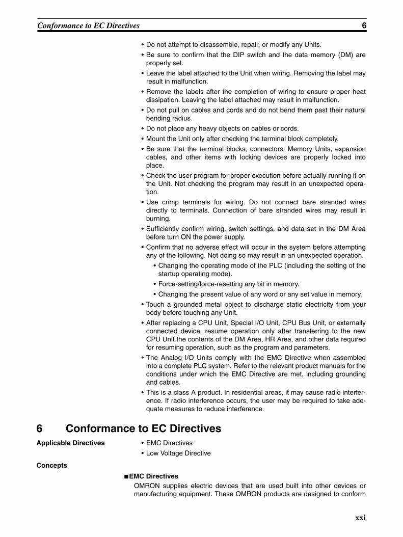
Conformance to EC Directives 6
• Do not attempt to disassemble, repair, or modify any Units.
• Be sure to confirm that the DIP switch and the data memory (DM) areproperly set.
• Leave the label attached to the Unit when wiring. Removing the label mayresult in malfunction.
• Remove the labels after the completion of wiring to ensure proper heatdissipation. Leaving the label attached may result in malfunction.
• Do not pull on cables and cords and do not bend them past their naturalbending radius.
• Do not place any heavy objects on cables or cords.
• Mount the Unit only after checking the terminal block completely.
• Be sure that the terminal blocks, connectors, Memory Units, expansioncables, and other items with locking devices are properly locked intoplace.
• Check the user program for proper execution before actually running it onthe Unit. Not checking the program may result in an unexpected opera-tion.
• Use crimp terminals for wiring. Do not connect bare stranded wiresdirectly to terminals. Connection of bare stranded wires may result inburning.
• Sufficiently confirm wiring, switch settings, and data set in the DM Areabefore turn ON the power supply.
• Confirm that no adverse effect will occur in the system before attemptingany of the following. Not doing so may result in an unexpected operation.
• Changing the operating mode of the PLC (including the setting of thestartup operating mode).
• Force-setting/force-resetting any bit in memory.
• Changing the present value of any word or any set value in memory.
• Touch a grounded metal object to discharge static electricity from yourbody before touching any Unit.
• After replacing a CPU Unit, Special I/O Unit, CPU Bus Unit, or externallyconnected device, resume operation only after transferring to the newCPU Unit the contents of the DM Area, HR Area, and other data requiredfor resuming operation, such as the program and parameters.
• The Analog I/O Units comply with the EMC Directive when assembledinto a complete PLC system. Refer to the relevant product manuals for theconditions under which the EMC Directive are met, including groundingand cables.
• This is a class A product. In residential areas, it may cause radio interfer-ence. If radio interference occurs, the user may be required to take ade-quate measures to reduce interference.
6 Conformance to EC DirectivesApplicable Directives • EMC Directives
• Low Voltage Directive
Concepts
EMC DirectivesOMRON supplies electric devices that are used built into other devices ormanufacturing equipment. These OMRON products are designed to conform
xxi

Conformance to EC Directives 6
to the related EMC standards (see note) so that the devices or equipment inwhich they are used can more easily conform to EMC standards.
EMC-related performance of the OMRON devices that conform to EC Direc-tives will vary depending on the configuration, wiring, and other conditions ofthe equipment or control panel on which the OMRON devices are installed.The customer must, therefore, perform the final check to confirm that devicesand the overall machine conform to EMC standards.
Note Applicable EMC (Electromagnetic Compatibility) standards are as follows:EMC (Electromagnetic Susceptibility)
CS-series PLCs: EN 61131-2 (CS1W-AD161: EN 61000-6-2)CJ-series PLCs: EN 61000-6-2
EMI (Electromagnetic Interference)CS-series PLCs: EN 61131-2 (CS1W-AD161: EN 61000-6-4)CJ-series PLCs: EN 61000-6-4
Low Voltage DirectiveAlways ensure that devices operating at voltages of 50 to 1,000 V AC and 75to 1,500 V DC meet the required safety standards for the PLC (EN 61131-2.)
Conformance to EC Directives
CS/CJ-series products conform to EC Directives. However, the following pre-cautions must be observed to ensure that the machine or device in which theCS/CJ-series PLC is used conforms to EC Directives:
1. The CS/CJ-series PLC must be installed within a control panel.
2. You must use reinforced insulation or double insulation for the DC powersupplies used for the I/O power supplies. The DC power supply connectedto the power supply terminals on PLCs using DC power must have an out-put hold time of at least 10 ms.
3. CS/CJ-series products conforming to EC Directives also conform to EN61000-6-4 for EMI. Radiated emission characteristics (10-m regulations)may vary depending on the configuration of the control panel used, otherdevices connected to the control panel, wiring, and other conditions. Youmust therefore confirm that the overall machine or equipment conforms toEC Directives even when using CS/CJ-series products that conform to ECDirectives.
Conditions for Conforming to EMC Directives
The following immunity test conditions apply to CS/CJ-series Analog I/OUnits.
Overall Accuracy
Use shielded twisted-pair cable to connect analog inputs and connect theshield on the input line to the AG terminal.
Analog Input Unit CS1W-AD161 +4%/−6%
CJ1W-AD041-V1/AD081-V1 +3%/−6%
CJ1W-AD042 +6%/−6%
Analog Output Units
CJ1W-DA021/DA041 +4%/−1%
CJ1W-DA08V/DA08C +4%/−4%
CJ1W-DA042V +4.5%/−4.5%
Analog I/O Unit CS1W-MAD44 +2%/−1%
CJ1W-MAD42 +4%/−4%
xxii

SECTION 1System Design
This section describes the features and system configurations of CS/CJ-series Analog I/O Units.
1-1 Features and Functions . . . . . . . . . . . . . . . . . . . . . . . . . . . . . . . . . . . . . . . . . . 2
1-2 Basic Configuration . . . . . . . . . . . . . . . . . . . . . . . . . . . . . . . . . . . . . . . . . . . . 9
1-2-1 Mounting Procedure . . . . . . . . . . . . . . . . . . . . . . . . . . . . . . . . . . . . . 11
1-2-2 Precautions . . . . . . . . . . . . . . . . . . . . . . . . . . . . . . . . . . . . . . . . . . . . 13
1-3 Function Applications . . . . . . . . . . . . . . . . . . . . . . . . . . . . . . . . . . . . . . . . . . . 14
1
Features and Functions Section 1-1
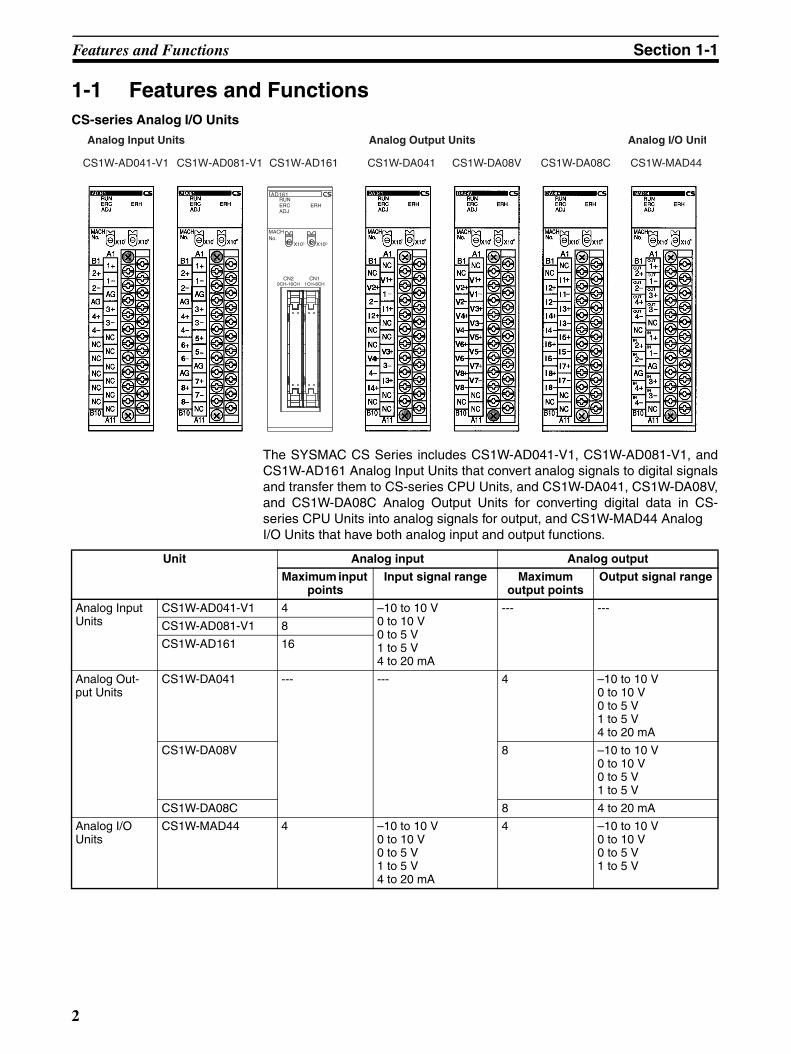
1-1 Features and FunctionsCS-series Analog I/O Units
The SYSMAC CS Series includes CS1W-AD041-V1, CS1W-AD081-V1, andCS1W-AD161 Analog Input Units that convert analog signals to digital signalsand transfer them to CS-series CPU Units, and CS1W-DA041, CS1W-DA08V,and CS1W-DA08C Analog Output Units for converting digital data in CS-series CPU Units into analog signals for output, and CS1W-MAD44 Analog I/O Units that have both analog input and output functions.
CS1W-MAD44
Analog I/O UnitAnalog Input Units Analog Output Units
CS1W-AD041-V1 CS1W-AD081-V1 CS1W-DA041 CS1W-DA08V CS1W-DA08CCS1W-AD161
Unit Analog input Analog output
Maximum input points
Input signal range Maximum output points
Output signal range
Analog Input Units
CS1W-AD041-V1 4 –10 to 10 V0 to 10 V0 to 5 V1 to 5 V4 to 20 mA
--- ---
CS1W-AD081-V1 8
CS1W-AD161 16
Analog Out-put Units
CS1W-DA041 --- --- 4 –10 to 10 V0 to 10 V0 to 5 V1 to 5 V4 to 20 mA
CS1W-DA08V 8 –10 to 10 V0 to 10 V0 to 5 V1 to 5 V
CS1W-DA08C 8 4 to 20 mA
Analog I/O Units
CS1W-MAD44 4 –10 to 10 V0 to 10 V0 to 5 V1 to 5 V4 to 20 mA
4 –10 to 10 V0 to 10 V0 to 5 V1 to 5 V
2

Features and Functions Section 1-1
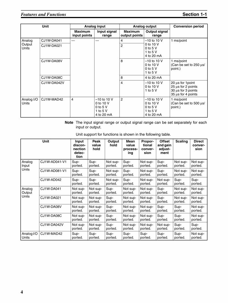
CJ-series Analog I/O Units
The SYSMAC CJ Series includes CJ1W-AD041-V1, CS1W-AD081-V1, andCJ1W-AD042 Analog Input Units that convert analog signals to digital signalsand transfer them to CJ-series CPU Units, and CJ1W-DA041, CS1W-DA021,and CJ1W-DA042V Analog Output Units for converting digital data from CJ-series CPU Units into analog signals for output.
The main specifications are listed in the following table.
AD081
B1 A1
MACHNo.x10 1
x10 0
RUNERCERHADJ
MODE
12
DA041
B1 A1
MACHNo.x10 1
x10 0
RUNERCERHADJ
MODE
12
Analog Input Unit
CJ1W-AD041-V1CJ1W-AD081-V1
Analog Output Unit
CJ1W-DA021CJ1W-DA041
CJ1W-DA08VCJ1W-DA08C
Analog I/O Unit
CJ1W-MAD42
DA08V
B1 A1
MACHNo.x10 1
x10 0
RUNERCERHADJ
MAD42
B1 A1
MACHNo.x10 1
x10 0
RUNERCERHADJ
CJ1W-AD042 CJ1W-DA042V
AD042
B1 A1
MACHNo.x10 1
x10 0
R
DA042V
B1 A1
MACHNo.x10 1
x10 0
R
Unit Analog input Analog output Conversion period
Maximum input points
Input signal range
Maximum output points
Output signal range
Analog Input Units
CJ1W-AD041-V1 4 –10 to 10 V0 to 10 V0 to 5 V1 to 5 V4 to 20 mA
--- --- 1 ms/point (Can be set to 250 µs/point.)
CJ1W-AD081-V1 8
CJ1W-AD042 4 –10 to 10 V0 to 10 V–5 to 5 V1 to 5 V4 to 20 mA
20 µs for 1point25 µs for 2 points30 µs for 3 points35 µs for 4 points
3
Features and Functions Section 1-1
Note The input signal range or output signal range can be set separately for eachinput or output.
Unit support for functions is shown in the following table.
Analog Output Units
CJ1W-DA041 --- --- 4 –10 to 10 V0 to 10 V0 to 5 V1 to 5 V4 to 20 mA
1 ms/point
CJ1W-DA021 2
CJ1W-DA08V 8 –10 to 10 V0 to 10 V0 to 5 V1 to 5 V
1 ms/point (Can be set to 250 µs/point.)
CJ1W-DA08C 8 4 to 20 mA
CJ1W-DA042V 4 –10 to 10 V0 to 10 V1 to 5 V
20 µs for 1point25 µs for 2 points30 µs for 3 points35 µs for 4 points
Analog I/O Units
CJ1W-MAD42 4 –10 to 10 V0 to 10 V0 to 5 V1 to 5 V4 to 20 mA
2 –10 to 10 V0 to 10 V0 to 5 V1 to 5 V4 to 20 mA
1 ms/point (Can be set to 500 µs/point.)
Unit Analog input Analog output Conversion period
Maximum input points
Input signal range
Maximum output points
Output signal range
Unit Input discon-nection detec-tion
Peak value hold
Output hold
Mean value
process-ing
Propor-tional
conver-sion
Offset and gain adjust-ment
Scaling Direct conver-
sion
Analog Input Units
CJ1W-AD041-V1 Sup-ported.
Sup-ported.
Not sup-ported.
Sup-ported.
Not sup-ported.
Sup-ported.
Not sup-ported.
Not sup-ported.
CJ1W-AD081-V1 Sup-ported.
Sup-ported.
Not sup-ported.
Sup-ported.
Not sup-ported.
Sup-ported.
Not sup-ported.
Not sup-ported.
CJ1W-AD042 Sup-ported.
Sup-ported.
Not sup-ported.
Sup-ported.
Not sup-ported.
Not sup-ported.
Sup-ported.
Sup-ported.
Analog Output Units
CJ1W-DA041 Not sup-ported.
Not sup-ported.
Sup-ported.
Not sup-ported.
Not sup-ported.
Sup-ported.
Not sup-ported.
Not sup-ported.
CJ1W-DA021 Not sup-ported.
Not sup-ported.
Sup-ported.
Not sup-ported.
Not sup-ported.
Sup-ported.
Not sup-ported.
Not sup-ported.
CJ1W-DA08V Not sup-ported.
Not sup-ported.
Sup-ported.
Not sup-ported.
Not sup-ported.
Sup-ported.
Sup-ported.
Not sup-ported.
CJ1W-DA08C Not sup-ported.
Not sup-ported.
Sup-ported.
Not sup-ported.
Not sup-ported.
Sup-ported.
Sup-ported.
Not sup-ported.
CJ1W-DA042V Not sup-ported.
Not sup-ported.
Sup-ported.
Not sup-ported.
Not sup-ported.
Not sup-ported.
Sup-ported.
Sup-ported.
Analog I/O Units
CJ1W-MAD42 Sup-ported.
Sup-ported.
Sup-ported.
Sup-ported.
Sup-ported.
Sup-ported.
Sup-ported.
Not sup-ported.
4

Features and Functions Section 1-1
Input Disconnection Detection Function
The input disconnection detection function can be used for analog inputswithin an input signal range of 1 to 5 V (4 to 20 mA). Any input under 0.3 V(1.2 mA) will be regarded as a disconnection. For details, refer to 2-6-5, 3-6-5,4-6-6, 8-6-4 or 9-6-6.
Peak Value Hold Function The peak value hold function holds the maximum digital conversion value forevery input (including mean value processing). This function can be used withanalog input. The following diagram shows how digital conversion values areaffected when the peak value hold function is used. For details, refer to 2-6-4,3-6-4, 4-6-5, 8-6-3 or 9-6-4.
Output Hold Function The output hold function can be used to hold the analog output value at anypreset value when there is a fatal error at the CPU Unit or when specified bythe CPU Unit. When output is stopped, CLR, HOLD, or MAX can be selectedfor output. For details, refer to 5-6-3, 6-6-4, 7-6-3, 8-7-2 or 9-7-3.
Disconnection
Analog Input Unit CPU Unit
Detection Flag
Peak hold bit
Analog Output Unit CPU Unit
Output Enable Flag OFF
CLR/HOLD/MAX
5

Features and Functions Section 1-1
Mean Value Function The mean value function can be used to remove erroneous values that occurdue to factors such as noise that is included in analog inputs. The operatingmean is taken without affecting the data refresh cycle. For details, refer to 2-6-3, 3-6-3, 4-6-3, 8-6-2 or 9-6-3.
Ratio Conversion Function
The CS1W-MAD44 and CJ1W-MAD42 Analog I/O Unit can output in analogformat the results of analog inputs calculated for ratio and bias. For details,refer to 8-8 or 9-8.
Offset and Gain Adjustment Function
The A/D and D/A converter offset deviation and gain deviation can beadjusted for each input and output. The offset and gain adjustments are madewith the Unit set for the adjustment mode, and the adjustment values arestored in the Unit’s built-in EEPROM. For details, refer to 2-7, 3-7, 5-7, 6-7, 8-9 or 9-9.
Scaling Function Refer to 4-6-4, 6-6-5, 7-6-4, 9-6-5 and 9-7-4.
With CS1W-AD042 Analog Input Units (See note 1.), CJ1W-DA08V/08C/042V Analog Output Units (See note 2.), and CJ1W-MAD42 Analog I/O Units,input analog values and output analog set values can be automatically con-verted into user-specified units. This scaling function eliminates the previousneed to provide programs (e.g., scaling using the SCL instruction) for numericconversion to different units.
When upper and lower limits have been preset in 16-bit binary data in theCPU Unit’s DM Area, within a decimal range of −32,000 to +32,000, input
Analog Input Unit CPU Unit
Mean value of "n" his-tory buffers
Ratio and bias setting device
Ratio and biasA x + B
Analog Input Function
(Input signal range: 0 to 10 V)
Analog Output Function
(Output signal range: 0 to 10 V)
Analog input10 V
Offset adjustment Offset adjustment
10 V
Adjustable range Adjustable range
0FA0/(1F40)
Gain adjustment Analog
output
Gain adjustment
6

Features and Functions Section 1-1
analog values and output analog set values can be automatically convertedinto user-specified units. (See note 3.) (Two's complements are used for neg-ative analog input conversion values and analog output set values.)
Note 1. Only input scaling is supported by CJ1W-AD042 Analog Input Units.
2. Only output scaling is supported by CJ1W-DA08V/08C/042V Analog Out-put Units.
3. With the CJ1W-DA08V/08C Analog Output Unit and CJ1W-MAD42 AnalogI/O Unit, scaling is possible only for a conversion period of 1 ms and a res-olution of 4,000. The scaling function is not enabled for a conversion timeof 250 µs (500 µs for the CJ1W-MAD42) and a resolution of 8,000.
Conceptual Diagram of Scaling (CJ1M-MAD42 Only)
Direct Conversion Refer to pages 156 and 289.
Direct conversion can be used with the CJ1W-AD042 Analog Input Unit andCJ1W-DA042V Analog Output Unit. Direct conversion can be used to immedi-ately perform conversion for an Analog Input Unit or Analog Output Unit andat the same time read or output the conversion data. With the CJ1W-AD042Analog Input Unit, A/D conversion is performed and the converted value isrefreshed immediately when the ANALOG INPUT DIRECT CONVERSION(AIDC) instruction is executed. With the CJ1W-DA042V Analog Output Unit,the conversion set value is refreshed and D/A conversion is performed imme-diately when the ANALOG OUTPUT DIRECT CONVERSION (AODC) instruc-tion is executed. A CJ2H-CPU@@(-EIP) CPU Unit with unit version 1.1 or lateris required to use direct conversion.
Input analog value(temperature, flowrate, etc.)
Output analog value
Analog I/O Unit
A/D conversion
D/A conversion
No scaling
Scaling
No scaling
Scaling
CPU Unit
Special I/O Unit Area
Converted analog input value(in engineering units)
Set analog output value(in engineering units)
DM Area
Scaling settingsInput scaling: D(m+27) to D(m+34)Output scaling: D(m+19) to D(m+22)Power turned ON or
Unit restarted.
7

Features and Functions Section 1-1
Direct conversion enables creating a consistent input-processing-output timefor superior periodic control. This is not possible with the following methods.
• Refreshing I/O during the CPU Unit’s cycle
• Using the I/O REFRESH (IORF) instruction
• Using the SPECIAL I/O UNIT I/O REFRESH (FIORF) instruction
CPU Unit
Ladder program
ANALOG INPUT DIRECT CONVERSION instruction
A/D conversion request
I/O memory
I/O memory
Analog input conversion value
ANALOG OUTPUT DIRECT CONVERSION instruction
Analog output set value
Equals Flag (normal end) and Error Flag
D/A conversion request
Equals Flag (normal end) and Error Flag
Analog Input Unit
A/D conversion
D/A conversion
Analog Output Unit
8

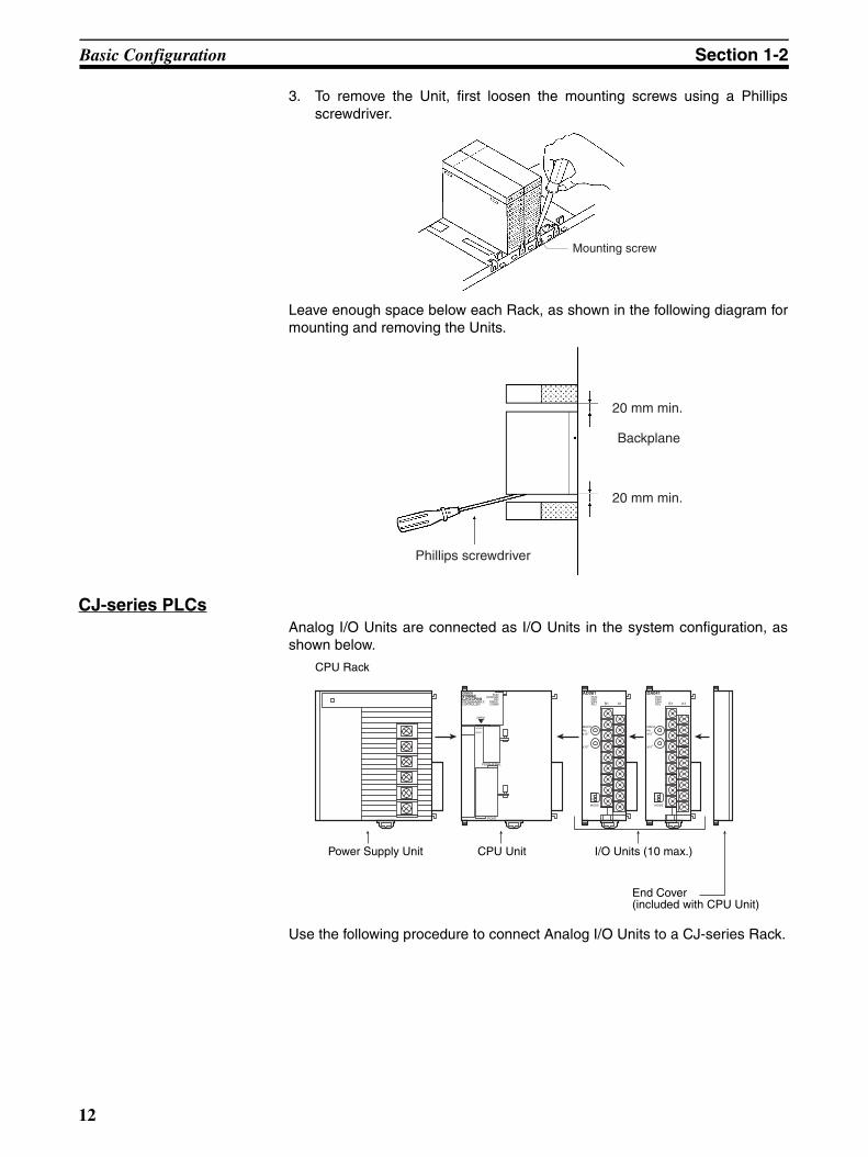
Basic Configuration Section 1-2
1-2 Basic Configuration
CS-series PLCs
Note The above diagram is an installation example for the CS1W-AD081-V1 Ana-log Input Unit and CS1W-DA08V Analog Output Unit.
Analog Input Unit CPU Unit
TemperaturePressureSpeedFlow rate
VoltageCurrentPowerPower factor
Preamp
Transducer
Variable speed controller
Servo-controller
Regulator(Temperature control)
(Speed control)
(Position control)
Chart recorder
Sensor
Sensor
Analog Output Unit
9

Basic Configuration Section 1-2
CJ-series PLCs
Note The above diagram is an installation example for the CJ1W-AD041-V1/081-V1Analog Input Unit and CJ1W-DA021/041 Analog Output Unit.
Mounting Restrictions
CS-series PLCs The CS1W-MAD44 Analog I/O Unit is a Special I/O Unit of the CS Series.
CS1W-MAD44 Analog I/O Units can be mounted to either CS-series CPURacks or CS-series Expansion Racks. These Analog I/O Units cannot bemounted to C200H Expansion I/O Racks or SYSMAC BUS Slave Racks.
The number of Analog I/O Units that can be mounted to one Rack (i.e., a CPURack or Expansion Rack) depends on the maximum supply current of thePower Supply Unit and the current consumption of other Units. If a Rack is tobe mounted with Analog Input, Output, or I/O Units only, the following restric-tions will apply.
SYSMACCJ1G-CPU44PROGRAMMABLECONTROLLER
RUNERR/ALM
INHPRPHLCOMM
OPEN
PERIHERAL
PORT
MCPWR
BUSY
AD081
B1 A1
MACHNo.x10 1
x10 0
RUNERCERHADJ
MODE
12
DA041
B1 A1
MACHNo.x10 1
x10 0
RUNERCERHADJ
MODE
12
M
M
CPU Unit
Temperature Pressure Speed Flow rate
VoltageCurrentPowerPower factor
Sensor
Sensor
Preamp
Trans-ducer
Regulator
Servo-controller
Variable speed controller
Chart recorder
(Temperature control)
(Position control)
(Speed control)
Analog Input Unit
Analog Output Unit
Power Supply Unit Rack CS1W-AD041-V1
CS1W-AD081-V1
(5 VDC 120 mA)
CS1W-DA041CS1W-DA08V
(5 VDC 130 mA)
CS1W-MAD44(5 VDC
200 mA)
CS1W-DA08C(5 VDC
130 mA)
CS1W-AD161(5 VDC
150 mA)
C200HW-PA204C200HW-PA204SC200HW-PA204RC200HW-PA204CC200HW-PD024(4.6 A at 5 VDC)
CPU Rack 6 3 3 2 8
Expansion Rack 6 3 3 2 9
C200HW-PA209R(9 A at 5 VDC)
CPU Rack 10 7 6 5 10
Expansion Rack 10 7 6 5 10
CS1D-PA207R(7 A at 5 VDC)
CPU Rack 8 5 4 4 8
Expansion Rack 9 6 5 4 9
CS1D-PD024(4.3 A at 5 VDC)
CPU Rack 6 3 2 2 7
Expansion Rack 6 3 2 2 8
10

Basic Configuration Section 1-2
Note The I/O bits of the Special I/O Unit are allocated according to the setting of theunit number switches on the front panel of the Unit, and not the slot numberwhere the Unit is mounted.
CJ-series PLCs CJ-series Analog I/O Units are Special I/O Unit of the CJ-series PLCs.
These Units can be connected in the CJ-series CPU Rack or ExpansionRacks. The number of Analog I/O Units that can be connected in each Rackwill depend on the current consumption of the other Units in the Rack. Thenumber of Analog I/O Units that can be mounted to one Rack (i.e., a CPURack or Expansion Rack) depends on the current consumption of other Units.
The maximum number of Analog Input Units, Analog Output Units, or AnalogI/O Units that can be mounted to a CJ2H-CPU6@ CPU Unit (no EtherNet/IP)is given in the following table for when only these Units are mounted.
Note The I/O bits of the Special I/O Unit are allocated according to the setting of theunit number switches on the front panel of the Unit, and not the order in whichit is connected.
1-2-1 Mounting Procedure
CS-series PLCsUse the following procedure to mount Analog I/O Units to the Backplane.
1,2,3... 1. Lock the top of the Analog I/O Unit into the slot on the Backplane and rotatethe Unit downwards as shown in the following diagram.
2. While making sure to align the Unit properly with the connectors, tightenthe mounting screws securely to the tightening torque of 0.4 N·m.
Power Supply Unit Rack CJ1W-DA021CJ1W-DA041
(5 VDC 120 mA)CJ1W-DA08VCJ1W-DA08C
(5 VDC 140 mA)
CS1W-AD041-V1CJ1W-AD081-V1(5 VDC 420 mA)CJ1W-DA042V
(5 VDC 400 mA)
CJ1W-AD042(5 VDC 520 mA)
CJ1W-MAD42(5 VDC 580 mA)
CJ1W-PA205RCJ1W-PA205CCJ1W-PD025(5.0 A at 5 VDC)
CPU Rack 10 10 8 7
Expansion Rack 10 10 9 8
CJ1W-PA202(2.8 A at 5 VDC)
CPU Rack 10 5 4 4
Expansion Rack 10 6 5 4
CJ1W-PD022(2.0 A at 5 VDC)
CPU Rack 10 3 3 2
Expansion Rack 10 4 3 3
Hook
Backplane
11
Basic Configuration Section 1-2
3. To remove the Unit, first loosen the mounting screws using a Phillipsscrewdriver.
Leave enough space below each Rack, as shown in the following diagram formounting and removing the Units.
CJ-series PLCsAnalog I/O Units are connected as I/O Units in the system configuration, asshown below.
Use the following procedure to connect Analog I/O Units to a CJ-series Rack.
Mounting screw
20 mm min.
20 mm min.
Backplane
Phillips screwdriver
AD081SYSMACCJ1G-CPU44PROGRAMMABLECONTROLLER
RUNERR/ALM
INHPRPHLCOMM
OPEN
PERIHERAL
PORT
MCPWR
BUSY
B1 A1
MACHNo.x10
1
x100
RUNERCERHADJ
MODE
12
DA041
B1 A1
MACHNo.x10
1
x100
RUNERCERHADJ
MODE
12
CPU Rack
Power Supply Unit CPU Unit I/O Units (10 max.)
End Cover (included with CPU Unit)
12

Basic Configuration Section 1-2
1,2,3... 1. Align the connectors and press in firmly on the Units to connect them com-pletely.
2. Move the sliders on the top and bottom of the Unit to the lock position to secure the Units. The sliders should click into place.
3. Attach an End Cover to the Unit on the right end of the Rack.
Note The CJ-series PLC may not operate properly if the sliders are not lockedfirmly into place.
1-2-2 PrecautionsBe sure to turn OFF the power supply to the PLC before installing or discon-necting Units or connecting lines.
To reduce the risk of malfunctioning due to electrical noise, wire input and out-put lines in separate ducts from high-voltage and power lines.
When wiring a Unit, place a label over the top of the Unit to prevent wire clip-pings or other materials from getting inside the Unit. When the wiring hasbeen completed, the label must be removed to prevent heat radiation.
CS-series PLCs
Hooks Hook holesConnector
Move the sliders to the back until they click into place.
Slider
ReleaseLock
Remove the label after the wiring has been completed.
13

Function Applications Section 1-3
CJ-series PLCs
1-3 Function Applications
AD081
MACH
No.
x101
x100
RUNERCERHADJ
MODE
12
AD081
MACH
No.
x101
x100
RUNERCERHADJ
MODE
12
Remove the label after the wiring has been completed.
Function Application Page
Mean value processing Performs a smooth conversion when the input fluctuation is too extreme.
Example: Removes noise interference from data such as flow/pressure.
57, 109, 158, 332, 400
Peak value hold Holds the maximum value that has been read.
Holds the data that is less than the maximum value.
60, 112, 162, 335, 403
Disconnection detection Detects disconnection of input signals. 61, 113, 163, 336, 406
Output hold Holds the output signal at the previous value for certain conditions, such as errors.
198, 246, 290, 339, 410
Holds the output signal in the lower-limit value or 0 V for certain conditions, such as errors.
Holds the output signal in the upper-limit value for certain conditions, such as errors.
Ratio conversion Uses the Analog I/O Unit as a gradient setting device for setting ratio and bias.
340, 413
Offset gain adjustment Adjusts the offset and gain, and uses the I/O functions. 62, 114, 201, 250, 345, 416
Direct conversion Creating a consistent input-processing-output time 156, 289
14

SECTION 2CS-series Analog Input Units (CS1W-AD041-V1/081-V1/161)
This section explains how to use the CS1W-AD041-V1/081-V1/161 Analog Input Units.
2-1 Specifications . . . . . . . . . . . . . . . . . . . . . . . . . . . . . . . . . . . . . . . . . . . . . . . . . 16
2-1-1 Specifications . . . . . . . . . . . . . . . . . . . . . . . . . . . . . . . . . . . . . . . . . . 16
2-1-2 Input Function Block Diagram . . . . . . . . . . . . . . . . . . . . . . . . . . . . . 19
2-1-3 Input Specifications . . . . . . . . . . . . . . . . . . . . . . . . . . . . . . . . . . . . . 19
2-2 Operating Procedure . . . . . . . . . . . . . . . . . . . . . . . . . . . . . . . . . . . . . . . . . . . . 22
2-2-1 Procedure Examples . . . . . . . . . . . . . . . . . . . . . . . . . . . . . . . . . . . . . 23
2-3 Components and Switch Settings . . . . . . . . . . . . . . . . . . . . . . . . . . . . . . . . . . 29
2-3-1 Indicators . . . . . . . . . . . . . . . . . . . . . . . . . . . . . . . . . . . . . . . . . . . . . 30
2-3-2 Unit Number Switches . . . . . . . . . . . . . . . . . . . . . . . . . . . . . . . . . . . 31
2-3-3 Operation Mode Switch . . . . . . . . . . . . . . . . . . . . . . . . . . . . . . . . . . 32
2-3-4 Voltage/Current Switch (CS1W-AD041-V1/AD081-V1) . . . . . . . . 33
2-4 Wiring . . . . . . . . . . . . . . . . . . . . . . . . . . . . . . . . . . . . . . . . . . . . . . . . . . . . . . . 34
2-4-1 Terminal Arrangement . . . . . . . . . . . . . . . . . . . . . . . . . . . . . . . . . . . 34
2-4-2 Internal Circuitry . . . . . . . . . . . . . . . . . . . . . . . . . . . . . . . . . . . . . . . 35
2-4-3 Voltage Input Disconnection. . . . . . . . . . . . . . . . . . . . . . . . . . . . . . . 36
2-4-4 Input Wiring Example . . . . . . . . . . . . . . . . . . . . . . . . . . . . . . . . . . . 37
2-4-5 Input Wiring Considerations. . . . . . . . . . . . . . . . . . . . . . . . . . . . . . . 40
2-5 Exchanging Data with the CPU Unit . . . . . . . . . . . . . . . . . . . . . . . . . . . . . . . 40
2-5-1 Outline of Data Exchange. . . . . . . . . . . . . . . . . . . . . . . . . . . . . . . . . 40
2-5-2 Unit Number Settings . . . . . . . . . . . . . . . . . . . . . . . . . . . . . . . . . . . . 41
2-5-3 Special I/O Unit Restart Bits . . . . . . . . . . . . . . . . . . . . . . . . . . . . . . 42
2-5-4 Fixed Data Allocations . . . . . . . . . . . . . . . . . . . . . . . . . . . . . . . . . . . 43
2-5-5 I/O Refresh Data Allocations . . . . . . . . . . . . . . . . . . . . . . . . . . . . . . 48
2-6 Analog Input Functions and Operating Procedures . . . . . . . . . . . . . . . . . . . . 54
2-6-1 Input Settings and Conversion Values . . . . . . . . . . . . . . . . . . . . . . . 54
2-6-2 Conversion Time/Resolution Setting . . . . . . . . . . . . . . . . . . . . . . . . 56
2-6-3 Mean Value Processing. . . . . . . . . . . . . . . . . . . . . . . . . . . . . . . . . . . 57
2-6-4 Peak Value Hold Function . . . . . . . . . . . . . . . . . . . . . . . . . . . . . . . . 60
2-6-5 Input Disconnection Detection Function . . . . . . . . . . . . . . . . . . . . . 61
2-6-6 Scaling Function (CS1W-AD161 Only) . . . . . . . . . . . . . . . . . . . . . . 62
2-7 Adjusting Offset and Gain . . . . . . . . . . . . . . . . . . . . . . . . . . . . . . . . . . . . . . . 62
2-7-1 Adjustment Mode Operational Flow . . . . . . . . . . . . . . . . . . . . . . . . 62
2-7-2 Input Offset and Gain Adjustment Procedures . . . . . . . . . . . . . . . . . 64
2-8 Handling Errors and Alarms . . . . . . . . . . . . . . . . . . . . . . . . . . . . . . . . . . . . . . 71
2-8-1 Indicators and Error Flowchart . . . . . . . . . . . . . . . . . . . . . . . . . . . . . 71
2-8-2 Alarms Occurring at the Analog Input Unit . . . . . . . . . . . . . . . . . . . 72
2-8-3 Errors in the CPU Unit . . . . . . . . . . . . . . . . . . . . . . . . . . . . . . . . . . . 75
2-8-4 Restarting Special I/O Units . . . . . . . . . . . . . . . . . . . . . . . . . . . . . . . 76
2-8-5 Troubleshooting . . . . . . . . . . . . . . . . . . . . . . . . . . . . . . . . . . . . . . . . 76
15

Specifications Section 2-1
2-1 Specifications
2-1-1 SpecificationsItem CS1W-AD041-V1 CS1W-AD081-V1 CS1W-AD161
Unit type CS-series Special I/O Unit
Isolation (See note 1.) Between inputs and PLC signals: Photocoupler(No isolation between input signals.)
External terminals 21-point detachable terminal block (M3 screws) Two 34-pin MIL connectors
Affect on CPU Unit cycle time 0.2 ms
Current consumption 120 mA max. at 5 VDC, 90 mA max. at 26 VDC 150 mA max. at 5 VDC, 55 mA max. at 26 VDC
Dimensions (mm) (See note 2.) 35 × 130 × 126 (W × H × D) 35 × 130 × 119 (W × H × D)
Weight 450 g max.
General specifications Conforms to general specifications for SYSMAC CS Series.
Mounting position CS-series CPU Rack or CS-series Expansion Rack(Cannot be mounted to a C200H Expansion I/O Rack or a SYSMAC BUS Slave Rack.)
Maximum number of Units (See note 3.)
Refer to the table on page 17.
Data exchange with CPU Units(See note 4.)
Special I/O Unit Area in CIO Area (CIO 2000 to CIO 2959): 10 words per UnitSpecial I/O Unit Area in DM Area (D20000 to D29599): 100 words per Unit
Special I/O Unit Area in CIO Area (CIO 2000 to CIO 2959): 20 words per UnitSpecial I/O Unit Area in DM Area (D20000 to D29599): 200 words per Unit
Input specifi-cations
Number of analog inputs 4 8 16
Input signal range (See note 5.)
1 to 5 V0 to 5 V0 to 10 V–10 to 10 V4 to 20 mA(See note 6.)
Maximum rated input (for 1 point) (See note 7.)
Voltage Input: ±15 VCurrent Input: ±30 mA
Input impedance Voltage Input: 1 MΩ min.Current Input: 250 Ω (rated value)
Resolution 4,000/8,000 (See note 8.)
Converted output data 16-bit binary data
Accuracy(See note 9.)
23±2°C Voltage Input: ±0.2% of full scaleCurrent Input: ±0.4% of full scale
Voltage Input: ±0.2% of full scaleCurrent Input: ±0.2% of full scale
0°C to 55°C Voltage Input:±0.4% of full scaleCurrent Input: ±0.6% of full scale
Voltage Input:±0.4% of full scaleCurrent Input: ±0.4% of full scale
A/D conversion period (See note 10.)
1.0 ms or 250 µs per point max. (See note 8.)
16

Specifications Section 2-1
Note 1. Do not apply a voltage higher than 600 V to the terminal block when per-forming withstand voltage test on this Unit. Otherwise, internal elementsmay deteriorate.
2. Refer to Dimensions on page 439 for details on the Unit’s dimensions.
3. The maximum number of Analog Input Units that can be mounted to oneRack depends on the Power Supply Unit mounted to the Rack.
The above limits may be reduced depending on the power consumed byother Units on the same Rack.
Input func-tions
Mean value processing Stores the last “n” data conversions in the buffer, and stores the mean value of the conversion values.
Number of mean value buffers: n = 2, 4, 8, 16, 32, 64
Peak value hold Stores the maximum conversion value while the Peak Value Hold Bit is ON.
Input disconnection detection
Detects the disconnection and turns ON the Disconnection Detection Flag. (See note 11.)
Scaling function None None Enabled only for conver-sion time of 1 ms and reso-lution of 4,000. Setting any values within a range of ±32,000 as the upper and lower limits allows the A/D conversion result to be out-put with these values as full scale.
Item CS1W-AD041-V1 CS1W-AD081-V1 CS1W-AD161
Power Supply Unit Rack CS1W-AD041-V1
CS1W-AD081-V1
(5 VDC 120 mA)
CS1W-DA041CS1W-DA08V
(5 VDC 130 mA)
CS1W-MAD44(5 VDC
200 mA)
CS1W-DA08C(5 VDC
130 mA)
CS1W-AD161(5 VDC
150 mA)
C200HW-PA204C200HW-PA204SC200HW-PA204RC200HW-PA204CC200HW-PD024(4.6 A at 5 VDC)
CPU Rack 6 3 3 2 8
Expansion Rack 6 3 3 2 9
C200HW-PA209R(9 A at 5 VDC)
CPU Rack 10 7 6 5 10
Expansion Rack 10 7 6 5 10
CS1D-PA207R(7 A at 5 VDC)
CPU Rack 8 5 4 4 8
Expansion Rack 9 6 5 4 9
CS1D-PD024(4.3 A at 5 VDC)
CPU Rack 6 3 2 2 7
Expansion Rack 6 3 2 2 8
17

Specifications Section 2-1
4. Data Exchange with the CPU Unit
Note The resolution/conversion time setting and operation mode settingare supported only by version-1 Analog Input Units.
5. Input signal ranges can be set for each input.
6. Voltage input or current input is selected for the CS1W-AD041-V1 andCS1W-AD081-V1 by using the voltage/current switch at the back of the ter-minal block. Voltage input or current input is selected for the CS1W-AD161by wiring the connector terminals. Voltage/current selection for input rang-es 1 to 5 V or 4 to 20 mA can be set in DM word m+52.
7. Use the analog input voltage/current value within the specified input signalrange. Exceeding the specified range may result in malfunction.
8. With Analog Input Units, the resolution can be changed from 4,000 to8,000 and the conversion time changed from 1 ms to 250 µs in DM wordm+18 for CS1W-AD041-V1 and CS1W-AD081-V1 or in DM word m+19 forCS1W-AD161.
9. The following are adjusted at the factory.
CS1W-AD041-V1/081-V1: Voltage inputs
CS1W-AD161: Voltage inputs and current inputs Calibration conditions: Recommended Terminal Block-Connector Conversion Unit used. (The factory calibrationfor a current input can be made effective by setting DMword m+52.)
To use current inputs with the CS1W-AD041-V1/081-V1 or to use theCS1W-AD161 with products other than the recommended ones, adjust theoffset and gain as required.
10. A/D conversion time is the time it takes for an analog signal to be stored inmemory as converted data after it has been input. It takes at least one cy-cle before the converted data is read by the CPU Unit.
11. Input disconnection detection is valid only when the 1 to 5-V or 4 to 20-mArange is set. If there is no input signal for when the 1 to 5-V or 4 to 20-mArange is set, the Disconnection Detection Flag will turn ON.
Area Number of words Data transfer timing
Transfer direction Data contents
Special I/O Unit Area in CIO Area (CIO 2000 to CIO 2959, CIO 2000.00 to CIO 2959.15)
• CS1W-AD041-V1/081-V1: 10 words per Unit
• CS1W-AD161: 20 words per Unit
Constantly CPU Unit to Ana-log Input Unit
Peak value hold
Analog Input Unit to CPU Unit
Analog input valuesLine disconnection detectionAlarm flagsEtc.
Special I/O Unit Area in DM Area (D20000 to D26959)
• CS1W-AD041-V1/081-V1: 100 words per Unit
• CS1W-AD161: 200 words per Unit
When power is turned ON or Unit is restarted
CPU Unit to Ana-log Input Unit
Input signal conversion ON/OFFSignal range specificationsAveraging specificationsResolution/conversion time settingOperation mode settingScaling setting (CS1W-AD161 only)
18

Specifications Section 2-1
2-1-2 Input Function Block Diagram
Note There are only four analog inputs for the CS1W-AD041-V1, and 16 analoginputs for the CS1W-AD161.
2-1-3 Input SpecificationsIf signals that are outside the specified range provided below are input, theconversion values (16-bit binary data) used will be either the maximum orminimum value.
Range: 1 to 5 V (4 to 20 mA)
Analog Input Unit CPU Unit
Special I/O Unit Area
Analog input 1 conver-sion value
I/O refresh
Analog input 1
Analog input 2 Same as above.
Input dis-connection detection
Mean value processing disabled
Mean value processing enabled
Peak value hold function disabledA/D
Analog input 3
Analog input 4
Peak value hold function enabled
Same as above.
Same as above.
Analog input 5 Same as above. (See note.)
Analog input 6 Same as above. (See note.)
Analog input 7 Same as above. (See note.)
Analog input 8 Same as above. (See note.)
1 V/4 mA 0.8 V/3.2 mA
5 V/20 mA 5.2 V/20.8 mA
Resolution: 4,000
Conversion value
1068 (20D0)0FA0 (1F40)
0000 (0000)FF38 (FE70)
Analog input signal
(Resolution: 8,000)
19
Specifications Section 2-1
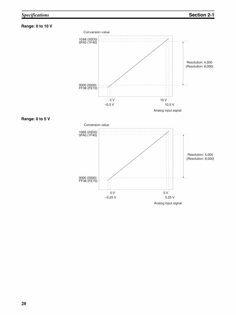
Range: 0 to 10 V
Range: 0 to 5 V
0 V 10 V–0.5 V 10.5 V
1068 (20D0)0FA0 (1F40)
0000 (0000)FF38 (FE70)
Conversion value
Analog input signal
Resolution: 4,000(Resolution: 8,000)
0 V 5 V–0.25 V 5.25 V
1068 (20D0)0FA0 (1F40)
0000 (0000)FF38 (FE70)
Conversion value
Analog input signal
Resolution: 4,000(Resolution: 8,000)
20

Specifications Section 2-1
Range: –10 to 10 V
Note The conversion values for a range of –10 to 10 V will be as follows (for a reso-lution of 4,000):
0 V 10 V11 V
0898 (1130)07D0 (0FA0)
F830 (F060)F768 (EED0)
0000 (0000)
–10 V–11 V
Conversion value
Analog input signal
Resolution: 4,000(Resolution: 8,000)
16-bit binary data BCD
F768 –2200
: :
FFFF –1
0000 0
0001 1
: :
0898 2200
21

Operating Procedure Section 2-2
2-2 Operating ProcedureFollow the procedure outlined below when using Analog Input Units.
Installation and Settings
1,2,3... 1. Set the operation mode to normal mode. (See note 1.)
2. Select voltage/current input using the switch at the back of the terminalblock. (See note 2.)
3. Wire the Unit.
4. Use the unit number switches on the front panel of the Unit to set the unitnumber. (See note 3.)
5. Turn ON the power to the PLC.
6. Create the Input tables.
7. Make the Special Input Unit DM Area settings.
• Set the input numbers to be used.
• Set the input signal ranges.
• Set the number of mean processing samplings.
• Conversion time and resolution
8. Turn the power to the PLC OFF and ON, or turn ON the Special I/O UnitRestart Bit to ON.
When the input for the connected devices needs to be calibrated, follow theprocedures in Offset Gain Adjustment below. Otherwise, skip to Operationbelow.
Offset and Gain Adjustment
1,2,3... 1. Set the operation mode to adjustment mode. (See note 1.)
2. Select voltage or current input. (See note 2.)
3. Turn ON the power to the PLC.
4. Adjust the offset and gain.
5. Turn OFF the power to the PLC.
6. Set the operation mode to normal mode. (See note 1.)
Operation
1,2,3... 1. Turn ON the power to the PLC.
2. Ladder program
• Read conversion values or write set values by means of MOV(021)and XFER(070).
• Specify the peak hold function.
• Obtain disconnection notifications and error codes.
Note 1. Setting the Operation ModeThe operation mode can be changed either by setting the DIP switch onthe rear panel of the Unit or changing the DM Area settings. When normalmode is set both in the DIP switch and in the DM Area settings, the Unitoperates in normal mode. If adjustment mode is set in either or both of thesettings, the Unit operates in adjustment mode. The operation mode selec-tion setting is allocated in DM word m+18 for CS1W-AD041-V1 and CS1W-AD081-V1 and in DM word m+19 for CS1W-AD161.
2. Selecting Voltage/Current InputWith the CS1W-AD041-V1 and CS1W-AD081-V1, remove the terminalblock and set the DIP switch located at the back. With the CS1W-AD161,
22
Operating Procedure Section 2-2
select either voltage input or current input by wiring the connector termi-nals. Use DM word m+52 to select 1 to 5 V or 4 to 20 mA as the voltage orcurrent input range, respectively.
3. Setting the Unit NumberSet the unit number for the Special I/O Unit using the rotary switches onthe front panel of the Unit.Set the CS1W-AD041-V1 and CS1W-AD081-V1 between 0 and 95. A sin-gle CS1W-AD161 is allocated words in the CIO Area and DM Area for twoUnits. Set the unit number between 0 and 94. To set a CS1W-AD161 to unitnumber “n,” the unit number setting “n+1” is not possible.
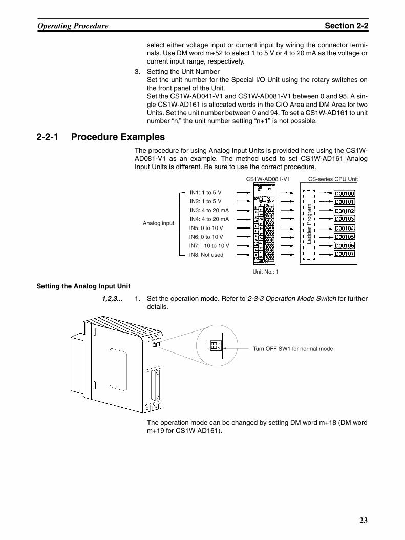
2-2-1 Procedure ExamplesThe procedure for using Analog Input Units is provided here using the CS1W-AD081-V1 as an example. The method used to set CS1W-AD161 AnalogInput Units is different. Be sure to use the correct procedure.
Setting the Analog Input Unit
1,2,3... 1. Set the operation mode. Refer to 2-3-3 Operation Mode Switch for furtherdetails.
The operation mode can be changed by setting DM word m+18 (DM wordm+19 for CS1W-AD161).
CS1W-AD081-V1 CS-series CPU Unit
Unit No.: 1
Analog inputIN5: 0 to 10 V
IN6: 0 to 10 V
IN7: –10 to 10 V
IN8: Not used
IN1: 1 to 5 V
IN2: 1 to 5 V
IN3: 4 to 20 mA
IN4: 4 to 20 mA
Ladd
er P
rogr
am
Turn OFF SW1 for normal mode
23

Operating Procedure Section 2-2
2. Set the voltage/current switch. Refer to 2-3-4 Voltage/Current Switch(CS1W-AD041-V1/AD081-V1) for further details.
Note With CS1W-AD161, select voltage/current input by wiring the connector termi-nals.
3. Mount and wire the Analog Input Unit. Refer to 1-2-1 Mounting Procedure,2-4 Wiring or 2-4-4 Input Wiring Example for further details.
4. Set the unit number switches. Refer to 2-3-2 Unit Number Switches for fur-ther details.
ON IN3 and IN4.
Pins IN1 to IN8 correspond to analog inputs 1 to 8.
E.g., To use voltage input for analog inputs 1 and 2, turn OFF IN1 and IN2.
To use current input for analog inputs 3 and 4, turn
24

Operating Procedure Section 2-2
If the unit number is set to 1, words will be allocated to the Special I/O UnitArea CIO 2010 to CIO 2019 and to the Special I/O Unit Area D20100 toD20199.
Note A single CS1W-AD161 is allocated CIO Area words and DM Area words fortwo Units. For example, if the unit number is set to 1, the CS1W-AD161 will beallocated CIO Area words CIO 2010 to CIO 2029 and DM Area words D20100to D20299.
5. Turn ON the power to the PLC.
Creating I/O TablesAfter turning ON the power to the PLC, be sure to create the I/O tables.
Power ON
Peripheral port
25

Operating Procedure Section 2-2
Initial Data Settings
1,2,3... 1. Specify the Special I/O Unit DM Area settings. Refer to 2-5-4 Fixed DataAllocations for further details.
• The following diagram shows the input settings used. Refer to Alloca-tions in DM Area on page 43 and 2-6-1 Input Settings and ConversionValues for more details.
• The following diagram shows the input range settings. Refer to DM Al-location Contents on page 43 and 2-6-1 Input Settings and ConversionValues for more details.
Also set DM word m+52 when using current input with the CS1W-AD161.
Peripheral port
Setting conditions
Unit No. 1
Analog input 1: 1 to 5 VAnalog input 2: 1 to 5 VAnalog input 3: 4 to 20 mAAnalog input 4: 4 to 20 mAAnalog input 5: 0 to 10 VAnalog input 6: 0 to 10 VAnalog input 7: –10 to 10 VAnalog input 8: Not used.
15 14 13 12 11 10 09 08 07 06 05 01 0004 03 02
0 0 0 0 0 0 0 0 0 1 1 1 1 1 1 1
Bit
Input 4
Input 3
Input 2Input 1
Used
m: D20100(007F hex)
Not used Input 8
Input 7Input 6
Input 5
15 14 13 12 11 10 09 08 07 06 05 01 0004 03 02
0 0 0 0 0 1 0 1 1 0 1 0 1 0 1 0
Bit
m+1: D20101(05AA hex)
Input 1: 1 to 5 V. Set to 10.
Input 2: 1 to 5 V. Set to 10.
Input 3: 4 to 20 mA. Set to 10.
Input 4: 4 to 20 mA. Set to 10.
Input 5: 0 to 10 V. Set to 01.
Input 6: 0 to 10 V. Set to 01.
Input 7: −10 to 10 V. Set to 00.
Input 8: Not used. Set to 00 (disabled)
26

Operating Procedure Section 2-2
• The following diagram shows the conversion time/resolution setting.(Refer to 2-6-2 Conversion Time/Resolution Setting.)
Note For CS1W-AD161, set D(m+19):D20119.
2. Restart the CPU Unit.
Creating Ladder Programs
The data that is converted from analog to digital and output to CIO words (n +1) to (n+ 7) of the Special I/O Unit Area (CIO 2011 to CIO2017), is stored inthe specified addresses D00100 to D00106 as signed binary values 0000 to0FA0 hex.
15 14 13 12 11 10 09 08 07 06 05 01 0004 03 02
0 0 0 0 0 0 0 0
Bit
(0000 hex)
m+18: D20118 (See note.)
Conversion Time/Resolution Setting0000: 1-ms conversion time, 4,000 resolutionC100: 250-µs conversion time, 8,000 resolution
Power turned ON again (or Special I/O Unit Restart Bit is turned ON)
Peripheral port
27

Operating Procedure Section 2-2
• The following table shows the addresses used for analog input.
Note 1. The addresses are fixed according to the unit number of the Special I/OUnit. Refer to 2-3-2 Unit Number Switches for further details.
2. Set as required.
3. Bits 00 to 07 of word (n + 9) are allocated to the input Disconnection De-tection Flags. Refer to Allocations for Normal Mode on page 49 for furtherdetails.
Input number Input signal range Input conversion value address(n = CIO 2010)(See note 1.)
Conversion data holding address
(See note 2.)
1 1 to 5 V (n+1) = CIO 2011 D00100
2 1 to 5 V (n+2) = CIO 2012 D00101
3 4 to 20 mA (n+3) = CIO 2013 D00102
4 4 to 20 mA (n+4) = CIO 2014 D00103
5 0 to 10 V (n+5) = CIO2015 D00104
6 0 to 10 V (n+6) = CIO2016 D00105
7 –10 to 10 V (n+7) = CIO2017 D00106
8 Not used --- ---
201900 Input 1 Disconnection Detection Flag (See note 3.)
201901 Input 2 Disconnection Detection Flag (See note 3.)
201902 Input 3 Disconnection Detection Flag (See note 3.)
201903 Input 4 Disconnection Detection Flag (See note 3.)
For 1 to 5 V, the hexadecimal value 0000 to 0FA0 will be stored in CIO 2011, so if there is no disconnection (i.e., 201900 is OFF), CIO 2011 will be stored in D00100.
In the same way, for 1 to 5 V, CIO 2012 will be stored in D00101.
In the same way, for 4 to 20 mA, CIO 2013 will be stored in D00102.
In the same way, for 4 to 20 mA, CIO 2014 will be stored in D00103.
MOV (021)
2011
D00100
MOV (021)
2012
D00101
MOV (021)
2013
D00102
MOV (021)
2014
D00103
28
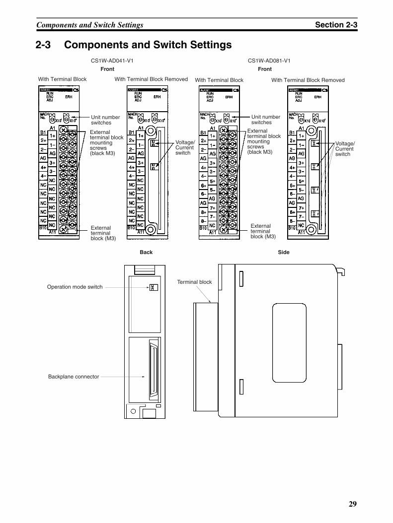
Components and Switch Settings Section 2-3
2-3 Components and Switch Settings
Unit number switches
External terminal block (M3)
Front
With Terminal Block With Terminal Block Removed
Voltage/Current switch
CS1W-AD041-V1 CS1W-AD081-V1
External terminal block (M3)
Front
Voltage/Current switch
External terminal block mounting screws (black M3)
External terminal block mounting screws (black M3)
With Terminal Block With Terminal Block Removed
Unit number switches
Operation mode switch
Backplane connector
Terminal block
SideBack
29

Components and Switch Settings Section 2-3
The terminal block is attached by a connector. It can be removed by looseningthe two black mounting screws located at the top and bottom of the terminalblock.
Check to be sure that the black terminal block mounting screw is securelytightened to a torque of 0.5 N·m.
CS1W-AD161
2-3-1 IndicatorsThe indicators show the operating status of the Unit. The following tableshows the meanings of the indicators.
Fasten the mounting screw.
Fasten the mounting screw.
34.5
118.03
100.5
130
Input connector 2(Inputs 9 to 16)
Input connector 1(Inputs 1 to 8) Backplane mounting screw
Mode Switch(two poles)
PC21 bus connector
Indicator Meaning Indicator status
Operating status
RUN (green) Operating Lit Operating in normal mode.
Not lit Unit has stopped exchanging data with the CPU Unit.
ERC (red) Error detected by Unit
Lit Alarm has occurred (such as disconnec-tion detection) or initial settings are incor-rect.
Not lit Operating normally.
30
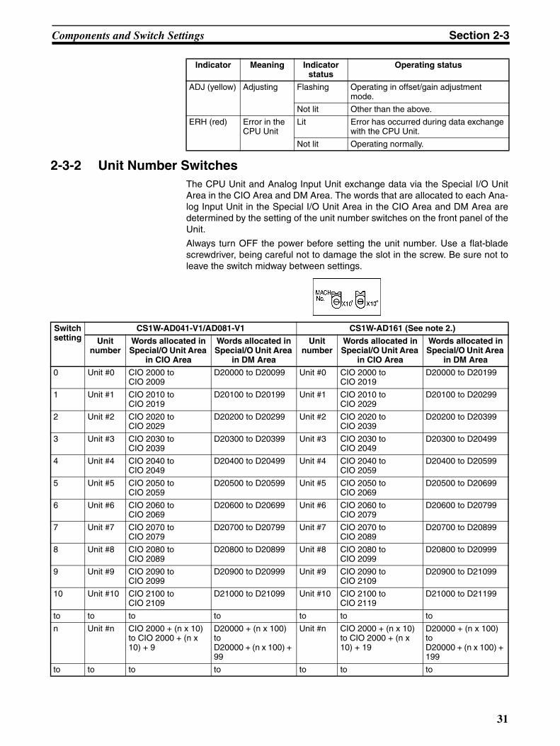
Components and Switch Settings Section 2-3
2-3-2 Unit Number SwitchesThe CPU Unit and Analog Input Unit exchange data via the Special I/O UnitArea in the CIO Area and DM Area. The words that are allocated to each Ana-log Input Unit in the Special I/O Unit Area in the CIO Area and DM Area aredetermined by the setting of the unit number switches on the front panel of theUnit.
Always turn OFF the power before setting the unit number. Use a flat-bladescrewdriver, being careful not to damage the slot in the screw. Be sure not toleave the switch midway between settings.
ADJ (yellow) Adjusting Flashing Operating in offset/gain adjustment mode.
Not lit Other than the above.
ERH (red) Error in the CPU Unit
Lit Error has occurred during data exchange with the CPU Unit.
Not lit Operating normally.
Indicator Meaning Indicator status
Operating status
Switch setting
CS1W-AD041-V1/AD081-V1 CS1W-AD161 (See note 2.)
Unit number
Words allocated in Special/O Unit Area
in CIO Area
Words allocated in Special/O Unit Area
in DM Area
Unit number
Words allocated in Special/O Unit Area
in CIO Area
Words allocated in Special/O Unit Area
in DM Area
0 Unit #0 CIO 2000 to CIO 2009
D20000 to D20099 Unit #0 CIO 2000 to CIO 2019
D20000 to D20199
1 Unit #1 CIO 2010 to CIO 2019
D20100 to D20199 Unit #1 CIO 2010 to CIO 2029
D20100 to D20299
2 Unit #2 CIO 2020 to CIO 2029
D20200 to D20299 Unit #2 CIO 2020 to CIO 2039
D20200 to D20399
3 Unit #3 CIO 2030 to CIO 2039
D20300 to D20399 Unit #3 CIO 2030 to CIO 2049
D20300 to D20499
4 Unit #4 CIO 2040 to CIO 2049
D20400 to D20499 Unit #4 CIO 2040 to CIO 2059
D20400 to D20599
5 Unit #5 CIO 2050 to CIO 2059
D20500 to D20599 Unit #5 CIO 2050 to CIO 2069
D20500 to D20699
6 Unit #6 CIO 2060 to CIO 2069
D20600 to D20699 Unit #6 CIO 2060 to CIO 2079
D20600 to D20799
7 Unit #7 CIO 2070 to CIO 2079
D20700 to D20799 Unit #7 CIO 2070 to CIO 2089
D20700 to D20899
8 Unit #8 CIO 2080 to CIO 2089
D20800 to D20899 Unit #8 CIO 2080 to CIO 2099
D20800 to D20999
9 Unit #9 CIO 2090 to CIO 2099
D20900 to D20999 Unit #9 CIO 2090 to CIO 2109
D20900 to D21099
10 Unit #10 CIO 2100 to CIO 2109
D21000 to D21099 Unit #10 CIO 2100 to CIO 2119
D21000 to D21199
to to to to to to to
n Unit #n CIO 2000 + (n x 10) to CIO 2000 + (n x 10) + 9
D20000 + (n x 100) to D20000 + (n x 100) + 99
Unit #n CIO 2000 + (n x 10) to CIO 2000 + (n x 10) + 19
D20000 + (n x 100) to D20000 + (n x 100) + 199
to to to to to to to
31

Components and Switch Settings Section 2-3
Note 1. If two or more Special I/O Units are assigned the same unit number, a“UNIT No. DPL ERR” error (in the Programming Console) will be generat-ed (A40113 will turn ON) and the PLC will not operate.
2. A single CS1W-AD161 is allocated CIO Area words and DM Area wordsfor two Units. Be sure to set a unit number so that the CS1W-AD161 is notallocated words in the CIO Area and DM Area that are already allocated toother Special I/O Units. For example, if the CS1W-AD161 is set to unitnumber n, another Special I/O Unit cannot be set with unit number n+1.The highest unit number that can be set for a CS1W-AD161 is unit number94.
2-3-3 Operation Mode SwitchThe operation mode switch on the back panel of the Unit is used to set theoperation mode to either normal mode or adjustment mode (for adjusting off-set and gain).
Note 1. The operation mode can be set in the DM Area as an alternative to usingthe operation mode switch.
2. Set the operation mode in DM word m+18 for CS1W-AD041-V1 andCS1W-AD081-V1, and in DM word m+19 for CS1W-AD161.
CS1W-AD041-V1/AD081-V1
m = D20000 + (unit number x 100)
CS1W-AD161
m = D20000 + (unit number x 100)
94 Unit #94 CIO 2940 to CIO 2949
D29400 to D29499 Unit #94 CIO 2940 to CIO 2959
D29400 to D29499
95 Unit #95 CIO 2950 to CIO 2959
D29500 to D29599 Not used.
--- ---
Switch setting
CS1W-AD041-V1/AD081-V1 CS1W-AD161 (See note 2.)
Unit number
Words allocated in Special/O Unit Area
in CIO Area
Words allocated in Special/O Unit Area
in DM Area
Unit number
Words allocated in Special/O Unit Area
in CIO Area
Words allocated in Special/O Unit Area
in DM Area
Pin number Mode
1 2
OFF OFF Normal mode
ON OFF Adjustment mode
Bit 15 14 13 12 11 10 09 08 07 06 05 04 03 02 01 00
D (m+18) Conversion time/resolution setting Operation mode setting
00: Normal modeC1: Adjustment mode
Bit 15 14 13 12 11 10 09 08 07 06 05 04 03 02 01 00
D (m+19) Conversion time/resolution setting Operation mode setting
00: Normal modeC1: Adjustment mode
32
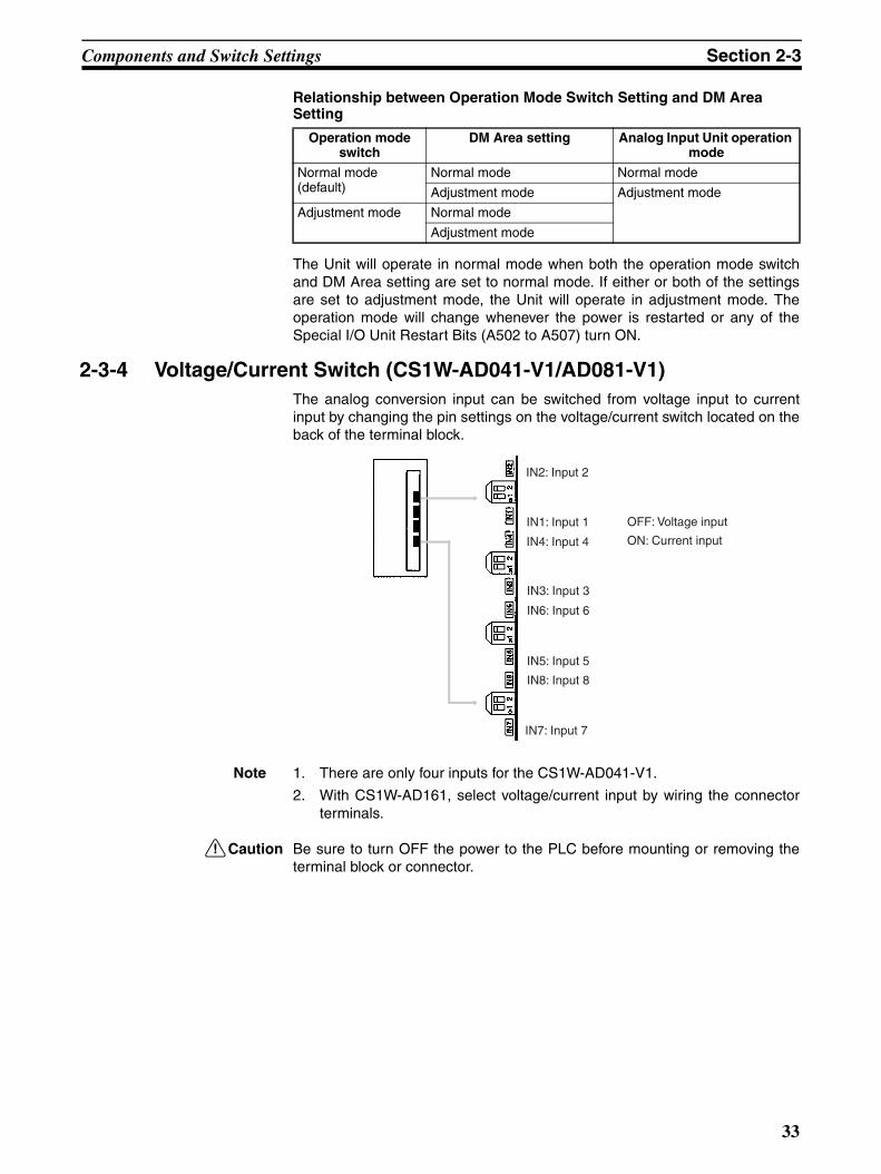
Components and Switch Settings Section 2-3
Relationship between Operation Mode Switch Setting and DM Area Setting
The Unit will operate in normal mode when both the operation mode switchand DM Area setting are set to normal mode. If either or both of the settingsare set to adjustment mode, the Unit will operate in adjustment mode. Theoperation mode will change whenever the power is restarted or any of theSpecial I/O Unit Restart Bits (A502 to A507) turn ON.
2-3-4 Voltage/Current Switch (CS1W-AD041-V1/AD081-V1)The analog conversion input can be switched from voltage input to currentinput by changing the pin settings on the voltage/current switch located on theback of the terminal block.
Note 1. There are only four inputs for the CS1W-AD041-V1.
2. With CS1W-AD161, select voltage/current input by wiring the connectorterminals.
!Caution Be sure to turn OFF the power to the PLC before mounting or removing theterminal block or connector.
Operation mode switch
DM Area setting Analog Input Unit operation mode
Normal mode (default)
Normal mode Normal mode
Adjustment mode Adjustment mode
Adjustment mode Normal mode
Adjustment mode
IN1: Input 1
IN4: Input 4
OFF: Voltage input
ON: Current input
IN3: Input 3
IN6: Input 6
IN2: Input 2
IN5: Input 5
IN8: Input 8
IN7: Input 7
33

Wiring Section 2-4
2-4 Wiring
2-4-1 Terminal ArrangementThe signal names corresponding to the connecting terminals are as shown inthe following diagram.
CS1W-AD041-V1
CS1W-AD081-V1
Input 2 (+)
Input 2 (–)
Input 4 (+)
Input 4 (–)
N.C.
N.C.
N.C.
N.C.
Input 1 (+)
Input 1 (–)
Input 3 (+)
Input 3 (–)
AG
N.C.
N.C.
N.C.
N.C.
B1
B2
B3
B4
B5
B6
B7
B8
B9
A1
A2
A3
A4
A5
A6
A7
A8
A9
AG
B10
N.C.
N.C.
N.C.
A10
A11
Input 2 (+)
Input 2 (–)
Input 4 (+)
Input 4 (–)
Input 6 (–)
AG
Input 8 (+)
Input 8 (–)
Input 1 (+)
Input 1 (–)
Input 3 (+)
Input 3 (–)
AG
Input 5 (+)
Input 5 (–)
AG
Input 7 (+)
B1
B2
B3
B4
B5
B6
B7
B8
B9
A1
A2
A3
A4
A5
A6
A7
A8
A9
AG
B10
Input 6 (+)
Input 7 (–)
N.C.
A10
A11
34

Wiring Section 2-4
CS1W-AD161
Note 1. The number of analog inputs that can be used is set in the DM Area.
2. The input signal ranges for individual inputs are set in the DM Area.The in-put signal range can be set separately for each input.
3. The AG terminals (A8, B8) are connected to the 0-V analog circuit in theUnit. Connecting shielded input lines can improve noise resistance.
!Caution Do not make any connections to the N.C. terminals.
2-4-2 Internal CircuitryThe following diagrams show the internal circuitry of the analog input section.
Input Circuitry
CS1W-AD041-V1/AD081-V1
CS1W-AD161
CN2 Inputs 9 to16 CN1 Inputs 1 to 8Input 9+ 1 2 Input 10+ Input 1+ 1 2 Input 2+Current mode 9 3 4 Current mode 10 Current mode 1 3 4 Current mode 2Input 9− 5 6 Input 10− Input 1− 5 6 Input 2−AG 7 8 AG AG 7 8 AGInput 11+ 9 10 Input 12+ Input 3+ 9 10 Input 4+Current mode 11 11 12 Current mode 12 Current mode 3 11 12 Current mode 4Input 11− 13 14 Input 12− Input 3− 13 14 Input 4−AG AG AG 15 16 AGInput 13+ 17 18 Input 14+ Input 15+ 17 18 Input 6+Current mode 13 19 20 Current mode 14 Current mode 5 19 20 Current mode 6Input 13− 21 22 Input 14− Input 5− 21 22 Input 6−AG AG AG 23 24 AGInput 15+ Input 16+ Input 7+ 25 26 Input 8+Current mode 15 28 Current mode 16 Current mode 7 27 28 Current mode 8Input 15− 30 Input 16− Input 7− 29 30 Input 8−AG 31 32 AG AG 31 32 AGNC 33 NC NC 33 34 NC34
15 16
23 2425 262729
1 MΩ
15 kΩ 15 kΩ
15 kΩ 15 kΩ
AG (common to all inputs)
Input (+)
Input (–)
AG (analog 0 V)
Input circuit and conversion circuit
1 MΩ
Voltage/currentinput switch
250 Ω
Input (+)
Input (−)
AG (analog 0 V)
AG (common to all inputs)
Input circuit and conversion circuit250 Ω
1 MΩ
15 kΩ 15 kΩ
15 kΩ 15 kΩ
1 MΩCurrent mode
35

Wiring Section 2-4
Internal Configuration
2-4-3 Voltage Input Disconnection
Note If the connected device #2 in the above example outputs 5 V and the powersupply is shared by 2 channels as shown in the above diagram, approximatelyone third of the voltage, or 1.6 V, will be input at input 1.
Bus interface
Indicators/Switch
MPU
RegulatorInsulation-type DC-to-DC converter
Oscillator
Division
CS-series PC
EEPROM
RAM ROM
Multi-plexer and amplifier
A/D converter
INPUT
Externallyconnectedterminal
Pho
toco
uple
r in
sula
tion
Connected device #1
24 VDC
Connected device #2
B C
36
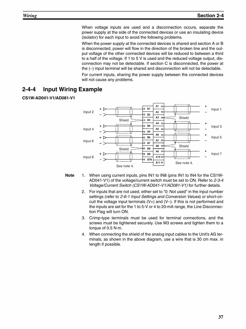
Wiring Section 2-4
When voltage inputs are used and a disconnection occurs, separate thepower supply at the side of the connected devices or use an insulating device(isolator) for each input to avoid the following problems.
When the power supply at the connected devices is shared and section A or Bis disconnected, power will flow in the direction of the broken line and the out-put voltage of the other connected devices will be reduced to between a thirdto a half of the voltage. If 1 to 5 V is used and the reduced voltage output, dis-connection may not be detectable. If section C is disconnected, the power atthe (–) input terminal will be shared and disconnection will not be detectable.
For current inputs, sharing the power supply between the connected deviceswill not cause any problems.
2-4-4 Input Wiring ExampleCS1W-AD041-V1/AD081-V1
Note 1. When using current inputs, pins IN1 to IN8 (pins IN1 to IN4 for the CS1W-AD041-V1) of the voltage/current switch must be set to ON. Refer to 2-3-4Voltage/Current Switch (CS1W-AD041-V1/AD081-V1) for further details.
2. For inputs that are not used, either set to “0: Not used” in the input numbersettings (refer to 2-6-1 Input Settings and Conversion Values) or short-cir-cuit the voltage input terminals (V+) and (V–). If this is not performed andthe inputs are set for the 1 to 5-V or 4 to 20-mA range, the Line Disconnec-tion Flag will turn ON.
3. Crimp-type terminals must be used for terminal connections, and thescrews must be tightened securely. Use M3 screws and tighten them to atorque of 0.5 N·m.
4. When connecting the shield of the analog input cables to the Unit’s AG ter-minals, as shown in the above diagram, use a wire that is 30 cm max. inlength if possible.
Input 2
Input 6
Shield
See note 4.See note 4.
Input 1
Input 4
Input 8
Input 3
Input 5
Input 7Shield
Shield
Shield
37

Wiring Section 2-4
!Caution Do not connect anything to N.C. terminals shown in the wiring diagram onpage 34.
Connect the analog input line shield to the AG terminal on the Analog InputUnit to improve noise resistance.
CS1W-AD161 Use OMRON's XW2D-34G6 Connector-Terminal Conversion Unit and SpecialConnection Cable for input wiring.
Terminal Block Pin Arrangement
6.0 mm max.
6.0 mm max.M3 screw
Fork type
Round type
CS1W-AD161 Analog Input Unit
CN2 (inputs 9 to 16)CN1 (inputs 1 to 8)
XW2Z-200C Terminal Block Conversion Unit Connection Cable
XW2Z-200C Terminal Block Conversion Unit Connection Cable
XW2D-34G6 Connector-Terminal Block Conversion Unit
XW2D-34G6 Connector-Terminal Block Conversion Unit
A1 A2 A3 A16 A17
B1 B2 B3 B16 B17
to
to
XW2D-34G6 Terminal Block Conversion Unit
Upper level
Lower level
38
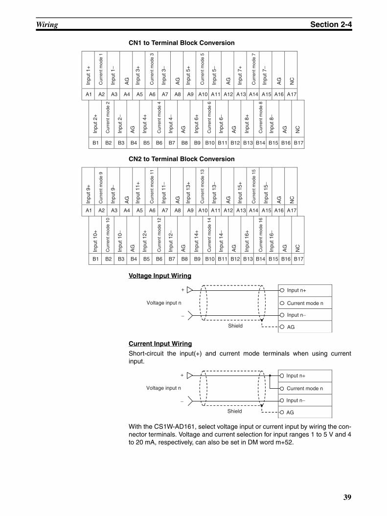
Wiring Section 2-4
CN1 to Terminal Block Conversion
CN2 to Terminal Block Conversion
Voltage Input Wiring
Current Input Wiring
Short-circuit the input(+) and current mode terminals when using currentinput.
With the CS1W-AD161, select voltage input or current input by wiring the con-nector terminals. Voltage and current selection for input ranges 1 to 5 V and 4to 20 mA, respectively, can also be set in DM word m+52.
AG
AG
AG
AG
NC
A1 A2 A3 A4 A5 A6 A7 A8 A9 A10 A11 A12 A13 A14 A15 A16 A17
AG
AG
AG
AG
NC
B1 B2 B3 B4 B5 B6 B7 B8 B9 B10 B11 B12 B13 B14 B15 B16 B17
Inpu
t 1+
Inpu
t 1−
Inpu
t 3+
Inpu
t 3−
Inpu
t 5+
Inpu
t 5−
Inpu
t 7+
Inpu
t 7−
Inpu
t 2+
Inpu
t 2−
Inpu
t 4+
Inpu
t 4−
Inpu
t 6+
Inpu
t 6−
Inpu
t 8+
Inpu
t 8−
Cur
rent
mod
e 1
Cur
rent
mod
e 3
Cur
rent
mod
e 5
Cur
rent
mod
e 7
Cur
rent
mod
e 2
Cur
rent
mod
e 4
Cur
rent
mod
e 6
Cur
rent
mod
e 8
AG
AG
AG
AG
NC
A1 A2 A3 A4 A5 A6 A7 A8 A9 A10 A11 A12 A13 A14 A15 A16 A17
AG
AG
AG
AG
NC
B1 B2 B3 B4 B5 B6 B7 B8 B9 B10 B11 B12 B13 B14 B15 B16 B17
Inpu
t 9+
Inpu
t 9−
Inpu
t 11+
Inpu
t 11−
Inpu
t 13+
Inpu
t 13−
Inpu
t 15+
Inpu
t 15−
Inpu
t 10+
Inpu
t 10−
Inpu
t 12+
Inpu
t 12−
Inpu
t 14+
Inpu
t 14−
Inpu
t 16+
Inpu
t 16−
Cur
rent
mod
e 9
Cur
rent
mod
e 11
Cur
rent
mod
e 13
Cur
rent
mod
e 15
Cur
rent
mod
e 10
Cur
rent
mod
e 12
Cur
rent
mod
e 14
Cur
rent
mod
e 16
+
−
Shield
Input n+
Input n−
AG
Voltage input n Current mode n
+
−
Shield
Input n+
Input n−
AG
Voltage input n Current mode n
39

Exchanging Data with the CPU Unit Section 2-5
Use crimp terminals to wire the terminal block.
Note The following Connectors are included with the CS1W-AD161. Use them ifyou are going to make your own cable (e.g., if you are not going to use anOMRON Connector-Terminal Block Conversion Unit).
2-4-5 Input Wiring ConsiderationsWhen wiring inputs, apply the following points to avoid noise interference andoptimize Analog Input Unit performance.
• Use two-core shielded twisted-pair cables for input connections.
• Route input cables separately from the AC cable, and do not run the Unit’scables near a main circuit cable, high voltage cable, or a non-PLC loadcable.
• If there is noise interference from power lines (if, for example, the powersupply is shared with electrical welding devices or electrical dischargemachines, or if there is a high-frequency generation source nearby) installa noise filter at the power supply input area.
2-5 Exchanging Data with the CPU Unit
2-5-1 Outline of Data ExchangeData is exchanged between the CPU Unit and the CS1W-AD041-V1/081-V1/AD161 Analog Input Unit via the Special I/O Unit Area in the CIO Area (fordata used to operate the Unit) and the Special I/O Unit in the DM Area (fordata used for initial settings).
I/O Refresh Data
Analog input conversion values, which are used as data for Unit operation, areallocated in the Special I/O Unit Area in the CIO Area of the CPU Unit accord-ing to the unit number, and are exchanged during I/O refreshing.
Fixed Data
The Unit’s fixed data, such as the analog input signal ranges and the numberof operational mean value buffers is allocated in the Special I/O Unit DM Areaof the CPU Unit according to the unit number, and is exchanged when thepower is turned ON or the Unit is restarted.
XW2D-34G6 Terminal Block Conversion Unit
Name Connection method
Manufacturer Model number Qty. included
Applicable Con-nector (34-pin)
Pressure welded
OMRON XG4M-3430-T 2
40

Exchanging Data with the CPU Unit Section 2-5
The conversion time and resolution can be set, along with the operationmode.
Note 1. A single CS1W-AD161 is allocated CIO Area words and DM Area wordsfor two Units, i.e., 20 words in the CIO Area (CIO 2000 + n × 10 to CIO 2000+ n × 10 + 19) and 200 words in the DM Area (D20000 + n × 100 to D20000+ n × 100 + 199).
2. Transferring scaling data is supported by CS1W-AD161 only.
2-5-2 Unit Number SettingsThe Special I/O Unit Area and Special I/O Unit DM Area word addresses thateach Analog Input Unit occupies are set by the unit number switches on thefront panel of the Unit.
CS-series CPU Unit CS1W-AD041-V1/081-V1 Analog Input Unit
Special I/O Unit Area I/O Refresh Data
Analog inputs
Analog inputs
DM (Data Memory) Area
Input signal range
Number of opera-tional mean value buffers
I/O refresh
Power ON or Unit restart
Exchanges analog inputvalues during data refresh.
Transmits fixed data such as analog input signal ranges and number of operational mean value buffers.
2000 + n x 10
2000 + n x 10 + 9
D20000 + n x 100
D20000 + n x 100 + 99
10 words
100 words
Fixed Data
:
n: Unit number
(See note 1.)
(See note 1.)
to
to
(See note 1.)
(See note 1.)
Scaling data (See note 2.)
Conversion time/res-olution and operating mode
See 2-5-5 I/O Refresh Data Allocations for details.
See 2-5-4 Fixed Data Allocations for details.
Switch setting
CS1W-AD041-V1/AD081-V1 CS1W-AD161 (See note 2.)
Unit number
Words allocated in Special I/O Unit
Area in CIO Area
Words allocated in Special I/O Unit Area in DM Area
Unit number
Words allocated in Special I/O Unit
Area in CIO Area
Words allocated in Special I/O Unit Area in DM Area
0 Unit #0 CIO 2000 to CIO 2009
D20000 to D20099 Unit #0 CIO 2000 to CIO 2019
D20000 to D20199
1 Unit #1 CIO 2010 to CIO 2019
D20100 to D20199 Unit #1 CIO 2010 to CIO 2029
D20100 to D20299
2 Unit #2 CIO 2020 to CIO 2029
D20200 to D20299 Unit #2 CIO 2020 to CIO 2039
D20200 to D20399
3 Unit #3 CIO 2030 to CIO 2039
D20300 to D20399 Unit #3 CIO 2030 to CIO 2049
D20300 to D20499
4 Unit #4 CIO 2040 to CIO 2049
D20400 to D20499 Unit #4 CIO 2040 to CIO 2059
D20400 to D20599
41

Exchanging Data with the CPU Unit Section 2-5
Note 1. If two or more Special I/O Units are assigned the same unit number, a“UNIT No. DPL ERR” error (in the Programming Console) will be generat-ed (A40113 will turn ON) and the PLC will not operate.
2. Be sure to set a unit number such that the CS1W-AD161 is not allocatedwords in the CIO Area and DM Area that are already allocated to otherSpecial I/O Units. The unit number can be set between 0 and 94.
2-5-3 Special I/O Unit Restart BitsTo restart the Unit after changing the contents of the DM Area or correcting anerror, cycle the power supply to the PLC or turn ON the Special I/O UnitRestart Bit.
A single CS1W-AD161 is allocated words for two unit numbers, but uses onlythe Special I/O Unit Restart Bit setting corresponding to the unit number thatis set.
Note Replace the Unit if the error is not cleared even though the power supply iscycled or the Restart Bit is turned ON.
5 Unit #5 CIO 2050 to CIO 2059
D20500 to D20599 Unit #5 CIO 2050 to CIO 2069
D20500 to D20699
6 Unit #6 CIO 2060 to CIO 2069
D20600 to D20699 Unit #6 CIO 2060 to CIO 2079
D20600 to D20799
7 Unit #7 CIO 2070 to CIO 2079
D20700 to D20799 Unit #7 CIO 2070 to CIO 2089
D20700 to D20899
8 Unit #8 CIO 2080 to CIO 2089
D20800 to D20899 Unit #8 CIO 2080 to CIO 2099
D20800 to D20999
9 Unit #9 CIO 2090 to CIO 2099
D20900 to D20999 Unit #9 CIO 2090 to CIO 2109
D20900 to D21099
10 Unit #10 CIO 2100 to CIO 2109
D21000 to D21099 Unit #10 CIO 2100 to CIO 2119
D21000 to D21199
to to to to to to to
n Unit #n CIO 2000 + (n × 10) to CIO 2000 + (n × 10) + 9
D20000 + (n × 100) to D20000 + (n × 100) + 99
Unit #n CIO 2000 + (n × 10) to CIO 2000 + (n × 10) + 19
D20000 + (n × 100) to D20000 + (n × 100) + 199
to to to to to to to
94 Unit #94 CIO 2940 to CIO 2949
D29400 to D29499 Unit #94 CIO 2940 to CIO 2959
D29400 to D29499
95 Unit #95 CIO 2950 to CIO 2959
D29500 to D29599 Not used.
--- ---
Switch setting
CS1W-AD041-V1/AD081-V1 CS1W-AD161 (See note 2.)
Unit number
Words allocated in Special I/O Unit
Area in CIO Area
Words allocated in Special I/O Unit Area in DM Area
Unit number
Words allocated in Special I/O Unit
Area in CIO Area
Words allocated in Special I/O Unit Area in DM Area
Special I/O Unit Area word address
Function
A50200 Unit No. 0 Restart Bit Restarts the Unit when turned ON and then OFF again.A50201 Unit No. 1 Restart Bit
to to
A50215 Unit No. 15 Restart Bit
A50300 Unit No. 16 Restart Bit
to to
A50715 Unit No. 95 Restart Bit
42
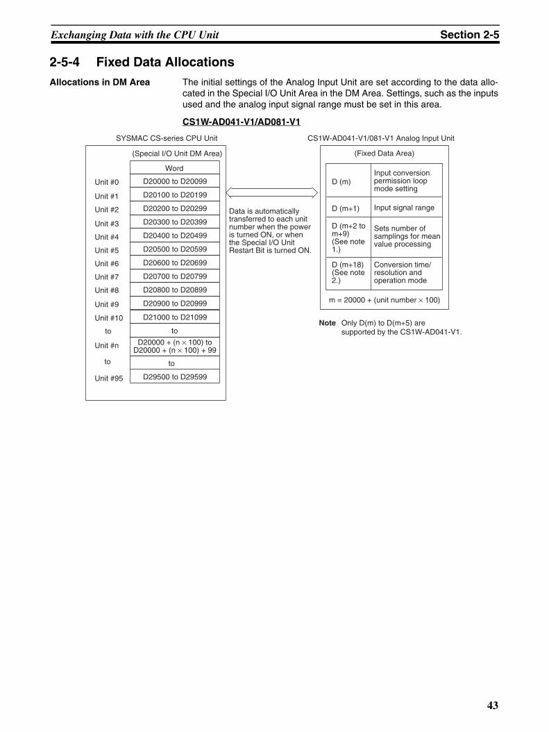
Exchanging Data with the CPU Unit Section 2-5
2-5-4 Fixed Data AllocationsAllocations in DM Area The initial settings of the Analog Input Unit are set according to the data allo-
cated in the Special I/O Unit Area in the DM Area. Settings, such as the inputsused and the analog input signal range must be set in this area.
CS1W-AD041-V1/AD081-V1
D (m+1)
D (m)
D20300 to D20399
D20400 to D20499
D20500 to D20599
D20000 to D20099
D20100 to D20199
D20200 to D20299
D20900 to D20999
D20600 to D20699
D20700 to D20799
D20800 to D20899
SYSMAC CS-series CPU Unit CS1W-AD041-V1/081-V1 Analog Input Unit
(Fixed Data Area)
Unit #0
Unit #1
Unit #2
Unit #3
Unit #4
Unit #5
Unit #6
Unit #7
Unit #8
Unit #9
(Special I/O Unit DM Area)
Word
D29500 to D29599
D21000 to D21099Unit #10
Unit #n
Unit #95
Input signal range
m = 20000 + (unit number × 100)
Note Only D(m) to D(m+5) are supported by the CS1W-AD041-V1.
D20000 + (n × 100) to D20000 + (n × 100) + 99
Data is automatically transferred to each unit number when the power is turned ON, or when the Special I/O Unit Restart Bit is turned ON.
Input conversion permission loop mode setting
Sets number of samplings for mean value processing
Conversion time/ resolution and operation mode
D (m+2 to m+9) (See note1.)
D (m+18)(See note2.)
to to
toto
43
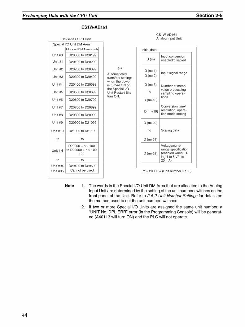
Exchanging Data with the CPU Unit Section 2-5
CS1W-AD161
Note 1. The words in the Special I/O Unit DM Area that are allocated to the AnalogInput Unit are determined by the setting of the unit number switches on thefront panel of the Unit. Refer to 2-5-2 Unit Number Settings for details onthe method used to set the unit number switches.
2. If two or more Special I/O Units are assigned the same unit number, a“UNIT No. DPL ERR” error (in the Programming Console) will be generat-ed (A40113 will turn ON) and the PLC will not operate.
Allocated DM Area words
Unit #0 D20000 to D20199
Unit #1 D20100 to D20299D (m)
Unit #2 D20200 to D20399
Unit #3 D20300 to D20499
D (m+1)
D (m+2)
Unit #4 D20400 to D20599 D (m+3)
Unit #5 D20500 to D20699
Unit #6 D20600 to D20799 D (m+18)
Unit #7 D20700 to D20899
Unit #8 D20800 to D20999D (m+19)
Unit #9 D20900 to D21099 D (m+20)
Unit #10 D21000 to D21199
D (m+51)
Unit #ND20000 + n × 100
to D20000 + n × 100 +99 D (m+52)
Unit #94 D29400 to D29599
Unit #95 m = 20000 + (Unit number × 100)
to to
to to
to
to
CS1W-AD161 Analog Input Unit
Special I/O Unit DM Area
Cannot be used.
Automatically transfers settings when the power is turned ON or the Special I/O Unit Restart Bits turn ON.
Initial data
Input conversion enabled/disabled
Input signal range
Number of mean value processing sampling opera-tions
Conversion time/ resolution, opera-tion mode setting
Scaling data
Voltage/current range specification (enabled when us-ing 1 to 5 V/4 to 20 mA)
CS-series CPU Unit
44

Exchanging Data with the CPU Unit Section 2-5
Allocations in DM Area The following table shows the allocation of DM Area words and bits for bothnormal and adjustment mode.
CS1W-AD041-V1
Note For the DM word addresses, m = D20000 + (unit number x 100).
CS1W-AD081-V1
Note For the DM word addresses, m = D20000 + (unit number × 100).
DM Area word (See
note.)
Bits
15 14 13 12 11 10 9 8 7 6 5 4 3 2 1 0
D (m) Not used. (Settings are ignored.) Not used. Input use setting
Input 4
Input 3
Input 2
Input 1
D (m+1) Not used. (Settings are ignored.) Input range setting
Input 4 Input 3 Input 2 Input 1
D (m+2) Input 1: Mean value processing setting
D (m+3) Input 2: Mean value processing setting
D (m+4) Input 3: Mean value processing setting
D (m+5) Input 4: Mean value processing setting
D (m+18) Conversion time/resolution setting 00: Conversion time of 1 ms and resolution of 4,000C1: Conversion time of 250 µs and resolution of 8,000
Operation mode setting00: Normal modeC1: Adjustment mode
DM Area word (See
note.)
Bits
15 14 13 12 11 10 9 8 7 6 5 4 3 2 1 0
D (m) Not used. (Settings are ignored.) Input use setting
Input 8
Input 7
Input 6
Input 5
Input 4
Input 3
Input 2
Input 1
D (m+1) Input range setting
Input 8 Input 7 Input 6 Input 5 Input 4 Input 3 Input 2 Input 1
D (m+2) Input 1: Mean value processing setting
D (m+3) Input 2: Mean value processing setting
D (m+4) Input 3: Mean value processing setting
D (m+5) Input 4: Mean value processing setting
D( m+6) Input 5: Mean value processing setting
D (m+7) Input 6: Mean value processing setting
D (m+8) Input 7: Mean value processing setting
D (m+9) Input 8: Mean value processing setting
D (m+18) Conversion time/resolution setting 00: Conversion time of 1 ms and resolution of 4,000C1: Conversion time of 250 µs and resolution of 8,000
Operation mode setting
00: Normal modeC1: Adjustment mode
45
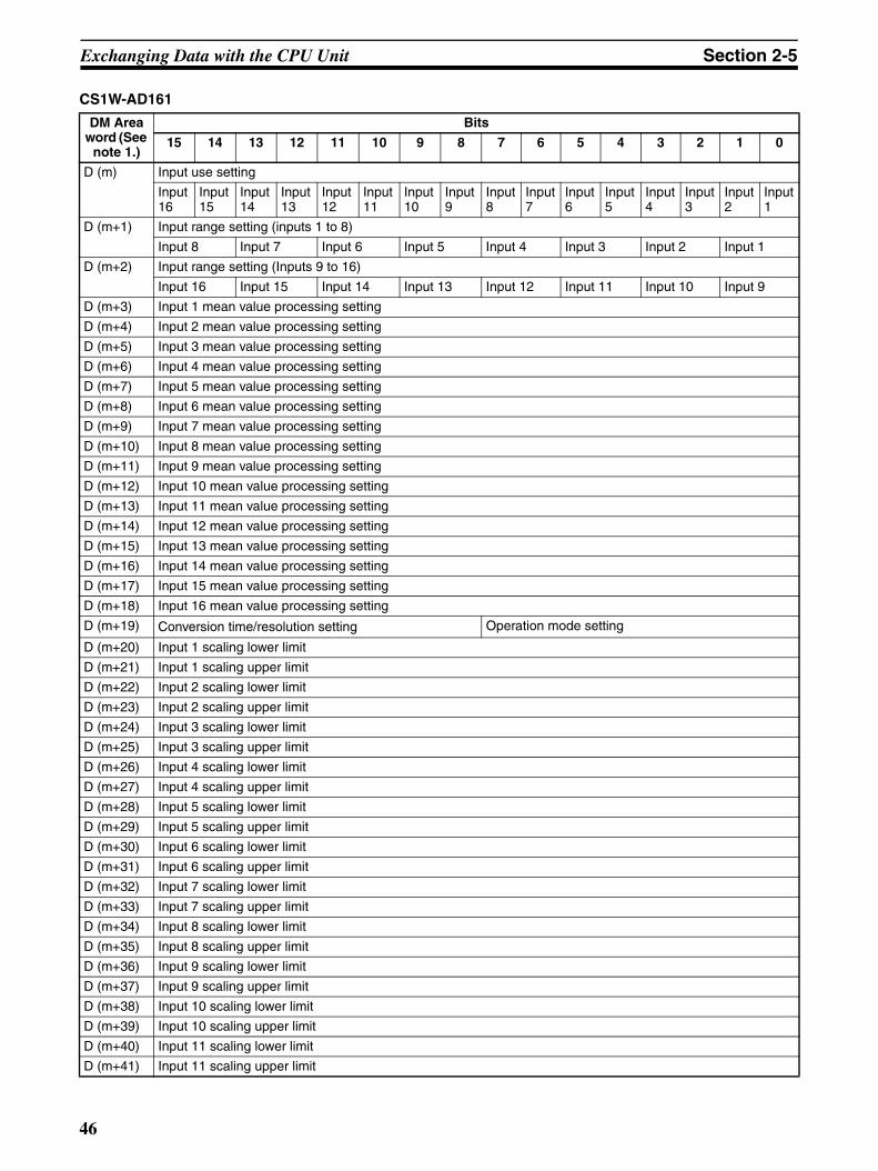
Exchanging Data with the CPU Unit Section 2-5
CS1W-AD161
DM Area word (See
note 1.)
Bits
15 14 13 12 11 10 9 8 7 6 5 4 3 2 1 0
D (m) Input use setting
Input 16
Input 15
Input 14
Input 13
Input 12
Input 11
Input 10
Input 9
Input 8
Input 7
Input 6
Input 5
Input 4
Input 3
Input 2
Input 1
D (m+1) Input range setting (inputs 1 to 8)
Input 8 Input 7 Input 6 Input 5 Input 4 Input 3 Input 2 Input 1
D (m+2) Input range setting (Inputs 9 to 16)
Input 16 Input 15 Input 14 Input 13 Input 12 Input 11 Input 10 Input 9
D (m+3) Input 1 mean value processing setting
D (m+4) Input 2 mean value processing setting
D (m+5) Input 3 mean value processing setting
D (m+6) Input 4 mean value processing setting
D (m+7) Input 5 mean value processing setting
D (m+8) Input 6 mean value processing setting
D (m+9) Input 7 mean value processing setting
D (m+10) Input 8 mean value processing setting
D (m+11) Input 9 mean value processing setting
D (m+12) Input 10 mean value processing setting
D (m+13) Input 11 mean value processing setting
D (m+14) Input 12 mean value processing setting
D (m+15) Input 13 mean value processing setting
D (m+16) Input 14 mean value processing setting
D (m+17) Input 15 mean value processing setting
D (m+18) Input 16 mean value processing setting
D (m+19) Conversion time/resolution setting Operation mode setting
D (m+20) Input 1 scaling lower limit
D (m+21) Input 1 scaling upper limit
D (m+22) Input 2 scaling lower limit
D (m+23) Input 2 scaling upper limit
D (m+24) Input 3 scaling lower limit
D (m+25) Input 3 scaling upper limit
D (m+26) Input 4 scaling lower limit
D (m+27) Input 4 scaling upper limit
D (m+28) Input 5 scaling lower limit
D (m+29) Input 5 scaling upper limit
D (m+30) Input 6 scaling lower limit
D (m+31) Input 6 scaling upper limit
D (m+32) Input 7 scaling lower limit
D (m+33) Input 7 scaling upper limit
D (m+34) Input 8 scaling lower limit
D (m+35) Input 8 scaling upper limit
D (m+36) Input 9 scaling lower limit
D (m+37) Input 9 scaling upper limit
D (m+38) Input 10 scaling lower limit
D (m+39) Input 10 scaling upper limit
D (m+40) Input 11 scaling lower limit
D (m+41) Input 11 scaling upper limit
46

Exchanging Data with the CPU Unit Section 2-5
Note For the DM word addresses, m = D20000 + (unit number x 100).
Set Values and Stored Values
Note 1. For CS1W-AD041-V1 and CS1W-AD081-V1, the input signal range of “1to 5 V” and “4 to 20 mA” is switched using the pins of the voltage/currentswitch. Refer to 2-3-4 Voltage/Current Switch (CS1W-AD041-V1/AD081-V1) for details. With CS1W-AD161, select voltage/current input by wiringthe connector terminals.
2. The default of mean value processing setting is set to “Mean value pro-cessing with 2 buffers.” Refer to 2-6-3 Mean Value Processing.
3. Voltage/current input selection can be set for input signal ranges of 1 to 5 Vand 4 to 20 mA using the switch at the back of the terminal block for CS1W-AD041-V1 and CS1W-AD081-V1, or selected when wiring the connectoror in DM word m+52 for CS1W-AD161.
D (m+42) Input 12 scaling lower limit
D (m+43) Input 12 scaling upper limit
D (m+44) Input 13 scaling lower limit
D (m+45) Input 13 scaling upper limit
D (m+46) Input 14 scaling lower limit
D( m+47) Input 14 scaling upper limit
D (m+48) Input 15 scaling lower limit
D (m+49) Input 15 scaling upper limit
D (m+50) Input 16 scaling lower limit
D (m+51) Input 16 scaling upper limit
D (m+52) Voltage/current range setting (Only for 1 to 5 V and 4 to 20 mA.)
Input 16
Input 15
Input 14
Input 13
Input 12
Input 11
Input 10
Input 9
Input 8
Input 7
Input 6
Input 5
Input 4
Input 3
Input 2
Input 1
Item Contents Page
Input Use setting 0: Not used.1: Used.
54
Input signal range 00: –10 to 10 V01: 0 to 10 V10: 1 to 5 V/4 to 20 mA (See note 1.)11: 0 to 5 V
54
Mean value processing set-ting
0000: Mean value processing with 2 buffers (See note 3.)0001: Mean value processing not used0002: Mean value processing with 4 buffers0003: Mean value processing with 8 buffers0004: Mean value processing with 16 buffers0005: Mean value processing with 32 buffers0006: Mean value processing with 64 buffers
57
Scaling setting Only set for CS1W-AD161 62
DM Area word (See
note 1.)
Bits
15 14 13 12 11 10 9 8 7 6 5 4 3 2 1 0
47

Exchanging Data with the CPU Unit Section 2-5
2-5-5 I/O Refresh Data AllocationsI/O refresh data for the Analog Input Unit is exchanged according to the allo-cations in the Special I/O Unit Area.
CS1W-AD041-V1/AD081-V1
CIO n
CIO 2030 to CIO 2039
CIO 2040 to CIO 2049
CIO 2050 to CIO 2059
CIO 2000 to CIO 2009
CIO 2010 to CIO 2019
CIO 2020 to CIO 2029
CIO 2090 to CIO 2099
CIO 2060 to CIO 2069
CIO 2070 to CIO 2079
CIO 2080 to CIO 2089
SYSMAC CS-series CPU Unit CS1W-AD041-V1/081-V1 Analog Input Unit
IN refresh
(I/O Refresh Data Area)
Unit #0
Unit #1
Unit #2
Unit #3
Unit #4
Unit #5
Unit #6
Unit #7
Unit #8
Unit #9
(Special I/O Unit Area)
OUT refresh
Allocated words
CIO 2950 to CIO 2959
CIO 2100 to CIO 2109Unit #10
Unit #n
Unit #95
Normal mode
IN refresh
OUT refresh
Adjustment mode
n = 2000 + (unit number × 10)
I/O refresh
CIO 2000 + (n × 10) to CIO 2000 + (n × 10) + 9
At the I/O refresh by the PLC, outputs (CPU to Unit) and inputs (Unit to CPU) are refreshed in order with every cycle.
CIO n + 1 to CIO n + 9
CIO n to CIO n + 7
CIO n + 8 to CIO n + 9
to
to
to
to
48

Exchanging Data with the CPU Unit Section 2-5
CS1W-AD161
Note 1. The words in the Special I/O Unit Area in the CIO Area that are allocatedto the Analog Input Unit are determined by the setting of the unit numberswitches on the front panel of the Unit. Refer to 2-5-2 Unit Number Settingsfor details on the method used to set the unit number switches.
2. If two or more Special I/O Units are assigned the same unit number, a“UNIT No. DPL ERR” error (in the Programming Console) will be generat-ed (A40113 will turn ON) and the PLC will not operate.
Allocations for Normal Mode
For normal mode, set to OFF the operation mode switch on the rear panel ofthe Unit as shown in the following diagram, or set bits 00 to 07 in DM wordm+18.
The allocation of words and bits in the CIO Area is shown in the followingtable.
Special I/O Unit CIO Area
Allocated addresses Normal mode
Unit #0 CIO 2000 to CIO 2019
Unit #1 CIO 2010 to CIO 2029
Unit #2 CIO 2020 to CIO 2039
CIO n OUT refresh
Unit #3 CIO 2030 to CIO 2049CIO n+1 to
Unit #4 CIO 2040 to CIO 2059 IN refresh
Unit #5 CIO 2050 to CIO 2069CIO n+19
Unit #6 CIO 2060 to CIO 2079
Unit #7 CIO 2070 to CIO 2089 Adjustment mode
Unit #8 CIO 2080 to CIO 2099
Unit #9 CIO 2090 to CIO 2109CIO n to
Unit #10 CIO 2100 to CIO 2119CIO n+17 OUT refresh
CIO n+18 toUnit #N CIO 2000 + (n × 10) to CIO 2000 + (n × 10) + 19
IN refreshCIO n+19
Unit #94 CIO 2940 to CIO 2959
Unit #95 n = 2000 + (unit number × 10)
to to
to to
I/O refresh
CS-series CPU UnitCS1W-AD161 Analog Input Unit
Cannot be set.
At the I/O refresh by the PLC, out-puts (CPU to Unit) and inputs (Unit to CPU) are refreshed in or-der with every cycle.
Operation data
49
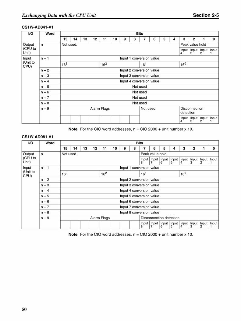
Exchanging Data with the CPU Unit Section 2-5
CS1W-AD041-V1
Note For the CIO word addresses, n = CIO 2000 + unit number x 10.
CS1W-AD081-V1
Note For the CIO word addresses, n = CIO 2000 + unit number x 10.
I/O Word Bits
15 14 13 12 11 10 9 8 7 6 5 4 3 2 1 0
Output (CPU to Unit)
n Not used. Peak value holdInput 4
Input 3
Input 2
Input 1
Input (Unit to CPU)
n + 1 Input 1 conversion value
163 162 161 160
n + 2 Input 2 conversion value
n + 3 Input 3 conversion value
n + 4 Input 4 conversion value
n + 5 Not used
n + 6 Not used
n + 7 Not used
n + 8 Not used
n + 9 Alarm Flags Not used Disconnection detectionInput 4
Input 3
Input 2
Input 1
I/O Word Bits
15 14 13 12 11 10 9 8 7 6 5 4 3 2 1 0
Output (CPU to Unit)
n Not used. Peak value holdInput 8
Input 7
Input 6
Input 5
Input 4
Input 3
Input 2
Input 1
Input (Unit to CPU)
n + 1 Input 1 conversion value
163 162 161 160
n + 2 Input 2 conversion value
n + 3 Input 3 conversion value
n + 4 Input 4 conversion value
n + 5 Input 5 conversion value
n + 6 Input 6 conversion value
n + 7 Input 7 conversion value
n + 8 Input 8 conversion value
n + 9 Alarm Flags Disconnection detectionInput 8
Input 7
Input 6
Input 5
Input 4
Input 3
Input 2
Input 1
50

Exchanging Data with the CPU Unit Section 2-5
CS1W-AD161
Note For the CIO word addresses, n = CIO 2000 + unit number x 10.
Set Values and Stored Values
The input disconnection detection function can be used when the input signalrange is set for 1 to 5 V (4 to 20 mA).
I/O Word Bits
15 14 13 12 11 10 9 8 7 6 5 4 3 2 1 0
Output (CPU to Unit)
n Peak value holdInput 16
Input 15
Input 14
Input 13
Input 12
Input 11
Input 10
Input 9
Input 8
Input 7
Input 6
Input 5
Input 4
Input 3
Input 2
Input 1
Input (Unit to CPU)
n + 1 Input 1 A/D conversion value
163 162 161 160
n + 2 Input 2 A/D conversion value
n + 3 Input 3 A/D conversion value
n + 4 Input 4 A/D conversion value
n + 5 Input 5 A/D conversion value
n + 6 Input 6 A/D conversion value
n + 7 Input 7 A/D conversion value
n + 8 Input 8 A/D conversion value
n + 9 Input 9 A/D conversion value
n + 10 Input 10 A/D conversion value
n + 11 Input 11 A/D conversion value
n + 12 Input 12 A/D conversion value
n + 13 Input 13 A/D conversion value
n + 14 Input 14 A/D conversion value
n + 15 Input 15 A/D conversion value
n + 16 Input 16 A/D conversion value
n + 17 Not used.
n + 18 Disconnection detectionInput 16
Input 15
Input 14
Input 13
Input 12
Input 11
Input 10
Input 9
Input 8
Input 7
Input 6
Input 5
Input 4
Input 3
Input 2
Input 1
n + 19 Alarm flags Not used.
Item Contents Page
Peak value hold function 0: Not used.1: Peak value hold used.
60
Conversion value (calculation result)
4-digit hexadecimal 55
Disconnection detection 0: No disconnection1: Disconnection
61
Alarm Flags • CS1W-AD041-VI and CS1W-AD081-V1: CIO n+9Bit 11: Mean value processing setting errorBit 15: Operating in adjustment mode (always OFF in normal mode)
• CS1W-AD161: CIO n+19Bit 08: Scaling data setting errorBit 11: Mean value processing setting errorBit 12: Conversion time/resolution or operation mode setting errorBit 15: Operating in adjustment mode (always OFF in normal mode)
73
Input signal range Voltage/current
1 to 5 V 0.3 V max.
4 to 20 mA 1.2 mA max.
51

Exchanging Data with the CPU Unit Section 2-5
Allocation for Adjustment Mode
For adjustment mode, turn ON the operation mode switch on the rear panel ofthe Unit as shown in the following diagram, or set bits 00 to 07 in DM wordm+18 (m+19 for CS1W-AD161) to C1. When the Unit is set for adjustmentmode, the ADJ indicator on the front panel of the Unit will flash.
The allocation of CIO words and bits is shown in the following table.
CS1W-AD041-V1/AD081-V1
Note 1. Use settings 1 to 4 for the CS1W-AD041-V1.
2. With the CS1W-AD041-V1, bits 04 to 07 in word n+9 (disconnection detec-tion) are not used.
CS1W-AD161
Note 1. For the CIO word addresses, n = CIO 2000 + unit number × 10.
I/O Word Bits
15 14 13 12 11 10 9 8 7 6 5 4 3 2 1 0
Output (CPU to Unit)
n Not used. Inputs to be adjusted
2 (fixed) 1 to 8 (1 to 4) (See note 1.)
n + 1 Not used. Not used. Clr Set Up Down Gain Off-set
n + 2 Not used.
n + 3 Not used.
n + 4 Not used.
n + 5 Not used.
n + 6 Not used.
n + 7 Not used.
Input (Unit to CPU)
n + 8 Conversion value at time of adjustment
163 162 161 160
n + 9 Alarm Flags Disconnection detec-tion (See note 2.)
Not used.
Input 8
Input 7
Input 6
Input 5
Input 4
Input3
Input2
Input 1
I/O Word Bits
15 14 13 12 11 10 9 8 7 6 5 4 3 2 1 0
Output (CPU to Unit)
n Not used. Inputs to be adjusted (See note 2.)
n + 1 Not used. Clr Set --- --- Gain Off-set
n + 2 to n+16
Not used.
Input (Unit to CPU)
n + 17 Conversion value at time of adjustment
163 162 161 160
n + 18 Disconnection detectionInput 16
Input 15
Input 14
Input 13
Input 12
Input 11
Input 10
Input 9
Input 8
Input 7
Input 6
Input 5
Input 4
Input 3
Input 2
Input 1
n + 19 Alarm Flags Not used.
52

Exchanging Data with the CPU Unit Section 2-5
2. The input format used for adjustment is as follows:
Set Values and Stored Values
Refer to 2-7-1 Adjustment Mode Operational Flow for further details.
Note For the CIO word addresses, n = CIO 2000 + (unit number × 10).
The input disconnection detection function can be used when the input signalrange is set for 1 to 5 V (4 to 20 mA).
11 10 09 08 07 06 05 04 03 02 01 00
0 0 1 0 101 100
Bit
Always 2 hex Number of input for adjustment: 1 to 16 (BCD)
Item Contents
Input to be adjusted Sets input to be adjusted.Leftmost digit: 2 (fixed)Rightmost digit: 1 to 8 (1 to 4 for CS1W-AD041-V1)
Offset (Offset Bit) When ON, adjusts offset error.
Gain (Gain Bit) When ON, adjusts gain error.
Down (Down Bit) Decrements the adjustment value while ON.
Up (Up Bit) Increments the adjustment value while ON.
Set (Set Bit) Sets adjusted value and writes to EEPROM.
Clr (Clear Bit) Clears adjusted value. (Returns to default status)
Conversion value for adjustment
The conversion value for adjustment is stored as 16 bits of binary data.
Disconnection detection 0: No disconnection1: Disconnection
Alarm Flags Bit 12: Input value is outside adjustment limits (in adjustment mode)
Bit 13: Input number setting error (in adjustment mode)
Bit 14: EEPROM write error (in adjustment mode)Bit 15: Operating in adjustment mode
(always 1 in adjustment mode)
Input signal range Voltage/current
1 to 5 V 0.3 V max.
4 to 20 mA 1.2 mA max.
53

Analog Input Functions and Operating Procedures Section 2-6
2-6 Analog Input Functions and Operating Procedures
2-6-1 Input Settings and Conversion ValuesInput Numbers The Analog Input Unit converts analog inputs specified by input numbers. To
specify the analog inputs to be used, turn ON from a Programming Device theD(m) bits in the DM Area shown in the following diagram.
Setting 0: Not used.1: Used
• CS1W-AD041-V1: Inputs 1 to 4
• CS1W-AD081-V1: Inputs 1 to 8
The analog input sampling interval can be shortened by setting any unusedinput numbers to 0.
Sampling interval = (1 ms) x (Number of inputs used) (See note.)
Note Use 250 µs instead of 1 ms is set to a conversion time of 250 µs andresolution of 8,000.
The conversion values in words for inputs that have been set to “Not used” willalways be “0000.”
For the DM word addresses, m = D20000 + (unit number x 100)
Input Signal Range Any of four types of input signal range (–10 to 10 V, 0 to 10 V, 1 to 5 V, and 4to 20 mA) can be selected for each of the inputs.
CS1W-AD041-V1/AD081-V1
To specify the input signal range for each input, set from a ProgrammingDevice the D(m + 1) bits in the DM Area as shown in the following diagram.
Note There are only four inputs for the CS1W-AD041-V1.
CS1W-AD161
D(m)
Bit 15 14 13 12 11 10 09 08 07 06 05 04 03 02 01 00
m = D20000 + unit number x 100
Inpu
t 2
Inpu
t 1
Inpu
t 4
Inpu
t 3
Inpu
t 6
Inpu
t 5
Inpu
t 8
Inpu
t 7
Inpu
t 10
Inpu
t 9
Inpu
t 12
Inpu
t 11
Inpu
t 14
Inpu
t 13
Inpu
t 16
Inpu
t 15
15 14 13 12 11 10 09 08 07 06 05 04 03 02 01 00Bit
DM (m+1)In
put 2
Inpu
t 1
00: −10 to 10 V01: 0 to 10 V10: 1 to 5 V / 4 to 20 mA11: 0 to 5 V
Inpu
t 4
Inpu
t 3
Inpu
t 6
Inpu
t 5
Inpu
t 8
Inpu
t 7
Bit 15 14 13 12 11 10 09 08 07 06 05 04 03 02 01 00
D (m+1) Input 8 Input 6 Input 6 Input 5 Input 4 Input 3 Input 2 Input 1
D (m+2) Input 16 Input 15 Input 14 Input 13 Input 12 Input 11 Input 10 Input 9
m = D20000 + unit number x 100
54

Analog Input Functions and Operating Procedures Section 2-6
00: −10 to +10 V01: 0 to 10 V10: 1 to 5 V/4 to 20 mA (See note 2.)11: 0 to 10 V
Select the input signal range 1 to 5 V/4 to 20 mA by wiring the connector orterminal block conversion connector. The voltage/current input setting canalso be set using DM word m+52.
0: 1 to 5 V1: 4 to 20 mA
Note 1. For the DM word addresses, m = D20000 + (unit number × 100)
2. The input signal range of “1 to 5 V” or “4 to 20 mA” is switched using thevoltage/current switch.
3. When DM Area settings have been carried out using a Programming De-vice, be sure to either cycle the power supply to the PLC, or turn ON theSpecial I/O Unit Restart Bit. The contents of the initial settings in the DMArea will be transferred to the Special I/O Unit when the power is turnedON or the Special I/O Unit Restart Bit is turned ON.
Reading Conversion Values
Analog input conversion values are read in 4-digit hexadecimal for each input.
Note For the CIO word addresses, n = CIO 2000 + (unit number × 10).
Use MOV(021) or XFER(070) to read conversion values in the user program.
Bit 15 14 13 12 11 10 09 08 07 06 05 04 03 02 01 00
D (m+52) Input16
Input15
Input14
Input13
Input12
Input11
Input10
Input9
Input8
Input7
Input6
Input5
Input4
Input3
Input2
Input1
m = D20000 + unit number x 100
Address CS1W-AD161 CS1W-AD081-V1 CS1W-AD041-V1
n+1 Input 1 conversion value Input 1 conversion value Input 1 conversion value
n+2 Input 2 conversion value Input 2 conversion value Input 2 conversion value
n+3 Input 3 conversion value Input 3 conversion value Input 3 conversion value
n+4 Input 4 conversion value Input 4 conversion value Input 4 conversion value
n+5 Input 5 conversion value Input 5 conversion value Cannot be used.
n+6 Input 6 conversion value Input 6 conversion value
n+7 Input 7 conversion value Input 7 conversion value
n+8 Input 8 conversion value Input 8 conversion value
n+9 Input 9 conversion value Cannot be used.
n+10 Input 0 conversion value
n+11 Input 1 conversion value
n+12 Input 12 conversion value
n+13 Input 13 conversion value
n+14 Input 14 conversion value
n+15 Input 15 conversion value
n+16 Input 16 conversion value
55

Analog Input Functions and Operating Procedures Section 2-6
Example 1 In this example, the conversion data from only one input is read. (The unitnumber is 0.)
Example 2 In this example, the conversion data from multiple inputs is read. (The unitnumber is 0.)
For details regarding conversion value scaling, refer to Scaling on page 446.
2-6-2 Conversion Time/Resolution Setting
The default setting is a conversion cycle of 1 ms and resolution of 4,000. Foreven higher speed and precision, change the settings in bits 08 to 15.
CS1W-AD041-V1/AD081-V1
m = D20000 + unit number x 100
CS1W-AD161
m = D20000 + unit number × 100
Note When DM Area settings have been carried out using a Programming Device,be sure to either cycle the power supply to the PLC, or turn ON the Special I/O Unit Restart Bit. The contents of the initial settings in the DM Area will betransferred to the Special I/O Unit when the power is turned ON or the SpecialI/O Unit Restart Bit is turned ON.
MOV(021)
2001
D00001
Input conditionConversion data in CIO word 2001 (input number 1) is read to D 00001.
XFER(070)
#0004
2001
D00001
Input conditionConversion data in CIO words 2001 to 2004 (input numbers 1 to 4) is read to D00001 and D00004.
Bit 15 14 13 12 11 10 9 8 7 6 5 4 3 2 1 0
D (m+18) Conversion time/resolution setting
00: Conversion time of 1 ms and resolution of 4,000C1: Conversion time of 250 µs and resolution of 8,000
Operation mode setting
00: Normal modeC1: Adjustment mode
Bit 15 14 13 12 11 10 9 8 7 6 5 4 3 2 1 0
D (m+19) Conversion time/resolution setting00: Conversion time of 1 ms and resolution of 4,000C1: Conversion time of 250 µs and resolution of 8,000
Operation mode setting00: Normal modeC1: Adjustment mode
56

Analog Input Functions and Operating Procedures Section 2-6
2-6-3 Mean Value ProcessingThe Analog Input Unit can compute the mean value of the conversion valuesof analog inputs that have been previously sampled. Mean value processinginvolves an operational mean value in the history buffers, so it has no effect onthe data refresh cycle. (The number of history buffers that can be set to usemean value processing is 2, 4, 8, 16, 32, or 64.)
When “n” number of history buffers are being used, the first conversion datawill be stored for all “n” number of history buffers immediately data conversionhas begun or after a disconnection is restored.
When mean value processing is used together with the peak value hold func-tion, the mean value will be held.
Specify whether or not to use mean value processing and the number of his-tory buffers to be used for mean value processing.
For the DM word addresses, m = D2000 + (unit number × 100)
Note When DM Area settings have been carried out using a Programming Device,be sure to either cycle the power supply to the PLC, or turn ON the Special
Conversion data Buffer 1
Buffer 2
Buffer 3
Buffer 4
Buffer n
(Mean value processing)
Conversion value
(Values stored in CIO words n+1 to n+8)
(Discarded)
Address CS1W-AD161 CS1W-AD081-V1 CS1W-AD041-V1 Set value
D (m+2) --- Input 1 Input 1 0000: Mean value processing with 2 buffers0001: No mean value processing0002: Mean value processing with 4 buffers0003: Mean value processing with 8 buffers0004: Mean value processing with 16 buffers0005: Mean value processing with 32 buffers0006: Mean value processing with 64 buffers
D (m+3) Input 1 Input 2 Input 2
D (m+4) Input 2 Input 3 Input 3
D( m+5) Input 3 Input 4 Input 4
D (m+6) Input 4 Input 5 Cannot be used.
D (m+7) Input 5 Input 6
D (m+8) Input 6 Input 7
D (m+9) Input 7 Input 8
D (m+10) Input 8 Cannot be used.
D (m+11) Input 9
D (m+12) Input 10
D (m+13) Input 11
D (m+14) Input 12
D (m+15) Input 13
D (m+16) Input 14
D (m+17) Input 15
D (m+18) Input 16
57

Analog Input Functions and Operating Procedures Section 2-6
I/O Unit Restart Bit. The contents of the initial settings in the DM Area will betransferred to the Special I/O Unit when the power is turned ON or the SpecialI/O Unit Restart Bit is turned ON.
The history buffer moving average is calculated as shown below. (In thisexample, there are four buffers.)
1,2,3... 1. With the first cycle, data 1 is stored in all the history buffers.
Mean value = (Data 1 + Data 1 + Data 1 + Data 1) ÷ 4
2. With the second cycle, data 2 is stored in the first history buffer.
Mean value = (Data 2 + Data 1 + Data 1 + Data 1) ÷ 4
3. With the third cycle, data 3 is stored in the first history buffer.
Mean value = (Data 3 + Data 2 + Data 1 + Data 1) ÷ 4
4. With the fourth cycle, data 4 is stored in the first history buffer.
Mean value = (Data 4 + Data 3 + Data 2 + Data 1) ÷ 4
5. With the fifth cycle, data 5 is stored in the first history buffer.
Mean value = (Data 5 + Data 4 + Data 3 + Data 2) ÷ 4
(Mean value processing)
Conversion value
Data 1
Data 1
Data 1
Data 1
(Mean value processing)
Conversion value
Data 2
Data 1
Data 1
Data 1
(Mean value processing)
Conversion value
Data 3
Data 2
Data 1
Data 1
(Mean value processing)
Conversion value
Data 4
Data 3
Data 2
Data 1
(Mean value processing)
Conversion value
Data 5
Data 4
Data 3
Data 2
58

Analog Input Functions and Operating Procedures Section 2-6
When a disconnection is restored, the mean value processing function beginsagain from step 1.
Note 1. The default setting for mean value processing in the Analog Input Unit ismean value processing with 2 buffers. The response time for the defaultsetting is different from when there is no mean processing, as shown in thefollowing diagram.
2. Specify “no mean value processing” to follow conversion of a rapid changein input signals.
3. If the averaging function is used, the delay in the conversion data in com-parison to changes in the input signals will be as shown below.
Response Time at 1-ms Conversion Time/4,000 Resolution
Unit: ms
Input signal to the Unit (V)
Conversion data
Time (ms)
Time (ms)
t: Delay
For V = 20 V (−10 to 10 V)1-ms Conversion Time/4,000 ResolutionUsing One Wordt = n + (2 to 3)Using m Words (1 ≤ m ≤ 16)No averaging (n = 1) or two averaging buffers (n = 2):
t = n x (m + 2)n averaging buffers (4 ≤ n ≤ 64):
t = (n − 2) x m + 10.5250-µs Conversion Time/8,000 Resolution (For version-1 Unit)Using One Wordt = n + (2 to 3) x 1/4Using m Words (1 ≤ m ≤ 16)No averaging (n = 1) or two averaging buffers (n = 2):
t = n x (m + 2) x 1/4n averaging buffers (4 ≤ n ≤ 64):
t = (n − 2) x m + 10.5 x 1/4
M N64 32 16 8 4 2 1
16 1002.5 490.5 234.5 106.5 42.5 36 1815 940.5 460.5 220.5 100.5 40.5 34 1714 878.5 430.5 206.5 94.5 38.5 32 1613 816.5 400.5 192.5 88.5 36.5 30 1512 754.5 370.5 178.5 82.5 34.5 28 1411 692.5 340.5 164.5 76.5 32.5 26 1310 630.5 310.5 150.5 70.5 30.5 24 129 568.5 280.5 136.5 64.5 28.5 22 118 506.5 250.5 122.5 58.5 26.5 20 107 444.5 220.5 108.5 52.5 24.5 18 96 382.5 190.5 94.5 46.5 22.5 16 85 320.5 160.5 80.5 40.5 20.5 14 74 258.5 130.5 66.5 34.5 18.5 12 63 196.5 100.5 52.5 28.5 16.5 10 52 134.5 70.5 38.5 22.5 14.5 8 41 67 35 19 11 7 5 3
59

Analog Input Functions and Operating Procedures Section 2-6
Response Time at 250-µs Conversion Time/8,000 Resolution
Unit: ms
Symbols M: Number of input words used in DM AreaN: Average number of buffers set for the input number for which to find theresponse time
Calculation Example The following example calculations are for a resolution of 8,000 with an appli-cation using inputs 1 and 8, 64 averaging buffers set for input 1, and no aver-aging set for input 8.
• Response time for input 1: t = (64 − 2) × 2 + 10.5 × 1/4 = 34 (ms)
• Response time for input 1: t = 1 × (2 + 2) × 1/4 = 1 (ms)
2-6-4 Peak Value Hold FunctionThe peak value hold function holds the maximum digital conversion value forevery input (including mean value processing). This function can be used withanalog input. The following diagram shows how digital conversion values areaffected when the peak value hold function is used.
The peak value hold function can be set separately for each input number byturning ON the respective bits (00 to 07 for CS1W-AD081-V1, 00 to 03 forCS1W-AD041-V1) in CIO word n.
M N64 32 16 8 4 2 1
16 250.625 122.625 58.625 26.625 10.625 9 4.515 235.125 115.125 55.125 25.125 10.125 8.5 4.2514 219.625 107.625 51.625 23.625 9.625 8 413 204.125 100.125 48.125 22.125 9.125 7.5 3.7512 188.625 92.625 44.625 20.625 8.625 7 3.511 173.125 85.125 41.125 19.125 8.125 6.5 3.2510 157.625 77.625 37.625 17.625 7.625 6 39 142.125 70.125 34.125 16.125 7.125 5.5 2.758 126.625 62.625 30.625 14.625 6.625 5 2.57 111.125 55.125 27.125 13.125 6.125 4.5 2.256 95.625 47.625 23.625 11.625 5.625 4 25 80.125 40.125 20.125 10.125 5.125 3.5 1.754 64.625 32.625 16.625 8.625 4.625 3 1.53 49.125 25.125 13.125 7.125 4.125 2.5 1.252 33.625 17.625 9.625 5.625 3.625 2 11 16.75 8.75 4.75 2.75 1.75 1.25 0.75
Peak value hold
Digital conversion value
t (Time)
Conversion value when the peak value hold function is used
Inpu
t 2
Inpu
t 1
Inpu
t 4
Inpu
t 3
Inpu
t 6
Inpu
t 5
Inpu
t 8
Inpu
t 7
Bit 15 14 13 12 11 10 09 08 07 06 05 04 03 02 01 00
n = D20000 + unit number x 10
Word n
Inpu
t 10
Inpu
t 9
Inpu
t 12
Inpu
t 11
Inpu
t 14
Inpu
t 13
Inpu
t 16
Inpu
t 15
60

Analog Input Functions and Operating Procedures Section 2-6
Setting 0: Not used (the conversion value is reset when the bit turns OFF)
1: Peak value hold function is used (held while ON)
• CS1W-AD041-V1: Inputs 1 to 4
• CS1W-AD081-V1: Inputs 1 to 8
For the CIO word addresses, n = CIO 2000 + (unit number × 10).
In the following example, the peak value hold function is in effect for inputnumber 1, and the unit number is 0.
When mean value processing is used together with the peak value hold func-tion, the mean value will be held.
As long as the peak value hold function is in effect, the peak value hold will beheld even in the event of a disconnection.
When the load to the CPU Unit is disconnected, the Peak Value Hold Bits.
2-6-5 Input Disconnection Detection FunctionWhen an input signal range of 1 to 5 V (4 to 20 mA) is used, input circuit dis-connections can be detected. The detection conditions for each of the inputsignal ranges are shown in the following table. (see note)
Note The current/voltage level will fluctuate according to the offset/gain adjustment.
The following bits turn ON when a disconnection is detected in each input.When the connection is recovered, these bits turn OFF. Be sure to specifythese bits in the execution condition of the ladder program when using the dis-connection detection function in the user program.
CS1W-AD041-V1/AD081-V1
CS1W-AD041-V1: Inputs 1 to 4
CS1W-AD161
For the CIO word addresses, n = CIO 2000 + (unit number × 10).
The conversion value during a disconnection will be 0000.
200000
Input conditionThe maximum conversion data value is held for input number 1.
Range Current/voltage
1 to 5 V Less than 0.3 V
4 to 20 mA Less than 1.2 mA
Bit 15 14 13 12 11 10 09 08 07 06 05 04 03 02 01 00
n = 2000 + unit number x 10
Word n+9 Not used.
Inpu
t 6
Inpu
t 5
Inpu
t 8
Inpu
t 7
Inpu
t 2
Inpu
t 1
Inpu
t 4
Inpu
t 3
Bit 15 14 13 12 11 10 09 08 07 06 05 04 03 02 01 00
n = 2000 + unit number x 10
Inpu
t 2
Inpu
t 1
Inpu
t 4
Inpu
t 3
Inpu
t 6
Inpu
t 5
Inpu
t 8
Inpu
t 7
Inpu
t 10
Inpu
t 9
Inpu
t 12
Inpu
t 11
Inpu
t 14
Inpu
t 13
Inpu
t 16
Inpu
t 15
Word n+18
61

Adjusting Offset and Gain Section 2-7
In the following example, the conversion value is read only if there is no dis-connection at analog input number 1. (The unit number is 0.)
2-6-6 Scaling Function (CS1W-AD161 Only)With the CS1W-AD161, the scaling function can be used to convert data intoengineering units after A/D conversion. The scaling function can only be usedwhen the resolution is set to 4,000. Scaling is not supported for resolutions of8,000.
Overview When using a resolution of 4,000, A/D conversion data in the ranges 1 to 5 V,0 to 5 V, 0 to 10 V, or 4 to 20 mA will be scaled to values between 0 and 4,000(BCD), approximately. A/D conversion data in the range −10 to +10 V will bescaled to values between −2,000 and +2,000 (BCD), approximately. (Actual D/A conversion is executed up to −5% to +105% of full scale.)
The lower limit and upper limit can be set to between −32000 and +32000(BCD). Actual settings in DM word m+20 to DM word m+51 are set in 4-digithexadecimal. (In the above example, the lower limit is 0000 and the upperlimit is 2710 hexadecimal.)
• Besides upper limit and lower limit. (Reverse scaling is supported.)
• Negative values are set as two's complement
• Scaling is not performed when the upper limit and lower limit are both setto 0000 (default setting).
2-7 Adjusting Offset and Gain
2-7-1 Adjustment Mode Operational FlowThe adjustment mode enables the input of the connected devices to be cali-brated.
The offset voltage (or current) and gain voltage (or current) at the outputdevice are entered as analog input conversion data 0000 and 0FA0 (07D0 ifthe range is ±10 V) respectively for a resolution of 4,000.
For example, when using in the range 1 to 5 V, the actual output may be in therange 0.8 to 4.8 V, even though the specifications range for the externaldevice is 1 to 5 V. In this case, when an offset voltage of 0.8 V is output at theexternal device, the conversion data at the Analog Input Unit for a resolutionof 4,000 will be FF38, and if a gain voltage of 4.8 V is output, the conversiondata will be 0EDA. The offset/gain adjustment function will, for this example,convert 0.8 V and 4.8 V to 0000 and 0FA0 respectively and not to FF38 and0EDA, as illustrated in the following table.
(Values in parentheses are for a resolution of 8,000.)
MOV (021)
2001
D00001
200901
The conver-sion value in CIO word 2001 (input number 1) is read to D00001.
Offset/gain voltage at the output device
Conversion data before adjustment
Conversion data after adjustment
0.8 V FF38 (FE70) 0000 (0000)
4.8 V 0EDA (0DB4) 0FA0 (1F40)
62

Adjusting Offset and Gain Section 2-7
The following diagram shows the flow of operations when using the adjust-ment mode for adjusting offset and gain.
!Caution Be sure to turn OFF the power to the PLC before changing the setting of theoperation mode switch.
!Caution The power must be cycled or the Unit restarted if the operation mode is set inDM.
Set the operation mode to adjustment mode.
Turn ON the PLC.
When adjusting another input number
When adjusting the same input number
Set the input number.
Offset adjustment
Offset Bit ON
Set Bit ON
Turn OFF power to the PLC.
Set the operation mode to normal mode.
Gain adjustment
Gain Bit ON
Input adjustment
Set Bit ON
Input adjustment
Set the operation mode switch, or (for version-1 Unit) set the operation mode in DM Area word m+18 (see note), to adjustment mode.
(Bit 0 of CIO word n+1 turns ON.)
Sampling input
(Add inputs so that conversion value becomes 0.)
(Bit 4 of CIO word n+1 turns ON.)
The ADJ indicator will flash while in adjustment mode.
Start up the PLC in PROGRAM mode.
Write the input number to be adjusted in the rightmost byte of CIO word n.
(Bit 1 of CIO word n+1 turns ON.)
Sampling input
(Add inputs so that conversion value is maximized.)
(Bit 4 of CIO word n+1 turns ON.)
Set the operation mode switch, or set the operation mode in DM Area word m+18 (see note), to normal mode.
Note: Set in DM Area word m+19 for CS1W-AD161.
Note: Set in DM Area word m+19 for CS1W-AD161.
63

Adjusting Offset and Gain Section 2-7
!Caution Set the PLC to PROGRAM mode when using the Analog Input Unit in adjust-ment mode. If the PLC is in MONITOR mode or RUN mode, the Analog InputUnit will stop operating, and the input values that existed immediately beforethis stoppage will be retained.
!Caution Always perform adjustments in conjunction with offset and gain adjustments.
Note Input adjustments can be performed more accurately in conjunction withmean value processing.
2-7-2 Input Offset and Gain Adjustment ProceduresSpecifying Input Number to be Adjusted
The following bits turn ON when a disconnection is detected in each input.When the connection is recovered, these bits turn OFF. Be sure to specifythese bits in the execution condition of the ladder program when using the dis-connection detection function in the user program.
CS1W-AD041-V1-AD081-V1
Note Use inputs 1 to 4 for the CS1W-AD041-V1.
CS1W-AD161
For the CIO word addresses, n = CIO 2000 + (unit number × 10).
The following example shows an adjustment for input number 1 using aCS1W-AD041-V1/081-V1 for illustration. (The unit number is 0.)
Word n
15 14 13 12 11 10 09 08 07 06 05 04 03 02 01 00
0 1Not used. Input numbers to be adjusted 1 to 8 (See note.)0 0
2: Input (fixed)n = CIO 2000 + unit number x 10
Bit
15 14 13 12 11 10 09 08 07 06 05 04 03 02 01 00
Word n 0 1
Bit
0 0Not used. Input numbers to be adjusted 1 to 16 (See note.)
2: Input (fixed)n = CIO 2000 + unit number x 10
CLR000000 CT00
SHIFTCH
*DM2
C0
A0
A0
AMON
2000 0000
CHG2000 0000PRES VAL ????
2C
1B
WRITE2000 0021
64

Adjusting Offset and Gain Section 2-7
Bits Used for Adjusting Offset and Gain
The CIO word (n+1) bits shown in the following diagram are used for adjustingoffset and gain.
Offset Adjustment The procedure for adjusting the analog input offset is explained below. Asshown in the following diagram, the offset is adjusted by sampling inputs sothat the conversion value becomes 0.
The following example uses input number 1 adjustment for illustration. (Theunit number is 0.)
1,2,3... 1. Turn ON bit 00 (the Offset Bit) of CIO word n+1. (Hold the ON status.)
For CS1W-AD041-V1 and CS1W-AD081-V1, the analog input’s digitalconversion values while the Offset Bit is ON will be monitored in CIO wordn+8. For CS1W-AD161, the values will be monitored in CIO word n+17.
2. Check whether the input devices are connected.
15 14 13 12 11 10 09 08 07 06 05 04 03 02 01 00Bit
Word n+1
Cle
ar B
it
Set
Bit
Gai
n B
it
Offs
et B
it
10 V0
0FA0
Offset adjustment input range
Input signal range:0 to 10 V
CLR000000 CT00
SHIFTCONT
#2
C0
A0
A1
B0
A0
AMON
200100 ^ OFF
SET
200100 ^ ON
65

Adjusting Offset and Gain Section 2-7
Wiring for Voltage Input
Wiring for Current Input
When using current input, short-circuit the input (+) terminal and the currentmode terminal.
3. Input the voltage or current so that the conversion value becomes 0000.The following table shows the offset adjustment voltages and currents tobe input according to the input signal range.
Input signal range Input range Word (n+8) monitoring value
0 to 10 V –0.5 to 0.5 V FF38 to 00C8 (4,000 res-olution)
FE70 to 0190 (8,000 res-olution)
–10 to 10 V –1.0 to 1.0 V
1 to 5 V 0.8 to 1.2 V
0 to 5 V –0.25 to 0.25 V
4 to 20 mA 3.2 to 4.8 mA
A1
A2
A3
+
–
Voltage input
Input 1
CS1W-AD041-V1/081-V1
Voltage n
+
−
Shield
Input n+
Current mode n
Input n−
AG
CS1W-AD161
A1
A2
A3
+
–
Current input
Input 1
For current input, check that the voltage/current switch is ON.
CS1W-AD041-V1/081-V1
Current input n
+
−
Shield
Input n+
Current mode n
Input n−
AG
CS1W-AD161
66

Adjusting Offset and Gain Section 2-7
4. After inputting the voltage or current so that the conversion value for theanalog input terminal is 0000, turn ON bit 04 (the Set Bit) of CIO word n+1,and then turn it OFF again.
While the Offset Bit is ON, the offset value will be saved to the Unit’s EE-PROM when the Set Bit turns ON.
5. To finish the offset adjustment, turn OFF bit 00 (the Offset Bit) of CIO wordn+1.
!Caution Do not turn OFF the power supply or restart the Unit while the Set Bit is ON(data is being written to the EEPROM). Otherwise, illegal data may be writtenin the Unit’s EEPROM and “EEPROM Errors” may occur when the power sup-ply is turned ON or when the Unit is restarted, causing a malfunction.
!Caution When making adjustments, be sure to perform both the offset adjustment andgain adjustment at the same time.
Note 1. The EEPROM can be overwritten 50,000 times.
2. While the Offset Bit or the Gain Bit is ON, the present conversion data willbe displayed in word n+8.If the Offset Bit or the Gain Bit is OFF, the value immediately prior to turningthe bit OFF will be held.
SHIFTCONT
#2
C0
A0
A1
B0
A4
EMON
200104 ^ OFF
SET
200104 ^ ON
RESET
200104 ^ OFF
SHIFTCONT
# 2C
0A
0A
1B
0A
0A
MON
200100 ^ ON
RESET
200100 ^ OFF
67
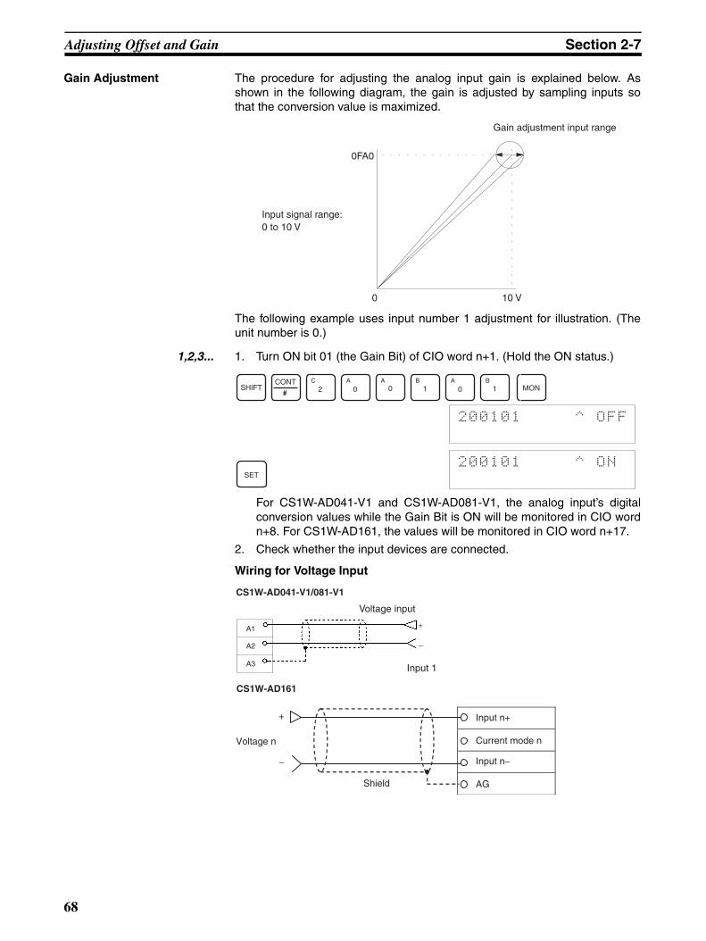
Adjusting Offset and Gain Section 2-7
Gain Adjustment The procedure for adjusting the analog input gain is explained below. Asshown in the following diagram, the gain is adjusted by sampling inputs sothat the conversion value is maximized.
The following example uses input number 1 adjustment for illustration. (Theunit number is 0.)
1,2,3... 1. Turn ON bit 01 (the Gain Bit) of CIO word n+1. (Hold the ON status.)
For CS1W-AD041-V1 and CS1W-AD081-V1, the analog input’s digitalconversion values while the Gain Bit is ON will be monitored in CIO wordn+8. For CS1W-AD161, the values will be monitored in CIO word n+17.
2. Check whether the input devices are connected.
Wiring for Voltage Input
10 V0
0FA0
Input signal range:0 to 10 V
Gain adjustment input range
SHIFTCONT
# 2C
0A
0A
1B
0A
1B
MON
200101 ^ OFF
SET
200101 ^ ON
+
–
Voltage input
Input 1
A1
A2
A3
CS1W-AD041-V1/081-V1
Voltage n
+
−
Shield
Input n+
Current mode n
Input n−
AG
CS1W-AD161
68

Adjusting Offset and Gain Section 2-7
Wiring for Current Input
When using current input, short-circuit the input (+) terminal and the currentmode terminal.
3. Input the voltage or current so that the conversion value is maximized(0FA0 or 07D0 at a resolution of 4,000). The following table shows the gainadjustment voltages and currents to be input according to the input signalrange.
(Values in parentheses are for a resolution of 8,000.)
4. With the voltage or current having been input so that the conversion valuefor the Analog Input Unit is maximized (0FA0 or 07D0), turn bit 04 (the SetBit) of CIO word n+1 ON and then OFF again.
While the Gain Bit is ON, the gain value will be saved to the Unit’s EE-PROM when the Set Bit turns ON.
Input signal range Input range Word (n+8) monitoring value
0 to 10 V 9.5 to 10.5 V 0ED8 to 1068 (0FB0 to 20D0)
–10 to 10 V 9.0 to 11.0 V 0708 to 0898 (0E10 to 1130)
1 to 5 V 4.8 to 5.2 V 0ED8 to 1068 (0FB0 to 20D0)
0 to 5 V 4.75 to 5.25 V 0ED8 to 1068 (0FB0 to 20D0)
4 to 20 mA 19.2 to 20.8 mA 0ED8 to 1068 (0FB0 to 20D0)
+
–
Current input
Input 1
For current input, check that the voltage/current switch is ON.
A1
A2
A3
CS1W-AD041-V1/081-V1
Current input n
+
−
Shield
Input n+
Current mode n
Input n−
AG
CS1W-AD161
SHIFTCONT
# 2C
0A
0A
1B
0A
4E
MON
200104 ^ OFF
SET
200104 ^ ON
RESET
200104 ^ OFF
69

Adjusting Offset and Gain Section 2-7
5. To finish the gain adjustment, turn OFF bit 01 (the Gain Bit) of CIO wordn+1.
!Caution Do not turn OFF the power supply or restart the Unit while the Set Bit is ON(data is being written to the EEPROM). Otherwise, illegal data may be writtenin the Unit’s EEPROM and “EEPROM Errors” may occur when the power sup-ply is turned ON or when the Unit is restarted, causing a malfunction.
!Caution When making adjustments, be sure to perform both the offset adjustment andgain adjustment at the same time.
Note 1. The EEPROM can be overwritten 50,000 times.
2. While the Offset Bit or the Gain Bit is ON, the present conversion data willbe displayed in word n+8.If the Offset Bit or the Gain Bit is OFF, the value immediately prior to turningthe bit OFF will be held.
Clearing Offset and Gain Adjusted Values
Follow the procedure outlined below to return the offset and gain adjusted val-ues to their default settings.
The following example uses adjustment for illustration. (The unit number is 0.)
1,2,3... 1. Turn ON bit 05 (the Clear Bit) of CIO word n+1. (Hold the ON status.) Re-gardless of the input value, 0000 will be monitored in CIO word n+8.
2. Turn bit 04 of CIO word n+1 ON and then OFF again.
SHIFTCONT
# 2C
0A
0A
1B
0A
1B
MON
200101 ^ ON
RESET
200101 ^ OFF
SHIFTCONT
# 2C
0A
0A
1B
0A
5F
MON
200105 ^ OFF
SET
200105 ^ ON
SHIFTCONT
# 2C
0A
0A
1B
0A
4E
MON
200104 ^ OFF
SET
200104 ^ ON
RESET
200104 ^ OFF
70

Handling Errors and Alarms Section 2-8
While the Clear Bit is ON, the adjusted value will be cleared and reset tothe default offset and gain values when the Set Bit turns ON.
3. To finish the clearing of adjusted values, turn OFF bit 05 (the Clear Bit) ofCIO word n+1.
!Caution Do not turn OFF the power supply or restart the Unit while the Set Bit is ON(data is being written to the EEPROM). Otherwise, illegal data may be writtenin the Unit’s EEPROM and “EEPROM Errors” may occur when the power sup-ply is turned ON or when the Unit is restarted, causing a malfunction.
!Caution When making adjustments, be sure to perform both the offset adjustment andgain adjustment at the same time.
Note The EEPROM can be overwritten 50,000 times.
2-8 Handling Errors and Alarms
2-8-1 Indicators and Error FlowchartIndicators If an alarm or error occurs in the Analog Input Unit, the ERC or ERH indica-
tors on the front panel of the Unit will light.
SHIFTCONT
# 2C
0A
0A
1B
0A
5F
MON
200105 ^ ON
RESET
200105 ^ OFF
LED Meaning Indicator Operating status
RUN (green) Operating Lit Operating in normal mode.
Not lit Unit has stopped exchanging data with the CPU Unit.
ERC (red) Error detected by Unit
Lit Alarm has occurred (such as disconnec-tion detection) or initial settings are incor-rect.
Not lit Operating normally.
ADJ (yellow) Adjusting Flashing Operating in offset/gain adjustment mode.
Not lit Other than the above.
ERH (red) Error in the CPU Unit
Lit Error has occurred during data exchange with the CPU Unit.
Not lit Operating normally.
Front panel of Unit
RUN
ERC
ADJ
ERH
71
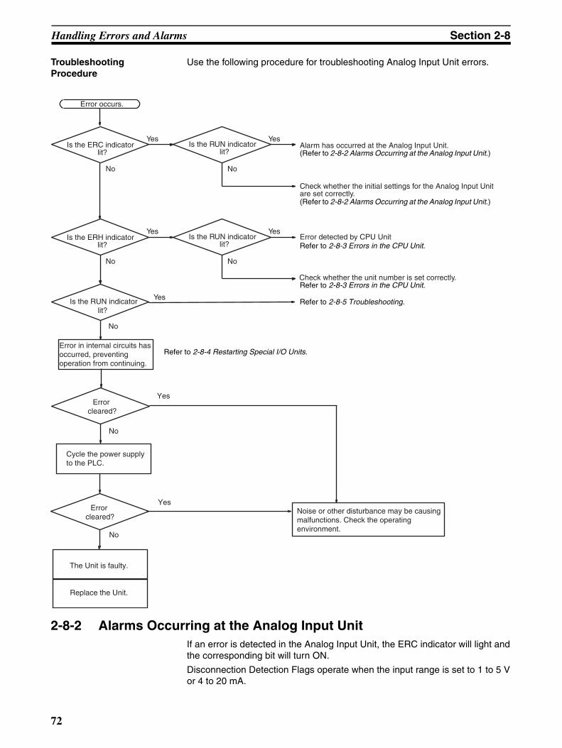
Handling Errors and Alarms Section 2-8
Troubleshooting Procedure
Use the following procedure for troubleshooting Analog Input Unit errors.
2-8-2 Alarms Occurring at the Analog Input UnitIf an error is detected in the Analog Input Unit, the ERC indicator will light andthe corresponding bit will turn ON.
Disconnection Detection Flags operate when the input range is set to 1 to 5 Vor 4 to 20 mA.
Error occurs.
Is the ERC indicator lit?
Yes
No
Is the RUN indicator lit?
Yes
No
Alarm has occurred at the Analog Input Unit.
Check whether the initial settings for the Analog Input Unit are set correctly.
Is the ERH indicator lit?
Yes
No
Is the RUN indicator lit?
Yes
No
Error detected by CPU Unit
Check whether the unit number is set correctly.
Yes
No
Is the RUN indicator lit?
Error cleared?
No
Cycle the power supplyto the PLC.
Error cleared?
No
The Unit is faulty.
Replace the Unit.
YesNoise or other disturbance may be causingmalfunctions. Check the operating environment.
Yes
Error in internal circuits has occurred, preventing operation from continuing.
(Refer to 2-8-2 Alarms Occurring at the Analog Input Unit.)
(Refer to 2-8-2 Alarms Occurring at the Analog Input Unit.)
Refer to 2-8-5 Troubleshooting.
Refer to 2-8-4 Restarting Special I/O Units.
Refer to 2-8-3 Errors in the CPU Unit.
Refer to 2-8-3 Errors in the CPU Unit.
72

Handling Errors and Alarms Section 2-8
CS1W-AD041-V1/AD081-V1
Note Use inputs 1 to 4 for the CS1W-AD041-V1.
CS1W-AD161
Alarm Flags
n = CIO 2000 + unit number x 10
ERC and RUN Indicators: Lit
The ERC and RUN indicators will be lit if an error occurs while the Unit isoperating normally. The following alarm flags will turn ON in CIO word n+9.These alarm flags will turn OFF automatically when the error is cleared.
Bit 15 14 13 12 11 10 09 08 07 06 05 04 03 02 01 00
m = D20000 + unit number x 10
Word n+9 Alarm Flags
Disconnection Detection Flags (See note.)
Inpu
t 1
Inpu
t 2
Inpu
t 3
Inpu
t 4
Inpu
t 5
Inpu
t 6
Inpu
t 7
Inpu
t 8
15 14 13 12 11 10 08 07 06 05 04 03 02 01 00Disconnection Detection Flags
Word n+18
Word n+19 Alarm Flags Not used.n = CIO 2000 + unit number x 10
Bit
Inpu
t 16
Inpu
t 15
Inpu
t 14
Inpu
t 13
Inpu
t 12
Inpu
t 11
Inpu
t 10
09
Inpu
t 9
Inpu
t 8
Inpu
t 7
Inpu
t 6
Inpu
t 5
Inpu
t 4
Inpu
t 3
Inpu
t 2
Inpu
t 1
Model CS1W-AD041-V1CS1W-AD081-V1
CS1W-AD161 Contents
Word n+9 n+19
Bit 15 15 Operating in adjustment mode.
14 14 EEPROM error occurred during adjustment mode.
13 13 Input number setting error occurred during adjustment mode.
12 12 Input adjustment value outside range during adjustment mode.
11 11 Mean average processing error occurred.
--- 08 Scaling data setting error occurred.
RUN
ERC ERH
: Lit
: Not lit
Word n+9, n+18, or n+19 (See note 1.)
Alarm flag Error contents Input status Countermeasure
Bits 00 to 07 (See note 2.)
Disconnection Detection
A disconnection was detected. (See note 3.)
Conversion data becomes 0000.
Check the rightmost byte of CIO word n+9. The inputs for bits that are ON may be discon-nected. Restore any discon-nected inputs.
73

Handling Errors and Alarms Section 2-8
n = CIO 2000 + unit number x 10
Note 1. These alarms are output in word n+9 for CS1W-AD041-V1 and CS1W-AD081-V1, and in words n+18/n+19 for CS1W-AD161.
2. The CS1W-AD041-V1 uses bits 00 to 08 of word n+9, and the CS1W-AD081-V1 uses bits 00 to 04. The CS1W-AD161 uses bits 00 to 15 of wordn+18.
3. The disconnection detection function is enabled for input numbers set with-in the input ranges 1 to 5 V or 4 to 20 mA.
ERC Indicator and RUN Indicator: Lit, ADJ Indicator: Flashing
This alarm will occur in the case of incorrect operation while in the adjustmentmode. In adjustment mode, the Adjustment Mode ON Flag will turn ON in bit15 of CIO word n+9.
n = CIO 2000 + unit number x 10
Note 1. When a PLC error occurs in the adjustment mode, the Unit will stop oper-ating. (The input values immediately prior to the error are held.)
Word n+9, n+18, or n+19 (See note 1.)
Alarm flag Error contents Input status Countermeasure
Bit 14 (Adjustment mode)EEPROM Writ-ing Error
An EEPROM writing error has occurred while in adjustment mode.
Holds the values immediately prior to the error. No data is changed.
Turn the Set Bit OFF, ON, and OFF again.If the error persists even after the reset, replace the Analog Input Unit.
RUN
ERC ERH
ADJ
: Lit
: Flashing
: Not lit
Word n+9/n+19 (See note 2.)
Alarm flag Error contents Input status Countermeasure
Bit 12 (Adjustment mode)Input Value Adjustment Range Exceeded
In adjustment mode, offset or gain cannot be adjusted because input value is out of the permissible range for adjust-ment.
Conversion data corresponding to the input sig-nal is monitored in word n+8/n+18 (see note 3).
If making the adjustment by means of a connected input device, first adjust the input device before adjusting the Ana-log Input Unit.
Bit 13 (Adjustment mode)Input Number Setting Error
In adjustment mode, adjust-ment cannot be performed because the specified input number is not set for use or because the wrong input num-ber is specified.
Holds the values immediately prior to the error. No data is changed.
• Check whether the word n input number to be adjusted is set within the following ranges: CS1W-AD041-V1: 21 to 24CS1W-AD801-V1: 21 to 28CS1W-AD161: 201 to 216
• Check whether the input num-ber to be adjusted is set for use by means of the DM set-ting (DM word m set to 1).
Bit 15 only ON (See note 5.)
(Adjustment Mode)
PLC Error
The PLC is in either MONITOR or RUN mode while the Analog Input Unit is operating in adjust-ment mode.
Holds the values immediately prior to the error. No data is changed.
Set the Unit to normal mode either by removing the Unit and setting the DIP switch on the rear panel or by setting the mode in DM word m+18 (see note 4), and then restart the Unit.
74

Handling Errors and Alarms Section 2-8
2. These alarms are output in CIO word n+9 for CS1W-AD041-V1 andCS1W-AD081-V1, and in CIO word n+19 for CS1W-AD161.
3. These alarms are output in CIO word n+8 for CS1W-AD041-V1 andCS1W-AD081-V1, and in CIO word n+18 for CS1W-AD161.
4. The operation mode is set in DM word m+18 for CS1W-AD041-V1 andCS1W-AD081-V1, and in DM word m+19 for CS1W-AD161.
5. Bit 15 is always ON in adjustment mode. When the PLC is in RUN modeor MONITOR mode, the ERC indicator will be lit.
ERC Indicator: Lit, RUN Indicator: Not Lit
The ERC indicator will be lit when the initial settings for the Analog Input Unitare not set correctly. The following alarm flags will turn ON in CIO word.These alarm flags will turn OFF when the error is cleared and the Unit isrestarted, or the Special I/O Unit Restart Bit is turned ON and then OFFagain.
Note These alarms are output in CIO word n+9 for CS1W-AD041-V1 and CS1W-AD081-V1, and in CIO word n+19 for CS1W-AD161.
2-8-3 Errors in the CPU UnitThe ERH indicator will light if an error occurs in the CPU Unit or I/O bus and I/O refreshing with the Special I/O Units is not performed correctly, preventingthe Analog Input Unit from operating.
ERH and RUN Indicators: Lit
The ERH and RUN indicators will be lit if an error occurs in the I/O bus caus-ing a WDT (watchdog timer) error in the CPU Unit, resulting in incorrect I/Orefresh with the Analog Input Unit.
Turn ON the power supply again or restart the system.For further details, refer to CS-series CS1G/H-CPU@@-EV1, CS1G/H-CPU@@H Programmable Controllers Operation Manual (W339).
RUN
ERC ERH
: Lit
: Not lit
Word n+9/n+19 (See note.)
Alarm flag Error contents Input status Countermeasure
Bit 11 Mean Value Processing Set-ting Error
The wrong number of samplings has been specified for mean processing.
Conversion does not start and data becomes 0000.
Specify a number from 0000 to 0006.
Bit 12 Conversion Time/Operation Mode Setting Error
The setting for conversion time/resolution is incorrect.
Conversion does not start and data becomes 0000.
Specify 00 or C1.
RUN
ERC ERH
: Lit
: Not lit
Error Error contents Input status
I/O bus error Error has occurred during data exchange with the CPU Unit.
Conversion data becomes 0000.
75

Handling Errors and Alarms Section 2-8
Note No error will be detected by the CPU Unit or displayed on the ProgrammingConsole, because the CPU Unit is continuing operation.
ERH Indicator: Lit, RUN Indicator: Not Lit
The unit number for the Analog Input Unit has not been set correctly.
Note A single CS1W-AD161 is allocated CIO Area and DM Area words for two Spe-cial I/O Units. Be sure to set a unit number so that the CS1W-AD161 is notallocated words in the CIO Area and DM Area that are already allocated toother Special I/O Units. Unit numbers for CS1W-AD161 can be set from 0 to94.
2-8-4 Restarting Special I/O UnitsTo restart the Analog Input Unit after changing the contents of the DM Area orcorrecting an error, cycle the power to the PLC or turn ON the Special I/O UnitRestart Bit.
Special I/O Unit Restart Bits
The conversion data becomes 0000 during restart.
If the error is not cleared even after turning the Special I/O Unit Restart Bit ONand then OFF again, then replace the Unit.
Note The highest unit number that can be set for a CS1W-AD161 is unit number 94.
2-8-5 TroubleshootingThe following tables explain the probable causes of troubles that may occur,and the countermeasures for dealing with them.
Error Error contents Input status
CPU Unit monitoring error (see note)
No response from CPU Unit dur-ing fixed period.
Maintains the condition existing before the error.
CPU Unit WDT error Error has been generated in CPU Unit.
Changes to undefined state.
RUN
ERC ERH
: Lit
: Not lit
Error Error contents Input status
Duplicate Unit Number (See note.)
The same unit number has been assigned to more than one Unit or the unit number was set to a value other than 00 to 95.
Conversion does not start and data becomes 0000.
Special I/O Unit Setting Error The Special I/O Units registered in the I/O table are different from the ones actually mounted.
Bits Functions
A50200 Unit #0 Restart Bit Turning the Restart Bit for any Unit ON and then OFF again restarts that Unit.
A50201 Unit #1 Restart Bit
to to
A50215 Unit #15 Restart Bit
A50300 Unit #16 Restart Bit
to to
A50715 Unit #95 Restart Bit (See note.)
76
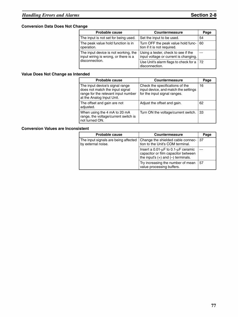
Handling Errors and Alarms Section 2-8
Conversion Data Does Not Change
Value Does Not Change as Intended
Conversion Values are Inconsistent
Probable cause Countermeasure Page
The input is not set for being used. Set the input to be used. 54
The peak value hold function is in operation.
Turn OFF the peak value hold func-tion if it is not required.
60
The input device is not working, the input wiring is wrong, or there is a disconnection.
Using a tester, check to see if the input voltage or current is changing.
---
Use Unit’s alarm flags to check for a disconnection.
72
Probable cause Countermeasure Page
The input device’s signal range does not match the input signal range for the relevant input number at the Analog Input Unit.
Check the specifications of the input device, and match the settings for the input signal ranges.
16
The offset and gain are not adjusted.
Adjust the offset and gain. 62
When using the 4 mA to 20 mA range, the voltage/current switch is not turned ON.
Turn ON the voltage/current switch. 33
Probable cause Countermeasure Page
The input signals are being affected by external noise.
Change the shielded cable connec-tion to the Unit’s COM terminal.
37
Insert a 0.01-µF to 0.1-µF ceramic capacitor or film capacitor between the input’s (+) and (–) terminals.
---
Try increasing the number of mean value processing buffers.
57
77

Handling Errors and Alarms Section 2-8
78
SECTION 3CJ-series Analog Input Units (CJ1W-AD041-V1/081-V1)
This section explains how to use the CJ1W-AD041-V1/081-V1 Analog Input Unit.
3-1 Specifications . . . . . . . . . . . . . . . . . . . . . . . . . . . . . . . . . . . . . . . . . . . . . . . . . 80
3-1-1 Specifications . . . . . . . . . . . . . . . . . . . . . . . . . . . . . . . . . . . . . . . . . . 80
3-1-2 Input Function Block Diagram . . . . . . . . . . . . . . . . . . . . . . . . . . . . . 82
3-1-3 Input Specifications . . . . . . . . . . . . . . . . . . . . . . . . . . . . . . . . . . . . . 82
3-2 Operating Procedure . . . . . . . . . . . . . . . . . . . . . . . . . . . . . . . . . . . . . . . . . . . . 85
3-2-1 Procedure Examples . . . . . . . . . . . . . . . . . . . . . . . . . . . . . . . . . . . . . 86
3-3 Components and Switch Settings . . . . . . . . . . . . . . . . . . . . . . . . . . . . . . . . . . 91
3-3-1 Indicators . . . . . . . . . . . . . . . . . . . . . . . . . . . . . . . . . . . . . . . . . . . . . 92
3-3-2 Unit Number Switches . . . . . . . . . . . . . . . . . . . . . . . . . . . . . . . . . . . 92
3-3-3 Operation Mode Switch . . . . . . . . . . . . . . . . . . . . . . . . . . . . . . . . . . 93
3-3-4 Voltage/Current Switch. . . . . . . . . . . . . . . . . . . . . . . . . . . . . . . . . . . 94
3-4 Wiring . . . . . . . . . . . . . . . . . . . . . . . . . . . . . . . . . . . . . . . . . . . . . . . . . . . . . . . 95
3-4-1 Terminal Arrangement . . . . . . . . . . . . . . . . . . . . . . . . . . . . . . . . . . . 95
3-4-2 Internal Circuitry . . . . . . . . . . . . . . . . . . . . . . . . . . . . . . . . . . . . . . . 96
3-4-3 Voltage Input Disconnection. . . . . . . . . . . . . . . . . . . . . . . . . . . . . . . 97
3-4-4 Input Wiring Example . . . . . . . . . . . . . . . . . . . . . . . . . . . . . . . . . . . 98
3-4-5 Input Wiring Considerations. . . . . . . . . . . . . . . . . . . . . . . . . . . . . . . 98
3-5 Exchanging Data with the CPU Unit . . . . . . . . . . . . . . . . . . . . . . . . . . . . . . . 99
3-5-1 Outline of Data Exchange. . . . . . . . . . . . . . . . . . . . . . . . . . . . . . . . . 99
3-5-2 Unit Number Setting. . . . . . . . . . . . . . . . . . . . . . . . . . . . . . . . . . . . . 100
3-5-3 Special I/O Unit Restart Bits . . . . . . . . . . . . . . . . . . . . . . . . . . . . . . 100
3-5-4 Fixed Data Allocations . . . . . . . . . . . . . . . . . . . . . . . . . . . . . . . . . . . 101
3-5-5 I/O Refresh Data Allocations . . . . . . . . . . . . . . . . . . . . . . . . . . . . . . 103
3-6 Analog Input Functions and Operating Procedures . . . . . . . . . . . . . . . . . . . . 106
3-6-1 Input Settings and Conversion Values . . . . . . . . . . . . . . . . . . . . . . . 106
3-6-2 Conversion Time/Resolution Setting . . . . . . . . . . . . . . . . . . . . . . . . 108
3-6-3 Mean Value Processing. . . . . . . . . . . . . . . . . . . . . . . . . . . . . . . . . . . 109
3-6-4 Peak Value Hold Function . . . . . . . . . . . . . . . . . . . . . . . . . . . . . . . . 112
3-6-5 Input Disconnection Detection Function . . . . . . . . . . . . . . . . . . . . . 113
3-7 Adjusting Offset and Gain . . . . . . . . . . . . . . . . . . . . . . . . . . . . . . . . . . . . . . . 114
3-7-1 Adjustment Mode Operational Flow . . . . . . . . . . . . . . . . . . . . . . . . 114
3-7-2 Input Offset and Gain Adjustment Procedures . . . . . . . . . . . . . . . . . 116
3-8 Handling Errors and Alarms . . . . . . . . . . . . . . . . . . . . . . . . . . . . . . . . . . . . . . 122
3-8-1 Indicators and Error Flowchart . . . . . . . . . . . . . . . . . . . . . . . . . . . . . 122
3-8-2 Alarms Occurring at the Analog Input Unit . . . . . . . . . . . . . . . . . . . 124
3-8-3 Errors in the CPU Unit . . . . . . . . . . . . . . . . . . . . . . . . . . . . . . . . . . . 126
3-8-4 Restarting Special I/O Units . . . . . . . . . . . . . . . . . . . . . . . . . . . . . . . 127
3-8-5 Troubleshooting . . . . . . . . . . . . . . . . . . . . . . . . . . . . . . . . . . . . . . . . 127
79

Specifications Section 3-1
3-1 Specifications
3-1-1 Specifications
Note 1. Do not apply a voltage higher than 600 V to the terminal block when per-forming withstand voltage test on this Unit. Otherwise, internal elementsmay deteriorate.
Item CJ1W-AD041-V1 CJ1W-AD081-V1
Unit type CJ-series Special I/O Unit
Isolation (See note 1.) Between inputs and PLC signals: Photocoupler(No isolation between input signals.)
External terminals 18-point detachable terminal block (M3 screws)
Affect on CPU Unit cycle time 0.2 ms
Current consumption 420 mA max. at 5 VDC
Dimensions (mm) (See note 2.) 31 × 90 × 65 (W × H × D)
Weight 140 g max.
General specifications Conforms to general specifications for SYSMAC CJ Series.
Mounting position CJ-series CPU Rack or CJ-series Expansion Rack
Maximum number of Units Per CPU Rack or Expan-sion Rack (See note 3.)
Power Supply Unit No. of mountable Units
CJ1W-PA205RCJ1W-PA205CCJ1W-PD025
CPU Rack: 10 Units/Rack Expansion Rack: 10 Units/Rack
CJ1W-PA202 CPU Rack: 5 Units/Rack Expansion Rack: 6 Units/Rack
CJ1W-PD022 CPU Rack: 3 Units/Rack Expansion Rack: 4 Units/Rack
Data exchange with CPU Units (See note 4.)
Special I/O Unit Area in CIO Area (CIO 2000 to CIO 2959): 10 words per UnitSpecial I/O Unit Area in DM Area (D20000 to D29599): 100 words per Unit
Inputs specifica-tions
Number of analog inputs 4 8
Input signal range (See note 5.)
1 to 5 V0 to 5 V0 to 10 V–10 to 10 V4 to 20 mA(See note 6.)
Maximum rated input (for 1 point) (See note 7.)
Voltage Input: ±15 VCurrent Input: ±30 mA
Input impedance Voltage Input: 1 MΩ min.Current Input: 250 Ω (rated value)
Resolution (See note 8.) 4,000/8,000 4,000/8,000
Converted output data 16-bit binary data
Accuracy(See note 9.)
23±2°C Voltage Input: ±0.2% of full scaleCurrent Input: ±0.4% of full scale
0°C to 55°C Voltage Input:±0.4% of full scaleCurrent Input: ±0.6% of full scale
A/D conversion period (See note 10.)
1 ms/250 µs (See note 8.)
1 ms/250 µs (See note 8.)
Inputs func-tions
Mean value processing Stores the last “n” data conversions in the buffer, and stores the mean value of the conversion values.Number of mean value buffers: n = 2, 4, 8, 16, 32, 64
Peak value hold Stores the maximum conversion value while the Peak Value Hold Bit is ON.
Input disconnection detec-tion
Detects the disconnection and turns ON the Disconnection Detection Flag. (See note 11.)
80

Specifications Section 3-1
2. Refer to Dimensions on page 439 for details on the Unit’s dimensions.
3. This is the maximum number of Units that can be mounted to a CJ2H-CPU6@ CPU Unit (no EtherNet/IP). The maximum number of Analog Out-put Units that can be mounted to one Rack varies depending on the currentconsumption of the other Units mounted to the Rack.
4. Data Transfer with the CPU Unit
5. Input signal ranges can be set for each input.
6. Voltage input or current input are chosen by using the voltage/currentswitch at the back of the terminal block.
7. The Analog Input Unit must be operated according to the input specifica-tions provided here. Operating the Unit outside these specifications willcause the Unit to malfunction.
8. The resolution can be set to 8,000 and the conversion time to 250 µs in theDM Area (m+18). There is only one setting for both of these, i.e., they areboth enabled or disabled together.
9. The accuracy is given for full scale. For example, an accuracy of ±0.2%means a maximum error of ±8 (BCD).
The default setting is adjusted for voltage input. To use current input, per-form the offset and gain adjustments as required.
10. A/D conversion time is the time it takes for an analog signal to be stored inmemory as converted data after it has been input. It takes at least one cy-cle before the converted data is read by the CPU Unit.
11. Line disconnection detection is supported only when the range is set to 1 to 5 V or 4 to 20 mA. If there is no input signal when the 1 to 5-V or 4 to20-mA range is set, the Line Disconnection Flag will turn ON.
Power Supply Unit Rack CJ1W-DA021CJ1W-DA041
(5 VDC 120 mA)CJ1W-DA08VCJ1W-DA08C
(5 VDC 140 mA)
CS1W-AD041-V1CJ1W-AD081-V1(5 VDC 420 mA)
CJ1W-MAD42(5 VDC 580 mA)
CJ1W-PA205RCJ1W-PA205CCJ1W-PD025
CPU Rack 10 9 7
Expansion Rack 10 10 8
CJ1W-PA202 CPU Rack 5 4 3
Expansion Rack 6 6 4
CJ1W-PD022 CPU Rack 3 2 1
Expansion Rack 4 4 3
Special I/O Unit Area in CIO Area (CIO 2000 to CIO 2959, CIO 200000 to CIO 295915)
10 words per Unit refreshed cyclically
CPU Unit to Analog Input Unit
Peak value hold function
Analog Input Unit to CPU Unit
Analog input valuesLine disconnection detectionAlarm flagsEtc.
Special I/O Unit Area in DM Area (D20000 to D29599)
100 words per Unit refreshed cyclically
CPU Unit to Analog Input Unit
Input signal conversion ON/OFFSignal range specificationsAveraging specificationsResolution/conversion time settingOperation mode setting
81

Specifications Section 3-1
3-1-2 Input Function Block Diagram
Note There are only four analog inputs for the CJ1W-AD041-V1.
3-1-3 Input SpecificationsIf signals that are outside the specified range provided below are input, theconversion values (16-bit binary data) used will be either the maximum orminimum value.
Range: 1 to 5 V (4 to 20 mA)
Analog Input Unit CPU Unit
Special I/O Unit AreaI/O
refresh
Analog input 1
Analog input 2 Same as above.
Input dis-connection detection
Mean value processing disabled
Mean value processing enabled
Peak value hold function disabledA/D
Analog input 3
Analog input 4
Peak value hold function enabled
Same as above.
Same as above.
Analog input 5 Same as above.
Analog input 6 Same as above.
Analog input 7 Same as above.
Analog input 8 Same as above.
Conver-sion value for Analog input 1
1 V/4 mA 0.8 V/3.2 mA
5 V/20 mA 5.2 V/20.8 mA
Conversion value
1068 (20D0)0FA0 (1F40)
0000 (0000)FF38 (FE70)
Analog input signal
Resolution: 4,000(Resolution: 8,000)
82

Specifications Section 3-1
Range: 0 to 10 V
Range: 0 to 5 V
0 V 10 V–0.5 V 10.5 V
1068 (20D0)0FA0 (1F40)
0000 (0000)FF38 (FE70)
Conversion value
Analog input signal
Resolution: 4,000(Resolution: 8,000)
0 V 5 V–0.25 V 5.25 V
1068 (20D0)0FA0 (1F40)
0000 (0000)FF38 (FE70)
Conversion value
Analog input signal
Resolution: 4,000(Resolution: 8,000)
83

Specifications Section 3-1
Range: –10 to 10 V
Note The conversion values for a range of –10 to 10 V will be as follows (for a reso-lution of 4,000):
Resolution: 4,000(Resolution: 8,000)
0 V 10 V11 V
0898 (1130)07D0 (0FA0)
F830 (F060)F768 (EED0)
0000 (0000)
–10 V–11 V
Conversion value
Analog input signal
16-bit binary data BCD
F768 –2200
: :
FFFF –1
0000 0
0001 1
: :
0898 2200
84

Operating Procedure Section 3-2
3-2 Operating ProcedureFollow the procedure outlined below when using Analog Input Units.
Installation and Settings
1,2,3... 1. Set the operation mode to normal mode.
Set the DIP switch on the front panel of the Unit, or set the operation modein DM word m+18, to normal mode.
2. Set the voltage/current switch at the back of the terminal block.
3. Use the unit number switches on the front panel of the Unit to set the unitnumber.
4. Wire the Unit.
5. Turn ON the power to the PLC.
6. Create the Input tables.
7. Make the Special Input Unit DM Area settings.
• Set the input numbers to be used.
• Set the input signal ranges.
• Set the number of mean processing samplings.
• Conversion period and resolution
8. Turn the power to the PLC OFF and ON, or turn ON the Special I/O UnitRestart Bit.
When the input for the connected devices needs to be calibrated, follow theprocedures in Offset Gain Adjustment below. Otherwise, skip to Operationbelow.
Offset and Gain Adjustment
1,2,3... 1. Set the operation mode to adjustment mode.
Set the DIP switch on the front panel of the Unit, or set the operation modein DM word m+18, to adjustment mode.
2. Set the voltage/current switch at the back of the terminal block.
3. Turn ON the power to the PLC.Be sure to set the PLC to PROGRAM mode.
4. Adjust the offset and gain.
5. Turn OFF the power to the PLC.
6. Set the operation mode to normal mode.
Set the DIP switch on the front panel of the Unit, or set the operation modein DM word m+18, to normal mode.
Operation
1,2,3... 1. Turn ON the power to the PLC.
2. Ladder program
• Read conversion values or write set values by means of MOV(021)and XFER(070).
• Specify the peak hold function.
• Obtain disconnection notifications and error codes.
85

Operating Procedure Section 3-2
3-2-1 Procedure Examples
Setting the Analog Input Unit
1,2,3... 1. Set the operation mode switch on the front panel of the Unit. Refer to 3-3-3 Operation Mode Switch for further details. (This setting can also be madein DM word m+18.)
2. Set the voltage/current switch. Refer to 3-3-4 Voltage/Current Switch forfurther details.
AD081
B1 A1
MACHNo.x10 1
x10 0
RUNERCERHADJ
MODE
12
IN1: 1 to 5 V
IN2: 1 to 5 V
IN3: 4 to 20 mA
IN4: 4 to 20 mA
IN5: 0 to 10 V
IN6: 0 to 10 V
IN7: -10 to 10V
IN8: Not used
CJ1W-AD041-V1CJ1W-AD081-V1 CJ-series CPU Unit
Analog inputs
Unit No.: 1
Ladd
er p
rogr
am
MACHNo.
AD081RUNERCERH B1 A1ADJ
x101
x100
09
8765 4 321
09
8765 4 321
ON1
2
MODE
ON1
2
MODE
Turn OFF SW1 for normal mode.
AD081RUNERCERH B1 A1ADJ
21
21
21
21
09
8765 4 321
09
8765 4 321
ON
ON
ON
21
21
ON
ON
ON
ON1
2
MODE
MACHNo.x101
x100
86

Operating Procedure Section 3-2
3. Set the unit number switches. Refer to 3-3-2 Unit Number Switches for fur-ther details.
4. Connect and wire the Analog Input Unit. Refer to 1-2-1 Mounting Proce-dure, 3-4 Wiring or 3-4-4 Input Wiring Example for further details.
5. Turn ON the power to the PLC.
Creating I/O TablesAfter turning ON the power to the PLC, be sure to create the I/O tables.
MACHNo.
AD081RUNERCERH B1 A1ADJ
x10 1
x10 0
09
8765 4 321
09
8765 4 321
ON1
2
MODE
MACHNo.
101
100
09
8765 4 321
09
8765 4 321
If the unit number is set to 1, words will be allocated to the Analog Input Unit in Special I/O Unit Area CIO 2010 to CIO 2019 and in the Special I/O Unit Area D20100 to D20199.
OD261SYSMACCJ1G-CPU44PROGRAMMABLECONTROLLER
RUNERR/ALM
INHPRPHLCOMM
OPEN
PERIHERAL
PORT
MCPWR
BUSY
0 1 2 3 4 5 6 78 9 10 11 12 13 14 15
20
1
CN1
DC24
V 0.
3A
1
20
CN2
B/A A/B
0
1
2
3
0 1 2 3 4 5 6 78 9 10 11 12 13 14 15
AD081
B1 A1
MACHNo.x10 1
x10 0
RUNERCERHADJ
MODE
12
DA041
B1 A1
MACHNo.x10 1
x10 0
RUNERCERHADJ
MODE
12
Peripheral port
Programming Console
87

Operating Procedure Section 3-2
Initial Data Settings
1,2,3... 1. Specify the Special I/O Unit DM Area settings. Refer to 3-5-4 Fixed DataAllocations for further details.
• The following diagram shows the input settings used. Refer to Alloca-tions in DM Area on page 101 and 3-6-1 Input Settings and Conver-sion Values for more details.
• The following diagram shows the input range settings. Refer to DM Al-location Contents on page 101 and 3-6-1 Input Settings and Conver-sion Values for more details.
OD261SYSMACCJ1G-CPU44PROGRAMMABLECONTROLLER
RUNERR/ALM
INHPRPHLCOMM
OPEN
PERIHERAL
PORT
MCPWR
BUSY
0 1 2 3 4 5 6 78 9 10 11 12 13 14 15
20
1
CN1
DC
24V
0.3A
1
20
CN2
B/A A/B
0
1
2
3
0 1 2 3 4 5 6 78 9 10 11 12 13 14 15
AD081
B1 A1
MACHNo.x10 1
x10 0
RUNERCERHADJ
MODE
12
DA041
B1 A1
MACHNo.x10 1
x10 0
RUNERCERHADJ
MODE
12
Analog input 1: 1 to 5 VAnalog input 2: 1 to 5 VAnalog input 3: 4 to 20 mAAnalog input 4: 4 to 20 mAAnalog input 5: 0 to 10 VAnalog input 6: 0 to 10 VAnalog input 7: −10 to 10 VAnalog input 8: Not used.
Programming Console
Peripheral port
15 14 13 12 11 10 09 08 07 06 05 01 0004 03 02
0 0 0 0 0 0 0 0 0 1 1 1 1 1 1 1
Bit
Input 4
Input 3
Input 2Input 1
Used
m: D20100(007F hex)
Not used Input 8
Input 7Input 6
Input 5
15 14 13 12 11 10 09 08 07 06 05 01 0004 03 02
0 0 0 0 0 1 0 1 0 0 1 0 1 0 1 0
Bit
m+1: D20101(05AA hex)
Input 1: 1 to 5 V. Set to 10.
Input 2: 1 to 5 V. Set to 10.
Input 3: 4 to 20 mA. Set to 10.
Input 4: 4 to 20 mA. Set to 10.
Input 5: 0 to 10 V. Set to 01.
Input 6: 0 to 10 V. Set to 01.
Input 7: −10 to 10 V. Set to 00.
Input 8: Not used. Set to 00 (disabled).
88

Operating Procedure Section 3-2
• The following diagram shows the conversion time/resolution setting.(Refer to 3-6-2 Conversion Time/Resolution Setting.)
2. Cycle the power to the PLC.
Creating Ladder Programs
The data that is converted from analog to digital and output to CIO words (n +1) to (n+ 7) of the Special I/O Unit Area (CIO 2011 to CIO2017), is stored inthe specified addresses D00100 to D00106 as signed binary values 0000 to0FA0 hex.
• The following table shows the addresses used for analog input.
Note 1. The addresses are fixed according to the unit number of the Special I/OUnit. Refer to 3-3-2 Unit Number Switches for further details.
15 14 13 12 11 10 09 08 07 06 05 01 0004 03 02
0 0 0 0 0 0 0 0
Bit
m+18: D20118(0000 hex)
Conversion Time/Resolution Setting0000: 1-ms conversion time, 4,000 resolutionC100: 250-µs conversion time, 8,000 resolution
OD261SYSMACCJ1G-CPU44PROGRAMMABLECONTROLLER
RUNERR/ALM
INHPRPHLCOMM
OPEN
PERIHERAL
PORT
MCPWR
BUSY
0 1 2 3 4 5 6 78 9 10 11 12 13 14 15
20
1
CN1
DC24
V 0.
3A
1
20
CN2
B/A A/B
0
1
2
3
0 1 2 3 4 5 6 78 9 10 11 12 13 14 15
AD081
B1 A1
MACHNo.x10 1
x10 0
RUNERCERHADJ
MODE
12
DA041
B1 A1
MACHNo.x10 1
x10 0
RUNERCERHADJ
MODE
12
Power turned ON again (or Special I/O Unit Restart Bit is turned ON).
Input number Input signal range Input conversion value address(n = CIO 2010)(See note 1.)
Conversion data holding address
(See note 2.)
1 1 to 5 V (n+1) = CIO 2011 D00100
2 1 to 5 V (n+2) = CIO 2012 D00101
3 4 to 20 mA (n+3) = CIO 2013 D00102
4 4 to 20 mA (n+4) = CIO 2014 D00103
5 0 to 10 V (n+5) = CIO2015 D00104
6 0 to 10 V (n+6) = CIO2016 D00105
7 –10 to 10 V (n+7) = CIO2017 D00106
8 Not used --- ---
OD261SYSMACCJ1G-CPU44PROGRAMMABLECONTROLLER
RUNERR/ALM
INHPRPHLCOMM
OPEN
PERIHERAL
PORT
MCPWR
BUSY
0 1 2 3 4 5 6 78 9 10 11 12 13 14 15
20
1
CN1
DC
24V
0.3A
1
20
CN2
B/A A/B
0
1
2
3
0 1 2 3 4 5 6 78 9 10 11 12 13 14 15
AD081
B1 A1
MACHNo.x10 1
x10 0
RUNERCERHADJ
MODE
12
DA041
B1 A1
MACHNo.x10 1
x10 0
RUNERCERHADJ
MODE
12
Peripheral port
Programming Console
OR
Personal computer
89
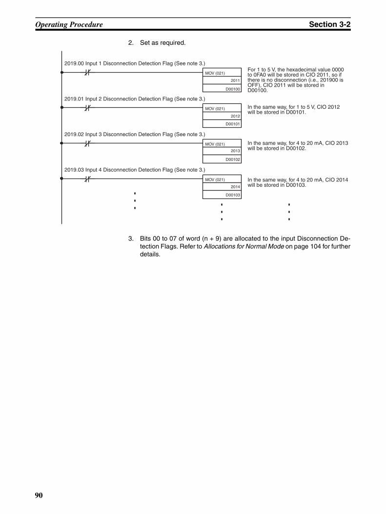
Operating Procedure Section 3-2
2. Set as required.
3. Bits 00 to 07 of word (n + 9) are allocated to the input Disconnection De-tection Flags. Refer to Allocations for Normal Mode on page 104 for furtherdetails.
2019.00 Input 1 Disconnection Detection Flag (See note 3.)
2019.01 Input 2 Disconnection Detection Flag (See note 3.)
2019.02 Input 3 Disconnection Detection Flag (See note 3.)
2019.03 Input 4 Disconnection Detection Flag (See note 3.)
For 1 to 5 V, the hexadecimal value 0000 to 0FA0 will be stored in CIO 2011, so if there is no disconnection (i.e., 201900 is OFF), CIO 2011 will be stored in D00100.
In the same way, for 1 to 5 V, CIO 2012 will be stored in D00101.
In the same way, for 4 to 20 mA, CIO 2013 will be stored in D00102.
In the same way, for 4 to 20 mA, CIO 2014 will be stored in D00103.
MOV (021)
2011
D00100
MOV (021)
2012
D00101
MOV (021)
2013
D00102
MOV (021)
2014
D00103
90

Components and Switch Settings Section 3-3
3-3 Components and Switch Settings
MACHNo.
AD081RUNERCERH B1 A1ADJ
x101
x100
09
8765 4 321
09
8765 4 321
ON1
2
MODE
MACHNo.
AD081RUNERCERH B1 A1ADJ
x101
x100
21
21
21
21
09
8765 4 321
09
8765 4 321
ON
ON
ON
ON
ON1
2
MODE
With Terminal Block
Front
Indicators
Terminal block
Voltage/current switch
Terminal block lock lever (pull down to release terminal block)
DIN Track mounting pin
Terminal block
Operating mode switch
Unit number switches
With Terminal Block Removed
CJ1W-AD041-V1CJ1W-AD081-V1
SideSlider
Slider
Expansion connector
91
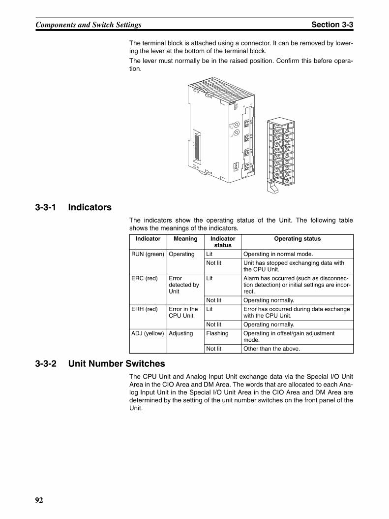
Components and Switch Settings Section 3-3
The terminal block is attached using a connector. It can be removed by lower-ing the lever at the bottom of the terminal block.
The lever must normally be in the raised position. Confirm this before opera-tion.
3-3-1 IndicatorsThe indicators show the operating status of the Unit. The following tableshows the meanings of the indicators.
3-3-2 Unit Number SwitchesThe CPU Unit and Analog Input Unit exchange data via the Special I/O UnitArea in the CIO Area and DM Area. The words that are allocated to each Ana-log Input Unit in the Special I/O Unit Area in the CIO Area and DM Area aredetermined by the setting of the unit number switches on the front panel of theUnit.
B1A1
21
21
21
21
ON
ON
ON
ON
AD081
MACH
No.10
1
100
RUNERCERHADJ
MODE
12
Indicator Meaning Indicator status
Operating status
RUN (green) Operating Lit Operating in normal mode.
Not lit Unit has stopped exchanging data with the CPU Unit.
ERC (red) Error detected by Unit
Lit Alarm has occurred (such as disconnec-tion detection) or initial settings are incor-rect.
Not lit Operating normally.
ERH (red) Error in the CPU Unit
Lit Error has occurred during data exchange with the CPU Unit.
Not lit Operating normally.
ADJ (yellow) Adjusting Flashing Operating in offset/gain adjustment mode.
Not lit Other than the above.
92
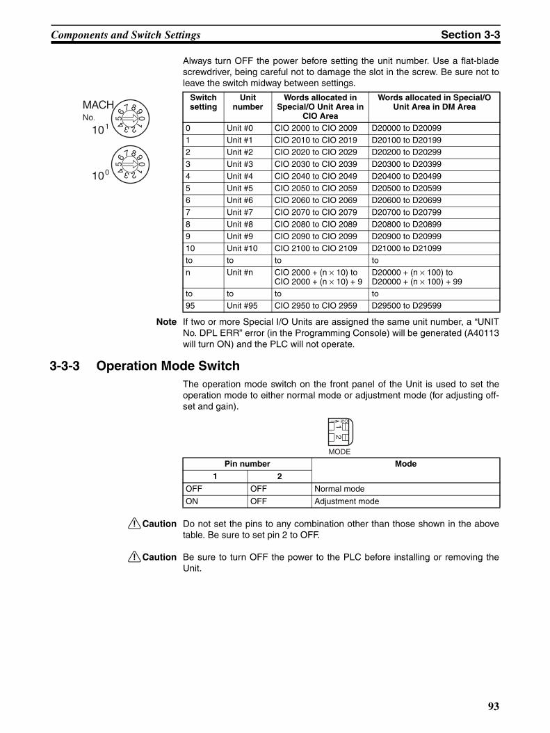
Components and Switch Settings Section 3-3
Always turn OFF the power before setting the unit number. Use a flat-bladescrewdriver, being careful not to damage the slot in the screw. Be sure not toleave the switch midway between settings.
Note If two or more Special I/O Units are assigned the same unit number, a “UNITNo. DPL ERR” error (in the Programming Console) will be generated (A40113will turn ON) and the PLC will not operate.
3-3-3 Operation Mode SwitchThe operation mode switch on the front panel of the Unit is used to set theoperation mode to either normal mode or adjustment mode (for adjusting off-set and gain).
!Caution Do not set the pins to any combination other than those shown in the abovetable. Be sure to set pin 2 to OFF.
!Caution Be sure to turn OFF the power to the PLC before installing or removing theUnit.
Switch setting
Unit number
Words allocated in Special/O Unit Area in
CIO Area
Words allocated in Special/O Unit Area in DM Area
0 Unit #0 CIO 2000 to CIO 2009 D20000 to D20099
1 Unit #1 CIO 2010 to CIO 2019 D20100 to D201992 Unit #2 CIO 2020 to CIO 2029 D20200 to D20299
3 Unit #3 CIO 2030 to CIO 2039 D20300 to D20399
4 Unit #4 CIO 2040 to CIO 2049 D20400 to D204995 Unit #5 CIO 2050 to CIO 2059 D20500 to D20599
6 Unit #6 CIO 2060 to CIO 2069 D20600 to D20699
7 Unit #7 CIO 2070 to CIO 2079 D20700 to D207998 Unit #8 CIO 2080 to CIO 2089 D20800 to D20899
9 Unit #9 CIO 2090 to CIO 2099 D20900 to D20999
10 Unit #10 CIO 2100 to CIO 2109 D21000 to D21099to to to to
n Unit #n CIO 2000 + (n × 10) to CIO 2000 + (n × 10) + 9
D20000 + (n × 100) to D20000 + (n × 100) + 99
to to to to
95 Unit #95 CIO 2950 to CIO 2959 D29500 to D29599
MACHNo.
101
100
09
8765 4 321
09
8765 4 321
Pin number Mode
1 2
OFF OFF Normal mode
ON OFF Adjustment mode
ON1
2
MODE
93

Components and Switch Settings Section 3-3
Note The operation mode can also be set using bits 00 to 07 of DM word m+18, inaddition to the hardware operation mode switch. The contents of DM wordm+18 are shown below.
m = D20000 + (unit number x 100)
Relationship between Operation Mode Setting and Hardware Operation Mode Switch
3-3-4 Voltage/Current SwitchThe analog conversion input can be switched from voltage input to currentinput by changing the pin settings on the voltage/current switch located on theback of the terminal block.
Note There are only four inputs for the CJ1W-AD041-V1.
!Caution Be sure to turn OFF the power to the PLC before mounting or removing theterminal block.
Bit 15 14 13 12 11 10 09 08 07 06 05 04 03 02 01 00
D (m+18) Conversion period/resolution setting Operation mode setting00: Normal modeC1: Adjustment mode
Hardware operation mode switch
Setting of bits 00 to 07 of m+18
Operation mode when power is turned ON or Unit
is restarted
Normal mode Normal mode Normal mode
Normal mode Adjustment mode Adjustment mode
Adjustment mode Normal mode Adjustment mode
Normal mode Adjustment mode Adjustment mode
MACHNo.
AD081RUNERCERH B1 A1ADJ
x101
x100
21
21
21
21
09
8765 4 321
09
8765 4 321
ON
ON
ON
ON
21
21
21
21
ON
ON
ON
ON
ON1
2
MODE
OFF: Voltage inputON: Current input
Input 2Input 1
Input 4Input 3
Input 6Input 5
Input 8Input 7
94
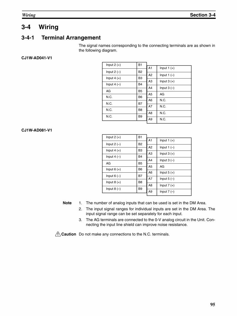
Wiring Section 3-4
3-4 Wiring
3-4-1 Terminal ArrangementThe signal names corresponding to the connecting terminals are as shown inthe following diagram.
CJ1W-AD041-V1
CJ1W-AD081-V1
Note 1. The number of analog inputs that can be used is set in the DM Area.
2. The input signal ranges for individual inputs are set in the DM Area. Theinput signal range can be set separately for each input.
3. The AG terminals are connected to the 0-V analog circuit in the Unit. Con-necting the input line shield can improve noise resistance.
!Caution Do not make any connections to the N.C. terminals.
Input 2 (+)
Input 2 (–)
Input 4 (+)
Input 4 (–)
AG
N.C.
N.C.
N.C.
N.C.
Input 1 (+)
Input 1 (–)
Input 3 (+)
Input 3 (–)
AG
N.C.
N.C.
N.C.
N.C.
B1
B2
B3
B4
B5
B6
B7
B8
B9
A1
A2
A3
A4
A5
A6
A7
A8
A9
Input 2 (+)
Input 2 (–)
Input 4 (+)
Input 4 (–)
AG
Input 6 (+)
Input 6 (–)
Input 8 (+)
Input 8 (–)
Input 1 (+)
Input 1 (–)
Input 3 (+)
Input 3 (–)
AG
Input 5 (+)
Input 5 (–)
Input 7 (+)
Input 7 (–)
B1
B2
B3
B4
B5
B6
B7
B8
B9
A1
A2
A3
A4
A5
A6
A7
A8
A9
95

Wiring Section 3-4
3-4-2 Internal CircuitryThe following diagrams show the internal circuitry of the analog input section.
Input Circuitry
Internal Configuration
1 MΩ
15 kΩ 15 kΩ
15 kΩ 15 kΩ
AG (common to all inputs)
Input (+)
Input (–)
AG (analog 0 V)
Input circuit and conversion circuit
1 MΩ
Voltage/currentinput switch
250 Ω
Bus interface
Indicators/Switch
MPU
RegulatorInsulation-type DC-to-DC converter
Oscillator
Division
CJ-series PC
EEPROM
RAM ROM
Multi-plexer and amplifier
A/D converter
INPUT
Externally connected terminal
Pho
toco
uple
r in
sula
tion
+5 V
96

Wiring Section 3-4
3-4-3 Voltage Input Disconnection
Note If the connected device #2 in the above example outputs 5 V and the powersupply is shared by 2 channels as shown in the above diagram, approximatelyone third of the voltage, or 1.6 V, will be input at input 1.
When voltage inputs are used and a disconnection occurs, separate thepower supply at the side of the connected devices or use an insulating device(isolator) for each input to avoid the following problems.
When the power supply at the connected devices is shared and section A or Bis disconnected, power will flow in the direction of the broken line and the out-put voltage of the other connected devices will be reduced to between a thirdto a half of the voltage. If 1 to 5 V is used and the reduced voltage output, dis-connection may not be detectable. If section C is disconnected, the power atthe (–) input terminal will be shared and disconnection will not be detectable.
For current inputs, sharing the power supply between the connected deviceswill not cause any problems.
Connected device #1
24 VDC
Connected device #2
B C
97

Wiring Section 3-4
3-4-4 Input Wiring Example
Note Crimp-type terminals must be used for terminal connections, and the screwsmust be tightened securely. Use M3 screws and tighten them to a torque of0.5 N·m.
Note 1. When using current inputs, turn ON the voltage/current switches. Refer to3-3-4 Voltage/Current Switch for further details.
2. For inputs that are not used, either set to “0: Not used” in the input numbersettings (refer to 3-6-1 Input Settings and Conversion Values) or short-cir-cuit the voltage input terminals (V+) and (V–). If this is not performed andthe inputs are set for the 1 to 5-V or 4 to 20-mA range, the Line Disconnec-tion Flag will turn ON.
3. When connecting the shield of the analog input cables* to the Unit’s AG ter-minals, as shown in the above diagram, use a wire that is 30 cm max. inlength if possible.
!Caution Do not connect anything to N.C. terminals shown in the wiring diagram onpage 95.
Connect the analog input line shield to the AG terminal on the Analog InputUnit to improve noise resistance.
3-4-5 Input Wiring ConsiderationsWhen wiring inputs, apply the following points to avoid noise interference andoptimize Analog Input Unit performance.
• Use two-core shielded twisted-pair cables for input connections.
B1
B3
B2
B4
B5
B6
B7
B8
B9
A1
A3
A2
A4
A5
A6
A7
A8
A9
+
−Input 2
+
−Input 4
+
−Input 6
+
−Input 8
+
−Input 1
+
−Input 3
+
−Input 5
+
−Input 7
(*) (*)
CJ1W-AD081-V1
Note There are only four inputs for the CJ1W-AD041-V1.Inputs 5 to 8 are not used.
6.2 mm max.
6.2 mm max.M3 screw
Fork type
Round type
98

Exchanging Data with the CPU Unit Section 3-5
• Route input cables separately from the AC cable, and do not run the Unit’scables near a main circuit cable, high voltage cable, or a non-PLC loadcable.
• If there is noise interference from power lines (if, for example, the powersupply is shared with electrical welding devices or electrical dischargemachines, or if there is a high-frequency generation source nearby) installa noise filter at the power supply input area.
3-5 Exchanging Data with the CPU Unit
3-5-1 Outline of Data ExchangeData is exchanged between the CPU Unit and the CJ1W-AD041-V1/081-V1Analog Input Unit via the Special I/O Unit Area in the CIO Area (for data usedto operate the Unit) and the Special I/O Unit Area in the DM Area (for dataused for initial settings).
I/O Refresh Data
Analog input conversion values, which are used as data for Unit operation, areallocated in the Special I/O Unit Area of the CPU Unit according to the unitnumber, and are exchanged during I/O refreshing.
Fixed Data
The Unit’s fixed data, such as the analog input signal ranges and the numberof operational mean value buffers is allocated in the Special I/O Unit Area inthe DM Area of the CPU Unit according to the unit number, and is exchangedwhen the power is turned ON or the Unit is restarted.
The conversion time and resolution can be set, along with the operationmode.
CJ-series CPU Unit CJ1W-AD041-V1/081-V1 Analog Input Unit
Special I/O Unit Area I/O Refresh Data
Analog inputs
Analog inputs
DM (Data Memory) Area
Input signal range
Number of opera-tional mean value buffers
I/O refresh
Power ON or Unit restart
Exchanges analog input val-ues during data refresh.
Transmits fixed data such as analog input signal ranges and number of operational mean value buffers..
2000 + n x 10
2000 + n x 10 + 9
D20000 + n x 100
D20000 + n x 100 + 99
10 words
100 words
Fixed Data
:
:
n: Unit number
See 3-5-5 I/O Refresh Data Allocations for details.
See 3-5-4 Fixed Data Allocations for details.
Conversion time/ resolution and operating mode
99

Exchanging Data with the CPU Unit Section 3-5
3-5-2 Unit Number SettingThe words in the Special I/O Unit Areas in the CIO Area and DM Area that areallocated to each Analog Input Unit are determined by the unit numberswitches on the front panel of the Unit.
Note If two or more Special I/O Units are assigned the same unit number, a “UNITNo. DPL ERR” error (in the Programming Console) will be generated (A40113will turn ON) and the PLC will not operate.
3-5-3 Special I/O Unit Restart BitsTo restart the Unit after changing the contents of the DM Area or correcting anerror, cycle the power supply to the PLC or turn ON the Special I/O UnitRestart Bit.
Note Replace the Unit if the error is not cleared even though the power supply iscycled or the Restart Bit is turned ON.
Switch setting
Unit number
Words allocated in Special I/O Unit Area in
CIO Area
Words allocated in Special I/O Unit Area in DM Area
0 Unit #0 CIO 2000 to CIO 2009 D20000 to D20099
1 Unit #1 CIO 2010 to CIO 2019 D20100 to D20199
2 Unit #2 CIO 2020 to CIO 2029 D20200 to D20299
3 Unit #3 CIO 2030 to CIO 2039 D20300 to D20399
4 Unit #4 CIO 2040 to CIO 2049 D20400 to D20499
5 Unit #5 CIO 2050 to CIO 2059 D20500 to D20599
6 Unit #6 CIO 2060 to CIO 2069 D20600 to D20699
7 Unit #7 CIO 2070 to CIO 2079 D20700 to D20799
8 Unit #8 CIO 2080 to CIO 2089 D20800 to D20899
9 Unit #9 CIO 2090 to CIO 2099 D20900 to D20999
10 Unit #10 CIO 2100 to CIO 2109 D21000 to D21099
to to to to
n Unit #n CIO 2000 + (n × 10) to CIO 2000 + (n × 10) + 9
D20000 + (n × 100) to D20000 + (n × 100) + 99
to to to to
95 Unit #95 CIO 2950 to CIO 2959 D29500 to D29599
MACHNo.
101
100
09
8765 4 321
09
8765 4 321
Special I/O Unit Area word address
Function
A50200 Unit No. 0 Restart Bit Restarts the Unit when turned ON and then OFF again.A50201 Unit No. 1 Restart Bit
to to
A50215 Unit No. 15 Restart Bit
A50300 Unit No. 16 Restart Bit
to to
A50715 Unit No. 95 Restart Bit
100

Exchanging Data with the CPU Unit Section 3-5
3-5-4 Fixed Data AllocationsAllocations in DM Area The initial settings of the Analog Input Unit are set according to the data allo-
cated in the Special I/O Unit Area in the DM Area. Settings, such as the inputsused and the analog input signal range must be set in this area.
The conversion time and resolution can be set, along with the operationmode, in DM word m+18.
Note 1. The words in the Special I/O Unit DM Area that are allocated to the AnalogInput Unit are determined by the setting of the unit number switches on thefront panel of the Unit. Refer to 3-5-2 Unit Number Setting for details on themethod used to set the unit number switches.
2. If two or more Special I/O Units are assigned the same unit number, a“UNIT No. DPL ERR” error (in the Programming Console) will be generat-ed (A40113 will turn ON) and the PLC will not operate.
3. Only D(m) to D(m+5) are supported by the CJ1W-AD041-V1.
D (m+1)
D (m)
D20300 to D20399
D20400 to D20499
D20500 to D20599
D20000 to D20099
D20100 to D20199
D20200 to D20299
D20900 to D20999
D20600 to D20699
D20700 to D20799
D20800 to D20899
SYSMAC CJ-series CPU Unit CJ1W-AD041-V1/081-V1 Analog Input Unit
(Fixed Data Area)
Unit #0
Unit #1
Unit #2
Unit #3
Unit #4
Unit #5
Unit #6
Unit #7
Unit #8
Unit #9
(Special I/O Unit DM Area)
Word
D29500 to D29599
D21000 to D21099Unit #10
Unit #n
Unit #95
Input signal range
m = 20000 + (unit number × 100)
D20000 + (n × 100) to D20000 + (n × 100) + 99
Data is automatically transferred to each unit number when the power is turned ON, or when the Special I/O Unit Restart Bit is turned ON.
Input conversion permission loop mode setting
D (m+2 to m+9) (See note3.)
Sets number of samplings for mean value processing
Conversion time/ resolution and operation mode
D (m+18)
to
to
to
to
101

Exchanging Data with the CPU Unit Section 3-5
Allocations in DM Area The following table shows the allocation of DM Area words and bits for bothnormal and adjustment mode.
CJ1W-AD041-V1
Note For the DM word addresses, m = D20000 + (unit number × 100).
CJ1W-AD081-V1
Note For the DM word addresses, m = D20000 + (unit number × 100).
DM Area word
Bits
15 14 13 12 11 10 9 8 7 6 5 4 3 2 1 0
D (m) Not used. (Settings are ignored.) Not used. Input use setting
Input 4
Input 3
Input 2
Input 1
D (m+1) Not used. (Settings are ignored.) Input signal range setting
Input 4 Input 3 Input 2 Input 1
D (m+2) Input 1: Mean value processing setting
D (m+3) Input 2: Mean value processing setting
D (m+4) Input 3: Mean value processing setting
D (m+5) Input 4: Mean value processing setting
D (m+6) to (m+17)
Not used. (Settings are ignored.)
D (m+18) Conversion time/resolution setting 00: Conversion time of 1 ms and resolution of 4,000C1: Conversion time of 250 µs and resolution of 8,000
Operation mode setting
00: Normal modeC1: Adjustment mode
DM Area word
Bits
15 14 13 12 11 10 9 8 7 6 5 4 3 2 1 0
D (m) Not used. (Settings are ignored.) Input use setting
Input 8
Input 7
Input 6
Input 5
Input 4
Input 3
Input 2
Input 1
D (m+1) Input signal range setting
Input 8 Input 7 Input 6 Input 5 Input 4 Input 3 Input 2 Input 1
D (m+2) Input 1: Mean value processing setting
D (m+3) Input 2: Mean value processing setting
D (m+4) Input 3: Mean value processing setting
D (m+5) Input 4: Mean value processing setting
D (m+6) Input 5: Mean value processing setting
D (m+7) Input 6: Mean value processing setting
D (m+8) Input 7: Mean value processing setting
D (m+9) Input 8: Mean value processing setting
D (m+10) to (m+17)
Not used. (Settings are ignored.)
D (m+18) Conversion time/resolution setting 00: Conversion time of 1 ms and resolution of 4,000C1: Conversion time of 250 µs and resolution of 8,000
Operation mode setting
00: Normal modeC1: Adjustment mode
102

Exchanging Data with the CPU Unit Section 3-5
Set Values and Stored Values
Note 1. The input signal range of “1 to 5 V” and “4 to 20 mA” is switched using thepins of the voltage/current switch. Refer to 3-3-4 Voltage/Current Switch fordetails.
2. The default of mean value processing setting is set to “Mean value pro-cessing with 2 buffers.” Refer to 3-6-3 Mean Value Processing.
3-5-5 I/O Refresh Data AllocationsI/O refresh data for the Analog Input Unit is exchanged according to the allo-cations in the Special I/O Unit Area.
Note 1. The words in the Special I/O Unit Area in the CIO Area that are allocatedto the Analog Input Unit are determined by the setting of the unit numberswitches on the front panel of the Unit. Refer to 3-5-2 Unit Number Settingfor details on the method used to set the unit number switches.
Item Contents Page
Input Use setting 0: Not used.1: Used.
106
Input signal range 00: –10 to 10 V01: 0 to 10 V10: 1 to 5 V/4 to 20 mA (See note 1.)11: 0 to 5 V
107
Mean value processing set-ting
0000: Mean value processing with 2 buffers (See note 3.)0001: Mean value processing not used0002: Mean value processing with 4 buffers0003: Mean value processing with 8 buffers0004: Mean value processing with 16 buffers0005: Mean value processing with 32 buffers0006: Mean value processing with 64 buffers
109
CIO n
CIO 2030 to CIO 2039
CIO 2040 to CIO 2049
CIO 2050 to CIO 2059
CIO 2000 to CIO 2009
CIO 2010 to CIO 2019
CIO 2020 to CIO 2029
CIO 2090 to CIO 2099
CIO 2060 to CIO 2069
CIO 2070 to CIO 2079
CIO 2080 to CIO 2089
SYSMAC CJ-series CPU Unit CJ1W-AD041-V1/081-V1 Analog Input Unit
IN refresh
(I/O Refresh Data Area)
Unit #0
Unit #1
Unit #2
Unit #3
Unit #4
Unit #5
Unit #6
Unit #7
Unit #8
Unit #9
(Special I/O Unit Area)
OUT refresh
Allocated words
CIO 2950 to CIO 2959
CIO 2100 to CIO 2109Unit #10
Unit #n
Unit #95
Normal mode
IN refresh
OUT refresh
Adjustment mode
n = 2000 + (unit number × 10)
I/O refresh
CIO 2000 + (n × 10) to CIO 2000 + (n × 10) + 9
At the I/O refresh by the PLC, outputs (CPU to Unit) and inputs (Unit to CPU) are refreshed in order with every cycle.
CIO n + 1 to CIO n + 9
CIO n to CIO n + 7
CIO n + 8 to CIO n + 9
to
to
to
to
103
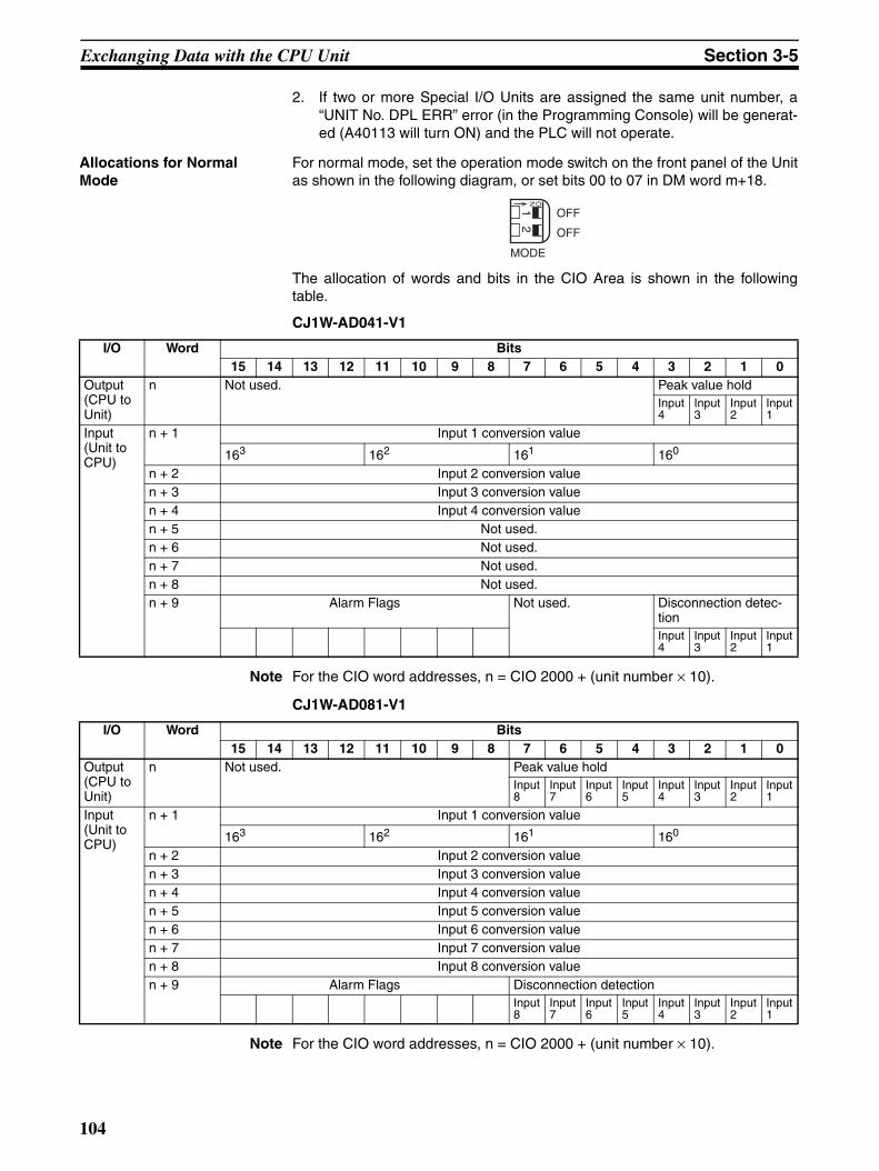
Exchanging Data with the CPU Unit Section 3-5
2. If two or more Special I/O Units are assigned the same unit number, a“UNIT No. DPL ERR” error (in the Programming Console) will be generat-ed (A40113 will turn ON) and the PLC will not operate.
Allocations for Normal Mode
For normal mode, set the operation mode switch on the front panel of the Unitas shown in the following diagram, or set bits 00 to 07 in DM word m+18.
The allocation of words and bits in the CIO Area is shown in the followingtable.
CJ1W-AD041-V1
Note For the CIO word addresses, n = CIO 2000 + (unit number × 10).
CJ1W-AD081-V1
Note For the CIO word addresses, n = CIO 2000 + (unit number × 10).
ON1
2
MODE
OFF
OFF
I/O Word Bits15 14 13 12 11 10 9 8 7 6 5 4 3 2 1 0
Output (CPU to Unit)
n Not used. Peak value holdInput 4
Input 3
Input 2
Input 1
Input (Unit to CPU)
n + 1 Input 1 conversion value
163 162 161 160
n + 2 Input 2 conversion valuen + 3 Input 3 conversion valuen + 4 Input 4 conversion valuen + 5 Not used.n + 6 Not used.n + 7 Not used.n + 8 Not used.n + 9 Alarm Flags Not used. Disconnection detec-
tionInput 4
Input 3
Input 2
Input 1
I/O Word Bits15 14 13 12 11 10 9 8 7 6 5 4 3 2 1 0
Output (CPU to Unit)
n Not used. Peak value holdInput 8
Input 7
Input 6
Input 5
Input 4
Input 3
Input 2
Input 1
Input (Unit to CPU)
n + 1 Input 1 conversion value
163 162 161 160
n + 2 Input 2 conversion valuen + 3 Input 3 conversion valuen + 4 Input 4 conversion valuen + 5 Input 5 conversion valuen + 6 Input 6 conversion valuen + 7 Input 7 conversion valuen + 8 Input 8 conversion valuen + 9 Alarm Flags Disconnection detection
Input 8
Input 7
Input 6
Input 5
Input 4
Input 3
Input 2
Input 1
104
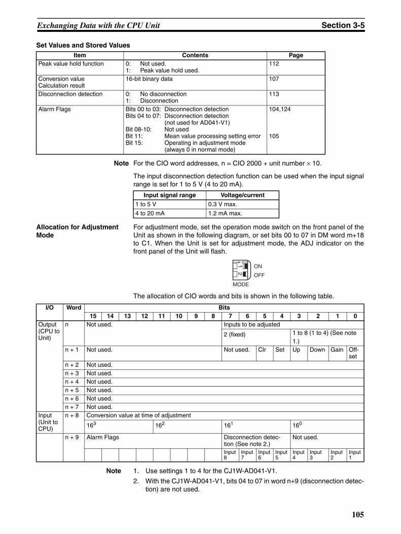
Exchanging Data with the CPU Unit Section 3-5
Set Values and Stored Values
Note For the CIO word addresses, n = CIO 2000 + unit number × 10.
The input disconnection detection function can be used when the input signalrange is set for 1 to 5 V (4 to 20 mA).
Allocation for Adjustment Mode
For adjustment mode, set the operation mode switch on the front panel of theUnit as shown in the following diagram, or set bits 00 to 07 in DM word m+18to C1. When the Unit is set for adjustment mode, the ADJ indicator on thefront panel of the Unit will flash.
The allocation of CIO words and bits is shown in the following table.
Note 1. Use settings 1 to 4 for the CJ1W-AD041-V1.
2. With the CJ1W-AD041-V1, bits 04 to 07 in word n+9 (disconnection detec-tion) are not used.
Item Contents PagePeak value hold function 0: Not used.
1: Peak value hold used.112
Conversion valueCalculation result
16-bit binary data 107
Disconnection detection 0: No disconnection1: Disconnection
113
Alarm Flags Bits 00 to 03: Disconnection detectionBits 04 to 07: Disconnection detection
(not used for AD041-V1)Bit 08-10: Not usedBit 11: Mean value processing setting errorBit 15: Operating in adjustment mode
(always 0 in normal mode)
104,124
105
Input signal range Voltage/current
1 to 5 V 0.3 V max.
4 to 20 mA 1.2 mA max.
ON1
2
MODE
ON
OFF
I/O Word Bits15 14 13 12 11 10 9 8 7 6 5 4 3 2 1 0
Output (CPU to Unit)
n Not used. Inputs to be adjusted
2 (fixed) 1 to 8 (1 to 4) (See note 1.)
n + 1 Not used. Not used. Clr Set Up Down Gain Off-set
n + 2 Not used.n + 3 Not used.n + 4 Not used.n + 5 Not used.n + 6 Not used.n + 7 Not used.
Input (Unit to CPU)
n + 8 Conversion value at time of adjustment
163 162 161 160
n + 9 Alarm Flags Disconnection detec-tion (See note 2.)
Not used.
Input 8
Input 7
Input 6
Input 5
Input 4
Input3
Input2
Input 1
105

Analog Input Functions and Operating Procedures Section 3-6
Set Values and Stored Values
Refer to 3-7-1 Adjustment Mode Operational Flow for further details.
Note For the CIO word addresses, n = CIO 2000 + (unit number × 10).
The input disconnection detection function can be used when the input signalrange is set for 1 to 5 V (4 to 20 mA).
3-6 Analog Input Functions and Operating Procedures
3-6-1 Input Settings and Conversion ValuesInput Numbers The Analog Input Unit converts analog inputs specified by input numbers 1 to
8 (1 to 4 for CJ1W-AD041-V1) only. To specify the analog inputs to be used,turn ON from a Programming Device the D(m) bits in the DM Area shown inthe following diagram.
Note There are only four inputs for the CJ1W-AD041-V1.
The analog input sampling interval can be shortened by setting any unusedinput numbers to 0.
Sampling interval = (1 ms) x (Number of inputs used) (See note.)
Item Contents
Input to be adjusted Sets input to be adjusted.Leftmost digit: 2 (fixed)Rightmost digit: 1 to 8 (1 to 4 for CJ1W-AD041-V1)
Offset (Offset Bit) When ON, adjusts offset error.
Gain (Gain Bit) When ON, adjusts gain error.
Down (Down Bit) Decrements the adjustment value while ON.
Up (Up Bit) Increments the adjustment value while ON.
Set (Set Bit) Sets adjusted value and writes to EEPROM.
Clr (Clear Bit) Clears adjusted value. (Returns to default status)
Conversion value for adjustment
The conversion value for adjustment is stored as 16 bits of binary data.
Disconnection detection 0: No disconnection1: Disconnection
Alarm Flags Bit 12: Input value is outside adjustment limits (in adjustment mode)
Bit 13: Input number setting error (in adjustment mode)
Bit 14: EEPROM write error (in adjustment mode)Bit 15: Operating in adjustment mode
(always 1 in adjustment mode)
Input signal range Voltage/current
1 to 5 V 0.3 V max.
4 to 20 mA 1.2 mA max.
15 14 13 12 11 10 09 08 07 06 05 04 03 02 01 00Bit
D(m)
Inpu
t 2
Inpu
t 1
0: Not used
1: Used
Inpu
t 4
Inpu
t 3
Inpu
t 6
Inpu
t 5
Inpu
t 8
Inpu
t 7
106

Analog Input Functions and Operating Procedures Section 3-6
Note Use 250 µs instead of 1 ms is set to a conversion time of 250 µs andresolution of 8,000.
The conversion values in words for inputs that have been set to “Not used” willalways be “0000.”
For the DM word addresses, m = D20000 + (unit number × 100)
Input Signal Range Any of four types of input signal range (–10 to 10 V, 0 to 10 V, 1 to 5 V, and 4to 20 mA) can be selected for each of the inputs. To specify the input signalrange for each input, set from a Programming Device the D(m+1) bits in theDM Area as shown in the following diagram.
Note There are only four inputs for the CJ1W-AD041-V1.
Note 1. For the DM word addresses, m = D20000 + (unit number × 100)
2. The input signal range of “1 to 5 V” or “4 to 20 mA” is switched using thevoltage/current switch.
3. When DM Area settings have been carried out using a Programming De-vice, be sure to either cycle the power supply to the PLC, or turn ON theSpecial I/O Unit Restart Bit. The contents of the initial settings in the DMArea will be transferred to the Special I/O Unit when the power is turnedON or the Special I/O Unit Restart Bit is turned ON.
Reading Conversion Values
Analog input conversion values are stored for each input number, in CIOwords n+1 to n+8. With the CJ1W-AD041-V1, the values are stored in CIOwords n+1 to n+4.
Note For the CIO word addresses, n = CIO 2000 + (unit number × 10).
Use MOV(021) or XFER(070) to read conversion values in the user program.
15 14 13 12 11 10 09 08 07 06 05 04 03 02 01 00Bit
DM (m+1)
Inpu
t 2
Inpu
t 1
00: −10 to 10 V01: 0 to 10 V10: 1 to 5 V / 4 to 20 mA11: 0 to 5 V
Inpu
t 4
Inpu
t 3
Inpu
t 6
Inpu
t 5
Inpu
t 8
Inpu
t 7
Word Function Stored value
n+1 Input 1 conversion value 16-bit binary data
n+2 Input 2 conversion value
n+3 Input 3 conversion value
n+4 Input 4 conversion value
n+5 Input 5 conversion value
n+6 Input 6 conversion value
n+7 Input 7 conversion value
n+8 Input 8 conversion value
107

Analog Input Functions and Operating Procedures Section 3-6
Example 1 In this example, the conversion data from only one input is read. (The unitnumber is 0.)
Example 2 In this example, the conversion data from multiple inputs is read. (The unitnumber is 0.)
For details regarding conversion value scaling, refer to Scaling on page 446.
3-6-2 Conversion Time/Resolution Setting
Bits 08 to 15 in DM word m+18 can be used to set the conversion time andresolution for the CJ1W-AD041-V1 and CJ1W-AD081-V1 to increase speedand accuracy.
This setting applies to analog inputs 1 to 8 (1 to 4 for the CJ1W-AD041-V1),i.e., there are not individual settings for each input.
Note When DM Area settings have been carried out using a Programming Device,be sure to either cycle the power supply to the PLC, or turn ON the Special I/O Unit Restart Bit. The contents of the initial settings in the DM Area will betransferred to the Special I/O Unit when the power is turned ON or the SpecialI/O Unit Restart Bit is turned ON.
MOV(021)
2001
D00001
Input conditionConversion data in CIO word 2001 (input number 1) is read to D 00001.
XFER(070)
#0004
2001
D00001
Input conditionConversion data in CIO words 2001 to 2004 (input numbers 1 to 4) is read to D00001 and D00004.
15 14 13 12 11 10 09 08 07 06 05 04 03 02 01 00Bit
D (m+18)
00: Conversion time = 1 ms, resolution = 4,000C1: Conversion time = 250 µs, resolution = 8,000
(m = D20000 + unit number x 100)
108

Analog Input Functions and Operating Procedures Section 3-6
3-6-3 Mean Value ProcessingThe Analog Input Unit can compute the mean value of the conversion valuesof analog inputs that have been previously sampled. Mean value processinginvolves an operational mean value in the history buffers, so it has no effect onthe data refresh cycle. (The number of history buffers that can be set to usemean value processing is 2, 4, 8, 16, 32, or 64.)
When “n” number of history buffers are being used, the first conversion datawill be stored for all “n” number of history buffers immediately data conversionhas begun or after a disconnection is restored.
When mean value processing is used together with the peak value hold func-tion, the mean value will be held.
To specify whether or not mean value processing is to be used, and to specifythe number of history buffers for mean data processing, use a ProgrammingDevice to make the settings in D (m+2) to D (m+9) as shown in the followingtable. (With the CJ1W-AD041-V1, make the settings in D (m+2) to D (m+5).)
For the DM word addresses, m = D20000 + (unit number × 100)
Note When DM Area settings have been carried out using a Programming Device,be sure to either cycle the power supply to the PLC, or turn ON the Special I/O Unit Restart Bit. The contents of the initial settings in the DM Area will betransferred to the Special I/O Unit when the power is turned ON or the SpecialI/O Unit Restart Bit is turned ON.
The history buffer moving average is calculated as shown below. (In thisexample, there are four buffers.)
Conversion data Buffer 1
Buffer 2
Buffer 3
Buffer 4
Buffer n
(Mean value processing)
Conversion value
(Values stored in CIO words n+1 to n+8)
(Discarded)
DM Area word
Function Set value
D (m+2) Input 1 mean value processing 0000: Mean value processing with 2 buffers0001: No mean value processing0002: Mean value processing with 4 buffers0003: Mean value processing with 8 buffers0004: Mean value processing with 16 buffers0005: Mean value processing with 32 buffers0006: Mean value processing with 64 buffers
D (m+3) Input 2 mean value processing
D (m+4) Input 3 mean value processing
D (m+5) Input 4 mean value processing
D (m+6) Input 5 mean value processing
D (m+7) Input 6 mean value processing
D (m+8) Input 7 mean value processing
D (m+9) Input 8 mean value processing
109

Analog Input Functions and Operating Procedures Section 3-6
1,2,3... 1. With the first cycle, data 1 is stored in all the history buffers.
Mean value = (Data 1 + Data 1 + Data 1 + Data 1) ÷ 4
2. With the second cycle, data 2 is stored in the first history buffer.
Mean value = (Data 2 + Data 1 + Data 1 + Data 1) ÷ 4
3. With the third cycle, data 3 is stored in the first history buffer.
Mean value = (Data 3 + Data 2 + Data 1 + Data 1) ÷ 4
4. With the fourth cycle, data 4 is stored in the first history buffer.
Mean value = (Data 4 + Data 3 + Data 2 + Data 1) ÷ 4
5. With the fifth cycle, data 5 is stored in the first history buffer.
Mean value = (Data 5 + Data 4 + Data 3 + Data 2) ÷ 4
When a disconnection is restored, the mean value processing function beginsagain from step 1.
Note 1. The default setting for mean value processing in the Analog Input Unit ismean value processing with 2 buffers. The response time for the default
(Mean value processing)
Conversion value
Data 1
Data 1
Data 1
Data 1
(Mean value processing)
Conversion value
Data 2
Data 1
Data 1
Data 1
(Mean value processing)
Conversion value
Data 3
Data 2
Data 1
Data 1
(Mean value processing)
Conversion value
Data 4
Data 3
Data 2
Data 1
(Mean value processing)
Conversion value
Data 5
Data 4
Data 3
Data 2
110

Analog Input Functions and Operating Procedures Section 3-6
setting is different from when there is no mean processing, as shown in thefollowing diagram.
2. Specify “no mean value processing” to follow conversion of a rapid changein input signals.
3. If the averaging function is used, the delay in the conversion data in com-parison to changes in the input signals will be as shown below.
Response Time at 1-ms Conversion Time/4,000 Resolution
Unit: ms
Response Time at 250-µs Conversion Time/8,000 Resolution
Unit: ms
Symbols m: Number of input words used in DM Arean: Average number of buffers set for the input number for which to find theresponse time
Input signal to the Unit (V)
Conversion data
Time (ms)
Time (ms)
t: Delay
For V = 20 V (−10 to 10 V)1-ms Conversion Time/4,000 ResolutionUsing One Wordt = n + (2 to 3)Using m Words (1 ≤ m ≤ 8)No averaging (n = 1) or two averaging buffers (n = 2):
t = n x (m + 2)n averaging buffers (4 ≤ n ≤ 64):
t = (n − 2) x m + 10.5250-µs Conversion Time/8,000 Resolution (For version-1 Unit)Using One Wordt = n + (2 to 3) x 1/4Using m Words (1 ≤ m ≤ 8)No averaging (n = 1) or two averaging buffers (n = 2):
t = n x (m + 2) x 1/4n averaging buffers (4 ≤ n ≤ 64):
t = (n − 2) x m + 10.5 x 1/4
m n64 32 16 8 4 2 1
8 506.5 250.5 122.5 58.5 26.5 20 107 444.5 220.5 108.5 52.5 24.5 18 96 382.5 190.5 94.5 46.5 22.5 16 85 320.5 160.5 80.5 40.5 20.5 14 74 258.5 130.5 66.5 34.5 18.5 12 63 196.5 100.5 52.5 28.5 16.5 10 52 134.5 70.5 38.5 22.5 14.5 8 41 67 35 19 11 7 5 3
m n64 32 16 8 4 2 1
8 126.625 62.625 30.625 14.625 6.625 5 2.57 111.125 55.125 27.125 13.125 6.125 4.5 2.256 95.625 47.625 23.625 11.625 5.625 4 25 80.125 40.125 20.125 10.125 5.125 3.5 1.754 64.625 32.625 16.625 8.625 4.625 3 1.53 49.125 25.125 13.125 7.125 4.125 2.5 1.252 33.625 17.625 9.625 5.625 3.625 2 11 16.75 8.75 4.75 2.75 1.75 1.25 0.75
111
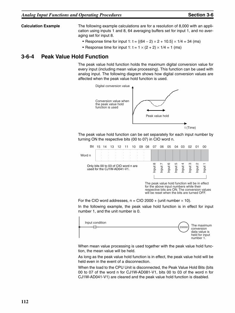
Analog Input Functions and Operating Procedures Section 3-6
Calculation Example The following example calculations are for a resolution of 8,000 with an appli-cation using inputs 1 and 8, 64 averaging buffers set for input 1, and no aver-aging set for input 8.
• Response time for input 1: t = (64 − 2) × 2 + 10.5 × 1/4 = 34 (ms)
• Response time for input 1: t = 1 × (2 + 2) × 1/4 = 1 (ms)
3-6-4 Peak Value Hold FunctionThe peak value hold function holds the maximum digital conversion value forevery input (including mean value processing). This function can be used withanalog input. The following diagram shows how digital conversion values areaffected when the peak value hold function is used.
The peak value hold function can be set separately for each input number byturning ON the respective bits (00 to 07) in CIO word n.
For the CIO word addresses, n = CIO 2000 + (unit number × 10).
In the following example, the peak value hold function is in effect for inputnumber 1, and the unit number is 0.
When mean value processing is used together with the peak value hold func-tion, the mean value will be held.
As long as the peak value hold function is in effect, the peak value hold will beheld even in the event of a disconnection.
When the load to the CPU Unit is disconnected, the Peak Value Hold Bits (bits00 to 07 of the word n for CJ1W-AD081-V1, bits 00 to 03 of the word n forCJ1W-AD041-V1) are cleared and the peak value hold function is disabled.
Peak value hold
Digital conversion value
t (Time)
Conversion value when the peak value hold function is used
15 14 13 12 11 10 09 08 07 06 05 04 03 02 01 00Bit
Inpu
t 2
Inpu
t 1
Word n
The peak value hold function will be in effect for the above input numbers while their respective bits are ON. The conversion values will be reset when the bits are turned OFF.
Inpu
t 4
Inpu
t 3
Inpu
t 6
Inpu
t 5
Inpu
t 8
Inpu
t 7Only bits 00 to 03 of CIO word n are used for the CJ1W-AD041-V1.
200000
Input conditionThe maximum conversion data value is held for input number 1.
112
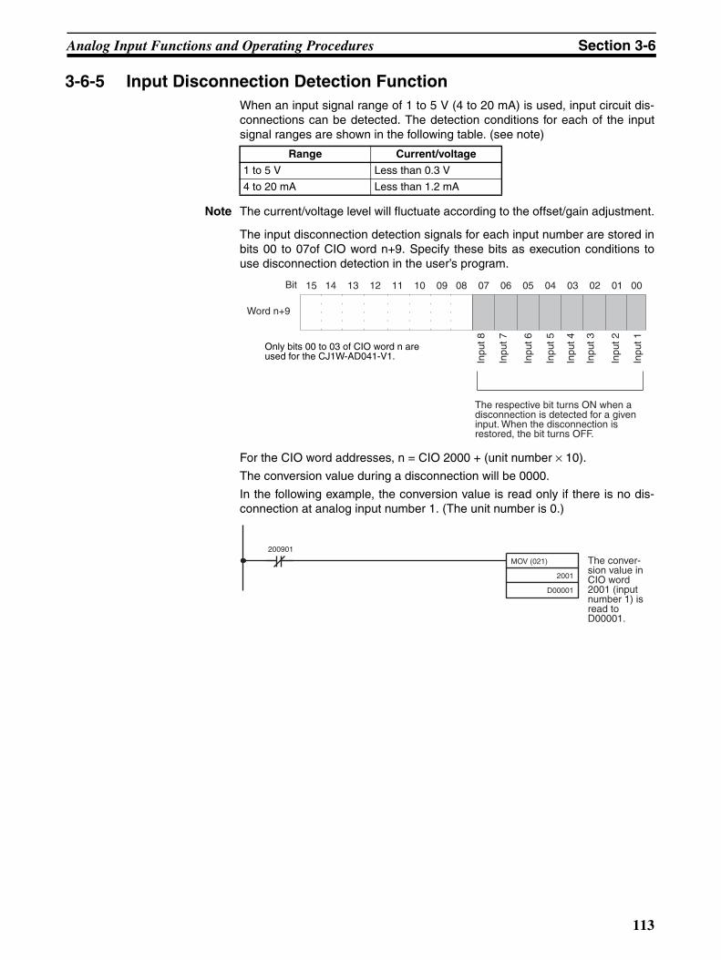
Analog Input Functions and Operating Procedures Section 3-6
3-6-5 Input Disconnection Detection FunctionWhen an input signal range of 1 to 5 V (4 to 20 mA) is used, input circuit dis-connections can be detected. The detection conditions for each of the inputsignal ranges are shown in the following table. (see note)
Note The current/voltage level will fluctuate according to the offset/gain adjustment.
The input disconnection detection signals for each input number are stored inbits 00 to 07of CIO word n+9. Specify these bits as execution conditions touse disconnection detection in the user’s program.
For the CIO word addresses, n = CIO 2000 + (unit number × 10).
The conversion value during a disconnection will be 0000.
In the following example, the conversion value is read only if there is no dis-connection at analog input number 1. (The unit number is 0.)
Range Current/voltage
1 to 5 V Less than 0.3 V
4 to 20 mA Less than 1.2 mA
15 14 13 12 11 10 09 08 07 06 05 04 03 02 01 00Bit
Inpu
t 6
Inpu
t 5
Word n+9
The respective bit turns ON when a disconnection is detected for a given input. When the disconnection is restored, the bit turns OFF.
Inpu
t 8
Inpu
t 7
Inpu
t 2
Inpu
t 1
Inpu
t 4
Inpu
t 3
Only bits 00 to 03 of CIO word n are used for the CJ1W-AD041-V1.
MOV (021)
2001
D00001
200901
The conver-sion value in CIO word 2001 (input number 1) is read to D00001.
113

Adjusting Offset and Gain Section 3-7
3-7 Adjusting Offset and Gain
3-7-1 Adjustment Mode Operational FlowThe adjustment mode enables the input of the connected devices to be cali-brated.
The offset voltage (or current) and gain voltage (or current) at the outputdevice are entered as analog input conversion data 0000 and 0FA0 (07D0 ifthe range is ±10 V) respectively for a resolution of 4,000.
For example, when using in the range 1 to 5 V, the actual output may be in therange 0.8 to 4.8 V, even though the specifications range for the externaldevice is 1 to 5 V. In this case, when an offset voltage of 0.8 V is output at theexternal device, the conversion data at the Analog Input Unit for a resolutionof 4,000 will be FF38, and if a gain voltage of 4.8 V is output, the conversiondata will be 0EDA. The offset/gain adjustment function will, for this example,convert 0.8 V and 4.8 V to 0000 and 0FA0 respectively and not to FF38 and0EDA, as illustrated in the following table.
(Values in parentheses are for a resolution of 8,000.)
Offset/gain voltage at the output device
Conversion data before adjustment
Conversion data after adjustment
0.8 V FF38 (FE70) 0000 (0000)
4.8 V 0EDA (0DB4) 0FA0 (1F40)
114

Adjusting Offset and Gain Section 3-7
The following diagram shows the flow of operations when using the adjust-ment mode for adjusting offset and gain.
!Caution Be sure to turn OFF the power to the PLC before changing the setting of theoperation mode switch.
!Caution The power must be cycled or the Unit restarted if the operation mode is set inDM word m+18.
Set the operation mode to adjustment mode.
Turn ON the PLC.
When adjusting another input number
When adjusting the same input number
Set the input number.
Offset adjustment
Offset Bit ON
Set Bit ON
Turn OFF power to the PLC.
Set the operation mode to normal mode.
Gain adjustment
Gain Bit ON
Input adjustment
Set Bit ON
Input adjustment
ON1
2
MODE
ON
OFF
ON1
2
MODE
ON
OFF
Set the operation mode switch, or set the operation mode in DM Area word m+18, to adjustment mode.
The ADJ indicator will flash while in adjustment mode.
Start up the PLC in PROGRAM mode.
Write the input number to be adjusted in the rightmost byte of CIO word n.
(Bit 0 of CIO word n+1 turns ON.)
Sampling input
(Add inputs so that conversion value becomes 0.)
(Bit 4 of CIO word n+1 turns ON.)
(Bit 1 of CIO word n+1 turns ON.)
Sampling input
(Add inputs so that conversion value is maximized.)
(Bit 4 of CIO word n+1 turns ON.)
Set the operation mode switch, or set the operation mode in DM Area word m+18, to normal mode.
115
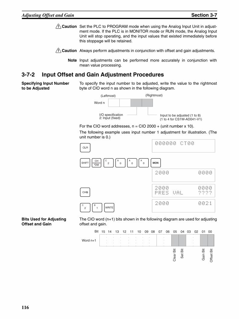
Adjusting Offset and Gain Section 3-7
!Caution Set the PLC to PROGRAM mode when using the Analog Input Unit in adjust-ment mode. If the PLC is in MONITOR mode or RUN mode, the Analog InputUnit will stop operating, and the input values that existed immediately beforethis stoppage will be retained.
!Caution Always perform adjustments in conjunction with offset and gain adjustments.
Note Input adjustments can be performed more accurately in conjunction withmean value processing.
3-7-2 Input Offset and Gain Adjustment ProceduresSpecifying Input Number to be Adjusted
To specify the input number to be adjusted, write the value to the rightmostbyte of CIO word n as shown in the following diagram.
For the CIO word addresses, n = CIO 2000 + (unit number x 10).
The following example uses input number 1 adjustment for illustration. (Theunit number is 0.)
Bits Used for Adjusting Offset and Gain
The CIO word (n+1) bits shown in the following diagram are used for adjustingoffset and gain.
(Rightmost)(Leftmost)
Word n
Input to be adjusted (1 to 8)I/O specification2: Input (fixed) (1 to 4 for CS1W-AD041-V1)
CLR000000 CT00
SHIFTCH
*DM2
C0
A0
A0
AMON
2000 0000
CHG2000 0000PRES VAL ????
2C
1B
WRITE2000 0021
15 14 13 12 11 10 09 08 07 06 05 04 03 02 01 00Bit
Word n+1
Cle
ar B
it
Set
Bit
Gai
n B
it
Offs
et B
it
116

Adjusting Offset and Gain Section 3-7
Offset Adjustment The procedure for adjusting the analog input offset is explained below. Asshown in the following diagram, the offset is adjusted by sampling inputs sothat the conversion value becomes 0.
The following example uses input number 1 adjustment for illustration. (Theunit number is 0.)
1,2,3... 1. Turn ON bit 00 (the Offset Bit) of CIO word n+1. (Hold the ON status.)
The analog input’s digital conversion values while the Offset Bit is ON willbe monitored in CIO word n+8.
2. Check whether the input devices are connected.
10 V0
0FA0
Offset adjustment input range
Input signal range:0 to 10 V
CLR000000 CT00
SHIFTCONT
#2
C0
A0
A1
B0
A0
AMON
200100 ^ OFF
SET
200100 ^ ON
A1
A2
A5
A1
A2
A5
+
–
+
–
Voltage input
Input 1
Current input
Input 1
For current input, check that the voltage/current switch is ON.
117
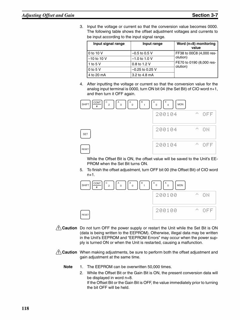
Adjusting Offset and Gain Section 3-7
3. Input the voltage or current so that the conversion value becomes 0000.The following table shows the offset adjustment voltages and currents tobe input according to the input signal range.
4. After inputting the voltage or current so that the conversion value for theanalog input terminal is 0000, turn ON bit 04 (the Set Bit) of CIO word n+1,and then turn it OFF again.
While the Offset Bit is ON, the offset value will be saved to the Unit’s EE-PROM when the Set Bit turns ON.
5. To finish the offset adjustment, turn OFF bit 00 (the Offset Bit) of CIO wordn+1.
!Caution Do not turn OFF the power supply or restart the Unit while the Set Bit is ON(data is being written to the EEPROM). Otherwise, illegal data may be writtenin the Unit’s EEPROM and “EEPROM Errors” may occur when the power sup-ply is turned ON or when the Unit is restarted, causing a malfunction.
!Caution When making adjustments, be sure to perform both the offset adjustment andgain adjustment at the same time.
Note 1. The EEPROM can be overwritten 50,000 times.
2. While the Offset Bit or the Gain Bit is ON, the present conversion data willbe displayed in word n+8.If the Offset Bit or the Gain Bit is OFF, the value immediately prior to turningthe bit OFF will be held.
Input signal range Input range Word (n+8) monitoring value
0 to 10 V –0.5 to 0.5 V FF38 to 00C8 (4,000 res-olution)FE70 to 0190 (8,000 res-olution)
–10 to 10 V –1.0 to 1.0 V
1 to 5 V 0.8 to 1.2 V
0 to 5 V –0.25 to 0.25 V
4 to 20 mA 3.2 to 4.8 mA
SHIFTCONT
#2
C0
A0
A1
B0
A4
EMON
200104 ^ OFF
SET
200104 ^ ON
RESET
200104 ^ OFF
SHIFTCONT
# 2C
0A
0A
1B
0A
0A
MON
200100 ^ ON
RESET
200100 ^ OFF
118

Adjusting Offset and Gain Section 3-7
Gain Adjustment The procedure for adjusting the analog input gain is explained below. Asshown in the following diagram, the gain is adjusted by sampling inputs sothat the conversion value is maximized.
The following example uses input number 1 adjustment for illustration. (Theunit number is 0.)
1,2,3... 1. Turn ON bit 01 (the Gain Bit) of CIO word n+1. (Hold the ON status.)
The analog input’s digital conversion values while the Gain Bit is ON willbe monitored in CIO word n+8.
2. Check whether the input devices are connected.
10 V0
0FA0
Input signal range:0 to 10 V
Gain adjustment input range
SHIFTCONT
# 2C
0A
0A
1B
0A
1B
MON
200101 ^ OFF
SET
200101 ^ ON
+
–
+
–
Voltage input
Input 1
Current input
Input 1
For current input, check that the voltage/current switch is ON.
A1
A2
A5
A1
A2
A5
119

Adjusting Offset and Gain Section 3-7
3. Input the voltage or current so that the conversion value is maximized(0FA0 or 07D0 at a resolution of 4,000). The following table shows the gainadjustment voltages and currents to be input according to the input signalrange.
(Values in parentheses are for a resolution of 8,000.)
4. With the voltage or current having been input so that the conversion valuefor the Analog Input Unit is maximized (0FA0 or 07D0 for a resolution of4,000), turn bit 04 (the Set Bit) of CIO word n+1 ON and then OFF again.
While the Gain Bit is ON, the gain value will be saved to the Unit’s EE-PROM when the Set Bit turns ON.
5. To finish the gain adjustment, turn OFF bit 01 (the Gain Bit) of CIO wordn+1.
!Caution Do not turn OFF the power supply or restart the Unit while the Set Bit is ON(data is being written to the EEPROM). Otherwise, illegal data may be writtenin the Unit’s EEPROM and “EEPROM Errors” may occur when the power sup-ply is turned ON or when the Unit is restarted, causing a malfunction.
!Caution When making adjustments, be sure to perform both the offset adjustment andgain adjustment at the same time.
Note 1. The EEPROM can be overwritten 50,000 times.
2. While the Offset Bit or the Gain Bit is ON, the present conversion data willbe displayed in word n+8.If the Offset Bit or the Gain Bit is OFF, the value immediately prior to turningthe bit OFF will be held.
Input signal range Input range Word (n+8) monitoring value
0 to 10 V 9.5 to 10.5 V 0ED8 to 1068 (1DB0 to 20D0)
–10 to 10 V 9.0 to 11.0 V 0708 to 0898 (0E10 to 1130)
1 to 5 V 4.8 to 5.2 V 0ED8 to 1068 (1DB0 to 20D0)
0 to 5 V 4.75 to 5.25 V 0ED8 to 1068 (1DB0 to 20D0)
4 to 20 mA 19.2 to 20.8 mA 0ED8 to 1068 (1DB0 to 20D0)
SHIFTCONT
# 2C
0A
0A
1B
0A
4E
MON
200104 ^ OFF
SET
200104 ^ ON
RESET
200104 ^ OFF
SHIFTCONT
# 2C
0A
0A
1B
0A
1B
MON
200101 ^ ON
RESET
200101 ^ OFF
120

Adjusting Offset and Gain Section 3-7
Clearing Offset and Gain Adjusted Values
Follow the procedure outlined below to return the offset and gain adjusted val-ues to their default settings.
The following example uses input number 1 adjustment for illustration. (Theunit number is 0.)
1,2,3... 1. Turn ON bit 05 (the Clear Bit) of CIO word n+1. (Hold the ON status.) Re-gardless of the input value, 0000 will be monitored in CIO word n+8.
2. Turn bit 04 of CIO word n+1 ON and then OFF again.
While the Clear Bit is ON, the adjusted value will be cleared and reset tothe default offset and gain values when the Set Bit turns ON.
3. To finish the clearing of adjusted values, turn OFF bit 05 (the Clear Bit) ofCIO word n+1.
!Caution Do not turn OFF the power supply or restart the Unit while the Set Bit is ON(data is being written to the EEPROM). Otherwise, illegal data may be writtenin the Unit’s EEPROM and “EEPROM Errors” may occur when the power sup-ply is turned ON or when the Unit is restarted, causing a malfunction.
Note The EEPROM can be overwritten 50,000 times.
SHIFTCONT
# 2C
0A
0A
1B
0A
5F
MON
200105 ^ OFF
SET
200105 ^ ON
SHIFTCONT
# 2C
0A
0A
1B
0A
4E
MON
200104 ^ OFF
SET
200104 ^ ON
RESET
200104 ^ OFF
SHIFTCONT
# 2C
0A
0A
1B
0A
5F
MON
200105 ^ ON
RESET
200105 ^ OFF
121

Handling Errors and Alarms Section 3-8
3-8 Handling Errors and Alarms
3-8-1 Indicators and Error FlowchartIndicators If an alarm or error occurs in the Analog Input Unit, the ERC or ERH indica-
tors on the front panel of the Unit will light.
LED Meaning Indicator Operating status
RUN (green) Operating Lit Operating in normal mode.
Not lit Unit has stopped exchanging data with the CPU Unit.
ERC (red) Error detected by Unit
Lit Alarm has occurred (such as disconnec-tion detection) or initial settings are incor-rect.
Not lit Operating normally.
ERH (red) Error in the CPU Unit
Lit Error has occurred during data exchange with the CPU Unit.
Not lit Operating normally.
ADJ (yellow) Adjusting Flashing Operating in offset/gain adjustment mode.
Not lit Other than the above.
RUNERCERHADJ
Front panel of Unit
122

Handling Errors and Alarms Section 3-8
Troubleshooting Procedure
Use the following procedure for troubleshooting Analog Input Unit errors.
Error occurs.
Is the ERC indicator lit?
Yes
No
Is the RUN indicator lit?
Yes
No
Alarm has occurred at the Analog Input Unit.
Check whether the initial settings for the Analog Input Unit are set correctly.
Is the ERH indicator lit?
Yes
No
Is the RUN indicator lit?
Yes
No
Error detected by CPU Unit
Check whether the unit number is set correctly.
Yes
No
Is the RUN indicator lit?
Error cleared?
No
Cycle the power supplyto the PLC.
Error cleared?
No
The Unit is faulty.
Replace the Unit.
YesNoise or other disturbance may be causingmalfunctions. Check the operating environment.
Yes
Error in internal circuits has occurred, preventing operation from continuing.
Refer to 3-8-5 Troubleshooting.
(Refer to 3-8-2 Alarms Occurring at the Analog Input Unit.)
(Refer to 3-8-2 Alarms Occurring at the Analog Input Unit.)
(Refer to 3-8-3 Errors in the CPU Unit.)
(Refer to 3-8-3 Errors in the CPU Unit.)
Refer to 3-8-4 Restarting Special I/O Units.
123
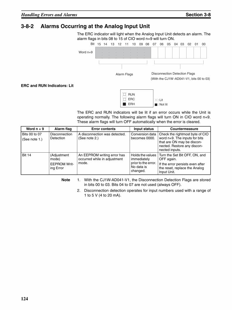
Handling Errors and Alarms Section 3-8
3-8-2 Alarms Occurring at the Analog Input UnitThe ERC indicator will light when the Analog Input Unit detects an alarm. Thealarm flags in bits 08 to 15 of CIO word n+9 will turn ON.
ERC and RUN Indicators: Lit
The ERC and RUN indicators will be lit if an error occurs while the Unit isoperating normally. The following alarm flags will turn ON in CIO word n+9.These alarm flags will turn OFF automatically when the error is cleared.
Note 1. With the CJ1W-AD041-V1, the Disconnection Detection Flags are storedin bits 00 to 03. Bits 04 to 07 are not used (always OFF).
2. Disconnection detection operates for input numbers used with a range of1 to 5 V (4 to 20 mA).
15 14 13 12 11 10 09 08 07 06 05 04 03 02 01 00Bit
Word n+9
Disconnection Detection FlagsAlarm Flags(With the CJ1W-AD041-V1, bits 00 to 03)
RUN
ERC
ERH: Lit: Not lit
Word n + 9 Alarm flag Error contents Input status Countermeasure
Bits 00 to 07
(See note 1.)
Disconnection Detection
A disconnection was detected. (See note 2.)
Conversion data becomes 0000.
Check the rightmost byte of CIO word n+9. The inputs for bits that are ON may be discon-nected. Restore any discon-nected inputs.
Bit 14 (Adjustment mode)EEPROM Writ-ing Error
An EEPROM writing error has occurred while in adjustment mode.
Holds the values immediately prior to the error. No data is changed.
Turn the Set Bit OFF, ON, and OFF again.If the error persists even after the reset, replace the Analog Input Unit.
124

Handling Errors and Alarms Section 3-8
ERC Indicator and RUN Indicator: Lit, ADJ Indicator: Flashing
This alarm will occur in the case of incorrect operation while in the adjustmentmode. In adjustment mode, the Adjustment Mode ON Flag will turn ON in bit15 of CIO word n+9.
Note 1. When a PLC error occurs in the adjustment mode, the Unit will stop oper-ating. (The input values immediately prior to the error are held.)
2. The operating mode can be set either with the DIP switch or with bits 00 to07 of D (m+18).
ERC Indicator: Lit, RUN Indicator: Not Lit
The ERC indicator will be lit when the initial settings for the Analog Input Unitare not set correctly. The following alarm flags will turn ON in CIO word n+9.These alarm flags will turn OFF when the error is cleared and the Unit isrestarted, or the Special I/O Unit Restart Bit is turned ON and then OFFagain.
RUN
ERC: Lit
ADJERH
: Flashing: Not lit
Word n + 9 Alarm flag Error contents Input status Countermeasure
Bit 12 (Adjustment mode)
Input Value Adjustment Range Exceeded
In adjustment mode, offset or gain cannot be adjusted because input value is out of the permissible range for adjust-ment.
Conversion data corresponding to the input sig-nal is monitored in word n+8.
If making the adjustment by means of a connected input device, first adjust the input device before adjusting the Ana-log Input Unit.
Bit 13 (Adjustment mode)
Input Number Setting Error
In adjustment mode, adjust-ment cannot be performed because the specified input number is not set for use or because the wrong input num-ber is specified.
Holds the values immediately prior to the error. No data is changed.
Check whether the word n input number to be adjusted is set from 21 to 28 (21 to 24 for CJ1W-AD041-V1.)Check whether the input number to be adjusted is set for use by means of the DM setting.
Bit 15 only ON (Adjustment Mode)
PLC Error (See note 1.)
The PLC is in either MONITOR or RUN mode while the Analog Input Unit is operating in adjust-ment mode.
Holds the values immediately prior to the error. No data is changed.
Switch the front panel DIP switch pin to OFF. Restart the Unit in normal mode. (See note 2.)
RUN
ERC
ERH: Lit
: Not lit
Word n + 9 Alarm flag Error contents Input status Countermeasure
Bit 11 Mean Value Processing Set-ting Error
The wrong number of samplings has been specified for mean processing.
Conversion does not start and data becomes 0000.
Specify a number from 0000 to 0006.
125

Handling Errors and Alarms Section 3-8
3-8-3 Errors in the CPU UnitThe ERH indicator will light if an error occurs in the CPU Unit or I/O bus and I/O refreshing with the Special I/O Units is not performed correctly, preventingthe Analog Input Unit from operating.
ERH and RUN Indicators: Lit
The ERH and RUN indicators will be lit if an error occurs in the I/O bus caus-ing a WDT (watchdog timer) error in the CPU Unit, resulting in incorrect I/Orefresh with the Analog Input Unit.
Turn ON the power supply again or restart the system.For further details, refer to CJ-series CJ1G-CPU@@, CJ1G/H-CPU@@H Pro-grammable Controllers Operation Manual (W393).
ERH Indicator: Lit, RUN Indicator: Not Lit
The unit number for the Analog Input Unit has not been set correctly.
RUN
ERC
ERH: Lit
: Not lit
Error Error contents Input status
I/O bus error Error has occurred during data exchange with the CPU Unit.
Conversion data becomes 0000.
CPU Unit monitoring error (see note)
No response from CPU Unit dur-ing fixed period.
Maintains the condition existing before the error.
CPU Unit WDT error Error has been generated in CPU Unit.
Changes to undefined state.
RUN
ERC
ERH: Lit
: Not lit
Error Error contents Input status
Duplicate Unit Number The same unit number has been assigned to more than one Unit or the unit number was set to a value other than 00 to 95.
Conversion does not start and data becomes 0000.
Special I/O Unit Setting Error The Special I/O Units registered in the I/O table are different from the ones actually mounted.
126

Handling Errors and Alarms Section 3-8
3-8-4 Restarting Special I/O UnitsTo restart the Analog Input Unit after changing the contents of the DM Area orcorrecting an error, cycle the power to the PLC or turn ON the Special I/O UnitRestart Bit.
Special I/O Unit Restart Bits
The previous conversion data will be held while the Unit is being restarted.
Note If the error is not cleared even after turning the Special I/O Unit Restart Bit ONand then OFF again, then replace the Unit.
3-8-5 TroubleshootingThe following tables explain the probable causes of troubles that may occur,and the countermeasures for dealing with them.
Conversion Data Does Not Change
Value Does Not Change as Intended
Conversion Values are Inconsistent
Bits Functions
A50200 Unit #0 Restart Bit Turning the Restart Bit for any Unit ON and then OFF again restarts that Unit.
A50201 Unit #1 Restart Bit
to to
A50215 Unit #15 Restart Bit
A50300 Unit #16 Restart Bit
to to
A50715 Unit #95 Restart Bit
Probable cause Countermeasure Page
The input is not set for being used. Set the input to be used. 106
The peak value hold function is in operation.
Turn OFF the peak value hold func-tion if it is not required.
112
The input device is not working, the input wiring is wrong, or there is a disconnection.
Using a tester, check to see if the input voltage or current is changing.
---
Use Unit’s alarm flags to check for a disconnection.
124
Probable cause Countermeasure Page
The input device’s signal range does not match the input signal range for the relevant input number at the Analog Input Unit.
Check the specifications of the input device, and match the settings for the input signal ranges.
80
The offset and gain are not adjusted.
Adjust the offset and gain. 114
When using the 4 mA to 20 mA range, the voltage/current switch is not turned ON.
Turn ON the voltage/current switch. 94
Probable cause Countermeasure Page
The input signals are being affected by external noise.
Change the shielded cable connec-tion to the Unit’s COM terminal.
98
Insert a 0.01-µF to 0.1-µF ceramic capacitor or film capacitor between the input’s (+) and (–) terminals.
---
Try increasing the number of mean value processing buffers.
109
127

Handling Errors and Alarms Section 3-8
128

SECTION 4CJ-series Analog Input Units (CJ1W-AD042)
This section explains how to use the CJ1W-AD042 Analog Input Units.
4-1 Specifications . . . . . . . . . . . . . . . . . . . . . . . . . . . . . . . . . . . . . . . . . . . . . . . . . 130
4-1-1 Specifications . . . . . . . . . . . . . . . . . . . . . . . . . . . . . . . . . . . . . . . . . . 130
4-1-2 Input Function Block Diagram . . . . . . . . . . . . . . . . . . . . . . . . . . . . . 132
4-1-3 Inputs Specifications. . . . . . . . . . . . . . . . . . . . . . . . . . . . . . . . . . . . . 132
4-2 Operating Procedure . . . . . . . . . . . . . . . . . . . . . . . . . . . . . . . . . . . . . . . . . . . . 135
4-3 Components and Switch Settings . . . . . . . . . . . . . . . . . . . . . . . . . . . . . . . . . . 140
4-3-1 Component Names . . . . . . . . . . . . . . . . . . . . . . . . . . . . . . . . . . . . . . 140
4-3-2 Indicators . . . . . . . . . . . . . . . . . . . . . . . . . . . . . . . . . . . . . . . . . . . . . 141
4-3-3 Unit Number Switches . . . . . . . . . . . . . . . . . . . . . . . . . . . . . . . . . . . 141
4-4 Wiring . . . . . . . . . . . . . . . . . . . . . . . . . . . . . . . . . . . . . . . . . . . . . . . . . . . . . . . 142
4-4-1 Terminal Arrangement . . . . . . . . . . . . . . . . . . . . . . . . . . . . . . . . . . . 142
4-4-2 Internal Circuitry . . . . . . . . . . . . . . . . . . . . . . . . . . . . . . . . . . . . . . . 143
4-4-3 Voltage Input Disconnection. . . . . . . . . . . . . . . . . . . . . . . . . . . . . . . 144
4-4-4 Input Wiring Example . . . . . . . . . . . . . . . . . . . . . . . . . . . . . . . . . . . 144
4-4-5 Input Wiring Considerations. . . . . . . . . . . . . . . . . . . . . . . . . . . . . . . 146
4-5 Exchanging Data with the CPU Unit . . . . . . . . . . . . . . . . . . . . . . . . . . . . . . . 147
4-5-1 Outline of Data Exchange. . . . . . . . . . . . . . . . . . . . . . . . . . . . . . . . . 147
4-5-2 Allocations for Initial Settings Data . . . . . . . . . . . . . . . . . . . . . . . . . 149
4-5-3 I/O Refresh Data Allocations . . . . . . . . . . . . . . . . . . . . . . . . . . . . . . 152
4-6 Analog Input Functions and Operating Procedures . . . . . . . . . . . . . . . . . . . . 155
4-6-1 Input Settings and Conversion Values . . . . . . . . . . . . . . . . . . . . . . . 155
4-6-2 Conversion Mode Setting . . . . . . . . . . . . . . . . . . . . . . . . . . . . . . . . . 156
4-6-3 Mean Value Processing. . . . . . . . . . . . . . . . . . . . . . . . . . . . . . . . . . . 158
4-6-4 Input Scaling Function . . . . . . . . . . . . . . . . . . . . . . . . . . . . . . . . . . . 160
4-6-5 Peak Value Hold Function . . . . . . . . . . . . . . . . . . . . . . . . . . . . . . . . 162
4-6-6 Input Disconnection Detection Function . . . . . . . . . . . . . . . . . . . . . 163
4-7 Handling Errors and Alarms . . . . . . . . . . . . . . . . . . . . . . . . . . . . . . . . . . . . . . 164
4-7-1 Indicators and Error Flowchart . . . . . . . . . . . . . . . . . . . . . . . . . . . . . 164
4-7-2 Alarms Occurring at the Analog Input Unit . . . . . . . . . . . . . . . . . . . 166
4-7-3 Errors in the CPU Unit . . . . . . . . . . . . . . . . . . . . . . . . . . . . . . . . . . . 167
4-7-4 Restarting Special I/O Units . . . . . . . . . . . . . . . . . . . . . . . . . . . . . . . 168
4-7-5 Troubleshooting . . . . . . . . . . . . . . . . . . . . . . . . . . . . . . . . . . . . . . . . 168
129

Specifications Section 4-1
4-1 Specifications
4-1-1 SpecificationsUnit model CJ1W-AD042
Unit type CJ-series Special I/O Unit
Isolation (See note 1.) Between inputs and PLC signals: Digital isolator (No isolation between input sig-nals.)
External terminals 18-point detachable terminal block (M3 screws)
Affect on CPU Unit cycle time CJ2 CPU Unit 0.05 ms
CJ1 CPU Unit 0.2 ms
Current consumption 520 mA at 5 VDC
Dimensions (mm) (See note 2.) 31 × 90 × 65 (W × H × D)
Weight 150 g max.
General specifications Conforms to general specifications for SYSMAC CJ Series.
Mounting position CJ-series CPU Rack or CJ-series Expansion Rack
Maximum number of Units Per CPU Rack or Expansion Rack (See note 3.)
Power Supply Unit No. of mountable Units
CJ1W-PA205RCJ1W-PA205CCJ1W-PD025
CPU Rack: 8 Units/Rack Expansion Rack: 9 Units/Rack
CJ1W-PA202 CPU Rack: 4 Units/Rack Expansion Rack: 5 Units/Rack
CJ1W-PD022 CPU Rack: 3 Units/Rack Expansion Rack: 3 Units/Rack
Data exchange with CPU Unit (See note 4.)
Special I/O Unit Area in CIO Area (CIO 2000 to CIO 2959): 10 words/Unit Special I/O Unit Area in DM Area (D20000 to D29599): 100 words/Unit
Inputs specifica-tions
Number of analog inputs 4
Input signal range (See note 5.)
1 to 5 V/0 to 10 V/−5 to 5 V/−10 to 10 V/4 to 20 mA (See note 6.)
Maximum rated input (See note 7.)
Voltage Input: ±15 V Current Input: ±30 mA
Input impedance Voltage Input: 1 MΩ min. Current Input: 250 Ω (typical)
Resolution 1 to 5 V 1/10,000 (full scale)
0 to 10 V 1/20,000 (full scale)
−5 to 5 V 1/20,000 (full scale)
−10 to 10 V 1/40,000(full scale)
4 to 20 mA 1/10,000(full scale)
A/D conversion data 16-bit binary data
Accuracy 25°C Voltage Input: ±0.2% of full scale Current Input: ±0.4% of full scale
0 to 55°C Voltage Input: ±0.4% of full scale Current Input: ±0.6% of full scale
Conversion period (See note 8.)
20 µs for 1 point, 25 µs for 2 points, 30 µs for 3 points, 35 µs for 4 points
130

Specifications Section 4-1
Note 1. Do not apply a voltage higher than 600 VAC to the terminal block when per-forming withstand voltage test on this Unit. Otherwise, internal elementsmay deteriorate.
2. Refer to page 439 for Unit dimensions.
3. This is the maximum number of Units that can be mounted to a CJ2H-CPU6@ CPU Unit (no EtherNet/IP). The maximum number of Analog InputUnits that can be mounted to one Rack varies depending on the currentconsumption of the other Units mounted to the Rack.
4. Data exchange methods with the CPU Unit are as follows:
5. Input signal ranges can be set for each input.
6. To use a current input, connect the positive current input terminal and pos-itive voltage input terminal with the enclosed short bar.
7. The Analog Input Unit must be operated according to the input specifica-tions provided here. Operating the Unit outside these specifications willcause the Unit to malfunction.
8. The A/D conversion period is the time it takes for an analog signal to bestored in memory in the Analog Input Unit as converted data after it hasbeen input. With direct conversion, A/D conversion can be performed andthe results read within the processing time of the ANALOG INPUT DIREC-TION CONVERSION (AIDC) instruction. With cyclic conversion, it takes atleast one cycle before the converted data is read by the CPU Unit.
9. Input disconnection detection is supported only when the range is set to 1to 5 V or 4 to 20 mA. If there is no input signal when the 1 to 5-V or 4 to 20-mA range is set, the Disconnection Detection Flag will turn ON.
Input functions
Mean value processing Stores the last “n” data conversions in the buffer, and stores the mean value of the conversion values. (Number of mean value buffers n = 2, 4, 8, 16, 32, 64,128, 256, or 512)
Peak value hold Stores the maximum conversion value (including mean value processing) while the Peak Value Hold Bit is ON.
Scaling Setting values in any specified unit within a range of ±32,000 as the upper and lower limits allows A/D conversion to be executed and analog signals to be output using the set values as full scale.
Input disconnection detection
Detects a disconnection and turns ON the Disconnection Detection Flag. (See note 9.)
Direct conversion A/D conversion is performed and the converted value is refreshed immediately when the ANALOG INPUT DIRECT CONVERSION (AIDC) instruction is executed.
A CJ2H-CPU@@(-EIP) CPU Unit with unit version 1.1 or later is required to use direct conversion.
Special I/O Unit Area in CIO Area (CIO 2000 to CIO 2959, CIO 2000.00 to CIO 2959.15)
10 words transferred per Unit
CPU Unit to Analog Input Unit Peak value hold function
Analog Input Unit to CPU Unit • Conversion value• Input disconnection detection• Alarm flags, etc.
Special I/O Unit Area in DM Area (D20000 to D29599)
100 words per Unit trans-ferred at startup or restart
CPU Unit to Analog Input Unit • Number of analog inputs used• Conversion mode setting• Input signal range setting• Number of mean value buffers• Scaling lower and upper limits
131

Specifications Section 4-1
4-1-2 Input Function Block Diagram
4-1-3 Inputs SpecificationsIf signals that are outside the specified range provided below are input, theconversion values (16-bit binary data) used will be either the maximum orminimum value.
Range: 1 to 5 V
A/D
Analog Input Units CPU Unit
Analog input 1
Special I/O Unit Area
Analog input 2
Analog input 3
Analog input 4
Same as above.
Same as above.
Same as above.
Input discon-nection detection
Mean value processing disabled
Mean value processing enabled
Valid only in Cyclic Conversion Mode.
Scaling enabled
Scaling disabled
Peak value hold disabled
Peak value hold enabled
Valid only for Cyclic Conversion Mode.
Conversion value for analog input 1
2904 hex 2710 hex
0000 hex FE0C hex
0.8 V1 V 5 V
5.2 VAnalog input signal
Conversion value
Resolution: 10,000
132
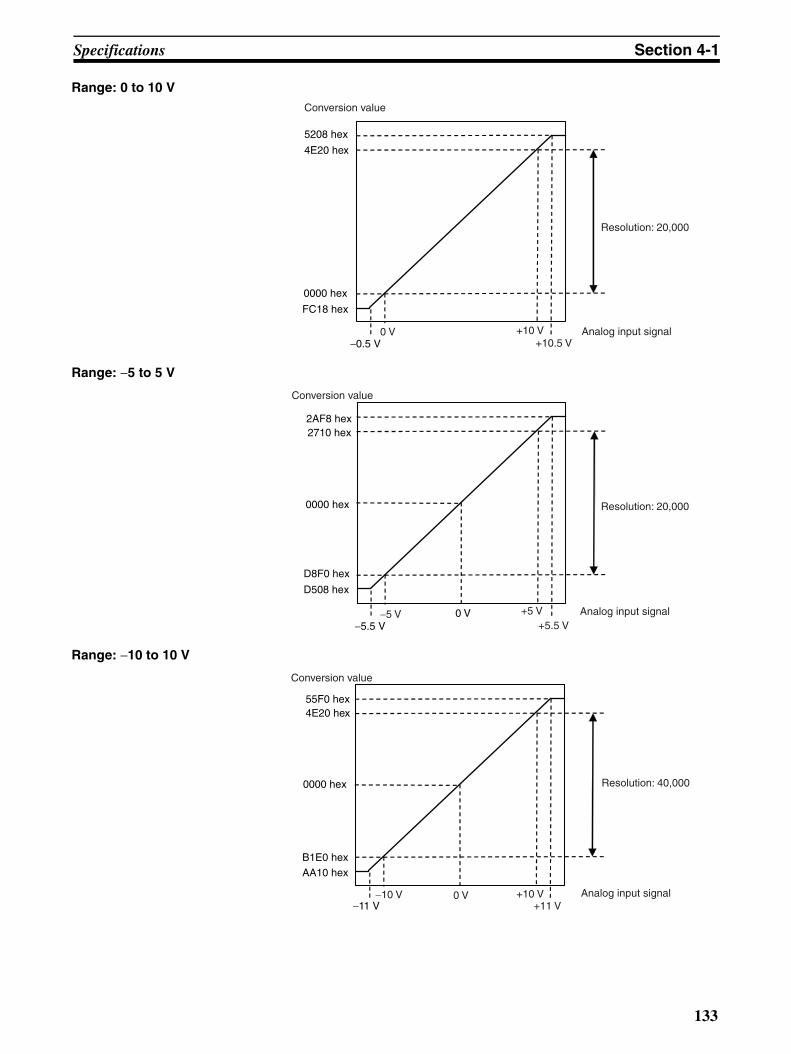
Specifications Section 4-1
Range: 0 to 10 V
Range: −5 to 5 V
Range: −10 to 10 V
5208 hex
4E20 hex
0000 hex
FC18 hex
−0.5 V 0 V +10 V
+10.5 VAnalog input signal
Conversion value
Resolution: 20,000
0 V
2AF8 hex 2710 hex
0000 hex
D8F0 hex
D508 hex
−5.5 V −5 V +5 V
+5.5 VAnalog input signal
Conversion value
Resolution: 20,000
55F0 hex 4E20 hex
0000 hex
B1E0 hex AA10 hex
−11 V−10 V 0 V +10 V
+11 VAnalog input signal
Resolution: 40,000
Conversion value
133

Specifications Section 4-1
Range: 4 to 20 mA
Note The conversion values for a range of −10 to 10 V will be as follows (for a reso-lution of 40,000):
2904 hex 2710 hex
0000 hex FE0C hex
3.2 mA 4 mA 20 mA
20.8 mAAnalog input signal
Conversion value
Resolution: 10,000
16-bit binary data BCD
AA10 –22,000
: :
FFFF –1
0000 0
0001 1
: :
55F0 22,000
134

Operating Procedure Section 4-2
4-2 Operating ProcedureFollow the procedure outlined below when using Analog Input Units.
Installation and Settings
1,2,3... 1. Use the unit number switches on the front panel of the Unit to set the unitnumber.
2. Wire the Unit.
3. Turn ON the power to the PLC.
4. Create the I/O tables.
5. Make the Special I/O Unit settings in the DM Area.
• Set the number of analog inputs to be used.
• Set the conversion mode.
• Set the input signal ranges.
• Set the number of mean value buffers.
• Set upper and lower limits for scaling.
6. Turn the power to the PLC OFF and ON, or turn ON the Special I/O UnitRestart Bit.
Operation
1,2,3... 1. Ladder program
• Read conversion values or write set values by means of MOV(021)and XFER(070).
• Specify the peak hold function.
• Obtain disconnection notifications and error codes.
Procedure ExamplesAn example application procedure is given below.
CJ1W-AD042
D00100
D00101
D00102
D00103
AD042
B1 A1
MACHNo.x10 1
x10 0
RUNERCERH
CPU UnitLa
dder
pro
gramIN1: 1 to 5 V
IN2: 4 to 20 mA
IN3: 0 to 10 V
IN4: −10 to 10 V
Unit No.: 1
In Cyclic Conversion Mode, A/D conversion is performed once each conversion cycle, the same way as it is for the CJ1W-AD041-V1/AD081-V1.
Analog inputs
Cyclic Conversion Mode*
*
135
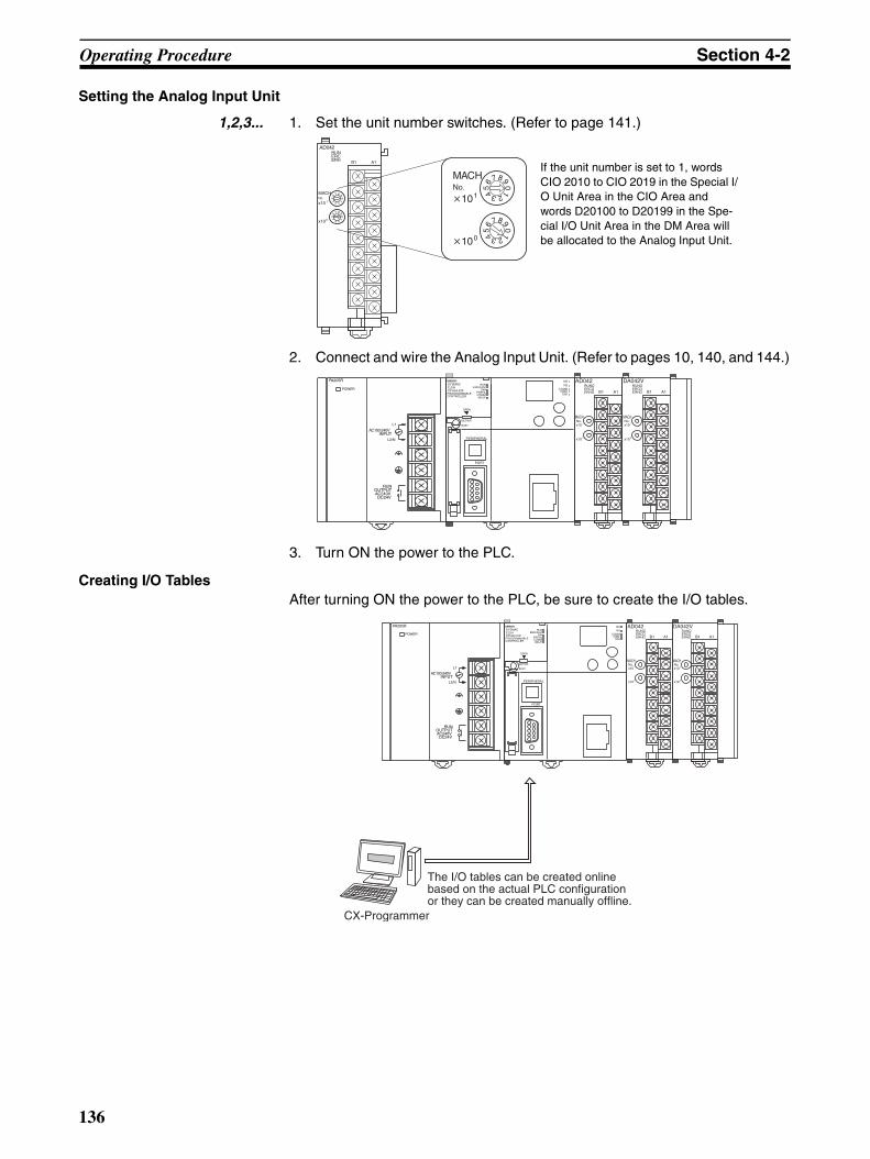
Operating Procedure Section 4-2
Setting the Analog Input Unit
1,2,3... 1. Set the unit number switches. (Refer to page 141.)
2. Connect and wire the Analog Input Unit. (Refer to pages 10, 140, and 144.)
3. Turn ON the power to the PLC.
Creating I/O TablesAfter turning ON the power to the PLC, be sure to create the I/O tables.
MACHNo.
AD042RUNERCERH B1 A1
x10 1
x10 0
09
8765 4 321
09
8765 4 321
MACHNo.
101
100
09876
5 4 3210
98765 4 321
If the unit number is set to 1, words CIO 2010 to CIO 2019 in the Special I/O Unit Area in the CIO Area and words D20100 to D20199 in the Spe-cial I/O Unit Area in the DM Area will be allocated to the Analog Input Unit.
POWER
PA205R
DC24VAC240VOUTPUT
RUN
INPUTAC100-240V
L2/N
L1
CONTROLLERPROGRAMMABLE
ERR/ALMRUN
COMMBKUP
INHPRPHL
PERIPHERAL
BUSY
MCPWR
PORT
CJ2HCPU64-EIP
SYSMAC NSMS
100M10M
COMM
AD042
B1 A1
MACHNo.x10 1
x10 0
DA042V
B1 A1
MACHNo.x10 1
x10 0
OPEN
POWER
PA205R
DC24VAC240VOUTPUT
RUN
INPUTAC100-240V
L2/N
L1
CONTROLLERPROGRAMMABLE
ERR/ALMRUN
COMMBKUP
INHPRPHL
PERIPHERAL
BUSY
MCPWR
PORT
CJ2HCPU64-EIP
SYSMAC NSMS
100M10M
COMM
AD042
B1 A1
MACHNo.x10 1
x10 0
DA042V
B1 A1
MACHNo.x10 1
x10 0
OPEN
CX-Programmer
The I/O tables can be created online based on the actual PLC configuration or they can be created manually offline.
136

Operating Procedure Section 4-2
Initial Data Settings
1,2,3... 1. Specify the Special I/O Unit settings in the DM Area. (Refer to page 149.)
Setting Examples
• Unit number: 1
• Cyclic Conversion Mode
• Analog input 1: 1 to 5 V Analog input 2: 4 to 20 mA Analog input 3: 0 to 10 V Analog input 4: −10 to 10 V
a) Set the number of analog inputs to use. (Refer to page 155.)
b) Set the conversion mode. (Refer to page 156.)
c) Set the input signal ranges. (Refer to page 155.)
1. Input Signal Range Setting for Input 1
2. Input Signal Range Setting for Input 2
3. Input Signal Range Setting for Input 3
4. Input Signal Range Setting for Input 4
15 14 13 12 11 10 09 08 07 06 05 04 03 02 01 00
0 0 0 0 0 0 0 0 0 0 0 0 0 1 0 0m: D20100 (0004 hex)
Bit
Set to “4” to indicate that four inputs will be used (inputs 1, 2, 3, and 4).
15 14 13 12 11 10 09 08 07 06 05 04 03 02 01 00
0 0 0 0 0 0 0 0 0 0 0 0 0 0 0 0m+1: D20101 (0000 hex)
Bit
Cyclic Conversion Mode: Set to 00.
15 14 13 12 11 10 09 08 07 06 05 04 03 02 01 00
0 0 0 0 0 0 0 0 0 0 0 0 0 1 1 1
m+2: D20102 (0007 hex)
Bit
Input 1: 1 to 5 V. Set to 7.
15 14 13 12 11 10 09 08 07 06 05 04 03 02 01 00
0 0 0 0 0 0 0 0 0 0 0 0 0 0 1 1 m+6: D20106 (0003 hex)
Bit
Input 2: 4 to 20 mA. Set to 3.
15 14 13 12 11 10 09 08 07 06 05 04 03 02 01 00
0 0 0 0 0 0 0 0 0 0 0 0 0 0 1 0
m+10: D20110 (0002 hex)
Bit
Input 3: 0 to 10 V. Set to 2.
15 14 13 12 11 10 09 08 07 06 05 04 03 02 01 00
0 0 0 0 0 0 0 0 0 0 0 0 0 0 0 0
m+14: D20114 (0000 hex)
Bit
Input 4: -10 to 10 V. Set to 0.
137

Operating Procedure Section 4-2
2. Cycle the power to the PLC.
Creating Ladder Programs
The data that is converted from analog to digital and output to CIO words (n +1) to (n+ 4) of the Special I/O Unit Area (CIO 2011 to CIO 2014), is stored inthe specified addresses D00100 to D00103 as signed binary values 0000 to0FA0 hex.
Analog Inputs
Note 1. The addresses are determined by the unit number of the Special I/O Unit.(Refer to page 141.)
POWER
PA205R
DC24VAC240VOUTPUT
RUN
INPUTAC100-240V
L2/N
L1
CONTROLLERPROGRAMMABLE
ERR/ALMRUN
COMMBKUP
INHPRPHL
PERIPHERAL
BUSY
MCPWR
PORT
CJ2HCPU64-EIP
SYSMAC NSMS
100M10M
COMM
AD042
B1 A1
MACHNo.x10 1
x10 0
DA042V
B1 A1
MACHNo.x10 1
x10 0
OPEN
Power turned ON again (or Special I/O Unit Restart Bit is turned ON).
POWER
PA205R
DC24VAC240VOUTPUT
RUN
INPUTAC100-240V
L2/N
L1
CONTROLLERPROGRAMMABLE
ERR/ALMRUN
COMMBKUP
INHPRPHL
PERIPHERAL
BUSY
MCPWR
PORT
CJ2HCPU64-EIP
SYSMAC NSMS
100M10M
COMM
AD042
B1 A1
MACHNo.x10 1
x10 0
DA042V
B1 A1
MACHNo.x10 1
x10 0
OPEN
CX-Programmer
Input number Input signal range Input conversion value address(n = CIO 2010) (See note 1.)
Conversion data holding address
(See note 2.)
1 1 to 5 V n+1 = CIO 2011 D00100
2 4 to 20 mA n+2 = CIO 2012 D00101
3 0 to 10 V n+3 = CIO 2013 D00102
4 −10 to 10 V n+4 = CIO 2014 D00103
138

Operating Procedure Section 4-2
2. Set as required.
3. Bits 00 to 03 of word (n + 9) are allocated to the Input Disconnection De-tection Flags. (Refer to page 163.)
MOV(021)2011
D00100
MOV(021)2012
D00101
MOV(021)2013
D00102
MOV(021)2014
D00103
2019.00
2019.01
P_On
P_On
If there is no disconnection (i.e., if CIO 2019.00 is OFF), the contents of CIO 2011 is stored in D00100.
In the same way, for 4 to 20 mA, CIO 2012 will be stored in D00101.
In the same way, for 0 to 10 V, CIO 2013 will be stored in D00102.
In the same way, for −10 to 10 V, CIO 2014 will be stored in D00103.
(Input 1 Disconnection Detection Flag)*3
(Input 2 Disconnection Detection Flag)*3
(Always ON Flag)
(Always ON Flag)
139

Components and Switch Settings Section 4-3
4-3 Components and Switch Settings
4-3-1 Component Names
Note 1. The terminal block is attached using a connector. It can be removed by low-ering the lever at the bottom of the terminal block.
2. The lever must normally be in the raised position. Confirm this before op-eration.
MACHNo.
AD042RUNERCERH B1 A1
x101
x100
09
8765 4 321
09
8765 4 321
Indicators
SideSlider
Slider
FrontWith Terminal Block
Expansion connector
Terminal block
Unit number switches
Terminal block lock lever (pull down to release terminal block)
DIN Track mounting pin
B1A1AD042
MACH
No.10
1
100
RUNERCERH
140
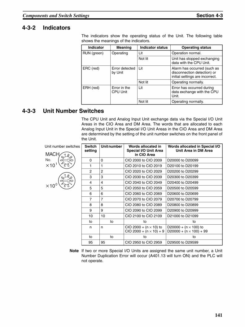
Components and Switch Settings Section 4-3
4-3-2 IndicatorsThe indicators show the operating status of the Unit. The following tableshows the meanings of the indicators.
4-3-3 Unit Number SwitchesThe CPU Unit and Analog Input Unit exchange data via the Special I/O UnitAreas in the CIO Area and DM Area. The words that are allocated to eachAnalog Input Unit in the Special I/O Unit Areas in the CIO Area and DM Areaare determined by the setting of the unit number switches on the front panel ofthe Unit.
Note If two or more Special I/O Units are assigned the same unit number, a UnitNumber Duplication Error will occur (A401.13 will turn ON) and the PLC willnot operate.
Indicator Meaning Indicator status Operating status
RUN (green) Operating Lit Operation normal.
Not lit Unit has stopped exchanging data with the CPU Unit.
ERC (red) Error detected by Unit
Lit Alarm has occurred (such as disconnection detection) or initial settings are incorrect.
Not lit Operating normally.
ERH (red) Error in the CPU Unit
Lit Error has occurred during data exchange with the CPU Unit.
Not lit Operating normally.
Unit number switches Switch setting
Unit number Words allocated in Special I/O Unit Area
in CIO Area
Words allocated in Special I/O Unit Area in DM Area
0 0 CIO 2000 to CIO 2009 D20000 to D20099
1 1 CIO 2010 to CIO 2019 D20100 to D20199
2 2 CIO 2020 to CIO 2029 D20200 to D20299
3 3 CIO 2030 to CIO 2039 D20300 to D20399
4 4 CIO 2040 to CIO 2049 D20400 to D20499
5 5 CIO 2050 to CIO 2059 D20500 to D20599
6 6 CIO 2060 to CIO 2069 D20600 to D20699
7 7 CIO 2070 to CIO 2079 D20700 to D20799
8 8 CIO 2080 to CIO 2089 D20800 to D20899
9 9 CIO 2090 to CIO 2099 D20900 to D20999
10 10 CIO 2100 to CIO 2109 D21000 to D21099
to to to to
n n CIO 2000 + (n × 10) to CIO 2000 + (n × 10) + 9
D20000 + (n × 100) to D20000 + (n × 100) + 99
to to to to
95 95 CIO 2950 to CIO 2959 D29500 to D29599
MACHNo.
101
100
09
8765 4 321
09876
5 4 321
141

Wiring Section 4-4
4-4 Wiring
!Caution Always connect surge suppressors to inductive loads in the system (e.g.,magnetic contactors, relays, and solenoids). Always separate devices thatgenerate surge from the Analog Input Unit. Faulty Unit operation may causeunexpected system operation.
If inductive loads are connected to output signals from Relay Contact OutputUnits, connect a surge suppressor in an AC circuit and a diode in a DC circuitclose to the inductive load to absorb the back electromotive force.
4-4-1 Terminal ArrangementThe signal names corresponding to the connecting terminals are as shown inthe following diagram.
* To use a current input, connect the positive current input terminal andpositive voltage input terminal with the enclosed short bar.
Note 1. The number of analog inputs that can be used is set in the DM Area.
2. The input signal ranges for individual inputs are set in the DM Area. Theinput signal range can be set separately for each input.
3. The AG terminals are connected to the 0-V analog circuit in the Unit. Con-necting the input line shield can improve noise resistance.
4. Do not make any connections to the NC terminals.
Connect a surge suppressor in an AC circuit and a diode in a DC circuit.
Inductive load
PLC Output Unit
Inductive load
PLC Output Unit
N.C.
AG
B1
B2
B3
B4
B5
B6
B7
B8
B9
A1
A2
A3
A4
A5
A6
A7
A8
A9
Current input 2 (+)
Voltage input 2 (+)
AG
Current input 4 (+)
Voltage input 4 (+)
AG
NC
Current input 1 (+)
Voltage input 1 (+)
Current input 3 (+)
Voltage input 3 (+)
AG
142
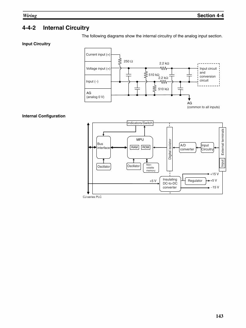
Wiring Section 4-4
4-4-2 Internal CircuitryThe following diagrams show the internal circuitry of the analog input section.
Input Circuitry
Internal Configuration
2.2 kΩ
2.2 kΩ
250 Ω
510 kΩ
510 kΩ
Current input (+)
Input (−)
Input circuit and conversion circuit
Voltage input (+)
AG (analog 0 V)
AG (common to all inputs)
MPU
RAM ROM
+15 V
+5 V
−15 V
+5 V
Indicators/Switch
Oscillator Oscillator
Insulating DC-to-DC converter
Regulator
Dig
ital i
sola
tor
Ext
erna
l ter
min
als
Inpu
t
Non- volatile memory
Bus interface
CJ-series PLC
Input Circuitry
A/D converter
143

Wiring Section 4-4
4-4-3 Voltage Input Disconnection
When voltage inputs are used and a disconnection occurs, separate thepower supply at the side of the connected devices or use an insulating device(isolator) for each input to avoid the following problems.
When the power supply at the connected devices is shared and section a or bis disconnected, power will flow in the direction of the dotted line and the out-put voltage of the other connected devices will be reduced to between a thirdto a half of the voltage. If 1 to 5 V is used and the reduced voltage occurs, dis-connection may not be detectable. If section c is disconnected, the power atthe negative input terminal will be shared and disconnection will not be detect-able.
For current inputs, sharing the power supply between the connected deviceswill not cause any problems.
4-4-4 Input Wiring Example Wiring Example for a Voltage Input
Connected device 1
Connected device 2
24 VDC
Input 2Input 1
Input 4Input 3
*
*
*
*
144

Wiring Section 4-4
Wiring Example for a Current Input
* Connect the positive current input terminal and positive voltage input ter-minal with the enclosed short bar.
Note Crimp terminals must be used for terminal connections, and the screws mustbe tightened securely. Use M3 screws and tighten them to a torque of 0.5 N·m.
Note 1. Set the number of analog inputs to be used so that unused inputs are setso that they are not used. (Refer to pages 150 and 155.) If an input that isnot used is set to be used, the input data for it may be unstable. The inputdata can be made stable by cross-connecting the voltage input terminals(V+) and (V−). However, if these terminals are connected and the inputsare set for the 1 to 5-V or 4 to 20-mA range, the Disconnection DetectionFlag will turn ON.
2. When connecting the shield of the analog input cable* to the Unit’s AG ter-minal, as shown in the above diagram, use a wire that is 30 cm or shorterif possible.
3. Do not connect anything to NC terminals shown in the wiring diagram onpage 142.
4. Connect the analog input line shield to the AG terminal on the Analog InputUnit to improve noise resistance.
Input 2 Input 1
Input 4Input 3
*
*
*
*
Round type
6.2 mm max.
Fork type
6.2 mm max.
M3 screw
145

Wiring Section 4-4
4-4-5 Input Wiring ConsiderationsWhen wiring inputs, apply the following points to avoid noise interference andoptimize Analog Input Unit performance.
• Use two-core shielded twisted-pair cables for input connections.
• Route input cables separately from power cables (e.g., AC and three-phase lines), and do not place them in the same duct with power cables.
• If there is noise interference from power lines (if, for example, the powersupply is shared with electrical welding devices or electrical dischargemachines, or if there is a high-frequency generation source nearby),install a noise filter at the power supply input.
146

Exchanging Data with the CPU Unit Section 4-5
4-5 Exchanging Data with the CPU Unit
4-5-1 Outline of Data ExchangeData is exchanged between the CPU Unit and the CJ1W-AD042 Analog InputUnit via the Special I/O Unit Area in the CIO Area (for data used to operate theUnit) and the Special I/O Unit Area in the DM Area (for data used for initial set-tings).
I/O Refresh Data
Analog input conversion values, which are used as data for Unit operation, areallocated in the Special I/O Unit Area in the CIO Area of the CPU Unit accord-ing to the unit number. These exchanged are updated during I/O refreshing.
Initial Settings Data
The Unit’s initial settings, such as the number of analog inputs used, the con-version mode, the analog input signal ranges, and the number of mean valuebuffers, are allocated in the Special I/O Unit Area in the DM Area of the CPUUnit according to the unit number. The settings are exchanged when thepower is turned ON or the Unit is restarted.
Special I/O Unit Area in CIO Area
Input conversion valueInput conversion value
Special I/O Unit Area in DM Area
I/O Refresh Data
Initial Settings Data
CJ-series CPU UnitCJ1W-AD042
Analog Input Unit
Input conversion values exchanged according to conversion mode setting.
I/O refresh period in Cyclic Conversion Mode or at execution of Direct Conversion Instruction in Direct Conversion Mode
Power ON or Unit restart
Refer to page 152.
Initial settings, such as number of analog inputs used, analog input signal ranges, and number of mean value buffers, exchanged.
Refer to page 149.
Number of mean value buffers
Input signal range
Conversion mode setting
Number of analog inputs used
n: Unit number
10 words
100 words
to
to
2000 + (n × 10) + 9
2000 + (n × 10)
D20000 + (n × 100)
D20000 + (n × 100) + 99
147
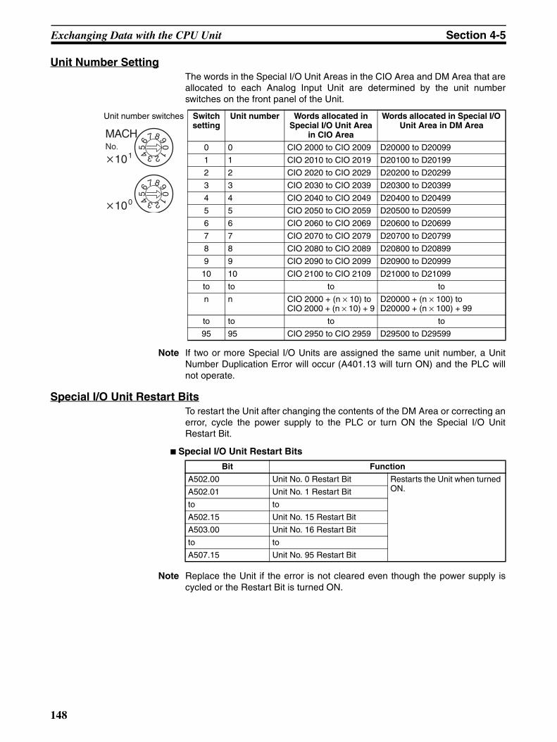
Exchanging Data with the CPU Unit Section 4-5
Unit Number SettingThe words in the Special I/O Unit Areas in the CIO Area and DM Area that areallocated to each Analog Input Unit are determined by the unit numberswitches on the front panel of the Unit.
Note If two or more Special I/O Units are assigned the same unit number, a UnitNumber Duplication Error will occur (A401.13 will turn ON) and the PLC willnot operate.
Special I/O Unit Restart BitsTo restart the Unit after changing the contents of the DM Area or correcting anerror, cycle the power supply to the PLC or turn ON the Special I/O UnitRestart Bit.
Special I/O Unit Restart Bits
Note Replace the Unit if the error is not cleared even though the power supply iscycled or the Restart Bit is turned ON.
Unit number switches Switch setting
Unit number Words allocated in Special I/O Unit Area
in CIO Area
Words allocated in Special I/O Unit Area in DM Area
0 0 CIO 2000 to CIO 2009 D20000 to D20099
1 1 CIO 2010 to CIO 2019 D20100 to D20199
2 2 CIO 2020 to CIO 2029 D20200 to D20299
3 3 CIO 2030 to CIO 2039 D20300 to D20399
4 4 CIO 2040 to CIO 2049 D20400 to D20499
5 5 CIO 2050 to CIO 2059 D20500 to D20599
6 6 CIO 2060 to CIO 2069 D20600 to D20699
7 7 CIO 2070 to CIO 2079 D20700 to D20799
8 8 CIO 2080 to CIO 2089 D20800 to D20899
9 9 CIO 2090 to CIO 2099 D20900 to D20999
10 10 CIO 2100 to CIO 2109 D21000 to D21099
to to to to
n n CIO 2000 + (n × 10) to CIO 2000 + (n × 10) + 9
D20000 + (n × 100) to D20000 + (n × 100) + 99
to to to to
95 95 CIO 2950 to CIO 2959 D29500 to D29599
MACHNo.
101
100
09
8765 4 321
09
8765 4 321
Bit Function
A502.00 Unit No. 0 Restart Bit Restarts the Unit when turned ON.A502.01 Unit No. 1 Restart Bit
to to
A502.15 Unit No. 15 Restart Bit
A503.00 Unit No. 16 Restart Bit
to to
A507.15 Unit No. 95 Restart Bit
148

Exchanging Data with the CPU Unit Section 4-5
4-5-2 Allocations for Initial Settings Data
DM Area The initial settings of the Analog Input Unit are set according to the data allo-cated in the Special I/O Unit Area in the DM Area. Settings, such as the num-ber of analog inputs used, the conversion mode, and the analog input signalranges, must be set in this area.
Note 1. The words in the Special I/O Unit Area in the DM Area that are allocatedto the Analog Input Unit are determined by the setting of the unit numberswitches on the front panel of the Unit. (Refer to page 148.)
2. If two or more Special I/O Units are assigned the same unit number, a UnitNumber Duplication Error will occur (A401.13 will turn ON) and the PLCwill not operate.
D20000 to D20099D20100 to D20199
D20200 to D20299D20300 to D20399
D20400 to D20499D20500 to D20599
D20600 to D20699D20700 to D20799
D20800 to D20899D20900 to D20999D21000 to D21099
D29500 to D29599
D20000 + (n × 100) to D20000 + (n × 100) + 99
Words allocated in Special I/O Unit Area in DM Area
Unit 0Unit 1Unit 2Unit 3Unit 4
Unit 5Unit 6Unit 7Unit 8Unit 9Unit 10
Unit n
Unit 95
CJ1W-AD042 Analog Input Unit
Initial Settings Data
Input 1
Input 2
Input 3
Input 4
Data is automati-cally transferred to each unit when the power is turned ON, or when the Special I/O Unit Restart Bit is turned ON.
CJ-series CPU Unit
Special I/O Unit Area in DM Area
Number of analog inputs usedConversion mode setting
Input signal rangeNumber of mean value buffersScaling lower limitScaling upper limit
Input signal rangeNumber of mean value buffersScaling lower limitScaling upper limit
Input signal rangeNumber of mean value buffersScaling lower limitScaling upper limit
m = 20000 + (unit number × 100)
Input signal rangeNumber of mean value buffersScaling lower limitScaling upper limit
to
to
to
to
D (m)
D (m+1)
D (m+2) to D (m+5)
D (m+6) to D (m+9)
D (m+10) to D (m+13)
D (m+14) to D (m+17)
149

Exchanging Data with the CPU Unit Section 4-5
Allocations in DM AreaThe following table shows the allocation of DM Area words and bits.
Note For the DM Area word addresses, m = D20000 + (unit number × 100).
DM Area word (See note.) Bits
15 14 13 12 11 10 09 08 07 06 05 04 03 02 01 00
D (m) Not used. (Settings are ignored.) Number of analog inputs used
D (m+1) Not used. (Settings are ignored.) Conversion mode setting 00 hex: Cyclic Conversion Mode A5 hex: Direct Conversion Mode
D (m+2) Not used. (Settings are ignored.) Input 1 signal range
D (m+3) Number of mean value buffers for input 1
D (m+4) Input 1 scaling lower limit
D (m+5) Input 1 scaling upper limit
D (m+6) Not used. (Settings are ignored.) Input 2 signal range
D (m+7) Number of mean value buffers for input 2
D (m+8) Input 2 scaling lower limit
D (m+9) Input 2 scaling upper limit
D (m+10) Not used. (Settings are ignored.) Input 3 signal range
D (m+11) Number of mean value buffers for input 3
D (m+12) Input 3 scaling lower limit
D (m+13) Input 3 scaling upper limit
D (m+14) Not used. (Settings are ignored.) Input 4 signal range
D (m+15) Number of mean value buffers for input 4
D (m+16) Input 4 scaling lower limit
D (m+17) Input 4 scaling upper limit
150

Exchanging Data with the CPU Unit Section 4-5
Set Values and Stored Values
Note 1. A CJ2H-CPU@@(-EIP) CPU Unit with unit version 1.1 or later is requiredto use direct conversion. Direct conversion is not supported by CJ1 CPUUnits.
2. Mean value processing cannot be used in Direct Conversion Mode.
Item Contents Page
Number of analog inputs used
0: No inputs used.
1: One input used (input 1 used).
2: Two inputs used (inputs 1 and 2 used).3: Three inputs used (inputs 1, 2, and 3 used).
4: Four inputs used (inputs 1, 2, 3, and 4 used).
155
Conversion mode setting
00 hex: Cyclic Conversion Mode
A5 hex: Direct Conversion Mode (See note 1.)
156
Input signal range 0: −10 to 10 V2: 0 to 10 V
3: 4 to 20 mA
6: −5 to 5 V7: 1 to 5 V
155
Numbers of mean value buffers (See note 2.)
0: Mean value processing not used.
1: Mean value processing with 2 buffers
2: Mean value processing with 4 buffers3: Mean value processing with 8 buffers
4: Mean value processing with 16 buffers
5: Mean value processing with 32 buffers6: Mean value processing with 64 buffers
7: Mean value processing with 128 buffers
8: Mean value processing with 256 buffers9: Mean value processing with 512 buffers
158
Scaling settings Any value other than 0 within range of ±32,000 (8300 hex to 7D00 hex) as long as the upper limit is not equal to the lower limit.
160
151

Exchanging Data with the CPU Unit Section 4-5
4-5-3 I/O Refresh Data AllocationsI/O refresh data for the Analog Input Unit is exchanged according to the allo-cations in the Special I/O Unit Area.
Note 1. The words in the Special I/O Unit Area in the CIO Area that are allocatedto the Analog Input Unit are determined by the setting of the unit numberswitches on the front panel of the Unit. (Refer to pages 141 and 148.)
2. If two or more Special I/O Units are assigned the same unit number, a UnitNumber Duplication Error will occur (A401.13 will turn ON) and the PLCwill not operate.
CJ1W-AD042 CJ-series CPU Unit
Special I/O Unit Area in CIO Area
Allocated words
Unit 0Unit 1Unit 2Unit 3Unit 4Unit 5Unit 6Unit 7Unit 8Unit 9
Unit 10
Unit n
Unit 95
CIO 2000 to CIO 2009
CIO 2010 to CIO 2019CIO 2020 to CIO 2029CIO 2030 to CIO 2039CIO 2040 to CIO 2049
CIO 2050 to CIO 2059CIO 2060 to CIO 2069CIO 2070 to CIO 2079CIO 2080 to CIO 2089
CIO 2090 to CIO 2099
CIO 2000 + (n × 10) to CIO 2000 + (n × 10) + 9
CIO 2950 to CIO 2959
Analog Input Unit
I/O Refresh Data
Output refresh
Input refresh
I/O Refresh Period (for Cyclic Conversion Mode) Data is refreshed during the I/O refresh period of the CPU Unit each cycle starting with outputs (CPU Units to other Units) and then inputs (other Units to CPU Unit).
At Execution of Direct Conversion Instruction (for Direct Conversion Mode) A/D conversion and data exchange are performed when the ANALOG INPUT DIRECT CONVERSION (AIDC) instruction is executed.
n = 2000 + (unit number × 10)
CIO n + 1 to CIO n + 9
to
to
to
to
CIO 2100 to CIO 2109
CIO n
152

Exchanging Data with the CPU Unit Section 4-5
Allocations in CIO AreaThe allocations of words and bits in the CIO Area for Cyclic Conversion Modeare shown in the following table. In Direct Conversion Mode, the peak valuehold function, Disconnection Detection Bits, and the Alarm Flag in bit 11 arenot used.
For the CIO Area word addresses, n = CIO 2000 + (unit number × 10).
I/O Word Bits
15 14 13 12 11 10 09 08 07 06 05 04 03 02 01 00
Outputs (CPU Unit to Analog Input Unit)
n Not used. Peak value hold function
Input 4
Input 3
Input 2
Input 1
Inputs (Ana-log Input Unit to CPU Unit)
n+1 Input 1 conversion value
163 162 161 160
n+2 Input 2 conversion value
n+3 Input 3 conversion value
n+4 Input 4 conversion value
n+5 Not used.
n+6 Not used.
n+7 Not used.
n+8 Not used.
n+9 Alarm Flags/Conversion Mode Not used. Disconnection detection
Input 4
Input 3
Input 2
Input 1
153

Exchanging Data with the CPU Unit Section 4-5
Set Values and Stored Values
Note 1. Data is stored when the ANALOG INPUT DIRECT CONVERSION (AIDC)instruction is executed.
2. Turns ON when there is a setting error.
3. The input disconnection detection function can be used when the input sig-nal range is set to 1 to 5 V or 4 to 20 mA.
4. In PROGRAM mode, all CIO Area data for the Analog Input Units will beexchanged regardless of the conversion mode.
Item Contents Yes: Settable or usableNo: Not settable or usable
Page
Cyclic Conversion
Mode
Direct Conversion
Mode
Peak value hold function
0: Peak value hold not used.
1: Peak value hold used.
Yes No 162
Conversion values
16-bit binary data Yes Yes (See note 1.)
155
Input discon-nection detec-tion
0: No disconnection
1: Disconnected
Yes No 163
Alarm Flags/Conversion Mode
Bits 00 to 03: Disconnec-tion detection
Yes No 166
Bits 04 to 07: Not used. Not used.
Bit 08: Scaling data set-ting error
Yes No
Bit 09: Input signal range setting error or error in number of inputs setting
Yes No
Bit 10: Not used Not used.
Bit 11: Error in setting of number of mean value buffers
Yes No (See note 2.)
Bit 12: Error in setting of conversion mode
Yes Yes
Bit 13: Direct Conversion Mode
Yes Yes
Bit 14: A/D converter error
Yes Yes
Bit 15: Not used Not used.
Input signal range Voltage/current for disconnection detection
1 to 5 V Less than 0.3 V
4 to 20 mA Less than 1.2 mA
154

Analog Input Functions and Operating Procedures Section 4-6
4-6 Analog Input Functions and Operating Procedures
4-6-1 Input Settings and Conversion Values
Number of Analog Inputs UsedThe Analog Input Unit performs conversion processing only for the specifiednumber of analog inputs. To specify the number of analog inputs, use a Pro-gramming Device to set DM word m as shown in the following diagram.
Note 1. In Cyclic Conversion Mode, the conversion period for analog inputs can bemade shorter by setting fewer analog inputs. 20 µs for 1 point, 25 µs for 2points, 30 µs for 3 points, 35 µs for 4 points
2. The conversion value for unused analog inputs will be 0000.
Input Signal RangeEach of inputs 1 to 4 can be set to one of the following input signal ranges: −10 to 10 V, 0 to 10 V, 4 to 20 mA, −5 to 5 V, 1 to 5 V. To specify the input sig-nal range for each input, use a Programming Device to set DM words m+2,m+6, m+10, and m+14 as shown in the following diagram.
Note When DM Area settings have been carried out using a Programming Device,be sure to either cycle the power supply to the PLC, or turn ON the Special I/O Unit Restart Bit. The contents of the initial settings in the DM Area will betransferred to the Special I/O Unit when the power is turned ON or the SpecialI/O Unit Restart Bit is turned ON.
Reading Conversion ValuesAnalog input conversion values are written to CIO words n+1 to n+4 as 16-bitbinary data.
For the CIO Area word addresses, n = CIO 2000 + (unit number × 10).
15 14 13 12 11 10 09 08 07 06 05 04 03 02 01 00
D (m)
Bit
0: No inputs used.1: One input used (input 1 used).2: Two inputs used (inputs 1 and 2 used).3: Three inputs used (inputs 1, 2, and 3 used).4: Four inputs used (inputs 1, 2, 3, and 4 used).m = 20000 + (unit number × 100)
15 14 13 12 11 10 09 08 07 06 05 04 03 02 01 00
0: −10 to 10 V2: 0 to 10 V3: 4 to 20 mA6: −5 to 5 V7: 1 to 5 V
BitD (m+2) Input 1D (m+6) Input 2D (m+10) Input 3D (m+14) Input 4
m = 20000 + (unit number × 100)
Word Contents
n+1 Input 1 conversion value
n+2 Input 2 conversion value
n+3 Input 3 conversion value
n+4 Input 4 conversion value
155

Analog Input Functions and Operating Procedures Section 4-6
Use MOV(021) or XFER(070) to read conversion values in the user program.
Example 1
In this example, the conversion value from only one input is read. (The unitnumber is 0.)
Example 2
In this example, the conversion values from multiple inputs are read. (The unitnumber is 0.)
4-6-2 Conversion Mode SettingBits 00 to 07 in DM word m+1 can be used to set the conversion mode. Theconversion mode that is set determines the timing of refreshing analog inputvalues. This setting applies to analog inputs 1 to 4. There are not individualsettings for each input.
The following table describes the conversion modes that can be set.
MOV(021)2001
D00001
Input condition
Conversion data in CIO 2001 (input 1) is read to D00001.
XFER(070)0004
2001
D00001
Input condition
Conversion values in CIO 2001 to CIO 2004 (inputs 1 to 4) are read to D00001 to D00004.
Conversion mode Operation Features Remarks
Cyclic Conversion Mode
A/D conversion is performed once each conversion period and conversion values are refreshed during the I/O refresh period. It takes at least one cycle before the con-verted data is read by the CPU Unit.
Operation is the same as that of the CJ1W-AD041-V1/AD081-V1 Analog Input Units.
This is the default setting.
Direct Conversion Mode
A/D conversion is performed and the converted value is refreshed immediately when the ANALOG INPUT DIRECT CONVERSION (AIDC) instruction is executed in the CPU Unit. The converted value is not refreshed unless the ANALOG INPUT DIRECT CONVERSION (AIDC) instruction is executed. If the CPU Unit is in PROGRAM mode, the conversion values are automatically refreshed using Cyclic Conversion Mode.
AIDC can be used together with the ANALOG OUTPUT DIRECT CONVERSION (AODC) instruction for the CJ1W-DA042V Analog Output Unit to create a consistent input-processing-output time. If these instructions are used in a scheduled interrupt task, a constant and consistent input-processing-output time can be created.
A CJ2H-CPU@@(-EIP) CPU Unit with unit version 1.1 or later is required to use direct conversion.
156

Analog Input Functions and Operating Procedures Section 4-6
To specify the conversion mode, use a Programming Device to set DM word(m+1) as shown in the following diagram.
Note 1. When DM Area settings have been carried out using a Programming De-vice, be sure to either cycle the power supply to the PLC, or turn ON theSpecial I/O Unit Restart Bit. The contents of the initial settings in the DMArea will be transferred to the Special I/O Unit when the power is turnedON or the Special I/O Unit Restart Bit is turned ON.
2.
Example 1
In this example, the conversion value from analog input 1 is read in DirectConversion Mode. (The unit number is 0.)
Example 2
In this example, the conversion values from analog inputs 1 to 4 are read inDirect Conversion Mode. (The unit number is 0.)
The ANALOG INPUT DIRECT CONVERSION (AIDC) instruction is used inDirect Conversion Mode.
3. Refer to the CS/CJ/NSJ-series Instruction Reference Manual (Cat. No.W474) for information on the ANALOG INPUT DIRECT CONVERSION(AIDC) instruction. Refer to page 479 for the instruction execution times for the ANALOG IN-PUT DIRECT CONVERSION instruction.
15 14 13 12 11 10 09 08 07 06 05 04 03 02 01 00
D(m+1)
00 hex: Cyclic Conversion ModeA5 hex: Direct Conversion Modem = 20000 + (unit number × 100)
AIDC(216)#0000 #0001
Input condition
Conversion value for analog input 1 is read to CIO 2001.
AIDC(216)#0000 #0000
Input condition
Conversion values for analog inputs 1 to 4 are read to CIO 2001 to CIO 2004.
157

Analog Input Functions and Operating Procedures Section 4-6
4-6-3 Mean Value ProcessingIn Cyclic Conversion Mode, the Analog Input Unit can compute the meanvalue of the conversion values of analog inputs that have been previouslysampled. Mean value processing uses a moving average of the values in thehistory buffers. It has no effect on the data refresh cycle. (The number of his-tory buffers that can be set for mean value processing is 2, 4, 8, 16, 32, 64,128, 256, or 512.)
Note 1. When “n” number of history buffers are being used, the first conversiondata will be stored for all “n” history buffers when data conversion is startedor after a disconnection is restored.
2. When mean value processing is used together with the peak value holdfunction, the peak mean value will be held.
Use a Programming Device to set the words shown in the following table toenable or disable mean value processing and to set the number of historybuffers to use.
Discarded
(Mean value processing)
(Value stored in CIO words n+1 to n+4.)
Conversion value
Buffer 1
Buffer 2
Buffer 3
Buffer 4
Buffer n
Conversion data
DM Area word Contents Set value
D (m+3) Input 1 mean value processing 0: Mean value processing not used.1: Mean value processing with 2 buffers
2: Mean value processing with 4 buffers
3: Mean value processing with 8 buffers4: Mean value processing with 16 buffers
5: Mean value processing with 32 buffers
6: Mean value processing with 64 buffers7: Mean value processing with 128 buffers
8: Mean value processing with 256 buffers
9: Mean value processing with 512 buffers
D (m+7) Input 2 mean value processing
D (m+11) Input 3 mean value processing
D (m+15) Input 4 mean value processing
158

Analog Input Functions and Operating Procedures Section 4-6
For the DM word addresses, m = D20000 + (unit number × 100)
Note 1. When DM Area settings have been carried out using a Programming De-vice, be sure to either cycle the power supply to the PLC, or turn ON theSpecial I/O Unit Restart Bit. The contents of the initial settings in the DMArea will be transferred to the Special I/O Unit when the power is turnedON or the Special I/O Unit Restart Bit is turned ON.
2. The history buffer moving average is calculated as shown below. (In thisexample, there are four buffers.)
a) With the first cycle, data 1 is stored in all the history buffers.
Mean value = (Data 1 + Data 1 + Data 1 + Data 1) ÷ 4
b) With the second cycle, data 2 is stored in the first history buffer.
Mean value = (Data 2 + Data 1 + Data 1 + Data 1) ÷ 4
c) With the third cycle, data 3 is stored in the first history buffer.
Mean value = (Data 3 + Data 2 + Data 1 + Data 1) ÷ 4
d) With the fourth cycle, data 4 is stored in the first history buffer.
Mean value = (Data 4 + Data 3 + Data 2 + Data 1) ÷ 4
Data 1
Data 1
Data 1
Data 1
Conversion value(Mean value processing)
Data 2
Data 1
Data 1
Data 1
Conversion value(Mean value processing)
Data 3
Data 2
Data 1
Data 1
Conversion value(Mean value processing)
Data 4
Data 3
Data 2
Data 1
Conversion value(Mean value processing)
159

Analog Input Functions and Operating Procedures Section 4-6
e) With the fifth cycle, data 5 is stored in the first history buffer.
Mean value = (Data 5 + Data 4 + Data 3 + Data 2) ÷ 4
• When a disconnection is restored, the mean value processing functionbegins again from step 1.
4-6-4 Input Scaling Function When upper and lower limits have been preset in 16-bit binary data in theCPU Unit’s DM Area between −32,000 and 32,000 decimal (8300 and 7D00hex), analog inputs are converted from analog to digital and the result is auto-matically converted to user-specified units with the upper and lower limitstaken as full scale based on the conversion resolution. (See note.) This scal-ing function eliminates the previous necessity of providing programs fornumeric conversion to specified units.
Note To set the upper or lower limit to a negative number, use two’s com-plement (i.e., −32,000 to −1 are set as 8300 to FFFF hex).
Note 1. The upper limit is normally set to be greater than the lower limit, but it isalso possible to set lower limit to be greater than the upper limit for reversescaling.
2. Actual A/D conversion is executed at up to −5% to +105% of full scale.
3. When setting upper and lower limits in the DM Area in the specified units,be sure to make the settings in 16-bit binary data (with negative values setas two’s complement). For decimal numbers −32,000 to 32,000, set 16-bitbinary data (8300 to 7D00 hex).
4. If the scaling upper limit equals the scaling lower limit, or if the scaling up-per limit or scaling lower limit is outside the range of ±32,000, a scalingdata setting error will occur and scaling will not be executed. Normal oper-ation is performed without scaling if both the upper and lower limits are setto 0000 (the default values).
Setting Upper and Lower Limits for ScalingSet the upper and lower limits for scaling for inputs 1 to 4 in the following DMArea words.
m = 20000 + (unit number × 100)
Data 5
Data 4
Data 3
Data 2
Conversion value(Mean value processing)
DM Area word Bits
15 14 13 12 11 10 09 08 07 06 05 04 03 02 01 00
DM (m+4) Input 1 scaling lower limit
DM (m+5) Input 1 scaling upper limit
DM (m+8) Input 2 scaling lower limit
DM (m+9) Input 2 scaling upper limit
DM (m+12) Input 3 scaling lower limit
DM (m+13) Input 3 scaling upper limit
DM (m+16) Input 4 scaling lower limit
DM (m+17) Input 4 scaling upper limit
160
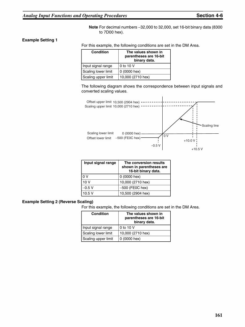
Analog Input Functions and Operating Procedures Section 4-6
Note For decimal numbers −32,000 to 32,000, set 16-bit binary data (8300to 7D00 hex).
Example Setting 1For this example, the following conditions are set in the DM Area.
The following diagram shows the correspondence between input signals andconverted scaling values.
Example Setting 2 (Reverse Scaling)For this example, the following conditions are set in the DM Area.
Condition The values shown in parentheses are 16-bit
binary data.
Input signal range 0 to 10 V
Scaling lower limit 0 (0000 hex)
Scaling upper limit 10,000 (2710 hex)
Input signal range The conversion results shown in parentheses are
16-bit binary data.
0 V 0 (0000 hex)
10 V 10,000 (2710 hex)
−0.5 V −500 (FE0C hex)
10.5 V 10,500 (2904 hex)
10,500 (2904 hex)10,000 (2710 hex)
Offset upper limitScaling upper limit
Scaling line
Scaling lower limit
Offset lower limit 0 (0000 hex)
−500 (FE0C hex)
−0.5 V
0 V+10.0 V
+10.5 V
Condition The values shown in parentheses are 16-bit
binary data.
Input signal range 0 to 10 V
Scaling lower limit 10,000 (2710 hex)
Scaling upper limit 0 (0000 hex)
161
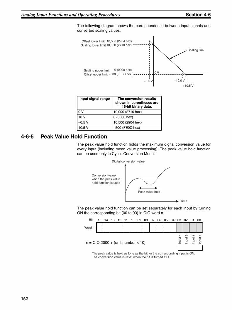
Analog Input Functions and Operating Procedures Section 4-6
The following diagram shows the correspondence between input signals andconverted scaling values.
4-6-5 Peak Value Hold FunctionThe peak value hold function holds the maximum digital conversion value forevery input (including mean value processing). The peak value hold functioncan be used only in Cyclic Conversion Mode.
The peak value hold function can be set separately for each input by turningON the corresponding bit (00 to 03) in CIO word n.
Input signal range The conversion results shown in parentheses are
16-bit binary data.
0 V 10,000 (2710 hex)
10 V 0 (0000 hex)
−0.5 V 10,500 (2904 hex)
10.5 V −500 (FE0C hex)
Scaling line
Offset lower limitScaling lower limit
Scaling upper limitOffset upper limit
10,500 (2904 hex)10,000 (2710 hex)
0 (0000 hex)−500 (FE0C hex)
−0.5 V
0 V
+10.0 V
+10.5 V
Time
Conversion value when the peak value hold function is used
Digital conversion value
Peak value hold
15 14 13 12 11 10 09 08 07 06 05 04 03 02 01 00
Bit
Word n
Inpu
t 4
Inpu
t 3
Inpu
t 2
Inpu
t 1
The peak value is held as long as the bit for the corresponding input is ON. The conversion value is reset when the bit is turned OFF.
n = CIO 2000 + (unit number × 10)
162

Analog Input Functions and Operating Procedures Section 4-6
Note 1. Example: In the following example, the peak value hold function is in effectfor input number 1. (The unit number is 0.)
2. When mean value processing is used together with the peak value holdfunction, the peak mean value will be held.
3. If a disconnection occurs when the peak value hold function is enabled, theconversion value will be 7FFF hex. When the disconnection is restored, thepeak hold function will be executed using the previous peak value. (The in-put signal range must be set to 1 to 5 V or 4 to 20 mA.)
4. The peak value hold function will be disabled when the loads are turnedOFF from the CPU Unit.
4-6-6 Input Disconnection Detection FunctionWhen an input signal range of 1 to 5 V or 4 to 20 mA is used, input wiring dis-connections can be detected. The detection condition for each of the inputsignal ranges is shown in the following table.
The input disconnection detection signals for the inputs are stored in bits 00 to03 of CIO word n+9. Specify these bits as execution conditions to use discon-nection detection in the user’s program.
Note The conversion value will be 7FFF hex during a disconnection. This conver-sion value can be used to detect disconnections during Direct ConversionMode.
Example
In the following example, the conversion value for analog input 1 is read onlywhen there is no disconnection (The unit number is 00.)
2000.00
Input condition
The maximum conversion data value is held for input 1.
Input signal range Voltage/current for disconnection detection
1 to 5 V Less than 0.3 V
4 to 20 mA Less than 1.2 mA
15 14 13 12 11 10 09 08 07 06 05 04 03 02 01 00
Bit
The corresponding bit turns ON when a disconnection is detected for a given input. When the disconnection is restored, the bit turns OFF.
Inpu
t 4
Inpu
t 3
Inpu
t 2
Inpu
t 1
Word n+9
n = CIO 2000 + (unit number × 10)
MOV(021)2001
D00001
2009.00
Conversion data in CIO 2001 (input 1) is read to D00001.
163

Handling Errors and Alarms Section 4-7
4-7 Handling Errors and Alarms
4-7-1 Indicators and Error Flowchart
IndicatorsIf an alarm or error occurs in the Analog Input Unit, the ERC or ERH indicatoron the front panel of the Unit will light.
RUN
ERC
ERH
Front panel of Unit
Indicator Meaning Indicator status Operating status
RUN (green) Operating Lit Operation normal.
Not lit Unit has stopped exchanging data with the CPU Unit.
ERC (red) Error detected by Unit Lit Alarm has occurred (such as disconnection detection) or initial settings are incorrect.
Not lit Operating normally.
ERH (red) Error in the CPU Unit Lit Error has occurred during data exchange with the CPU Unit.
Not lit Operating normally.
164

Handling Errors and Alarms Section 4-7
Troubleshooting ProcedureUse the following procedure for troubleshooting Analog Input Unit errors.
Lit Lit
Not lit Not lit
LitIs the RUN indicator
lit?
LitError detected by CPU Unit
(Refer to 4-7-3 Errors in the CPU Unit.)
Not lit Not litCheck whether the unit number is set correctly.
(Refer to 4-7-3 Errors in the CPU Unit.)Lit
Not lit
Not lit
Lit
No
Error cleared?
No
Check the operating environment.
Alarm has occurred at the Analog Input Unit.
(Refer to 4-7-2 Alarms Occurring at the Analog Input Unit.)
Check whether the initial settings for the Analog Input Unit are set correctly.
(Refer to 4-7-2 Alarms Occurring at the Analog Input Unit.)
Refer to 4-7-5 Troubleshooting.
Noise or other disturbance may be causing malfunctions.
Replace the Unit.
The Unit is faulty.
Yes
Cycle the power supply to the PLC.
Error cleared?Yes
Check the current consumptions of the Units mounted on the Rack against the power supply capacity of the Power Supply Unit. Restart the Analog Input Unit
according to 4-7-4 Restarting Special I/O Units.
Error in internal circuits has occurred, preventing operation from continuing.
Is the POWER indicator lit on the Power Supply
Unit?
Is the RUN indicator lit?
Is the ERH indicator lit?
Is the ERC indicator lit?
Is the RUN indicator lit?
Error occurs.
165

Handling Errors and Alarms Section 4-7
4-7-2 Alarms Occurring at the Analog Input UnitThe ERC indicator will light when the Analog Input Unit detects an alarm. Thealarm flags in bits 08 to 15 of CIO word n+9 will turn ON.
ERH and RUN Indicators: Lit
The ERC and RUN indicators will be lit if an error occurs while the Unit isoperating normally.The following alarm flags will turn ON in CIO word n+9The alarms will be cleared automatically when the error has been eliminated.
n = CIO 2000 + (unit number × 10)
Note The input disconnection detection function can be used for analog in-puts that are in Cyclic Conversion Mode and for which the input sig-nal range is set to 1 to 5 V or 4 to 20 mA.
ERC Indicator: Lit, RUN Indicator: Not Lit
The ERC indicator will be lit when the initial settings for the Analog Input Unitare not set correctly. The following alarm flags will turn ON in CIO word n+9.
15 14 13 12 11 10 09 08 07 06 05 04 03 02 01 00
Bit
Disconnection Detection FlagsAlarm Flags
Word n+9
n+9 Alarm flag Error contents Input status Countermeasure
Bits 00 to 03
Input dis-connection detection
A disconnec-tion was detected. (See note.)
Conversion data becomes 7FFF hex.
Check the rightmost byte of CIO word n+9. The input for bits that are ON may be disconnected. Restore any disconnected inputs.
Bit 14 A/D con-verter error
An error occurred in the A/D converter or in A/D con-version.
Holds the val-ues immedi-ately prior to the error. No data is changed.
• If the error persists even after the power supply is cycled or the Unit is restarted, check for a source of noise in the environment.
• If the error persists even when there is no source of noise, replace the Ana-log Input Unit.
RUN
ERC
ERH
Lit :
Not lit :
RUN
ERC
ERH
Lit :
Not lit :
166
Handling Errors and Alarms Section 4-7
These alarm flags will turn OFF when the error is cleared and the power sup-ply to the PLC is cycled, or the Special I/O Unit Restart Bit is turned ON.
4-7-3 Errors in the CPU UnitThe ERH indicator will light if an error occurs in the CPU Unit or I/O bus and I/O refreshing with the Special I/O Units is not performed correctly, preventingthe Analog Input Unit from operating.
ERH and RUN Indicators: Lit
The ERH and RUN indicators will light if an I/O bus error occurs or if a WDT(watchdog timer) error occurs in the CPU Unit, resulting in incorrect I/Orefresh with the Analog Input Unit. Cycle the power supply to the PLC orrestart the Analog Input Unit.
ERH Indicator: Lit, RUN Indicator: Not Lit
n+9 Alarm flag Error contents Input status Countermeasure
Bit 08 Scaling data setting error
The scaling set-tings are out of range. The upper limit equals the lower limit (not 0000).
Conversion does not start and data becomes 0000 hex.
Correct the settings.
Bit 09 Input signal range setting error or error in number of inputs setting
The setting of the number of inputs used or an input signal range is wrong.
Set the number of ana-log inputs used to 0 to 4 and set the input sig-nal ranges to 0, 2, 3, 6, or 7.
Bit 11 Error in setting of number of mean value buffers
The wrong num-ber of samplings has been speci-fied for mean processing.
Specify a number from 0 to 9.
Bit 12 Error in setting of conversion mode
The setting for Cyclic Conver-sion Mode or Direct Conver-sion Mode is wrong.
Set 00 hex or A5 hex.
Error Error contents Input status
I/O bus error Error has occurred during data exchange with the CPU Unit.
Conversion data becomes 0000 hex.
CPU Unit monitoring error No response from CPU Unit for a specified period of time.
Maintains the status from before the error.
CPU Unit WDT error Error has occurred in CPU Unit.
Changes to undefined state.
RUN
ERC
ERH
Lit :
Not lit :
RUN
ERC
ERH
Lit :
Not lit :
167

Handling Errors and Alarms Section 4-7
The unit number of the Analog Input Unit has not been set correctly.
4-7-4 Restarting Special I/O UnitsTo restart the Analog Input Unit after changing the contents of the DM Area orcorrecting an error, cycle the power to the PLC or turn ON the Special I/O UnitRestart Bit.
Special I/O Unit Restart Bits
• The previous conversion data will be held while the Unit is beingrestarted.
Note If the error is not cleared even after turning the Special I/O Unit Restart BitON, then replace the Unit.
4-7-5 TroubleshootingThe following tables list the probable causes of troubles that may occur, andthe countermeasures for dealing with them.
Error Error contents Input status
Unit Number Duplication Error
The same unit number has been assigned to more than one Unit or the unit number was set to a value other than 00 to 95.
Conversion does not start and data becomes 0000 hex.
Special I/O Unit Setting Error
The Special I/O Units reg-istered in the I/O tables are different from the ones actually mounted.
Bit Function
A502.00 Unit No. 0 Restart Bit Restarts the Unit when turned ON.A502.01 Unit No. 1 Restart Bit
to to
A502.15 Unit No. 15 Restart Bit
A503.00 Unit No. 16 Restart Bit
to to
A507.15 Unit No. 95 Restart Bit
168

Handling Errors and Alarms Section 4-7
Conversion Data Does Not Change
Value Does Not Change as Intended
Conversion Values are Inconsistent
Probable cause Countermeasure Page
Number of analog inputs used is not set correctly.
Set the number of analog inputs used to enable all inputs that are being used.
155
The ANALOG INPUT DIRECT CONVERSION (AIDC) instruction is not being executed in Direct Conversion Mode.
Execute the ANALOG INPUT DIRECT CONVERSION (AIDC) instruction in the user program.
156
The peak value hold func-tion is in operation.
Turn OFF the peak value hold function if it is not required.
162
The input device is not working, the input wiring is wrong, or there is a discon-nection.
Using a tester, check to see if the input volt-age or current is changing.
---
Use Unit’s alarm flags to check for a discon-nection. In Direct Conversion Mode, see if the conversion value is 7FFF hex in RUN or MONITOR mode to check for disconnec-tions.
163
Probable cause Countermeasure Page
The input device’s signal range does not match the input signal range for the relevant input number at the Analog Input Unit.
Check the specifications of the input device, and match the settings for the input signal ranges.
130, 132
For the 4 to 20 mA range, the positive current input terminal and positive volt-age input terminal are not connected with the enclosed short bar.
Connect the positive current input terminal and positive voltage input terminal with the enclosed short bar.
142
Probable cause Countermeasure Page
The input signals are being affected by external noise.
Try connecting the cable shield to the AG terminal on the Analog Input Unit, or discon-necting it if it is already connected.
144
Insert a 0.01-µF ceramic capacitor or film capacitor between the input’s (+) and (−) ter-minals.
---
Try increasing the number of mean value processing buffers.
158
169

Handling Errors and Alarms Section 4-7
170

SECTION 5CS-series Analog Output Units (CS1W-DA041/08V/08C)
This section explains how to use the CS1W-DA041/08V/08C Analog Output Units.
5-1 Specifications . . . . . . . . . . . . . . . . . . . . . . . . . . . . . . . . . . . . . . . . . . . . . . . . . 172
5-1-1 Specifications . . . . . . . . . . . . . . . . . . . . . . . . . . . . . . . . . . . . . . . . . . 172
5-1-2 Output Function Block Diagram . . . . . . . . . . . . . . . . . . . . . . . . . . . 174
5-1-3 Output Specifications . . . . . . . . . . . . . . . . . . . . . . . . . . . . . . . . . . . . 174
5-2 Operating Procedure . . . . . . . . . . . . . . . . . . . . . . . . . . . . . . . . . . . . . . . . . . . . 176
5-2-1 Procedure Examples . . . . . . . . . . . . . . . . . . . . . . . . . . . . . . . . . . . . . 177
5-3 Components and Switch Settings . . . . . . . . . . . . . . . . . . . . . . . . . . . . . . . . . . 182
5-3-1 Indicators . . . . . . . . . . . . . . . . . . . . . . . . . . . . . . . . . . . . . . . . . . . . . 183
5-3-2 Unit Number Switches . . . . . . . . . . . . . . . . . . . . . . . . . . . . . . . . . . . 184
5-3-3 Operation Mode Switch . . . . . . . . . . . . . . . . . . . . . . . . . . . . . . . . . . 184
5-4 Wiring . . . . . . . . . . . . . . . . . . . . . . . . . . . . . . . . . . . . . . . . . . . . . . . . . . . . . . . 185
5-4-1 Terminal Arrangement . . . . . . . . . . . . . . . . . . . . . . . . . . . . . . . . . . . 185
5-4-2 Internal Circuitry . . . . . . . . . . . . . . . . . . . . . . . . . . . . . . . . . . . . . . . 186
5-4-3 Output Wiring Example . . . . . . . . . . . . . . . . . . . . . . . . . . . . . . . . . . 187
5-4-4 Output Wiring Considerations . . . . . . . . . . . . . . . . . . . . . . . . . . . . . 188
5-5 Exchanging Data with the CPU Unit . . . . . . . . . . . . . . . . . . . . . . . . . . . . . . . 188
5-5-1 Outline of Data Exchange. . . . . . . . . . . . . . . . . . . . . . . . . . . . . . . . . 188
5-5-2 Unit Number Settings . . . . . . . . . . . . . . . . . . . . . . . . . . . . . . . . . . . . 189
5-5-3 Special I/O Unit Restart Bits . . . . . . . . . . . . . . . . . . . . . . . . . . . . . . 189
5-5-4 Fixed Data Allocations . . . . . . . . . . . . . . . . . . . . . . . . . . . . . . . . . . . 190
5-5-5 I/O Refresh Data Allocations . . . . . . . . . . . . . . . . . . . . . . . . . . . . . . 192
5-6 Analog Output Functions and Operating Procedures . . . . . . . . . . . . . . . . . . . 195
5-6-1 Output Settings and Conversions . . . . . . . . . . . . . . . . . . . . . . . . . . . 195
5-6-2 Starting and Stopping Conversion . . . . . . . . . . . . . . . . . . . . . . . . . . 197
5-6-3 Output Hold Function . . . . . . . . . . . . . . . . . . . . . . . . . . . . . . . . . . . . 198
5-6-4 Output Setting Errors . . . . . . . . . . . . . . . . . . . . . . . . . . . . . . . . . . . . 199
5-7 Adjusting Offset and Gain . . . . . . . . . . . . . . . . . . . . . . . . . . . . . . . . . . . . . . . 199
5-7-1 Adjustment Mode Operational Flow . . . . . . . . . . . . . . . . . . . . . . . . 199
5-7-2 Output Offset and Gain Adjustment Procedures . . . . . . . . . . . . . . . 201
5-8 Handling Errors and Alarms . . . . . . . . . . . . . . . . . . . . . . . . . . . . . . . . . . . . . . 209
5-8-1 Indicators and Error Flowchart . . . . . . . . . . . . . . . . . . . . . . . . . . . . . 209
5-8-2 Alarms Occurring at the Analog Output Unit. . . . . . . . . . . . . . . . . . 211
5-8-3 Errors in the CPU Unit . . . . . . . . . . . . . . . . . . . . . . . . . . . . . . . . . . . 212
5-8-4 Restarting Special I/O Units . . . . . . . . . . . . . . . . . . . . . . . . . . . . . . . 213
5-8-5 Troubleshooting . . . . . . . . . . . . . . . . . . . . . . . . . . . . . . . . . . . . . . . . 214
171

Specifications Section 5-1
5-1 Specifications
5-1-1 Specifications
Note 1. Do not apply a voltage higher than 600 V to the terminal block when per-forming withstand voltage test on this Unit.
2. Refer to Dimensions on page 439 for details on the Unit’s dimensions.
Item CS1W-DA041 CS1W-DA08V CS1W-DA08C
Unit type CS-series Special I/O Unit
Isolation (See note 1.) Between outputs and PLC signals: Photocoupler(No isolation between output signals.)
External terminals 21-point detachable terminal block (M3 screws)
Current consumption 130 mA max. at 5 VDC, 180 mA max. at 26 VDC
130 mA max. at 5 VDC, 180 mA max. at 26 VDC
130 mA max. at 5 VDC, 250 mA max. at 26 VDC
Dimensions (mm) (See note 2.)
35 × 130 × 126 (W × H × D)
Weight 450 g max.
General specifications Conforms to general specifications for SYSMAC CS-series Series.
Mounting position CS-series CPU Rack or CS-series Expansion Rack(Cannot be mounted to a C200H Expansion I/O Rack or a SYSMAC BUS Slave Rack.)
Maximum number of Units (See note 3.)
Depends on the Power Supply Unit.
Data exchange with CPU Units (See note 4.)
Special I/O Unit Area
CIO 200000 to CIO295915
(Words CIO 2000 to CIO 2959)
Internal Special I/O Unit DM Area(D20000 to D29599)
Output specifi-cations
Number of analog out-puts
4 8 8
Output signal ranges
(See note 5.)
1 to 5 V/4 to 20 mA0 to 5 V0 to 10 V–10 to 10V
1 to 5 V0 to 5 V0 to 10 V–10 to 10 V
4 to 20 mA
Output impedance 0.5 Ω max. (for voltage output)
Max. output current (for 1 point)
12 mA (for voltage output)
Maximum permissible load resistance
600 Ω (current output) (See note 9.)
--- 600 Ω (current output) (See note 8.)
Resolution 4,000 (full scale)
Set data 16-bit binary data
Accuracy
(See note 6.)
23±2°C: Voltage output: ±0.3% of full scaleCurrent output: ±0.5% of full scale
0°C to 55°C: Voltage output: ±0.5% of full scaleCurrent output: ±0.8% of full scale
D/A conversion period (See note 7.)
1.0 ms/point max.
Output func-tions
Output hold function Outputs the specified output status (CLR, HOLD, or MAX) under any of the following cir-cumstances.
When the Conversion Enable Bit is OFF. (See note 8.)In adjustment mode, when a value other than the output number is output during adjust-ment.
When there is an output setting error or a fatal error occurs at the PLC.When the CPU Unit is on standby.
When the Load is OFF.
172

Specifications Section 5-1
3. Maximum Number of Units
The maximum number of Units that can be mounted to one Rack varies de-pending on the current consumption of the other Units mounted to theRack and may be less than the number shown in the above table.
4. Data Exchange with CPU Units
5. Output signal ranges can be set for each output.
6. The accuracy is given for full scale. For example, an accuracy of ±0.3%means a maximum error of ±12 (BCD).
7. D/A conversion time is the time required for converting and outputting thePLC data. It takes at least one cycle for the data stored in the PLC to beread by the Analog Output Unit.
8. When the operation mode for the CPU Unit is changed from RUN mode orMONITOR mode to PROGRAM mode, or when the power is turned ON,the Output Conversion Enable Bit will turn OFF. The output status specifiedaccording to the output hold function will be output.
9. The load resistance is adjusted to 250 Ω at the factory. Always adjust theoffset gain before application when the load resistance is not 250 Ω.
The CS1W-DA041 is adjusted for current outputs (load resistance: 250 Ω)at the factory. Adjust the offset gain before application when using voltageoutputs.
Power Supply Unit
CS1W-DA041/08V CS1W-DA08C
C200HW-PA204C200HW-PA204SC200HW-PA204RC200HW-PD204
3 Units max. 2 Units max.
C200HW-PA209R 7 Units max. 5 Units max.
Special I/O Unit Area
CIO 200000 to CIO295915 (Words CIO 2000 to CIO 2959)
Exchanges 10 words of data per Unit.
CPU Unit to Analog Out-put Unit
Analog output setting data
Conversion Enable Bit
Analog Out-put Unit to CPU Unit
Alarm flags
Internal Special I/O Unit DM Area
(D20000 to D29599)
Transmits 100 words of data per Unit at power-up or when the Unit is restarted.
CPU Unit to Analog Out-put Unit
Output signal conver-sion enable/disable, out-put signal range settingOutput status for output hold
173
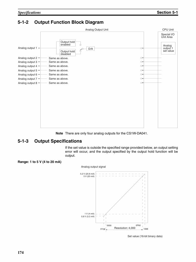
Specifications Section 5-1
5-1-2 Output Function Block Diagram
Note There are only four analog outputs for the CS1W-DA041.
5-1-3 Output SpecificationsIf the set value is outside the specified range provided below, an output settingerror will occur, and the output specified by the output hold function will beoutput.
Range: 1 to 5 V (4 to 20 mA)
Analog Output Unit CPU Unit
Special I/O Unit Area
Analog output 1 set value
Output hold enabled
Output hold disabled
D/AAnalog output 1
Same as above.Analog output 2Same as above.Analog output 3
Same as above.Analog output 4
Same as above.Analog output 5
Same as above.Analog output 7
Same as above.Analog output 8
Same as above.Analog output 6
5.2 V (20.8 mA)5 V (20 mA)
1 V (4 mA)0.8 V (3.2 mA)
0000
FF38
0FA0
1068Resolution: 4,000
Set value (16-bit binary data)
Analog output signal
174

Specifications Section 5-1
Range: 0 to 10 V
Range: 0 to 5 V
0000FF38
0FA0
1068
10.5 V10 V
0 V–0.5 V
Resolution: 4,000
Set value (16-bit binary data)
Analog output signal
0000FF38
0FA0
1068
5.25 V5 V
0 V–0.25 V
Resolution: 4,000
Set value (16-bit binary data)
Analog output signal
175

Operating Procedure Section 5-2
Range: −10 to 10 V
Note The set values for a range of –10 to 10 V will be as follows:
5-2 Operating ProcedureFollow the procedure outlined below when using Analog Output Units.
Installation and Settings
1,2,3... 1. Set the operation mode switch on the rear panel of the Unit to normalmode.
2. Wire the Unit.
3. Use the unit number switches on the front panel of the Unit to set the unitnumber.
4. Turn ON the power to the PLC.
5. Create the I/O tables.
6. Make the Special I/O Unit DM Area settings.
• Set the output numbers to be used.
• Set the output signal ranges.
• Set the output hold function.
7. Turn the power to the PLC OFF and ON, or turn ON the Special I/O UnitRestart Bit.
When the output for the connected devices needs to be calibrated, follow theprocedures in Offset and Gain Adjustment below. Otherwise, skip to Opera-tion below.
0000F830
F768
07D0
0898
0 V
–10 V–11 V
11 V10 V
Resolution: 4,000
Set value (16-bit binary data)
Analog output signal
16-bit binary data BCD
F768 –2200
: :
FFFF –1
0000 0
0001 1
: :
0898 2200
176

Operating Procedure Section 5-2
Offset and Gain Adjustment
1,2,3... 1. Set the operation mode switch on the rear panel of the Unit to adjustmentmode.
2. Turn ON the power to the PLC.
3. Adjust the offset and gain.
4. Turn OFF the power to the PLC.
5. Change the setting of the operation mode switch on the rear panel of theUnit back to normal mode.
Operation
1,2,3... 1. Turn ON the power to the PLC.
2. Ladder program
• Write set values by means of MOV(021) and XFER(070).
• Start and stop conversion output.
• Obtain error codes.
5-2-1 Procedure Examples
Setting the Analog Output Unit
1,2,3... 1. Set the operation mode switch on the rear panel of the Unit. Refer to 5-3-3 Operation Mode Switch for further details.
CS1W-DA041 CS-series CPU Unit
Unit No. 1
Analog output
OUT1: 1 to 5 V
OUT2: 1 to 5 V
OUT3: –10 to 10 V
OUT4: Not used
Ladd
er P
rogr
am
Turn OFF SW1 for normal mode
177
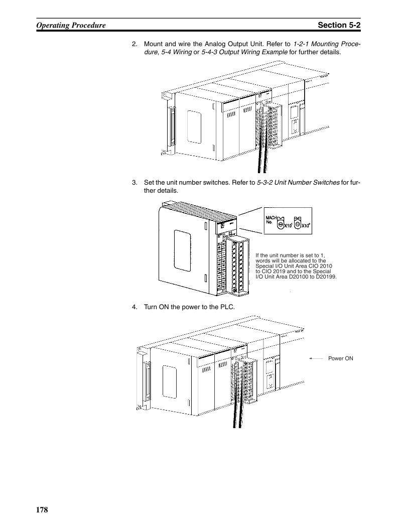
Operating Procedure Section 5-2
2. Mount and wire the Analog Output Unit. Refer to 1-2-1 Mounting Proce-dure, 5-4 Wiring or 5-4-3 Output Wiring Example for further details.
3. Set the unit number switches. Refer to 5-3-2 Unit Number Switches for fur-ther details.
4. Turn ON the power to the PLC.
If the unit number is set to 1, words will be allocated to the Special I/O Unit Area CIO 2010 to CIO 2019 and to the Special I/O Unit Area D20100 to D20199.
Power ON
178

Operating Procedure Section 5-2
Creating I/O TablesAfter turning ON the power to the PLC, be sure to create the I/O tables.
Initial Data Settings
1,2,3... 1. Specify the Special I/O Unit settings in the DM Area. Refer to DM Alloca-tion Contents on page 191 for further details.
• The following diagram shows the output settings used. Refer to 5-6-1Output Settings and Conversions for more details.
Peripheral port
Peripheral port
Setting conditions
Unit No. 1
Analog output 1: 1 to 5 VAnalog output 2: 1 to 5 VAnalog output 3: –10 to 10 VAnalog output 4: Not used.
15 14 13 12 11 10 09 08 07 06 05 01 0004 03 02
0 0 0 0 0 0 0 0 0 0 0 0 0 1 1 1
Bit
Not used Output 4
Output 3
Output 2
Output 1Used
m: DM20100(0007 hex)
179

Operating Procedure Section 5-2
• The following diagram shows the output range settings. Refer to 5-6-1Output Settings and Conversions for more details.
2. Restart the CPU Unit.
Creating Ladder Programs
The setting address D00200 is stored in words (n + 1) to (n + 3) of the SpecialI/O Unit Area (CIO 2011 to CIO 2013) as a signed binary value between 0000to 0FA0 hex.
15 14 13 12 11 10 09 08 07 06 05 01 0004 03 02
0 0 0 0 0 0 0 0 0 0 0 0 1 0 1 0
Bit
m+1: DM20101(000A hex)
Output 1: 1 to 5 V. Set to 10.
Output 2: 1 to 5 V. Set to 10.
Output 3: –10 to 10 V. Set to 00.
Output 4: Not used. Set to 00 (disabled).
Power turned ON again (or Special I/O Unit Restart Bit is turned ON)
Peripheral port
180

Operating Procedure Section 5-2
The following table shows the addresses used for analog output.
Note 1. The addresses are determined by the unit number of the Special I/O Unit.Refer to 5-3-2 Unit Number Switches for further details.
2. Set as required.
Output number Output signal range
Address of output set value
(n = CIO 2010)See note 1.
Conversion source address
1 1 to 5 V (n+1) = CIO 2011 D00200
2 0 to 10 V (n+2) = CIO 2012 D00201
3 –10 to 10 V (n+3) = CIO 2013 D00202
4 Not used. --- ---
D00200 is set in word CIO 2011.
D00201 is set in word CIO 2012.
D00202 is set in word CIO 2013.
To start analog output, turn ON the Conversion Enable Bits 201000 to 201002 (bits 00 to 03 of word CIO 2010).
The data in words CIO 2011 and 2012 will be output as 1 to 5 V, and CIO the data in CIO 2013 will be output as –10 to 10 V.
MOV (021)
D00200
2011
MOV (021)
D00201
2012
Execution condition
MOV (021)
D00202
2013
SET
201000
SET
201002
SET
201001
Execution condition
See 5-6-2 Starting and Stopping Conversion for details.
181
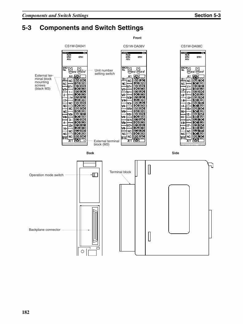
Components and Switch Settings Section 5-3
5-3 Components and Switch Settings
Unit number setting switch
External terminal block (M3)
External ter-minal block mounting screws (black M3)
Front
CS1W-DA041 CS1W-DA08V CS1W-DA08C
Operation mode switch
Backplane connector
Terminal block
SideBack
182

Components and Switch Settings Section 5-3
The terminal block is attached using a connector. It can be removed by loos-ening the two black mounting screws located at the top and bottom of the ter-minal block.
Check to be sure that the black terminal block mounting screw is securelytightened to a torque of 0.5 N·m.
5-3-1 IndicatorsThe indicators show the operating status of the Unit. The following tableshows the meanings of the indicators.
Fasten the mounting screw.
Fasten the mounting screw.
Indicator Meaning Indicator status
Operating status
RUN (green) Operating Lit Operating in normal mode.
Not lit Unit has stopped exchanging data with the CPU Unit.
ERC (red) Error detected by Unit
Lit Alarm has occurred (such as disconnec-tion detection) or initial settings are incor-rect.
Not lit Operating normally.
ADJ (yellow) Adjusting Flashing Operating in offset/gain adjustment mode.
Not lit Other than the above.
ERH (red) Error in the CPU Unit
Lit Error has occurred during data exchange with the CPU Unit.
Not lit Operating normally.
183

Components and Switch Settings Section 5-3
5-3-2 Unit Number SwitchesThe CPU Unit and Analog Output Unit exchange data via the Special I/O UnitAreas in the CIO Area and DM Area. The words that are allocated to eachAnalog Output Unit in the Special I/O Unit Areas in the CIO Area and DM Areaare determined by the setting of the unit number switches on the front panel ofthe Unit.
Always turn OFF the power before setting the unit number. Use a flat-bladescrewdriver, being careful not to damage the slot in the screw. Be sure not toleave the switch midway between settings
Note If two or more Special I/O Units are assigned the same unit number, a “UNITNo. DPL ERR” error (in the Programming Console) will be generated (A40113will turn ON) and the PLC will not operate.
5-3-3 Operation Mode SwitchThe operation mode switch on the back panel of the Unit is used to set theoperation mode to either normal mode or adjustment mode (for adjusting off-set and gain).
!Caution Do not set the pins to any combination other than those shown in the abovetable. Be sure to set pin 2 to OFF.
!Caution Be sure to turn OFF the power to the PLC before installing or removing theUnit.
Switch setting
Unit number
Words allocated in Special I/O Unit Area in
CIO Area
Words allocated in Special I/O Unit Area in DM Area
0 Unit #0 CIO 2000 to CIO 2009 D20000 to D20099
1 Unit #1 CIO 2010 to CIO 2019 D20100 to D20199
2 Unit #2 CIO 2020 to CIO 2029 D20200 to D20299
3 Unit #3 CIO 2030 to CIO 2039 D20300 to D20399
4 Unit #4 CIO 2040 to CIO 2049 D20400 to D20499
5 Unit #5 CIO 2050 to CIO 2059 D20500 to D20599
6 Unit #6 CIO 2060 to CIO 2069 D20600 to D20699
7 Unit #7 CIO 2070 to CIO 2079 D20700 to D20799
8 Unit #8 CIO 2080 to CIO 2089 D20800 to D20899
9 Unit #9 CIO 2090 to CIO 2099 D20900 to D20999
10 Unit #10 CIO 2100 to CIO 2109 D21000 to D21099
to to to to
n Unit #n CIO 2000 + (n × 10) to CIO 2000 + (n × 10) + 9
D20000 + (n × 100) to D20000 + (n × 100) + 99
to to to to
95 Unit #95 CIO 2950 to CIO 2959 D29500 to D29599
Pin number Mode
1 2
OFF OFF Normal mode
ON OFF Adjustment mode
184

Wiring Section 5-4
5-4 Wiring
5-4-1 Terminal ArrangementThe signal names corresponding to the connecting terminals are as shown inthe following diagram.
CS1W-DA08V/08C
CS1W-DA041
Note 1. The number of analog outputs that can be used is set in the DM Area.
2. The output signal ranges for individual outputs are set in the DM Area. Theoutput signal range can be set separately for each output.
3. The N.C. terminals are not connected to internal circuitry.
Output 2 (+)
Output 2 (–)
Output 4 (+)
Output 4 (–)
Output 6 (–)
Output 8 (+)
Output 8 (–)
Output 1 (+)
Output 1 (–)
Output 3 (+)
Output 3 (–)
Output 5 (+)
Output 5 (–)
Output 7 (+)
B1
B2
B3
B4
B5
B6
B7
B8
B9
A1
A2
A3
A4
A5
A6
A7
A8
A9
B10
Output 6 (+)
Output 7 (–)
N.C.
A10
A11N.C.
N.C.
N.C.
N.C.
Output current 2 (+)
Output 2 (–)
Output current 4 (+)
Output 4 (–)
Output current 1 (+)
Output 1 (–)
B1
B2
B3
B4
B5
B6
B7
B8
B9
A1
A2
A3
A4
A5
A6
A7
A8
A9
B10
N.C.
A10
A11
N.C.
Output voltage 2 (+)
N.C.
N.C.
Output voltage 4 (–)
N.C.
Output voltage 1 (+)
N.C.
N.C.
Output current 3 (+)
Output 3 (–)
Output voltage 3 (+)
N.C.
N.C.
185

Wiring Section 5-4
5-4-2 Internal CircuitryThe following diagrams show the internal circuitry of the analog output sec-tion.
Voltage Output Circuitry
Current Output Circuitry
Internal Configuration
Output switch and conversion circuit
AMP Voltage output (+)
Voltage output (–)
AG (common to all outputs)
Voltage output section for CS1W-DA08V/DA041
AMP
Current output section for CS1W-DA08C/DA041
Output switch and con-version circuit
Current output (+)
Current output (−)
Indicators/Switch
MPUOUTPUT
Regulator
Oscillator
Division
CS-series PLC
EEPROM
RAM ROM
Pho
toco
uple
r in
sula
tion
+26 V+5 V
−15 V
+18 V/+15 V
Bus interface
D/A converter
Multi-plexer and amplifier
Externally connected terminal
Insulation-type DC-to-DC converter
186
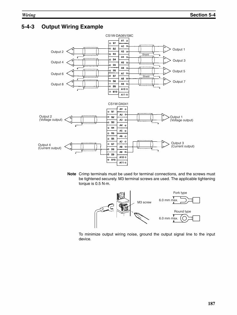
Wiring Section 5-4
5-4-3 Output Wiring Example
Note Crimp terminals must be used for terminal connections, and the screws mustbe tightened securely. M3 terminal screws are used. The applicable tighteningtorque is 0.5 N·m.
To minimize output wiring noise, ground the output signal line to the inputdevice.
Output 2
CS1W-DA08V/08C
Shield
Output 4
Output 6
Output 8
Shield
Output 1
Output 3
Output 5
Output 7
Output 2(Voltage output)
Output 4(Current output)
CS1W-DA041
Output 3(Current output)
Output 1(Voltage output)
6.0 mm max.
6.0 mm max.M3 screw
Fork type
Round type
187
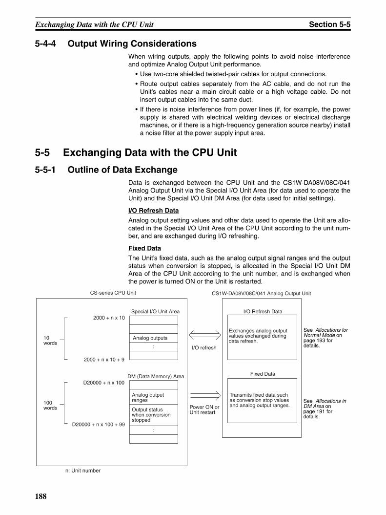
Exchanging Data with the CPU Unit Section 5-5
5-4-4 Output Wiring ConsiderationsWhen wiring outputs, apply the following points to avoid noise interferenceand optimize Analog Output Unit performance.
• Use two-core shielded twisted-pair cables for output connections.
• Route output cables separately from the AC cable, and do not run theUnit’s cables near a main circuit cable or a high voltage cable. Do notinsert output cables into the same duct.
• If there is noise interference from power lines (if, for example, the powersupply is shared with electrical welding devices or electrical dischargemachines, or if there is a high-frequency generation source nearby) installa noise filter at the power supply input area.
5-5 Exchanging Data with the CPU Unit
5-5-1 Outline of Data ExchangeData is exchanged between the CPU Unit and the CS1W-DA08V/08C/041Analog Output Unit via the Special I/O Unit Area (for data used to operate theUnit) and the Special I/O Unit DM Area (for data used for initial settings).
I/O Refresh Data
Analog output setting values and other data used to operate the Unit are allo-cated in the Special I/O Unit Area of the CPU Unit according to the unit num-ber, and are exchanged during I/O refreshing.
Fixed Data
The Unit’s fixed data, such as the analog output signal ranges and the outputstatus when conversion is stopped, is allocated in the Special I/O Unit DMArea of the CPU Unit according to the unit number, and is exchanged whenthe power is turned ON or the Unit is restarted.
CS-series CPU Unit CS1W-DA08V/08C/041 Analog Output Unit
Special I/O Unit Area I/O Refresh Data
Analog outputs
DM (Data Memory) Area
Analog output ranges
Output status when conversion stopped
I/O refresh
Power ON or Unit restart
Exchanges analog output values exchanged duringdata refresh.
Transmits fixed data such as conversion stop values and analog output ranges.
2000 + n x 10
2000 + n x 10 + 9
D20000 + n x 100
D20000 + n x 100 + 99
10 words
100 words
Fixed Data
:
:
n: Unit number
See Allocations for Normal Mode on page 193 for details.
See Allocations in DM Area on page 191 for details.
188

Exchanging Data with the CPU Unit Section 5-5
5-5-2 Unit Number SettingsThe words in the Special I/O Unit Areas in the CIO Area and DM Area that areallocated to each Analog Output Unit are determined by the setting of the unitnumber switches on the front panel of the Unit.
Note If two or more Special I/O Units are assigned the same unit number, a “UNITNo. DPL ERR” error (in the Programming Console) will be generated (A40113will turn ON) and the PLC will not operate.
5-5-3 Special I/O Unit Restart BitsTo restart the Unit operations after changing the contents of the data memoryor correcting an error, turn ON the power to the PLC again or turn the SpecialI/O Unit Restart Bit ON and then OFF again.
Note Replace the Unit if the error is not cleared even though the power supply iscycled or the Restart Bit is turned ON.
Switch setting
Unit number
Words allocated in Special I/O Unit Area in
CIO Area
Words allocated in Special I/O Unit Area in DM Area
0 Unit #0 CIO 2000 to CIO 2009 D20000 to D20099
1 Unit #1 CIO 2010 to CIO 2019 D20100 to D20199
2 Unit #2 CIO 2020 to CIO 2029 D20200 to D20299
3 Unit #3 CIO 2030 to CIO 2039 D20300 to D20399
4 Unit #4 CIO 2040 to CIO 2049 D20400 to D20499
5 Unit #5 CIO 2050 to CIO 2059 D20500 to D20599
6 Unit #6 CIO 2060 to CIO 2069 D20600 to D20699
7 Unit #7 CIO 2070 to CIO 2079 D20700 to D20799
8 Unit #8 CIO 2080 to CIO 2089 D20800 to D20899
9 Unit #9 CIO 2090 to CIO 2099 D20900 to D20999
10 Unit #10 CIO 2100 to CIO 2109 D21000 to D21099
to to to to
n Unit #n CIO 2000 + (n × 10) to CIO 2000 + (n × 10) + 9
D20000 + (n × 100) to D20000 + (n × 100) + 99
to to to to
95 Unit #95 CIO 2950 to CIO 2959 D29500 to D29599
Special I/O Unit Area word address
Function
A50200 Unit No. 0 Restart Bit Restarts the Unit when turned ON and then OFF again.A50201 Unit No. 1 Restart Bit
to to
A50215 Unit No. 15 Restart Bit
A50300 Unit No. 16 Restart Bit
to to
A50715 Unit No. 95 Restart Bit
189
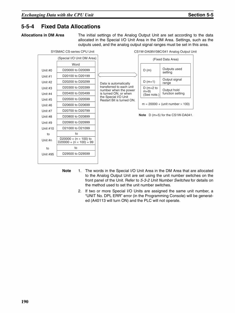
Exchanging Data with the CPU Unit Section 5-5
5-5-4 Fixed Data AllocationsAllocations in DM Area The initial settings of the Analog Output Unit are set according to the data
allocated in the Special I/O Unit Area in the DM Area. Settings, such as theoutputs used, and the analog output signal ranges must be set in this area.
Note 1. The words in the Special I/O Unit Area in the DM Area that are allocatedto the Analog Output Unit are set using the unit number switches on thefront panel of the Unit. Refer to 5-3-2 Unit Number Switches for details onthe method used to set the unit number switches.
2. If two or more Special I/O Units are assigned the same unit number, a“UNIT No. DPL ERR” error (in the Programming Console) will be generat-ed (A40113 will turn ON) and the PLC will not operate.
D (m+1)
D (m)
D20300 to D20399
D20400 to D20499
D20500 to D20599
D20000 to D20099
D20100 to D20199
D20200 to D20299
D20900 to D20999
D20600 to D20699
D20700 to D20799
D20800 to D20899
SYSMAC CS-series CPU Unit CS1W-DA08V/08C/041 Analog Output Unit
(Fixed Data Area)
Unit #0
Unit #1
Unit #2
Unit #3
Unit #4
Unit #5
Unit #6
Unit #7
Unit #8
Unit #9
(Special I/O Unit DM Area)
Word
D29500 to D29599
D21000 to D21099Unit #10
Unit #n
Unit #95
m = 20000 + (unit number × 100)
Note D (m+5) for the CS1W-DA041.
D20000 + (n × 100) to D20000 + (n × 100) + 99
Data is automatically transferred to each unit number when the power is turned ON, or when the Special I/O Unit Restart Bit is turned ON.
Outputs used setting
Output signal range
D (m+2 to m+9) (See note.)
Output hold function setting
to
to
to
to
190

Exchanging Data with the CPU Unit Section 5-5
Allocations in DM Area The following table shows the allocation of DM words and bits for both normaland adjustment mode.
CS1W-DA08V/08C
CS1W-DA041
Note For the DM word addresses, m = D20000 + (unit number × 100).
Set Values and Stored Values]
Note 1. With the CS1W-DA041, the output signal ranges 1 to 5 V and 4 to 20 mAare switched using the output terminal connections. For details, refer to 5-4-3 Output Wiring Example. With the CS1W-DA08C, these ranges are in-valid. Regardless of the settings made, the output range will be 4 to 20 mA.The CS1W-DA08V does not support an output range of 4 to 20 mA.
DM Area word
Bits
15 14 13 12 11 10 9 8 7 6 5 4 3 2 1 0
D (m) Not used. Output use setting
Out-put 8
Out-put 7
Out-put 6
Out-put 5
Out-put 4
Out-put 3
Out-put 2
Out-put 1
D (m+1) Output signal range setting
Output 8 Output 7 Output 6 Output 5 Output 4 Output 3 Output 2 Output 1
D (m+2) Not used. Output 1: Output status when conversion stopped
D (m+3) Not used. Output 2: Output status when conversion stopped
D (m+4) Not used. Output 3: Output status when conversion stopped
D (m+5) Not used. Output 4: Output status when conversion stopped
D (m+6) Not used. Output 5: Output status when conversion stopped
D (m+7) Not used. Output 6: Output status when conversion stopped
D (m+8) Not used. Output 7: Output status when conversion stopped
D (m+9) Not used. Output 8: Output status when conversion stopped
DM Area word
Bits
15 14 13 12 11 10 9 8 7 6 5 4 3 2 1 0
D (m) Not used. Not used. Output use setting
Out-put 4
Out-put 3
Out-put 2
Out-put 1
D (m+1) Not used. Output signal range setting
Output 4 Output 3 Output 2 Output 1
D (m+2) Not used. Output 1: Output status when conversion stopped
D (m+3) Not used. Output 2: Output status when conversion stopped
D (m+4) Not used. Output 3: Output status when conversion stopped
D (m+5) Not used. Output 4: Output status when conversion stopped
Item Contents Page
Output Use setting 0: Not used.1: Used.
191, 195
Output signal range 00: –10 to 10 V01: 0 to 10 V10: 1 to 5 V/4 to 20 mA (See note 1.)11: 0 to 5 V
191, 195
Output status when stopped 00: CLR Outputs 0 or minimum value of each range. (See note 2.)
01: HOLD Holds output just before stopping.02: MAX Outputs maximum value of range.
197
191

Exchanging Data with the CPU Unit Section 5-5
2. The values output for the signal ranges will be 0 V for the range of ±10 V,and the minimum value for the other ranges. For details, refer to 5-6-3 Out-put Hold Function.
5-5-5 I/O Refresh Data AllocationsI/O refresh data for the Analog Output Unit is exchanged according to the allo-cations in the Special I/O Unit Area.
Note 1. The Special I/O Unit Area words that are occupied by the Analog OutputUnit are set using the unit number switches on the front panel of the Unit.Refer to 5-3-2 Unit Number Switches for details on the method used to setthe unit number switches.
2. If two or more Special I/O Units are assigned the same unit number, a“UNIT No. DPL ERR” error (in the Programming Console) will be generat-ed (A40113 will turn ON) and the PLC will not operate.
CIO n + 9CIO 2030 to CIO 2039
CIO 2040 to CIO 2049
CIO 2050 to CIO 2059
CIO 2000 to CIO 2009
CIO 2010 to CIO 2019
CIO 2020 to CIO 2029
CIO 2090 to CIO 2099
CIO 2060 to CIO 2069
CIO 2070 to CIO 2079
CIO 2080 to CIO 2089
SYSMAC CS-series CPU Unit CS1W-DA08V/08C/041 Analog Output Unit
IN refresh
(I/O Refresh Data Area)
Unit #0
Unit #1
Unit #2
Unit #3
Unit #4
Unit #5
Unit #6
Unit #7
Unit #8
Unit #9
(Special I/O Unit Area)
OUT refresh
Allocated words
CIO 2950 to CIO 2959
CIO 2100 to CIO 2109Unit #10
Unit #n
Unit #95
Normal mode
CIO n + 9 IN refresh
OUT refresh
Adjustment mode
n = 2000 + (unit number × 10)
I/O refresh
CIO 2000 + (n × 10) to CIO 2000 + (n × 10) + 9
At the I/O refresh by the PLC, outputs (CPU to Unit) and inputs (Unit to CPU) are refreshed in order with every cycle.
CIO n to CIO n + 8
CIO n to CIO n + 7
to
to
to
to
192

Exchanging Data with the CPU Unit Section 5-5
Allocations for Normal Mode
For normal mode, set the operation mode switch on the rear panel of the Unitas shown in the following diagram.
The allocation of words and bits in the CIO Area is shown in the followingtable.
CS1W-DA08V/08C
CS1W-DA041
Note For the CIO word addresses, n = CIO 2000 + unit number × 10.
I/O Word Bits
15 14 13 12 11 10 9 8 7 6 5 4 3 2 1 0
Output (CPU to Unit)
n Not used. Conversion enableOut-put 8
Out-put 7
Out-put 6
Out-put 5
Out-put 4
Out-put 3
Out-put 2
Out-put 1
n + 1 Output 1 set value
163 162 161 160
n + 2 Output 2 set value
n + 3 Output 3 set value
n + 4 Output 4 set value
n + 5 Output 5 set value
n + 6 Output 6 set value
n + 7 Output 7 set value
n + 8 Output 8 set value
Input (Unit to CPU)
n + 9 Alarm Flags Output setting errorOut-put 8
Out-put 7
Out-put 6
Out-put 5
Out-put 4
Out-put 3
Out-put 2
Out-put 1
I/O Word Bits
15 14 13 12 11 10 9 8 7 6 5 4 3 2 1 0
Output (CPU to Unit)
n Not used. Not used. Conversion enableOut-put 4
Out-put 3
Out-put 2
Out-put 1
n + 1 Output 1 set value
163 162 161 160
n + 2 Output 2 set value
n + 3 Output 3 set value
n + 4 Output 4 set value
n + 5 Not used.
n + 6 Not used.
n + 7 Not used.
n + 8 Not used.
Input (Unit to CPU)
n + 9 Alarm Flags Not used. Output setting errorOut-put 4
Out-put 3
Out-put 2
Out-put 1
193

Exchanging Data with the CPU Unit Section 5-5
Set Values and Stored Values
Allocation for Adjustment Mode
For adjustment mode, set the operation mode switch on the rear panel of theUnit as shown in the following diagram. When the Unit is set for adjustmentmode, the ADJ indicator on the front panel of the Unit will flash.
The allocation of CIO words and bits is shown in the following table.
Note 1. For the CIO word addresses, n = CIO 2000 + (unit number × 10).
2. The range is 1 to 4 for the CS1W-DA04.
Item Contents Page
Conversion enable 0: Conversion output stopped.1: Conversion output begun.
197
Set value 16-bit binary data 196
Output setting error 0: No error1: Output setting error
199
Alarm Flags Bits 00 to 03: Output set value errorBits 04 to 09: Not usedBit 10: Output hold setting error Bit 11: Not usedBit 15: Operating in adjustment mode
(always 0 in normal mode)
193, 211
I/O Word Bits
15 14 13 12 11 10 9 8 7 6 5 4 3 2 1 0
Output (CPU to Unit)
n Not used. Outputs to be adjusted
1 (fixed) 1 to 8 (See note 2.)
n + 1 Not used. Not used. Clr Set Up Down Gain Off-set
n + 2 Not used.
n + 3 Not used.
n + 4 Not used.
n + 5 Not used.
n + 6 Not used.
n + 7 Not used.
Input (Unit to CPU)
n + 8 Conversion value or set value at time of adjustment
163 162 161 160
n + 9 Alarm Flags Not used.
194
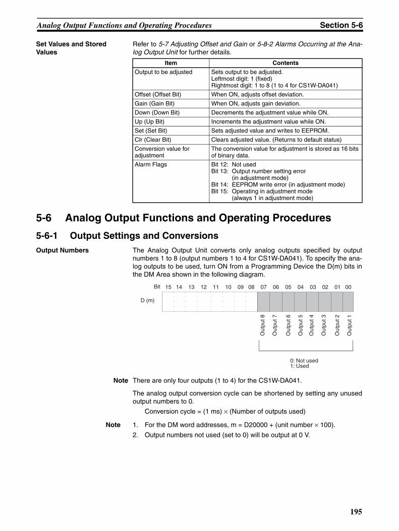
Analog Output Functions and Operating Procedures Section 5-6
Set Values and Stored Values
Refer to 5-7 Adjusting Offset and Gain or 5-8-2 Alarms Occurring at the Ana-log Output Unit for further details.
5-6 Analog Output Functions and Operating Procedures
5-6-1 Output Settings and ConversionsOutput Numbers The Analog Output Unit converts only analog outputs specified by output
numbers 1 to 8 (output numbers 1 to 4 for CS1W-DA041). To specify the ana-log outputs to be used, turn ON from a Programming Device the D(m) bits inthe DM Area shown in the following diagram.
Note There are only four outputs (1 to 4) for the CS1W-DA041.
The analog output conversion cycle can be shortened by setting any unusedoutput numbers to 0.
Conversion cycle = (1 ms) × (Number of outputs used)
Note 1. For the DM word addresses, m = D20000 + (unit number × 100).
2. Output numbers not used (set to 0) will be output at 0 V.
Item Contents
Output to be adjusted Sets output to be adjusted.Leftmost digit: 1 (fixed)Rightmost digit: 1 to 8 (1 to 4 for CS1W-DA041)
Offset (Offset Bit) When ON, adjusts offset deviation.
Gain (Gain Bit) When ON, adjusts gain deviation.
Down (Down Bit) Decrements the adjustment value while ON.
Up (Up Bit) Increments the adjustment value while ON.
Set (Set Bit) Sets adjusted value and writes to EEPROM.
Clr (Clear Bit) Clears adjusted value. (Returns to default status)
Conversion value for adjustment
The conversion value for adjustment is stored as 16 bits of binary data.
Alarm Flags Bit 12: Not usedBit 13: Output number setting error
(in adjustment mode)Bit 14: EEPROM write error (in adjustment mode)Bit 15: Operating in adjustment mode
(always 1 in adjustment mode)
15 14 13 12 11 10 09 08 07 06 05 04 03 02 01 00Bit
D (m)
Out
put 2
Out
put 1
0: Not used1: Used
Out
put 4
Out
put 3
Out
put 6
Out
put 5
Out
put 8
Out
put 7
195

Analog Output Functions and Operating Procedures Section 5-6
Output Signal Range Any of four types of output signal range (–10 to 10 V, 0 to 10 V, 1 to 5 V/4 to20 mA, and 0 to 5 V) can be selected for each of the outputs. To specify theoutput signal range for each output, use a Programming Device to set theD(m+1) bits in the DM Area shown in the following diagram.
Note 1. For the DM word addresses, m = D20000 + (unit number × 100).
2. With the CS1W-DA041, the 1 to 5 V output range and the 4 to 20 mA outputrange are switched by changing the terminal connections.
3. There is no 4 to 20 mA output range for the CS1W-DA08V.
4. Output setting range settings for the CS1W-DA08C are invalid. The outputsignal range will be 4 to 20 mA, regardless of the settings.
5. When data memory settings have been carried out using a ProgrammingDevice, be sure to either cycle the power supply to the PLC, or turn ON theSpecial I/O Unit Restart Bit. The contents of the data memory settings willbe transferred to the Special I/O Unit when the power is turned ON or theSpecial I/O Unit Restart Bit is ON.
Writing Set Values Analog output set values are written to CIO words (n+1) to (n+8). For theCS1W-DA041, they are written to CIO words (n+1) to (n+4).
For the CIO word addresses, n = CIO 2000 + (unit number × 10).
Use MOV(021) or XFER(070) to write values in the user program.
Example 1 In this example, the set value from only one output is written. (The unit num-ber is 0.)
15 14 13 12 11 10 09 08 07 06 05 04 03 02 01 00Bit
D (m + 1)
Out
put 2
Out
put 1
00: −10 to 10 V01: 0 to 10 V10: 1 to 5 V/4 to 20 mA11: 0 to 5 V
Out
put 4
Out
put 3
Out
put 6
Out
put 5
Out
put 8
Out
put 7
Word Function Stored value
n+1 Output 1 set value 16-bit binary data
n+2 Output 2 set value
n+3 Output 3 set value
n+4 Output 4 set value
n+5 Output 5 set value
n+6 Output 6 set value
n+7 Output 7 set value
n+8 Output 8 set value
MOV (021)
D00001
2001
Input conditionThe set value stored in D 00001 is written to CIO word 2001 (out-put number 1).
196

Analog Output Functions and Operating Procedures Section 5-6
Example 2 In this example, multiple set values are written. (The unit number is #0.)
Note If the set value has been written outside the specified range, an output settingerror will occur, and the value set by the output hold function will be output.
5-6-2 Starting and Stopping ConversionTo begin analog output conversion, turn ON the corresponding ConversionEnable Bit (word n, bits 00 to 07 for the CS1W-DA08V and CS1W-DA08C;word n, bits 00 to 03 for the CS1W-DA041) from the user’s program.
For the CIO word addresses, n = CIO 2000 + (unit number × 10).
The analog output when conversion is stopped will differ depending on theoutput signal range setting and output hold setting. Refer to 5-6-1 Output Set-tings and Conversions and 5-6-3 Output Hold Function.
Conversion will not begin under the following conditions even if the Conver-sion Enable Bit is turned ON. Refer to 5-6-3 Output Hold Function.
1,2,3... 1. In adjustment mode, when something other than the output number is out-put during adjustment.
2. When there is an output setting error.
3. When a fatal error occurs at the PLC.
When the operation mode for the CPU Unit is changed from RUN mode orMONITOR mode to PROGRAM mode, the Conversion Enable Bits will all turnOFF. They will also turn OFF when the power supply to the PLC is turned ON.The output status at this time depends on the output hold function.
In this example, conversion is begun for analog output number 1. (The unitnumber is 0.)
XFER(070)
#0004
D00001
2001
Input condition
The set values stored in D 00001to D 00004 are written to CIO words 2001 to 2004 (outputs 1 to 4).
15 14 13 12 11 10 09 08 07 06 05 04 03 02 01 00Bit
Out
put 2
Out
put 1
Analog conversion is executed while these bits are ON. When the bits are turned OFF, the conversion is stopped and the output data is held.
Word n
Out
put 4
Out
put 3
Out
put 6
Out
put 5
Out
put 8
Out
put 7
200000
Input conditionConversion begins for output number 1.
197

Analog Output Functions and Operating Procedures Section 5-6
5-6-3 Output Hold FunctionThe Analog Output Unit stops conversion under the following conditions andoutputs the value set for the output hold function.
1,2,3... 1. When the Conversion Enable Bit is OFF. Refer to Allocations for NormalMode on page 193 and 5-6-2 Starting and Stopping Conversion.
2. In adjustment mode, when something other than the output number is out-put during adjustment. Refer to Allocation for Adjustment Mode onpage 194.
3. When there is an output setting error. Refer to Allocations for Normal Modeon page 193 and 5-6-4 Output Setting Errors.
4. When a fatal error occurs at the PLC.
5. When there is an I/O bus error.
6. When the CPU Unit is in LOAD OFF status.
7. When there is a WDT (watchdog timer) error in the CPU Unit.
CLR, HOLD, or MAX can be selected for the output status when conversionstops.
The above values may fluctuate if offset/gain adjustment has been applied.
To specify the output hold function, use a Programming Device to set the DMArea words D(m+2) to D(m+9) as shown in the following table. (DM Areawords D(m+2) to D(m+5) for the CS1W-DA041.)
For the DM word addresses, m = D20000 + (unit number × 100).
Note When DM Area settings have been carried out using a Programming Device,be sure to either cycle the power supply to the PLC, or turn ON the Special I/O Unit Restart Bit. The contents of the initial settings in the DM Area will be
Output signal range
CLR HOLD MAX
0 to 10 V –0.5 V (Min. –5% of full scale)
Voltage that was output just prior to stopping.
10.5 V (Max. +5% of full scale)
–10 to 10 V 0.0 V Voltage that was output just prior to stopping.
11.0 V (Max. +5% of full scale)
1 to 5 V 0.8 V (Min. –5% of full scale)
Voltage that was output just prior to stopping.
5.2 V (Max. +5% of full scale)
0 to 5 V –0.25 V (Min. –5% of full scale)
Voltage that was output just prior to stopping.
5.25 V (Max. +5% of full scale)
4 to 20 mA 3.2 mA (Min. –5% of full scale)
Current that was output just prior to stopping.
20.8 mA (Max. +5% of full scale)
DM word Function Set value
D(m+2) Output 1: Output status when conversion stops xx00:CLROutput 0 or mini-mum value of range (–5%).
xx01:HOLDHold output value prior to stop.
xx02: MAXOutput maximum value of range (105%).
Set any value in the left-most bytes (xx).
D(m+3) Output 2: Output status when conversion stops
D(m+4) Output 3: Output status when conversion stops
D(m+5) Output 4: Output status when conversion stops
D(m+6) Output 5: Output status when conversion stops
D(m+7) Output 6: Output status when conversion stops
D(m+8) Output 7: Output status when conversion stops
D(m+9) Output 8: Output status when conversion stops
198

Adjusting Offset and Gain Section 5-7
transferred to the Special I/O Unit when the power is turned ON or the SpecialI/O Unit Restart Bit is turned ON.
5-6-4 Output Setting ErrorsIf the analog output set value is greater than the specified range, a settingerror signal will be stored in CIO word n+9, bits 00 to 07. (Bits 00 to 03 for theCS1W-DA041.)
For the CIO word addresses, n = CIO 2000 + (unit number × 10).
The voltage for an output number at which a setting error has occurred will beoutput according to the output hold function.
5-7 Adjusting Offset and Gain
5-7-1 Adjustment Mode Operational FlowThe adjustment mode enables the output of the connected devices to be cali-brated.
This function adjusts the output voltage according to the offset value and gainvalue at the input device, and sets the settings values at the Unit at that timeto 0000 and 0FA0 (07D0 if the range is ±10 V) respectively.
For example, suppose that the specifications range for the external inputdevice (e.g., indicator, etc.) is 100.0 to 500.0 when using in the range 1 to 5 V.Also, suppose that when voltage is output at the Analog Output Unit at a setvalue of 0000, the external input device actually displays 100.5 and not 100.0.It is possible to make settings to adjust the output voltage (making it smaller inthis case) so that 100.0 is displayed and to make 0000 (not FFFB as in thiscase) the set value for which 100.0 is displayed.
Similarly for gain values, suppose that when voltage is output at the AnalogOutput Unit at a set value of 0FA0, the external input device actually displays500.5 and not 500.0. It is possible to make settings to adjust the output volt-age (make it smaller in this case) so that 500.0 is displayed and to make 0FA0(not 0F9B as in this case) the set value for which 500.0 is displayed.
15 14 13 12 11 10 09 08 07 06 05 04 03 02 01 00Bit
Out
put 2
Out
put 1
Word n+9
When a setting error is detected for a particular output, the corre-sponding bit turns ON. When the error is cleared, the bit turns OFF.
Out
put 4
Out
put 3
Out
put 6
Out
put 5
Out
put 8
Out
put 7
External input device display
Set value before adjustment (word n+8)
Set value after adjustment
100.0 FFFB 0000
500.0 0F9B 0FA0
199
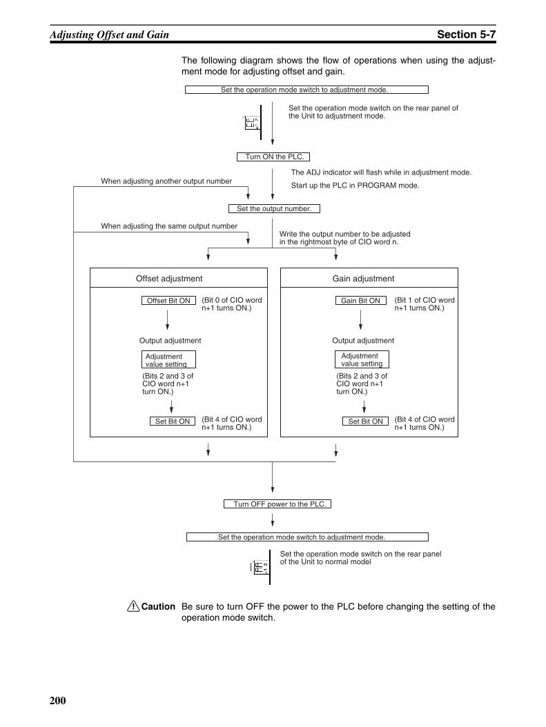
Adjusting Offset and Gain Section 5-7
The following diagram shows the flow of operations when using the adjust-ment mode for adjusting offset and gain.
!Caution Be sure to turn OFF the power to the PLC before changing the setting of theoperation mode switch.
Set the operation mode switch to adjustment mode.
Turn ON the PLC.
When adjusting another output number
When adjusting the same output number
Set the output number.
Offset adjustment
Offset Bit ON
Set Bit ON
Turn OFF power to the PLC.
Set the operation mode switch to adjustment mode.
The ADJ indicator will flash while in adjustment mode.
Gain adjustment
Gain Bit ON
Output adjustment
Set Bit ON
Output adjustment
Set the operation mode switch on the rear panel of the Unit to normal model
(Bit 4 of CIO word n+1 turns ON.)
(Bits 2 and 3 of CIO word n+1 turn ON.)
Adjustment value setting
(Bit 0 of CIO word n+1 turns ON.)
(Bit 4 of CIO word n+1 turns ON.)
(Bits 2 and 3 of CIO word n+1 turn ON.)
Adjustment value setting
(Bit 1 of CIO word n+1 turns ON.)
Write the output number to be adjusted in the rightmost byte of CIO word n.
Start up the PLC in PROGRAM mode.
Set the operation mode switch on the rear panel of the Unit to adjustment mode.
200

Adjusting Offset and Gain Section 5-7
!Caution Set the PLC to PROGRAM mode when using the Analog Output Unit inadjustment mode. If the PLC is in MONITOR mode or RUN mode, the AnalogOutput Unit will stop operating, and the output values that existed immediatelybefore this stoppage will be retained.
!Caution Always perform adjustments in conjunction with offset and gain adjustments.
5-7-2 Output Offset and Gain Adjustment ProceduresSpecifying Output Number to be Adjusted
To specify the output number to be adjusted, write the value to the rightmostbyte of CIO word n as shown in the following diagram.
For the CIO word addresses, n = CIO 2000 + unit number x 10.
The following example uses output number 1 adjustment for illustration. (Theunit number is 0.)
Bits Used for Adjusting Offset and Gain
The CIO word n+1 bits shown in the following diagram are used for adjustingoffset and gain.
(Rightmost)(Leftmost)
Word n
Output to be adjusted (1 to 8)(1 to 4 for CS1W-DA041)
I/O specification1: Output (fixed)
CLR000000 CT00
SHIFTCH
*DM2
C0
A0
A0
AMON
2000 0000
CHG2000 0000PRES VAL ????
1B
1B
WRITE2000 0011
15 14 13 12 11 10 09 08 07 06 05 04 03 02 01 00Bit
Word n+1
Cle
ar B
it
Set
Bit
Up
Bit
Dow
n B
it
Gai
n B
it
Offs
et B
it
201

Adjusting Offset and Gain Section 5-7
Offset Adjustment The procedure for adjusting the analog output offset is explained below. Asshown in the following diagram, the set value is adjusted so that the analogoutput reaches the standard value (0 V/1 V/4 mA).
The following example uses output number 1 adjustment for illustration. (Theunit number is 0.)
1,2,3... 1. Turn ON bit 00 (the Offset Bit) of CIO word n+1. (Hold the ON status.)
2. Check whether the output devices are connected.
3. Monitor CIO word n+8 and check the set value while the Offset Bit is ON.
10 V
00FA0
Offset adjustment output range
Output signal range:0 to 10 V
CLR000000 CT00
SHIFTCONT
# 2C
0A
0A
1B
0A
0A
MON
200100 ^ OFF
SET
200100 ^ ON
Voltage output/current output
Output 1
CS1W-DA08V/08CCS1W-DA041 (voltage output)
Current output
CS1W-DA041 (current output)
CLR000000 CT00
SHIFTCH
*DM 2C
0A
0A
8 MON
2008 0000
202

Adjusting Offset and Gain Section 5-7
4. Change the set value so that the output voltage are as shown in the follow-ing table. The data can be set within the indicated ranges.
Change the set value, using the Up Bit (bit 03 of word n+1) and the DownBit (bit 02 of word n+1).
• The following example increases the output voltage.
The bit will remain ON until the output becomes an appropriate value, atwhich time, it will turn OFF.
• The following example decreases the output voltage.
Output signal range Possible output voltage/current
adjustment
Output range
0 to 10 V –0.5 to 0.5 V FF38 to 00C8
–10 to 10 V –1.0 to 1.0 V
1 to 5 V 0.8 to 1.2 V
0 to 5 V –0.25 to 0.25 V
4 to 20 mA 3.2 to 4.8 mA
15 14 13 12 11 10 09 08 07 06 05 04 03 02 01 00Bit
Up Bit Down Bit
While the Down Bit is ON, the set value will be decreased by 1 resolution every 0.5 seconds. After it has been ON for 3 seconds, the set value will be decreased by 1 resolution every 0.1 seconds.
Word n+1
While the Up Bit is ON, the set value will be increased by 1 resolution every 0.5 seconds. After it has been ON for 3 seconds, the set value will be increased by 1 resolution every 0.1 seconds.
SHIFTCONT
#2
C0
A0
A1
B0
A3
DMON
200103 ^ OFF
SET200103 ^ ON
RESET
200103 ^ OFF
SHIFTCONT
#2
C
0A
0A
1B
0A
2C
MON
200102 ^ OFF
203

Adjusting Offset and Gain Section 5-7
The bit will remain ON until the output becomes an appropriate value, atwhich time, it will turn OFF.
5. Check the 0-V/1-V/4-mA output, and then turn bit 04 (the Set Bit) of CIOword n+1 ON and then OFF again.
While the Offset Bit is ON, the offset value will be saved to the Unit’s EE-PROM when the Set Bit turns ON.
6. To finish the offset adjustment, turn OFF bit 00 (the Offset Bit) of CIO wordn+1.
!Caution Do not turn OFF the power supply or restart the Unit while the Set Bit is ON(data is being written to the EEPROM). Otherwise, illegal data may be writtenin the Unit’s EEPROM and “EEPROM Errors” may occur when the power sup-ply is turned ON or when the Unit is restarted, causing a malfunction.
!Caution When making adjustments, be sure to perform both the offset adjustment andgain adjustment at the same time.
Note The EEPROM can be overwritten 50,000 times.
SET
200102 ^ ON
RESET
200102 ^ OFF
SHIFTCONT
#2
C0
A0
A1
B0
A4
EMON
200104 ^ OFF
SET
200104 ^ ON
RESET
200104 ^ OFF
SHIFTCONT
#2
C
0A
0A
1B
0A
0A
MON
200100 ^ ON
SET
200100 ^ OFF
204

Adjusting Offset and Gain Section 5-7
Gain Adjustment The procedure for adjusting the analog output gain is explained below. Asshown in the following diagram, the set value is adjusted so that the analogoutput is maximized (to 10 V/5 V/20 mA).
The following example uses output number 1 adjustment for illustration. (Theunit number is 0.)
1,2,3... 1. Turn ON bit 01 (the Gain Bit) of CIO word n+1. (Hold the ON status.)
2. Check whether the output devices are connected.
3. Monitor CIO word n+8 and check the set value while the Gain Bit is ON.
10 V
00FA0
Output signal range:0 to 10 V
Gain adjustment output range
CLR000000 CT00
SHIFTCONT
#2
C0
A0
A1
B0
A1
BMON
200101 ^ OFF
SET
200101 ^ ON
Voltage output/current output
Output 1
CS1W-DA08V/08CCS1W-DA041 (voltage output)
Current output
CS1W-DA041 (current output)
CLR000000 CT00
SHIFTCH
*DM2
C0
A0
A8 MON
2008 0000
205

Adjusting Offset and Gain Section 5-7
4. Change the set value so that the output voltage is as shown in the followingtable. The data can be set within the indicated ranges.
Change the set value, using the Up Bit (bit 03 of word n+1) and the DownBit (bit 02 of word n+1).
• The following example increases the output voltage.
The bit will remain ON until the output voltage becomes an appropriate val-ue, at which time, the output will turn OFF.
• The following example decreases the output voltage.
Output signal range Possible output voltage/current
adjustment
Output range
0 to 10 V 9.5 to 10.5 V 0ED8 to 1068
–10 to 10 V 9 to 11 V 0708 to 0898
1 to 5 V 4.8 to 5.2 V 0ED8 to 1068
0 to 5 V 4.75 to 5.25 V 0ED8 to 1068
4 to 20 mA 19.2 to 20.8 mA 0ED8 to 1068
15 14 13 12 11 10 09 08 07 06 05 04 03 02 01 00Bit
Up Bit Down Bit
While the Up Bit is ON, the set value will be increased by 1 resolution every 0.5 seconds. After it has been ON for 3 seconds, the set value will be increased by 1 resolution every 0.1 seconds.
While the Down Bit is ON, the set value will be decreased by 1 resolution every 0.5 seconds. After it has been ON for 3 seconds, the set value will be decreased by 1 resolution every 0.1 seconds.
Word n+1
SHIFTCONT
# 2C
0A
0A
1B
0A
3D
MON
200103 ^ OFF
SET200103 ^ ON
RESET
200103 ^ OFF
SHIFTCONT
#2
C0
A
0A
1B
0A
2C
MON
200102 ^ OFF
206
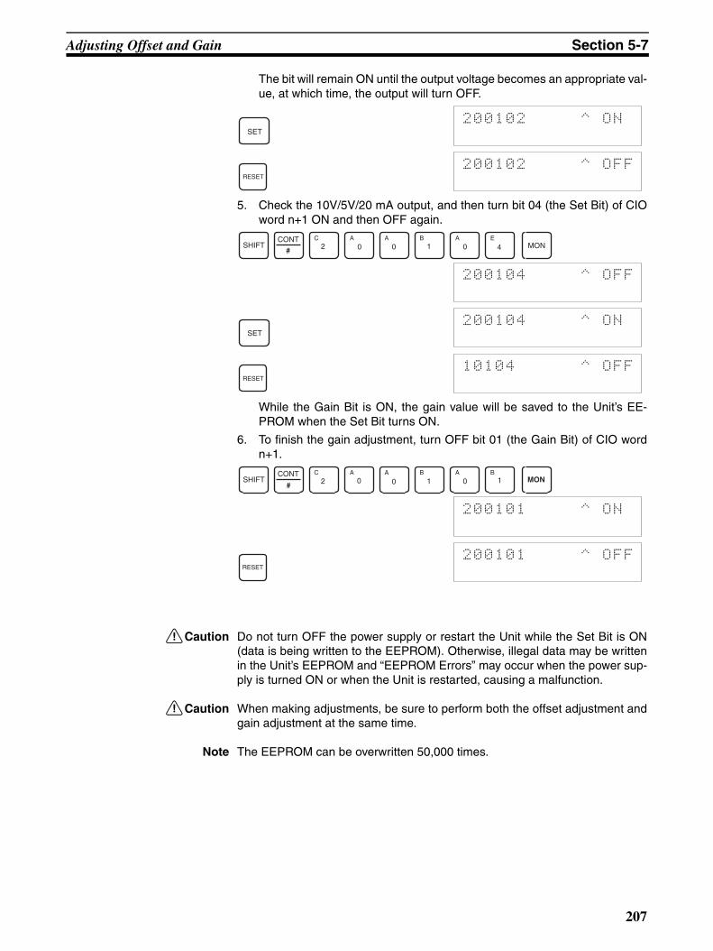
Adjusting Offset and Gain Section 5-7
The bit will remain ON until the output voltage becomes an appropriate val-ue, at which time, the output will turn OFF.
5. Check the 10V/5V/20 mA output, and then turn bit 04 (the Set Bit) of CIOword n+1 ON and then OFF again.
While the Gain Bit is ON, the gain value will be saved to the Unit’s EE-PROM when the Set Bit turns ON.
6. To finish the gain adjustment, turn OFF bit 01 (the Gain Bit) of CIO wordn+1.
!Caution Do not turn OFF the power supply or restart the Unit while the Set Bit is ON(data is being written to the EEPROM). Otherwise, illegal data may be writtenin the Unit’s EEPROM and “EEPROM Errors” may occur when the power sup-ply is turned ON or when the Unit is restarted, causing a malfunction.
!Caution When making adjustments, be sure to perform both the offset adjustment andgain adjustment at the same time.
Note The EEPROM can be overwritten 50,000 times.
SET
200102 ^ ON
RESET
200102 ^ OFF
SHIFTCONT
# 2C
0A
0A
1B
0A
4E
MON
200104 ^ OFF
SET200104 ^ ON
RESET
10104 ^ OFF
SHIFTCONT
# 2C
0A
0A
1B
0A
1B
MON
200101 ^ ON
RESET
200101 ^ OFF
207

Adjusting Offset and Gain Section 5-7
Clearing Offset and Gain Adjusted Values
Follow the procedure outlined below to return the offset and gain adjusted val-ues to their default settings.
The following example uses output number 1 adjustment for illustration. (Theunit number is 0.)
1,2,3... 1. Turn ON bit 05 (the Clear Bit) of CIO word n+1. (Hold the ON status.) Re-gardless of the set value, 0000 will be monitored in CIO word n+8.
2. Turn bit 04 of CIO word n+1 ON and then OFF again.
While the Clear Bit is ON, the adjusted value will be cleared and reset tothe default offset and gain values when the Set Bit turns ON.
3. To finish the clearing of adjusted values, turn OFF bit 05 (the Clear Bit) ofCIO word n+1.
!Caution Do not turn OFF the power supply or restart the Unit while the Set Bit is ON(data is being written to the EEPROM). Otherwise, illegal data may be writtenin the Unit’s EEPROM and “EEPROM Errors” may occur when the power sup-ply is turned ON or when the Unit is restarted, causing a malfunction.
Note The EEPROM can be overwritten 50,000 times.
SHIFTCONT
# 2C
0A
0A
1B
0A
5F
MON
200105 ^ OFF
SET
200105 ^ ON
SHIFTCONT
# 2C
0A
0A
1B
0A
4E
MON
200104 ^ OFF
SET
200104 ^ ON
RESET200104 ^ OFF
SHIFTCONT
# 2C
0A
0A
1B
0A
5F
MON
200105 ^ ON
RESET
200105 ^ OFF
208

Handling Errors and Alarms Section 5-8
5-8 Handling Errors and Alarms
5-8-1 Indicators and Error FlowchartIndicators If an alarm or error occurs in the Analog Output Unit, the ERC or ERH indica-
tors on the front panel of the Unit will light.
LED Meaning Indicator Operating status
RUN (green) Operating Lit Operating in normal mode.
Not lit Unit has stopped exchanging data with the CPU Unit.
ERC (red) Error detected by Unit
Lit Alarm has occurred (such as disconnec-tion detection) or initial settings are incor-rect.
Not lit Operating normally.
ADJ (yellow) Adjusting Flashing Operating in offset/gain adjustment mode.
Not lit Other than the above.
ERH (red) Error in the CPU Unit
Lit Error has occurred during data exchange with the CPU Unit.
Not lit Operating normally.
Front panel of Unit
RUN
ERC
ADJ
ERH
209

Handling Errors and Alarms Section 5-8
Troubleshooting Procedure
Use the following procedure for troubleshooting Analog Output Unit errors.
Is the ERC indicator lit?
Yes
No
Is the RUN indicator lit?
Yes
No
Alarm has occurred at the Analog Output Unit.
Check whether the initial settings for the Analog Output Unit are set correctly.
Is the ERH indicator lit?
Yes
No
Is the RUN indicator lit?
Yes
No
Error detected by CPU Unit
Check whether the unit number is set correctly.
Error occurs.
Yes
No
Is the RUN indicator lit?
Error cleared?
No
Cycle the power supplyto the PLC.
Error cleared?
No
The Unit is faulty.
Replace the Unit.
YesNoise or other disturbance may be causingmalfunctions. Check the operating environment.
Yes
Error in internal circuits has occurred, preventing operation from continuing.
(Refer to 5-8-2 Alarms Occurring at the Analog Output Unit.)
(Refer to 5-8-2 Alarms Occurring at the Analog Output Unit.)
(Refer to 5-8-3 Errors in the CPU Unit.)
(Refer to 5-8-3 Errors in the CPU Unit.)
Refer to 5-8-5 Troubleshooting.
Refer to 5-8-4 Restarting Special I/O Units.
210

Handling Errors and Alarms Section 5-8
5-8-2 Alarms Occurring at the Analog Output UnitThe ERC indicator will light when the Analog Output Unit detects an alarm.The Alarm Flags in bits 08 to 15 of CIO word n+9 will turn ON.
Note With the CS1W-DA041, the Output Setting Error Flags are bits 00 to 03.
For the CIO word addresses, n = CIO 2000 + (unit number × 10).
ERC and RUN Indicators: Lit
The ERC and RUN indicators will be lit if an error occurs while the Unit isoperating normally. The following alarm flags will turn ON in CIO word n+9.These alarm flags will turn OFF automatically when the error is cleared.
Note 1. n = CIO 2000 + (unit number × 10).
2. The Output Setting Error Flags for the CS1W-DA041 are bits 00 to 03. Bits04 to 07 are not used (always OFF).
15 14 13 12 11 10 09 08 07 06 05 04 03 02 01 00Bit
Word n+9
Output Setting Error FlagsAlarm Flags(See 5-6-4 Output Setting Errors.)
RUN
ERC ERH
: Lit
: Not lit
Word n + 9 Alarm flag Error contents Output status Countermeasure
Bits 00 to 07 (See note 1.)
Output Set Value Error
The output setting range has been exceeded.
Output value set by output hold function.
Correct the set value.
Bit 14 (Adjustment mode)
EEPROM Writ-ing Error
An EEPROM writing error has occurred while in adjustment mode.
Holds the out-put status imme-diately prior to the error.
Turn the Set Bit OFF, ON, and OFF again.
If the error persists even after the reset, replace the Analog Output Unit.
211

Handling Errors and Alarms Section 5-8
ERC Indicator and RUN Indicator: Lit, ADJ Indicator: Flashing
This alarm will occur in the case of incorrect operation while in the adjustmentmode. In adjustment mode, the Adjustment Mode ON Flag will turn ON in bit15 of CIO word n+9.
Note When a PLC error occurs in the adjustment mode, Unit operations will stopoperating. (The input and output values immediately prior to the error will beheld.)
ERC Indicator: Lit, RUN Indicator: Not Lit
The ERC indicator will be lit when the initial settings for the Analog OutputUnit are not set correctly. The alarm flags for the following errors will turn ONin CIO word n+9. These alarm flags will turn OFF when the error is clearedand the power to the PLC is cycled, or the Special I/O Unit Restart Bit isturned ON and then OFF again.
Note Bit 15 is normally turned OFF (i.e., set to 0).
5-8-3 Errors in the CPU UnitThe ERH indicator will light if an error occurs in the CPU Unit or I/O bus and I/O refreshing with the Special I/O Units is not performed correctly, preventingthe Analog Output Unit from operating.
ERH and RUN Indicators: Lit
RUN
ERC ERH
ADJ
: Lit
: Flashing
: Not lit
Word n + 9 Alarm flag Error contents Output status Countermeasure
Bit 13 (Adjustment mode)
Output Number Setting Error
In adjustment mode, adjust-ment cannot be performed because the specified output number is not set for use or because the wrong output num-ber is specified.
The output volt-age or current becomes 0 V or 0 mA.
Check whether the word n out-put number to be adjusted is set from 11 to 14.Check whether the output num-ber to be adjusted is set for use by means of the DM setting.
Bit 15 only ON (Adjustment Mode)
PLC Error
The PLC is in either MONITOR or RUN mode while the Analog Output Unit is operating in adjustment mode.
The output volt-age or current becomes 0 V or 0 mA.
Detach the Unit. Switch the rear panel DIP switch pin to OFF. Restart the Unit in normal mode.
RUN
ERC ERH
: Lit
: Not lit
Word n + 9 Alarm flag Error contents Countermeasure
Bit 10 Output Hold Setting Error
The setting of the output status for when conversion is stopped is wrong.
Specify a number from 0000 to 0002.
RUN
ERC ERH
: Lit
: Not lit
212
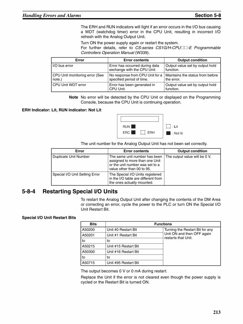
Handling Errors and Alarms Section 5-8
The ERH and RUN indicators will lIght if an error occurs in the I/O bus causinga WDT (watchdog timer) error in the CPU Unit, resulting in incorrect I/Orefresh with the Analog Output Unit.
Turn ON the power supply again or restart the system.For further details, refer to CS-series CS1G/H-CPU@@-E ProgrammableControllers Operation Manual (W339).
Note No error will be detected by the CPU Unit or displayed on the ProgrammingConsole, because the CPU Unit is continuing operation.
ERH Indicator: Lit, RUN Indicator: Not Lit
The unit number for the Analog Output Unit has not been set correctly.
5-8-4 Restarting Special I/O UnitsTo restart the Analog Output Unit after changing the contents of the DM Areaor correcting an error, cycle the power to the PLC or turn ON the Special I/OUnit Restart Bit.
Special I/O Unit Restart Bits
The output becomes 0 V or 0 mA during restart.
Replace the Unit if the error is not cleared even though the power supply iscycled or the Restart Bit is turned ON.
Error Error contents Output condition
I/O bus error Error has occurred during data exchange with the CPU Unit.
Output value set by output hold function.
CPU Unit monitoring error (See note.)
No response from CPU Unit for a specified period of time.
Maintains the status from before the error.
CPU Unit WDT error Error has been generated in CPU Unit.
Output value set by output hold function.
RUN
ERC ERH
: Lit
: Not lit
Error Error contents Output condition
Duplicate Unit Number The same unit number has been assigned to more than one Unit or the unit number was set to a value other than 00 to 95.
The output value will be 0 V.
Special I/O Unit Setting Error The Special I/O Units registered in the I/O table are different from the ones actually mounted.
Bits Functions
A50200 Unit #0 Restart Bit Turning the Restart Bit for any Unit ON and then OFF again restarts that Unit.
A50201 Unit #1 Restart Bit
to to
A50215 Unit #15 Restart Bit
A50300 Unit #16 Restart Bit
to to
A50715 Unit #95 Restart Bit
213

Handling Errors and Alarms Section 5-8
5-8-5 TroubleshootingThe following tables list the probable causes of troubles that may occur, andthe countermeasures for dealing with them.
Analog Output Does Not Change
Value Does Not Change as Intended
Outputs Are Inconsistent
Probable Cause Countermeasure Page
The output is not set for being used. Set the output for being used. 195
The output hold function is in opera-tion.
Turn ON the Output Conversion Enable Bit.
198
The conversion value is set outside of the permissible range.
Set the data within the range. 174
Probable Cause Countermeasure Page
The output signal range setting is wrong.
Correct the output signal range set-ting.
196
The specifications of the output device do not match those of the Analog Output Unit (e.g., input sig-nal range, input impedance).
Change the output device. 172
The offset or gain is not adjusted. Adjust the offset or gain. 199
Probable Cause Countermeasure Page
The output signals are being affected by external noise.
Try changing the shielded cable connection (e.g., the grounding at the output device).
188
214

SECTION 6CJ-series Analog Output Unit (CJ1W-DA021/041/08V/08C)
This section explains how to use the CJ1W-DA021/041/08V/08C Analog Output Units.
6-1 Specifications . . . . . . . . . . . . . . . . . . . . . . . . . . . . . . . . . . . . . . . . . . . . . . . . . 216
6-1-1 Specifications . . . . . . . . . . . . . . . . . . . . . . . . . . . . . . . . . . . . . . . . . . 216
6-1-2 Output Function Block Diagram . . . . . . . . . . . . . . . . . . . . . . . . . . . 218
6-1-3 Output Specifications . . . . . . . . . . . . . . . . . . . . . . . . . . . . . . . . . . . . 218
6-2 Operating Procedure . . . . . . . . . . . . . . . . . . . . . . . . . . . . . . . . . . . . . . . . . . . . 220
6-2-1 Procedure Examples . . . . . . . . . . . . . . . . . . . . . . . . . . . . . . . . . . . . . 222
6-3 Components and Switch Settings . . . . . . . . . . . . . . . . . . . . . . . . . . . . . . . . . . 228
6-3-1 Indicators . . . . . . . . . . . . . . . . . . . . . . . . . . . . . . . . . . . . . . . . . . . . . 229
6-3-2 Unit Number Switches . . . . . . . . . . . . . . . . . . . . . . . . . . . . . . . . . . . 229
6-3-3 Operation Mode Switch (DA021/041) . . . . . . . . . . . . . . . . . . . . . . . 230
6-4 Wiring . . . . . . . . . . . . . . . . . . . . . . . . . . . . . . . . . . . . . . . . . . . . . . . . . . . . . . . 230
6-4-1 Terminal Arrangement . . . . . . . . . . . . . . . . . . . . . . . . . . . . . . . . . . . 230
6-4-2 Internal Circuitry . . . . . . . . . . . . . . . . . . . . . . . . . . . . . . . . . . . . . . . 232
6-4-3 Output Wiring Example . . . . . . . . . . . . . . . . . . . . . . . . . . . . . . . . . . 233
6-4-4 Output Wiring Considerations . . . . . . . . . . . . . . . . . . . . . . . . . . . . . 233
6-5 Exchanging Data with the CPU Unit . . . . . . . . . . . . . . . . . . . . . . . . . . . . . . . 234
6-5-1 Outline of Data Exchange. . . . . . . . . . . . . . . . . . . . . . . . . . . . . . . . . 234
6-5-2 Unit Number Setting. . . . . . . . . . . . . . . . . . . . . . . . . . . . . . . . . . . . . 235
6-5-3 Special I/O Unit Restart Bits . . . . . . . . . . . . . . . . . . . . . . . . . . . . . . 235
6-5-4 Fixed Data Allocations . . . . . . . . . . . . . . . . . . . . . . . . . . . . . . . . . . . 236
6-5-5 I/O Refresh Data Allocations . . . . . . . . . . . . . . . . . . . . . . . . . . . . . . 239
6-6 Analog Output Functions and Operating Procedures . . . . . . . . . . . . . . . . . . . 243
6-6-1 Output Settings and Conversions . . . . . . . . . . . . . . . . . . . . . . . . . . . 243
6-6-2 Conversion Time/Resolution Setting (CJ1W-DA08V/08C Only) . . 245
6-6-3 Starting and Stopping Conversion . . . . . . . . . . . . . . . . . . . . . . . . . . 245
6-6-4 Output Hold Function . . . . . . . . . . . . . . . . . . . . . . . . . . . . . . . . . . . . 246
6-6-5 Output Scaling (CJ1W-DA08V/08C Only) . . . . . . . . . . . . . . . . . . . 247
6-6-6 Output Setting Errors . . . . . . . . . . . . . . . . . . . . . . . . . . . . . . . . . . . . 249
6-7 Adjusting Offset and Gain . . . . . . . . . . . . . . . . . . . . . . . . . . . . . . . . . . . . . . . 250
6-7-1 Adjustment Mode Operational Flow . . . . . . . . . . . . . . . . . . . . . . . . 250
6-7-2 Output Offset and Gain Adjustment Procedures . . . . . . . . . . . . . . . 253
6-8 Handling Errors and Alarms . . . . . . . . . . . . . . . . . . . . . . . . . . . . . . . . . . . . . . 261
6-8-1 Indicators and Error Flowchart . . . . . . . . . . . . . . . . . . . . . . . . . . . . . 261
6-8-2 Alarms Occurring at the Analog Output Unit. . . . . . . . . . . . . . . . . . 263
6-8-3 Errors in the CPU Unit . . . . . . . . . . . . . . . . . . . . . . . . . . . . . . . . . . . 265
6-8-4 Restarting Special I/O Units . . . . . . . . . . . . . . . . . . . . . . . . . . . . . . . 266
6-8-5 Troubleshooting . . . . . . . . . . . . . . . . . . . . . . . . . . . . . . . . . . . . . . . . 266
215

Specifications Section 6-1
6-1 Specifications
6-1-1 Specifications
Output Specifications and Functions
Item CJ1W-DA021 CJ1W-DA041 CJ1W-DA08V CJ1W-DA08C
Unit type CJ-series Special I/O Unit
Isolation (See note 1.) Between outputs and PLC signals: Photocoupler (No isolation between output signals.)
External terminals 18-point detachable terminal block (M3 screws)
Affect on CPU Unit cycle time
0.2 ms
Current consumption 5 VDC, 120 mA max. 5 VDC, 140 mA max.
External power supply 24 VDC +10%, −15% (inrush current: 20 A max., pulse width: 1 ms min.)
140 mA max. 200 mA max. 140 mA max. 170 mA max.
Dimensions (mm) (See note 2.)
31 × 90 × 65 (W × H × D)
Weight 150 g max.
General specifications Conforms to general specifications for SYSMAC CJ-series Series.
Mounting position CJ-series CPU Rack or CJ-series Expansion Rack
Maximum number of Units
Per CPU Rack or Expansion Rack (See note 3.)
Power Supply Unit No. of mountable Units
CJ1W-PA205RCJ1W-PA205CCJ1W-PD025
CPU Rack: 10 Units/RackExpansion Rack: 10 Units/Rack
CJ1W-PA202 CPU Rack: 10 Units/RackExpansion Rack: 10 Units/Rack
CJ1W-PD022 CPU Rack: 10 Units/RackExpansion Rack: 10 Units/Rack
Data exchange with CPU Unit
Special I/O Unit AreaCIO 200000 to CIO295915
(Words CIO 2000 to CIO 2959)
Internal Special I/O Unit DM Area
(D20000 to D29599)
Item CJ1W-DA021 CJ1W-DA041 CJ1W-DA08V CJ1W-DA08C
Number of analog outputs 2 4 8 8
Output signal range
(See note 4.)
1 to 5 V/4 to 20 mA0 to 5 V0 to 10 V−10 to +10 V
1 to 5 V0 to 5 V0 to 10 V−10 to +10 V
4 to 20 mA
Output impedance 0.5 Ω max. (for voltage output)
Max. output current (for 1 point) 12 mA (for voltage output) 2.4 mA (for voltage output)
---
Maximum permissible load resis-tance
600 Ω (current output) --- 350 Ω
Resolution 4,000 (full scale) 4,000/8,000 (See note 9.)
Set data 16-bit binary data
Accuracy
(See note 6.)
23±2°C Voltage output: ±0.3% of full scaleCurrent output: ±0.5% of full scale
±0.3% of full scale ±0.3% of full scale
0°C to 55°C Voltage output: ±0.5% of full scaleCurrent output: ±0.8% of full scale
±0.5% of full scale ±0.6% of full scale
D/A conversion period (See note 7.)
1.0 ms/point max. 1.0 ms or 250 µs max. per point
216
Specifications Section 6-1
Note 1. Do not apply a voltage higher than 600 V to the terminal block when per-forming withstand voltage test on this Unit.
2. Refer to Dimensions on page 439 for details on the Unit’s dimensions.
3. This is the maximum number of Units that can be mounted to a CJ2H-CPU6@ CPU Unit (no EtherNet/IP). The maximum number of Analog InputUnits that can be mounted to one Rack varies depending on the currentconsumption of the other Units mounted to the Rack.
Select a 24-VDC power supply based on the surge current. The followingOMRON power supplies are recommended.
S82K-05024: 100 VAC, 50 WS82K-10024: 100 VAC, 100 W
4. Data exchange methods with the CPU Unit are as follows:
5. Output signal ranges can be set for each output.
6. The accuracy is given for full scale. For example, an accuracy of ±0.3%means a maximum error of ±12 (BCD) at a resolution of 4,000. For theCJ1W-DA021/041, the accuracy is at the factory setting for a current out-put. When using a voltage output, adjust the offset gain as required.
7. D/A conversion time is the time required for converting and outputting thePLC data. It takes at least one cycle for the data stored in the PLC to beread by the Analog Output Unit.
8. When the operation mode for the CPU Unit is changed from RUN mode orMONITOR mode to PROGRAM mode, or when the power is turned ON,the Output Conversion Enable Bit will turn OFF. The output status specifiedaccording to the output hold function will be output.
9. The CJ1W-DA08V/08C can be set to a conversion cycle of 250 µs and aresolution of 8,000 using the setting in D(m+18).
Output hold function
Outputs the specified output status (CLR, HOLD, or MAX) under any of the following circumstances.When the Conversion Enable Bit is OFF. (See note 8.)
In adjustment mode, when a value other than the output number is output during adjustment.
When there is an output setting error or a fatal error occurs at the PLC. (See note 10.)When the Load is OFF.
Scaling function Setting values in any specified unit within a range of ±32,000 as the upper and lower limits allows D/A conversion to be executed and analog signals to be output with these values as full scale.
(With the CJ1W-DA08V/DA08C, this function is enabled only for a conversion time of 1.0 s and a reso-lution of 4,000.)
Item CJ1W-DA021 CJ1W-DA041 CJ1W-DA08V CJ1W-DA08C
Special I/O Unit Area in CIO Area
CIO 2000 to CIO 2959 (CIO 200000 to CIO 295915
10 words per Unit
Refreshed cycli-cally
CPU Unit to Analog I/O Unit
Analog output valuesConversion enable bits
Analog I/O Unit to CPU Unit
Alarm flags
Special I/O Unit Area in DM Area
D20000 to D29599
100 words per UnitRefreshed at power ON and restarts
CPU Unit to Analog I/O Unit
Output signal conversion settings and signal rangesOutput status when hold-ing outputs
217
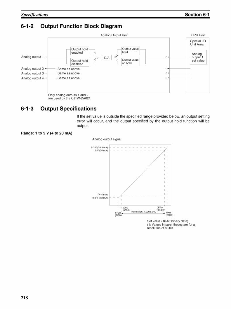
Specifications Section 6-1
6-1-2 Output Function Block Diagram
6-1-3 Output SpecificationsIf the set value is outside the specified range provided below, an output settingerror will occur, and the output specified by the output hold function will beoutput.
Range: 1 to 5 V (4 to 20 mA)
Analog Output Unit CPU Unit
D/AAnalog output 1
Same as above.Analog output 2Same as above.Analog output 3
Same as above.Analog output 4
Output hold enabled
Output hold disabled
Output value, hold
Output value, no hold
Special I/O Unit Area
Analog output 1 set value
Only analog outputs 1 and 2 are used by the CJ1W-DA021.
5.2 V (20.8 mA)5 V (20 mA)
1 V (4 mA)0.8 V (3.2 mA)
0000(0000)
FF38(FE70)
0FA0(1F40)
1068(20D0)
Resolution: 4,000/8,000
Set value (16-bit binary data)
Analog output signal
( ): Values in parentheses are for aresolution of 8,000.
218

Specifications Section 6-1
Range: 0 to 10 V
Range: 0 to 5 V
0000(0000)FF38
(FE70)
0FA0(1F40)
1068(20D0)
10.5 V10 V
0 V−0.5 V
Resolution: 4,000/8,000
Set value (16-bit binary data)
Analog output signal
( ): Values in parentheses are for a resolution of 8,000.
0000(0000)FF38
(FE70)
0FA0(1F40)
1068(20D0)
5.25 V5 V
0 V−0.25 V
Resolution: 4,000/8,000
Set value (16-bit binary data)
Analog output signal
( ): Values in parentheses are for a resolution of 8,000.
219

Operating Procedure Section 6-2
Range: −10 to 10 V
Note The set values for a range of –10 to 10 V will be as follows:
6-2 Operating ProcedureFollow the procedures outlined below when using CJ1W-DA021/041 andCJ1W-DA08V/08C Analog Output Units.
Installation and Settings
CJ1W-DA021/041
1,2,3... 1. Set the operation mode switch on the front panel of the Unit to normalmode.
2. Use the unit number switches on the front panel of the Unit to set the unitnumber.
3. Wire the Unit.
4. Turn ON the power to the PLC.
5. Turn ON the power to the external devices.
6. Create the I/O tables.
7. Make the Special I/O Unit DM Area settings.
• Set the output numbers to be used.
• Set the output signal ranges.
0000(0000)
F830(F060)
F768(FED0)
07D0(0FA0)
0898(1130)
0 V
−10 V−11 V
11 V10 V
Resolution: 4,000/8,000
Set value (16-bit binary data)
Analog output signal
( ): Values in parentheses are for aresolution of 8,000.
16-bit binary data (when resolution is
4,000)
BCD
F768 –2200
: :
FFFF –1
0000 0
0001 1
: :
0898 2200
220

Operating Procedure Section 6-2
• Set the output hold function.
8. Turn the power to the PLC OFF and ON, or turn ON the Special I/O UnitRestart Bit.
When the output for the connected devices needs to be calibrated, follow theprocedures in Offset and Gain Adjustment below. Otherwise, skip to Opera-tion below.
Offset and Gain Adjustment
1,2,3... 1. Set the operation mode switch on the front panel of the Unit to adjustmentmode.
2. Turn ON the power to the PLC.Be sure to set the PLC to PROGRAM mode.
3. Turn ON the power to the external devices.
4. Adjust the offset and gain.
5. Turn OFF the power to the external devices.
6. Turn OFF the power to the PLC.
7. Change the setting of the operation mode switch on the front panel of theUnit back to normal mode.
Operation
1,2,3... 1. Turn ON the power to the PLC.
2. Turn ON the power to the external devices.
3. Ladder program
• Write set values by means of MOV(021) and XFER(070).
• Start and stop conversion output.
• Obtain error codes.
Note Turn the external power supply ON and OFF while power is supplied to theCPU Unit or simultaneously with the CPU Unit. Do not turn the external powersupply ON or OFF when power is not supplied to the CPU Unit.
Installation and Settings
CJ1W-DA08V/08C
1,2,3... 1. Use the unit number switches on the front panel of the Unit to set the unitnumber.
2. Wire the Unit.
3. Turn ON the power to the PLC.
4. Turn ON the power to the external devices.
5. Create the I/O tables.
6. Make the Special I/O Unit DM Area settings.
• Set the output numbers to be used.
• Set the output signal ranges. (Not required for the CJ1W-DA08C.)
• Set the output hold function.
• Set the conversion time and resolution.
• Set the scaling function
7. Turn the power to the PLC OFF and ON, or turn ON the Special I/O UnitRestart Bit.
221

Operating Procedure Section 6-2
When the output for the connected devices needs to be calibrated, follow theprocedures in Offset and Gain Adjustment below. Otherwise, skip to Opera-tion below.
Offset and Gain Adjustment
1,2,3... 1. Turn ON the power to the PLC.Be sure to set the PLC to PROGRAM mode.
2. Turn ON the power to the external devices.
3. Set the mode to adjustment mode in the Special I/O Unit DM Area.
4. Turn the power to the PLC OFF and ON, or turn ON the Special I/O UnitRestart Bit.
5. Adjust the offset and gain.
6. Set the mode to normal mode in the Special I/O Unit DM Area.
7. Restart the Analog Output Unit using its Special I/O Unit Restart Bit or turnthe power supply to the PLC OFF and ON.
OperationLadder program
• Write set values by means of MOV(021) and XFER(070).
• Start and stop conversion output.
• Obtain error codes.
Note Turn the external power supply ON and OFF while power is supplied to theCPU Unit or simultaneously with the CPU Unit. Do not turn the external powersupply ON or OFF when power is not supplied to the CPU Unit.
6-2-1 Procedure Examples
DA041
B1 A1
MACHNo.x10 1
x10 0
RUNERCERHADJ
MODE
12
D00200
D00201
D00202
CJ1W-DA041 CJ-series CPU Unit
OUT1: 1 to 5 V
OUT2: 1 to 5 V
OUT3: −10 to 10V
OUT4: Not used
Analog outputs
Unit No. 1
Ladd
er p
rogr
am
222

Operating Procedure Section 6-2
Setting the Analog Output Unit
1,2,3... 1. Set the operation mode switch on the front panel of the Unit. Refer to 6-3-3 Operation Mode Switch (DA021/041) for further details.The CJ1W-DA08V/08C does not have this switch. Change the mode bymaking the setting in D (m+18).
2. Set the unit number switches. Refer to 6-3-2 Unit Number Switches for fur-ther details.
3. Connect and wire the Analog Output Unit. Refer to 1-2-1 Mounting Proce-dure, Note The CJ1W-DA08V/08C Analog Output Unit has a software set-ting for the operation mode in bits 00 to 07 of DM word m+18. The contentsof DM word m+18 are shown below. or 6-4-3 Output Wiring Example forfurther details.
MACHNo.
DA041RUNERCERH B1 A1ADJ
x101
x100
09
8765 4 321
09
8765 4 321
ON1
2MODE
OFF
OFF
ON1
2
MODE
Turn OFF SW1 for normal mode.
MACHNo.
DA041RUNERCERH B1 A1ADJ
x10 1
x10 0
09
8765 4 321
09
8765 4 321
ON1
2
MODE
MACHNo.
101
100
09
8765 4 321
09
8765 4 321
If the unit number is set to 1, words CIO 2010 to CIO 2019 in the Special I/O Unit Area in the CIO Area and words D20100 to D20199 in the Special I/O Unit Area in the DM Area will be allocated to the Analog Output Unit.
OD261SYSMACCJ1G-CPU44PROGRAMMABLECONTROLLER
RUNERR/ALM
INHPRPHLCOMM
OPEN
PERIHERAL
PORT
MCPWR
BUSY
0 1 2 3 4 5 6 78 9 10 11 12 13 14 15
20
1
CN1
DC24
V 0.
3A
1
20
CN2
B/A A/B
0
1
2
3
0 1 2 3 4 5 6 78 9 10 11 12 13 14 15
AD081
B1 A1
MACHNo.x10 1
x10 0
RUNERCERHADJ
MODE
12
DA041
B1 A1
MACHNo.x10 1
x10 0
RUNERCERHADJ
MODE
12
223

Operating Procedure Section 6-2
4. Turn ON the power to the PLC.
5. Turn ON the power to the external devices. (Can be turned ON at the sametime as the PLC.)
Creating I/O TablesAfter turning ON the power to the PLC, be sure to create the I/O tables.
Initial Data Settings
1,2,3... 1. Specify the Special I/O Unit settings in the DM Area. Refer to DM Alloca-tion Contents on page 236 for further details.
OD261SYSMACCJ1G-CPU44PROGRAMMABLECONTROLLER
RUNERR/ALM
INHPRPHLCOMM
OPEN
PERIHERAL
PORT
MCPWR
BUSY
0 1 2 3 4 5 6 78 9 10 11 12 13 14 15
20
1
CN1
DC24
V 0.
3A
1
20
CN2
B/A A/B
0
1
2
3
0 1 2 3 4 5 6 78 9 10 11 12 13 14 15
AD081
B1 A1
MACHNo.x10 1
x10 0
RUNERCERHADJ
MODE
12
DA041
B1 A1
MACHNo.x10 1
x10 0
RUNERCERHADJ
MODE
12
Peripheral port
Programming Console
OD261SYSMACCJ1G-CPU44PROGRAMMABLECONTROLLER
RUNERR/ALM
INHPRPHLCOMM
OPEN
PERIHERAL
PORT
MCPWR
BUSY
0 1 2 3 4 5 6 78 9 10 11 12 13 14 15
20
1
CN1
DC24
V 0.
3A
1
20
CN2
B/A A/B
0
1
2
3
0 1 2 3 4 5 6 78 9 10 11 12 13 14 15
AD081
B1 A1
MACHNo.x10 1
x10 0
RUNERCERHADJ
MODE
12
DA041
B1 A1
MACHNo.x10 1
x10 0
RUNERCERHADJ
MODE
12
ConditionsUnit number: 1Analog output 1: 1 to 5 VAnalog output 2: 1 to 5 VAnalog output 3: −10 to 10 VAnalog output 4: Not used
Programming Console
Peripheral port
224
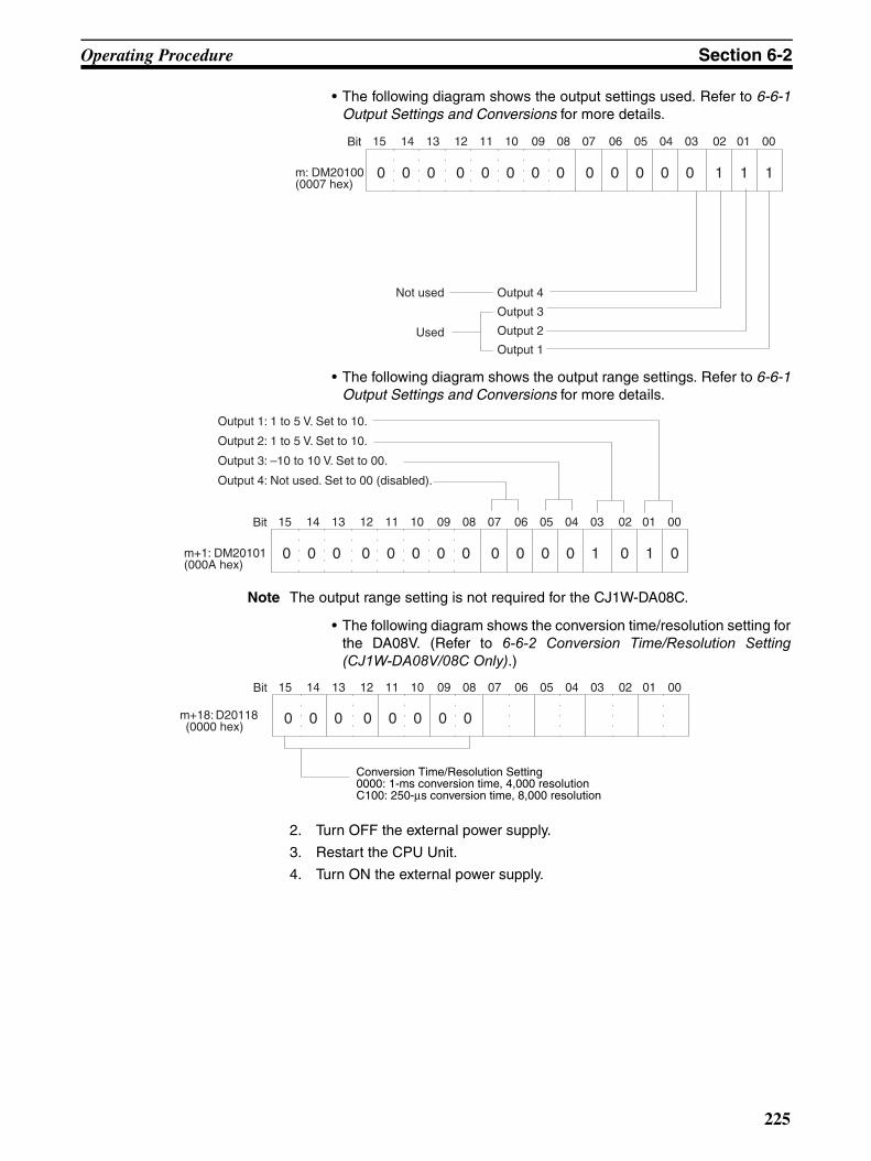
Operating Procedure Section 6-2
• The following diagram shows the output settings used. Refer to 6-6-1Output Settings and Conversions for more details.
• The following diagram shows the output range settings. Refer to 6-6-1Output Settings and Conversions for more details.
Note The output range setting is not required for the CJ1W-DA08C.
• The following diagram shows the conversion time/resolution setting forthe DA08V. (Refer to 6-6-2 Conversion Time/Resolution Setting(CJ1W-DA08V/08C Only).)
2. Turn OFF the external power supply.
3. Restart the CPU Unit.
4. Turn ON the external power supply.
15 14 13 12 11 10 09 08 07 06 05 01 0004 03 02
0 0 0 0 0 0 0 0 0 0 0 0 0 1 1 1
Bit
Not used Output 4
Output 3
Output 2
Output 1Used
m: DM20100(0007 hex)
15 14 13 12 11 10 09 08 07 06 05 01 0004 03 02
0 0 0 0 0 0 0 0 0 0 0 0 1 0 1 0
Bit
m+1: DM20101(000A hex)
Output 1: 1 to 5 V. Set to 10.
Output 2: 1 to 5 V. Set to 10.
Output 3: –10 to 10 V. Set to 00.
Output 4: Not used. Set to 00 (disabled).
15 14 13 12 11 10 09 08 07 06 05 01 0004 03 02
0 0 0 0 0 0 0 0
Bit
m+18: D20118(0000 hex)
Conversion Time/Resolution Setting0000: 1-ms conversion time, 4,000 resolutionC100: 250-µs conversion time, 8,000 resolution
225

Operating Procedure Section 6-2
Creating Ladder Programs
The setting address D00200 is stored in words (n + 1) to (n + 3) of the SpecialI/O Unit Area (CIO 2011 to CIO 2013) as a signed binary value between 0000to 0FA0 hex.
The following table shows the addresses used for analog output.
Note 1. The addresses are determined by the unit number of the Special I/O Unit.Refer to 6-3-2 Unit Number Switches for further details.
Output number Output signal range
Address of output set value
(n = CIO 2010)See note 1.
Conversion source address
1 1 to 5 V (n+1) = CIO 2011 D00200
2 0 to 10 V (n+2) = CIO 2012 D00201
3 –10 to 10 V (n+3) = CIO 2013 D00202
4 Not used. --- ---
OD261SYSMACCJ1G-CPU44PROGRAMMABLECONTROLLER
RUNERR/ALM
INHPRPHLCOMM
OPEN
PERIHERAL
PORT
MCPWR
BUSY
0 1 2 3 4 5 6 78 9 10 11 12 13 14 15
20
1
CN1
DC
24V
0.3A
1
20
CN2
B/A A/B
0
1
2
3
0 1 2 3 4 5 6 78 9 10 11 12 13 14 15
AD081
B1 A1
MACHNo.x10 1
x10 0
RUNERCERHADJ
MODE
12
DA041
B1 A1
MACHNo.x10 1
x10 0
RUNERCERHADJ
MODE
12
Peripheral port
Programming Console
226

Operating Procedure Section 6-2
2. Set as required.
D00200 is set in word CIO 2011.
D00201 is set in word CIO 2012.
D00202 is set in word CIO 2013.
To start analog output, turn ON the Conversion Enable Bits 201000 to 201002 (bits 00 to 03 of word CIO 2010).
The data in words CIO 2011 and 2012 will be output as 1 to 5 V, and CIO the data in CIO 2013 will be output as –10 to 10 V.
MOV (021)
D00200
2011
MOV (021)
D00201
2012
Execution condition
MOV (021)
D00202
2013
SET
201000
SET
201002
SET
201001
Execution condition
See 6-6-3 Starting and Stopping Conversion for details.
227
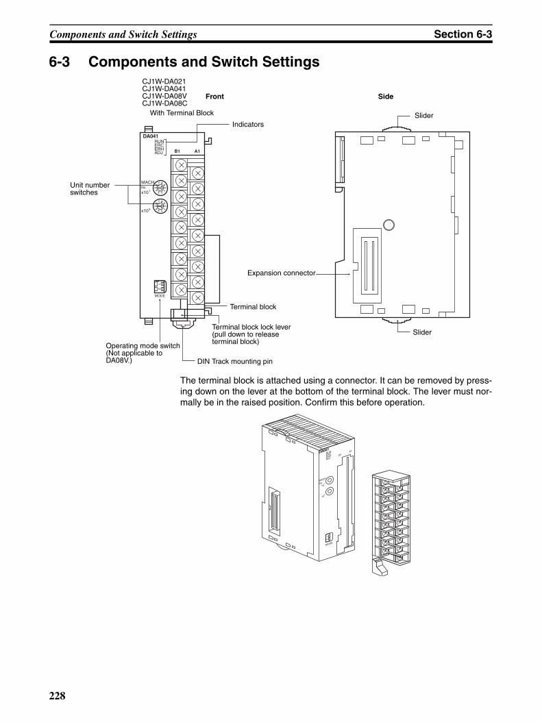
Components and Switch Settings Section 6-3
6-3 Components and Switch Settings
The terminal block is attached using a connector. It can be removed by press-ing down on the lever at the bottom of the terminal block. The lever must nor-mally be in the raised position. Confirm this before operation.
MACHNo.
DA041RUNERCERH B1 A1ADJ
x101
x100
09
8765 4 321
09
8765 4 321
ON1
2
MODE
With Terminal Block
Indicators
Terminal block lock lever (pull down to release terminal block)
DIN Track mounting pin
Operating mode switch(Not applicable to DA08V.)
Unit number switches
Front Side
Slider
Slider
Expansion connector
Terminal block
CJ1W-DA021CJ1W-DA041CJ1W-DA08VCJ1W-DA08C
B1A1DA041
MACH
No.10
1
100
RUNERCERHADJ
MODE
12
228

Components and Switch Settings Section 6-3
6-3-1 IndicatorsThe indicators show the operating status of the Unit. The following tableshows the meanings of the indicators.
6-3-2 Unit Number SwitchesThe CPU Unit and Analog Output Unit exchange data via the Special I/O UnitAreas in the CIO Area and DM Area. The words that are allocated to eachAnalog Output Unit in the Special I/O Unit Areas in the CIO Area and DM Areaare determined by the setting of the unit number switches on the front panel ofthe Unit.
Always turn OFF the power before setting the unit number. Use a flat-bladescrewdriver, being careful not to damage the slot in the screw. Be sure not toleave the switch midway between settings.
Note If two or more Special I/O Units are assigned the same unit number, a “UNITNo. DPL ERR” error (in the Programming Console) will be generated (A40113will turn ON) and the PLC will not operate.
Indicator Meaning Indicator status
Operating status
RUN (green) Operating Lit Operating in normal mode.
Not lit Unit has stopped exchanging data with the CPU Unit.
ERC (red) Error detected by Unit
Lit Alarm has occurred (such as disconnec-tion detection) or initial settings are incor-rect.
Not lit Operating normally.
ERH (red) Error in the CPU Unit
Lit Error has occurred during data exchange with the CPU Unit.
Not lit Operating normally.
ADJ (yellow) Adjusting Flashing Operating in offset/gain adjustment mode.
Not lit Other than the above.
Switch setting
Unit number
Words allocated in Special I/O Unit Area in
CIO Area
Words allocated in Special I/O Unit Area in DM Area
0 Unit #0 CIO 2000 to CIO 2009 D20000 to D20099
1 Unit #1 CIO 2010 to CIO 2019 D20100 to D20199
2 Unit #2 CIO 2020 to CIO 2029 D20200 to D20299
3 Unit #3 CIO 2030 to CIO 2039 D20300 to D20399
4 Unit #4 CIO 2040 to CIO 2049 D20400 to D20499
5 Unit #5 CIO 2050 to CIO 2059 D20500 to D20599
6 Unit #6 CIO 2060 to CIO 2069 D20600 to D20699
7 Unit #7 CIO 2070 to CIO 2079 D20700 to D20799
8 Unit #8 CIO 2080 to CIO 2089 D20800 to D20899
9 Unit #9 CIO 2090 to CIO 2099 D20900 to D20999
10 Unit #10 CIO 2100 to CIO 2109 D21000 to D21099
to to to to
n Unit #n CIO 2000 + (n × 10) to CIO 2000 + (n × 10) + 9
D20000 + (n × 100) to D20000 + (n × 100) + 99
to to to to
95 Unit #95 CIO 2950 to CIO 2959 D29500 to D29599
MACHNo.
101
100
09
8765 4 321
09
8765 4 321
229

Wiring Section 6-4
6-3-3 Operation Mode Switch (DA021/041)The operation mode switch on the front panel of the Unit is used to set theoperation mode to either normal mode or adjustment mode (for adjusting off-set and gain).(The CJ1W-DA08V/08C does not have this switch. Change the mode by mak-ing the setting in bits 00 to 07 of DM word m+18. Set 00 for adjustment modeor 01 for normal mode.)
!Caution Do not set the pins to any combination other than those shown in the abovetable. Be sure to set pin 2 to OFF.
!Caution Be sure to turn OFF the power to the PLC before installing or removing theUnit.
Note The CJ1W-DA08V/08C Analog Output Unit has a software setting for theoperation mode in bits 00 to 07 of DM word m+18. The contents of DM wordm+18 are shown below.
m = D20000 + (unit number × 100)
6-4 Wiring
6-4-1 Terminal ArrangementThe signal names corresponding to the connecting terminals are as shown inthe following diagram.
CJ1W-DA021
Pin number Mode
1 2
OFF OFF Normal mode
ON OFF Adjustment mode
ON1
2
MODE
Bit 15 14 13 12 11 10 09 08 07 06 05 04 03 02 01 00
D (m+18) Conversion time/resolution setting00: Conversion time of 1 ms and resolution of 4,000C1: Conversion time of 250 µs and resolution of 8,000
Operation mode setting
00: Normal modeC1: Adjustment mode
Voltage output 2 (+)
Output 2 (–)
Current output 2 (+)
N.C.
N.C.
N.C.
N.C.
N.C.
0 V
Voltage output 1 (+)
Output 1 (–)
Current output 1 (+)
N.C.
N.C.
N.C.
N.C.
N.C.
24 V
B1
B2
B3
B4
B5
B6
B7
B8
B9
A1
A2
A3
A4
A5
A6
A7
A8
A9
230

Wiring Section 6-4
CJ1W-DA041
CJ1W-DA08V (Voltage Output)and CJ1W-DA08C (Current Output)
1. The number of analog outputs that can be used is set in the DM Area.
2. The output signal ranges for individual outputs are set in the DM Area. Theoutput signal range can be set separately for each output.
3. The N.C. terminals are not connected to internal circuitry.
4. We recommend the following external power supplies.
!Caution Use a separate power supply from the one used for Basic I/O Units. FaultyUnit operation may be caused by noise if power is supplied from the samesource.
Voltage output 2 (+)
Output 2 (–)
Current output 2 (+)
Voltage output 4 (+)
Output 4 (–)
Current output 4 (+)
N.C.
N.C.
0 V
Voltage output 1 (+)
Output 1 (–)
Current output 1 (+)
Voltage output 3 (+)
Output 3 (–)
Current output 3 (+)
N.C.
N.C.
24 V
B1
B2
B3
B4
B5
B6
B7
B8
B9
A1
A2
A3
A4
A5
A6
A7
A8
A9
Maker Model number Specifications
OMRON S82K-05024 100 VAC, 50 W
S82K-10024 100 VAC, 100 W
B1
B2
B3
B4
B5
B6
B7
B8
B9
Output 2 (+)
Output 2 (−)
Output 4 (+)
Output 4 (−)
Output 6 (+)
Output 6 (−)
Output 8 (+)
Output 8 (−)
0 V
A1
A2
A3
A4
A5
A6
A7
A8
A9
Output 1 (+)
Output 1 (−)
Output 3 (+)
Output 3 (−)
Output 5 (+)
Output 5 (−)
Output 7 (+)
Output 7 (−)
24 V
231
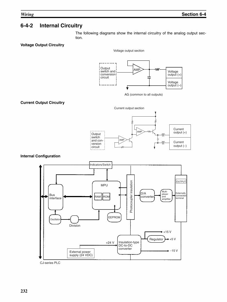
Wiring Section 6-4
6-4-2 Internal CircuitryThe following diagrams show the internal circuitry of the analog output sec-tion.
Voltage Output Circuitry
Current Output Circuitry
Internal Configuration
Output switch and conversion circuit
AMP Voltage output (+)
Voltage output (–)
AG (common to all outputs)
Voltage output section
AMP
Current output section
Output switch and con-version circuit
Current output (+)
Current output (−)
AMP
Indicators/Switch
MPUOUTPUT
Regulator
Oscillator
Division
CJ-series PLC
EEPROM
RAM ROM
Pho
toco
uple
r in
sula
tion
+24 V+5 V
−15 V
+15 V
Bus interface
D/A converter
Multi-plexer and amplifier
Externally connected terminal
Insulation-type DC-to-DC converter
External power supply (24 VDC)
232

Wiring Section 6-4
6-4-3 Output Wiring Example
Note Crimp terminals must be used for terminal connections, and the screws mustbe tightened securely. M3 terminal screws are used. The applicable tighten-ing torque is 0.5 N·m.
To minimize output wiring noise, ground the output signal line to the inputdevice.
6-4-4 Output Wiring ConsiderationsWhen wiring outputs, apply the following points to avoid noise interferenceand optimize Analog Output Unit performance.
• Use two-core shielded twisted-pair cables for output connections.
• Route output cables separately from the AC cable, and do not run theUnit’s cables near a main circuit cable or a high voltage cable. Do notinsert output cables into the same duct.
• If there is noise interference from power lines (if, for example, the powersupply is shared with electrical welding devices or electrical dischargemachines, or if there is a high-frequency generation source nearby) installa noise filter at the power supply input area.
• Use a separate power supply for the external power supply from the oneused for Basic I/O Units. If the same power supply is used, noise maycause Units to malfunction.
Output 2 (voltage output)
Output 4 (current output)
Output 1(voltage output)
Output 3(current output)
0 V24 VDC
External power supply
+−
−+
+−
−+
B1
B2
B3
B4
B5
B6
B7
B8
B9
A1
A2
A3
A4
A5
A6
A7
A8
A9
CJ1W-DA041
6.2 mm max.
6.2 mm max.M3 screw
Fork type
Round type
233

Exchanging Data with the CPU Unit Section 6-5
6-5 Exchanging Data with the CPU Unit
6-5-1 Outline of Data ExchangeData is exchanged between the CPU Unit and the Analog Output Unit via theSpecial I/O Unit Area (for data used to operate the Unit) and the Special I/OUnit DM Area (for data used for initial settings).
I/O Refresh Data
Analog output setting values and other data used to operate the Unit are allo-cated in the Special I/O Unit Area of the CPU Unit according to the unit num-ber, and are exchanged during I/O refreshing.
Fixed Data
The Unit’s fixed data, such as the analog output signal ranges and the outputstatus when conversion is stopped, is allocated in the Special I/O Unit DMArea of the CPU Unit according to the unit number, and is exchanged whenthe power is turned ON or the Unit is restarted.
CJ-series CPU Unit CJ1W-DA021/041/08V/08C Analog Output Unit
Special I/O Unit Area I/O Refresh Data
Analog outputs
DM (Data Memory) Area
I/O refresh
2000 + n x 10
2000 + n x 10 + 9
D20000 + n x 100
D20000 + n x 100 + 99
Fixed Data
:
:
10 words
100 words
Analog output ranges
Output status when conversion stopped
Power ON or Unit restart
Exchanges analog output values exchanged during data refresh.
Transmits fixed data such as conversion stop values and analog output ranges.
n: Unit number
See Allocations for Normal Mode on page 239 for details.
See Allocations in DM Area on page 236 for details.
234

Exchanging Data with the CPU Unit Section 6-5
6-5-2 Unit Number SettingThe words in the Special I/O Unit Areas in the CIO Area and DM Area that areallocated to each Analog Output Unit are determined by the setting of the unitnumber switches on the front panel of the Unit.
Note If two or more Special I/O Units are assigned the same unit number, a “UNITNo. DPL ERR” error (in the Programming Console) will be generated (A40113will turn ON) and the PLC will not operate.
6-5-3 Special I/O Unit Restart BitsTo restart the Analog Output Unit after changing the contents of the DM Areaor correcting an error, cycle the power to the PLC or turn ON the Special I/OUnit Restart Bit.
Note Replace the Unit if the error is not cleared even though the power supply iscycled or the Restart Bit is turned ON.
Switch setting
Unit number
Words allocated in Special I/O Unit Area in
CIO Area
Words allocated in Special I/O Unit Area in DM Area
0 Unit #0 CIO 2000 to CIO 2009 D20000 to D20099
1 Unit #1 CIO 2010 to CIO 2019 D20100 to D20199
2 Unit #2 CIO 2020 to CIO 2029 D20200 to D20299
3 Unit #3 CIO 2030 to CIO 2039 D20300 to D20399
4 Unit #4 CIO 2040 to CIO 2049 D20400 to D20499
5 Unit #5 CIO 2050 to CIO 2059 D20500 to D20599
6 Unit #6 CIO 2060 to CIO 2069 D20600 to D20699
7 Unit #7 CIO 2070 to CIO 2079 D20700 to D20799
8 Unit #8 CIO 2080 to CIO 2089 D20800 to D20899
9 Unit #9 CIO 2090 to CIO 2099 D20900 to D20999
10 Unit #10 CIO 2100 to CIO 2109 D21000 to D21099
to to to to
n Unit #n CIO 2000 + (n × 10) to CIO 2000 + (n × 10) + 9
D20000 + (n × 100) to D20000 + (n × 100) + 99
to to to to
95 Unit #95 CIO 2950 to CIO 2959 D29500 to D29599
MACHNo.
101
100
09
8765 4 321
09
8765 4 321
Special I/O Unit Area word address
Function
A50200 Unit No. 0 Restart Bit Restarts the Unit when turned ON.A50201 Unit No. 1 Restart Bit
to to
A50215 Unit No. 15 Restart Bit
A50300 Unit No. 16 Restart Bit
to to
A50715 Unit No. 95 Restart Bit
235

Exchanging Data with the CPU Unit Section 6-5
6-5-4 Fixed Data AllocationsDM Area The initial settings of the Analog Output Unit are set according to the data
allocated in the Special I/O Unit Area in the DM Area. Settings, such as theoutputs used, and the analog output signal ranges must be set in this area.
Note 1. The words in the Special I/O Unit Area in the DM Area that are allocatedto the Analog Output Unit are set using the unit number switches on thefront panel of the Unit. Refer to 6-3-2 Unit Number Switches for details onthe method used to set the unit number switches.
2. If two or more Special I/O Units are assigned the same unit number, a“UNIT No. DPL ERR” error (in the Programming Console) will be generat-ed (A40113 will turn ON) and the PLC will not operate.
Allocations in DM Area The following table shows the allocation of DM words and bits for both normaland adjustment mode.
CJ1W-DA021
D (m+1)
D (m)
D20300 to D20399
D20400 to D20499
D20500 to D20599
D20000 to D20099
D20100 to D20199
D20200 to D20299
D20900 to D20999
D20600 to D20699
D20700 to D20799
D20800 to D20899
SYSMAC CJ-series PLC CJ1W-DA021/041/08V/08C Analog Output Unit
(Fixed Data Area)
Unit #0
Unit #1
Unit #2
Unit #3
Unit #4
Unit #5
Unit #6
Unit #7
Unit #8
Unit #9
(Special I/O Unit DM Area)
Word
D29500 to D29599
D21000 to D21099Unit #10
Unit #n
Unit #95
m = 20000 + (unit number × 100)D20000 + (n × 100) to
D20000 + (n × 100) + 99
Data is automatically transferred to each unit number when the power is turned ON, or when the Special I/O Unit Restart Bit is turned ON.
Outputs used setting
Output signal range
D (m+2 to m+9) (See note.)
Output hold function setting
D (m+10 to m+17)
Not used.
D (m+18) Conversion time/resolution and operation mode settings
D (m+19 to m+34)
Scaling function setting
to
to
to
to
DM Area word
Bits
15 14 13 12 11 10 9 8 7 6 5 4 3 2 1 0
D (m) Not used. Not used. Output use setting
Out-put 2
Out-put 1
D (m+1) Not used. Not used. Output signal range set-ting
Output 2 Output 1
D (m+2) Not used. Output 1: Output status when conversion stopped
D (m+3) Not used. Output 2: Output status when conversion stopped
236
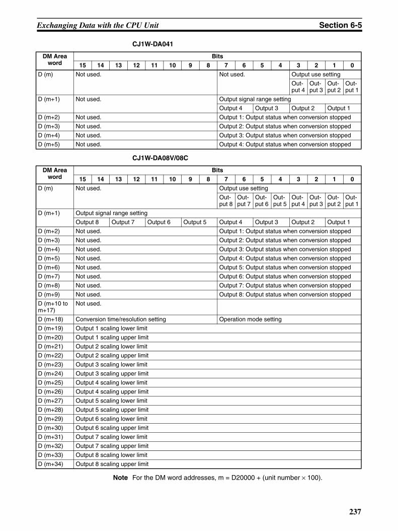
Exchanging Data with the CPU Unit Section 6-5
CJ1W-DA041
CJ1W-DA08V/08C
Note For the DM word addresses, m = D20000 + (unit number × 100).
DM Area word
Bits
15 14 13 12 11 10 9 8 7 6 5 4 3 2 1 0
D (m) Not used. Not used. Output use setting
Out-put 4
Out-put 3
Out-put 2
Out-put 1
D (m+1) Not used. Output signal range setting
Output 4 Output 3 Output 2 Output 1
D (m+2) Not used. Output 1: Output status when conversion stopped
D (m+3) Not used. Output 2: Output status when conversion stopped
D (m+4) Not used. Output 3: Output status when conversion stopped
D (m+5) Not used. Output 4: Output status when conversion stopped
DM Area word
Bits
15 14 13 12 11 10 9 8 7 6 5 4 3 2 1 0
D (m) Not used. Output use setting
Out-put 8
Out-put 7
Out-put 6
Out-put 5
Out-put 4
Out-put 3
Out-put 2
Out-put 1
D (m+1) Output signal range setting
Output 8 Output 7 Output 6 Output 5 Output 4 Output 3 Output 2 Output 1
D (m+2) Not used. Output 1: Output status when conversion stopped
D (m+3) Not used. Output 2: Output status when conversion stopped
D (m+4) Not used. Output 3: Output status when conversion stopped
D (m+5) Not used. Output 4: Output status when conversion stopped
D (m+6) Not used. Output 5: Output status when conversion stopped
D (m+7) Not used. Output 6: Output status when conversion stopped
D (m+8) Not used. Output 7: Output status when conversion stopped
D (m+9) Not used. Output 8: Output status when conversion stopped
D (m+10 to m+17)
Not used.
D (m+18) Conversion time/resolution setting Operation mode setting
D (m+19) Output 1 scaling lower limit
D (m+20) Output 1 scaling upper limit
D (m+21) Output 2 scaling lower limit
D (m+22) Output 2 scaling upper limit
D (m+23) Output 3 scaling lower limit
D (m+24) Output 3 scaling upper limit
D (m+25) Output 4 scaling lower limit
D (m+26) Output 4 scaling upper limit
D (m+27) Output 5 scaling lower limit
D (m+28) Output 5 scaling upper limit
D (m+29) Output 6 scaling lower limit
D (m+30) Output 6 scaling upper limit
D (m+31) Output 7 scaling lower limit
D (m+32) Output 7 scaling upper limit
D (m+33) Output 8 scaling lower limit
D (m+34) Output 8 scaling upper limit
237

Exchanging Data with the CPU Unit Section 6-5
Set Values and Stored Values
Note 1. When using a CJ1W-DA08C, these output signal range settings are invalidand the contents will be ignored. The output signal range for the CJ1W-DA08C is fixed at 4 to 20 mA.
2. The output signal ranges 1 to 5 V and 4 to 20 mA are switched using theoutput terminal connections. For details, refer to 6-4 Wiring. (The CJ1W-DA08V supports only voltage outputs.)
3. The values output for the signal ranges will be 0 V for the range of ±10 V,and the minimum value for the other ranges. For details, refer to 6-6-4 Out-put Hold Function.
Item Contents Page
Output Use setting 0: Not used.1: Used.
236, 242
Output signal range (See note 1.)
00: –10 to 10 V01: 0 to 10 V10: 1 to 5 V/4 to 20 mA (See note 2.)11: 0 to 5 V
236, 242
Output status when stopped 00: CLR Outputs 0 or minimum value of each range. (See note 3.)
01: HOLD Holds output just before stopping.02: MAX Outputs maximum value of range.
245
Conversion time/resolution setting
00: Conversion time: 1 ms; resolution: 4,00001: Conversion time: 250 µs; resolution: 8,000
245
Operation mode setting 00: Normal mode01: Adjustment mode
230
Scaling settings Any value other than 0 within range of ±32,000 (8300 hex to 7D00 hex) as long as the upper limit is not equal to the lower limit.
247
238

Exchanging Data with the CPU Unit Section 6-5
6-5-5 I/O Refresh Data AllocationsI/O refresh data for the Analog Output Unit is exchanged according to the allo-cations in the Special I/O Unit Area.
Note 1. The Special I/O Unit Area words that are occupied by the Analog OutputUnit are set using the unit number switches on the front panel of the Unit.Refer to 6-3-2 Unit Number Switches for details on the method used to setthe unit number switches.
2. If two or more Special I/O Units are assigned the same unit number, a“UNIT No. DPL ERR” error (in the Programming Console) will be generat-ed (A40113 will turn ON) and the PLC will not operate.
Allocations for Normal Mode
For normal mode, with CJ1W-DA021/041 Units, set the operation modeswitch on the front panel of the Unit as shown in the following diagram. (TheCJ1W-DA08V/08C does not have this switch. Change the mode by setting bits00 to 07 in D(m+18) to 00 hex.)
The allocation of words and bits in the CIO Area is shown in the followingtable.
CIO n + 9CIO 2030 to CIO 2039
CIO 2040 to CIO 2049
CIO 2050 to CIO 2059
CIO 2000 to CIO 2009
CIO 2010 to CIO 2019
CIO 2020 to CIO 2029
CIO 2090 to CIO 2099
CIO 2060 to CIO 2069
CIO 2070 to CIO 2079
CIO 2080 to CIO 2089
SYSMAC CJ-series CPU Unit CJ1W-DA021/041/08V/08C Analog Output Unit
IN refresh
(I/O Refresh Data Area)
Unit #0
Unit #1
Unit #2
Unit #3
Unit #4
Unit #5
Unit #6
Unit #7
Unit #8
Unit #9
(Special I/O Unit Area)
OUT refresh
Allocated words
CIO 2950 to CIO 2959
CIO 2100 to CIO 2109Unit #10
Unit #n
Unit #95
Normal mode
CIO n + 9 IN refresh
OUT refresh
Adjustment mode
n = 2000 + (unit number × 10)
I/O refresh
CIO 2000 + (n × 10) to CIO 2000 + (n × 10) + 9
At the I/O refresh by the PLC, outputs (CPU to Unit) and inputs (Unit to CPU) are refreshed in order with every cycle.
CIO n to CIO n + 8
CIO n to CIO n + 7
to
to
to
to
ON1
2
MODE
OFF
OFF
239

Exchanging Data with the CPU Unit Section 6-5
CJ1W-DA021
CJ1W-DA041
I/O Word Bits
15 14 13 12 11 10 9 8 7 6 5 4 3 2 1 0
Output (CPU to Unit)
n Not used. Not used. Conversion enable--- --- Out-
put 2Out-put 1
n + 1 Output 1 set value
163 162 161 160
n + 2 Output 2 set value
n + 3 Not used.
n + 4 Not used.
n + 5 Not used.
n + 6 Not used.
n + 7 Not used.
n + 8 Not used.
Input (Unit to CPU)
n + 9 Alarm Flags Not used. Output setting error--- --- Out-
put 2Out-put 1
I/O Word Bits
15 14 13 12 11 10 9 8 7 6 5 4 3 2 1 0
Output (CPU to Unit)
n Not used. Not used. Conversion enableOut-put 4
Out-put 3
Out-put 2
Out-put 1
n + 1 Output 1 set value
163 162 161 160
n + 2 Output 2 set value
n + 3 Output 3 set value
n + 4 Output 4 set value
n + 5 Not used.
n + 6 Not used.
n + 7 Not used.
n + 8 Not used.
Input (Unit to CPU)
n + 9 Alarm Flags Not used. Output setting errorOut-put 4
Out-put 3
Out-put 2
Out-put 1
240

Exchanging Data with the CPU Unit Section 6-5
CJ1W-DA08V/08C
Note For the CIO word addresses, n = CIO 2000 + unit number × 10.
Set Values and Stored Values
Allocation for Adjustment Mode
For adjustment mode, set the operation mode switch on the front panel of theUnit as shown in the following diagram. When the Unit is set for adjustmentmode, the ADJ indicator on the front panel of the Unit will flash. (The CJ1W-DA08V/08C does not have this switch. Change the mode by set-ting bits 00 to 07 in D (m+18) to C1 hex.)
I/O Word Bits
15 14 13 12 11 10 9 8 7 6 5 4 3 2 1 0
Output (CPU to Unit)
n Not used. Conversion enable
--- Out-put 8
Out-put 7
Out-put 6
Out-put 5
Out-put 4
Out-put 3
Out-put 2
Out-put 1
n + 1 Output 1 set value
163 162 161 160
n + 2 Output 2 set value
n + 3 Output 3 set value
n + 4 Output 4 set value
n + 5 Output 5 set value
n + 6 Output 6 set value
n + 7 Output 7 set value
n + 8 Output 8 set value
Input (Unit to CPU)
n + 9 Alarm Flags Output setting errorOut-put 8
Out-put 7
Out-put 6
Out-put 5
Out-put 4
Out-put 3
Out-put 2
Out-put 1
Item Contents Page
Conversion enable 0: Conversion output stopped.1: Conversion output begun.
245
Set value 16-bit binary data 244
Output setting error 0: No error1: Output setting error
249
Alarm Flags Bits 00 to 07: Output setting error (CJ1W-DA021: bits 00 and 01, CJ1W-DA041: bits 00 to 03)
Bit 08: Scaling data setting errorBit 09: Not used.Bit 10: Output hold setting errorBit 11: Not used.Bit 12: Conversion time/resolution or operation mode setting errorBit 15: Operating in adjustment mode
(Always 0 in normal mode.)
239, 263
ON1
2
MODE
ON
OFF
241
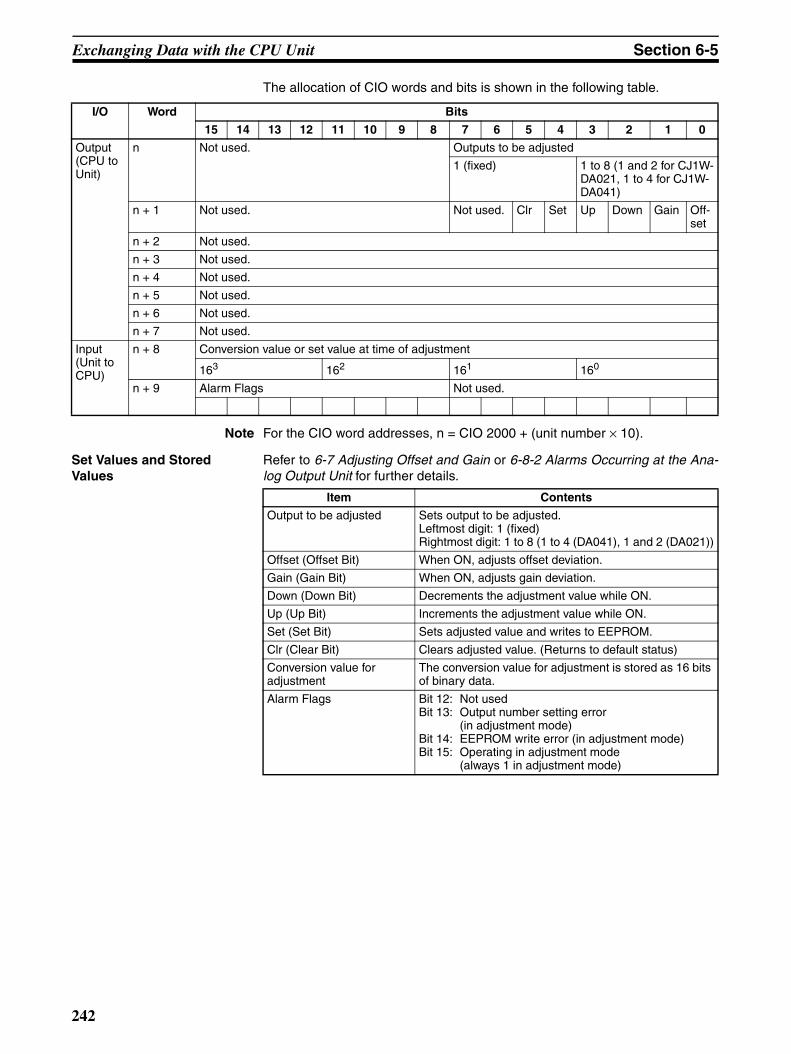
Exchanging Data with the CPU Unit Section 6-5
The allocation of CIO words and bits is shown in the following table.
Note For the CIO word addresses, n = CIO 2000 + (unit number × 10).
Set Values and Stored Values
Refer to 6-7 Adjusting Offset and Gain or 6-8-2 Alarms Occurring at the Ana-log Output Unit for further details.
I/O Word Bits
15 14 13 12 11 10 9 8 7 6 5 4 3 2 1 0
Output (CPU to Unit)
n Not used. Outputs to be adjusted
1 (fixed) 1 to 8 (1 and 2 for CJ1W-DA021, 1 to 4 for CJ1W-DA041)
n + 1 Not used. Not used. Clr Set Up Down Gain Off-set
n + 2 Not used.
n + 3 Not used.
n + 4 Not used.
n + 5 Not used.
n + 6 Not used.
n + 7 Not used.
Input (Unit to CPU)
n + 8 Conversion value or set value at time of adjustment
163 162 161 160
n + 9 Alarm Flags Not used.
Item Contents
Output to be adjusted Sets output to be adjusted.Leftmost digit: 1 (fixed)Rightmost digit: 1 to 8 (1 to 4 (DA041), 1 and 2 (DA021))
Offset (Offset Bit) When ON, adjusts offset deviation.
Gain (Gain Bit) When ON, adjusts gain deviation.
Down (Down Bit) Decrements the adjustment value while ON.
Up (Up Bit) Increments the adjustment value while ON.
Set (Set Bit) Sets adjusted value and writes to EEPROM.
Clr (Clear Bit) Clears adjusted value. (Returns to default status)
Conversion value for adjustment
The conversion value for adjustment is stored as 16 bits of binary data.
Alarm Flags Bit 12: Not usedBit 13: Output number setting error
(in adjustment mode)Bit 14: EEPROM write error (in adjustment mode)Bit 15: Operating in adjustment mode
(always 1 in adjustment mode)
242

Analog Output Functions and Operating Procedures Section 6-6
6-6 Analog Output Functions and Operating Procedures
6-6-1 Output Settings and ConversionsOutput Numbers The Analog Output Unit converts only analog outputs specified by output
numbers 1 to 8 (1 to 4 for the CJ1W-DA041, and 1 and 2 for the CJ1W-DA021). To specify the analog outputs to be used, turn ON from a Program-ming Device the D(m) bits in the DM Area shown in the following diagram.
The analog output conversion cycle can be shortened by setting any unusedoutput numbers to 0.
Conversion cycle = (1 ms) (See note 3.) × (Number of outputs used)
Note 1. For the DM word addresses, m = D20000 + (unit number × 100).
2. Output numbers not used (set to 0) will be output at 0 V.
3. With the CJ1W-DA08V, the value will be 250 µs when set for a conversiontime of 250 µs and a resolution of 8,000.
Output Signal Range Any of four types of output signal range (–10 to 10 V, 0 to 10 V, 1 to 5 V, 4 to20 mA, and 0 to 5 V) can be selected for each of the outputs (only voltage out-put for the CJ1W-DA08V). (The output signal range for the CJ1W-DA08C is 4to 20 mA only.) To specify the output signal range for each output, use a Pro-gramming Device to set the D (m+1) bits in the DM Area as shown in the fol-lowing diagram.
Note 1. For the DM word addresses, m = D20000 + (unit number × 100).
2. The 1 to 5 V output range and the 4 to 20 mA output range are switchedby changing the terminal connections.
3. When data memory settings have been carried out using a ProgrammingDevice, be sure to either cycle the power supply to the PLC, or turn ON the
15 14 13 12 11 10 09 08 07 06 05 04 03 02 01 00Bit
D (m)
Out
put 2
Out
put 1
0: Not used1: Used
Out
put 4
Out
put 3Only outputs 1 and 2 are used
by the CJ1W-DA021.Only outputs 1 to 4 are used by the CJ1W-DA041
Out
put 6
Out
put 5
Out
put 8
Out
put 7
15 14 13 12 11 10 09 08 07 06 05 04 03 02 01 00Bit
D (m+1)
Out
put 2
Out
put 1
00: −10 to 10 V01: 0 to 10 V10: 1 to 5 V (4 to 20 mA) (See note.)11: 0 to 5 V
Out
put 4
Out
put 3
Only outputs 1 and 2 are used by the CJ1W-DA021.Only outputs 1 to 4 are used by the CJ1W-DA041.
Out
put 6
Out
put 5
Out
put 8
Out
put 7
Note Only voltage output is enabled for the CJ1W-DA08V. A range of 4 to 20 mA cannot be set.
243

Analog Output Functions and Operating Procedures Section 6-6
Special I/O Unit Restart Bit. The contents of the data memory settings willbe transferred to the Special I/O Unit when the power is turned ON or theSpecial I/O Unit Restart Bit is ON.
4. The CJ1W-DA08C provides current output (4 to 20 mA) only. The CJ1W-DA08C cannot be used for voltage output.
Writing Set Values Analog output set values are written to CIO words n+1 to n+8 (CIO words n+1to n+4 for the CJ1W-DA041, n+1 and n+2 for the CJ1W-DA021).
For the CIO word addresses, n = CIO 2000 + (unit number × 10).
Use MOV(021) or XFER(070) to write values in the user program.
Example 1 In this example, the set value from only one output is written. (The unit num-ber is 0.)
Example 2 In this example, multiple set values are written. (The unit number is #0.)
Note If the set value has been written outside the specified range, an output settingerror will occur, and the value set by the output hold function will be output.
Word Function Stored value
n+1 Output 1 set value 16-bit binary data
n+2 Output 2 set value
n+3 Output 3 set value
n+4 Output 4 set value
n+5 Output 5 set value
n+6 Output 6 set value
n+7 Output 7 set value
n+8 Output 8 set value
MOV (021)
D00001
2001
Input conditionThe set value stored in D 00001 is written to CIO word 2001 (out-put number 1).
XFER(070)
#0008
D00001
2001
Input condition
The set values stored in D 00001 to D 00008 are written to CIO words 2001 to 2008 (outputs 1 to 8).
244
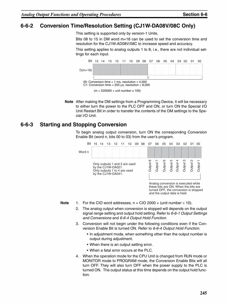
Analog Output Functions and Operating Procedures Section 6-6
6-6-2 Conversion Time/Resolution Setting (CJ1W-DA08V/08C Only)
This setting is supported only by version-1 Units.
Bits 08 to 15 in DM word m+18 can be used to set the conversion time andresolution for the CJ1W-AD08V/08C to increase speed and accuracy.
This setting applies to analog outputs 1 to 8, i.e., there are not individual set-tings for each input.
Note After making the DM settings from a Programming Device, it will be necessaryto either turn the power to the PLC OFF and ON, or turn ON the Special I/OUnit Restart Bit in order to transfer the contents of the DM settings to the Spe-cial I/O Unit.
6-6-3 Starting and Stopping ConversionTo begin analog output conversion, turn ON the corresponding ConversionEnable Bit (word n, bits 00 to 03) from the user’s program.
Note 1. For the CIO word addresses, n = CIO 2000 + (unit number × 10).
2. The analog output when conversion is stopped will depends on the outputsignal range setting and output hold setting. Refer to 6-6-1 Output Settingsand Conversions and 6-6-4 Output Hold Function.
3. Conversion will not begin under the following conditions even if the Con-version Enable Bit is turned ON. Refer to 6-6-4 Output Hold Function.
• In adjustment mode, when something other than the output number isoutput during adjustment.
• When there is an output setting error.
• When a fatal error occurs at the PLC.
4. When the operation mode for the CPU Unit is changed from RUN mode orMONITOR mode to PROGRAM mode, the Conversion Enable Bits will allturn OFF. They will also turn OFF when the power supply to the PLC isturned ON. The output status at this time depends on the output hold func-tion.
15 14 13 12 11 10 09 08 07 06 05 04 03 02 01 00Bit
D(m+18)
00: Conversion time = 1 ms, resolution = 4,000C1: Conversion time = 250 µs, resolution = 8,000
(m = D20000 + unit number x 100)
15 14 13 12 11 10 09 08 07 06 05 04 03 02 01 00Bit
Out
put 2
Out
put 1
Word n
Out
put 4
Out
put 3Only outputs 1 and 2 are used
by the CJ1W-DA021.Only outputs 1 to 4 are used by the CJ1W-DA041.
Out
put 6
Out
put 5
Out
put 8
Out
put 7
Analog conversion is executed while these bits are ON. When the bits are turned OFF, the conversion is stopped and the output data is held.
245

Analog Output Functions and Operating Procedures Section 6-6
In this example, conversion is begun for analog output number 1. (The unitnumber is 0.)
6-6-4 Output Hold FunctionThe Analog Output Unit stops conversion under the following conditions andoutputs the value set for the output hold function.
1,2,3... 1. When the Conversion Enable Bit is OFF. Refer to Allocations for NormalMode on page 239 and 6-6-3 Starting and Stopping Conversion.
2. In adjustment mode, when something other than the output number is out-put during adjustment. Refer to Allocation for Adjustment Mode onpage 241.
3. When there is an output setting error. Refer to Allocations for Normal Modeon page 239 and page 250.
4. When a fatal error occurs at the PLC.
5. When there is an I/O bus error.
6. When the CPU Unit is in LOAD OFF status.
7. When there is a WDT (watchdog timer) error in the CPU Unit.
CLR, HOLD, or MAX can be selected for the output status when conversionstops.
The above values may fluctuate if offset/gain adjustment has been applied.
Input conditionConversion begins for output number 1.
2000.00
Output signal range
CLR HOLD MAX
0 to 10 V –0.5 V (Min. –5% of full scale)
Voltage that was output just prior to stopping.
10.5 V (Max. +5% of full scale)
–10 to 10 V 0.0 V Voltage that was output just prior to stopping.
11.0 V (Max. +5% of full scale)
1 to 5 V 0.8 V (Min. –5% of full scale)
Voltage that was output just prior to stopping.
5.2 V (Max. +5% of full scale)
0 to 5 V –0.25 V (Min. –5% of full scale)
Voltage that was output just prior to stopping.
5.25 V (Max. +5% of full scale)
4 to 20 mA 3.2 mA (Min. –5% of full scale)
Current that was output just prior to stopping.
20.8 mA (Max. +5% of full scale)
246

Analog Output Functions and Operating Procedures Section 6-6
To set the output hold function, use a Programming Device to set the DM Areawords D(m+2) to D(m+9) as shown in the following table. (See note.)
Note 1. Only D (m+2) and D (m+3) are used by the CJ1W-DA021, and only D(m+2) to D (m+5) are used by the CJ1W-DA041.
2. For the DM word addresses, m = D20000 + (unit number × 100).
3. When DM Area settings have been carried out using a Programming De-vice, be sure to either cycle the power supply to the PLC, or turn ON theSpecial I/O Unit Restart Bit. The contents of the initial settings in the DMArea will be transferred to the Special I/O Unit when the power is turnedON or the Special I/O Unit Restart Bit is turned ON.
6-6-5 Output Scaling (CJ1W-DA08V/08C Only)When upper and lower limits have been preset in 16-bit binary data in theCPU Unit’s DM Area within a range of −32,000 to 32,000 decimal (from 8300to 7D00 hex), analog output set values with the upper and lower limits takenas full scale and are converted from digital to analog. (See notes 1 and 2.)This scaling function eliminates the previous necessity of providing programsfor numeric conversion from specified units. It is only enabled, however, for aconversion time of 1 ms and a resolution of 4,000 (and not for a conversiontime of 250 µs and a resolution of 8,000).
Note 1. To set the upper or lower limit to a negative number, use two’s complement.(Set 8300 to FFF for −32,000 to −1.)
2. Addresses m = D20000 + unit number × 100 are allocated in the DM Area.
3. The upper limit is normally set to be greater than the lower limit, but it isalso possible to set lower limit to be greater than the upper limit for reversescaling.
4. Actual D/A conversion is executed at up to −5% to +105% of full scale. Ifvalues exceeding this range are set, an output setting value error will occurand the output hold function will operate.
5. When setting upper and lower limits in the DM Area in the specified units,be sure to make the settings in 16-bit binary data (with negative values setas two’s complement).
6. The scaling function is enabled for only a conversion time of 1 ms and aresolution of 4,000 (and not for a conversion time of 250 µs and a resolu-tion of 8,000).
7. If the scaling upper limit equals the lower limit, or if the scaling upper limitor lower limit is outside the range of ±32,000, a scaling data setting error is
DM Area word
Function Set value
D (m+2) Output 1: Output status when conversion stops xx00:CLROutput 0 or mini-mum value of range (–5%).
xx01:HOLDHold output value prior to stop.
xx02: MAXOutput maximum value of range (105%).
Set any value in the left-most bytes (xx).
D (m+3) Output 2: Output status when conversion stops
D (m+4) Output 3: Output status when conversion stops
D (m+5) Output 4: Output status when conversion stops
D (m+6) Output 5: Output status when conversion stops
D (m+7) Output 6: Output status when conversion stops
D (m+8) Output 7: Output status when conversion stops
D (m+9) Output 8: Output status when conversion stops
247

Analog Output Functions and Operating Procedures Section 6-6
generated and scaling cannot be executed. Operation starts normallywhen both the upper and lower limits are set to 0000 (the default values).
Setting Upper and Lower Limits for Output Scaling
Set the upper and lower limits for scaling for outputs 1 and 2 in words D(m+19) to D (m+22) of the DM Area, as shown below.
Note For decimal numbers −32,000 to +32,000, set 16-bit binary data (8300 to7D00).
Example Setting 1 Set the following conditions in D (m+19) to D (m+22). (The values shown inparentheses are binary data.)
When Output Signal Range is 0 V to 10 V
The following table shows the correspondence between output signals andconverted scaling values. (The values shown in parentheses are 16-bit binarydata.)
Example Setting 2 (Reverse Scaling)
Set the following conditions in D (m+27) to D (m+34). (The values shown inparentheses are binary data.)
DM word Bits
15 14 13 12 11 10 9 8 7 6 5 4 3 2 1 0
D (m+19) Output 1 scaling lower limit
D (m+20) Output 1 scaling upper limit
D (m+21) Output 2 scaling lower limit
D (m+22) Output 2 scaling upper limit
Setting condition Set value
Output signal range 0 to 10 V
Scaling lower limit 0000 (0000)
Scaling upper limit 10,000 (2710)
Output set value Output signal
0000 (0000) 0 V
10,000 (2710) 10 V
−500 (FE0C) −0.5 V
10,500 (2904) 10.5 V
+10.5 V+10 V
0 V−0.5 V 0000 (0000)
−500 (FE0C)
Scaling line
10500 (2904)
10000 (2710)
Setting condition Set value
Output signal range 0 to 10 V
Scaling lower limit 10,000 (2710)
Scaling upper limit 0000 (0000)
248

Analog Output Functions and Operating Procedures Section 6-6
When Output Signal Range is 0 V to 10 V (Reverse Scaling)
The following table shows the correspondence between output signals andconverted scaling values. (The values shown in parentheses are 16-bit binarydata.)
6-6-6 Output Setting ErrorsIf the analog output set value is greater than the specified range, a settingerror signal will be stored in CIO word n+9, bits 00 to 07.
Note 1. For the CIO word addresses, n = CIO 2000 + (unit number × 10).
2. The voltage for an output number at which a setting error has occurred willbe output according to the output hold function.
Conversion result Output signal
10,000 (2710) 0 V
0000 (0000) 10 V
10,500 (2904) −0.5 V
−500 (FE0C) 10.5 V
+10.5 V+10 V
0 V−0.5 V 0000 (0000)
−500 (FE0C)
Scaling line
10500 (2904)
10000 (2710)
15 14 13 12 11 10 09 08 07 06 05 04 03 02 01 00Bit
Out
put 2
Out
put 1
Word n+9
Out
put 4
Out
put 3
Only outputs 1 and 2 are used by the CJ1W-DA021.Only outputs 1 to 4 are used by the CJ1W-DA041.
Out
put 6
Out
put 5
Out
put 8
Out
put 7
When a setting error is detected for a particular output, the corre-sponding bit turns ON. When the error is cleared, the bit turns OFF.
249

Adjusting Offset and Gain Section 6-7
6-7 Adjusting Offset and Gain
6-7-1 Adjustment Mode Operational FlowThe adjustment mode enables the output of the connected devices to be cali-brated.
This function adjusts the output voltage according to the offset value and gainvalue at the input device, and sets the settings values at the Unit at that timeto 0000 and 0FA0 (07D0 if the range is ±10 V) respectively.
For example, suppose that the specifications range for the external inputdevice (e.g., indicator, etc.) is 100.0 to 500.0 when using in the range 1 to 5 V.Also, suppose that when voltage is output at the Analog Output Unit at a setvalue of 0000, the external input device actually displays 100.5 and not 100.0.It is possible to make settings to adjust the output voltage (making it smaller inthis case) so that 100.0 is displayed and to make 0000 (not FFFB as in thiscase) the set value for which 100.0 is displayed.
Similarly for gain values, suppose that when voltage is output at the AnalogOutput Unit at a set value of 0FA0, the external input device actually displays500.5 and not 500.0. It is possible to make settings to adjust the output volt-age (make it smaller in this case) so that 500.0 is displayed and to make 0FA0(not 0F9B as in this case) the set value for which 500.0 is displayed.
External input device display
Set value before adjustment (word n+8)
Set value after adjustment
100.0 FFFB (FFF0) 0000 (0000)
500.0 0F9B (1F36) 0FA0 (1F40)
(Values in parentheses are for a resolution of 8,000.)
250

Adjusting Offset and Gain Section 6-7
CJ1W-DA021/041 The following diagram shows the flow of operations when using the adjust-ment mode for adjusting offset and gain.
!Caution Be sure to turn OFF the power to the PLC before changing the setting of theoperation mode switch.
Set the operation mode switch to adjustment mode
Turn ON the PLC and the external power supply.
When adjusting another output number
When adjusting the same output number
Set the output number.
Offset adjustment
Offset Bit ON
Set Bit ON
Turn OFF power to the PLC and the external power supply.
Set the operation mode switch to normal mode.
The ADJ indicator will flash while in adjustment mode.
Start up the PLC in PROGRAM mode.
Gain adjustment
Gain Bit ON
Output adjustment
Set Bit ON
Output adjustment
ON1
2
MODE
ON
OFF
ON1
2
MODE
ON
OFF
Set the operation mode switch on the DIP switch on the back panel of the Unit to adjustment mode.
Write the output number to be adjusted in the rightmost byte of CIO word n.
(Bit 0 of CIO word n+1 turns ON.)
Adjustment value setting
(Bits 2 and 3 of CIO word n+1 turn ON.)
(Bit 4 of CIO word n+1 turns ON.)
(Bit 1 of CIO word n+1 turns ON.)
Adjustment value setting
(Bits 2 and 3 of CIO word n+1 turn ON.)
(Bit 4 of CIO word n+1 turns ON.)
Set the operation mode switch on the DIP switch on the back panel of the Unit to normal mode.
251

Adjusting Offset and Gain Section 6-7
!Caution Set the PLC to PROGRAM mode when using the Analog Output Unit inadjustment mode. If the PLC is in MONITOR mode or RUN mode, the AnalogOutput Unit will stop operating, and the output values that existed immediatelybefore this stoppage will be retained.
!Caution Always perform adjustments in conjunction with offset and gain adjustments.
CJ1W-DA08V/08C
!Caution Set the PLC to PROGRAM mode when using the Analog Output Unit inadjustment mode. If the PLC is in MONITOR mode or RUN mode, the AnalogOutput Unit will stop operating, and the output values that existed immediatelybefore this stoppage will be retained.
!Caution Always perform adjustments in conjunction with offset and gain adjustments.
Turn ON the PLC and external power supplies.
When adjusting another output number
When adjusting the same output number
Set the output number.
Offset adjustment
Offset Bit ON
Set Bit ON
The ADJ indicator will flash while in adjustment mode.
Gain adjustment
Gain Bit ON
Output adjustment
Set Bit ON
Output adjustment
Write the output number to be adjusted in the rightmost byte of CIO word n.
(Bit 0 of CIO word n+1 turns ON.)
Adjustment value setting
(Bits 2 and 3 of CIO word n+1 turn ON.)
(Bit 4 of CIO word n+1 turns ON.)
(Bit 1 of CIO word n+1 turns ON.)
Adjustment value setting
(Bits 2 and 3 of CIO word n+1 turn ON.)
(Bit 4 of CIO word n+1 turns ON.)
Make a setting in the Special I/O Unit area.
Set the Unit to adjustment mode.
Restart the Unit using the Special I/O Unit RestartBit or by turning the PLC power supply OFF and ON.
Start the PLC in PROGRAM mode.
Make a setting in the Special I/O Unit area.
Set the Unit to normal mode.
Restart the Unit using the Special I/O Unit RestartBit or by turning the PLC power supply OFF and ON.
252
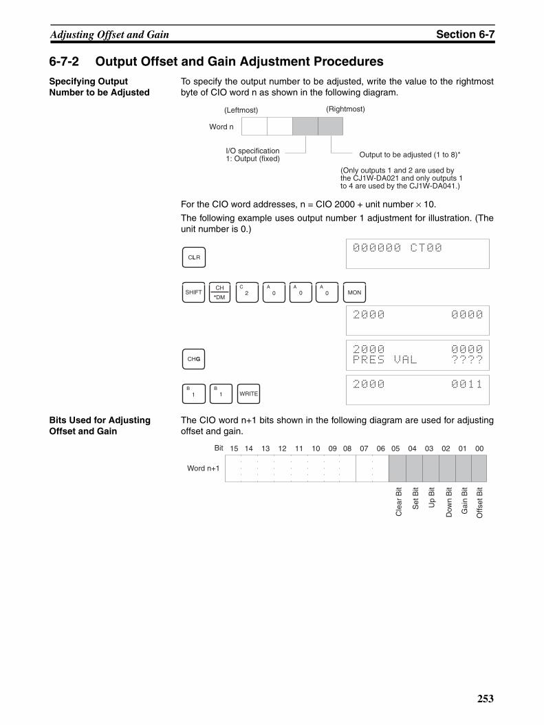
Adjusting Offset and Gain Section 6-7
6-7-2 Output Offset and Gain Adjustment ProceduresSpecifying Output Number to be Adjusted
To specify the output number to be adjusted, write the value to the rightmostbyte of CIO word n as shown in the following diagram.
For the CIO word addresses, n = CIO 2000 + unit number × 10.
The following example uses output number 1 adjustment for illustration. (Theunit number is 0.)
Bits Used for Adjusting Offset and Gain
The CIO word n+1 bits shown in the following diagram are used for adjustingoffset and gain.
(Rightmost)(Leftmost)
Word n
Output to be adjusted (1 to 8)*I/O specification 1: Output (fixed)
(Only outputs 1 and 2 are used by the CJ1W-DA021 and only outputs 1 to 4 are used by the CJ1W-DA041.)
CLR000000 CT00
SHIFTCH
*DM2
C0
A0
A0
AMON
2000 0000
CHG2000 0000PRES VAL ????
1B
1B
WRITE2000 0011
15 14 13 12 11 10 09 08 07 06 05 04 03 02 01 00Bit
Word n+1
Cle
ar B
it
Set
Bit
Up
Bit
Dow
n B
it
Gai
n B
it
Offs
et B
it
253

Adjusting Offset and Gain Section 6-7
Offset Adjustment The procedure for adjusting the analog output offset is explained below. Asshown in the following diagram, the set value is adjusted so that the analogoutput reaches the standard value (0 V/1 V/4 mA).
The following example uses output number 1 adjustment for illustration. (Theunit number is 0.)
1,2,3... 1. Turn ON bit 00 (the Offset Bit) of CIO word n+1. (Hold the ON status.)
2. Check whether the output devices are connected.
Note The output is current output when using a CJ1W-DA08C.
3. Monitor CIO word n+8 and check the set value while the Offset Bit is ON.
10 V
00FA0
Offset adjustment output range
Output signal range:0 to 10 V
CLR000000 CT00
SHIFTCONT
# 2C
0A
0A
1B
0A
0A
MON
200100 ^ OFF
SET
200100 ^ ON
Voltage output (See note.)
Output 1
Current output (CJ1W-DA021/041 only)
CLR000000 CT00
SHIFTCH
*DM 2C
0A
0A
8 MON
2008 0000
254

Adjusting Offset and Gain Section 6-7
4. Change the set value so that the output voltage are as shown in the follow-ing table. The data can be set within the indicated ranges.
Change the set value, using the Up Bit (bit 03 of word n+1) and the DownBit (bit 02 of word n+1).
• The following example increases the output voltage.
The bit will remain ON until the output becomes an appropriate value, atwhich time, it will turn OFF.
• The following example decreases the output voltage.
Output signal range Possible output voltage/current
adjustment
Output range
0 to 10 V –0.5 to 0.5 V FF38 to 00C8 (FE70 to 0190)–10 to 10 V –1.0 to 1.0 V
1 to 5 V 0.8 to 1.2 V
0 to 5 V –0.25 to 0.25 V
4 to 20 mA 3.2 to 4.8 mA
(Values in parentheses are for a resolution of 8,000.)
15 14 13 12 11 10 09 08 07 06 05 04 03 02 01 00Bit
Up Bit Down Bit
While the Down Bit is ON, the set value will be decreased by 1 resolution every 0.5 seconds. After it has been ON for 3 seconds, the set value will be decreased by 1 resolution every 0.1 seconds.
Word n+1
While the Up Bit is ON, the set value will be increased by 1 resolution every 0.5 seconds. After it has been ON for 3 seconds, the set value will be increased by 1 resolution every 0.1 seconds.
SHIFTCONT
#2
C0
A0
A1
B0
A3
DMON
200103 ^ OFF
SET200103 ^ ON
RESET
200103 ^ OFF
SHIFTCONT
#2
C
0A
0A
1B
0A
2C
MON
200102 ^ OFF
255

Adjusting Offset and Gain Section 6-7
The bit will remain ON until the output becomes an appropriate value, atwhich time, it will turn OFF.
5. Check the 0-V/1-V/4 mA output, and then turn bit 04 (the Set Bit) of CIOword n+1 ON and then OFF again.
While the Offset Bit is ON, the offset value will be saved to the Unit’s EE-PROM when the Set Bit turns ON.
6. To finish the offset adjustment, turn OFF bit 00 (the Offset Bit) of CIO wordn+1.
!Caution Do not turn OFF the power supply or restart the Unit while the Set Bit is ON(data is being written to the EEPROM). Otherwise, illegal data may be writtenin the Unit’s EEPROM and “EEPROM Errors” may occur when the power sup-ply is turned ON or when the Unit is restarted, causing a malfunction.
!Caution When making adjustments, be sure to perform both the offset adjustment andgain adjustment at the same time.
Note The EEPROM can be overwritten 50,000 times.
SET
200102 ^ ON
RESET
200102 ^ OFF
SHIFTCONT
#2
C0
A0
A1
B0
A4
EMON
200104 ^ OFF
SET
200104 ^ ON
RESET
200104 ^ OFF
SHIFTCONT
#2
C
0A
0A
1B
0A
0A
MON
200100 ^ ON
SET
200100 ^ OFF
256

Adjusting Offset and Gain Section 6-7
Gain Adjustment The procedure for adjusting the analog output gain is explained below. Asshown in the following diagram, the set value is adjusted so that the analogoutput is maximized (to 10 V/5 V/20 mA).
The following example uses output number 1 adjustment for illustration. (Theunit number is 0.)
1,2,3... 1. Turn ON bit 01 (the Gain Bit) of CIO word n+1. (Hold the ON status.)
2. Check whether the output devices are connected.
Note The output is current output when using a CJ1W-DA08C.
3. Monitor CIO word n+8 and check the set value while the Gain Bit is ON.
10 V
00FA0
Output signal range:0 to 10 V
Gain adjustment output range
CLR000000 CT00
SHIFTCONT
#2
C0
A0
A1
B0
A1
BMON
200101 ^ OFF
SET
200101 ^ ON
Voltage output (See note.)
Output 1
Current output (CJ1W-DA021/041 only)
CLR000000 CT00
SHIFTCH
*DM2
C0
A0
A8 MON
2008 0000
257

Adjusting Offset and Gain Section 6-7
4. Change the set value so that the output voltage is as shown in the followingtable. The data can be set within the indicated ranges.
Change the set value, using the Up Bit (bit 03 of word n+1) and the DownBit (bit 02 of word n+1).
• The following example increases the output voltage.
The bit will remain ON until the output voltage becomes an appropriate val-ue, at which time, the output will turn OFF.
• The following example decreases the output voltage.
Output signal range
Possible output voltage/current
adjustment
Output range
0 to 10 V 9.5 to 10.5 V 0ED8 to 1068 (1DB0 to 20D0)
–10 to 10 V 9 to 11 V 0708 to 0898 (0E10 to 1130)
1 to 5 V 4.8 to 5.2 V 0ED8 to 1068 (1DB0 to 20D0)
0 to 5 V 4.75 to 5.25 V 0ED8 to 1068 (1DB0 to 20D0)
4 to 20 mA 19.2 to 20.8 mA 0ED8 to 1068 (1DB0 to 20D0)
(Values in parentheses are for a resolution of 8,000.)
15 14 13 12 11 10 09 08 07 06 05 04 03 02 01 00Bit
Up Bit Down Bit
While the Up Bit is ON, the set value will be increased by 1 resolution every 0.5 seconds. After it has been ON for 3 seconds, the set value will be increased by 1 resolution every 0.1 seconds.
While the Down Bit is ON, the set value will be decreased by 1 resolution every 0.5 seconds. After it has been ON for 3 seconds, the set value will be decreased by 1 resolution every 0.1 seconds.
Word n+1
SHIFTCONT
# 2C
0A
0A
1B
0A
3D
MON
200103 ^ OFF
SET200103 ^ ON
RESET
200103 ^ OFF
SHIFTCONT
#2
C0
A
0A
1B
0A
2C
MON
200102 ^ OFF
258

Adjusting Offset and Gain Section 6-7
The bit will remain ON until the output voltage becomes an appropriate val-ue, at which time, the output will turn OFF.
5. Check the 10V/5V/20 mA output, and then turn bit 04 (the Set Bit) of CIOword n+1 ON and then OFF again.
While the Gain Bit is ON, the gain value will be saved to the Unit’s EE-PROM when the Set Bit turns ON.
6. To finish the gain adjustment, turn OFF bit 01 (the Gain Bit) of CIO wordn+1.
!Caution Do not turn OFF the power supply or restart the Unit while the Set Bit is ON(data is being written to the EEPROM). Otherwise, illegal data may be writtenin the Unit’s EEPROM and “EEPROM Errors” may occur when the power sup-ply is turned ON or when the Unit is restarted, causing a malfunction.
!Caution When making adjustments, be sure to perform both the offset adjustment andgain adjustment at the same time.
Note The EEPROM can be overwritten 50,000 times.
SET
200102 ^ ON
RESET
200102 ^ OFF
SHIFTCONT
# 2C
0A
0A
1B
0A
4E
MON
200104 ^ OFF
SET200104 ^ ON
RESET
210104 ^ OFF
SHIFTCONT
# 2C
0A
0A
1B
0A
1B
MON
200101 ^ ON
RESET
200101 ^ OFF
259

Adjusting Offset and Gain Section 6-7
Clearing Offset and Gain Adjusted Values
Follow the procedure outlined below to return the offset and gain adjusted val-ues to their default settings.
The following example uses output number 1 adjustment for illustration. (Theunit number is 0.)
1,2,3... 1. Turn ON bit 05 (the Clear Bit) of CIO word n+1. (Hold the ON status.) Re-gardless of the set value, 0000 will be monitored in CIO word n+8.
2. Turn bit 04 of CIO word n+1 ON and then OFF again.
While the Clear Bit is ON, the adjusted value will be cleared and reset tothe default offset and gain values when the Set Bit turns ON.
3. To finish the clearing of adjusted values, turn OFF bit 05 (the Clear Bit) ofCIO word n+1.
!Caution Do not turn OFF the power supply or restart the Unit while the Set Bit is ON(data is being written to the EEPROM). Otherwise, illegal data may be writtenin the Unit’s EEPROM and “EEPROM Errors” may occur when the power sup-ply is turned ON or when the Unit is restarted, causing a malfunction.
Note The EEPROM can be overwritten 50,000 times.
SHIFTCONT
# 2C
0A
0A
1B
0A
5F
MON
200105 ^ OFF
SET
200105 ^ ON
SHIFTCONT
# 2C
0A
0A
1B
0A
4E
MON
200104 ^ OFF
SET
200104 ^ ON
RESET200104 ^ OFF
SHIFTCONT
# 2C
0A
0A
1B
0A
5F
MON
200105 ^ ON
RESET
200105 ^ OFF
260

Handling Errors and Alarms Section 6-8
6-8 Handling Errors and Alarms
6-8-1 Indicators and Error FlowchartIndicators If an alarm or error occurs in the Analog Output Unit, the ERC or ERH indica-
tors on the front panel of the Unit will light.
LED Meaning Indicator Operating status
RUN (green) Operating Lit Operating in normal mode.
Not lit Unit has stopped exchanging data with the CPU Unit.
ERC (red) Error detected by Unit
Lit Alarm has occurred or initial settings are incorrect.
Not lit Operating normally.
ERH (red) Error in the CPU Unit
Lit Error has occurred during data exchange with the CPU Unit.
Not lit Operating normally.
ADJ (yellow) Adjusting Flashing Operating in offset/gain adjustment mode.
Not lit Other than the above.
RUN
ERCERH
ADJ
Front panel of Unit
261

Handling Errors and Alarms Section 6-8
Troubleshooting Procedure
Use the following procedure for troubleshooting Analog Output Unit errors.
Is the ERC indicator lit?
Yes
No
Is the RUN indicator lit?
Yes
No
Alarm has occurred at the Analog Output Unit.
Check whether the initial settings for the Analog Output Unit are set correctly.
Is the ERH indicator lit?
Yes
No
Is the RUN indicator lit?
Yes
No
Error detected by CPU Unit
Check whether the unit number is set correctly.
Error occurs.
Yes
No
Is the RUN indicator lit?
Error cleared?
No
Cycle the power supplyto the PLC.
Error cleared?
No
The Unit is faulty.
Replace the Unit.
YesNoise or other disturbance may be causingmalfunctions. Check the operating environment.
Yes
Error in internal circuits has occurred, preventing operation from continuing.
(Refer to 6-8-2 Alarms Occurring at the Analog Output Unit.)
(Refer to 6-8-2 Alarms Occurring at the Analog Output Unit.)
(Refer to 6-8-3 Errors in the CPU Unit.)
(Refer to 6-8-3 Errors in the CPU Unit.)
Refer to 6-8-5 Troubleshooting.
Refer to 6-8-4 Restarting Special I/O Units.
262

Handling Errors and Alarms Section 6-8
6-8-2 Alarms Occurring at the Analog Output UnitThe ERC indicator will light when the Analog Output Unit detects an alarm.The Alarm Flags in bits 08 to 15 of CIO word n+9 will turn ON.
For the CIO word addresses, n = CIO 2000 + (unit number × 10).
ERC and RUN Indicators: Lit
The ERC and RUN indicators will be lit if an error occurs while the Unit isoperating normally. The following alarm flags will turn ON in CIO word n+9.These alarm flags will turn OFF automatically when the error is cleared.
Note 1. n = CIO 2000 + (unit number × 10)
2. Only bits 00 and 01 are used for the CJ1W-DA021 and only bits 00 to 03are used for the CJ1-DA041.
15 14 13 12 11 10 09 08 07 06 05 04 03 02 01 00Bit
Word n+9
Output Setting Error FlagsAlarm Flags
(Outputs are made only to bits 00 and 01 for the CJ1W-DA021, and to bits 00 to 03 for the CJ1W-DA041.)
(See 6-6-6 Output Setting Errors.)
RUN
ERC
ERH: Lit
: Not lit
Word n + 9 Alarm flag Error contents Output status Countermeasure
Bits 00 to 07 (See note 2.)
Output Set Value Error
The output setting range has been exceeded.
Output value set by output hold function.
Correct the set value.
Bit 14 (Adjustment mode)
EEPROM Writ-ing Error
An EEPROM writing error has occurred while in adjustment mode.
Holds the out-put status imme-diately prior to the error.
Turn the Set Bit OFF, ON, and OFF again.
If the error persists even after the reset, replace the Analog Output Unit.
263

Handling Errors and Alarms Section 6-8
ERC Indicator and RUN Indicator: Lit, ADJ Indicator: Flashing
This alarm will occur in the case of incorrect operation while in the adjustmentmode. In adjustment mode, the Adjustment Mode ON Flag will turn ON in bit15 of CIO word n+9.
Note When a PLC error occurs in the adjustment mode, Unit operations will stopoperating. (The input and output values immediately prior to the error will beheld.)
ERC Indicator: Lit, RUN Indicator: Not Lit
The ERC indicator will be lit when the initial settings for the Analog OutputUnit are not set correctly. The alarm flags for the following errors will turn ONin CIO word n+9. These alarm flags will turn OFF when the error is clearedand the power to the PLC is cycled, or the Special I/O Unit Restart Bit isturned ON and then OFF again.
Note Bit 15 is normally turned OFF (i.e., set to 0).
RUN
ERC
ERHADJ
: Lit
: Not lit: Flashing
Word n + 9 Alarm flag Error contents Output status Countermeasure
Bit 13 (Adjustment mode)Output Number Setting Error
In adjustment mode, adjust-ment cannot be performed because the specified output number is not set for use or because the wrong output num-ber is specified.
The output volt-age or current becomes 0 V or 0 mA.
Check whether the word n out-put number to be adjusted is set from 11 to 14.
Check whether the output num-ber to be adjusted is set for use by means of the DM setting.
Bit 15 only ON (Adjustment Mode)
PLC Error
The PLC is in either MONITOR or RUN mode while the Analog Output Unit is operating in adjustment mode.
The output volt-age or current becomes 0 V or 0 mA.
For the CJ1W-DA021 or CJ1W-DA041, set the operation mode to normal mode and restart.For the CJ1W-DA08V/08C, set bits 00 to 07 of D(m+18) to 00 hex. Then either power up again or turn the Special I/O Unit Restart Bit ON and then OFF again.
RUN
ERC
ERH: Lit: Not lit
Word n + 9 Alarm flag Error contents Countermeasure
Bit 08 Scaling Data Setting Error
There is a mistake in the upper or lower limit setting when scaling is used. The setting range has been exceeded. The upper limit equals the lower limit (not 0000).
Correct the settings.
Bit 10 Output Hold Setting Error
The settings of the output status for when conversion is stopped is wrong.
Specify a number from 0000 to 0002.
Bit 12 Conversion Time/Resolu-tion, Operation Mode Setting Error
The conversion time/resolution setting or operation mode setting is incorrect.
Set 00 hex or 01 hex.
264

Handling Errors and Alarms Section 6-8
6-8-3 Errors in the CPU UnitThe ERH indicator will light if an error occurs in the CPU Unit or I/O bus and I/O refreshing with the Special I/O Units is not performed correctly, preventingthe Analog Output Unit from operating.
ERH and RUN Indicators: Lit
The ERH and RUN indicators will light if an error occurs in the I/O bus causinga WDT (watchdog timer) error in the CPU Unit, resulting in incorrect I/Orefresh with the Analog Output Unit.
Turn ON the power supply again or restart the system.For further details, refer to CJ-series CJ1G-CPU@@, CJ1G/H CPU@@H Pro-grammable Controllers Operation Manual (W393).
Note No error will be detected by the CPU Unit or displayed on the ProgrammingConsole, because the CPU Unit is continuing operation.
ERH Indicator: Lit, RUN Indicator: Not Lit
The unit number for the Analog Output Unit has not been set correctly.
RUN
ERC
ERH : Lit: Not lit
Error Error contents Output condition
I/O bus error Error has occurred during data exchange with the CPU Unit.
Output value set by output hold function.
CPU Unit monitoring error (see note)
No response from CPU Unit for specified period of time.
Maintains the status from before the error.
CPU Unit WDT error Error has been generated in CPU Unit.
Output value set by output hold function.
RUN
ERC
ERH : Lit
: Not lit
Error Error contents Output condition
Duplicate Unit Number The same unit number has been assigned to more than one Unit or the unit number was set to a value other than 00 to 95.
The output value will be 0 V.
Special I/O Unit Setting Error The Special I/O Units registered in the I/O table are different from the ones actually mounted.
265

Handling Errors and Alarms Section 6-8
6-8-4 Restarting Special I/O UnitsTo restart the Analog Output Unit after changing the contents of the DM Areaor correcting an error, cycle the power to the PLC or turn ON the Special I/OUnit Restart Bit.
Special I/O Unit Restart Bits
The output becomes 0 V or 0 mA during restart.
Replace the Unit if the error is not cleared even though the power supply iscycled or the Restart Bit is turned ON.
6-8-5 TroubleshootingThe following tables list the probable causes of troubles that may occur, andthe countermeasures for dealing with them.
Analog Output Does Not Change
Value Does Not Change as Intended
Outputs Are Inconsistent
Bit Function
A50200 Unit #0 Restart Bit Turning the Restart Bit for any Unit ON and then OFF again restarts that Unit.
A50201 Unit #1 Restart Bit
to to
A50215 Unit #15 Restart Bit
A50300 Unit #16 Restart Bit
to to
A50715 Unit #95 Restart Bit
Probable Cause Countermeasure Page
The output is not set for being used. Set the output for being used. 242
The output hold function is in opera-tion.
Turn ON the Output Conversion Enable Bit.
246
The conversion value is set outside of the permissible range.
Set the data within the range. 218
Probable Cause Countermeasure Page
The output signal range setting is wrong.
Correct the output signal range set-ting.
243
The specifications of the output device do not match those of the Analog Output Unit (e.g., input sig-nal range, input impedance).
Change the output device. 217
The offset or gain is not adjusted. Adjust the offset or gain. 250
Probable Cause Countermeasure Page
The output signals are being affected by external noise.
Try changing the shielded cable connection (e.g., the grounding at the output device).
233
266

SECTION 7CJ-series Analog Output Unit (CJ1W-DA042V)
This section explains how to use the CJ1W-DA042V Analog Output Units.
7-1 Specifications . . . . . . . . . . . . . . . . . . . . . . . . . . . . . . . . . . . . . . . . . . . . . . . . . 268
7-1-1 Specifications . . . . . . . . . . . . . . . . . . . . . . . . . . . . . . . . . . . . . . . . . . 268
7-1-2 Output Function Block Diagram . . . . . . . . . . . . . . . . . . . . . . . . . . . 269
7-1-3 Output Specifications . . . . . . . . . . . . . . . . . . . . . . . . . . . . . . . . . . . . 270
7-2 Operating Procedure . . . . . . . . . . . . . . . . . . . . . . . . . . . . . . . . . . . . . . . . . . . . 272
7-3 Components and Switch Settings . . . . . . . . . . . . . . . . . . . . . . . . . . . . . . . . . . 276
7-3-1 Component Names . . . . . . . . . . . . . . . . . . . . . . . . . . . . . . . . . . . . . . 276
7-3-2 Indicators . . . . . . . . . . . . . . . . . . . . . . . . . . . . . . . . . . . . . . . . . . . . . 277
7-3-3 Unit Number Switches . . . . . . . . . . . . . . . . . . . . . . . . . . . . . . . . . . . 277
7-4 Wiring . . . . . . . . . . . . . . . . . . . . . . . . . . . . . . . . . . . . . . . . . . . . . . . . . . . . . . . 278
7-4-1 Terminal Arrangement . . . . . . . . . . . . . . . . . . . . . . . . . . . . . . . . . . . 278
7-4-2 Internal Circuitry . . . . . . . . . . . . . . . . . . . . . . . . . . . . . . . . . . . . . . . 278
7-4-3 Output Wiring Example . . . . . . . . . . . . . . . . . . . . . . . . . . . . . . . . . . 279
7-4-4 Output Wiring Considerations . . . . . . . . . . . . . . . . . . . . . . . . . . . . . 280
7-5 Exchanging Data with the CPU Unit . . . . . . . . . . . . . . . . . . . . . . . . . . . . . . . 281
7-5-1 Outline of Data Exchange. . . . . . . . . . . . . . . . . . . . . . . . . . . . . . . . . 281
7-5-2 Allocations for Initial Settings Data . . . . . . . . . . . . . . . . . . . . . . . . . 283
7-5-3 I/O Refresh Data Allocations . . . . . . . . . . . . . . . . . . . . . . . . . . . . . . 285
7-6 Analog Output Functions and Operating Procedures . . . . . . . . . . . . . . . . . . . 287
7-6-1 Output Settings and Conversion Values . . . . . . . . . . . . . . . . . . . . . . 287
7-6-2 Conversion Mode Setting . . . . . . . . . . . . . . . . . . . . . . . . . . . . . . . . . 289
7-6-3 Output Hold Function . . . . . . . . . . . . . . . . . . . . . . . . . . . . . . . . . . . . 290
7-6-4 Output Scaling . . . . . . . . . . . . . . . . . . . . . . . . . . . . . . . . . . . . . . . . . 291
7-6-5 Output Setting Errors . . . . . . . . . . . . . . . . . . . . . . . . . . . . . . . . . . . . 293
7-7 Handling Errors and Alarms . . . . . . . . . . . . . . . . . . . . . . . . . . . . . . . . . . . . . . 294
7-7-1 Indicators and Error Flowchart . . . . . . . . . . . . . . . . . . . . . . . . . . . . . 294
7-7-2 Alarms Occurring at the Analog Output Unit. . . . . . . . . . . . . . . . . . 296
7-7-3 Errors in the CPU Unit . . . . . . . . . . . . . . . . . . . . . . . . . . . . . . . . . . . 297
7-7-4 Restarting Special I/O Units . . . . . . . . . . . . . . . . . . . . . . . . . . . . . . . 298
7-7-5 Troubleshooting . . . . . . . . . . . . . . . . . . . . . . . . . . . . . . . . . . . . . . . . 298
267

Specifications Section 7-1
7-1 Specifications
7-1-1 Specifications
Note 1. Do not apply a voltage higher than 600 V to the terminal block when per-
Unit model CJ1W-DA042V
Unit type CJ-series Special I/O Unit
Isolation Between outputs and PLC signals: Digital isolator (No isolation between output signals.) (See note 1.)
External terminals 18-point detachable terminal block (M3 screws)
Affect on CPU Unit cycle time CJ2 CPU Unit 0.05 ms
CJ1 CPU Unit 0.2 ms
Current consumption 400 mA max. at 5 VDC
Dimensions (mm) (See note 2.) 31 × 90 × 65 (W × H × D)
Weight 150 g max.
General specifications Conforms to general specifications for SYSMAC CJ-series Series.
Mounting position CJ-series CPU Rack or CJ-series Expansion Rack
Maximum number of Units Per CPU Rack or Expansion Rack (See note 3.)
Power Supply Unit No. of mountable Units
CJ1W-PA205RCJ1W-PA205CCJ1W-PD025
CPU Rack: 10 Units/RackExpansion Rack: 10 Units/Rack
CJ1W-PA202 CPU Rack: 5 Units/RackExpansion Rack: 6 Units/Rack
CJ1W-PD022 CPU Rack: 3 Units/RackExpansion Rack: 4 Units/Rack
Data exchange with the CPU Unit (See note 4.)
Special I/O Unit Area in CIO Area (CIO 2000 to CIO 2959): 10 words/UnitSpecial I/O Unit Area in DM Area (D20000 to D29599): 100 words/Unit
Output specifica-tions
Number of analog outputs 4
Output signal range (See note 5.) 1 to 5 V0 to 10 V−10 to 10 V
Output impedance 0.5 Ω max.
Maximum permissible load resis-tance
5 kΩ min. (per output)
Resolution 1 to 5 V 1/10,000 (full scale)
0 to 10 V 1/20,000(full scale)
−10 to 10 V 1/40,000(full scale)
Set data 16-bit binary data
Accuracy 25°C ±0.3% (full scale)
0 to 55°C ±0.5% (full scale)
Conversion period (See note 6.) 20 µs for 1 point, 25 µs for 2 points, 30 µs for 3 points, 35 µs for 4 points
Output functions
Output hold function Outputs the specified output status (CLR, HOLD, or MAX) under any of the following circumstances.• When the Conversion Enable Bit is OFF. (See note 7.)
• When there is an output setting error or a fatal error occurs at the PLC.
• When all loads are turned OFF.
Scaling Setting values in any specified unit within a range of ±32,000 as the upper and lower limits allows D/A conversion to be executed and analog signals to be output with these values as full scale.
Direct conversion The output set value refreshed and D/A conversion is performed immedi-ately when the ANALOG OUTPUT DIRECT CONVERSION (AODC) instruction is executed.
A CJ2H-CPU@@(-EIP) CPU Unit with unit version 1.1 or later is required to use direct conversion.
268

Specifications Section 7-1
forming withstand voltage test on this Unit. Otherwise, internal elementsmay deteriorate.
2. Refer to page 439 for Unit dimensions.
3. This is the maximum number of Units that can be mounted to a CJ2H-CPU6@ CPU Unit (no EtherNet/IP). The maximum number of Analog Out-put Units that can be mounted to one Rack varies depending on the currentconsumption of the other Units mounted to the Rack.
4. Data exchange methods with the CPU Unit are as follows:
5. Output signal range can be set for each output.
6. D/A conversion time is the time required for converting and outputting thePLC data. With direct conversion, data can be exchanged with the PLCand D/A conversion can be performed within the processing time of theANALOG OUTPUT DIRECTION CONVERSION (AODC) instruction. Ittakes at least one cycle for the data stored in the PLC to be transferred tothe Analog Output Unit in Cyclic Conversion Mode.
7. When the operation mode for the CPU Unit is changed from RUN mode orMONITOR mode to PROGRAM mode, or when the power is turned ON,the Output Conversion Enable Bit will turn OFF. The output status specifiedfor the output hold function will be output. In Direct Conversion Mode, theset value specified with the ANALOG OUTPUT DIRECT CONVERSIONS(AODC) instruction will be output in RUN or MONITOR mode even if theOutput Conversion Enable Bit is OFF.
7-1-2 Output Function Block Diagram
Special I/O Unit Area in CIO Area
CIO 2000 to CIO 2959 (2000.00 to 2959.15)
10 words transferred per Unit
CPU Unit to Analog Output Unit
• Set value• Conversion enable bits
Analog Output Unit to CPU Unit
• Alarm Flags
Special I/O Unit Area in DM Area (D20000 to D29599)
100 words per Unit refreshed at power ON and restarts
CPU Unit to Analog Output Unit
• Number of analog outputs used• Conversion mode setting• Output signal range setting• Output status when conversion
stops• Scaling lower and upper limits
D/A
Analog Output UnitCPU Unit
Analog output 1
CPU Unit
Analog output 2
Analog output 3
Analog output 4
Same as above.
Same as above.
Same as above.
Analog output 1 set value
Output hold enabled
Output hold disabled
Scaling disabled
Scaling enabled
269

Specifications Section 7-1
7-1-3 Output SpecificationsIf the set value is outside the specified range given below, an output settingerror will occur, and the output specified by the output hold function will beoutput.
Range: 1 to 5 V
Range: 0 to 10 V
5.2 V
5 V
1 V 0.8 V
FE0C hex 0000 hex 2710 hex
2904 hex
Analog output signal
Resolution: 10,000
Set value
+10.5 V
+10 V
0 V
−0.5 V
5208 hex4E20 hex0000 hex
FC18 hex
Analog output signal
Resolution: 20,000
Set value
270

Specifications Section 7-1
Range: −10 to 10 V
Note The conversion values for a range of −10 to 10 V will be as follows (for a reso-lution of 40,000):
+11 V
+10 V
0 V
-10 V
-11 V
AA10 hex
B1E0 hex 0000 hex4E20 hex
55F0 hex
Analog output signal
Resolution: 40,000
Set value
16-bit binary data BCD
AA10 –22,000
: :
FFFF –1
0000 0
0001 1
: :
55F0 22,000
271
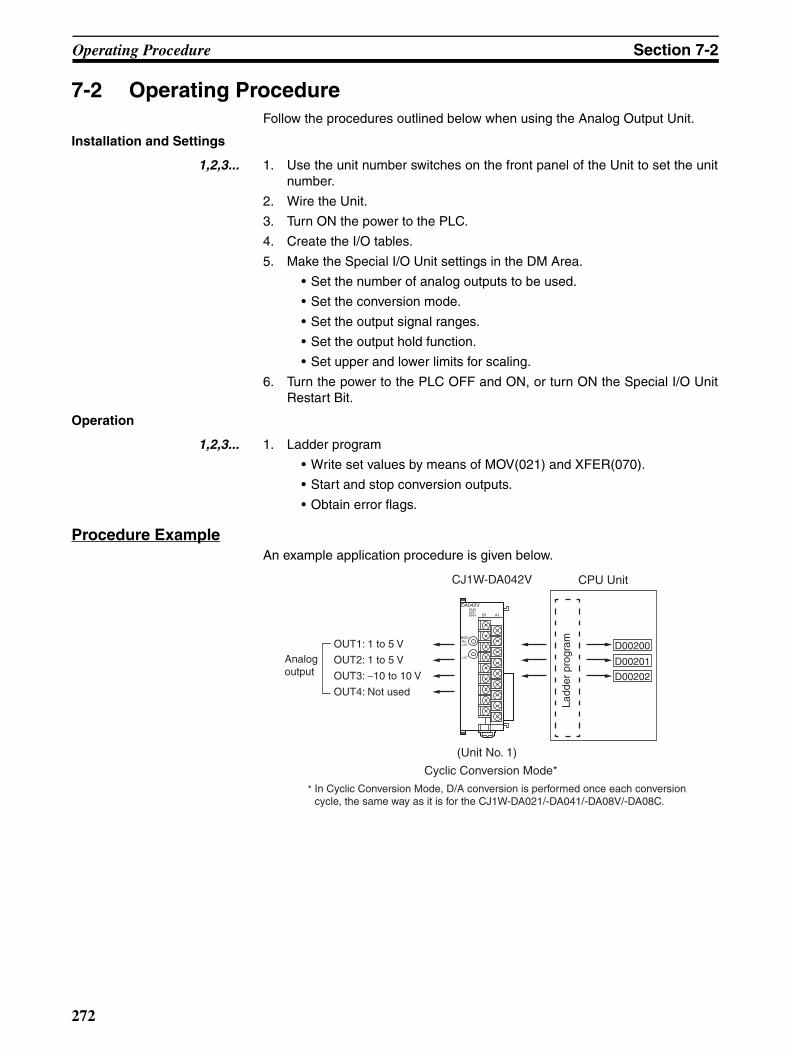
Operating Procedure Section 7-2
7-2 Operating ProcedureFollow the procedures outlined below when using the Analog Output Unit.
Installation and Settings
1,2,3... 1. Use the unit number switches on the front panel of the Unit to set the unitnumber.
2. Wire the Unit.
3. Turn ON the power to the PLC.
4. Create the I/O tables.
5. Make the Special I/O Unit settings in the DM Area.
• Set the number of analog outputs to be used.
• Set the conversion mode.
• Set the output signal ranges.
• Set the output hold function.
• Set upper and lower limits for scaling.
6. Turn the power to the PLC OFF and ON, or turn ON the Special I/O UnitRestart Bit.
Operation
1,2,3... 1. Ladder program
• Write set values by means of MOV(021) and XFER(070).
• Start and stop conversion outputs.
• Obtain error flags.
Procedure ExampleAn example application procedure is given below.
D00200
D00201
D00202
DA042V
B1 A1
MACHNo.x10 1
x10 0
RUNERCERH
CPU Unit
Cyclic Conversion Mode*
CJ1W-DA042V
*
Ladd
er p
rogr
am
Analog output
OUT1: 1 to 5 V
OUT2: 1 to 5 V
OUT3: −10 to 10 V
OUT4: Not used
(Unit No. 1)
In Cyclic Conversion Mode, D/A conversion is performed once each conversion cycle, the same way as it is for the CJ1W-DA021/-DA041/-DA08V/-DA08C.
272

Operating Procedure Section 7-2
Setting the Analog Output Unit
1,2,3... 1. Set the unit number switches. (Refer to page 275.)
2. Connect and wire the Analog Output Unit. (Refer to pages 10, 278, and279.)
3. Turn ON the power to the PLC.
Creating I/O TablesAfter turning ON the power to the PLC, be sure to create the I/O tables.
MACHNo.
DA042VRUNERCERH B1 A1
x10 1
x10 0
09
8765
4 32109
8765
4 321
MACHNo.
101
100
09
8765 4 321
09
8765 4 321
If the unit number is set to 1, words CIO 2010to CIO 2019 in the Special I/O Unit Area in theCIO Area and words D20100 to D20199 in theSpecial I/O Unit Area in the DM Area will beallocated to the Analog Output Unit.
POWER
PA205R
DC24VAC240VOUTPUT
RUN
INPUTAC100-240V
L2/N
L1
CONTROLLERPROGRAMMABLE
ERR/ALMRUN
COMMBKUP
INHPRPHL
PERIPHERAL
BUSY
MCPWR
PORT
CJ2HCPU64-EIP
SYSMAC NSMS
100M10M
COMM
AD042
B1 A1
MACHNo.x10 1
x10 0
DA042V
B1 A1
MACHNo.x10 1
x10 0
OPEN
POWER
PA205R
DC24VAC240VOUTPUT
RUN
INPUTAC100-240V
L2/N
L1
CONTROLLERPROGRAMMABLE
ERR/ALMRUN
COMMBKUP
INHPRPHL
PERIPHERAL
BUSY
MCPWR
PORT
CJ2HCPU64-EIP
SYSMAC NSMS
100M10M
COMM
AD042
B1 A1
MACHNo.x10 1
x10 0
DA042V
B1 A1
MACHNo.x10 1
x10 0
OPEN
CX-Programmer
The I/O tables can be created online based on the actual PLC configuration or they can be created manually offline.
273

Operating Procedure Section 7-2
Initial Data Settings
1,2,3... 1. Specify the Special I/O Unit settings in the DM Area. (Refer to page 283.)
Setting Examples
• Unit number: 1
• Cyclic Conversion Mode
• Analog output 1: 1 to 5 V Analog output 2: 1 to 5 V Analog output 3: −10 to −10 VAnalog output 4: Not used.
a) Set the number of analog outputs to use. (Refer to page 287.)
b) Set the conversion mode. (Refer to page 289.)
c) Output Signal Range Settings (Refer to page 287.)
1. Output Signal Range Setting for Output 1
2. Output Signal Range Setting for Output 2
3. Output Signal Range Setting for Output 3
2. Cycle the power to the PLC.
15 14 13 12 11 10 09 08 07 06 05 04 03 02 01 00
0 0 0 0 0 0 0 0 0 0 0 0 0 0 1 1m: D20100 (0003 hex)
Bit
Set to “3” to indicate that three outputs will be used (outputs 1, 2, and 3).
15 14 13 12 11 10 09 08 07 06 05 04 03 02 01 00
0 0 0 0 0 0 0 0 0 0 0 0 0 0 0 0
Bitm+1: D20101 (0000 hex)
Cyclic Conversion Mode: 00
15 14 13 12 11 10 09 08 07 06 05 04 03 02 01 00
0 0 0 0 0 0 0 0 0 0 0 0 0 1 1 0
Bitm+2: D20102 (0006 hex)
Output 1: 1 to 5 V. Set to 6.
15 14 13 12 11 10 09 08 07 06 05 04 03 02 01 00
0 0 0 0 0 0 0 0 0 0 0 0 0 1 1 0Bit
m+6: D20106 (0006 hex)
Output 2: 1 to 5 V. Set to 6.
15 14 13 12 11 10 09 08 07 06 05 04 03 02 01 00
0 0 0 0 0 0 0 0 0 0 0 0 0 0 1 1Bit
m+10: D20110 (0003 hex)
Output 3: −10 to 10 V. Set to 3.
274

Operating Procedure Section 7-2
Creating Ladder Programs
Analog Outputs
Note 1. The addresses are determined by the unit number of the Special I/O Unit.(Refer to page 277.)
2. Set as required.
Output number Output signal range
Address of output set value
(n = CIO 2010) (See note 1.)
Conversion source address
(See note 2.)
1 1 to 5 V n+1 = CIO 2011 D00200
2 1 to 5 V n+2 = CIO 2012 D00201
3 −10 to 10 V n+3 = CIO 2013 D00202
4 Not used. --- ---
POWER
PA205R
DC24VAC240VOUTPUT
RUN
INPUTAC100-240V
L2/N
L1
CONTROLLERPROGRAMMABLE
ERR/ALMRUN
COMMBKUP
INHPRPHL
PERIPHERAL
BUSY
MCPWR
PORT
CJ2HCPU64-EIP
SYSMAC NSMS
100M10M
COMM
AD042
B1 A1
MACHNo.x10 1
x10 0
DA042V
B1 A1
MACHNo.x10 1
x10 0
OPEN
CX-Programmer
The contents of the specified address, D00200, is stored in words (n + 1) to (n + 3) of the Special I/O Unit Area (CIO 2011 to CIO 2013) as a signed binary value.
MOV(021)D00200
2011
MOV(021)D00201
2012
MOV(021)D00202
2013
2010.00
2010.01
2010.02
Contents of D00200 is set in word CIO 2011.
Contents of D00201 is set in word CIO 2012.
Contents of D00202 is set in word CIO 2013.
To start the analog outputs, turn ON the Conversion Enable Bits 2010.00 to 2010.02 (bits 00 to 02 of word CIO 2010). (Refer to pages 286 and 288.) The data in words CIO 2011 to CIO 2013 will be output as 1 to 5 V, 1 to 5 V, −10 to 10 V, respectively.
Execution condition
Execution condition
275

Components and Switch Settings Section 7-3
7-3 Components and Switch Settings
7-3-1 Component Names
Note 1. The terminal block is attached using a connector. It can be removed by low-ering the lever at the bottom of the terminal block.
2. The lever must normally be in the raised position. Confirm this before op-eration.
MACHNo.
DA042VRUNERCERH B1 A1
x101
x100
09
8765 4 321
09
8765 4 321
Indicators
Terminal block
SideSlider
Slider
FrontWith Terminal Block
Unit number switches
Terminal block lock lever (pull down to release terminal block)
DIN Track mounting pin
Expansion connector
B1A1DA042V
MACH
No.10
1
100
RUNERCERH
276
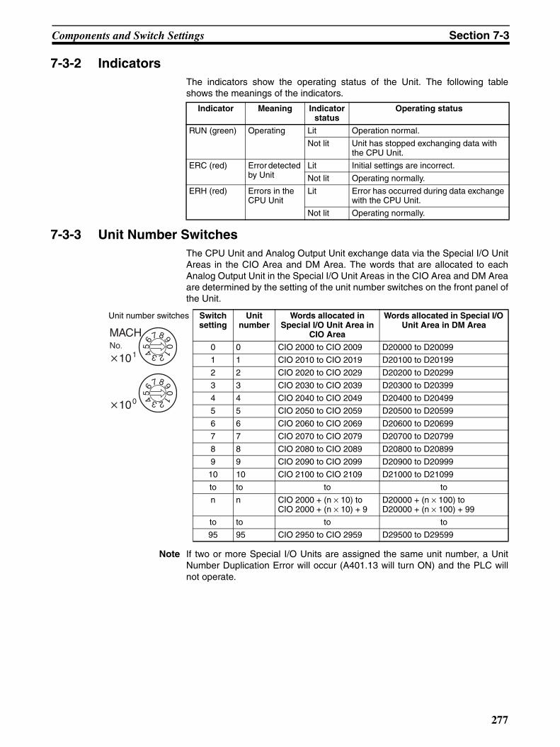
Components and Switch Settings Section 7-3
7-3-2 IndicatorsThe indicators show the operating status of the Unit. The following tableshows the meanings of the indicators.
7-3-3 Unit Number SwitchesThe CPU Unit and Analog Output Unit exchange data via the Special I/O UnitAreas in the CIO Area and DM Area. The words that are allocated to eachAnalog Output Unit in the Special I/O Unit Areas in the CIO Area and DM Areaare determined by the setting of the unit number switches on the front panel ofthe Unit.
Note If two or more Special I/O Units are assigned the same unit number, a UnitNumber Duplication Error will occur (A401.13 will turn ON) and the PLC willnot operate.
Indicator Meaning Indicator status
Operating status
RUN (green) Operating Lit Operation normal.
Not lit Unit has stopped exchanging data with the CPU Unit.
ERC (red) Error detected by Unit
Lit Initial settings are incorrect.
Not lit Operating normally.
ERH (red) Errors in the CPU Unit
Lit Error has occurred during data exchange with the CPU Unit.
Not lit Operating normally.
Unit number switches Switch setting
Unit number
Words allocated in Special I/O Unit Area in
CIO Area
Words allocated in Special I/O Unit Area in DM Area
0 0 CIO 2000 to CIO 2009 D20000 to D20099
1 1 CIO 2010 to CIO 2019 D20100 to D20199
2 2 CIO 2020 to CIO 2029 D20200 to D20299
3 3 CIO 2030 to CIO 2039 D20300 to D20399
4 4 CIO 2040 to CIO 2049 D20400 to D20499
5 5 CIO 2050 to CIO 2059 D20500 to D20599
6 6 CIO 2060 to CIO 2069 D20600 to D20699
7 7 CIO 2070 to CIO 2079 D20700 to D20799
8 8 CIO 2080 to CIO 2089 D20800 to D20899
9 9 CIO 2090 to CIO 2099 D20900 to D20999
10 10 CIO 2100 to CIO 2109 D21000 to D21099
to to to to
n n CIO 2000 + (n × 10) to CIO 2000 + (n × 10) + 9
D20000 + (n × 100) to D20000 + (n × 100) + 99
to to to to
95 95 CIO 2950 to CIO 2959 D29500 to D29599
MACHNo.
101
10009
8765 4 321
09
8765 4 321
277

Wiring Section 7-4
7-4 Wiring
!Caution Always connect surge suppressors to inductive loads in the system (e.g.,magnetic contactors, relays, and solenoids). Always separate devices thatgenerate surge from the Analog I/O Units. Faulty Unit operation may causeunexpected system operation.
If inductive loads are connected to output signals from Relay Contact OutputUnits, connect a surge suppressor in an AC circuit and a diode in a DC circuitclose to the inductive load to absorb the back electromotive force.
7-4-1 Terminal ArrangementThe signal names corresponding to the connecting terminals are as shown inthe following diagram.
Note 1. The number of analog outputs that can be used is set in the DM Area.
2. The output signal ranges for individual outputs are set in the DM Area. Theoutput signal range can be set separately for each output.
3. Do not make any connections to the N.C. terminals.
7-4-2 Internal CircuitryThe following diagrams show the internal circuitry of the analog output sec-tion.
Output circuits
Connect a surge suppressor in an AC circuit and a diode in a DC circuit.
PLC Output Unit
PLC Output Unit
Inductive load
Inductive load
B1 B2
N.C. B3 B4 B5
N.C. B6 N.C. B7 N.C. B8 N.C. B9
A1 A2 A3 N.C. A4 A5 A6 N.C. A7 N.C. A8 N.C. A9 N.C.
Output 2 (+)
Output 4 (+)
Output 1 (+)
Output 3 (+)
AMP
AG
Voltage output
Voltage output
(common to all outputs)
Output circuit and conversion circuit
278

Wiring Section 7-4
Internal Configuration
7-4-3 Output Wiring Example
Note Crimp terminals must be used for terminal connections, and the screws mustbe tightened securely. M3 terminal screws are used. The applicable tighten-ing torque is 0.5 N·m.
Note To increase noise resistance for analog output wiring, ground the shield on theoutput signal cable at the output device.
ROMRAM
MPU
Indicators/Switch
Oscillator
Regulator
Oscillator
Ext
erna
l ter
min
als
Out
put
CJ-series PLC
Dig
ital i
sola
tor
Bus interface
Non- volatile memory
Insulating DC-to-DC converter
D/A Converter
Output circuits
+15 V
+5 V+5 V
−15 V
Output 2Output 1
Output 4Output 3
Round type
6.2 mm max. 6.2 mm max.
Fork type
M3 screw
279

Wiring Section 7-4
7-4-4 Output Wiring ConsiderationsWhen wiring outputs, apply the following points to avoid noise interferenceand optimize Analog Output Unit performance.
• Use two-core shielded twisted-pair cables for output connections.
• Route output cables separately from power cables (e.g., AC and three-phase lines), and do not place them in the same duct with power cables.
• If there is noise interference from power lines (if, for example, the powersupply is shared with electrical welding devices or electrical dischargemachines, or if there is a high-frequency generation source nearby),install a noise filter at the power supply input area.
280
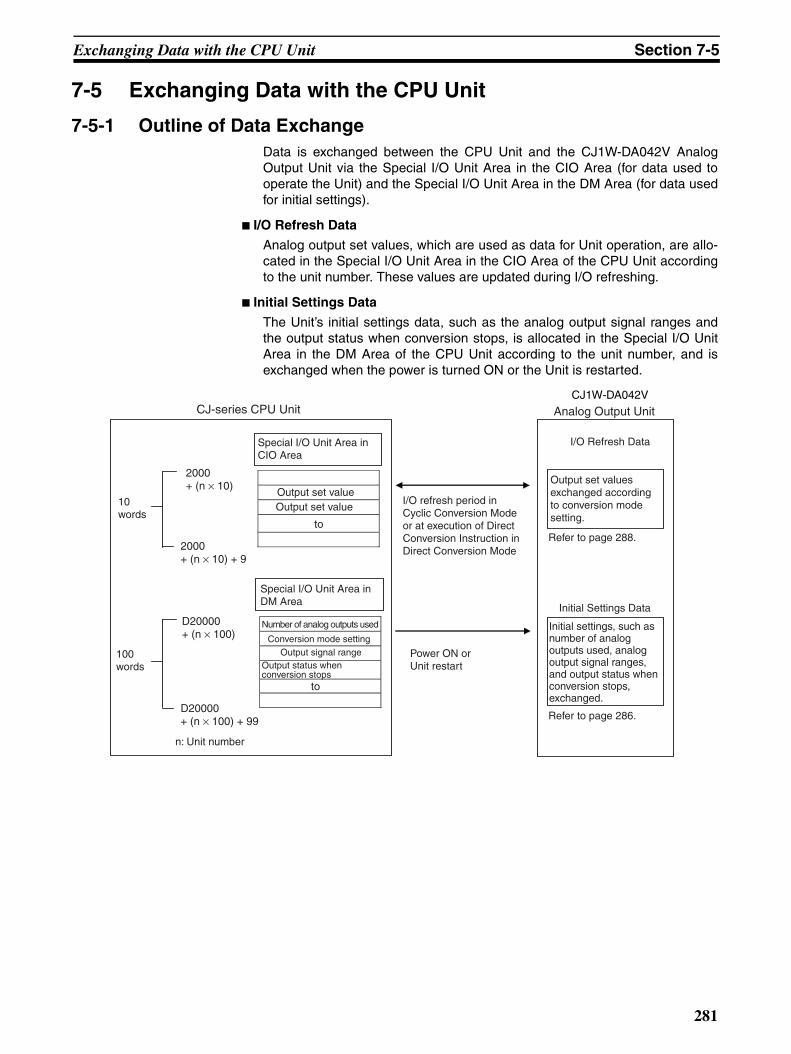
Exchanging Data with the CPU Unit Section 7-5
7-5 Exchanging Data with the CPU Unit
7-5-1 Outline of Data ExchangeData is exchanged between the CPU Unit and the CJ1W-DA042V AnalogOutput Unit via the Special I/O Unit Area in the CIO Area (for data used tooperate the Unit) and the Special I/O Unit Area in the DM Area (for data usedfor initial settings).
I/O Refresh Data
Analog output set values, which are used as data for Unit operation, are allo-cated in the Special I/O Unit Area in the CIO Area of the CPU Unit accordingto the unit number. These values are updated during I/O refreshing.
Initial Settings Data
The Unit’s initial settings data, such as the analog output signal ranges andthe output status when conversion stops, is allocated in the Special I/O UnitArea in the DM Area of the CPU Unit according to the unit number, and isexchanged when the power is turned ON or the Unit is restarted.
CJ1W-DA042V
Power ON or Unit restart
I/O refresh period in Cyclic Conversion Mode or at execution of Direct Conversion Instruction in Direct Conversion Mode
I/O Refresh Data
CJ-series CPU Unit Analog Output Unit
Output set values exchanged according to conversion mode setting.
Refer to page 288.
Initial Settings Data
Initial settings, such as number of analog outputs used, analog output signal ranges, and output status when conversion stops, exchanged.
Refer to page 286.
Special I/O Unit Area in CIO Area
Output set valueOutput set value
Special I/O Unit Area in DM Area
Number of analog outputs used
Conversion mode settingOutput signal range
Output status when conversion stops
n: Unit number
100 words
10 words
2000+ (n × 10)
2000+ (n × 10) + 9
D20000+ (n × 100)
D20000+ (n × 100) + 99
to
to
281

Exchanging Data with the CPU Unit Section 7-5
Unit Number SettingThe words in the Special I/O Unit Areas in the CIO Area and DM Area that areallocated to each Analog Output Unit are determined by the setting of the unitnumber switches on the front panel of the Unit.
Note If two or more Special I/O Units are assigned the same unit number, a UnitNumber Duplication Error will occur (A401.13 will turn ON) and the PLC willnot operate.
Special I/O Unit Restart BitsTo restart the Analog Output Unit after changing the contents of the DM Areaor correcting an error, cycle the power to the PLC or turn ON the Special I/OUnit Restart Bit.
Special I/O Unit Restart Bits
Note Replace the Unit if the error is not cleared even though the power supply iscycled or the Restart Bit is turned ON.
Unit number switches Switch setting
Unit number
Words allocated in Special I/O Unit Area
in CIO Area
Words allocated in Special I/O Unit Area in DM Area
0 0 CIO 2000 to CIO 2009 D20000 to D20099
1 1 CIO 2010 to CIO 2019 D20100 to D20199
2 2 CIO 2020 to CIO 2029 D20200 to D20299
3 3 CIO 2030 to CIO 2039 D20300 to D20399
4 4 CIO 2040 to CIO 2049 D20400 to D20499
5 5 CIO 2050 to CIO 2059 D20500 to D20599
6 6 CIO 2060 to CIO 2069 D20600 to D20699
7 7 CIO 2070 to CIO 2079 D20700 to D20799
8 8 CIO 2080 to CIO 2089 D20800 to D20899
9 9 CIO 2090 to CIO 2099 D20900 to D20999
10 10 CIO 2100 to CIO 2109 D21000 to D21099
to to to to
n n CIO 2000 + (n × 10) to CIO 2000 + (n × 10) + 9
D20000 + (n × 100) to D20000 + (n × 100) + 99
to to to to
95 95 CIO 2950 to CIO 2959 D29500 to D29599
MACHNo.
101
100
09
8765 4 321
09
8765 4 321
Bit Function
A502.00 Unit No. 0 Restart Bit Restarts the Unit when turned ON.A502.01 Unit No. 1 Restart Bit
to to
A502.15 Unit No. 15 Restart Bit
A503.00 Unit No. 16 Restart Bit
to to
A507.15 Unit No. 95 Restart Bit
282

Exchanging Data with the CPU Unit Section 7-5
7-5-2 Allocations for Initial Settings DataDM Area
The initial settings of the Analog Output Unit are set according to the dataallocated in the Special I/O Unit Area in the DM Area. Settings, such as thenumber of outputs used and the analog output signal ranges, must be set inthis area.
Note 1. The words in the Special I/O Unit Area in the DM Area that are allocatedto the Analog Output Unit are set using the unit number switches on thefront panel of the Unit. (Refer to page 282.)
2. If two or more Special I/O Units are assigned the same unit number, a UnitNumber Duplication Error will occur (A401.13 will turn ON) and the PLCwill not operate.
Allocations in DM AreaThe following table shows the allocation of DM Area words and bits.
CJ-series CPU Unit
CJ1W-DA042V
Unit 0Unit 1
Unit 2Unit 3
Unit 4
Unit 5
Unit 6Unit 7
Unit 8
Unit 9
Unit 10
Unit n
Unit 95
D20000 to D20099
D20100 to D20199
D20200 to D20299
D20300 to D20399
D20400 to D20499
D20500 to D20599
D20600 to D20699
D20700 to D20799
D20800 to D20899
D20900 to D20999
D21000 to D21099
D20000 + (n x 100) to D20000 + (n x 100) + 99
D29500 to D29599
Analog Output Unit
Initial Settings Data
m = 20000 + (unit number × 100)
Special I/O Unit Area in DM Area
Allocated words
Data is automatically transferred to each Unit when the power is turned ON, or when the Special I/O Unit Restart Bit is turned ON.
Number of analog outputs used
Conversion mode setting
Output 2 Output signal range Output status when
conversion stops Scaling lower limit Scaling upper limit
Output 3 Output signal range Output status when
conversion stops Scaling lower limit Scaling upper limit
Output 4 Output signal range Output status when
conversion stops Scaling lower limit Scaling upper limit
Output 1 Output signal range Output status when
conversion stops Scaling lower limit Scaling upper limit
D (m)
D (m+1)
D (m+2) to D (m+5)
D (m+6) to D (m+9)
D (m+10) to D (m+13)
D (m+14) to D (m+17)
to
to
to
to
DM Area word (See note.)
Bits
15 14 13 12 11 10 09 08 07 06 05 04 03 02 01 00
D (m) Not used. (Settings are ignored.) Number of analog out-puts used
D (m+1) Not used. (Settings are ignored.) Conversion mode
00 hex: Cyclic Conversion Mode, A5 hex: Direct Conversion Mode
D (m+2) Not used. (Settings are ignored.) Output 1 output signal range setting
D (m+3) Output 1 output status when conversion stops
D (m+4) Output 1 scaling lower limit
D (m+5) Output 1 scaling upper limit
283

Exchanging Data with the CPU Unit Section 7-5
Note For the DM word addresses, m = D20000 + (unit number × 100)
Set Values and Stored Values
Note 1. Output numbers that are not to be used (set to 0) will be output at 0 V.
2. A CJ2H-CPU@@(-EIP) CPU Unit with unit version 1.1 or later is requiredto use direct conversion. Direct conversion is not supported by CJ1 CPUUnits.
3. The values output for the signal ranges will be 0 V for the range of ±10 V,and the minimum value for the other ranges. (Refer to page 290.)
D (m+6) Not used. (Settings are ignored.) Output 2 output signal range setting
D (m+7) Output 2 output status when conversion stops
D (m+8) Output 2 scaling lower limit
D (m+9) Output 2 scaling upper limit
D (m+10) Not used. (Settings are ignored.) Output 3 output signal range setting
D (m+11) Output 3 output status when conversion stops
D (m+12) Output 3 scaling lower limit
D (m+13) Output 3 scaling upper limit
D (m+14) Not used. (Settings are ignored.) Output 4 output signal range setting
D (m+15) Output 4 output status when conversion stops
D (m+16) Output 4 scaling lower limit
D (m+17) Output 4 scaling upper limit
Setting Contents Page
Number of analog outputs used (See note 1.)
0: No outputs used.1: One output used (output 1 used).2: Two outputs used (outputs 1 and 2 used).3: Three outputs used (outputs 1, 2, and 3 used).4: Four outputs used (outputs 1, 2, 3, and 4 used).
287
Conversion mode setting
00 hex: Cyclic Conversion ModeA5 hex: Direct Conversion Mode (See note 2.)
289
Output signal range 1: 0 to 10 V3: −10 to 10 V6: 1 to 5 V
287
Output status when conversion stops
0: CLR Outputs 0 or minimum value of output range (See note 3.).1: HOLD Holds output value prior to stop.2: MAX Outputs maximum value of range
290
Scaling settings Any value other than 0 within range of ±32,000 (8300 hex to 7D00 hex) as long as the upper limit is not equal to the lower limit.
291
DM Area word (See note.)
Bits
15 14 13 12 11 10 09 08 07 06 05 04 03 02 01 00
284
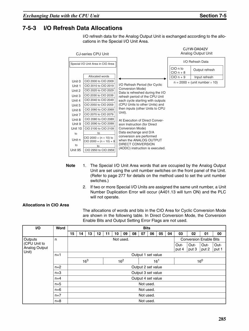
Exchanging Data with the CPU Unit Section 7-5
7-5-3 I/O Refresh Data AllocationsI/O refresh data for the Analog Output Unit is exchanged according to the allo-cations in the Special I/O Unit Area.
Note 1. The Special I/O Unit Area words that are occupied by the Analog OutputUnit are set using the unit number switches on the front panel of the Unit.(Refer to page 277 for details on the method used to set the unit numberswitches.)
2. If two or more Special I/O Units are assigned the same unit number, a UnitNumber Duplication Error will occur (A401.13 will turn ON) and the PLCwill not operate.
Allocations in CIO AreaThe allocations of words and bits in the CIO Area for Cyclic Conversion Modeare shown in the following table. In Direct Conversion Mode, the ConversionEnable Bits and Output Setting Error Flags are not used.
CJ1W-DA042V
to
to
Special I/O Unit Area in CIO Area
Allocated words
Unit 0Unit 1Unit 2
Unit 3Unit 4Unit 5Unit 6Unit 7
Unit 8Unit 9
Unit 10
Unit 95
Unit n
CIO 2000 to CIO 2009
CIO 2010 to CIO 2019
CIO 2020 to CIO 2029
CIO 2030 to CIO 2039
CIO 2040 to CIO 2049
CIO 2050 to CIO 2059
CIO 2060 to CIO 2069
CIO 2070 to CIO 2079
CIO 2080 to CIO 2089
CIO 2090 to CIO 2099
CIO 2100 to CIO 2109
CIO 2000 + (n × 10) to CIO 2000 + (n × 10) + 9
CIO 2950 to CIO 2959
Analog Output Unit
I/O Refresh Data
Output refresh
Input refresh
n = 2000 + (unit number × 10)I/O Refresh Period (for Cyclic Conversion Mode) Data is refreshed during the I/O refresh period of the CPU Unit each cycle starting with outputs (CPU Units to other Units) and then inputs (other Units to CPU Unit).
At Execution of Direct Conver-sion Instruction (for Direct Conversion Mode) Data exchange and D/A conversion are performed when the ANALOG OUTPUT DIRECT CONVERSION (AODC) instruction is executed.
CIO n to CIO n + 8
CJ-series CPU Unit
to
to
CIO n + 9
I/O Word Bits
15 14 13 12 11 10 09 08 07 06 05 04 03 02 01 00
Outputs (CPU Unit to Analog Output Unit)
n Not used. Conversion Enable Bits
Out-put 4
Out-put 3
Out-put 2
Out-put 1
n+1 Output 1 set value
163 162 161 160
n+2 Output 2 set value
n+3 Output 3 set value
n+4 Output 4 set value
n+5 Not used.
n+6 Not used.
n+7 Not used.
n+8 Not used.
285

Exchanging Data with the CPU Unit Section 7-5
• For the CIO word addresses, n = CIO 2000 + (unit number × 10).
Set Values and Stored Values
Note D/A conversion is performed for the set value when the ANALOGOUTPUT DIRECT CONVERSION (AODC) instruction is executed.
Inputs (Analog Output Unit to CPU Unit)
n+9 Alarm Flags Not used. Output Setting Error Bits
Out-put 4
Out-put 3
Out-put 2
Out-put 1
I/O Word Bits
15 14 13 12 11 10 09 08 07 06 05 04 03 02 01 00
Setting Contents Yes: Settable or usable No: Not settable or usable
Page
Cyclic Conversion
Mode
Direct Conversion
Mode
Conversion Enable Bit
0: Conversion outputs stopped.1: Conversion outputs started.
Yes No 288
Set value 16-bit binary data Yes Yes (See note.)
287
Output Setting Error Bit
0: No error1: Output setting error
Yes No 293
Alarm Flags Bits 00 to 03: Output setting error
Yes No 296
Bits 04 to 07: Not used. Not used.
Bit 08: Scaling data setting error
Yes Yes
Bit 09: Output signal range setting error or error in number of outputs used set-ting
Yes Yes
Bit 10: Output hold setting error
Yes Yes
Bit 11: Not used Not used.
Bit 12: Error in setting of conversion mode
Yes Yes
Bit 13: Direct Conversion Mode
Yes Yes
Bits 14 to 15: Not used Not used.
286
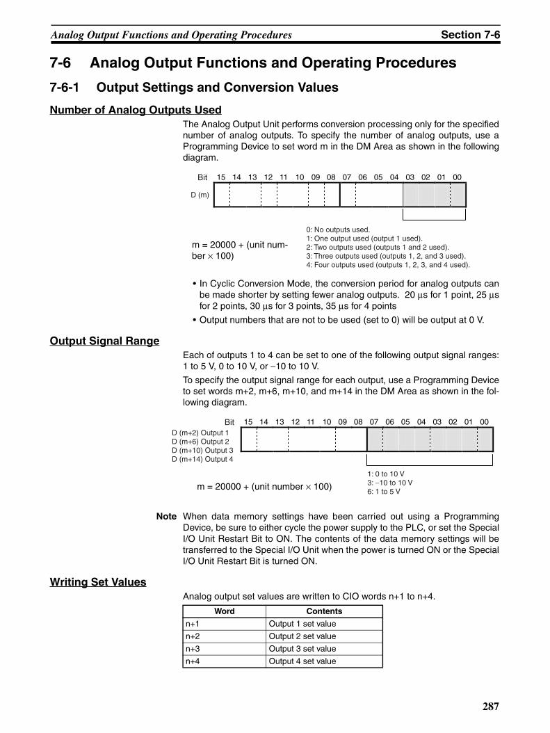
Analog Output Functions and Operating Procedures Section 7-6
7-6 Analog Output Functions and Operating Procedures
7-6-1 Output Settings and Conversion Values
Number of Analog Outputs UsedThe Analog Output Unit performs conversion processing only for the specifiednumber of analog outputs. To specify the number of analog outputs, use aProgramming Device to set word m in the DM Area as shown in the followingdiagram.
• In Cyclic Conversion Mode, the conversion period for analog outputs canbe made shorter by setting fewer analog outputs. 20 µs for 1 point, 25 µsfor 2 points, 30 µs for 3 points, 35 µs for 4 points
• Output numbers that are not to be used (set to 0) will be output at 0 V.
Output Signal RangeEach of outputs 1 to 4 can be set to one of the following output signal ranges:1 to 5 V, 0 to 10 V, or −10 to 10 V.
To specify the output signal range for each output, use a Programming Deviceto set words m+2, m+6, m+10, and m+14 in the DM Area as shown in the fol-lowing diagram.
Note When data memory settings have been carried out using a ProgrammingDevice, be sure to either cycle the power supply to the PLC, or set the SpecialI/O Unit Restart Bit to ON. The contents of the data memory settings will betransferred to the Special I/O Unit when the power is turned ON or the SpecialI/O Unit Restart Bit is turned ON.
Writing Set ValuesAnalog output set values are written to CIO words n+1 to n+4.
15 14 13 12 11 10 09 08 07 06 05 04 03 02 01 00
Bit
0: No outputs used.1: One output used (output 1 used).2: Two outputs used (outputs 1 and 2 used).3: Three outputs used (outputs 1, 2, and 3 used).4: Four outputs used (outputs 1, 2, 3, and 4 used).
D (m)
m = 20000 + (unit num-ber × 100)
15 14 13 12 11 10 09 08 07 06 05 04 03 02 01 00
Bit
1: 0 to 10 V3: −10 to 10 V6: 1 to 5 V
D (m+2) Output 1D (m+6) Output 2D (m+10) Output 3D (m+14) Output 4
m = 20000 + (unit number × 100)
Word Contents
n+1 Output 1 set value
n+2 Output 2 set value
n+3 Output 3 set value
n+4 Output 4 set value
287

Analog Output Functions and Operating Procedures Section 7-6
• For the CIO word addresses, n = CIO 2000 + (unit number × 10).
Use MOV(021) or XFER(070) to write values in the user program.
Example 1 In this example, the set value from only one output is written. (The unit num-ber is 0.)
Example 2 In this example, multiple set values are written. (The unit number is #0.)
Note If the set value has been written outside the specified range, an output settingerror will occur and the value set by the output hold function will be output.
Starting and Stopping ConversionTo begin analog output conversion in Cyclic Conversion Mode, turn ON thecorresponding Conversion Enable Bit (word n, bits 00 to 03) from the user’sprogram.
Note 1. To perform analog output conversion in Direct Conversion Mode, executethe ANALOG OUTPUT DIRECT CONVERSION (AODC) instruction in theuser’s program. (Refer to page 289.)
2. The analog output when conversion is stopped depends on the output sig-nal range setting and output hold setting. (Refer to pages 287 and 290.)
3. Conversion will not begin under the following conditions even if the Con-version Enable Bit is turned ON. (Refer to page 290.)
1. When there is an output setting error.
2. When a fatal error occurs in the PLC.
4. When the operation mode for the CPU Unit is changed from RUN mode orMONITOR mode to PROGRAM mode, the Conversion Enable Bits will allturn OFF. They will also turn OFF when the power supply to the PLC isturned ON. The output status at this time depends on the output hold func-tion.
MOV(021)D00001
2001
Input condition
The set value stored in D00001 is written to CIO 2001 (output 1).
XFER(070)0004
D00001
2001
The set values stored in D00001 to D00004 are written to CIO 2001 to CIO 2004 (outputs 1 to 4).
Input condition
15 14 13 12 11 10 09 08 07 06 05 04 03 02 01 00
Bit
Out-put 4
Out-put 3
Out-put 2
Out-put 1
Word n
n = CIO 2000 + (unit number × 10)
Analog conversion is executed while these bits areON. When the bits are turned OFF, the conversionis stopped and the output data is held.
288

Analog Output Functions and Operating Procedures Section 7-6
Example: In this example, conversion is begun for analog output number 1. (The unit number is 0.)
7-6-2 Conversion Mode SettingBits 00 to 07 in DM word m+1 can be used to set the conversion mode. Theconversion mode that is set determines the timing of refreshing analog outputvalues. This setting applies to analog outputs 1 to 4. There are not individualsettings for each output.
The following table describes the conversion modes that can be set.
To specify the conversion mode, use a Programming Device to set the bits inDM word (m+1) as shown in the following diagram.
Note 1. When DM Area settings have been carried out using a Programming De-vice, be sure to either cycle the power supply to the PLC, or turn ON theSpecial I/O Unit Restart Bit. The contents of the initial settings in the DMArea will be transferred to the Special I/O Unit when the power is turnedON or the Special I/O Unit Restart Bit is turned ON.
2000.00
Input condition
Conversion begins for output 1.
Conversion mode Operation Features Remarks
Cyclic Conversion Mode
Output set values are refreshed during the I/O refresh period. Each conversion period, the refreshed set values are con-verted to analog values and output. It takes at least one cycle for the data set in the PLC to be transferred to the Analog Output Unit.
Operation is the same as that of the CJ1W-DA021/-DA041/-DA08V/-DA08C Analog Out-put Units.
This is the default set-ting.
Direct Conversion Mode
The output set values are refreshed and D/A conversion is performed immediately when the ANALOG OUTPUT DIRECT CONVERSION (AODC) instruction is executed in the CPU Unit. The set values are not refreshed unless the ANALOG OUTPUT DIRECT CONVERSION (AODC) instruction is executed. If the CPU Unit is in PROGRAM mode, the set values are automatically output using Cyclic Conversion Mode.
AODC can be used together with the ANALOG INPUT DIRECT CONVERSION (AIDC) instruction for the CJ1W-AD042 Analog Input Unit to create a consistent input-processing-output time. If these instructions are used in a scheduled interrupt task, a constant and consistent input-processing-output time can be created.
A CJ2H-CPU@@(-EIP) CPU Unit with unit ver-sion 1.1 or later is required to use direct conversion.
15 14 13 12 11 10 09 08 07 06 05 04 03 02 01 00
Bit
00 hex: Cyclic Conversion ModeA5 hex: Direct Conversion Mode
D (m+1)
m = 20000 + (unit number × 100)
289
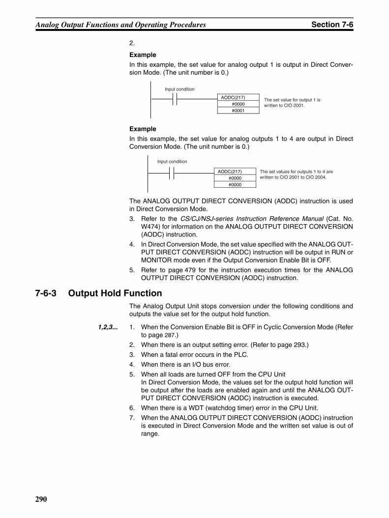
Analog Output Functions and Operating Procedures Section 7-6
2.
Example
In this example, the set value for analog output 1 is output in Direct Conver-sion Mode. (The unit number is 0.)
Example
In this example, the set value for analog outputs 1 to 4 are output in DirectConversion Mode. (The unit number is 0.)
The ANALOG OUTPUT DIRECT CONVERSION (AODC) instruction is usedin Direct Conversion Mode.
3. Refer to the CS/CJ/NSJ-series Instruction Reference Manual (Cat. No.W474) for information on the ANALOG OUTPUT DIRECT CONVERSION(AODC) instruction.
4. In Direct Conversion Mode, the set value specified with the ANALOG OUT-PUT DIRECT CONVERSION (AODC) instruction will be output in RUN orMONITOR mode even if the Output Conversion Enable Bit is OFF.
5. Refer to page 479 for the instruction execution times for the ANALOGOUTPUT DIRECT CONVERSION (AODC) instruction.
7-6-3 Output Hold FunctionThe Analog Output Unit stops conversion under the following conditions andoutputs the value set for the output hold function.
1,2,3... 1. When the Conversion Enable Bit is OFF in Cyclic Conversion Mode (Referto page 287.)
2. When there is an output setting error. (Refer to page 293.)
3. When a fatal error occurs in the PLC.
4. When there is an I/O bus error.
5. When all loads are turned OFF from the CPU Unit In Direct Conversion Mode, the values set for the output hold function willbe output after the loads are enabled again and until the ANALOG OUT-PUT DIRECT CONVERSION (AODC) instruction is executed.
6. When there is a WDT (watchdog timer) error in the CPU Unit.
7. When the ANALOG OUTPUT DIRECT CONVERSION (AODC) instructionis executed in Direct Conversion Mode and the written set value is out ofrange.
AODC(217)#0000 #0001
Input condition
The set value for output 1 is written to CIO 2001.
AODC(217)#0000 #0000
Input condition
The set values for outputs 1 to 4 are written to CIO 2001 to CIO 2004.
290

Analog Output Functions and Operating Procedures Section 7-6
CLR, HOLD, or MAX can be selected for the output status when conversionstops.
To set the output hold function, use a Programming Device to set DM Area asshown in the following diagram.
Note For the DM word addresses, m = D20000 + (unit number x 100).
Note When DM Area settings have been carried out using a Programming Device,be sure to either cycle the power supply to the PLC, or turn ON the Special I/O Unit Restart Bit. The contents of the initial settings in the DM Area will betransferred to the Special I/O Unit when the power is turned ON or the SpecialI/O Unit Restart Bit is turned ON.
7-6-4 Output ScalingWhen upper and lower limits have been preset in 16-bit binary data in theCPU Unit’s DM Area within a range of −32,000 to 32,000 decimal (from 8300to 7D00 hex), analog output set values (in user-specified units) with the upperand lower limits taken as full scale are converted from digital to analog. (Seenote.)
This scaling function eliminates the previous necessity of providing programsfor numeric conversion to specified units.
Note To set the upper or lower limit to a negative number, use two’s com-plement. (Set 8300 to FFFF hex for −32,000 to −1.)
Note 1. The upper limit is normally set to be greater than the lower limit, but it isalso possible to set lower limit to be greater than the upper limit for reversescaling.
2. Actual D/A conversion is executed at up to −5% to +105% of full scale. Ifvalues exceeding this range are set, an output setting value error will occurand the output hold function will operate.
3. When setting upper and lower limits in the DM Area in the specified units,be sure to make the settings in 16-bit binary data (with negative values setas two’s complement).
Output signal range
CLR HOLD MAX
1 to 5 V 0.8 V (−5% (full scale)) Voltage that was output just prior to stopping.
5.2 V (5% (full scale))
0 to 10 V −0.5 V (−5% (full scale)) Voltage that was output just prior to stopping.
10.5 V (5% (full scale))
−10 to 10 V 0.0 V Voltage that was output just prior to stopping.
11.0 V (5% (full scale))
DM Area word (See note.)
Function Set value
D (m+3) Output 1: Output status when conversion stops
0: CLROutputs 0 or minimum value of range (−5%).1: HOLDHolds output value prior to stop.
2: MAXOutputs maximum value of range (105%).
D (m+7) Output 2: Output status when conversion stops
D (m+11) Output 3: Output status when conversion stops
D (m+15) Output 4: Output status when conversion stops
291

Analog Output Functions and Operating Procedures Section 7-6
4. If the scaling upper limit equals the lower limit, or if the scaling upper limitor lower limit is outside the range of ±32,000, a scaling data setting erroroccurs and scaling will not be performed. Scaling will not be performed butoperation will be normal when both the upper and lower limits are set to0000 (the default values).
Setting Upper and Lower Limits for Output ScalingSet the upper and lower limits for scaling for outputs 1 to 4 in the following DMArea words.
m = 20000 + (unit number × 100)
Note For decimal numbers −32,000 to 32,000, set 16-bit binary data (8300to 7D00 hex).
Example Setting 1For this example, the following conditions are set in the DM Area.
The following diagram shows the correspondence between output signals andconverted scaling values.
DM Area word Bits
15 14 13 12 11 10 09 08 07 06 05 04 03 02 01 00
DM (m+4) Output 1 scaling lower limit
DM (m+5) Output 1 scaling upper limit
DM (m+8) Output 2 scaling lower limit
DM (m+9) Output 2 scaling upper limit
DM (m+12) Output 3 scaling lower limit
DM (m+13) Output 3 scaling upper limit
DM (m+16) Output 4 scaling lower limit
DM (m+17) Output 4 scaling upper limit
Conditions The values shown in parentheses are 16-bit binary data.
Output signal range 0 to 10 V
Scaling lower limit 0 (0000 hex)
Scaling upper limit 10,000 (2710 hex)
The values shown in parentheses are 16-bit binary data.
Output signal
0 (0000 hex) 0 V
10,000 (2710 hex) 10 V
−500 (FE0C hex) −0.5 V
10,500 (2904 hex) 10.5 V
0
−0.5 V
Scaling line
10,500 (2904 hex)
10,000 (2710 hex)
(0000 hex)
−500 FE0C hex
+10.5 V+10.0 V
0 V
292
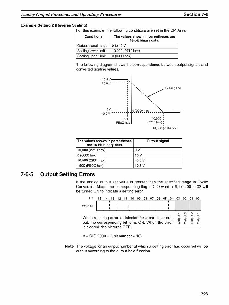
Analog Output Functions and Operating Procedures Section 7-6
Example Setting 2 (Reverse Scaling)For this example, the following conditions are set in the DM Area.
The following diagram shows the correspondence between output signals andconverted scaling values.
7-6-5 Output Setting ErrorsIf the analog output set value is greater than the specified range in CyclicConversion Mode, the corresponding flag in CIO word n+9, bits 00 to 03 willbe turned ON to indicate a setting error.
Note The voltage for an output number at which a setting error has occurred will beoutput according to the output hold function.
Conditions The values shown in parentheses are 16-bit binary data.
Output signal range 0 to 10 V
Scaling lower limit 10,000 (2710 hex)
Scaling upper limit 0 (0000 hex)
The values shown in parentheses are 16-bit binary data.
Output signal
10,000 (2710 hex) 0 V
0 (0000 hex) 10 V
10,500 (2904 hex) −0.5 V
−500 (FE0C hex) 10.5 V
Scaling line
−0.5 V
10,500 (2904 hex)
10,000 (2710 hex)
0 (0000 hex)
−500 FE0C hex
+10.5 V+10.0 V
0 V
15 14 13 12 11 10 09 08 07 06 05 04 03 02 01 00
Bit
Word n+9
Out
put 4
Out
put 3
Out
put 2
Out
put 1
n = CIO 2000 + (unit number × 10)
When a setting error is detected for a particular out-put, the corresponding bit turns ON. When the erroris cleared, the bit turns OFF.
293

Handling Errors and Alarms Section 7-7
7-7 Handling Errors and Alarms
7-7-1 Indicators and Error Flowchart
IndicatorsIf an alarm or error occurs in the Analog Output Unit, the ERC or ERH indica-tor on the front panel of the Unit will light.
RUN
ERC
ERH
Front panel of Unit
Indicator Meaning Indicator status Operating status
RUN (green) Operating Lit Operation normal.
Not lit Unit has stopped exchanging data with the CPU Unit.
ERC (red) Error detected by Unit Lit Alarm has occurred or initial settings are incorrect.
Not lit Operating normally.
ERH (red) Error in the CPU Unit Lit Error has occurred during data exchange with the CPU Unit.
Not lit Operating normally.
294
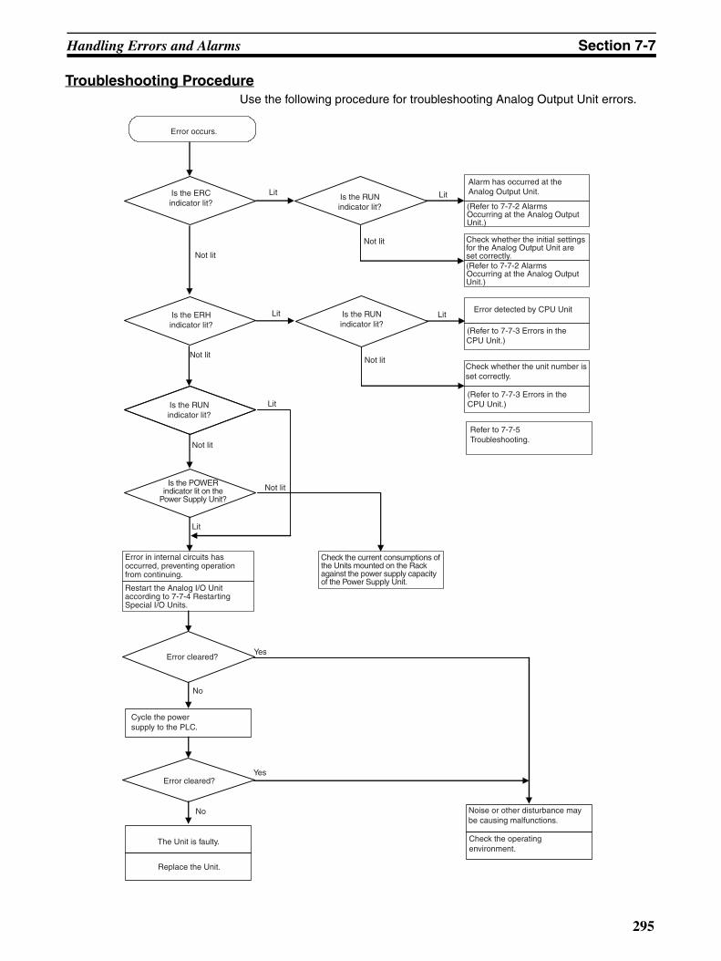
Handling Errors and Alarms Section 7-7
Troubleshooting ProcedureUse the following procedure for troubleshooting Analog Output Unit errors.
Lit Lit
Alarm has occurred at the Analog Output Unit.
(Refer to 7-7-2 Alarms Occurring at the Analog Output Unit.)
Not lit
Not lit Check whether the initial settings for the Analog Output Unit are set correctly.(Refer to 7-7-2 AlarmsOccurring at the Analog Output Unit.)
Lit LitError detected by CPU Unit
(Refer to 7-7-3 Errors in the CPU Unit.)
Not litNot lit
Check whether the unit number is set correctly.
(Refer to 7-7-3 Errors in theCPU Unit.)Lit
Not lit
Not lit
Lit
No
Error cleared?
No
Error occurs.
Is the ERC indicator lit?
Is the RUN indicator lit?
Is the RUN indicator lit?
Is the ERH indicator lit?
Is the RUN indicator lit?
Is the POWER indicator lit on the
Power Supply Unit?
Error in internal circuits has occurred, preventing operation from continuing.
Restart the Analog I/O Unit according to 7-7-4 Restarting Special I/O Units.
Error cleared?
Check the current consumptions of the Units mounted on the Rack against the power supply capacity of the Power Supply Unit.
Cycle the power supply to the PLC.
The Unit is faulty.
Replace the Unit.
Noise or other disturbance may be causing malfunctions.
Yes
Yes
Refer to 7-7-5 Troubleshooting.
Check the operating environment.
295
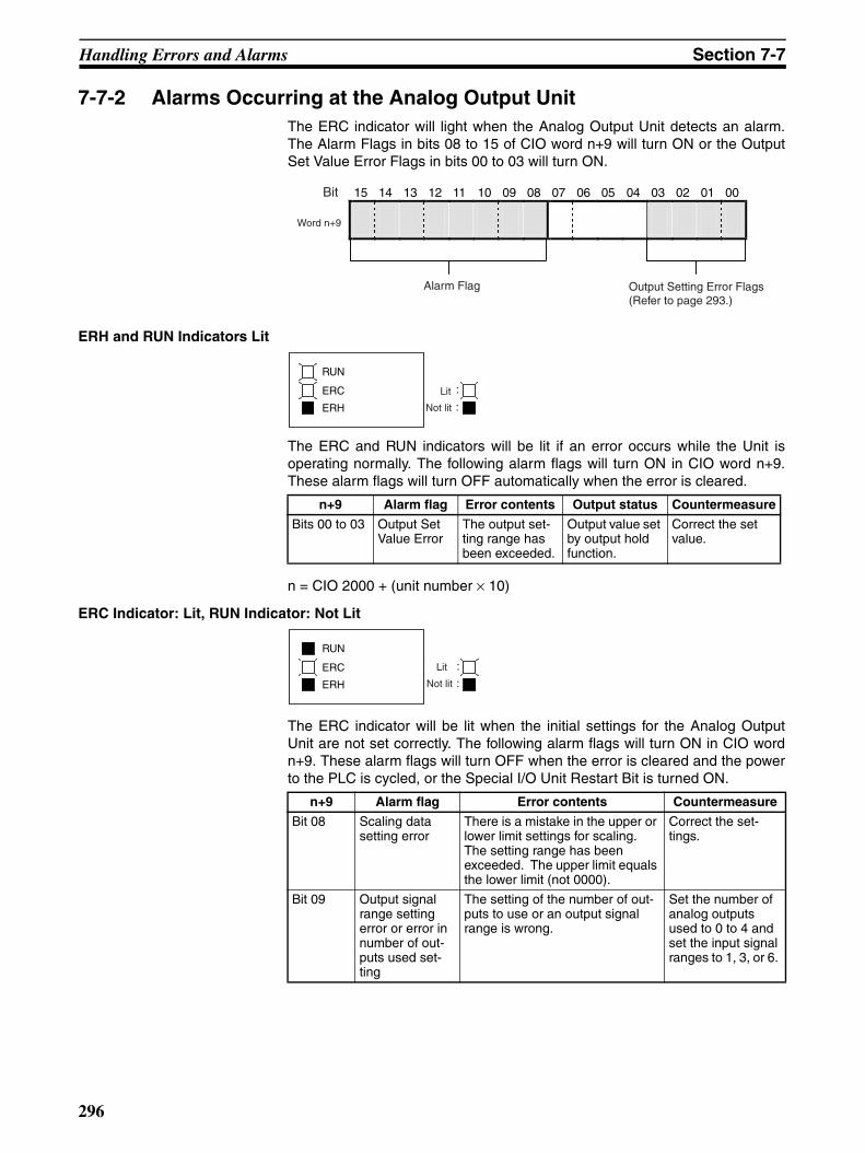
Handling Errors and Alarms Section 7-7
7-7-2 Alarms Occurring at the Analog Output UnitThe ERC indicator will light when the Analog Output Unit detects an alarm.The Alarm Flags in bits 08 to 15 of CIO word n+9 will turn ON or the OutputSet Value Error Flags in bits 00 to 03 will turn ON.
ERH and RUN Indicators Lit
The ERC and RUN indicators will be lit if an error occurs while the Unit isoperating normally. The following alarm flags will turn ON in CIO word n+9.These alarm flags will turn OFF automatically when the error is cleared.
n = CIO 2000 + (unit number × 10)
ERC Indicator: Lit, RUN Indicator: Not Lit
The ERC indicator will be lit when the initial settings for the Analog OutputUnit are not set correctly. The following alarm flags will turn ON in CIO wordn+9. These alarm flags will turn OFF when the error is cleared and the powerto the PLC is cycled, or the Special I/O Unit Restart Bit is turned ON.
15 14 13 12 11 10 09 08 07 06 05 04 03 02 01 00
Bit
Output Setting Error Flags (Refer to page 293.)
Alarm Flag
Word n+9
n+9 Alarm flag Error contents Output status Countermeasure
Bits 00 to 03 Output Set Value Error
The output set-ting range has been exceeded.
Output value set by output hold function.
Correct the set value.
RUN
ERC
ERH
Lit
Not lit :
:
n+9 Alarm flag Error contents Countermeasure
Bit 08 Scaling data setting error
There is a mistake in the upper or lower limit settings for scaling. The setting range has been exceeded. The upper limit equals the lower limit (not 0000).
Correct the set-tings.
Bit 09 Output signal range setting error or error in number of out-puts used set-ting
The setting of the number of out-puts to use or an output signal range is wrong.
Set the number of analog outputs used to 0 to 4 and set the input signal ranges to 1, 3, or 6.
RUN
ERC
ERH
Lit
Not lit :
:
296

Handling Errors and Alarms Section 7-7
n = CIO 2000 + (unit number × 10)
7-7-3 Errors in the CPU UnitThe ERH indicator will light if an error occurs in the CPU Unit or I/O bus and I/O refreshing with the Special I/O Units is not performed correctly, preventingthe Analog Output Unit from operating.
ERH and RUN Indicators: Lit
The ERH and RUN indicators will light if an I/O bus error occurs or if a WDT(watchdog timer) error occurs in the CPU Unit, resulting in incorrect I/Orefresh with the Analog Output Unit. Cycle the power supply to the PLC orrestart the Analog Output Unit.
ERH Indicator: Lit, RUN Indicator: Not Lit
The unit number for the Analog Output Unit has not been set correctly.
Bit 10 Output hold set-ting error
The setting of the output status for when conversion is stopped is wrong.
Specify 00, 01, or 02.
Bit 12 Error in setting of conversion mode
The setting for Cyclic Conversion Mode or Direct Conversion Mode is wrong.
Set 00 hex or A5 hex.
n+9 Alarm flag Error contents Countermeasure
Error Error contents Output status
I/O bus error Error has occurred during data exchange with the CPU Unit.
Output value set by output hold function.
CPU Unit monitoring error No response from CPU Unit for a specified period of time.
Maintains the status from before the error.
CPU Unit WDT error Error has occurred in CPU Unit.
Output value set by output hold function.
RUN
ERC
ERH
Lit
Not lit ::
Error Error contents Output status
Unit Number Duplica-tion Error
The same unit number has been assigned to more than one Unit or the unit number was set to a value other than 00 to 95.
The output value will be 0 V.
Special I/O Unit Setting Error
The Special I/O Units reg-istered in the I/O tables are different from the ones actually mounted.
RUN
ERC
ERH
Lit
Not lit :
:
297

Handling Errors and Alarms Section 7-7
7-7-4 Restarting Special I/O UnitsTo restart the Analog Output Unit after changing the contents of the DM Areaor correcting an error, cycle the power to the PLC or turn ON the Special I/OUnit Restart Bit.
Special I/O Unit Restart Bits
Note 1. Replace the Unit if the error is not cleared even though the power supplyis cycled or the Restart Bit is turned ON.
2. The output becomes 0 V during restart.
7-7-5 TroubleshootingThe following tables list the probable causes of troubles that may occur, andthe countermeasures for dealing with them.
Analog Output Does Not Change
Value Does Not Change as Intended
Outputs Are Inconsistent
Bit Function
A502.00 Unit No. 0 Restart Bit Restarts the Unit when turned ON.A502.01 Unit No. 1 Restart Bit
to to
A502.15 Unit No. 15 Restart Bit
A503.00 Unit No. 16 Restart Bit
to to
A507.15 Unit No. 95 Restart Bit
Probable cause Countermeasure Page
Number of analog outputs used is not set correctly.
Set the number of analog outputs used to enable all outputs that are being used.
287
The ANALOG OUTPUT DIRECT CONVERSION (AODC) instruction is not being executed in Direct Con-version Mode.
Execute the ANALOG OUTPUT DIRECT CONVERSION (AODC) instruction in the user program.
289
The output hold function is in opera-tion.
Turn ON the Conversion Enable Bit. 290
The value set for the output set value is out of range.
Set the data within the range. 270
Probable cause Countermeasure Page
The output signal range setting is wrong.
Correct the output signal range set-ting.
287
The specifications of the input device do not match those of the Analog Output Unit (e.g., input signal range, input impedance).
Change the input device. 268
Probable cause Countermeasure Page
The output signals are being affected by external noise.
Try connecting the cable shield at the Analog Output Unit, or disconnecting it if it is already connected.
279
298

SECTION 8CS-series Analog I/O Unit (CS1W-MAD44)
This section explains how to use the CS1W-MAD44 Analog I/O Unit.
8-1 Specifications . . . . . . . . . . . . . . . . . . . . . . . . . . . . . . . . . . . . . . . . . . . . . . . . . 3008-1-1 Specifications . . . . . . . . . . . . . . . . . . . . . . . . . . . . . . . . . . . . . . . . . . 3008-1-2 I/O Function Block Diagram . . . . . . . . . . . . . . . . . . . . . . . . . . . . . . 3038-1-3 Input Specifications . . . . . . . . . . . . . . . . . . . . . . . . . . . . . . . . . . . . . 3038-1-4 Output Specifications . . . . . . . . . . . . . . . . . . . . . . . . . . . . . . . . . . . . 305
8-2 Operating Procedure . . . . . . . . . . . . . . . . . . . . . . . . . . . . . . . . . . . . . . . . . . . . 3088-2-1 Procedure Examples . . . . . . . . . . . . . . . . . . . . . . . . . . . . . . . . . . . . . 309
8-3 Components and Switch Settings . . . . . . . . . . . . . . . . . . . . . . . . . . . . . . . . . . 3158-3-1 Indicators . . . . . . . . . . . . . . . . . . . . . . . . . . . . . . . . . . . . . . . . . . . . . 3168-3-2 Unit Number Switches . . . . . . . . . . . . . . . . . . . . . . . . . . . . . . . . . . . 3178-3-3 Operation Mode Switch . . . . . . . . . . . . . . . . . . . . . . . . . . . . . . . . . . 3178-3-4 Voltage/Current Switch. . . . . . . . . . . . . . . . . . . . . . . . . . . . . . . . . . . 318
8-4 Wiring . . . . . . . . . . . . . . . . . . . . . . . . . . . . . . . . . . . . . . . . . . . . . . . . . . . . . . . 3188-4-1 Terminal Arrangement . . . . . . . . . . . . . . . . . . . . . . . . . . . . . . . . . . . 3188-4-2 Internal Circuitry . . . . . . . . . . . . . . . . . . . . . . . . . . . . . . . . . . . . . . . 3198-4-3 Voltage Input Disconnection. . . . . . . . . . . . . . . . . . . . . . . . . . . . . . . 3208-4-4 I/O Wiring Example . . . . . . . . . . . . . . . . . . . . . . . . . . . . . . . . . . . . . 3218-4-5 I/O Wiring Considerations . . . . . . . . . . . . . . . . . . . . . . . . . . . . . . . . 322
8-5 Exchanging Data with the CPU Unit . . . . . . . . . . . . . . . . . . . . . . . . . . . . . . . 3228-5-1 Outline of Data Exchange. . . . . . . . . . . . . . . . . . . . . . . . . . . . . . . . . 3228-5-2 Unit Number Settings . . . . . . . . . . . . . . . . . . . . . . . . . . . . . . . . . . . . 3238-5-3 Special I/O Unit Restart Bits . . . . . . . . . . . . . . . . . . . . . . . . . . . . . . 3238-5-4 Fixed Data Allocations . . . . . . . . . . . . . . . . . . . . . . . . . . . . . . . . . . . 3248-5-5 I/O Refresh Data Allocations . . . . . . . . . . . . . . . . . . . . . . . . . . . . . . 327
8-6 Analog Input Functions and Operating Procedures . . . . . . . . . . . . . . . . . . . . 3308-6-1 Input Settings and Conversion Values . . . . . . . . . . . . . . . . . . . . . . . 3308-6-2 Mean Value Processing. . . . . . . . . . . . . . . . . . . . . . . . . . . . . . . . . . . 3328-6-3 Peak Value Hold Function . . . . . . . . . . . . . . . . . . . . . . . . . . . . . . . . 3358-6-4 Input Disconnection Detection Function . . . . . . . . . . . . . . . . . . . . . 336
8-7 Analog Output Functions and Operating Procedures . . . . . . . . . . . . . . . . . . . 3378-7-1 Output Settings and Conversions . . . . . . . . . . . . . . . . . . . . . . . . . . . 3378-7-2 Output Hold Function . . . . . . . . . . . . . . . . . . . . . . . . . . . . . . . . . . . . 3398-7-3 Output Setting Errors . . . . . . . . . . . . . . . . . . . . . . . . . . . . . . . . . . . . 340
8-8 Ratio Conversion Function . . . . . . . . . . . . . . . . . . . . . . . . . . . . . . . . . . . . . . . 3408-9 Adjusting Offset and Gain . . . . . . . . . . . . . . . . . . . . . . . . . . . . . . . . . . . . . . . 343
8-9-1 Adjustment Mode Operational Flow . . . . . . . . . . . . . . . . . . . . . . . . 3448-9-2 Input Offset and Gain Adjustment Procedures . . . . . . . . . . . . . . . . . 3458-9-3 Output Offset and Gain Adjustment Procedures . . . . . . . . . . . . . . . 351
8-10 Handling Errors and Alarms . . . . . . . . . . . . . . . . . . . . . . . . . . . . . . . . . . . . . . 3598-10-1 Indicators and Error Flowchart . . . . . . . . . . . . . . . . . . . . . . . . . . . . . 3598-10-2 Alarms Occurring at the Analog I/O Unit . . . . . . . . . . . . . . . . . . . . 3618-10-3 Errors in the CPU Unit . . . . . . . . . . . . . . . . . . . . . . . . . . . . . . . . . . . 3638-10-4 Restarting Special I/O Units . . . . . . . . . . . . . . . . . . . . . . . . . . . . . . . 3648-10-5 Troubleshooting . . . . . . . . . . . . . . . . . . . . . . . . . . . . . . . . . . . . . . . . 364
299
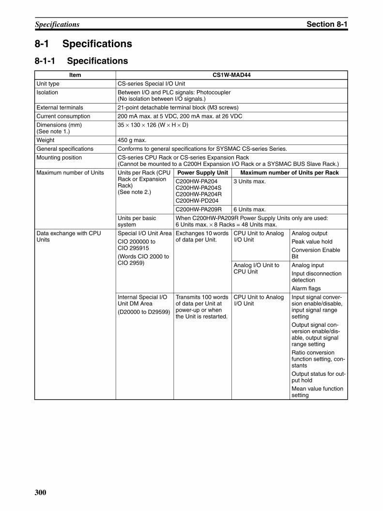
Specifications Section 8-1
8-1 Specifications
8-1-1 SpecificationsItem CS1W-MAD44
Unit type CS-series Special I/O Unit
Isolation Between I/O and PLC signals: Photocoupler(No isolation between I/O signals.)
External terminals 21-point detachable terminal block (M3 screws)
Current consumption 200 mA max. at 5 VDC, 200 mA max. at 26 VDC
Dimensions (mm) (See note 1.)
35 × 130 × 126 (W × H × D)
Weight 450 g max.
General specifications Conforms to general specifications for SYSMAC CS-series Series.
Mounting position CS-series CPU Rack or CS-series Expansion Rack(Cannot be mounted to a C200H Expansion I/O Rack or a SYSMAC BUS Slave Rack.)
Maximum number of Units Units per Rack (CPU Rack or Expansion Rack)(See note 2.)
Power Supply Unit Maximum number of Units per Rack
C200HW-PA204C200HW-PA204SC200HW-PA204RC200HW-PD204
3 Units max.
C200HW-PA209R 6 Units max.
Units per basic system
When C200HW-PA209R Power Supply Units only are used:6 Units max. × 8 Racks = 48 Units max.
Data exchange with CPU Units
Special I/O Unit AreaCIO 200000 to CIO 295915
(Words CIO 2000 to CIO 2959)
Exchanges 10 words of data per Unit.
CPU Unit to Analog I/O Unit
Analog outputPeak value hold
Conversion Enable Bit
Analog I/O Unit to CPU Unit
Analog inputInput disconnection detection
Alarm flags
Internal Special I/O Unit DM Area
(D20000 to D29599)
Transmits 100 words of data per Unit at power-up or when the Unit is restarted.
CPU Unit to Analog I/O Unit
Input signal conver-sion enable/disable, input signal range settingOutput signal con-version enable/dis-able, output signal range setting
Ratio conversion function setting, con-stants
Output status for out-put holdMean value function setting
300

Specifications Section 8-1
Note 1. Refer to Dimensions on page 439 for details on the Unit’s dimensions.
Input Specifications Voltage input Current input
Number of analog inputs 4
Input signal range (See note 3.) 1 to 5 V0 to 5 V0 to 10 V–10 to 10 V
4 to 20 mA(See note 4.)
Maximum rated input (for 1 point) (See note 5.)
±15 V ±30 mA
Input impedance 1 MΩ min. 250 Ω (rated value)
Resolution 4,000 (full scale)
Converted output data 16-bit binary data
Accuracy(See note 6.)
23±2°C ±0.2% of full scale ±0.4% of full scale
0°C to 55°C ±0.4% of full scale ±0.6% of full scale
A/D conversion time (See note 7.) 1.0 ms/point max.
Functions Mean value process-ing
Stores the last “n” data conversions in the buffer, and stores the the mean value of the conversion values.
Number of mean value buffers: n = 2, 4, 8, 16, 32, 64
Peak value holding Stores the maximum conversion value while the Peak Value Hold Bit is ON.
Input disconnection detection (See note 9.)
Detects the disconnection and turns ON the Disconnection Detec-tion Flag.
Output Specifications Voltage output
Number of analog outputs 4
Output signal range(See note 3.)
1 to 5 V0 to 5 V0 to 10 V–10 to 10 V
Output impedance (for 1 point) 0.5 Ω max.
Max. output current 12 mA
Resolution 4,000 (full scale)
Set data 16-bit binary data
Accuracy
(See note 6.)
23±2°C ±0.3% of full scale
0°C to 55°C ±0.5% of full scale
D/A conversion time (See note 7.) 1.0 ms/point max.
Functions Output hold function Outputs the specified output status (CLR, HOLD, or MAX) under any of the following circumstances.When the Conversion Enable Bit is OFF. (See note 8.)
In adjustment mode, when a value other than the output number is output during adjustment.When there is an output setting error or a fatal error occurs at the PLC.
When the CPU Unit is on standby.When the Load is OFF.
Other Functions Ratio conversion function
Stores the results of positive and negative gradient analog inputs calculated for ratio and bias as analog output values.
Positive gradient: Analog output = A × Analog input + B(A = 0 to 99.99, B = 8,000 to 7FFF hex)
Negative gradient: Analog output = F – A × Analog input + B(A = 0 to 99.99, B = 8,000 to 7FFF hex, F = output range max. value)
Item CS1W-MAD44
301

Specifications Section 8-1
2. The maximum number of Analog I/O Units that can be mounted to oneRack will varies depending on the current consumption of the other Unitsmounted to the Rack.
3. Input and output signal ranges can be set for each input and output.
4. Voltage input or current input are chosen by using the voltage/currentswitch at the back of the terminal block.
5. The Analog I/O Unit must be operated according to the input specificationsprovided here. Operating the Unit outside these specifications will causethe Unit to malfunction.
6. The accuracy is given for full scale. For example, an accuracy of ±0.2%means a maximum error of ±8 (BCD).
The default setting is adjusted for voltage input. To use current input, per-form the offset and gain adjustments as required.
7. A/D conversion time is the time it takes for an analog signal to be stored inmemory as converted data after it has been input. It takes at least one cy-cle before the converted data is read by the CPU Unit. D/A conversion timeis the time required for converting and outputting the PLC data. It takes atleast one cycle for the data stored in the PLC to be read by the Analog I/OUnit.
8. When the operation mode for the CPU Unit is changed from RUN mode orMONITOR mode to PROGRAM mode, or when the power is turned ON,the Output Conversion Enable Bit will turn OFF. The output status specifiedaccording to the output hold function will be output.
9. Input disconnection detection is valid only when the 1 to 5-V or 4 to 20-mArange is set. If there is no input signal for when the 1 to 5-V or 4 to 20-mArange is set, the Disconnection Detection Flag will turn ON.
302

Specifications Section 8-1
8-1-2 I/O Function Block Diagram
8-1-3 Input SpecificationsIf signals that are outside the specified range provided below are input, theconversion values used will be either the maximum or minimum value.
Range: 1 to 5 V (4 to 20 mA)
Ratio con-version
Ratio conver-sion enabled
Ratio conver-sion disabled
Analog I/O Unit CPU Unit
Special I/O Unit Area
Analog input 1 conver-sion value
I/O refresh
Analog output 1 conver-sion value
Analog input 1
Analog input 2 Same as above.
Input dis-connection detection
Mean value processing disabled
Mean value processing enabled
Peak value hold function disabled
Ratio conver-sion disabled
Output hold enabled
Output hold disabled
A/D
D/AAnalog output 1
Analog input 3
Analog input 4
Same as above.Analog output 2
Peak value hold function enabled
Same as above.
Same as above.
Same as above.Analog output 3
Same as above.Analog output 4
1 V (4 mA)0.8 V (3.2 mA)
5 V (20 mA)5.2 V (20.8 mA)
Resolution: 4,000
Conversion value (16-bit binary data)
10680FA0
0000FF38
Analog input signal
303

Specifications Section 8-1
Range: 0 to 10 V
Range: 0 to 5 V
0 V 10 V–0.5 V 10.5 V
10680FA0
0000FF38
Resolution: 4,000
Conversion value (16-bit binary data)
Analog input signal
0 V 5 V–0.25 V 5.25 V
10680FA0
0000FF38
Resolution: 4,000
Conversion value (16-bit binary data)
Analog input signal
304

Specifications Section 8-1
Range: –10 to 10 V
8-1-4 Output SpecificationsIf the set value is outside the specified range provided below, an output settingerror will occur, and the output specified by the output hold function will beoutput.
Range: 1 to 5 V
0 V 10 V11 V
089807D0
F830F768
0000
–10 V–11 V
Resolution: 4,000
Conversion value (16-bit binary data)
Analog input signal
5.2 V5 V
1 V0.8 V
0000
FF38
0FA0
1068Resolution: 4,000
Set value (16-bit binary data)
Analog output signal
305
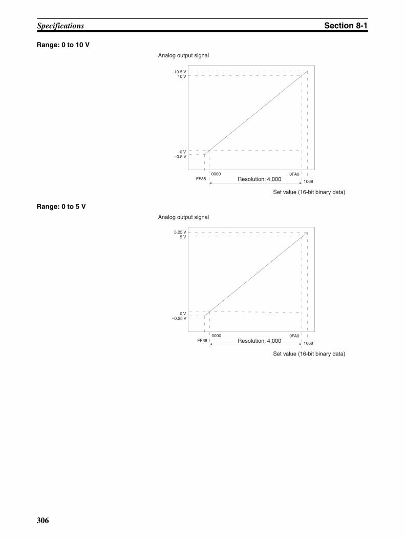
Specifications Section 8-1
Range: 0 to 10 V
Range: 0 to 5 V
0000FF38
0FA0
1068
10.5 V10 V
0 V–0.5 V
Resolution: 4,000
Set value (16-bit binary data)
Analog output signal
0000FF38
0FA0
1068
5.25 V5 V
0 V–0.25 V
Resolution: 4,000
Set value (16-bit binary data)
Analog output signal
306

Specifications Section 8-1
Range: –10 to 10 V
Note The conversion values and set values for a range of –10 to 10 V will be as fol-lows:
0000F830
F768
07D0
0898
0 V
–10 V–11 V
11 V10 V
Resolution: 4,000
Set value (16-bit binary data)
Analog output signal
16-bit binary data BCD
F768 –2200
: :
FFFF –1
0000 0
0001 1
: :
0898 2200
307

Operating Procedure Section 8-2
8-2 Operating ProcedureFollow the procedure outlined below when using Analog I/O Units.
Installation and Settings
1,2,3... 1. Set the operation mode switch on the rear panel of the Unit to normalmode.
2. Set the voltage/current switch at the back of the terminal block.
3. Wire the Unit.
4. Use the unit number switches on the front panel of the Unit to set the unitnumber.
5. Turn ON the power to the PLC.
6. Create the I/O tables.
7. Make the Special I/O Unit DM Area settings.
• Set the I/O numbers to be used.
• Set the input and output signal ranges.
• Set the number of mean processing samplings.
• Set the output hold function.
• Set the ratio conversion usage, the ratio set value, and the bias value.
8. Turn the power to the PLC OFF and ON, or turn ON the Special I/O UnitRestart Bit.
When the input or output of the connected devices needs to be calibrated, fol-low the procedures in Offset Gain Adjustment below. Otherwise, skip to Oper-ation below.
Offset and Gain Adjustment
1,2,3... 1. Set the operation mode on the rear panel of the Unit to adjustment mode.
2. Set the voltage/current switch at the back of the terminal block.
3. Turn ON the power to the PLC.
4. Adjust the offset and gain.
5. Turn OFF the power to the PLC.
6. Change the setting of the operation mode switch on the rear panel of theUnit back to normal mode.
Operation
1,2,3... 1. Turn ON the power to the PLC.
2. Ladder program
• Read conversion values or write set values by means of MOV(021)and XFER(070).
• Start and stop conversion output.
• Specify the peak hold function.
• Obtain disconnection notifications and error codes.
308

Operating Procedure Section 8-2
8-2-1 Procedure Examples
Setting the Analog I/O Unit
1,2,3... 1. Set the operation mode switch on the rear panel of the Unit. Refer to 8-3-4 Voltage/Current Switch for further details.
2. Set the voltage/current switch. Refer to 8-3-4 Voltage/Current Switch forfurther details.
CS1W-MAD44 CS-series CPU Unit
Unit No. 1
Analog input
Analog output
D00100
D00101
D00102
D00103
D00200
D00201
D00202
D00203
IN1: 1 to 5 V
IN2: 0 to 10 V
IN3: 4 to 20 mA
IN4: 4 to 20 mA
OUT1: 1 to 5 V
OUT2: 1 to 5 V
OUT3: –10 to 10 V
OUT4: Not used
Ladd
er P
rogr
am
Turn OFF SW1 for normal mode
Pins IN1 to IN4 correspond to analog inputs 1 to 4.
E.g., To use voltage input for analog inputs 1 and 2, turn OFF IN1 and IN2.
To use current input for analog inputs 3 and 4, turn ON IN3 and IN4.
309
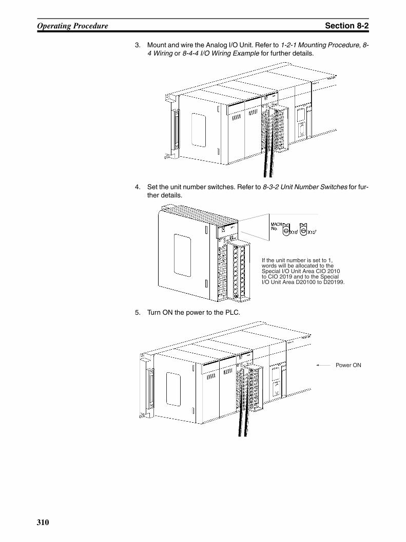
Operating Procedure Section 8-2
3. Mount and wire the Analog I/O Unit. Refer to 1-2-1 Mounting Procedure, 8-4 Wiring or 8-4-4 I/O Wiring Example for further details.
4. Set the unit number switches. Refer to 8-3-2 Unit Number Switches for fur-ther details.
5. Turn ON the power to the PLC.
If the unit number is set to 1, words will be allocated to the Special I/O Unit Area CIO 2010 to CIO 2019 and to the Special I/O Unit Area D20100 to D20199.
Power ON
310

Operating Procedure Section 8-2
Creating I/O TablesAfter turning ON the power to the PLC, be sure to create the I/O tables.
Initial Data Settings
1,2,3... 1. Specify the Special I/O Unit DM Area settings. Refer to Allocations in DMArea on page 324 for further details.
• The following diagram shows the input and output settings used. Referto 8-6-1 Input Settings and Conversion Values or 8-7-1 Output Settingsand Conversions for more details.
Peripheral port
Peripheral port
Setting conditions
Unit No. 1
Analog input 1: 1 to 5 VAnalog input 2: 0 to 10 VAnalog input 3: 4 to 20 mAAnalog input 4: 4 to 20 mA
Analog output 1: 1 to 5 VAnalog output 2: 1 to 5 VAnalog output 3: –10 to 10 VAnalog output 4: Not used.
15 14 13 12 11 10 09 08 07 06 05 01 0004 03 02
0 0 0 0 0 0 0 0 1 1 1 1 0 1 1 1
Bit
All used
Input 4
Input 3
Input 2
Input 1
Not used Output 4
Output 3
Output 2
Output 1Used
m: DM20100(00F7 hex)
311

Operating Procedure Section 8-2
• The following diagram shows the input and output range settings. Re-fer to 8-6-1 Input Settings and Conversion Values or 8-7-1 Output Set-tings and Conversions for more details.
2. Restart the CPU Unit.
Creating Ladder Programs
1,2,3... 1. The following example describes how to use analog inputs.
The data that is converted from analog to digital and output to CIO words (n +5) to (n+ 8) of the Special I/O Unit Area (CIO 2015 to CIO2018), is stored inthe specified addresses D00100 to D00103 as signed binary values 0000 to0FA0 hex.
15 14 13 12 11 10 09 08 07 06 05 01 0004 03 02
1 0 1 0 0 1 1 0 0 0 0 0 1 0 1 0
Bit
m+1: DM20101(A60A hex)
Output 1: 1 to 5 V. Set to 10.
Output 2: 1 to 5 V. Set to 10.
Output 3: –10 to 10 V. Set to 00.
Output 4: Not used. Set to 00 (disabled).
Input 1: 1 to 5 V. Set to 10.
Input 2: 0 to 10 V. Set to 01.
Input 3: 4 to 20 mA. Set to 10.
Input 4: 4 to 20 mA. Set to 10.
Power turned ON again (or Special I/O Unit Restart Bit is turned ON)
Peripheral port
312

Operating Procedure Section 8-2
• The following table shows the addresses used for analog input.
Note a) The addresses are set according to the unit number of the SpecialI/O Unit. Refer to 8-3-2 Unit Number Switches for further details.
b) Set as required.
c) The input Disconnection Detection Flag is allocated to bits 04 to07 of word (n+9). Refer to Allocations for Normal Mode onpage 328 and 8-6-4 Input Disconnection Detection Function forfurther details.
2. The following example shows how to use analog outputs.
The setting address D00200 is stored in words (n+1) to (n+3) of the Special I/O Unit Area (CIO 2011 to CIO 2013) as a signed binary value between 0000to 0FA0 hex.
• The following table shows the addresses used for analog output.
Input number Input signal range Input conversion value address(n = CIO 2010)(See note a.)
Conversion data holding address
(See note b.)
1 1 to 5 V (n+5) = CIO 2015 D00100
2 0 to 10 V (n+6) = CIO 2016 D00101
3 4 to 20 mA (n+7) = CIO 2017 D00102
4 4 to 20 mA (n+8) = CIO 2018 D00103
201904 Input 1 Disconnection Detection Flag (See note c.)
201905 Input 2 Disconnection Detection Flag (See note c.)
201906 Input 3 Disconnection Detection Flag (See note c.)
201907 Input 4 Disconnection Detection Flag (See note c.)
For 1 to 5 V, the hexadecimal value 0000 to 0FA0 will be stored in CIO 2015, so if there is no disconnection (i.e., 201904 is OFF), CIO 2015 will be stored in D00100.
In the same way, for 0 to 10 V, CIO 2016 will be stored in D00101.
In the same way, for 4 to 20 mA, CIO 2017 will be stored in D00102.
In the same way, for 4 to 20 mA, CIO 2018 will be stored in D00103.
MOV (021)
2015
D00100
MOV (021)
2016
D00101
MOV (021)
2017
D00102
MOV (021)
2018
D00103
Output number Input signal range Output setting address
(n = CIO 2010)(See note a.)
Original conversion
address (See note b.)
1 1 to 5 V (n+1) = CIO 2011 D00200
2 0 to 10 V (n+2) = CIO 2012 D00201
3 –10 to 10 V (n+3) = CIO 2013 D00202
4 Not used. --- ---
313

Operating Procedure Section 8-2
Note a) The addresses are set according to the unit number of the SpecialI/O Unit. Refer to 8-3-2 Unit Number Switches for further details.
b) Set as required.
D00200 is set in word CIO 2011.
D00201 is set in word CIO 2012.
D00202 is set in word CIO 2013.
The data in words CIO 2011 and CIO 2012 will be output as 1 to 5 V, and the data in CIO 2013 will be output as –10 to 10 V.
To start analog output, turn ON the Conversion Enable Bits 201000 to 201002 (bits 00 to 02 of word CIO 2010).
MOV (021)
D00200
2011
MOV (021)
D00201
2012
Execution condition
MOV (021)
D00202
2013
SET
201000
SET
201002
SET
201001
Execution condition
See Starting and Stopping Conversion on page 338 for details.
314

Components and Switch Settings Section 8-3
8-3 Components and Switch Settings
Unit numberswitches
External terminal block (M3)
External ter-minal block mounting screws (black M3)
FrontMounting to terminal block Removing from terminal block
Voltage/Current switch
Operation mode switch
Backplane connector
Terminal block
SideBack
315

Components and Switch Settings Section 8-3
The terminal block is attached by a connector. It can be removed by looseningthe two black mounting screws located at the top and bottom of the terminalblock.
Check to be sure that the black terminal block mounting screw is securelytightened to a torque of 0.5 N·m.
8-3-1 IndicatorsThe indicators show the operating status of the Unit. The following tableshows the meanings of the indicators.
Fasten the mounting screw.
Fasten the mounting screw.
LED Meaning Indicator Operating status
RUN (green)
Operating Lit Operating in normal mode.
Not lit Unit has stopped exchanging data with the CPU Unit.
ERC (red) Error detected by Unit
Lit Alarm has occurred (such as disconnection detection) or initial settings are incorrect.
Not lit Operating normally.
ADJ (yel-low)
Adjusting Flashing Operating in offset/gain adjustment mode.
Not lit Other than the above.
ERH (red) Error in the CPU Unit
Lit Error has occurred during data exchange with the CPU Unit.
Not lit Operating normally.
316

Components and Switch Settings Section 8-3
8-3-2 Unit Number SwitchesThe CPU Unit and Analog I/O Unit exchange data via the Special I/O UnitArea and the Special I/O Unit DM Area. The Special I/O Unit Area and SpecialI/O Unit DM Area word addresses that each Analog I/O Unit occupies are setby the unit number switches on the front panel of the Unit.
Always turn OFF the power before setting the unit number. Use a flat-bladescrewdriver, being careful not to damage the slot in the screw. Be sure not toleave the switch midway between settings.
Note If two or more Special I/O Units are assigned the same unit number, a “UNITNo. DPL ERR” error (in the Programming Console) will be generated (A40113will turn ON) and the PLC will not operate.
8-3-3 Operation Mode SwitchThe operation mode switch on the back panel of the Unit is used to set theoperation mode to either normal mode or adjustment mode (for adjusting off-set and gain).
!Caution Do not set the pins to any combination other than those shown in the abovetable. Be sure to set pin 2 to OFF.
!Caution Be sure to turn OFF the power to the PLC before installing or removing theUnit.
Switch setting
Unit number
Special/O Unit Area addresses
Special I/O Unit DM Area addresses
0 Unit #0 CIO 2000 to CIO 2009 D20000 to D20099
1 Unit #1 CIO 2010 to CIO 2019 D20100 to D20199
2 Unit #2 CIO 2020 to CIO 2029 D20200 to D20299
3 Unit #3 CIO 2030 to CIO 2039 D20300 to D20399
4 Unit #4 CIO 2040 to CIO 2049 D20400 to D20499
5 Unit #5 CIO 2050 to CIO 2059 D20500 to D20599
6 Unit #6 CIO 2060 to CIO 2069 D20600 to D20699
7 Unit #7 CIO 2070 to CIO 2079 D20700 to D20799
8 Unit #8 CIO 2080 to CIO 2089 D20800 to D20899
9 Unit #9 CIO 2090 to CIO 2099 D20900 to D20999
10 Unit #10 CIO 2100 to CIO 2109 D21000 to D21099
to to to to
n Unit #n CIO 2000 + (n × 10) to CIO 2000 + (n × 10) + 9
D20000 + (n × 100) to D20000 + (n × 100) + 99
to to to to
95 Unit #95 CIO 2950 to CIO 2959 D29500 to D29599
Pin number Mode
1 2
OFF OFF Normal mode
ON OFF Adjustment mode
317

Wiring Section 8-4
8-3-4 Voltage/Current SwitchThe analog conversion input can be switched from voltage input to currentinput by changing the pin settings on the voltage/current switch located on theback of the terminal block.
!Caution Be sure to turn OFF the power to the PLC before mounting or removing theterminal block.
8-4 Wiring
8-4-1 Terminal ArrangementThe signal names corresponding to the connecting terminals are as shown inthe following diagram.
Note 1. The analog I/O numbers that can be used are set in the Data Memory(DM).
2. The I/O signal ranges for individual inputs and outputs are set in the DataMemory (DM). They can be set in units of I/O numbers.
3. The AG terminal (A8, B8) is connected to the 0-V analog circuit in the Unit.Connecting shielded input lines can improve noise resistance.
4. The N.C. terminals (A5, A11, B5) are not connected to internal circuitry.
IN2: Input 2IN1: Input 1
OFF: Voltage inputON: Current input
IN4: Input 4IN3: Input 3
Output 2 (+) B1
Output 2 (–) B2
Output 4 (+) B3
Output 4 (–) B4
N.C. B5
Input 2 (+) B6
Input 2 (–) B7
AG B8
Input 4 (+) B9
Input 4 (–) B10
A1
A2
A3
A4
A5
A6
A7
A8
A9
A10
A11
Output 1 (+)
Output 1 (–)
Output 3 (+)
Output 3 (–)
N.C.
Input 1 (+)
Input 1 (–)
AG
Input 3 (+)
Input 3 (–)
N.C.
318

Wiring Section 8-4
8-4-2 Internal CircuitryThe following diagrams show the internal circuitry of the analog I/O section.
Input Circuitry
Output Circuitry
Internal Configuration
1 MΩ
15 kΩ 15 kΩ
15 kΩ 15 kΩ
AG (common to all inputs)
Input (+)
Input (–)
AG (analog 0 V)
Input circuit and conversion circuit
1 MΩ
Voltage/currentinput switch
250 Ω
Output switch and conversion circuit
AMPVoltage output (+)
Voltage output (–)
AG (common to all outputs)
Indicators/Switch
MPU
Regulator
Oscillator
Division
CS-series PLC
EEPROM
RAM ROM
Pho
toco
uple
r in
sula
tion
OUTPUT
INPUT
+26 V+5 V
−15 V
+15 V
Bus interface
Insulation-type DC-to-DC converter
D/A converter
A/D converter
Multi-plexer and amplifier
Multi-plexer and amplifier
Externally connected terminal
319
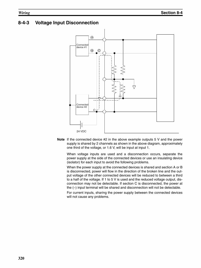
Wiring Section 8-4
8-4-3 Voltage Input Disconnection
Note If the connected device #2 in the above example outputs 5 V and the powersupply is shared by 2 channels as shown in the above diagram, approximatelyone third of the voltage, or 1.6 V, will be input at input 1.
When voltage inputs are used and a disconnection occurs, separate thepower supply at the side of the connected devices or use an insulating device(isolator) for each input to avoid the following problems.
When the power supply at the connected devices is shared and section A or Bis disconnected, power will flow in the direction of the broken line and the out-put voltage of the other connected devices will be reduced to between a thirdto a half of the voltage. If 1 to 5 V is used and the reduced voltage output, dis-connection may not be detectable. If section C is disconnected, the power atthe (–) input terminal will be shared and disconnection will not be detectable.
For current inputs, sharing the power supply between the connected deviceswill not cause any problems.
Connected device #1
24 VDC
Connected device #2
320
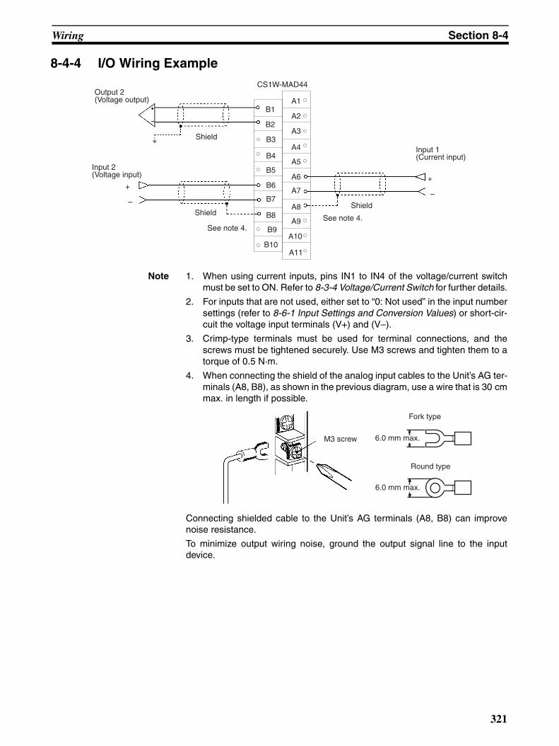
Wiring Section 8-4
8-4-4 I/O Wiring Example
Note 1. When using current inputs, pins IN1 to IN4 of the voltage/current switchmust be set to ON. Refer to 8-3-4 Voltage/Current Switch for further details.
2. For inputs that are not used, either set to “0: Not used” in the input numbersettings (refer to 8-6-1 Input Settings and Conversion Values) or short-cir-cuit the voltage input terminals (V+) and (V–).
3. Crimp-type terminals must be used for terminal connections, and thescrews must be tightened securely. Use M3 screws and tighten them to atorque of 0.5 N·m.
4. When connecting the shield of the analog input cables to the Unit’s AG ter-minals (A8, B8), as shown in the previous diagram, use a wire that is 30 cmmax. in length if possible.
Connecting shielded cable to the Unit’s AG terminals (A8, B8) can improvenoise resistance.
To minimize output wiring noise, ground the output signal line to the inputdevice.
A7
A10
B1
B2
B3
B4
B5
B6
B7
B8
B9
B10
A1
A2
A3
A4
A5
A6
A8
A9
A11
Output 2(Voltage output)
Input 2(Voltage input)
CS1W-MAD44
Shield
Shield
See note 4.See note 4.
Shield
Input 1(Current input)
+
–
+
–
6.0 mm max.
6.0 mm max.M3 screw
Fork type
Round type
321

Exchanging Data with the CPU Unit Section 8-5
8-4-5 I/O Wiring ConsiderationsWhen wiring inputs, apply the following points to avoid noise interference andoptimize Analog I/O Unit performance.
• Use two-core shielded twisted-pair cables for external connections.
• Route I/O cables separately from the AC cable, and do not run the Unit’scables near a main circuit cable or a high voltage cable. Do not insert out-put cables into the same duct.
• If there is noise interference from power lines (if, for example, the powersupply is shared with electrical welding devices or electrical dischargemachines, or if there is a high-frequency generation source nearby) installa noise filter at the power supply input area.
8-5 Exchanging Data with the CPU Unit
8-5-1 Outline of Data ExchangeData is exchanged between the CPU Unit and the CS1W-MAD44 Analog I/OUnit via the Special I/O Unit Area (for data used to operate the Unit) and theSpecial I/O Unit DM Area (for data used for initial settings).
I/O Refresh Data
Analog input conversion values, analog output setting values, and other dataused to operate the Unit are allocated in the Special I/O Unit Area of the CPUUnit according to the unit number, and are exchanged during I/O refreshing.
Fixed Data
The Unit’s fixed data, such as the analog input signal ranges and analog out-put signal ranges, is allocated in the Special I/O Unit DM Area of the CPU Unitaccording to the unit number, and is exchanged when the power is turned ONor the Unit is restarted.
CS-series CPU Unit CS1W-MAD44 Analog I/O Unit
Special I/O Unit Area I/O Refresh Data
Analog inputs
Analog outputs
DM (Data Memory) Area
Input signal range
Output signal range
I/O refresh
Power ON or Unit restart
Exchanges normal data such as analog inputs andanalog outputs.
Transmits initial settings such as analog input ranges and analog output ranges.
2000 + n × 10
2000 + n × 10 + 9
D20000 + n × 100
D20000 + n × 100 + 99
10 words
100 words
Fixed Data
:
:
n: Unit number
See 8-5-5 I/O Refresh Data Allocations for details.
See 8-5-4 Fixed Data Allocations for details.
322

Exchanging Data with the CPU Unit Section 8-5
8-5-2 Unit Number SettingsThe Special I/O Unit Area and Special I/O Unit DM Area word addresses thateach Analog I/O Unit occupies are set by the unit number switches on thefront panel of the Unit.
Note If two or more Special I/O Units are assigned the same unit number, a “UNITNo. DPL ERR” error (in the Programming Console) will be generated (A40113will turn ON) and the PLC will not operate.
8-5-3 Special I/O Unit Restart BitsTo restart the Unit operations after changing the contents of the data memoryor correcting an error, turn ON the power to the PLC again or turn the SpecialI/O Unit Restart Bit ON and then OFF again.
Note If the error is not corrected by restarting the Unit or turning the Special I/OUnit Restart Bit ON and then OFF again, replace the Analog I/O Unit.
Switch setting
Unit number
Special/O Unit Area addresses
Special I/O Unit DM Area addresses
0 Unit #0 CIO 2000 to CIO 2009 D20000 to D20099
1 Unit #1 CIO 2010 to CIO 2019 D20100 to D20199
2 Unit #2 CIO 2020 to CIO 2029 D20200 to D20299
3 Unit #3 CIO 2030 to CIO 2039 D20300 to D20399
4 Unit #4 CIO 2040 to CIO 2049 D20400 to D20499
5 Unit #5 CIO 2050 to CIO 2059 D20500 to D20599
6 Unit #6 CIO 2060 to CIO 2069 D20600 to D20699
7 Unit #7 CIO 2070 to CIO 2079 D20700 to D20799
8 Unit #8 CIO 2080 to CIO 2089 D20800 to D20899
9 Unit #9 CIO 2090 to CIO 2099 D20900 to D20999
10 Unit #10 CIO 2100 to CIO 2109 D21000 to D21099
to to to to
n Unit #n CIO 2000 + (n × 10) to CIO 2000 + (n × 10) + 9
D20000 + (n × 100) to D20000 + (n × 100) + 99
to to to to
95 Unit #95 CIO 2950 to CIO 2959 D29500 to D29599
Special I/O Unit Area word address
Function
A50200 Unit No. 0 Restart Bit Restarts the Unit when turned ON and then OFF again.A50201 Unit No. 1 Restart Bit
to to
A50215 Unit No. 15 Restart Bit
A50300 Unit No. 16 Restart Bit
to to
A50715 Unit No. 95 Restart Bit
323

Exchanging Data with the CPU Unit Section 8-5
8-5-4 Fixed Data AllocationsAllocations in DM Area The initial settings of the Analog I/O Unit are set according to the data allo-
cated in the Special I/O Unit DM Area. Settings, such as the inputs and out-puts used, the analog input signal range, and analog output signal range mustbe set in this area.
Note 1. The Special I/O Unit DM Area words that are occupied by the Analog I/OUnit are set using the unit number switches on the front panel of the Unit.Refer to 8-3-2 Unit Number Switches for details on the method used to setthe unit number switches.
2. If two or more Special I/O Units are assigned the same unit number, a“UNIT No. DPL ERR” error (in the Programming Console) will be generat-ed (A40113 will turn ON) and the PLC will not operate.
D (m+1)
D (m)
D20300 to D20399
D20400 to D20499
D20500 to D20599
D20000 to D20099
D20100 to D20199
D20200 to D20299
D20900 to D20999
D20600 to D20699
D20700 to D20799
D20800 to D20899
SYSMAC CS-series CPU Unit CS1W-MAD44 Analog I/O Unit
(Fixed Data Area)
Unit #0
Unit #1
Unit #2
Unit #3
Unit #4
Unit #5
Unit #6
Unit #7
Unit #8
Unit #9
(Special I/O Unit DM Area)
Word
D29500 to D29599
D21000 to D21099Unit #10
Unit #n
Unit #95
I/O signal range
m = 20000 + (unit number × 100)
D20000 + (n × 100) to D20000 + (n × 100) + 99
Data is automatically transferred to each unit number when the power is turned ON, or when the Special I/O Unit Restart Bit is turned ON.
I/O conversion permission loop mode setting
D (m+2 to m+5)
Output hold function setting
D (m+6 to m+9)
Sets number of samples for mean value processing
D (m+10 to m+17)
Ratio set value, bias value setting
to
to
to
to
324

Exchanging Data with the CPU Unit Section 8-5
Allocations in DM Area The following table shows the allocation of DM words and bits for both normaland adjustment mode.
Note For the DM word addresses, m = D20000 + (unit number × 100).
DM word Bits
15 14 13 12 11 10 9 8 7 6 5 4 3 2 1 0
D (m) Ratio conversion use setting Input use setting Output use setting
Loop 4 Loop 3 Loop 2 Loop 1 Input 4
Input 3
Input 2
Input 1
Out-put 4
Out-put 3
Out-put 2
Out-put 1
D (m+1) Input signal range setting Output signal range setting
Input 4 Input 3 Input 2 Input 1 Output 4 Output 3 Output 2 Output 1
D (m+2) Not used. Output 1: Output status when conversion stopped
D (m+3) Not used. Output 2: Output status when conversion stopped
D (m+4) Not used. Output 3: Output status when conversion stopped
D (m+5) Not used. Output 4: Output status when conversion stopped
D (m+6) Input 1: Mean value processing setting
D (m+7) Input 2: Mean value processing setting
D (m+8) Input 3: Mean value processing setting
D (m+9) Input 4: Mean value processing setting
D (m+10) Loop 1 (input 1 to output 1), A constant
D (m+11) Loop 1 (input 1 to output 1), B constant
D (m+12) Loop 2 (input 2 to output 2), A constant
D (m+13) Loop 2 (input 2 to output 2), B constant
D (m+14) Loop 3 (input 3 to output 3), A constant
D (m+15) Loop 3 (input 3 to output 3), B constant
D (m+16) Loop 4 (input 4 to output 4), A constant
D (m+17) Loop 4 (input 4 to output 4), B constant
325

Exchanging Data with the CPU Unit Section 8-5
Set Values and Stored Values
Note 1. The input signal range of “1 to 5 V” and “4 to 20 mA” is switched using thepins of the voltage/current switch. Refer to 8-3-4 Voltage/Current Switch fordetails.
2. For the range of ±10 V, the output is 0 V. For other output signal ranges,the minimum value of each signal range is output. Refer to 8-7-2 OutputHold Function for details.
3. The default of mean value processing setting is set to “Mean value pro-cessing with 2 buffers.” Refer to 8-6-2 Mean Value Processing.
Item Contents Page
Input Use setting 0: Not used.1: Used.
330
Input signal range 00: –10 to 10 V01: 0 to 10 V10: 1 to 5 V/4 to 20 mA (See note 1.)11: 0 to 5 V
331
Mean value processing set-ting
0000: Mean value processing for 2 buffers (See note 3.)0001: No mean value processing0002: Mean value processing for 4 buffers0003: Mean value processing for 8 buffers0004: Mean value processing for 16 buffers0005: Mean value processing for 32 buffers0006: Mean value processing for 64 buffers
332
Output Use setting 0: Not used.1: Used.
337
Output signal range 00: –10 to 10 V01: 0 to 10 V10: 1 to 5 V11: 0 to 5 V
337
Output status when stopped 00: CLR Outputs 0 or minimum value of each range. (See note 2.)
01: HOLD Holds output just before stopping.02: MAX Outputs maximum value of range.
339
Loop Ratio conversion use setting 00: Not used.01: Uses positive gradient conversion.10: Uses negative gradient conversion.11: Same as for setting “00” above.
340
A constant 4 digits BCD (0 to 9999)
B constant 16-bit binary data
326

Exchanging Data with the CPU Unit Section 8-5
8-5-5 I/O Refresh Data AllocationsSpecial I/O Unit Area Allocation and Contents
I/O refresh data for the Analog I/O Unit is exchanged according to the alloca-tions in the Special I/O Unit Area. Analog input converted values and analogoutput set values are exchanged with the CPU Unit at I/O refresh.
Note 1. The Special I/O Unit Area words that are occupied by the Analog I/O Unitare set using the unit number switches on the front panel of the Unit. Referto 8-3-2 Unit Number Switches for details on the method used to set theunit number switches.
2. If two or more Special I/O Units are assigned the same unit number, a“UNIT No. DPL ERR” error (in the Programming Console) will be generat-ed (A40113 will turn ON) and the PLC will not operate.
CIO 2030 to CIO 2039
CIO 2040 to CIO 2049
CIO 2050 to CIO 2059
CIO 2000 to CIO 2009
CIO 2010 to CIO 2019
CIO 2020 to CIO 2029
CIO 2090 to CIO 2099
CIO 2060 to CIO 2069
CIO 2070 to CIO 2079
CIO 2080 to CIO 2089
SYSMAC CS-series CPU Unit CS1W-MAD44 Analog I/O Unit
IN refresh
(I/O Refresh Data Area)
Unit #0
Unit #1
Unit #2
Unit #3
Unit #4
Unit #5
Unit #6
Unit #7
Unit #8
Unit #9
(Special I/O Unit Area)
OUT refresh
Allocated words
CIO 2950 to CIO 2959
CIO 2100 to CIO 2109Unit #10
Unit #n
Unit #95
Normal mode
IN refresh
OUT refresh
Adjustment mode
n = 2000 + (unit number × 10)
I/O refresh
CIO 2000 + (n × 10) to CIO 2000 + (n × 10) + 9
At the I/O refresh by the PLC, outputs (CPU to Unit) and inputs (Unit to CPU) are refreshed in order with every cycle.
CIO n to CIO n + 4
CIO n + 5 to CIO n + 9
CIO n to CIO n + 7
CIO n + 8 to CIO n + 9
to
to
to
to
327

Exchanging Data with the CPU Unit Section 8-5
Allocations for Normal Mode
For normal mode, set the operation mode switch on the rear panel of the Unitas shown in the following diagram.
The allocation of words and bits in the CIO Area is shown in the followingtable.
Set Values and Stored Values
Note For the CIO word addresses, n = CIO 2000 + unit number × 10.
I/O Word Bits
15 14 13 12 11 10 9 8 7 6 5 4 3 2 1 0
Output (CPU to Unit)
n Not used. Peak value hold Conversion enableInput 4
Input 3
Input 2
Input 1
Out-put 4
Out-put 3
Out-put 2
Out-put 1
n + 1 Output 1 set value
163 162 161 160
n + 2 Output 2 set value
n + 3 Output 3 set value
n + 4 Output 4 set value
Input (Unit to CPU)
n + 5 Input 1 conversion value / Loop 1 calculation result
163 162 161 160
n + 6 Input 2 conversion value / Loop 2 calculation result
n + 7 Input 3 conversion value / Loop 3 calculation result
n + 8 Input 4 conversion value / Loop 4 calculation result
n + 9 Alarm Flags Disconnection detec-tion
Output setting error
Input 4
Input 3
Input 2
Input 1
Out-put 4
Out-put 3
Out-put 2
Out-put 1
I/O Item Contents Page
Input Peak value hold function 0: Not used.1: Peak value hold used.
335
Conversion valueCalculation result
16-bit binary data 331
Disconnection detection 0: No disconnection1: Disconnection
336
Output Conversion enable 0: Conversion output stopped.1: Conversion output begun.
338
Set value 16-bit binary data 338
Output setting error 0: No error1: Output setting error
340
Common Alarm Flags Bits 00 to 03: Output set value errorBits 04 to 07: Input disconnection detectionBit 08: Ratio conversion use setting errorBit 09: Ratio set value errorBit 10: Output hold setting error Bit 11: Mean value processing setting errorBit 15: Operating in adjustment mode
(always 0 in normal mode)
361
362
328

Exchanging Data with the CPU Unit Section 8-5
The input disconnection detection function can be used when the input signalrange is set for 1 to 5 V (4 to 20 mA).
Allocation for Adjustment Mode
For adjustment mode, set the operation mode switch on the rear panel of theUnit as shown in the following diagram. When the Unit is set for adjustmentmode, the ADJ indicator on the front panel of the Unit will flash.
The allocation of CIO words and bits is shown in the following table.
Set Values and Stored Values
Refer to 8-9-1 Adjustment Mode Operational Flow for further details.
Input signal range Voltage/current
1 to 5 V 0.3 V max.
4 to 20 mA 1.2 mA max.
I/O Word Bits
15 14 13 12 11 10 9 8 7 6 5 4 3 2 1 0
Output (CPU to Unit)
n Not used. Inputs and outputs to be adjusted
161 160
n + 1 Not used. Not used. Clr Set Up Down Gain Off-set
n + 2 Not used.
n + 3 Not used.
n + 4 Not used.
n + 5 Not used.
n + 6 Not used.
n + 7 Not used.
Input (Unit to CPU)
n + 8 Conversion value or set value at time of adjustment
163 162 161 160
n + 9 Alarm Flags Disconnection detec-tion
Not used.
Input 4
Input 3
Input 2
Input 1
Item Contents
Input or output to be adjusted
Sets input or output to be adjusted.Leftmost digit: 1 (output) or 2 (input)Rightmost digit: 1 to 4
Offset (Offset Bit) When ON, adjusts offset error.
Gain (Gain Bit) When ON, adjusts gain error.
Down (Down Bit) Decrements the adjustment value while ON.
Up (Up Bit) Increments the adjustment value while ON.
Set (Set Bit) Sets adjusted value and writes to EEPROM.
Clr (Clear Bit) Clears adjusted value. (Returns to default status)
Conversion value for adjustment
The conversion value for adjustment is stored as 16 bits of binary data.
329

Analog Input Functions and Operating Procedures Section 8-6
Note For the CIO word addresses, n = CIO 2000 + (unit number × 10).
The input disconnection detection function can be used when the input signalrange is set for 1 to 5 V (4 to 20 mA).
8-6 Analog Input Functions and Operating Procedures
8-6-1 Input Settings and Conversion Values
Setting Inputs and Signal Ranges
Input Numbers The Analog I/O Unit converts only analog inputs specified by input numbers 1to 4. To specify the analog inputs to be used, turn ON from a ProgrammingDevice the D(m) bits in the DM Area shown in the following diagram.
The analog input sampling interval can be shortened by setting any unusedinput numbers to 0.
Sampling interval = (1 ms) × (Number of inputs used)
For the DM word addresses, m = D20000 + (unit number × 100)
The word for inputs that have been set to “Not used” will always be “0000.”
Disconnection detection 0: No disconnection1: Disconnection
Alarm Flags Bit 12: Input value is outside adjustment limits(in adjustment mode)
Bit 13: I/O number setting error (in adjustment mode)Bit 14: EEPROM write error (in adjustment mode)Bit 15: Operating in adjustment mode
(always 1 in adjustment mode)
Item Contents
Input signal range Voltage/current
1 to 5 V 0.3 V max.
4 to 20 mA 1.2 mA max.
15 14 13 12 11 10 09 08 07 06 05 04 03 02 01 00Bit
D (m)
Inpu
t 2
Inpu
t 1
0: Not used
1: Used
Inpu
t 4
Inpu
t 3
330

Analog Input Functions and Operating Procedures Section 8-6
Input Signal Range Any of four types of input signal range (–10 to 10 V, 0 to 10 V, 1 to 5 V, and 4to 20 mA) can be selected for each of the inputs (i.e., input numbers 1 to 4).To specify the input signal range for each input, set from a ProgrammingDevice the D(m+1) bits in the DM Area as shown in the following diagram.
Note 1. For the DM word addresses, m = D20000 + (unit number × 100)
2. The input signal range of “1 to 5 V” or “4 to 20 mA” is switched using thevoltage/current switch.
3. After making the DM settings from a Programming Device, it will be neces-sary to either turn the power to the PLC OFF and ON, or turn ON the Spe-cial I/O Unit Restart Bit in order to transfer the contents of the DM settingsto the Special I/O Unit.
Reading Conversion Values
Analog input conversion values are stored for each input number, in CIOwords n+5 to n+8.
Note For the CIO word addresses, n = CIO 2000 + (unit number × 10).
Use MOV(021) or XFER(070) to read conversion values in the user program.
Example 1 In this example, the conversion data from only one input is read. (The unitnumber is 0.)
Example 2 In this example, the conversion data from multiple inputs is read. (The unitnumber is 0.)
For details regarding conversion value scaling, refer to Scaling on page 446.
15 14 13 12 11 10 09 08 07 06 05 04 03 02 01 00Bit
D (m+1)
Inpu
t 2
Inpu
t 1
00: −10 to 10 V01: 0 to 10 V10: 1 to 5 V / 4 to 20 mA11: 0 to 5 V
Inpu
t 4
Inpu
t 3
Word Function Stored value
n+5 Input 1 conversion value 16-bit binary data
n+6 Input 2 conversion value
n+7 Input 3 conversion value
n+8 Input 4 conversion value
MOV(021)
2005
D00001
Input conditionConversion data in CIO word 2005 (input number 1) is read to D00001.
XFER(070)
#0004
2005
D00001
Input conditionConversion data in CIO words 2005 and 2008 (input num-bers 1 and 4) is read to D00001 and D00004.
331

Analog Input Functions and Operating Procedures Section 8-6
8-6-2 Mean Value ProcessingThe Analog I/O Unit can compute the mean value of the conversion values ofanalog inputs that have been previously sampled. Mean value processinginvolves an operational mean value in the history buffers, so it has no effect onthe data refresh cycle. (The number of history buffers that can be set to usemean value processing is 2, 4, 8, 16, 32, or 64.)
When “n” number of history buffers are being used, the first conversion datawill be stored for all “n” number of history buffers immediately after data con-version has begun or after a disconnection is restored.
When mean value processing is used together with the peak value hold func-tion, the mean value will be held.
To specify whether or not mean value processing is to be used, and to specifythe number of history buffers for mean data processing, use a ProgrammingDevice to make the settings in D(m+6) to D(m+9) as shown in the followingtable.
For the DM word addresses, m = D20000 + (unit number × 100)
Note After making the DM settings from a Programming Device, it will be necessaryto either turn the power to the PLC OFF and ON, or turn ON the Special I/OUnit Restart Bit to transfer the contents of the DM settings to the Special I/OUnit.
The history buffer moving average is calculated as shown below. (In thisexample, there are four buffers.)
Conversion data Buffer 1
Buffer 2
Buffer 3
Buffer 4
Buffer n
(Mean value processing)
Conversion value
(Values stored in CIO words n+5 and n+8)
(Discarded)
DM word Function Set value
D (m+6) Input 1 mean value processing 0000: Mean value processing with 2 buffers0001: No mean value processing0002: Mean value processing with 4 buffers0003: Mean value processing with 8 buffers0004: Mean value processing with 16 buffers0005: Mean value processing with 32 buffers0006: Mean value processing with 64 buffers
D (m+7) Input 2 mean value processing
D (m+8) Input 3 mean value processing
D (m+9) Input 4 mean value processing
332

Analog Input Functions and Operating Procedures Section 8-6
1,2,3... 1. With the first cycle, Data 1 is stored in all the history buffers.
Mean value = (Data 1 + Data 1 + Data 1 + Data 1) ÷ 4
2. With the second cycle, Data 2 is stored in the first history buffer.
Mean value = (Data 2 + Data 1 + Data 1 + Data 1) ÷ 4
3. With the third cycle, Data 3 is stored in the first history buffer.
Mean value = (Data 3 + Data 2 + Data 1 + Data 1) ÷ 4
4. With the fourth cycle, the Data 4 is stored in the first history buffer.
Mean value = (Data 4 + Data 3 + Data 2 + Data 1) ÷ 4
5. With the fifth cycle, Data 5 is stored in the first history buffer.
Mean value = (Data 5 + Data 4 + Data 3 + Data 2) ÷ 4
When a disconnection is restored, the mean value processing function beginsagain from step 1.
Note 1. The default setting for mean value processing in the Analog I/O Unit ismean value processing with 2 buffers. When the mean value processing
(Mean value processing)
Conversion value
Data 1
Data 1
Data 1
Data 1
(Mean value processing)
Conversion value
Data 2
Data 1
Data 1
Data 1
(Mean value processing)
Conversion value
Data 3
Data 2
Data 1
Data 1
(Mean value processing)
Conversion value
Data 4
Data 3
Data 2
Data 1
(Mean value processing)
Conversion value
Data 5
Data 4
Data 3
Data 2
333

Analog Input Functions and Operating Procedures Section 8-6
function is used, the delay in refreshing converted data for input signalchanges will be as shown in the following diagram.
2. Specify “no mean value processing” to follow conversion of a rapid changein input signals.
Response Time Unit: ms
Symbols m: Number of input words used in DM Arean: Average number of buffers set for the input number for which to find theresponse time
Calculation Example The following example calculations are for a resolution of 8,000 with an appli-cation using inputs 1 and 4, 64 averaging buffers set for input 1, and no aver-aging set for input 4.
• Response time for input 1: t = (64 − 2) × 2 + 10.5 = 134.5 (ms)
• Response time for input 1: t = 1 × (2 + 2) = 4 (ms)
Input signal to the Unit (V)
Conversion data
Time (ms)
Time (ms)
t: Delay
For V = 20 V (−10 to 10 V)Using One Wordt = n + (2 to 3)Using m Words (1 ≤ m ≤ 8)No averaging (n = 1) or two averaging buffers (n = 2):
t = n x (m + 2)n averaging buffers (4 ≤ n ≤ 64):
t = (n − 2) x m + 10.5
m n64 32 16 8 4 2 1
4 258.5 130.5 66.5 34.5 18.5 12 63 196.5 100.5 52.5 28.5 16.5 10 52 134.5 70.5 38.5 22.5 14.5 8 41 67 35 19 11 7 5 3
334

Analog Input Functions and Operating Procedures Section 8-6
8-6-3 Peak Value Hold FunctionThe peak value hold function holds the maximum digital conversion value forevery input (including mean value processing). This function can be used withanalog input. The following diagram shows how digital conversion values areaffected when the peak value hold function is used.
The peak value hold function can be set individually for each input number byturning on the respective bits (04 to 07) in CIO word n.
For the CIO word addresses, n = CIO 2000 + (unit number × 10).
In the following example, the peak value hold function is in effect for inputnumber 1, and the unit number is 0.
When mean value processing is used together with the peak value hold func-tion, the mean value will be held.
As long as the peak value hold function is in effect, the peak value hold will beheld even in the event of a disconnection.
When the load to the CPU Unit is disconnected, the Peak Value Hold Bits (bits04 to 07 of the word n) are cleared and the peak value hold function is dis-abled.
Peak value hold
Digital conversion value
t (Time)
Conversion value when the peak value hold function is used
15 14 13 12 11 10 09 08 07 06 05 04 03 02 01 00Bit
Inpu
t 2
Inpu
t 1
Word n
The peak value hold function will be in effect for the above input numbers while their respective bits are ON. The conversion values will be reset when the bits are turned OFF.
Inpu
t 4
Inpu
t 3
200004
Input conditionThe maximum conversion data value is held for input number 1.
335

Analog Input Functions and Operating Procedures Section 8-6
8-6-4 Input Disconnection Detection FunctionWhen an input signal range of 1 to 5 V (4 to 20 mA) is used, input circuit dis-connections can be detected. The detection conditions for each of the inputsignal ranges are shown in the following table.
The current/voltage level will fluctuate according to the offset/gain adjustment.
The input disconnection detection signals for each input number are stored inbits 04 to 07 of CIO word n+9. Specify these bits as execution conditions touse disconnection detection in the user’s program.
For the CIO word addresses, n = CIO 2000 + (unit number × 10).
The conversion value during a disconnection will be 0000.
In the following example, the conversion value is read only if there is no dis-connection at analog input number 1. (The unit number is 0.)
Range Current/voltage
1 to 5 V 0.3 V max.
4 to 20 mA 1.2 mA max.
15 14 13 12 11 10 09 08 07 06 05 04 03 02 01 00Bit
Inpu
t 2
Inpu
t 1
Word n+9
The respective bit turns ON when a disconnection is detected for a given input. When the disconnection is restored, the bit turns OFF.
Inpu
t 4
Inpu
t 3
MOV (021)
2005
D00001
200904
The conver-sion value in CIO word 2005 (input number 1) is read to D00001.
336

Analog Output Functions and Operating Procedures Section 8-7
8-7 Analog Output Functions and Operating Procedures
8-7-1 Output Settings and Conversions
Setting Outputs and Signal Ranges
Output Numbers The Analog I/O Unit converts analog outputs specified by output numbers 1 to4 only. To specify the analog outputs to be used, turn ON from a ProgrammingDevice the D(m) bits in the DM Area shown in the following diagram.
The analog output conversion cycle can be shortened by setting any unusedoutput numbers to 0.
Conversion cycle = (1 ms) × (Number of outputs used)
Note 1. For the DM word addresses, m = D20000 + (unit number × 100).
2. Output numbers not used (set to 0) will be output at 0 V.
Output Signal Range Any of four types of output signal range (–10 to 10 V, 0 to 10 V, 1 to 5 V, and 0to 5 V) can be selected for each of the outputs (i.e., output numbers 1 to 4). Tospecify the output signal range for each output, use a Programming Device toset the D(m+1) bits in the DM Area shown in the following diagram.
Note 1. For the DM word addresses, m = D20000 + (unit number × 100).
2. After making the DM settings from a Programming Device, it will be neces-sary to either turn the power to the PLC OFF and ON, or turn ON the Spe-cial I/O Unit Restart Bit to transfer the contents of the DM settings to theSpecial I/O Unit.
15 14 13 12 11 10 09 08 07 06 05 04 03 02 01 00Bit
D (m)
Out
put 2
Out
put 1
0: Not used1: Used
Out
put 4
Out
put 3
15 14 13 12 11 10 09 08 07 06 05 04 03 02 01 00Bit
D (m + 1)
Out
put 2
Out
put 1
00: −10 to 10 V01: 0 to 10 V10: 1 to 5 V11: 0 to 5 V
Out
put 4
Out
put 3
337

Analog Output Functions and Operating Procedures Section 8-7
Writing Set Values Analog output set values are written to CIO words (n+1) to (n+4).
For the CIO word addresses, n = CIO 2000 + (unit number × 10).
Use MOV(021) or XFER(070) to write values in the user program.
Example 1 In this example, the set value from only one input is read. (The unit number is0.)
Example 2 In this example, multiple set values are written. (The unit number is #0.)
Note If the set value has been written outside the specified range, an output settingerror will occur, and the value set by the output hold function will be output.
Starting and Stopping Conversion
To begin analog output conversion, turn ON the corresponding ConversionEnable Bit (word n, bits 00 to 03) from the user’s program.
For the CIO word addresses, n = CIO 2000 + (unit number × 10).
The analog output when conversion is stopped will differ depending on theoutput signal range setting and output hold setting. Refer to Setting Outputsand Signal Ranges on page 337 and 8-7-2 Output Hold Function.
Conversion will not begin under the following conditions even if the Conver-sion Enable Bit is turned ON. Refer to 8-7-2 Output Hold Function.
1,2,3... 1. In adjustment mode, when something other than the output number is out-put during adjustment.
2. When there is an output setting error.
Word Function Stored value
n+1 Output 1 set value 16-bit binary data
n+2 Output 2 set value
n+3 Output 3 set value
n+4 Output 4 set value
MOV (021)
D00001
2001
Input conditionThe set value stored in D 00001 is written to CIO word 2001 (out-put number 1).
XFER(070)
#0004
D00001
2001
Input condition
The set values stored in D 00001to D 00004 are written to CIO words 2001 to 2004 (outputs 1 to 4).
15 14 13 12 11 10 09 08 07 06 05 04 03 02 01 00Bit
Out
put 2
Out
put 1
Analog conversion is executed while these bits are ON. When the bits are turned OFF, the conversion is stopped and the output data is held.
Word n
Out
put 4
Out
put 3
338

Analog Output Functions and Operating Procedures Section 8-7
3. When a fatal error occurs at the PLC.
4. When there is an input disconnection during a ratio conversion.
When the operation mode for the CPU Unit is changed from RUN or MONI-TOR mode to PROGRAM mode, or when the power is turned ON, the Conver-sion Enable Bits will all turn OFF. The output status at this time depends onthe output hold function.
In this example, conversion is begun for analog output number 1. (The unitnumber is 0.)
8-7-2 Output Hold FunctionThe Analog I/O Unit stops conversion under the following circumstances andoutputs the value set by the output hold function.
1,2,3... 1. When the Conversion Enable Bit is OFF. Refer to Starting and StoppingConversion on page 338.
2. In adjustment mode, when something other than the output number is out-put during adjustment. Refer to 8-9-2 Input Offset and Gain AdjustmentProcedures.
3. When there is an output setting error. Refer to 8-7-3 Output Setting Errors.
4. When a fatal error occurs at the PLC.
5. When there is an input disconnection during ratio conversion.
6. When there is an I/O bus error.
7. When the CPU Unit is in LOAD OFF status.
8. When there is a WDT (watchdog timer) error in the CPU Unit.
CLR, HOLD, or MAX can be selected for the output status when conversion isstopped.
The above values may fluctuate if offset/gain adjustment has been applied.
200000
Input conditionConversion begins for output number 1.
Output signal range
CLR HOLD MAX
0 to 10 V –0.5 V (Min. –5% of full scale)
Voltage that was output just prior to stop.
10.5 V (Max. +5% of full scale)
–10 to 10 V 0.0 V Voltage that was output just prior to stop.
11.0 V (Max. +5% of full scale)
1 to 5 V 0.8 V (Min. –5% of full scale)
Voltage that was output just prior to stop.
5.2 V (Max. +5% of full scale)
0 to 5 V –0.25 V (Min. –5% of full scale)
Voltage that was output just prior to stop.
5.25 V (Max. +5% of full scale)
339

Ratio Conversion Function Section 8-8
To specify the output hold function, use a Programming Device to set the DMArea words D (m+2) to D (m+5) as shown in the following table.
For the DM word addresses, m = D20000 + (unit number × 100).
Note After specifying the DM settings from a Programming Device, it will be neces-sary to either turn the power to the PLC OFF and ON, or turn ON the SpecialI/O Unit Restart Bit to transfer the contents of the DM settings to the Special I/O Unit.
8-7-3 Output Setting ErrorsIf the analog output set value is greater than the specified range, a settingerror signal will be stored in CIO word n+9 (bits 00 to 03).
For the CIO word addresses, n = CIO 2000 + (unit number × 10).
The voltage for an output number at which a setting error has occurred will beoutput according to the output hold function.
8-8 Ratio Conversion FunctionThe Analog I/O Unit has a ratio conversion function that enables it to performanalog-to-analog conversions by itself, without utilizing the PLC. It can useeither Loop 1 (input number 1 → output number 1), Loop 2 (input number 2 →output number 2), Loop 3 (input number 3 → output number 3), or Loop 4(input number 4 → output number 4).
Input 1 → Ratio bias calculation → Output 1
Input 2 → Ratio bias calculation → Output 2
Input 3 → Ratio bias calculation → Output 3
Input 4 → Ratio bias calculation → Output 4
DM word Function Set value
D (m+2) Output 1: Output status when stopped xx00: CLROutput 0 or mini-mum value of range (–5%).
xx01: HOLDHold output value prior to stop.
xx02: MAXOutput maximum value of range (105%).
Set any value in the leftmost bytes (xx).
D (m+3) Output 2: Output status when stopped
D (m+4) Output 3: Output status when stopped
D (m+5) Output 4: Output status when stopped
15 14 13 12 11 10 09 08 07 06 05 04 03 02 01 00Bit
Out
put 2
Out
put 1
Word n+9
When a setting error is detected for a particular output, the corre-sponding bit turns ON. When the error is cleared, the bit turns OFF.
Out
put 4
Out
put 3
340

Ratio Conversion Function Section 8-8
The relationship between the analog input and the analog output is expressedby the following conversion equations.
Positive Gradient Conversion
(Analog output) = A × (Analog input) + B
A: Ratio set value 0 to 99.99 (BCD)B: Bias 8000 to 7FFF (16-bit binary data)
The following example is for an I/O range of –10 to 10 V.
Constant A: 0050 (0.5)Constant B: 0190 (2.0 V)
Analog input: –10 to 10 VAnalog output = 0.5 × (–10 to 10 V) + 2.0 V
= –3.0 to 7.0 V
Negative Gradient Conversion
(Analog output) = F – A x (Analog input) + B
F: Output range maximum valueA: Ratio set value 0 to 99.99 (BCD)B: Bias 8000 to 7FFF (16-bit binary data)
The following example is for an I/O range of 0 to 10 V.
Constant A: 1000 (10.0)Constant B: 0068 (0.5 V)F: 10 V (output range maximum value) Analog input: 0 to 1 VAnalog output = 10 V – 10 × (0 to 1 V) + 0.5 V
= 10.5 to 0.5 V
X
Y A = YX
BA
Analog output
Analog input
F+BA
X
Y
A =YX
Analog output
Analog input
341

Ratio Conversion Function Section 8-8
Specifying Ratio Conversion Function
To specify the use of Loop 1 to Loop 4 and their I/O relationships, set bits 08to 15 of DM Area word D (m) as shown in the following diagram.
The response time of ratio conversion (input-to-output conversion) is 0.7 ms.
For the DM word addresses, m = D20000 + (unit number × 100).
Specifying Ratio Set Value and Bias
The ratio set value (A) and the bias (B) are set in the DM words from D(m+10) to D (m+17).
For the DM word addresses, m = D20000 + (unit number x 100).
Note 1. After making the DM settings from a Programming Device, it will be neces-sary to either turn the power to the PLC OFF and ON, or turn ON the Spe-cial I/O Unit Restart Bit to transfer the contents of the DM settings to theSpecial I/O Unit. For details regarding the Special I/O Unit Restart Bit, referto 8-10-4 Restarting Special I/O Units.
2. The calculation results will be output in digital values to word n+5 (Loop 1),word n+6 (Loop 2), word n+7 (Loop 3). and word n+8 (Loop 4).
3. If an input cable is disconnected, the calculation value will become 0000,and the analog output value will be output according to the output holdfunction.
4. If the output value exceeds the specified signal range due to the ratio con-version of the digital input value, the calculation result and analog outputwill be given as the lower-limit or upper-limit value.
15 14 13 12 11 10 09 08 07 06 05 04 03 02 01 00Bit
D (m)
Loop 2 Loop 1
00: Not used.01: Uses positive gradient conversion.10: Uses negative gradient conversion.11: Same as 10 above.
Loop 4 Loop 3
DM word Function Set value
D (m+10) Loop 1 (input 1 → output 1), A constant
BCD 0 to 9999 (0.00 to 99.99; unit: 0.01)
D (m+11) Loop 1 (input 1 → output 1), B constant
16-bit binary data
D (m+12) Loop 2 (input 2 → output 2), A constant
BCD 0 to 9999 (0.00 to 99.99; unit: 0.01)
D (m+13) Loop 2 (input 2 → output 2), B constant
16-bit binary data
D (m+14) Loop 3 (input 3 → output 3), A constant
BCD 0 to 9999 (0.00 to 99.99; unit: 0.01)
D (m+15) Loop 3 (input 3 → output 3), B constant
16-bit binary data
D (m+16) Loop 4 (input 4 → output 4), A constant
BCD 0 to 9999 (0.00 to 99.99; unit: 0.01)
D (m+17) Loop 4 (input 4 → output 4), B constant
16-bit binary data
342

Adjusting Offset and Gain Section 8-9
8-9 Adjusting Offset and GainThese functions can be used to calibrate inputs or outputs according to thedevices that are connected.
Input Calibration Function This function takes an output device’s offset voltage (or current) and gain volt-age (or current) as the analog input conversion data 0000 and 0FA0 (or 07D0when the range is ±10 V). For example, when used in a range of 1 to 5 V, arange of 0.8 to 4.8 V may be output even if the external device specificationsare for 1 to 5 V. In such cases, when the external device outputs an offset volt-age of 0.8 V, the converted data at the Analog Input Unit will be FF38. When again voltage of 4.8 V is output, the converted data will be 0EDA. With the off-set and gain adjustment functions, when 0.8 V and 4.8 V are input, then thevalues are converted to 0000 and 0FA0 respectively (instead of FF38 and0EDA).
Input Calibration Function This function adjusts output voltages according to input device offset valuesand gain values, and takes the presently set values of the Unit to be 0000 and00FA0 (or 07D0 when the range is ±10 V) respectively. For example, assumethat the specifications for an external input device (such as a display device)are 100.0 to 500.0. If voltage is output by the Analog Output Unit at a setvalue of 0000, and the actual display at the external input device shows not100.0 but 100.5, the output voltage can be adjusted (lowered in this case) sothat the display will show 100.0, and the set value (FFFB in this case) whenthe display shows exactly 100.0 can be set as 0000.
Similarly, for the gain value, if the Analog Output Unit outputs voltage at a setvalue of 0FA0, and the actual display at the external input device shows not500.0 but 500.5, the output voltage can be adjusted (lowered in this case) sothat the display will show 500.0, and the set value (0F9B in this case) whenthe display shows exactly 500.0 can be set as 0FA0.
Output device offset and gain
voltage
Converted data before adjustment
Converted data after adjustment
0.8 V FF38 0000
4.8 V 0EDA 0FA0
Display at external input device
Set value before adjustment (word n+8)
Set value after adjustment
100.0 FFFB 0000
500.0 0F9B 0FA0
343

Adjusting Offset and Gain Section 8-9
8-9-1 Adjustment Mode Operational FlowThe following diagram shows the flow of operations when using the adjust-ment mode for adjusting offset and gain.
!Caution Be sure to turn OFF the power to the PLC before changing the setting of theoperation mode switch.
Set the operation mode switch to adjustment mode.
Turn ON the PLC.
When adjusting another I/O number
When adjusting the same I/O number
Set the I/O number.
Offset adjustment
Offset Bit ON
Set Bit ON
Turn OFF power to the PLC.
Set the operation mode switch to normal mode.
The ADJ indicator will flash while in adjustment mode.
Start up the PLC in PROGRAM mode.
Gain adjustment
Gain Bit ON
Input adjustment Output adjustment
Set Bit ON
Input adjustment Output adjustment
Set the operation mode switch on the DIP switch on the back panel of the Unit to adjustment mode.
Write the I/O number to be adjusted in the rightmost byte of CIO word n.
(Bit 0 of CIO word n+1 turns ON.)
Sampling input
Adjustment value setting
(Add inputs so that conversion value becomes 0.)
(Bits 2 and 3 of CIO word n+1 turn ON.)
(Bit 4 of CIO word n+1 turns ON.)
(Bit 1 of CIO word n+1 turns ON.)
Sampling input
Adjustment value setting
(Add inputs so that conversion value is maximized.)
(Bits 2 and 3 of CIO word n+1 turn ON.)
(Bit 4 of CIO word n+1 turns ON.)
Set the operation mode switch on the DIP switch on the back panel of the Unit to normal mode.
344

Adjusting Offset and Gain Section 8-9
!Caution Set the PLC to PROGRAM mode when using the Analog I/O Unit in adjust-ment mode. If the PLC is in MONITOR mode or RUN mode, the Analog I/OUnit will stop operating, and the input and output values that existed immedi-ately before this stoppage will be retained.
!Caution Always perform adjustments in conjunction with offset and gain adjustments.
Note Input adjustments can be performed more accurately in conjunction withmean value processing.
8-9-2 Input Offset and Gain Adjustment ProceduresSpecifying Input Number to be Adjusted
To specify the input number to be adjusted, write the value to the rightmostbyte of CIO word n as shown in the following diagram.
For the CIO word addresses, n = CIO 2000 + (unit number × 10).
The following example uses input number 1 adjustment for illustration. (Theunit number is 0.)
Bits Used for Adjusting Offset and Gain
The CIO word (n+1) bits shown in the following diagram are used for adjustingoffset and gain.
(Rightmost)(Leftmost)
Word n
Input to be adjusted (1 to 4)I/O specification2: Input (fixed)
--- ---
CLR000000 CT00
SHIFTCH
*DM2
C0
A0
A0
AMON
2000 0000
CHG2000 0000PRES VAL ????
2C
1B
WRITE2000 0021
15 14 13 12 11 10 09 08 07 06 05 04 03 02 01 00Bit
Word n+1
Offs
et B
it
Gai
n B
it
Set
Bit
Cle
ar B
it
345

Adjusting Offset and Gain Section 8-9
Offset Adjustment The procedure for adjusting the analog input offset is explained below. Asshown in the following diagram, the offset is adjusted by sampling inputs sothat the conversion value becomes 0000.
The following example uses input number 1 adjustment for illustration. (Theunit number is 0.)
1,2,3... 1. Turn ON bit 00 (the Offset Bit) of CIO word n+1. (Hold the ON status.)
The analog input’s digital conversion values while the Offset Bit is ON willbe monitored in CIO word n+8.
2. Check whether the input devices are connected.
10 V0
0FA0
Offset adjustment input range
Input signal range:0 to 10 V
CLR000000 CT00
SHIFTCONT
# 2C
0A
0A
1B
0A
0A
MON
200100 ^ OFF
SET
200100 ^ ON
A6
A7
A8
A6
A7
A8
+
–
+
–
Voltage input
Input 1
Current input
Input 1
For current input, check that the voltage/current switch is ON.
346
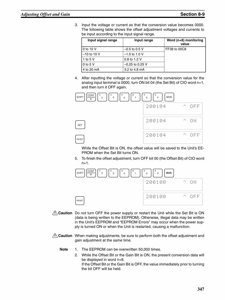
Adjusting Offset and Gain Section 8-9
3. Input the voltage or current so that the conversion value becomes 0000.The following table shows the offset adjustment voltages and currents tobe input according to the input signal range.
4. After inputting the voltage or current so that the conversion value for theanalog input terminal is 0000, turn ON bit 04 (the Set Bit) of CIO word n+1,and then turn it OFF again.
While the Offset Bit is ON, the offset value will be saved to the Unit’s EE-PROM when the Set Bit turns ON.
5. To finish the offset adjustment, turn OFF bit 00 (the Offset Bit) of CIO wordn+1.
!Caution Do not turn OFF the power supply or restart the Unit while the Set Bit is ON(data is being written to the EEPROM). Otherwise, illegal data may be writtenin the Unit’s EEPROM and “EEPROM Errors” may occur when the power sup-ply is turned ON or when the Unit is restarted, causing a malfunction.
!Caution When making adjustments, be sure to perform both the offset adjustment andgain adjustment at the same time.
Note 1. The EEPROM can be overwritten 50,000 times.
2. While the Offset Bit or the Gain Bit is ON, the present conversion data willbe displayed in word n+8.If the Offset Bit or the Gain Bit is OFF, the value immediately prior to turningthe bit OFF will be held.
Input signal range Input range Word (n+8) monitoring value
0 to 10 V –0.5 to 0.5 V FF38 to 00C8
–10 to 10 V –1.0 to 1.0 V
1 to 5 V 0.8 to 1.2 V
0 to 5 V –0.25 to 0.25 V
4 to 20 mA 3.2 to 4.8 mA
SHIFTCONT
# 2C
0A
0A
1B
0A
4E
MON
200104 ^ OFF
SET
200104 ^ ON
RESET
200104 ^ OFF
SHIFTCONT
#2
C0
A0
A1
B0
A0
AMON
200100 ^ ON
RESET
200100 ^ OFF
347
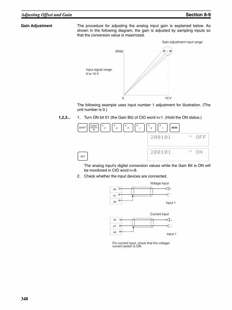
Adjusting Offset and Gain Section 8-9
Gain Adjustment The procedure for adjusting the analog input gain is explained below. Asshown in the following diagram, the gain is adjusted by sampling inputs sothat the conversion value is maximized.
The following example uses input number 1 adjustment for illustration. (Theunit number is 0.)
1,2,3... 1. Turn ON bit 01 (the Gain Bit) of CIO word n+1. (Hold the ON status.)
The analog input’s digital conversion values while the Gain Bit is ON willbe monitored in CIO word n+8.
2. Check whether the input devices are connected.
10 V0
0FA0
Input signal range:0 to 10 V
Gain adjustment input range
SHIFTCONT
#2
C0
A0
A
1B
0A
1B
MON
200101 ^ OFF
SET
200101 ^ ON
+
–
+
–
Voltage input
Input 1
Current input
Input 1
For current input, check that the voltage/current switch is ON.
A6
A7
A8
A6
A7
A8
348

Adjusting Offset and Gain Section 8-9
3. Input the voltage or current so that the conversion value is maximized(0FA0 or 07D0). The following table shows the gain adjustment voltagesand currents to be input according to the input signal range.
4. With the voltage or current having been input so that the conversion valuefor the Analog I/O Unit is maximized (0FA0 or 07D0), turn bit 04 (the SetBit) of CIO word n+1 ON and then OFF again.
While the Gain Bit is ON, the gain value will be saved to the Unit’s EE-PROM when the Set Bit turns ON.
5. To finish the gain adjustment, turn OFF bit 01 (the Gain Bit) of CIO wordn+1.
!Caution Do not turn OFF the power supply or restart the Unit while the Set Bit is ON(data is being written to the EEPROM). Otherwise, illegal data may be writtenin the Unit’s EEPROM and “EEPROM Errors” may occur when the power sup-ply is turned ON or when the Unit is restarted, causing a malfunction.
!Caution When making adjustments, be sure to perform both the offset adjustment andgain adjustment at the same time.
Note 1. The EEPROM can be overwritten 50,000 times.
2. While the Offset Bit or the Gain Bit is ON, the present conversion data willbe displayed in word n+8.If the Offset Bit or the Gain Bit is OFF, the value immediately prior to turningthe bit OFF will be held.
Input signal range Input range Word (n+8) monitoring value
0 to 10 V 9.5 to 10.5 V 0ED8 to 1068
–10 to 10 V 9.0 to 11.0 V 0708 to 0898
1 to 5 V 4.8 to 5.2 V 0ED8 to 1068
0 to 5 V 4.75 to 5.25 V 0ED8 to 1068
4 to 20 mA 19.2 to 20.8 mA 0ED8 to 1068
SHIFTCONT
#2
C0
A0
A1
B0
A4
EMON
200104 ^ OFF
SET
200104 ^ ON
RESET
200104 ^ OFF
SHIFTCONT
# 2C
0A
0A
1B
0A
1B
MON
200101 ^ ON
RESET200101 ^ OFF
349

Adjusting Offset and Gain Section 8-9
Clearing Offset and Gain Adjusted Values
Follow the procedure outlined below to return the offset and gain adjusted val-ues to their default settings.
The following example uses input number 1 adjustment for illustration. (Theunit number is 0.)
1,2,3... 1. Turn ON bit 05 (the Clear Bit) of CIO word n+1. (Hold the ON status.) Re-gardless of the input value, 0000 will be monitored in CIO word n+8.
2. Turn bit 04 of CIO word n+1 ON and then OFF again.
While the Clear Bit is ON, the adjusted value will be cleared and reset tothe default offset and gain values when the Set Bit turns ON.
3. To finish the clearing of adjusted values, turn OFF bit 05 (the Clear Bit) ofCIO word n+1.
!Caution Do not turn OFF the power supply or restart the Unit while the Set Bit is ON(data is being written to the EEPROM). Otherwise, illegal data may be writtenin the Unit’s EEPROM and “EEPROM Errors” may occur when the power sup-ply is turned ON or when the Unit is restarted, causing a malfunction.
!Caution When making adjustments, be sure to perform both the offset adjustment andgain adjustment at the same time.
Note The EEPROM can be overwritten 50,000 times.
SHIFTCONT
# 2C
0A
0A
1B
0A
5F
MON
200105 ^ OFF
SET200105 ^ ON
SHIFTCONT
# 2C
0A
0A
1B
0A
4E
MON
200104 ^ OFF
SET
200104 ^ ON
RESET
200104 ^ OFF
SHIFTCONT
#2
C0
A0
A1
B0
A
5F
MON
200105 ^ ON
RESET
200105 ^ OFF
350
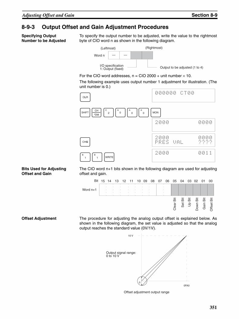
Adjusting Offset and Gain Section 8-9
8-9-3 Output Offset and Gain Adjustment ProceduresSpecifying Output Number to be Adjusted
To specify the output number to be adjusted, write the value to the rightmostbyte of CIO word n as shown in the following diagram.
For the CIO word addresses, n = CIO 2000 + unit number × 10.
The following example uses output number 1 adjustment for illustration. (Theunit number is 0.)
Bits Used for Adjusting Offset and Gain
The CIO word n+1 bits shown in the following diagram are used for adjustingoffset and gain.
Offset Adjustment The procedure for adjusting the analog output offset is explained below. Asshown in the following diagram, the set value is adjusted so that the analogoutput reaches the standard value (0V/1V).
(Rightmost)(Leftmost)
Word n
Output to be adjusted (1 to 4)I/O specification1: Output (fixed)
--- ---
CLR000000 CT00
SHIFTCH
*DM2
C0
A0
A0
AMON
2000 0000
CHG2000 0000PRES VAL ????
1B
1B
WRITE2000 0011
15 14 13 12 11 10 09 08 07 06 05 04 03 02 01 00Bit
Word n+1
Cle
ar B
it
Set
Bit
Up
Bit
Dow
n B
it
Gai
n B
it
Offs
et B
it
10 V
00FA0
Offset adjustment output range
Output signal range:0 to 10 V
351

Adjusting Offset and Gain Section 8-9
The following example uses output number 1 adjustment for illustration. (Theunit number is 0.)
1,2,3... 1. Turn ON bit 00 (the Offset Bit) of CIO word n+1. (Hold the ON status.)
2. Check whether the output devices are connected.
3. Monitor CIO word n+8 and check the set value while the Offset Bit is ON.
4. Change the set value so that the output voltage are as shown in the follow-ing table. The data can be set within the indicated ranges.
Output signal range Possible output voltage/current adjustment
Output range
0 to 10 V –0.5 to 0.5 V FF38 to 00C8
–10 to 10 V –1.0 to 1.0 V
1 to 5 V 0.8 to 1.2 V
0 to 5 V –0.25 to 0.25 V
CLR000000 CT00
SHIFTCONT
#2
C0
A0
A1
B0
A0
AMON
200100 ^ OFF
SET
200100 ^ ON
A1
A2
Voltage output
Output 1
CLR000000 CT00
SHIFTCH
*DM2
C0
A0
A8 MON
2008 0000
352

Adjusting Offset and Gain Section 8-9
Change the set value, using the Up Bit (bit 03 of word n+1) and the DownBit (bit 02 of word n+1).
• The following example increases the output voltage.
The bit will remain ON until the output becomes an appropriate value, atwhich time, it will turn OFF.
• The following example decreases the output voltage.
The bit will remain ON until the output becomes an appropriate value, atwhich time, it will turn OFF.
15 14 13 12 11 10 09 08 07 06 05 04 03 02 01 00Bit
Up Bit Down Bit
While the Up Bit is ON, the set value will be increased by 1 resolution every 0.5 seconds. After it has been ON for 3 seconds, the set value will be increased by 1 resolution every 0.1 seconds.
While the Down Bit is ON, the set value will be decreased by 1 resolution every 0.5 seconds. After it has been ON for 3 seconds, the set value will be decreased by 1 resolution every 0.1 seconds.
Word n+1
SHIFTCONT
#2
C0
A0
A1
B0
A3
DMON
200103 ^ OFF
SET
200103 ^ ON
RESET
200103 ^ OFF
SHIFTCONT
# 2C
0A
0A
1B
0A
2C
MON
200102 ^ OFF
SET
200102 ^ ON
RESET
200102 ^ OFF
353

Adjusting Offset and Gain Section 8-9
5. Check the 0-V/1-V output, and then turn bit 04 (the Set Bit) of CIO wordn+1 ON and then OFF again.
While the Offset Bit is ON, the offset value will be saved to the Unit’s EE-PROM when the Set Bit turns ON.
6. To finish the offset adjustment, turn OFF bit 00 (the Offset Bit) of CIO wordn+1.
!Caution Do not turn OFF the power supply or restart the Unit while the Set Bit is ON(data is being written to the EEPROM). Otherwise, illegal data may be writtenin the Unit’s EEPROM and “EEPROM Errors” may occur when the power sup-ply is turned ON or when the Unit is restarted, causing a malfunction.
!Caution When making adjustments, be sure to perform both the offset adjustment andgain adjustment at the same time.
Note The EEPROM can be overwritten 50,000 times.
Gain Adjustment The procedure for adjusting the analog output gain is explained below. Asshown in the following diagram, the set value is adjusted so that the analogoutput is maximized (to 10 V/5 V).
SHIFTCONT
# 2C
0A
0A
1B
0A
4E
MON
200104 ^ OFF
SET
200104 ^ ON
RESET
200104 ^ OFF
SHIFTCONT
#2
C0
A0
A1
B0
A0
AMON
200100 ^ ON
SET
200100 ^ OFF
10 V
00FA0
Output signal range:0 to 10 V
Gain adjustment output range
354
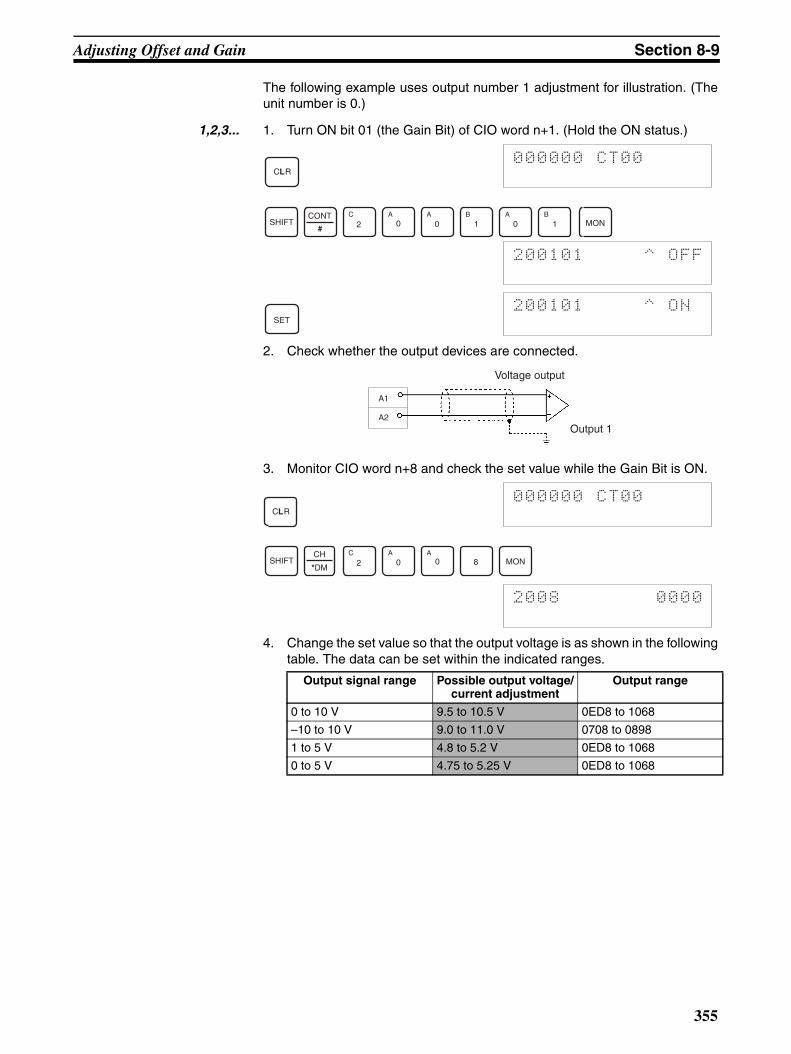
Adjusting Offset and Gain Section 8-9
The following example uses output number 1 adjustment for illustration. (Theunit number is 0.)
1,2,3... 1. Turn ON bit 01 (the Gain Bit) of CIO word n+1. (Hold the ON status.)
2. Check whether the output devices are connected.
3. Monitor CIO word n+8 and check the set value while the Gain Bit is ON.
4. Change the set value so that the output voltage is as shown in the followingtable. The data can be set within the indicated ranges.
Output signal range Possible output voltage/current adjustment
Output range
0 to 10 V 9.5 to 10.5 V 0ED8 to 1068
–10 to 10 V 9.0 to 11.0 V 0708 to 0898
1 to 5 V 4.8 to 5.2 V 0ED8 to 1068
0 to 5 V 4.75 to 5.25 V 0ED8 to 1068
CLR000000 CT00
SHIFTCONT
# 2C
0A
0A
1B
0A
1B
MON
200101 ^ OFF
SET
200101 ^ ON
A1
A2
Voltage output
Output 1
CLR
000000 CT00
SHIFTCH
*DM 2C
0A
0A
8 MON
2008 0000
355

Adjusting Offset and Gain Section 8-9
Change the set value, using the Up Bit (bit 03 of word n+1) and the DownBit (bit 02 of word n+1).
• The following example increases the output voltage.
The bit will remain ON until the output voltage becomes an appropriate val-ue, at which time, the output will turn OFF.
• The following example decreases the output voltage.
The bit will remain ON until the output voltage becomes an appropriate val-ue, at which time, the output will turn OFF.
Up Bit Down Bit
While the Up Bit is ON, the set value will be increased by 1 resolution every 0.5 seconds. After it has been ON for 3 seconds, the set value will be increased by 1 resolution every 0.1 seconds.
While the Down Bit is ON, the set value will be decreased by 1 resolution every 0.5 seconds. After it has been ON for 3 seconds, the set value will be decreased by 1 resolution every 0.1 seconds.
Word n+1
15 14 13 12 11 10 09 08 07 06 05 04 03 02 01 00Bit
SHIFTCONT
#2
C0
A0
A1
B0
A3
DMON
200103 ^ OFF
SET
200103 ^ ON
RESET
200103 ^ OFF
SHIFTCONT
# 2C
0A
0A
1B
0A
2C
MON
200102 ^ OFF
SET
200102 ^ ON
RESET
200102 ^ OFF
356

Adjusting Offset and Gain Section 8-9
5. Check the 10V/5V output, and then turn bit 04 (the Set Bit) of CIO wordn+1 ON and then OFF again.
While the Gain Bit is ON, the gain value will be saved to the Unit’s EE-PROM when the Set Bit turns ON.
6. To finish the gain adjustment, turn OFF bit 01 (the Gain Bit) of CIO wordn+1.
!Caution Do not turn OFF the power supply or restart the Unit while the Set Bit is ON(data is being written to the EEPROM). Otherwise, illegal data may be writtenin the Unit’s EEPROM and “EEPROM Errors” may occur when the power sup-ply is turned ON or when the Unit is restarted, causing a malfunction.
!Caution When making adjustments, be sure to perform both the offset adjustment andgain adjustment at the same time.
Note The EEPROM can be overwritten 50,000 times.
Clearing Offset and Gain Adjusted Values
Follow the procedure outlined below to return the offset and gain adjusted val-ues to their default settings.
The following example uses output number 1 adjustment for illustration. (Theunit number is 0.)
1,2,3... 1. Turn ON bit 05 (the Clear Bit) of CIO word n+1. (Hold the ON status.) Re-gardless of the set value, 0000 will be monitored in CIO word n+8.
SHIFTCONT
# 2C
0A
0A
1B
0A
4E
MON
200104 ^ OFF
SET
200104 ^ ON
RESET
200104 ^ OFF
SHIFTCONT
#2
C0
A0
A1
B0
A1
BMON
200101 ^ ON
RESET
200101 ^ OFF
SHIFTCONT
# 2C
0A
0A
1B
0A
5F
MON
200105 ^ OFF
SET
200105 ^ ON
357

Adjusting Offset and Gain Section 8-9
2. Turn bit 04 of CIO word n+1 ON and then OFF again.
While the Clear Bit is ON, the adjusted value will be cleared and reset tothe default offset and gain values when the Set Bit turns ON.
3. To finish the clearing of adjusted values, turn OFF bit 05 (the Clear Bit) ofCIO word n+1.
!Caution Do not turn OFF the power supply or restart the Unit while the Set Bit is ON(data is being written to the EEPROM). Otherwise, illegal data may be writtenin the Unit’s EEPROM and “EEPROM Errors” may occur when the power sup-ply is turned ON or when the Unit is restarted, causing a malfunction.
Note The EEPROM can be overwritten 50,000 times.
SHIFTCONT
# 2C
0A
0A
1B
0A
4E
MON
200104 ^ OFF
SET
200104 ^ ON
RESET
200104 ^ OFF
SHIFTCONT
#2
C
0A
0A
1B
0A
5F
MON
200105 ^ ON
RESET
200105 ^ OFF
358

Handling Errors and Alarms Section 8-10
8-10 Handling Errors and Alarms
8-10-1 Indicators and Error FlowchartIndicators If an alarm or error occurs in the Analog I/O Unit, the ERC or ERH indicators
on the front panel of the Unit will light.
LED Meaning Indicator Operating status
RUN (green) Operating Lit Operating in normal mode.
Not lit Unit has stopped exchanging data with the CPU Unit.
ERC (red) Unit has detected an error
Lit Alarm has occurred (such as disconnec-tion detection) or initial settings are incor-rect.
Not lit Operating normally.
ADJ (yellow) Adjusting Flashing Operating in offset/gain adjustment mode.
Not lit Other than the above.
ERH (red) Error in the CPU Unit
Lit Error has occurred during data exchange with the CPU Unit.
Not lit Operating normally.
Front panel of Unit
RUN
ERC
ADJ
ERH
359

Handling Errors and Alarms Section 8-10
Troubleshooting Procedure
Use the following procedure for troubleshooting Analog I/O Unit errors.
Is the ERC indicator lit?
Yes
No
Is the RUN indicator lit?
Yes
No
Alarm has occurred at the Analog I/O Unit.
Check whether the initial settings for the Analog I/O Unit are set correctly.
Is the ERH indicator lit?
Yes
No
Is the RUN indicator lit?
Yes
No
Error detected by CPU Unit
Check whether the unit number is set correctly.
Error occurs.
Yes
No
Is the RUN indicator lit?
Error cleared?
No
Cycle the power supplyto the PLC.
Error cleared?
No
The Unit is faulty.
Replace the Unit.
YesNoise or other disturbance may be causingmalfunctions. Check the operating environment.
Yes
Error in internal circuits has occurred, preventing operation from continuing.
(Refer to 8-10-2 Alarms Occurring at the Analog I/O Unit.)
Refer to 8-10-5 Troubleshooting.
(Refer to 8-10-2 Alarms Occurring at the Analog I/O Unit.)
(Refer to 8-10-3 Errors in the CPU Unit.)
(Refer to 8-10-3 Errors in the CPU Unit.)
Refer to 8-10-4 Restarting Special I/O Units.
360

Handling Errors and Alarms Section 8-10
8-10-2 Alarms Occurring at the Analog I/O UnitWhen an alarm occurs at the Analog I/O Unit, the ERC indicator lights and theAlarm Flags are stored in bits 08 to 15 of CIO word n+9.
ERC and RUN Indicators: Lit
The ERC and RUN indicators will be lit when an error occurs while the Unit isoperating normally. The following alarm flags will turn ON in CIO word n+9.These alarm flags will turn OFF automatically when the error is cleared.
Note Disconnection detection operates for input numbers used with a range of 1 to5 V (4 to 20 mA).
For the CIO word addresses, n = CIO 2000 + (unit number × 10).
Word n+9
Disconnection Detection Flags
Output setting errorsAlarm Flags
15 14 13 12 11 10 09 08 07 06 05 04 03 02 01 00Bit
(See 8-6-4 Input Disconnection Detection Function.)
(See 8-7-3 Output Setting Errors.)
RUN
ERC ERH
: Lit
: Not lit
Word n + 9 Alarm flag Error contents I/O status Countermeasure
Bits 00 to 03 Output Set Value Error
The output setting range has been exceeded.
Output value set by output hold function.
Correct the set value.
Bits 04 to 07 Disconnection Detection
A disconnection was detected. (See note.)
Conversion data becomes 0000.
Check the rightmost byte of CIO word n+9. The inputs for bits that are ON may be discon-nected. Restore any discon-nected inputs.
Bit 14 (Adjustment mode)
EEPROM Writ-ing Error
An EEPROM writing error has occurred while in adjustment mode.
Holds the out-put status imme-diately prior to the error.
Turn the Set Bit OFF, ON, and OFF again.
If the error persists even after the reset, replace the Analog I/O Unit.
361

Handling Errors and Alarms Section 8-10
ERC Indicator and RUN Indicator: Lit, ADJ Indicator: Flashing
This alarm will occur in the case of incorrect operation while in the adjustmentmode. In adjustment mode, the Adjustment Mode ON Flag will turn ON in bit15 of CIO word n+9.
Note When a PLC error occurs in the adjustment mode, Unit operations will stopoperating. (The input and output values immediately prior to the error will beheld.)
ERC Indicator: Lit, RUN Indicator: Not Lit
The ERC indicator will be lit when the initial settings for the Analog I/O Unitare not set correctly. The alarm flags for the following errors will turn ON inCIO word n+9. These alarm flags will turn OFF when the error is cleared and
RUN
ERC ERH
ADJ
: Lit
: Flashing
: Not lit
Word n + 9 Alarm flag Error contents I/O status Countermeasure
Bit 12 (Adjustment mode)
Input Value Adjustment Range Exceeded
In adjustment mode, offset or gain cannot be adjusted because input value is out of the permissible range for adjust-ment.
Conversion data corresponding to the input sig-nal is monitored in word n+8.
If making the adjustment by means of a connected input device, first adjust the input device before adjusting the Ana-log I/O Unit.
Bit 13 (Adjustment mode)
I/O Number Set-ting Error
In adjustment mode, adjust-ment cannot be performed because the specified input or output number is not set for use or because the wrong input or output number is specified.
Holds the values immediately prior to the error. No data is changed.
Check whether the word n input or output number to be adjusted is set from 11 to 14, or 21 to 24.
Check whether the input or out-put number to be adjusted is set for use by means of the DM set-ting.
Bit 15 only ON (Adjustment Mode)
PLC Error
The PLC is in either MONITOR or RUN mode while the Analog I/O Unit is operating in adjust-ment mode.
Holds the values immediately prior to the error. No data is changed.
Detach the Unit. Switch the rear panel DIP switch pin to OFF. Restart the Unit in normal mode.
RUN
ERC ERH
: Lit
: Not lit
362

Handling Errors and Alarms Section 8-10
the Unit is restarted, or the Special I/O Unit Restart Bit is turned ON and thenOFF again.
8-10-3 Errors in the CPU UnitWhen errors occur in the CPU Unit or I/O bus, and I/O refresh with the SpecialI/O Unit is not performed correctly resulting in the Analog I/O Unit malfunction-ing, the ERH indicator will be lit.
ERH and RUN Indicators: Lit
The ERH and RUN indicators will be lit if an error occurs in the I/O bus caus-ing a WDT (watchdog timer) error in the CPU Unit, resulting in incorrect I/Orefresh with the Analog I/O Unit.
Turn ON the power supply again or restart the system.For further details, refer to CS-series CS1G/H-CPU@@-EV1, CS1G/H-CPU@@H Programmable Controllers Operation Manual (W339).
Note No error will be detected by the CPU Unit or displayed on the ProgrammingConsole, because the CPU Unit is continuing operation.
Word n + 9 Alarm flag Error contents I/O status Countermeasure
Bit 08 Ratio Conver-sion Use Set-ting Error
The I/O number for the ratio con-version function has been set to be not used.
Conversion does not start and data becomes 0000.
Set the I/O number for use.
Bit 09 Ratio Set Value Error
A number outside of the 0 to 9999 BCD range has been specified for the ratio set value.
Specify a number from 0 to 9999 BCD.
Bit 10 Output Hold Setting Error
The wrong output status for when conversion is stopped has been specified.
Specify a number from 0000 to 0002.
Bit 11 Mean Value Processing Set-ting Error
The wrong number of samplings has been specified for mean processing.
Specify a number from 0000 to 0006.
RUN
ERC ERH
: Lit
: Not lit
Error Error contents Input condition Output condition
I/O bus error Error has occurred during data exchange with the CPU Unit.
Conversion data becomes 0000.
Depends on the output hold function.
CPU Unit monitoring error (see note)
No response from CPU Unit during fixed period.
Maintains the condition exist-ing before the error.
Maintains the condition exist-ing before the error.
CPU Unit WDT error Error has been generated in CPU Unit.
Changes to undefined state. Depends on the output hold function.
363

Handling Errors and Alarms Section 8-10
ERH Indicator: Lit, RUN Indicator: Not Lit
The unit number for the Analog I/O Unit has not been set correctly.
8-10-4 Restarting Special I/O UnitsThere are two ways to restart Special I/O Unit operation after having changedDM contents or having cleared the cause of an error. The first way is to turnthe power to the PLC OFF and ON, and the second way is to turn ON theSpecial I/O Unit Restart Bit ON.
Special I/O Unit Restart Bits
If the error is not cleared even after turning the Special I/O Unit Restart Bit ONand then OFF again, then replace the Unit.
There previous input data will be held and the output will be 0 V while restart-ing the Unit.
8-10-5 TroubleshootingThe following tables explain the probable causes of troubles that may occur,and the countermeasures for dealing with them.
Conversion Data Does Not Change
RUN
ERC ERH
: Lit
: Not lit
Error Error contents Input condition Output condition
Duplicate Unit Number The same unit number has been assigned to more than one Unit or the unit number was set to a value other than 00 to 95.
Conversion does not start and data becomes 0000.
The output value will be 0 V.
Special I/O Unit Setting Error The Special I/O Units regis-tered in the I/O table are dif-ferent from the ones actually mounted.
Bits Functions
A50200 Unit #0 Restart Bit Turning the Restart Bit for any Unit ON and then OFF again restarts that Unit.
A50201 Unit #1 Restart Bit
to to
A50215 Unit #15 Restart Bit
A50300 Unit #16 Restart Bit
to to
A50715 Unit #95 Restart Bit
Probable cause Countermeasure Page
The input is not set for being used. Set the input to be used. 330
The peak value hold function is in operation.
Turn OFF the peak value hold func-tion if it is not required.
335
The input device is not working, the input wiring is wrong, or there is a disconnection.
Using a tester, check to see if the input voltage or current is changing.
---
Use Unit’s alarm flags to check for a disconnection.
336
364

Handling Errors and Alarms Section 8-10
Value Does Not Change as Intended
Conversion Values are Inconsistent
Analog Output Does Not Change
Output Does Not Change as Intended
Outputs are Inconsistent
Probable cause Countermeasure Page
The input device’s signal range does not match the input signal range for the relevant input number at the Analog I/O Unit.
Check the specifications of the input device, and match the settings for the input signal ranges.
303
The offset and gain are not adjusted.
Adjust the offset and gain. 343
When using the 4 mA to 20 mA range, the voltage/current switch is not turned ON.
Turn ON the voltage/current switch. 309, 316
The ratio conversion function is set to be used, so the calculation results are being monitored.
Correct the conversion settings. 361
Probable cause Countermeasure Page
The input signals are being affected by external noise.
Change the shielded cable connec-tion to the Unit’s COM terminal.
321
Insert a 0.01-µF to 0.1-µF ceramic capacitor or film capacitor between the input’s (+) and (–) terminals.
---
Try increasing the number of mean value processing buffers.
332
Probable Cause Countermeasure Page
The output is not set for being used. Set the output to be used. 337
The output hold function is in opera-tion.
Turn ON the Output Conversion Enable Bit.
339
The conversion value is set outside of the permissible range.
Set the data within the range. 305, 337
Probable Cause Countermeasure Page
The output signal range setting is wrong.
Correct the output signal range set-ting.
337
The I/O specifications of the output device do not match those of the Analog I/O Unit (e.g., input signal range, input impedance).
Change the output device. 301
The offset or gain is not adjusted. Adjust the offset or gain. 343
The ratio conversion function is set to be used.
Correct the conversion settings. 340
Probable Cause Countermeasure Page
The output signals are being affected by external noise.
Try changing the shielded cable connection (e.g., the grounding at the output device).
---
365

Handling Errors and Alarms Section 8-10
366

SECTION 9CJ-series Analog I/O Unit (CJ1W-MAD42)
This section explains how to use the CJ1W-MAD42 Analog I/O Unit.
9-1 Specifications . . . . . . . . . . . . . . . . . . . . . . . . . . . . . . . . . . . . . . . . . . . . . . . . . 3689-1-1 Specifications . . . . . . . . . . . . . . . . . . . . . . . . . . . . . . . . . . . . . . . . . . 3689-1-2 I/O Function Block Diagram . . . . . . . . . . . . . . . . . . . . . . . . . . . . . . 3709-1-3 Input Specifications . . . . . . . . . . . . . . . . . . . . . . . . . . . . . . . . . . . . . 3719-1-4 Output Specifications . . . . . . . . . . . . . . . . . . . . . . . . . . . . . . . . . . . . 373
9-2 Operating Procedure . . . . . . . . . . . . . . . . . . . . . . . . . . . . . . . . . . . . . . . . . . . . 3759-2-1 Procedure Examples . . . . . . . . . . . . . . . . . . . . . . . . . . . . . . . . . . . . . 376
9-3 Components and Switch Settings . . . . . . . . . . . . . . . . . . . . . . . . . . . . . . . . . . 3829-3-1 Indicators . . . . . . . . . . . . . . . . . . . . . . . . . . . . . . . . . . . . . . . . . . . . . 3839-3-2 Unit Number Switches . . . . . . . . . . . . . . . . . . . . . . . . . . . . . . . . . . . 3839-3-3 Voltage/Current Switch. . . . . . . . . . . . . . . . . . . . . . . . . . . . . . . . . . . 384
9-4 Wiring . . . . . . . . . . . . . . . . . . . . . . . . . . . . . . . . . . . . . . . . . . . . . . . . . . . . . . . 3859-4-1 Terminal Arrangement . . . . . . . . . . . . . . . . . . . . . . . . . . . . . . . . . . . 3859-4-2 Internal Circuitry . . . . . . . . . . . . . . . . . . . . . . . . . . . . . . . . . . . . . . . 3859-4-3 Voltage Input Disconnection. . . . . . . . . . . . . . . . . . . . . . . . . . . . . . . 3879-4-4 I/O Wiring Example . . . . . . . . . . . . . . . . . . . . . . . . . . . . . . . . . . . . . 3889-4-5 I/O Wiring Considerations . . . . . . . . . . . . . . . . . . . . . . . . . . . . . . . . 389
9-5 Exchanging Data with the CPU Unit . . . . . . . . . . . . . . . . . . . . . . . . . . . . . . . 3899-5-1 Outline of Data Exchange. . . . . . . . . . . . . . . . . . . . . . . . . . . . . . . . . 3899-5-2 Unit Number Settings . . . . . . . . . . . . . . . . . . . . . . . . . . . . . . . . . . . . 3909-5-3 Operation Mode Setting . . . . . . . . . . . . . . . . . . . . . . . . . . . . . . . . . . 3909-5-4 Special I/O Unit Restart Bits . . . . . . . . . . . . . . . . . . . . . . . . . . . . . . 3919-5-5 Fixed Data Allocations . . . . . . . . . . . . . . . . . . . . . . . . . . . . . . . . . . . 3929-5-6 I/O Refresh Data Allocations . . . . . . . . . . . . . . . . . . . . . . . . . . . . . . 395
9-6 Analog Input Functions and Operating Procedures . . . . . . . . . . . . . . . . . . . . 3989-6-1 Input Settings and Conversion Values . . . . . . . . . . . . . . . . . . . . . . . 3989-6-2 Conversion Time and Resolution Setting . . . . . . . . . . . . . . . . . . . . . 4009-6-3 Mean Value Processing. . . . . . . . . . . . . . . . . . . . . . . . . . . . . . . . . . . 4009-6-4 Peak Value Hold Function . . . . . . . . . . . . . . . . . . . . . . . . . . . . . . . . 4039-6-5 Input Scaling Function . . . . . . . . . . . . . . . . . . . . . . . . . . . . . . . . . . . 4049-6-6 Input Disconnection Detection Function . . . . . . . . . . . . . . . . . . . . . 406
9-7 Analog Output Functions and Operating Procedures . . . . . . . . . . . . . . . . . . . 4079-7-1 Output Settings and Conversions . . . . . . . . . . . . . . . . . . . . . . . . . . . 4079-7-2 Conversion Time and Resolution Setting . . . . . . . . . . . . . . . . . . . . . 4099-7-3 Output Hold Function . . . . . . . . . . . . . . . . . . . . . . . . . . . . . . . . . . . . 4109-7-4 Output Scaling Function . . . . . . . . . . . . . . . . . . . . . . . . . . . . . . . . . . 4119-7-5 Output Setting Errors . . . . . . . . . . . . . . . . . . . . . . . . . . . . . . . . . . . . 413
9-8 Ratio Conversion Function . . . . . . . . . . . . . . . . . . . . . . . . . . . . . . . . . . . . . . . 4139-9 Adjusting Offset and Gain . . . . . . . . . . . . . . . . . . . . . . . . . . . . . . . . . . . . . . . 416
9-9-1 Adjustment Mode Operational Flow . . . . . . . . . . . . . . . . . . . . . . . . 4179-9-2 Input Offset and Gain Adjustment Procedures . . . . . . . . . . . . . . . . . 4189-9-3 Output Offset and Gain Adjustment Procedures . . . . . . . . . . . . . . . 424
9-10 Handling Errors and Alarms . . . . . . . . . . . . . . . . . . . . . . . . . . . . . . . . . . . . . . 4329-10-1 Indicators and Error Flowchart . . . . . . . . . . . . . . . . . . . . . . . . . . . . . 4329-10-2 Alarms Occurring at the Analog I/O Unit . . . . . . . . . . . . . . . . . . . . 4349-10-3 Errors in the CPU Unit . . . . . . . . . . . . . . . . . . . . . . . . . . . . . . . . . . . 4369-10-4 Restarting Special I/O Units . . . . . . . . . . . . . . . . . . . . . . . . . . . . . . . 4379-10-5 Troubleshooting . . . . . . . . . . . . . . . . . . . . . . . . . . . . . . . . . . . . . . . . 437
367

Specifications Section 9-1
9-1 Specifications
9-1-1 Specifications
Note 1. Refer to Appendix A Dimensions on page 439 for details on the Unit’s di-mensions.
2. This is the maximum number of Units that can be mounted to a CJ2H-CPU6@ CPU Unit (no EtherNet/IP). The maximum number of Analog Out-put Units that can be mounted to one Rack varies depending on the currentconsumption of the other Units mounted to the Rack.
Input Specifications and Functions
Item CJ1W-MAD42
Unit type CJ-series Special I/O Unit
Isolation Between I/O and PLC signals: Photocoupler(No isolation between I/O signals.)
External terminals 18-point detachable terminal block (M3 screws)
Current consumption 580 mA max. at 5 V DC
Dimensions (mm) (See note 1.)
31 × 90 × 65 (W × H × D)
Weight 150 g max.
General specifications Conforms to general specifications for SYSMAC CJ-series Series.
Mounting position CJ-series CPU Rack or CJ-series Expansion Rack(Cannot be mounted to a C200H Expansion I/O Rack or a SYSMAC BUS Slave Rack.)
Maximum number of Units (See note 2.)
Per CPU Rack or Expansion Rack (See note 2.)
Power Supply Unit No. of mountable Units
CJ1W-PA205RCJ1W-PA205CCJ1W-PD025
CPU Rack: 7 Units/RackExpansion Rack: 8 Units/Rack
CJ1W-PA202 CPU Rack: 4 Units/RackExpansion Rack: 4 Units/Rack
CJ1W-PD022 CPU Rack: 2 Units/RackExpansion Rack: 3 Units/Rack
Data exchange with CPU Units
Special I/O Unit Area CIO 200000 to CIO295915 (Words CIO 2000 to CIO 2959): Exchanges 10 words of data per Unit.Internal Special I/O Unit DM Area (D20000 to D29599)
Item Voltage input Current input
Number of analog inputs 4
Input signal range (See note 3.)
1 to 5 V0 to 5 V0 to 10 V–10 to 10 V
4 to 20 mA(See note 4.)
Maximum rated input (for 1 point) (See note 5.)
±15 V ±30 mA
External input impedance 1 MΩ min. 250 Ω (rated value)
Resolution 4,000/8,000 (full scale) (See note 8.)
Converted output data 16-bit binary data
Accuracy(See note 6.)
25°C ±0.2% of full scale
0°C to 55°C ±0.4% of full scale
A/D conversion time (See note 7.)
1.0 ms/500 µs max. per point
Mean value processing Stores the last “n” data conversions in the buffer, and stores the mean value of the conver-sion values.Number of mean value buffers: n = 2, 4, 8, 16, 32, 64
Peak value holding Stores the maximum conversion value while the Peak Value Hold Bit is ON.
368

Specifications Section 9-1
3. Input and output signal ranges can be set for each input and output.
4. Voltage input or current input are chosen by using the voltage/currentswitch at the back of the terminal block.
5. The Analog I/O Unit must be operated according to the input specificationsprovided here. Operating the Unit outside these specifications will causethe Unit to malfunction.
6. The accuracy is given for full scale. For example, an accuracy of ±0.2%means a maximum error of ±8 (BCD).
7. A/D conversion time is the time it takes for an analog signal to be stored inmemory as converted data after it has been input. It takes at least one cy-cle before the converted data is read by the CPU Unit.
8. By means of the D(m+18) setting, the resolution can be changed to 8,000,and the conversion time can be changed to 500 µs.
Output Specifications
Scaling Enabled only for conversion time of 1 ms and resolution of 4,000. Setting any values within a range of ±32,000 as the upper and lower limits allows the A/D conversion result to be output with these values as full scale.
Input disconnection detection Detects the disconnection and turns ON the Disconnection Detection Flag.
Item Voltage input Current input
Item Voltage output Current output
Number of analog outputs 2
Output signal range (See note 1.)
1 to 5 V0 to 5 V0 to 10 V–10 to 10 V
4 to 20 mA
External output impedance 0.5 Ω max. ---
Maximum external output cur-rent (for 1 point)
2.4 mA ---
Maximum allowed load resis-tance
--- 600 Ω
Resolution 4,000/8,000 (full scale) (See note 5.)
Set data 16-bit binary data
Accuracy(See note 2.)
25°C ±0.3% of full scale ±0.3% of full scale
0°C to 55°C ±0.5% of full scale ±0.6% of full scale
D/A conversion time (See note 3.)
1.0 ms/500 µs max. per point
Output hold function Outputs the specified output status (CLR, HOLD, or MAX) under any of the following cir-cumstances.When the Conversion Enable Bit is OFF. (See note 4.)
In adjustment mode, when a value other than the output number is output during adjust-ment.When there is an output setting error or a fatal error occurs at the PLC.
When the Load is OFF.
Scaling Enabled only for conversion time or 1 ms and resolution of 4,000. Setting any values within a range of ±32,000 as the upper and lower limits allows D/A conversion to be exe-cuted and analog signals to be output with these values as full scale.
Ratio conversion function Stores the results of positive and negative gradient analog inputs calculated for ratio and bias as analog output values.
Positive gradient: Analog output = A × Analog input + B(A = 0 to 99.99, B = 8,000 to 7FFF hex)
Negative gradient: Analog output = F – A × Analog input + B(A: 0 to 99.99, B = 8,000 to 7FFF hex, F: Output range maximum value)
369

Specifications Section 9-1
1. Input and output signal ranges can be set for each input and output.
2. The accuracy is given for full scale. For example, an accuracy of ±0.2%means a maximum error of ±8 (BCD) at a resolution of 4,000.
3. D/A conversion time is the time required for converting and outputting thePLC data. It takes at least one cycle for the data stored in the PLC to beread by the Analog I/O Unit.
4. When the operation mode for the CPU Unit is changed from RUN mode orMONITOR mode to PROGRAM mode, or when the power is turned ON,the Output Conversion Enable Bit will turn OFF. The output status specifiedaccording to the output hold function will be output.
5. By means of the D(m+18) setting, the resolution can be changed to 8,000,and the conversion time can be changed to 500 µs.
9-1-2 I/O Function Block Diagram
Same as above.
Same as above.
Same as above.
Same as above.
A/D
Analog I/O Unit CPU Unit
Special I/O Unit Area
D/A
Input discon-nection de-tection
Mean value proc-essing disabled
Mean value proc-essing enabled
Scaling enabled
Scaling disabled
Peak value hold function disabled
Peak value hold function enabled
I/O refresh Analog input
1 conver-sion value
Analog out-put 1 con-version val-ue
Output hold enabled
Output hold disabled
Scaling enabled
Scaling disabled
Ratio conver-sion disabled
Ratio conversion
Ratio conver-sion enabled
Ratio conver-sion disabled
Analog input 1
Analog input 2Analog input 3Analog input 4
Analog output 1
Analog output 2
370

Specifications Section 9-1
9-1-3 Input SpecificationsIf signals that are outside the specified range provided below are input, theconversion values used will be at either the maximum or minimum value.
Range: 1 to 5 V (4 to 20 mA)
Range: 0 to 10 V
1 V (4 mA)0.8 V (3.2 mA)
5 V (20 mA)5.2 V (20.8 mA)
Resolution: 4,000/8,000
Conversion value (16-bit binary data)
1068 (20D0)0FA0 (1F40)
0000 (0000)FF38 (FE70)
Analog input signal( ): Values in parentheses are for a resolution of 8,000.
0 V 10 V–0.5 V 10.5 V
1068 (20D0)0FA0 (1F40)
0000 (0000)FF38 (FE70)
Resolution: 4,000/8,000
Conversion value (16-bit binary data)
Analog input signal( ): Values in parentheses are for a resolution of 8,000.
371

Specifications Section 9-1
Range: 0 to 5 V
Range: –10 to 10 V
0 V 5 V–0.25 V 5.25 V
1068 (20D0)0FA0 (1F40)
0000 (0000)FF38 (FE70)
Resolution: 4,000/8,000
Conversion value (16-bit binary data)
Analog input signal
0 V 10 V11 V
0898 (1130)07D0 (0FA0)
F830 (F060)F768 (EED0)
0000 (0000)
–10 V–11 V
Resolution: 4,000/8,000
Conversion value (16-bit binary data)
Analog input signal
372

Specifications Section 9-1
9-1-4 Output SpecificationsIf the set value is outside the specified range provided below, the output set-ting will be fixed at the maximum or the minimum value.
Range: 1 to 5 V
Range: 0 to 10 V
5.2 V5 V
1 V0.8 V
0000 (0000)
FF38(FE70)
0FA0 (1F40)
1068 (20D0)Resolution: 4,000/8,000
Set value (16-bit binary data)
Analog output signal
( ): Values in parentheses are for a resolution of 8,000.
0000 (0000)FF38
(FE70)
0FA0 (1F40)
1068 (20D0)
10.5 V10 V
0 V–0.5 V
Resolution: 4,000/8,000
Set value (16-bit binary data)
Analog output signal
( ): Values in parentheses are for a resolution of 8,000.
373

Specifications Section 9-1
Range: 0 to 5 V
Range: –10 to 10 V
Note The conversion values and set values for a range of –10 to 10 V will be as fol-lows:
0000 (0000)FF38
(FE70)
0FA0 (1F40)
1068(20D0)
5.25 V5 V
0 V–0.25 V
Resolution: 4,000/8,000
Set value (16-bit binary data)
Analog output signal
( ): Values in parentheses are for a resolution of 8,000.
0000 (0000)
F830 (F060)
F768 (EED0)
07D0 (0FA0)
0898 (1130)
0 V
–10 V–11 V
11 V10 V
Resolution: 4,000/8,000
Set value (16-bit binary data)
Analog output signal
( ): Values in parentheses are for aresolution of 8,000.
16-bit binary data BCD (Resolution: 4,000)
F768 –2200
: :
FFFF –1
0000 0
0001 1
: :
0898 2200
374

Operating Procedure Section 9-2
9-2 Operating ProcedureFollow the procedure outlined below when using Analog I/O Units.
Installation and Settings
1,2,3... 1. Set the voltage/current switch at the back of the terminal block.
2. Wire the Unit.
3. Use the unit number switches on the front panel of the Unit to set the unitnumber.
4. Turn ON the power to the PLC.
5. Create the I/O tables.
6. Make the Special I/O Unit DM Area settings.
• Set the I/O numbers to be used.
• Set the input and output signal ranges.
• Set the number of mean processing samplings.
• Set the output hold function
• Set the scaling function.
• Set the ratio conversion usage, the ratio set value, and the bias value.
• Set the conversion time and resolution.
7. Turn the power to the PLC OFF and ON, or turn ON the Special I/O UnitRestart Bit.
When the input or output of the connected devices needs to be calibrated, fol-low the procedures in Offset Gain Adjustment below. Otherwise, skip to Oper-ation below.
Offset and Gain Adjustment
1,2,3... 1. Set the voltage/current switch at the back of the terminal block.
2. Turn ON the power to the PLC.
3. Set to adjustment mode in the Special I/O Unit DM Area.
4. Turn the power to the PLC OFF and ON, or turn ON the Special I/O UnitRestart Bit.
5. Adjust the offset and gain.
6. Set to normal mode in the Special I/O Unit DM Area.
7. Restart the Analog I/O Unit by turning ON the Special I/O Unit Restart Bitor turn the power supply to the PLC OFF and ON.
OperationLadder program
• Read conversion values or write set values by means of MOV(021) andXFER(070).
• Start and stop conversion output.
• Specify the peak hold function.
• Obtain disconnection notifications and error codes.
375

Operating Procedure Section 9-2
9-2-1 Procedure Examples
Setting the Analog I/O Unit
1,2,3... 1. Set the voltage/current switch. Refer to 9-3-3 Voltage/Current Switch forfurther details.
2. Mount and wire the Analog I/O Unit. Refer to 1-2-1 Mounting Procedure, 9-4 Wiring or 9-4-4 I/O Wiring Example for further details.
CJ1W-MAD42 CJ-series CPU Unit
Unit No. 1
Analog input
Analog outputD00100
D00101
D00102
D00103
D00200
D00201
D00202
D00203
IN1: 1 to 5 V
IN2: 0 to 10 V
IN3: 4 to 20 mA
IN4: 4 to 20 mA
OUT1: 0 to 10 V
OUT2: 4 to 20 mA
Ladd
er P
rogr
am
MAD42
B1 A1
MACHNo.x10 1
x10 0
RUNERCERHADJ
RUNERCERH B1 A1ADJ
21
21
09
8765 4 32109
8765 4 321
ON
21
21
ON
ON
ON
MACHNo.x101
x100
MAD42
OD261SYSMACCJ1G-CPU44PROGRAMMABLECONTROLLER
RUNERR/ALM
INHPRPHLCOMM
OPEN
PERIHERAL
PORT
MCPWR
BUSY
I0 1 2 3 4 5 6 78 9 10 11 12 13 14 15
II
20
1
CN1
DC24
V 0.
3A
1
20
CN2
B/A A/B
I
II
0
1
2
3
0 1 2 3 4 5 6 78 9 10 11 12 13 14 15
MAD42
B1 A1
MACHNo.x10 1
x10 0
RUNERCERHADJ
376

Operating Procedure Section 9-2
3. Set the unit number switches. Refer to 9-3-2 Unit Number Switches for fur-ther details.
4. Turn ON the power to the PLC.
Creating I/O TablesAfter turning ON the power to the PLC, be sure to create the I/O tables.
Initial Data Settings
1,2,3... 1. Specify the Special I/O Unit DM Area settings. Refer to Allocations in DMArea on page 392 for further details.
MACHNo.
MAD42RUNERCERH B1 A1ADJ
x10 1
x10 0
09
8765 4 321
09
8765 4 321
MACHNo.
101
100
09
8765 4 321
09
8765 4 321
If the unit number is set to 1, words will be allocated to the Analog Input Unit in Special I/O Unit Area CIO 2010 to CIO 2019 and in the Special I/O Unit Area D20100 to D20199.
OD261SYSMACCJ1G-CPU44PROGRAMMABLECONTROLLER
RUNERR/ALM
INHPRPHLCOMM
OPEN
PERIHERAL
PORT
MCPWR
BUSY
I0 1 2 3 4 5 6 78 9 10 11 12 13 14 15
II
20
1
CN1
DC24
V 0.
3A
1
20
CN2
B/A A/B
I
II
0
1
2
3
0 1 2 3 4 5 6 78 9 10 11 12 13 14 15
MAD42
B1 A1
MACHNo.x10 1
x10 0
RUNERCERHADJ
7 8 9
6
PRO01PRO01PROGRAMMING CONSOLEPROGRAMMING CONSOLE
ORAND
LD OUT TIM CH
DM*
EXT
5F4E
1B 2C 3D
0A
TRCNT
FUN SFT NOT
RUNMONITOR
PROGRAM
LR
* EM
EM
DM
HR
AR
Programming Console
Setting conditions
Unit No. 1
Analog input 1: 1 to 5 VAnalog input 2: 0 to 10 VAnalog input 3: 4 to 20 mAAnalog input 4: 4 to 20 mA
Analog output 1: 0 to 10 VAnalog output 2: 4 to 20 mA
377
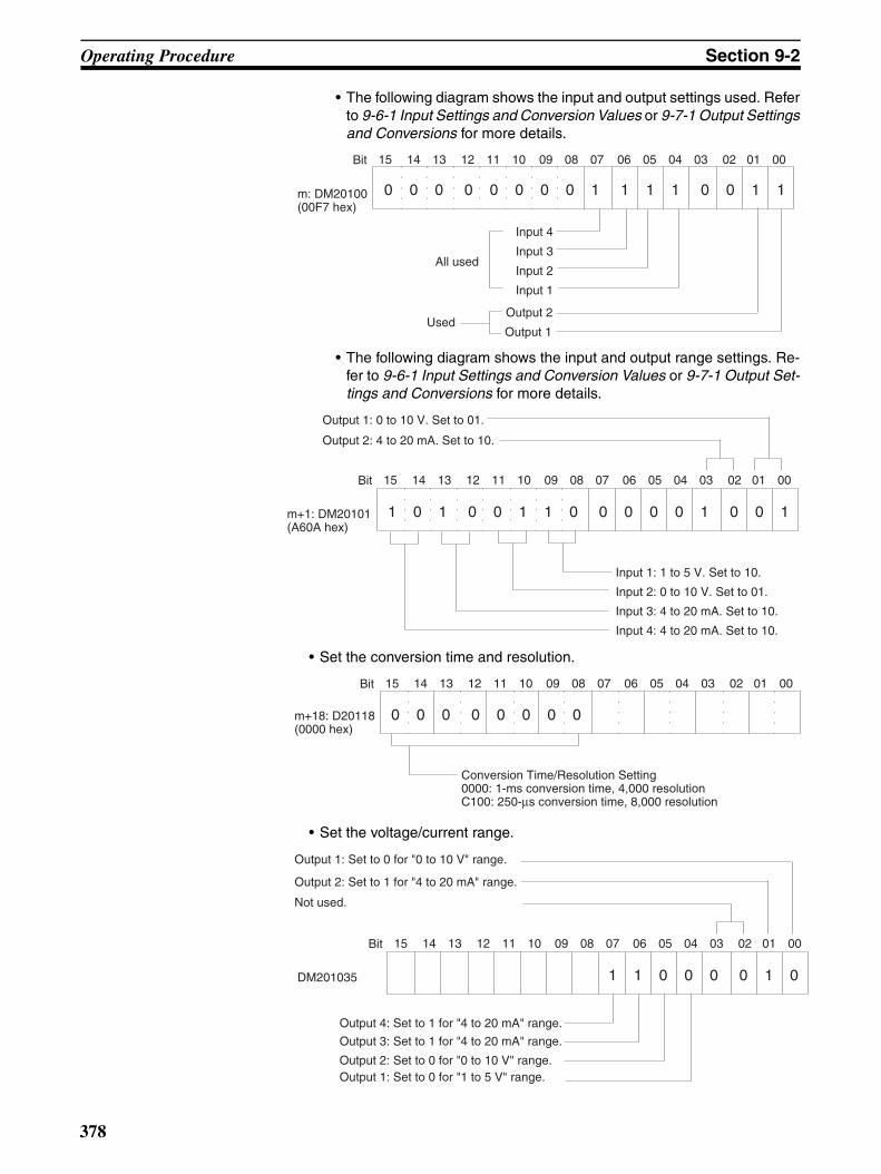
Operating Procedure Section 9-2
• The following diagram shows the input and output settings used. Referto 9-6-1 Input Settings and Conversion Values or 9-7-1 Output Settingsand Conversions for more details.
• The following diagram shows the input and output range settings. Re-fer to 9-6-1 Input Settings and Conversion Values or 9-7-1 Output Set-tings and Conversions for more details.
• Set the conversion time and resolution.
• Set the voltage/current range.
15 14 13 12 11 10 09 08 07 06 05 01 0004 03 02
0 0 0 0 0 0 0 0 1 1 1 1 0 0 1 1
Bit
All used
Input 4
Input 3
Input 2
Input 1
Output 2
Output 1Used
m: DM20100 (00F7 hex)
15 14 13 12 11 10 09 08 07 06 05 01 0004 03 02
1 0 1 0 0 1 1 0 0 0 0 0 1 0 0 1
Bit
Output 1: 0 to 10 V. Set to 01.
Output 2: 4 to 20 mA. Set to 10.
Input 1: 1 to 5 V. Set to 10.
Input 2: 0 to 10 V. Set to 01.
Input 3: 4 to 20 mA. Set to 10.
Input 4: 4 to 20 mA. Set to 10.
m+1: DM20101 (A60A hex)
15 14 13 12 11 10 09 08 07 06 05 01 0004 03 02
0 0 0 0 0 0 0 0
Bit
Conversion Time/Resolution Setting0000: 1-ms conversion time, 4,000 resolutionC100: 250-µs conversion time, 8,000 resolution
m+18: D20118 (0000 hex)
15 14 13 12 11 10 09 08 07 06 05 01 0004 03 02
1 1 0 0 0 0 1 0
Bit
Output 2: Set to 1 for "4 to 20 mA" range.
Not used.
DM201035
Output 1: Set to 0 for "0 to 10 V" range.
Output 3: Set to 1 for "4 to 20 mA" range.
Output 4: Set to 1 for "4 to 20 mA" range.
Output 1: Set to 0 for "1 to 5 V" range.Output 2: Set to 0 for "0 to 10 V" range.
378

Operating Procedure Section 9-2
2. Restart the CPU Unit.
Creating Ladder Programs
1,2,3... 1. The following example describes how to use analog inputs.
The data that is converted from analog to digital and output to CIO words (n +5) to (n+8) of the Special I/O Unit Area (CIO 2015 to CIO2018), is stored inthe specified addresses D00100 to D00103 as signed binary values 0000 to0FA0 hex.
• The following table shows the addresses used for analog input.
Note a) The addresses are set according to the unit number of the SpecialI/O Unit. Refer to 9-3-2 Unit Number Switches for further details.
Power turned ON again (or Special I/O Unit Restart Bit is turned ON).
OD261SYSMACCJ1G-CPU44PROGRAMMABLECONTROLLER
RUNERR/ALM
INHPRPHLCOMM
OPEN
PERIHERAL
PORT
MCPWR
BUSY
I0 1 2 3 4 5 6 78 9 10 11 12 13 14 15
II
20
1
CN1
DC24
V 0.
3A
1
20
CN2
B/A A /B
I
II
0
1
2
3
0 1 2 3 4 5 6 78 9 10 11 12 13 14 15
MAD42
B1 A1
MACHNo.x10 1
x10 0
RUNERCERHADJ
OD261SYSMACCJ1G-CPU44PROGRAMMABLECONTROLLER
RUNERR/ALM
INHPRPHLCOMM
OPEN
PERIHERAL
PORT
MCPWR
BUSY
I0 1 2 3 4 5 6 78 9 10 11 12 13 14 15
II
20
1
CN1
DC24
V 0.
3A
1
20
CN2
B/A A/B
I
II
0
1
2
3
0 1 2 3 4 5 6 78 9 10 11 12 13 14 15
MAD42
B1 A1
MACHNo.x10 1
x10 0
RUNERCERHADJ
7 8 9
6
PRO01PRO01PROGRAMMING CONSOLEPROGRAMMING CONSOLE
ORAND
LD OUT TIM CH
DM*
EXT
5F4E
1B 2C 3D
0A
TRCNT
FUN SFT NOT
RUNMONITOR
PROGRAM
LR
* EM
EM
DM
HR
AR OR
Programming Console Personal computer
Input number Input signal range Input conversion value address(n = CIO 2010)(See note a.)
Conversion data holding address
(See note b.)
1 1 to 5 V (n+5) = CIO 2015 D00100
2 0 to 10 V (n+6) = CIO 2016 D00101
3 4 to 20 mA (n+7) = CIO 2017 D00102
4 4 to 20 mA (n+8) = CIO 2018 D00103
379

Operating Procedure Section 9-2
b) Set as required.
c) The input Disconnection Detection Flag is allocated to bits 04 to07 of word (n+9). Refer to Allocations for Normal Mode onpage 396 and 9-6-6 Input Disconnection Detection Function forfurther details.
2. The following example shows how to use analog outputs.
The setting address D00200 is stored in words (n+1) to (n+2) of the Special I/O Unit Area (CIO 2011 to CIO 2012) as a signed binary value between 0000to 0FA0 hex.
• The following table shows the addresses used for analog output.
Note a) The addresses are set according to the unit number of the SpecialI/O Unit. Refer to 9-3-2 Unit Number Switches for further details.
201904 Input 1 Disconnection Detection Flag (See note c.)
Always ON Flag
201906 Input 3 Disconnection Detection Flag (See note c.)
201907 Input 4 Disconnection Detection Flag (See note c.)
For 1 to 5 V, the hexadecimal value 0000 to 0FA0 will be stored in CIO 2015, so if there is no disconnection (i.e., 201904 is OFF), CIO 2015 will be stored in D00100.
In the same way, for 0 to 10 V, CIO 2016 will be stored in D00101.
In the same way, for 4 to 20 mA, CIO 2017 will be stored in D00102.
In the same way, for 4 to 20 mA, CIO 2018 will be stored in D00103.
MOV (021)
2015
D00100
MOV (021)
2016
D00101
MOV (021)
2017
D00102
MOV (021)
2018
D00103
The disconnection detection function is notvalid for the 0 to 10-V range, so the Disconnection Detection Flag cannot be used.
Output number Input signal range Output setting address
(n = CIO 2010)(See note a.)
Original conversion
address (See note b.)
1 0 to 10 V (n+1) = CIO 2011 D00200
2 4 to 20 mA (n+2) = CIO 2012 D00201
380

Operating Procedure Section 9-2
b) Set as required.
D00200 is set in word CIO 2011.
D00201 is set in word CIO 2012.
MOV (021)
D00200
2011
MOV (021)
D00201
2012
Execution condition
SET
201000
SET
201001
Execution conditionTo start analog output, turn ON the Conversion Enable Bits 201000 to 201001 (bits 00 to 01 of word CIO 2010).
The data in words CIO 2011 and CIO 2012 will be output as 0 to 10 V, and the data in CIO 2013 will be output as 4 to 20 mA.
See Conversion Time and Resolution Setting on page 409 for details.
381

Components and Switch Settings Section 9-3
9-3 Components and Switch Settings
MACHNo.
MAD42RUNERCERH B1 A1ADJ
x101
x100
09
8765 4 321
09
8765 4 321
MACHNo.
MAD42RUNERCERH B1 A1ADJ
x101
x100
21
21
09
8765 4 321
09
8765 4 321
ON
ON
Front
With Terminal Block With Terminal Block Removed
Indicators
Terminal block
Voltage/current switch
DIN Track mounting pin
Terminal block
Terminal block lock lever (pull down to release terminal block)
User number setting switch
Slider
Expansion connector
Slider
Side
382
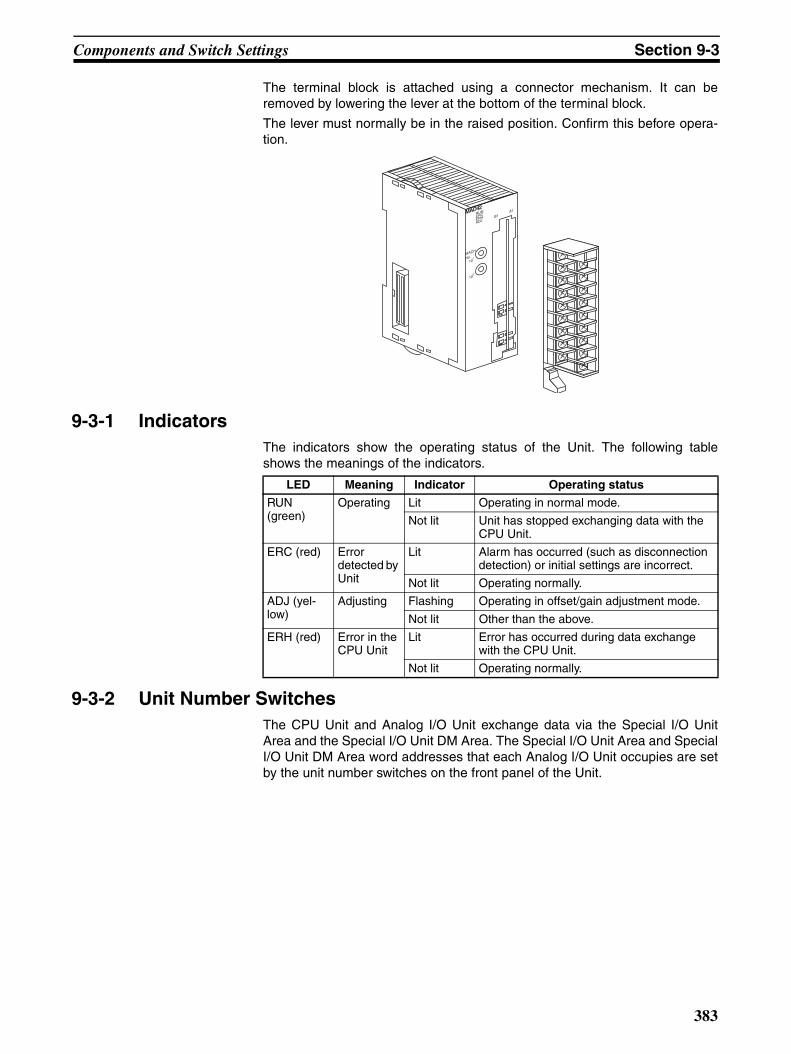
Components and Switch Settings Section 9-3
The terminal block is attached using a connector mechanism. It can beremoved by lowering the lever at the bottom of the terminal block.
The lever must normally be in the raised position. Confirm this before opera-tion.
9-3-1 IndicatorsThe indicators show the operating status of the Unit. The following tableshows the meanings of the indicators.
9-3-2 Unit Number SwitchesThe CPU Unit and Analog I/O Unit exchange data via the Special I/O UnitArea and the Special I/O Unit DM Area. The Special I/O Unit Area and SpecialI/O Unit DM Area word addresses that each Analog I/O Unit occupies are setby the unit number switches on the front panel of the Unit.
B1A1
21
21
ON
ON
MAD42
MACH
No.10
1
100
RUNERCERHADJ
LED Meaning Indicator Operating status
RUN (green)
Operating Lit Operating in normal mode.
Not lit Unit has stopped exchanging data with the CPU Unit.
ERC (red) Error detected by Unit
Lit Alarm has occurred (such as disconnection detection) or initial settings are incorrect.
Not lit Operating normally.
ADJ (yel-low)
Adjusting Flashing Operating in offset/gain adjustment mode.
Not lit Other than the above.
ERH (red) Error in the CPU Unit
Lit Error has occurred during data exchange with the CPU Unit.
Not lit Operating normally.
383

Components and Switch Settings Section 9-3
Always turn OFF the power before setting the unit number. Use a flat-bladescrewdriver, being careful not to damage the slot in the screw. Be sure not toleave the switch midway between settings.
Note If two or more Special I/O Units are assigned the same unit number, a “UNITNo. DPL ERR” error (in the Programming Console) will be generated (A40113will turn ON) and the PLC will not operate.
9-3-3 Voltage/Current SwitchThe analog conversion input can be switched from voltage input to currentinput by changing the pin settings on the voltage/current switch located on theback of the terminal block.
!Caution Be sure to turn OFF the power to the PLC before mounting or removing theterminal block.
Switch setting
Unit number
Special/O Unit Area addresses
Special I/O Unit DM Area addresses
0 Unit #0 CIO 2000 to CIO 2009 D20000 to D20099
1 Unit #1 CIO 2010 to CIO 2019 D20100 to D20199
2 Unit #2 CIO 2020 to CIO 2029 D20200 to D20299
3 Unit #3 CIO 2030 to CIO 2039 D20300 to D20399
4 Unit #4 CIO 2040 to CIO 2049 D20400 to D20499
5 Unit #5 CIO 2050 to CIO 2059 D20500 to D20599
6 Unit #6 CIO 2060 to CIO 2069 D20600 to D20699
7 Unit #7 CIO 2070 to CIO 2079 D20700 to D20799
8 Unit #8 CIO 2080 to CIO 2089 D20800 to D20899
9 Unit #9 CIO 2090 to CIO 2099 D20900 to D20999
10 Unit #10 CIO 2100 to CIO 2109 D21000 to D21099
to to to to
n Unit #n CIO 2000 + (n × 10) to CIO 2000 + (n × 10) + 9
D20000 + (n × 100) to D20000 + (n × 100) + 99
to to to to
95 Unit #95 CIO 2950 to CIO 2959 D29500 to D29599
MACHNo.
101
100
09
8765 4 321
09
8765 4 321
MACHNo.
MAD42RUNERCERH B1 A1ADJ
x101
x100
21
21
09
8765 4 321
09
8765 4 321
ON
ON
21
21
ON
ON
OFF: Voltage inputON: Current input
Input 2Input 1
Input 4Input 3
384

Wiring Section 9-4
9-4 Wiring
9-4-1 Terminal ArrangementThe signal names corresponding to the connecting terminals are as shown inthe following diagram.
Note 1. The analog I/O numbers that can be used are set in the Data Memory(DM).
2. The I/O signal ranges for individual inputs and outputs are set in the DataMemory (DM). They can be set in units of I/O numbers.
3. The AG terminal (A7, B7) is connected to the 0-V analog circuit in the Unit.Connecting shielded input lines can improve noise resistance.
4. The N.C. terminals (A4, B4) are not connected to internal circuitry.
9-4-2 Internal CircuitryThe following diagrams show the internal circuitry of the analog I/O section.
Input Circuitry
Output Circuitry
Voltage output 2 (+) B1
Output 2 (–) B2
Current output 2 (+) B3
N.C. B4
Input 2 (+) B5
Input 2 (–) B6
AG B7
Input 4 (+) B8
Input 4 (–) B9
A1
A2
A3
A4
A5
A6
A7
A8
A9
Voltage output 1 (+)
Output 1 (–)
Current output 1 (+)
N.C.
Input 1 (+)
Input 1 (–)
AG
Input 3 (+)
Input 3 (–)
1 MΩ
15 kΩ 15 kΩ
15 kΩ 15 kΩ
AG (common to all inputs)
Input (+)
Input (–)
AG (analog 0 V)
Input circuit and conversion circuit
1 MΩ
Voltage/currentinput switch
250 Ω
Output switch and conversion circuit
AMPVoltage output (+)
Voltage output (–)
AG (common to all outputs)
385
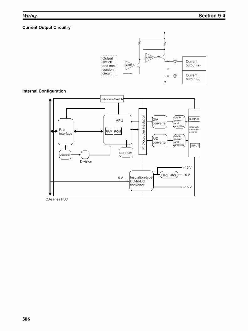
Wiring Section 9-4
Current Output Circuitry
Internal Configuration
AMP
AMP
Output switch and con-version circuit
Current output (+)
Current output (–)
Indicators/Switch
MPU
Regulator
Oscillator
Division
CJ-series PLC
EEPROM
RAM ROM
Pho
toco
uple
r in
sula
tion
OUTPUT
INPUT
5 V+5 V
−15 V
+15 V
Bus interface
D/A converter
A/D converter
Multi-plexer and amplifier
Multi-plexer and amplifier
Externally connected terminal
Insulation-type DC-to-DC converter
386

Wiring Section 9-4
9-4-3 Voltage Input Disconnection
Note If the connected device #2 in the above example outputs 5 V and the powersupply is shared by 2 channels as shown in the above diagram, approximatelyone third of the voltage, or 1.6 V, will be input at input 1.
When voltage inputs are used and a disconnection occurs, separate thepower supply at the side of the connected devices or use an insulating device(isolator) for each input to avoid the following problems.
When the power supply at the connected devices is shared and section A or Bis disconnected, power will flow in the direction of the broken line and the out-put voltage of the other connected devices will be reduced to between a thirdto a half of the voltage. If 1 to 5 V is used and the reduced voltage output, dis-connection may not be detectable. If section C is disconnected, the power atthe (–) input terminal will be shared and disconnection will not be detectable.
For current inputs, sharing the power supply between the connected deviceswill not cause any problems.
Connected device #1
24 VDC
Connected device #2
387
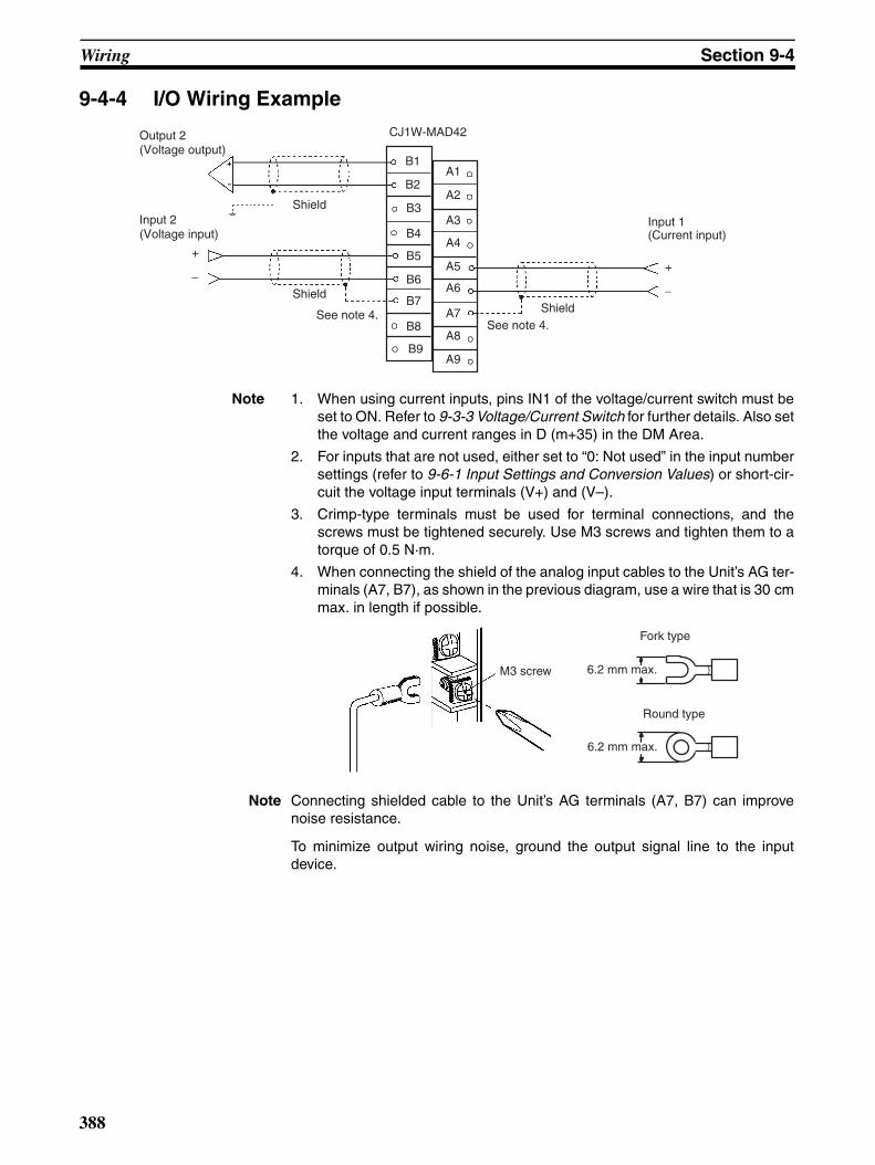
Wiring Section 9-4
9-4-4 I/O Wiring Example
Note 1. When using current inputs, pins IN1 of the voltage/current switch must beset to ON. Refer to 9-3-3 Voltage/Current Switch for further details. Also setthe voltage and current ranges in D (m+35) in the DM Area.
2. For inputs that are not used, either set to “0: Not used” in the input numbersettings (refer to 9-6-1 Input Settings and Conversion Values) or short-cir-cuit the voltage input terminals (V+) and (V–).
3. Crimp-type terminals must be used for terminal connections, and thescrews must be tightened securely. Use M3 screws and tighten them to atorque of 0.5 N·m.
4. When connecting the shield of the analog input cables to the Unit’s AG ter-minals (A7, B7), as shown in the previous diagram, use a wire that is 30 cmmax. in length if possible.
Note Connecting shielded cable to the Unit’s AG terminals (A7, B7) can improvenoise resistance.
To minimize output wiring noise, ground the output signal line to the inputdevice.
A6
A9
B1
B2
B3
B4
B5
B6
B7
B8
B9
A1
A2
A3
A4
A5
A7
A8
CJ1W-MAD42
Shield
Shield
See note 4. Shield
+
−+
−
Output 2 (Voltage output)
Input 2 (Voltage input)
Input 1 (Current input)
See note 4.
6.2 mm max.
6.2 mm max.M3 screw
Fork type
Round type
388

Exchanging Data with the CPU Unit Section 9-5
9-4-5 I/O Wiring ConsiderationsWhen wiring inputs, apply the following points to avoid noise interference andoptimize Analog I/O Unit performance.
• Use two-core shielded twisted-pair cables for external connections.
• Route I/O cables separately from the AC cable, and do not run the Unit’scables near a main circuit cable or a high voltage cable. Do not insert out-put cables into the same duct.
• If there is noise interference from power lines (if, for example, the powersupply is shared with electrical welding devices or electrical dischargemachines, or if there is a high-frequency generation source nearby) installa noise filter at the power supply input area.
9-5 Exchanging Data with the CPU Unit
9-5-1 Outline of Data ExchangeData is exchanged between the CPU Unit and the CJ1W-MAD42 Analog I/OUnit via the Special I/O Unit Area (for data used to operate the Unit) and theSpecial I/O Unit DM Area (for data used for initial settings).
I/O Refresh Data
Analog input conversion values, analog output set values, and other dataused to operate the Unit are allocated in the Special I/O Unit Area of the CPUUnit according to the unit number, and are exchanged during I/O refreshing.
Fixed Data
The Unit’s fixed data, such as the analog input signal ranges and analog out-put signal ranges, is allocated in the Special I/O Unit DM Area of the CPU Unitaccording to the unit number, and is exchanged when the power is turned ONor the Unit is restarted.
CJ-series CPU Unit CJ1W-MAD42 Analog I/O Unit
Special I/O Unit Area I/O Refresh Data
Analog inputs
Analog outputs
DM (Data Memory) Area
Input signal range
Output signal range
I/O refresh
2000 + n x 10
2000 + n x 10 + 9
D20000 + n x 100
D20000 + n x 100 + 99
Fixed Data
:
:
10 words
100 words Power ON or
Unit restart
Exchanges normal data such as analog inputs and analog outputs.
Transmits initial settings such as analog input ranges and analog output ranges.
n: Unit number
See 9-5-6 I/O Refresh Data Allocations for details.
See 9-5-5 Fixed Data Allocations for details.
389

Exchanging Data with the CPU Unit Section 9-5
9-5-2 Unit Number SettingsThe Special I/O Unit Area and Special I/O Unit DM Area word addresses thateach Analog I/O Unit occupies are set by the unit number switches on thefront panel of the Unit.
Note If two or more Special I/O Units are assigned the same unit number, a “UNITNo. DPL ERR” error (in the Programming Console) will be generated (A40113will turn ON) and the PLC will not operate.
9-5-3 Operation Mode SettingThe operation mode can be switched between normal mode and adjustmentmode (for offset gain adjustment) by changing the setting in bits 00 to 07 ofD(m+18).
Settings in D(m+18)
m = D20000 + (unit number × 100)
Switch setting
Unit number
Special/O Unit Area addresses
Special I/O Unit DM Area addresses
0 Unit #0 CIO 2000 to CIO 2009 D20000 to D20099
1 Unit #1 CIO 2010 to CIO 2019 D20100 to D20199
2 Unit #2 CIO 2020 to CIO 2029 D20200 to D20299
3 Unit #3 CIO 2030 to CIO 2039 D20300 to D20399
4 Unit #4 CIO 2040 to CIO 2049 D20400 to D20499
5 Unit #5 CIO 2050 to CIO 2059 D20500 to D20599
6 Unit #6 CIO 2060 to CIO 2069 D20600 to D20699
7 Unit #7 CIO 2070 to CIO 2079 D20700 to D20799
8 Unit #8 CIO 2080 to CIO 2089 D20800 to D20899
9 Unit #9 CIO 2090 to CIO 2099 D20900 to D20999
10 Unit #10 CIO 2100 to CIO 2109 D21000 to D21099
to to to to
n Unit #n CIO 2000 + (n × 10) to CIO 2000 + (n × 10) + 9
D20000 + (n × 100) to D20000 + (n × 100) + 99
to to to to
95 Unit #95 CIO 2950 to CIO 2959 D29500 to D29599
MACHNo.
101
100
09
8765 4 321
09
8765 4 321
DM word Bits
15 14 13 12 11 10 9 8 7 6 5 4 3 2 1 0
D(m+18) Conversion time/resolution setting Operation mode setting00: Normal modeC1: Adjustment mode
390

Exchanging Data with the CPU Unit Section 9-5
9-5-4 Special I/O Unit Restart BitsTo restart the Unit operations after changing the contents of the data memoryor correcting an error, turn ON the power to the PLC again or turn the SpecialI/O Unit Restart Bit ON and then OFF again.
Note If the error is not corrected by restarting the Unit or turning the Special I/OUnit Restart Bit ON and then OFF again, replace the Analog I/O Unit.
Special I/O Unit Area word address
Function
A50200 Unit No. 0 Restart Bit Restarts the Unit when turned ON and then OFF again.A50201 Unit No. 1 Restart Bit
to to
A50215 Unit No. 15 Restart Bit
A50300 Unit No. 16 Restart Bit
to to
A50715 Unit No. 95 Restart Bit
391

Exchanging Data with the CPU Unit Section 9-5
9-5-5 Fixed Data AllocationsAllocations in DM Area The initial settings of the Analog I/O Unit are set according to the data allo-
cated in the Special I/O Unit DM Area. Settings, such as the inputs and out-puts used, the analog input signal range, and analog output signal range mustbe set in this area.
Note 1. The Special I/O Unit DM Area words that are occupied by the Analog I/OUnit are set using the unit number switches on the front panel of the Unit.Refer to 9-3-2 Unit Number Switches for details on the method used to setthe unit number switches.
2. If two or more Special I/O Units are assigned the same unit number, a“UNIT No. DPL ERR” error (in the Programming Console) will be generat-ed (A40113 will turn ON) and the PLC will not operate.
D (m+1)
D (m)
D20300 to D20399
D20400 to D20499
D20500 to D20599
D20000 to D20099
D20100 to D20199
D20200 to D20299
D20900 to D20999
D20600 to D20699
D20700 to D20799
D20800 to D20899
SYSMAC CJ-series CPU Unit CJ1W-MAD42 Analog I/O Unit
(Fixed Data Area)
Unit #0
Unit #1
Unit #2
Unit #3
Unit #4
Unit #5
Unit #6
Unit #7
Unit #8
Unit #9
(Special I/O Unit DM Area)
Word
D29500 to D29599
D21000 to D21099
D20000 + (n × 100) to D20000 + (n × 100) + 99
Unit #10
Unit #n
Unit #95
I/O signal range
m = 20000 + (unit number × 100)
Data is automatically transferred to each unit number when the power is turned ON, or when the Special I/O Unit Restart Bit is turned ON.
I/O conversion permission loop mode setting
Output hold function setting
D (m+2 to m+3)
D (m+6 to m+9)
Sets number of samples for mean value processing
D (m+10 to m+13)
Ratio set value, bias value setting
D (m+18)
D (m+19 to m+22)
D (m+27 to m+34)
D (m+35)
Conversion time/resolution setting and operation mode setting
Output scaling function setting (Only when conversion time is 1 ms and resolution is 4,000.)
Input scaling function setting (Only when conversion time is 1 ms and resolution is 4,000.)
Voltage/current range setting (Only for 1 to 5 V and 4 to 20 mA.)
to
to
to
to
392

Exchanging Data with the CPU Unit Section 9-5
Allocations in DM Area The following table shows the allocation of DM words and bits for both normaland adjustment mode.
DM word Bits
15 14 13 12 11 10 9 8 7 6 5 4 3 2 1 0
D (m) Ratio conversion use setting Input use setting Output use setting
Not used. Not used. Loop 2 Loop 1 Input 4
Input 3
Input 2
Input 1
Not used.
Not used.
Out-put 2
Out-put 1
D (m+1) Input signal range setting Output signal range setting
Input 4 Input 3 Input 2 Input 1 Not used. Not used. Output 2 Output 1
D (m+2) Not used. Output 1: Output status when conversion stopped
D (m+3) Not used. Output 2: Output status when conversion stopped
D (m+4) Not used.
D (m+5) Not used.
D (m+6) Input 1: Mean value processing setting
D (m+7) Input 2: Mean value processing setting
D (m+8) Input 3: Mean value processing setting
D (m+9) Input 4: Mean value processing setting
D (m+10) Loop 1 (input 1 to output 1), A constant
D (m+11) Loop 1 (input 1 to output 1), B constant
D (m+12) Loop 2 (input 2 to output 2), A constant
D (m+13) Loop 2 (input 2 to output 2), B constant
D (m+14) Not used.
D (m+15) Not used.
D (m+16) Not used.
D (m+17) Not used.
D (m+18) Conversion time and resolution setting Operation mode setting
D (m+19) Output 1 scaling lower limit (Enabled only for conversion time of 1 ms and resolution of 4,000.)
D (m+20) Output 1 scaling upper limit (Enabled only for conversion time of 1 ms and resolution of 4,000.)
D (m+21) Output 2 scaling lower limit (Enabled only for conversion time of 1 ms and resolution of 4,000.)
D (m+22) Output 2 scaling upper limit (Enabled only for conversion time of 1 ms and resolution of 4,000.)
D (m+23) Not used.
D (m+24) Not used.
D (m+25) Not used.
D (m+26) Not used.
D (m+27) Input 1 scaling lower limit
D (m+28) Input 1 scaling upper limit
D (m+29) Input 2 scaling lower limit
D (m+30) Input 2 scaling upper limit
D (m+31) Input 3 scaling lower limit
D (m+32) Input 3 scaling upper limit
D (m+33) Input 4 scaling lower limit
D (m+34) Input 4 scaling upper limit
D (m+35) Voltage/current range setting (Enabled only when set for 1 to 5 V, 4 to 20 mA)
Not used. Input 4
Input 3
Input 2
Input 1
Not used. Out-put 2
Out-put 1
393

Exchanging Data with the CPU Unit Section 9-5
Set Values and Stored Values
Note 1. The input signal range of “1 to 5 V” and “4 to 20 mA” is switched using thepins of the voltage/current switch. Refer to 9-3-3 Voltage/Current Switch fordetails.
2. For the range of ±10 V, the output is 0 V. For other output signal ranges,the minimum value of each signal range is output. Refer to 9-7-3 OutputHold Function for details.
3. The default setting for mean value processing is to use two buffers.
Item Contents Page
Input Use setting 0: Not used.1: Used.
398
Input signal range 00: –10 to 10 V01: 0 to 10 V10: 1 to 5 V, 4 to 20 mA (See note 1.)11: 0 to 5 V
398
Voltage/current range setting 0: Voltage range (1 to 5 V)1: Current range (4 to 20 mA)
Mean value processing set-ting
0000: Mean value processing with 2 buffers (See note 3.)0001: No mean value processing0002: Mean value processing with 4 buffers0003: Mean value processing with 8 buffers0004: Mean value processing with 16 buffers0005: Mean value processing with 32 buffers0006: Mean value processing with 64 buffers
400
Scaling setting Set any value in binary data from -32,000 (8,300) to +32,000 (7D00), except when upper limit = lower limit (not 0000).
Output Use setting 0: Not used.1: Used.
407
Output signal range 00: –10 to 10 V01: 0 to 10 V10: 1 to 5 V11: 0 to 5 V
408
Voltage/current range setting 0: Voltage range (1 to 5 V)1: Current range (4 to 20 mA)
Output status when stopped 00: CLR Outputs 0 or minimum value of each range. (See note 2.)
01: HOLD Holds output just before stopping.02: MAX Outputs maximum value of range.
410
Scaling setting Set any value in binary data from −32,000 (8,300) to +32,000 (7D00), except when upper limit = lower limit (not 0000).
Loop Ratio conversion use setting 00: Not used.01: Uses positive gradient conversion.10: Uses negative gradient conversion.11: Same as for setting “00” above.
413
A constant 4 digits BCD (0 to 9999)
B constant 16-bit binary data
Conversion time/resolution setting (for inputs and outputs)
00: Conversion time of 1 ms and resolution of 4,000C1: Conversion time of 500 µs and resolution of 8,000
400
394
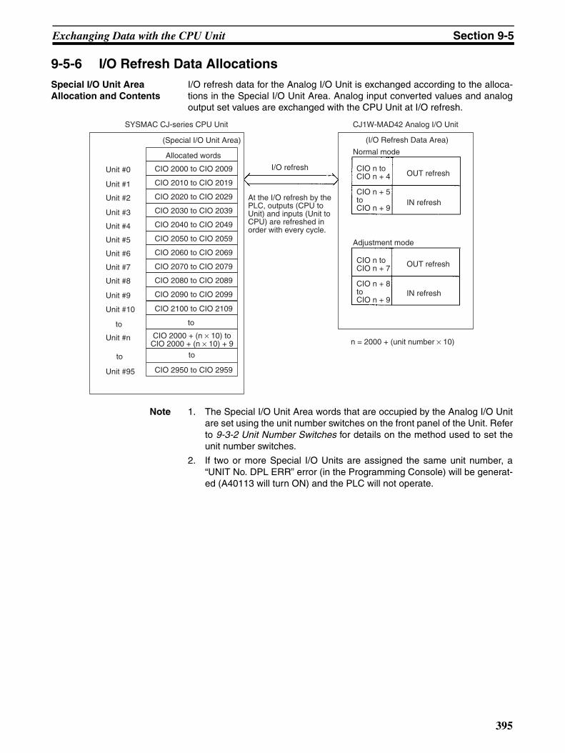
Exchanging Data with the CPU Unit Section 9-5
9-5-6 I/O Refresh Data AllocationsSpecial I/O Unit Area Allocation and Contents
I/O refresh data for the Analog I/O Unit is exchanged according to the alloca-tions in the Special I/O Unit Area. Analog input converted values and analogoutput set values are exchanged with the CPU Unit at I/O refresh.
Note 1. The Special I/O Unit Area words that are occupied by the Analog I/O Unitare set using the unit number switches on the front panel of the Unit. Referto 9-3-2 Unit Number Switches for details on the method used to set theunit number switches.
2. If two or more Special I/O Units are assigned the same unit number, a“UNIT No. DPL ERR” error (in the Programming Console) will be generat-ed (A40113 will turn ON) and the PLC will not operate.
CIO 2030 to CIO 2039
CIO 2040 to CIO 2049
CIO 2050 to CIO 2059
CIO 2000 to CIO 2009
CIO 2010 to CIO 2019
CIO 2020 to CIO 2029
CIO 2090 to CIO 2099
CIO 2060 to CIO 2069
CIO 2070 to CIO 2079
CIO 2080 to CIO 2089
SYSMAC CJ-series CPU Unit CJ1W-MAD42 Analog I/O Unit
IN refresh
(I/O Refresh Data Area)
Unit #0
Unit #1
Unit #2
Unit #3
Unit #4
Unit #5
Unit #6
Unit #7
Unit #8
Unit #9
(Special I/O Unit Area)
OUT refresh
Allocated words
CIO 2950 to CIO 2959
CIO 2100 to CIO 2109Unit #10
Unit #n
Unit #95
Normal mode
IN refresh
OUT refresh
Adjustment mode
n = 2000 + (unit number × 10)
I/O refresh
At the I/O refresh by the PLC, outputs (CPU to Unit) and inputs (Unit to CPU) are refreshed in order with every cycle.
CIO 2000 + (n × 10) to CIO 2000 + (n × 10) + 9
CIO n to CIO n + 4
CIO n + 5 to CIO n + 9
CIO n to CIO n + 7
CIO n + 8 to CIO n + 9
to
to
to
to
395

Exchanging Data with the CPU Unit Section 9-5
Allocations for Normal Mode
For normal mode, set bits 00 to 07 in D(m+18) to 00 hex.
The allocation of words and bits in the CIO Area is shown in the followingtable.
Set Values and Stored Values
Note For the CIO word addresses, n = CIO 2000 + unit number × 10.
I/O Word Bits
15 14 13 12 11 10 9 8 7 6 5 4 3 2 1 0
Output (CPU to Unit)
n Not used. Peak value hold Not used. Conver-sion enable
Input 4
Input 3
Input 2
Input 1
Out-put 2
Out-put 1
n + 1 Output 1 set value
163 162 161 160
n + 2 Output 2 set value
n + 3 Not used.
n + 4 Not used.
Input (Unit to CPU)
n + 5 Input 1 conversion value / Loop 1 calculation result
163 162 161 160
n + 6 Input 2 conversion value / Loop 2 calculation result
n + 7 Input 3 conversion value
n + 8 Input 4 conversion value
n + 9 Alarm Flags Disconnection detec-tion
Output setting error
Input 4
Input 3
Input 2
Input 1
Out-put 2
Out-put 1
I/O Item Contents Page
Input Peak value hold function 0: Not used.1: Peak value hold used.
403
Conversion value
Calculation result
16-bit binary data 399
Disconnection detection 0: No disconnection1: Disconnection
406
Output Conversion enable 0: Conversion output stopped.1: Conversion output begun.
409
Set value 16-bit binary data 408
Output setting error 0: No error1: Output setting error
412
Common Alarm Flags Bits 00 to 03: Output set value errorBits 04 to 07: Input disconnection detectionBit 08: Ratio conversion use setting error; scaling data errorBit 09: Ratio set value errorBit 10: Output hold setting error Bit 11: Mean value processing setting errorBit 12: Conversion time/resolution; operation mode setting errorBit 15: Operating in adjustment mode.
(Always 0 in normal mode.)
434
435
396

Exchanging Data with the CPU Unit Section 9-5
The input disconnection detection function can be used when the input signalrange is set for 1 to 5 V (4 to 20 mA).
Allocation for Adjustment Mode
For adjustment mode, set bits 00 to 07 in D (m+18) to 01 hex.
The allocation of CIO words and bits is shown in the following table.
Set Values and Stored Values
Refer to 9-9-1 Adjustment Mode Operational Flow for further details.
Note For the CIO word addresses, n = CIO 2000 + (unit number × 10).
Input signal range Voltage/current
1 to 5 V 0.3 V max.
4 to 20 mA 1.2 mA max.
I/O Word Bits
15 14 13 12 11 10 9 8 7 6 5 4 3 2 1 0
Output (CPU to Unit)
n Not used. Inputs and outputs to be adjusted
161 160
n + 1 Not used. Not used. Clr Set Up Down Gain Off-set
n + 2 Not used.
n + 3 Not used.
n + 4 Not used.
n + 5 Not used.
n + 6 Not used.
n + 7 Not used.
Input (Unit to CPU)
n + 8 Conversion value or set value at time of adjustment
163 162 161 160
n + 9 Alarm Flags Disconnection detec-tion
Not used.
Input 4
Input 3
Input 2
Input 1
Item Contents
Input or output to be adjusted
Sets input or output to be adjusted.Leftmost digit: 1 (output) or 2 (input)Rightmost digit: 1 to 2 (output)/ 1 to 4 (input)
Offset (Offset Bit) When ON, adjusts offset error.
Gain (Gain Bit) When ON, adjusts gain error.
Down (Down Bit) Decrements the adjustment value while ON.
Up (Up Bit) Increments the adjustment value while ON.
Set (Set Bit) Sets adjusted value and writes to EEPROM.
Clr (Clear Bit) Clears adjusted value. (Returns to default status)
Conversion value for adjustment
The conversion value for adjustment is stored as 16 bits of binary data.
Disconnection detection 0: No disconnection1: Disconnection
Alarm Flags Bit 12: Input value is outside adjustment limits(in adjustment mode)
Bit 13: I/O number setting error (in adjustment mode)Bit 14: EEPROM write error (in adjustment mode)Bit 15: Operating in adjustment mode.
(Always ON in adjustment mode.)
397
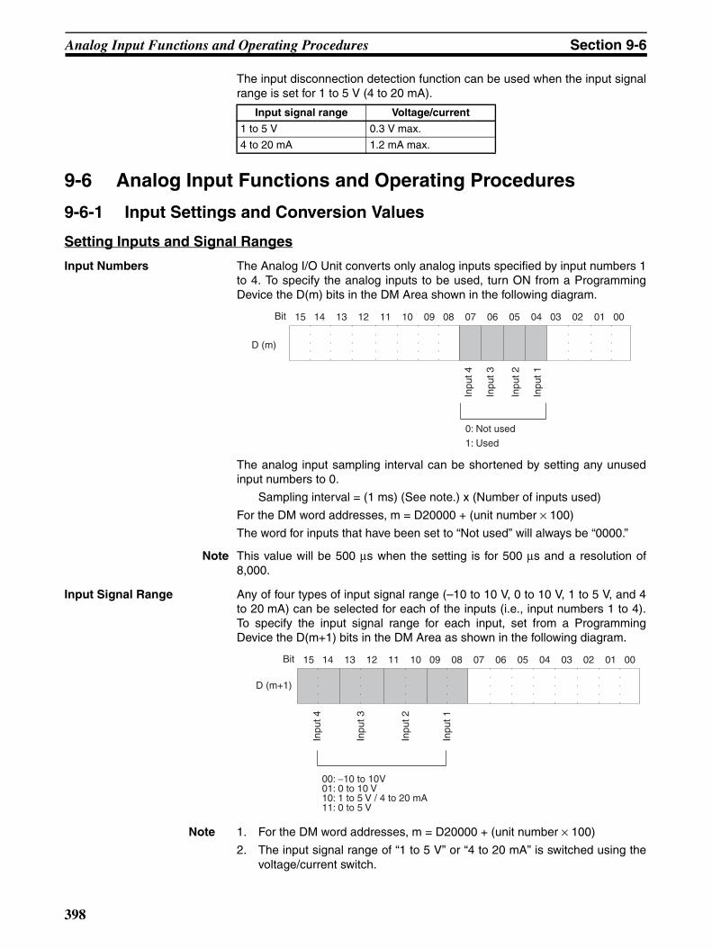
Analog Input Functions and Operating Procedures Section 9-6
The input disconnection detection function can be used when the input signalrange is set for 1 to 5 V (4 to 20 mA).
9-6 Analog Input Functions and Operating Procedures
9-6-1 Input Settings and Conversion Values
Setting Inputs and Signal Ranges
Input Numbers The Analog I/O Unit converts only analog inputs specified by input numbers 1to 4. To specify the analog inputs to be used, turn ON from a ProgrammingDevice the D(m) bits in the DM Area shown in the following diagram.
The analog input sampling interval can be shortened by setting any unusedinput numbers to 0.
Sampling interval = (1 ms) (See note.) x (Number of inputs used)
For the DM word addresses, m = D20000 + (unit number × 100)
The word for inputs that have been set to “Not used” will always be “0000.”
Note This value will be 500 µs when the setting is for 500 µs and a resolution of8,000.
Input Signal Range Any of four types of input signal range (–10 to 10 V, 0 to 10 V, 1 to 5 V, and 4to 20 mA) can be selected for each of the inputs (i.e., input numbers 1 to 4).To specify the input signal range for each input, set from a ProgrammingDevice the D(m+1) bits in the DM Area as shown in the following diagram.
Note 1. For the DM word addresses, m = D20000 + (unit number × 100)
2. The input signal range of “1 to 5 V” or “4 to 20 mA” is switched using thevoltage/current switch.
Input signal range Voltage/current
1 to 5 V 0.3 V max.
4 to 20 mA 1.2 mA max.
15 14 13 12 11 10 09 08 07 06 05 04 03 02 01 00Bit
D (m)
Inpu
t 2
Inpu
t 1
0: Not used
1: Used
Inpu
t 4
Inpu
t 3
15 14 13 12 11 10 09 08 07 06 05 04 03 02 01 00Bit
D (m+1)
Inpu
t 2
Inpu
t 1
00: −10 to 10 V01: 0 to 10 V10: 1 to 5 V / 4 to 20 mA11: 0 to 5 V
Inpu
t 4
Inpu
t 3
398

Analog Input Functions and Operating Procedures Section 9-6
3. After making the DM settings from a Programming Device, it will be neces-sary to either turn the power to the PLC OFF and ON, or turn ON the Spe-cial I/O Unit Restart Bit in order to transfer the contents of the DM settingsto the Special I/O Unit.
Voltage/Current Range Setting
When “1 to 5 V, 4 to 20 mA” is selected for the input signal range, either the “1to 5 V” or “4 to 20 mA” range can then be selected by means of the D (m+35)setting. Adjusting the factory-set voltage and current can improve the accu-racy of current output specifications.
Reading Conversion Values
Analog input conversion values are stored for each input number, in CIOwords n+5 to n+8.
Note For the CIO word addresses, n = CIO 2000 + (unit number × 10).
Use MOV(021) or XFER(070) to read conversion values in the user program.
Example 1 In this example, the conversion data from only one input is read. (The unitnumber is 0.)
Example 2 In this example, the conversion data from multiple inputs is read. (The unitnumber is 0.)
For details regarding conversion value scaling, refer to Scaling on page 446.
15 14 13 12 11 10 09 08 07 06 05 04 03 02 01 00Bit
D (m+35)
Inpu
t 2
Inpu
t 1
0: Voltage: 1 V to 5 V
1: Current 4 mA to 20 mA
Inpu
t 4
Inpu
t 3
Word Function Stored value
n+5 Input 1 conversion value 16-bit binary data
n+6 Input 2 conversion value
n+7 Input 3 conversion value
n+8 Input 4 conversion value
MOV(021)
2005
D00001
Input conditionConversion data in CIO word 2005 (input number 1) is read to D00001.
XFER(070)
#0004
2005
D00001
Input conditionConversion data in CIO words 2005 and 2008 (input num-bers 1 and 4) is read to D00001 and D00004.
399
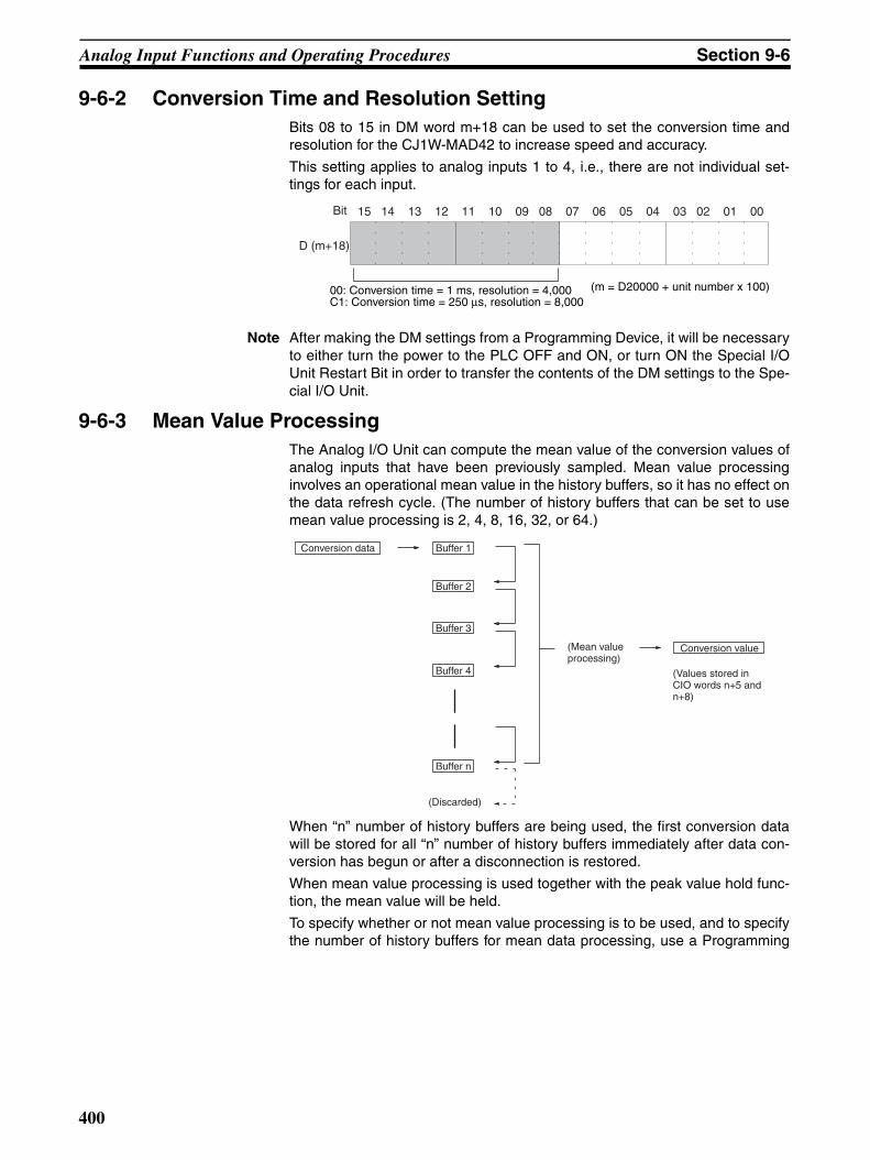
Analog Input Functions and Operating Procedures Section 9-6
9-6-2 Conversion Time and Resolution Setting
Bits 08 to 15 in DM word m+18 can be used to set the conversion time andresolution for the CJ1W-MAD42 to increase speed and accuracy.
This setting applies to analog inputs 1 to 4, i.e., there are not individual set-tings for each input.
Note After making the DM settings from a Programming Device, it will be necessaryto either turn the power to the PLC OFF and ON, or turn ON the Special I/OUnit Restart Bit in order to transfer the contents of the DM settings to the Spe-cial I/O Unit.
9-6-3 Mean Value ProcessingThe Analog I/O Unit can compute the mean value of the conversion values ofanalog inputs that have been previously sampled. Mean value processinginvolves an operational mean value in the history buffers, so it has no effect onthe data refresh cycle. (The number of history buffers that can be set to usemean value processing is 2, 4, 8, 16, 32, or 64.)
When “n” number of history buffers are being used, the first conversion datawill be stored for all “n” number of history buffers immediately after data con-version has begun or after a disconnection is restored.
When mean value processing is used together with the peak value hold func-tion, the mean value will be held.
To specify whether or not mean value processing is to be used, and to specifythe number of history buffers for mean data processing, use a Programming
15 14 13 12 11 10 09 08 07 06 05 04 03 02 01 00Bit
D (m+18)
00: Conversion time = 1 ms, resolution = 4,000C1: Conversion time = 250 µs, resolution = 8,000
(m = D20000 + unit number x 100)
Conversion data Buffer 1
Buffer 2
Buffer 3
Buffer 4
Buffer n
(Mean value processing)
Conversion value
(Values stored in CIO words n+5 and n+8)
(Discarded)
400

Analog Input Functions and Operating Procedures Section 9-6
Device to make the settings in D(m+6) to D(m+9) as shown in the followingtable.
For the DM word addresses, m = D20000 + (unit number × 100)
Note After making the DM settings from a Programming Device, it will be necessaryto either turn the power to the PLC OFF and ON, or turn ON the Special I/OUnit Restart Bit to transfer the contents of the DM settings to the Special I/OUnit.
The history buffer moving average is calculated as shown below. (In thisexample, there are four buffers.)
1,2,3... 1. With the first cycle, Data 1 is stored in all the history buffers.
Mean value = (Data 1 + Data 1 + Data 1 + Data 1) ÷ 4
2. With the second cycle, Data 2 is stored in the first history buffer.
Mean value = (Data 2 + Data 1 + Data 1 + Data 1) ÷ 4
3. With the third cycle, Data 3 is stored in the first history buffer.
Mean value = (Data 3 + Data 2 + Data 1 + Data 1) ÷ 4
DM word Function Set value
D (m+6) Input 1 mean value processing 0000: Mean value processing with 2 buffers0001: No mean value processing0002: Mean value processing with 4 buffers0003: Mean value processing with 8 buffers0004: Mean value processing with 16 buffers0005: Mean value processing with 32 buffers0006: Mean value processing with 64 buffers
D (m+7) Input 2 mean value processing
D (m+8) Input 3 mean value processing
D (m+9) Input 4 mean value processing
(Mean value processing)
Conversion value
Data 1
Data 1
Data 1
Data 1
(Mean value processing)
Conversion value
Data 2
Data 1
Data 1
Data 1
(Mean value processing)
Conversion value
Data 3
Data 2
Data 1
Data 1
401

Analog Input Functions and Operating Procedures Section 9-6
4. With the fourth cycle, the Data 4 is stored in the first history buffer.
Mean value = (Data 4 + Data 3 + Data 2 + Data 1) ÷ 4
5. With the fifth cycle, Data 5 is stored in the first history buffer.
Mean value = (Data 5 + Data 4 + Data 3 + Data 2) ÷ 4
When a disconnection is restored, the mean value processing function beginsagain from step 1.
Note 1. The default setting for mean value processing in the Analog I/O Unit ismean value processing with 2 buffers.
2. When the mean value processing function is used, the delay in refreshingconverted data for input signal changes will be as shown in the followingdiagram.
3. Specify “no mean value processing” to follow conversion of a rapid changein input signals.
Response Time for a Resolution of 1 ms/4,000
Unit: ms
(Mean value processing)
Conversion value
Data 4
Data 3
Data 2
Data 1
(Mean value processing)
Conversion value
Data 5
Data 4
Data 3
Data 2
Input signal to the Unit (V)
Conversion data
Time (ms)
Time (ms)
t: Delay
For V = 20 V (−10 to 10 V)When Resolution is 1 ms/4,000
• For One Wordt = n + (2 to 3)
• For m Words (1 < m ≤ 4)No averaging (n = 1) or two averaging buffers (n = 2)t = n × (m + 2)For n averaging buffers (4 ≤ n ≤ 64)t = (n − 2) × m + 10.5
When Resolution is 500 µs/8,000• For One Word
t = [n + (2 to 3)] × 1/4• For m Words (1 < m ≤ 4)
No averaging (n = 1) or two averaging buffers (n = 2)t = n × (m + 2) × 1/2For n averaging buffers (4 ≤ n ≤ 64)t = [(n − 2) × m + 10.5] × 1/2
m n64 32 16 8 4 2 1
4 258.5 130.5 66.5 34.5 18.5 12 63 196.5 100.5 52.5 28.5 16.5 10 5
402

Analog Input Functions and Operating Procedures Section 9-6
Response Time for a Resolution of 500 µs/8,000
Unit: ms
The above response times are not affected by the number of analog I/O pointsthat are used.
Symbols m: Number of input words used in DM Arean: Average number of buffers set for the input number for which to find theresponse time
Calculation Example The following example calculations are for a resolution of 8,000 with an appli-cation using inputs 1 and 8, 64 averaging buffers set for input 1, and no aver-aging set for input 8.
• Response time for input 1: t = (64 − 2) × 2 + 10.5 × 1/2 = 67.25 (ms)
• Response time for input 1: t = 1 × (2 + 2) × 1/2 = 2 (ms)
9-6-4 Peak Value Hold FunctionThe peak value hold function holds the maximum digital conversion value forevery input (including mean value processing). This function can be used withanalog input. The following diagram shows how digital conversion values areaffected when the peak value hold function is used.
2 134.5 70.5 38.5 22.5 14.5 8 41 67 35 19 11 7 5 3
m n64 32 16 8 4 2 1
m n64 32 16 8 4 2 1
4 129.25 65.25 33.25 17.25 9.25 6 33 98.25 50.25 26.25 14.25 8.25 5 2.52 67.25 35.25 19.25 11.25 7.25 4 21 33.5 17.5 9.5 5.5 3.5 2.5 1.5
Peak value hold
Digital conversion value
t (Time)
Conversion value when the peak value hold function is used
403
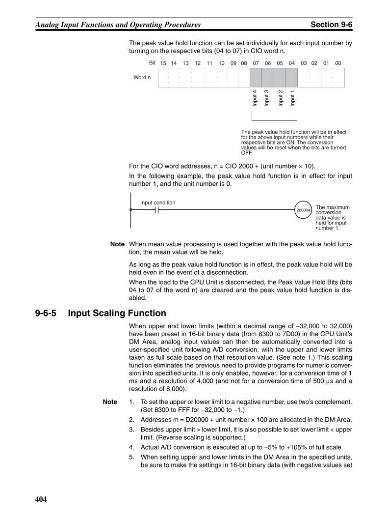
Analog Input Functions and Operating Procedures Section 9-6
The peak value hold function can be set individually for each input number byturning on the respective bits (04 to 07) in CIO word n.
For the CIO word addresses, n = CIO 2000 + (unit number × 10).
In the following example, the peak value hold function is in effect for inputnumber 1, and the unit number is 0.
Note When mean value processing is used together with the peak value hold func-tion, the mean value will be held.
As long as the peak value hold function is in effect, the peak value hold will beheld even in the event of a disconnection.
When the load to the CPU Unit is disconnected, the Peak Value Hold Bits (bits04 to 07 of the word n) are cleared and the peak value hold function is dis-abled.
9-6-5 Input Scaling FunctionWhen upper and lower limits (within a decimal range of −32,000 to 32,000)have been preset in 16-bit binary data (from 8300 to 7D00) in the CPU Unit’sDM Area, analog input values can then be automatically converted into auser-specified unit following A/D conversion, with the upper and lower limitstaken as full scale based on that resolution value. (See note 1.) This scalingfunction eliminates the previous need to provide programs for numeric conver-sion into specified units. It is only enabled, however, for a conversion time of 1ms and a resolution of 4,000 (and not for a conversion time of 500 µs and aresolution of 8,000).
Note 1. To set the upper or lower limit to a negative number, use two’s complement.(Set 8300 to FFF for −32,000 to −1.)
2. Addresses m = D20000 + unit number × 100 are allocated in the DM Area.
3. Besides upper limit > lower limit, it is also possible to set lower limit < upperlimit. (Reverse scaling is supported.)
4. Actual A/D conversion is executed at up to −5% to +105% of full scale.
5. When setting upper and lower limits in the DM Area in the specified units,be sure to make the settings in 16-bit binary data (with negative values set
15 14 13 12 11 10 09 08 07 06 05 04 03 02 01 00Bit
Inpu
t 2
Inpu
t 1
Word n
The peak value hold function will be in effect for the above input numbers while their respective bits are ON. The conversion values will be reset when the bits are turned OFF.
Inpu
t 4
Inpu
t 3
200004
Input conditionThe maximum conversion data value is held for input number 1.
404

Analog Input Functions and Operating Procedures Section 9-6
as two’s complement). For decimal numbers −32,000 to +32,000, set 16-bit binary data (8300 to 7D00).
6. The scaling function is enabled for only a conversion time of 1 ms and aresolution of 4,000 (and not for a conversion time of 500 µs and a resolu-tion of 8,000).
7. The scaling function cannot be used when the ratio conversion function isused.
8. If the scaling upper limit equals the lower limit, or if the scaling upper limitor lower limit is outside the range of ±32,000, a scaling data setting error isgenerated and scaling cannot be executed. Operation starts normallywhen both the upper and lower limits are set to 0000 (the default values).
Setting Upper and Lower Limits for Input Scaling
Set the scaling upper and lower limits for inputs 1 to 4 in words m+27 to m+34of the DM Area, as shown below.
Note For decimal numbers −32,000 to +32,000, set 16-bit binary data (8300 to7D00).
Example Setting 1 Set the following conditions in D (m+27) to D (m+34). (The values shown inparentheses are binary data.)
When Input Signal Range is 0 V to 10 V
The following table shows the correspondence between input signals andconverted scaling values. (The values shown in parentheses are binary data.)
DM word Bits
15 14 13 12 11 10 9 8 7 6 5 4 3 2 1 0
D (m+27) Input 1 scaling lower limit
D (m+28) Input 1 scaling upper limit
D (m+29) Input 2 scaling lower limit
D (m+30) Input 2 scaling upper limit
D (m+31) Input 3 scaling lower limit
D (m+32) Input 3 scaling upper limit
D (m+33) Input 4 scaling lower limit
D (m+34) Input 4 scaling upper limit
Setting condition Set value
Input signal range 0 to 10 V
Scaling lower limit 0000 (0000)
Scaling upper limit 10,000 (2710)
Input signal Conversion result
0 V 0000 (0000)
10 V 10,000 (2710)
Offset upper limit 10500 (2904)
Scaling upper limit 10000 (2710)
Scaling lower limit −500 (FE0C)Offset lower limit 0000 (0000)
Scaling line
0 V
−0.5 V
+10.0 V
+10.5 V
405

Analog Input Functions and Operating Procedures Section 9-6
Example Setting 2 (Reverse Scaling)
Set the following conditions in D (m+27) to D (m+34). (The values shown inparentheses are binary data.)
When Input Signal Range is 0 V to 10 V (Reverse Scaling)
The following table shows the correspondence between input signals andconverted scaling values. (The values shown in parentheses are binary data.)
9-6-6 Input Disconnection Detection FunctionWhen an input signal range of 1 to 5 V (4 to 20 mA) is used, input circuit dis-connections can be detected. The detection conditions for each of the inputsignal ranges are shown in the following table.
The current/voltage level will fluctuate according to the offset/gain adjustment.
−0.5 V −500 (FE0C)
10.5 V 10,500 (2904)
Input signal Conversion result
Setting condition Set value
Input signal range 0 to 10 V
Scaling lower limit 10000 (2710)
Scaling upper limit 0000 (0000)
Input signal Conversion result
0 V 10,000 (2710)
10 V 0000 (0000)
−0.5 V 10,500 (2904)
10.5 V −500 (FE0C)
Scaling line
10500 (2904)10000 (2710)
0000 (0000)−500 (EFC0)
0 V
−0.5 V
+10.5 V+10 V
Range Current/voltage
1 to 5 V 0.3 V max.
4 to 20 mA 1.2 mA max.
406

Analog Output Functions and Operating Procedures Section 9-7
The input disconnection detection signals for each input number are stored inbits 04 to 07 of CIO word n+9. Specify these bits as execution conditions touse disconnection detection in the user’s program.
For the CIO word addresses, n = CIO 2000 + (unit number × 10).
The conversion value during a disconnection will be 0000.
In the following example, the conversion value is read only if there is no dis-connection at analog input number 1. (The unit number is 0.)
9-7 Analog Output Functions and Operating Procedures
9-7-1 Output Settings and Conversions
Setting Outputs and Signal Ranges
Output Numbers The Analog I/O Unit converts analog outputs specified by output numbers 1 to2 only. To specify the analog outputs to be used, turn ON from a ProgrammingDevice the D(m) bits in the DM Area shown in the following diagram.
The analog output conversion cycle can be shortened by setting any unusedoutput numbers to 0.
Conversion cycle = (1 ms) (See note 3.) × (Number of outputs used)
Note 1. For the DM word addresses, m = D20000 + (unit number × 100).
2. Output numbers not used (set to 0) will be output at 0 V.
15 14 13 12 11 10 09 08 07 06 05 04 03 02 01 00Bit
Inpu
t 2
Inpu
t 1
Word n+9
The respective bit turns ON when a disconnection is detected for a given input. When the disconnection is restored, the bit turns OFF.
Inpu
t 4
Inpu
t 3
MOV (021)
2005
D00001
200904
The conver-sion value in CIO word 2005 (input number 1) is read to D00001.
15 14 13 12 11 10 09 08 07 06 05 04 03 02 01 00Bit
D(m)
Out
put 2
Out
put 1
0: Not used1: Used
407

Analog Output Functions and Operating Procedures Section 9-7
3. This value will be 500 µs when the setting is for 500 µs and a resolution of8,000.
Output Signal Range Any of four types of output signal range (–10 to 10 V, 0 to 10 V, 1 to 5 V/4 to20 mA, and 0 to 5 V) can be selected for each of the outputs (i.e., output num-bers 1 to 4). To specify the output signal range for each output, use a Pro-gramming Device to set the D (m+1) bits in the DM Area shown in thefollowing diagram.
Note 1. For the DM word addresses, m = D20000 + (unit number × 100).
2. After making the DM settings from a Programming Device, it will be neces-sary to either turn the power to the PLC OFF and ON, or turn ON the Spe-cial I/O Unit Restart Bit to transfer the contents of the DM settings to theSpecial I/O Unit.
Voltage/Current Range Setting
When “1 to 5 V, 4 to 20 mA” is selected for the output signal range, either the“1 to 5 V” or “4 to 20 mA” range can then be selected by means of the D(m+35) setting. Adjusting the factory-set voltage and current can improve theaccuracy of current output specifications.
Writing Set Values Analog output set values are written to CIO words (n+1) and (n+2).
For the CIO word addresses, n = CIO 2000 + (unit number × 10).
Use MOV(021) or XFER(070) to write values in the user program.
15 14 13 12 11 10 09 08 07 06 05 04 03 02 01 00Bit
D (m+1)
Out
put 2
Out
put 1
00: −10 to 10 V01: 0 to 10 V10: 1 to 5 V/4 to 20 mA11: 0 to 5 V
15 14 13 12 11 10 09 08 07 06 05 04 03 02 01 00Bit
D (m+35)
Out
put 2
Out
put 1
0: Voltage: 1 V to 5 V1: Current 4 mA to 20 mA
Word Function Stored value
n+1 Output 1 set value 16-bit binary data
n+2 Output 2 set value
408
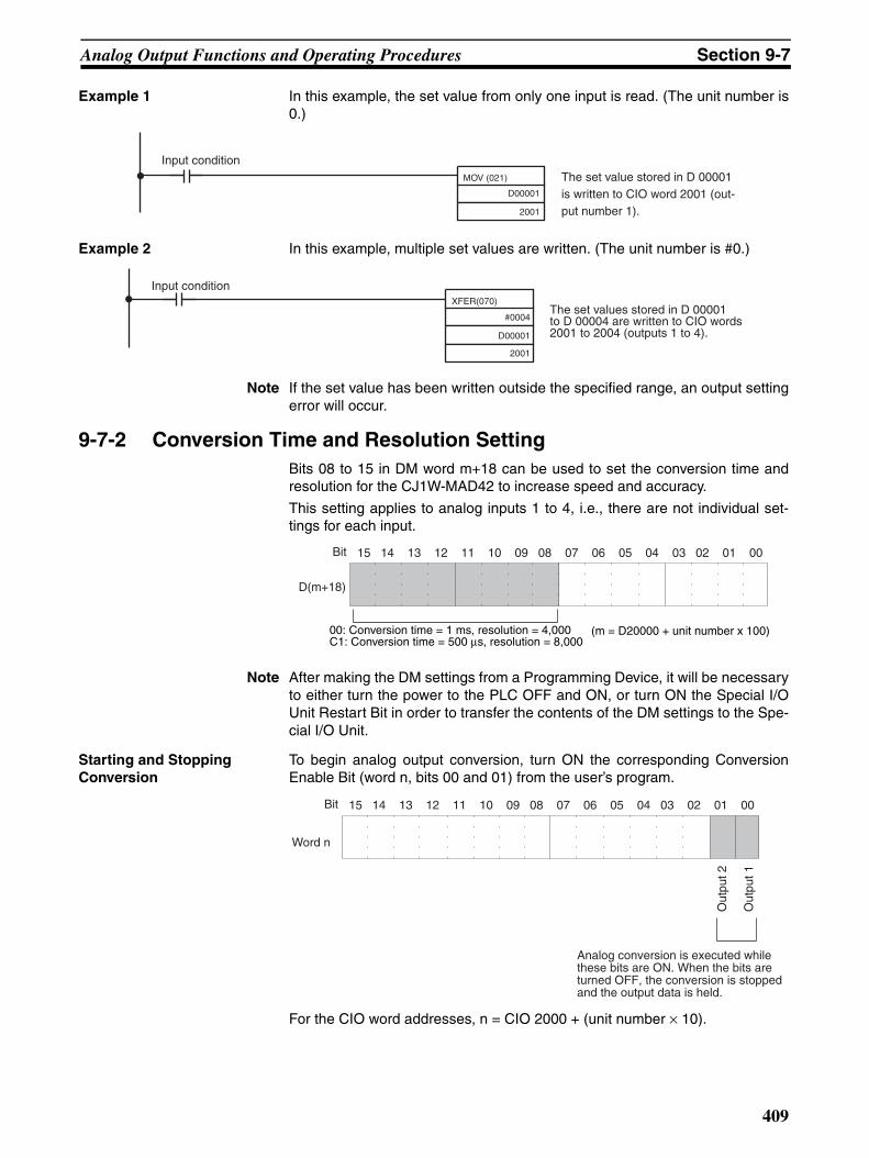
Analog Output Functions and Operating Procedures Section 9-7
Example 1 In this example, the set value from only one input is read. (The unit number is0.)
Example 2 In this example, multiple set values are written. (The unit number is #0.)
Note If the set value has been written outside the specified range, an output settingerror will occur.
9-7-2 Conversion Time and Resolution Setting
Bits 08 to 15 in DM word m+18 can be used to set the conversion time andresolution for the CJ1W-MAD42 to increase speed and accuracy.
This setting applies to analog inputs 1 to 4, i.e., there are not individual set-tings for each input.
Note After making the DM settings from a Programming Device, it will be necessaryto either turn the power to the PLC OFF and ON, or turn ON the Special I/OUnit Restart Bit in order to transfer the contents of the DM settings to the Spe-cial I/O Unit.
Starting and Stopping Conversion
To begin analog output conversion, turn ON the corresponding ConversionEnable Bit (word n, bits 00 and 01) from the user’s program.
For the CIO word addresses, n = CIO 2000 + (unit number × 10).
MOV (021)
D00001
2001
Input conditionThe set value stored in D 00001 is written to CIO word 2001 (out-put number 1).
XFER(070)
#0004
D00001
2001
Input condition
The set values stored in D 00001to D 00004 are written to CIO words 2001 to 2004 (outputs 1 to 4).
15 14 13 12 11 10 09 08 07 06 05 04 03 02 01 00Bit
D(m+18)
00: Conversion time = 1 ms, resolution = 4,000C1: Conversion time = 500 µs, resolution = 8,000
(m = D20000 + unit number x 100)
15 14 13 12 11 10 09 08 07 06 05 04 03 02 01 00Bit
Out
put 2
Out
put 1
Word n
Analog conversion is executed while these bits are ON. When the bits are turned OFF, the conversion is stopped and the output data is held.
409
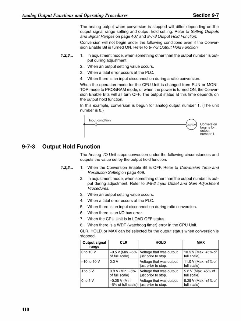
Analog Output Functions and Operating Procedures Section 9-7
The analog output when conversion is stopped will differ depending on theoutput signal range setting and output hold setting. Refer to Setting Outputsand Signal Ranges on page 407 and 9-7-3 Output Hold Function.
Conversion will not begin under the following conditions even if the Conver-sion Enable Bit is turned ON. Refer to 9-7-3 Output Hold Function.
1,2,3... 1. In adjustment mode, when something other than the output number is out-put during adjustment.
2. When an output setting value occurs.
3. When a fatal error occurs at the PLC.
4. When there is an input disconnection during a ratio conversion.
When the operation mode for the CPU Unit is changed from RUN or MONI-TOR mode to PROGRAM mode, or when the power is turned ON, the Conver-sion Enable Bits will all turn OFF. The output status at this time depends onthe output hold function.
In this example, conversion is begun for analog output number 1. (The unitnumber is 0.)
9-7-3 Output Hold FunctionThe Analog I/O Unit stops conversion under the following circumstances andoutputs the value set by the output hold function.
1,2,3... 1. When the Conversion Enable Bit is OFF. Refer to Conversion Time andResolution Setting on page 409.
2. In adjustment mode, when something other than the output number is out-put during adjustment. Refer to 9-9-2 Input Offset and Gain AdjustmentProcedures.
3. When an output setting value occurs.
4. When a fatal error occurs at the PLC.
5. When there is an input disconnection during ratio conversion.
6. When there is an I/O bus error.
7. When the CPU Unit is in LOAD OFF status.
8. When there is a WDT (watchdog timer) error in the CPU Unit.
CLR, HOLD, or MAX can be selected for the output status when conversion isstopped.
200000
Input conditionConversion begins for output number 1.
Output signal range
CLR HOLD MAX
0 to 10 V –0.5 V (Min. –5% of full scale)
Voltage that was output just prior to stop.
10.5 V (Max. +5% of full scale)
–10 to 10 V 0.0 V Voltage that was output just prior to stop.
11.0 V (Max. +5% of full scale)
1 to 5 V 0.8 V (Min. –5% of full scale)
Voltage that was output just prior to stop.
5.2 V (Max. +5% of full scale)
0 to 5 V –0.25 V (Min. –5% of full scale)
Voltage that was output just prior to stop.
5.25 V (Max. +5% of full scale)
410
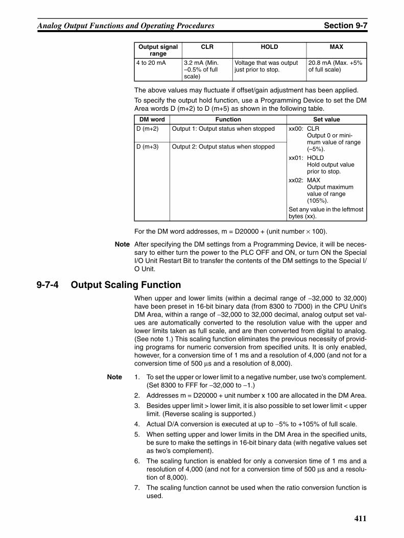
Analog Output Functions and Operating Procedures Section 9-7
The above values may fluctuate if offset/gain adjustment has been applied.
To specify the output hold function, use a Programming Device to set the DMArea words D (m+2) to D (m+5) as shown in the following table.
For the DM word addresses, m = D20000 + (unit number × 100).
Note After specifying the DM settings from a Programming Device, it will be neces-sary to either turn the power to the PLC OFF and ON, or turn ON the SpecialI/O Unit Restart Bit to transfer the contents of the DM settings to the Special I/O Unit.
9-7-4 Output Scaling FunctionWhen upper and lower limits (within a decimal range of −32,000 to 32,000)have been preset in 16-bit binary data (from 8300 to 7D00) in the CPU Unit’sDM Area, within a range of −32,000 to 32,000 decimal, analog output set val-ues are automatically converted to the resolution value with the upper andlower limits taken as full scale, and are then converted from digital to analog.(See note 1.) This scaling function eliminates the previous necessity of provid-ing programs for numeric conversion from specified units. It is only enabled,however, for a conversion time of 1 ms and a resolution of 4,000 (and not for aconversion time of 500 µs and a resolution of 8,000).
Note 1. To set the upper or lower limit to a negative number, use two’s complement.(Set 8300 to FFF for −32,000 to −1.)
2. Addresses m = D20000 + unit number x 100 are allocated in the DM Area.
3. Besides upper limit > lower limit, it is also possible to set lower limit < upperlimit. (Reverse scaling is supported.)
4. Actual D/A conversion is executed at up to −5% to +105% of full scale.
5. When setting upper and lower limits in the DM Area in the specified units,be sure to make the settings in 16-bit binary data (with negative values setas two’s complement).
6. The scaling function is enabled for only a conversion time of 1 ms and aresolution of 4,000 (and not for a conversion time of 500 µs and a resolu-tion of 8,000).
7. The scaling function cannot be used when the ratio conversion function isused.
4 to 20 mA 3.2 mA (Min. –0.5% of full scale)
Voltage that was output just prior to stop.
20.8 mA (Max. +5% of full scale)
DM word Function Set value
D (m+2) Output 1: Output status when stopped xx00: CLROutput 0 or mini-mum value of range (–5%).
xx01: HOLDHold output value prior to stop.
xx02: MAXOutput maximum value of range (105%).
Set any value in the leftmost bytes (xx).
D (m+3) Output 2: Output status when stopped
Output signal range
CLR HOLD MAX
411

Analog Output Functions and Operating Procedures Section 9-7
8. If the scaling upper limit equals the lower limit, or if the scaling upper limitor lower limit is outside the range of ±32,000, a scaling data setting error isgenerated and scaling cannot be executed. Operation starts normallywhen both the upper and lower limits are set to 0000 (the default values).
Setting Upper and Lower Limits for Output Scaling
Set the scaling upper and lower limits for outputs 1 and 2 in words D (m+19)to D (m+22) of the DM Area, as shown below.
Note For decimal numbers −32,000 to +32,000, set 16-bit binary data (8300 to7D00).
Example Setting 1 Set the following conditions in D (m+19) to D (m+22). (The values shown inparentheses are binary data.)
When Output Signal Range is 0 V to 10 V
The following table shows the correspondence between output signals andconverted scaling values. (The values shown in parentheses are 16-bit binarydata.)
Example Setting 2 (Reverse Scaling)
Set the following conditions in D (m+27) to D (m+34). (The values shown inparentheses are binary data.)
DM word Bits
15 14 13 12 11 10 9 8 7 6 5 4 3 2 1 0
D (m+19) Output 1 scaling lower limit
D (m+20) Output 1 scaling upper limit
D (m+21) Output 2 scaling lower limit
D (m+22) Output 2 scaling upper limit
Setting condition Set value
Output signal range 0 to 10 V
Scaling lower limit 0000 (0000)
Scaling upper limit 10,000 (2710)
Output set value Output signal
0000 (0000) 0 V
10,000 (2710) 10 V
−500 (FE0C) −0.5 V
10,500 (2904) 10.5 V
+10.5 V+10 V
0 V−0.5 V 0000 (0000)
−500 (FE0C)
Scaling line
10500 (2904)
10000 (2710)
Setting condition Set value
Output signal range 0 to 10 V
Scaling lower limit 10000 (2710)
Scaling upper limit 0000 (0000)
412
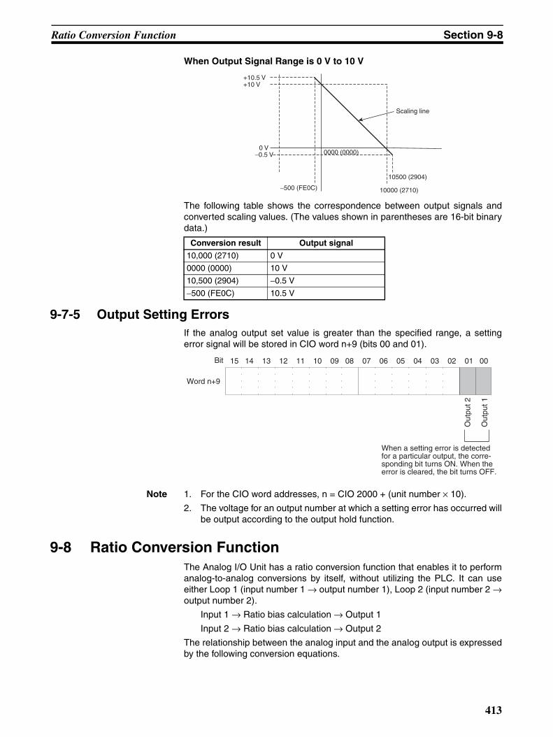
Ratio Conversion Function Section 9-8
When Output Signal Range is 0 V to 10 V
The following table shows the correspondence between output signals andconverted scaling values. (The values shown in parentheses are 16-bit binarydata.)
9-7-5 Output Setting ErrorsIf the analog output set value is greater than the specified range, a settingerror signal will be stored in CIO word n+9 (bits 00 and 01).
Note 1. For the CIO word addresses, n = CIO 2000 + (unit number × 10).
2. The voltage for an output number at which a setting error has occurred willbe output according to the output hold function.
9-8 Ratio Conversion FunctionThe Analog I/O Unit has a ratio conversion function that enables it to performanalog-to-analog conversions by itself, without utilizing the PLC. It can useeither Loop 1 (input number 1 → output number 1), Loop 2 (input number 2 →output number 2).
Input 1 → Ratio bias calculation → Output 1
Input 2 → Ratio bias calculation → Output 2
The relationship between the analog input and the analog output is expressedby the following conversion equations.
Conversion result Output signal
10,000 (2710) 0 V
0000 (0000) 10 V
10,500 (2904) −0.5 V
−500 (FE0C) 10.5 V
+10.5 V+10 V
0 V−0.5 V 0000 (0000)
−500 (FE0C)
Scaling line
10500 (2904)
10000 (2710)
15 14 13 12 11 10 09 08 07 06 05 04 03 02 01 00Bit
Out
put 2
Out
put 1
Word n+9
When a setting error is detected for a particular output, the corre-sponding bit turns ON. When the error is cleared, the bit turns OFF.
413

Ratio Conversion Function Section 9-8
Positive Gradient Conversion
(Analog output) = A × (Analog input) + B
A: Ratio set value 0 to 99.99 (BCD)B: Bias 8000 to 7FFF (16-bit binary data)
The following example is for an I/O range of –10 to 10 V.
Constant A: 0050 (0.5)Constant B: 0190 (2.0 V)
Analog input: –10 to 10 VAnalog output = 0.5 × (–10 to 10 V) + 2.0 V
= –3.0 to 7.0 V
Note The scaling function cannot be used simultaneously with the ration conversionfunction.
Negative Gradient Conversion
(Analog output) = F – A x (Analog input) + B
F: Output range maximum valueA: Ratio set value 0 to 99.99 (BCD)B: Bias 8000 to 7FFF (16-bit binary data)
The following example is for an I/O range of 0 to 10 V.
Constant A: 1000 (10.0)Constant B: 0068 (0.5 V)F: 10 V (output range maximum value) Analog input: 0 to 1 VAnalog output = 10 V – 10 × (0 to 1 V) + 0.5 V
= 10.5 to 0.5 V
X
Y A = YX
BA
Analog output
Analog input
F+BA
X
Y
A =YX
Analog output
Analog input
414

Ratio Conversion Function Section 9-8
Specifying Ratio Conversion Function
To specify the use of Loop 1 and Loop 2 and their I/O relationships, set bits 08to 11 of DM Area word D (m) as shown in the following diagram.
The response time of ratio conversion (input-to-output conversion) is 850 µsfor a resolution of 4,000 and 420 µs for a resolution of 8,000.
For the DM word addresses, m = D20000 + (unit number × 100).
Specifying Ratio Set Value and Bias
The ratio set value (A) and the bias (B) are set in the DM words from D(m+10)to D (m+13).
For the DM word addresses, m = D20000 + (unit number × 100).
Note 1. After making the DM settings from a Programming Device, it will be neces-sary to either turn the power to the PLC OFF and ON, or turn ON the Spe-cial I/O Unit Restart Bit to transfer the contents of the DM settings to theSpecial I/O Unit. For details regarding the Special I/O Unit Restart Bit, referto 9-10-4 Restarting Special I/O Units.
2. The calculation results will be output in digital values to word n+5 (Loop 1)and word n+6 (Loop 2).
3. If an input cable is disconnected, the calculation value will become 0000,and the analog output value will be output according to the output holdfunction.
4. If the output value exceeds the specified signal range due to the ratio con-version of the digital input value, the calculation result and analog outputwill be given as the lower or upper-limit value.
15 14 13 12 11 10 09 08 07 06 05 04 03 02 01 00Bit
D (m)
Loop 2 Loop 1
00: Not used.01: Uses positive gradient conversion.10: Uses negative gradient conversion.11: Same as 10 above.
DM word Function Set value
D (m+10) Loop 1 (input 1 → output 1), A constant
BCD 0 to 9999 (0.00 to 99.99; unit: 0.01)
D (m+11) Loop 1 (input 1 → output 1), B constant
16-bit binary data
D (m+12) Loop 2 (input 2 → output 2), A constant
BCD 0 to 9999 (0.00 to 99.99; unit: 0.01)
D (m+13) Loop 2 (input 2 → output 2), B constant
16-bit binary data
415

Adjusting Offset and Gain Section 9-9
9-9 Adjusting Offset and GainThese functions can be used to calibrate inputs or outputs according to thedevices that are connected.
Input Calibration Function When the resolution is set to 4,000, this function takes an output device’s off-set voltage (or current) and gain voltage (or current) as the analog input con-version data 0000 and 0FA0 (or 07D0 when the range is ±10 V). For example,when used in a range of 1 to 5 V, a range of 0.8 to 4.8 V may be output even ifthe external device specifications are for 1 to 5 V. In such cases, when theexternal device outputs an offset voltage of 0.8 V, the converted data at theAnalog Input Unit will be FF38, at a resolution of 4,000. When a gain voltageof 4.8 V is output, the converted data will be 0EDA. With the offset and gainadjustment functions, when 0.8 V and 4.8 V are input, then the values areconverted to 0000 and 0FA0 respectively (instead of FF38 and 0EDA).
(Resolution: 8,000)
Input Calibration Function This function adjusts output voltages according to input device offset valuesand gain values, and takes the presently set values of the Unit to be 0000 and00FA0 (or 07D0 when the range is ±10 V) respectively. For example, assumethat the specifications for an external input device (such as a display device)are 100.0 to 500.0. If voltage is output by the Analog Output Unit at a setvalue of 0000, and the actual display at the external input device shows not100.0 but 100.5, the output voltage can be adjusted (lowered in this case) sothat the display will show 100.0, and the set value (FFFB in this case) whenthe display shows exactly 100.0 can be set as 0000.
Similarly, for the gain value, if the Analog Output Unit outputs voltage at a setvalue of 0FA0, and the actual display at the external input device shows not500.0 but 500.5, the output voltage can be adjusted (lowered in this case) sothat the display will show 500.0, and the set value (0F9B in this case) whenthe display shows exactly 500.0 can be set as 0FA0.
(Resolution: 8,000)
Output device offset and gain
voltage
Converted data before adjustment
Converted data after adjustment
0.8 V FF38 (FE70) 0000 (0000)
4.8 V 0EDA (0DB4) 0FA0 (1F40)
Display at external input device
Set value before adjustment (word n+8)
Set value after adjustment
100.0 FFFB (FFFD) 0000 (0000)
500.0 0F9B (1F36) 0FA0 (1F40)
416

Adjusting Offset and Gain Section 9-9
9-9-1 Adjustment Mode Operational FlowThe adjustment mode enables the input or output of the connected devices tobe calibrated. Refer to 2-7 Adjusting Offset and Gain and 5-7 Adjusting Offsetand Gain for details of input and output functions. The following diagramshows the flow of operations when using the adjustment mode for adjustingoffset and gain.
!Caution Set the PLC to PROGRAM mode when using the Analog I/O Unit in adjust-ment mode. If the PLC is in MONITOR mode or RUN mode, the Analog I/OUnit will stop operating, and the input and output values that existed immedi-ately before this stoppage will be retained.
Turn ON the PLC.
When adjusting another I/O number
When adjusting the same I/O number
Set the I/O number.
Offset adjustment
Offset Bit ON
Set Bit ON
The ADJ indicator will flash while in adjustment mode.
Start up the PLC in PROGRAM mode.
Gain adjustment
Gain Bit ON
Input adjustment Output adjustment
Set Bit ON
Input adjustment Output adjustment
Set D(m+18) to adjustment mode.
Restart the Unit using the Special I/O Unit Restart Bitor turn the power supply to the PLC OFF and ON.
Write the I/O number to be adjusted in the rightmost byte of CIO word n.
(Bit 0 of CIO word n+1 turns ON.)
Sampling input
Adjustment value setting
(Add inputs so that conversion value becomes 0.)
(Bits 2 and 3 of CIO word n+1 turn ON.)
(Bit 4 of CIO word n+1 turns ON.)
(Bit 1 of CIO word n+1 turns ON.)
Sampling input
Adjustment value setting
(Add inputs so that conversion value is maximized.)
(Bits 2 and 3 of CIO word n+1 turn ON.)
(Bit 4 of CIO word n+1 turns ON.)
Set D(m+18) to normal mode.
Restart the Unit using the Special I/O Unit Restart Bitor turn the power supply to the PLC OFF and ON.
417

Adjusting Offset and Gain Section 9-9
!Caution Always perform adjustments in conjunction with offset and gain adjustments.
Note Input adjustments can be performed more accurately in conjunction withmean value processing.
9-9-2 Input Offset and Gain Adjustment ProceduresSpecifying Input Number to be Adjusted
To specify the input number to be adjusted, write the value to the rightmostbyte of CIO word n as shown in the following diagram.
For the CIO word addresses, n = CIO 2000 + (unit number x 10).
The following example uses input number 1 adjustment for illustration. (Theunit number is 0.)
Bits Used for Adjusting Offset and Gain
The CIO word (n+1) bits shown in the following diagram are used for adjustingoffset and gain.
(Rightmost)(Leftmost)
Word n
Input to be adjusted (1 to 4)I/O specification2: Input (fixed)
--- ---
CLR000000 CT00
SHIFTCH
*DM2
C0
A0
A0
AMON
2000 0000
CHG2000 0000PRES VAL ????
2C
1B
WRITE2000 0021
15 14 13 12 11 10 09 08 07 06 05 04 03 02 01 00Bit
Word n+1
Offs
et B
it
Gai
n B
it
Set
Bit
Cle
ar B
it
418

Adjusting Offset and Gain Section 9-9
Offset Adjustment The procedure for adjusting the analog input offset is explained below. Asshown in the following diagram, the offset is adjusted by sampling inputs sothat the conversion value becomes 0000.
The following example uses input number 1 adjustment for illustration. (Theunit number is 0.)
1,2,3... 1. Turn ON bit 00 (the Offset Bit) of CIO word n+1. (Hold the ON status.)
The analog input’s digital conversion values while the Offset Bit is ON willbe monitored in CIO word n+8.
2. Check whether the input devices are connected.
10 V0
0FA0
Offset adjustment input range
Input signal range:0 to 10 V
CLR000000 CT00
SHIFTCONT
# 2C
0A
0A
1B
0A
0A
MON
200100 ^ OFF
SET
200100 ^ ON
A5
A6
A7
A5
A6
A7
+
−
+
−
Voltage input
Input 1
Current input
Input 1
For current input, check that the voltage/ current switch is ON.
419

Adjusting Offset and Gain Section 9-9
3. Input the voltage or current so that the conversion value becomes 0000.The following table shows the offset adjustment voltages and currents tobe input according to the input signal range.
4. After inputting the voltage or current so that the conversion value for theanalog input terminal is 0000, turn ON bit 04 (the Set Bit) of CIO word n+1,and then turn it OFF again.
While the Offset Bit is ON, the offset value will be saved to the Unit’s EE-PROM when the Set Bit turns ON.
5. To finish the offset adjustment, turn OFF bit 00 (the Offset Bit) of CIO wordn+1.
!Caution Do not turn OFF the power supply or restart the Unit while the Set Bit is ON(data is being written to the EEPROM). Otherwise, illegal data may be writtenin the Unit’s EEPROM and “EEPROM Errors” may occur when the power sup-ply is turned ON or when the Unit is restarted, causing a malfunction.
!Caution When making adjustments, be sure to perform both the offset adjustment andgain adjustment at the same time.
Note 1. The EEPROM can be overwritten 50,000 times.
2. While the Offset Bit or the Gain Bit is ON, the present conversion data willbe displayed in word n+8.If the Offset Bit or the Gain Bit is OFF, the value immediately prior to turningthe bit OFF will be held.
Input signal range Input range Word (n+8) monitoring value
0 to 10 V –0.5 to 0.5 V FF38 to 00C8 (FE70 to 0190)–10 to 10 V –1.0 to 1.0 V
1 to 5 V 0.8 to 1.2 V
0 to 5 V –0.25 to 0.25 V
4 to 20 mA 3.2 to 4.8 mA
(Values in parentheses are for a resolution of 8,000.)
SHIFTCONT
# 2C
0A
0A
1B
0A
4E
MON
200104 ^ OFF
SET
200104 ^ ON
RESET
200104 ^ OFF
SHIFTCONT
#2
C0
A0
A1
B0
A0
AMON
200100 ^ ON
RESET
200100 ^ OFF
420

Adjusting Offset and Gain Section 9-9
Gain Adjustment The procedure for adjusting the analog input gain is explained below. Asshown in the following diagram, the gain is adjusted by sampling inputs sothat the conversion value is maximized.
The following example uses input number 1 adjustment for illustration. (Theunit number is 0.)
1,2,3... 1. Turn ON bit 01 (the Gain Bit) of CIO word n+1. (Hold the ON status.)
The analog input’s digital conversion values while the Gain Bit is ON willbe monitored in CIO word n+8.
2. Check whether the input devices are connected.
10 V0
0FA0
Input signal range:0 to 10 V
Gain adjustment input range
SHIFTCONT
#2
C0
A0
A
1B
0A
1B
MON
200101 ^ OFF
SET
200101 ^ ON
+
−
+
−
Voltage input
Input 1
Current input
Input 1
A5
A6
A7
A5
A6
A7
For current input, check that the voltage/ current switch is ON.
421
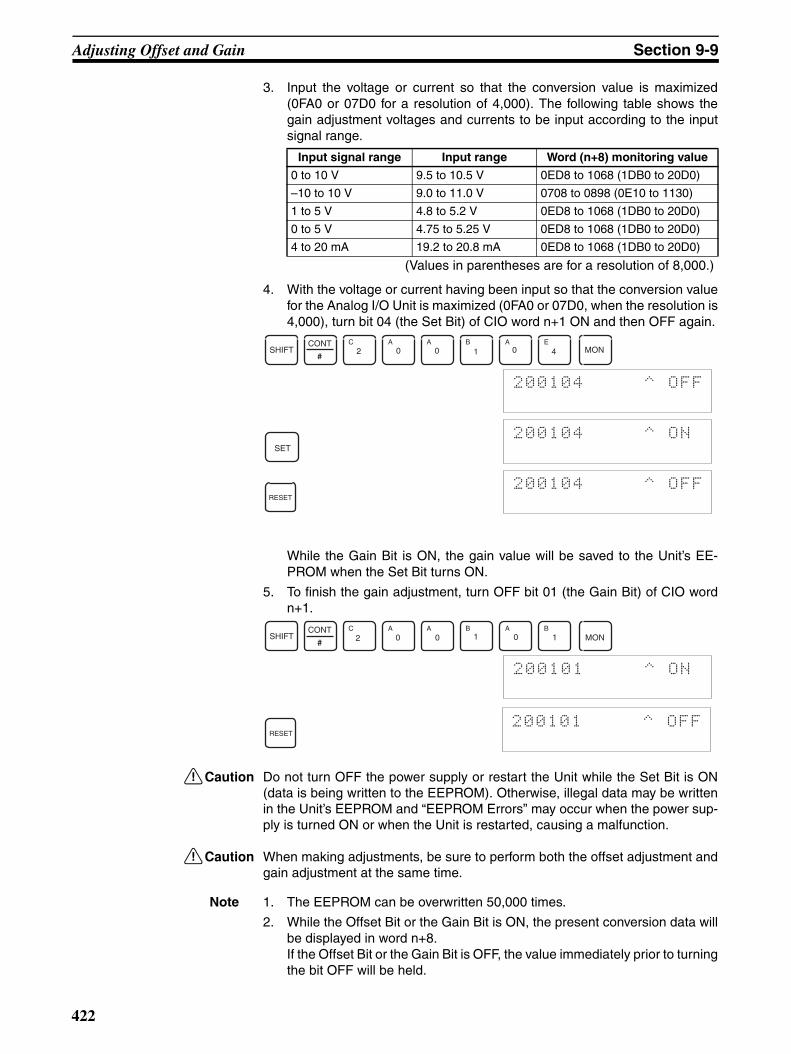
Adjusting Offset and Gain Section 9-9
3. Input the voltage or current so that the conversion value is maximized(0FA0 or 07D0 for a resolution of 4,000). The following table shows thegain adjustment voltages and currents to be input according to the inputsignal range.
4. With the voltage or current having been input so that the conversion valuefor the Analog I/O Unit is maximized (0FA0 or 07D0, when the resolution is4,000), turn bit 04 (the Set Bit) of CIO word n+1 ON and then OFF again.
While the Gain Bit is ON, the gain value will be saved to the Unit’s EE-PROM when the Set Bit turns ON.
5. To finish the gain adjustment, turn OFF bit 01 (the Gain Bit) of CIO wordn+1.
!Caution Do not turn OFF the power supply or restart the Unit while the Set Bit is ON(data is being written to the EEPROM). Otherwise, illegal data may be writtenin the Unit’s EEPROM and “EEPROM Errors” may occur when the power sup-ply is turned ON or when the Unit is restarted, causing a malfunction.
!Caution When making adjustments, be sure to perform both the offset adjustment andgain adjustment at the same time.
Note 1. The EEPROM can be overwritten 50,000 times.
2. While the Offset Bit or the Gain Bit is ON, the present conversion data willbe displayed in word n+8.If the Offset Bit or the Gain Bit is OFF, the value immediately prior to turningthe bit OFF will be held.
Input signal range Input range Word (n+8) monitoring value
0 to 10 V 9.5 to 10.5 V 0ED8 to 1068 (1DB0 to 20D0)
–10 to 10 V 9.0 to 11.0 V 0708 to 0898 (0E10 to 1130)
1 to 5 V 4.8 to 5.2 V 0ED8 to 1068 (1DB0 to 20D0)
0 to 5 V 4.75 to 5.25 V 0ED8 to 1068 (1DB0 to 20D0)
4 to 20 mA 19.2 to 20.8 mA 0ED8 to 1068 (1DB0 to 20D0)
(Values in parentheses are for a resolution of 8,000.)
SHIFTCONT
#2
C0
A0
A1
B0
A4
EMON
200104 ^ OFF
SET
200104 ^ ON
RESET
200104 ^ OFF
SHIFTCONT
# 2C
0A
0A
1B
0A
1B
MON
200101 ^ ON
RESET200101 ^ OFF
422

Adjusting Offset and Gain Section 9-9
Clearing Offset and Gain Adjusted Values
Follow the procedure outlined below to return the offset and gain adjusted val-ues to their default settings.
The following example uses input number 1 adjustment for illustration. (Theunit number is 0.)
1,2,3... 1. Turn ON bit 05 (the Clear Bit) of CIO word n+1. (Hold the ON status.) Re-gardless of the input value, 0000 will be monitored in CIO word n+8.
2. Turn bit 04 of CIO word n+1 ON and then OFF again.
While the Clear Bit is ON, the adjusted value will be cleared and reset tothe default offset and gain values when the Set Bit turns ON.
3. To finish the clearing of adjusted values, turn OFF bit 05 (the Clear Bit) ofCIO word n+1.
!Caution Do not turn OFF the power supply or restart the Unit while the Set Bit is ON(data is being written to the EEPROM). Otherwise, illegal data may be writtenin the Unit’s EEPROM and “EEPROM Errors” may occur when the power sup-ply is turned ON or when the Unit is restarted, causing a malfunction.
!Caution When making adjustments, be sure to perform both the offset adjustment andgain adjustment at the same time.
Note The EEPROM can be overwritten 50,000 times.
SHIFTCONT
# 2C
0A
0A
1B
0A
5F
MON
200105 ^ OFF
SET200105 ^ ON
SHIFTCONT
# 2C
0A
0A
1B
0A
4E
MON
200104 ^ OFF
SET
200104 ^ ON
RESET
200104 ^ OFF
SHIFTCONT
#2
C0
A0
A1
B0
A
5F
MON
200105 ^ ON
RESET
200105 ^ OFF
423

Adjusting Offset and Gain Section 9-9
9-9-3 Output Offset and Gain Adjustment ProceduresSpecifying Output Number to be Adjusted
To specify the output number to be adjusted, write the value to the rightmostbyte of CIO word n as shown in the following diagram.
For the CIO word addresses, n = CIO 2000 + unit number × 10.
The following example uses output number 1 adjustment for illustration. (Theunit number is 0.)
Bits Used for Adjusting Offset and Gain
The CIO word n+1 bits shown in the following diagram are used for adjustingoffset and gain.
Offset Adjustment The procedure for adjusting the analog output offset is explained below. Asshown in the following diagram, the set value is adjusted so that the analogoutput reaches the standard value (0 V/1 V/4 mA).
(Rightmost)(Leftmost)
Word n
Output to be adjusted (1 and 2)
--- ---
I/O specification 1: Output (fixed)
CLR000000 CT00
SHIFTCH
*DM2
C0
A0
A0
AMON
2000 0000
CHG2000 0000PRES VAL ????
1B
1B
WRITE2000 0011
15 14 13 12 11 10 09 08 07 06 05 04 03 02 01 00Bit
Word n+1
Cle
ar B
it
Set
Bit
Up
Bit
Dow
n B
it
Gai
n B
it
Offs
et B
it
10 V
00FA0
Offset adjustment output range
Output signal range:0 to 10 V
424
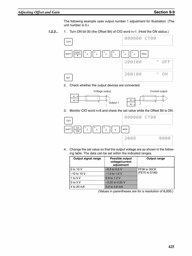
Adjusting Offset and Gain Section 9-9
The following example uses output number 1 adjustment for illustration. (Theunit number is 0.)
1,2,3... 1. Turn ON bit 00 (the Offset Bit) of CIO word n+1. (Hold the ON status.)
2. Check whether the output devices are connected.
3. Monitor CIO word n+8 and check the set value while the Offset Bit is ON.
4. Change the set value so that the output voltage are as shown in the follow-ing table. The data can be set within the indicated ranges.
Output signal range Possible output voltage/current
adjustment
Output range
0 to 10 V –0.5 to 0.5 V FF38 to 00C8 (FE70 to 0190)–10 to 10 V –1.0 to 1.0 V
1 to 5 V 0.8 to 1.2 V
0 to 5 V –0.25 to 0.25 V
4 to 20 mA 3.2 to 4.8 mA
(Values in parentheses are for a resolution of 8,000.)
CLR000000 CT00
SHIFTCONT
#2
C0
A0
A1
B0
A0
AMON
200100 ^ OFF
SET
200100 ^ ON
A1
A2
Voltage output
Output 1A2
A3
Current output
CLR000000 CT00
SHIFTCH
*DM2
C0
A0
A8 MON
2008 0000
425

Adjusting Offset and Gain Section 9-9
Change the set value, using the Up Bit (bit 03 of word n+1) and the DownBit (bit 02 of word n+1).
• The following example increases the output voltage.
The bit will remain ON until the output becomes an appropriate value, atwhich time, it will turn OFF.
• The following example decreases the output voltage.
The bit will remain ON until the output becomes an appropriate value, atwhich time, it will turn OFF.
15 14 13 12 11 10 09 08 07 06 05 04 03 02 01 00Bit
Up Bit Down Bit
While the Up Bit is ON, the set value will be increased by 1 resolution every 0.5 seconds. After it has been ON for 3 seconds, the set value will be increased by 1 resolution every 0.1 seconds.
While the Down Bit is ON, the set value will be decreased by 1 resolution every 0.5 seconds. After it has been ON for 3 seconds, the set value will be decreased by 1 resolution every 0.1 seconds.
Word n+1
SHIFTCONT
#2
C0
A0
A1
B0
A3
DMON
200103 ^ OFF
SET
200103 ^ ON
RESET
200103 ^ OFF
SHIFTCONT
# 2C
0A
0A
1B
0A
2C
MON
200102 ^ OFF
SET
200102 ^ ON
RESET
200102 ^ OFF
426

Adjusting Offset and Gain Section 9-9
5. Check the 0-V/1-V/4 mA output, and then turn bit 04 (the Set Bit) of CIOword n+1 ON and then OFF again.
While the Offset Bit is ON, the offset value will be saved to the Unit’s EE-PROM when the Set Bit turns ON.
6. To finish the offset adjustment, turn OFF bit 00 (the Offset Bit) of CIO wordn+1.
!Caution Do not turn OFF the power supply or restart the Unit while the Set Bit is ON(data is being written to the EEPROM). Otherwise, illegal data may be writtenin the Unit’s EEPROM and “EEPROM Errors” may occur when the power sup-ply is turned ON or when the Unit is restarted, causing a malfunction.
!Caution When making adjustments, be sure to perform both the offset adjustment andgain adjustment at the same time.
Note The EEPROM can be overwritten 50,000 times.
Gain Adjustment The procedure for adjusting the analog output gain is explained below. Asshown in the following diagram, the set value is adjusted so that the analogoutput is maximized (to 10 V/5 V/20 mA).
SHIFTCONT
# 2C
0A
0A
1B
0A
4E
MON
200104 ^ OFF
SET
200104 ^ ON
RESET
200104 ^ OFF
SHIFTCONT
#2
C0
A0
A1
B0
A0
AMON
200100 ^ ON
SET
200100 ^ OFF
10 V
00FA0
Output signal range:0 to 10 V
Gain adjustment output range
427

Adjusting Offset and Gain Section 9-9
The following example uses output number 1 adjustment for illustration. (Theunit number is 0.)
1,2,3... 1. Turn ON bit 01 (the Gain Bit) of CIO word n+1. (Hold the ON status.)
2. Check whether the output devices are connected.
3. Monitor CIO word n+8 and check the set value while the Gain Bit is ON.
4. Change the set value so that the output voltage is as shown in the followingtable. The data can be set within the indicated ranges.
Output signal range Possible output voltage/current
adjustment
Output range
0 to 10 V 9.5 to 10.5 V 0ED8 to 1068 (1DB0 to 20D0)
–10 to 10 V 9.0 to 11.0 V 0708 to 0898 (0E10 to 1130)
1 to 5 V 4.8 to 5.2 V 0ED8 to 1068 (1DB0 to 20D0)
0 to 5 V 4.75 to 5.25 V 0ED8 to 1068 (1DB0 to 20D0)
4 to 20 mA 19.2 to 20.8 mA 0ED8 to 1068 (1DB0 to 20D0)
(Values in parentheses are for a resolution of 8,000.)
CLR000000 CT00
SHIFTCONT
# 2C
0A
0A
1B
0A
1B
MON
200101 ^ OFF
SET
200101 ^ ON
A1
A2
Voltage output
Output 1
Current output
A2
A3
CLR
000000 CT00
SHIFTCH
*DM 2C
0A
0A
8 MON
2008 0000
428

Adjusting Offset and Gain Section 9-9
Change the set value, using the Up Bit (bit 03 of word n+1) and the DownBit (bit 02 of word n+1).
• The following example increases the output voltage.
The bit will remain ON until the output voltage becomes an appropriate val-ue, at which time, the output will turn OFF.
• The following example decreases the output voltage.
The bit will remain ON until the output voltage becomes an appropriate val-ue, at which time, the output will turn OFF.
Up Bit Down Bit
While the Up Bit is ON, the set value will be increased by 1 resolution every 0.5 seconds. After it has been ON for 3 seconds, the set value will be increased by 1 resolution every 0.1 seconds.
While the Down Bit is ON, the set value will be decreased by 1 resolution every 0.5 seconds. After it has been ON for 3 seconds, the set value will be decreased by 1 resolution every 0.1 seconds.
Word n+1
15 14 13 12 11 10 09 08 07 06 05 04 03 02 01 00Bit
SHIFTCONT
#2
C0
A0
A1
B0
A3
DMON
200103 ^ OFF
SET
200103 ^ ON
RESET
200103 ^ OFF
SHIFTCONT
# 2C
0A
0A
1B
0A
2C
MON
200102 ^ OFF
SET
200102 ^ ON
RESET
200102 ^ OFF
429

Adjusting Offset and Gain Section 9-9
5. Check the 10 V/5 V/20 mA output, and then turn bit 04 (the Set Bit) of CIOword n+1 ON and then OFF again.
While the Gain Bit is ON, the gain value will be saved to the Unit’s EE-PROM when the Set Bit turns ON.
6. To finish the gain adjustment, turn OFF bit 01 (the Gain Bit) of CIO wordn+1.
!Caution Do not turn OFF the power supply or restart the Unit while the Set Bit is ON(data is being written to the EEPROM). Otherwise, illegal data may be writtenin the Unit’s EEPROM and “EEPROM Errors” may occur when the power sup-ply is turned ON or when the Unit is restarted, causing a malfunction.
!Caution When making adjustments, be sure to perform both the offset adjustment andgain adjustment at the same time.
Note The EEPROM can be overwritten 50,000 times.
Clearing Offset and Gain Adjusted Values
Follow the procedure outlined below to return the offset and gain adjusted val-ues to their default settings.
The following example uses output number 1 adjustment for illustration. (Theunit number is 0.)
1,2,3... 1. Turn ON bit 05 (the Clear Bit) of CIO word n+1. (Hold the ON status.) Re-gardless of the set value, 0000 will be monitored in CIO word n+8.
SHIFTCONT
# 2C
0A
0A
1B
0A
4E
MON
200104 ^ OFF
SET
200104 ^ ON
RESET
200104 ^ OFF
SHIFTCONT
#2
C0
A0
A1
B0
A1
BMON
200101 ^ ON
RESET
200101 ^ OFF
SHIFTCONT
# 2C
0A
0A
1B
0A
5F
MON
200105 ^ OFF
SET
200105 ^ ON
430

Adjusting Offset and Gain Section 9-9
2. Turn bit 04 of CIO word n+1 ON and then OFF again.
While the Clear Bit is ON, the adjusted value will be cleared and reset tothe default offset and gain values when the Set Bit turns ON.
3. To finish the clearing of adjusted values, turn OFF bit 05 (the Clear Bit) ofCIO word n+1.
!Caution Do not turn OFF the power supply or restart the Unit while the Set Bit is ON(data is being written to the EEPROM). Otherwise, illegal data may be writtenin the Unit’s EEPROM and “EEPROM Errors” may occur when the power sup-ply is turned ON or when the Unit is restarted, causing a malfunction.
Note The EEPROM can be overwritten 50,000 times.
SHIFTCONT
# 2C
0A
0A
1B
0A
4E
MON
200104 ^ OFF
SET
200104 ^ ON
RESET
200104 ^ OFF
SHIFTCONT
#2
C
0A
0A
1B
0A
5F
MON
200105 ^ ON
RESET
200105 ^ OFF
431

Handling Errors and Alarms Section 9-10
9-10 Handling Errors and Alarms
9-10-1 Indicators and Error FlowchartIndicators If an alarm or error occurs in the Analog I/O Unit, the ERC or ERH indicators
on the front panel of the Unit will light.
LED Meaning Indicator Operating status
RUN (green) Operating Lit Operating in normal mode.
Not lit Unit has stopped exchanging data with the CPU Unit.
ERC (red) Unit has detected an error
Lit Alarm has occurred (such as disconnec-tion detection) or initial settings are incor-rect.
Not lit Operating normally.
ERH (red) Error in the CPU Unit
Lit Error has occurred during data exchange with the CPU Unit.
Not lit Operating normally.
ADJ (yellow) Adjusting Flashing Operating in offset/gain adjustment mode.
Not lit Other than the above.
Front panel of Unit
RUN
ERC
ADJ
ERH
432
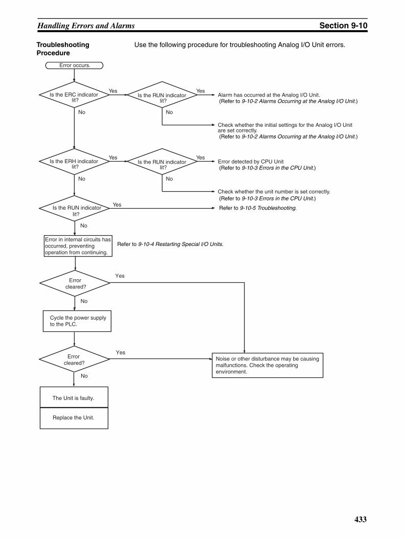
Handling Errors and Alarms Section 9-10
Troubleshooting Procedure
Use the following procedure for troubleshooting Analog I/O Unit errors.
Is the ERC indicator lit?
Yes
No
Is the RUN indicator lit?
Yes
No
Alarm has occurred at the Analog I/O Unit.
Check whether the initial settings for the Analog I/O Unit are set correctly.
Is the ERH indicator lit?
Yes
No
Is the RUN indicator lit?
Yes
No
Error detected by CPU Unit
Check whether the unit number is set correctly.
Error occurs.
Yes
No
Is the RUN indicator lit?
Error cleared?
No
Cycle the power supplyto the PLC.
Error cleared?
No
The Unit is faulty.
Replace the Unit.
YesNoise or other disturbance may be causingmalfunctions. Check the operating environment.
Yes
Error in internal circuits has occurred, preventing operation from continuing.
(Refer to 9-10-2 Alarms Occurring at the Analog I/O Unit.)
Refer to 9-10-5 Troubleshooting.
(Refer to 9-10-2 Alarms Occurring at the Analog I/O Unit.)
(Refer to 9-10-3 Errors in the CPU Unit.)
(Refer to 9-10-3 Errors in the CPU Unit.)
Refer to 9-10-4 Restarting Special I/O Units.
433

Handling Errors and Alarms Section 9-10
9-10-2 Alarms Occurring at the Analog I/O UnitWhen an alarm occurs at the Analog I/O Unit, the ERC indicator lights and theAlarm Flags are stored in bits 08 to 15 of CIO word n+9.
ERC and RUN Indicators: Lit
The ERC and RUN indicators will be lit when an error occurs while the Unit isoperating normally. The following alarm flags will turn ON in CIO word n+9.These alarm flags will turn OFF automatically when the error is cleared.
Note Disconnection detection operates for input numbers used with a range of 1 to5 V (4 to 20 mA).
For the CIO word addresses, n = CIO 2000 + (unit number x 10).
Word n+9
Output setting errorsAlarm Flags
15 14 13 12 11 10 09 08 07 06 05 04 03 02 01 00Bit
Disconnection Detection Flags(See 9-6-6 Input Disconnection Detection Function.)
(See 9-7-5 Output Setting Errors.)
RUN
ERC
ERH
: Lit
: Not lit
Word n + 9 Alarm flag Error contents I/O status Countermeasure
Bits 00 and 01 Output Set Value Error
The output setting range has been exceeded.
Output value set by output hold function.
Correct the set value.
Bits 04 to 07 Disconnection Detection
A disconnection was detected. (See note.)
Conversion data becomes 0000.
Check the rightmost byte of CIO word n+9. The inputs for bits that are ON may be discon-nected. Restore any discon-nected inputs.
Bit 14 (Adjustment mode)
EEPROM Writ-ing Error
An EEPROM writing error has occurred while in adjustment mode.
Holds the out-put status imme-diately prior to the error.
Turn the Set Bit OFF, ON, and OFF again.
If the error persists even after the reset, replace the Analog I/O Unit.
434

Handling Errors and Alarms Section 9-10
ERC Indicator and RUN Indicator: Lit, ADJ Indicator: Flashing
This alarm will occur in the case of incorrect operation while in the adjustmentmode. In adjustment mode, the Adjustment Mode ON Flag will turn ON in bit15 of CIO word n+9.
Note When a PLC error occurs in the adjustment mode, Unit operations will stopoperating. (The input and output values immediately prior to the error will beheld.)
ERC Indicator: Lit, RUN Indicator: Not Lit
The ERC indicator will be lit when the initial settings for the Analog I/O Unitare not set correctly. The alarm flags for the following errors will turn ON in
RUN
ERC
ERH
ADJ
: Lit
: Flashing
: Not lit
Word n + 9 Alarm flag Error contents I/O status Countermeasure
Bit 12 (Adjustment mode)Input Value Adjustment Range Exceeded
In adjustment mode, offset or gain cannot be adjusted because input value is out of the permissible range for adjust-ment.
Conversion data corresponding to the input sig-nal is monitored in word n+8.
If making the adjustment by means of a connected input device, first adjust the input device before adjusting the Ana-log I/O Unit.
Bit 13 (Adjustment mode)
I/O Number Set-ting Error
In adjustment mode, adjust-ment cannot be performed because the specified input or output number is not set for use or because the wrong input or output number is specified.
Holds the values immediately prior to the error. No data is changed.
Check whether the word n input or output number to be adjusted is set from 11 to 14, or 21 to 24.Check whether the input or out-put number to be adjusted is set for use by means of the DM set-ting.
Bit 15 only ON (Adjustment Mode)
PLC Error
The PLC is in either MONITOR or RUN mode while the Analog I/O Unit is operating in adjust-ment mode.
Holds the values immediately prior to the error. No data is changed.
Change the setting in bits 00 to 07 of D(m+18) and then either turn the power supply to the PLC OFF and ON or turn ON the Special I/O Unit Restart Bit.
RUN
ERC
ERH
: Lit
: Not lit
435

Handling Errors and Alarms Section 9-10
CIO word n+9. These alarm flags will turn OFF when the error is cleared andthe Unit is restarted, or the Special I/O Unit Restart Bit is turned ON and thenOFF again.
9-10-3 Errors in the CPU UnitWhen errors occur in the CPU Unit or I/O bus, and I/O refresh with the SpecialI/O Unit is not performed correctly resulting in the Analog I/O Unit malfunction-ing, the ERH indicator will be lit.
ERH and RUN Indicators: Lit
The ERH and RUN indicators will be lit if an error occurs in the I/O bus caus-ing a WDT (watchdog timer) error in the CPU Unit, resulting in incorrect I/Orefresh with the Analog I/O Unit.
Turn ON the power supply again or restart the system.For further details, refer to CJ-series Programmable Controllers OperationManual (W393).
Note No error will be detected by the CPU Unit or displayed on the ProgrammingConsole, because the CPU Unit is continuing operation.
Word n + 9 Alarm flag Error contents I/O status Countermeasure
Bit 08 Ratio Conver-sion Use Set-ting Error
The I/O number for the ratio con-version function has been set to be not used.
Conversion does not start and data becomes 0000.
Set the I/O number for use.
Scaling Data Setting Error
There is a mistake in the upper or lower limit setting when scal-ing is used. The set value is exceeded, the upper limit equals the lower limit (not 0000), etc.
Correct the settings.
Bit 09 Ratio Set Value Error
A number outside of the 0 to 9999 BCD range has been specified for the ratio set value.
Specify a number from 0 to 9999 BCD.
Bit 10 Output Hold Setting Error
The wrong output status for when conversion is stopped has been specified.
Specify a number from 0000 to 0002.
Bit 11 Mean Value Processing Set-ting Error
The wrong number of samplings has been specified for mean processing.
Specify a number from 0000 to 0006.
Bit 12 Conversion Time/Resolu-tion, Operation Mode Setting Error
The conversion time/resolution setting or operation mode set-ting is incorrect.
Set 00 hex or C1 hex.
RUN
ERC
ERH
: Lit
: Not lit
Error Error contents Input condition Output condition
I/O bus error Error has occurred during data exchange with the CPU Unit.
Conversion data becomes 0000.
Depends on the output hold function.
CPU Unit monitoring error (See note.)
No response from CPU Unit during fixed period.
Maintains the condition exist-ing before the error.
Maintains the condition exist-ing before the error.
CPU Unit WDT error Error has been generated in CPU Unit.
Changes to undefined state. Depends on the output hold function.
436
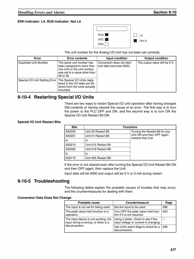
Handling Errors and Alarms Section 9-10
ERH Indicator: Lit, RUN Indicator: Not Lit
The unit number for the Analog I/O Unit has not been set correctly.
9-10-4 Restarting Special I/O UnitsThere are two ways to restart Special I/O Unit operation after having changedDM contents or having cleared the cause of an error. The first way is to turnthe power to the PLC OFF and ON, and the second way is to turn ON theSpecial I/O Unit Restart Bit ON.
Special I/O Unit Restart Bits
If the error is not cleared even after turning the Special I/O Unit Restart Bit ONand then OFF again, then replace the Unit.
Input data will be 0000 and output will be 0 V or 0 mA during restart.
9-10-5 TroubleshootingThe following tables explain the probable causes of troubles that may occur,and the countermeasures for dealing with them.
Conversion Data Does Not Change
RUN
ERC
ERH
: Lit
: Not lit
Error Error contents Input condition Output condition
Duplicate Unit Number The same unit number has been assigned to more than one Unit or the unit number was set to a value other than 00 to 95.
Conversion does not start and data becomes 0000.
The output value will be 0 V.
Special I/O Unit Setting Error The Special I/O Units regis-tered in the I/O table are dif-ferent from the ones actually mounted.
Bits Functions
A50200 Unit #0 Restart Bit Turning the Restart Bit for any Unit ON and then OFF again restarts that Unit.
A50201 Unit #1 Restart Bit
to to
A50215 Unit #15 Restart Bit
A50300 Unit #16 Restart Bit
to to
A50715 Unit #95 Restart Bit
Probable cause Countermeasure Page
The input is not set for being used. Set the input to be used. 398
The peak value hold function is in operation.
Turn OFF the peak value hold func-tion if it is not required.
403
The input device is not working, the input wiring is wrong, or there is a disconnection.
Using a tester, check to see if the input voltage or current is changing.
---
Use Unit’s alarm flags to check for a disconnection.
406
437

Handling Errors and Alarms Section 9-10
Value Does Not Change as Intended
Conversion Values are Inconsistent
Analog Output Does Not Change
Output Does Not Change as Intended
Outputs are Inconsistent
Probable cause Countermeasure Page
The input device’s signal range does not match the input signal range for the relevant input number at the Analog I/O Unit.
Check the specifications of the input device, and match the settings for the input signal ranges.
371
The offset and gain are not adjusted.
Adjust the offset and gain. 416
When using the 4 mA to 20 mA range, the voltage/current switch is not turned ON.
Turn ON the voltage/current switch. 376, 383
The voltage and current ranges are not set in D (m+35).
Set D (m+35) correctly. 399
The ratio conversion function is set to be used, so the calculation results are being monitored.
Correct the conversion settings. 434
Probable cause Countermeasure Page
The input signals are being affected by external noise.
Change the shielded cable connec-tion to the Unit’s COM terminal.
388
Insert a 0.01-µF to 0.1-µF ceramic capacitor or film capacitor between the input’s (+) and (–) terminals.
---
Try increasing the number of mean value processing buffers.
400
Probable Cause Countermeasure Page
The output is not set for being used. Set the output to be used. 407
The output hold function is in opera-tion.
Turn ON the Output Conversion Enable Bit.
410
The conversion value is set outside of the permissible range.
Set the data within the range. 373, 407
Probable Cause Countermeasure Page
The output signal range setting is wrong.
Correct the output signal range set-ting.
408
The I/O specifications of the output device do not match those of the Analog I/O Unit (e.g., input signal range, input impedance).
Change the output device. 369
The offset or gain is not adjusted. Adjust the offset or gain. 416
The voltage and current ranges are not set in D (m+35).
Set D (m+35) correctly. 399
The ratio conversion function is set to be used.
Correct the conversion settings. 413
Probable Cause Countermeasure Page
The output signals are being affected by external noise.
Try changing the shielded cable connection (e.g., the grounding at the output device).
---
438

Appendix ADimensions
CS-series Units: CS1W-AD041-V1/081-V1, CS1W-DA08V/08C/041, CS1W-MAD44
CS1W-AD161
101
12635
130
118.03
100.534.5
130
439

Dimensions Appendix A
CS-series Unit Terminal Block Dimensions
CJ-series Units: CJ1W-AD041-V1/081-V1/042, CJ1W-DA021/041/08V/08C/042V, CJ1W-MAD42
Terminal size: M3
MACHNo.
AD081RUNERCERH B1 A1ADJ
x101
x100
09
8765 4 321
09
8765 4 321
ON1
2
MODE
2.731
90
2.7
8965
440

Dimensions Appendix A
CJ-series Unit Terminal Block Dimensions
Note The appearance varies with the model.
17.58.2
6.4
7.62
74.77
441

Dimensions Appendix A
442

Appendix BSample Programs
Obtaining Analog Input Conversion ValuesThis is a program for obtaining the Analog Input Unit’s input conversion values. Individual input values areobtained by MOV(021) when their Disconnection Detection Flags are OFF.
Unit Settings
Program Example
Writing Analog Output Set ValuesThis is a program for writing the Analog Output Unit’s output set values.
Unit Settings
Item Setting contents Actual settings
Unit CS1W-AD081-V1 ---
Unit number #0 Unit number switches: 00
Operation mode Normal mode Back-panel DIP switch: All OFF
Input number Inputs 1 to 8 used D20000 = 00FF
Input signal range All input numbers, 1 to 5 V D20001 = AAAA
200900
MOV(021)
2001
D00000200901
MOV(021)
2002
D00001
Conversion value
Conversion value
200907
MOV(021)
2008
D00007
Conversion value
Input 1 Disconnection Detection Flag
Input 2 Disconnection Detection Flag
Input 8 Disconnection Detection Flag
Item Setting contents Actual settings
Unit CS1W-DA08V ---
Unit number #0 Unit number switches: 00
Operation mode Normal mode Back-panel DIP switch: All OFF
Output number Output 1 used D20000 = 0001
Output signal range Output number 1, 0 to 10 V D20001 = 0001
443

Sample Programs Appendix B
Program Example
Upper and Lower-limit Alarm (Constant Monitoring)Comparisons are made to the upper and lower limits of the A/D conversion values or D/A output values fromthe beginning of operation. If they fall outside the specified range, the Alarm Flag will turn ON.
Unit Settings
Program Example
MOV(021)
D00000
2001
200900
Output Setting Error FlagReset condition
Output 1 Setting Error FlagSet value
Execution condition
Upper limit
Lower limit
Alarm FlagON
OFF
Item Setting contents Actual settings
Unit CS1W-AD081-V1 ---
Unit number #0 Unit number switches: 00
Operation mode Normal mode Back-panel DIP switch: All OFF
Input number Input 1 used D20000 = 0001
Input signal range Input number 1, 0 to 10 V D20001 = 0001
<
2001
D00000
>
2001
D00001
Operation condition
Conversion valueLower limit
Alarm Flag
Conversion valueUpper limit
444

Sample Programs Appendix B
Upper and Lower-limit Alarm (with Standby Sequence)Comparisons are made to the upper and lower limits of the A/D conversion values or D/A output values afterthe value falls within the range between the upper limit and lower limit following the beginning of operation. Ifthey fall outside the specified range, the Alarm Flag will turn ON.
Unit Settings
Program Example
Upper limit
Lower limit
Alarm FlagON
OFF
Item Setting contents Actual settings
Unit CS1W-AD081-V1 ---
Unit number #0 Unit number switches: 00
Operation mode Normal mode Back-panel DIP switch: All OFF
Input number Input 1 used D20000 = 0001
Input signal range Input number 1, 0 to 10 V D20001 = 0001
KEEP(11)
020001
<
2001
D00000
Operation condition
Conversion valueLower limit
Alarm Flag
>
2001
D00001
Conversion valueUpper limit
020001
020001
2001
D00000
Conversion valueLower limit
2001
D00001
Conversion valueUpper limit
Operation condition
445

Sample Programs Appendix B
Scaling
Using the Scaling Functions
Note This function is supported only by the CS1W-AD161, CJ1W-MAD42, CJ1W-DA08V/08C/042V, andCJ1W-AD042.
OutlineA pressure sensor is connected to analog input 1 of CJ1W-MAD42. The pressure sensor outputs an analogsignal of between 0 and 20 mA for a pressure between 0 and 500 Pa. Therefore, for a 4 to 20-mA input, abinary value of 0000 to 01F4 (0 to 500 decimal) in engineering units for the pressure in Pa is directly set usingthe MOV instruction. The analog input scaling function of the CJ1W-MAD42 is used here. Therefore, scaling inthe ladder program (using the SCL or other instruction) is not required to convert the values 0000 to 0FA0 ofthe resolution to engineering units 0000 to 01F4.
Unit Settings
Program Example
Not Using the Scaling Function
OutlineA/D conversion values are converted according to the linear function calculated from the offset and the valuesof ∆X and ∆Y, and retrieved as scaling data.
• The following example uses at resolution of 4,000 and an input signal range of 1 to 5 V where 1 to 5 V isscaled to 0000 to 0300 (0°C to 300°C).
Item Setting contents Actual settings
Unit CJ1W-MAD42 ---
Unit number #0 Unit number switches: 00
Input number Input 1 (and output 1) used D20000 = 0011
Input signal range 1 to 5 V/4 to 20 mA D20001 = 0202
Voltage/current range Current: 4 to 20 mA D20035 = 0011
Conversion time/resolution setting and operation mode
Conversion time: 1 ms, resolution: 4,000Normal mode
D20018 = 0000
Scaling settings for input 1 Lower limit: 0000 (0000 decimal)Upper limit: 01F4 (500 decimal)
D20027 (lower limit) = 0000D20028 (upper limit) 01F4
Disconnection Detection Flag for analog input 1200904
The scaled conversion value in engineering units stored in CIO 2005 is moved to D00000.
MOV (021)
2005
D00000
446

Sample Programs Appendix B
Unit Settings
Program Example• Data Flow (Unit Number 0):
Word CIO 2001 (A/D Conversion Value) → D00200 (Scaling Result)
The value of word CIO 2005 is scaled according to the linear function calculated using the offset (0000 hex),and the values of ∆X (1068 hex) and ∆Y (0315 hex). The scaled value is then stored in word D00200.
DM Area Settings
0315
0300
0000
–0015FF38
0.8 V 1 V
0000 0FA0
5 V
1068
5.2 V
0315(nY)
1068 hex(nX)
Item Setting contents Actual settings
Unit CS1W-AD081-V1 ---
Unit number #0 Unit number switches: 00
Operation mode Normal mode Back-panel DIP switch: All OFF
Input number Input 1 used D20000 = 0001
Input signal range Input number 1, 1 to 5 V D20001 = 0002
SCL2
2001
D00100
D00200
Execution condition
D00100: 0000
D00101: 1068
D00102: 0315
Offset
nX value
nY value
447

Sample Programs Appendix B
Note The value scaled using SCL2(486) is stored as positive or negative BCD data according to the status ofthe CY (Carry) Flag. To convert the BCD data into signed binary data, use the SCL3(487) instruction.
DM Area Settings
Signed Binary-to-Signed BCD ConversionA/D conversion values (16-bit binary data) are recognized as 4-digit signed binary data, and converted into 8-digit signed BCD data. When the leftmost bit is 1, the binary data is recognized as a two’s complement. The“signed BCD” data refers to BCD data that is indicated by 7-digit data and 1-digit sign (0: +; F: –).
• Conversion Graph (Horizontal Axis: Input Voltage, Vertical Axis: BCD Data)
Unit Settings
SCL2
2005
D00100
D00200
SCL3
D00200
D00300
D00400
Execution condition
D00300: 0000
D00301: 0200
D00302: 00C8
D00303: 00C8
D00304: FF9C
Offset
nX value
nY value
Maximum conversion value
Minimum conversion value
00002000
F0002000
10 V (07D0)
–10 V (F830)
00004200
F0002000
–0.5 V (FF38)
10.5 V (1068)
Input signal range: –10 to 10 V Input signal range: 0 to 10 VResolution: 4,000 Resolution: 4,000
Item Setting contents Actual settings
Unit CS1W-AD081-V1 ---
Unit number #0 Unit number switches: 00
Operation mode Normal mode Back-panel DIP switch: All OFF
Input number Input 1 used D20000 = 0001
Input signal range Input number 1, 0 to 10 V D20001 = 0001
448

Sample Programs Appendix B
Program Example• Data Flow (Unit Number 0):
Word 2001 (A/D Conversion Value) → Words 0201 and 0200 (Conversion Result)
(1) If the leftmost bit is a 1 (negative number) in 16-bit binary data, the data is reversed and the leftmost wordbecomes F000.
(2) 16-bit binary data is converted to BCD.
(3) Signed BCD data is output to words 0200 and 0201.
Square Root CalculationData expressed as quadratic curves, such as thermocouple inputs, is converted and output to linear data (0000to 4000).
Unit Settings
Item Setting contents Actual settings
Unit CS1W-AD081-V1 ---
Unit number #0 Unit number switches: 00
Operation mode Normal mode Back-panel DIP switch: All OFF
Input number Input 1 used D20000 = 0001
Input signal range Input number 1, 0 to 10 V D20001 = 0001
ANDW(034)
#8000
D00000
D00002
=ERR
MOV(021)
2001
D00000
MOV(021)
#0000
D00001
NEG (060)
D00000
D00000
MOV(021)
#F000
D00001
BCD(024)
D00000
D00000
XFER(070)
#0002
D00000
0200
Execution condition
16-bit binary data
Clears leftmost word to 0000
Adds 1 and reverses leftmost bit if it is not 0.
Sends F000 to leftmost word if the leftmost bit is not 0.
Converts to BCD.
Outputs signed BCD data to words 0200 and 0201.
(1)
(2)
(3)
449

Sample Programs Appendix B
Program Example• Data Flow (Unit Number 0): Word 2001 (A/D Conversion Value) → Word 0200 (Calculation Result)
(1) The negative number portion is added to the conversion value (word 2001).
(2) The binary data is scaled to a range of 0 to 4000.
(3) The scaling results are multiplied by 4400.
(4) The square root is calculated, and the result is output to word 0200.
DM Area SettingsInput signal range: 0 to 10 V / 1 to 5 V / 4 to 20 mA
If the result of the binary-to-BCD conversion is negative, an error will be generated by the ROOT(072) instruc-tion.
With a signal range of –10 to 10 V, scaling is executed by augmenting the negative portion (–10 V –5%). In thisprogram example, the value of D00000 is converted to 0898. Refer to Scaling on page 446 for details.
Mean Value ProcessingData is taken for the set number of samplings and the mean value is calculated.
Unit Settings
+(400)
2001
D00000
D00001
ROOT(072)
D00006
0200
SCL(194)
D00001
D00002
D00006
*B(424)
D00006
#4400
D00006
Execution condition
Conversion value + Negative number
Scaling is executed using augmented value. Result is output to word D00006.
Result of step #2 (above) is multiplied by 4400.
Square root is calculated, and result is output to word 0200.
(1)
(2)
(3)
(4)
D00000: 00C8
D00001: (Used for calculation)
D00002: 0000
D00003: 0000
D00004: 4400
D00005: 1130
D00006: (Used for calculation)
Digital value for −5%
Conversion value +C8 (−5% portion)
Lower limit: BCD
Lower limit +C8 (−5% portion): Binary
Upper limit: BCD
Upper limit +C8 (−5% portion): Binary
Used with SCL(194) instruction
Item Setting contents Actual settings
Unit CS1W-AD081-V1 ---
Unit number #0 Unit number switches: 00
Operation mode Normal mode Back-panel DIP switch: All OFF
Input number Input 1 used D20000 = 0001
Input signal range Input number 1, 0 to 10 V D20001 = 0001
450

Sample Programs Appendix B
Program Example• Data Flow (Unit Number 0): Word 2001 (AD Conversion Value) → D00001 (Mean Value Result)
LimitIf the output value range is exceeded, the output voltage is held when the Conversion Enable Flag turns OFF.
Unit Settings
Program Example
DM Area Settings
Item Setting contents Actual settings
Unit CS1W-DA08V ---
Unit number #0 Unit number switches: 00
Operation mode Normal mode Back-panel DIP switch: All OFF
Output number Output 1 used D20000 = 0001
Output signal range All output numbers, 0 to 10 V D20001 = 0001
Output hold function HOLD D20002 = 0001
AVG(195)
2001
#0064
D00001
Execution condition
Conversion value
Number of samplings
Mean value
5 V (03E8)
0 V (0000)
Set value
Actual output value
When program is started
MOV(021)
D00000
2001
Execution condition
Set value
<
2001
D00000
Set valueLower limit
Conversion Enable Flag for output 1
>
2001
D00001
Set valueUpper limit
200000
D00001: 0000
D00002: 03E8
Lower limit: 0 V
Upper limit: 5 V
451

Sample Programs Appendix B
452

Appendix CData Memory Coding Sheets
453

Data Memory Coding Sheets Appendix C
CS1W-AD041-V1/CJ1W-AD041-V1
DM wordSetting contents
D2@@00
D2@@01
D2@@02
D2@@03
D2@@04
D2@@05
0
0
0
0
0
0
0
0
0
0
0
0
14 13 12 11 10 09 08 07 06 05 04 03 02 01 0015
0 0
0 0 0
D2@@18
454

Data Memory Coding Sheets Appendix C
Note m = 20000 + unit number x 100 is allocated as the DM number.
DM word Setting contents
15 8 7 0
m
m+1
m+2
m+3
m+4
m+5
Input use designation
03 02 01 00
Inpu
t 2
Inpu
t 1
Use Designation
0: Do not use.1: Use
07 06 05 04 03 02 01 00
Inpu
t 2
Inpu
t 1
Signal Range Setting
00: −10 to 10 V 01: 0 to 10 V10: 1 to 5 V / 4 to 20 mA (change using voltage/current switch)11: 0 to 5 V
15 12 11 08 07 04 03 00
163 162 161 160
Mean Value Processing Setting
0000: Mean value processing with 2 buffers.0001: No mean value processing0002: Mean value processing with 4 buffers.0003: Mean value processing with 8 buffers.0004: Mean value processing with 16 buffers.0005: Mean value processing with 32 buffers.0006: Mean value processing with 64 buffers.
Input signal range setting
Inpu
t 4
Inpu
t 3In
put 4
Inpu
t 3
Input 1: Mean value processing setting
Input 2: Mean value processing setting
Input 3: Mean value processing setting
Input 4: Mean value processing setting
15 12 11 08
163 162
07 04 03 00
161 160
m+18Conversion time/resolution setting
Operation mode setting
Conversion Time/Resolution Setting
00: Conversion time of 1 ms and resolution of 4,000C1: Conversion time of 250 µs and resolution of 8,000
Operation Mode Setting
00: Normal modeC1: Adjustment mode
455

Data Memory Coding Sheets Appendix C
CS1W-AD081-V1/CJ1W-AD081-V1
DM wordSetting contents
D2@@00
D2@@01
D2@@02
D2@@03
D2@@04
D2@@05
0
0
0
0
0
0
0
0
0
0
0
0
14 13 12 11 10 09 08 07 06 05 04 03 02 01 0015
0 0
D2@@06 0 0 0
D2@@07
D2@@08
D2@@09
D2@@18
0
0
0
0
0
0
0
0
0
0
456

Data Memory Coding Sheets Appendix C
Note m = 20000 + unit number x 100 is allocated as the DM number.
DM word Setting contents
15 8 7 0
m
m+1
m+2
m+3
m+4
m+5
07 06 05 04 03 02 01 00
Inpu
t 6
Inpu
t 5
Use Designation
0: Do not use.1: Use
07 06 05 04 03 02 01 00
Inpu
t 2
Inpu
t 1
Signal Range Setting
00: −10 to 10 V 01: 0 to 10 V10: 1 to 5 V / 4 to 20 mA (change using voltage/current switch)11: 0 to 5 V
15 12 11 08 07 04 03 00
163 162 161 160
Mean Value Processing Setting
0000: Mean value processing with 2 buffers.0001: No mean value processing0002: Mean value processing with 4 buffers.0003: Mean value processing with 8 buffers.0004: Mean value processing with 16 buffers.0005: Mean value processing with 32 buffers.0006: Mean value processing with 64 buffers.
Inpu
t 8
Inpu
t 7In
put 4
Inpu
t 3
Input 1: Mean value processing setting
Input 2: Mean value processing setting
Input 3: Mean value processing setting
Input 4: Mean value processing setting
15 12 11 08
163 162
07 04 03 00
161 160
m+18
Not used. Input use designation
m+6
m+7
m+8
m+9
Input 5: Mean value processing setting
Input 6: Mean value processing setting
Input 7: Mean value processing setting
Input 8: Mean value processing setting
Inpu
t 2
Inpu
t 1
Inpu
t 4
Inpu
t 3
15 14 13 12 11 10 09 08
Inpu
t 6
Inpu
t 5
Inpu
t 8
Inpu
t 7
Conversion time/resolution setting
Operation mode setting
Conversion Time/Resolution Setting
00: Conversion time of 1 ms and resolution of 4,000C1: Conversion time of 250 µs and resolution of 8,000
Operation Mode Setting
00: Normal modeC1: Adjustment mode
457

Data Memory Coding Sheets Appendix C
CS1W-AD161@@: Unit number
DM Area address
Bit
15 14 13 12 11 10 09 08 07 06 05 04 03 02 01 00
D2@@00
D2@@01
D2@@02
D2@@03
D2@@04
D2@@05
D2@@06
D2@@07
D2@@08
D2@@09
D2@@10
D2@@11
D2@@12
D2@@13
D2@@14
D2@@15
D2@@16
D2@@17
D2@@18
D2@@19
D2@@20
D2@@21
D2@@22
D2@@23
D2@@24
D2@@25
D2@@26
D2@@27
D2@@28
D2@@29
D2@@30
D2@@31
D2@@32
D2@@33
D2@@34
D2@@35
D2@@36
D2@@37
D2@@38
D2@@39
D2@@40
D2@@41
D2@@42
D2@@43
D2@@44
458

Data Memory Coding Sheets Appendix C
m = D20000 + unit number x 100
D2@@45
D2@@46
D2@@47
D2@@48
D2@@49
D2@@50
D2@@51
D2@@52
DM Area address
Setting contents
15 to 08 07 to 00
m Input use setting
m+1 Input signal range setting (inputs 1 to 8)
m+2 Input signal range setting (inputs 9 to 16)
m+3 Input 1 mean value processing setting
m+4 Input 2 mean value processing setting
m+5 Input 3 mean value processing setting
m+6 Input 4 mean value processing setting
m+7 Input 5 mean value processing setting
m+8 Input 6 mean value processing setting
m+9 Input 7 mean value processing setting
m+10 Input 8 mean value processing setting
m+11 Input 9 mean value processing setting
m+12 Input 10 mean value processing setting
m+13 Input 11 mean value processing setting
m+14 Input 12 mean value processing setting
m+15 Input 13 mean value processing setting
m+16 Input 14 mean value processing setting
m+17 Input 15 mean value processing setting
m+18 Input 16 mean value processing setting
m+19 Conversion time/resolution setting Operation mode setting
m+20 Input 1 scaling lower limit
m+21 Input 1 scaling upper limit
m+22 Input 2 scaling lower limit
m+23 Input 2 scaling upper limit
m+24 Input 3 scaling lower limit
m+25 Input 3 scaling upper limit
m+26 Input 4 scaling lower limit
m+27 Input 4 scaling upper limit
m+28 Input 5 scaling lower limit
m+29 Input 5 scaling upper limit
m+30 Input 6 scaling lower limit
m+31 Input 6 scaling upper limit
m+32 Input 7 scaling lower limit
m+33 Input 7 scaling upper limit
m+34 Input 8 scaling lower limit
m+35 Input 8 scaling upper limit
DM Area address
Bit
15 14 13 12 11 10 09 08 07 06 05 04 03 02 01 00
459

Data Memory Coding Sheets Appendix C
m = D20000 + unit number x 100
Input Use Setting
0: Not used1: Used
Input Signal Range Setting
00: −10 to +10 V01: 0 to 10 V10: 1 to 5 V/4 to 20 mA (Select voltage/current in DM word m+52)10: 0 to 5 V
m+36 Input 9 scaling lower limit
m+37 Input 9 scaling upper limit
m+38 Input 10 scaling lower limit
m+39 Input 10 scaling upper limit
m+40 Input 11 scaling lower limit
m+41 Input 11 scaling upper limit
m+42 Input 12 scaling lower limit
m+43 Input 12 scaling upper limit
m+44 Input 13 scaling lower limit
m+45 Input 13 scaling upper limit
m+46 Input 14 scaling lower limit
m+47 Input 14 scaling upper limit
m+48 Input 15 scaling lower limit
m+49 Input 15 scaling upper limit
m+50 Input 16 scaling lower limit
m+51 Input 16 scaling upper limit
m+52 Voltage/current range setting (Only for 1 to 5 V and 4 to 20 mA.)
DM Area address
Setting contents
15 to 08 07 to 00
07 06 05 04 03 02 01 00
Input8
Input7
Input6
Input5
Input4
Input3
Input2
Input1
15 14 13 12 11 10 09 08
Input16
Input15
Input14
Input13
Input12
Input11
Input10
Input09
05-14 13-1211-10 09-08 07-06 05-04 03-02 01-00
Input8
Input7
Input6
Input5
Input4
Input3
Input2
Input1
05-14 13-1211-10 09-08 07-06 05-04 03-02 01-00
Input16
Input15
Input14
Input13
Input12
Input11
Input10
Input9
460

Data Memory Coding Sheets Appendix C
Mean Value Processing Setting
0000: Mean value processing with 2 buffers0001: No mean value processing0002: Mean value processing with 4 buffers0003: Mean value processing with 8 buffers0004: Mean value processing with 16 buffers0005: Mean value processing with 32 buffers0006: Mean value processing with 64 buffers
Conversion Time/Resolution or Operation Mode Setting
Scaling data−32000 to +32000
Voltage/current range setting (Only for 1 to 5 V and 4 to 20 mA.)
0: Voltage1: Current
15 to 12 11 to 08 07 to 04 03 to 00
16 3 16 2 16 1 16 0
15 to 12 11 to 08 07 to 04 03 to 00
16 3 16 2 16 1 16 0
00: Conversion time = 1 ms /resolution of 4,000C1: Conversion time = 1 ms /resolution of 4,000
00: Normal mode01: Adjustment mode
07 06 05 04 03 02 01 00
Input8
Input7
Input6
Input5
Input4
Input3
Input2
Input1
15 14 13 12 11 10 09 08
Input16
Input15
Input14
Input13
Input12
Input11
Input10
Input9
461

Data Memory Coding Sheets Appendix C
CJ1W-DA021
DM wordSetting contents
D2@@00
D2@@01
D2@@02
D2@@03
0
0
0
0
0
0
14 13 12 11 10 09 08 07 06 05 04 03 02 01
0 0
0015
0 0 0 0 0
0
462

Data Memory Coding Sheets Appendix C
Note m = 20000 + unit number x 100 is allocated as the DM number.
DM word Setting contents
15 8 7 0
m
m+1
m+2
m+3
Output 1: Output status when conversion stopped
Output 2: Output status when conversion stopped
01 00Use Designation
0: Do not use.1: Use
03 02 01 00
Signal Range Setting
00: −10 to 10 V01: 0 to 10 V10: 1 to 5 V / 4 to 20 mA11: 0 to 5 V
07 04 03 00
161 160
00: CLR (0 or minimum value for each range output)01: HOLD (Hold prior output value.)02: MAX (Output maximum value of range.)
Output Status when Conversion Stopped
Output signal range setting
Out
put 2
Out
put 1
Out
put 2
Out
put 1
Output use designation ---
---
463

Data Memory Coding Sheets Appendix C
CS1W-DA041/CJ1W-DA041
DM wordSetting contents
D2@@00
D2@@01
D2@@02
D2@@03
D2@@04
D2@@05
0
0
0
0
0
0
0
0
0
0
0
0
14 13 12 11 10 09 08 07 06 05 04 03 02 01 0015
0 0
0 0 0
464

Data Memory Coding Sheets Appendix C
Note m = 20000 + unit number x 100 is allocated as the DM number.
DM word Setting contents
15 8 7 0
m
m+1
m+2
m+3
m+4
m+5
Output 1: Output status when conversion stopped
Output 2: Output status when conversion stopped
03 02 01 00
Out
put 2
Out
put 1
Use Designation
0: Do not use.1: Use
07 06 05 04 03 02 01 00
Signal Range Setting
00: −10 to 10 V01: 0 to 10 V10: 1 to 5 V / 4 to 20 mA11: 0 to 5 V
Out
put 2
Out
put 1
07 04 03 00
161 160
00: CLR (0 or minimum value for each range output)01: HOLD (Hold prior output value.)02: MAX (Output maximum value of range.)
Output Status when Conversion Stopped
Output 3: Output status when conversion stopped
Output 4: Output status when conversion stopped
Output signal range setting
Out
put 4
Out
put 3
Out
put 4
Out
put 3
Output use designation
465

Data Memory Coding Sheets Appendix C
CS1W-DA08V/08C
DM wordSetting contents
D2@@00
D2@@01
D2@@02
D2@@03
D2@@04
D2@@05
D2@@06
D2@@07
D2@@08
D2@@09
0
0
0
0
0
0
0
0
0
0
0
0
14 13 12 11 10 09 08 07 06 05 04 03 02 01 0015
0 0
0
0
0
0
0
0
0
0
0
0
0
0
466
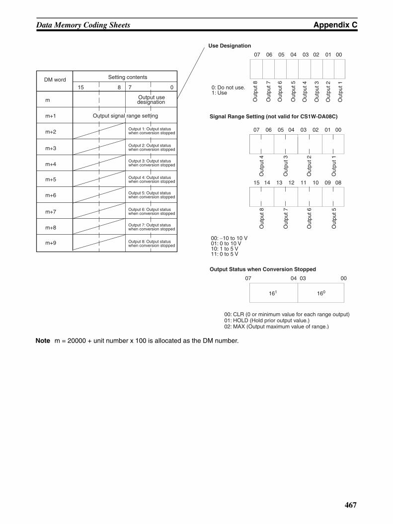
Data Memory Coding Sheets Appendix C
Note m = 20000 + unit number x 100 is allocated as the DM number.
DM word Setting contents
15 8 7 0
m
m+1
m+2
m+3
m+4
m+5
m+6
m+7
m+8
m+9
Output 1: Output status when conversion stopped
Output 2: Output status when conversion stopped
07 06 05 04 03 02 01 00
Out
put 6
Out
put 5
Out
put 2
Out
put 1
Use Designation
0: Do not use.1: Use
07 06 05 04 03 02 01 00
15 14 13 12 11 10 09 08
Signal Range Setting (not valid for CS1W-DA08C)
00: −10 to 10 V 01: 0 to 10 V10: 1 to 5 V11: 0 to 5 V
Out
put 2
Out
put 1
07 04 03 00
161 160
00: CLR (0 or minimum value for each range output)01: HOLD (Hold prior output value.)02: MAX (Output maximum value of range.)
Output Status when Conversion Stopped
Output 3: Output status when conversion stopped
Output 4: Output status when conversion stopped
Output signal range setting
Out
put 8
Out
put 7
Out
put 4
Out
put 3
Out
put 4
Out
put 3
Output 5: Output status when conversion stopped
Output 6: Output status when conversion stopped
Output 7: Output status when conversion stopped
Output 8: Output status when conversion stopped
Out
put 6
Out
put 5
Out
put 8
Out
put 7
Output use designation
467

Data Memory Coding Sheets Appendix C
CJ1W-DA08V/08C
DM wordSetting contents
D2@@00
D2@@01
D2@@02
D2@@03
D2@@04
D2@@05
0
0
0
0
0
0
14 13 12 11 10 09 08 07 06 05 04 03 02 01 0015
0
D2@@06
D2@@07
D2@@08
D2@@09
D2@@18
D2@@20
D2@@21
D2@@22
D2@@23
D2@@24
D2@@25
D2@@26
D2@@27
D2@@28
D2@@29
D2@@30
D2@@31
D2@@32
D2@@33
D2@@34
0 0
0 0
0 0
0 0
0 0
0
0
0
0
0
0
0
0
0
468
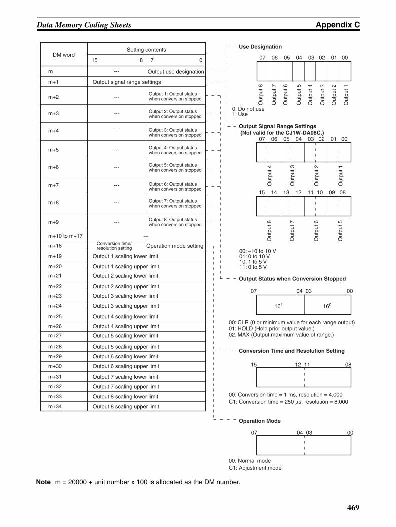
Data Memory Coding Sheets Appendix C
Note m = 20000 + unit number x 100 is allocated as the DM number.
DM wordSetting contents
15 8 7 0
m
m+1
m+2
m+3
m+4
m+5
m+6
m+7
m+8
m+9
m+10 to m+17
m+18
m+19
m+20
m+21
m+22
m+23
m+24
m+25
m+26
m+27
m+28
m+29
m+30
m+31
m+32
m+33
m+34
---
---
---
---
---
---
---
---
---
Output use designation
Output signal range settings
Output 1: Output status when conversion stopped
Output 2: Output status when conversion stopped
Output 3: Output status when conversion stopped
Output 4: Output status when conversion stopped
Output 5: Output status when conversion stopped
Output 6: Output status when conversion stopped
Output 7: Output status when conversion stopped
Output 8: Output status when conversion stopped
---Conversion time/ resolution setting Operation mode setting
Output 1 scaling lower limit
Output 1 scaling upper limit
Output 2 scaling lower limit
Output 2 scaling upper limit
Output 3 scaling lower limit
Output 3 scaling upper limit
Output 4 scaling lower limit
Output 4 scaling upper limit
Output 5 scaling lower limit
Output 5 scaling upper limit
Output 6 scaling lower limit
Output 6 scaling upper limit
Output 7 scaling lower limit
Output 7 scaling upper limit
Output 8 scaling lower limit
Output 8 scaling upper limit
Use Designation
07 06 05 04 03 02 01 00
Out
put 6
Out
put 5
Out
put 2
Out
put 1
0: Do not use1: Use
Out
put 8
Out
put 7
Out
put 4
Out
put 3
Output Signal Range Settings (Not valid for the CJ1W-DA08C.)
07 06 05 04 03 02 01 00
Out
put 2
Out
put 1
Out
put 4
Out
put 3
15 14 13 12 11 10 09 08
Out
put 6
Out
put 5
Out
put 8
Out
put 7
00: −10 to 10 V 01: 0 to 10 V10: 1 to 5 V11: 0 to 5 V
Output Status when Conversion Stopped
07 04 03 00
161 160
00: CLR (0 or minimum value for each range output)01: HOLD (Hold prior output value.)02: MAX (Output maximum value of range.)
Conversion Time and Resolution Setting
Operation Mode
15 12 11 08
07 04 03 00
00: Conversion time = 1 ms, resolution = 4,000C1: Conversion time = 250 µs, resolution = 8,000
00: Normal modeC1: Adjustment mode
469

Data Memory Coding Sheets Appendix C
CS1W-MAD44
DM wordSetting contents
D2@@00
D2@@01
D2@@02
D2@@03
D2@@04
D2@@05
D2@@06
D2@@07
D2@@08
D2@@09
D2@@10
D2@@11
D2@@12
D2@@13
D2@@14
D2@@15
D2@@16
D2@@17
0
0
0
0
0
0
0
0
0
0
0
0
14 13 12 11 10 09 08 07 06 05 04 03 02 01 0015
0 0 0
0 0 0
0 0 0
0 0 0
470

Data Memory Coding Sheets Appendix C
Note m = 20000 + unit number x 100 is allocated as the DM number.
DM word Setting contents
15 8 7 0
m
m+1
m+2
m+3
m+4
m+5
m+6
m+7
m+8
m+9
m+10
m+11
m+12
m+13
Input use designation
Output use designation
Output 1: Output status when conversion stopped
Output 2: Output status when conversion stopped
Input 1: Mean value processing setting
Input 2: Mean value processing setting
Loop 1 (input 1 → output 1), A constant
Loop 1 (input 1 → output 1), B constant
Loop 2 (input 2 → output 2), A constant
Loop 2 (input 2 → output 2), B constant
07 06 05 04 03 02 01 00
Inpu
t 2
Inpu
t 1
Out
put 2
Out
put 1
15 14 13 12 11 10 09 08
Loop
2
Loop
1
Use Designation
0: Do not use.1: Use
00: Do not use.01: Positive gradient conversion10: Negative gradient conversion11: Same as the above "00" setting
07 06 05 04 03 02 01 00
15 14 13 12 11 10 09 08
Inpu
t 2
Inpu
t 1
Signal Range Setting
00: −10 to 10 V 01: 0 to 10 V10: 1 to 5 V / 4 to 20 mA (4 to 20 mA is for analog input only)11: 0 to 5 V
Out
put 2
Out
put 1
B Constant16-bit binary data
A Constant0 to 9999 BCD (0.00 to 99.99; unit: 0.01)
07 04 03 00
161 160
00: CLR (0 or minimum value for each range output)01: HOLD (Hold prior output value.)02: MAX (Output maximum value of range.)
Output Status when Conversion Stopped
15 12 11 08 07 04 03 00
163 162 161 160
Mean Value Processing Setting
0000: Mean value processing with 2 buffers.0001: No mean value processing0002: Mean value processing with 4 buffers.0003: Mean value processing with 8 buffers.0004: Mean value processing with 16 buffers.0005: Mean value processing with 32 buffers.0006: Mean value processing with 64 buffers.
m+14
m+15
m+16
m+17
Loop 3 (input 3 → output 3), A constant
Loop 3 (input 3 → output 3), B constant
Loop 4 (input 4 → output 4), A constant
Loop 4 (input 4 → output 4), B constant
Output 3: Output status when conversion stopped
Output 4: Output status when conversion stopped
Input 3: Mean value processing setting
Input 4: Mean value processing setting
Ratio conversion use designation
Input signal range setting
Output signal range setting
Inpu
t 4
Inpu
t 3
Out
put 4
Out
put 3
Loop
4
Loop
3
Out
put 4
Out
put 3
Inpu
t 4
Inpu
t 3
16-bit binary data
471

Data Memory Coding Sheets Appendix C
CJ1W-MAD42
DM wordSetting contents
D2@@00
D2@@01
D2@@02
D2@@03
D2@@06
D2@@07
0
0
0
0
0
0
14 13 12 11 10 09 08 07 06 05 04 03 02 01 0015
D2@@08
D2@@09
D2@@10
D2@@11
D2@@12
D2@@13
D2@@18
D2@@19
D2@@20
D2@@21
D2@@22
D2@@27
D2@@28
D2@@29
D2@@30
D2@@31
D2@@32
D2@@33
D2@@34
D2@@35
D2@@35
0 0
0 0
0 0
0
0
0
0
0
0
0
0 0
0 0 0
472

Data Memory Coding Sheets Appendix C
Note m = 20000 + unit number x 100 is allocated as the DM number.
DM wordSetting contents
15 8 7 0
m
m+1
m+2
m+3
m+4
m+5
m+6
m+7
m+8
m+9
m+10
m+11
m+12
m+13
m+14 to m+17
m+18
m+19
m+20
m+21
m+22
m+23 to m+26
m+27
m+28
m+29
m+30
m+31
m+32
m+33
m+34
m+35
Ratio conversion use designation
Input use designation
Output use designation
Input signal range setting Output signal range setting
---
---
Output 1: Output status when conversion stopped
Output 2: Output status when conversion stopped
---
---
Input 1: Mean value processing setting
Input 2: Mean value processing setting
Input 3: Mean value processing setting
Input 4: Mean value processing setting
Loop 1 (input 1 → output 1), A constant
Loop 1 (input 1 → output 1), B constant
Loop 2 (input 1 → output 1), A constant
Loop 2 (input 1 → output 1), B constant
---
Output 1 scaling lower limit
Output 1 scaling upper limit
Output 2 scaling lower limit
Output 2 scaling upper limit
Input 1 scaling lower limit
Input 1 scaling upper limit
Input 2 scaling lower limit
Input 2 scaling upper limit
Input 3 scaling lower limit
Input 3 scaling upper limit
Input 4 scaling lower limit
Input 4 scaling upper limit
Voltage/current range setting (Valid for 1 to 5 V or 4 to 20 mA.)
--- ---Input Output
15 12 11 08
07 04 03 00
07 06 05 04 03 02 01 00
Use Designation
0: Do not use.1: Use
15 12 11 10 09 08
00: Do not use.01: Positive gradient conversion10: Negative gradient conversion11: Same as the above "00" setting
Signal Range Setting
07 03 02 01 00
15 14 13 12 11 10 09 08
00: −10 to 10 V 01: 0 to 10 V10: 1 to 5 V/4 to 20 mA11: 0 to 5 V
07 04 03 00
161 160
00: CLR (0 or minimum value for each range output)01: HOLD (Hold prior output value.)02: MAX (Output maximum value of range.)
Output Status when Conversion Stopped
15 12 11 08 07 04 03 00
163 162 161 160
Mean Value Processing Setting
0000: Mean value processing with 2 buffers.0001: No mean value processing0002: Mean value processing with 4 buffers.0003: Mean value processing with 8 buffers.0004: Mean value processing with 16 buffers.0005: Mean value processing with 32 buffers.0006: Mean value processing with 64 buffers.
Conversion Time and Resolution Setting
Operation Mode
00: Conversion time = 1 ms, resolution = 4,000C1: Conversion time = 500 µs, resolution = 8,000
00: Normal modeC1: Adjustment mode
Conversion time/ resolution setting Operation mode setting
---
Input 4
Input 3
Input 2
Input 1
Out-put 2
Out-put 1
Loop 1
Loop 2
Output 2
Output 1
Input 4
Input 3
Input 2
Input 1
Voltage/Current Specifications (when 1 to 5 V/4 to 20 mA is selected)
15 08 07 06 05 04 03 02 01 00
This setting is valid for inputs and/or outputs only if "10" (1 to 5 V/4 to 20 mA) was specified in m+1.
Input 4
Input 3
Input 2
Input 1
Out-put 2
Out-put 1
0: Voltage (1 to 5 V)1: Current (4 to 20 mA)
473

Data Memory Coding Sheets Appendix C
CJ1W-AD042
DM wordSetting contents
15 14 13 12 11 10 09 08 07 06 05 04 03 02 01 00
0 0
0
0
0
0
0
D2@@00
D2@@01
D2@@02
D2@@03
D2@@04
D2@@05
D2@@06
D2@@07
D2@@08
D2@@09
D2@@10
D2@@11
D2@@12
D2@@13
D2@@14
D2@@15
D2@@16
D2@@17
0
0
0
0
0
0
474

Data Memory Coding Sheets Appendix C
DM Area word (See note.)
Settings
---
m
m+1
m+2
m+3
m+4
m+5
m+6 m+7
m+8
m+9 m+10
m+11
m+12
m+13 m+14
m+15
m+16
m+17
163 162 161 16 0
161 160
160
161 160
15 08 07 00
---
---
---
---
---
---
Number of mean value buffers for input 2
Input 2 scaling lower limit
Input 2 scaling upper limit
Number of mean value buffers for input 3
Input 3 scaling lower limit
Input 3 scaling upper limit
Number of mean value buffers for input 4
Input 4 scaling lower limit
Input 4 scaling upper limit
Input 3 signal range
Input 4 signal range
Number of Analog Inputs Used
Conversion Mode Setting
Input Signal Range Setting
Numbers of Mean Value BuffersNote: For the DM word addresses, m = D20000 + (unit number x 100)
0: No inputs used.1: One input used2: Two inputs used3: Three inputs used4: Four inputs used
00 hex: Cyclic Conversion ModeA5 hex: Direct Conversion Mode
0: −10 to 10 V2: 0 to 10 V3: 4 to 20 mA6: −5 to 5 V7: 1 to 5 V
0: Mean value processing not used.1: Mean value processing with 2 buffers2: Mean value processing with 4 buffers3: Mean value processing with 8 buffers4: Mean value processing with 16 buffers5: Mean value processing with 32 buffers6: Mean value processing with 64 buffers7: Mean value processing with 128 buffers8: Mean value processing with 256 buffers9: Mean value processing with 512 buffers
Number of inputs used
Conversion mode setting
Input 1 signal range
Number of mean value buffers for input 1
Input 1 scaling lower limit
Input 1 scaling upper limit
Input 2 signal range
03 00
07 04 03 00
07 04 03 00
15 12 11 08 07 04 03 00
475

Data Memory Coding Sheets Appendix C
CJ1W-DA042V
DM wordSetting contents
D2@@00
D2@@01
D2@@02
D2@@03
D2@@04
D2@@05
D2@@06
D2@@07
D2@@08
D2@@09
D2@@10
D2@@11
D2@@12
D2@@13
D2@@14
D2@@15
D2@@16
D2@@17
0
0
0
0
0
0
15 14 13 12 11 10 09 08 07 06 05 04 03 02 01 00
0 0
0
0
0
0
0
476

Data Memory Coding Sheets Appendix C
---
15 08 07 00
---
---
---
Conversion mode setting
Output 1 output signal range setting
---
---
---
Output 1 output status when conversion stops
Output 1 scaling lower limit
Output 1 scaling upper limit
Output 2 output status when conversion stops
Output 2 scaling lower limit
Output 2 scaling upper limit
Output 3 output status when conversion stops
Output 3 scaling lower limit
Output 3 scaling upper limit
Output 4 output status when conversion stops
Output 4 scaling lower limit
Output 4 scaling upper limit
Output 2 output signal range setting
Output 3 output signal range setting
Output 4 output signal range setting
Number of Analog Outputs Used
Conversion Mode Setting
Output Signal Range Setting
Output Status when Conversion Stops
Note: For the DM word addresses, m = D20000 + (unit number x 100)
0: No outputs used.1: One output used2: Two outputs used3: Three outputs used4: Four outputs used
00 hex: Cyclic Conversion ModeA5 hex: Direct Conversion Mode
1: 0 to 10 V3: −10 to 10 V6: 1 to 5 V
0: CLR (Outputs 0 or minimum value of output range)1: HOLD (Holds output value prior to stop.)2: MAX (Outputs maximum value of output range)
m
m+1
m+2
m+3
m+4
m+5
m+6
m+7
m+8
m+9
m+10
m+11
m+12
m+13
m+14
m+15
m+16
m+17
163 162 161 160
161 160
160
161 160
DM Area word (See note.)
Settings
Number of outputs used
03 00
03 0007 04
03 0007 04
03 0007 0415 12 11 08
477

Data Memory Coding Sheets Appendix C
478

Appendix DExecution Times for Special Instructions for
the CJ1W-AD042/-DA042V
Execution times for the ANALOG INPUT DIRECT CONVERSION (AIDC) instruction and ANALOG OUTPUTDIRECT CONVERSION (AODC) instruction are provided below.
Instruction Mnemonic Function No.
Execution time (µs) Conditions
CJ2H-CPU6@(-EIP)
ANALOG INPUT DIRECT CONVERSION (for the CJ1W-AD042)
AIDC 216 26.0 Analog input 1, number of analog inputs used set to 4
27.7 Analog input 2, number of analog inputs used set to 4
34.6 Analog input 3, number of analog inputs used set to 4
35.9 Analog input 4, number of analog inputs used set to 4
29.8 Analog input 0, number of analog inputs used set to 1
32.7 Analog input 0, number of analog inputs used set to 2
39.4 Analog input 0, number of analog inputs used set to 3
41.6 Analog input 0, number of analog inputs used set to 4
ANALOG OUT-PUT DIRECT CONVERSION (for the CJ1W-DA042V)
AODC 217 24.6 Analog output 1, number of analog outputs used set to 4
24.6 Analog output 2, number of analog outputs used set to 4
24.6 Analog output 3, number of analog outputs used set to 4
24.6 Analog output 4, number of analog outputs used set to 4
28.4 Analog output 0, number of analog outputs used set to 1
34.5 Analog output 0, number of analog outputs used set to 2
39.1 Analog output 0, number of analog outputs used set to 3
45.8 Analog output 0, number of analog outputs used set to 4
479

Execution Times for Special Instructions for the CJ1W-AD042/-DA042V Appendix D
480

Index
A–BA constant
Analog I/O Unit, 326, 342, 394, 415
A/D conversion time
Analog I/O Unit, 301, 368
adjustment mode
allocations
Analog I/O Unit, 329, 397
Analog Input Unit, 52, 105
Analog Output Unit, 194, 241
operational flow
Analog I/O Unit, 344, 417
Analog Input Unit, 62, 114
Analog Output Unit, 199, 250
Alarm Flags
Analog I/O Unit, 328, 330, 361, 396, 397, 434
Analog Input Unit, 51, 53, 105, 106, 154
Analog Output Unit, 194, 195, 211, 241, 242, 263, 286
alarms
Analog I/O Unit, 359, 432
Analog Input Unit, 71, 122, 164
Analog Output Unit, 209, 261, 294
upper and lower limit, 444
B constant
Analog I/O Unit, 326, 342, 394, 415
bias
Analog I/O Unit, 342, 415
Ccircuitry
input
Analog I/O Unit, 319, 385
Analog Input Unit, 35, 96, 143
internal
Analog I/O Unit, 319, 385
Analog Input Unit, 35, 96, 143
Analog Output Unit, 186, 232, 278
output
Analog I/O Unit, 319, 385
Analog Output Unit, 186, 232, 278
Clear Bit
Analog I/O Unit, 329, 345, 351, 397, 418, 424
Analog Input Unit, 53, 65, 106, 116
Analog Output Unit, 195, 201, 242, 253
components
Analog I/O Unit, 315, 382
Analog Input Unit, 29, 91, 140
Analog Output Unit, 182, 228
configuration
internal
Analog I/O Unit, 319, 386
Analog Input Unit, 36, 96, 143
Analog Output Unit, 186, 232, 279
conversion
signed binary to signed BCD, 448
stopping and starting
Analog I/O Unit, 338, 409
Analog Output Unit, 197, 245, 288
time
Analog I/O Unit, 301, 368
values
Analog I/O Unit, 330, 337, 398, 407
Analog Input Unit, 54, 106, 155
Analog Output Unit, 195, 243, 287
Conversion Enable Bit
Analog I/O Unit, 338, 409
Analog Output Unit, 197, 245, 288
conversion time
Analog Input Units
setting, 27, 45, 46, 56, 89, 102, 108, 225, 245, 400,409
cyclic conversion
Analog Input Unit, 156
Analog Output Unit, 289
DD/A conversion time
Analog I/O Unit, 301
data exchange
Analog I/O Unit, 300, 322, 368, 389
Analog Input Unit, 16, 40, 80, 99, 130, 147
Analog Output Unit, 172, 173, 188, 216, 234, 268, 281
data memory coding sheets, 453
dimensions, 439
Analog I/O Unit, 300, 368
Analog Input Unit, 80, 130
Analog Output Unit, 172, 216, 268
direct conversion, 7Analog Input Unit, 156
Analog Output Unit, 289
disconnection
voltage input
Analog I/O Unit, 320, 387
Analog Input Unit, 36, 97, 144
Disconnection Detection Flag, 443
481
Index
Analog I/O Unit, 313, 380
Analog Input Unit, 28, 90, 139
DM allocations
contents
Analog I/O Unit, 325, 393
Analog Input Unit, 45, 102, 150
Analog Output Unit, 191, 236, 283
Down Bit
Analog I/O Unit, 329, 351, 397, 424
Analog Input Unit, 53, 106
Analog Output Unit, 195, 201, 242, 253
EEC Directives, xxi
errors
Analog I/O Unit, 359, 432
Analog Input Unit, 71, 122, 164
Analog Output Unit, 209, 261, 294
CPU Unit, 75, 126, 167, 212, 265, 297, 363, 436
UNIT No. DPL ERR
Analog I/O Unit, 324, 392
Analog Input Unit, 44, 101
Analog Output Unit, 190, 236
external terminals
Analog I/O Unit, 300, 368
Analog Input Unit, 80, 130
Analog Output Unit, 172, 216, 268
Ffixed data
allocations
Analog I/O Unit, 324, 392
Analog Input Unit, 43, 101
Analog Output Unit, 190, 236
Analog I/O Unit, 322, 389
Analog Input Unit, 40, 99
Analog Output Unit, 188, 234
set values
Analog I/O Unit, 326, 394
Analog Input Unit, 47, 103
Analog Output Unit, 191, 238
stored values
Analog I/O Unit, 326, 394
Analog Input Unit, 47, 103
Analog Output Unit, 191, 238
functions, 2applications, 14
input
Analog I/O Unit, 301
other
Analog I/O Unit, 301
output
Analog I/O Unit, 301
G–Hgain adjustment function, 6
Analog I/O Unit, 343, 348, 354, 416, 421, 427
Analog Input Unit, 62, 68, 114, 119
Analog Output Unit, 199, 205, 250, 257
applications, 14
clearing adjusted values
Analog I/O Unit, 350, 357, 423, 430
Analog Input Unit, 70, 121
Analog Output Unit, 208, 260
setting procedure
Analog I/O Unit, 308, 375
Analog Input Unit, 22, 85
Analog Output Unit, 177, 221, 222
Gain Bit
Analog I/O Unit, 329, 345, 351, 397, 418, 424
Analog Input Unit, 53, 65, 106, 116
Analog Output Unit, 195, 201, 242, 253
gradient conversion
negative
Analog I/O Unit, 341, 414
positive
Analog I/O Unit, 341, 414
history buffers
Analog I/O Unit, 332, 400
Analog Input Unit, 57, 109, 158
I–LI/O refresh data
allocations
Analog I/O Unit, 327, 395
Analog Input Unit, 48, 103, 152
Analog Output Unit, 192, 239, 285
Analog I/O Unit, 322, 389
Analog Input Unit, 40, 99, 147
Analog Output Unit, 188, 234, 281
set values
Analog I/O Unit, 328, 396
Analog Input Unit, 51, 105, 154
Analog Output Unit, 194, 241, 286
stored values
Analog I/O Unit, 328, 396
482

Index
Analog Input Unit, 51, 105, 154
Analog Output Unit, 194, 241, 286
I/O tables
creation
Analog I/O Unit, 311, 377
Analog Input Unit, 25, 87, 136
Analog Output Unit, 179, 224, 273
indicators
Analog I/O Unit, 316, 383
Analog Input Unit, 30, 92, 141
Analog Output Unit, 183, 229, 277
errors
Analog I/O Unit, 359, 432
Analog Input Unit, 71, 122, 164
Analog Output Unit, 209, 261, 294
initial data
settings
Analog I/O Unit, 311, 377
Analog Input Unit, 26, 88, 137
Analog Output Unit, 179, 224, 274
input
circuitry
Analog I/O Unit, 319, 385
Analog Input Unit, 35, 96, 143
impedance
Analog I/O Unit, 301, 368
Analog Input Unit, 16, 80, 130
numbers
Analog I/O Unit, 330, 345, 398, 418
Analog Input Unit, 54, 64, 106, 116
settings
Analog I/O Unit, 330, 398
Analog Input Unit, 54, 106, 155
signal range, 2, 3Analog I/O Unit, 301, 326, 331, 368, 369, 394, 398
Analog Input Unit, 16, 47, 54, 80, 103, 107, 130,151, 155
specifications
Analog I/O Unit, 301, 303, 371
Analog Input Unit, 19, 82, 132
input disconnection detection function, 5Analog I/O Unit, 336, 406
Analog Input Unit, 61, 113, 163
applications, 14
input functions
block diagram
Analog I/O Unit, 303, 370
Analog Input Unit, 19, 82, 132
installation
procedure
Analog I/O Unit, 308, 375
Analog Input Unit, 22, 85, 135
Analog Output Unit, 176, 220, 272
isolation
Analog I/O Unit, 300, 368
Analog Input Unit, 16, 80, 130
Analog Output Unit, 172, 216, 268
ladder programs
Analog I/O Unit, 312, 379
Analog Input Unit, 27, 89, 138
Analog Output Unit, 180, 226, 275
limit, 451
loops
Analog I/O Unit, 342, 415
M–Nmaximum Units
per Rack
Analog I/O Unit, 300, 368
Analog Input Unit, 16, 80, 130
Analog Output Unit, 172, 216, 268
per system
Analog I/O Unit, 300
mean value function, 6applications, 14
settings
Analog I/O Unit, 326, 394
Analog Input Unit, 47, 103, 151
mean value processing, 450
Analog I/O Unit, 332, 400
Analog Input Unit, 57, 109, 158
mounting
position
Analog I/O Unit, 300, 368
Analog Input Unit, 16, 80, 130
Analog Output Unit, 172, 216, 268
precautions
Analog I/O Unit, 344, 417
Analog Input Unit, 63, 115
Analog Output Unit, 200, 251, 252
restrictions, 10
normal mode
allocations
Analog I/O Unit, 328, 396
Analog Output Unit, 193, 239
number of analog inputs used, 155
number of analog outputs used, 287
483

Index
Ooffset adjustment function, 6
Analog I/O Unit, 343, 346, 351, 416, 419, 424
Analog Input Unit, 62, 65, 114, 117
Analog Output Unit, 199, 202, 250, 254
applications, 14
clearing adjusted values
Analog I/O Unit, 350, 357, 423, 430
Analog Input Unit, 70, 121
Analog Output Unit, 208, 260
setting procedure
Analog I/O Unit, 308, 375
Analog Input Unit, 22, 85
Analog Output Unit, 177, 221, 222
Offset Bit
Analog I/O Unit, 329, 345, 351, 397, 418, 424
Analog Input Unit, 53, 65, 106, 116
Analog Output Unit, 195, 201, 242, 253
operating procedure
Analog I/O Unit, 308, 375
Analog Input Unit, 22, 85, 135
Analog Output Unit, 177, 221, 222
operation mode switch
Analog I/O Unit, 317
Analog Input Unit, 32, 93
Analog Output Unit, 184, 230
output
circuitry
Analog I/O Unit, 319, 385
Analog Output Unit, 186, 232, 278
current
Analog I/O Unit, 301, 369
Analog Output Unit, 172, 216
data
Analog I/O Unit, 301, 368, 369
Analog Input Unit, 80
impedance
Analog I/O Unit, 301, 369
Analog Output Unit, 172, 216, 268
numbers
Analog I/O Unit, 337, 351, 407, 424
Analog Output Unit, 195, 201, 243, 253
setting errors
Analog I/O Unit, 340, 413
Analog Output Unit, 199, 249, 293
settings
Analog I/O Unit, 337, 407
Analog Output Unit, 195, 243, 287
signal range, 2, 3Analog I/O Unit, 301, 326, 337, 339, 394, 408, 410
Analog Output Unit, 172, 191, 196, 198, 216, 238,243, 246, 268, 284, 287
specifications
Analog I/O Unit, 301, 305, 373
Analog Output Unit, 174, 218
status, 191, 238
Analog I/O Unit, 326, 339, 394, 410
Analog Output Unit, 198, 246
output functions
block diagram
Analog I/O Unit, 303, 370
Analog Output Unit, 174, 218, 269
output hold function, 5Analog I/O Unit, 339, 410
Analog Output Unit, 198, 246, 290
applications, 14
PPeak Value Hold Bit
Analog I/O Unit, 335, 404
Analog Input Unit, 61, 112
peak value hold function, 5Analog I/O Unit, 335, 403
Analog Input Unit, 60, 112, 162
applications, 14
power consumption
Analog I/O Unit, 300, 368
Analog Input Unit, 16, 80, 130
Analog Output Unit, 172, 216, 268
Power Supply Units, 10, 11, 17, 81
precautions, 13
application, xx
general, xviii
mounting
Analog I/O Unit, 344, 417
Analog Input Unit, 63, 115
Analog Output Unit, 200, 251, 252
operating environment, xix
safety, xviii
Programming Console
errors
Analog I/O Unit, 324, 327, 392, 395
Analog Input Unit, 44, 49, 101, 104
Analog Output Unit, 190, 192, 236, 239
Programming Devices
Analog I/O Unit, 330, 398
Analog Input Unit, 54, 106
Analog Output Unit, 195, 243
484

Index
Rrated input
Analog I/O Unit, 301, 368
Analog Input Unit, 16, 80, 130
ratio conversion function
Analog I/O Unit, 340, 413
applications, 14
ratio set value
Analog I/O Unit, 342, 415
resolution
Analog Input Units
setting, 27, 45, 46, 56, 89, 102, 108, 225, 245, 400,409
input
Analog I/O Unit, 301, 368, 369
Analog Input Unit, 16, 80, 130
output
Analog I/O Unit, 301
Analog Output Unit, 172, 216, 268
S–Tsafety precautions, xviii
scaling, 446
Set Bit
Analog I/O Unit, 329, 345, 351, 397, 418, 424
Analog Input Unit, 53, 65, 106, 116
Analog Output Unit, 195, 201, 242, 253
set data
Analog I/O Unit, 301
Analog Output Unit, 172, 216, 268
settings
procedure
Analog I/O Unit, 308, 375
Analog Input Unit, 22, 85, 135
Analog Output Unit, 176, 220
Special I/O Unit Area
Analog I/O Unit, 300, 368
Analog Input Unit, 130
Analog Output Unit, 172, 173, 216, 268
Special I/O Unit DM Area
Analog I/O Unit, 300, 324, 368, 392
Analog Input Unit, 43, 101, 130, 149
Analog Output Unit, 172, 173, 190, 216, 236, 268, 283
Special I/O Unit Restart Bits
Analog I/O Unit, 323, 332, 364, 391, 401, 437
Analog Input Unit, 42, 58, 76, 100, 127, 148, 168
Analog Output Unit, 189, 213, 235, 266, 282, 298
specifications
Analog I/O Unit, 300, 369
Analog Input Unit, 16, 80, 130
Analog Output Unit, 172, 216, 268
general
Analog I/O Unit, 300, 368
Analog Input Unit, 16, 80, 130
Analog Output Unit, 172, 216, 268
input
Analog I/O Unit, 301, 303, 371
Analog Input Unit, 19, 82, 132
output
Analog I/O Unit, 301, 305, 373
Analog Output Unit, 174, 218
square root calculation, 449
switch settings
Analog I/O Unit, 315, 382
Analog Input Unit, 29, 91, 140
Analog Output Unit, 182, 228, 276
system configuration, 9terminal arrangement
Analog I/O Unit, 318, 385
Analog Input Unit, 34, 95, 142
Analog Output Unit, 185, 230, 278
UUNIT No. DPL ERR
Analog I/O Unit, 324, 327, 392, 395
Analog Input Unit, 44, 49, 101, 104
Analog Output Unit, 190, 192, 236, 239
unit number
settings
Analog I/O Unit, 323, 390
Analog Input Unit, 41, 100, 148
Analog Output Unit, 189, 235, 282
unit number switches
Analog I/O Unit, 317, 383
Analog Input Unit, 31, 92, 141
Analog Output Unit, 184, 229, 277
Up Bit
Analog I/O Unit, 329, 351, 397, 424
Analog Input Unit, 53, 106
Analog Output Unit, 195, 201, 242, 253
Vvoltage input disconnection
Analog I/O Unit, 320, 387
Analog Input Unit, 36, 97, 144
485

Index
voltage/current switch
Analog I/O Unit, 318, 384
Analog Input Unit, 33, 94
Wweight
Analog I/O Unit, 300, 368
Analog Input Unit, 16, 80, 130
Analog Output Unit, 172, 216, 268
wiring
Analog I/O Unit, 318, 385
Analog Input Unit, 34, 95, 142
Analog Output Unit, 185, 230, 278
considerations
Analog I/O Unit, 322, 389
Analog Input Unit, 40, 98, 146
Analog Output Unit, 188, 233, 280
examples
Analog I/O Unit, 321, 388
Analog Input Unit, 37, 98, 144
Analog Output Unit, 187, 233, 279
486

487
Revision History
A manual revision code appears as a suffix to the catalog number on the front cover of the manual.
The following table outlines the changes made to the manual during each revision. Page numbers refer to theprevious version.
Date Revised content
01 March 1999 Original production
02 August 1999 Revised to include information on CS1W-AD041/081, CS1W-DA041/08V/08C.
03 May 2001 Revised to add CJ1W-AD081 and CJ1W-DA041 Analog I/O Units and one new section added on each. “CS1” changed to “CS (-series)” or “CS/CJ (-series)” accordingly.Other changes are as follows:Page xiv: Precautions added.Pages 11 and 57: Note added.
04 November 2001 Revised to include information on CS1W-AD041-V1, CS1W-AD081-V1, CJ1W-AD041-V1, CJ1W-AD081-V1, CJ1W-DA021.
05 November 2002 Revised to include information on CJ1W-DA08V and CJ1W-MAD42.Changes include changes and additions to the following items.
Conversion time/resolution settings and operation mode settingsVoltage and current range settingsScaling functionOffset and gain adjustment
06 July 2003 Revised to include information on the CJ1W-DA08C, including the following changes.Page 8: “CS1W-DA8C” corrected to “CS1W-DA08C” in table heading.Pages 104, 253, and 324: Note corrected at the bottom of each page regarding the ON/OFF status of the Offset Bit and Gain Bit and the conversion data.Pages 53, 55, 102, 255, and 326: Note added at the bottom of each page regarding the ON/OFF status of the Offset Bit and Gain Bit and the conversion data.
07 December 2004 Revised to include information on the CS1W-AD161, and remove certain infor-mation on the CS1W-AD041, CS1W-AD081, and CJ1W-AD081.
08 July 2005 Page xii: Information on liability and warranty added.Pages xvii and xviii: Common Emission Standard EN50081-2 changed to EN61000-6-4.
09 September 2006 Page xxi: Information on EC Directives replaced. Page 34: Wiring diagram corrected. Page 38: Note added at bottom of page. Pages 49 and 195: Left column removed from bottom table. Pages 70, 120, 163, 215, 281, and 352: Flowchart expanded. Page 103: Left column removed from top table. Page 145: Information added to note 1. Page 148: Value of bits 4 to 7 of word n corrected.
10 March 2008 Page xi: Updated related manual table. Page xviii: Added warning to the general precautions. Page 96: Corrected wiring diagram and added asterisks.
11 August 2009 Added CJ1W-AD042 Analog Input Unit and CJ1W-DA042V Analog Output Unit
Cat. No. W345-E1-11
Revision code


OMR
OMRIndust
RegioOMROWegalThe NeTel: (3
ControAutomAutomShiokoKyoto,Tel: (8
Authorized Distributor:ON Corporationrial Automation Company
OMRON ELECTRONICS LLCOne Commerce Drive Schaumburg, IL 60173-5302 U.S.A.Tel: (1) 847-843-7900/Fax: (1) 847-843-7787
OMRON ASIA PACIFIC PTE. LTD.No. 438A Alexandra Road # 05-05/08 (Lobby 2), Alexandra Technopark, Singapore 119967Tel: (65) 6835-3011/Fax: (65) 6835-2711
l Devices Division H.Q.ation & Drive Divisionation Department 1ji Horikawa, Shimogyo-ku, 600-8530 Japan1) 75-344-7084/Fax: (81) 75-344-7149
In the interest of product improvement, specifications are subject to change without notice.
Cat. No. W345-E1-11ON Industrial Automation Global: www.ia.omron.comPrinted in Japan
0809
nal HeadquartersN EUROPE B.V.aan 67-69-2132 JD Hoofddorptherlands
1)2356-81-300/Fax: (31)2356-81-388
OMRON (CHINA) CO., LTD.Room 2211, Bank of China Tower, 200 Yin Cheng Zhong Road, PuDong New Area, Shanghai, 200120, ChinaTel: (86) 21-5037-2222/Fax: (86) 21-5037-2200
© OMRON Corporation 1999 All Rights Reserved.
Related Documents