Analog Integrated CMOS Circuits for the Readout and Powering of Highly Segmented Detectors in Particle Physics Applications Dissertation zur Erlangung des akademischen Grades DOKTOR-INGENIEUR der Fakultät für Mathematik und Informatik der Fernuniversität in Hagen von Michael Athanassios Karagounis aus Köln Hagen 2010

Welcome message from author
This document is posted to help you gain knowledge. Please leave a comment to let me know what you think about it! Share it to your friends and learn new things together.
Transcript

Analog Integrated CMOS Circuits for the Readout andPowering of Highly Segmented Detectors in Particle
Physics Applications
Dissertation
zur Erlangung des akademischen Grades
DOKTOR-INGENIEUR
der Fakultät für
Mathematik und Informatik
der Fernuniversität
in Hagen
von
Michael Athanassios Karagounis
aus
Köln
Hagen 2010


Kurzbeschreibung
Halbleiterdetektoren sind etablierte Instrumente der Teilchenphysik, die zur Spurrekon-struktion aber auch für spektroskopische und kalorimetrische Messungen verwendet wer-den. Streifen- und Pixeldetektoren verfügen über eine ein- bzw. zweidimensionale Seg-mentierung, durch die eine entsprechende Ortsauflösung erzielt wird. Die einzelnen Sen-sorsegmente bestehen aus zu einander isolierten Dioden, die während des Betriebes inSperrrichtung geschaltet und von allen freien Ladungsträgern vollständig depletiert sind.Einfallende Strahlung ionisiert Ladung im Sensormaterial, die durch das anliegende elek-trische Feld an den Sensorelektroden ausgelesen werden kann. Hierzu werden hochintegri-erte Mehrkanal-Auslesechips verwendet, die meist in CMOS Technologie implementiertwerden. Ein typischer analoger Auslesekanal besteht aus einem ladungsempfindlichenVerstärker, einem Bandpass zur Bandbreitenbegrenzung und einem Komparator um dasAusgangssignal mit einer globalen Schwelle zu vergleichen. Digitale Logik wird verwen-det, um die Anzahl der Treffer zu zählen oder die einzelnen Treffer mit einer Zeitmarkezu versehen.
Mit zunehmender Anzahl der Auslesekanäle wird die Handhabung der anfallendenDatenmenge schwieriger und die Spannungsversorgung ineffizienter. Zur Implementierungvon seriellen Hochgeschwindigkeitsübertragungsstecken werden die Auslesechips meist mitLVDS Sende- und Empfangsschaltungen ausgestattet. Ein Konzept für die Verbesserungder Versorgungseffizienz ist Serial Powering. Bei diesem Versorgungsschema wird eineKette aus in Reihe geschalteter Verbraucher durch eine Konstantstromquelle versorgt.Dadurch verringert sich der Stromfluss auf den Versorgungsleitungen, was zu einer Re-duzierung von Spannungsabfällen auf den Versorgungsleitung führt. Shunt-Regulatorenerzeugen eine lokale Versorgungsspannung für jeden Verbraucher.
Die im Rahmen dieser Arbeit geleistete Entwicklungsarbeit, ist eingebettet in mehrereProjekte mit teilchenphysikalischem Hintergrund. Für ein Compton-Polarimeter mit ho-her Präzision wurde ein Siliziumstreifendetektor Auslesechip entwickelt, um einzelne ein-fallende Photonen zählen zu können. Der FE-I4 Hybrid-Pixelauslesechip wurde für dieanstehenden IBL und super-LHC Upgrades des am LHC installierten ATLAS Pixeldetek-tors entworfen. Der Chip verfügt über eine Auslesearchitektur, die die höheren Raten, dienach den Upgrades zu erwarten sind, mit nur geringen Datenverlusten verarbeiten kann.Die Chipgröße wurde bis an die Technologiegrenze skaliert, um Material und Kosten zusparen. Ein weiteres Projekt beschäftigt sich mit der differentiellen Sensorauslese bei derdie Signalladung gleichzeitig sowohl an der p als auch an der n Elektrode ausgelesen wird.Die differentielle Auslese führt zu einem höheren Signal-zu-Rauschabstand und ist wenigeranfällig auf Übersprecheffekte.
Contents
Introduction 1
1 Segmented Silicon Radiation Sensors 41.1 Charge Signal for Ionizing Particles . . . . . . . . . . . . . . . . . . . . . . 51.2 Signal Formation . . . . . . . . . . . . . . . . . . . . . . . . . . . . . . . . 61.3 Silicon Sensor Properties . . . . . . . . . . . . . . . . . . . . . . . . . . . . 71.4 Sensor Segmentation . . . . . . . . . . . . . . . . . . . . . . . . . . . . . . 9
2 Charge Sensitive Amplifiers 132.1 Charge Collection Efficiency . . . . . . . . . . . . . . . . . . . . . . . . . . 14
2.1.1 Influence of AC-coupling on Charge Collection Efficiency . . . . . . 162.2 Signal Rise Time . . . . . . . . . . . . . . . . . . . . . . . . . . . . . . . . 172.3 Noise Optimization . . . . . . . . . . . . . . . . . . . . . . . . . . . . . . . 20
2.3.1 Classical Noise Optimization Methodology . . . . . . . . . . . . . . 212.3.2 Noise Optimization Using the EKV Transistor Model . . . . . . . . 24
2.4 Continuous Reset . . . . . . . . . . . . . . . . . . . . . . . . . . . . . . . . 282.5 Preamplifier Circuit Implementation . . . . . . . . . . . . . . . . . . . . . 31
2.5.1 Folded versus Telescopic Cascode . . . . . . . . . . . . . . . . . . . 322.5.2 NMOS versus PMOS input transistor . . . . . . . . . . . . . . . . . 342.5.3 Single-Ended versus Differential Topology . . . . . . . . . . . . . . 36
2.6 Summary . . . . . . . . . . . . . . . . . . . . . . . . . . . . . . . . . . . . 37
3 The Shaper 383.1 Matched Filter for Optimum SNR . . . . . . . . . . . . . . . . . . . . . . . 383.2 Gaussian Filter . . . . . . . . . . . . . . . . . . . . . . . . . . . . . . . . . 423.3 CR-RCn Shaper . . . . . . . . . . . . . . . . . . . . . . . . . . . . . . . . 453.4 Classic Shaper Implementations . . . . . . . . . . . . . . . . . . . . . . . . 493.5 Shaper Implementation Based on Gm-C Filtering . . . . . . . . . . . . . . 513.6 Summary . . . . . . . . . . . . . . . . . . . . . . . . . . . . . . . . . . . . 55
4 Compton Strip Detector Readout Chip 564.1 Compton Polarimetry at ELSA . . . . . . . . . . . . . . . . . . . . . . . . 56
4.1.1 Principle of Compton Polarimetry . . . . . . . . . . . . . . . . . . . 574.1.2 The Experimental Setup . . . . . . . . . . . . . . . . . . . . . . . . 57
4.2 The Compton Chip . . . . . . . . . . . . . . . . . . . . . . . . . . . . . . . 58
I

II CONTENTS
4.2.1 Analog Front-End . . . . . . . . . . . . . . . . . . . . . . . . . . . 594.2.2 Digital Chip Architecture . . . . . . . . . . . . . . . . . . . . . . . 694.2.3 Noise Characterization . . . . . . . . . . . . . . . . . . . . . . . . . 72
4.3 Compton Polarimeter Readout System . . . . . . . . . . . . . . . . . . . . 734.4 Summary . . . . . . . . . . . . . . . . . . . . . . . . . . . . . . . . . . . . 75
5 The FE-I4 ATLAS hybrid pixel chip for b-Layer insertion & super-LHC 765.1 Physics Motivation . . . . . . . . . . . . . . . . . . . . . . . . . . . . . . . 765.2 The Large Hadron Colider . . . . . . . . . . . . . . . . . . . . . . . . . . . 775.3 The ATLAS Experiment . . . . . . . . . . . . . . . . . . . . . . . . . . . . 77
5.3.1 The Inner Detector . . . . . . . . . . . . . . . . . . . . . . . . . . . 795.3.2 The ATLAS Pixel Detector . . . . . . . . . . . . . . . . . . . . . . 805.3.3 The FE-I3 Hybrid Pixel Readout Chip . . . . . . . . . . . . . . . . 83
5.4 Requirements for the FE-I4 ATLAS Hybrid Pixel Readout Chip . . . . . . 865.5 The FE-I4 Chip Architecture . . . . . . . . . . . . . . . . . . . . . . . . . 90
5.5.1 The Analog Front-End . . . . . . . . . . . . . . . . . . . . . . . . . 935.5.2 The Digital Pixel Region . . . . . . . . . . . . . . . . . . . . . . . 104
5.6 Biasing Circuits and DACs . . . . . . . . . . . . . . . . . . . . . . . . . . . 1075.7 I/O Circuitry and Pad Frame . . . . . . . . . . . . . . . . . . . . . . . . . 114
5.7.1 LVDS Driver . . . . . . . . . . . . . . . . . . . . . . . . . . . . . . 1155.7.2 LVDS Receiver . . . . . . . . . . . . . . . . . . . . . . . . . . . . . 1185.7.3 Pad Frame and Wire Bond Pads . . . . . . . . . . . . . . . . . . . . 1235.7.4 ESD Protection Strategy . . . . . . . . . . . . . . . . . . . . . . . . 124
5.8 Power Management . . . . . . . . . . . . . . . . . . . . . . . . . . . . . . . 1265.8.1 Integrated Divide-by-Two DC-DC converter . . . . . . . . . . . . . 1285.8.2 Low Drop-Out Regulator for Low-ESR Load Capacitors . . . . . . 1305.8.3 A Shunt-LDO Regulator for Serially Powered Systems . . . . . . . 138
5.9 3D Integration of Hybrid Pixel Electronics . . . . . . . . . . . . . . . . . . 1565.9.1 The Tezzaron-Chartered 3D Process . . . . . . . . . . . . . . . . . 1575.9.2 Design Porting from the IBM to the Chartered Process . . . . . . . 1595.9.3 Measurement Results . . . . . . . . . . . . . . . . . . . . . . . . . . 1605.9.4 Alternative Analog Front-End for 3D Electronics . . . . . . . . . . 161
5.10 Summary . . . . . . . . . . . . . . . . . . . . . . . . . . . . . . . . . . . . 162
6 Fully-Differential Sensor Readout 1636.1 Analysis of the Fully-Differential CSA . . . . . . . . . . . . . . . . . . . . 1666.2 Fully-Differential Analog Front-Ends . . . . . . . . . . . . . . . . . . . . . 171
6.2.1 Fully-Differential Folded-Cascode Preamplifier . . . . . . . . . . . . 1716.2.2 Continuous-Time Common-Mode Feedback Circuit . . . . . . . . . 1726.2.3 Continuous Reset with Exponential Decay . . . . . . . . . . . . . . 1746.2.4 Constant-Current Feedback . . . . . . . . . . . . . . . . . . . . . . 1766.2.5 Differential Difference Comparator . . . . . . . . . . . . . . . . . . 178
6.3 Test-Chip for Crosstalk Studies . . . . . . . . . . . . . . . . . . . . . . . . 1796.3.1 Comparison between Threshold-Scan and Occupancy-Scan . . . . . 182
6.4 Test-Chip for 3D Sensor Tests . . . . . . . . . . . . . . . . . . . . . . . . . 187

CONTENTS III
6.5 Summary . . . . . . . . . . . . . . . . . . . . . . . . . . . . . . . . . . . . 189
Summary 191
A Power Supply Rejection Analysis of the FE-I4 Analog Front-End 192
B Noise Analysis of the FE-I4 Analog Front-End 195B.1 Preamplifier feedback and leakage compensation transistor . . . . . . . . . 195B.2 Preamplifier input transistor . . . . . . . . . . . . . . . . . . . . . . . . . . 197
Bibliography 200
Acknowledgments 211
Curriculum Vitae 213

Introduction
Following the tradition of the Atomistic model formulated by Democritus and his mentorLeucippus, particle physicist have developed the Standard Model which describes elemen-tary particles and their interaction. While Democritus based his model on reason only,contemporary physicists adapt their model to empiric data collected from experiments.These experiments require reliable instrumentation which is the field where engineers ofdifferent disciplines can support experimental physicists and contribute to the progress ofscience with their expertise.
Semiconductor detectors are well-proven instruments in high-energy physics applica-tions which are used for particle detection, tracking, spectroscopy and calorimetry. Spa-tial resolution is introduced by partitioning the sensor into small segments with a pitchof down to 50 µm. Strip detectors are segmented in one sensor dimension while pixeldetectors have a two dimensional sensor segmentation. Each sensor segment is connectedto a dedicated readout channel for signal processing. Common readout electronics areimplemented as multi-channel integrated mixed-signal CMOS circuits.
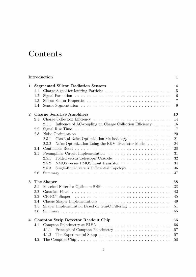
A typical readout channel is shown in Fig. 1. The sensor diode is reverse biased andcompletely depleted from mobile charge carriers. Incident radiation generates charge inthe sensor volume which is integrated by a charge sensitive amplifier (CSA). A high-passlow-pass filter combination is used for noise filtering and signal shaping. A discriminatorcompares the signal pulse amplitude to a configurable threshold voltage and creates aCMOS level pulse whenever the signal exceeds the threshold. The CMOS pulse is thenprocessed by digital circuitry to count for example the amount of detected hits or togenerate a time-stamp. Other readout architectures also allow the digitalization of the
-A
Cf
- +++-
--
isignal
--
--
+
++
+
+
CSA
1 1CH
RH
RL
CL
1
high-pass
filter
low-pass
filter
sensor
+
-Vthreshold
counter /
time stamping
comparator digital logic
Fig. 1: "Typical architecture of a semiconductor detector readout channel"
1
2
signal pulse amplitude. The power consumption of the readout system and the datavolume which has to be handled scales with the number of readout channels. For a largenumber of readout channels, efficient power supply and data traffic management becomesmore and more challenging. These challenges are addressed by optimized powering andcommunication schemes.
This thesis covers the author’s research and development work on the readout andpowering of highly segmented particle detectors used in particle physics applications. Thestructure of this thesis corresponds to the three major projects which have been carriedout. The development of a silicon strip detector readout chip used in an individual photoncounting detection system for precision Compton polarimetry is described in chapter 4.The Compton chip has been developed in the AMS 0.35 µm CMOS process and hasbeen used as a platform for the testing of different shaping circuits and alternative logicarchitectures.
Chapter 5 is dedicated to the development of the FE-I4 ATLAS hybrid pixel readoutchip in IBM 130 nm CMOS technology which is aimed to be used for the upcoming up-grades of the ATLAS pixel detector installed at the LHC at CERN. A readout architecturehas been developed which is adapted to the increased hit rate expected for the new pixellayer (b-layer) which will be inserted into the ATLAS pixel detector detector at reducedradius and the increased luminosity of the upgraded LHC. A main focus of the ongoingdevelopment work is to improve the power efficiency of the ATLAS pixel detector. Oneof the studied options is a serially powered scheme based on a constant current supply.Within the scope of this project a new Shunt-LDO regulator architecture has been in-troduced and successfully implemented which allows parallel placed devices to generatedifferent supply voltages out of a single current supply. The feasibility of 3D integrationis studied as a technological solution for the demands imposed on the inner pixel layers atsuper-LHC conditions. To apply the Chartered-Tezzaron 3D integration process to a FE-I4 prototype, the design has been ported to the Chartered 130 nm CMOS process usingmanual and semi-automatical techniques and a test-chip has been successfully producedin Chartered technology.
Studies performed on the differential readout of 3D sensors and implementation pro-posals for the respective fully-differential readout circuits are given in chapter 6. Themechanical properties of the 3D sensor with cylindrical electrodes perpendicular to thesensor surface which penetrate the entire sensor thickness allow to connect the readoutchip to both the n and the p type electrodes at the same sensor side. Fully-differentialsensor readout has the potential of a higher signal to noise ratio (SNR) and a betterimmunity against crosstalk effects compared to ordinary single-ended readout. Test-chipshave been developed in the UMC 180 nm CMOS technology to test fully-differential sen-sor readout and to investigate the crosstalk immunity of fully-differential circuits basedon the comparison of the results of threshold and noise occupancy scans.
To avoid unnecessary repetitions the basic principles which all three projects have incommon are summarized in the first chapters of the thesis. The first chapter deals withthe properties of segmented silicon sensors focusing on the derivation of the specificationwhich the readout circuitry has to meet for a given sensor used for the detection of ionizingparticles. This chapter is confined to silicon sensors since silicon is still the first choicematerial for tracking applications in particle physics. The second chapter introduces the

3
charge sensitive amplifier which is directly coupled to the sensor to integrate the generatedcharge signal. This basic building block has to be carefully designed since it has a highinfluence on the performance of the whole analog signal processing chain. The thirdchapter is about shaping circuits which are used to increase the SNR by filtering spectralnoise components located at very low and very high frequencies. In addition shapers areused to adapt the signal shape to the expected hit rate in the experiment.
Some parts of this work were previously published in [Kar08], [Kar09a] and [Kar09b].
Chapter 1
Segmented Silicon Radiation Sensors
Sensors are the detector components which primarily interact with incident radiationand generate a signal which is processable by the readout electronics. Sensor signalsare generated by electron-hole pairs which arise from ionization of the sensor material.In most cases, the favored sensor material for particle tracking in high energy physics(HEP) applications is silicon. Common usage of silicon as detector material originatesfrom the well suited material properties and the availability of mature silicon processingtechnology. The average energy of 3.6 eV for creating an electron-hole pair is an order ofmagnitude smaller than the energy for the ionization of gases. Because of the moderateband gap energy of 1.12 eV, cooling of silicon sensors is needed only in ultra-low-noiseapplications or if required to mitigate radiation damage. The high density of 2.33 g/cm3
leads to large energy loss per traversed length of the ionizing particle which allows aconstruction of thin sensors. Despite the high material density, the mobility of bothelectrons and holes is high (µe=1450 cm2/Vs, µh=505 cm2/Vs). Thus the signal chargecan be rapidly collected and detectors can cope with high event rates [Lut99][Sad01]. Anadditional advantage of silicon as compared to other sensor materials, is its broad usagein microelectronics industry. Therefore, a highly developed technology base exists whichassures cheap and reliable sensor production. However, alternative sensor materials arestudied for usage in special applications and under special conditions. In X-ray imagingapplications semiconductor compounds containing elements with higher atomic number(Z) than silicon are preferred, because of their higher absorption efficiency. Diamondwhich due to its wider band gap is more radiation hard than silicon is studied for use indetector systems exposed to extreme radiation levels, .
This chapter will focus on how the specification for the development of readout cir-cuitry is derived from the properties of silicon sensors but it will not cover in detail thephysics processes involved in the signal generation and formation which can be foundin the literature [Leo87][Kno89][Lut99][Ros06]. For charge readout, the main relevantparameters are the expected signal dynamic range to which the readout circuit has tobe adapted, the detector capacitance and its leakage current which influence the noiseperformance, as well as the charge collection time which establishes a lower bound forthe signal rise time of the readout circuit. In addition, an important system parameter isspatial resolution which primarily is defined by the sensor segmentation.
4

1.1. CHARGE SIGNAL FOR IONIZING PARTICLES 5
0.1 1 10 100 1 10 100 1 10 100 1 10 100
Muon kinetic energy
1
10
100
Sto
pp
ing
po
we
r [M
eV
cm
2/g
]
Lin
dh
ard
-S
cha
r!Andersen-
Ziegler
Bethe-Bloch Radiative
Radiativee!ects
reach 1%
µ+ on Cu
Without δ
RadiativelossesMinimum
ionization
E µc
Nuclearlosses
[TeV][GeV][MeV][keV]
µ−
Fig. 1.1: Energy loss of muons in copper, illustrating the functional behavior of energy loss ofionizing particles in matter [Gro01]
1.1 Charge Signal for Ionizing Particles
Charged particles lose part of their energy through scattering with electrons of the sensormaterial along the particle track. This process is described analytically with the Bethe-Bloch formula which has been derived from quantum mechanics and can be found in[Leo87]. In Fig. 1.1, the average energy loss of muons penetrating copper normalized tocopper density is shown as a function of the muons kinetic energy. The depicted averageenergy loss to density ratio, also called stopping power, depends only weakly on materialparameters and can therefore be used as a reference for silicon. Energy loss reachesa minimum in the energy range which is of interest for contemporary particle physicsexperiments. As a rule of thumb, the minimum stopping power is approximately 1.5 MeVcm2/g independent of the sensor material. A particle which deposits the minimum amountof energy is called a minimum ionizing particle (MIP). Since an increase in energy lossbeyond this minimum is relatively small over the relevant energy region, MIPs are usedto quantify a detector’s response.
To calculate the average amount of electron-hole pairs, generated in thin silicon sensorby a MIP, the normalized energy loss is multiplied with the density of silicon and dividedby the average ionization energy in silicon, giving the average number of electron-holepairs per sensor thickness:
Qaverage ≈ 100qeµm
d (1.1)
where qe is the charge of an electron and d is the sensor thickness in µm. Hence a MIPwhich penetrates a sensor with a typical thickness of 250 µm generates about 24,000electron-hole pairs on average, corresponding to a charge of about 4 fC. However, theionization process is subject to statistical fluctuations. For thin sensors the individualsensor signal response varies according to Landau statistics [Lan44]. An illustration of a
6 CHAPTER 1. SEGMENTED SILICON RADIATION SENSORS
100 200 300 400 500 6000.0
0.2
0.4
0.6
0.8
1.0
0.50 1.00 1.50 2.00 2.50
640 µm (149 mg/cm2)
320 µm (74.7 mg/cm2)
160 µm (37.4 mg/cm2)
80 µm (18.7 mg/cm2)
500 MeV pion in silicon
Mean energyloss rate
wf(∆
/x)
∆/x (eV/µm)
∆p/x
∆/x (MeV g−1 cm2)
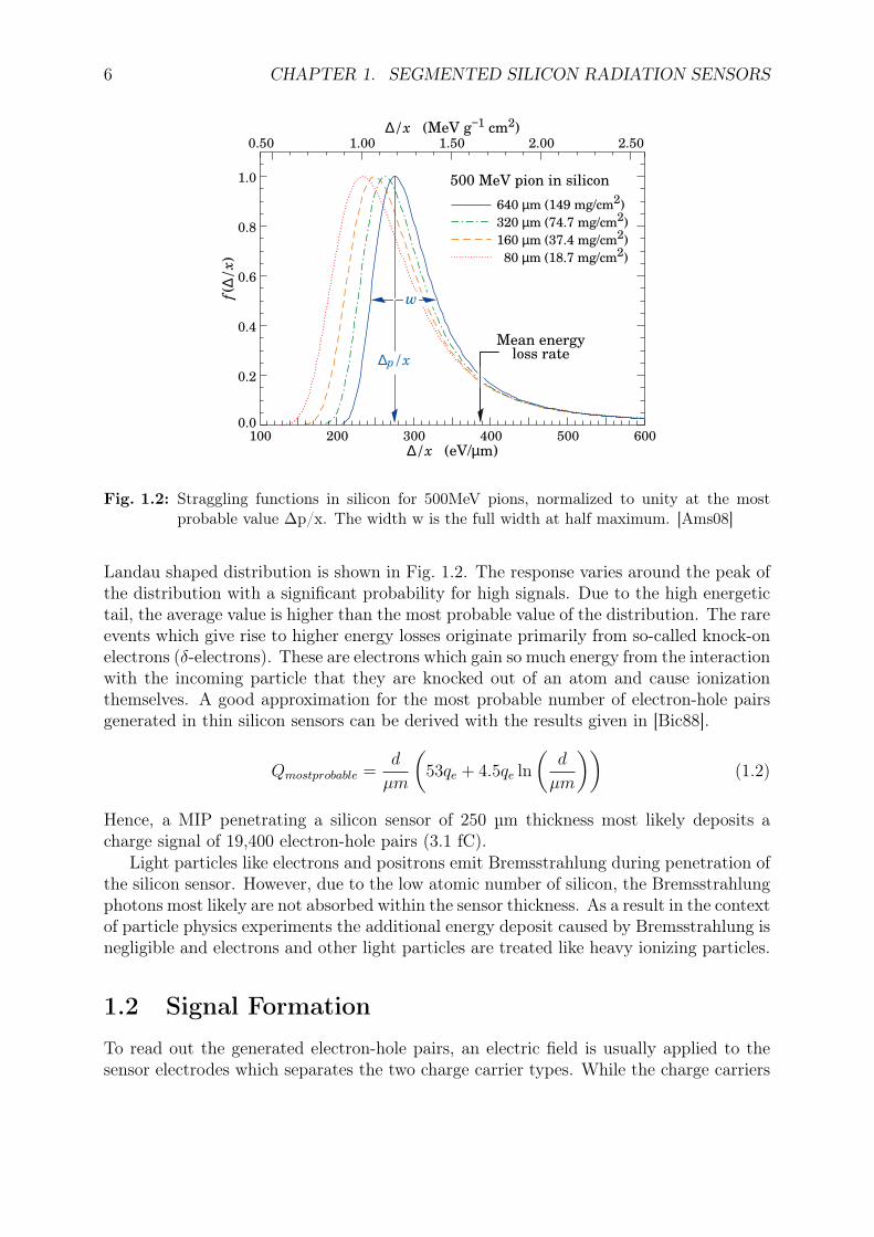
Fig. 1.2: Straggling functions in silicon for 500MeV pions, normalized to unity at the mostprobable value ∆p/x. The width w is the full width at half maximum. [Ams08]
Landau shaped distribution is shown in Fig. 1.2. The response varies around the peak ofthe distribution with a significant probability for high signals. Due to the high energetictail, the average value is higher than the most probable value of the distribution. The rareevents which give rise to higher energy losses originate primarily from so-called knock-onelectrons (δ-electrons). These are electrons which gain so much energy from the interactionwith the incoming particle that they are knocked out of an atom and cause ionizationthemselves. A good approximation for the most probable number of electron-hole pairsgenerated in thin silicon sensors can be derived with the results given in [Bic88].
Qmostprobable =d
µm
(53qe + 4.5qe ln
(d
µm
))(1.2)
Hence, a MIP penetrating a silicon sensor of 250 µm thickness most likely deposits acharge signal of 19,400 electron-hole pairs (3.1 fC).
Light particles like electrons and positrons emit Bremsstrahlung during penetration ofthe silicon sensor. However, due to the low atomic number of silicon, the Bremsstrahlungphotons most likely are not absorbed within the sensor thickness. As a result in the contextof particle physics experiments the additional energy deposit caused by Bremsstrahlung isnegligible and electrons and other light particles are treated like heavy ionizing particles.
1.2 Signal Formation
To read out the generated electron-hole pairs, an electric field is usually applied to thesensor electrodes which separates the two charge carrier types. While the charge carriers
1.3. SILICON SENSOR PROPERTIES 7
n+
p+
n depleted
MIP
Vb
+++
+++
+
---
--
--
induced
signal
ionized
e/h pairs
+
-
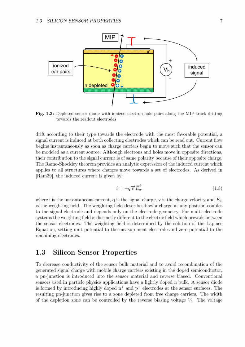
Fig. 1.3: Depleted sensor diode with ionized electron-hole pairs along the MIP track driftingtowards the readout electrodes
drift according to their type towards the electrode with the most favorable potential, asignal current is induced at both collecting electrodes which can be read out. Current flowbegins instantaneously as soon as charge carriers begin to move such that the sensor canbe modeled as a current source. Although electrons and holes move in opposite directions,their contribution to the signal current is of same polarity because of their opposite charge.The Ramo-Shockley theorem provides an analytic expression of the induced current whichapplies to all structures where charges move towards a set of electrodes. As derived in[Ram39], the induced current is given by:
i = −q−→v−→Ew (1.3)
where i is the instantaneous current, q is the signal charge, v is the charge velocity and Ew
is the weighting field. The weighting field describes how a charge at any position couplesto the signal electrode and depends only on the electrode geometry. For multi electrodesystems the weighting field is distinctly different to the electric field which prevails betweenthe sensor electrodes. The weighting field is determined by the solution of the LaplaceEquation, setting unit potential to the measurement electrode and zero potential to theremaining electrodes.
1.3 Silicon Sensor Properties
To decrease conductivity of the sensor bulk material and to avoid recombination of thegenerated signal charge with mobile charge carriers existing in the doped semiconductor,a pn-junction is introduced into the sensor material and reverse biased. Conventionalsensors used in particle physics applications have a lightly doped n bulk. A sensor diodeis formed by introducing highly doped n+ and p+ electrodes at the sensor surfaces. Theresulting pn-junction gives rise to a zone depleted from free charge carriers. The widthof the depletion zone can be controlled by the reverse biasing voltage Vb. The voltage
8 CHAPTER 1. SEGMENTED SILICON RADIATION SENSORS
needed to extend the depletion zone over the whole sensor thickness is called the depletionvoltage Vdepl and is given by [Ros06]:
Vdepl =qeNDd
2
2ε0εSi(1.4)
where ND is the dopant concentration of the sensor bulk, d is the sensor thickness and εSi isthe relative permittivity in silicon (εSi = 11.9). Assuming a typical dopant concentrationND in the sensor bulk of about 4×10¹²/cm3, a sensor of 250 µm thickness exhibits adepletion voltage of about 50 V. However, defects introduced by radiation can act asextra dopants increasing the doping concentration. Depending on the radiation dose towhich the sensor has been exposed, the depletion voltage may reach values of more than1000 V.
If the reverse bias voltage Vb exceeds the depletion voltage magnitude Vdepl, a sensoris operated in so-called overdepletion. Overdepletion is commonly applied to decrease thecharge collection time, defined as the time interval which a charge carrier needs to traversethe sensitive sensor volume. Assuming constant charge carrier mobility µ, independentof the applied electric field, the charge-collection of an overdepleted sensor is given by[Spi05]:
tc =d2
2µVdepl
ln
(Vb + Vdepl
Vb − Vdepl
)(1.5)
Using equation 1.5 and assuming a depletion voltage of 50 V, a biasing voltage of 100 Vand a sensor thickness of 250 µm, charge collection times of tce=4.4 ns and tch=13.6 ns,respectively, are calculated for electrons and holes. However, for high electric fields mo-bility of electrons and holes in silicon starts to decrease which results in longer chargecollection times.
The capacitance of the fully depleted sensor can be estimated using the formula forthe parallel-plate capacitor:
Cdepl = ε0εSiA
d(1.6)
where A is the sensor area. Hence, the capacitance of a fully depleted sensor of 250 µmthickness is about 420 fF/mm2. However, this result does not take fringing capacitancesinto account which highly depend on sensor segmentation and sensor environment. Fortypical sensor structures, the fringing capacitance is of same order of magnitude or eventhe dominant contribution to the total capacitance.
Diffusion and thermally generated charge carriers cause the flow of leakage currentsthrough the depleted sensor diode. Usually leakage currents are dominated by thermalgeneration. For a fully depleted sensor leakage current is given by [Lut99]:
Ileakage = −qeni
τgAd (1.7)
where ni is the intrinsic charge carrier concentration and τg is the lifetime of the generatedcarriers. Assuming an intrinsic charge carrier concentration at room temperature of 1.45×10¹⁰/cm3 and a charge carrier generation lifetime τg in silicon of about 1ms, a leakagecurrent of 580 pA/mm2 results for a sensor thickness of 250 µm. However, the defects
1.4. SENSOR SEGMENTATION 9
pitch
width
bond
padbackside
contact
length
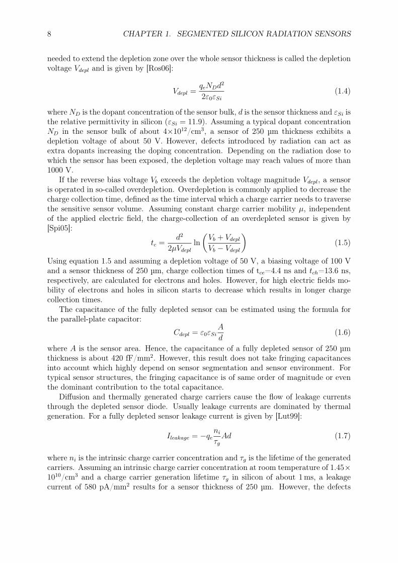
Fig. 1.4: Single-sided and double-sided strip detector
which accumulate with irradiation dose, reduce carrier life time and increase leakagecurrent. In addition, intrinsic carrier concentration shows an exponential dependence ontemperature. As a rule of thumb, around room temperature the leakage current doublesevery 8° K with increasing temperature.
In addition to increasing leakage current and depletion voltage, defects in the sensorsilicon lattice formed by radiation cause further charge trapping centers. As a result,electrons or holes are trapped and released with a delay of µs and are not detected in timewith the bulk of charge carriers generated by the ionizing particle. The relation betweencharge trapping and charge collection efficiency is illustrated by the effective drift lengthLeff of the charge carriers. Exposing the sensor to a particle flux1 of 1015 neutrons/cm2
leads to an effective drift length Leff of 150 µm for electrons and 50 µm for holes [Dav03].Charge collection efficiency is then reduced by a factor of exp(−d/Leff ), where d is thedistance which charge carriers have to travel to reach the sensor electrode.
1.4 Sensor Segmentation
The sensor electrodes can be segmented if extraction of position information is needed.In a segmented sensor, the signal magnitude of a given electrode depends on the distancebetween an electrode and the location in the sensor where the signal charge is generated.Single-sided strip detectors like the one shown in the left panel of Fig. 1.4 provide one-dimensional position information. In a sensor with n-bulk material the p-electrode isusually segmented. With binary hit readout, the pitch p of the segmented electrodedefines the spatial resolution which is calculated as RMS deviation of the true coordinate:
∆x =
√√√√√√1
p
p/2∫−p/2
x2dx =p√12
(1.8)
1A particle flux of 1015 neutrons/cm2 corresponds to 10 years of sensor operation at the nominal LHCluminosity of 1034 cm−2s−1
10 CHAPTER 1. SEGMENTED SILICON RADIATION SENSORS
bump-bond
pad
backside
contact
p-column
n-column
electrode
distance
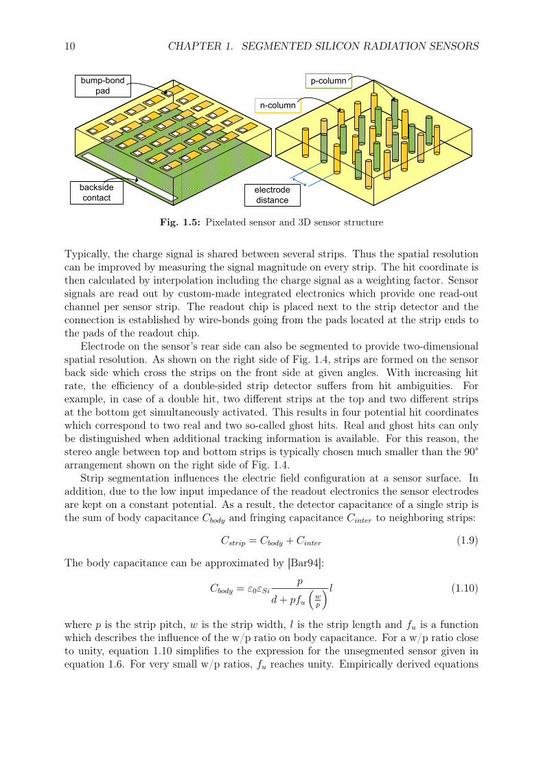
Fig. 1.5: Pixelated sensor and 3D sensor structure
Typically, the charge signal is shared between several strips. Thus the spatial resolutioncan be improved by measuring the signal magnitude on every strip. The hit coordinate isthen calculated by interpolation including the charge signal as a weighting factor. Sensorsignals are read out by custom-made integrated electronics which provide one read-outchannel per sensor strip. The readout chip is placed next to the strip detector and theconnection is established by wire-bonds going from the pads located at the strip ends tothe pads of the readout chip.
Electrode on the sensor’s rear side can also be segmented to provide two-dimensionalspatial resolution. As shown on the right side of Fig. 1.4, strips are formed on the sensorback side which cross the strips on the front side at given angles. With increasing hitrate, the efficiency of a double-sided strip detector suffers from hit ambiguities. Forexample, in case of a double hit, two different strips at the top and two different stripsat the bottom get simultaneously activated. This results in four potential hit coordinateswhich correspond to two real and two so-called ghost hits. Real and ghost hits can onlybe distinguished when additional tracking information is available. For this reason, thestereo angle between top and bottom strips is typically chosen much smaller than the 90°arrangement shown on the right side of Fig. 1.4.
Strip segmentation influences the electric field configuration at a sensor surface. Inaddition, due to the low input impedance of the readout electronics the sensor electrodesare kept on a constant potential. As a result, the detector capacitance of a single strip isthe sum of body capacitance Cbody and fringing capacitance Cinter to neighboring strips:
Cstrip = Cbody + Cinter (1.9)
The body capacitance can be approximated by [Bar94]:
Cbody = ε0εSip
d+ pfu
(wp
) l (1.10)
where p is the strip pitch, w is the strip width, l is the strip length and fu is a functionwhich describes the influence of the w/p ratio on body capacitance. For a w/p ratio closeto unity, equation 1.10 simplifies to the expression for the unsegmented sensor given inequation 1.6. For very small w/p ratios, fu reaches unity. Empirically derived equations
1.4. SENSOR SEGMENTATION 11
sensorbackside
metalization
readout chip
readout pixel
solder bump
pixel
metalization
Fig. 1.6: Schematic view of a hybrid pixel detector
also exist for the interstrip capacitance [Dem00]. For typical sensor geometries the in-terstrip capacitance is about 1 pF/cm [Spi05]. The strip detector used in the Comptonpolarimeter described in chapter 4 has a thickness of 250 µm, a pitch of 50 µm and striplength of 4 cm. For this sensor, the calculated strip body capacitance is 210 fF/cm, whilethe total detector capacitance per strip amounts to around 5 pF.
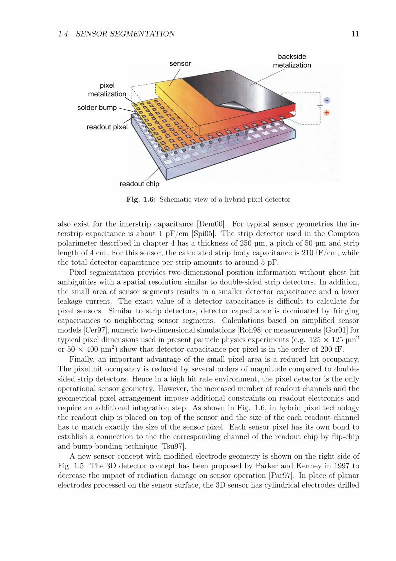
Pixel segmentation provides two-dimensional position information without ghost hitambiguities with a spatial resolution similar to double-sided strip detectors. In addition,the small area of sensor segments results in a smaller detector capacitance and a lowerleakage current. The exact value of a detector capacitance is difficult to calculate forpixel sensors. Similar to strip detectors, detector capacitance is dominated by fringingcapacitances to neighboring sensor segments. Calculations based on simplified sensormodels [Cer97], numeric two-dimensional simulations [Roh98] or measurements [Gor01] fortypical pixel dimensions used in present particle physics experiments (e.g. 125 × 125 µm2
or 50 × 400 µm2) show that detector capacitance per pixel is in the order of 200 fF.Finally, an important advantage of the small pixel area is a reduced hit occupancy.
The pixel hit occupancy is reduced by several orders of magnitude compared to double-sided strip detectors. Hence in a high hit rate environment, the pixel detector is the onlyoperational sensor geometry. However, the increased number of readout channels and thegeometrical pixel arrangement impose additional constraints on readout electronics andrequire an additional integration step. As shown in Fig. 1.6, in hybrid pixel technologythe readout chip is placed on top of the sensor and the size of the each readout channelhas to match exactly the size of the sensor pixel. Each sensor pixel has its own bond toestablish a connection to the the corresponding channel of the readout chip by flip-chipand bump-bonding technique [Tsu97].
A new sensor concept with modified electrode geometry is shown on the right side ofFig. 1.5. The 3D detector concept has been proposed by Parker and Kenney in 1997 todecrease the impact of radiation damage on sensor operation [Par97]. In place of planarelectrodes processed on the sensor surface, the 3D sensor has cylindrical electrodes drilled

12 CHAPTER 1. SEGMENTED SILICON RADIATION SENSORS
into the sensor bulk perpendicular to the sensor surface. With this configuration, thesensor electrode distance is no longer given by the sensor thickness but is defined by thespace between the n and the p columns. Hence the electrode distance can be reduced toreach smaller depletion voltages and to decrease the charge collection time. Furthermore,the reduced electrode distance suits well the smaller average drift length of charge carriersin irradiated sensors. Therefore the 3D sensor is less prone to charge trapping and ismore radiation hard. Due to the 3D electrode geometry, the electrode distance can bereduced without the need to decrease the sensor thickness. As a consequence, the chargesignal generated in 3D sensors is independent of the electrode distance. Pixel and stripsare formed by a group of electrodes of same type which are connected together by themetalization deposited on the sensor surface. Typically one column type is used forreadout whereas the other column type is used for bias only. Recently new dual readoutschemes have been proposed which exploit the fact that both electrode types are availableon the same sensor side [Dav08][Par08]. An additional new concept based on a fully-differential sensor readout is presented in chapter 6.
Chapter 2
Charge Sensitive Amplifiers
A charge sensitive amplifier (CSA) is coupled to one of the electrodes of a reverse biasedsensor diode to integrate the current induced by the movement of charge carriers generatedin the sensor by incident radiation.
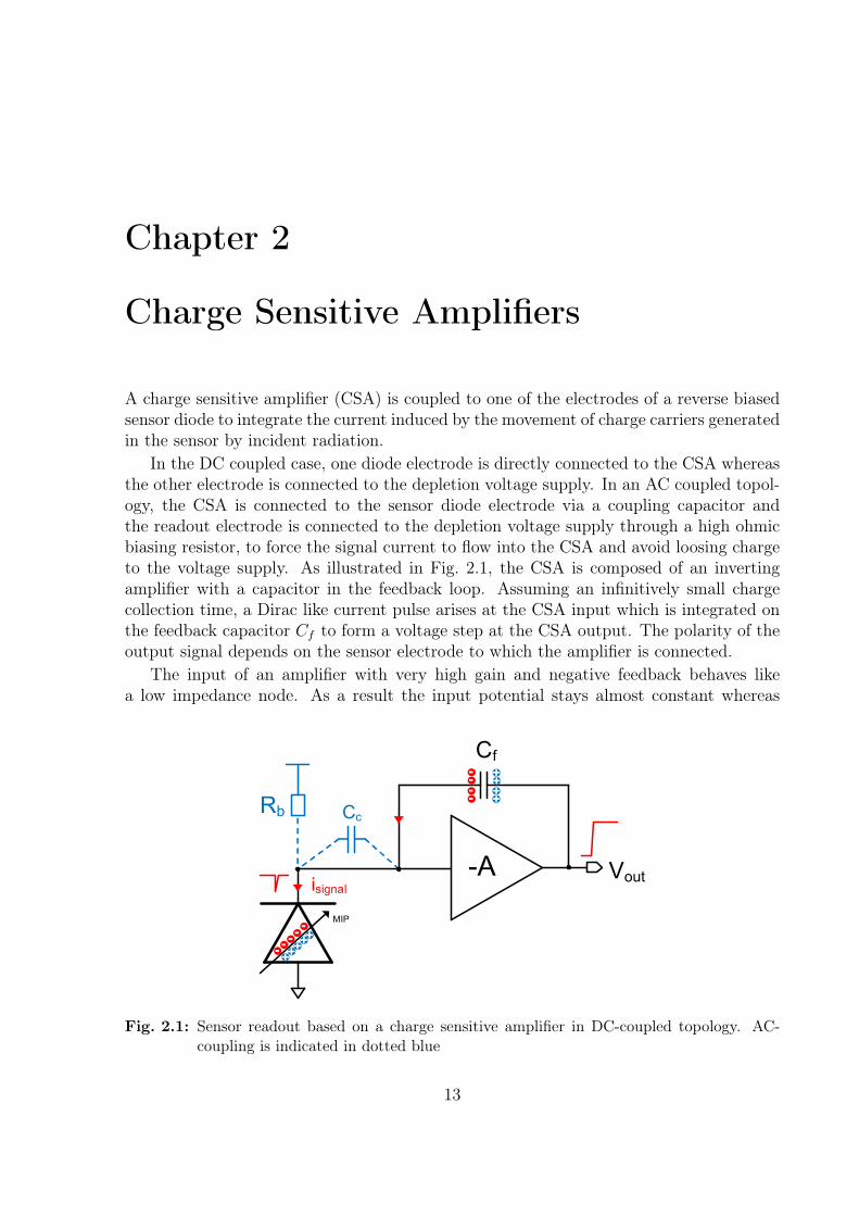
In the DC coupled case, one diode electrode is directly connected to the CSA whereasthe other electrode is connected to the depletion voltage supply. In an AC coupled topol-ogy, the CSA is connected to the sensor diode electrode via a coupling capacitor andthe readout electrode is connected to the depletion voltage supply through a high ohmicbiasing resistor, to force the signal current to flow into the CSA and avoid loosing chargeto the voltage supply. As illustrated in Fig. 2.1, the CSA is composed of an invertingamplifier with a capacitor in the feedback loop. Assuming an infinitively small chargecollection time, a Dirac like current pulse arises at the CSA input which is integrated onthe feedback capacitor Cf to form a voltage step at the CSA output. The polarity of theoutput signal depends on the sensor electrode to which the amplifier is connected.
The input of an amplifier with very high gain and negative feedback behaves likea low impedance node. As a result the input potential stays almost constant whereas
-A
Cf
CcRb
Vout
+- ++++-
---
MIP
isignal
--
--
+
++
+
Fig. 2.1: Sensor readout based on a charge sensitive amplifier in DC-coupled topology. AC-coupling is indicated in dotted blue
13
14 CHAPTER 2. CHARGE SENSITIVE AMPLIFIERS
-A
Cf
VoutIsignal
--
-
-
++
+
Cd+
ICSA
Idet
Vin
Fig. 2.2: Charge readout scheme with sensor modeled as a current source in parallel to aclumped capacitance
the output signal changes when the feedback capacitor is charged by the signal current.From technical perspective, in case of a n-side readout the signal current is flowing outof the CSA into the reverse biased sensor and the amplifier output voltage increases.This readout topology is commonly called electron collection. In case of a p-side readout,the signal current flows out of the sensor into the CSA and the amplifier output voltagedecreases. This configuration is respectively called hole collection.
Assuming that initially Cf is completely discharged, the CSA output voltage magni-tude we can be calculated by means of the capacitor equation:
vout =1
Cf
∞∫0
isdt =1
Cf
qs d t Vout =IssCf
(2.1)
The magnitude of the output voltage change Vout is proportional to the amount of chargeqs that has been collected, whereas the proportionality constant is given by the inverseof the feedback capacitance 1/Cf . The smaller the feedback capacitor is, the higher thevoltage step magnitude becomes for a fixed amount of charge. Although a high gain in thecharge to voltage conversion is advantageous for most signal processing types, the choiceof a very small feedback capacitor value is not efficient in most applications. As will bedescribed in more detail in the following sections, the value of the feedback capacitor hasan influence on the charge collection efficiency and on the output signal rise-time, bothbeing related to power consumption.
2.1 Charge Collection Efficiency
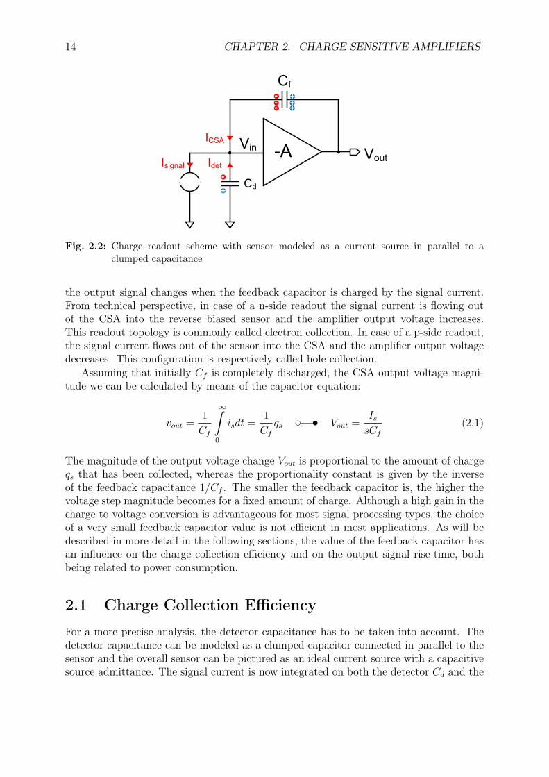
For a more precise analysis, the detector capacitance has to be taken into account. Thedetector capacitance can be modeled as a clumped capacitor connected in parallel to thesensor and the overall sensor can be pictured as an ideal current source with a capacitivesource admittance. The signal current is now integrated on both the detector Cd and the
2.1. CHARGE COLLECTION EFFICIENCY 15
CSA feedback capacitor Cf because the signal current isignal is split in two parts idet andiCSA, as is illustrated in Fig. 2.2. This gives:
isignal = idet + iCSA (2.2)
The current flowing into the feedback capacitance will lead to a voltage drop across thefeedback capacitor:
Vin − Vout =icsas · Cf
=Isignal − Idet
s · Cf
(2.3)
The amount of current that is flowing into the detector capacitance depends on the inputpotential change of the CSA:
Idet = sCd · Vin (2.4)
The input voltage change is related to the gain A of the used amplifier by:
Vin = −Aout
A(2.5)
From equations 2.2 and 2.5, a relation between the signal current Isignal and the CSAoutput voltage Vout can be derived.
Vout =A
s ((1 + A)Cf + Cd)· Isignal t d vout =
A
(1 + A)Cf + Cd
∞∫0
isignaldt (2.6)
The denominator of equation 2.6 can be interpreted as the parallel connection of thedetector capacitor Cd and an effective CSA input capacitance Cieff which is defined bythe feedback capacitor Cf scaled by the gain A of the inverting amplifier. The scaling ofthe feedback capacitance is caused by the Miller effect [Mil20] which is observed wheneveran impedance is placed into the feedback loop of an inverting amplifier. From equation2.6, the following requirement for high charge collection efficiency can be derived:
Cieff = (1 + A)Cf ≫ Cd (2.7)
To integrate a big fraction of the charge which has been generated in the sensor diodevolume on the CSA feedback capacitor Cf , the effective CSA input capacitance has tobe much larger than the detector capacitance Cd. The larger the detector capacitor Cd iswith respect to the effective CSA input capacitance Cieff , the smaller the output voltagevout becomes because a higher fraction of charge is collected on the detector capacitanceCd and hence is missing on the feedback capacitor Cf . Only if the condition of equation2.7 is valid and for A ≫ 1 the CSA transfer function simplifies to the simple expressionof equation 2.1
A large equivalent input capacitance can be implemented by the use of either a largecapacitance value for the feedback capacitor, or by using a high gain amplifier or bychoosing both options at the same time. As has already been mentioned in the previoussection, other system aspects have to be also considered which leads to design trade-offswhich have to be balanced from case to case.
16 CHAPTER 2. CHARGE SENSITIVE AMPLIFIERS
-A
Cf
Cc
Rb
Vout
Fig. 2.3: Alternative ac-coupling scheme
A large value feedback capacitance requires a large chip area per readout channelwhich might not be available especially in a pixel topology. In addition, a large feedbackcapacitance value leads to a small charge to voltage conversion factor. With small voltagesignals parasitic effects like mismatch, process variation and crosstalk have strong influenceon system performance. The gain of the inverting amplifier is also limited by severalsystem aspects. As will be shown in the following sections the gain of the amplifier isdefined by the transconductance of the input transistor and the output impedance ofthe amplifier. A high transconductance requires a high current flow and hence a highpower consumption which might be limited by the available power budget. In additionthe transistor output impedance in current deep sub micron CMOS technologies is rathersmall in comparison to older CMOS processes with longer transistor channel lengths,which also limits the amplifier gain which can be achieved with a single amplificationstage.
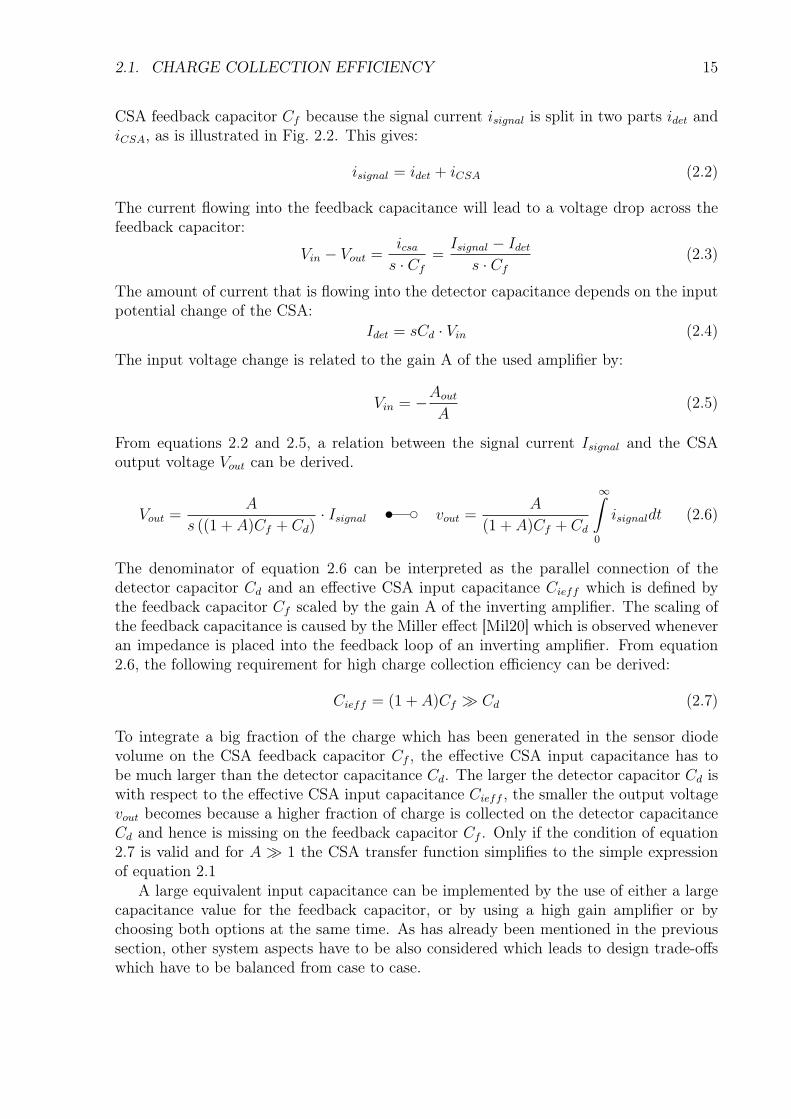
2.1.1 Influence of AC-coupling on Charge Collection Efficiency
In an AC-coupled topology, the coupling capacitor Cc is in series with the effective inputcapacitance Cieff of the CSA. The equivalent capacitance Cic of the two capacitors placedin series is given by:
Cic =CcCieff
Cc + Cieff
(2.8)
Hence the equivalent input capacitance in an AC-coupled readout scheme is lowered withrespect to the DC coupled case. To reduce the influence the coupling capacitor has oncharge collection efficiency, the coupling capacitor has to be chosen much bigger than theeffective input capacitor of the CSA. Usually AC-coupling is applied to strip detectors andthe capacitors are implemented as big passive devices which are integrated on the sensorrather than on the readout chip. The reduced area available in a pixel system for theimplementation of coupling capacitors poses a limitation to the maximum achievable cou-pling capacitance and hence on charge collection efficiency. For this reason AC-couplingis in general not used for pixel systems.
2.2. SIGNAL RISE TIME 17
VbpM2
M1
Vout
Vin
a)
voutCi rogmvinvin
b)
Fig. 2.4: a) inverting amplifier with NMOS input transistor and PMOS load transistor b) smallsignal equivalent cirucit of the inverting amplifier
In Fig. 2.3, a different AC-coupling scheme is shown, which has been originally de-veloped for the readout of gaseous detectors to reduce the amount of energy stored inthe coupling capacitor Cc [Har07] but has also been applied to monolithic pixel detectors[Per07]. With this approach, the coupling capacitor is incorporated into the feedback loopof the CSA and the equivalent capacitance value is scaled by the preamplifer gain whichresults in smaller needed capacitance values and smaller physical size. One should keep inmind, however, that in a readout scheme where the capacitors Cf and Cc are integratedon the readout chip, the biasing voltage of the sensor diode has to be close to the CSAinput potential, due to the fact that integrated capacitors can only bear a limited voltagedrop.
2.2 Signal Rise Time
For some applications, the exact timing information of the signal arrival is crucial. Forthis reason, the signal rise time of the CSA is an important design constraint. A lowerlimit for the signal rise time is the charge collection time of the used sensor since noimprovement in timing accuracy is gained when the rise time of the CSA is faster thanthe time which is needed until the signal charge is collected from the sensor. More oftenthe signal rise time is limited by the power budget. For a single pole system, the signalrise time is set by the bandwidth of the amplifier by:
trise = 2.2τrise =2.2
ωc
=0.35
fc(2.9)
where fc is the cut-off frequency. The bandwith of the CSA is determined by the transcon-ductance of the input transistor and the capacitance connected to the CSA terminals. Toprove this, a more detailed model for the inverting amplifier of the CSA has to be applied.
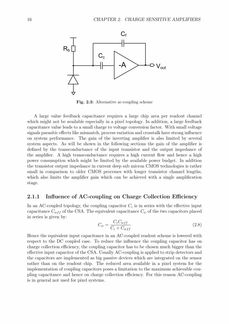
The simplest implementation of an inverting amplifier in CMOS technology is shownin Fig. 2.4a. The inverting amplifier consists of an NMOS input transistor and a loadformed by a PMOS transistor with constant biasing voltage. As is illustrated in Fig.2.4b, for small signals the inverting amplifier is modeled by a voltage controlled currentsource with the transconductance gm of transistor M1, connected in parallel to the output
18 CHAPTER 2. CHARGE SENSITIVE AMPLIFIERS
vout
Cf
Ciiin Cd rogmvinvin~ Co
Fig. 2.5: CSA small-signal equivalent circuit
impedance ro. Parasitic capacitances at the input are modeled by capacitor Ci. Assuminga square-law transistor characteristic, the transconductance gm of transistor M1 can beexpressed by:
gm =∂Id∂Vgs
= µCoxW
L(Vgs − Vth) =
√2µCox
W
LId =
2IdVgs − Vth
(2.10)
where Id is the current flowing through the transistor channel, Vgs is the gate-sourcevoltage, µ is the charge carrier mobility, Cox is the gate oxide capacitance, W is thetransistor width, L is the transistor length and Vth is the transistor threshold voltage oftransistor M1. As is seen from equation 2.10, three different expressions for the transistortransconductance gm exist. For a given transistor geometry, a high transconductance gmis reached by a high load current Id which in turn leads to high power consumption. Theoutput impedance ro of the inverting amplifier is expressed by:
ro =1
gds1 + gds2(2.11)
where gds1 and gds2 respectively is the output conductance of transistor M1 and M2. TheDC-gain of the error amplifier is then expressed by:
voutvin
= −gmro = − gmgds1 + gds2
(2.12)
The input capacitance Ci of the inverting amplifier is the sum of the parasitic capacitancesof the input transistor M1 which are the gate-source capacitance Cgs, the gate-draincapacitance Cgd and the gate-bulk capacitance Cgb. In the strong inversion operationregion, the gate-bulk capacitance Cgb becomes very small and can be neglected. For thesake of clarity the rather small gate-drain capacitance Cgd will be also neglected in thisanalysis, which gives:
Ci = Cgs + Cgd + Cgb ≈ Cgs =2
3WLCox (2.13)
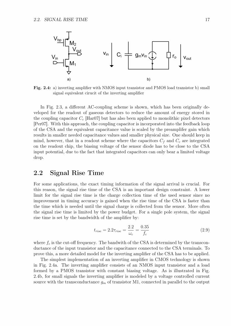
Thus with increasing transistor width, both the transconductance gm and the input ca-pacitance Ci increases. Introducing the equivalent small signal circuit of the invertedamplifier shown in Fig. 2.4b to the CSA circuit of Fig. 2.2, the equivalent small signalcircuit of the CSA result which is shown in Fig. 2.5. In this circuit the capacitive load of
2.2. SIGNAL RISE TIME 19
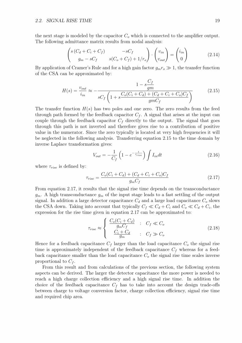
the next stage is modeled by the capacitor Co which is connected to the amplifier output.The following admittance matrix results from nodal analysis:(
s (Cd + Ci + Cf ) −sCf
gm − sCf s(Co + Cf ) + 1/ro
)·
(vin
vout
)=
(iin
0
)(2.14)
By application of Cramer’s Rule and for a high gain factor gmro ≫ 1, the transfer functionof the CSA can be approximated by:
H(s) =voutiin
≈ −1− s
Cf
gm
sCf
(1 + s
Co(Ci + Cd) + (Cd + Ci + Co)Cf
gmCf
) (2.15)
The transfer function H(s) has two poles and one zero. The zero results from the feedthrough path formed by the feedback capacitor Cf . A signal that arises at the input cancouple through the feedback capacitor Cf directly to the output. The signal that goesthrough this path is not inverted and therefore gives rise to a contribution of positivevalue in the numerator. Since the zero typically is located at very high frequencies it willbe neglected in the following analysis. Transferring equation 2.15 to the time domain byinverse Laplace transformation gives:
Vout = − 1
Cf
(1− e
− tτrise
)∫Iindt (2.16)
where τrise is defined by:
τrise =Co(Ci + Cd) + (Cd + Ci + Co)Cf
gmCf
(2.17)
From equation 2.17, it results that the signal rise time depends on the transconductancegm. A high transconductance gm of the input stage leads to a fast settling of the outputsignal. In addition a large detector capacitance Cd and a large load capacitance Co slowsthe CSA down. Taking into account that typically Cf ≪ Cd +Ci and Co ≪ Cd +Ci, theexpression for the rise time given in equation 2.17 can be approximated to:
τrise ≈
Co(Ci + Cd)
gmCf: Cf ≪ Co
Ci + Cdgm : Cf ≫ Co
(2.18)
Hence for a feedback capacitance Cf larger than the load capacitance Co the signal risetime is approximately independent of the feedback capacitance Cf whereas for a feed-back capacitance smaller than the load capacitance Co the signal rise time scales inverseproportional to Cf .
From this result and from calculations of the previous section, the following systemaspects can be derived. The larger the detector capacitance the more power is needed toreach a high charge collection efficiency and a high signal rise time. In addition thechoice of the feedback capacitance Cf has to take into account the design trade-offsbetween charge to voltage conversion factor, charge collection efficiency, signal rise timeand required chip area.
20 CHAPTER 2. CHARGE SENSITIVE AMPLIFIERS
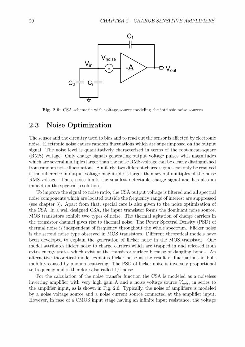
-A
Cf
Vnoise
Vout
CiCd
*Vin
Fig. 2.6: CSA schematic with voltage source modeling the intrinsic noise sources
2.3 Noise Optimization
The sensor and the circuitry used to bias and to read out the sensor is affected by electronicnoise. Electronic noise causes random fluctuations which are superimposed on the outputsignal. The noise level is quantitatively characterized in terms of the root-mean-square(RMS) voltage. Only charge signals generating output voltage pulses with magnitudeswhich are several multiples larger than the noise RMS-voltage can be clearly distinguishedfrom random noise fluctuations. Similarly, two different charge signals can only be resolvedif the difference in output voltage magnitude is larger than several multiples of the noiseRMS-voltage. Thus, noise limits the smallest detectable charge signal and has also animpact on the spectral resolution.
To improve the signal to noise ratio, the CSA output voltage is filtered and all spectralnoise components which are located outside the frequency range of interest are suppressed(see chapter 3). Apart from that, special care is also given to the noise optimization ofthe CSA. In a well designed CSA, the input transistor forms the dominant noise source.MOS transistors exhibit two types of noise. The thermal agitation of charge carriers inthe transistor channel gives rise to thermal noise. The Power Spectral Density (PSD) ofthermal noise is independent of frequency throughout the whole spectrum. Flicker noiseis the second noise type observed in MOS transistors. Different theoretical models havebeen developed to explain the generation of flicker noise in the MOS transistor. Onemodel attributes flicker noise to charge carriers which are trapped in and released fromextra energy states which exist at the transistor surface because of dangling bonds. Analternative theoretical model explains flicker noise as the result of fluctuations in bulkmobility caused by phonon scattering. The PSD of flicker noise is inversely proportionalto frequency and is therefore also called 1/f noise.
For the calculation of the noise transfer function the CSA is modeled as a noiselessinverting amplifier with very high gain A and a noise voltage source Vnoise in series tothe amplifier input, as is shown in Fig. 2.6. Typically, the noise of amplifiers is modeledby a noise voltage source and a noise current source connected at the amplifier input.However, in case of a CMOS input stage having an infinite input resistance, the voltage
2.3. NOISE OPTIMIZATION 21
and the current noise sources are strongly correlated. The correlation factor is given bythe input capacitance of the amplifier. As a result, if the input capacitance is taken intoaccount for the noise transfer function calculation, it is sufficient to consider only thenoise voltage source and to neglect the noise current source. The noise transfer functioncan be calculated by the closed loop gain of the feedback system.
Hnoise =Vout
Vnoise
=A
1 + Aβ(2.19)
where β is the impedance located in the feedback loop. Assuming that the bandwidthof the readout system is defined by the following filter stages, the bandwidth limitationA(s) of the inverting amplifier can be neglected. For very high gain A, equation 2.19 canbe simplified to:
Hnoise ≈1
β(2.20)
The feedback loop is composed of a capacitive voltage divider formed by the feedbackcapacitor Cf and the capacitors which appear at the amplifier input namely the detectorcapacitor Cd and the amplifier input capacitance Ci. The feedback factor β is given by:
β =Vin
Vout
=
1
s(Cd + Ci)1
sCf
+1
s(Ci + Cd)
=Cf
Ci + Cd + Cf
(2.21)
Hence the noise transfer function Hnoise which will be used for the optimization analysisin the following sections is equal to:
Hnoise =Ci + Cd + Cf
Cf
(2.22)
As can be inferred by equation 2.22, noise of the CSA preamplifier scales linearly withdetector capacitance Cd and input capacitance Ci. Furthermore the transferred noisemagnitude decreases with increasing feedback capacitance Cf but as the voltage signalmagnitude decreases at the same time (equation 2.1) the signal to noise ratio is indepen-dent of the feedback capacitance Cf .
As will be shown in section 2.3.1, a noise optimum can be reached if the capacitanceof the CSA input transistor is adapted to the detector capacitance. To save power, theCSA input stage of pixel readout chips is commonly biased in moderate or weak inversionregion. For these circuits a more enhanced noise optimization methodology is applied insection 2.3.2 which is based on the EKV transistor model [Enz95].
2.3.1 Classical Noise Optimization Methodology
The classic noise optimization analysis reported in [San90] assumes that the CMOS inputtransistor of the preamplifier is biased in the strong inversion operation region. Thethermal noise PSD Sthc of a transistor operated in strong inversion region and biased insaturation is given in the current domain by [Tsi99]:
Sthc =8
3kTgm (2.23)
22 CHAPTER 2. CHARGE SENSITIVE AMPLIFIERS
where k is the Boltzmann constant, T is absolute temperature and gm is the transistortransconductance. The thermal noise PSD Sthv which is referred to the transistor inputvoltage which corresponds to the gate-source voltage is calculated by:
Sthv =Sthc
g2m=
8
3
kT
gm(2.24)
Equation 2.10 shows that the transconductance gm and thus the input-referred thermalnoise can be improved by increasing the drain current Id and choosing a short transistorchannel length L. The smallest possible transistor channel length L is given by thetechnology node. Transistors with very small channel lengths are affected by small-channeleffects which degrade the transistor output impedance and increase the noise level abovethe value that is predicted by equation 2.23. As a result the transistor channel length Lis usually chosen to be longer than the minimum length.
Furthermore the transistor drain current Id cannot be scaled independent from thetransistor channel width W. For a fixed channel width W an increase in drain currentresults in an increase of saturation voltage VDSAT = Vgs−Vth which defines the voltage VDS
where transistors reach saturation which in most cases is the desired region of operation.Hence the transistor width W has to be scaled according to the drain current Id to avoida reduction of both the input and output voltage dynamic range.
The thermal noise PSD at the CSA input Sthv gives rise to a noise PSD at the CSAoutput Stho which considering equation 2.22 results to:
Stho = |Hnoise|2 Sthv =8
3
kT
gm
(Ci + Cd + Cf )2
C2f
(2.25)
By combination of equation 2.10 and 2.13, the transconductance gm can be written as afunction of the input capacitance Ci:
gm =
√3µIdCi
L(2.26)
This yields a thermal noise PSD at the CSA output Stho of:
Stho =8
3
kTL√3µId
(Ci + Cd + Cf )2
√CiC2
f
(2.27)
An optimum value for the output thermal noise PSD is reached by an adequate choice ofthe input capacitance Ci. The optimum value is calculated by:
∂Stho
∂Ci
= 0 → Ciopt =Cd + Cf
3(2.28)
Using equation 2.13, an optimal transistor width Wopt can be derived:
Wopt =Cd + Cf
2LCox
(2.29)
According to this calculation the output thermal noise PSD can be improved by raisingthe drain current Id and scaling the width W of the input transistor accordingly until the
2.3. NOISE OPTIMIZATION 23
optimum width Wopt defined by equation 2.29 is reached. Further scaling leads to no noiseimprovement because the increase in input capacitance Ci counteracts the improvementin transconductance gm.
The same methodology can be applied to find the optimal configuration with respectto flicker noise reduction. The input-referred flicker noise PSD in MOS transistors is givenby:
Sf =K
CoxWLf(2.30)
where K is the flicker noise coefficient of the used CMOS process. Combining equation2.30 and equation 2.13 the output flicker noise PSD can be expressed as a function of theinput capacitance Ci:
Sfo =2K
3f
(Ci + Cd + Cf )2
CiC2f
(2.31)
The input capacitance Ci which gives a minimum output flicker PSD magnitude is calcu-lated by:
∂Sfo
∂Ci
= 0 → Ciopt = Cd + Cf (2.32)
The optimum input capacitance Ciopt corresponds to an optimal value of the transistorwidth of:
Wopt = 3Cd + Cf
2CoxL(2.33)
In equation 2.29 and 2.33, different results have been calculated for the optimal transistorwidth for a minimum in thermal and flicker noise propagation respectively. It is importantto note, that the same result is obtained for the thermal and flicker noise optimizationwhen an alternative expression is used for the input transistor transconductance gm. Ifthe optimization is performed for a given saturation voltage Vgs − Vth instead of a givendrain current Id, the following expression for the input transistor transconductance gm isapplied and formulated as a function of the input capacitance Ci:
gm = µCoxW
L(Vgs − Vth) =
3
2
Ci
L2µ (Vgs − Vth) (2.34)
with this expression the thermal noise PSD at the CSA output can be written as:
Stho =16
9
kTL2
µ (Vgs − Vth)
(Ci + Cd + Cf )2
CiC2f
(2.35)
A comparison of expressions 2.35 and 2.31 which describe the output referred PSD ofthermal and flicker noise respectively shows that both expressions have the same depen-dence on the capacitors connected to the amplifier ports and that they differ only by aproportional factor. As a result, if the expression of equation 2.35 is used for the descrip-tion of the output referred thermal noise, the optimization calculation for both flicker andthermal noise lead to the same optimum transistor width which is given in equation 2.33.
In general the circuit designer should be aware that the square-law transistor modelthat is used for the noise optimization calculations is simplistic and neglects all secondorder effects. The obtained results are useful as a starting condition for a more detailedanalysis based on transistor level circuit simulations.
24 CHAPTER 2. CHARGE SENSITIVE AMPLIFIERS
1E-10 1E-9 1E-8 1E-7 1E-6 1E-5 1E-4 1E-3
0
5
10
15
20
25
30
35
40
Strong Inversion
Moderate Inversion
Weak Inversion
g m /I d [V
-1 ]
Id [A]
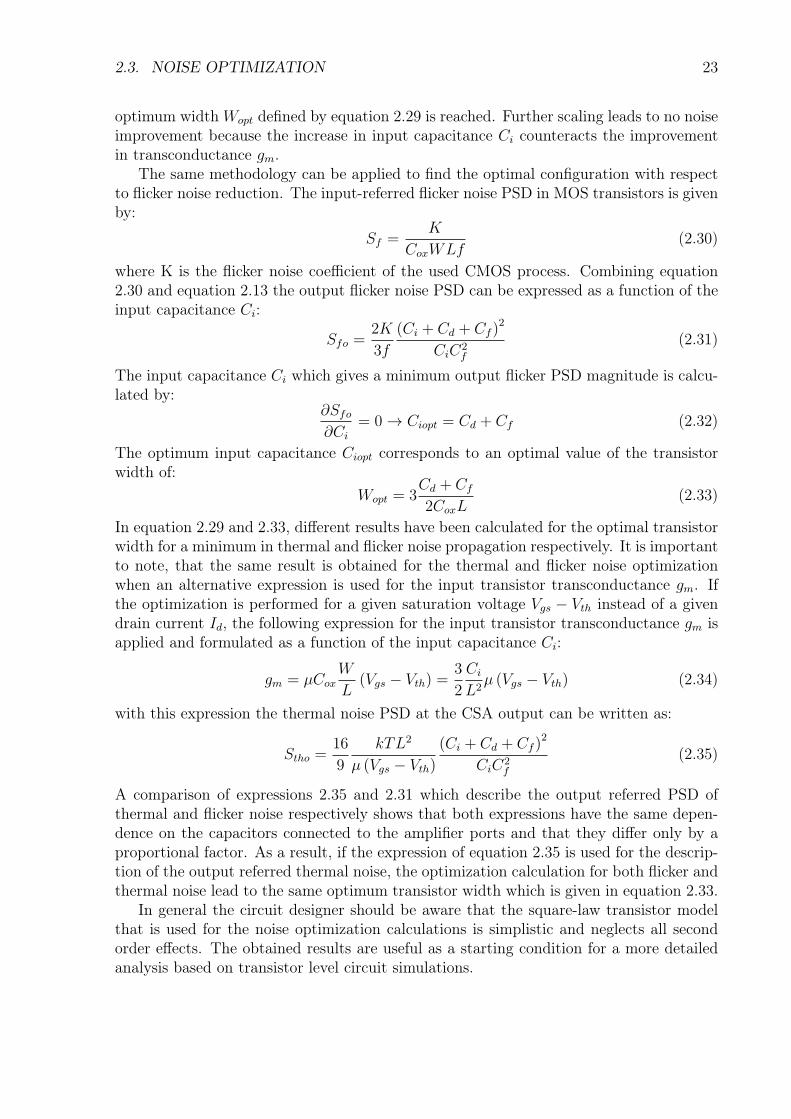
Fig. 2.7: Simulated gm/Id curve for a long-channel NMOS in a 130 nm CMOS technology
2.3.2 Noise Optimization Using the EKV Transistor Model
The input transistor of a CSA is very often operated in weak and moderate inversionrather than in strong inversion. The reason for this is shown in Fig. 2.7 where thetransconductance to drain current ratio gm/Id is plotted. The gm/Id ratio increases whenthe transistor leaves the strong inversion region (Vgs > Vth) and reaches the weak inversion(Vgs < Vth) region. This means that for a fixed drain current, a transistor has a highertransconductance in weak than in strong inversion region. As a result, a specified amplifiergain is reached for a smaller bias current and hence for less power consumption when theinput transistor is operated in moderate or weak inversion instead of strong inversion.
It is therefore very advantageous and of high practical value to extend the noise op-timization methodology into the weak and moderate inversion regime. A natural choicefor this effort is the use of the EKV model which provides transistor equations valid in allregions of operation [Enz95][Gry07]. Hence the solution of the noise optimization problemderived by use of the EKV model is also valid in all regions of operation.
The EKV model introduces the inversion factor if as the main transistor design pa-rameter. The inversion factor is defined as the ratio between drain current Id and the socalled specific current Ispec:
if =IdIspec
=Id
2nµCoxWLU2T
(2.36)
where the slope factor n is a technology dependent EKV model parameter, and UT isthe thermal voltage. The specific current Ispec corresponds to the current that flowsthrough the transistor channel in moderate region. Hence an inversion factor of oneindicates the moderate inversion region whereas an inversion factor smaller and greaterthan one indicates weak and strong inversion respectively. The EKV model is charge basedwhich means that the transistor equations are formulated as a function of the normalized
2.3. NOISE OPTIMIZATION 25
inversion charge qs accumulated in the transistor channel. In saturation, the normalizedinversion charge qs can be calculated as a function of the inversion factor if by:
qs =
√1 + 4if − 1
2(2.37)
The relation between the gate-source potential and the normalized inversion charge qs canbe approximated to:
Vgs − Vth
nUT
= 2qs + ln qs (2.38)
Unfortunately the expression in equation 2.38 cannot be inverted analytically to provide ageneral expression of qs(Vgs) which would than result into a general expression of if (Vgs).However in the context of the CSA noise optimization, the EKV model can still be applied,if the noise optimization procedure is based on the inversion factor if . The inversion factorbased optimization procedure provides the optimum transistor width for a given inversionfactor and therefore for a given region of operation. The corresponding transistor draincurrent is then derived from equation 2.36, using the optimum transistor width and thewanted inversion factor.
For the noise optimization analysis, EKV model expressions for the input capacitorCi, the transistor transconductance gm and the PSD of thermal and flicker transistor noiseare needed. Due to the fact that in weak inversion the gate-bulk Cgb is bigger than thegate-source capacitance Cgs, Cgb is not neglected as in the previous calculations but issummed to Cgs to form the input capacitance Ci. In saturation, the input capacitance Ci
is given by:
Ci = Cgs + Cgb = CoxWL1
n
(n− 1 +
qs3
2qs + 3
(qs + 1)2
)(2.39)
The transconductance gm of a saturated transistor is given by:
gm = 2µCoxW
LUT qs (2.40)
The input referred PSD of the MOS transistor thermal noise in saturation can be expressedas:
Sthi = Γ4kT
gm(2.41)
where Γ is the noise excess factor defined as:
Γ =1
6
4qs + 3
qs + 1(2.42)
Based on the Carrier Fluctuation Model (Mc Whorter Model [McW57]), the input referredPSD of the MOS transistor flicker noise is given as:
Sfi =K
WLCoxf(1 + qs)
2
(1
qs(1 + qs)ln (1 + 2qs) +
αµ
1 + qs+(αµ
2
)2)(2.43)
where α is a technology dependent constant related to the Coulomb scattering coefficient.According to this model the biasing dependence of the flicker noise generation is very
26 CHAPTER 2. CHARGE SENSITIVE AMPLIFIERS
0 0.002 0.004 0.006 0.008 0.01W@mD1. ´ 10-15
1. ´ 10-14
1. ´ 10-13
1. ´ 10-12
Sth@V^2HzD
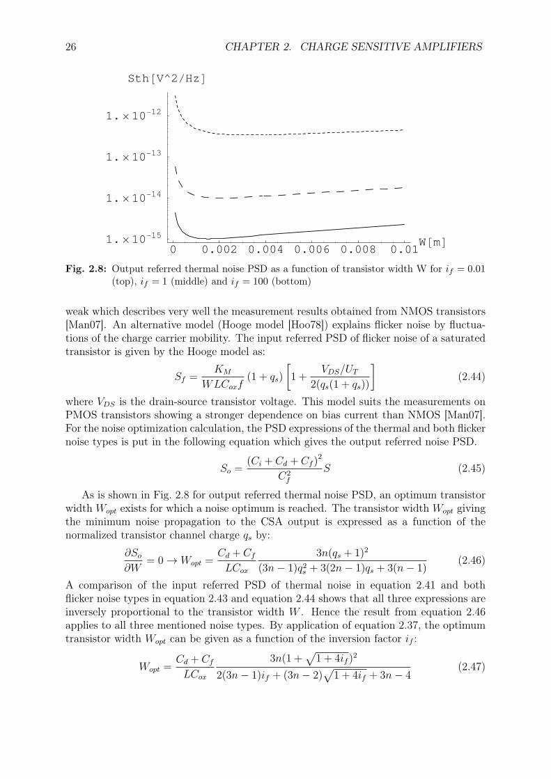
Fig. 2.8: Output referred thermal noise PSD as a function of transistor width W for if = 0.01(top), if = 1 (middle) and if = 100 (bottom)
weak which describes very well the measurement results obtained from NMOS transistors[Man07]. An alternative model (Hooge model [Hoo78]) explains flicker noise by fluctua-tions of the charge carrier mobility. The input referred PSD of flicker noise of a saturatedtransistor is given by the Hooge model as:
Sf =KM
WLCoxf(1 + qs)
[1 +
VDS/UT
2(qs(1 + qs))
](2.44)
where VDS is the drain-source transistor voltage. This model suits the measurements onPMOS transistors showing a stronger dependence on bias current than NMOS [Man07].For the noise optimization calculation, the PSD expressions of the thermal and both flickernoise types is put in the following equation which gives the output referred noise PSD.
So =(Ci + Cd + Cf )
2
C2f
S (2.45)
As is shown in Fig. 2.8 for output referred thermal noise PSD, an optimum transistorwidth Wopt exists for which a noise optimum is reached. The transistor width Wopt givingthe minimum noise propagation to the CSA output is expressed as a function of thenormalized transistor channel charge qs by:
∂So
∂W= 0 → Wopt =
Cd + Cf
LCox
3n(qs + 1)2
(3n− 1)q2s + 3(2n− 1)qs + 3(n− 1)(2.46)
A comparison of the input referred PSD of thermal noise in equation 2.41 and bothflicker noise types in equation 2.43 and equation 2.44 shows that all three expressions areinversely proportional to the transistor width W . Hence the result from equation 2.46applies to all three mentioned noise types. By application of equation 2.37, the optimumtransistor width Wopt can be given as a function of the inversion factor if :
Wopt =Cd + Cf
LCox
3n(1 +√1 + 4if )
2
2(3n− 1)if + (3n− 2)√
1 + 4if + 3n− 4(2.47)
2.3. NOISE OPTIMIZATION 27
20 40 60 80 100if
1.6
1.8
2.2
2.4
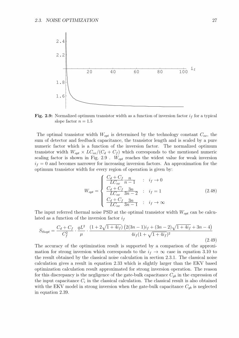
Fig. 2.9: Normalized optimum transistor width as a function of inversion factor if for a typicalslope factor n = 1.5
The optimal transistor width Wopt is determined by the technology constant Cox, thesum of detector and feedback capacitance, the transistor length and is scaled by a purenumeric factor which is a function of the inversion factor. The normalized optimumtransistor width Wopt × LCox/(Cd + Cf ) which corresponds to the mentioned numericscaling factor is shown in Fig. 2.9 . Wopt reaches the widest value for weak inversionif = 0 and becomes narrower for increasing inversion factors. An approximation for theoptimum transistor width for every region of operation is given by:
Wopt =
Cd + Cf
LCox
nn− 1 : if → 0
Cd + Cf
LCox
3n3n− 2 : if = 1
Cd + Cf
LCox
3n3n− 1 : if → ∞
(2.48)
The input referred thermal noise PSD at the optimal transistor width Wopt can be calcu-lated as a function of the inversion factor if
Sthopt =Cd + Cf
C2f
· qL2
µ·(1 + 2
√1 + 4if )
(2(3n− 1)if + (3n− 2)
√1 + 4if + 3n− 4
)4if (1 +
√1 + 4if )2
(2.49)The accuracy of the optimization result is supported by a comparison of the approxi-mation for strong inversion which corresponds to the if → ∞ case in equation 3.10 tothe result obtained by the classical noise calculation in section 2.3.1. The classical noisecalculation gives a result in equation 2.33 which is slightly larger than the EKV basedoptimization calculation result approximated for strong inversion operation. The reasonfor this discrepancy is the negligence of the gate-bulk capacitance Cgb in the expression ofthe input capacitance Ci in the classical calculation. The classical result is also obtainedwith the EKV model in strong inversion when the gate-bulk capacitance Cgb is neglectedin equation 2.39.
28 CHAPTER 2. CHARGE SENSITIVE AMPLIFIERS
-A
Cf
Vout
Ci Co
Rf
CdIsignal
Inoise
*
Fig. 2.10: CSA with continuous. The noise current source of the feedback resistor is indicatedin dotted blue
2.4 Continuous Reset
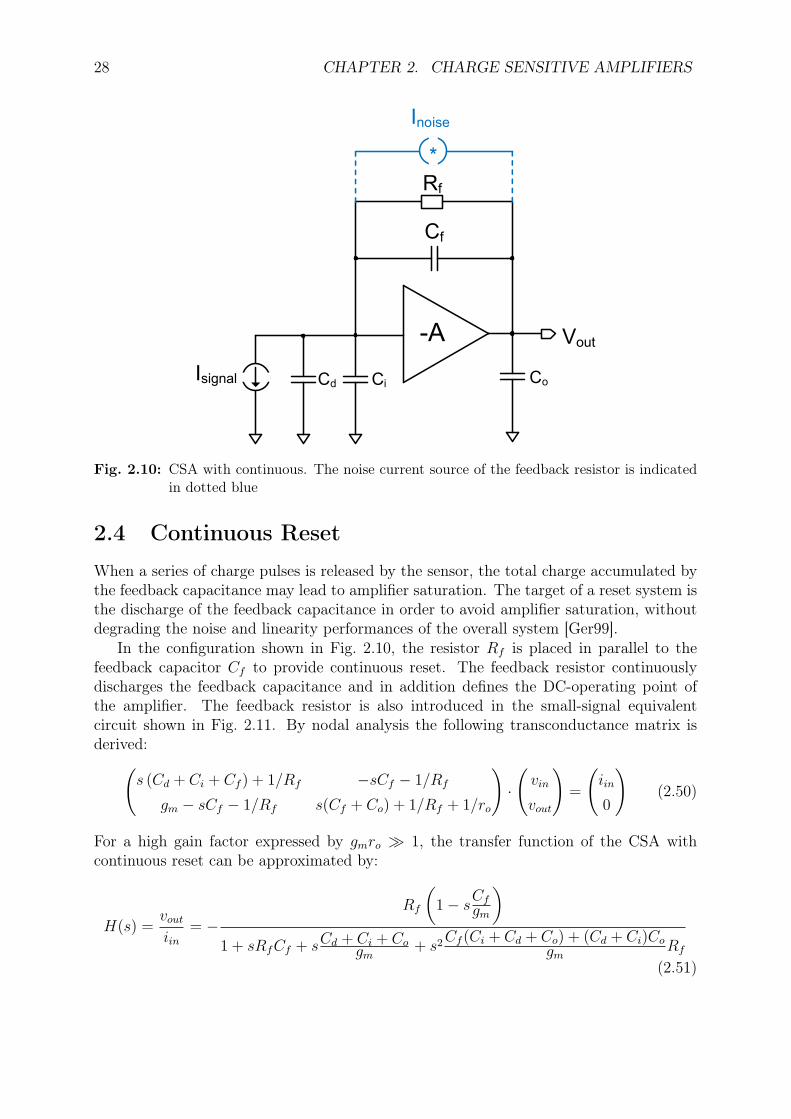
When a series of charge pulses is released by the sensor, the total charge accumulated bythe feedback capacitance may lead to amplifier saturation. The target of a reset system isthe discharge of the feedback capacitance in order to avoid amplifier saturation, withoutdegrading the noise and linearity performances of the overall system [Ger99].
In the configuration shown in Fig. 2.10, the resistor Rf is placed in parallel to thefeedback capacitor Cf to provide continuous reset. The feedback resistor continuouslydischarges the feedback capacitance and in addition defines the DC-operating point ofthe amplifier. The feedback resistor is also introduced in the small-signal equivalentcircuit shown in Fig. 2.11. By nodal analysis the following transconductance matrix isderived:(
s (Cd + Ci + Cf ) + 1/Rf −sCf − 1/Rf
gm − sCf − 1/Rf s(Cf + Co) + 1/Rf + 1/ro
)·
(vin
vout
)=
(iin
0
)(2.50)
For a high gain factor expressed by gmro ≫ 1, the transfer function of the CSA withcontinuous reset can be approximated by:
H(s) =voutiin
= −Rf
(1− s
Cfgm
)1 + sRfCf + sCd + Ci + Co
gm + s2Cf (Ci + Cd + Co) + (Cd + Ci)Co
gm Rf
(2.51)
2.4. CONTINUOUS RESET 29
vout
Rf1
Cf1
Ciiin Cd rogmvinvin~ Co
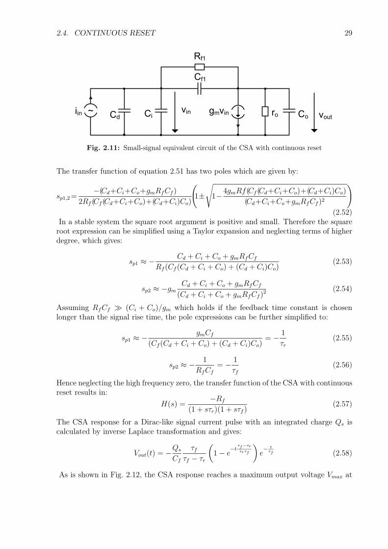
Fig. 2.11: Small-signal equivalent circuit of the CSA with continuous reset
The transfer function of equation 2.51 has two poles which are given by:
sp1,2=−(Cd+Ci+Co+gmRfCf )
2Rf (Cf (Cd+Ci+Co)+(Cd+Ci)Co)
(1±
√1− 4gmRf(Cf (Cd+Ci+Co)+(Cd+Ci)Co)
(Cd+Ci+Co+gmRfCf )2
)(2.52)
In a stable system the square root argument is positive and small. Therefore the squareroot expression can be simplified using a Taylor expansion and neglecting terms of higherdegree, which gives:
sp1 ≈ − Cd + Ci + Co + gmRfCf
Rf (Cf (Cd + Ci + Co) + (Cd + Ci)Co)(2.53)
sp2 ≈ −gmCd + Ci + Co + gmRfCf
(Cd + Ci + Co + gmRfCf )2 (2.54)
Assuming RfCf ≫ (Ci + Co)/gm which holds if the feedback time constant is chosenlonger than the signal rise time, the pole expressions can be further simplified to:
sp1 ≈ − gmCf
(Cf (Cd + Ci + Co) + (Cd + Ci)Co)= − 1
τr(2.55)
sp2 ≈ − 1
RfCf
= − 1
τf(2.56)
Hence neglecting the high frequency zero, the transfer function of the CSA with continuousreset results in:
H(s) =−Rf
(1 + sτr)(1 + sτf )(2.57)
The CSA response for a Dirac-like signal current pulse with an integrated charge Qs iscalculated by inverse Laplace transformation and gives:
Vout(t) = −Qs
Cf
τfτf − τr
(1− e
−tτf−τr
τrτf
)e− t
τf (2.58)
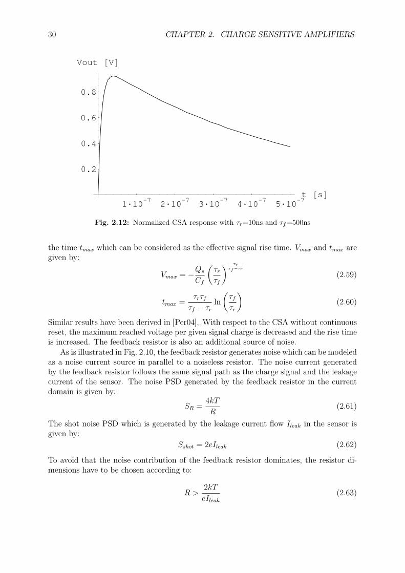
As is shown in Fig. 2.12, the CSA response reaches a maximum output voltage Vmax at
30 CHAPTER 2. CHARGE SENSITIVE AMPLIFIERS
1·10-7 2·10-7 3·10-7 4·10-7 5·10-7t @sD
0.2
0.4
0.6
0.8
Vout @VD
Fig. 2.12: Normalized CSA response with τr=10ns and τf=500ns
the time tmax which can be considered as the effective signal rise time. Vmax and tmax aregiven by:
Vmax = −Qs
Cf
(τrτf
) τrτf−τr
(2.59)
tmax =τrτf
τf − τrln
(τfτr
)(2.60)
Similar results have been derived in [Per04]. With respect to the CSA without continuousreset, the maximum reached voltage per given signal charge is decreased and the rise timeis increased. The feedback resistor is also an additional source of noise.
As is illustrated in Fig. 2.10, the feedback resistor generates noise which can be modeledas a noise current source in parallel to a noiseless resistor. The noise current generatedby the feedback resistor follows the same signal path as the charge signal and the leakagecurrent of the sensor. The noise PSD generated by the feedback resistor in the currentdomain is given by:
SR =4kT
R(2.61)
The shot noise PSD which is generated by the leakage current flow Ileak in the sensor isgiven by:
Sshot = 2eIleak (2.62)
To avoid that the noise contribution of the feedback resistor dominates, the resistor di-mensions have to be chosen according to:
R >2kT
eIleak(2.63)
2.5. PREAMPLIFIER CIRCUIT IMPLEMENTATION 31
VbpM2
M1
Vout
Vin
a) b)
VbpM2
M1
Vout
Vin
VbncM3
VbpM2
M1
Vout
Vin
M3
c)
M4
M5
Vds1
Vgs3
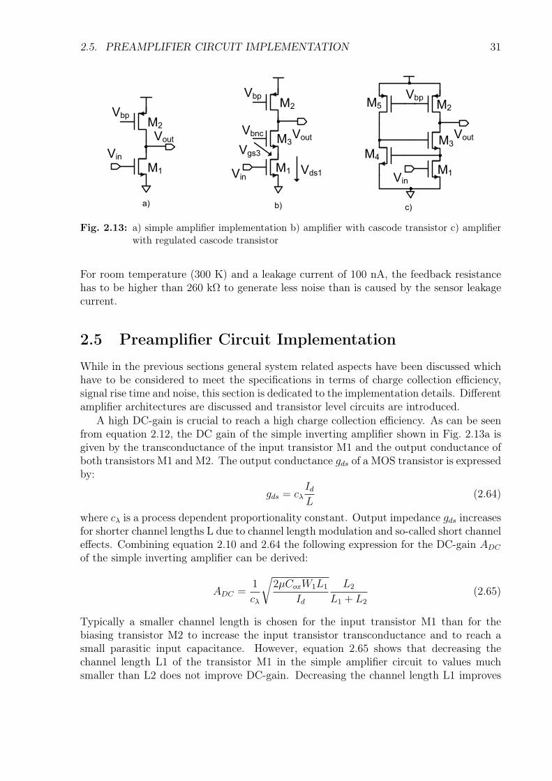
Fig. 2.13: a) simple amplifier implementation b) amplifier with cascode transistor c) amplifierwith regulated cascode transistor
For room temperature (300 K) and a leakage current of 100 nA, the feedback resistancehas to be higher than 260 kΩ to generate less noise than is caused by the sensor leakagecurrent.
2.5 Preamplifier Circuit Implementation
While in the previous sections general system related aspects have been discussed whichhave to be considered to meet the specifications in terms of charge collection efficiency,signal rise time and noise, this section is dedicated to the implementation details. Differentamplifier architectures are discussed and transistor level circuits are introduced.
A high DC-gain is crucial to reach a high charge collection efficiency. As can be seenfrom equation 2.12, the DC gain of the simple inverting amplifier shown in Fig. 2.13a isgiven by the transconductance of the input transistor M1 and the output conductance ofboth transistors M1 and M2. The output conductance gds of a MOS transistor is expressedby:
gds = cλIdL
(2.64)
where cλ is a process dependent proportionality constant. Output impedance gds increasesfor shorter channel lengths L due to channel length modulation and so-called short channeleffects. Combining equation 2.10 and 2.64 the following expression for the DC-gain ADC
of the simple inverting amplifier can be derived:
ADC =1
cλ
√2µCoxW1L1
Id
L2
L1 + L2
(2.65)
Typically a smaller channel length is chosen for the input transistor M1 than for thebiasing transistor M2 to increase the input transistor transconductance and to reach asmall parasitic input capacitance. However, equation 2.65 shows that decreasing thechannel length L1 of the transistor M1 in the simple amplifier circuit to values muchsmaller than L2 does not improve DC-gain. Decreasing the channel length L1 improves
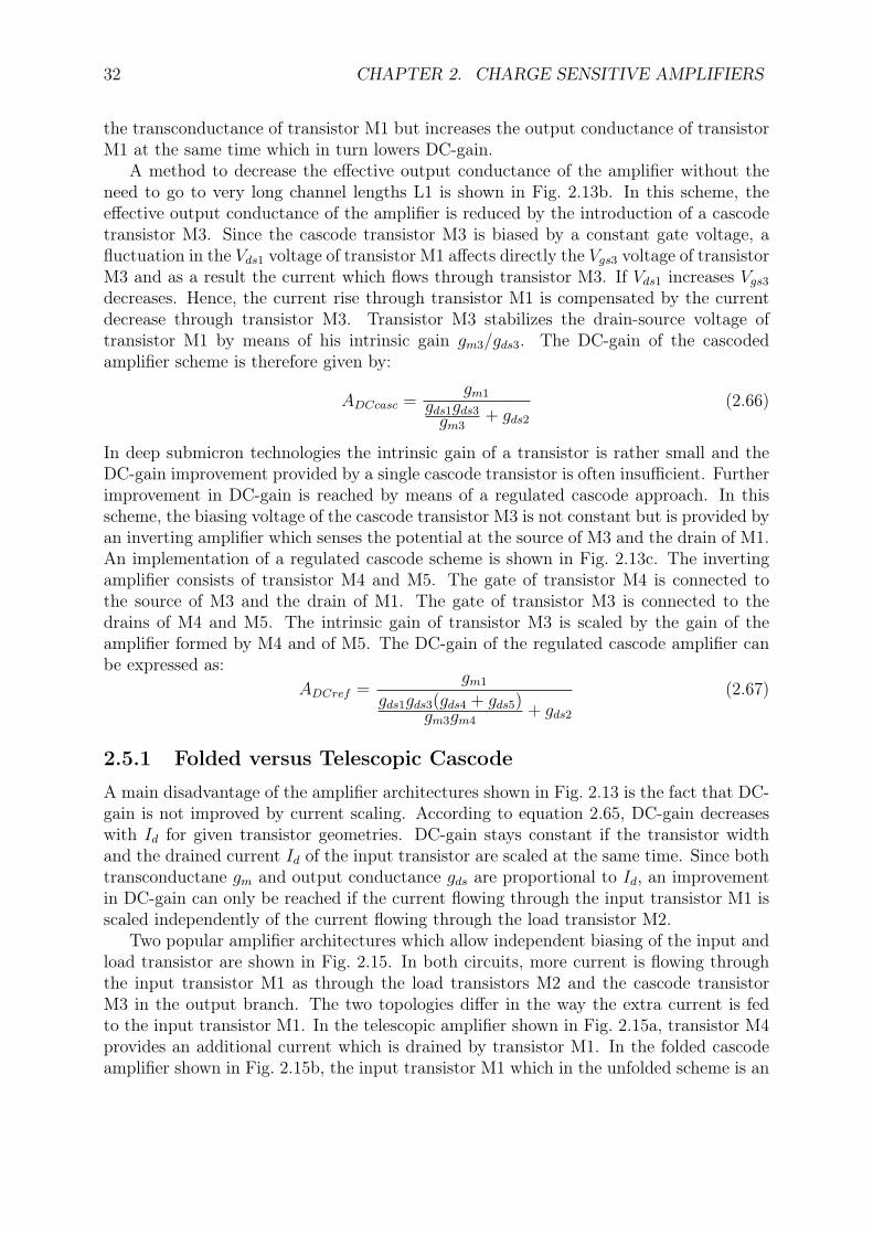
32 CHAPTER 2. CHARGE SENSITIVE AMPLIFIERS
the transconductance of transistor M1 but increases the output conductance of transistorM1 at the same time which in turn lowers DC-gain.
A method to decrease the effective output conductance of the amplifier without theneed to go to very long channel lengths L1 is shown in Fig. 2.13b. In this scheme, theeffective output conductance of the amplifier is reduced by the introduction of a cascodetransistor M3. Since the cascode transistor M3 is biased by a constant gate voltage, afluctuation in the Vds1 voltage of transistor M1 affects directly the Vgs3 voltage of transistorM3 and as a result the current which flows through transistor M3. If Vds1 increases Vgs3
decreases. Hence, the current rise through transistor M1 is compensated by the currentdecrease through transistor M3. Transistor M3 stabilizes the drain-source voltage oftransistor M1 by means of his intrinsic gain gm3/gds3. The DC-gain of the cascodedamplifier scheme is therefore given by:
ADCcasc =gm1
gds1gds3gm3
+ gds2(2.66)
In deep submicron technologies the intrinsic gain of a transistor is rather small and theDC-gain improvement provided by a single cascode transistor is often insufficient. Furtherimprovement in DC-gain is reached by means of a regulated cascode approach. In thisscheme, the biasing voltage of the cascode transistor M3 is not constant but is provided byan inverting amplifier which senses the potential at the source of M3 and the drain of M1.An implementation of a regulated cascode scheme is shown in Fig. 2.13c. The invertingamplifier consists of transistor M4 and M5. The gate of transistor M4 is connected tothe source of M3 and the drain of M1. The gate of transistor M3 is connected to thedrains of M4 and M5. The intrinsic gain of transistor M3 is scaled by the gain of theamplifier formed by M4 and of M5. The DC-gain of the regulated cascode amplifier canbe expressed as:
ADCref =gm1
gds1gds3(gds4 + gds5)gm3gm4
+ gds2
(2.67)
2.5.1 Folded versus Telescopic Cascode
A main disadvantage of the amplifier architectures shown in Fig. 2.13 is the fact that DC-gain is not improved by current scaling. According to equation 2.65, DC-gain decreaseswith Id for given transistor geometries. DC-gain stays constant if the transistor widthand the drained current Id of the input transistor are scaled at the same time. Since bothtransconductane gm and output conductance gds are proportional to Id, an improvementin DC-gain can only be reached if the current flowing through the input transistor M1 isscaled independently of the current flowing through the load transistor M2.
Two popular amplifier architectures which allow independent biasing of the input andload transistor are shown in Fig. 2.15. In both circuits, more current is flowing throughthe input transistor M1 as through the load transistors M2 and the cascode transistorM3 in the output branch. The two topologies differ in the way the extra current is fedto the input transistor M1. In the telescopic amplifier shown in Fig. 2.15a, transistor M4provides an additional current which is drained by transistor M1. In the folded cascodeamplifier shown in Fig. 2.15b, the input transistor M1 which in the unfolded scheme is an
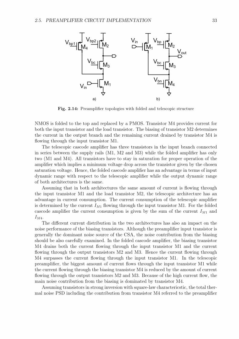
2.5. PREAMPLIFIER CIRCUIT IMPLEMENTATION 33
Vbn
Vbc
VbpM2M1
M3
M4
Vout
Vin
a)
Vbc
Vbp2M2
M1
M3
M4
Vin
Vbp1
b)
Fig. 2.14: Preamplifier topologies with folded and telescopic structure
NMOS is folded to the top and replaced by a PMOS. Transistor M4 provides current forboth the input transistor and the load transistor. The biasing of transistor M2 determinesthe current in the output branch and the remaining current drained by transistor M4 isflowing through the input transistor M1.
The telescopic cascode amplifier has three transistors in the input branch connectedin series between the supply rails (M1, M2 and M3) while the folded amplifier has onlytwo (M1 and M4). All transistors have to stay in saturation for proper operation of theamplifier which implies a minimum voltage drop across the transistor given by the chosensaturation voltage. Hence, the folded cascode amplifier has an advantage in terms of inputdynamic range with respect to the telescopic amplifier while the output dynamic rangeof both architectures is the same.
Assuming that in both architectures the same amount of current is flowing throughthe input transistor M1 and the load transistor M2, the telescopic architecture has anadvantage in current consumption. The current consumption of the telescopic amplifieris determined by the current IM1 flowing through the input transistor M1. For the foldedcascode amplifier the current consumption is given by the sum of the current IM1 andIM4.
The different current distribution in the two architectures has also an impact on thenoise performance of the biasing transistors. Although the preamplifier input transistor isgenerally the dominant noise source of the CSA, the noise contribution from the biasingshould be also carefully examined. In the folded cascode amplifier, the biasing transistorM4 drains both the current flowing through the input transistor M1 and the currentflowing through the output transistors M2 and M3. Hence the current flowing throughM4 surpasses the current flowing through the input transistor M1. In the telescopicpreamplifier, the biggest amount of current flows through the input transistor M1 whilethe current flowing through the biasing transistor M4 is reduced by the amount of currentflowing through the output transistors M2 and M3. Because of the high current flow, themain noise contribution from the biasing is dominated by transistor M4.
Assuming transistors in strong inversion with square-law charactericstic, the total ther-mal noise PSD including the contribution from transistor M4 referred to the preamplifier
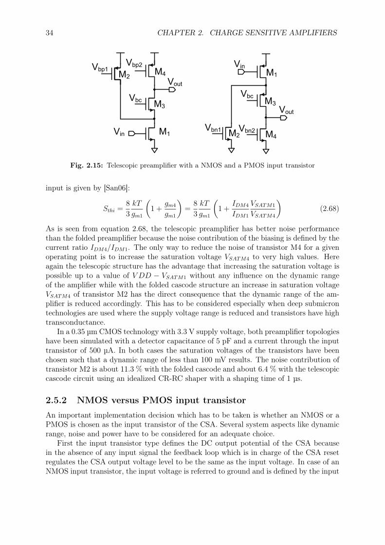
34 CHAPTER 2. CHARGE SENSITIVE AMPLIFIERS
Vbp1
Vbc
Vbp2M2
M1
M3
M4
Vbn2
Vbc
Vin
M4
M3
M1
Vout
VinVbn1
M2
Vout
Fig. 2.15: Telescopic preamplifier with a NMOS and a PMOS input transistor
input is given by [San06]:
Sthi =8
3
kT
gm1
(1 +
gm4
gm1
)=
8
3
kT
gm1
(1 +
IDM4
IDM1
VSATM1
VSATM4
)(2.68)
As is seen from equation 2.68, the telescopic preamplifier has better noise performancethan the folded preamplifier because the noise contribution of the biasing is defined by thecurrent ratio IDM4/IDM1. The only way to reduce the noise of transistor M4 for a givenoperating point is to increase the saturation voltage VSATM4 to very high values. Hereagain the telescopic structure has the advantage that increasing the saturation voltage ispossible up to a value of V DD − VSATM1 without any influence on the dynamic rangeof the amplifier while with the folded cascode structure an increase in saturation voltageVSATM4 of transistor M2 has the direct consequence that the dynamic range of the am-plifier is reduced accordingly. This has to be considered especially when deep submicrontechnologies are used where the supply voltage range is reduced and transistors have hightransconductance.
In a 0.35 µm CMOS technology with 3.3 V supply voltage, both preamplifier topologieshave been simulated with a detector capacitance of 5 pF and a current through the inputtransistor of 500 µA. In both cases the saturation voltages of the transistors have beenchosen such that a dynamic range of less than 100 mV results. The noise contribution oftransistor M2 is about 11.3 % with the folded cascode and about 6.4 % with the telescopiccascode circuit using an idealized CR-RC shaper with a shaping time of 1 µs.
2.5.2 NMOS versus PMOS input transistor
An important implementation decision which has to be taken is whether an NMOS or aPMOS is chosen as the input transistor of the CSA. Several system aspects like dynamicrange, noise and power have to be considered for an adequate choice.
First the input transistor type defines the DC output potential of the CSA becausein the absence of any input signal the feedback loop which is in charge of the CSA resetregulates the CSA output voltage level to be the same as the input voltage. In case of anNMOS input transistor, the input voltage is referred to ground and is defined by the input
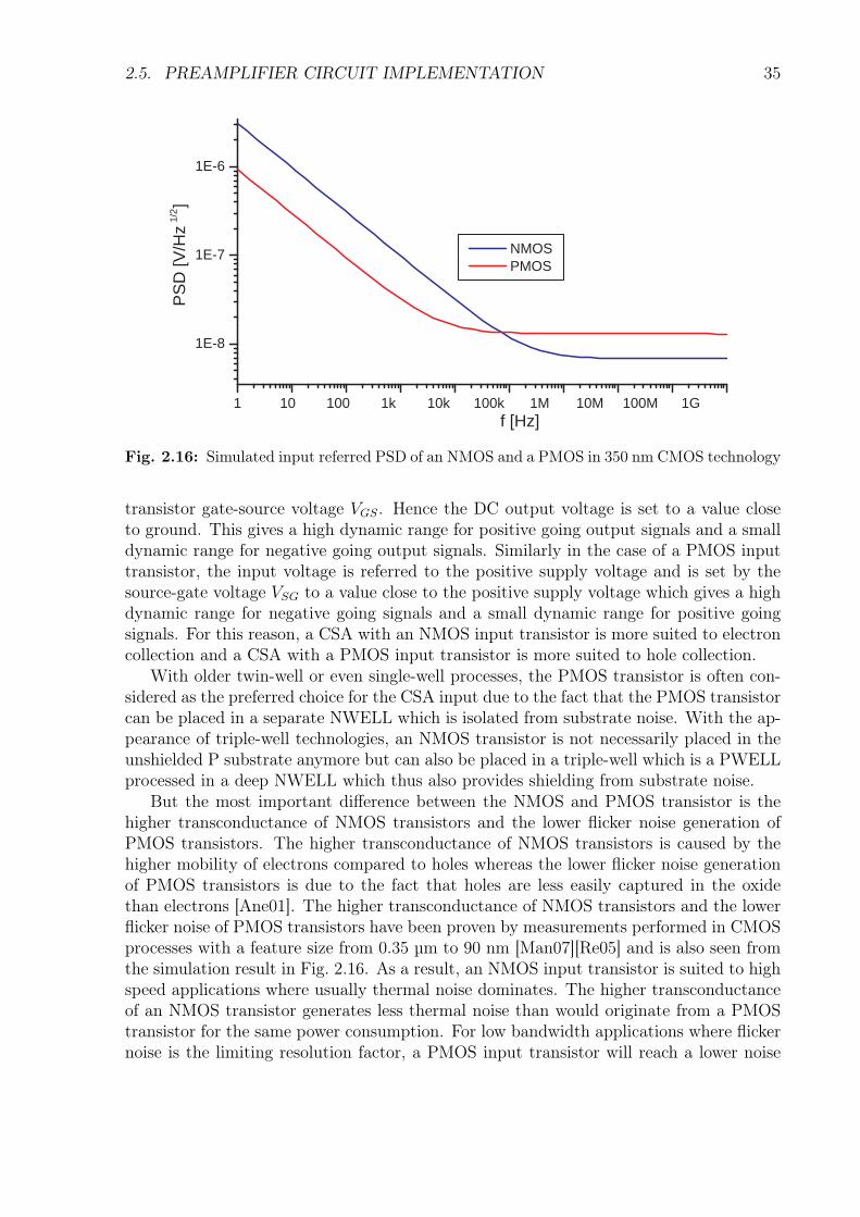
2.5. PREAMPLIFIER CIRCUIT IMPLEMENTATION 35
1 10 100 1k 10k 100k 1M 10M 100M 1G
1E-8
1E-7
1E-6
NMOS PMOS
PS
D [V
/Hz
1/2 ]
f [Hz]
Fig. 2.16: Simulated input referred PSD of an NMOS and a PMOS in 350 nm CMOS technology
transistor gate-source voltage VGS. Hence the DC output voltage is set to a value closeto ground. This gives a high dynamic range for positive going output signals and a smalldynamic range for negative going output signals. Similarly in the case of a PMOS inputtransistor, the input voltage is referred to the positive supply voltage and is set by thesource-gate voltage VSG to a value close to the positive supply voltage which gives a highdynamic range for negative going signals and a small dynamic range for positive goingsignals. For this reason, a CSA with an NMOS input transistor is more suited to electroncollection and a CSA with a PMOS input transistor is more suited to hole collection.
With older twin-well or even single-well processes, the PMOS transistor is often con-sidered as the preferred choice for the CSA input due to the fact that the PMOS transistorcan be placed in a separate NWELL which is isolated from substrate noise. With the ap-pearance of triple-well technologies, an NMOS transistor is not necessarily placed in theunshielded P substrate anymore but can also be placed in a triple-well which is a PWELLprocessed in a deep NWELL which thus also provides shielding from substrate noise.
But the most important difference between the NMOS and PMOS transistor is thehigher transconductance of NMOS transistors and the lower flicker noise generation ofPMOS transistors. The higher transconductance of NMOS transistors is caused by thehigher mobility of electrons compared to holes whereas the lower flicker noise generationof PMOS transistors is due to the fact that holes are less easily captured in the oxidethan electrons [Ane01]. The higher transconductance of NMOS transistors and the lowerflicker noise of PMOS transistors have been proven by measurements performed in CMOSprocesses with a feature size from 0.35 µm to 90 nm [Man07][Re05] and is also seen fromthe simulation result in Fig. 2.16. As a result, an NMOS input transistor is suited to highspeed applications where usually thermal noise dominates. The higher transconductanceof an NMOS transistor generates less thermal noise than would originate from a PMOStransistor for the same power consumption. For low bandwidth applications where flickernoise is the limiting resolution factor, a PMOS input transistor will reach a lower noise
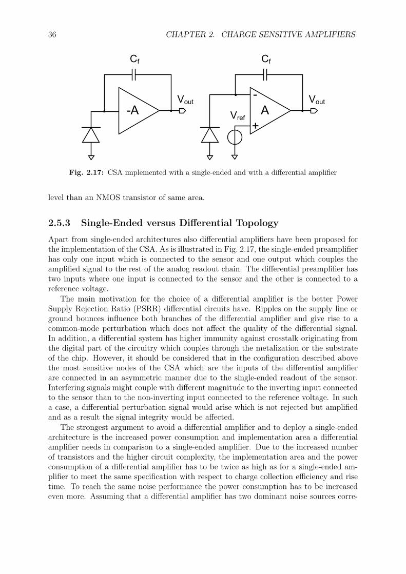
36 CHAPTER 2. CHARGE SENSITIVE AMPLIFIERS
A
Cf
Vout
-A
Cf
Vout-
+
Vref
Fig. 2.17: CSA implemented with a single-ended and with a differential amplifier
level than an NMOS transistor of same area.
2.5.3 Single-Ended versus Differential Topology
Apart from single-ended architectures also differential amplifiers have been proposed forthe implementation of the CSA. As is illustrated in Fig. 2.17, the single-ended preamplifierhas only one input which is connected to the sensor and one output which couples theamplified signal to the rest of the analog readout chain. The differential preamplifier hastwo inputs where one input is connected to the sensor and the other is connected to areference voltage.
The main motivation for the choice of a differential amplifier is the better PowerSupply Rejection Ratio (PSRR) differential circuits have. Ripples on the supply line orground bounces influence both branches of the differential amplifier and give rise to acommon-mode perturbation which does not affect the quality of the differential signal.In addition, a differential system has higher immunity against crosstalk originating fromthe digital part of the circuitry which couples through the metalization or the substrateof the chip. However, it should be considered that in the configuration described abovethe most sensitive nodes of the CSA which are the inputs of the differential amplifierare connected in an asymmetric manner due to the single-ended readout of the sensor.Interfering signals might couple with different magnitude to the inverting input connectedto the sensor than to the non-inverting input connected to the reference voltage. In sucha case, a differential perturbation signal would arise which is not rejected but amplifiedand as a result the signal integrity would be affected.
The strongest argument to avoid a differential amplifier and to deploy a single-endedarchitecture is the increased power consumption and implementation area a differentialamplifier needs in comparison to a single-ended amplifier. Due to the increased numberof transistors and the higher circuit complexity, the implementation area and the powerconsumption of a differential amplifier has to be twice as high as for a single-ended am-plifier to meet the same specification with respect to charge collection efficiency and risetime. To reach the same noise performance the power consumption has to be increasedeven more. Assuming that a differential amplifier has two dominant noise sources corre-
2.6. SUMMARY 37
sponding to the input transistors, the output referred PSD magnitude of a single inputtransistor has to be halved to get the RMS noise equality between a differential and asingle-ended amplifier. This is seen when the contribution of the second input transistoris included into the thermal noise PSD expression. The second input transistor which hasits gate connected to the reference voltage generates noise in the current domain. Thenoise current is then referred to the sensor input node by the transconductance of thefirst transistor. The total thermal noise PSD for the differential amplifier is given by:
Sthdiff =8
3kT
gm1 + gm2
g2m1
(2.69)
Since both input transistors have the same transconductance, the noise PSD for thedifferential amplifier simplifies to:
Sthdiff =16
3kT
1
gm1
(2.70)
The transconductance of the differential input transistors has to be doubled with respectto the single-ended amplifier to reach the same thermal noise level. For constant geometryand transistors biased in strong inversion this leads to an increase of current by a factor of4 through both input transistors which results in an overall increase of power consumptionby a factor of 8. In a similar manner, to decrease the flicker noise caused by the differentialinput transistors by a factor of two, the area of both input transistors has to be doubledwhich results in an overall area increase by a factor of 4.
2.6 SummaryIn this chapter, functionality block of the CSA have been introduced and basic parame-ters like charge collection efficiency, signal rise time and noise have been reviewed. Thenoise optimization methodology based on capacitive matching between the detector ca-pacitance and the CSA input transistor capacitance has been formulated in terms of theEKV model. In addition, the trade-offs of different CSA implementations have been dis-cussed. A differential amplifier should be used if PSRR is a concern. For power and noiseoptimization the single-ended counterpart should be preferred. The telescopic cascodeamplifier has less noise originating from the biasing and has a higher dynamic outputrange than the folded cascode amplifier. PMOS input transistors should be used for slowand ultra-low noise applications. NMOS transistors placed in a tripple-well should beused for high-rate applications.
Chapter 3
The Shaper
A shaper is a band-pass filter which is added to the signal processing chain to filter and toshape the CSA output signal. Filtering is applied to attenuate spectral noise componentswhich are located outside the frequency band of interest. An improvement in SNR isachieved when flicker noise at low frequencies and thermal noise at high frequencies getdamped. Pulse shaping is required to adapt the output signal form to the expected hit-rate in the experiment. Typically, a long feedback time constant is chosen for the CSAwith continuous-reset, to achieve a high charge collection efficiency and to decrease thenoise contribution of the CSA feedback transistor. If the interaction rate in the detectoris higher than the CSA feedback time constant, the generated signal pulses will tendto overlap at the CSA output. Since the information of the charge signal magnitudeis embedded in the output signal pulse amplitude it is desirable to avoid the describedpile-up effect by shortening the pulse decay time through subsequent signal shaping.
3.1 Matched Filter for Optimum SNRIn the classic theory of filtering for particle physics experiments and nuclear spectroscopy,the main concern is the maximization of the SNR. The idea of an optimum linear filteris introduced which serves as a reference for existing filter implementations [Rad67]. Itcan be shown that in the presence of white noise, the optimum filtering is provided bythe matched filter design [Nor63]. Assuming that the transfer function of the matchedfilter is given by M(f), the noise PSD is given by XN(f) = N0 and the signal spectrum isgiven by XS(f), the ratio of the signal-to-noise power ρ at the time t0 is given by inverseFourier transform:
ρ =
∣∣∣∣ ∞∫−∞
XS(f)M(f)ej2πft0df
∣∣∣∣2N0
∞∫−∞
|M(f)|2 df(3.1)
Applying the Schwartz inequality given by:∣∣∣∣∣∣∞∫
−∞
X1(f)X2(f)df
∣∣∣∣∣∣2
≤∞∫
−∞
|X1(f)|2 df∞∫
−∞
|X2(f)|2 df (3.2)
38
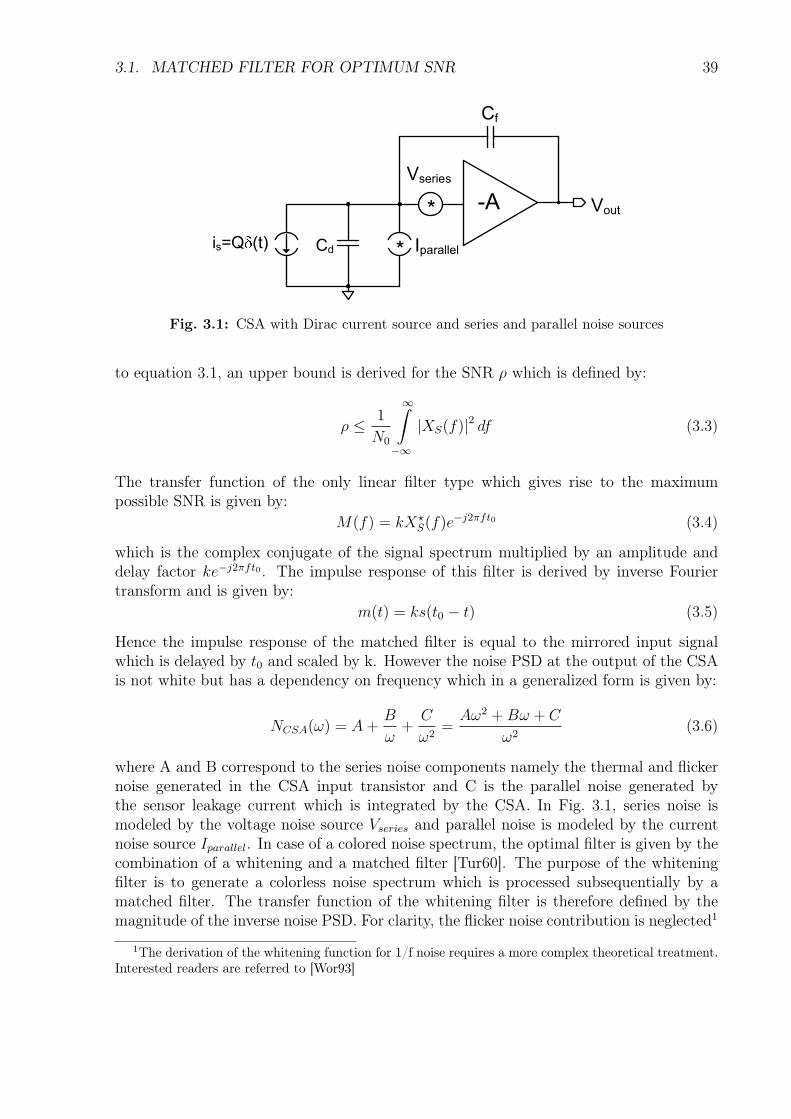
3.1. MATCHED FILTER FOR OPTIMUM SNR 39
-A
Cf
Vseries
Vout
Cd Iparallel
*
*is=Q (t)
Fig. 3.1: CSA with Dirac current source and series and parallel noise sources
to equation 3.1, an upper bound is derived for the SNR ρ which is defined by:
ρ ≤ 1
N0
∞∫−∞
|XS(f)|2 df (3.3)
The transfer function of the only linear filter type which gives rise to the maximumpossible SNR is given by:
M(f) = kX⋆S(f)e
−j2πft0 (3.4)
which is the complex conjugate of the signal spectrum multiplied by an amplitude anddelay factor ke−j2πft0 . The impulse response of this filter is derived by inverse Fouriertransform and is given by:
m(t) = ks(t0 − t) (3.5)
Hence the impulse response of the matched filter is equal to the mirrored input signalwhich is delayed by t0 and scaled by k. However the noise PSD at the output of the CSAis not white but has a dependency on frequency which in a generalized form is given by:
NCSA(ω) = A+B
ω+
C
ω2=
Aω2 +Bω + C
ω2(3.6)
where A and B correspond to the series noise components namely the thermal and flickernoise generated in the CSA input transistor and C is the parallel noise generated bythe sensor leakage current which is integrated by the CSA. In Fig. 3.1, series noise ismodeled by the voltage noise source Vseries and parallel noise is modeled by the currentnoise source Iparallel. In case of a colored noise spectrum, the optimal filter is given by thecombination of a whitening and a matched filter [Tur60]. The purpose of the whiteningfilter is to generate a colorless noise spectrum which is processed subsequentially by amatched filter. The transfer function of the whitening filter is therefore defined by themagnitude of the inverse noise PSD. For clarity, the flicker noise contribution is neglected1
1The derivation of the whitening function for 1/f noise requires a more complex theoretical treatment.Interested readers are referred to [Wor93]
40 CHAPTER 3. THE SHAPER
-1 1 2 3 4t
ΤC
0.2
0.4
0.6
0.8
1
hCSAW HtL
h0
Fig. 3.2: Normalized impulse response of the filter matched to the CSA/whitening-filter systemwith a measurement time of tm = 3τc
(B=0). The transfer function of the whitening filter is then given by:
W (ω) =1√C
jω
1 + jωτc(3.7)
where τc is the noise corner time constant. The noise corner time constant τc is the inverseof the angular frequency at which the series noise and the parallel noise contributionsreferred to the CSA output are equal. τc is defined by:
τc =
√A
C(3.8)
As is seen from equation 3.7, the CSA whitening filter which neglects the flicker noisecomponent can be implemented as a simple CR differentiation stage. The impulse re-sponse at the output of the whitening filter connected in series to the CSA is then givenby the inverse Fourier transformation:
hCSAW (t) = F−1 CSA(ω) ·W (ω) = F−1
Q
Cf
· 1/√C
1 + jωτc
=
1√ACf
e−t/τc (3.9)
where Q is the charge signal integrated on the CSA feedback capacitor Cf . Accordingto equation 3.5, the impulse response m(t) of the matched filter is the mirror image ofthe function derived in 3.9 delayed by t0. A realizable filter has to be causal which meansthat the filter cannot respond before the signal arrives. As a consequence, the functionm(t) has to be delayed by the measurement time t0 = tm and truncated for t < 0 as isshown in Fig. 3.2 for tm = 3τc. For k = Cf/Q, the matched filter response m(t) is then

3.1. MATCHED FILTER FOR OPTIMUM SNR 41
2.5 5 7.5 10 12.5 15t
ΤC
0.2
0.4
0.6
0.8
hout HtL
h0
Fig. 3.3: Normalized response to a Dirac like charge signal pulse given by the CSA with optimalfilter configuration and a measurement time of tm = 3τc
given by a piecewise-defined function:
m(t) =
0 : t ≤ 0
e(t−tm)/τc : 0 < t < tm
0 : t ≥ tm
(3.10)
The SNR is calculated according to equation 3.1 and using Parsevals theorem which gives:
ρ(tm) =Q2
C2fA
tm∫0
e−2t/τcdt =Q2
C2fA
τc2
(1− e−2tm/τc
)(3.11)
Neglecting the flicker noise contribution, the maximum possible SNR which is reached forthe CSA using the optimum filter and an infinitely long measurement time tm is hencegiven by:
ρmax = limtm→∞
ρ(tm) =Q2
C2fA
τc2
=Q2
C2f
1
2√AC
(3.12)
The response hout(t) which arises for a Dirac like charge signal pulse at the end ofthe complete signal processing chain composed of CSA, whitening and matched filter iscalculated by the convolution of the functions given in equation 3.9 and 3.10 and is givenby:
hout(t) =
t∫0
hCSAW (τ)m(t− τ)dτ =
QCf
τc2e(t−tm)/τc
(1− e−2t/τc
): t < tm
QCf
τc2e−(t−tm)/τc
(1− e−2tm/τc
): t ≥ tm
(3.13)
As is seen in Fig. 3.3, the output response peaks at the end of the measurement timetm and has an exponential decay with the noise corner time constant τc. According to
42 CHAPTER 3. THE SHAPER
equation 3.11, the measurement time tm has to be a few multiples of the noise timeconstant τc to reach SNR values close to the optimum. As a consequence the classicalnoise optimization methodology using a whitening filter section followed by a matchedfilter is inapplicable when the noise corner time constant τc does not match the hit ratein the experiment. In addition, existing optimum filter implementations are based ontime-variant and switched structures which change their filter weighting function withtime. Often, the required implementation complexity collides with the need for smallimplementation area and low power consumption in multi channel readout ASICs. As aresult sub-optimal filters with less circuit complexity are in many cases preferred.
3.2 Gaussian FilterAnother theoretic filter concept which has been applied to particle physics and nuclearspectroscopy instrumentation is Gaussian filtering [Ohk76]. A main advantage of theGaussian filter is a small bandwidth rise-time product [Kla59]. In general, the aim of afilter is to reduce the bandwidth as much as possible. In high rate applications, short riseand fall times of the output signal are also appreciated to reach small pile-up probability.Since the charge signal is integrated by the CSA, the first stage of the pulse formingnetwork is an ideal differentiator. The differentiator is followed by an ideal Gaussianfilter. The frequency characteristics of an ideal Gaussian filter system are given by:
H(ω) =c0√2π
e−12σ2ω2
(3.14)
where c0 is a proportionality constant and σ is the standard deviation of the normaldistribution. An interesting property of the Gaussian filter is that the amplitude-responsein the frequency domain has the same Gauss characteristic as the impulse response in thetime domain which can be expressed as:
h(t) =c0√2πσ
e−t2
2σ2 (3.15)
Assuming a Dirac like charge input signal and the noise PSD NCSA(ω) at the CSAoutput defined in equation 3.6, the SNR using the filtering system composed of a Gaussianfilter in series with an ideal differentiator is given by:
ρ =
(QCf
)2 ∞∫0
H(ω)2dω
∞∫0
ω2NCSA(ω)H(ω)2dω
=
(Q
Cf
)22√πσ2
2√πAσ2 + 2Bσ +
√πC
(3.16)
The ideal Gaussian filter is non-causal and therefore a Gaussian waveform cannot beachieved by a physically realizable network. For a Dirac pulse which is applied at t=0,the impulse response begins at negative infinity. Therefore the Gauss waveform has tobe delayed by an infinite amount of time using an infinite amount of delay components.The Gaussian filter, however, is relatively easily approximated over the most important

3.2. GAUSSIAN FILTER 43
region, which is the low-attenuation frequency band [Kla59]. Several approaches for theapproximation of the Gaussian filter have been proposed. The scheme based on cascadedRC low-pass stages will be discussed in section 3.3 due to the very common usage ofthis implementation in HEP applications. An alternative approach which has a higherefficiency due to the smaller amount of required filter stages is based on direct synthesisof the amplitude response using series expansion.Assuming that the Gaussian filter can be expressed as:
H(jω) =H0
D(jω)(3.17)
the amplitude characteristic |H(ω)|2 of the Gaussian filter can be written as:
H(jω)H(−jω) = |H(ω)|2 (3.18)
Combining equations 3.17 and 3.14 and setting c0 = 1, equation 3.18 is translated withoutloss of generality to:
D(jω)D(−jω) =1
2πH0
eσ2ω2
(3.19)
Substituting p = σjω = σs, using proper normalization and applying Taylor series ex-pansion to equation 3.19 gives:
D(p)D(−p) = e−p2 = 1− p2 +p4
2!− p6
3!+ ...+ (−1)n
p2n
n!(3.20)
Neglecting terms above n=1, results in:
Dn=1(p)Dn=1(−p) = 1− p2 = (1 + p)(1− p) (3.21)
Thus Dn=1(p) is given by:Dn=1(p) ≈ 1 + p (3.22)
Hence for n=1, the Gauss function is approximated by a function with a real pole at -1on the p-plane. Including terms of the Taylor series expansion given in equation 3.20 upto n=2, results in:
Dn=2(p)Dn=2(−p) = 1− p2 +p4
2!(3.23)
=(√1 + j + p)(
√1− j + p)(
√1 + j − p)(
√1− j − p)
2(3.24)
Dn=2(p) is hence given by the complex conjugate pole pair:
Dn=2(p) =1√2
√√2 + 1
2+ j
√√2− 1
2+ p
√√2 + 1
2− j
√√2− 1
2+ p
(3.25)
Thus for n=2, the Gauss filter is approximated by a function which has two complex conju-gate poles. For higher order filter synthesis, the poles are derived numerically. According
44 CHAPTER 3. THE SHAPER
0 2 4 6 8 10ω
1015
1012
109
106
0.001
1
H ω2
H0
σ
n=3
n=4
n=5
n=6
n=7
Gauss function
Fig. 3.4: Amplitude frequency characteristics of the approximated Gaussian filters
to this, the Gauss filter is synthesized by factorization of the Taylor series expansion of thesquare of the Gauss function. The transfer function Hn(s) of the approximated Gaussianfilter is then given by:
Hn(s) =
sp0
k∏i=1
s2pi
(σs+ sp0)k∏
i=1
(σs+ spi)(σs+ s∗pi)
: n odd
k∏i=1
s2pi
k∏i=1
(σs+ spi)(σs+ s∗pi)
: n even
(3.26)
where sp0 is the real pole, (spi, s∗pi) is the i-th complex pole pair and k is the number ofcomplex pole pairs. The numerator of equation 3.26 is the normalization factor whichgives Hn(s = 0) = 1.
In Fig. 3.4, the amplitude characteristic of approximated Gaussian filters with differentn parameters are shown in the frequency domain together with a true Gaussian waveform.It is clearly seen that the attenuation improves with increasing n especially for highfrequencies. Fig. 3.5 illustrates the impulse responses of Gaussian filters with different nparameters. With increasing n, symmetry of rising and falling edge improves. Peaking-time is shifted towards longer values while fall-time is shortened. For a given bandwidth,the output signal has a smaller pile up probability than the unshaped CSA output pulsedue to the small bandwidth rise time product of the Gaussian filter.
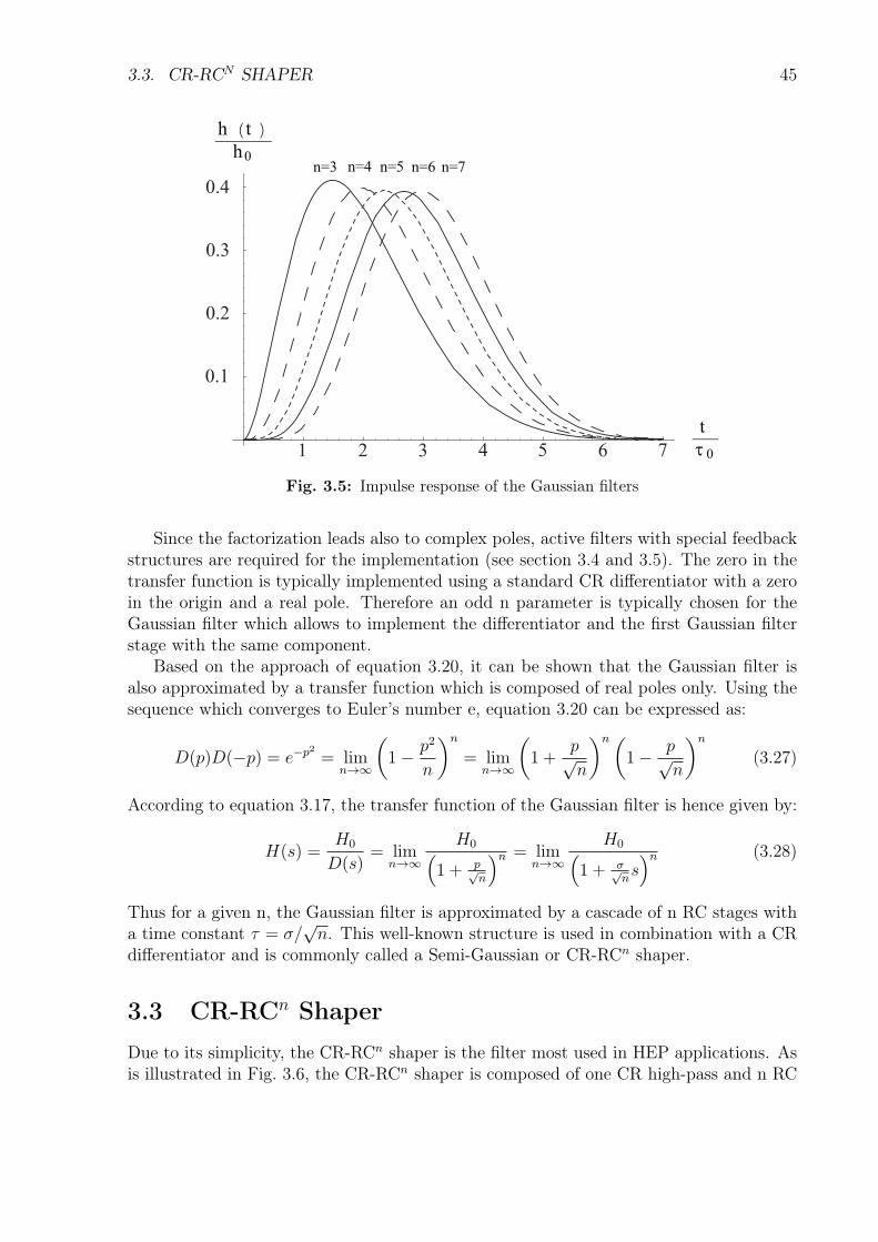
3.3. CR-RCN SHAPER 45
1 2 3 4 5 6 7
t
τ 0
0.1
0.2
0.3
0.4
h t
h0n=3 n=4 n=5 n=6 n=7
Fig. 3.5: Impulse response of the Gaussian filters
Since the factorization leads also to complex poles, active filters with special feedbackstructures are required for the implementation (see section 3.4 and 3.5). The zero in thetransfer function is typically implemented using a standard CR differentiator with a zeroin the origin and a real pole. Therefore an odd n parameter is typically chosen for theGaussian filter which allows to implement the differentiator and the first Gaussian filterstage with the same component.
Based on the approach of equation 3.20, it can be shown that the Gaussian filter isalso approximated by a transfer function which is composed of real poles only. Using thesequence which converges to Euler’s number e, equation 3.20 can be expressed as:
D(p)D(−p) = e−p2 = limn→∞
(1− p2
n
)n
= limn→∞
(1 +
p√n
)n(1− p√
n
)n
(3.27)
According to equation 3.17, the transfer function of the Gaussian filter is hence given by:
H(s) =H0
D(s)= lim
n→∞
H0(1 + p√
n
)n = limn→∞
H0(1 + σ√
ns)n (3.28)
Thus for a given n, the Gaussian filter is approximated by a cascade of n RC stages witha time constant τ = σ/
√n. This well-known structure is used in combination with a CR
differentiator and is commonly called a Semi-Gaussian or CR-RCn shaper.
3.3 CR-RCn ShaperDue to its simplicity, the CR-RCn shaper is the filter most used in HEP applications. Asis illustrated in Fig. 3.6, the CR-RCn shaper is composed of one CR high-pass and n RC
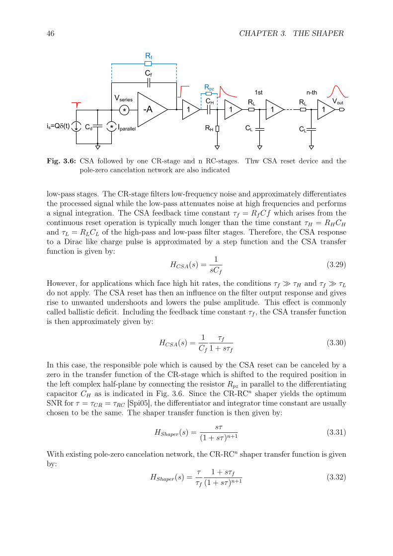
46 CHAPTER 3. THE SHAPER
-A
Cf
Vseries
Cd Iparallel
*
*is=Q (t)
1 1 1 1CH
RH
RL
CL
RL
CL
Vout
1st n-th
Rf
Rpz
Fig. 3.6: CSA followed by one CR-stage and n RC-stages. Thw CSA reset device and thepole-zero cancelation network are also indicated
low-pass stages. The CR-stage filters low-frequency noise and approximately differentiatesthe processed signal while the low-pass attenuates noise at high frequencies and performsa signal integration. The CSA feedback time constant τf = RfCf which arises from thecontinuous reset operation is typically much longer than the time constant τH = RHCH
and τL = RLCL of the high-pass and low-pass filter stages. Therefore, the CSA responseto a Dirac like charge pulse is approximated by a step function and the CSA transferfunction is given by:
HCSA(s) =1
sCf
(3.29)
However, for applications which face high hit rates, the conditions τf ≫ τH and τf ≫ τLdo not apply. The CSA reset has then an influence on the filter output response and givesrise to unwanted undershoots and lowers the pulse amplitude. This effect is commonlycalled ballistic deficit. Including the feedback time constant τf , the CSA transfer functionis then approximately given by:
HCSA(s) =1
Cf
τf1 + sτf
(3.30)
In this case, the responsible pole which is caused by the CSA reset can be canceled by azero in the transfer function of the CR-stage which is shifted to the required position inthe left complex half-plane by connecting the resistor Rpz in parallel to the differentiatingcapacitor CH as is indicated in Fig. 3.6. Since the CR-RCn shaper yields the optimumSNR for τ = τCR = τRC [Spi05], the differentiator and integrator time constant are usuallychosen to be the same. The shaper transfer function is then given by:
HShaper(s) =sτ
(1 + sτ)n+1(3.31)
With existing pole-zero cancelation network, the CR-RCn shaper transfer function is givenby:
HShaper(s) =τ
τf
1 + sτf(1 + sτ)n+1
(3.32)
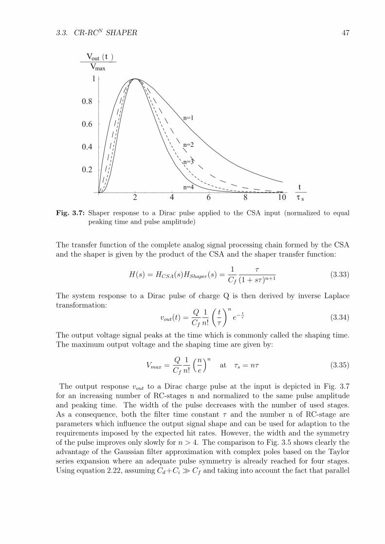
3.3. CR-RCN SHAPER 47
2 4 6 8 10
t
τ s
0.2
0.4
0.6
0.8
1
Vout t
Vmax
n=4
n=1
n=3
n=2
Fig. 3.7: Shaper response to a Dirac pulse applied to the CSA input (normalized to equalpeaking time and pulse amplitude)
The transfer function of the complete analog signal processing chain formed by the CSAand the shaper is given by the product of the CSA and the shaper transfer function:
H(s) = HCSA(s)HShaper(s) =1
Cf
τ
(1 + sτ)n+1(3.33)
The system response to a Dirac pulse of charge Q is then derived by inverse Laplacetransformation:
vout(t) =Q
Cf
1
n!
(t
τ
)n
e−tτ (3.34)
The output voltage signal peaks at the time which is commonly called the shaping time.The maximum output voltage and the shaping time are given by:
Vmax =Q
Cf
1
n!
(ne
)nat τs = nτ (3.35)
The output response vout to a Dirac charge pulse at the input is depicted in Fig. 3.7for an increasing number of RC-stages n and normalized to the same pulse amplitudeand peaking time. The width of the pulse decreases with the number of used stages.As a consequence, both the filter time constant τ and the number n of RC-stage areparameters which influence the output signal shape and can be used for adaption to therequirements imposed by the expected hit rates. However, the width and the symmetryof the pulse improves only slowly for n > 4. The comparison to Fig. 3.5 shows clearly theadvantage of the Gaussian filter approximation with complex poles based on the Taylorseries expansion where an adequate pulse symmetry is already reached for four stages.Using equation 2.22, assuming Cd+Ci ≫ Cf and taking into account the fact that parallel
48 CHAPTER 3. THE SHAPER
noise contributions have the same propagation path as the charge signal, the noise PSDat the CSA output is given by:
NCSA(ω) =(Cd + Ci)
2
C2f
(A+
B
ω
)+
1
C2f
C
ω2(3.36)
where A and B describe series noise contributions (thermal and flicker noise of the CSA)and C denotes parallel noise (leakage current shot noise and feedback resistor thermalnoise). The RMS noise voltage at the shaper output is then calculated by:
V 2RMS =
∞∫0
((Cd + Ci)
2
C2f
(A+
B
ω
)+
1
C2f
C
ω2
)ω2τ 2
(1 + ω2τ 2)n+1df (3.37)
=(Cd + Ci)
2
C2f
(Γ(2n−1
2
)8√πΓ(n− 1)
A
τ+
B
4πn
)+
1
C2f
Γ(2n−1
2
)(2n− 1)
8√πΓ(n− 1)
Cτ (3.38)
In HEP applications, a noise to signal ratio is introduced which is given by the ratio ofthe RMS noise voltage VRMS to the signal pulse height Vmax(qe) for a charge signal of asingle electron. This definition corresponds to the equivalent input noise of the CSA andis called Equivalent Noise Charge (ENC).
ENC =VRMS
Vmax(Q = qe)(3.39)
The ENC for the CSA with a CR-RCn shaper is given in numbers of electrons by:
ENC2 =ne2nn!
8√πn2n+1q2e
[(Cd + Ci)
2
(Γ(
2n−1
2
) A
τ+
2(n− 1)!√π
B
)+ Γ
(2n−1
2
)(2n− 1)Cτ
](3.40)
To get the ENC in electrons the ENC value from equation 3.40 has to be divided bythe charge of an electron. Equation 3.40 shows that the CSA thermal (A) and flicker (B)noise which are both series noise sources scale with the detector capacitance Cd and theCSA input capacitance Ci whereas the contribution of the parallel noise sources (C) tothe ENC is independent of Cd and Ci. Equation 3.40 also reveals that the individual noisesources scale differently with the shaping time. As is illustrated in Fig. 3.8, the influenceof the CSA thermal noise decreases with the shaping time whereas the impact of theparallel noise sources like the sensor leakage current and the thermal noise generated bythe CSA feedback transistor increases with the shaping time. For the optimum shapingtime τopt, the ENC contribution of the CSA thermal noise and the parallel noise is equal.The flicker noise is independent of the shaping time. CSA flicker noise increases the totalENC level and flattens out the ENC minimum. The optimum shaping time τopt for whichthe ENC minimum is reached, is given by:
τopt =
√A
C(2n− 1)=
τc√2n− 1
(3.41)
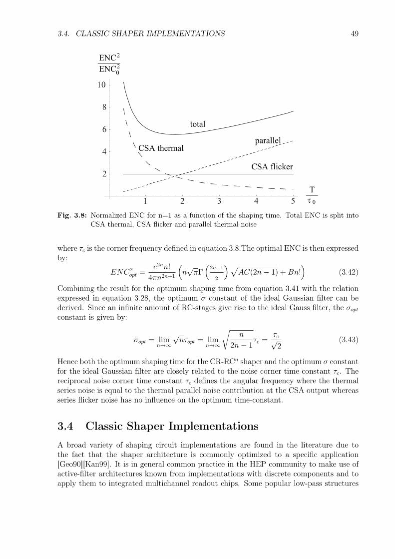
3.4. CLASSIC SHAPER IMPLEMENTATIONS 49
1 2 3 4 5
Τ
τ 0
2
4
6
8
10
ENC2
ENC02
total
parallel
CSA flicker
CSA thermal
Fig. 3.8: Normalized ENC for n=1 as a function of the shaping time. Total ENC is split intoCSA thermal, CSA flicker and parallel thermal noise
where τc is the corner frequency defined in equation 3.8.The optimal ENC is then expressedby:
ENC2opt =
e2nn!
4πn2n+1
(n√πΓ(
2n−1
2
)√AC(2n− 1) +Bn!
)(3.42)
Combining the result for the optimum shaping time from equation 3.41 with the relationexpressed in equation 3.28, the optimum σ constant of the ideal Gaussian filter can bederived. Since an infinite amount of RC-stages give rise to the ideal Gauss filter, the σopt
constant is given by:
σopt = limn→∞
√nτopt = lim
n→∞
√n
2n− 1τc =
τc√2
(3.43)
Hence both the optimum shaping time for the CR-RCn shaper and the optimum σ constantfor the ideal Gaussian filter are closely related to the noise corner time constant τc. Thereciprocal noise corner time constant τc defines the angular frequency where the thermalseries noise is equal to the thermal parallel noise contribution at the CSA output whereasseries flicker noise has no influence on the optimum time-constant.
3.4 Classic Shaper Implementations
A broad variety of shaping circuit implementations are found in the literature due tothe fact that the shaper architecture is commonly optimized to a specific application[Geo90][Kan99]. It is in general common practice in the HEP community to make use ofactive-filter architectures known from implementations with discrete components and toapply them to integrated multichannel readout chips. Some popular low-pass structures
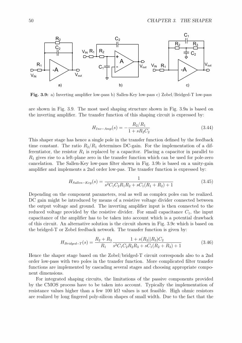
50 CHAPTER 3. THE SHAPER
-AVoutVIN
C2
R2
R1A
Vout
VIN
C2
R2R1
-
+
C1VIN Vout
C1
R1
R2 R3
C2
-A
a) b) c)
Fig. 3.9: a) Inverting amplifier low-pass b) Sallen-Key low-pass c) Zobel/Bridged-T low-pass
are shown in Fig. 3.9. The most used shaping structure shown in Fig. 3.9a is based onthe inverting amplifier. The transfer function of this shaping circuit is expressed by:
HInv−Amp(s) = − R2/R1
1 + sR2C2
(3.44)
This shaper stage has hence a single pole in the transfer function defined by the feedbacktime constant. The ratio R2/R1 determines DC-gain. For the implementation of a dif-ferentiator, the resistor R1 is replaced by a capacitor. Placing a capacitor in parallel toR1 gives rise to a left-plane zero in the transfer function which can be used for pole-zerocancelation. The Sallen-Key low-pass filter shown in Fig. 3.9b is based on a unity-gainamplifier and implements a 2nd order low-pas. The transfer function is expressed by:
HSallen−Key(s) =1
s2C1C2R1R2 + sC1(R1 +R2) + 1(3.45)
Depending on the component parameters, real as well as complex poles can be realized.DC gain might be introduced by means of a resistive voltage divider connected betweenthe output voltage and ground. The inverting amplifier input is then connected to thereduced voltage provided by the resistive divider. For small capacitance C1, the inputcapacitance of the amplifier has to be taken into account which is a potential drawbackof this circuit. An alternative solution is the circuit shown in Fig. 3.9c which is based onthe bridged-T or Zobel feedback network. The transfer function is given by:
HBridged−T (s) =R2 +R3
R1
1 + s(R2||R3)C2
s2C1C2R2R3 + sC1(R2 +R3) + 1(3.46)
Hence the shaper stage based on the Zobel/bridged-T circuit corresponds also to a 2ndorder low-pass with two poles in the transfer function. More complicated filter transferfunctions are implemented by cascading several stages and choosing appropriate compo-nent dimensions.
For integrated shaping circuits, the limitations of the passive components providedby the CMOS process have to be taken into account. Typically the implementation ofresistance values higher than a few 100 kΩ values is not feasible. High ohmic resistorsare realized by long fingered poly-silicon shapes of small width. Due to the fact that the
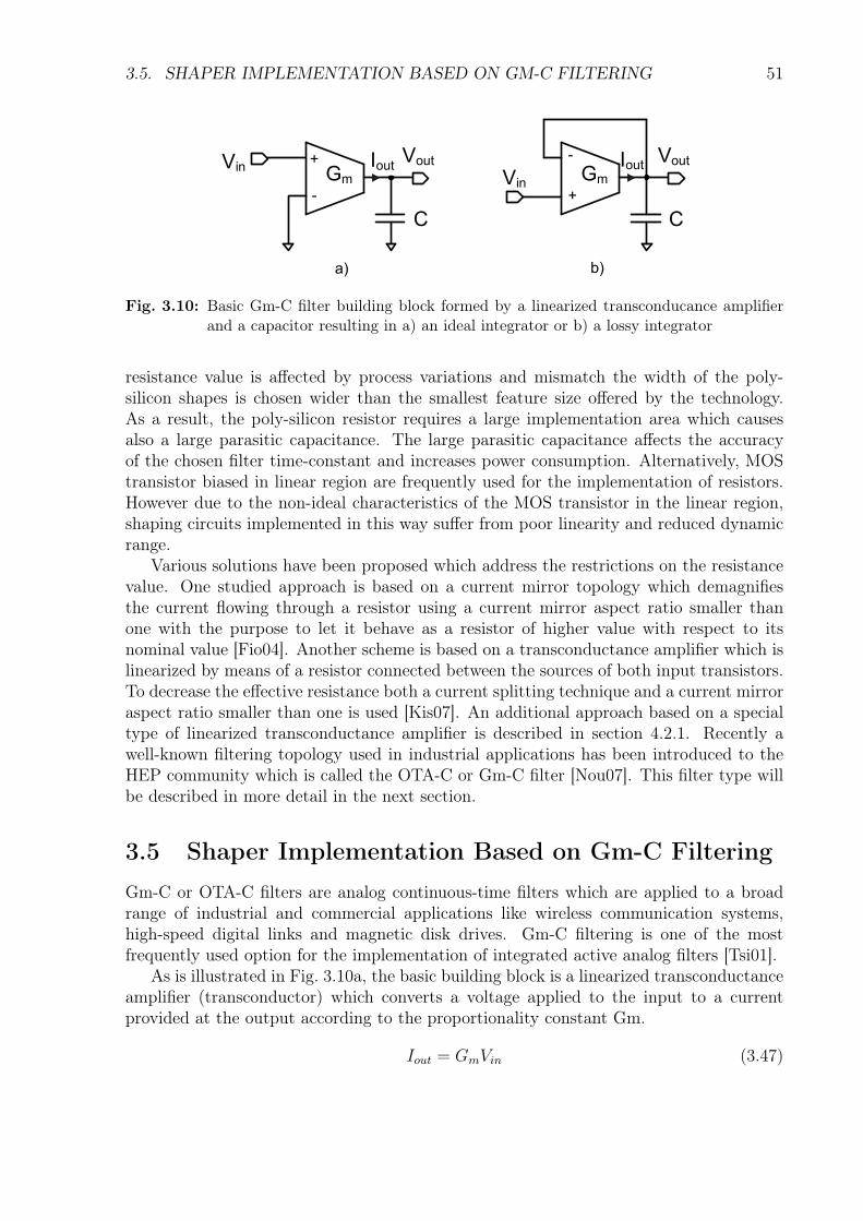
3.5. SHAPER IMPLEMENTATION BASED ON GM-C FILTERING 51
C
+
-
GmVin VoutIout
Vin+
-
GmVoutIout
C
a) b)
Fig. 3.10: Basic Gm-C filter building block formed by a linearized transconducance amplifierand a capacitor resulting in a) an ideal integrator or b) a lossy integrator
resistance value is affected by process variations and mismatch the width of the poly-silicon shapes is chosen wider than the smallest feature size offered by the technology.As a result, the poly-silicon resistor requires a large implementation area which causesalso a large parasitic capacitance. The large parasitic capacitance affects the accuracyof the chosen filter time-constant and increases power consumption. Alternatively, MOStransistor biased in linear region are frequently used for the implementation of resistors.However due to the non-ideal characteristics of the MOS transistor in the linear region,shaping circuits implemented in this way suffer from poor linearity and reduced dynamicrange.
Various solutions have been proposed which address the restrictions on the resistancevalue. One studied approach is based on a current mirror topology which demagnifiesthe current flowing through a resistor using a current mirror aspect ratio smaller thanone with the purpose to let it behave as a resistor of higher value with respect to itsnominal value [Fio04]. Another scheme is based on a transconductance amplifier which islinearized by means of a resistor connected between the sources of both input transistors.To decrease the effective resistance both a current splitting technique and a current mirroraspect ratio smaller than one is used [Kis07]. An additional approach based on a specialtype of linearized transconductance amplifier is described in section 4.2.1. Recently awell-known filtering topology used in industrial applications has been introduced to theHEP community which is called the OTA-C or Gm-C filter [Nou07]. This filter type willbe described in more detail in the next section.
3.5 Shaper Implementation Based on Gm-C FilteringGm-C or OTA-C filters are analog continuous-time filters which are applied to a broadrange of industrial and commercial applications like wireless communication systems,high-speed digital links and magnetic disk drives. Gm-C filtering is one of the mostfrequently used option for the implementation of integrated active analog filters [Tsi01].
As is illustrated in Fig. 3.10a, the basic building block is a linearized transconductanceamplifier (transconductor) which converts a voltage applied to the input to a currentprovided at the output according to the proportionality constant Gm.
Iout = GmVin (3.47)
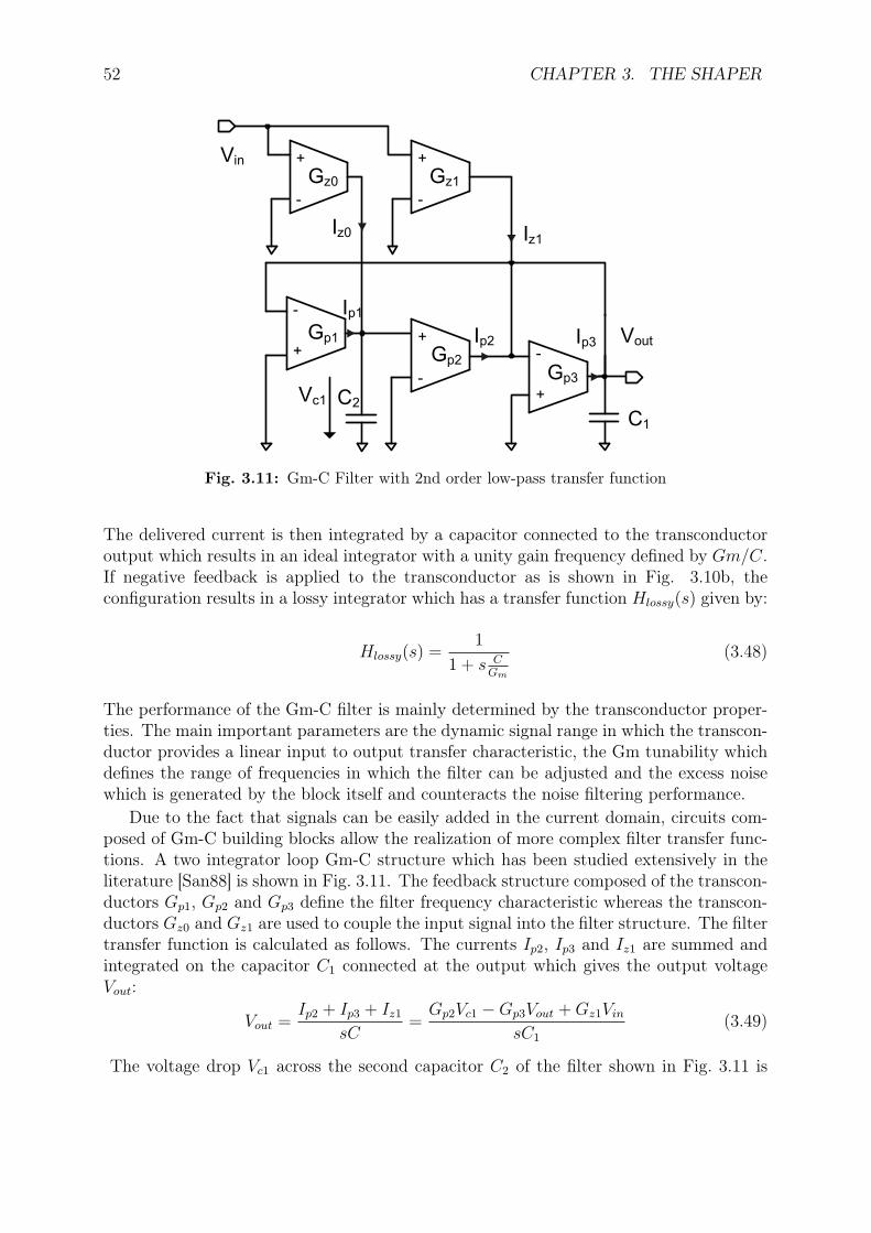
52 CHAPTER 3. THE SHAPER
+
-
+
-+
-
Gp1
+
-
+
-
Gz0 Gz1
Gp2Gp3
Vin
Vout
Vc1
Iz0 Iz1
Ip1
Ip2 Ip3
C1
C2
Fig. 3.11: Gm-C Filter with 2nd order low-pass transfer function
The delivered current is then integrated by a capacitor connected to the transconductoroutput which results in an ideal integrator with a unity gain frequency defined by Gm/C.If negative feedback is applied to the transconductor as is shown in Fig. 3.10b, theconfiguration results in a lossy integrator which has a transfer function Hlossy(s) given by:
Hlossy(s) =1
1 + s CGm
(3.48)
The performance of the Gm-C filter is mainly determined by the transconductor proper-ties. The main important parameters are the dynamic signal range in which the transcon-ductor provides a linear input to output transfer characteristic, the Gm tunability whichdefines the range of frequencies in which the filter can be adjusted and the excess noisewhich is generated by the block itself and counteracts the noise filtering performance.
Due to the fact that signals can be easily added in the current domain, circuits com-posed of Gm-C building blocks allow the realization of more complex filter transfer func-tions. A two integrator loop Gm-C structure which has been studied extensively in theliterature [San88] is shown in Fig. 3.11. The feedback structure composed of the transcon-ductors Gp1, Gp2 and Gp3 define the filter frequency characteristic whereas the transcon-ductors Gz0 and Gz1 are used to couple the input signal into the filter structure. The filtertransfer function is calculated as follows. The currents Ip2, Ip3 and Iz1 are summed andintegrated on the capacitor C1 connected at the output which gives the output voltageVout:
Vout =Ip2 + Ip3 + Iz1
sC=
Gp2Vc1 −Gp3Vout +Gz1Vin
sC1
(3.49)
The voltage drop Vc1 across the second capacitor C2 of the filter shown in Fig. 3.11 is
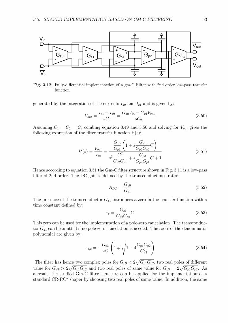
3.5. SHAPER IMPLEMENTATION BASED ON GM-C FILTERING 53
+
-
+
-
+
-
+
-
+
-
+
-
+
-
+
-+
-
+
-
Vout
Vout
Vin
Vin
Gz0 Gz1 Gp1 Gp2 Gp3
Fig. 3.12: Fully-differential implementation of a gm-C Filter with 2nd order low-pass transferfunction
generated by the integration of the currents Iz0 and Ip1 and is given by:
Vout =Ip1 + Iz0
sC2
=Gz0Vin −Gp1Vout
sC2
(3.50)
Assuming C1 = C2 = C, combing equation 3.49 and 3.50 and solving for Vout gives thefollowing expression of the filter transfer function H(s):
H(s) =Vout
Vin
=
Gz0
Gp1
(1 + s
Gz1
Gp2Gz0
C
)s2
C2
Gp2Gp1
+ sGp3
Gp2Gp1
C + 1
(3.51)
Hence according to equation 3.51 the Gm-C filter structure shown in Fig. 3.11 is a low-passfilter of 2nd order. The DC gain is defined by the transconductance ratio:
ADC =Gz0
Gp1
(3.52)
The presence of the transconductor Gz1 introduces a zero in the transfer function with atime constant defined by:
τz =Gz1
Gp2Gz0
C (3.53)
This zero can be used for the implementation of a pole-zero cancelation. The transconduc-tor Gz1 can be omitted if no pole-zero cancelation is needed. The roots of the denominatorpolynomial are given by:
s1,2 = −Gp3
2C
(1∓
√1− 4
Gp1Gp2
G2p3
)(3.54)
The filter has hence two complex poles for Gp3 < 2√
Gp1Gp2, two real poles of differentvalue for Gp3 > 2
√Gp1Gp2 and two real poles of same value for Gp3 = 2
√Gp1Gp2. As
a result, the studied Gm-C filter structure can be applied for the implementation of astandard CR-RCn shaper by choosing two real poles of same value. In addition, the same
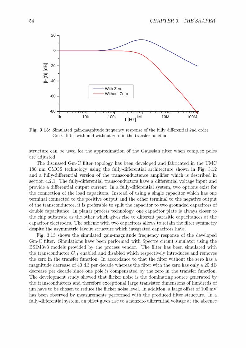
54 CHAPTER 3. THE SHAPER
1k 10k 100k 1M 10M 100M -80
-60
-40
-20
0
20
With Zero Without Zero
|H(f
)| [d
B]
f [Hz]
Fig. 3.13: Simulated gain-magnitude frequency response of the fully differential 2nd orderGm-C filter with and without zero in the transfer function
structure can be used for the approximation of the Gaussian filter when complex polesare adjusted.
The discussed Gm-C filter topology has been developed and fabricated in the UMC180 nm CMOS technology using the fully-differential architecture shown in Fig. 3.12and a fully-differential version of the transconductance amplifier which is described insection 4.2.1. The fully-differential transconductors have a differential voltage input andprovide a differential output current. In a fully-differential system, two options exist forthe connection of the load capacitors. Instead of using a single capacitor which has oneterminal connected to the positive output and the other terminal to the negative outputof the transconductor, it is preferable to split the capacitor to two grounded capacitors ofdouble capacitance. In planar process technology, one capacitor plate is always closer tothe chip substrate as the other which gives rise to different parasitic capacitances at thecapacitor electrodes. The scheme with two capacitors allows to retain the filter symmetrydespite the asymmetric layout structure which integrated capacitors have.
Fig. 3.13 shows the simulated gain-magnitude frequency response of the developedGm-C filter. Simulations have been performed with Spectre circuit simulator using theBSIM3v3 models provided by the process vendor. The filter has been simulated withthe transconductor Gz1 enabled and disabled which respectively introduces and removesthe zero in the transfer function. In accordance to that the filter without the zero has amagnitude decrease of 40 dB per decade whereas the filter with the zero has only a 20 dBdecrease per decade since one pole is compensated by the zero in the transfer function.The development study showed that flicker noise is the dominating source generated bythe transconductors and therefore exceptional large transistor dimensions of hundreds ofµm have to be chosen to reduce the flicker noise level. In addition, a large offset of 100 mVhas been observed by measurements performed with the produced filter structure. In afully-differential system, an offset gives rise to a nonzero differential voltage at the absence
3.6. SUMMARY 55
of any input signal. Since an offset has less impact in a system with negative feedback,the offset is very likely introduced by the two transconductors Gz0 and Gz1 which are usedto inject the signal into the filter and which are not embedded in any feedback loop. Itshould be finally noted that more advanced filter structures can be found in the literaturewhich avoid the usage of open loop transconductors [Del99].
3.6 SummaryShapers are used in HEP applications to improve the SNR by filtering spectral noise com-ponents outside the frequency band of interest. In addition, shapers are used to adaptthe signal shape to the expected hit rate in the experiment which reduces the pile-upprobability. The matched filter used in combination with a whitening filter section givesrise to the optimum SNR. However due to the high implementation effort, matched filtersare rarely applied to integrated multi-channel readout chips. The ideal Gaussian filter isan interesting filter concept for HEP applications due to its small bandwidth by signalrise-time product. Two common options exist to approximate the ideal Gaussian filter.One option is the factorization of the Taylor series expansion of the square of the Gaus-sian function which gives rise to conjugate complex poles. An alternative but less efficientapproach is the CR-RCn shaper which has a sequence of n RC-stages with real poles.The difficulty with the implementation of integrated shaper structures are the bad prop-erties of the passive components available in CMOS processes. In particular high ohmicresistors require large implementation areas and have high parasitic capacitances. TheGm-C filtering technique which is one of the most used architectures for integrated analogcontinuous-time filters in commercial applications has been introduced as an alternativesolution well suited for integration.
Chapter 4
A Counting Strip Detector ReadoutChip for Precision ComptonPolarimetry
4.1 Compton Polarimetry at ELSA
At the Electron Stretcher Accelerator (ELSA) [Alt90][Hil06] facility installed at the Uni-versity of Bonn since 1987, electrons are accelerated up to a maximum energy of 3.5 GeV.The electrons are either stored in the ring and used as a source of synchrotron radiation,which is generated when the electrons are forced by a magnetic field to move on a curvedpath, or an electron beam is extracted from the ring to scatter off a target.
For a systematic experimental study of the structure of nucleons, it is advantageous ifboth interaction partners the target material and the electrons have a defined and well-known spin polarization. Polarized electrons are generated by a pulsed 50 kV source usinga Be-InGaAs/AlGaAs strained layer superlattice photocathode [Hil00]. The polarizedelectrons are then accelerated in the linear accelerator LINAC2, the booster synchrotronand the stretcher ring shown in Fig. 4.1. A sophisticated correction scheme is applied toavoid the depolarization of the electron beam by resonance effects during the accelerationprocess. Correction magnets have been installed and the electrons are shifted quicklythrough resonance energies [Hof00].
During this correction sequence, the precise determination and monitoring of the elec-tron polarization is mandatory. The measurement has to be performed within a reasonabletime in the order of several minutes and a significant perturbation of the electron beamhas to be avoided. At the low energy beam-line close to the electron source, the beampolarization is measured by means of a Mott polarimeter. The polarization of the highenergy beam which has been extracted for use in the experiment is measured by means ofa Møller polarimeter [Spe04]. For the detection of the polarization of the stored electronbeam in the stretcher ring, both methods are insufficient in terms of measurement dura-tion and interference with the electron beam. Hence an additional polarimetry methodhas been implemented which makes use of the Compton effect [Dol02][Hil09].
56
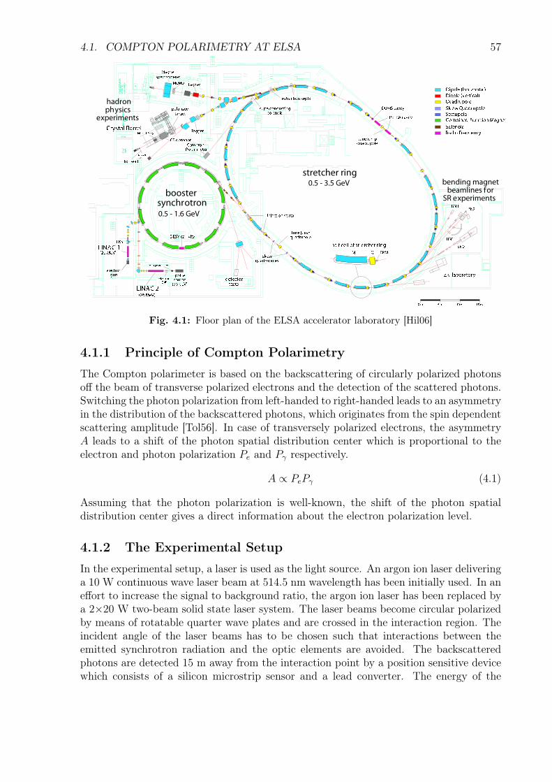
4.1. COMPTON POLARIMETRY AT ELSA 57
Fig. 4.1: Floor plan of the ELSA accelerator laboratory [Hil06]
4.1.1 Principle of Compton Polarimetry
The Compton polarimeter is based on the backscattering of circularly polarized photonsoff the beam of transverse polarized electrons and the detection of the scattered photons.Switching the photon polarization from left-handed to right-handed leads to an asymmetryin the distribution of the backscattered photons, which originates from the spin dependentscattering amplitude [Tol56]. In case of transversely polarized electrons, the asymmetryA leads to a shift of the photon spatial distribution center which is proportional to theelectron and photon polarization Pe and Pγ respectively.
A ∝ PePγ (4.1)
Assuming that the photon polarization is well-known, the shift of the photon spatialdistribution center gives a direct information about the electron polarization level.
4.1.2 The Experimental Setup
In the experimental setup, a laser is used as the light source. An argon ion laser deliveringa 10 W continuous wave laser beam at 514.5 nm wavelength has been initially used. In aneffort to increase the signal to background ratio, the argon ion laser has been replaced bya 2×20 W two-beam solid state laser system. The laser beams become circular polarizedby means of rotatable quarter wave plates and are crossed in the interaction region. Theincident angle of the laser beams has to be chosen such that interactions between theemitted synchrotron radiation and the optic elements are avoided. The backscatteredphotons are detected 15 m away from the interaction point by a position sensitive devicewhich consists of a silicon microstrip sensor and a lead converter. The energy of the
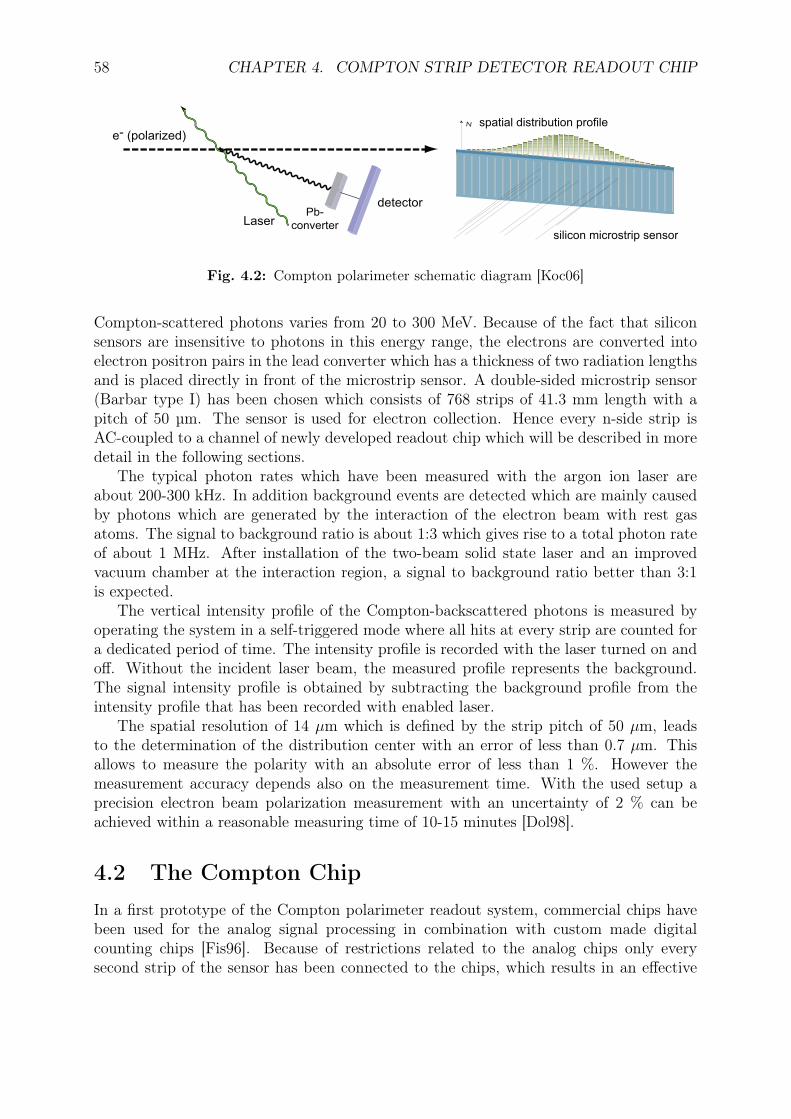
58 CHAPTER 4. COMPTON STRIP DETECTOR READOUT CHIP
e- (polarized)
LaserPb-
converter
detector
silicon microstrip sensor
spatial distribution profileN
Fig. 4.2: Compton polarimeter schematic diagram [Koc06]
Compton-scattered photons varies from 20 to 300 MeV. Because of the fact that siliconsensors are insensitive to photons in this energy range, the electrons are converted intoelectron positron pairs in the lead converter which has a thickness of two radiation lengthsand is placed directly in front of the microstrip sensor. A double-sided microstrip sensor(Barbar type I) has been chosen which consists of 768 strips of 41.3 mm length with apitch of 50 µm. The sensor is used for electron collection. Hence every n-side strip isAC-coupled to a channel of newly developed readout chip which will be described in moredetail in the following sections.
The typical photon rates which have been measured with the argon ion laser areabout 200-300 kHz. In addition background events are detected which are mainly causedby photons which are generated by the interaction of the electron beam with rest gasatoms. The signal to background ratio is about 1:3 which gives rise to a total photon rateof about 1 MHz. After installation of the two-beam solid state laser and an improvedvacuum chamber at the interaction region, a signal to background ratio better than 3:1is expected.
The vertical intensity profile of the Compton-backscattered photons is measured byoperating the system in a self-triggered mode where all hits at every strip are counted fora dedicated period of time. The intensity profile is recorded with the laser turned on andoff. Without the incident laser beam, the measured profile represents the background.The signal intensity profile is obtained by subtracting the background profile from theintensity profile that has been recorded with enabled laser.
The spatial resolution of 14 µm which is defined by the strip pitch of 50 µm, leadsto the determination of the distribution center with an error of less than 0.7 µm. Thisallows to measure the polarity with an absolute error of less than 1 %. However themeasurement accuracy depends also on the measurement time. With the used setup aprecision electron beam polarization measurement with an uncertainty of 2 % can beachieved within a reasonable measuring time of 10-15 minutes [Dol98].
4.2 The Compton ChipIn a first prototype of the Compton polarimeter readout system, commercial chips havebeen used for the analog signal processing in combination with custom made digitalcounting chips [Fis96]. Because of restrictions related to the analog chips only everysecond strip of the sensor has been connected to the chips, which results in an effective
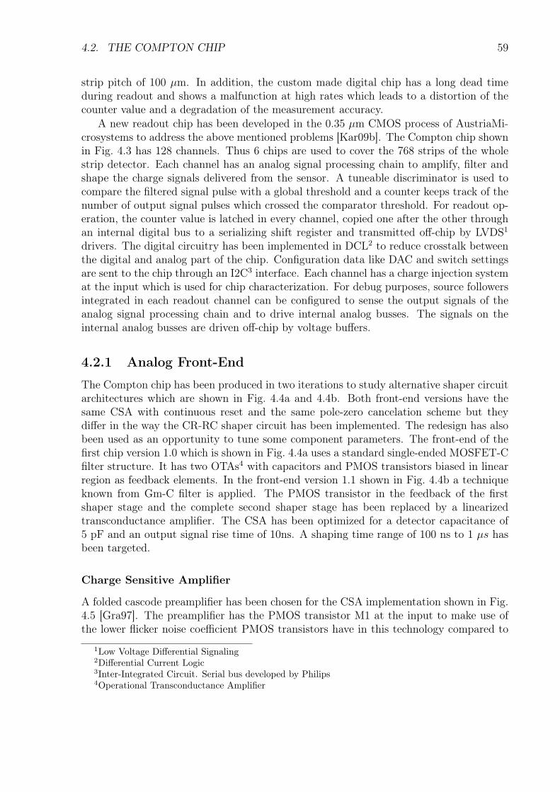
4.2. THE COMPTON CHIP 59
strip pitch of 100 µm. In addition, the custom made digital chip has a long dead timeduring readout and shows a malfunction at high rates which leads to a distortion of thecounter value and a degradation of the measurement accuracy.
A new readout chip has been developed in the 0.35 µm CMOS process of AustriaMi-crosystems to address the above mentioned problems [Kar09b]. The Compton chip shownin Fig. 4.3 has 128 channels. Thus 6 chips are used to cover the 768 strips of the wholestrip detector. Each channel has an analog signal processing chain to amplify, filter andshape the charge signals delivered from the sensor. A tuneable discriminator is used tocompare the filtered signal pulse with a global threshold and a counter keeps track of thenumber of output signal pulses which crossed the comparator threshold. For readout op-eration, the counter value is latched in every channel, copied one after the other throughan internal digital bus to a serializing shift register and transmitted off-chip by LVDS1
drivers. The digital circuitry has been implemented in DCL2 to reduce crosstalk betweenthe digital and analog part of the chip. Configuration data like DAC and switch settingsare sent to the chip through an I2C3 interface. Each channel has a charge injection systemat the input which is used for chip characterization. For debug purposes, source followersintegrated in each readout channel can be configured to sense the output signals of theanalog signal processing chain and to drive internal analog busses. The signals on theinternal analog busses are driven off-chip by voltage buffers.
4.2.1 Analog Front-End
The Compton chip has been produced in two iterations to study alternative shaper circuitarchitectures which are shown in Fig. 4.4a and 4.4b. Both front-end versions have thesame CSA with continuous reset and the same pole-zero cancelation scheme but theydiffer in the way the CR-RC shaper circuit has been implemented. The redesign has alsobeen used as an opportunity to tune some component parameters. The front-end of thefirst chip version 1.0 which is shown in Fig. 4.4a uses a standard single-ended MOSFET-Cfilter structure. It has two OTAs4 with capacitors and PMOS transistors biased in linearregion as feedback elements. In the front-end version 1.1 shown in Fig. 4.4b a techniqueknown from Gm-C filter is applied. The PMOS transistor in the feedback of the firstshaper stage and the complete second shaper stage has been replaced by a linearizedtransconductance amplifier. The CSA has been optimized for a detector capacitance of5 pF and an output signal rise time of 10ns. A shaping time range of 100 ns to 1 µs hasbeen targeted.
Charge Sensitive Amplifier
A folded cascode preamplifier has been chosen for the CSA implementation shown in Fig.4.5 [Gra97]. The preamplifier has the PMOS transistor M1 at the input to make use ofthe lower flicker noise coefficient PMOS transistors have in this technology compared to
1Low Voltage Differential Signaling2Differential Current Logic3Inter-Integrated Circuit. Serial bus developed by Philips4Operational Transconductance Amplifier
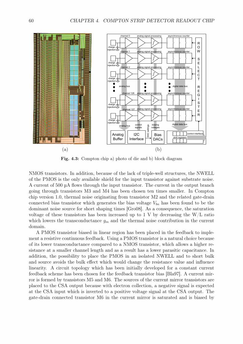
60 CHAPTER 4. COMPTON STRIP DETECTOR READOUT CHIP
(a)
I2C
InterfaceBias
DACs
R
O
W
S
E
L
E
C
T
R
E
G
I
S
T
E
R
control
signals
DAC settings
shift registers
control interface
analog signal processing
analog signal processing
analog signal processing
analog signal processing
analog signal processing
channel 0
channel 1
channel 2
channel 126
channel 127
asynchronous counter
asynchronous counter
asynchronous counter
asynchronous counter
asynchronous counter
biasing
voltages
charge
injection
charge
injection
charge
injection
charge
injection
charge
injection
digital data bus
digital data bus
Analog
Buffer
analog bus
analog bus
(b)
Fig. 4.3: Compton chip a) photo of die and b) block diagram
NMOS transistors. In addition, because of the lack of triple-well structures, the NWELLof the PMOS is the only available shield for the input transistor against substrate noise.A current of 500 µA flows through the input transistor. The current in the output branchgoing through transistors M3 and M4 has been chosen ten times smaller. In Comptonchip version 1.0, thermal noise originating from transistor M2 and the related gate-drainconnected bias transistor which generates the bias voltage Vbn has been found to be thedominant noise source for short shaping times [Gro08]. As a consequence, the saturationvoltage of these transistors has been increased up to 1 V by decreasing the W/L ratiowhich lowers the transconductance gm and the thermal noise contribution in the currentdomain.
A PMOS transistor biased in linear region has been placed in the feedback to imple-ment a resistive continuous feedback. Using a PMOS transistor is a natural choice becauseof its lower transconductance compared to a NMOS transistor, which allows a higher re-sistance at a smaller channel length and as a result has a lower parasitic capacitance. Inaddition, the possibility to place the PMOS in an isolated NWELL and to short bulkand source avoids the bulk effect which would change the resistance value and influencelinearity. A circuit topology which has been initially developed for a constant currentfeedback scheme has been chosen for the feedback transistor bias [Bla97]. A current mir-ror is formed by transistors M5 and M6. The sources of the current mirror transistors areplaced to the CSA output because with electron collection, a negative signal is expectedat the CSA input which is inverted to a positive voltage signal at the CSA output. Thegate-drain connected transistor M6 in the current mirror is saturated and is biased by
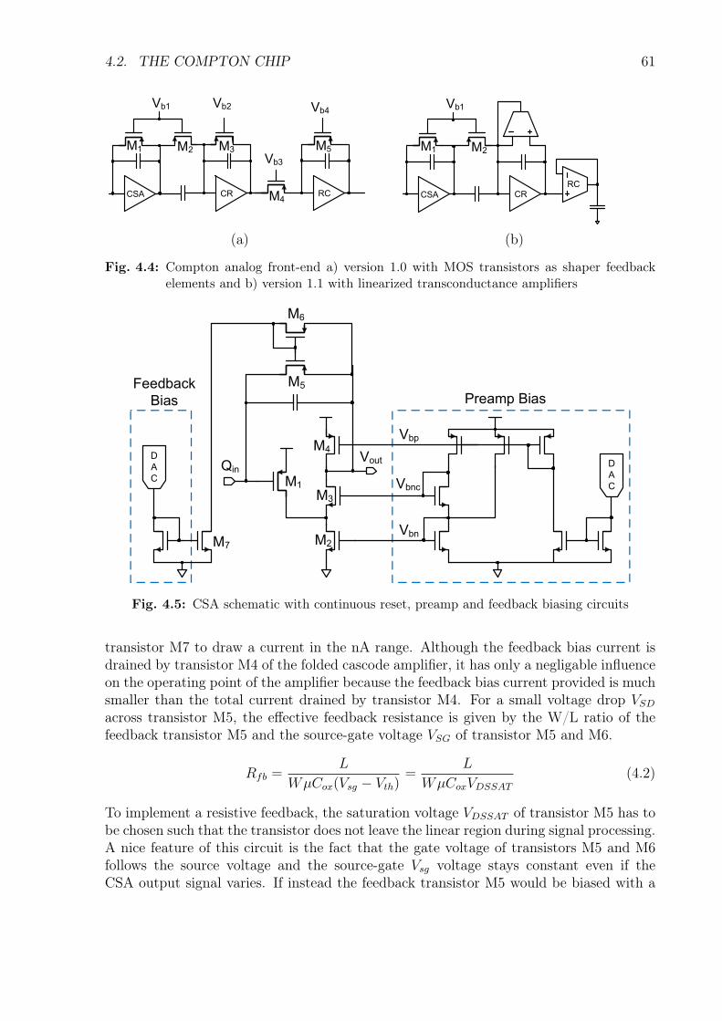
4.2. THE COMPTON CHIP 61
M1 M2 M3
Vb1
CSA CR
Vb2
M5
RCM4
Vb3
Vb4
(a)
M1 M2
Vb1
CSA CR
RC
(b)
Fig. 4.4: Compton analog front-end a) version 1.0 with MOS transistors as shaper feedbackelements and b) version 1.1 with linearized transconductance amplifiers
Vbn
Vbnc
Vbp
M2
M1
M3
M4
M6
M5
Qin
Vout D
A
C
D
A
C
Preamp BiasFeedback
Bias
M7
Fig. 4.5: CSA schematic with continuous reset, preamp and feedback biasing circuits
transistor M7 to draw a current in the nA range. Although the feedback bias current isdrained by transistor M4 of the folded cascode amplifier, it has only a negligable influenceon the operating point of the amplifier because the feedback bias current provided is muchsmaller than the total current drained by transistor M4. For a small voltage drop VSD
across transistor M5, the effective feedback resistance is given by the W/L ratio of thefeedback transistor M5 and the source-gate voltage VSG of transistor M5 and M6.
Rfb =L
WµCox(Vsg − Vth)=
L
WµCoxVDSSAT
(4.2)
To implement a resistive feedback, the saturation voltage VDSSAT of transistor M5 has tobe chosen such that the transistor does not leave the linear region during signal processing.A nice feature of this circuit is the fact that the gate voltage of transistors M5 and M6follows the source voltage and the source-gate Vsg voltage stays constant even if theCSA output signal varies. If instead the feedback transistor M5 would be biased with a
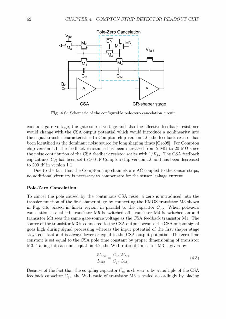
62 CHAPTER 4. COMPTON STRIP DETECTOR READOUT CHIP
M2
M1
Qin
M3
ENEN
M4
M5
-A
Cfb Cac
-A
CSA CR-shaper stage
Pole-Zero Cancelation
Vfbs1
Vfbp
M3
Fig. 4.6: Schematic of the configurable pole-zero cancelation circuit
constant gate voltage, the gate-source voltage and also the effective feedback resistancewould change with the CSA output potential which would introduce a nonlinearity intothe signal transfer characteristic. In Compton chip version 1.0, the feedback resistor hasbeen identified as the dominant noise source for long shaping times [Gro08]. For Comptonchip version 1.1, the feedback resistance has been increased from 2 MΩ to 20 MΩ sincethe noise contribution of the CSA feedback resistor scales with 1/Rfb. The CSA feedbackcapacitance Cfb has been set to 500 fF Compton chip version 1.0 and has been decreasedto 200 fF in version 1.1
Due to the fact that the Compton chip channels are AC-coupled to the sensor strips,no additional circuitry is necessary to compensate for the sensor leakage current.
Pole-Zero Cancelation
To cancel the pole caused by the continuous CSA reset, a zero is introduced into thetransfer function of the first shaper stage by connecting the PMOS transistor M3 shownin Fig. 4.6, biased in linear region, in parallel to the capacitor Cac. When pole-zerocancelation is enabled, transistor M5 is switched off, transistor M4 is switched on andtransistor M3 sees the same gate-source voltage as the CSA feedback transistor M1. Thesource of the transistor M3 is connected to the CSA output because the CSA output signalgoes high during signal processing whereas the input potential of the first shaper stagestays constant and is always lower or equal to the CSA output potential. The zero timeconstant is set equal to the CSA pole time constant by proper dimensioning of transistorM3. Taking into account equation 4.2, the W/L ratio of transistor M3 is given by:
WM3
LM3
=Cac
Cfb
WM1
LM1
(4.3)
Because of the fact that the coupling capacitor Cac is chosen to be a multiple of the CSAfeedback capacitor Cfb, the W/L ratio of transistor M3 is scaled accordingly by placing
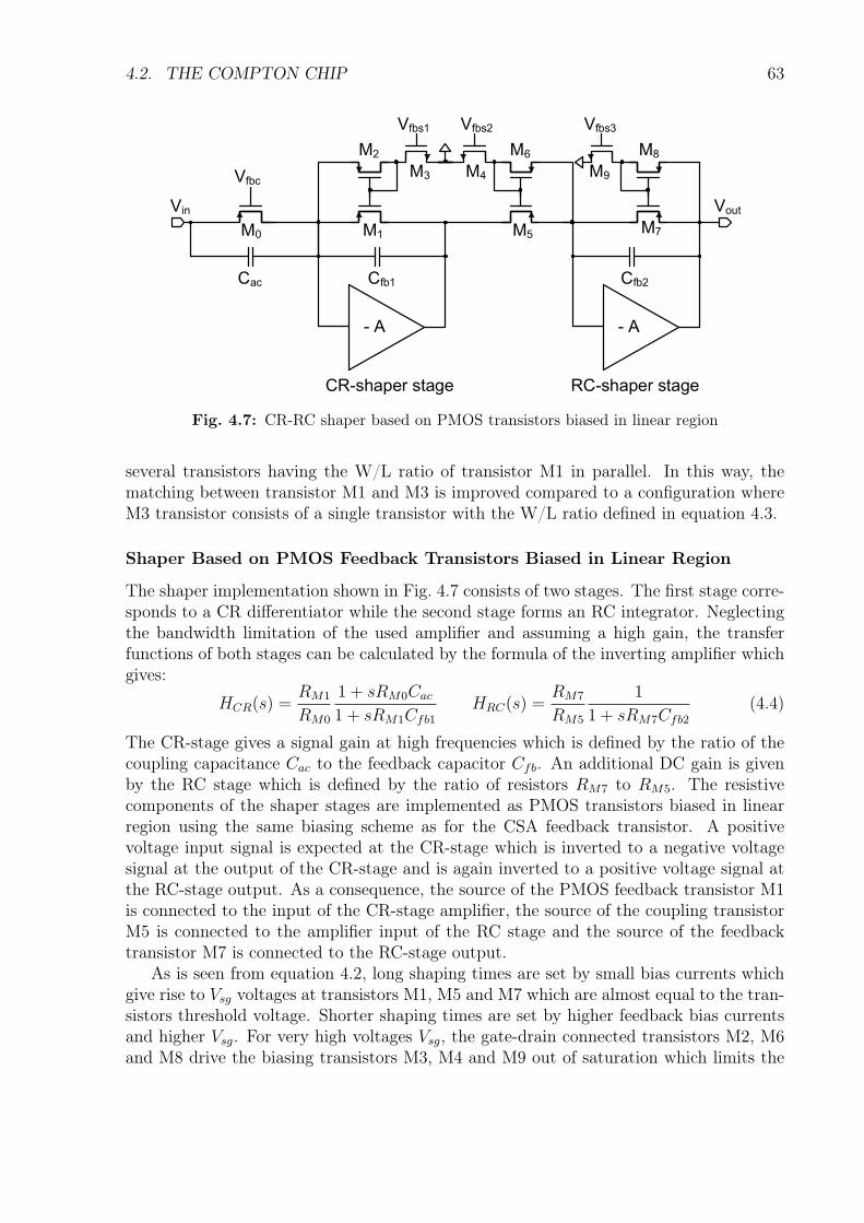
4.2. THE COMPTON CHIP 63
M1
- A
Cfb1
CR-shaper stage RC-shaper stage
M2
Vfbs1
M5
Vfbs2
- A
Cfb2
M0
VoutVin
Vfbc
M7
M3 M4
M6
Cac
M8
Vfbs3
M9
Fig. 4.7: CR-RC shaper based on PMOS transistors biased in linear region
several transistors having the W/L ratio of transistor M1 in parallel. In this way, thematching between transistor M1 and M3 is improved compared to a configuration whereM3 transistor consists of a single transistor with the W/L ratio defined in equation 4.3.
Shaper Based on PMOS Feedback Transistors Biased in Linear Region
The shaper implementation shown in Fig. 4.7 consists of two stages. The first stage corre-sponds to a CR differentiator while the second stage forms an RC integrator. Neglectingthe bandwidth limitation of the used amplifier and assuming a high gain, the transferfunctions of both stages can be calculated by the formula of the inverting amplifier whichgives:
HCR(s) =RM1
RM0
1 + sRM0Cac
1 + sRM1Cfb1
HRC(s) =RM7
RM5
1
1 + sRM7Cfb2
(4.4)
The CR-stage gives a signal gain at high frequencies which is defined by the ratio of thecoupling capacitance Cac to the feedback capacitor Cfb. An additional DC gain is givenby the RC stage which is defined by the ratio of resistors RM7 to RM5. The resistivecomponents of the shaper stages are implemented as PMOS transistors biased in linearregion using the same biasing scheme as for the CSA feedback transistor. A positivevoltage input signal is expected at the CR-stage which is inverted to a negative voltagesignal at the output of the CR-stage and is again inverted to a positive voltage signal atthe RC-stage output. As a consequence, the source of the PMOS feedback transistor M1is connected to the input of the CR-stage amplifier, the source of the coupling transistorM5 is connected to the amplifier input of the RC stage and the source of the feedbacktransistor M7 is connected to the RC-stage output.
As is seen from equation 4.2, long shaping times are set by small bias currents whichgive rise to Vsg voltages at transistors M1, M5 and M7 which are almost equal to the tran-sistors threshold voltage. Shorter shaping times are set by higher feedback bias currentsand higher Vsg. For very high voltages Vsg, the gate-drain connected transistors M2, M6and M8 drive the biasing transistors M3, M4 and M9 out of saturation which limits the
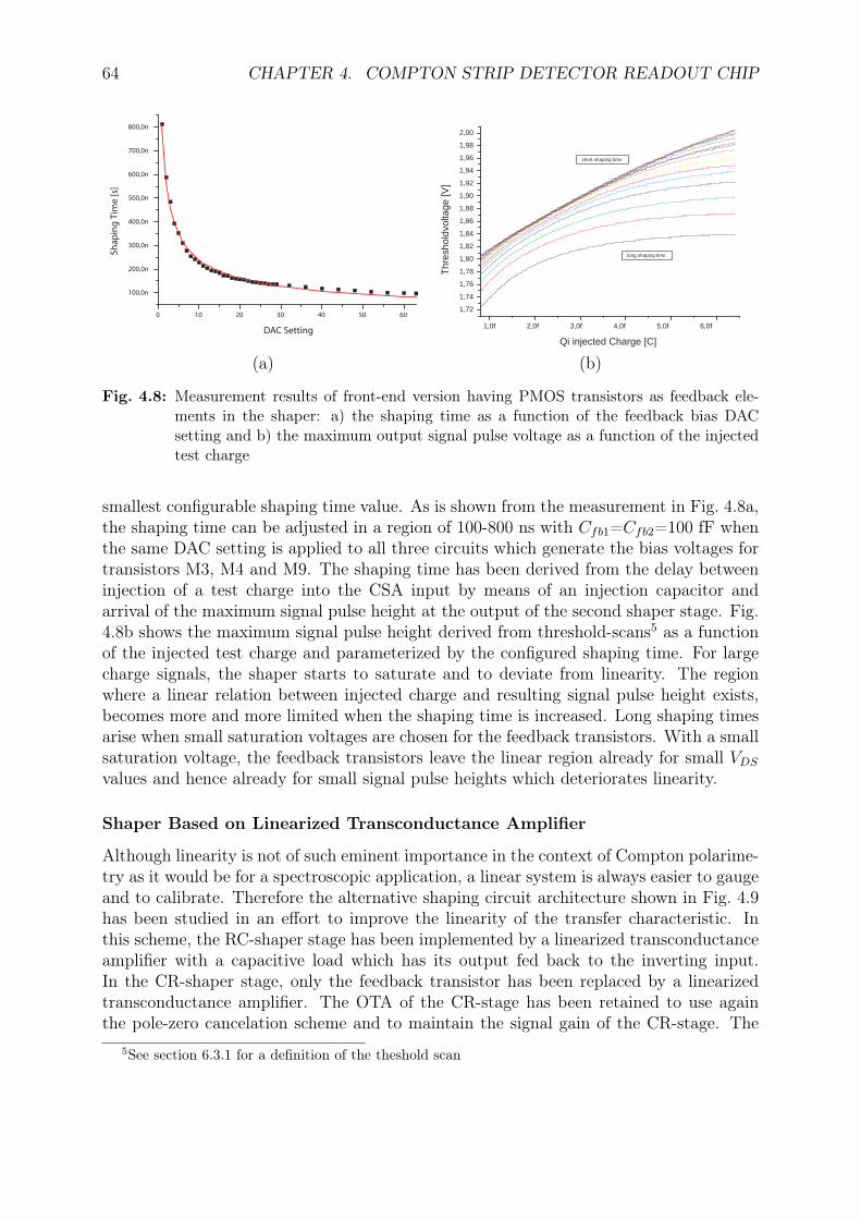
64 CHAPTER 4. COMPTON STRIP DETECTOR READOUT CHIP
0 10 20 30 40 50 60
100,0n
200,0n
300,0n
400,0n
500,0n
600,0n
700,0n
800,0n
Sh
ap
ing
Tim
e [
s]
DAC Setting
(a)
1,0f 2,0f 3,0f 4,0f 5,0f 6,0f
1,72
1,74
1,76
1,78
1,80
1,82
1,84
1,86
1,88
1,90
1,92
1,94
1,96
1,98
2,00
short shaping time
long shaping time
Thr
esho
ldvo
ltage
[V]
Qi injected Charge [C]
(b)
Fig. 4.8: Measurement results of front-end version having PMOS transistors as feedback ele-ments in the shaper: a) the shaping time as a function of the feedback bias DACsetting and b) the maximum output signal pulse voltage as a function of the injectedtest charge
smallest configurable shaping time value. As is shown from the measurement in Fig. 4.8a,the shaping time can be adjusted in a region of 100-800 ns with Cfb1=Cfb2=100 fF whenthe same DAC setting is applied to all three circuits which generate the bias voltages fortransistors M3, M4 and M9. The shaping time has been derived from the delay betweeninjection of a test charge into the CSA input by means of an injection capacitor andarrival of the maximum signal pulse height at the output of the second shaper stage. Fig.4.8b shows the maximum signal pulse height derived from threshold-scans5 as a functionof the injected test charge and parameterized by the configured shaping time. For largecharge signals, the shaper starts to saturate and to deviate from linearity. The regionwhere a linear relation between injected charge and resulting signal pulse height exists,becomes more and more limited when the shaping time is increased. Long shaping timesarise when small saturation voltages are chosen for the feedback transistors. With a smallsaturation voltage, the feedback transistors leave the linear region already for small VDS
values and hence already for small signal pulse heights which deteriorates linearity.
Shaper Based on Linearized Transconductance Amplifier
Although linearity is not of such eminent importance in the context of Compton polarime-try as it would be for a spectroscopic application, a linear system is always easier to gaugeand to calibrate. Therefore the alternative shaping circuit architecture shown in Fig. 4.9has been studied in an effort to improve the linearity of the transfer characteristic. Inthis scheme, the RC-shaper stage has been implemented by a linearized transconductanceamplifier with a capacitive load which has its output fed back to the inverting input.In the CR-shaper stage, only the feedback transistor has been replaced by a linearizedtransconductance amplifier. The OTA of the CR-stage has been retained to use againthe pole-zero cancelation scheme and to maintain the signal gain of the CR-stage. The
5See section 6.3.1 for a definition of the theshold scan
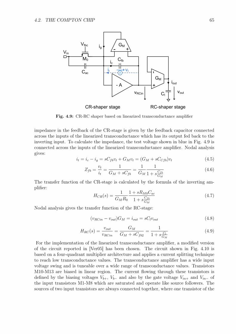
4.2. THE COMPTON CHIP 65
- A
CfbM0
Vin
Vfbc
Cac
- +GM
-+
GM
voutvRCin
iout
~
vtit
ic
ig
Cl
CR-shaper stage RC-shaper stage
Fig. 4.9: CR-RC shaper based on linearized transconductance amplifier
impedance in the feedback of the CR-stage is given by the feedback capacitor connectedacross the inputs of the linearized transconductance which has its output fed back to theinverting input. To calculate the impedance, the test voltage shown in blue in Fig. 4.9 isconnected across the inputs of the linearized transconductance amplifier. Nodal analysisgives:
it = ic − ig = sCfbvt +GMvt = (GM + sCCfb)vt (4.5)
Zfb =vtit
=1
GM + sCfb
=1
GM
1
1 + sCfb
GM
(4.6)
The transfer function of the CR-stage is calculated by the formula of the inverting am-plifier:
HCR(s) =1
GMR0
1 + sRM0Cac
1 + sCfb
GM
(4.7)
Nodal analysis gives the transfer function of the RC-stage:
(vRCin − vout)GM = iout = sClvout (4.8)
HRC(s) =voutvRCin
=GM
GM + sCfb2
=1
1 + s Cl
GM
(4.9)
For the implementation of the linearized transconductance amplifier, a modified versionof the circuit reported in [Ver05] has been chosen. The circuit shown in Fig. 4.10 isbased on a four-quadrant multiplier architecture and applies a current splitting techniqueto reach low transconductance values. The transconductance amplifier has a wide inputvoltage swing and is tuneable over a wide range of transconductance values. TransistorsM10-M13 are biased in linear region. The current flowing through these transistors isdefined by the biasing voltages Vb+, Vb− and also by the gate voltage Vin+ and Vin− ofthe input transistors M1-M8 which are saturated and operate like source followers. Thesources of two input transistors are always connected together, where one transistor of the
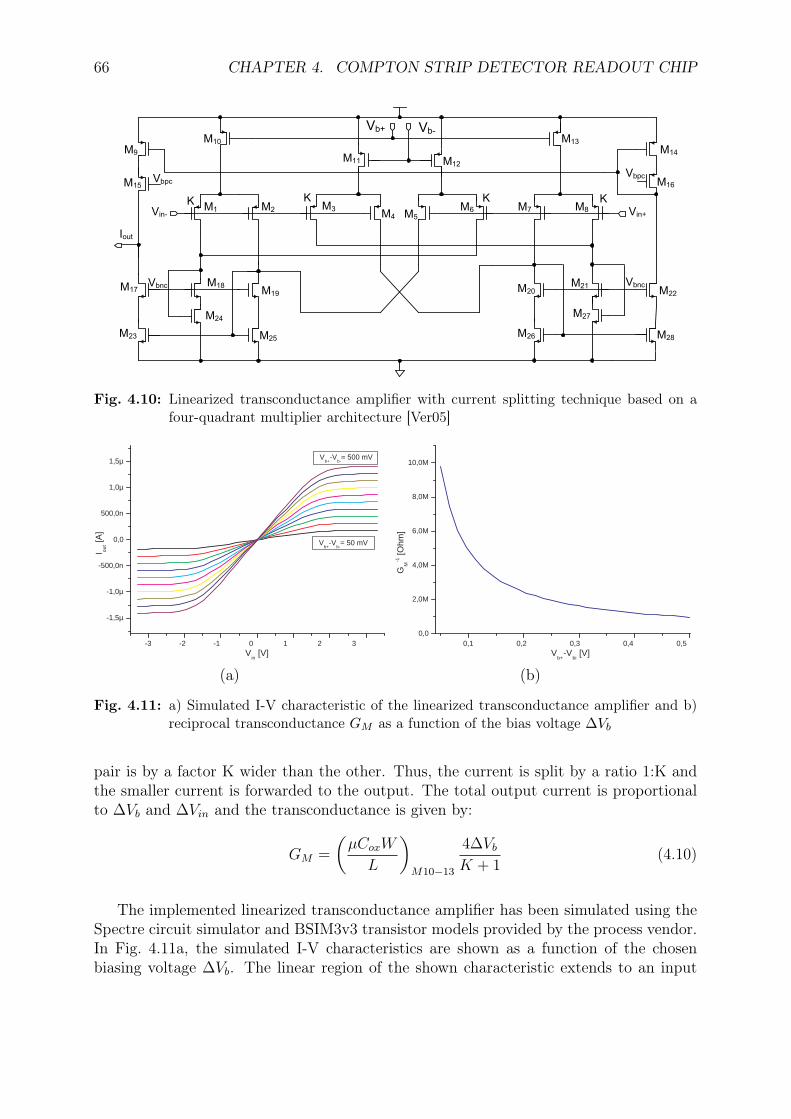
66 CHAPTER 4. COMPTON STRIP DETECTOR READOUT CHIP
M14
Vb-Vb+
M11 M12
M1 M2 M3
M10
M15
M9
M17
M23
M5
M6 M7 M8
M13
M16
Vin+M4
M18
M24
M19
M25
M20
M26
M27
M21
M28
M22
Vin-
Iout
VbpcVbpc
K K K K
Vbnc Vbnc
Fig. 4.10: Linearized transconductance amplifier with current splitting technique based on afour-quadrant multiplier architecture [Ver05]
-3 -2 -1 0 1 2 3
-1,5µ
-1,0µ
-500,0n
0,0
500,0n
1,0µ
1,5µ V b+
-V b- = 500 mV
V b+
-V b- = 50 mV
I out [A
]
V in [V]
(a)
0,1 0,2 0,3 0,4 0,5 0,0
2,0M
4,0M
6,0M
8,0M
10,0M
G M
-1 [O
hm]
V b+
-V bi [V]
(b)
Fig. 4.11: a) Simulated I-V characteristic of the linearized transconductance amplifier and b)reciprocal transconductance GM as a function of the bias voltage ∆Vb
pair is by a factor K wider than the other. Thus, the current is split by a ratio 1:K andthe smaller current is forwarded to the output. The total output current is proportionalto ∆Vb and ∆Vin and the transconductance is given by:
GM =
(µCoxW
L
)M10−13
4∆Vb
K + 1(4.10)
The implemented linearized transconductance amplifier has been simulated using theSpectre circuit simulator and BSIM3v3 transistor models provided by the process vendor.In Fig. 4.11a, the simulated I-V characteristics are shown as a function of the chosenbiasing voltage ∆Vb. The linear region of the shown characteristic extends to an input
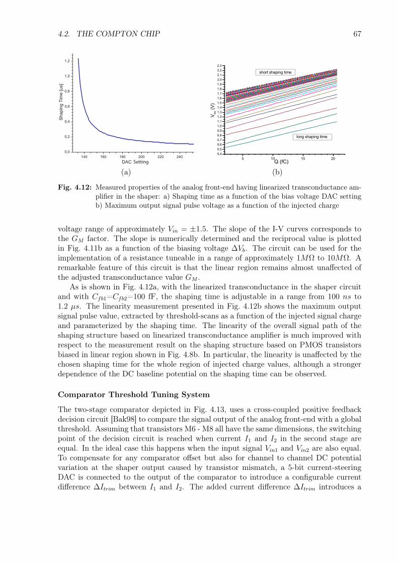
4.2. THE COMPTON CHIP 67
Setting
(a)
5 10 15 200,40,50,60,70,80,91,01,11,21,31,41,51,61,71,81,92,02,12,22,3
V thr (V
)
Q (fC)
short shaping time
long shaping time
(b)
Fig. 4.12: Measured properties of the analog front-end having linearized transconductance am-plifier in the shaper: a) Shaping time as a function of the bias voltage DAC settingb) Maximum output signal pulse voltage as a function of the injected charge
voltage range of approximately Vin = ±1.5. The slope of the I-V curves corresponds tothe GM factor. The slope is numerically determined and the reciprocal value is plottedin Fig. 4.11b as a function of the biasing voltage ∆Vb. The circuit can be used for theimplementation of a resistance tuneable in a range of approximately 1MΩ to 10MΩ. Aremarkable feature of this circuit is that the linear region remains almost unaffected ofthe adjusted transconductance value GM .
As is shown in Fig. 4.12a, with the linearized transconductance in the shaper circuitand with Cfb1=Cfb2=100 fF, the shaping time is adjustable in a range from 100 ns to1.2 µs. The linearity measurement presented in Fig. 4.12b shows the maximum outputsignal pulse value, extracted by threshold-scans as a function of the injected signal chargeand parameterized by the shaping time. The linearity of the overall signal path of theshaping structure based on linearized transconductance amplifier is much improved withrespect to the measurement result on the shaping structure based on PMOS transistorsbiased in linear region shown in Fig. 4.8b. In particular, the linearity is unaffected by thechosen shaping time for the whole region of injected charge values, although a strongerdependence of the DC baseline potential on the shaping time can be observed.
Comparator Threshold Tuning System
The two-stage comparator depicted in Fig. 4.13, uses a cross-coupled positive feedbackdecision circuit [Bak98] to compare the signal output of the analog front-end with a globalthreshold. Assuming that transistors M6 - M8 all have the same dimensions, the switchingpoint of the decision circuit is reached when current I1 and I2 in the second stage areequal. In the ideal case this happens when the input signal Vin1 and Vin2 are also equal.To compensate for any comparator offset but also for channel to channel DC potentialvariation at the shaper output caused by transistor mismatch, a 5-bit current-steeringDAC is connected to the output of the comparator to introduce a configurable currentdifference ∆Itrim between I1 and I2. The added current difference ∆Itrim introduces a
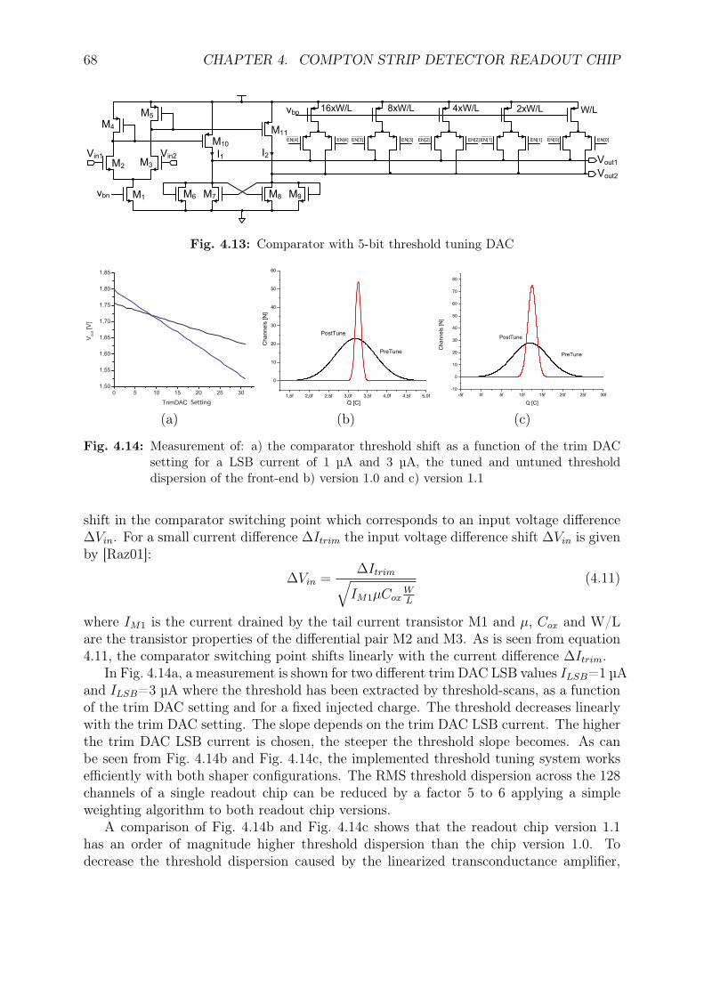
68 CHAPTER 4. COMPTON STRIP DETECTOR READOUT CHIP
vbn M1
Vin1 Vin2M2 M3
M4
M5
M6 M7 M8 M9
M10
M11
Vout2
Vout1I1 I2
vbp W/L2xW/L4xW/L8xW/L16xW/L
EN[0]EN[0]EN[1]EN[1]EN[2]EN[2]EN[3]EN[3]EN[4]EN[4]
Fig. 4.13: Comparator with 5-bit threshold tuning DAC
Setting
(a)
1,5f 2,0f 2,5f 3,0f 3,5f 4,0f 4,5f 5,0f
0
10
20
30
40
50
60C
hann
els
[N]
Q [C]
PostTune
PreTune
(b)
-5f 0f 5f 10f 15f 20f 25f 30f-10
0
10
20
30
40
50
60
70
80
Cha
nnel
s [N
]
Q [C]
PostTune
PreTune
(c)
Fig. 4.14: Measurement of: a) the comparator threshold shift as a function of the trim DACsetting for a LSB current of 1 µA and 3 µA, the tuned and untuned thresholddispersion of the front-end b) version 1.0 and c) version 1.1
shift in the comparator switching point which corresponds to an input voltage difference∆Vin. For a small current difference ∆Itrim the input voltage difference shift ∆Vin is givenby [Raz01]:
∆Vin =∆Itrim√IM1µCox
WL
(4.11)
where IM1 is the current drained by the tail current transistor M1 and µ, Cox and W/Lare the transistor properties of the differential pair M2 and M3. As is seen from equation4.11, the comparator switching point shifts linearly with the current difference ∆Itrim.
In Fig. 4.14a, a measurement is shown for two different trim DAC LSB values ILSB=1 µAand ILSB=3 µA where the threshold has been extracted by threshold-scans, as a functionof the trim DAC setting and for a fixed injected charge. The threshold decreases linearlywith the trim DAC setting. The slope depends on the trim DAC LSB current. The higherthe trim DAC LSB current is chosen, the steeper the threshold slope becomes. As canbe seen from Fig. 4.14b and Fig. 4.14c, the implemented threshold tuning system worksefficiently with both shaper configurations. The RMS threshold dispersion across the 128channels of a single readout chip can be reduced by a factor 5 to 6 applying a simpleweighting algorithm to both readout chip versions.
A comparison of Fig. 4.14b and Fig. 4.14c shows that the readout chip version 1.1has an order of magnitude higher threshold dispersion than the chip version 1.0. Todecrease the threshold dispersion caused by the linearized transconductance amplifier,
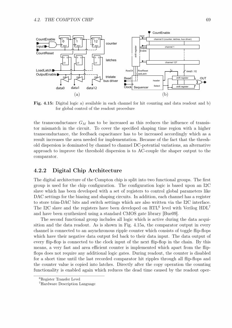
4.2. THE COMPTON CHIP 69
0 1 12counter
latches
tristate
bus driver
CountEnable
Input
CountReset
LoadLatch
D Q
D
LD
Q
RST
EN
D Q
D
LD
Q
RST
EN
D Q
D
LD
Q
RST
EN
data0 data12data1
OutputEnable
(a)
Clock
OUT
RowCK
Output
Enable
RowReset
input
Read
CountEnable
Sequencer
header
Select
channel 0 (counter, latches, bus driver)
channel 1
3data[0..12]
channel 127
shift register
sh
ift re
gis
ter
shift register
LoadLatch
(b)
Fig. 4.15: Digital logic a) available in each channel for hit counting and data readout and b)for global control of the readout procedure
the transconductance GM has to be increased as this reduces the influence of transis-tor mismatch in the circuit. To cover the specified shaping time region with a highertransconductance, the feedback capacitance has to be increased accordingly which as aresult increases the area needed for implementation. Because of the fact that the thresh-old dispersion is dominated by channel to channel DC-potential variations, an alternativeapproach to improve the threshold dispersion is to AC-couple the shaper output to thecomparator.
4.2.2 Digital Chip Architecture
The digital architecture of the Compton chip is split into two functional groups. The firstgroup is used for the chip configuration. The configuration logic is based upon an I2Cslave which has been developed with a set of registers to control global parameters likeDAC settings for the biasing and shaping circuits. In addition, each channel has a registerto store trim-DAC bits and switch settings which are also written via the I2C interface.The I2C slave and the registers have been developed on RTL6 level with Verilog HDL7
and have been synthesized using a standard CMOS gate library [Bue09].The second functional group includes all logic which is active during the data acqui-
sition and the data readout. As is shown in Fig. 4.15a, the comparator output in everychannel is connected to an asynchronous ripple counter which consists of toggle flip-flopswhich have their negative data output fed back to their data input. The data output ofevery flip-flop is connected to the clock input of the next flip-flop in the chain. By thismeans, a very fast and area efficient counter is implemented which apart from the flip-flops does not require any additional logic gates. During readout, the counter is disabledfor a short time until the last recorded comparator hit ripples through all flip-flops andthe counter value is copied into latches. Directly after the copy operation the countingfunctionality is enabled again which reduces the dead time caused by the readout oper-
6Register Transfer Level7Hardware Description Language
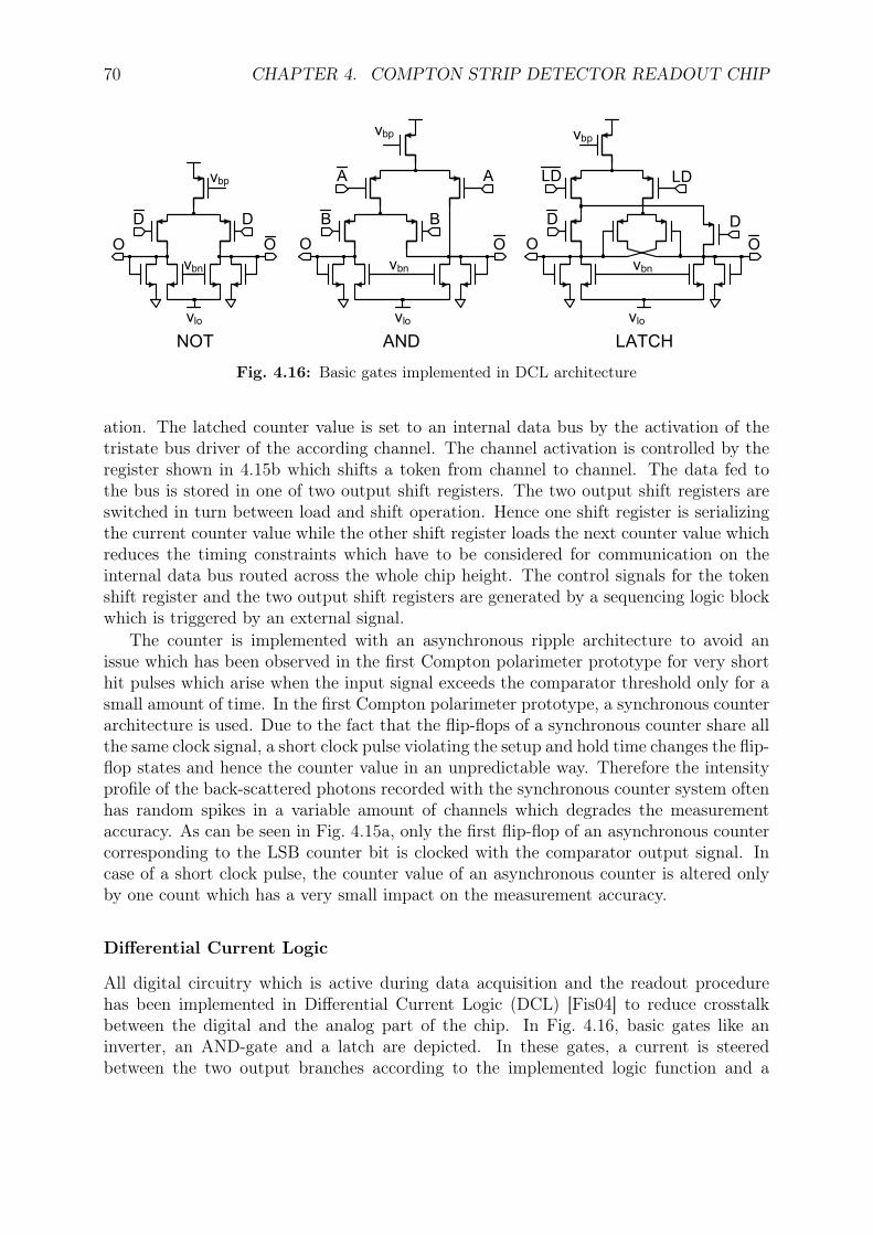
70 CHAPTER 4. COMPTON STRIP DETECTOR READOUT CHIP
D D
vbn
vbp
OO
vlo
B B
vbn
vbp
OO
vlo
A A
D D
vbn
vbp
OO
vlo
LD LD
NOT AND LATCH
Fig. 4.16: Basic gates implemented in DCL architecture
ation. The latched counter value is set to an internal data bus by the activation of thetristate bus driver of the according channel. The channel activation is controlled by theregister shown in 4.15b which shifts a token from channel to channel. The data fed tothe bus is stored in one of two output shift registers. The two output shift registers areswitched in turn between load and shift operation. Hence one shift register is serializingthe current counter value while the other shift register loads the next counter value whichreduces the timing constraints which have to be considered for communication on theinternal data bus routed across the whole chip height. The control signals for the tokenshift register and the two output shift registers are generated by a sequencing logic blockwhich is triggered by an external signal.
The counter is implemented with an asynchronous ripple architecture to avoid anissue which has been observed in the first Compton polarimeter prototype for very shorthit pulses which arise when the input signal exceeds the comparator threshold only for asmall amount of time. In the first Compton polarimeter prototype, a synchronous counterarchitecture is used. Due to the fact that the flip-flops of a synchronous counter share allthe same clock signal, a short clock pulse violating the setup and hold time changes the flip-flop states and hence the counter value in an unpredictable way. Therefore the intensityprofile of the back-scattered photons recorded with the synchronous counter system oftenhas random spikes in a variable amount of channels which degrades the measurementaccuracy. As can be seen in Fig. 4.15a, only the first flip-flop of an asynchronous countercorresponding to the LSB counter bit is clocked with the comparator output signal. Incase of a short clock pulse, the counter value of an asynchronous counter is altered onlyby one count which has a very small impact on the measurement accuracy.
Differential Current Logic
All digital circuitry which is active during data acquisition and the readout procedurehas been implemented in Differential Current Logic (DCL) [Fis04] to reduce crosstalkbetween the digital and the analog part of the chip. In Fig. 4.16, basic gates like aninverter, an AND-gate and a latch are depicted. In these gates, a current is steeredbetween the two output branches according to the implemented logic function and a
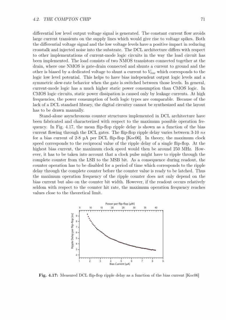
4.2. THE COMPTON CHIP 71
differential low level output voltage signal is generated. The constant current flow avoidslarge current transients on the supply lines which would give rise to voltage spikes. Boththe differential voltage signal and the low voltage levels have a positive impact in reducingcrosstalk and injected noise into the substrate. The DCL architecture differs with respectto other implementations of current-mode logic circuits in the way the load circuit hasbeen implemented. The load consists of two NMOS transistors connected together at thedrain, where one NMOS is gate-drain connected and shunts a current to ground and theother is biased by a dedicated voltage to shunt a current to Vlow which corresponds to thelogic low level potential. This helps to have bias independent output logic levels and asymmetric slew-rate behavior when the gate is switched between those levels. In general,current-mode logic has a much higher static power consumption than CMOS logic. InCMOS logic circuits, static power dissipation is caused only by leakage currents. At highfrequencies, the power consumption of both logic types are comparable. Because of thelack of a DCL standard library, the digital circuitry cannot be synthesized and the layouthas to be drawn manually.
Stand-alone asynchronous counter structures implemented in DCL architecture havebeen fabricated and characterized with respect to the maximum possible operation fre-quency. In Fig. 4.17, the mean flip-flop ripple delay is shown as a function of the biascurrent flowing through the DCL gates. The flip-flop ripple delay varies between 3-10 nsfor a bias current of 2-8 µA per DCL flip-flop [Koc06]. In theory, the maximum clockspeed corresponds to the reciprocal value of the ripple delay of a single flip-flop. At thehighest bias current, the maximum clock speed would then be around 250 MHz. How-ever, it has to be taken into account that a clock pulse might have to ripple through thecomplete counter from the LSB to the MSB bit. As a consequence during readout, thecounter operation has to be disabled for a period of time which corresponds to the rippledelay through the complete counter before the counter value is ready to be latched. Thusthe maximum operation frequency of the ripple counter does not only depend on thebias current but also on the counter bit width. However, if the readout occurs relativelyseldom with respect to the counter hit rate, the maximum operation frequency reachesvalues close to the theoretical limit.
5 10 15 20 25 30 35 40
1 2 3 4 5 6 7 8 9
2
3
4
5
6
7
8
9
Power per ip-op [µW]
Rip
ple
De
lay
pe
r
ip-
op
[n
s]
Bias Current [µA]
Fig. 4.17: Measured DCL flip-flop ripple delay as a function of the bias current [Koc06]
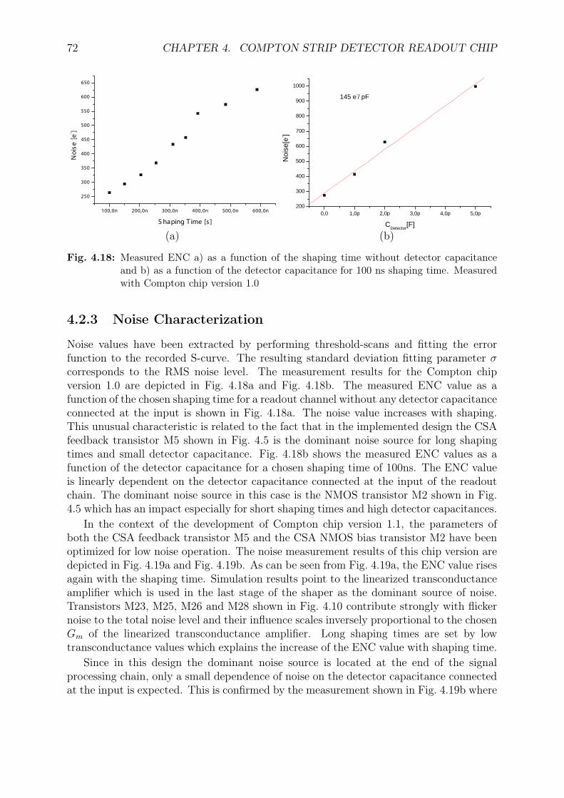
72 CHAPTER 4. COMPTON STRIP DETECTOR READOUT CHIP
100,0n 200,0n 300,0n 400,0n 500,0n 600,0n
250
300
350
400
450
500
550
600
650
No
ise
[e
- ]
S haping T ime [s ]
(a)
0,0 1,0p 2,0p 3,0p 4,0p 5,0p200
300
400
500
600
700
800
900
1000
145 e-/ pF
Noi
se[e
- ]
CDetector
[F]
(b)
Fig. 4.18: Measured ENC a) as a function of the shaping time without detector capacitanceand b) as a function of the detector capacitance for 100 ns shaping time. Measuredwith Compton chip version 1.0
4.2.3 Noise Characterization
Noise values have been extracted by performing threshold-scans and fitting the errorfunction to the recorded S-curve. The resulting standard deviation fitting parameter σcorresponds to the RMS noise level. The measurement results for the Compton chipversion 1.0 are depicted in Fig. 4.18a and Fig. 4.18b. The measured ENC value as afunction of the chosen shaping time for a readout channel without any detector capacitanceconnected at the input is shown in Fig. 4.18a. The noise value increases with shaping.This unusual characteristic is related to the fact that in the implemented design the CSAfeedback transistor M5 shown in Fig. 4.5 is the dominant noise source for long shapingtimes and small detector capacitance. Fig. 4.18b shows the measured ENC values as afunction of the detector capacitance for a chosen shaping time of 100ns. The ENC valueis linearly dependent on the detector capacitance connected at the input of the readoutchain. The dominant noise source in this case is the NMOS transistor M2 shown in Fig.4.5 which has an impact especially for short shaping times and high detector capacitances.
In the context of the development of Compton chip version 1.1, the parameters ofboth the CSA feedback transistor M5 and the CSA NMOS bias transistor M2 have beenoptimized for low noise operation. The noise measurement results of this chip version aredepicted in Fig. 4.19a and Fig. 4.19b. As can be seen from Fig. 4.19a, the ENC value risesagain with the shaping time. Simulation results point to the linearized transconductanceamplifier which is used in the last stage of the shaper as the dominant source of noise.Transistors M23, M25, M26 and M28 shown in Fig. 4.10 contribute strongly with flickernoise to the total noise level and their influence scales inversely proportional to the chosenGm of the linearized transconductance amplifier. Long shaping times are set by lowtransconductance values which explains the increase of the ENC value with shaping time.
Since in this design the dominant noise source is located at the end of the signalprocessing chain, only a small dependence of noise on the detector capacitance connectedat the input is expected. This is confirmed by the measurement shown in Fig. 4.19b where
4.3. COMPTON POLARIMETER READOUT SYSTEM 73
0 200 400 600 800
200
400
600
800
1000
1200
1400
1600e- (N
)
ShapingTime (ns)
(a)
0.0 1.0p 2.0p 3.0p 4.0p 5.0p280
300
320
340
360
380
Noi
se [
e- ]
CDetector
[F]
(b)
Fig. 4.19: Measured ENC as a function of the a) shaping time without any detector capacitanceand b) as a function of the detector capacitance for 100 ns shaping time. Measuredwith Compton chip version 1.1
the measured ENC value is given as a function of the detector capacitance for a shapingtime of 100 ns. The extracted ENC values differ only by 30 e− where the difference isalso influenced by channel to channel noise variations. Simulations have shown that theflicker noise level can be reduced significantly by increasing the transconductance of theamplifier and the area of the noisy transistors. Noise levels lower than 200 e− are thenexpected. Still, for both chip versions, the attained noise performance at small shapingtimes is sufficient to reach a signal to noise ratio > 10 since a signal of 24.000 e− isexpected to be generated by a MIP.
4.3 Compton Polarimeter Readout System
The hardware for the Compton polarimeter consists of the three boards shown in Fig.4.20. The silicon microstrip sensor and six Compton-chips are placed on the hybrid PCBand connected together via wire bonds. A ribbon cable connects the hybrid PCB to theadapter PCB which is equipped with voltage regulators, DACs, comparators and analogmultiplexer [Ahl09]. The regulators provide all needed supply voltages. The DACs areused to set the threshold voltage and to define the amount of charge which is injectedduring calibration. The comparators and the analog multiplexer are needed for the I/Osignal level adaption to the first Compton-chip version which uses DCL level signals atthe I/O interface. The I/O signal level adaption is configurable due to the fact that thesecond Compton-chip version has LVDS compatible I/O signals and does not need anysignal level adaption. A robust plug system is used to establish a connection betweenthe adapter board and the I/O board which contains an FPGA and a microcontrollerwith USB interface for communication with a PC. The FPGA is programmed to controlthe readout sequence of the Compton-chips, to generate strobe signals for calibration andto provide timing information during data acquisition. The readout data is stored in aninternal RAM and prepared for transmission to the PC.
74 CHAPTER 4. COMPTON STRIP DETECTOR READOUT CHIP
Fig. 4.20: Compton polarimeter readout system composed of the hybrid PCB with sensor andreadout chips, the adapter PCB with voltage regulators, DACs and signal level adap-tion and the I/O board with FPGA, microprocessor and USB interface
A C++ software package has been developed which implements an application pro-gramming interface (API) to control the whole readout system. The API covers low-levelfunctions like chip readout and configuration but also functions of higher level of abstrac-tion like the execution of parameterized thresholds scans and data fitting algorithms. Auser friendly graphical interface has been developed based on the QT framework.
The described readout system and other dedicated test systems have been used forthe characterization of the Compton-chips. In addition, the readout system has beeninstalled at the ELSA laboratory and first measurements with the Compton polarimetrysetup have been performed. Fig. 4.21 shows a measurement of a spatial distribution ofphotons generated by background events. The profile has been recorded within 1 secondwith a beam energy of 2.35 GeV. The total background event rate extracted from thismeasurement is about 38 kHz.
Fig. 4.21: Spatial distribution of photons generated by background events
4.4. SUMMARY 75
4.4 SummaryA silicon microstrip readout chip has been developed for precision Compton polarimetry.The Compton chip has been produced in two iterations to test different shaping circuitarchitectures and to optimize some device parameters.
The shaping structure which uses PMOS transistors biased in linear region as feedbackelements, generates low excess noise and gives a small contribution to threshold dispersionbut is limited in terms of linearity for long shaping times. In this scheme, linearity couldbe improved by having a set of parallel connected PMOS transistors with different channellengths in the feedback. Dependent on the wanted shaping time region, the correspondingtransistor is enabled and all others are disabled. The biasing voltage of the feedbacktransistors is then only used for fine tuning and process variation compensation. Thesaturation voltage should be set as high as it is needed to keep the feedback transistorsin linear region during signal processing.
The alternative shaping structure based on linearized transconductance amplifier showsa very good linearity behavior in a wide range of charge signal levels and in a wide rangeof shaping times but adds excess noise and deteriorates threshold dispersion. Both noiseand threshold dispersion can be improved by choosing a higher transconductance valueand a higher feedback capacitor at the cost of increased implementation area.
The counting and readout logic implemented in Differential Current Logic reaches highcount rates and small dead times. With both chip versions, a SNR has been achievedwhich is sufficient for the application. A complete readout system based on the Compton-chip has been developed and first measurements with the Compton polarimetry setup havebeen performed.
sensor
chips
wire bonds
Fig. 4.22: 6 Compton chips connected via wire bonds to the silicon microstrip sensor
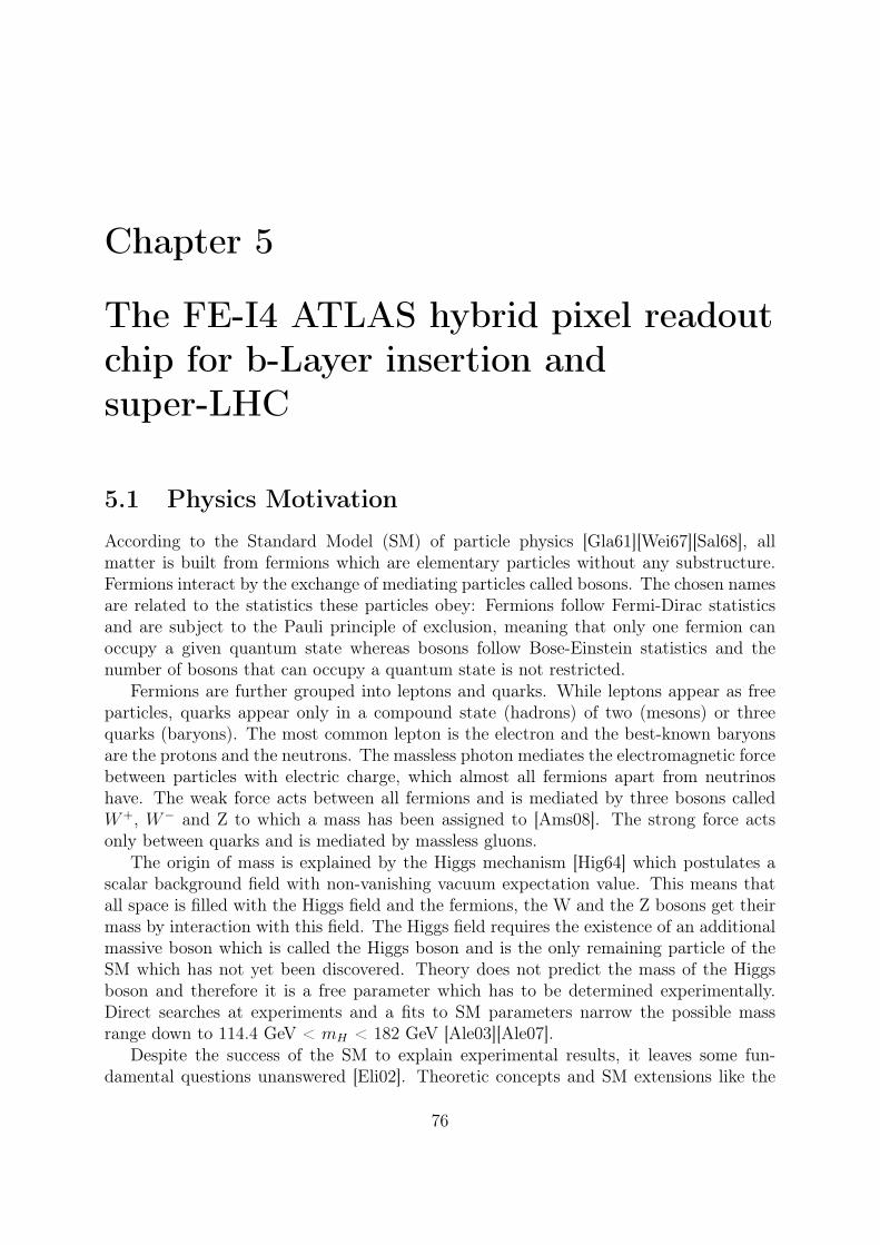
Chapter 5
The FE-I4 ATLAS hybrid pixel readoutchip for b-Layer insertion andsuper-LHC
5.1 Physics Motivation
According to the Standard Model (SM) of particle physics [Gla61][Wei67][Sal68], allmatter is built from fermions which are elementary particles without any substructure.Fermions interact by the exchange of mediating particles called bosons. The chosen namesare related to the statistics these particles obey: Fermions follow Fermi-Dirac statisticsand are subject to the Pauli principle of exclusion, meaning that only one fermion canoccupy a given quantum state whereas bosons follow Bose-Einstein statistics and thenumber of bosons that can occupy a quantum state is not restricted.
Fermions are further grouped into leptons and quarks. While leptons appear as freeparticles, quarks appear only in a compound state (hadrons) of two (mesons) or threequarks (baryons). The most common lepton is the electron and the best-known baryonsare the protons and the neutrons. The massless photon mediates the electromagnetic forcebetween particles with electric charge, which almost all fermions apart from neutrinoshave. The weak force acts between all fermions and is mediated by three bosons calledW+, W− and Z to which a mass has been assigned to [Ams08]. The strong force actsonly between quarks and is mediated by massless gluons.
The origin of mass is explained by the Higgs mechanism [Hig64] which postulates ascalar background field with non-vanishing vacuum expectation value. This means thatall space is filled with the Higgs field and the fermions, the W and the Z bosons get theirmass by interaction with this field. The Higgs field requires the existence of an additionalmassive boson which is called the Higgs boson and is the only remaining particle of theSM which has not yet been discovered. Theory does not predict the mass of the Higgsboson and therefore it is a free parameter which has to be determined experimentally.Direct searches at experiments and a fits to SM parameters narrow the possible massrange down to 114.4 GeV < mH < 182 GeV [Ale03][Ale07].
Despite the success of the SM to explain experimental results, it leaves some fun-damental questions unanswered [Eli02]. Theoretic concepts and SM extensions like the
76
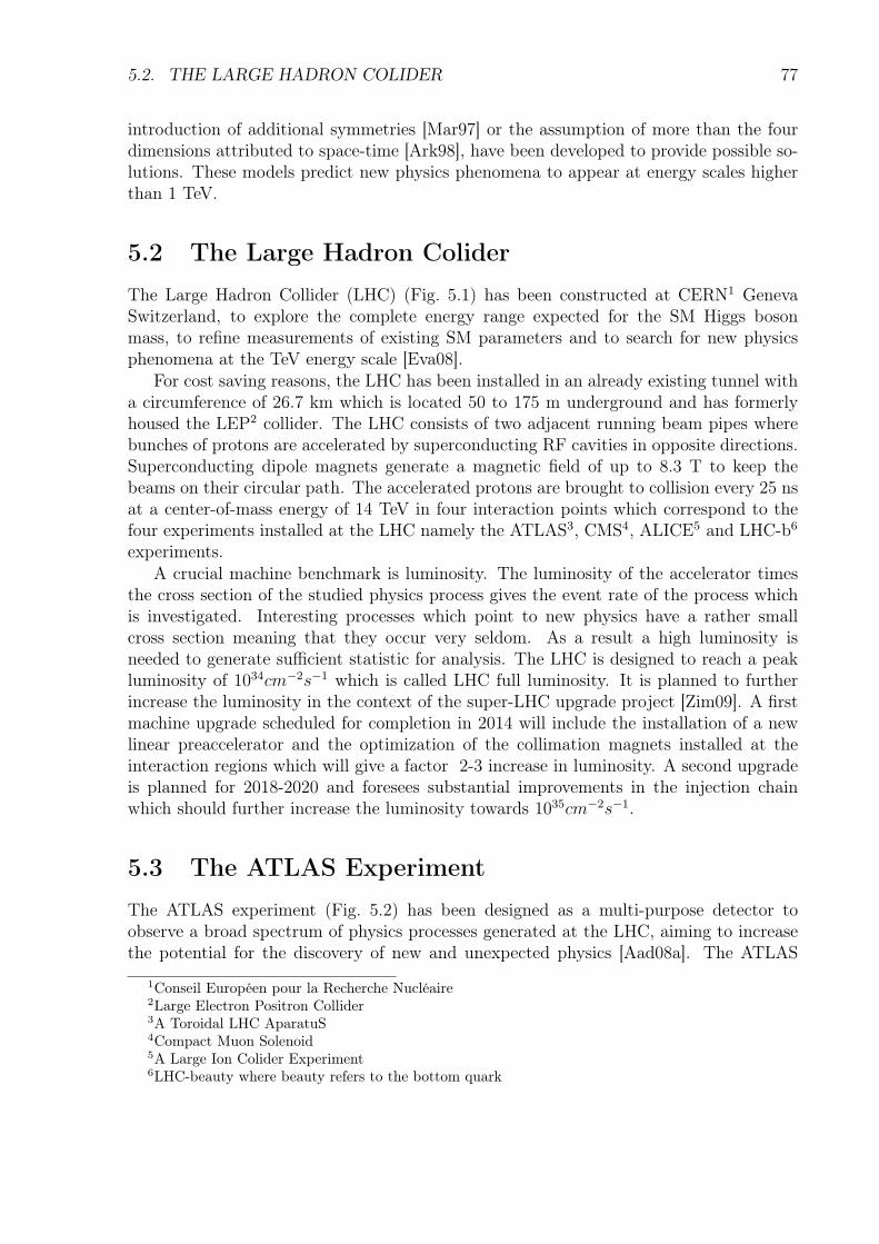
5.2. THE LARGE HADRON COLIDER 77
introduction of additional symmetries [Mar97] or the assumption of more than the fourdimensions attributed to space-time [Ark98], have been developed to provide possible so-lutions. These models predict new physics phenomena to appear at energy scales higherthan 1 TeV.
5.2 The Large Hadron Colider
The Large Hadron Collider (LHC) (Fig. 5.1) has been constructed at CERN1 GenevaSwitzerland, to explore the complete energy range expected for the SM Higgs bosonmass, to refine measurements of existing SM parameters and to search for new physicsphenomena at the TeV energy scale [Eva08].
For cost saving reasons, the LHC has been installed in an already existing tunnel witha circumference of 26.7 km which is located 50 to 175 m underground and has formerlyhoused the LEP2 collider. The LHC consists of two adjacent running beam pipes wherebunches of protons are accelerated by superconducting RF cavities in opposite directions.Superconducting dipole magnets generate a magnetic field of up to 8.3 T to keep thebeams on their circular path. The accelerated protons are brought to collision every 25 nsat a center-of-mass energy of 14 TeV in four interaction points which correspond to thefour experiments installed at the LHC namely the ATLAS3, CMS4, ALICE5 and LHC-b6
experiments.A crucial machine benchmark is luminosity. The luminosity of the accelerator times
the cross section of the studied physics process gives the event rate of the process whichis investigated. Interesting processes which point to new physics have a rather smallcross section meaning that they occur very seldom. As a result a high luminosity isneeded to generate sufficient statistic for analysis. The LHC is designed to reach a peakluminosity of 1034cm−2s−1 which is called LHC full luminosity. It is planned to furtherincrease the luminosity in the context of the super-LHC upgrade project [Zim09]. A firstmachine upgrade scheduled for completion in 2014 will include the installation of a newlinear preaccelerator and the optimization of the collimation magnets installed at theinteraction regions which will give a factor 2-3 increase in luminosity. A second upgradeis planned for 2018-2020 and foresees substantial improvements in the injection chainwhich should further increase the luminosity towards 1035cm−2s−1.
5.3 The ATLAS Experiment
The ATLAS experiment (Fig. 5.2) has been designed as a multi-purpose detector toobserve a broad spectrum of physics processes generated at the LHC, aiming to increasethe potential for the discovery of new and unexpected physics [Aad08a]. The ATLAS
1Conseil Européen pour la Recherche Nucléaire2Large Electron Positron Collider3A Toroidal LHC AparatuS4Compact Muon Solenoid5A Large Ion Colider Experiment6LHC-beauty where beauty refers to the bottom quark
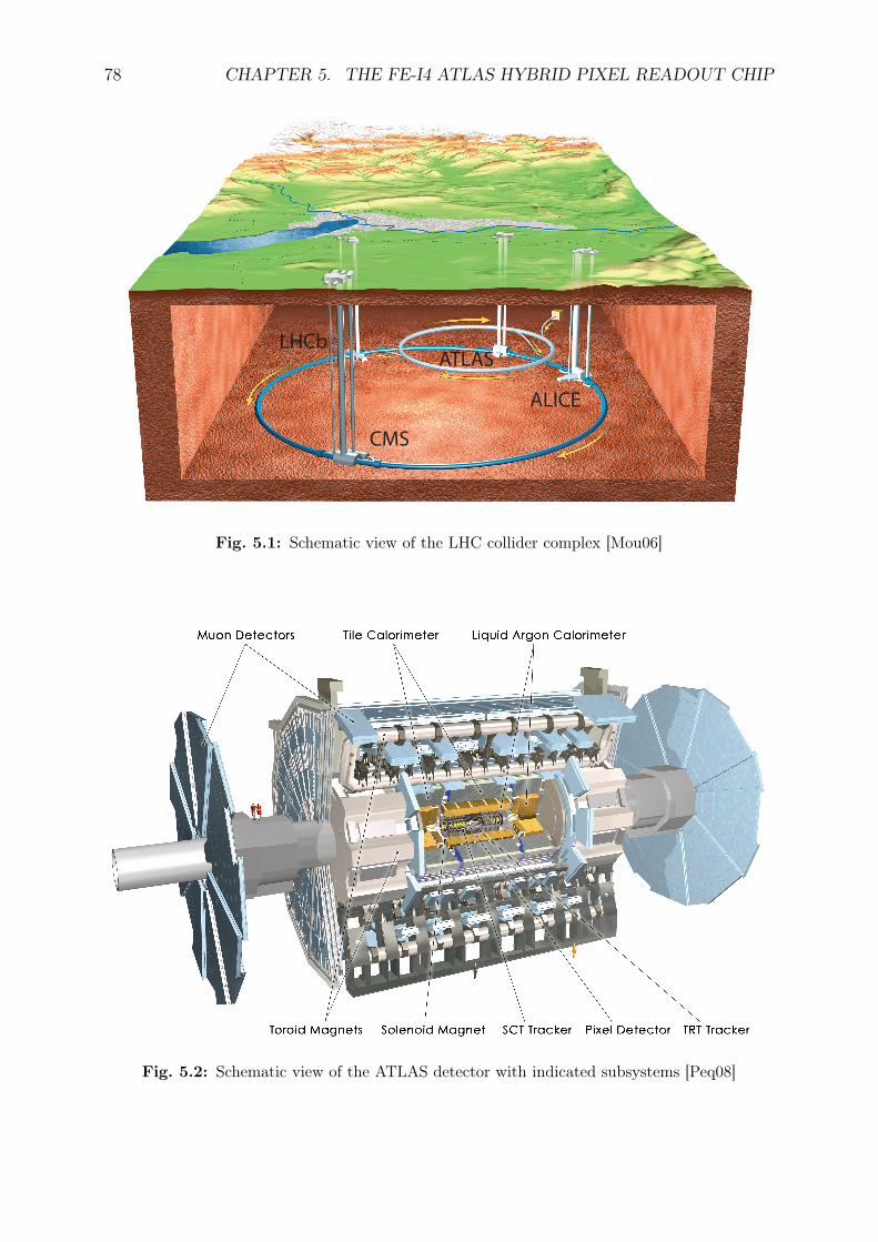
78 CHAPTER 5. THE FE-I4 ATLAS HYBRID PIXEL READOUT CHIP
ATLAS
ALICE
CMS
LHCb
Fig. 5.1: Schematic view of the LHC collider complex [Mou06]
Fig. 5.2: Schematic view of the ATLAS detector with indicated subsystems [Peq08]
5.3. THE ATLAS EXPERIMENT 79
experiment is built in a sequence of layers corresponding to the respective subdetectorsystem which enclose the interaction point hermetically which means that every spatialdirection is covered as complete as possible. The individual subdetectors are formed likebarrels around the beam pipes and are terminated by active disks at both ends. Thedimensions of the detector are 25 m in height and 44 m in length. The overall weight isapproximately 7000 tonnes.
The outermost layers of the ATLAS experiment are formed by the muon spectrometerswhich identify muons and measures their momentum. Muons are highly penetratingleptons which reach the outer detector layers because of their relatively long mean lifetimecompared to other unstable particles. The muon spectrometer is surrounded by a magneticfield which is generated by a toroidal magnet and bends the particles by means of theLorentz force. The muon momentum is determined by precise tracking and measuring ofthe curvature.
Going inwards the next layers are dedicated to the calorimetry system. The outer layerforms the hadronic calorimeter which absorbs and measures the energy of hadrons whereasthe inner layer is the electromagnetic calorimeter and absorbs the energy from photonsand electrons. The calorimeters are segmented to introduce spatial resolution which isneeded to assign the measured energy to particle traces left in other subdetectors.
The muon spectrometer and the calorimeter system are both of special importancefor the basic triggering system which is called the Level-1 trigger. Interesting physicsprocesses leave distinctive energy signatures in the calorimeters and also generate muonswithin a certain momentum range. A hardware based system searches for expected pat-terns and generates the Level-1 readout trigger within a fixed latency of 2.5 µs whichreduces the event rate from 40 MHz (bunch crossing rate) to approximately 75 KHz. Ad-ditional software based high-level trigger [Atl03] exist which analyze data generated alsofrom other subdetectors to further reduce the event rate down to approximately 200 Hz.
5.3.1 The Inner Detector
The following layers belong all to the inner detector [Atl97] which is used to precisely trackcharged particles originating from the primary proton-proton collision or from secondarydecay processes. The inner detector is surrounded by a 2 T magnetic field which isgenerated by a solenoid magnet located between the electromagnetic calorimeter and theinner detector. As a result charged particles in the inner detector move on a curvedtrajectory. The reconstruction of the curvature direction reveals the charge whereas thedegree of curvature reveals the momentum of the particle.
With decreasing radius, the requirements on the tracking device change significantly.While a larger volume has to be covered at the outer radii which implies the need for costefficiency, the particle flux increases at smaller radius which demands higher granularityas well as radiation hard sensors and readout electronics. The different requirements havebeen addressed with three different tracking detectors which are the gaseous transitionradiation tracker (TRT), the semiconductor tracker (SCT) which is based on silicon mi-crostrip detectors and the innermost silicon pixel detector. A major redesign of the innerdetector scheme is scheduled for the super-LHC luminosity upgrade. Although layout andtechnology details are still under discussion and have not been agreed on yet, the revised
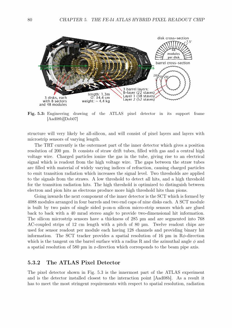
80 CHAPTER 5. THE FE-I4 ATLAS HYBRID PIXEL READOUT CHIP
Fig. 5.3: Engineering drawing of the ATLAS pixel detector in its support frame[Aad08b][Dob07]
structure will very likely be all-silicon, and will consist of pixel layers and layers withmicrostrip sensors of varying length.
The TRT currently is the outermost part of the inner detector which gives a positionresolution of 200 µm. It consists of straw drift tubes, filled with gas and a central highvoltage wire. Charged particles ionize the gas in the tube, giving rise to an electricalsignal which is readout from the high voltage wire. The gaps between the straw tubesare filled with material of widely varying indices of refraction, causing charged particlesto emit transition radiation which increases the signal level. Two thresholds are appliedto the signals from the straws. A low threshold to detect all hits, and a high thresholdfor the transition radiation hits. The high threshold is optimized to distinguish betweenelectron and pion hits as electrons produce more high threshold hits than pions.
Going inwards the next component of the inner detector is the SCT which is formed by4088 modules arranged in four barrels and two end caps of nine disks each. A SCT moduleis built by two pairs of single sided p-on-n silicon micro-strip sensors which are gluedback to back with a 40 mrad stereo angle to provide two-dimensional hit information.The silicon microstrip sensors have a thickness of 285 µm and are segmented into 768AC-coupled strips of 12 cm length with a pitch of 80 µm. Twelve readout chips areused for sensor readout per module each having 128 channels and providing binary hitinformation. The SCT tracker provides a spatial resolution of 16 µm in Rϕ-directionwhich is the tangent on the barrel surface with a radius R and the azimuthal angle ϕ anda spatial resolution of 580 µm in z-direction which corresponds to the beam pipe axis.
5.3.2 The ATLAS Pixel Detector
The pixel detector shown in Fig. 5.3 is the innermost part of the ATLAS experimentand is the detector installed closest to the interaction point [Aad08b]. As a result ithas to meet the most stringent requirements with respect to spatial resolution, radiation
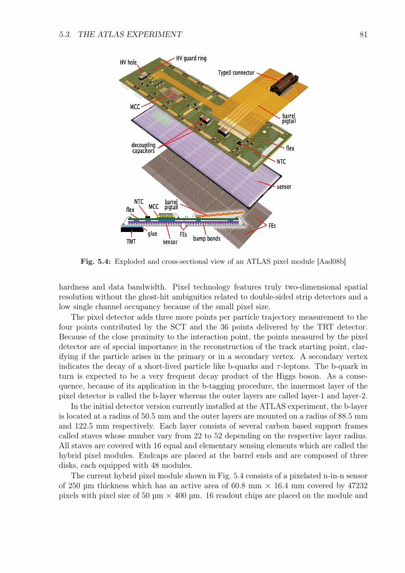
5.3. THE ATLAS EXPERIMENT 81
Fig. 5.4: Exploded and cross-sectional view of an ATLAS pixel module [Aad08b]
hardness and data bandwidth. Pixel technology features truly two-dimensional spatialresolution without the ghost-hit ambiguities related to double-sided strip detectors and alow single channel occupancy because of the small pixel size.
The pixel detector adds three more points per particle trajectory measurement to thefour points contributed by the SCT and the 36 points delivered by the TRT detector.Because of the close proximity to the interaction point, the points measured by the pixeldetector are of special importance in the reconstruction of the track starting point, clar-ifying if the particle arises in the primary or in a secondary vertex. A secondary vertexindicates the decay of a short-lived particle like b-quarks and τ -leptons. The b-quark inturn is expected to be a very frequent decay product of the Higgs boson. As a conse-quence, because of its application in the b-tagging procedure, the innermost layer of thepixel detector is called the b-layer whereas the outer layers are called layer-1 and layer-2.
In the initial detector version currently installed at the ATLAS experiment, the b-layeris located at a radius of 50.5 mm and the outer layers are mounted on a radius of 88.5 mmand 122.5 mm respectively. Each layer consists of several carbon based support framescalled staves whose number vary from 22 to 52 depending on the respective layer radius.All staves are covered with 16 equal and elementary sensing elements which are called thehybrid pixel modules. Endcaps are placed at the barrel ends and are composed of threedisks, each equipped with 48 modules.
The current hybrid pixel module shown in Fig. 5.4 consists of a pixelated n-in-n sensorof 250 µm thickness which has an active area of 60.8 mm × 16.4 mm covered by 47232pixels with pixel size of 50 µm × 400 µm. 16 readout chips are placed on the module and
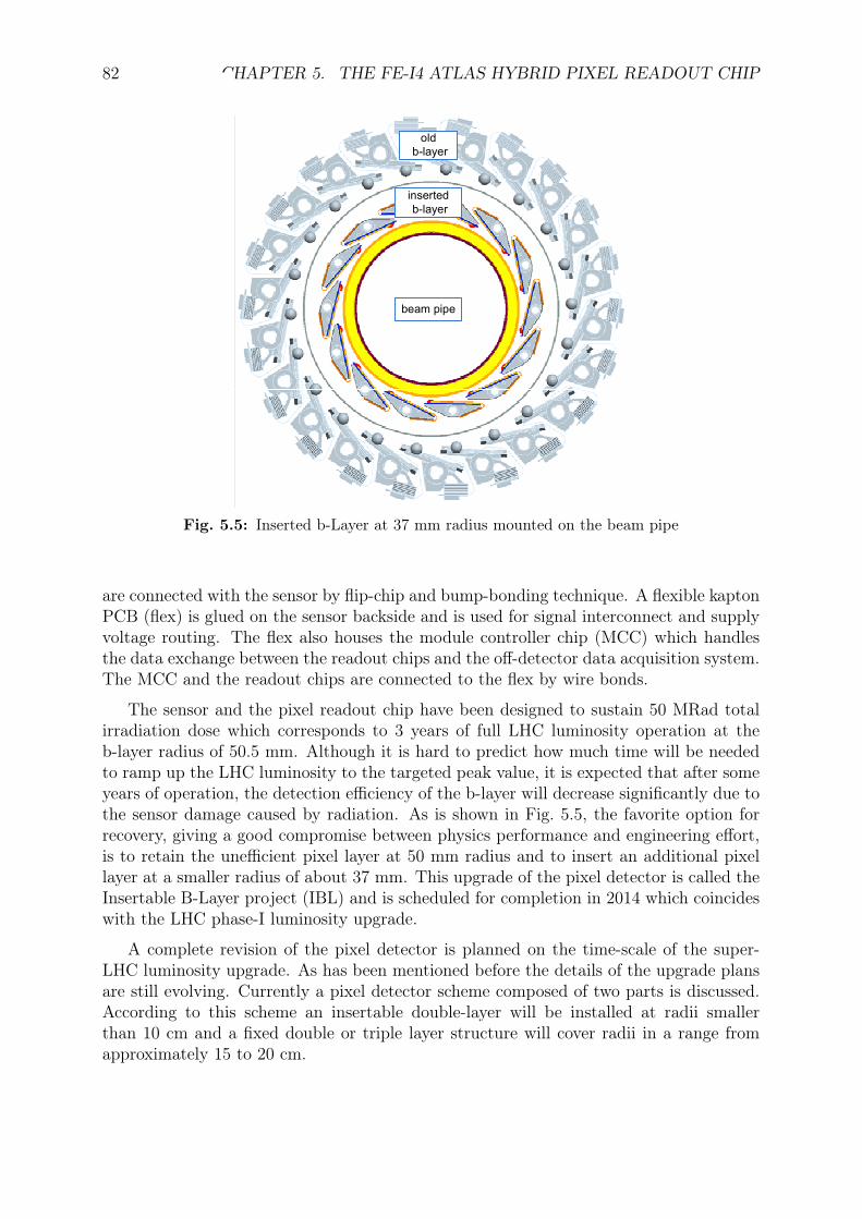
82 CHAPTER 5. THE FE-I4 ATLAS HYBRID PIXEL READOUT CHIP
beam pipe
inserted
b-layer
old
b-layer
Fig. 5.5: Inserted b-Layer at 37 mm radius mounted on the beam pipe
are connected with the sensor by flip-chip and bump-bonding technique. A flexible kaptonPCB (flex) is glued on the sensor backside and is used for signal interconnect and supplyvoltage routing. The flex also houses the module controller chip (MCC) which handlesthe data exchange between the readout chips and the off-detector data acquisition system.The MCC and the readout chips are connected to the flex by wire bonds.
The sensor and the pixel readout chip have been designed to sustain 50 MRad totalirradiation dose which corresponds to 3 years of full LHC luminosity operation at theb-layer radius of 50.5 mm. Although it is hard to predict how much time will be neededto ramp up the LHC luminosity to the targeted peak value, it is expected that after someyears of operation, the detection efficiency of the b-layer will decrease significantly due tothe sensor damage caused by radiation. As is shown in Fig. 5.5, the favorite option forrecovery, giving a good compromise between physics performance and engineering effort,is to retain the unefficient pixel layer at 50 mm radius and to insert an additional pixellayer at a smaller radius of about 37 mm. This upgrade of the pixel detector is called theInsertable B-Layer project (IBL) and is scheduled for completion in 2014 which coincideswith the LHC phase-I luminosity upgrade.
A complete revision of the pixel detector is planned on the time-scale of the super-LHC luminosity upgrade. As has been mentioned before the details of the upgrade plansare still evolving. Currently a pixel detector scheme composed of two parts is discussed.According to this scheme an insertable double-layer will be installed at radii smallerthan 10 cm and a fixed double or triple layer structure will cover radii in a range fromapproximately 15 to 20 cm.
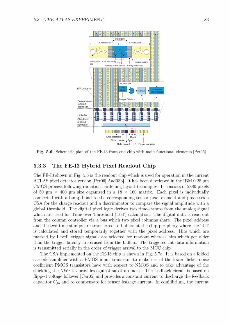
5.3. THE ATLAS EXPERIMENT 83
cell
l
l l
l
l
ller
ll
cell
cell
l
l
Fig. 5.6: Schematic plan of the FE-I3 front-end chip with main functional elements [Per06]
5.3.3 The FE-I3 Hybrid Pixel Readout Chip
The FE-I3 shown in Fig. 5.6 is the readout chip which is used for operation in the currentATLAS pixel detector version [Per06][Aad08b]. It has been developed in the IBM 0.25 µmCMOS process following radiation hardening layout techniques. It consists of 2880 pixelsof 50 µm × 400 µm size organized in a 18 × 160 matrix. Each pixel is individuallyconnected with a bump-bond to the corresponding sensor pixel element and possesses aCSA for the charge readout and a discriminator to compare the signal amplitude with aglobal threshold. The digital pixel logic derives two time-stamps from the analog signalwhich are used for Time-over-Threshold (ToT) calculation. The digital data is read outfrom the column controller via a bus which two pixel columns share. The pixel addressand the two time-stamps are transferred to buffers at the chip periphery where the ToTis calculated and stored temporarily together with the pixel address. Hits which aremarked by Level1 trigger signals are selected for readout whereas hits which get olderthan the trigger latency are erased from the buffers. The triggered hit data informationis transmitted serially in the order of trigger arrival to the MCC chip.
The CSA implemented on the FE-I3 chip is shown in Fig. 5.7a. It is based on a foldedcascode amplifier with a PMOS input transistor to make use of the lower flicker noisecoefficient PMOS transistors have with respect to NMOS and to take advantage of theshielding the NWELL provides against substrate noise. The feedback circuit is based onflipped voltage follower [Car05] and provides a constant current to discharge the feedbackcapacitor Cfb and to compensate for sensor leakage current. In equilibrium, the current
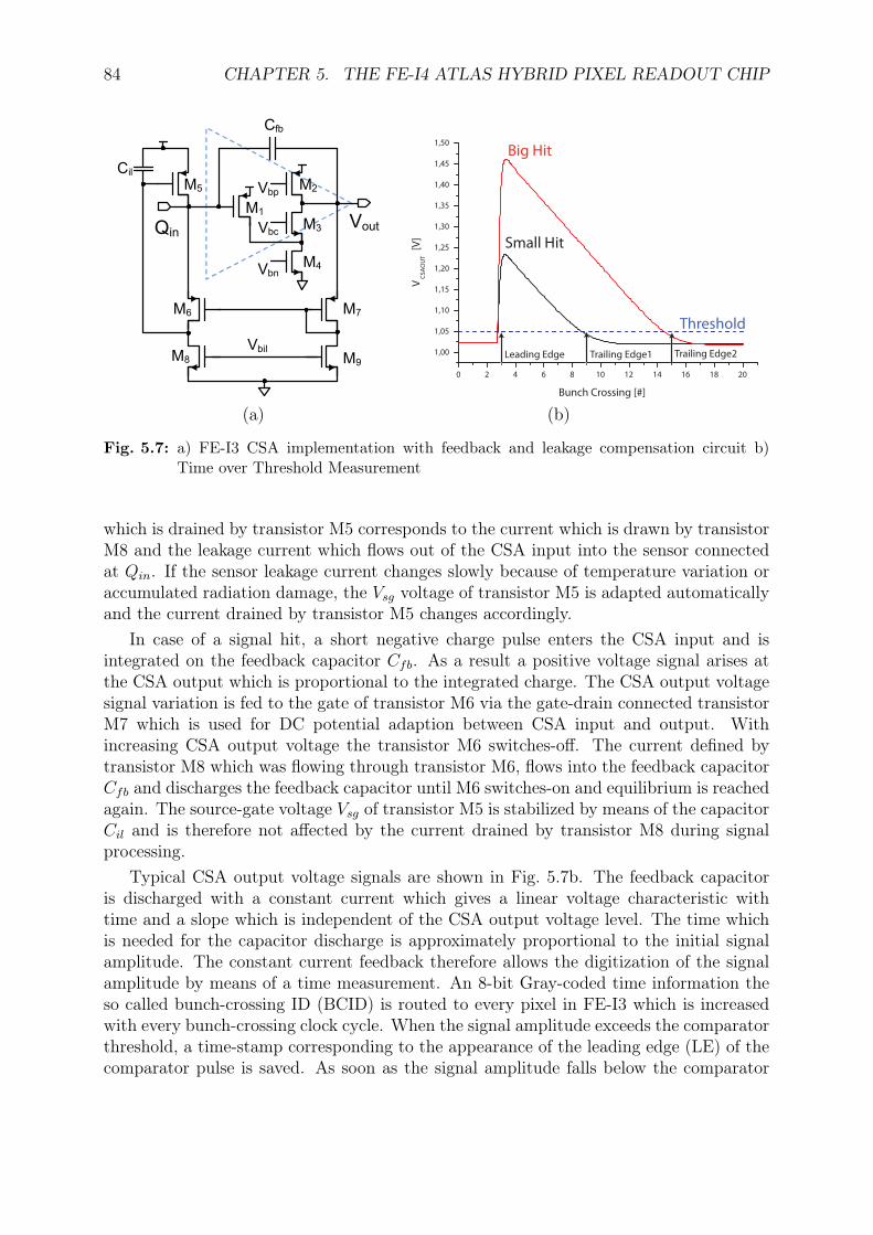
84 CHAPTER 5. THE FE-I4 ATLAS HYBRID PIXEL READOUT CHIP
VoutQin
M1
M2
M3
M4
M5
M6 M7
M8 M9
Cfb
Cil
Vbil
Vbn
Vbc
Vbp
(a)
0 2 4 6 8 10 12 14 16 18 20
1,00
1,05
1,10
1,15
1,20
1,25
1,30
1,35
1,40
1,45
1,50
VC
SA
OU
T[V
]
Bunch Crossing [#]
Threshold
Big Hit
Small Hit
Leading Edge Trailing Edge1 Trailing Edge2
(b)
Fig. 5.7: a) FE-I3 CSA implementation with feedback and leakage compensation circuit b)Time over Threshold Measurement
which is drained by transistor M5 corresponds to the current which is drawn by transistorM8 and the leakage current which flows out of the CSA input into the sensor connectedat Qin. If the sensor leakage current changes slowly because of temperature variation oraccumulated radiation damage, the Vsg voltage of transistor M5 is adapted automaticallyand the current drained by transistor M5 changes accordingly.
In case of a signal hit, a short negative charge pulse enters the CSA input and isintegrated on the feedback capacitor Cfb. As a result a positive voltage signal arises atthe CSA output which is proportional to the integrated charge. The CSA output voltagesignal variation is fed to the gate of transistor M6 via the gate-drain connected transistorM7 which is used for DC potential adaption between CSA input and output. Withincreasing CSA output voltage the transistor M6 switches-off. The current defined bytransistor M8 which was flowing through transistor M6, flows into the feedback capacitorCfb and discharges the feedback capacitor until M6 switches-on and equilibrium is reachedagain. The source-gate voltage Vsg of transistor M5 is stabilized by means of the capacitorCil and is therefore not affected by the current drained by transistor M8 during signalprocessing.
Typical CSA output voltage signals are shown in Fig. 5.7b. The feedback capacitoris discharged with a constant current which gives a linear voltage characteristic withtime and a slope which is independent of the CSA output voltage level. The time whichis needed for the capacitor discharge is approximately proportional to the initial signalamplitude. The constant current feedback therefore allows the digitization of the signalamplitude by means of a time measurement. An 8-bit Gray-coded time information theso called bunch-crossing ID (BCID) is routed to every pixel in FE-I3 which is increasedwith every bunch-crossing clock cycle. When the signal amplitude exceeds the comparatorthreshold, a time-stamp corresponding to the appearance of the leading edge (LE) of thecomparator pulse is saved. As soon as the signal amplitude falls below the comparator
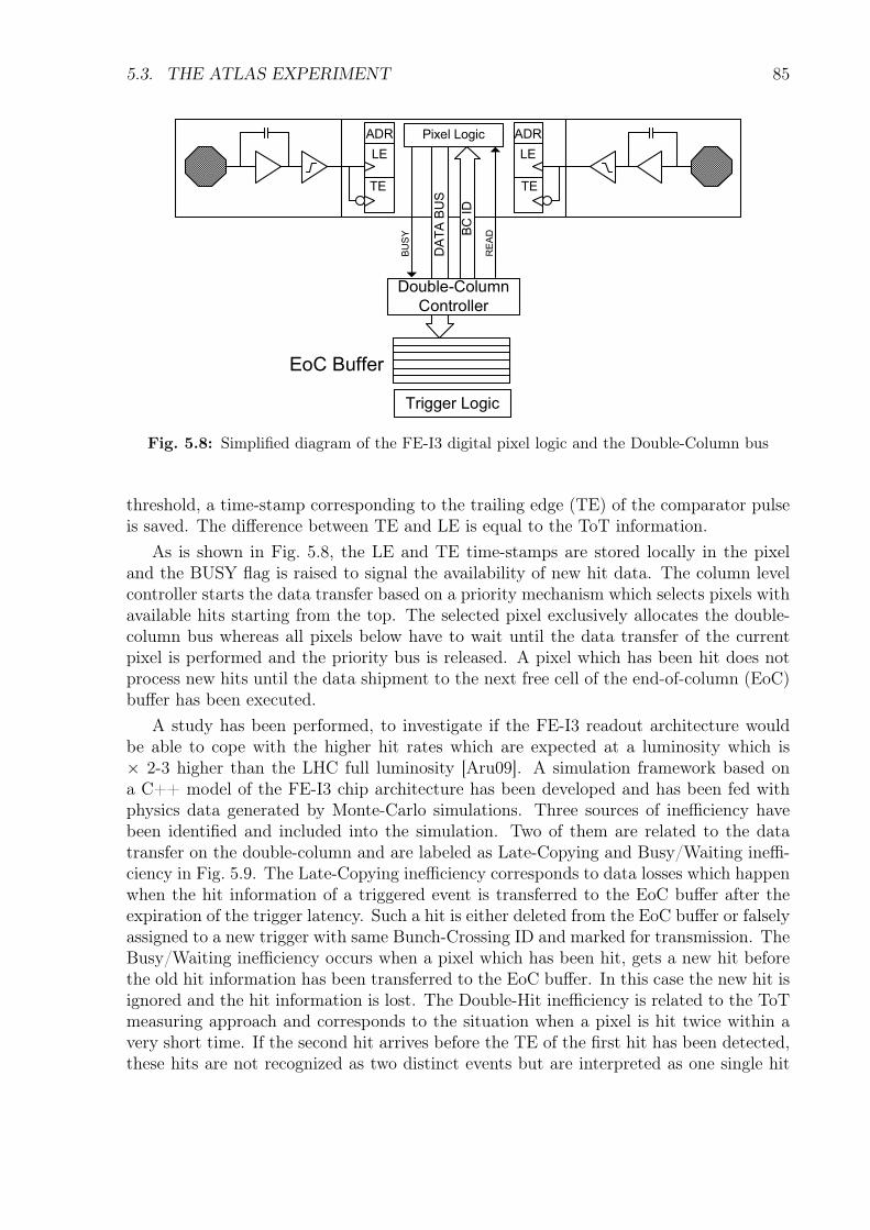
5.3. THE ATLAS EXPERIMENT 85
DATA BUS
BC ID
Double-Column
Controller
EoC Buffer
Trigger Logic
LE
TE
ADR
LE
TE
ADRPixel Logic
READ
BUSY
Fig. 5.8: Simplified diagram of the FE-I3 digital pixel logic and the Double-Column bus
threshold, a time-stamp corresponding to the trailing edge (TE) of the comparator pulseis saved. The difference between TE and LE is equal to the ToT information.
As is shown in Fig. 5.8, the LE and TE time-stamps are stored locally in the pixeland the BUSY flag is raised to signal the availability of new hit data. The column levelcontroller starts the data transfer based on a priority mechanism which selects pixels withavailable hits starting from the top. The selected pixel exclusively allocates the double-column bus whereas all pixels below have to wait until the data transfer of the currentpixel is performed and the priority bus is released. A pixel which has been hit does notprocess new hits until the data shipment to the next free cell of the end-of-column (EoC)buffer has been executed.
A study has been performed, to investigate if the FE-I3 readout architecture wouldbe able to cope with the higher hit rates which are expected at a luminosity which is× 2-3 higher than the LHC full luminosity [Aru09]. A simulation framework based ona C++ model of the FE-I3 chip architecture has been developed and has been fed withphysics data generated by Monte-Carlo simulations. Three sources of inefficiency havebeen identified and included into the simulation. Two of them are related to the datatransfer on the double-column and are labeled as Late-Copying and Busy/Waiting ineffi-ciency in Fig. 5.9. The Late-Copying inefficiency corresponds to data losses which happenwhen the hit information of a triggered event is transferred to the EoC buffer after theexpiration of the trigger latency. Such a hit is either deleted from the EoC buffer or falselyassigned to a new trigger with same Bunch-Crossing ID and marked for transmission. TheBusy/Waiting inefficiency occurs when a pixel which has been hit, gets a new hit beforethe old hit information has been transferred to the EoC buffer. In this case the new hit isignored and the hit information is lost. The Double-Hit inefficiency is related to the ToTmeasuring approach and corresponds to the situation when a pixel is hit twice within avery short time. If the second hit arrives before the TE of the first hit has been detected,these hits are not recognized as two distinct events but are interpreted as one single hit
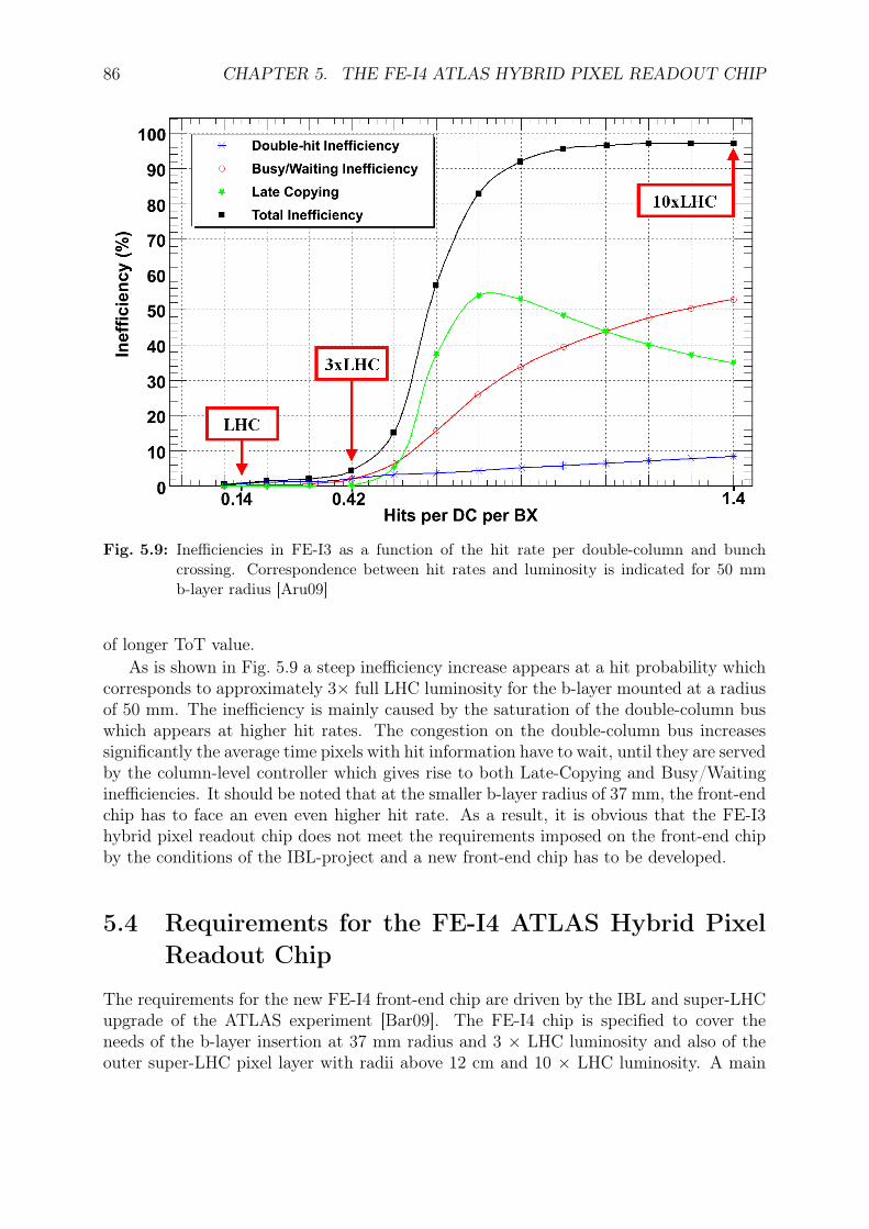
86 CHAPTER 5. THE FE-I4 ATLAS HYBRID PIXEL READOUT CHIP
Fig. 5.9: Inefficiencies in FE-I3 as a function of the hit rate per double-column and bunchcrossing. Correspondence between hit rates and luminosity is indicated for 50 mmb-layer radius [Aru09]
of longer ToT value.As is shown in Fig. 5.9 a steep inefficiency increase appears at a hit probability which
corresponds to approximately 3× full LHC luminosity for the b-layer mounted at a radiusof 50 mm. The inefficiency is mainly caused by the saturation of the double-column buswhich appears at higher hit rates. The congestion on the double-column bus increasessignificantly the average time pixels with hit information have to wait, until they are servedby the column-level controller which gives rise to both Late-Copying and Busy/Waitinginefficiencies. It should be noted that at the smaller b-layer radius of 37 mm, the front-endchip has to face an even even higher hit rate. As a result, it is obvious that the FE-I3hybrid pixel readout chip does not meet the requirements imposed on the front-end chipby the conditions of the IBL-project and a new front-end chip has to be developed.
5.4 Requirements for the FE-I4 ATLAS Hybrid PixelReadout Chip
The requirements for the new FE-I4 front-end chip are driven by the IBL and super-LHCupgrade of the ATLAS experiment [Bar09]. The FE-I4 chip is specified to cover theneeds of the b-layer insertion at 37 mm radius and 3 × LHC luminosity and also of theouter super-LHC pixel layer with radii above 12 cm and 10 × LHC luminosity. A main
5.4. REQUIREMENTS FOR THE FE-I4 READOUT CHIP 87
concern is the ability of the chip architecture to handle the increased average hit rate of50 kHz per pixel which is comparable in both addressed upgrade scenarios. Furthermore,the reduction of material is very beneficial since the amount of material needed for theconstruction of the b-layer determines the measuring accuracy and the overall physicsperformance of the detector. A cutback in pixel module assembly cost is also desiredso that the coverage of the large area related to the super-LHC outer pixel layers getsfeasible. A decrease in power consumption and the improvement of the powering efficiencyis aimed to simplify cabling and cooling which in turn is also beneficial in terms of costand material reduction. Due to the fact that a definitive decision on the sensor type hasnot yet been reached and that a different sensor technology might be used for the IBL andthe outer super-LHC pixel layer, the FE-I4 chip has to be compatible to several sensorcandidates like standard planar silicon, 3D silicon or diamond which all have differentcharacteristics in terms of detector capacitance, leakage current, charge collection timeand signal charge.
130nm CMOS Technology Node
The FE-I4 chip has been designed in the IBM 130 nm CMOS process. The chosentechnology node affords a higher integration density, compared to the 250 nm CMOStechnology which has been used for the development of the FE-I3 chip and has also a higherradiation tolerance which relaxes the layout rules for radiation hard design. The sensitivityof MOS transistors to radiation is mainly defined by the gate-oxide thickness. Radiationcauses less gate-oxide defects in transistors with thin gate-oxide than in transistors withthick gate-oxide. The IBM 130 nm CMOS process provides transistors with 2.2 nmphysical gate-oxide thickness whereas the thinnest gate-oxide available in the 250 nmCMOS process is about 5 nm. As a result only a minimum set of radiation-hardnessrelated layout and design rules have to be applied to reach a radiation-tolerance of morethan 200 MRad. Obviously thick gate-oxide IO transistors also available in this technologyshould not be used if possible. For transistors in analog circuits, minimum width transistorsize and weak inversion operation region should be avoided. In addition NMOS transistorsused in analog and sensitive digital circuits which have different drain or source potentialsshould be separated by p-diffusion guard rings to absorb leakage currents induced bydefects in the field-oxide. The use of the area consuming enclosed-gate transistor layoutgeometry is obsolete in this technology which together with the smaller feature size resultsin the much higher integration density.
An 8 metal technology option has been chosen, which offers a 4 µm thick aluminiumand a 3 µm thick copper top metal layer and also three more metal layers of intermediatethickness (0.46 - 0.55 µm) which are very valuable for global power and signal routingwith low resistance. The technology offers three thin (0.29 - 0.32 µm) copper layers whichare mainly used for local routing.
All layouts have been adapted to the T3 process option which features a deep NWELLstructure to isolate transistors from the substrate. The T3WELL can be used to eithershield sensitive transistors in analog circuits from substrate noise or to shield the substratefrom the switching activity generated by transistors in digital circuits. The IBM T3process options features the placement of isolated NWELLs within the T3WELL according
88 CHAPTER 5. THE FE-I4 ATLAS HYBRID PIXEL READOUT CHIP
to the regular layout rules. This allows the placement of existing IP7 blocks with TWIN-WELL layout structures within the T3WELL without the need to modify the layout.
Chip and Pixel Geometry
The FE-I4 chip size has been scaled to 20 mm width and 19 mm height which is closeto the technology limits. The dominant cost factor in the assembly of the hybrid pixelmodules is given by the number of chips which have to be handled per sensor elementduring the flip-chip process. The large chip size allows the construction of a 2 × 2 chiphybrid pixel module which is much cheaper in production than the previous 2 × 8 FE-I3based module. The bigger chip size gives also a better active over total chip area ratio of89.5 % compared to 75.3 % reached with FE-I3. The smaller inactive chip area fractionis beneficial in terms of material reduction.
To fight against potential production yield problems related to the large chip area,single defects causing the rejection of the whole chip have to be avoided by the introductionof redundancy, fault-tolerance and error correction. The active chip area is segmented in26880 pixels organized in 80 columns and 336 rows. The pixel size has been scaled from50 µm × 400 µm in FE-I3 to 50 µm × 250 µm which reduces the pixel cross-section andenhances the spatial resolution in z-direction.
Power Consumption
The FE-I4 chip is powered by two different supply voltages for analog and digital circuitswhere the nominal analog supply voltage is 1.4 V and the digital is 1.2 V. The analogsupply voltage has an influence on the dynamic signal range the analog circuits reach andis chosen such that some operation margin is supported. The digital supply voltage hasbeen chosen lower than the analog supply to decrease the transistor-gate overdrive voltageapplied to transistors in the logic gates which reduces the resulting current consumption.The nominal current drawn from the analog supply is 10 µA per pixel for a sensor capac-itance of 400 fF which gives rise to a nominal analog power consumption of 14 µW perpixel. The average current drawn from the digital supply depends strongly on the digitalactivity defined by the average pixel hit rate and should be less than 10 µA per pixel fortypical IBL operation.
The analog and digital supply rails are further subdivided which gives a total numberof four independent supply domains. This allows to apply power gradually to the chipand to avoid large current transients during power-on. To improve the powering efficiency,circuits for two different powering schemes have been implemented on the FE-I4 chip whichare based on DC-DC voltage conversion and an alternative current based serial poweringtopology.
Dynamic Range
With a silicon sensor of 250 µm thickness a charge signal of 24,000 e− is generated onaverage by a MIP8 whereas the most probable charge signal is about 19,400 e− according
7Intellectual Property8Minimum Ionizing Particle
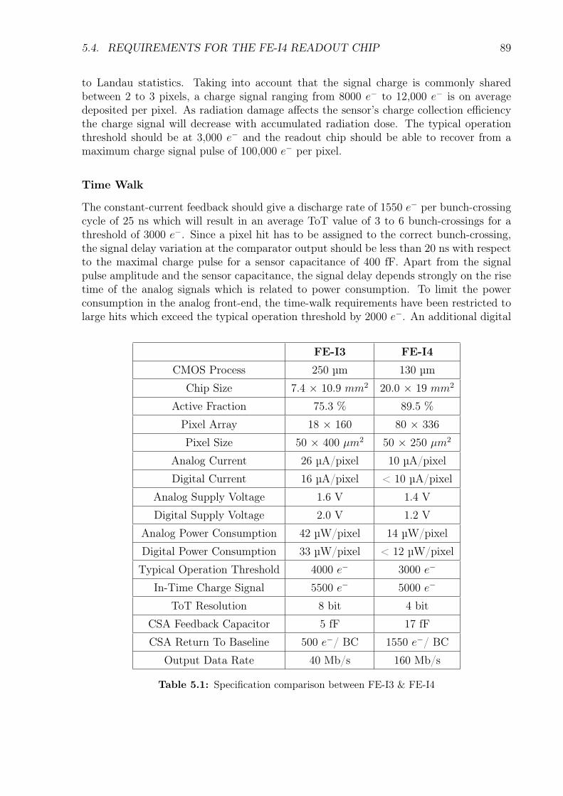
5.4. REQUIREMENTS FOR THE FE-I4 READOUT CHIP 89
to Landau statistics. Taking into account that the signal charge is commonly sharedbetween 2 to 3 pixels, a charge signal ranging from 8000 e− to 12,000 e− is on averagedeposited per pixel. As radiation damage affects the sensor’s charge collection efficiencythe charge signal will decrease with accumulated radiation dose. The typical operationthreshold should be at 3,000 e− and the readout chip should be able to recover from amaximum charge signal pulse of 100,000 e− per pixel.
Time Walk
The constant-current feedback should give a discharge rate of 1550 e− per bunch-crossingcycle of 25 ns which will result in an average ToT value of 3 to 6 bunch-crossings for athreshold of 3000 e−. Since a pixel hit has to be assigned to the correct bunch-crossing,the signal delay variation at the comparator output should be less than 20 ns with respectto the maximal charge pulse for a sensor capacitance of 400 fF. Apart from the signalpulse amplitude and the sensor capacitance, the signal delay depends strongly on the risetime of the analog signals which is related to power consumption. To limit the powerconsumption in the analog front-end, the time-walk requirements have been restricted tolarge hits which exceed the typical operation threshold by 2000 e−. An additional digital
FE-I3 FE-I4
CMOS Process 250 µm 130 µm
Chip Size 7.4 × 10.9 mm2 20.0 × 19 mm2
Active Fraction 75.3 % 89.5 %
Pixel Array 18 × 160 80 × 336
Pixel Size 50 × 400 µm2 50 × 250 µm2
Analog Current 26 µA/pixel 10 µA/pixel
Digital Current 16 µA/pixel < 10 µA/pixel
Analog Supply Voltage 1.6 V 1.4 V
Digital Supply Voltage 2.0 V 1.2 V
Analog Power Consumption 42 µW/pixel 14 µW/pixel
Digital Power Consumption 33 µW/pixel < 12 µW/pixel
Typical Operation Threshold 4000 e− 3000 e−
In-Time Charge Signal 5500 e− 5000 e−
ToT Resolution 8 bit 4 bit
CSA Feedback Capacitor 5 fF 17 fF
CSA Return To Baseline 500 e−/ BC 1550 e−/ BC
Output Data Rate 40 Mb/s 160 Mb/s
Table 5.1: Specification comparison between FE-I3 & FE-I4
90 CHAPTER 5. THE FE-I4 ATLAS HYBRID PIXEL READOUT CHIP
threshold is used in combination with a clustering logic block in the digital pixel region,to associate small hits which generate less than 5000 e− to the correct bunch-crossing bytheir proximity to large hits which have been recorded up to two bunch-crossing cyclesearlier. Isolated small hits are classified as noise.
Noise and Threshold Dispersion
The ENC should be less than 300 e− for the nominal bias current setting of the analogfront-end, a detector capacitance of 400 fF and a maximal sensor leakage current of upto 100 nA. At this noise level, an almost negligible noise occupancy is reached at thetypical operation threshold and the ToT digitization resolution is not deteriorated. Thethreshold dispersion across the whole pixel matrix should be less than 100 e− after tuningthe global threshold by means of a 5-bit trim DAC which is available on pixel level.
5.5 The FE-I4 Chip Architecture
The architecture of the FE-I4 chip shown in Fig. 5.10 is derived from the FE-I3 chip buthas been improved at crucial points to meet the requirements of the increased luminosity.Since the FE-I4 is a hybrid-pixel readout chip, it is connected to the sensor via bump-bonding and flip-chip techniques. A hexagonal bump-bond pad with 12 µm passivationopening is placed in each pixel to establish a connection to the corresponding sensor seg-ment. The analog pixel circuit is designed for electron collection. It contains a two-stageCSA with adjustable constant-current feedback and a comparator with an independentlyadjustable threshold for ToT digitization with 4 bit resolution.
Four pixels are grouped together to form one pixel region. The pixels in the regionshare the same digital pixel circuitry which is placed in the region center and servestwo adjacent analog pixels on the left and two adjacent pixels on the right region side.168 pixel regions are further grouped into one double column which is terminated at thebottom of the chip with the End-of-Digital-Column (EoDC) logic. The total active regionof the chip is covered by 40 double columns. The double column structure gives rise tovertical slices which belong alternately to the analog or to the digital circuit domain.Signals and the power supply rails are routed only within these slices according to theircircuit domain affiliation. Crossings of analog and digital signals and the power supplyrails have been avoided to reduce crosstalk between the digital and the analog part.
To dispose of the inefficiencies related to the FE-I3 chip, the double-column readoutarchitecture has been modified. Data of up to 5 events is kept in local buffers withinthe pixel region until the expiration of the trigger latency. This is feasible due to thesmaller feature size and the higher integration density the new technology offers. Thestored events are synchronized by local logic with incoming trigger signals. Triggered hitsare Hamming coded and transferred across the double column bus to the EoDC logic.Because of the fact that only 0.25% of all recorded hits are triggered for transmission, thedata traffic on the double-column bus is reduced tremendously with respect to the FE-I3column drain structure which increases the efficiency of the readout architecture and alsoreduces the digital power dissipation as unnecessary digital activity is avoided.
5.5. THE FE-I4 CHIP ARCHITECTURE 91
20 mm
40 double-columns
Command
Decoder
End of Digital Columns Logic
336 rows
PLL
RX RX
4 to1
Mux
TXRX RX RX
8b10b
Encoder
Serializer
Data Output
Block
L1T,Token,ReadData 47bData 8b
Data 1b
Token
ClockData-In Data-Out
L1T
CLK-Sel
Configuration
Register
Pixel Config
FIFOHamming
Encoder
Hamming
Decoder
End of Chip Logic
Data Format/
Compress
CLK
Pad Frame
DACsCurrent
Ref.
Bias
Generator
Voltage
Ref.
Shunt
LDO
DC-DC
Conv.Power
17 mm
2mm
40 double-columns
20 mm
Hamming
Decoder
EFUSE
Buffer
Buffer
Hit Processing
Hit Processing
Buffer
Buffer
Hit Processing
Hit Processing
Analog Front End Digital Pixel Region Analog Front End
Trigger Logic
Hamming Encoder
&
Fig. 5.10: Schematic diagram of the FE-I4 chip architecture
92 CHAPTER 5. THE FE-I4 ATLAS HYBRID PIXEL READOUT CHIP
The EoDC logic blocks are consecutively activated by a token pass mechanism. TheEoDC logic steers the column readout, adds the column-address to the read out data andforwards the data to the End-of-Chip (EoCh) logic. In the EoC logic block, the datacoming from the EoDC is Hamming decoded and error corrected if necessary. The hitdata of two pixels adjacent in column direction is then merged together and reformattedin byte-multiples which eases data handling and reduces the needed bandwidth for datatransmission. The reformatted data is stored in an asynchronous FIFO to provide aninterface to the separated clock domain of the the Data Output Block (DOB). Data inthe FIFO is stored Hamming coded to reduce the influence radiation induced Single EventUpset (SEU) has on the bit error rate.
The FE-I4 data output rate has been chosen to be 160 Mb/s according to the re-quirements of the IBL upgrade project, but the clock which is provided to the FE-I4chip corresponds to the 40 MHz LHC bunch-crossing rate. For this reason, a PLL9 isintegrated in the FE-I4 chip periphery which generates a programmable output clock in afrequency range of 40 - 320 MHz [Kru09]. In the nominal case, the DOB is clocked with160 MHz. Before transmission, the data is DC-balanced by means of an 8b10b coder andserialized in a high-speed shift register. The serialized data is transmitted off-chip usinga current based differential signal driver which is compatible to the LVDS standard buthas a reduced offset voltage. Three differential signaling receiver circuits and a 4-to-1multiplexer have been integrated on the FE-I4 chip to test an alternative communicationscheme for use at the outer super-LHC pixel layers. For this sequence, the output dataof three FE-I4 chips are transmitted at 80 Mb/s and bundled in the fourth FE-I4 chipon the hybrid pixel module. The three received output streams are multiplexed with thefourth output data stream and transmitted off-chip with a data rate of 320 Mb/s. Inthis way, three transmission lines can be saved per module which is beneficial in terms ofmaterial and cost reduction.
The chip is configured at 40 Mb/s via a serial interface which is synchronous to the40 MHz LHC bunch-crossing clock. Both the serial data input and the clock are LVDS sig-nals with reduced offset voltage and are transformed to single-ended CMOS by dedicatedreceivers in the pad frame. The serial data input stream is organized in command frameswhich are interpreted on the FE-I4 chip by the command decoder. A short command with5 bit length has been defined to signal a trigger event according to the ATLAS triggerspecification. Commands of intermediate length (9 bit) have been defined for the reset andthe calibration of the FE-I4 chip. Longer commands are used for the configuration of thechip registers. The central register data bank consists of custom-made SEU tolerant andredundant latches [Men08] with 16 bit word length. About 72 configuration parametersare stored in the register bank which also can be read back. The stored parameters includesettings for the global analog threshold, the trigger mode and the trigger latency and theDOB clock frequency and the settings of the DACs used in the bias generator. The DACsprovide the multiple of a unit current defined by a current-reference adjustable with 3-bitsaccuracy to compensate for process variation. During wafer-probing, the current-referencetrim-bits are burned into a nonvolatile E-FUSE memory together with other informationlike the chip ID.
9Phase-Lock Loop
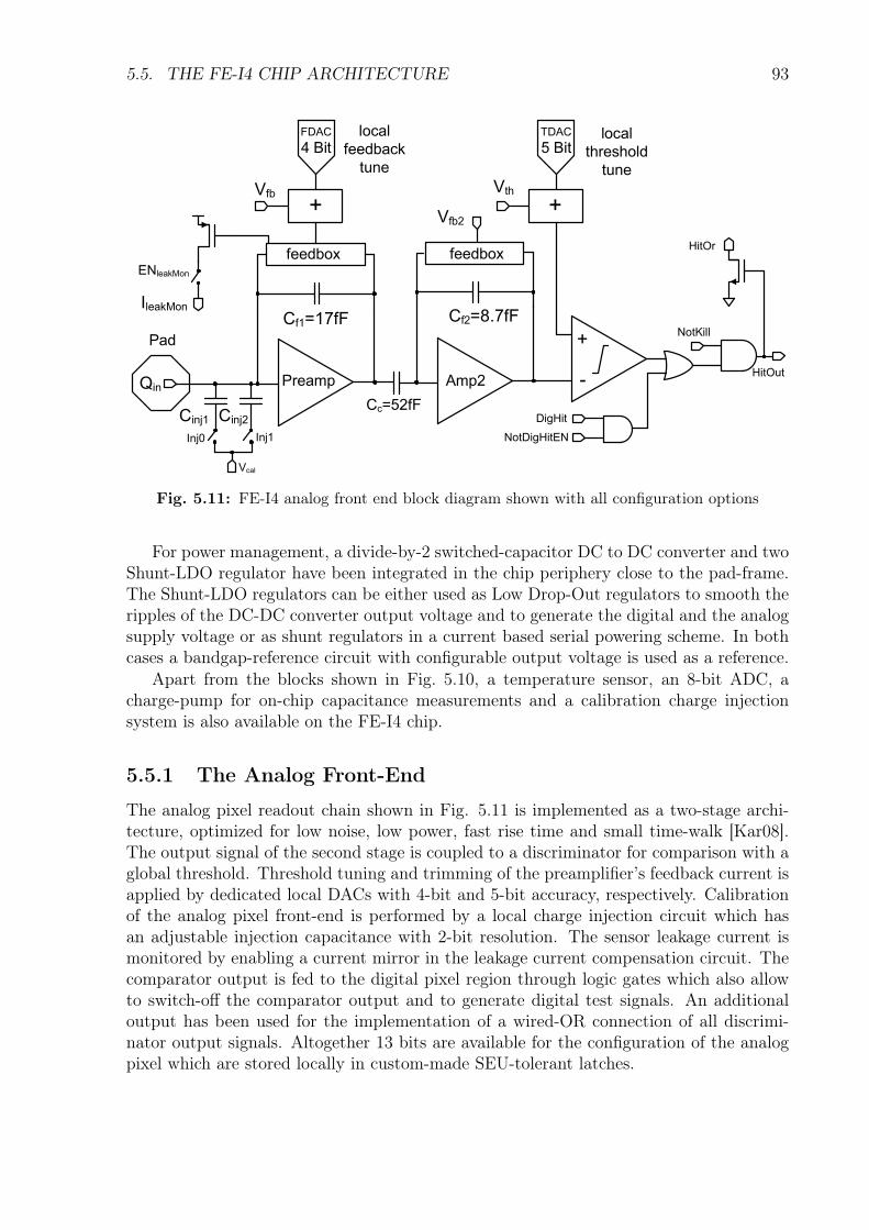
5.5. THE FE-I4 CHIP ARCHITECTURE 93
Cc=52fF
Cf2=8.7fFCf1=17fF
Preamp Amp2
feedbox
Cinj1
+
local
feedback
tune
FDAC
4 Bit
Vfb+
local
threshold
tune
TDAC
5 Bit
Vfb2
+
-HitOut
NotKill
Vth
feedbox
Inj0 Inj1
Vcal
Cinj2
Qin
Pad
DigHit
NotDigHitEN
HitOr
ENleakMon
IleakMon
Fig. 5.11: FE-I4 analog front end block diagram shown with all configuration options
For power management, a divide-by-2 switched-capacitor DC to DC converter and twoShunt-LDO regulator have been integrated in the chip periphery close to the pad-frame.The Shunt-LDO regulators can be either used as Low Drop-Out regulators to smooth theripples of the DC-DC converter output voltage and to generate the digital and the analogsupply voltage or as shunt regulators in a current based serial powering scheme. In bothcases a bandgap-reference circuit with configurable output voltage is used as a reference.
Apart from the blocks shown in Fig. 5.10, a temperature sensor, an 8-bit ADC, acharge-pump for on-chip capacitance measurements and a calibration charge injectionsystem is also available on the FE-I4 chip.
5.5.1 The Analog Front-End
The analog pixel readout chain shown in Fig. 5.11 is implemented as a two-stage archi-tecture, optimized for low noise, low power, fast rise time and small time-walk [Kar08].The output signal of the second stage is coupled to a discriminator for comparison with aglobal threshold. Threshold tuning and trimming of the preamplifier’s feedback current isapplied by dedicated local DACs with 4-bit and 5-bit accuracy, respectively. Calibrationof the analog pixel front-end is performed by a local charge injection circuit which hasan adjustable injection capacitance with 2-bit resolution. The sensor leakage current ismonitored by enabling a current mirror in the leakage current compensation circuit. Thecomparator output is fed to the digital pixel region through logic gates which also allowto switch-off the comparator output and to generate digital test signals. An additionaloutput has been used for the implementation of a wired-OR connection of all discrimi-nator output signals. Altogether 13 bits are available for the configuration of the analogpixel which are stored locally in custom-made SEU-tolerant latches.
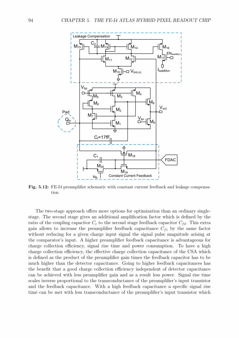
94 CHAPTER 5. THE FE-I4 ATLAS HYBRID PIXEL READOUT CHIP
Qin
Vbp
Vbn
Vout
vfb
VbnLcc
Cf=17fF
Leakage Compensation
Constant Current Feedback
IleakMon
ENleakMon
Pad
FDAC
M1
M2
M3M4
M5
M6
M7
M8
M9
M10
M11 M12
M13 M14M15
C1
C2M16
M17
M18
M19
M20
Fig. 5.12: FE-I4 preamplifier schematic with constant current feedback and leakage compensa-tion
The two-stage approach offers more options for optimization than an ordinary single-stage. The second stage gives an additional amplification factor which is defined by theratio of the coupling capacitor Cc to the second stage feedback capacitor Cf2. This extragain allows to increase the preamplifier feedback capacitance Cf1 by the same factorwithout reducing for a given charge input signal the signal pulse magnitude arising atthe comparator’s input. A higher preamplifier feedback capacitance is advantageous forcharge collection efficiency, signal rise time and power consumption. To have a highcharge collection efficiency, the effective charge collection capacitance of the CSA whichis defined as the product of the preamplifier gain times the feedback capacitor has to bemuch higher than the detector capacitance. Going to higher feedback capacitances hasthe benefit that a good charge collection efficiency independent of detector capacitancecan be achieved with less preamplifier gain and as a result less power. Signal rise timescales inverse proportional to the transconductance of the preamplifier’s input transistorand the feedback capacitance. With a high feedback capacitance a specific signal risetime can be met with less transconductance of the preamplifier’s input transistor which
5.5. THE FE-I4 CHIP ARCHITECTURE 95
again means less current and less power. Furthermore, the AC-coupling between first andsecond stage has the advantage that the rear part of the analog readout chain is decoupledfrom any DC-shift that could arise because of detector leakage current. Although the pixelis equipped with a leakage current compensation circuit, still the non ideal behavior ofthe compensation circuit gives rise to small DC shifts which without AC-coupling wouldinfluence the system and would lead increase threshold dispersion.
The schematic of the leakage current compensated CSA with constant current feedbackwhich forms the first stage is shown in Fig. 5.12. The preamplifier is implemented as aregulated telescopic cascode with the NMOS input transistor M1. The availability ofTriple-Well structures allows to exploit the higher transconductance of NMOS transistorswith respect to PMOS and still be shielded from substrate noise. In addition, the NMOSinput transistor gives a low DC output potential that introduces a high dynamic rangefor the expected positive going output signals. Due to the regulated cascode formed bythe cascode transistor M2 and the amplifer composed of transistors M5, M6 and M7 thepreamplifier has a high output impedance and hence a high gain. Since the biasing voltageof the cascode transistor M2 is generated locally the amount of potential crosstalk pathsare reduced and global routing is simplified. Transistor M4 provides additional currentto the input transistor M1, to increase its transconductance. The telescopic structure hasthe advantage that the highest current in the amplifier flows through the input transistorand not through any biasing transistor which reduces the noise contribution from thebiasing.
The source-follower formed by transistors M8 and M9 decreases the CSA outputimpedance without lowering the preamplifier gain significantly. A low output impedanceis necessary to avoid that the capacitive load at the CSA output limits the preamplifierbandwidth which would reduce the output signal rise-time. The feedback capacitor Cf
is connected between the CSA input and the input of the source-follower. In this way,the damping introduced by the source-follower does not reduce the effective CSA chargecollection capacitance. In addition, the feedback capacitor Cf is isolated from the CSAoutput which prevents that voltage fluctuations at the CSA output inject parasitic signalsto the CSA input through the feedback capacitor.
Continuous reset is applied by the NMOS feedback transistor M18 which is biased ina current mirror topology. The feedback bias current flows into the source-follower at theCSA output. Since the feedback bias current is much smaller than the bias current of thesource-follower, it has only a negligible influence on the source-follower operating point.The feedback bias current is defined by a global PMOS biasing voltage. The feedbackbias current can be tuned at pixel level by a local DAC which steers a current into thegate-drain biasing transistor M19. For high output signals, the NMOS feedback transistorM18 gets saturated and drains a constant current. A nearly linear return to baseline andas a result a pulse width proportional to the input charge is obtained. During the responseto an electron signal, the potential at the CSA output is higher than the potential at theCSA input. As a result the terminal of transistor M18 which is connected to the CSAinput becomes the source which stays at constant potential. On the contrary, the sourceof the gate-drain connected feedback bias transistor M19 is located at the CSA output andthe source potential follows the CSA output signal. To avoid that the feedback currentchanges with the CSA output voltage the gate potential of the feedback transistor is
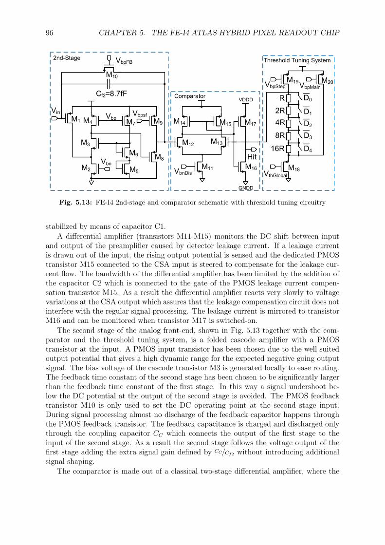
96 CHAPTER 5. THE FE-I4 ATLAS HYBRID PIXEL READOUT CHIP
Hit
VDDD
VbnDis
GNDD
Comparator
VthGlobal
Vbp
Vin Vbpsf
Cf2=8.7fF
VbpFB
Vbn
2nd-Stage Threshold Tuning System
VbpMain
R
2R
4R
8R
16R
D0
D1
D2
D3
D4
VbpStep
M1
M2
M3
M4
M5
M6
M7
M8
M9
M10
M11
M12 M13
M14 M15
M16
M17
M18
M20M19
Fig. 5.13: FE-I4 2nd-stage and comparator schematic with threshold tuning circuitry
stabilized by means of capacitor C1.A differential amplifier (transistors M11-M15) monitors the DC shift between input
and output of the preamplifier caused by detector leakage current. If a leakage currentis drawn out of the input, the rising output potential is sensed and the dedicated PMOStransistor M15 connected to the CSA input is steered to compensate for the leakage cur-rent flow. The bandwidth of the differential amplifier has been limited by the addition ofthe capacitor C2 which is connected to the gate of the PMOS leakage current compen-sation transistor M15. As a result the differential amplifier reacts very slowly to voltagevariations at the CSA output which assures that the leakage compensation circuit does notinterfere with the regular signal processing. The leakage current is mirrored to transistorM16 and can be monitored when transistor M17 is switched-on.
The second stage of the analog front-end, shown in Fig. 5.13 together with the com-parator and the threshold tuning system, is a folded cascode amplifier with a PMOStransistor at the input. A PMOS input transistor has been chosen due to the well suitedoutput potential that gives a high dynamic range for the expected negative going outputsignal. The bias voltage of the cascode transistor M3 is generated locally to ease routing.The feedback time constant of the second stage has been chosen to be significantly largerthan the feedback time constant of the first stage. In this way a signal undershoot be-low the DC potential at the output of the second stage is avoided. The PMOS feedbacktransistor M10 is only used to set the DC operating point at the second stage input.During signal processing almost no discharge of the feedback capacitor happens throughthe PMOS feedback transistor. The feedback capacitance is charged and discharged onlythrough the coupling capacitor CC which connects the output of the first stage to theinput of the second stage. As a result the second stage follows the voltage output of thefirst stage adding the extra signal gain defined by CC/Cf2 without introducing additionalsignal shaping.
The comparator is made out of a classical two-stage differential amplifier, where the
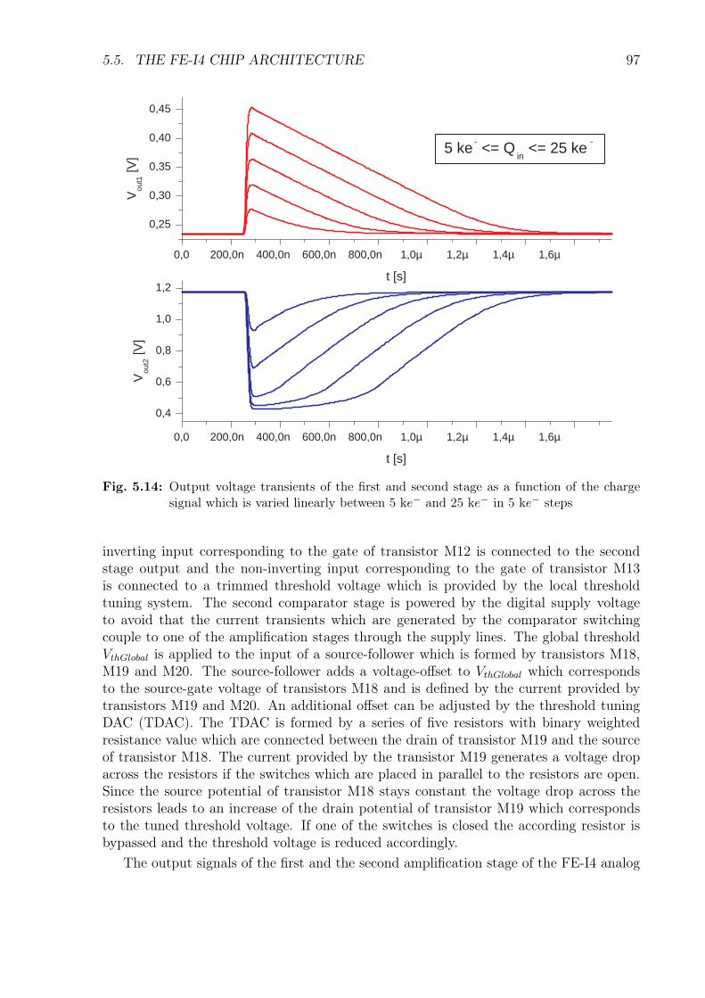
5.5. THE FE-I4 CHIP ARCHITECTURE 97
0,0 200,0n 400,0n 600,0n 800,0n 1,0µ 1,2µ 1,4µ 1,6µ
0,4
0,6
0,8
1,0
1,2
5 ke - <= Q in <= 25 ke -
V ou
t2 [V
]
t [s]
0,0 200,0n 400,0n 600,0n 800,0n 1,0µ 1,2µ 1,4µ 1,6µ
0,25
0,30
0,35
0,40
0,45
V ou
t1 [V
]
t [s]
Fig. 5.14: Output voltage transients of the first and second stage as a function of the chargesignal which is varied linearly between 5 ke− and 25 ke− in 5 ke− steps
inverting input corresponding to the gate of transistor M12 is connected to the secondstage output and the non-inverting input corresponding to the gate of transistor M13is connected to a trimmed threshold voltage which is provided by the local thresholdtuning system. The second comparator stage is powered by the digital supply voltageto avoid that the current transients which are generated by the comparator switchingcouple to one of the amplification stages through the supply lines. The global thresholdVthGlobal is applied to the input of a source-follower which is formed by transistors M18,M19 and M20. The source-follower adds a voltage-offset to VthGlobal which correspondsto the source-gate voltage of transistors M18 and is defined by the current provided bytransistors M19 and M20. An additional offset can be adjusted by the threshold tuningDAC (TDAC). The TDAC is formed by a series of five resistors with binary weightedresistance value which are connected between the drain of transistor M19 and the sourceof transistor M18. The current provided by the transistor M19 generates a voltage dropacross the resistors if the switches which are placed in parallel to the resistors are open.Since the source potential of transistor M18 stays constant the voltage drop across theresistors leads to an increase of the drain potential of transistor M19 which correspondsto the tuned threshold voltage. If one of the switches is closed the according resistor isbypassed and the threshold voltage is reduced accordingly.
The output signals of the first and the second amplification stage of the FE-I4 analog
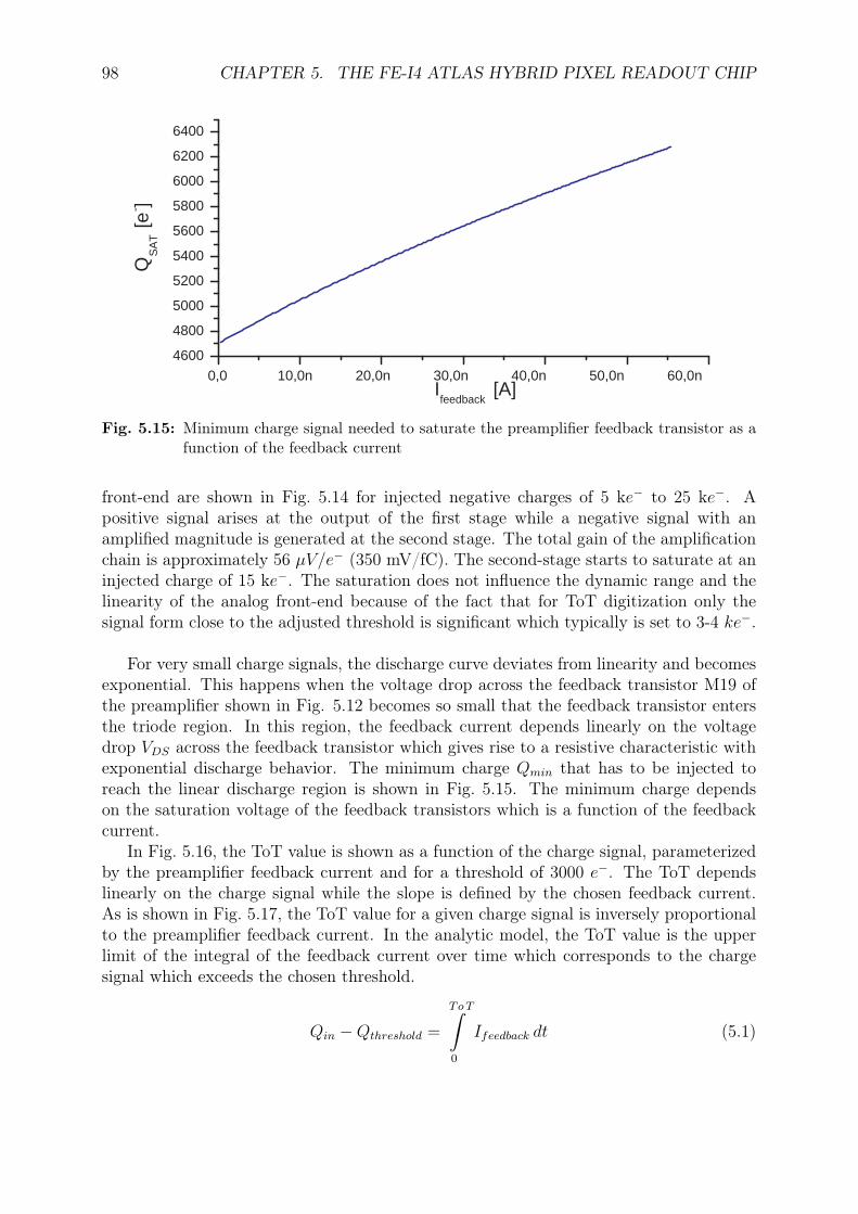
98 CHAPTER 5. THE FE-I4 ATLAS HYBRID PIXEL READOUT CHIP
0,0 10,0n 20,0n 30,0n 40,0n 50,0n 60,0n 4600
4800
5000
5200
5400
5600
5800
6000
6200
6400 Q
SA
T [e
- ]
I feedback
[A]
Fig. 5.15: Minimum charge signal needed to saturate the preamplifier feedback transistor as afunction of the feedback current
front-end are shown in Fig. 5.14 for injected negative charges of 5 ke− to 25 ke−. Apositive signal arises at the output of the first stage while a negative signal with anamplified magnitude is generated at the second stage. The total gain of the amplificationchain is approximately 56 µV/e− (350 mV/fC). The second-stage starts to saturate at aninjected charge of 15 ke−. The saturation does not influence the dynamic range and thelinearity of the analog front-end because of the fact that for ToT digitization only thesignal form close to the adjusted threshold is significant which typically is set to 3-4 ke−.
For very small charge signals, the discharge curve deviates from linearity and becomesexponential. This happens when the voltage drop across the feedback transistor M19 ofthe preamplifier shown in Fig. 5.12 becomes so small that the feedback transistor entersthe triode region. In this region, the feedback current depends linearly on the voltagedrop VDS across the feedback transistor which gives rise to a resistive characteristic withexponential discharge behavior. The minimum charge Qmin that has to be injected toreach the linear discharge region is shown in Fig. 5.15. The minimum charge dependson the saturation voltage of the feedback transistors which is a function of the feedbackcurrent.
In Fig. 5.16, the ToT value is shown as a function of the charge signal, parameterizedby the preamplifier feedback current and for a threshold of 3000 e−. The ToT dependslinearly on the charge signal while the slope is defined by the chosen feedback current.As is shown in Fig. 5.17, the ToT value for a given charge signal is inversely proportionalto the preamplifier feedback current. In the analytic model, the ToT value is the upperlimit of the integral of the feedback current over time which corresponds to the chargesignal which exceeds the chosen threshold.
Qin −Qthreshold =
ToT∫0
Ifeedback dt (5.1)
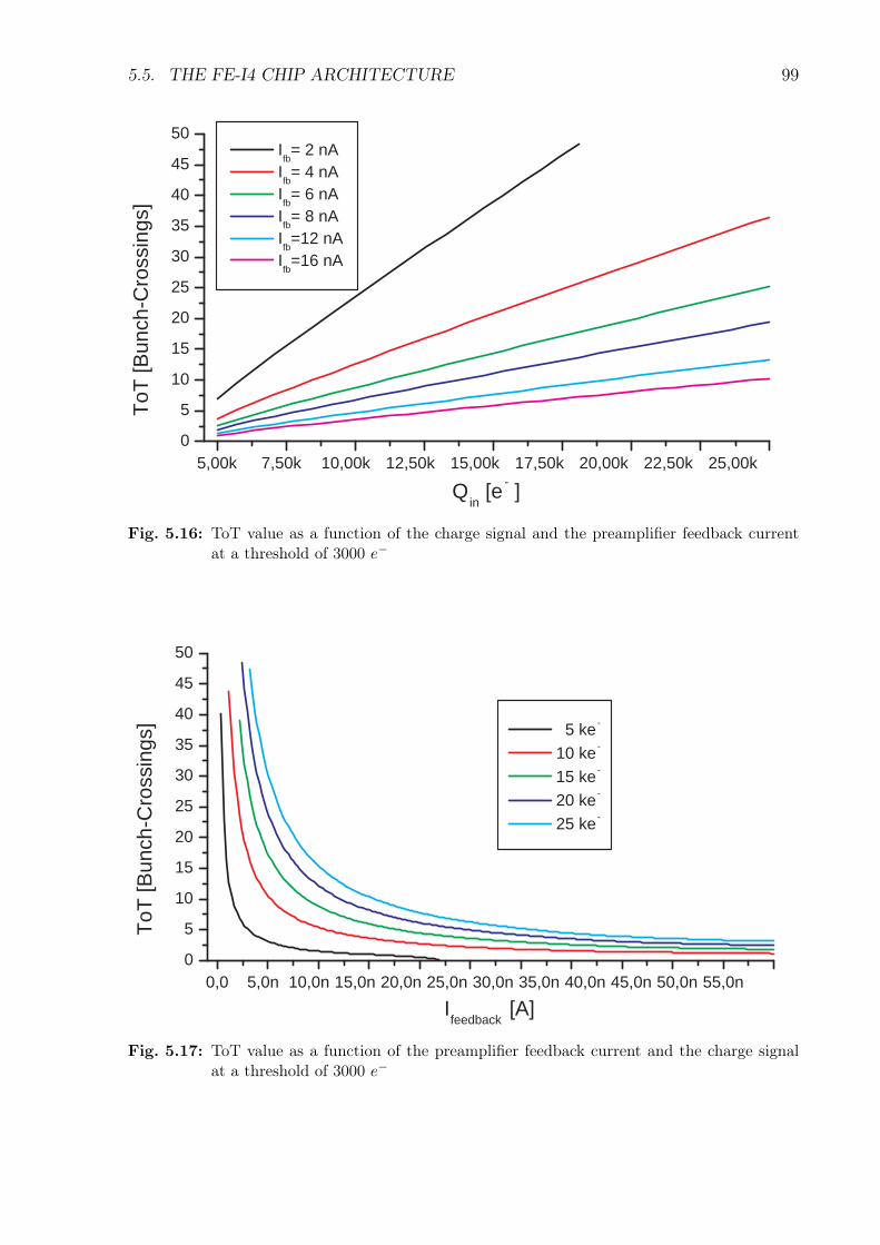
5.5. THE FE-I4 CHIP ARCHITECTURE 99
5,00k 7,50k 10,00k 12,50k 15,00k 17,50k 20,00k 22,50k 25,00k 0
5
10
15
20
25
30
35
40
45
50 I
fb = 2 nA
I fb = 4 nA
I fb = 6 nA
I fb = 8 nA
I fb =12 nA
I fb =16 nA
ToT
[Bun
ch-C
ross
ings
]
Q in [e
- ]
Fig. 5.16: ToT value as a function of the charge signal and the preamplifier feedback currentat a threshold of 3000 e−
0,0 5,0n 10,0n 15,0n 20,0n 25,0n 30,0n 35,0n 40,0n 45,0n 50,0n 55,0n 0
5
10
15
20
25
30
35
40
45
50
5 ke -
10 ke -
15 ke -
20 ke -
25 ke -
ToT
[Bun
ch-C
ross
ings
]
I feedback
[A]
Fig. 5.17: ToT value as a function of the preamplifier feedback current and the charge signalat a threshold of 3000 e−
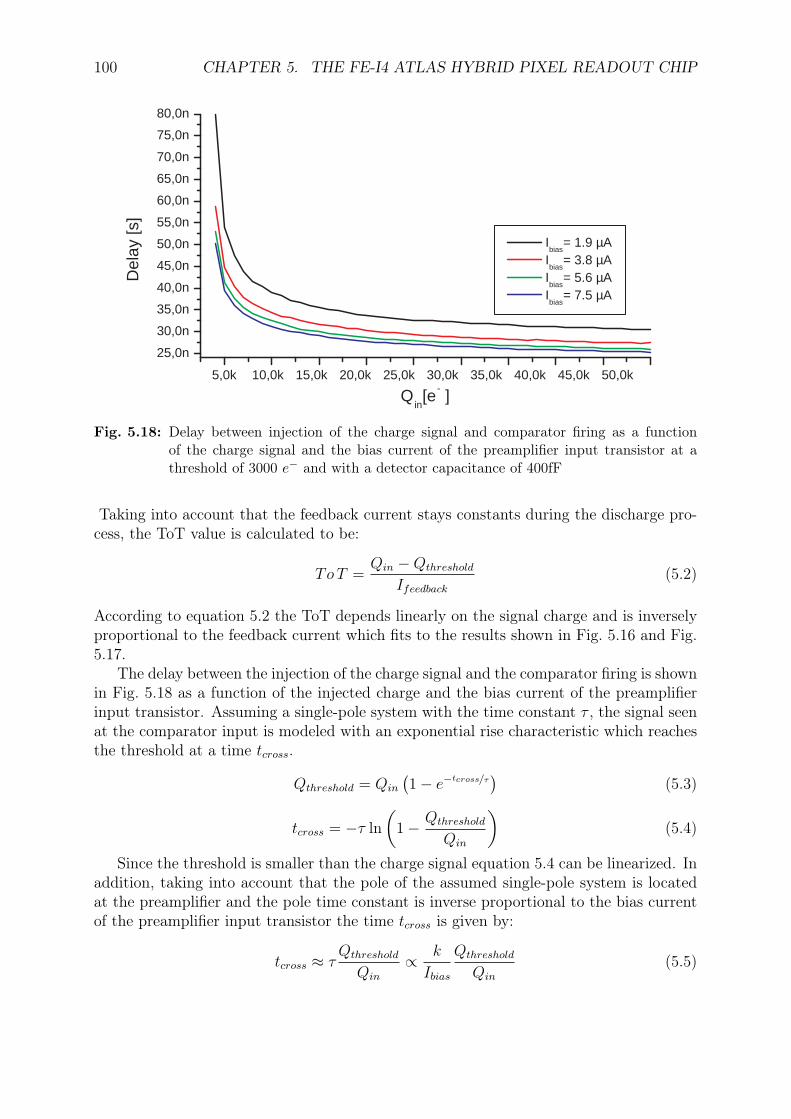
100 CHAPTER 5. THE FE-I4 ATLAS HYBRID PIXEL READOUT CHIP
5,0k 10,0k 15,0k 20,0k 25,0k 30,0k 35,0k 40,0k 45,0k 50,0k
25,0n
30,0n
35,0n
40,0n
45,0n
50,0n
55,0n
60,0n
65,0n
70,0n
75,0n
80,0n
I bias
= 1.9 µA I
bias = 3.8 µA
I bias
= 5.6 µA I
bias = 7.5 µA
Del
ay [s
]
Q in [e
- ]
Fig. 5.18: Delay between injection of the charge signal and comparator firing as a functionof the charge signal and the bias current of the preamplifier input transistor at athreshold of 3000 e− and with a detector capacitance of 400fF
Taking into account that the feedback current stays constants during the discharge pro-cess, the ToT value is calculated to be:
To T =Qin −Qthreshold
Ifeedback(5.2)
According to equation 5.2 the ToT depends linearly on the signal charge and is inverselyproportional to the feedback current which fits to the results shown in Fig. 5.16 and Fig.5.17.
The delay between the injection of the charge signal and the comparator firing is shownin Fig. 5.18 as a function of the injected charge and the bias current of the preamplifierinput transistor. Assuming a single-pole system with the time constant τ , the signal seenat the comparator input is modeled with an exponential rise characteristic which reachesthe threshold at a time tcross.
Qthreshold = Qin
(1− e−
tcross/τ)
(5.3)
tcross = −τ ln
(1− Qthreshold
Qin
)(5.4)
Since the threshold is smaller than the charge signal equation 5.4 can be linearized. Inaddition, taking into account that the pole of the assumed single-pole system is locatedat the preamplifier and the pole time constant is inverse proportional to the bias currentof the preamplifier input transistor the time tcross is given by:
tcross ≈ τQthreshold
Qin
∝ k
Ibias
Qthreshold
Qin
(5.5)
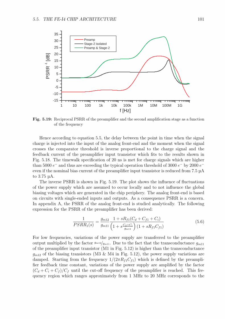
5.5. THE FE-I4 CHIP ARCHITECTURE 101
1 10 100 1k 10k 100k 1M 10M 100M 1G -15
-10
-5
0
5
10
15
20
25
30
35
Preamp Stage-2 isolated Preamp & Stage-2
PS
RR
-1 [d
B]
f [Hz]
Fig. 5.19: Reciprocal PSRR of the preamplifier and the second amplification stage as a functionof the frequency
Hence according to equation 5.5, the delay between the point in time when the signalcharge is injected into the input of the analog front-end and the moment when the signalcrosses the comparator threshold is inverse proportional to the charge signal and thefeedback current of the preamplifier input transistor which fits to the results shown inFig. 5.18. The timewalk specification of 20 ns is met for charge signals which are higherthan 5000 e− and thus are exceeding the typical operation threshold of 3000 e− by 2000 e−
even if the nominal bias current of the preamplifier input transistor is reduced from 7.5 µAto 3.75 µA.
The inverse PSRR is shown in Fig. 5.19. The plot shows the influence of fluctuationsof the power supply which are assumed to occur locally and to not influence the globalbiasing voltages which are generated in the chip periphery. The analog front-end is basedon circuits with single-ended inputs and outputs. As a consequence PSRR is a concern.In appendix A, the PSRR of the analog front-end is studied analytically. The followingexpression for the PSRR of the preamplifier has been derived:
1
PSRR1(s)=
gm12
gm11
1 + sRf1(Cd + Cf1 + Ci)(1 + sCd+Ci
gm11
)(1 + sRf1Cf1)
(5.6)
For low frequencies, variations of the power supply are transferred to the preamplifieroutput multiplied by the factor gm12/gm11. Due to the fact that the transconductance gm11
of the preamplifier input transistor (M1 in Fig. 5.12) is higher than the transconductancegm12 of the biasing transistors (M3 & M4 in Fig. 5.12), the power supply variations aredamped. Starting from the frequency 1/(2πRf1Cf1) which is defined by the preampli-fier feedback time constant, variations of the power supply are amplified by the factor(Cd + Ci + Cf )/Cf until the cut-off frequency of the preamplifier is reached. This fre-quency region which ranges approximately from 1 MHz to 20 MHz corresponds to the
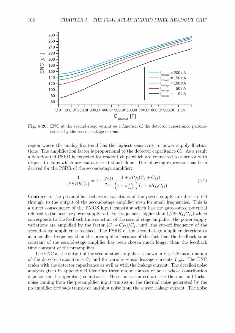
102 CHAPTER 5. THE FE-I4 ATLAS HYBRID PIXEL READOUT CHIP
0,0 100,0f 200,0f 300,0f 400,0f 500,0f 600,0f 700,0f 800,0f 900,0f 1,0p
60
80
100
120
140
160
180
200
220
240
260
280
I leakage
= 200 nA I
leakage = 150 nA
I leakage
= 100 nA I
leakage = 50 nA
I leakage
= 0 nA
EN
C [e
- ]
C detector
[F]
Fig. 5.20: ENC at the second-stage output as a function of the detector capacitance parame-terized by the sensor leakage current
region where the analog front-end has the highest sensitivity to power supply fluctua-tions. The amplification factor is proportional to the detector capacitance Cd. As a resulta deteriorated PSRR is expected for readout chips which are connected to a sensor withrespect to chips which are characterized stand alone. The following expression has beenderived for the PSRR of the second-stage amplifier:
1
PSRR2(s)= 1 +
gm24
gm21
1 + sRf2(Cc + Cf2)(1 + s Cc
gm21
)(1 + sRf2Cf2)
(5.7)
Contrary to the preamplifier behavior, variations of the power supply are directly fedthrough to the output of the second-stage amplifier even for small frequencies. This isa direct consequence of the PMOS input transistor which has the gate-source potentialreferred to the positive power supply rail. For frequencies higher than 1/(2πRf2Cf2) whichcorresponds to the feedback time constant of the second-stage amplifier, the power supplyvariations are amplified by the factor (Cc + Cf2)/Cf2 until the cut-off frequency of thesecond-stage amplifier is reached. The PSRR of the second-stage amplifier deterioratesat a smaller frequency than the preamplifier because of the fact that the feedback timeconstant of the second-stage amplifier has been chosen much longer than the feedbacktime constant of the preamplifier.
The ENC at the output of the second-stage amplifier is shown in Fig. 5.20 as a functionof the detector capacitance Cd and for various sensor leakage currents Ileak. The ENCscales with the detector capacitance as well as with the leakage current. The detailed noiseanalysis given in appendix B identifies three major sources of noise whose contributiondepends on the operating conditions. These noise sources are the thermal and flickernoise coming from the preamplifier input transistor, the thermal noise generated by thepreamplifier feedback transistor and shot noise from the sensor leakage current. The noise
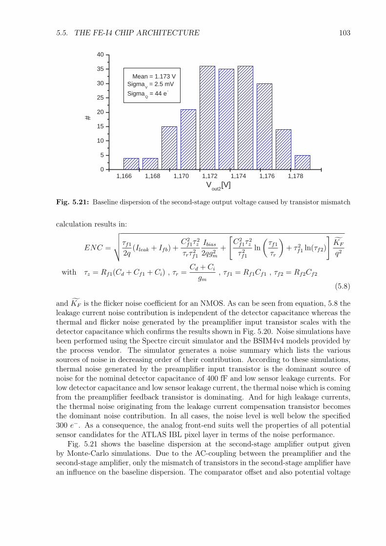
5.5. THE FE-I4 CHIP ARCHITECTURE 103
1,166 1,168 1,170 1,172 1,174 1,176 1,178 0
5
10
15
20
25
30
35
40
Mean = 1.173 V Sigma
V = 2.5 mV
Sigma Q = 44 e -
#
V out2
[V]
Fig. 5.21: Baseline dispersion of the second-stage output voltage caused by transistor mismatch
calculation results in:
ENC =
√√√√τf12q
(Ileak + Ifb) +C2
f1τ2z
τrτ 2f1
Ibias2qg2m
+
[C2
f1τ2z
τ 2f1ln
(τf1τr
)+ τ 2f1 ln(τf2)
]KF
q2
with τz = Rf1(Cd + Cf1 + Ci) , τr =Cd + Ci
gm, τf1 = Rf1Cf1 , τf2 = Rf2Cf2
(5.8)
and KF is the flicker noise coefficient for an NMOS. As can be seen from equation, 5.8 theleakage current noise contribution is independent of the detector capacitance whereas thethermal and flicker noise generated by the preamplifier input transistor scales with thedetector capacitance which confirms the results shown in Fig. 5.20. Noise simulations havebeen performed using the Spectre circuit simulator and the BSIM4v4 models provided bythe process vendor. The simulator generates a noise summary which lists the varioussources of noise in decreasing order of their contribution. According to these simulations,thermal noise generated by the preamplifier input transistor is the dominant source ofnoise for the nominal detector capacitance of 400 fF and low sensor leakage currents. Forlow detector capacitance and low sensor leakage current, the thermal noise which is comingfrom the preamplifier feedback transistor is dominating. And for high leakage currents,the thermal noise originating from the leakage current compensation transistor becomesthe dominant noise contribution. In all cases, the noise level is well below the specified300 e−. As a consequence, the analog front-end suits well the properties of all potentialsensor candidates for the ATLAS IBL pixel layer in terms of the noise performance.
Fig. 5.21 shows the baseline dispersion at the second-stage amplifier output givenby Monte-Carlo simulations. Due to the AC-coupling between the preamplifier and thesecond-stage amplifier, only the mismatch of transistors in the second-stage amplifier havean influence on the baseline dispersion. The comparator offset and also potential voltage
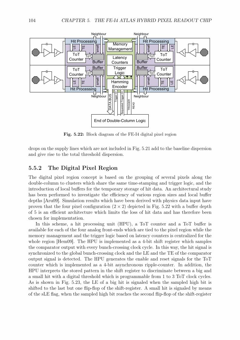
104 CHAPTER 5. THE FE-I4 ATLAS HYBRID PIXEL READOUT CHIP
READ
TRIG
GER
Neighbour
Hit Processing
ToT
Counter
LE
TE
Buffer
ToT
small
Neighbour
Hit Processing
ToT
CounterLE
TE
Buffer
ToT
small
Neighbour
Hit Processing
ToT
Counter
LE
TE
Buffer
ToT
small
Neighbour
Hit Processing
ToT
Counter
LE
TE
Buffer
ToT
small
Memory
Management
Latency
Counters
Trigger
Logic
End of Double-Column Logic
Trigger ID
Requested Trigger ID
Hamming
Encoder
DATA BUS
Fig. 5.22: Block diagram of the FE-I4 digital pixel region
drops on the supply lines which are not included in Fig. 5.21 add to the baseline dispersionand give rise to the total threshold dispersion.
5.5.2 The Digital Pixel Region
The digital pixel region concept is based on the grouping of several pixels along thedouble-column to clusters which share the same time-stamping and trigger logic, and theintroduction of local buffers for the temporary storage of hit data. An architectural studyhas been performed to investigate the efficiency of various region sizes and local bufferdepths [Aru09]. Simulation results which have been derived with physics data input haveproven that the four pixel configuration (2× 2) depicted in Fig. 5.22 with a buffer depthof 5 is an efficient architecture which limits the loss of hit data and has therefore beenchosen for implementation.
In this scheme, a hit processing unit (HPU), a ToT counter and a ToT buffer isavailable for each of the four analog front-ends which are tied to the pixel region while thememory management and the trigger logic based on latency counters is centralized for thewhole region [Hem09]. The HPU is implemented as a 4-bit shift register which samplesthe comparator output with every bunch-crossing clock cycle. In this way, the hit signal issynchronized to the global bunch-crossing clock and the LE and the TE of the comparatoroutput signal is detected. The HPU generates the enable and reset signals for the ToTcounter which is implemented as a 4-bit asynchronous ripple-counter. In addition, theHPU interprets the stored pattern in the shift register to discriminate between a big anda small hit with a digital threshold which is programmable from 1 to 3 ToT clock cycles.As is shown in Fig. 5.23, the LE of a big hit is signaled when the sampled high bit isshifted to the last but one flip-flop of the shift-register. A small hit is signaled by meansof the sLE flag, when the sampled high bit reaches the second flip-flop of the shift-register
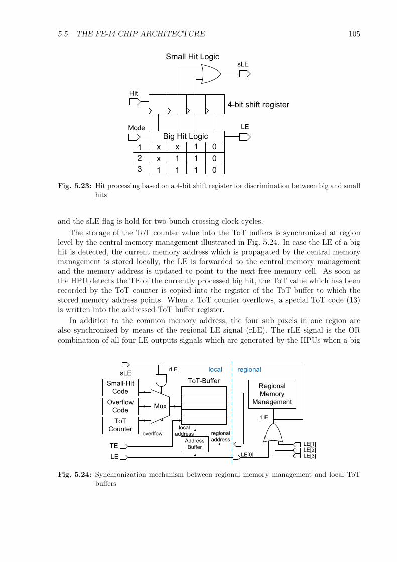
5.5. THE FE-I4 CHIP ARCHITECTURE 105
Hit
Mode
Big Hit Logic
01xx
011x
0111
1
2
3
LE
4-bit shift register
sLESmall Hit Logic
Fig. 5.23: Hit processing based on a 4-bit shift register for discrimination between big and smallhits
and the sLE flag is hold for two bunch crossing clock cycles.The storage of the ToT counter value into the ToT buffers is synchronized at region
level by the central memory management illustrated in Fig. 5.24. In case the LE of a bighit is detected, the current memory address which is propagated by the central memorymanagement is stored locally, the LE is forwarded to the central memory managementand the memory address is updated to point to the next free memory cell. As soon asthe HPU detects the TE of the currently processed big hit, the ToT value which has beenrecorded by the ToT counter is copied into the register of the ToT buffer to which thestored memory address points. When a ToT counter overflows, a special ToT code (13)is written into the addressed ToT buffer register.
In addition to the common memory address, the four sub pixels in one region arealso synchronized by means of the regional LE signal (rLE). The rLE signal is the ORcombination of all four LE outputs signals which are generated by the HPUs when a big
ToT
Counter
ToT-Buffer
Address
Buffer
local
address
LE
local regional
Regional
Memory
Management
LE[0]
rLE
LE[1]LE[2]LE[3]
regional
address
Mux
Small-Hit
Code
sLErLE
Overflow
Code
overlfow
TE
Fig. 5.24: Synchronization mechanism between regional memory management and local ToTbuffers
106 CHAPTER 5. THE FE-I4 ATLAS HYBRID PIXEL READOUT CHIP
hit occurs. If the rLE coincides with a sLE flag, a special ToT code (14) is stored inthe addressed register of the according ToT buffer which indicates the occurrence of asmall hit. Since the HPU generates the sLE flag earlier than the LE flag and holds thesLE signal for two bunch-crossing clock cycles, a time-frame of two bunch-crossing cyclesresults within which small hits can be associated to a big hit in the region. Small hitswhich have not been associated to big hits are not saved. This mechanism of small-hit tobig-hit association, allows to compensate the time-walk related to small hits by exploitingthe spatial proximity to big hits in the region which bear accurate timing information.The sLE flag of each HPU is also routed to the adjacent pixels of the neighboring regionsin the double-column. If a small hit is detected in a pixel which coincides with a big hitin the neighboring region, the small hit information is stored by the neighboring regionin dedicated neighbor memories of the adjacent pixel which are also synchronized to theregional ToT buffer address. The neighbor mechanism takes care of hit clusters whichstraddle the region border along the double-column. Hit clusters which cross the double-column border are not recognized and small hits might be lost. However, this is acceptabledue to the fact that the demands on the spatial resolution in z-direction are less stringent.
The occurrence of the rLE signal which indicates a big hit in one of the pixels in theregion also activates the trigger logic. The trigger logic is formed by a set of latencycounters which are implemented as 8-bit asynchronous ripple-counters. When enabled,the latency counters start to count up to a configurable value which corresponds to thetrigger latency. The selection of the next idle latency counter is managed with the samememory address as the ToT buffers. As a result, the addressed data in the ToT buffer,the neighbor hit memory and the according latency counter are tied together and formone event in the pixel region. If a level-1 trigger is received in the same point of time asthe final latency counter value is reached, the according event is flagged for readout. Inthis case, the 4-bit trigger ID which is assigned by the EoCH logic is stored and the hitdata is kept in the buffers until the regional hit data is read out. If the latency counterexpires without the arrival of a level-1 trigger, the buffers and the latency counter arecleared and are free for the processing of the next event.
The readout of the double-column is organized in sequence of the trigger ID based ona token pass mechanism. The EoDC logic initializes a readout cycle by setting the Readsignal and the trigger ID for which data is requested. Starting from the top the tokenis passed from region to region. A region which is activated by the token and also hasa stored event with the requested trigger ID sends the hit out to the double-column busdata by means of OR gates. All other regions which are not activated by the token, feedthe data which arrives from the previous region through to the next region below in thedouble-column. The regional hit data (16 ToT + 4 neighbor bits) is transferred Hammingencoded with a (25,20) scheme, to increase the yield of the double-column bus. The pixelregion address is generated during the readout process by a thermometer to gray decoderwhich is distributed along the double-column. The readout token serves as the input tothe thermometer decoder and the token position defines the generated 8-bit pixel regionaddress, which is also protected with 4 Hamming bits.
For the implemented architecture, the buffer overflow inefficiency has been determinedby analytical calculation as well as by simulation based on physics data. The hit dataloss inefficiency is below 0.1% for a b-layer radius of 37 mm and 3 × LHC full luminosity
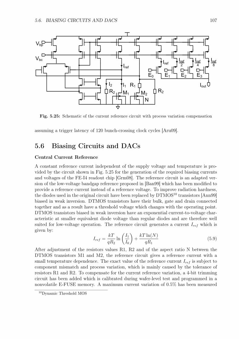
5.6. BIASING CIRCUITS AND DACS 107
Iref8
Vbp
Vbc
E0 E1 E2 E3
R1R2 R2
I1I2
IrefIref
Iref2
Iref4
N
Iout
M1 M2
Fig. 5.25: Schematic of the current reference circuit with process variation compensation
assuming a trigger latency of 120 bunch-crossing clock cycles [Aru09].
5.6 Biasing Circuits and DACsCentral Current Reference
A constant reference current independent of the supply voltage and temperature is pro-vided by the circuit shown in Fig. 5.25 for the generation of the required biasing currentsand voltages of the FE-I4 readout chip [Grm08]. The reference circuit is an adapted ver-sion of the low-voltage bandgap reference proposed in [Ban99] which has been modified toprovide a reference current instead of a reference voltage. To improve radiation hardness,the diodes used in the original circuit have been replaced by DTMOS10 transistors [Ann99]biased in weak inversion. DTMOS transistors have their bulk, gate and drain connectedtogether and as a result have a threshold voltage which changes with the operating point.DTMOS transistors biased in weak inversion have an exponential current-to-voltage char-acteristic at smaller equivalent diode voltage than regular diodes and are therefore wellsuited for low-voltage operation. The reference circuit generates a current Iref which isgiven by:
Iref =kT
qR2
ln
(I1I0
)+
kT ln(N)
qR1
(5.9)
After adjustment of the resistors values R1, R2 and of the aspect ratio N between theDTMOS transistors M1 and M2, the reference circuit gives a reference current with asmall temperature dependence. The exact value of the reference current Iref is subject tocomponent mismatch and process variation, which is mainly caused by the tolerance ofresistors R1 and R2. To compensate for the current reference variation, a 4-bit trimmingcircuit has been added which is calibrated during wafer-level test and programmed in anonvolatile E-FUSE memory. A maximum current variation of 0.5% has been measured
10Dynamic Threshold MOS
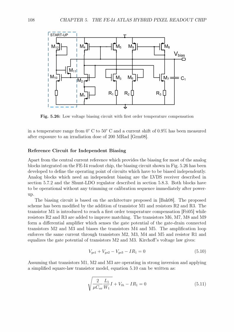
108 CHAPTER 5. THE FE-I4 ATLAS HYBRID PIXEL READOUT CHIP
START-UP
Vbias
M1R1 R2 R3
M2
M3
M4 M5
M6 M7
M8M9
M10
M11
M12
C1
Fig. 5.26: Low voltage biasing circuit with first order temperature compensation
in a temperature range from 0° C to 50° C and a current shift of 0.9% has been measuredafter exposure to an irradiation dose of 200 MRad [Grm08].
Reference Circuit for Independent Biasing
Apart from the central current reference which provides the biasing for most of the analogblocks integrated on the FE-I4 readout chip, the biasing circuit shown in Fig. 5.26 has beendeveloped to define the operating point of circuits which have to be biased independently.Analog blocks which need an independent biasing are the LVDS receiver described insection 5.7.2 and the Shunt-LDO regulator described in section 5.8.3. Both blocks haveto be operational without any trimming or calibration sequence immediately after power-up.
The biasing circuit is based on the architecture proposed in [Bak08]. The proposedscheme has been modified by the addition of transistor M1 and resistors R2 and R3. Thetransistor M1 is introduced to reach a first order temperature compensation [Fri05] whileresistors R2 and R3 are added to improve matching. The transistors M6, M7, M8 and M9form a differential amplifier which senses the gate potential of the gate-drain connectedtransistors M2 and M3 and biases the transistors M4 and M5. The amplification loopenforces the same current through transistors M2, M3, M4 and M5 and resistor R1 andequalizes the gate potential of transistors M2 and M3. Kirchoff’s voltage law gives:
Vgs1 + Vgs2 − Vgs3 − IR1 = 0 (5.10)
Assuming that transistors M1, M2 and M3 are operating in strong inversion and applyinga simplified square-law transistor model, equation 5.10 can be written as:√
2
µCox
L1
W1
I + Vth − IR1 = 0 (5.11)
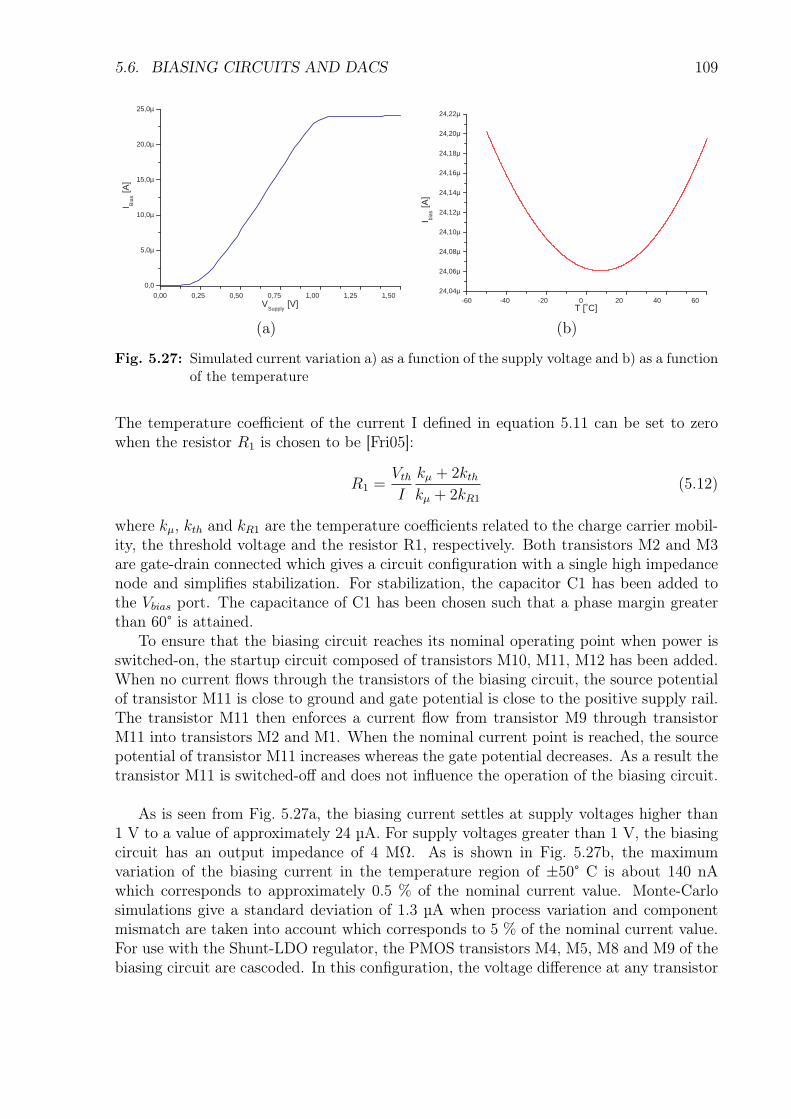
5.6. BIASING CIRCUITS AND DACS 109
0,00 0,25 0,50 0,75 1,00 1,25 1,50
0,0
5,0µ
10,0µ
15,0µ
20,0µ
25,0µ
I Bia
s [A]
V Supply
[V]
(a)
-60 -40 -20 0 20 40 60 24,04µ
24,06µ
24,08µ
24,10µ
24,12µ
24,14µ
24,16µ
24,18µ
24,20µ
24,22µ
I bias
[A]
T [˚C]
(b)
Fig. 5.27: Simulated current variation a) as a function of the supply voltage and b) as a functionof the temperature
The temperature coefficient of the current I defined in equation 5.11 can be set to zerowhen the resistor R1 is chosen to be [Fri05]:
R1 =Vth
I
kµ + 2kthkµ + 2kR1
(5.12)
where kµ, kth and kR1 are the temperature coefficients related to the charge carrier mobil-ity, the threshold voltage and the resistor R1, respectively. Both transistors M2 and M3are gate-drain connected which gives a circuit configuration with a single high impedancenode and simplifies stabilization. For stabilization, the capacitor C1 has been added tothe Vbias port. The capacitance of C1 has been chosen such that a phase margin greaterthan 60° is attained.
To ensure that the biasing circuit reaches its nominal operating point when power isswitched-on, the startup circuit composed of transistors M10, M11, M12 has been added.When no current flows through the transistors of the biasing circuit, the source potentialof transistor M11 is close to ground and gate potential is close to the positive supply rail.The transistor M11 then enforces a current flow from transistor M9 through transistorM11 into transistors M2 and M1. When the nominal current point is reached, the sourcepotential of transistor M11 increases whereas the gate potential decreases. As a result thetransistor M11 is switched-off and does not influence the operation of the biasing circuit.
As is seen from Fig. 5.27a, the biasing current settles at supply voltages higher than1 V to a value of approximately 24 µA. For supply voltages greater than 1 V, the biasingcircuit has an output impedance of 4 MΩ. As is shown in Fig. 5.27b, the maximumvariation of the biasing current in the temperature region of ±50° C is about 140 nAwhich corresponds to approximately 0.5 % of the nominal current value. Monte-Carlosimulations give a standard deviation of 1.3 µA when process variation and componentmismatch are taken into account which corresponds to 5 % of the nominal current value.For use with the Shunt-LDO regulator, the PMOS transistors M4, M5, M8 and M9 of thebiasing circuit are cascoded. In this configuration, the voltage difference at any transistor
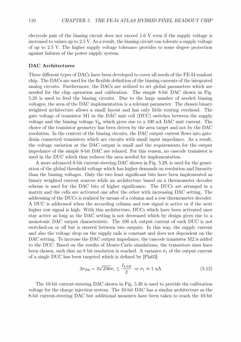
110 CHAPTER 5. THE FE-I4 ATLAS HYBRID PIXEL READOUT CHIP
electrode pair of the biasing circuit does not exceed 1.6 V even if the supply voltage isincreased to values up to 2.5 V. As a result, the biasing circuit can tolerate a supply voltageof up to 2.5 V. The higher supply voltage tolerance provides to some degree protectionagainst failures of the power supply system.
DAC Architectures
Three different types of DACs have been developed to cover all needs of the FE-I4 readoutchip. The DACs are used for the flexible definition of the biasing currents of the integratedanalog circuits. Furthermore, the DACs are utilized to set global parameters which areneeded for the chip operation and calibration. The simple 8-bit DAC shown in Fig.5.28 is used to feed the biasing circuits. Due to the large number of needed biasingvoltages, the area of the DAC implementation is a relevant parameter. The chosen binaryweighted architecture allows a small layout and has only little routing overhead. Thegate voltage of transistor M1 in the DAC unit cell (DUC) switches between the supplyvoltage and the biasing voltage Vbp which gives rise to a 100 nA DAC unit current. Thechoice of the transistor geometry has been driven by the area target and not by the DACresolution. In the context of the biasing circuits, the DAC output current flows into gate-drain connected transistors which are circuits with small input impedance. As a result,the voltage variation at the DAC output is small and the requirements for the outputimpedance of the simple 8-bit DAC are relaxed. For this reason, no cascode transistor isused in the DUC which thus reduces the area needed for implementation.
A more advanced 8-bit current-steering DAC shown in Fig. 5.29, is used for the gener-ation of the global threshold voltage which has higher demands on resolution and linearitythan the biasing voltages. Only the two least significant bits have been implemented asbinary weighted current sources while an architecture based on a thermometer decoderscheme is used for the DAC bits of higher significance. The DUCs are arranged in amatrix and the cells are activated one after the other with increasing DAC setting. Theaddressing of the DUCs is realized by means of a column and a row thermometer decoder.A DUC is addressed when the according column and row signal is active or if the nexthigher row signal is high. With this architecture, DUCs which have been activated oncestay active as long as the DAC setting is not decreased which by design gives rise to amonotonic DAC output characteristic. The 100 nA output current of each DUC is notswitched-on or off but is steered between two outputs. In this way, the supply currentand also the voltage drop on the supply rails is constant and does not dependent on theDAC setting. To increase the DAC output impedance, the cascode transistor M2 is addedto the DUC. Based on the results of Monte-Carlo simulations, the transistors sizes havebeen chosen, such that an 8 bit resolution is reached. A variance σ1 of the output currentof a single DUC has been targeted which is defined by [Pla03]:
3σ256 = 3√256σ1 ≤
ILSB2
⇒ σ1 ≈ 1 nA (5.13)
The 10-bit current-steering DAC shown in Fig. 5.30 is used to provide the calibrationvoltage for the charge injection system. The 10-bit DAC has a similar architecture as the8-bit current-steering DAC but additional measures have been taken to reach the 10-bit
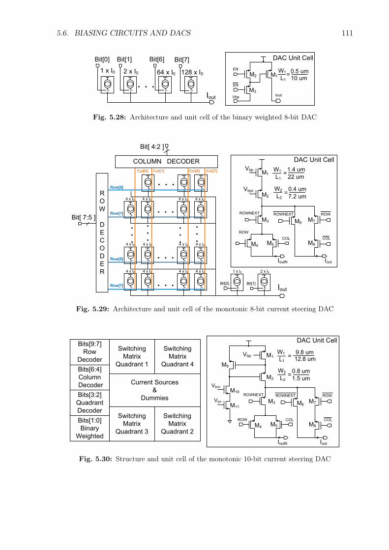
5.6. BIASING CIRCUITS AND DACS 111
Iout
1 x I0 2 x I0 64 x I0 128 x I0
Bit[0] Bit[1] Bit[6] Bit[7]
EN
EN
VbpIout
= 10 um
0.5 umM1
W1
L1M2
M3
DAC Unit Cell
Fig. 5.28: Architecture and unit cell of the binary weighted 8-bit DAC
R
O
W
D
E
C
O
D
E
R
COLUMN DECODER
Bit[ 4:2 ]
Bit[ 7:5 ]
Col[0] Col[1] Col[7]
Row[0]
Row[1]
Col[6]
Row[6]
Row[7] Iout
M1
Vbp
Vbpc
M2
W1 1.4 um=
L1 22 um
= 0.4 um
7.2 um
W2
L2
ROWNEXT
M3 M6M7
M8
Iout
ROWNEXT ROW
COL
IoutN
ROW
M4 M5
COL
4 x I0 4 x I0 4 x I0 4 x I0
4 x I0 4 x I0 4 x I0 4 x I0
4 x I0 4 x I0 4 x I0 4 x I0
2 x I01 x I0
Bit[0] Bit[1]
DAC Unit Cell
Fig. 5.29: Architecture and unit cell of the monotonic 8-bit current steering DAC
M1
M9
M2
= 9.8 um12.8 um
Vbp
VbnM11
VbncM10
= 0.8 um
1.5 um
W2
L2
W1
L1
ROWNEXT
M3 M6M7
M8
Iout
ROWNEXT ROW
COLROW
IoutN
M4 M5
COL
Current Sources
&
Dummies
Bits[9:7]
Row
Decoder
Switching
Matrix
Quadrant 3
Switching
Matrix
Quadrant 2
Bits[6:4]
Column
Decoder
Bits[3:2]
Quadrant
Decoder
Bits[1:0]
Binary
Weighted
Switching
Matrix
Quadrant 1
Switching
Matrix
Quadrant 4
DAC Unit Cell
Fig. 5.30: Structure and unit cell of the monotonic 10-bit current steering DAC
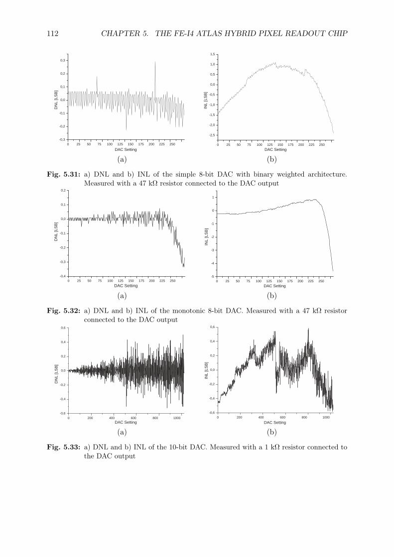
112 CHAPTER 5. THE FE-I4 ATLAS HYBRID PIXEL READOUT CHIP
0 25 50 75 100 125 150 175 200 225 250 -0,3
-0,2
-0,1
0,0
0,1
0,2
0,3
DN
L [L
SB
]
DAC Setting
(a)
0 25 50 75 100 125 150 175 200 225 250
-2,5
-2,0
-1,5
-1,0
-0,5
0,0
0,5
1,0
1,5
INL
[LS
B]
DAC Setting
(b)
Fig. 5.31: a) DNL and b) INL of the simple 8-bit DAC with binary weighted architecture.Measured with a 47 kΩ resistor connected to the DAC output
0 25 50 75 100 125 150 175 200 225 250 -0,4
-0,3
-0,2
-0,1
0,0
0,1
0,2
DN
L [L
SB
]
DAC Setting
(a)
0 25 50 75 100 125 150 175 200 225 250 -5
-4
-3
-2
-1
0
1
INL
[LS
B]
DAC Setting
(b)
Fig. 5.32: a) DNL and b) INL of the monotonic 8-bit DAC. Measured with a 47 kΩ resistorconnected to the DAC output
0 200 400 600 800 1000
-0,6
-0,4
-0,2
0,0
0,2
0,4
0,6
DN
L [L
SB
]
DAC Setting
(a)
0 200 400 600 800 1000
-0,6
-0,4
-0,2
0,0
0,2
0,4
0,6
INL
[LS
B]
DAC Setting
(b)
Fig. 5.33: a) DNL and b) INL of the 10-bit DAC. Measured with a 1 kΩ resistor connected tothe DAC output
5.6. BIASING CIRCUITS AND DACS 113
resolution. All current source transistors which correspond to transistor M1 of the DUCschematic in Fig. 5.30 have been placed next to each other in the middle of the layoutsurrounded by two lines of dummy transistors. The remaining transistors of the DUC aregrouped in four quadrants of 256 cells each which are placed above and below the currentsource transistor matrix. To improve transistor matching, the cells in each quadrant arearranged in a common centroid layout and the quadrants have a mirror symmetry alongthe x and y-axis to each other. The six DAC bits with the highest significance are decodedby the row and the column thermometer decoder which activate the cells in the quadrants.Two more bits are fed to the quadrant thermometer decoder which cyclically selects thequadrant in which the next cell has to be activated. The two least significant bits areimplemented by binary weighted current sources. To improve linearity, the regulatedcascode formed by transistors M2, M9, M10 and M11 in Fig. 5.30 have been added to theDUC which increases the DAC output impedance significantly. The DAC unit currenthas been chosen to be 1 µA. The DUC has been designed to give a current variation of10 pA for an output voltage variation of 1V. The transistor sizes have been chosen toreach a DUC current variance σ1 in Monte-Carlo simulation of:
3σ1024 = 3√1024σ1 ≤
ILSB2
⇒ σ1 ≈ 5 nA (5.14)
The Differential (DNL) and the Integral Non-Linearity (INL) of all DACs have beenmeasured on test-chips. The DNL and the INL is defined as:
DNL =I(n)− I(n− 1)− ILSB
ILSB(5.15)
INL =I(n)− nILSB
ILSB(5.16)
As can be seen from Fig. 5.31a and 5.31b, the DNL and the INL characteristic of the simplebinary weighted DAC has peaks at the DAC settings of 64, 128 and 192 which is typicalfor a binary weighted DAC architecture. The INL varies in a range of approximately±1.5ILSB which results in an effective dynamic range of 7-bit.
In Fig. 5.32a and 5.32b the DNL and INL characteristic of the monotonic current-steering 8-bit DAC is shown. Since this DAC is used to generate the global thresholdvoltage, the DAC output current is fed to a 47 kΩ resistor. The measured characteristicsare much improved with respect to the measurement results of the binary weighted DAC.However, starting from a DAC setting of 215, the DAC output current deviates from theideal behavior. The voltage potential at the DAC output rises with increasing DAC settingand the DAC linearity deteriorates when the cascode transistors of the DUCs leave thesaturation region. Still in the voltage range which is relevant for the application (<1.1 V)which corresponds to DAC settings smaller than 235, the INL stays below ±0.5ILSB.
The INL and DNL of the 10-bit DAC is shown in Fig. 5.33a and 5.33b. The DNLvalues are randomly distributed and increase in magnitude with the DAC setting. Thisbehavior is caused by thermal noise generated in the DUC. The more DUCs are activatedthe higher the number of parallel connected noise sources and the higher the total noiselevel. The discontinuity of the INL characteristic at the DAC setting of 512 is caused
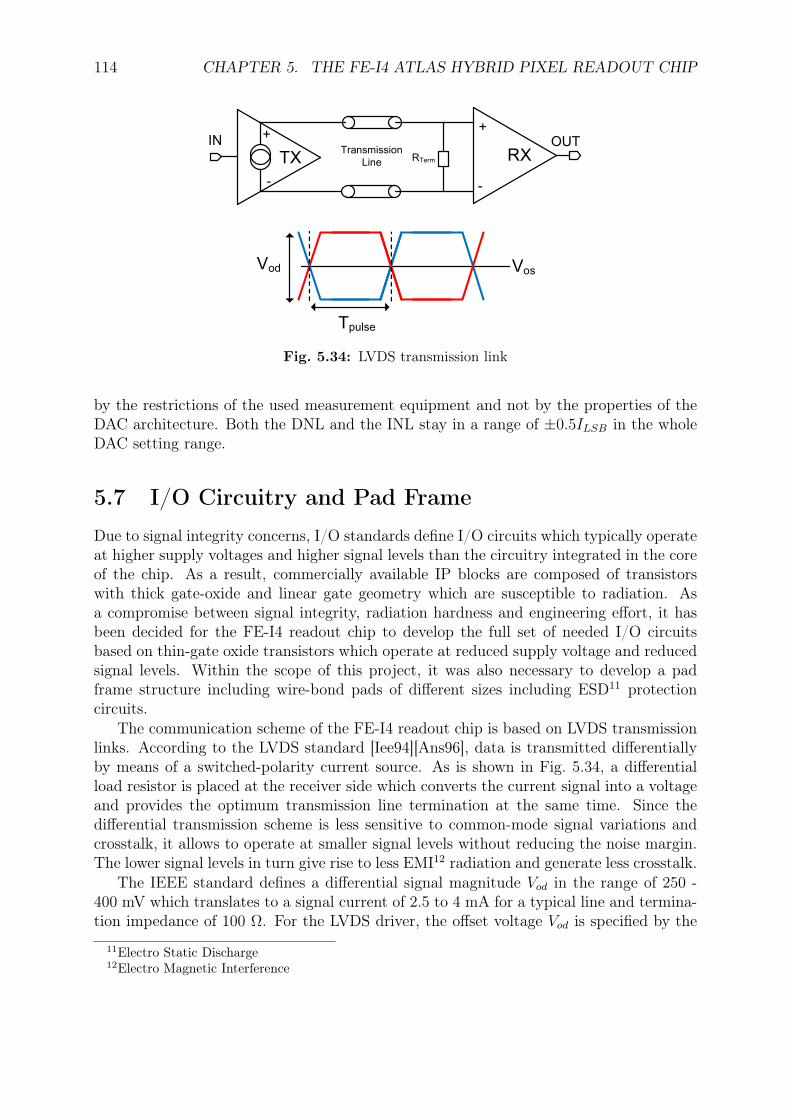
114 CHAPTER 5. THE FE-I4 ATLAS HYBRID PIXEL READOUT CHIP
Transmission
Line RTerm
OUT+
-
RXTX
+
-
IN
Vod Vos
Tpulse
Fig. 5.34: LVDS transmission link
by the restrictions of the used measurement equipment and not by the properties of theDAC architecture. Both the DNL and the INL stay in a range of ±0.5ILSB in the wholeDAC setting range.
5.7 I/O Circuitry and Pad Frame
Due to signal integrity concerns, I/O standards define I/O circuits which typically operateat higher supply voltages and higher signal levels than the circuitry integrated in the coreof the chip. As a result, commercially available IP blocks are composed of transistorswith thick gate-oxide and linear gate geometry which are susceptible to radiation. Asa compromise between signal integrity, radiation hardness and engineering effort, it hasbeen decided for the FE-I4 readout chip to develop the full set of needed I/O circuitsbased on thin-gate oxide transistors which operate at reduced supply voltage and reducedsignal levels. Within the scope of this project, it was also necessary to develop a padframe structure including wire-bond pads of different sizes including ESD11 protectioncircuits.
The communication scheme of the FE-I4 readout chip is based on LVDS transmissionlinks. According to the LVDS standard [Iee94][Ans96], data is transmitted differentiallyby means of a switched-polarity current source. As is shown in Fig. 5.34, a differentialload resistor is placed at the receiver side which converts the current signal into a voltageand provides the optimum transmission line termination at the same time. Since thedifferential transmission scheme is less sensitive to common-mode signal variations andcrosstalk, it allows to operate at smaller signal levels without reducing the noise margin.The lower signal levels in turn give rise to less EMI12 radiation and generate less crosstalk.
The IEEE standard defines a differential signal magnitude Vod in the range of 250 -400 mV which translates to a signal current of 2.5 to 4 mA for a typical line and termina-tion impedance of 100 Ω. For the LVDS driver, the offset voltage Vod is specified by the
11Electro Static Discharge12Electro Magnetic Interference
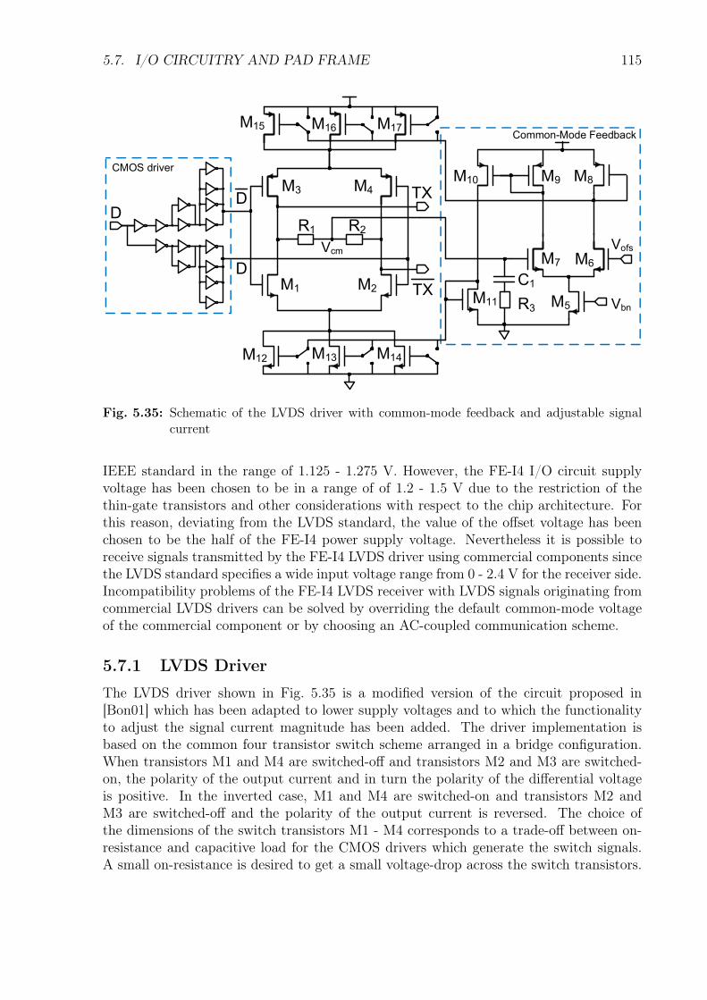
5.7. I/O CIRCUITRY AND PAD FRAME 115
M3 M4
M1 M2
D
D
D
Vcm
Vbn
TX
TX
M8M9
M5
M6M7
Vofs
M10
M11
Common-Mode Feedback
CMOS driver
M12 M13 M14
M15 M16 M17
R1 R2
R3
C1
Fig. 5.35: Schematic of the LVDS driver with common-mode feedback and adjustable signalcurrent
IEEE standard in the range of 1.125 - 1.275 V. However, the FE-I4 I/O circuit supplyvoltage has been chosen to be in a range of of 1.2 - 1.5 V due to the restriction of thethin-gate transistors and other considerations with respect to the chip architecture. Forthis reason, deviating from the LVDS standard, the value of the offset voltage has beenchosen to be the half of the FE-I4 power supply voltage. Nevertheless it is possible toreceive signals transmitted by the FE-I4 LVDS driver using commercial components sincethe LVDS standard specifies a wide input voltage range from 0 - 2.4 V for the receiver side.Incompatibility problems of the FE-I4 LVDS receiver with LVDS signals originating fromcommercial LVDS drivers can be solved by overriding the default common-mode voltageof the commercial component or by choosing an AC-coupled communication scheme.
5.7.1 LVDS Driver
The LVDS driver shown in Fig. 5.35 is a modified version of the circuit proposed in[Bon01] which has been adapted to lower supply voltages and to which the functionalityto adjust the signal current magnitude has been added. The driver implementation isbased on the common four transistor switch scheme arranged in a bridge configuration.When transistors M1 and M4 are switched-off and transistors M2 and M3 are switched-on, the polarity of the output current and in turn the polarity of the differential voltageis positive. In the inverted case, M1 and M4 are switched-on and transistors M2 andM3 are switched-off and the polarity of the output current is reversed. The choice ofthe dimensions of the switch transistors M1 - M4 corresponds to a trade-off between on-resistance and capacitive load for the CMOS drivers which generate the switch signals.A small on-resistance is desired to get a small voltage-drop across the switch transistors.
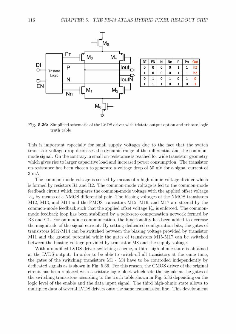
116 CHAPTER 5. THE FE-I4 ATLAS HYBRID PIXEL READOUT CHIP
M6
M5
M3 M4
M1 M2
Iout
IoutN
Tristate
Logic
Nn
Pn
EN
DIP
N0
1
1
1
Pn
1
0
hZ
hZ
OutDI EN N Nn P
0 0 0 0 1
1 0 0 0 1
0 1 0 1 0
1 1 1 0 1 0
1
1
1
Pn
1
0
hZ
hZ
OutDI EN N Nn P
0 0 0 0 1
1 0 0 0 1
0 1 0 1 0
1 1 1 0 1
Fig. 5.36: Simplified schematic of the LVDS driver with tristate output option and tristate-logictruth table
This is important especially for small supply voltages due to the fact that the switchtransistor voltage drop decreases the dynamic range of the differential and the common-mode signal. On the contrary, a small on-resistance is reached for wide transistor geometrywhich gives rise to larger capacitive load and increased power consumption. The transistoron-resistance has been chosen to generate a voltage drop of 50 mV for a signal current of3 mA.
The common-mode voltage is sensed by means of a high ohmic voltage divider whichis formed by resistors R1 and R2. The common-mode voltage is fed to the common-modefeedback circuit which compares the common-mode voltage with the applied offset voltageVos by means of a NMOS differential pair. The biasing voltages of the NMOS transistorsM12, M13, and M14 and the PMOS transistors M15, M16, and M17 are steered by thecommon-mode feedback such that the applied offset voltage Vos is enforced. The common-mode feedback loop has been stabilized by a pole-zero compensation network formed byR3 and C1. For on module communication, the functionality has been added to decreasethe magnitude of the signal current. By setting dedicated configuration bits, the gates oftransistors M12-M14 can be switched between the biasing voltage provided by transistorM11 and the ground potential while the gates of transistors M15-M17 can be switchedbetween the biasing voltage provided by transistor M8 and the supply voltage.
With a modified LVDS driver switching scheme, a third high-ohmic state is obtainedat the LVDS output. In order to be able to switch-off all transistors at the same time,the gates of the switching transistors M1 - M4 have to be controlled independently bydedicated signals as is shown in Fig. 5.36. For this reason, the CMOS driver of the originalcircuit has been replaced with a tristate logic block which sets the signals at the gates ofthe switching transistors according to the truth table shown in Fig. 5.36 depending on thelogic level of the enable and the data input signal. The third high-ohmic state allows tomultiplex data of several LVDS drivers onto the same transmission line. This development
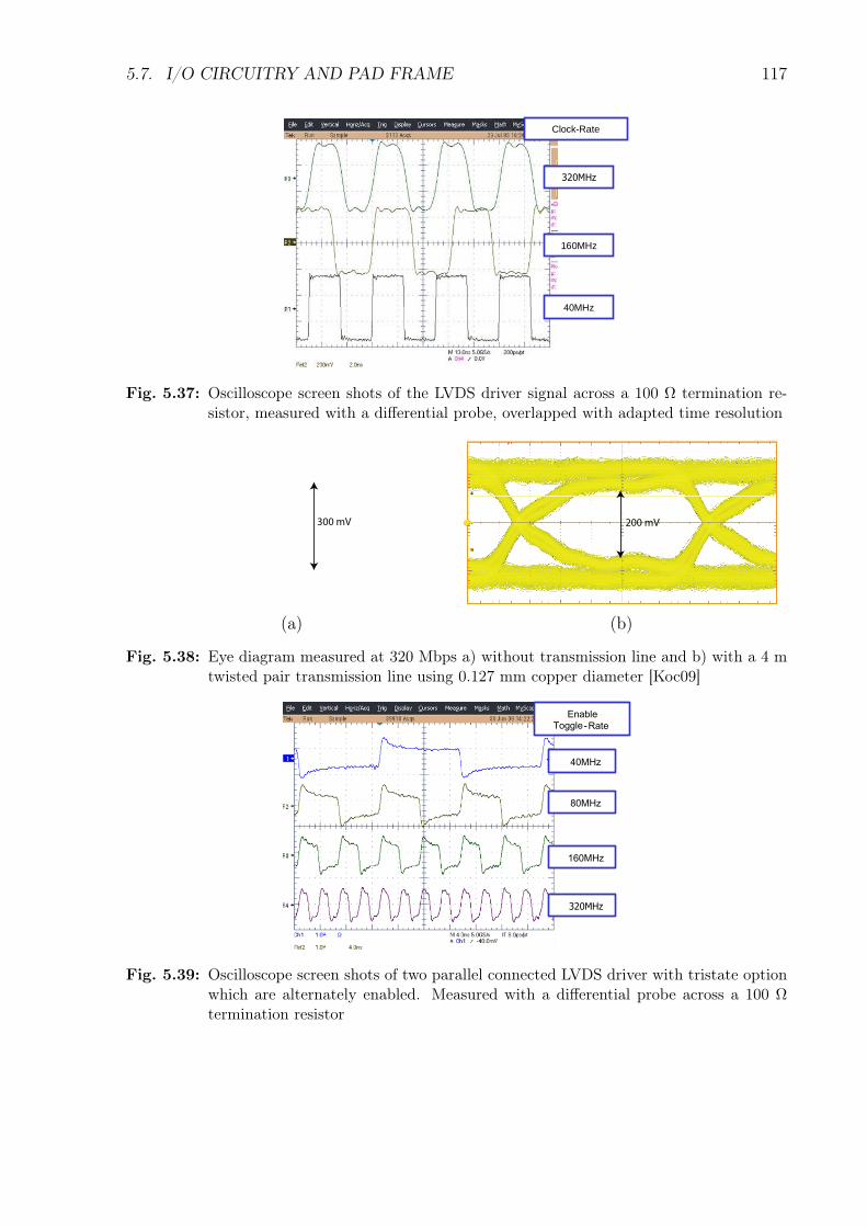
5.7. I/O CIRCUITRY AND PAD FRAME 117
40MHz
160MHz
320MHz
Clock-Rate
Fig. 5.37: Oscilloscope screen shots of the LVDS driver signal across a 100 Ω termination re-sistor, measured with a differential probe, overlapped with adapted time resolution
300 mV
(a)
200 mV
(b)
Fig. 5.38: Eye diagram measured at 320 Mbps a) without transmission line and b) with a 4 mtwisted pair transmission line using 0.127 mm copper diameter [Koc09]
40MHz
160MHz
320MHz
Enable
Toggle-Rate
80MHz
Fig. 5.39: Oscilloscope screen shots of two parallel connected LVDS driver with tristate optionwhich are alternately enabled. Measured with a differential probe across a 100 Ωtermination resistor
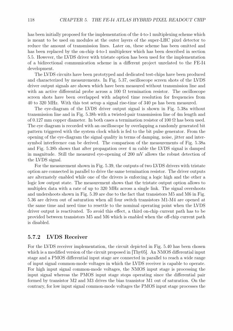
118 CHAPTER 5. THE FE-I4 ATLAS HYBRID PIXEL READOUT CHIP
has been initially proposed for the implementation of the 4-to-1 multiplexing scheme whichis meant to be used on modules at the outer layers of the super-LHC pixel detector toreduce the amount of transmission lines. Later on, these scheme has been omitted andhas been replaced by the on-chip 4-to-1 multiplexer which has been described in section5.5. However, the LVDS driver with tristate option has been used for the implementationof a bidirectional communication scheme in a different project unrelated to the FE-I4development.
The LVDS circuits have been prototyped and dedicated test-chips have been producedand characterized by measurements. In Fig. 5.37, oscilloscope screen shots of the LVDSdriver output signals are shown which have been measured without transmission line andwith an active differential probe across a 100 Ω termination resistor. The oscilloscopescreen shots have been overlapped with adapted time resolution for frequencies from40 to 320 MHz. With this test setup a signal rise-time of 340 ps has been measured.
The eye-diagram of the LVDS driver output signal is shown in Fig. 5.38a withouttransmission line and in Fig. 5.38b with a twisted-pair transmission line of 4m length andof 0.127 mm copper diameter. In both cases a termination resistor of 100 Ω has been used.The eye diagram is recorded with an oscilloscope by overlapping a randomly generated bitpattern triggered with the system clock which is fed to the bit pulse generator. From theopening of the eye-diagram the signal quality in terms of damping, noise, jitter and inter-symbol interference can be derived. The comparison of the measurements of Fig. 5.38aand Fig. 5.38b shows that after propagation over 4 m cable the LVDS signal is dampedin magnitude. Still the measured eye-opening of 200 mV allows the robust detection ofthe LVDS signal.
For the measurement shown in Fig. 5.39, the outputs of two LVDS drivers with tristateoption are connected in parallel to drive the same termination resistor. The driver outputsare alternately enabled while one of the drivers is enforcing a logic high and the other alogic low output state. The measurement shows that the tristate output option allows tomultiplex data with a rate of up to 320 MHz across a single link. The signal overshootsand undershoots shown in Fig. 5.39 are due to the fact that transistors M5 and M6 in Fig.5.36 are driven out of saturation when all four switch transistors M1-M4 are opened atthe same time and need time to resettle to the nominal operating point when the LVDSdriver output is reactivated. To avoid this effect, a third on-chip current path has to beprovided between transistors M5 and M6 which is enabled when the off-chip current pathis disabled.
5.7.2 LVDS Receiver
For the LVDS receiver implementation, the circuit depicted in Fig. 5.40 has been chosenwhich is a modified version of the circuit proposed in [Thy05]. An NMOS differential inputstage and a PMOS differential input stage are connected in parallel to reach a wide rangeof input signal common-mode voltages in which the LVDS receiver is capable to operate.For high input signal common-mode voltages, the NMOS input stage is processing theinput signal whereas the PMOS input stage stops operating since the differential pairformed by transistor M2 and M3 drives the bias transistor M1 out of saturation. On thecontrary, for low input signal common-mode voltages the PMOS input stage processes the
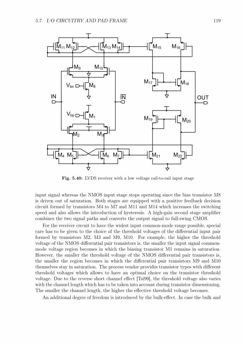
5.7. I/O CIRCUITRY AND PAD FRAME 119
M11M12 M13M14
M8
M9 M10
M4 M5 M6 M7
M1
M2 M3
M15 M16
M18M17
OUT
M20M19
M21 M22
ININ
Vbn
Vbp
Fig. 5.40: LVDS receiver with a low voltage rail-to-rail input stage
input signal whereas the NMOS input stage stops operating since the bias transistor M8is driven out of saturation. Both stages are equipped with a positive feedback decisioncircuit formed by transistors M4 to M7 and M11 and M14 which increases the switchingspeed and also allows the introduction of hysteresis. A high-gain second stage amplifiercombines the two signal paths and converts the output signal to full-swing CMOS.
For the receiver circuit to have the widest input common-mode range possible, specialcare has to be given to the choice of the threshold voltages of the differential input pairformed by transistors M2, M3 and M9, M10. For example, the higher the thresholdvoltage of the NMOS differential pair transistors is, the smaller the input signal common-mode voltage region becomes in which the biasing transistor M1 remains in saturation.However, the smaller the threshold voltage of the NMOS differential pair transistors is,the smaller the region becomes in which the differential pair transistors M9 and M10themselves stay in saturation. The process vendor provides transistor types with differentthreshold voltages which allows to have an optimal choice on the transistor thresholdvoltage. Due to the reverse short channel effect [Tsi99], the threshold voltage also varieswith the channel length which has to be taken into account during transistor dimensioning.The smaller the channel length, the higher the effective threshold voltage becomes.
An additional degree of freedom is introduced by the bulk-effect. In case the bulk and
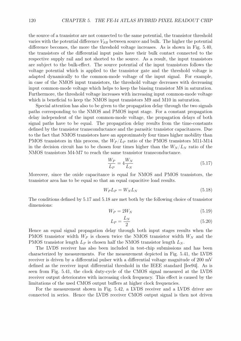
120 CHAPTER 5. THE FE-I4 ATLAS HYBRID PIXEL READOUT CHIP
the source of a transistor are not connected to the same potential, the transistor thresholdvaries with the potential difference VSB between source and bulk. The higher the potentialdifference becomes, the more the threshold voltage increases. As is shown in Fig. 5.40,the transistors of the differential input pairs have their bulk contact connected to therespective supply rail and not shorted to the source. As a result, the input transistorsare subject to the bulk-effect. The source potential of the input transistors follows thevoltage potential which is applied to the transistor gate and the threshold voltage isadapted dynamically to the common-mode voltage of the input signal. For example,in case of the NMOS input transistors, the threshold voltage decreases with decreasinginput common-mode voltage which helps to keep the biasing transistor M8 in saturation.Furthermore, the threshold voltage increases with increasing input common-mode voltagewhich is beneficial to keep the NMOS input transistors M9 and M10 in saturation.
Special attention has also to be given to the propagation delay through the two signalspaths corresponding to the NMOS and PMOS input stage. For a constant propagationdelay independent of the input common-mode voltage, the propagation delays of bothsignal paths have to be equal. The propagation delay results from the time-constantsdefined by the transistor transconductance and the parasitic transistor capacitances. Dueto the fact that NMOS transistors have an approximately four times higher mobility thanPMOS transistors in this process, the WP/LP ratio of the PMOS transistors M11-M14in the decision circuit has to be chosen four times higher than the WN/LN ratio of theNMOS transistors M4-M7 to reach the same transistor transconductance.
WP
LP
= 4WN
LN
(5.17)
Moreover, since the oxide capacitance is equal for NMOS and PMOS transistors, thetransistor area has to be equal so that an equal capacitive load results.
WPLP = WNLN (5.18)
The conditions defined by 5.17 and 5.18 are met both by the following choice of transistordimensions:
WP = 2WN (5.19)
LP =LN
2(5.20)
Hence an equal signal propagation delay through both input stages results when thePMOS transistor width WP is chosen twice the NMOS transistor width WN and thePMOS transistor length LP is chosen half the NMOS transistor length LN .
The LVDS receiver has also been included in test-chip submissions and has beencharacterized by measurements. For the measurement depicted in Fig. 5.41, the LVDSreceiver is driven by a differential pulser with a differential voltage magnitude of 200 mVdefined as the receiver input differential threshold in the IEEE standard [Iee94]. As isseen from Fig. 5.41, the clock duty-cycle of the CMOS signal measured at the LVDSreceiver output deteriorates with increasing clock frequency. This effect is caused by thelimitations of the used CMOS output buffers at higher clock frequencies.
For the measurement shown in Fig. 5.42, a LVDS receiver and a LVDS driver areconnected in series. Hence the LVDS receiver CMOS output signal is then not driven
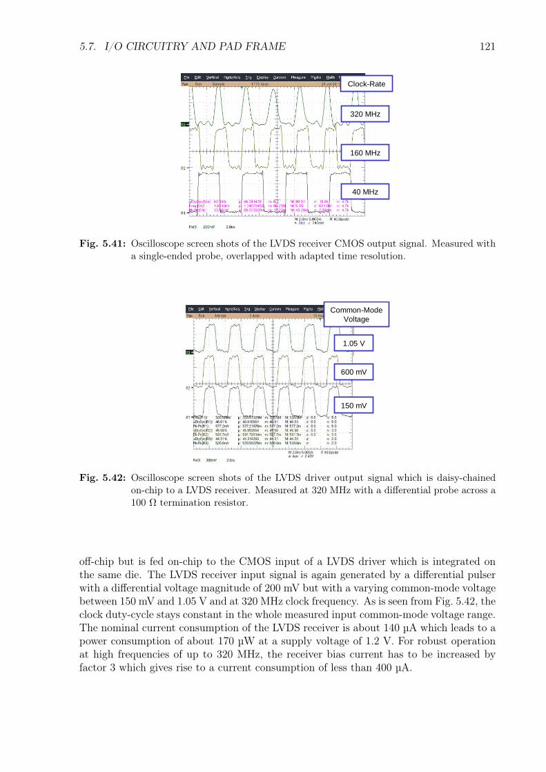
5.7. I/O CIRCUITRY AND PAD FRAME 121
40 MHz
160 MHz
320 MHz
Clock-Rate
Fig. 5.41: Oscilloscope screen shots of the LVDS receiver CMOS output signal. Measured witha single-ended probe, overlapped with adapted time resolution.
Common-ModeVoltage
1.05 V
600 mV
150 mV
Fig. 5.42: Oscilloscope screen shots of the LVDS driver output signal which is daisy-chainedon-chip to a LVDS receiver. Measured at 320 MHz with a differential probe across a100 Ω termination resistor.
off-chip but is fed on-chip to the CMOS input of a LVDS driver which is integrated onthe same die. The LVDS receiver input signal is again generated by a differential pulserwith a differential voltage magnitude of 200 mV but with a varying common-mode voltagebetween 150 mV and 1.05 V and at 320 MHz clock frequency. As is seen from Fig. 5.42, theclock duty-cycle stays constant in the whole measured input common-mode voltage range.The nominal current consumption of the LVDS receiver is about 140 µA which leads to apower consumption of about 170 µW at a supply voltage of 1.2 V. For robust operationat high frequencies of up to 320 MHz, the receiver bias current has to be increased byfactor 3 which gives rise to a current consumption of less than 400 µA.
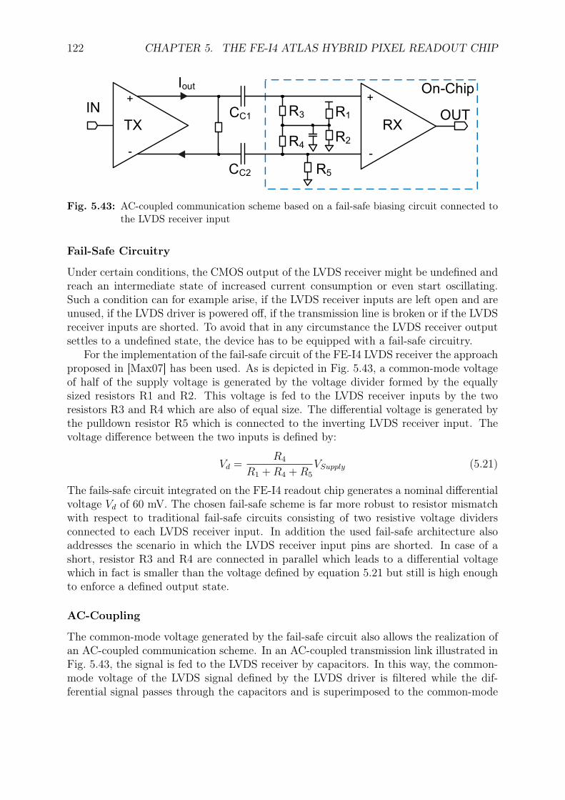
122 CHAPTER 5. THE FE-I4 ATLAS HYBRID PIXEL READOUT CHIP
TX RX
+
-
+
-
On-Chip
R1
R2
R3
R4
R5
OUTIN CC1
CC2
Iout
Fig. 5.43: AC-coupled communication scheme based on a fail-safe biasing circuit connected tothe LVDS receiver input
Fail-Safe Circuitry
Under certain conditions, the CMOS output of the LVDS receiver might be undefined andreach an intermediate state of increased current consumption or even start oscillating.Such a condition can for example arise, if the LVDS receiver inputs are left open and areunused, if the LVDS driver is powered off, if the transmission line is broken or if the LVDSreceiver inputs are shorted. To avoid that in any circumstance the LVDS receiver outputsettles to a undefined state, the device has to be equipped with a fail-safe circuitry.
For the implementation of the fail-safe circuit of the FE-I4 LVDS receiver the approachproposed in [Max07] has been used. As is depicted in Fig. 5.43, a common-mode voltageof half of the supply voltage is generated by the voltage divider formed by the equallysized resistors R1 and R2. This voltage is fed to the LVDS receiver inputs by the tworesistors R3 and R4 which are also of equal size. The differential voltage is generated bythe pulldown resistor R5 which is connected to the inverting LVDS receiver input. Thevoltage difference between the two inputs is defined by:
Vd =R4
R1 +R4 +R5
VSupply (5.21)
The fails-safe circuit integrated on the FE-I4 readout chip generates a nominal differentialvoltage Vd of 60 mV. The chosen fail-safe scheme is far more robust to resistor mismatchwith respect to traditional fail-safe circuits consisting of two resistive voltage dividersconnected to each LVDS receiver input. In addition the used fail-safe architecture alsoaddresses the scenario in which the LVDS receiver input pins are shorted. In case of ashort, resistor R3 and R4 are connected in parallel which leads to a differential voltagewhich in fact is smaller than the voltage defined by equation 5.21 but still is high enoughto enforce a defined output state.
AC-Coupling
The common-mode voltage generated by the fail-safe circuit also allows the realization ofan AC-coupled communication scheme. In an AC-coupled transmission link illustrated inFig. 5.43, the signal is fed to the LVDS receiver by capacitors. In this way, the common-mode voltage of the LVDS signal defined by the LVDS driver is filtered while the dif-ferential signal passes through the capacitors and is superimposed to the common-mode
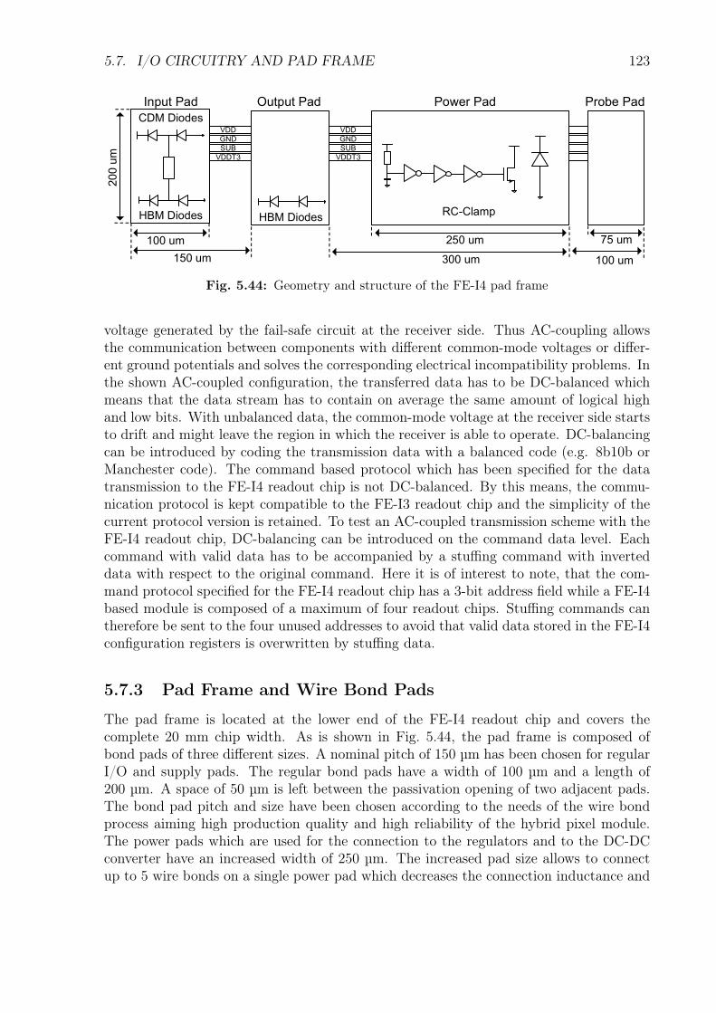
5.7. I/O CIRCUITRY AND PAD FRAME 123
VDD
GND
SUB
VDDT3
VDD
GND
SUB
VDDT3
HBM Diodes
CDM Diodes
100 um
150 um
Input Pad Output Pad
250 um
Power Pad
300 um
RC-ClampHBM Diodes
200 um
75 um
100 um
Probe Pad
Fig. 5.44: Geometry and structure of the FE-I4 pad frame
voltage generated by the fail-safe circuit at the receiver side. Thus AC-coupling allowsthe communication between components with different common-mode voltages or differ-ent ground potentials and solves the corresponding electrical incompatibility problems. Inthe shown AC-coupled configuration, the transferred data has to be DC-balanced whichmeans that the data stream has to contain on average the same amount of logical highand low bits. With unbalanced data, the common-mode voltage at the receiver side startsto drift and might leave the region in which the receiver is able to operate. DC-balancingcan be introduced by coding the transmission data with a balanced code (e.g. 8b10b orManchester code). The command based protocol which has been specified for the datatransmission to the FE-I4 readout chip is not DC-balanced. By this means, the commu-nication protocol is kept compatible to the FE-I3 readout chip and the simplicity of thecurrent protocol version is retained. To test an AC-coupled transmission scheme with theFE-I4 readout chip, DC-balancing can be introduced on the command data level. Eachcommand with valid data has to be accompanied by a stuffing command with inverteddata with respect to the original command. Here it is of interest to note, that the com-mand protocol specified for the FE-I4 readout chip has a 3-bit address field while a FE-I4based module is composed of a maximum of four readout chips. Stuffing commands cantherefore be sent to the four unused addresses to avoid that valid data stored in the FE-I4configuration registers is overwritten by stuffing data.
5.7.3 Pad Frame and Wire Bond Pads
The pad frame is located at the lower end of the FE-I4 readout chip and covers thecomplete 20 mm chip width. As is shown in Fig. 5.44, the pad frame is composed ofbond pads of three different sizes. A nominal pitch of 150 µm has been chosen for regularI/O and supply pads. The regular bond pads have a width of 100 µm and a length of200 µm. A space of 50 µm is left between the passivation opening of two adjacent pads.The bond pad pitch and size have been chosen according to the needs of the wire bondprocess aiming high production quality and high reliability of the hybrid pixel module.The power pads which are used for the connection to the regulators and to the DC-DCconverter have an increased width of 250 µm. The increased pad size allows to connectup to 5 wire bonds on a single power pad which decreases the connection inductance and
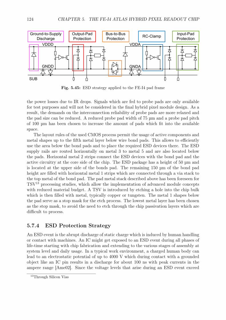
124 CHAPTER 5. THE FE-I4 ATLAS HYBRID PIXEL READOUT CHIP
VDDD
GNDD
SUB
VDDA
GNDA
Ground-to-Supply
Discharge
Bus-to-Bus
Protection
Output-Pad
ProtectionRC-Clamp
Input-Pad
Protection
Fig. 5.45: ESD strategy applied to the FE-I4 pad frame
the power losses due to IR drops. Signals which are fed to probe pads are only availablefor test purposes and will not be considered in the final hybrid pixel module design. As aresult, the demands on the interconnection reliability of probe pads are more relaxed andthe pad size can be reduced. A reduced probe pad width of 75 µm and a probe pad pitchof 100 µm has been chosen to increase the amount of pads which fit into the availablespace.
The layout rules of the used CMOS process permit the usage of active components andmetal shapes up to the fifth metal layer below wire bond pads. This allows to efficientlyuse the area below the bond pads and to place the required ESD devices there. The ESDsupply rails are routed horizontally on metal 3 to metal 5 and are also located belowthe pads. Horizontal metal 2 strips connect the ESD devices with the bond pad and theactive circuitry at the core side of the chip. The ESD package has a height of 50 µm andis located at the upper side of the bonds pad. The remaining 150 µm of the bond padheight are filled with horizontal metal 1 strips which are connected through a via stack tothe top metal of the bond pad. The pad metal stack described above has been foreseen forTSV13 processing studies, which allow the implementation of advanced module conceptswith reduced material budget. A TSV is introduced by etching a hole into the chip bulkwhich is then filled with metal, typically copper or tungsten. The metal 1 shapes belowthe pad serve as a stop mask for the etch process. The lowest metal layer has been chosenas the stop mask, to avoid the need to etch through the chip passivation layers which aredifficult to process.
5.7.4 ESD Protection Strategy
An ESD event is the abrupt discharge of static charge which is induced by human handlingor contact with machines. An IC might get exposed to an ESD event during all phases oflife-time starting with chip fabrication and extending to the various stages of assembly atsystem level and daily usage. In a typical work environment, a charged human body canlead to an electrostatic potential of up to 4000 V which during contact with a groundedobject like an IC pin results in a discharge for about 100 ns with peak currents in theampere range [Ame02]. Since the voltage levels that arise during an ESD event exceed
13Through Silicon Vias
5.7. I/O CIRCUITRY AND PAD FRAME 125
the breakdown voltages of transistors and other components integrated on the chip, theimplementation of a protection strategy is mandatory to avoid device destruction. Theprotection objective is to provide a discharge path of least impedance to ground throughdevices which have been designed to withstand large currents. During the dischargeprocess the appearance of high voltage drops on the wires of the ESD network has to beavoided. High voltage drops would cause an ESD current flow into the sensitive internalcircuits which would then be harmed.
The ESD protection strategy for the FE-I4 readout chip shown in Fig. 5.45 is basedon recommendations of the process vendor [Ibm09]. The applied strategy follows a non-self protecting approach which means that additional ESD devices are added in parallelto the I/O circuits. In case of the FE-I4 chip, the added ESD circuitry is formed by adouble-diode network which connects the I/O pin to the supply rails by reverse biaseddiodes. During an ESD event of positive voltage the upper diode conducts a currentto the positive supply rail while during an ESD event of negative voltage the currentflows through the lower diode and originates from the ground bus. Due to the fact thatthe diode junction capacitance increases the capacitive load at the I/O pins, the diodedimensions have to be balanced between the demands for robust ESD protection andfor high I/O circuit bandwidth. Input pads which provide connection to transistor gateelectrodes are equipped with additional ESD structures to avoid the breakdown of thetransistor gate-oxide during an ESD event. A series resistor and an additional secondarydiode pair of smaller diode area is added to the primary double-diode network. The seriesresistor and the on resistance of the second diode pair form a voltage divider. Hence thevoltage across the conducting diode of the primary diode network is reduced if the seriesresistor is higher than the on-resistance of the secondary diode pair.
To provide an ESD current path from the positive supply voltage to the ground bus, anRC-triggered power clamp is connected between the supply rails. During normal operationthe NMOS transistor of the RC-clamp circuit is switched-off whereas the NMOS transistoris switched-on during the transient pulse of an ESD event. ESD events can also inducea current flow into the ground pin. To avoid the current flow through parasitic diodes ofthe internal circuitry, dedicated ground-to-supply discharge diodes are added in parallelto the RC-clamp circuit. Since the diode junction capacitance is not harmful to the powersupply bus, the diodes can be large without an impact on the chip performance.
As has been mentioned in section 5.4, the supply voltages of the FE-I4 chip are or-ganized in several supply domains. In addition a dedicated ground rail is used for thedefinition of the substrate potential. Since an ESD discharge might cross the supply do-main boundaries, it has to be avoided that the discharge happens through the connectionswhich the internal sensitive circuitry has across the supply domains. For this reason abus-to-bus protection circuit composed of an antiparallel connected diode pair is placedbetween the ground busses of the different supply domains and between the ground bussesand the substrate rail which provides a discharge path of low impedance in both direc-tions. Amongst others, the separation of the supply voltage into an analog and a digitaldomain is motivated by concerns related to crosstalk and noise. Due to the fact that thejunction capacitance of the antiparallel connected diodes re-couples the supply rails tosome degree, the choice of the diode dimensions is a trade-off between ESD reliability andisolation quality.
126 CHAPTER 5. THE FE-I4 ATLAS HYBRID PIXEL READOUT CHIP
5.8 Power ManagementDue to the special environment in which the ATLAS pixel detector operates and the de-manding conditions the detector has to meet, the implementation of an efficient powerdistribution system is an ambitious engineering challenge. In general, hybrid pixel de-tectors are power hungry devices with a high current consumption in the order of sev-eral amperes per module. In ATLAS, power is supplied independently to each hybridpixel module from off-detector power supplies through a multiple stage regulation scheme[Cit07]. Because of the large size of the ATLAS detector, the power cables reach a lengthof about 100 m. Furthermore, the maximum possible cable cross section is limited, owingto mechanical space restrictions and concerns about detection performance degradationcaused by particle interactions with the cable mass. In case of direct powering, the powerefficiency ηDirect is defined as:
ηDirect =1
1 +nRI
V
(5.22)
where n corresponds to the number of powered modules, I is the module current consump-tion, R is the cable resistance and V is the module supply voltage. The present ATLAShybrid pixel detector has a power efficiency of 20 %. This means that 80 % of the poweris dissipated in the cables due to IR voltage drops before the actual hybrid pixel modulesare reached. With the upcoming IBL and super-LHC upgrades, the amount of installedmodules and readout channels will increase and as a result the current consumption willalso rise. Hence, the present power distribution scheme has to be replaced by a newapproach with higher power efficiency.
Several powering schemes are currently investigated to increase the powering efficiency.A well known approach is DC-DC conversion. In this scheme, power is distributed athigher voltage and is then down converted close to the load to the needed supply voltagelevel. Neglecting the inefficiency introduced by the DC-DC converter the achieved powerefficiency is given by:
ηDCDC =1
1 + nRIm2V
(5.23)
where m is the voltage conversion factor of the DC-DC converter. Hence, the powering ef-ficiency increases when DC-DC conversion is applied, since less current is flowing throughthe power cables. Commercial DC-DC converters for high power applications are com-monly based on Buck-converters which are switched inductive converters with ferrite corecoils. These ferrite cores would be saturated by the 2 Tesla constant magnetic field whichsurrounds the ATLAS detector. Air coils of same inductance tend to be much bigger insize and thus incompatible with the need to reduce the amount of material used in thedetector. Calculations and prototype studies concerning off-chip switched capacitor basedconverter have shown that for high current applications like in the case of hybrid pixeldetectors, no improvement in material budget is achieved when a powering efficiency of70% is targeted [Den09]. In addition, the ripples on the supply voltage that come alongwith switched power supplies influence the noise performance of the analog front-end.Common front-end architectures are based on circuits with single ended inputs and out-puts due the the single-ended nature of the sensor signal and as a result have a low PSRR
5.8. POWER MANAGEMENT 127
nR I
Module
FE-I4 FE-I4 FE-I4 FE-I4
1
n -1
n
V FE-I4 FE-I4 FE-I4 FE-I4
FE-I4 FE-I4 FE-I4 FE-I4
nI
(a)
Module
FE-I4 FE-I4 FE-I4 FE-I4
Module
FE-I4 FE-I4 FE-I4 FE-I4
Module
FE-I4 FE-I4 FE-I4 FE-I4
1
n -1
n
R I
nV
I
(b)
Fig. 5.46: a) Parallel powering b) serial powering
(see Fig. 5.19). LDO regulators are used to filter the ripples on the supply voltage butdissipate additional power on top of the power loss related to the DC-DC converter itselfand thus decrease the overall powering efficiency.
An alternative approach shown in Fig. 5.46b is serial powering [Ta06]. In a seriallypowered scheme, modules are placed in series and powered by a constant current source.Shunt regulators are used at module level to generate the local supply voltage from theinput current. In a scheme with n modules connected in series, the current through thecable is reduced by a factor n with respect to the parallel powering of n modules whilethe voltage drop across the module chain corresponds to n times the voltage drop across asingle module. Neglecting the inefficiency caused by the regulation circuitry, the poweringefficiency ηSerial of a serially powered system is given by:
ηSerial =1
1 +RI
nV
(5.24)
As is seen from equation 5.24, the power efficiency of a serial powered system increaseswith the number of modules which are placed in series. The comparison of equation5.24 and equation 5.23 shows that the efficiency of a serial powered system exceeds theefficiency of a power distribution system which is based on DC-DC conversion when theamount of powered modules n is higher than the voltage conversion factor m of the DC-DCconverter.
The FE-I4 hybrid pixel chip is designed for use with both powering options. A switchedcapacitor charge pump is integrated to provide a divide by two (m=2) DC-DC conversion(see section 5.8.1). Two independent Shunt-LDO regulators are available for shunt regula-tion in serial powered supply schemes (see section 5.8.3). A dedicated LDO regulator hasbeen developed which allows stable operation with low ESR14 load capacitors by means
14Equivalent Series Resistance
128 CHAPTER 5. THE FE-I4 ATLAS HYBRID PIXEL READOUT CHIP
33 33
33 33
Vin
Vout
Cout
Cpump
ClkTop
ClkBot1 ClkBot2
M1 M2
M3 M4
Cout
Vin
Cpump
CoutCpump
Vout
Vout
+
+
+
Charge:M1,M4 on
M2,M3 off
Discharge:M2,M3 on
M1,M4 off
Fig. 5.47: Switched-Capacitor based divide-by-two DCDC-converter
of an integrated active compensation circuit. However the LDO regulator has not beenintegrated on the FE-I4 due to the fact that the Shunt-LDO regulator can be configuredto provide linear voltage regulation. Nevertheless the architecture of the developed LDOregulator and the applied compensation scheme are described in section 5.8.2 to intro-duce the regulation functional principle and to present measurement results derived froma prototype.
5.8.1 Integrated Divide-by-Two DC-DC converter
A switched-capacitor charge pump has been integrated on the FE-I4 readout chip for usewith a power distribution scheme based on DC-DC conversion. On the one hand, theintegrated scheme reduces the amount of material which is introduced by the addition ofthe DC-DC converter. For the implementation of the charge-pump, only two additionalexternal capacitors are needed whereas the remaining circuitry is integrated on the FE-I4chip periphery. On the other hand, the integrated scheme imposes a constraint on themaximum reachable voltage conversion factor. The maximum voltage drop of 3.3 V whichtransistors in the chosen CMOS process can bear, limits the voltage conversion to a factorof two.
As is depicted in Fig. 5.47, the switched-capacitor charge pump is composed of fourthick-gate oxide switch transistors and two external capacitors. During the charge phase,transistor M1 and transistor M4 are switched-on while transistors M2 and M3 are switched-off. The capacitors Cpump and Cout are then connected in series and form a capacitivevoltage divider. In the discharge phase, transistors M2 and M3 are switched-on whereastransistors M1 and M4 are switched-off. The capacitors Cpump and Cout are then connectedin parallel and both capacitors are discharged by the load connected to the output. Ac-cording to [Mak95], the charge pump output voltage settles to Vin/2 independently ofthe chosen capacitance ratio Cpump/Cout. For this reason the capacitance Cout is typ-ically chosen to be larger than Cpump which decreases the magnitude of the switching
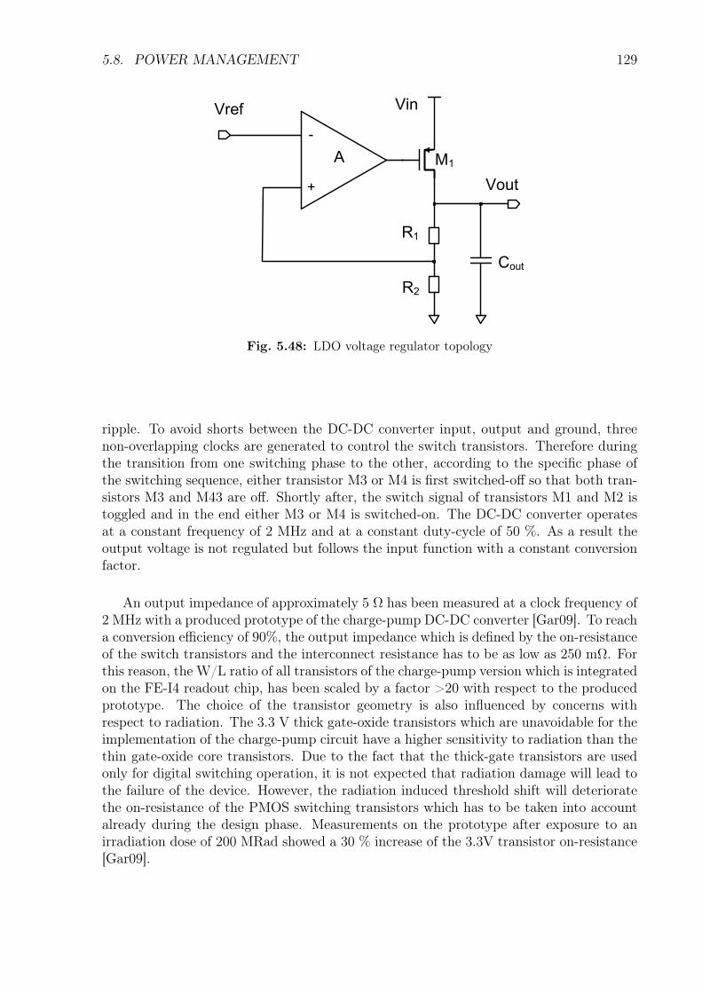
5.8. POWER MANAGEMENT 129
-
VinVref
Vout
R1
R2
Cout
M1
+
A
Fig. 5.48: LDO voltage regulator topology
ripple. To avoid shorts between the DC-DC converter input, output and ground, threenon-overlapping clocks are generated to control the switch transistors. Therefore duringthe transition from one switching phase to the other, according to the specific phase ofthe switching sequence, either transistor M3 or M4 is first switched-off so that both tran-sistors M3 and M43 are off. Shortly after, the switch signal of transistors M1 and M2 istoggled and in the end either M3 or M4 is switched-on. The DC-DC converter operatesat a constant frequency of 2 MHz and at a constant duty-cycle of 50 %. As a result theoutput voltage is not regulated but follows the input function with a constant conversionfactor.
An output impedance of approximately 5 Ω has been measured at a clock frequency of2 MHz with a produced prototype of the charge-pump DC-DC converter [Gar09]. To reacha conversion efficiency of 90%, the output impedance which is defined by the on-resistanceof the switch transistors and the interconnect resistance has to be as low as 250 mΩ. Forthis reason, the W/L ratio of all transistors of the charge-pump version which is integratedon the FE-I4 readout chip, has been scaled by a factor >20 with respect to the producedprototype. The choice of the transistor geometry is also influenced by concerns withrespect to radiation. The 3.3 V thick gate-oxide transistors which are unavoidable for theimplementation of the charge-pump circuit have a higher sensitivity to radiation than thethin gate-oxide core transistors. Due to the fact that the thick-gate transistors are usedonly for digital switching operation, it is not expected that radiation damage will lead tothe failure of the device. However, the radiation induced threshold shift will deterioratethe on-resistance of the PMOS switching transistors which has to be taken into accountalready during the design phase. Measurements on the prototype after exposure to anirradiation dose of 200 MRad showed a 30 % increase of the 3.3V transistor on-resistance[Gar09].
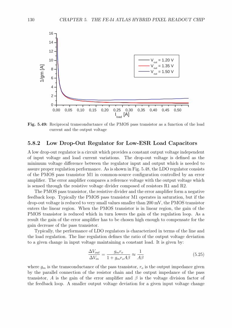
130 CHAPTER 5. THE FE-I4 ATLAS HYBRID PIXEL READOUT CHIP
0,00 0,05 0,10 0,15 0,20 0,25 0,30 0,35 0,40 0,45 0,50 0
2
4
6
8
10
12
14
16
V out
= 1.20 V V
out = 1.35 V
V out
= 1.50 V
1/gm
[A]
I load
[A]
Fig. 5.49: Reciprocal transconductance of the PMOS pass transistor as a function of the loadcurrent and the output voltage
5.8.2 Low Drop-Out Regulator for Low-ESR Load Capacitors
A low drop-out regulator is a circuit which provides a constant output voltage independentof input voltage and load current variations. The drop-out voltage is defined as theminimum voltage difference between the regulator input and output which is needed toassure proper regulation performance. As is shown in Fig. 5.48, the LDO regulator consistsof the PMOS pass transistor M1 in common-source configuration controlled by an erroramplifier. The error amplifier compares a reference voltage with the output voltage whichis sensed through the resistive voltage divider composed of resistors R1 and R2.
The PMOS pass transistor, the resistive divider and the error amplifier form a negativefeedback loop. Typically the PMOS pass transistor M1 operates in saturation, but if thedrop-out voltage is reduced to very small values smaller than 200 mV, the PMOS transistorenters the linear region. When the PMOS transistor is in linear region, the gain of thePMOS transistor is reduced which in turn lowers the gain of the regulation loop. As aresult the gain of the error amplifier has to be chosen high enough to compensate for thegain decrease of the pass transistor.
Typically, the performance of LDO regulators is characterized in terms of the line andthe load regulation. The line regulation defines the ratio of the output voltage deviationto a given change in input voltage maintaining a constant load. It is given by:
∆Vout
∆Vin
=gmro
1 + gmroAβ≈ 1
Aβ(5.25)
where gm is the transconductance of the pass transistor, ro is the output impedance givenby the parallel connection of the resistor chain and the output impedance of the passtransistor, A is the gain of the error amplifier and β is the voltage division factor ofthe feedback loop. A smaller output voltage deviation for a given input voltage change
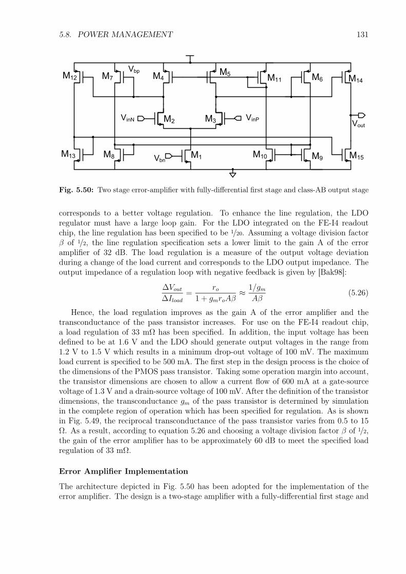
5.8. POWER MANAGEMENT 131
M4M5
M1
M2 M3 VinPVinN
Vbp
Vout
M6M7
M8 M9M10
M11M12
M13
M14
M15Vbn
Fig. 5.50: Two stage error-amplifier with fully-differential first stage and class-AB output stage
corresponds to a better voltage regulation. To enhance the line regulation, the LDOregulator must have a large loop gain. For the LDO integrated on the FE-I4 readoutchip, the line regulation has been specified to be 1/20. Assuming a voltage division factorβ of 1/2, the line regulation specification sets a lower limit to the gain A of the erroramplifier of 32 dB. The load regulation is a measure of the output voltage deviationduring a change of the load current and corresponds to the LDO output impedance. Theoutput impedance of a regulation loop with negative feedback is given by [Bak98]:
∆Vout
∆Iload=
ro1 + gmroAβ
≈ 1/gmAβ
(5.26)
Hence, the load regulation improves as the gain A of the error amplifier and thetransconductance of the pass transistor increases. For use on the FE-I4 readout chip,a load regulation of 33 mΩ has been specified. In addition, the input voltage has beendefined to be at 1.6 V and the LDO should generate output voltages in the range from1.2 V to 1.5 V which results in a minimum drop-out voltage of 100 mV. The maximumload current is specified to be 500 mA. The first step in the design process is the choice ofthe dimensions of the PMOS pass transistor. Taking some operation margin into account,the transistor dimensions are chosen to allow a current flow of 600 mA at a gate-sourcevoltage of 1.3 V and a drain-source voltage of 100 mV. After the definition of the transistordimensions, the transconductance gm of the pass transistor is determined by simulationin the complete region of operation which has been specified for regulation. As is shownin Fig. 5.49, the reciprocal transconductance of the pass transistor varies from 0.5 to 15Ω. As a result, according to equation 5.26 and choosing a voltage division factor β of 1/2,the gain of the error amplifier has to be approximately 60 dB to meet the specified loadregulation of 33 mΩ.
Error Amplifier Implementation
The architecture depicted in Fig. 5.50 has been adopted for the implementation of theerror amplifier. The design is a two-stage amplifier with a fully-differential first stage and
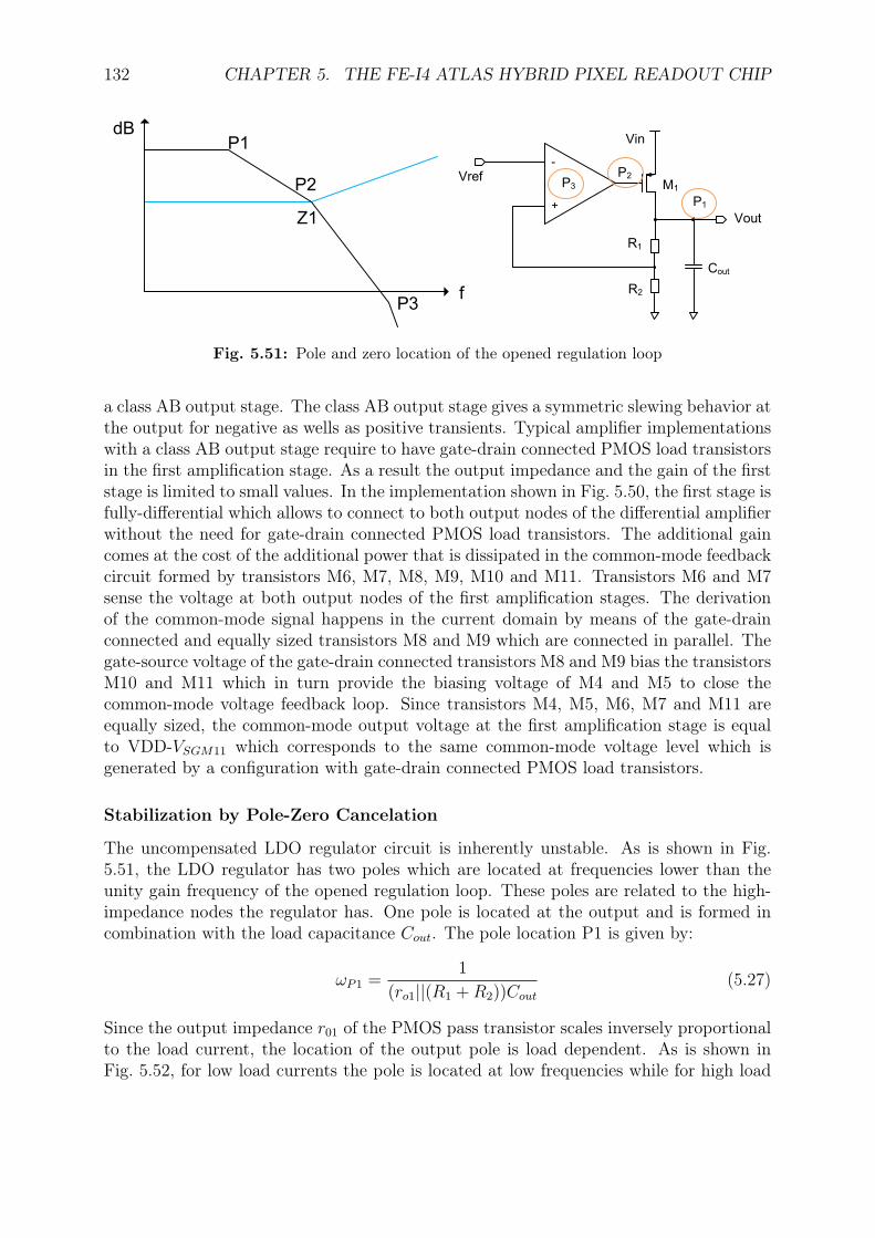
132 CHAPTER 5. THE FE-I4 ATLAS HYBRID PIXEL READOUT CHIP
P1
P2
P3
Z1
f
dB
+
-
Vin
Vref
Vout
R1
R2
Cout
M1
P1
P2P3
Fig. 5.51: Pole and zero location of the opened regulation loop
a class AB output stage. The class AB output stage gives a symmetric slewing behavior atthe output for negative as wells as positive transients. Typical amplifier implementationswith a class AB output stage require to have gate-drain connected PMOS load transistorsin the first amplification stage. As a result the output impedance and the gain of the firststage is limited to small values. In the implementation shown in Fig. 5.50, the first stage isfully-differential which allows to connect to both output nodes of the differential amplifierwithout the need for gate-drain connected PMOS load transistors. The additional gaincomes at the cost of the additional power that is dissipated in the common-mode feedbackcircuit formed by transistors M6, M7, M8, M9, M10 and M11. Transistors M6 and M7sense the voltage at both output nodes of the first amplification stages. The derivationof the common-mode signal happens in the current domain by means of the gate-drainconnected and equally sized transistors M8 and M9 which are connected in parallel. Thegate-source voltage of the gate-drain connected transistors M8 and M9 bias the transistorsM10 and M11 which in turn provide the biasing voltage of M4 and M5 to close thecommon-mode voltage feedback loop. Since transistors M4, M5, M6, M7 and M11 areequally sized, the common-mode output voltage at the first amplification stage is equalto VDD-VSGM11 which corresponds to the same common-mode voltage level which isgenerated by a configuration with gate-drain connected PMOS load transistors.
Stabilization by Pole-Zero Cancelation
The uncompensated LDO regulator circuit is inherently unstable. As is shown in Fig.5.51, the LDO regulator has two poles which are located at frequencies lower than theunity gain frequency of the opened regulation loop. These poles are related to the high-impedance nodes the regulator has. One pole is located at the output and is formed incombination with the load capacitance Cout. The pole location P1 is given by:
ωP1 =1
(ro1||(R1 +R2))Cout
(5.27)
Since the output impedance r01 of the PMOS pass transistor scales inversely proportionalto the load current, the location of the output pole is load dependent. As is shown inFig. 5.52, for low load currents the pole is located at low frequencies while for high load
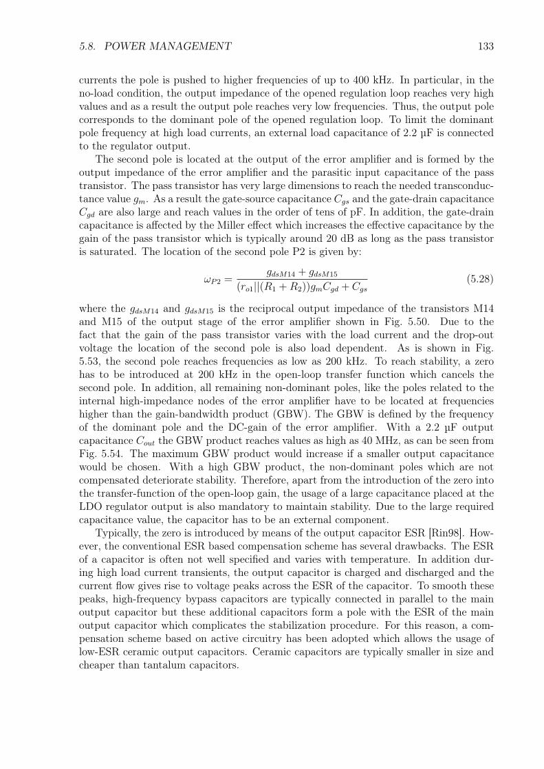
5.8. POWER MANAGEMENT 133
currents the pole is pushed to higher frequencies of up to 400 kHz. In particular, in theno-load condition, the output impedance of the opened regulation loop reaches very highvalues and as a result the output pole reaches very low frequencies. Thus, the output polecorresponds to the dominant pole of the opened regulation loop. To limit the dominantpole frequency at high load currents, an external load capacitance of 2.2 µF is connectedto the regulator output.
The second pole is located at the output of the error amplifier and is formed by theoutput impedance of the error amplifier and the parasitic input capacitance of the passtransistor. The pass transistor has very large dimensions to reach the needed transconduc-tance value gm. As a result the gate-source capacitance Cgs and the gate-drain capacitanceCgd are also large and reach values in the order of tens of pF. In addition, the gate-draincapacitance is affected by the Miller effect which increases the effective capacitance by thegain of the pass transistor which is typically around 20 dB as long as the pass transistoris saturated. The location of the second pole P2 is given by:
ωP2 =gdsM14 + gdsM15
(ro1||(R1 +R2))gmCgd + Cgs
(5.28)
where the gdsM14 and gdsM15 is the reciprocal output impedance of the transistors M14and M15 of the output stage of the error amplifier shown in Fig. 5.50. Due to thefact that the gain of the pass transistor varies with the load current and the drop-outvoltage the location of the second pole is also load dependent. As is shown in Fig.5.53, the second pole reaches frequencies as low as 200 kHz. To reach stability, a zerohas to be introduced at 200 kHz in the open-loop transfer function which cancels thesecond pole. In addition, all remaining non-dominant poles, like the poles related to theinternal high-impedance nodes of the error amplifier have to be located at frequencieshigher than the gain-bandwidth product (GBW). The GBW is defined by the frequencyof the dominant pole and the DC-gain of the error amplifier. With a 2.2 µF outputcapacitance Cout the GBW product reaches values as high as 40 MHz, as can be seen fromFig. 5.54. The maximum GBW product would increase if a smaller output capacitancewould be chosen. With a high GBW product, the non-dominant poles which are notcompensated deteriorate stability. Therefore, apart from the introduction of the zero intothe transfer-function of the open-loop gain, the usage of a large capacitance placed at theLDO regulator output is also mandatory to maintain stability. Due to the large requiredcapacitance value, the capacitor has to be an external component.
Typically, the zero is introduced by means of the output capacitor ESR [Rin98]. How-ever, the conventional ESR based compensation scheme has several drawbacks. The ESRof a capacitor is often not well specified and varies with temperature. In addition dur-ing high load current transients, the output capacitor is charged and discharged and thecurrent flow gives rise to voltage peaks across the ESR of the capacitor. To smooth thesepeaks, high-frequency bypass capacitors are typically connected in parallel to the mainoutput capacitor but these additional capacitors form a pole with the ESR of the mainoutput capacitor which complicates the stabilization procedure. For this reason, a com-pensation scheme based on active circuitry has been adopted which allows the usage oflow-ESR ceramic output capacitors. Ceramic capacitors are typically smaller in size andcheaper than tantalum capacitors.
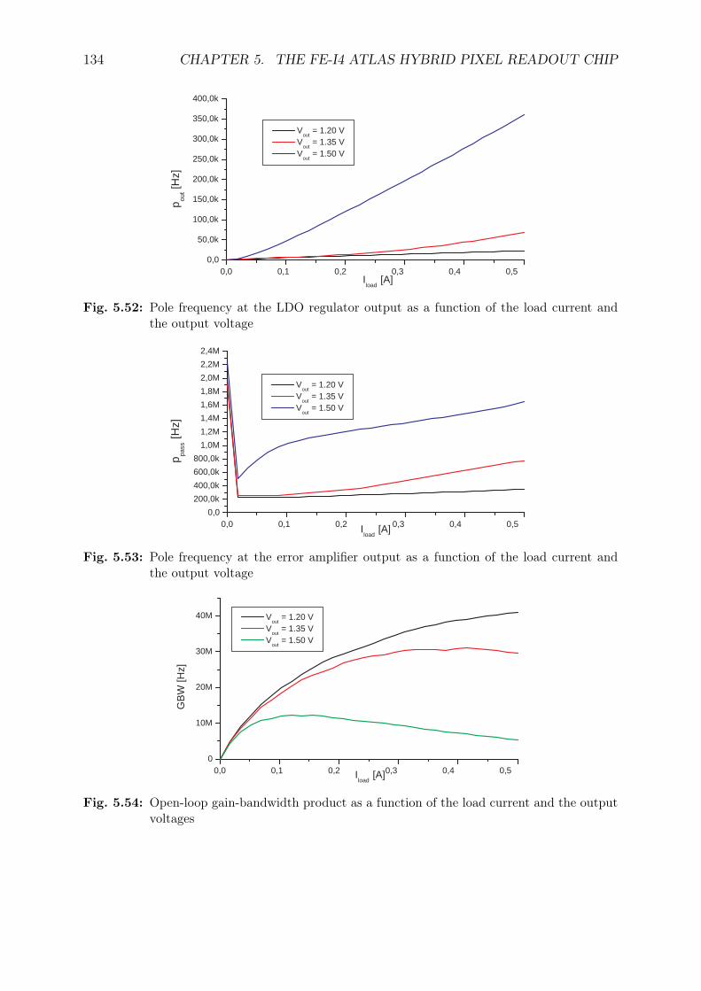
134 CHAPTER 5. THE FE-I4 ATLAS HYBRID PIXEL READOUT CHIP
0,0 0,1 0,2 0,3 0,4 0,5 0,0
50,0k
100,0k
150,0k
200,0k
250,0k
300,0k
350,0k
400,0k
V out
= 1.20 V V
out = 1.35 V
V out
= 1.50 V
p ou
t [Hz]
I load
[A]
Fig. 5.52: Pole frequency at the LDO regulator output as a function of the load current andthe output voltage
0,0 0,1 0,2 0,3 0,4 0,5 0,0
200,0k
400,0k
600,0k
800,0k
1,0M
1,2M
1,4M
1,6M
1,8M
2,0M
2,2M
2,4M
V out
= 1.20 V V
out = 1.35 V
V out
= 1.50 V
p pass
[Hz]
I load
[A]
Fig. 5.53: Pole frequency at the error amplifier output as a function of the load current andthe output voltage
0,0 0,1 0,2 0,3 0,4 0,5 0
10M
20M
30M
40M V out
= 1.20 V V
out = 1.35 V
V out
= 1.50 V
GB
W [H
z]
I load
[A]
Fig. 5.54: Open-loop gain-bandwidth product as a function of the load current and the outputvoltages
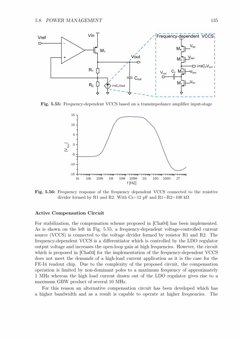
5.8. POWER MANAGEMENT 135
+
-
VinVref
Vout
R1
R2
Cout
M1
i=sCzVout
Vout
i=sCzVout
Vbn
Vbpc
Vbp
M1
M4
M3
Cz Vbnc
Frequency-dependent VCCS
M2
Fig. 5.55: Frequency-dependent VCCS based on a transimpedance amplifier input-stage
1k 10k 100k 1M 10M 100M 1G 10G 100G 1T -15
-10
-5
0
5
10
15
|V Z
ero |
f [HZ]
Fig. 5.56: Frequency response of the frequency dependent VCCS connected to the resistivedivider formed by R1 and R2. With Cz=12 pF and R1=R2=100 kΩ
Active Compensation Circuit
For stabilization, the compensation scheme proposed in [Cha04] has been implemented.As is shown on the left in Fig. 5.55, a frequency-dependent voltage-controlled currentsource (VCCS) is connected to the voltage divider formed by resistor R1 and R2. Thefrequency-dependent VCCS is a differentiator which is controlled by the LDO regulatoroutput voltage and increases the open-loop gain at high frequencies. However, the circuitwhich is proposed in [Cha04] for the implementation of the frequency-dependent VCCSdoes not meet the demands of a high-load current application as it is the case for theFE-I4 readout chip. Due to the complexity of the proposed circuit, the compensationoperation is limited by non-dominant poles to a maximum frequency of approximately1 MHz whereas the high load current drawn out of the LDO regulator gives rise to amaximum GBW product of several 10 MHz.
For this reason an alternative compensation circuit has been developed which hasa higher bandwidth and as a result is capable to operate at higher frequencies. The
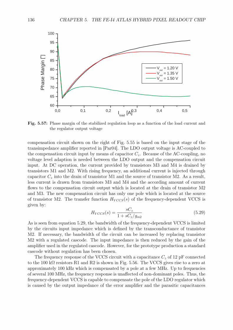
136 CHAPTER 5. THE FE-I4 ATLAS HYBRID PIXEL READOUT CHIP
0,0 0,1 0,2 0,3 0,4 0,5 60
65
70
75
80
85
90
95
100
V out
= 1.20 V V
out = 1.35 V
V out
= 1.50 V
Pha
se M
argi
n [˚
]
I load
[A]
Fig. 5.57: Phase margin of the stabilized regulation loop as a function of the load current andthe regulator output voltage
compensation circuit shown on the right of Fig. 5.55 is based on the input stage of thetransimpedance amplifier reported in [Par04]. The LDO output voltage is AC-coupled tothe compensation circuit input by means of capacitor Cz. Because of the AC-coupling, novoltage level adaption is needed between the LDO output and the compensation circuitinput. At DC operation, the current provided by transistors M3 and M4 is drained bytransistors M1 and M2. With rising frequency, an additional current is injected throughcapacitor Cz into the drain of transistor M1 and the source of transistor M2. As a result,less current is drawn from transistors M3 and M4 and the according amount of currentflows to the compensation circuit output which is located at the drain of transistor M2and M3. The new compensation circuit has only one pole which is located at the sourceof transistor M2. The transfer function HV CCS(s) of the frequency-dependent VCCS isgiven by:
HV CCS(s) =sCz
1 + sCz/gm2
(5.29)
As is seen from equation 5.29, the bandwidth of the frequency-dependent VCCS is limitedby the circuits input impedance which is defined by the transconductance of transistorM2. If necessary, the bandwidth of the circuit can be increased by replacing transistorM2 with a regulated cascode. The input impedance is then reduced by the gain of theamplifier used in the regulated cascode. However, for the prototype production a standardcascode without regulation has been chosen.
The frequency response of the VCCS circuit with a capacitance Cz of 12 pF connectedto the 100 kΩ resistors R1 and R2 is shown in Fig. 5.56. The VCCS gives rise to a zero atapproximately 100 kHz which is compensated by a pole at a few MHz. Up to frequenciesof several 100 MHz, the frequency response is unaffected of non-dominant poles. Thus, thefrequency-dependent VCCS is capable to compensate the pole of the LDO regulator whichis caused by the output impedance of the error amplifier and the parasitic capacitances
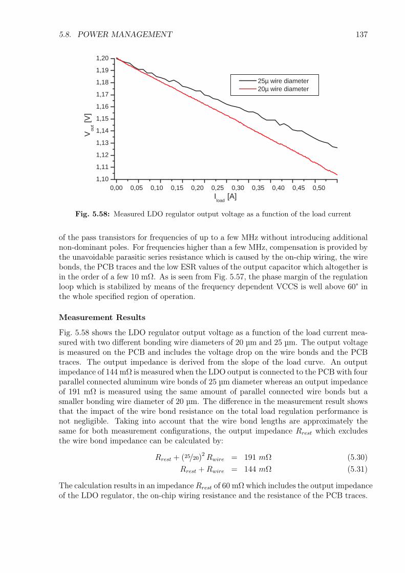
5.8. POWER MANAGEMENT 137
0,00 0,05 0,10 0,15 0,20 0,25 0,30 0,35 0,40 0,45 0,50 1,10
1,11
1,12
1,13
1,14
1,15
1,16
1,17
1,18
1,19
1,20
25µ wire diameter 20µ wire diameter
V ou
t [V]
I load
[A]
Fig. 5.58: Measured LDO regulator output voltage as a function of the load current
of the pass transistors for frequencies of up to a few MHz without introducing additionalnon-dominant poles. For frequencies higher than a few MHz, compensation is provided bythe unavoidable parasitic series resistance which is caused by the on-chip wiring, the wirebonds, the PCB traces and the low ESR values of the output capacitor which altogether isin the order of a few 10 mΩ. As is seen from Fig. 5.57, the phase margin of the regulationloop which is stabilized by means of the frequency dependent VCCS is well above 60° inthe whole specified region of operation.
Measurement Results
Fig. 5.58 shows the LDO regulator output voltage as a function of the load current mea-sured with two different bonding wire diameters of 20 µm and 25 µm. The output voltageis measured on the PCB and includes the voltage drop on the wire bonds and the PCBtraces. The output impedance is derived from the slope of the load curve. An outputimpedance of 144 mΩ is measured when the LDO output is connected to the PCB with fourparallel connected aluminum wire bonds of 25 µm diameter whereas an output impedanceof 191 mΩ is measured using the same amount of parallel connected wire bonds but asmaller bonding wire diameter of 20 µm. The difference in the measurement result showsthat the impact of the wire bond resistance on the total load regulation performance isnot negligible. Taking into account that the wire bond lengths are approximately thesame for both measurement configurations, the output impedance Rrest which excludesthe wire bond impedance can be calculated by:
Rrest + (25/20)2Rwire = 191 mΩ (5.30)Rrest +Rwire = 144 mΩ (5.31)
The calculation results in an impedance Rrest of 60 mΩ which includes the output impedanceof the LDO regulator, the on-chip wiring resistance and the resistance of the PCB traces.
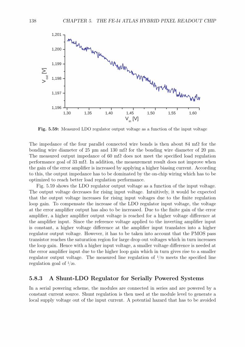
138 CHAPTER 5. THE FE-I4 ATLAS HYBRID PIXEL READOUT CHIP
1,30 1,35 1,40 1,45 1,50 1,55 1,60 1,196
1,197
1,198
1,199
1,200
1,201
V ou
t [V]
V in [V]
Fig. 5.59: Measured LDO regulator output voltage as a function of the input voltage
The impedance of the four parallel connected wire bonds is then about 84 mΩ for thebonding wire diameter of 25 µm and 130 mΩ for the bonding wire diameter of 20 µm.The measured output impedance of 60 mΩ does not meet the specified load regulationperformance goal of 33 mΩ. In addition, the measurement result does not improve whenthe gain of the error amplifier is increased by applying a higher biasing current. Accordingto this, the output impedance has to be dominated by the on-chip wiring which has to beoptimized to reach better load regulation performance.
Fig. 5.59 shows the LDO regulator output voltage as a function of the input voltage.The output voltage decreases for rising input voltage. Intuitively, it would be expectedthat the output voltage increases for rising input voltages due to the finite regulationloop gain. To compensate the increase of the LDO regulator input voltage, the voltageat the error amplifier output has also to be increased. Due to the finite gain of the erroramplifier, a higher amplifier output voltage is reached for a higher voltage difference atthe amplifier input. Since the reference voltage applied to the inverting amplifier inputis constant, a higher voltage difference at the amplifier input translates into a higherregulator output voltage. However, it has to be taken into account that the PMOS passtransistor reaches the saturation region for large drop out voltages which in turn increasesthe loop gain. Hence with a higher input voltage, a smaller voltage difference is needed atthe error amplifier input due to the higher loop gain which in turn gives rise to a smallerregulator output voltage. The measured line regulation of 1/70 meets the specified lineregulation goal of 1/20.
5.8.3 A Shunt-LDO Regulator for Serially Powered Systems
In a serial powering scheme, the modules are connected in series and are powered by aconstant current source. Shunt regulation is then used at the module level to generate alocal supply voltage out of the input current. A potential hazard that has to be avoided
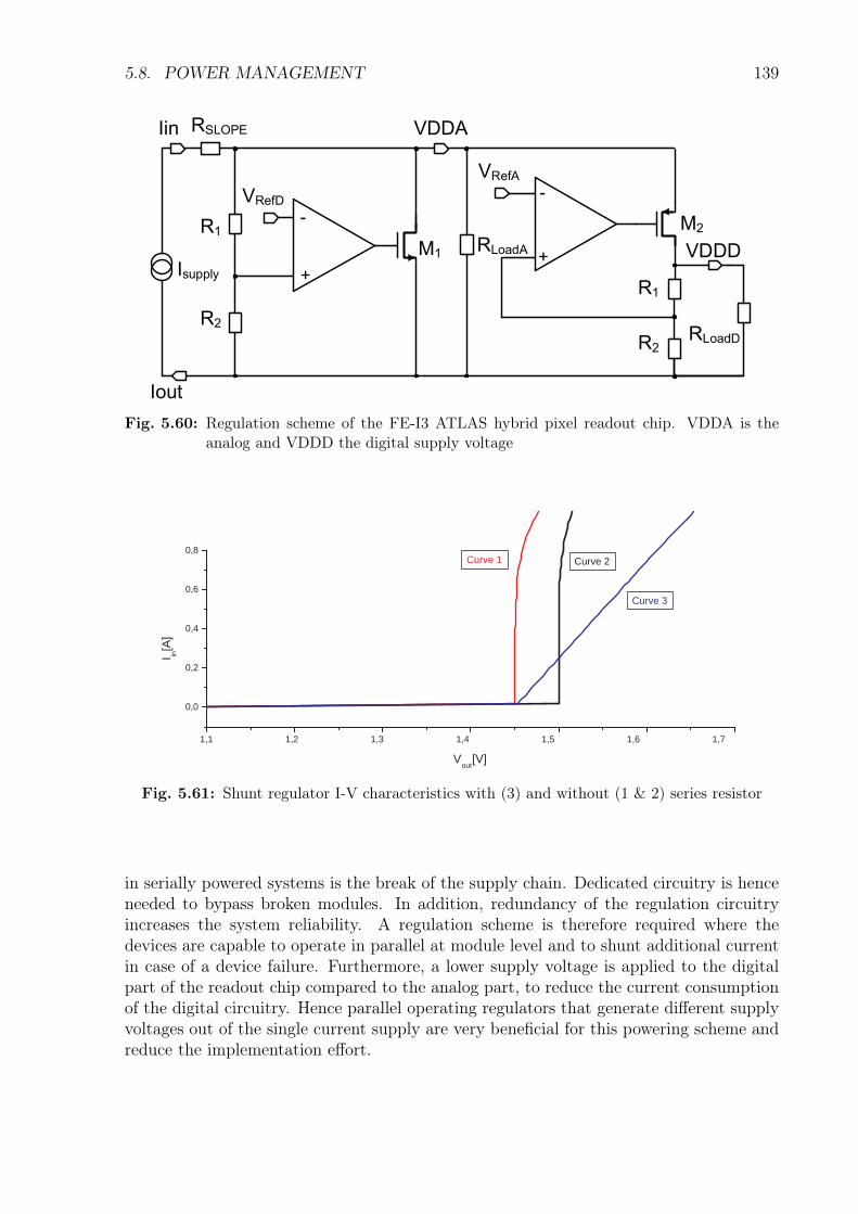
5.8. POWER MANAGEMENT 139
Iin
Iout
Isupply
RSLOPE
+
-
VRefD
VDDA
R1
R2
M1RLoadA
+
-
VRefA
VDDD
R1
R2
M2
RLoadD
Fig. 5.60: Regulation scheme of the FE-I3 ATLAS hybrid pixel readout chip. VDDA is theanalog and VDDD the digital supply voltage
1,1 1,2 1,3 1,4 1,5 1,6 1,7
0,0
0,2
0,4
0,6
0,8
Curve 3
Curve 2 Curve 1
I in [A
]
V out
[V]
Fig. 5.61: Shunt regulator I-V characteristics with (3) and without (1 & 2) series resistor
in serially powered systems is the break of the supply chain. Dedicated circuitry is henceneeded to bypass broken modules. In addition, redundancy of the regulation circuitryincreases the system reliability. A regulation scheme is therefore required where thedevices are capable to operate in parallel at module level and to shunt additional currentin case of a device failure. Furthermore, a lower supply voltage is applied to the digitalpart of the readout chip compared to the analog part, to reduce the current consumptionof the digital circuitry. Hence parallel operating regulators that generate different supplyvoltages out of the single current supply are very beneficial for this powering scheme andreduce the implementation effort.
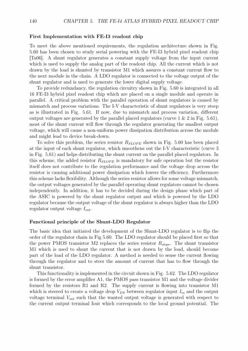
140 CHAPTER 5. THE FE-I4 ATLAS HYBRID PIXEL READOUT CHIP
First Implementation with FE-I3 readout chip
To meet the above mentioned requirements, the regulation architecture shown in Fig.5.60 has been chosen to study serial powering with the FE-I3 hybrid pixel readout chip[Ta06]. A shunt regulator generates a constant supply voltage from the input currentwhich is used to supply the analog part of the readout chip. All the current which is notdrawn by the load is shunted by transistor M1 which assures a constant current flow tothe next module in the chain. A LDO regulator is connected to the voltage output of theshunt regulator and is used to generate the lower digital supply voltage.
To provide redundancy, the regulation circuitry shown in Fig. 5.60 is integrated in all16 FE-I3 hybrid pixel readout chip which are placed on a single module and operate inparallel. A critical problem with the parallel operation of shunt regulators is caused bymismatch and process variations. The I-V characteristic of shunt regulators is very steepas is illustrated in Fig. 5.61. If now, due to mismatch and process variation, differentoutput voltages are generated by the parallel placed regulators (curve 1 & 2 in Fig. 5.61),most of the shunt current will flow through the regulator generating the smallest outputvoltage, which will cause a non-uniform power dissipation distribution across the moduleand might lead to device break-down.
To solve this problem, the series resistor RSLOPE shown in Fig. 5.60 has been placedat the input of each shunt regulator, which smoothens out the I-V characteristic (curve 3in Fig. 5.61) and helps distributing the shunt current on the parallel placed regulators. Inthis scheme, the added resistor RSLOPE is mandatory for safe operation but the resistoritself does not contribute to the regulation performance and the voltage drop across theresistor is causing additional power dissipation which lowers the efficiency. Furthermorethis scheme lacks flexibility. Although the series resistor allows for some voltage mismatch,the output voltages generated by the parallel operating shunt regulators cannot be chosenindependently. In addition, it has to be decided during the design phase which part ofthe ASIC is powered by the shunt regulator output and which is powered by the LDOregulator because the output voltage of the shunt regulator is always higher than the LDOregulator output voltage Iout.
Functional principle of the Shunt-LDO Regulator
The basic idea that initiated the development of the Shunt-LDO regulator is to flip theorder of the regulator chain in Fig 5.60. The LDO regulator should be placed first so thatthe power PMOS transistor M2 replaces the series resistor Rslope. The shunt transistorM1 which is used to shunt the current that is not drawn by the load, should becomepart of the load of the LDO regulator. A method is needed to sense the current flowingthrough the regulator and to steer the amount of current that has to flow through theshunt transistor.
This functionality is implemented in the circuit shown in Fig. 5.62. The LDO regulatoris formed by the error amplifier A1, the PMOS pass transistor M1 and the voltage dividerformed by the resistors R1 and R2. The supply current is flowing into transistor M1which is steered to create a voltage drop VDS between regulator input Iin and the outputvoltage terminal Vout such that the wanted output voltage is generated with respect tothe current output terminal Iout which corresponds to the local ground potential. The
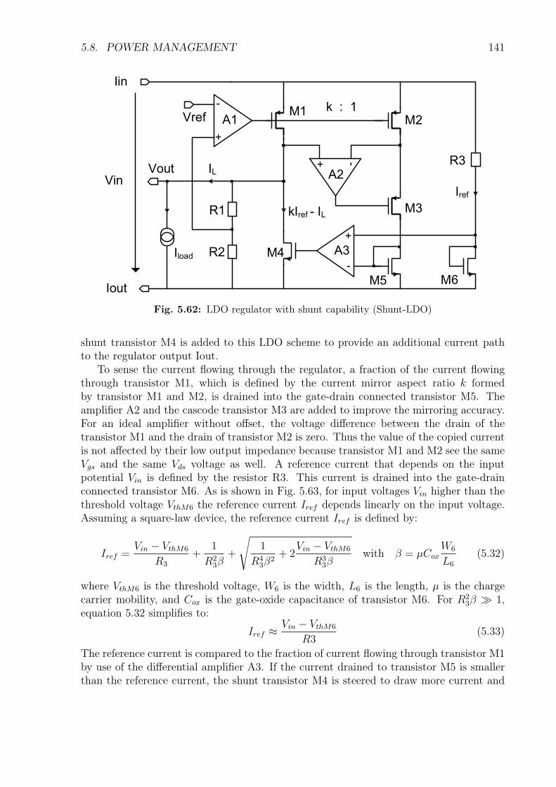
5.8. POWER MANAGEMENT 141
+ -
+
-
+
-
Iin
Iout
Vref
Vout
A1
A2
A3
M1M2
M3
M4
M5
R1
R2
Vin
Iload
R3
M6
kIref - IL
IL
Iref
k : 1
Fig. 5.62: LDO regulator with shunt capability (Shunt-LDO)
shunt transistor M4 is added to this LDO scheme to provide an additional current pathto the regulator output Iout.
To sense the current flowing through the regulator, a fraction of the current flowingthrough transistor M1, which is defined by the current mirror aspect ratio k formedby transistor M1 and M2, is drained into the gate-drain connected transistor M5. Theamplifier A2 and the cascode transistor M3 are added to improve the mirroring accuracy.For an ideal amplifier without offset, the voltage difference between the drain of thetransistor M1 and the drain of transistor M2 is zero. Thus the value of the copied currentis not affected by their low output impedance because transistor M1 and M2 see the sameVgs and the same Vds voltage as well. A reference current that depends on the inputpotential Vin is defined by the resistor R3. This current is drained into the gate-drainconnected transistor M6. As is shown in Fig. 5.63, for input voltages Vin higher than thethreshold voltage VthM6 the reference current Iref depends linearly on the input voltage.Assuming a square-law device, the reference current Iref is defined by:
Iref =Vin − VthM6
R3
+1
R23β
+
√1
R43β
2+ 2
Vin − VthM6
R33β
with β = µCoxW6
L6
(5.32)
where VthM6 is the threshold voltage, W6 is the width, L6 is the length, µ is the chargecarrier mobility, and Cox is the gate-oxide capacitance of transistor M6. For R2
3β ≫ 1,equation 5.32 simplifies to:
Iref ≈ Vin − VthM6
R3(5.33)
The reference current is compared to the fraction of current flowing through transistor M1by use of the differential amplifier A3. If the current drained to transistor M5 is smallerthan the reference current, the shunt transistor M4 is steered to draw more current and
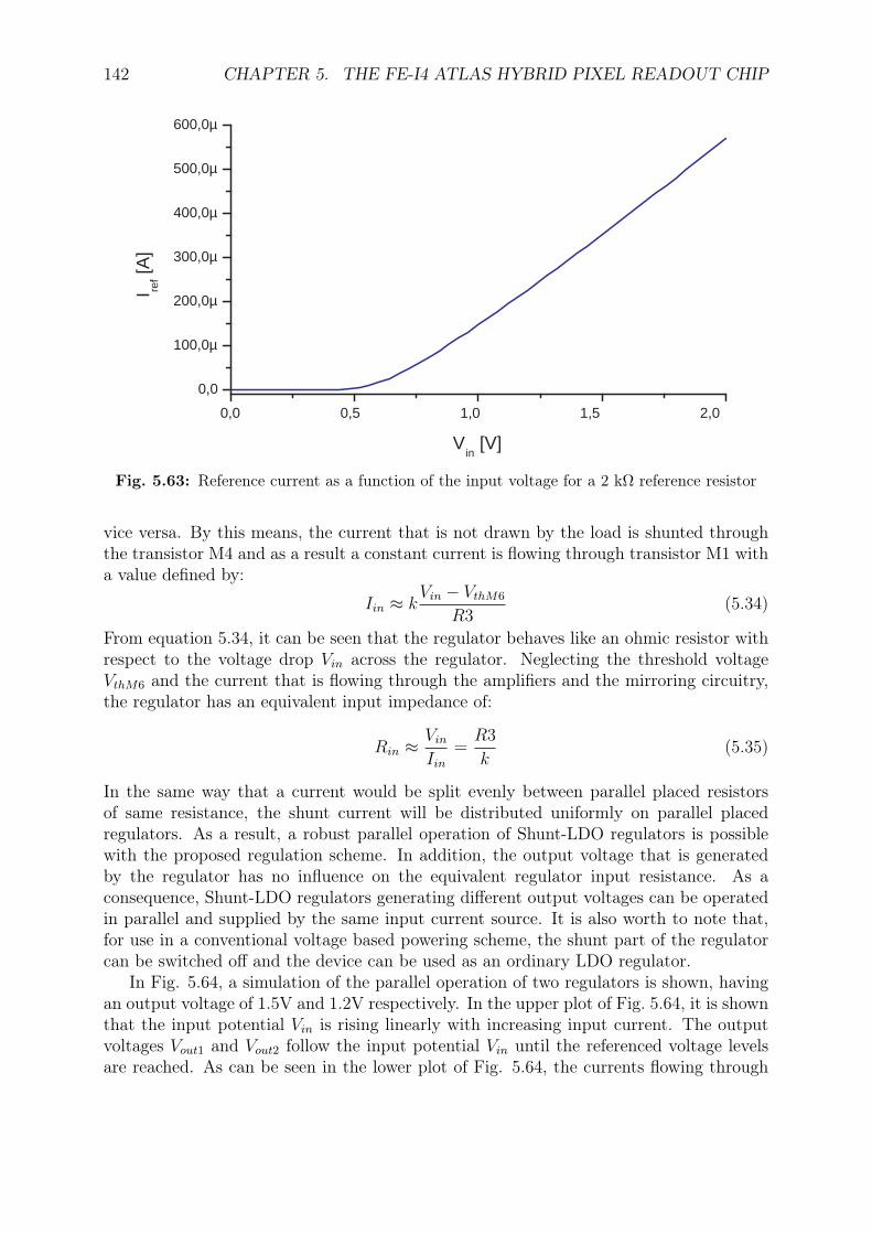
142 CHAPTER 5. THE FE-I4 ATLAS HYBRID PIXEL READOUT CHIP
0,0 0,5 1,0 1,5 2,0
0,0
100,0µ
200,0µ
300,0µ
400,0µ
500,0µ
600,0µ I re
f [A]
V in [V]
Fig. 5.63: Reference current as a function of the input voltage for a 2 kΩ reference resistor
vice versa. By this means, the current that is not drawn by the load is shunted throughthe transistor M4 and as a result a constant current is flowing through transistor M1 witha value defined by:
Iin ≈ kVin − VthM6
R3(5.34)
From equation 5.34, it can be seen that the regulator behaves like an ohmic resistor withrespect to the voltage drop Vin across the regulator. Neglecting the threshold voltageVthM6 and the current that is flowing through the amplifiers and the mirroring circuitry,the regulator has an equivalent input impedance of:
Rin ≈ Vin
Iin=
R3
k(5.35)
In the same way that a current would be split evenly between parallel placed resistorsof same resistance, the shunt current will be distributed uniformly on parallel placedregulators. As a result, a robust parallel operation of Shunt-LDO regulators is possiblewith the proposed regulation scheme. In addition, the output voltage that is generatedby the regulator has no influence on the equivalent regulator input resistance. As aconsequence, Shunt-LDO regulators generating different output voltages can be operatedin parallel and supplied by the same input current source. It is also worth to note that,for use in a conventional voltage based powering scheme, the shunt part of the regulatorcan be switched off and the device can be used as an ordinary LDO regulator.
In Fig. 5.64, a simulation of the parallel operation of two regulators is shown, havingan output voltage of 1.5V and 1.2V respectively. In the upper plot of Fig. 5.64, it is shownthat the input potential Vin is rising linearly with increasing input current. The outputvoltages Vout1 and Vout2 follow the input potential Vin until the referenced voltage levelsare reached. As can be seen in the lower plot of Fig. 5.64, the currents flowing through
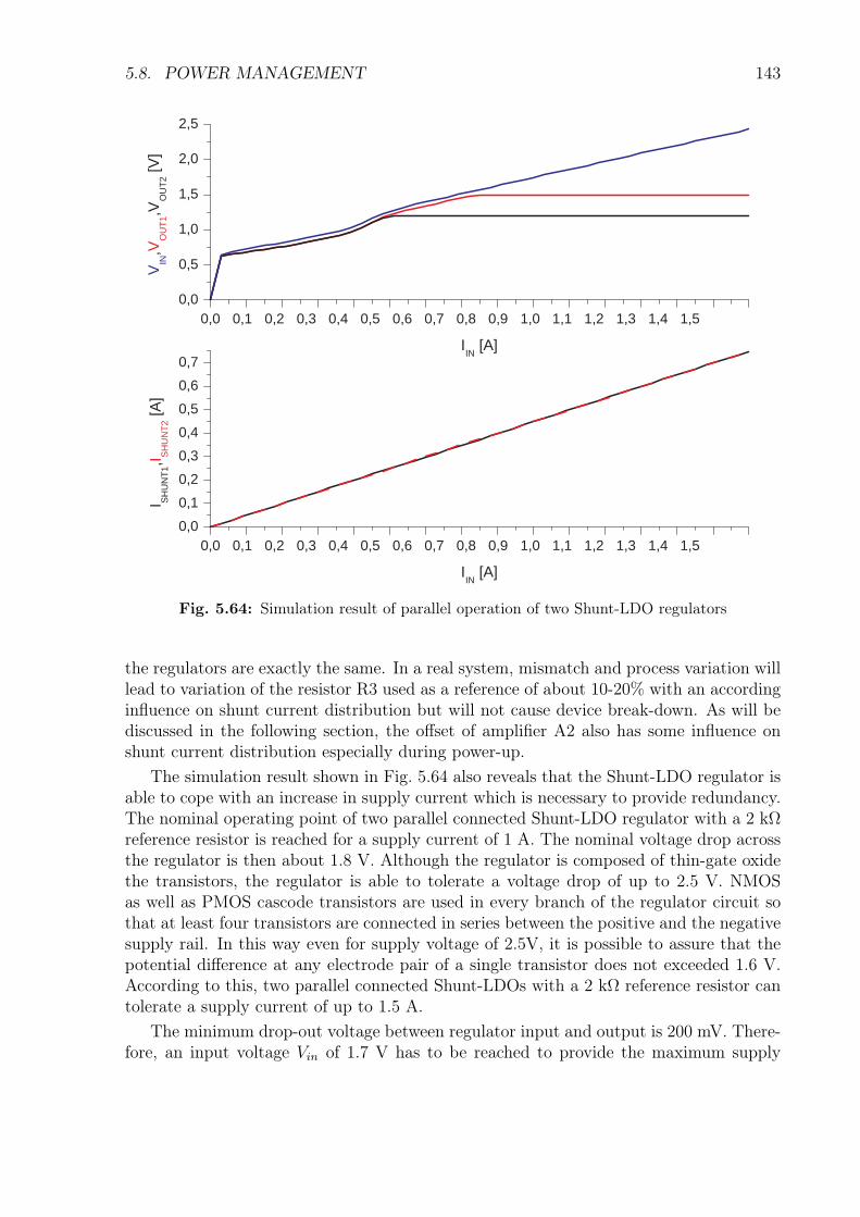
5.8. POWER MANAGEMENT 143
0,0 0,1 0,2 0,3 0,4 0,5 0,6 0,7 0,8 0,9 1,0 1,1 1,2 1,3 1,4 1,5 0,0
0,1
0,2
0,3
0,4
0,5
0,6
0,7
I SH
UN
T1 , I S
HU
NT
2 [A
]
I IN
[A]
0,0 0,1 0,2 0,3 0,4 0,5 0,6 0,7 0,8 0,9 1,0 1,1 1,2 1,3 1,4 1,5 0,0
0,5
1,0
1,5
2,0
2,5
V IN
, V O
UT
1 ,V O
UT
2 [V]
I IN
[A]
Fig. 5.64: Simulation result of parallel operation of two Shunt-LDO regulators
the regulators are exactly the same. In a real system, mismatch and process variation willlead to variation of the resistor R3 used as a reference of about 10-20% with an accordinginfluence on shunt current distribution but will not cause device break-down. As will bediscussed in the following section, the offset of amplifier A2 also has some influence onshunt current distribution especially during power-up.
The simulation result shown in Fig. 5.64 also reveals that the Shunt-LDO regulator isable to cope with an increase in supply current which is necessary to provide redundancy.The nominal operating point of two parallel connected Shunt-LDO regulator with a 2 kΩreference resistor is reached for a supply current of 1 A. The nominal voltage drop acrossthe regulator is then about 1.8 V. Although the regulator is composed of thin-gate oxidethe transistors, the regulator is able to tolerate a voltage drop of up to 2.5 V. NMOSas well as PMOS cascode transistors are used in every branch of the regulator circuit sothat at least four transistors are connected in series between the positive and the negativesupply rail. In this way even for supply voltage of 2.5V, it is possible to assure that thepotential difference at any electrode pair of a single transistor does not exceeded 1.6 V.According to this, two parallel connected Shunt-LDOs with a 2 kΩ reference resistor cantolerate a supply current of up to 1.5 A.
The minimum drop-out voltage between regulator input and output is 200 mV. There-fore, an input voltage Vin of 1.7 V has to be reached to provide the maximum supply
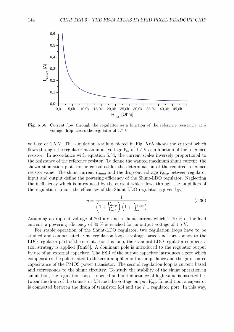
144 CHAPTER 5. THE FE-I4 ATLAS HYBRID PIXEL READOUT CHIP
0,0 5,0k 10,0k 15,0k 20,0k 25,0k 30,0k 35,0k 40,0k 45,0k 0,0
0,1
0,2
0,3
0,4
0,5
0,6
I SH
UN
T [A
]
R REF
[Ohm]
Fig. 5.65: Current flow through the regulaltor as a function of the reference resistance at avoltage drop across the regulator of 1.7 V
voltage of 1.5 V. The simulation result depicted in Fig. 5.65 shows the current whichflows through the regulator at an input voltage Vin of 1.7 V as a function of the referenceresistor. In accordance with equation 5.34, the current scales inversely proportional tothe resistance of the reference resistor. To define the wanted maximum shunt current, theshown simulation plot can be consulted for the determination of the required referenceresistor value. The shunt current Ishunt and the drop-out voltage Vdrop between regulatorinput and output define the powering efficiency of the Shunt-LDO regulator. Neglectingthe inefficiency which is introduced by the current which flows through the amplifiers ofthe regulation circuit, the efficiency of the Shunt-LDO regulator is given by:
η =1(
1 +Vdrop
Vout
)(1 + Ishunt
Iload
) (5.36)
Assuming a drop-out voltage of 200 mV and a shunt current which is 10 % of the loadcurrent, a powering efficiency of 80 % is reached for an output voltage of 1.5 V.
For stable operation of the Shunt-LDO regulator, two regulation loops have to bestudied and compensated. One regulation loop is voltage based and corresponds to theLDO regulator part of the circuit. For this loop, the standard LDO regulator compensa-tion strategy is applied [Rin98]. A dominant pole is introduced to the regulator outputby use of an external capacitor. The ESR of the output capacitor introduces a zero whichcompensates the pole related to the error amplifier output impedance and the gate-sourcecapacitance of the PMOS power transistor. The second regulation loop is current basedand corresponds to the shunt circuitry. To study the stability of the shunt operation insimulation, the regulation loop is opened and an inductance of high value is inserted be-tween the drain of the transistor M4 and the voltage output Vout. In addition, a capacitoris connected between the drain of transistor M4 and the Iout regulator port. In this way,
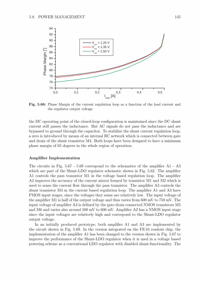
5.8. POWER MANAGEMENT 145
0,0 0,1 0,2 0,3 0,4 0,5 74
76
78
80
82
84
86
88
90
92
94
V out
= 1.20 V V
out = 1.35 V
V out
= 1.50 V
Pha
se M
argi
n [˚
]
I load
[A]
Fig. 5.66: Phase Margin of the current regulation loop as a function of the load current andthe regulator output voltage
the DC operating point of the closed-loop configuration is maintained since the DC shuntcurrent still passes the inductance. But AC signals do not pass the inductance and arebypassed to ground through the capacitor. To stabilize the shunt current regulation loop,a zero is introduced by means of an internal RC network which is connected between gateand drain of the shunt transistor M4. Both loops have been designed to have a minimumphase margin of 65 degrees in the whole region of operation.
Amplifier Implementation
The circuits in Fig. 5.67 - 5.69 correspond to the schematics of the amplifier A1 - A3which are part of the Shunt-LDO regulator schematic shown in Fig. 5.62. The amplifierA1 controls the pass transistor M1 in the voltage based regulation loop. The amplifierA2 improves the accuracy of the current mirror formed by transistor M1 and M2 which isused to sense the current flow through the pass transistor. The amplifier A3 controls theshunt transistor M4 in the current based regulation loop. The amplifier A1 and A3 havePMOS input stages, since the voltages they sense are relatively low. The input voltage ofthe amplifier M1 is half of the output voltage and thus varies from 600 mV to 750 mV. Theinput voltage of amplifier A3 is defined by the gate-drain connected NMOS transistors M5and M6 and varies also around 500 mV to 600 mV. Amplifier A2 has a NMOS input stagesince the input voltages are relatively high and correspond to the Shunt-LDO regulatoroutput voltage.
In an initially produced prototype, both amplifier A1 and A3 are implemented bythe circuit shown in Fig. 5.69. In the version integrated on the FE-I4 readout chip, theimplementation of the amplifier A1 has been changed to the version shown in Fig. 5.67 toimprove the performance of the Shunt-LDO regulator when it is used in a voltage basedpowering scheme as a conventional LDO regulator with disabled shunt-functionality. The
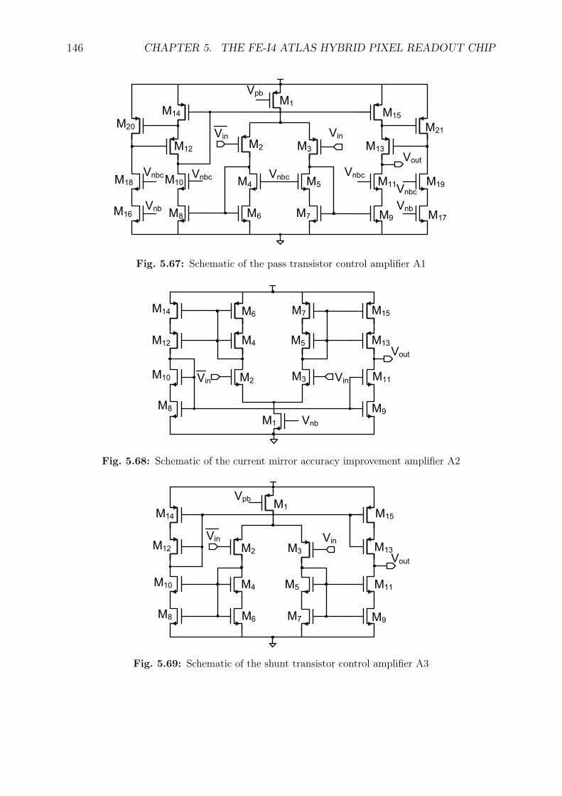
146 CHAPTER 5. THE FE-I4 ATLAS HYBRID PIXEL READOUT CHIP
M2 M3
M8
Vpb
M9
M10 M11
M12 M13
M14 M15
M16
M1
M4 M5
M6 M7
VnbcVnbcVnbc Vnbc
Vnbc
Vnb VnbM17
M18 M19
M20 M21Vin Vin
Vout
Fig. 5.67: Schematic of the pass transistor control amplifier A1
Vin Vin
VnbM1
M2M3
M4 M5
M7M6
M9M8
M11M10
M12 M13
M15M14
Vout
Fig. 5.68: Schematic of the current mirror accuracy improvement amplifier A2
M1
M2 M3
M4 M5
M7
Vpb
M9
M11
M12 M13
M10
Vin Vin
Vout
M8
M15M14
M6
Fig. 5.69: Schematic of the shunt transistor control amplifier A3
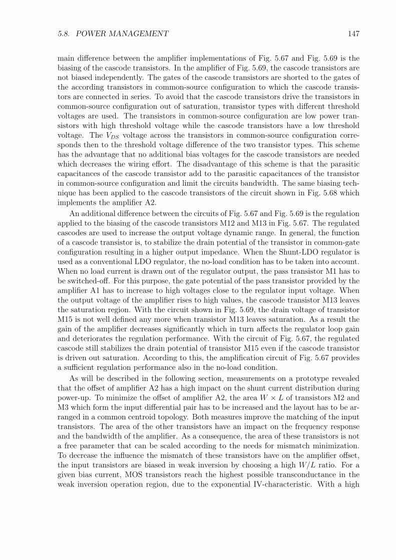
5.8. POWER MANAGEMENT 147
main difference between the amplifier implementations of Fig. 5.67 and Fig. 5.69 is thebiasing of the cascode transistors. In the amplifier of Fig. 5.69, the cascode transistors arenot biased independently. The gates of the cascode transistors are shorted to the gates ofthe according transistors in common-source configuration to which the cascode transis-tors are connected in series. To avoid that the cascode transistors drive the transistors incommon-source configuration out of saturation, transistor types with different thresholdvoltages are used. The transistors in common-source configuration are low power tran-sistors with high threshold voltage while the cascode transistors have a low thresholdvoltage. The VDS voltage across the transistors in common-source configuration corre-sponds then to the threshold voltage difference of the two transistor types. This schemehas the advantage that no additional bias voltages for the cascode transistors are neededwhich decreases the wiring effort. The disadvantage of this scheme is that the parasiticcapacitances of the cascode transistor add to the parasitic capacitances of the transistorin common-source configuration and limit the circuits bandwidth. The same biasing tech-nique has been applied to the cascode transistors of the circuit shown in Fig. 5.68 whichimplements the amplifier A2.
An additional difference between the circuits of Fig. 5.67 and Fig. 5.69 is the regulationapplied to the biasing of the cascode transistors M12 and M13 in Fig. 5.67. The regulatedcascodes are used to increase the output voltage dynamic range. In general, the functionof a cascode transistor is, to stabilize the drain potential of the transistor in common-gateconfiguration resulting in a higher output impedance. When the Shunt-LDO regulator isused as a conventional LDO regulator, the no-load condition has to be taken into account.When no load current is drawn out of the regulator output, the pass transistor M1 has tobe switched-off. For this purpose, the gate potential of the pass transistor provided by theamplifier A1 has to increase to high voltages close to the regulator input voltage. Whenthe output voltage of the amplifier rises to high values, the cascode transistor M13 leavesthe saturation region. With the circuit shown in Fig. 5.69, the drain voltage of transistorM15 is not well defined any more when transistor M13 leaves saturation. As a result thegain of the amplifier decreases significantly which in turn affects the regulator loop gainand deteriorates the regulation performance. With the circuit of Fig. 5.67, the regulatedcascode still stabilizes the drain potential of transistor M15 even if the cascode transistoris driven out saturation. According to this, the amplification circuit of Fig. 5.67 providesa sufficient regulation performance also in the no-load condition.
As will be described in the following section, measurements on a prototype revealedthat the offset of amplifier A2 has a high impact on the shunt current distribution duringpower-up. To minimize the offset of amplifier A2, the area W × L of transistors M2 andM3 which form the input differential pair has to be increased and the layout has to be ar-ranged in a common centroid topology. Both measures improve the matching of the inputtransistors. The area of the other transistors have an impact on the frequency responseand the bandwidth of the amplifier. As a consequence, the area of these transistors is nota free parameter that can be scaled according to the needs for mismatch minimization.To decrease the influence the mismatch of these transistors have on the amplifier offset,the input transistors are biased in weak inversion by choosing a high W/L ratio. For agiven bias current, MOS transistors reach the highest possible transconductance in theweak inversion operation region, due to the exponential IV-characteristic. With a high
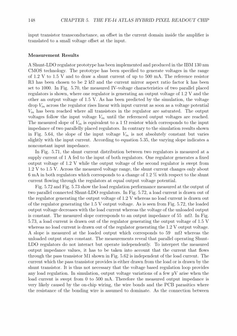
148 CHAPTER 5. THE FE-I4 ATLAS HYBRID PIXEL READOUT CHIP
input transistor transconductance, an offset in the current domain inside the amplifier istranslated to a small voltage offset at the input.
Measurement Results
A Shunt-LDO regulator prototype has been implemented and produced in the IBM 130 nmCMOS technology. The prototype has been specified to generate voltages in the rangeof 1.2 V to 1.5 V and to draw a shunt current of up to 500 mA. The reference resistorR3 has been chosen to be 2 kΩ and the current mirror aspect ratio factor k has beenset to 1000. In Fig. 5.70, the measured IV-voltage characteristics of two parallel placedregulators is shown, where one regulator is generating an output voltage of 1.2 V and theother an output voltage of 1.5 V. As has been predicted by the simulation, the voltagedrop Vin across the regulator rises linear with input current as soon as a voltage potentialVin has been reached where all transistors in the regulator are saturated. The outputvoltages follow the input voltage Vin until the referenced output voltages are reached.The measured slope of Vin is equivalent to a 1 Ω resistor which corresponds to the inputimpedance of two parallelly placed regulators. In contrary to the simulation results shownin Fig. 5.64, the slope of the input voltage Vin is not absolutely constant but variesslightly with the input current. According to equation 5.35, the varying slope indicates anonconstant input impedance.
In Fig. 5.71, the shunt current distribution between two regulators is measured at asupply current of 1 A fed to the input of both regulators. One regulator generates a fixedoutput voltage of 1.2 V while the output voltage of the second regulator is swept from1.2 V to 1.5 V. Across the measured voltage range, the shunt current changes only about6 mA in both regulators which corresponds to a change of 1.2 % with respect to the shuntcurrent flowing through the regulators at equal output voltage potential.
Fig. 5.72 and Fig. 5.73 show the load regulation performance measured at the output oftwo parallel connected Shunt-LDO regulators. In Fig. 5.72, a load current is drawn out ofthe regulator generating the output voltage of 1.2 V whereas no load current is drawn outof the regulator generating the 1.5 V output voltage. As is seen from Fig. 5.72, the loadedoutput voltage decreases with the load current whereas the voltage of the unloaded outputis constant. The measured slope corresponds to an output impedance of 55 mΩ. In Fig.5.73, a load current is drawn out of the regulator generating the output voltage of 1.5 Vwhereas no load current is drawn out of the regulator generating the 1.2 V output voltage.A slope is measured at the loaded output which corresponds to 59 mΩ whereas theunloaded output stays constant. The measurements reveal that parallel operating Shunt-LDO regulators do not interact but operate independently. To interpret the measuredoutput impedance values, it has to be taken into account that the current that flowsthrough the pass transistor M1 shown in Fig. 5.62 is independent of the load current. Thecurrent which the pass transistor provides is either drawn from the load or is drawn by theshunt transistor. It is thus not necessary that the voltage based regulation loop providesany load regulation. In simulation, output voltage variations of a few µV arise when theload current is swept from 0 to 500 mA. Therefore the measured output impedance isvery likely caused by the on-chip wiring, the wire bonds and the PCB parasitics wherethe resistance of the bonding wire is assumed to dominate. As the connection between
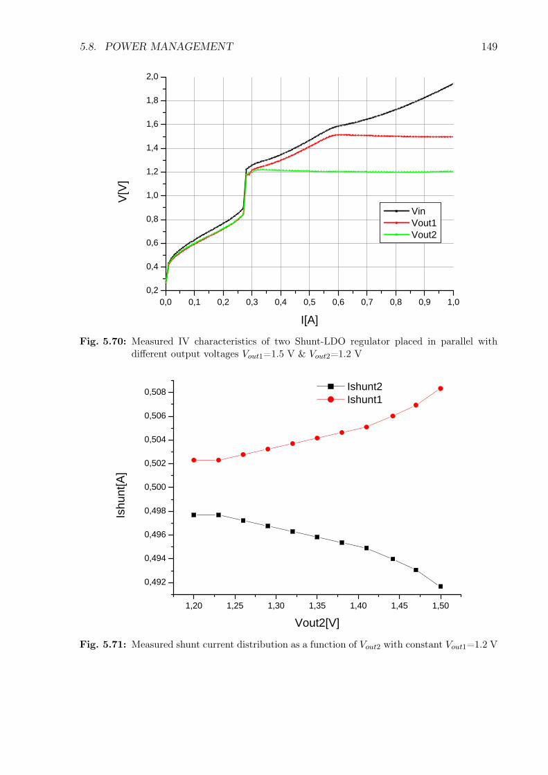
5.8. POWER MANAGEMENT 149
0,0 0,1 0,2 0,3 0,4 0,5 0,6 0,7 0,8 0,9 1,00,2
0,4
0,6
0,8
1,0
1,2
1,4
1,6
1,8
2,0
Vin Vout1 Vout2
V[V
]
I[A]
Fig. 5.70: Measured IV characteristics of two Shunt-LDO regulator placed in parallel withdifferent output voltages Vout1=1.5 V & Vout2=1.2 V
1,20 1,25 1,30 1,35 1,40 1,45 1,50
0,492
0,494
0,496
0,498
0,500
0,502
0,504
0,506
0,508 Ishunt2 Ishunt1
Ishu
nt[A
]
Vout2[V]
Fig. 5.71: Measured shunt current distribution as a function of Vout2 with constant Vout1=1.2 V
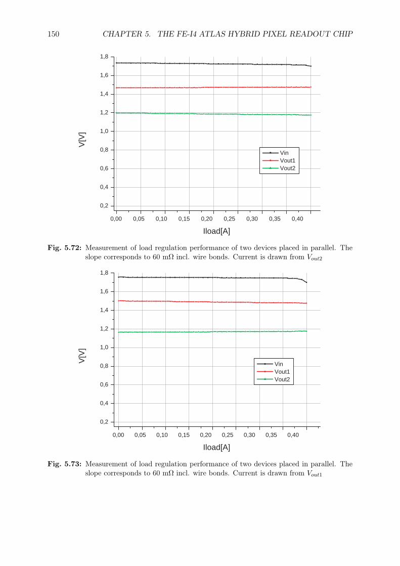
150 CHAPTER 5. THE FE-I4 ATLAS HYBRID PIXEL READOUT CHIP
0,00 0,05 0,10 0,15 0,20 0,25 0,30 0,35 0,40
0,2
0,4
0,6
0,8
1,0
1,2
1,4
1,6
1,8
Vin Vout1 Vout2
V[V
]
Iload[A]
Fig. 5.72: Measurement of load regulation performance of two devices placed in parallel. Theslope corresponds to 60 mΩ incl. wire bonds. Current is drawn from Vout2
0,00 0,05 0,10 0,15 0,20 0,25 0,30 0,35 0,40
0,2
0,4
0,6
0,8
1,0
1,2
1,4
1,6
1,8
Vin Vout1 Vout2
V[V
]
Iload[A]
Fig. 5.73: Measurement of load regulation performance of two devices placed in parallel. Theslope corresponds to 60 mΩ incl. wire bonds. Current is drawn from Vout1
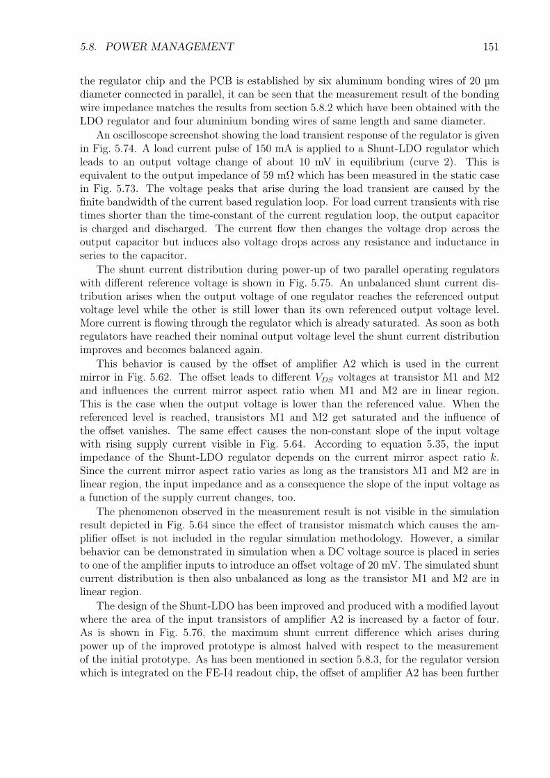
5.8. POWER MANAGEMENT 151
the regulator chip and the PCB is established by six aluminum bonding wires of 20 µmdiameter connected in parallel, it can be seen that the measurement result of the bondingwire impedance matches the results from section 5.8.2 which have been obtained with theLDO regulator and four aluminium bonding wires of same length and same diameter.
An oscilloscope screenshot showing the load transient response of the regulator is givenin Fig. 5.74. A load current pulse of 150 mA is applied to a Shunt-LDO regulator whichleads to an output voltage change of about 10 mV in equilibrium (curve 2). This isequivalent to the output impedance of 59 mΩ which has been measured in the static casein Fig. 5.73. The voltage peaks that arise during the load transient are caused by thefinite bandwidth of the current based regulation loop. For load current transients with risetimes shorter than the time-constant of the current regulation loop, the output capacitoris charged and discharged. The current flow then changes the voltage drop across theoutput capacitor but induces also voltage drops across any resistance and inductance inseries to the capacitor.
The shunt current distribution during power-up of two parallel operating regulatorswith different reference voltage is shown in Fig. 5.75. An unbalanced shunt current dis-tribution arises when the output voltage of one regulator reaches the referenced outputvoltage level while the other is still lower than its own referenced output voltage level.More current is flowing through the regulator which is already saturated. As soon as bothregulators have reached their nominal output voltage level the shunt current distributionimproves and becomes balanced again.
This behavior is caused by the offset of amplifier A2 which is used in the currentmirror in Fig. 5.62. The offset leads to different VDS voltages at transistor M1 and M2and influences the current mirror aspect ratio when M1 and M2 are in linear region.This is the case when the output voltage is lower than the referenced value. When thereferenced level is reached, transistors M1 and M2 get saturated and the influence ofthe offset vanishes. The same effect causes the non-constant slope of the input voltagewith rising supply current visible in Fig. 5.64. According to equation 5.35, the inputimpedance of the Shunt-LDO regulator depends on the current mirror aspect ratio k.Since the current mirror aspect ratio varies as long as the transistors M1 and M2 are inlinear region, the input impedance and as a consequence the slope of the input voltage asa function of the supply current changes, too.
The phenomenon observed in the measurement result is not visible in the simulationresult depicted in Fig. 5.64 since the effect of transistor mismatch which causes the am-plifier offset is not included in the regular simulation methodology. However, a similarbehavior can be demonstrated in simulation when a DC voltage source is placed in seriesto one of the amplifier inputs to introduce an offset voltage of 20 mV. The simulated shuntcurrent distribution is then also unbalanced as long as the transistor M1 and M2 are inlinear region.
The design of the Shunt-LDO has been improved and produced with a modified layoutwhere the area of the input transistors of amplifier A2 is increased by a factor of four.As is shown in Fig. 5.76, the maximum shunt current difference which arises duringpower up of the improved prototype is almost halved with respect to the measurementof the initial prototype. As has been mentioned in section 5.8.3, for the regulator versionwhich is integrated on the FE-I4 readout chip, the offset of amplifier A2 has been further
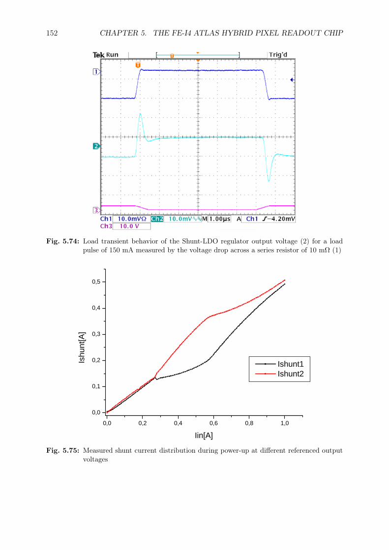
152 CHAPTER 5. THE FE-I4 ATLAS HYBRID PIXEL READOUT CHIP
Fig. 5.74: Load transient behavior of the Shunt-LDO regulator output voltage (2) for a loadpulse of 150 mA measured by the voltage drop across a series resistor of 10 mΩ (1)
0,0 0,2 0,4 0,6 0,8 1,0
0,0
0,1
0,2
0,3
0,4
0,5
Ishunt1 Ishunt2
Ishu
nt[A
]
Iin[A]
Fig. 5.75: Measured shunt current distribution during power-up at different referenced outputvoltages
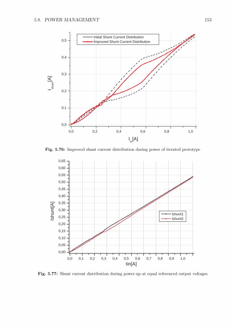
5.8. POWER MANAGEMENT 153
0,0 0,2 0,4 0,6 0,8 1,0
0,0
0,1
0,2
0,3
0,4
0,5 Initial Shunt Current Distribution Ímproved Shunt Current Distribution
I shun
t [A]
I in [A]
Fig. 5.76: Improved shunt current distribution during power of iterated prototype
0,0 0,1 0,2 0,3 0,4 0,5 0,6 0,7 0,8 0,9 1,0
0,00
0,05
0,10
0,15
0,20
0,25
0,30
0,35
0,40
0,45
0,50
0,55
0,60
0,65
Ishunt1 Ishunt2 Is
hunt
[A]
Iin[A]
Fig. 5.77: Shunt current distribution during power-up at equal referenced output voltages
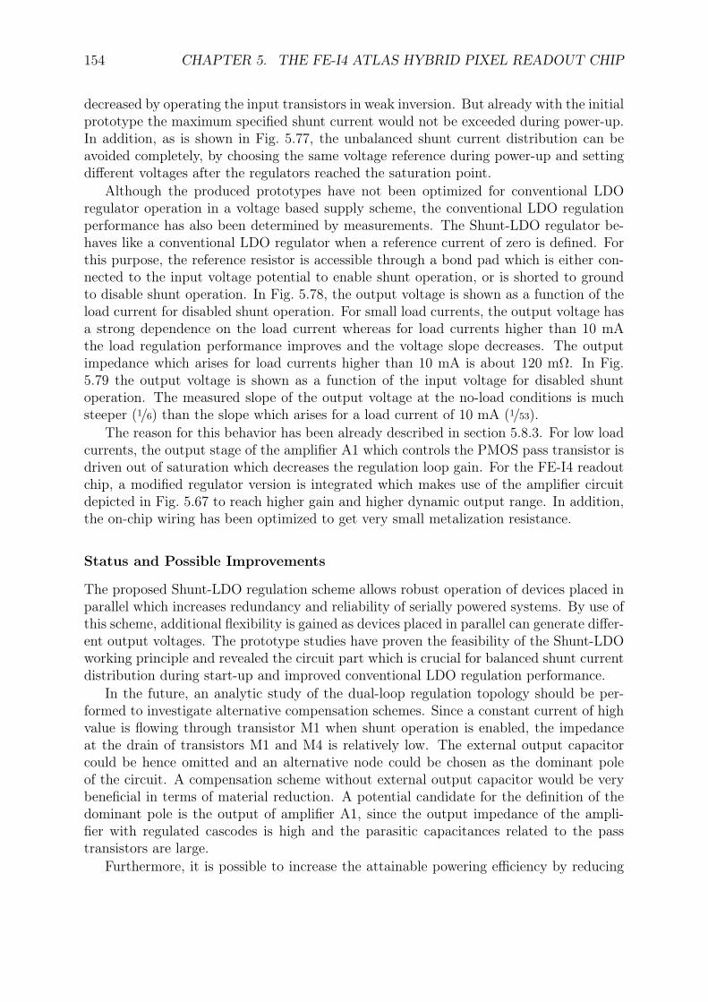
154 CHAPTER 5. THE FE-I4 ATLAS HYBRID PIXEL READOUT CHIP
decreased by operating the input transistors in weak inversion. But already with the initialprototype the maximum specified shunt current would not be exceeded during power-up.In addition, as is shown in Fig. 5.77, the unbalanced shunt current distribution can beavoided completely, by choosing the same voltage reference during power-up and settingdifferent voltages after the regulators reached the saturation point.
Although the produced prototypes have not been optimized for conventional LDOregulator operation in a voltage based supply scheme, the conventional LDO regulationperformance has also been determined by measurements. The Shunt-LDO regulator be-haves like a conventional LDO regulator when a reference current of zero is defined. Forthis purpose, the reference resistor is accessible through a bond pad which is either con-nected to the input voltage potential to enable shunt operation, or is shorted to groundto disable shunt operation. In Fig. 5.78, the output voltage is shown as a function of theload current for disabled shunt operation. For small load currents, the output voltage hasa strong dependence on the load current whereas for load currents higher than 10 mAthe load regulation performance improves and the voltage slope decreases. The outputimpedance which arises for load currents higher than 10 mA is about 120 mΩ. In Fig.5.79 the output voltage is shown as a function of the input voltage for disabled shuntoperation. The measured slope of the output voltage at the no-load conditions is muchsteeper (1/6) than the slope which arises for a load current of 10 mA (1/53).
The reason for this behavior has been already described in section 5.8.3. For low loadcurrents, the output stage of the amplifier A1 which controls the PMOS pass transistor isdriven out of saturation which decreases the regulation loop gain. For the FE-I4 readoutchip, a modified regulator version is integrated which makes use of the amplifier circuitdepicted in Fig. 5.67 to reach higher gain and higher dynamic output range. In addition,the on-chip wiring has been optimized to get very small metalization resistance.
Status and Possible Improvements
The proposed Shunt-LDO regulation scheme allows robust operation of devices placed inparallel which increases redundancy and reliability of serially powered systems. By use ofthis scheme, additional flexibility is gained as devices placed in parallel can generate differ-ent output voltages. The prototype studies have proven the feasibility of the Shunt-LDOworking principle and revealed the circuit part which is crucial for balanced shunt currentdistribution during start-up and improved conventional LDO regulation performance.
In the future, an analytic study of the dual-loop regulation topology should be per-formed to investigate alternative compensation schemes. Since a constant current of highvalue is flowing through transistor M1 when shunt operation is enabled, the impedanceat the drain of transistors M1 and M4 is relatively low. The external output capacitorcould be hence omitted and an alternative node could be chosen as the dominant poleof the circuit. A compensation scheme without external output capacitor would be verybeneficial in terms of material reduction. A potential candidate for the definition of thedominant pole is the output of amplifier A1, since the output impedance of the ampli-fier with regulated cascodes is high and the parasitic capacitances related to the passtransistors are large.
Furthermore, it is possible to increase the attainable powering efficiency by reducing
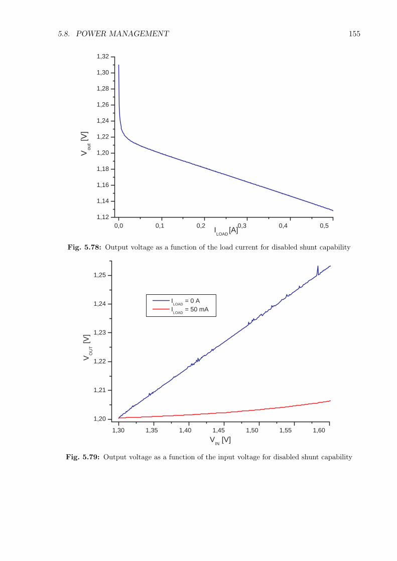
5.8. POWER MANAGEMENT 155
0,0 0,1 0,2 0,3 0,4 0,5 1,12
1,14
1,16
1,18
1,20
1,22
1,24
1,26
1,28
1,30
1,32
V ou
t [V]
I LOAD
[A]
Fig. 5.78: Output voltage as a function of the load current for disabled shunt capability
1,30 1,35 1,40 1,45 1,50 1,55 1,60
1,20
1,21
1,22
1,23
1,24
1,25
I LOAD
= 0 A I
LOAD = 50 mA
V O
UT
[V]
V IN
[V]
Fig. 5.79: Output voltage as a function of the input voltage for disabled shunt capability
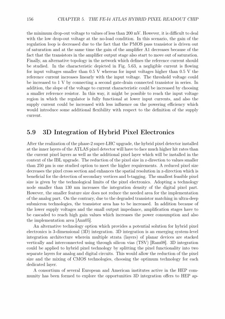
156 CHAPTER 5. THE FE-I4 ATLAS HYBRID PIXEL READOUT CHIP
the minimum drop-out voltage to values of less than 200 mV. However, it is difficult to dealwith the low drop-out voltage at the no-load condition. In this scenario, the gain of theregulation loop is decreased due to the fact that the PMOS pass transistor is driven outof saturation and at the same time the gain of the amplifier A1 decreases because of thefact that the transistors in the amplifier output stage also start to move out of saturation.Finally, an alternative topology in the network which defines the reference current shouldbe studied. In the characteristic depicted in Fig. 5.63, a negligible current is flowingfor input voltages smaller than 0.5 V whereas for input voltages higher than 0.5 V thereference current increases linearly with the input voltage. The threshold voltage couldbe increased to 1 V by connecting a second gate-drain connected transistor in series. Inaddition, the slope of the voltage to current characteristic could be increased by choosinga smaller reference resistor. In this way, it might be possible to reach the input voltageregion in which the regulator is fully functional at lower input currents, and also thesupply current could be increased with less influence on the powering efficiency whichwould introduce some additional flexibility with respect to the definition of the supplycurrent.
5.9 3D Integration of Hybrid Pixel Electronics
After the realization of the phase-2 super-LHC upgrade, the hybrid pixel detector installedat the inner layers of the ATLAS pixel detector will have to face much higher hit rates thanthe current pixel layers as well as the additional pixel layer which will be installed in thecontext of the IBL upgrade. The reduction of the pixel size in z-direction to values smallerthan 250 µm is one studied option to meet the higher requirements. A reduced pixel sizedecreases the pixel cross section and enhances the spatial resolution in z-direction which isbeneficial for the detection of secondary vertices and b-tagging. The smallest feasible pixelsize is given by the technological limits of the pixel electronics. Adopting a technologynode smaller than 130 nm increases the integration density of the digital pixel part.However, the smaller feature size does not reduce the needed area for the implementationof the analog part. On the contrary, due to the degraded transistor matching in ultra-deepsubmicron technologies, the transistor area has to be increased. In addition because ofthe lower supply voltages and the small output impedance, amplification stages have tobe cascaded to reach high gain values which increases the power consumption and alsothe implementation area [Ann05].
An alternative technology option which provides a potential solution for hybrid pixelelectronics is 3-dimensional (3D) integration. 3D integration is an emerging system-levelintegration architecture wherein multiple strata (layers) of planar devices are stackedvertically and interconnected using through silicon vias (TSV) [Ram08]. 3D integrationcould be applied to hybrid pixel technology by splitting the pixel functionality into twoseparate layers for analog and digital circuits. This would allow the reduction of the pixelsize and the mixing of CMOS technologies, choosing the optimum technology for eachdedicated layer.
A consortium of several European and American institutes active in the HEP com-munity has been formed to explore the opportunities 3D integration offers to HEP ap-
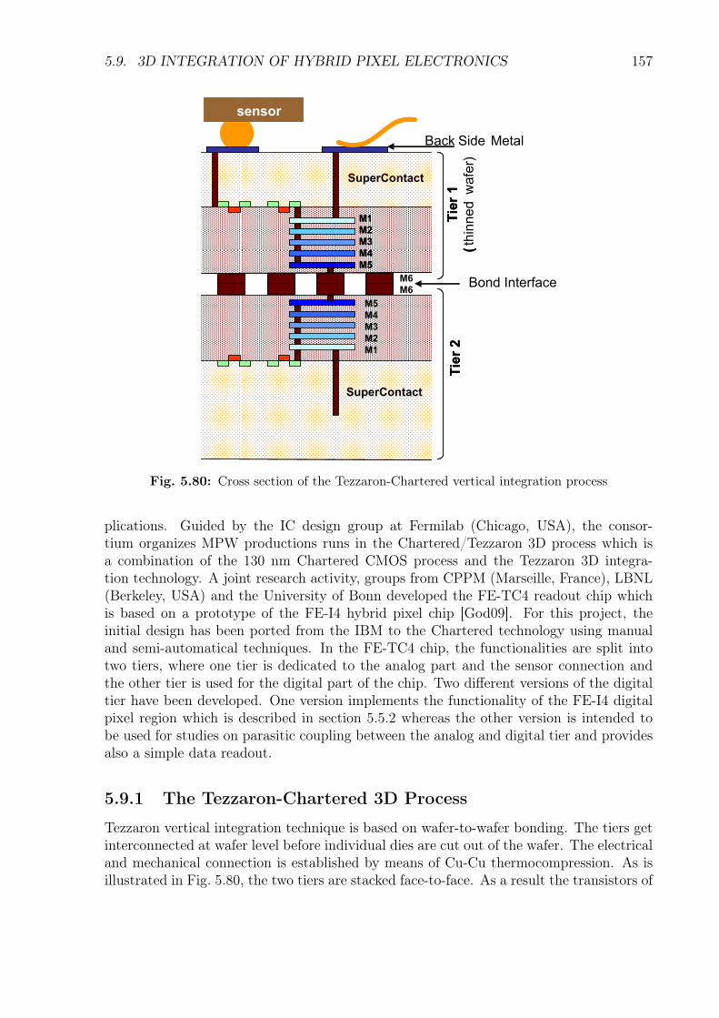
5.9. 3D INTEGRATION OF HYBRID PIXEL ELECTRONICS 157
M5
M4
M3
M2
M1
M6
SuperContact
M1
M2
M3
M4
M5
M6
SuperContact
Bond Interface
Tier2
Tier1
(thinnedwafer)
Back Side Metal
sensor
M5
M4
M3
M2
M1
SuperContact
M1
M2
M3
M4
M5
SuperContact
Tier2
Tier1
(
sensor
Fig. 5.80: Cross section of the Tezzaron-Chartered vertical integration process
plications. Guided by the IC design group at Fermilab (Chicago, USA), the consor-tium organizes MPW productions runs in the Chartered/Tezzaron 3D process which isa combination of the 130 nm Chartered CMOS process and the Tezzaron 3D integra-tion technology. A joint research activity, groups from CPPM (Marseille, France), LBNL(Berkeley, USA) and the University of Bonn developed the FE-TC4 readout chip whichis based on a prototype of the FE-I4 hybrid pixel chip [God09]. For this project, theinitial design has been ported from the IBM to the Chartered technology using manualand semi-automatical techniques. In the FE-TC4 chip, the functionalities are split intotwo tiers, where one tier is dedicated to the analog part and the sensor connection andthe other tier is used for the digital part of the chip. Two different versions of the digitaltier have been developed. One version implements the functionality of the FE-I4 digitalpixel region which is described in section 5.5.2 whereas the other version is intended tobe used for studies on parasitic coupling between the analog and digital tier and providesalso a simple data readout.
5.9.1 The Tezzaron-Chartered 3D Process
Tezzaron vertical integration technique is based on wafer-to-wafer bonding. The tiers getinterconnected at wafer level before individual dies are cut out of the wafer. The electricaland mechanical connection is established by means of Cu-Cu thermocompression. As isillustrated in Fig. 5.80, the two tiers are stacked face-to-face. As a result the transistors of
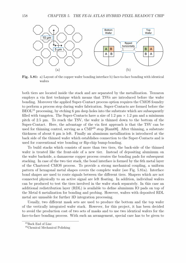
158 CHAPTER 5. THE FE-I4 ATLAS HYBRID PIXEL READOUT CHIP
10 µm
5 µm
(a)
A
A B
A
A
B
B
flipped
horizontally
Bottom
Wafer
Top
Wafer
B
(b)
Fig. 5.81: a) Layout of the copper wafer bonding interface b) face-to-face bonding with identicalwafers
both tiers are located inside the stack and are separated by the metallization. Tezzaronemploys a via first technique which means that TSVs are introduced before the waferbonding. Moreover the applied Super-Contact process option requires the CMOS foundryto perform a process step during wafer fabrication. Super-Contacts are formed before theBEOL15 processing, by etching 6 µm deep holes into the substrate which are subsequentlyfilled with tungsten. The Super-Contacts have a size of 1.2 µm × 1.2 µm and a minimumpitch of 2.5 µm. To reach the TSV, the wafer is thinned down to the bottom of theSuper-Contact. Here, the advantage of the via first approach is that the TSV can beused for thinning control, serving as a CMP16 stop [Ram08]. After thinning, a substratethickness of about 6 µm is left. Finally an aluminum metallization is introduced at theback side of the thinned wafer which establishes connection to the Super-Contacts and isused for conventional wire bonding or flip-chip bump-bonding.
To build stacks which consists of more than two tiers, the back-side of the thinnedwafer is treated like the front-side of a new tier. Instead of depositing aluminum onthe wafer backside, a damascene copper process creates the bonding pads for subsequentstacking. In case of the two tier stack, the bond interface is formed by the 6th metal layerof the Chartered CMOS process. To provide a strong mechanical coupling, a uniformpattern of hexagonal metal shapes covers the complete wafer (see Fig. 5.81a). Interfacebond shapes are used to route signals between the different tiers. Shapers which are notconnected physically to an active signal are left floating. In addition, individual waferscan be produced to test the tiers involved in the wafer stack separately. In this case anadditional redistribution layer (RDL) is available to define aluminum IO pads on top ofthe Metal 6 metalization for bonding and probing. However, wafers with deposited RDLmetal are unusable for further 3D integration processing.
Usually, two different mask sets are used to produce the bottom and the top waferof the vertically integrated wafer stack. However, for this project, it has been decidedto avoid the production cost of two sets of masks and to use two identical wafers for theface-to-face bonding process. With such an arrangement, special care has to be given to
15Back End of Line16Chemical Mechanical Polishing
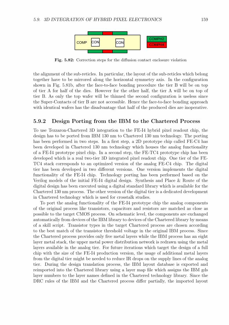
5.9. 3D INTEGRATION OF HYBRID PIXEL ELECTRONICS 159
COMP CONCONCOMPH2
COMPH4
Fig. 5.82: Correction steps for the diffusion contact enclosure violation
the alignment of the sub-reticles. In particular, the layout of the sub-reticles which belongtogether have to be mirrored along the horizontal symmetry axis. In the configurationshown in Fig. 5.81b, after the face-to-face bonding procedure the tier B will be on topof tier A for half of the dies. However for the other half, the tier A will be on top oftier B. As only the top wafer will be thinned the second configuration is useless sincethe Super-Contacts of tier B are not accessible. Hence the face-to-face bonding approachwith identical wafers has the disadvantage that half of the produced dies are inoperative.
5.9.2 Design Porting from the IBM to the Chartered Process
To use Tezzaron-Chartered 3D integration to the FE-I4 hybrid pixel readout chip, thedesign has to be ported from IBM 130 nm to Chartered 130 nm technology. The portinghas been performed in two steps. In a first step, a 2D prototype chip called FE-C4 hasbeen developed in Chartered 130 nm technology which houses the analog functionalityof a FE-I4 prototype pixel chip. In a second step, the FE-TC4 prototype chip has beendeveloped which is a real two-tier 3D integrated pixel readout chip. One tier of the FE-TC4 stack corresponds to an optimized version of the analog FE-C4 chip. The digitaltier has been developed in two different versions. One version implements the digitalfunctionality of the FE-I4 chip. Technology porting has been performed based on theVerilog models of the initial FE-I4 digital design. Synthesis and Place & Route of thedigital design has been executed using a digital standard library which is available for theChartered 130 nm process. The other version of the digital tier is a dedicated developmentin Chartered technology which is used for crosstalk studies.
To port the analog functionality of the FE-I4 prototype chip the analog componentsof the original process like transistors, capacitors and resistors are matched as close aspossible to the target CMOS process. On schematic level, the components are exchangedautomatically from devices of the IBM library to devices of the Chartered library by meansof a skill script. Transistor types in the target Chartered process are chosen accordingto the best match of the transistor threshold voltage in the original IBM process. Sincethe Chartered process provides only five metal layers while the IBM process has an eightlayer metal stack, the upper metal power distribution network is redrawn using the metallayers available in the analog tier. For future iterations which target the design of a fullchip with the size of the FE-I4 production version, the usage of additional metal layersfrom the digital tier might be needed to reduce IR drops on the supply lines of the analogtier. During the design translation process, the IBM layout database is exported andreimported into the Chartered library using a layer map file which assigns the IBM gdslayer numbers to the layer names defined in the Chartered technology library. Since theDRC rules of the IBM and the Chartered process differ partially, the imported layout
160 CHAPTER 5. THE FE-I4 ATLAS HYBRID PIXEL READOUT CHIP
typically violates layout rules. Depending on the specific block, these DRC violations areeither fixed manually like in case of the analog pixel layout or semi automatically like incase of the circuits of the chip periphery such as DACs, biasing circuits and configurationregisters.
The semi-automatical correction is executed on gds file level before the layout is im-ported into the Chartered library using the layout manipulation capabilities which CalibreDRC offers. For example a wider enclosure of diffusion contacts is defined in the Char-tered process than in the IBM process. To remove this violation the following code isused with Calibre DRC:
COMPH1 = COMP and ContactCOMPH2 = SIZE COMPH1 BY 0.07COMPH3 = COMP or COMPH2COMPH4 = EXT COMPH3 < 0.21 OPPOSITE NOTCHCOMPH5 = DFM COPY COMPH4 REGIONCOMPH = COMPH3 or COMPH5
Listing 5.1: Calibre DRC commands for correction of the diffusion contact enclosure violation
The first command in listing 5.1 searches the layout for overlaps of diffusion (COMP)and contact shapes and assigns these structures to the layer definition COMPH1. Theshapes are then increased in size in all directions by a factor which is chosen according tothe Chartered enclosure rule and assigned to the layer definition COMPH2. The scaledlayout structures in COMPH2 are then merged to the initial diffusion shapes and assignedto the layer definition COMPH3. After the merging, rectangles like the ones which areshown in green in Fig. 5.82 are added to the initial diffusion layers. Depending on thecontact distance, it might happen that notches (red shapes in Fig. 5.82) arise after themerging which violate the diffusion spacing rules. Therefore a Calibre DRC command isused which searches for the respective notches and assigns them to the layer definitionCOMPH5. The notch shapes (red) defined in COMPH5 are then merged to COMPH3which contains the initial diffusion geometry (yellow) and the added (green) rectangles.In this way the notches are filled with diffusion and the notch violation as well as thediffusion contact enclosure violations are removed.
In the same way N-well and Poly contact enclosure violations are addressed, the miss-ing NPLUS layer which defines n-type diffusion regions is generated, and PPLUS diffusionoverlap and enclosure violations are corrected. In addition, since the via size and the min-imum via pitch defined in the IBM and the Chartered technology are incompatible, thelayout is scanned for via arrays and new vias with correct size and pitch are generatedin the corresponding layout regions. The remaining DRC violations are mainly spacingerrors which ask for a manual rearrangement of the layout and therefore cannot be fixedautomatically. However, the automatic layout preprocessing, reduces tremendously theamount of manual work which has to be performed.
5.9.3 Measurement Results
Measurements on the 2D chip FE-TC4 give results which are comparable to the FE-I4prototype counterpart. Across the pixel matrix of 14 columns and 61 pixels an (un-tuned)
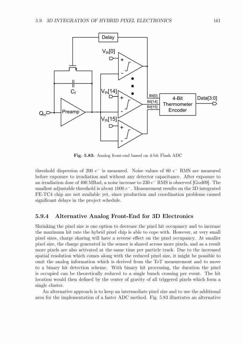
5.9. 3D INTEGRATION OF HYBRID PIXEL ELECTRONICS 161
Cf
PreampQin
+
-
+
-
+
-
4-Bit
Thermometer
Encoder
Vth[0]
Vth[14]
Vth[15]
Data[3:0]
Delay
Bit[0]
Bit[14]
Bit[15]
Fig. 5.83: Analog front-end based on 4-bit Flash ADC
threshold dispersion of 200 e− is measured. Noise values of 80 e− RMS are measuredbefore exposure to irradiation and without any detector capacitance. After exposure toan irradiation dose of 400 MRad, a noise increase to 230 e− RMS is observed [God09]. Thesmallest adjustable threshold is about 1000 e−. Measurement results on the 3D integratedFE-TC4 chip are not available yet, since production and coordination problems causedsignificant delays in the project schedule.
5.9.4 Alternative Analog Front-End for 3D Electronics
Shrinking the pixel size is one option to decrease the pixel hit occupancy and to increasethe maximum hit rate the hybrid pixel chip is able to cope with. However, at very smallpixel sizes, charge sharing will have a reverse effect on the pixel occupancy. At smallerpixel size, the charge generated in the sensor is shared across more pixels, and as a resultmore pixels are also activated at the same time per particle track. Due to the increasedspatial resolution which comes along with the reduced pixel size, it might be possible toomit the analog information which is derived from the ToT measurement and to moveto a binary hit detection scheme. With binary hit processing, the duration the pixelis occupied can be theoretically reduced to a single bunch crossing per event. The hitlocation would then defined by the center of gravity of all triggered pixels which form asingle cluster.
An alternative approach is to keep an intermediate pixel size and to use the additionalarea for the implementation of a faster ADC method. Fig. 5.83 illustrates an alternative
162 CHAPTER 5. THE FE-I4 ATLAS HYBRID PIXEL READOUT CHIP
front-end topology based on a Flash-ADC which is considered to be the fastest availableconversion method. To implement a Flash-ADC with 4 bit resolution, 16 comparatorshave to be integrated per pixel and in addition 16 different and equidistant thresholdvoltages have to be generated and routed across the chip. If the power dissipated bythe comparators is a concern, a dynamic comparator architecture without static powerconsumption can be used [Sam04]. To avoid the need for local threshold tuning circuitry,a dynamic offset cancelation technique can be applied [Mih09]. After the end of theconversion process the preamplifier feedback capacitor could be discharged by a switchedreset device. In this way the pixel occupancy can be reduced to one bunch-crossing cycleper event without the need to abandon the analog hit information.
5.10 SummaryThe FE-I4 hybrid pixel readout chip has been developed to cover the needs of the upcom-ing IBL detector upgrade and the outer pixel layers at super-LHC conditions. A readoutarchitecture has been developed which is able to cope with the increased hit rate expectedat the reduced radius of the inserted b-layer radius and the increased luminosity of theupgraded LHC. In addition a chip size close to the technology limits has been chosen, toreduce the material budget and the production cost. New powering concepts based onDC-DC conversion and serial powering have been prototyped to increase the poweringefficiency.
The development of the FE-I4 hybrid pixel chip was a joint effort of several individualsfrom several institutes. In the context of this work, an analytic evaluation of the noiseperformance and the PSRR of the analog front-end has been derived by the author. A ref-erence circuit, an 8-bit and a 10-bit DAC have been developed for biasing and calibration.For off-chip communication, LVDS driver and receiver circuits have been implemented.An LDO regulator with a new active compensation circuit has been designed which allowsthe use of low-ESR ceramic output capacitors. For serial powering, a new Shunt-LDOregulator concept has been introduced and successfully implemented. This regulationscheme allows the parallel operation of regulators which generate different output volt-ages out of a single current supply. Finally the complete wire bond pad frame composedof all needed pad types such as I/O, power and probe pads have been constructed and anESD protection strategy has been devised.
Motivated by the requirements which are imposed on the inner pixel layers at super-LHC, the feasibility of 3D integration is studied as a technological solution. Based on a FE-I4 prototype, the FE-C4 and FE-TC4 prototype chips have been developed in Chartered130 nm technology. To reduce the design translation effort, semi-automatical designporting tools have been developed and successfully applied in the scope of this work. TheFE-TC4 will be one of the first 3D integrated hybrid pixel readout chips and hopefullyconfirm the aspirations the HEP community has on the vertical integration technology.
Chapter 6
Fully-Differential Sensor Readout
Pixel and strip detector readout chips are mixed-signal systems with a very sensitiveanalog part, optimized for low noise operation. In particular pixel detector readout chipshave the analog and the digital parts located in close proximity. As a consequence,the digital switching activity can couple either through the metallization or through thesubstrate into the analog readout chain. If the crosstalk signal couples into the input of asingle ended analog readout chain, the parasitic signal is amplified the same amount as aregular signal which leads to a degradation of the SNR. Noise coupling is also caused byelectro magnetic interference (EMI) when detector systems are located close to unshieldedtransmission links and other components which emit electromagnetic fields. EMI effectsmight not be observed under laboratory conditions or during the development and testingphase but might still appear after installation when the detector system reaches the finalconfiguration. Single ended circuits are also very susceptible to variations of the powersupply voltage (see section 5.5.1 and appendix A). If the input signal is defined withrespect to the power supply rails, a change in power supply potential has the same effectas a change in input signal potential, meaning that fluctuations on the power supplypotential are not rejected but amplified resulting in a low PSRR.
Several techniques have been applied to address the above mentioned problems. Dig-ital and analog circuits are usually supplied by different supply rails, so that the loadcurrent transients caused by digital circuits do not affect the supply potential of the ana-log part. Some metal layers of the available metal stack are completely dedicated toshielding. Sensitive analog blocks are surrounded by guard rings in the layout to shieldthem from noise coming from the substrate. If a triple-well process option is available,either the digital switching noise sources or the sensitive analog blocks or even both areplaced in triple wells which are isolated from the substrate. The impact of crosstalk andpower supply variations becomes noticeable especially at low adjusted thresholds whensmall signals close to the baseline are discriminated. As will be described in more detailin the next sections, the noise occupancy, that is the amount of hits caused by noise,increases with smaller threshold. The smallest possible threshold is defined by the noiseoccupancy specification. However, it has been observed that with some detector systemsthe specified noise occupancy is reached only for higher threshold values than predictedby theory [Wei07]. This indicates that the measures listed above might not be sufficientto reach high signal integrity and stable operation at low thresholds. Therefore typical
163
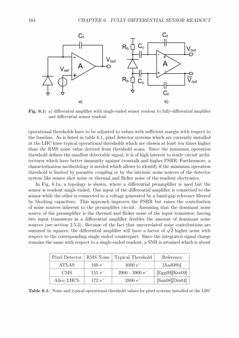
164 CHAPTER 6. FULLY-DIFFERENTIAL SENSOR READOUT
A
Cf
Vout-
+Vref
A
Cf
Vout-
+
Cf
Vout
Cc
Cc
-
+
a) b)
Rb
Rb
Fig. 6.1: a) differential amplifier with single-ended sensor readout b) fully-differential amplifierand differential sensor readout
operational thresholds have to be adjusted to values with sufficient margin with respect tothe baseline. As is listed in table 6.1, pixel detector systems which are currently installedat the LHC have typical operational thresholds which are chosen at least ten times higherthan the RMS noise value derived from threshold scans. Since the minimum operationthreshold defines the smallest detectable signal, it is of high interest to study circuit archi-tectures which have better immunity against crosstalk and higher PSRR. Furthermore, acharacterization methodology is needed which allows to identify if the minimum operationthreshold is limited by parasitic coupling or by the intrinsic noise sources of the detectorsystem like sensor shot noise or thermal and flicker noise of the readout electronics.
In Fig. 6.1a, a topology is shown, where a differential preamplifier is used but thesensor is readout single ended. One input of the differential amplifier is connected to thesensor while the other is connected to a voltage generated by a band-gap reference filteredby blocking capacitors. This approach improves the PSRR but raises the contributionof noise sources inherent to the preamplifier circuit. Assuming that the dominant noisesource of the preamplifier is the thermal and flicker noise of the input transistor, havingtwo input transistors in a differential amplifier doubles the amount of dominant noisesources (see section 2.5.3). Because of the fact that uncorrelated noise contributions aresummed in squares, the differential amplifier will have a factor of
√2 higher noise with
respect to the corresponding single ended counterpart. Since the integrated signal chargeremains the same with respect to a single-ended readout, a SNR is attained which is about
Pixel Detector RMS Noise Typical Threshold Reference
ATLAS 160 e− 4000 e− [Aad08b]
CMS 155 e− 2900 - 3900 e− [Egg09][Kot09]
Alice/LHCb 172 e− 2800 e− [San08][Din04]
Table 6.1: Noise and typical operational threshold values for pixel systems installed at the LHC
165
a factor of√2 smaller. In addition, the second input of the differential amplifier which is
not connected to the sensor but to a common voltage potential, introduces an additionalcrosstalk path. With this configuration, the topology at the input of the differentialpreamplifier is asymmetric and as a result might lead to an asymmetric crosstalk coupling,which is not rejected but amplified.
A differential sensor readout scheme based on a fully-differential CSA is illustrated inFig. 6.1b. With these scheme, the inputs of the differential amplifier are AC-coupled tothe n and p electrode of the sensor diode [Nis06]. The movement of the charge carriersgenerated by particle interaction in the sensor volume induces currents of complementarypolarity on both sensor diode electrodes. While in a single ended readout structure onlythe signal current flowing out of a single sensor electrode is integrated, in the CSA andthe signal current of the opposite sensor electrode is flowing into the depletion voltagepower supply, the differential readout integrates both signal currents [Rov00]. As a result,the differential readout doubles the signal magnitude with respect to single-ended readoutfor the same amount of ionized charge in the sensor diode. Taking into account that thenoise level of a differential amplifier is increased by a factor of
√2, the differential readout
gives rise to a SNR which is improved by a factor√2 [Roe94]. Furthermore, the fully
differential architecture combined with the use of a common mode feedback circuit has avery good PSRR and suppresses common mode crosstalk signals.
The improvement in crosstalk immunity and PSRR is of course combined with a highercircuit complexity which leads to increased power consumption and larger implementa-tion area. The differential readout requires also two coupling capacitors and two biasingresistors. Due to the fact that the coupling capacitors have to bear the full depletionvoltage1 and since high capacitance values are needed to reach high charge collection ef-ficiency, it is difficult to integrate the coupling capacitors on a standard CMOS process.It might however be possible to integrate the resistors and the coupling capacitors on thesensor. Alternatively, high voltage CMOS processes could be used which provide passivecomponents with higher voltage ratings. In addition, alternative AC-coupling schemesexist which reach high charge collection efficiency for smaller coupling capacitance (seesection 2.1.1).
Further obstacles which prevented the application of a fully-differential readout schemein the past were related to mechanical problems. For example, to connect a fully-differential CSA to both strip types of a double-sided strip detector with parallel strips, itis needed to have bond pads on both sides of the PCB on which the sensor is placed andit is required to add vias to connect to the other side of the PCB. This additional routingincreases the parasitic capacitance acting on the CSA input. Moreover, the existence ofwire bonds on both sides of the module complicate the module handling. With planarpixel sensors, the implementation of a fully-differential readout scheme is impossible dueto mechanical restrictions which prevent to establish connections to the electrodes locatedat both sensor sides. However, these mechanical limitations do not apply to the 3D sensor.
The 3D sensor [Par97] (see section 1.4) has cylindrical n and p electrodes perpen-
1With a depletion voltage which is defined symmetrically around the ground potential, the couplingcapacitor has to widthstand only a voltage drop which corresponds approximately to halve of the depletionvoltage
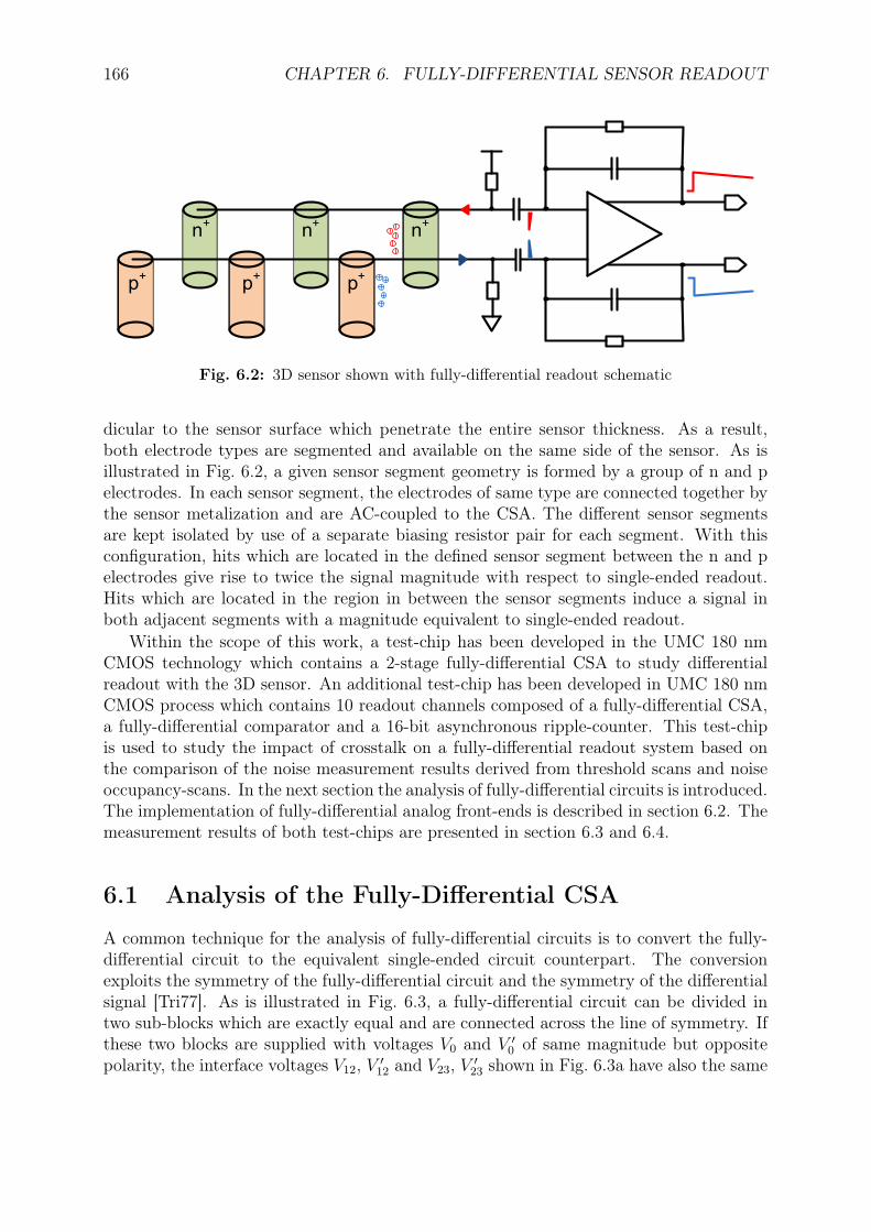
166 CHAPTER 6. FULLY-DIFFERENTIAL SENSOR READOUT
p+
p+
p+
n+
n+
n+
Fig. 6.2: 3D sensor shown with fully-differential readout schematic
dicular to the sensor surface which penetrate the entire sensor thickness. As a result,both electrode types are segmented and available on the same side of the sensor. As isillustrated in Fig. 6.2, a given sensor segment geometry is formed by a group of n and pelectrodes. In each sensor segment, the electrodes of same type are connected together bythe sensor metalization and are AC-coupled to the CSA. The different sensor segmentsare kept isolated by use of a separate biasing resistor pair for each segment. With thisconfiguration, hits which are located in the defined sensor segment between the n and pelectrodes give rise to twice the signal magnitude with respect to single-ended readout.Hits which are located in the region in between the sensor segments induce a signal inboth adjacent segments with a magnitude equivalent to single-ended readout.
Within the scope of this work, a test-chip has been developed in the UMC 180 nmCMOS technology which contains a 2-stage fully-differential CSA to study differentialreadout with the 3D sensor. An additional test-chip has been developed in UMC 180 nmCMOS process which contains 10 readout channels composed of a fully-differential CSA,a fully-differential comparator and a 16-bit asynchronous ripple-counter. This test-chipis used to study the impact of crosstalk on a fully-differential readout system based onthe comparison of the noise measurement results derived from threshold scans and noiseoccupancy-scans. In the next section the analysis of fully-differential circuits is introduced.The implementation of fully-differential analog front-ends is described in section 6.2. Themeasurement results of both test-chips are presented in section 6.3 and 6.4.
6.1 Analysis of the Fully-Differential CSA
A common technique for the analysis of fully-differential circuits is to convert the fully-differential circuit to the equivalent single-ended circuit counterpart. The conversionexploits the symmetry of the fully-differential circuit and the symmetry of the differentialsignal [Tri77]. As is illustrated in Fig. 6.3, a fully-differential circuit can be divided intwo sub-blocks which are exactly equal and are connected across the line of symmetry. Ifthese two blocks are supplied with voltages V0 and V ′
0 of same magnitude but oppositepolarity, the interface voltages V12, V ′
12 and V23, V ′23 shown in Fig. 6.3a have also the same
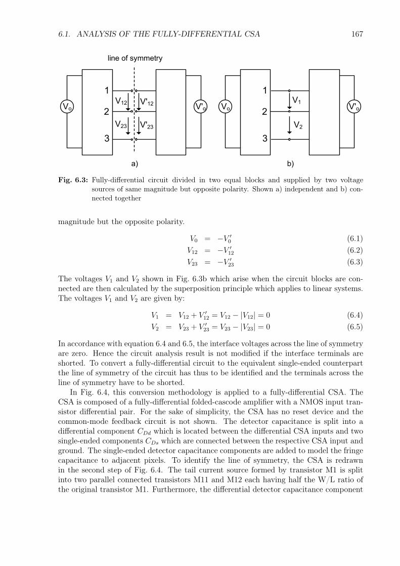
6.1. ANALYSIS OF THE FULLY-DIFFERENTIAL CSA 167
V'o
line of symmetry
1
2
3
1'
2'
3'
V12
V23
VoV'12
V'23
1
2
3
1'
2'
3'
V'oV1
V2
a) b)
Vo
Fig. 6.3: Fully-differential circuit divided in two equal blocks and supplied by two voltagesources of same magnitude but opposite polarity. Shown a) independent and b) con-nected together
magnitude but the opposite polarity.
V0 = −V ′0 (6.1)
V12 = −V ′12 (6.2)
V23 = −V ′23 (6.3)
The voltages V1 and V2 shown in Fig. 6.3b which arise when the circuit blocks are con-nected are then calculated by the superposition principle which applies to linear systems.The voltages V1 and V2 are given by:
V1 = V12 + V ′12 = V12 − |V12| = 0 (6.4)
V2 = V23 + V ′23 = V23 − |V23| = 0 (6.5)
In accordance with equation 6.4 and 6.5, the interface voltages across the line of symmetryare zero. Hence the circuit analysis result is not modified if the interface terminals areshorted. To convert a fully-differential circuit to the equivalent single-ended counterpartthe line of symmetry of the circuit has thus to be identified and the terminals across theline of symmetry have to be shorted.
In Fig. 6.4, this conversion methodology is applied to a fully-differential CSA. TheCSA is composed of a fully-differential folded-cascode amplifier with a NMOS input tran-sistor differential pair. For the sake of simplicity, the CSA has no reset device and thecommon-mode feedback circuit is not shown. The detector capacitance is split into adifferential component CDd which is located between the differential CSA inputs and twosingle-ended components CDs which are connected between the respective CSA input andground. The single-ended detector capacitance components are added to model the fringecapacitance to adjacent pixels. To identify the line of symmetry, the CSA is redrawnin the second step of Fig. 6.4. The tail current source formed by transistor M1 is splitinto two parallel connected transistors M11 and M12 each having half the W/L ratio ofthe original transistor M1. Furthermore, the differential detector capacitance component
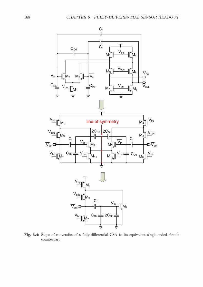
168 CHAPTER 6. FULLY-DIFFERENTIAL SENSOR READOUT
M5
M1
Vin VinM2 M3
M6M7
M8M9
M4
Cf
Cf
CDdVbp
VbnVbn VoutCDs
Vbpc
CDs
M12
Vin VinM2 M3
M6
M8
M4
M7
M9
M5
M11
2CDd2CDd
Cf
VbpVbp
VbpcVbpc
Cf
Vbn VbnVbn Vbn
VoutVout
CDsCDs
Vout
VinM2
M7
M9
M5
Vbp
Vbpc
Cf
Vbn
Vout
CDs 2CDd
line of symmetry
Fig. 6.4: Steps of conversion of a fully-differential CSA to its equivalent single-ended circuitcounterpart
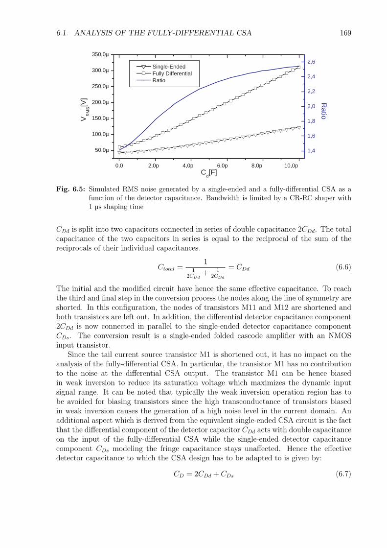
6.1. ANALYSIS OF THE FULLY-DIFFERENTIAL CSA 169
0,0 2,0p 4,0p 6,0p 8,0p 10,0p
50,0µ
100,0µ
150,0µ
200,0µ
250,0µ
300,0µ
350,0µ
Single-Ended Fully Differential Ratio
C d [F]
V R
MS
[V]
1,4
1,6
1,8
2,0
2,2
2,4
2,6 R
atio
Fig. 6.5: Simulated RMS noise generated by a single-ended and a fully-differential CSA as afunction of the detector capacitance. Bandwidth is limited by a CR-RC shaper with1 µs shaping time
CDd is split into two capacitors connected in series of double capacitance 2CDd. The totalcapacitance of the two capacitors in series is equal to the reciprocal of the sum of thereciprocals of their individual capacitances.
Ctotal =1
12CDd
+ 12CDd
= CDd (6.6)
The initial and the modified circuit have hence the same effective capacitance. To reachthe third and final step in the conversion process the nodes along the line of symmetry areshorted. In this configuration, the nodes of transistors M11 and M12 are shortened andboth transistors are left out. In addition, the differential detector capacitance component2CDd is now connected in parallel to the single-ended detector capacitance componentCDs. The conversion result is a single-ended folded cascode amplifier with an NMOSinput transistor.
Since the tail current source transistor M1 is shortened out, it has no impact on theanalysis of the fully-differential CSA. In particular, the transistor M1 has no contributionto the noise at the differential CSA output. The transistor M1 can be hence biasedin weak inversion to reduce its saturation voltage which maximizes the dynamic inputsignal range. It can be noted that typically the weak inversion operation region has tobe avoided for biasing transistors since the high transconductance of transistors biasedin weak inversion causes the generation of a high noise level in the current domain. Anadditional aspect which is derived from the equivalent single-ended CSA circuit is the factthat the differential component of the detector capacitor CDd acts with double capacitanceon the input of the fully-differential CSA while the single-ended detector capacitancecomponent CDs modeling the fringe capacitance stays unaffected. Hence the effectivedetector capacitance to which the CSA design has to be adapted to is given by:
CD = 2CDd + CDs (6.7)
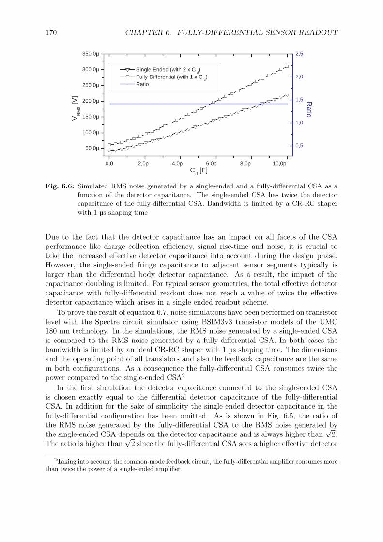
170 CHAPTER 6. FULLY-DIFFERENTIAL SENSOR READOUT
0,0 2,0p 4,0p 6,0p 8,0p 10,0p
50,0µ
100,0µ
150,0µ
200,0µ
250,0µ
300,0µ
350,0µ
Single Ended (with 2 x C d )
Fully-Differential (with 1 x C d )
Ratio
C d [F]
V R
MS
[V]
0,5
1,0
1,5
2,0
2,5
Ratio
Fig. 6.6: Simulated RMS noise generated by a single-ended and a fully-differential CSA as afunction of the detector capacitance. The single-ended CSA has twice the detectorcapacitance of the fully-differential CSA. Bandwidth is limited by a CR-RC shaperwith 1 µs shaping time
Due to the fact that the detector capacitance has an impact on all facets of the CSAperformance like charge collection efficiency, signal rise-time and noise, it is crucial totake the increased effective detector capacitance into account during the design phase.However, the single-ended fringe capacitance to adjacent sensor segments typically islarger than the differential body detector capacitance. As a result, the impact of thecapacitance doubling is limited. For typical sensor geometries, the total effective detectorcapacitance with fully-differential readout does not reach a value of twice the effectivedetector capacitance which arises in a single-ended readout scheme.
To prove the result of equation 6.7, noise simulations have been performed on transistorlevel with the Spectre circuit simulator using BSIM3v3 transistor models of the UMC180 nm technology. In the simulations, the RMS noise generated by a single-ended CSAis compared to the RMS noise generated by a fully-differential CSA. In both cases thebandwidth is limited by an ideal CR-RC shaper with 1 µs shaping time. The dimensionsand the operating point of all transistors and also the feedback capacitance are the samein both configurations. As a consequence the fully-differential CSA consumes twice thepower compared to the single-ended CSA2
In the first simulation the detector capacitance connected to the single-ended CSAis chosen exactly equal to the differential detector capacitance of the fully-differentialCSA. In addition for the sake of simplicity the single-ended detector capacitance in thefully-differential configuration has been omitted. As is shown in Fig. 6.5, the ratio ofthe RMS noise generated by the fully-differential CSA to the RMS noise generated bythe single-ended CSA depends on the detector capacitance and is always higher than
√2.
The ratio is higher than√2 since the fully-differential CSA sees a higher effective detector
2Taking into account the common-mode feedback circuit, the fully-differential amplifier consumes morethan twice the power of a single-ended amplifier
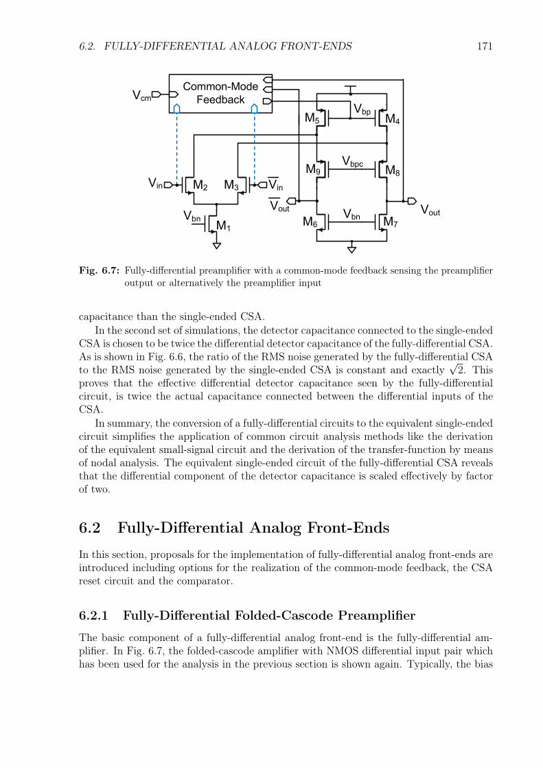
6.2. FULLY-DIFFERENTIAL ANALOG FRONT-ENDS 171
M5
M1
Vin VinM2 M3
M6 M7
M8M9
M4
Vbp
VbnVbnVout
Vbpc
Vout
Common-Mode
FeedbackVcm
Fig. 6.7: Fully-differential preamplifier with a common-mode feedback sensing the preamplifieroutput or alternatively the preamplifier input
capacitance than the single-ended CSA.In the second set of simulations, the detector capacitance connected to the single-ended
CSA is chosen to be twice the differential detector capacitance of the fully-differential CSA.As is shown in Fig. 6.6, the ratio of the RMS noise generated by the fully-differential CSAto the RMS noise generated by the single-ended CSA is constant and exactly
√2. This
proves that the effective differential detector capacitance seen by the fully-differentialcircuit, is twice the actual capacitance connected between the differential inputs of theCSA.
In summary, the conversion of a fully-differential circuits to the equivalent single-endedcircuit simplifies the application of common circuit analysis methods like the derivationof the equivalent small-signal circuit and the derivation of the transfer-function by meansof nodal analysis. The equivalent single-ended circuit of the fully-differential CSA revealsthat the differential component of the detector capacitance is scaled effectively by factorof two.
6.2 Fully-Differential Analog Front-Ends
In this section, proposals for the implementation of fully-differential analog front-ends areintroduced including options for the realization of the common-mode feedback, the CSAreset circuit and the comparator.
6.2.1 Fully-Differential Folded-Cascode Preamplifier
The basic component of a fully-differential analog front-end is the fully-differential am-plifier. In Fig. 6.7, the folded-cascode amplifier with NMOS differential input pair whichhas been used for the analysis in the previous section is shown again. Typically, the bias
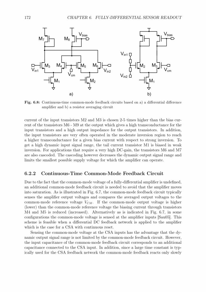
172 CHAPTER 6. FULLY-DIFFERENTIAL SENSOR READOUT
Vin2
M2
Vcm
M5 M6
M1
M3 M4
M8
VbiasM7
Vin1Vin2
M1
VcmM2 M3
Vbias
Vin1
a) b)
Fig. 6.8: Continuous-time common-mode feedback circuits based on a) a differential differenceamplifier and b) a resistor averaging circuit
current of the input transistors M2 and M3 is chosen 2-5 times higher than the bias cur-rent of the transistors M6 - M9 at the output which gives a high transconductance for theinput transistors and a high output impedance for the output transistors. In addition,the input transistors are very often operated in the moderate inversion region to reacha higher transconductance for a given bias current with respect to strong inversion. Toget a high dynamic input signal range, the tail current transistor M1 is biased in weakinversion. For applications that require a very high DC-gain, the transistors M6 and M7are also cascoded. The cascoding however decreases the dynamic output signal range andlimits the smallest possible supply voltage for which the amplifier can operate.
6.2.2 Continuous-Time Common-Mode Feedback Circuit
Due to the fact that the common-mode voltage of a fully-differential amplifier is undefined,an additional common-mode feedback circuit is needed to avoid that the amplifier movesinto saturation. As is illustrated in Fig. 6.7, the common-mode feedback circuit typicallysenses the amplifier output voltages and compares the averaged output voltages to thecommon-mode reference voltage VCM . If the common-mode output voltage is higher(lower) than the common-mode reference voltage the biasing current through transistorsM4 and M5 is reduced (increased). Alternatively as is indicated in Fig. 6.7, in someconfigurations the common-mode voltage is sensed at the amplifier inputs [Sau05]. Thisscheme is feasible when a differential DC feedback network is applied to the amplifierwhich is the case for a CSA with continuous reset.
Sensing the common-mode voltage at the CSA inputs has the advantage that the dy-namic output signal range is not limited by the common-mode feedback circuit. However,the input capacitance of the common-mode feedback circuit corresponds to an additionalcapacitance connected to the CSA input. In addition, since a large time constant is typ-ically used for the CSA feedback network the common-mode feedback reacts only slowly
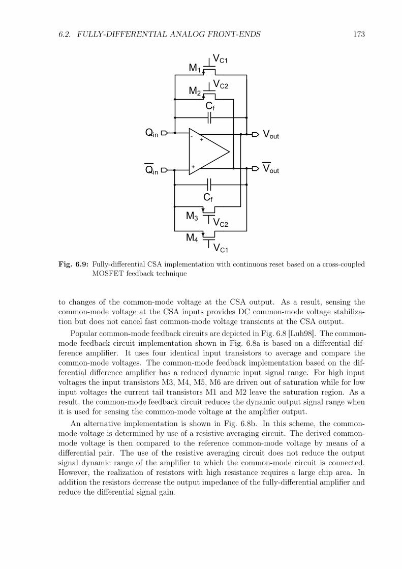
6.2. FULLY-DIFFERENTIAL ANALOG FRONT-ENDS 173
+
-+
-
VC1
VC2
VC2
VC1
Cf
Cf
VoutQin
Qin Vout
M1
M2
M3
M4
Fig. 6.9: Fully-differential CSA implementation with continuous reset based on a cross-coupledMOSFET feedback technique
to changes of the common-mode voltage at the CSA output. As a result, sensing thecommon-mode voltage at the CSA inputs provides DC common-mode voltage stabiliza-tion but does not cancel fast common-mode voltage transients at the CSA output.
Popular common-mode feedback circuits are depicted in Fig. 6.8 [Luh98]. The common-mode feedback circuit implementation shown in Fig. 6.8a is based on a differential dif-ference amplifier. It uses four identical input transistors to average and compare thecommon-mode voltages. The common-mode feedback implementation based on the dif-ferential difference amplifier has a reduced dynamic input signal range. For high inputvoltages the input transistors M3, M4, M5, M6 are driven out of saturation while for lowinput voltages the current tail transistors M1 and M2 leave the saturation region. As aresult, the common-mode feedback circuit reduces the dynamic output signal range whenit is used for sensing the common-mode voltage at the amplifier output.
An alternative implementation is shown in Fig. 6.8b. In this scheme, the common-mode voltage is determined by use of a resistive averaging circuit. The derived common-mode voltage is then compared to the reference common-mode voltage by means of adifferential pair. The use of the resistive averaging circuit does not reduce the outputsignal dynamic range of the amplifier to which the common-mode circuit is connected.However, the realization of resistors with high resistance requires a large chip area. Inaddition the resistors decrease the output impedance of the fully-differential amplifier andreduce the differential signal gain.
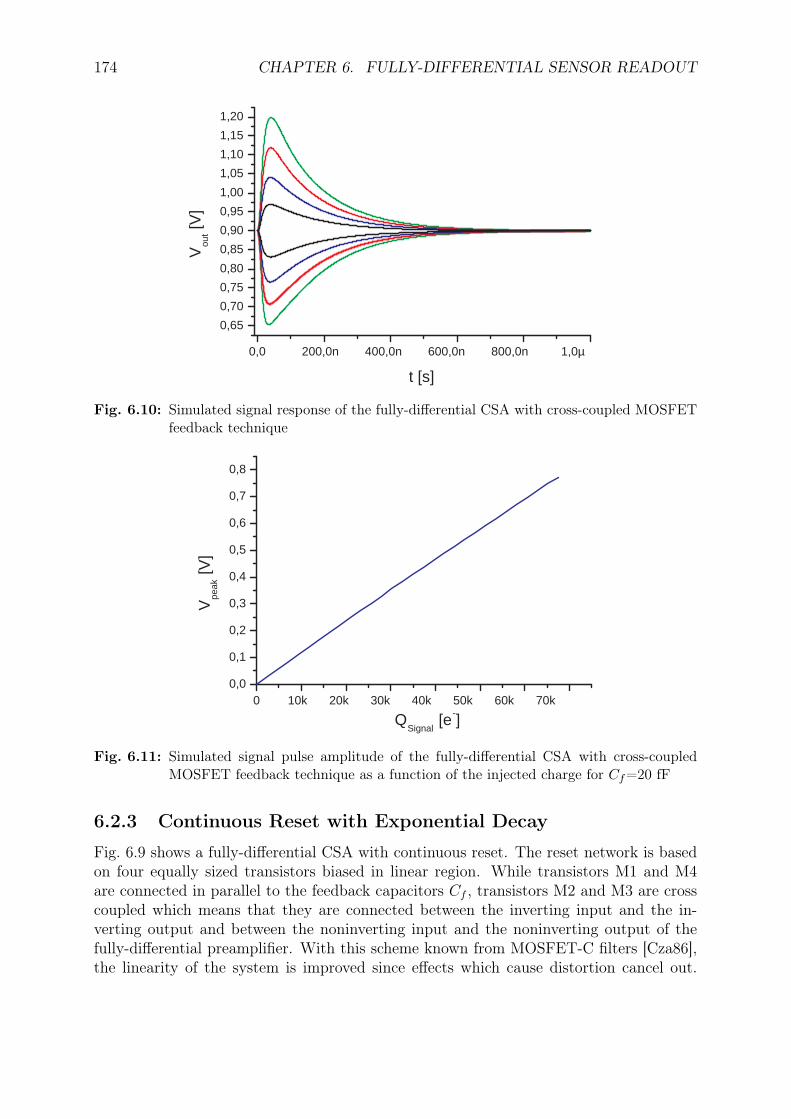
174 CHAPTER 6. FULLY-DIFFERENTIAL SENSOR READOUT
0,0 200,0n 400,0n 600,0n 800,0n 1,0µ
0,65
0,70
0,75
0,80
0,85
0,90
0,95
1,00
1,05
1,10
1,15
1,20
V ou
t [V]
t [s]
Fig. 6.10: Simulated signal response of the fully-differential CSA with cross-coupled MOSFETfeedback technique
0 10k 20k 30k 40k 50k 60k 70k 0,0
0,1
0,2
0,3
0,4
0,5
0,6
0,7
0,8
V pe
ak [V
]
Q Signal
[e - ]
Fig. 6.11: Simulated signal pulse amplitude of the fully-differential CSA with cross-coupledMOSFET feedback technique as a function of the injected charge for Cf=20 fF
6.2.3 Continuous Reset with Exponential Decay
Fig. 6.9 shows a fully-differential CSA with continuous reset. The reset network is basedon four equally sized transistors biased in linear region. While transistors M1 and M4are connected in parallel to the feedback capacitors Cf , transistors M2 and M3 are crosscoupled which means that they are connected between the inverting input and the in-verting output and between the noninverting input and the noninverting output of thefully-differential preamplifier. With this scheme known from MOSFET-C filters [Cza86],the linearity of the system is improved since effects which cause distortion cancel out.
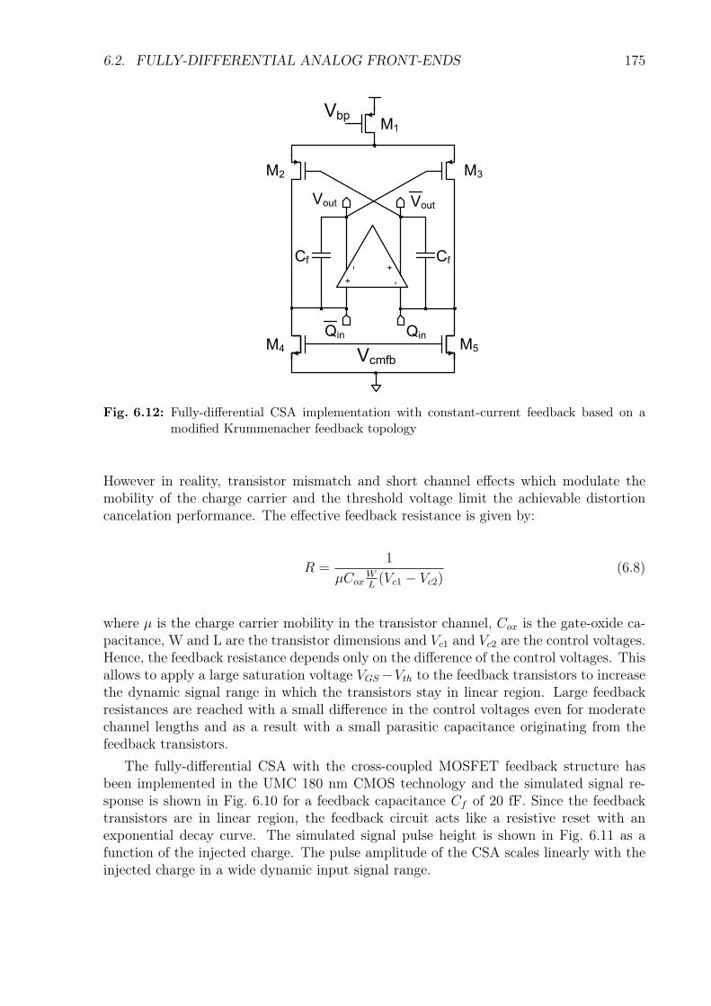
6.2. FULLY-DIFFERENTIAL ANALOG FRONT-ENDS 175
-+-
+
Vcmfb
Vbp
Vout Vout
QinQin
M1
M2 M3
M4 M5
Cf Cf
Fig. 6.12: Fully-differential CSA implementation with constant-current feedback based on amodified Krummenacher feedback topology
However in reality, transistor mismatch and short channel effects which modulate themobility of the charge carrier and the threshold voltage limit the achievable distortioncancelation performance. The effective feedback resistance is given by:
R =1
µCoxWL(Vc1 − Vc2)
(6.8)
where µ is the charge carrier mobility in the transistor channel, Cox is the gate-oxide ca-pacitance, W and L are the transistor dimensions and Vc1 and Vc2 are the control voltages.Hence, the feedback resistance depends only on the difference of the control voltages. Thisallows to apply a large saturation voltage VGS−Vth to the feedback transistors to increasethe dynamic signal range in which the transistors stay in linear region. Large feedbackresistances are reached with a small difference in the control voltages even for moderatechannel lengths and as a result with a small parasitic capacitance originating from thefeedback transistors.
The fully-differential CSA with the cross-coupled MOSFET feedback structure hasbeen implemented in the UMC 180 nm CMOS technology and the simulated signal re-sponse is shown in Fig. 6.10 for a feedback capacitance Cf of 20 fF. Since the feedbacktransistors are in linear region, the feedback circuit acts like a resistive reset with anexponential decay curve. The simulated signal pulse height is shown in Fig. 6.11 as afunction of the injected charge. The pulse amplitude of the CSA scales linearly with theinjected charge in a wide dynamic input signal range.
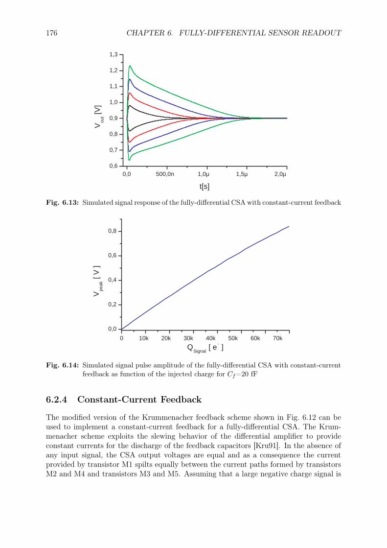
176 CHAPTER 6. FULLY-DIFFERENTIAL SENSOR READOUT
0,0 500,0n 1,0µ 1,5µ 2,0µ 0,6
0,7
0,8
0,9
1,0
1,1
1,2
1,3
V ou
t [V]
t[s]
Fig. 6.13: Simulated signal response of the fully-differential CSA with constant-current feedback
0 10k 20k 30k 40k 50k 60k 70k
0,0
0,2
0,4
0,6
0,8
V pe
ak [
V ]
Q Signal
[ e - ]
Fig. 6.14: Simulated signal pulse amplitude of the fully-differential CSA with constant-currentfeedback as function of the injected charge for Cf=20 fF
6.2.4 Constant-Current Feedback
The modified version of the Krummenacher feedback scheme shown in Fig. 6.12 can beused to implement a constant-current feedback for a fully-differential CSA. The Krum-menacher scheme exploits the slewing behavior of the differential amplifier to provideconstant currents for the discharge of the feedback capacitors [Kru91]. In the absence ofany input signal, the CSA output voltages are equal and as a consequence the currentprovided by transistor M1 spilts equally between the current paths formed by transistorsM2 and M4 and transistors M3 and M5. Assuming that a large negative charge signal is
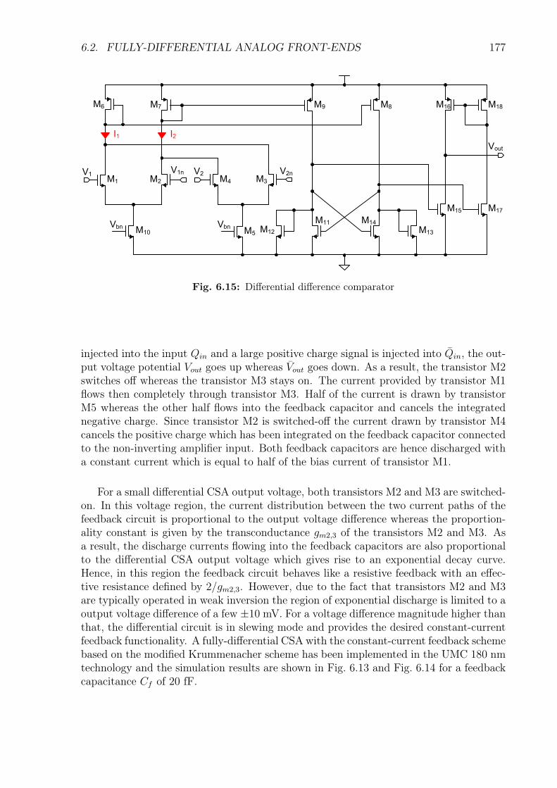
6.2. FULLY-DIFFERENTIAL ANALOG FRONT-ENDS 177
V1
Vbn
M1
V1n V2 V2n
Vout
M2 M3M4
M5
M6 M7 M8M9 M16 M18
M17M15
M13
M11
M12M10
M14
I1 I2
Vbn
Fig. 6.15: Differential difference comparator
injected into the input Qin and a large positive charge signal is injected into Qin, the out-put voltage potential Vout goes up whereas Vout goes down. As a result, the transistor M2switches off whereas the transistor M3 stays on. The current provided by transistor M1flows then completely through transistor M3. Half of the current is drawn by transistorM5 whereas the other half flows into the feedback capacitor and cancels the integratednegative charge. Since transistor M2 is switched-off the current drawn by transistor M4cancels the positive charge which has been integrated on the feedback capacitor connectedto the non-inverting amplifier input. Both feedback capacitors are hence discharged witha constant current which is equal to half of the bias current of transistor M1.
For a small differential CSA output voltage, both transistors M2 and M3 are switched-on. In this voltage region, the current distribution between the two current paths of thefeedback circuit is proportional to the output voltage difference whereas the proportion-ality constant is given by the transconductance gm2,3 of the transistors M2 and M3. Asa result, the discharge currents flowing into the feedback capacitors are also proportionalto the differential CSA output voltage which gives rise to an exponential decay curve.Hence, in this region the feedback circuit behaves like a resistive feedback with an effec-tive resistance defined by 2/gm2,3. However, due to the fact that transistors M2 and M3are typically operated in weak inversion the region of exponential discharge is limited to aoutput voltage difference of a few ±10 mV. For a voltage difference magnitude higher thanthat, the differential circuit is in slewing mode and provides the desired constant-currentfeedback functionality. A fully-differential CSA with the constant-current feedback schemebased on the modified Krummenacher scheme has been implemented in the UMC 180 nmtechnology and the simulation results are shown in Fig. 6.13 and Fig. 6.14 for a feedbackcapacitance Cf of 20 fF.
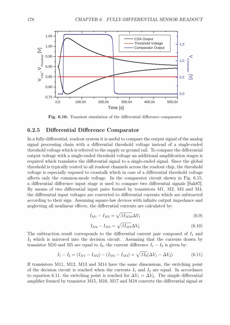
178 CHAPTER 6. FULLY-DIFFERENTIAL SENSOR READOUT
0,0 100,0n 200,0n 300,0n 400,0n 500,0n 0,75
0,80
0,85
0,90
0,95
1,00
1,05 CSA Output Threshold Voltage Comparator Output
Time [s]
V C
SA
, V T
hres
hold
[V]
0,0
0,5
1,0
1,5
V C
omparator [V
]
Fig. 6.16: Transient simulation of the differential difference comparator
6.2.5 Differential Difference Comparator
In a fully-differential, readout system it is useful to compare the output signal of the analogsignal processing chain with a differential threshold voltage instead of a single-endedthreshold voltage which is referred to the supply or ground rail. To compare the differentialoutput voltage with a single-ended threshold voltage an additional amplification stages isrequired which translates the differential signal to a single-ended signal. Since the globalthreshold is typically routed to all readout channels across the readout chip, the thresholdvoltage is especially exposed to crosstalk which in case of a differential threshold voltageaffects only the common-mode voltage. In the comparator circuit shown in Fig. 6.15,a differential difference input stage is used to compare two differential signals [Sak87].By means of two differential input pairs formed by transistors M1, M2, M3 and M4,the differential input voltages are converted to differential currents which are subtractedaccording to their sign. Assuming square-law devices with infinite output impedance andneglecting all nonlinear effects, the differential currents are calculated by:
IM1 − IM2 =√βIM10∆V1 (6.9)
IM4 − IM3 =√
βIM5∆V2 (6.10)
The subtraction result corresponds to the differential current pair composed of I1 andI2 which is mirrored into the decision circuit. Assuming that the currents drawn bytransistor M10 and M5 are equal to I0, the current difference I1 − I2 is given by:
I1 − I2 = (IM1 − IM2)− (IM4 − IM3) =√βI0(∆V1 −∆V2) (6.11)
If transistors M11, M12, M13 and M14 have the same dimensions, the switching pointof the decision circuit is reached when the currents I1 and I2 are equal. In accordanceto equation 6.11, the switching point is reached for ∆V1 = ∆V2. The simple differentialamplifier formed by transistor M15, M16, M17 and M18 converts the differential signal at
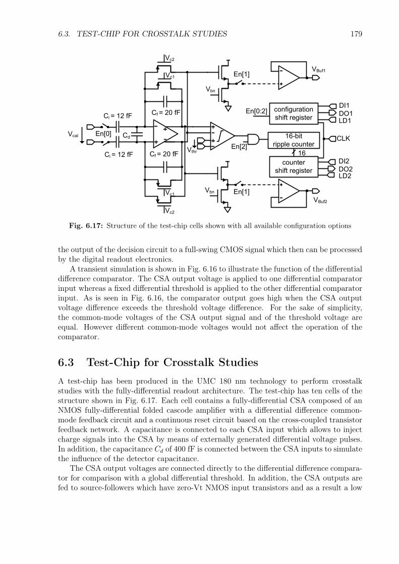
6.3. TEST-CHIP FOR CROSSTALK STUDIES 179
Vc1
Vc2
Vc1
Vc2
Cd
Cf = 20 fF
Vcal En[0]
Vthr
Vbn
Vbn
En[1]
En[1]
En[2]
16-bit
ripple counter
configuration
shift register
counter
shift register
16
VBuf1
VBuf2
DI1
DO1En[0:2]
CLK
DI2
DO2
Cf = 20 fFCi = 12 fF
Ci = 12 fF
LD2
LD1
Fig. 6.17: Structure of the test-chip cells shown with all available configuration options
the output of the decision circuit to a full-swing CMOS signal which then can be processedby the digital readout electronics.
A transient simulation is shown in Fig. 6.16 to illustrate the function of the differentialdifference comparator. The CSA output voltage is applied to one differential comparatorinput whereas a fixed differential threshold is applied to the other differential comparatorinput. As is seen in Fig. 6.16, the comparator output goes high when the CSA outputvoltage difference exceeds the threshold voltage difference. For the sake of simplicity,the common-mode voltages of the CSA output signal and of the threshold voltage areequal. However different common-mode voltages would not affect the operation of thecomparator.
6.3 Test-Chip for Crosstalk StudiesA test-chip has been produced in the UMC 180 nm technology to perform crosstalkstudies with the fully-differential readout architecture. The test-chip has ten cells of thestructure shown in Fig. 6.17. Each cell contains a fully-differential CSA composed of anNMOS fully-differential folded cascode amplifier with a differential difference common-mode feedback circuit and a continuous reset circuit based on the cross-coupled transistorfeedback network. A capacitance is connected to each CSA input which allows to injectcharge signals into the CSA by means of externally generated differential voltage pulses.In addition, the capacitance Cd of 400 fF is connected between the CSA inputs to simulatethe influence of the detector capacitance.
The CSA output voltages are connected directly to the differential difference compara-tor for comparison with a global differential threshold. In addition, the CSA outputs arefed to source-followers which have zero-Vt NMOS input transistors and as a result a low
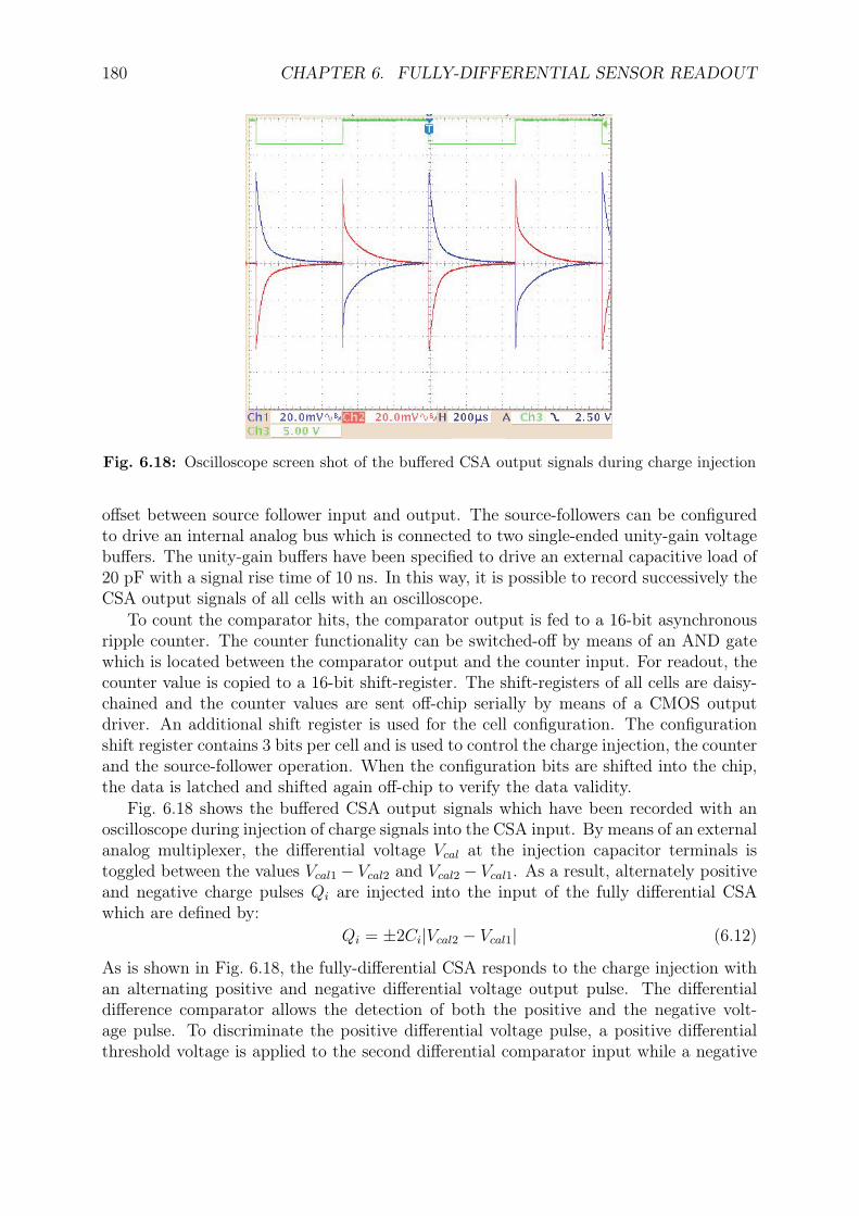
180 CHAPTER 6. FULLY-DIFFERENTIAL SENSOR READOUT
Fig. 6.18: Oscilloscope screen shot of the buffered CSA output signals during charge injection
offset between source follower input and output. The source-followers can be configuredto drive an internal analog bus which is connected to two single-ended unity-gain voltagebuffers. The unity-gain buffers have been specified to drive an external capacitive load of20 pF with a signal rise time of 10 ns. In this way, it is possible to record successively theCSA output signals of all cells with an oscilloscope.
To count the comparator hits, the comparator output is fed to a 16-bit asynchronousripple counter. The counter functionality can be switched-off by means of an AND gatewhich is located between the comparator output and the counter input. For readout, thecounter value is copied to a 16-bit shift-register. The shift-registers of all cells are daisy-chained and the counter values are sent off-chip serially by means of a CMOS outputdriver. An additional shift register is used for the cell configuration. The configurationshift register contains 3 bits per cell and is used to control the charge injection, the counterand the source-follower operation. When the configuration bits are shifted into the chip,the data is latched and shifted again off-chip to verify the data validity.
Fig. 6.18 shows the buffered CSA output signals which have been recorded with anoscilloscope during injection of charge signals into the CSA input. By means of an externalanalog multiplexer, the differential voltage Vcal at the injection capacitor terminals istoggled between the values Vcal1 − Vcal2 and Vcal2 − Vcal1. As a result, alternately positiveand negative charge pulses Qi are injected into the input of the fully differential CSAwhich are defined by:
Qi = ±2Ci|Vcal2 − Vcal1| (6.12)
As is shown in Fig. 6.18, the fully-differential CSA responds to the charge injection withan alternating positive and negative differential voltage output pulse. The differentialdifference comparator allows the detection of both the positive and the negative volt-age pulse. To discriminate the positive differential voltage pulse, a positive differentialthreshold voltage is applied to the second differential comparator input while a negative
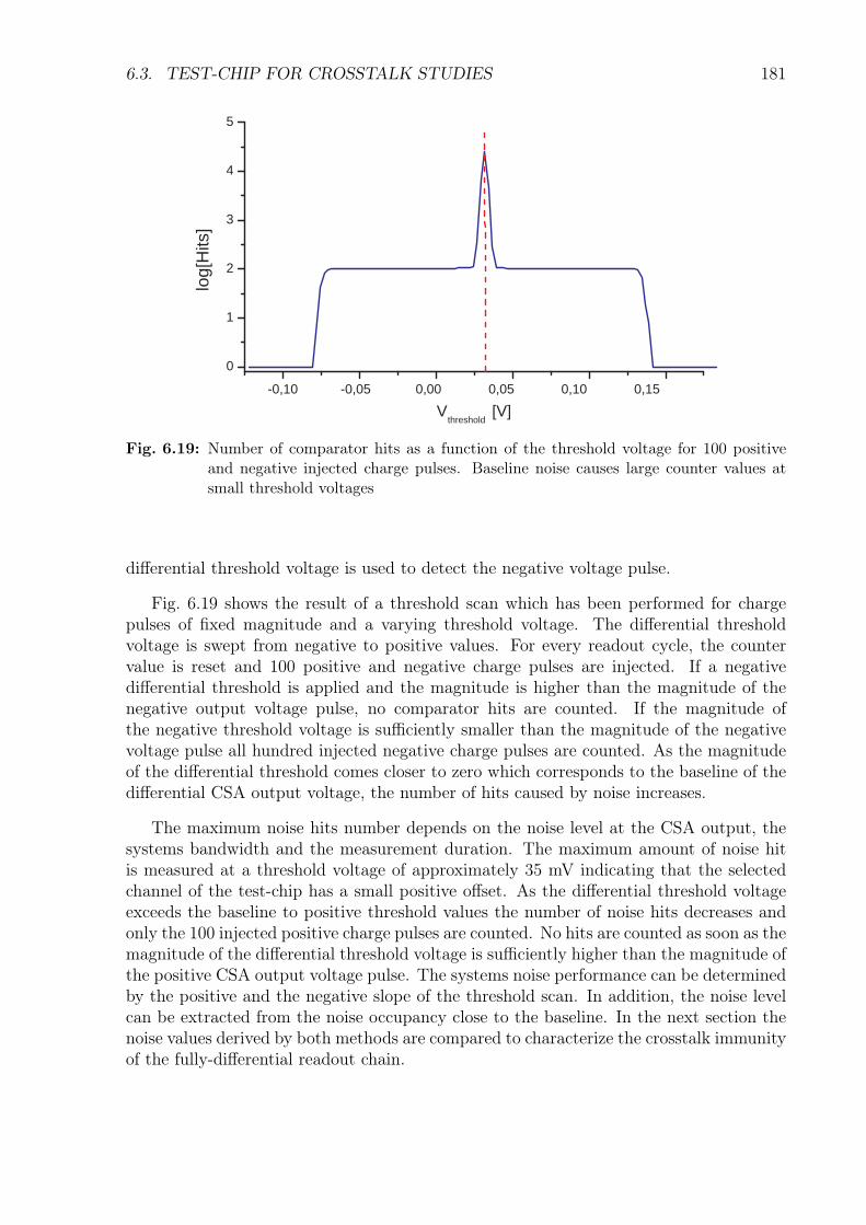
6.3. TEST-CHIP FOR CROSSTALK STUDIES 181
-0,10 -0,05 0,00 0,05 0,10 0,15
0
1
2
3
4
5
log[
Hits
]
V threshold
[V]
Fig. 6.19: Number of comparator hits as a function of the threshold voltage for 100 positiveand negative injected charge pulses. Baseline noise causes large counter values atsmall threshold voltages
differential threshold voltage is used to detect the negative voltage pulse.
Fig. 6.19 shows the result of a threshold scan which has been performed for chargepulses of fixed magnitude and a varying threshold voltage. The differential thresholdvoltage is swept from negative to positive values. For every readout cycle, the countervalue is reset and 100 positive and negative charge pulses are injected. If a negativedifferential threshold is applied and the magnitude is higher than the magnitude of thenegative output voltage pulse, no comparator hits are counted. If the magnitude ofthe negative threshold voltage is sufficiently smaller than the magnitude of the negativevoltage pulse all hundred injected negative charge pulses are counted. As the magnitudeof the differential threshold comes closer to zero which corresponds to the baseline of thedifferential CSA output voltage, the number of hits caused by noise increases.
The maximum noise hits number depends on the noise level at the CSA output, thesystems bandwidth and the measurement duration. The maximum amount of noise hitis measured at a threshold voltage of approximately 35 mV indicating that the selectedchannel of the test-chip has a small positive offset. As the differential threshold voltageexceeds the baseline to positive threshold values the number of noise hits decreases andonly the 100 injected positive charge pulses are counted. No hits are counted as soon as themagnitude of the differential threshold voltage is sufficiently higher than the magnitude ofthe positive CSA output voltage pulse. The systems noise performance can be determinedby the positive and the negative slope of the threshold scan. In addition, the noise levelcan be extracted from the noise occupancy close to the baseline. In the next section thenoise values derived by both methods are compared to characterize the crosstalk immunityof the fully-differential readout chain.
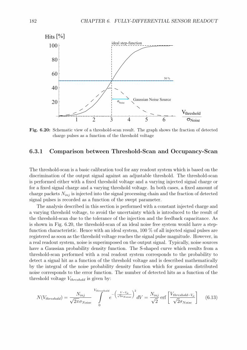
182 CHAPTER 6. FULLY-DIFFERENTIAL SENSOR READOUT
1 2 3 4 5 6
Vthreshold
σNoise
20
40
60
80
100
Hits [%]ideal step-function
Gaussian Noise Sourceσ
Noise
50 %
Fig. 6.20: Schematic view of a threshold-scan result. The graph shows the fraction of detectedcharge pulses as a function of the threshold voltage
6.3.1 Comparison between Threshold-Scan and Occupancy-Scan
The threshold-scan is a basic calibration tool for any readout system which is based on thediscrimination of the output signal against an adjustable threshold. The threshold-scanis performed either with a fixed threshold voltage and a varying injected signal charge orfor a fixed signal charge and a varying threshold voltage. In both cases, a fixed amount ofcharge packets Ninj is injected into the signal processing chain and the fraction of detectedsignal pulses is recorded as a function of the swept parameter.
The analysis described in this section is performed with a constant injected charge anda varying threshold voltage, to avoid the uncertainty which is introduced to the result ofthe threshold-scan due to the tolerance of the injection and the feedback capacitance. Asis shown in Fig. 6.20, the threshold-scan of an ideal noise free system would have a step-function characteristic. Hence with an ideal system, 100 % of all injected signal pulses areregistered as soon as the threshold voltage reaches the signal pulse magnitude. However, ina real readout system, noise is superimposed on the output signal. Typically, noise sourceshave a Gaussian probability density function. The S-shaped curve which results from athreshold-scan performed with a real readout system corresponds to the probability todetect a signal hit as a function of the threshold voltage and is described mathematicallyby the integral of the noise probability density function which for gaussian distributednoise corresponds to the error function. The number of detected hits as a function of thethreshold voltage Vthreshold is given by:
N(Vthreshold) =Ninj√2πσNoise
Vthreshold∫0
e−(
V −Vµ√2σNoise
)2
dV =Ninj√
2erf
[Vthreshold−Vµ√
2σNoise
](6.13)
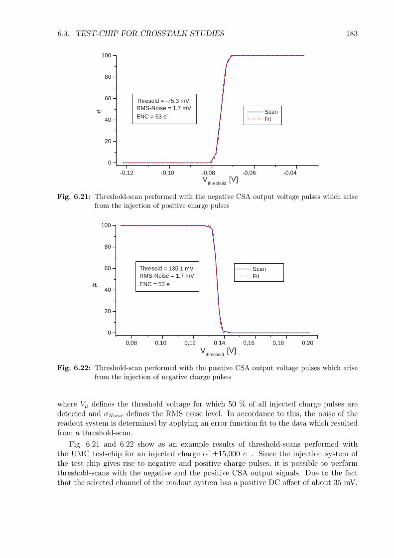
6.3. TEST-CHIP FOR CROSSTALK STUDIES 183
-0,12 -0,10 -0,08 -0,06 -0,04
0
20
40
60
80
100
Thresold = -75.3 mV RMS-Noise = 1.7 mV ENC = 53 e -
Scan Fit
#
V threshold
[V]
Fig. 6.21: Threshold-scan performed with the negative CSA output voltage pulses which arisefrom the injection of positive charge pulses
0,08 0,10 0,12 0,14 0,16 0,18 0,20
0
20
40
60
80
100
Thresold = 135.1 mV RMS-Noise = 1.7 mV ENC = 53 e -
Scan Fit
#
V threshold
[V]
Fig. 6.22: Threshold-scan performed with the positive CSA output voltage pulses which arisefrom the injection of negative charge pulses
where Vµ defines the threshold voltage for which 50 % of all injected charge pulses aredetected and σNoise defines the RMS noise level. In accordance to this, the noise of thereadout system is determined by applying an error function fit to the data which resultedfrom a threshold-scan.
Fig. 6.21 and 6.22 show as an example results of threshold-scans performed withthe UMC test-chip for an injected charge of ±15,000 e−. Since the injection system ofthe test-chip gives rise to negative and positive charge pulses, it is possible to performthreshold-scans with the negative and the positive CSA output signals. Due to the factthat the selected channel of the readout system has a positive DC offset of about 35 mV,
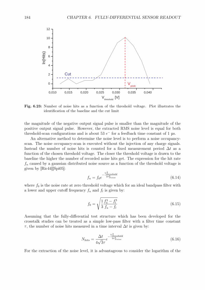
184 CHAPTER 6. FULLY-DIFFERENTIAL SENSOR READOUT
0,010 0,015 0,020 0,025 0,030 0,035 0,040
0
2
4
6
8
10
12
Cut
V peak
ln(H
its)
V threshold
[V]
Fig. 6.23: Number of noise hits as a function of the threshold voltage. Plot illustrates theidentification of the baseline and the cut limit
the magnitude of the negative output signal pulse is smaller than the magnitude of thepositive output signal pulse. However, the extracted RMS noise level is equal for boththreshold-scan configurations and is about 53 e− for a feedback time constant of 1 µs.
An alternative method to determine the noise level is to perform a noise occupancy-scan. The noise occupancy-scan is executed without the injection of any charge signals.Instead the number of noise hits is counted for a fixed measurement period ∆t as afunction of the chosen threshold voltage. The closer the threshold voltage is drawn to thebaseline the higher the number of recorded noise hits get. The expression for the hit ratefn caused by a gaussian distributed noise source as a function of the threshold voltage isgiven by [Ric44][Spi05]:
fn = f0e−V 2
threshold2σ2
Noise (6.14)
where f0 is the noise rate at zero threshold voltage which for an ideal bandpass filter witha lower and upper cutoff frequency fu and fl is given by:
f0 =
√1
3
f 3u − f 3
l
fu − fl(6.15)
Assuming that the fully-differential test structure which has been developed for thecrosstalk studies can be treated as a simple low-pass filter with a filter time constantτ , the number of noise hits measured in a time interval ∆t is given by:
Nhits =∆t
4√3τ
e−V 2
threshold2σ2
Noise (6.16)
For the extraction of the noise level, it is advantageous to consider the logarithm of the
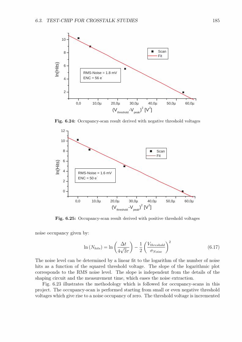
6.3. TEST-CHIP FOR CROSSTALK STUDIES 185
0,0 10,0µ 20,0µ 30,0µ 40,0µ 50,0µ 60,0µ
2
4
6
8
10
RMS-Noise = 1.8 mV ENC = 56 e -
Scan Fit
ln(H
its)
(V threshold
-V peak
) 2 [V 2 ]
Fig. 6.24: Occupancy-scan result derived with negative threshold voltages
0,0 10,0µ 20,0µ 30,0µ 40,0µ 50,0µ 60,0µ
0
2
4
6
8
10
12
RMS-Noise = 1.6 mV ENC = 50 e -
Scan Fit
ln(H
its)
(V threshold
-V peak
) 2 [V 2 ]
Fig. 6.25: Occupancy-scan result derived with positive threshold voltages
noise occupancy given by:
ln (Nhits) = ln
(∆t
4√3τ
)− 1
2
(Vthreshold
σNoise
)2
(6.17)
The noise level can be determined by a linear fit to the logarithm of the number of noisehits as a function of the squared threshold voltage. The slope of the logarithmic plotcorresponds to the RMS noise level. The slope is independent from the details of theshaping circuit and the measurement time, which eases the noise extraction.
Fig. 6.23 illustrates the methodology which is followed for occupancy-scans in thisproject. The occupancy-scan is performed starting from small or even negative thresholdvoltages which give rise to a noise occupancy of zero. The threshold voltage is incremented
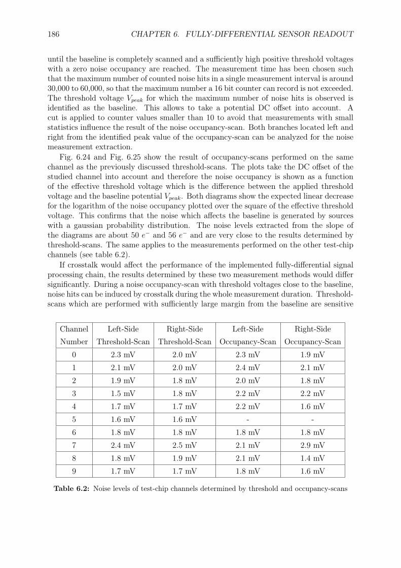
186 CHAPTER 6. FULLY-DIFFERENTIAL SENSOR READOUT
until the baseline is completely scanned and a sufficiently high positive threshold voltageswith a zero noise occupancy are reached. The measurement time has been chosen suchthat the maximum number of counted noise hits in a single measurement interval is around30,000 to 60,000, so that the maximum number a 16 bit counter can record is not exceeded.The threshold voltage Vpeak for which the maximum number of noise hits is observed isidentified as the baseline. This allows to take a potential DC offset into account. Acut is applied to counter values smaller than 10 to avoid that measurements with smallstatistics influence the result of the noise occupancy-scan. Both branches located left andright from the identified peak value of the occupancy-scan can be analyzed for the noisemeasurement extraction.
Fig. 6.24 and Fig. 6.25 show the result of occupancy-scans performed on the samechannel as the previously discussed threshold-scans. The plots take the DC offset of thestudied channel into account and therefore the noise occupancy is shown as a functionof the effective threshold voltage which is the difference between the applied thresholdvoltage and the baseline potential Vpeak. Both diagrams show the expected linear decreasefor the logarithm of the noise occupancy plotted over the square of the effective thresholdvoltage. This confirms that the noise which affects the baseline is generated by sourceswith a gaussian probability distribution. The noise levels extracted from the slope ofthe diagrams are about 50 e− and 56 e− and are very close to the results determined bythreshold-scans. The same applies to the measurements performed on the other test-chipchannels (see table 6.2).
If crosstalk would affect the performance of the implemented fully-differential signalprocessing chain, the results determined by these two measurement methods would differsignificantly. During a noise occupancy-scan with threshold voltages close to the baseline,noise hits can be induced by crosstalk during the whole measurement duration. Threshold-scans which are performed with sufficiently large margin from the baseline are sensitive
Channel Left-Side Right-Side Left-Side Right-SideNumber Threshold-Scan Threshold-Scan Occupancy-Scan Occupancy-Scan
0 2.3 mV 2.0 mV 2.3 mV 1.9 mV
1 2.1 mV 2.0 mV 2.4 mV 2.1 mV
2 1.9 mV 1.8 mV 2.0 mV 1.8 mV
3 1.5 mV 1.8 mV 2.2 mV 2.2 mV
4 1.7 mV 1.7 mV 2.2 mV 1.6 mV
5 1.6 mV 1.6 mV - -
6 1.8 mV 1.8 mV 1.8 mV 1.8 mV
7 2.4 mV 2.5 mV 2.1 mV 2.9 mV
8 1.8 mV 1.9 mV 2.1 mV 1.4 mV
9 1.7 mV 1.7 mV 1.8 mV 1.6 mV
Table 6.2: Noise levels of test-chip channels determined by threshold and occupancy-scans
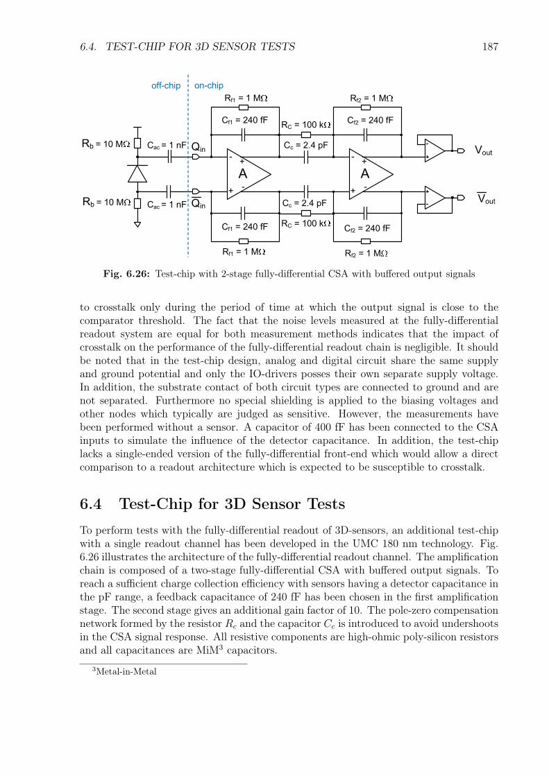
6.4. TEST-CHIP FOR 3D SENSOR TESTS 187
A
Vout-
+Vout
-
+
A
Cf1 = 240 fF
-
+ -
+
Rf1 = 1 M
Cf1 = 240 fF
Rf1 = 1 M
Cc = 2.4 pF
Cc = 2.4 pF
RC = 100 k
RC = 100 k
Cf2 = 240 fF
Rf2 = 1 M
Cf2 = 240 fF
Rf2 = 1 M
Qin
Qin
Cac = 1 nFRb = 10 M
Cac = 1 nFRb = 10 M
on-chipoff-chip
Fig. 6.26: Test-chip with 2-stage fully-differential CSA with buffered output signals
to crosstalk only during the period of time at which the output signal is close to thecomparator threshold. The fact that the noise levels measured at the fully-differentialreadout system are equal for both measurement methods indicates that the impact ofcrosstalk on the performance of the fully-differential readout chain is negligible. It shouldbe noted that in the test-chip design, analog and digital circuit share the same supplyand ground potential and only the IO-drivers posses their own separate supply voltage.In addition, the substrate contact of both circuit types are connected to ground and arenot separated. Furthermore no special shielding is applied to the biasing voltages andother nodes which typically are judged as sensitive. However, the measurements havebeen performed without a sensor. A capacitor of 400 fF has been connected to the CSAinputs to simulate the influence of the detector capacitance. In addition, the test-chiplacks a single-ended version of the fully-differential front-end which would allow a directcomparison to a readout architecture which is expected to be susceptible to crosstalk.
6.4 Test-Chip for 3D Sensor Tests
To perform tests with the fully-differential readout of 3D-sensors, an additional test-chipwith a single readout channel has been developed in the UMC 180 nm technology. Fig.6.26 illustrates the architecture of the fully-differential readout channel. The amplificationchain is composed of a two-stage fully-differential CSA with buffered output signals. Toreach a sufficient charge collection efficiency with sensors having a detector capacitance inthe pF range, a feedback capacitance of 240 fF has been chosen in the first amplificationstage. The second stage gives an additional gain factor of 10. The pole-zero compensationnetwork formed by the resistor Rc and the capacitor Cc is introduced to avoid undershootsin the CSA signal response. All resistive components are high-ohmic poly-silicon resistorsand all capacitances are MiM3 capacitors.
3Metal-in-Metal
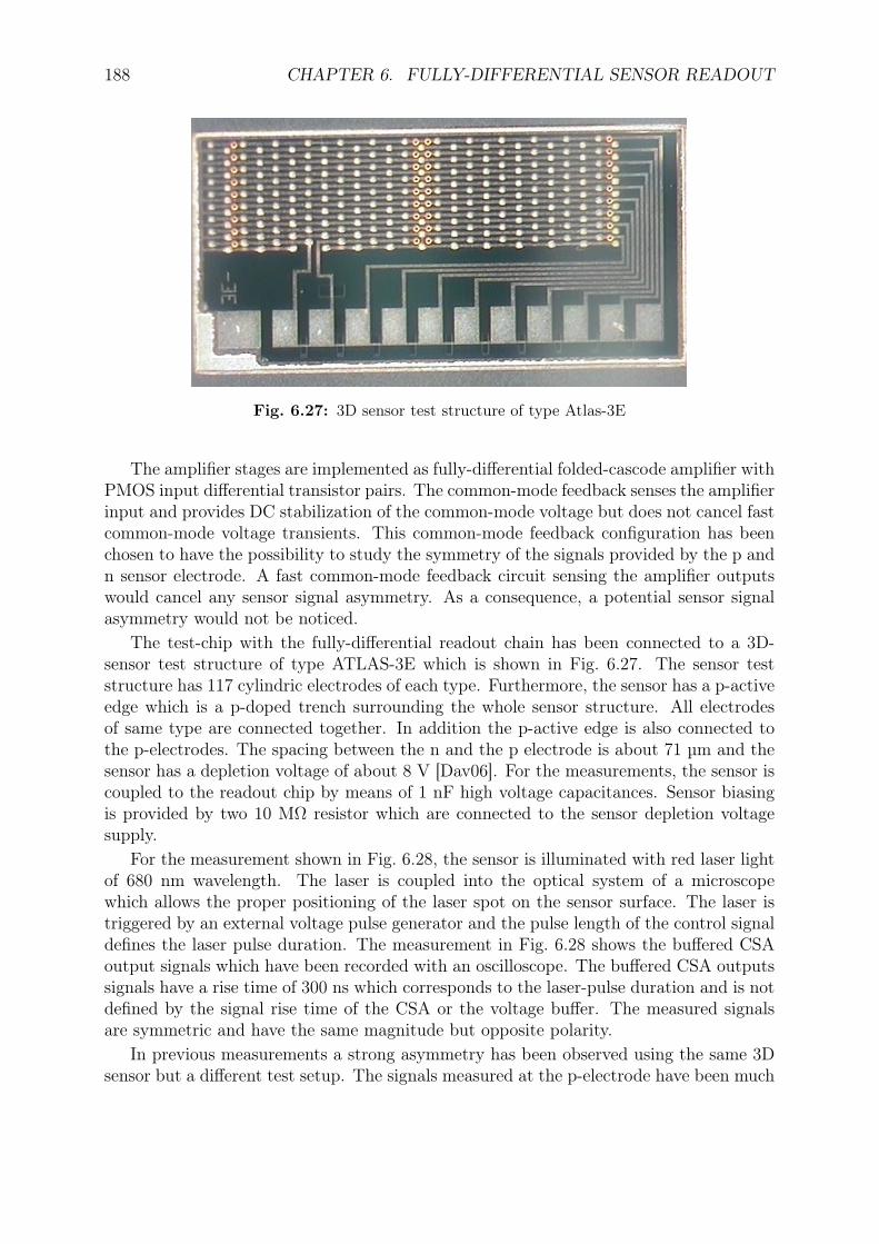
188 CHAPTER 6. FULLY-DIFFERENTIAL SENSOR READOUT
Fig. 6.27: 3D sensor test structure of type Atlas-3E
The amplifier stages are implemented as fully-differential folded-cascode amplifier withPMOS input differential transistor pairs. The common-mode feedback senses the amplifierinput and provides DC stabilization of the common-mode voltage but does not cancel fastcommon-mode voltage transients. This common-mode feedback configuration has beenchosen to have the possibility to study the symmetry of the signals provided by the p andn sensor electrode. A fast common-mode feedback circuit sensing the amplifier outputswould cancel any sensor signal asymmetry. As a consequence, a potential sensor signalasymmetry would not be noticed.
The test-chip with the fully-differential readout chain has been connected to a 3D-sensor test structure of type ATLAS-3E which is shown in Fig. 6.27. The sensor teststructure has 117 cylindric electrodes of each type. Furthermore, the sensor has a p-activeedge which is a p-doped trench surrounding the whole sensor structure. All electrodesof same type are connected together. In addition the p-active edge is also connected tothe p-electrodes. The spacing between the n and the p electrode is about 71 µm and thesensor has a depletion voltage of about 8 V [Dav06]. For the measurements, the sensor iscoupled to the readout chip by means of 1 nF high voltage capacitances. Sensor biasingis provided by two 10 MΩ resistor which are connected to the sensor depletion voltagesupply.
For the measurement shown in Fig. 6.28, the sensor is illuminated with red laser lightof 680 nm wavelength. The laser is coupled into the optical system of a microscopewhich allows the proper positioning of the laser spot on the sensor surface. The laser istriggered by an external voltage pulse generator and the pulse length of the control signaldefines the laser pulse duration. The measurement in Fig. 6.28 shows the buffered CSAoutput signals which have been recorded with an oscilloscope. The buffered CSA outputssignals have a rise time of 300 ns which corresponds to the laser-pulse duration and is notdefined by the signal rise time of the CSA or the voltage buffer. The measured signalsare symmetric and have the same magnitude but opposite polarity.
In previous measurements a strong asymmetry has been observed using the same 3Dsensor but a different test setup. The signals measured at the p-electrode have been much
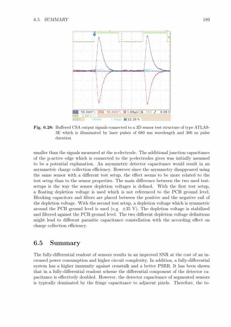
6.5. SUMMARY 189
Fig. 6.28: Buffered CSA output signals connected to a 3D sensor test structure of type ATLAS-3E which is illuminated by laser pulses of 680 nm wavelength and 300 ns pulseduration
smaller than the signals measured at the n-electrode. The additional junction capacitanceof the p-active edge which is connected to the p-electrodes gives was initially assumedto be a potential explanation. An asymmetric detector capacitance would result in anasymmetric charge collection efficiency. However since the asymmetry disappeared usingthe same sensor with a different test setup, the effect seems to be more related to thetest setup than to the sensor properties. The main difference between the two used test-setups is the way the sensor depletion voltages is defined. With the first test setup,a floating depletion voltage is used which is not referenced to the PCB ground level.Blocking capacitors and filters are placed between the positive and the negative rail ofthe depletion voltage. With the second test setup, a depletion voltage which is symmetricaround the PCB ground level is used (e.g. ±35 V). The depletion voltage is stabilizedand filtered against the PCB ground level. The two different depletion voltage definitionsmight lead to different parasitic capacitance constellation with the according effect oncharge collection efficiency.
6.5 Summary
The fully-differential readout of sensors results in an improved SNR at the cost of an in-creased power consumption and higher circuit complexity. In addition, a fully-differentialsystem has a higher immunity against crosstalk and a better PSRR. It has been shownthat in a fully-differential readout scheme the differential component of the detector ca-pacitance is effectively doubled. However, the detector capacitance of segmented sensorsis typically dominated by the fringe capacitance to adjacent pixels. Therefore, the to-

190 CHAPTER 6. FULLY-DIFFERENTIAL SENSOR READOUT
tal effective detector capacitance in a fully-differential readout scheme should be onlyslightly larger with respect to a single-ended readout configuration. Fully-differentialCSA implementations with continuous reset have been proposed. To implement a fully-differential CSA with exponential signal decay, the cross-coupled transistor feedback cir-cuit known from MOSFET-C filter stages can be applied. For the implementation ofa fully-differential constant-current feedback, a modified Krummenacher scheme can beused. A test-chip with several channels of a fully-differential readout chain has been de-veloped for crosstalk related studies. The comparison of the noise levels determined bythreshold-scans and the noise levels extracted from occupancy-scan showed that the in-fluence of crosstalk to the studied fully-differential readout chain is negligible. Finally, atwo-stage fully differential CSA has been connected to an ATLAS-3E 3D-sensor test struc-ture. Sensor illumination with laser pulses of 680 nm wavelength resulted in symmetricsignals at the buffered CSA outputs.
Summary
This theses addresses the readout and powering of highly segmented semiconductor de-tectors such as strip and pixel detectors used in particle physics applications. Charge ion-ized in the sensor volume by incident radiation is readout by multi-channel mixed-signalASICs implemented in deep sub-micron CMOS technologies. For in time processing ofsmall charge signals (∼ 3.7 fC) low noise analog circuits with short propagation delayand low power consumption are required. Noise optimization techniques based on theEKV transistor model have been studied to design CMOS circuits composed of transis-tors operating in both strong and weak inversion. Sensitive analog circuitry and digitallogic are integrated in close proximity on the readout chips. Therefore, fully-differentialreadout circuits have been investigated with respect to their crosstalk immunity and dig-ital circuitry has been implemented in differential current logic (DCL) to reach low signaldisturbance.
Detection systems like the ATLAS hybrid pixel detector have a very large number ofreadout channels and require dedicated powering and communication schemes for efficientpower supply and data handling. LVDS receiver and transmitter have been developed forthe implementation of high speed serial LVDS links including options for AC-coupling andtransmission line multiplexing. Serial powering is an option to decreases the current flowon the supply lines which lowers IR drops and in turn increases powering efficiency. Serialpowering requires shunt regulation for the generation of a local supply voltage from theinput current. A Shunt-LDO regulator has been developed which allows the operation ofdevices placed in parallel on module level. Parallel placed Shunt-LDO regulators increasethe system redundancy and balance the power dissipation on the module.
The above mentioned development work has been performed in the framework of sev-eral particle physics related projects. The Compton chip has been developed for theusage in an individual photon counting detection system for precision Compton polarime-try. The FE-I4 hybrid pixel readout chip (see chapter 5) has been developed to coverthe needs of the upcoming IBL upgrade of the ATLAS pixel detector and the outer pixellayers at super-LHC conditions. The implemented readout architecture is able to copewith the increased hit rate expected for the reduced radius of the inserted b-layer radiusand the increased luminosity of the upgraded LHC. In addition, the chip is size close thetechnology limits, to reduced the material budget and the production cost. Targetingthe super-LHC upgrade, 3D integration is studied as a technological option for handlinghigher hit rates and the improvement of spatial resolution. Fully-differential circuits havebeen developed ro readout both the p and the n electrode of the 3D sensor at the sametime. Fully-differential sensor readout offers an improved SNR at the cost of an increasedpower consumption and higher circuit complexity.
191
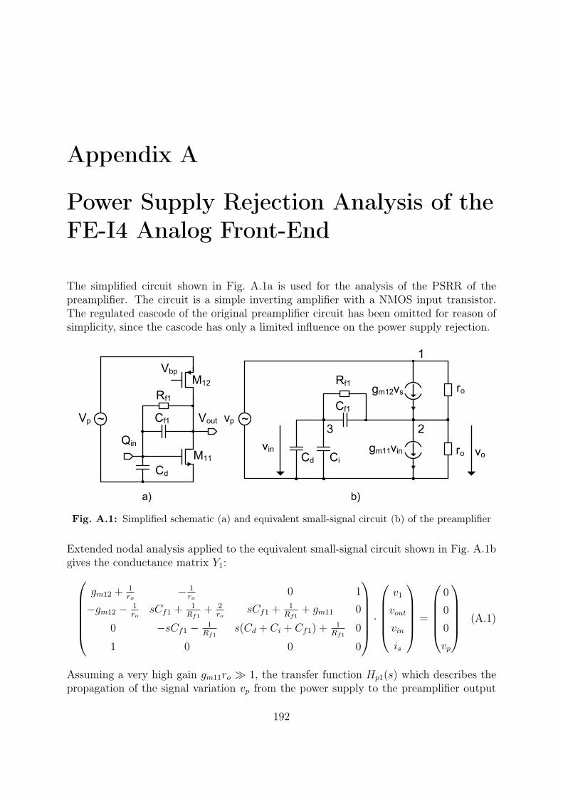
Appendix A
Power Supply Rejection Analysis of theFE-I4 Analog Front-End
The simplified circuit shown in Fig. A.1a is used for the analysis of the PSRR of thepreamplifier. The circuit is a simple inverting amplifier with a NMOS input transistor.The regulated cascode of the original preamplifier circuit has been omitted for reason ofsimplicity, since the cascode has only a limited influence on the power supply rejection.
M11
M12
Qin
Vout
Rf1
Cf1
Vbp
Cd
Vp ~
vorogm11vin
gm12vs ro
Cf1
Rf1
Cd Civin
3 2
1
vp ~
a) b)
Fig. A.1: Simplified schematic (a) and equivalent small-signal circuit (b) of the preamplifier
Extended nodal analysis applied to the equivalent small-signal circuit shown in Fig. A.1bgives the conductance matrix Y1:
gm12 +1ro
− 1ro
0 1
−gm12 − 1ro
sCf1 +1
Rf1+ 2
rosCf1 +
1Rf1
+ gm11 0
0 −sCf1 − 1Rf1
s(Cd + Ci + Cf1) +1
Rf10
1 0 0 0
·
v1
vout
vin
is
=
0
0
0
vp
(A.1)
Assuming a very high gain gm11ro ≫ 1, the transfer function Hp1(s) which describes thepropagation of the signal variation vp from the power supply to the preamplifier output
192
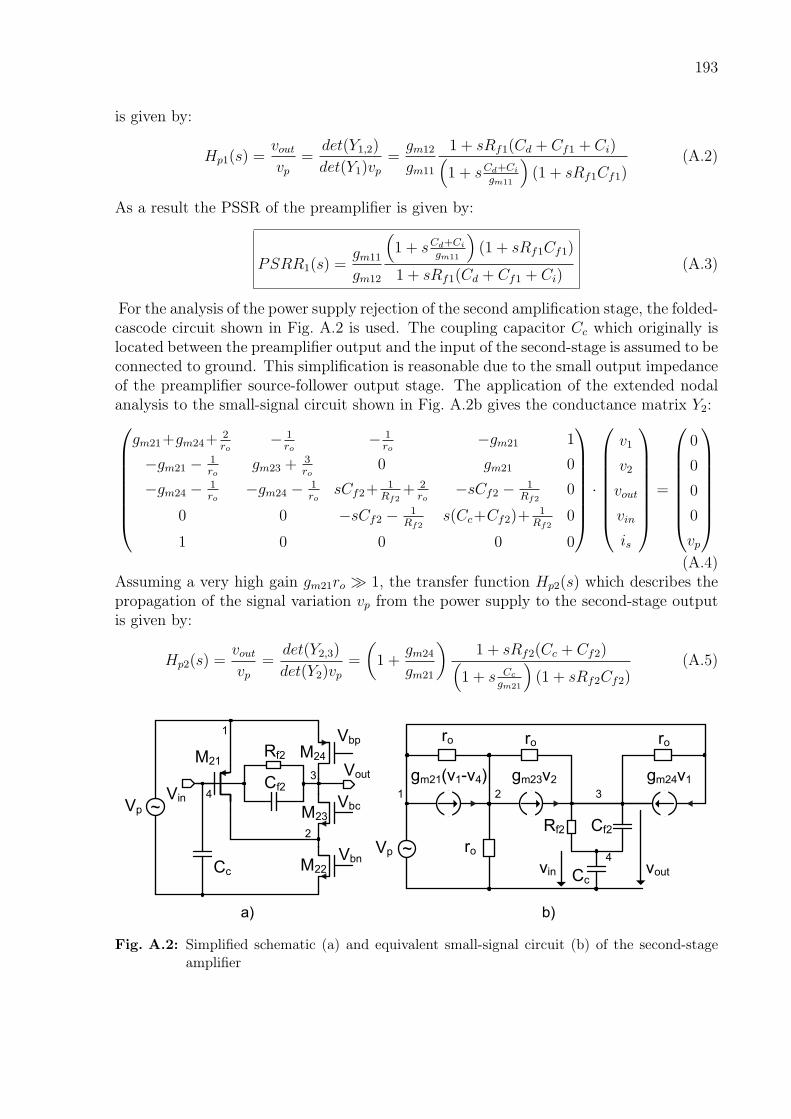
193
is given by:
Hp1(s) =voutvp
=det(Y1,2)
det(Y1)vp=
gm12
gm11
1 + sRf1(Cd + Cf1 + Ci)(1 + sCd+Ci
gm11
)(1 + sRf1Cf1)
(A.2)
As a result the PSSR of the preamplifier is given by:
PSRR1(s) =gm11
gm12
(1 + sCd+Ci
gm11
)(1 + sRf1Cf1)
1 + sRf1(Cd + Cf1 + Ci)(A.3)
For the analysis of the power supply rejection of the second amplification stage, the folded-cascode circuit shown in Fig. A.2 is used. The coupling capacitor Cc which originally islocated between the preamplifier output and the input of the second-stage is assumed to beconnected to ground. This simplification is reasonable due to the small output impedanceof the preamplifier source-follower output stage. The application of the extended nodalanalysis to the small-signal circuit shown in Fig. A.2b gives the conductance matrix Y2:
gm21+gm24+2ro
− 1ro
− 1ro
−gm21 1
−gm21 − 1ro
gm23 +3ro
0 gm21 0
−gm24 − 1ro
−gm24 − 1ro
sCf2+1
Rf2+ 2
ro−sCf2 − 1
Rf20
0 0 −sCf2 − 1Rf2
s(Cc+Cf2)+1
Rf20
1 0 0 0 0
·
v1
v2
vout
vin
is
=
0
0
0
0
vp
(A.4)
Assuming a very high gain gm21ro ≫ 1, the transfer function Hp2(s) which describes thepropagation of the signal variation vp from the power supply to the second-stage outputis given by:
Hp2(s) =voutvp
=det(Y2,3)
det(Y2)vp=
(1 +
gm24
gm21
)1 + sRf2(Cc + Cf2)(
1 + s Cc
gm21
)(1 + sRf2Cf2)
(A.5)
a) b)
M22
M21
M23
M24
Vin
Cc
Vp ~
Vbp
Vbn
Vbc
Vout gm23v2gm21(v1-v4)
1
2
3
4 1
Vp ~
ro
ro
Cf2
Rf2
Cf2Rf2
Cc
2
ro
3
ro
gm24v1
4voutvin
Fig. A.2: Simplified schematic (a) and equivalent small-signal circuit (b) of the second-stageamplifier

194 APPENDIX A. PSRR ANALYSIS OF THE FE-I4 ANALOG FRONT-END
As a result the PSSR of the second stage is given by:
PSRR2(s) =gm21
gm21 + gm24
(1 + s Cc
gm21
)(1 + sRf2Cf2)
1 + sRf2(Cc + Cf2)(A.6)
Appendix B
Noise Analysis of the FE-I4 AnalogFront-End
All dominant sources of noise are located at the very front of the analog signal processingchain and affect the input of the preamplifier. Thermal and flicker noise is coming from thepreamplifier input transistor. Thermal noise is also generated by the preamplifier feedbackand the leakage current compensation transistor. To study analytically the influence thenoise sources have on the output signal of the analog front end, expressions for the PSD1
of the respective noise sources have to be formulated and the noise transfer functions haveto be calculated.
B.1 Preamplifier feedback and leakage compensationtransistor
Both the preamplifier feedback and the leakage compensation transistor generate thermalnoise. Since these transistors are biased in weak inversion, the noise expression is givenby the shot noise formula. Flicker noise generated by this transistors is neglected for theanalysis because this noise contribution is very small.
Sleak = 2qIleak (B.1)
Sfb = 2qIfb (B.2)
The transistors generate a current mode noise which flows into the preamplifier input andis processed in the same way as a regular signal. As a result the noise transfer function isequal to the signal transfer function. For the transfer function calculation the simplifiedsmall signal equivalent circuit shown in Fig. B.1 is used. Special care has to be given tothe modeling of the feedback transistor. Since a constant-current feedback is used, theeffective feedback resistance is not constant but depends on the voltage drop VDS acrossthe the feedback transistor. In equilibrium when the feedback transistor is in linear region,the effective feedback resistance is much smaller than during signal processing when thefeedback transistor is saturated. Noise affects the detection performance in particular
1Power Spectral Density
195

196 APPENDIX B. NOISE ANALYSIS OF THE FE-I4 ANALOG FRONT-END
Vout
Rf1
Cf1
CinIin Cd rogmVinVin~
Fig. B.1: Simplified equivalent small signal circuit of the FE-I4 preamplifier
during the comparator threshold crossing. For this reason, the region of operation whichthe feedback transistor reaches when the signals is close to the comparator threshold hasbeen chosen for the noise analysis. As is shown in Fig. 5.15, for a typical operationalthreshold of 3000 e− the preamplifier feedback transistor is not saturated but in the linearregion. Nodal analysis gives then the following conductance matrix Yi:(
s (Cd + Ci + Cf1) +1
Rf1−sCf1 − 1
Rf1
gm − sCf1 − 1Rf1
sCf1 + 1/ro +1
Rf1
)·
(vin
vout
)=
(iin
0
)· (B.3)
Assuming an amplifier with a very high gain gmro ≫ 1, the transfer function Hi(s) iscalculated to be:
Hi(s) =voutiin
=det(Yi,2)
det(Yi)iin=
Rf
(1− s
Cf1
gm
)(1 + sCd+Ci
gm
)(1 + sRf1Cf1)
(B.4)
In the context of this analysis, the zero in the transfer function numerator is neglected asit affects only very high frequencies.
Hi(s) =Rf1
(1 + sτr) (1 + sτf1)with τf1 = Rf1Cf1 , τr =
Cd + Ci
gm(B.5)
The transfer function of the second amplification stage is calculated by means of theformula of the inverting amplifier neglecting the bandwidth limitation of the second-stageamplifier.
H2(s) =sRf2Cc
1 + sτf2with τf2 = Rf2Cf2 (B.6)
The total transfer function is then given by:
Hit(s) =sRf1Rf2Cc
(1 + sτr) (1 + sτf1) (1 + sτf2)(B.7)
The RMS noise at the output of the analog front-end caused by the noise contribution ofthe preamplifier feedback transistor and the leakage compensation transistor is calculated
B.2. PREAMPLIFIER INPUT TRANSISTOR 197
by integration of the noise PSD, combining equation B.7,B.1 and B.2:
V 2it =
∞∫0
H2it(s)(Sleak + Sfb) df (B.8)
=Sleak + Sfb
2π
∞∫0
(ωRf1Rf2Cc)2
(1 + (ωτr)2)(1 + (ωτf1)2)(1 + (ωτf2))2dω (B.9)
=(Rf1Rf2Cc)
2
4(τr + τf1)(τr + τf2)(τf1 + τf2)(Sleak + Sfb) (B.10)
Taking into account that the feedback time constant of the second amplification stage τf2is much longer than the preamplifier feedback time constant τf1 and that both feedbacktime constants are much longer than the preamplifier signal rise time τr (τf2 ≫ τf1 ≫ τr),equation B.10 can be simplified to:
V 2it =
(Rf1Rf2Cc)2
4τf1τ 2f2(Sleak + Sfb) (B.11)
The ENC is calculated by dividing the output RMS noise by the charge signal gain factorand the elementary charge q. Taking the additional gain factor Cc/Cf2 of the second stageinto account and combining equation B.1 and B.2, the ENC generated by the leakagecurrent and the feedback transistor is given by:
ENC2it = V 2
it
(Cf1Cf2
Ccq
)2
=τf12q
(Ileak + Ifb) =Rf1Cf1
2q(Ileak + Ifb) (B.12)
Equation B.12 shows that the noise coming from the leakage compensation transistor andthe preamplifier is proportional to the leakage current Ileak and the feedback current Ifbrespectively. Both noise contributions are independent of the detector capacitance andscale with the preamplifier feedback time constant τf1.
B.2 Preamplifier input transistorThe preamplifier input transistor contributes both with thermal and flicker noise. Sincethe input transistor is operating in weak inversion the respective thermal noise PSDexpression and a simple flicker noise PSD expression is used. For the calculation the noisePSD is referred to the transistor gate.
Sth =2qIdg2m
(B.13)
Sf =KF
fwith KF =
KF
WLCox
(B.14)
For the transfer function calculation of the input transistor noise contributions, the sim-plified small signal equivalent circuit shown in Fig. B.2 is used. Applying extended nodalanalysis results in the conduction matrix Yv:

198 APPENDIX B. NOISE ANALYSIS OF THE FE-I4 ANALOG FRONT-END
Vout
Rf1
Cf1
CinCd rogmVgVg
Vnoise
Vin
Fig. B.2: Simplified equivalent small signal circuit of the FE-I4 preamplifier including the inputtransistor noise source
0 0 0 −1
0 s (Cd + Ci + Cf1) +1
Rf1−sCf1 − 1
Rf11
gm −sCf1 − 1Rf1
sCf1 +1ro+ 1
Rf10
−1 1 0 0
·
vg
vin
vout
inoise
=
0
0
0
vnoise
(B.15)
Assuming an amplifier with a very high gain gmro ≫ 1 the transfer function is calculatedto be:
Hv(s) =voutvnoise
=det(Yv,3)
det(Yv)vnoise=
1 + sRf1 (Cd + Cf1 + Ci)
(1 + sτr) (1 + sτf1)(B.16)
The total transfer function is then given by combination with the second-stage transferfunction from equation B.6:
Hvt(s) =sRf2Cc (1 + sτz)
(1 + sτr) (1 + sτf1) (1 + sτf2)with τz = Rf1(Cd + Cf1 + Ci) (B.17)
The RMS noise at the output of the analog front-end caused by the thermal noise comingfrom the preamplifier input transistor is calculated by the integration of the thermal noisePSD combining equation B.13 and B.17.
V 2vth =
Sth
2π
∞∫0
(ωRf2Cc)2(1 + (ωτz)
2)
(1 + (ωτr)2)(1 + (ωτf1)2)(1 + (ωτf2)2)dω (B.18)
= (Rf2Cc)2 τ 2z (τf1 + τf2) + τr(τ
2z + τf1τf2)
4τrτf1τf2(τr + τf1)(τr + τf2)(τf1 + τf2)Sth (B.19)
Assuming τf2 ≫ τz ≫ τf1 ≫ τr, equation B.19 can be simplified to:
V 2vth = (Rf2Cc)
2 τ 2z4τrτ 2f1τ
2f2
Sth (B.20)
The ENC is calculated by dividing the output RMS noise by the charge signal gain factorand the elementary charge q which in combination with equation B.13 gives:
ENC2vth = V 2
vth
(Cf1Cf2
Ccq
)2
=C2
f1τ2z
τrτ 2f1
Ibias2qg2m
=(Cd + Ci + Cf )
2
Cd + Ci
nVt
2q(B.21)

B.2. PREAMPLIFIER INPUT TRANSISTOR 199
Equation B.21 shows that the thermal noise contributed by the preamplifier input tran-sistor scales with the detector capacitance Cd and the effective preamplifier feedbackresistance Rf1. The RMS noise at the output of the analog front-end caused by the flickernoise contribution of the preamplifier input transistor is calculated by the integration ofthe flicker noise PSD combining equation B.14 and B.17.
V 2vf = KF
∞∫0
(ωRf2Cc)2(1 + (ωτz)
2)
(1 + (ωτr)2)(1 + (ωτf1)2)(1 + (ωτf2)2)ωdω (B.22)
= KF (Rf2Cc)2
[(τ 2r − τ 2z ) ln(τr)
(τ 2r − τ 2f1)(τ2r − τ 2f2)
−(τ 2f1 − τ 2z ) ln(τf1)
(τ 2r − τ 2f1)(τ2f1 − τ 2f2)
−(τ 2z − τ 2f2) ln(τf2)
(τ 2r − τ 2f2)(τ2f1 − τ 2f2)
](B.23)
Assuming τf2 ≫ τz ≫ τf1 ≫ τr, equation B.23 can be simplified to:
V 2vf = KF (Rf2Cc)
2
[τ 2z
τ 2f1τ2f2
ln
(τf1τr
)+
ln(τf2)
τ 2f2
](B.24)
The ENC is calculated by dividing the output RMS noise by the charge signal gain factorwhich results in:
ENC2vf = V 2
vf
(Cf1Cf2
Ccq
)2
=
[C2
f1τ2z
τ 2f1ln
(τf1τr
)+ τ 2f1 ln(τf2)
]KF
q2(B.25)
Equation B.25 shows that the flicker noise contributed by the preamplifier input transistorscales with the detector capacitance Cd and the preamplifier feedback time constant τf1.The total ENC is the quadratic sum of all single ENC contributions. Combining equationsB.25, B.21 and B.12 results in:
ENC =√
ENC2it + ENC2
vth + ENC2vf (B.26)
ENC =
√√√√τf12q
(Ileak + Ifb) +C2
f1τ2z
τrτ 2f1
Ibias2qg2m
+
[C2
f1τ2z
τ 2f1ln
(τf1τr
)+ τ 2f1 ln(τf2)
]KF
q2
with τz = Rf1(Cd + Cf1 + Ci) , τr =Cd + Ci
gm, τf1 = Rf1Cf1 , τf2 = Rf2Cf2
(B.27)
Bibliography
[Aad08a] G. Aad et al., The ATLAS experiment at the Large Hadron Collider, Journalof Instrumentation 3, S08003, 2008
[Aad08b] G. Aad et al., ATLAS pixel detector electronics and sensor, Journal of Instru-mentation 3, P07007 (2008)
[Ahl09] G. Ahluwalia, Entwicklung eines Auslesesystems für das Compton-Polarimeterder Elektronen-Stretcher-Anlage (ELSA), Faculty of Information-, Media- andElectrical Technology, University of Applied Sciences Cologne, 2009
[Ame02] A. Amerasekera, C. Duvvury, ESD in Silicon Integrated Circuits, Wiley & Sons,2nd edition, 2002
[Ale03] ALEPH, DELPHI, L3, OPAL, The LEP Working Group for Higgs BosonSearches, Search for the Standard Model Higgs boson at LEP, Physics Letters,B565, 61, 2003
[Ale07] ALEPH, DELPHI, L3, OPAL, SLD Collaborations, The LEP ElectroweakWorking Group, The SLD Electroweak and Heavy Flavour Groups, PrecisionElectroweak Measurements on the Z Resonance, Physics Reports, 427, 5-6, 2007
[Alt90] K.H. Althoff, W. v. Drachenfels, A. Dreist, D. Husmann, M. Neckenig, H.D.Nuhn, W. Schauerte, M. Schillo, F.J. Schittko, C. Wermelskirchen, ELSA -One year of experience with the Bonn Electron Stretcher Accelerator, ParticleAccelerators, Vol. 27, p. 101-106, 1990
[Ams08] C. Amsler et al. (Particle Data Group), Physics Letters, B667, 1, 2008
[Ane01] G. Anelli, F. Faccio, S. Florian and P. Jarron, Noise characterization of a 0.25µm CMOS technology for the LHC experiments, Nuclear Instuments and Meth-ods, A457, 361-368, 2001
[Ann99] A. Annema, Low-Power Bandgap References Featuring DTMOST’s, IEEE Jour-nal of Solid-State Circuits, Vol. 34, No. 7, 1999
[Ann05] A. Annema, B. Nauta, R. van Langevelde, H.Tuinhout, Analog Circuits in Ultra-Deep-Submicron CMOS, IEEE Journal of Solid-State Circuits, Vol. 40, No. 1,2005
200
BIBLIOGRAPHY 201
[Ans96] Electrical characteristics of low-voltage differential-signalling (LVDS) interfacecircuits, TIA/EIA-644, National Semiconductor Corp., ANSI/TIA/EIA Stan-dard, 1996
[Ark98] N. Arkami-Hamed, S. Dimopoulos, G. Dvali, The Hierarchy Problem and NewDimensions at a Millimeter, Physics Letters, B429, 263-272, 1998
[Aru09] D. Arutinov, M. Barbero, R. Beccherle, V. Buscher, G. Darbo, R. Ely, D.Fougeron, M. Garcia-Sciveres, D. Gnani, T. Hemperek, M. Karagounis, R.Kluit, V. Kostyukhin, A. Mekkaoui, M. Menouni, J. D. Schipper, N. Wermes,Digital Architecture and Interface of the New ATLAS Pixel Front-End IC forUpgraded LHC Luminosity, IEEE Transactions on Nuclear Science, Vol. 56 No.2, 388-393, 2009
[Atl97] The ATLAS collaboration, Inner Tracker: Technical Design Report, 1, CERN-LHCC-97-016; Inner Tracker: Technical Design Report, 2, CERN-LHCC-97-017, 1997
[Atl03] The ATLAS collaboration, ATLAS High-Level Trigger, Data Acquisition andControls - Technical Design Report, CERN-LHCC-2003-022, 2003
[Bak98] R. J. Baker, H. W. Li, D. E. Boyce, CMOS Circuit Design Layout and Simula-tion, IEEE Press, 1st edition, 1998
[Bak08] R. J. Baker, CMOS Circuit Design Layout and Simulation, IEEE Press, p. 629,2nd edition, 2008
[Ban99] H. Banba, H. Shiga, A. Umezawa, T. Miyaba, T. Tanzawa, S. Atsumi, K. Sakui,A CMOS Bandgap Reference Circuit with Sub-1-V Operation, IEEE Journal ofSolid-State Circuits, Vol. 34., No. 05, 1999
[Bar94] E. Barberis, N. Cartiglia, C. LeVier, J . Rahn, P. Rinaldi, H.F.-W. Sadrozinski,R. Wichmann, T. Ohsugi, Y. Unno, H. Mîyata, N. Tamura, K. Yamamoto,Capacitances in silicon microstrip detectors, Nuclear Instruments and Methods,A342, 90-95, 1994
[Bar09] M. Barbero, D. Arutinov, R. Beccherle, G. Darbo, R. Ely, D. Fougeron, M.Garcia-Sciveres, D. Gnani, T. Hemperek, M. Karagounis, R. Kluit, V. Kos-tioukhine, A. Mekkaoui, M. Menouni, J. D. Schipper, A new ATLAS pixelfront-end IC for upgraded LHC luminosity, Nuclear Instruments and Methods,A604, 397-399, 2009
[Bic88] H. Bichsel, Straggling in thin silicon detectors, Reviews of Modern Physics, Vol.60, Is. 3, 1988
[Bla97] L. Blanquart, A. Mekkaoui, V. Bonzom, P. Delpierre, Pixel analog cells pro-totypes for ATLAS in DMILL technology, Nuclear Instuments and Methods,A395, 313-317, 1997
202 BIBLIOGRAPHY
[Bon01] A. Boni, A. Pierazzi,D. Vecchi, LVDS I/O interface for Gb/s-per-pin operationin 0.35-µm CMOS, IEEE Journal of Solid-State Circuits, Vol. 36. No. 04, 2001
[Bue09] T. Büth, Logikentwurf, Layout und Verifikation einer I2C Einheit für einenASIC, diploma thesis, Faculty of Information-, Media- and Electrical Technol-ogy, University of Applied Sciences Cologne, 2009
[Car05] R. G. Carvajal, J. Ramirez-Angulo, A. J. Lopez-Martin, A. Torralba, J. A. G.Galan, A. Carlosena, F. M. Chavero, The flipped voltage follower: a useful cellfor low-voltage low-power circuit design, IEEE Transactions on Circuits andSystems I: Regular Papers, Vol. 52 Iss. 7, 1276-1291, 2005
[Cer97] A. Cerdeira, M. Estrada, Analytical Expressions for the Calculation of PixelDetector Capacitances, IEEE Transactions on Nuclear Science, Vol. 44 No. 1,1997
[Cer09] CERN faq, LHC the guide, Communication Group, CERN Brochure, 2009-003-Eng, 2009
[Cha04] C. Chava, J. Silva-Martinez, A Frequency Compensation Scheme for LDO Volt-age Regulators, IEEE Transactions on Circuits and Systems I - Regular Papers,Vol. 51, No.6, 2004
[Cit07] M. Citterio, F. Alberti, G. Alimonti, A. Andreani, A. Andreazza, F. Bellina, K.Einsweiler, S. Kersten, K. Lantzsch, M. Leyton, S. Latorre, C. Meroni, E. Mu-sial, F. Sabatini, Voltage-Regulation Stations for the Distributed Power SupplySystem of the ATLAS Pixel Detector, IEEE Nuclear Science Symposium Con-ference Record 2007, Honolulu, Hawaii, USA, 2007
[Cza86] Z. Czarnul, Modification of the Banu-Tsividis continuous-time integrator struc-ture, IEEE Transactions on Circuits and Systems, Vol. 33, Iss. 7, 1986
[Dav03] C. Da Via, S.J. Watts, Can silicon operate beyond 1015 neutrons cm−2 ?, NuclearInstruments and Methods, A 501, 138-145,2003
[Dav06] C. Da Via. Status of 3d active edge silicon sensors. Cern Pixel Meeting, Sep.2006
[Dav08] C. Da Via, S. Parker, M. Deile, T. Hansen, J. Hasi, C. Kenney, A. Kok, S.Watts, Dual readout—strip/pixel systems, A594, 7– 12, 2008
[Del99] T. Deliyannis, Y. Sun, J. Fidler, Continuous Time Active Filter Design, CRCpress, 1999
[Dem00] N. Demaria et. al., New results on silicon microstrip detectors of CMS tracker,Nuclear Instruments and Methods, A447, 142-150, 2000
[Den09] P. Denes, R. Ely and M. Garcia-Sciveres, A Capacitor Charge Pump DC-DCConverter for Physics Instrumentation, IEEE Transactions on Nuclear Science,Vol. 56 No. 3, 2009
BIBLIOGRAPHY 203
[Din04] R. Dinapoli, A radiation tolerant pixel detector system for the ALICE andLHCb experiments at CERN, Dissertation, Université Montpellier, 2004
[Dob07] D. Dobos, Commissioning Perspectives for the ATLAS Pixel Detector, PhDthesis, University of Dortmund, 2007
[Dol98] D. Doll, Das Compton Polarimeter an ELSA, Dissertation, Physics Department,University of Bonn, 1998
[Dol02] D. Doll, P. Fischer, W. Hillert, H. Krueger, K. Stammschroer and N. Wermes,A counting silicon microstrip detector for precision compton polarimetry, Nucl.Instr. Meth., A492, 2002
[Egg09] C. Egggel, CMS Pixel Module Qualification and Search for B0s → µ+µ−, Dis-
sertation, ETH Zürich, 2009
[Eli02] J. R. Ellis, Limits of the Standard Model, arXiv:hep-ph/0211168v1, 2002
[Enz95] C. C. Enz, F. Krummenacher and E. A. Vittoz, An Analytical MOS TransistorModel Valid in All Regions of Operation and Dedicated to Low-Voltage andLow-Current Applications, Journal of Analog Integrated Circuits and SignalProcessing, Kluwer Academic Publishers, No. 8, p. 83-114, 1995
[Enz06] C. C. Enz and E. A. Vittoz, Charge based MOS Transistor Modeling - TheEKV model for low-power and RF IC design, John Wiley & Sons, 2006
[Eva08] L. Evans, P. Bryant, LHC Machine, Journal of Instrumentation 3, SO8001, 2008
[Fio04] C. Fiorini, M. Porro, Integrated RC Cell for Time Invariant Shaping Amplifiers,IEEE Transactions on Nuclear Science, Vol. 51, No. 5, 2004
[Fis96] P. Fischer, An area efficient 128 channel counter chip, Nuclear Instuments andMethods, A378, 297-300, 1996
[Fis04] P. Fischer, E. Kraft, Low swing differential logic for mixed signal applications,Nuclear Instruments and Methods, A518, 511-514, 2004
[Fri05] F. Friori, P. Crovetti, A New Compact Temperature-Compensated CMOS Cur-rent Reference, IEEE Transactions on Circuits and Systems-II: Express Briefs,Vol. 52, No. 11, 2005
[Gar09] M. Garcia-Sciveres, D. Gnani, On-chip DC-DC charge pump for ATLAS FEI4,Common ATLAS CMS Electronics Workshop for SLHC 2009, CERN, Geneva,Switzerland, 2009
[Geo90] G. Georginis, A Low-Noise Preamplifier-Filter System, Nuclear Instuments andMethods, A 294, 563-574, 1990
[Ger99] G. De Geronimo, P. O´Connor, A CMOS detector leakage current self-adaptablecontinuous reset system: Theoretical analysis, Nuclear Instruments and Meth-ods, A421, 322-333, 1999
204 BIBLIOGRAPHY
[Gla61] S. L. Glashow, Partial-symmetries of weak interactions, Nuclear Physics 22,579–588, 1961
[God09] S. Godiot, M. Barbero, B. Chantepie, J.C. Clémens, R. Fei, J. Fleury, D.Fougeron, M. Garcia-Sciveres, T. Hemperek, M. Karagounis, H. Krueger, A.Mekkaoui, P. Pangaud, A. Rozanov, N. Wermes, 3D electronics for hybrid pixeldetectors, Topical Workshop on Electronics for Particle Physics 2008, Paris,France, 2009
[Gor01] G. Gorfine, M. Hoeferkamp, G. Santistevan, S. Seidel, Capacitance of siliconpixels, Nuclear Instruments and Methods, A460, 336-351, 2001
[Gra97] G. Gramenga, P. De O´Connor, P. Rehak and S. Hart, CMOS preamplifier forlow-capacitance detectors, Nuclear Instuments and Methods, A390, 241-250,1997
[Gro01] D. E. Groom, V. Mokhov, S. Striganov, Muon Stopping Power and Range Tables10 MeV - 100 TeV, Atomic Data and Nuclear Data Tables, Vol.76, No. 2, 2001
[Gro08] M. Gronewald, Optimierung einer integrierten Ausleseelektronik für einen Siliz-iumstreifendetektor in 350nm CMOS Technologie unter Verwendung der Ca-dence Design-Software, diploma thesis, Faculty of Information-, Media- andElectrical Engineering, University of Applied Sciences Cologne, 2008
[Grm08] V. Gromov, R. Kluit, A Radiation Hard Current Reference Circuit in a Stan-dard 0.13µm CMOS Technology, Topical Workshop on Electronics for ParticlePhysics 2008, Naxos, Greece, 2008
[Gry07] P. Grybos, M. Idzik, and P. Maj, Noise Optimization of Charge Amplifierswith MOS Input Transistors Operating in Moderate Inversion Region for ShortPeaking Times, IEEE Transactions on Nuclear Science, Vol. 54 No. 3, 2007
[Har07] J. Harder, V. Radeka, G. Smith and B. Yu, A Low-Noise Low Stored En-ergy Preamplifier For High-Voltage Radiation Detectors, Nuclear Instumentsand Methods, A576, 397-402, 2007 Proceedings of the 14th International SpinPhysics Symposium SPIN2000, Osaka, 2000
[Hem09] T. Hemperek, D. Arutinov, M. Barbero, R. Beccherle, G. Darbo, S. Dube, D.Elledge, D. Fougeron, M. Garcia-Sciveres, D. Gnani, V. Gromov, M. Karagou-nis, R. Kluit, V. Kostyukhin, A. Kruth, A. Mekkaoui, M. Menouni, J. D. Schip-per, N. Wermes, Digital Architecture of the New ATLAS Pixel Chip FE-I4,Proceedings of the Nuclear Science Symposium 2009, Orlando, USA, 2009
[Hig64] P. W. Higgs, Broken Symmetries and the Masses of Gauge Bosons, PhysicalReview Letters 13, 508–509, 1964
[Hil00] W. Hillert, M. Gowin, B. Neff, The 50 kV inverted source of polarized elec-trons at ELSA, Proceedings of the 14th International Spin Physics SymposiumSPIN2000, Osaka, 2000
BIBLIOGRAPHY 205
[Hil06] W. Hillert, The European Journal of Physics A - Hadrons and Nuclei, Vol. 28Sup. 1, p. 139-148, 2006
[Hil09] W. Hillert, B. Aurand, J. Wittschen, The Compton Polarimeter at ELSA, Pro-ceedings of the 18th International Spin Physics Symposium, Vol. 1149, p. 1160-1164, 2009
[Hof00] M. Hoffmann, W. v. Drachenfels, F. Frommberger, M. Gowin, K. Helbing, W.Hillert, D. Husmann, J. Keil, T. Michel, J. Naumann, T. Speckner, G. Zeitler,The polarized electron beam at ELSA, Proceedings of the 14th InternationalSpin Physics Symposium SPIN2000, Osaka, 2000
[Hoo78] F. N. Hooge, L. K. J. Vandamme, Lattice scattering causes 1/f noise, PhysicsLetters A, Vol. 66 Iss. 4, 315-316, 1978
[Ibm09] CMOS8RF/CMRF8SF ESD Reference Guide, IBM cooperation, 2009
[Iee94] IEEE Standard for Low-Voltage Differential Signals (LVDS) for Scalbale Coher-ent Interface (SCI), 1596.3 SCI-LVDS Standard, IEEE Standard 1596.3-1996,1994
[Kan99] A. Kandasamy, E. O’Brien, P. O’Connor, W. Von Achen, A monolithicpreamplifier-shaper for measurement of energy loss and transition radiation,IEEE Transactions on Nuclear Science, Vol. 46, Iss. 3, 1999
[Kap04] J. Kaplon, Fast Bipolar and CMOS Rad-Hard Front End Electronics for Sili-con Strio Detectors, Dissertation, AGH University of Science and Technology,Cracow, Poland, 2004
[Kar08] M. Karagounis, D. Arutinov, M. Barbero, R. Beccherle, G. Darbo, R. Ely, D.Fougeron, M. Garcia-Sciveres, D. Gnani, V. Gromov, T. Hemperek, H. Junker,M. Menouni, A. Mekkaoui, R. Kluit, J.D. Schipper, Development of the ATLASFE-I4 pixel readout IC for b-layer Upgrade and Super-LHC, Topical Workshopon Electronics for Particle Physics 2008, Naxos, Greece, 2008
[Kar09a] M. Karagounis, D. Arutinov, M. Barbero, F. Huegging, H. Krueger, N. Wermes,An integrated Shunt-LDO regulator for serial powered systems, Proceedings ofthe IEEE European Solid-State Circuits Conference, Athens, Greece, p. 276 -279, 2009
[Kar09b] M. Karagounis, G. Ahluwalia, M. Gronewald, M. Koch, H. Krueger, N. Wermes,Development of a counting strip detector readout chip for precision compton po-larimetry, IEEE Nuclear Science Symposium Conference 2009 Record, Orlando,USA, 2009
[Kis07] T. Kishishitaa, H. Ikedaa, T. Kiyunac, K. Tamuraa, K. Nakazawab, T. Taka-hashia, Development of a low-noise analog front-end ASIC for CdTe detectors,Nuclear Instruments and Methods in Physics Research, A 580, 1363–1371, 2007
206 BIBLIOGRAPHY
[Kla59] J. Klapper, C. Harris, On the response and approximation of Gaussian filters,IRE Transactions on Audio, Vol. 3, No. 3, 1959
[Kno89] G. Knoll, Radiation Detection and Measurement, 3rd edition, John Wiley andsons, 1989
[Koc06] M. Koch, Chipentwicklung für Pixel- und Mikrostreifendetektorelektronik fürden Teilchennachweis und biomedizinische Bildgebung, diploma thesis, PhysicsInstitute, Bonn University, BONN-IB-2006-04, 2006.
[Koc09] M. Kocian, 160 Mbit/s Link Over 6-m-Long Twisted Pair, IBL General Meeting,CERN, 2009
[Kot09] D. Kotlinski, Private Communication, Pau-Scherer Institute, Basel, Switzer-land, 2009
[Kru91] F. Krummenacher, Pixel detectors with local intelligence : an IC designer pointof view, Nuclear Instruments and Methods, A305, 527-532, 1991
[Kru09] A. K. Kruth, G. Ahluwalia, D. Arutinov, M. Barbero, R. Beccherle, S. Dube, G.Darbo, D. Elledge, R. Ely, D. Fougeron, M. Garcia-Sciveres, D. Gnani, V. Gro-mov, M. Gronewald, T. Hemperek, M. Karagounis, R. Kluit, V. Kostioukhine,A. Mekkaoui, M. Menouni, J. D. Schipper, Charge Pump Clock GenerationPLL for the Data Output Blocks of the Upgraded ATLAS Front-End in 130nmCMOS, Proceedings of the Topical Workshop on Electronics for Particle Physics2009, Paris, France, 2009
[Lan44] L. Landau, On the energy loss of fast particles by ionization, Journal of Physics,Vol. 8, No. 4, 201–205, 1944
[Leo87] W. R. Leo, Techniques for Nuclear and Particle Physics Experiments, 2nd edi-tion, Springer, 1987
[Luh98] L. Luh, J. Choma, J. Drapper, A Continuous-Time Common-Mode FeedbackCircuit (CMFB) for High-Impedance Current Mode Application, IEEE Intern-tation Conference on Electronics, Circuits and System, Lisboa, Portugal, 1998
[Lut99] G. Lutz, Semiconductor Radiation Detectors, Springer, 1999
[Mak95] M. Makowski, D. Maksimovic, Performance Limits of Switched-Capacitor DC-DC Converters, Power Electronics Specialists Conference, June 18-22 1995, pp1215-1221, 1995
[Man07] M. Manghisoni, L. Ratti, V. Re, V. Speziali, and G. Traversi, Resolution Limitsin 130 nm and 90 nm CMOS Technologies for Analog Front-End Applications,IEEE Transactions on Nuclear Science, Vol 54 No. 3, 2007
[Mar97] S. P. Martin, A Supersymmetry Primer, arXiv:hep-ph/9709356v5, 1997
BIBLIOGRAPHY 207
[Max07] Robust Fail-Safe Biasing Circuit for AC-Coupled Multidrop LVDS Bus, Aplica-tion Note 4007, Maxim Engineering Journal, Vol. 60, 2007
[McW57] A. L. McWhorter, 1/f noise and germanium surface properties, SemiconductorSurface Physics, 207-228, University of Pennsylvania Press, 1957
[Men08] M. Menouni, D. Arutinov, M. Barbero, R. Beccherle, R. Ely, D. Fougeron,M. Garcia-Sciveres, D. Gnani, T. Hemperek, M. Karagounis, R. Kluit, A.Mekkaoui, A. Rozanov, J. D. Schipper, Design and Measurement of SEU tol-erant latches, Proceedings of the Topical Workshop on Electronics for ParticlePhysics 2008, Naxos, Greece, pp 402-405, 2008
[Mih09] M. Miyahara, A. Matsuzawa, A low-offset latched comparator using zero-staticpower dynamic offset cancellation technique, IEEE Asian Solid-State CircuitsConference, Tapei, Taiwan, 2009
[Mil20] J. M. Miller,Dependence of the input impedance of a three-electrode vacuumtube upon the load in the plate circuit, Scientifc Papers of the Bureau ofStandards,15(351):367-385, 1920
[Mou06] P. Mouche, Overall View of the LHC, CERN PhotoLab, CERN-DI-0609031,2006
[Nis06] J. Nissinen, J. Kostamovaara, Fully Differential Regulated Cascode, IEEEMediterranean Electrotechnical Conference, Malaga, Spain, 2006
[Nor63] D. North, An Analysis of the Factors Which Determine Signal Noise Discrim-ination in Pulsed-Carrier Systems, Proceedings of the IEEE, Vol. 51, Iss. 7,1963
[Nou07] T. Noulis, C. Deradonisa, S. Siskosa, G. Sarrabayrouse, Detailed study of par-ticle detectors OTA-based CMOS Semi-Gaussian shapers, Nuclear Instrumentsand Methods, A583, 469–478, 2007
[Ohk76] S. Ohkawa, M. Yoshizawa, K. Husimi, Direct Synthesis of the Gaussian Filterfor Nuclear Pulse Amplifiers, Nuclear Instruments and Methods, Vol. 138, Iss.1, 1976
[Par04] S. Park, H. Yoo, 1.25-Gb/s Regulated Cascode CMOS Transimpedance Am-plifier for Gigabit Ethernet Applications, IEEE Journal of Solid-State Circuits,Vol. 39, No. 1, 2004
[Par97] S. Parker, C. Kenney, and J. Segal. 3D – A proposed new architecture for solid-state radiation detectors, Nucl. Inst. and Meth. A, 395:328–343, 1997
[Par08] S. Parker, C. Da Via, M. Deile, T. Hansen, J. Hasi, C. Kenney, A. Kok, S.Watts, Dual readout: 3D direct/induced-signals pixel systems, A594, 332–338,2008
208 BIBLIOGRAPHY
[Peq08] J. Pequenao, Computer Generated Image of the whole ATLAS Detector, CERNPhotoLab, CERN-GE-0803012 05, 2008
[Per04] I. Peric, Design and Realisation of Integrated Circuits for the Readout of PixelSensors in High-Energy Physics and Biomedical Imaging, Dissertation, PhysicsDepartment, University of Bonn, 2004
[Per06] I. Peric, L. Blanquart, G. Comes, P. Denes, K. Einsweiler, P. Fischer, E. Man-delli, G. Meddeler, The FE-I3 readout chip for the ATLAS pixel detector, Nu-clear Instruments nad Methods, A565, 2006
[Per07] I. Peric, A novel monolithic pixelated particle detector implemented in high-voltage CMOS technology, Nuclear Instruments and Methods, A582, 876–885,2007
[Pla03] R. van de Plassche, CMOS Integrated Analog-to-Digital and Digital-to-AnalogConverters, Kluwer, 2003
[Rad67] V. Radeka, N. Karlovac, Least-Square-Error Amplitude Measurement of PulseSignals in Presence of Noise, Nuclear Instruments and Methods, A52, 86-92,1967
[Ram39] S. Ramo, Proceedings of the Institute of Radio Engineers, Vol. 27, 584–585,1939
[Ram08] P. Ramm, C. Bower, P. Garrou, Handbook of 3D Integration: Technology andApplications of 3D Integrated Circuits, Wiley-VCH, 2008
[Raz01] B. Razavi, Design of Analog CMOS Integrated Circuits, McGraw-Hill, p.108,2001
[Re05] V. Re, M. Manghisoni, L. Ratti, V. Speziali, and G. Traversi, Survey of NoisePerformances and Scaling Effects in Deep Submicrometer CMOS Devices FromDifferent Foundries, IEEE Transactions on Nuclear Science, Vol. 52 No. 6, 2005
[Ric44] S. Rice, Mathematical Analysis of random noise, Bell System Technical Journal,Iss. 23, 282-332, 1944
[Rin98] G. Rincon-Mora, P. Allen, A low-voltage, low quiescent current, low drop-outregulator, Vol. 33, No. 1, 1998
[Roe94] C. Rrnnqvist, F. Santos, O. Toker, P. Weilhammer, K. Yoshioka, E. Nygard,A. Czermak, P. Jalocha, W. Dulinski, Y. Hu, Double-sided silicon microstripdetectors and low noise self-triggering multichannel readout chips for imagingapplications, Nuclear Instruments and Methods in Physics Research, A348, 440-443, 1994
[Roh98] T. Rohe, F. Hügging, G. Lutz, R.H. Richter, R. Wunsdorf, Nuclear Instrumentsand Methods, A409, 224-228, 1998
BIBLIOGRAPHY 209
[Ros06] L. Rossi, P. Fischer, T. Rohe, N. Wermes, Pixel Detectors From Fundamentalsto Applications, Springer, 2006
[Rov00] L. Rovati, Optimum Preamplification and Shaping of Signals Delivered byPhotodetectors Without Internal Amplification: A Theoretical Analysis, IEEETransaction on Circuits and Systems-II: Analog and Digital Signal Processing,Vol. 47, No. 5, 2000
[Sak87] E. Säckinger, W. Guggenbühl, A versatile building block: the CMOS differentialdifference amplifier, IEEE Journal of Solid-State Circuits, Vol. 22, Iss. 2, 1987
[Sad01] H. Sadrozinski, Applications of Silicon Detectors, IEEE Transactions on NuclearScience, Vol. 48, No. 4, 2001
[Sal68] A. Salam, Elementary Particle Theory, N. Svartholm (ed.), Almquvist and Wik-sell, Stockholm, 367, 1968
[Sam04] L. Samid, P. Volz, Y. Manoli, A dynamic analysis of a latched CMOS compara-tor, Proceedings of the 2004 International Symposium on Circuits and Systems,Vancouver, Canada, 2004
[San88] E. Sanchez-Sinencio, R. Geiger, H. Nevarez-Lozano, Generation of continuous-time two integrator loop OTA filter structure, IEEE Transactions on Circuitsand Systems, Vol. 35, Iss. 8, 1988
[San90] W. M. C. Sansen and Z. Yuan Chang, Limits of Low Noise Performance ofDetector Readout Front Ends in CMOS Technology, IEEE Transactions onCircuits and Systems, Vol. 37 No. 11, 1990
[San06] W. Sansen, Analog Design Essentials, Springer, p. 136, 2006
[San08] R. Santoro et. al., The ALICE Silicon Pixel Detector: readiness for the firstproton beam, Journal of Instrumentation, Vol. 4, P03023, 2009
[Sau05] M. Saukoski, L. Aaltonen, K. Halonen, T. Salo, Fully Integrated Charge Sensi-tive Amplifier for Readout of Micromechanical Capacitive Sensors, IEEE Inter-national Symposium on Circuits and Systems, Kobe, Japan, 2005
[Spe04] T. Speckner, G. Anton, W. von Drachenfels , F. Frommberger, K. Helbing, M.Hoffmann,1, B. Kiel, T. Michel, J. Naumann, G. Zeitler, The GDH-Moeller-Polarimeter at ELSA, Nuclear Instruments and Methods, A519, 518-531, 2004
[Spi05] H. Spieler, Semiconductor Detector Systems, Oxford University Press, 2005
[Ta06] D.B. Ta, T. Stockmanns, F. Huegging, P. Fischer, J. Grosse-Knetter, O. Runolf-sson and N. Wermes, Serial powering: Proof of principle demonstration of ascheme for the operation of a large pixel detector at the LHC, Nuclear Instru-ments and Methods, A557, 2006
210 BIBLIOGRAPHY
[Tol56] H. A. Tolhoek, Electron Polarization, Theory and Experiment, Reviews of Mod-ern Physics, Vol. 28 Iss. 3, 1956
[Tri77] T. N. Trick, Introduction to Circuit Analysis, 1977
[Tsi99] Y. Tsivids, Operation and Modeling of the MOS Transistor, 2nd edition,McGraw-Hill, 1981
[Tsi01] Y. Tsividis, Continuous-Time Filters in Telecommunications Chips, IEEE Com-munications Magazine, Vol. 39, Iss. 4, 2001
[Tsu97] H. Tsunetsugu, T. Hayashi, M. Hosoya, K. Katsura, M. Hirano, Y. Imai, Flipchip bonding technique using transferred microsolder bumps, IEEE Transactionon Components Packaging and Manufactoring Technology, Vol. 20, Iss. 4, 1997
[Thy05] J. Tyhach, B. Wang, C. Sung, J. Huang, K. Nguyen, X. Wang, Y. Chong, P.Pan, H. Kim, G. Rangan, T- Chang, J. Tan, A 90-nm FPGA I/O Buffer DesignWith 1.6-Gb/s Data Rate for Source-Synchronous System and 300-MHz ClockRate for External Memory Interface, IEEE Journal of Solid-State Circuits, Vol.40. No. 09, 2005
[Tur60] G. Turin, An Introduction to Matched Filters, IRE Transaction on InformationTheory, 1960
[Ver05] A. Veeravalli, E. Sanchez-Sinencio and J. Silva-Martinez, A CMOS Transcon-ductance Amplifier Architecture With Wide Tuning Range for Very Low Fre-quency Applications, IEEE Journal of Solid-State Circuits, Vol. 37. NO. 06,2002
[Wor93] G. Wornell, Wavelet-Based Representations for the l/f Family of Fractal Pro-cesses, Proceedings of the IEEE, Vol. 81, Iss. 10, 1993
[Wei67] S. Weinberg, A Model of Leptons, Physical Review Letters 19, 1264–1266, 1967
[Wei07] J. Weingarten, System Test and Noise Performance Studies at The ATLAS PixelDetector, Dissertation, University of Bonn, Physics Department, 2007
[Zim09] F. Zimmermann, CERN Upgrade Plans for the LHC and its Injectors, 2009Europhysics Conference on High Energy Physics, Krakow, Poland, 2009

Acknowledgments
Looking back, I remember many years of hard work. However, I have to humbly ac-knowledge that this work would have not been accomplished without the contribution ofa number of people to which I want to express my deepest gratefulness.
I would like to thank Prof. Wupper for the willingness to supervise my thesis, even thoughhe went to retirement in 2004.
I would like to thank Prof. Wermes for accepting me as a member of his research groupat the physics department of the university of Bonn. I really appreciate the professionalworking environment which provides access to the latest technology, interesting and chal-lenging projects and a lot of opportunities for creative and satisfactory work.
I would like to thank Dr. Marlon Barbero for the diligent management of the FE-I4 project,the interesting and fruitful discussions and the proof-reading of all of my publications.
I would like to thank Dr. Hans Krüger and Dr. Fabian Hügging who supported my researchthrough their helpful advice.
I would like to thank my former diploma students Hayat Ait-Menssour, Nouredine Baallal,Thomas Büth, Gabriel Ahluwalia and Marcus Gronewald for being highly motivated andfor their contribution in the projects.
During this work, many test systems had to be developed and equipped. I would like tothank Ms. Odendahl for the logistic support and the help with the soldering. In addition,I would like to thank Walter Ockenfels and Wolfgang Dietsche for providing their bondingexpertise.
I would like to thank my parents Anastassia and Petros Karagounis for their encourage-ment and that they never lost faith in me.
I have to thank my wife Rabea for her support and her patience. I have to apologize fornot being at home so many weekends, holidays and nights.
211


Curriculum Vitae
Michael Athanassios Karagounisgeboren am 04.06.1977 in Köln
1993-1996 Allgemeine Hochschulreife Gymnasium Thusnelda Str.Köln-Deutz
1996-2000 Dipl. Ing. Nachrichtentechnik (FH) Fachhochschule Köln
2000-2004 Dipl. Ing. Elektrotechnik Fernuniversität Hagen
seit 2004 Wissenschaftlicher Mitarbeiter Universität BonnPhysikalisches Institut
213
Related Documents