Analog Computation of a High Frequency Exactly Solvable Chaotic Communication System Using State Variable Networks by Aubrey Nathan Beal A dissertation submitted to the Graduate Faculty of Auburn University in partial fulfillment of the requirements for the Degree of Doctor of Philosophy Auburn, Alabama August 1, 2015 Keywords: Analog Computing, Chaotic Oscillator, Chaos Communication Copyright 2014 by Aubrey Nathan Beal Approved by Dr. Robert N. Dean, Chair, Associate Professor of Electrical and Computer Engineering Dr. Lloyd S. Riggs, Professor of Electrical and Computer Engineering Dr. Bogdan M. Wilamowski, Professor of Electrical and Computer Engineering Dr. Michael C. Hamilton, Assistant Professor of Electrical and Computer Engineering Dr. Ned J. Corron, Adjunct Assistant Professor of Physics, University of Alabama in Huntsville

Analog Computation of Chaotic Oscillator
Dec 12, 2015
Dissertation
Welcome message from author
This document is posted to help you gain knowledge. Please leave a comment to let me know what you think about it! Share it to your friends and learn new things together.
Transcript
Analog Computation of a High Frequency Exactly Solvable ChaoticCommunication System Using State Variable Networks
by
Aubrey Nathan Beal
A dissertation submitted to the Graduate Faculty ofAuburn University
in partial fulfillment of therequirements for the Degree of
Doctor of Philosophy
Auburn, AlabamaAugust 1, 2015
Keywords: Analog Computing, Chaotic Oscillator, Chaos Communication
Copyright 2014 by Aubrey Nathan Beal
Approved by
Dr. Robert N. Dean, Chair, Associate Professor of Electrical and Computer EngineeringDr. Lloyd S. Riggs, Professor of Electrical and Computer Engineering
Dr. Bogdan M. Wilamowski, Professor of Electrical and Computer EngineeringDr. Michael C. Hamilton, Assistant Professor of Electrical and Computer EngineeringDr. Ned J. Corron, Adjunct Assistant Professor of Physics, University of Alabama in
Huntsville

Abstract
The design of a high frequency, chaotic oscillator and linear matched filter has been
shown as a viable means of electronic communication. Although many chaotic systems are
noted for complex or unpredictable behavior, a class of chaotic oscillators may be constructed
by imposing elementary, iterated maps with unstable, linear oscillations. These simple hy-
brid systems exhibit closed-form solutions that allow expressions of the system’s symbolic
dynamics. Previously, these exact solvable systems have been implemented at low frequen-
cies (∼100Hz-10kHz). This work considers the design, simulation, fabrication and testing of
these systems at higher frequencies (∼10kHz-2MHz). These designs contribute a frequency
increase that effectively provides new applications for chaotic systems such as low probability
of intercept radar and communications using linear matched filters and well defined symbolic
dynamics. A treatment of theory, modeling, simulation and implementation is provided.
ii

Acknowledgments
I would like to deeply thank my advisor Dr. Robert N. Dean for his guidance, pa-
tience and encouragement throughout my studies and research. His support has nurtured
an opportunity in higher education that I would have never found otherwise.
My sincere gratitude and respect are extended to the members of my committee: Dr.
Lloyd S. Riggs, Dr. Bogdan M. Wilamowski, Dr. Michael C. Hamilton and Dr. Ned J.
Corron. Each of these individuals has taught me invaluable merit in persistence, academic
study and personal character. Their thoughtful and engaging conversations will stay with
me for a long time.
Most critically, I thank my wife, Anna Beal, my family and my friends for their under-
standing and willingness to endure my pursuit of a doctoral degree. Without this support
network, my goals in academia would would be far out of reach.
iii
Table of Contents
Abstract . . . . . . . . . . . . . . . . . . . . . . . . . . . . . . . . . . . . . . . . . . . ii
Acknowledgments . . . . . . . . . . . . . . . . . . . . . . . . . . . . . . . . . . . . . . iii
List of Figures . . . . . . . . . . . . . . . . . . . . . . . . . . . . . . . . . . . . . . . vii
List of Tables . . . . . . . . . . . . . . . . . . . . . . . . . . . . . . . . . . . . . . . . xiii
1 Introduction . . . . . . . . . . . . . . . . . . . . . . . . . . . . . . . . . . . . . . 1
1.0.1 Organization of Material . . . . . . . . . . . . . . . . . . . . . . . . . 2
2 Background . . . . . . . . . . . . . . . . . . . . . . . . . . . . . . . . . . . . . . 3
2.1 Exact Solvable Chaos . . . . . . . . . . . . . . . . . . . . . . . . . . . . . . . 3
2.2 The Iterated Shift Map . . . . . . . . . . . . . . . . . . . . . . . . . . . . . . 3
2.3 Exact Solvable Shift-band Chaos . . . . . . . . . . . . . . . . . . . . . . . . 5
2.4 Analytic Solution for Shift-band Chaos . . . . . . . . . . . . . . . . . . . . . 10
2.5 Symbolic Dynamics for the Shift-band . . . . . . . . . . . . . . . . . . . . . 16
2.6 Control of Chaotic Systems . . . . . . . . . . . . . . . . . . . . . . . . . . . 18
2.7 Shift-Band Linear Solution . . . . . . . . . . . . . . . . . . . . . . . . . . . . 19
2.8 Spectral Content of Shift-Band Oscillations . . . . . . . . . . . . . . . . . . . 20
2.9 Linear Matched Filters . . . . . . . . . . . . . . . . . . . . . . . . . . . . . . 20
2.10 Shift-band Linear Matched Filter . . . . . . . . . . . . . . . . . . . . . . . . 25
2.11 Overview of Exactly Solvable Communications System . . . . . . . . . . . . 26
2.12 Ergodic Properties of Exact Solvable Chaos . . . . . . . . . . . . . . . . . . 29
3 Subsystem Circuit Design and Simulation . . . . . . . . . . . . . . . . . . . . . 33
3.1 System Overview . . . . . . . . . . . . . . . . . . . . . . . . . . . . . . . . . 33
3.2 Stable and Unstable RLC Tank Circuits . . . . . . . . . . . . . . . . . . . . 34
3.2.1 Operational Amplifier -RLC Synthesis . . . . . . . . . . . . . . . . . 38
iv
3.2.2 Operational Transconductance Amplifier -RLC Synthesis . . . . . . . 44
3.3 Signum Function . . . . . . . . . . . . . . . . . . . . . . . . . . . . . . . . . 47
3.3.1 Diode Thresholding . . . . . . . . . . . . . . . . . . . . . . . . . . . . 48
3.3.2 Opamp & Comparator Thresholding . . . . . . . . . . . . . . . . . . 52
3.4 Zero Crossing Detector . . . . . . . . . . . . . . . . . . . . . . . . . . . . . . 53
3.4.1 Simple Hysteresis . . . . . . . . . . . . . . . . . . . . . . . . . . . . . 53
3.4.2 Schmitt Trigger Topology . . . . . . . . . . . . . . . . . . . . . . . . 56
3.5 Guard Circuit . . . . . . . . . . . . . . . . . . . . . . . . . . . . . . . . . . . 58
3.5.1 Sample & Hold . . . . . . . . . . . . . . . . . . . . . . . . . . . . . . 58
3.5.2 Latches, D-Flip Flops & Latched Comparators . . . . . . . . . . . . . 59
3.6 Delay . . . . . . . . . . . . . . . . . . . . . . . . . . . . . . . . . . . . . . . . 60
3.6.1 Conversion Based Delay . . . . . . . . . . . . . . . . . . . . . . . . . 61
3.6.2 All Pass Filter . . . . . . . . . . . . . . . . . . . . . . . . . . . . . . . 61
4 System Design and Simulation . . . . . . . . . . . . . . . . . . . . . . . . . . . . 70
4.1 Opamp Synthesized System . . . . . . . . . . . . . . . . . . . . . . . . . . . 71
4.1.1 Opamp Synthesized Transmitter Circuit . . . . . . . . . . . . . . . . 71
4.1.2 Opamp Synthesized Receiver Circuit . . . . . . . . . . . . . . . . . . 76
4.2 OTA Synthesized System . . . . . . . . . . . . . . . . . . . . . . . . . . . . . 78
4.2.1 OTA Synthesized Transmitter Circuit . . . . . . . . . . . . . . . . . . 78
4.2.2 Chaotic Transmitter with AMIS 0.5µm Process OTAs . . . . . . . . . 80
5 Hardware Implementation & Results . . . . . . . . . . . . . . . . . . . . . . . . 86
5.1 Opamp-based Transmitter Prototype . . . . . . . . . . . . . . . . . . . . . . 86
5.2 Opamp-based Transmitter Proof of Concept . . . . . . . . . . . . . . . . . . 88
5.3 All-pass Delay of Exact Solvable Chaos . . . . . . . . . . . . . . . . . . . . . 92
6 Conclusion . . . . . . . . . . . . . . . . . . . . . . . . . . . . . . . . . . . . . . . 94
7 Future Work . . . . . . . . . . . . . . . . . . . . . . . . . . . . . . . . . . . . . 95
Bibliography . . . . . . . . . . . . . . . . . . . . . . . . . . . . . . . . . . . . . . . . 97
v

Appendices . . . . . . . . . . . . . . . . . . . . . . . . . . . . . . . . . . . . . . . . . 100
A SPICE MODELS . . . . . . . . . . . . . . . . . . . . . . . . . . . . . . . . . . . 101
A.1 AMIS 0.5 µm Process . . . . . . . . . . . . . . . . . . . . . . . . . . . . . . 101
vi

List of Figures
2.1 Plot of iterated shift-map . . . . . . . . . . . . . . . . . . . . . . . . . . . . . . 4
2.2 Function block diagram of exact solvable shift band chaotic system. . . . . . . . 6
2.3 Time series data for solution u(t) of shift band chaotic system in SIMULINK
with β = 0.81 · ln2 and ω = 2π. . . . . . . . . . . . . . . . . . . . . . . . . . . . 7
2.4 Time series data for s(t) of shift band chaotic system in SIMULINK. . . . . . . 7
2.5 Time series data for solutions u(t) and s(t) of shift band chaotic system in
SIMULINK overlain. . . . . . . . . . . . . . . . . . . . . . . . . . . . . . . . . . 8
2.6 Phase space data for shift band chaotic system in SIMULINK with β = 0.81 · ln2
and ω = 2π. . . . . . . . . . . . . . . . . . . . . . . . . . . . . . . . . . . . . . . 9
2.7 3D Phase space data for shift band chaotic system in SIMULINK. . . . . . . . . 10
2.8 Time series divergence of shift map chaotic system due to small change in initial
condition. . . . . . . . . . . . . . . . . . . . . . . . . . . . . . . . . . . . . . . . 11
2.9 Basis pulse for synthesizing chaos via linear superposition with β = ln(2) . . . . 20
2.10 Basis pulse for synthesizing chaos via linear superposition with β = ln(2) . . . . 21
2.11 Function block diagram of matched filter for the basis pulse of the exact solvable
shift-band chaotic system. . . . . . . . . . . . . . . . . . . . . . . . . . . . . . . 27
2.12 Overview of exactly solvable chaotic communications system. . . . . . . . . . . 28
vii

3.1 Lumped element circuit realization of unstable, linear portion of the exactly
solvable chaotic system . . . . . . . . . . . . . . . . . . . . . . . . . . . . . . . . 35
3.2 LTSPICE IV simulation schematic of unstable -RLC network with R = −1.4Ω,
C = .3F and L = 1H. . . . . . . . . . . . . . . . . . . . . . . . . . . . . . . . . 36
3.3 LTSPICE IV simulation result of unstable -RLC network with R = −1.4Ω, C =
.3F and L = 1H. . . . . . . . . . . . . . . . . . . . . . . . . . . . . . . . . . . . 36
3.4 State variables for unstable -RLC tank circuit synthesized using integrators in a
ladder network . . . . . . . . . . . . . . . . . . . . . . . . . . . . . . . . . . . . 37
3.5 (a) Inverting amplifier topology using operational amplifier (b) Non-inverting
amplifier topology using operational amplifier . . . . . . . . . . . . . . . . . . . 38
3.6 (a) Differentiator topology using operational amplifier (b) Integrator topology
using operational amplifier . . . . . . . . . . . . . . . . . . . . . . . . . . . . . . 39
3.7 -RLC network realized using operational amplifier ladder filter techniques . . . . 41
3.8 Waveform of opamp ladder filter synthesized -RLC network simulation schematic
for LTSPICEIV . . . . . . . . . . . . . . . . . . . . . . . . . . . . . . . . . . . . 41
3.9 Opamp ladder filter synthesized -RLC network simulation schematic for LTSPI-
CEIV . . . . . . . . . . . . . . . . . . . . . . . . . . . . . . . . . . . . . . . . . 42
3.10 Opamp Ladder filter synthesized RLC network simulation schematic for LTSPI-
CEIV . . . . . . . . . . . . . . . . . . . . . . . . . . . . . . . . . . . . . . . . . 43
3.11 Waveform for opamp ladder filter synthesized RLC network simulation schematic
for LTSPICEIV . . . . . . . . . . . . . . . . . . . . . . . . . . . . . . . . . . . . 44
viii

3.12 (a) Non inverting amplifier topology using OTA (b) Inverting amplifier topology
using OTA (c) No inverting integrator topology using OTA . . . . . . . . . . . . 45
3.13 LTSPICEIV simulation schematic for OTA implementation of unstable -RLC
network . . . . . . . . . . . . . . . . . . . . . . . . . . . . . . . . . . . . . . . . 46
3.14 LTSPICEIV simulation waveform for OTA implementation of unstable -RLC
network . . . . . . . . . . . . . . . . . . . . . . . . . . . . . . . . . . . . . . . . 47
3.15 LTSPICEIV simulation schematic for OTA implementation of stable RLC network 47
3.16 LTSPICEIV simulation waveform for OTA implementation of stable RLC network 48
3.17 Schematic for SPICE simulation of forward biased diode with VD = V 1 . . . . . 49
3.18 SPICE simulation of I-V relationship of a forward-biased diode. . . . . . . . . . 50
3.19 SPICE simulation of I-V relationship of a forward-biased diode. . . . . . . . . . 50
3.20 Simulation schematic for opamp used as a comparator in LTSPICEIV . . . . . . 52
3.21 Simulation results for opamp used as a comparator in LTSPICEIV . . . . . . . 53
3.22 Simulation results for ideal zero crossing detector in LTSPICEIV . . . . . . . . 54
3.23 Zoomed view of simulation results for zero crossing detector comparison in LT-
SPICE IV when 100mV of random white noise is introduced. . . . . . . . . . . 55
3.24 Simulation results for opamp used as a comparator in LTSPICEIV . . . . . . . 55
3.25 Simulation results for opamp used as a comparator in LTSPICEIV . . . . . . . 56
3.26 Guard circuit using sample and hold function block. . . . . . . . . . . . . . . . 59
ix
3.27 Latch based circuits to implement the guard condition digitally: (a) integrated
D latch (b)D latch using AND & OR gates (c) D latch using NAND gates (d)
latched comparator as guard circuit. . . . . . . . . . . . . . . . . . . . . . . . . 60
3.28 Signal delay scheme utilizing an ADC, timed storage in a µC and a DAC. . . . 61
3.29 Circuit schematic for a single all-pass delay cell. . . . . . . . . . . . . . . . . . . 62
3.30 Output magnitude of a single all-pass delay cell as a function of frequency. . . . 64
3.31 Output phase of a single all-pass delay cell as a function of frequency. . . . . . . 64
3.32 Group delay of a single all-pass delay cell as a function of frequency. . . . . . . 66
3.33 Schematic of 4 cascaded all-pass delay stages used to increase total effective signal
delay. . . . . . . . . . . . . . . . . . . . . . . . . . . . . . . . . . . . . . . . . . 66
3.34 SPICE simulation of 4 cascaded all-pass delay stages as shown in Figure 3.33. . 67
3.35 Zoomed view of LTSPICE simulation of 4 cascaded all-pass delay stages as shown
in Figure 3.33. . . . . . . . . . . . . . . . . . . . . . . . . . . . . . . . . . . . . 68
3.36 Output magnitude comparison of a single all-pass delay cell and 4 cascaded delay
cells as a function of frequency. . . . . . . . . . . . . . . . . . . . . . . . . . . . 69
4.1 Detailed overview of exact solvable chaotic system with identified subsystem com-
ponents. . . . . . . . . . . . . . . . . . . . . . . . . . . . . . . . . . . . . . . . . 70
4.2 LTSPICE simulation schematic of op amp synthesized transmitter circuit. . . . 72
4.3 LTSPICE time-series simulation of op amp synthesized transmitter circuit. . . . 72
4.4 LTSPICE phase space simulation of op amp synthesized transmitter circuit. . . 73
x
4.5 LTSPICE simulation schematic of the scaled op amp synthesized transmitter
circuit. . . . . . . . . . . . . . . . . . . . . . . . . . . . . . . . . . . . . . . . . . 74
4.6 LTSPICE time-series simulation of op amp synthesized transmitter circuit. . . . 74
4.7 LTSPICE phase space simulation of scaled op amp synthesized transmitter circuit. 75
4.8 LTSPICE FFT simulation of scaled op amp synthesized transmitter circuit. . . 75
4.9 LTSPICE simulation schematic for the linear matched filter corresponding to the
basis pulse of the chaotic oscillator. Values used were C3 = CL = 700pF and
C2 = CC = 10pF . . . . . . . . . . . . . . . . . . . . . . . . . . . . . . . . . . . 76
4.10 SPICE simulation results for the linear matched filter corresponding to the basis
pulse of the chaotic oscillator shown if Figure 4.9. . . . . . . . . . . . . . . . . . 78
4.11 Simplified schematic of chaotic oscillator using ideal OTAs. . . . . . . . . . . . . 79
4.12 Simulated time series waveform of the circuit provided by Figure 4.11. . . . . . 80
4.13 Transistor level schematic for an AMIS 0.5 µm process OTA. . . . . . . . . . . 81
4.14 SPICE simulation showing how the transconductanceGm of the network in Figure
4.13 changes in respect to signal frequency provided at its input. A single ended
supply was used with a 9V supply source. . . . . . . . . . . . . . . . . . . . . . 83
4.15 Chaotic transmitter simulation schematic for using AMIS 0.5 µm process OTAs
and off-the-shelf folding and guard circuit components. . . . . . . . . . . . . . . 84
4.16 SPICE simulation showing chaotic time series data produced by the circuit in
Figure 4.15. . . . . . . . . . . . . . . . . . . . . . . . . . . . . . . . . . . . . . . 84
4.17 SPICE simulation showing phase space data produced by the circuit in Figure
4.15. . . . . . . . . . . . . . . . . . . . . . . . . . . . . . . . . . . . . . . . . . . 85
xi
5.1 Low frequency prototype of chaotic oscillator – LEFT: top side of prototype –
RIGHT: bottom side of prototype. . . . . . . . . . . . . . . . . . . . . . . . . . 87
5.2 Testing of the LF chaotic transmitter prototype. . . . . . . . . . . . . . . . . . . 87
5.3 Testing results of the LF chaotic transmitter prototype. (Yellow) Continuous
voltage signal Vv = u(t). (Green) Discrete switching function VS = s(t). . . . . . 88
5.4 CAD screen capture depicting the Rev 0 four layer PCB design of the chaotic
transmitter circuit. . . . . . . . . . . . . . . . . . . . . . . . . . . . . . . . . . . 89
5.5 Top and bottom layers of chaotic transmitter PCB. . . . . . . . . . . . . . . . . 90
5.6 Middle layers of chaotic transmitter PCB. . . . . . . . . . . . . . . . . . . . . . 91
5.7 Unpopulated chaotic transmitter PCB. . . . . . . . . . . . . . . . . . . . . . . . 92
5.8 Completed PCB showing fully populated circuit. . . . . . . . . . . . . . . . . . 92
5.9 Testing results for a single delay cell using op amp based all-pass filter used as a
delay for a chaotic voltage signal. . . . . . . . . . . . . . . . . . . . . . . . . . . 93
xii

List of Tables
3.1 Table displaying the input/output relationship of a D-flip flop as it applies to theguard condition. . . . . . . . . . . . . . . . . . . . . . . . . . . . . . . . . . . . 60
xiii
Chapter 1
Introduction
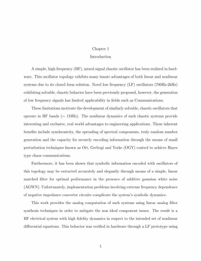
A simple, high frequency (HF), mixed signal chaotic oscillator has been realized in hard-
ware. This oscillator topology exhibits many innate advantages of both linear and nonlinear
systems due to its closed form solution. Novel low frequency (LF) oscillators (700Hz-2kHz)
exhibiting solvable, chaotic behavior have been previously proposed, however, the generation
of low frequency signals has limited applicability in fields such as Communications.
These limitations motivate the development of similarly solvable, chaotic oscillators that
operate in HF bands (∼ 1MHz). The nonlinear dynamics of such chaotic systems provide
interesting and exclusive, real world advantages to engineering applications. These inherent
benefits include synchronicity, the spreading of spectral components, truly random number
generation and the capacity for securely encoding information through the means of small
perturbation techniques known as Ott, Grebogi and Yorke (OGY) control to achieve Hayes
type chaos communications.
Furthermore, it has been shown that symbolic information encoded with oscillators of
this topology may be extracted accurately and elegantly through means of a simple, linear
matched filter for optimal performance in the presence of additive gaussian white noise
(AGWN). Unfortunately, implementation problems involving extreme frequency dependence
of negative impedance converter circuits complicate the system’s symbolic dynamics.
This work provides the analog computation of such systems using linear analog filter
synthesis techniques in order to mitigate the non ideal component issues. The result is a
HF electrical system with high fidelity dynamics in respect to the intended set of nonlinear
differential equations. This behavior was verified in hardware through a LF prototype using
1
operational amplifiers (opamps). Finally, a HF system design utilizing operational transcon-
ductance amplifiers (OTAs) was verified through SPICE simulation and a clear path to an
application specific integrated circuit (ASIC) was provided.
1.0.1 Organization of Material
The material in this manuscript is offered in 6 distinct section. After this brief introduc-
tion, Chapter 2 offers a background of exact solvable chaos as well as previous work related
to the topic. Chapter 3 focuses on modeling and designing each subsystem needed to realize
the exact solvable chaotic system transmitter and receiver. In most cases several circuit
realizations are offered with a short discussion of alternate designs and trade-offs. The sys-
tem in its entirety is examined in Chapter 4. The communication is implemented fully using
operational amplifiers, and partially using operational transconductance amplifiers. Chapter
5 addresses hardware implementation and results as well as errors. Finally, Chapter 6 offers
a conclusion to the work and provides suggestions for extending these endeavors.
2
Chapter 2
Background
2.1 Exact Solvable Chaos
Counterintuitively, complex behavior may often arise from simple systems or rule sets.
Although complicated system dynamics are found in examples of sophisticated functions, the
interconnectivity of variables contributes to significant complexity. In an effort to construct
a complex system from simple functions, consider the dynamics of an elementary iterated
map imposed upon a simple basis function such as a linear 2nd order differential equation.
This chapter reviews a detailed analysis of this concept revealing that from simple functions
(such as a binary shift or a set of piecewise linear conditions), second order oscillations may
be conditioned to exhibit chaotic behavior without prohibiting a closed-form solution.
More precisely, noninvertible dynamics characterized by a chaotic semi-flow may be
observed in a low-dimensional equation that includes a discontinuous, nonlinear term. A
chaotic set of continuous-time waveforms is then defined using linear differential equations.
This linear system is not chaotic, but a family of linear systems may be distinguished with
solutions which collectively constitute a chaotic set. This chaotic set provides an analytic
solution for the resultant nonlinear differential equation.[17]
2.2 The Iterated Shift Map
As an introductory example of a simple iterated map, consider the iteration:
xn+1 = 2xnmod(1) (2.1)
3
xn
xn+1
0 .5
1
1
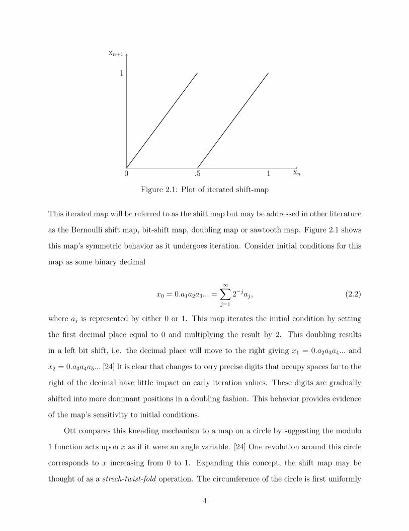
Figure 2.1: Plot of iterated shift-map
This iterated map will be referred to as the shift map but may be addressed in other literature
as the Bernoulli shift map, bit-shift map, doubling map or sawtooth map. Figure 2.1 shows
this map’s symmetric behavior as it undergoes iteration. Consider initial conditions for this
map as some binary decimal
x0 = 0.a1a2a3... =∞∑j=1
2−jaj, (2.2)
where aj is represented by either 0 or 1. This map iterates the initial condition by setting
the first decimal place equal to 0 and multiplying the result by 2. This doubling results
in a left bit shift, i.e. the decimal place will move to the right giving x1 = 0.a2a3a4... and
x2 = 0.a3a4a5... [24] It is clear that changes to very precise digits that occupy spaces far to the
right of the decimal have little impact on early iteration values. These digits are gradually
shifted into more dominant positions in a doubling fashion. This behavior provides evidence
of the map’s sensitivity to initial conditions.
Ott compares this kneading mechanism to a map on a circle by suggesting the modulo
1 function acts upon x as if it were an angle variable. [24] One revolution around this circle
corresponds to x increasing from 0 to 1. Expanding this concept, the shift map may be
thought of as a strech-twist-fold operation. The circumference of the circle is first uniformly
4
stretched to twice its initial length. This newly stretched circle is then twisted to construct
a figure 8 shape that has upper and lower lobes equal to the original circumference. Finally,
this figure 8 shape is combined by folding the upper lobe down on the lower lobe such that
the two circles are pressed together. The progression of this operation satisfies the necessary
stretching and folding needed to produce chaotic dynamics.
2.3 Exact Solvable Shift-band Chaos
Chaos may be synthesized in the iterated shift map by means of a linear second order
differential equation. [17] The result is a chaotic semi-flow possessing a return map that is
a chaotic shift map. This system is realized by driving linear differential equations to define
a low-dimensional chaotic set of continuous-time waveforms. These waveforms are exact
analytic solutions to a chaotic, nonlinear differential equation. Exact symbolic dynamics for
this system are observed due to these closed form, exact solutions. Interestingly, it may be
shown that this system’s Poincare return map is conjugate to a shift-map as shown in Figure
2.1, thus providing an exact symbolic representation of the continuous-time waveform with
a one-sided shift dynamic. [17]
Consider the linear, ordinary differential equation
x− 2βx+ (ω2 + β2)(x) = (ω2 + β2)s(t) (2.3)
with initial conditions x(0) = x0 and x(0) = y0, where 0 < β ≤ ln2 and ω = 2π as a hybrid
system. A binary waveform s(t) provides a conditional switching event or guard condition.
This discrete signal may be loosely considered as a random square wave that provides a
scaled, forcing function f(x) to the system x − 2βx + (ω2 + β2)(x)=f(x). The unscaled,
binary forcing is provided provisionally by the signum function, sgn(x), and is defined as
s(t) =
1 : u(t) ≥ 0
−1 : u(t) < 0
5
Note that the 2nd order system has a negative damping factor that cause the sinusoid
to grow exponentially. As the system satisfies u(t) = 0, the signum function is applied to
u(t) and s takes the value of sgn(u). This value is held as the waveform resets and continues
to grow until the next guard condition is satisfied, at which time the guard condition is
reevaluated.
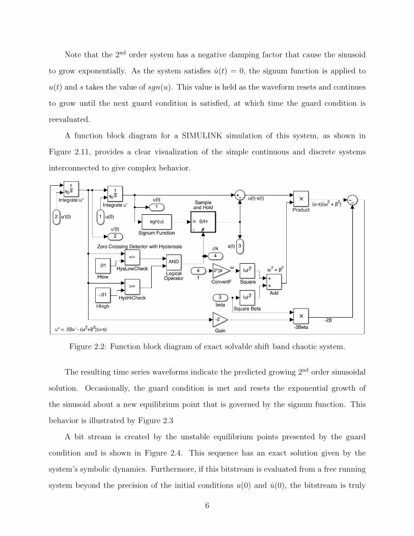
A function block diagram for a SIMULINK simulation of this system, as shown in
Figure 2.11, provides a clear visualization of the simple continuous and discrete systems
interconnected to give complex behavior.
Figure 2.2: Function block diagram of exact solvable shift band chaotic system.
The resulting time series waveforms indicate the predicted growing 2nd order sinusoidal
solution. Occasionally, the guard condition is met and resets the exponential growth of
the sinusoid about a new equilibrium point that is governed by the signum function. This
behavior is illustrated by Figure 2.3
A bit stream is created by the unstable equilibrium points presented by the guard
condition and is shown in Figure 2.4. This sequence has an exact solution given by the
system’s symbolic dynamics. Furthermore, if this bitstream is evaluated from a free running
system beyond the precision of the initial conditions u(0) and u(0), the bitstream is truly
6
0 5 10 15 20 25 30 35 40 45 50−3
−2
−1
0
1
2
3
time
u(t)
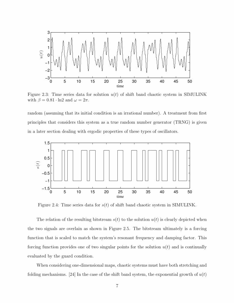
Figure 2.3: Time series data for solution u(t) of shift band chaotic system in SIMULINKwith β = 0.81 · ln2 and ω = 2π.
random (assuming that its initial condition is an irrational number). A treatment from first
principles that considers this system as a true random number generator (TRNG) is given
in a later section dealing with ergodic properties of these types of oscillators.
0 5 10 15 20 25 30 35 40 45 50−1.5
−1
−0.5
0
0.5
1
1.5
time
s(t)
Figure 2.4: Time series data for s(t) of shift band chaotic system in SIMULINK.
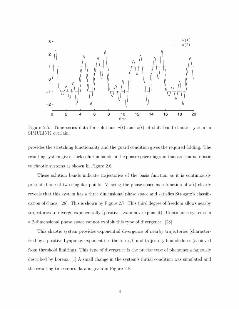
The relation of the resulting bitstream s(t) to the solution u(t) is clearly depicted when
the two signals are overlain as shown in Figure 2.5. The bitstream ultimately is a forcing
function that is scaled to match the system’s resonant frequency and damping factor. This
forcing function provides one of two singular points for the solution u(t) and is continually
evaluated by the guard condition.
When considering one-dimensional maps, chaotic systems must have both stretching and
folding mechanisms. [24] In the case of the shift band system, the exponential growth of u(t)
7
0 2 4 6 8 10 12 14 16 18 20
−2
−1
0
1
2
3
time
u (t )s (t )
Figure 2.5: Time series data for solutions u(t) and s(t) of shift band chaotic system inSIMULINK overlain.
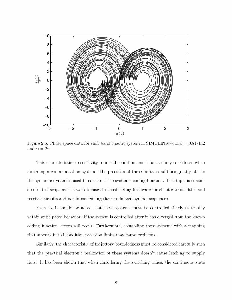
provides the stretching functionality and the guard condition gives the required folding. The
resulting system gives thick solution bands in the phase space diagram that are characteristic
to chaotic systems as shown in Figure 2.6.
These solution bands indicate trajectories of the basis function as it is continuously
presented one of two singular points. Viewing the phase-space as a function of s(t) clearly
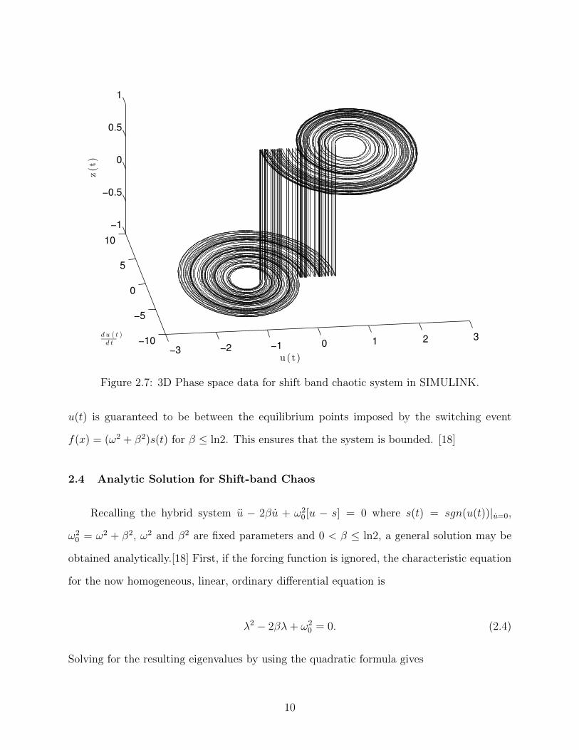
reveals that this system has a three dimensional phase space and satisfies Strogatz’s classifi-
cation of chaos. [28]. This is shown by Figure 2.7. This third degree of freedom allows nearby
trajectories to diverge exponentially (positive Lyapunov exponent). Continuous systems in
a 2-dimensional phase space cannot exhibit this type of divergence. [28]
This chaotic system provides exponential divergence of nearby trajectories (character-
ized by a positive Lyapunov exponent i.e. the term β) and trajectory boundedness (achieved
from threshold limiting). This type of divergence is the precise type of phenomena famously
described by Lorenz. [1] A small change in the system’s initial condition was simulated and
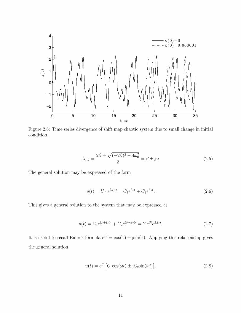
the resulting time series data is given in Figure 2.8.
8
−3 −2 −1 0 1 2 3−10
−8
−6
−4
−2
0
2
4
6
8
10
u(t)
du(t)
dt
Figure 2.6: Phase space data for shift band chaotic system in SIMULINK with β = 0.81 · ln2and ω = 2π.
This characteristic of sensitivity to initial conditions must be carefully considered when
designing a communication system. The precision of these initial conditions greatly affects
the symbolic dynamics used to construct the system’s coding function. This topic is consid-
ered out of scope as this work focuses in constructing hardware for chaotic transmitter and
receiver circuits and not in controlling them to known symbol sequences.
Even so, it should be noted that these systems must be controlled timely as to stay
within anticipated behavior. If the system is controlled after it has diverged from the known
coding function, errors will occur. Furthermore, controlling these systems with a mapping
that stresses initial condition precision limits may cause problems.
Similarly, the characteristic of trajectory boundedness must be considered carefully such
that the practical electronic realization of these systems doesn’t cause latching to supply
rails. It has been shown that when considering the switching times, the continuous state
9
−3 −2 −1 0 1 2 3−10
−5
0
5
10
−1
−0.5
0
0.5
1
u(t)
d u ( t )d t
z(t)
Figure 2.7: 3D Phase space data for shift band chaotic system in SIMULINK.
u(t) is guaranteed to be between the equilibrium points imposed by the switching event
f(x) = (ω2 + β2)s(t) for β ≤ ln2. This ensures that the system is bounded. [18]
2.4 Analytic Solution for Shift-band Chaos
Recalling the hybrid system u − 2βu + ω20[u − s] = 0 where s(t) = sgn(u(t))|u=0,
ω20 = ω2 + β2, ω2 and β2 are fixed parameters and 0 < β ≤ ln2, a general solution may be
obtained analytically.[18] First, if the forcing function is ignored, the characteristic equation
for the now homogeneous, linear, ordinary differential equation is
λ2 − 2βλ+ ω20 = 0. (2.4)
Solving for the resulting eigenvalues by using the quadratic formula gives
10
0 5 10 15 20 25 30 35
−2
−1
0
1
2
3
4
u(t)
time
x (0)=0x (0)=0.000001
Figure 2.8: Time series divergence of shift map chaotic system due to small change in initialcondition.
λ1,2 =2β ±
√(−2β)2 − 4ω2
0
2= β ± jω (2.5)
The general solution may be expressed of the form
u(t) = U · eλ1,2t = C1eλ1t + C2e
λ2t. (2.6)
This gives a general solution to the system that may be expressed as
u(t) = C1e(β+jω)t + C2e
(β−jω)t = Y eβte±jωt. (2.7)
It is useful to recall Euler’s formula ejx = cos(x) + jsin(x). Applying this relationship gives
the general solution
u(t) = eβt[C1cos(ωt)± jC2sin(ωt)
]. (2.8)
11
In the case of linearly independent solutions to homogeneous ODEs, the linear sum, i.e.
the real and imaginary parts, are taken independently to satisfy the ODE. This gives
u(t) = eβt[Acos(ωt) +Bsin(ωt)
]. (2.9)
If u(t) is expressed, a system of equations involving u(0) and u(0) may be produced in order
to solve for the constants A and B. In an effort to reinforce undergraduate Calculus topics,
the derivative of u(t) may be found by simply applying the product rule, (f ·g)′ = f ′ ·g+f ·g′.
This gives
u = βeβtAcos(ωt)− Aωeβtsin(ωt) + βeβtBsin(ωt) + eβtBωcos(ωt) (2.10)
Creating a system of equations to find the constants A and B gives
u(0) = A (2.11)
and
u(0) = Aβ +Bω = u0β +Bω. (2.12)
Finally, solving for B gives the expression
B =u(0)
ω− u0β
ω(2.13)
The solution may now be written as
u(t) = eβt
[u0cos(ωt) +
[u(0)
ω− u0β
ω
]sin(ωt)
]. (2.14)
Recalling the restriction u(0) = 0 gives
12
u(t) = eβt[u0cos(ωt)− u0β
ωsin(ωt)
]= u0e
βt
[cos(ωt)− β
ωsin(ωt)
]. (2.15)
In order to consider the result of the forcing function applied by the guard condition,
this result may be elaborated to produce a general solution for the non-homogeneous case.
This solution consists of the homogeneous solution uh(t) and the particular solution up(t)
such that u(t) = uh(t) +up(t). The homogeneous solution is expressed by Equation 2.15. To
find the particular solution, it may be assumed that up(t) is of the same form as the forcing
function, which is some constant C = s0. This gives
up(t) = C. (2.16)
By differentiation, up(t) = 0 and up(t) = 0. Applying this to the original ODE gives
0− 0 +ω20(C− s) = 0 or C = s0. Combining the general solution and the particular solution
such that u(t) = uh(t) + up(t) gives
u(t) = s0 +[u0 − s0
]eβt[cos(ωt)− β
ωsin(ωt)
]. (2.17)
Recall the restriction |u0| < 1. In order to keep this restriction and simultaneously account
for the particular solution up(t) = s0, the homogeneous solution uh(t) is modified such that
uh(t) =[u0 − s0
]eβt[cos(ωt)− β
ωsin(ωt)
].
This general solution may be differentiated – i.e. recall Equation 2.12 with substituted
constants A and B
u = (u0 − s0)eβt[βcos(ωt)− ωsin(ωt)− β βω
sin(ωt)− β
ωωcos(ωt)]
= (u0 − s0)eβt[(−ω + ββ
ω)sin(ωt)]
13
u = −(u0 − s0)eβt(ω2 + β2
ω
)sin(ωt) (2.18)
This expression may be evaluated at zero crossings to investigate instances at which the
guard condition is met. Because ω = 2π, these zero crossings expressed by u = 0 occur when
sin(2πt) = 0. The first instance of where the guard condition is met occurs when t = 1/2.
Consider this system with the initial conditions u(0) = u0, u(0) = 0 and s(0) = s0 with
the restriction |u(0)| ≤ 1 and allow s0 = sgn(u0).
Uninterestingly, when |u0| = 1 the system’s solution is it’s singular points u(t) = u0 and
s(t) = s0. However, in the case of |u0| < 1, the solution is
u(t) = s0 +[u0 − s0
]eβt[cos(ωt)− β
ωsin(ωt)
](2.19)
between switching conditions, i.e. while s(t) is constant. Evaluating the derivative described
previously such that the guard condition is met gives
u(t) = −(u0 − s0)eβt(ω2 + β2
ω
)sin(ωt) = 0. (2.20)
For analytical purposes, recognize that ω = 2π. The guard condition will be met periodically
as described by setting u(t) = 0. This occurs when sin(2πt) = 0 or in the fashion of t = n2
for integers n = 1, 2, 3, 4.... The guard condition is first met as t = 1/2 giving
u
(1
2
)= s0 −
[|u0| − s0
]eβ2 = s0[1 + (1− |u0|)e
β2 ]. (2.21)
Because |u0| < 1, the magnitude of the equilibrium point s0 is too great to undergo a
sign change. Therefore, it may be shown that sgn(u(1/2)) = s0 and the discrete state does
not undergo a switching event. The first trigger of the guard condition results in no change
and the solution for u(t) may be followed until the guard condition is next satisfied.
14
The second triggering of the guard condition may be found at t = 1. The solution u(t)
may be described at this point by
u(1) = u1 = s0 +[u0 − s0
]eβ = eβu0 − (eβ − 1)s0. (2.22)
It may be shown that |u(1)| ≤ 1 because |u0| ≤ 1. At this point in the analysis, uncertainty
arises. Because the sign s1 = sgn(u1) depends explicitly on u0, a transition in the discrete
state may occur. Generally, Equation 2.19 is reliably valid on the interval 0 ≤ t < 1 for all
|u0| ≤ 1. [18]
Further analysis of the system for t ≥ 1 requires consideration of the hybrid system
complete with switching events for u(1) = u1, u(1) = 0, and s(1) = s1. The initial conditions
will keep the similar restrictions u1 ≤ 1 and s1 = sgn(u1). A new problem is posed with
similarity to the previous problem. This allows for a time-shifted analysis. This translation
will be further denoted by incrementing subscripts. For the first interval 1 ≤ t < 2 the
solution is
u(t) = s1 +[u1 − s1
]eβ(t−1)
[cos(ωt)− β
ωsin(ωt)
]. (2.23)
Similar analysis over this interval results with
u(2) = u2 = eβu1 − (eβ − 1)s1 (2.24)
where
s2 = sgn(u2). (2.25)
Once more, it may be shown that |u2| ≤ 1 giving yet another time-shifted extension to
express a solution for a new interval.
15
For the general case, this solution approach may be continually repeated for the interval
n ≤ t < n+ 1. The solution over this arbitrary interval is
u(t) = sn +[un − sn
]eβ(t−n)
[cos(ωt)− β
ωsin(ωt)
]. (2.26)
The returns at potential transition times satisfy the iterated relation
un+1 = eβun − (eβ − 1)sn (2.27)
with
sn+1 = sgn(un+1). (2.28)
This analytic process shows that for given initial conditions, u0 and s0, this hybrid dynamical
system may be exactly calculated using a known solution for all intervals t ≥ 0. [18]
The resulting iterated relation is a form of the iterated shift map. The map is closed
on the interval |un| ≤ 1 and piecewise linear with a constant slope of eβ > 1. The slope of
this map is positive indicating that the map has positive entropy. Because this system is
a source of entropy it is chaotic. Furthermore, the continuous state of the system may be
sampled at regular times to obtain a Poincare return map for the continuos-time dynamics
of the system. It follows that the hybrid system is also chaotic with a Lyapunov exponent
λ = β. [18]This map may be used to describe symbols related to sn = ±1 as un is iterated
relative to partition defined at zero.
2.5 Symbolic Dynamics for the Shift-band
The symbols described by partitioning the aforementioned iterated map gives a means
to fully describe the continuous-time hybrid system dynamics. This is done by forming a
description of the system’s symbolic dynamics. Although, symbolic dynamics is considered
16
outside the scope of this work – for completeness, a brief description is offered. It is recom-
mended that source[18] be reviewed. The initial condition and recurrence relation formed
by the analytic solution yield
un = enβu0 − (1− e−β)
n−1∑i=0
sie−iβ. (2.29)
This equation may be inverted to gain an expression that is terms of future iterates. This
inversion gives
u0 = e−nβun + (1− e−β)n−1∑i=0
sie−iβ (2.30)
for all n > 0. Because un is bounded, a given initial condition may be expressed exclusively
in terms of future symbols si : 0 ≤ i <∞ by taking the limit as n→∞. This yields
u0 = (1− e−β)∞∑i=0
si+ne−iβ. (2.31)
This representation shows that the symbolic dynamics are characterized by a one-sided shift.
These symbols form the symbolic dynamics for the chaotic map.[18] Considering the integer
portion of continuous-time n = [t], the continuous-time waveform may be described in terms
of current and future symbols by
u(t) = sn +
− sn + (1− e−β)
∞∑i=0
si+ne−iβ· eβ(t−n)
(cos(ωt)− β
ωsin(ωt)
). (2.32)
Using this solution, subsequent waveforms may be established for an initial condition at
any integer time by temporally translating this expression such that t = 0. This specifies an
analytic relationship such that symbol sequences may be communicated using predetermined
initial conditions.
17
2.6 Control of Chaotic Systems
The characteristic of sensitivity to initial conditions intuitively seems to subvert the
useful control of chaotic systems. However, this is not the case. Small perturbation tech-
niques may be used to steer the phase space orbit of a chaotic system to a desired trajectory.
[43] [44] In terms of symbolic dynamics, sequences of future symbols correspond to desired
trajectories and are used to define the otherwise ambiguous precision of initial conditions.
For the shift-band oscillator, encoding symbols for targeted trajectories using many bits ef-
ficiently satisfies small perturbations. These small control signals increasingly influence the
system as time progresses by the shifting operation inherit to the iterated shift map. There
is a trade-off, however, with latency of newly presented information and using such small
control signals. [43]
Chaos control mechanisms are not considered in this work, although, for completeness
the concept of chaos control is briefly provided. At the heart of a successful communication
system is some sort of controller that imposing information. Generally, a coding function
may be obtained by iterating through the initial conditions of the chaotic oscillator. A
mapping of these initial conditions may be used to create a representation of symbols. This
mapping may be imposed by a chaotic control technique. For the system presented, chaotic
control techniques such as Hayes type control [47], OGY small perturbation techniques [45]
and forms of dynamic limiting [43] may be employed. These techniques are closely detailed
in Reference [43] and Reference [44].
Interestingly, subsequent design of the shift band chaotic oscillator may be thought of
as an analog computer. This is a slight shift in electronic design philosophy that views the
system as an analog computation of the exactly solvable shift band oscillator. Although less
mathematically elegant, this analog computation allows for conventional analog computation
techniques to be used for the control of this system. It is expected that this approach may
have limited applicability at very high frequencies.
18
2.7 Shift-Band Linear Solution
A complete description of the system may be found by evaluating the solution due to
an initial condition at a series of discrete time stages, n, such that t = tn, u(tn) = un,
dudt
(tn) = 0, and s(tn) = sn where sn = sgn(un). Considering the closed-form analytic
expression that describes the continuous-time solution for u(t) and a particular symbol, sm,
a powerful representation of u(t) may be found in the linear convolution
u(t) =∞∑
m=−∞
sm · P (t− tn −m), (2.33)
where P (t) is the analytic solution found for the linear, 2nd order basis function,
P (t) =
(1− e−β)eβt
(cos(ωt)− β
ωsin(ωt)
), t < 0
1− e−β(t−1)(
cos(ωt)− βω
sin(ωt)
), 0 ≤ t < 1
0, t ≥ 1.
The discrete signal, s(t), may be written as the linear convolution
s(t) =∞∑
m=−∞
sm · φ(t− tn −m) (2.34)
where
φ =
0, t < 0
1, 0 ≤ t < 1
0, t ≥ 1.
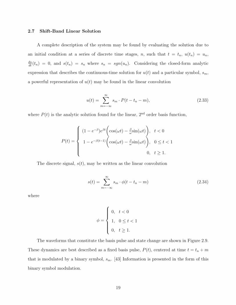
The waveforms that constitute the basis pulse and state change are shown in Figure 2.9.
These dynamics are best described as a fixed basis pulse, P (t), centered at time t = tn +m
that is modulated by a binary symbol, sm. [43] Information is presented in the form of this
binary symbol modulation.
19
−4 −3.5 −3 −2.5 −2 −1.5 −1 −0.5 0 0.5 1 1.5−0.50
0.00
0.50
1.00
1.50
2.00
Time (s)
u(t)s(t)
Figure 2.9: Basis pulse for synthesizing chaos via linear superposition with β = ln(2).
2.8 Spectral Content of Shift-Band Oscillations
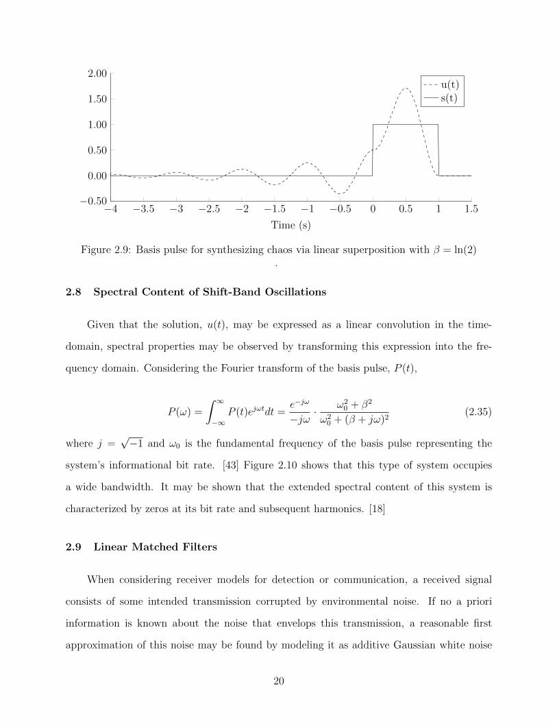
Given that the solution, u(t), may be expressed as a linear convolution in the time-
domain, spectral properties may be observed by transforming this expression into the fre-
quency domain. Considering the Fourier transform of the basis pulse, P (t),
P (ω) =
∫ ∞−∞
P (t)ejωtdt =e−jω
−jω ·ω20 + β2
ω20 + (β + jω)2
(2.35)
where j =√−1 and ω0 is the fundamental frequency of the basis pulse representing the
system’s informational bit rate. [43] Figure 2.10 shows that this type of system occupies
a wide bandwidth. It may be shown that the extended spectral content of this system is
characterized by zeros at its bit rate and subsequent harmonics. [18]
2.9 Linear Matched Filters
When considering receiver models for detection or communication, a received signal
consists of some intended transmission corrupted by environmental noise. If no a priori
information is known about the noise that envelops this transmission, a reasonable first
approximation of this noise may be found by modeling it as additive Gaussian white noise
20
10−1 100
10−2.00
10−1.00
100.00
ω/2π
|P(ω
)|2
Figure 2.10: Basis pulse for synthesizing chaos via linear superposition with β = ln(2).
(AGWN). Thus, an important task arises. Given a receiver network input, x(t), seek some
network with an impulse response, h(t), such that a desired transmission may be optimally
obtained in the presence of AGWN, w(t).
To begin, consider the input of the receiver as
x(t) = g(t) + w(t) 0 ≤ t ≤ T (2.36)
where T isn arbitrary observation interval and g(t) is some arbitrarily shaped transmission
pulse.[15] It is assumed that w(t) is a stochastic noise process of zero mean and power
spectral density No/2. It is further assumed that the receiver has knowledge of the shape of
the transmitted waveform.
In order to optimize this filter design by maximizing the detection of the transmitted
signal, g(t) by minimizing the effects of noise w(t), consider a linear matched filter with the
output y(t) such that
y(t) = go(t) + n(t) (2.37)
where go(t) is produced by the signal component of input x(t) and n(t) is produced by the
noise component of x(t). Ultimately, the instantaneous power in the output signal go(t),
21
measured at time t = T must be maximized when compared to the average power of the
output noise n(t). This may be expressed as the peak pulse signal-to-noise ratio
η =|go(T )|2E|n2(t)| (2.38)
where |go(T )|2 is the instantaneous power provided by the output signal, and E|n2(t)| is the
statistical expectation of the average output noise power. This expression gives a signal-to-
noise ratio in terms of power that may be maximized for some filter input’s impulse h(t).
Defining the Fourier transform of g(t) as G(f) and h(t) as H(f), the output signal may
be expressed as Go(f) = H(f)G(f). Taking the inverse Fourier transform of the output
signal gives the time-domain representation
go(t) =
∫ ∞−∞
H(f)G(f)ej2πftdf. (2.39)
Ignoring the presence of noise, the output of the filter may be sampled at t = T to give
|go(T )|2 =
∣∣∣∣ ∫ ∞−∞
H(f)G(f)ej2πfTdf
∣∣∣∣2. (2.40)
Similarly, ignoring the presence of the transmitted signal, the power spectral density of
the output noise may be expressed as
SN(f) =N0
2|H(f)|2. (2.41)
This expression assumes that the power spectral density of the output noise, n(t), is equal
to the power spectral density of the input noise, w(t), with the impulse response of the filter,
H(f), imposed upon it. The average power of the noise, n(t), seen at the output of the filter
is expressed by
E[n2(t)] =
∫ ∞−∞
SN(f)df =N0
2
∫ ∞−∞|H(f)|2df. (2.42)
22

The expressions for the independent contributions to the power seen at the output of
the filter, Equation 2.40 and Equation 2.42, may be substituted into Equation 2.38 to give
η =
∣∣∣∣ ∫∞−∞H(f)G(f)ej2πfTdf
∣∣∣∣2N0
2
∫∞−∞ |H(f)|2df . (2.43)
With this expression, the signal-to-noise ratio is now in terms of an input signal G(f) and
the response of some linear matched filter H(f). This ratio gives a relation to which an
optimization problem may be solved. It is desired to find the filter response, H(f), in order
maximize the signal-to-noise ratio, η, if an arbitrary signal, G(f), is presented as in input.
To obtain a solution, Schwarz’s inequality may be applied to the numerator. [14]
Schwarz’s inequality states that if two complex functions φ1(x) and φ2(x) in the real variable
x satisfy
∫ ∞−∞|φ1(x)|2dx <∞ (2.44)
and
∫ ∞−∞|φ2(x)|2dx <∞ (2.45)
then the expression
∣∣∣∣ ∫ ∞−∞
φ1(x)φ2(x)dx
∣∣∣∣2 ≤ ∫ ∞−∞|φ1(x)|2dx
∫ ∞−∞|φ2(x)|2dx (2.46)
if and only if
φ1 = kφ∗2(x) (2.47)
where k is an arbitrary constant, and φ∗2 represents the complex conjugate of φ2.
23

Recognizing that the terms in the numerator of Equation 2.43 are finite, the impulse
response may be set as H(f) = φ1(x) and G(f)exp(j2πfT ) = φ2(x). Applying Schwarz’s
inequality to the numerator of Equation 2.43 gives
∣∣∣∣ ∫ ∞−∞
H(f)G(f)ej2πfTdf
∣∣∣∣2 ≤ ∫ ∞−∞|H(f)|2df
∫ ∞−∞|G(f)|2df. (2.48)
Substituting this result into Equation 2.43 gives a new relation for the signal-to-noise ratio,
η ≤∫∞−∞ |H(f)|2df
∫∞−∞ |G(f)|2df
N0
2
∫∞−∞ |H(f)|2df =
2
N0
∫ ∞−∞|G(f)|2df, (2.49)
that describes a maximum signal-to-noise ratio exclusively dependent on the input, G(f).
As a result, the maximum signal-to-noise ratio, ηmax, may be obtained when the conditions
of the inequality are met. More formally,
ηmax =2
N0
∫ ∞−∞|G(f)|2df (2.50)
for an optimally matched filter response Hopt(f) if the following condition is met
Hopt(f) = kG∗(f)e−j2πfT (2.51)
where k is an arbitrary magnitude scaling factor and G∗(f) is the complex conjugate of the
input signal G(f). Succinctly stated, the transfer function for the optimally matched filter
is identical to the complex conjugate of the input signal with the exception of magnitude
scaling and a term that represents a linear time shift, T .
This time shift is explicitly shown by transforming these results into the time-domain.
Taking the inverse Fourier transform of Hopt(f) gives
hopt(t) = k
∫ ∞−∞
G∗(f)e−j2πf(T−t)df . (2.52)
24
If it is assumed that g(t) is a real signal, taking the complex conjugate gives G∗(f) = G(−f).
The result is
hopt(t) = kg(T − t). (2.53)
This result concludes with a powerful and elegant statement that the presence of any
physical waveform, g(t), may be optimally detected when considering corruption due to
AGWN by simply selecting a filter with an impulse response that is a time-reversed, time-
delayed version of the input with a magnitude scaling factor k. [15] A linear time-invariant
filter defined using this approach is referred to a a matched filter. [14] It may be carefully
noted that the only assumption made about the input noise is that w(t) is white, stationary,
zero mean, and has power spectral density of N0/2.
Design advantages arise when considering matched filters because the impulse response
of the optimal filter is uniquely defined by a known input pulse signal, g(t), with the exception
of magnitude scaling and time delay. Ultimately, the peak pulse signal-to-noise ratio of a
matched filter only depends on the ratio of signal energy to the power spectral density of
the white noise at the filter input. [14]
2.10 Shift-band Linear Matched Filter
Despite the characteristics of chaotic systems to behave in a seemingly random, noise-
like manner – this specific chaotic system may be optimally detected in the presence of
AGWN. Because chaos is synthesized by a known basis function, P (t), a linear matched
filter may be constructed for its detection. As previously derived, a matched filter may be
constructed for any physical signal by constructing a filter with an impulse response that is
a time-reversed and delayed version of the desired input signal. [14] [18]
Let ρ(t) = P (−t) that satisfies
25
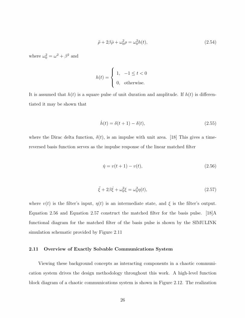
ρ+ 2βρ+ ω20ρ = ω2
0h(t), (2.54)
where ω20 = ω2 + β2 and
h(t) =
1, −1 ≤ t < 0
0, otherwise.
It is assumed that h(t) is a square pulse of unit duration and amplitude. If h(t) is differen-
tiated it may be shown that
h(t) = δ(t+ 1)− δ(t), (2.55)
where the Dirac delta function, δ(t), is an impulse with unit area. [18] This gives a time-
reversed basis function serves as the impulse response of the linear matched filter
η = v(t+ 1)− v(t), (2.56)
ξ + 2βξ + ω20ξ = ω2
0η(t), (2.57)
where v(t) is the filter’s input, η(t) is an intermediate state, and ξ is the filter’s output.
Equation 2.56 and Equation 2.57 construct the matched filter for the basis pulse. [18]A
functional diagram for the matched filter of the basis pulse is shown by the SIMULINK
simulation schematic provided by Figure 2.11
2.11 Overview of Exactly Solvable Communications System
Viewing these background concepts as interacting components in a chaotic communi-
cation system drives the design methodology throughout this work. A high-level function
block diagram of a chaotic communications system is shown in Figure 2.12. The realization
26
Figure 2.11: Function block diagram of matched filter for the basis pulse of the exact solvableshift-band chaotic system.
of each subsystem in Figure 2.12 leads to successful communication by means of encoding
and decoding information in a chaotic oscillator over some communications channel.
First, considering some information such as the text “I’m picking up good vibrations”
may be converted into binary data using ASCII, unicode or any binary character encoding
scheme. This binary code is then presented to the inverse coding function of a particular
chaotic oscillator. This inverse coding function translates the intended binary signal into
representative initial conditions that are imposed upon the chaotic oscillator. These ini-
tial conditions may be elegantly imposed using small perturbation techniques or controlled
with a more heavy handed technique as the rapid analog computation of consecutive initial
conditions.
27
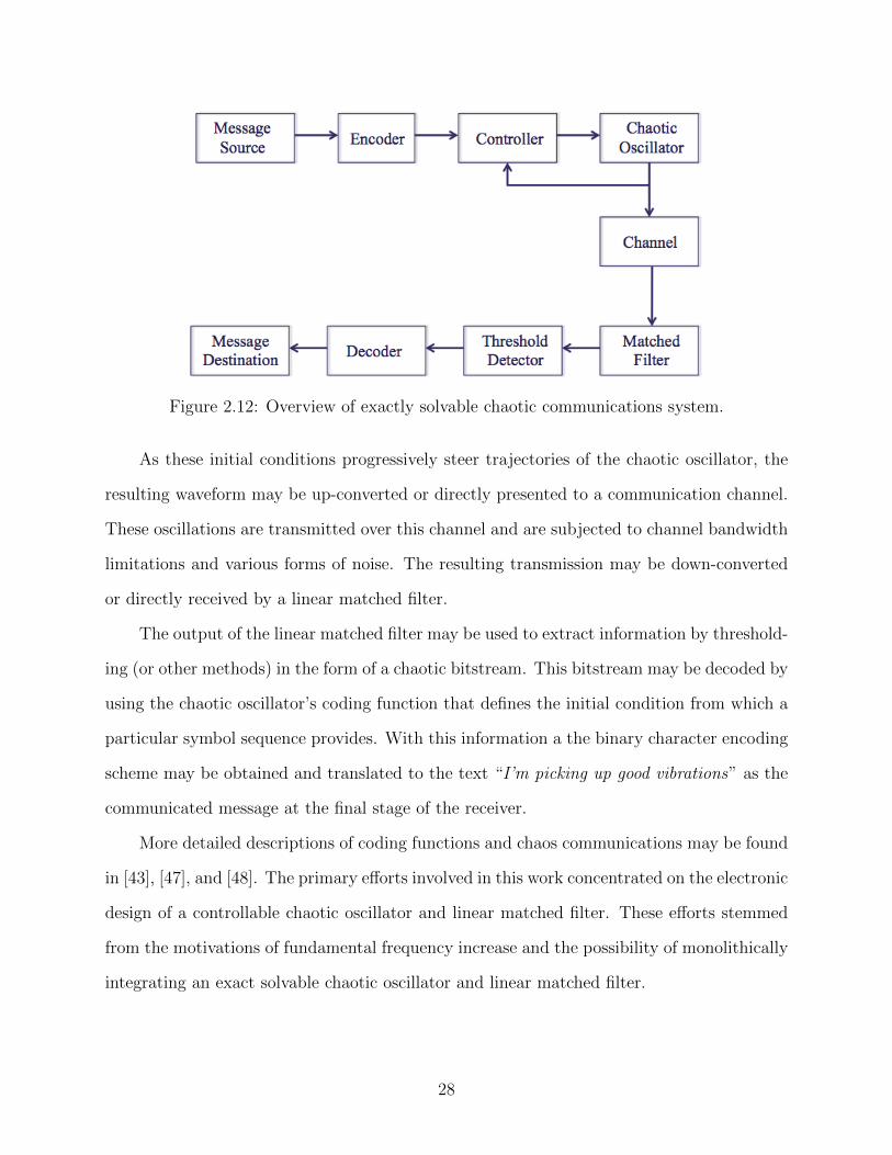
Figure 2.12: Overview of exactly solvable chaotic communications system.
As these initial conditions progressively steer trajectories of the chaotic oscillator, the
resulting waveform may be up-converted or directly presented to a communication channel.
These oscillations are transmitted over this channel and are subjected to channel bandwidth
limitations and various forms of noise. The resulting transmission may be down-converted
or directly received by a linear matched filter.
The output of the linear matched filter may be used to extract information by threshold-
ing (or other methods) in the form of a chaotic bitstream. This bitstream may be decoded by
using the chaotic oscillator’s coding function that defines the initial condition from which a
particular symbol sequence provides. With this information a the binary character encoding
scheme may be obtained and translated to the text “I’m picking up good vibrations” as the
communicated message at the final stage of the receiver.
More detailed descriptions of coding functions and chaos communications may be found
in [43], [47], and [48]. The primary efforts involved in this work concentrated on the electronic
design of a controllable chaotic oscillator and linear matched filter. These efforts stemmed
from the motivations of fundamental frequency increase and the possibility of monolithically
integrating an exact solvable chaotic oscillator and linear matched filter.
28
2.12 Ergodic Properties of Exact Solvable Chaos
Because this system is topologically conjugate to the iterated shift map, or Bernoulli
map, the system dynamics may be analyzed using well defined ergodic theory developed for
one dimensional maps. This system is a reliable entropy source because possible solution
trajectories that compromise the system’s randomness is of zero measure. [20] Chaotic
trajectories are theoretically ensured and motivations to obtain the entropy and statistical
properties produced by the dynamical system may be pursued. Ergodic theory is used to
analyze the probability distribution function (PDF) of dynamical systems. The PDF for
such systems is often referred to as the system’s invariant measure or natural measure.
If this map is given enough iterations, the resulting solution trajectory will orbit arbi-
trarily close to every point on its defined interval. Ideally, the solution trajectories tracing
these points would be uniformly distributed to ensure a fair coin flip. This means that no
orbit within a given solution is favored over a long enough time duration. All solution tra-
jectories are equally typical. [20] Furthermore, the entropy of this system may be defined
from first principles.
Although the Bernoulli map is deterministic, the symbols generated by the map may
be Markovian if the correct partition is chosen by considering the critical point of the map.
Given a chaotic, one-dimensional, piecewise-linear Markov map, the system’s invariant den-
sity may be computed by obtaining the kneading matrix K and applying the Boyarsky-Gora
method. [21] Ultimately, the system’s entropy may be found using the Shannon formula and
the invariant density.
Consider the Bernoulli shift map xn+1 = f(xn) partitioned in two sets on the [−1, 1]
interval. The sets ρ1 = [−1, 0) and ρ2 = [0, 1] span the domain of f(xn) with a piecewise
discontinuity at xn = 0. These partitions correspond to the binary symbols A and B. The
partition is denoted as β = ρ1, ρ2 and the union of the boundaries between the regions of β
are denoted by B(β). Verifying that the map f(xn) is Markov of order 1 [22]; the boundaries
29
B(β) are invariant of the map dynamics, i.e. xn+1 = f [B(β)] ⊆ B(β). It is easily verified
that indeed xn+1 is a subset of the union of the boundaries between regions of β.
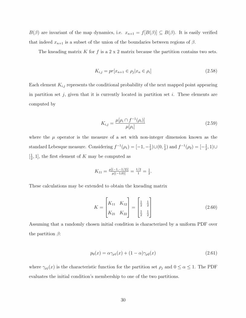
The kneading matrix K for f is a 2 x 2 matrix because the partition contains two sets.
Ki,j = pr[xn+1 ∈ ρj|xn ∈ ρi] (2.58)
Each element Ki,j represents the conditional probability of the next mapped point appearing
in partition set j, given that it is currently located in partition set i. These elements are
computed by
Ki,j =µ[ρi ∩ f−1(ρi)]
µ[ρi](2.59)
where the µ operator is the measure of a set with non-integer dimension known as the
standard Lebesque measure. Considering f−1(ρ1) = [−1,−12)∪(0, 1
2) and f−1(ρ2) = [−1
2, 1)∪
[12, 1], the first element of K may be computed as
K11 = µ[(−1,−1/2)]µ[(−1,0)] = 1/2
1= 1
2.
These calculations may be extended to obtain the kneading matrix
K =
K11 K12
K21 K22
=
12
12
12
12
(2.60)
Assuming that a randomly chosen initial condition is characterized by a uniform PDF over
the partition β:
p0(x) = αγρ1(x) + (1− α)γρ2(x) (2.61)
where γρj(x) is the characteristic function for the partition set ρj and 0 ≤ α ≤ 1. The PDF
evaluates the initial condition’s membership to one of the two partitions.
30
The Frobenius-Perron (F-B) operator is used to describe the time evolution of densities
in phase space. These densities may be described ergodically by taking the fixed point of
the Frobenius-Perron equation
ρn+1(x) =
∫ 1
0
dyδ[x− F (y)]ρn(y) (2.62)
which gives
ρ(x) =
∫ 1
0
δ[x− F (y)]ρ(y) (2.63)
as the resulting invariant measure for the system. For the next iteration of the mapping,
the F-B operator creates a description of partition membership for p1 when applied to p0.
When considering ρ(x) = 12[γρ1(x) + γρ2(x)], the resulting invariant density is
ρ(y) =1
2
[ρ(y
2
)+ ρ(1− y
2
)](2.64)
A uniform invariant density is shown over the [−1, 1] interval with the probability of each
symbol A and B being 12. More formally,
ρA =
∫x∈A
ρ(x)dx = ρB =
∫x∈B
ρ(x)dx =1
2(2.65)
verifies that the Bernoulli shift map ensures a fair coin flip. This satisfies that the PDF is
uniform by ρ(x) = 1n
for n = 2 symbols. This has been computed equivalently by many -
both for the case of Markov maps [21] as well as the more general case where Markovian
properties are not assumed.[23]
The entropy for this map is described using the formula for the Shannon entropy Hs:
Hs =r∑i=1
piln(1/pi) (2.66)
31
where it is defined that p ln(1/p) ≡ 0 if p = 0 and pi is the probability of symbol i appearing
in a stream of symbols. This information entropy describes the degree of surprise a system
is capable of providing. For the Bernoulli map with two full shifts, the Shannon entropy is
described by the most uncertain case for which each symbol is equally probable, i.e. pi = 1/r
for i = 1, 2, ...r. [24]
This gives Hs = ln(r) which yields Hs = ln(2) = 0.693. For the case of the hybrid
dynamical system, the entropy is given directly be its Lyapunov exponent β = ln(2).[18]
This theoretically verifies the system as an entropy source that produces two symbols A and
B analogous to a perfect coin flip.
32
Chapter 3
Subsystem Circuit Design and Simulation
3.1 System Overview
Consider the design of this chaotic communications system with two major components;
a transmitter and a receiver. The transmitter must be designed such that given an initial
condition, it accurately reproduces a predetermined bit sequence as defined by the system’s
symbolic dynamics. This is a careful conversion of a continuous input signal, sampled at
discrete time intervals that corresponds to an output bitstream to a predefined coding func-
tion. From a design perspective, this is an analog computation of a series of clocked initial
conditions. Although, the coding function and symbolic dynamics are of great importance
to the overall communications system, it will be assumed that these dynamics are known
a priori and implemented using OGY type control techniques [45] or conventional analog
computational approaches [49].
Essentially, the transmitter may be considered an analog computer implementing the
desired differential equations. From a subsystem point of view, this computer consists of a
few components that contribute to an unstable stretching mechanism that interacts with a
guarded folding mechanism. The interdependence of these components give the necessary
conditions for chaos:
1. Unstable RLC network (stretching mechanism)
2. Signum function (guard mechanism)
3. Zero crossing detector (trigger for guard mechanism)
4. Sample & Hold (conditional folding mechanism)
33

Similarly, the receiver constructs a linear matched filter for the transmitter’s basis pulse
allowing for optimal detection in the presence of additive gaussian white noise (AGWN).
This matched filter is comprised of the following subsystems:
1. Carefully paired RLC network
2. Wideband delay
3. Integration function
4. Summing function
This chapter’s focus entails the design and simulation of these subsystems such that
each component may be systematically integrated with relative ease. A systematic approach
grants universality to many electronic implementations of nonlinear systems by providing a
methodology complete with basic, process independent building blocks. These basic building
blocks include integrators built from opamps or OTAs, thresholding decisions, logic functions
and simple delay circuits. Complex interconnections and systems of equations may be easily
and reliably realized using well researched and documented techniques common in Microelec-
tronics, Analog Computing, Hybrid Computing and Filter Synthesis. Using these techniques
gives reliable integration when considering non ideal effects such as temperature fluctuations,
noise, power supply rejection, fabrication dependent errors and other well researched and
mitigated topics.
3.2 Stable and Unstable RLC Tank Circuits
The linear portion of the transmitter and receiver systems may be synthesized using
standard ladder filter synthesis techniques [27]. This method contrasts General Impedance
Converter (GIC) and Negative Impedance Converter (NIC) topologies that may bottleneck
or distort some systems when frequency scaling is needed. [19] It should be noted that fil-
ter synthesis techniques may inadvertently implement GIC topologies in some cases. These
cases, generally, do not provide frequency or distortion bottlenecks, however, careful consid-
eration should be given.
34
First, consider the unstable, linear portion of the system between switching events. For
this special case, the switching event s(t) may be considered as a constant forcing function.
This gives
u− 2βu+ (ω2 + β2)(u− s(t)) = 0 (3.1)
and is illustrated by Figure 3.1. A very simple ladder network may be used to implement
this second order, nonhomogenous differential equation. A series -RLC network may be
used to ensure that the forcing function, s(t) may be applied as a voltage. Furthermore, if
this design is intended to be synthesized as a ladder network using opamps or OTAs, it is
generally desired to use the voltage across capacitors and current through inductors [25] [27].
-R
L
IL=CdVCdt =u(t)
C
VC=u(t)
+−(ω2 + β2)s(t)
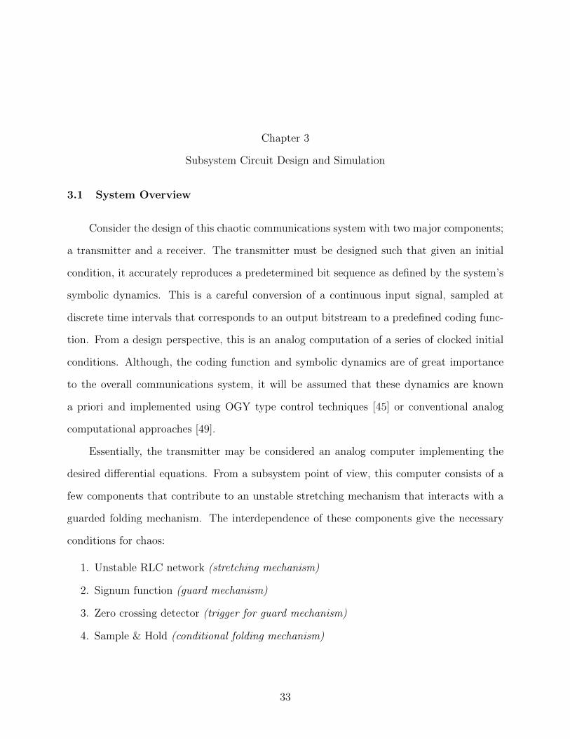
1Figure 3.1: Lumped element circuit realization of unstable, linear portion of the exactlysolvable chaotic system
Favoring the passive sign convention in relation to IL and applying Kirchoff’s Voltage
Law (KVL) to the circuit in Figure 3.1 gives
−(ω2 + β2)s(t) + VR + VL + VC = 0 (3.2)
Progressing with Ohm’s law and noting that all elements share the same current gives
(ω2 + β2)s(t) = −IRR + LdIL(t)dt
+ 1C
∫ t−∞ ic(τ)dτ
= −ILR + LdIL(t)dt
+ 1C
∫ t−∞ IL(τ)dτ
ddt
(ω2 + β2)s(t) = −C dVCdtR + LC d2VC(t)
dt2+ VC
VC −R
LVC +
1
LCVC = A· (3.3)
35
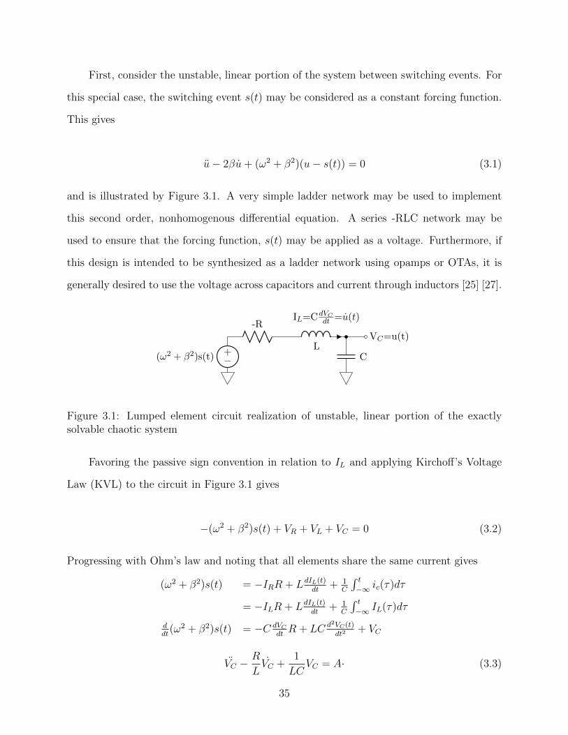
where β = R2L
, ω2n = (ω2 + β2) = 1
LC, A = (ω2 + β2) and s(t) is assumed to be constant
between switching events. A SPICE simulation of this unstable network is shown in Figures
3.2 and 3.3. The expected waveform is an exponentially growing waveform that constitutes
the system’s basis pulse.
Figure 3.2: LTSPICE IV simulation schematic of unstable -RLC network with R = −1.4Ω,C = .3F and L = 1H.
Figure 3.3: LTSPICE IV simulation result of unstable -RLC network with R = −1.4Ω,C = .3F and L = 1H.
This simple network implements the desired set of linear equations using the state
variables VC(t) = u(t) and IL(t) = u. Ladder synthesis from these state variables proceeds
by recognizing VC = 1CIC(t) and IL = 1
LVL(t). Continuing with ladder synthesis of the
lumped element network only in terms of state variables and the forcing function gives
VC =1
CIL (3.4)
and
36
IL =1
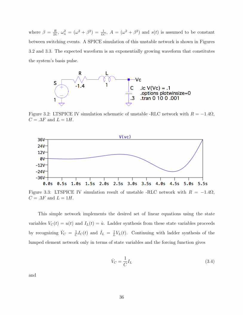
L[ILR− VC + A · s(t)] (3.5)
These state variables may be associated by interconnecting integrators and amplifiers
as shown in Figure 3.4. Although, this is a simple second order system, more complicated
systems may be easily implemented by using this same method. More details on implement-
ing higher order or more complex systems such as Chua’s Circuit, Rossler’s Equations and
a 5th order Chebyshev filter is provided in the Appendix.
A · s(t)
R
+
1Ls
IL
− 1Cs
−VC
1Figure 3.4: State variables for unstable -RLC tank circuit synthesized using integrators in aladder network
Secondly, consider the stable portion of the system intended for receiving the signal u(t).
The ladder synthesis used to realize the unstable -RLC network may be similarly applied
to the linear portion of the receiver’s matched filter. Implementing a stable RLC network
follows the same procedure with the exception that the negative resistance is made positive.
In practice, this may be implemented as a simple resistor or a non inverting amplifier.
37
3.2.1 Operational Amplifier -RLC Synthesis
Consider the implementation of the -RLC network shown in Figure 3.2. During publica-
tion of this manuscript, the availability of a single, lumped element component that simply
provides a negative resistance, inductance or capacitance was elusive. In order to achieve
this effect, a -RLC network with a negative resistance may be synthesized using operational
amplifiers. Note that this approach is borrowed from analog filter theory and yields many
advantages. Namely, the synthesis replaces any need for inductance with capacitance. This
is of notable importance in the interest of the system’s integration into a monolithic design.
Inductors occupy a large, costly area and are low Q, lossy devices [26]. As a secondary ad-
vantage of the synthesized ladder network, the derivative of the function u(t) is conveniently
provided. This allows for for zero crossing detection of u without the need for inherently
noisy differentiator circuitry [25].
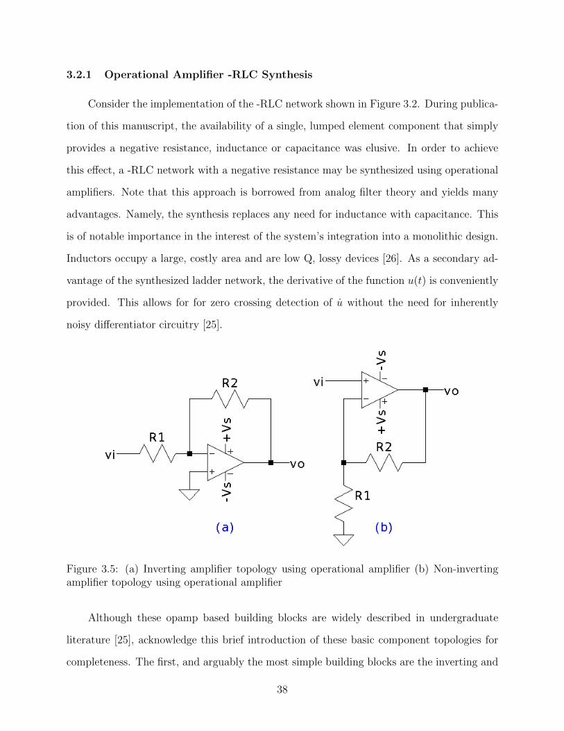
Figure 3.5: (a) Inverting amplifier topology using operational amplifier (b) Non-invertingamplifier topology using operational amplifier
Although these opamp based building blocks are widely described in undergraduate
literature [25], acknowledge this brief introduction of these basic component topologies for
completeness. The first, and arguably the most simple building blocks are the inverting and
38
non-inverting amplifiers. These topologies are illustrated by Figure 3.5 and are often derived
as an introduction to analog electronics [25]. The ideal transfer function of the inverting
topology is
Av =vovi
= −R2
R1
. (3.6)
Similarly, the ideal transfer function of the non-inverting configuration is
Av =vovi
= 1 +R2
R1
. (3.7)
These amplifier topologies serve as simple instruments to realize both positive and negative
scaling between interconnections of computational state variables.
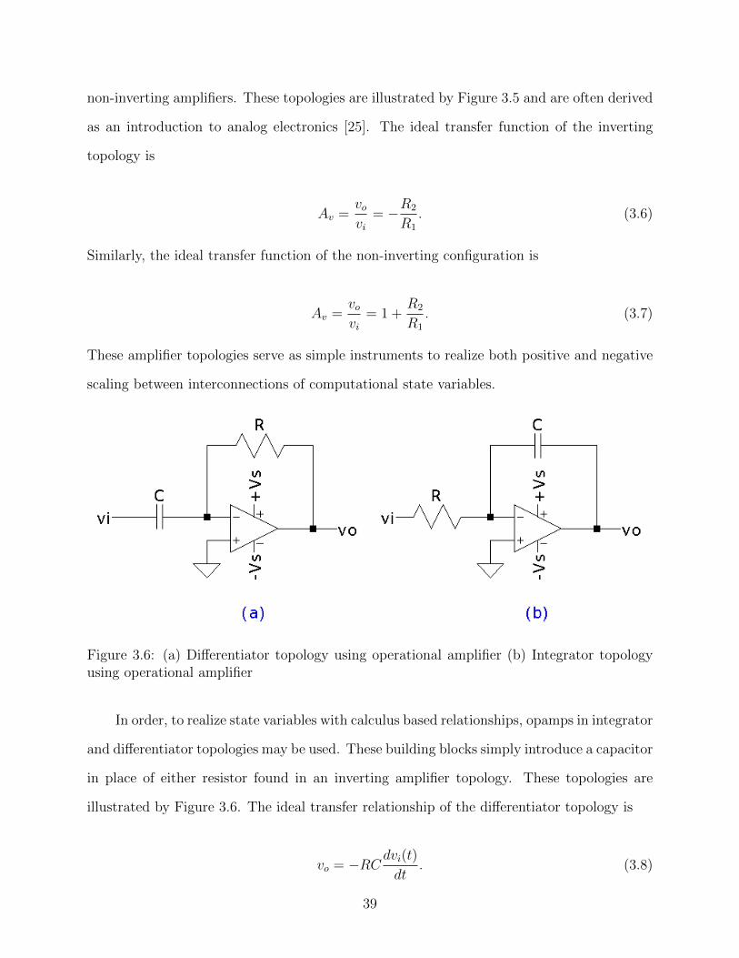
Figure 3.6: (a) Differentiator topology using operational amplifier (b) Integrator topologyusing operational amplifier
In order, to realize state variables with calculus based relationships, opamps in integrator
and differentiator topologies may be used. These building blocks simply introduce a capacitor
in place of either resistor found in an inverting amplifier topology. These topologies are
illustrated by Figure 3.6. The ideal transfer relationship of the differentiator topology is
vo = −RCdvi(t)dt
. (3.8)
39

Similarly, the ideal transfer function of the integrator configuration is
vo = − 1
RC
∫ t
0
iC(τ)dτ + VC(0). (3.9)
Although, the differentiator topology is provided for completeness, it is not used in this
design due to its susceptibility to increasing HF noise and its inability to pass D.C. (and
some LF) signals. The integrator topology is a much better choice when considering noise,
stability and D.C. or LF signal response as needed in the case of Bernoulli shift map and
iterated tent map exact solvable chaos communication.
These pedestrian circuit topologies may be interconnected to achieve impressively com-
plex polynomials and computational relationships. Recall the state variables declared in
Equations 3.4 and 3.5 VC = 1CIL and IL = 1
L[ILR − VC + A · s(t)]. These are illustrated
electrically by Figure 3.1 and functionally by Figure 3.4. Trivial inspection suggests that this
unstable -RLC network may be implemented using operational amplifiers in the inverting,
non-inverting and integrator topologies. The state variable representations will result as
voltage signals provided by the synthesized ladder network. No negative resistance is needed
as it is provided by an inverting amplifier.
It should be observed that the network shown in Figure 3.7 has been optimized for
minimal use of components and provides two voltage output nodes −VC and VIL representa-
tive of the aforementioned state variables – respectivley VC and IL. Another opamp circuit
configured as an inverting amplifier may be placed in series after the integrator with the
integrating capacitive component CC. This addition will invert the output voltage node
−VC giving VC . However, this is not necessary as will be illustrated when the nature of
the signum function circuitry is detailed. Interestingly, the state variable representing the
current IL has now been realized as a voltage. This provides straight forward voltage mode
control techniques for computing initial conditions as well as a means to easily provide a
conditional guard mechanism with a comparator based zero crossing detector. Finally, note
the current summing junction where three resistors interface to allow the forcing function
40
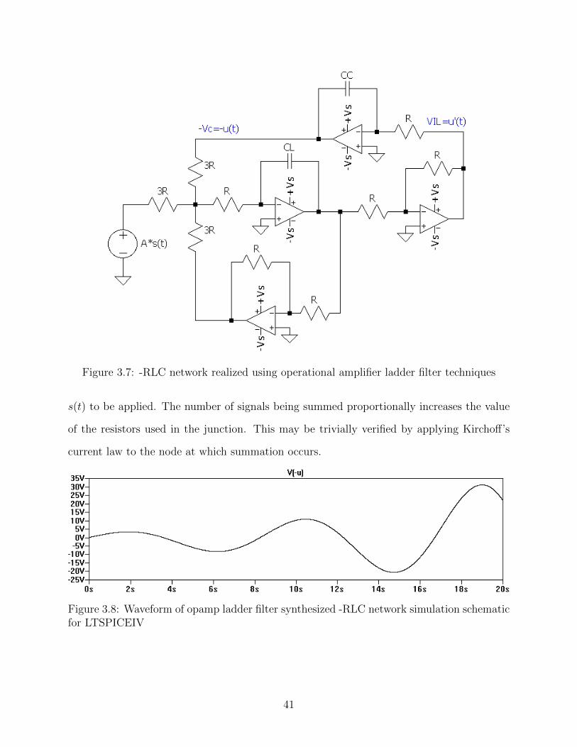
Figure 3.7: -RLC network realized using operational amplifier ladder filter techniques
s(t) to be applied. The number of signals being summed proportionally increases the value
of the resistors used in the junction. This may be trivially verified by applying Kirchoff’s
current law to the node at which summation occurs.
Figure 3.8: Waveform of opamp ladder filter synthesized -RLC network simulation schematicfor LTSPICEIV
41

LTSPICEIV simulation of this circuit gives a 2nd order waveform solution that consti-
tutes a desired, unstable basis pulse for exact solvable chaotic oscillations. The resulting
waveform is shown by Figure 3.8. The circuit used to produce such a waveform is depicted
in Figure 3.9.
Figure 3.9: Opamp ladder filter synthesized -RLC network simulation schematic for LTSPI-CEIV
Given that the operational amplifier is non-ideal, i.e. exhibits finite gain, input impedance
and other imperfections, computational parameters are approximate, however, components
may be easily scaled to compensate for these imperfections where precision is required. Alter-
nately, precision opamps such as Linear Technology’s LT1001 [38] may be used or feedback
mechanisms may be employed. As an approximation, the simulated circuit in Figure 3.9
maps parameters to the -RLC lumped element circuit shown in Figure 3.1 by the follow-
ing relations: R = R8R7
, L = CL and C = CC . These relationships compute the original
differential equations parameters by
42
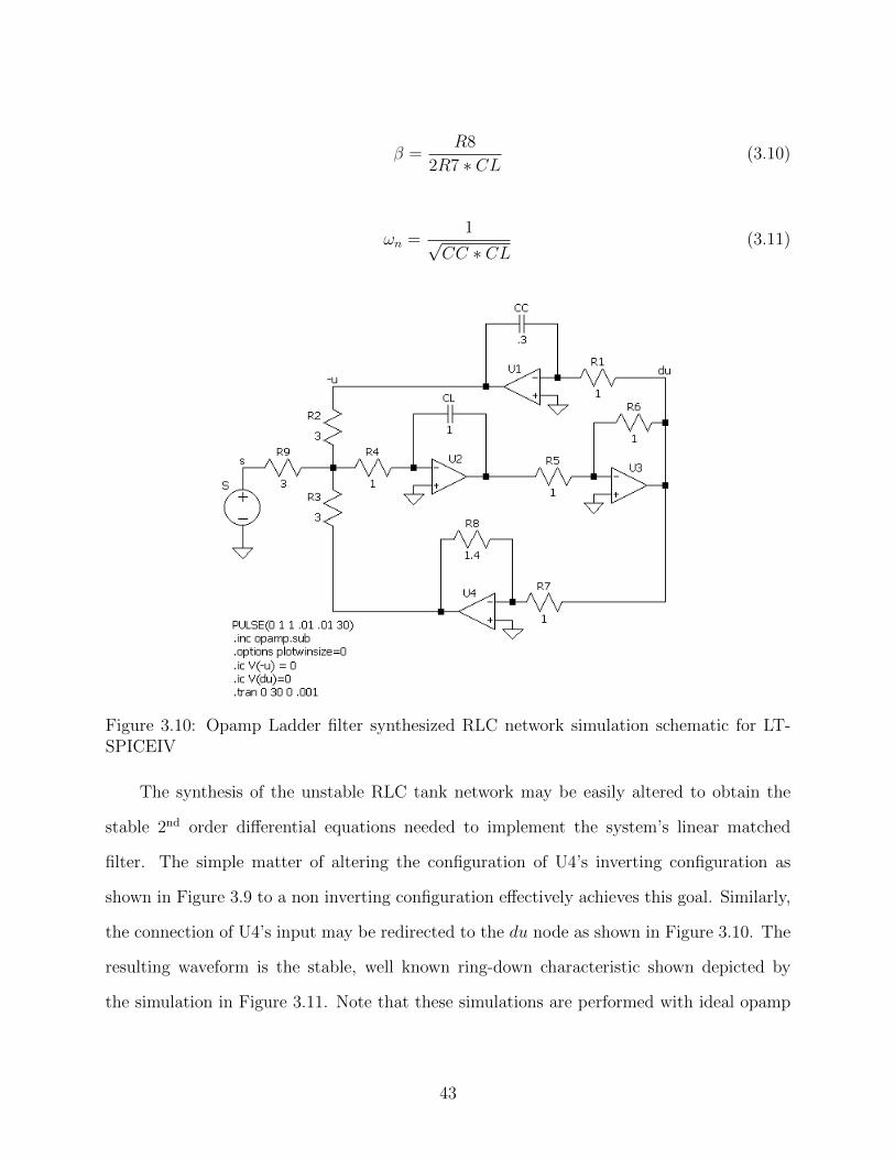
β =R8
2R7 ∗ CL (3.10)
ωn =1√
CC ∗ CL(3.11)
Figure 3.10: Opamp Ladder filter synthesized RLC network simulation schematic for LT-SPICEIV
The synthesis of the unstable RLC tank network may be easily altered to obtain the
stable 2nd order differential equations needed to implement the system’s linear matched
filter. The simple matter of altering the configuration of U4’s inverting configuration as
shown in Figure 3.9 to a non inverting configuration effectively achieves this goal. Similarly,
the connection of U4’s input may be redirected to the du node as shown in Figure 3.10. The
resulting waveform is the stable, well known ring-down characteristic shown depicted by
the simulation in Figure 3.11. Note that these simulations are performed with ideal opamp
43
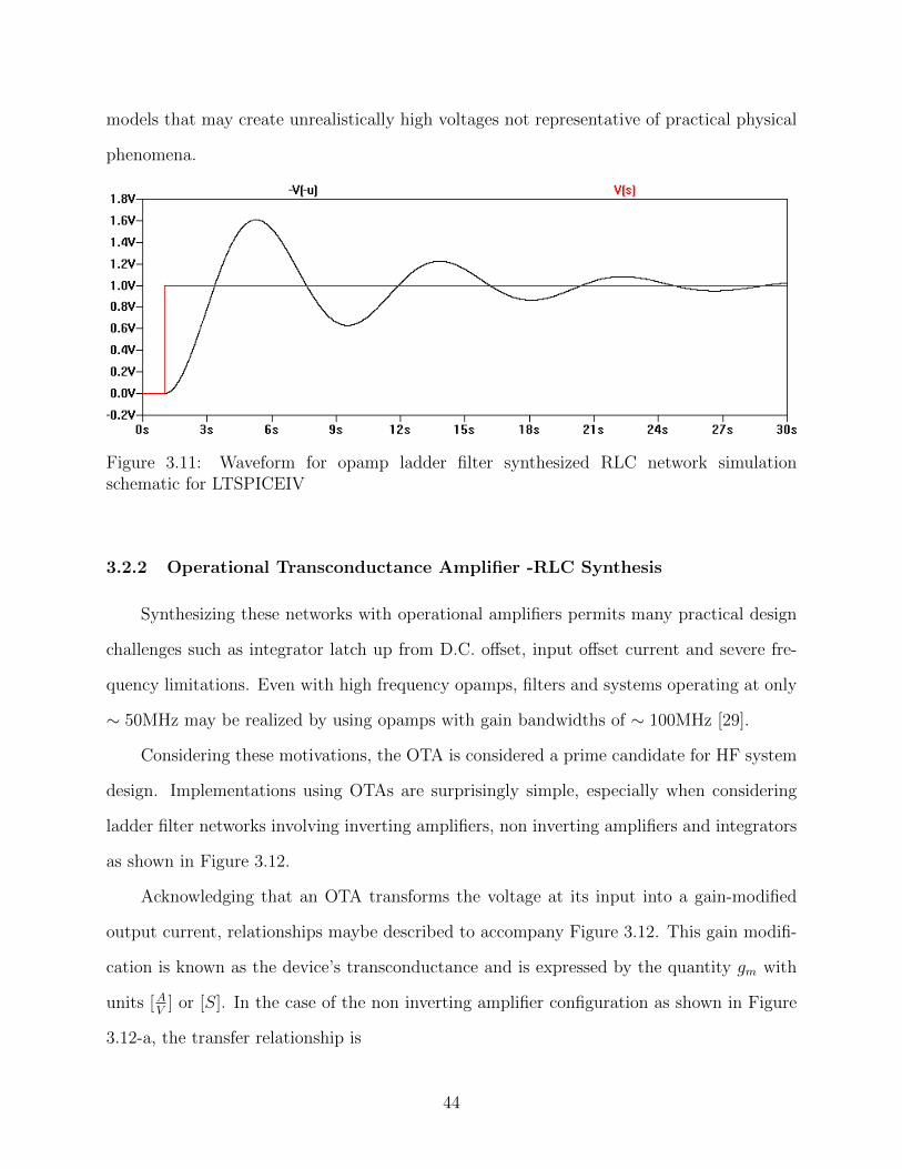
models that may create unrealistically high voltages not representative of practical physical
phenomena.
Figure 3.11: Waveform for opamp ladder filter synthesized RLC network simulationschematic for LTSPICEIV
3.2.2 Operational Transconductance Amplifier -RLC Synthesis
Synthesizing these networks with operational amplifiers permits many practical design
challenges such as integrator latch up from D.C. offset, input offset current and severe fre-
quency limitations. Even with high frequency opamps, filters and systems operating at only
∼ 50MHz may be realized by using opamps with gain bandwidths of ∼ 100MHz [29].
Considering these motivations, the OTA is considered a prime candidate for HF system
design. Implementations using OTAs are surprisingly simple, especially when considering
ladder filter networks involving inverting amplifiers, non inverting amplifiers and integrators
as shown in Figure 3.12.
Acknowledging that an OTA transforms the voltage at its input into a gain-modified
output current, relationships maybe described to accompany Figure 3.12. This gain modifi-
cation is known as the device’s transconductance and is expressed by the quantity gm with
units [AV
] or [S]. In the case of the non inverting amplifier configuration as shown in Figure
3.12-a, the transfer relationship is
44
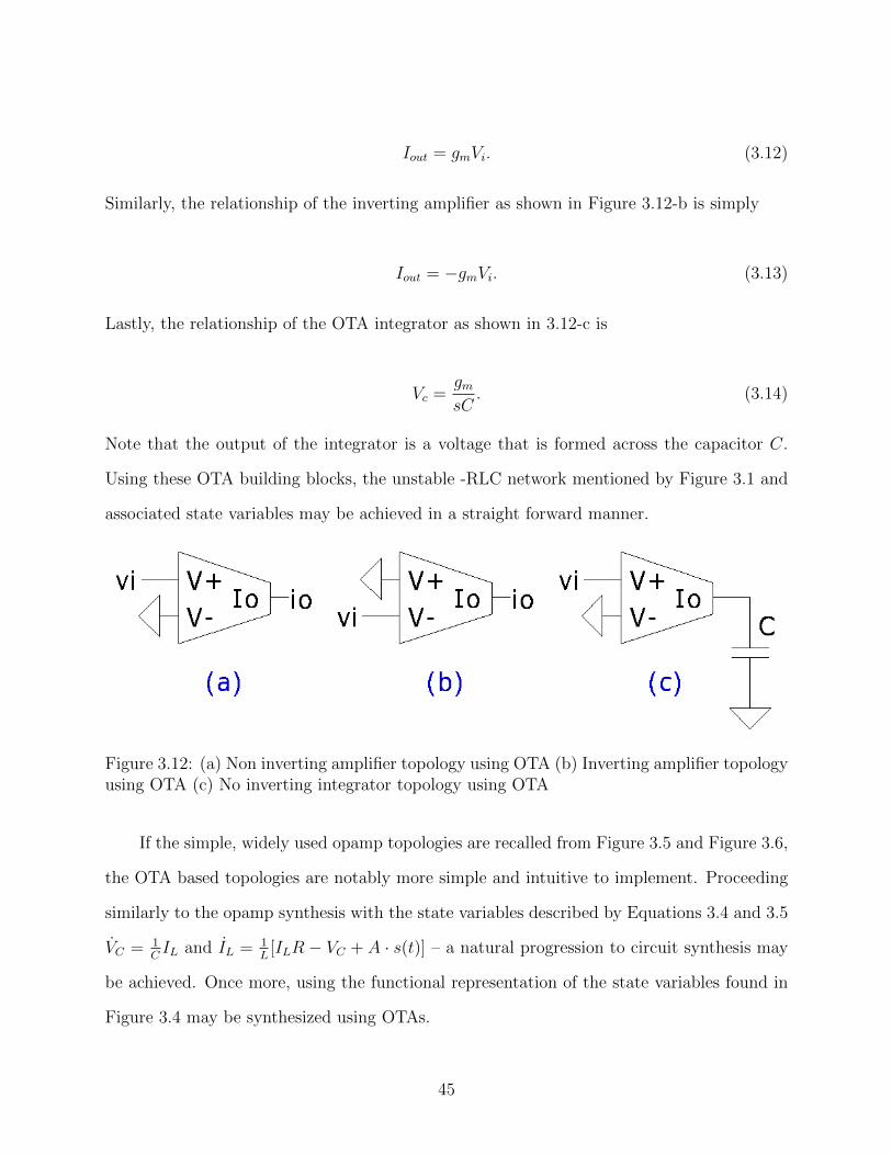
Iout = gmVi. (3.12)
Similarly, the relationship of the inverting amplifier as shown in Figure 3.12-b is simply
Iout = −gmVi. (3.13)
Lastly, the relationship of the OTA integrator as shown in 3.12-c is
Vc =gmsC
. (3.14)
Note that the output of the integrator is a voltage that is formed across the capacitor C.
Using these OTA building blocks, the unstable -RLC network mentioned by Figure 3.1 and
associated state variables may be achieved in a straight forward manner.
Figure 3.12: (a) Non inverting amplifier topology using OTA (b) Inverting amplifier topologyusing OTA (c) No inverting integrator topology using OTA
If the simple, widely used opamp topologies are recalled from Figure 3.5 and Figure 3.6,
the OTA based topologies are notably more simple and intuitive to implement. Proceeding
similarly to the opamp synthesis with the state variables described by Equations 3.4 and 3.5
VC = 1CIL and IL = 1
L[ILR − VC + A · s(t)] – a natural progression to circuit synthesis may
be achieved. Once more, using the functional representation of the state variables found in
Figure 3.4 may be synthesized using OTAs.
45
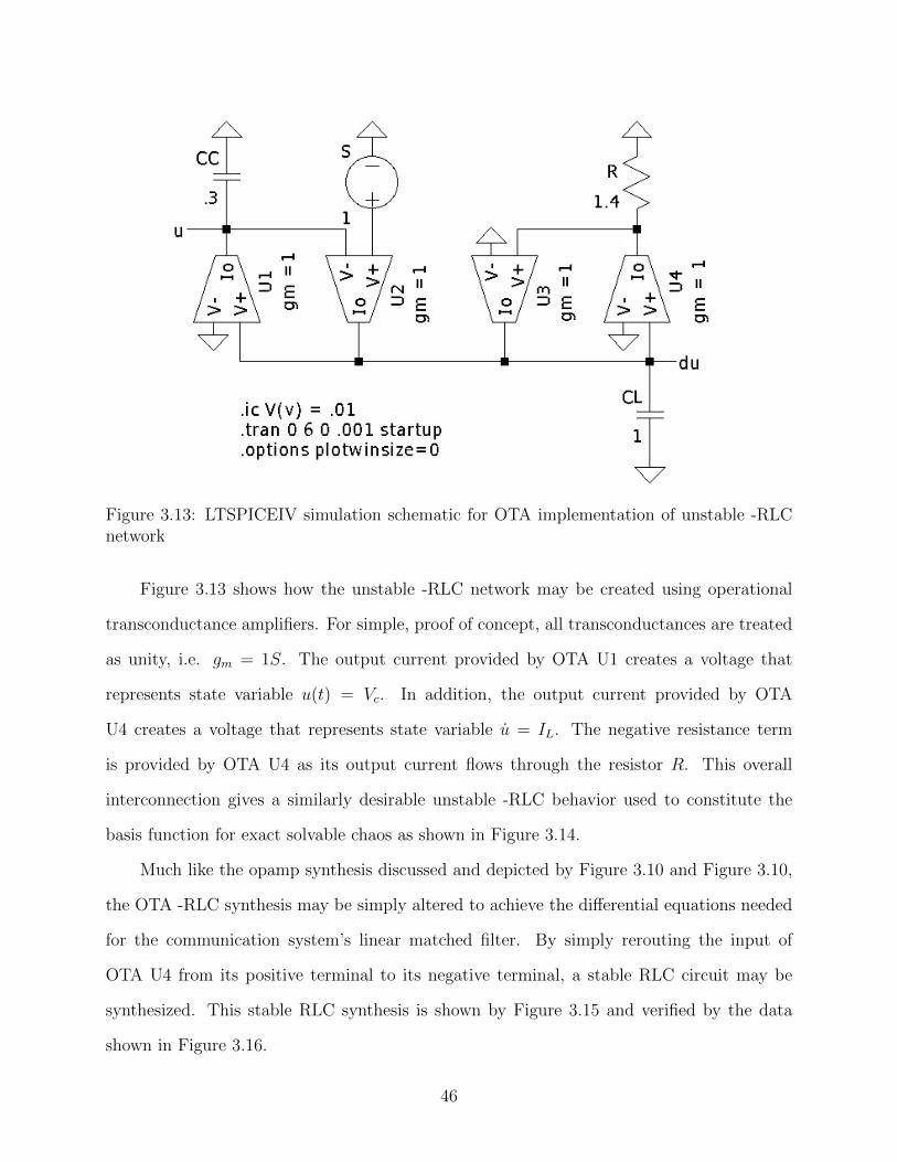
Figure 3.13: LTSPICEIV simulation schematic for OTA implementation of unstable -RLCnetwork
Figure 3.13 shows how the unstable -RLC network may be created using operational
transconductance amplifiers. For simple, proof of concept, all transconductances are treated
as unity, i.e. gm = 1S. The output current provided by OTA U1 creates a voltage that
represents state variable u(t) = Vc. In addition, the output current provided by OTA
U4 creates a voltage that represents state variable u = IL. The negative resistance term
is provided by OTA U4 as its output current flows through the resistor R. This overall
interconnection gives a similarly desirable unstable -RLC behavior used to constitute the
basis function for exact solvable chaos as shown in Figure 3.14.
Much like the opamp synthesis discussed and depicted by Figure 3.10 and Figure 3.10,
the OTA -RLC synthesis may be simply altered to achieve the differential equations needed
for the communication system’s linear matched filter. By simply rerouting the input of
OTA U4 from its positive terminal to its negative terminal, a stable RLC circuit may be
synthesized. This stable RLC synthesis is shown by Figure 3.15 and verified by the data
shown in Figure 3.16.
46
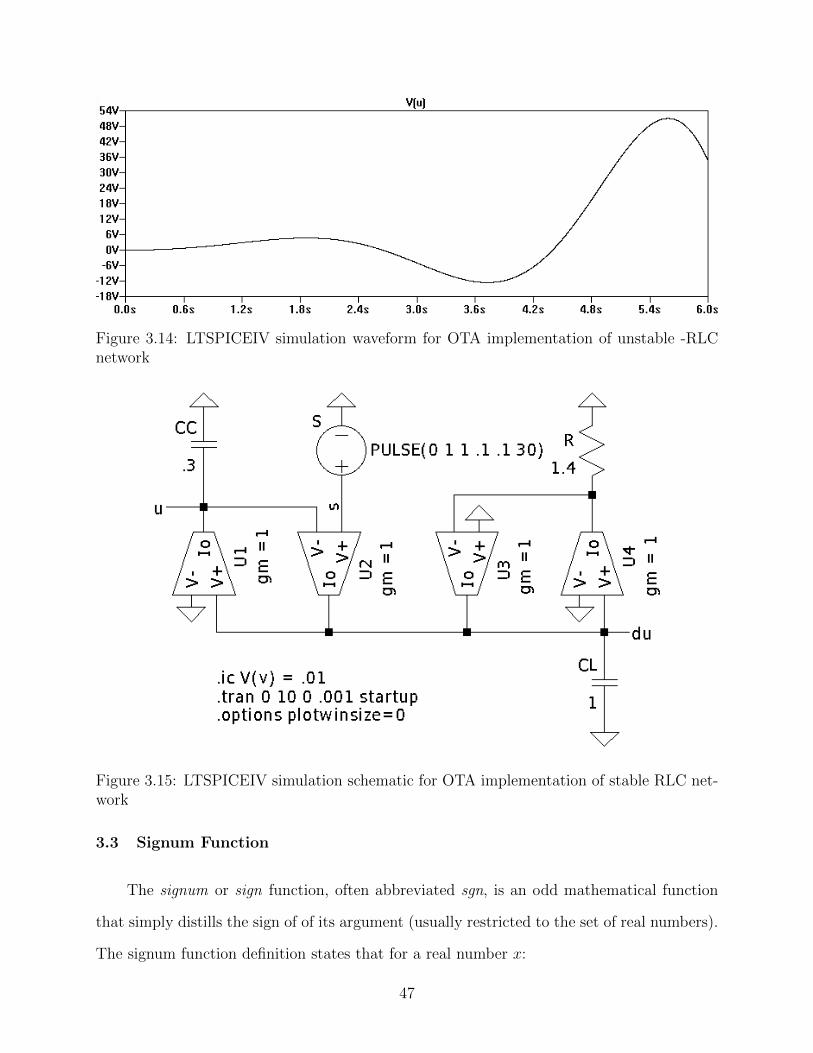
Figure 3.14: LTSPICEIV simulation waveform for OTA implementation of unstable -RLCnetwork
Figure 3.15: LTSPICEIV simulation schematic for OTA implementation of stable RLC net-work
3.3 Signum Function
The signum or sign function, often abbreviated sgn, is an odd mathematical function
that simply distills the sign of of its argument (usually restricted to the set of real numbers).
The signum function definition states that for a real number x:
47
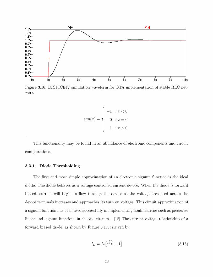
Figure 3.16: LTSPICEIV simulation waveform for OTA implementation of stable RLC net-work
sgn(x) =
−1 : x < 0
0 : x = 0
1 : x > 0
.
This functionality may be found in an abundance of electronic components and circuit
configurations.
3.3.1 Diode Thresholding
The first and most simple approximation of an electronic signum function is the ideal
diode. The diode behaves as a voltage controlled current device. When the diode is forward
biased, current will begin to flow through the device as the voltage presented across the
device terminals increases and approaches its turn on voltage. This circuit approximation of
a signum function has been used successfully in implementing nonlinearities such as piecewise
linear and signum functions in chaotic circuits . [18] The current-voltage relationship of a
forward biased diode, as shown by Figure 3.17, is given by
ID = IS[eVDVT − 1
](3.15)
48
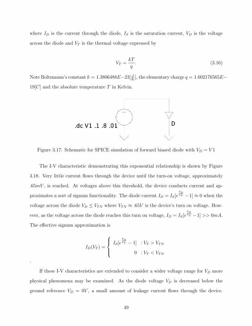
where ID is the current through the diode, IS is the saturation current, VD is the voltage
across the diode and VT is the thermal voltage expressed by
VT =kT
q. (3.16)
Note Boltzmann’s constant k = 1.3806488E−23[ JK
], the elementary charge q = 1.602176565E−
19[C] and the absolute temperature T in Kelvin.
Figure 3.17: Schematic for SPICE simulation of forward biased diode with VD = V 1
The I-V characteristic demonstrating this exponential relationship is shown by Figure
3.18. Very little current flows through the device until the turn-on voltage, approximately
.65mV , is reached. At voltages above this threshold, the device conducts current and ap-
proximates a sort of signum functionality. The diode current ID = IS[eVDVT − 1] ≈ 0 when the
voltage across the diode VD ≤ VTN where VTN ≈ .65V is the device’s turn on voltage. How-
ever, as the voltage across the diode reaches this turn on voltage, ID = IS[eVDVT −1] >> 0mA.
The effective signum approximation is
ID(VT ) =
IS[eVDVT − 1] : VT > VTN
0 : VT < VTN
.
If these I-V characteristics are extended to consider a wider voltage range for VD more
physical phenomena may be examined. As the diode voltage VD is decreased below the
ground reference VD = 0V , a small amount of leakage current flows through the device.
49
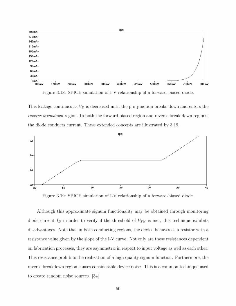
Figure 3.18: SPICE simulation of I-V relationship of a forward-biased diode.
This leakage continues as VD is decreased until the p-n junction breaks down and enters the
reverse breakdown region. In both the forward biased region and reverse break down regions,
the diode conducts current. These extended concepts are illustrated by 3.19.
Figure 3.19: SPICE simulation of I-V relationship of a forward-biased diode.
Although this approximate signum functionality may be obtained through monitoring
diode current ID in order to verify if the threshold of VTN is met, this technique exhibits
disadvantages. Note that in both conducting regions, the device behaves as a resistor with a
resistance value given by the slope of the I-V curve. Not only are these resistances dependent
on fabrication processes, they are asymmetric in respect to input voltage as well as each other.
This resistance prohibits the realization of a high quality signum function. Furthermore, the
reverse breakdown region causes considerable device noise. This is a common technique used
to create random noise sources. [34]
50
Finally, the thermal voltage VT often introduces temperature dependence in diode cir-
cuits as well as other devices with p-n junctions like transistors. When considering small
signal characteristics ID = ISeVDVT . Solving this equation for the diode voltage VD yields
VD =k
qln
(IDIS
)− kT
q
1
IS
dISdT
. (3.17)
The presence of the thermal voltage VT term gives a clearly linear dependence of diode
voltage VD to device temperature T . Temperature dependence is also attributed to the term
IS. This type of dependence is often exploited to achieve temperature sensors known as
proportional to absolute temperature (PTAT) devices. If the derivative of VD in respect to
temperature and it is assumed that ID >> IS an expression for the diode’s temperature
coefficient is obtained
dVDdT
=kT
qln
(IDIS
)=VDT− VTIS
dISdT
=VD − VGO − 3VT
T(3.18)
where VGO is the voltage corresponding to silicon bandgap energy at 0K. Further temperature
dependence is arises from the device material’s intrinsic carriers. [25] For a silicon diode with
VD = 0.65V , EG = qVGO = 1.12eV , and V T = 0.025V the resulting temperature dependence
is expected to be −1.82[mVK
]. [25]
This phenomena becomes particularly important to avoid when considering the differ-
ential pair, a very common input stage in both opamp and OTA designs. Temperature
compensation techniques are used to avoid this behavior such as introducing circuit ele-
ments that are complimentary to absolute temperature (CTAT). Combinations of PTATs
and CTATs are commonly used to create circuits with temperature independent parameters
[26]. These techniques are employed in most modern off the shelf opamps and OTAs and
give motivation to investigate finer and more reliable approximations of the signum function.
51
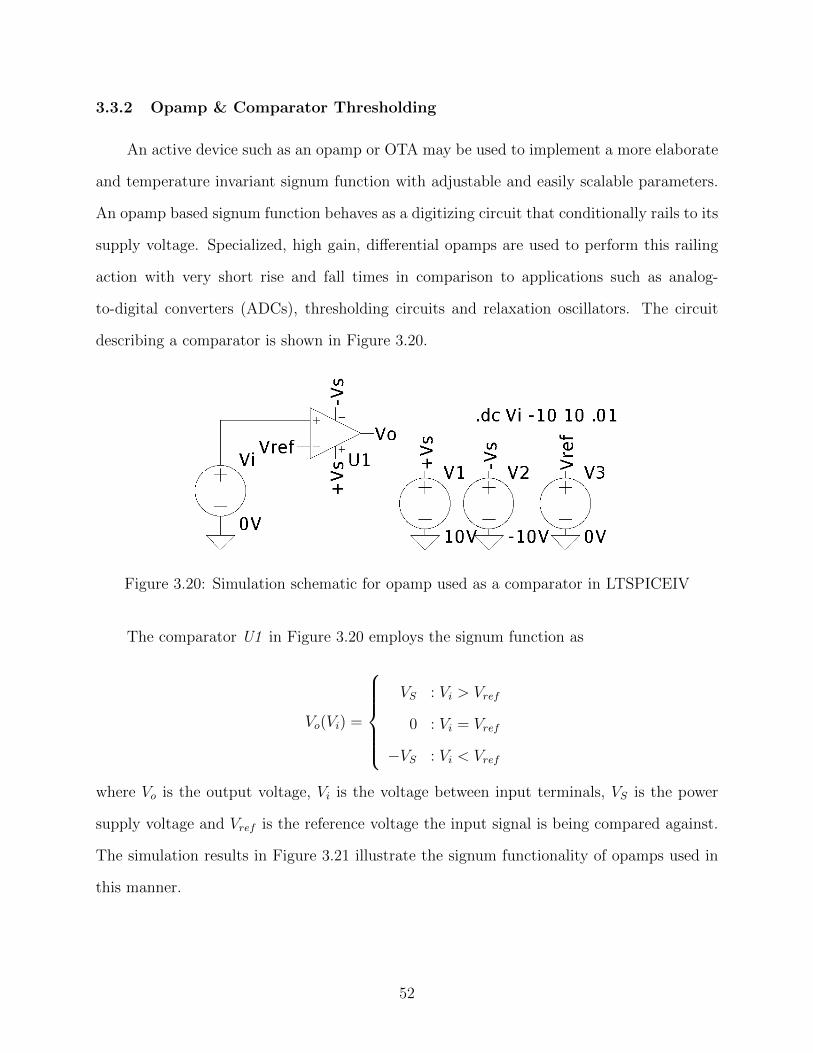
3.3.2 Opamp & Comparator Thresholding
An active device such as an opamp or OTA may be used to implement a more elaborate
and temperature invariant signum function with adjustable and easily scalable parameters.
An opamp based signum function behaves as a digitizing circuit that conditionally rails to its
supply voltage. Specialized, high gain, differential opamps are used to perform this railing
action with very short rise and fall times in comparison to applications such as analog-
to-digital converters (ADCs), thresholding circuits and relaxation oscillators. The circuit
describing a comparator is shown in Figure 3.20.
Figure 3.20: Simulation schematic for opamp used as a comparator in LTSPICEIV
The comparator U1 in Figure 3.20 employs the signum function as
Vo(Vi) =
VS : Vi > Vref
0 : Vi = Vref
−VS : Vi < Vref
where Vo is the output voltage, Vi is the voltage between input terminals, VS is the power
supply voltage and Vref is the reference voltage the input signal is being compared against.
The simulation results in Figure 3.21 illustrate the signum functionality of opamps used in
this manner.
52
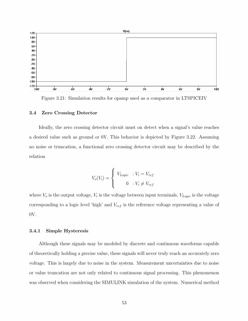
Figure 3.21: Simulation results for opamp used as a comparator in LTSPICEIV
3.4 Zero Crossing Detector
Ideally, the zero crossing detector circuit must on detect when a signal’s value reaches
a desired value such as ground or 0V. This behavior is depicted by Figure 3.22. Assuming
no noise or truncation, a functional zero crossing detector circuit may be described by the
relation
Vo(Vi) =
VLogic : Vi = Vref
0 : Vi 6= Vref
where Vo is the output voltage, Vi is the voltage between input terminals, VLogic is the voltage
corresponding to a logic level ‘high’ and Vref is the reference voltage representing a value of
0V.
3.4.1 Simple Hysteresis
Although these signals may be modeled by discrete and continuous waveforms capable
of theoretically holding a precise value, these signals will never truly reach an accurately zero
voltage. This is largely due to noise in the system. Measurement uncertainties due to noise
or value truncation are not only related to continuous signal processing. This phenomenon
was observed when considering the SIMULINK simulation of the system. Numerical method
53
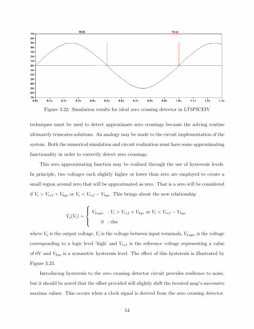
Figure 3.22: Simulation results for ideal zero crossing detector in LTSPICEIV
techniques must be used to detect approximate zero crossings because the solving routine
ultimately truncates solutions. An analogy may be made to the circuit implementation of the
system. Both the numerical simulation and circuit realization must have some approximating
functionality in order to correctly detect zero crossings.
This zero approximating function may be realized through the use of hysteresis levels.
In principle, two voltages each slightly higher or lower than zero are employed to create a
small region around zero that will be approximated as zero. That is a zero will be considered
if Vi > Vref + Vhys or Vi < Vref − Vhys. This brings about the new relationship
Vo(Vi) =
VLogic : Vi > Vref + Vhys or Vi < Vref − Vhys0 : else
where Vo is the output voltage, Vi is the voltage between input terminals, VLogic is the voltage
corresponding to a logic level ‘high’ and Vref is the reference voltage representing a value
of 0V and Vhys is a symmetric hysteresis level. The effect of this hysteresis is illustrated by
Figure 3.23.
Introducing hysteresis to the zero crossing detector circuit provides resilience to noise,
but it should be noted that the offset provided will slightly shift the iterated map’s successive
maxima values. This occurs when a clock signal is derived from the zero crossing detector.
54
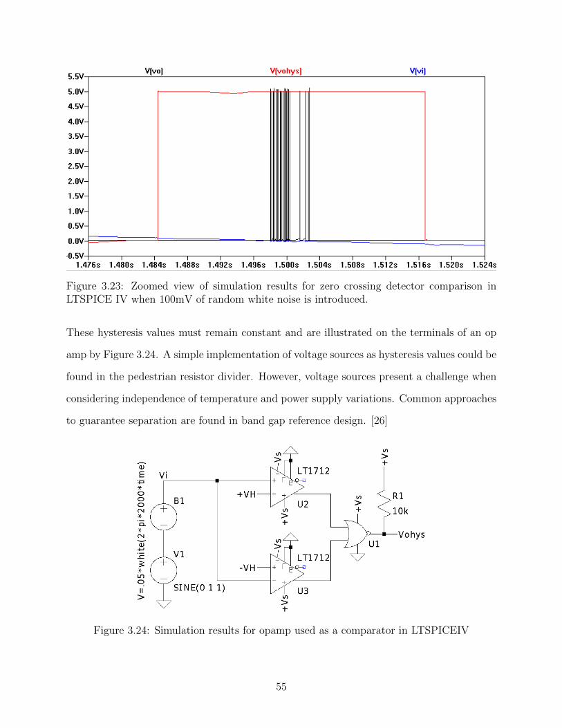
Figure 3.23: Zoomed view of simulation results for zero crossing detector comparison inLTSPICE IV when 100mV of random white noise is introduced.
These hysteresis values must remain constant and are illustrated on the terminals of an op
amp by Figure 3.24. A simple implementation of voltage sources as hysteresis values could be
found in the pedestrian resistor divider. However, voltage sources present a challenge when
considering independence of temperature and power supply variations. Common approaches
to guarantee separation are found in band gap reference design. [26]
Figure 3.24: Simulation results for opamp used as a comparator in LTSPICEIV
55
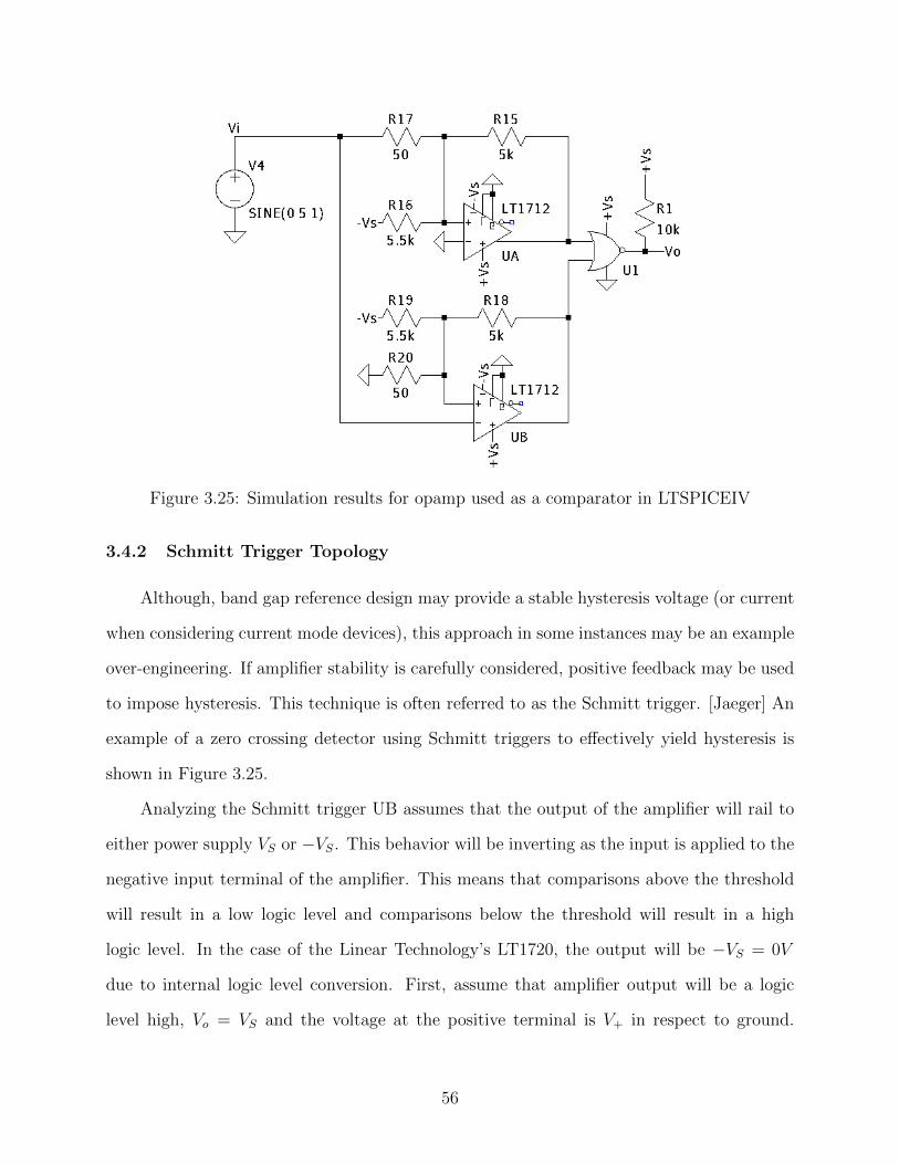
Figure 3.25: Simulation results for opamp used as a comparator in LTSPICEIV
3.4.2 Schmitt Trigger Topology
Although, band gap reference design may provide a stable hysteresis voltage (or current
when considering current mode devices), this approach in some instances may be an example
over-engineering. If amplifier stability is carefully considered, positive feedback may be used
to impose hysteresis. This technique is often referred to as the Schmitt trigger. [Jaeger] An
example of a zero crossing detector using Schmitt triggers to effectively yield hysteresis is
shown in Figure 3.25.
Analyzing the Schmitt trigger UB assumes that the output of the amplifier will rail to
either power supply VS or −VS. This behavior will be inverting as the input is applied to the
negative input terminal of the amplifier. This means that comparisons above the threshold
will result in a low logic level and comparisons below the threshold will result in a high
logic level. In the case of the Linear Technology’s LT1720, the output will be −VS = 0V
due to internal logic level conversion. First, assume that amplifier output will be a logic
level high, Vo = VS and the voltage at the positive terminal is V+ in respect to ground.
56
Taking Kirchoff’s current law to the node connected to V+ of the amplifier UB in Figure
3.25 gives −I18 + I19 + I20 = 0. This can be used to solve for the hysteresis values. The
second hysteresis value may be found by assuming the output of UB is a logic level low,
Vo = −VS and analyzing the same V+ terminal using KCL. This gives
Vh± ∓ VSR18
+Vh± + VSR19
+Vh± − 0
R20
= 0A. (3.19)
Solving in terms of Vh+ gives the hysteresis values of
Vh± = ± R20VS(R19 ∓R18)
R18(R19 +R20) +R19R20
. (3.20)
Recall the case of the LT1712, −VS = 0 due to the internal logic level conversion. This
results in a lower hysteresis value of 0V . If it assumed that VS = 5V the resulting hysteresis
value for both Schmitt trigger UB gives Vh+ = 43mV and Vh− ≈ 0V .
Analysis of Schmitt trigger UA follows the same approach except appling KCL at the
terminal V+ gives I15−I16+I17 = 0. Schmitt trigger UA will have an assumed output Vo = VS
corresponding to a high logic level and Vo = −VS corresponding to a low logic level due to its
non inverting configuration. Recognizing that the inverting terminal of amplifier UA imposes
a virtual ground at the terminal V+ and applying Ohm’s law gives ViR17
+ −VSR16
+ VSR15
= 0 for a
high logic level at the amplifier’s output. This yields an equation similar to the analysis of
the network surrounding UB.
VSR15
− VSR16
+ViR17
= 0 (3.21)
Once again solving for the hysteresis values Vi = Vh± gives
Vh± = R17VS
(1
R16
± 1
R15
)(3.22)
57
By using this positive feedback technique, an effective voltage region above and below
ground reference creates an area for approximating a zero detection and establishes a noise
tolerance. This tolerance may be easily adjusted by altering the resistance values stated in
Equation 3.20 and Equation 3.22. Note that this design does not require perfect symmetry
for the zero detection’s approximation region, but if this is required, designs should aim for
an equivalence between amplifier UA’s Vh− and amplifier UB’s Vh+. That is
R17VS
(1
R16
− 1
R15
)=
R20VS(R19 −R18)
R18(R19 +R20) +R19R20
. (3.23)
3.5 Guard Circuit
The purpose of the guard circuit is to conditionally provide the scaled forcing function
f(t) = A · s(t) (3.24)
to the unstable, linear 2nd order oscillation u(t) provided by the -RLC tank circuit where
A = (ω2 + β2)2. Effectively, the guard circuit electronically alternates between two fixed
points as the guard condition is met. A circuit with an input of sgn(u(t)) and a clock
triggered by zero crossings of u(t) that enables a scaled output of two discrete equilibrium
points, provides the folding utility needed to achieve exact solvable chaos.
3.5.1 Sample & Hold
At first evaluation, the guard condition may be applied using a sample and hold circuit as
shown by Figure 3.26. In concept, the guard condition must sample the value of sgn(u(t))
at zero crossings of u(t) and hold this value until the next instance of u(t) = 0. If this
functionality is abstracted, it may be viewed as the definition of a sample-and-hold circuit.
Early designs and a hardware prototype were developed using this approach. Although the
functionality of a sample and hold circuit satisfies the definition of the guard condition, in
58
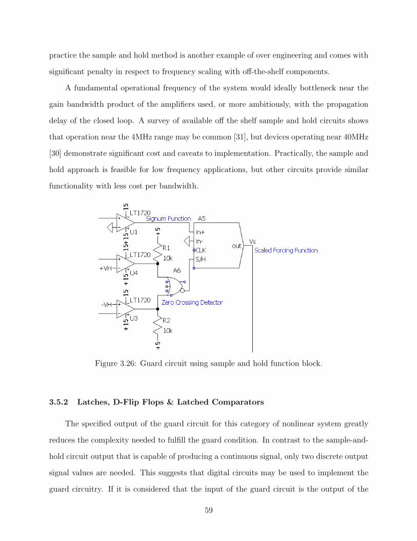
practice the sample and hold method is another example of over engineering and comes with
significant penalty in respect to frequency scaling with off-the-shelf components.
A fundamental operational frequency of the system would ideally bottleneck near the
gain bandwidth product of the amplifiers used, or more ambitiously, with the propagation
delay of the closed loop. A survey of available off the shelf sample and hold circuits shows
that operation near the 4MHz range may be common [31], but devices operating near 40MHz
[30] demonstrate significant cost and caveats to implementation. Practically, the sample and
hold approach is feasible for low frequency applications, but other circuits provide similar
functionality with less cost per bandwidth.
Figure 3.26: Guard circuit using sample and hold function block.
3.5.2 Latches, D-Flip Flops & Latched Comparators
The specified output of the guard circuit for this category of nonlinear system greatly
reduces the complexity needed to fulfill the guard condition. In contrast to the sample-and-
hold circuit output that is capable of producing a continuous signal, only two discrete output
signal values are needed. This suggests that digital circuits may be used to implement the
guard circuitry. If it is considered that the input of the guard circuit is the output of the
59
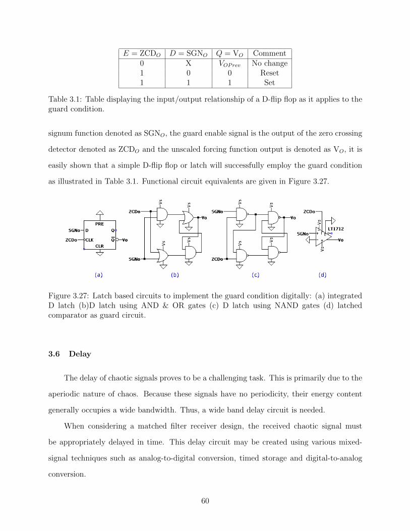
E = ZCDO D = SGNO Q = VO Comment0 X VOPrev No change1 0 0 Reset1 1 1 Set
Table 3.1: Table displaying the input/output relationship of a D-flip flop as it applies to theguard condition.
signum function denoted as SGNO, the guard enable signal is the output of the zero crossing
detector denoted as ZCDO and the unscaled forcing function output is denoted as VO, it is
easily shown that a simple D-flip flop or latch will successfully employ the guard condition
as illustrated in Table 3.1. Functional circuit equivalents are given in Figure 3.27.
Figure 3.27: Latch based circuits to implement the guard condition digitally: (a) integratedD latch (b)D latch using AND & OR gates (c) D latch using NAND gates (d) latchedcomparator as guard circuit.
3.6 Delay
The delay of chaotic signals proves to be a challenging task. This is primarily due to the
aperiodic nature of chaos. Because these signals have no periodicity, their energy content
generally occupies a wide bandwidth. Thus, a wide band delay circuit is needed.
When considering a matched filter receiver design, the received chaotic signal must
be appropriately delayed in time. This delay circuit may be created using various mixed-
signal techniques such as analog-to-digital conversion, timed storage and digital-to-analog
conversion.
60
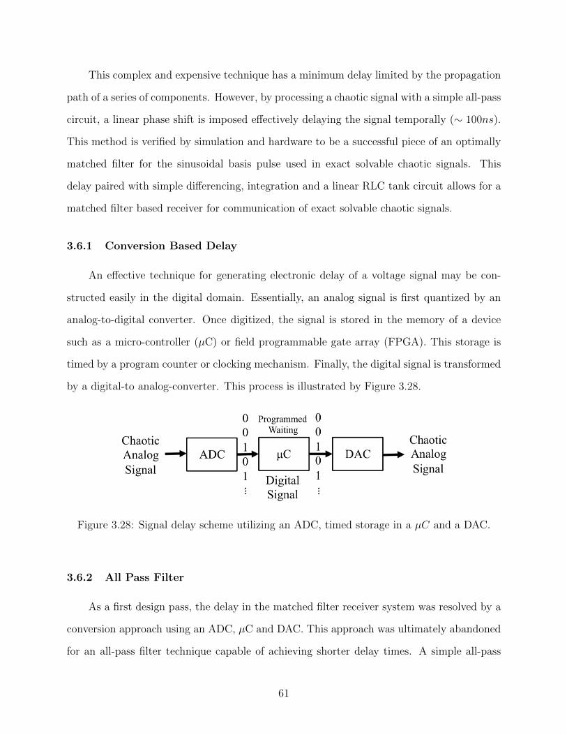
This complex and expensive technique has a minimum delay limited by the propagation
path of a series of components. However, by processing a chaotic signal with a simple all-pass
circuit, a linear phase shift is imposed effectively delaying the signal temporally (∼ 100ns).
This method is verified by simulation and hardware to be a successful piece of an optimally
matched filter for the sinusoidal basis pulse used in exact solvable chaotic signals. This
delay paired with simple differencing, integration and a linear RLC tank circuit allows for a
matched filter based receiver for communication of exact solvable chaotic signals.
3.6.1 Conversion Based Delay
An effective technique for generating electronic delay of a voltage signal may be con-
structed easily in the digital domain. Essentially, an analog signal is first quantized by an
analog-to-digital converter. Once digitized, the signal is stored in the memory of a device
such as a micro-controller (µC) or field programmable gate array (FPGA). This storage is
timed by a program counter or clocking mechanism. Finally, the digital signal is transformed
by a digital-to analog-converter. This process is illustrated by Figure 3.28.
Figure 3.28: Signal delay scheme utilizing an ADC, timed storage in a µC and a DAC.
3.6.2 All Pass Filter
As a first design pass, the delay in the matched filter receiver system was resolved by a
conversion approach using an ADC, µC and DAC. This approach was ultimately abandoned
for an all-pass filter technique capable of achieving shorter delay times. A simple all-pass
61
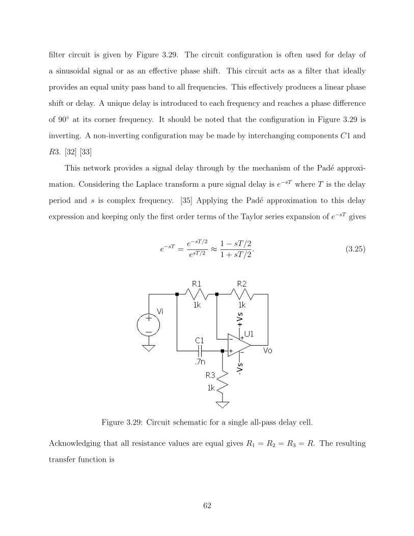
filter circuit is given by Figure 3.29. The circuit configuration is often used for delay of
a sinusoidal signal or as an effective phase shift. This circuit acts as a filter that ideally
provides an equal unity pass band to all frequencies. This effectively produces a linear phase
shift or delay. A unique delay is introduced to each frequency and reaches a phase difference
of 90 at its corner frequency. It should be noted that the configuration in Figure 3.29 is
inverting. A non-inverting configuration may be made by interchanging components C1 and
R3. [32] [33]
This network provides a signal delay through by the mechanism of the Pade approxi-
mation. Considering the Laplace transform a pure signal delay is e−sT where T is the delay
period and s is complex frequency. [35] Applying the Pade approximation to this delay
expression and keeping only the first order terms of the Taylor series expansion of e−sT gives
e−sT =e−sT/2
esT/2≈ 1− sT/2
1 + sT/2. (3.25)
Figure 3.29: Circuit schematic for a single all-pass delay cell.
Acknowledging that all resistance values are equal gives R1 = R2 = R3 = R. The resulting
transfer function is
62
VoVi
=RCs− 1
RCs+ 1. (3.26)
This first order filter has one pole at − 1RC
and a zero at 1RC
. Further analysis shows the
phase shift of the network is
φ = −2tan−1(RC
2πf
)(3.27)
where f represents a specific frequency in Hz corresponding to the expressed phase shift.
Continuing, the group delay δ of the network may be expressed as
δ =2RC
(2πfRC)2 + 1. (3.28)
From this equation, it is easily shown that the delay at DC is given by
δ|f=0Hz = 2RC. (3.29)
When considering design parameters for a given frequency, f , with a specified phase shift,
φ, the values of R and C may be selected based on the relationship
RC = 2πftan
(− φ
2
). (3.30)
Operation of this network is greatly influenced by the capacitor C1 that exhibits short-
circuit behavior at high frequencies therefore causing the opamp to create a unity gain buffer.
As frequencies are lowered, the phase shift approaches 90 as the corner frequency ω = 1R3C1
is observed. Finally, as low frequencies such as D.C. values are considered, the network may
be viewed as an inverting amplifier due to the capacitor C1 acting as an open circuit.
Ultimately, this network has a frequency dependent response as described by the pre-
vious equations. This dependence causes high frequencies to be phase shifted or delayed
63
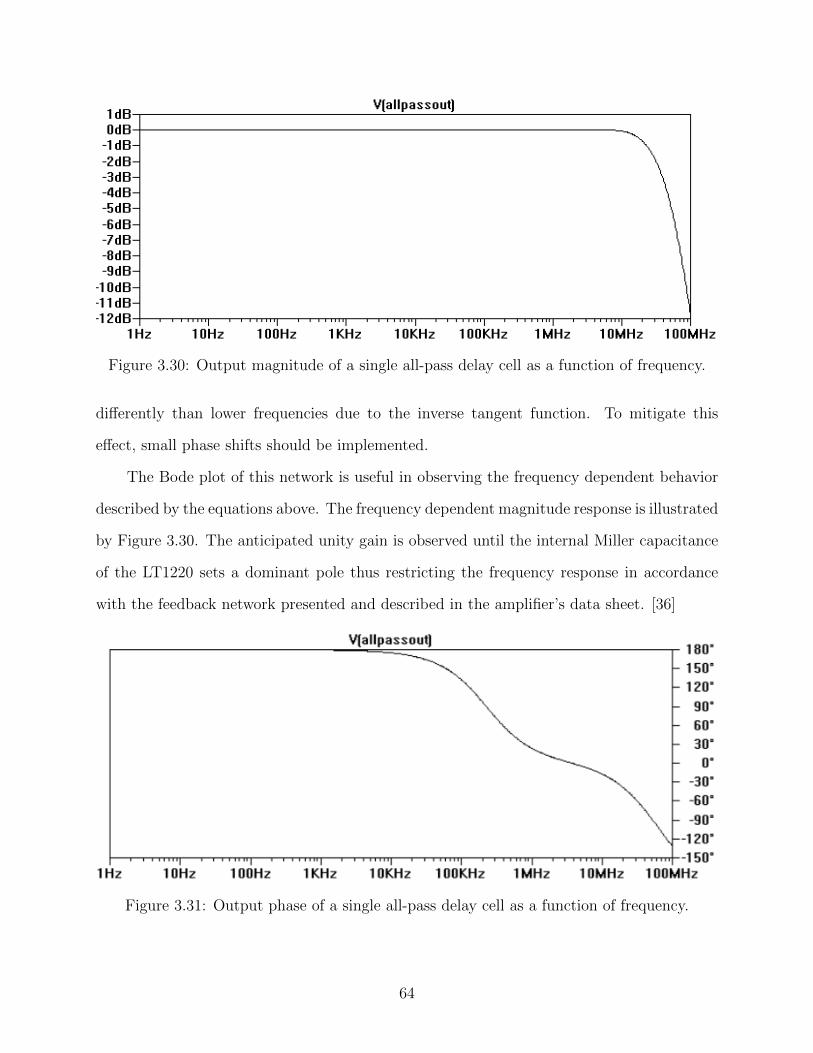
Figure 3.30: Output magnitude of a single all-pass delay cell as a function of frequency.
differently than lower frequencies due to the inverse tangent function. To mitigate this
effect, small phase shifts should be implemented.
The Bode plot of this network is useful in observing the frequency dependent behavior
described by the equations above. The frequency dependent magnitude response is illustrated
by Figure 3.30. The anticipated unity gain is observed until the internal Miller capacitance
of the LT1220 sets a dominant pole thus restricting the frequency response in accordance
with the feedback network presented and described in the amplifier’s data sheet. [36]
Figure 3.31: Output phase of a single all-pass delay cell as a function of frequency.
64
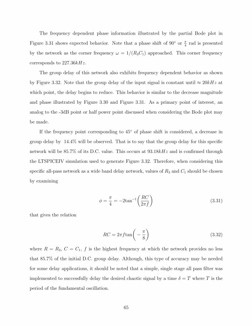
The frequency dependent phase information illustrated by the partial Bode plot in
Figure 3.31 shows expected behavior. Note that a phase shift of 90 or π4
rad is presented
by the network as the corner frequency ω = 1/(R3C1) approached. This corner frequency
corresponds to 227.36kHz.
The group delay of this network also exhibits frequency dependent behavior as shown
by Figure 3.32. Note that the group delay of the input signal is constant until ≈ 20kHz at
which point, the delay begins to reduce. This behavior is similar to the decrease magnitude
and phase illustrated by Figure 3.30 and Figure 3.31. As a primary point of interest, an
analog to the -3dB point or half power point discussed when considering the Bode plot may
be made.
If the frequency point corresponding to 45 of phase shift is considered, a decrease in
group delay by 14.4% will be observed. That is to say that the group delay for this specific
network will be 85.7% of its D.C. value. This occurs at 93.18kHz and is confirmed through
the LTSPICEIV simulation used to generate Figure 3.32. Therefore, when considering this
specific all-pass network as a wide band delay network, values of R3 and C1 should be chosen
by examining
φ =π
4= −2tan−1
(RC
2πf
)(3.31)
that gives the relation
RC = 2πftan
(− π
8
)(3.32)
where R = R3, C = C1, f is the highest frequency at which the network provides no less
that 85.7% of the initial D.C. group delay. Although, this type of accuracy may be needed
for some delay applications, it should be noted that a simple, single stage all pass filter was
implemented to successfully delay the desired chaotic signal by a time δ = T where T is the
period of the fundamental oscillation.
65
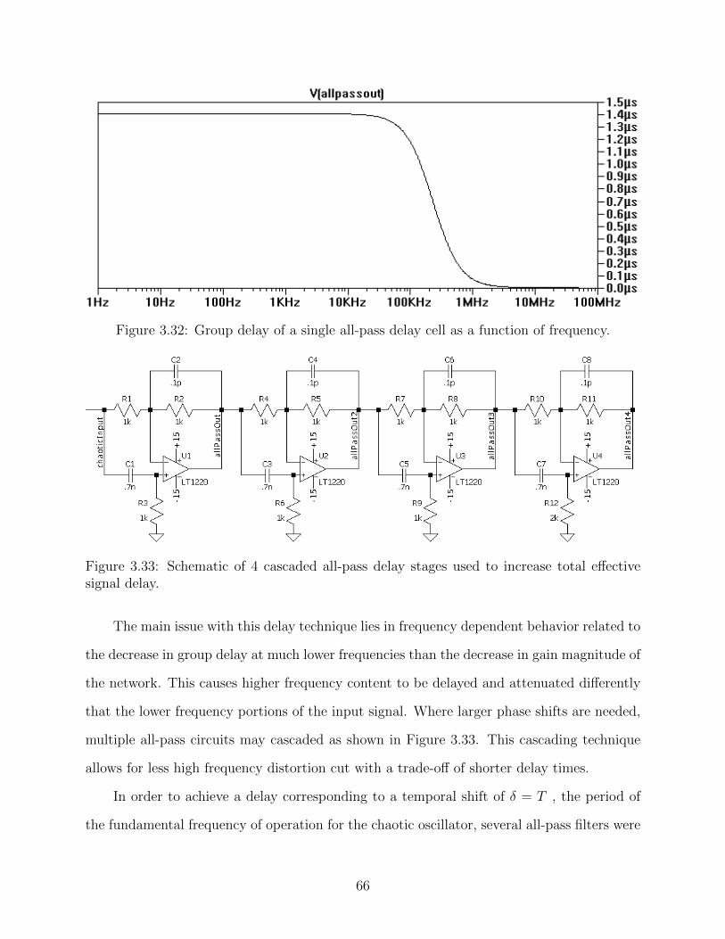
Figure 3.32: Group delay of a single all-pass delay cell as a function of frequency.
Figure 3.33: Schematic of 4 cascaded all-pass delay stages used to increase total effectivesignal delay.
The main issue with this delay technique lies in frequency dependent behavior related to
the decrease in group delay at much lower frequencies than the decrease in gain magnitude of
the network. This causes higher frequency content to be delayed and attenuated differently
that the lower frequency portions of the input signal. Where larger phase shifts are needed,
multiple all-pass circuits may cascaded as shown in Figure 3.33. This cascading technique
allows for less high frequency distortion cut with a trade-off of shorter delay times.
In order to achieve a delay corresponding to a temporal shift of δ = T , the period of
the fundamental frequency of operation for the chaotic oscillator, several all-pass filters were
66
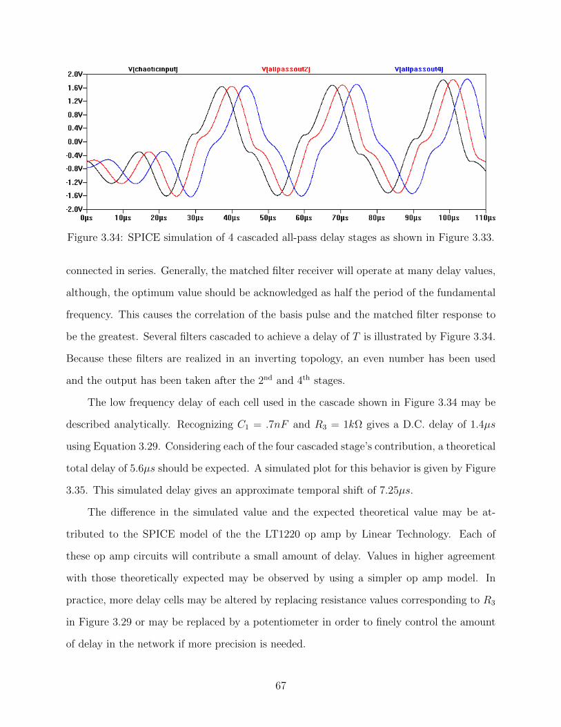
Figure 3.34: SPICE simulation of 4 cascaded all-pass delay stages as shown in Figure 3.33.
connected in series. Generally, the matched filter receiver will operate at many delay values,
although, the optimum value should be acknowledged as half the period of the fundamental
frequency. This causes the correlation of the basis pulse and the matched filter response to
be the greatest. Several filters cascaded to achieve a delay of T is illustrated by Figure 3.34.
Because these filters are realized in an inverting topology, an even number has been used
and the output has been taken after the 2nd and 4th stages.
The low frequency delay of each cell used in the cascade shown in Figure 3.34 may be
described analytically. Recognizing C1 = .7nF and R3 = 1kΩ gives a D.C. delay of 1.4µs
using Equation 3.29. Considering each of the four cascaded stage’s contribution, a theoretical
total delay of 5.6µs should be expected. A simulated plot for this behavior is given by Figure
3.35. This simulated delay gives an approximate temporal shift of 7.25µs.
The difference in the simulated value and the expected theoretical value may be at-
tributed to the SPICE model of the the LT1220 op amp by Linear Technology. Each of
these op amp circuits will contribute a small amount of delay. Values in higher agreement
with those theoretically expected may be observed by using a simpler op amp model. In
practice, more delay cells may be altered by replacing resistance values corresponding to R3
in Figure 3.29 or may be replaced by a potentiometer in order to finely control the amount
of delay in the network if more precision is needed.
67
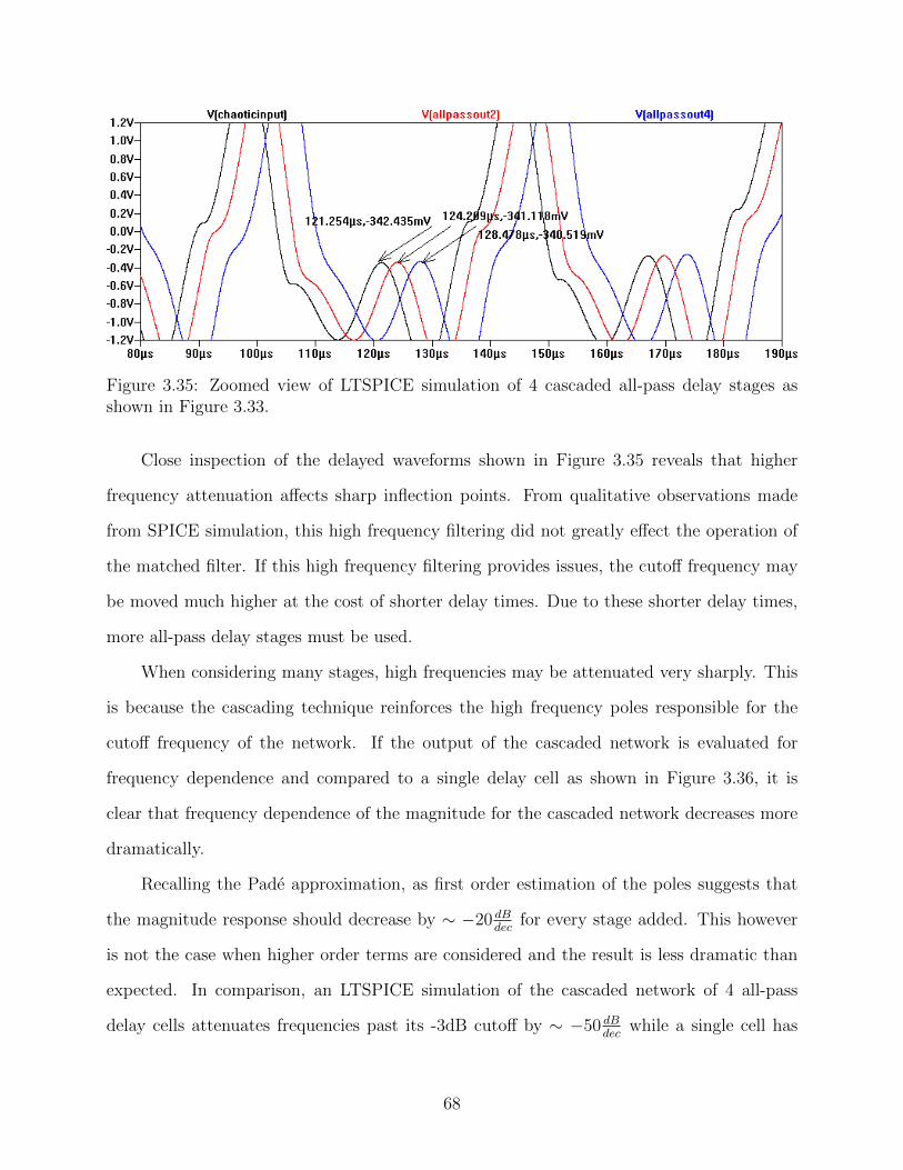
Figure 3.35: Zoomed view of LTSPICE simulation of 4 cascaded all-pass delay stages asshown in Figure 3.33.
Close inspection of the delayed waveforms shown in Figure 3.35 reveals that higher
frequency attenuation affects sharp inflection points. From qualitative observations made
from SPICE simulation, this high frequency filtering did not greatly effect the operation of
the matched filter. If this high frequency filtering provides issues, the cutoff frequency may
be moved much higher at the cost of shorter delay times. Due to these shorter delay times,
more all-pass delay stages must be used.
When considering many stages, high frequencies may be attenuated very sharply. This
is because the cascading technique reinforces the high frequency poles responsible for the
cutoff frequency of the network. If the output of the cascaded network is evaluated for
frequency dependence and compared to a single delay cell as shown in Figure 3.36, it is
clear that frequency dependence of the magnitude for the cascaded network decreases more
dramatically.
Recalling the Pade approximation, as first order estimation of the poles suggests that
the magnitude response should decrease by ∼ −20 dBdec
for every stage added. This however
is not the case when higher order terms are considered and the result is less dramatic than
expected. In comparison, an LTSPICE simulation of the cascaded network of 4 all-pass
delay cells attenuates frequencies past its -3dB cutoff by ∼ −50 dBdec
while a single cell has
68
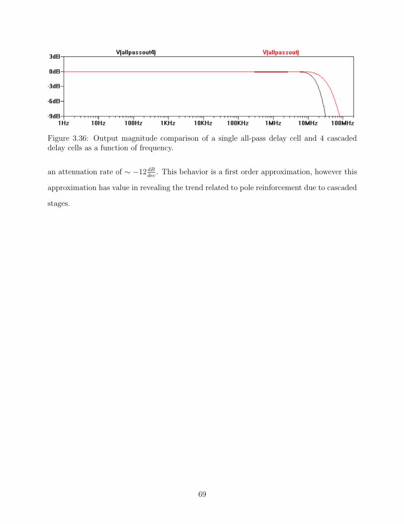
Figure 3.36: Output magnitude comparison of a single all-pass delay cell and 4 cascadeddelay cells as a function of frequency.
an attenuation rate of ∼ −12 dBdec
. This behavior is a first order approximation, however this
approximation has value in revealing the trend related to pole reinforcement due to cascaded
stages.
69
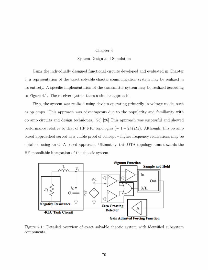
Chapter 4
System Design and Simulation
Using the individually designed functional circuits developed and evaluated in Chapter
3, a representation of the exact solvable chaotic communication system may be realized in
its entirety. A specific implementation of the transmitter system may be realized according
to Figure 4.1. The receiver system takes a similar approach.
First, the system was realized using devices operating primarily in voltage mode, such
as op amps. This approach was advantageous due to the popularity and familiarity with
op amp circuits and design techniques. [25] [26] This approach was successful and showed
performance relative to that of HF NIC topologies (∼ 1 − 2MHz). Although, this op amp
based approached served as a viable proof of concept – higher frequency realizations may be
obtained using an OTA based approach. Ultimately, this OTA topology aims towards the
HF monolithic integration of the chaotic system.
Figure 4.1: Detailed overview of exact solvable chaotic system with identified subsystemcomponents.
70
4.1 Opamp Synthesized System
High frequency op amps were considered such as the Linear Technology LT1220 [11],
LT1222, and the LT1818. These op amps have gain bandwidth products between 45-100MHz,
a maximum power supply range of 36V and a sufficiently flat phase response around the
frequency of interest (1-2MHz). The LT1818 proved to give the best results and a successful
simulation of the frequency scaled system is subsequently provided.
4.1.1 Opamp Synthesized Transmitter Circuit
Circuit design of the op amp based transmitter system began with much similarity to
active ladder filter synthesis. The -RLC network was realized as a low frequency prototype
that generated the desired basis pulse. This network shown in Figure 4.2 consists of the op
amp components U1, U2, U3, U4 and U5. This network produces a voltage at node v that
is representative of the chaotic time series signal u(t) at the output of op amp U5.
Similarly, the output of op amp U4 produces a voltage vd that is representative of the
derivative of signal u(t). This derivative is evaluated for zero crossings by a zero crossing
detector circuit that is comprised of op amps U8 and U9 and the NOR logic gate A2 where
V+H and V−H are voltages representing hysteresis values. A signum function is applied to
the signal v by the op amp U7 and the result is presented to the sample-and-hold circuit A1
that is clocked by the zero crossing detector circuit. Finally, the output of A1 provides the
forcing function which is buffered by U6 and summed as a current by resistors R2, R7 and
R10. These interconnections are displayed by the schematic found in Figure 4.2.
SPICE simulation of the low frequency prototype shown in Figure 4.2 gives desirably
characteristic waveforms. A time series plot of the continuous u(t) representative voltage v
and the discrete switching event s(t) representative voltage VS that is given by Figure 4.3.
A mapping from theoretical equations to the circuit parameters related to the schematic
in Figure 4.2 may be found by relatively simple analysis. Considering the -RLC network,
the capacitor value is set by C1, the inductor value is set by C2 and the negative resistance
71
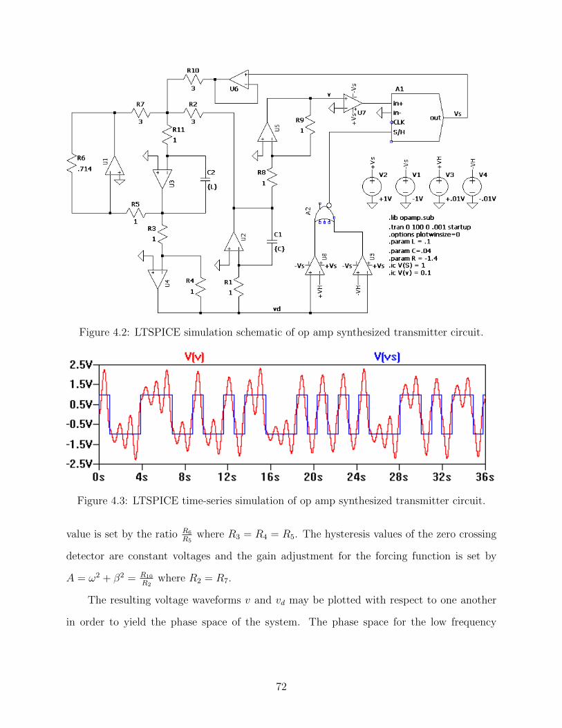
Figure 4.2: LTSPICE simulation schematic of op amp synthesized transmitter circuit.
Figure 4.3: LTSPICE time-series simulation of op amp synthesized transmitter circuit.
value is set by the ratio R6
R5where R3 = R4 = R5. The hysteresis values of the zero crossing
detector are constant voltages and the gain adjustment for the forcing function is set by
A = ω2 + β2 = R10
R2where R2 = R7.
The resulting voltage waveforms v and vd may be plotted with respect to one another
in order to yield the phase space of the system. The phase space for the low frequency
72
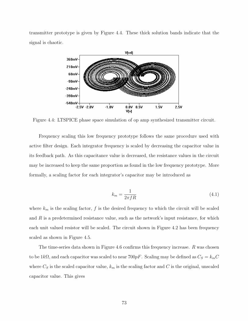
transmitter prototype is given by Figure 4.4. These thick solution bands indicate that the
signal is chaotic.
Figure 4.4: LTSPICE phase space simulation of op amp synthesized transmitter circuit.
Frequency scaling this low frequency prototype follows the same procedure used with
active filter design. Each integrator frequency is scaled by decreasing the capacitor value in
its feedback path. As this capacitance value is decreased, the resistance values in the circuit
may be increased to keep the same proportion as found in the low frequency prototype. More
formally, a scaling factor for each integrator’s capacitor may be introduced as
km =1
2πfR(4.1)
where km is the scaling factor, f is the desired frequency to which the circuit will be scaled
and R is a predetermined resistance value, such as the network’s input resistance, for which
each unit valued resistor will be scaled. The circuit shown in Figure 4.2 has been frequency
scaled as shown in Figure 4.5.
The time-series data shown in Figure 4.6 confirms this frequency increase. R was chosen
to be 1kΩ, and each capacitor was scaled to near 700pF . Scaling may be defined as CS = kmC
where CS is the scaled capacitor value, km is the scaling factor and C is the original, unscaled
capacitor value. This gives
73
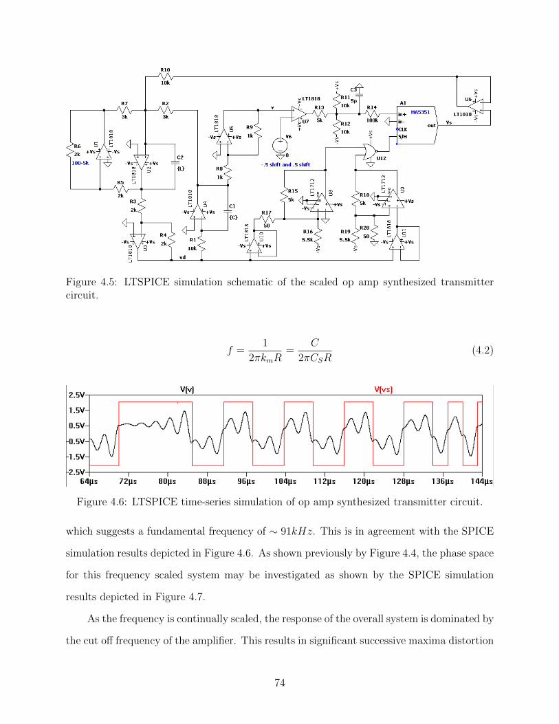
Figure 4.5: LTSPICE simulation schematic of the scaled op amp synthesized transmittercircuit.
f =1
2πkmR=
C
2πCSR(4.2)
Figure 4.6: LTSPICE time-series simulation of op amp synthesized transmitter circuit.
which suggests a fundamental frequency of ∼ 91kHz. This is in agreement with the SPICE
simulation results depicted in Figure 4.6. As shown previously by Figure 4.4, the phase space
for this frequency scaled system may be investigated as shown by the SPICE simulation
results depicted in Figure 4.7.
As the frequency is continually scaled, the response of the overall system is dominated by
the cut off frequency of the amplifier. This results in significant successive maxima distortion
74
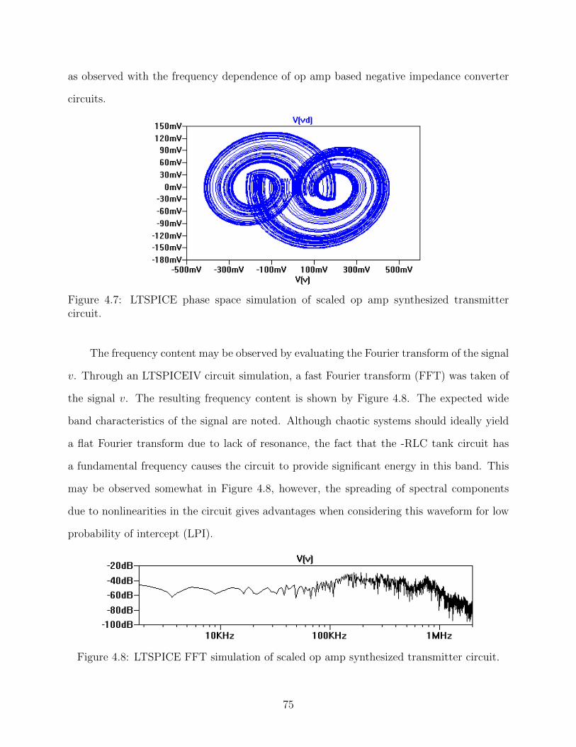
as observed with the frequency dependence of op amp based negative impedance converter
circuits.
Figure 4.7: LTSPICE phase space simulation of scaled op amp synthesized transmittercircuit.
The frequency content may be observed by evaluating the Fourier transform of the signal
v. Through an LTSPICEIV circuit simulation, a fast Fourier transform (FFT) was taken of
the signal v. The resulting frequency content is shown by Figure 4.8. The expected wide
band characteristics of the signal are noted. Although chaotic systems should ideally yield
a flat Fourier transform due to lack of resonance, the fact that the -RLC tank circuit has
a fundamental frequency causes the circuit to provide significant energy in this band. This
may be observed somewhat in Figure 4.8, however, the spreading of spectral components
due to nonlinearities in the circuit gives advantages when considering this waveform for low
probability of intercept (LPI).
Figure 4.8: LTSPICE FFT simulation of scaled op amp synthesized transmitter circuit.
75
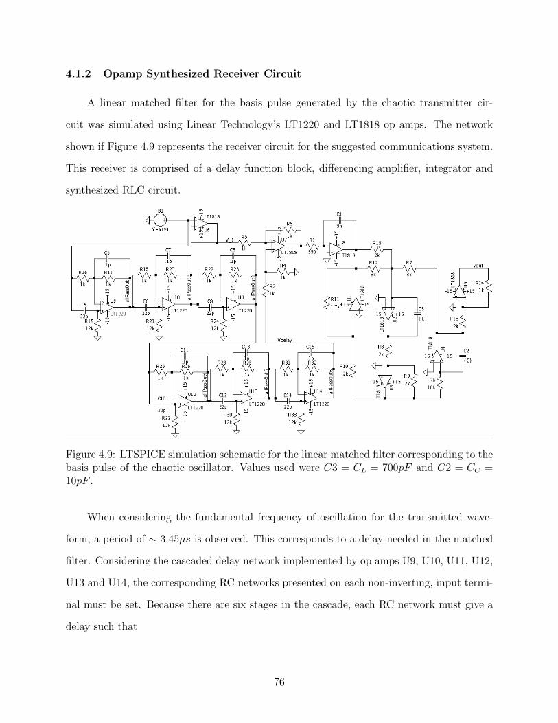
4.1.2 Opamp Synthesized Receiver Circuit
A linear matched filter for the basis pulse generated by the chaotic transmitter cir-
cuit was simulated using Linear Technology’s LT1220 and LT1818 op amps. The network
shown if Figure 4.9 represents the receiver circuit for the suggested communications system.
This receiver is comprised of a delay function block, differencing amplifier, integrator and
synthesized RLC circuit.
Figure 4.9: LTSPICE simulation schematic for the linear matched filter corresponding to thebasis pulse of the chaotic oscillator. Values used were C3 = CL = 700pF and C2 = CC =10pF .
When considering the fundamental frequency of oscillation for the transmitted wave-
form, a period of ∼ 3.45µs is observed. This corresponds to a delay needed in the matched
filter. Considering the cascaded delay network implemented by op amps U9, U10, U11, U12,
U13 and U14, the corresponding RC networks presented on each non-inverting, input termi-
nal must be set. Because there are six stages in the cascade, each RC network must give a
delay such that
76
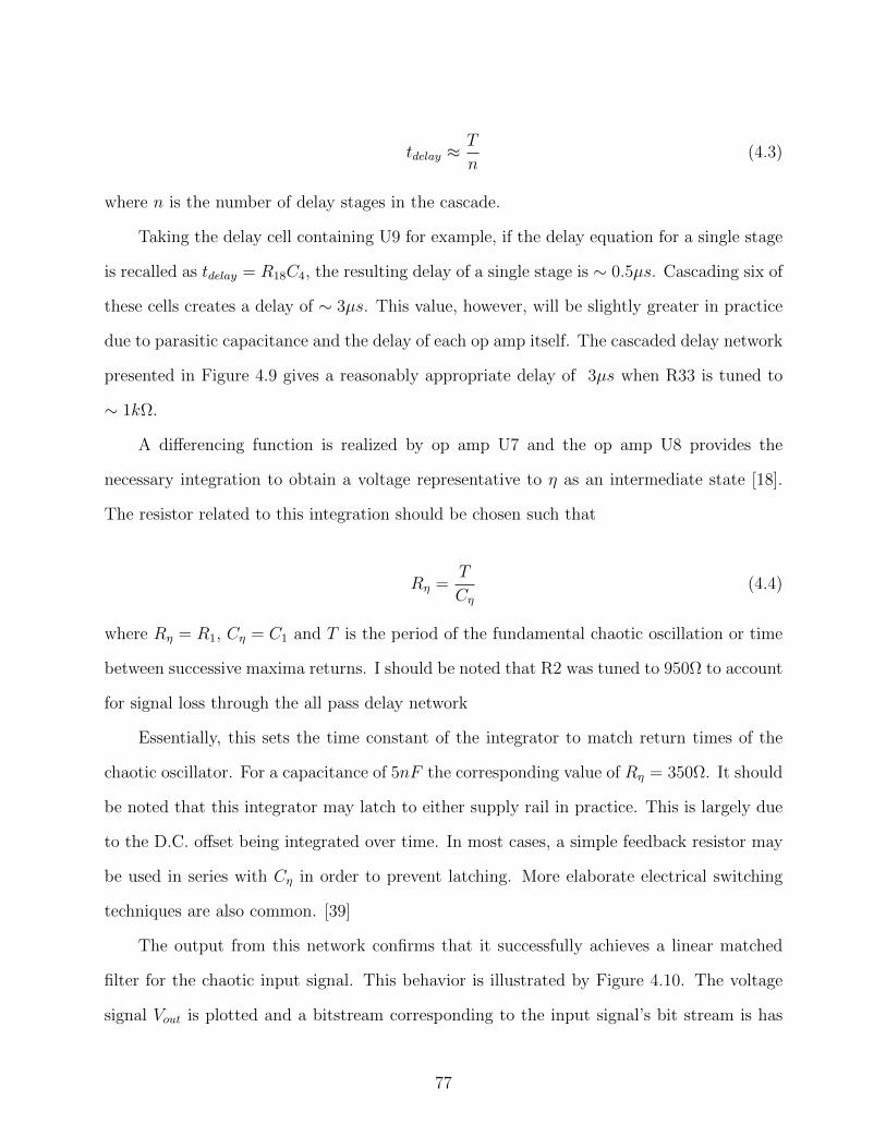
tdelay ≈T
n(4.3)
where n is the number of delay stages in the cascade.
Taking the delay cell containing U9 for example, if the delay equation for a single stage
is recalled as tdelay = R18C4, the resulting delay of a single stage is ∼ 0.5µs. Cascading six of
these cells creates a delay of ∼ 3µs. This value, however, will be slightly greater in practice
due to parasitic capacitance and the delay of each op amp itself. The cascaded delay network
presented in Figure 4.9 gives a reasonably appropriate delay of 3µs when R33 is tuned to
∼ 1kΩ.
A differencing function is realized by op amp U7 and the op amp U8 provides the
necessary integration to obtain a voltage representative to η as an intermediate state [18].
The resistor related to this integration should be chosen such that
Rη =T
Cη(4.4)
where Rη = R1, Cη = C1 and T is the period of the fundamental chaotic oscillation or time
between successive maxima returns. I should be noted that R2 was tuned to 950Ω to account
for signal loss through the all pass delay network
Essentially, this sets the time constant of the integrator to match return times of the
chaotic oscillator. For a capacitance of 5nF the corresponding value of Rη = 350Ω. It should
be noted that this integrator may latch to either supply rail in practice. This is largely due
to the D.C. offset being integrated over time. In most cases, a simple feedback resistor may
be used in series with Cη in order to prevent latching. More elaborate electrical switching
techniques are also common. [39]
The output from this network confirms that it successfully achieves a linear matched
filter for the chaotic input signal. This behavior is illustrated by Figure 4.10. The voltage
signal Vout is plotted and a bitstream corresponding to the input signal’s bit stream is has
77
Figure 4.10: SPICE simulation results for the linear matched filter corresponding to thebasis pulse of the chaotic oscillator shown if Figure 4.9.
been appropriated scaled. It should be carefully noted that this matched filter does not
provide optimum detection for the bit stream, but rather for the basis pulse in the presence
of AGWN.
4.2 OTA Synthesized System
A standard and well-documented method to overcome the bandwidth limitations of
opamps is the use of the OTA. The main draw of the OTA is that it is a current-mode
device capable at operating at much high frequencies when compared to an opamp. Such
applications as active filter synthesis demonstrate that opamps with gain bandwidth products
on the order of 100MHz may only provide functional filters on the order 1-10MHz, while OTA
based filters with datasheets that specify 40MHz may create filters in the range of 1-10MHz.
[29] This OTA approach effectively increases the fundamental frequency of operation of the
RLC tank circuit found in these chaotic systems when compared to the -RLC tank circuit .
4.2.1 OTA Synthesized Transmitter Circuit
The synthesis of an unstable ladder filter network uses integrators in the place of dif-
ferentiators due to the natural noisy operation of differentiation when considering circuit
design. The result is a system that is easily integrated and may be frequency scaled to
reach high frequencies using similar techniques to analog filter design. These techniques are
commonly referred to in literature as state variable filter design of KHN filters. [27]
78
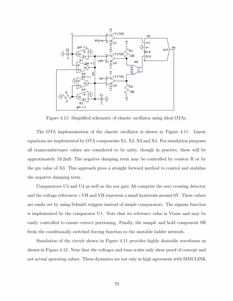
Figure 4.11: Simplified schematic of chaotic oscillator using ideal OTAs.
The OTA implementation of the chaotic oscillator is shown in Figure 4.11. Linear
equations are implemented by OTA components X1, X2, X3 and X4. For simulation purposes
all transconductance values are considered to be unity, though in practice, these will be
approximately 19.2mS. The negative damping term may be controlled by resistor R or by
the gm value of X3. This approach gives a straight forward method to control and stabilize
the negative damping term.
Comparators U3 and U4 as well as the nor gate A6 comprise the zero crossing detector
and the voltage references +VH and VH represent a small hysteresis around 0V. These values
are easily set by using Schmitt triggers instead of simple comparators. The signum function
is implemented by the comparator U1. Note that its reference value is Vtune and may be
easily controlled to ensure correct portioning. Finally, the sample and hold component SH
feeds the conditionally switched forcing function to the unstable ladder network.
Simulation of the circuit shown in Figure 4.11 provides highly desirable waveforms as
shown in Figure 4.12. Note that the voltages and time scales only show proof of concept and
not actual operating values. These dynamics are not only in high agreement with SIMULINK
79
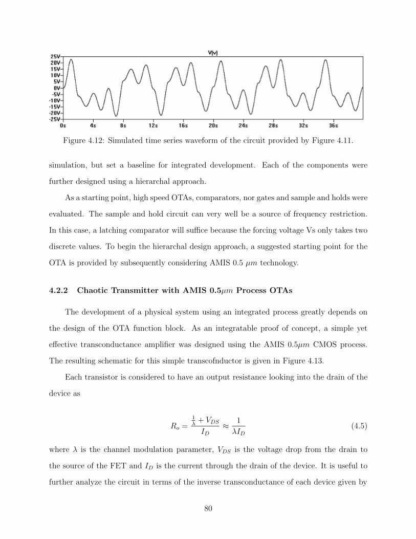
Figure 4.12: Simulated time series waveform of the circuit provided by Figure 4.11.
simulation, but set a baseline for integrated development. Each of the components were
further designed using a hierarchal approach.
As a starting point, high speed OTAs, comparators, nor gates and sample and holds were
evaluated. The sample and hold circuit can very well be a source of frequency restriction.
In this case, a latching comparator will suffice because the forcing voltage Vs only takes two
discrete values. To begin the hierarchal design approach, a suggested starting point for the
OTA is provided by subsequently considering AMIS 0.5 µm technology.
4.2.2 Chaotic Transmitter with AMIS 0.5µm Process OTAs
The development of a physical system using an integrated process greatly depends on
the design of the OTA function block. As an integratable proof of concept, a simple yet
effective transconductance amplifier was designed using the AMIS 0.5µm CMOS process.
The resulting schematic for this simple transcofnductor is given in Figure 4.13.
Each transistor is considered to have an output resistance looking into the drain of the
device as
Ro =1λ
+ VDS
ID≈ 1
λID(4.5)
where λ is the channel modulation parameter, VDS is the voltage drop from the drain to
the source of the FET and ID is the current through the drain of the device. It is useful to
further analyze the circuit in terms of the inverse transconductance of each device given by
80
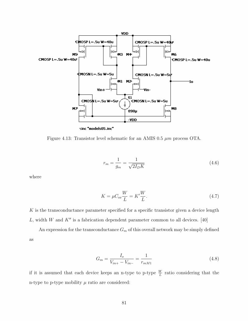
Figure 4.13: Transistor level schematic for an AMIS 0.5 µm process OTA.
rm =1
gm=
1√2IDK
(4.6)
where
K = µCoxW
L= K ′
W
L. (4.7)
K is the transconductance parameter specified for a specific transistor given a device length
L, width W and K ′′ is a fabrication dependent parameter common to all devices. [40]
An expression for the transconductanceGm of this overall network may be simply defined
as
Gm =Io
Vin+ − Vin−=
1
rmM1
(4.8)
if it is assumed that each device keeps an n-type to p-type WL
ratio considering that the
n-type to p-type mobility µ ratio are considered:
81
(W
L
)n
·(L
W
)p
=µpµn. (4.9)
This simple expression is obtained by realizing the current produced by the voltage gain at
the input of the network is reflected by the current mirror consisting of M4 and M6. As-
suming that the bias current I1 is divided equally between devices M1 and M2, the resulting
transconductance for this amplifier is given by
Gm =
√IDM2K ′
(W
L
)M2
=
√IDM2µn
(ε
Tox
)(W
L
)M2
. (4.10)
Analytically, a precise value may be obtained by referring the the Level 7 SPICE model for
the AMIS 0.5µm process. Cox may be obtained by evaluating
Cox =εoxTox
. (4.11)
In the case of silicon dioxide εox = 3.9ε0 where ε0 = 8.854 × 10⁻¹⁴ F/cm. For this specific
fabrication process the SPICE model states the dielectric oxide thickness as Tox = 1.41×10⁻⁸
m and the n-type mobility as µn = U0 = 479.4186448 cm2/V·s as found in the Appendix.
Considering that µp = 233.5715825 cm2/V·s, the current mirror M4 and M6 will cre-
ate a multiplier of ∼ 4 because the schematic in Figure 4.13 violates the ratio described in
Equation 4.9. Although this violation gives an increase in transconductance, a small D.C.
offset is introduced, however the symmetric nature of this design mitigates this effect some-
what by reflecting offset errors with devices M5 and M7. The resulting expression for the
transconductance of the network in Figure 4.13 is
Gm =(W/L)pµp(W/L)nµn
√IDM2µn
(ε
Tox
)(W
L
)M2
(4.12)
which gives an analytically expected transconductance value of 133.33µS. This value is
confirmed by the simulation results give in Figure 4.14, and the transconductance reaches
82
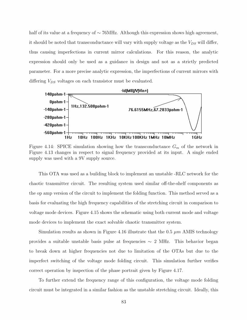
half of its value at a frequency of ∼ 76MHz. Although this expression shows high agreement,
it should be noted that transconductance will vary with supply voltage as the VDS will differ,
thus causing imperfections in current mirror calculations. For this reason, the analytic
expression should only be used as a guidance in design and not as a strictly predicted
parameter. For a more precise analytic expression, the imperfections of current mirrors with
differing VDS voltages on each transistor must be evaluated.
Figure 4.14: SPICE simulation showing how the transconductance Gm of the network inFigure 4.13 changes in respect to signal frequency provided at its input. A single endedsupply was used with a 9V supply source.
This OTA was used as a building block to implement an unstable -RLC network for the
chaotic transmitter circuit. The resulting system used similar off-the-shelf components as
the op amp version of the circuit to implement the folding function. This method served as a
basis for evaluating the high frequency capabilities of the stretching circuit in comparison to
voltage mode devices. Figure 4.15 shows the schematic using both current mode and voltage
mode devices to implement the exact solvable chaotic transmitter system.
Simulation results as shown in Figure 4.16 illustrate that the 0.5 µm AMIS technology
provides a suitable unstable basis pulse at frequencies ∼ 2 MHz. This behavior began
to break down at higher frequencies not due to limitation of the OTAs but due to the
imperfect switching of the voltage mode folding circuit. This simulation further verifies
correct operation by inspection of the phase portrait given by Figure 4.17.
To further extend the frequency range of this configuration, the voltage mode folding
circuit must be integrated in a similar fashion as the unstable stretching circuit. Ideally, this
83
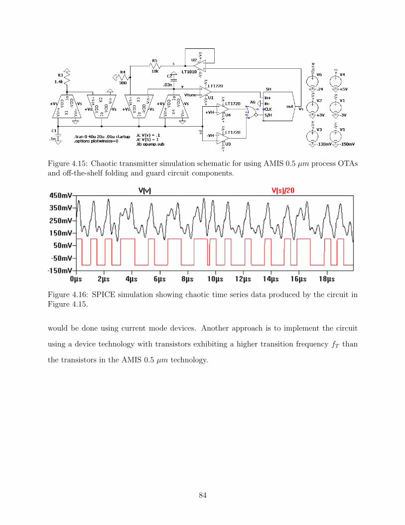
Figure 4.15: Chaotic transmitter simulation schematic for using AMIS 0.5 µm process OTAsand off-the-shelf folding and guard circuit components.
Figure 4.16: SPICE simulation showing chaotic time series data produced by the circuit inFigure 4.15.
would be done using current mode devices. Another approach is to implement the circuit
using a device technology with transistors exhibiting a higher transition frequency fT than
the transistors in the AMIS 0.5 µm technology.
84
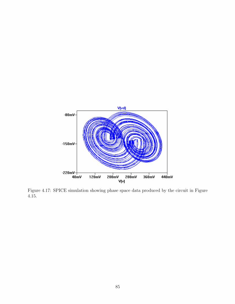
Figure 4.17: SPICE simulation showing phase space data produced by the circuit in Figure4.15.
85
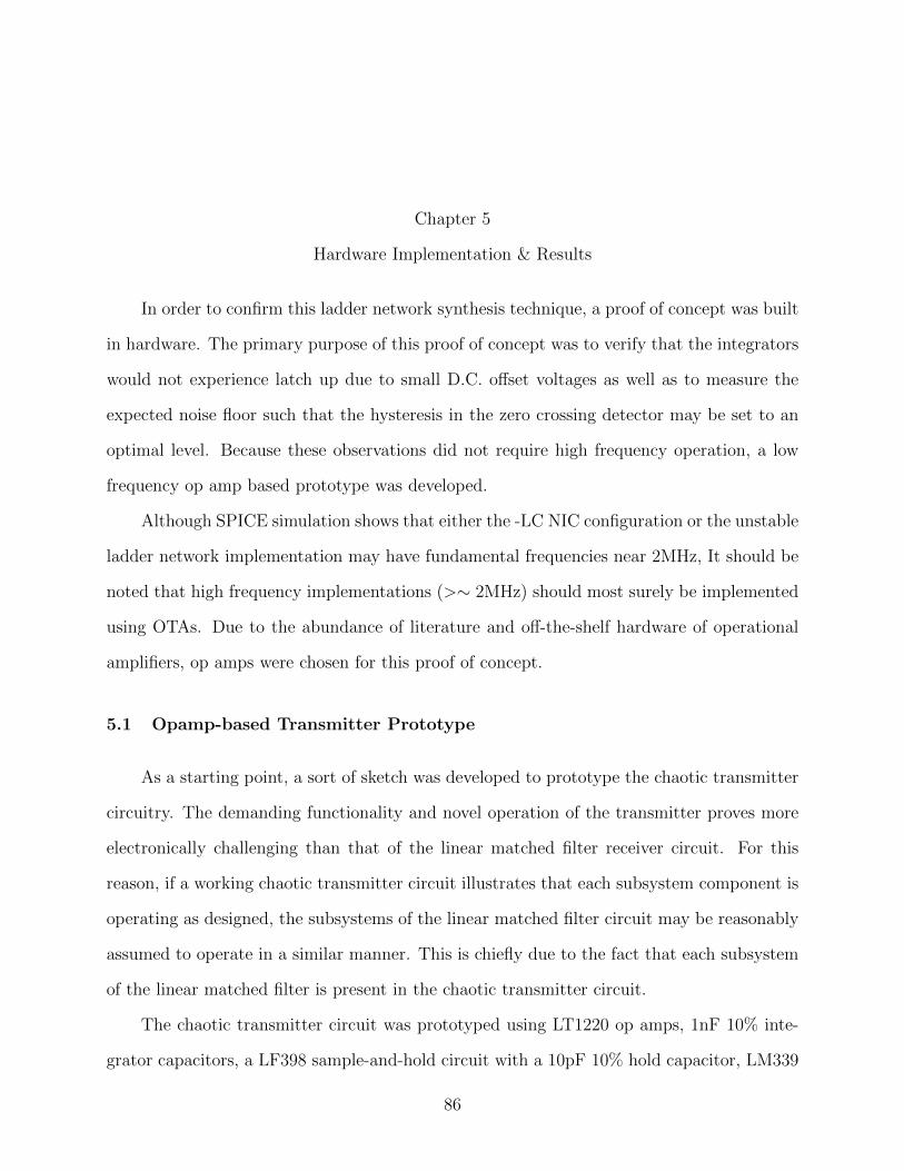
Chapter 5
Hardware Implementation & Results
In order to confirm this ladder network synthesis technique, a proof of concept was built
in hardware. The primary purpose of this proof of concept was to verify that the integrators
would not experience latch up due to small D.C. offset voltages as well as to measure the
expected noise floor such that the hysteresis in the zero crossing detector may be set to an
optimal level. Because these observations did not require high frequency operation, a low
frequency op amp based prototype was developed.
Although SPICE simulation shows that either the -LC NIC configuration or the unstable
ladder network implementation may have fundamental frequencies near 2MHz, It should be
noted that high frequency implementations (>∼ 2MHz) should most surely be implemented
using OTAs. Due to the abundance of literature and off-the-shelf hardware of operational
amplifiers, op amps were chosen for this proof of concept.
5.1 Opamp-based Transmitter Prototype
As a starting point, a sort of sketch was developed to prototype the chaotic transmitter
circuitry. The demanding functionality and novel operation of the transmitter proves more
electronically challenging than that of the linear matched filter receiver circuit. For this
reason, if a working chaotic transmitter circuit illustrates that each subsystem component is
operating as designed, the subsystems of the linear matched filter circuit may be reasonably
assumed to operate in a similar manner. This is chiefly due to the fact that each subsystem
of the linear matched filter is present in the chaotic transmitter circuit.
The chaotic transmitter circuit was prototyped using LT1220 op amps, 1nF 10% inte-
grator capacitors, a LF398 sample-and-hold circuit with a 10pF 10% hold capacitor, LM339
86
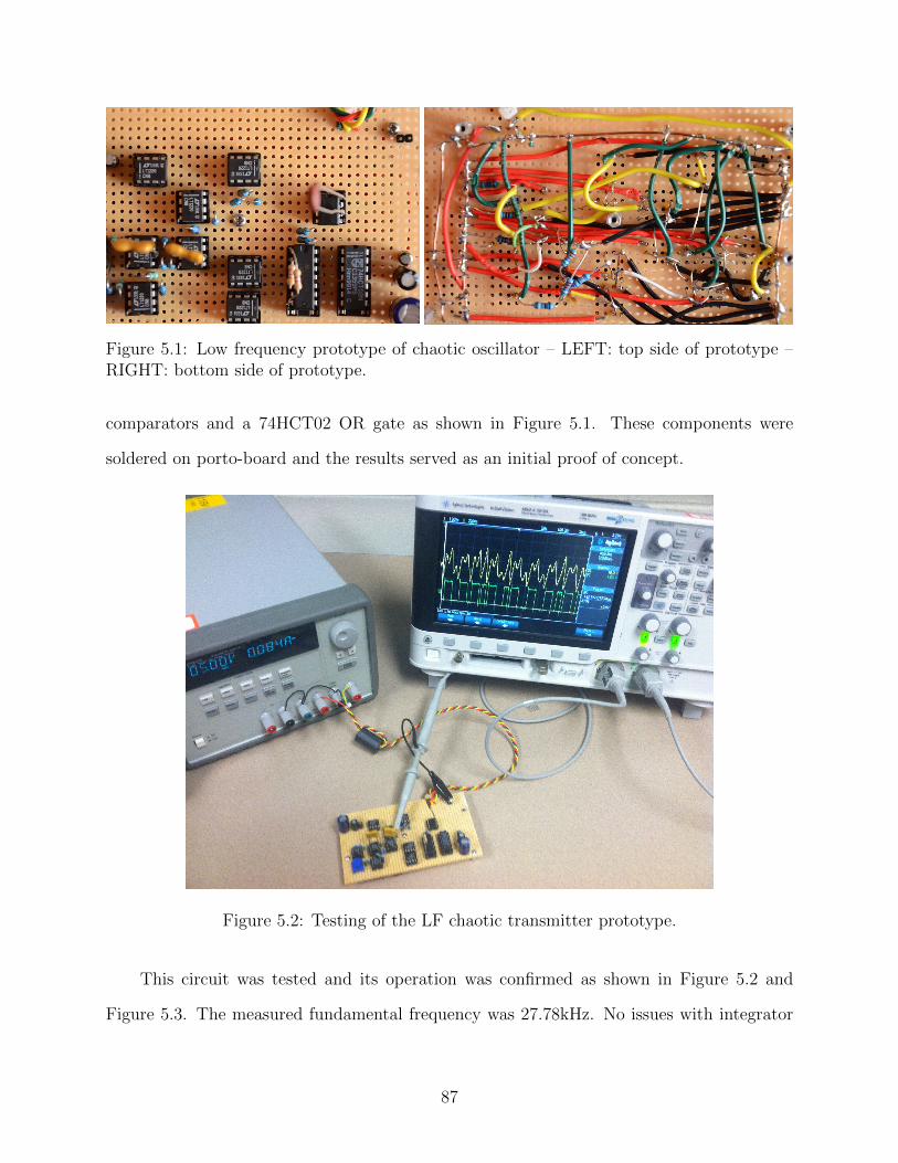
Figure 5.1: Low frequency prototype of chaotic oscillator – LEFT: top side of prototype –RIGHT: bottom side of prototype.
comparators and a 74HCT02 OR gate as shown in Figure 5.1. These components were
soldered on porto-board and the results served as an initial proof of concept.
Figure 5.2: Testing of the LF chaotic transmitter prototype.
This circuit was tested and its operation was confirmed as shown in Figure 5.2 and
Figure 5.3. The measured fundamental frequency was 27.78kHz. No issues with integrator
87
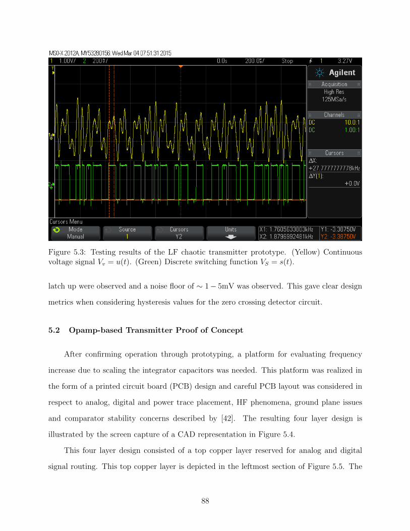
Figure 5.3: Testing results of the LF chaotic transmitter prototype. (Yellow) Continuousvoltage signal Vv = u(t). (Green) Discrete switching function VS = s(t).
latch up were observed and a noise floor of ∼ 1− 5mV was observed. This gave clear design
metrics when considering hysteresis values for the zero crossing detector circuit.
5.2 Opamp-based Transmitter Proof of Concept
After confirming operation through prototyping, a platform for evaluating frequency
increase due to scaling the integrator capacitors was needed. This platform was realized in
the form of a printed circuit board (PCB) design and careful PCB layout was considered in
respect to analog, digital and power trace placement, HF phenomena, ground plane issues
and comparator stability concerns described by [42]. The resulting four layer design is
illustrated by the screen capture of a CAD representation in Figure 5.4.
This four layer design consisted of a top copper layer reserved for analog and digital
signal routing. This top copper layer is depicted in the leftmost section of Figure 5.5. The
88
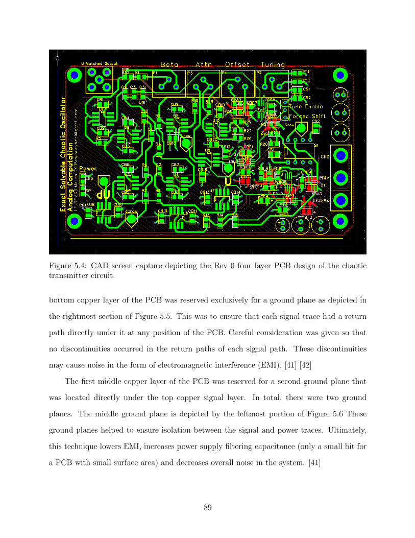
Figure 5.4: CAD screen capture depicting the Rev 0 four layer PCB design of the chaotictransmitter circuit.
bottom copper layer of the PCB was reserved exclusively for a ground plane as depicted in
the rightmost section of Figure 5.5. This was to ensure that each signal trace had a return
path directly under it at any position of the PCB. Careful consideration was given so that
no discontinuities occurred in the return paths of each signal path. These discontinuities
may cause noise in the form of electromagnetic interference (EMI). [41] [42]
The first middle copper layer of the PCB was reserved for a second ground plane that
was located directly under the top copper signal layer. In total, there were two ground
planes. The middle ground plane is depicted by the leftmost portion of Figure 5.6 These
ground planes helped to ensure isolation between the signal and power traces. Ultimately,
this technique lowers EMI, increases power supply filtering capacitance (only a small bit for
a PCB with small surface area) and decreases overall noise in the system. [41]
89
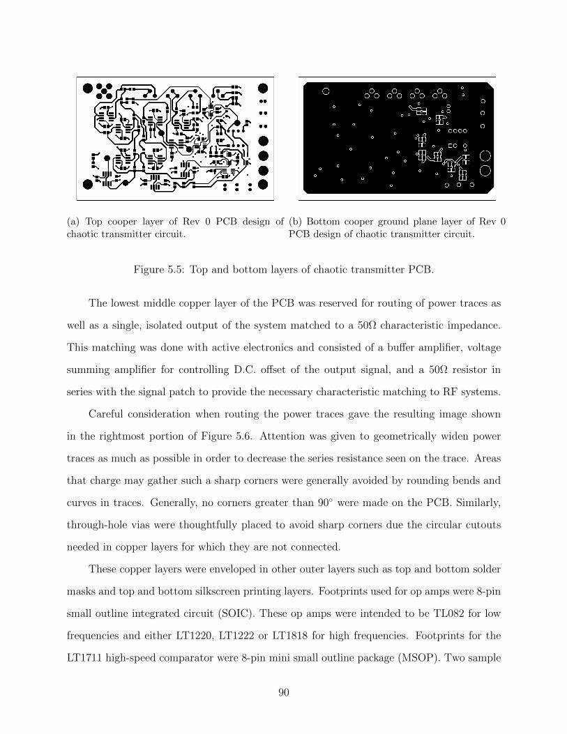
(a) Top cooper layer of Rev 0 PCB design ofchaotic transmitter circuit.
(b) Bottom cooper ground plane layer of Rev 0PCB design of chaotic transmitter circuit.
Figure 5.5: Top and bottom layers of chaotic transmitter PCB.
The lowest middle copper layer of the PCB was reserved for routing of power traces as
well as a single, isolated output of the system matched to a 50Ω characteristic impedance.
This matching was done with active electronics and consisted of a buffer amplifier, voltage
summing amplifier for controlling D.C. offset of the output signal, and a 50Ω resistor in
series with the signal patch to provide the necessary characteristic matching to RF systems.
Careful consideration when routing the power traces gave the resulting image shown
in the rightmost portion of Figure 5.6. Attention was given to geometrically widen power
traces as much as possible in order to decrease the series resistance seen on the trace. Areas
that charge may gather such a sharp corners were generally avoided by rounding bends and
curves in traces. Generally, no corners greater than 90 were made on the PCB. Similarly,
through-hole vias were thoughtfully placed to avoid sharp corners due the circular cutouts
needed in copper layers for which they are not connected.
These copper layers were enveloped in other outer layers such as top and bottom solder
masks and top and bottom silkscreen printing layers. Footprints used for op amps were 8-pin
small outline integrated circuit (SOIC). These op amps were intended to be TL082 for low
frequencies and either LT1220, LT1222 or LT1818 for high frequencies. Footprints for the
LT1711 high-speed comparator were 8-pin mini small outline package (MSOP). Two sample
90
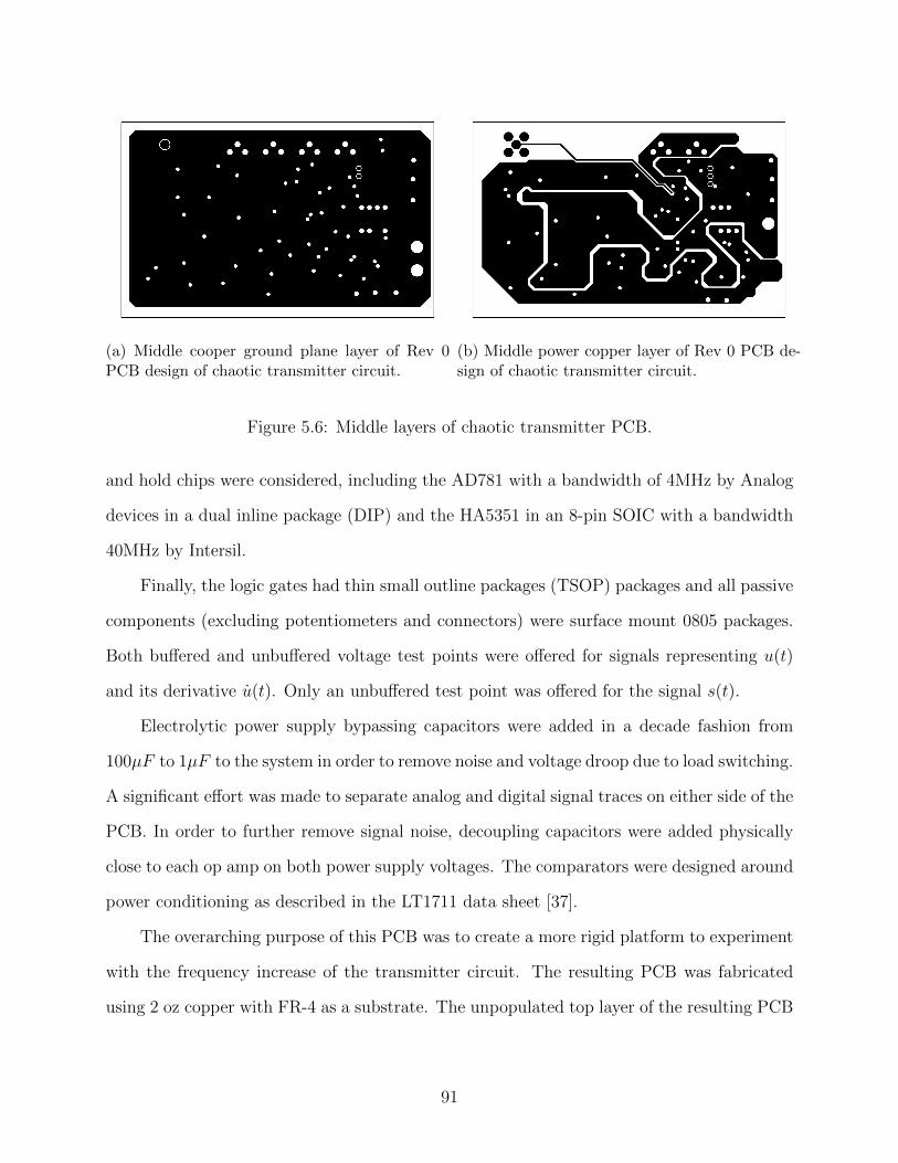
(a) Middle cooper ground plane layer of Rev 0PCB design of chaotic transmitter circuit.
(b) Middle power copper layer of Rev 0 PCB de-sign of chaotic transmitter circuit.
Figure 5.6: Middle layers of chaotic transmitter PCB.
and hold chips were considered, including the AD781 with a bandwidth of 4MHz by Analog
devices in a dual inline package (DIP) and the HA5351 in an 8-pin SOIC with a bandwidth
40MHz by Intersil.
Finally, the logic gates had thin small outline packages (TSOP) packages and all passive
components (excluding potentiometers and connectors) were surface mount 0805 packages.
Both buffered and unbuffered voltage test points were offered for signals representing u(t)
and its derivative u(t). Only an unbuffered test point was offered for the signal s(t).
Electrolytic power supply bypassing capacitors were added in a decade fashion from
100µF to 1µF to the system in order to remove noise and voltage droop due to load switching.
A significant effort was made to separate analog and digital signal traces on either side of the
PCB. In order to further remove signal noise, decoupling capacitors were added physically
close to each op amp on both power supply voltages. The comparators were designed around
power conditioning as described in the LT1711 data sheet [37].
The overarching purpose of this PCB was to create a more rigid platform to experiment
with the frequency increase of the transmitter circuit. The resulting PCB was fabricated
using 2 oz copper with FR-4 as a substrate. The unpopulated top layer of the resulting PCB
91
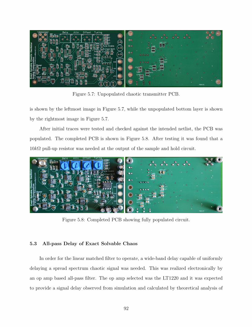
Figure 5.7: Unpopulated chaotic transmitter PCB.
is shown by the leftmost image in Figure 5.7, while the unpopulated bottom layer is shown
by the rightmost image in Figure 5.7.
After initial traces were tested and checked against the intended netlist, the PCB was
populated. The completed PCB is shown in Figure 5.8. After testing it was found that a
10kΩ pull-up resistor was needed at the output of the sample and hold circuit.
Figure 5.8: Completed PCB showing fully populated circuit.
5.3 All-pass Delay of Exact Solvable Chaos
In order for the linear matched filter to operate, a wide-band delay capable of uniformly
delaying a spread spectrum chaotic signal was needed. This was realized electronically by
an op amp based all-pass filter. The op amp selected was the LT1220 and it was expected
to provide a signal delay observed from simulation and calculated by theoretical analysis of
92
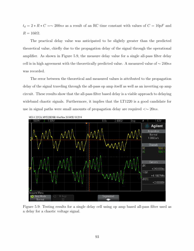
td = 2 ∗ R ∗ C =∼ 200ns as a result of an RC time constant with values of C = 10pF and
R = 10kΩ.
The practical delay value was anticipated to be slightly greater than the predicted
theoretical value, chiefly due to the propagation delay of the signal through the operational
amplifier. As shown in Figure 5.9, the measure delay value for a single all-pass filter delay
cell is in high agreement with the theoretically predicted value. A measured value of ∼ 240ns
was recorded.
The error between the theoretical and measured values is attributed to the propagation
delay of the signal traveling through the all-pass op amp itself as well as an inverting op amp
circuit. These results show that the all-pass filter based delay is a viable approach to delaying
wideband chaotic signals. Furthermore, it implies that the LT1220 is a good candidate for
use in signal paths were small amounts of propagation delay are required <∼ 20ns.
Figure 5.9: Testing results for a single delay cell using op amp based all-pass filter used asa delay for a chaotic voltage signal.
93
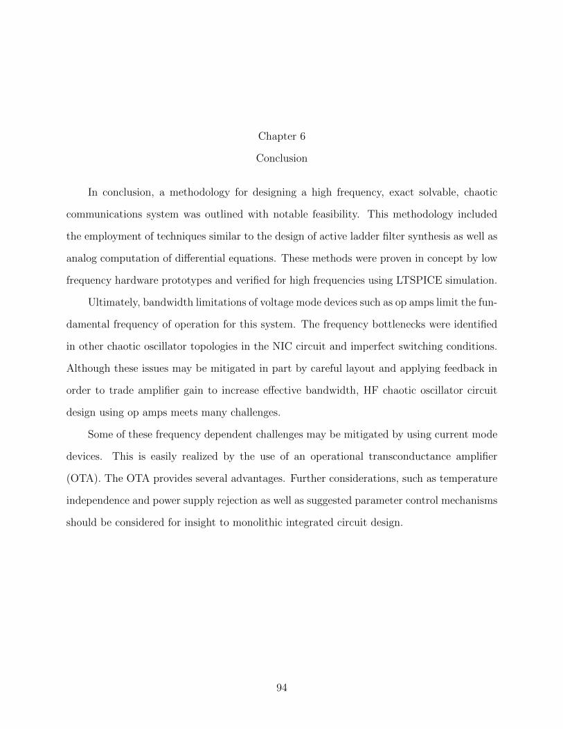
Chapter 6
Conclusion
In conclusion, a methodology for designing a high frequency, exact solvable, chaotic
communications system was outlined with notable feasibility. This methodology included
the employment of techniques similar to the design of active ladder filter synthesis as well as
analog computation of differential equations. These methods were proven in concept by low
frequency hardware prototypes and verified for high frequencies using LTSPICE simulation.
Ultimately, bandwidth limitations of voltage mode devices such as op amps limit the fun-
damental frequency of operation for this system. The frequency bottlenecks were identified
in other chaotic oscillator topologies in the NIC circuit and imperfect switching conditions.
Although these issues may be mitigated in part by careful layout and applying feedback in
order to trade amplifier gain to increase effective bandwidth, HF chaotic oscillator circuit
design using op amps meets many challenges.
Some of these frequency dependent challenges may be mitigated by using current mode
devices. This is easily realized by the use of an operational transconductance amplifier
(OTA). The OTA provides several advantages. Further considerations, such as temperature
independence and power supply rejection as well as suggested parameter control mechanisms
should be considered for insight to monolithic integrated circuit design.
94
Chapter 7
Future Work
Motivations to move to a monolithic integrated design bring considerations of the stabi-
lization and control of system parameters. To ensure that these systems maintain a correct
value for the negative damping factor, β, a reliable, constant gain must be found in the in-
verting amplifier that provides exponential growth to the sinusoidal basis function. Common
gain errors may arise from change in environmental conditions such as temperature change.
Considering amplifier temperature dependence, topologies utilizing a differential pair
suffer from drifting due to the property of parameter proportion to absolute temperature
(PTAT). This comes from temperature dependence in the device physics of a transistor. It
may be derived from the current equation for an deal diode ID = ISexp[VD/VT ] − 1 where
ID is the diode current, IS is the diodes saturation current, VD is the voltage drop across the
diode and VT is known as the thermal voltage of the diode. This thermal voltage provides
the temperature dependence in these circuits. [25]
Because VT = kT/q where k is Boltzmanns constant, T is the absolute temperature
of the pn junction and q is the unit charge; the expression for the diode equation may be
rewritten to obtain VD = kT/Qln(ID/Is) showing that a pn junction is a device with a voltage
proportional to absolute temperature often referred to as a PTAT. This is very desirable for
designing temperature sensors but if the differential pair is created for an amplifier, the pn
junctions will alter the gain of the amplifier when subjected to temperature changes. To
mitigate these effects, the biasing current for the differential pair is often realized using
current mirrors or other circuits that are complimentary to absolute temperature of CTAT
devices to bias input transistors or other temperature compensation method. [25]
95
To further ensure the stabilization of β, a closed loop control system may be employed
to dynamically alter the gain of the inverting amplifier as its parameters drift. This system
would consist of a circuit that would detect successive maxima (similar to the zero crossing
detector circuit) and extract the current β value of the system. This β would then be
compared to the expected value derived from theory. A voltage that is proportional to the
difference of these two values would be produced. This voltage would then be applied to
a well-documented and commonly designed voltage controlled amplifier (VCA). This VCA
would provide a voltage controlled negative resistance term that is dynamically altered to
ensure the correct β value is applied.
Similarly, circuit voltages representing threshold values that define the systems parti-
tions should be virtually free of noise and stable in the presence of environmental factors.
Fortunately, when the system is operated in the shift band, the partition threshold is related
to ground or 0V. Ensuring a well established, low noise ground will give a stable partition. As
the systems threshold voltage is perturbed, new chaotic bands are entered called the folded
bands. These bands may be stabilized and controlled using similar closed-loop feedback
techniques as suggested for the β control system.
Oscillator coupling is not anticipated to be an issue in the integration of these sys-
tems, although monolithic designs will consider this issue. Mutual resistive coupling may,
to some extent, be present through by the common Si substrate that these oscillators share.
Designs will include fabrication technologies with deep isolation trenches to mitigate this
phenomenon.
96
Bibliography
[1] Lorenz, E. N. “Deterministic Nonperiodic Flow,” J. Atmos. Sci. In Journal of the At-mospheric Sciences, Vol. 20, No. 2. (1 March 1963), pp. 130-141.
[2] N. J. Corron. “An Exactly Solvable Chaotic Differential Equation,” Dynamics of Con-tinuous, Discrete and Impulsive Systems Series A: Mathematical Analysis 16, WatamPress, pp 777-788, 2009.
[3] S. Katsura and W. Fukuda, “Exactly solvable models showing chaotic behavior,” Phys-ica A, 130, pp 597-605, 1985.
[4] K. Umeno, “A method of construction exactly solvable chaos,” Phys. Rev. E, 55, pp5280-5284, 1997.
[5] N. J. Corron and J. N. Blakely. “Exact folded-band chaotic oscillator,” Chaos 22,023113, 2012.
[6] E. M. Bollt. “Review of chaos communication by feedback control of symbolic dynam-ics,” Int. J. Bifurcation Chaos, 13, 269, 2003.
[7] N. J. Corron and J. N. Blakely. “Controlling symbolic dynamics in an exact folded-bandchaotic oscillator,” Proc. Analysis and Control of Chaotic Systems - The InternationalFederation of Automatic Control, Volume 3, Part 1, pp 143-148, Cancn, Mexico. 2012.
[8] N. J. Corron and S. D. Pethel. “Experimental targeting of chaos via controlled symbolicdynamics,” Physics Letters A Volume 313, Issue 3, 30 June 2003, pp 192-197.
[9] N. J. Corron, J. N. Blakely and M. T. Stahl. “A matched filter for chaos,” Chaos 20,023123 (2010).
[10] N. J. Corron and J. N. Blakely. “A matched filter for communicating with chaos,” AIPConf. Proc. 1339, 25; September 21-24 2010; Alberta, Canada (2011).
[11] J.N. Blakely, D. W. Hahs and N. J. Corron. “Communication waveform properties ofan exact folded-band chaotic oscillator,” Physica D: Nonlinear Phenomena Volume 263,15 November 2013, Pages 99106.
[12] R. L. Devaney An Introduction to Chaotic Dynamical Systems, Addison-Wesley, Red-wood City, CA 1989.
[13] K. T. Alligood, T. D. Sauer and J. A. Yorke, Chaos: An Introduction to DynamicalSystems, Springer New York 1996.
97
[14] Haykin, S., Communication Systems. Fifth Edition, New York: Wiley, 2009.
[15] Turin, G.L., ”An introduction to matched filters,” Information Theory, IRE Transac-tions on , vol.6, no.3, pp.311,329, June 1960.
[16] O. B. Ozdoganlar, B. D. Hansche, T. G. Carne “Modal testing techniques for Micro-electromechanical Systems (MEMS),” 2003 SEM Annual Conference & Exposition onExperimental and Applied Mechanics, Conference Proceedings, 2003.
[17] N. J. Corron. “An Exactly Solvable Chaotic Differential Equation,” Dynamics of Con-tinuous, Discrete and Impulsive Systems Series A: Mathematical Analysis 16, WatamPress, pp 777-788, 2009.
[18] N. J. Corron, J. N. Blakely and M. T. Stahl. “A matched filter for chaos,” Chaos 20,023123 (2010).
[19] Beal, A.N.; Bailey, J.P.; Hale, S.A.; Dean, R.N.; Hamilton, M.; Tugnait, J.K.; Hahs,D.W.; Corron, N.J., ”Design and simulation of a high frequency exact solvable chaoticoscillator,” MILITARY COMMUNICATIONS CONFERENCE, 2012 - MILCOM 2012, vol., no., pp.1,6, Oct. 29 2012-Nov. 1 2012.
[20] J.C. Sprott, Chaos and Time-series Analysis, Oxford University Press 2001.
[21] Boyarsky, A., and Gora, P., Laws of Chaos: Invariant Measures and Dynamical Systemsin One Dimension, Birkhauser, 1997.
[22] Stojanovski, T.D., and Kocarev, L. Construction of Markov partitions in PL1D maps,IEEE Trans. On Circuits and Systems, Vol. 60, pp. 702-706. 2013.
[23] Addabbo, T., Fort, A., Rocchi, S., and Vignoli, V., An efficient and accurate methodfor computing the invariant measure of piecewise affine chaotic maps, IEEE 978-1-4244-4/08/ 2008.
[24] Edward Ott, Chaos in Dynamical Systems, Cambridge University Press, 2002.
[25] Jaeger, Richard C, and Blalock, Travis, Microelectronic Circuit Design. New York, NY:McGraw-Hill, 2004.
[26] P. Gray and R. Meyer, Analysis and design of analog integrated circuits. 5th Edition,New York: Wiley, 2009.
[27] Chang, C. M., Pai, S. K. (2000). Universal current- mode OTA-C biquad with the min-imum components. IEEE Transactions on Circuits and Systems I Fundamental Theoryand Applications, 1235-1238.
[28] Strogatz, S.H., Nonlinear Dynamics and Chaos: With Applications to Physics, Biology,Chemistry, and Engineering, Westview Press, Cambridge Center, Cambridge MA, 021421994.
98
[29] Texas Instruments, Demystifying the Operational Transconductance Amplifier, Appl.Report SBOA117A.
[30] Intersil, HA5351 64ns Sample and Hold Amplifier, Data Sheet, 2013.
[31] Analog Devices, AD781 Complete 700ns Sample-and-Hold Amplifier, Data Sheet RevA.
[32] Analog Devices, Demystifying the Operational Transconductance Amplifier, Mini Tu-torial MT-202.
[33] Texas Instruments, Opamps for Everyone Excerpt: Chapter 16 Active Filter DesignTechniques, Literature Number SLOA088.
[34] Maxim Integrated, Building a Low-Cost White-Noise Generator, Application Note 3469
[35] B. Lathi, Linear systems and signals. New York: Oxford University Press, 2005.
[36] Linear Technology, LT1220 45MHz, 250V/µs Operational Amplifier, Data Sheet Rev b,1991.
[37] Linear Technology, LT1711/LT1712 Single/Dual 4.5ns, 3V/5V/±5V, Rail-to-Rail Com-parators, Data Sheet, 2001.
[38] Linear Technology, LT1001 Precision Operational Amplifier, Data Sheet Rev B,1983.
[39] P. Horowitz and W. Hill, The art of electronics. Cambridge [England]: CambridgeUniversity Press, 1989.
[40] B. Wilamowski and J. Irwin, The industrial electronics handbook. Boca Raton, FL:CRC Press, 2011.
[41] H. Ott, Noise reduction techniques in electronic systems. New York: Wiley, 1988.
[42] H. Ott, Partitioning and Layout of a Mixed-signal PCB, Printed Circuit Board Design,pp. 8-11, June 2001.
[43] Ned J. Corron, Jonathan N. Blakely, and Shawn D. Pethel, ”Communicating withExactly Solvable Chaos,” in; Henry Leung, ed., Chaotic Signal Processing, pp. 49-84(SIAM, 2014).
[44] M. Van Wyk and W. Steeb, Chaos in electronics. Dordrecht: Kluwer Academic Pub-lishers, 1997.
[45] Ott, E., Grebogi, C. and Yorke, J. A. (1990). Controlling chaos. Physical review letters,64(11), 1196.
[46] N. J. Corron, S. D. Pethel, Control of long-period orbits and arbitrary trajectories inchaotic systems using dynamic limiting, Chaos 12, 1 (2002).
99
[47] S. Hayes, C. Grebogi and E. Ott, ’Communicating with chaos’, Phys. Rev. Lett., vol.70, no. 20, pp. 3031-3034, 1993.
[48] N. J. Corron, J. N. Blakely, Controlling Symbolic Dynamics in an Exact Folded-BandChaotic Oscillator Analysis and Control of Chaotic Systems, Volume no. 3 Part no. 1,3rd IFAC Conference on Analysis and Control of Chaotic Systems, Cancun, Mexico,2012.
[49] A. Jackson, Analog computation. New York: McGraw-Hill, 1960.
100

Appendix A
SPICE MODELS
A.1 AMIS 0.5 µm Process
.MODEL CMOSN NMOS ( LEVEL = 7 +VERSION = 3.1 TNOM = 27 TOX =
1.41E-8 +XJ = 1.5E-7 NCH = 1.7E17 VTH0 = 0.6394078 +K1 = 0.8797763 K2 = -
0.101648 K3 = 22.7282152 +K3B = -9.4213761 W0 = 1E-8 NLX = 1E-9 +DVT0W =
0 DVT1W = 0 DVT2W = 0 +DVT0 = 2.7334674 DVT1 = 0.419695 DVT2 = -0.1437711
+U0 = 479.4186448 UA = 2.410464E-13 UB = 2.100688E-18 +UC = 2.161768E-12 VSAT
= 1.549123E5 A0 = 0.593756 +AGS = 0.138164 B0 = 2.476574E-6 B1 = 5E-6 +KETA =
-3.000619E-3 A1 = 1.257922E-4 A2 = 0.3989121 +RDSW = 1.447499E3 PRWG = 0.014654
PRWB = 0.0320564 +WR = 1 WINT = 2.627592E-7 LINT = 7.265689E-8 +XL = 1E-7 XW
= 0 DWG = -2.390541E-8 +DWB = 1.036659E-9 VOFF = 0 NFACTOR = 1.1157256 +CIT
= 0 CDSC = 2.4E-4 CDSCD = 0 +CDSCB = 0 ETA0 = 2.616252E-3 ETAB = -9.856187E-5
+DSUB = 0.0879772 PCLM = 1.4276648 PDIBLC1 = 1 +PDIBLC2 = 2.890383E-3 PDI-
BLCB = -0.0207482 DROUT = 0.9774041 +PSCBE1 = 6.226031E8 PSCBE2 = 1.380813E-4
PVAG = 0 +DELTA = 0.01 RSH = 81.8 MOBMOD = 1 +PRT = 0 UTE = -1.5 KT1 = -0.11
+KT1L = 0 KT2 = 0.022 UA1 = 4.31E-9 +UB1 = -7.61E-18 UC1 = -5.6E-11 AT = 3.3E4
+WL = 0 WLN = 1 WW = 0 +WWN = 1 WWL = 0 LL = 0 +LLN = 1 LW = 0 LWN = 1
+LWL = 0 CAPMOD = 2 XPART = 0.5 +CGDO = 1.99E-10 CGSO = 1.99E-10 CGBO =
1E-9 +CJ = 4.270492E-4 PB = 0.9112977 MJ = 0.4304805 +CJSW = 3.220481E-10 PBSW
= 0.8 MJSW = 0.1979137 +CJSWG = 1.64E-10 PBSWG = 0.8 MJSWG = 0.1979137 +CF
= 0 PVTH0 = -0.051744 PRDSW = 346.3408616 +PK2 = -0.0305149 WKETA = -0.0230394
LKETA = 4.606854E-3 ) *
101
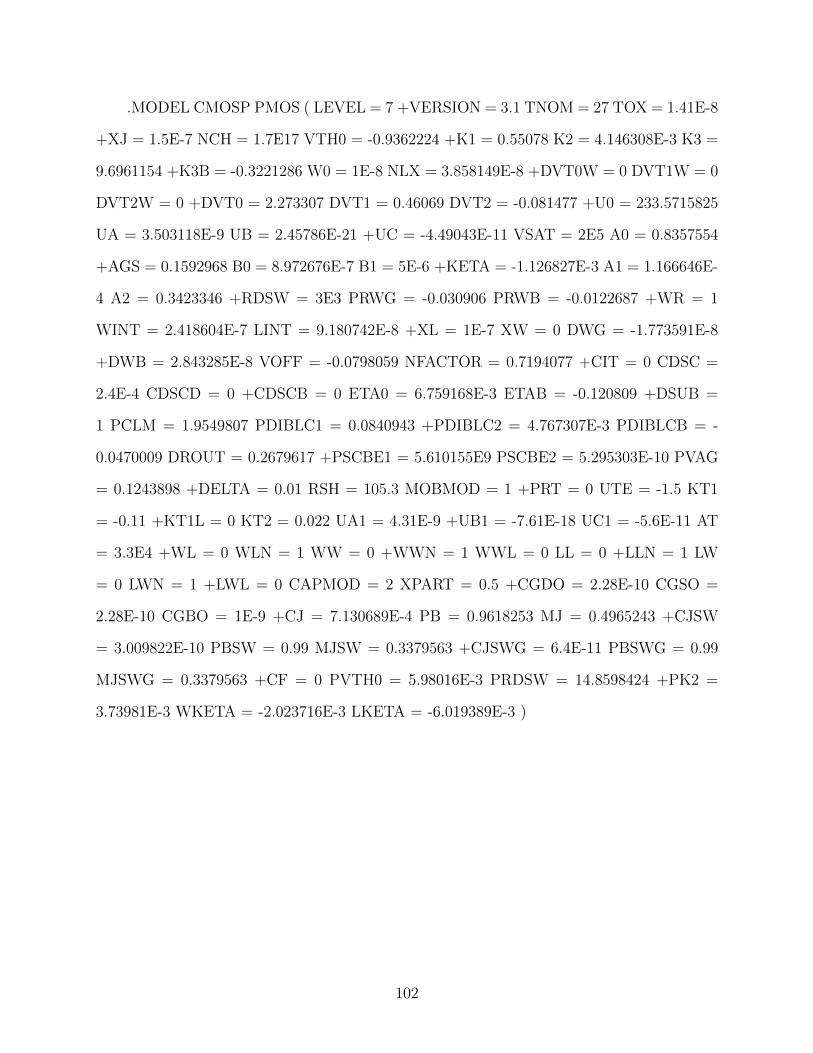
.MODEL CMOSP PMOS ( LEVEL = 7 +VERSION = 3.1 TNOM = 27 TOX = 1.41E-8
+XJ = 1.5E-7 NCH = 1.7E17 VTH0 = -0.9362224 +K1 = 0.55078 K2 = 4.146308E-3 K3 =
9.6961154 +K3B = -0.3221286 W0 = 1E-8 NLX = 3.858149E-8 +DVT0W = 0 DVT1W = 0
DVT2W = 0 +DVT0 = 2.273307 DVT1 = 0.46069 DVT2 = -0.081477 +U0 = 233.5715825
UA = 3.503118E-9 UB = 2.45786E-21 +UC = -4.49043E-11 VSAT = 2E5 A0 = 0.8357554
+AGS = 0.1592968 B0 = 8.972676E-7 B1 = 5E-6 +KETA = -1.126827E-3 A1 = 1.166646E-
4 A2 = 0.3423346 +RDSW = 3E3 PRWG = -0.030906 PRWB = -0.0122687 +WR = 1
WINT = 2.418604E-7 LINT = 9.180742E-8 +XL = 1E-7 XW = 0 DWG = -1.773591E-8
+DWB = 2.843285E-8 VOFF = -0.0798059 NFACTOR = 0.7194077 +CIT = 0 CDSC =
2.4E-4 CDSCD = 0 +CDSCB = 0 ETA0 = 6.759168E-3 ETAB = -0.120809 +DSUB =
1 PCLM = 1.9549807 PDIBLC1 = 0.0840943 +PDIBLC2 = 4.767307E-3 PDIBLCB = -
0.0470009 DROUT = 0.2679617 +PSCBE1 = 5.610155E9 PSCBE2 = 5.295303E-10 PVAG
= 0.1243898 +DELTA = 0.01 RSH = 105.3 MOBMOD = 1 +PRT = 0 UTE = -1.5 KT1
= -0.11 +KT1L = 0 KT2 = 0.022 UA1 = 4.31E-9 +UB1 = -7.61E-18 UC1 = -5.6E-11 AT
= 3.3E4 +WL = 0 WLN = 1 WW = 0 +WWN = 1 WWL = 0 LL = 0 +LLN = 1 LW
= 0 LWN = 1 +LWL = 0 CAPMOD = 2 XPART = 0.5 +CGDO = 2.28E-10 CGSO =
2.28E-10 CGBO = 1E-9 +CJ = 7.130689E-4 PB = 0.9618253 MJ = 0.4965243 +CJSW
= 3.009822E-10 PBSW = 0.99 MJSW = 0.3379563 +CJSWG = 6.4E-11 PBSWG = 0.99
MJSWG = 0.3379563 +CF = 0 PVTH0 = 5.98016E-3 PRDSW = 14.8598424 +PK2 =
3.73981E-3 WKETA = -2.023716E-3 LKETA = -6.019389E-3 )
102
Related Documents