Analog and RF CMOS circuit design 135 avenue de Rangueil – 31077 Toulouse cedex 4 – Tel : 05.61.55.95.13 – Fax : 05.61.55.95.00 - www.insa-toulouse.fr Design of a fully integrated wireless power transmitter– Some theoretical elements Alexandre Boyer [email protected] www.alexandre-boyer.fr 2017-2018

Welcome message from author
This document is posted to help you gain knowledge. Please leave a comment to let me know what you think about it! Share it to your friends and learn new things together.
Transcript

Analog and RF CMOS circuit design
Design of a fully integrated
135 avenue de Rangueil – 31077 Toulouse cedex 4 – Tel : 05.61.55.95.13 – Fax : 05.61.55.95.00 - www.insa-toulouse.fr
Design of a fully integrated wireless power transmitter–
Some theoretical elements
Alexandre [email protected]
www.alexandre-boyer.fr
2017-2018

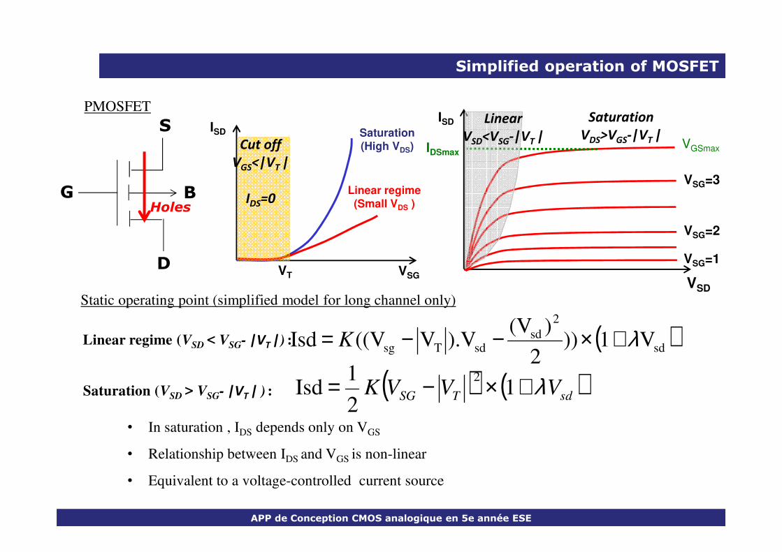
Simplified operation of MOSFET
V
IDSmax
VGS=3
VGS=2
VGS=1
VGSmax
Linear
VDS<VGS-VT
Saturation
VDS>VGS-VT
IDS
Linear regime
(Small VDS )
VT
Saturation
(High VDS)
VGS
Cut off
VGS<VT
IDS=0G
S
D
BElectrons
NMOSFETIDS
APP de Conception CMOS analogique en 5e année ESE
VDS
VT VGS
• In saturation , IDS depends only on VGS
• Relationship between IDS and VGS is non-linear
• Equivalent to a voltage-controlled current source
Linear regime (VDS < VGS-VT ) :
Saturation (VDS > VGS-VT ) :
( )ds
2
dsdsTgs V1))
2
)(V).VV((V Ids λ+×−−= K
( ) ( )dsTGS VVVK λ+×−= 12
1 Ids
2
Static operating point (simplified model for long channel only)
Simplified operation of MOSFET
V
IDSmax
VSG=3
VSG=2
VSG=1
VGSmax
Linear
VSD<VSG-|VT |
Saturation
VDS>VGS-|VT |ISD
Linear regime
(Small VDS )
VT
Saturation
(High VDS)
VSG
Cut off
VGS<|VT |
IDS=0Holes
ISD
G
D
S
B
PMOSFET
APP de Conception CMOS analogique en 5e année ESE
VSD
VT VSG
• In saturation , IDS depends only on VGS
• Relationship between IDS and VGS is non-linear
• Equivalent to a voltage-controlled current source
Linear regime (VSD < VSG- |VT |) :
Saturation (VSD > VSG- |VT | ) :
Static operating point (simplified model for long channel only)
( )sd
2
sdsdTsg V1))
2
)(V).VV((V Isd λ+×−−= K
( ) ( )sdTSG VVVK λ+×−= 12
1 Isd
2
Simplified small signal model (dynamic regime analysis)
G
S S
D
C
GS i
DS= g
m.v
GS
r
0=1/ g
m
G
S S
D
C
)(3
2oxgs WLCC ≈
In saturation regime (VDS > VGS-VT ) :
VGS
IDS
rD gsmds VgI =
APP de Conception CMOS analogique en 5e année ESE
)( ThGS
GS
DSm VVK
V
Ig −=
∂∂≡
)V(VL
W.
TOX
εε UO g ThGS
rm −= 0
The transconductance sets the voltage, current
or power gain of amplifier stage
Fit by designer
• Technology CMOS 0.35 µm 50 V (process H35B4S1)
• Integration on the same chip of power drivers (50 V) with command
command and analog processing (3.3/5 V)
• Old technological node, but reliable, robust and low-cost technology
adapted to automtive industry
• Available devices (refer ENG-238_rev6.pdf) :
• NMOS/PMOSFET (LV and HV cores - 3.3 V à 50 V)
Design kit AMS H35
APP de Conception CMOS analogique en 5e année ESE
• NMOS/PMOSFET (LV and HV cores - 3.3 V à 50 V)
• BJT vertical and lateral NPN/PNP
• Diodes
• Resistor (diffusion, Nwell, POLY1/2/H)
• Cpacitor (MIM, POLY, POLY-Metal)
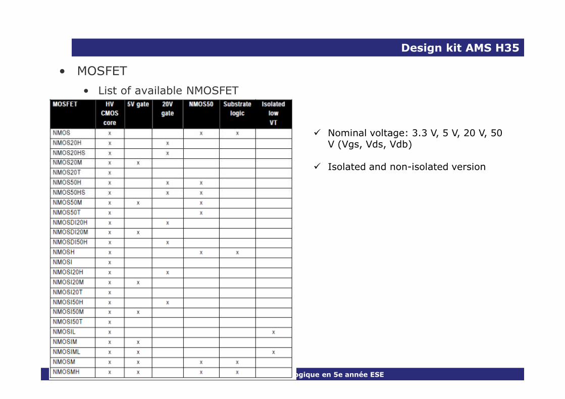
• MOSFET
• List of available NMOSFET
Design kit AMS H35
Nominal voltage: 3.3 V, 5 V, 20 V, 50 V (Vgs, Vds, Vdb)
Isolated and non-isolated version
APP de Conception CMOS analogique en 5e année ESE

• MOSFET – Wafer cross-section (ENG-236_rev6.pdf)
Design kit AMS H35
Bulk = VDDBulk = VSSSource = VSS
Source = VDD
VDD = 3.3 – 5 VVSS = 0 V
APP de Conception CMOS analogique en 5e année ESE
VSSP-substrate
N-well
P-substrate
N-well
P-well N-well
VSS
Bulk = VSSSource = VSS Bulk = VDD
Source = VDD
Junction-based isolation
Tub = VDDTub = VDD
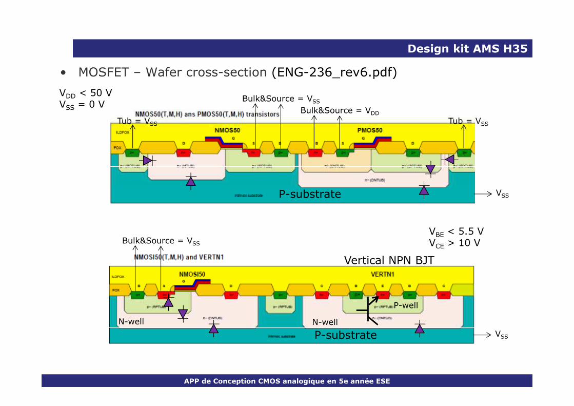
• MOSFET – Wafer cross-section (ENG-236_rev6.pdf)
Design kit AMS H35
VSSP-substrate
Bulk&Source = VDD
VDD < 50 VVSS = 0 V
Bulk&Source = VSS
Tub = VSSTub = VSS
APP de Conception CMOS analogique en 5e année ESE
VSSP-substrate
N-well N-well
Bulk&Source = VSS
Vertical NPN BJT
VBE < 5.5 VVCE > 10 V
P-well

CMOS power driver (half-bridge)
VDD_PWR
VSS_PWR
RLoad
LLoad
Pre-driver
Level shifter
High side
Low side
Level shifter
High side command
Low side command
VDD_PWR
VDD_PWR
VSS_PWR
VDD_PWRVDD
VDD_PWRVDD
VSS
APP de Conception CMOS analogique en 5e année ESE
• Constraints :
• Efficiency optimization (reduce power losses)
• Small Ron small drain-source voltage drop reduction of power
dissipation
• Dead time (remove « crossbar current » or « shoot-through
current »)
• Robustness to overvoltage
• Slew rate control (EMC)
VSS_PWRVSS_PWRVSS

CMOS power driver (half-bridge)
• Smart Power IC example (High Voltage CMOS 0.35 µm) – Imax = 1 A
High side
(W=9500 µm,
L= 0.7 µm
Low side
3100 µm2500 µ
m
APP de Conception CMOS analogique en 5e année ESE
Low side
(W=7000 µm,
L= 0.7 µm
2500 µ
m
Command +
pre-driver +
on-chip
diagnosis
CMOS power driver (half-bridge)
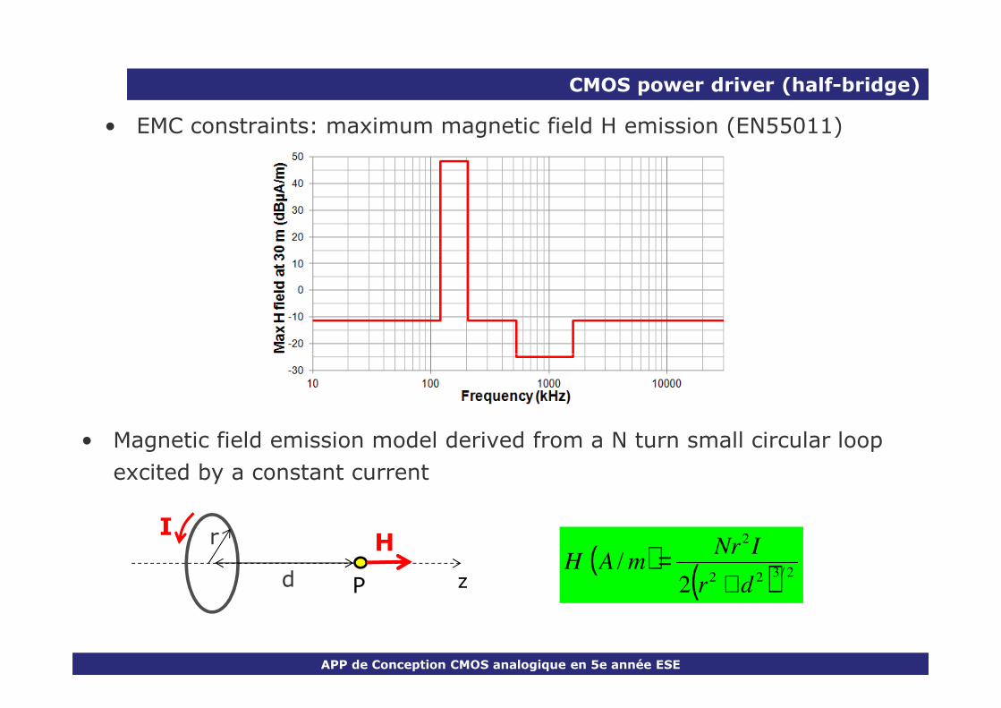
• EMC constraints: maximum magnetic field H emission (EN55011)
APP de Conception CMOS analogique en 5e année ESE
• Magnetic field emission model derived from a N turn small circular loop
excited by a constant current
I
z
r
Pd
H ( ) ( ) 2/322
2
2/
dr
INrmAH
+=
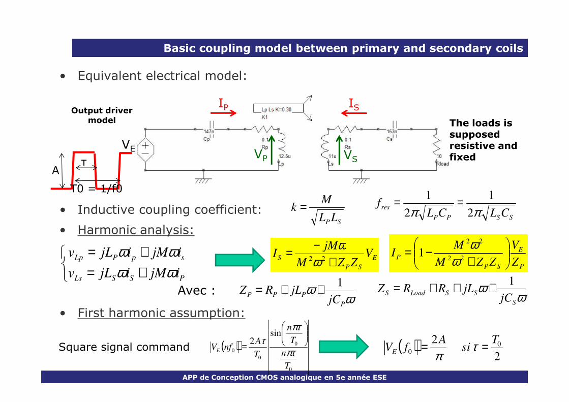
• Equivalent electrical model:
Basic coupling model between primary and secondary coils
Output driver model
A
T0 = 1/f0
The loads is supposed resistive and fixed
IP IS
Mk =
VP VS
VE
τ
f11 ==
APP de Conception CMOS analogique en 5e année ESE
• Harmonic analysis:SPLL
Mk =• Inductive coupling coefficient:
+=+=
PSSLs
spPLp
ijMijLv
ijMijLv
ωωωω
E
SP
S VZZM
jMI
+−=
22ωω
P
E
SP
PZ
V
ZZM
MI
+−=
22
22
1ω
ω
ωω
P
PPPjC
jLRZ1++= ω
ωS
SSLoadSjC
jLRRZ1+++=Avec :
• First harmonic assumption:
Square signal command ( )
0
0
0
0
sin2
T
n
T
n
T
AnfVE πτ
πττ
= ( )2
2 00
Tsi
AfVE == τ
π
SSPP
resCLCL
fππ 2
1
2
1 ==

• Example :
Basic coupling model between primary and secondary coils
Fres = 117 kHz, τ = T0/2, A = 9 V, k = 0.4, RL = 10 Ω
IP
ISLimit IP
APP de Conception CMOS analogique en 5e année ESE
Fres = 117 kHz, F0 = 150 kHz, τ = T0/2, A = 9 V , RL = 10 Ω
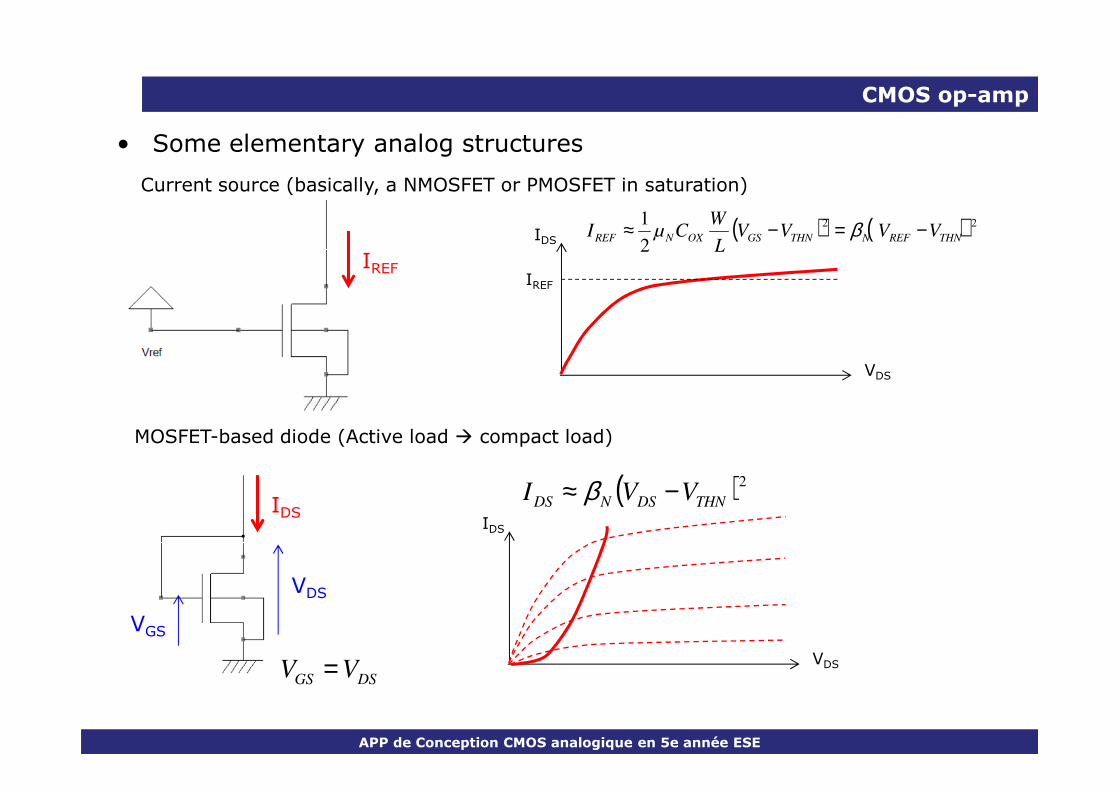
• Some elementary analog structures
CMOS op-amp
Current source (basically, a NMOSFET or PMOSFET in saturation)
IREF
VDS
IDS
IREF
( ) ( )22
2
1THNREFNTHNGSOXNREF VVVV
L
WCµI −=−≈ β
APP de Conception CMOS analogique en 5e année ESE
MOSFET-based diode (Active load compact load)
IDS
VDS
VGS
VDS
IDS
DSGS VV =
( )2
THNDSNDS VVI −≈ β

Current mirror (based on NMOSFET or PMOSFET)
IIN IOUT
W1, L1W2, L2
M1 M2
M1 and M2 have same characteristics, except dimensions W and L which can be different
1
1
2
2
L
WK
L
W =
• Some elementary analog structures
CMOS op-amp
APP de Conception CMOS analogique en 5e année ESE
W1, L1W2, L2
VDS2
IOUT
IIN
If M2 is in saturation and if its output conductance is null:
INOUT IKI ×=

• Refer to book Gray, Hurst, Lewis, Meyer, « Analysis and Design of
Analog Integrated Circuits », chapitres 6, 7, 8
• Principle of two-stage diff. Amplifier with single-ended output:
CMOS op-amp
diffDmo vRgv 122
1=
Differential pair
Output stage with gain (common-
source)
( )vRrgv //−=
APP de Conception CMOS analogique en 5e année ESE
M1 and M2 are identical and in saturation, transconductance gm1.
Open circuit
( ) iDmo vRrgv //032 −=
M3
vi
M3 saturated, transconductance gm3
, output resistance r0

CMOS op-amp
• Miller OTA amplifier (with PMOSFET diff. pair):
Diff. pair Output stage with gain
Bias current source for diff. Pair and
output stageCurrent mirror (biasing)
Compensation capacitor
APP de Conception CMOS analogique en 5e année ESE
Diff. pair
Active load for the diff. Pair (current mirror)
Current reference
Compensation capacitor (optional according to stability, pole splitting)
Common-mode source ampli.

• Main characteristics to control:
• Tatic gain
• Output voltage range (rail-to-rail ideally)
• Input/output offset
• Common-mode rejection
• Bandwidth, gain-bandwidth product
• Open-loop transfer function, poles, stability (phase margin)
CMOS op-amp
APP de Conception CMOS analogique en 5e année ESE
• Slew rate
• Power supply rejection ratio (PSRR)
• Power consumption

• OPA based comparator (slew rate, offset issues…)
• Schmitt trigger (digital structure):
CMOS comparator
APP de Conception CMOS analogique en 5e année ESE
With : VTxx = Threshold voltage(VTN2 = VTN3,
VTP4 = VTP6) βx = ½µxCoxW/L = transconductance

• Internal hysteresis comparator
CMOS comparator
I1 I2
VREF
VIN
VOx
VDD
VT5+VT1
VO1
VO2
VIN : from VSS to VDD
APP de Conception CMOS analogique en 5e année ESE
I5 = IBias
Conditions : M1 = M2 M3 = M4 M6 = M7 I5 = IBias = constant Β1= M1 transconductance
K
LW
LW
LW
LW
==
4
4
7
7
3
3
6
6
VINVSS VDDVREF+VT+
Threshold and hysteresis width:
K
KiVT +
−=+1
1
1
5
β K
KiVT +
−=−1
1
1
5
β
K
KiVV TT +
−=− −+1
12
1
5
β
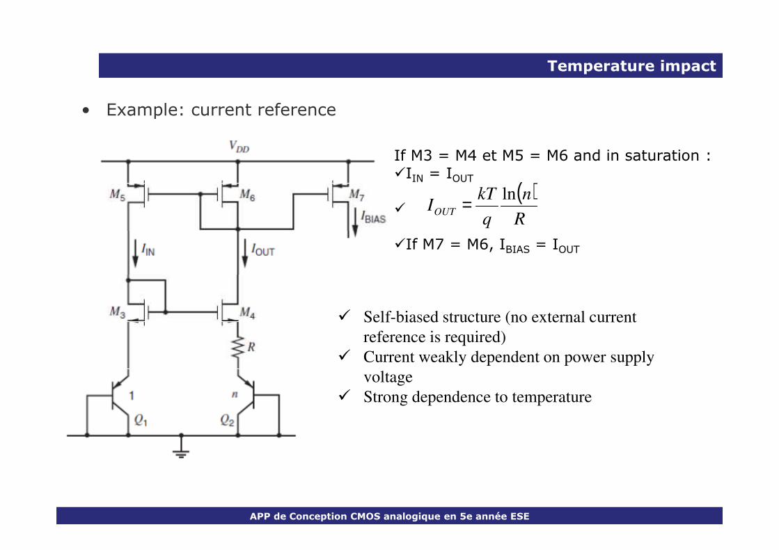
• Example: current reference
Temperature impact
If M3 = M4 et M5 = M6 and in saturation :IIN = IOUT
If M7 = M6, IBIAS = IOUT
( )R
n
q
kTIOUT
ln=
APP de Conception CMOS analogique en 5e année ESE
Self-biased structure (no external current
reference is required)
Current weakly dependent on power supply
voltage
Strong dependence to temperature

• Example: bandgap voltage reference
• Reuse the previous current reference and adding of a temperature
compensation strategy
Temperature impact
( )R
n
q
kTRVIRVV EBOUTEBOUT
ln2222 +=+=
Proportional To Absolute Temperature (PTAT) = voltage drop across R2
APP de Conception CMOS analogique en 5e année ESE
(PTAT) = voltage drop across R2 (dVR2/dT ≈ +1.8 mV/°c)
Complementary To Absolute Temperature (CTAT) = PNP-based diode (dVEB/dT ≈ -2 mV/°c)
1 14
VBE multiplier
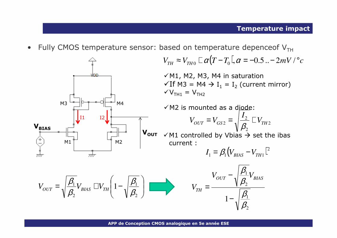
• Fully CMOS temperature sensor: based on temperature depenceof VTH
Temperature impact
( ) cmVTTVV THTH °−−=−+≈ /2..5.0,00 αα
I1 I2
M1, M2, M3, M4 in saturation
If M3 = M4 I1 = I2 (current mirror)VTH1 = VTH2
M2 is mounted as a diode:M3 M4
2 VI
VV +==
APP de Conception CMOS analogique en 5e année ESE
VBIASVOUT
I1 I2
M1 M2
2
2
22 THGSOUT V
IVV +==
β
( )2
111 THBIAS VVI −= β
M1 controlled by Vbias set the ibas current :
−+=
2
1
2
1 1ββ
ββ
THBIASOUT VVV
2
1
2
1
1ββββ
−
−=
BIASOUT
TH
VV
V
Related Documents