HAL Id: hal-02175745 https://hal.archives-ouvertes.fr/hal-02175745 Submitted on 10 Jul 2019 HAL is a multi-disciplinary open access archive for the deposit and dissemination of sci- entific research documents, whether they are pub- lished or not. The documents may come from teaching and research institutions in France or abroad, or from public or private research centers. L’archive ouverte pluridisciplinaire HAL, est destinée au dépôt et à la diffusion de documents scientifiques de niveau recherche, publiés ou non, émanant des établissements d’enseignement et de recherche français ou étrangers, des laboratoires publics ou privés. Analog and Mixed-Signal Test Haralampos-G. Stratigopoulos, Bozena Kaminska To cite this version: Haralampos-G. Stratigopoulos, Bozena Kaminska. Analog and Mixed-Signal Test. Grant Martin; Luciano Lavagno; Igor Markov. Electronic Design Automation for Integrated Circuits Handbook, CRC Press, 2016. hal-02175745

Welcome message from author
This document is posted to help you gain knowledge. Please leave a comment to let me know what you think about it! Share it to your friends and learn new things together.
Transcript

HAL Id: hal-02175745https://hal.archives-ouvertes.fr/hal-02175745
Submitted on 10 Jul 2019
HAL is a multi-disciplinary open accessarchive for the deposit and dissemination of sci-entific research documents, whether they are pub-lished or not. The documents may come fromteaching and research institutions in France orabroad, or from public or private research centers.
L’archive ouverte pluridisciplinaire HAL, estdestinée au dépôt et à la diffusion de documentsscientifiques de niveau recherche, publiés ou non,émanant des établissements d’enseignement et derecherche français ou étrangers, des laboratoirespublics ou privés.
Analog and Mixed-Signal TestHaralampos-G. Stratigopoulos, Bozena Kaminska
To cite this version:Haralampos-G. Stratigopoulos, Bozena Kaminska. Analog and Mixed-Signal Test. Grant Martin;Luciano Lavagno; Igor Markov. Electronic Design Automation for Integrated Circuits Handbook,CRC Press, 2016. �hal-02175745�

1
Haralampos-G. Stratigopoulos
Université Grenoble Alpes, CNRS, TIMA, France
Bozena Kaminska
Simon Fraser University, Canada
Analog and Mixed-Signal Test

2
CONTENTS
1 Introduction . . . . . . . . . . . . . . . . . . . . . . . . . . . . . . . . . . . . . . . . . . . . . . . . . . . . . . 3
2 Integrated Test - An Overview . . . . . . . . . . . . . . . . . . . . . . . . . . . . . . . . . . . . . 3
3 Alternate Test . . . . . . . . . . . . . . . . . . . . . . . . . . . . . . . . . . . . . . . . . . . . . . . . . . . . 7
4 Specification-Based Test Compaction . . . . . . . . . . . . . . . . . . . . . . . . . . . . . . . . 9
5 Probabilistic Test Metrics Estimation. . . . . . . . . . . . . . . . . . . . . . . . . . . . . . . . . 11
6 Fault Modeling and Structural Test. . . . . . . . . . . . . . . . . . . . . . . . . . . . . . . . . . 13
7 Oscillation-Based Test. . . . . . . . . . . . . . . . . . . . . . . . . . . . . . . . . . . . . . . . . . . . 14
8 Data converters DFT and BIST. . . . . . . . . . . . . . . . . . . . . . . . . . . . . . . . . . . . . . . 15
9 PLL DFT and BIST. . . . . . . . . . . . . . . . . . . . . . . . . . . . . . . . . . . . . . . . . . . . . . . . . . . . 17
10 RF DFT and BIST. . . . . . . . . . . . . . . . . . . . . . . . . . . . . . . . . . . . . . . . . . . . . . . . . . . . 18
11 Summary. . . . . . . . . . . . . . . . . . . . . . . . . . . . . . . . . . . . . . . . . . . . . . . . . . . . . . . . . . 20
12 Bibliography. . . . . . . . . . . . . . . . . . . . . . . . . . . . . . . . . . . . . . . . . . . . . . . . . . . . . . . . . 21
3
1 Introduction
Integrated circuits (ICs) are fabricated using a series of photolithographic, printing, etching,
implanting, and chemical vapor deposition steps. This process is subject to imperfections that may
cause complete failure in the operation of individual ICs, or variations in performance amongst ICs on
the same wafer or across different lots. The performance of an IC could also shift in the post-silicon
production flow during the packaging process. For all the above reasons, each fabricated IC must be
tested, in order to ensure that it meets its design specifications.
The current practice for testing the analog and mixed-signal (AMS) functions of ICs is specification-
based testing [1, 2, 3, 4]. Specification-based testing involves direct measurement of the
performances that are promised in the specification data sheet one by one. However, despite the
ease of interpreting the test result, specification-based testing incurs a very high cost since it relies
on specialized Automatic Test Equipment (ATE) with advanced capabilities and running the tests
takes a long time. In fact, testing the AMS functions of modern Systems-on-Chip (SoC) is responsible
for the largest fraction of the test cost despite the fact that AMS circuits occupy a much smaller area
on the die compared to their digital counterparts [5]. With the ever-increasing levels of integration of
SoC designs, more and more of which include AMS circuits, ATE cost, test development and test
execution times are being increasingly impacted and will keep increasing as we move towards more
advanced technology nodes. AMS testing is nowadays an area of focus and innovation for the
microelectronics industry.
It is thus necessary for design and test engineers to work together, early in the SoC architecture
design phase, in order to keep the testing costs under control. Alternative low-cost test techniques
need to be developed that can effectively replace standard specification-based tests. These
techniques should target reducing test times and/or alleviating the need to rely on specialized ATE.
Introducing alternative test techniques, however, should not sacrifice the high accuracy of
specification-based testing, which is measured by test metrics such as test escape (e.g. faulty circuits
passing the test) and yield loss (e.g. functional circuits failing the test). Therefore, any alternative test
technique should be assessed by estimating the resultant test metrics that will be met in production.
This chapter will focus on generic alternative test techniques, such as inferring the outcome of
specification-based testing from low-cost measurements (broadly known as “alternate test”),
eliminating redundant specification- based tests and applying a reduced set, structural test
techniques where the test problem reduces to checking for the presence of faults contained in a pre-
defined list, as well as on practical integrated test techniques for different types of AMS circuits, such
as analog-to-digital converters (ADC), digital-to- analog converters (DAC), phase locked loops (PLL),
and radio-frequency (RF) circuits. This chapter will also review tools to assess the feasibility of alter-
native test techniques. All these techniques and tools are seen as an enabling technology to break
the cost trend.
2 Integrated Test - An Overview
Integrated test techniques are grouped into Design-for-Test (DFT) and Built- In Self-Test (BIST)
techniques.
4
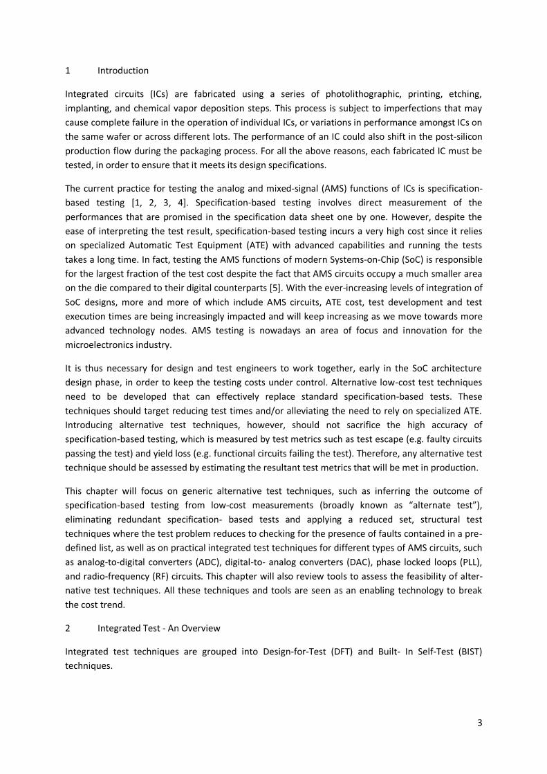
DFT techniques can be broadly grouped into two approaches. The first DFT approach is to facilitate
test access into the design by implementing test signal buses according to the IEEE Standards 1149.1
[6] and 1149.4 [7], as illustrated in Fig. 1. The IEEE 1149.4 architecture in Fig. 1 comprises a test bus
interface circuit (TBIC) with analog test stimulus (AT1) and analog test output (AT2) pins, analog
boundary modules (ABM) on each analog I/O, digital boundary modules (DBM) on each digital I/O,
and a test access port (TAP) controller with test data in (TDI), test data out (TDO), test mode select
(TMS), test clock (TCLK), and test reset (TRSTn) pins. This test bus architecture provides the means for
bypassing functional blocks in the circuit under test (CUT), in order to apply test stimuli directly to
internal blocks and reading out the test responses. Therefore, the test bus can be used to enhance
the overall testability, as well as to enable system diagnostics and silicon debugging in post-
manufacturing. In addition, the test bus can be used for testing for open- and short-circuits among
the interconnections of circuits in a printed circuit assembly. The second DFT approach is based on
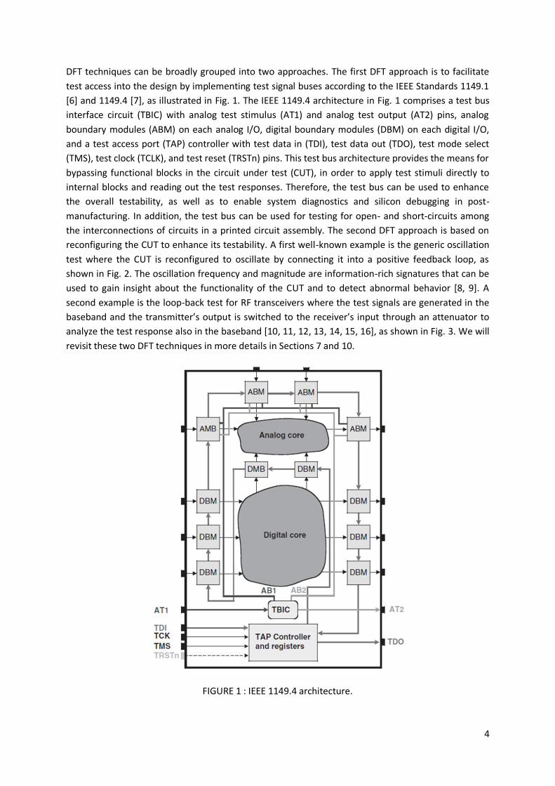
reconfiguring the CUT to enhance its testability. A first well-known example is the generic oscillation
test where the CUT is reconfigured to oscillate by connecting it into a positive feedback loop, as
shown in Fig. 2. The oscillation frequency and magnitude are information-rich signatures that can be
used to gain insight about the functionality of the CUT and to detect abnormal behavior [8, 9]. A
second example is the loop-back test for RF transceivers where the test signals are generated in the
baseband and the transmitter’s output is switched to the receiver’s input through an attenuator to
analyze the test response also in the baseband [10, 11, 12, 13, 14, 15, 16], as shown in Fig. 3. We will
revisit these two DFT techniques in more details in Sections 7 and 10.
FIGURE 1 : IEEE 1149.4 architecture.
5
FIGURE 2 : Oscillation-based test architecture.
FIGURE 3 : Loop-back test for RF transceivers.
FIGURE 4 : BIST employing an on-chip test stimulus generator and an on-chip test response analyzer.
FIGURE 5 : BIST employing on-chip sensors.
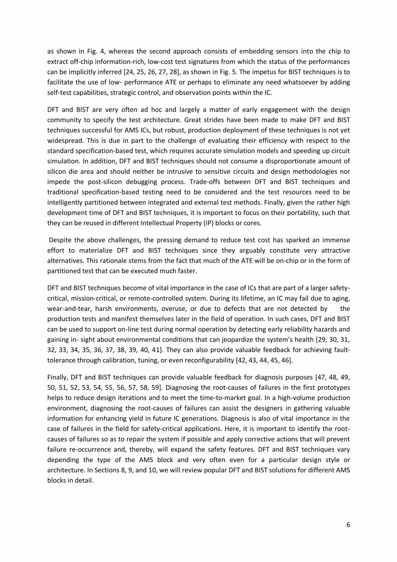
BIST techniques can also be broadly grouped into two approaches. The first approach consists of
embedding a signal generator and a test response analyzer into the chip [17, 18, 19, 20, 21, 22, 23],
6
as shown in Fig. 4, whereas the second approach consists of embedding sensors into the chip to
extract off-chip information-rich, low-cost test signatures from which the status of the performances
can be implicitly inferred [24, 25, 26, 27, 28], as shown in Fig. 5. The impetus for BIST techniques is to
facilitate the use of low- performance ATE or perhaps to eliminate any need whatsoever by adding
self-test capabilities, strategic control, and observation points within the IC.
DFT and BIST are very often ad hoc and largely a matter of early engagement with the design
community to specify the test architecture. Great strides have been made to make DFT and BIST
techniques successful for AMS ICs, but robust, production deployment of these techniques is not yet
widespread. This is due in part to the challenge of evaluating their efficiency with respect to the
standard specification-based test, which requires accurate simulation models and speeding up circuit
simulation. In addition, DFT and BIST techniques should not consume a disproportionate amount of
silicon die area and should neither be intrusive to sensitive circuits and design methodologies nor
impede the post-silicon debugging process. Trade-offs between DFT and BIST techniques and
traditional specification-based testing need to be considered and the test resources need to be
intelligently partitioned between integrated and external test methods. Finally, given the rather high
development time of DFT and BIST techniques, it is important to focus on their portability, such that
they can be reused in different Intellectual Property (IP) blocks or cores.
Despite the above challenges, the pressing demand to reduce test cost has sparked an immense
effort to materialize DFT and BIST techniques since they arguably constitute very attractive
alternatives. This rationale stems from the fact that much of the ATE will be on-chip or in the form of
partitioned test that can be executed much faster.
DFT and BIST techniques become of vital importance in the case of ICs that are part of a larger safety-
critical, mission-critical, or remote-controlled system. During its lifetime, an IC may fail due to aging,
wear-and-tear, harsh environments, overuse, or due to defects that are not detected by the
production tests and manifest themselves later in the field of operation. In such cases, DFT and BIST
can be used to support on-line test during normal operation by detecting early reliability hazards and
gaining in- sight about environmental conditions that can jeopardize the system’s health [29, 30, 31,
32, 33, 34, 35, 36, 37, 38, 39, 40, 41]. They can also provide valuable feedback for achieving fault-
tolerance through calibration, tuning, or even reconfigurability [42, 43, 44, 45, 46].
Finally, DFT and BIST techniques can provide valuable feedback for diagnosis purposes [47, 48, 49,
50, 51, 52, 53, 54, 55, 56, 57, 58, 59]. Diagnosing the root-causes of failures in the first prototypes
helps to reduce design iterations and to meet the time-to-market goal. In a high-volume production
environment, diagnosing the root-causes of failures can assist the designers in gathering valuable
information for enhancing yield in future IC generations. Diagnosis is also of vital importance in the
case of failures in the field for safety-critical applications. Here, it is important to identify the root-
causes of failures so as to repair the system if possible and apply corrective actions that will prevent
failure re-occurrence and, thereby, will expand the safety features. DFT and BIST techniques vary
depending the type of the AMS block and very often even for a particular design style or
architecture. In Sections 8, 9, and 10, we will review popular DFT and BIST solutions for different AMS
blocks in detail.
7
3 Alternate Test
As mentioned in the introduction, the standard approach for testing AMS circuits is to measure
directly the performances that are promised in the data sheet. The IC is declared faulty or functional
by simply comparing the measured performance values to the design specifications. In this context,
the necessary ATE resources are employed and overall the test approach is easy to interpret and
implement since the same test benches are used as during the design and prototype characterization
phases.
Alternate test aims to circumvent specialized ATE resources and speed up the test execution time by
relying solely on measurements that can be rapidly extracted using a low-cost assortment of test
equipment [60, 61, 62]. The grounds for achieving the objective of inferring the performances
implicitly from low-cost alternate measurements is that both the performances and the alternate
measurements are subject to the same process variations. Thus, in the presence of process
variations, both performances and alternate measurements vary and the objective boils down to
identifying alternate measurements that correlate well with the performances, such that any
performance shift can be predicted from the corresponding shift in the alternate measurement
pattern, as illustrated in Fig. 6. For the method to succeed, it is needed first to (a) identify such
information-rich alternate measurements and second to (b) build the mapping between alternate
measurements and performances.
FIGURE 6 : Principle of alternate test.
The identification of appropriate alternate measurements is a circuit-specific problem since the
input, output, frequency band, transfer function, etc., depend on the type of the IC, as well as its
architecture. In the recent years, the alternate test paradigm has been proven for different types of
ICs, including, baseband analog [60, 63], RF [64, 65, 66, 67], data converters [68, 69], PLLs [70], and
8
MicroElectroMechanical Systems (MEMS) [71]. Very often, the alternate measurements are
extracted ad hoc without a clear rationale. Through simulations it is demonstrated that they can be
used in- deed to predict the performance values and in the next step the concept is demonstrated
experimentally in silicon. The reason is the large number of process parameters and their intricate
interactions which makes impossible to justify that an alternate measurement captures all variation
scenarios that can occur in practice. A typical approach is to identify as many alternate
measurements as possible and then compact this set using feature selection algorithms [60, 72, 73,
74, 75], such as genetic algorithms [76], floating search algorithms [77], etc. Another approach is to
craft the test stimulus such that the output response becomes appropriate for alternate test [60, 78].
Examples of alternate measurements for baseband analog circuits include sampling the output
response when applying at the input a piecewise linear test stimulus [60, 63], a multi-tone sinusoidal
[72], or a pseudo-random bit sequence [73]. Popular approaches to extract alternate measurements
from RF circuits include (a) applying a baseband multi-tone sinusoidal, up-converting it using a mixer
that exists on the test load board or on-chip, down-converting the RF output using again a mixer, and
sampling the demodulated baseband test response [64, 65, 73]; (b) sensors that tap into the RF
signal path, for example, amplitude detectors [79, 80, 25, 24, 81, 82, 83] and current sensors [84, 26,
82].
The intricate relationship among performances and alternate measurements makes impossible to
build a mapping in the form of a closed-form mathematical equation. For this reason, the mapping is
built through statistical learning. In particular, a set of N circuit instances that is representative of the
fabrication process is collected. The d performances 𝑃 = [𝑃1, … , 𝑃𝑑] and alternate measurements M
are obtained on each circuit instance. Part of the circuit instances are used to train a regression
function 𝑓𝑖: 𝑀 → 𝑃𝑖 for each performance 𝑃𝑖. The circuit instances that are left out are used as an
independent validation set. Target performances for the circuit instances in the validation set are
assumed to be unknown and they are only used to estimate the test error. In particular, the alternate
measurements are given as arguments to the regression functions to obtain performance predictions
�̂�. If the test error 𝑃 − �̂�, averaged over all circuit instances in the validation set, is deemed to be
small, then the alternate measurements are satisfactory.
It should be noticed that outliers should be excluded from the training phase since they are
inconsistent with the statistical nature of the bulk of the training data stemming from circuits with
process variations and will adversely affect the regression fit results. In fact, outliers are non-
statistical in nature since their real cause is physical defects that are induced or enhanced during the
IC manufacturing in a random fashion. Likewise, the learned regression functions are not designed to
predict the performances of outliers as the test outcome will be somewhat random. Thus, in the
testing phase, all ICs should be checked to verify that they are not outliers before the learned
regression functions are applied to reach a test decision. This indispensable step in the flow of
alternate test makes use of a defect filter [85].
Instead of predicting the actual values of the performances, it is also possible to predict directly
whether the performances satisfy their specifications, that is, a form of go/no-go test. In this case, a
classifier is used that implements a function 𝑔: 𝑀 → [pass, fail] [86, 87, 88, 89, 72, 73]. The classifier
should be able to allocate a non-linear decision boundary in the space of alternate measurements
such that the population of functional circuits is separated from the population of circuits that violate
9
at least one specification, as illustrated in Fig. 6. Various classifiers can be used in this context,
including Support Vector Machines (SVM) [90], decision trees [91], ontogenic neural networks [92],
feed-forward neural networks [93], etc. Similarly to the regression functions, the better the
correlation among performances and alternate measurements is, the smaller will be the overlap
between the two populations and the better the classification rate will be. Furthermore, the classifier
can be implemented on-chip towards a stand-alone BIST [94].
The advantage of using regression functions is that it offers the possibility of predicting the
performance values, which allows binning of functional circuits and a better insight into the
performance distributions. The classifier has the advantage that it can screen out circuits with
defects on top of circuits with excessive process variations. However, this is at the expense of
requiring to include circuits with defects in the training set which may be difficult to collect in the
production environment in a short period of time. To this end, an one-class classifier can be used that
avoids this requirement [95].
Finally, as any other indirect test method, alternate test is prone to error. To improve confidence in
the test decision, it is possible to identify the small fraction of circuits that will be likely erroneously
predicted and forward them to a second test tier where more thorough testing is performed. Several
techniques exist for this purpose, including the use of guard-bands in the case of classifiers [73],
using multiple regression functions [96], and a pair of defect filters [95].
4 Specification-Based Test Compaction
A plausible direction towards decreasing test cost is to identify and eliminate information
redundancy in the set of specification-based tests, thereby relying only on a subset of them in order
to reach a pass/fail decision. Such redundancy is likely to exist since groups of performances refer to
the same portion of the IC and are subject to similar process imperfections. However, it is highly
unlikely that it will manifest itself in a coarse and easily observable form of superfluous tests that can
be summarily discarded. Hence, more advanced statistical analysis methods are likely to be required.
In the linear error-mechanism model algorithm (LEMMA) [97], availability of a linear model 𝑦 = 𝐴𝑥 is
assumed [98], where 𝑦 is the 𝑚 × 1 measurement error vector, x is a 𝑛 × 1 process parameter error
vector, 𝐴 is a 𝑚 × 𝑛 sensitivity matrix, and 𝑚 corresponds to the number of measurements required
for complete specification testing. The method aims to predict the complete vector 𝑦 by carrying out
only a subset �̃� of y. The cardinality 𝑝 of �̃� (𝑝 ≥ 𝑛) is a compromise between the permitted
measurement cost and the maximum tolerable prediction error. The selection process is performed
through QR factorization [99] and minimizes the normalized prediction variance. This is equivalent to
maximizing the determinant �̃�𝑇�̃� , where �̃� designates the 𝑝 × 𝑛 row-reduced matrix 𝐴. In [100],
an iterative selection approach is followed, which considers subsets rather than individual
measurements. Next, the complete measurement vector is predicted by 𝑦 = 𝐴(�̃�𝑇�̃� )−1
�̃�𝑇�̃�. A
leisurely look at this approach and some refinements are provided in [101].
In [102], a fault-driven test selection approach is proposed. The set of needed tests is cumulatively
built by adding to the current set the test for which the yield, as computed by considering only the
specifications of the remaining tests, is maximized. The algorithm terminates when the desired fault
coverage is reached. In [103], in addition to fault coverage, the test selection is driven by the degree
to which faults are exposed. After the redundant tests have been eliminated, a test ordering
10
algorithm can be run, aiming to reduce the average test time. The tests that have higher priority of
being placed at the beginning of the sequence are those that have a high probability of detecting
failures, are low-cost, and are independent of the previous tests in the sequence. Test ordering
algorithms that appear in the literature include trial of various test permutations based on a heuristic
approach to estimate whether a permutation is likely to improve average test time [102], dynamic
programming of a directed flow graph [104], which results in the optimal order, and a variation of
the latter, called A∗ algorithm [102], which, in the worst case, requires the same computational cost
while maintaining optimality.
In [105], specification testing is simplified using a technique called predictive subset testing. It
requires measurement of all performances for a set of circuit instances, which is assumed to be
representative, reflecting accurately the statistical mechanisms of the manufacturing process. The
technique is based upon establishing regression mappings between correlated pairs of
performances. In this situation, we seek to predict one (untested) performance using another
performance that is explicitly tested. Then, new test limits are assigned to the tested performance,
such that they guarantee the compliance of the untested performance to its specifications with the
desired confidence levels.
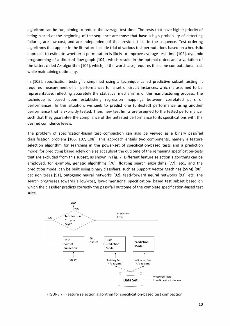
The problem of specification-based test compaction can also be viewed as a binary pass/fail
classification problem [106, 107, 108]. This approach entails two components, namely a feature
selection algorithm for searching in the power-set of specification-based tests and a prediction
model for predicting based solely on a select subset the outcome of the remaining specification-tests
that are excluded from this subset, as shown in Fig. 7. Different feature selection algorithms can be
employed, for example, genetic algorithms [76], floating search algorithms [77], etc., and the
prediction model can be built using binary classifiers, such as Support Vector Machines (SVM) [90],
decision trees [91], ontogenic neural networks [92], feed-forward neural networks [93], etc. The
search progresses towards a low-cost, low-dimensional specification- based test subset based on
which the classifier predicts correctly the pass/fail outcome of the complete specification-based test
suite.
FIGURE 7 : Feature selection algorithm for specification-based test compaction.
11
5 Probabilistic Test Metrics Estimation
As it has been made clear so far, the general objective of the research con- ducted in the AMS test
domain is to develop alternative tests that can replace effectively the costly specification-based tests.
Despite the high number of proposals, few have materialized to date. One of the primary reasons is
the lack of automated tools to evaluate alternative tests in terms of the resultant test error. Indeed,
although it is straightforward to provide claims about the test cost reduction and overhead in the
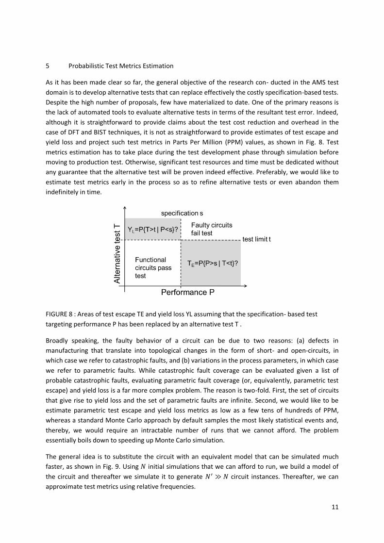
case of DFT and BIST techniques, it is not as straightforward to provide estimates of test escape and
yield loss and project such test metrics in Parts Per Million (PPM) values, as shown in Fig. 8. Test
metrics estimation has to take place during the test development phase through simulation before
moving to production test. Otherwise, significant test resources and time must be dedicated without
any guarantee that the alternative test will be proven indeed effective. Preferably, we would like to
estimate test metrics early in the process so as to refine alternative tests or even abandon them
indefinitely in time.
FIGURE 8 : Areas of test escape TE and yield loss YL assuming that the specification- based test
targeting performance P has been replaced by an alternative test T .
Broadly speaking, the faulty behavior of a circuit can be due to two reasons: (a) defects in
manufacturing that translate into topological changes in the form of short- and open-circuits, in
which case we refer to catastrophic faults, and (b) variations in the process parameters, in which case
we refer to parametric faults. While catastrophic fault coverage can be evaluated given a list of
probable catastrophic faults, evaluating parametric fault coverage (or, equivalently, parametric test
escape) and yield loss is a far more complex problem. The reason is two-fold. First, the set of circuits
that give rise to yield loss and the set of parametric faults are infinite. Second, we would like to be
estimate parametric test escape and yield loss metrics as low as a few tens of hundreds of PPM,
whereas a standard Monte Carlo approach by default samples the most likely statistical events and,
thereby, we would require an intractable number of runs that we cannot afford. The problem
essentially boils down to speeding up Monte Carlo simulation.
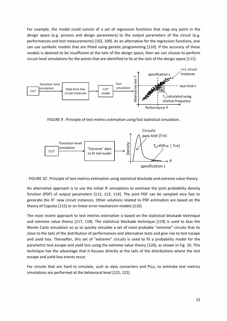
The general idea is to substitute the circuit with an equivalent model that can be simulated much
faster, as shown in Fig. 9. Using 𝑁 initial simulations that we can afford to run, we build a model of
the circuit and thereafter we simulate it to generate 𝑁′ ≫ 𝑁 circuit instances. Thereafter, we can
approximate test metrics using relative frequencies.
12
For example, the model could consist of a set of regression functions that map any point in the
design space (e.g. process and design parameters) to the output parameters of the circuit (e.g.
performances and test measurements) [102, 109]. As an alternative for the regression functions, one
can use symbolic models that are fitted using genetic programming [110]. If the accuracy of these
models is deemed to be insufficient at the tails of the design space, then we can choose to perform
circuit-level simulations for the points that are identified to lie at the tails of the design space [111].
FIGURE 9 : Principle of test metrics estimation using fast statistical simulation.
FIGURE 10 : Principle of test metrics estimation using statistical blockade and extreme value theory.
An alternative approach is to use the initial 𝑁 simulations to estimate the joint probability density
function (PDF) of output parameters [112, 113, 114]. The joint PDF can be sampled very fast to
generate the 𝑁′ new circuit instances. Other solutions related to PDF estimation are based on the
theory of Copulas [115] or on linear error-mechanism models [116].
The most recent approach to test metrics estimation is based on the statistical blockade technique
and extreme value theory [117, 118]. The statistical blockade technique [119] is used to bias the
Monte Carlo simulation so as to quickly simulate a set of most probable “extreme” circuits that lie
close to the tails of the distribution of performances and alternative tests and give rise to test escape
and yield loss. Thereafter, this set of “extreme” circuits is used to fit a probability model for the
parametric test escape and yield loss using the extreme value theory [120], as shown in Fig. 10. This
technique has the advantage that it focuses directly at the tails of the distributions where the test
escape and yield loss events occur.
For circuits that are hard to simulate, such as data converters and PLLs, to estimate test metrics
simulations are performed at the behavioral level [121, 122].
13
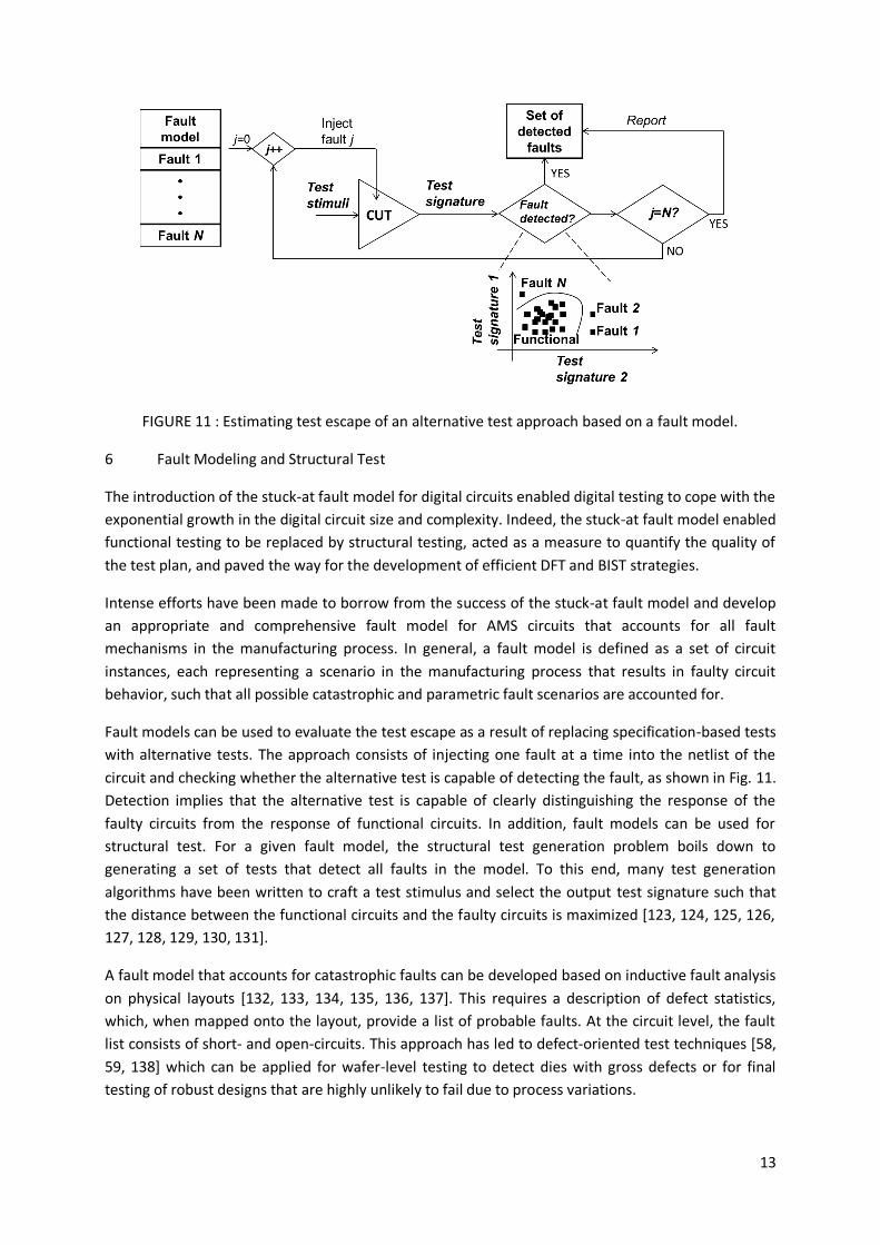
FIGURE 11 : Estimating test escape of an alternative test approach based on a fault model.
6 Fault Modeling and Structural Test
The introduction of the stuck-at fault model for digital circuits enabled digital testing to cope with the
exponential growth in the digital circuit size and complexity. Indeed, the stuck-at fault model enabled
functional testing to be replaced by structural testing, acted as a measure to quantify the quality of
the test plan, and paved the way for the development of efficient DFT and BIST strategies.
Intense efforts have been made to borrow from the success of the stuck-at fault model and develop
an appropriate and comprehensive fault model for AMS circuits that accounts for all fault
mechanisms in the manufacturing process. In general, a fault model is defined as a set of circuit
instances, each representing a scenario in the manufacturing process that results in faulty circuit
behavior, such that all possible catastrophic and parametric fault scenarios are accounted for.
Fault models can be used to evaluate the test escape as a result of replacing specification-based tests
with alternative tests. The approach consists of injecting one fault at a time into the netlist of the
circuit and checking whether the alternative test is capable of detecting the fault, as shown in Fig. 11.
Detection implies that the alternative test is capable of clearly distinguishing the response of the
faulty circuits from the response of functional circuits. In addition, fault models can be used for
structural test. For a given fault model, the structural test generation problem boils down to
generating a set of tests that detect all faults in the model. To this end, many test generation
algorithms have been written to craft a test stimulus and select the output test signature such that
the distance between the functional circuits and the faulty circuits is maximized [123, 124, 125, 126,
127, 128, 129, 130, 131].
A fault model that accounts for catastrophic faults can be developed based on inductive fault analysis
on physical layouts [132, 133, 134, 135, 136, 137]. This requires a description of defect statistics,
which, when mapped onto the layout, provide a list of probable faults. At the circuit level, the fault
list consists of short- and open-circuits. This approach has led to defect-oriented test techniques [58,
59, 138] which can be applied for wafer-level testing to detect dies with gross defects or for final
testing of robust designs that are highly unlikely to fail due to process variations.
14
The definition of a parametric fault model poses a greater challenge [139]. The reason is that there is
an infinite number of combinations of process parameters that result in specification violation, that
is, the size of the parametric fault model is limitless. Thus, we need to consider parametric faults
according to their probability of occurrence and define a parametric fault model that contains the
most probable parametric faults. Previous proposals for parametric fault modeling made certain
assumptions to be able to deal with this challenge [137, 140, 141, 142, 143, 144, 145]. The
widespread approach has been to build a parametric fault model at a higher level of abstraction, for
example, by modeling faults as variations in passive components and in transistor parameters, i.e.
transconductance, geometry, oxide thick- ness, threshold voltage, etc., or by considering behavioral
simulation instead of transistor-level simulation and modeling faults as variations in the parameters
of the behavioral model. Furthermore, a common assumption is that parameters vary independently,
which is known as single fault assumption, and that a circuit fails a specification when one parameter
exceeds a specific tolerance. These simplified fault models make simulation more traceable, yet their
ability to capture correctly faulty behavior due to process variations has never been proven.
A fault model that consists of the most probable parametric faults generated naturally by a Monte
Carlo analysis that makes use of the actual Process Design Kit (PDK) remains an open challenge [146].
A technique was proposed recently in [147] that employs the statistical blockade algorithm to speed
up Monte Carlo analysis. The underlying idea is to bias the Monte Carlo analysis such as to avoid
simulating circuits that are functional and, thereby, are of no use for generating a fault model.
7 Oscillation-Based Test
Oscillation-based test is a generic DFT/BIST technique [8, 9]. It relies on con- verting the circuit to an
oscillator and subsequently measuring the oscillation frequency and magnitude, as shown in Fig. 2.
The reconfiguration of the circuit is accomplished by using digital circuits to control analog switches
and multiplexers, which are designed to have a minimal impact on the measurement. The oscillation
frequency and magnitude are information-rich alternate measurements that are a function of the
process parameters and also the elements that are added in the feedback path to enable oscillation.
As a result, by repeating these measurements under varying voltage conditions, for different
frequency selection, and for different feedback topologies with different attenuation levels, it is
possible to infer implicitly the status of the performances. In particular, test limits can be placed on
the oscillation frequency and magnitude to guarantee with some level of certainty that the
performance values lie within the specification range. The test limits can be found through
simulation and can be selected such that a desired trade-off between test metrics is achieved [148].
Oscillation-based test has several advantages: (a) it is adaptable virtually to all AMS circuits including
baseband analog [8, 149, 150, 151, 152, 153, 154, 9, 155, 156], data converters [157, 158, 159], RF
[160], and MEMS [161]; (b) it is vector-less since the circuit is self-excited without requiring signal
generators; (c) the oscillation frequency can be processed to obtain digital test signatures that can be
easily extracted off-chip for analysis; (d) it is immune to noise since the frequency is averaged over
many periods; (e) it delivers excellent fault coverage for catastrophic and parametric faults [162].
15
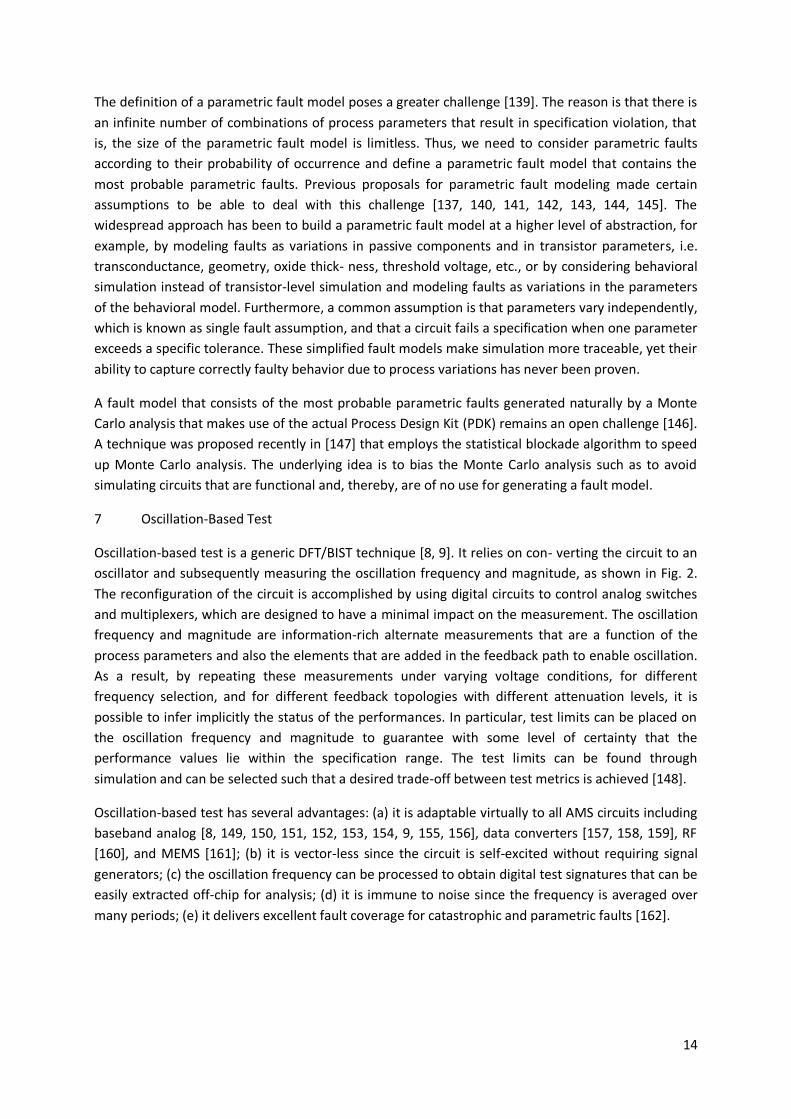
8 Data converters DFT and BIST
ADCs and DACs are characterized by dynamic specifications, such as total harmonic distortion (THD),
signal-to-noise ratio (SNR), signal-to-noise-and- distortion ratio (SNDR), etc., and static specifications,
such as differential non-linearity (DNL), integral non-linearity, offset, gain error, etc.
The standard approach to measure the dynamic specifications of an ADC is to apply a high-resolution
sinusoidal at the input and compute the Fast Fourier Transform (FFT) at the output. The resolution of
the sinusoidal typically needs to be at least two bits higher than the effective resolution of the ADC,
which poses a great design challenge for BIST implementation. A classical approach for generating
on-chip an analog sinusoidal is to employ a closed-loop oscillator that involves a highly selective
bandpass filter and a comparator [163, 164], as shown in Fig. 12. To improve the resolution of the
sinusoidal generators they can be combined with harmonic cancellation techniques [165, 166, 167,
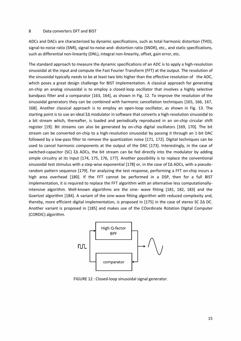
168]. Another classical approach is to employ an open-loop oscillator, as shown in Fig. 13. The
starting point is to use an ideal Σ∆ modulator in software that converts a high-resolution sinusoidal to
a bit stream which, thereafter, is loaded and periodically reproduced in an on-chip circular shift
register [19]. Bit streams can also be generated by on-chip digital oscillators [169, 170]. The bit
stream can be converted on-chip to a high-resolution sinusoidal by passing it through an 1-bit DAC
followed by a low-pass filter to remove the quantization noise [171, 172]. Digital techniques can be
used to cancel harmonic components at the output of the DAC [173]. Interestingly, in the case of
switched-capacitor (SC) Σ∆ ADCs, the bit stream can be fed directly into the modulator by adding
simple circuitry at its input [174, 175, 176, 177]. Another possibility is to replace the conventional
sinusoidal test stimulus with a step-wise exponential [178] or, in the case of Σ∆ ADCs, with a pseudo-
random pattern sequence [179]. For analyzing the test response, performing a FFT on-chip incurs a
high area overhead [180]. If the FFT cannot be performed in a DSP, then for a full BIST
implementation, it is required to replace the FFT algorithm with an alternative less computationally-
intensive algorithm. Well-known algorithms are the sine- wave fitting [181, 182, 183] and the
Goertzel algorithm [184]. A variant of the sine-wave fitting algorithm with reduced complexity and,
thereby, more efficient digital implementation, is proposed in [175] in the case of stereo SC Σ∆ DC.
Another variant is proposed in [185] and makes use of the COordinate Rotation DIgital Computer
(CORDIC) algorithm.
FIGURE 12 : Closed-loop sinusoidal signal generator.
16
FIGURE 13 : Open-loop sinusoidal signal generator based on Σ∆ bit streams.
The standard approach to measure the static specifications of an ADC is to apply a ramp at the input
and obtain the histogram of the number of occurrences of each code at the output. On-chip adaptive
ramp generators are proposed in [186, 187]. A ramp generator that relies on the oscillation-based
test principle is described in [158]. Alternatively, an exponential waveform can be employed in the
analysis [188, 189]. Another interesting approach is based upon first identifying and computationally
removing the source non-linearity and then accurately estimating the ADC static performances [190,
191, 166]. For analyzing the test response, it is required to store both the experimental and
reference histograms and use the DSP to perform the comparison. Efficient BIST implementations of
the histogram analysis are proposed in [192, 193]. For ADCs having a repetitive structure, such as
pipeline, cyclic, and successive approximation ADCs, we can also apply what is broadly known as
reduced code testing [194, 195, 196, 197]. Only a few codes need to be judiciously targeted and from
this information we can extrapolate the complete histogram.
Instead of targeting a functional BIST approach aiming at measuring directly the dynamic and static
specifications, it is also possible to consider a structural DFT approach where the aim is to obtain
measurements that re- veal important design parameters, such as the poles and settling errors of the
integrators in the case of Σ∆ ADCs [198]. A DFT approach proposed also specifically for pipeline ADCs
is to reconfigure consecutive pipeline stages to form Σ∆ modulators and then test instead the Σ∆
modulators through digital means [199]. A generic approach virtually applicable to any ADC is to
obtain information from process control monitors that are scattered across the die and use this
information to make judgements about the performances of the ADC [200].
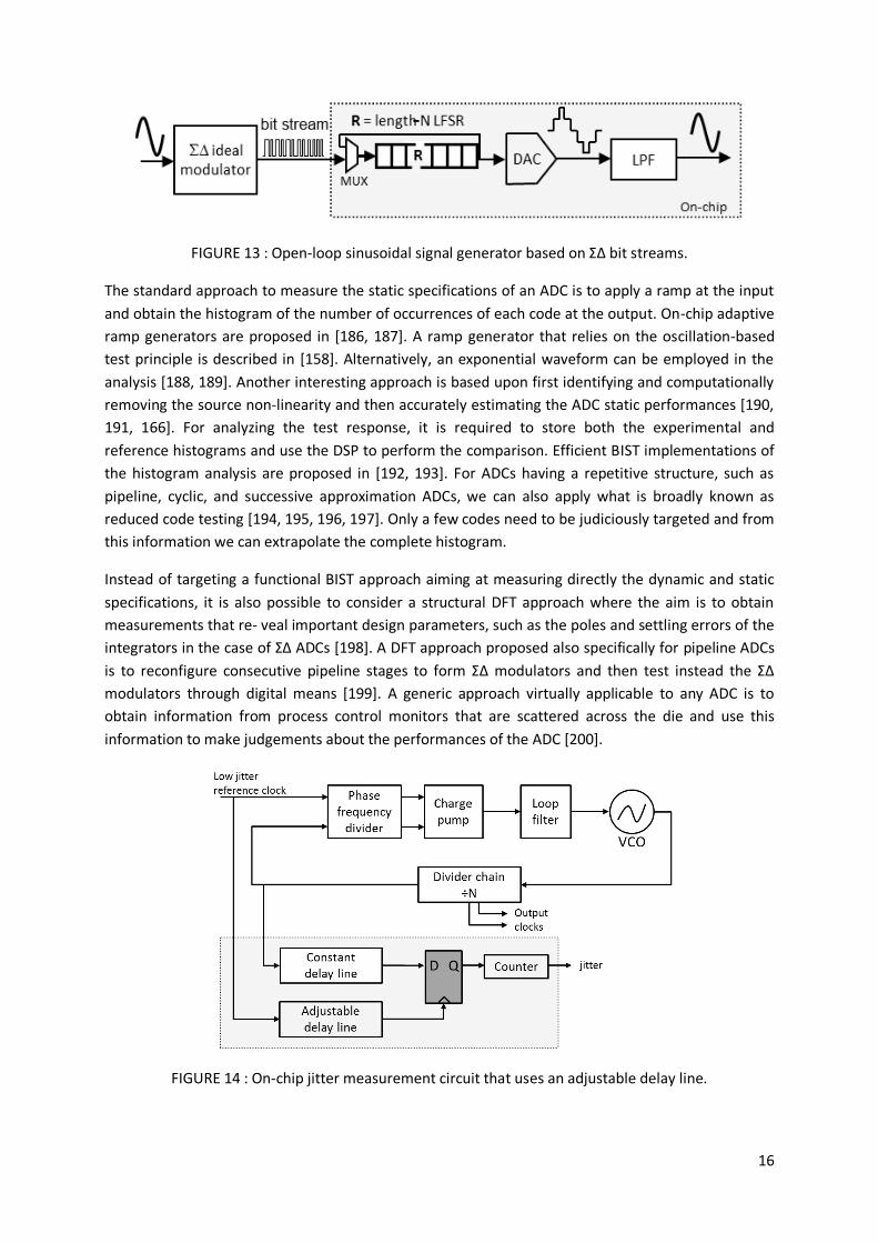
FIGURE 14 : On-chip jitter measurement circuit that uses an adjustable delay line.
17
Regarding a DAC, the standard approach to measure the dynamic specifications is to apply a digital
signal at the input that encodes a high-resolution sinusoidal and compute the FFT at the output. For a
BIST implementation the digital signal can be stored on-chip in a memory. However, for analyzing the
test response, performing the FFT on-chip [22, 23, 201, 202, 203] seems to be unavoidable, unlike in
the case of ADCs where there exist alternatives, as discussed above. The standard approach to
measure the static specifications is to apply a digital ramp at the input that contains all possible
digital codes and measure the output with a digital voltmeter. A BIST implementation is proposed in
[204].
Finally, in the case of SoCs that comprise a set of ADCs and DACs, a technique to test them altogether
in a fully digital set-up is proposed in [205].
9 PLL DFT and BIST
PLLs are fundamental building blocks for processors and communication systems since they are used
to synthesize clocks for data synchronization and to provide the frequency sources for up-conversion
and down-conversion in RF transceivers. The standard functional tests for PLLs include measuring the
loop gain, the lock time, defined as the time it takes for a PLL to acquire phase lock after an abrupt
change in the phase of its reference signal, and the lock range, defined by the minimum and
maximum frequencies that a PLL can lock to within its lock time.
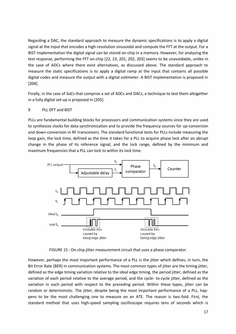
FIGURE 15 : On-chip jitter measurement circuit that uses a phase comparator.
However, perhaps the most important performance of a PLL is the jitter which defines, in turn, the
Bit Error Rate (BER) in communication systems. The most common types of jitter are the timing jitter,
defined as the edge timing variation relative to the ideal edge timing, the period jitter, defined as the
variation of each period relative to the average period, and the cycle- to-cycle jitter, defined as the
variation in each period with respect to the preceding period. Within these types, jitter can be
random or deterministic. The jitter, despite being the most important performance of a PLL, hap-
pens to be the most challenging one to measure on an ATE. The reason is two-fold. First, the
standard method that uses high-speed sampling oscilloscope requires tens of seconds which is
18
prohibitive for production testing. Second, as the PLL output is transferred off-chip, significant jitter is
added due to capacitive coupling to other signals on-chip and transmission line effects off-chip. In
addition, sampling the PLL output to extract the PLL jitter introduces even more jitter and, thus, the
measurement ends up being imprecise. For these reasons, measuring jitter exactly at the PLL output
using BIST is the recommended method, especially for multi-GHz PLLs that may have RMS jitter as
low 0.1-5 ps.
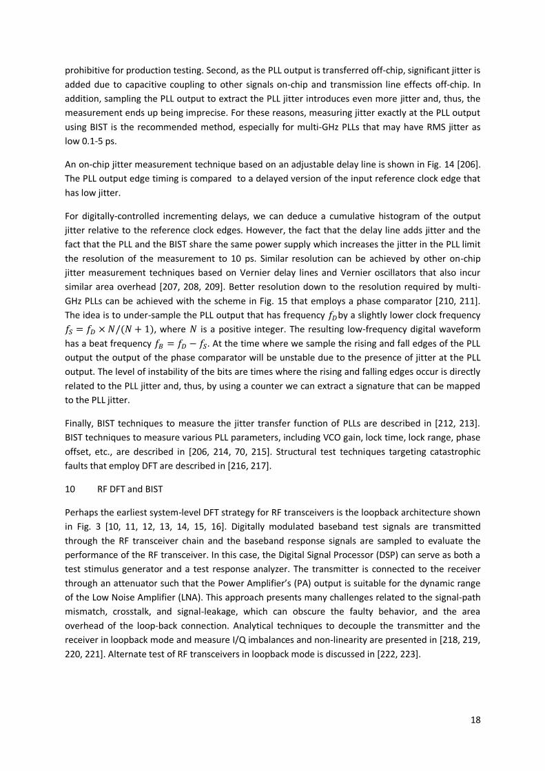
An on-chip jitter measurement technique based on an adjustable delay line is shown in Fig. 14 [206].
The PLL output edge timing is compared to a delayed version of the input reference clock edge that
has low jitter.
For digitally-controlled incrementing delays, we can deduce a cumulative histogram of the output
jitter relative to the reference clock edges. However, the fact that the delay line adds jitter and the
fact that the PLL and the BIST share the same power supply which increases the jitter in the PLL limit
the resolution of the measurement to 10 ps. Similar resolution can be achieved by other on-chip
jitter measurement techniques based on Vernier delay lines and Vernier oscillators that also incur
similar area overhead [207, 208, 209]. Better resolution down to the resolution required by multi-
GHz PLLs can be achieved with the scheme in Fig. 15 that employs a phase comparator [210, 211].
The idea is to under-sample the PLL output that has frequency 𝑓𝐷by a slightly lower clock frequency
𝑓𝑆 = 𝑓𝐷 × 𝑁/(𝑁 + 1), where 𝑁 is a positive integer. The resulting low-frequency digital waveform
has a beat frequency 𝑓𝐵 = 𝑓𝐷 − 𝑓𝑆. At the time where we sample the rising and fall edges of the PLL
output the output of the phase comparator will be unstable due to the presence of jitter at the PLL
output. The level of instability of the bits are times where the rising and falling edges occur is directly
related to the PLL jitter and, thus, by using a counter we can extract a signature that can be mapped
to the PLL jitter.
Finally, BIST techniques to measure the jitter transfer function of PLLs are described in [212, 213].
BIST techniques to measure various PLL parameters, including VCO gain, lock time, lock range, phase
offset, etc., are described in [206, 214, 70, 215]. Structural test techniques targeting catastrophic
faults that employ DFT are described in [216, 217].
10 RF DFT and BIST
Perhaps the earliest system-level DFT strategy for RF transceivers is the loopback architecture shown
in Fig. 3 [10, 11, 12, 13, 14, 15, 16]. Digitally modulated baseband test signals are transmitted
through the RF transceiver chain and the baseband response signals are sampled to evaluate the
performance of the RF transceiver. In this case, the Digital Signal Processor (DSP) can serve as both a
test stimulus generator and a test response analyzer. The transmitter is connected to the receiver
through an attenuator such that the Power Amplifier’s (PA) output is suitable for the dynamic range
of the Low Noise Amplifier (LNA). This approach presents many challenges related to the signal-path
mismatch, crosstalk, and signal-leakage, which can obscure the faulty behavior, and the area
overhead of the loop-back connection. Analytical techniques to decouple the transmitter and the
receiver in loopback mode and measure I/Q imbalances and non-linearity are presented in [218, 219,
220, 221]. Alternate test of RF transceivers in loopback mode is discussed in [222, 223].
19
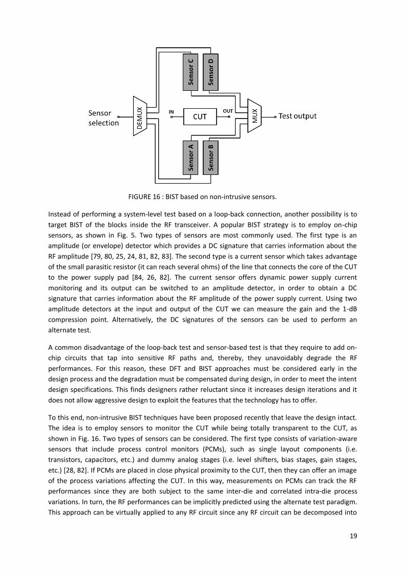
FIGURE 16 : BIST based on non-intrusive sensors.
Instead of performing a system-level test based on a loop-back connection, another possibility is to
target BIST of the blocks inside the RF transceiver. A popular BIST strategy is to employ on-chip
sensors, as shown in Fig. 5. Two types of sensors are most commonly used. The first type is an
amplitude (or envelope) detector which provides a DC signature that carries information about the
RF amplitude [79, 80, 25, 24, 81, 82, 83]. The second type is a current sensor which takes advantage
of the small parasitic resistor (it can reach several ohms) of the line that connects the core of the CUT
to the power supply pad [84, 26, 82]. The current sensor offers dynamic power supply current
monitoring and its output can be switched to an amplitude detector, in order to obtain a DC
signature that carries information about the RF amplitude of the power supply current. Using two
amplitude detectors at the input and output of the CUT we can measure the gain and the 1-dB
compression point. Alternatively, the DC signatures of the sensors can be used to perform an
alternate test.
A common disadvantage of the loop-back test and sensor-based test is that they require to add on-
chip circuits that tap into sensitive RF paths and, thereby, they unavoidably degrade the RF
performances. For this reason, these DFT and BIST approaches must be considered early in the
design process and the degradation must be compensated during design, in order to meet the intent
design specifications. This finds designers rather reluctant since it increases design iterations and it
does not allow aggressive design to exploit the features that the technology has to offer.
To this end, non-intrusive BIST techniques have been proposed recently that leave the design intact.
The idea is to employ sensors to monitor the CUT while being totally transparent to the CUT, as
shown in Fig. 16. Two types of sensors can be considered. The first type consists of variation-aware
sensors that include process control monitors (PCMs), such as single layout components (i.e.
transistors, capacitors, etc.) and dummy analog stages (i.e. level shifters, bias stages, gain stages,
etc.) [28, 82]. If PCMs are placed in close physical proximity to the CUT, then they can offer an image
of the process variations affecting the CUT. In this way, measurements on PCMs can track the RF
performances since they are both subject to the same inter-die and correlated intra-die process
variations. In turn, the RF performances can be implicitly predicted using the alternate test paradigm.
This approach can be virtually applied to any RF circuit since any RF circuit can be decomposed into
20
PCMs. The objective is to layout the PCMs in close physical proximity to the corresponding structures
in the RF circuit such that they are well- matched, in order to minimize uncorrelated intra-die process
variations.
However, variation-aware sensors cannot detect the presence of defects within the CUT since they
are not electrically connected to it. For the purpose of detecting defects, a second type of non-
intrusive sensor can be used that is based on temperature monitoring [224, 225, 226, 227, 228]. The
under- lying observation is that when the CUT operates, part of its electric power is dissipated, that
is, it is converted to heat due to the electrothermal Joule effect. The heat is mostly conducted
through the silicon substrate and the temperature in a sensing point near a dissipating device of the
CUT varies due to the power dissipated. The idea is that a defect will necessarily shift the dissipated
power which, in turn, will change the temperature profile close to the CUT. Thus, a temperature
sensor can capture this change to indicate the presence of the defect. The heat transfer has a low-
pass filter behavior with a time constant defined by the thermal path of a few tens of kHz. It appears
that only DC spectral component of the dissipated power induces a temperature variation near the
CUT. Nevertheless, since the dissipated power is the product of current flowing through the
dissipating device and the voltage across its terminals, this DC component carries information about
both the DC biasing and the RF amplitude of the signals. By extension, by measuring temperature
near a dissipating device of the CUT, we can monitor both the DC biasing point and RF operation of
the CUT.
11 Summary
We presented a concise overview of AMS testing and practical DFT and BIST techniques. The aim of
this chapter was to explain basic concepts and provide references where the interested reader can
find a more detailed presentation of the material as well as experiments that demonstrate these
concepts. Finally, we should note that, in general, we did not include traditional test approaches that
have been for many years the practice in industry. These approaches are presented in great detail in
[2, 4]. The aim was instead to collect in a comprehensive manner the latest research results in the
field and describe techniques that have a high potential and are close to industrialization.
21
12 Bibliography
[1] B. Vinnakota, Ed., Analog and Mixed-Signal Test. Prentice Hall, Englewood Cliffs, NJ, 1998.
[2] K. B. Schaub and J. Kelly, Production Testing of RF and System-on-a- Chip Devices for Wireless
Communications. Artech House, Inc., Norwood, MA, 2004.
[3] S. Sunter, “Mixed-signal testing and DfT,” in Advances in Electronic Testing: Challenges and
Methodologies, D. Gizopoulos, Ed. Springer, Dordrecht, The Netherlands, 2006, pp. 301–336.
[4] M. Burns and G. W. Roberts, An Introduction to Mixed-Signal IC Test and Measurement.
Oxford University Press, 2nd ed., New York, NY, 2011.
[5] F. Poehl, F. Demmerle, J. Alt, and J. Obermeir, “Production test challenges for highly
integrated mobile phone SoCs,” in Proc. IEEE European Test Symposium, 2010, pp. 17–22.
[6] IEEE Standard for Test Access Port and Boundary-Scan Architecture, IEEE Std. 1149.1-2013.
[7] IEEE Standard for Mixed-Signal Test Bus, IEEE Std. 1149.4-2010.
[8] K. Arabi and B. Kaminska, “Oscillation-test strategy for analog and mixed-signal integrated
circuits,” in Proc. IEEE VLSI Test Symposium, 1996, pp. 476 – 482.
[9] G. Huertas, D. V´azquez, A. Rueda, and J. L. Huertas, Oscillation-Based Test in Mixed-Signal
Circuits. Springer, Dordrecht, The Netherlands, 2006.
[10] M. Jarwala, L. Duy, and M. S. Heutmaker, “End-to-end test strategy for wireless systems,” in
Proc. IEEE International Test Conference, 1995, pp. 940–946.
[11] M. S. Heutmaker and D. K. Le, “An architecture for self-test of a wire- less communication
system,” IEEE Communications Magazine, vol. 37, no. 6, pp. 98–102, 1999.
[12] D. Lupea, U. Pursche, and H.-J. Jentschel, “RF-BIST: loopback spectral signature analysis,” in
Proc. Design, Automation, & Test in Europe Conference, 2003, pp. 478–483.
[13] S. Ozev and C. Olgaard, “Wafer-level RF test and DfT for VCO modulating transceiver
architectures,” in Proc. IEEE VLSI Test Symposium, 2004, pp. 217–222.
[14] J.-S. Yoon and W. R. Eisenstadt, “Embedded loopback test for RF ICs,” IEEE Transactions on
Instrumentation and Measurement, vol. 54, no. 5, pp. 1715–1720, 2005.
[15] A. Valdes-Garcia, J. Silva-Martinez, and E. Sanchez-Sinencio, “On-chip testing techniques for
RF wireless transceivers,” IEEE Design & Test of Computers, vol. 23, no. 4, pp. 268–277, 2006.
[16] J. J. Dabrowski and R. M. Ramzan, “Built-in loopback test for IC RF transceivers,” IEEE
Transactions on Very Large Scale Integration (VLSI) Systems, vol. 18, no. 6, pp. 933–946, 2010.
[17] B. R. Veillette and G. W. Roberts, “A built-in self-test strategy for wire- less communication
systems,” in Proc. IEEE International Test Conference, 1995, pp. 930–939.

22
[18] X. Haurie and G. W. Roberts, “Arbitrary-precision signal generation for mixed-signal built-in-
self-test,” IEEE Transactions on Circuits and Systems-II: Analog and Digital Signal Processing, vol. 45,
no. 11, pp. 1425–32, 1998.
[19] B. Dufort and G. W. Roberts, “On-chip analog signal generation for mixed-signal built-in self-
test,” IEEE Journal of Solid-State Circuits, vol. 34, no. 3, pp. 318–30, 1999.
[20] M. M. Hafed, N. Abaskharoun, and G. W. Roberts, “A 4-GHz effective sample rate integrated
test core for analog and mixed-signal circuits,” IEEE Journal of Solid-State Circuits, vol. 37, no. 4, pp.
499–514, 2002.
[21] M. M. Hafed and G. W. Roberts, “Techniques for high-frequency integrated test and
measurement,” IEEE Transactions on Instrumentation and Measurement, vol. 52, no. 6, pp. 1780–
1786, 2003.
[22] M. G. Mendez-Rivera, A. Valdes-Garcia, J. Silva-Martinez, and E. Sanchez-Sinencio,
“An on-chip spectrum analyzer for analog built-in testing,” Journal of Electronic Testing: Theory and
Applications, vol. 21, no. 3, pp. 205–219, 2005.
[23] A. Valdes-Garcia, F. A.-L. Hussien, J. Silva-Martinez, and E. Sanchez- Sinencio, “An integrated
frequency response characterization system with a digital interface for analog testing,” IEEE Journal
of Solid-State Circuits, vol. 41, no. 10, pp. 2301–2313, 2006.
[24] A. Valdes-Garcia, R. Venkatasubramanian, J. Silva-Martinez, and E. Sanchez-Sinencio, “A
broadband CMOS amplitude detector for on-chip RF measurements,” IEEE Transactions on
Instrumentation and Measurement, vol. 57, no. 7, pp. 1470–1477, 2008.
[25] Y.-C. Huang, H.-H. Hsieh, and L.-H. Lu, “A built-in self-test technique for RF low-noise
amplifiers,” IEEE Transactions on Microwave Theory and Techniques, vol. 56, no. 2, pp. 1035–1042,
2008.
[26] M. Cimino, H. Lapuyade, Y. Deval, T. Taris, and J.-B. Begueret, “De- sign of a 0.9V 2.45 GHz
self-testable and reliability-enhanced CMOS LNA,” IEEE Journal of Solid-State Circuits, vol. 43, no. 5,
pp. 1187– 1194, 2008.
[27] D. Mannath, D. Webster, V. Montano-Martinez, D. Cohen, S. Kush, T. Ganesan, and A.
Sontakke, “Structural approach for built-in tests in RF devices,” in Proc. IEEE International Test
Conference, 2010, paper 14.1.
[28] L. Abdallah, H.-G. Stratigopoulos, S. Mir, and C. Kelma, “Experiences with non-intrusive
sensors for RF built-in test,” in Proc. IEEE International Test Conference, 2012, paper 17.1.
[29] J. L. Huertas, A. Rueda, and D. Vasquez, “Testable switched-capacitor filters,” IEEE Journal of
Solid-State Circuits, vol. 28, no. 7, pp. 719–724, 1993.
[30] A. Chatterjee, “Concurrent error detection and fault-tolerance in lin- ear analog circuits using
continuous checksums,” IEEE Transactions on Very Large Scale Integration (VLSI) Systems, vol. 1, no.
2, pp. 138–150, 1993.
23
[31] B. Vinnakota and R. Harjani, “The design of analog self-checking cir- cuits,” in Proc. IEEE
International Conference on VLSI Design, 1994, pp. 67–70.
[32] V. Kolarik, S. Mir, M. Lubaszewski, and B. Courtois, “Analog check- ers with absolute and
relative tolerances,” IEEE Transactions on Computer-Aided Design of Integrated Circuits and
Systems, vol. 14, no. 5, pp. 607–612, 1995.
[33] C.-L. Wey, S. Krishnan, and S. Sahli, “Test generation and concurrent error detection in
current-mode A/D converters,” IEEE Transactions on Computer-Aided Design of Integrated Circuits
and Systems, vol. 14, no. 10, pp. 1291–1298, 1995.
[34] A. Laknaur and H. Wang, “A methodology to perform online self-testing for field-
programmable analog array circuits,” IEEE Transactions on Instrumentation and Measurement, vol.
54, no. 5, pp. 1751–1760, 2005.
[35] E. Simeu, A. Peters, and I. Rayane, “Automatic design of optimal con- current fault detector
for linear analog systems,” in Proc. IEEE Inter- national Symposium on Fault-Tolerant Computing,
1999, pp. 184–191.
[36] K.-J. Lee, W.-C. Wang, and K.-S. Huang, “A current-mode testable de- sign of operational
transconductance amplifier-capacitor filters,” IEEE Transactions on Circuits and Systems-II: Analog
and Digital Signal Processing, vol. 46, no. 4, pp. 401–413, 1999.
[37] M. Lubaszewski, S. Mir, V. Kolarik, C. Nielsen, and B. Courtois, “De- sign of self-checking fully
differential circuits and boards,” IEEE Trans- actions on Very Large Scale Integration (VLSI) Systems,
vol. 8, no. 2, pp. 113–128, 2000.
[38] S. Ozev and A. Orailoglu, “Design of concurrent test hardware for linear analog circuits with
constained hardware overhead,” IEEE Transactions on Very Large Scale Integration (VLSI) Systems,
vol. 12, no. 7, pp. 756– 765, 2004.
[39] H.-G. D. Stratigopoulos and Y. Makris, “Concurrent detection of erroneous responses in linear
analog circuits,” IEEE Transactions on Computer-Aided Design of Integrated Circuits and Systems,
vol. 25, no. 5, pp. 878–891, 2006.
[40] H.-G. D. Stratigopoulos and Y. Makris, “An adaptive checker for the fully differential analog
code,” IEEE Journal of Solid-State Circuits, vol. 41, no. 6, pp. 1421–1429, 2006.
[41] V. Natarajan, G. Srinivasan, and A. Chatterjee, “On-line error detection in wireless RF
transmitters using real-time streaming data,” in Proc. IEEE International On-Line Testing Symposium,
2006, pp. 159 – 164.
[42] T. Das, A. Gopalan, C. Washburn, and P. R. Mukund, “Self-calibration of input-match in RF
front-end circuitry,” IEEE Transactions on Circuits and Systems-II: Express Briefs, vol. 52, no. 12, pp.
821–825, 2005.
[43] S. Bou-Sleiman and M. Ismail, “Enabling efficient built-in-self- calibration for RFICs,” in Proc.
IEEE International Conference on Elec- tronics, Circuits and Systems, 2011, pp. 492–495.
24
[44] A. Goyal, M. Swaminathan, A. Chatterjee, D. Howard, and J. Cressler, “A new self-healing
methodology for RF amplifier circuits based on os- cillation principles,” IEEE Transactions on Very
Large Scale Integration (VLSI) Systems, vol. 20, no. 10, pp. 1835 –1848, 2012.
[45] C. Maxey, G. Creech, S. Raman, J. Rockway, K. Groves, T. Quach, L. Orlando, and A.
Mattamana, “Mixed-signal SoCs with in situ self- healing circuitry,” IEEE Design & Test of Computers,
vol. 29, no. 6, pp. 27–39, 2012.
[46] S. Bowers, K. Sengupta, B. Parker, and A. Hajimiri, “Integrated self- healing for mm-wave
power amplifiers,” IEEE Transactions on Microwave Theory and Techniques, vol. 61, no. 3, pp. 352–
363, 2013.
[47] N. Sen and R. Saeks, “Fault diagnosis for linear systems via multifrequency measurements,”
IEEE Transactions on Circuits and Systems, vol. 26, no. 7, pp. 457–465, 1979.
[48] H. Dai and M. Souders, “Time-domain testing strategies and fault diagnosis for analog
systems,” IEEE Transactions on Instrumentation and Measurement, vol. 39, no. 1, pp. 157–162, 1990.
[49] M. Slamani and B. Kaminska, “Analog circuit fault diagnosis based on sensitivity computation
and functional testing,” IEEE Design & Test of Computers, vol. 9, no. 1, pp. 30–39, 1992.
[50] S. S. Somayajula, E. Sanchez-Sinencio, and J. P. de Gyvez, “Analog fault diagnosis based on
ramping power supply current signature clusters,” IEEE Transactions on Circuits and Systems-II:
Analog and Dig- ital Signal Processing, vol. 43, no. 10, pp. 703–712, 1996.
[51] R. Spina and S. Upadhyaya, “Linear circuit fault diagnosis using neuromorphic analyzers,” IEEE
Transactions on Circuits and Systems-II: Analog and Digital Signal Processing, vol. 44, no. 3, pp. 188–
196, 1997.
[52] S. Chakrabarti, S. Cherubal, and A. Chatterjee, “Fault diagnosis for mixed-signal electronic
systems,” in Proc. IEEE Aerospace Conference, 1999, pp. 169–179.
[53] E. F. Cota, M. Negreiros, L. Carro, and M. Lubaszewski, “A new adaptive analog test and
diagnosis system,” IEEE Transactions on Instrumentation and Measurement, vol. 49, no. 2, pp. 223–
227, 2000.
[54] M. Aminian and F. Aminian, “A modular fault-diagnosis system for analog electronic circuits
using neural networks with wavelet transform as a preprocessor,” IEEE Transactions on
Instrumentation and Measurement, vol. 56, no. 5, pp. 1546–1554, 2007.
[55] E. S. Erdogan, S. Ozev, and P. Cauvet, “Diagnosis of assembly failures for system-in-package
RF tuners,” in IEEE International Symposium on Circuits and Systems, 2008, pp. 2286–2289.
[56] K. Huang, H.-G. Stratigopoulos, and S. Mir, “Fault diagnosis of analog circuits based on
machine learning,” in Proc. Design, Automation & Test in Europe Conference, 2010, pp. 1761–1766.
[57] S. Krishnan, K. D. Doornbos, R. Brand, and H. G. Kerkhoff, “Block level bayesian diagnosis of
analogue electronic circuits,” in Proc. Design, Automation & Test in Europe Conference, 2010, pp.
1767–1772.
25
[58] H. Hashempour, J. Dohmen, B. Tasic, B. Kruseman, C. Hora, M. Beurden, and Y. Xing, “Test
time reduction in Analogue/Mixed-signal de- vices by defect oriented testing: An industrial example,”
in Proc. Design, Automation & Test in Europe Conference, 2011.
[59] K. Huang, H.-G. Stratigopoulos, S. Mir, C. Hora, Y. Xing, and B. Kruseman, “Diagnosis of local
spot defects in analog circuits,” IEEE Trans- actions on Instrumentation and Measurement, vol. 61,
no. 10, pp. 2701– 2712, 2012.
[60] P. N. Variyam, S. Cherubal, and A. Chatterjee, “Prediction of analog performance parameters
using fast transient testing,” IEEE Transactions on Computer-Aided Design of Integrated Circuits
and Systems, vol. 21, no. 3, pp. 349–361, 2002.
[61] S. S. Akbay, A. Halder, A. Chatterjee, and D. Keezer, “Low-cost test of embedded
RF/Analog/Mixed-signal circuits in SOPs,” IEEE Transactions on Advanced Packaging, vol. 27, no. 2,
pp. 352–363, 2004.
[62] R. Voorakaranam, S. S. Akbay, S. Bhattacharya, S. Cherubal, and A. Chatterjee, “Signature
testing of analog and RF circuits: Algorithms and methodology,” IEEE Transactions on Circuits and
Systems - I, vol. 54, no. 5, pp. 1018–1031, 2007.
[63] R. Voorakaranam, R. Newby, S. Cherubal, B. Cometta, T. Kuehl, D. Majernik, and A.
Chatterjee, “Production deployment of a fast transient testing methodology for analog circuits: Case
study and results,” in IEEE International Test Conference, 2003, pp. 1174–1181.
[64] R. Voorakaranam, S. Cherubal, and A. Chatterjee, “A signature test framework for rapid
production testing of RF circuits,” in Proc. Design, Automation and Test in Europe Conference, 2002,
pp. 186–191.
[65] S. Cherubal, R. Voorakaranam, A. Chatterjee, J. Mclaughlin, J. L. Smith, and D. M. Majernik,
“Concurrent RF test using optimized modulated RF stimuli,” in IEEE International Conference on VLSI
Design, 2004, pp. 1017–1022.
[66] A. Halder and A. Chatterjee, “Low-cost alternate EVM test for wireless receiver systems,” in
Proc. IEEE VLSI Test Symposium, 2005, pp. 255– 260.
[67] S. Ellouz, P. Gamand, C. Kelma, B. Vandewiele, and B. Allard, “Combining internal probing
with artficial neural networks for optimal RFIC testing,” in Proc. IEEE International Test Conference,
2006, pp. 4.3.1– 4.3.9.
[68] S. Goyal, A. Chatterjee, and M. Purtell, “A low-cost test methodology for dynamic
specification testing of high-speed data converters,” Journal of Electronic Testing: Theory and
Applications, vol. 23, no. 1, pp. 95– 106, 2006.
[69] S. Kook, A. Banerjee, and A. Chatterjee, “Dynamic specification testing and diagnosis of high-
precision sigma-delta ADCs,” IEEE Design & Test of Computers, vol. 30, no. 4, pp. 36–48, 2013.
[70] S.-W. Hsiao, X. Wang, and A. Chatterjee, “Analog sensor based testing of phase-locked loop
dynamic performance parameters,” in Proc. IEEE Asian Test Symposium, 2013, pp. 50–55.

26
[71] V. Natarajan, S. Bhattacharya, and A. Chatterjee, “Alternate electrical tests for extracting
mechanical parameters of MEMS accelerometer sensors,” in Proc. IEEE VLSI Test Symposium, 2006,
pp. 192–199.
[72] H.-G. D. Stratigopoulos and Y. Makris, “Non-linear decision boundaries for testing analog
circuits,” IEEE Transactions on Computer-Aided De- sign of Integrated Circuits and Systems, vol. 24,
no. 11, pp. 1760–1773, 2005.
[73] H.-G. Stratigopoulos and Y. Makris, “Error moderation in low-cost machine-learning-based
Analog/RF testing,” IEEE Transactions on Computer-Aided Design of Integrated Circuits and
Systems, vol. 27, no. 2, pp. 339–351, 2008.
[74] H. Ayari, F. Azais, S. Bernard, M. Compte, M. Renovell, V. Kerzerho, O. Potin, and C. Kelma,
“Smart selection of indirect parameters for dc- based alternate RF IC testing,” in Proc. IEEE VLSI Test
Symposium, 2012, pp. 19–24.
[75] M. J. Barragan and G. Leger, “Efficient selection of signatures for analog/rf alternate test,” in
Proc. IEEE European Test Symposium, 2013.
[76] D. E. Goldberg, Genetic Algorithms in Search, Optimization, and Machine Learning. Addison-
Wesley, Boston, MA, 1989.
[77] P. Pudil, J. Novovicova, and J. Kittler, “Floating search methods in feature selection,” Pattern
Recognition Letters, vol. 15, pp. 1119–1125, 1994.
[78] S. S. Akbay, J. L. Torres, J. M. Rumer, A. Chatterjee, and J. Amts- field, “Alternate test of RF
front ends with IP constraints: Frequency domain test generation and validation,” in Proc. IEEE
International Test Conference, 2006, pp. 4.4.1–4.4.10.
[79] S. S. Akbay and A. Chatterjee, “Built-in test of RF components using mapped feature
extraction sensors,” in IEEE VLSI Test Symposium, 2005, pp. 243–248.
[80] S. Bhattacharya and A. Chatterjee, “A DFT approach for testing embedded systems using DC
sensors,” IEEE Design & Test of Computers, vol. 23, no. 6, pp. 464–475, 2006.
[81] P. F. D. Mota and J. M. D. Silva, “A true power detector for RF PA built-in calibration and
testing,” in Proc. Design, Automation, & Test in Europe Conference, 2011, pp. 1–6.
[82] L. Abdallah, H.-G. Stratigopoulos, S. Mir, and C. Kelma, “RF front-end test using built-in
sensors,” IEEE Design & Test of Computers, vol. 28, no. 6, pp. 76–84, 2011.
[83] C. Zhang, R. Gharpurey, and J. A. Abraham, “Built-in self-test of RF subsystems with
integrated sensors,” Journal of Electronic Testing: Theory and Applications, vol. 28, no. 5, pp. 557–
569, 2012.
[84] A. Gopalan, M. Margala, and P. R. Mukund, “A current based self- test methodology for RF
front-end circuits,” Microelectronics Journal, vol. 36, no. 12, pp. 1091–1102, 2005.
[85] H.-G. Stratigopoulos, S. Mir, E. Acar, and S. Ozev, “Defect filter for alternate RF test,” in Proc.
IEEE European Test Symposium, 2009, pp. 101–106.
27
[86] C. Y. Pan and K. T. Cheng, “Test generation for linear time-invariant analog circuits,” IEEE
Transactions on Circuits and Systems-II: Analog and Digital Signal Processing, vol. 46, no. 5, pp. 554–
564, 1999.
[87] W. M. Lindermeir, H. E. Graeb, and K. J. Antreich, “Analog testing by characteristic
observation inference,” IEEE Transactions on Computer- Aided Design of Integrated Circuits and
Systems, vol. 18, no. 9, pp. 1353–1368, 1999.
[88] P. N. Variyam and A. Chatterjee, “Specification-driven test generation for analog circuits,”
IEEE Transactions on Computer-Aided Design of Integrated Circuits and Systems, vol. 19, no. 10, pp.
1189–1201, 2000.
[89] V. Stopjakova, P. Malosek, D. Micusik, M. Matej, and M. Margala, “Classification of defective
analog integrated circuits using artificial neural networks,” Journal of Electronic Testing: Theory and
Applications, vol. 20, pp. 25–37, 2004.
[90] N. Cristianini and J. Shawe-Taylor, Support Vector Machines and Other Kernel-Based Learning
Methods. Cambridge, New York, NY, 2000.
[91] L. Rokach and O. Maimon, “Top-down induction of decision trees classifiers a survey,” IEEE
Transactions on Systems, Man, and Cybernetics- Part C: Applications and Reviews, vol. 35, no. 46,
pp. 476–487, 2005.
[92] R. Parekh, J. Yang, and V. Honavar, “Constructive neural-network learning algorithms for
pattern classification,” IEEE Transactions on Neural Networks, vol. 11, no. 2, pp. 436–451, 2000.
[93] N. Burgess, “A constructive algorithm that converges for real-valued input patterns,”
International Journal of Neural Systems, vol. 5, no. 1, pp. 59–66, 1994.
[94] D. Maliuk, H.-G. Stratigopoulos, H. Huang, and Y. Makris, “Analog neural network design for
RF built-in self-test,” in Proc. IEEE International Test Conference, 2010, paper 23.2.
[95] H.-G. Stratigopoulos and S. Mir, “Adaptive alternate analog test,” IEEE Design & Test of
Computers, vol. 29, no. 4, pp. 71–79, 2012.
[96] H. Ayari, F. Azais, S. Bernard, M. Compte, V. Kerzerho, O. Potin, and M. Renovell, “Making
predictive analog/RF alternate test strategy independent of training set size,” in Proc. IEEE
International Test Conference, 2012, paper 10.1.
[97] T. M. Souders and G. N. Stenbakken, “A comprehensive approach for modeling and testing
analog and mixed-signal devices,” in Proc. IEEE International Test Conference, 1990, pp. 169–176.
[98] G. N. Stenbakken and T. M. Souders, “Developing linear error models for analog devices,”
IEEE Transactions on Instrumentation and Mea- surement, vol. 43, no. 2, pp. 157–163, 1994.
[99] G. N. Stenbakken and T. M. Souders, “Test-point selection and testability measures via QR
factorization of linear models,” IEEE Transactions on Instrumentation and Measurement, vol. IM-36,
no. 2, pp. 406–410, 1987.
28
[100] J. V. Spaandonk and T. A. M. Kevenaar, “Iterative test-point selection for analog circuits,” in
Proc. IEEE VLSI Test Symposium, 1996, pp. 66–71.
[101] A. Wrixon and M. P. Kennedy, “A rigorous exposition of the LEMMA method for analog and
mixed-signal testing,” IEEE Transactions on Instrumentation and Measurement, vol. 48, no. 5, pp.
978–985, 1999.
[102] L. Milor and A. L. Sangiovanni-Vincentelli, “Minimizing production test time to detect faults in
analog circuits,” IEEE Transactions on Computer-Aided Design of Integrated Circuits and Systems,
vol. 13, no. 6, pp. 796–813, 1994.
[103] G. Devarayanadurg, M. Soma, P. Goteti, and S. D. Huynh, “Test set selection for structural
faults in analog IC’s,” IEEE Transactions on Computer-Aided Design of Integrated Circuits and
Systems, vol. 18, no. 7, pp. 1026–1039, 1999.
[104] S. D. Huss and R. S. Gyurcsik, “Optimal ordering of analog integrated circuit tests to minimize
test time,” in ACM/IEEE Design Automation Conference, 1991, pp. 494–499.
[105] J. B. Brockman and S. W. Director, “Predictive subset testing: Optimizing IC parametric
performance testing for quality, cost, and yield,” IEEE Transactions on Semiconductor Manufacturing,
vol. 2, no. 3, pp. 104–113, 1989.
[106] S. Biswas, P. Li, R. D. Blanton, and L. Pileggi, “Specification test compaction for analog circuits
and MEMS,” in Proc. Design, Automation & Test in Europe Conference, 2005, pp. 164–169.
[107] S. Biswas and R. D. Blanton, “Statistical test compaction using binary decision trees,” IEEE
Design & Test of Computers, vol. 23, no. 6, pp. 452–462, 2006.
[108] H.-G. Stratigopoulos, P. Drineas, M. Slamani, and Y. Makris, “RF specification test compaction
using learning machines,” IEEE Transactions on Very Large Scale Integration (VLSI) Systems, vol. 18,
no. 6, pp. 998–1002, 2010.
[109] A. A. Mutlu and M. Rahman, “Statistical methods for the estimation of process variation
effects on circuit operation,” IEEE Transactions on Electronics Packaging Manufacturing, vol. 28, no.
4, pp. 364–375, 2005.
[110] T. McConaghy and G. G. E. Gielen, “Template-free symbolic performance modeling of analog
circuits via canonical-form functions and genetic programming,” IEEE Transactions on Computer-
Aided Design of Integrated Circuits and Systems, vol. 28, no. 8, pp. 1162–1175, 2009.
[111] E. Yilmaz and S. Ozev, “Fast and accurate DPPM computation using model based filtering,” in
Proc. IEEE European Test Symposium, 2011, pp. 165–170.
[112] A. Bounceur, S. Mir, E. Simeu, and L. Rolindez, “Estimation of test metrics for the
optimisation of analogue circuit testing,” Journal of Electronic Testing: Theory and Applications, vol.
23, no. 6, pp. 471– 484, 2007.
[113] H.-G. Stratigopoulos, S. Mir, and A. Bounceur, “Evaluation of analog/RF test measurements at
the design stage,” IEEE Transactions on Computer-Aided Design of Integrated Circuits and
Systems, vol. 28, no. 4, pp. 582–590, 2009.
29
[114] S. Mukhopadhyay, “A generic data-driven nonparametric framework for variability analysis of
integrated circuits in nanometer technologies,” IEEE Transactions on Computer-Aided Design of
Integrated Circuits and Systems, vol. 28, no. 7, pp. 1038–1046, 2009.
[115] A. Bounceur, S. Mir, and H.-G. Stratigopoulos, “Estimation of analog parametric test metrics
using copulas,” IEEE Transactions on Computer-Aided Design of Integrated Circuits and Systems,
vol. 30, no. 9, pp. 1400–1410, 2011.
[116] C. Wegener and M. P. Kennedy, “Test development through defect and test escape level
estimation for data converters,” Journal of Electronic Testing: Theory and Applications, vol. 22, no. 4-
6, pp. 313–324, 2006.
[117] H.-G. Stratigopoulos, “Test metrics model for analog test development,” IEEE Transactions
on Computer-Aided Design of Integrated Circuits and Systems, vol. 31, no. 7, pp. 1116–1128,
2012.
[118] H.-G. Stratigopoulos, P. Faubet, Y. Courant, and M. Firas, “Multidimensional analog test
metrics estimation using extreme value theory and statistical blockade,” in ACM/IEEE Design
Automation Conference, 2013.
[119] A. Singhee and R. A. Rutenbar, “Statistical blockade: Very fast statistical simulation and
modeling of rare circuit events and its application to memory design,” IEEE Transactions on
Computer-Aided Design of Integrated Circuits and Systems, vol. 28, no. 8, pp. 1176–1189, 2009.
[120] S. Coles, An Introduction to Statistical Modeling of Extreme Values, ser. Springer Series in
Statistics. Springer, London, UK, 2001.
[121] C. M. Kurker, J. J. Paulos, R. S. Gyurcsik, and J.-C. Lu, “Hierarchical yield estimation of large
analog integrated circuits,” IEEE Journal of Solid-State Circuits, vol. 28, no. 3, pp. 203–209, 1993.
[122] M. Dubois, H.-G. Stratigopoulos, and S. Mir, “Hierarchical parametric test metrics estimation:
A Σ∆ converter BIST case study,” in Proc. IEEE International Conference on Computer Design, 2009,
pp. 78–83.
[123] L. Milor and V. Visvanathan, “Detection of catastrophic faults in ana- log integrated circuits,”
IEEE Transactions on Computer-Aided Design, vol. 8, no. 2, pp. 114–130, 1989.
[124] S. J. Tsai, “Test vector generation for linear analog devices,” in Proc. IEEE International Test
Conference, 1991, pp. 592–7.
[125] M. Slamani and B. Kaminska, “Multifrequency analysis of faults in analog circuits,” IEEE
Design & Test of Computers, vol. 12, no. 2, pp. 70–80, 1995.
[126] S. Mir, M. Lubaszewski, and B. Courtois, “Fault-based ATPG for linear analog circuits with
minimal size multifrequency test sets,” Journal of Electronic Testing: Theory and Applications, vol. 9,
no. 1-2, pp. 43–57, 1996.
[127] Z. Wang, G. Gielen, and W. Sansen, “Probabilistic fault detection and the selection of
measurements for analog integrated circuits,” IEEE Transactions on Computer-Aided Design of
Integrated Circuits and Systems, vol. 17, no. 9, pp. 862–872, 1998.

30
[128] S. D. Huynh, S. Kim, M. Soma, and J. Zhang, “Automatic analog test signal generation using
multifrequency analysis,” IEEE Transactions on Circuits and Systems-II: Analog and Digital Signal
Processing, vol. 46, no. 5, pp. 565–576, 1999.
[129] K. Saab, N. B. Hamida, and B. Kaminska, “Closing the gap between analog and digital testing,”
IEEE Transactions on Computer-Aided De- sign of Integrated Circuits and Systems, vol. 20, no. 2, pp.
307–314, 2001.
[130] S. Bhunia and K. Roy, “Dynamic supply current testing of analog cir- cuits using wavelet
transform,” in Proc. IEEE VLSI Test Symposium, 2002, pp. 302–307.
[131] Y. Joannon, V. Beroulle, C. Robach, S. Tedjini, and J.-L. Carbonero, “Decreasing test
qualification time in AMS and RF systems,” IEEE Design & Test of Computers, vol. 25, no. 1, pp. 29 –
37, 2008.
[132] A. Meixner and W. Maly, “Fault modeling for the testing of mixed integrated circuits,” in
Proc. IEEE International Test Conference, 1991, pp. 564–572.
[133] M. Soma, “An experimental approach to analog fault models,” in Proc. IEEE Custom
Integrated Circuits Conference, 1991, paper 13.6.
[134] M. Sachdev and B. Atzema, “Industrial relevance of analog IFA: A fact or a fiction,” in Proc.
IEEE International Test Conference, 1995, pp. 61–70.
[135] C. Sebeke, J. Teixeira, and M. Ohletz, “Automatic fault extraction and simulation of layout
realistic faults for integrated analogue circuits,” in Proc. IEEE European Design & Test Conference,
1995, pp. 464–468.
[136] A. Milne, D. Taylor, J. Saunders, and A. Talbot, “Generation of optimised fault lists for
simulation of analogue circuits and test programs,” IEE Proceedings, vol. 146, no. 6, pp. 355–360,
1999.
[137] E. Acar and S. Ozev, “Defect-oriented testing of RF circuits,” IEEE Transactions on Computer-
Aided Design of Integrated Circuits and Systems, vol. 27, no. 5, pp. 920–931, 2008.
[138] E. Yilmaz, G. Shofner, L. Winemberg, and S. Ozev, “Fault analysis and simulation of large
scale industrial mixed-signal circuits,” in Proc. Design, Automation & Test in Europe Conference,
2013, pp. 565–570.
[139] M. Soma, “Challenges in analog and mixed-signal fault models,” IEEE Circuits & Devices
Magazine, vol. 12, no. 1, pp. 16–19, 1996.
[140] N. Nagi and J. A. Abraham, “Hierarchical fault modeling for analog and mixed-signal circuits,”
in Proc. IEEE VLSI Test Symposium, 1992, pp. 96–101.
[141] R. Voorakaranam, S. Chakrabarti, J. Hoo, A. G. ans S. Cherubal, and A. Chatterjee,
“Hierarchical specification-driven analog fault modeling for efficient fault simulation and diagnosis,”
in Proc. IEEE International Test Conference, 1997, paper 36.1.
31
[142] S. Sunter and N. Nagi, “Test metrics for analog parametric faults,” in Proc. IEEE VLSI Test
Symposium, 1999, pp. 226–234.
[143] K. Saab, N. Ben-Hamida, and B. Kaminska, “Parametric fault simula- tion and test vector
generation,” in Proc. Design, Automation & Test in Europe Conference, 2000, pp. 650–656.
[144] J. Savir and Z. Guo, “Test limitations of parametric faults in analog test,” IEEE Transactions on
Instrumentation and Measurement, vol. 52, no. 5, pp. 1444–1454, 2003.
[145] H.-C. Hong, “A static linear behavior analog fault model for switched- capacitor circuits,” IEEE
Transactions on Computer-Aided Design of Integrated Circuits and Systems, vol. 31, no. 4, pp. 597–
609, 2012.
[146] M. B. Yelten, S. Natarajan, B. Xue, and P. Goteti, “Scalable and efficient analog parametric
fault identification,” in Proc. IEEE/ACM International Conference on Computer-Aided Design, 2013,
pp. 387 – 392.
[147] H.-G. Stratigopoulos and S. Sunter, “Efficient monte carlo-based analog parametric fault
modelling,” in Proc. IEEE VLSI Test Symposium, 2014.
[148] H.-G. Stratigopoulos and S. Mir, “Analog test metrics estimates with PPM accuracy,” in Proc.
IEEE/ACM International Conference on Computer-Aided Design, 2010, pp. 241–247.
[149] K. Arabi and B. Kaminska, “Testing analog and mixed-signal integrated circuits using
oscillation-test method,” IEEE Transactions on Computer-Aided Design of Integrated Circuits and
Systems, vol. 16, no. 7, pp. 745–753, 1997.
[150] K. Arabi and B. Kaminska, “Design for testability of embedded integrated operational
amplifiers,” IEEE Journal of Solid-State Circuits, vol. 33, no. 4, pp. 573–81, 1998.
[151] K. Arabi and B. Kaminska, “Oscillation-test methodology for low-cost testing of active analog
filters,” IEEE Transactions on Instrumentation and Measurement,
[152] M. S. Zarnik, F. Novak, and S. Macek, “Design of oscillation-based test structures for active RC
filters,” IEE Proceedings-Circuits, Devices, and Systems, vol. 147, no. 5, pp. 297–302, 2000.
[153] G. Huertas, D. Vazquez, E. J. Peralias, A. Rueda, and J. L. Huertas, “Practical oscillation-
based test of integrated filters,” IEEE Design & Test of Computers, vol. 19, no. 6, pp. 64–72, 2002.
[154] J. Roy and J. A. Abraham, “A comprehensive signature analysis scheme for oscillation-test,”
IEEE Transactions on Computer-Aided Design of Integrated Circuits and Systems, vol. 22, no. 10, pp.
1409–1423, 2003.
[155] K. Suenaga, E. Isern, R. Picos, S. Bota, M. Roca, and E. Garc´ıa-Moreno, “Application of
predictive oscillation-based test to a CMOS opAmp,” IEEE Transactions on Instrumentation and
Measurement, vol. 59, no. 8, pp. 2076 – 2082, 2010.
[156] S. Callegari, F. Pareschi, G. Setti, and M. Soma, “Complex oscillation- based test and its
application to analog filters,” IEEE Transactions on Circuits and systems I: Regular Papers, vol. 57, no.
5, pp. 956–969, 2010.
32
[157] K. Arabi and B. Kaminska, “Efficient and accurate testing of analog- to-digital converters using
oscillation-test method,” in Proc. European Design and Test Conference, 1997, pp. 348 – 352.
[158] K. Arabi and B. Kaminska, “Oscillation built-in self-test (OBIST) scheme for functional and
structural testing of analog and mixed-signal integrated circuits,” in Proc. IEEE International Test
Conference, 1997, pp. 786–795.
[159] G. Huertas, D. Vazquez, E. J. Peralias, A. Rueda, and J. L. Huertas, “Oscillation-based test in
oversampling Σ∆ modulators,” Microelectronics Journal, vol. 33, pp. 799–806, 2002.
[160] A. Goyal, M. Swaminathan, and A. Chatterjee, “Low-cost specification based testing of RF
amplifier circuits using oscillation principles,” Journal of Electronic Testing: Theory and Applications,
vol. 26, no. 1, pp. 13–24, 2010.
[161] V. Beroulle, Y. Bertrand, and L. Latorre, and P. Nouet, “Evaluation of the oscillation-based
test methodology for micro-electro-mechanical systems,” in Proc. IEEE VLSI Test Symposium, 2002,
pp. 439–444.
[162] K. Arabi and B. Kaminska, “Parametric and catastrophic fault coverage of analog circuits in
oscillation-test methodology,” in Proc. IEEE VLSI Test Symposium, 1997, pp. 166–171.
[163] A. K. Lu, G. W. Roberts, and D. A. Johns, “A high quality analog oscillator using oversampling
D/A converters technique,” IEEE Transactions on Circuits and Systems II: Analog and Digital Signal
Processing, vol. 41, no. 7, pp. 437-444, 1994.
[164] S. W. Park, J. L. Ausin, F. Bahmani, and E. Sanchez-Sinencio, “Non- linear shaping SC
oscillator with enhanced linearity,” IEEE Journal of Solid-State Circuits, vol. 42, no. 11, pp. 2421–2431,
2007.
[165] M. M. Elsayed and E. Sanchez-Sinencio, “A low thd, low power, high output-swing
time-mode-based tunable oscillator via digital harmonic- cancellation technique,” IEEE Journal of
Solid-State Circuits, vol. 45, no. 5, pp. 1061–1071, 2010.
[166] M. J. Barragan, D. Vazquez, and A. Rueda, “Analog sinewave signal generators for
mixed-signal built-in test applications,” Journal of Electronic Testing: Theory and Applications, vol. 27,
no. 3, pp. 305–320, 2011.
[167] M. J. Barragan, G. Leger, D. Vazquez, and A. Rueda, “Sinusoidal signal generation for mixed-
signal BIST using a harmonic-cancellation technique,” in Proc. IEEE Latin American Symposium on
Circuits and Systems, 2013, pp. 1–4.
[168] B. K. Vasan, S. K. Sudani, D. J. Chen, and R. L. Geiger, “Low-distortion sine wave generation
using a novel harmonic cancellation technique,” IEEE Transactions on Circuits and Systems I: Regular
Papers, vol. 60, no. 5, pp. 1122–1134, 2013.
[169] A. Lu, G. Roberts, and D. Johns, “A high-quality analog oscillator using oversampling DA
conversion techniques,” in Proc. IEEE International Symposium on Circuits and Systems, 1993, pp.
1298–1301.
33
[170] H.-C. Hong, S.-C. Liang, and H.-C. Song, “A cost effective BIST second- order Σ∆ modulator,” in
Proc. of IEEE Workshop on Design and Di- agnostics of Electronic Circuits and Systems, 2008, pp. 1–6.
[171] S. Mir, L. Rolindez, C. Domigues, and L. Rufer, “An implementation of memory-based on-chip
analogue test signal generation,” in Proc. IEEE Asia and South Pacific Design Automation Conference,
2003, pp. 663 – 668.
[172] H. Mattes, S. Sattler, and C. Dworski, “Controlled sine wave fitting for ADC test,” in Proc.
IEEE International Test Conference, 2004, pp. 963–971.
[173] D. A. Lampasi, A. Moschitta, and P. Carbone, “Accurate digital synthesis of sinewaves,” IEEE
Transactions on Instrumentation and Measurement, vol. 57, no. 3, pp. 522–529, 2008.
[174] C.-K. Ong, K.-T. Cheng, and L.-C. Wang, “A new sigma-delta modulator architecture for testing
using digital stimulus,” IEEE Transactions on Circuits and Systems I: Regular Papers, vol. 51, no. 1, pp.
206–213, 2004.
[175] L. Rolindez, S. Mir, J.-L. Carbonero, D. Goguet, and N. Chouba, “A stereo Σ∆ ADC architecture
with embedded SNDR self-test,” in Proc. IEEE International Test Conference, 2007, paper 32.1.
[176] H.-C. Hong and S.-C. Liang, “A decorrelating design-for-digital- testability scheme for Σ∆
modulators,” IEEE Transactions on Circuits and Systems I: Regular Papers, vol. 56, no. 1, pp. 60–73,
2009.
[177] M. Dubois, H.-G. Stratigopoulos, and S. Mir, “Ternary stimulus for fully digital dynamic testing
of SC Σ∆ ADCs,” in IEEE International Mixed-Signals, Sensors, and Systems Test Workshop, 2012.
[178] A. Roy, S. Sunter, A. Fudoli, and D. Appello, “High accuracy stimulus generation for A/D
converter BIST,” in Proc. IEEE International Test Conference, 2002, pp. 1031–1039.
[179] C. K. Ong, J. L. Huang, and K. T. Cheng, “Testing second-order delta-sigma modulators using
pseudo-random patterns,” Microelectronics Journal, vol. 33, no. 10, pp. 807–814, 2002.
[180] H. Chauhan, Y. Choi, M. Onabajo, I.-S. Jung, and Y.-B. Kim, “Ac- curate and efficient on-chip
spectral analysis for built-in testing and calibration approaches,” IEEE Transactions on Very Large
Scale Integration (VLSI) Systems, vol. 22, no. 3, pp. 49 –506, 2014.
[181] IEEE Standard for Digitizing Waveform Recorders, IEEE Std. 1057- 2007 (revision of IEEE
1057-2004).
[182] H. Mattes, S. Sattler, and C. Dworski, “Controlled sine wave fitting for ADC test,” in Proc.
IEEE International Test Conference, 2004, pp. 963–971.
[183] H.-C. Hong, F.-Y. Su, and S.-F. Hung, “A fully integrated built-in self-test Σ∆ ADC based on the
modified controlled sine-wave fitting procedure,” IEEE Transactions on Instrumentation and
Measurement, vol. 59, no. 9, pp. 2334–2344, 1996.
[184] A. Tchegho, H. Mattes, and S. Sattler, “Optimal high-resolution spectral analyzer,” in Proc.
Design, Automation and Test in Europe Conference, 2008, pp. 62–67.
34
[185] N. Chouba and L. Bouzaida, “A BIST architecture for sigma delta ADC testing based on
embedded NOEB self-test and CORDIC algorithm,” in Proc. International Conference on Design and
Technology of Interated Systems in Nanoscale Era, 2004, pp. 1–7.
[186] F. Azais, S. Bernard, Y. Bertrand, X. Michel, and M. Renovell, “A low- cost adaptive ramp
generator for analog BIST applications,” in Proc. IEEE VLSI Test Symposium, 2001, pp. 266–271.
[187] B. Provost and E. Sanchez-Sinencio, “On-chip ramp generators for mixed-signal BIST and
ADC self-test,” IEEE Journal of Solid-State Circuits, vol. 38, no. 2, pp. 263–273, 2003.
[188] H.-K. Chen, C.-H. Wang, and C.-C. Su, “A self calibrated ADC BIST methodology,” in Proc. IEEE
VLSI Test Symposium, 2002, pp. 117–122.
[189] R. Holcer, L. Michaeli, and J. Saliga, “DNL ADC testing by the exponential shaped voltage,”
IEEE Transactions on Instrumentation and Measurement, vol. 52, no. 3, pp. 946–949, 2003.
[190] L. Jin, K. Parthasarathy, T. Kuyel, D. Chen, and R. L. Geiger, “Ac- curate testing of analog-to-
digital converters using low linearity signals with stimulus error identification and removal,” IEEE
Transactions on Instrumentation and Measurement, vol. 54, no. 3, p. 11881199, 2005.
[191] M. A. Jalon, A. Rueda, and E. Peralias, “Enhanced double-histogram test,” Electronics Letters,
vol. 45, no. 7, pp. 349–351, 2009.
[192] F. Azais, S. Bernard, Y. Bertrand, and M. Renovell, “Optimizing sinusoidal histogram test for
low cost ADC BIST,” Journal of Electronic Testing: Theory and Applications, vol. 17, no. 3-4, pp. 255–
266, 2001.
[193] Y. Wang, J. Wang, F. Lai, and Y. Ye, “Optimal schemes for ADC BIST based on histogram,” in
Proc. IEEE Asian Test Symposium, 2005, pp. 52–57.
[194] S. Goyal and A. Chatterjee, “Linearity testing of A/D converters using selective code
measurement,” Journal of Electronic Testing: Theory and Applications, vol. 24, no. 6, pp. 567–576,
2008.
[195] H. Xing, H. Jiang, D. Chen, and R. L. Geiger, “High-resolution ADC linearity testing using a fully
digital-compatible BIST strategy,” IEEE Transactions on Instrumentation and Measurement, vol. 58,
no. 8, pp. 2697–2705, 2009.
[196] J. Lin, S. Chang, T. Kung, H.Ting, and C. Huang, “Transition-code based linearity test method
for pipelined ADCs with digital error correction,” IEEE Transactions on Very Large Scale Integration
(VLSI) Systems, vol. 19, no. 12, pp. 2158–2169, 2010.
[197] A. Laraba, H.-G. Stratigopoulos, S. Mir, H. Naudet, and G. Bret, “Reduced-code linearity
testing of pipeline ADCs,” IEEE Design & Test, vol. 30, no. 6, pp. 80–88, 2013.
[198] G. Leger and A. Rueda, “Low-cost digital detection of paremetric faults in cascaded sigma-
delta modulators,” IEEE Transactions on Circuits and Systems I: Regular Papers, vol. 56, no. 7, pp.
1326–1338, 2009.
35
[199] A. Gines and G. Leger, “Sigma-delta testability for pipeline A/D converters,” in Proc. Design,
Automation and Test in Europe Conference, 2014.
[200] A. Zjajo, M. B. Asian, and J. P. de Gyvez, “BIST method for die- level process parameter
variation monitoring in analog/mixed-signal in- tegrated circuits,” in Proc. Design, Automation & Test
in Europe Conference, 2007, pp. 1301–1306.
[201] M. A. Dominguez, J. L. Ausisin, J. F. Duque-Carrilo, and G. Torelli, “A 1-MHz area-efficient
on-chip spectrum analyzer for analog testing,” Journal of Electronic Testing: Theory and Applications,
vol. 22, no. 4, 2006.
[202] J. Qin, C. E. Stroud, and F. F. Dai, “FPGA-based analog functional measurements for adaptive
control in mixed-signal systems,” IEEE Transactions on Industrial Electronics, vol. 54, no. 4, pp. 1885–
1897, 2010.
[203] M. J. Barragan, D. Vazquez, and A. Rueda, “A BIST solution for frequency domain
characterization of analog circuits,” Journal of Electronic Testing: Theory and Applications, vol. 26,
no. 4, pp. 429–441, 2010.
[204] K. Arabi, B. Kaminska, and J. Rzeszut, “Bist for d/a and a/d converters,” IEEE Design & Test of
Computers, vol. 13, no. 4, pp. 40–49, 1996.
[205] V. Kerzerho, P. Cauvet, S. Bernard, F. Azais, M. Comte, and M. Renovell, ““analogue network
of converters”: A DFT technique to test a complete set of ADCs and DACs embedded in a complex SiP
or SoC,” in Proc. IEEE European Test Symposium, 2007, pp. 211–216.
[206] S. Sunter and A. Roy, “BIST for phase-locked loops in digital applications,” in Proc. IEEE
International Test Conference, 1999, pp. 532–540.
[207] P. Dudek, S. Szczepanski, and J. Hatfield, “A high resolution CMOS time-to-digital converter
utilizing a Vernier delay line,” IEEE Journal of Solid-State Circuits, vol. 35, no. 2, pp. 240–247, 2000.
[208] A. Chan and G.Roberts, “A synthesizable, fast and high-resolution timing measurement
device using a component-invariant Vernier delay line,” in Proc. IEEE International Test Conference,
2001, pp. 858–867.
[209] S. Tabatabaei and A. Ivanov, “Embedded timing analysis: a SoC infrastructure,” IEEE Design &
Test of Computers, vol. 19, no. 3, pp. 22–34, 2002.
[210] S. Sunter and A. Roy, “On-chip digital jitter measurement, from mega- hertz to gigahertz,”
IEEE Design & Test of Computers, vol. 21, no. 4, pp. 314–321, 2004.
[211] J.-L. Huang, J.-J. Huang, and Y.-S. Liu, “A low-cost jitter measurement technique for bist
applications,” Journal of Electronic Testing: Theory and Applications, vol. 22, no. 3, pp. 219–228,
2006.
[212] B. R. Veillette and G. Roberts, “On-chip measurement of the jitter transfer function of charge-
pump phase-locked loops,” IEEE Journal of Solid-State Circuits, vol. 33, no. 3, pp. 483–491, 1998.
36
[213] J. Kim, “On-chip measurement of jitter transfer and supply sensitivity of PLL/DLLs,” IEEE
Transactions on Circuits and Systems II: Express Briefs, vol. 56, no. 6, pp. 449–453, 2009.
[214] A. Asquini, F. Badets, S. Mir, J.-L. Carbonero, and L. Bouzaida, “PFD output monitoring for RF
PLL BIST,” in Proc. IEEE International Mixed-Signals, Sensors, and Systems Test Workshop, 2008.
[215] S.-W. Hsiao, N. Tzou, and A. Chatterjee, “A programmable BIST design for PLL static phase
offset estimation and clock duty cycle detection,” in Proc. IEEE VLSI Test Symposium, 2013.
[216] S. Kim and M. Soma, “An all-digital built-in self-test for high-speed phase-locked loops,” IEEE
Transactions on Circuits and Systems-II: Analog and Digital Signal Processing, vol. 48, no. 2, pp. 141–
150, 2001.
[217] F. Azais, Y. Bertrand, M. Renovell, A. Ivanov, and S. Tabatabaei, “On- chip digital jitter
measurement, from megahertz to gigahertz,” IEEE Design & Test of Computers, vol. 20, no. 1, pp. 60–
67, 2003.
[218] E. S. Erdogan and S. Ozev, “Detailed characterization of transceiver parameters through loop-
back-based BiST,” IEEE Transactions on Very Large Scale Integration (VLSI) Systems, vol. 18, no. 6,
pp. 901–911, 2010.
[219] J. W. Jeong, S. Ozev, S. Sen, and T. M. Mak, “Measurement of envelope/phase path delay
skew and envelope path bandwidth in polar transmitters,” in Proc. IEEE VLSI Test Symposium, 2013.
[220] A. Nassery, J. W. Jeong, and S. Ozev, “Zero-overhead self test and calibration of RF
transceivers,” in Proc. IEEE International Test Conference, 2013.
[221] J. W. Jeong, S. Ozev, S. Sen, V. Natarajan, and M. Slamani, “Built-in self-test and
characterization of polar transmitter parameters in the loop-back mode,” in Proc. Design,
Automation, & Test in Europe Conference, 2014.
[222] A. Haider, S. Bhattacharya, G. Srinivasan, and A. Chatterjee, “A system-level alternate test
approach for specification test of RF transceivers in loopback mode,” in Proc. IEEE International
Conference on VLSI Design, 2005, pp. 289–294.
[223] G. Srinivasan, A. Chatterjee, and F. Taenzler, “Alternate loop-back di- agnostic tests for wafer-
level diagnosis of modern wireless transceivers using spectral signatures,” in Proc. IEEE VLSI Test
Symposium, 2006, pp. 222–227.
[224] J. Altet, A. Rubio, E. Schaub, S. Dilhaire, and W. Claeys, “Thermal coupling in integrated
circuits: application to thermal testing,” IEEE Journal of Solid-State Circuits, vol. 36, no. 1, pp. 81–91,
2001.
[225] J. Altet, A. Rubio, J. L. Rossello, and J. Segura, “Structural RFIC device testing through
built-in thermal monitoring,” IEEE Communications Magazine, vol. 41, no. 9, pp. 98–104, 2003.
[226] M. Onabajo, J. Altet, E. Aldrete-Vidrio, D. Mateo, and J. Silva- Martinez, “Electrothermal
design procedure to observe rf circuit power and linearity characteristics with a homodyne
differential temperature sensor,” Circuits and Systems I: Regular Papers, IEEE Transactions on, no.
99, pp. 1–1, 2011.

37
[227] J. Altet, D. Mateo, D. G´omez, X. Perpinya, M. Vallvehi, and X. Jorda, “DC temperature
measurements for power gain monitoring in RF power amplifiers,” in Proc. IEEE International Test
Conference, 2012, paper 17.3.
[228] L. Abdallah, H.-G. Stratigopoulos, S. Mir, and J. Altet, “Defect-oriented non-intrusive RF test
using on-chip temperature sensors,” in Proc. IEEE VLSI Test Symposium, 2013.
Related Documents