AN ULTRAFAST PHOTO-ELECTRON DIFFRACTOMETER By Peter Edward Diehr A dissertation submitted in partial fulfillment of the requirements for the degree of Doctor of Philosophy (Applied Physics) in The University of Michigan 2009 Doctoral Committee: Professor Roy Clarke, Co-chair Emeritus Professor Gérard A. Mourou, Co-chair Professor Massoud Kaviany Professor Steven M. Yalisove Associate Professor David A. Reis

Welcome message from author
This document is posted to help you gain knowledge. Please leave a comment to let me know what you think about it! Share it to your friends and learn new things together.
Transcript
AN ULTRAFAST PHOTO-ELECTRON DIFFRACTOMETER
By
Peter Edward Diehr
A dissertation submitted in partial fulfillment of the requirements for the degree of
Doctor of Philosophy (Applied Physics)
in The University of Michigan 2009
Doctoral Committee: Professor Roy Clarke, Co-chair Emeritus Professor Gérard A. Mourou, Co-chair Professor Massoud Kaviany Professor Steven M. Yalisove Associate Professor David A. Reis

©
2009

ii
Dedication
For Della and the future
iii
Acknowledgements
To all the people who helped or encouraged me, thanks! Ibrahim El-Kholy taught me
how to build ultrafast electron guns, though we (and it) started out slowly enough. Paul
Van Rompay helped for a year and more, both with experimental design and automation,
and the management of vacuum chambers and Siamese cats. Paul Fairchild of Creative
Machine Works assisted with mechanical design and machining expertise for vacuum
systems; he also taught my son Eric how to talk to a block of metal and determine who is
to be the master, as well as introducing me to Dan Gorzen of X-Ray and Specialty
Instruments. Dan Gorzen has been very helpful with high voltage problems for the
electron gun and the microchannel plate detectors. John Nees of CUOS was always
friendly and helpful with the laser and optical questions, even the questions that shouldn’t
need to be asked. Pascal Rousseau of CUOS was very helpful with a number of
instrumentation and computer support issues. Professor Eric Essene of Geology and
Carl Henderson, John Mansfield, Kai Sun from both locations of the Electron Microbeam
Analysis Laboratory were helpful and informative, assisting with equipment used for thin
film preparation and their analysis. Codrin Cionca, among other things, helped with
making better thin film samples. Vladimir Stoica collected reflectivity data from the
platinum films. I also spent some time in enjoyable collaborations with Olivier Dubois, a
visitor from France who worked with me at the very beginning. Also Davidé Boschetto
of the Laboratoire d'Optique Appliquée LOA-ENSTA; we tried his bismuth sample, and
together identified a number of improvements required in the system.
Of course this work would not have been possible without my advisors, Professor Roy
Clarke and Emeritus Professor Gérard Mourou. They were both inspiring, though in
different ways. Roy was very patient, and stuck by me through the good and the bad,
especially after a serious illness; even when the transformer of the electron microscope I
was repairing “blew up” and Randall Hall had to be evacuated! In the earlier days, I had
iv
more than daily contact with Gérard, who provided both an example of a respected and
successful scientist, but also much excellent and direct advice. I wish I had been able to
follow more of it; I would have finished much sooner. Also on the committee from the
beginning was Professor Peter Pronko, who ran my supervised project and taught this ex-
swabbie how to be ultra-high vacuum clean, and even though he has now retired to the
Coast Guard Auxiliary, I remember spending much time with him I was starting out.
Professor David Reis, who I had as both an instructor and advisor will be missed … he
was always available for discussions of items theoretical and experimental. Professor
Steve Yalisove has also been a provider of advice and encouragement; as my work has
progressed he has had a greater influence, and an indirect provider of laser support.
Other faculty members have provided advice and support as well; in particular Professor
Steven Rand, Professor Herbert Winful, and Professor Massoud Kaviany. Their support
and interest has been much appreciated.
I have only thanked the people with a direct impact on my work, but there are others as
well, from Marc Wilcox and Adrian Cavalieri, both members of the Mourou research
group when I started, to Joel McDonald and Yoosuf Picard of the Yalisove research
group. The staff of Applied Physics and Physics who provided support in their own way:
Cyndi D’Agostino McNabb, Charles Sutton, and the redoubtable Ramon Isea-Torres.
And finally let me acknowledge the assistance of my own special corps of helpers, each
with a particular skill of value to my project, my children: Christiana (machining and
showing me how to do it), Mark (optics and photography and the cutting and pasting of
delicate gold mesh), Eric (machine drawings), Sarah (encouragement), Brian
(illustrations and animations), Kevin (photography, thin sample preparation and
mounting). In addition the boys also helped with vacuum chamber cleaning after an
accident introduced rotary pump oil into the main chamber. For all of that and more,
thanks!
v
Table of Contents
Dedication ................................................................................................................. ii Acknowledgements .................................................................................................. iii List of Tables .......................................................................................................... viii List of Figures .......................................................................................................... ix
List of Appendices .................................................................................................. xii Abstract .................................................................................................................. xiii
Chapter 1 ............................................................................................................................. 1
An Ultrafast Photo-Electron Diffractometer ........................................................ 1
Introduction ............................................................................................................... 1
Two-Temperature Model and Molecular Dynamics ................................................. 2
Time Resolved Structural Probes .............................................................................. 4
Bragg Diffraction and Electron Wavelength ............................................................. 7
Heating and the Debye-Waller Effect ....................................................................... 8
An Ultrafast Photo-Electron Diffractometer ............................................................. 9
Temporal Resolution ............................................................................................... 12
Chapter 2 ........................................................................................................................... 14
Crystal Theory ....................................................................................................... 14
Crystal Structure ...................................................................................................... 14
Constructing the Unit Cell ....................................................................................... 16
A Geometric View of Vector Products ................................................................... 17
Reciprocal Space ..................................................................................................... 19
Distance Between Planes ........................................................................................ 20
Direct Lattice Planes to Reciprocal Lattice Points .................................................. 20
Reciprocal Lattice Points to Direct Lattice Planes .................................................. 21
Crystal Planes and Diffraction ................................................................................ 22
Atomic Scattering Mechanisms .............................................................................. 25
Elastic Scattering from a Crystal ............................................................................. 27
Structure Factors ..................................................................................................... 30
Imperfect Crystals ................................................................................................... 31
Temperature and the Debye-Waller Effect ............................................................. 31
Polycrystalline Diffraction ...................................................................................... 35
Multiplicity of Reflections and Ring Brightness ..................................................... 36
vi
Brilliance ................................................................................................................. 37
Chapter 3 ........................................................................................................................... 40
Design of an Ultrafast Photo-Electron Diffractometer ..................................... 40
Basis of an Ultrafast Photo-Electron Gun Design ................................................... 41
Characteristics of the Electron Gun ........................................................................ 41
Calculating Electron Pulse Duration ....................................................................... 45
Self-Chirp ................................................................................................................ 46
Photocathode Fabrication ........................................................................................ 46
Anode Fabrication and Alignment .......................................................................... 48
A Note on Materials ................................................................................................ 49
Previous Electron Gun Designs ............................................................................... 50
Transmission and Reflection Modes ....................................................................... 52
Chapter 4 ........................................................................................................................... 54
Experimental Determination of Time-Zero ........................................................ 54
Importance of Time-Zero ........................................................................................ 54
Optical Alignment ................................................................................................... 55
Determination of Time-Zero ................................................................................... 56
Finding Time-Zero When Lost ............................................................................... 62
Chapter 5 ........................................................................................................................... 64
Ultrafast Experimental Results ........................................................................... 64
Analysis of Experimental Data ............................................................................... 64
Dataset from 9 nm Platinum Film ........................................................................... 65
Preliminary Time-Series Analysis .......................................................................... 67
Reflectivity Data ..................................................................................................... 69
Debye Relation for Acoustic Phonon Dispersion ................................................... 70
Analysis of Integrated Peak Position and Intensity ................................................. 72
Chapter 6 ........................................................................................................................... 76
Summary and Conclusions ................................................................................. 76
Summary ................................................................................................................. 76
Proposed Future Experiments ................................................................................. 77
Proposed Improvements to the Diffractometer ....................................................... 77
Appendices ........................................................................................................................ 80
Appendix A ....................................................................................................................... 81
Sample Preparation and Evaluation .................................................................. 81
vii
Considerations for Samples ..................................................................................... 81
Making Samples ...................................................................................................... 82
Free Standing Thin Films ........................................................................................ 85
Appendix B ....................................................................................................................... 87
Program Code ....................................................................................................... 87
Program Code for Ring_Profile_Peak Finder ......................................................... 87
Appendix C ....................................................................................................................... 99
Experimental Procedures .................................................................................... 99
Running an Ultrafast Photo-Electron Diffractometer ............................................. 99
Determination of Electron Beam FWHM ............................................................. 100
Calibrating Pump Pulse Intensity .......................................................................... 101
Automated Experimental Software ....................................................................... 102
Post-Experimental Processing of Diffraction Image Data .................................... 103
Signal-To-Noise .................................................................................................... 105
Equipment Manifest and Notes ............................................................................. 106
References ....................................................................................................................... 111
viii
List of Tables
Table 2-1 Reduction of Intensity of Platinum Diffraction, Debye-Waller Effect. ........... 34 Table 2-2 Percentage Change in Intensity from 300 K for Platinum Diffraction. ............ 34 Table 2-3 Multiplicity is the number of different diffraction spots in a ring. ................... 36 Table 2-4 Kinematically permitted orders for FCC crystals, and their multiplicity ......... 36 Table 3-1 Electron beam relative intensity by wave plate setting, November 17, 2007. . 44 Table 5-1 Debye acoustic phonon dispersion calculations for low-index platinum
directions. .............................................................................................................. 71 Table 5-2 Experimental results from 9 nm platinum film, showing temperature changes
and time elapsed for maximum strain in the [111] and [311] directions. The rate of temperature change per phonon cycle time is the same for both. ..................... 74
ix
List of Figures
Figure 1-1 Time Resolved Photo-Electron Diffractometer; circa 2002. ............................. 6 Figure 1-2 Evaporated gold film, 20 nm thick. TEM magnification is 135,000. Note that
the “film” is actually a network of nanoparticles. The material constants differ from bulk samples. .................................................................................................. 6
Figure 1-3 Meeting the Bragg condition is required to obtain diffraction patterns. ........... 7 Figure 1-4 Diffraction patterns undergo geometric magnification as they travel to the
detector. The magnification is described by the camera equation, and relates the measured ring sizes to the interplanar distances. .................................................... 8
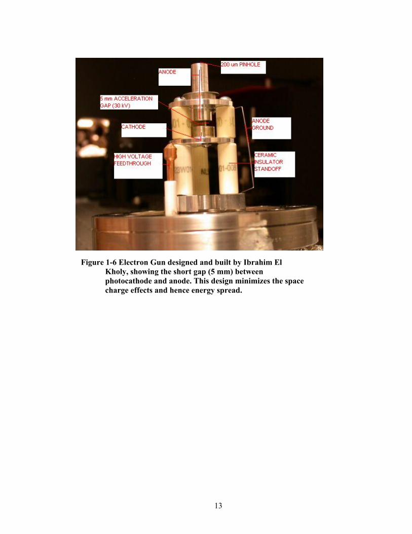
Figure 1-5 Schematic of a sub-picosecond electron diffraction apparatus. ...................... 10 Figure 1-6 Electron Gun designed and built by Ibrahim El Kholy, showing the short gap
(5 mm) between photocathode and anode. This design minimizes the space charge effects and hence energy spread. .......................................................................... 13
Figure 2-1 Crystal forms for garnet, pyrite, and calcite, built up from uniform primitive cells; (Models from Haüy's Traité de Minéralogie (1801) - the crystal forms have been redrawn in red). ............................................................................................ 15
Figure 2-2 Cubic crystals: simple cubic, body centered (BCC), face centered (FCC). .... 15 Figure 2-3 Miller indices are determined from reciprocal intercepts with the crystal axes.
............................................................................................................................... 16 Figure 2-4 Parallelepiped with volume ×a b ci ................................................................. 18 Figure 2-5 Ewald sphere, from the IUCr Online Dictionary of Crystallography; Sh (our S)
is the reflected beam; H and G are nodes of the reciprocal space on the surface of the sphere, and will diffract. ................................................................................. 23
Figure 2-6 Ewald sphere depicted in two dimensions, with multiple reciprocal lattice nodes on or near the circumference. Each of these could appear in the diffraction pattern. .................................................................................................................. 24
Figure 2-7 Illustration of elastic scattering from multiple sites within a crystal. ............. 28 Figure 2-8 Polycrystalline gold diffraction rings. ............................................................. 35 Figure 2-9 Potential time-resolution of the different techniques; electrons are suited for
thinner samples, surface studies, gas reactions, and shorter interaction times. X-rays are more suitable for heavier atoms and bulk studies; for surface studies they are effective when used at glancing angles. .......................................................... 38
Figure 2-10 Brilliance comparison by equivalent photon wavelength; ultrafast electrons offer superior brightness circa 1999. The synchrotron brilliance is from the first generation; recent improvements have increased synchrotron brilliance to 1022. 39
Figure 3-1 Photocathode and anode of the ultrafast electron gun, showing 30 kV electrical contact plate and 30 nm of gold sputtered onto a fused silica negative lens below; the grounded anode tube with 400M gold extraction grid leading up to a 200 um pinhole exit above. Operation requires an ultrahigh vacuum. The small bolts at the top are 0-80. ........................................................................................ 40
Figure 3-2 Optical diffraction of 260 nm UV pulse by 500 LPI extraction grid. ............. 42 Figure 3-3 Peak spacing for 260 nm UV diffraction; FWHM= 350 µm. ......................... 42 Figure 3-4 Wave Plate Setting vs. Mean Intensity is very close to linear when the two end
points are omitted. ................................................................................................. 44 Figure 3-5 Anode structure, with photocathode at left. The cutaway sections allow for
close passage of the pump laser beam and allow for a very close target sample. 48
x
Figure 3-6 20 kV electron gun parts explosion; produced 2-5 ps electron pulses. .......... 51 Figure 3-7 Left: Photocathode was held in a friction fitting. Right: Anode extraction grid
was 500 LPI gold mesh. ........................................................................................ 51 Figure 3-8 Sample holder with HOPG (highly ordered pyrolytic graphite) sample for
reflection mode diffraction. Note the horizontal channel used for grazing incidence. .............................................................................................................. 53
Figure 3-9 HOPG RHEED streaks at left; the cross hatched region at the right is a focused image of the extraction grid due to mis-focus of the electron gun. ......... 53
Figure 4-1 10x10 mm sample cartridge. Right: 600 um aperture w/gold film. Left: cut wire target for time-zero. The bolts are size 0-80. ............................................... 56
Figure 4-2 Rear view of sample holder with cartridge mounted. The bottom most aperture holds a gold 400M TEM grid; 5.0 mm above it is a gold 600 µm TEM aperture, and above that is the sample cartridge. Each of the TEM grid holder cells is centered on the same vertical line. ........................................................................ 57
Figure 4-3 Picosecond time resolution for a 300 fs electron pulse of ~9,000 electrons. Time-zero is at T=221 ps on this centroid deflection chart. The red line is a 5 point moving average. ........................................................................................... 60
Figure 4-4 Beam centroid moves from right-to-left on this motion-tracking chart. The total motion is about 30 um (0.5 camera pixels), or about 10% of the electron beam FWHM diameter. The changeover took 3 ps. ............................................ 61
Figure 4-5 Beam centroid motion for 20 ps pulse from older electron gun design running at 19 kV; number of electrons was over 250,000, the drift distance was 409 mm, and the changeover was much longer at 20 ps. ..................................................... 61
Figure 4-6 Angle of deflection chart showing a definite direction of motion for the centroid after time-zero. The red line is a 5 point moving average. ..................... 62
Figure 4-7 Self-interference of the probe beam as it passes through the ionized air bead. The interefernce bars of interest are the large zebra stripes; the circular patterns are from the camera optics. ................................................................................... 63
Figure 5-1 Debye-Waller heating of ~25 °C with 200 ps electron pulse. Error bars were not calculated. The graph on the right is for the (311) peak, and shows a reduction in peak amplitude. ................................................................................. 65
Figure 5-2 Polycrystalline platinum film, 9 nm. Diffraction image and integrated amplitudes for (E-N) images. Rings (111), (220), (311), and (331) are very clear; (200) is on the shoulder of (111)........................................................................... 66
Figure 5-3 Azimuthal averages for heated platinum film, 9 nm, from April 16, 2008 run. Laser fluence was 2 mJ/cm2. Time-zero was previously and independently determined to be 54 ps. The white background highlights the changes over the first six picoseconds. ............................................................................................. 67
Figure 5-4 Error bars (2 x Standard Error) for diffraction intensity of three different times. April 16, 2008 dataset. The lines correspond to times at 52 ps, 54 ps (time-zero), and 60 ps; 60 ps is the time of maximum change. ............................ 68
Figure 5-5 Reflectivity for 10 nm platinum film showing an impulsive decrease, followed by a series of 3 ps oscillations and a slow recovery. ............................................ 70
Figure 5-6 Peak (111) and (311) relative change of position with time, and corresponding change in temperature. .......................................................................................... 73
Figure 5-7 Peak (311) relative change of integrated intensity with time. ......................... 75
xi
Figure A-1 Polycrystalline gold film, 15 nm thick, mounted on 400M TEM grid; false color. ..................................................................................................................... 81
Figure A-2 TEM image of polycrystalline gold thin film contaminated by dissolved rock salt from the substrate; M=30,000. ....................................................................... 83
Figure A-3 TEM image of polycrystalline gold film, 10 nm thick, showing nanoparticle structure; M=82,000. The low-contrast areas are voids. ..................................... 84
Figure A-4 TEM diffraction pattern for polycrystalline gold thin film, 10 nm. Substrate is amorphous carbon which is responsible for some weak amorphous rings. ...... 85
Figure A-5 Polycrystalline gold thin films, 10 nm thick, free standing on 600 um aperture. ................................................................................................................ 86
Figure C-1 Electron beam calibrated by 400M grid at sample plane as captured by single plate MCP; FWHM is ~200 um. The corresponding line profile shows the TEM grid bars. ............................................................................................................. 101
Figure C-2 Calibration of the pump pulse intensity depends on recording an image of the sample plane illuminated by the pump beam. A 400M TEM grid provides a scale, 63.5 um bar-to-bar. ............................................................................................. 102
Figure C-3 Signal-to-Noise ratio aligned with mean integrated diffraction amplitudes for 9 nm platinum film; data from April 16, 2008. S/N is better than 100:1 for most peaks. .................................................................................................................. 105
Figure C-4 Vacuum chamber (open to atmosphere) showing XYZ translation stage and partial aluminum foil wrap for bake out. ............................................................ 107
Figure C-5 MCP detector, air side, showing electron beam. ......................................... 109

xii
List of Appendices
Appendix A Sample Preparation and Evaluation ............................................................ 81
Appendix B Program Code .............................................................................................. 87
Appendix C Experimental Procedures ............................................................................. 99
xiii
Abstract
AN ULTRAFAST PHOTO-ELECTRON DIFFRACTOMETER
By
Peter Edward Diehr
Co-Chairs: Roy Clarke and Gérard A. Mourou Ultrafast laser pulses - optical pulses shorter than a picosecond - result in rapid processes
occurring at both the surface and the interior of solid materials. Understanding these
processes requires ultrafast probes; optical probes (reflectivity, spectral) are suitable for
some surface studies, but the tracking of structural changes are well suited to x-ray and
electron diffraction. An ultrafast photo-electron diffractometer is a tool for tracking
structural changes such as thermal expansion, melting and super-heating, crystal phase
changes, ionization, and more.
The design and operation of an ultrafast photo-electron diffractometer is detailed, and its
successful operation is demonstrated by sub-picosecond recording of strain in a free-
standing polycrystalline platinum film of 9 nm thickness subjected to a fluence of
2 mJ/cm2 from 150 fs laser pulses. The temporal profile of the relative change of strain is
xiv
used to determine corresponding temperatures changes; for the (311) peak an increase of
70 K is noted within 10 ps. The increase in temperature takes place at a very nearly
linear 7 K/ps. The (111) peak heats more rapidly, reaching 84 K in 6 ps, and is also
nearly linear at 14 K/ps. A temporal relationship is found which connects the phonons in
different directions with energy transport: the rate of change of temperature per phonon
oscillation period is the same in both directions, indicating that thermalization of phonons
in polycrystalline platinum is coupled to the actual vibration rate.
Reflectivity data shows rapid, coherent oscillations, but slower than acoustic phonons.
These appear to be connected to the nanoparticle network structure of the ultrathin film;
further work is planned to unravel these unexpected results.
A new, in-situ method for the determination of time-zero - when the pump and probe
pulses are temporally coincident at the sample - is demonstrated, and shown to be quick,
reliable, and precise to within half a picosecond.
1
Chapter 1
An Ultrafast Photo-Electron Diffractometer
Introduction
Laser pulses with sub-picosecond ( )1210 seconds−≤ pulse durations conveniently define
the ultrafast time-domain. For reference note that picosecond pulse travels 300 µm per
picosecond, which is 375 wave lengths for an 800 nm Ti:Sapphire ultrafast laser; for a
150 femtosecond pulse the length is 45 µm, or about 56 wavelengths. Focusing a 150 fs
pulse with 100 microJoules of energy to a modest 200 µm diameter spot size delivers
power at 12 210 W/cm , a fluence of over 2100 mJ/cm . “Ultrashort laser pulses offer high
laser intensity and offer precise laser-induced breakdown threshold with reduced laser
fluence. The ablation of materials with ultrashort pulses has a very limited heat-affected
volume.”1 This is due to the rapid delivery of the pulse energy; the immediate transfer is
through coupling of the electromagnetic light field to the electrons of the material, while
the relatively massive atomic nuclei and their inner electrons are barely disturbed.
2
Two-Temperature Model and Molecular Dynamics
Anisimov et al.2 utilizes a macroscopic model for the absorption of an ultrashort laser
pulse by a metal surface. This is known as the two-temperature model, and is based upon
energy balance and heat flow. The two temperatures refer to the non-equilibrium state of
the system, where the electrons are rapidly elevated in temperature while the temperature
of the ion cores lags behind. The laser pulse acts primarily through its electric field, and
interacts directly with the electron gas of the metal. Since the pulse is so brief, the
electrons absorb energy, but do not have time to lose any during the pulse. The resulting
electron state has been characterized as plasma, caused by avalanche ionization3. The
electron plasma is very hot, but the lattice remains at its initial temperature, taking up to
several picoseconds to equilibrate. The heat capacity of the electron gas is very low, and
as the electrons thermalize they lose energy to the lattice. That is, energy is transferred
from the electrons to the phonons of the lattice. This gives a pair of coupled heat
equations, which must be solved numerically. This two-temperature model has been
implemented using a finite element integration scheme. This model has been
successfully used not only with metals, but also with semiconductors4. However other
channels exist for the loss of the electronic excitation, including ballistic transport of non-
thermalized electrons, stress waves5, and diffusive transport of thermalized electrons into
the bulk6 7.
When the two-temperature model is applied, an electron-phonon coupling parameter is
required. Fitting the results of ultrafast diffraction studies by means of the Debye-Waller
relation (see appendices) or ultrafast reflectivity measurements8 6 can obtain this function.
Zhigilei incorporates the two-temperature model as an extension of molecular dynamics
code: “where C and K are the heat capacities and thermal conductivities of the electrons
and lattice as denoted by subscripts e and , and G is the electron-phonon coupling
constant. The two-temperature equations are:
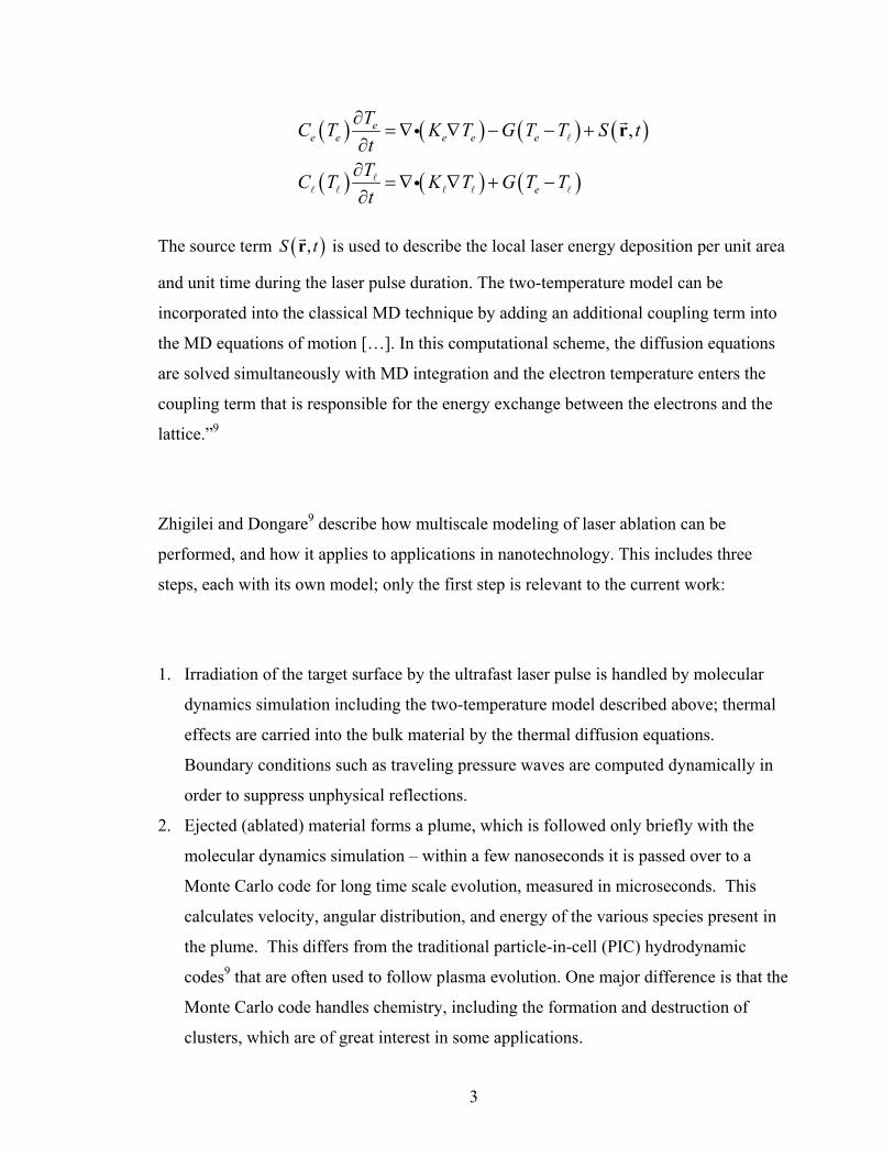
3
( ) ( ) ( ) ( )
( ) ( ) ( )
,ee e e e e
e
TC T K T G T T S tt
TC T K T G T Tt
∂= ∇ ∇ − − +
∂∂
= ∇ ∇ + −∂
ri
i
The source term ( ),S tr is used to describe the local laser energy deposition per unit area
and unit time during the laser pulse duration. The two-temperature model can be
incorporated into the classical MD technique by adding an additional coupling term into
the MD equations of motion […]. In this computational scheme, the diffusion equations
are solved simultaneously with MD integration and the electron temperature enters the
coupling term that is responsible for the energy exchange between the electrons and the
lattice.”9
Zhigilei and Dongare9 describe how multiscale modeling of laser ablation can be
performed, and how it applies to applications in nanotechnology. This includes three
steps, each with its own model; only the first step is relevant to the current work:
1. Irradiation of the target surface by the ultrafast laser pulse is handled by molecular
dynamics simulation including the two-temperature model described above; thermal
effects are carried into the bulk material by the thermal diffusion equations.
Boundary conditions such as traveling pressure waves are computed dynamically in
order to suppress unphysical reflections.
2. Ejected (ablated) material forms a plume, which is followed only briefly with the
molecular dynamics simulation – within a few nanoseconds it is passed over to a
Monte Carlo code for long time scale evolution, measured in microseconds. This
calculates velocity, angular distribution, and energy of the various species present in
the plume. This differs from the traditional particle-in-cell (PIC) hydrodynamic
codes9 that are often used to follow plasma evolution. One major difference is that the
Monte Carlo code handles chemistry, including the formation and destruction of
clusters, which are of great interest in some applications.
4
3. Modeling of film growth occurs when the plume strikes the target. The detailed
results of the plume simulation are passed on to a molecular dynamics simulation to
handle the clusters as they build the film.
In particular this first step can be adapted to the simulation of the non-ablative laser-
matter interactions of the Debye-Waller electron-phonon coupling experiment. The time-
resolved diffraction data provides a step-by-step temporal map of the actual lattice
temperature during the heating and the cooling stages; the coupled differential equations
from the two-temperature model is applied to this lattice temperature data, using the
conservation of energy as a constraint to imply the electron temperature. This leaves the
electron-phonon coupling constant as the free parameter to be numerically fitted. As the
temperatures equilibrate the system settles into the ordinary thermal diffusion equation.
Over longer time scales radiative losses would also have to be accounted for, but they
hardly contribute during the initial fraction of a nanosecond.
Time Resolved Structural Probes
The first time-domain ultrafast (picoseconds) structural probe experiment was performed
in 198210 by using electron diffraction to study the physics of melting in the picosecond
time scale. This study revealed for the first time a superheated (solid) phase for aluminum
with a temperature of 1000 K above melting which lasted ~10 ps. A theory based on
nucleation from laser induced dislocations was used to explain the observations.
Diffraction techniques as opposed to optical techniques provide direct information on
lattice dynamics as a function of time. Heat transport and mechanical properties are
closely associated with the generation and propagation of dislocations. Probing the
structural changes on the pico- and sub-picosecond time scale requires x-ray or electron
diffraction techniques.
5
Currently ultrashort time resolution techniques such as laser-based x-ray diffraction often
require single crystals for investigation in order to improve the signal-to-noise ratio
during the lengthy exposure times. Ultrafast electron diffraction affords the capability to
study the case of polycrystalline and amorphous materials.
Probing matter with electrons instead of x-rays offers a number of significant advantages:
• Electron beams with a de Broglie wavelength corresponding to those of hard x-rays
(100 keV) are easily obtainable.
• Monochromaticity of the beam is excellent, since ΔΕ/Ε can be as small as 10-4 to10-5.
• Scattering cross-sections are extremely large, typically 104 to 108 times that of x-rays,
which makes them ideal for probing the first atomic layers at a crystal surface.
• Use of the photoelectric effect to generate the electron pulses supports very high and
adjustable repetition rates from single shot to greater than 100 MHz.
• Temporal resolution of 30 fs or better can be reached when using very high repetition
rates.
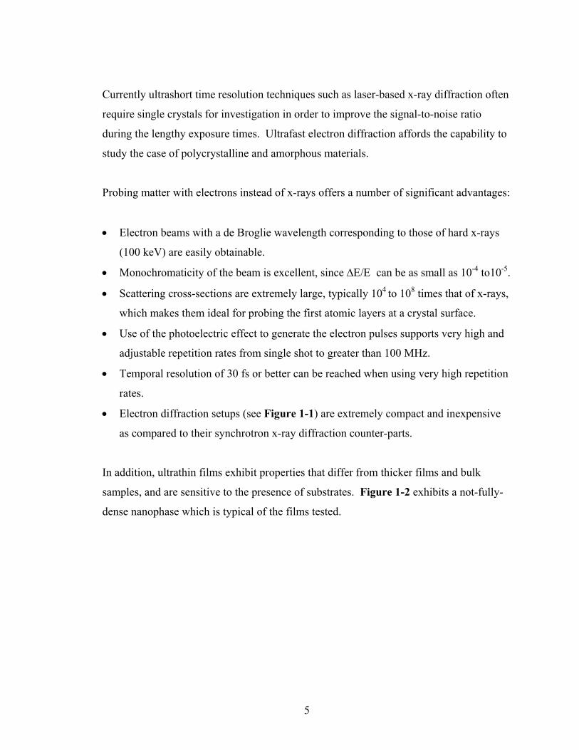
• Electron diffraction setups (see Figure 1-1) are extremely compact and inexpensive
as compared to their synchrotron x-ray diffraction counter-parts.
In addition, ultrathin films exhibit properties that differ from thicker films and bulk
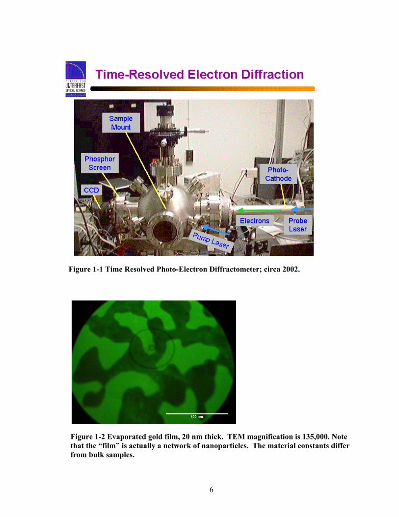
samples, and are sensitive to the presence of substrates. Figure 1-2 exhibits a not-fully-
dense nanophase which is typical of the films tested.
6
Figure 1-2 Evaporated gold film, 20 nm thick. TEM magnification is 135,000. Note that the “film” is actually a network of nanoparticles. The material constants differ from bulk samples.
Figure 1-1 Time Resolved Photo-Electron Diffractometer; circa 2002.
7
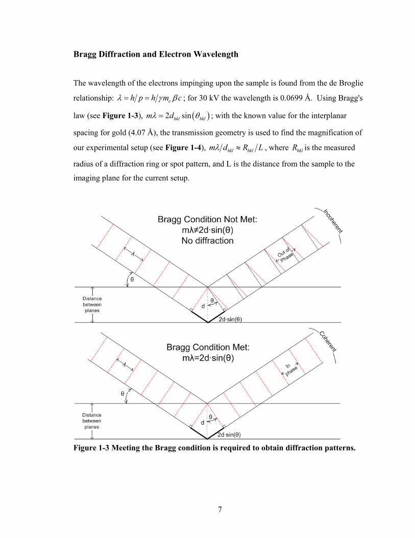
Bragg Diffraction and Electron Wavelength
The wavelength of the electrons impinging upon the sample is found from the de Broglie
relationship: eh p h m cλ γ β= = ; for 30 kV the wavelength is 0.0699 Å. Using Bragg's
law (see Figure 1-3), ( )2 sinhkl hklm dλ θ= ; with the known value for the interplanar
spacing for gold (4.07 Å), the transmission geometry is used to find the magnification of
our experimental setup (see Figure 1-4), hkl hklm d R Lλ ≈ , where hklR is the measured
radius of a diffraction ring or spot pattern, and L is the distance from the sample to the
imaging plane for the current setup.
Figure 1-3 Meeting the Bragg condition is required to obtain diffraction patterns.
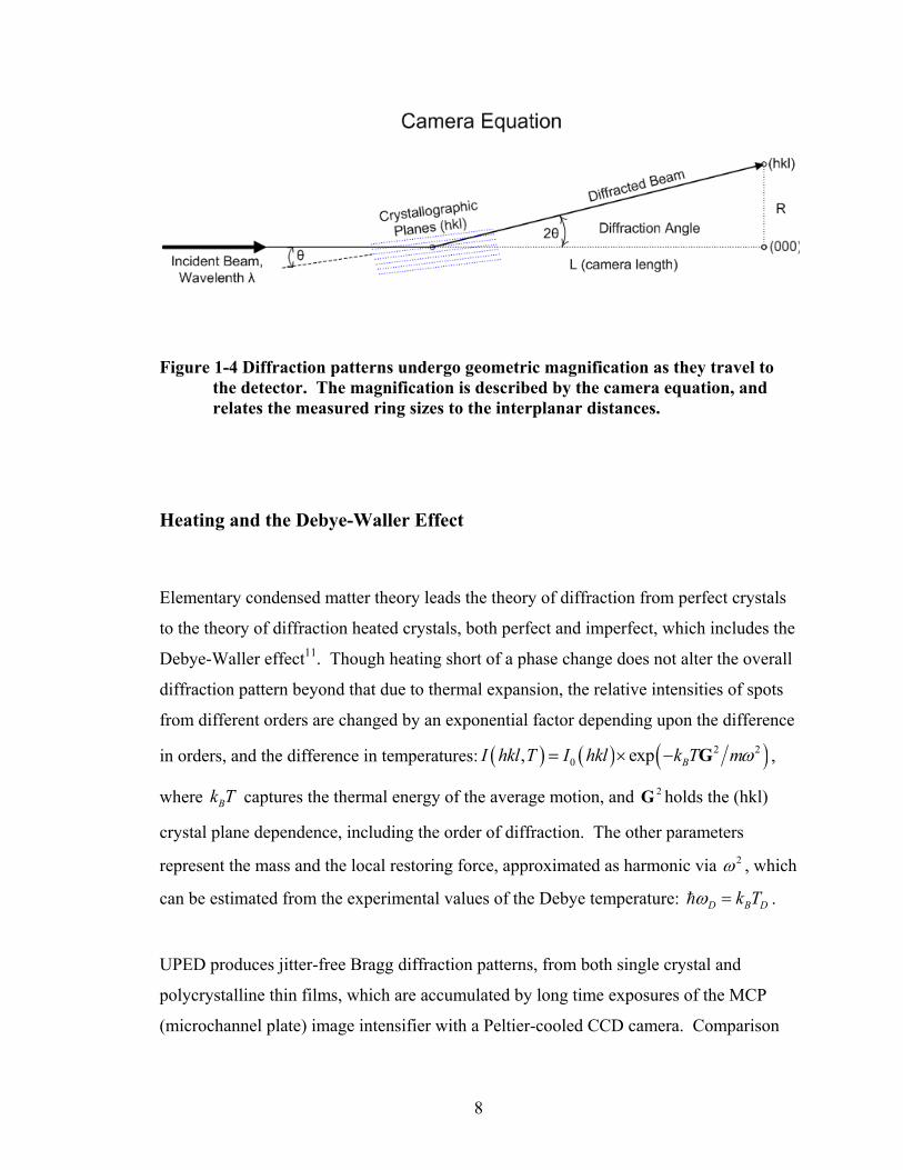
8
Figure 1-4 Diffraction patterns undergo geometric magnification as they travel to the detector. The magnification is described by the camera equation, and relates the measured ring sizes to the interplanar distances.
Heating and the Debye-Waller Effect
Elementary condensed matter theory leads the theory of diffraction from perfect crystals
to the theory of diffraction heated crystals, both perfect and imperfect, which includes the
Debye-Waller effect11. Though heating short of a phase change does not alter the overall
diffraction pattern beyond that due to thermal expansion, the relative intensities of spots
from different orders are changed by an exponential factor depending upon the difference
in orders, and the difference in temperatures: ( ) ( ) ( )2 20, exp BI hkl T I hkl k T mω= × − G ,
where Bk T captures the thermal energy of the average motion, and 2G holds the (hkl)
crystal plane dependence, including the order of diffraction. The other parameters
represent the mass and the local restoring force, approximated as harmonic via 2ω , which
can be estimated from the experimental values of the Debye temperature: D B Dk Tω = .
UPED produces jitter-free Bragg diffraction patterns, from both single crystal and
polycrystalline thin films, which are accumulated by long time exposures of the MCP
(microchannel plate) image intensifier with a Peltier-cooled CCD camera. Comparison
9
of relative intensities of diffraction spots under different laser heating conditions
determines the temperature changes via ( ) ( )* * *1 2 1 2log logI I I I T T= , where the
starred measurements are the heated ones, or ( )* 21 1log I I T∝ −Δ G which requires a
single diffraction order. The availability of multiple orders of diffraction allows for self-
consistency checks, as well as providing information about the directionality of the
bonding, measures of relative stress, etc.
Advancing the pump pulse in small steps (300 μm for each picosecond) gives a temporal
profile of the ion heating induced by the pump pulse. Temporal resolution is limited by
the duration of the pump and probe pulses, and any jitter between them. Essentially, we
can make an ultrafast movie of structural changes and heat transfer within a material
being struck by an ultrafast laser pulse.
An Ultrafast Photo-Electron Diffractometer
Ultrafast photoelectron diffraction (UPED) is a temporally short probe/long detector
experiment. A short laser pump pulse induces a transformation in the sample, and a short
pulse of electrons probes it. For each shot, corresponding to one time delay, a slow
detector collects the entire diffraction pattern. When performed at high repetition rates,
the detector integrates the results of many shots for each time delay.
Application of a femtosecond laser pulse to matter gives rise to an ultrafast laser-matter
interaction involving electrons and ions. This dynamic regime requires temporal
measurements on the time scale of femtoseconds and thus is based on correlation
phenomena of the femtosecond laser pulse with itself.
Ultrafast Photo-Electron Diffraction has had many successes in this regard 10 12 13. By
harnessing the faster pulses of a relatively stable kilohertz laser and accumulating
thousands of shots, we can directly study electron-phonon coupling at the femtosecond
10
time scale by using the Debye-Waller effect, which relates changes in diffraction
intensity to changes in temperature, as well as surface dynamics.
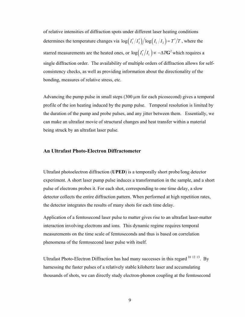
The current approach is illustrated by Figure 1-5,which shows the original pulse being
split into a pump pulse (and associated delay line), and the probe pulse. Though the probe
line process of multiple frequency conversion is quite inefficient with laser power, it is
sufficient to drive the photocathode and obtain a pulsed electron beam. The electron
pulse is a near replica of the laser pulse, though somewhat temporally broadened14 15,
expanding longitudinally as it propagates.
Figure 1-5 Schematic of a sub-picosecond electron diffraction apparatus.
11
The laser system is an ultrafast Ti:Sapphire, a Clark-MXR Model 2001, generating 150
femtosecond pulses trains in the near infrared, centered at 780 nm, with typical pulse
energy of 800 μJ at a repetition rate of 1,000 Hz. The pulse-to-pulse energy stability is
within 1% RMS.
Once the laser has delivered a pulse, all of the following optical processes used are jitter-
free, so splitting a single ultrafast laser pulse generates jitter-free pump and probe pulses.
A half-wave plate followed by a thin-film polarizing beam splitter facilitates setting the
relative energy of the two pulses. The probe pulse starts in the near infrared, centered at
780 nm, and is passed through a BBO frequency-doubling crystal to generate 390 nm
(blue), and both the blue and the fundamental go through a BBO frequency mixing
crystal to generate the third harmonic centered at 260 nm. A series of dichroic mirrors is
used to select the UV component and guide it into the vacuum chamber; the other
wavelengths pass through the mirrors (95%) and are discarded. When the photocathode
is struck by the now-UV pulse it emits a near-replica electron pulse.
The resulting jitter-free Bragg diffraction patterns are accumulated by a long time
exposure of the MCP (microchannel plate) image intensifier with of a Peltier-cooled
CCD camera. Introduction of any temporal jitter between the pump and the probe reduces
the temporal resolution achievable.
The electron gun voltage controls the speed of the electron pulse. The gun is designed
for 15 to 30 kV, with the electrons travelling at up to 1/3 the speed of light. The system
has an optical delay line for the pump pulse, and an adjustable electron speed for the
probe pulse. The pump delay line must make up for the 3-to-1 pump-to-probe speed
differential, 300 μm of delay line for each picosecond of temporal delay.
12
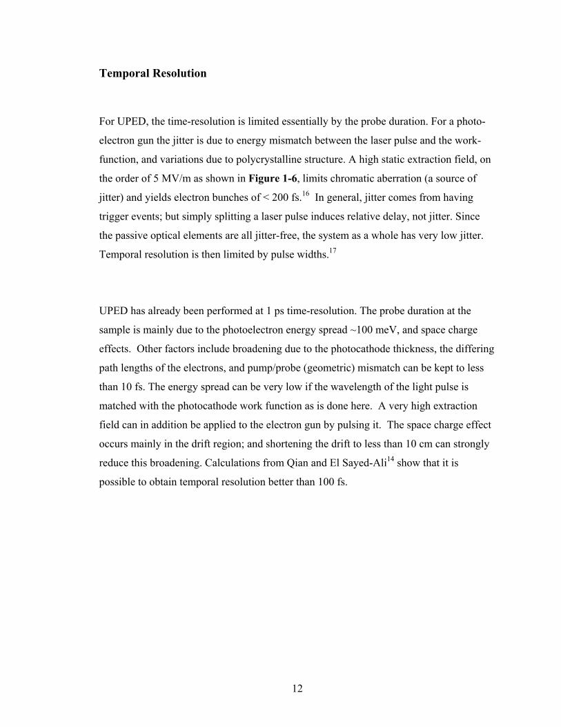
Temporal Resolution
For UPED, the time-resolution is limited essentially by the probe duration. For a photo-
electron gun the jitter is due to energy mismatch between the laser pulse and the work-
function, and variations due to polycrystalline structure. A high static extraction field, on
the order of 5 MV/m as shown in Figure 1-6, limits chromatic aberration (a source of
jitter) and yields electron bunches of < 200 fs.16 In general, jitter comes from having
trigger events; but simply splitting a laser pulse induces relative delay, not jitter. Since
the passive optical elements are all jitter-free, the system as a whole has very low jitter.
Temporal resolution is then limited by pulse widths.17
UPED has already been performed at 1 ps time-resolution. The probe duration at the
sample is mainly due to the photoelectron energy spread ~100 meV, and space charge
effects. Other factors include broadening due to the photocathode thickness, the differing
path lengths of the electrons, and pump/probe (geometric) mismatch can be kept to less
than 10 fs. The energy spread can be very low if the wavelength of the light pulse is
matched with the photocathode work function as is done here. A very high extraction
field can in addition be applied to the electron gun by pulsing it. The space charge effect
occurs mainly in the drift region; and shortening the drift to less than 10 cm can strongly
reduce this broadening. Calculations from Qian and El Sayed-Ali14 show that it is
possible to obtain temporal resolution better than 100 fs.
13
Figure 1-6 Electron Gun designed and built by Ibrahim El Kholy, showing the short gap (5 mm) between photocathode and anode. This design minimizes the space charge effects and hence energy spread.
14
Chapter 2
Crystal Theory
Crystal Structure
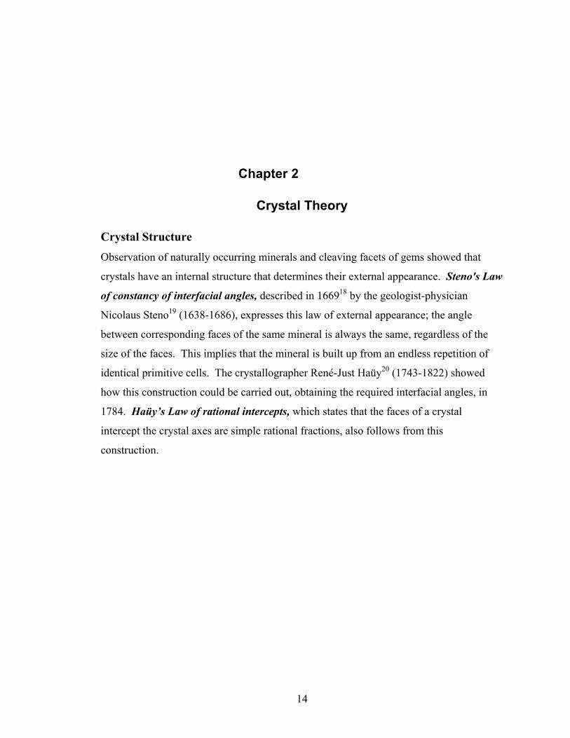
Observation of naturally occurring minerals and cleaving facets of gems showed that
crystals have an internal structure that determines their external appearance. Steno's Law
of constancy of interfacial angles, described in 166918 by the geologist-physician
Nicolaus Steno19 (1638-1686), expresses this law of external appearance; the angle
between corresponding faces of the same mineral is always the same, regardless of the
size of the faces. This implies that the mineral is built up from an endless repetition of
identical primitive cells. The crystallographer René-Just Haüy20 (1743-1822) showed
how this construction could be carried out, obtaining the required interfacial angles, in
1784. Haüy’s Law of rational intercepts, which states that the faces of a crystal
intercept the crystal axes are simple rational fractions, also follows from this
construction.
15
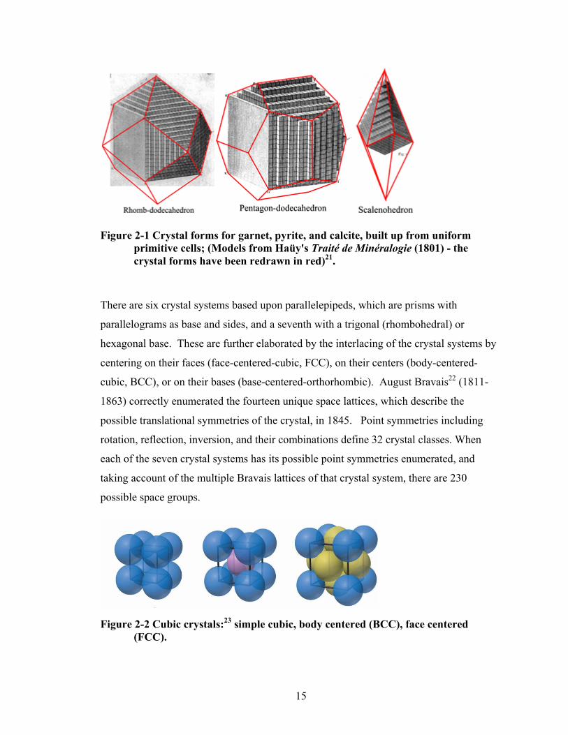
Figure 2-1 Crystal forms for garnet, pyrite, and calcite, built up from uniform primitive cells; (Models from Haüy's Traité de Minéralogie (1801) - the crystal forms have been redrawn in red)21.
There are six crystal systems based upon parallelepipeds, which are prisms with
parallelograms as base and sides, and a seventh with a trigonal (rhombohedral) or
hexagonal base. These are further elaborated by the interlacing of the crystal systems by
centering on their faces (face-centered-cubic, FCC), on their centers (body-centered-
cubic, BCC), or on their bases (base-centered-orthorhombic). August Bravais22 (1811-
1863) correctly enumerated the fourteen unique space lattices, which describe the
possible translational symmetries of the crystal, in 1845. Point symmetries including
rotation, reflection, inversion, and their combinations define 32 crystal classes. When
each of the seven crystal systems has its possible point symmetries enumerated, and
taking account of the multiple Bravais lattices of that crystal system, there are 230
possible space groups.
Figure 2-2 Cubic crystals:23 simple cubic, body centered (BCC), face centered (FCC).
16
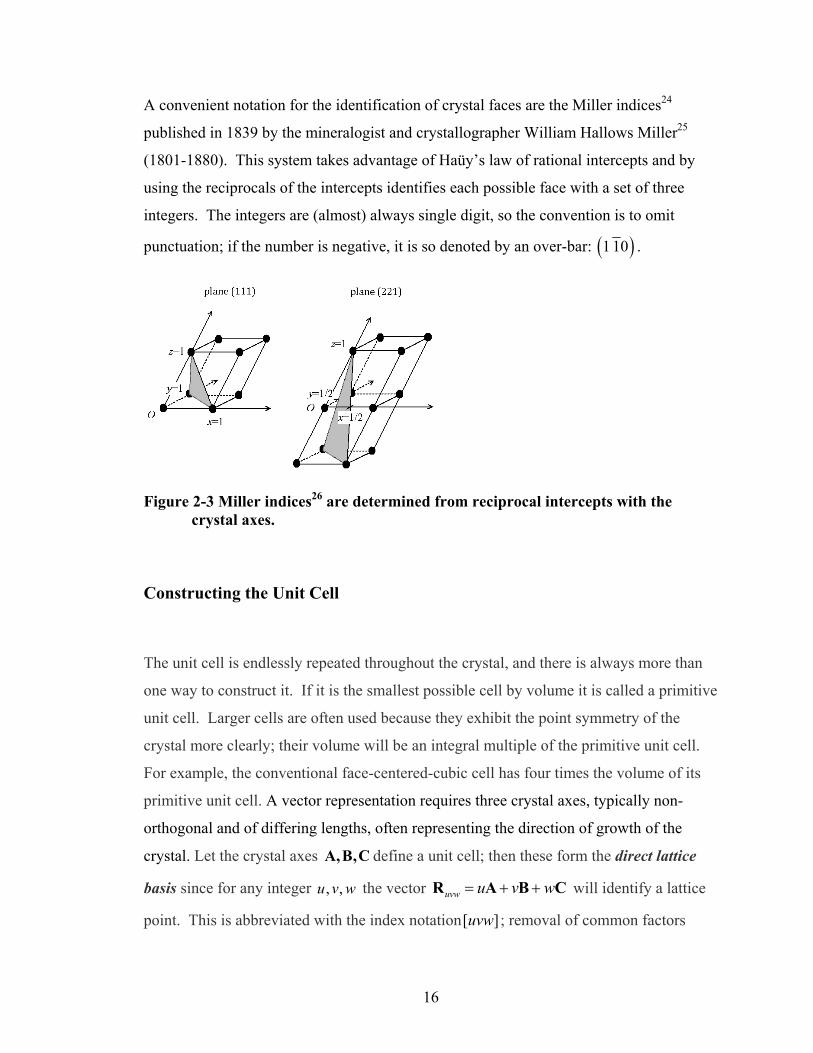
A convenient notation for the identification of crystal faces are the Miller indices24
published in 1839 by the mineralogist and crystallographer William Hallows Miller25
(1801-1880). This system takes advantage of Haüy’s law of rational intercepts and by
using the reciprocals of the intercepts identifies each possible face with a set of three
integers. The integers are (almost) always single digit, so the convention is to omit
punctuation; if the number is negative, it is so denoted by an over-bar: ( )1 10 .
Figure 2-3 Miller indices26 are determined from reciprocal intercepts with the crystal axes.
Constructing the Unit Cell
The unit cell is endlessly repeated throughout the crystal, and there is always more than
one way to construct it. If it is the smallest possible cell by volume it is called a primitive
unit cell. Larger cells are often used because they exhibit the point symmetry of the
crystal more clearly; their volume will be an integral multiple of the primitive unit cell.
For example, the conventional face-centered-cubic cell has four times the volume of its
primitive unit cell. A vector representation requires three crystal axes, typically non-
orthogonal and of differing lengths, often representing the direction of growth of the
crystal. Let the crystal axes A,B,C define a unit cell; then these form the direct lattice
basis since for any integer , ,u v w the vector uvw u v w= + +R A B C will identify a lattice
point. This is abbreviated with the index notation[ ]uvw ; removal of common factors
17
leaves the direction unchanged. Translation along any of the crystal axes puts you in a
different cell, but identical in every way to the previous one.
In order to describe the elements of a unit cell the positions of the constituent atoms and
molecules must be specified. The notation of Warren27 conveniently labels the crystal
axes numerically: 1 2 3A , A , A , and the n elements of the unit cell are described by a set of
vectors nR . Starting from an arbitrary origin within the crystal, each unit cell can be
accessed by a triple of integers 1 2 3m m m m= by 1 1 2 2 3 3m m m m= + +R A A A . Putting these
together gives access to every element of every cell as 1 1 2 2 3 3n nm m m m= + + +R A A A R .
A Geometric View of Vector Products
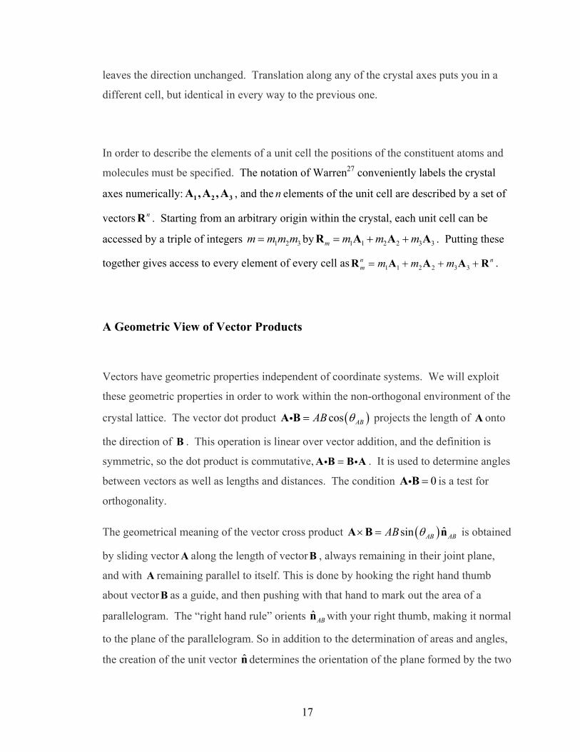
Vectors have geometric properties independent of coordinate systems. We will exploit
these geometric properties in order to work within the non-orthogonal environment of the
crystal lattice. The vector dot product ( )cos ABAB θ=A Bi projects the length of A onto
the direction of B . This operation is linear over vector addition, and the definition is
symmetric, so the dot product is commutative, =A B B Ai i . It is used to determine angles
between vectors as well as lengths and distances. The condition 0=A Bi is a test for
orthogonality.
The geometrical meaning of the vector cross product ( ) ˆsin AB ABAB θ× =A B n is obtained
by sliding vector A along the length of vector B , always remaining in their joint plane,
and with A remaining parallel to itself. This is done by hooking the right hand thumb
about vector B as a guide, and then pushing with that hand to mark out the area of a
parallelogram. The “right hand rule” orients ˆ ABn with your right thumb, making it normal
to the plane of the parallelogram. So in addition to the determination of areas and angles,
the creation of the unit vector n determines the orientation of the plane formed by the two
v
or
T
F
T
V
h
if
th
eq
A
v
pr
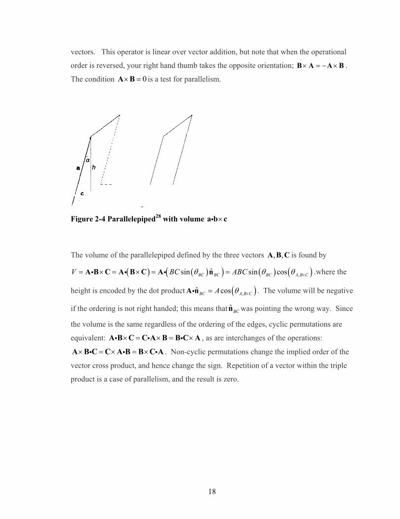
ectors. Thi
rder is rever
The condition
Figure 2-4 P
The volume o
V = × =A B Ci
eight is enco
f the ordering
he volume is
quivalent: A
× = ×A B C Ci
ector cross p
roduct is a c
s operator is
rsed, your rig
n 0× =A B i
arallelepipe
of the paralle
( )= ×A B Ci
oded by the d
g is not right
s the same re
× =A B C Ci i
× = ×A B Bi
product, and
case of parall
s linear over
ght hand thu
s a test for p
ed28 with vo
elepiped def
( sinBC= Ai
dot product A
t handed; thi
egardless of t
× =A B B Ci
C Ai . Non-
d hence chang
lelism, and t
18
vector addit
umb takes the
parallelism.
olume ×a b ci
fined by the t
( ) )ˆn BC BCθ n
ˆ coBC A=A ni
is means tha
the ordering
×C A , as are
cyclic permu
ge the sign.
the result is z
tion, but note
e opposite or
c
three vectors
(sinABC θ=
( ),os A B Cθ × .
at ˆ BCn was po
g of the edge
interchange
utations chan
Repetition o
zero.
e that when
rientation; B
s , ,A B C is f
) ( ,cosBC Aθ θ
The volume
ointing the w
s, cyclic per
es of the oper
nge the impl
of a vector w
the operatio
× = − ×B A A
found by
)B C× .where
e will be neg
wrong way. S
rmutations ar
rations:
lied order of
within the tri
nal
× B .
the
gative
Since
re
f the
iple
19
Reciprocal Space
The distance between parallel faces of a parallelepiped is ( ),ˆ cosBC A B CA θ ×=A ni for the
×B C face. ( )
( ) ( )*
,
ˆsin ˆˆsin cos
AB AB AB
AB AB C A B
ABAB C
θθ θ ×
×= = =
×n nA BC
C A B C ni iand its cyclic
permutations defines an alternative set of vectors * * *A ,B ,C with magnitude which is the
reciprocal of this distance between faces. These vectors are normal to the planes of the
unit cell, and form the reciprocal lattice basis. Reciprocal lattice elements can be
denoted * * *hkl h k l= + +H A B C , with common integral factors removed, and is
abbreviated ( )hkl . As is shown later, this similarity to the Miller index notation is
intentional. An important property which follows directly from this definition is that the
direct and reciprocal basis vectors are orthonormal: * 1=C Ci and * * 0= =C A C Bi i for
each pair. Furthermore, the direct lattice can be recovered from the reciprocal lattice with * *
* * *
×=
×A BC
C A Biby direct substitution and application of the vector identity
( ) ( ) ( ) ( )× × × = × − ×A B C D A B D C A B C Di i 29; they are mathematically dual spaces.
The volume of the reciprocal space unit cell * * * * 1 1VV
= × = =×
A B CA B C
ii
is the
reciprocal of the corresponding direct lattice cell volume. Forming matrices column-wise
from the basis vectors, the orthonormal condition means that [ ] 1 * * * T− ⎡ ⎤= ⎣ ⎦ABC A B C , and
as their determinants are the volumes, it follows that the volumes are reciprocals.
20
Distance Between Planes
By construction * * *hkl h k l= + +H A B C is normal to the plane ( )hkl with magnitude equal
to the reciprocal of the distance from the origin: 1hkl
hkld=H . Evaluating the left hand
side, ( )2 2 222 * * * * * * * * *2 2 2 2 2 2hkl
h k lh k l hk hl klA B C
= + + = + + + + +H A B C A B A C B Ci i i ;
this can be evaluated directly if the dihedral angles are known; otherwise use the vector
identity ( ) ( ) ( )( ) ( )( )1 2 3 4 1 3 2 4 1 4 2 3× × = −A A A A A A A A A A A Ai i i i i after transforming
back to the direct lattice. For cubic systems the reciprocal lattice basis vectors are
orthogonal and of equal length, and so the expression reduces directly to
( )2 2 2 22
1hkl h k l
A= + +H and so
2 2 2hklAd
h k l=
+ +for cubic crystals such as for gold,
platinum, aluminum, and silicon.
Direct Lattice Planes to Reciprocal Lattice Points
Every plane of the direct lattice can be represented by an element of the reciprocal
lattice. Starting with crystal axes A,B,C representing a unit cell of volume V = ×A B Ci ,
and the direct lattice direction [ ]uvw , define a vector n which is normal to the plane
which connects their tips, and divide by the unit cell volume. The normal direction is
given by the vector cross product of the vectors the tips ofu to vA B and u to wA C :
( ) ( )v u w uuv vw uw
V− × − × × ×
= = + +× × ×
B A C A A B B C C AnC A B A B C B C Ai i i
, where the volume
has been replaced by different cyclic permutations of the triple vector product on the right
hand side. The three terms remaining on the right hand side represent important physical
vectors: by construction their sum is normal to the plane of the axial intercepts, while
each one is perpendicular to the face defined by that pair of axes, with magnitude equal to
21
the reciprocal of the distances between faces. These terms are members of the reciprocal
lattice: * * *uv vw uw= + +n C A B .
Reciprocal Lattice Points to Direct Lattice Planes
The points of the reciprocal lattice represent families of planes in the direct lattice. By
removal of common factors this expression for the normal of the direct lattice plane is
reduced to lowest integer form, and the reciprocal lattice element * * *hkl h k l= + +H A B C
denoted ( )hkl , is shown to be equivalent to the Miller index by transforming each term
from the reciprocal space to the direct lattice space: * *
** * *
h jll h j l
×⇒ =
×A B CC
C A Bi, and
similarly * *,h kh k
⇒ ⇒A BA B . From analytic geometry we know these to be the
intercepts of the plane ( ) ( ) ( )
1x y z hx ky lzCA B A B C
h k l+ + = + + = when the directions are
measured in the same units; when these are scaled by the three axial vectors the Miller
indices for the plane ( )hkl are obtained, and the equation of this plane in the direct lattice
space becomes constanthx ky lz+ + = ; the constant is no longer unity due to the
rationalization and the scaling. The left hand expression also appears in the dot product
( ) ( )* * *hkl uvw h k l u v w hu kv lw= + + + + = + +H R A B C A B Ci i , so ( ) [ ] constanthkl uvw =i is
the condition that direction [ ]uvw is parallel to plane ( )hkl . If the constant is zero, then
[ ]uvw is a zone axis, and lies in the plane ( )hkl .
22
Crystal Planes and Diffraction
Real crystals are made up of atoms or molecules within the unit cells, and can be probed
by means of coherent radiation, though the coherence requirement (temporal and spatial)
is limited to a very small interaction volume. The Bragg hypothesis30 is that the crystal
planes act as partially reflecting mirrors, and when the angle of the beam with a stack of
parallel planes supports constructive interference of that beam, that stack of planes will
produce a diffracted beam. The diffraction condition is well known to require path
lengths that differ only by integer multiples of the wavelength. The specifications
available are the beam wavelength λ , the direction [ ]uvw from which it approaches the
crystal, and the orientation of the crystal which provides the ( )hkl family of planes with
spacing 1hkl
hkl
d =H
. The density of atoms on the planes becomes sparser as the distance
becomes closer; thus the principal (low index) planes will diffract more than the high
index planes.
In reciprocal space it is convenient to take the beam directions as unit vectors, then scale
them to reciprocal length: 0
λS is the incoming beam, defining the origin as the first plane
it strikes, and λS is the specularly reflected beam with unchanged wavelength; thus both
vectors make the same glancing angle θ with the plane ( )hkl , so that ( )0 cos 2θ=S Si .
23
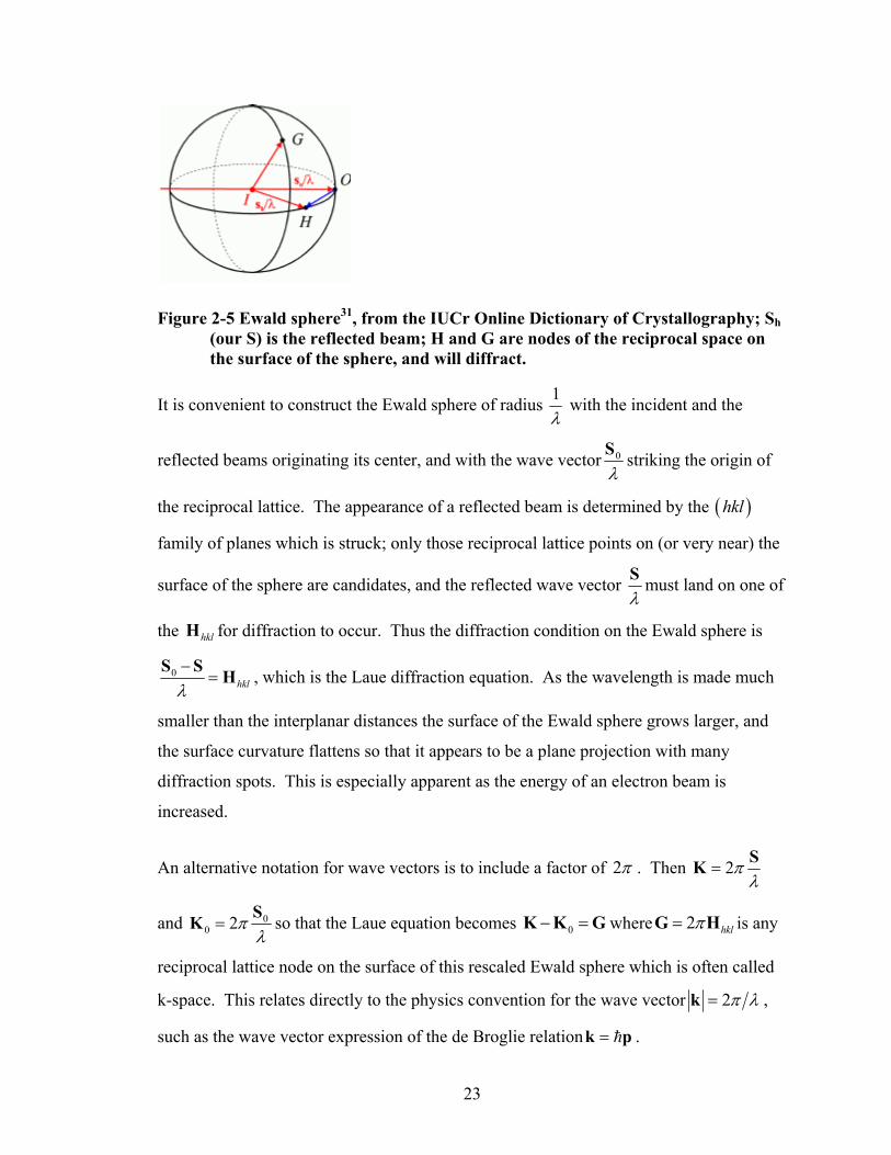
Figure 2-5 Ewald sphere31, from the IUCr Online Dictionary of Crystallography; Sh (our S) is the reflected beam; H and G are nodes of the reciprocal space on the surface of the sphere, and will diffract.
It is convenient to construct the Ewald sphere of radius 1λ
with the incident and the
reflected beams originating its center, and with the wave vector 0
λS striking the origin of
the reciprocal lattice. The appearance of a reflected beam is determined by the ( )hkl
family of planes which is struck; only those reciprocal lattice points on (or very near) the
surface of the sphere are candidates, and the reflected wave vector λS must land on one of
the hklH for diffraction to occur. Thus the diffraction condition on the Ewald sphere is
0hklλ
−=
S S H , which is the Laue diffraction equation. As the wavelength is made much
smaller than the interplanar distances the surface of the Ewald sphere grows larger, and
the surface curvature flattens so that it appears to be a plane projection with many
diffraction spots. This is especially apparent as the energy of an electron beam is
increased.
An alternative notation for wave vectors is to include a factor of 2π . Then 2πλ
=SK
and 00 2π
λ=
SK so that the Laue equation becomes 0− =K K G where 2 hklπ=G H is any
reciprocal lattice node on the surface of this rescaled Ewald sphere which is often called
k-space. This relates directly to the physics convention for the wave vector 2π λ=k ,
such as the wave vector expression of the de Broglie relation =k p .
24
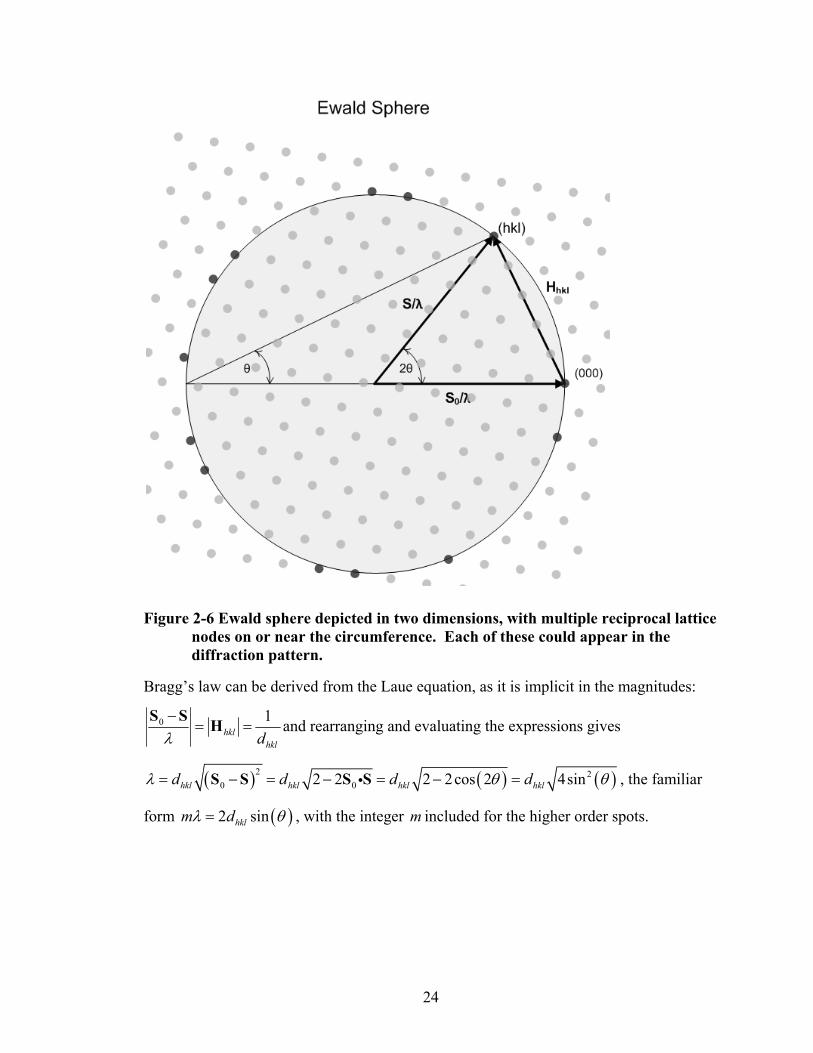
Figure 2-6 Ewald sphere depicted in two dimensions, with multiple reciprocal lattice nodes on or near the circumference. Each of these could appear in the diffraction pattern.
Bragg’s law can be derived from the Laue equation, as it is implicit in the magnitudes:
0 1hkl
hkldλ−
= =S S H and rearranging and evaluating the expressions gives
( ) ( ) ( )2 20 02 2 2 2cos 2 4sinhkl hkl hkl hkld d d dλ θ θ= − = − = − =S S S Si , the familiar
form ( )2 sinhklm dλ θ= , with the integer m included for the higher order spots.
25
Atomic Scattering Mechanisms
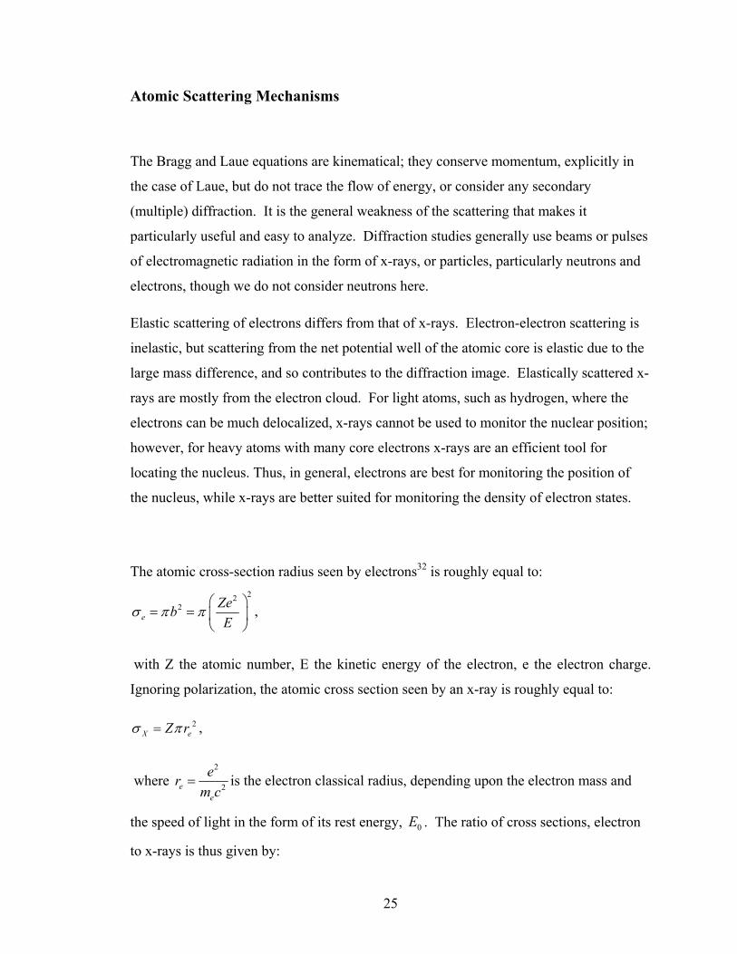
The Bragg and Laue equations are kinematical; they conserve momentum, explicitly in
the case of Laue, but do not trace the flow of energy, or consider any secondary
(multiple) diffraction. It is the general weakness of the scattering that makes it
particularly useful and easy to analyze. Diffraction studies generally use beams or pulses
of electromagnetic radiation in the form of x-rays, or particles, particularly neutrons and
electrons, though we do not consider neutrons here.
Elastic scattering of electrons differs from that of x-rays. Electron-electron scattering is
inelastic, but scattering from the net potential well of the atomic core is elastic due to the
large mass difference, and so contributes to the diffraction image. Elastically scattered x-
rays are mostly from the electron cloud. For light atoms, such as hydrogen, where the
electrons can be much delocalized, x-rays cannot be used to monitor the nuclear position;
however, for heavy atoms with many core electrons x-rays are an efficient tool for
locating the nucleus. Thus, in general, electrons are best for monitoring the position of
the nucleus, while x-rays are better suited for monitoring the density of electron states.
The atomic cross-section radius seen by electrons32 is roughly equal to: 22
2e
ZebE
σ π π⎛ ⎞
= = ⎜ ⎟⎝ ⎠
,
with Z the atomic number, E the kinetic energy of the electron, e the electron charge.
Ignoring polarization, the atomic cross section seen by an x-ray is roughly equal to:
2X eZ rσ π= ,
where 2
2ee
erm c
= is the electron classical radius, depending upon the electron mass and
the speed of light in the form of its rest energy, 0E . The ratio of cross sections, electron
to x-rays is thus given by:
26
20
/e
e XX
ER ZE
σσ
⎛ ⎞= = ⎜ ⎟⎝ ⎠
.
For the system being described, the electron energy is provided by the electric potential
of a photo-electron gun designed to work from 15 to 30 kV. A simple relativistic
calculation33 gives the electron velocity: the total energy is just the rest mass energy plus
the work done on the electron, 0 0E E Eγ = + , and is equal to the rest mass energy times
the relativistic Lorentz factor, ( ) 1 221γ β−
= − ; isolating and inverting this gives the
electron speed as ( )1 221vc
β γ −= = − . It also follows that ( ) 10 1EE
γ −= − , so the ratio of
cross sections is simplified to:
( ) 2/ 1e
e XX
R Zσ γσ
−= = − .
For an electron accelerated through 30 kV the Lorentz factor 1.0587γ = , and the speed is
0.328 vc
β = = , or 1/3 the speed of light. For a heavy element such as gold, Z=79 we
have 4/ 2
79 2.2 100.0587e XR = = × . As the relativistic factor increases /e XR decreases;
clearly this model favors low speed electrons, which are in fact used for detailed surface
studies; as the electron energy increases the electrons gain penetration power, interacting
less and less with the material. For this reason most transmission electron microscopes
operate in the range 100 to 400 kV; at 512 kV the relativistic factor is 2γ = , and
/e XR Z= .
The ratio of intensities is 2/ /e X e XI R= , so for 30 kV acceleration typically is 108. This
large ratio has two consequences: (1) x-rays are excellent for thick samples or bulk
studies and electrons are excellent for surface, gas, and thin sample studies, and (2) there
is a consequence specific to time-resolved diffraction: the electron penetration depth is
shorter than the pump light so they can probe a sample excitation uniformly, which is not
27
generally the case for x-rays; the exception is for x-rays at glancing angles. This latter
effect will make a significant contribution towards improvement of the signal-to-noise
ratio of the diffracted signal for electrons.
Elastic Scattering from a Crystal
Elastic scattering of electrons or x-rays from the periodic array of a crystal can be
analyzed in terms of the scattering amplitude function for each type of atom, ( )0 ,F K K ,
in terms incoming and outgoing wave vectors. In this study only elastic scattering
conforming to the Laue equation is considered; the illuminating beam is the incoming
wave vector 00 2π
λ=
SK , while the diffracted beam is the outgoing wave vector
2πλ
=SK .
28
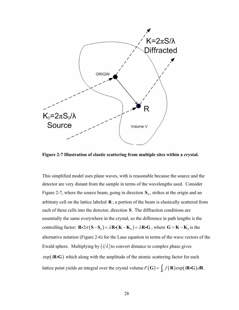
Figure 2-7 Illustration of elastic scattering from multiple sites within a crystal.
This simplified model uses plane waves, with is reasonable because the source and the
detector are very distant from the sample in terms of the wavelengths used. Consider
Figure 2-7, where the source beam, going in direction 0S , strikes at the origin and an
arbitrary cell on the lattice labeled R ; a portion of the beam is elastically scattered from
each of these cells into the detector, direction S . The diffraction conditions are
essentially the same everywhere in the crystal, so the difference in path lengths is the
controlling factor: ( ) ( )0 02π λ λ− = − =R S S R K K R Gi i i , where 0= −G K K is the
alternative notation (Figure 2-6) for the Laue equation in terms of the wave vectors of the
Ewald sphere. Multiplying by ( )i λ to convert distance to complex phase gives
( )exp iR Gi which along with the amplitude of the atomic scattering factor for each
lattice point yields an integral over the crystal volume ( ) ( ) ( )expV
F f i d= ∫G R R G Ri .
29
This is the scattering amplitude in terms of the reciprocal lattice nodes, which are the
Bragg planes.
There are several items of note about this integral, beginning with the phase expression
( )exp iR Gi for which we have previously noted that 2 hklπ=G H , and thus is 2π times a
reciprocal space point; therefore the inner product R Gi is an integer multiple of 2π so
the ( )exp 1i =R Gi at every crystal lattice point when the Laue condition is satisfied. The
integral is also clearly recognized as a Fourier transform of the atomic scattering
amplitude; the structure of the integral makes it clear that the crystal lattice is the spatial
Fourier transform of the reciprocal lattice, and vice versa. The use of wave vectors
=k p to navigate reciprocal space shows that the Laue condition is also a condition on
momentum. The volume of integration simply increases the contribution in proportion to
the number of cells in the crystal; it is apparent that the fundamental information all lies
within the unit cell of the crystal.
30
Structure Factors
However, we have only taken into account the lattice positions; many crystal structures,
including FCC and BCC, include an additional “basis” to describe the off-lattice atoms.
These can result in additional constructive and destructive interference. For example, the
primitive cell of the FCC structure has an additional basis which can be described by an
additional three vectors ( ) ( ) ( )1 2 31 1 1, ,2 2 2
= + = + = +R A B R B C R C A which connect
the lattice points to the face centers. This allows the calculation of the structure factor
for this crystal: ( )exp mhkl m
mF f i= ∑ G Ri , where mf is the atomic form factor for the type
of atom at position m . For crystals made up of a single element, such as gold or
platinum, the mf are all the same, though in the rock salt FCC structure they alternate.
Expanding the structure factor expression for gold yields four terms, one for the lattice
point serving as the origin of the cell, and the three additional basis vectors products :
( ) ( ) ( ) ( )exp 0 exp exp exphklF f i h k i k l i l hπ π π⎡ ⎤= + + + + + +⎣ ⎦ . The first term is
unity ; the other arguments involve integer expressions which may be positive or
negative, depending upon the Miller indices. These exponentials will become +1 if the
index sum is even, or -1 if the index sum is odd. Since each index is paired once with
each of the others, they will all be even sums if all of the indexes are even, or if all of the
indexes are odd; all cases with mixed indices result in two sums being odd, and one even.
This produces the index rule for FCC structure factors with a single atomic type such as
copper, gold, and platinum: 0hklF = for mixed index reflections, and these Bragg
reflections vanish.
31
Imperfect Crystals
Imperfect crystals result in deviations from the expressions derived previously; B.E.
Warren27 devotes an entire chapter to the subject, and its sensitivity to imperfections is
one of the advantages of electron diffraction34. In general, the defect information appears
between the Bragg reflections, though some effects, such as beam broadening due to
small crystal size (Scherrer formula35), or amplitude reduction due to temperature
(Debye-Waller effect) impact the Bragg reflections directly. Multiple elastic scattering
inside a sample also leads to departures from Bragg’s law, though this is not seen with
very thin samples.
Temperature and the Debye-Waller Effect
Consider the effects of temperature upon a perfect crystal as discussed by Kittel22: the
lattice positions mR are now averages over time due to the thermal vibrations. Let mδ be
the instantaneous deviation from the average position. The simplest model is the thermal
average energy of an isotropic harmonic oscillator: ( )223 12 2
mBU k T mω δ= = . Thus
the thermal average displacement can be expressed as ( )2 23mBk T mδ ω= . This
depends upon the temperature, the atomic mass, and the restoring forces which in turn
determine the oscillation frequency. An estimation of this frequency can be obtained
from experimental values of the Debye temperature relationship: D B Dk Tω = .
The structure factor of the heated crystal becomes ( )exp m mhkl m
mF f i= +∑ G R δi with
each term expanding as ( ) ( )exp expm mi iG R G δi i . The second factor contains the
vibrational effects of the temperature, which are presumed to be random and incoherent
32
with other atoms of the structure whenever an equilibrium temperature has been reached.
The structure factor is not directly observed; most detectors respond to time averaged
intensity, so the contribution is a thermal average, with series expansion
( ) ( )2 2
exp 11! 2!
m m mi ii = + + +G δ G δ G δi i i
The first order term vanishes due to the randomness of mδ , and the second order term is
( ) ( ) ( )2 2 222 21 1cos
2! 2 6m m m mi G Gθ δ= − = −G δ δ δi i . Ignoring higher order terms,
this sum can be expressed as a new exponential function:
( ) ( )2 22 21 1exp 16 6
m mG Gδ δ⎛ ⎞− = − +⎜ ⎟⎝ ⎠
, with the higher order terms matching
exactly to our ignored terms if they are harmonic oscillators. Expressed as an
experimentally detectable intensity we have ( )220
1exp3
mhklI I G δ⎛ ⎞= −⎜ ⎟
⎝ ⎠, where the
exponential is the Debye-Waller factor. Note that as 22 hklhkldππ= =G H we can make
use of Bragg’s law to write ( )4 sin hklπ θλ
=G , and this form is often used. Substituting
the previously derived thermal expression for ( )2mδ gives a useful form for the
Debye-Waller factor of ( )2 20 exphkl BI I k TG mω= − .
The Debye-Waller factor reduces the amplitude of the Bragg peaks; more rapidly as the
temperature increases, and more so for the higher-index Bragg planes. This loss of
amplitude is due to inelastic scattering, and will appear between the Bragg peaks as
increased diffuse reflections.
Temperature information can be retrieved by comparison of the same reflection heated
and unheated, or by analysis of a set of Bragg reflections with different Miller indices.
This is in addition to changes in peak position due to thermal expansion of the crystal,
33
which is a bulk property. This also provides a measure of strain as relative change of
peak position R RΔ .
For an FCC crystal with Bragg plane ( )hkl we have ( )2 2 2
2222 h k lG
aπ + +
= , and making
use of the Debye temperature formula B DD
k Tω = a form is obtained which depends upon
the equilibrium temperature, the Bragg plane ( )hkl and properties of the crystal: the cell
size a , its Debye temperature DT , and the mass of the atom:
( )2 2 2 2
02exphkl
D B
h k l TI I
aT mkπ⎛ ⎞+ +⎛ ⎞⎜ ⎟= −⎜ ⎟⎜ ⎟⎝ ⎠⎝ ⎠
. This FCC approximation provides a tool for
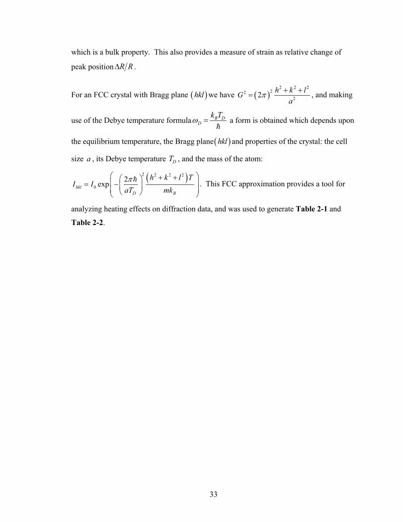
analyzing heating effects on diffraction data, and was used to generate Table 2-1 and
Table 2-2.
34
Table 2-1 Reduction of Intensity of Platinum Diffraction, Debye-Waller Effect.
Element Structure TD Mass a ω=kTD/ħ
Pt FCC 240 3.239448E-25 3.9242E-10 3.1421E+13
(111) (200) (220) (311) (331)
T (in K) 3 4 8 11 19
200 0.9934 0.9912 0.9824 0.9759 0.9588
225 0.9926 0.9901 0.9803 0.9730 0.9538
250 0.9917 0.9890 0.9781 0.9700 0.9488
275 0.9909 0.9879 0.9759 0.9671 0.9438
300 0.9901 0.9868 0.9738 0.9641 0.9389
325 0.9893 0.9857 0.9716 0.9612 0.9339
350 0.9884 0.9846 0.9695 0.9583 0.9290
375 0.9876 0.9835 0.9673 0.9554 0.9242
400 0.9868 0.9824 0.9652 0.9525 0.9193
Table 2-2 Percentage Change in Intensity from 300 K for Platinum Diffraction.
T (in K) (111) (200) (220) (311) (331)
300 0.00% 0.00% 0.00% 0.00% 0.00%
325 -0.08% -0.11% -0.22% -0.30% -0.52%
350 -0.17% -0.22% -0.44% -0.61% -1.05%
375 -0.25% -0.33% -0.66% -0.91% -1.56%
400 -0.33% -0.44% -0.88% -1.21% -2.08%
35
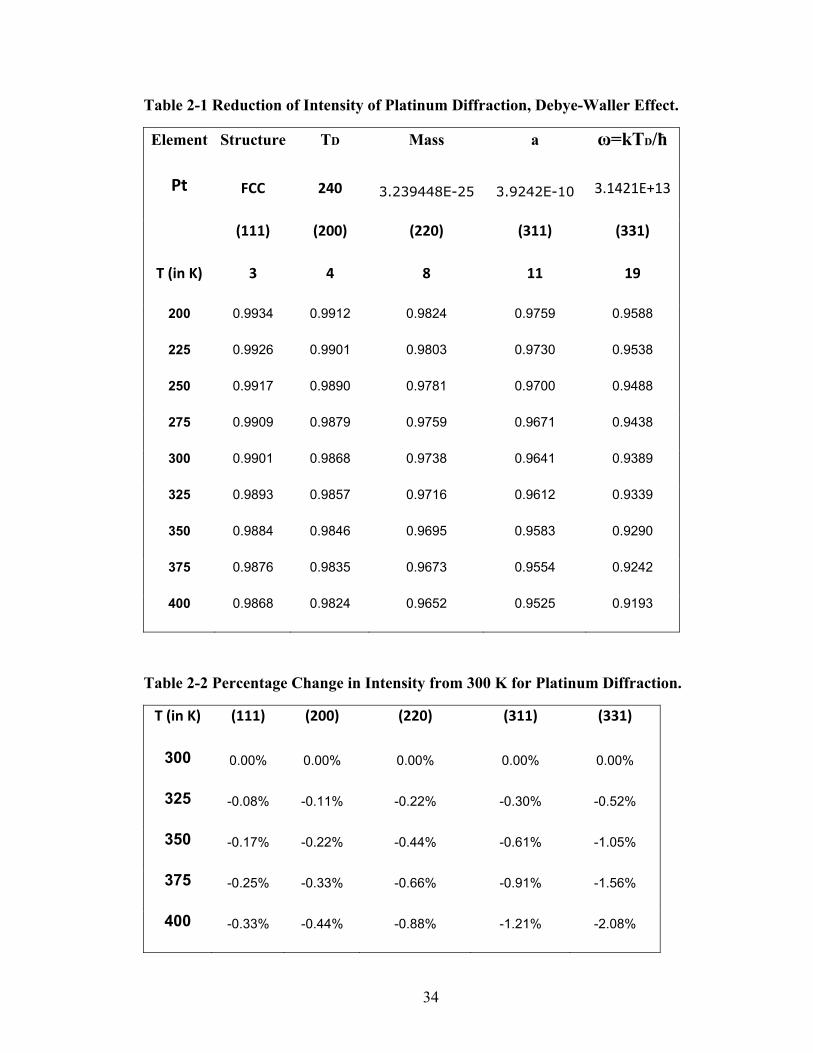
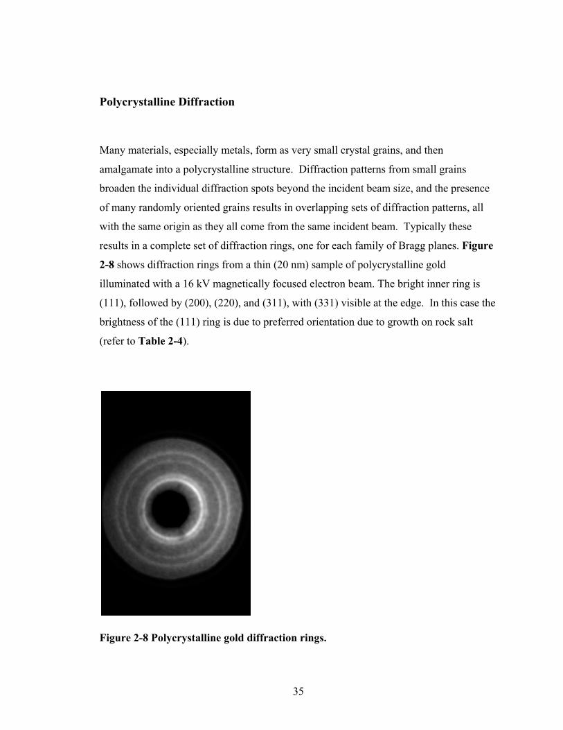
Polycrystalline Diffraction
Many materials, especially metals, form as very small crystal grains, and then
amalgamate into a polycrystalline structure. Diffraction patterns from small grains
broaden the individual diffraction spots beyond the incident beam size, and the presence
of many randomly oriented grains results in overlapping sets of diffraction patterns, all
with the same origin as they all come from the same incident beam. Typically these
results in a complete set of diffraction rings, one for each family of Bragg planes. Figure
2-8 shows diffraction rings from a thin (20 nm) sample of polycrystalline gold
illuminated with a 16 kV magnetically focused electron beam. The bright inner ring is
(111), followed by (200), (220), and (311), with (331) visible at the edge. In this case the
brightness of the (111) ring is due to preferred orientation due to growth on rock salt
(refer to Table 2-4).
Figure 2-8 Polycrystalline gold diffraction rings.
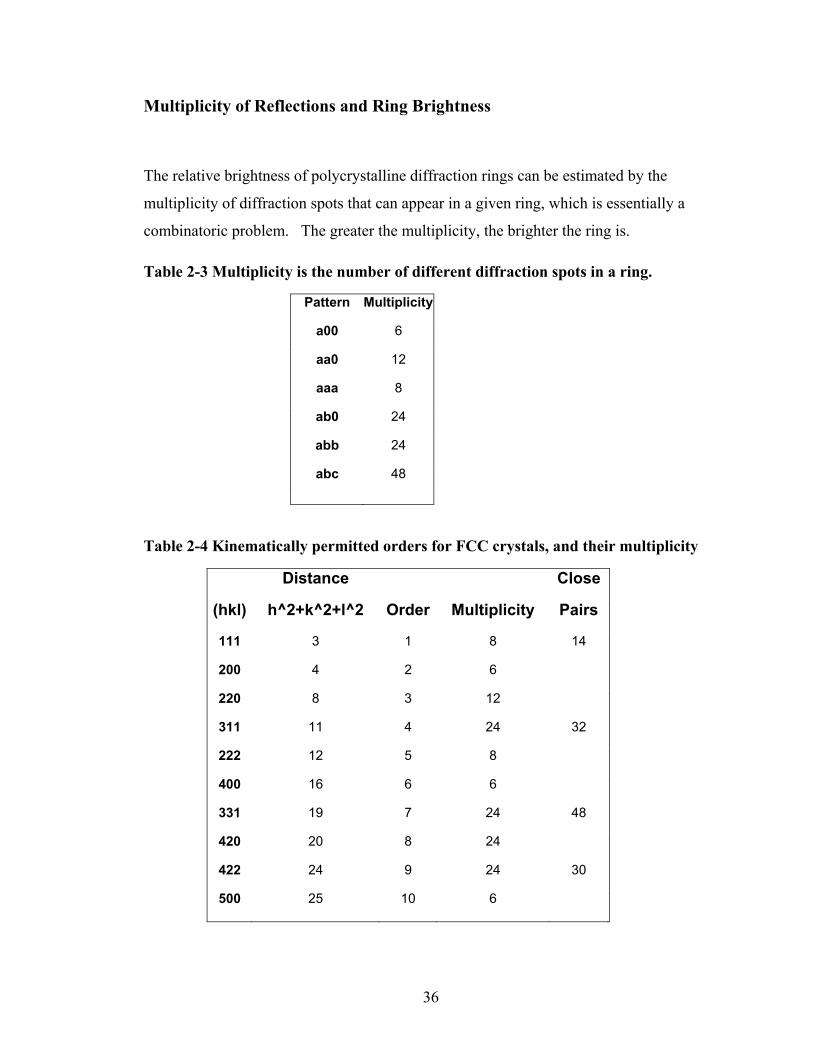
36
Multiplicity of Reflections and Ring Brightness
The relative brightness of polycrystalline diffraction rings can be estimated by the
multiplicity of diffraction spots that can appear in a given ring, which is essentially a
combinatoric problem. The greater the multiplicity, the brighter the ring is.
Table 2-3 Multiplicity is the number of different diffraction spots in a ring.
Pattern Multiplicity
a00 6
aa0 12
aaa 8
ab0 24
abb 24
abc 48
Table 2-4 Kinematically permitted orders for FCC crystals, and their multiplicity
Distance Close
(hkl) h^2+k^2+l^2 Order Multiplicity Pairs
111 3 1 8 14
200 4 2 6
220 8 3 12
311 11 4 24 32
222 12 5 8
400 16 6 6
331 19 7 24 48
420 20 8 24
422 24 9 24 30
500 25 10 6
37
Brilliance
The definition of probe beam brilliance relevant for time-resolved diffraction is:
2 2
nNBx
ρηθ
=Δ Δ
where n is the repetition rate, N is the number of photons or electrons emitted by the
source at each shot and in a .01% bandwidth, ρ is the geometric factor, i.e. the fraction of
the diffraction pattern seen by the detector, η is the quantum efficiency of the detector,
xΔ is the size of the source, θΔ is the emitting angle of the source. This definition takes
into account the whole experimental set-up including the type of detector used in the
experiment.
The optimum UPED brilliance can be calculated with the following parameters:
1 2
3 mradEE
θ Δ⎛ ⎞Δ = =⎜ ⎟⎝ ⎠
; 10 μmxΔ = ,
with the geometric factor ρ and the quantum efficiency η equal to one. The number N of
electrons per shot is 1000, which permits a less than 100 fs time-resolution (see later). To
create such a small number of electrons, a simple oscillator is sufficient, with a repetition
rate of 100 MHz. However, the pump needs a high energy that will keep the repetition
rate to a lower value: ~100 kHz. With this value used for the calculation,
B =1011 electrons/s.mm2.mrad2/ per .01% bandwidth.
This compares very favorably with first generation synchrotron x-ray sources when the
relative electron/x-ray scattering cross sections are taken into account36. At 1,000
electrons per pulse, with pulse duration of 100 fs, the periodic electron current at the
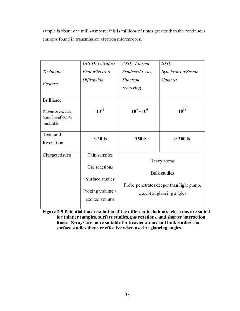
38
sample is about one milli-Ampere; this is millions of times greater than the continuous
currents found in transmission electron microscopes.
Technique/
Feature
UPED: Ultrafast
PhotoElectron
Diffraction
PXD: Plasma
Produced x-ray,
Thomson
scattering
SXD:
Synchrotron/Streak
Camera
Brilliance
Photons or electrons
/s.mm2.mrad2/0.01%
bandwidth
1011 104 - 105 1011
Temporal
Resolution < 30 fs ~150 fs > 200 fs
Characteristics Thin samples
Gas reactions
Surface studies
Probing volume <
excited volume
Heavy atoms
Bulk studies
Probe penetrates deeper than light pump,
except at glancing angles
Figure 2-9 Potential time-resolution of the different techniques; electrons are suited for thinner samples, surface studies, gas reactions, and shorter interaction times. X-rays are more suitable for heavier atoms and bulk studies; for surface studies they are effective when used at glancing angles.
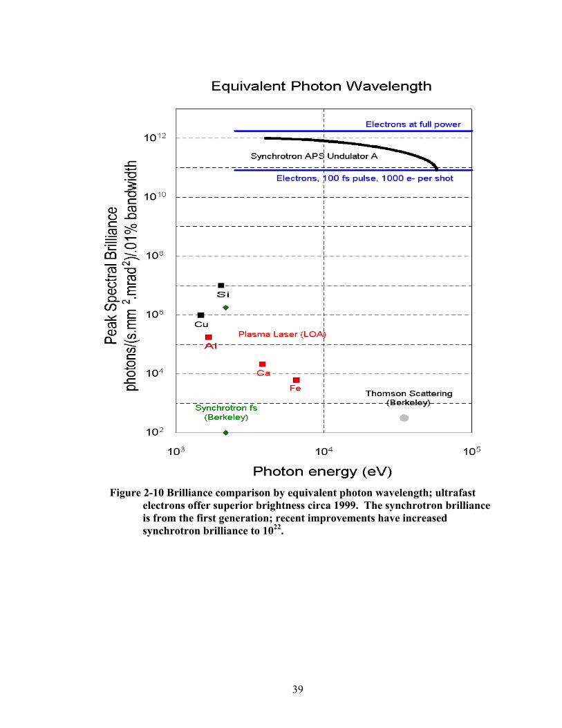
39
Figure 2-10 Brilliance comparison by equivalent photon wavelength; ultrafast electrons offer superior brightness circa 1999. The synchrotron brilliance is from the first generation; recent improvements have increased synchrotron brilliance to 1022.
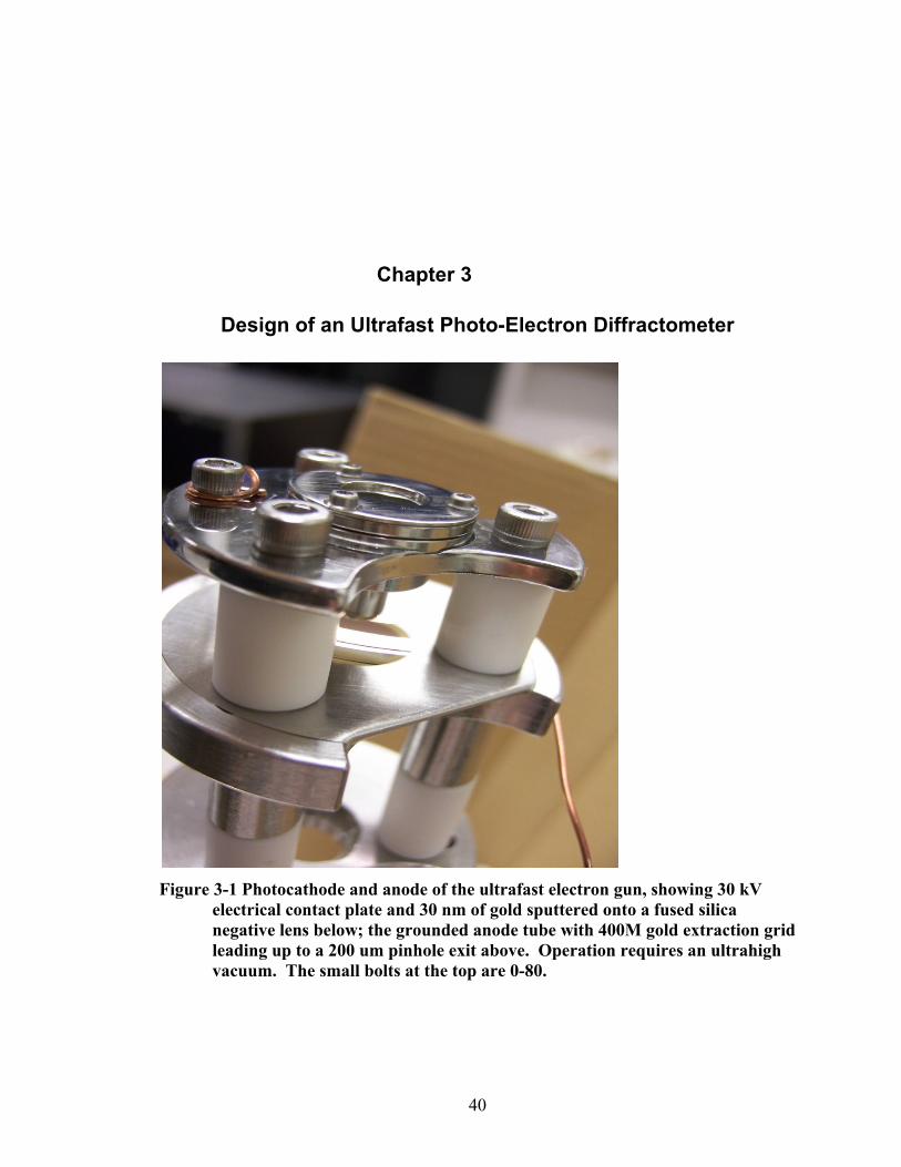
40
Chapter 3
Design of an Ultrafast Photo-Electron Diffractometer
Figure 3-1 Photocathode and anode of the ultrafast electron gun, showing 30 kV
electrical contact plate and 30 nm of gold sputtered onto a fused silica negative lens below; the grounded anode tube with 400M gold extraction grid leading up to a 200 um pinhole exit above. Operation requires an ultrahigh vacuum. The small bolts at the top are 0-80.
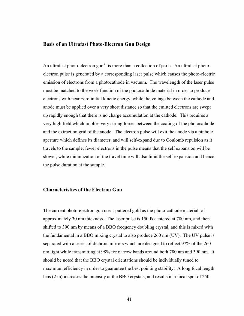
41
Basis of an Ultrafast Photo-Electron Gun Design
An ultrafast photo-electron gun37 is more than a collection of parts. An ultrafast photo-
electron pulse is generated by a corresponding laser pulse which causes the photo-electric
emission of electrons from a photocathode in vacuum. The wavelength of the laser pulse
must be matched to the work function of the photocathode material in order to produce
electrons with near-zero initial kinetic energy, while the voltage between the cathode and
anode must be applied over a very short distance so that the emitted electrons are swept
up rapidly enough that there is no charge accumulation at the cathode. This requires a
very high field which implies very strong forces between the coating of the photocathode
and the extraction grid of the anode. The electron pulse will exit the anode via a pinhole
aperture which defines its diameter, and will self-expand due to Coulomb repulsion as it
travels to the sample; fewer electrons in the pulse means that the self expansion will be
slower, while minimization of the travel time will also limit the self-expansion and hence
the pulse duration at the sample.
Characteristics of the Electron Gun
The current photo-electron gun uses sputtered gold as the photo-cathode material, of
approximately 30 nm thickness. The laser pulse is 150 fs centered at 780 nm, and then
shifted to 390 nm by means of a BBO frequency doubling crystal, and this is mixed with
the fundamental in a BBO mixing crystal to also produce 260 nm (UV). The UV pulse is
separated with a series of dichroic mirrors which are designed to reflect 97% of the 260
nm light while transmitting at 98% for narrow bands around both 780 nm and 390 nm. It
should be noted that the BBO crystal orientations should be individually tuned to
maximum efficiency in order to guarantee the best pointing stability. A long focal length
lens (2 m) increases the intensity at the BBO crystals, and results in a focal spot of 250
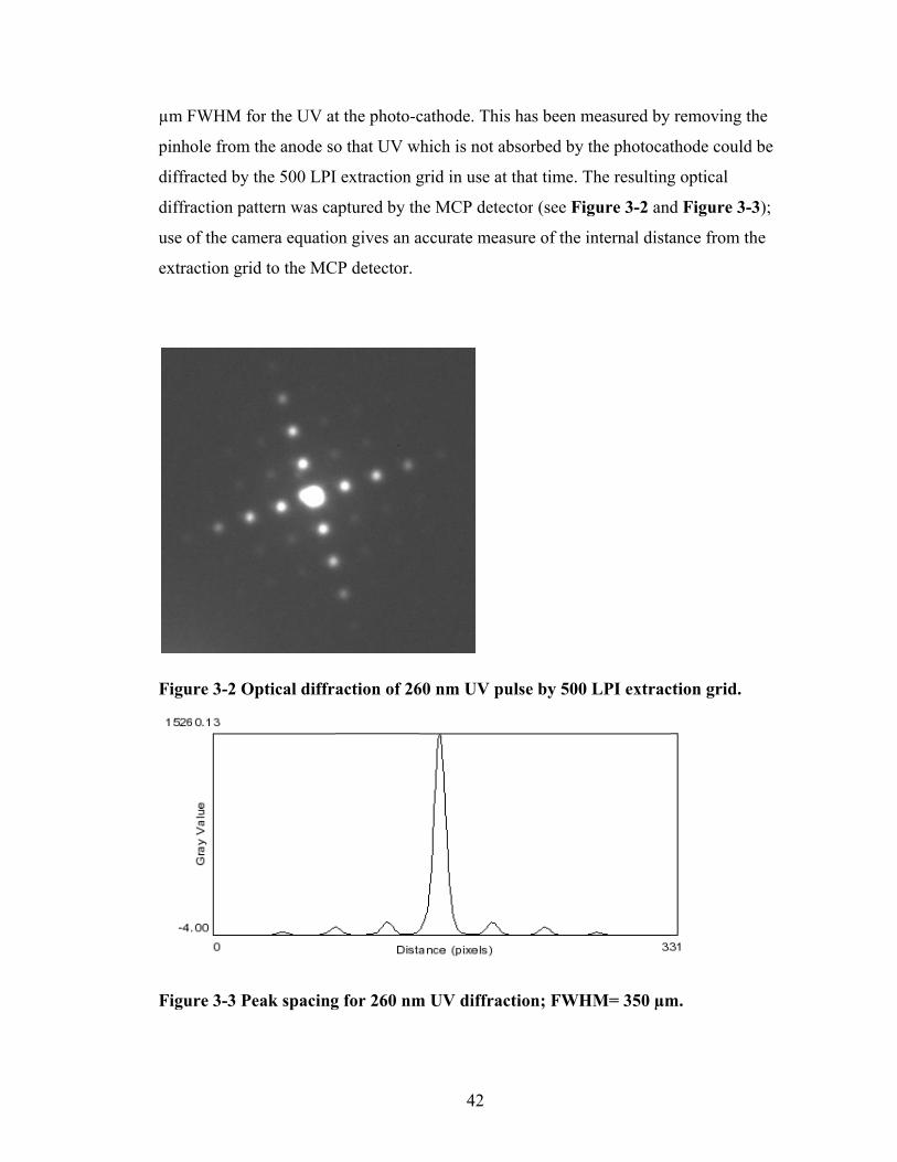
µ
p
d
d
u
ex
F
F
µm FWHM f
inhole from
iffracted by
iffraction pa
se of the cam
xtraction gri
Figure 3-2 O
Figure 3-3 P
for the UV at
the anode so
the 500 LPI
attern was ca
mera equatio
id to the MC
Optical diffr
eak spacing
t the photo-c
o that UV w
I extraction g
aptured by th
on gives an a
CP detector.
action of 26
g for 260 nm
42
cathode. Thi
which is not a
grid in use at
he MCP dete
accurate mea
60 nm UV p
m UV diffra
s has been m
absorbed by
t that time. T
ector (see Fig
asure of the i
ulse by 500
ction; FWH
measured by
the photocat
The resulting
gure 3-2 and
internal dista
LPI extrac
HM= 350 µm
removing th
thode could
g optical
d Figure 3-3
ance from th
ction grid.
m.
he
be
3);
he
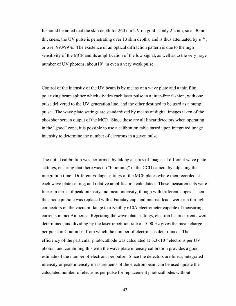
43
It should be noted that the skin depth for 260 nm UV on gold is only 2.2 nm, so at 30 nm
thickness, the UV pulse is penetrating over 13 skin depths, and is thus attenuated by 13e− ,
or over 99.999%. The existence of an optical diffraction pattern is due to the high
sensitivity of the MCP and its amplification of the low signal, as well as to the very large
number of UV photons, about 810 in even a very weak pulse.
Control of the intensity of the UV beam is by means of a wave plate and a thin film
polarizing beam splitter which divides each laser pulse in a jitter-free fashion, with one
pulse delivered to the UV generation line, and the other destined to be used as a pump
pulse. The wave plate settings are standardized by means of digital images taken of the
phosphor screen output of the MCP. Since these are all linear detectors when operating
in the “good” zone, it is possible to use a calibration table based upon integrated image
intensity to determine the number of electrons in a given pulse.
The initial calibration was performed by taking a series of images at different wave plate
settings, ensuring that there was no “blooming” in the CCD camera by adjusting the
integration time. Different voltage settings of the MCP plates where then recorded at
each wave plate setting, and relative amplification calculated. These measurements were
linear in terms of peak intensity and mean intensity, though with different slopes. Then
the anode pinhole was replaced with a Faraday cup, and internal leads were run through
connectors on the vacuum flange to a Keithly 610A electrometer capable of measuring
currents in picoAmperes. Repeating the wave plate settings, electron beam currents were
determined, and dividing by the laser repetition rate of 1000 Hz gives the mean charge
per pulse in Coulombs, from which the number of electrons is determined. The
efficiency of the particular photocathode was calculated at 53.3 10−× electrons per UV
photon, and combining this with the wave plate intensity calibration provides a good
estimate of the number of electrons per pulse. Since the detectors are linear, integrated
intensity or peak intensity measurements of the electron beam can be used update the
calculated number of electrons per pulse for replacement photocathodes without
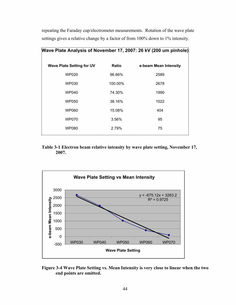
44
repeating the Faraday cup/electrometer measurements. Rotation of the wave plate
settings gives a relative change by a factor of from 100% down to 1% intensity.
Wave Plate Analysis of November 17, 2007: 26 kV (200 um pinhole)
Wave Plate Setting for UV Ratio e-beam Mean Intensity
WP020 96.66% 2589
WP030 100.00% 2678
WP040 74.30% 1990
WP050 38.16% 1022
WP060 15.08% 404
WP070 3.56% 95
WP080 2.79% 75
Table 3-1 Electron beam relative intensity by wave plate setting, November 17, 2007.
Figure 3-4 Wave Plate Setting vs. Mean Intensity is very close to linear when the two end points are omitted.
y = -675.12x + 3263.2R² = 0.9725
-500
0
500
1000
1500
2000
2500
3000
WP030 WP040 WP050 WP060 WP070
e-be
am M
ean
Inte
nsity
Wave Plate Setting
Wave Plate Setting vs Mean Intensity
45
Calculating Electron Pulse Duration
Electron pulse duration depends upon the number of electrons in the pulse, the applied
voltage and length of the cathode-anode region, and the distance from the extraction grid
to the sample14 15, though there is some disagreement between the experts as to the
details, for short distances their formulations agree. The derivations depend upon solving
the Poisson equation, 2
0
ρε∇ Φ = , based upon boundary conditions guessed at from the
laser pulse striking the photocathode. Having previously established approximate
numbers of electrons as described in the previous section, the pulse broadening can be
estimated by an analytic formula derived by Qian and Elsayed-Ali14: 2 2 3 2Nd r V− − , which
is the number of electrons in the pulse times the square of the distance propagated,
divided by the radial diameter of the electron bunch squared times the accelerating
voltage to the 3/2 power. The broadening is with respect to the initial laser pulse
duration, and this form is valid for short distances; otherwise it overstates the broadening.
The radial diameter of the electron pulse is controlled by the anode pinhole, and the
accelerating voltage is an important operating parameter of the electron gun. Larger
values of the accelerating voltage result in shorter pulse duration; a larger radial diameter
means a lower electron density, while a higher voltage means that the pulse is
propagating at a higher speed, and thus has less time to self-expand. This is self-evident
if one is riding in the rest frame of the pulse. The remaining factors are the number of the
electrons times the square of the distance travelled. The distance is determined by how
the electron gun is built, and how close the sample can be positioned while still providing
access to the pump laser pulse. In the current 30 kV electron gun, the cathode to
extraction grid distance is 4.3 mm, for a field strength of 6.9 MV/m, the drift distance
from the extraction grid to the sample is 16.3 mm. For an electron pulse with 12,000
electrons the laser-pulse replica starting at 150 fs will broaden to almost 300 fs at the
46
sample plane. Further broadening as it travels afterwards to the detector is immaterial,
for the dynamics of the electron diffraction process are faithfully carried by the
expanding pulse.
Self-Chirp
Self repulsion from within the electron bunch results in self-chirping of the electron
pulse15. The electrons at the leading edge of the pulse are slightly accelerated, and so pull
further ahead, while the ones at the back are slightly decelerated, and so fall farther
behind. The ones in the middle feel intermediate forces, and seek equilibrium. If the
pulse spends enough time drifting it becomes nicely chirped, and some form of
compression could be applied to shorten it up significantly. Such a device has been
proposed by Qian and Elsayed-Ali38, though none has been constructed on an appropriate
scale for a table-top system. Implementation of a chirp-compressor will permit the
electron source to be distant from the target. This allows room for focusing optics, beam
steering, and diagnostics such as a Faraday cup. This would make the diffractometer
compatible with imaging applications such as an ultrafast TEM. Development of single-
shot imaging with 10 nm spatial/10 ps temporal resolution by 5 MeV electrons has been
recently proposed.39 Baum and Zewail40 propose a technique based on tilted optical
wave fronts for the generation of reverse-chirped, self-compressing electron pulses.
These and many related issues are examined in detail in a review article41 by W.E. King
et al.
Photocathode Fabrication
Photocathodes must be transparent to the 260 nm UV laser pulse. Suitable materials are
UV-grade fused silica, and sapphire. The current design uses the curved surface of a 12.6
mm diameter negative lens made of fused silica. Several lenses are purchased at a time
47
so that spare photocathodes are available when needed. The photocathode is prepared for
coating by washing in high purity acetone for 10 minutes in an ultrasonic cleaner to
remove any oily contaminants, followed by another 10 minutes in high purity methanol.
Gloves are used for handling. The blanks are placed in a Denton sputter coater with a
gold target, and after achieving vacuum and then stabilizing the argon pressure, the coater
runs a current of 40 mA for 90 seconds to produce a 30 nm coating.
Since electrical contact with the film is made by an electrical contact plate on the front
side, the outer region of the coating is made thicker by covering the 90 second coating
with a 10 mm diameter sapphire window left over from a previous design, and then
applying a further coating of 300 seconds. This thicker film does not tear or wear during
the working life of a photocathode which can be up to three months before it ruptures at
the point where the UV beam strikes it. Attempting to focus the UV beam below 250 µm
FWHM also leads to rapid (or even immediate) rupture, so finer beams depend upon
smaller pinhole exits from the anode.
This coating procedure was adequate at 20 kV, but required further steps at 30 kV due to
the increased forces of the nearly 7 MV/m electrostatic field which would pull off loosely
bound nanoparticles, and then rip the film. The current procedure for toughening the film
is to expose it to a germicidal UV lamp (260 nm) for 48 hours. This process improves
surface adhesion of the film to the fused silica substrate. TEM examination of
“toughened” thin films also showed a slight increase in particle size and an increase in
the number of inter-particle connections.
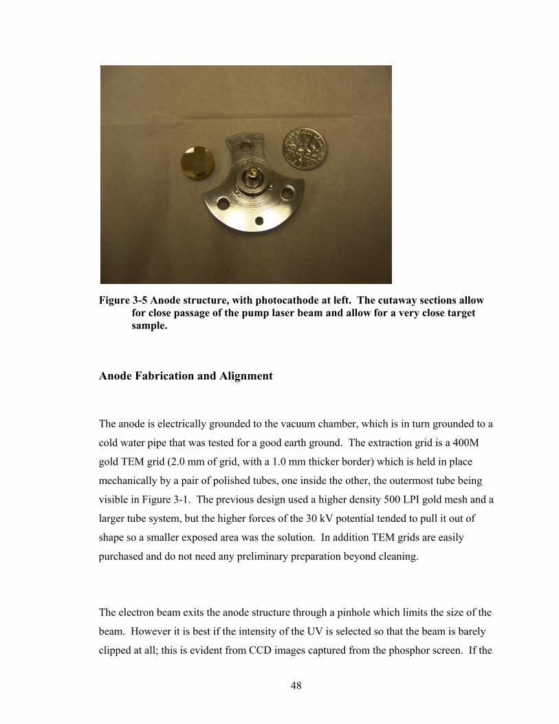
48
Figure 3-5 Anode structure, with photocathode at left. The cutaway sections allow for close passage of the pump laser beam and allow for a very close target sample.
Anode Fabrication and Alignment
The anode is electrically grounded to the vacuum chamber, which is in turn grounded to a
cold water pipe that was tested for a good earth ground. The extraction grid is a 400M
gold TEM grid (2.0 mm of grid, with a 1.0 mm thicker border) which is held in place
mechanically by a pair of polished tubes, one inside the other, the outermost tube being
visible in Figure 3-1. The previous design used a higher density 500 LPI gold mesh and a
larger tube system, but the higher forces of the 30 kV potential tended to pull it out of
shape so a smaller exposed area was the solution. In addition TEM grids are easily
purchased and do not need any preliminary preparation beyond cleaning.
The electron beam exits the anode structure through a pinhole which limits the size of the
beam. However it is best if the intensity of the UV is selected so that the beam is barely
clipped at all; this is evident from CCD images captured from the phosphor screen. If the
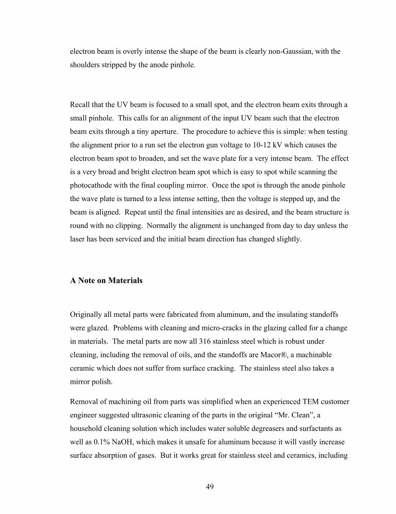
49
electron beam is overly intense the shape of the beam is clearly non-Gaussian, with the
shoulders stripped by the anode pinhole.
Recall that the UV beam is focused to a small spot, and the electron beam exits through a
small pinhole. This calls for an alignment of the input UV beam such that the electron
beam exits through a tiny aperture. The procedure to achieve this is simple: when testing
the alignment prior to a run set the electron gun voltage to 10-12 kV which causes the
electron beam spot to broaden, and set the wave plate for a very intense beam. The effect
is a very broad and bright electron beam spot which is easy to spot while scanning the
photocathode with the final coupling mirror. Once the spot is through the anode pinhole
the wave plate is turned to a less intense setting, then the voltage is stepped up, and the
beam is aligned. Repeat until the final intensities are as desired, and the beam structure is
round with no clipping. Normally the alignment is unchanged from day to day unless the
laser has been serviced and the initial beam direction has changed slightly.
A Note on Materials
Originally all metal parts were fabricated from aluminum, and the insulating standoffs
were glazed. Problems with cleaning and micro-cracks in the glazing called for a change
in materials. The metal parts are now all 316 stainless steel which is robust under
cleaning, including the removal of oils, and the standoffs are Macor®, a machinable
ceramic which does not suffer from surface cracking. The stainless steel also takes a
mirror polish.
Removal of machining oil from parts was simplified when an experienced TEM customer
engineer suggested ultrasonic cleaning of the parts in the original “Mr. Clean”, a
household cleaning solution which includes water soluble degreasers and surfactants as
well as 0.1% NaOH, which makes it unsafe for aluminum because it will vastly increase
surface absorption of gases. But it works great for stainless steel and ceramics, including
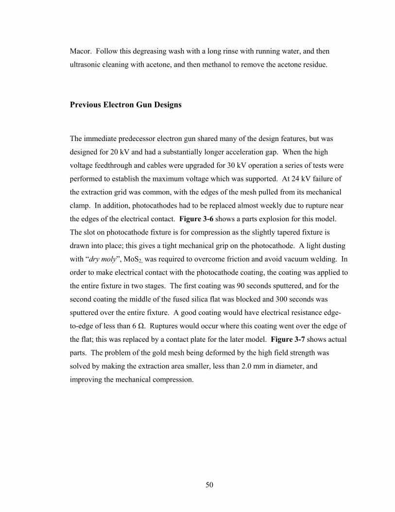
50
Macor. Follow this degreasing wash with a long rinse with running water, and then
ultrasonic cleaning with acetone, and then methanol to remove the acetone residue.
Previous Electron Gun Designs
The immediate predecessor electron gun shared many of the design features, but was
designed for 20 kV and had a substantially longer acceleration gap. When the high
voltage feedthrough and cables were upgraded for 30 kV operation a series of tests were
performed to establish the maximum voltage which was supported. At 24 kV failure of
the extraction grid was common, with the edges of the mesh pulled from its mechanical
clamp. In addition, photocathodes had to be replaced almost weekly due to rupture near
the edges of the electrical contact. Figure 3-6 shows a parts explosion for this model.
The slot on photocathode fixture is for compression as the slightly tapered fixture is
drawn into place; this gives a tight mechanical grip on the photocathode. A light dusting
with “dry moly”, MoS2, was required to overcome friction and avoid vacuum welding. In
order to make electrical contact with the photocathode coating, the coating was applied to
the entire fixture in two stages. The first coating was 90 seconds sputtered, and for the
second coating the middle of the fused silica flat was blocked and 300 seconds was
sputtered over the entire fixture. A good coating would have electrical resistance edge-
to-edge of less than 6 Ω. Ruptures would occur where this coating went over the edge of
the flat; this was replaced by a contact plate for the later model. Figure 3-7 shows actual
parts. The problem of the gold mesh being deformed by the high field strength was
solved by making the extraction area smaller, less than 2.0 mm in diameter, and
improving the mechanical compression.
51
Figure 3-6 20 kV electron gun parts explosion; produced 2-5 ps electron pulses.
Figure 3-7 Left: Photocathode was held in a friction fitting. Right: Anode extraction grid was 500 LPI gold mesh.
The earliest versions included a magnetic focusing solenoid which was mounted external
to the vacuum chamber around a nipple midway between the electron gun and the
sample. This was used to collimate the electron beam, resulting in finer diffraction
patterns as seen in Figure 2-8, but required an additional 16” of travel for the electron
pulse, making it 200-300 ps in duration. When this became fully understood it was clear
52
that the magnet would have to go into the vacuum chamber, but the in-vacuo coil was not
strong enough to collimate the beam and was abandoned in order to reduce the beam drift
distance. The problem was that as the current increased, the Kaptan® polyimide film
insulation of the wires out-gassed faster than the pumps could clear it, and the vacuum
was degraded. A workable in-vacuo solenoid must be UHV compatible, or else isolated
from the vacuum, and probably requires water cooling to remove the heat in either case.
Transmission and Reflection Modes
The description to this point has been of transmission mode, similar to that used in an
electron microscope. With a few adjustments it is also possible to operate in reflection
mode, similar to a RHEED system. These adjustments were made in order to
accommodate a bismuth sample provided by Davidé Boschetto of the Laboratoire
d'Optique Appliquée LOA-ENSTA, which had previously been used for time-resolved x-
ray diffraction experiments. This required addition of high-voltage deflector plates
mounted to the flange holding the MCP detector, a new sample holder design that could
rotate to grazing incidence with the electron beam, and a modified optical path for the
laser pump beam perpendicular to the electron beam. Preliminary bismuth experiments
were carried out, but the diffraction pattern was not that of a clean Bi surface – the
previous x-ray experiments did not detect a thin layer of bismuth oxide on the sample;
however, the electron beam probes only the topmost layers in reflection, and saw only the
bismuth oxide.
Additional samples tested include highly ordered pyrolitic graphite (HOPG), see Figure
3-8 and Figure 3-9, and thermally evaporated gold on silicon substrates. RHEED
requires very flat samples; the nanostructure of the sputtered gold was not smooth enough
to obtain good RHEED patterns.
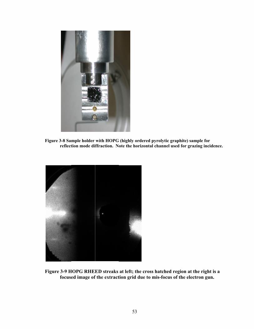
F
F
Figure 3-8 Samreflect
Figure 3-9 Hfocuse
mple holder tion mode di
HOPG RHEEed image of
with HOPGiffraction. N
ED streaks f the extract
53
G (highly ordeote the horiz
at left; the tion grid du
ered pyrolytizontal chann
cross hatchue to mis-foc
ic graphite) sel used for g
hed region acus of the el
sample for razing incide
t the right ilectron gun.
ence.
is a .
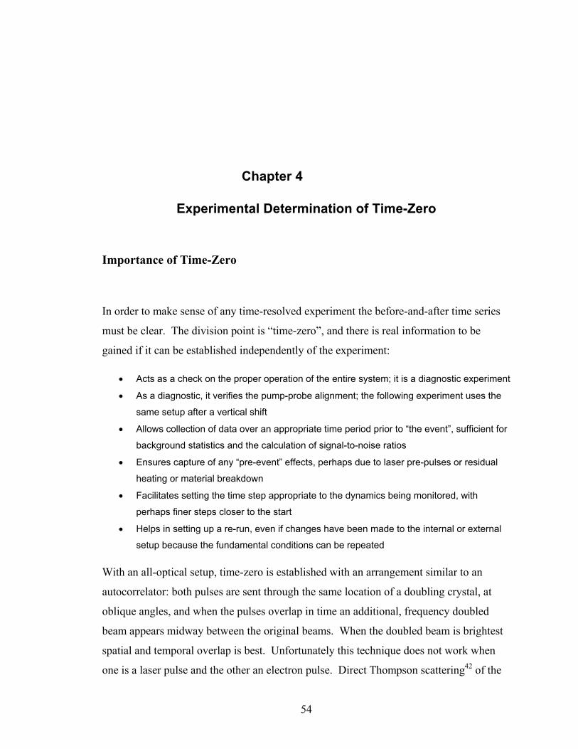
54
Chapter 4
Experimental Determination of Time-Zero
Importance of Time-Zero
In order to make sense of any time-resolved experiment the before-and-after time series
must be clear. The division point is “time-zero”, and there is real information to be
gained if it can be established independently of the experiment:
• Acts as a check on the proper operation of the entire system; it is a diagnostic experiment
• As a diagnostic, it verifies the pump-probe alignment; the following experiment uses the
same setup after a vertical shift
• Allows collection of data over an appropriate time period prior to “the event”, sufficient for
background statistics and the calculation of signal-to-noise ratios
• Ensures capture of any “pre-event” effects, perhaps due to laser pre-pulses or residual
heating or material breakdown
• Facilitates setting the time step appropriate to the dynamics being monitored, with
perhaps finer steps closer to the start
• Helps in setting up a re-run, even if changes have been made to the internal or external
setup because the fundamental conditions can be repeated
With an all-optical setup, time-zero is established with an arrangement similar to an
autocorrelator: both pulses are sent through the same location of a doubling crystal, at
oblique angles, and when the pulses overlap in time an additional, frequency doubled
beam appears midway between the original beams. When the doubled beam is brightest
spatial and temporal overlap is best. Unfortunately this technique does not work when
one is a laser pulse and the other an electron pulse. Direct Thompson scattering42 of the
55
electron pulses by interaction with the laser pulses can be tried, but the cross sections are
too small unless the electron density is enhanced along with the laser intensity at the
spatial intersection. These conditions are inappropriate for most time-resolved
experiments because the increased electron density increases the electron pulse duration
greatly, and the overly intense laser pulse will vaporize the sample.
Indirect methods include special features in the system such as a pinhole43 or a sharply
pointed needle44 which will drive off electrons at the tip when struck by the laser pulse,
and the charge buildup will deflect the electron pulse around the tip. Another is to use the
laser pulse to ionize some material which will interact with the electron pulse; this is
especially convenient for gas phase experiments45 where it is the gas which is ionized.
These methods can be performed without changing the focus of the pump beam; the only
change is a temporary increase in the power being admitted to the pump line. The
traditional method has been to monitor a target for a solid-to-liquid phase change; this
requires repetitions of single-shot experiments, and their associated target manipulator.
Another method that has been suggested46 is to use a photoconductive switch so that the
laser pulse “connects” the amplified electron beam charge to an external oscilloscope,
allowing a rapid determination of time zero as the pump delay line is rapidly scanned.
Other ingenious approaches will no doubt be found, as has been shown in “Clocking
Femtosecond X-Rays”47; SLAC was able to compress an ultra relativistic (28.5 GeV)
electron bunch electron with over 1010 electrons to 80 fs using a magnetic chicane.
Optical Alignment
Optical stability is crucial. The alignment of the pump laser beam includes reflection
from a cube-corner style retro-reflector mounted on a computer controlled translation
stage. The laser beam must enter and leave parallel to the optical table, and to its own
path. This ensures that the pump beam focal point won’t wander about as the stage is
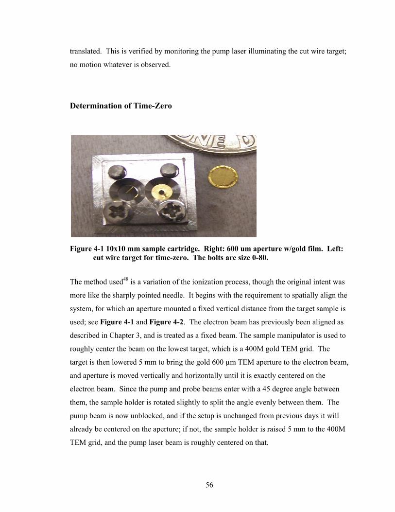
tr
n
D
F
T
m
sy
u
d
ro
ta
an
el
th
pu
al
T
ranslated. Th
o motion wh
Determinat
Figure 4-1 10cut w
The method u
more like the
ystem, for w
sed; see Fig
escribed in C
oughly cente
arget is then
nd aperture i
lectron beam
hem, the sam
ump beam is
lready be cen
TEM grid, an
his is verifie
hatever is ob
ion of Tim
0x10 mm sawire target fo
used48 is a va
sharply poin
which an aper
ure 4-1 and
Chapter 3, an
er the beam o
lowered 5 m
is moved ver
m. Since the
mple holder i
s now unblo
ntered on th
nd the pump
ed by monito
bserved.
me-Zero
ample cartrior time-zero
ariation of th
nted needle.
rture mounte
Figure 4-2.
nd is treated
on the lowes
mm to bring
rtically and
pump and p
is rotated slig
ocked, and if
e aperture; i
laser beam i
56
oring the pum
idge. Righto. The bolts
he ionization
It begins w
ed a fixed ve
. The electro
d as a fixed b
st target, whi
the gold 600
horizontally
probe beams
ghtly to split
f the setup is
f not, the sam
is roughly ce
mp laser illu
t: 600 um aps are size 0-
n process, tho
with the requ
ertical distan
on beam has
beam. The sa
ich is a 400M
0 µm TEM a
y until it is ex
s enter with a
t the angle e
unchanged
mple holder
entered on th
minating the
perture w/g80.
ough the ori
irement to sp
nce from the
s previously
ample manip
M gold TEM
aperture to th
xactly center
a 45 degree a
evenly betwe
from previo
is raised 5 m
hat.
e cut wire tar
old film. Le
ginal intent
patially align
target samp
been aligned
pulator is use
M grid. The
he electron b
red on the
angle betwee
een them. Th
us days it w
mm to the 40
rget;
eft:
was
n the
ple is
d as
ed to
beam,
en
he
ill
00M
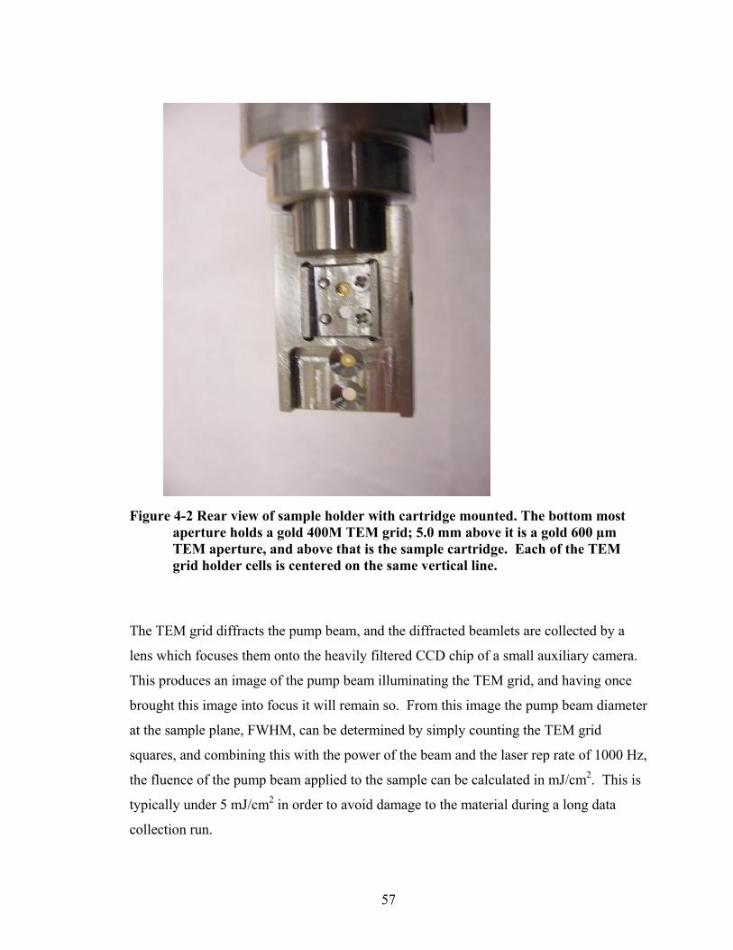
57
Figure 4-2 Rear view of sample holder with cartridge mounted. The bottom most aperture holds a gold 400M TEM grid; 5.0 mm above it is a gold 600 µm TEM aperture, and above that is the sample cartridge. Each of the TEM grid holder cells is centered on the same vertical line.
The TEM grid diffracts the pump beam, and the diffracted beamlets are collected by a
lens which focuses them onto the heavily filtered CCD chip of a small auxiliary camera.
This produces an image of the pump beam illuminating the TEM grid, and having once
brought this image into focus it will remain so. From this image the pump beam diameter
at the sample plane, FWHM, can be determined by simply counting the TEM grid
squares, and combining this with the power of the beam and the laser rep rate of 1000 Hz,
the fluence of the pump beam applied to the sample can be calculated in mJ/cm2. This is
typically under 5 mJ/cm2 in order to avoid damage to the material during a long data
collection run.
58
If the pump laser beam is not found by the camera directly, another small camera which
images from the face of the sample holder is used to find where the pump laser beam is
striking, and the coupling mirror is slightly adjusted to put the beam through the TEM
grid. The alternative is to use an IR viewer and look around inside the vacuum chamber;
cameras are much easier and safer because the eyes are never exposed to stray
reflections.
Having spatially aligned the beams, and if necessary measured the pump beam diameter,
the sample holder can be lowered further if the cut wire target is being used for time-zero
determination. This is from a special TEM grid made of 80 µm parallels, most of which
have been cut away by means of a razor blade under a microscope, leaving a cut wire of
80 µm diameter with the tip roughly centered in the aperture. When this cut wire is used
it replaces one of the target samples. Since the beams are co-centered at this point of the
procedure, it is only necessary to bring the wire tip into the center of the pump beam
using the sample plane imaging camera. This automatically brings the tip into the
electron beam, though this can be verified by increasing the intensity of the electron
beam by means of the wave plate setting. Next the tip is moved slightly so that it is
closer to the edge of the electron beam, and the laser beam is manipulated to bring its
center back onto the tip. This results in the greatest deflection of the electron beam, and
hence is easiest to interpret.
It is worth noting that the same time-zero is determined regardless of the intensity of the
electron beam; the detection is approximately the front edge of the pulse, and the front
edges are the same regardless of the number of electrons in the pulse.
The cut wire worked very well at first, but then the deflection effect slowly grew less and
less. The same had been noted when the target was the edge of the 600 µm aperture, and

59
later with the 400M grid. The reason for this decay was not obvious at first, but
eventually it became apparent that in each case the dominant process was not multi-
photon emission, or induced currents, but instead it was a surface ionization process, a
form of laser cleaning process. As the surface became cleaner and cleaner, there was less
debris available to ionize and knock off, so the deflection signal became weaker and
weaker. It is easy to restore a target: just aim the laser at a fresh spot, or replace the
target, or brush it with a (tiny) bit of colloidal silver paste and acetone.
Having prepared the run, it is now necessary to take a series of shots, alternating with the
pump beam blocked and unblocked. The CCD camera records an image of the central
electron beam; the remainder of the image field need not be recorded. The camera
integration time can be as fast as one second; better results are obtained by repeating each
position five times, or not quite as good, increasing the integration time to five seconds.
The time required to scan 140 ps is less than an hour, followed by a brief analysis of the
data. Pump power is adjusted to generate a fluence of 5-10 mJ/cm2 at the target; this
typically results in pump beam intensity slightly above 1010 W/cm2.
The data are analyzed by calculating the centroid (first moment) of the intensity
distribution of the central beam image for each shot of each position. If shots have been
repeated, the centroids are averaged together. From them the difference in the centroids
between the heated and unheated shots is computed and the time series is plotted. A
typical deflection chart is shown in Figure 4-3. Time-zero is the last point prior to where
the deflection has started.
Extensive experience with this technique has shown that changes in the measured time-
zero are less than one picosecond from day to day; when multiple shots are taken at each
step and the positions averaged, then the change is on the order of 0.5 ps.
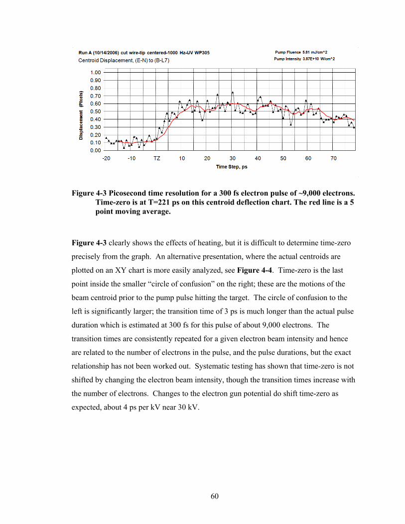
60
Figure 4-3 Picosecond time resolution for a 300 fs electron pulse of ~9,000 electrons. Time-zero is at T=221 ps on this centroid deflection chart. The red line is a 5 point moving average.
Figure 4-3 clearly shows the effects of heating, but it is difficult to determine time-zero
precisely from the graph. An alternative presentation, where the actual centroids are
plotted on an XY chart is more easily analyzed, see Figure 4-4. Time-zero is the last
point inside the smaller “circle of confusion” on the right; these are the motions of the
beam centroid prior to the pump pulse hitting the target. The circle of confusion to the
left is significantly larger; the transition time of 3 ps is much longer than the actual pulse
duration which is estimated at 300 fs for this pulse of about 9,000 electrons. The
transition times are consistently repeated for a given electron beam intensity and hence
are related to the number of electrons in the pulse, and the pulse durations, but the exact
relationship has not been worked out. Systematic testing has shown that time-zero is not
shifted by changing the electron beam intensity, though the transition times increase with
the number of electrons. Changes to the electron gun potential do shift time-zero as
expected, about 4 ps per kV near 30 kV.
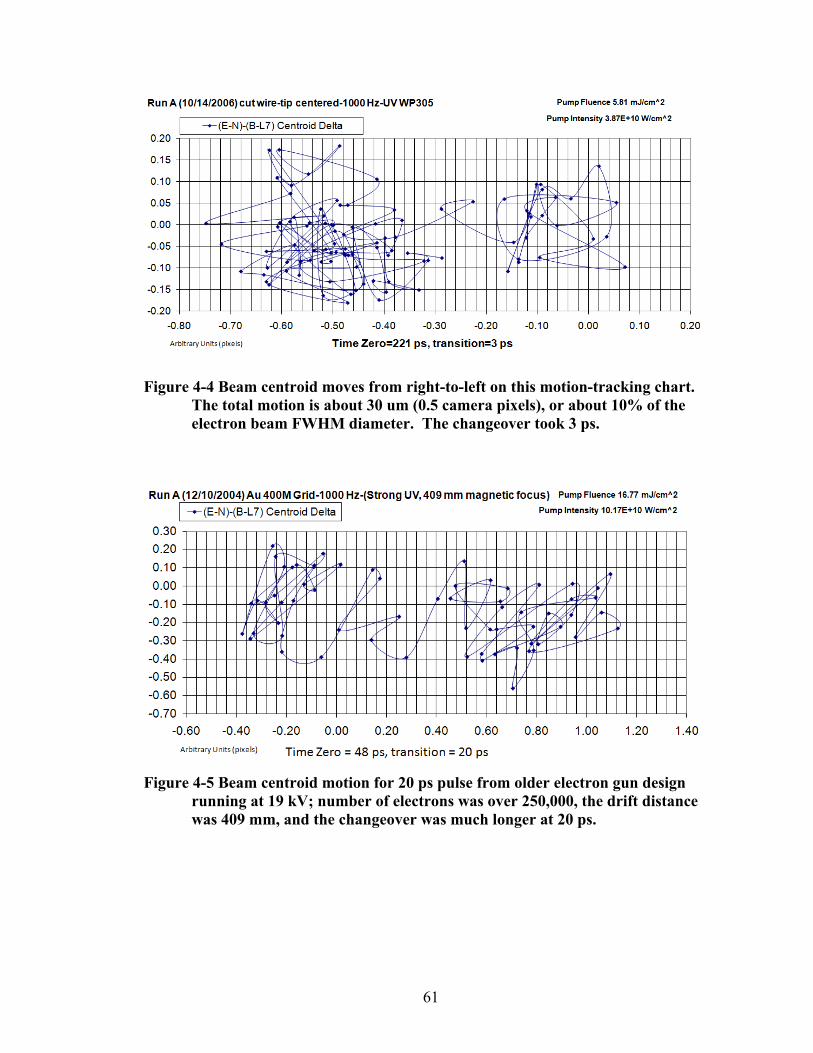
61
Figure 4-4 Beam centroid moves from right-to-left on this motion-tracking chart. The total motion is about 30 um (0.5 camera pixels), or about 10% of the electron beam FWHM diameter. The changeover took 3 ps.
Figure 4-5 Beam centroid motion for 20 ps pulse from older electron gun design running at 19 kV; number of electrons was over 250,000, the drift distance was 409 mm, and the changeover was much longer at 20 ps.
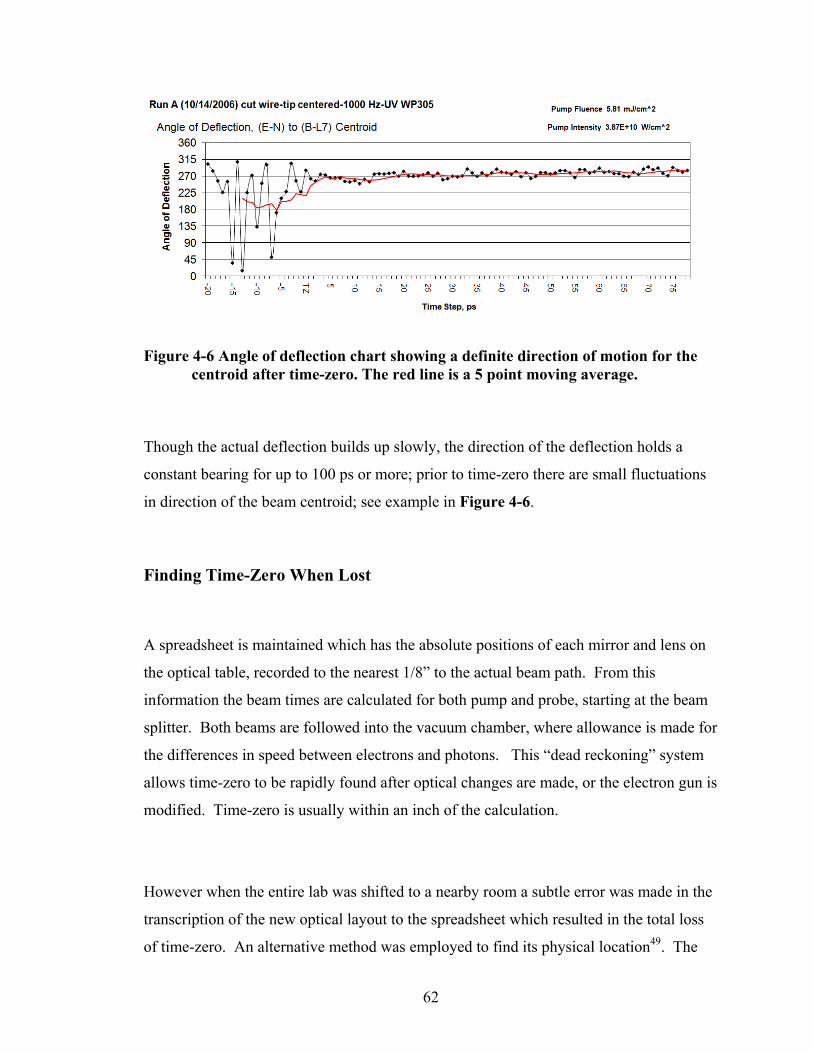
62
Figure 4-6 Angle of deflection chart showing a definite direction of motion for the centroid after time-zero. The red line is a 5 point moving average.
Though the actual deflection builds up slowly, the direction of the deflection holds a
constant bearing for up to 100 ps or more; prior to time-zero there are small fluctuations
in direction of the beam centroid; see example in Figure 4-6.
Finding Time-Zero When Lost
A spreadsheet is maintained which has the absolute positions of each mirror and lens on
the optical table, recorded to the nearest 1/8” to the actual beam path. From this
information the beam times are calculated for both pump and probe, starting at the beam
splitter. Both beams are followed into the vacuum chamber, where allowance is made for
the differences in speed between electrons and photons. This “dead reckoning” system
allows time-zero to be rapidly found after optical changes are made, or the electron gun is
modified. Time-zero is usually within an inch of the calculation.
However when the entire lab was shifted to a nearby room a subtle error was made in the
transcription of the new optical layout to the spreadsheet which resulted in the total loss
of time-zero. An alternative method was employed to find its physical location49. The
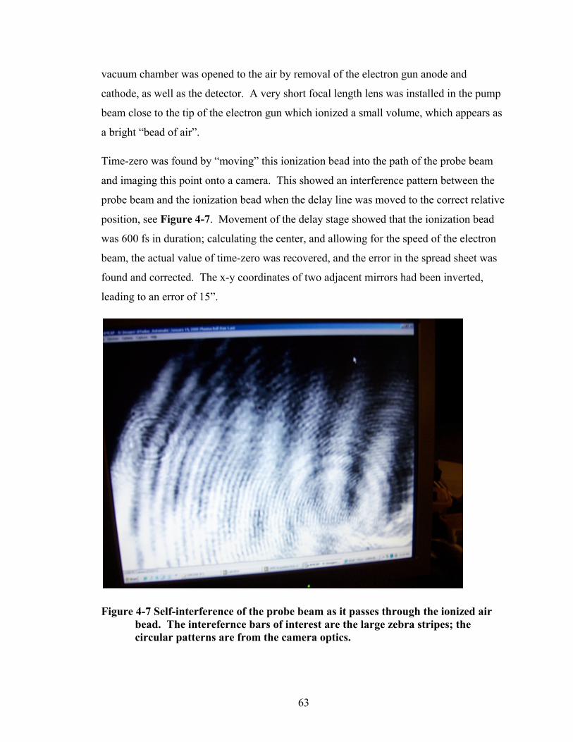
63
vacuum chamber was opened to the air by removal of the electron gun anode and
cathode, as well as the detector. A very short focal length lens was installed in the pump
beam close to the tip of the electron gun which ionized a small volume, which appears as
a bright “bead of air”.
Time-zero was found by “moving” this ionization bead into the path of the probe beam
and imaging this point onto a camera. This showed an interference pattern between the
probe beam and the ionization bead when the delay line was moved to the correct relative
position, see Figure 4-7. Movement of the delay stage showed that the ionization bead
was 600 fs in duration; calculating the center, and allowing for the speed of the electron
beam, the actual value of time-zero was recovered, and the error in the spread sheet was
found and corrected. The x-y coordinates of two adjacent mirrors had been inverted,
leading to an error of 15”.
Figure 4-7 Self-interference of the probe beam as it passes through the ionized air bead. The interefernce bars of interest are the large zebra stripes; the circular patterns are from the camera optics.
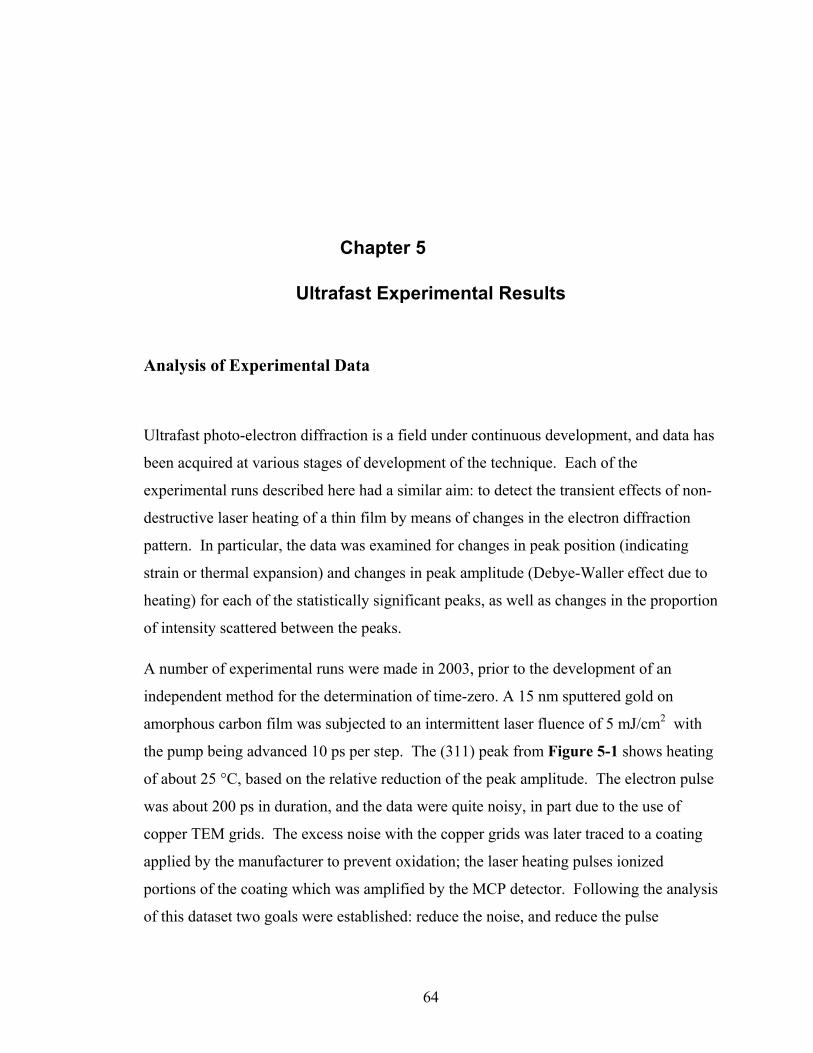
64
Chapter 5
Ultrafast Experimental Results
Analysis of Experimental Data
Ultrafast photo-electron diffraction is a field under continuous development, and data has
been acquired at various stages of development of the technique. Each of the
experimental runs described here had a similar aim: to detect the transient effects of non-
destructive laser heating of a thin film by means of changes in the electron diffraction
pattern. In particular, the data was examined for changes in peak position (indicating
strain or thermal expansion) and changes in peak amplitude (Debye-Waller effect due to
heating) for each of the statistically significant peaks, as well as changes in the proportion
of intensity scattered between the peaks.
A number of experimental runs were made in 2003, prior to the development of an
independent method for the determination of time-zero. A 15 nm sputtered gold on
amorphous carbon film was subjected to an intermittent laser fluence of 5 mJ/cm2 with
the pump being advanced 10 ps per step. The (311) peak from Figure 5-1 shows heating
of about 25 °C, based on the relative reduction of the peak amplitude. The electron pulse
was about 200 ps in duration, and the data were quite noisy, in part due to the use of
copper TEM grids. The excess noise with the copper grids was later traced to a coating
applied by the manufacturer to prevent oxidation; the laser heating pulses ionized
portions of the coating which was amplified by the MCP detector. Following the analysis
of this dataset two goals were established: reduce the noise, and reduce the pulse
65
duration. It took about a year to accomplish both goals; in addition, the method for
finding time-zero (Chapter 4, page 54) was developed and successfully tested.
Figure 5-1 Debye-Waller heating of ~25 °C with 200 ps electron pulse. Error bars were not calculated. The graph on the right is for the (311) peak, and shows a reduction in peak amplitude.
Dataset from 9 nm Platinum Film
After a number of improvements to the electron gun, and significant improvements to the
S/N ratio, a series of time-resolved heating experiments were run in October-November
2006. These were unsuccessful due to problems with the polycrystalline gold films and
the electron gun. The lab was moved in December 2006 and further improvements were
carried out on the electron gun intermittently with the search for the lost time-zero.
Time-zero was recovered in January 2008, and upon completion of repairs to the MCP
and preparation of improved samples in platinum by Codrin Cionca50, time-resolved
experiments resumed in April, 2008. Good results were obtained quickly for a laser
fluence of 2 mJ/cm2 and a target of 9 nm thick polycrystalline platinum mounted on a
400M gold TEM grid. The electron gun was operated at 30 kV, and the wave plate
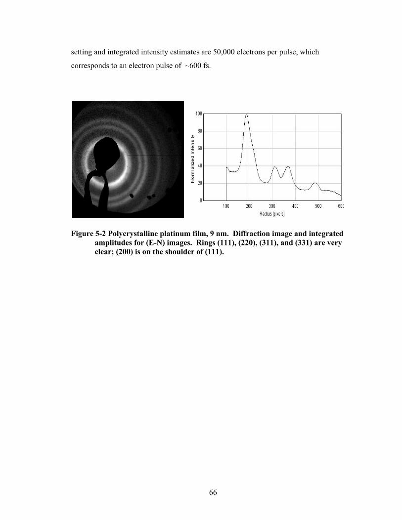
66
setting and integrated intensity estimates are 50,000 electrons per pulse, which
corresponds to an electron pulse of ~600 fs.
Figure 5-2 Polycrystalline platinum film, 9 nm. Diffraction image and integrated amplitudes for (E-N) images. Rings (111), (220), (311), and (331) are very clear; (200) is on the shoulder of (111).
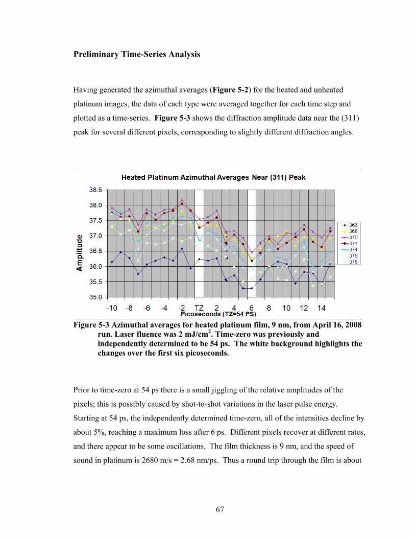
67
Preliminary Time-Series Analysis
Having generated the azimuthal averages (Figure 5-2) for the heated and unheated
platinum images, the data of each type were averaged together for each time step and
plotted as a time-series. Figure 5-3 shows the diffraction amplitude data near the (311)
peak for several different pixels, corresponding to slightly different diffraction angles.
Figure 5-3 Azimuthal averages for heated platinum film, 9 nm, from April 16, 2008
run. Laser fluence was 2 mJ/cm2. Time-zero was previously and independently determined to be 54 ps. The white background highlights the changes over the first six picoseconds.
Prior to time-zero at 54 ps there is a small jiggling of the relative amplitudes of the
pixels; this is possibly caused by shot-to-shot variations in the laser pulse energy.
Starting at 54 ps, the independently determined time-zero, all of the intensities decline by
about 5%, reaching a maximum loss after 6 ps. Different pixels recover at different rates,
and there appear to be some oscillations. The film thickness is 9 nm, and the speed of
sound in platinum is 2680 m/s = 2.68 nm/ps. Thus a round trip through the film is about
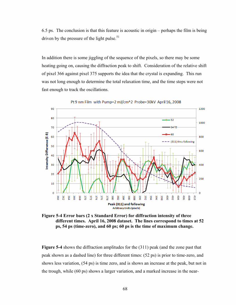
68
6.5 ps. The conclusion is that this feature is acoustic in origin – perhaps the film is being
driven by the pressure of the light pulse.51
In addition there is some jiggling of the sequence of the pixels, so there may be some
heating going on, causing the diffraction peak to shift. Consideration of the relative shift
of pixel 366 against pixel 375 supports the idea that the crystal is expanding. This run
was not long enough to determine the total relaxation time, and the time steps were not
fast enough to track the oscillations.
Figure 5-4 Error bars (2 x Standard Error) for diffraction intensity of three
different times. April 16, 2008 dataset. The lines correspond to times at 52 ps, 54 ps (time-zero), and 60 ps; 60 ps is the time of maximum change.
Figure 5-4 shows the diffraction amplitudes for the (311) peak (and the zone past that
peak shown as a dashed line) for three different times: (52 ps) is prior to time-zero, and
shows less variation, (54 ps) is time zero, and is shows an increase at the peak, but not in
the trough, while (60 ps) shows a larger variation, and a marked increase in the near-
69
trough, which is the recipient of any diffuse scattering. The lack of overlap in the error
bars of the (52 ps) and the (60 ps) traces indicates statistical significance of at least 95%
confidence for two standard errors. This is based on the analysis of ten shots heated, and
ten shots unheated at each time step; the values shown above are the differences in the
amplitude, unheated minus heated, abbreviated (E-B) on the chart.
Reflectivity Data
Samples of ultrathin platinum films, free-standing on gold 400M TEM grids, were
subjected to 22 mJ/cm fluence pump pulses, and then probed at increasing time delays in
a reflectivity experiment52 (see Figure 5-5). Similar results were obtained for the
reduced fluence of 20.5 mJ/cm . The coherent oscillations are very clear for the first 25
ps; they are much too slow to be phonons. The longitudinal and transverse speed of
sound in platinum at 20 °C of 3260 m/s and 1730 m/s53; an impulsive longitudinal wave
launched by the arrival of the pump pulse has a round-trip time through the 10 nm film
and back of 6 ps. None of these fit the temporal profile.
Similar results were obtained with silver nanoparticles embedded in a glass substrate.54
These were explained in terms of the “breathing mode” vibrations of the nanoparticles as
they exchanged energy with the surrounding matrix; they disappear then thermal
equilibrium is achieved.
Generalizing this explanation to the somewhat loosely connected nanoparticles of an
ultrathin film, we suggest that the network of roughly 10 nm sized platinum nanoparticles
is exchanging energy via the connections of the network. Figure 1-2 shows an ultrathin
gold film; the platinum network is similar for the thinnest films.
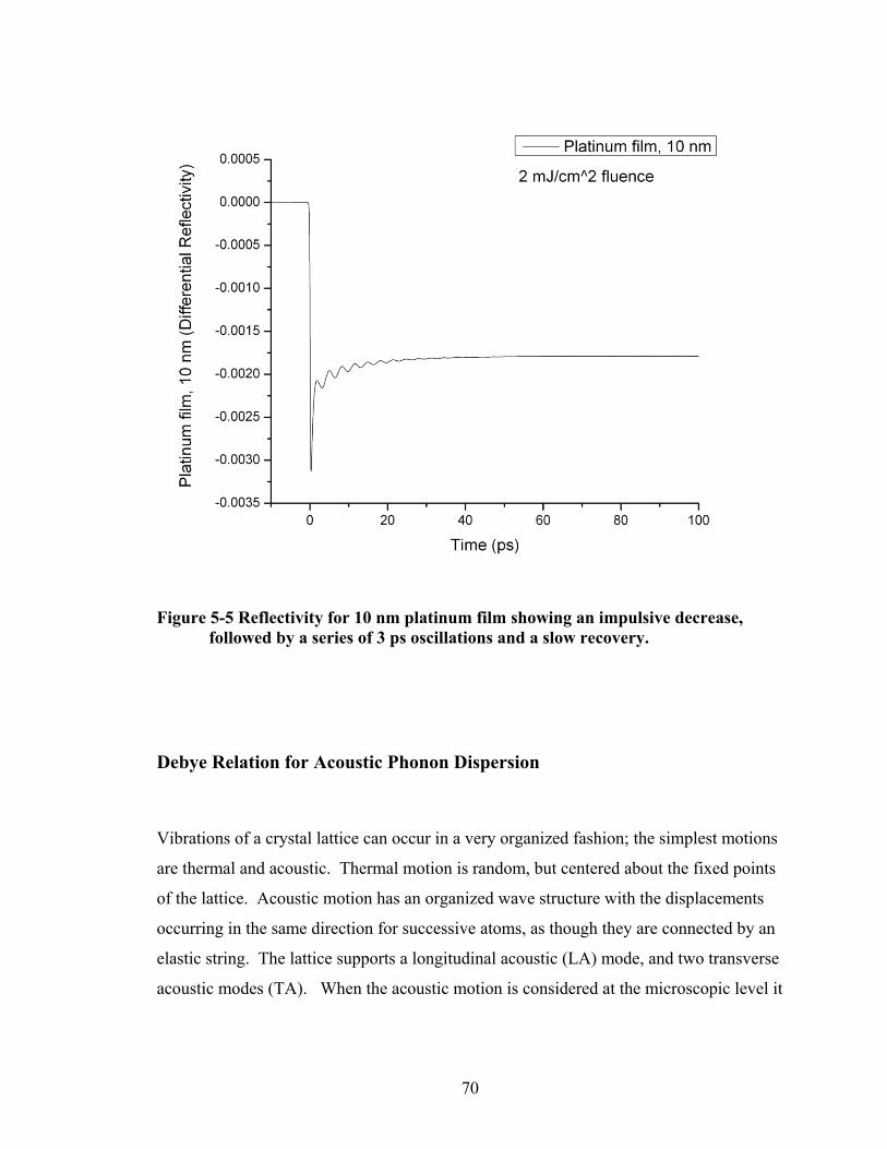
70
Figure 5-5 Reflectivity for 10 nm platinum film showing an impulsive decrease, followed by a series of 3 ps oscillations and a slow recovery.
Debye Relation for Acoustic Phonon Dispersion
Vibrations of a crystal lattice can occur in a very organized fashion; the simplest motions
are thermal and acoustic. Thermal motion is random, but centered about the fixed points
of the lattice. Acoustic motion has an organized wave structure with the displacements
occurring in the same direction for successive atoms, as though they are connected by an
elastic string. The lattice supports a longitudinal acoustic (LA) mode, and two transverse
acoustic modes (TA). When the acoustic motion is considered at the microscopic level it
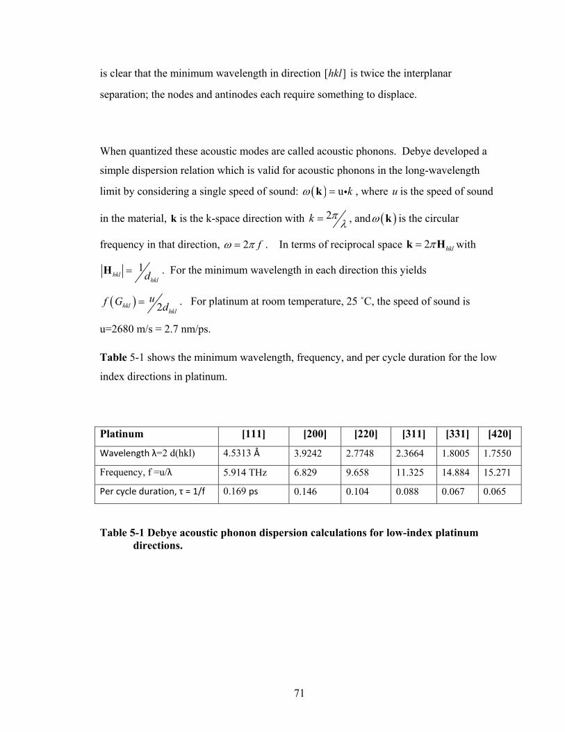
71
is clear that the minimum wavelength in direction [ ]hkl is twice the interplanar
separation; the nodes and antinodes each require something to displace.
When quantized these acoustic modes are called acoustic phonons. Debye developed a
simple dispersion relation which is valid for acoustic phonons in the long-wavelength
limit by considering a single speed of sound: ( ) u kω =k i , where u is the speed of sound
in the material, k is the k-space direction with 2k πλ= , and ( )ω k is the circular
frequency in that direction, 2 fω π= . In terms of reciprocal space 2 hklπ=k H with
1hkl
hkld=H . For the minimum wavelength in each direction this yields
( ) 2hklhkl
uf G d= . For platinum at room temperature, 25 ˚C, the speed of sound is
u=2680 m/s = 2.7 nm/ps.
Table 5-1 shows the minimum wavelength, frequency, and per cycle duration for the low
index directions in platinum.
Platinum [111] [200] [220] [311] [331] [420]
Wavelength λ=2 d(hkl) 4.5313 Å 3.9242 2.7748 2.3664 1.8005 1.7550
Frequency, f =u/λ 5.914 THz 6.829 9.658 11.325 14.884 15.271
Per cycle duration, τ = 1/f 0.169 ps 0.146 0.104 0.088 0.067 0.065
Table 5-1 Debye acoustic phonon dispersion calculations for low-index platinum directions.
72
Analysis of Integrated Peak Position and Intensity
The raw data was analyzed as to the relative stability of the peak positions. By
establishing a bracket about the nominal peaks corresponding to their FWHM, the
centroid of the pixel position with respect to the corresponding intensity was calculated
( )k k kPeakPosition position intensity intensity= ×∑ ∑ ; this serves as a proxy for the
peak position. The integrated intensity over this interval serves as the peak intensity.
This computational process smoothes fluctuations in the raw data and provides time-
series values for position and intensity for each of the diffraction peaks.
Figure 5-6 shows the temporal evolution of the (111) and (311) peak positions as a
relative percentage compared to the reference (unheated) data. The thermal expansion of
platinum is 6=8.8 10 / Kβ −× , and the change in temperature is found from R R TβΔ = Δ .
The maximum change of the (311) peak position is 0.060% , so 0.00060 68KβΔΤ = = ,
and occurs 10 ps after time-zero. The oscillations prior to time-zero are about10K .
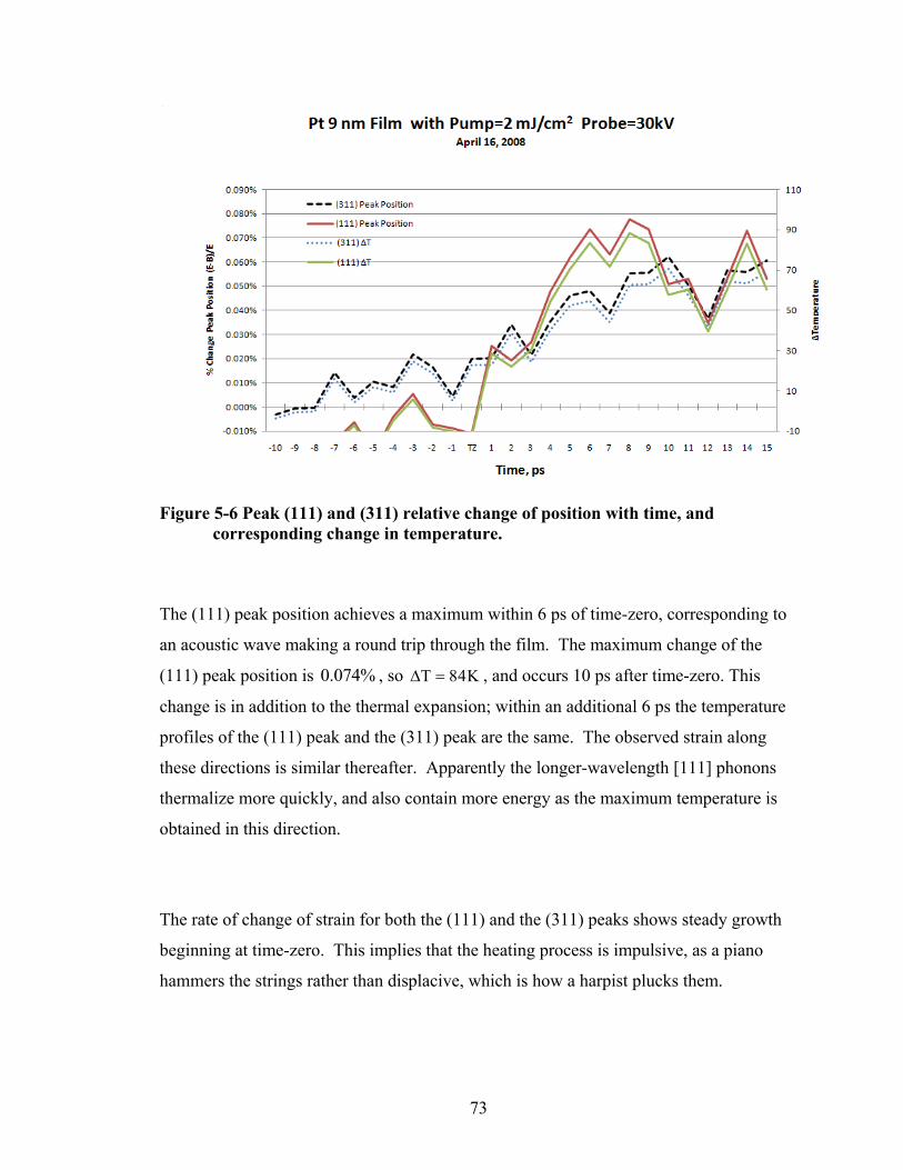
73
Figure 5-6 Peak (111) and (311) relative change of position with time, and corresponding change in temperature.
The (111) peak position achieves a maximum within 6 ps of time-zero, corresponding to
an acoustic wave making a round trip through the film. The maximum change of the
(111) peak position is 0.074% , so 84KΔΤ = , and occurs 10 ps after time-zero. This
change is in addition to the thermal expansion; within an additional 6 ps the temperature
profiles of the (111) peak and the (311) peak are the same. The observed strain along
these directions is similar thereafter. Apparently the longer-wavelength [111] phonons
thermalize more quickly, and also contain more energy as the maximum temperature is
obtained in this direction.
The rate of change of strain for both the (111) and the (311) peaks shows steady growth
beginning at time-zero. This implies that the heating process is impulsive, as a piano
hammers the strings rather than displacive, which is how a harpist plucks them.
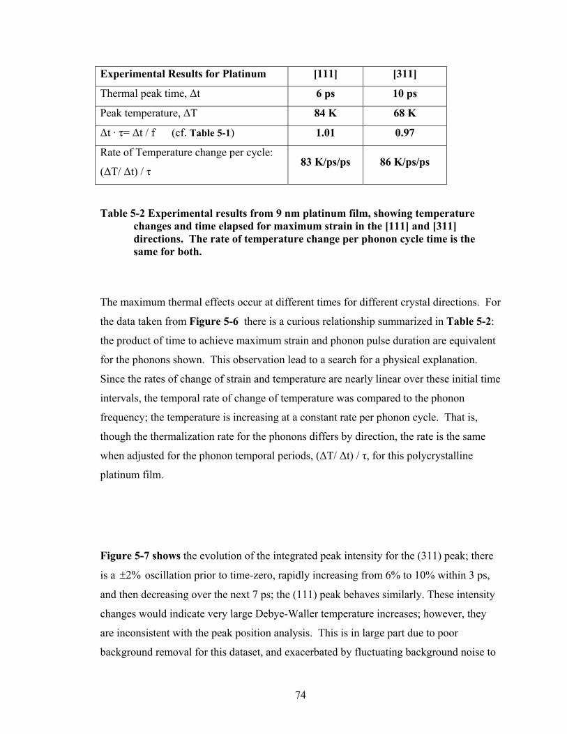
74
Experimental Results for Platinum [111] [311]
Thermal peak time, Δt 6 ps 10 ps
Peak temperature, ΔT 84 K 68 K
Δt · τ= Δt / f (cf. Table 5-1) 1.01 0.97
Rate of Temperature change per cycle:
(ΔT/ Δt) / τ 83 K/ps/ps 86 K/ps/ps
Table 5-2 Experimental results from 9 nm platinum film, showing temperature changes and time elapsed for maximum strain in the [111] and [311] directions. The rate of temperature change per phonon cycle time is the same for both.
The maximum thermal effects occur at different times for different crystal directions. For
the data taken from Figure 5-6 there is a curious relationship summarized in Table 5-2:
the product of time to achieve maximum strain and phonon pulse duration are equivalent
for the phonons shown. This observation lead to a search for a physical explanation.
Since the rates of change of strain and temperature are nearly linear over these initial time
intervals, the temporal rate of change of temperature was compared to the phonon
frequency; the temperature is increasing at a constant rate per phonon cycle. That is,
though the thermalization rate for the phonons differs by direction, the rate is the same
when adjusted for the phonon temporal periods, (ΔT/ Δt) / τ, for this polycrystalline
platinum film.
Figure 5-7 shows the evolution of the integrated peak intensity for the (311) peak; there
is a 2%± oscillation prior to time-zero, rapidly increasing from 6% to 10% within 3 ps,
and then decreasing over the next 7 ps; the (111) peak behaves similarly. These intensity
changes would indicate very large Debye-Waller temperature increases; however, they
are inconsistent with the peak position analysis. This is in large part due to poor
background removal for this dataset, and exacerbated by fluctuating background noise to
75
which the peak positions are less sensitive. An additional factor is the impact of the
acoustic wave traversing the thin film.
Figure 5-7 Peak (311) relative change of integrated intensity with time.
76
Chapter 6
Summary and Conclusions
Summary
An ultrafast photo-electron diffractometer has been built and described in detail. This
device depends upon an ultrafast laser to deliver optical pulses to “pump” a sample, as
well as to “probe” the structure by means of photo-electrons. An in-situ method for the
determination of time-zero - the time when the optical pump and electron probe pulses
are temporally coincident at the sample - has been developed and tested. The method
reliably determines time-zero to within half a picosecond.
Experiments have been conducted in transmission mode with unsupported polycrystalline
thin films (9 to 15 nm) of gold and platinum, as well as reflection mode experiments with
bismuth (oxide) and highly ordered pyrolitic graphite (HOPG). These experiments show
that it is possible to probe dynamically for structure changes caused by intense but non-
destructive laser pulses at the sub-picosecond time scale.
Information which can be obtained includes the rate at which the optical energy of the
pulse, which is captured primarily by the free electrons of metals, is transferred to
acoustic phonons, transient strain and bond softening. This work also shows how phonon
77
energy transforms into thermal energy. Changes in surface reflectivity were measured
which can be explained in terms of the nanostructure of the ultrathin films.
Proposed Future Experiments
The experiments conducted with free-standing ultrathin films, as described in Chapter 5,
exhibited unexpected results which may be connected to the nanostructure of the
materials. A series of further experiments are proposed which may elucidate these
properties:
• Preparation of ultrathin platinum films made by different techniques, and fully
characterized by SEM, TEM, and AFM
• Repetition of the ultrathin platinum experiments, conducted with different fluences for
both ultrafast diffraction and reflectivity
Further experiments with various materials are proposed:
• Ultrafast diffraction experiments with few-layer graphene, to see if layers are ejected
under impulsive pump pulses
• Ultrafast diffraction of TiSe2 a layer type compound, to see how charge waves appear
• Ultrafast diffraction of GaAs to monitor the desorption of oxides and then As; this material
is known to exhibit a stick-slip operation with microscopic, molten Ga droplets
• Ultrafast diffraction with magnetic thin films, such as Ni or Fe, looking for spin waves
• Ultrafast diffraction with CdTe, to study electron phonon scattering, and thermal transport
Proposed Improvements to the Diffractometer
Improvements in operation are to be found in three areas: (1) generation of a finer, more
collimated electron beam, (2) delivery of a shorter, more temporally focused electron
beam, (3) reduction of system background noise.
78
An improved electron beam requires a smaller source; in the current design the electron
source is ~250 µm, which is due to the UV spot size. One approach is to expand the UV
beam, and then sharply focus it onto the photocathode with a lens mounted within the
framework of the electron gun. A provision for this has been made, though experiments
have shown that as the UV is focused more finely it tends to cause the polycrystalline
gold film of the photocathode to rupture. An alternative approach is to use a thermal
field emission filament, heated somewhat below the emission threshold, and initiate an
electron pulse by means of a laser pulse to the cathode tip. This would result in a precise
release of electrons from a very small source spot, resulting in greater spatial coherence.
For example, a cold field emission tip compatible with ultra high vacuum, and made of
tungsten can have a cathode radius of under 100 nm, operate at room temperature, and
have an energy spread at the cathode of 0.2 eV.
Better collimation is achieved by means of magnetic lenses, implemented by the fringing
fields of a solenoid. These can be used to produce a slightly converging electron beam
with the focus not at the sample but at the detector plane. This provides better separation
of the diffraction pattern. The difficulty in the current system is that good electron optics
takes space, and the additional drift distance increases the temporal length of the electron
pulse. The response has been to lower the number of electrons per pulse, which increases
the duration of an experiment proportionally, or to eliminate the focusing optics, which
results in a diverging beam due to radial Coulomb repulsion. This lowers the quality of
the recorded diffraction pattern. Making room for good electron optics can be achieved
if temporal compression is performed immediately before hitting the sample to be
probed.
If given sufficient time, an electron pulse will self-chirp; the self-repulsion of the
electrons in the pulse will cause it to spread out evenly, somewhat like a set of springs in
equilibrium. The velocity (and energy) distribution is then linear, in proportion to its
position in the pulse. A chirped pulse can be compressed by a variety of means including
79
a magnetic chicane or an electrostatic compressor which retard the speeds of the faster
electrons while the laggards catch up. The most elegant approach is to reverse-chirp40 the
electron pulse during its creation, and allow it to compress itself as it approaches the
sample. In this case the slowest, lowest energy electrons are generated at the head of the
electron pulse, and as the increasingly faster electrons of the pulse follow them, the
mutual repulsion acts as a traffic jam, and deliver the maximally compressed pulse at the
sample. In order to achieve this, the design of the system would have to optimize the
distance and the accelerating voltage (together these determine the travel time), and the
degree of reverse chirping possible.
Limiting the operation of the detector to the time when the electron pulses should be
arriving improves the signal-to-noise ratio by removing stray ions generated in the
continuous high voltage fields of the electron gun and the ion pump. It also removes any
ions generated from the pump laser interaction with the sample. “Fast gating” the
detector is achievable at the 10 ns or better time scale, coordinated with the pump laser
pulse by an optical switch. The current system is ungated; all background events are
recorded, along with the data.
With the increased distance available, and the requirement for improved electron optics, a
system based upon a TEM column appears feasible and desirable. This implies the
availability of ultrafast electron imaging as well as diffraction. Such instruments have
previously been built, including the DTEM at LLNL55 with temporal resolution of 15 ns.
Experiments that commend themselves include the determination of electron-phonon
coupling parameters in metallic films, but also the properties of graphene. Graphene is a
two-dimensional crystal, consisting of a single (or very few) planes of graphite, and has
only recently begun to be characterized56. Clearly there are many things to be learned
from a time-resolved studies of graphene.

80
Appendices
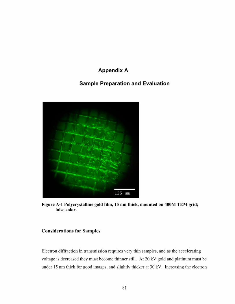
81
Appendix A
Sample Preparation and Evaluation
Figure A-1 Polycrystalline gold film, 15 nm thick, mounted on 400M TEM grid;
false color.
Considerations for Samples
Electron diffraction in transmission requires very thin samples, and as the accelerating
voltage is decreased they must become thinner still. At 20 kV gold and platinum must be
under 15 nm thick for good images, and slightly thicker at 30 kV. Increasing the electron
82
beam intensity will allow use of somewhat thicker samples, but this increases the pulse
duration and so is not useful for an ultrafast Diffractometer. Working samples in
polycrystalline platinum were from 9 to 12 nm thick.
At least one sample from each film should be examined with a TEM in order to
characterize nanoparticle size (see Figure A-2 and Figure A-3) and the expected
diffraction pattern. The nanoparticles from the sputtered gold films appear to be
polycrystalline under selected area diffraction. General film quality can be determined
with an optical microscope for the remaining samples. Note that for gold films this thin
will appear blue due to their optical transparency; the golden color dominates as they
approach 20 nm.
Making Samples
Preparation of polycrystalline samples is conveniently performed by sputtering onto a
rock salt flat at room temperature. The rock salt flats must be free of dust prior to
coating; this can be accomplished with a can of “dry air” and a brief rub with a Kim Wipe
or similar tissue, or a clean piece of flannel. The sputtered film can be saved for an
extended period in a dry box. It is floated off in a mixture of 20% methanol with 80%
deionized water. The methanol is used to reduce the surface tension of the water which
otherwise tends to break up the film during the floating off process. It also seems to
reduce breakage during the drying process. The floating-off process is best performed by
deliberately sliding the rock salt into the water, film side up, and allowing the surface
tension to dislodge the film. It only takes a second or so, and the substrate can be
withdrawn from the water. If the rock salt is allowed to dissolve in the water tiny
crystalline grains of rock salt will contaminate the sample; these will generate additional
diffraction spots and/or rings. These can be clearly seen with a TEM examination,
Figure A-2. For this reason the water-methanol mix should be discarded after each float-
off.
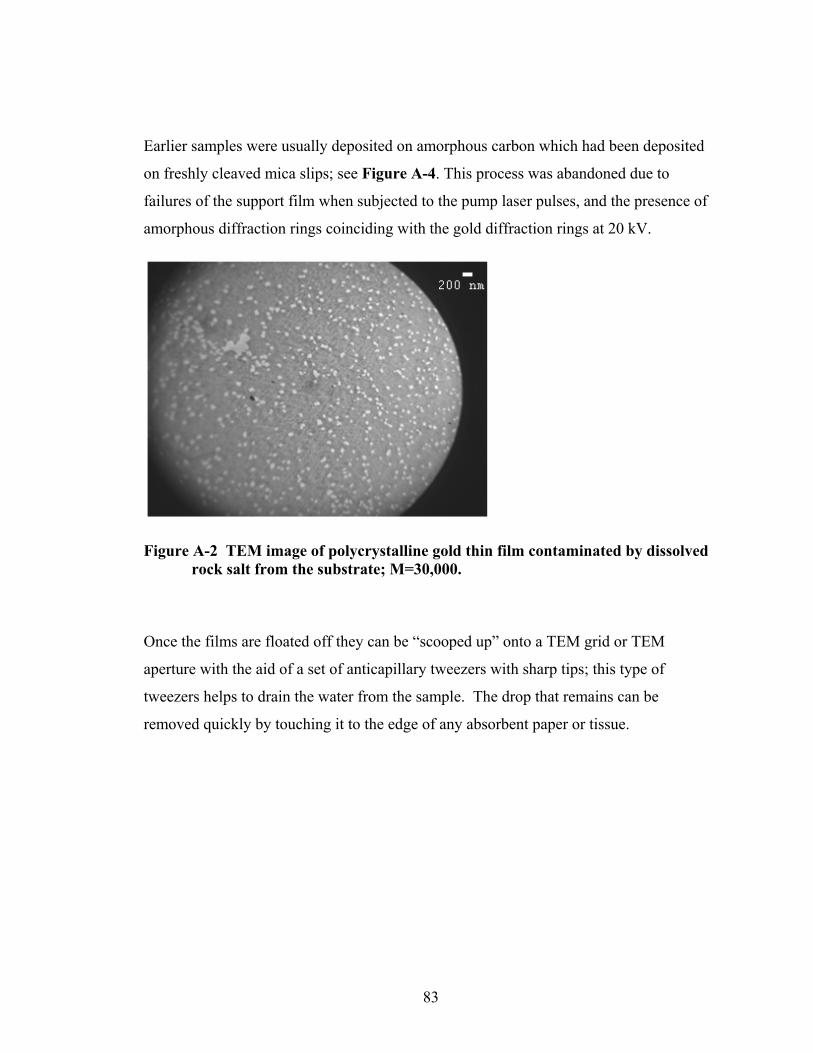
83
Earlier samples were usually deposited on amorphous carbon which had been deposited
on freshly cleaved mica slips; see Figure A-4. This process was abandoned due to
failures of the support film when subjected to the pump laser pulses, and the presence of
amorphous diffraction rings coinciding with the gold diffraction rings at 20 kV.
Figure A-2 TEM image of polycrystalline gold thin film contaminated by dissolved rock salt from the substrate; M=30,000.
Once the films are floated off they can be “scooped up” onto a TEM grid or TEM
aperture with the aid of a set of anticapillary tweezers with sharp tips; this type of
tweezers helps to drain the water from the sample. The drop that remains can be
removed quickly by touching it to the edge of any absorbent paper or tissue.
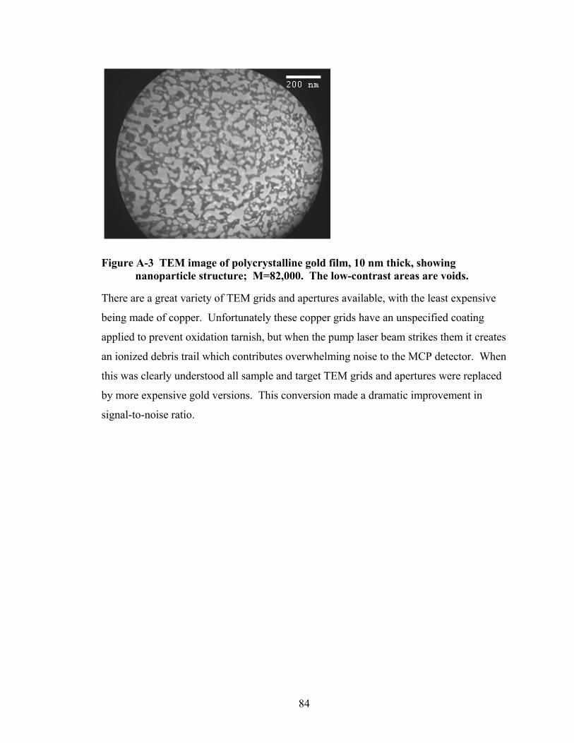
84
Figure A-3 TEM image of polycrystalline gold film, 10 nm thick, showing nanoparticle structure; M=82,000. The low-contrast areas are voids.
There are a great variety of TEM grids and apertures available, with the least expensive
being made of copper. Unfortunately these copper grids have an unspecified coating
applied to prevent oxidation tarnish, but when the pump laser beam strikes them it creates
an ionized debris trail which contributes overwhelming noise to the MCP detector. When
this was clearly understood all sample and target TEM grids and apertures were replaced
by more expensive gold versions. This conversion made a dramatic improvement in
signal-to-noise ratio.
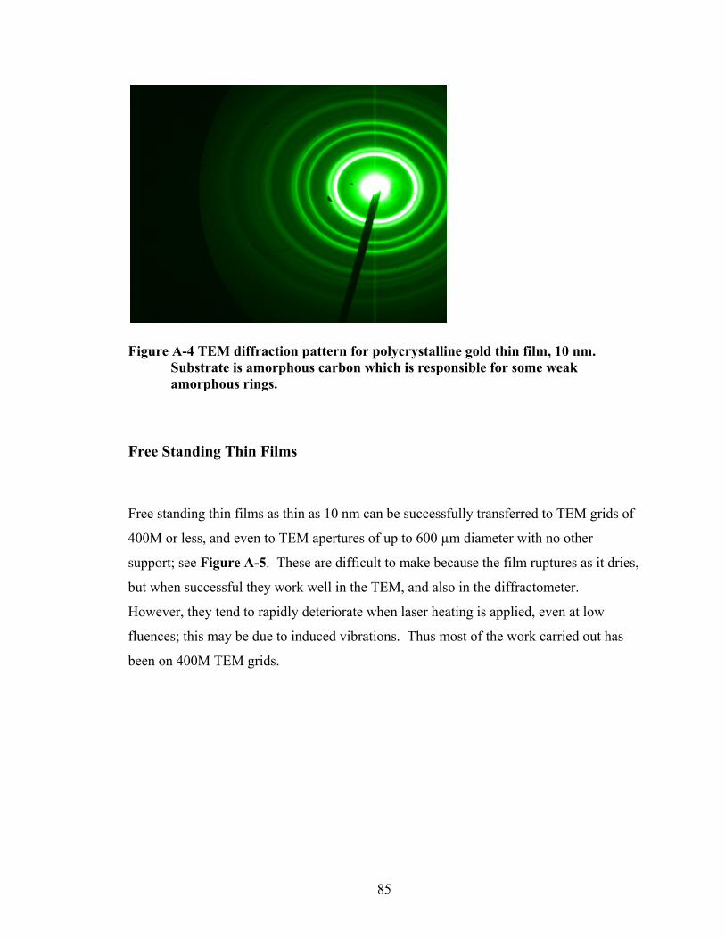
85
Figure A-4 TEM diffraction pattern for polycrystalline gold thin film, 10 nm. Substrate is amorphous carbon which is responsible for some weak amorphous rings.
Free Standing Thin Films
Free standing thin films as thin as 10 nm can be successfully transferred to TEM grids of
400M or less, and even to TEM apertures of up to 600 µm diameter with no other
support; see Figure A-5. These are difficult to make because the film ruptures as it dries,
but when successful they work well in the TEM, and also in the diffractometer.
However, they tend to rapidly deteriorate when laser heating is applied, even at low
fluences; this may be due to induced vibrations. Thus most of the work carried out has
been on 400M TEM grids.
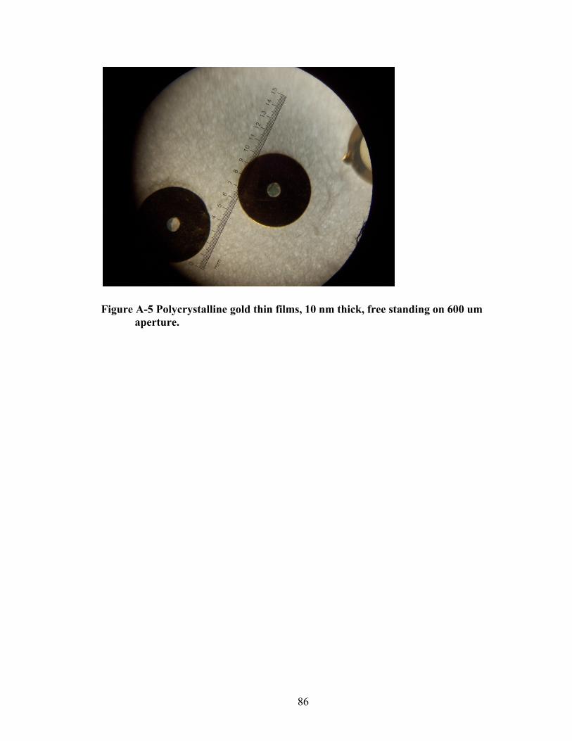
86
Figure A-5 Polycrystalline gold thin films, 10 nm thick, free standing on 600 um aperture.
87
Appendix B
Program Code
Program Code for Ring_Profile_Peak Finder import ij.*;
import ij.plugin.filter.PlugInFilter;
import ij.plugin.*;
import ij.process.ImageProcessor;
import ij.process.*;
import ij.gui.*;
import java.awt.*;
import java.io.*;
import ij.io.*;
import java.util.*;
import ij.text.*;
/* Portions based upon Radial_Profile.java, by Paul Baggethun, 2002/05/01 */
/* Adapted and extended by Peter Diehr, University of Michigan, 2002/09/23 */
/* Major rewrite by Peter Diehr, University of Michigan, 2008/11/22 - removed unused
code, added auto-find of best fit rings */
/* *******************************
Description: This ImageJ plugin produces a profile plot of normalized integrated
intensities around concentric circles as a function of distance from a point in the image.
The position of this point, or the radius of integration, can be modified in a dialog box.
The intensity at any given distance from the point represents the sum of the pixel values
around a circle.
This circle has the point as its center and the distance from the point as radius. The
integrated intensity
is divided by the number of pixels in the circle that is also part of the image, yielding
normalized comparablevalues. The profile x-axis can be plotted as pixel values or as
values according to the spatial calibration of input image.
88
Radial profiles are useful for measurement of x-ray powder diffraction patterns as well as
electron diffraction patterns.
******************************* */
public class Ring_Profile_Peak implements PlugInFilter
/*debug*/ // TextWindow tw = new TextWindow("Distances", "", 700, 200);
ImagePlus imp;
boolean canceled=false;
static boolean done=false;
int X, Y;
static int nC = 3; // #
of contrast pairs
static double X0;
static double Y0;
static double mR, mRI;
static double mLimitLo, mLimitHi;
static double mC1a;
static double mC2a;
static double mC1b;
static double mC2b;
static double mC1c;
static double mC2c;
static double mScan;
static boolean doNormalize = true;
static boolean doReportAll = false;
static boolean doMaxContrast = false;
int nBins=100;
double max, max_r, maxPeak, maxPeakValue;
double maxC, maxCPeakValue;
double maxX0, maxY0;
double mX0, mY0;
double [] cMax = new double [4];
double [] cMin = new double [4];
89
double [] cContrast = new double [4];
double [] mContrast = new double [4];
double [] mC1 = new double [4];
double [] mC2 = new double [4];
public int setup(String arg, ImagePlus imp)
this.imp = imp;
return DOES_ALL+NO_UNDO;
public void run(ImageProcessor ip)
// could not make static arrays work!
mC1[1] = mC1a;
mC2[1] = mC2a;
mC1[2] = mC1b;
mC2[2] = mC2b;
mC1[3] = mC1c;
mC2[3] = mC2c;
// Get circle ROI from stored points (center and radius)
if(!done) GetCircleROI();
IJ.makeOval((int)(X0-mR), (int)(Y0-mR), (int)(2*mR), (int)(2*mR));
doDialog();
// pass array information back to static holders
mC1a = mC1[1];
mC2a = mC2[1];
mC1b = mC1[2];
mC2b = mC2[2];
mC1c = mC1[3];
mC2c = mC2[3];
// Redraw, with altered radius
IJ.makeOval((int)(X0-mR), (int)(Y0-mR), (int)(2*mR), (int)(2*mR));
90
if (canceled) return;
doRadialDistribution(ip);
// Read Circle coordinates and radius for the circular ROI
public void GetCircleROI()
// Only do this the first time ... remember what was read in
done=true;
TextReader tr = new TextReader();
ImageProcessor ip = tr.open(".//RingProfilePeak.txt");
if (ip==null) return;
int width = ip.getWidth();
int height = ip.getHeight();
if (width <13 || height!=1)
IJ.showMessage("Ring_Profile_Peak", "Need Center (X,Y), Scan distance,
Radius(Inner, Outer), Level (Lo/Hi), 3 x Contrast(Begin/End) - all on one line to make the
circle: found ["+width +" "+ height+"]");
return;
X0 = ip.getPixelValue(0, 0);
Y0 = ip.getPixelValue(1, 0);
mScan = ip.getPixelValue(2, 0);
mRI = ip.getPixelValue(3, 0);
mR = ip.getPixelValue(4, 0);
mLimitLo=ip.getPixelValue(5, 0);
mLimitHi=ip.getPixelValue(6, 0);
mC1[1] = ip.getPixelValue(7, 0);
mC2[1] = ip.getPixelValue(8, 0);
mC1[2] = ip.getPixelValue(9, 0);
mC2[2] = ip.getPixelValue(10, 0);
mC1[3] = ip.getPixelValue(11, 0);
mC2[3] = ip.getPixelValue(12, 0);
91
private void doDialog()
canceled=false;
GenericDialog gd = new GenericDialog("Radial Distribution...",
IJ.getInstance());
gd.addNumericField("X center (pixels):",X0,1);
gd.addNumericField("Y center (pixels):", Y0,1);
gd.addNumericField("Distance to Scan:",mScan,0);
gd.addNumericField("Inner Radius (pixels):", mRI,0);
gd.addNumericField("Outer Radius (pixels):", mR,0);
gd.addNumericField("Minimum Level :", mLimitLo,0);
gd.addNumericField("Maximum Level :", mLimitHi,0);
gd.addNumericField("Begin Contrast 1 (pixel):", mC1[1],0);
gd.addNumericField("End Contrast 1 (pixel):", mC2[1],0);
gd.addNumericField("Begin Contrast 2 (pixel):", mC1[2],0);
gd.addNumericField("End Contrast 2 (pixel):", mC2[2],0);
gd.addNumericField("Begin Contrast 3 (pixel):", mC1[3],0);
gd.addNumericField("End Contrast 3 (pixel):", mC2[3],0);
gd.addCheckbox("Normalize?", doNormalize);
gd.addCheckbox("Report All?", doReportAll);
gd.addCheckbox("Optimize Contrast?", doMaxContrast);
gd.showDialog();
if (gd.wasCanceled())
canceled = true;
return;
X0=gd.getNextNumber();
Y0=gd.getNextNumber();
mScan=gd.getNextNumber();
mRI=gd.getNextNumber();
mR=gd.getNextNumber();
mLimitLo=gd.getNextNumber();
mLimitHi=gd.getNextNumber();
mC1[1]=gd.getNextNumber();
92
mC2[1]=gd.getNextNumber();
mC1[2]=gd.getNextNumber();
mC2[2]=gd.getNextNumber();
mC1[3]=gd.getNextNumber();
mC2[3]=gd.getNextNumber();
doNormalize = gd.getNextBoolean();
doReportAll = gd.getNextBoolean();
doMaxContrast = gd.getNextBoolean();
if(gd.invalidNumber())
IJ.showMessage("Error", "Invalid input Number");
canceled=true;
return;
// doRadialDistribution
private void doRadialDistribution(ImageProcessor ip)
nBins = (int) (3*mR/4);
int nSkipBins = (int)( (3*mR/4)*mRI/mR);
int thisBin;
int k;
double[][] mAccumulator = new double[2][nBins];
double[][] Accumulator = new double[2][nBins];
// Fetch data from the image only once
int[][] intPixels = (int [][])ip.getIntArray();
int nRows = ip.getHeight();
int nCols = ip.getWidth();
double R;
double D;
double xmin,xmax,ymin,ymax;
93
double mPixel;
// Initialize the "Peak" values ... we will scan the center (X0,Y0) thru a box
2*mScan on a side
maxX0 = X0;
maxY0 = Y0;
maxPeak = 0.0;
maxPeakValue = 0.0;
maxCPeakValue = 0.0;
double dSteps = (2*mScan)*(2*mScan);
double dStep = 0;
// Scan the region centered on (X0,Y0) as boxed by mScan
for (mX0 = X0 - mScan; mX0 <= X0 + mScan; mX0++)
for (mY0 = Y0 - mScan; mY0 <= Y0 + mScan; mY0++)
dStep++;
IJ.showProgress(dStep/dSteps);
for (k=0; k<nBins;k++) //
clear the accumulators
Accumulator[0][k] = 0;
Accumulator[1][k] = 0;
// Set the bounds for checking
xmin=mX0-mR;
xmax=mX0+mR;
ymin=mY0-mR;
ymax=mY0+mR;
if( xmin < 0) xmin = 0;
if( xmax > nCols - 1) xmax = nCols - 1;
if( ymin < 0) ymin = 0;
if( ymax > nRows - 1) ymax = nRows - 1;
/* debug */ // tw.append("Scanning ("+ mX0+","+mY0+")="+maxPeakValue+"
xmin="+xmin+" xmax="+xmax+" ymin="+ymin+" ymax="+ymax+" mR="+mR);
94
// Integrate the rings based on the trial center (mX0,mY0)
for (double i=xmin; i<xmax; i++)
for (double j=ymin; j<ymax; j++)
if( i < 0 || i > nCols - 1 || j < 0 || j > nRows - 1)
D = 0.0;
else
D=(double)intPixels[(int)i][(int)j];
if( (mLimitLo <=D) & (D <= mLimitHi) )
R = Math.sqrt((i-mX0)*(i-mX0)+(j-mY0)*(j-mY0));
thisBin = (int) Math.floor((R/mR)*(double)nBins);
if (thisBin==0) thisBin=1;
thisBin=thisBin-1;
if (thisBin>nBins-1) thisBin=nBins-1;
Accumulator[0][thisBin]++; // [0]=Good pixels for this ring
Accumulator[1][thisBin]+=D; // [1]=Integrated counts for this ring
max = maxPeakValue;
max_r =maxPeak;
maxC = maxCPeakValue;
for (int kk=1; kk<= nC; kk++)
cMax[kk] = ip.getMin();
cMin[kk] = ip.getMax();
/* debug */ // tw.append("LocalPeak ("+ mX0+","+mY0+")="+ IJ.d2s( max,1) + " @ "+
IJ.d2s( max_r,1) + " PrevMax="+ IJ.d2s( max,1));
int intNewPeak = 0;
// Find the peak, and the peak value for (mX0,mY0)
95
for (k=0; k<nBins;k++)
mPixel = mR*((double)(k+1)/nBins);
if (k < nSkipBins)
Accumulator[1][k] = 0;
else
Accumulator[1][k] = Accumulator[1][k] / Accumulator[0][k];
// Average counts around the ring
Accumulator[0][k] = mPixel;
// Record ring ID
if ( max < Accumulator[1][k] )
max = Accumulator[1][k];
// Value for this ring
max_r = Accumulator[0][k];
// Note the ring ID
/* debug */ // tw.append("LocalPeak ("+ mX0+","+mY0+")="+ IJ.d2s( max,1) + "
@ "+ IJ.d2s( max_r,1));
intNewPeak++;
// Find peaks and valleys for ring contrast calculations
for( int kk = 1; kk<= nC; kk++)
if( mC1[kk] <= mPixel && mPixel <= mC2[kk] )
if(cMax[kk] < Accumulator[1][k]) cMax[kk] = Accumulator[1][k];
if(cMin[kk] > Accumulator[1][k]) cMin[kk] = Accumulator[1][k];
Accumulator[1][nBins-1] = Accumulator[1][nBins-2];
// Fix anomaly on last bin
// Calculate total contrast for this center
maxC = 0.0;
for( int kk = 1; kk<= nC; kk++)
96
cContrast[kk] = 100.0 * (cMax[kk]-cMin[kk])/(cMax[kk]+cMin[kk]);
maxC += cContrast[kk];
maxC /= nC;
if( maxCPeakValue < maxC )
if( doMaxContrast ) intNewPeak = -1;
maxCPeakValue = maxC;
if( maxPeakValue < max )
if( !doMaxContrast ) intNewPeak = -1;
/* debug */ // IJ.showMessage("MaxPeak ("+ mX0+","+mY0+")="+ IJ.d2s(
maxPeakValue,1));
if( intNewPeak < 0 )
maxX0 = mX0;
maxY0 = mY0;
maxPeakValue = max;
maxPeak = max_r;
// Ring ID of the peak value
for (k=0; k<nBins;k++)
// Copy the entire distribution for later
mAccumulator[0][k] = Accumulator[0][k];
mAccumulator[1][k] = Accumulator[1][k];
for (int kk=1; kk<= nC; kk++)
mContrast[kk]= cContrast[kk];
if( doReportAll && intNewPeak < 0) doPlot(ip, mAccumulator); // Plot all
new peaks
97
// inner scan
// outer scan
// Update parameters for next run ...
X0 = maxX0;
Y0 = maxY0;
if( !doReportAll) doPlot(ip, mAccumulator);
// Omit plot if already done
// doPlot ... generate plot of diffraction results
private void doPlot(ImageProcessor ip, double[][] mAccumulator)
String sMsg;
String sContrast = " [";
PlotWindow pw;
double[][] plotAccumulator = new double[2][nBins];
for (int k=0; k<nBins;k++)
// Copy the entire distribution for later
plotAccumulator[0][k] = mAccumulator[0][k];
plotAccumulator[1][k] = mAccumulator[1][k];
// Report peak contrast for this center
for( int kk = 1; kk<= nC; kk++)
sContrast += IJ.d2s(mContrast[kk],1)+ " ";
sMsg = imp.getTitle();
if (sMsg.startsWith("Result of ") )
sMsg = sMsg.substring(10);
if(sMsg.endsWith(".fit"))
sMsg = sMsg.substring(1,sMsg.length()-4);
98
sMsg =sMsg + ": Peak@" + IJ.d2s( maxPeak,1) + " = " + IJ.d2s(
maxPeakValue,1) + sContrast + "%] C=(" + maxX0 + ", " + maxY0 + ") Limits=" +
(int)mLimitLo + "/" + (int)mLimitHi+ " Scan="+(int)mScan;
if (doNormalize )
for (int i=0; i<nBins;i++)
plotAccumulator[1][i] /= 0.01*maxPeakValue;
pw = new PlotWindow(sMsg, "Radius [pixels]", "Normalized Intensity",
plotAccumulator[0], plotAccumulator[1]);
else
pw = new PlotWindow(sMsg, "Radius [pixels]", "Intensity",
plotAccumulator[0], plotAccumulator[1]);
pw.draw();
99
Appendix C
Experimental Procedures
Running an Ultrafast Photo-Electron Diffractometer
Since changing samples requires that the vacuum chamber be opened, a full vacuum
chamber bake out at 375 °F is required to drive out the water vapor, followed by a cool
down to room temperature is required. Final vacuum should be with the ion pump alone,
and should be better than 5x10⁻⁹ Torr. This takes about two days, and should be followed
by an experimental determination of time-zero. The samples are previously prepared and
installed as described in Sample Preparation and Evaluation. Beam alignment is carried
out as previously described in Determination of Time-Zero.
The actual sample should have been previously evaluated optically and with a TEM. The
diffraction quality of the installed sample should be verified again when it is in the
diffractometer. This allows a determination of the camera integration time, and the
corresponding MCP amplification level. The sample should also be tested at the intended
laser fluence to ensure that it is robust enough to test.
When everything is ready, the automated experimental software can be initiated, and the
process runs by itself. Since things can go wrong, it needs to be monitored.
100
Determination of Electron Beam FWHM
The electron beam intensity distribution is essentially Gaussian when it reaches the MCP
detector as long as it is not too bright. This is easily determined by recording an image
and taking a line profile. As previously noted, pulses containing fewer electrons have
shorter pulse durations, so for most experiments weak beams are preferred, and thus
longer integration times. It is necessary to know the electron beam diameter so that the
laser heating beam is wide enough to ensure even heating across the portion of the
sample illuminated by the electron beam.
Beam divergence can be partially controlled by magnetic focusing, but the current system
eliminated the focusing coils in favor of a very short drift region; thus the beam diameter
as recorded by the MCP detector is irrelevant; the diameter at the sample plane is needed.
Two methods are available for measuring the electron beam at the sample plane. The
first is the use of a “knife edge”, the flat part at the bottom of the sample holder. A series
of beam images are recorded, the first with the beam fully in view, and the final with the
beam fully occluded, in 50 µm vertical translation steps. This spatial series is then
transformed into a series of intensities by integrating the intensity counts of each image.
The resulting curve is analyzed to find the 90-10 cutoff values for total intensity; the
interpolated distance between these limits is 1.07 times the 21
e beam diameter, multiply
by 0.59 to get the FWHM beam diameter. This gives consistent results with the direct
method, see Figure C-1. The direct method is to image the electron beam passing
through a clean 400M grid at the sample plane. The direct method works best with a
single microchannel plate; when two are used in chevron fashion the details are blurred.
Due to the very short drift distance beyond the anode pinhole exit the value obtained is
approximately that of the pinhole diameter.
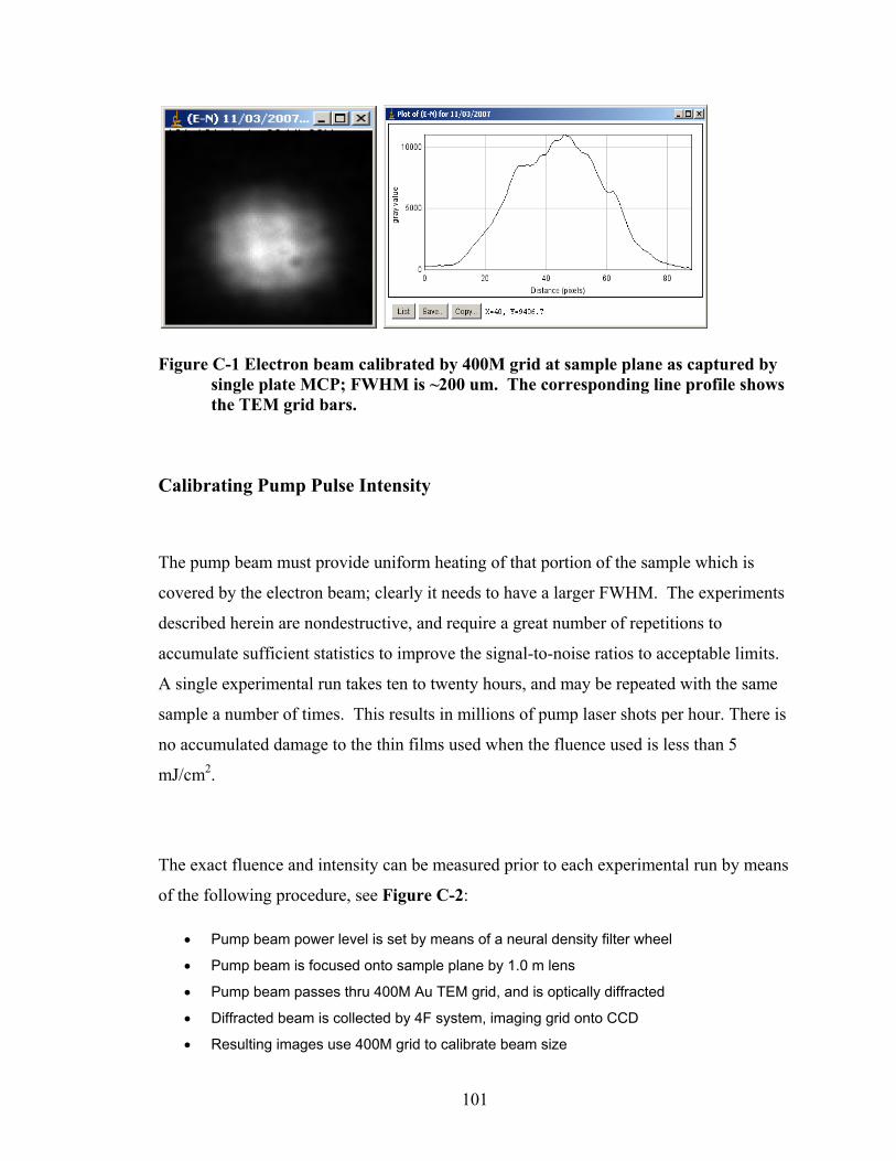
101
Figure C-1 Electron beam calibrated by 400M grid at sample plane as captured by single plate MCP; FWHM is ~200 um. The corresponding line profile shows the TEM grid bars.
Calibrating Pump Pulse Intensity
The pump beam must provide uniform heating of that portion of the sample which is
covered by the electron beam; clearly it needs to have a larger FWHM. The experiments
described herein are nondestructive, and require a great number of repetitions to
accumulate sufficient statistics to improve the signal-to-noise ratios to acceptable limits.
A single experimental run takes ten to twenty hours, and may be repeated with the same
sample a number of times. This results in millions of pump laser shots per hour. There is
no accumulated damage to the thin films used when the fluence used is less than 5
mJ/cm2.
The exact fluence and intensity can be measured prior to each experimental run by means
of the following procedure, see Figure C-2:
• Pump beam power level is set by means of a neural density filter wheel
• Pump beam is focused onto sample plane by 1.0 m lens
• Pump beam passes thru 400M Au TEM grid, and is optically diffracted
• Diffracted beam is collected by 4F system, imaging grid onto CCD
• Resulting images use 400M grid to calibrate beam size
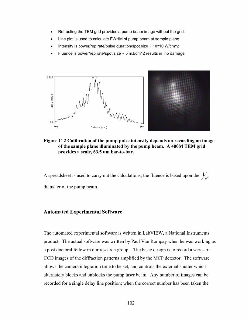
102
• Retracting the TEM grid provides a pump beam image without the grid.
• Line plot is used to calculate FWHM of pump beam at sample plane
• Intensity is power/rep rate/pulse duration/spot size ~ 10^10 W/cm^2
• Fluence is power/rep rate/spot size ~ 5 mJ/cm^2 results in no damage
Figure C-2 Calibration of the pump pulse intensity depends on recording an image of the sample plane illuminated by the pump beam. A 400M TEM grid provides a scale, 63.5 um bar-to-bar.
A spreadsheet is used to carry out the calculations; the fluence is based upon the 21
e
diameter of the pump beam.
Automated Experimental Software
The automated experimental software is written in LabVIEW, a National Instruments
product. The actual software was written by Paul Van Rompay when he was working as
a post doctoral fellow in our research group. The basic design is to record a series of
CCD images of the diffraction patterns amplified by the MCP detector. The software
allows the camera integration time to be set, and controls the external shutter which
alternately blocks and unblocks the pump laser beam. Any number of images can be
recorded for a single delay line position; when the correct number has been taken the

103
delay stage is advanced the specified number of steps. The steps have been calibrated to
the time delay, and convenient step sizes are 400 fs (10 steps) and 1 ps (25 steps). In
addition, the automated experimental software can check maximum and minimum
intensity levels on each image, and if out of range will save the image with an error tag,
and automatically take a replacement. This has been valuable when the electron gun has
a discharge, or when somebody turns on the room lights by mistake.
Prior to starting the run a set of background images are taken. Some have the electron
beam blocked; of these the most important are the ones labeled “N” for no beams active,
and the one labeled “L” for laser-beam only active. These will be directly subtracted
from the actual images during later processing.
As the run progresses each image is written out as a separate image file with timestamp
and specific run information coded in the file names. The shots with the pump beam
blocked are labeled “E” for electron beam only, while the unblocked shots are labeled
“B” for both beams active. Thus each heated diffraction pattern is accompanied by a
baseline comparison shot which was not heated, but which has the same history.
Post-Experimental Processing of Diffraction Image Data
The image files are processed by a series of Java plugins written by Peter Diehr, and
integrated with ImageJ57, an image processing an analysis program. One of the main
programs is used to determine the center of the diffraction pattern based upon contrast
between consecutive rings. Another uses the specified center and specified, and a mask
which is hand-crafted for each data run, and which masks out all features which are not
part of the diffraction pattern, such as the rotatable beam blocker, the edges of the MCP,
as well as camera and MCP defects. This program subtracts the “N” background from
each of the “E” shots, applies the image mask, and then performs a circular integration on
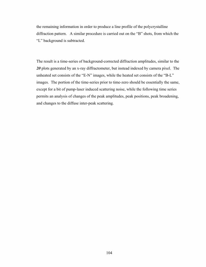
104
the remaining information in order to produce a line profile of the polycrystalline
diffraction pattern. A similar procedure is carried out on the “B” shots, from which the
“L” background is subtracted.
The result is a time-series of background-corrected diffraction amplitudes, similar to the
2θ plots generated by an x-ray diffractometer, but instead indexed by camera pixel. The
unheated set consists of the “E-N” images, while the heated set consists of the “B-L”
images. The portion of the time-series prior to time-zero should be essentially the same,
except for a bit of pump-laser induced scattering noise, while the following time series
permits an analysis of changes of the peak amplitudes, peak positions, peak broadening,
and changes to the diffuse inter-peak scattering.
105
Figure C-3 Signal-to-Noise ratio aligned with mean integrated diffraction amplitudes for 9 nm platinum film; data from April 16, 2008. S/N is better than 100:1 for most peaks.
Signal-To-Noise
When a series of measurements are taken of the same or similar items, the mean value is
best estimate of the value, and the standard deviation describes can be used as an
estimator of the noise. The signal-to-noise ration, S/N, is the mean divided by the
standard deviation. Because the Debye-Waller effect is only a few percent for integrated
intensity, a S/N ratio of over 100 is required. See Figure C-3 for recent results.

106
Equipment Manifest and Notes
Laser: Clark-MXR CPA 2001. 780 nm Ti:Sapphire output at 1000 Hz rep rate, 800 µJ
per pulse, or about 0.8 Watts into a power meter; beam is ~ 5 mm diameter, and well
collimated, with < 1% RMS noise in the pulse-to-pulse energy. Pulse duration is ~150 fs,
and when well maintained rarely drops even a single pulse.
Laser Shutter: Uniblitz, 50 ms duty cycle, controlled by computer program.
Camera: AndOr, 1024x1024 Peltier-cooled CCD. With f 55 mm Micro-Nikkor-P lens.
Images the air-side of the optical fiber coupler of the MCP detectors phosphor screen.
High Voltage: Glassman High Voltage, Inc. EL30N1.5, 30 kV Regulated DC Power
Low ripple < 0.03% at full load
Beam blocker: Hand made from oxygen free copper sheet, mounted to a manual rotary
feedthrough.
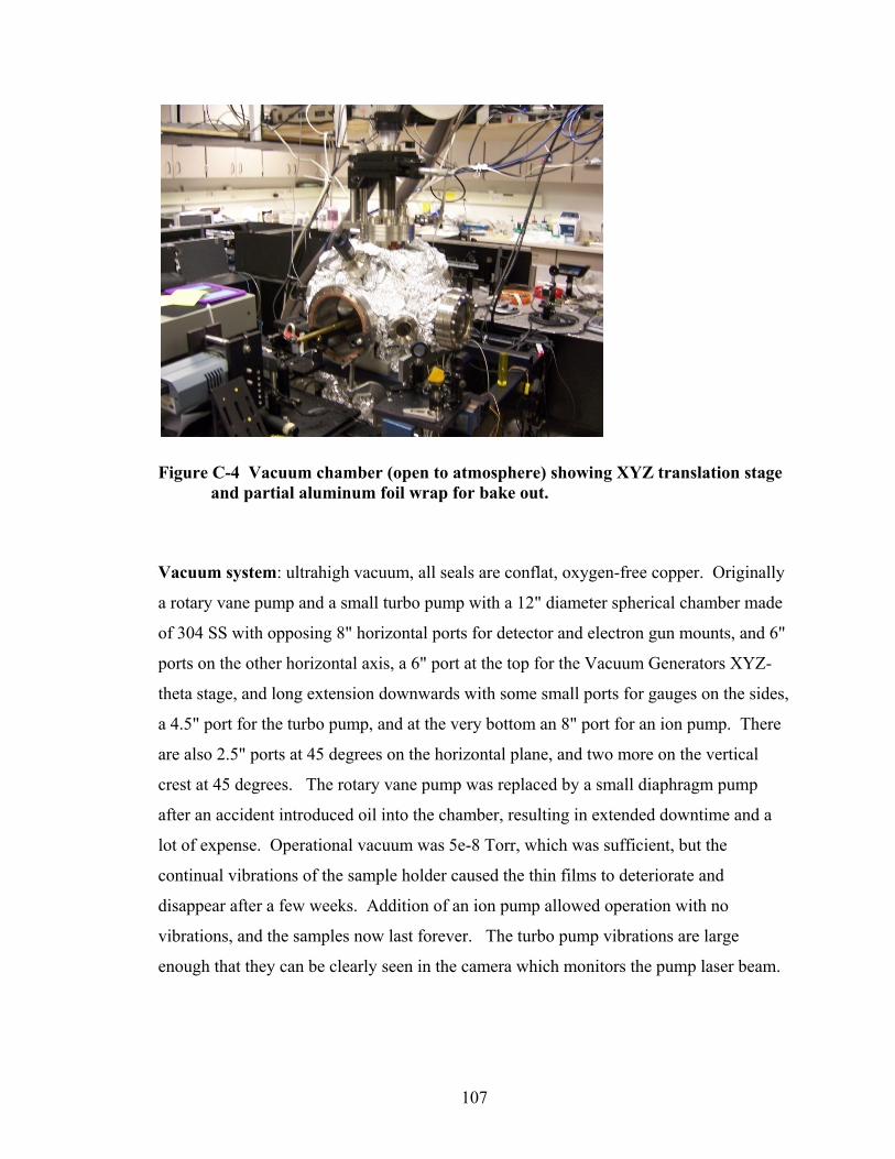
107
Figure C-4 Vacuum chamber (open to atmosphere) showing XYZ translation stage and partial aluminum foil wrap for bake out.
Vacuum system: ultrahigh vacuum, all seals are conflat, oxygen-free copper. Originally
a rotary vane pump and a small turbo pump with a 12" diameter spherical chamber made
of 304 SS with opposing 8" horizontal ports for detector and electron gun mounts, and 6"
ports on the other horizontal axis, a 6" port at the top for the Vacuum Generators XYZ-
theta stage, and long extension downwards with some small ports for gauges on the sides,
a 4.5" port for the turbo pump, and at the very bottom an 8" port for an ion pump. There
are also 2.5" ports at 45 degrees on the horizontal plane, and two more on the vertical
crest at 45 degrees. The rotary vane pump was replaced by a small diaphragm pump
after an accident introduced oil into the chamber, resulting in extended downtime and a
lot of expense. Operational vacuum was 5e-8 Torr, which was sufficient, but the
continual vibrations of the sample holder caused the thin films to deteriorate and
disappear after a few weeks. Addition of an ion pump allowed operation with no
vibrations, and the samples now last forever. The turbo pump vibrations are large
enough that they can be clearly seen in the camera which monitors the pump laser beam.
108
With the three pump system operation goes: diaphragm on, when it gets to e-0 Torr (2
minutes), turn on Turbo. When pressure gets to e-6 (10 minutes), cover with foil, and
start bake out ... start at 35% for 30 minutes, temperature goes to 90 F; then increase to
50% on rheostat, temperature is 170 F in 50 minutes; increase to 70%, temperature is 220
F in 50 minutes, increase to 80% and leave it overnight... by morning the temperature
will be ~375 F. The temperature should be reduced slowly, so turn the rheostat down to
50% - but don't remove aluminum foil yet! After 30 minutes the rheostat can be turned to
0% (off), and leave it overnight. In the morning it will be room temp, and the aluminum
foil can be removed, and the ion pump started. After about an hour, the gate valve is
closed, and if the ion pump holds the pressure at 5e-8, then turn off diaphragm pump and
the turbo pump.
Vacuum Generators translation stage: XYZ-theta. Precision stage, micrometers on
XY, one turn per mm on vertical, and rotation via manual operation with a locking knob.
Sample holder mounts to bottom end of rod, and hence can be adjusted by the stage.
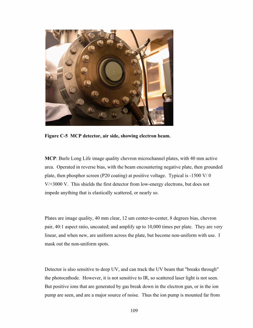
109
Figure C-5 MCP detector, air side, showing electron beam.
MCP: Burle Long Life image quality chevron microchannel plates, with 40 mm active
area. Operated in reverse bias, with the beam encountering negative plate, then grounded
plate, then phosphor screen (P20 coating) at positive voltage. Typical is -1500 V/ 0
V/+3000 V. This shields the first detector from low-energy electrons, but does not
impede anything that is elastically scattered, or nearly so.
Plates are image quality, 40 mm clear, 12 um center-to-center, 8 degrees bias, chevron
pair, 40:1 aspect ratio, uncoated; and amplify up to 10,000 times per plate. They are very
linear, and when new, are uniform across the plate, but become non-uniform with use. I
mask out the non-uniform spots.
Detector is also sensitive to deep UV, and can track the UV beam that "breaks through"
the photocathode. However, it is not sensitive to IR, so scattered laser light is not seen.
But positive ions that are generated by gas break down in the electron gun, or in the ion
pump are seen, and are a major source of noise. Thus the ion pump is mounted far from
110
the detector, and has a screen and a grounded deflector plate between them; and the noise
declines substantially as vacuum goes from e-7 to e-9 Torr. The noise picks up when the
electron gun has voltage applied, and increases rapidly as the voltage exceeds 20 kV
unless the sputtered photocathodes are subjected to the 48 hour UV treatment; this
appears to be due to particles (debris) escaping from the photocathode surface and edges,
and is much worse if the photocathode is recoated without first removing the previous
coating from the edges of the lens. This treatment involves ultrasonic cleaning in dilute
hydrochloric acid (commercial grade muriatic acid works fine), which must be performed
under a fume hood; 20 minutes is sufficient, followed by cold running water rinse for 10
minutes, then regular vacuum cleaning steps of acetone followed by methanol. Then the
newly coated, UV treated lens works fine at 30 kV as long as the vacuum pressure is e-9.
MCP plates need to be replaced regularly, as they lose amplification power with extended
use, especially in the over-used regions where the central e-beam strikes. In addition
exposure to UV leads to little round holes in the amplifiers, as does any hot ion trail that
accidentally strikes the plates when activated. Never operate the plates until the vacuum
is at least e-6 Torr.
MCP plates are hygroscopic, and tend to crack if not stored correctly due to the glass
rims. Rimless plates have very good shelf life, but still wear out with use, and have a new
problem if there is insufficient space between the plates ... trapped atmospheric gasses
remain even after a bake out, and the applied voltages ionize the trapped gases and these
ions are amplified in the hidden rim channels. These really light up, and a portion
escapes and causes random brightening and dimming of nearby areas and makes the data
unusable. The problem is obvious when the plates are pulled and examined, but appears
to be just random noise until the cause has been determined. Lesson: always provide
spacers between rimless plates, or just don't use them.
One problem with single plates is the “chicken wire” pattern that shows up in the images;
a chevron pair blurs the local detail, but eliminates the chicken wire artifact.

111
References
112
1 X. Liu, D. Du, and G. Mourou. IEEE J.Quantum Electron., vol. QE-33 (1997) 1706–1716. “Laser Ablation and Micromachining with Ultrashort Laser Pulses” 2 S.I. Anisimov, B.L. Kapeliovich, and T.L. Perel’man JETP 39 (1974) 375. “Electron emission from metal surfaces exposed to ultrashort laser pulses”; M.I. Kaganov, I.M. Lifshitz and L.V. Tanatarov, JETP 4 (1957) 173. “Relaxation between Electrons and the Crystalline Lattice”; S.I. Anisimov, A.M. Bonch-Bruevich, M.A. El'yashevich, Y.A. Imas, N.A. Pavlenko, and G.S. Romanov, Sov. Phys. Tech. Phys. 11 (1967) 945. “Effect of powerful light fluxes on metals”
3 P.P. Pronko, P.A. Van Rompay, R.K. Singh, F. Qian, D. Du, and X. Liu, Mat. Res. Soc. Symp. Proc. 397 (1996) 45. "Laser Induced Avalanche Ionization and Electron-Lattice Heating of Silicon with Intense Near IR Femtosecond Pulses"
4 P.P. Pronko, P.A. Van Rompay, C. Horvath, F. Loesel, T. Juhasz, X. Liu, and G. Mourou, Phys. Rev. B 58 (1998) 2387. "Avalanche ionization and dielectric breakdown in silicon with ultrafast laser pulses"
5 Leonid V. Zhigilei, Dmitriy S. Ivanov, Appl. Surf. Sci. 248 (2005) 433-439. “Channels of energy redistribution in short-pulse laser interactions with metal targets” 6 M. Bonn, D.N. Denzler, S. Funk, M. Wolf and S.-S. Wellershoff and J. Hohlfeld, Phys. Rev. B 61 (2000) 1101. "Ultrafast electron dynamics at metal surfaces: Competition between electron-phonon coupling and hot-electron transport"
7 T. Juhasz, H.E. Elsayed-Ali, G.O. Smith, C. Suárez, W.E. Bron, Phys. Rev. B 48 (1993) 15488. “Direct measurements of the transport of nonequilibrium electrons in gold films with different crystal structures”
8 H.E. Elsayed-Ali, T.B. Norris, M.A. Pessot, and G.A. Mourou, Phys. Rev. Lett. 58 (1987) 1212. "Time-Resolved Observation of Electron-Phonon Relaxation in Copper"
9 L. V. Zhigilei and A. M. Dongare, CMES 3 (2002) 539. "Multiscale Modeling of Laser Ablation: Applications to Nanotechnology"
10 G. Mourou and S. Williamson, Appl. Phys. Lett. 41 (1982) 44; S. Williamson and G. Mourou, Phys. Rev. Lett. 52 (1984) 2364. "Time-Resolved Laser-Induced Phase Transformation in Aluminum"
11 H.E. Elsayed-Ali, T.B. Norris, M.A. Pessot, and G.A. Mourou, Phys. Rev. Lett. 58 (1987) 1212. "Time-Resolved Observation of Electron-Phonon Relaxation in Copper"
12 X. Zeng, B.Lin, I. El-Kholy, and H.E. Elsayed-Ali, Surf. Sci. 439 (1999) 95.
113
13 J. C. Williamson, J. Cao, H. Ihee, H. Frey, A. H. Zewail, Nature, 386 (1997) 159. 14 B. L. Qian and H. E. Elsayed-Ali, J. Appl. Phys. 91, 462 (2002), “Electron pulse broadening due to space charge effects in a photoelectron gun for electron diffraction and streak camera systems” 15 B. J. Siwick, J. R. Dwyer, R. E. Jordan, and R. J. D. Miller, J. Appl. Phys. 92, 1643 (2002). “Ultrafast electron optics: Propagation dynamics of femtosecond electron packets” 16 Mikhail Monastyrskiy, Sergey Andreev, Dmitry Greenfield, Gennadiy Bryukhnevich , Victor Tarasov, and Mikhail Schelev. SPIE Proceedings, vol. 5580 (2005) 324-334. “Computer modeling of a sub-femtosecond photoelectron gun with time dependent electric field for TRED experiments”
17 G. Mourou and W. Knox. Appl. Phys. Lett. 36(8), 523-626 (1980). “A picosecond jitter streak camera”
18 Nicolas Stenon. De solido intra solidum naturaliter contento, Florence, 1669 according to http://reference.iucr.org/dictionary/Law_of_the_constancy_of_interfacial_angles 19 Steno’s law. (2009). In Encyclopædia Britannica. Retrieved January 14, 2009, from Encyclopædia Britannica Online: http://www.britannica.com/EBchecked/topic/565304/Stenos-law
20 Essai d'une théorie sur la structure des crystaux, appliquée à plusieurs genres de substances crystallisées [Texte imprimé] / par M. l'abbé Haüy,... Paris : Gogué et Née de La Rochelle, 1784 21 Image and caption from http://reference.iucr.org/dictionary/Law_of_rational_indices 22 C. Kittel. Introduction to Solid State Physics. John Wiley & Sons, 7th edition, 1996. 23 Image from http://itl.chem.ufl.edu/2041_f97/lectures/lec_h.html 24 W.H. Miller. A Treatise on Crystallography. Cambridge, 1839. Available at http://www.archive.org/details/treatiseoncrysta00millrich 25 William Hallowes Miller. (2009). In Encyclopædia Britannica. Retrieved January 22, 2009, from Encyclopædia Britannica Online: http://www.britannica.com/EBchecked/topic/382835/William-Hallowes-Miller
26 Image from http://en.wikipedia.org/wiki/File:Indices_miller_plan_definition.png 27 B.E. Warren. X-Ray Diffraction. Dover Publications. Corrected edition, 1990.
114
28 Image from http://upload.wikimedia.org/wikipedia/commons/3/3e/Parallelepiped_volume.svg 29 Weisstein, Eric W. "Cross Product." From MathWorld--A Wolfram Web Resource. http://mathworld.wolfram.com/CrossProduct.html 30 A history of this subject is available from the International Union of Crystallography as a reprint of P.P. Ewald, 50 Years of X-Ray Diffraction, http://www.iucr.org/publ/50yearsofxraydiffraction 31Image from http://reference.iucr.org/dictionary/Ewald_sphere 32 J.D. Jackson. Classical Electrodynamics. John Wiley & Sons, 3rd edition, 1998. 33 Albert Einstein. Relativity. Bonanza Books, New York, 1961. 34 David B. Williams and C. Barry Carter. Transmission Electron Microscopy. Plenum Press, New York and London, 1996. 35 A.L. Patterson, Phy. Rev. 56, 978 (1939). “The Scherrer Formula for X-Ray Particle Size Determination” 36 The European XFEL and FLASH: http://www.xfel.eu/en/in-comparison/ 37 M. Aeschlimann, E. Hull, J. Cao, C. A. Schmuttenmaer, L. G. Jahn, Y. Gao, H. E. Elsayed-Ali, D. A. Mantell, and M. R. Scheinfein, Rev. Sci. Instrum. 66(2), 1000 (1995). “A picosecond electron gun for surface analysis” 38 Bao-Liang Qian and Hani E. Elsayed-Ali. Phys. Rev. E. 65, 046502 (2002). "An Acceleration Element for Femtosecond Electron Pulse Compression," 39 Michael R. Armstrong, Bryan W. Reed, Ben R. Torralva, and Nigel D. Browning Appl. Phys. Lett. 90, 114101 (2007). “Prospects for electron imaging with ultrafast time resolution”
40 Peter Baum and Ahmed H. Zewail. Proc Natl Acad Sci USA 103(44) 16105–16110 (2006). "Breaking resolution limits in ultrafast electron diffraction and microscopy" 41 W.E. King, G.H. Campbell, A. Frank, B. Reed, J.F. Schmerge, B.J. Siwick, B.C. Stuart, and P.M. Weber, J. Appl. Phys. 97 111101 (2005). “Ultrafast electron microscopy in materials science, biology, and chemistry.” 42 Christoph T. Hebeisen, Ralph Ernstorfer, Maher Harb, Thibault Dartigalongue,
115
Robert E. Jordan, and R. J. Dwayne Miller. Optics Letters 31(23), 3517 (2006). “Femtosecond electron pulse characterization using laser ponderomotive scattering” 43 A. Dolocan , M. Hengsberger , H.J. Neff , M. Barry , C. Cirelli , T. Greber, and J. Osterwalder. Unpublished draft article dated September 29, 2004. ”Electron-Photon Pulse Correlator Based on Space-Charge Effects in a Metal Pinhole” 44 H. Park, Z. Hao, X. Wang, S. Nie, R. Clinite, and J. Cao. Rev. Sci. Instrum. 76, 083905 (2005) “Synchronization of femtosecond laser and electron pulses with subpicosecond precision” 45 H. Zewail, Annu. Rev. Phys. Chem. 57, 65–103 (2006). “4D ultrafast electron diffraction, crystallography, and microscopy.” 46 Steve Williamson, private communication. 47 L. Cavalieri, D. M. Fritz, S. H. Lee, P. H. Bucksbaum, D. A. Reis, J. Rudati, D. M. Mills, P. H. Fuoss, G. B. Stephenson, C. C. Kao, D. P. Siddons, D. P. Lowney, A. G. MacPhee, D. Weinstein, R. W. Falcone, R. Pahl, J. Als-Nielsen, C. Blome, S. Dursterer, R. Ischebeck, H. Schlarb, H. Schulte-Schrepping, Th. Tschentscher, J. Schneider, O. Hignette, F. Sette, k. Sokolowski- Tinten, H. N. Chapman, R. W. Lee, T. N. Hansen, O. Synnergren, J. Larsson, S. Techert, J. Sheppard, J. S. Wark, M. Bergh, C. Caleman, G. Huldt, D. van der Spoel, N. Timneanu, J. Hajdu, R. A. Akre, E. Bong, P. Emma, P. Krejcik, J. Arthur, S. Brennan, K. J. Gaffney, A. M. Lindenberg, K. Luening, and J. B. Hastings. Phys. Rev. Lett., 94:114801, (2005). "Clocking femtosecond x-rays." 48 First attempted in summer 2004; it failed because the TEM apertures used as targets were made from copper with an unknown coating. Laser ablation of the coating generated tremendous noise. Another experiment intervened while Gold TEM apertures were ordered, and when the attempt was next made in November 2004 it was successful on the first try. Subsequent efforts were toward understanding the mechanism, and improving the electron gun performance. 49 Method due to John Nees of CUOS, who uses a similar technique for an all-optical experiment. 50 Codrin is a much-appreciated colleague and a research scientist in the Roy Clarke group. 51 David A. Reis. Solid State Commun. 136 (2005) 564-565. “A film of picosecond vibrations of a film”, and H. Park, X. Wang, S. Nie, R. Clinite, J. Cao. Solid State Commun. 136 (2005). “Direct and real-time probing of both coherent and thermal lattice motions” 52 Conducted by my colleague, Vladimir Stoica. The setup is described in: Vladimir A. Stoica, Yu-Miin Sheu, David A. Reis, and Roy Clarke. Optics Express 16(4) 2322-2335 (2008). "Wideband detection of transient solid-state dynamics using ultrafast fiber lasers and asynchronous optical sampling" 53 Table 7.9; Michael De Podesta. Understanding the properties of matter, Second Edition. CRC Press, 2002.
116
54 N. Del Fatti, C. Voisin, D. Christofilos, F. Valle, C. Flytzanis. J. Phys. Chem. A 2000(104) 4321-4326. 55 “Taking Ultrafast Snapshots of Material Changes” https://www.llnl.gov/str/NovDec08/pdfs/11.08.1.pdf 56 K. S. Novoselov, S. V. Morozov, T. M. G. Mohinddin, L. A. Ponomarenko, D. C. Elias, R. Yang, I. I. Barbolina, P. Blake, T. J. Booth, D. Jiang, J. Giesbers, E. W. Hill, A. K. Geim. Physica Status Solidi (b) 255: 4106 – 4111 (2007). "Electronic properties of graphene" 57 ImageJ; available at http://rsb.info.nih.gov/nih-imageJ; developed by Wayne Rasband, National Institutes of Health, Bethesda, MD.
Related Documents


